WO2025142588A1 - Oscillator, production method for same, information processing device - Google Patents
Oscillator, production method for same, information processing deviceDownload PDFInfo
- Publication number
- WO2025142588A1 WO2025142588A1PCT/JP2024/044391JP2024044391WWO2025142588A1WO 2025142588 A1WO2025142588 A1WO 2025142588A1JP 2024044391 WJP2024044391 WJP 2024044391WWO 2025142588 A1WO2025142588 A1WO 2025142588A1
- Authority
- WO
- WIPO (PCT)
- Prior art keywords
- film
- electrode
- ferroelectric
- paraelectric
- forming
- Prior art date
- Legal status (The legal status is an assumption and is not a legal conclusion. Google has not performed a legal analysis and makes no representation as to the accuracy of the status listed.)
- Pending
Links
Images


Classifications
- H—ELECTRICITY
- H10—SEMICONDUCTOR DEVICES; ELECTRIC SOLID-STATE DEVICES NOT OTHERWISE PROVIDED FOR
- H10D—INORGANIC ELECTRIC SEMICONDUCTOR DEVICES
- H10D30/00—Field-effect transistors [FET]
- H10D30/01—Manufacture or treatment
- H—ELECTRICITY
- H10—SEMICONDUCTOR DEVICES; ELECTRIC SOLID-STATE DEVICES NOT OTHERWISE PROVIDED FOR
- H10D—INORGANIC ELECTRIC SEMICONDUCTOR DEVICES
- H10D30/00—Field-effect transistors [FET]
- H10D30/60—Insulated-gate field-effect transistors [IGFET]
- H10D30/67—Thin-film transistors [TFT]
- H—ELECTRICITY
- H10—SEMICONDUCTOR DEVICES; ELECTRIC SOLID-STATE DEVICES NOT OTHERWISE PROVIDED FOR
- H10D—INORGANIC ELECTRIC SEMICONDUCTOR DEVICES
- H10D84/00—Integrated devices formed in or on semiconductor substrates that comprise only semiconducting layers, e.g. on Si wafers or on GaAs-on-Si wafers
- H10D84/80—Integrated devices formed in or on semiconductor substrates that comprise only semiconducting layers, e.g. on Si wafers or on GaAs-on-Si wafers characterised by the integration of at least one component covered by groups H10D12/00 or H10D30/00, e.g. integration of IGFETs
- H10D84/82—Integrated devices formed in or on semiconductor substrates that comprise only semiconducting layers, e.g. on Si wafers or on GaAs-on-Si wafers characterised by the integration of at least one component covered by groups H10D12/00 or H10D30/00, e.g. integration of IGFETs of only field-effect components
- H10D84/83—Integrated devices formed in or on semiconductor substrates that comprise only semiconducting layers, e.g. on Si wafers or on GaAs-on-Si wafers characterised by the integration of at least one component covered by groups H10D12/00 or H10D30/00, e.g. integration of IGFETs of only field-effect components of only insulated-gate FETs [IGFET]
- H—ELECTRICITY
- H10—SEMICONDUCTOR DEVICES; ELECTRIC SOLID-STATE DEVICES NOT OTHERWISE PROVIDED FOR
- H10D—INORGANIC ELECTRIC SEMICONDUCTOR DEVICES
- H10D86/00—Integrated devices formed in or on insulating or conducting substrates, e.g. formed in silicon-on-insulator [SOI] substrates or on stainless steel or glass substrates
- H10D86/40—Integrated devices formed in or on insulating or conducting substrates, e.g. formed in silicon-on-insulator [SOI] substrates or on stainless steel or glass substrates characterised by multiple TFTs
- H—ELECTRICITY
- H10—SEMICONDUCTOR DEVICES; ELECTRIC SOLID-STATE DEVICES NOT OTHERWISE PROVIDED FOR
- H10D—INORGANIC ELECTRIC SEMICONDUCTOR DEVICES
- H10D89/00—Aspects of integrated devices not covered by groups H10D84/00 - H10D88/00
Definitions
- This disclosurerelates to an oscillator using a ferroelectric transistor, a manufacturing method thereof, and an information processing device.
- Non-Patent Document 1a device that uses ferroelectric transistors is disclosed in Non-Patent Document 1.
- Non-Patent Document 1discloses that AI processing is performed using an oscillator that uses a ferroelectric transistor.
- the disclosed oscillatorincludes a ferroelectric FET (Field Effect Transistor), a discharge FET, and a capacitor.
- ferroelectric FETField Effect Transistor
- discharge FETdischarge field Effect Transistor
- capacitorcapacitor
- the purpose of this disclosureis to provide an oscillator using a ferroelectric transistor that is small in size and inexpensive to manufacture, as well as a manufacturing method and information processing device for the oscillator.
- An oscillatorincludes a substrate, a first field effect transistor formed on the substrate and having a ferroelectric as a gate insulating film, a second field effect transistor formed on the substrate and having a paraelectric as a gate insulating film, and a capacitor formed on the substrate.
- the first field effect transistorincludes a first gate electrode, a ferroelectric film formed to cover the first gate electrode, a first semiconductor film forming a first channel layer formed on the ferroelectric film, and a first source electrode and a first drain electrode formed on the first semiconductor film.
- the second field effect transistorincludes a second semiconductor film forming a second channel layer formed on the ferroelectric film, a second source electrode and a second drain electrode formed on the second semiconductor film, a paraelectric film formed to cover the second source electrode, the second drain electrode, and the second semiconductor film, and a second gate electrode formed on the paraelectric film.
- the paraelectric filmis further formed to cover the first source electrode, the first drain electrode, and the first semiconductor film.
- the capacitorincludes a first electrode electrically connected to the first source electrode, and a second electrode facing the first electrode via at least one of a ferroelectric film and a paraelectric film and electrically connected to the second source electrode.
- the first source electrodeis electrically connected to the second drain electrode.
- a method for manufacturing an oscillator according to one embodiment of the present disclosureis a method for manufacturing an oscillator including a substrate, a first field effect transistor formed on the substrate and having a ferroelectric as a gate insulating film, a second field effect transistor formed on the substrate and having a paraelectric as a gate insulating film, and a capacitor formed on the substrate.
- the second semiconductor filmis made of the same material as the first semiconductor film.
Landscapes
- Semiconductor Memories (AREA)
Abstract
Description
Translated fromJapanese本開示は、強誘電体トランジスタを用いた発振器、およびその製造方法、情報処理装置に関する。This disclosure relates to an oscillator using a ferroelectric transistor, a manufacturing method thereof, and an information processing device.
近年、エッジAI(Artificial Intelligence)と呼ばれる、AI処理を行う機能を直接搭載したデバイス(情報処理装置)が注目されている。特に、エッジAIでは、省電力性、高速性を実現するためにAI処理をすべてソフトウェアで処理するのではなく、一部ハードウェアで処理することが提案されている。AI処理をハードウェアで処理することについて、強誘電体トランジスタを用いるデバイスが非特許文献1に開示されている。In recent years, devices (information processing devices) that are directly equipped with AI processing functions, known as edge AI (Artificial Intelligence), have been attracting attention. In particular, in edge AI, in order to achieve low power consumption and high speed, it has been proposed to process some of the AI processing by hardware, rather than processing it entirely by software. Regarding processing AI processing by hardware, a device that uses ferroelectric transistors is disclosed in Non-Patent
非特許文献1には、強誘電体トランジスタを用いた発振器を使ってAI処理を行うことが開示されている。開示されている発振器は、強誘電体FET(Field Effect Transistor)、放電FET、およびキャパシタを含む。しかし、当該発振器を製造する場合、基板上に、強誘電体FET、放電FET、およびキャパシタをそれぞれ別々に形成する必要があり、サイズが大きく、製造コストが高くなる虞があった。Non-Patent
そこで、本開示の目的は、サイズが小さく、製造コストが安い強誘電体トランジスタを用いた発振器、およびその製造方法、情報処理装置を提供する。The purpose of this disclosure is to provide an oscillator using a ferroelectric transistor that is small in size and inexpensive to manufacture, as well as a manufacturing method and information processing device for the oscillator.
本開示の一形態に係る発振器は、基板と、基板上に形成され、強誘電体をゲート絶縁膜とする第1電界効果トランジスタと、基板上に形成され、常誘電体をゲート絶縁膜とする第2電界効果トランジスタと、基板上に形成されるキャパシタと、を備える。第1電界効果トランジスタは、第1ゲート電極と、第1ゲート電極を覆って形成される強誘電体膜と、強誘電体膜上に形成される第1チャネル層を形成する第1半導体膜と、第1半導体膜上に形成される第1ソース電極および第1ドレイン電極と、を含む。第2電界効果トランジスタは、強誘電体膜上に形成される第2チャネル層を形成する第2半導体膜と、第2半導体膜上に形成される第2ソース電極および第2ドレイン電極と、第2ソース電極、第2ドレイン電極、および第2半導体膜を覆って形成される常誘電体膜と、常誘電体膜上に形成される第2ゲート電極と、を含む。常誘電体膜は、第1ソース電極、第1ドレイン電極、および第1半導体膜をさらに覆って形成される。キャパシタは、第1ソース電極と電気的に接続される第1電極と、強誘電体膜および常誘電体膜のうち少なくとも一方の膜を介して第1電極と対向し、第2ソース電極と電気的に接続される第2電極と、を含む。第1ソース電極は、第2ドレイン電極と電気的に接続される。An oscillator according to one embodiment of the present disclosure includes a substrate, a first field effect transistor formed on the substrate and having a ferroelectric as a gate insulating film, a second field effect transistor formed on the substrate and having a paraelectric as a gate insulating film, and a capacitor formed on the substrate. The first field effect transistor includes a first gate electrode, a ferroelectric film formed to cover the first gate electrode, a first semiconductor film forming a first channel layer formed on the ferroelectric film, and a first source electrode and a first drain electrode formed on the first semiconductor film. The second field effect transistor includes a second semiconductor film forming a second channel layer formed on the ferroelectric film, a second source electrode and a second drain electrode formed on the second semiconductor film, a paraelectric film formed to cover the second source electrode, the second drain electrode, and the second semiconductor film, and a second gate electrode formed on the paraelectric film. The paraelectric film is further formed to cover the first source electrode, the first drain electrode, and the first semiconductor film. The capacitor includes a first electrode electrically connected to the first source electrode, and a second electrode facing the first electrode via at least one of a ferroelectric film and a paraelectric film and electrically connected to the second source electrode. The first source electrode is electrically connected to the second drain electrode.
本開示の一形態に係る発振器を製造する方法は、基板と、基板上に形成され、強誘電体をゲート絶縁膜とする第1電界効果トランジスタと、基板上に形成され、常誘電体をゲート絶縁膜とする第2電界効果トランジスタと、基板上に形成されるキャパシタと、を備える発振器を製造する方法である。発振器を製造する方法は、基板上に第1電界効果トランジスタの第1ゲート電極およびキャパシタの第1電極を形成するステップと、第1ゲート電極および第1電極を覆う強誘電体膜を形成するステップと、強誘電体膜に第1電極へ達するビアを形成するステップと、第1電界効果トランジスタの第1チャネル層を形成する第1半導体膜を強誘電体膜上に形成するステップと、第2電界効果トランジスタの第2チャネル層を形成する第2半導体膜を強誘電体膜上に形成するステップと、を含む。さらに、発振器を製造する方法は、第1半導体膜上に第1電界効果トランジスタの第1ソース電極および第1ドレイン電極を、第2半導体膜上に第2電界効果トランジスタの第2ソース電極および第2ドレイン電極を、強誘電体膜上にキャパシタの第2電極を、ビアに第1電極と第1ソース電極とを電気的に接続するビア導体をそれぞれ形成するステップと、第1ソース電極、第1ドレイン電極、第2ソース電極、第2ドレイン電極、第2電極、第1半導体膜、および第2半導体膜を覆う常誘電体膜を形成するステップと、常誘電体膜上に第2電界効果トランジスタの第2ゲート電極を形成するステップと、を含む。A method for manufacturing an oscillator according to one embodiment of the present disclosure is a method for manufacturing an oscillator including a substrate, a first field effect transistor formed on the substrate and having a ferroelectric as a gate insulating film, a second field effect transistor formed on the substrate and having a paraelectric as a gate insulating film, and a capacitor formed on the substrate. The method for manufacturing the oscillator includes the steps of forming a first gate electrode of the first field effect transistor and a first electrode of the capacitor on the substrate, forming a ferroelectric film covering the first gate electrode and the first electrode, forming a via in the ferroelectric film reaching the first electrode, forming a first semiconductor film on the ferroelectric film that forms a first channel layer of the first field effect transistor, and forming a second semiconductor film on the ferroelectric film that forms a second channel layer of the second field effect transistor. Furthermore, the method for manufacturing the oscillator includes the steps of forming a first source electrode and a first drain electrode of a first field effect transistor on a first semiconductor film, a second source electrode and a second drain electrode of a second field effect transistor on a second semiconductor film, a second electrode of a capacitor on a ferroelectric film, and a via conductor that electrically connects the first electrode and the first source electrode to a via, forming a paraelectric film that covers the first source electrode, the first drain electrode, the second source electrode, the second drain electrode, the second electrode, the first semiconductor film, and the second semiconductor film, and forming a second gate electrode of the second field effect transistor on the paraelectric film.
本開示によれば、第1電界効果トランジスタが、第1ゲート電極を覆って形成される強誘電体膜を含み、第2電界効果トランジスタが、強誘電体膜上に形成される第2半導体膜を覆って形成される常誘電体膜と、常誘電体膜上に形成される第2ゲート電極と、を含むので、サイズが小さく、製造コストが安い強誘電体トランジスタを用いた発振器を構成することができる。According to the present disclosure, the first field effect transistor includes a ferroelectric film formed to cover the first gate electrode, and the second field effect transistor includes a paraelectric film formed to cover the second semiconductor film formed on the ferroelectric film, and a second gate electrode formed on the paraelectric film, so that an oscillator can be constructed using ferroelectric transistors that are small in size and inexpensive to manufacture.
以下に、本開示の実施の形態に係る発振器について図面を参照して詳しく説明する。なお、図中同一符号は同一または相当部分を示す。Below, an oscillator according to an embodiment of the present disclosure will be described in detail with reference to the drawings. Note that the same reference numerals in the drawings indicate the same or corresponding parts.
(実施の形態)
実施の形態では、たとえば、エッジAIの中間層に用いられる発振器について図面を参照しながら説明する。当該発振器は、エッジAIの中間層に用いられる場合に限られず、他の用途に用いてもよい。図1は、実施の形態に係る発振器100の構成を説明するための断面図である。図2は、実施の形態に係る発振器100の回路図である。(Embodiment)
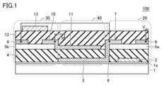
In the embodiment, for example, an oscillator used in an intermediate layer of an edge AI will be described with reference to the drawings. The oscillator is not limited to being used in an intermediate layer of an edge AI, and may be used for other purposes. Fig. 1 is a cross-sectional view for explaining the configuration of an
図1に示す発振器100は、半導体基板1上に形成した強誘電体FET20(第1電界効果トランジスタ)と、常誘電体FET30(第2電界効果トランジスタ)と、キャパシタ40とを含んでいる。図1では、強誘電体FET20と、常誘電体FET30との間に、キャパシタ40が設けられているが、強誘電体FET20、常誘電体FET30、およびキャパシタ40の半導体基板1上でのレイアウトはこれに限られない。なお、半導体基板1は、強誘電体FET20、常誘電体FET30、およびキャパシタ40が設けられる面にパッシベーション膜1aを形成している。The
強誘電体FET20は、ゲート電極2(第1ゲート電極)、強誘電体膜4(ゲート絶縁膜)、チャネル形成膜5a(第1半導体膜)、ドレイン電極6(第1ドレイン電極)、およびソース電極7(第1ソース電極)を有している。図1に示す強誘電体FET20では、半導体基板1上にゲート電極2を形成し、ゲート電極2に重ねて強誘電体膜4およびチャネル形成膜5aを順に形成し、それらの上にドレイン電極6、およびソース電極7をそれぞれ形成している。つまり、強誘電体FET20は、ボトムゲート型の電界効果トランジスタである。The
より具体的に、強誘電体FET20は、MFSFET(Metal Ferroelectric Semiconductor FET)である。半導体基板1には、たとえば、シリコン(Si)を用い、その上に酸化アルミニウム(Al2O3)のパッシベーション膜1aが形成される。ゲート電極2は、パッシベーション膜1a上に白金(Pt)を用いて所定のパターンで形成される。ゲート絶縁膜には、たとえば、酸化ハフニウムのHfの一部がCeに置換されている強誘電体膜4(Ce:HfO2)を用い、チャネル形成膜5aには、たとえば、Zrを添加したITO膜(Zr:ITO)を用いる。強誘電体FET20は、チャネル形成膜5aの上に、白金(Pt)でドレイン電極6、およびソース電極7を所定のパターンで形成する。More specifically, the
常誘電体FET30は、チャネル形成膜5b(第2半導体膜)、ドレイン電極9(第2ドレイン電極)、およびソース電極10(第2ソース電極)、絶縁膜12(ゲート絶縁膜)、ゲート電極13(第2ゲート電極)を有している。図1に示す常誘電体FET30では、強誘電体膜4上にチャネル形成膜5bを形成し、その上にドレイン電極9、およびソース電極10をそれぞれ形成して、さらに絶縁膜12およびゲート電極13を順に形成している。つまり、常誘電体FET30は、トップゲート型の電界効果トランジスタである。なお、絶縁膜12は、常誘電体膜である。The
より具体的に、常誘電体FET30は、MISFET(Metal Insulator Semiconductor FET)である。常誘電体FET30は、強誘電体膜4上に形成される。強誘電体膜4上には、たとえば、Zrを添加したITO膜(Zr:ITO)を用いたチャネル形成膜5bが形成される。チャネル形成膜5bは、チャネル形成膜5aと同じ材料で構成され、チャネル形成膜5aと共通の1つの膜として形成される。しかし、チャネル形成膜5bは、チャネル形成膜5aと異なる材料で構成してもよく、チャネル形成膜5aと異なる膜として形成してもよい。また、図1に示す発振器100では、チャネル形成膜5aとチャネル形成膜5bとが分かれているが、チャネル形成膜5aとチャネル形成膜5bとが繋がっていてもよい。More specifically, the
常誘電体FET30は、チャネル形成膜5bの上に、白金(Pt)でドレイン電極9、およびソース電極10を所定のパターンで形成する。ゲート絶縁膜には、たとえば、酸化アルミニウム(Al2O3)の絶縁膜12を用いる。ゲート電極13は、絶縁膜12上に白金(Pt)を用いて所定のパターンで形成される。絶縁膜12(常誘電体膜)は、ドレイン電極9、ソース電極10、およびチャネル形成膜5bを覆うだけでなく、ドレイン電極6、ソース電極7、およびチャネル形成膜5aをさらに覆って形成される。そのため、絶縁膜12は、常誘電体FET30においてゲート絶縁膜として機能するが、強誘電体FET20においてチャネル形成膜5aを保護するパッシベーション膜として機能する。チャネル形成膜5a上に絶縁膜12を形成するので、絶縁膜12を形成する際にチャネル形成膜5a対してダメージを与えないように、プラズマを発生させない成膜法で形成されることが好ましい。In the
キャパシタ40は、ソース電極7と電気的に接続される電極3(第1電極)と、強誘電体膜4を介して電極3と対向し、ソース電極10と電気的に接続される電極11(第2電極)と、を含む。キャパシタ40は、電極3と電極11とで強誘電体膜4を挟む構成であるが、強誘電体膜4および絶縁膜12(常誘電体膜)のうち少なくとも一方の膜を挟む構成でもよい。なお、強誘電体膜4は絶縁膜12より比誘電率が高いのでキャパシタ40の面積を小さくすることができる。具体的に、電極3と電極11と間に強誘電体膜であるハフニウム系強誘電体(比誘電率:約30)を用いた場合、電極3と電極11と間に常誘電体膜である二酸化ケイ素(比誘電率:約4)を用いた場合に比べ、同じ膜厚であればキャパシタ40の面積を約1/7.5倍に縮小することができる。The
電極3は、パッシベーション膜1a上に白金(Pt)を用いて所定のパターンで形成される。電極3は、ゲート電極2と同じプロセスで形成されてもよい。また、電極3は、ソース電極7と電気的に接続するため強誘電体膜4にビア導体8を設けている。電極11は、強誘電体膜4上に白金(Pt)を用いて所定のパターンで形成される。電極11は、ドレイン電極6,9およびソース電極7,10と同じプロセスで形成されてもよい。また、電極11は、一部または全部がチャネル形成膜5b上に形成されてもよい。The
発振器100は、図2に示すように強誘電体FET20のドレイン電極に電源電圧VDDが供給され、強誘電体FET20のソース電極が常誘電体FET30のドレイン電極と電気的に接続されている。そのため、図1に示すドレイン電極6に電源電圧VDDが供給され、ソース電極7とドレイン電極9とが電気的に接続されている。2, in the
また、発振器100は、図2に示すように強誘電体FET20のソース電極がキャパシタ40の一方の電極と電気的に接続され、他方の電極はGNDを介して常誘電体FET30のソース電極と電気的に接続されている。そのため、図1に示すソース電極7にキャパシタ40の電極3が電気的に接続され、ソース電極10およびキャパシタ40の電極11がGNDと電気的に接続されている。In addition, in the
次に、発振器100の動作について説明する。図3は、実施の形態に係る発振器100の動作を説明するための図である。図3(a)は、発振器100の電流IDと発振器100の出力電圧VSとの関係を示すグラフで、縦軸を電流、横軸を電圧としている。図3(b)は、時間tに対する発振器100の出力電圧VSの変化を示すグラフで、縦軸を電圧、横軸を時間としている。Next, the operation of the
図3に、電源電圧VDD、常誘電体FET30のゲート電圧VGM、キャパシタ40の容量Cとし、強誘電体FET20のゲート電圧VGFをVGF1,VGF2(VGF1<VGF2)と変化させた場合の波形(模式図)を示す。FIG. 3 shows waveforms (schematic diagrams) when the power supply voltage is VDD , the gate voltage VGM of the
発振器100は、図3(a)に示すように電流IDと出力電圧VSとの関係がヒステリシス曲線となる。当該ヒステリシス曲線は、ゲート電圧VGFが高くなるに従い、出力電圧VSの高い側にシフトする。具体的に、ゲート電圧VGFがVGF1の場合、電流IDは、強誘電体FET20のドレイン電極-ソース電極を通ってキャパシタ40に流れ、キャパシタ40を充電することで出力電圧VSが上昇する。電流IDは、出力電圧VSが上昇することで流れにくくなるので、図3(a)に示す点Aから出力電圧VSの上昇に従って低下する。さらに、出力電圧VSがVt1(点B)になると、強誘電体FET20のドレイン電極-ソース電極に電流IDが流れなくなる(点C)。電流IDが流れなくなるとキャパシタ40が放電することになり出力電圧VSがVt2まで低下する(点D)。出力電圧VSがVt2に低下すると電流IDが流れ始め、点Eになるとキャパシタ40の充電が始まり出力電圧VSが上昇する。In the
このように、ゲート電圧VGFがVGF1の場合、電流IDと出力電圧VSとの関係が点Bから点Eに至るヒステリシス曲線となることで、発振器100は、図3(b)に示すように、出力電圧VSがVt1となる状態(点B,点C)と出力電圧VSがVt2となる状態(点D,点E)とを繰り返す。つまり、発振器100は、一定の間隔で出力電圧VSがVt1とVt2との間を繰り返す信号を出力する。In this way, when the gate voltageVGF isVGF1 , the relationship between the currentID and the output voltageVs forms a hysteresis curve extending from point B to point E, so that the
一方、ゲート電圧VGFをVGF2とした場合、強誘電体FET20のドレイン電極-ソース電極に電流IDが流れなくなる前(点P)に、常誘電体FET30のドレイン電極-ソース電極に流れる電流IMが支配的となる。そのため、発振器100は、ゲート電圧VGFをVGF1とした場合、発振することなく、出力電圧VSがVPの一定電圧となる信号を出力する。On the other hand, when the gate voltageVGF is set toVGF2 , the current IM flowing between the drain electrode and source electrode of the
次に、発振器100の製造方法について図を用いて説明する。図4~図6は、実施の形態に係る発振器100の製造方法を説明するための断面図である。まず、図4(a)では、準備したシリコン(Si)の半導体基板1の一方の面に、白金(Pt)のゲート電極2および電極3を形成する。なお、図4~図6では、図中左側がキャパシタ40を形成する領域で、図中右側が強誘電体FET20および常誘電体FET30を形成する領域である。また、半導体基板1上にゲート電極2および電極3を直接形成しているが、半導体基板1上にパッシベーション膜1aを設けて、パッシベーション膜1a上にゲート電極2および電極3を形成してもよい。Next, the manufacturing method of the
具体的に、ゲート電極2および電極3を形成する場合、まず、半導体基板1の一方の面にフォトリソグラフィ技術を用いて所定のパターンのフォトレジストを形成する。その後、たとえば、高周波(RF)スパッタリングで白金(Pt)を半導体基板1の一方の面に成膜し、リフトオフによってフォトレジストを取り去ることでゲート電極2および電極3が形成される。Specifically, when forming the
図4(b)では、ゲート電極2および電極3を形成した半導体基板1の面に重ねて強誘電体膜4を形成する。ゲート電極2上の強誘電体膜4は、強誘電体FET20のゲート絶縁膜を構成し、電極3上の強誘電体膜4は、キャパシタ40の絶縁体を構成する。具体的に、強誘電体膜4は、たとえば化学溶液堆積法(CSD:Chemical Solution Deposition)を用いゲート電極2および電極3を覆う半導体基板1の面にCe:HfO2を成膜する。4B, a
図4(c)では、キャパシタ40を形成する領域において、電極3上の強誘電体膜4にビアホール4aを形成する。具体的に、強誘電体膜4にフォトリソグラフィ技術を用いて所定のパターンのフォトレジストを形成し、ドライエッチングで強誘電体膜4を取り除いてビアホール4aを形成する。In FIG. 4(c), in the region where the
次に、図5(a)では、強誘電体FET20および常誘電体FET30を形成する領域において、強誘電体膜4に重ねてのチャネル形成膜5(図1に示すチャネル形成膜5a,5bを含む)を形成する。具体的に、チャネル形成膜5は、スパッタリングを用い、強誘電体膜4に重ねてITO膜を成膜する。なお、図5(a)では、強誘電体FET20および常誘電体FET30を形成する領域のみにチャネル形成膜5を成膜しているが、キャパシタ40を形成する領域にチャネル形成膜5を成膜してもよい。Next, in FIG. 5(a), a channel formation film 5 (including the
図5(b)では、強誘電体FET20および常誘電体FET30を形成する領域において、チャネル形成膜5の上に、白金(Pt)のドレイン電極6,9およびソース電極7,10を形成する。また、キャパシタ40を形成する領域において、強誘電体膜4の上に白金(Pt)の電極7a,11、およびビアホール4aに白金(Pt)のビア導体8を形成する。電極7aは、ビア導体8および電極3と電気的に接続され、ビア導体8および電極3とソース電極7およびドレイン電極9とを電気的に接続する部分である。In FIG. 5(b), in the region where the
具体的に、ドレイン電極6,9およびソース電極7,10を形成する場合、まず、チャネル形成膜5の上にフォトリソグラフィ技術を用いて所定のパターンのフォトレジストを形成する。その後、たとえば、高周波(RF)スパッタリングで白金(Pt)を成膜し、リフトオフによってフォトレジストを取り去ることでドレイン電極6,9およびソース電極7,10が形成される。なお、図5(b)では、ソース電極7とドレイン電極9とが電気的に接続されているので、1つの電極と図示されている。電極7a,11、およびビアホール4aを形成する場合、まず、強誘電体膜4の上にフォトリソグラフィ技術を用いて所定のパターンのフォトレジストを形成する。その後、たとえば、高周波(RF)スパッタリングで白金(Pt)を成膜し、リフトオフによってフォトレジストを取り去ることで電極7a,11、およびビアホール4aが形成される。Specifically, when forming the
図6(a)では、強誘電体FET20および常誘電体FET30を形成する領域において、ドレイン電極6,9およびソース電極7,10を形成したチャネル形成膜5に重ねて絶縁膜12を形成する。また、キャパシタ40を形成する領域において、電極7a,11を形成した強誘電体膜4に重ねて絶縁膜12を形成する。具体的に、絶縁膜12は、たとえば、プラズマを発生させない成膜法であるECR(Electron Cyclotron Resonance)スパッタリングでAl2O3膜を成膜する。プラズマを発生させない成膜法でチャネル形成膜5に重ねて絶縁膜12を形成することで、チャネル形成膜5に対してダメージを与えることなく絶縁膜12を成膜できる。6A, in the region where the
図6(b)では、ドレイン電極9およびソース電極10を覆う絶縁膜12の上に、白金(Pt)のゲート電極13を形成する。具体的に、ゲート電極13を形成する場合、まず、絶縁膜12の上にフォトリソグラフィ技術を用いて所定のパターンのフォトレジストを形成する。その後、たとえば、高周波(RF)スパッタリングで白金(Pt)を成膜し、リフトオフによってフォトレジストを取り去ることでゲート電極13が形成される。In FIG. 6(b), a platinum (Pt)
図4~図6で説明したように、発振器100は、強誘電体FET20、常誘電体FET30、およびキャパシタ40の3つの素子を同じ半導体基板1上に、共通の材料を利用して同時に形成することができる構成である。特に、絶縁膜12は、ボトムゲート型の強誘電体FET20のチャネル部分を保護するパシベーション膜として機能すると共に、トップゲート型の常誘電体FET30のゲート絶縁膜としても機能する構成となっている。さらに、強誘電体膜4は、強誘電体FET20のゲート絶縁膜として機能すると共に、キャパシタ40の絶縁体としても機能する構成となっている。そのため、発振器100は、強誘電体FET20が、ゲート電極2を覆って形成される強誘電体膜4を含み、常誘電体FET30が、強誘電体膜4上に形成されるチャネル形成膜5bを覆って形成される絶縁膜12と、絶縁膜12上に形成されるゲート電極13と、を含むことになり、サイズを小さくすること、製造コストを安くすることができる。As described in FIG. 4 to FIG. 6, the
発振器100は、強誘電体FET20の強誘電体膜4に酸化ハフニウムのHfの一部がCeに置換されている膜(Ce:HfO2)を用い、チャネル形成膜5(5a)にZrを添加したITO膜(Zr:ITO)を用いる一例を説明した。このように金属酸化物の強誘電体膜4と金属酸化物のチャネル形成膜5(5a)とを組み合わせることにより、強誘電体膜4とチャネル形成膜5(5a)との界面において高い界面品質を得ることができる。The
なお、強誘電体膜4に用いる材料は、酸化ハフニウムのHfの一部がCeに置換されている膜(Ce:HfO2)であると説明したが、一例でありこれに限定されない。たとえば、強誘電体膜4は、ハフニウム酸化物系強誘電体、もしくはBIT(Bi4Ti3O12)からなる膜、または、それらの膜を含む積層膜であればよい。さらに詳しく、強誘電体膜4に用いる材料は、ハフニウム酸化物系強誘電体(Ce:HfO2,Hf0.5Zr0.5O2,La:HfO2,Si:HfO2,Gd:HfO2等)、PZT(Pb(ZrX,Ti1-X)O3)、BLT(Bi4-XLaXTi3O12)、SBT(SrBi2Ta2O9)、BFO(BiFeO3)、もしくはBIT(Bi4Ti3O12)からなる膜、またはそれらの膜を含む積層膜であればよい。The material used for the
チャネル形成膜5(5a,5b)に用いる材料は、Zrを添加したITO膜(Zr:ITO)であると説明したが、一例でありこれに限定されない。たとえば、チャネル形成膜5(5a,5b)に用いる材料は、インジウム錫酸化物(ITO)、LSCO(LaXSr1-XCuO4)、酸化錫(SnOX)、酸化亜鉛(ZnOX)、酸化インジウム(InOX)、インジウムガリウム酸化亜鉛(InGaZnO)もしくはインジウム錫酸化亜鉛(InSnZnO)からなる膜、またはそれらの膜を含む積層膜であればよい。The material used for the channel formation film 5 (5a, 5b) has been described as an ITO film with added Zr (Zr:ITO), but this is an example and is not limited to this. For example, the material used for the channel formation film 5 (5a, 5b) may be a film made of indium tin oxide (ITO), LSCO (Lax Sr1-x CuO4 ), tin oxide (SnOx ), zinc oxide (ZnOx ), indium oxide (InOx ), indium gallium zinc oxide (InGaZnO) or indium tin zinc oxide (InSnZnO), or a laminated film including these films.
絶縁膜12に用いる材料は、酸化アルミニウム(Al2O3)であると説明したが、一例でありこれに限定されない。たとえば、絶縁膜12に用いる材料は、酸化ケイ素(SiO2)、窒化ケイ素(SiN)、酸化ハフニウム(HfO2)、もしくはParylene C(ポリマーコーティング膜)からなる膜、またはそれらの膜を含む積層膜であればよい。The material used for the insulating
ゲート電極2,13、ドレイン電極6,9、ソース電極7,10、および電極3,7a,11に用いる材料は、白金(Pt)であると説明したが、一例でありこれに限定されない。たとえば、ゲート電極2,13、ドレイン電極6,9、ソース電極7,10、および電極3,7a,11に用いる材料は、イリジウム(Ir)、窒化チタン(TiN)、窒化タンタル(TaN)、窒化タングステン(WN)、イリジウム酸化物(IrOX)もしくはランタンニッケル酸化物(LaNiOX)からなる膜、またはそれらの膜を含む積層膜であればよい。Although the material used for the
前述の発振器100を用いてAI処理を行う機能を直接搭載したデバイス200(情報処理装置)について説明する。図7は、実施の形態に係る発振器100を用いたデバイス200の概略図である。デバイス200は、クラウドにアクセスして、AI処理を実行するのではなく、独立してAI処理を実行する。デバイス200では、独立してAI処理を実行するために、デバイス内にニューラルネットワークを有している。The following describes a device 200 (information processing device) that is directly equipped with a function for performing AI processing using the
ニューラルネットワークは、データ(情報)の入力を受け付ける入力層201、データを処理する中間層202、データを出力する出力層203を含む。デバイス200では、省電力性、高速性を実現するためにAI処理をすべてソフトウェアで処理するのではなく、中間層202をハードウェアで構成して処理している。なお、図示していないが、デバイス200には、ニューラルネットワークのソフトウェアの部分を処理する演算装置を有している。演算装置は、CPU、MPU、TPU、またはGPUなどのプロセッサ、ASICまたはFPGAなどのハードワイヤード回路などで構成される。The neural network includes an input layer 201 that accepts input of data (information), an
具体的に、中間層202は、ハードウェアで構成され、各ノード210に図1で示した発振器100を有している。各ノード210には、発振器100だけでなく、たとえば前段に記憶手段を設けてもよい。Specifically, the
ニューラルネットワークおいて、データは入力層201に入力されて、所定の重みが掛けられる。入力層201から出力された値は中間層202に入力されて、さらに所定の重みが掛けられる。中間層202から出力された値は、出力層203を介してAI処理されたデータ(たとえば、推定結果)が出力される。前述したように中間層202は、発振器100を有するハードウェアで構成されるため、各ノード210での重みは固定である。In a neural network, data is input to the input layer 201 and is multiplied by a predetermined weight. The value output from the input layer 201 is input to the
しかし、入力層201および出力層203は、ソフトウェアで構成されているので、たとえば中間層202から出力層203へ至る部分の重みを更新することができる。ニューラルネットワークでは、中間層202から出力層203へ至る部分の重みを更新することで、AI処理の演算精度を確保しつつ、ソフトウェアによる計算負荷を大幅に軽減して、省電力性、高速性を実現している。However, since the input layer 201 and
たとえば、デバイス200を用いてデータから推定結果を求める場合、ニューラルネットワークの訓練に用いる学習用データを用意する。ニューラルネットワークは、たとえば、教師あり学習によって訓練されている。図7では、正解データを含む学習用データを用意し、ニューラルネットワークは、学習用データを演算した推定結果と正解データとの一致度合いに基づき、中間層202から出力層203へ至る部分の重みを調整することで、自身が推定した推定結果と正解データとの一致度合いが基準値を超えるように訓練を行う。For example, when using
(態様)
(1) 本開示に係る発振器は、
基板と、
基板上に形成され、強誘電体をゲート絶縁膜とする第1電界効果トランジスタと、
基板上に形成され、常誘電体をゲート絶縁膜とする第2電界効果トランジスタと、
基板上に形成されるキャパシタと、を備え、
第1電界効果トランジスタは、
第1ゲート電極と、
第1ゲート電極を覆って形成される強誘電体膜と、
強誘電体膜上に形成される第1チャネル層を形成する第1半導体膜と、
第1半導体膜上に形成される第1ソース電極および第1ドレイン電極と、を含み、
第2電界効果トランジスタは、
強誘電体膜上に形成される第2チャネル層を形成する第2半導体膜と、
第2半導体膜上に形成される第2ソース電極および第2ドレイン電極と、
第2ソース電極、第2ドレイン電極、および第2半導体膜を覆って形成される常誘電体膜と、
常誘電体膜上に形成される第2ゲート電極と、を含み、
常誘電体膜は、第1ソース電極、第1ドレイン電極、および第1半導体膜をさらに覆って形成され、
キャパシタは、
第1ソース電極と電気的に接続される第1電極と、
強誘電体膜および常誘電体膜のうち少なくとも一方の膜を介して第1電極と対向し、第2ソース電極と電気的に接続される第2電極と、を含み、
第1ソース電極は、第2ドレイン電極と電気的に接続される。(Aspects)
(1) An oscillator according to the present disclosure includes:
A substrate;
a first field effect transistor formed on a substrate and having a ferroelectric film as a gate insulating film;
a second field effect transistor formed on the substrate and having a paraelectric gate insulating film;
a capacitor formed on the substrate;
The first field effect transistor is
A first gate electrode;
a ferroelectric film formed covering the first gate electrode;
a first semiconductor film forming a first channel layer formed on the ferroelectric film;
a first source electrode and a first drain electrode formed on the first semiconductor film;
The second field effect transistor is
a second semiconductor film forming a second channel layer formed on the ferroelectric film;
a second source electrode and a second drain electrode formed on the second semiconductor film;
a paraelectric film formed covering the second source electrode, the second drain electrode, and the second semiconductor film;
a second gate electrode formed on the paraelectric film;
a paraelectric film is formed further covering the first source electrode, the first drain electrode, and the first semiconductor film;
The capacitor is
a first electrode electrically connected to the first source electrode;
a second electrode facing the first electrode via at least one of a ferroelectric film and a paraelectric film and electrically connected to the second source electrode;
The first source electrode is electrically connected to the second drain electrode.
(2)(1)に記載の発振器において、
第2半導体膜は、第1半導体膜と同じ材料で構成されている。(2) In the oscillator according to (1),
The second semiconductor film is made of the same material as the first semiconductor film.
(3)(2)に記載の発振器において、
第2半導体膜は、第1半導体膜と共通の1つの膜として形成されている。(3) In the oscillator according to (2),
The second semiconductor film is formed as one common film with the first semiconductor film.
(4)(1)~(3)のいずれか1項に記載の発振器において、
キャパシタは、強誘電体膜を介して第1電極と第2電極とが対向している。(4) In the oscillator according to any one of (1) to (3),
The capacitor has a first electrode and a second electrode opposed to each other with a ferroelectric film interposed therebetween.
(5)(1)~(4)のいずれか1項に記載の発振器において、
強誘電体膜は、ハフニウム酸化物系強誘電体、もしくはBIT(Bi4Ti3O12)からなる膜、または、それらの膜を含む積層膜である。(5) In the oscillator according to any one of (1) to (4),
The ferroelectric film is a film made of a hafnium oxide-based ferroelectric material or BIT (Bi4 Ti3 O12 ), or a laminated film including these films.
(6)本開示に係る発振器を製造する方法は、
基板と、基板上に形成され、強誘電体をゲート絶縁膜とする第1電界効果トランジスタと、基板上に形成され、常誘電体をゲート絶縁膜とする第2電界効果トランジスタと、基板上に形成されるキャパシタと、を備える発振器を製造する方法であって、
基板上に第1電界効果トランジスタの第1ゲート電極およびキャパシタの第1電極を形成するステップと、
第1ゲート電極および第1電極を覆う強誘電体膜を形成するステップと、
強誘電体膜に第1電極へ達するビアを形成するステップと、
第1電界効果トランジスタの第1チャネル層を形成する第1半導体膜を強誘電体膜上に形成するステップと、
第2電界効果トランジスタの第2チャネル層を形成する第2半導体膜を強誘電体膜上に形成するステップと、
第1半導体膜上に第1電界効果トランジスタの第1ソース電極および第1ドレイン電極を、第2半導体膜上に第2電界効果トランジスタの第2ソース電極および第2ドレイン電極を、強誘電体膜上にキャパシタの第2電極を、ビアに第1電極と第1ソース電極とを電気的に接続するビア導体をそれぞれ形成するステップと、
第1ソース電極、第1ドレイン電極、第2ソース電極、第2ドレイン電極、第2電極、第1半導体膜、および第2半導体膜を覆う常誘電体膜を形成するステップと、
常誘電体膜上に第2電界効果トランジスタの第2ゲート電極を形成するステップと、を含む。(6) A method for manufacturing an oscillator according to the present disclosure includes:
A method for manufacturing an oscillator including a substrate, a first field effect transistor formed on the substrate and having a ferroelectric as a gate insulating film, a second field effect transistor formed on the substrate and having a paraelectric as a gate insulating film, and a capacitor formed on the substrate, the method comprising the steps of:
forming a first gate electrode of a first field effect transistor and a first electrode of a capacitor on a substrate;
forming a first gate electrode and a ferroelectric film covering the first electrode;
forming a via in the ferroelectric film reaching the first electrode;
forming a first semiconductor film on the ferroelectric film, the first semiconductor film forming a first channel layer of a first field effect transistor;
forming a second semiconductor film on the ferroelectric film, the second semiconductor film forming a second channel layer of a second field effect transistor;
forming a first source electrode and a first drain electrode of a first field effect transistor on the first semiconductor film, a second source electrode and a second drain electrode of a second field effect transistor on the second semiconductor film, a second electrode of a capacitor on the ferroelectric film, and a via conductor electrically connecting the first electrode and the first source electrode to the via;
forming a paraelectric film covering the first source electrode, the first drain electrode, the second source electrode, the second drain electrode, the second electrode, the first semiconductor film, and the second semiconductor film;
forming a second gate electrode of a second field effect transistor on the paraelectric film.
(7)(6)に記載の発振器を製造する方法において、
第1半導体膜および第2半導体膜は、同じ成膜プロセスで形成される。(7) A method for manufacturing an oscillator according to (6), comprising the steps of:
The first semiconductor film and the second semiconductor film are formed in the same film formation process.
(8)(6)または(7)に記載の発振器を製造する方法において、
常誘電体膜を形成するステップは、プラズマを発生させない成膜法で常誘電体膜を形成する。(8) A method for manufacturing an oscillator according to (6) or (7),
The step of forming the paraelectric film forms the paraelectric film by a film formation method that does not generate plasma.
(9)本開示に係る情報処理装置は、
ニューラルネットワークを用いて情報を処理する情報処理装置であって、
ニューラルネットワークは、入力層と、中間層と、出力層と、を含み、
中間層は、ハードウェアで構成され、各ノードに(1)~(5)のいずれか1項に記載の発振器を有する。(9) An information processing device according to the present disclosure includes:
An information processing device that processes information using a neural network,
The neural network includes an input layer, an intermediate layer, and an output layer.
The intermediate layer is configured with hardware, and each node has an oscillator described in any one of (1) to (5).
今回開示された実施の形態はすべての点で例示であって制限的なものではないと考えられるべきである。本開示の範囲は、上記した説明ではなく、請求の範囲によって示され、請求の範囲と均等の意味および範囲内でのすべての変更が含まれることが意図される。The embodiments disclosed herein should be considered in all respects as illustrative and not restrictive. The scope of the present disclosure is indicated by the claims, not the above description, and is intended to include all modifications within the meaning and scope of the claims.
1 半導体基板、1a パッシベーション膜、2,13 ゲート電極、3,7a,11 電極、4 強誘電体膜、4a ビアホール、5,5a,5b チャネル形成膜、6,9 ドレイン電極、7,10 ソース電極、8 ビア導体、12 絶縁膜、20 強誘電体FET、30 常誘電体FET、40 キャパシタ、100 発振器。1 semiconductor substrate, 1a passivation film, 2, 13 gate electrode, 3, 7a, 11 electrode, 4 ferroelectric film, 4a via hole, 5, 5a, 5b channel formation film, 6, 9 drain electrode, 7, 10 source electrode, 8 via conductor, 12 insulating film, 20 ferroelectric FET, 30 paraelectric FET, 40 capacitor, 100 oscillator.
Claims (9)
Translated fromJapanese前記基板上に形成され、強誘電体をゲート絶縁膜とする第1電界効果トランジスタと、
前記基板上に形成され、常誘電体をゲート絶縁膜とする第2電界効果トランジスタと、
前記基板上に形成されるキャパシタと、を備え、
前記第1電界効果トランジスタは、
第1ゲート電極と、
前記第1ゲート電極を覆って形成される強誘電体膜と、
前記強誘電体膜上に形成される第1チャネル層を形成する第1半導体膜と、
前記第1半導体膜上に形成される第1ソース電極および第1ドレイン電極と、を含み、
前記第2電界効果トランジスタは、
前記強誘電体膜上に形成される第2チャネル層を形成する第2半導体膜と、
前記第2半導体膜上に形成される第2ソース電極および第2ドレイン電極と、
前記第2ソース電極、前記第2ドレイン電極、および前記第2半導体膜を覆って形成される常誘電体膜と、
前記常誘電体膜上に形成される第2ゲート電極と、を含み、
前記常誘電体膜は、前記第1ソース電極、前記第1ドレイン電極、および前記第1半導体膜をさらに覆って形成され、
前記キャパシタは、
前記第1ソース電極と電気的に接続される第1電極と、
前記強誘電体膜および前記常誘電体膜のうち少なくとも一方の膜を介して前記第1電極と対向し、前記第2ソース電極と電気的に接続される第2電極と、を含み、
前記第1ソース電極は、前記第2ドレイン電極と電気的に接続される、発振器。A substrate;
a first field effect transistor formed on the substrate and having a ferroelectric as a gate insulating film;
a second field effect transistor formed on the substrate and having a paraelectric gate insulating film;
a capacitor formed on the substrate;
The first field effect transistor is
A first gate electrode;
a ferroelectric film formed covering the first gate electrode;
a first semiconductor film forming a first channel layer formed on the ferroelectric film;
a first source electrode and a first drain electrode formed on the first semiconductor film;
The second field effect transistor is
a second semiconductor film forming a second channel layer formed on the ferroelectric film;
a second source electrode and a second drain electrode formed on the second semiconductor film;
a paraelectric film formed to cover the second source electrode, the second drain electrode, and the second semiconductor film;
a second gate electrode formed on the paraelectric film;
the paraelectric film is formed to further cover the first source electrode, the first drain electrode, and the first semiconductor film;
The capacitor is
a first electrode electrically connected to the first source electrode;
a second electrode facing the first electrode via at least one of the ferroelectric film and the paraelectric film and electrically connected to the second source electrode;
The first source electrode is electrically connected to the second drain electrode.
前記基板上に前記第1電界効果トランジスタの第1ゲート電極および前記キャパシタの第1電極を形成するステップと、
前記第1ゲート電極および前記第1電極を覆う強誘電体膜を形成するステップと、
前記強誘電体膜に前記第1電極へ達するビアを形成するステップと、
前記第1電界効果トランジスタの第1チャネル層を形成する第1半導体膜を前記強誘電体膜上に形成するステップと、
前記第2電界効果トランジスタの第2チャネル層を形成する第2半導体膜を前記強誘電体膜上に形成するステップと、
前記第1半導体膜上に前記第1電界効果トランジスタの第1ソース電極および第1ドレイン電極を、前記第2半導体膜上に前記第2電界効果トランジスタの第2ソース電極および第2ドレイン電極を、前記強誘電体膜上に前記キャパシタの第2電極を、前記ビアに前記第1電極と前記第1ソース電極とを電気的に接続するビア導体をそれぞれ形成するステップと、
前記第1ソース電極、前記第1ドレイン電極、前記第2ソース電極、前記第2ドレイン電極、前記第2電極、前記第1半導体膜、および前記第2半導体膜を覆う常誘電体膜を形成するステップと、
前記常誘電体膜上に前記第2電界効果トランジスタの第2ゲート電極を形成するステップと、を含む、発振器を製造する方法。A method for manufacturing an oscillator comprising: a substrate; a first field effect transistor formed on the substrate and having a ferroelectric as a gate insulating film; a second field effect transistor formed on the substrate and having a paraelectric as a gate insulating film; and a capacitor formed on the substrate, the method comprising the steps of:
forming a first gate electrode of the first field effect transistor and a first electrode of the capacitor on the substrate;
forming a ferroelectric film covering the first gate electrode and the first electrode;
forming a via in the ferroelectric film reaching the first electrode;
forming a first semiconductor film on the ferroelectric film, the first semiconductor film forming a first channel layer of the first field effect transistor;
forming a second semiconductor film on the ferroelectric film, the second semiconductor film forming a second channel layer of the second field effect transistor;
forming a first source electrode and a first drain electrode of the first field effect transistor on the first semiconductor film, a second source electrode and a second drain electrode of the second field effect transistor on the second semiconductor film, a second electrode of the capacitor on the ferroelectric film, and a via conductor in the via that electrically connects the first electrode and the first source electrode;
forming a paraelectric film covering the first source electrode, the first drain electrode, the second source electrode, the second drain electrode, the second electrode, the first semiconductor film, and the second semiconductor film;
and forming a second gate electrode of the second field effect transistor on the paraelectric film.
前記ニューラルネットワークは、入力層と、中間層と、出力層と、を含み、
前記中間層は、ハードウェアで構成され、各ノードに請求項1~請求項5のいずれか1項に記載の発振器を有する、情報処理装置。An information processing device that processes information using a neural network,
The neural network includes an input layer, an intermediate layer, and an output layer.
The information processing device, wherein the intermediate layer is configured with hardware, and each node has the oscillator according to any one of claims 1 to 5.
Applications Claiming Priority (2)
| Application Number | Priority Date | Filing Date | Title |
|---|---|---|---|
| JP2023220647 | 2023-12-27 | ||
| JP2023-220647 | 2023-12-27 |
Publications (1)
| Publication Number | Publication Date |
|---|---|
| WO2025142588A1true WO2025142588A1 (en) | 2025-07-03 |
Family
ID=96217619
Family Applications (1)
| Application Number | Title | Priority Date | Filing Date |
|---|---|---|---|
| PCT/JP2024/044391PendingWO2025142588A1 (en) | 2023-12-27 | 2024-12-16 | Oscillator, production method for same, information processing device |
Country Status (1)
| Country | Link |
|---|---|
| WO (1) | WO2025142588A1 (en) |
Citations (3)
| Publication number | Priority date | Publication date | Assignee | Title |
|---|---|---|---|---|
| JP2009033145A (en)* | 2007-06-29 | 2009-02-12 | Semiconductor Energy Lab Co Ltd | Semiconductor device |
| JP2010267704A (en)* | 2009-05-13 | 2010-11-25 | Panasonic Corp | Semiconductor memory cell and manufacturing method thereof |
| WO2022080253A1 (en)* | 2020-10-12 | 2022-04-21 | 株式会社村田製作所 | Variable electronic element and circuit device |
- 2024
- 2024-12-16WOPCT/JP2024/044391patent/WO2025142588A1/enactivePending
Patent Citations (3)
| Publication number | Priority date | Publication date | Assignee | Title |
|---|---|---|---|---|
| JP2009033145A (en)* | 2007-06-29 | 2009-02-12 | Semiconductor Energy Lab Co Ltd | Semiconductor device |
| JP2010267704A (en)* | 2009-05-13 | 2010-11-25 | Panasonic Corp | Semiconductor memory cell and manufacturing method thereof |
| WO2022080253A1 (en)* | 2020-10-12 | 2022-04-21 | 株式会社村田製作所 | Variable electronic element and circuit device |
Similar Documents
| Publication | Publication Date | Title |
|---|---|---|
| TWI731863B (en) | Oxide semiconductor transistor and manufacturing method thereof | |
| US11121208B2 (en) | MIM capacitor and method of forming the same | |
| US20030180969A1 (en) | Thin film polycrystalline memory structure | |
| CN110010691B (en) | Negative capacitance field effect transistor and preparation method thereof | |
| US10741702B2 (en) | Thin-film variable metal-oxide-semiconductor (MOS) capacitor for passive-on-glass (POG) tunable capacitor | |
| US20050098816A1 (en) | Capacitor and method for fabricating the same, and semiconductor device and method for fabricating the same | |
| US20220367665A1 (en) | Method for forming semiconductor structure | |
| KR20210138997A (en) | Capacitor, method of controlling the same, and transistor including the same | |
| CN115867040A (en) | Semiconductor structures and methods of forming them | |
| JP4438963B2 (en) | Ferroelectric capacitor | |
| JP3415496B2 (en) | Semiconductor device and manufacturing method thereof | |
| WO2025142588A1 (en) | Oscillator, production method for same, information processing device | |
| US10062734B2 (en) | Method for fabricating a semiconductor device | |
| US6906367B2 (en) | Semiconductor device and method of fabricating the same | |
| US20060286687A1 (en) | Method for manufacturing semiconductor device | |
| US6764896B2 (en) | Semiconductor manufacturing method including patterning a capacitor lower electrode by chemical etching | |
| US7390679B2 (en) | Method for manufacturing ferroelectric memory device | |
| TW201807832A (en) | Semiconductor component and manufacturing method thereof | |
| US7528429B2 (en) | Ferroelectric capacitor and semiconductor device | |
| JP5414036B2 (en) | Insulated gate type semiconductor device manufacturing method | |
| US9590027B2 (en) | Method for fabricating an integrated-passives device with a MIM capacitor and a high-accuracy resistor on top | |
| US7527984B2 (en) | Semiconductor device | |
| TWI839315B (en) | Method for forming ferroelectric memory device | |
| JP3144405B2 (en) | Method for manufacturing semiconductor memory device | |
| TWI737087B (en) | Semicoudcutor structure and manufacturing method therefore |
Legal Events
| Date | Code | Title | Description |
|---|---|---|---|
| 121 | Ep: the epo has been informed by wipo that ep was designated in this application | Ref document number:24912477 Country of ref document:EP Kind code of ref document:A1 |