WO2025116413A1 - Electronic device comprising antenna - Google Patents
Electronic device comprising antennaDownload PDFInfo
- Publication number
- WO2025116413A1 WO2025116413A1PCT/KR2024/018476KR2024018476WWO2025116413A1WO 2025116413 A1WO2025116413 A1WO 2025116413A1KR 2024018476 WKR2024018476 WKR 2024018476WWO 2025116413 A1WO2025116413 A1WO 2025116413A1
- Authority
- WO
- WIPO (PCT)
- Prior art keywords
- electronic device
- segment
- slot
- housing portion
- antenna element
- Prior art date
- Legal status (The legal status is an assumption and is not a legal conclusion. Google has not performed a legal analysis and makes no representation as to the accuracy of the status listed.)
- Pending
Links
Images


Classifications
- H—ELECTRICITY
- H01—ELECTRIC ELEMENTS
- H01Q—ANTENNAS, i.e. RADIO AERIALS
- H01Q1/00—Details of, or arrangements associated with, antennas
- H01Q1/12—Supports; Mounting means
- H01Q1/22—Supports; Mounting means by structural association with other equipment or articles
- H01Q1/24—Supports; Mounting means by structural association with other equipment or articles with receiving set
- H—ELECTRICITY
- H01—ELECTRIC ELEMENTS
- H01Q—ANTENNAS, i.e. RADIO AERIALS
- H01Q1/00—Details of, or arrangements associated with, antennas
- H01Q1/48—Earthing means; Earth screens; Counterpoises
- H—ELECTRICITY
- H01—ELECTRIC ELEMENTS
- H01Q—ANTENNAS, i.e. RADIO AERIALS
- H01Q13/00—Waveguide horns or mouths; Slot antennas; Leaky-waveguide antennas; Equivalent structures causing radiation along the transmission path of a guided wave
- H01Q13/10—Resonant slot antennas
- H—ELECTRICITY
- H01—ELECTRIC ELEMENTS
- H01Q—ANTENNAS, i.e. RADIO AERIALS
- H01Q5/00—Arrangements for simultaneous operation of antennas on two or more different wavebands, e.g. dual-band or multi-band arrangements
- H01Q5/30—Arrangements for providing operation on different wavebands
- H01Q5/307—Individual or coupled radiating elements, each element being fed in an unspecified way
- H01Q5/314—Individual or coupled radiating elements, each element being fed in an unspecified way using frequency dependent circuits or components, e.g. trap circuits or capacitors
- H01Q5/328—Individual or coupled radiating elements, each element being fed in an unspecified way using frequency dependent circuits or components, e.g. trap circuits or capacitors between a radiating element and ground
- H—ELECTRICITY
- H04—ELECTRIC COMMUNICATION TECHNIQUE
- H04M—TELEPHONIC COMMUNICATION
- H04M1/00—Substation equipment, e.g. for use by subscribers
- H04M1/02—Constructional features of telephone sets
Definitions
- Various embodiments disclosed in this documentrelate to electronic devices including antennas.
- wireless communication technologyelectronic devices utilizing wireless communication, including at least one antenna, are being used widely. Since the commercialization of communication systems for portable wireless communication devices, wireless communication technology of electronic devices has been utilized and developed in various fields.
- An electronic devicemay include a first housing portion including a first side, a second side opposite the first side, and a plurality of first side regions extending from the first side to the second side; a second housing portion including a third side, a fourth side opposite the third side, and a plurality of second side regions extending from the third side to the fourth side; and a hinge unit connecting the first housing portion and the second housing portion and operating between a folded state in which the first side and the third side face each other and an unfolded state in which the first side and the third side do not face each other.
- the plurality of first side regionsmay include a first segmented portion and an antenna element having a shape extending from the first segmented portion.
- the plurality of second side regionsmay include a first ground portion and a slot having a shape extending from the first ground portion.
- the slotis arranged substantially opposite the antenna element in the folded state, such that currents of the same phase can flow through the slot and the antenna element.
- an electronic devicemay include a first housing portion including a plurality of first side regions; and a second housing portion including a plurality of second side regions and being relatively movable with respect to the first housing portion.
- the plurality of first side regionsmay include a first segmented portion, a second segmented portion, and an antenna element provided between the first segmented portion and the second segmented portion.
- the plurality of second side regionsmay include a first ground portion, a second ground portion, and a slot provided between the first segmented portion and the second segmented portion.
- the slotis disposed to substantially face the antenna element when the first housing portion and the second housing portion face each other, such that current of the same phase may flow through the slot and the antenna element.
- FIG. 1is a block diagram of an electronic device within a network environment according to various embodiments.
- FIG. 2Ais a drawing of an unfolded state of an electronic device according to one embodiment.
- FIG. 2bis a drawing of a folded state of an electronic device according to one embodiment.
- FIG. 3ais a drawing of an unfolded state of an electronic device according to one embodiment.
- FIG. 3bis a drawing of a folded state of an electronic device according to one embodiment.
- FIG. 3cis a schematic diagram illustrating a cross-section of an electronic device according to one embodiment.
- FIG. 4Ais a plan view of a first housing portion of an electronic device according to one embodiment.
- FIG. 4bis a plan view of a second housing portion of an electronic device according to one embodiment.
- Figure 4cis a graph of radiation efficiency according to frequency band of multiple embodiments.
- FIG. 4dis a plan view of a second housing portion of an electronic device according to one embodiment.
- FIG. 4eis a plan view of a second housing portion of an electronic device according to one embodiment.
- FIG. 4fis a plan view of a second housing portion of an electronic device according to one embodiment.
- FIG. 5Ais a plan view of a first housing portion of an electronic device according to one embodiment.
- FIG. 5bis a plan view of a second housing portion of an electronic device according to one embodiment.
- Figure 5cis a graph of radiation efficiency according to frequency band of multiple embodiments.
- FIG. 5dis a plan view of a second housing portion of an electronic device according to one embodiment.
- FIG. 5eis a plan view of a second housing portion of an electronic device according to one embodiment.
- FIG. 5fis a plan view of a second housing portion of an electronic device according to one embodiment.
- FIG. 6Ais a plan view of a first housing portion of an electronic device according to one embodiment.
- FIG. 6bis a plan view of a second housing portion of an electronic device according to one embodiment.
- Figure 6cis a graph of radiation efficiency according to frequency band of multiple embodiments.
- FIG. 6dis a plan view of a second housing portion of an electronic device according to one embodiment.
- FIG. 6eis a plan view of a second housing portion of an electronic device according to one embodiment.
- FIG. 6fis a plan view of a second housing portion of an electronic device according to one embodiment.
- Figure 7ais a graph of radiation efficiency according to frequency band of multiple embodiments.
- Figure 7bis a graph of radiation efficiency according to frequency band of multiple embodiments.
- FIG. 7cis a plan view of a first housing portion and a second housing portion of an electronic device according to one embodiment of the present invention in a separated and arranged state.
- Figure 8ais a graph of radiation efficiency according to frequency band of multiple embodiments.
- Figure 8bis a graph of radiation efficiency according to frequency band of multiple embodiments.
- FIG. 8cis a plan view of the first housing portion and the second housing portion of the electronic device according to one embodiment of the present invention in a separated and arranged state.
- FIG. 9is a plan view of a first housing portion and a second housing portion of an electronic device according to one embodiment of the present invention in a separated and arranged state.
- FIG. 10is a plan view of a first housing portion and a second housing portion of an electronic device according to one embodiment of the present invention in a separated and arranged state.
- FIG. 11is a plan view of a first housing portion and a second housing portion of an electronic device according to one embodiment of the present invention in a separated and arranged state.
- first, second, or first or secondmay be used merely to distinguish one component from another, and do not limit the components in any other respect (e.g., importance or order).
- a componente.g., a first
- another componente.g., a second
- functionallye.g., a third component
- modulemay include a unit implemented in hardware, software or firmware, and may be used interchangeably with terms such as logic, logic block, component, or circuit, for example.
- a modulemay be an integrally configured component or a minimum unit of the component or a portion thereof that performs one or more functions.
- a modulemay be implemented in the form of an application-specific integrated circuit (ASIC).
- ASICapplication-specific integrated circuit
- Various embodimentsmay be implemented as software (e.g., a program) including one or more instructions stored in a storage medium (e.g., the internal memory (136) or the external memory (138) of FIG. 1) readable by a machine (e.g., an electronic device).
- a machinee.g., an electronic device
- a processor of the machinee.g., an electronic device
- the one or more instructionsmay include code generated by a compiler or code executable by an interpreter.
- the machine-readable storage mediummay be provided in the form of a non-transitory storage medium.
- 'non-transitory'simply means that the storage medium is a tangible device and does not contain signals (e.g. electromagnetic waves), and the term does not distinguish between cases where data is stored semi-permanently or temporarily on the storage medium.
- the method according to the various embodiments disclosed in the present disclosuremay be provided as included in a computer program product.
- the computer program productmay be traded between a seller and a buyer as a commodity.
- the computer program productmay be distributed in the form of a machine-readable storage medium (e.g., a compact disc read only memory (CD-ROM)), or may be distributed online (e.g., downloaded or uploaded) via an application store (e.g., Play StoreTM) or directly between two user devices (e.g., smartphones).
- an application storee.g., Play StoreTM
- at least a part of the computer program productmay be temporarily stored or temporarily generated in a machine-readable storage medium, such as a memory of a manufacturer's server, a server of an application store, or an intermediary server.
- each componente.g., a module or a program of the above-described components may include a single or multiple entities, and some of the multiple entities may be separated and arranged in other components.
- one or more of the components or operations of the above-described componentsmay be omitted, or one or more other components or operations may be added.
- the multiple componentse.g., a module or a program
- the integrated componentmay perform one or more functions of each of the multiple components identically or similarly to those performed by the corresponding component of the multiple components before the integration.
- the operations performed by the module, program or other componentsmay be executed sequentially, in parallel, repeatedly, or heuristically, or one or more of the operations may be executed in a different order, omitted, or one or more other operations may be added.
- FIG. 1is a block diagram of an electronic device (101) within a network environment (100) according to one embodiment.
- an electronic device (101)may communicate with an electronic device (102) through a first network (198) (e.g., a short-range wireless communication network), or may communicate with at least one of an electronic device (104) or a server (108) through a second network (199) (e.g., a long-range wireless communication network).
- a first network (198)e.g., a short-range wireless communication network
- a server (108)e.g., a server
- a second network (199)e.g., a long-range wireless communication network
- the electronic device (101)may communicate with the electronic device (104) via the server (108).
- the electronic device (101)may include a processor (120), a memory (130), an input module (150), an audio output module (155), a display module (160), an audio module (170), a sensor module (176), an interface (177), a connection terminal (178), a haptic module (179), a camera module (180), a power management module (188), a battery (189), a communication module (190), a subscriber identification module (196), or an antenna module (197).
- the electronic device (101)may have at least one of these components (e.g., the connection terminal (178)) omitted, or one or more other components added.
- some of these componentsmay be integrated into one component (e.g., the display module (160)).
- the processor (120)may control at least one other component (e.g., a hardware or software component) of the electronic device (101) connected to the processor (120), for example, by executing software (e.g., a program (140)), and may perform various data processing or calculations.
- the processor (120)may store commands or data received from another component (e.g., a sensor module (176) or a communication module (190)) in the volatile memory (132), process the commands or data stored in the volatile memory (132), and store result data in the non-volatile memory (134).
- the processor (120)may include a main processor (121) (e.g., a central processing unit or an application processor) or a secondary processor (123) (e.g., a graphics processing unit, a neural processing unit (NPU), an image signal processor, a sensor hub processor, or a communication processor) that may operate independently therefrom.
- main processor (121)e.g., a central processing unit or an application processor
- a secondary processor (123)e.g., a graphics processing unit, a neural processing unit (NPU), an image signal processor, a sensor hub processor, or a communication processor
- the secondary processor (123)may be configured to use lower power than the main processor (121) or to be specialized for a given function.
- the secondary processor (123)may be implemented separately from the main processor (121) or as a part thereof.
- the auxiliary processor (123)may control at least a portion of functions or states associated with at least one of the components of the electronic device (101) (e.g., the display module (160), the sensor module (176), or the communication module (190)), for example, on behalf of the main processor (121) while the main processor (121) is in an inactive (e.g., sleep) state, or together with the main processor (121) while the main processor (121) is in an active (e.g., application execution) state.
- the auxiliary processor (123)e.g., an image signal processor or a communication processor
- the auxiliary processor (123)may include a hardware structure specialized for processing an artificial intelligence model.
- the artificial intelligence modelmay be generated through machine learning. Such learning may be performed, for example, in the electronic device (101) itself on which the artificial intelligence model is executed, or may be performed through a separate server (e.g., the server (108)).
- the learning algorithmmay include, for example, supervised learning, unsupervised learning, semi-supervised learning, or reinforcement learning, but is not limited to the examples described above.
- the artificial intelligence modelmay include a plurality of artificial neural network layers.
- the artificial neural networkmay be one of a deep neural network (DNN), a convolutional neural network (CNN), a recurrent neural network (RNN), a restricted Boltzmann machine (RBM), a deep belief network (DBN), a bidirectional recurrent deep neural network (BRDNN), a deep Q-network, or a combination of two or more of the above, but is not limited to the examples described above.
- the artificial intelligence modelmay include a software structure.
- the memory (130)can store various data used by at least one component (e.g., processor (120) or sensor module (176)) of the electronic device (101).
- the datacan include, for example, software (e.g., program (140)) and input data or output data for commands related thereto.
- the memory (130)can include volatile memory (132) or nonvolatile memory (134).
- the program (140)may be stored as software in memory (130) and may include, for example, an operating system (142), middleware (144), or an application (146).
- the input module (150)can receive commands or data to be used in a component of the electronic device (101) (e.g., a processor (120)) from an external source (e.g., a user) of the electronic device (101).
- the input module (150)can include, for example, a microphone, a mouse, a keyboard, a key (e.g., a button), or a digital pen (e.g., a stylus pen).
- the audio output module (155)can output an audio signal to the outside of the electronic device (101).
- the audio output module (155)can include, for example, a speaker or a receiver.
- the speakercan be used for general purposes such as multimedia playback or recording playback.
- the receivercan be used to receive an incoming call. In one embodiment, the receiver can be implemented separately from the speaker or as a part thereof.
- the display module (160)can visually provide information to an external party (e.g., a user) of the electronic device (101).
- the display module (160)can include, for example, a display, a holographic device, or a projector and a control circuit for controlling the device.
- the display module (160)can include a touch sensor configured to detect a touch, or a pressure sensor configured to measure a strength of a force generated by the touch.
- the audio module (170)can convert sound into an electrical signal, or vice versa, convert an electrical signal into sound.
- the audio module (170)can obtain sound through an input module (150), or output sound through an audio output module (155), or an external electronic device (e.g., an electronic device (102)) (e.g., a speaker or a headphone) directly or wirelessly connected to the electronic device (101).
- an electronic device (102)e.g., a speaker or a headphone
- the sensor module (176)can detect an operating state (e.g., power or temperature) of the electronic device (101) or an external environmental state (e.g., user state) and generate an electric signal or data value corresponding to the detected state.
- the sensor module (176)can include, for example, a gesture sensor, a gyro sensor, a barometric pressure sensor, a magnetic sensor, an acceleration sensor, a grip sensor, a proximity sensor, a color sensor, an IR (infrared) sensor, a biometric sensor, a temperature sensor, a humidity sensor, or an illuminance sensor.
- the interface (177)may support one or more designated protocols that may be used to directly or wirelessly connect the electronic device (101) with an external electronic device (e.g., the electronic device (102)).
- the interface (177)may include, for example, a high definition multimedia interface (HDMI), a universal serial bus (USB) interface, an SD card interface, or an audio interface.
- HDMIhigh definition multimedia interface
- USBuniversal serial bus
- SD card interfaceSecure Digital Card
- connection terminal (178)may include a connector through which the electronic device (101) may be physically connected to an external electronic device (e.g., the electronic device (102)).
- the connection terminal (178)may include, for example, an HDMI connector, a USB connector, an SD card connector, or an audio connector (e.g., a headphone connector).
- the haptic module (179)can convert an electrical signal into a mechanical stimulus (e.g., vibration or movement) or an electrical stimulus that a user can perceive through a tactile or kinesthetic sense.
- the haptic module (179)can include, for example, a motor, a piezoelectric element, or an electrical stimulation device.
- the camera module (180)can capture still images and moving images.
- the camera module (180)can include one or more lenses, image sensors, image signal processors, or flashes.
- the power management module (188)can manage power supplied to the electronic device (101).
- the power management module (188)can be implemented as, for example, at least a part of a power management integrated circuit (PMIC).
- PMICpower management integrated circuit
- a battery (189)may power at least one component of the electronic device (101).
- the battery (189)may include, for example, a non-rechargeable primary battery, a rechargeable secondary battery, or a fuel cell.
- the communication module (190)may support establishment of a direct (e.g., wired) communication channel or a wireless communication channel between the electronic device (101) and an external electronic device (e.g., the electronic device (102), the electronic device (104), or the server (108)), and performance of communication through the established communication channel.
- the communication module (190)may operate independently from the processor (120) (e.g., the application processor) and may include one or more communication processors that support direct (e.g., wired) communication or wireless communication.
- the communication module (190)may include a wireless communication module (192) (e.g., a cellular communication module, a short-range wireless communication module, or a GNSS (global navigation satellite system) communication module) or a wired communication module (194) (e.g., a local area network (LAN) communication module or a power line communication module).
- a wireless communication module (192)e.g., a cellular communication module, a short-range wireless communication module, or a GNSS (global navigation satellite system) communication module
- a wired communication module (194)e.g., a local area network (LAN) communication module or a power line communication module.
- a corresponding communication modulemay communicate with an external electronic device (104) via a first network (198) (e.g., a short-range communication network such as Bluetooth, wireless fidelity (WiFi) direct, or infrared data association (IrDA)) or a second network (199) (e.g., a long-range communication network such as a legacy cellular network, a 5G network, a next-generation communication network, the Internet, or a computer network (e.g., a LAN or WAN)).
- a first network (198)e.g., a short-range communication network such as Bluetooth, wireless fidelity (WiFi) direct, or infrared data association (IrDA)
- a second network (199)e.g., a long-range communication network such as a legacy cellular network, a 5G network, a next-generation communication network, the Internet, or a computer network (e.g., a LAN or WAN)
- a computer networke.g.,
- the wireless communication module (192)may use subscriber information (e.g., an international mobile subscriber identity (IMSI)) stored in the subscriber identification module (196) to identify or authenticate the electronic device (101) within a communication network such as the first network (198) or the second network (199).
- subscriber informatione.g., an international mobile subscriber identity (IMSI)
- IMSIinternational mobile subscriber identity
- the wireless communication module (192)can support a 5G network and next-generation communication technology after a 4G network, for example, NR access technology (new radio access technology).
- the NR access technologycan support high-speed transmission of high-capacity data (eMBB (enhanced mobile broadband)), terminal power minimization and connection of multiple terminals (mMTC (massive machine type communications)), or high reliability and low latency (URLLC (ultra-reliable and low-latency communications)).
- eMBBenhanced mobile broadband
- mMTCmassive machine type communications
- URLLCultra-reliable and low-latency communications
- the wireless communication module (192)can support, for example, a high-frequency band (e.g., mmWave band) to achieve a high data transmission rate.
- a high-frequency bande.g., mmWave band
- the wireless communication module (192)may support various technologies for securing performance in a high-frequency band, such as beamforming, massive multiple-input and multiple-output (MIMO), full dimensional MIMO (FD-MIMO), array antenna, analog beam-forming, or large scale antenna.
- the wireless communication module (192)may support various requirements specified in an electronic device (101), an external electronic device (e.g., an electronic device (104)), or a network system (e.g., a second network (199)).
- the wireless communication module (192)may support a peak data rate (e.g., 20 Gbps or higher) for eMBB realization, a loss coverage (e.g., 164 dB or lower) for mMTC realization, or a U-plane latency (e.g., 0.5 ms or lower for downlink (DL) and uplink (UL), or 1 ms or lower for round trip) for URLLC realization.
- a peak data ratee.g., 20 Gbps or higher
- a loss coveragee.g., 164 dB or lower
- U-plane latencye.g., 0.5 ms or lower for downlink (DL) and uplink (UL), or 1 ms or lower for round trip
- the antenna module (197)can transmit or receive signals or power to or from the outside (e.g., an external electronic device).
- the antenna module (197)can include an antenna including a radiator formed of a conductor or a conductive pattern formed on a substrate (e.g., a PCB).
- the antenna module (197)can include a plurality of antennas (e.g., an array antenna).
- at least one antenna suitable for a communication method used in a communication network, such as the first network (198) or the second network (199)can be selected from the plurality of antennas, for example, by the communication module (190).
- a signal or powercan be transmitted or received between the communication module (190) and the external electronic device via the selected at least one antenna.
- another componente.g., a radio frequency integrated circuit (RFIC)
- RFICradio frequency integrated circuit
- the antenna module (197)can form a mmWave antenna module.
- the mmWave antenna modulecan include a printed circuit board, an RFIC positioned on or adjacent a first side (e.g., a bottom side) of the printed circuit board and capable of supporting a designated high frequency band (e.g., a mmWave band), and a plurality of antennas (e.g., an array antenna) positioned on or adjacent a second side (e.g., a top side or a side) of the printed circuit board and capable of transmitting or receiving signals in the designated high frequency band.
- a first sidee.g., a bottom side
- a plurality of antennase.g., an array antenna
- peripheral devicese.g., a bus, a general purpose input and output (GPIO), a serial peripheral interface (SPI), or a mobile industry processor interface (MIPI)
- GPIOgeneral purpose input and output
- SPIserial peripheral interface
- MIPImobile industry processor interface
- commands or datamay be transmitted or received between the electronic device (101) and an external electronic device (104) via a server (108) connected to a second network (199).
- Each of the external electronic devices (102, or 104)may be the same or a different type of device as the electronic device (101).
- all or part of the operations executed in the electronic device (101)may be executed in one or more of the external electronic devices (102, 104, or 108). For example, when the electronic device (101) is to perform a certain function or service automatically or in response to a request from a user or another device, the electronic device (101) may, instead of or in addition to executing the function or service itself, request one or more external electronic devices to perform at least a part of the function or service.
- One or more external electronic devices that have received the requestmay execute at least a part of the requested function or service, or an additional function or service related to the request, and transmit the result of the execution to the electronic device (101).
- the electronic device (101)may provide the result, as is or additionally processed, as at least a part of a response to the request.
- cloud computing, distributed computing, mobile edge computing (MEC), or client-server computing technologymay be used, for example.
- the electronic device (101)may provide an ultra-low latency service by using distributed computing or mobile edge computing, for example.
- the external electronic device (104)may include an IoT (Internet of Things) device.
- the server (108)may be an intelligent server using machine learning and/or a neural network.
- the external electronic device (104) or the server (108)may be included in the second network (199).
- the electronic device (101)can be applied to intelligent services (e.g., smart home, smart city, smart car, or healthcare) based on 5G communication technology and IoT-related technology.
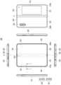
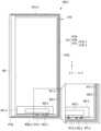
- FIG. 2ais a drawing illustrating a folded state of an electronic device according to one embodiment
- FIG. 2bis a drawing illustrating an unfolded state of an electronic device according to one embodiment.
- an electronic device (300)(e.g., the electronic device (101) of FIG. 1) according to one embodiment may include a housing (301) that forms an exterior and accommodates components therein.
- the electronic device (300) of FIGS. 2A and 2Bmay be an embodiment of the electronic device (101) of FIG. 1.
- the electronic device (300)may be a foldable or bendable electronic device.
- the electronic device (300)may include a housing (301) and/or a display module (350) (e.g., the display module (160) of FIG. 1).
- the housing (301)may form an exterior of the electronic device (300).
- the display module (350)may include a flexible or foldable display panel disposed within a space formed by the housing (301).
- a surface on which a display module (350) is disposedmay be defined as a front surface of the electronic device (300).
- a surface opposite to the front surfacemay be defined as a back surface of the electronic device (300).
- a surface surrounding a space between the front surface and the back surfacemay be defined as a side surface of the electronic device (300).
- the housing (301)may include a first housing portion (310), a second housing portion (320), and/or a hinge unit (330).
- the hinge unit (330)may include a hinge cover (330a) that covers a foldable portion of the housing (301).
- the housing (301) of the electronic device (300)is not limited to the shape and combination illustrated in FIGS. 2a and 2b, and may be implemented by other shapes or combinations and/or combinations of parts.
- the first housing portion (310)is connected to the hinge unit (330) and may include a first face (310a) facing a first direction and a second face (310b) facing a second direction opposite to the first direction.
- the second housing portion (320)is connected to the hinge unit (330) and may include a third face (320a) facing a third direction and a fourth face (310b) facing a fourth direction opposite to the third direction.
- the second housing portion (320)may rotate about the hinge unit (330) with respect to the first housing portion (310).
- the electronic device (300)may be variable between a folded state and an unfolded state.
- the electronic device (300)may have a first side (310a) facing a third side (320a) in a fully folded state, and a third direction may be substantially the same as the first direction in a fully unfolded state.
- first housing portion (310) and the second housing portion (320)may be foldably connected to each other.
- the first housing portion (310) and the second housing portion (320)may be arranged on both sides with respect to the folding axis (A) and may have a shape that is overall symmetrical with respect to the folding axis (A).
- the angle or distance between the first housing portion (310) and the second housing portion (320)may vary depending on whether the state of the electronic device (300) is an unfolded state, a folded state, or a partially unfolded (or partially folded) intermediate state.
- the second housing portion (320)may include a sensor area (322) in which various sensors are arranged.
- the various sensorsmay be positioned on the back surface of the display module (350) in the sensor area (322).
- the first housing portion (310)may also include a sensor area (not shown) in which at least one sensor is arranged.
- the first housing portion (310) and the second housing portion (320)may form a recess for accommodating a display module (350).
- components for performing various functions built into the electronic device (300)may be exposed to the front of the electronic device (300) through the sensor area (322) or through one or more openings provided in the sensor area (322).
- the componentsmay include various types of sensors.
- the sensorsmay include, for example, at least one of a front camera or a proximity sensor.
- the sensor area (322) in the second housing portion (320)may be omitted or formed in a different location than that shown in the drawing.
- At least a portion of the first housing portion (310) and the second housing portion (320)may include a metallic or non-metallic material having a rigidity of a selected size to support the display module (350).
- a portion formed of the metallic materialmay provide a ground for the electronic device (300) and may be electrically connected to a ground formed on a printed circuit board disposed inside the housing (301).
- the first housing portion (310)may include a first rear cover (315) and a first side region (341).
- the first rear cover (315)may be coupled to the first side region (341).
- the first rear cover (315)may have a substantially rectangular periphery and may be wrapped around the periphery by the first side region (341).
- the second housing portion (320)may include a second rear cover (325) and a second side region (342).
- the second rear cover (325)may be coupled to the second side region (342).
- the second rear cover (325)may have an edge wrapped by the second side region (342).
- first rear cover (315) and the second rear cover (325)may have substantially symmetrical shapes with respect to the folding axis (A).
- first rear cover (315) and the second rear cover (325)do not necessarily have mutually symmetrical shapes, and in one embodiment, the electronic device (300) may include the first rear cover (315) and the second rear cover (325) of various shapes.
- first rear cover (315)may be formed integrally with the first side area (341), and the second rear cover (325) may be formed integrally with the second side area (342).
- the first housing portion (310) and the second housing portion (320)may form a space in which various components of the electronic device (300) may be placed (e.g., a printed circuit board or a battery). According to one embodiment, one or more components may be placed or visually exposed on the rear surface of the electronic device (300).
- the sub-displaymay be visually exposed through the first rear area (316) of the first rear cover (315).
- one or more components or sensorsmay be visually exposed through the second rear area (326) of the second rear cover (325).
- the sensorsmay include a proximity sensor and/or a rear camera.
- the electronic device (300)may include a front camera visually exposed on the front side of the electronic device (300) through one or more openings provided in the sensor area (322) or a rear camera visually exposed through the second rear area (326) of the second rear cover (325), which may include one or more lenses, image sensors, and/or image signal processors.
- the flashmay include, for example, a light emitting diode or a xenon lamp.
- two or more lenses (infrared camera, wide-angle and telephoto lenses) and image sensorsmay be arranged on one side of the electronic device (300).
- the hinge cover (330a)may be configured to be disposed between the first housing portion (310) and the second housing portion (320) so as to cover an internal component (e.g., the hinge unit (330)).
- the hinge unit (330)may be covered by a portion of the first housing portion (310) and the second housing portion (320) or exposed to the outside depending on the state of the electronic device (300) (unfolded state, intermediate state, or folded state).
- the hinge unit (330)when the electronic device (300) is in an unfolded state (e.g., a fully unfolded state), the hinge unit (330) may be substantially uncovered by the first housing portion (310) and the second housing portion (320).
- the hinge unit (330)when the electronic device (300) is in a folded state (e.g., a fully folded state), the hinge unit (330) may be exposed externally between the first housing portion (310) and the second housing portion (320).
- the hinge unit (330)when the first housing portion (310) and the second housing portion (320) are in an intermediate state where they are folded with a certain angle, the hinge unit (330) may be partially exposed to the outside between the first housing portion (310) and the second housing portion (320). However, in this case, the exposed area may be less than that in the completely folded state. In one embodiment, the hinge unit (330) may include a curved surface.
- first side region (341) and the second side region (342)may be formed to surround at least a portion of the border region of the display module (350).
- first side region (341) and the second side region (342)may surround the front and/or the side of the border region of the display module (350).
- first side region (341) and the second side region (342)may be formed to surround at least a portion of the border region of the display module (350).
- the display module (350)may be placed on a space formed by the housing (301).
- the display module (350)may be mounted on a recess formed by the housing (301) and may be visible from the outside through the front of the electronic device (300).
- the display module (350)may form most of the front of the electronic device (300).
- the front of the electronic device (300)may include the display module (350) and a portion of the first housing portion (310) adjacent to the display module (350) and a portion of the second housing portion (320).
- the back of the electronic device (300)may include a first back cover (315), a portion of a first housing portion (310) adjacent to the first back cover (315), a second back cover (325), and a portion of a second housing portion (320) adjacent to the second back cover (325).
- the display module (350)may mean a display in which at least a portion of the area can be transformed into a flat surface or a curved surface.
- the display module (350)may include a folding area (353), a first area (351) arranged on one side (e.g., the left side of the folding area (353) illustrated in FIG. 2A) relative to the folding area (353), and a second area (352) arranged on the other side (e.g., the right side of the folding area (353) illustrated in FIG. 2A).
- the display module (350)may be divided into a plurality of areas (e.g., four or more or two) depending on the structure or function.
- the regions of the display module (350)may be divided by a folding region (353) extending parallel to the folding axis (A), but in one embodiment, the regions may be divided based on another folding axis of the display module (350) (e.g., a folding axis parallel to the width direction of the electronic device).
- the display module (350)may be coupled with or disposed adjacent to a touch panel having a touch detection circuit and a pressure sensor capable of measuring the intensity (pressure) of a touch.
- the display module (350)may be coupled with or disposed adjacent to a touch panel that detects a stylus pen of an electromagnetic resonance (EMR) type, as an example of a touch panel.
- EMRelectromagnetic resonance
- the first region (351) and the second region (352)may have an overall symmetrical shape centered on the folding region (353).
- the second region (352)may include a cut notch depending on the presence of the sensor region (322), but may have a shape symmetrical to the first region (351) in other regions.
- the first region (351) and the second region (352)may include a portion having a symmetrical shape and a portion having an asymmetrical shape.
- the edge thicknesses of the first region (351) and the second region (352)may be formed differently from the edge thickness of the folding region (353).
- the edge thickness of the folding region (353)may be formed thinner than the thicknesses of the first region (351) and the second region (352).
- the first region (351) and the second region (352)may have an asymmetrical shape when the first region (351) and the second region (352) are viewed in cross-section.
- the edge of the first region (351)may be formed to have a first radius of curvature
- the edge of the second region (352)may be formed to have a second radius of curvature that is different from the first radius of curvature.
- the first region (351) and the second region (352)may have a symmetrical shape when the first region (351) and the second region (352) are viewed in cross section.
- first housing part (310) and the second housing part (320) and each area of the display module (350)according to the state of the electronic device (300) (e.g., folded state, unfolded state, or intermediate state) will be described.
- the first surface (310a) of the first housing portion (310) and the third surface (320a) of the second housing portion (320)may be arranged to face the same direction at an angle of about 180 degrees.
- the surface of the first region (351) and the surface of the second region (352) of the display module (350)may form an angle of 180 degrees with each other and face the same direction (e.g., toward the front of the electronic device).
- the folding region (353)may form the same plane as the first region (351) and the second region (352).
- the first surface (310a) of the first housing portion (310) and the third surface (320a) of the second housing portion (320)may be arranged to face each other.
- the surface of the first region (351) and the surface of the second region (352) of the display module (350)may form a narrow angle (e.g., between 0 and 10 degrees) with each other and may face each other.
- the folding region (353)may be variable to a curved surface having at least a portion of a predetermined curvature.
- the first housing part (310) and the second housing part (320)may be arranged at a certain angle with respect to each other.
- the surface of the first region (351) and the surface of the second region (352) of the display module (350)may form an angle that is larger than the angle in the folded state and smaller than the angle in the unfolded state.
- the folding region (353)may be variable to a curved surface having at least a portion of a certain curvature, and the curvature at this time may be smaller than that in the folded state.
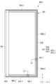
- FIG. 3ais a drawing of an unfolded state of an electronic device (400) according to one embodiment
- FIG. 3bis a drawing of a folded state of an electronic device (400) according to one embodiment
- FIG. 3cis a drawing schematically illustrating a cross-section of an electronic device (400) according to one embodiment.
- an electronic device (400)may include a housing (410, 420) (e.g., the housing (301) of FIGS. 2A and 2B).
- the electronic device (400) of FIGS. 3A to 3Cmay be an embodiment of the electronic device (101) of FIG. 1 described above.
- the electronic device (400)may be a foldable or bendable device. Or, in one embodiment, the electronic device (400) may be a slidable, expandable or rollable device. Or, in one embodiment, the electronic device (400) may be a foldable and expandable hybrid type device.
- the electronic device (400)may include a housing (410, 420), a display (430) (e.g., the display module (160) of FIG. 1 or the display module (350) of FIGS. 2A and 2B), and a hinge unit (445) (e.g., the hinge unit (330) of FIGS. 2A and 2B).
- a displaye.g., the display module (160) of FIG. 1 or the display module (350) of FIGS. 2A and 2B
- a hinge unit (445)e.g., the hinge unit (330) of FIGS. 2A and 2B.
- the housing (410, 420)may form an outer appearance of the electronic device (400).
- the housing (410, 420)may include a first housing portion (410) and a second housing portion (420).
- the first housing portion (410) and the second housing portion (420)may be foldably connected via a hinge unit (445).
- the hinge unit (445)may include a hinge cover that covers the foldable portions of the first housing portion (410) and the second housing portion (420).
- the first housing portion (410) and the second housing portion (420)are not limited to the shapes and combinations illustrated in FIGS. 3A to 3C, and may be implemented by other shapes or combinations and/or combinations of parts.
- the first housing portion (410)may include a first face (411) facing a first direction (e.g., a +Z direction) and a second face (412) facing a second direction (e.g., a -Z direction) opposite to the first direction, based on the state of FIG. 3a (e.g., an unfolded state).
- the first housing portion (410)may include a plurality of first side regions (413) extending from the first face (411) to the second face (412).
- the plurality of first side regions (413)may be made of a metallic material or a conductive material at least in some regions.
- the plurality of first side regions (413)may include a first side (413a) facing the hinge unit (445), a second side (413b) facing the first side (413a), and a plurality of third side surfaces (413c-1, 413c-2) extending from the first side (413a) to the second side (413b).
- the plurality of third side surfaces (413c-1, 413c-2)may include a first lower side surface (413c-1) and a first upper side surface (413c-2).
- the second housing portion (420)may include a third face (421) facing the first direction and a fourth face (422) facing the second direction, based on the state of FIG. 3A (e.g., unfolded state).
- the second housing portion (420)may include a plurality of second side regions (423) extending from the third face (421) to the fourth face (422).
- the plurality of second side regions (423)may be made of a metallic material or a conductive material at least in some regions.
- the plurality of second side regions (423)include a fourth side (423a) facing the hinge unit (445), a fifth side (423b) facing the fourth side (423a), and a plurality of sixth side surfaces (423c-1, 423c-2) extending from the fourth side (423a) to the fifth side (423b).
- the plurality of sixth side surfaces (423c-1, 423c-2)may include a second lower side surface (423c-1) and a second upper side surface (423c-2).
- the hinge unit (445)can foldably connect the first housing portion (410) and the second housing portion (420).
- the hinge unit (445)can be driven between a folded state in which the first side (411) and the third side (421) face each other (e.g., the state of the electronic device (400) of FIGS. 3b and 3c) and an unfolded state in which the first side (411) and the third side (421) do not face each other (e.g., the state of the electronic device (400) of FIG. 3a).
- either one of the first housing portion (410) and the second housing portion (420)can rotate relative to each other about the hinge unit (445).
- the electronic device (400)can be changed into a folding state (or folded state) or an unfolding state (or unfolded state).
- the electronic device (400)may have a first side (411) facing a third side (421) in a fully folded state, and may have a direction in which the first side (411) faces the third side (421) in a fully unfolded state.
- 'substantially' in this documentmay mean the same level reflecting tolerance or error in general manufacturing processes.
- 'substantially'may refer to a range including any one of +/-0.1%, +/-0.5%, +/-1%, +/-3%, +/-5%, +/-7%, +/-10%, +/-15%, and +/-20% based on the literal same 0%.
- At least a portion of the first housing portion (410) and the second housing portion (420)may comprise a metallic or non-metallic material having a rigidity selected to support the display (430).
- a housing (410, 420) formed of a metal materialmay be connected to a ground of the electronic device (400).
- a portion of the housing (410, 420) connected to the groundmay operate as a ground.
- at least a portion of the housing (410, 420)e.g., a plurality of first side regions (413) or a plurality of second side regions (423)
- the first housing portion (410) and the second housing portion (420)may form a space in which various components of the electronic device (400) may be placed (e.g., the first PCB (441) or the battery (e.g., the battery (189) of FIG. 1).
- the first PCB (441)may be a main PCB of the electronic device (400) and may include at least one processor (e.g., the processor (120) of FIG. 1), at least one memory (e.g., the memory (130) of FIG. 1), and an antenna module (e.g., the antenna module (197) of FIG. 1).
- the hinge unit (445)may be positioned between the first housing portion (410) and the second housing portion (420) and covered by a hinge cover.
- the hinge covermay cover internal components.
- the first housing portion (410)can be a slidable housing.
- the first housing portion (410)can include a main housing (410a) and an extension housing (410b).
- the main housing (410a)can be a main region of the first housing portion (410) that is connected to the second housing portion (420).
- the extension housing (410b)can be an extension region that is relatively movable from the main housing (410a).
- the expansion housing (410b)may be connected to be slidable relative to the main housing (410a).
- the expansion housing (410b)may be movable relative to the main housing (410a) in a first movement direction (e.g., in the +X direction) or in a second movement direction (e.g., in the -X direction) opposite to the first movement direction.
- first movement directione.g., in the +X direction
- second movement directione.g., in the -X direction
- the expansion housing (410b)is described as moving relative to the main housing (410a). However, since this is intended to describe a relative movement motion between the main housing (410a) and the expansion housing (410b), it may also be understood that the main housing (410a) moves relative to the expansion housing (410b).
- the state of the electronic device (400)can change between a first state and a second state depending on the relative movement of the main housing (410a) and the extension housing (410b).
- the electronic device (400)can have a reduced form in the first state (e.g., the state of FIGS. 3b and 3c) and an expanded form in the second state (e.g., the state of FIG. 3a).
- the electronic device (400)can be used in the first state or the second state, and can be used in an intermediate state between the first state and the second state.
- the display (430)may include a flexible display panel disposed within a space formed by a plurality of housings.
- a surface on which the display (430) is disposed(or a surface on which the display (430) is visible from the outside of the electronic device (400)) may be defined as a front surface of the electronic device (400).
- a surface opposite to the front surfacemay be defined as a back surface of the electronic device (400).
- a surface surrounding the space between the front surface and the back surfacemay be defined as a side surface of the electronic device (400).
- the display (430)may include a first region (431), a second region (432), and a third region (433).
- the first region (431) and the third region (433)may be disposed in the first housing portion (410), and the second region (432) may be disposed in the second housing portion (420).
- the area of the third region (433)may vary by relative movement of the extended housing (410b).
- the third region (433)can move from the inside of the first housing portion (410) to the outside and be visually exposed.
- the processor of the electronic device (400)can control the screen displayed by the display (430) based on the visual exposure state of the third region (433).
- the electronic device (400)may further include a sub-display (435).
- the sub-display (435)may be disposed on an opposite side of the display (430) in the electronic device (400).
- the sub-display (435)may be disposed so as to be visually exposed on the fourth side (422) of the second housing portion (420).
- the sub-display (435)may be driven when the electronic device (400) is in a folded state or a standby state.
- the first bracket (436)may be positioned inside the first housing portion (410).
- the first bracket (436)may support a component positioned inside the first housing portion (410), for example, the first region (431) and the third region (433) of the display (430), or the first PCB (441).
- the second bracket (437)may be positioned inside the second housing portion (420).
- the second bracket (437)may support a component positioned inside the second housing portion (420), for example, the second region (432) of the display (430) or the sub-display (435).
- the guide rail (438)may be provided inside the first housing portion (410).
- the guide rail (438)may be connected to the main housing (410a) and the extension housing (410b).
- at least a portion of the guide rail (438)may be fixed to the main housing (410a), and the remaining portion of the guide rail (438) may be connected to the extension housing (410b), thereby assisting the extension housing (410b) to move relative to the main housing (410a).
- the guide rail (438)can be connected to a multi-bar (439).
- the multi-bar (439)can support the display (430) during the process of the display (430) being flexibly bent.
- the multi-bar (439)can prevent or reduce damage to the display panel.
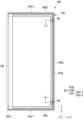
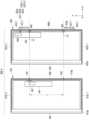
- FIG. 4ais a plan view of a first housing portion (410) of an electronic device (400) according to one embodiment
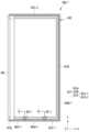
- FIG. 4bis a plan view of a second housing portion (420) of an electronic device (400) according to one embodiment.
- an electronic device (400)may include an antenna element (450) and a slot (460a).
- the plurality of first side regions (413)can include at least one segment.
- the at least one segmentcan include at least one of the first segment (451) and the second segment (452).
- the first segment (451) and the second segment (452)can be formed of a non-metallic or non-conductive material.
- a portion of the plurality of first side regions (413) between the first segments (451) and the second segments (452)can operate as an antenna radiator.
- a portion of the plurality of first side regions (413) between the first segments (451) and the second segments (452) that can operate as an antenna radiatorwill be described as an 'antenna element (450)'.
- the antenna element (450)can be positioned in a portion of the plurality of first side regions (413).
- the antenna element (450)can include a conductive portion between the first segments (451) and the second segments (452).
- the antenna element (450)may have a shape extending from the first segment (451).
- the antenna element (450)may be provided between the first segment (451) and the second segment (452).
- the present inventionis not limited thereto, and the plurality of first side regions (413) may form an antenna element (450) with only one segment (e.g., the first segment (451)).
- one end of the antenna element (450)faces the first segment (451), and the other end of the antenna element (450) extends to an end of the first side region (413) (e.g., a contact point between the first side (413a) and the second lower side (413c-1)), so that the plurality of first side regions (413) may form one antenna element (450).
- the first feed unit (471)may be electrically connected to the antenna element (450).
- the antenna element (450)may be connected to a wireless communication circuit (443) (e.g., the antenna module (197) of FIG. 1) via the first feed unit (471).
- the wireless communication circuit (443)may be disposed within the first housing portion (410), for example, on the first PCB (441).
- the wireless communication circuit (443)may transmit and receive communication signals from the antenna element (450) and/or the slot (460a) via the first feed portion (471).
- the antenna element (450)can receive a communication signal from the outside or transmit a communication signal to the outside.
- the electronic device (400)can provide improved communication performance by utilizing at least a portion of the plurality of first side areas (413) of the first housing portion (410) as the antenna element (450).
- the plurality of second side regions (423)can be connected to at least one ground portion.
- the at least one ground portioncan include at least one of a first ground portion (461) and a second ground portion (462).
- the first ground portion (461) and the second ground portion (462)can be made of a metallic material or a conductive material.
- the first ground portion (461) and the second ground portion (462)can be connected to a ground within the second housing portion (420).
- At least one slot (460a, 460b, 460c)may be formed in the plurality of second side regions (423) by the first ground portion (461) and/or the second ground portion (462).
- at least one slot (460a, 460b, 460c)may be formed by being surrounded by at least one ground portion (e.g., the first ground portion (461)), a portion of the second housing portion (420), and a ground provided inside the second housing portion (420).
- At least one slot (460a, 460b, 460c)can include at least one of a first slot (460a), a second slot (460b), and a third slot (460c).
- the first slot (460a)can be formed between the first ground portion (461) and the second ground portion (462).
- the second slot (460b)can be formed between the first ground portion (461) and another ground point or an end portion of the second side portion (423).
- the third slot (460c)can be formed between the second ground portion (462) and another ground point or an end portion of the second side portion (423).
- the first slot (460a) formed between the first grounding portion (461) and the second grounding portion (462)is referred to as a 'slot (460a)', but the description of the 'slot (460a)' can be substantially equally applied to other slots (460b, 460c).
- a slot (460a)may be formed between the first ground portion (461) and the second ground portion (462).
- the slot (460a)may have a shape extending from the first ground portion (461).
- the slot (460a)may be provided between the first ground portion (461) and the second ground portion (462).
- a plurality of second side regions (423)may form a slot (460a) with only one grounding portion (e.g., a first grounding portion (461)).
- the first grounding portion (461) of the slot (460a)may correspond to the first segment (451), and one end of the slot (460a) may be formed at a position corresponding to the second segment (452).
- the slot (460a)may be formed to substantially correspond to the antenna element (450) in the folded state of the electronic device (400).
- the first segment (451) and the first ground portion (461)may be formed at positions substantially opposite to each other, and the second segment (452) and the second ground portion (462) may be formed at positions substantially opposite to each other.
- the slot (460a)is positioned substantially corresponding to the antenna element (450), thereby omitting a separate power supply connected to the slot (460a), and is coupled to the antenna element (450) so that a current of the same phase as that of the antenna element (450) flows, thereby allowing the slot antenna to operate.
- the 'substantially opposing position'may mean a position where they overlap each other based on a plan view of the electronic device (400).
- the 'substantially opposing position'may mean a position where the antenna element (450) and the slot (460a) substantially overlap each other by the first segment (451), the second segment (452), the first ground portion (461), and the second ground portion (462).
- 'substantially' in this documentmay mean the same level reflecting tolerance or error in general manufacturing processes.
- 'substantially'may refer to a range including any one of +/-0.1%, +/-0.5%, +/-1%, +/-3%, +/-5%, +/-7%, +/-10%, +/-15%, and +/-20% based on the literal same 0%.
- first segment (451) and the second segment (452)may be arranged on a second side (413b) among the plurality of first side regions (413).
- the antenna element (450)may be formed on the second side (413b).
- first grounding portion (461) and the second grounding portion (462)may be arranged on a fifth side (423b) among the plurality of second side regions (423).
- the slot (460a)may be formed adjacent to the fifth side (423b).
- the slot (460a)may be formed in a bracket (or support member) positioned within the second housing portion (420).
- the antenna element (450) and the slot (460a)may be formed on a right side (e.g., in the +X direction) of the electronic device (400) (or a left side (e.g., in the -X direction)).
- the electronic device (400)may have a major axis (e.g., in the Y-axis direction) and a minor axis (e.g., in the X-axis direction).
- the antenna element (450) and the slot (460a)are formed on the right side parallel to the long axis of the electronic device (400), so that the length of the antenna element (450) and the slot (460a) can be longer, which can be advantageous in securing the antenna performance of the electronic device (400).
- currents of substantially the same phasemay flow through the slot (460a) and the antenna element (450) in the folded state of the electronic device (400).
- the electronic device (400)may provide improved antenna performance in the folded state.
- overlap between metals that serve as antenna radiatorsmay occur due to the driving of the first housing portion (410) and/or the second housing portion (420). If overlap between metals occurs, they may influence each other, thereby degrading the radiation performance of the antenna.
- the electronic device (400)includes a slot (460a) of the second housing portion (420) positioned to correspond to the metal (e.g., antenna element (450)) of the first housing portion (410) in the folded state, thereby reducing or preventing degradation of radiation performance even when the metals overlap.
- the antenna element (450) and the slot (460a)are arranged substantially opposite each other, which may be advantageous in securing antenna performance of the electronic device (400).
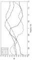
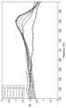
- FIG. 4cis a graph of radiation efficiency according to a frequency band of multiple embodiments
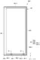
- FIGS. 4d, 4e, and 4fare plan views of a second housing portion (420) of an electronic device according to one embodiment.
- LO, L1, L2 and L3are graphs illustrating radiation efficiencies of an electronic device (400) according to an embodiment, each including a first housing portion (410) like FIG. 4a and a second housing portion (420) different from FIG. 4b.
- L0is a graph in the case where the second housing part (420) does not include the first ground part (461) and the slot (460a).
- L1is a graph for FIG. 4d in which the entirety of the second housing portion (420) corresponding to the plurality of second side areas (423) is driven by a slot (460a) since the second housing portion (420) does not include the first ground portion (461).
- L2is a graph for FIG. 4e in which the slot (460a) extends longer than the antenna element (450) on the fifth side (423b).
- L3is a graph for FIG. 4f in which the slot (460a) extends from the fifth side (423b) to a plurality of sixth sides (423c-1, 423c-2) and is longer than the antenna element (450).
- L4is a graph illustrating the radiation efficiency of an electronic device (400) according to an embodiment including a second housing portion (420) such as FIG. 4b.
- Fig. 4creferring to an exemplary target frequency band (e.g., 0.95 to 1.05 GHz), it can be confirmed that the radiation efficiency of L4, where the antenna element (450) and the slot (460a) are substantially arranged oppositely, is the best.
- the electronic device (400)by arranging the first segment (451), the second segment (452), the first ground portion (461), and the second ground portion (462) to be arranged oppositely to each other, the electronic device (400) can provide improved antenna radiation efficiency.
- the second housing part (420)can secure communication performance of the electronic device (400) through the slot (460a) and also help reduce the weight and/or slimness of the electronic device (400).
- the second housing part (420)may form a slot (460) through the first ground part (461) without a separate segment structure.
- the segment structure formed on the sidemay require a thickness of a certain value or more of the side area (423).
- the second housing part (420)according to one embodiment of the present document may provide communication performance of the electronic device (400) and may be advantageous in slimming and weight reduction, compared to a case where the electronic device includes a segment structure, by implementing a slot (460a) through the first ground part (461).
- the slot (460a)is communicatively connected to the wireless communication circuit (443) of the first housing part (410), a separate PCB and antenna module may not be required for the second housing part (420).
- the electronic device (400) according to one embodiment of the present documentmay be advantageous in terms of weight reduction/slimming and may secure efficiency and economy in manufacturing.
- the plurality of second side regions (423)may be formed of a non-segmental structure.
- An electronic device (400) according to one embodiment of the present documentmay implement a thinner thickness of the second housing portion (420) by including a slot (460a) without including a segmental structure in the second housing portion (420).
- An electronic device (400) according to one embodiment of the present documentcan be advantageously applied when one housing is formed thinner than another housing as a functional or design element of the electronic device (400).
- the thicknesses of the first housing portion (410) and the second housing portion (420)may be different.
- the second housing portion (420)may have a relatively thinner thickness compared to the first housing portion (410).
- the first housing portion (410)may include elements such as a guide rail (438), a multi-bar (439), a first region (431) and a third region (433) to implement a slider-like actuation, and may be relatively thicker than the second housing portion (420).
- the second housing portion (420)is formed with a segmentless structure, and thus can be formed relatively thinner than when including a segmented structure, thereby helping to secure communication performance and make the electronic device (400) slimmer and lighter.
- the second housing portion (420)can be formed with a segmentless structure, thereby providing rigidity.
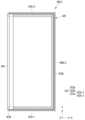
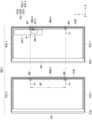
- FIG. 5ais a plan view of a first housing portion (410) of an electronic device (400-1) according to one embodiment
- FIG. 5bis a plan view of a second housing portion (420) of an electronic device (400-1) according to one embodiment.
- an electronic device (400-1)may include an antenna element (450-1) and a slot (460a-1).
- the plurality of first side regions (413)can include at least one segment.
- the at least one segmentcan include at least one of the first segment (451-1) and the second segment (452-1).
- the first segment (451-1) and the second segment (452-1)can be formed of a non-metallic or non-conductive material.
- a portion of the plurality of first side regions (413) between the first segment (451-1) and the second segment (452-1)can operate as an antenna radiator.
- a portion of the plurality of first side regions (413) between the first segment (451-1) and the second segment (452-2) that can operate as an antenna radiatoris described as an 'antenna element (450-1)'.
- the antenna element (450-1)can be composed of a portion of the plurality of first side regions (413).
- the antenna element (450-1)can be a conductive portion between the first segment (451-1) and the second segment (452-1).
- the antenna element (450-1)may have a shape extending from the first segment (451-1). Alternatively, the antenna element (450-1) may be provided between the first segment (451-1) and the second segment (452-1).
- the present inventionis not limited thereto, and the plurality of first side regions (413) may form an antenna element (450-1) with only one segment (e.g., the first segment (451-1)).
- one end of the antenna element (450-1)faces the first segment (451-1), and the other end of the antenna element (450-1) extends to an end of the first side region (413) (e.g., a contact point between the first side (413a) and the second lower side (413c-1)), so that the plurality of first side regions (413) may form one antenna element (450-1).
- the first feed unit (471-1)may be electrically connected to the antenna element (450-1).
- the antenna element (450-1)may be connected to a wireless communication circuit (443-1) (e.g., the antenna module (197) of FIG. 1) through the first feed unit (471-1).
- the wireless communication circuit (443-1)may be disposed inside the first housing portion (410), for example, may be disposed on the first PCB (441-1).
- the wireless communication circuit (443-1)may transmit and receive communication signals from the antenna element (450-1) and/or the slot (460a-1) via the first feed portion (471-1).
- the antenna element (450-1)can receive a communication signal from the outside or transmit a communication signal to the outside.
- the electronic device (400-1)can provide improved communication performance by utilizing at least a portion of the plurality of first side areas (413) of the first housing portion (410) as the antenna element (450-1).
- the plurality of second side regions (423)can be connected to at least one ground portion.
- the at least one ground portioncan include at least one of the first ground portion (461-1) and the second ground portion (462-1).
- the first ground portion (461-1) and the second ground portion (462-1)can be made of a metal material or a conductive material.
- the first ground portion (461-1) and the second ground portion (462-1)can be connected to a ground inside the second housing portion (420).
- At least one slot (460a-1, 460b-1, 460c-1)may be formed in the plurality of second side regions (423) by the first ground portion (461-1) and/or the second ground portion (462-1).
- at least one slot (460a-1, 460b-1, 460c-1)may be formed surrounded by at least one ground portion (e.g., the first ground portion (461-1)), a portion of the second housing portion (420), and a ground provided inside the second housing portion (420).
- At least one slot (460a-1, 460b-1, 460c-1)can include at least one of a first slot (460a-1), a second slot (460b-1), and a third slot (460c-1).
- the first slot (460a-1)can be formed between the first ground portion (461-1) and the second ground portion (462-1).
- the second slot (460b-1)can be formed between the first ground portion (461-1) and another ground point or an end portion of the second side portion (423).
- the third slot (460c-1)can be formed between the second ground portion (462-1) and another ground point or an end portion of the second side portion (423).
- the first slot (460a-1) formed between the first grounding portion (461-1) and the second grounding portion (462-1)is referred to as a ‘slot (460a-1)’, but the description of the ‘slot (460a-1)’ can be substantially equally applied to other slots (460b-1, 460c-1).
- a slot (460a-1)may be formed between the first ground portion (461-1) and the second ground portion (462-1).
- the slot (460a-1)may have a shape extending from the first ground portion (461-1).
- the slot (460a-1)may be provided between the first ground portion (461-1) and the second ground portion (462-1).
- the slot (460a-1)may be formed by being surrounded by at least one ground portion (e.g., the first ground portion (461)), a portion of the second housing portion (420), and a ground provided inside the second housing portion (420).
- at least one ground portione.g., the first ground portion (461)
- a portion of the second housing portion (420)e.g., a ground provided inside the second housing portion (420).
- the present inventionis not limited thereto, and the plurality of second side regions (423) may form a slot (460a-1) with only one grounding portion (e.g., the first grounding portion (461-1)).
- the first grounding portion (461-1) of the slot (460a-1)may face the first segment (451), and one end of the slot (460a-1) may be formed at a position corresponding to the second segment (452).
- the slot (460a-1)may be formed to substantially correspond to the antenna element (450-1) in the folded state of the electronic device (400-1).
- the first segment (451-1) and the first ground portion (461-1)may be formed at positions substantially opposite to each other, and the second segment (452-1) and the second ground portion (462-1) may be formed at positions substantially opposite to each other.
- the slot (460a-1)is positioned substantially corresponding to the antenna element (450-1), thereby omitting a separate feed section connected to the slot (460a-1), and is coupled to the antenna element (450-1) so that a current of the same phase as that of the antenna element (450-1) flows, thereby allowing the slot antenna to operate.
- the 'substantially opposing position'may mean a position where they overlap each other based on a plan view of the electronic device (400-1).
- the 'substantially opposing position'may mean a position where the antenna element (450-1) and the slot (460a-1) substantially overlap each other by the first segment (451-1), the second segment (452-1), the first ground portion (461-1), and the second ground portion (462-1).
- 'substantially' in this documentmay mean the same level reflecting tolerance or error in general manufacturing processes.
- 'substantially'may refer to a range including any one of +/-0.1%, +/-0.5%, +/-1%, +/-3%, +/-5%, +/-7%, +/-10%, +/-15%, and +/-20% based on the literal same 0%.
- the first segment (451-1) and the second segment (452-1)may be disposed on any one of the plurality of third sides (413c-1, 413c-2).
- the first segment (451-1) and the second segment (452-1)may be disposed on the first lower side (413c-1).
- the antenna element (450-1)may be disposed between the first segment (451-1) and the second segment (452-1), for example, on the first lower side (413c-1).
- the first ground portion (461-1) and the second ground portion (462-1)may be positioned adjacent to one of the plurality of sixth sides (423c-1, 423c-2).
- the first ground portion (461-1) and the second ground portion (462-1)may be positioned on the second lower side (423c-1).
- the slot (460a-1)may be positioned between the first ground portion (461-1) and the second ground portion (462-1), for example, on the second lower side (423c-1).
- the slot (460a)may be formed in a bracket (or, support member) positioned inside the second housing portion (420).
- the antenna element (450-1) and the slot (460a-1)may be formed on a lower side (e.g., in the -Y direction) surface (or an upper side (e.g., in the +Y direction) surface) of the electronic device (400-1).
- the electronic device (400-1)may have a long axis (e.g., in the Y-axis direction) and a short axis (e.g., in the X-axis direction).
- the usermay hold the electronic device (400-1) along the long axis of the electronic device (400-1). While the user is directly holding the antenna element (450-1) and the slot (460a-1), there is a possibility that the communication performance of the antenna element (450-1) and the slot (460a-1) may be degraded.
- the antenna element (450-1) and the slot (460a-1)are formed on a plane parallel to the short axis of the electronic device (400-1), thereby reducing or preventing performance degradation caused by a user, and the antenna element (450-1) and the slot (460a-1) may be advantageous in securing antenna performance of the electronic device (400-1).
- currents of substantially the same phasemay flow through the slot (460a-1) and the antenna element (450-1) in the folded state of the electronic device (400-1).
- the electronic device (400-1)may provide improved antenna performance in the folded state.
- overlap between metals that serve as antenna radiatorsmay occur due to the driving of the first housing portion (410) and/or the second housing portion (420). If overlap between metals occurs, they may influence each other, thereby deteriorating the radiation performance of the antenna.
- the electronic device (400-1)includes a slot (460a-1) of the second housing portion (420) arranged to correspond to the metal (e.g., antenna element (450-1)) of the first housing portion (410) in the folded state, thereby reducing or preventing degradation of radiation performance even when the metals overlap.
- the metale.g., antenna element (450-1)
- the antenna element (450-1) and the slot (460a-1)are arranged substantially opposite each other, which may be advantageous in securing antenna performance of the electronic device (400-1).
- FIG. 5cis a graph of radiation efficiency according to a frequency band of multiple embodiments
- FIGS. 5d, 5e, and 5fare plan views of a second housing portion (420) of an electronic device according to one embodiment.
- L1, L2 and L3are graphs illustrating radiation efficiencies of an electronic device (400-1) according to an embodiment, each including a first housing portion (410) like FIG. 5a and a second housing portion (420) different from FIG. 5b.
- L1is a graph for FIG. 5d in which the entirety of the second housing portion (420) corresponding to the plurality of second side areas (423) is driven by a slot (460a-1) since the second housing portion (420) does not include the first ground portion (461-1).
- L2is a graph for FIG. 5e in which the slot (460a-1) extends longer than the antenna element (450-1) on the second lower side (423c-1).
- L3is a graph for FIG. 5f in which the slot (460a-1) extends from the second lower side (423c-1) to the fifth side (423b) and is longer than the antenna element (450-1).
- L4is a graph illustrating the radiation efficiency of an electronic device (400-1) according to an embodiment including a second housing portion (420) such as FIG. 5b.
- the radiation efficiency of L4where the antenna element (450-1) and the slot (460a-1) are substantially arranged oppositely, is the best.
- the electronic device (400-1)by arranging the first segment (451-1), the second segment (452-1), the first ground portion (461-1), and the second ground portion (462-1) to be arranged oppositely to each other, the electronic device (400-1) can provide improved antenna radiation efficiency.
- the second housing part (420)can secure communication performance of the electronic device (400-1) through the slot (460a-1) and also help reduce the weight and/or slimness of the electronic device (400-1).
- the second housing part (420)may form a slot (460a-1) through the first ground part (461-1) without a separate segment structure.
- the segment structure formed on the sidemay require a thickness of a certain value or more of the side area (423).
- the second housing part (420)according to one embodiment of the present document may provide communication performance of the electronic device (400-1) and may be advantageous in slimming and weight reduction, compared to a case where the segment structure is included, by implementing the slot (460a-1) through the first ground part (461-1).
- An electronic device (400-1)may be advantageous in terms of weight reduction/slimming and may secure efficiency and economy in manufacturing.
- the plurality of second side regions (423)may be formed of a non-segmental structure.
- An electronic device (400-1) according to one embodiment of the present documentmay implement a thinner thickness of the second housing portion (420) by including a slot (460a-1) without including a segmental structure in the second housing portion (420).
- An electronic device (400-1) according to one embodiment of the present documentcan be advantageously applied when one housing is formed thinner than the other housing as a functional or design element of the electronic device (400-1).
- the thicknesses of the first housing portion (410) and the second housing portion (420)may be different.
- the second housing portion (420)may have a relatively thinner thickness compared to the first housing portion (410).
- the first housing portion (410)may include elements such as a guide rail (438), a multi-bar (439), a first region (431) and a third region (433) to implement a slider-like actuation, and may be relatively thicker than the second housing portion (420).
- the second housing portion (420)is formed with a segmentless structure, and thus can be formed relatively thinner than when including a segmented structure, thereby helping to secure communication performance and make the electronic device (400-1) slimmer and lighter.
- the second housing portion (420)can be formed with a segmentless structure, thereby providing rigidity.
- FIG. 6ais a plan view of a first housing portion (410) of an electronic device (400-2) according to one embodiment
- FIG. 6bis a plan view of a second housing portion (420) of an electronic device (400-2) according to one embodiment.
- an electronic device (400-2)may include an antenna element (450-2) and a slot (460a-2).
- the plurality of first side regions (413)can include at least one segment.
- the at least one segmentcan include at least one of the first segment (451-2) and the second segment (452-2).
- the first segment (451-2) and the second segment (452-2)can be formed of a non-metallic or non-conductive material.
- a portion of the plurality of first side regions (413) between the first segment (451-2) and the second segment (452-2)can operate as an antenna radiator.
- a portion of the plurality of first side regions (413) between the first segment (451-2) and the second segment (452-2) that can operate as an antenna radiatoris described as an 'antenna element (450-2)'.
- the antenna element (450-2)can be formed as a portion of the plurality of first side regions (413).
- the antenna element (450-2)can be included in a conductive portion between the first segment (451-2) and the second segment (452-2).
- the antenna element (450-2)may have a shape extending from the first segment (451-2).
- the antenna element (450-2)may be provided between the first segment (451-2) and the second segment (452-2).
- the present inventionis not limited thereto, and the plurality of first side regions (413) may form an antenna element (450-2) with only one segment (e.g., the first segment (451-2)).
- one end of the antenna element (450-2)faces the first segment (451-2), and the other end of the antenna element (450-2) extends to an end of the first side region (413) (e.g., a contact point between the first side (413a) and the second lower side (413c-1)), so that the plurality of first side regions (413) may form one antenna element (450-2).
- the first feed unit (471-2)may be electrically connected to the antenna element (450-2).
- the antenna element (450-2)may be connected to a wireless communication circuit (443-2) (e.g., the antenna module (197) of FIG. 1) through the first feed unit (471-2).
- the wireless communication circuit (443-2)may be disposed inside the first housing portion (410), for example, may be disposed on the first PCB (441-2).
- the wireless communication circuit (443-2)may transmit and receive communication signals from the antenna element (450-2) and/or the slot (460a-2) through the first feed portion (471-2).
- the antenna element (450-2)can receive a communication signal from the outside or transmit a communication signal to the outside.
- the electronic device (400-2)can provide improved communication performance by utilizing at least a portion of the plurality of first side areas (413) of the first housing portion (410) as the antenna element (450-2).
- the plurality of second side regions (423)can be connected to at least one ground portion.
- the at least one ground portioncan include at least one of the first ground portion (461-2) and the second ground portion (462-2).
- the first ground portion (461-2) and the second ground portion (462-2)can be made of a metal material or a conductive material.
- the first ground portion (461-2) and the second ground portion (462-2)can be connected to a ground inside the second housing portion (420).
- At least one slot (460a-2, 460b-2, 460c-2)may be formed in the plurality of second side regions (423) by the first ground portion (461-2) and/or the second ground portion (462-2).
- at least one slot (460a-2, 460b-2, 460c-2)may be formed by being surrounded by at least one ground portion (e.g., the first ground portion (461-2)), a portion of the second housing portion (420), and a ground provided inside the second housing portion (420).
- At least one slot (460a-2, 460b-2, 460c-2)can include at least one of a first slot (460a-2), a second slot (460b-2), and a third slot (460c-2).
- the first slot (460a-2)can be formed between the first ground portion (461-2) and the second ground portion (462-2).
- the second slot (460b-2)can be formed between the first ground portion (461-2) and another ground point or an end portion of the second side portion (423).
- the third slot (460c-2)can be formed between the second ground portion (462-2) and another ground point or an end portion of the second side portion (423).
- the first slot (460a-2) formed between the first grounding portion (461-2) and the second grounding portion (462-2)is referred to as a ‘slot (460a-2)’, but the description of the ‘slot (460a-2)’ can be substantially equally applied to other slots (460b-2, 460c-2).
- a slot (460a-2)may be formed between the first ground portion (461-2) and the second ground portion (462-2).
- the slot (460a-2)may have a shape extending from the first ground portion (461-2).
- the slot (460a-2)may be provided between the first ground portion (461-2) and the second ground portion (462-2).
- the slot (460a-2)may be formed by being surrounded by at least one ground portion (e.g., the first ground portion (461-2)), a portion of the second housing portion (420), and a ground provided inside the second housing portion (420).
- at least one ground portione.g., the first ground portion (461-2)
- a portion of the second housing portion (420)e.g., the first ground portion (461-2)
- a portion of the second housing portion (420)e.g., the first ground portion (461-2)
- a grounde.g., the first ground portion (461-2)
- a plurality of second side regions (423)may form a slot (460a-2) with only one grounding portion (e.g., a first grounding portion (461-2)).
- the first grounding portion (461-2) of the slot (460a-2)may correspond to the first segment (451-2), and one end of the slot (460a-2) may be formed at a position corresponding to the second segment (452-2).
- the slot (460a-2)may be formed to substantially correspond to the antenna element (450-2) in the folded state of the electronic device (400-2).
- the first segment (451-2) and the first ground portion (461-2)may be formed at positions substantially opposite to each other, and the second segment (452-2) and the second ground portion (462-2) may be formed at positions substantially opposite to each other.
- the slot (460a-2)is positioned substantially corresponding to the antenna element (450-2), thereby omitting a separate feed section connected to the slot (460a-2), and is coupled to the antenna element (450-2) so that a current of the same phase as that of the antenna element (450-2) flows, thereby allowing the slot antenna to operate.
- the 'substantially opposing position'may mean a position where they overlap each other based on a plan view of the electronic device (400-2).
- the 'substantially opposing position'may mean a position where the antenna element (450-2) and the slot (460a-2) substantially overlap each other by the first segment (451-2), the second segment (452-2), the first ground portion (461-2), and the second ground portion (462-2).
- 'substantially' in this documentmay mean the same level reflecting tolerance or error in general manufacturing processes.
- 'substantially'may refer to a range including any one of +/-0.1%, +/-0.5%, +/-1%, +/-3%, +/-5%, +/-7%, +/-10%, +/-15%, and +/-20% based on the literal same 0%.
- the first segment (451-2)may be disposed on the second side (413b), and the second segment (452-2) may be disposed on one of the plurality of third side surfaces (413c-1, 413c-2).
- the second segment (452-2)may be disposed on the first lower side surface (413c-1).
- the antenna element (450-2)may be disposed between the first segment (451-2) and the second segment (452-2), and may be disposed to extend from the second side surface (413b) to the first lower side surface (413c-1), for example.
- the first ground portion (461-2)may be disposed on the fifth side (423b), and the second ground portion (462-2) may be disposed on one of the plurality of sixth side portions (423c-1, 423c-2).
- the second ground portion (462-2)may be disposed on the second lower side (423c-1).
- the slot (460a-2)may be disposed between the first ground portion (461-2) and the second ground portion (462-2), and may be disposed to extend, for example, from the fifth side (423b) to the second lower side (423c-1).
- the slot (460a-2)may be formed adjacent to the fifth side (423b) and the second lower side (423c-1).
- the slot (460a-2)may be formed in a bracket (or support member) positioned within the second housing portion (420).
- the antenna element (450-2) and the slot (460a-2)may be formed across a lower (e.g., in the -Y direction) side (or an upper (e.g., in the +Y direction) side) of the right side (e.g., in the +X direction) of the electronic device (400-2).
- the electronic device (400-2)may have a major axis (e.g., in the Y-axis direction) and a minor axis (e.g., in the X-axis direction).
- the usermay hold the electronic device (400-2) along the major axis of the electronic device (400-2). While the user is directly holding the antenna element (450-2) and the slot (460a-2), there is a possibility that the communication performance of the antenna element (450-2) and the slot (460a-2) may be degraded.
- the antenna element (450-2) and the slot (460a-2)are formed from the right side to the lower side, performance degradation caused by a user can be reduced or prevented, and the antenna element (450-2) and the slot (460a-2) can be advantageous in securing antenna performance of the electronic device (400-2).
- the antenna element (450-2) and the slot (460a-2)are formed from the right side to the lower side, the length of the antenna element (450-2) and the slot (460a-2) can be longer, and the antenna performance of the electronic device (400-2) can be advantageous in securing antenna performance.
- currents of substantially the same phasemay flow through the slot (460a-2) and the antenna element (450-2) in the folded state of the electronic device (400-2).
- the electronic device (400-2)may provide improved antenna performance in the folded state.
- overlap between metals that serve as antenna radiatorsmay occur due to the driving of the first housing portion (410) and/or the second housing portion (420). If overlap between metals occurs, they may influence each other, thereby deteriorating the radiation performance of the antenna.
- the electronic device (400-2)includes a slot (460a-2) of the second housing portion (420) arranged to correspond to the metal (e.g., antenna element (450-2)) of the first housing portion (410) in the folded state, thereby reducing or preventing degradation of radiation performance even when the metals overlap.
- the metale.g., antenna element (450-2)
- the antenna element (450-2) and the slot (460a-2)are arranged substantially opposite each other, which may be advantageous in securing antenna performance of the electronic device (400-2).
- the electronic device (400-2)may further include an additional antenna element (450a-2) and an additional feeder (471a-2).
- the additional antenna element (450a-2)may have a shape extending in a different direction from the antenna element (450-2) from the second segment (452-2).
- the additional antenna element (450a-2)may extend from the second segment (452-2) in a direction opposite to a direction facing the first segment (452-1) at the first lower side (413c-1).
- the second housing portion (420)may include a plurality of slots (460a-2, 460b-2, 460c-2) formed by the first ground portion (461-2) and/or the second ground portion (462-2). Any one of the plurality of slots (460a-2, 460b-2, 460c-2) (e.g., the third slot (460c-2)) may be formed to substantially correspond with the additional antenna element (450a-2) in the folded state of the electronic device (400-2).
- the additional feeder (471a-2)may be electrically connected to the additional antenna element (450a-2).
- the additional antenna element (450a-2)may be connected to the wireless communication circuit (443-2) via the additional feeder (471a-2).
- the wireless communication circuit (443-2)may transmit and receive communication signals from the additional antenna element (450a-2) and/or the slot (460c-2) via the additional feeder (471a-2).
- the additional antenna element (450a-2)can receive a communication signal from an external source or transmit a communication signal to an external source.
- the electronic device (400-2)can provide improved communication performance by utilizing at least a portion of the plurality of first side areas (413) of the first housing portion (410) as the additional antenna element (450a-2).
- the third slot (460c-2)is positioned substantially corresponding to the additional antenna element (450a-2), thereby omitting a separate feeder connected to the slot (460c-2), and the third slot (460c-2) is coupled with the additional antenna element (450c-2) so that a current of the same phase as that of the additional antenna element (450c-2) flows, thereby allowing the slot antenna to operate.
- FIG. 6cis a graph of radiation efficiency according to a frequency band of multiple embodiments
- FIGS. 6d, 6e, and 6fare plan views of a second housing portion (420) of an electronic device according to one embodiment.
- L1, L2 and L3are graphs illustrating radiation efficiencies of an electronic device (400-2) according to an embodiment, each including a first housing portion (410) like FIG. 6a and a second housing portion (420) different from FIG. 6b.
- L1is a graph for FIG. 6d in which the entirety of the second housing portion (420) corresponding to the plurality of second side areas (423) is driven by a slot (460a-2) since the second housing portion (420) does not include the first ground portion (461-2).
- L2is a graph for FIG. 6e in which the slot (460a-2) extends longer than the antenna element (450-2) on the second lower side (423c-1).
- L3is a graph for FIG. 6f in which the slot (460a-2) extends longer than the antenna element (450-2) on the fifth side (423b).
- L4is a graph illustrating the radiation efficiency of an electronic device (400-2) according to an embodiment including a second housing portion (420) such as FIG. 6b.
- Fig. 6creferring to an exemplary target frequency band (e.g., 0.95 to 1.05 GHz), it can be confirmed that the radiation efficiency of L4, where the antenna element (450-2) and the slot (460a-2) are substantially arranged oppositely, is the best.
- the electronic device (400-2)by arranging the first segment (451-2), the second segment (452-2), the first ground portion (461-2), and the second ground portion (462-2) to be arranged oppositely to each other, the electronic device (400-2) can provide improved antenna radiation efficiency.
- the second housing part (420)can secure communication performance of the electronic device (400-2) through the slot (460a-2) and also help reduce the weight and/or slimness of the electronic device (400-2).
- the second housing part (420)may form a slot (460a-2) through the first ground part (461-2) without a separate segment structure.
- the segment structure formed on the sidemay require a thickness of a certain value or more.
- the second housing part (420) according to one embodiment of the present documentmay provide communication performance of the electronic device (400-2) and may be advantageous in slimming and weight reduction, compared to a case where the electronic device includes a segment structure, by implementing the slot (460a-2) through the first ground part (461-2).
- An electronic device (400-2)may be advantageous in terms of weight reduction/slimming and may secure efficiency and economy in manufacturing.
- the plurality of second side regions (423)may be formed of a non-segmental structure.
- An electronic device (400-2) according to one embodiment of the present documentmay implement a thinner thickness of the second housing portion (420) by including a slot (460a-2) without including a segmental structure in the second housing portion (420).
- An electronic device (400-2) according to one embodiment of the present documentcan be advantageously applied in a case where one housing is formed thinner than the other housing as a functional or design element of the electronic device (400-2).
- the thicknesses of the first housing portion (410) and the second housing portion (420)may be different.
- the second housing portion (420)may have a relatively thinner thickness compared to the first housing portion (410).
- the first housing portion (410)may include elements such as a guide rail (438), a multi-bar (439), a first region (431) and a third region (433) to implement a slider-like actuation, and may be relatively thicker than the second housing portion (420).
- the second housing portion (420)is formed with a segmentless structure, and thus can be formed relatively thinner than when including a segmented structure, thereby helping to secure communication performance and make the electronic device (400-2) slimmer and lighter.
- the second housing portion (420)can be formed with a segmentless structure, thereby providing rigidity.
- FIG. 7ais a graph of radiation efficiency according to a frequency band of a plurality of embodiments
- FIG. 7bis a graph of radiation efficiency according to a frequency band of a plurality of embodiments
- FIG. 7cis a plan view of a first housing portion and a second housing portion of an electronic device according to one embodiment in a separated and arranged state.
- FIG. 7cis an exemplary drawing showing the arrangement of the first ground portion (461) and/or the second ground portion (462) in a direction that reduces the length (L') of the slot (460a) relative to the length (L) of the antenna element (450), based on the electronic device (400) of FIGS. 4a and 4b, and FIGS. 7a and 7b are graphs showing radiation efficiencies for this.
- results for radiation efficiency of FIGS. 7a and 7bare not limited to the electronic device (400) of FIGS. 4a and 4b, and can be expected to be applied identically or similarly to the electronic device (400) of FIGS. 5a and 5b or the electronic device (400) of FIGS. 6a and 6b.
- L1is a graph illustrating radiation efficiency of an electronic device (400) according to an embodiment including a first housing portion (410) like that of FIG. 4A and a second housing portion (420) like that of FIG. 4B, such that the antenna element (450) and the slot (460a) have substantially the same length.
- L2, L3, L4, L5, L6, and L7are graphs illustrating radiation efficiency of an electronic device (400) according to an embodiment including a first housing portion (410) like that of FIG. 4A and a second housing portion (420) different from that of FIG. 4B.
- L2, L3, L4, L5, L6 and L7are embodiments in which the first ground portion (461) is moved in a direction that reduces the length (L') of the slot (460a) by 2.5 mm, 5 mm, 7.5 mm, 10 mm, 12.5 mm and 15 mm from a position substantially opposite to the first segment portion (451), respectively.
- L2, L3, L4, L5, L6 and L7are embodiments in which the second ground portion (462) is moved in a direction (e.g., +Y direction in FIG. 4b) that reduces the slot (460a) by 2.5 mm, 5 mm, 7.5 mm, 10 mm, 12.5 mm and 15 mm from a position substantially opposite to the second segment portion (452).
- a directione.g., +Y direction in FIG. 4b
- the target frequency band of the electronic device (400)may be 0.95 to 1.05 GHz
- the communication wavelength bandmay be between 300 mm and 330 mm
- the length of the antenna element (450)may be 75 mm.
- the radiation efficiencyis the best at a position where the first segment (451), the second segment (452), the first ground portion (461), and the second ground portion (462) are substantially opposite each other through L1.
- the communication efficiencyis rapidly reduced when the length of the slot (460a) is reduced to a certain value or more compared to the antenna element (450).
- an embodiment having a difference in radiation efficiency of less than about 0.5 dBcan be determined as a reduction threshold of the length (L') of the slot (460a), and it can be seen that the electronic device (400) implements substantially the same performance within the reduction threshold. Therefore, in each of FIGS. 7A and 7B, the length reduction to L6 can be expected as the threshold.
- the length reduction range from L1 to L6can be a length of 1/25 times the wavelength.
- the electronic device (400)can provide improved antenna radiation efficiency.
- a reduction in the length of the slot (460a) within 1/25 times the communication wavelength band of the electronic device (400)may be included in a range in which the slot (460a) and the antenna element (450) according to one embodiment of the present document are substantially arranged opposite each other.
- FIG. 8ais a graph of radiation efficiency according to a frequency band of a plurality of embodiments
- FIG. 8bis a graph of radiation efficiency according to a frequency band of a plurality of embodiments
- FIG. 8cis a plan view of a first housing portion and a second housing portion of an electronic device according to one embodiment in a separated and arranged state.
- FIG. 8cis an exemplary drawing showing the arrangement of the first ground portion (461) and the second ground portion (462) in a direction that extends the length (L') of the slot (460a) longer than the length (L) of the antenna element (450) based on the electronic device (400) of FIGS. 4a and 4b, and FIGS. 8a and 8b are graphs showing radiation efficiency for this.
- results for radiation efficiency of FIGS. 8a and 8bare not limited to the electronic device (400) of FIGS. 4a and 4b, and can be expected to be applied identically or similarly to the electronic device (400) of FIGS. 5a and 5b or the electronic device (400) of FIGS. 6a and 6b.
- L1is a graph illustrating radiation efficiency of an electronic device (400) according to an embodiment including a first housing portion (410) like that of FIG. 4A and a second housing portion (420) like that of FIG. 4B, such that the antenna element (450) and the slot (460a) have substantially the same length.
- L2, L3, L4, L5, L6, and L7are graphs illustrating radiation efficiency of an electronic device (400) according to an embodiment including a first housing portion (410) like that of FIG. 4A and a second housing portion (420) different from that of FIG. 4B.
- L2, L3, L4, L5, L6 and L7are embodiments in which the first ground portion (461) is moved in a direction (e.g., +Y direction) that extends the length (L') of the slot (460a) by 2.5 mm, 5 mm, 7.5 mm, 10 mm, 12.5 mm and 15 mm from a position substantially opposite to the first segment portion (451), respectively.
- a directione.g., +Y direction
- L2, L3, L4, L5, L6 and L7are embodiments in which the second ground portion (462) is moved in a direction (e.g., in the -Y direction) to extend the length (L') of the slot (460a) by 2.5 mm, 5 mm, 7.5 mm, 10 mm, 12.5 mm and 15 mm from a position substantially opposite to the second segment portion (452), respectively.
- the target frequency band of the electronic device (400)may be about 0.95 to 1.05 GHz
- the communication wavelength bandmay be about 300 mm to 330 mm
- the length of the antenna element (450)may be about 75 mm.
- the radiation efficiencyis the best at a position where the first segment (451), the second segment (452), the first ground portion (461), and the second ground portion (462) are substantially opposite each other through L1.
- the communication efficiencyis rapidly reduced when the length of the slot (460a) is extended beyond a certain value compared to the antenna element (450).
- an embodiment having a difference in radiation efficiency of less than about 0.5 dBcan be determined as an extension threshold of the length (L') of the slot (460a), and it can be seen that the electronic device (400) implements substantially the same performance within the extension threshold. Therefore, in each of FIGS. 8A and 8B, the length extension to L6 can be expected as the threshold.
- the length extension range from L1 to L6can be a length of 1/30 times the wavelength.
- the electronic device (400)can provide improved antenna radiation efficiency.
- the length extension of the slot (460a) within 1/30 times the communication wavelength band of the electronic device (400)may be included in a range in which the slot (460a) and the antenna element (450) according to one embodiment of the present document are substantially arranged opposite each other.
- FIG. 9is a plan view of the first housing part (410) and the second housing part (420) of the electronic device (400-3) according to one embodiment of the present invention, separated and arranged.
- the second housing portion (420) of the electronic device (400-3)may further include at least one segmented portion (453, 454), at least one of a second PCB (442), a wireless communication circuit (444), and a second power supply portion (472).
- the electronic device (400-3)may include a first housing portion (e.g., the first housing portion (410) of FIG. 4a).
- FIG. 9is intended to explain the components of the second housing portion (420) based on the electronic device (400-3) including the first ground portion (461) and the second ground portion (462) of FIG. 4b, and the description of FIG. 9 may be applied identically or similarly not only to the electronic device (400) of FIGS. 4a and 4b, but also to the electronic device (400-1) of FIGS. 5a and 5b or the electronic device (400-2) of FIGS. 6a and 6b.
- the second housing portion (420)may further include at least one segment (453, 454).
- the at least one segment (453, 454)may include at least one of a third segment (453) and a fourth segment (454).
- the second housing portion (420)may include separate segments (453, 454) from the first housing portion (410), thereby implementing an antenna including an antenna element (457), and the electronic device (400-3) may include more antennas.
- the third segment (453) and the fourth segment (454)may be arranged to be non-aligned with the first segment (451) and the second segment (452). For example, based on the length (L) of the antenna element (450) provided between the first segment (451) and the second segment (452), the third segment (453) and the fourth segment (454) may be arranged to be spaced apart by a distance longer than the length (L) of the antenna element (450).
- the third segment (453) and the fourth segment (454)may be respectively disposed on the plurality of sixth sides (423c-1, 423c-2).
- the third segment (453)may be disposed on the second upper side (423c-2), and the fourth segment (454) may be disposed on the second lower side (423c-1).
- the electronic device (400-3)can form a variety of drivable antennas by forming various power supply portions in the second housing portion (420) including the third segment portion (453) and the fourth segment portion (454).
- the electronic device (400-3)may additionally form an antenna that forms a second feed portion (472) and forms a closed loop from the third segment (453) to the first ground portion (461).
- the electronic device (400-3)may additionally implement an antenna that forms a closed loop from the fourth segment (454) to the second ground (462) by implementing a separate additional power supply.
- the electronic device (400-3)may also configure a separate additional feed to the additional antenna element (457), so that the additional antenna element (457) may operate as an additional antenna radiator.
- the third segment (453) and the fourth segment (454)are formed on the upper and lower sides of the second housing part (420), respectively, so that additional antenna radiators of the second housing part (420) can be formed in various ways, and this can be advantageous in securing antenna performance of the electronic device (400-3).
- the second feed unit (472)may be electrically connected to an additional antenna element (457).
- the additional antenna element (457)may be connected to a wireless communication circuit (444) (e.g., the antenna module (197) of FIG. 1) via the second feed unit (472).
- the wireless communication circuit (444)may be disposed within the second housing portion (420), for example, on the second PCB (442).
- the wireless communication circuit (444)may transmit and receive communication signals from the additional antenna element (457) via the second feed portion (472).
- the electronic device (400-3)may further include at least one switching element.
- the at least one switching elementmay control an electrical connection between at least one of a plurality of antenna modules (e.g., the wireless communication circuit (443) and the wireless communication circuit (444)) of the electronic device (400-3) and at least one of a plurality of antenna elements (e.g., the antenna element (457), the slot (460a), and the additional antenna element (457)).
- the electronic device (400-3)may control the at least one switching element based on environmental factors such as a communication environment, a usage status, and a communication band.
- FIG. 10is a plan view of the first housing part (410) and the second housing part (420) of the electronic device (400-4) according to one embodiment of the present invention, separated and arranged.
- a second housing portion (420) of an electronic device (400-4)may further include at least one segmented portion (453-1, 454-1), a second PCB (442), a wireless communication circuit (444), and at least one of a second power supply portion (472-1).
- the electronic device (400-4)may include a first housing portion (e.g., the first housing portion (410) of FIG. 4a).
- FIG. 10is intended to explain components of the second housing portion (420) based on the electronic device (400-4) including the first ground portion (461) and the second ground portion (462) of FIG. 4b, and the description of FIG. 10 may be applied identically or similarly not only to the electronic device (400) of FIGS. 4a and 4b, but also to the electronic device (400-1) of FIGS. 5a and 5b or the electronic device (400-2) of FIGS. 6a and 6b.
- the second housing portion (420)may further include at least one segment (453-1, 454-1).
- the at least one segment (453-1, 454-1)may include at least one of a third segment (453-1) and a fourth segment (454-1).
- the second housing portion (420)may include a separate segment from the first housing portion (410), thereby forming an additional antenna element (457-1) separately from the slot (460a), and the electronic device (400-4) may provide improved communication efficiency.
- the third segment (453-1) and the fourth segment (454-1)may be arranged to be non-aligned with the first segment (451) and the second segment (452). For example, based on the length (L) of the antenna element (450) provided between the first segment (451) and the second segment (452), the third segment (453-1) and the fourth segment (454-1) may be arranged to be spaced apart by a distance longer than the length (L) of the antenna element (450).
- the third segment (453-1) and the fourth segment (454-1)may be positioned on opposite sides of the slot (460a) on the fifth side (423b), respectively.
- the third segment (453-1)may be positioned adjacent to the first grounding portion (461), and the fourth segment (454-1) may be positioned adjacent to the second grounding portion (462).
- the electronic device (400-4)may form a variety of drivable antennas by forming various power supply portions in the second housing portion (420) including the third segment (453-1) and the fourth segment (454-1).
- the electronic device (400-4)may additionally implement an antenna that forms a closed loop from the third segment (453-1) to the first grounding portion (461) by configuring the second feed portion (472-1).
- the electronic device (400-4)may additionally implement an antenna that forms a closed loop from the fourth segment (454-1) to the second ground (462) by implementing a separate additional power supply.
- the electronic device (400-4)may also form a separate additional feed to the additional antenna element (457-1), so that the additional antenna element (457-1) may operate as an additional antenna radiator.
- the third segment (453-1) and the fourth segment (454-1)are formed on the upper side of the first ground portion (461) and the lower side of the second ground portion (462) of the second housing portion (420), respectively, so that the length of the additional antenna element (457-1) of the second housing portion (420) can be increased, which can be advantageous in securing the antenna performance of the electronic device (400-4).
- the second feed unit (472-1)may be electrically connected to an additional antenna element (457-1).
- the additional antenna element (457-1)may be connected to a wireless communication circuit (444) (e.g., the antenna module (197) of FIG. 1) via the second feed unit (472-1).
- the wireless communication circuit (444)may be disposed within the second housing portion (420), for example, on the second PCB (442).
- the wireless communication circuit (444)may transmit and receive communication signals from the additional antenna element (457-1) via the second feed portion (472-1).
- the electronic device (400-4)may further include at least one switching element.
- the at least one switching elementmay control an electrical connection between at least one of a plurality of antenna modules (e.g., the wireless communication circuit (443) and the wireless communication circuit (444)) of the electronic device (400-4) and at least one of a plurality of antenna elements (e.g., the antenna element (457), the slot (460a), and the additional antenna element (457-1)).
- the electronic device (400-4)may control the at least one switching element based on environmental factors such as a communication environment, a usage status, and a communication band.
- FIG. 11is a plan view of the first housing part (410) and the second housing part (420) of the electronic device (400-5) according to one embodiment of the present invention, separated and arranged.
- an electronic device (400-5)may include a plurality of slots (460a, 460a-3).
- the plurality of second side regions (423)can include at least one ground portion.
- the at least one ground portioncan include at least one of a first ground portion (461) and a second ground portion (462).
- the first ground portion (461) and the second ground portion (462)can be made of a metallic material or a conductive material.
- the first ground portion (461) and the second ground portion (462)can be connected to a ground inside the second housing portion (420).
- At least one slot (460a-4, 460a-5)may be formed between the first ground portion (461) and the second ground portion (462).
- the at least one slot (460a-4, 460a-5)may have a shape extending from the first ground portion (461).
- the at least one slot (460a-4, 460a-5)may be provided between the first ground portion (461) and the second ground portion (462).
- At least one slotmay be formed on both sides with respect to the feed portion (472-3).
- a first slot area (460a-4)may be provided between the first ground portion (461) and the feed portion (472-3)
- a second slot area (460a-5)may be provided between the second ground portion (462) and the feed portion (472-3).
- first slot region (460a-4) and the second slot region (460a-5)can form one slot (460a-4, 460a-5).
- the first slot region (460a-4) and the second slot region (460a-5) formed between the first grounding portion (461) and the second grounding portion (462)will be referred to as ‘slots (460a-4, 460a-5)’.
- the slots (460a-4, 460a-5)may have a shape corresponding to an additional slot (460a-3) to be described later, and may be arranged corresponding to the additional slot (460a-3).
- the plurality of first side regions (413)can include at least one ground portion (463, 464).
- the at least one ground portion (463, 464)can include at least one of a third ground portion (463) and a fourth ground portion (464).
- the third ground portion (463) and the fourth ground portion (464)can be made of a metallic material or a conductive material.
- an additional slot (460a-3)may be formed between the third ground portion (463) and the fourth ground portion (464).
- the additional slot (460a-3)may have a shape extending from the third ground portion (463).
- the additional slot (460a-3)may be provided between the third ground portion (463) and the fourth ground portion (464).
- the present inventionis not limited thereto, and the plurality of first side regions (413) may form an additional slot (460a-3) with only one grounding portion (e.g., the third grounding portion (463)).
- one end of the additional slot (460a-3)may face the third grounding portion (463), and the other end of the additional slot (460a-3) may be disposed at an end of the first side region (413), so that the plurality of first side regions (413) may form one additional slot (460a-3).
- the slots (460a-4, 460a-5) and the additional slot (460a-3)may be arranged substantially opposite each other in a folded state of the electronic device (400-5). In one embodiment, the slots (460a-4, 460a-5) and the additional slot (460a-3) may have substantially the same length (L) as each other.
- the first ground portion (461) and the third ground portion (463)may be formed at positions substantially opposite to each other, and the second ground portion (462) and the fourth ground portion (464) may be formed at positions substantially opposite to each other.
- the 'substantially opposite positions'may mean positions where they overlap each other based on the plan view of the electronic device (400-5).
- the 'substantially opposite positions'may mean positions where the antenna element (450) and the slots (460a-4, 460a-5) substantially overlap each other by the first ground portion (461), the second ground portion (462), the third ground portion (463), and the fourth ground portion (464).
- 'substantially' in this documentmay mean the same level reflecting tolerance or error in general manufacturing processes.
- 'substantially'may refer to a range including any one of +/-0.1%, +/-0.5%, +/-1%, +/-3%, +/-5%, +/-7%, +/-10%, +/-15%, and +/-20% based on the literal same 0%.
- the antenna module (444-3)can be disposed inside the second housing portion (420), for example, on the PCB (442-3).
- the antenna module (444-3)can transmit and receive communication signals from the slots (460a-4, 460a-5) and/or the additional slot (460a-3) through the feeder (472-3).
- currents of substantially the same phasemay flow through the slots (460a-4, 460a-5) and the additional slot (460a-3) in the folded state of the electronic device (400-5).
- the electronic device (400-5)may provide improved antenna performance in the folded state.
- overlap between metals that serve as an antenna arraymay occur due to the actuation of the first housing portion (410) and/or the second housing portion (420). If overlap between metals occurs, they may influence each other, thereby degrading the radiation performance of the antenna.
- the electronic device (400-5)can reduce or prevent degradation of radiation performance even when the metals overlap each other by aligning the metal of the first housing portion (410) (e.g., the additional slot (460a-3)) and the metal of the second housing portion (420) (e.g., the slots (460a-4, 460a-5)) in a folded state.
- a second housing part (420)can secure communication performance of an electronic device (400-5) through a slot (460a) and an additional slot (460a-3), and can also help reduce the weight and/or slimness of the electronic device (400-5).
- the first housing portion (410) and the second housing portion (420)may form a slot (460a) and an additional slot (460a-3) without a separate segmented structure.
- the segmented structure formed on the sidemay require a thickness of the first housing portion (410) and the second housing portion (420) greater than a certain value.
- the first housing portion (410) and the second housing portion (420)according to one embodiment of the present document may provide communication performance of the electronic device (400-5) by implementing the slot (460a) and the additional slot (460a-3), and may be advantageous in slimming and weight reduction, compared to a case where the electronic device includes a segmented structure.
- the plurality of first side regions (413) and the plurality of second side regions (423)may be formed of a non-segmental structure.
- the electronic device (400-5)according to one embodiment of the present document may be implemented to have a thinner thickness by including the slot (460a) and the additional slot (460a-3) without including a segmental structure in the first housing portion (410) and the second housing portion (420).
- An electronic device (400, 400-1, 400-2, 400-3, 400-4)comprises a first housing portion (410) including a first surface (411), a second surface (412) opposite the first surface (411) and a plurality of first side regions (413) extending from the first surface (411) to the second surface (412), a third surface (421), a fourth surface (422) opposite the third surface (421) and a plurality of second side regions (423) extending from the third surface (421) to the fourth surface (422), and a second housing portion (420) connecting the first housing portion (410) and the second housing portion (420), and wherein the first surface (411) and the third surface (421) face each other in a folded state and the first
- the hinge unit (445)may be included to actuate between the unfolded state where the surface (411) and the third surface (421) do not face each other.
- the plurality of first side regions (413)may include a first split unit (451, 451-1, 451-2) and an antenna element (450, 450-1, 450-2) having a shape extending from the first split unit (451, 451-1, 451-2).
- the plurality of second side regions (423)may include a first ground unit (461, 461-1, 461-2) and a slot (460a, 460a-1, 460a-2) having a shape extending from the first ground unit (461, 461-1, 461-2).
- the slot (460a, 460a-1, 460a-2)is arranged to substantially face the antenna element (450, 450-1, 450-2) in the folded state, such that current of the same phase may flow through the slot (460a, 460a-1, 460a-2) and the antenna element (450, 450-1, 450-2).
- the electronic device (400, 400-1, 400-2, 400-3, 400-4)may further include a first power feeding unit (471) electrically connected to the antenna element (450, 450-1, 450-2) and a wireless communication circuit (443) disposed in the first housing portion (410) and transmitting and receiving a communication signal from the antenna element (450, 450-1, 450-2) and the slot (460a, 460a-1, 460a-2) through the first power feeding unit (471).
- a first power feeding unit (471)electrically connected to the antenna element (450, 450-1, 450-2) and a wireless communication circuit (443) disposed in the first housing portion (410) and transmitting and receiving a communication signal from the antenna element (450, 450-1, 450-2) and the slot (460a, 460a-1, 460a-2) through the first power feeding unit (471).
- the plurality of first side regions (413)may further include second segments (452, 452-1, 452-2).
- the antenna elements (450, 450-1, 450-2)may be provided between the first segments (451, 451-1, 451-2) and the second segments (452, 452-1, 452-2).
- the plurality of second side regions (423)may include second ground portions (462, 462-1, 462-2).
- the slots (460a, 460a-1, 460a-2)may be provided between the first ground portions (461, 461-1, 461-2) and the second ground portions (462, 462-1, 462-2).
- the first ground portion (461, 461-1, 461-2)may substantially face the first segment portion (451, 451-1, 451-2), and the second ground portion (462, 462-1, 462-2) may substantially face the second segment portion (452, 452-1, 452-2).
- the plurality of first side regions (413)may include a first side (413a) on which the hinge unit (445) is arranged, a second side (413b) facing the first side (413a), and a plurality of third side regions (413c-1, 413c-2) extending from the first side (413a) to the second side (413b).
- first segment (451-1) and the second segment (452-1)may be arranged on one of the plurality of third side surfaces (413c-1, 413c-2).
- first segment (451-2)may be arranged on the second side (413b). In one embodiment, the second segment (452-2) may be arranged on any one of the plurality of third sides (413c-1, 413c-2).
- first segment (451) and the second segment (452)may be positioned on the second side (413b).
- the plurality of second side regions (423)may include a fourth side (423a) on which the hinge unit (445) is disposed, a fifth side (423b) facing the fourth side (423a), and a plurality of sixth side regions (423c-1, 423c-2) extending from the fourth side (423a) to the fifth side (423b).
- the plurality of second side regions (423)may further include a third segment (453) and a fourth segment (454) disposed on the plurality of sixth side regions (423c-1, 423c-2), respectively.
- the plurality of second side regions (423)may include a fourth side (423a) on which the hinge unit (445) is disposed, a fifth side (423b) facing the fourth side (423a), and a plurality of sixth side regions (423c-1, 423c-2) extending from the fourth side (423a) to the fifth side (423b).
- the plurality of second side regions (423)may further include a third segment (453-1) and a fourth segment (454-1) disposed on both sides of the slot (460a) on the fifth side (423b) in the folded state, respectively.
- the plurality of second side regions (423)may be formed of a non-segmental structure.
- the second housing portion (420)may have a relatively thinner thickness compared to the first housing portion (410).
- the electronic device (400-3, 400-4)may further include a second power supply unit (472) electrically connected to the slot (460a) and a wireless communication circuit (444) disposed in the second housing portion (420) and transmitting and receiving a communication signal from the slot (460a) through the second power supply unit (472).
- a second power supply unit (472)electrically connected to the slot (460a)
- a wireless communication circuit (444)disposed in the second housing portion (420) and transmitting and receiving a communication signal from the slot (460a) through the second power supply unit (472).
- an electronic device400, 400-1, 400-2, 400-3, 400-4) may include a first housing portion (410) including a plurality of first side regions (413), a second housing portion (420) including a plurality of second side regions (423), and being relatively movable with respect to the first housing portion (410).
- the plurality of first side regions (413)may include a first segment (451, 451-1, 451-2), a second segment (452, 452-1, 452-2), and an antenna element (450, 450-1, 450-2) provided between the first segment (451, 451-1, 451-2) and the second segment (452, 452-1, 452-2).
- the plurality of second side regions (423)may include a first ground portion (461, 461-1, 461-2), a second ground portion (462, 462-1, 462-2), and a slot (460a, 460a-1, 460a-2) provided between the first segment portion (451, 451-1, 451-2) and the second segment portion (452, 452-1, 452-2).
- the slot (460a, 460a-1, 460a-2)is arranged to substantially face the antenna element (450, 450-1, 450-2) with the first housing portion (410) and the second housing portion (420) facing each other, so that current of the same phase can flow through the slot (460a, 460a-1, 460a-2) and the antenna element (450, 450-1, 450-2).
- the electronic device (400, 400-1, 400-2, 400-3, 400-4)may further include a first power feeding unit (471) electrically connected to the antenna element (450, 450-1, 450-2) and a wireless communication circuit (443) disposed in the first housing portion (410) and transmitting and receiving a communication signal from the antenna element (450, 450-1, 450-2) and the slot (460a, 460a-1, 460a-2) through the first power feeding unit (471).
- a first power feeding unit (471)electrically connected to the antenna element (450, 450-1, 450-2) and a wireless communication circuit (443) disposed in the first housing portion (410) and transmitting and receiving a communication signal from the antenna element (450, 450-1, 450-2) and the slot (460a, 460a-1, 460a-2) through the first power feeding unit (471).
- the plurality of second side regions (423)may be formed of a non-segmental structure.
- the second housing portion (420)may have a relatively thinner thickness compared to the first housing portion (410).
- the electronic device (400-3, 400-4)may further include a second power supply unit (472) electrically connected to the slot (460a) and a wireless communication circuit (444) disposed in the second housing portion (420) and transmitting and receiving a communication signal from the slot (460a) through the second power supply unit (472).
- a second power supply unit (472)electrically connected to the slot (460a)
- a wireless communication circuit (444)disposed in the second housing portion (420) and transmitting and receiving a communication signal from the slot (460a) through the second power supply unit (472).
Landscapes
- Engineering & Computer Science (AREA)
- Signal Processing (AREA)
- Telephone Set Structure (AREA)
Abstract
Description
Translated fromKorean본 문서에 개시된 다양한 실시 예들은 안테나를 포함하는 전자 장치에 관한 것이다.Various embodiments disclosed in this document relate to electronic devices including antennas.
무선 통신 기술의 발전에 따라, 적어도 하나의 안테나를 포함하여 무선 통신을 이용하는 전자 장치가 보편적으로 사용되고 있다. 휴대용 무선 통신 장치를 위한 통신 시스템이 상용화된 이후, 전자 장치의 무선 통신 기술은 다양한 분야에서 활용되며 발전되어 왔다.With the development of wireless communication technology, electronic devices utilizing wireless communication, including at least one antenna, are being used widely. Since the commercialization of communication systems for portable wireless communication devices, wireless communication technology of electronic devices has been utilized and developed in various fields.
단, 상술한 내용은 출원인이 본 문서에 기재된 내용에 대한 선행 기술로 인정한 것으로 해석되어서는 안 되고, 본 문서에 기재된 발명에 관련된 기술(related art)로만 해석되어야 한다.However, the above-described content should not be construed as the applicant's recognition of the content described in this document as prior art, but should be construed only as related art related to the invention described in this document.
일 실시 예에 따른 전자 장치는 제1 면, 상기 제1 면이 반대되는 제2 면 및 상기 제1 면으로부터 상기 제2 면으로 이어지는 복수의 제1 측면 영역을 포함하는 제1 하우징 부분; 제3 면, 상기 제3 면에 반대되는 제4 면 및 상기 제3 면으로부터 상기 제4 면으로 이어지는 복수의 제2 측면 영역을 포함하는 제2 하우징 부분; 및 상기 제1 하우징 부분 및 상기 제2 하우징 부분을 연결하고, 상기 제1 면 및 상기 제3 면이 서로 대면하는 폴딩 상태 및 상기 제1 면 및 상기 제3 면이 서로 대면하지 않는 언폴딩 상태 사이에서 구동하는 힌지 유닛을 포함할 수 있다. 일 실시 예에서, 상기 복수의 제1 측면 영역은, 제1 분절부 및 상기 제1 분절부로부터 연장되는 형상의 안테나 엘리먼트를 포함할 수 있다. 일 실시 예에서, 상기 복수의 제2 측면 영역은, 제1 접지부 및 상기 제1 접지부로부터 연장되는 형상의 슬롯을 포함할 수 있다. 일 실시 예에서, 상기 슬롯은, 상기 폴딩 상태에서, 상기 안테나 엘리먼트와 실질적으로 대향하여 배치되어, 상기 슬롯 및 상기 안테나 엘리먼트에는 동일한 위상의 전류가 흐를 수 있다.An electronic device according to one embodiment may include a first housing portion including a first side, a second side opposite the first side, and a plurality of first side regions extending from the first side to the second side; a second housing portion including a third side, a fourth side opposite the third side, and a plurality of second side regions extending from the third side to the fourth side; and a hinge unit connecting the first housing portion and the second housing portion and operating between a folded state in which the first side and the third side face each other and an unfolded state in which the first side and the third side do not face each other. In one embodiment, the plurality of first side regions may include a first segmented portion and an antenna element having a shape extending from the first segmented portion. In one embodiment, the plurality of second side regions may include a first ground portion and a slot having a shape extending from the first ground portion. In one embodiment, the slot is arranged substantially opposite the antenna element in the folded state, such that currents of the same phase can flow through the slot and the antenna element.
또는, 일 실시 예에 따르는 전자 장치는 복수의 제1 측면 영역을 포함하는 제1 하우징 부분; 복수의 제2 측면 영역을 포함하고, 상기 제1 하우징 부분에 대하여 상대적으로 이동 가능한 제2 하우징 부분을 포함할 수 있다. 일 실시 예에서, 상기 복수의 제1 측면 영역은, 제1 분절부, 제2 분절부 및 상기 제1 분절부 및 상기 제2 분절부 사이에 마련되는 안테나 엘리먼트를 포함할 수 있다. 일 실시 예에서, 상기 복수의 제2 측면 영역은, 제1 접지부, 제2 접지부 및 상기 제1 분절부 및 상기 제2 분절부 사이에 마련되는 슬롯을 포함할 수 있다. 일 실시 예에서, 상기 슬롯은, 상기 제1 하우징 부분 및 상기 제2 하우징 부분이 대면하는 상태에서, 상기 안테나 엘리먼트와 실질적으로 대향하여 배치되어, 상기 슬롯 및 상기 안테나 엘리먼트에는 동일한 위상의 전류가 흐를 수 있다.Alternatively, an electronic device according to one embodiment may include a first housing portion including a plurality of first side regions; and a second housing portion including a plurality of second side regions and being relatively movable with respect to the first housing portion. In one embodiment, the plurality of first side regions may include a first segmented portion, a second segmented portion, and an antenna element provided between the first segmented portion and the second segmented portion. In one embodiment, the plurality of second side regions may include a first ground portion, a second ground portion, and a slot provided between the first segmented portion and the second segmented portion. In one embodiment, the slot is disposed to substantially face the antenna element when the first housing portion and the second housing portion face each other, such that current of the same phase may flow through the slot and the antenna element.
본 개시의 특정 실시 예들의 상기 및 다른 측면들, 특징들 및 이점들은 첨부된 도면과 함께 취해지는 아래의 설명으로부터 보다 명백해질 것이다.The above and other aspects, features and advantages of specific embodiments of the present disclosure will become more apparent from the following description taken in conjunction with the accompanying drawings.
도 1은 다양한 실시 예들에 따른 네트워크 환경 내의 전자 장치의 블록도이다.FIG. 1 is a block diagram of an electronic device within a network environment according to various embodiments.
도 2a는 일 실시 예에 따르는 전자 장치의 언폴딩 상태의 도면이다.FIG. 2A is a drawing of an unfolded state of an electronic device according to one embodiment.
도 2b는 일 실시 예에 따르는 전자 장치의 폴딩 상태의 도면이다.FIG. 2b is a drawing of a folded state of an electronic device according to one embodiment.
도 3a는 일 실시 예에 따르는 전자 장치의 언폴딩 상태의 도면이다.FIG. 3a is a drawing of an unfolded state of an electronic device according to one embodiment.
도 3b는 일 실시 예에 따르는 전자 장치의 폴딩 상태의 도면이다.FIG. 3b is a drawing of a folded state of an electronic device according to one embodiment.
도 3c는 일 실시 예에 따르는 전자 장치의 단면을 개략적으로 도시한 도면이다.FIG. 3c is a schematic diagram illustrating a cross-section of an electronic device according to one embodiment.
도 4a는 일 실시 예에 따르는 전자 장치의 제1 하우징 부분의 평면도이다.FIG. 4A is a plan view of a first housing portion of an electronic device according to one embodiment.
도 4b는 일 실시 예에 따르는 전자 장치의 제2 하우징 부분의 평면도이다.FIG. 4b is a plan view of a second housing portion of an electronic device according to one embodiment.
도 4c는 복수의 실시예의 주파수 대역에 따른 방사 효율의 그래프이다.Figure 4c is a graph of radiation efficiency according to frequency band of multiple embodiments.
도 4d는 일 실시 예에 따르는 전자 장치의 제2 하우징 부분의 평면도이다.FIG. 4d is a plan view of a second housing portion of an electronic device according to one embodiment.
도 4e는 일 실시 예에 따르는 전자 장치의 제2 하우징 부분의 평면도이다.FIG. 4e is a plan view of a second housing portion of an electronic device according to one embodiment.
도 4f는 일 실시 예에 따르는 전자 장치의 제2 하우징 부분의 평면도이다.FIG. 4f is a plan view of a second housing portion of an electronic device according to one embodiment.
도 5a는 일 실시 예에 따르는 전자 장치의 제1 하우징 부분의 평면도이다.FIG. 5A is a plan view of a first housing portion of an electronic device according to one embodiment.
도 5b는 일 실시 예에 따르는 전자 장치의 제2 하우징 부분의 평면도이다.FIG. 5b is a plan view of a second housing portion of an electronic device according to one embodiment.
도 5c는 복수의 실시예의 주파수 대역에 따른 방사 효율의 그래프이다.Figure 5c is a graph of radiation efficiency according to frequency band of multiple embodiments.
도 5d는 일 실시 예에 따르는 전자 장치의 제2 하우징 부분의 평면도이다.FIG. 5d is a plan view of a second housing portion of an electronic device according to one embodiment.
도 5e는 일 실시 예에 따르는 전자 장치의 제2 하우징 부분의 평면도이다.FIG. 5e is a plan view of a second housing portion of an electronic device according to one embodiment.
도 5f는 일 실시 예에 따르는 전자 장치의 제2 하우징 부분의 평면도이다.FIG. 5f is a plan view of a second housing portion of an electronic device according to one embodiment.
도 6a는 일 실시 예에 따르는 전자 장치의 제1 하우징 부분의 평면도이다.FIG. 6A is a plan view of a first housing portion of an electronic device according to one embodiment.
도 6b는 일 실시 예에 따르는 전자 장치의 제2 하우징 부분의 평면도이다.FIG. 6b is a plan view of a second housing portion of an electronic device according to one embodiment.
도 6c는 복수의 실시예의 주파수 대역에 따른 방사 효율의 그래프이다.Figure 6c is a graph of radiation efficiency according to frequency band of multiple embodiments.
도 6d는 일 실시 예에 따르는 전자 장치의 제2 하우징 부분의 평면도이다.FIG. 6d is a plan view of a second housing portion of an electronic device according to one embodiment.
도 6e는 일 실시 예에 따르는 전자 장치의 제2 하우징 부분의 평면도이다.FIG. 6e is a plan view of a second housing portion of an electronic device according to one embodiment.
도 6f는 일 실시 예에 따르는 전자 장치의 제2 하우징 부분의 평면도이다.FIG. 6f is a plan view of a second housing portion of an electronic device according to one embodiment.
도 7a는 복수의 실시예의 주파수 대역에 따른 방사 효율의 그래프이다.Figure 7a is a graph of radiation efficiency according to frequency band of multiple embodiments.
도 7b는 복수의 실시예의 주파수 대역에 따른 방사 효율의 그래프이다.Figure 7b is a graph of radiation efficiency according to frequency band of multiple embodiments.
도 7c는 일 실시 예에 따르는 전자 장치의 제1 하우징 부분 및 제2 하우징 부분이 분리 및 배열된 상태의 평면도이다.FIG. 7c is a plan view of a first housing portion and a second housing portion of an electronic device according to one embodiment of the present invention in a separated and arranged state.
도 8a는 복수의 실시예의 주파수 대역에 따른 방사 효율의 그래프이다.Figure 8a is a graph of radiation efficiency according to frequency band of multiple embodiments.
도 8b는 복수의 실시예의 주파수 대역에 따른 방사 효율의 그래프이다.Figure 8b is a graph of radiation efficiency according to frequency band of multiple embodiments.
도 8c는 일 실시 예에 따르는 전자 장치의 제1 하우징 부분 및 제2 하우징 부분이 분리 및 배열된 상태의 평면도이다.FIG. 8c is a plan view of the first housing portion and the second housing portion of the electronic device according to one embodiment of the present invention in a separated and arranged state.
도 9은 일 실시 예에 따르는 전자 장치의 제1 하우징 부분 및 제2 하우징 부분이 분리 및 배열된 상태의 평면도이다.FIG. 9 is a plan view of a first housing portion and a second housing portion of an electronic device according to one embodiment of the present invention in a separated and arranged state.
도 10은 일 실시 예에 따르는 전자 장치의 제1 하우징 부분 및 제2 하우징 부분이 분리 및 배열된 상태의 평면도이다.FIG. 10 is a plan view of a first housing portion and a second housing portion of an electronic device according to one embodiment of the present invention in a separated and arranged state.
도 11는 일 실시 예에 따르는 전자 장치의 제1 하우징 부분 및 제2 하우징 부분이 분리 및 배열 상태의 평면도이다.FIG. 11 is a plan view of a first housing portion and a second housing portion of an electronic device according to one embodiment of the present invention in a separated and arranged state.
이하, 실시 예들을 첨부된 도면들을 참조하여 상세하게 설명한다. 첨부 도면을 참조하여 설명함에 있어, 도면 부호에 관계없이 동일한 구성 요소는 동일한 참조 부호를 부여하고, 이에 대한 중복되는 설명은 생략하기로 한다.Hereinafter, embodiments will be described in detail with reference to the attached drawings. In describing with reference to the attached drawings, identical components are given the same reference numerals regardless of the drawing numbers, and redundant descriptions thereof will be omitted.
다양한 실시 예들 및 이에 사용된 용어들은 본 개시에 기재된 기술적 특징들을 특정한 실시 예들로 한정하려는 것이 아니며, 해당 실시 예의 다양한 변경, 균등물, 또는 대체물을 포함하는 것으로 이해되어야 한다. 도면의 설명과 관련하여, 유사한 또는 관련된 구성요소에 대해서는 유사한 참조 부호가 사용될 수 있다. 아이템에 대응하는 명사의 단수형은 관련된 문맥상 명백하게 다르게 지시하지 않는 한, 상기 아이템 한 개 또는 복수 개를 포함할 수 있다. 본 개시에서, "A 또는 B", "A 및 B 중 적어도 하나", "A 또는 B 중 적어도 하나", "A, B 또는 C", "A, B 및 C 중 적어도 하나", 및 "A, B, 또는 C 중 적어도 하나"와 같은 문구들 각각은 그 문구들 중 해당하는 문구에 함께 나열된 항목들 중 어느 하나, 또는 그들의 모든 가능한 조합을 포함할 수 있다. "제1 ", "제2 ", 또는 "첫째" 또는 "둘째"와 같은 용어들은 단순히 해당 구성요소를 다른 해당 구성요소와 구분하기 위해 사용될 수 있으며, 해당 구성요소들을 다른 측면(예: 중요성 또는 순서)에서 한정하지 않는다. 어떤(예: 제1) 구성요소가 다른(예: 제2 ) 구성요소에, "기능적으로" 또는 "통신적으로"라는 용어와 함께 또는 이런 용어 없이, "커플드" 또는 "커넥티드"라고 언급된 경우, 그것은 상기 어떤 구성요소가 상기 다른 구성요소에 직접적으로(예: 유선으로), 무선으로, 또는 제3 구성요소를 통하여 연결될 수 있다는 것을 의미한다.It should be understood that the various embodiments and the terminology used herein are not intended to limit the technical features described in the present disclosure to specific embodiments, but rather to encompass various modifications, equivalents, or substitutes of the embodiments. In connection with the description of the drawings, similar reference numerals may be used for similar or related components. The singular form of a noun corresponding to an item may include one or more of the items, unless the context clearly dictates otherwise. In the present disclosure, each of the phrases "A or B", "at least one of A and B", "at least one of A or B", "A, B, or C", "at least one of A, B, and C", and "at least one of A, B, or C" can include any one of the items listed together in the corresponding phrase, or all possible combinations thereof. Terms such as "first", "second", or "first" or "second" may be used merely to distinguish one component from another, and do not limit the components in any other respect (e.g., importance or order). When a component (e.g., a first) is referred to as "coupled" or "connected" to another (e.g., a second) component, with or without the terms "functionally" or "communicatively," it means that the component can be connected to the other component directly (e.g., by wire), wirelessly, or through a third component.
다양한 실시 예들에서 사용된 용어 "모듈"은 하드웨어, 소프트웨어 또는 펌웨어로 구현된 유닛을 포함할 수 있으며, 예를 들면, 로직, 논리 블록, 부품, 또는 회로와 같은 용어와 상호 호환적으로 사용될 수 있다. 모듈은, 일체로 구성된 부품 또는 하나 또는 그 이상의 기능을 수행하는, 상기 부품의 최소 단위 또는 그 일부가 될 수 있다. 예를 들면, 일 실시 예에서, 모듈은 ASIC(application-specific integrated circuit)의 형태로 구현될 수 있다.The term "module" as used in various embodiments may include a unit implemented in hardware, software or firmware, and may be used interchangeably with terms such as logic, logic block, component, or circuit, for example. A module may be an integrally configured component or a minimum unit of the component or a portion thereof that performs one or more functions. For example, in one embodiment, a module may be implemented in the form of an application-specific integrated circuit (ASIC).
다양한 실시 예들은 기기(machine)(예: 전자 장치) 의해 읽을 수 있는 저장 매체(storage medium)(예: 도 1의 내장 메모리(136) 또는 외장 메모리(138))에 저장된 하나 이상의 명령어들을 포함하는 소프트웨어(예: 프로그램)로서 구현될 수 있다. 예를 들면, 기기(예: 전자 장치)의 프로세서는, 저장 매체로부터 저장된 하나 이상의 명령어들 중 적어도 하나의 명령을 호출하고, 그것을 실행할 수 있다. 이것은 기기가 상기 호출된 적어도 하나의 명령어에 따라 적어도 하나의 기능을 수행하도록 운영되는 것을 가능하게 한다. 상기 하나 이상의 명령어들은 컴파일러에 의해 생성된 코드 또는 인터프리터에 의해 실행될 수 있는 코드를 포함할 수 있다. 기기로 읽을 수 있는 저장 매체는, 비 일시적(non-transitory) 저장 매체의 형태로 제공될 수 있다. 여기서, '비 일시적'은 저장 매체가 실재(tangible)하는 장치이고, 신호(signal)(예: 전자기파)를 포함하지 않는다는 것을 의미할 뿐이며, 이 용어는 데이터가 저장 매체에 반영구적으로 저장되는 경우와 임시적으로 저장되는 경우를 구분하지 않는다.Various embodiments may be implemented as software (e.g., a program) including one or more instructions stored in a storage medium (e.g., the internal memory (136) or the external memory (138) of FIG. 1) readable by a machine (e.g., an electronic device). For example, a processor of the machine (e.g., an electronic device) may call at least one instruction among the one or more instructions stored from the storage medium and execute it. This enables the machine to operate to perform at least one function according to the called at least one instruction. The one or more instructions may include code generated by a compiler or code executable by an interpreter. The machine-readable storage medium may be provided in the form of a non-transitory storage medium. Here, 'non-transitory' simply means that the storage medium is a tangible device and does not contain signals (e.g. electromagnetic waves), and the term does not distinguish between cases where data is stored semi-permanently or temporarily on the storage medium.
일 실시 예에서, 본 개시에 개시된 다양한 실시 예들에 따른 방법은 컴퓨터 프로그램 제품(computer program product)에 포함되어 제공될 수 있다. 컴퓨터 프로그램 제품은 상품으로서 판매자 및 구매자 간에 거래될 수 있다. 컴퓨터 프로그램 제품은 기기로 읽을 수 있는 저장 매체(예: compact disc read only memory(CD-ROM))의 형태로 배포되거나, 또는 어플리케이션 스토어(예: 플레이 스토어TM)를 통해 또는 두 개의 사용자 장치들(예: 스마트폰들) 간에 직접, 온라인으로 배포(예: 다운로드 또는 업로드)될 수 있다. 온라인 배포의 경우에, 컴퓨터 프로그램 제품의 적어도 일부는 제조사의 서버, 어플리케이션 스토어의 서버, 또는 중계 서버의 메모리와 같은 기기로 읽을 수 있는 저장 매체에 적어도 일시 저장되거나, 임시적으로 생성될 수 있다.In one embodiment, the method according to the various embodiments disclosed in the present disclosure may be provided as included in a computer program product. The computer program product may be traded between a seller and a buyer as a commodity. The computer program product may be distributed in the form of a machine-readable storage medium (e.g., a compact disc read only memory (CD-ROM)), or may be distributed online (e.g., downloaded or uploaded) via an application store (e.g., Play StoreTM) or directly between two user devices (e.g., smartphones). In the case of online distribution, at least a part of the computer program product may be temporarily stored or temporarily generated in a machine-readable storage medium, such as a memory of a manufacturer's server, a server of an application store, or an intermediary server.
다양한 실시 예들에 따르면, 상기 기술한 구성요소들의 각각의 구성요소(예: 모듈 또는 프로그램)는 단수 또는 복수의 개체를 포함할 수 있으며, 복수의 개체 중 일부는 다른 구성요소에 분리 배치될 수도 있다. 다양한 실시 예들에 따르면, 전술한 해당 구성요소들 중 하나 이상의 구성요소들 또는 동작들이 생략되거나, 또는 하나 이상의 다른 구성요소들 또는 동작들이 추가될 수 있다. 대체적으로 또는 추가적으로, 복수의 구성요소들(예: 모듈 또는 프로그램)은 하나의 구성요소로 통합될 수 있다. 이런 경우, 통합된 구성요소는 상기 복수의 구성요소들 각각의 구성요소의 하나 이상의 기능들을 상기 통합 이전에 상기 복수의 구성요소들 중 해당 구성요소에 의해 수행되는 것과 동일 또는 유사하게 수행할 수 있다. 다양한 실시 예들에 따르면, 모듈, 프로그램 또는 다른 구성요소에 의해 수행되는 동작들은 순차적으로, 병렬적으로, 반복적으로, 또는 휴리스틱 하게 실행되거나, 상기 동작들 중 하나 이상이 다른 순서로 실행되거나, 생략되거나, 또는 하나 이상의 다른 동작들이 추가될 수 있다.According to various embodiments, each component (e.g., a module or a program) of the above-described components may include a single or multiple entities, and some of the multiple entities may be separated and arranged in other components. According to various embodiments, one or more of the components or operations of the above-described components may be omitted, or one or more other components or operations may be added. Alternatively or additionally, the multiple components (e.g., a module or a program) may be integrated into one component. In such a case, the integrated component may perform one or more functions of each of the multiple components identically or similarly to those performed by the corresponding component of the multiple components before the integration. According to various embodiments, the operations performed by the module, program or other components may be executed sequentially, in parallel, repeatedly, or heuristically, or one or more of the operations may be executed in a different order, omitted, or one or more other operations may be added.
도 1은, 일 실시 예에 따른, 네트워크 환경(100) 내의 전자 장치(101)의 블록도이다.FIG. 1 is a block diagram of an electronic device (101) within a network environment (100) according to one embodiment.
도 1을 참조하면, 네트워크 환경(100)에서 전자 장치(101)는 제 1 네트워크(198)(예: 근거리 무선 통신 네트워크)를 통하여 전자 장치(102)와 통신하거나, 또는 제 2 네트워크(199)(예: 원거리 무선 통신 네트워크)를 통하여 전자 장치(104) 또는 서버(108) 중 적어도 하나와 통신할 수 있다.Referring to FIG. 1, in a network environment (100), an electronic device (101) may communicate with an electronic device (102) through a first network (198) (e.g., a short-range wireless communication network), or may communicate with at least one of an electronic device (104) or a server (108) through a second network (199) (e.g., a long-range wireless communication network).
일 실시 예에서, 전자 장치(101)는 서버(108)를 통하여 전자 장치(104)와 통신할 수 있다. 일 실시 예에서, 전자 장치(101)는 프로세서(120), 메모리(130), 입력 모듈(150), 음향 출력 모듈(155), 디스플레이 모듈(160), 오디오 모듈(170), 센서 모듈(176), 인터페이스(177), 연결 단자(178), 햅틱 모듈(179), 카메라 모듈(180), 전력 관리 모듈(188), 배터리(189), 통신 모듈(190), 가입자 식별 모듈(196), 또는 안테나 모듈(197)을 포함할 수 있다.In one embodiment, the electronic device (101) may communicate with the electronic device (104) via the server (108). In one embodiment, the electronic device (101) may include a processor (120), a memory (130), an input module (150), an audio output module (155), a display module (160), an audio module (170), a sensor module (176), an interface (177), a connection terminal (178), a haptic module (179), a camera module (180), a power management module (188), a battery (189), a communication module (190), a subscriber identification module (196), or an antenna module (197).
일 실시 예에서는, 전자 장치(101)에는, 이 구성요소들 중 적어도 하나(예: 연결 단자(178))가 생략되거나, 하나 이상의 다른 구성요소가 추가될 수 있다.In one embodiment, the electronic device (101) may have at least one of these components (e.g., the connection terminal (178)) omitted, or one or more other components added.
일 실시 예에서는, 이 구성요소들 중 일부들(예: 센서 모듈(176), 카메라 모듈(180), 또는 안테나 모듈(197))은 하나의 구성요소(예: 디스플레이 모듈(160))로 통합될 수 있다. 프로세서(120)는, 예를 들면, 소프트웨어(예: 프로그램(140))를 실행하여 프로세서(120)에 연결된 전자 장치(101)의 적어도 하나의 다른 구성요소(예: 하드웨어 또는 소프트웨어 구성요소)를 제어할 수 있고, 다양한 데이터 처리 또는 연산을 수행할 수 있다.In one embodiment, some of these components (e.g., the sensor module (176), the camera module (180), or the antenna module (197)) may be integrated into one component (e.g., the display module (160)). The processor (120) may control at least one other component (e.g., a hardware or software component) of the electronic device (101) connected to the processor (120), for example, by executing software (e.g., a program (140)), and may perform various data processing or calculations.
일 실시 예에서, 데이터 처리 또는 연산의 적어도 일부로서, 프로세서(120)는 다른 구성요소(예: 센서 모듈(176) 또는 통신 모듈(190))로부터 수신된 명령 또는 데이터를 휘발성 메모리(132)에 저장하고, 휘발성 메모리(132)에 저장된 명령 또는 데이터를 처리하고, 결과 데이터를 비휘발성 메모리(134)에 저장할 수 있다. 일 실시 예에서, 프로세서(120)는 메인 프로세서(121)(예: 중앙 처리 장치 또는 어플리케이션 프로세서) 또는 이와는 독립적으로 또는 함께 운영 가능한 보조 프로세서(123)(예: 그래픽 처리 장치, 신경망 처리 장치(NPU: neural processing unit), 이미지 시그널 프로세서, 센서 허브 프로세서, 또는 커뮤니케이션 프로세서)를 포함할 수 있다.In one embodiment, as at least part of data processing or calculation, the processor (120) may store commands or data received from another component (e.g., a sensor module (176) or a communication module (190)) in the volatile memory (132), process the commands or data stored in the volatile memory (132), and store result data in the non-volatile memory (134). In one embodiment, the processor (120) may include a main processor (121) (e.g., a central processing unit or an application processor) or a secondary processor (123) (e.g., a graphics processing unit, a neural processing unit (NPU), an image signal processor, a sensor hub processor, or a communication processor) that may operate independently therefrom.
예를 들어, 전자 장치(101)가 메인 프로세서(121) 및 보조 프로세서(123)를 포함하는 경우, 보조 프로세서(123)는 메인 프로세서(121)보다 저전력을 사용하거나, 지정된 기능에 특화되도록 설정될 수 있다. 보조 프로세서(123)는 메인 프로세서(121)와 별개로, 또는 그 일부로서 구현될 수 있다.For example, if the electronic device (101) includes a main processor (121) and a secondary processor (123), the secondary processor (123) may be configured to use lower power than the main processor (121) or to be specialized for a given function. The secondary processor (123) may be implemented separately from the main processor (121) or as a part thereof.
보조 프로세서(123)는, 예를 들면, 메인 프로세서(121)가 인액티브(예: 슬립) 상태에 있는 동안 메인 프로세서(121)를 대신하여, 또는 메인 프로세서(121)가 액티브(예: 어플리케이션 실행) 상태에 있는 동안 메인 프로세서(121)와 함께, 전자 장치(101)의 구성요소들 중 적어도 하나의 구성요소(예: 디스플레이 모듈(160), 센서 모듈(176), 또는 통신 모듈(190))와 관련된 기능 또는 상태들의 적어도 일부를 제어할 수 있다. 일 실시 예에서, 보조 프로세서(123)(예: 이미지 시그널 프로세서 또는 커뮤니케이션 프로세서)는 기능적으로 관련 있는 다른 구성요소(예: 카메라 모듈(180) 또는 통신 모듈(190))의 일부로서 구현될 수 있다.The auxiliary processor (123) may control at least a portion of functions or states associated with at least one of the components of the electronic device (101) (e.g., the display module (160), the sensor module (176), or the communication module (190)), for example, on behalf of the main processor (121) while the main processor (121) is in an inactive (e.g., sleep) state, or together with the main processor (121) while the main processor (121) is in an active (e.g., application execution) state. In one embodiment, the auxiliary processor (123) (e.g., an image signal processor or a communication processor) may be implemented as a part of another functionally related component (e.g., a camera module (180) or a communication module (190)).
일 실시 예에서, 보조 프로세서(123)(예: 신경망 처리 장치)는 인공지능 모델의 처리에 특화된 하드웨어 구조를 포함할 수 있다. 인공지능 모델은 기계 학습을 통해 생성될 수 있다. 이러한 학습은, 예를 들어, 인공지능 모델이 수행되는 전자 장치(101) 자체에서 수행될 수 있고, 별도의 서버(예: 서버(108))를 통해 수행될 수도 있다. 학습 알고리즘은, 예를 들어, 지도형 학습(supervised learning), 비지도형 학습(unsupervised learning), 준지도형 학습(semi-supervised learning) 또는 강화 학습(reinforcement learning)을 포함할 수 있으나, 전술한 예에 한정되지 않는다. 인공지능 모델은, 복수의 인공 신경망 레이어들을 포함할 수 있다. 인공 신경망은 심층 신경망(DNN: deep neural network), CNN(convolutional neural network), RNN(recurrent neural network), RBM(restricted boltzmann machine), DBN(deep belief network), BRDNN(bidirectional recurrent deep neural network), 심층 Q-네트워크(deep Q-networks) 또는 상기 중 둘 이상의 조합 중 하나일 수 있으나, 전술한 예에 한정되지 않는다. 인공지능 모델은 하드웨어 구조 이외에, 추가적으로 또는 대체적으로, 소프트웨어 구조를 포함할 수 있다.In one embodiment, the auxiliary processor (123) (e.g., a neural network processing device) may include a hardware structure specialized for processing an artificial intelligence model. The artificial intelligence model may be generated through machine learning. Such learning may be performed, for example, in the electronic device (101) itself on which the artificial intelligence model is executed, or may be performed through a separate server (e.g., the server (108)). The learning algorithm may include, for example, supervised learning, unsupervised learning, semi-supervised learning, or reinforcement learning, but is not limited to the examples described above. The artificial intelligence model may include a plurality of artificial neural network layers. The artificial neural network may be one of a deep neural network (DNN), a convolutional neural network (CNN), a recurrent neural network (RNN), a restricted Boltzmann machine (RBM), a deep belief network (DBN), a bidirectional recurrent deep neural network (BRDNN), a deep Q-network, or a combination of two or more of the above, but is not limited to the examples described above. In addition to or as an alternative to a hardware structure, the artificial intelligence model may include a software structure.
메모리(130)는, 전자 장치(101)의 적어도 하나의 구성요소(예: 프로세서(120) 또는 센서 모듈(176))에 의해 사용되는 다양한 데이터를 저장할 수 있다. 데이터는, 예를 들어, 소프트웨어(예: 프로그램(140)) 및, 이와 관련된 명령에 대한 입력 데이터 또는 출력 데이터를 포함할 수 있다. 메모리(130)는, 휘발성 메모리(132) 또는 비휘발성 메모리(134)를 포함할 수 있다.The memory (130) can store various data used by at least one component (e.g., processor (120) or sensor module (176)) of the electronic device (101). The data can include, for example, software (e.g., program (140)) and input data or output data for commands related thereto. The memory (130) can include volatile memory (132) or nonvolatile memory (134).
프로그램(140)은 메모리(130)에 소프트웨어로서 저장될 수 있으며, 예를 들면, 운영 체제(142), 미들 웨어(144) 또는 어플리케이션(146)을 포함할 수 있다.The program (140) may be stored as software in memory (130) and may include, for example, an operating system (142), middleware (144), or an application (146).
입력 모듈(150)은, 전자 장치(101)의 구성요소(예: 프로세서(120))에 사용될 명령 또는 데이터를 전자 장치(101)의 외부(예: 사용자)로부터 수신할 수 있다. 입력 모듈(150)은, 예를 들면, 마이크, 마우스, 키보드, 키(예: 버튼), 또는 디지털 펜(예: 스타일러스 펜)을 포함할 수 있다.The input module (150) can receive commands or data to be used in a component of the electronic device (101) (e.g., a processor (120)) from an external source (e.g., a user) of the electronic device (101). The input module (150) can include, for example, a microphone, a mouse, a keyboard, a key (e.g., a button), or a digital pen (e.g., a stylus pen).
음향 출력 모듈(155)은 음향 신호를 전자 장치(101)의 외부로 출력할 수 있다. 음향 출력 모듈(155)은, 예를 들면, 스피커 또는 리시버를 포함할 수 있다. 스피커는 멀티미디어 재생 또는 녹음 재생과 같이 일반적인 용도로 사용될 수 있다. 리시버는 착신 전화를 수신하기 위해 사용될 수 있다. 일 실시 예에서, 리시버는 스피커와 별개로, 또는 그 일부로서 구현될 수 있다.The audio output module (155) can output an audio signal to the outside of the electronic device (101). The audio output module (155) can include, for example, a speaker or a receiver. The speaker can be used for general purposes such as multimedia playback or recording playback. The receiver can be used to receive an incoming call. In one embodiment, the receiver can be implemented separately from the speaker or as a part thereof.
디스플레이 모듈(160)은 전자 장치(101)의 외부(예: 사용자)로 정보를 시각적으로 제공할 수 있다. 디스플레이 모듈(160)은, 예를 들면, 디스플레이, 홀로그램 장치, 또는 프로젝터 및 해당 장치를 제어하기 위한 제어 회로를 포함할 수 있다. 일 실시 예에서, 디스플레이 모듈(160)은 터치를 감지하도록 설정된 터치 센서, 또는 상기 터치에 의해 발생되는 힘의 세기를 측정하도록 설정된 압력 센서를 포함할 수 있다.The display module (160) can visually provide information to an external party (e.g., a user) of the electronic device (101). The display module (160) can include, for example, a display, a holographic device, or a projector and a control circuit for controlling the device. In one embodiment, the display module (160) can include a touch sensor configured to detect a touch, or a pressure sensor configured to measure a strength of a force generated by the touch.
오디오 모듈(170)은 소리를 전기 신호로 변환시키거나, 반대로 전기 신호를 소리로 변환시킬 수 있다. 일 실시 예에서, 오디오 모듈(170)은, 입력 모듈(150)을 통해 소리를 획득하거나, 음향 출력 모듈(155), 또는 전자 장치(101)와 직접 또는 무선으로 연결된 외부 전자 장치(예: 전자 장치(102))(예: 스피커 또는 헤드폰)를 통해 소리를 출력할 수 있다.The audio module (170) can convert sound into an electrical signal, or vice versa, convert an electrical signal into sound. In one embodiment, the audio module (170) can obtain sound through an input module (150), or output sound through an audio output module (155), or an external electronic device (e.g., an electronic device (102)) (e.g., a speaker or a headphone) directly or wirelessly connected to the electronic device (101).
센서 모듈(176)은 전자 장치(101)의 작동 상태(예: 전력 또는 온도), 또는 외부의 환경 상태(예: 사용자 상태)를 감지하고, 감지된 상태에 대응하는 전기 신호 또는 데이터 값을 생성할 수 있다. 일 실시 예에서, 센서 모듈(176)은, 예를 들면, 제스처 센서, 자이로 센서, 기압 센서, 마그네틱 센서, 가속도 센서, 그립 센서, 근접 센서, 컬러 센서, IR(infrared) 센서, 생체 센서, 온도 센서, 습도 센서, 또는 조도 센서를 포함할 수 있다.The sensor module (176) can detect an operating state (e.g., power or temperature) of the electronic device (101) or an external environmental state (e.g., user state) and generate an electric signal or data value corresponding to the detected state. In one embodiment, the sensor module (176) can include, for example, a gesture sensor, a gyro sensor, a barometric pressure sensor, a magnetic sensor, an acceleration sensor, a grip sensor, a proximity sensor, a color sensor, an IR (infrared) sensor, a biometric sensor, a temperature sensor, a humidity sensor, or an illuminance sensor.
인터페이스(177)는 전자 장치(101)가 외부 전자 장치(예: 전자 장치(102))와 직접 또는 무선으로 연결되기 위해 사용될 수 있는 하나 이상의 지정된 프로토콜들을 지원할 수 있다. 일 실시 예에서, 인터페이스(177)는, 예를 들면, HDMI(high definition multimedia interface), USB(universal serial bus) 인터페이스, SD카드 인터페이스, 또는 오디오 인터페이스를 포함할 수 있다.The interface (177) may support one or more designated protocols that may be used to directly or wirelessly connect the electronic device (101) with an external electronic device (e.g., the electronic device (102)). In one embodiment, the interface (177) may include, for example, a high definition multimedia interface (HDMI), a universal serial bus (USB) interface, an SD card interface, or an audio interface.
연결 단자(178)는, 그를 통해서 전자 장치(101)가 외부 전자 장치(예: 전자 장치(102))와 물리적으로 연결될 수 있는 커넥터를 포함할 수 있다. 일 실시 예에서, 연결 단자(178)는, 예를 들면, HDMI 커넥터, USB 커넥터, SD 카드 커넥터, 또는 오디오 커넥터(예: 헤드폰 커넥터)를 포함할 수 있다.The connection terminal (178) may include a connector through which the electronic device (101) may be physically connected to an external electronic device (e.g., the electronic device (102)). In one embodiment, the connection terminal (178) may include, for example, an HDMI connector, a USB connector, an SD card connector, or an audio connector (e.g., a headphone connector).
햅틱 모듈(179)은 전기적 신호를 사용자가 촉각 또는 운동 감각을 통해서 인지할 수 있는 기계적인 자극(예: 진동 또는 움직임) 또는 전기적인 자극으로 변환할 수 있다. 일 실시 예에서, 햅틱 모듈(179)은, 예를 들면, 모터, 압전 소자, 또는 전기 자극 장치를 포함할 수 있다.The haptic module (179) can convert an electrical signal into a mechanical stimulus (e.g., vibration or movement) or an electrical stimulus that a user can perceive through a tactile or kinesthetic sense. In one embodiment, the haptic module (179) can include, for example, a motor, a piezoelectric element, or an electrical stimulation device.
카메라 모듈(180)은 정지 영상 및 동영상을 촬영할 수 있다. 일 실시 예에서, 카메라 모듈(180)은 하나 이상의 렌즈들, 이미지 센서들, 이미지 시그널 프로세서들, 또는 플래시들을 포함할 수 있다.The camera module (180) can capture still images and moving images. In one embodiment, the camera module (180) can include one or more lenses, image sensors, image signal processors, or flashes.
전력 관리 모듈(188)은 전자 장치(101)에 공급되는 전력을 관리할 수 있다. 일 실시 예에서, 전력 관리 모듈(188)은, 예를 들면, PMIC(power management integrated circuit)의 적어도 일부로서 구현될 수 있다.The power management module (188) can manage power supplied to the electronic device (101). In one embodiment, the power management module (188) can be implemented as, for example, at least a part of a power management integrated circuit (PMIC).
배터리(189)는 전자 장치(101)의 적어도 하나의 구성요소에 전력을 공급할 수 있다. 일 실시 예에서, 배터리(189)는, 예를 들면, 재충전 불가능한 1차 전지, 재충전 가능한 2차 전지 또는 연료 전지를 포함할 수 있다.A battery (189) may power at least one component of the electronic device (101). In one embodiment, the battery (189) may include, for example, a non-rechargeable primary battery, a rechargeable secondary battery, or a fuel cell.
통신 모듈(190)은 전자 장치(101)와 외부 전자 장치(예: 전자 장치(102), 전자 장치(104), 또는 서버(108)) 간의 직접(예: 유선) 통신 채널 또는 무선 통신 채널의 수립, 및 수립된 통신 채널을 통한 통신 수행을 지원할 수 있다. 통신 모듈(190)은 프로세서(120)(예: 어플리케이션 프로세서)와 독립적으로 운영되고, 직접(예: 유선) 통신 또는 무선 통신을 지원하는 하나 이상의 커뮤니케이션 프로세서를 포함할 수 있다. 일 실시 예에서, 통신 모듈(190)은 무선 통신 모듈(192)(예: 셀룰러 통신 모듈, 근거리 무선 통신 모듈, 또는 GNSS(global navigation satellite system) 통신 모듈) 또는 유선 통신 모듈(194)(예: LAN(local area network) 통신 모듈, 또는 전력선 통신 모듈)을 포함할 수 있다. 이들 통신 모듈 중 해당하는 통신 모듈은 제 1 네트워크(198)(예: 블루투스, WiFi(wireless fidelity) direct 또는 IrDA(infrared data association)와 같은 근거리 통신 네트워크) 또는 제 2 네트워크(199)(예: 레거시 셀룰러 네트워크, 5G 네트워크, 차세대 통신 네트워크, 인터넷, 또는 컴퓨터 네트워크(예: LAN 또는 WAN)와 같은 원거리 통신 네트워크)를 통하여 외부의 전자 장치(104)와 통신할 수 있다. 이런 여러 종류의 통신 모듈들은 하나의 구성요소(예: 단일 칩)로 통합되거나, 또는 서로 별도의 복수의 구성요소들(예: 복수 칩들)로 구현될 수 있다. 무선 통신 모듈(192)은 가입자 식별 모듈(196)에 저장된 가입자 정보(예: 국제 모바일 가입자 식별자(IMSI))를 이용하여 제 1 네트워크(198) 또는 제 2 네트워크(199)와 같은 통신 네트워크 내에서 전자 장치(101)를 확인 또는 인증할 수 있다.The communication module (190) may support establishment of a direct (e.g., wired) communication channel or a wireless communication channel between the electronic device (101) and an external electronic device (e.g., the electronic device (102), the electronic device (104), or the server (108)), and performance of communication through the established communication channel. The communication module (190) may operate independently from the processor (120) (e.g., the application processor) and may include one or more communication processors that support direct (e.g., wired) communication or wireless communication. In one embodiment, the communication module (190) may include a wireless communication module (192) (e.g., a cellular communication module, a short-range wireless communication module, or a GNSS (global navigation satellite system) communication module) or a wired communication module (194) (e.g., a local area network (LAN) communication module or a power line communication module). Among these communication modules, a corresponding communication module may communicate with an external electronic device (104) via a first network (198) (e.g., a short-range communication network such as Bluetooth, wireless fidelity (WiFi) direct, or infrared data association (IrDA)) or a second network (199) (e.g., a long-range communication network such as a legacy cellular network, a 5G network, a next-generation communication network, the Internet, or a computer network (e.g., a LAN or WAN)). These various types of communication modules may be integrated into a single component (e.g., a single chip) or implemented as multiple separate components (e.g., multiple chips). The wireless communication module (192) may use subscriber information (e.g., an international mobile subscriber identity (IMSI)) stored in the subscriber identification module (196) to identify or authenticate the electronic device (101) within a communication network such as the first network (198) or the second network (199).
무선 통신 모듈(192)은 4G 네트워크 이후의 5G 네트워크 및 차세대 통신 기술, 예를 들어, NR 접속 기술(new radio access technology)을 지원할 수 있다. NR 접속 기술은 고용량 데이터의 고속 전송(eMBB(enhanced mobile broadband)), 단말 전력 최소화와 다수 단말의 접속(mMTC(massive machine type communications)), 또는 고신뢰도와 저지연(URLLC(ultra-reliable and low-latency communications))을 지원할 수 있다. 무선 통신 모듈(192)은, 예를 들어, 높은 데이터 전송률 달성을 위해, 고주파 대역(예: mmWave 대역)을 지원할 수 있다. 무선 통신 모듈(192)은 고주파 대역에서의 성능 확보를 위한 다양한 기술들, 예를 들어, 빔포밍(beamforming), 거대 배열 다중 입출력(massive MIMO(multiple-input and multiple-output)), 전차원 다중입출력(FD-MIMO: full dimensional MIMO), 어레이 안테나(array antenna), 아날로그 빔형성(analog beam-forming), 또는 대규모 안테나(large scale antenna)와 같은 기술들을 지원할 수 있다. 무선 통신 모듈(192)은 전자 장치(101), 외부 전자 장치(예: 전자 장치(104)) 또는 네트워크 시스템(예: 제 2 네트워크(199))에 규정되는 다양한 요구사항을 지원할 수 있다. 일 실시 예에서, 무선 통신 모듈(192)은 eMBB 실현을 위한 Peak data rate(예: 20Gbps 이상), mMTC 실현을 위한 손실 Coverage(예: 164dB 이하), 또는 URLLC 실현을 위한 U-plane latency(예: 다운링크(DL) 및 업링크(UL) 각각 0.5ms 이하, 또는 라운드 트립 1ms 이하)를 지원할 수 있다.The wireless communication module (192) can support a 5G network and next-generation communication technology after a 4G network, for example, NR access technology (new radio access technology). The NR access technology can support high-speed transmission of high-capacity data (eMBB (enhanced mobile broadband)), terminal power minimization and connection of multiple terminals (mMTC (massive machine type communications)), or high reliability and low latency (URLLC (ultra-reliable and low-latency communications)). The wireless communication module (192) can support, for example, a high-frequency band (e.g., mmWave band) to achieve a high data transmission rate. The wireless communication module (192) may support various technologies for securing performance in a high-frequency band, such as beamforming, massive multiple-input and multiple-output (MIMO), full dimensional MIMO (FD-MIMO), array antenna, analog beam-forming, or large scale antenna. The wireless communication module (192) may support various requirements specified in an electronic device (101), an external electronic device (e.g., an electronic device (104)), or a network system (e.g., a second network (199)). In one embodiment, the wireless communication module (192) may support a peak data rate (e.g., 20 Gbps or higher) for eMBB realization, a loss coverage (e.g., 164 dB or lower) for mMTC realization, or a U-plane latency (e.g., 0.5 ms or lower for downlink (DL) and uplink (UL), or 1 ms or lower for round trip) for URLLC realization.
안테나 모듈(197)은 신호 또는 전력을 외부(예: 외부의 전자 장치)로 송신하거나 외부로부터 수신할 수 있다. 일 실시 예에서, 안테나 모듈(197)은 서브스트레이트(예: PCB) 위에 형성된 도전체 또는 도전성 패턴으로 이루어진 방사체를 포함하는 안테나를 포함할 수 있다. 일 실시 예에서, 안테나 모듈(197)은 복수의 안테나들(예: 어레이 안테나)을 포함할 수 있다. 이런 경우, 제 1 네트워크(198) 또는 제 2 네트워크(199)와 같은 통신 네트워크에서 사용되는 통신 방식에 적합한 적어도 하나의 안테나가, 예를 들면, 통신 모듈(190)에 의하여 상기 복수의 안테나들로부터 선택될 수 있다. 신호 또는 전력은 상기 선택된 적어도 하나의 안테나를 통하여 통신 모듈(190)과 외부의 전자 장치 간에 송신되거나 수신될 수 있다. 일 실시 예에서, 방사체 이외에 다른 부품(예: RFIC(radio frequency integrated circuit))이 추가로 안테나 모듈(197)의 일부로 형성될 수 있다.The antenna module (197) can transmit or receive signals or power to or from the outside (e.g., an external electronic device). In one embodiment, the antenna module (197) can include an antenna including a radiator formed of a conductor or a conductive pattern formed on a substrate (e.g., a PCB). In one embodiment, the antenna module (197) can include a plurality of antennas (e.g., an array antenna). In this case, at least one antenna suitable for a communication method used in a communication network, such as the first network (198) or the second network (199), can be selected from the plurality of antennas, for example, by the communication module (190). A signal or power can be transmitted or received between the communication module (190) and the external electronic device via the selected at least one antenna. In one embodiment, in addition to the radiator, another component (e.g., a radio frequency integrated circuit (RFIC)) can be additionally formed as a part of the antenna module (197).
일 실시 예에서, 안테나 모듈(197)은 mmWave 안테나 모듈을 형성할 수 있다. 일 실시 예에서, mmWave 안테나 모듈은 인쇄 회로 기판, 상기 인쇄 회로 기판의 제 1 면(예: 아래 면)에 또는 그에 인접하여 배치되고 지정된 고주파 대역(예: mmWave 대역)을 지원할 수 있는 RFIC, 및 상기 인쇄 회로 기판의 제 2 면(예: 윗 면 또는 측 면)에 또는 그에 인접하여 배치되고 상기 지정된 고주파 대역의 신호를 송신 또는 수신할 수 있는 복수의 안테나들(예: 어레이 안테나)을 포함할 수 있다.In one embodiment, the antenna module (197) can form a mmWave antenna module. In one embodiment, the mmWave antenna module can include a printed circuit board, an RFIC positioned on or adjacent a first side (e.g., a bottom side) of the printed circuit board and capable of supporting a designated high frequency band (e.g., a mmWave band), and a plurality of antennas (e.g., an array antenna) positioned on or adjacent a second side (e.g., a top side or a side) of the printed circuit board and capable of transmitting or receiving signals in the designated high frequency band.
상기 구성요소들 중 적어도 일부는 주변 기기들간 통신 방식(예: 버스, GPIO(general purpose input and output), SPI(serial peripheral interface), 또는 MIPI(mobile industry processor interface))을 통해 서로 연결되고 신호(예: 명령 또는 데이터)를 상호간에 교환할 수 있다.At least some of the above components may be interconnected and exchange signals (e.g., commands or data) with each other via a communication method between peripheral devices (e.g., a bus, a general purpose input and output (GPIO), a serial peripheral interface (SPI), or a mobile industry processor interface (MIPI)).
일 실시 예에서, 명령 또는 데이터는 제 2 네트워크(199)에 연결된 서버(108)를 통해서 전자 장치(101)와 외부의 전자 장치(104)간에 송신 또는 수신될 수 있다. 외부의 전자 장치(102, 또는 104) 각각은 전자 장치(101)와 동일한 또는 다른 종류의 장치일 수 있다. 일 실시 예에서, 전자 장치(101)에서 실행되는 동작들의 전부 또는 일부는 외부의 전자 장치들(102, 104, 또는 108) 중 하나 이상의 외부의 전자 장치들에서 실행될 수 있다. 예를 들면, 전자 장치(101)가 어떤 기능이나 서비스를 자동으로, 또는 사용자 또는 다른 장치로부터의 요청에 반응하여 수행해야 할 경우에, 전자 장치(101)는 기능 또는 서비스를 자체적으로 실행시키는 대신에 또는 추가적으로, 하나 이상의 외부의 전자 장치들에게 그 기능 또는 그 서비스의 적어도 일부를 수행하라고 요청할 수 있다. 상기 요청을 수신한 하나 이상의 외부의 전자 장치들은 요청된 기능 또는 서비스의 적어도 일부, 또는 상기 요청과 관련된 추가 기능 또는 서비스를 실행하고, 그 실행의 결과를 전자 장치(101)로 전달할 수 있다. 전자 장치(101)는 상기 결과를, 그대로 또는 추가적으로 처리하여, 상기 요청에 대한 응답의 적어도 일부로서 제공할 수 있다. 이를 위하여, 예를 들면, 클라우드 컴퓨팅, 분산 컴퓨팅, 모바일 에지 컴퓨팅(MEC: mobile edge computing), 또는 클라이언트-서버 컴퓨팅 기술이 이용될 수 있다. 전자 장치(101)는, 예를 들어, 분산 컴퓨팅 또는 모바일 에지 컴퓨팅을 이용하여 초저지연 서비스를 제공할 수 있다. 다른 실시 예에 있어서, 외부의 전자 장치(104)는 IoT(internet of things) 기기를 포함할 수 있다. 서버(108)는 기계 학습 및/또는 신경망을 이용한 지능형 서버일 수 있다. 일 실시 예에서, 외부의 전자 장치(104) 또는 서버(108)는 제 2 네트워크(199) 내에 포함될 수 있다. 전자 장치(101)는 5G 통신 기술 및 IoT 관련 기술을 기반으로 지능형 서비스(예: 스마트 홈, 스마트 시티, 스마트 카, 또는 헬스 케어)에 적용될 수 있다.In one embodiment, commands or data may be transmitted or received between the electronic device (101) and an external electronic device (104) via a server (108) connected to a second network (199). Each of the external electronic devices (102, or 104) may be the same or a different type of device as the electronic device (101). In one embodiment, all or part of the operations executed in the electronic device (101) may be executed in one or more of the external electronic devices (102, 104, or 108). For example, when the electronic device (101) is to perform a certain function or service automatically or in response to a request from a user or another device, the electronic device (101) may, instead of or in addition to executing the function or service itself, request one or more external electronic devices to perform at least a part of the function or service. One or more external electronic devices that have received the request may execute at least a part of the requested function or service, or an additional function or service related to the request, and transmit the result of the execution to the electronic device (101). The electronic device (101) may provide the result, as is or additionally processed, as at least a part of a response to the request. For this purpose, cloud computing, distributed computing, mobile edge computing (MEC), or client-server computing technology may be used, for example. The electronic device (101) may provide an ultra-low latency service by using distributed computing or mobile edge computing, for example. In another embodiment, the external electronic device (104) may include an IoT (Internet of Things) device. The server (108) may be an intelligent server using machine learning and/or a neural network. In one embodiment, the external electronic device (104) or the server (108) may be included in the second network (199). The electronic device (101) can be applied to intelligent services (e.g., smart home, smart city, smart car, or healthcare) based on 5G communication technology and IoT-related technology.
도 2a는 일 실시 예에 따르는 전자 장치의 접힌 상태를 도시한 도면이고, 도 2b는 일 실시 예에 따르는 전자 장치의 펼쳐진 상태를 도시한 도면이다.FIG. 2a is a drawing illustrating a folded state of an electronic device according to one embodiment, and FIG. 2b is a drawing illustrating an unfolded state of an electronic device according to one embodiment.
도 2a 및 도 2b를 참조하면, 일 실시 예에 따른 전자 장치(300)(예: 도 1의 전자 장치(101))는 외관을 형성하며 내부에 부품을 수용하는 하우징(301)을 포함할 수 있다.Referring to FIGS. 2A and 2B, an electronic device (300) (e.g., the electronic device (101) of FIG. 1) according to one embodiment may include a housing (301) that forms an exterior and accommodates components therein.
이하에서는, 상술한 내용과 중복되는 내용은 생략하여 설명하며, 전자 장치(300)에 있어서, 이하의 도면 및 설명을 참고하여 당업자가 용이하게 이해 가능한 범위에서 일부 구성 및 구조가 교체되거나, 추가 또는 생략될 수 있음은 물론이다. 또한, 전자 장치(300)에는 앞서 설명한 실시 예들의 적어도 하나의 구성, 또는 특징들이 기술적으로 명백히 불가능하지 않는 한 결합될 수 있다.In the following, any content that overlaps with the above-described content will be omitted and explained, and it is obvious that some configurations and structures of the electronic device (300) may be replaced, added, or omitted within a range that can be easily understood by those skilled in the art by referring to the drawings and descriptions below. In addition, at least one configuration or feature of the embodiments described above may be combined in the electronic device (300) unless it is technically clearly impossible.
도 2a 및 도 2b의 전자 장치(300)는, 도 1의 전자 장치(101)의 일 실시 예일 수 있다. 전자 장치(300)는 접힘 가능한(foldable or bendable) 전자 장치일 수 있다.The electronic device (300) of FIGS. 2A and 2B may be an embodiment of the electronic device (101) of FIG. 1. The electronic device (300) may be a foldable or bendable electronic device.
일 실시 예에서, 전자 장치(300)는, 하우징(301) 및/또는 디스플레이 모듈(350)(예: 도 1의 디스플레이 모듈(160))을 포함할 수 있다. 하우징(301)은 전자 장치(300)의 외관을 형성할 수 있다. 디스플레이 모듈(350)은 하우징(301)에 의해 형성된 공간 내에 배치된 플렉서블(flexible) 또는 폴더블(foldable) 디스플레이 패널을 포함할 수 있다.In one embodiment, the electronic device (300) may include a housing (301) and/or a display module (350) (e.g., the display module (160) of FIG. 1). The housing (301) may form an exterior of the electronic device (300). The display module (350) may include a flexible or foldable display panel disposed within a space formed by the housing (301).
일 실시 예에 따르면, 디스플레이 모듈(350)이 배치된 면(또는, 디스플레이 모듈(350)이 전자 장치(300)의 외부에서 보여지는 면)을 전자 장치(300)의 전면으로 정의할 수 있다. 그리고, 전면의 반대 면을 전자 장치(300)의 후면으로 정의할 수 있다. 또한, 전면과 후면 사이의 공간을 둘러싸는 면을 전자 장치(300)의 측면으로 정의할 수 있다.According to one embodiment, a surface on which a display module (350) is disposed (or a surface on which the display module (350) is visible from the outside of the electronic device (300)) may be defined as a front surface of the electronic device (300). And, a surface opposite to the front surface may be defined as a back surface of the electronic device (300). In addition, a surface surrounding a space between the front surface and the back surface may be defined as a side surface of the electronic device (300).
일 실시 예에서, 하우징(301)은, 제1 하우징 부분(310), 제2 하우징 부분(320) 및/또는 힌지 유닛(330)을 포함할 수 있다. 예를 들어, 힌지 유닛(330)은 하우징(301)의 접힘 가능한 부분을 커버하는 힌지 커버(330a)를 포함할 수 있다. 전자 장치(300)의 하우징(301)은 도 2a 및 도 2b에 도시된 형태 및 결합으로 제한되지 않으며, 다른 형상이나 부품의 조합 및/또는 결합에 의해 구현될 수 있다.In one embodiment, the housing (301) may include a first housing portion (310), a second housing portion (320), and/or a hinge unit (330). For example, the hinge unit (330) may include a hinge cover (330a) that covers a foldable portion of the housing (301). The housing (301) of the electronic device (300) is not limited to the shape and combination illustrated in FIGS. 2a and 2b, and may be implemented by other shapes or combinations and/or combinations of parts.
일 실시 예에서, 제1 하우징 부분(310)은 힌지 유닛(330)에 연결되며, 제1 방향으로 향하는 제1 면(310a), 및 제1 방향과 반대인 제2 방향으로 향하는 제2 면(310b)을 포함할 수 있다. 제2 하우징 부분(320)은 힌지 유닛(330)에 연결되며, 제3 방향으로 향하는 제3 면(320a), 및 제3 방향과 반대인 제4 방향으로 향하는 제4 면(310b)을 포함할 수 있다. 제2 하우징 부분(320)은 힌지 유닛(330)을 중심으로 제1 하우징 부분(310)에 대해 회전할 수 있다. 전자 장치(300)는 접힌 상태(folded status) 또는 펼쳐진 상태(unfolded status)로 가변할 수 있다.In one embodiment, the first housing portion (310) is connected to the hinge unit (330) and may include a first face (310a) facing a first direction and a second face (310b) facing a second direction opposite to the first direction. The second housing portion (320) is connected to the hinge unit (330) and may include a third face (320a) facing a third direction and a fourth face (310b) facing a fourth direction opposite to the third direction. The second housing portion (320) may rotate about the hinge unit (330) with respect to the first housing portion (310). The electronic device (300) may be variable between a folded state and an unfolded state.
일 실시 예에서, 전자 장치(300)는 완전히 접힌(fully folded) 상태에서 제1 면(310a)이 제3 면(320a)에 대면할 수 있으며, 완전히 펼쳐진(fully unfolded) 상태에서 제3 방향이 제1 방향과 실질적으로 동일할 수 있다.In one embodiment, the electronic device (300) may have a first side (310a) facing a third side (320a) in a fully folded state, and a third direction may be substantially the same as the first direction in a fully unfolded state.
일 실시 예에서, 제1 하우징 부분(310) 및 제2 하우징 부분(320)은 서로에 대하여 폴딩 가능하게 연결될 수 있다. 제1 하우징 부분(310)과 제2 하우징 부분(320)은 폴딩 축(A)을 중심으로 양측에 배치되고, 폴딩 축(A)에 대하여 전체적으로 대칭인 형상을 가질 수 있다. 후술하는 바와 같이, 제1 하우징 부분(310) 및 제2 하우징 부분(320)은 전자 장치(300)의 상태가 펼쳐진 상태(unfolded status)인지, 접힌 상태(folded status)인지, 또는 일부 펼쳐진(또는 일부 접힌) 중간 상태(intermediate status)인지 여부에 따라 서로 이루는 각도나 거리가 달라질 수 있다.In one embodiment, the first housing portion (310) and the second housing portion (320) may be foldably connected to each other. The first housing portion (310) and the second housing portion (320) may be arranged on both sides with respect to the folding axis (A) and may have a shape that is overall symmetrical with respect to the folding axis (A). As described below, the angle or distance between the first housing portion (310) and the second housing portion (320) may vary depending on whether the state of the electronic device (300) is an unfolded state, a folded state, or a partially unfolded (or partially folded) intermediate state.
일 실시 예에 따르면, 제2 하우징 부분(320)은, 다양한 센서들이 배치되는 센서 영역(322)을 포함할 수 있다. 예를 들어, 다양한 센서들은 센서 영역(322)에서 디스플레이 모듈(350)의 배면에 위치될 수 있다. 일 실시 예에 따르면, 제1 하우징 부분(310)은 적어도 하나의 센서가 배치되는 센서 영역(미도시)을 포함할 수도 있다.According to one embodiment, the second housing portion (320) may include a sensor area (322) in which various sensors are arranged. For example, the various sensors may be positioned on the back surface of the display module (350) in the sensor area (322). According to one embodiment, the first housing portion (310) may also include a sensor area (not shown) in which at least one sensor is arranged.
일 실시 예에서, 제1 하우징 부분(310)과 제2 하우징 부분(320)은 디스플레이 모듈(350)을 수용하는 리세스를 형성할 수 있다. 일 실시 예에서, 전자 장치(300)에 내장된 다양한 기능을 수행하기 위한 부품들(components)이 센서 영역(322)을 통해, 또는 센서 영역(322)에 마련된 하나 이상의 개구(opening)를 통해 전자 장치(300)의 전면에 노출될 수 있다. 일 실시 예에서, 부품들은 다양한 종류의 센서들을 포함할 수 있다. 센서는, 예를 들어, 전면 카메라 또는 근접 센서 중 적어도 하나를 포함할 수 있다. 일 실시 예에 따르면 제2 하우징 부분(320)에서 센서 영역(322)은 생략되거나, 도면에 도시된 바와 다른 위치에 형성될 수도 있다.In one embodiment, the first housing portion (310) and the second housing portion (320) may form a recess for accommodating a display module (350). In one embodiment, components for performing various functions built into the electronic device (300) may be exposed to the front of the electronic device (300) through the sensor area (322) or through one or more openings provided in the sensor area (322). In one embodiment, the components may include various types of sensors. The sensors may include, for example, at least one of a front camera or a proximity sensor. According to one embodiment, the sensor area (322) in the second housing portion (320) may be omitted or formed in a different location than that shown in the drawing.
일 실시 예에서, 제1 하우징 부분(310) 및 제2 하우징 부분(320)의 적어도 일부는 디스플레이 모듈(350)을 지지하기 위해 선택된 크기의 강성을 갖는 금속 재질이나 비금속 재질을 포함할 수 있다. 예를 들어, 금속 재질로 형성된 적어도 일부분은 전자 장치(300)의 그라운드(ground)를 제공할 수 있으며, 하우징(301) 내부에 배치된 인쇄 회로 기판에 형성된 그라운드(ground)와 전기적으로 연결될 수 있다.In one embodiment, at least a portion of the first housing portion (310) and the second housing portion (320) may include a metallic or non-metallic material having a rigidity of a selected size to support the display module (350). For example, at least a portion formed of the metallic material may provide a ground for the electronic device (300) and may be electrically connected to a ground formed on a printed circuit board disposed inside the housing (301).
일 실시 예에서, 제1 하우징 부분(310)은 제1 후면 커버(315) 및 제1 측면 영역(341)을 포함할 수 있다. 제1 후면 커버(315)는 제1 측면 영역(341)에 결합될 수 있다. 예를 들어, 제1 후면 커버(315)는 실질적으로 직사각형인 가장자리(periphery)를 가질 수 있으며, 제1 측면 영역(341)에 의해 가장자리가 감싸질 수 있다.In one embodiment, the first housing portion (310) may include a first rear cover (315) and a first side region (341). The first rear cover (315) may be coupled to the first side region (341). For example, the first rear cover (315) may have a substantially rectangular periphery and may be wrapped around the periphery by the first side region (341).
일 실시 예에서, 제2 하우징 부분(320)은 제2 후면 커버(325) 및 제2 측면 영역(342)을 포함할 수 있다. 제2 후면 커버(325)는 제2 측면 영역(342)에 결합될 수 있다. 예를 들어, 제2 후면 커버(325)는 제2 측면 영역(342)에 의해 가장자리가 감싸질 수 있다.In one embodiment, the second housing portion (320) may include a second rear cover (325) and a second side region (342). The second rear cover (325) may be coupled to the second side region (342). For example, the second rear cover (325) may have an edge wrapped by the second side region (342).
일 실시 예에서, 제1 후면 커버(315) 및 제2 후면 커버(325)는 폴딩 축(A)을 중심으로 실질적으로 대칭적인 형상을 가질 수 있다. 다만, 제1 후면 커버(315) 및 제2 후면 커버(325)가 반드시 상호 대칭적인 형상을 가지는 것은 아니며, 일 실시 예에서, 전자 장치(300)는 다양한 형상의 제1 후면 커버(315) 및 제2 후면 커버(325)를 포함할 수 있다. 일 실시 예에서, 제1 후면 커버(315)는 제1 측면 영역(341)과 일체로 형성될 수 있고, 제2 후면 커버(325)는 제2 측면 영역(342)과 일체로 형성될 수 있다.In one embodiment, the first rear cover (315) and the second rear cover (325) may have substantially symmetrical shapes with respect to the folding axis (A). However, the first rear cover (315) and the second rear cover (325) do not necessarily have mutually symmetrical shapes, and in one embodiment, the electronic device (300) may include the first rear cover (315) and the second rear cover (325) of various shapes. In one embodiment, the first rear cover (315) may be formed integrally with the first side area (341), and the second rear cover (325) may be formed integrally with the second side area (342).
일 실시 예에서, 제1 하우징 부분(310), 및 제2 하우징 부분(320)은 전자 장치(300)의 다양한 부품들(예: 인쇄 회로 기판, 또는 배터리)이 배치될 수 있는 공간을 형성할 수 있다. 일 실시 예에 따르면, 전자 장치(300)의 후면에는 하나 이상의 부품(components)이 배치되거나 시각적으로 노출될 수 있다.In one embodiment, the first housing portion (310) and the second housing portion (320) may form a space in which various components of the electronic device (300) may be placed (e.g., a printed circuit board or a battery). According to one embodiment, one or more components may be placed or visually exposed on the rear surface of the electronic device (300).
예를 들어, 제1 후면 커버(315)의 제1 후면 영역(316)을 통해 서브 디스플레이의 적어도 일부가 시각적으로 노출될 수 있다. 일 실시 예에서, 제2 후면 커버(325)의 제2 후면 영역(326)을 통해 하나 이상의 부품 또는 센서가 시각적으로 노출될 수 있다. 일 실시 예에서 센서는 근접 센서 및/또는 후면 카메라를 포함할 수 있다.For example, at least a portion of the sub-display may be visually exposed through the first rear area (316) of the first rear cover (315). In one embodiment, one or more components or sensors may be visually exposed through the second rear area (326) of the second rear cover (325). In one embodiment, the sensors may include a proximity sensor and/or a rear camera.
일 실시 예에서, 전자 장치(300)는 센서 영역(322)에 마련된 하나 이상의 개구(opening)를 통해 전자 장치(300)의 전면에 시각적으로 노출된 전면 카메라 또는 제2 후면 커버(325)의 제2 후면 영역(326)을 통해 시각적으로 노출된 후면 카메라는 하나 또는 복수의 렌즈들, 이미지 센서, 및/또는 이미지 시그널 프로세서를 포함할 수 있다. 플래시는, 예를 들어, 발광 다이오드 또는 제논 램프(xenon lamp)를 포함할 수 있다. 어떤 실시 예에서는, 2개 이상의 렌즈들 (적외선 카메라, 광각 및 망원 렌즈) 및 이미지 센서들이 전자 장치(300)의 한 면에 배치될 수 있다.In one embodiment, the electronic device (300) may include a front camera visually exposed on the front side of the electronic device (300) through one or more openings provided in the sensor area (322) or a rear camera visually exposed through the second rear area (326) of the second rear cover (325), which may include one or more lenses, image sensors, and/or image signal processors. The flash may include, for example, a light emitting diode or a xenon lamp. In some embodiments, two or more lenses (infrared camera, wide-angle and telephoto lenses) and image sensors may be arranged on one side of the electronic device (300).
일 실시 예에서, 도 2b를 참조하면, 힌지 커버(330a)는, 제1 하우징 부분(310)과 제2 하우징 부분(320) 사이에 배치되어, 내부 부품(예: 힌지 유닛(330))을 가릴 수 있도록 구성될 수 있다. 일 실시 예에 따르면, 힌지 유닛(330)은, 전자 장치(300)의 상태(펼쳐진 상태(unfolded status), 중간 상태(intermediate status) 또는 접힌 상태(folded status))에 따라, 제1 하우징 부분(310) 및 제2 하우징 부분(320)의 일부에 의해 가려지거나, 외부로 노출될 수 있다.In one embodiment, referring to FIG. 2b, the hinge cover (330a) may be configured to be disposed between the first housing portion (310) and the second housing portion (320) so as to cover an internal component (e.g., the hinge unit (330)). According to one embodiment, the hinge unit (330) may be covered by a portion of the first housing portion (310) and the second housing portion (320) or exposed to the outside depending on the state of the electronic device (300) (unfolded state, intermediate state, or folded state).
일 실시 예에서, 도 2a에 도시된 바와 같이, 전자 장치(300)가 펼쳐진 상태(예: 완전 펼쳐진 상태(fully unfolded status))인 경우, 힌지 유닛(330)은 제1 하우징 부분(310) 및 제2 하우징 부분(320)에 의해 가려져 실질적으로 노출되지 않을 수 있다.In one embodiment, as illustrated in FIG. 2A, when the electronic device (300) is in an unfolded state (e.g., a fully unfolded state), the hinge unit (330) may be substantially uncovered by the first housing portion (310) and the second housing portion (320).
일 실시 예에서, 도 2b에 도시된 바와 같이, 전자 장치(300)가 접힌 상태(예: 완전 접힌 상태(fully folded status))인 경우, 힌지 유닛(330)은 제1 하우징 부분(310) 및 제2 하우징 부분(320) 사이에서 외부로 노출될 수 있다.In one embodiment, as illustrated in FIG. 2b, when the electronic device (300) is in a folded state (e.g., a fully folded state), the hinge unit (330) may be exposed externally between the first housing portion (310) and the second housing portion (320).
일 실시 예에서, 제1 하우징 부분(310) 및 제2 하우징 부분(320)이 소정의 각도를 이루는(folded with a certain angle) 중간 상태(intermediate status)인 경우, 힌지 유닛(330)은 제1 하우징 부분(310) 및 제2 하우징 부분(320)의 사이에서 외부로 일부 노출될 수 있다. 다만 이 경우 노출되는 영역은 완전히 접힌 상태보다 적을 수 있다. 일 실시 예에서, 힌지 유닛(330)은 곡면을 포함할 수 있다.In one embodiment, when the first housing portion (310) and the second housing portion (320) are in an intermediate state where they are folded with a certain angle, the hinge unit (330) may be partially exposed to the outside between the first housing portion (310) and the second housing portion (320). However, in this case, the exposed area may be less than that in the completely folded state. In one embodiment, the hinge unit (330) may include a curved surface.
일 실시 예에서, 제1 측면 영역(341) 및 제2 측면 영역(342)은 디스플레이 모듈(350)의 테두리 영역의 적어도 일부를 감싸도록 형성될 수 있다. 예를 들어, 제1 측면 영역(341) 및 제2 측면 영역(342)은 디스플레이 모듈(350)의 테두리 영역의 전면 및/또는 측면을 감쌀 수 있다. 일 실시 예에서, 제1 측면 영역(341) 및 제2 측면 영역(342)은 디스플레이 모듈(350)의 테두리 영역의 적어도 일부를 감싸도록 형성될 수 있다.In one embodiment, the first side region (341) and the second side region (342) may be formed to surround at least a portion of the border region of the display module (350). For example, the first side region (341) and the second side region (342) may surround the front and/or the side of the border region of the display module (350). In one embodiment, the first side region (341) and the second side region (342) may be formed to surround at least a portion of the border region of the display module (350).
일 실시 예에서, 디스플레이 모듈(350)은, 하우징(301)에 의해 형성된 공간 상에 배치될 수 있다. 예를 들어, 디스플레이 모듈(350)은 하우징(301)에 의해 형성되는 리세스(recess) 상에 안착되며, 전자 장치(300)의 전면을 통해 외부에서 보여질 수 있다. 예를 들어, 디스플레이 모듈(350)은 전자 장치(300)의 전면의 대부분을 형성할 수 있다. 예를 들어, 전자 장치(300)의 전면은 디스플레이 모듈(350) 및 디스플레이 모듈(350)에 인접한 제1 하우징 부분(310)의 일부 영역 및 제2 하우징 부분(320)의 일부 영역을 포함할 수 있다. 예를 들어, 전자 장치(300)의 후면은 제1 후면 커버(315), 제1 후면 커버(315)에 인접한 제1 하우징 부분(310)의 일부 영역, 제2 후면 커버(325) 및 제2 후면 커버(325)에 인접한 제2 하우징 부분(320)의 일부 영역을 포함할 수 있다.In one embodiment, the display module (350) may be placed on a space formed by the housing (301). For example, the display module (350) may be mounted on a recess formed by the housing (301) and may be visible from the outside through the front of the electronic device (300). For example, the display module (350) may form most of the front of the electronic device (300). For example, the front of the electronic device (300) may include the display module (350) and a portion of the first housing portion (310) adjacent to the display module (350) and a portion of the second housing portion (320). For example, the back of the electronic device (300) may include a first back cover (315), a portion of a first housing portion (310) adjacent to the first back cover (315), a second back cover (325), and a portion of a second housing portion (320) adjacent to the second back cover (325).
일 실시 예에서, 디스플레이 모듈(350)은, 적어도 일부 영역이 평면 또는 곡면으로 변형될 수 있는 디스플레이를 의미할 수 있다. 일 실시 예에 따르면, 디스플레이 모듈(350)은 폴딩 영역(353), 폴딩 영역(353)을 기준으로 일측(예: 도 2a에 도시된 폴딩 영역(353)의 좌측)에 배치되는 제1 영역(351) 및 타측(예: 도 2a에 도시된 폴딩 영역(353)의 우측)에 배치되는 제2 영역(352)을 포함할 수 있다. 다만, 도 2a에 도시된 디스플레이 모듈(350)의 영역 구분은 예시적인 것이며, 디스플레이 모듈(350)은 구조 또는 기능에 따라 복수(예를 들어, 4 개 이상 혹은 2 개)의 영역으로 구분될 수도 있다. 예를 들어, 도 2a에 도시된 실시 예에서는 폴딩 축(A)에 평행하게 연장되는 폴딩 영역(353)에 의해 디스플레이 모듈(350)의 영역이 구분될 수 있으나, 일 실시 예에서 디스플레이 모듈(350)의 다른 폴딩 축(예: 전자 장치의 폭 방향에 평행한 폴딩 축)을 기준으로 영역이 구분될 수도 있다.In one embodiment, the display module (350) may mean a display in which at least a portion of the area can be transformed into a flat surface or a curved surface. According to one embodiment, the display module (350) may include a folding area (353), a first area (351) arranged on one side (e.g., the left side of the folding area (353) illustrated in FIG. 2A) relative to the folding area (353), and a second area (352) arranged on the other side (e.g., the right side of the folding area (353) illustrated in FIG. 2A). However, the area division of the display module (350) illustrated in FIG. 2A is exemplary, and the display module (350) may be divided into a plurality of areas (e.g., four or more or two) depending on the structure or function. For example, in the embodiment illustrated in FIG. 2A, the regions of the display module (350) may be divided by a folding region (353) extending parallel to the folding axis (A), but in one embodiment, the regions may be divided based on another folding axis of the display module (350) (e.g., a folding axis parallel to the width direction of the electronic device).
일 실시 예에서, 디스플레이 모듈(350)은, 터치 감지 회로, 터치의 세기(압력)를 측정할 수 있는 압력 센서가 구비된 터치 패널과 결합되거나 인접하여 배치될 수 있다. 예를 들면, 디스플레이 모듈(350)은 터치 패널의 일 예시로서, 전자기 공진(electromagnetic resonance, EMR) 방식의 스타일러스 펜을 검출하는 터치 패널과 결합되거나 인접하여 배치될 수 있다.In one embodiment, the display module (350) may be coupled with or disposed adjacent to a touch panel having a touch detection circuit and a pressure sensor capable of measuring the intensity (pressure) of a touch. For example, the display module (350) may be coupled with or disposed adjacent to a touch panel that detects a stylus pen of an electromagnetic resonance (EMR) type, as an example of a touch panel.
일 실시 예에서, 제1 영역(351)과 제2 영역(352)은 폴딩 영역(353)을 중심으로 전체적으로 대칭인 형상을 가질 수 있다. 다만, 제2 영역(352)은, 제1 영역(351)과 달리, 센서 영역(322)의 존재에 따라 컷(cut)된 노치(notch)를 포함할 수 있으나, 이외의 영역에서는 제1 영역(351)과 대칭적인 형상을 가질 수 있다. 예를 들어, 제1 영역(351)과 제2 영역(352)은 서로 대칭적인 형상을 갖는 부분과, 서로 비대칭적인 형상을 갖는 부분을 포함할 수 있다.In one embodiment, the first region (351) and the second region (352) may have an overall symmetrical shape centered on the folding region (353). However, unlike the first region (351), the second region (352) may include a cut notch depending on the presence of the sensor region (322), but may have a shape symmetrical to the first region (351) in other regions. For example, the first region (351) and the second region (352) may include a portion having a symmetrical shape and a portion having an asymmetrical shape.
일 실시 예에서, 제1 영역(351)과 제2 영역(352)의 엣지 두께는 폴딩 영역(353)의 엣지 두께와 다르게 형성될 수 있다. 폴딩 영역(353)의 엣지 두께는 제1 영역(351) 및 제2 영역(352)의 두께보다 얇게 형성될 수 있다. 두께 측면에서 제1 영역(351) 및 제2 영역(352)은 제1 영역(351) 및 제2 영역(352)을 그 단면에서 볼 때, 비대칭 형상을 가질 수 있다. 예를 들면, 제1 영역(351)의 엣지는 제1 곡률 반경을 갖도록 형성될 수 있으며, 제2 영역(352)의 엣지는 제1 곡률 반경과 다른 제2 곡률 반경을 갖도록 형성될 수 있다. 일 실시 예에서, 두께측면에서 제1 영역(351) 및 제2 영역(352)은 제1 영역(351) 및 제2 영역(352)을 그 단면에서 볼 때, 대칭 형상을 가질 수 있다.In one embodiment, the edge thicknesses of the first region (351) and the second region (352) may be formed differently from the edge thickness of the folding region (353). The edge thickness of the folding region (353) may be formed thinner than the thicknesses of the first region (351) and the second region (352). In terms of thickness, the first region (351) and the second region (352) may have an asymmetrical shape when the first region (351) and the second region (352) are viewed in cross-section. For example, the edge of the first region (351) may be formed to have a first radius of curvature, and the edge of the second region (352) may be formed to have a second radius of curvature that is different from the first radius of curvature. In one embodiment, in terms of thickness, the first region (351) and the second region (352) may have a symmetrical shape when the first region (351) and the second region (352) are viewed in cross section.
이하, 전자 장치(300)의 상태(예: 접힌 상태(folded status), 펼쳐진 상태(unfolded status), 또는 중간 상태(intermediate status))에 따른 제1 하우징 부분(310) 및 제2 하우징 부분(320)의 동작과 디스플레이 모듈(350)의 각 영역을 설명한다.Hereinafter, the operation of the first housing part (310) and the second housing part (320) and each area of the display module (350) according to the state of the electronic device (300) (e.g., folded state, unfolded state, or intermediate state) will be described.
일 실시 예에서, 전자 장치(300)가 펼쳐진 상태(unfolded status)(예: 도 2a)인 경우, 제1 하우징 부분(310)의 제1면(310a) 및 제2 하우징 부분(320)의 제3 면(320a)은 약 180도의 각도를 이루며 동일 방향을 향하도록 배치될 수 있다. 디스플레이 모듈(350)의 제1 영역(351)의 표면과 제2 영역(352)의 표면은 서로 180도를 형성하며, 동일한 방향(예: 전자 장치의 전면 방향)을 향할 수 있다. 폴딩 영역(353)은 제1 영역(351) 및 제2 영역(352)과 동일 평면을 형성할 수 있다.In one embodiment, when the electronic device (300) is in an unfolded state (e.g., FIG. 2a), the first surface (310a) of the first housing portion (310) and the third surface (320a) of the second housing portion (320) may be arranged to face the same direction at an angle of about 180 degrees. The surface of the first region (351) and the surface of the second region (352) of the display module (350) may form an angle of 180 degrees with each other and face the same direction (e.g., toward the front of the electronic device). The folding region (353) may form the same plane as the first region (351) and the second region (352).
일 실시 예에서, 전자 장치(300)가 접힌 상태(folded status)(예: 도 2b)인 경우, 제1 하우징 부분(310)의 제1면(310a) 및 제2 하우징 부분(320)의 제3면(320a)은 서로 마주보게 배치될 수 있다. 디스플레이 모듈(350)의 제1 영역(351)의 표면과 제2 영역(352)의 표면은 서로 좁은 각도(예: 0도에서 10도 사이)를 형성하며, 서로 마주볼 수 있다. 폴딩 영역(353)은 적어도 일부가 소정의 곡률을 가지는 곡면으로 가변될 수 있다.In one embodiment, when the electronic device (300) is in a folded state (e.g., FIG. 2b), the first surface (310a) of the first housing portion (310) and the third surface (320a) of the second housing portion (320) may be arranged to face each other. The surface of the first region (351) and the surface of the second region (352) of the display module (350) may form a narrow angle (e.g., between 0 and 10 degrees) with each other and may face each other. The folding region (353) may be variable to a curved surface having at least a portion of a predetermined curvature.
일 실시 예에서, 전자 장치(300)가 중간 상태(intermediate status)인 경우, 제1 하우징 부분(310) 및 제2 하우징 부분(320)은 서로 소정의 각도(a certain angle)로 배치될 수 있다. 디스플레이 모듈(350)의 제1 영역(351)의 표면과 제2 영역(352)의 표면은 접힌 상태보다 크고 펼쳐진 상태보다 작은 각도를 형성할 수 있다. 폴딩 영역(353)은 적어도 일부가 소정의 곡률을 가지는 곡면으로 가변될 수 있으며, 이 때의 곡률은 접힌 상태(folded status)인 경우보다 작을 수 있다.In one embodiment, when the electronic device (300) is in an intermediate state, the first housing part (310) and the second housing part (320) may be arranged at a certain angle with respect to each other. The surface of the first region (351) and the surface of the second region (352) of the display module (350) may form an angle that is larger than the angle in the folded state and smaller than the angle in the unfolded state. The folding region (353) may be variable to a curved surface having at least a portion of a certain curvature, and the curvature at this time may be smaller than that in the folded state.
도 3a는 일 실시 예에 따르는 전자 장치(400)의 언폴딩 상태의 도면이고, 도 3b는 일 실시 예에 따르는 전자 장치(400)의 폴딩 상태의 도면이고, 도 3c는 일 실시 예에 따르는 전자 장치(400)의 단면을 개략적으로 도시한 도면이다.FIG. 3a is a drawing of an unfolded state of an electronic device (400) according to one embodiment, FIG. 3b is a drawing of a folded state of an electronic device (400) according to one embodiment, and FIG. 3c is a drawing schematically illustrating a cross-section of an electronic device (400) according to one embodiment.
도 3a, 도 3b 및 도 3c를 참조하면, 일 실시 예에 따른 전자 장치(400)(예: 도 1의 전자 장치(101), 또는 도 2a 및 도 2b의 전자 장치(300))는 하우징(410, 420)(예: 도 2a 및 도 2b의 하우징(301))을 포함할 수 있다.Referring to FIGS. 3A, 3B, and 3C, an electronic device (400) according to one embodiment (e.g., the electronic device (101) of FIG. 1, or the electronic device (300) of FIGS. 2A and 2B) may include a housing (410, 420) (e.g., the housing (301) of FIGS. 2A and 2B).
이하에서는, 상술한 내용과 중복되는 내용은 생략하여 설명하며, 전자 장치(400)에 있어서, 이하의 도면 및 설명을 참고하여 당업자가 용이하게 이해 가능한 범위에서 일부 구성 및 구조가 교체되거나, 추가 또는 생략될 수 있음은 물론이다. 또한, 전자 장치(400)에는 앞서 설명한 실시 예들의 적어도 하나의 구성, 또는 특징들이 기술적으로 명백히 불가능하지 않는 한 결합될 수 있다.In the following, any content that overlaps with the above-described content will be omitted and explained, and it is obvious that some configurations and structures of the electronic device (400) may be replaced, added, or omitted within a range that can be easily understood by those skilled in the art by referring to the drawings and descriptions below. In addition, at least one configuration or feature of the above-described embodiments may be combined in the electronic device (400) unless it is technically clearly impossible.
일 실시 예에서, 도 3a 내지 도 3c의 전자 장치(400)는, 상술한 도 1의 전자 장치(101)의 일 실시 예일 수 있다.In one embodiment, the electronic device (400) of FIGS. 3A to 3C may be an embodiment of the electronic device (101) of FIG. 1 described above.
일 실시 예에서, 전자 장치(400)는 접힘 가능한(foldable or bendable) 장치일 수 있다. 또는, 일 실시 예에서, 전자 장치(400)는 확장 가능한(slidable, expandable or rollable) 장치일 수 있다. 또는, 일 실시 예에서, 전자 장치(400)는 접힘 가능하고 확장 가능한 하이브리드 타입의 장치일 수 있다.In one embodiment, the electronic device (400) may be a foldable or bendable device. Or, in one embodiment, the electronic device (400) may be a slidable, expandable or rollable device. Or, in one embodiment, the electronic device (400) may be a foldable and expandable hybrid type device.
일 실시 예에서, 전자 장치(400)는 하우징(410, 420), 디스플레이(430)(예: 도 1의 디스플레이 모듈(160) 또는 도 2a 및 도 2b의 디스플레이 모듈(350)) 및 힌지 유닛(445)(예: 도 2a 및 도 2b의 힌지 유닛(330))을 포함할 수 있다.In one embodiment, the electronic device (400) may include a housing (410, 420), a display (430) (e.g., the display module (160) of FIG. 1 or the display module (350) of FIGS. 2A and 2B), and a hinge unit (445) (e.g., the hinge unit (330) of FIGS. 2A and 2B).
일 실시 예에서, 하우징(410, 420)은 전자 장치(400)의 외관을 형성할 수 있다. 하우징(410, 420)은 제1 하우징 부분(410) 및 제2 하우징 부분(420)을 포함할 수 있다. 제1 하우징 부분(410) 및 제2 하우징 부분(420)은 힌지 유닛(445)을 통하여 접힘 가능하게 연결될 수 있다. 예를 들어, 힌지 유닛(445)은 제1 하우징 부분(410) 및 제2 하우징 부분(420)의 접힘 가능한 부분을 커버하는 힌지 커버를 포함할 수 있다. 제1 하우징 부분(410) 및 제2 하우징 부분(420)은 도 3a 내지 도 3c에 도시된 형태 및 결합으로 제한되지 않으며, 다른 형상이나 부품의 조합 및/또는 결합에 의해 구현될 수 있다.In one embodiment, the housing (410, 420) may form an outer appearance of the electronic device (400). The housing (410, 420) may include a first housing portion (410) and a second housing portion (420). The first housing portion (410) and the second housing portion (420) may be foldably connected via a hinge unit (445). For example, the hinge unit (445) may include a hinge cover that covers the foldable portions of the first housing portion (410) and the second housing portion (420). The first housing portion (410) and the second housing portion (420) are not limited to the shapes and combinations illustrated in FIGS. 3A to 3C, and may be implemented by other shapes or combinations and/or combinations of parts.
일 실시 예에서, 제1 하우징 부분(410)은, 도 3a의 상태(예: 언폴딩 상태)를 기준으로, 제1 방향(예: +Z 방향)을 향하는 제1 면(411), 및 제1 방향과 반대인 제2 방향(예: -Z 방향)을 향하는 제2 면(412)을 포함할 수 있다. 일 실시 예에서, 제1 하우징 부분(410)은 제1 면(411)으로부터 제2 면(412)으로 이어지는 복수의 제1 측면 영역(413)을 포함할 수 있다. 복수의 제1 측면 영역(413)은 적어도 일부 영역에서 금속 물질 또는 전도성 물질로 이루질 수 있다.In one embodiment, the first housing portion (410) may include a first face (411) facing a first direction (e.g., a +Z direction) and a second face (412) facing a second direction (e.g., a -Z direction) opposite to the first direction, based on the state of FIG. 3a (e.g., an unfolded state). In one embodiment, the first housing portion (410) may include a plurality of first side regions (413) extending from the first face (411) to the second face (412). The plurality of first side regions (413) may be made of a metallic material or a conductive material at least in some regions.
일 실시 예에서, 복수의 제1 측면 영역(413)은 힌지 유닛(445)을 바라보는 제1 측면(413a), 제1 측면(413a)과 마주보는 제2 측면(413b) 및 제1 측면(413a)으로부터 제2 측면(413b)으로 이어지는 복수의 제3 측면들(413c-1, 413c-2)을 포함할 수 있다. 복수의 제3 측면들(413c-1, 413c-2)은 제1 하측면(413c-1) 및 제1 상측면(413c-2)을 포함할 수 있다.In one embodiment, the plurality of first side regions (413) may include a first side (413a) facing the hinge unit (445), a second side (413b) facing the first side (413a), and a plurality of third side surfaces (413c-1, 413c-2) extending from the first side (413a) to the second side (413b). The plurality of third side surfaces (413c-1, 413c-2) may include a first lower side surface (413c-1) and a first upper side surface (413c-2).
일 실시 예에서, 제2 하우징 부분(420)은, 도 3a의 상태(예: 언폴딩 상태)를 기준으로, 제1 방향을 향하는 제3 면(421) 및 제2 방향을 향하는 제4 면(422)을 포함할 수 있다. 일 실시 예에서, 제2 하우징 부분(420)은 제3 면(421)으로부터 제4 면(422)으로 이어지는 복수의 제2 측면 영역(423)을 포함할 수 있다. 복수의 제2 측면 영역(423)은 적어도 일부 영역에서 금속 물질 또는 전도성 물질로 이루질 수 있다.In one embodiment, the second housing portion (420) may include a third face (421) facing the first direction and a fourth face (422) facing the second direction, based on the state of FIG. 3A (e.g., unfolded state). In one embodiment, the second housing portion (420) may include a plurality of second side regions (423) extending from the third face (421) to the fourth face (422). The plurality of second side regions (423) may be made of a metallic material or a conductive material at least in some regions.
일 실시 예에서, 복수의 제2 측면 영역(423)은 힌지 유닛(445)을 바라보는 제4 측면(423a), 제4 측면(423a)과 마주보는 제5 측면(423b) 및 제4 측면(423a)으로부터 제5 측면(423b)으로 이어지는 복수의 제6 측면(423c-1, 423c-2)을 포함하다. 복수의 제6 측면(423c-1, 423c-2)은 제2 하측면(423c-1) 및 제2 상측면(423c-2)을 포함할 수 있다.In one embodiment, the plurality of second side regions (423) include a fourth side (423a) facing the hinge unit (445), a fifth side (423b) facing the fourth side (423a), and a plurality of sixth side surfaces (423c-1, 423c-2) extending from the fourth side (423a) to the fifth side (423b). The plurality of sixth side surfaces (423c-1, 423c-2) may include a second lower side surface (423c-1) and a second upper side surface (423c-2).
일 실시 예에서, 힌지 유닛(445)은 제1 하우징 부분(410) 및 제2 하우징 부분(420)을 폴더블 가능하게 연결할 수 있다. 힌지 유닛(445)은 제1 면(411) 및 제3 면(421)이 서로 대면하는 폴딩 상태(예: 도 3b 및 도 3c의 전자 장치(400)의 상태) 및 제1 면(411) 및 제3 면(421)이 서로 대면하지 않는 언폴딩 상태(예: 도 3a의 전자 장치(400)의 상태) 사이에서 구동할 수 있다.In one embodiment, the hinge unit (445) can foldably connect the first housing portion (410) and the second housing portion (420). The hinge unit (445) can be driven between a folded state in which the first side (411) and the third side (421) face each other (e.g., the state of the electronic device (400) of FIGS. 3b and 3c) and an unfolded state in which the first side (411) and the third side (421) do not face each other (e.g., the state of the electronic device (400) of FIG. 3a).
일 실시 예에서, 제1 하우징 부분(410) 및 제2 하우징 부분(420) 중 어느 하나는 힌지 유닛(445)을 중심으로 서로에 대해 상대적으로 회전할 수 있다. 제1 하우징 부분(410) 및 제2 하우징 부분(420)의 회전에 의하여 전자 장치(400)는 폴딩 상태(folding status 또는 folded status) 또는 언폴딩 상태(unfolding status 또는 unfolded status)로 가변할 수 있다.In one embodiment, either one of the first housing portion (410) and the second housing portion (420) can rotate relative to each other about the hinge unit (445). By rotating the first housing portion (410) and the second housing portion (420), the electronic device (400) can be changed into a folding state (or folded state) or an unfolding state (or unfolded state).
일 실시 예에서, 전자 장치(400)는 완전히 접힌(fully folded) 상태에서 제1 면(411)이 제3 면(421)에 대면할 수 있으며, 완전히 펼쳐진(fully unfolded) 상태에서 제1 면(411)이 제3 면(421)이 바라보는 방향이 실질적으로 동일할 수 있다.In one embodiment, the electronic device (400) may have a first side (411) facing a third side (421) in a fully folded state, and may have a direction in which the first side (411) faces the third side (421) in a fully unfolded state.
다만, 본 문서의 '실질적으로'는 일반적인 제조 공정에서의 공차 또는 오차를 반영하여 동일한 수준을 의미할 수 있다. 또는, '실질적으로'는, 문언적으로 동일한 0%를 기준으로, +/-0.1%, +/-0.5%, +/-1%, +/-3%, +/-5%, +/-7%, +/-10%, +/-15%, 및 +/-20% 중 어느 하나의 범위를 포함하는 범위를 지칭할 수 있다.However, 'substantially' in this document may mean the same level reflecting tolerance or error in general manufacturing processes. Alternatively, 'substantially' may refer to a range including any one of +/-0.1%, +/-0.5%, +/-1%, +/-3%, +/-5%, +/-7%, +/-10%, +/-15%, and +/-20% based on the literal same 0%.
일 실시 예에서, 제1 하우징 부분(410) 및 제2 하우징 부분(420)의 적어도 일부는 디스플레이(430)를 지지하기 위해 선택된 크기의 강성을 갖는 금속 재질이나 비금속 재질을 포함할 수 있다.In one embodiment, at least a portion of the first housing portion (410) and the second housing portion (420) may comprise a metallic or non-metallic material having a rigidity selected to support the display (430).
일 실시 예에서, 금속 재질로 형성된 하우징(410, 420)의 적어도 일부 영역(예: 복수의 제1 측면 영역(413) 또는 복수의 제2 측면 영역(423))은 전자 장치(400)의 그라운드(ground)와 연결될 수 있다. 예를 들면, 그라운드에 연결된 하우징(410, 420)의 일부 영역은 그라운드로서 동작할 수 있다. 또는, 예를 들면, 하우징(410, 420)의 적어도 일부 영역(예: 복수의 제1 측면 영역(413) 또는 복수의 제2 측면 영역(423))은 안테나 방사체로 동작할 수 있다.In one embodiment, at least a portion of a housing (410, 420) formed of a metal material (e.g., a plurality of first side regions (413) or a plurality of second side regions (423)) may be connected to a ground of the electronic device (400). For example, a portion of the housing (410, 420) connected to the ground may operate as a ground. Alternatively, for example, at least a portion of the housing (410, 420) (e.g., a plurality of first side regions (413) or a plurality of second side regions (423)) may operate as an antenna radiator.
일 실시 예에서, 제1 하우징 부분(410), 및 제2 하우징 부분(420)은 전자 장치(400)의 다양한 부품들(예: 제1 PCB(441) 또는 배터리(예: 도 1의 배터리(189))이 배치될 수 있는 공간을 형성할 수 있다. 예를 들어, 제1 PCB(441)는 전자 장치(400)의 메인 PCB일 수 있고, 적어도 하나의 프로세서(예: 도 1의 프로세서(120), 적어도 하나의 메모리(예: 도 1의 메모리(130)), 안테나 모듈(예: 도 1의 안테나 모듈(197))을 포함할 수 있다.In one embodiment, the first housing portion (410) and the second housing portion (420) may form a space in which various components of the electronic device (400) may be placed (e.g., the first PCB (441) or the battery (e.g., the battery (189) of FIG. 1). For example, the first PCB (441) may be a main PCB of the electronic device (400) and may include at least one processor (e.g., the processor (120) of FIG. 1), at least one memory (e.g., the memory (130) of FIG. 1), and an antenna module (e.g., the antenna module (197) of FIG. 1).
일 실시 예에서, 힌지 유닛(445)은 제1 하우징 부분(410)과 제2 하우징 부분(420) 사이에 배치되어, 힌지 커버에 의하여 커버될 수 있다. 힌지 커버는 내부 부품을 가릴 수 있다.In one embodiment, the hinge unit (445) may be positioned between the first housing portion (410) and the second housing portion (420) and covered by a hinge cover. The hinge cover may cover internal components.
일 실시 예에서, 제1 하우징 부분(410)은 슬라이더블 하우징일 수 있다. 제1 하우징 부분(410)은 메인 하우징(410a) 및 확장 하우징(410b)을 포함할 수 있다. 일 실시 예에서, 메인 하우징(410a)은 제2 하우징 부분(420)에 연결되는 제1 하우징 부분(410)의 메인 영역일 수 있다. 확장 하우징(410b)은 메인 하우징(410a)으로부터 상대적으로 이동 가능한 확장 영역일 수 있다.In one embodiment, the first housing portion (410) can be a slidable housing. The first housing portion (410) can include a main housing (410a) and an extension housing (410b). In one embodiment, the main housing (410a) can be a main region of the first housing portion (410) that is connected to the second housing portion (420). The extension housing (410b) can be an extension region that is relatively movable from the main housing (410a).
일 실시 예에서, 확장 하우징(410b)은 메인 하우징(410a)에 대해 상대적으로 슬라이딩 가능하도록 연결될 수 있다. 예를 들어, 확장 하우징(410b)은 메인 하우징(410a)에 대해 제1 이동 방향(예: +X 방향)으로 이동하거나, 제1 이동 방향에 반대되는 제2 이동 방향 (예: -X 방향)으로 이동 가능할 수 있다. 이하에서는, 본 문서에 개시된 다양한 실시 예에서 확장 하우징(410b)이 메인 하우징(410a)에 대해 이동하는 것으로 설명하나, 이는 메인 하우징(410a) 및 확장 하우징(410b)의 상호간의 상대적인 이동 동작을 설명하기 위한 것이므로, 메인 하우징(410a)이 확장 하우징(410b)에 대해 이동하는 것으로도 이해할 수 있다.In one embodiment, the expansion housing (410b) may be connected to be slidable relative to the main housing (410a). For example, the expansion housing (410b) may be movable relative to the main housing (410a) in a first movement direction (e.g., in the +X direction) or in a second movement direction (e.g., in the -X direction) opposite to the first movement direction. Hereinafter, in the various embodiments disclosed in this document, the expansion housing (410b) is described as moving relative to the main housing (410a). However, since this is intended to describe a relative movement motion between the main housing (410a) and the expansion housing (410b), it may also be understood that the main housing (410a) moves relative to the expansion housing (410b).
일 실시 예에서, 메인 하우징(410a) 및 확장 하우징(410b)의 상대적인 이동에 따라, 전자 장치(400)의 상태가 제1 상태 및 제2 상태 사이에서 변화할 수 있다. 일 실시 예에서, 전자 장치(400)는 제1 상태(예: 도 3b 및 도 3c의 상태)에서 축소된 형태를 가지고, 제2 상태(예: 도 3a의 상태)에서 확장된 형태를 가질 수 있다. 전자 장치(400)는 제1 상태 또는 제2 상태에서 사용될 수 있으며, 제1 상태 및 제2 상태 사이의 중간 상태에서 사용될 수 있다.In one embodiment, the state of the electronic device (400) can change between a first state and a second state depending on the relative movement of the main housing (410a) and the extension housing (410b). In one embodiment, the electronic device (400) can have a reduced form in the first state (e.g., the state of FIGS. 3b and 3c) and an expanded form in the second state (e.g., the state of FIG. 3a). The electronic device (400) can be used in the first state or the second state, and can be used in an intermediate state between the first state and the second state.
일 실시 예에서, 디스플레이(430)는 복수의 하우징에 의해 형성된 공간 내에 배치된 플렉서블(flexible) 디스플레이 패널을 포함할 수 있다. 일 실시 예에 따르면, 언폴딩 상태(예: 도 3a의 상태)를 기준으로, 디스플레이(430)가 배치된 면(또는, 디스플레이(430)가 전자 장치(400)의 외부에서 보여지는 면)을 전자 장치(400)의 전면으로 정의할 수 있다. 그리고, 전면의 반대 면을 전자 장치(400)의 후면으로 정의할 수 있다. 또한, 전면과 후면 사이의 공간을 둘러싸는 면을 전자 장치(400)의 측면으로 정의할 수 있다.In one embodiment, the display (430) may include a flexible display panel disposed within a space formed by a plurality of housings. According to one embodiment, based on an unfolded state (e.g., a state of FIG. 3A), a surface on which the display (430) is disposed (or a surface on which the display (430) is visible from the outside of the electronic device (400)) may be defined as a front surface of the electronic device (400). And, a surface opposite to the front surface may be defined as a back surface of the electronic device (400). In addition, a surface surrounding the space between the front surface and the back surface may be defined as a side surface of the electronic device (400).
일 실시 예에서, 디스플레이(430)는 제1 영역(431), 제2 영역(432) 및 제3 영역(433)을 포함할 수 있다. 제1 영역(431) 및 제3 영역(433)은 제1 하우징 부분(410)에 배치될 수 있고, 제2 영역(432)은 제2 하우징 부분(420)에 배치될 수 있다. 일 실시 예에서, 제3 영역(433)의 면적은 확장 하우징(410b)의 상대적인 이동에 의하여 변화할 수 있다.In one embodiment, the display (430) may include a first region (431), a second region (432), and a third region (433). The first region (431) and the third region (433) may be disposed in the first housing portion (410), and the second region (432) may be disposed in the second housing portion (420). In one embodiment, the area of the third region (433) may vary by relative movement of the extended housing (410b).
예를 들면, 확장 하우징(410b)의 일 측면이 메인 하우징(410a)으로부터 멀어지면, 제3 영역(433)은 제1 하우징 부분(410) 내부로부터 외부로 이동하여 시각적으로 노출될 수 있다. 예를 들면, 확장 하우징(410b)의 상기 일 측면이 메인 하우징(410a)에 가까워지면, 제3 영역(433)은 제1 하우징 부분(410) 외부로부터 내부로 인입될 수 있다. 전자 장치(400)의 프로세서는 제3 영역(433)의 시각적 노출 상태에 기초하여, 디스플레이(430)가 표시하는 화면을 제어할 수 있다.For example, when one side of the extension housing (410b) moves away from the main housing (410a), the third region (433) can move from the inside of the first housing portion (410) to the outside and be visually exposed. For example, when the one side of the extension housing (410b) approaches the main housing (410a), the third region (433) can move from the outside of the first housing portion (410) to the inside. The processor of the electronic device (400) can control the screen displayed by the display (430) based on the visual exposure state of the third region (433).
일 실시 예에서, 전자 장치(400)는 서브 디스플레이(435)를 더 포함할 수 있다. 서브 디스플레이(435)는 전자 장치(400)에서 디스플레이(430)의 반대 면에 배치될 수 있다. 예를 들면, 서브 디스플레이(435)는 제2 하우징 부분(420)의 제4 면(422)에 시각적으로 노출되도록 배치될 수 있다. 예를 들어, 서브 디스플레이(435)는 전자 장치(400)가 폴딩 상태이거나, 또는 대기 상태인 경우에 구동될 수 있다.In one embodiment, the electronic device (400) may further include a sub-display (435). The sub-display (435) may be disposed on an opposite side of the display (430) in the electronic device (400). For example, the sub-display (435) may be disposed so as to be visually exposed on the fourth side (422) of the second housing portion (420). For example, the sub-display (435) may be driven when the electronic device (400) is in a folded state or a standby state.
일 실시 예에서, 제1 브라켓(436)은 제1 하우징 부분(410) 내부에 배치될 수 있다. 제1 브라켓(436)은 제1 하우징 부분(410) 내부에 배치되는 부품을, 예를 들면 디스플레이(430) 중 제1 영역(431) 및 제3 영역(433), 또는 제1 PCB(441)를 지지할 수 있다. 제2 브라켓(437)은 제2 하우징 부분(420) 내부에 배치될 수 있다. 제2 브라켓(437)은 제2 하우징 부분(420) 내부에 배치되는 부품을, 예를 들면 디스플레이(430) 중 제2 영역(432) 또는 서브 디스플레이(435))를 지지할 수 있다.In one embodiment, the first bracket (436) may be positioned inside the first housing portion (410). The first bracket (436) may support a component positioned inside the first housing portion (410), for example, the first region (431) and the third region (433) of the display (430), or the first PCB (441). The second bracket (437) may be positioned inside the second housing portion (420). The second bracket (437) may support a component positioned inside the second housing portion (420), for example, the second region (432) of the display (430) or the sub-display (435).
일 실시 예에서, 가이드 레일(438)은 제1 하우징 부분(410) 내부에 마련될 수 있다. 가이드 레일(438)은 메인 하우징(410a) 및 확장 하우징(410b)에 연결될 수 있다. 일 실시 예에서, 가이드 레일(438)의 적어도 일부는 메인 하우징(410a)에 고정될 수 있고, 가이드 레일(438)의 나머지 일부는 확장 하우징(410b)에 연결되어, 확장 하우징(410b)이 메인 하우징(410a)에 대해 상대적으로 이동하는 것을 보조할 수 있다.In one embodiment, the guide rail (438) may be provided inside the first housing portion (410). The guide rail (438) may be connected to the main housing (410a) and the extension housing (410b). In one embodiment, at least a portion of the guide rail (438) may be fixed to the main housing (410a), and the remaining portion of the guide rail (438) may be connected to the extension housing (410b), thereby assisting the extension housing (410b) to move relative to the main housing (410a).
일 실시 예에서, 가이드 레일(438)은 멀티 바(439)에 연결될 수 있다. 멀티 바(439)는 디스플레이(430)가 플렉서블하게 구부러지는 과정에서 디스플레이(430)를 지지할 수 있다. 멀티 바(439)는 디스플레이 패널이 손상되는 것을 방지 또는 저감할 수 있다.In one embodiment, the guide rail (438) can be connected to a multi-bar (439). The multi-bar (439) can support the display (430) during the process of the display (430) being flexibly bent. The multi-bar (439) can prevent or reduce damage to the display panel.
도 4a는 일 실시 예에 따르는 전자 장치(400)의 제1 하우징 부분(410)의 평면도이고, 도 4b는 일 실시 예에 따르는 전자 장치(400)의 제2 하우징 부분(420)의 평면도이다.FIG. 4a is a plan view of a first housing portion (410) of an electronic device (400) according to one embodiment, and FIG. 4b is a plan view of a second housing portion (420) of an electronic device (400) according to one embodiment.
도 4a 및 도 4b를 참고하면, 일 실시 예에 따르는 전자 장치(400)는 안테나 엘리먼트(450) 및 슬롯(460a)을 포함할 수 있다.Referring to FIGS. 4a and 4b, an electronic device (400) according to one embodiment may include an antenna element (450) and a slot (460a).
이하에서는, 상술한 내용과 중복되는 내용은 생략하여 설명하며, 전자 장치(400)에 있어서, 이하의 도면 및 설명을 참고하여 당업자가 용이하게 이해 가능한 범위에서 일부 구성 및 구조가 교체되거나, 추가 또는 생략될 수 있음은 물론이다. 또한, 전자 장치(400)에는 앞서 설명한 실시 예들의 적어도 하나의 구성, 또는 특징들이 기술적으로 명백히 불가능하지 않는 한 결합될 수 있다.In the following, any content that overlaps with the above-described content will be omitted and explained, and it is obvious that some configurations and structures of the electronic device (400) may be replaced, added, or omitted within a range that can be easily understood by those skilled in the art by referring to the drawings and descriptions below. In addition, at least one configuration or feature of the above-described embodiments may be combined in the electronic device (400) unless it is technically clearly impossible.
일 실시 예에서, 복수의 제1 측면 영역(413)은 적어도 하나의 분절부를 포함할 수 있다. 예를 들어, 적어도 하나의 분절부는 제1 분절부(451) 및 제2 분절부(452) 중 적어도 하나를 포함할 수 있다. 에를 들어, 제1 분절부(451) 및 제2 분절부(452)에는 비-금속 또는 비-도전성 물질이 배치될 수 있다.In one embodiment, the plurality of first side regions (413) can include at least one segment. For example, the at least one segment can include at least one of the first segment (451) and the second segment (452). For example, the first segment (451) and the second segment (452) can be formed of a non-metallic or non-conductive material.
일 실시 예에서, 제1 분절부(451) 및 제2 분절부(452) 사이의 복수의 제1 측면 영역(413)의 일부 영역은 안테나 방사체로서 동작할 수 있다. 이하에서는, 안테나 방사체로서 동작 가능한 제1 분절부(451) 및 제2 분절부(452) 사이의 복수의 제1 측면 영역(413)의 일부 영역을 '안테나 엘리먼트(450)'로 설명한다. 안테나 엘리먼트(450)는 복수의 제1 측면 영역(413)의 일부 영역에 위치될 수 있다. 또는, 안테나 엘리먼트(450)는 제1 분절부(451) 및 제2 분절부(452) 사이의 도전성 부분을 포함할 수 있다.In one embodiment, a portion of the plurality of first side regions (413) between the first segments (451) and the second segments (452) can operate as an antenna radiator. Hereinafter, a portion of the plurality of first side regions (413) between the first segments (451) and the second segments (452) that can operate as an antenna radiator will be described as an 'antenna element (450)'. The antenna element (450) can be positioned in a portion of the plurality of first side regions (413). Alternatively, the antenna element (450) can include a conductive portion between the first segments (451) and the second segments (452).
일 실시 예에서, 안테나 엘리먼트(450)는 제1 분절부(451)로부터 연장되는 형상을 가질 수 있다. 또는, 안테나 엘리먼트(450)는 제1 분절부(451) 및 제2 분절부(452) 사이에 마련될 수 있다.In one embodiment, the antenna element (450) may have a shape extending from the first segment (451). Alternatively, the antenna element (450) may be provided between the first segment (451) and the second segment (452).
다만, 이에 한정되지 아니하고, 복수의 제1 측면 영역(413)은 하나의 분절부(예: 제1 분절부(451)) 만으로 안테나 엘리먼트(450)를 형성할 수 있다. 예를 들면, 안테나 엘리먼트(450)의 일 단부는 제1 분절부(451)에 대향하고, 안테나 엘리먼트(450)의 타 단부는 제1 측면 영역(413)의 단부(예: 제1 측면(413a) 및 제2 하측면(413c-1)의 접점))로 연장되어, 복수의 제1 측면 영역(413)은 하나의 안테나 엘리먼트(450)를 구성할 수 있다.However, the present invention is not limited thereto, and the plurality of first side regions (413) may form an antenna element (450) with only one segment (e.g., the first segment (451)). For example, one end of the antenna element (450) faces the first segment (451), and the other end of the antenna element (450) extends to an end of the first side region (413) (e.g., a contact point between the first side (413a) and the second lower side (413c-1)), so that the plurality of first side regions (413) may form one antenna element (450).
일 실시 예에서, 제1 급전부(471)는 안테나 엘리먼트(450)에 전기적으로 연결될 수 있다. 안테나 엘리먼트(450)는 제1 급전부(471)를 통하여 무선 통신 회로(443)(예: 도 1의 안테나 모듈(197))에 연결될 수 있다.In one embodiment, the first feed unit (471) may be electrically connected to the antenna element (450). The antenna element (450) may be connected to a wireless communication circuit (443) (e.g., the antenna module (197) of FIG. 1) via the first feed unit (471).
일 실시 예에서, 무선 통신 회로(443)는 제1 하우징 부분(410) 내부에 배치될 수 있고, 예를 들면 제1 PCB(441)에 배치될 수 있다. 무선 통신 회로(443)는 제1 급전부(471)를 통하여 안테나 엘리먼트(450) 및/또는 슬롯(460a)으로부터 통신 신호를 송수신할 수 있다.In one embodiment, the wireless communication circuit (443) may be disposed within the first housing portion (410), for example, on the first PCB (441). The wireless communication circuit (443) may transmit and receive communication signals from the antenna element (450) and/or the slot (460a) via the first feed portion (471).
일 실시 예에서, 안테나 엘리먼트(450)는 외부로부터 통신 신호를 수신하거나 외부로 통신 신호를 송신할 수 있다. 전자 장치(400)는 제1 하우징 부분(410)의 복수의 제1 측면 영역(413)의 적어도 일부를 안테나 엘리먼트(450)로 활용함으로써, 향상된 통신 성능을 제공할 수 있다.In one embodiment, the antenna element (450) can receive a communication signal from the outside or transmit a communication signal to the outside. The electronic device (400) can provide improved communication performance by utilizing at least a portion of the plurality of first side areas (413) of the first housing portion (410) as the antenna element (450).
일 실시 예에서, 복수의 제2 측면 영역(423)은 적어도 하나의 접지부에 연결될 수 있다. 예를 들어, 적어도 하나의 접지부는 제1 접지부(461) 및 제2 접지부(462) 중 적어도 하나를 포함할 수 있다. 제1 접지부(461) 및 제2 접지부(462)는 금속 물질 또는 도전성 물질로 이루어질 수 있다. 제1 접지부(461) 및 제2 접지부(462)는 제2 하우징 부분(420) 내부의 그라운드에 연결될 수 있다.In one embodiment, the plurality of second side regions (423) can be connected to at least one ground portion. For example, the at least one ground portion can include at least one of a first ground portion (461) and a second ground portion (462). The first ground portion (461) and the second ground portion (462) can be made of a metallic material or a conductive material. The first ground portion (461) and the second ground portion (462) can be connected to a ground within the second housing portion (420).
일 실시 예에서, 제1 접지부(461) 및/또는 제2 접지부(462)에 의하여, 복수의 제2 측면 영역(423)에는 적어도 하나의 슬롯(460a, 460b, 460c)이 형성될 수 있다. 예를 들면, 적어도 하나의 슬롯(460a, 460b, 460c)은 적어도 하나의 접지부(예: 제1 접지부(461)), 제2 하우징 부분(420)의 일부 영역, 그리고 제2 하우징 부분(420)의 내부에 마련되는 그라운드에 둘러싸여 형성될 수 있다.In one embodiment, at least one slot (460a, 460b, 460c) may be formed in the plurality of second side regions (423) by the first ground portion (461) and/or the second ground portion (462). For example, at least one slot (460a, 460b, 460c) may be formed by being surrounded by at least one ground portion (e.g., the first ground portion (461)), a portion of the second housing portion (420), and a ground provided inside the second housing portion (420).
일 실시 예에서, 적어도 하나의 슬롯(460a, 460b, 460c)은 제1 슬롯(460a), 제2 슬롯(460b) 및 제3 슬롯(460c) 중 적어도 하나를 포함할 수 있다. 예를 들면, 제1 슬롯(460a)은 제1 접지부(461) 및 제2 접지부(462) 사이에 형성될 수 있다. 또는, 예를 들면, 제2 슬롯(460b)은 제1 접지부(461)로부터 다른 접지 지점 또는 제2 측면 영역(423)의 말 단부 사이에 형성될 수 있다. 또는, 예를 들면, 제3 슬롯(460c)은 제2 접지부(462)로부터 다른 접지 지점 또는 제2 측면 영역(423)의 말 단부 사이에 형성될 수 있다.In one embodiment, at least one slot (460a, 460b, 460c) can include at least one of a first slot (460a), a second slot (460b), and a third slot (460c). For example, the first slot (460a) can be formed between the first ground portion (461) and the second ground portion (462). Or, for example, the second slot (460b) can be formed between the first ground portion (461) and another ground point or an end portion of the second side portion (423). Or, for example, the third slot (460c) can be formed between the second ground portion (462) and another ground point or an end portion of the second side portion (423).
이하에서는, 별도의 언급이 없는 한, 제1 접지부(461) 및 제2 접지부(462) 사이에 형성되는 제1 슬롯(460a)을 '슬롯(460a)'으로 지칭하나, '슬롯(460a)'에 대한 설명은 다른 슬롯(460b, 460c)에도 실질적으로 동일하게 적용될 수 있다.Hereinafter, unless otherwise stated, the first slot (460a) formed between the first grounding portion (461) and the second grounding portion (462) is referred to as a 'slot (460a)', but the description of the 'slot (460a)' can be substantially equally applied to other slots (460b, 460c).
일 실시 예에서, 제1 접지부(461) 및 제2 접지부(462) 사이에는 슬롯(460a)이 형성될 수 있다. 슬롯(460a)은 제1 접지부(461)로부터 연장되는 형상을 가질 수 있다. 예를 들어, 슬롯(460a)은 제1 접지부(461) 및 제2 접지부(462) 사이에 마련될 수 있다.In one embodiment, a slot (460a) may be formed between the first ground portion (461) and the second ground portion (462). The slot (460a) may have a shape extending from the first ground portion (461). For example, the slot (460a) may be provided between the first ground portion (461) and the second ground portion (462).
다만, 이에 한정되지 아니하고, 복수의 제2 측면 영역(423)은 하나의 접지부(예: 제1 접지부(461)) 만으로 슬롯(460a)을 형성할 수 있다. 예를 들면, 슬롯(460a)의 제1 접지부(461)는 제1 분절부(451)에 대응하고, 슬롯(460a)의 일 단부는 제2 분절부(452)에 대응하는 위치에 형성될 수 있다.However, the present invention is not limited thereto, and a plurality of second side regions (423) may form a slot (460a) with only one grounding portion (e.g., a first grounding portion (461)). For example, the first grounding portion (461) of the slot (460a) may correspond to the first segment (451), and one end of the slot (460a) may be formed at a position corresponding to the second segment (452).
일 실시 예에서, 슬롯(460a)은, 전자 장치(400)의 폴딩 상태에서, 안테나 엘리먼트(450)와 실질적으로 대응하도록 형성될 수 있다. 예를 들면, 폴딩 상태를 기준으로, 제1 분절부(451) 및 제1 접지부(461)는 상호 실질적으로 대향하는 위치에 형성될 수 있고, 제2 분절부(452) 및 제2 접지부(462)는 상호 실질적으로 대향하는 위치에 형성될 수 있다.In one embodiment, the slot (460a) may be formed to substantially correspond to the antenna element (450) in the folded state of the electronic device (400). For example, based on the folded state, the first segment (451) and the first ground portion (461) may be formed at positions substantially opposite to each other, and the second segment (452) and the second ground portion (462) may be formed at positions substantially opposite to each other.
일 실시 예에서, 슬롯(460a)은 안테나 엘리먼트(450)와 실질적으로 대응하여 위치함으로써, 슬롯(460a)에 연결되는 별도의 급전부를 생략하며, 안테나 엘리먼트(450)와 커플링되어 안테나 엘리먼트(450)와 동일한 위상의 전류가 흐르며 슬롯 안테나로 동작할 수 있다.In one embodiment, the slot (460a) is positioned substantially corresponding to the antenna element (450), thereby omitting a separate power supply connected to the slot (460a), and is coupled to the antenna element (450) so that a current of the same phase as that of the antenna element (450) flows, thereby allowing the slot antenna to operate.
여기서, '실질적으로 대향하는 위치'란, 전자 장치(400)의 평면도를 기준으로, 상호 오버랩되는 위치를 의미할 수 있다. 또는, '실질적으로 대향하는 위치'란, 제1 분절부(451), 제2 분절부(452), 제1 접지부(461) 및 제2 접지부(462)에 의하여 안테나 엘리먼트(450) 및 슬롯(460a)이 상호 실질적으로 오버랩되는 위치를 의미할 수 있다.Here, the 'substantially opposing position' may mean a position where they overlap each other based on a plan view of the electronic device (400). Alternatively, the 'substantially opposing position' may mean a position where the antenna element (450) and the slot (460a) substantially overlap each other by the first segment (451), the second segment (452), the first ground portion (461), and the second ground portion (462).
다만, 본 문서의 '실질적으로'는 일반적인 제조 공정에서의 공차 또는 오차를 반영하여 동일한 수준을 의미할 수 있다. 또는, '실질적으로'는, 문언적으로 동일한 0%를 기준으로, +/-0.1%, +/-0.5%, +/-1%, +/-3%, +/-5%, +/-7%, +/-10%, +/-15%, 및 +/-20% 중 어느 하나의 범위를 포함하는 범위를 지칭할 수 있다.However, 'substantially' in this document may mean the same level reflecting tolerance or error in general manufacturing processes. Alternatively, 'substantially' may refer to a range including any one of +/-0.1%, +/-0.5%, +/-1%, +/-3%, +/-5%, +/-7%, +/-10%, +/-15%, and +/-20% based on the literal same 0%.
일 실시 예에서, 제1 분절부(451) 및 제2 분절부(452)는, 복수의 제1 측면 영역(413) 중 제2 측면(413b)에 배치될 수 있다. 안테나 엘리먼트(450)는 제2 측면(413b)에 형성될 수 있다. 일 실시 예에서, 제1 접지부(461) 및 제2 접지부(462)는 복수의 제2 측면 영역(423) 중 제5 측면(423b)에 배치될 수 있다.In one embodiment, the first segment (451) and the second segment (452) may be arranged on a second side (413b) among the plurality of first side regions (413). The antenna element (450) may be formed on the second side (413b). In one embodiment, the first grounding portion (461) and the second grounding portion (462) may be arranged on a fifth side (423b) among the plurality of second side regions (423).
일 실시 예에서, 슬롯(460a)은 제5 측면(423b)에 인접하게 형성될 수 있다. 예를 들면, 슬롯(460a)은 제2 하우징 부분(420)의 내부에 위치되는 브라켓(또는, 지지 부재)에 형성될 수 있다.In one embodiment, the slot (460a) may be formed adjacent to the fifth side (423b). For example, the slot (460a) may be formed in a bracket (or support member) positioned within the second housing portion (420).
본 문서의 일 실시 예에서, 안테나 엘리먼트(450) 및 슬롯(460a)은 전자 장치(400)의 우측(예: +X 방향)의 면(또는, 좌측(예: -X 방향)의 면)에 형성될 수 있다. 예를 들면, 전자 장치(400)는 장축(예: Y축 방향) 및 단축(예: X축 방향)을 가질 수 있다.In one embodiment of the present document, the antenna element (450) and the slot (460a) may be formed on a right side (e.g., in the +X direction) of the electronic device (400) (or a left side (e.g., in the -X direction)). For example, the electronic device (400) may have a major axis (e.g., in the Y-axis direction) and a minor axis (e.g., in the X-axis direction).
본 문서의 일 실시 예에서, 안테나 엘리먼트(450) 및 슬롯(460a)이 전자 장치(400)의 장축에 평행하는 우측면에 형성됨으로써, 안테나 엘리먼트(450) 및 슬롯(460a)의 길이가 더 길어질 수 있고, 전자 장치(400)의 안테나 성능 확보에 유리할 수 있다.In one embodiment of the present document, the antenna element (450) and the slot (460a) are formed on the right side parallel to the long axis of the electronic device (400), so that the length of the antenna element (450) and the slot (460a) can be longer, which can be advantageous in securing the antenna performance of the electronic device (400).
일 실시 예에서, 슬롯(460a) 및 안테나 엘리먼트(450)에는, 전자 장치(400)의 폴딩 상태에서, 실질적으로 동일한 위상의 전류가 흐를 수 있다. 슬롯(460a) 및 안테나 엘리먼트(450)에 동일한 위상의 전류가 흐름으로써, 전자 장치(400)는 폴딩 상태에서 개선된 안테나 성능을 제공할 수 있다.In one embodiment, currents of substantially the same phase may flow through the slot (460a) and the antenna element (450) in the folded state of the electronic device (400). By allowing currents of the same phase to flow through the slot (460a) and the antenna element (450), the electronic device (400) may provide improved antenna performance in the folded state.
예를 들면, 폴더블 및/또는 슬라이더블 전자 장치(400)에 있어서, 제1 하우징 부분(410) 및/또는 제2 하우징 부분(420)의 구동에 의하여 안테나 방사체의 역할을 수행하는 금속 간의 중첩이 발생할 수 있다. 금속 간 중첩이 발생하면, 상호 영향을 주어 안테나의 방사 성능이 저하될 수 있다.For example, in a foldable and/or slideable electronic device (400), overlap between metals that serve as antenna radiators may occur due to the driving of the first housing portion (410) and/or the second housing portion (420). If overlap between metals occurs, they may influence each other, thereby degrading the radiation performance of the antenna.
본 문서의 일 실시 예에서, 전자 장치(400)는 폴딩 상태에서 제1 하우징 부분(410)의 금속(예: 안테나 엘리먼트(450))에 대응하도록 배치되는 제2 하우징 부분(420)의 슬롯(460a)을 포함함으로써, 금속 간의 중첩 시에도 방사 성능의 저하를 줄이거나 방지할 수 있다.In one embodiment of the present document, the electronic device (400) includes a slot (460a) of the second housing portion (420) positioned to correspond to the metal (e.g., antenna element (450)) of the first housing portion (410) in the folded state, thereby reducing or preventing degradation of radiation performance even when the metals overlap.
본 문서의 일 실시 예에서, 안테나 엘리먼트(450) 및 슬롯(460a)이 실질적으로 대향하여 배치됨으로써, 전자 장치(400)의 안테나 성능 확보에 유리할 수 있다.In one embodiment of the present document, the antenna element (450) and the slot (460a) are arranged substantially opposite each other, which may be advantageous in securing antenna performance of the electronic device (400).
도 4c는 복수의 실시예의 주파수 대역에 따른 방사 효율의 그래프이고, 도 4d, 도 4e 및 도 4f는 일 실시 예에 따르는 전자 장치의 제2 하우징 부분(420)의 평면도이다.FIG. 4c is a graph of radiation efficiency according to a frequency band of multiple embodiments, and FIGS. 4d, 4e, and 4f are plan views of a second housing portion (420) of an electronic device according to one embodiment.
도 4c를 참고하면, LO, L1, L2 및 L3는 각각은 도 4a와 같은 제1 하우징 부분(410)을 포함하고, 도 4b와 상이한 제2 하우징 부분(420)을 포함하는 실시예에 따르는 전자 장치(400)의 방사 효율을 도시한 그래프이다.Referring to FIG. 4c, LO, L1, L2 and L3 are graphs illustrating radiation efficiencies of an electronic device (400) according to an embodiment, each including a first housing portion (410) like FIG. 4a and a second housing portion (420) different from FIG. 4b.
예를 들어, L0은 제2 하우징 부분(420)이 제1 접지부(461) 및 슬롯(460a)을 포함하지 않는 경우의 그래프이다.For example, L0 is a graph in the case where the second housing part (420) does not include the first ground part (461) and the slot (460a).
예를 들어, L1은 제2 하우징 부분(420)이 제1 접지부(461)를 포함하지 않아 복수의 제2 측면 영역(423)에 대응하는 전체가 슬롯(460a)으로 구동하는 도 4d에 대한 그래프이다.For example, L1 is a graph for FIG. 4d in which the entirety of the second housing portion (420) corresponding to the plurality of second side areas (423) is driven by a slot (460a) since the second housing portion (420) does not include the first ground portion (461).
예를 들어, L2는 슬롯(460a)이 제5 측면(423b)에서 안테나 엘리먼트(450)보다 길게 확장된 도 4e에 대한 그래프 이다.For example, L2 is a graph for FIG. 4e in which the slot (460a) extends longer than the antenna element (450) on the fifth side (423b).
예를 들어, L3는 슬롯(460a)이 제5 측면(423b)으로부터 복수의 제6 측면(423c-1, 423c-2)까지 확장되어 안테나 엘리먼트(450)보다 길게 확장된 도 4f에 대한 그래프 이다.For example, L3 is a graph for FIG. 4f in which the slot (460a) extends from the fifth side (423b) to a plurality of sixth sides (423c-1, 423c-2) and is longer than the antenna element (450).
예를 들어, L4는 도 4b와 같은 제2 하우징 부분(420)을 포함하는 실시예에 따르는 전자 장치(400)의 방사 효율을 도시한 그래프이다.For example, L4 is a graph illustrating the radiation efficiency of an electronic device (400) according to an embodiment including a second housing portion (420) such as FIG. 4b.
도 4c에서, 예시적인 타겟 주파수 대역(예: 0.95 내지 1.05 GHz)를 참고하면, 안테나 엘리먼트(450) 및 슬롯(460a)이 실질적으로 대향하여 배치되는 L4의 방사 효율이 가장 우수한 것을 확인할 수 있다. 본 문서의 일 실시 예에서, 제1 분절부(451), 제2 분절부(452), 제1 접지부(461) 및 제2 접지부(462)의 배치를 상호 대향하여 배치시킴으로써, 전자 장치(400)는 개선된 안테나 방사 효율을 제공할 수 있다.In Fig. 4c, referring to an exemplary target frequency band (e.g., 0.95 to 1.05 GHz), it can be confirmed that the radiation efficiency of L4, where the antenna element (450) and the slot (460a) are substantially arranged oppositely, is the best. In one embodiment of the present document, by arranging the first segment (451), the second segment (452), the first ground portion (461), and the second ground portion (462) to be arranged oppositely to each other, the electronic device (400) can provide improved antenna radiation efficiency.
본 문서의 일 실시 예에 따르는 제2 하우징 부분(420)은, 슬롯(460a)을 통하여 전자 장치(400)의 통신 성능을 확보할 수 있고, 또한 전자 장치(400)의 경량화 및/또는 슬림화에 도움을 줄 수 있다.The second housing part (420) according to one embodiment of the present document can secure communication performance of the electronic device (400) through the slot (460a) and also help reduce the weight and/or slimness of the electronic device (400).
예를 들면, 제2 하우징 부분(420)은, 별도의 분절 구조 없이, 제1 접지부(461)를 통하여 슬롯(460)을 형성할 수 있다. 측면에 형성되는 분절 구조는 측면 영역(423)의 일정 값 이상의 두께를 요구할 수 있다. 본 문서의 일 실시 예에 따르는 제2 하우징 부분(420)은, 제1 접지부(461)를 통하여 슬롯(460a)을 구현함으로써, 분절 구조를 포함하는 경우와 비교하여, 전자 장치(400)의 통신 성능을 제공할 수 있고, 슬림화 및 경량화에 유리할 수 있다.For example, the second housing part (420) may form a slot (460) through the first ground part (461) without a separate segment structure. The segment structure formed on the side may require a thickness of a certain value or more of the side area (423). The second housing part (420) according to one embodiment of the present document may provide communication performance of the electronic device (400) and may be advantageous in slimming and weight reduction, compared to a case where the electronic device includes a segment structure, by implementing a slot (460a) through the first ground part (461).
예를 들면, 슬롯(460a)은 제1 하우징 부분(410)의 무선 통신 회로(443)와 통신적으로 연결되기에, 제2 하우징 부분(420)에 별도의 PCB 및 안테나 모듈을 요구하지 않을 수 있다. 본 문서의 일 실시 예에 따르는 전자 장치(400)는 경량화/슬림화에 유리할 수 있고 제조 상의 효율성 및 경제성을 확보할 수 있다.For example, since the slot (460a) is communicatively connected to the wireless communication circuit (443) of the first housing part (410), a separate PCB and antenna module may not be required for the second housing part (420). The electronic device (400) according to one embodiment of the present document may be advantageous in terms of weight reduction/slimming and may secure efficiency and economy in manufacturing.
일 실시 예에서, 복수의 제2 측면 영역(423)은, 무분절 구조(non-segmental structure)로 이루어질 수 있다. 본 문서의 일 실시에에 따르는 전자 장치(400)는, 제2 하우징 부분(420)에 분절 구조를 포함하지 않고 슬롯(460a)을 포함함으로써, 제2 하우징 부분(420)의 두께를 더 얇게 구현할 수 있다.In one embodiment, the plurality of second side regions (423) may be formed of a non-segmental structure. An electronic device (400) according to one embodiment of the present document may implement a thinner thickness of the second housing portion (420) by including a slot (460a) without including a segmental structure in the second housing portion (420).
본 문서의 일 실시 예에 따르는 전자 장치(400)는, 전자 장치(400)의 기능적 요소 또는 디자인적 요소로서 하나의 하우징이 다른 하우징 보다 얇게 형성되는 경우에 유리하게 적용될 수 있다.An electronic device (400) according to one embodiment of the present document can be advantageously applied when one housing is formed thinner than another housing as a functional or design element of the electronic device (400).
일 실시 예에서, 제1 하우징 부분(410) 및 제2 하우징 부분(420)의 두께가 상이할 수 있다. 예를 들면, 도 3a 내지 도 3c에 도시된 바와 같이, 제2 하우징 부분(420)은 제1 하우징 부분(410)과 비교하여, 상대적으로 더 얇은 두께를 가질 수 있다.In one embodiment, the thicknesses of the first housing portion (410) and the second housing portion (420) may be different. For example, as illustrated in FIGS. 3A to 3C, the second housing portion (420) may have a relatively thinner thickness compared to the first housing portion (410).
일 실시 예에서, 제1 하우징 부분(410)은 슬라이더블 구동을 구현하기에, 가이드 레일(438), 멀티 바(439), 제1 영역(431) 및 제3 영역(433)을 포함하는 디스플레이(430)와 같은 요소들을 포함할 수 있고, 제2 하우징 부분(420)보다 상대적으로 두꺼울 수 있다.In one embodiment, the first housing portion (410) may include elements such as a guide rail (438), a multi-bar (439), a first region (431) and a third region (433) to implement a slider-like actuation, and may be relatively thicker than the second housing portion (420).
본 문서의 일 실시 예에서, 제2 하우징 부분(420)은 무분절 구조로 이루어짐으로써, 분절 구조를 포함하는 경우보다 상대적으로 얇게 형성될 수 있기에, 통신 성능을 확보하고 전자 장치(400)의 슬림화 및 경량화에 도움을 줄 수 있다. 또는, 제2 하우징 부분(420)은 무분절 구조로 이루어짐으로써, 강성을 제공할 수 있다.In one embodiment of the present document, the second housing portion (420) is formed with a segmentless structure, and thus can be formed relatively thinner than when including a segmented structure, thereby helping to secure communication performance and make the electronic device (400) slimmer and lighter. Alternatively, the second housing portion (420) can be formed with a segmentless structure, thereby providing rigidity.
도 5a는 일 실시 예에 따르는 전자 장치(400-1)의 제1 하우징 부분(410)의 평면도이고, 도 5b는 일 실시 예에 따르는 전자 장치(400-1)의 제2 하우징 부분(420)의 평면도이다.FIG. 5a is a plan view of a first housing portion (410) of an electronic device (400-1) according to one embodiment, and FIG. 5b is a plan view of a second housing portion (420) of an electronic device (400-1) according to one embodiment.
도 5a 및 도 5b를 참고하면, 일 실시 예에 따르는 전자 장치(400-1)(예: 도 1의 전자 장치(101), 도 2a 및 도 2b의 전자 장치(300) 또는 도 3a 내지 도 4b의 전자 장치(400))는 안테나 엘리먼트(450-1) 및 슬롯(460a-1)을 포함할 수 있다.Referring to FIGS. 5a and 5b, an electronic device (400-1) according to one embodiment (e.g., the electronic device (101) of FIG. 1, the electronic device (300) of FIGS. 2a and 2b, or the electronic device (400) of FIGS. 3a to 4b) may include an antenna element (450-1) and a slot (460a-1).
이하에서는, 상술한 내용과 중복되는 내용은 생략하여 설명하며, 전자 장치(400-1)에 있어서, 이하의 도면 및 설명을 참고하여 당업자가 용이하게 이해 가능한 범위에서 일부 구성 및 구조가 교체되거나, 추가 또는 생략될 수 있음은 물론이다. 또한, 전자 장치(400-1)에는 앞서 설명한 실시 예들의 적어도 하나의 구성, 또는 특징들이 기술적으로 명백히 불가능하지 않는 한 결합될 수 있다.Hereinafter, any content that overlaps with the above-described content will be omitted and explained, and it is obvious that some configurations and structures of the electronic device (400-1) may be replaced, added, or omitted within a range that can be easily understood by those skilled in the art by referring to the drawings and descriptions below. In addition, at least one configuration or feature of the embodiments described above may be combined in the electronic device (400-1) unless it is technically clearly impossible.
일 실시 예에서, 복수의 제1 측면 영역(413)은 적어도 하나의 분절부를 포함할 수 있다. 예를 들어, 적어도 하나의 분절부는 제1 분절부(451-1) 및 제2 분절부(452-1) 중 적어도 하나를 포함할 수 있다. 예를 들어, 제1 분절부(451-1) 및 제2 분절부(452-1)에는 비-금속 또는 비-도전성 물질이 배치될 수 있다.In one embodiment, the plurality of first side regions (413) can include at least one segment. For example, the at least one segment can include at least one of the first segment (451-1) and the second segment (452-1). For example, the first segment (451-1) and the second segment (452-1) can be formed of a non-metallic or non-conductive material.
일 실시 예에서, 제1 분절부(451-1) 및 제2 분절부(452-1) 사이의 복수의 제1 측면 영역(413)의 일부 영역은 안테나 방사체로서 동작할 수 있다. 이하에서는, 안테나 방사체로서 동작 가능한 제1 분절부(451-1) 및 제2 분절부(452-2) 사이의 복수의 제1 측면 영역(413)의 일부 영역을 '안테나 엘리먼트(450-1)'로 설명한다. 안테나 엘리먼트(450-1)는 복수의 제1 측면 영역(413)의 일부 영역으로 구성될 수 있다. 또는, 안테나 엘리먼트(450-1)는 제1 분절부(451-1) 및 제2 분절부(452-1)사이의 도전성 부분일 수 있다.In one embodiment, a portion of the plurality of first side regions (413) between the first segment (451-1) and the second segment (452-1) can operate as an antenna radiator. Hereinafter, a portion of the plurality of first side regions (413) between the first segment (451-1) and the second segment (452-2) that can operate as an antenna radiator is described as an 'antenna element (450-1)'. The antenna element (450-1) can be composed of a portion of the plurality of first side regions (413). Alternatively, the antenna element (450-1) can be a conductive portion between the first segment (451-1) and the second segment (452-1).
안테나 엘리먼트(450-1)는 제1 분절부(451-1)로부터 연장되는 형상을 가질 수 있다. 또는, 안테나 엘리먼트(450-1)는 제1 분절부(451-1) 및 제2 분절부(452-1) 사이에 마련될 수 있다.The antenna element (450-1) may have a shape extending from the first segment (451-1). Alternatively, the antenna element (450-1) may be provided between the first segment (451-1) and the second segment (452-1).
다만, 이에 한정되지 아니하고, 복수의 제1 측면 영역(413)은 하나의 분절부(예: 제1 분절부(451-1)) 만으로 안테나 엘리먼트(450-1)를 형성할 수 있다. 예를 들면, 안테나 엘리먼트(450-1)의 일 단부는 제1 분절부(451-1)에 대향하고, 안테나 엘리먼트(450-1)의 타 단부는 제1 측면 영역(413)의 단부(예: 제1 측면(413a) 및 제2 하측면(413c-1)의 접점))로 연장되어, 복수의 제1 측면 영역(413)은 하나의 안테나 엘리먼트(450-1)를 형성할 수 있다.However, the present invention is not limited thereto, and the plurality of first side regions (413) may form an antenna element (450-1) with only one segment (e.g., the first segment (451-1)). For example, one end of the antenna element (450-1) faces the first segment (451-1), and the other end of the antenna element (450-1) extends to an end of the first side region (413) (e.g., a contact point between the first side (413a) and the second lower side (413c-1)), so that the plurality of first side regions (413) may form one antenna element (450-1).
일 실시 예에서, 제1 급전부(471-1)는 안테나 엘리먼트(450-1)에 전기적으로 연결될 수 있다. 안테나 엘리먼트(450-1)는 제1 급전부(471-1)를 통하여 무선 통신 회로(443-1)(예: 도 1의 안테나 모듈(197))에 연결될 수 있다.In one embodiment, the first feed unit (471-1) may be electrically connected to the antenna element (450-1). The antenna element (450-1) may be connected to a wireless communication circuit (443-1) (e.g., the antenna module (197) of FIG. 1) through the first feed unit (471-1).
일 실시 예에서, 무선 통신 회로(443-1)는 제1 하우징 부분(410) 내부에 배치될 수 있고, 예를 들면 제1 PCB(441-1)에 배치될 수 있다. 무선 통신 회로(443-1)는 제1 급전부(471-1)를 통하여 안테나 엘리먼트(450-1) 및/또는 슬롯(460a-1)으로부터 통신 신호를 송수신할 수 있다.In one embodiment, the wireless communication circuit (443-1) may be disposed inside the first housing portion (410), for example, may be disposed on the first PCB (441-1). The wireless communication circuit (443-1) may transmit and receive communication signals from the antenna element (450-1) and/or the slot (460a-1) via the first feed portion (471-1).
일 실시 예에서, 안테나 엘리먼트(450-1)는 외부로부터 통신 신호를 수신하거나 외부로 통신 신호를 송신할 수 있다. 전자 장치(400-1)는 제1 하우징 부분(410)의 복수의 제1 측면 영역(413)의 적어도 일부를 안테나 엘리먼트(450-1)로 활용함으로써, 향상된 통신 성능을 제공할 수 있다.In one embodiment, the antenna element (450-1) can receive a communication signal from the outside or transmit a communication signal to the outside. The electronic device (400-1) can provide improved communication performance by utilizing at least a portion of the plurality of first side areas (413) of the first housing portion (410) as the antenna element (450-1).
일 실시 예에서, 복수의 제2 측면 영역(423)은 적어도 하나의 접지부에 연결될 수 있다. 예를 들어, 적어도 하나의 접지부는 제1 접지부(461-1) 및 제2 접지부(462-1) 중 적어도 하나를 포함할 수 있다. 제1 접지부(461-1) 및 제2 접지부(462-1)는 금속 물질 또는 도전성 물질로 이루어질 수 있다. 제1 접지부(461-1) 및 제2 접지부(462-1)는 제2 하우징 부분(420) 내부의 그라운드에 연결될 수 있다.In one embodiment, the plurality of second side regions (423) can be connected to at least one ground portion. For example, the at least one ground portion can include at least one of the first ground portion (461-1) and the second ground portion (462-1). The first ground portion (461-1) and the second ground portion (462-1) can be made of a metal material or a conductive material. The first ground portion (461-1) and the second ground portion (462-1) can be connected to a ground inside the second housing portion (420).
일 실시 예에서, 제1 접지부(461-1) 및/또는 제2 접지부(462-1)에 의하여, 복수의 제2 측면 영역(423)에는 적어도 하나의 슬롯(460a-1, 460b-1, 460c-1)이 형성될 수 있다. 예를 들면, 적어도 하나의 슬롯(460a-1, 460b-1, 460c-1)은 적어도 하나의 접지부(예: 제1 접지부(461-1)), 제2 하우징 부분(420)의 일부 영역, 및 제2 하우징 부분(420)의 내부에 마련되는 그라운드에 둘러싸여 형성될 수 있다.In one embodiment, at least one slot (460a-1, 460b-1, 460c-1) may be formed in the plurality of second side regions (423) by the first ground portion (461-1) and/or the second ground portion (462-1). For example, at least one slot (460a-1, 460b-1, 460c-1) may be formed surrounded by at least one ground portion (e.g., the first ground portion (461-1)), a portion of the second housing portion (420), and a ground provided inside the second housing portion (420).
일 실시 예에서, 적어도 하나의 슬롯(460a-1, 460b-1, 460c-1)은 제1 슬롯(460a-1), 제2 슬롯(460b-1) 및 제3 슬롯(460c-1) 중 적어도 하나를 포함할 수 있다. 예를 들면, 제1 슬롯(460a-1)은 제1 접지부(461-1) 및 제2 접지부(462-1) 사이에 형성될 수 있다. 또는, 예를 들면, 제2 슬롯(460b-1)은 제1 접지부(461-1)로부터 다른 접지 지점 또는 제2 측면 영역(423)의 말 단부 사이에 형성될 수 있다. 또는, 예를 들면, 제3 슬롯(460c-1)은 제2 접지부(462-1)로부터 다른 접지 지점 또는 제2 측면 영역(423)의 말 단부 사이에 형성될 수 있다.In one embodiment, at least one slot (460a-1, 460b-1, 460c-1) can include at least one of a first slot (460a-1), a second slot (460b-1), and a third slot (460c-1). For example, the first slot (460a-1) can be formed between the first ground portion (461-1) and the second ground portion (462-1). Or, for example, the second slot (460b-1) can be formed between the first ground portion (461-1) and another ground point or an end portion of the second side portion (423). Or, for example, the third slot (460c-1) can be formed between the second ground portion (462-1) and another ground point or an end portion of the second side portion (423).
이하에서는, 별도의 언급이 없는 한, 제1 접지부(461-1) 및 제2 접지부(462-1) 사이에 형성되는 제1 슬롯(460a-1)을 ‘슬롯(460a-1)’으로 지칭하나, ‘슬롯(460a-1)’에 대한 설명은 다른 슬롯(460b-1, 460c-1)에도 실질적으로 동일하게 적용될 수 있다.Hereinafter, unless otherwise stated, the first slot (460a-1) formed between the first grounding portion (461-1) and the second grounding portion (462-1) is referred to as a ‘slot (460a-1)’, but the description of the ‘slot (460a-1)’ can be substantially equally applied to other slots (460b-1, 460c-1).
일 실시 예에서, 제1 접지부(461-1) 및 제2 접지부(462-1) 사이에는 슬롯 (460a-1)이 형성될 수 있다. 슬롯(460a-1)은 제1 접지부(461-1)로부터 연장되는 형상을 가질 수 있다. 예를 들어, 슬롯(460a-1)은 제1 접지부(461-1) 및 제2 접지부(462-1) 사이에 마련될 수 있다.In one embodiment, a slot (460a-1) may be formed between the first ground portion (461-1) and the second ground portion (462-1). The slot (460a-1) may have a shape extending from the first ground portion (461-1). For example, the slot (460a-1) may be provided between the first ground portion (461-1) and the second ground portion (462-1).
예를 들면, 슬롯(460a-1)은 적어도 하나의 접지부(예: 제1 접지부(461)), 제2 하우징 부분(420)의 일부 영역, 및 제2 하우징 부분(420)의 내부에 마련되는 그라운드에 둘러싸여 형성될 수 있다.For example, the slot (460a-1) may be formed by being surrounded by at least one ground portion (e.g., the first ground portion (461)), a portion of the second housing portion (420), and a ground provided inside the second housing portion (420).
다만, 이에 한정되지 아니하고, 복수의 제2 측면 영역(423)은 하나의 접지부(예: 제1 접지부(461-1)) 만으로 슬롯(460a-1)을 형성할 수 있다. 예를 들면, 슬롯(460a-1)의 제1 접지부(461-1)는 제1 분절부(451)에 대향하고, 슬롯(460a-1)의 일 단부는 제2 분절부(452)에 대응하는 위치에 형성될 수 있다.However, the present invention is not limited thereto, and the plurality of second side regions (423) may form a slot (460a-1) with only one grounding portion (e.g., the first grounding portion (461-1)). For example, the first grounding portion (461-1) of the slot (460a-1) may face the first segment (451), and one end of the slot (460a-1) may be formed at a position corresponding to the second segment (452).
일 실시 예에서, 슬롯(460a-1)은, 전자 장치(400-1)의 폴딩 상태에서, 안테나 엘리먼트(450-1)와 실질적으로 대응하도록 형성될 수 있다. 예를 들면, 폴딩 상태를 기준으로, 제1 분절부(451-1) 및 제1 접지부(461-1)는 상호 실질적으로 대향하는 위치에 형성될 수 있고, 제2 분절부(452-1) 및 제2 접지부(462-1)는 상호 실질적으로 대향하는 위치에 형성될 수 있다.In one embodiment, the slot (460a-1) may be formed to substantially correspond to the antenna element (450-1) in the folded state of the electronic device (400-1). For example, based on the folded state, the first segment (451-1) and the first ground portion (461-1) may be formed at positions substantially opposite to each other, and the second segment (452-1) and the second ground portion (462-1) may be formed at positions substantially opposite to each other.
일 실시 예에서, 슬롯(460a-1)은 안테나 엘리먼트(450-1)와 실질적으로 대응하여 위치함으로써, 슬롯(460a-1)에 연결되는 별도의 급전부를 생략하며, 안테나 엘리먼트(450-1)와 커플링되어 안테나 엘리먼트(450-1)와 동일한 위상의 전류가 흐르며 슬롯 안테나로 동작할 수 있다.In one embodiment, the slot (460a-1) is positioned substantially corresponding to the antenna element (450-1), thereby omitting a separate feed section connected to the slot (460a-1), and is coupled to the antenna element (450-1) so that a current of the same phase as that of the antenna element (450-1) flows, thereby allowing the slot antenna to operate.
여기서, '실질적으로 대향하는 위치'란, 전자 장치(400-1)의 평면도를 기준으로, 상호 오버랩되는 위치를 의미할 수 있다. 또는, '실질적으로 대향하는 위치'란, 제1 분절부(451-1), 제2 분절부(452-1), 제1 접지부(461-1) 및 제2 접지부(462-1)에 의하여 안테나 엘리먼트(450-1) 및 슬롯(460a-1)이 상호 실질적으로 오버랩되는 위치를 의미할 수 있다.Here, the 'substantially opposing position' may mean a position where they overlap each other based on a plan view of the electronic device (400-1). Alternatively, the 'substantially opposing position' may mean a position where the antenna element (450-1) and the slot (460a-1) substantially overlap each other by the first segment (451-1), the second segment (452-1), the first ground portion (461-1), and the second ground portion (462-1).
다만, 본 문서의 '실질적으로'는 일반적인 제조 공정에서의 공차 또는 오차를 반영하여 동일한 수준을 의미할 수 있다. 또는, '실질적으로'는, 문언적으로 동일한 0%를 기준으로, +/-0.1%, +/-0.5%, +/-1%, +/-3%, +/-5%, +/-7%, +/-10%, +/-15%, 및 +/-20% 중 어느 하나의 범위를 포함하는 범위를 지칭할 수 있다.However, 'substantially' in this document may mean the same level reflecting tolerance or error in general manufacturing processes. Alternatively, 'substantially' may refer to a range including any one of +/-0.1%, +/-0.5%, +/-1%, +/-3%, +/-5%, +/-7%, +/-10%, +/-15%, and +/-20% based on the literal same 0%.
일 실시 예에서, 제1 분절부(451-1) 및 제2 분절부(452-1)는, 복수의 제3 측면들(413c-1, 413c-2) 중 어느 하나에 배치될 수 있다. 예를 들면, 제1 분절부(451-1) 및 제2 분절부(452-1)는 제1 하측면(413c-1)에 배치될 수 있다. 안테나 엘리먼트(450-1)는 제1 분절부(451-1) 및 제2 분절부(452-1) 사이에 배치될 수 있고, 예를 들면 제1 하측면(413c-1)에 배치될 수 있다.In one embodiment, the first segment (451-1) and the second segment (452-1) may be disposed on any one of the plurality of third sides (413c-1, 413c-2). For example, the first segment (451-1) and the second segment (452-1) may be disposed on the first lower side (413c-1). The antenna element (450-1) may be disposed between the first segment (451-1) and the second segment (452-1), for example, on the first lower side (413c-1).
일 실시 예에서, 제1 접지부(461-1) 및 제2 접지부(462-1)는 복수의 제6 측면(423c-1, 423c-2) 중 어느 하나에 인접하여 배치될 수 있다. 예를 들면, 제1 접지부(461-1) 및 제2 접지부(462-1)는 제2 하측면(423c-1)에 배치될 수 있다. 슬롯(460a-1)은 제1 접지부(461-1) 및 제2 접지부(462-1) 사이에 배치될 수 있고, 예를 들면 제2 하측면(423c-1)에 배치될 수 있다. 예를 들면, 슬롯(460a)은 제2 하우징 부분(420)의 내부에 위치되는 브라켓(또는, 지지 부재)에 형성될 수 있다.In one embodiment, the first ground portion (461-1) and the second ground portion (462-1) may be positioned adjacent to one of the plurality of sixth sides (423c-1, 423c-2). For example, the first ground portion (461-1) and the second ground portion (462-1) may be positioned on the second lower side (423c-1). The slot (460a-1) may be positioned between the first ground portion (461-1) and the second ground portion (462-1), for example, on the second lower side (423c-1). For example, the slot (460a) may be formed in a bracket (or, support member) positioned inside the second housing portion (420).
본 문서의 일 실시 예에서, 안테나 엘리먼트(450-1) 및 슬롯(460a-1)은 전자 장치(400-1)의 하측(예: -Y 방향)의 면(또는, 상측(예: +Y 방향)의 면)에 형성될 수 있다. 예를 들면, 전자 장치(400-1)는 장축(예: Y축 방향) 및 단축(예: X축 방향)을 가질 수 있다. 사용자는 전자 장치(400-1)의 장축을 따라 전자 장치(400-1)를 파지할 수 있다. 사용자가 안테나 엘리먼트(450-1) 및 슬롯(460a-1)을 직접 파지하고 있는 동안에는 안테나 엘리먼트(450-1) 및 슬롯(460a-1)의 통신 성능이 저하될 가능성이 있다.In one embodiment of the present document, the antenna element (450-1) and the slot (460a-1) may be formed on a lower side (e.g., in the -Y direction) surface (or an upper side (e.g., in the +Y direction) surface) of the electronic device (400-1). For example, the electronic device (400-1) may have a long axis (e.g., in the Y-axis direction) and a short axis (e.g., in the X-axis direction). The user may hold the electronic device (400-1) along the long axis of the electronic device (400-1). While the user is directly holding the antenna element (450-1) and the slot (460a-1), there is a possibility that the communication performance of the antenna element (450-1) and the slot (460a-1) may be degraded.
본 문서의 일 실시 예에서, 안테나 엘리먼트(450-1) 및 슬롯(460a-1)이 전자 장치(400-1)의 단축에 평행하는 면에 형성됨으로써, 사용자에 의한 성능 저하를 줄이거나 방지할 수 있고, 안테나 엘리먼트(450-1) 및 슬롯(460a-1)은 전자 장치(400-1)의 안테나 성능 확보에 유리할 수 있다.In one embodiment of the present document, the antenna element (450-1) and the slot (460a-1) are formed on a plane parallel to the short axis of the electronic device (400-1), thereby reducing or preventing performance degradation caused by a user, and the antenna element (450-1) and the slot (460a-1) may be advantageous in securing antenna performance of the electronic device (400-1).
일 실시 예에서, 슬롯(460a-1) 및 안테나 엘리먼트(450-1)에는, 전자 장치(400-1)의 폴딩 상태에서, 실질적으로 동일한 위상의 전류가 흐를 수 있다. 슬롯(460a-1) 및 안테나 엘리먼트(450-1)에 동일한 위상의 전류가 흐름으로써, 전자 장치(400-1)는 폴딩 상태에서 개선된 안테나 성능을 제공할 수 있다.In one embodiment, currents of substantially the same phase may flow through the slot (460a-1) and the antenna element (450-1) in the folded state of the electronic device (400-1). By allowing currents of the same phase to flow through the slot (460a-1) and the antenna element (450-1), the electronic device (400-1) may provide improved antenna performance in the folded state.
예를 들면, 폴더블 및/또는 슬라이더블 전자 장치(400-1)에 있어서, 제1 하우징 부분(410) 및/또는 제2 하우징 부분(420)의 구동에 의하여 안테나 방사체의 역할을 수행하는 금속 간의 중첩이 발생할 수 있다. 금속 간 중첩이 발생하면, 상호 영향을 주어 안테나의 방사 성능이 저하될 수 있다.For example, in a foldable and/or slideable electronic device (400-1), overlap between metals that serve as antenna radiators may occur due to the driving of the first housing portion (410) and/or the second housing portion (420). If overlap between metals occurs, they may influence each other, thereby deteriorating the radiation performance of the antenna.
본 문서의 일 실시 예에서, 전자 장치(400-1)는 폴딩 상태에서 제1 하우징 부분(410)의 금속(예: 안테나 엘리먼트(450-1))에 대응하도록 배치되는 제2 하우징 부분(420)의 슬롯(460a-1)을 포함함으로써, 금속 간의 중첩 시에도 방사 성능의 저하를 줄이거나 방지할 수 있다.In one embodiment of the present document, the electronic device (400-1) includes a slot (460a-1) of the second housing portion (420) arranged to correspond to the metal (e.g., antenna element (450-1)) of the first housing portion (410) in the folded state, thereby reducing or preventing degradation of radiation performance even when the metals overlap.
본 문서의 일 실시 예에서, 안테나 엘리먼트(450-1) 및 슬롯(460a-1)이 실질적으로 대향하여 배치됨으로써, 전자 장치(400-1)의 안테나 성능 확보에 유리할 수 있다.In one embodiment of the present document, the antenna element (450-1) and the slot (460a-1) are arranged substantially opposite each other, which may be advantageous in securing antenna performance of the electronic device (400-1).
도 5c는 복수의 실시예의 주파수 대역에 따른 방사 효율의 그래프이고, 도 5d, 도 5e 및 도 5f는 일 실시 예에 따르는 전자 장치의 제2 하우징 부분(420)의 평면도이다.FIG. 5c is a graph of radiation efficiency according to a frequency band of multiple embodiments, and FIGS. 5d, 5e, and 5f are plan views of a second housing portion (420) of an electronic device according to one embodiment.
도 5c를 참고하면, L1, L2 및 L3는 각각은 도 5a와 같은 제1 하우징 부분(410)을 포함하고, 도 5b와 상이한 제2 하우징 부분(420)을 포함하는 실시예에 따르는 전자 장치(400-1)의 방사 효율을 도시한 그래프이다.Referring to FIG. 5c, L1, L2 and L3 are graphs illustrating radiation efficiencies of an electronic device (400-1) according to an embodiment, each including a first housing portion (410) like FIG. 5a and a second housing portion (420) different from FIG. 5b.
예를 들어, L1은 제2 하우징 부분(420)이 제1 접지부(461-1)를 포함하지 않아 복수의 제2 측면 영역(423)에 대응하는 전체가 슬롯(460a-1)으로 구동하는 도 5d에 대한 그래프이다.For example, L1 is a graph for FIG. 5d in which the entirety of the second housing portion (420) corresponding to the plurality of second side areas (423) is driven by a slot (460a-1) since the second housing portion (420) does not include the first ground portion (461-1).
예를 들어, L2는 슬롯(460a-1)이 제2 하측면(423c-1)에서 안테나 엘리먼트(450-1)보다 길게 확장된 도 5e에 대한 그래프이다.For example, L2 is a graph for FIG. 5e in which the slot (460a-1) extends longer than the antenna element (450-1) on the second lower side (423c-1).
예를 들어, L3는 슬롯(460a-1)이 제2 하측면(423c-1)으로부터 제5 측면(423b)까지 확장되어 안테나 엘리먼트(450-1)보다 길게 확장된 도 5f에 대한 그래프이다.For example, L3 is a graph for FIG. 5f in which the slot (460a-1) extends from the second lower side (423c-1) to the fifth side (423b) and is longer than the antenna element (450-1).
예를 들어, L4는 도 5b와 같은 제2 하우징 부분(420)을 포함하는 실시예에 따르는 전자 장치(400-1)의 방사 효율을 도시한 그래프이다.For example, L4 is a graph illustrating the radiation efficiency of an electronic device (400-1) according to an embodiment including a second housing portion (420) such as FIG. 5b.
도 5c에서, 예시적인 타겟 주파수 대역(예: 2.3 내지 2.5 GHz)를 참고하면, 안테나 엘리먼트(450-1) 및 슬롯(460a-1)이 실질적으로 대향하여 배치되는 L4의 방사 효율이 가장 우수한 것을 확인할 수 있다. 본 문서의 일 실시 예에서, 제1 분절부(451-1), 제2 분절부(452-1), 제1 접지부(461-1) 및 제2 접지부(462-1)의 배치를 상호 대향하여 배치시킴으로써, 전자 장치(400-1)는 개선된 안테나 방사 효율을 제공할 수 있다.In FIG. 5c, referring to an exemplary target frequency band (e.g., 2.3 to 2.5 GHz), it can be confirmed that the radiation efficiency of L4, where the antenna element (450-1) and the slot (460a-1) are substantially arranged oppositely, is the best. In one embodiment of the present document, by arranging the first segment (451-1), the second segment (452-1), the first ground portion (461-1), and the second ground portion (462-1) to be arranged oppositely to each other, the electronic device (400-1) can provide improved antenna radiation efficiency.
본 문서의 일 실시 예에 따르는 제2 하우징 부분(420)은, 슬롯(460a-1)을 통하여 전자 장치(400-1)의 통신 성능을 확보할 수 있고, 또한 전자 장치(400-1)의 경량화 및/또는 슬림화에 도움을 줄 수 있다.The second housing part (420) according to one embodiment of the present document can secure communication performance of the electronic device (400-1) through the slot (460a-1) and also help reduce the weight and/or slimness of the electronic device (400-1).
예를 들면, 제2 하우징 부분(420)은, 별도의 분절 구조 없이, 제1 접지부(461-1)를 통하여 슬롯(460a-1)을 형성할 수 있다. 측면에 형성되는 분절 구조는 측면 영역(423)의 일정 값 이상의 두께를 요구할 수 있다. 본 문서의 일 실시 예에 따르는 제2 하우징 부분(420)은, 제1 접지부(461-1)를 통하여 슬롯(460a-1)을 구현함으로써, 분절 구조를 포함하는 경우와 비교하여, 전자 장치(400-1)의 통신 성능을 제공할 수 있고, 슬림화 및 경량화에 유리할 수 있다.For example, the second housing part (420) may form a slot (460a-1) through the first ground part (461-1) without a separate segment structure. The segment structure formed on the side may require a thickness of a certain value or more of the side area (423). The second housing part (420) according to one embodiment of the present document may provide communication performance of the electronic device (400-1) and may be advantageous in slimming and weight reduction, compared to a case where the segment structure is included, by implementing the slot (460a-1) through the first ground part (461-1).
예를 들면, 슬롯(460a-1)은 제1 하우징 부분(410)의 무선 통신 회로(443-1)와 통신적으로 연결되기에, 제2 하우징 부분(420)에 별도의 PCB 및 안테나 모듈을 요구하지 않을 수 있다. 본 문서의 일 실시 예에 따르는 전자 장치(400-1)는 경량화/슬림화에 유리할 수 있고 제조 상의 효율성 및 경제성을 확보할 수 있다.For example, since the slot (460a-1) is communicatively connected to the wireless communication circuit (443-1) of the first housing part (410), a separate PCB and antenna module may not be required for the second housing part (420). An electronic device (400-1) according to one embodiment of the present document may be advantageous in terms of weight reduction/slimming and may secure efficiency and economy in manufacturing.
일 실시 예에서, 복수의 제2 측면 영역(423)은, 무분절 구조(non-segmental structure)로 이루어질 수 있다. 본 문서의 일 실시에에 따르는 전자 장치(400-1)는, 제2 하우징 부분(420)에 분절 구조를 포함하지 않고 슬롯(460a-1)을 포함함으로써, 제2 하우징 부분(420)의 두께를 더 얇게 구현할 수 있다.In one embodiment, the plurality of second side regions (423) may be formed of a non-segmental structure. An electronic device (400-1) according to one embodiment of the present document may implement a thinner thickness of the second housing portion (420) by including a slot (460a-1) without including a segmental structure in the second housing portion (420).
본 문서의 일 실시 예에 따르는 전자 장치(400-1)는, 전자 장치(400-1)의 기능적 요소 또는 디자인적 요소로서 하나의 하우징이 다른 하우징 보다 얇게 형성되는 경우에 유리하게 적용될 수 있다.An electronic device (400-1) according to one embodiment of the present document can be advantageously applied when one housing is formed thinner than the other housing as a functional or design element of the electronic device (400-1).
일 실시 예에서, 제1 하우징 부분(410) 및 제2 하우징 부분(420)의 두께가 상이할 수 있다. 예를 들면, 도 3a 내지 도 3c에 도시된 바와 같이, 제2 하우징 부분(420)은 제1 하우징 부분(410)과 비교하여, 상대적으로 더 얇은 두께를 가질 수 있다.In one embodiment, the thicknesses of the first housing portion (410) and the second housing portion (420) may be different. For example, as illustrated in FIGS. 3A to 3C, the second housing portion (420) may have a relatively thinner thickness compared to the first housing portion (410).
일 실시 예에서, 제1 하우징 부분(410)은 슬라이더블 구동을 구현하기에, 가이드 레일(438), 멀티 바(439), 제1 영역(431) 및 제3 영역(433)을 포함하는 디스플레이(430)와 같은 요소들을 포함할 수 있고, 제2 하우징 부분(420)보다 상대적으로 두꺼울 수 있다.In one embodiment, the first housing portion (410) may include elements such as a guide rail (438), a multi-bar (439), a first region (431) and a third region (433) to implement a slider-like actuation, and may be relatively thicker than the second housing portion (420).
본 문서의 일 실시 예에서, 제2 하우징 부분(420)은 무분절 구조로 이루어짐으로써, 분절 구조를 포함하는 경우보다 상대적으로 얇게 형성될 수 있기에, 통신 성능을 확보하고 전자 장치(400-1)의 슬림화 및 경량화에 도움을 줄 수 있다. 또는, 제2 하우징 부분(420)은 무분절 구조로 이루어짐으로써, 강성을 제공할 수 있다.In one embodiment of the present document, the second housing portion (420) is formed with a segmentless structure, and thus can be formed relatively thinner than when including a segmented structure, thereby helping to secure communication performance and make the electronic device (400-1) slimmer and lighter. Alternatively, the second housing portion (420) can be formed with a segmentless structure, thereby providing rigidity.
도 6a는 일 실시 예에 따르는 전자 장치(400-2)의 제1 하우징 부분(410)의 평면도이고, 도 6b는 일 실시 예에 따르는 전자 장치(400-2)의 제2 하우징 부분(420)의 평면도이다.FIG. 6a is a plan view of a first housing portion (410) of an electronic device (400-2) according to one embodiment, and FIG. 6b is a plan view of a second housing portion (420) of an electronic device (400-2) according to one embodiment.
도 6a 및 도 6b를 참고하면, 일 실시 예에 따르는 전자 장치(400-2)(예: 도 1의 전자 장치(101), 도 2a 및 도 2b의 전자 장치(300) 또는 도 3a 내지 도 4b의 전자 장치(400))는 안테나 엘리먼트(450-2) 및 슬롯(460a-2)을 포함할 수 있다.Referring to FIGS. 6a and 6b, an electronic device (400-2) according to one embodiment (e.g., the electronic device (101) of FIG. 1, the electronic device (300) of FIGS. 2a and 2b, or the electronic device (400) of FIGS. 3a to 4b) may include an antenna element (450-2) and a slot (460a-2).
이하에서는, 상술한 내용과 중복되는 내용은 생략하여 설명하며, 전자 장치(400-2)에 있어서, 이하의 도면 및 설명을 참고하여 당업자가 용이하게 이해 가능한 범위에서 일부 구성 및 구조가 교체되거나, 추가 또는 생략될 수 있음은 물론이다. 또한, 전자 장치(400-2)에는 앞서 설명한 실시 예들의 적어도 하나의 구성, 또는 특징들이 기술적으로 명백히 불가능하지 않는 한 결합될 수 있다.In the following, any content that overlaps with the above-described content will be omitted and explained, and it is obvious that some configurations and structures of the electronic device (400-2) may be replaced, added, or omitted within a range that can be easily understood by those skilled in the art by referring to the drawings and descriptions below. In addition, at least one configuration or feature of the embodiments described above may be combined in the electronic device (400-2) unless it is technically clearly impossible.
일 실시 예에서, 복수의 제1 측면 영역(413)은 적어도 하나의 분절부를 포함할 수 있다. 예를 들어, 적어도 하나의 분절부는 제1 분절부(451-2) 및 제2 분절부(452-2) 중 적어도 하나를 포함할 수 있다. 예를 들어, 제1 분절부(451-2) 및 제2 분절부(452-2)에는 비-금속 또는 비-도전성 물질이 배치될 수 있다.In one embodiment, the plurality of first side regions (413) can include at least one segment. For example, the at least one segment can include at least one of the first segment (451-2) and the second segment (452-2). For example, the first segment (451-2) and the second segment (452-2) can be formed of a non-metallic or non-conductive material.
일 실시 예에서, 제1 분절부(451-2) 및 제2 분절부(452-2) 사이의 복수의 제1 측면 영역(413)의 일부 영역은 안테나 방사체로서 동작할 수 있다. 이하에서는, 안테나 방사체로서 동작 가능한 제1 분절부(451-2) 및 제2 분절부(452-2) 사이의 복수의 제1 측면 영역(413)의 일부 영역을 '안테나 엘리먼트(450-2)'로 설명한다. 안테나 엘리먼트(450-2)는 복수의 제1 측면 영역(413)의 일부 영역으로 형성될 수 있다. 또는, 안테나 엘리먼트(450-2)는 제1 분절부(451-2) 및 제2 분절부(452-2) 사이의 도전성 부분에 포함될 수 있다.In one embodiment, a portion of the plurality of first side regions (413) between the first segment (451-2) and the second segment (452-2) can operate as an antenna radiator. Hereinafter, a portion of the plurality of first side regions (413) between the first segment (451-2) and the second segment (452-2) that can operate as an antenna radiator is described as an 'antenna element (450-2)'. The antenna element (450-2) can be formed as a portion of the plurality of first side regions (413). Alternatively, the antenna element (450-2) can be included in a conductive portion between the first segment (451-2) and the second segment (452-2).
일 실시 예에서, 안테나 엘리먼트(450-2)는 제1 분절부(451-2)로부터 연장되는 형상을 가질 수 있다. 또는, 안테나 엘리먼트(450-2)는 제1 분절부(451-2) 및 제2 분절부(452-2) 사이에 마련될 수 있다.In one embodiment, the antenna element (450-2) may have a shape extending from the first segment (451-2). Alternatively, the antenna element (450-2) may be provided between the first segment (451-2) and the second segment (452-2).
다만, 이에 한정되지 아니하고, 복수의 제1 측면 영역(413)은 하나의 분절부(예: 제1 분절부(451-2)) 만으로 안테나 엘리먼트(450-2)를 형성할 수 있다. 예를 들면, 안테나 엘리먼트(450-2)의 일 단부는 제1 분절부(451-2)에 대향하고, 안테나 엘리먼트(450-2)의 타 단부는 제1 측면 영역(413)의 단부(예: 제1 측면(413a) 및 제2 하측면(413c-1)의 접점))로 연장되어, 복수의 제1 측면 영역(413)은 하나의 안테나 엘리먼트(450-2)를 구성할 수 있다.However, the present invention is not limited thereto, and the plurality of first side regions (413) may form an antenna element (450-2) with only one segment (e.g., the first segment (451-2)). For example, one end of the antenna element (450-2) faces the first segment (451-2), and the other end of the antenna element (450-2) extends to an end of the first side region (413) (e.g., a contact point between the first side (413a) and the second lower side (413c-1)), so that the plurality of first side regions (413) may form one antenna element (450-2).
일 실시 예에서, 제1 급전부(471-2)는 안테나 엘리먼트(450-2)에 전기적으로 연결될 수 있다. 안테나 엘리먼트(450-2)는 제1 급전부(471-2)를 통하여 무선 통신 회로(443-2)(예: 도 1의 안테나 모듈(197))에 연결될 수 있다.In one embodiment, the first feed unit (471-2) may be electrically connected to the antenna element (450-2). The antenna element (450-2) may be connected to a wireless communication circuit (443-2) (e.g., the antenna module (197) of FIG. 1) through the first feed unit (471-2).
일 실시 예에서, 무선 통신 회로(443-2)는 제1 하우징 부분(410) 내부에 배치될 수 있고, 예를 들면 제1 PCB(441-2)에 배치될 수 있다. 무선 통신 회로(443-2)는 제1 급전부(471-2)를 통하여 안테나 엘리먼트(450-2) 및/또는 슬롯(460a-2)으로부터 통신 신호를 송수신할 수 있다.In one embodiment, the wireless communication circuit (443-2) may be disposed inside the first housing portion (410), for example, may be disposed on the first PCB (441-2). The wireless communication circuit (443-2) may transmit and receive communication signals from the antenna element (450-2) and/or the slot (460a-2) through the first feed portion (471-2).
일 실시 예에서, 안테나 엘리먼트(450-2)는 외부로부터 통신 신호를 수신하거나 외부로 통신 신호를 송신할 수 있다. 전자 장치(400-2)는 제1 하우징 부분(410)의 복수의 제1 측면 영역(413)의 적어도 일부를 안테나 엘리먼트(450-2)로 활용함으로써, 향상된 통신 성능을 제공할 수 있다.In one embodiment, the antenna element (450-2) can receive a communication signal from the outside or transmit a communication signal to the outside. The electronic device (400-2) can provide improved communication performance by utilizing at least a portion of the plurality of first side areas (413) of the first housing portion (410) as the antenna element (450-2).
일 실시 예에서, 복수의 제2 측면 영역(423)은 적어도 하나의 접지부에 연결될 수 있다. 예를 들어, 적어도 하나의 접지부는 제1 접지부(461-2) 및 제2 접지부(462-2) 중 적어도 하나를 포함할 수 있다. 제1 접지부(461-2) 및 제2 접지부(462-2)는 금속 물질 또는 도전성 물질로 이루어질 수 있다. 제1 접지부(461-2) 및 제2 접지부(462-2)는 제2 하우징 부분(420) 내부의 그라운드에 연결될 수 있다.In one embodiment, the plurality of second side regions (423) can be connected to at least one ground portion. For example, the at least one ground portion can include at least one of the first ground portion (461-2) and the second ground portion (462-2). The first ground portion (461-2) and the second ground portion (462-2) can be made of a metal material or a conductive material. The first ground portion (461-2) and the second ground portion (462-2) can be connected to a ground inside the second housing portion (420).
일 실시 예에서, 제1 접지부(461-2) 및/또는 제2 접지부(462-2)에 의하여, 복수의 제2 측면 영역(423)에는 적어도 하나의 슬롯(460a-2, 460b-2, 460c-2)이 형성될 수 있다. 예를 들면, 적어도 하나의 슬롯(460a-2, 460b-2, 460c-2)은 적어도 하나의 접지부(예: 제1 접지부(461-2)), 제2 하우징 부분(420)의 일부 영역, 및 제2 하우징 부분(420)의 내부에 마련되는 그라운드에 둘러싸여 형성될 수 있다.In one embodiment, at least one slot (460a-2, 460b-2, 460c-2) may be formed in the plurality of second side regions (423) by the first ground portion (461-2) and/or the second ground portion (462-2). For example, at least one slot (460a-2, 460b-2, 460c-2) may be formed by being surrounded by at least one ground portion (e.g., the first ground portion (461-2)), a portion of the second housing portion (420), and a ground provided inside the second housing portion (420).
일 실시 예에서, 적어도 하나의 슬롯(460a-2, 460b-2, 460c-2)은 제1 슬롯(460a-2), 제2 슬롯(460b-2) 및 제3 슬롯(460c-2) 중 적어도 하나를 포함할 수 있다. 예를 들면, 제1 슬롯(460a-2)은 제1 접지부(461-2) 및 제2 접지부(462-2) 사이에 형성될 수 있다. 또는, 예를 들면, 제2 슬롯(460b-2)은 제1 접지부(461-2)로부터 다른 접지 지점 또는 제2 측면 영역(423)의 말 단부 사이에 형성될 수 있다. 또는, 예를 들면, 제3 슬롯(460c-2)은 제2 접지부(462-2)로부터 다른 접지 지점 또는 제2 측면 영역(423)의 말 단부 사이에 형성될 수 있다.In one embodiment, at least one slot (460a-2, 460b-2, 460c-2) can include at least one of a first slot (460a-2), a second slot (460b-2), and a third slot (460c-2). For example, the first slot (460a-2) can be formed between the first ground portion (461-2) and the second ground portion (462-2). Or, for example, the second slot (460b-2) can be formed between the first ground portion (461-2) and another ground point or an end portion of the second side portion (423). Or, for example, the third slot (460c-2) can be formed between the second ground portion (462-2) and another ground point or an end portion of the second side portion (423).
이하에서는, 별도의 언급이 없는 한, 제1 접지부(461-2) 및 제2 접지부(462-2) 사이에 형성되는 제1 슬롯(460a-2)을 ‘슬롯(460a-2)’으로 지칭하나, ‘슬롯(460a-2)’에 대한 설명은 다른 슬롯(460b-2, 460c-2)에도 실질적으로 동일하게 적용될 수 있다.Hereinafter, unless otherwise stated, the first slot (460a-2) formed between the first grounding portion (461-2) and the second grounding portion (462-2) is referred to as a ‘slot (460a-2)’, but the description of the ‘slot (460a-2)’ can be substantially equally applied to other slots (460b-2, 460c-2).
일 실시 예에서, 제1 접지부(461-2) 및 제2 접지부(462-2) 사이에는 슬롯(460a-2)이 형성될 수 있다. 슬롯(460a-2)은 제1 접지부(461-2)로부터 연장되는 형상을 가질 수 있다. 예를 들어, 슬롯(460a-2)은 제1 접지부(461-2) 및 제2 접지부(462-2) 사이에 마련될 수 있다.In one embodiment, a slot (460a-2) may be formed between the first ground portion (461-2) and the second ground portion (462-2). The slot (460a-2) may have a shape extending from the first ground portion (461-2). For example, the slot (460a-2) may be provided between the first ground portion (461-2) and the second ground portion (462-2).
예를 들면, 슬롯(460a-2)은 적어도 하나의 접지부(예: 제1 접지부(461-2)), 제2 하우징 부분(420)의 일부 영역, 및 제2 하우징 부분(420)의 내부에 마련되는 그라운드에 둘러싸여 형성될 수 있다.For example, the slot (460a-2) may be formed by being surrounded by at least one ground portion (e.g., the first ground portion (461-2)), a portion of the second housing portion (420), and a ground provided inside the second housing portion (420).
다만, 이에 한정되지 아니하고, 복수의 제2 측면 영역(423)은 하나의 접지부(예: 제1 접지부(461-2)) 만으로 슬롯(460a-2)을 형성할 수 있다. 예를 들면, 슬롯(460a-2)의 제1 접지부(461-2)는 제1 분절부(451-2)에 대응하고, 슬롯(460a-2)의 일 단부는 제2 분절부(452-2)에 대응하는 위치에 형성될 수 있다.However, the present invention is not limited thereto, and a plurality of second side regions (423) may form a slot (460a-2) with only one grounding portion (e.g., a first grounding portion (461-2)). For example, the first grounding portion (461-2) of the slot (460a-2) may correspond to the first segment (451-2), and one end of the slot (460a-2) may be formed at a position corresponding to the second segment (452-2).
일 실시 예에서, 슬롯(460a-2)은, 전자 장치(400-2)의 폴딩 상태에서, 안테나 엘리먼트(450-2)와 실질적으로 대응하도록 형성될 수 있다. 예를 들면, 폴딩 상태를 기준으로, 제1 분절부(451-2) 및 제1 접지부(461-2)는 상호 실질적으로 대향하는 위치에 형성될 수 있고, 제2 분절부(452-2) 및 제2 접지부(462-2)는 상호 실질적으로 대향하는 위치에 형성될 수 있다.In one embodiment, the slot (460a-2) may be formed to substantially correspond to the antenna element (450-2) in the folded state of the electronic device (400-2). For example, based on the folded state, the first segment (451-2) and the first ground portion (461-2) may be formed at positions substantially opposite to each other, and the second segment (452-2) and the second ground portion (462-2) may be formed at positions substantially opposite to each other.
일 실시 예에서, 슬롯(460a-2)은 안테나 엘리먼트(450-2)와 실질적으로 대응하여 위치함으로써, 슬롯(460a-2)에 연결되는 별도의 급전부를 생략하며, 안테나 엘리먼트(450-2)와 커플링되어 안테나 엘리먼트(450-2)와 동일한 위상의 전류가 흐르며 슬롯 안테나로 동작할 수 있다.In one embodiment, the slot (460a-2) is positioned substantially corresponding to the antenna element (450-2), thereby omitting a separate feed section connected to the slot (460a-2), and is coupled to the antenna element (450-2) so that a current of the same phase as that of the antenna element (450-2) flows, thereby allowing the slot antenna to operate.
여기서, '실질적으로 대향하는 위치'란, 전자 장치(400-2)의 평면도를 기준으로, 상호 오버랩되는 위치를 의미할 수 있다. 또는, '실질적으로 대향하는 위치'란, 제1 분절부(451-2), 제2 분절부(452-2), 제1 접지부(461-2) 및 제2 접지부(462-2)에 의하여 안테나 엘리먼트(450-2) 및 슬롯(460a-2)이 상호 실질적으로 오버랩되는 위치를 의미할 수 있다.Here, the 'substantially opposing position' may mean a position where they overlap each other based on a plan view of the electronic device (400-2). Alternatively, the 'substantially opposing position' may mean a position where the antenna element (450-2) and the slot (460a-2) substantially overlap each other by the first segment (451-2), the second segment (452-2), the first ground portion (461-2), and the second ground portion (462-2).
다만, 본 문서의 '실질적으로'는 일반적인 제조 공정에서의 공차 또는 오차를 반영하여 동일한 수준을 의미할 수 있다. 또는, '실질적으로'는, 문언적으로 동일한 0%를 기준으로, +/-0.1%, +/-0.5%, +/-1%, +/-3%, +/-5%, +/-7%, +/-10%, +/-15%, 및 +/-20% 중 어느 하나의 범위를 포함하는 범위를 지칭할 수 있다.However, 'substantially' in this document may mean the same level reflecting tolerance or error in general manufacturing processes. Alternatively, 'substantially' may refer to a range including any one of +/-0.1%, +/-0.5%, +/-1%, +/-3%, +/-5%, +/-7%, +/-10%, +/-15%, and +/-20% based on the literal same 0%.
일 실시 예에서, 제1 분절부(451-2)는 제2 측면(413b)에 배치되고, 제2 분절부(452-2)는 복수의 제3 측면들(413c-1, 413c-2) 중 어느 하나에 배치될 수 있다. 예를 들면, 제2 분절부(452-2)는 제1 하측면(413c-1)에 배치될 수 있다. 안테나 엘리먼트(450-2)는 제1 분절부(451-2) 및 제2 분절부(452-2) 사이에 배치될 수 있고, 예를 들면 제2 측면(413b)으로부터 제1 하측면(413c-1)까지 연장되어 배치될 수 있다.In one embodiment, the first segment (451-2) may be disposed on the second side (413b), and the second segment (452-2) may be disposed on one of the plurality of third side surfaces (413c-1, 413c-2). For example, the second segment (452-2) may be disposed on the first lower side surface (413c-1). The antenna element (450-2) may be disposed between the first segment (451-2) and the second segment (452-2), and may be disposed to extend from the second side surface (413b) to the first lower side surface (413c-1), for example.
일 실시 예에서, 제1 접지부(461-2)는 제5 측면(423b)에 배치되고, 제2 접지부(462-2)는 복수의 제6 측면(423c-1, 423c-2) 중 어느 하나에 배치될 수 있다. 예를 들면, 제2 접지부(462-2)는 제2 하측면(423c-1)에 배치될 수 있다. 슬롯(460a-2)은 제1 접지부(461-2) 및 제2 접지부(462-2) 사이에 배치될 수 있고, 예를 들면 제5 측면(423b)으로부터 제2 하측면(423c-1)까지 연장되어 배치될 수 있다.In one embodiment, the first ground portion (461-2) may be disposed on the fifth side (423b), and the second ground portion (462-2) may be disposed on one of the plurality of sixth side portions (423c-1, 423c-2). For example, the second ground portion (462-2) may be disposed on the second lower side (423c-1). The slot (460a-2) may be disposed between the first ground portion (461-2) and the second ground portion (462-2), and may be disposed to extend, for example, from the fifth side (423b) to the second lower side (423c-1).
일 실시 예에서, 슬롯(460a-2)은 제5 측면(423b) 및 제2 하측면(423c-1)에 인접하게 형성될 수 있다. 예를 들면, 슬롯(460a-2)은 제2 하우징 부분(420)의 내부에 위치되는 브라켓(또는, 지지 부재)에 형성될 수 있다.In one embodiment, the slot (460a-2) may be formed adjacent to the fifth side (423b) and the second lower side (423c-1). For example, the slot (460a-2) may be formed in a bracket (or support member) positioned within the second housing portion (420).
본 문서의 일 실시 예에서, 안테나 엘리먼트(450-2) 및 슬롯(460a-2)은 전자 장치(400-2)의 우측(예: +X 방행)의 면으로부터 하측(예: -Y 방향)의 면(또는, 상측(예: +Y 방향)의 면)에 걸쳐 형성될 수 있다. 예를 들면, 전자 장치(400-2)는 장축(예: Y축 방향) 및 단축(예: X축 방향)을 가질 수 있다. 사용자는 전자 장치(400-2)의 장축을 따라 전자 장치(400-2)를 파지할 수 있다. 사용자가 안테나 엘리먼트(450-2) 및 슬롯(460a-2)을 직접 파지하고 있는 동안에는 안테나 엘리먼트(450-2) 및 슬롯(460a-2)의 통신 성능이 저하될 가능성이 있다.In one embodiment of the present document, the antenna element (450-2) and the slot (460a-2) may be formed across a lower (e.g., in the -Y direction) side (or an upper (e.g., in the +Y direction) side) of the right side (e.g., in the +X direction) of the electronic device (400-2). For example, the electronic device (400-2) may have a major axis (e.g., in the Y-axis direction) and a minor axis (e.g., in the X-axis direction). The user may hold the electronic device (400-2) along the major axis of the electronic device (400-2). While the user is directly holding the antenna element (450-2) and the slot (460a-2), there is a possibility that the communication performance of the antenna element (450-2) and the slot (460a-2) may be degraded.
본 문서의 일 실시 예에서, 안테나 엘리먼트(450-2) 및 슬롯(460a-2)이 우측면으로부터 하측면에 걸쳐 형성됨으로써, 사용자에 의한 성능 저하를 줄이거나 방지할 수 있고, 안테나 엘리먼트(450-2) 및 슬롯(460a-2)은 전자 장치(400-2)의 안테나 성능 확보에 유리할 수 있다. 또한, 안테나 엘리먼트(450-2) 및 슬롯(460a-2)이 우측면으로부터 하측면에 걸쳐 형성됨으로써, 안테나 엘리먼트(450-2) 및 슬롯(460a-2)의 길이가 더 길어질 수 있고, 전자 장치(400-2)의 안테나 성능 확보에 유리할 수 있다.In one embodiment of the present document, since the antenna element (450-2) and the slot (460a-2) are formed from the right side to the lower side, performance degradation caused by a user can be reduced or prevented, and the antenna element (450-2) and the slot (460a-2) can be advantageous in securing antenna performance of the electronic device (400-2). In addition, since the antenna element (450-2) and the slot (460a-2) are formed from the right side to the lower side, the length of the antenna element (450-2) and the slot (460a-2) can be longer, and the antenna performance of the electronic device (400-2) can be advantageous in securing antenna performance.
일 실시 예에서, 슬롯(460a-2) 및 안테나 엘리먼트(450-2)에는, 전자 장치(400-2)의 폴딩 상태에서, 실질적으로 동일한 위상의 전류가 흐를 수 있다. 슬롯(460a-2) 및 안테나 엘리먼트(450-2)에 동일한 위상의 전류가 흐름으로써, 전자 장치(400-2)는 폴딩 상태에서 개선된 안테나 성능을 제공할 수 있다.In one embodiment, currents of substantially the same phase may flow through the slot (460a-2) and the antenna element (450-2) in the folded state of the electronic device (400-2). By allowing currents of the same phase to flow through the slot (460a-2) and the antenna element (450-2), the electronic device (400-2) may provide improved antenna performance in the folded state.
예를 들면, 폴더블 및/또는 슬라이더블 전자 장치(400-2)에 있어서, 제1 하우징 부분(410) 및/또는 제2 하우징 부분(420)의 구동에 의하여 안테나 방사체의 역할을 수행하는 금속 간의 중첩이 발생할 수 있다. 금속 간 중첩이 발생하면, 상호 영향을 주어 안테나의 방사 성능이 저하될 수 있다.For example, in a foldable and/or slideable electronic device (400-2), overlap between metals that serve as antenna radiators may occur due to the driving of the first housing portion (410) and/or the second housing portion (420). If overlap between metals occurs, they may influence each other, thereby deteriorating the radiation performance of the antenna.
본 문서의 일 실시 예에서, 전자 장치(400-2)는 폴딩 상태에서 제1 하우징 부분(410)의 금속(예: 안테나 엘리먼트(450-2))에 대응하도록 배치되는 제2 하우징 부분(420)의 슬롯(460a-2)을 포함함으로써, 금속 간의 중첩 시에도 방사 성능의 저하를 줄이거나 방지할 수 있다.In one embodiment of the present document, the electronic device (400-2) includes a slot (460a-2) of the second housing portion (420) arranged to correspond to the metal (e.g., antenna element (450-2)) of the first housing portion (410) in the folded state, thereby reducing or preventing degradation of radiation performance even when the metals overlap.
본 문서의 일 실시 예에서, 안테나 엘리먼트(450-2) 및 슬롯(460a-2)이 실질적으로 대향하여 배치됨으로써, 전자 장치(400-2)의 안테나 성능 확보에 유리할 수 있다.In one embodiment of the present document, the antenna element (450-2) and the slot (460a-2) are arranged substantially opposite each other, which may be advantageous in securing antenna performance of the electronic device (400-2).
일 실시 예에서, 전자 장치(400-2)는 추가 안테나 엘리먼트(450a-2) 및 추가 급전부(471a-2)를 더 포함할 수 있다. 추가 안테나 엘리먼트(450a-2)는 제2 분절부(452-2)로부터 안테나 엘리먼트(450-2)와 상이한 방향으로 연장되는 형상을 가질 수 있다. 예를 들면, 추가 안테나 엘리먼트(450a-2)는, 제1 하측면(413c-1)에서, 제2 분절부(452-2)로부터, 제1 분절부(452-1)를 바라보는 방향과 반대되는 방향으로 연장될 수 있다.In one embodiment, the electronic device (400-2) may further include an additional antenna element (450a-2) and an additional feeder (471a-2). The additional antenna element (450a-2) may have a shape extending in a different direction from the antenna element (450-2) from the second segment (452-2). For example, the additional antenna element (450a-2) may extend from the second segment (452-2) in a direction opposite to a direction facing the first segment (452-1) at the first lower side (413c-1).
일 실시 예에서, 제2 하우징 부분(420)은 제1 접지부(461-2) 및/또는 제2 접지부(462-2)에 의하여 형성되는 복수의 슬롯(460a-2, 460b-2, 460c-2)을 포함할 수 있다. 복수의 슬롯(460a-2, 460b-2, 460c-2) 중 어느 하나의 슬롯(예: 제3 슬롯(460c-2))은, 전자 장치(400-2)의 폴딩 상태에서, 추가 안테나 엘리먼트(450a-2)와 실질적으로 대응하도록 형성될 수 있다.In one embodiment, the second housing portion (420) may include a plurality of slots (460a-2, 460b-2, 460c-2) formed by the first ground portion (461-2) and/or the second ground portion (462-2). Any one of the plurality of slots (460a-2, 460b-2, 460c-2) (e.g., the third slot (460c-2)) may be formed to substantially correspond with the additional antenna element (450a-2) in the folded state of the electronic device (400-2).
일 실시 예에서, 추가 급전부(471a-2)는 추가 안테나 엘리먼트(450a-2)에 전기적으로 연결될 수 있다. 추가 안테나 엘리먼트(450a-2)는 추가 급전부(471a-2)를 통하여 무선 통신 회로(443-2)에 연결될 수 있다. 무선 통신 회로(443-2)는 추가 급전부(471a-2)를 통하여 추가 안테나 엘리먼트(450a-2) 및/또는 슬롯(460c-2)으로부터 통신 신호를 송수신할 수 있다.In one embodiment, the additional feeder (471a-2) may be electrically connected to the additional antenna element (450a-2). The additional antenna element (450a-2) may be connected to the wireless communication circuit (443-2) via the additional feeder (471a-2). The wireless communication circuit (443-2) may transmit and receive communication signals from the additional antenna element (450a-2) and/or the slot (460c-2) via the additional feeder (471a-2).
일 실시 예에서, 추가 안테나 엘리먼트(450a-2)는 외부로부터 통신 신호를 수신하거나 외부로 통신 신호를 송신할 수 있다. 전자 장치(400-2)는 제1 하우징 부분(410)의 복수의 제1 측면 영역(413)의 적어도 일부를 추가 안테나 엘리먼트(450a-2)로 활용함으로써, 향상된 통신 성능을 제공할 수 있다.In one embodiment, the additional antenna element (450a-2) can receive a communication signal from an external source or transmit a communication signal to an external source. The electronic device (400-2) can provide improved communication performance by utilizing at least a portion of the plurality of first side areas (413) of the first housing portion (410) as the additional antenna element (450a-2).
일 실시 예에서, 제3 슬롯(460c-2)은 추가 안테나 엘리먼트(450a-2)와 실질적으로 대응하여 위치함으로써, 슬롯(460c-2)에 연결되는 별도의 급전부를 생략하며, 제3 슬롯(460c-2)은 추가 안테나 엘리먼트(450c-2)와 커플링되어 추가 안테나 엘리먼트(450c-2)와 동일한 위상의 전류가 흐르며 슬롯 안테나로 동작할 수 있다.In one embodiment, the third slot (460c-2) is positioned substantially corresponding to the additional antenna element (450a-2), thereby omitting a separate feeder connected to the slot (460c-2), and the third slot (460c-2) is coupled with the additional antenna element (450c-2) so that a current of the same phase as that of the additional antenna element (450c-2) flows, thereby allowing the slot antenna to operate.
도 6c는 복수의 실시예의 주파수 대역에 따른 방사 효율의 그래프이고, 도 6d, 도 6e 및 도 6f는 일 실시 예에 따르는 전자 장치의 제2 하우징 부분(420)의 평면도이다.FIG. 6c is a graph of radiation efficiency according to a frequency band of multiple embodiments, and FIGS. 6d, 6e, and 6f are plan views of a second housing portion (420) of an electronic device according to one embodiment.
도 6c를 참고하면, L1, L2 및 L3는 각각은 도 6a와 같은 제1 하우징 부분(410)을 포함하고, 도 6b와 상이한 제2 하우징 부분(420)을 포함하는 실시예에 따르는 전자 장치(400-2)의 방사 효율을 도시한 그래프이다.Referring to FIG. 6c, L1, L2 and L3 are graphs illustrating radiation efficiencies of an electronic device (400-2) according to an embodiment, each including a first housing portion (410) like FIG. 6a and a second housing portion (420) different from FIG. 6b.
예를 들어, L1은 제2 하우징 부분(420)이 제1 접지부(461-2)를 포함하지 않아 복수의 제2 측면 영역(423)에 대응하는 전체가 슬롯(460a-2)으로 구동하는 도 6d에 대한 그래프이다.For example, L1 is a graph for FIG. 6d in which the entirety of the second housing portion (420) corresponding to the plurality of second side areas (423) is driven by a slot (460a-2) since the second housing portion (420) does not include the first ground portion (461-2).
예를 들어, L2는 슬롯(460a-2)이 제2 하측면(423c-1)에서 안테나 엘리먼트(450-2)보다 길게 확장된 도 6e에 대한 그래프이다.For example, L2 is a graph for FIG. 6e in which the slot (460a-2) extends longer than the antenna element (450-2) on the second lower side (423c-1).
예를 들어, L3는 슬롯(460a-2)이 제5 측면(423b)에서 안테나 엘리먼트(450-2)보다 길게 확장된 도 6f에 대한 그래프이다.For example, L3 is a graph for FIG. 6f in which the slot (460a-2) extends longer than the antenna element (450-2) on the fifth side (423b).
예를 들어, L4는 도 6b와 같은 제2 하우징 부분(420)을 포함하는 실시예에 따르는 전자 장치(400-2)의 방사 효율을 도시한 그래프이다.For example, L4 is a graph illustrating the radiation efficiency of an electronic device (400-2) according to an embodiment including a second housing portion (420) such as FIG. 6b.
도 6c에서, 예시적인 타겟 주파수 대역(예: 0.95 내지 1.05 GHz)를 참고하면, 안테나 엘리먼트(450-2) 및 슬롯(460a-2)이 실질적으로 대향하여 배치되는 L4의 방사 효율이 가장 우수한 것을 확인할 수 있다. 본 문서의 일 실시 예에서, 제1 분절부(451-2), 제2 분절부(452-2), 제1 접지부(461-2) 및 제2 접지부(462-2)의 배치를 상호 대향하여 배치시킴으로써, 전자 장치(400-2)는 개선된 안테나 방사 효율을 제공할 수 있다.In Fig. 6c, referring to an exemplary target frequency band (e.g., 0.95 to 1.05 GHz), it can be confirmed that the radiation efficiency of L4, where the antenna element (450-2) and the slot (460a-2) are substantially arranged oppositely, is the best. In one embodiment of the present document, by arranging the first segment (451-2), the second segment (452-2), the first ground portion (461-2), and the second ground portion (462-2) to be arranged oppositely to each other, the electronic device (400-2) can provide improved antenna radiation efficiency.
본 문서의 일 실시 예에 따르는 제2 하우징 부분(420)은, 슬롯(460a-2)을 통하여 전자 장치(400-2)의 통신 성능을 확보할 수 있고, 또한 전자 장치(400-2)의 경량화 및/또는 슬림화에 도움을 줄 수 있다.The second housing part (420) according to one embodiment of the present document can secure communication performance of the electronic device (400-2) through the slot (460a-2) and also help reduce the weight and/or slimness of the electronic device (400-2).
예를 들면, 제2 하우징 부분(420)은, 별도의 분절 구조 없이, 제1 접지부(461-2)를 통하여 슬롯(460a-2)을 형성할 수 있다. 측면에 형성되는 분절 구조는 일정 값 이상의 두께를 요구할 수 있다. 본 문서의 일 실시 예에 따르는 제2 하우징 부분(420)은, 제1 접지부(461-2)를 통하여 슬롯(460a-2)을 구현함으로써, 분절 구조를 포함하는 경우와 비교하여, 전자 장치(400-2)의 통신 성능을 제공할 수 있고, 슬림화 및 경량화에 유리할 수 있다.For example, the second housing part (420) may form a slot (460a-2) through the first ground part (461-2) without a separate segment structure. The segment structure formed on the side may require a thickness of a certain value or more. The second housing part (420) according to one embodiment of the present document may provide communication performance of the electronic device (400-2) and may be advantageous in slimming and weight reduction, compared to a case where the electronic device includes a segment structure, by implementing the slot (460a-2) through the first ground part (461-2).
예를 들면, 슬롯(460a-2)은 제1 하우징 부분(410)의 무선 통신 회로(443-2)와 전자기적으로 연결되기에, 제2 하우징 부분(420)에 별도의 PCB 및 안테나를 위한 구성 중 적어도 일부가 생략될 수 있다. 본 문서의 일 실시 예에 따르는 전자 장치(400-2)는 경량화/슬림화에 유리할 수 있고 제조 상의 효율성 및 경제성을 확보할 수 있다.For example, since the slot (460a-2) is electromagnetically connected to the wireless communication circuit (443-2) of the first housing part (410), at least a part of the configuration for a separate PCB and antenna in the second housing part (420) may be omitted. An electronic device (400-2) according to one embodiment of the present document may be advantageous in terms of weight reduction/slimming and may secure efficiency and economy in manufacturing.
일 실시 예에서, 복수의 제2 측면 영역(423)은, 무분절 구조(non-segmental structure)로 이루어질 수 있다. 본 문서의 일 실시에에 따르는 전자 장치(400-2)는, 제2 하우징 부분(420)에 분절 구조를 포함하지 않고 슬롯(460a-2)을 포함함으로써, 제2 하우징 부분(420)의 두께를 더 얇게 구현할 수 있다.In one embodiment, the plurality of second side regions (423) may be formed of a non-segmental structure. An electronic device (400-2) according to one embodiment of the present document may implement a thinner thickness of the second housing portion (420) by including a slot (460a-2) without including a segmental structure in the second housing portion (420).
본 문서의 일 실시 예에 따르는 전자 장치(400-2)는, 전자 장치(400-2)의 기능적 요소 또는 디자인적 요소로서 하나의 하우징이 다른 하우징 보다 얇게 형성되는 경우에 유리하게 적용될 수 있다.An electronic device (400-2) according to one embodiment of the present document can be advantageously applied in a case where one housing is formed thinner than the other housing as a functional or design element of the electronic device (400-2).
일 실시 예에서, 제1 하우징 부분(410) 및 제2 하우징 부분(420)의 두께가 상이할 수 있다. 예를 들면, 도 3a 내지 도 3c에 도시된 바와 같이, 제2 하우징 부분(420)은 제1 하우징 부분(410)과 비교하여, 상대적으로 더 얇은 두께를 가질 수 있다.In one embodiment, the thicknesses of the first housing portion (410) and the second housing portion (420) may be different. For example, as illustrated in FIGS. 3A to 3C, the second housing portion (420) may have a relatively thinner thickness compared to the first housing portion (410).
일 실시 예에서, 제1 하우징 부분(410)은 슬라이더블 구동을 구현하기에, 가이드 레일(438), 멀티 바(439), 제1 영역(431) 및 제3 영역(433)을 포함하는 디스플레이(430)와 같은 요소들을 포함할 수 있고, 제2 하우징 부분(420)보다 상대적으로 두꺼울 수 있다.In one embodiment, the first housing portion (410) may include elements such as a guide rail (438), a multi-bar (439), a first region (431) and a third region (433) to implement a slider-like actuation, and may be relatively thicker than the second housing portion (420).
본 문서의 일 실시 예에서, 제2 하우징 부분(420)은 무분절 구조로 이루어짐으로써, 분절 구조를 포함하는 경우보다 상대적으로 얇게 형성될 수 있기에, 통신 성능을 확보하고 전자 장치(400-2)의 슬림화 및 경량화에 도움을 줄 수 있다. 또는, 제2 하우징 부분(420)은 무분절 구조로 이루어짐으로써, 강성을 제공할 수 있다.In one embodiment of the present document, the second housing portion (420) is formed with a segmentless structure, and thus can be formed relatively thinner than when including a segmented structure, thereby helping to secure communication performance and make the electronic device (400-2) slimmer and lighter. Alternatively, the second housing portion (420) can be formed with a segmentless structure, thereby providing rigidity.
도 7a는 복수의 실시예의 주파수 대역에 따른 방사 효율의 그래프이고, 도 7b는 복수의 실시예의 주파수 대역에 따른 방사 효율의 그래프이고, 도 7c는 일 실시 예에 따르는 전자 장치의 제1 하우징 부분 및 제2 하우징 부분이 분리 및 배열된 상태의 평면도이다.FIG. 7a is a graph of radiation efficiency according to a frequency band of a plurality of embodiments, FIG. 7b is a graph of radiation efficiency according to a frequency band of a plurality of embodiments, and FIG. 7c is a plan view of a first housing portion and a second housing portion of an electronic device according to one embodiment in a separated and arranged state.
도 7c는, 도 4a 및 도 4b의 전자 장치(400)를 기준으로, 안테나 엘리먼트(450)의 길이(L) 보다 슬롯(460a)의 길이(L')를 축소시키는 방향으로 제1 접지부(461) 및/또는 제2 접지부(462)를 배치시키는 예시 도면이고, 도 7a 및 도 7b는 이에 대한 방사 효율을 도시한 그래프이다.FIG. 7c is an exemplary drawing showing the arrangement of the first ground portion (461) and/or the second ground portion (462) in a direction that reduces the length (L') of the slot (460a) relative to the length (L) of the antenna element (450), based on the electronic device (400) of FIGS. 4a and 4b, and FIGS. 7a and 7b are graphs showing radiation efficiencies for this.
다만, 도 7a 및 도 7b의 방사 효율에 대한 결과는 도 4a 및 도 4b의 전자 장치(400)에 한정되지 아니하고, 도 5a 및 도 5b의 전자 장치(400) 또는 도 6a 및 도 6b의 전자 장치(400)에서도 동일하거나 유사하게 적용될 것으로 예상할 수 있다.However, the results for radiation efficiency of FIGS. 7a and 7b are not limited to the electronic device (400) of FIGS. 4a and 4b, and can be expected to be applied identically or similarly to the electronic device (400) of FIGS. 5a and 5b or the electronic device (400) of FIGS. 6a and 6b.
도 7a 및 도 7b에 있어서, L1는 도 4a와 같은 제1 하우징 부분(410)을 포함하고, 도 4b와 같은 제2 하우징 부분(420)을 포함하여, 안테나 엘리먼트(450) 및 슬롯(460a)이 실질적으로 동일한 길이를 가지는 실시예에 따르는 전자 장치(400)의 방사 효율을 도시한 그래프이다. 또한, 도 7a 및 도 7b에 있어서, L2, L3, L4, L5, L6 및 L7 각각은 도 4a와 같은 제1 하우징 부분(410)을 포함하고, 도 4b와 상이한 제2 하우징 부분(420)을 포함하는 실시예에 따르는 전자 장치(400)의 방사 효율을 도시한 그래프이다.In FIGS. 7A and 7B, L1 is a graph illustrating radiation efficiency of an electronic device (400) according to an embodiment including a first housing portion (410) like that of FIG. 4A and a second housing portion (420) like that of FIG. 4B, such that the antenna element (450) and the slot (460a) have substantially the same length. In addition, in FIGS. 7A and 7B, L2, L3, L4, L5, L6, and L7 are graphs illustrating radiation efficiency of an electronic device (400) according to an embodiment including a first housing portion (410) like that of FIG. 4A and a second housing portion (420) different from that of FIG. 4B.
예를 들어, 도 7a에 있어서, L2, L3, L4, L5, L6 및 L7 각각은 제1 접지부(461)가, 제1 분절부(451)와 상호 실질적으로 대향하는 위치로부터, 2.5mm, 5mm, 7.5mm, 10mm, 12.5mm 및 15mm만큼 슬롯(460a)의 길이(L')를 축소시키는 방향으로 이동한 상태의 실시예들이다.For example, in FIG. 7a, L2, L3, L4, L5, L6 and L7 are embodiments in which the first ground portion (461) is moved in a direction that reduces the length (L') of the slot (460a) by 2.5 mm, 5 mm, 7.5 mm, 10 mm, 12.5 mm and 15 mm from a position substantially opposite to the first segment portion (451), respectively.
예를 들어, 도 7b에 있어서, L2, L3, L4, L5, L6 및 L7 각각은 제2 접지부(462)가, 제2 분절부(452)와 상호 실질적으로 대향하는 위치로부터, 2.5mm, 5mm, 7.5mm, 10mm, 12.5mm 및 15mm만큼 슬롯(460a)을 축소시키는 방향(예: 도 4b의 +Y 방향)으로 이동한 상태의 실시예들이다.For example, in FIG. 7b, L2, L3, L4, L5, L6 and L7 are embodiments in which the second ground portion (462) is moved in a direction (e.g., +Y direction in FIG. 4b) that reduces the slot (460a) by 2.5 mm, 5 mm, 7.5 mm, 10 mm, 12.5 mm and 15 mm from a position substantially opposite to the second segment portion (452).
도 7a 및 도 7b의 복수의 실시예들에 있어서, 전자 장치(400)의 타겟 주파수 대역은 0.95 내지 1.05 GHz일 수 있고, 통신 파장 대역은 300mm 내지 330mm 사이일 수 있고, 안테나 엘리먼트(450)의 길이는 75mm일 수 있다.In the multiple embodiments of FIGS. 7A and 7B, the target frequency band of the electronic device (400) may be 0.95 to 1.05 GHz, the communication wavelength band may be between 300 mm and 330 mm, and the length of the antenna element (450) may be 75 mm.
도 7a 및 도 7b를 참고하면, L1을 통하여, 제1 분절부(451), 제2 분절부(452), 제1 접지부(461) 및 제2 접지부(462)가 실질적으로 대향하는 위치에서 가장 방사 효율이 우수한 것을 확인할 수 있다. 또한, L7을 통하여, 안테나 엘리먼트(450)에 비하여 슬롯(460a)의 길이가 일정 수치 이상으로 줄어들 때 통신 효율이 급격하게 저하되는 것을 확인할 수 있다.Referring to FIGS. 7a and 7b, it can be confirmed that the radiation efficiency is the best at a position where the first segment (451), the second segment (452), the first ground portion (461), and the second ground portion (462) are substantially opposite each other through L1. In addition, it can be confirmed through L7 that the communication efficiency is rapidly reduced when the length of the slot (460a) is reduced to a certain value or more compared to the antenna element (450).
예를 들면, 타겟 주파수 대역에서, 방사 효율이 우수한 실시예(예: L1)을 기준으로, 약 0.5dB 이내의 방사 효율 차이를 갖는 실시예를 슬롯(460a)의 길이(L')의 축소 임계값으로 결정할 수 있고, 상기 축소 임계값 내에서 전자 장치(400)는 실질적으로 동일한 성능을 구현하는 것으로 볼 수 있다. 그러므로, 도 7a 및 도 7b 각각에서 L6까지의 길이 축소를 임계값으로 예상할 수 있다. 여기서, L1으로부터 L6까지의 길이 축소 범위를 파장의 1/25배의 길이일 수 있다.For example, in the target frequency band, with respect to an embodiment having excellent radiation efficiency (e.g., L1), an embodiment having a difference in radiation efficiency of less than about 0.5 dB can be determined as a reduction threshold of the length (L') of the slot (460a), and it can be seen that the electronic device (400) implements substantially the same performance within the reduction threshold. Therefore, in each of FIGS. 7A and 7B, the length reduction to L6 can be expected as the threshold. Here, the length reduction range from L1 to L6 can be a length of 1/25 times the wavelength.
본 문서의 일 실시 예에서, 제1 분절부(451), 제2 분절부(452), 제1 접지부(461) 및 제2 접지부(462)의 적절한 배치를 통하여, 전자 장치(400)는 개선된 안테나 방사 효율을 제공할 수 있다.In one embodiment of the present document, through appropriate arrangement of the first segment (451), the second segment (452), the first ground portion (461), and the second ground portion (462), the electronic device (400) can provide improved antenna radiation efficiency.
도 7a 및 도 7b를 참고하면, 전자 장치(400)의 통신 파장 대역의 1/25배 내의 슬롯(460a)의 길이 축소는, 본 문서의 일 실시 예에 따르는 슬롯(460a) 및 안테나 엘리먼트(450)가 실질적으로 대향하여 배치되는 범위로 포함될 수 있다.Referring to FIGS. 7a and 7b, a reduction in the length of the slot (460a) within 1/25 times the communication wavelength band of the electronic device (400) may be included in a range in which the slot (460a) and the antenna element (450) according to one embodiment of the present document are substantially arranged opposite each other.
도 8a는 복수의 실시예의 주파수 대역에 따른 방사 효율의 그래프이고, 도 8b는 복수의 실시예의 주파수 대역에 따른 방사 효율의 그래프이고, 도 8c는 일 실시 예에 따르는 전자 장치의 제1 하우징 부분 및 제2 하우징 부분이 분리 및 배열된 상태의 평면도이다.FIG. 8a is a graph of radiation efficiency according to a frequency band of a plurality of embodiments, FIG. 8b is a graph of radiation efficiency according to a frequency band of a plurality of embodiments, and FIG. 8c is a plan view of a first housing portion and a second housing portion of an electronic device according to one embodiment in a separated and arranged state.
도 8c는, 도 4a 및 도 4b의 전자 장치(400)를 기준으로, 안테나 엘리먼트(450)의 길이(L)를 보다 슬롯(460a)의 길이(L')를 연장시키는 방향으로 제1 접지부(461) 및 제2 접지부(462)를 배치시키는 예시 도면이고, 도 8a 및 도 8b는 이에 대한 방사 효율을 도시한 그래프이다.FIG. 8c is an exemplary drawing showing the arrangement of the first ground portion (461) and the second ground portion (462) in a direction that extends the length (L') of the slot (460a) longer than the length (L) of the antenna element (450) based on the electronic device (400) of FIGS. 4a and 4b, and FIGS. 8a and 8b are graphs showing radiation efficiency for this.
다만, 도 8a 및 도8b의 방사 효율에 대한 결과는 도 4a 및 도 4b의 전자 장치(400)에 한정되지 아니하고, 도 5a 및 도 5b의 전자 장치(400) 또는 도 6a 및 도 6b의 전자 장치(400)에서도 동일하거나 유사하게 적용될 것으로 예상할 수 있다.However, the results for radiation efficiency of FIGS. 8a and 8b are not limited to the electronic device (400) of FIGS. 4a and 4b, and can be expected to be applied identically or similarly to the electronic device (400) of FIGS. 5a and 5b or the electronic device (400) of FIGS. 6a and 6b.
도 8a 및 도 8b에 있어서, L1는 도 4a와 같은 제1 하우징 부분(410)을 포함하고, 도 4b와 같은 제2 하우징 부분(420)을 포함하여, 안테나 엘리먼트(450) 및 슬롯(460a)이 실질적으로 동일한 길이를 가지는 실시예에 따르는 전자 장치(400)의 방사 효율을 도시한 그래프이다. 또한, 도 8a 및 도 8b에 있어서, L2, L3, L4, L5, L6 및 L7 각각은 도 4a와 같은 제1 하우징 부분(410)을 포함하고, 도 4b와 상이한 제2 하우징 부분(420)을 포함하는 실시예에 따르는 전자 장치(400)의 방사 효율을 도시한 그래프이다.In FIGS. 8A and 8B, L1 is a graph illustrating radiation efficiency of an electronic device (400) according to an embodiment including a first housing portion (410) like that of FIG. 4A and a second housing portion (420) like that of FIG. 4B, such that the antenna element (450) and the slot (460a) have substantially the same length. In addition, in FIGS. 8A and 8B, L2, L3, L4, L5, L6, and L7 are graphs illustrating radiation efficiency of an electronic device (400) according to an embodiment including a first housing portion (410) like that of FIG. 4A and a second housing portion (420) different from that of FIG. 4B.
예를 들어, 도 8a에 있어서, L2, L3, L4, L5, L6 및 L7 각각은 제1 접지부(461)가, 제1 분절부(451)와 상호 실질적으로 대향하는 위치로부터, 2.5mm, 5mm, 7.5mm, 10mm, 12.5mm 및 15mm만큼 슬롯(460a)의 길이(L')를 확장시키는 방향(예: +Y 방향)으로 이동한 상태의 실시예들이다.For example, in FIG. 8a, L2, L3, L4, L5, L6 and L7 are embodiments in which the first ground portion (461) is moved in a direction (e.g., +Y direction) that extends the length (L') of the slot (460a) by 2.5 mm, 5 mm, 7.5 mm, 10 mm, 12.5 mm and 15 mm from a position substantially opposite to the first segment portion (451), respectively.
예를 들어, 도 8b에 있어서, L2, L3, L4, L5, L6 및 L7 각각은 제2 접지부(462)가, 제2 분절부(452)와 상호 실질적으로 대향하는 위치로부터, 2.5mm, 5mm, 7.5mm, 10mm, 12.5mm 및 15mm만큼 슬롯(460a)의 길이(L')을 확장시키는 방향(예: -Y 방향) 으로 이동한 상태의 실시예들이다.For example, in FIG. 8b, L2, L3, L4, L5, L6 and L7 are embodiments in which the second ground portion (462) is moved in a direction (e.g., in the -Y direction) to extend the length (L') of the slot (460a) by 2.5 mm, 5 mm, 7.5 mm, 10 mm, 12.5 mm and 15 mm from a position substantially opposite to the second segment portion (452), respectively.
도 8a 및 도 8b의 복수의 실시예들에 있어서, 전자 장치(400)의 타겟 주파수 대역은 약 0.95 내지 1.05 GHz일 수 있고, 통신 파장 대역은 약 300mm 내지 330mm 사이일 수 있고, 안테나 엘리먼트(450)의 길이는 약 75mm일 수 있다.In the multiple embodiments of FIGS. 8A and 8B, the target frequency band of the electronic device (400) may be about 0.95 to 1.05 GHz, the communication wavelength band may be about 300 mm to 330 mm, and the length of the antenna element (450) may be about 75 mm.
도 8a 및 도 8b를 참고하면, L1을 통하여, 제1 분절부(451), 제2 분절부(452), 제1 접지부(461) 및 제2 접지부(462)가 실질적으로 대향하는 위치에서 가장 방사 효율이 우수한 것을 확인할 수 있다. 또한, L7을 통하여, 안테나 엘리먼트(450)에 비하여 슬롯(460a)의 길이가 일정 수치 이상으로 연장들 때 통신 효율이 급격하게 저하되는 것을 확인할 수 있다.Referring to FIGS. 8a and 8b, it can be confirmed that the radiation efficiency is the best at a position where the first segment (451), the second segment (452), the first ground portion (461), and the second ground portion (462) are substantially opposite each other through L1. In addition, it can be confirmed through L7 that the communication efficiency is rapidly reduced when the length of the slot (460a) is extended beyond a certain value compared to the antenna element (450).
예를 들면, 타겟 주파수 대역에서, 방사 효율이 우수한 실시예(예: L1)을 기준으로, 약 0.5dB 이내의 방사 효율 차이를 갖는 실시예를 슬롯(460a)의 길이(L')의 확장 임계값으로 결정할 수 있고, 상기 확장 임계값 내에서 전자 장치(400)는 실질적으로 동일한 성능을 구현하는 것으로 볼 수 있다. 그러므로, 도 8a 및 도 8b 각각에서 L6까지의 길이 확장을 임계값으로 예상할 수 있다. 여기서, L1으로부터 L6까지의 길이 확장 범위를 파장의 1/30배의 길이일 수 있다.For example, in the target frequency band, with respect to an embodiment having excellent radiation efficiency (e.g., L1), an embodiment having a difference in radiation efficiency of less than about 0.5 dB can be determined as an extension threshold of the length (L') of the slot (460a), and it can be seen that the electronic device (400) implements substantially the same performance within the extension threshold. Therefore, in each of FIGS. 8A and 8B, the length extension to L6 can be expected as the threshold. Here, the length extension range from L1 to L6 can be a length of 1/30 times the wavelength.
본 문서의 일 실시 예에서, 제1 분절부(451), 제2 분절부(452), 제1 접지부(461) 및 제2 접지부(462)의 적절한 배치를 통하여, 전자 장치(400)는 개선된 안테나 방사 효율을 제공할 수 있다.In one embodiment of the present document, through appropriate arrangement of the first segment (451), the second segment (452), the first ground portion (461), and the second ground portion (462), the electronic device (400) can provide improved antenna radiation efficiency.
도 8a 및 도 8b를 참고하면, 전자 장치(400)의 통신 파장 대역의 1/30배 내의 슬롯(460a)의 길이 연장은, 본 문서의 일 실시 예에 따르는 슬롯(460a) 및 안테나 엘리먼트(450)가 실질적으로 대향하여 배치되는 범위로 포함될 수 있다.Referring to FIGS. 8A and 8B, the length extension of the slot (460a) within 1/30 times the communication wavelength band of the electronic device (400) may be included in a range in which the slot (460a) and the antenna element (450) according to one embodiment of the present document are substantially arranged opposite each other.
도 9는 일 실시 예에 따르는 전자 장치(400-3)의 제1 하우징 부분(410) 및 제2 하우징 부분(420)이 분리 및 배열된 상태의 평면도이다.FIG. 9 is a plan view of the first housing part (410) and the second housing part (420) of the electronic device (400-3) according to one embodiment of the present invention, separated and arranged.
도 9을 참고하면, 전자 장치(400-3)(예: 도 1의 전자 장치(101), 도 2a 및 도 2b의 전자 장치(300) 또는 도 3a 내지 도 4b의 전자 장치(400))의 제2 하우징 부분(420)은 적어도 하나의 분절부(453, 454), 제2 PCB(442), 무선 통신 회로(444) 및 제2 급전부(472) 중 적어도 하나를 더 포함할 수 있다.Referring to FIG. 9, the second housing portion (420) of the electronic device (400-3) (e.g., the electronic device (101) of FIG. 1, the electronic device (300) of FIGS. 2A and 2B, or the electronic device (400) of FIGS. 3A to 4B) may further include at least one segmented portion (453, 454), at least one of a second PCB (442), a wireless communication circuit (444), and a second power supply portion (472).
일 실시 예예서, 전자 장치(400-3)는 제1 하우징 부분(예: 도 4a의 제1 하우징 부분(410))을 포함할 수 있다. 또한, 도 9는 도 4b의 제1 접지부(461) 및 제2 접지부(462)를 포함하는 전자 장치(400-3)를 기준으로 제2 하우징 부분(420)의 구성 요소를 설명하기 위한 것으로, 도 9의 설명은 도 4a 및 도 4b의 전자 장치(400) 뿐만 아니라, 도 5a 및 도 5b의 전자 장치(400-1) 또는 도 6a 및 도 6b의 전자 장치(400-2)에서도 동일하거나 유사하게 적용될 수 있다.In one embodiment, the electronic device (400-3) may include a first housing portion (e.g., the first housing portion (410) of FIG. 4a). In addition, FIG. 9 is intended to explain the components of the second housing portion (420) based on the electronic device (400-3) including the first ground portion (461) and the second ground portion (462) of FIG. 4b, and the description of FIG. 9 may be applied identically or similarly not only to the electronic device (400) of FIGS. 4a and 4b, but also to the electronic device (400-1) of FIGS. 5a and 5b or the electronic device (400-2) of FIGS. 6a and 6b.
이하에서는, 상술한 내용과 중복되는 내용은 생략하여 설명하며, 전자 장치(400-3)에 있어서, 이하의 도면 및 설명을 참고하여 당업자가 용이하게 이해 가능한 범위에서 일부 구성 및 구조가 교체되거나, 추가 또는 생략될 수 있음은 물론이다. 또한, 전자 장치(400-3)에는 앞서 설명한 실시 예들의 적어도 하나의 구성, 또는 특징들이 기술적으로 명백히 불가능하지 않는 한 결합될 수 있다.In the following, any content that overlaps with the above-described content will be omitted and explained, and it is obvious that some configurations and structures of the electronic device (400-3) may be replaced, added, or omitted within a range that can be easily understood by those skilled in the art by referring to the drawings and descriptions below. In addition, at least one configuration or feature of the embodiments described above may be combined in the electronic device (400-3) unless it is technically clearly impossible.
일 실시 예에서, 제2 하우징 부분(420)은 적어도 하나의 분절부(453, 454)를 더 포함할 수 있다. 적어도 하나의 분절부(453, 454)는 제3 분절부(453) 및 제4 분절부(454) 중 적어도 하나를 포함할 수 있다.In one embodiment, the second housing portion (420) may further include at least one segment (453, 454). The at least one segment (453, 454) may include at least one of a third segment (453) and a fourth segment (454).
본 문서의 일 실시 예에서, 제2 하우징 부분(420)은 제1 하우징 부분(410)과 별개의 분절부(453, 454)를 포함함으로써, 안테나 엘리먼트(457)를 포함하는 안테나를 구현할 수 있고, 전자 장치(400-3)는 보다 많은 안테나를 포함할 수 있다.In one embodiment of the present document, the second housing portion (420) may include separate segments (453, 454) from the first housing portion (410), thereby implementing an antenna including an antenna element (457), and the electronic device (400-3) may include more antennas.
일 실시 예에서, 제3 분절부(453) 및 제4 분절부(454)는 제1 분절부(451) 및 제2 분절부(452)와 비-정렬되도록 배치될 수 있다. 예를 들면, 제1 분절부(451) 및 제2 분절부(452) 사이에 마련되는 안테나 엘리먼트(450)의 길이(L)를 기준으로, 제3 분절부(453) 및 제4 분절부(454)는 안테나 엘리먼트(450)의 길이(L) 보다 더 긴 간격으로 이격되어 배치될 수 있다.In one embodiment, the third segment (453) and the fourth segment (454) may be arranged to be non-aligned with the first segment (451) and the second segment (452). For example, based on the length (L) of the antenna element (450) provided between the first segment (451) and the second segment (452), the third segment (453) and the fourth segment (454) may be arranged to be spaced apart by a distance longer than the length (L) of the antenna element (450).
일 실시 예에서, 제3 분절부(453) 및 제4 분절부(454)는 복수의 제6 측면(423c-1, 423c-2)에 각각 배치될 수 있다. 예를 들면, 제3 분절부(453)는 제2 상측면(423c-2)에 배치될 수 있고, 제4 분절부(454)는 제2 하측면(423c-1)에 배치될 수 있다.In one embodiment, the third segment (453) and the fourth segment (454) may be respectively disposed on the plurality of sixth sides (423c-1, 423c-2). For example, the third segment (453) may be disposed on the second upper side (423c-2), and the fourth segment (454) may be disposed on the second lower side (423c-1).
일 실시 예에서, 전자 장치(400-3)는 제3 분절부(453) 및 제4 분절부(454)를 포함하는 제2 하우징 부분(420)에 다양한 급전부를 형성함으로써, 전자 장치(400-3)는 다양하게 구동 가능한 안테나를 형성할 수 있다.In one embodiment, the electronic device (400-3) can form a variety of drivable antennas by forming various power supply portions in the second housing portion (420) including the third segment portion (453) and the fourth segment portion (454).
예를 들면, 전자 장치(400-3)는 제2 급전부(472)를 형성하여, 제3 분절부(453)에서부터 제1 접지부(461)로 통하는 폐-루프를 형성하는 안테나를 추가로 형성할 수 있다.For example, the electronic device (400-3) may additionally form an antenna that forms a second feed portion (472) and forms a closed loop from the third segment (453) to the first ground portion (461).
예를 들면, 전자 장치(400-3)는 별도의 추가 급전을 구현하여, 제4 분절부(454)에서부터 제2 접지부(462)로 통하는 폐-루프를 형성하는 안테나를 추가로 구현할 수 있다.For example, the electronic device (400-3) may additionally implement an antenna that forms a closed loop from the fourth segment (454) to the second ground (462) by implementing a separate additional power supply.
예를 들면, 전자 장치(400-3)는 추가 안테나 엘리먼트(457)에도 별도의 추가 급전을 구성하여, 추가 안테나 엘리먼트(457)는 추가 안테나 방사체로 동작할 수 있다.For example, the electronic device (400-3) may also configure a separate additional feed to the additional antenna element (457), so that the additional antenna element (457) may operate as an additional antenna radiator.
본 문서의 일 실시 예에서, 제3 분절부(453) 및 제4 분절부(454)가 제2 하우징 부분(420)의 상측 및 하측에 각각 형성됨으로써, 제2 하우징 부분(420)의 추가 안테나 방사체를 다양하게 형성할 수 있고, 전자 장치(400-3)의 안테나 성능 확보에 유리할 수 있다.In one embodiment of the present document, the third segment (453) and the fourth segment (454) are formed on the upper and lower sides of the second housing part (420), respectively, so that additional antenna radiators of the second housing part (420) can be formed in various ways, and this can be advantageous in securing antenna performance of the electronic device (400-3).
일 실시 예에서, 제2 급전부(472)는 추가 안테나 엘리먼트(457)에 전기적으로 연결될 수 있다. 추가 안테나 엘리먼트(457)는 제2 급전부(472)를 통하여 무선 통신 회로(444)(예: 도 1의 안테나 모듈(197))에 연결될 수 있다.In one embodiment, the second feed unit (472) may be electrically connected to an additional antenna element (457). The additional antenna element (457) may be connected to a wireless communication circuit (444) (e.g., the antenna module (197) of FIG. 1) via the second feed unit (472).
일 실시 예에서, 무선 통신 회로(444)는 제2 하우징 부분(420) 내부에 배치될 수 있고, 예를 들면 제2 PCB(442)에 배치될 수 있다. 무선 통신 회로(444)는 제2 급전부(472)를 통하여 추가 안테나 엘리먼트(457)로부터 통신 신호를 송수신할 수 있다.In one embodiment, the wireless communication circuit (444) may be disposed within the second housing portion (420), for example, on the second PCB (442). The wireless communication circuit (444) may transmit and receive communication signals from the additional antenna element (457) via the second feed portion (472).
일 실시 예에서, 전자 장치(400-3)는 적어도 하나의 스위칭 소자를 더 포함할 수 있다. 적어도 하나의 스위칭 소자는 전자 장치(400-3)의 복수의 안테나 모듈(예: 무선 통신 회로(443) 및 무선 통신 회로(444)) 중 적어도 하나와 복수의 안테나 엘리먼트(예: 안테나 엘리먼트(457), 슬롯(460a) 및 추가 안테나 엘리먼트(457)) 중 적어도 하나의 전기적 연결을 제어할 수 있다. 전자 장치(400-3)는 통신 환경, 사용 상태, 통신 대역과 같은 환경 요인에 기초하여 적어도 하나의 스위칭 소자를 제어할 수 있다.In one embodiment, the electronic device (400-3) may further include at least one switching element. The at least one switching element may control an electrical connection between at least one of a plurality of antenna modules (e.g., the wireless communication circuit (443) and the wireless communication circuit (444)) of the electronic device (400-3) and at least one of a plurality of antenna elements (e.g., the antenna element (457), the slot (460a), and the additional antenna element (457)). The electronic device (400-3) may control the at least one switching element based on environmental factors such as a communication environment, a usage status, and a communication band.
도 10은 일 실시 예에 따르는 전자 장치(400-4)의 제1 하우징 부분(410) 및 제2 하우징 부분(420)이 분리 및 배열된 상태의 평면도이다.FIG. 10 is a plan view of the first housing part (410) and the second housing part (420) of the electronic device (400-4) according to one embodiment of the present invention, separated and arranged.
도 10을 참고하면, 전자 장치(400-4)(예: 도 1의 전자 장치(101), 도 2a 및 도 2b의 전자 장치(300) 또는 도 3a 내지 도 4b의 전자 장치(400))의 제2 하우징 부분(420)은 적어도 하나의 분절부(453-1, 454-1), 제2 PCB(442), 무선 통신 회로(444) 및 제2 급전부(472-1) 중 적어도 하나를 더 포함할 수 있다.Referring to FIG. 10, a second housing portion (420) of an electronic device (400-4) (e.g., the electronic device (101) of FIG. 1, the electronic device (300) of FIGS. 2A and 2B, or the electronic device (400) of FIGS. 3A to 4B) may further include at least one segmented portion (453-1, 454-1), a second PCB (442), a wireless communication circuit (444), and at least one of a second power supply portion (472-1).
일 실시 예예서, 전자 장치(400-4)는 제1 하우징 부분(예: 도 4a의 제1 하우징 부분(410))을 포함할 수 있다. 도 10은 도 4b의 제1 접지부(461) 및 제2 접지부(462)를 포함하는 전자 장치(400-4)를 기준으로 제2 하우징 부분(420)의 구성 요소를 설명하기 위한 것으로, 도 10의 설명은 도 4a 및 도 4b의 전자 장치(400)뿐만 아니라, 도 5a 및 도 5b의 전자 장치(400-1) 또는 도 6a 및 도 6b의 전자 장치(400-2)에서도 동일하거나 유사하게 적용될 수 있다.In one embodiment, the electronic device (400-4) may include a first housing portion (e.g., the first housing portion (410) of FIG. 4a). FIG. 10 is intended to explain components of the second housing portion (420) based on the electronic device (400-4) including the first ground portion (461) and the second ground portion (462) of FIG. 4b, and the description of FIG. 10 may be applied identically or similarly not only to the electronic device (400) of FIGS. 4a and 4b, but also to the electronic device (400-1) of FIGS. 5a and 5b or the electronic device (400-2) of FIGS. 6a and 6b.
이하에서는, 상술한 내용과 중복되는 내용은 생략하여 설명하며, 전자 장치(400-4)에 있어서, 이하의 도면 및 설명을 참고하여 당업자가 용이하게 이해 가능한 범위에서 일부 구성 및 구조가 교체되거나, 추가 또는 생략될 수 있음은 물론이다. 또한, 전자 장치(400-4)에는 앞서 설명한 실시 예들의 적어도 하나의 구성, 또는 특징들이 기술적으로 명백히 불가능하지 않는 한 결합될 수 있다.In the following, any content that overlaps with the above-described content will be omitted and explained, and it is obvious that some configurations and structures of the electronic device (400-4) may be replaced, added, or omitted within a range that can be easily understood by those skilled in the art by referring to the drawings and descriptions below. In addition, at least one configuration or feature of the embodiments described above may be combined in the electronic device (400-4) unless it is technically clearly impossible.
일 실시 예에서, 제2 하우징 부분(420)은 적어도 하나의 분절부(453-1, 454-1)를 더 포함할 수 있다. 적어도 하나의 분절부(453-1, 454-1)는 제3 분절부(453-1) 및 제4 분절부(454-1) 중 적어도 하나를 포함할 수 있다.In one embodiment, the second housing portion (420) may further include at least one segment (453-1, 454-1). The at least one segment (453-1, 454-1) may include at least one of a third segment (453-1) and a fourth segment (454-1).
본 문서의 일 실시 예에서, 제2 하우징 부분(420)은 제1 하우징 부분(410)과 별개의 분절부를 포함함으로써, 슬롯(460a)과 개별적으로 추가 안테나 엘리먼트(457-1)를 형성할 수 있고, 전자 장치(400-4)는 향상된 통신 효율을 제공할 수 있다.In one embodiment of the present document, the second housing portion (420) may include a separate segment from the first housing portion (410), thereby forming an additional antenna element (457-1) separately from the slot (460a), and the electronic device (400-4) may provide improved communication efficiency.
일 실시 예에서, 제3 분절부(453-1) 및 제4 분절부(454-1)는 제1 분절부(451) 및 제2 분절부(452)와 비-정렬되도록 배치될 수 있다. 예를 들면, 제1 분절부(451) 및 제2 분절부(452) 사이에 마련되는 안테나 엘리먼트(450)의 길이(L)를 기준으로, 제3 분절부(453-1) 및 제4 분절부(454-1)는 안테나 엘리먼트(450)의 길이(L) 보다 더 긴 간격으로 이격되어 배치될 수 있다.In one embodiment, the third segment (453-1) and the fourth segment (454-1) may be arranged to be non-aligned with the first segment (451) and the second segment (452). For example, based on the length (L) of the antenna element (450) provided between the first segment (451) and the second segment (452), the third segment (453-1) and the fourth segment (454-1) may be arranged to be spaced apart by a distance longer than the length (L) of the antenna element (450).
일 실시 예에서, 제3 분절부(453-1) 및 제4 분절부(454-1)는 제5 측면(423b)에 슬롯(460a)의 양 측에 각각 배치될 수 있다. 예를 들면, 제3 분절부(453-1)는 제1 접지부(461)에 인접하여 배치될 수 있고, 제4 분절부(454-1)는 제2 접지부(462)에 인접하여 배치될 수 있다.In one embodiment, the third segment (453-1) and the fourth segment (454-1) may be positioned on opposite sides of the slot (460a) on the fifth side (423b), respectively. For example, the third segment (453-1) may be positioned adjacent to the first grounding portion (461), and the fourth segment (454-1) may be positioned adjacent to the second grounding portion (462).
일 실시 예에서, 전자 장치(400-4)는 제3 분절부(453-1) 및 제4 분절부(454-1)를 포함하는 제2 하우징 부분(420)에 다양한 급전부를 형성함으로써, 전자 장치(400-4)는 다양하게 구동 가능한 안테나를 형성할 수 있다.In one embodiment, the electronic device (400-4) may form a variety of drivable antennas by forming various power supply portions in the second housing portion (420) including the third segment (453-1) and the fourth segment (454-1).
예를 들면, 전자 장치(400-4)는 제2 급전부(472-1)를 구성하여, 제3 분절부(453-1)에서부터 제1 접지부(461)로 통하는 폐-루프를 형성하는 안테나를 추가로 구현할 수 있다.For example, the electronic device (400-4) may additionally implement an antenna that forms a closed loop from the third segment (453-1) to the first grounding portion (461) by configuring the second feed portion (472-1).
예를 들면, 전자 장치(400-4)는 별도의 추가 급전을 구현하여, 제4 분절부(454-1)에서부터 제2 접지부(462)로 통하는 폐-루프를 형성하는 안테나를 추가로 구현할 수 있다.For example, the electronic device (400-4) may additionally implement an antenna that forms a closed loop from the fourth segment (454-1) to the second ground (462) by implementing a separate additional power supply.
예를 들면, 전자 장치(400-4)는 추가 안테나 엘리먼트(457-1)에도 별도의 추가 급전을 형성하여, 추가 안테나 엘리먼트(457-1)는 추가 안테나 방사체로 동작할 수 있다.For example, the electronic device (400-4) may also form a separate additional feed to the additional antenna element (457-1), so that the additional antenna element (457-1) may operate as an additional antenna radiator.
본 문서의 일 실시 예에서, 제3 분절부(453-1) 및 제4 분절부(454-1)가 제2 하우징 부분(420)의 제1 접지부(461)의 상측 및 제2 접지부(462)의 하측에 각각 형성됨으로써, 제2 하우징 부분(420)의 추가 안테나 엘리먼트(457-1)의 길이가 더 길어질 수 있고, 전자 장치(400-4)의 안테나 성능 확보에 유리할 수 있다.In one embodiment of the present document, the third segment (453-1) and the fourth segment (454-1) are formed on the upper side of the first ground portion (461) and the lower side of the second ground portion (462) of the second housing portion (420), respectively, so that the length of the additional antenna element (457-1) of the second housing portion (420) can be increased, which can be advantageous in securing the antenna performance of the electronic device (400-4).
일 실시 예에서, 제2 급전부(472-1)는 추가 안테나 엘리먼트(457-1)에 전기적으로 연결될 수 있다. 추가 안테나 엘리먼트(457-1)는 제2 급전부(472-1)를 통하여 무선 통신 회로(444)(예: 도 1의 안테나 모듈(197))에 연결될 수 있다.In one embodiment, the second feed unit (472-1) may be electrically connected to an additional antenna element (457-1). The additional antenna element (457-1) may be connected to a wireless communication circuit (444) (e.g., the antenna module (197) of FIG. 1) via the second feed unit (472-1).
일 실시 예에서, 무선 통신 회로(444)는 제2 하우징 부분(420) 내부에 배치될 수 있고, 예를 들면 제2 PCB(442)에 배치될 수 있다. 무선 통신 회로(444)는 제2 급전부(472-1)를 통하여 추가 안테나 엘리먼트(457-1)로부터 통신 신호를 송수신할 수 있다.In one embodiment, the wireless communication circuit (444) may be disposed within the second housing portion (420), for example, on the second PCB (442). The wireless communication circuit (444) may transmit and receive communication signals from the additional antenna element (457-1) via the second feed portion (472-1).
일 실시 예에서, 전자 장치(400-4)는 적어도 하나의 스위칭 소자를 더 포함할 수 있다. 적어도 하나의 스위칭 소자는 전자 장치(400-4)의 복수의 안테나 모듈(예: 무선 통신 회로(443) 및 무선 통신 회로(444)) 중 적어도 하나와 복수의 안테나 엘리먼트(예: 안테나 엘리먼트(457), 슬롯(460a) 및 추가 안테나 엘리먼트(457-1)) 중 적어도 하나의 전기적 연결을 제어할 수 있다. 전자 장치(400-4)는 통신 환경, 사용 상태, 통신 대역과 같은 환경 요인에 기초하여 적어도 하나의 스위칭 소자를 제어할 수 있다.In one embodiment, the electronic device (400-4) may further include at least one switching element. The at least one switching element may control an electrical connection between at least one of a plurality of antenna modules (e.g., the wireless communication circuit (443) and the wireless communication circuit (444)) of the electronic device (400-4) and at least one of a plurality of antenna elements (e.g., the antenna element (457), the slot (460a), and the additional antenna element (457-1)). The electronic device (400-4) may control the at least one switching element based on environmental factors such as a communication environment, a usage status, and a communication band.
도 11은 일 실시 예에 따르는 전자 장치(400-5)의 제1 하우징 부분(410) 및 제2 하우징 부분(420)이 분리 및 배열된 상태의 평면도이다.FIG. 11 is a plan view of the first housing part (410) and the second housing part (420) of the electronic device (400-5) according to one embodiment of the present invention, separated and arranged.
도 11를 참고하면, 일 실시 예에 따르는 전자 장치(400-5)(예: 도 1의 전자 장치(101), 도 2a 및 도 2b의 전자 장치(300) 또는 도 3a 내지 도 4b의 전자 장치(400))는 복수의 슬롯(460a, 460a-3)을 포함할 수 있다.Referring to FIG. 11, an electronic device (400-5) according to one embodiment (e.g., the electronic device (101) of FIG. 1, the electronic device (300) of FIGS. 2A and 2B, or the electronic device (400) of FIGS. 3A to 4B) may include a plurality of slots (460a, 460a-3).
이하에서는, 상술한 내용과 중복되는 내용은 생략하여 설명하며, 전자 장치(400-5)에 있어서, 이하의 도면 및 설명을 참고하여 당업자가 용이하게 이해 가능한 범위에서 일부 구성 및 구조가 교체되거나, 추가 또는 생략될 수 있음은 물론이다. 또한, 전자 장치(400-5)에는 앞서 설명한 실시 예들의 적어도 하나의 구성, 또는 특징들이 기술적으로 명백히 불가능하지 않는 한 결합될 수 있다.In the following, any content that overlaps with the above-described content will be omitted and explained, and it is obvious that some configurations and structures of the electronic device (400-5) may be replaced, added, or omitted within a range that can be easily understood by those skilled in the art by referring to the drawings and descriptions below. In addition, at least one configuration or feature of the embodiments described above may be combined in the electronic device (400-5) unless it is technically clearly impossible.
일 실시 예에서, 복수의 제2 측면 영역(423)은 적어도 하나의 접지부를 포함할 수 있다. 적어도 하나의 접지부는 제1 접지부(461) 및 제2 접지부(462) 중 적어도 하나를 포함할 수 있다. 제1 접지부(461) 및 제2 접지부(462)는 금속 물질 또는 도전성 물질로 이루어질 수 있다. 제1 접지부(461) 및 제2 접지부(462)는 제2 하우징 부분(420) 내부의 그라운드에 연결될 수 있다.In one embodiment, the plurality of second side regions (423) can include at least one ground portion. The at least one ground portion can include at least one of a first ground portion (461) and a second ground portion (462). The first ground portion (461) and the second ground portion (462) can be made of a metallic material or a conductive material. The first ground portion (461) and the second ground portion (462) can be connected to a ground inside the second housing portion (420).
일 실시 예에서, 제1 접지부(461) 및 제2 접지부(462) 사이에는 적어도 하나의 슬롯(460a-4, 460a-5)이 형성될 수 있다. 적어도 하나의 슬롯(460a-4, 460a-5)은 제1 접지부(461)로부터 연장되는 형상을 가질 수 있다. 또는, 적어도 하나의 슬롯(460a-4, 460a-5)은 제1 접지부(461) 및 제2 접지부(462) 사이에 마련될 수 있다.In one embodiment, at least one slot (460a-4, 460a-5) may be formed between the first ground portion (461) and the second ground portion (462). The at least one slot (460a-4, 460a-5) may have a shape extending from the first ground portion (461). Alternatively, the at least one slot (460a-4, 460a-5) may be provided between the first ground portion (461) and the second ground portion (462).
일 실시 예에에서, 적어도 하나의 슬롯(460a-4, 460a-5)은 급전부(472-3)를 기준으로 양 측에 형성될 수 있다. 예를 들면, 제1 접지부(461) 및 급전부(472-3) 사이에 제1 슬롯 영역(460a-4)이 마련되고, 제2 접지부(462) 및 급전부(472-3) 사이에 제2 슬롯 영역(460a-5)이 마련될 수 있다.In one embodiment, at least one slot (460a-4, 460a-5) may be formed on both sides with respect to the feed portion (472-3). For example, a first slot area (460a-4) may be provided between the first ground portion (461) and the feed portion (472-3), and a second slot area (460a-5) may be provided between the second ground portion (462) and the feed portion (472-3).
예를 들면, 제1 슬롯 영역(460a-4) 및 제2 슬롯 영역(460a-5)은 하나의 슬롯(460a-4, 460a-5)을 형성할 수 있다.For example, the first slot region (460a-4) and the second slot region (460a-5) can form one slot (460a-4, 460a-5).
이하에서는, 제1 접지부(461) 및 제2 접지부(462) 사이에 형성되는 제1 슬롯 영역(460a-4) 및 제2 슬롯 영역(460a-5)을 ‘슬롯(460a-4, 460a-5)’으로 지칭하여 설명한다. 예를 들면, 슬롯(460a-4, 460a-5)은 후술할 추가 슬롯(460a-3)에 대응되는 형상을 가질 수 있고, 추가 슬롯(460a-3)에 대응하여 배치될 수 있다.Hereinafter, the first slot region (460a-4) and the second slot region (460a-5) formed between the first grounding portion (461) and the second grounding portion (462) will be referred to as ‘slots (460a-4, 460a-5)’. For example, the slots (460a-4, 460a-5) may have a shape corresponding to an additional slot (460a-3) to be described later, and may be arranged corresponding to the additional slot (460a-3).
일 실시 예에서, 복수의 제1 측면 영역(413)은 적어도 하나의 접지부(463, 464)를 포함할 수 있다. 적어도 하나의 접지부(463, 464)는 제3 접지부(463) 및 제4 접지부(464) 중 적어도 하나를 포함할 수 있다. 제3 접지부(463) 및 제4 접지부(464)는 금속 물질 또는 도전성 물질로 이루어질 수 있다.In one embodiment, the plurality of first side regions (413) can include at least one ground portion (463, 464). The at least one ground portion (463, 464) can include at least one of a third ground portion (463) and a fourth ground portion (464). The third ground portion (463) and the fourth ground portion (464) can be made of a metallic material or a conductive material.
일 실시 예에서, 제3 접지부(463) 및 제4 접지부(464) 사이에는 추가 슬롯(460a-3)이 형성될 수 있다. 추가 슬롯(460a-3)은 제3 접지부(463)로부터 연장되는 형상을 가질 수 있다. 또는, 추가 슬롯(460a-3)은 제3 접지부(463) 및 제4 접지부(464) 사이에 마련될 수 있다.In one embodiment, an additional slot (460a-3) may be formed between the third ground portion (463) and the fourth ground portion (464). The additional slot (460a-3) may have a shape extending from the third ground portion (463). Alternatively, the additional slot (460a-3) may be provided between the third ground portion (463) and the fourth ground portion (464).
다만, 이에 한정되지 아니하고, 복수의 제1 측면 영역(413)은 하나의 접지부(예: 제3 접지부(463)) 만으로 추가 슬롯(460a-3)을 형성할 수 있다. 예를 들면, 추가 슬롯(460a-3)의 일 단부는 제3 접지부(463)에 대향하고, 추가 슬롯(460a-3)의 타 단부는 제1 측면 영역(413)의 말 단부에 배치되어, 복수의 제1 측면 영역(413)은 하나의 추가 슬롯(460a-3)을 형성할 수 있다.However, the present invention is not limited thereto, and the plurality of first side regions (413) may form an additional slot (460a-3) with only one grounding portion (e.g., the third grounding portion (463)). For example, one end of the additional slot (460a-3) may face the third grounding portion (463), and the other end of the additional slot (460a-3) may be disposed at an end of the first side region (413), so that the plurality of first side regions (413) may form one additional slot (460a-3).
일 실시 예에서, 슬롯(460a-4, 460a-5) 및 추가 슬롯(460a-3)은, 전자 장치(400-5)의 폴딩 상태에서, 상호 실질적으로 대향하여 배치될 수 있다. 일 실시 예에서, 슬롯(460a-4, 460a-5) 및 추가 슬롯(460a-3)은 상호 실질적으로 동일한 길이(L)를 가질 수 있다.In one embodiment, the slots (460a-4, 460a-5) and the additional slot (460a-3) may be arranged substantially opposite each other in a folded state of the electronic device (400-5). In one embodiment, the slots (460a-4, 460a-5) and the additional slot (460a-3) may have substantially the same length (L) as each other.
예를 들면, 폴딩 상태를 기준으로, 제1 접지부(461) 및 제3 접지부(463)는 상호 실질적으로 대향하는 위치에 형성될 수 있고, 제2 접지부(462) 및 제4 접지부(464)는 상호 실질적으로 대향하는 위치에 형성될 수 있다. 여기서, '실질적으로 대향하는 위치'란, 전자 장치(400-5)의 평면도를 기준으로, 상호 오버랩되는 위치를 의미할 수 있다. 또는, '실질적으로 대향하는 위치'란, 제1 접지부(461), 제2 접지부(462), 제3 접지부(463) 및 제4 접지부(464)에 의하여 안테나 엘리먼트(450) 및 슬롯(460a-4, 460a-5)이 상호 실질적으로 오버랩되는 위치를 의미할 수 있다.For example, based on the folding state, the first ground portion (461) and the third ground portion (463) may be formed at positions substantially opposite to each other, and the second ground portion (462) and the fourth ground portion (464) may be formed at positions substantially opposite to each other. Here, the 'substantially opposite positions' may mean positions where they overlap each other based on the plan view of the electronic device (400-5). Alternatively, the 'substantially opposite positions' may mean positions where the antenna element (450) and the slots (460a-4, 460a-5) substantially overlap each other by the first ground portion (461), the second ground portion (462), the third ground portion (463), and the fourth ground portion (464).
다만, 본 문서의 '실질적으로'는 일반적인 제조 공정에서의 공차 또는 오차를 반영하여 동일한 수준을 의미할 수 있다. 또는, '실질적으로'는, 문언적으로 동일한 0%를 기준으로, +/-0.1%, +/-0.5%, +/-1%, +/-3%, +/-5%, +/-7%, +/-10%, +/-15%, 및 +/-20% 중 어느 하나의 범위를 포함하는 범위를 지칭할 수 있다.However, 'substantially' in this document may mean the same level reflecting tolerance or error in general manufacturing processes. Alternatively, 'substantially' may refer to a range including any one of +/-0.1%, +/-0.5%, +/-1%, +/-3%, +/-5%, +/-7%, +/-10%, +/-15%, and +/-20% based on the literal same 0%.
일 실시 예에서, 안테나 모듈(444-3)은 제2 하우징 부분(420) 내부에 배치될 수 있고, 예를 들면 PCB(442-3)에 배치될 수 있다. 안테나 모듈(444-3)은 급전부(472-3)를 통하여 슬롯(460a-4, 460a-5) 및/또는 추가 슬롯(460a-3)으로부터 통신 신호를 송수신할 수 있다.In one embodiment, the antenna module (444-3) can be disposed inside the second housing portion (420), for example, on the PCB (442-3). The antenna module (444-3) can transmit and receive communication signals from the slots (460a-4, 460a-5) and/or the additional slot (460a-3) through the feeder (472-3).
일 실시 예에서, 슬롯(460a-4, 460a-5) 및 추가 슬롯(460a-3)에는, 전자 장치(400-5)의 폴딩 상태에서, 실질적으로 동일한 위상의 전류가 흐를 수 있다. 슬롯(460a-4, 460a-5) 및 추가 슬롯(460a-3)에 동일한 위상의 전류가 흐름으로써, 전자 장치(400-5)는 폴딩 상태에서 개선된 안테나 성능을 제공할 수 있다.In one embodiment, currents of substantially the same phase may flow through the slots (460a-4, 460a-5) and the additional slot (460a-3) in the folded state of the electronic device (400-5). By allowing currents of the same phase to flow through the slots (460a-4, 460a-5) and the additional slot (460a-3), the electronic device (400-5) may provide improved antenna performance in the folded state.
예를 들면, 폴더블 및/또는 슬라이더블 전자 장치(400-5)에 있어서, 제1 하우징 부분(410) 및/또는 제2 하우징 부분(420)의 구동에 의하여 안테나 어레이의 역할을 수행하는 금속 간의 중첩이 발생할 수 있다. 금속 간 중첩이 발생하면, 상호 영향을 주어 안테나의 방사 성능이 저하될 수 있다.For example, in a foldable and/or slideable electronic device (400-5), overlap between metals that serve as an antenna array may occur due to the actuation of the first housing portion (410) and/or the second housing portion (420). If overlap between metals occurs, they may influence each other, thereby degrading the radiation performance of the antenna.
본 문서의 일 실시 예에서, 전자 장치(400-5)는 제1 하우징 부분(410)의 금속(예: 추가 슬롯(460a-3)) 및 제2 하우징 부분(420)의 금속(예: 슬롯(460a-4, 460a-5))을 폴딩 상태에서 상호 정렬 배치함으로써, 금속 간의 중첩 시에도 방사 성능의 저하를 줄이거나 방지할 수 있다.In one embodiment of the present document, the electronic device (400-5) can reduce or prevent degradation of radiation performance even when the metals overlap each other by aligning the metal of the first housing portion (410) (e.g., the additional slot (460a-3)) and the metal of the second housing portion (420) (e.g., the slots (460a-4, 460a-5)) in a folded state.
본 문서의 일 실시 예에 따르는 제2 하우징 부분(420)은, 슬롯(460a) 및 추가 슬롯(460a-3)을 통하여 전자 장치(400-5)의 통신 성능을 확보할 수 있고, 또한 전자 장치(400-5)의 경량화 및/또는 슬림화에 도움을 줄 수 있다.A second housing part (420) according to one embodiment of the present document can secure communication performance of an electronic device (400-5) through a slot (460a) and an additional slot (460a-3), and can also help reduce the weight and/or slimness of the electronic device (400-5).
예를 들면, 제1 하우징 부분(410) 및 제2 하우징 부분(420)은, 별도의 분절 구조 없이, 슬롯(460a) 및 추가 슬롯(460a-3)을 형성할 수 있다. 측면에 형성되는 분절 구조는 제1 하우징 부분(410) 및 제2 하우징 부분(420)의 일정 값 이상의 두께를 요구할 수 있다. 본 문서의 일 실시 예에 따르는 제1 하우징 부분(410) 및 제2 하우징 부분(420)은, 슬롯(460a) 및 추가 슬롯(460a-3)을 구현함으로써, 분절 구조를 포함하는 경우와 비교하여, 전자 장치(400-5)의 통신 성능을 제공할 수 있고, 슬림화 및 경량화에 유리할 수 있다.For example, the first housing portion (410) and the second housing portion (420) may form a slot (460a) and an additional slot (460a-3) without a separate segmented structure. The segmented structure formed on the side may require a thickness of the first housing portion (410) and the second housing portion (420) greater than a certain value. The first housing portion (410) and the second housing portion (420) according to one embodiment of the present document may provide communication performance of the electronic device (400-5) by implementing the slot (460a) and the additional slot (460a-3), and may be advantageous in slimming and weight reduction, compared to a case where the electronic device includes a segmented structure.
일 실시 예에서, 복수의 제1 측면 영역(413) 및 복수의 제2 측면 영역(423)은, 무분절 구조(non-segmental structure)로 이루어질 수 있다. 본 문서의 일 실시에에 따르는 전자 장치(400-5)는, 제1 하우징 부분(410) 및 제2 하우징 부분(420)에 분절 구조를 포함하지 않고 슬롯(460a) 및 추가 슬롯(460a-3)을 포함함으로써, 전자 장치(400-5)의 두께를 더 얇게 구현할 수 있다.In one embodiment, the plurality of first side regions (413) and the plurality of second side regions (423) may be formed of a non-segmental structure. The electronic device (400-5) according to one embodiment of the present document may be implemented to have a thinner thickness by including the slot (460a) and the additional slot (460a-3) without including a segmental structure in the first housing portion (410) and the second housing portion (420).
일 실시 예에 따른 전자 장치(400, 400-1, 400-2, 400-3, 400-4)는, 제1 면(411), 상기 제1 면(411)이 반대되는 제2 면(412) 및 상기 제1 면(411)으로부터 상기 제2 면(412)으로 이어지는 복수의 제1 측면 영역(413)을 포함하는 제1 하우징 부분(410), 제3 면(421), 상기 제3 면(421)에 반대되는 제4 면(422) 및 상기 제3 면(421)으로부터 상기 제4 면(422)으로 이어지는 복수의 제2 측면 영역(423)을 포함하는 제2 하우징 부분(420) 및 상기 제1 하우징 부분(410) 및 상기 제2 하우징 부분(420)을 연결하고, 상기 제1 면(411) 및 상기 제3 면(421)이 서로 대면하는 폴딩 상태 및 상기 제1 면(411) 및 상기 제3 면(421)이 서로 대면하지 않는 언폴딩 상태 사이에서 구동하는 힌지 유닛(445)을 포함할 수 있다. 일 실시 예에서, 상기 복수의 제1 측면 영역(413)은, 제1 분절부(451, 451-1, 451-2)(split unit) 및 상기 제1 분절부(451, 451-1, 451-2)로부터 연장되는 형상의 안테나 엘리먼트(450, 450-1, 450-2)를 포함할 수 있다. 일 실시 예에서, 상기 복수의 제2 측면 영역(423)은, 제1 접지부(461, 461-1, 461-2)(ground unit) 및 상기 제1 접지부(461, 461-1, 461-2)로부터 연장되는 형상의 슬롯(460a, 460a-1, 460a-2)을 포함할 수 있다. 일 실시 예에서, 상기 슬롯(460a, 460a-1, 460a-2)은, 상기 폴딩 상태에서, 상기 안테나 엘리먼트(450, 450-1, 450-2)와 실질적으로 대향하여 배치되어, 상기 슬롯(460a, 460a-1, 460a-2) 및 상기 안테나 엘리먼트(450, 450-1, 450-2)에는 동일한 위상의 전류가 흐를 수 있다.An electronic device (400, 400-1, 400-2, 400-3, 400-4) according to an embodiment comprises a first housing portion (410) including a first surface (411), a second surface (412) opposite the first surface (411) and a plurality of first side regions (413) extending from the first surface (411) to the second surface (412), a third surface (421), a fourth surface (422) opposite the third surface (421) and a plurality of second side regions (423) extending from the third surface (421) to the fourth surface (422), and a second housing portion (420) connecting the first housing portion (410) and the second housing portion (420), and wherein the first surface (411) and the third surface (421) face each other in a folded state and the first The hinge unit (445) may be included to actuate between the unfolded state where the surface (411) and the third surface (421) do not face each other. In one embodiment, the plurality of first side regions (413) may include a first split unit (451, 451-1, 451-2) and an antenna element (450, 450-1, 450-2) having a shape extending from the first split unit (451, 451-1, 451-2). In one embodiment, the plurality of second side regions (423) may include a first ground unit (461, 461-1, 461-2) and a slot (460a, 460a-1, 460a-2) having a shape extending from the first ground unit (461, 461-1, 461-2). In one embodiment, the slot (460a, 460a-1, 460a-2) is arranged to substantially face the antenna element (450, 450-1, 450-2) in the folded state, such that current of the same phase may flow through the slot (460a, 460a-1, 460a-2) and the antenna element (450, 450-1, 450-2).
일 실시 예에서, 상기 전자 장치(400, 400-1, 400-2, 400-3, 400-4)는, 상기 안테나 엘리먼트(450, 450-1, 450-2)에 전기적으로 연결되는 제1 급전부(471)(power feeding unit) 및 상기 제1 하우징 부분(410)에 배치되고, 상기 제1 급전부(471)를 통하여 상기 안테나 엘리먼트(450, 450-1, 450-2) 및 상기 슬롯(460a, 460a-1, 460a-2)으로부터 통신 신호를 송수신하는 무선 통신 회로(443)를 더 포함할 수 있다.In one embodiment, the electronic device (400, 400-1, 400-2, 400-3, 400-4) may further include a first power feeding unit (471) electrically connected to the antenna element (450, 450-1, 450-2) and a wireless communication circuit (443) disposed in the first housing portion (410) and transmitting and receiving a communication signal from the antenna element (450, 450-1, 450-2) and the slot (460a, 460a-1, 460a-2) through the first power feeding unit (471).
일 실시 예에서, 상기 복수의 제1 측면 영역(413)은, 제2 분절부(452, 452-1, 452-2)를 더 포함할 수 있다. 일 실시 예에서, 상기 안테나 엘리먼트(450, 450-1, 450-2)는, 상기 제1 분절부(451, 451-1, 451-2) 및 상기 제2 분절부(452, 452-1, 452-2) 사이에 마련될 수 있다.In one embodiment, the plurality of first side regions (413) may further include second segments (452, 452-1, 452-2). In one embodiment, the antenna elements (450, 450-1, 450-2) may be provided between the first segments (451, 451-1, 451-2) and the second segments (452, 452-1, 452-2).
일 실시 예에서, 상기 복수의 제2 측면 영역(423)은, 제2 접지부(462, 462-1, 462-2)를 포함할 수 있다. 일 실시 예에서, 상기 슬롯(460a, 460a-1, 460a-2)은, 상기 제1 접지부(461, 461-1, 461-2) 및 상기 제2 접지부(462, 462-1, 462-2) 사이에 마련될 수 있다.In one embodiment, the plurality of second side regions (423) may include second ground portions (462, 462-1, 462-2). In one embodiment, the slots (460a, 460a-1, 460a-2) may be provided between the first ground portions (461, 461-1, 461-2) and the second ground portions (462, 462-1, 462-2).
일 실시 예에서, 상기 폴딩 상태에서, 상기 제1 접지부(461, 461-1, 461-2)는 상기 제1 분절부(451, 451-1, 451-2)와 실질적으로 대향하고, 상기 제2 접지부(462, 462-1, 462-2)는 상기 제2 분절부(452, 452-1, 452-2)와 실질적으로 대향할 수 있다.In one embodiment, in the folded state, the first ground portion (461, 461-1, 461-2) may substantially face the first segment portion (451, 451-1, 451-2), and the second ground portion (462, 462-1, 462-2) may substantially face the second segment portion (452, 452-1, 452-2).
일 실시 예에서, 상기 복수의 제1 측면 영역(413)은, 상기 힌지 유닛(445)이 배치되는 제1 측면(413a), 상기 제1 측면(413a)과 마주보는 제2 측면(413b) 및 상기 제1 측면(413a)으로부터 상기 제2 측면(413b)으로 이어지는 복수의 제3 측면들(413c-1, 413c-2)을 포함할 수 있다.In one embodiment, the plurality of first side regions (413) may include a first side (413a) on which the hinge unit (445) is arranged, a second side (413b) facing the first side (413a), and a plurality of third side regions (413c-1, 413c-2) extending from the first side (413a) to the second side (413b).
일 실시 예에서, 상기 제1 분절부(451-1) 및 상기 제2 분절부(452-1)는, 상기 복수의 제3 측면들(413c-1, 413c-2) 중 어느 하나에 배치될 수 있다.In one embodiment, the first segment (451-1) and the second segment (452-1) may be arranged on one of the plurality of third side surfaces (413c-1, 413c-2).
일 실시 예에서, 상기 제1 분절부(451-2)는 상기 제2 측면(413b)에 배치될 수 있다. 일 실시 예에서, 상기 제2 분절부(452-2)는 상기 복수의 제3 측면들(413c-1, 413c-2) 중 어느 하나에 배치될 수 있다.In one embodiment, the first segment (451-2) may be arranged on the second side (413b). In one embodiment, the second segment (452-2) may be arranged on any one of the plurality of third sides (413c-1, 413c-2).
일 실시 예에서, 상기 제1 분절부(451) 및 상기 제2 분절부(452)는, 상기 제2 측면(413b)에 배치될 수 있다.In one embodiment, the first segment (451) and the second segment (452) may be positioned on the second side (413b).
일 실시 예에서, 상기 복수의 제2 측면 영역(423)은 상기 힌지 유닛(445)이 배치되는 제4 측면(423a), 상기 제4 측면(423a)과 마주보는 제5 측면(423b) 및 상기 제4 측면(423a)으로부터 상기 제5 측면(423b)으로 이어지는 복수의 제6 측면(423c-1, 423c-2)을 포함할 수 있다. 일 실시 예에서, 상기 복수의 제2 측면 영역(423)은, 상기 복수의 제6 측면(423c-1, 423c-2)에 각각 배치되는 제3 분절부(453) 및 제4 분절부(454)를 더 포함할 수 있다.In one embodiment, the plurality of second side regions (423) may include a fourth side (423a) on which the hinge unit (445) is disposed, a fifth side (423b) facing the fourth side (423a), and a plurality of sixth side regions (423c-1, 423c-2) extending from the fourth side (423a) to the fifth side (423b). In one embodiment, the plurality of second side regions (423) may further include a third segment (453) and a fourth segment (454) disposed on the plurality of sixth side regions (423c-1, 423c-2), respectively.
일 실시 예에서, 상기 복수의 제2 측면 영역(423)은, 상기 힌지 유닛(445)이 배치되는 제4 측면(423a), 상기 제4 측면(423a)과 마주보는 제5 측면(423b) 및 상기 제4 측면(423a)으로부터 상기 제5 측면(423b)으로 이어지는 복수의 제6 측면(423c-1, 423c-2)을 포함할 수 있다. 일 실시 예에서, 상기 복수의 제2 측면 영역(423)은, 상기 폴딩 상태에서, 상기 제5 측면(423b)에 상기 슬롯(460a)의 양 측에 각각 배치되는 제3 분절부(453-1) 및 제4 분절부(454-1)를 더 포함할 수 있다.In one embodiment, the plurality of second side regions (423) may include a fourth side (423a) on which the hinge unit (445) is disposed, a fifth side (423b) facing the fourth side (423a), and a plurality of sixth side regions (423c-1, 423c-2) extending from the fourth side (423a) to the fifth side (423b). In one embodiment, the plurality of second side regions (423) may further include a third segment (453-1) and a fourth segment (454-1) disposed on both sides of the slot (460a) on the fifth side (423b) in the folded state, respectively.
일 실시 예에서, 상기 복수의 제2 측면 영역(423)은, 무분절 구조(non-segmental structure)로 이루어질 수 있다.In one embodiment, the plurality of second side regions (423) may be formed of a non-segmental structure.
일 실시 예에서, 상기 제2 하우징 부분(420)은, 상기 제1 하우징 부분(410)과 비교하여, 상대적으로 더 얇은 두께를 가질 수 있다.In one embodiment, the second housing portion (420) may have a relatively thinner thickness compared to the first housing portion (410).
일 실시 예에서, 상기 전자 장치(400-3, 400-4)는, 상기 슬롯(460a)에 전기적으로 연결되는 제2 급전부(472) 및 상기 제2 하우징 부분(420)에 배치되고, 상기 제2 급전부(472)를 통하여 상기 슬롯(460a)으로부터 통신 신호를 송수신하는 무선 통신 회로(444)를 더 포함할 수 있다.In one embodiment, the electronic device (400-3, 400-4) may further include a second power supply unit (472) electrically connected to the slot (460a) and a wireless communication circuit (444) disposed in the second housing portion (420) and transmitting and receiving a communication signal from the slot (460a) through the second power supply unit (472).
또한, 일 실시 예에 따르는 전자 장치(400, 400-1, 400-2, 400-3, 400-4)는, 복수의 제1 측면 영역(413)을 포함하는 제1 하우징 부분(410), 복수의 제2 측면 영역(423)을 포함하고, 상기 제1 하우징 부분(410)에 대하여 상대적으로 이동 가능한 제2 하우징 부분(420) 포함할 수 있다. 일 실시 예에서, 상기 복수의 제1 측면 영역(413)은, 제1 분절부(451, 451-1, 451-2), 제2 분절부(452, 452-1, 452-2) 및 상기 제1 분절부(451, 451-1, 451-2) 및 상기 제2 분절부(452, 452-1, 452-2) 사이에 마련되는 안테나 엘리먼트(450, 450-1, 450-2)를 포함할 수 있다. 일 실시 예에서, 상기 복수의 제2 측면 영역(423)은, 제1 접지부(461, 461-1, 461-2), 제2 접지부(462, 462-1, 462-2) 및 상기 제1 분절부(451, 451-1, 451-2) 및 상기 제2 분절부(452, 452-1, 452-2) 사이에 마련되는 슬롯(460a, 460a-1, 460a-2)을 포함할 수 있다. 일 실시 예에서, 상기 슬롯(460a, 460a-1, 460a-2)은, 상기 제1 하우징 부분(410) 및 상기 제2 하우징 부분(420)이 대면하는 상태에서, 상기 안테나 엘리먼트(450, 450-1, 450-2)와 실질적으로 대향하여 배치되어, 상기 슬롯(460a, 460a-1, 460a-2) 및 상기 안테나 엘리먼트(450, 450-1, 450-2)에는 동일한 위상의 전류가 흐를 수 있다.Additionally, an electronic device (400, 400-1, 400-2, 400-3, 400-4) according to one embodiment may include a first housing portion (410) including a plurality of first side regions (413), a second housing portion (420) including a plurality of second side regions (423), and being relatively movable with respect to the first housing portion (410). In one embodiment, the plurality of first side regions (413) may include a first segment (451, 451-1, 451-2), a second segment (452, 452-1, 452-2), and an antenna element (450, 450-1, 450-2) provided between the first segment (451, 451-1, 451-2) and the second segment (452, 452-1, 452-2). In one embodiment, the plurality of second side regions (423) may include a first ground portion (461, 461-1, 461-2), a second ground portion (462, 462-1, 462-2), and a slot (460a, 460a-1, 460a-2) provided between the first segment portion (451, 451-1, 451-2) and the second segment portion (452, 452-1, 452-2). In one embodiment, the slot (460a, 460a-1, 460a-2) is arranged to substantially face the antenna element (450, 450-1, 450-2) with the first housing portion (410) and the second housing portion (420) facing each other, so that current of the same phase can flow through the slot (460a, 460a-1, 460a-2) and the antenna element (450, 450-1, 450-2).
일 실시 예에서, 상기 전자 장치(400, 400-1, 400-2, 400-3, 400-4)는, 상기 안테나 엘리먼트(450, 450-1, 450-2)에 전기적으로 연결되는 제1 급전부(471)(power feeding unit) 및 상기 제1 하우징 부분(410)에 배치되고, 상기 제1 급전부(471)를 통하여 상기 안테나 엘리먼트(450, 450-1, 450-2) 및 상기 슬롯(460a, 460a-1, 460a-2)으로부터 통신 신호를 송수신하는 무선 통신 회로(443)를 더 포함할 수 있다.In one embodiment, the electronic device (400, 400-1, 400-2, 400-3, 400-4) may further include a first power feeding unit (471) electrically connected to the antenna element (450, 450-1, 450-2) and a wireless communication circuit (443) disposed in the first housing portion (410) and transmitting and receiving a communication signal from the antenna element (450, 450-1, 450-2) and the slot (460a, 460a-1, 460a-2) through the first power feeding unit (471).
일 실시 예에서, 상기 복수의 제2 측면 영역(423)은, 무분절 구조(non-segmental structure)로 이루어질 수 있다.In one embodiment, the plurality of second side regions (423) may be formed of a non-segmental structure.
일 실시 예에서, 상기 제2 하우징 부분(420)은, 상기 제1 하우징 부분(410)과 비교하여, 상대적으로 더 얇은 두께를 가질 수 있다.In one embodiment, the second housing portion (420) may have a relatively thinner thickness compared to the first housing portion (410).
일 실시 예에서, 상기 전자 장치(400-3, 400-4)는, 상기 슬롯(460a)에 전기적으로 연결되는 제2 급전부(472) 및 상기 제2 하우징 부분(420)에 배치되고, 상기 제2 급전부(472)를 통하여 상기 슬롯(460a)으로부터 통신 신호를 송수신하는 무선 통신 회로(444)를 더 포함할 수 있다.In one embodiment, the electronic device (400-3, 400-4) may further include a second power supply unit (472) electrically connected to the slot (460a) and a wireless communication circuit (444) disposed in the second housing portion (420) and transmitting and receiving a communication signal from the slot (460a) through the second power supply unit (472).
이상에서는 바람직한 실시 예에 대하여 도시하고 설명하였지만, 본 개시는 상술한 특정의 실시 예에 한정되지 아니하며, 청구범위 상에서 청구하는 요지를 벗어남이 없이 본 개시가 속하는 기술 분야에서 통상의 지식을 가진 자에 의해 다양한 변형 실시가 가능한 것은 물론이고, 이러한 변형실시들은 기술적 사상이나 전망으로부터 개별적으로 이해되어서는 안 될 것이다.Although the preferred embodiments have been illustrated and described above, the present disclosure is not limited to the specific embodiments described above, and various modifications may be made by those skilled in the art without departing from the scope of the claims. Furthermore, these modifications should not be individually understood from the technical idea or perspective.
Claims (15)
Translated fromKoreanApplications Claiming Priority (4)
| Application Number | Priority Date | Filing Date | Title |
|---|---|---|---|
| KR20230172444 | 2023-12-01 | ||
| KR10-2023-0172444 | 2023-12-01 | ||
| KR1020240011524AKR20250083977A (en) | 2023-12-01 | 2024-01-25 | Electronic device comprising an antenna |
| KR10-2024-0011524 | 2024-01-25 |
Publications (1)
| Publication Number | Publication Date |
|---|---|
| WO2025116413A1true WO2025116413A1 (en) | 2025-06-05 |
Family
ID=95898077
Family Applications (1)
| Application Number | Title | Priority Date | Filing Date |
|---|---|---|---|
| PCT/KR2024/018476PendingWO2025116413A1 (en) | 2023-12-01 | 2024-11-21 | Electronic device comprising antenna |
Country Status (1)
| Country | Link |
|---|---|
| WO (1) | WO2025116413A1 (en) |
Citations (5)
| Publication number | Priority date | Publication date | Assignee | Title |
|---|---|---|---|---|
| KR101562585B1 (en)* | 2009-07-02 | 2015-10-22 | 엘지전자 주식회사 | Mobile terminal |
| KR102127403B1 (en)* | 2018-09-11 | 2020-06-26 | 엘지전자 주식회사 | Mobile terminal |
| KR102239022B1 (en)* | 2019-09-16 | 2021-04-14 | 주식회사 갤트로닉스 코리아 | Antenna for foldable device |
| US20220123469A1 (en)* | 2019-02-22 | 2022-04-21 | Huawei Technologies Co., Ltd. | Antenna Apparatus and Electronic Device |
| KR102553887B1 (en)* | 2016-06-01 | 2023-07-11 | 삼성전자주식회사 | Foldable electronic device |
- 2024
- 2024-11-21WOPCT/KR2024/018476patent/WO2025116413A1/enactivePending
Patent Citations (5)
| Publication number | Priority date | Publication date | Assignee | Title |
|---|---|---|---|---|
| KR101562585B1 (en)* | 2009-07-02 | 2015-10-22 | 엘지전자 주식회사 | Mobile terminal |
| KR102553887B1 (en)* | 2016-06-01 | 2023-07-11 | 삼성전자주식회사 | Foldable electronic device |
| KR102127403B1 (en)* | 2018-09-11 | 2020-06-26 | 엘지전자 주식회사 | Mobile terminal |
| US20220123469A1 (en)* | 2019-02-22 | 2022-04-21 | Huawei Technologies Co., Ltd. | Antenna Apparatus and Electronic Device |
| KR102239022B1 (en)* | 2019-09-16 | 2021-04-14 | 주식회사 갤트로닉스 코리아 | Antenna for foldable device |
Similar Documents
| Publication | Publication Date | Title |
|---|---|---|
| WO2020171580A1 (en) | Antenna and electronic device comprising same | |
| WO2022015048A1 (en) | Electronic device comprising rollable display | |
| WO2023038366A1 (en) | Antenna and electronic apparatus including same | |
| WO2022086089A1 (en) | Foldable electronic device comprising antenna | |
| WO2021162290A1 (en) | Electronic device comprising antenna | |
| WO2022019680A1 (en) | Electronic device comprising antenna | |
| WO2022014958A1 (en) | Electronic device comprising expandable display | |
| WO2022014959A1 (en) | Electronic device comprising expandable display, and method for controlling screen of electronic device | |
| WO2022015011A1 (en) | Electronic apparatus comprising flexible display | |
| WO2022015012A1 (en) | Electronic device comprising flexible display | |
| WO2023018099A1 (en) | Electronic device comprising antenna | |
| WO2025116413A1 (en) | Electronic device comprising antenna | |
| WO2025058387A1 (en) | Electronic device comprising antenna | |
| WO2025071132A1 (en) | Electronic device comprising antenna | |
| WO2024019410A1 (en) | Electronic apparatus comprising flexible printed circuit board | |
| WO2023136671A1 (en) | Electronic device including antenna | |
| WO2023068554A1 (en) | Electronic device comprising foldable display | |
| WO2025121738A1 (en) | Cover and electronic device on which cover is mounted | |
| WO2024048968A1 (en) | Hinge structure and electronic device comprising same | |
| WO2025075360A1 (en) | Apparatus including loop antenna | |
| WO2022014976A1 (en) | Electronic device comprising flexible display | |
| WO2025135470A1 (en) | Electronic device including antenna | |
| WO2025095401A1 (en) | Electronic device including antenna | |
| WO2023239027A1 (en) | Hinge assembly and electronic device comprising same | |
| WO2025084695A1 (en) | Foldable housing and electronic device comprising same |
Legal Events
| Date | Code | Title | Description |
|---|---|---|---|
| 121 | Ep: the epo has been informed by wipo that ep was designated in this application | Ref document number:24898009 Country of ref document:EP Kind code of ref document:A1 |