WO2025095401A1 - Electronic device including antenna - Google Patents
Electronic device including antennaDownload PDFInfo
- Publication number
- WO2025095401A1 WO2025095401A1PCT/KR2024/015778KR2024015778WWO2025095401A1WO 2025095401 A1WO2025095401 A1WO 2025095401A1KR 2024015778 WKR2024015778 WKR 2024015778WWO 2025095401 A1WO2025095401 A1WO 2025095401A1
- Authority
- WO
- WIPO (PCT)
- Prior art keywords
- coupling
- circuit board
- pad
- coupling pad
- pads
- Prior art date
- Legal status (The legal status is an assumption and is not a legal conclusion. Google has not performed a legal analysis and makes no representation as to the accuracy of the status listed.)
- Pending
Links
Images


Classifications
- H—ELECTRICITY
- H01—ELECTRIC ELEMENTS
- H01Q—ANTENNAS, i.e. RADIO AERIALS
- H01Q1/00—Details of, or arrangements associated with, antennas
- H01Q1/12—Supports; Mounting means
- H01Q1/22—Supports; Mounting means by structural association with other equipment or articles
- H01Q1/24—Supports; Mounting means by structural association with other equipment or articles with receiving set
- H01Q1/241—Supports; Mounting means by structural association with other equipment or articles with receiving set used in mobile communications, e.g. GSM
- H01Q1/242—Supports; Mounting means by structural association with other equipment or articles with receiving set used in mobile communications, e.g. GSM specially adapted for hand-held use
- H01Q1/243—Supports; Mounting means by structural association with other equipment or articles with receiving set used in mobile communications, e.g. GSM specially adapted for hand-held use with built-in antennas
- H—ELECTRICITY
- H01—ELECTRIC ELEMENTS
- H01Q—ANTENNAS, i.e. RADIO AERIALS
- H01Q1/00—Details of, or arrangements associated with, antennas
- H01Q1/48—Earthing means; Earth screens; Counterpoises
- H—ELECTRICITY
- H01—ELECTRIC ELEMENTS
- H01Q—ANTENNAS, i.e. RADIO AERIALS
- H01Q1/00—Details of, or arrangements associated with, antennas
- H01Q1/52—Means for reducing coupling between antennas; Means for reducing coupling between an antenna and another structure
- H01Q1/528—Means for reducing coupling between antennas; Means for reducing coupling between an antenna and another structure reducing the re-radiation of a support structure
- H—ELECTRICITY
- H01—ELECTRIC ELEMENTS
- H01Q—ANTENNAS, i.e. RADIO AERIALS
- H01Q9/00—Electrically-short antennas having dimensions not more than twice the operating wavelength and consisting of conductive active radiating elements
- H01Q9/04—Resonant antennas
- H01Q9/0407—Substantially flat resonant element parallel to ground plane, e.g. patch antenna
- H01Q9/0414—Substantially flat resonant element parallel to ground plane, e.g. patch antenna in a stacked or folded configuration
- H—ELECTRICITY
- H01—ELECTRIC ELEMENTS
- H01Q—ANTENNAS, i.e. RADIO AERIALS
- H01Q9/00—Electrically-short antennas having dimensions not more than twice the operating wavelength and consisting of conductive active radiating elements
- H01Q9/04—Resonant antennas
- H01Q9/30—Resonant antennas with feed to end of elongated active element, e.g. unipole
- H01Q9/42—Resonant antennas with feed to end of elongated active element, e.g. unipole with folded element, the folded parts being spaced apart a small fraction of the operating wavelength
Definitions
- the disclosurerelates to an electronic device including an antenna.
- Wireless communication technologyenables the transmission and reception of various types of information.
- electronic devicessuch as smartphones capable of wireless communication can provide services utilizing communication functions such as GPS (global positioning system), Wi-Fi, LTE (long-term evolution), or NFC (near field communication).
- the electronic devicemay include an antenna structure.
- an electronic devicemay include: a housing including a side member forming a portion of an external side of the electronic device and including a conductive portion; a circuit board provided within the housing; and a wireless communication circuit electrically connected to the circuit board.
- the circuit boardmay include: a plurality of first coupling pads provided on at least some of a plurality of layers of the circuit board; at least one second coupling pad spaced apart from the plurality of first coupling pads; a dielectric provided between the plurality of first coupling pads and the at least one second coupling pad; and an electrical connection member connected to form an electrical path with the plurality of first coupling pads and connected to the conductive portion.
- the at least one second coupling padmay be connected to form an electrical path with the wireless communication circuit, and at least a portion of the at least one second coupling pad may be provided between a pair of first coupling pads among the plurality of first coupling pads.
- the at least one second coupling padmay be provided as a plurality of second coupling pads, and the plurality of first coupling pads and the plurality of second coupling pads may be alternately provided on at least some of the plurality of layers of the circuit board along the first direction.
- the plurality of first coupling padsmay be adjacent to the plurality of second coupling pads, and individual capacitances for indirectly transmitting electrical signals may be formed between the plurality of first coupling pads and the plurality of second coupling pads, and the total sum of the individual capacitances formed on the circuit board may be configured to be 10 pF or more.
- the overlapping areas of the plurality of first coupling pads and the plurality of second coupling pads in the first directionare substantially similar.
- the circuit boardmay further include one or more first conductive vias connected to form an electrical path to the plurality of first coupling pads; and one or more second conductive vias connected to form an electrical path to the second coupling pads.
- the circuit boardmay include a first substrate surface and a second substrate surface opposite to the first substrate surface, and the dielectric may be arranged on the first substrate surface and the second substrate surface such that the plurality of first coupling pads and the at least one second coupling pad are not exposed to the outside of the circuit board.
- the circuit boardmay further include a switch connected to at least one of the one or more first conductive vias and the one or more second conductive vias, and configured to selectively block an electrical path formed by the at least one conductive via.
- the circuit boardmay further include a ground spaced apart from the plurality of first coupling pads and at least one second coupling pad; and a discharge induction unit for inducing discharge of an electrical signal from the plurality of first coupling pads to the ground.
- At least one of the first coupling pads among the plurality of first coupling pads and the groundmay be provided on the same layer of the circuit board.
- the discharge inducing membermay include one or more first discharge members directly connected to the first coupling pad disposed on the same layer as the ground and protruding toward the ground.
- the above discharge inducing membermay include one or more second discharge members connected to the ground and protruding toward the at least one first coupling pad provided on the same layer as the ground.
- At least one of the first coupling pads and the at least one second coupling pad among the plurality of first coupling padsmay be provided on the same layer with respect to the first direction of the circuit board, and the at least one first coupling pad and the at least one second coupling pad on the same layer may be provided crosswise along the second direction of the circuit board that is perpendicular to the first direction.
- the circuit boardmay further include a third coupling pad electrically insulated from the plurality of first coupling pads and the at least one second coupling pad through the dielectric, the third coupling pad and the at least one second coupling pad at least partially overlapping in the first direction of the circuit board, and the electrical connection member may be connected to form an electrical path to the third coupling pad.
- the side membermay include a first conductive portion and a second conductive portion that are electrically separated along an outer side surface of the electronic device, and the first electrical connection member and the second electrical connection member may be connected to the first conductive portion and the second conductive portion, respectively.
- the circuit boardmay further include a fourth coupling pad that is electrically insulated from the plurality of first coupling pads and the at least one second coupling pad through the dielectric, and connected to form an electrical path with the wireless communication circuit. At least one of the plurality of first coupling pads and the fourth coupling pad may at least partially overlap in the first direction of the circuit board.
- the circuit boardmay further include a radiating member including a conductive material or a conductive pattern, wherein the radiating member may be overlapped with the at least one second coupling pad in the first direction of the circuit board, or may be electrically connected to the wireless communication circuit.
- an electronic devicemay include a housing including a side member forming a portion of an outer side of the electronic device and including a conductive portion; a circuit board provided within the housing; and a wireless communication circuit electrically connected to the circuit board.
- the circuit boardmay include a first coupling pad; a first coupling pad spaced apart from the first coupling pad and connected to form an electrical path to the wireless communication circuit; a dielectric configured to electrically insulate the first coupling pad and the second coupling pad; an electrical connection member connected to form an electrical path with the first coupling pad and connected to the conductive portion; a ground electrically isolated from the first coupling pad and the second coupling pad; and a discharge induction unit for inducing a discharge of an electrical signal from the first coupling pad to the ground, wherein the first coupling pad and the second coupling pad may at least partially overlap along a first direction of the circuit board.
- the above groundmay be provided on the surface of the circuit board, the first coupling pad may be provided on the same layer as the ground, and the discharge inducing portion may be between the first coupling pad on the same layer and the ground.
- the above discharge inducing membermay include a first discharge member connected to the first coupling pad and protruding toward the ground; or a second discharge member connected to the ground and protruding toward the first coupling pad, and a gap is formed between the first discharge member and the ground or between the second discharge member and the first coupling pad, and the dielectric may be provided in the gap.
- an electronic devicemay include a housing including a side member forming a portion of an exterior side of the electronic device and including a first conductive portion and a second conductive portion that are electrically isolated from each other; a circuit board provided within the housing; and a wireless communication circuit electrically connected to the circuit board.
- the circuit boardincludes a first coupling pad; a second coupling pad spaced from the first coupling pad and connected to form an electrical path to the wireless communication circuit; a third coupling pad spaced from the first coupling pad and the second coupling pad; a dielectric configured to electrically insulate the first coupling pad, the second coupling pad, and the third coupling pad; a first electrical connection member connected to form an electrical path to the first coupling pad and connected to the first conductive portion; And may include a second electrical connecting member connected to form an electrical path to the third coupling pad and connected to the second conductive portion, wherein the first coupling pad and the third coupling pad may at least partially overlap the second coupling pad along the first direction of the circuit board.
- an electronic devicemay include a housing including a side member forming a portion of an outer side of the electronic device and including a conductive portion; a circuit board provided within the housing; and a wireless communication circuit electrically connected to the circuit board.
- the circuit boardmay include a first coupling pad; a second coupling pad spaced from the first coupling pad and connected to the wireless communication circuit via a first signal line; a fourth coupling pad spaced from the first coupling pad and connected to the wireless communication circuit via a second signal line; a dielectric configured to electrically insulate the first coupling pad, the second coupling pad, and the fourth coupling pad; and an electrical connection member connected to form an electrical path with the first coupling pad and connected to the conductive portion, wherein the second coupling pad and the fourth coupling pad may at least partially overlap the first coupling pad along a first direction of the circuit board.
- an electronic devicemay include a housing including a side member forming a portion of an external side surface of the electronic device and including a first conductive portion and a second conductive portion that are electrically isolated from each other; and a circuit board provided within the housing.
- the circuit boardincludes a first coupling pad, a second coupling pad spaced apart from the first coupling pad; a dielectric configured to electrically insulate the first coupling pad and the second coupling pad; a first electrical connection member connected to form an electrical path with the first coupling pad and connected to the first conductive portion; and a second electrical connection member connected to form an electrical path with the second coupling pad and connected to the second conductive portion, wherein the first coupling pad and the second coupling pad may at least partially overlap along a first direction of the circuit board.
- an electronic devicemay include a housing including a side member forming a portion of an external side of the electronic device and including a conductive portion; a circuit board provided within the housing; and a wireless communication circuit electrically connected to the circuit board.
- the circuit boardmay include a first coupling pad; a plurality of second coupling pads spaced apart from the first coupling pad; a dielectric configured to electrically insulate the first coupling pad and the plurality of second coupling pads; and an electrical connection member connected to form an electrical path to the first coupling pad and connected to the conductive portion.
- the plurality of second coupling padsare connected to form an electrical path to the wireless communication circuit, and at least a portion of the first coupling pad may be provided between a pair of second coupling pads among the plurality of second coupling pads.
- an electronic devicemay include a housing including a side member forming a portion of an external side of the electronic device and including a conductive portion; a circuit board provided within the housing; and a wireless communication circuit electrically connected to the circuit board.
- the circuit boardmay include a pair of first coupling pads each provided on different layers among a plurality of layers of the circuit board; a second coupling pad provided on a layer between the pair of first coupling pads and spaced apart from the pair of first coupling pads; a dielectric configured to electrically insulate the pair of first coupling pads and the second coupling pad; and an electrical connection member connected to form an electrical path to the pair of first coupling pads and connected to the conductive portion, wherein at least a portion of the second coupling pad is connected to form an electrical path to the wireless communication circuit and may overlap the pair of first coupling pads.
- FIG. 1is a block diagram of an electronic device within a network environment according to one embodiment of the present disclosure.
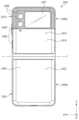
- FIG. 2Ais a front perspective view of an electronic device according to one embodiment of the present disclosure.
- FIG. 2bis a rear perspective view of an electronic device according to an embodiment of the present disclosure.
- FIG. 4ais a plan view schematically illustrating a connection structure of a side member and a circuit board in an electronic device according to an embodiment of the present disclosure.
- FIG. 4bis a graph for explaining antenna performance when an electrical signal is transmitted through capacitance between coupling pads in an electronic device according to an embodiment of the present disclosure.
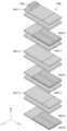
- FIG. 5ais a cross-sectional view of a circuit board according to one embodiment of the present disclosure.
- FIG. 5bis a partial cross-sectional view of a circuit board showing area A of FIG. 5a according to one embodiment of the present disclosure.
- FIG. 5cis a partial perspective view of a circuit board showing area A of FIG. 5a according to one embodiment of the present disclosure.
- FIG. 5dis a partial plan view of a circuit board illustrating a discharge induction unit according to one embodiment of the present disclosure.
- FIG. 5eis a partial plan view of a circuit board illustrating a discharge induction unit according to one embodiment of the present disclosure.
- FIG. 5fis a partial plan view of a circuit board illustrating a discharge induction unit according to an embodiment of the present disclosure.
- FIG. 5gis a partial plan view of a circuit board illustrating a discharge induction unit according to an embodiment of the present disclosure.
- FIG. 5his a partial plan view of a circuit board illustrating a discharge induction unit according to an embodiment of the present disclosure.
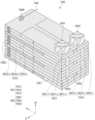
- FIG. 6Ais a partial cross-sectional view of a circuit board according to one embodiment of the present disclosure.
- FIG. 6bis a partial plan view of a circuit board illustrating a discharge induction unit according to one embodiment of the present disclosure.
- FIG. 7ais a partial perspective view of a circuit board according to one embodiment of the present disclosure.
- FIG. 7bis a partial perspective view of a circuit board according to one embodiment of the present disclosure.
- FIG. 7cis a partial perspective view of a circuit board according to one embodiment of the present disclosure.
- FIG. 7dis a partial perspective view of a circuit board according to one embodiment of the present disclosure.
- FIG. 7eis a partial perspective view of a circuit board according to one embodiment of the present disclosure.
- FIG. 7fis a partial perspective view of a circuit board according to one embodiment of the present disclosure.
- FIG. 7gis a partial perspective view of a circuit board according to one embodiment of the present disclosure.
- FIG. 8ais a partial perspective view of a circuit board according to one embodiment of the present disclosure.
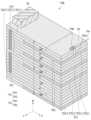
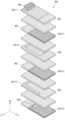
- FIG. 8bis an exploded perspective view illustrating the layer structure of a portion of a circuit board according to one embodiment of the present disclosure.
- FIG. 9ais a partial perspective view of a circuit board according to one embodiment of the present disclosure.
- FIG. 9bis an exploded perspective view illustrating the layer structure of a portion of a circuit board according to one embodiment of the present disclosure.
- FIG. 10is a partial perspective view of a circuit board according to one embodiment of the present disclosure.
- FIG. 11is a partial perspective view of a circuit board according to one embodiment of the present disclosure.
- FIG. 12is a partial perspective view of a circuit board according to one embodiment of the present disclosure.
- FIG. 13is a partial perspective view of a circuit board according to one embodiment of the present disclosure.
- FIG. 14ais a diagram schematically illustrating a connection structure of a side member and a circuit board in an electronic device according to one embodiment of the present disclosure.
- FIG. 14bis a diagram schematically illustrating a circuit connection structure of a side member, a circuit board, and a wireless communication circuit according to one embodiment of the present disclosure.
- FIG. 14cis a partial perspective view of a circuit board according to one embodiment of the present disclosure.
- FIG. 14dis an exploded perspective view illustrating the layer structure of a portion of a circuit board according to one embodiment of the present disclosure.
- FIG. 15ais a drawing schematically illustrating a connection structure of a side member and a circuit board in an electronic device according to one embodiment of the present disclosure.
- FIG. 15bis a diagram schematically illustrating a circuit connection structure of a side member, a circuit board, and a wireless communication circuit according to one embodiment of the present disclosure.
- FIG. 15cis a partial perspective view of a circuit board according to one embodiment of the present disclosure.
- FIG. 15dis an exploded perspective view illustrating the layer structure of a portion of a circuit board according to one embodiment of the present disclosure.
- FIG. 16Ais a drawing schematically illustrating a connection structure of a side member and a circuit board in an electronic device according to one embodiment of the present disclosure.
- FIG. 16bis a perspective view illustrating a portion of a circuit board according to one embodiment of the present disclosure.
- FIG. 17ais a perspective view illustrating a portion of a circuit board according to one embodiment of the present disclosure.
- FIG. 17bis a perspective view illustrating a portion of a circuit board according to one embodiment of the present disclosure.
- FIG. 17cis a graph for explaining the change in radiation performance of an antenna depending on the presence or absence of a radiating member in a circuit board according to one embodiment of the present disclosure.
- FIG. 18ais a perspective view illustrating a portion of a circuit board according to one embodiment of the present disclosure.
- FIG. 18bis a cross-sectional view illustrating a portion of a circuit board according to one embodiment of the present disclosure.
- FIG. 19is a cross-sectional view illustrating a portion of a circuit board according to one embodiment of the present disclosure.
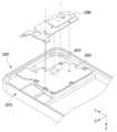
- FIG. 20Ais a partially exploded perspective view of an electronic device according to an embodiment of the present disclosure.
- FIG. 20bis a partial cross-sectional view illustrating a connection structure of a circuit board and a rear frame according to one embodiment of the present disclosure.
- FIG. 21ais a drawing schematically illustrating a connection structure of a side member and a circuit board in an electronic device according to an embodiment of the present disclosure.
- FIG. 21bis a partial cross-sectional view illustrating area F21 of FIG. 21a according to one embodiment of the present disclosure.
- FIG. 22ais a perspective view illustrating a front side of an electronic device according to an embodiment of the present disclosure.
- FIG. 22bis a perspective view illustrating a rear side of an electronic device according to an embodiment of the present disclosure.
- FIG. 22cis an exploded perspective view of an electronic device according to an embodiment of the present disclosure.
- FIG. 23is a diagram schematically illustrating an exemplary connection structure of a side member and a circuit board in an electronic device according to one embodiment of the present disclosure.
- FIG. 24Ais a perspective view illustrating a front side of an electronic device according to an embodiment of the present disclosure.
- FIG. 24bis a perspective view illustrating a rear side of an electronic device according to an embodiment of the present disclosure.
- FIG. 24cis an exploded perspective view of an electronic device according to an embodiment of the present disclosure.
- FIG. 25is a diagram schematically illustrating an exemplary connection structure of a side member and a circuit board in an electronic device according to one embodiment of the present disclosure.
- FIG. 26Ais a front perspective view illustrating an unfolded state of an electronic device according to one embodiment of the present disclosure.
- FIG. 26bis a rear view illustrating an unfolded state of an electronic device according to an embodiment of the present disclosure.
- FIG. 26cis a perspective view illustrating a folded state of an electronic device according to an embodiment of the present disclosure.
- FIG. 27is a diagram schematically illustrating an exemplary connection structure of a side member and a circuit board in an electronic device according to one embodiment of the present disclosure.
- FIG. 28ais a front perspective view illustrating a first state of an electronic device according to an embodiment of the present disclosure.
- FIG. 28bis a front perspective view illustrating a second state of an electronic device according to an embodiment of the present disclosure.
- FIG. 28cis a rear perspective view illustrating a first state of an electronic device according to an embodiment of the present disclosure.
- FIG. 28dis a rear perspective view illustrating a second state of an electronic device according to an embodiment of the present disclosure.
- FIG. 29is a diagram schematically illustrating an exemplary connection structure of a side member and a circuit board in an electronic device according to one embodiment of the present disclosure.
- FIG. 1is a block diagram of an electronic device (101) within a network environment (100) according to various embodiments.
- an electronic device (101)may communicate with an electronic device (102) through a first network (198) (e.g., a short-range wireless communication network), or may communicate with an electronic device (104) or a server (108) through a second network (199) (e.g., a long-range wireless communication network).
- the electronic device (101)may communicate with the electronic device (104) through the server (108).
- the electronic device (101)may include a processor (120), a memory (130), an input module (150), an audio output module (155), a display module (160), an audio module (170), a sensor module (176), an interface (177), a connection terminal (178), a haptic module (179), a camera module (180), a power management module (188), a battery (189), a communication module (190), a subscriber identification module (196), or an antenna module (197).
- the electronic device (101)may omit at least one of these components (e.g., the connection terminal (178)), or may include one or more other components.
- some of these componentse.g., the sensor module (176), the camera module (180), or the antenna module (197) may be integrated into one component (e.g., the display module (160)).
- the processor (120)may control at least one other component (e.g., a hardware or software component) of the electronic device (101) connected to the processor (120) by executing, for example, software (e.g., a program (140)), and may perform various data processing or calculations.
- the processor (120)may store a command or data received from another component (e.g., a sensor module (176) or a communication module (190)) in a volatile memory (132), process the command or data stored in the volatile memory (132), and store result data in a non-volatile memory (134).
- the processor (120)may include a main processor (121) (e.g., a central processing unit or an application processor) or an auxiliary processor (123) (e.g., a graphic processing unit, a neural processing unit (NPU), an image signal processor, a sensor hub processor, or a communication processor) that can operate independently or together therewith.
- a main processor (121)e.g., a central processing unit or an application processor
- an auxiliary processor (123)e.g., a graphic processing unit, a neural processing unit (NPU), an image signal processor, a sensor hub processor, or a communication processor
- the secondary processor (123)may be configured to use lower power than the main processor (121) or to be specialized for a given function.
- the secondary processor (123)may be implemented separately from the main processor (121) or as a part thereof.
- the auxiliary processor (123)may control at least a part of functions or states associated with at least one of the components of the electronic device (101) (e.g., the display module (160), the sensor module (176), or the communication module (190)), for example, while the main processor (121) is in an inactive (e.g., sleep) state, or together with the main processor (121) while the main processor (121) is in an active (e.g., application execution) state.
- the auxiliary processor (123)e.g., an image signal processor or a communication processor
- the auxiliary processor (123)may include a hardware structure specialized for processing an artificial intelligence model.
- the artificial intelligence modelmay be generated through machine learning. Such learning may be performed, for example, in the electronic device (101) on which artificial intelligence is performed, or may be performed through a separate server (e.g., server (108)).
- the learning algorithmmay include, for example, supervised learning, unsupervised learning, semi-supervised learning, or reinforcement learning, but is not limited to the examples described above.
- the artificial intelligence modelmay include a plurality of artificial neural network layers.
- the artificial neural networkmay be one of a deep neural network (DNN), a convolutional neural network (CNN), a recurrent neural network (RNN), a restricted Boltzmann machine (RBM), a deep belief network (DBN), a bidirectional recurrent deep neural network (BRDNN), deep Q-networks, or a combination of two or more of the above, but is not limited to the examples described above.
- the artificial intelligence modelmay additionally or alternatively include a software structure.
- the memory (130)can store various data used by at least one component (e.g., processor (120) or sensor module (176)) of the electronic device (101).
- the datacan include, for example, software (e.g., program (140)) and input data or output data for commands related thereto.
- the memory (130)can include volatile memory (132) or nonvolatile memory (134).
- the nonvolatile memory (134)can include built-in memory (136) and external memory (138).
- the program (140)may be stored as software in memory (130) and may include, for example, an operating system (142), middleware (144), or an application (146).
- the input module (150)can receive commands or data to be used in a component of the electronic device (101) (e.g., a processor (120)) from an external source (e.g., a user) of the electronic device (101).
- the input module (150)can include, for example, a microphone, a mouse, a keyboard, a key (e.g., a button), or a digital pen (e.g., a stylus pen).
- the audio output module (155)can output an audio signal to the outside of the electronic device (101).
- the audio output module (155)can include, for example, a speaker or a receiver.
- the speakercan be used for general purposes such as multimedia playback or recording playback.
- the receivercan be used to receive an incoming call. According to one embodiment, the receiver can be implemented separately from the speaker or as a part thereof.
- the display module (160)can visually provide information to an external party (e.g., a user) of the electronic device (101).
- the display module (160)can include, for example, a display, a holographic device, or a projector and a control circuit for controlling the device.
- the display module (160)can include a touch sensor configured to detect a touch, or a pressure sensor configured to measure the intensity of a force generated by the touch.
- the audio module (170)can convert sound into an electrical signal, or vice versa, convert an electrical signal into sound. According to one embodiment, the audio module (170) can obtain sound through an input module (150), or output sound through an audio output module (155), or an external electronic device (e.g., an electronic device (102)) (e.g., a speaker or a headphone) directly or wirelessly connected to the electronic device (101).
- an electronic devicee.g., an electronic device (102)
- a speaker or a headphonedirectly or wirelessly connected to the electronic device (101).
- the sensor module (176)can detect an operating state (e.g., power or temperature) of the electronic device (101) or an external environmental state (e.g., user state) and generate an electric signal or data value corresponding to the detected state.
- the sensor module (176)can include, for example, a gesture sensor, a gyro sensor, a barometric pressure sensor, a magnetic sensor, an acceleration sensor, a grip sensor, a proximity sensor, a color sensor, an IR (infrared) sensor, a biometric sensor, a temperature sensor, a humidity sensor, or an illuminance sensor.
- the interface (177)may support one or more designated protocols that may be used to directly or wirelessly connect the electronic device (101) with an external electronic device (e.g., the electronic device (102)).
- the interface (177)may include, for example, a high definition multimedia interface (HDMI), a universal serial bus (USB) interface, an SD card interface, or an audio interface.
- HDMIhigh definition multimedia interface
- USBuniversal serial bus
- SD card interfaceSecure Digital Card
- connection terminal (178)may include a connector through which the electronic device (101) may be physically connected to an external electronic device (e.g., the electronic device (102)).
- the connection terminal (178)may include, for example, an HDMI connector, a USB connector, an SD card connector, or an audio connector (e.g., a headphone connector).
- the haptic module (179)can convert an electrical signal into a mechanical stimulus (e.g., vibration or movement) or an electrical stimulus that a user can perceive through a tactile or kinesthetic sense.
- the haptic module (179)can include, for example, a motor, a piezoelectric element, or an electrical stimulation device.
- the camera module (180)can capture still images and moving images.
- the camera module (180)can include one or more lenses, image sensors, image signal processors, or flashes.
- the power management module (188)can manage power supplied to the electronic device (101).
- the power management module (188)can be implemented as, for example, at least a part of a power management integrated circuit (PMIC).
- PMICpower management integrated circuit
- the battery (189)can power at least one component of the electronic device (101).
- the battery (189)can include, for example, a non-rechargeable primary battery, a rechargeable secondary battery, or a fuel cell.
- the communication module (190)may support establishment of a direct (e.g., wired) communication channel or a wireless communication channel between the electronic device (101) and an external electronic device (e.g., the electronic device (102), the electronic device (104), or the server (108)), and performance of communication through the established communication channel.
- the communication module (190)may operate independently from the processor (120) (e.g., the application processor) and may include one or more communication processors that support direct (e.g., wired) communication or wireless communication.
- the communication module (190)may include a wireless communication module (192) (e.g., a cellular communication module, a short-range wireless communication module, or a GNSS (global navigation satellite system) communication module) or a wired communication module (194) (e.g., a local area network (LAN) communication module, or a power line communication module).
- a wireless communication module (192)e.g., a cellular communication module, a short-range wireless communication module, or a GNSS (global navigation satellite system) communication module
- a wired communication module (194)e.g., a local area network (LAN) communication module, or a power line communication module.
- a corresponding communication modulemay communicate with an external electronic device (104) via a first network (198) (e.g., a short-range communication network such as Bluetooth, wireless fidelity (WiFi) direct, or infrared data association (IrDA)) or a second network (199) (e.g., a long-range communication network such as a legacy cellular network, a 5G network, a next-generation communication network, the Internet, or a computer network (e.g., a LAN or WAN)).
- a first network (198)e.g., a short-range communication network such as Bluetooth, wireless fidelity (WiFi) direct, or infrared data association (IrDA)
- a second network (199)e.g., a long-range communication network such as a legacy cellular network, a 5G network, a next-generation communication network, the Internet, or a computer network (e.g., a LAN or WAN)
- a computer networke.g.,
- the wireless communication module (192)may use subscriber information (e.g., international mobile subscriber identity (IMSI)) stored in the subscriber identification module (196) to identify or authenticate the electronic device (101) within a communication network such as the first network (198) or the second network (199).
- subscriber informatione.g., international mobile subscriber identity (IMSI)
- IMSIinternational mobile subscriber identity
- the wireless communication module (192)can support a 5G network and next-generation communication technology after a 4G network, for example, NR access technology (new radio access technology).
- the NR access technologycan support high-speed transmission of high-capacity data (eMBB (enhanced mobile broadband)), terminal power minimization and connection of multiple terminals (mMTC (massive machine type communications)), or high reliability and low latency (URLLC (ultra-reliable and low-latency communications)).
- eMBBenhanced mobile broadband
- mMTCmassive machine type communications
- URLLCultra-reliable and low-latency communications
- the wireless communication module (192)can support, for example, a high-frequency band (e.g., mmWave band) to achieve a high data transmission rate.
- a high-frequency bande.g., mmWave band
- the wireless communication module (192)may support various technologies for securing performance in a high-frequency band, such as beamforming, massive multiple-input and multiple-output (MIMO), full dimensional MIMO (FD-MIMO), array antenna, analog beam-forming, or large scale antenna.
- the wireless communication module (192)may support various requirements specified in an electronic device (101), an external electronic device (e.g., electronic device (104)), or a network system (e.g., second network (199)).
- the wireless communication module (192)may support a peak data rate (e.g., 20 Gbps or more) for eMBB realization, a loss coverage (e.g., 164 eB or less) for mMTC realization, or a U-plane latency (e.g., 0.5 ms or less for downlink (DL) and uplink (UL) each, or 1 ms or less for round trip) for URLLC realization.
- a peak data ratee.g., 20 Gbps or more
- a loss coveragee.g., 164 eB or less
- U-plane latencye.g., 0.5 ms or less for downlink (DL) and uplink (UL) each, or 1 ms or less for round trip
- the antenna module (197)can transmit or receive signals or power to or from the outside (e.g., an external electronic device).
- the antenna module (197)may include an antenna including a radiator formed of a conductor or a conductive pattern formed on a substrate (e.g., a PCB).
- the antenna module (197)may include a plurality of antennas (e.g., an array antenna).
- at least one antenna suitable for a communication method used in a communication network, such as the first network (198) or the second network (199)may be selected from the plurality of antennas by, for example, the communication module (190).
- a signal or powermay be transmitted or received between the communication module (190) and the external electronic device through the selected at least one antenna.
- another componente.g., a radio frequency integrated circuit (RFIC)
- RFICradio frequency integrated circuit
- the antenna module (197)may form a mmWave antenna module.
- the mmWave antenna modulemay include a printed circuit board, an RFIC positioned on or adjacent a first side (e.g., a bottom side) of the printed circuit board and capable of supporting a designated high-frequency band (e.g., a mmWave band), and a plurality of antennas (e.g., an array antenna) positioned on or adjacent a second side (e.g., a top side or a side) of the printed circuit board and capable of transmitting or receiving signals in the designated high-frequency band.
- a first sidee.g., a bottom side
- a plurality of antennase.g., an array antenna
- a command or datamay be transmitted or received between the electronic device (101) and an external electronic device (104) via a server (108) connected to a second network (199).
- Each of the external electronic devices (102 or 104)may be the same or a different type of device as the electronic device (101).
- all or part of the operations executed in the electronic device (101)may be executed in one or more of the external electronic devices (102, 104, or 108). For example, when the electronic device (101) is to perform a certain function or service automatically or in response to a request from a user or another device, the electronic device (101) may, instead of executing the function or service by itself or in addition, request one or more external electronic devices to perform at least a part of the function or service.
- One or more external electronic devices that have received the requestmay execute at least a part of the requested function or service, or an additional function or service related to the request, and transmit the result of the execution to the electronic device (101).
- the electronic device (101)may provide the result, as is or additionally processed, as at least a part of a response to the request.
- cloud computing, distributed computing, mobile edge computing (MEC), or client-server computing technologymay be used, for example.
- the electronic device (101)may provide an ultra-low latency service by using distributed computing or mobile edge computing, for example.
- the external electronic device (104)may include an IoT (Internet of Things) device.
- the server (108)may be an intelligent server using machine learning and/or a neural network.
- the external electronic device (104) or the server (108)may be included in the second network (199).
- the electronic device (101)can be applied to intelligent services (e.g., smart home, smart city, smart car, or healthcare) based on 5G communication technology and IoT-related technology.
- first, second, or first or secondmay be used merely to distinguish one component from another, and do not limit the components in any other respect (e.g., importance or order).
- a componente.g., a first component
- anothere.g., a second component
- functionallye.g., a third component
- moduleused in the embodiments of this document may include a unit implemented in hardware, software or firmware, and may be used interchangeably with terms such as logic, logic block, component, or circuit, for example.
- a modulemay be an integrally configured component or a minimum unit of the component or a part thereof that performs one or more functions.
- a modulemay be implemented in the form of an application-specific integrated circuit (ASIC).
- ASICapplication-specific integrated circuit
- Embodiments of the present documentmay be implemented as software (e.g., a program (140)) including one or more instructions stored in a storage medium (e.g., an internal memory (136) or an external memory (138)) readable by a machine (e.g., an electronic device (101)).
- a processore.g., a processor (120)
- the machinee.g., the electronic device (101)
- the one or more instructionsmay include code generated by a compiler or code executable by an interpreter.
- the method according to the embodiments disclosed in the present documentmay be provided as included in a computer program product.
- the computer program productmay be traded between a seller and a buyer as a commodity.
- the computer program productmay be distributed in the form of a machine-readable storage medium (e.g., a compact disc read only memory (CD-ROM)), or may be distributed online (e.g., by download or upload) via an application store (e.g., Play StoreTM) or directly between two user devices (e.g., smart phones).
- an application storee.g., Play StoreTM
- at least a part of the computer program productmay be at least temporarily stored or temporarily generated in a machine-readable storage medium, such as a memory of a manufacturer's server, a server of an application store, or an intermediary server.
- each componente.g., a module or a program of the above-described components may include a single or multiple entities, and some of the multiple entities may be separated and arranged in other components. According to various embodiments, one or more components or operations of the above-described components may be omitted, or one or more other components or operations may be added. Alternatively or additionally, the multiple components (e.g., a module or a program) may be integrated into one component. In such a case, the integrated component may perform one or more functions of each of the multiple components identically or similarly to those performed by the corresponding component of the multiple components before the integration.
- the operations performed by the module, program, or other componentmay be executed sequentially, in parallel, repeatedly, or heuristically, or one or more of the operations may be executed in a different order, omitted, or one or more other operations may be added.
- FIG. 2ais a front perspective view of an electronic device according to one embodiment.
- FIG. 2bis a rear perspective view of an electronic device according to one embodiment.
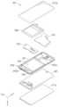
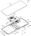
- FIG. 3is an exploded perspective view of an electronic device according to one embodiment.
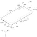
- an electronic device (201)may include a housing (210) forming a first side (210a) (or front side), a second side (210b) (or back side), and a side surface (211c) surrounding a space between the first side (210a) and the second side (210b).
- a housing (210)forming a first side (210a) (or front side), a second side (210b) (or back side), and a side surface (211c) surrounding a space between the first side (210a) and the second side (210b).
- a housing (210)forming a first side (210a) (or front side), a second side (210b) (or back side), and a side surface (211c) surrounding a space between the first side (210a) and the second side (210b).
- An electronic device (201)may include a housing (210) forming an exterior and accommodating components therein.
- the housing (210)may form a front surface (210a) (e.g., a surface facing the +Z direction), a rear surface (210b) (e.g., a surface facing the -Z direction), and a side surface (211c) surrounding an interior space between the front surface (210a) and the rear surface (210b).
- the housing (210)may form the side surface (211c) through a first side surface (211c-1) (e.g., a surface facing the -Y direction), a second side surface (211c-2) (e.g., a surface facing the +Y direction), a third side surface (211c-3) (e.g., a surface facing the +X direction), and a fourth side surface (211c-4) (e.g., a surface facing the -X direction) connecting the front surface (210a) and the rear surface (210b).
- a first side surface211c-1
- a second side surfacee.g., a surface facing the +Y direction
- a third side surface211c-3
- a fourth side surface (211c-4)e.g., a surface facing the -X direction
- the front side (210a)can be formed by a front plate (211a) that is at least partially substantially transparent.
- the front plate (211a)can include a glass plate or a polymer plate including at least one coating layer.
- the back side (210b)can be formed by a substantially opaque back plate (211b).
- the back plate (211b)can be formed by a coated or colored glass, ceramic, polymer, metal (e.g., aluminum, stainless steel, magnesium, etc.), or a combination thereof.
- the side side (211c)can be formed by a side member (240) that is joined to the front plate (211a) and the back plate (211b) and includes a metal and/or a polymer.
- the back plate (211b) and the side member (240)can be formed seamlessly as one piece.
- the back plate (211b) and the side member (240)may be formed of substantially the same material (e.g., aluminum).
- the front plate (211a)may include a plurality of first edge regions (212a-1) facing one direction (e.g., +/- X direction) and extending from at least a portion of the front surface (210a) to the back plate (211b) and having rounded surfaces, a plurality of second edge regions (212a-2) facing another direction (e.g., +/- Y direction) and extending from at least a portion of the front surface (210a) to the back plate (211b) and having rounded surfaces, and a plurality of third edge regions (212a-3) extending from at least a portion of the front surface (210a) to the back plate (211b) and having rounded surfaces and positioned between the plurality of first edge regions (212a-1) and the plurality of second edge regions (212a-2).
- first edge regions212a-1 facing one direction (e.g., +/- X direction) and extending from at least a portion of the front surface (210a) to the back plate (211b) and having
- the back plate (211b)may include a plurality of fourth edge regions (212b-1) facing one direction (e.g., +/- X direction) and extending from at least a portion of the back plate (210b) to the front plate (211a) and having a rounded surface, a plurality of fifth edge regions (212b-2) facing another direction (e.g., +/- Y direction) and extending from at least a portion of the back plate (210b) to the front plate (211a) and having a rounded surface, and a plurality of sixth edge regions (212b-3) extending from at least a portion of the back plate (210b) to the front plate (211a) and having a rounded surface and positioned between the plurality of fourth edge regions (212b-1) and the plurality of fifth edge regions (212b-2).
- a plurality of fourth edge regions (212b-1)facing one direction (e.g., +/- X direction) and extending from at least a portion of the back plate (210b
- the side member (240)can surround at least a portion of the interior space between the front (210a) and the back (210b).
- a display (261)can be positioned on one surface (e.g., in the +Z direction) of the side member (240), and a back plate (211b) can be positioned on the other surface (e.g., in the -Z direction) of the side member (240).
- the side member (240)can include a conductive portion.
- at least a portion of the side member (240)can be formed of a conductive material.
- the side member (240)can include a side portion (241) positioned on at least a portion of the side (211c), and a support portion (242) connected to the side portion (241) and positioned inside the electronic device (201).
- the side portion (241)may connect edges of the front plate (211a) and the back plate (211b) and may form a side portion (211c) of the housing (210) by surrounding between the front plate (211a) and the back plate (211b).
- the support portion (242)may be disposed inside the electronic device (201).
- the side portion (241) and the support portion (242)may be formed integrally or may be formed separately and coupled to each other. When the side portion (241) and the support portion (242) are formed separately, the side member (240) may be formed to include only the side portion (241).
- the side portion (241)may include a plurality of conductive portions disposed along the side portion (211c) of the electronic device (201).
- the conductive portioncan be formed of a metal and/or a conductive polymer material.
- the support portion (242)can be formed of a metal and/or a conductive polymer material with the side portion (241).
- the support portion (242)when the support portion (242) is directly connected to the conductive portion of the side portion (241), the support portion (242) can form an electrical path from the conductive portion of the side portion (241) to ground.
- the electronic device (201)may include a display (261) (e.g., the display module (160) of FIG. 1).
- the display (261)may be located on the front surface (210a) of the electronic device (201).
- the display (261)may be exposed through at least a portion of the front plate (211a) (e.g., the first edge regions (212a-1), the second edge regions (212a-2), and the third edge regions (212a-3).
- the display (261)may have a shape substantially the same as the outer contour shape of the front plate (211a).
- the display (261)may include a touch screen panel (TSP), a pressure sensor, and/or a digitizer (not shown) for detecting a stylus pen.
- the display (261)may include a screen display area (261a) that is visually exposed to the outside of the electronic device (201) and displays content through pixels or a plurality of cells.
- the screen display area (261a)may include a sensing area (261a-1) and a camera area (261a-2).
- the sensing area (261a-1)may overlap at least a portion of the screen display area (261a).
- the sensing area (261a-1)may allow transmission of an input signal related to a sensor module (e.g., the sensor module (176) of FIG. 1).
- the sensing area (261a-1)may display content together with a screen display area (261a) that does not overlap with the sensing area (261a-1).
- the camera area (261a-2)can overlap at least a portion of the screen display area (261a).
- the camera area (261a-2)can expose a lens of a first camera module (280a) (e.g., the camera module (180) of FIG. 1) positioned to face the front of the electronic device (201).
- the camera area (261a-2)can allow transmission of an optical signal (e.g., light) related to the first camera module (280a).
- the camera area (261a-2)can display content similarly to the screen display area (261a) that does not overlap the camera area (261a-2).
- the camera area (261a-2)can display content while the first camera module (280a) is not operating.
- the electronic device (201)may include a sensor module (276).
- the sensor module (276)may sense a signal applied to the electronic device (201).
- the sensor module (276)may be located, for example, on the front (210a) of the electronic device (201).
- the sensor module (276)may be arranged in the electronic device (201) to correspond to a sensing area (261a-1) of a screen display area (261a).
- the sensor module (276)may be arranged to perform its function without being visually exposed through the display (261) in the internal space of the electronic device (201).
- the sensor module (276)may receive an input signal penetrating the sensing area (261a-1) and generate an electric signal based on the received input signal.
- the input signalmay have a specified physical quantity (e.g., heat, light, temperature, sound, pressure, ultrasound).
- the input signalmay include signals relating to the user's biometric information (e.g., the user's fingerprint, voice, etc.).
- the electronic device (201)may include a camera module (280a, 280b) (e.g., the camera module (180) of FIG. 1).
- the camera module (280a, 280b)may include a first camera module (280a) and a second camera module (280b).
- the electronic device (201)may include a flash (280c) disposed near the first camera module (280a) and the second camera module (280b).
- the first camera module (280a)is arranged so that its lens is exposed on the front side (210a) of the housing (210) and can receive an optical signal from the front side (e.g., in the +Z direction) of the electronic device (201).
- the second camera module (280b)is arranged so that its lens is exposed on the rear side (210b) of the housing (210) and can receive an optical signal from the rear side (e.g., in the -Z direction) of the electronic device (201).
- at least a portion of the first camera module (280a)may be arranged in the housing (210) so as to be covered by the display (261).
- the first camera module (280a)may include an under display camera (UDC).
- the first camera module (280a)may receive an optical signal that passes through the camera area (261a-2).
- the second camera module (280b)may include multiple cameras (e.g., dual cameras, triple cameras, or quad cameras).
- the flash (280c)may include a light-emitting diode or a xenon lamp.
- the electronic device (201)may include an input module (250) (e.g., the input module (150) of FIG. 1).
- the input module (250)may receive an operation signal from a user.
- the input module (250)may include at least one key input device that is positioned to be exposed on a side surface (211c) of the housing (210).
- the electronic device (201)may include a connection terminal (278) (e.g., connection terminal (178) of FIG. 1). In one embodiment, the connection terminal (278) may be disposed on an outer surface of the housing (210). The electronic device (201) may be wired and connected to an external device (e.g., another electronic device or an external power source) through the connection terminal (278).
- a connection terminal (278)e.g., connection terminal (178) of FIG. 1
- the connection terminal (278)may be disposed on an outer surface of the housing (210).
- the electronic device (201)may be wired and connected to an external device (e.g., another electronic device or an external power source) through the connection terminal (278).
- the electronic device (301)may include one or more printed circuit boards.
- the electronic device (201)may include a first circuit board (251) (or a main circuit board) and a second circuit board (252) (or a sub-circuit board).
- the first circuit board (251) and the second circuit board (252)may be disposed inside the electronic device (201), for example, in a second support structure (242).
- At least one of the circuit boards (251, 252)may be connected to the second support portion (242) via a ground.
- the first circuit board (251)may be accommodated in a first substrate slot (242a) formed by the second support portion (242).
- the second circuit board (252)may be accommodated in the second board slot (242b) formed by the second support portion (242).
- the circuit boards (251, 252)may be a rigid printed circuit board (PCB) or a flexible printed circuit board (FPCB) that is at least partially bendable.
- the circuit boards (251, 252)may be formed in a multi-layer structure.
- the direction in which each layer of the circuit board is laminatedis referred to as the first direction.
- the electronic device (201)may include a battery (289) disposed therein.
- the battery (289)may be disposed in a battery slot (245) formed in the second support portion (242).
- An electronic devicemay be a device of various forms.
- the electronic devicemay include, for example, a portable communication device (e.g., a smartphone), a computer device, a portable multimedia device, a portable medical device, a camera, a wearable device, or a home appliance device.
- a portable communication devicee.g., a smartphone
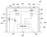
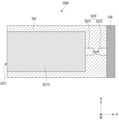
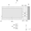
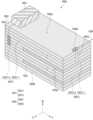
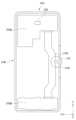
- FIG. 4ais a plan view schematically illustrating a connection structure of a side member and a circuit board in an electronic device according to one embodiment.
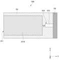
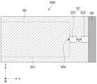
- FIG. 4bis a graph for explaining antenna performance that appears when an electrical signal is transmitted through capacitance between coupling pads in an electronic device according to one embodiment.
- an electronic device (401)may include a housing (e.g., the housing (210) of FIG. 2A), a circuit board (450) (e.g., the first circuit board (251) or the second circuit board (252) of FIG. 3), and a wireless communication circuit (490).
- a housinge.g., the housing (210) of FIG. 2A
- a circuit boarde.g., the first circuit board (251) or the second circuit board (252) of FIG. 3
- a wireless communication circuit (490)e.g., the wireless communication circuit (490).
- the housingmay include a front surface (e.g., the front surface (210a) of FIG. 2a), a back surface opposite the front surface (e.g., the back surface (210b) of FIG. 2a), and a side surface surrounding an interior space between the front surface and the back surface (e.g., the side surface (211c) of FIG. 2a).
- the housingmay include a side member (440) forming at least a portion of the side surface and surrounding the interior space (e.g., the side member (240) of FIG. 3).
- the side member (440)may include a plurality of conductive portions (4411) formed of a conductive material.
- a portion of the conductive portions (4411)may function as a radiator through which an electrical signal flows.
- the side member (440)may include an insulating portion (4412) disposed between the plurality of conductive portions (4411) and electrically isolating adjacent conductive portions (4411) from each other.
- the side member (440)may include one or more connecting portions (4413) formed on the conductive portion (4411) and electrically connected to the circuit board (450).
- the connecting portion (4413)may function as a power supply point to which an electrical signal is applied to the conductive portion (4411), or a grounding point from which an electrical signal applied to the conductive portion (4411) is discharged.
- the connecting portion (4413)may overlap at least a portion of the circuit board (450) disposed within the housing, based on the plan view as in FIG. 4.
- the connecting portion (4413)may be in direct contact with the electrical connection member (453) disposed on the circuit board (450), as illustrated in FIG. 4.
- the connecting portion (4413)may be disposed so as not to overlap the circuit board (450).
- the connecting portion (4413)may be It may also be indirectly connected to an electrical connection member (453) arranged on a circuit board (450) through a separate circuit.
- the circuit board (450)may be disposed in the inner space of the housing. In one embodiment, the circuit board (450) may be formed as a multi-layer structure in which a plurality of layers are laminated. In one embodiment, the circuit board (450) may include one or more electrical connection members (453) electrically connected to the conductive portion (4411). In one embodiment, the electrical connection members (453) may be formed in the form of a conductive contact member formed of a conductive material or a C-clip. For example, the electrical connection members (453) may be connected to a connection member (4413) formed in the conductive portion (4411). In one embodiment, the circuit board (450) may be mounted in the inner space of the housing such that each electrical connection member (453) contacts the connection member (4413) of the corresponding conductive portion (4411).
- the circuit board (450)can be electrically connected to the wireless communication circuit (490).
- the wireless communication circuit (490)can be disposed on the circuit board (450) or disposed on another circuit board.
- the circuit board (450)can include one or more signal lines (454) connected to the wireless communication circuit (490).
- the circuit board (450)can form one or more electrical paths from an electrical connection member (453) connected to the conductive portion (4411) through the signal lines (454) to the wireless communication circuit (490).
- the circuit board (450)may include a plurality of coupling pads (451) arranged in an electrical path.
- the coupling pads (451)may electrically connect a signal line (454) connected to an electrical connection member (453) and a corresponding wireless communication circuit (490) by a coupled feeding structure.
- the coupling pads (451)may indirectly transmit an electrical signal through a capacitance formed between the coupling pads (451) by electrically connecting a corresponding electrical connection member (453) and a signal line (454) by the coupled feeding structure.
- an electro-static discharge (ESD) blocking structurecan be formed that prevents or reduces transmission of noise signals or static electricity from the conductive portion (4411) to the wireless communication circuit (490).
- the circuit board (450)may include a ground (456) for grounding a static electricity or noise signal transmitted from the conductive portion (4411).
- the ground (456) of the circuit board (450)is connected to a ground (456) area of the electronic device (401) (e.g., a ground (456) area of the side member (440)), thereby emitting and eliminating a noise signal applied to the circuit board (450) to the outside of the circuit board (450).
- the radiation performance of the antennawhen transmitting and receiving an electrical signal of a specific frequency band through a conductive portion (4411) of a side member (440), the radiation performance of the antenna can be confirmed.
- the horizontal axis of the graph of FIG. 4brepresents a frequency band radiated through the conductive portion, and the vertical axis represents total radiation efficiency through the conductive portion.
- Line G1represents radiation performance according to a frequency band that appears when the conductive portion (4411) and the wireless communication circuit (490) are directly connected through a circuit including an ESD protection element.
- Line G2represents radiation performance according to a frequency band that appears when the conductive portion (4411) and the wireless communication circuit (490) are connected through a capacitance formed between a plurality of coupling pads (451) under the same conditions as G1.
- FIG. 5Ais a cross-sectional view of a circuit board according to an embodiment.
- FIG. 5Bis a partial cross-sectional view of a circuit board according to an embodiment, showing area A of FIG. 5A.
- FIG. 5Cis a partial perspective view of a circuit board according to an embodiment, showing area A of FIG. 5A.
- FIG. 5Dis a partial plan view of a circuit board showing a discharge inducing unit according to an embodiment.
- FIG. 5Eis a partial plan view of a circuit board showing a discharge inducing unit according to an embodiment.
- FIG. 5Fis a partial plan view of a circuit board showing a discharge inducing unit according to an embodiment.
- FIG. 5Gis a partial plan view of a circuit board showing a discharge inducing unit according to an embodiment.
- FIG. 5His a partial plan view of a circuit board showing a discharge inducing unit according to an embodiment.
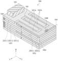
- coupling pads (551)may be formed on a portion of a circuit board (550) according to an embodiment.
- the coupling pads (551)may be arranged on an edge of the circuit board (550) adjacent to a side member (e.g., the side member (440) of FIG. 4A ) of an electronic device (e.g., the electronic device (401) of FIG. 4A ), for example, an edge region of the circuit board (550) adjacent to a conductive portion (e.g., the conductive portion (4411) of FIG. 4A ).
- a coupling connection structureis formed in region A indicated in FIG.
- the coupling connection structuremay be formed in various regions of the circuit board (550) that are connected to the conductive portions of the side members.
- the embodimentswill be described with a focus on a coupling connection structure formed on a portion of a circuit board (550).
- FIGS. 5A to 5Hschematically illustrate a portion of a circuit board (550) on which coupling pads (551) are formed.
- a circuit board (550)e.g., the circuit board (450) of FIG. 4A
- a circuit board (550)may include an electrical connection member (553), a signal line (554) connected to a wireless communication circuit (e.g., the wireless communication circuit (490) of FIG. 4A), a plurality of coupling pads (551), a dielectric (552), an electrical connection member (553), a plurality of conductive vias (5551, 5552), a ground (556), and a discharge induction member (557).
- the circuit board (550)may include a first substrate surface (550a) and a second substrate surface (550b) opposite to the first substrate surface (550a).
- the first substrate surface (550a) and the second substrate surface (550b)may form two outer surfaces of the circuit board (550) that are exposed to the outside.
- additional layersmay be arranged on at least a portion of the first substrate surface (550a) and the second substrate surface (550b) of the circuit board (550).
- additional structuressuch as a protective layer (e.g., a dielectric layer formed of a dielectric (552)), a conductive layer for signal transmission, and a shield can for protecting elements disposed on the first substrate surface (550a) or the second substrate surface (550b) may be disposed on the outer surfaces of the first substrate surface (550a) and the second substrate surface (550b) of the circuit board (550).
- a protective layere.g., a dielectric layer formed of a dielectric (552)
- a conductive layer for signal transmissione.g., a conductive layer for signal transmission
- a shieldcan for protecting elements disposed on the first substrate surface (550a) or the second substrate surface (550b) may be disposed on the outer surfaces of the first substrate surface (550a) and the second substrate surface (550b) of the circuit board (550).
- the first substrate surface (550a) and the second substrate surface (550b) of the circuit board (550)are illustrated as forming surfaces exposed to the outside of the circuit board (550).
- the circuit board (550)may be formed with a multilayer structure.
- the circuit board (550)may be formed with a multilayer structure in which coupling pads (551) and dielectrics (552) are intersectingly overlapped.
- at least one coupling pad (551) and dielectric (552) in the circuit board (550)may be arranged substantially on the same plane to form one layer.
- the electrical connection member (553)can be disposed on one side of the circuit board (550), for example, the first board side (550a) or the second board side (550b).
- the electrical connection member (553)can be electrically connected to a conductive portion of a side member (e.g., conductive portion (4411) of FIG. 4a).
- the signal line (554)may be connected to a wireless communication circuit.
- the signal line (554)is illustrated as being arranged on the first substrate surface (550a) of the circuit board (550), but this is for convenience of explanation, and it should be noted that the position of the signal line (554) on the circuit board (550), the arrangement relationship with other components, or the shape are not limited thereto.
- a plurality of coupling pads (551)may be arranged separately from each other on the circuit board (550). At least some of the coupling pads (5511-1, 5511-2, 5512-1, 5512-2) among the plurality of coupling pads (551) may have different positions in a first direction (T) of the circuit board (550) (e.g., the W-axis direction of FIG. 5B).
- the plurality of coupling pads (551)may be arranged separately along the first direction (T) of the circuit board (550).
- the first direction (T) of the circuit board (550)may mean a direction in which a plurality of layers of the circuit board (550) are stacked.
- the first direction (T)is understood to mean a stacking direction (e.g., a thickness direction) of the plurality of layers of the circuit board.
- a dielectric (552)may be placed between a plurality of coupling pads (551).
- Each of the plurality of coupling pads (551)may be electrically insulated through the dielectric (552).
- the plurality of coupling pads (551)may include a plurality of first coupling pads (5511) and a plurality of second coupling pads (5512).
- the plurality of first coupling pads (5511)can be electrically connected to each other.
- the plurality of first coupling pads (5511)can be electrically connected to an electrical connection member (553).
- the first coupling pads (5511)can be in direct contact with the electrical connection member (553), or can be connected to the electrical connection member (553) through a separate conductive connection line (5511) or a conductive via (555).
- the conductive viacan be a structure in which a conductive material is at least partially filled in a via hole.
- the plurality of first coupling pads (5511)can form an electrical path through which an electrical signal flows with the electrical connection member (553).
- the first coupling pad (5511)can function as a feeding pad that forms an electrical path for applying an electrical signal to a conductive portion (e.g., the conductive portion (4411) of FIG. 4A) or directly receiving an electrical signal from the conductive portion through an electrical connection member (553).
- a conductive portione.g., the conductive portion (4411) of FIG. 4A
- an electrical connection member553
- the first coupling pad (5511)may include a first-first coupling pad (5511-1) and a first-second coupling pad (5511-2) that are separately arranged along the first direction (T) of the circuit board (550).
- the number of the plurality of first coupling pads (5511)is not limited thereto, and may be singular, unlike what is illustrated.
- the plurality of second coupling pads (5512)can be electrically connected to each other.
- the plurality of second coupling pads (5512)can be electrically insulated from the first coupling pads (5511) on the circuit board (550).
- the plurality of second coupling pads (5512)can be electrically connected to a signal line (554) connected to a wireless communication circuit.
- the second coupling pads (5512)can be in direct contact with the signal line (554), or can be connected to the signal line (554) connected to the wireless communication circuit through a separate conductive connection line or a second conductive via (5552).
- the plurality of second coupling pads (5512)can form an electrical path through which an electrical signal flows with the wireless communication circuit through the signal line (554).
- the second coupling pad (5512)may function as a signal deliver pad that receives an electrical signal from a wireless communication circuit through a signal line (554) or forms an electrical path for transmitting an electrical signal to the wireless communication circuit through the signal line (554).
- the second coupling pad (5512)may include a second-first coupling pad (5512-1) and a second-second coupling pad (5512-2) that are separately arranged along the first direction (T) of the circuit board (550).
- the number of the plurality of second coupling pads (5512)is not limited thereto.
- the first coupling pad (5511) and the second coupling pad (5512)can transmit electrical signals in a non-contact manner.
- the first coupling pad (5511) and the second coupling pad (5512)can be arranged to overlap at least a portion when viewing the circuit board (550) in one direction and form a capacitance therebetween for indirectly transmitting an electrical signal.
- the capacitance formed between the first coupling pad (5511) and the second coupling pad (5512)can be determined according to factors such as a gap between the first coupling pad (5511) and the second coupling pad (5512), an overlapping area, or a permittivity of a dielectric (552).
- the impedance of an electrical signal applied to a corresponding conductive portioncan be determined.
- At least one second coupling pad (5512)may be positioned to overlap between at least one pair of first coupling pads (5511).
- the second-first coupling pad (5512-1)may be positioned between the first-first coupling pad (5511-1) and the first-second coupling pad (5511-2).
- a plurality of first coupling pads (5511) and a plurality of second coupling pads (5512)may be alternately arranged along a first direction (T) of the circuit board (550).
- a first-first coupling pad (5511-1), a second-first coupling pad (5512-1), a first-second coupling pad (5511-2), and a second-second coupling pad (5512-2)may be alternately arranged along the first direction (T) of the circuit board (550).
- at least some of the first coupling pads (5511) and the second coupling pads (5512)may overlap each other along the first direction (T) of the circuit board (550).
- the plurality of coupling pads (551)may be arranged such that the overlapping area (A) between the adjacent first coupling pads (5511) and the second coupling pads (5512) is substantially the same. For example, as shown in FIG.
- the overlapping area (A) between the first-first coupling pad (5511-1) and the second-first coupling pad (5512-1), the overlapping area (A) between the first-first coupling pad (5511-1) and the second-second coupling pad (5512-2), and the overlapping area (A) between the first-second coupling pad (5511-2) and the second-second coupling pad (5512-2)may be substantially the same.
- the arrangement of multiple coupling pads (551)is not limited to this, and the overlapping area between adjacent coupling pads may be set differently depending on the design.
- the total capacitance formed by the plurality of coupling pads (551)can be determined through the respective capacitances formed between the first-first coupling pad (5511-1) and the second-first coupling pad (5512-1), between the first-first coupling pad (5511-1) and the second-second coupling pad (5512-2), and between the second-second coupling pad (5512-2) and the first-second coupling pad (5511-2).
- the total capacitance formed by the plurality of coupling pads (551)may be greater than or equal to the sum of the individual capacitances formed between the plurality of first coupling pads (5511) and the plurality of second coupling pads (5512) that are arranged adjacent to each other.
- the total capacitance formed through the overlapping area of the plurality of first coupling pads (5511) and the plurality of second coupling pads (5512)may be set to match the target capacitance.
- the total capacitance formed through the plurality of coupling pads (551) in the circuit board (550)may be determined through the type of dielectric, the thickness of the dielectric, the spacing between each coupling pad, or the overlapping area between the coupling pads.
- An individual capacitance for transmitting an indirect electrical signalis formed between the first coupling pad (5511) and the second coupling pad (5512) adjacent to each other, and the total sum of the individual capacitances formed on the circuit board (550), for example, the total capacitance, may be about 10 pF (picofrads) or more.
- the present inventionis not limited thereto.
- a plurality of conductive viascan penetrate the circuit board (550) in a first direction (T) and electrically connect at least some of the coupling pads (5511, 5512) among the plurality of coupling pads (551) that are arranged separately from each other.
- the plurality of conductive vias (5551, 5552)can individually connect the plurality of first coupling pads (5511) and second coupling pads (5512).
- the plurality of conductive vias (5551, 5552)may include one or more first conductive vias (5551) connected to the plurality of first coupling pads (5511) and electrically connecting the plurality of first coupling pads (5511), and one or more second conductive vias (5552) connected to the plurality of second coupling pads (5512) and electrically connecting the plurality of second coupling pads (5512).
- the first conductive vias (5551) and the second conductive vias (5552)may be electrically insulated from each other.
- the plurality of conductive vias (5551, 5552)may not directly connect the first coupling pads (5511) and the second coupling pads (5512).
- one or more first conductive vias (5551)can electrically connect a plurality of first coupling pads (5511) along a first direction (T) of a circuit board (550).
- the first conductive vias (5551)can form an electrical path between the plurality of first coupling pads (5511).
- the first conductive vias (5551)can be provided in plurality on the circuit board (550) and each can be arranged between a pair of adjacent first coupling pads (5511).
- one first conductive via (5551)can penetrate the circuit board (550) in the first direction (T) to simultaneously connect a plurality of first coupling pads (5511) that are spaced apart from each other in the first direction (T) of the circuit board (550).
- the first conductive via (5551)can electrically connect at least one first coupling pad (5511) and the electrical connection member (553) when the first coupling pad (5511) and the electrical connection member (553) are separately disposed on the circuit board (550), thereby forming an electrical path between the electrical connection member (553) and the first coupling pad (5511).
- one or more second conductive vias (5552)can electrically connect a plurality of second coupling pads (5512) along the first direction (T) of the circuit board (550).
- the second conductive vias (5552)can form an electrical path between the plurality of second coupling pads (5512).
- the second conductive vias (5552)can be provided in the circuit board (550) in multiple numbers and arranged between a pair of adjacent second coupling pads (5512).
- one second conductive via (5552)can be arranged to penetrate the circuit board (550) in the first direction (T) and simultaneously connect a plurality of second coupling pads (5512) that are spaced apart from each other in the first direction (T) of the circuit board (550).
- the second conductive via (5552)can electrically connect at least one second coupling pad (5512) and the signal line (554) connected to the wireless communication circuit when the second coupling pad (5512) and the signal line (554) are separately arranged on the circuit board (550), thereby forming an electrical path between the second coupling pad (5512) and the wireless communication circuit.
- a switch(e.g., switch (1859) of FIG. 18B) may be arranged between at least one of the plurality of conductive vias (5551, 5552) and the first coupling pad (5511) or the second coupling pad (5512) to selectively block a connection path of an electrical signal formed through the conductive via.
- the switchmay be arranged in at least one layer of the circuit board (550) on which the first coupling pad (5511) or the second coupling pad (5512) is arranged. A detailed description thereof will be provided later.
- the ground (556)may be arranged on the circuit board (550) and may form a path for static electricity or noise signals introduced into the circuit board (550) to escape.
- the ground (556)may prevent or reduce electrical signals, such as static electricity or noise signals, from being introduced into component elements arranged on the circuit board (550) by inducing the introduced electrical signals to travel through other electrical structures.
- the ground (556)may be connected to another ground of the electronic device.
- the ground (556)may be arranged on the circuit board (550) so as to be separated from a plurality of coupling pads (551).
- the ground (556)may be placed on an exposed surface of the circuit board (550) (e.g., the second substrate surface (550b) of FIG.
- the ground (556)may receive an electrical signal, such as a static electricity or noise signal, from the first coupling pad (5511) and discharge it to the outside of the circuit board (550).
- At least one first coupling pad (5511) of the plurality of first coupling pads (5511)may be arranged adjacent to the ground (556).
- one first coupling pad (5511)may be arranged on the same layer as the ground (556) to form a gap adjacent to the ground (556).
- one first coupling pad (5511D) and the ground (556)may be arranged on the second substrate surface (550b) of the circuit board (550), and the ground (556) may receive static electricity or noise signals introduced from the conductive portion to the circuit board (550) through the adjacently arranged first coupling pad (5511D).
- the ground (556) and the first coupling pad (5511)do not necessarily have to be arranged on the same layer of the circuit board (550).
- the ground (556)may be arranged adjacent to the first conductive via (5551) connected to the first coupling pad (5511), and may receive static electricity or noise signals introduced from the conductive portion to the circuit board (550) through the adjacently arranged first conductive via (5551).
- the ground (556)when the ground (556) is arranged on the first substrate surface (550a) of the circuit board (550), the ground (556) may receive static electricity or noise signals through the first coupling pad (5511) arranged on the first substrate surface (550a) or the first conductive via (5551) connected to the first coupling pad (5511).
- the ground (556)is preferably arranged on the first substrate surface (550a) or the second substrate surface (550b) of the circuit board (550), but it should be noted that the arrangement location of the ground (556) on the circuit board (550) is not limited and the arrangement location of the ground (556) may be changed depending on the design of the circuit board (550).
- the discharge inducing portion (557D, 557E, 557F, 557G, 557H)can induce movement for discharge of an electrical signal from the first coupling pad (5511) to the ground (556).
- the discharge inducing portion (557D, 557E, 557F, 557G, 557H)can function as a lightning rod to induce movement of an electrical signal by narrowing the gap between one of the first coupling pads (5511) (e.g., the first-second coupling pad (5511-2)) and the ground (556).
- the discharge inducing portion (557D, 557E, 557F, 557G, 557H)can induce movement for discharge of an electrical signal between the ground (556) and the first coupling pad (5511) positioned adjacent to the ground (556).
- the discharge inducing member (557D, 557E, 557F, 557G, 557H)may include one or more discharge members (5571, 5572) for narrowing the gap between the first coupling pad (5511) and the ground (556).
- the discharge members (5571, 5572)may be formed of a conductive material.
- the discharge members (5571, 5572)may narrow the gap between the first coupling pad (5511) and the ground (556) through which an electrical signal moves for discharge, for example, the gap through which the electrical signal moves through the dielectric (552), by a predetermined gap (G).
- the gap (G)may be about 200 ⁇ m or less, but is not limited thereto.
- a discharge inducing member (557D)may include a first discharge member (5571) that is connected to one of the first coupling pads (5511) and protrudes in a direction toward the ground (556) (e.g., the +v direction of FIG. 5D).
- the discharge inducing member (557D)may be separately formed of a material that is the same as or different from the first coupling pad (5511) and may be connected to the first coupling pad (5511D), but may also mean a protruding portion in which a part of the first coupling pad (5511D) protrudes toward the ground (556).
- a gap (G) in which a dielectric (552) is positionedmay be formed between the first discharge member (5571) and the ground (556).
- a discharge inducing member (557E)may include a second discharge member (5572) that is connected to a ground (556) and protrudes in a direction (e.g., in the -v direction of FIG. 5E) toward one of the first coupling pads (5511).
- the second discharge member (5572)may be separately formed of a material that is the same as or different from the ground (556) and may be connected to the ground (556), but may also mean a protruding portion in which a part of the ground (556) protrudes toward the first coupling pad (5511E).
- a gap (G) in which a dielectric (552) is positionedmay be formed between the second discharge member (5572) and the ground (556).
- a discharge inducing member (557F)may include a first discharge member (5571) and a second discharge member (5572), which are respectively connected to one of the first coupling pads (5511) and the ground (556) and extend in a direction toward each other (e.g., the v-axis direction of FIG. 5F).
- the first discharge member (5571)may be individually formed of a material identical to or different from the first coupling pad (5511F) and connected to the first coupling pad (5511F), but may also mean a protruding portion of a part of the first coupling pad (5511F) that protrudes toward the ground (556).
- the second discharge member (5572)may be formed separately from a material identical to or different from the ground (556) and connected to the ground (556), but may also mean a protruding portion in which a portion of the ground (556) protrudes toward the first coupling pad (5511F).
- a gap (G) in which a dielectric (552) is disposedmay be formed between the first discharge member (5571) and the second discharge member (5572).
- a discharge inducing member (557G)may include a plurality of first discharge members (5571) and a plurality of second discharge members (5572) that are respectively connected to one of the first coupling pads (5511) and the ground (556) of the first coupling pads (5511) and extend in a direction toward each other (e.g., the V-axis direction of FIG. 5G).
- the plurality of first discharge members (5571)may include a first-first discharge member (5571-1) and a first-second discharge member (5571-2) that are connected to the first coupling pad (5511G) and spaced apart from each other.
- the plurality of second discharge members (5572)may include second-first discharge members (5572-1) and second-second discharge members (5572-2) that are connected to the ground (556) and spaced apart from each other.
- the first-first discharge members (5571-1) and the second-first discharge members (5572-1)may correspond to each other and form a gap (G) therebetween.
- the first-second discharge members (5571-2) and the second-second discharge members (5572-2)may correspond to each other and form a gap (G) therebetween.
- the number of the first discharge members (5571) and the second discharge members (5572)is not limited.
- the first discharge member (5571) and the second discharge member (5572)may be formed in three or more, respectively, and may be arranged to correspond to each other.
- the lengths of the plurality of discharge members (5571, 5572)may be the same as each other, but may also be different from each other.
- the gap (G) between the first discharge members (5571) and the second discharge members (5572) that correspond to each othermay be constant.
- the first discharge member (5571)may be individually formed of a material that is the same as or different from the first coupling pad (5511G) and may be connected to the first coupling pad (5511G), but may also mean a protruding portion of the first coupling pad (5511G) that protrudes toward the ground (556).
- the second discharge member (5572)may be individually formed of a material identical to or different from the ground (556) and connected to the ground (556), but may also mean a protruding portion of the ground (556) that protrudes toward the first coupling pad (5511G).
- a discharge inducing member (557H)may include a first discharge member (5571) connected to a conductive via (5553) connected to a first coupling pad (5511).
- the first discharge member (5571)may be formed in a different layer from the first coupling pad (5511) and may be connected to the first coupling pad (5511) through the conductive via (5553).
- the first discharge member (5571)may extend in a direction toward the ground (556) (e.g., the +v direction of FIG. 5G).
- the discharge inducing member (557G)may include a second discharge member (5572) connected to the ground (556) and extending in a direction toward the first discharge member (5571).
- the second discharge member (5572)may be formed separately from a material identical to or different from the ground (556) and connected to the ground (556), but may also mean a protruding portion in which a portion of the ground (556) protrudes toward the first coupling pad (5511).
- a gap (G) in which a dielectric (552) is positionedmay be formed between the first discharge member (5571) and the second discharge member (5572).
- the circuit board (550)can form an indirect signal transmission path between an electrical connection member (553) connected to a conductive portion and a signal line (554) connected to a wireless communication circuit through a coupling connection structure between a first coupling pad (5511) and a second coupling pad (5512). Due to the indirect signal transmission through the first coupling pad (5511) and the second coupling pad (5512), a direct connection between the electrical connection member (553) and the wireless communication circuit on the circuit board (550) is prevented, and thus a phenomenon in which static electricity or noise signals introduced into the circuit board (550) through the conductive portion are transmitted to the wireless communication circuit can be prevented or reduced.
- static electricity or noise signals introduced into the circuit board (550) through the conductive portionare induced to be transmitted from the first coupling pad (5511) to the ground (556) through the discharge inducing portions (557D, 557E, 557F, 557G, 557H), thereby allowing the static electricity or noise signals introduced into the circuit board (550) to be effectively discharged to the outside of the circuit board (550).
- ground (556) and the discharge inducing portions(557D, 557E, 557F, 557G, 557H) may be omitted in certain embodiments, but it should be noted that it will be apparent to those skilled in the art that the configuration of the ground (556) and the discharge inducing portions (557D, 557E, 557F, 557G, 557H) described in FIGS. 5d to 5g may be applied to other embodiments.
- circuit board including a coupling connection structureincludes the configuration of the above-described ground and discharge inducing portions unless there is a separate mention that the configuration is excluded.
- FIG. 6ais a partial perspective view of a circuit board according to one embodiment.
- FIG. 6bis a partial plan view of a circuit board illustrating a discharge induction unit according to one embodiment.
- a circuit board (650)may include a first coupling pad (6511), a second coupling pad (6512) that is separately disposed from the first coupling pad (6511), a dielectric (652) that electrically insulates the first coupling pad (6511) and the second coupling pad (6512), an electrical connection member (653) that is connected to form an electrical path with the first coupling pad (6511) and is connected to a conductive portion of a side member (e.g., the conductive portion (4411) of FIG. 4A), a signal line (654) that is connected to form an electrical path with the second coupling pad (6512) and is connected to a wireless communication circuit (e.g., the wireless communication circuit (490) of FIG. 4A), and a ground (656).
- a wireless communication circuite.g., the wireless communication circuit (490) of FIG. 4A
- first coupling pad (6511) and the second coupling pad (6512)may be arranged to overlap each other while being separated along the first direction (T) of the circuit board (650).
- a capacitance for indirect signal transmissionmay be formed between the first coupling pad (6511) and the second coupling pad (6512).
- the electrical connection member (653)may be positioned in contact with the first coupling pad (6511), but may be connected through a conductive connection line, such as a first conductive via (e.g., the first conductive via (5551) of FIG. 5a).
- the electrical connection member (653)may be positioned on a surface of the circuit board (650), for example, a first substrate surface (650a) of the circuit board (650).
- the signal line (654)may be directly connected to the second coupling pad (6512), but may also be connected to the second coupling pad (6512) through a conductive connection line, such as a second conductive via (5552) of FIG. 5a.
- the signal line (654)may be formed separately from the second coupling pad (6512) of a material that is the same as or different from the second coupling pad (6512). It may be connected to the second coupling pad (6512) or formed integrally with the second coupling pad (6512) and extended from the second coupling pad (6512).
- the ground (656)may be arranged on the circuit board (650) so as to be separated from the first coupling pad (6511) and the second coupling pad (6512).
- a dielectric (652)may be arranged between the ground (656) and the coupling pad to block direct connection between the ground (656) and the coupling pad.
- the ground (656)may be arranged on a surface of the circuit board (650), for example, a second substrate surface (650b) of the circuit board (650), so as to be connected to another structure outside the circuit board (650).
- the ground (656)may be arranged substantially on the same plane (i.e., substantially on the same layer) with respect to the first coupling pad (6511) and the circuit board (650) in the first direction (T).
- a discharge inducing portion (657)may be arranged between the ground (656) and the first coupling pad (6511) to induce transmission of an electrical signal, such as a static electricity or noise signal.
- the discharge inducing portion (657)may be connected to either the ground (656) or the first coupling pad (6511) arranged adjacent to the ground (656), thereby narrowing the gap between the first coupling pad (6511) and the ground (656).
- a gap (G) in which a dielectric (652) is arrangedmay be formed between the discharge inducing portion (657) and the ground (656).
- FIG. 7Ais a partial perspective view of a circuit board according to an embodiment.
- FIG. 7Bis a partial perspective view of a circuit board according to an embodiment.
- FIG. 7Cis a partial perspective view of a circuit board according to an embodiment.
- FIG. 7Dis a partial perspective view of a circuit board according to an embodiment.
- FIG. 7Eis a partial perspective view of a circuit board according to an embodiment.
- FIG. 7Fis a partial perspective view of a circuit board according to an embodiment.
- FIG. 7Gis a partial perspective view of a circuit board according to an embodiment.
- FIGS. 7A to 7Fillustrate a portion of a circuit board having a coupling connection structure formed thereon, each illustrating various embodiments of the circuit board.
- a circuit board (750A)may include a plurality of coupling pads (751) (e.g., coupling pads (451) of FIG. 4A) that are electrically insulated and separated by a dielectric (752), an electrical connecting member (753) (e.g., electrical connecting member (453) of FIG. 4A), a signal line (754) connected to a wireless communication circuit (e.g., wireless communication circuit (490) of FIG. 4A), a plurality of conductive vias (755), a ground (756), and/or a discharge inducing member (757).
- a wireless communication circuite.g., wireless communication circuit (490) of FIG. 4A
- a plurality of conductive vias (755e.g., a ground (756), and/or a discharge inducing member (757).
- the plurality of coupling pads (751)may include a plurality of first coupling pads (7511) connected to form an electrical path to the electrical connection member (753), and a plurality of second coupling pads (7512) connected to form an electrical path to the wireless communication circuit via the signal line (754).
- the first coupling pads (7511)may include a first-first coupling pad (7511-1) and/or a first-second coupling pad (7511-2)
- the second coupling pads (7512)may include a second-first coupling pad (7512-1) and/or a second-second coupling pad (7512-2).
- At least one of the second coupling pads (7512)may be disposed between a pair of first coupling pads (7511) with respect to the first direction (T) of the circuit board (750A).
- the second-first coupling pad (7512-1)may be disposed to overlap between the first-first coupling pad (7511-1) and the first-second coupling pad (7511-2).
- a plurality of first coupling pads (7511) and a plurality of second coupling pads (7512)may be alternately disposed to overlap along the first direction (T) of the circuit board (750A) (e.g., the W-axis direction of FIG. 7A).
- the first-first coupling pad (7511-1), the second-first coupling pad (7512-1), the first-second coupling pad (7511-2), and the second-second coupling pad (7512-2)may be alternately arranged to overlap each other.
- a plurality of conductive vias (755)can be arranged to penetrate the circuit board (750A) in a first direction (T).
- the plurality of conductive vias (755)can include one or more first conductive vias (7551) electrically connecting a first coupling pad (7511) and one or more second conductive vias (7552) electrically connecting a second coupling pad (7512).
- the one or more second conductive vias (7552)can connect a signal line (754) connected to the second coupling pad (7512) and a wireless communication circuit.
- the ground (756)may be arranged on a surface of the circuit board (750A). In one embodiment, the ground (756) may be separately arranged on the circuit board (750) while being electrically insulated from the plurality of coupling pads (751) through a dielectric (752). In one embodiment, with respect to the first direction (T) of the circuit board (750), the ground (756) may be arranged on the same layer (e.g., on the same plane) as at least one first coupling pad (7511) among the plurality of first coupling pads (7511). For example, the ground (756) may be arranged on the same plane as the first-1 coupling pad (7511-1).
- the discharge inducing portion (757)may be disposed between the 1-1 coupling pad (7511-1) and the ground (756) to induce transmission of an electrical signal, such as a static electricity or noise signal, from the 1-1 coupling pad (7511-1) toward the ground (756).
- the discharge inducing portion (757)may be individually formed of a material identical to or different from that of the 1-1 coupling pad (7511-1) and connected to the 1-1 coupling pad (7511-1), or may mean a protruding portion in which a portion of the 1-1 coupling pad (7511-1) protrudes toward the ground (756).
- a gap (G) in which a dielectric (752) is disposedcan be formed between the discharge induction unit (757) and the ground (756).
- a circuit board (750B)may include a plurality of coupling pads (751) (e.g., the coupling pads (451) of FIG. 4A) that are electrically insulated and separated from each other by a dielectric (752), an electrical connecting member (753) (e.g., the electrical connecting member (453) of FIG. 4A), a signal line (754) connected to a wireless communication circuit (e.g., the wireless communication circuit (490) of FIG. 4A), a plurality of conductive vias (755), a ground (756), and/or a discharge inducing member (757) for reducing a gap (G) between the ground (756) and the first coupling pad (7511).
- a wireless communication circuite.g., the wireless communication circuit (490) of FIG. 4A
- a plurality of conductive vias (755)a ground (756
- a discharge inducing member (757)for reducing a gap (G) between the ground (756) and the first coupling pad (7511
- the plurality of coupling pads (751)may include a plurality of first coupling pads (7511) electrically connected through one or more first conductive vias (7551), a plurality of second coupling pads (7512) electrically connected through one or more second conductive vias (7552).
- the first coupling pads (7511)may be connected to form an electrical path to an electrical connection member (753).
- the second coupling pads (7512)may be connected to form an electrical path to a signal line (754) connected to a wireless communication circuit.
- the plurality of first coupling pads (7511)may include first-first coupling pads (7511-1) and/or first-second coupling pads (7511-2) spaced apart from each other along a first direction (T) of a circuit board (750B).
- the plurality of second coupling pads (7512)may include second-first coupling pads (7512-1) and/or second-second coupling pads (7512-2) spaced apart from each other along the first direction (T) of the circuit board (750B).
- the plurality of first coupling pads (7511) and second coupling pads (7512)may be alternately arranged along the first direction (T) of the circuit board (750).
- first coupling pads (7511) and second coupling pads (7512) that are adjacent to each othermay overlap each other.
- a plurality of coupling pads (751)can transmit electrical signals in a non-contact manner through capacitance formed in an overlapping area of first coupling pads (7511) and second coupling pads (7512) that are arranged adjacent to each other.
- the electrical connection member (753)can be connected to the first coupling pad (7511) through a connection line (7531) of a conductive material.
- the connection line (7531)can be individually formed of the same or different material as the first coupling pad (7511) and connected, or a portion of the first coupling pad (7511) can be extended to the electrical connection member (753).
- a signal line (754) connected to the wireless communication circuitcan be connected to the second coupling pad (7512) through a connection line (7541) of a conductive material.
- the signal line (754)can be individually formed of the same or different material as the second coupling pad (7512) and connected to the second coupling pad (7512), or a portion of the second coupling pad (7512) can be extended.
- a circuit board (750C)may include a plurality of coupling pads (751) (e.g., the coupling pads (451) of FIG. 4A) that are electrically insulated and separated from each other by a dielectric (752), an electrical connection member (753) (e.g., the electrical connection member (453) of FIG. 4A) to be connected to a conductive portion of a side member (e.g., the conductive portion (4411) of FIG. 4A), a signal line (754) connected to a wireless communication circuit (e.g., the wireless communication circuit (490) of FIG. 4A), and/or a plurality of conductive vias (755).
- a coupling pads (751)e.g., the coupling pads (451) of FIG. 4A
- an electrical connection member (753)e.g., the electrical connection member (453) of FIG. 4A
- a signal line (754)connected to a wireless communication circuit (e.g., the wireless communication circuit (490) of FIG. 4
- the plurality of coupling pads (751)may include a plurality of first coupling pads (7511) electrically connected to the electrical connection member (753), and a plurality of second coupling pads (7512) electrically connected to the signal line (754).
- the plurality of first coupling pads (7511)may include a first-first coupling pad (7511-1) and/or a first-second coupling pad (7511-2).
- the plurality of first coupling pads (7511)may be electrically connected through a first conductive via (7551).
- the second coupling pads (7512)may be connected to the signal line (754) through a second conductive via (7552).
- the second coupling pad (7512)may be positioned between the first-first coupling pad (7511-1) and the first-second coupling pad (7511-2) with respect to the first direction (T) of the circuit board (750C).
- a capacitance for non-contact signal transmissionmay be formed between the second coupling pad (7512) and each of the first coupling pads (7511).
- a circuit board (750D)may include a plurality of coupling pads (751) (e.g., coupling pads (451) of FIG. 4A) that are electrically insulated and separated from each other by a dielectric (752), an electrical connection member (753) (e.g., electrical connection member (453) of FIG. 4A) for connection to a conductive portion of a side member (e.g., conductive portion (4411) of FIG. 4A), a signal line (754) connected to a wireless communication circuit (e.g., wireless communication circuit (490) of FIG. 4A), and/or a plurality of conductive vias (755).
- a coupling pads (751)e.g., coupling pads (451) of FIG. 4A
- an electrical connection member (753)e.g., electrical connection member (453) of FIG. 4A
- a signal line (754)connected to a wireless communication circuit (e.g., wireless communication circuit (490) of FIG. 4A), and/or a pluralit
- the plurality of coupling pads (751)can include a plurality of first coupling pads (7511) connected to form an electrical path to an electrical connection member (753), and a plurality of second coupling pads (7512) connected to form an electrical path to a signal line (754).
- the plurality of first coupling pads (7511)can include a first-first coupling pad (7511-1), a first-second coupling pad (7511-2), and/or a first-third coupling pad (7511-3).
- the plurality of second coupling pads (7512)can include a second-first coupling pad (7512-1), a second-second coupling pad (7512-2), and/or a second-third coupling pad (7512-3).
- At least one second coupling pad (7512) among the plurality of second coupling pads (7512)may be arranged to overlap between a pair of first coupling pads (7511).
- the second-first coupling pad (7512-1)may be arranged to overlap between the first-first coupling pad (7511-1) and the first-second coupling pad (7511-2)
- the second-second coupling pad (7512-2)may be arranged to overlap between the first-second coupling pad (7511-2) and the first-third coupling pad (7511-3).
- a plurality of first coupling pads (7511) and second coupling pads (7512)may be alternately arranged along a first direction (T) of the circuit board (750) such that at least some of them overlap each other.
- three first coupling pads (7511-1, 7511-2, 7511-3) and three second coupling pads (7512-1, 7512-2, 7512-3)may be alternately arranged along the first direction (T) of the circuit board (750D) such that at least some of them overlap each other.
- a capacitance for non-contact signal transmissionmay be formed between the first coupling pads (7511) and the second coupling pads (7512) that are adjacent to each other with respect to the first direction (T) of the circuit board (750D).
- the total capacitance formed between the plurality of coupling pads (751)may be greater than or equal to the sum of the respective capacitances formed between the adjacent first coupling pads (7511) and second coupling pads (7512).
- the plurality of conductive vias (755)may include a plurality of first conductive vias (7551) electrically connecting a plurality of first coupling pads (7511), and a plurality of second conductive vias (7552) electrically connecting a plurality of second coupling pads (7512).
- the plurality of first conductive vias (7551)may electrically connect a pair of first coupling pads (7511) that are arranged adjacent to each other along a first direction (T) of the circuit board (750D).
- a first conductive via (7551)may be arranged between a first-first coupling pad (7511-1) and a first-second coupling pad (7511-2), and between a first-second coupling pad (7511-2) and a first-third coupling pad (7511-3).
- a plurality of second conductive vias (7552)may electrically connect a pair of second coupling pads (7512) that are arranged adjacent to each other along a first direction (T) of a circuit board (750D).
- a second conductive via (7552)may be arranged between the second-first coupling pad (7512-1) and the second-second coupling pad (7512-2), and between the second-second coupling pad (7512-2) and the second-third coupling pad (7512-3).
- At least one second connecting conductive via (7552a)may electrically connect the second coupling pad (7512) and the signal line (754).
- a circuit board (750E)may include a plurality of coupling pads (751) (e.g., coupling pads (451) of FIG. 4A) that are electrically insulated and separated from each other by a dielectric (752), an electrical connection member (753) (e.g., electrical connection member (453) of FIG. 4A) to be connected to a conductive portion of a side member (e.g., conductive portion (4411) of FIG. 4A), a signal line (754) connected to a wireless communication circuit (e.g., wireless communication circuit (490) of FIG. 4A), and/or a plurality of conductive vias (755).
- a coupling pads (751)e.g., coupling pads (451) of FIG. 4A
- an electrical connection member (753)e.g., electrical connection member (453) of FIG. 4A
- a signal line (754)connected to a wireless communication circuit (e.g., wireless communication circuit (490) of FIG. 4A), and/or a
- the plurality of coupling pads (751)can include a plurality of first coupling pads (7511) connected to form an electrical path to the electrical connection member (753), and a plurality of second coupling pads (7512) connected to form an electrical path to the signal line (754).
- the plurality of second coupling pads (7512)can be connected to the signal line (754) via at least one conductive via (7522a).
- the first coupling pad (7511)can include a first-first coupling pad (7511-1), a first-second coupling pad (7511-2), and/or a first-third coupling pad (7511-3).
- the second coupling pad (7512)may include a second-first coupling pad (7512-1), a second-second coupling pad (7512-2), a second-third coupling pad (7512-3), and/or a second-fourth coupling pad (7512-4).
- the plurality of first coupling pads (7511)may be electrically connected through one or more first conductive vias (7551).
- the plurality of second coupling pads (7512)may be electrically connected through one or more second conductive vias (7552).
- the plurality of coupling pads (751)can form a plurality of coupling pad sets including at least one first coupling pad (7511) and at least one second coupling pad (7512) that are arranged adjacent to each other.
- first-first coupling pad (7511-1) and the second-first coupling pad (7512-1)can be arranged adjacent to each other to form a first coupling pad set
- the second-second coupling pad (7512-2), the first-second coupling pad (7511-2) and the second-third coupling pad (7512-3)can form a second coupling pad set
- the first-third coupling pad (7511-3) and the second-fourth coupling pad (7512-4)can form a third coupling pad set.
- the spacing (d1, d3, d4, d6) between the first coupling pad (7511) and the second coupling pad (7512) forming one set of coupling pads with respect to the first direction (T) of the circuit board (750E)may vary.
- a gap (d1) between the first-first coupling pad (7511-1) and the second-first coupling pad (7512-1) forming the first coupling pad set, a gap (d3) between the second-second coupling pad (7512-2) and the first-second coupling pad (7511-2) forming the second coupling pad set, a gap (d4) between the first-second coupling pad (7511-2) and the second-third coupling pad (7512-3), and a gap (d6) between the first-third coupling pad (7511-3) and the second-fourth coupling pad (7512-4) forming the third coupling pad setmay be smaller than a gap (d2) between the first coupling pad set and the second coupling pad set, and a gap (d5) between the second coupling pad set and the third coupling pad set.
- the gap (d2) between the first coupling pad set and the second coupling pad set and the gap (d5) between the second coupling pad set and the third coupling pad setcan be different from each other.
- the gaps (d1, d3, d4, d6) between the first coupling pad (7511) and the second coupling pad (7512) forming each coupling pad setcan be substantially the same, but are not limited thereto and can be different from each other.
- a circuit board (750F)may include a plurality of coupling pads (751) (e.g., coupling pads (451) of FIG. 4A) that are electrically insulated and separated from each other by a dielectric (752), an electrical connection member (753) (e.g., electrical connection member (453) of FIG. 4A) for connection to a conductive portion of a side member (e.g., conductive portion (4411) of FIG. 4A), a signal line (754) connected to a wireless communication circuit (e.g., wireless communication circuit (490) of FIG. 4A), and/or a plurality of conductive vias (755).
- a coupling pads (751)e.g., coupling pads (451) of FIG. 4A
- an electrical connection member (753)e.g., electrical connection member (453) of FIG. 4A
- a signal line (754)connected to a wireless communication circuit (e.g., wireless communication circuit (490) of FIG. 4A), and/or a pluralit
- the plurality of coupling pads (751)may include a plurality of first coupling pads (7511) electrically connected to the electrical connection member (753) and a plurality of second coupling pads (7512) electrically connected to the signal line (754).
- the first coupling pads (7511)may include a first-first coupling pad (7511-1), a first-second coupling pad (7511-2), and/or a first-third coupling pad (7511-3).
- the plurality of first coupling pads (7511)may be electrically connected through a first conductive via (7551).
- the second coupling pad (7512)may include a second-first coupling pad (7512-1), a second-second coupling pad (7512-2), and a second-third coupling pad (7512-3).
- the plurality of second coupling pads (7512)may be connected to the signal line (754) through at least one conductive via (7522a).
- at least one second coupling pad (7512)may be arranged between a pair of first coupling pads (7511).
- the plurality of first coupling pads (7511) and second coupling pads (7512)may be arranged alternately along the first direction (T) of the circuit board (750F) such that at least a portion of the first coupling pads (7511) overlap each other.
- the plurality of coupling pads (751)can form a plurality of sets of coupling pads (751) including at least one first coupling pad (7511) and at least one second coupling pad (7512) that are arranged adjacent to each other.
- the first-first coupling pad (7511-1), the second-first coupling pad (7512-1), and the first-second coupling pad (7511-2)can be arranged adjacent to each other to form a first coupling pad set.
- the second-second coupling pad (7512-2), the first-third coupling pad (7511-3), and the second-third coupling pad (7512-3)can be arranged adjacent to each other to form a second coupling pad set.
- the spacing (d1, d2, d4, d5) between the first coupling pad (7511) and the second coupling pad (7512) forming one coupling setmay be smaller than the spacing (d3) between adjacent coupling pad sets.
- the thickness of each of the plurality of coupling pads (751) and the spacing between adjacent coupling padsmay be different from each other.
- first-first coupling pad (7511-1) and the first-second coupling pad (7511-2)may have a first-first thickness (t1-1) and a first-second thickness (t1-2), respectively, and the second-first coupling pad (7512-1) disposed adjacent to the first-first coupling pad (7511-1) and the first-second coupling pad (7511-2) may have a second-first thickness (t2-1) greater than the first-first thickness (t1-1) and the first-2 thickness (t1-2).
- the 2-2 coupling pad (7512-2) and the 2-3 coupling pad (7512-3)may have a 2-2 thickness (t2-2) and a 2-3 thickness (t2-3), respectively, and the 1-3 coupling pad (7511-3) disposed between the 2-2 coupling pad (7512-2) and the 2-3 coupling pad (7512-3) may have a 1-3 thickness (t1-3) greater than the 2-2 thickness (t2-2) and the 2-3 thickness (t2-3).
- the thicknesses of the plurality of coupling pads (751)may be the same as each other or at least partially different, and the intervals between the adjacent coupling pads (7511, 7512) may also be the same as each other or at least partially different.
- the capacitance formed between adjacent coupling pads (7511, 7512)may vary. Since the thickness of the dielectric (752) arranged between the coupling pads (7511, 7512) varies depending on the spacing between the adjacent coupling pads (7511, 7512), the capacitance formed between the adjacent coupling pads (7511, 7512) may be set differently.
- a circuit board (750G)may include a plurality of coupling pads (751) (e.g., coupling pads (451) of FIG. 4A) that are electrically insulated and separated from each other by a dielectric (752), an electrical connection member (753) (e.g., electrical connection member (453) of FIG. 4A) for connection to a conductive portion of a side member (e.g., conductive portion (4411) of FIG. 4A), a signal line (754) connected to a wireless communication circuit (e.g., wireless communication circuit (490) of FIG. 4A), and/or a plurality of conductive vias (755).
- a coupling pads (751)e.g., coupling pads (451) of FIG. 4A
- an electrical connection member (753)e.g., electrical connection member (453) of FIG. 4A
- a signal line (754)connected to a wireless communication circuit (e.g., wireless communication circuit (490) of FIG. 4A), and/or a pluralit
- the plurality of coupling pads (751)may include a first coupling pad (7511) electrically connected to an electrical connection member (753) and a plurality of second coupling pads (7512) electrically connected to a signal line (754).
- the first coupling pad (7511)may be electrically connected to the electrical connection member (753) through a first conductive via (7551).
- the second coupling pad (7512)may include a second-first coupling pad (7512-1) and a second-second coupling pad (7512-2).
- the plurality of second coupling pads (7512)may be electrically connected to each other through the second conductive via (7552).
- the first coupling pad (7511)may be arranged between a pair of second coupling pads (7512).
- the first coupling pad (7511)may be arranged in a layer located between the second-first coupling pad (7512-1) and the second-second coupling pad (7512-2).
- the first coupling pad (7511) and the pair of second coupling pads (7512)may be arranged alternately along the first direction (T) of the circuit board (750G) so that at least a portion of the first coupling pads overlap.
- FIG. 8ais a partial perspective view of a circuit board according to one embodiment.
- FIG. 8bis an exploded perspective view illustrating the layer structure of a portion of the circuit board according to one embodiment.
- a circuit board (850)may include a plurality of coupling pads (851) (e.g., the coupling pads (451) of FIG. 4A ) that are electrically insulated and separated from each other by a dielectric (852), an electrical connection member (853) (e.g., the electrical connection member (453) of FIG. 4A ) for connection to a conductive portion of a side member (e.g., the conductive portion (4411) of FIG. 4A ), a signal line (854) connected to a wireless communication circuit (e.g., the wireless communication circuit (490) of FIG. 4A ), and/or a plurality of conductive vias (855).
- a coupling pads (851)e.g., the coupling pads (451) of FIG. 4A
- an electrical connection member (853)e.g., the electrical connection member (453) of FIG. 4A
- a signal line (854)connected to a wireless communication circuit (e.g., the wireless communication circuit (490) of FIG
- the plurality of coupling pads (851)may include a plurality of first coupling pads (8511) electrically connected through one or more first conductive vias (8551), and a plurality of second coupling pads (8512) electrically connected through one or more second conductive vias (8552).
- the plurality of first coupling pads (8511) and second coupling pads (8512)may be alternately arranged along a first direction (T) of the circuit board (850), and the first coupling pads (8511) and second coupling pads (8512) that are adjacent to each other may at least partially overlap each other when viewed in the first direction (T) of the circuit board (850).
- the first coupling pad (8511)may include a first-first coupling pad (8511-1), a first-second coupling pad (8511-2), and/or a first-third coupling pad (8511-3).
- the second coupling pad (8512)may include a second-first coupling pad (8512-1), a second-second coupling pad (8512-2), and/or a second-third coupling pad (8512-3).
- the overlapping areas between the first coupling pad (8511) and the second coupling pad (8512) that are adjacent to each othermay be different from each other.
- the overlapping areas between the first coupling pad (8511) and the second coupling pad (8512) that are adjacent to each othermay have an irregular shape.
- each of the coupling pads (851)may have a different shape from each other. For example, as illustrated in FIG.
- the overlapping area of the first-first coupling pad (8511-1) and the second-first coupling pad (8512-1) that are arranged adjacent to each othermay be different from the overlapping area of the second-first coupling pad (8512-1) and the first-second coupling pad (8511-2).
- the second-second coupling pad (8512-2) and the second-third coupling pad (8512-3)may have different shapes, and thus the overlapping area for the first-third coupling pad (8511-3) arranged therebetween may be set to be different from each other.
- the size of each capacitance formed between the first coupling pad (8511) and the second coupling pad (8512) positioned adjacent to each othercan be set differently.
- FIG. 9ais a partial perspective view of a circuit board according to one embodiment.
- FIG. 9bis an exploded perspective view illustrating the layer structure of a portion of the circuit board according to one embodiment.
- a circuit board (950)may include a plurality of coupling pads (951) (e.g., the coupling pads (451) of FIG. 4A ) that are electrically insulated and separated from each other by a dielectric (952), an electrical connection member (953) (e.g., the electrical connection member (453) of FIG. 4A ) for connection to a conductive portion of a side member (e.g., the conductive portion (4411) of FIG. 4A ), a signal line (954) connected to a wireless communication circuit (e.g., the wireless communication circuit (490) of FIG. 4A ), and/or a plurality of conductive vias (955).
- a coupling pads (951)e.g., the coupling pads (451) of FIG. 4A
- an electrical connection member (953)e.g., the electrical connection member (453) of FIG. 4A
- a signal line (954)connected to a wireless communication circuit (e.g., the wireless communication circuit (490) of FIG
- the plurality of coupling pads (951)may include a plurality of first coupling pads (9511) electrically connected through one or more first conductive vias (9551), and a plurality of second coupling pads (9512) electrically connected through one or more second conductive vias (9552).
- the plurality of first coupling pads (9511)may be separatedly arranged along the first direction (T) of the circuit board (950).
- the plurality of first coupling pads (9511)may include a first-first coupling pad (9511-1), a first-second coupling pad (9511-2), a first-third coupling pad (9511-3), a first-fourth coupling pad (9511-4), and a first-fifth coupling pad (9511-5).
- a plurality of second coupling pads (9512)may be separatedly arranged along the first direction (T) of the circuit board (950).
- the plurality of second coupling pads (9512)may include a second-first coupling pad (9512-1), a second-second coupling pad (9512-2), a second-third coupling pad (9512-3), a second-fourth coupling pad (9512-4), and a second-fifth coupling pad (9512-5).
- the first coupling pads (9511) and the second coupling pads (9512) that are arranged adjacent to each othermay at least partially overlap each other.
- the 2-2 coupling pad (9512-2)may be arranged to overlap between the 1-1 coupling pad (9511-1) and the 1-3 coupling pad (9511-3)
- the 2-3 coupling pad (9512-3)may be arranged to overlap between the 1-3 coupling pad (9511-3) and the 1-5 coupling pad (9511-5)
- the 2-4 coupling pad (9512-4)may be arranged to overlap with the 1-4 coupling pad (9511-4).
- the overlapping areas between the adjacent first coupling pads (9511) and the second coupling pads (9512)may be different from each other.
- the overlapping area of the first coupling pad (9511) and the second coupling pad (9512) adjacent to each othermay have an irregular shape.
- the coupling pads (951)may have different shapes from each other.
- At least one first coupling pad (9511) and at least one second coupling pad (9512)may be arranged on substantially the same layer with respect to the first direction (T) of the circuit board (950).
- at least one first coupling pad (9511) and one second coupling pad (9512)may be arranged to overlap at least partially when viewed in a direction perpendicular to the first direction (T) of the circuit board (950).
- the first-first coupling pad (9511-1) and the second-first coupling pad (9512-1)may be arranged to overlap when viewed in a direction perpendicular to the first direction (T) of the circuit board (950) (e.g., in the V-axis direction).
- the first-second coupling pad (9511-2) and the second-second coupling pad (9512-2)may be arranged to overlap each other when viewed in a direction perpendicular to the first direction (T) of the circuit board (950) (e.g., the V-axis direction and the U-axis direction).
- the first-fourth coupling pad (9511-4) and the second-third coupling pad (9512-3)may be arranged to overlap each other when viewed in a second direction perpendicular to the first direction (T) of the circuit board (950) (e.g., the V-axis direction and the U-axis direction).
- the first-fifth coupling pad (9511-5) and the second-fourth coupling pad (9512-4)may be arranged to overlap each other when viewed in a second direction perpendicular to the first direction (T) of the circuit board (950) (e.g., the V-axis direction and the U-axis direction).
- the plurality of coupling pads (951)may form a capacitance (e.g., a capacitance formed in the first direction (T) of the circuit board (950)) formed between the first coupling pad (9511) and the second coupling pad (9512) arranged to overlap along the first direction (T) of the circuit board (950).
- the plurality of coupling pads (951)may form a capacitance (e.g., a capacitance formed between the overlapping area in the U-axis or V-axis direction) formed between the first coupling pad (9511) and the second coupling pad (9512) arranged on the same layer (plane).
- the total capacitance formed by the plurality of coupling pads (951)can be determined through the capacitance between the first coupling pad (9511) and the second coupling pad (9512) formed in the plane direction of the circuit board (950) as well as the first direction (T) of the circuit board (950).
- FIG. 10is a partial perspective view of a circuit board according to one embodiment.
- a circuit board (1050)may include a plurality of coupling pads (1051) (e.g., coupling pads (451) of FIG. 4A) that are electrically insulated and separated from each other by a dielectric (1052), an electrical connection member (1053) (e.g., electrical connection member (453) of FIG. 4A) for connection to a conductive portion of a side member (e.g., conductive portion (4411) of FIG. 4A), a signal line (1054) connected to a wireless communication circuit (e.g., wireless communication circuit (490) of FIG. 4A), and/or a plurality of conductive vias (1055).
- a coupling pads1051
- an electrical connection member1053
- a signal line (1054)connected to a wireless communication circuit (e.g., wireless communication circuit (490) of FIG. 4A), and/or a plurality of conductive vias (1055).
- the circuit board (1050)may include a first substrate surface (1050a) and a second substrate surface (1050b) that are exposed to the outside with respect to the first direction (T).
- the electrical connection member (1053)may be disposed on the first substrate surface (1050a) of the circuit board (1050).
- the grounde.g., the ground (556) of FIG. 5b
- the circuit board (1050)may include a first substrate surface (1050a) or the second substrate surface (1050b) of the circuit board (1050).
- the plurality of coupling pads (1051)may include a plurality of first coupling pads (10511) electrically connected through one or more first conductive vias (10551), and a plurality of second coupling pads (10512) electrically connected through one or more second conductive vias (10552).
- the plurality of first coupling pads (10511) and second coupling pads (10512)may be alternately arranged along a first direction (T) of the circuit board (1050).
- Tfirst direction
- the first coupling pads (10511) and the second coupling pads (10512) that are arranged adjacent to each othermay be arranged such that at least a portion thereof overlaps.
- the plurality of first coupling pads (10511)may include first-first coupling pads (10511-1) and first-second coupling pads (10511-2).
- the plurality of second coupling pads (10512)may include second-first coupling pads (10512-1) and second-second coupling pads (10512-2).
- the plurality of coupling pads (1051)may be arranged inside the circuit board (1050) so as not to be exposed to an outer surface of the circuit board (1050), for example, a first substrate surface (1050a) and a second substrate surface (1050b).
- a dielectric (1052)may be arranged on an outer surface of a 1-1 coupling pad (10511-1) in the direction of the first substrate surface (1050a), and a dielectric (1052) may be arranged on an outer surface of a 2-2 coupling pad (10512-2) in the direction of the second substrate surface (1050b).
- the plurality of coupling pads (1051)may not be exposed to the outer surface of the circuit board (1050).
- FIG. 11is a partial perspective view of a circuit board according to one embodiment.
- a circuit board (1150)may include a plurality of coupling pads (1151) (e.g., coupling pads (451) of FIG. 4a) that are electrically insulated and separated from each other by a dielectric (1152), an electrical connection member (1153) (e.g., electrical connection member (453) of FIG. 4a) for connection to a conductive portion of a side member (e.g., conductive portion (4411) of FIG. 4), a signal line (1154) connected to a wireless communication circuit (e.g., wireless communication circuit (490) of FIG. 4a), and/or a plurality of conductive vias (1155).
- the plurality of coupling pads (1151)may include a plurality of first coupling pads (11511) electrically connected through one or more first conductive vias (11551) and a plurality of second coupling pads (11512) electrically connected through one or more second conductive vias (11552).
- the plurality of first coupling pads (11511)may be separatedly arranged along the first direction (T) of the circuit board (1150).
- the plurality of first coupling pads (11511)may include a first-first coupling pad (11511-1), a first-second coupling pad (11511-2), and a first-third coupling pad (11511-3).
- a plurality of second coupling pads (11512)may be separately arranged along the first direction (T) of the circuit board (1150).
- the plurality of second coupling pads (11512)may include a second-first coupling pad (11512-1) and a second-second coupling pad (11512-2).
- At least one of the first coupling pad (11511) and the second coupling pad (11512)may be arranged so as to overlap at least partially when viewed in the first direction (T) of the circuit board (1150).
- the second-2 coupling pad (11512-2)may be arranged between the first-2 coupling pad (11511-2) and the first-3 coupling pad (11511-3), and may overlap at least partially with the first-2 coupling pad (11511-2) and the first-3 coupling pad (11511-3).
- At least one first coupling pad (11511) and at least one second coupling pad (11512)may be arranged on a same layer of the circuit board (1150) with respect to a first direction (T) of the circuit board (1150).
- the first-first coupling pad (11511-1) and the second-first coupling pad (11512-1)may be arranged on a same layer in the first direction (T) of the circuit board (1150) while being separated from each other by a dielectric (1152).
- At least a portion of the first-first coupling pad (11511-1) and the second-first coupling pad (11512-1)may overlap.
- a capacitancemay be formed between the overlapping area of the first-first coupling pad (11511-1) and the second-first coupling pad (11512-1) in a direction perpendicular to the first direction (T) of the circuit board (1150) (e.g., V-axis direction).
- FIG. 12is a partial perspective view of a circuit board according to one embodiment.
- a circuit board (1250)may include a plurality of coupling pads (1251) (e.g., coupling pads (451) of FIG. 4a) electrically insulated and separated from each other by a dielectric (1252), an electrical connection member (1253) (e.g., electrical connection member (453) of FIG. 4a) to be connected to a conductive portion of a side member (e.g., conductive portion (4411) of FIG. 4a), a signal line (1254) connected to a wireless communication circuit (e.g., wireless communication circuit (490) of FIG. 4a), and a plurality of conductive vias (1255).
- a coupling padse.g., coupling pads (451) of FIG. 4a
- the plurality of coupling pads (1251)may include a plurality of first coupling pads (12511) electrically connected through one or more first conductive vias (12551), and a plurality of second coupling pads (12512) electrically connected through one or more second conductive vias (12552).
- the plurality of first coupling pads (12511)may be separatedly arranged along the first direction (T) of the circuit board (1250).
- the plurality of first coupling pads (12511)may include a first-first coupling pad (12511-1), a first-second coupling pad (12511-2), and a first-third coupling pad (12511-3).
- the plurality of second coupling pads (12512)may be separately arranged along the first direction (T) of the circuit board (1250).
- the plurality of second coupling pads (12512)may include a second-first coupling pad (12512-1) and a second-second coupling pad (12512-2).
- At least one of the first coupling pad (12511) and the second coupling pad (12512)may be arranged so as to overlap at least partially when viewed in the first direction (T) of the circuit board (1250).
- the second-second coupling pad (12512-2)may be arranged between the first-second coupling pad (12511-2) and the first-third coupling pad (12511-3), and may overlap at least partially with the first-second coupling pad (12511-2) and the first-third coupling pad (12511-3).
- a capacitancemay be formed in the first direction (T) of the circuit board (1250) between the first coupling pad (12511) and the second coupling pad (12512) that are arranged adjacent to each other.
- At least one first coupling pad (12511) and at least one second coupling pad (12512)may be arranged on the same layer with respect to the first direction (T) of the circuit board (1250).
- the first-first coupling pad (12511-1) and the second-first coupling pad (12512-1)may be arranged on the same layer.
- the first coupling pad (12511) and the second coupling pad (12512) arranged on the same layermay each include a plurality of pad portions that are cross-arranged in a direction perpendicular to the first direction (T) of the circuit board (1250).
- the first-first coupling pad (12511-1)may include a plurality of first-first pad portions (12511a) extending in the +V direction and being separated from each other
- the second-first coupling pad (12512-1)may include a plurality of second-first pad portions (12512a) extending in the -V direction and being separated from each other.
- the plurality of first-first pad portions (12511a) and the plurality of second-first pad portions (12512a)may be cross-aligned along a direction perpendicular to the first direction (T) of the circuit board (1250), for example, the U-axis direction, while being separated by a dielectric (1252).
- a capacitancemay be formed in the U-axis direction between the first-first pad portions (12511a) and the second-first pad portions (12512a) that are arranged adjacent to each other.
- FIG. 13is a partial perspective view of a circuit board according to one embodiment.
- a circuit board (1350)may include a plurality of coupling pads (1351) (e.g., coupling pads (451) of FIG. 4a) that are electrically insulated and separated from each other by a dielectric (1352), an electrical connection member (1353) (e.g., electrical connection member (453) of FIG. 4a) for connection to a conductive portion of a side member (e.g., conductive portion (4411) of FIG. 4a), a signal line (1354) connected to a wireless communication circuit (e.g., wireless communication circuit (490) of FIG. 4a), and/or a plurality of conductive vias (1355).
- a coupling pads (1351)e.g., coupling pads (451) of FIG. 4a
- an electrical connection member (1353)e.g., electrical connection member (453) of FIG. 4a
- a signal line (1354connected to a wireless communication circuit (e.g., wireless communication circuit (490) of FIG. 4a), and/or a
- the plurality of coupling pads (1351)may include a plurality of first coupling pads (13511) electrically connected through one or more first conductive vias (13551), and a plurality of second coupling pads (13512) electrically connected through one or more second conductive vias (13552).
- At least one first coupling pad (13511) and at least one second coupling pad (13512)may be arranged on a same layer with respect to a first direction (T) of the circuit board (1350).
- the first coupling pad (13511) and the second coupling pad (13512) arranged on the same layermay each include a plurality of pad portions that are cross-arranged in a direction perpendicular to the first direction (T) of the circuit board (1350).
- the first coupling pad (13511)may include a first-1 pad portion (13511a) extending in a +V direction and a first-2 pad portion (13511b) extending in a +U direction.
- the second coupling pad (13512)may include a second-first pad portion (13512a) extending in the -V direction and a second-second pad portion (13512b) extending in the -U direction.
- the pad portions of the first coupling pad (13511) and the pad portions of the second coupling pad (13512)may be separated by a dielectric (1352) and at least part of them may be intersected along a direction perpendicular to the first direction (T) of the circuit board (1350).
- first-second pad portions (13511b) of the first coupling pad (13511) and the second-second pad portions (13512b) of the second coupling pad (13512)may be intersected along a direction perpendicular to the first direction (T) of the circuit board (1350), for example, along the V-axis direction.
- a capacitancemay be formed in the V-axis direction between the first-2 pad portions (13511b) and the second-2 pad portions (13512b) which are arranged adjacent to each other.
- a capacitancemay be formed in the U-axis direction between the first-1 pad portions (13511a) and the second-2 pad portions (13512b) which are arranged adjacent to each other.
- a capacitancemay be formed in the U-axis direction between the second-1 pad portions (13512a) and the first-2 pad portions (13511b) which are arranged adjacent to each other.
- a capacitancecan be formed between the first conductive vias (13551) and the second conductive vias (13552) that are arranged adjacent to each other along a direction perpendicular to the first direction (T) of the circuit board (1350).
- FIG. 13illustrates that the first coupling pad (13511) and the second coupling pad (13512) are arranged only on a surface layer (e.g., a surface facing the +W direction) of the circuit board (1350) for convenience of explanation, a plurality of first coupling pads (13511) and second coupling pads (13512) may be arranged on the layers of the circuit board (1350) along the first direction (T). In one embodiment, the first coupling pads (13511) and the second coupling pads (13512) arranged on the same layer of the circuit board (1350) may form the same pattern and may be arranged along the first direction (T) of the circuit board (1350).
- FIG. 14ais a diagram schematically illustrating a connection structure of a side member and a circuit board in an electronic device according to an embodiment.
- FIG. 14bis a diagram schematically illustrating a circuit connection structure of a side member, a circuit board, and a wireless communication circuit according to an embodiment.
- FIG. 14cis a perspective view illustrating a portion of a circuit board according to an embodiment.
- FIG. 14dis an exploded perspective view illustrating a layer structure of a portion of a circuit board according to an embodiment.
- an electronic device (1401)may include a housing (e.g., housing (210) of FIG. 2A ), a circuit board (1450) (e.g., circuit boards (251, 252) of FIG. 3 ), and wireless communication circuitry (1490).
- a housinge.g., housing (210) of FIG. 2A
- a circuit board (1450)e.g., circuit boards (251, 252) of FIG. 3
- wireless communication circuitry1490
- the housingmay include a front surface (e.g., a front surface (210a) of FIG. 2a), a back surface opposite to the front surface (e.g., a back surface (210b) of FIG. 2b), and a side surface surrounding an interior space between the front surface and the back surface (e.g., a side surface (211c) of FIG. 2a).
- the housingmay include a side member (1440) forming at least a portion of the side surface and surrounding the interior space (e.g., a side member (240) of FIG. 3).
- the side member (1440)may include a conductive portion (14411) formed of a conductive material.
- the conductive portion (14411)may function as a radiator of an antenna through which an electrical signal flows.
- the side member (1440)may include one or more connection portions (14413) formed on the conductive portion (14411) and electrically connected to a circuit board (1450).
- the connecting portion (14413)may function as a power supply portion to which an electrical signal is applied to the conductive portion (14411), or as a ground portion for an electrical signal applied to the conductive portion (14411) to escape.
- a circuit board (1450)may be disposed in an inner space of the housing.
- the circuit board (1450)may include one or more electrical connection members (1453) electrically connected to the conductive portion (14411).
- the circuit board (1450)may be electrically connected to a wireless communication circuit (1490).
- the circuit board (1450)may include a plurality of signal lines (14541, 14542) connected to the wireless communication circuit (1490).
- the circuit board (1450)may include a first signal line (14541) and a second signal line (14542) each connected to the wireless communication circuit (1490).
- Each of the plurality of signal lines (14541, 14542)may be connected to different wireless communication circuits (1490) or may be independently connected to one wireless communication circuit (1490) to transmit and receive individual electrical signals, respectively.
- the circuit board (1450)may form a plurality of electrical paths from an electrical connection member (1453) connected to one conductive portion (14411) to the wireless communication circuit (1490) through each of the signal lines (14541, 14542).
- the circuit board (1450)may form a first electrical path from the electrical connection member (1453) to the first signal line (14541), and a second electrical path from the electrical connection member (1453) to the second signal line (14542).
- the circuit board (1450)may include a plurality of coupling pads (1451) arranged in an electrical path.
- the plurality of coupling pads (1451)may electrically connect an electrical connection member (1453) and a signal line (14541, 14542) connected to a wireless communication circuit (1490) by a non-contact coupling connection structure.
- the plurality of coupling pads (1451)may include a first coupling pad (14511) connected to the electrical connection member (1453), a second coupling pad (14512) coupled with the first coupling pad (14511) and connected to a first signal line (14541), and a fourth coupling pad (14514) coupled with the first coupling pad (14511) and connected to a second signal line (14542).
- the second coupling pad (14512) and the fourth coupling pad (14514)may be coupled with the first coupling pad (14511) to form capacitances therebetween, respectively, thereby forming an electrical path between the electrical connection member (1453) and the first signal line (14541), and an electrical path between the electrical connection member (1453) and the second signal line (14542).
- the electronic device (1401)may selectively transmit an electrical signal to one electrical connection member (1453) through the first signal line (14541) and the second signal line (14542), thereby utilizing one conductive portion (14411) to which the electrical connection member (1453) is connected as an antenna of a different frequency band.
- the wireless communication circuit (1490)may include a first circuit (14901) and a second circuit (14902) each connected to a first signal line (14541) and a second signal line (14542), respectively. In one embodiment, the wireless communication circuit (1490) may selectively transmit and receive an electrical signal with one of the first signal line (14541) and the second signal line (14542) through a switching operation of the first circuit (14901) and the second circuit (14902).
- a circuit board (1450)may include a plurality of coupling pads (1451) that are electrically insulated and separated from each other through a dielectric (1452), an electrical connection member (1453) to be connected to a conductive portion (14411) of a side member (1440), a first signal line (14541), a second signal line (14542) connected to a wireless communication circuit (1490), and a plurality of conductive vias (1455).
- the plurality of coupling pads (1451)can include a plurality of first coupling pads (14511), a plurality of second coupling pads (14512), and a plurality of fourth coupling pads (14514).
- the plurality of first coupling pads (14511)can be connected to form an electrical path to the electrical connection member (1453).
- the plurality of second coupling pads (14512)can be connected to form an electrical path to the wireless communication circuit (1490) via the first signal line (14541).
- the plurality of fourth coupling pads (14514)can be connected to form an electrical path to the wireless communication circuit (1490) via the second signal line (14542).
- At least one of the plurality of second coupling pads (14512)may be disposed between a pair of first coupling pads (14511). At least a portion of the second coupling pad (14512) may overlap an adjacent first coupling pad (14511) when the circuit board (1450) is viewed in the first direction (T).
- at least one of the plurality of fourth coupling pads (14514)may be disposed between a pair of first coupling pads (14511). At least a portion of the fourth coupling pad (14514) may overlap an adjacent first coupling pad (14511) when the circuit board (1450) is viewed in the first direction (T).
- a plurality of first coupling pads (14511) and second coupling pads (14512)may be alternately arranged along a first direction (T) of a circuit board (1450).
- the plurality of first coupling pads (14511)may include a first-first coupling pad (14511-1), a first-second coupling pad (14511-2), and a first-third coupling pad (14511-3)
- the plurality of second coupling pads (14512)may include a second-first coupling pad (14512-1), a second-second coupling pad (14512-2), and a second-third coupling pad (14512-3) alternately arranged with each of the first coupling pads (14511-1, 14511-2, 14511-3).
- a plurality of first coupling pads (14511) and fourth coupling pads (14514)may be alternately arranged along a first direction (T) of the circuit board (1450).
- the fourth coupling pad (14514)may include a fourth-first coupling pad (14514-1), a fourth-second coupling pad (14514-2), and a fourth-third coupling pad (14514-3), and may be alternately arranged along the first direction (T) of the circuit board (1450) with the first-first coupling pad (14511-1), the first-second coupling pad (14511-2), and the first-third coupling pad (14511-3).
- the second coupling pad (14512) and the fourth coupling pad (14514)can be separated from each other in an insulated state through a dielectric (1452).
- each of the second coupling pad (14512) and the fourth coupling pad (14514)can be disposed on the same layer, as illustrated in FIG. 14d.
- the second-first coupling pad (14512-1) and the fourth-first coupling pad (14514-1)can be disposed on the same layer
- the second-second coupling pad (14512-2) and the fourth-second coupling pad (14514-2)can be disposed on the same layer
- the second-third coupling pad (14512-3) and the fourth-third coupling pad (14514-3)can be disposed on the same layer.
- the second coupling pad (14512) and the fourth coupling pad (14514)may not be arranged on the same layer.
- the second coupling pad (14512) and the fourth coupling pad (14514) arranged on the same layermay have different overlapping areas with respect to the adjacent first coupling pad (14511). In this case, for the same first coupling pad (14511), the capacitances formed by each of the second coupling pad (14512) and the fourth coupling pad (14514) may be different from each other.
- the plurality of conductive vias (1455)can include one or more first conductive vias (14551) electrically connecting the plurality of first coupling pads (14511), one or more second conductive vias (14552) electrically connecting the plurality of second coupling pads (14512), and one or more fourth conductive vias (14554) electrically connecting the plurality of fourth coupling pads (14514).
- the first conductive vias (14551), the second conductive vias (14552), and the fourth conductive vias (14554)can be electrically isolated from each other.
- the plurality of conductive vias (1455)may not directly connect the first coupling pads (14511), the second coupling pads (14512), and the fourth coupling pads (14514).
- FIG. 15ais a diagram schematically illustrating a connection structure of a side member and a circuit board in an electronic device according to an embodiment.
- FIG. 15bis a diagram schematically illustrating a circuit connection structure of a side member, a circuit board, and a wireless communication circuit according to an embodiment.
- FIG. 15cis a perspective view illustrating a portion of a circuit board according to an embodiment.
- FIG. 15dis an exploded perspective view illustrating a layer structure of a portion of a circuit board according to an embodiment.
- an electronic device (1501)may include a housing (e.g., housing (210) of FIG. 2A ), a circuit board (1550) (e.g., circuit boards (251, 252) of FIG. 3 ), and a wireless communication circuit (1590).
- a housinge.g., housing (210) of FIG. 2A
- a circuit boarde.g., circuit boards (251, 252) of FIG. 3
- a wireless communication circuit1590
- the housingmay include a front surface (e.g., front surface (210a) of FIG. 2a), a back surface opposite the front surface (e.g., back surface (210b) of FIG. 2b), and a side surface surrounding an interior space between the front surface and the back surface (e.g., side surface (211c) of FIG. 2a).
- the housingmay include a side member (1540) forming at least a portion of the side surface and surrounding the interior space (e.g., side member (440) of FIG. 4a).
- the side member (1540)may include a plurality of conductive portions (15411) formed of a conductive material.
- the plurality of conductive portions (15411)may be physically separated by an insulating portion (15412) along the side surface.
- the side member (1540)may include a first conductive portion (15411-1) and a second conductive portion (15411-2) physically separated by the insulating portion (15412). may include a portion (15411-2).
- each of the conductive portions (15411-1, 15411-2)may function as a radiator of an antenna through which an electrical signal flows.
- the side member (1540)may include one or more connecting portions (15413) formed on each of the conductive portions (15411-1, 15411-2) and electrically connected to the circuit board (1550).
- the connecting portions (15413)may function as a feeding portion through which an electrical signal is applied to the corresponding conductive portion (15411), or a grounding portion through which an electrical signal applied to the conductive portion (15411) is released.
- the circuit board (1550)may be disposed in the inner space of the housing.
- the circuit board (1550)may include a plurality of electrical connection members (15531, 15532) electrically connected to the first conductive portion (15411-1) and the second conductive portion (15411-2), respectively.
- the plurality of electrical connection members (15531, 15532)may include a first electrical connection member (15531) electrically connected to the first conductive portion (15411-1) and a second electrical connection member (15532) electrically connected to the second conductive portion (15411-2).
- the circuit board (1550)can be electrically connected to the wireless communication circuit (1590).
- the circuit board (1550)can include signal lines (1554) connected to the wireless communication circuit (1590).
- the circuit board (1550)can form a plurality of electrical paths from each of the electrical connecting members (15531, 15532) connected to the plurality of conductive portions (15411-1, 15411-2) to the wireless communication circuit (1590).
- the circuit board (1550)may form a first electrical path from a first electrical connection member (15531) connected to a first conductive portion (15411-1) to a signal line (1554), and a second electrical path from a second electrical connection member (15532) connected to a second conductive portion (15411-2) to the signal line (1554).
- the circuit board (1550)may include a plurality of coupling pads (1551) arranged in an electrical path.
- the plurality of coupling pads (1551)may electrically connect an electrical connection member (1553) and a signal line (1554) connected to a wireless communication circuit (1590) by a non-contact coupling connection structure.
- the plurality of coupling pads (1551)may include a first coupling pad (15511) connected to a first electrical connection member (15531), a third coupling pad (15513) connected to a second electrical connection member (15532), and a second coupling pad (15512) coupled with the first coupling pad (15511) and the third coupling pad (15513), respectively, and connected to the signal line (1554).
- the second coupling pad (15512)may be coupled with the first coupling pad (15511) and the third coupling pad (15513) to form independent capacitances therebetween, thereby forming an electrical path between the first electrical connection member (15531) and the signal line (1554) and an electrical path between the second electrical connection member (15532) and the signal line (1554), respectively.
- the electronic device (1501)may selectively transmit an electrical signal to a plurality of electrical connection members (15531, 15532) through one signal line (1554), thereby selectively utilizing either the first conductive portion (15411-1) to which the first electrical connection member (15531) is connected or the second conductive portion (15411-2) to which the second electrical connection member (15532) is connected as an antenna.
- a circuit board (1550)may include a plurality of coupling pads (1551) that are electrically insulated and separated by a dielectric (1552), an electrical connection member (15531, 15532) for connection to a conductive portion (15411) of a side member (1540), a signal line (1554) connected to a wireless communication circuit (1590), and a plurality of conductive vias (1555).
- the plurality of coupling pads (1551)can include a plurality of first coupling pads (15511), a plurality of third coupling pads (15513), and a plurality of second coupling pads (15512).
- the plurality of first coupling pads (15511)can be electrically connected to a first electrical connection member (15531).
- the plurality of third coupling pads (15513)can be electrically connected to a second electrical connection member (15532).
- the plurality of second coupling pads (15512)can be electrically connected to a signal line (1554).
- At least one of the plurality of second coupling pads (15512)may be disposed between a pair of first coupling pads (15511). At least a portion of the second coupling pad (15512) may overlap an adjacent first coupling pad (15511) when the circuit board (1550) is viewed in the first direction (T). In one embodiment, with respect to the first direction (T) of the circuit board (1550), at least one of the plurality of second coupling pads (15512) may be disposed between a pair of third coupling pads (15513). At least a portion of the second coupling pad (15512) may overlap an adjacent third coupling pad (15513) when the circuit board (1550) is viewed in the first direction (T).
- a plurality of first coupling pads (15511) and second coupling pads (15512)may be alternately arranged along a first direction (T) of a circuit board (1550).
- the plurality of first coupling pads (15511)may include a first-first coupling pad (15511-1), a first-second coupling pad (15511-2), and a first-third coupling pad (15511-3)
- the plurality of second coupling pads (15512)may include a second-first coupling pad (15512-1), a second-second coupling pad (15512-2), and a second-third coupling pad (15512-3) alternately arranged with each of the first coupling pads (15511).
- a plurality of third coupling pads (15513) and second coupling pads (15512)may be alternately arranged along the first direction (T) of the circuit board (1550).
- the third coupling pad (15513)may include a third-first coupling pad (15513-1), a third-second coupling pad (15513-2), and a third-third coupling pad (15513-3), and may be alternately arranged along the first direction (T) of the circuit board (1550) with a second-first coupling pad (15512-1), a second-second coupling pad (15512-2), and a second-third coupling pad (15512-3).
- the first coupling pad (15511) and the third coupling pad (15513)can be separated from each other in an insulated state through a dielectric (1552).
- each of the first coupling pad (15511) and the third coupling pad (15513)can be disposed on the same layer, as illustrated in FIG. 15d.
- the first-first coupling pad (15511-1) and the third-first coupling pad (15513-1)can be disposed on the same layer
- the first-second coupling pad (15511-2) and the third-second coupling pad (15513-2)can be disposed on the same layer
- the first-third coupling pad (15511-3) and the third-third coupling pad (15513-3)can be disposed on the same layer.
- the first coupling pad (15511) and the third coupling pad (15513)may not be arranged on the same layer.
- the first coupling pad (15511) and the third coupling pad (15513) arranged on the same layermay have different overlapping areas with respect to the adjacent second coupling pad (15512). In this case, for the same second coupling pad (15512), the capacitances formed by the first coupling pad (15511) and the third coupling pad (15513) may be different from each other.
- the plurality of conductive vias (1555)may include one or more first conductive vias (15551) electrically connecting the plurality of first coupling pads (15511), one or more second conductive vias (15552) electrically connecting the plurality of second coupling pads (15512), and one or more third conductive vias (15553) electrically connecting the plurality of third coupling pads (15513).
- the first conductive vias (15551), the second conductive vias (15552), and the third conductive vias (15553)may be electrically insulated from each other.
- the plurality of conductive vias (15555)may not directly connect the first coupling pads (15511), the second coupling pads (15512), and the third coupling pads (15513).
- FIG. 16ais a diagram schematically illustrating a connection structure of a side member and a circuit board in an electronic device according to one embodiment.
- FIG. 16bis a perspective view illustrating a portion of a circuit board according to one embodiment.
- another electronic device (1601) in one embodimentmay include a housing (e.g., housing (210) of FIG. 2A ), a circuit board (1650) (e.g., circuit boards (251, 252) of FIG. 3 ), and wireless communication circuitry (e.g., wireless communication circuitry (490) of FIG. 4 ).
- a housinge.g., housing (210) of FIG. 2A
- a circuit board (1650)e.g., circuit boards (251, 252) of FIG. 3
- wireless communication circuitrye.g., wireless communication circuitry (490) of FIG. 4
- the housingcan include a front surface (e.g., the front surface (210a) of FIG. 2a), a back surface opposite the front surface (e.g., the back surface (210b) of FIG. 2b), and a side surface surrounding an interior space between the front surface and the back surface (e.g., the side surface (211c) of FIG. 2a).
- the housingcan include a side member (1640) forming at least a portion of the side surface and surrounding the interior space (e.g., the side member (440) of FIG. 4a).
- the side member (1640)can include a plurality of conductive portions (16411) formed of a conductive material.
- the plurality of conductive portions (16411)can be physically separated by an insulating portion (16412) along the side surface.
- the side member (1640)can include a first conductive portion (16411-1) and a second conductive portion (16411-2) that are physically separated.
- the conductive portions (16411-1, 16411-2)can function as a radiator of an antenna through which an electrical signal flows.
- the conductive portions (16411-1, 16411-2)can function as a radiator of an antenna for transmitting and receiving a wireless signal of a frequency band corresponding to the length of an electrical path within the conductive portions (16411-1, 16411-2) through which an applied electrical signal flows.
- the side member (1640)can include one or more connection portions (16413) formed on each of the conductive portions (16411-1, 16411-2) and electrically connected to a circuit board (1650).
- the circuit board (1650)may be disposed in the interior space of the housing.
- the circuit board (1650)may include a plurality of electrical connection members (16531, 16532) each electrically connected to a different conductive portion (1641).
- the plurality of electrical connection members (16531, 16532)may include a first electrical connection member (16531) electrically connected to a first conductive portion (16411-1) and a second electrical connection member (16532) electrically connected to a second conductive portion (16411-2).
- the circuit board (1650)may include a plurality of coupling pads (1651, 1651a) for indirect electrical signal transmission between the first conductive portion (16411-1) and the second conductive portion (16411-2).
- the plurality of coupling pads (1651, 1651a)may be separately arranged on the circuit board (1650) while being spaced apart from each other by a dielectric (1652).
- the plurality of coupling pads (1651)may electrically connect the first conductive portion (16411-1) and the second conductive portion (16411-2) by a non-contact coupling connection structure.
- a plurality of coupling pads (1651) that are provided separately from a plurality of coupling pads (1651a) that connect the first conductive portion (16411-1) and the second conductive portion (16411-2)can connect the first conductive portion (16411-1) or the second conductive portion (16411-2) to a wireless communication circuit (1690) or a ground (1656).
- the plurality of coupling pads (1651)may include one or more first coupling pads (16511) connected to a first electrical connection member (16531) and one or more second coupling pads (16512) connected to a second electrical connection member (16532).
- the first coupling pad (16511)may include a first-first coupling pad (16511-1), a first-second coupling pad (16511-2), and a first-third coupling pad (16511-3).
- the second coupling pad (16512)may include a second-first coupling pad (16512-1), a second-second coupling pad (16512-2), and a second-third coupling pad (16512-3).
- a plurality of first coupling pads (16511)can be electrically connected by first conductive vias (16551).
- a plurality of second coupling pads (16512)can be electrically connected by second conductive vias (16552).
- the circuit board (1650)can further include other coupling pads for connecting the conductive portion (16411) to the wireless communication circuit (1690) or for connecting the conductive portion (16411) to ground (1656).
- At least one of the plurality of second coupling pads (16512)may be disposed between a pair of first coupling pads (16511) with respect to the first direction (T) of the circuit board (1650). In one embodiment, the plurality of first coupling pads (16511) and second coupling pads (16512) may be alternately disposed along the first direction (T) of the circuit board (1650). In one embodiment, the first coupling pads (16511) and second coupling pads (16512) that are adjacent to each other may at least partially overlap each other when the circuit board (1650) is viewed in the first direction (T), and may form a capacitance for indirectly transmitting an electrical signal between the first electrical connection member (16531) and the second electrical connection member (16532).
- the plurality of coupling pads (1651)can connect the first conductive portion (16411-1) to which the first electrical connection member (16531) is connected and the second conductive portion (16411-2) to which the second electrical connection member (16532) is connected in a non-contact manner through the capacitance formed between the first coupling pad (16511) and the second coupling pad (16512).
- the circuit board (1650)can transmit the electrical signal applied to the first conductive portion (16411-1) to the second conductive portion (16411-2) through the coupling connection structure of the first coupling pad (16511) and the second coupling pad (16512).
- the first conductive part (16411-1) and the second conductive part (16411-2)can be utilized as one radiator.
- FIG. 17ais a perspective view illustrating a portion of a circuit board according to one embodiment.
- FIG. 17bis a perspective view illustrating a portion of a circuit board according to one embodiment.
- FIG. 17cis a graph for explaining changes in radiation performance of an antenna depending on the presence or absence of a radiating member in a circuit board according to one embodiment.
- a circuit board (1750A)may include a plurality of coupling pads (1751) (e.g., coupling pads (451) of FIG. 4A) that are electrically insulated and separated from each other by a dielectric (1752), an electrical connection member (1753) (e.g., electrical connection member (453) of FIG. 4A) for connection to a conductive portion of a side member (e.g., conductive portion (4411) of FIG. 4A), a signal line (1754) connected to a wireless communication circuit (e.g., wireless communication circuit (490) of FIG. 4A), a plurality of conductive vias (1755), and a radiating member (1756).
- a coupling pads (1751)e.g., coupling pads (451) of FIG. 4A
- an electrical connection member (1753)e.g., electrical connection member (453) of FIG. 4A
- a signal line (1754)connected to a wireless communication circuit (e.g., wireless communication circuit (490) of FIG. 4A
- the plurality of coupling pads (1751)may include a plurality of first coupling pads (17511) that are electrically connected through one or more first conductive vias (17551) and connected to an electrical connection member (1753), and a plurality of second coupling pads (17512) that are electrically connected through one or more second conductive vias (17552) and connected to a signal line (1754).
- the plurality of first coupling pads (17511)may be separatedly arranged along the first direction (T) of the circuit board (1750A).
- the plurality of first coupling pads (17511)may include a first-first coupling pad (17511-1), a first-second coupling pad (17511-2), and a first-third coupling pad (17511-3).
- a plurality of second coupling pads (17512)may be separately arranged along the first direction (T) of the circuit board (1750A).
- the plurality of second coupling pads (17512)may include a second-first coupling pad (17512-1), a second-second coupling pad (17512-2), and a second-third coupling pad (17512-3).
- At least one of the second coupling pads (17512)is disposed between two of the first coupling pads (17511) and may overlap at least partially with the two adjacent ones when the circuit board (1750A, 1750B) is viewed in a first direction (T).
- a plurality of first coupling pads (17511) and second coupling pads (17512)may be alternately disposed along the first direction (T) of the circuit board (1750A, 1750B).
- a capacitance for indirect transmission of an electrical signalmay be formed between adjacent first coupling pads (17511) and second coupling pads (17512).
- the radiating member (1756)can be formed of a conductive material. In one embodiment, the radiating member (1756) can be physically separated from the plurality of coupling pads (1751) via a dielectric (1752). In one embodiment, the radiating member (1756) can be arranged to overlap the second coupling pad (17512) when the circuit board (1750A) is viewed in the first direction (T). For example, the radiating member (1756) can be arranged to overlap at least a portion of the second-1 coupling pad (17512-1). In one embodiment, the radiating member (1756) and the second coupling pad (17512) can be configured to be coupled through an overlapping region in the first direction (T) of the circuit board (1750A).
- a capacitancemay be formed between the radiating member (1756) and the second-first coupling pad (17512-1) in the first direction (T) of the circuit board (1750A).
- the radiating member (1756)may indirectly receive the electrical signal from the second coupling pad (17512).
- the radiating member (1756)may function as a radiator of an antenna that forms a radiation pattern through the electrical signal received from the second coupling pad (17512).
- a circuit board (1750B)may include a plurality of coupling pads (1751) (e.g., coupling pads (451) of FIG. 4A) physically separated from each other by a dielectric (1752), an electrical connection member (1753) (e.g., electrical connection member (453) of FIG. 4A) to be connected to a conductive portion of a side member (e.g., conductive portion (4411) of FIG. 4A), a signal line (1754) connected to a wireless communication circuit (e.g., wireless communication circuit (490) of FIG. 4A), a plurality of conductive vias (1755), and a radiating member (1757).
- a coupling pads (1751)e.g., coupling pads (451) of FIG. 4A
- an electrical connection member (1753)e.g., electrical connection member (453) of FIG. 4A
- a signal line (1754connected to a wireless communication circuit (e.g., wireless communication circuit (490) of FIG. 4A), a plurality of
- the plurality of coupling pads (1751)may include a plurality of first coupling pads (17511) that are electrically connected through one or more first conductive vias (17551) and connected to an electrical connection member (1753), and a plurality of second coupling pads (17512) that are electrically connected through one or more second conductive vias (17552) and connected to a signal line (1754).
- the plurality of first coupling pads (17511)may include a first-first coupling pad (17511-1), a first-second coupling pad (17511-2), and a first-third coupling pad (17511-3) that are separately arranged along a first direction (T) of the circuit board (1750A, 1750B).
- a plurality of second coupling pads (17512)may be separately arranged along a first direction (T) of the circuit board (1750B).
- the plurality of second coupling pads (17512)may include a second-first coupling pad (17512-1), a second-second coupling pad (17512-2), and a second-third coupling pad (17512-3).
- at least one of the second coupling pads (17512)is arranged between two of the first coupling pads (17511), and may overlap at least a portion of the two adjacent ones when the circuit board (1750B) is viewed in the first direction (T).
- first coupling pads (17511) and second coupling pads (17512)may be alternately arranged along the first direction (T) of the circuit board (1750B).
- a capacitance for indirect transmission of an electrical signalmay be formed between adjacent first coupling pads (17511) and second coupling pads (17512).
- the radiating member (1757)may include a conductive pattern.
- the radiating member (1757)may be a PEA (PCB Embedded Antenna) having a radiating pattern formed on a surface.
- the radiating member (1757)may be directly connected to the signal line (1754).
- the radiating member (1757)may receive an electrical signal from a wireless communication circuit through the signal line (1754) and may function as a radiator of an antenna that radiates the electrical signal.
- FIG. 17Cis a graph showing the radiation performance of an antenna depending on whether or not a radiation member (1757) having a conductive pattern formed thereon is connected when an electrical signal is applied to utilize the same conductive portion as an antenna.
- the horizontal axisrepresents a frequency band
- the vertical axisrepresents radiation performance (Total radiation efficiency).
- the solid linerepresents the radiation performance of the antenna for each frequency when the radiation member (1757) is utilized
- the dotted linerepresents the radiation performance of the antenna for each frequency when the radiation member (1757) is not utilized.
- the radiation performance of the antenna when the radiation member (1757) is utilizedhas significant radiation performance in a specific frequency band (e.g., a wi-fi band of 5 GHz to 6 GHz) compared to when the radiation member (1757) is not utilized.
- a specific frequency bande.g., a wi-fi band of 5 GHz to 6 GHz
- the radiation efficiency of the antennacan be improved by additionally utilizing a radiation member in which a corresponding radiation pattern is formed.
- FIG. 18ais a perspective view illustrating a portion of a circuit board according to one embodiment.
- FIG. 18bis a cross-sectional view illustrating a portion of a circuit board according to one embodiment.
- a circuit board (1850)may include a plurality of coupling pads (1851) (e.g., the coupling pads (451) of FIG. 4A ) physically separated from each other by a dielectric (1852), an electrical connection member (1853) (e.g., the electrical connection member (453) of FIG. 4A ) for connection to a conductive portion of a side member (e.g., the conductive portion (4411) of FIG. 4A ), a signal line (1854) (e.g., the signal line (454) of FIG. 4A ) for connection to a wireless communication circuit (e.g., the wireless communication circuit (490) of FIG. 4A ), and a plurality of conductive vias (1855).
- a coupling pads (1851)e.g., the coupling pads (451) of FIG. 4A
- an electrical connection member (1853)e.g., the electrical connection member (453) of FIG. 4A
- a signal line (1854)e.g., the signal line (
- the plurality of coupling pads (1851)may include a plurality of first coupling pads (18511) connected to the electrical connection member (1853) and a plurality of second coupling pads (18512) connected to the signal line (1854).
- the plurality of first coupling pads (18511)may include a first-first coupling pad (18511-1), a first-second coupling pad (18511-2), and a first-third coupling pad (18511-3)
- the plurality of second coupling pads (18512)may include a second-first coupling pad (18512-1), a second-second coupling pad (18512-2), and a second-third coupling pad (18512-3).
- At least one second coupling pad (18512)is disposed between a pair of first coupling pads (18511) and may overlap at least partially with an adjacent first coupling pad (18511) when the circuit board (1850) is viewed in a first direction (T).
- a plurality of first coupling pads (18511) and second coupling pads (18512)may be alternately disposed along the first direction (T) (e.g., the W-axis direction) of the circuit board (1850).
- a capacitance for indirect transmission of an electrical signalmay be formed between overlapping areas of adjacent first coupling pads (18511) and second coupling pads (18512).
- one or more first conductive vias (18551)can penetrate the circuit board (1850) in the first direction (T) and electrically connect the plurality of first coupling pads (18511).
- One or more second conductive vias (18552)can penetrate the circuit board (1850) in the first direction (T) and electrically connect the plurality of second coupling pads (18512).
- At least one of the plurality of conductive vias (1855)may be connected to a switch (1859) for selectively blocking electrical connection between coupling pads through the conductive via.
- a switch (1859)for selectively blocking electrical connection between coupling pads through the conductive via.
- a plurality of switches (1859)may be connected to each of the first conductive vias (18551) for selectively blocking electrical connection with the first-first coupling pad (18511-1), the first-second coupling pad (18511-2), and the first-third coupling pad (18511-3), respectively.
- a plurality of switches (1859)may be connected to the second conductive via (18552) to selectively block electrical connection with the second-first coupling pad (18512-1), the second-second coupling pad (18512-2), and the second-third coupling pad (18512-3), respectively.
- the plurality of switches (1859)may be arranged on one surface of the circuit board (1850) (e.g., the first substrate surface (550a) of FIG. 5a).
- the plurality of switches (1859)may be implemented as a switch module (18590). For example, based on the embodiment illustrated in FIG.
- an electrical signalcan be transmitted and received through the capacitance formed between the first-first coupling pad (18511-1) and the second-first coupling pad (18512-1) among the plurality of first coupling pads (18511) and second coupling pads (18512) during the indirect transmission process of the electrical signal.
- the total capacitance formed between the plurality of coupling pads (1851)can be selectively changed through selective operation of the switch (1859).
- FIG. 19is a cross-sectional view illustrating a portion of a circuit board according to one embodiment.
- a circuit board (1950)may include a plurality of coupling pads (1951) (e.g., coupling pads (451) of FIG. 4A) physically separated from each other by a dielectric (1952), an electrical connection member (e.g., an electrical connection member (453) of FIG. 4A) to be connected to a conductive portion of a side member (e.g., a conductive portion (4411) of FIG. 4A), a signal line (e.g., a signal line (454) of FIG. 4A) to be connected to a wireless communication circuit (e.g., a wireless communication circuit (490) of FIG. 4A), a plurality of first conductive vias (19551), and a plurality of second conductive vias (19552).
- a wireless communication circuite.g., a wireless communication circuit (490) of FIG. 4A
- the plurality of coupling pads (1951)may include a plurality of first coupling pads (19511) electrically connected through a plurality of first conductive vias (19551), and a plurality of second coupling pads (19512) electrically connected through a plurality of second conductive vias (19552).
- the first coupling pads (19511)may be connected to an electrical connection member.
- the second coupling pads (19512)may be connected to a wireless communication circuit via a signal line.
- the plurality of first coupling pads (19511)may be separately arranged along a first direction (T) of the circuit board (1950).
- the plurality of first coupling pads (19511)may include a first-first coupling pad (19511-1), a first-second coupling pad (19511-2), and a first-third coupling pad (19511-3).
- the plurality of second coupling pads (19512)may be separatedly arranged along the first direction (T) of the circuit board (1950).
- the plurality of second coupling pads (19512)may include a second-first coupling pad (19512-1), a second-second coupling pad (19512-2), and a second-third coupling pad (19512-3).
- the first coupling pad (19511) and the second coupling pad (19512)may be arranged to overlap along the first direction (T).
- a capacitance for transmitting an electrical signalcan be formed between the overlapping areas of the first coupling pad (19511) and the second coupling pad (19512) in the first direction (T).
- adjacent first coupling pads (19511)may be connected each other via first conductive vias (19551).
- the first conductive vias (19551)may include a first-first conductive via (19551-1) electrically connecting a first-first coupling pad (19511-1) and a first-second coupling pad (19511-2) along a first direction (T) of the circuit board (1950), and a first-second conductive via (19551-2) electrically connecting a first-second coupling pad (19511-2) and a first-third coupling pad (19511-3).
- adjacent second coupling pads (19512)may be individually connected to each other through respective second conductive vias (19552).
- each first conductive via (19551)may individually connect adjacent first coupling pads (19511)
- each second conductive via (19512)may individually connect adjacent second coupling pads (19511).
- the second conductive vias (19552)may include a second-first conductive via (19552-1) electrically connecting the second-first coupling pad (19512-1) and the second-second coupling pad (19512-2) along the first direction (T) of the circuit board (1950), and a second-second conductive via (19552-2) electrically connecting the second-second coupling pad (19512-2) and the second-third coupling pad (19512-3).
- a plurality of first conductive vias (19551)may be arranged in different layers of the circuit board (1950).
- a plurality of second conductive vias (19552)may be arranged in different layers of the circuit board (1950).
- FIG. 20Ais a partial exploded perspective view of an electronic device according to one embodiment.
- FIG. 20Bis a partial cross-sectional view illustrating a connection structure of a circuit board and a rear frame according to one embodiment.
- an electronic device (2001)may include a housing (2010) (e.g., the housing (210) of FIG. 2A), a rear frame (2090), and a circuit board (2050) (e.g., the circuit board (251) of FIG. 3).
- the housing (2010)may form an exterior of the electronic device (2001).
- the housing (2010)may include a front surface (e.g., a surface facing the +Z direction), a back surface (e.g., a surface facing the -Z direction), and a side surface (e.g., a side surface (211c) of FIG. 2A) enclosing an interior space between the front surface and the back surface.
- the rear frame (2090)may be arranged in an internal space of the electronic device (2001). In one embodiment, the rear frame (2090) may support component elements (e.g., a circuit board (2050)) inside the electronic device (2001). In one embodiment, the rear frame (2090) may include a conductive portion (2091) exposed on at least a portion of a surface.
- the rear frame (2090)may be formed of a non-conductive material such as a synthetic resin (e.g., polycarbonate (PC)), and the conductive portion (2091) may be formed as a metal pattern layer (2091) on a surface of the rear frame (2090) facing the circuit board (2050) (e.g., a surface facing the +Z direction).
- a synthetic resine.g., polycarbonate (PC)
- the conductive portion (2091)may be formed on the surface of the rear frame (2090) through LDS (laser direct structuring) pattern plating processing, but the method of forming the conductive portion (2091) is not limited thereto.
- the rear frame (2090)may be placed inside the electronic device (2001) such that at least a portion of the conductive portion (2091) may be in contact with the circuit board (2050) or may be indirectly connected through another connecting member.
- the circuit board (2050)may be disposed in an internal space of the electronic device (2001).
- the circuit board (2050)may include a plurality of coupling pads (2051) physically separated from each other by a dielectric (2052), an electrical connection member (2053) to be connected to a conductive portion (2091) of a rear frame (2090), a signal line (e.g., a signal line (454) of FIG. 4A) connected to a wireless communication circuit (e.g., a wireless communication circuit (490) of FIG. 4A), or a plurality of conductive vias (2055).
- the plurality of coupling pads (2051)can include a plurality of first coupling pads (20511) electrically connected through first conductive vias (20551) and a plurality of second coupling pads (20512) electrically connected through second conductive vias (20552).
- the first coupling pads (20511)can be connected to an electrical connection member (2053).
- the second coupling pads (20512)can be connected to a wireless communication circuit via a signal line.
- the plurality of first coupling pads (20511)may be separately arranged along the first direction (T) of the circuit board (2050).
- the plurality of first coupling pads (20511)may include a first-first coupling pad (20511-1) and a first-second coupling pad (20511-2).
- the plurality of second coupling pads (20512)may be separately arranged along the first direction (T) of the circuit board (2050).
- the plurality of second coupling pads (20512)may include a second-first coupling pad (20512-2) and a second-second coupling pad (20512-2).
- the first coupling pad (20511) and the second coupling pad (20512)may be arranged to overlap along the first direction (T).
- a capacitance for transmitting an electrical signalmay be formed between the overlapping region of each first coupling pad (20511) and each second coupling pad (20512) in the first direction (T).
- a plurality of coupling pads (2051)can transmit electrical signals between the conductive portion (2091) of the rear frame (2090) and the wireless communication circuit through capacitance formed between the first coupling pad (20511) and the second coupling pad (20512).
- the conductive portion (2091) of the rear frame (2090)can function as an antenna exhibiting radiation characteristics through the electrical signals transmitted from the wireless communication circuit.
- FIG. 21ais a drawing schematically illustrating a connection structure of a side member and a circuit board in an electronic device according to one embodiment.
- FIG. 21bis a partial cross-sectional view illustrating an area F21 of FIG. 21a.
- an electronic device (2101)may include a housing (e.g., housing (210) of FIG. 2A), a plurality of circuit boards (2150a, 2150b), a connecting circuit board (2150) connecting the plurality of circuit boards (2150a, 2150b), and a wireless communication circuit (2190) disposed on a first circuit board (2150a).
- a housinge.g., housing (210) of FIG. 2A
- a plurality of circuit boards(2150a, 2150b
- a connecting circuit board (2150)connecting the plurality of circuit boards (2150a, 2150b
- a wireless communication circuit(2190
- the housingmay include a front surface (e.g., a front surface (210a) of FIG. 2A), a back surface opposite to the front surface (e.g., a back surface (210b) of FIG. 2B), and a side surface surrounding an interior space between the front surface and the back surface (e.g., a side surface (211c) of FIG. 2A).
- the housingmay include a side member (2140) forming at least a portion of the side surface and surrounding the interior space (e.g., a side member (240) of FIG. 3).
- the side member (2140)may include a conductive portion (2141) formed of a conductive material.
- the conductive portion (2141)may function as a radiator of an antenna through which an electrical signal flows.
- the electronic device (2101)may include a connection portion formed on the conductive portion (2141) and functioning as a feeding portion receiving an electrical signal or a grounding portion for grounding an electrical signal.
- a plurality of circuit boards (2150a, 2150b)may be arranged in an inner space of the housing.
- the plurality of circuit boards (2150a, 2150b)may include a first circuit board (2150a) and a second circuit board (2150b) that are spaced apart from each other.
- a wireless communication circuit (2190)may be arranged on the first circuit board (2150a).
- the connecting circuit board (2150)can be connected to the first circuit board (2150a) and the second circuit board (2150b) respectively to electrically connect the first circuit board (2150a) and the second circuit board (2150b).
- the connecting circuit board (2150)can have at least a portion connected to the conductive portion (2141).
- the connecting circuit board (2150)can be connected to a connection portion formed on the conductive portion (2141).
- the connecting circuit board (2150)can be formed as a flexible printed circuit board (FPCB).
- the connecting circuit board (2150)can be at least partially bendable.
- the connecting circuit board (2150)can form an electrical path for transmitting an electrical signal between the conductive portion (2141) and the wireless communication circuit (2190).
- the connecting circuit board (2150)may include an electrical connecting member (2153) electrically connected to the conductive portion (2151), and a signal line (2154) electrically connected to the wireless communication circuit (2190).
- the connecting circuit board (2150)may include a plurality of coupling pads (2151) for transmitting electrical signals between the electrical connecting member (2153) and the signal line (2154), and conductive vias (2155) for electrically connecting the plurality of coupling pads (2151).
- a plurality of coupling pads (2151)can be separated and arranged in a layer of a connection circuit board (2150) via a dielectric (2152).
- the coupling pads (2151)can include one or more first coupling pads (21511) connected to an electrical connection member (2153) and one or more second coupling pads (21512) connected to a signal line (2154).
- the one or more first coupling pads (21511) and the one or more second coupling pads (21512)can be arranged to overlap at least a portion of each other along a first direction (T) of the connection circuit board (2150) to form a capacitance therebetween.
- the second coupling pad (21512)may be positioned so as to overlap at least a portion between the first-first coupling pad (21511-1) and the first-second coupling pad (21511-2).
- the first-first coupling pad (21511-1) and the first-second coupling pad (21511-2)may be electrically connected through the first conductive via (21551).
- the second coupling pad (21512)may be directly connected to the signal line (2154) or may be connected through the second conductive via (21552).
- the connecting circuit board (2150)is connected to a wireless communication circuit (2190) disposed on the first circuit board (2150a) via a signal line (2154), and can transmit an electrical signal between the conductive portion (2141) and the signal line (2154) via a capacitance formed between a plurality of coupling pads (2151).
- FIG. 22ais a perspective view illustrating a front side of an electronic device according to one embodiment.
- FIG. 22bis a perspective view illustrating a rear side of an electronic device according to one embodiment.
- FIG. 22cis an exploded perspective view of an electronic device according to one embodiment.
- an electronic device (2201)may include a first housing (2210) (e.g., a first housing (2210) structure) and a second housing (2220) (e.g., a second housing (2220) structure) that are foldable with respect to each other via at least one hinge device (2270, 2270-1) (e.g., a hinge module or a hinge structure) with respect to a folding axis (F).
- a hinge devicee.g., a hinge module or a hinge structure
- Ffolding axis
- the first housing (2210) and the second housing (2220)may be configured as a foldable housing (e.g., a housing structure).
- the first housing (2210)can include a first surface (2211) and a second surface (2212) facing in an opposite direction (e.g., in the -Z direction of FIG. 22a) of the first surface (2211).
- the second housing (2220)can include a third surface (2221) and a fourth surface (2222) facing in an opposite direction (e.g., in the -Z direction of FIG. 22a) of the third surface (2221).
- the first housing (2210)can include a first side surface formed between the first surface (2211) and the second surface (2212).
- the second housing (2220)can include a second side surface formed between the third surface (2221) and the fourth surface (2222).
- the first housing (2210)can include a first side member (2240a) forming at least a portion of the first side (e.g., a first side bezel).
- the first side member (2240a)can include a conductive portion.
- the first housing (2210)can include a first rear cover (2214) coupled with the first side member (2240a) and forming a second side (2212).
- the second housing (2220)can include a second side member (2240b) forming at least a portion of the second side (e.g., a second side bezel).
- the second side member (2240b)can include a conductive portion.
- the second housing (2220)may include a second rear cover (2224) coupled with the second side member (2240b) to form a fourth surface (2222).
- the electronic device (2201)may change shape as the relative angle between the first housing (2210) and the second housing (2220) changes about the folding axis (F).
- the electronic device (2201)may change shape between a first state (e.g., an unfolded state or an unfolded state) in which the first surface (2211) and the second surface (2212) are completely unfolded so that they are substantially on the same plane, and a second state (e.g., a folded state or a folded state) in which the first surface (2211) and the second surface (2212) are completely folded inward so that they face each other or completely folded outward so that they face each other in opposite directions.
- the electronic device (2201)may be operated to have a shape of a third state (e.g., an intermediate unfolded state) between the first state and the second state.
- the electronic device (2201)may include a first receiver (2200), at least one first sensor module (2204) (e.g., an ambient light sensor) and/or at least one first camera module (2205) (e.g., a UDC; under display camera) disposed through a first side (2211) of the first housing (2210).
- the electronic device (2201)may include at least one button (2206) formed on the first side member (2240a).
- the electronic device (2201)may include at least one second camera module (2208) and/or a flash (2209) disposed through a second side (2212) of the first housing (2210) (e.g., the first back cover (2214)).
- the electronic device (2201)may include a first display (2236) (e.g., a flexible display (2236), a foldable display (2236), or a main display (2236)) supported by the first housing (2210) and the second housing (2220) and arranged to be visually displayed through the first side (2211) and the third side (2221).
- a first display (2236)e.g., a flexible display (2236), a foldable display (2236), or a main display (2236) supported by the first housing (2210) and the second housing (2220) and arranged to be visually displayed through the first side (2211) and the third side (2221).
- the first display (2236)may include a first region (2236a) (e.g., a first plane portion) corresponding to at least a portion of the first surface (2211), a second region (2236b) (e.g., a second plane portion) corresponding to at least a portion of the third surface (2221), and a folding region (2236c) (e.g., a folding portion) that connects the first region (2236a) and the second region (2236b) and whose shape is transformed during the folding process of the electronic device (2201).
- a first regione.g., a first plane portion
- second regione.g., a second plane portion
- a folding regione.g., a folding portion
- the folding region (2236c)may be positioned to at least partially overlap at least one hinge device (2270, 2270-1) when the first display (2236) is viewed from above (e.g., in the +Z direction of FIG. 22A).
- the first display (2236)may be arranged so as not to be visible from the outside in a second state of the electronic device (2201) in which the first side (2211) and the third side (2221) face each other (e.g., in the case of an in-folding type).
- the first display (2236)may be arranged so as to be visible from the outside in a second state of the electronic device (2201) in which the first side (2211) and the third side (2221) face opposite directions (e.g., in the case of an out-folding type).
- the electronic device (2201)may include a second display (2236) (e.g., an auxiliary display) disposed through a fourth side (2222) of the second housing (2220), at least one third camera module (2225), at least one second sensor module (2226), and/or a second receiver (2227).
- the second display (2231)may be disposed to be visually visible from the outside through at least a portion of the second rear cover (2224).
- the electronic device (2201)may include a speaker (2202) disposed through a second side member (2240b), a microphone (2203) disposed through a first side member (2240a), and/or a connector port (2207). At least some of the components described above may have their arrangement changed and/or modified between the first housing (2210) and/or the second housing (2220).
- At least one hinge device (2270, 2270-1)may be disposed at a lower portion (e.g., in the -Z direction of FIG. 22c) of the first display (2236) and may connect the first housing (2210) and the second housing (2220).
- the at least one hinge device (2270, 2270-1)may include a first hinge device (2270) disposed along the folding axis (F) and a second hinge device (2270-1) disposed spaced apart from the first hinge device (2270).
- the first hinge device (2270)may be formed in a configuration that is substantially symmetrical or substantially identical to the second hinge device (2270-1).
- At least one hinge device (2270, 2270-1)may be supported by a first support member (2281) extending from the first side member (2240a) to the first space (22101) of the first housing (2210), and a second support member (2282) extending from the second side member (2240b) to the second space (22202) of the second housing (2220).
- at least one hinge device (2270, 2270-1)may be covered by a hinge housing (2250) between the first housing (2210) and the second housing (2220) and may not be visible from the outside.
- the hinge device (2270, 2270-1)may include a gear assembly (2243) that symmetrically rotates a first rotational member (2251) (e.g., a first arm or a first rotator) disposed on a first support member (2281) of a first housing (2210) and a second rotational member (2252) (e.g., a second arm or a second rotator) disposed on a second support member (2282) of a second housing (2220) relative to each other.
- the gear assemblymay include a plurality of gears (e.g., spur gears and/or worm gears) that are gear-coupled relative to each other.
- the gear assembly (2243)may include a plurality of gears (e.g., spur gears and/or worm gears) that are gear-engaged with respect to one another.
- the gear assembly (2243)may include a cam-engaging structure and/or a spring structure for urging the first housing (2210) and the second housing (2220) to transition from a first state to a second state or from a second state to the first state at a predetermined angle relative to one another.
- the electronic device (2201)may be coupled with at least one hinge device (2270, 2270-1) and may include at least one detent module to provide a stopping sensation at various folding angles of the electronic device (2201).
- the at least one hinge device (2270, 2270-1) and/or the detent modulemay form substantially the same plane as the first support member (2281) and the second support member (2282) when the electronic device (2201) is in the first state.
- the electronic device (2201)may include a first hinge plate (2261) connected to the first support member (2281) and/or the first rotation member (2251).
- the electronic device (2201)may include a second hinge plate (2262) connected to the second support member (2282) and/or the second rotation member (2252).
- at least one hinge device (2270, 2270-1), the first rotation member (2251), the second rotation member (2252), the first hinge plate (2261), and the second hinge plate (2262)may form substantially the same plane as the first support member (2281) and the second support member (2282) when the electronic device (2201) is in the first state.
- FIG. 23is a diagram schematically illustrating an exemplary connection structure of a side member and a circuit board in an electronic device according to one embodiment.
- an electronic device (2301)may include a housing structure (2300) including a first housing (2310) and a second housing (2320) that are rotatable relative to each other about a folding axis (F), a first circuit board (2350a) disposed in the first housing (2310), a second circuit board (2350b) disposed in the second housing (2320), a connecting circuit board (e.g., FPCB) (2350c) connecting the first circuit board (2350a) and the second circuit board (2350b) across the folding axis (F), and a wireless communication circuit (2390).
- a housing structure (2300)including a first housing (2310) and a second housing (2320) that are rotatable relative to each other about a folding axis (F), a first circuit board (2350a) disposed in the first housing (2310), a second circuit board (2350b) disposed in the second housing (2320), a connecting circuit board (e.g., FPCB) (2350c) connecting the first circuit board (2350a) and the
- the first housing (2310) and the second housing (2320)can rotate about each other about the folding axis (F).
- the housing structure (2300)can include side members (2340) surrounding an interior space of the electronic device (2301).
- the first housing (2310) and the second housing (2320)can include a first side member (2340a) and a second side member (2340b), respectively, forming a side surface surrounding the interior space of the electronic device (2301).
- the first side member (2340a) and the second side member (2340b)can each include a plurality of conductive portions (23411) including a conductive material.
- at least some of the conductive portions (23411)can function as radiators through which electrical signals flow.
- the conductive portions (23411)can include first conductive portions (23411a) positioned in the first housing (2310) and second conductive portions (23411b) positioned in the second housing (2320).
- the first side member (2340a) and the second side member (2340b)can include insulating portions (23412) formed of an insulating material.
- the insulating portions (23412)can physically separate adjacent conductive portions (23411).
- Each of the conductive portions (23411) physically separated by the insulating portions (23412)can form an electrical path through which electrical signals flow.
- the first side member (2340a) and the second side member (2340b)may be formed with one or more conductive portions (23411) respectively and may include a connection portion for connecting to a circuit board (2350a, 2350b).
- At least some of the plurality of conductive portions (23411)may be connected to the wireless communication circuit (2390) through the circuit board (2350a, 2350b) and may each form an antenna area for transmitting and receiving a wireless signal of a frequency band corresponding to the length of a path along which an electrical signal flows.
- the first conductive portions (23411a) formed on the first side member (2340a)may be connected to the wireless communication circuit (2390) and function as an antenna
- the second conductive portions (23411b) formed on the second side member (2340b)may not be connected to the wireless communication circuit (2390).
- thisit should be noted that this is one example, and at least some of the second conductive portions (23411b) may be connected to the wireless communication circuit (2390) and form an antenna area.
- the first conductive portions (23411a) formed on the first side member (2340a)may include a 1-1 conductive portion (23411a-1), a 1-2 conductive portion (23411a-2), a 1-3 conductive portion (23411a-3), a 1-4 conductive portion (23411a-4), a 1-5 conductive portion (23411a-5), a 1-6 conductive portion (23411a-6), and/or a 1-7 conductive portion (23411a-7).
- the second conductive portions (23411b) formed on the second side member (2340b)may include a second-first conductive portion (23411b-1), a second-second conductive portion (23411b-2), a second-third conductive portion (23411b-3), a second-fourth conductive portion (23411b-4), a second-fifth conductive portion (23411b-5), a second-sixth conductive portion (23411b-6), and/or a second-seventh conductive portion (23411b-7).
- the length and arrangement of the first conductive portions (23411a) formed on the first side member (2340a) and the second conductive portions (23411b) formed on the second side member (2340b)may be formed to be mutually symmetrical with respect to the folding axis (F).
- the facing first conductive portions (23411a) and the facing second conductive portions (23411b)may be formed to have substantially the same length so as to be mutually symmetrical with respect to the folding axis (F).
- the first-first conductive portion (23411a-1) and the second-first conductive portion (23411b-1)may be mutually symmetrical with respect to the folding axis (F).
- first-second conductive portion (23411a-2) and the second-second conductive portion (23411b-2)may be mutually symmetrical with respect to the folding axis (F).
- first-third conductive portion (23411a-3) and the second-third conductive portion (23411b-3)may be mutually symmetrical with respect to the folding axis (F).
- first-fourth conductive portion (23411a-4) and the second-fourth conductive portion (23411b-4)may be mutually symmetrical with respect to the folding axis (F).
- first-fifth conductive portion (23411a-5) and the second-fifth conductive portion (23411b-5)may be mutually symmetrical with respect to the folding axis (F).
- first-sixth conductive portion (23411a-6) and the second-sixth conductive portion (23411b-6)may be mutually symmetrical with respect to the folding axis (F).
- first-seventh conductive portion (23411a-7) and the second-seventh conductive portion (23411b-7)may be mutually symmetrical with respect to the folding axis (F).
- the phenomenon of antenna performance deteriorating due to an electrical signal introduced into a conductive portion that does not function as an antenna through the symmetrical conductive portioncan be reduced or prevented. For example, as illustrated in FIG.
- the frequency band of an electrical path formed by an electrical signal(e.g., an unintended electrical signal) introduced into the second-first conductive portion (23411b-1) is formed similarly to the frequency band of an electrical path formed by an electrical signal applied to the first-first conductive portion (23411a-1), thereby reducing deterioration of antenna performance through the first-first conductive portion (23411a-1).
- an electrical signale.g., an unintended electrical signal
- the electrical signal applied to the first conductive portionis transmitted to the corresponding second conductive portion (e.g., the second-first conductive portion (23411b-1)), thereby minimizing or preventing changes in the electrical path through which the electrical signal flows, thereby minimizing deterioration of the antenna performance through the first conductive portion (e.g., the first-first conductive portion (23411a-1)) by the electrical signal applied to the second conductive portion (e.g., the second-first conductive portion (23411b-1)).
- the wireless communication circuit (2390)may be disposed on the first circuit board (2350a) (e.g., the main circuit board), but may alternatively be disposed on the second circuit board (2350b) or another circuit board. Alternatively, the wireless communication circuit (2390) may be disposed on each of the first circuit board (2350a) and the second circuit board (2350b).
- the first circuit board (2350a) and/or the second circuit board (2350b)may include one or more electrical connection members (2353).
- the first circuit board (2350a)may be connected to the connection members (2353) formed on the first conductive portions (23411a) through the electrical connection members (2353) and may be electrically connected to the first conductive portions (23411a).
- the second circuit board (2350b)may be connected to the connection members (2353) formed on the second conductive portions (23411b) through the electrical connection members (2353) and may be electrically connected to the second conductive portions (23411b).
- the circuit board (2350a, 2350b)may include one or more coupling connection structures (2351) for transmitting an electrical signal.
- the coupling connection structure (2351)may include one or more first coupling pads (e.g., the first coupling pad (5511) of FIG. 5a) and one or more second coupling pads (e.g., the second coupling pad (5512) of FIG. 5b) that are arranged on different layers of the circuit board and are separated from each other.
- the coupling connection structure (2351)may transmit an electrical signal through a capacitance formed between the first coupling pad and the second coupling pad.
- the coupling connection structure (2351)may be implemented through the arrangement and connection structure of a plurality of coupling pads according to various embodiments illustrated in FIGS. 4a to 21b described above.
- the plurality of coupling connection structures (2351)may include a first coupling connection structure (2351a) for forming an electrical path between the conductive portion (23411) and the wireless communication circuit (2390) and/or a second coupling connection structure (2351b) for forming an electrical path between a pair of adjacent conductive portions (23411).
- the first coupling connection structure (2351a)can form an electrical path with the conductive portion (23411) through one or more first coupling pads, and can form an electrical path with the wireless communication circuit (2390) or the ground (2356) through one or more second coupling pads.
- the first coupling connection structure (2351a)can transmit an electrical signal between the conductive portion (23411) and the wireless communication circuit (2390), or between the conductive portion (23411) and the ground (2356), through a capacitance formed between the one or more first coupling pads and the one or more second coupling pads.
- the first coupling connection structure (2351a)may implement an ESD blocking function to prevent or reduce transmission of a noise signal or static electricity from the conductive portion (23411) to the wireless communication circuit (2390) by preventing direct transmission of an electrical signal between the conductive portion (23411) and the wireless communication circuit (2390).
- the first coupling connection structure (2351a)may include a discharge inducing portion (e.g., a discharge inducing portion (557D) of FIG. 5d) to induce discharge of static electricity or noise signals transmitted from the conductive portion (23411) to the first coupling pad to the ground (2356).
- the discharge inducing portionmay be implemented through the arrangement and structure of the discharge inducing portion according to various embodiments illustrated in FIGS. 5a to 5h described above.
- the second coupling connection structure (2351b)(e.g., the coupling connection structure (1651) of FIG. 16a) can form an electrical path for an electrical signal to travel between a pair of adjacent conductive portions (23411) separated by an insulating portion (23412).
- the second coupling connection structure (2351b)can form an electrical path with one conductive portion (e.g., the first-fifth conductive portion (23511a-5)) of a pair of adjacent conductive portions (e.g., the first-fifth conductive portion (23511a-5) and the first-sixth conductive portion (23511a-6)) through one or more first coupling pads, and can form an electrical path with another conductive portion (e.g., the first-sixth conductive portion (23511a-6)) through one or more second coupling pads.
- one conductive portione.g., the first-fifth conductive portion (23511a-5)
- a pair of adjacent conductive portionse.g., the first-fifth conductive portion (23511a-5) and the first-sixth conductive portion (23511a-6)
- another conductive portione.g., the first-sixth conductive portion (23511a-6)
- the second coupling connection structure (2351b)can transmit an electrical signal between a pair of adjacent conductive portions (e.g., the first-fifth conductive portion (23511a-5) and the first-sixth conductive portion (23511a-6)) through a capacitance formed between the first coupling pad and the second coupling pad.
- the second coupling connection structure (2351b)can utilize a pair of separated conductive portions (e.g., the first-fifth conductive portion (23511a-5) and the first-sixth conductive portion (23511a-6)) as one radiator.
- each of the first conductive portions (23411a) formed on the first side member (2340a)may be connected to a wireless communication circuit (2390) and form an antenna region in which electrical signals corresponding to different frequency bands flow.
- the 1-1st conductive portion (23411a-1)may form a first antenna region (A1).
- the 1-2nd conductive portion (23411a-2)may form a second antenna region (A2).
- the 1-3rd conductive portion (23411a-3)may form a third antenna region (A3).
- the 1-4th conductive portion (23411a-4)may form a fourth antenna region (A4).
- the first-fifth conductive portion (23411a-5)can form a fifth antenna region (A5).
- the first-sixth conductive portion (23411a-6)can form a sixth antenna region (A6).
- the first-seventh conductive portion (23411a-7)can form a seventh antenna region (A7).
- some of the antenna regions (A1, A2, A5)may be utilized to transmit and receive wireless signals of a specific frequency band (e.g., a frequency band of 3 GHz or higher).
- a specific frequency bande.g., a frequency band of 3 GHz or higher.
- the first antenna region (A1), the second antenna region (A2), and the fifth antenna region (A5)may function as antennas for transmitting and receiving wireless signals of an ultra-high band (UHB) (e.g., a frequency band of 6 GHz to 10 GHz).
- UHBultra-high band
- the first-first conductive portion (23411a-1) forming the first antenna region (A1), the first-second conductive portion (23411a-2) forming the second antenna region (A2), and the first-fifth conductive portion (23411a-5) forming the fifth antenna region (A5)can be connected to a wireless communication circuit (2390) or a ground (2356) via the first coupling connection structure (2351a).
- the loss of the electrical signal occurring in a high frequency bandcan be minimized or reduced, and a separate element (e.g., ESD protection element (2358)) for removing ESD during the transmission of the electrical signal can be omitted.
- a high frequency bande.g., UHB
- ESD protection elemente.g., ESD protection element (2358)
- the conductive portions (23411a-1, 23411a-2, 23411a-5) forming antenna regions (A1, A2, A5) connected to the wireless communication circuit (2390) through the first coupling connection structure (2351a)may be arranged more toward the upper side (e.g., the portion of the first side member (2340a) adjacent to the +Y direction) of the electronic device (2301) than toward the lower side (e.g., the portion of the first side member (2340a) adjacent to the -Y direction) of the electronic device (2301) based on the usage state of the electronic device (2301).
- the antenna regions connected to the wireless communication circuit (2390) through the first coupling connection structure (2351a)may be arranged adjacent to a housing region (e.g., the first housing (2310)) in which a main circuit board (e.g., the first circuit board (2350a)) is arranged.
- the main circuit boardmay be a circuit board on which an application processor (AP) or a communication processor (CP) is arranged.
- APapplication processor
- CPcommunication processor
- the antenna regions (A1, A2, A5) connected to the wireless communication circuit (2390) through the first coupling connection structure (2351a)may be arranged more on the first side member (2340a) of the first housing (2310) than on the second side member (2340b) of the second housing (2320). In this case, the antenna region connected to the wireless communication circuit (2390) through the first coupling connection structure (2351a) may not be arranged on the second side member (2340b) of the second housing (2320). In one embodiment, the antenna regions connected to the wireless communication circuit (2390) through the first coupling connection structure (2351a) may be arranged adjacent to the camera module (e.g., the second camera module (2208) of FIG. 22b). For example, as illustrated in FIG.
- the camera modulewhen the camera module is arranged adjacent to the upper side (e.g., the first side member (2340a) portion adjacent to the +Y direction) of the electronic device (2301) relative to the lower side (e.g., the first side member (2340a) portion adjacent to the -Y direction), more antenna regions connected to the wireless communication circuit (2390) through the first coupling connection structure (2351a) may be arranged on the first side member (2340a) portion adjacent to the upper side relative to the lower side of the electronic device (2301). In this case, the antenna area connected to the wireless communication circuit (2390) through the first coupling connection structure (2351a) may not be placed in the first side member (2340a) portion adjacent to the lower side of the electronic device (2301).
- each of the above-described embodimentsis only an example, and the arrangement and number of antenna areas (A1, A2, A5) connected to the wireless communication circuit (2390) through the first coupling connection structure (2351a) are not limited.
- At least some of the antenna regions (A1, A5) among the antenna regions (A1, A2, A5) connected to the wireless communication circuit (2390) through the first coupling connection structure (2351a)may additionally include a connection path directly connected to the wireless communication circuit (2390) or the ground (2356) so as to transmit and receive wireless signals of a specific frequency band (e.g., a frequency band of 3 GHz or lower).
- a specific frequency bande.g., a frequency band of 3 GHz or lower.
- the first-first conductive portion (23411a-1) forming the first antenna region (A1) and the first-fifth conductive portion (23411a-5) forming the fifth antenna region (A5)may be directly connected to the wireless communication circuit (2390) or the ground (2356) via a signal transmission path in which the ESD protection element (2358) is disposed, separately from the signal transmission path formed by the first coupling connection structure (2351a).
- the first antenna region (A1) or the fifth antenna region (A5)may be connected to the wireless communication circuit (2390) or the ground (2356) via the signal transmission path formed by the first coupling connection structure (2351a) or the signal transmission path including the ESD protection element (2358), depending on the frequency band of the wireless signal to be transmitted and received.
- some of the antenna regions (A6)may be connected to the wireless communication circuit (2390) or the ground (2356) via a signal transmission path including an ESD protection element (2358) to transmit and receive wireless signals of a specific frequency band (e.g., a frequency band of 3 GHz or less).
- the first-sixth conductive portion (23411a-6) forming the sixth antenna region (A6)may be directly connected to the wireless communication circuit (2390) or the ground (2356) via a signal transmission path in which the ESD protection element (2358) is disposed.
- some of the conductive portions (23411a) forming the antenna regionmay be connected to a ground (e.g., a ground of the electronic device) by contacting a conductive structure (e.g., a support member (2282) of FIG. 22c, or a hinge plate (2262)) of the electronic device (2301).
- a grounde.g., a ground of the electronic device
- a conductive structuree.g., a support member (2282) of FIG. 22c, or a hinge plate (2262)
- the first-third conductive portion (23411a-3) forming the third antenna region (A3) and the first-seventh conductive portion (23411a-7) forming the seventh antenna region (A7)may be connected to the ground by contacting the hinge plate without a separate signal transmission path connecting to the first circuit board (2350a).
- the first-fourth conductive portion (23411a-4) forming the fourth antenna area (A4)may be connected to the ground without a separate signal transmission path connecting to the first circuit board (2350a) by contacting the support member (2282).
- the conductive portions (23411a-3, 23411a-4, 23411a-7) forming the antenna areas (A3, A4, A7) directly connected to the groundmay be connected to the wireless communication circuit (2390) via a signal transmission path in which the ESD protection element (2358) is omitted.
- the first-fifth conductive portion (23411a-5) forming the fifth antenna region (A5) and the first-sixth conductive portion (23411a-6) forming the sixth antenna region (A6)can be connected to transmit and receive electrical signals through the second coupling connection structure (2351b).
- the first-fifth conductive portion (23411a-5) and the first-sixth conductive portion (23411a-6)can function as one radiator through the second coupling connection structure (2351b).
- an electrical signal applied to the 1st-5th conductive portion (23411a-5)may travel to the 6th conductive portion (23411a-6) through the 2nd coupling connection structure (2351b), thereby forming an electrical path that flows through at least a portion of the 1st-5th conductive portion (23411a-5) and at least a portion of the 1st-6th conductive portion (23411a-6).
- the second conductive portions (23411b)may not be connected to the wireless communication circuitry (2390). At least some of the second conductive portions (23411b-1, 23411b-2, 23411b-5, 23411b-6) of the second conductive portions (23411b) may transmit an applied electrical signal or noise signal to the ground (2356) through a signal transmission path including the ESD protection element (2358). At least some of the second conductive portions (23411b) of the second conductive portions (23411b) (23411b-3, 23411b-4, 23411b-7) can be connected to ground by contacting a conductive structure of the electronic device (2301) (e.g., the support member (2282) of FIG. 22c, or the hinge plate (2262), etc.).
- a conductive structure of the electronic devicee.g., the support member (2282) of FIG. 22c, or the hinge plate (2262), etc.
- At least one pair of adjacent conductive portions among the plurality of second conductive portions (23411b)may be connected to transmit an electrical signal through the second coupling connection structure (2351b).
- the 2-6th conductive portion (23411b-6) and the 2-7th conductive portion (23411b-7)may be electrically connected through the second coupling connection structure (2351b).
- an electrical signale.g., a noise signal
- an electrical signal applied to a portion of the 2-6th conductive portion (23411b-6) adjacent to the 2-7th conductive portion (23411b-7)may be transmitted to the 2-6th conductive portion (23411b-6) through the second coupling connection structure (2351b) and may be discharged to the ground.
- An electrical signal(e.g., noise signal) applied to the 2-6 conductive portion (23411b-6) adjacent to the 2-5 conductive portion (23411b-5) can escape to ground (2356) through a signal transmission path in which an ESD protection element (2358) is disposed.
- FIG. 24ais a perspective view illustrating a front side of an electronic device according to one embodiment.
- FIG. 24bis a perspective view illustrating a rear side of an electronic device according to one embodiment.
- FIG. 24cis an exploded perspective view of an electronic device according to one embodiment.
- an electronic device (2401)may include a first housing (2410) (e.g., a first housing structure) and a second housing (2420) (e.g., a second housing structure) that are foldable with respect to each other via at least one hinge device (2460, 2460-1) (e.g., a hinge module or a hinge structure) with respect to a folding axis (F).
- the first housing (2410) and the second housing (2420)may be configured as a foldable housing (e.g., a housing structure).
- the first housing (2410)can include a first side (2411) and a second side (2412) facing in an opposite direction (e.g., in the -Z direction of FIG. 22a) of the first side (2411).
- the second housing (2420)can include a third side (2421) and a fourth side (2422) facing in an opposite direction (e.g., in the -Z direction of FIG. 22a) of the third side (2421).
- the first housing (2410)can include a first side formed between the first side (2411) and the second side (2412).
- the second housing (2420)can include a second side formed between the third side (2421) and the fourth side (2422).
- the first housing (2410)can include a first side member (2440a) forming at least a portion of the first side (e.g., a first side bezel).
- the first side member (2440a)can include a conductive portion.
- the first housing (2410)can include a first rear cover (2414) coupled with the first side member (2440a) and forming a second side (2412).
- the second housing (2420)can include a second side member (2440b) forming at least a portion of the second side (e.g., a second side bezel).
- the second side member (2440b)can include a conductive portion.
- the second housing (2420)may include a second rear cover (2424) coupled with the second side member (2440b) and forming a fourth surface (2422).
- the electronic device (2401)may change shape as the relative angle between the first housing (2410) and the second housing (2420) about the folding axis (F) changes.
- the electronic device (2401)may change shape between a first state (e.g., an unfolded state or an unfolded state) in which the first surface (2411) and the second surface (2412) are completely unfolded so that they are substantially on the same plane, and a second state (e.g., a folded state or a folded state) in which the first surface (2411) and the second surface (2412) are completely folded inward so that they face each other or completely folded outward so that they face each other in opposite directions.
- the electronic device (2401)may be operated to have a shape of a third state (e.g., an intermediate unfolded state) between the first state and the second state.
- the electronic device (2401)may include a first receiver (2481), at least one first sensor module (2404) (e.g., an ambient light sensor) and/or at least one first camera module (2405) (e.g., a UDC; under display camera) disposed through a first side (2411) of the first housing (2410).
- the electronic device (2401)may include at least one button (2406) formed on the first side member (2440a).
- the electronic device (2401)may include at least one second camera module (2408) and/or a flash (2409) disposed through a second side (2421) of the first housing (2410) (e.g., the first back cover (2414)).
- the electronic device (2401)may include a first display (2436) (e.g., a flexible display (2436), a foldable display (2436), or a main display (2436)) supported by the first housing (2410) and the second housing (2420) and arranged to be visually displayed through the first side (2411) and the third side (2421).
- a first displaye.g., a flexible display (2436), a foldable display (2436), or a main display (2436) supported by the first housing (2410) and the second housing (2420) and arranged to be visually displayed through the first side (2411) and the third side (2421).
- the first display (2436)may include a first area (2436a) (e.g., a first plane area) corresponding to at least a portion of the first surface (2411), a second area (2436b) (e.g., a second plane area) corresponding to at least a portion of the third surface (2421), and a folding area (2436c) (e.g., a folding area) that connects the first area (2436a) and the second area (2436b) and whose shape is transformed during the folding process of the electronic device (2401).
- a first areae.g., a first plane area
- second areae.g., a second plane area
- a folding areae.g., a folding area
- the folding area (2436c)may be positioned to at least partially overlap at least one hinge device (2460, 2460-1) when the first display (2436) is viewed from above (e.g., in the +Z direction of FIG. 22A).
- the first display (2436)may be arranged so as not to be visible from the outside in a second state of the electronic device (2401) in which the first side (2411) and the third side (2421) face each other (e.g., in the case of an in-folding type).
- the first display (2436)may be arranged so as to be visible from the outside in a second state of the electronic device (2401) in which the first side (2411) and the third side (2421) face opposite directions (e.g., in the case of an out-folding type).
- the electronic device (2401)may include a second display (2431) (e.g., an auxiliary display) disposed through a third side (2412) of the first housing (2410), at least one third camera module (2408), at least one second sensor module (2409), and/or a second receiver.
- the second display (2431)may be disposed to be visually visible from the outside through at least a portion of the first rear cover (2414).
- the electronic device (2401)may include a speaker (2402) disposed through a second side member (2440b), a microphone (2403) disposed through a first side member (2440a), and/or a connector port (2407). At least some of the components described above may have their arrangement changed and/or modified between the first housing (2410) and/or the second housing (2420).
- At least one hinge device (2460, 2460-1)may be disposed at a lower portion (e.g., in the -Z direction of FIG. 22c) of the first display (2436) and may connect the first housing (2410) and the second housing (2420).
- the at least one hinge device (2460, 2460-1)may include a first hinge device (2460) disposed along the folding axis (F) and a second hinge device (2460-1) disposed spaced apart from the first hinge device (2460).
- the first hinge device (2460)may be formed in a configuration that is substantially symmetrical or substantially identical to the second hinge device (2460-1).
- At least one hinge device (2460, 2460-1)may be supported by a first support member (24131) extending from the first side member (2440a) to the first space (24101) of the first housing (2410), and a second support member (24231) extending from the second side member (2440b) to the second space (24201) of the second housing (2420).
- at least one hinge device (2460, 2460-1)may be covered by a hinge housing (2450) between the first housing (2410) and the second housing (2420) and may not be visible from the outside.
- the hinge device (2460, 2460-1)may include a gear assembly (2463) that symmetrically rotates a first rotational member (2461) (e.g., a first arm or a first rotator) disposed on a first support member (24131) of a first housing (2410) and a second rotational member (2462) (e.g., a second arm or a second rotator) disposed on a second support member (24231) of a second housing (2420) relative to each other.
- the gear assembly (2463)may include a plurality of gears (e.g., spur gears and/or worm gears) that are gear-coupled relative to each other.
- the gear assembly (2463)may include a cam coupling structure and/or a spring structure to urge the first housing (2410) and the second housing (2420) in a direction in which they are to transition from the first state to the second state or from the second state to the first state at a predetermined angle relative to each other.
- the electronic device (2401)may be coupled with at least one hinge device (2460, 2460-1) and may include at least one detent module (2464) to provide a stopping sensation at various folding angles of the electronic device (2401).
- the at least one hinge device (2460, 2460-1) and/or the detent module (2464)may form substantially the same plane as the first support member and the second support member when the electronic device (2401) is in the first state.
- FIG. 25is a diagram schematically illustrating an exemplary connection structure of a side member and a circuit board in an electronic device according to an embodiment.
- an electronic device (2501)according to an embodiment (e.g., the electronic device (2401) of FIG.
- a housing structure (2500)including a first housing (2510) and a second housing (2520) that are rotatable relative to each other about a folding axis (F), a first circuit board (2550a) disposed in the first housing (2510), a second circuit board (2550b) disposed in the second housing (2520), a connection circuit board (2550c) (e.g., FPCB) connecting the first circuit board (2550a) and the second circuit board (2550b), and a wireless communication circuit (2590).
- the housing structure (2500)can include a side member (2540) forming a side surface surrounding the interior space.
- the first housing (2510) and the second housing (2520)can include a first side member (2540a) and a second side member (2540b), respectively, forming a side surface surrounding the interior space.
- the first side member (2540a) and/or the second side member (2540b)can each include a plurality of conductive portions (25411) including a conductive material.
- at least some of the conductive portions (25411)can function as radiators through which electrical signals flow.
- the conductive portions (25411)may include first conductive portions (25411a) positioned in the first housing (2510) and second conductive portions (25411b) positioned in the second housing (2520).
- the first side member (2540a) and the second side member (2540b)may include insulating portions (25412) formed of an insulating material.
- the insulating portions (25412)may be arranged to separate adjacent conductive portions (25411).
- the conductive portions (25411) physically separated by the insulating portions (25412)may form an electrical path through which an electrical signal flows.
- the first side member (2540a) and the second side member (2540b)may be formed on at least one of the conductive portions (25411) of the conductive portions (25411) and may include a connection portion for connecting to a circuit board (2550a, 2550b).
- some of the plurality of conductive portions (25411)may be connected to a wireless communication circuit (2590) through a circuit board (2550a, 2550b) and may form an antenna region for transmitting and receiving a wireless signal of a frequency band corresponding to the length of a path along which an electrical signal flows.
- Other some of the plurality of conductive portions (25411)may not be connected to the wireless communication circuit (2590).
- an example of utilizing some of the conductive portions (25411) of the electronic device (2501) as an antennawill be described based on the connection structure of the conductive portions (25411) and the wireless communication circuit (2590) illustrated in FIG. 25.
- the length and arrangement structure of each conductive portion (25411) formed in the electronic device (2501), the wireless communication circuit (2590), and the connection structure with the ground (2556)are not limited thereto.
- the first conductive portions (25411a) formed on the first side member (2540a)may include a first-first conductive portion (25411a-1), a first-second conductive portion (25411a-2), a first-third conductive portion (25411a-3), a first-fourth conductive portion (25411a-4), and/or a first-fifth conductive portion (25411a-5).
- the second conductive portions (25411b) formed on the second side member (2540b)may include a second-first conductive portion (25411b-1), a second-second conductive portion (25411b-2), a second-third conductive portion (25411b-3), a second-fourth conductive portion (25411b-4), and/or a second-fifth conductive portion (25411b-5).
- the length and arrangement of the first conductive portions (25411a) formed on the first side member (2540a) and the second conductive portions (25411b) formed on the second side member (2540b)may be formed to be mutually symmetrical with respect to the folding axis (F).
- the first conductive portions (25411a) and the second conductive portions (25411b) of the first side members (2540a) facing each othermay be formed to have substantially the same length so as to be mutually symmetrical with respect to the folding axis (F).
- first-first conductive portion (25411a-1) and the second-first conductive portion (25411b-1)may be mutually symmetrical with respect to the folding axis (F).
- first-second conductive portion (25411a-2) and the second-second conductive portion (25411b-2)may be mutually symmetrical with respect to the folding axis (F).
- first-third conductive portion (25411a-3) and the second-third conductive portion (25411b-3)may be mutually symmetrical with respect to the folding axis (F).
- first-fourth conductive portion (25411a-4) and the second-fourth conductive portion (25411b-4)may be mutually symmetrical with respect to the folding axis (F).
- first-fifth conductive portion (25411a-5) and the second-fifth conductive portion (25411b-5)may be mutually symmetrical with respect to the folding axis (F).
- each of the first conductive parts (25411a) and each of the second conductive parts (25411b)is depicted as being mutually symmetrical about the folding axis (F), but is not limited thereto.
- the wireless communication circuit (2590)may be disposed on the first circuit board (2550a) (e.g., the main circuit board), but may alternatively be disposed on the second circuit board (2550b) or another circuit board. Alternatively, the wireless communication circuit (2590) may be disposed on each of the first circuit board (2550a) and the second circuit board (2550b).
- the first circuit board (2550a) and the second circuit board (2550b)may each include one or more electrical connection members (2553).
- the first circuit board (2550a)may be connected to a connection portion formed in the first conductive portions (25511a) through the electrical connection member (2553) to form a signal transmission path with the first conductive portions (25411a).
- the second circuit board (2550b)may be connected to a connection portion formed in the second conductive portions (25411b) through the electrical connection member (2553) to form a signal transmission path with a portion of the second conductive portions (25411b).
- the circuit board (2550a, 2550b)may include one or more coupling connection structures (2551) for transmitting an electrical signal.
- the coupling connection structures (2551)may include one or more first coupling pads (e.g., the first coupling pad (5511) of FIG. 5a) and one or more second coupling pads (e.g., the second coupling pad (5512) of FIG. 5b) that are arranged on different layers of the circuit board (2550a, 2550b) and are separated from each other.
- the coupling connection structures (2551)may transmit an electrical signal through a capacitance formed between the first coupling pad and the second coupling pad.
- the coupling connection structure (2551)can be implemented through the arrangement and connection structure of a plurality of coupling pads according to various embodiments illustrated in FIGS. 4a to 21b described above.
- the coupling connection structure (2551)can form an electrical path with the conductive portion (25411) through one or more first coupling pads, and can form an electrical path with the wireless communication circuit (2590) or the ground (2556) through one or more second coupling pads.
- the coupling connection structure (2551)can transmit an electrical signal between the conductive portion (25411) and the wireless communication circuit (2590), or between the conductive portion (25411) and the ground (2556), through a capacitance formed between the one or more first coupling pads and the one or more second coupling pads.
- the coupling connection structure (2551)can implement an ESD blocking function that prevents or reduces the transmission of a noise signal or static electricity from the conductive portion (25411) to the wireless communication circuit (2590) by preventing direct transmission of an electrical signal between the conductive portion (25411) and the wireless communication circuit (2590).
- the coupling connection structure (2551)can include a discharge inducing unit (e.g., a discharge inducing unit (557D) of FIG. 5D) for inducing the discharge of static electricity or noise signal transmitted from the conductive portion (25411) to the first coupling pad to the ground (2556).
- the discharge inducing unitcan be implemented through the arrangement and structure of the discharge inducing unit according to various embodiments illustrated in FIGS. 5A to 5H described above.
- some of the conductive portions (25411)may be connected to the wireless communication circuit (2590) and may form an antenna region through which electrical signals corresponding to various frequency bands flow.
- the 1-1st conductive portion (25411a-1)may form a first antenna region (A1).
- the 1-2nd conductive portion (25411a-2)may form a second antenna region (A2).
- the 1-3rd conductive portion (25411a-3)may form a third antenna region (A3).
- the 1-4th conductive portion (25411a-4)may form a fourth antenna region (A4).
- the 1-5th conductive portion (25411a-5)may form a fifth antenna region (A5) or a sixth antenna region (A6).
- the 2-5th conductive portion (25411b-5)can form a 7th antenna area (A7).
- the 2-2nd conductive portion (25411b-2)can form an 8th antenna area (A8).
- the 2-3rd conductive portion (25411b-3)can form a 9th antenna area (A9).
- some of the antenna regions (A3, A4, A7)may be utilized to transmit and receive wireless signals of a specific frequency band (e.g., a frequency band of 3 GHz or higher).
- a specific frequency bande.g., a frequency band of 3 GHz or higher.
- the third antenna region (A3), the fourth antenna region (A4), and the seventh antenna region (A7)may function as antennas for transmitting and receiving wireless signals of UHB (e.g., a frequency band of 6 GHz to 10 GHz).
- the first-third conductive portion (25411a-3) forming the third antenna region (A3), the first-fourth conductive portion (25411a-4) forming the fourth antenna region (A4), and the second-fifth conductive portion (25411b-5) forming the seventh antenna region (A7)can be connected to a wireless communication circuit (2590) or a ground (2556) via a coupling connection structure (2551).
- a wireless communication circuit2590
- a conductive portion(25411a-3, 25411a-4, 25411b-5)
- a coupling connection structure2551
- the loss of an electrical signal occurring in a high frequency bande.g., UHB
- a separate elemente.g., ESD protection element (2558)
- the antenna areas (A3, A4, A7) connected to the wireless communication circuit (2590) through the coupling connection structure (2551)may be arranged more on the upper side (e.g., the first side member (2540a) adjacent to the +Y direction) of the electronic device (2501) than on the lower side (e.g., the second side member (2540b) adjacent to the -Y direction) of the electronic device (2501), based on the usage state of the electronic device (2501).
- the antenna regions connected to the wireless communication circuit (2590) through the coupling connection structure (2551)may be arranged adjacent to a housing region (e.g., the first housing (2510)) on which a main circuit board (e.g., the first circuit board (2550a)) is arranged.
- the main circuit boardmay be a circuit board on which an application processor (AP) or a communication processor (CP) is arranged.
- APapplication processor
- CPcommunication processor
- the antenna regions (A3, A4, A7) connected to the wireless communication circuit (2590) through the coupling connection structure (2551)may be arranged more on the first side member (2540a) of the first housing (2510) than on the second side member (2540b) of the second housing (2520).
- the antenna region connected to the wireless communication circuit (2590) through the coupling connection structure (2551)may not be disposed on the second side member (2540b) of the second housing (2520).
- the antenna regions connected to the wireless communication circuit (2590) through the coupling connection structure (2551a)may be disposed adjacent to a camera module (e.g., the second camera module (2408) of FIG. 24b).
- the camera modulewhen the camera module is positioned closer to the upper side (e.g., the first side member (2540a) portion adjacent to the +Y direction) than to the lower side (e.g., the first side member (2540a) portion adjacent to the -Y direction) of the electronic device (2501), more antenna areas connected to the wireless communication circuit (2590) through the coupling connection structure (2551) may be positioned on the first side member (2540a) portion adjacent to the upper side than on the lower side of the electronic device (2501). In this case, the antenna area connected to the wireless communication circuit (2590) through the coupling connection structure (2551) may not be positioned on the first side member (2540a) portion adjacent to the lower side of the electronic device (2501).
- each of the above-described embodimentsis only an example, and the number and arrangement of antenna areas (A3, A4, A7) connected to the wireless communication circuit (2590) through the coupling connection structure (2551) are not limited thereto.
- some of the antenna regionsmay be connected to the wireless communication circuit (2590) or the ground (2556) via a signal transmission path including an ESD protection element (2558) to transmit and receive wireless signals of a specific frequency band (e.g., a frequency band of 3 GHz or less).
- a specific frequency bande.g., a frequency band of 3 GHz or less.
- the first-second conductive portion (25411a-2) forming the second antenna region (A2), the second-second conductive portion (25411b-2) forming the eighth antenna region (A8), and the second-third conductive portion (25411b-3) forming the ninth antenna region (A9)may be directly connected to the wireless communication circuit (2590) or the ground (2556) via a signal transmission path on which the ESD protection element (2558) is disposed.
- some of the conductive portions (25411) forming the antenna regionmay be directly connected to the ground without a separate signal transmission path connecting them to the circuit board (2550a) by contacting a conductive structure (e.g., a support member, a hinge plate, etc.) of the electronic device (2501).
- a conductive structuree.g., a support member, a hinge plate, etc.
- the 1-1 conductive portion (25411a-1) forming the first antenna region (A1) and the 1-5 conductive portions (25411a-5) forming the fifth antenna region (A5) and the sixth antenna region (A6)are directly connected to the ground, and thus may be connected to the wireless communication circuit (2590) through a signal transmission path in which the ESD protection element (2558) is omitted.
- a plurality of grounding/power supply portionsmay be formed in the fifth conductive portion (25411a-5).
- the fifth conductive portionmay function as a fifth antenna region (A5) or a sixth antenna region (A6).
- FIG. 26ais a front perspective view illustrating an unfolded state of an electronic device according to one embodiment.
- FIG. 26bis a rear perspective view illustrating an unfolded state of an electronic device according to one embodiment.
- FIG. 26cis a perspective view illustrating a folded state of an electronic device according to one embodiment.
- an electronic device (2601)may have a shape that can be transformed depending on a usage state.
- the electronic device (2601)may be provided as a foldable type that can be folded or unfolded depending on a usage state.
- the electronic device (2601)may include a first housing (2610), a second housing (2620), a third housing (2630), a display (2661), a first hinge housing (2615), and a second hinge housing (2625).
- the surface of the display (2661) that is visually visible to the outsideis referred to as the front surface (2601a) of the electronic device (e.g., the surface facing the +Z direction in FIG. 26A), the surface opposite to the front surface (2601a) is referred to as the back surface (2601b) of the electronic device (2601) (e.g., the surface facing the -Z direction in FIG. 26A), and the outer surface of the electronic device (2601) that surrounds the internal space between the front surface (2601a) and the back surface (2601b) is referred to as the side surface (2601c).
- the front surface (2601a) of the electronic devicee.g., the surface facing the +Z direction in FIG. 26A
- the back surface (2601b) of the electronic device (2601)e.g., the surface facing the -Z direction in FIG. 26A
- the first housing (2610), the second housing (2620), and the third housing (2630)may form an exterior of the electronic device (2601).
- the first housing (2610)may include a first front surface (2610a) and a first rear surface (2610b).
- the second housing (2620)may include a second front surface (2620a) and a second rear surface (2620b).
- the third housing (2630)may include a third front surface (2630a) and a third rear surface (2630b).
- the first front surface (2610a) of the first housing (2610), the second front surface (2620a) of the second housing (2620), and the third front surface (2630a) of the third housing (2630)may form the front surface (2601a) of the electronic device (2601) based on the unfolded state of the electronic device (2601) as shown in FIG. 26A.
- the front surface (2601a) of the electronic device (2601)may be formed so that most of the area is open so that the display (2661) is visually visible to the outside.
- the first rear surface (2610b) of the first housing (2610), the second rear surface (2620b) of the second housing (2620), and the third rear surface (2630b) of the third housingmay form the rear surface (2601b) of the electronic device (2601) based on the unfolded state of the electronic device (2601) as shown in FIG. 26b.
- the first housing (2610), the second housing (2620), and the third housing (2630)may form a side surface (2601c) that surrounds an internal space between the front surface (2601a) and the rear surface (2601b) of the electronic device (2601), respectively.
- the first housing (2610)can include a first side member (2640a) forming a portion of a side surface (2601c) of the electronic device (2601).
- the first side member (2640a)can include a conductive portion.
- the second housing (2620)can include a second side member (2640b) forming a portion of a side surface (2601c) of the electronic device (2601).
- the second side member (2640b)can include a conductive portion.
- the third housing (2630)can include a third side member (2640c) forming a portion of a side surface (2601c) of the electronic device (2601).
- the third side member (2640c)can include a conductive portion.
- a first rear cover (2651)may be arranged on a first rear surface (2610b) of a first housing (2610). At least a portion of an edge of the first rear cover (2651) may be surrounded by the first housing (2610).
- a second rear cover (2652)may be arranged on a second rear surface (2620b) of a second housing (2620). At least a portion of an edge of the second rear cover (2652) may be surrounded by the second housing (2620).
- a third rear cover (2653)may be arranged on a third rear surface (2630b) of a third housing (2630). At least a portion of an edge of the third rear cover (2653) may be surrounded by the third housing (2630).
- the first rear cover (2651), the second rear cover (2652), and the third rear cover (2653)may be formed integrally with the first housing (2610), the second housing (2620), and the third housing (2630), respectively.
- the first housing (2610), the second housing (2620), the third housing (2630), the first rear cover (2651), the second rear cover (2652), and the third rear cover (2653)may be coupled to each other to form a space in which various components of the electronic device (2601) may be placed (e.g., circuit boards (2750a, 2750b, 2750c) of FIG. 27).
- at least one componentmay be placed so as to be visually visible on the rear surface (2601b) of the electronic device (2601).
- at least one componente.g., a proximity sensor, a rear camera module, and/or a flash
- at least a portion of the sub-display (2670)may be visually exposed through the third rear area (2653a) of the third rear cover (2653).
- first hinge housing (2615)can rotatably connect the first housing (2610) and the second housing (2620) about the first folding axis (F1).
- second hinge housing (2625)can rotatably connect the second housing (2620) and the third housing (2630) about the second folding axis (F2).
- first folding axis (F1) and the second folding axis (F2)can be parallel to each other.
- the display (2661)may be configured to have at least a portion of its shape deformable so that the shape can change in response to a deformation of the electronic device (2601) (e.g., an opening/closing operation of the electronic device (2601) between the first state (e.g., an unfolded state, or a fully open state) of FIG. 26a and the second state (e.g., a folded state, or a fully closed state) of FIG. 26c).
- a deformation of the electronic device (2601)e.g., an opening/closing operation of the electronic device (2601) between the first state (e.g., an unfolded state, or a fully open state) of FIG. 26a and the second state (e.g., a folded state, or a fully closed state) of FIG. 26c).
- the display (2661)may be supported by the first housing (2610), the second housing (2620), the third housing (2630), the first hinge housing (2615), and the second hinge housing (2625), and may be arranged to be visually displayed to the outside through the front surface (2601a) of the electronic device (2601).
- the display (2661)may include a first planar portion (2661a) corresponding to the first housing (2610), a second planar portion (2661b) corresponding to the second housing (2620), a third planar portion (2661c) corresponding to the third housing (2630), a first folding portion (2661d) connecting the first planar portion (2661a) and the second planar portion (2661b) and corresponding to the first hinge housing (2615), and a second folding portion (2661e) connecting the second planar portion (2661b) and the third planar portion (2661c) and corresponding to the second hinge housing (2625).
- the first folding portion (2661d) and the second folding portion (2661e)can be at least partially bent to conform to a change in shape of the electronic device (2601).
- the electronic device (2601)may include a connector port (2678) (e.g., connection terminal (178) of FIG. 1) disposed through a side (2601c), and an audio output module (2655) including one or more holes formed in the side (2601c).
- a connector port (2678)e.g., connection terminal (178) of FIG. 1
- an audio output module (2655)including one or more holes formed in the side (2601c).
- FIG. 27is a diagram schematically illustrating an exemplary connection structure of a side member and a circuit board in an electronic device according to one embodiment.
- an electronic device (2701)includes a housing structure (2700) including a first housing (2710), a second housing (2720), and a third housing (2730), a first circuit board (2750a) disposed in the first housing (2710), a second circuit board (2750b) disposed in the second housing (2720), a third circuit board (2750c) disposed in the third housing (2730), a first connection circuit board (2750d) connecting the first circuit board (2750a) and the second circuit board (2750b), a second connection circuit board (2750e) connecting the second circuit board (2750b) and the third circuit board (2750c), and/or a wireless It may include a communication circuit (2790).
- first housing (2710) and the second housing (2720)can rotate around the first folding axis (F1).
- the second housing (2720) and the third housing (2730)can rotate around the second folding axis (F2).
- the housing structure (2700)can include side members (2740) forming side surfaces surrounding the interior space.
- the first housing (2710), the second housing (2720), and the third housing (2730)can include a first side member (2740a), a second side member (2740b), and a third side member (2740c), respectively, forming side surfaces surrounding the interior space.
- the first side member (2740a), the second side member (2740b), and the third side member (2740c)can include a plurality of conductive portions (27411) including a conductive material.
- at least a portion of the conductive portions (27411)can function as radiators through which electrical signals flow.
- the first side member (2740a), the second side member (2740b), and the third side member (2740c)may include an insulating portion (27412) disposed between a plurality of conductive portions (27411) and electrically isolating adjacent conductive portions (27411).
- the first side member (2740a), the second side member (2740b), and the third side member (2740c)may include one or more connecting portions formed on the conductive portions (27411) and connected to a circuit board (2750a, 2750b).
- some of the conductive portions (27411) formed on the first side member (2740a), the second side member (2740b), and the third side member (2740c)may be connected to a wireless communication circuit (2790) through a circuit board (2750a, 2750b, 2750c) and may function as radiators for transmitting and receiving wireless signals of a frequency band corresponding to the length of a path along which an electrical signal flows.
- Other some of the plurality of conductive portions (27411)may not be connected to the wireless communication circuit (2790).
- the embodimentwill be described based on the antenna area illustrated in the drawing, but it should be noted that the antenna structure and arrangement formed in the electronic device (2701) are not limited thereto.
- the plurality of conductive portions (27411)can include a first conductive portion (27411-1), a second conductive portion (27411-2), a third conductive portion (27411-3), a fourth conductive portion (27411-4), a fifth conductive portion (27411-5), a sixth conductive portion (27411-6), a seventh conductive portion (27411-7), an eighth conductive portion (27411-8), a ninth conductive portion (27411-9), a tenth conductive portion (27411-10), an eleventh conductive portion (27411-11), a twelfth conductive portion (27411-12), and/or a thirteenth conductive portion (27411-13).
- the first conductive portion (27411-1), the second conductive portion (27411-2), the third conductive portion (27411-3), the sixth conductive portion (27411-6), the seventh conductive portion (27411-7), the eighth conductive portion (27411-8), and/or the tenth conductive portion (27411-10)can be formed on the first side member (2740a).
- the fourth conductive portion (27411-4), the fifth conductive portion (27411-5), the ninth conductive portion (27411-9), and/or the eleventh conductive portion (27411-11)can be formed on the second side member (2740b).
- the twelfth conductive portion (27411-12) and/or the thirteenth conductive portion (27411-13)may be formed on the third side member (2740c).
- the conductive portions (27411) facing each other when the electronic device (2701) is foldedmay be formed to be symmetrical with respect to the first folding axis (F1) and/or the second folding axis (F2).
- the fifth conductive portion (27411-5)may be formed to be symmetrical with respect to the second conductive portion (27411-2) with respect to the first folding axis (F1), and may be formed to be symmetrical with respect to the twelfth conductive portion (27411-12) with respect to the second folding axis (F2).
- the 11th challenging portion (27411-11)can be formed symmetrically with the 7th challenging portion (27411-7) about the 1st folding axis (F1) and can be formed symmetrically with the 13th challenging portion (27411-13) about the 2nd folding axis (F2).
- the wireless communication circuit (2790)may be disposed on the first circuit board (2750a), but may alternatively be disposed on the second circuit board (2750b), the third circuit board (2750c), or another circuit board.
- the first circuit board (2750a), the second circuit board (2750b), and the third circuit board (2750c)are respectively disposed in the first housing (2710), the second housing (2720), and the third housing (2730), and may include one or more electrical connection members (2753) electrically connected to the conductive portions (27411) of each housing.
- the electrical connection members (2753)may be connected to the conductive portions (27411) by contacting a connection portion formed in the conductive portions (27411).
- the circuit board (2750a, 2750b, 2750c)may include one or more coupling connection structures (2751) for transmitting an electrical signal.
- the coupling connection structures (2751)may include one or more first coupling pads (e.g., the first coupling pads (5511) of FIG. 5a) and one or more second coupling pads (e.g., the second coupling pads (5512) of FIG. 5b) that are arranged on different layers of the circuit board (2750a, 2750b, 2750c) and are separated from each other.
- the coupling connection structures (2751)may transmit an electrical signal through a capacitance formed between the first coupling pad and the second coupling pad.
- the coupling connection structure (2751)can be implemented through the arrangement and connection structure of a plurality of coupling pads according to various embodiments illustrated in FIGS. 4a to 21b described above.
- the coupling connection structure (2751)can form an electrical path with the conductive portion (27411) through one or more first coupling pads, and can form an electrical path with the wireless communication circuit (2790) or the ground (2756) through one or more second coupling pads.
- the coupling connection structure (2751)can transmit an electrical signal between the conductive portion (27411) and the wireless communication circuit (2790), or between the conductive portion (27411) and the ground (2756), through a capacitance formed between the one or more first coupling pads and the one or more second coupling pads.
- the coupling connection structure (2751)can implement an ESD blocking function to prevent or reduce the transmission of a noise signal or static electricity from the conductive portion (27411) to the wireless communication circuit (2790) by preventing direct transmission of an electrical signal between the conductive portion (27411) and the wireless communication circuit (2790).
- the coupling connection structure (2751)can include a discharge inducing unit (e.g., a discharge inducing unit (557D) of FIG. 5D) to induce the static electricity or noise signal transmitted from the conductive portion (27411) to the first coupling pad to be discharged to the ground (2756).
- the discharge inducing unitcan be implemented through the arrangement and structure of the discharge inducing unit according to various embodiments illustrated in FIGS. 5A to 5H described above.
- some of the plurality of conductive portions (27411)may be connected to the wireless communication circuit (2790) and may form antenna regions through which electrical signals corresponding to various frequency bands flow.
- the first conductive portion (27411-1)may form a first antenna region (A1).
- the second conductive portion (27411-2)may form a second antenna region (A2).
- the third conductive portion (27411-3)may form a third antenna region (A3).
- the fourth conductive portion (27411-4)may form a fourth antenna region (A4).
- the fifth conductive portion (27411-5)may form a fifth antenna region (A5).
- the sixth conductive portion (27411-6)can form a sixth antenna region (A6).
- the seventh conductive portion (27411-7)can form a seventh antenna region (A7).
- the eighth conductive portion (27411-8)can form an eighth antenna region (A8).
- the ninth conductive portion (27411-9)can form a ninth antenna region (A9).
- the tenth conductive portion (27411-10)can form a tenth antenna region (A10).
- the loss of an electrical signal occurring in a high frequency bandcan be minimized or reduced, and a separate element (e.g., ESD protection element (2758)) for removing ESD during the transmission of the electrical signal can be omitted.
- a high frequency bande.g., UHB
- ESD protection elemente.g., ESD protection element (2758)
- the antenna regions (A1, A2) connected to the wireless communication circuit (2790) through the coupling connection structure (2751)may be arranged more toward the upper side (e.g., +Y direction) of the electronic device (2901) than toward the lower side (e.g., -Y direction) of the electronic device (2901) based on the usage state of the electronic device (2901).
- the antenna regions connected to the wireless communication circuit (2790) through the coupling connection structure (2751)may be arranged adjacent to a housing region (e.g., second housing (2720)) in which a main circuit board (e.g., second circuit board (2750b)) is arranged.
- the main circuit boardmay be a circuit board in which an application processor (AP) or a communication processor (CP) is arranged.
- APapplication processor
- CPcommunication processor
- the antenna regions connected to the wireless communication circuit (2790) through the coupling connection structure (2751)may be arranged more on the side member (2740b) of the second housing (2720) than on the first housing (2710) or the third housing (2730). In this case, the antenna regions connected to the wireless communication circuit (2790) through the coupling connection structure (2751) may not be arranged on the first housing (2710) or the third housing (2730).
- the antenna regions connected to the wireless communication circuit (2790) through the coupling connection structure (2751)may be arranged adjacent to a camera module (e.g., at least one camera module (2680a) arranged on the first rear cover (2652) of FIG. 26b).
- a camera modulee.g., at least one camera module (2680a) arranged on the first rear cover (2652) of FIG. 26b.
- the first housing (2710) and the third housing (2730) in which the camera module (2680a) is not arrangedmay have the same number of antenna areas connected to the wireless communication circuit (2790) through the coupling connection structure (2751).
- the antenna region connected to the wireless communication circuit (2790) through the coupling connection structure (2751)may not be placed in the second side member (2740b) portion adjacent to the lower side of the electronic device (2701).
- each of the above embodimentsis only an example, and the number and arrangement of antenna areas connected to the wireless communication circuit (2790) through the coupling connection structure (2751) are not limited thereto.
- the first antenna region (A1)may include a separate signal transmission path directly connected to the wireless communication circuit (2790) or the ground (2756) so as to transmit and receive a wireless signal of a different frequency band (e.g., a frequency band of 3 GHz or less) from the frequency band for transmission and reception through the coupling connection structure (2751).
- the first conductive portion (27411-1)may be directly connected to the wireless communication circuit (2790) or the ground (2756) through a signal transmission path in which an ESD protection element (2758) is disposed, separately from the signal transmission path formed by the coupling connection structure (2751).
- the frequency band of the wireless signal transmitted and received through the first antenna region (A1)may be changed.
- some of the antenna regions (A5, A6, A7)may be connected to the wireless communication circuit (2790) or the ground (2756) through a signal transmission path including an ESD protection element (2758) to transmit and receive a wireless signal of a specific frequency band (e.g., a frequency band of 3 GHz or less).
- a specific frequency bande.g., a frequency band of 3 GHz or less.
- the fifth conductive portion (27411-5) forming the fifth antenna region (A5), the sixth conductive portion (27411-6) forming the sixth antenna region (A6), and the seventh conductive portion (27411-7) forming the seventh antenna region (A7)may be directly connected to the wireless communication circuit (2790) or the ground (2756) through a signal transmission path in which an ESD protection element (2758) for removing a noise signal is disposed.
- some of the conductive portions (23411-3, 23411-4, 23411-8, 23411-9, 23411-10) forming the antenna regionmay be connected to ground by contacting a conductive structure (e.g., a support member, a hinge plate, etc.) of the electronic device (2701).
- a conductive structuree.g., a support member, a hinge plate, etc.
- the third conductive portion (27411-3) forming the third antenna region (A3), the fourth conductive portion (27411-4) forming the fourth antenna region (A4), the eighth conductive portion (27411-8) forming the eighth antenna region (A8), the ninth conductive portion (27411-9) forming the ninth antenna region (A9), and/or the tenth conductive portion (27411-10) forming the tenth antenna region (A10)can be connected to ground without a separate signal transmission path connecting to the circuit board (2750a, 2750b, 2750c).
- conductive portions(27411-3, 27411-4, 27411-8, 27411-9, 27411-10) forming antenna areas (A3, A4, A8, A9, A10) directly connected to the ground can be connected to a wireless communication circuit (2790) through a signal transmission path in which an ESD protection element (2758) is omitted.
- FIG. 28ais a front perspective view illustrating a first state of an electronic device according to an embodiment.
- FIG. 28bis a front perspective view illustrating a second state of an electronic device according to an embodiment.
- FIG. 28cis a rear perspective view illustrating a first state of an electronic device according to an embodiment.
- FIG. 28dis a rear perspective view illustrating a second state of an electronic device according to an embodiment.
- an electronic device (2801)may be transformed in shape.
- the electronic device (2801)may change in size by expanding and contracting along a movement direction (e.g., a direction parallel to the Y-axis of FIG. 28A).
- the electronic device (2801)may be transformed between a first state (e.g., a slide-in state) as in FIG. 28A and a second state (e.g., a slide-out state) as in FIG. 28B.
- the electronic device (2801)may include housings (2810, 2820) that form an exterior and accommodate components therein.
- the housings (2810, 2820)may include a first housing (2810) and a second housing (2820) that are movably connected to each other.
- the first housing (2810)may be slidably connected to the second housing (2820).
- the first housing (2810)may move relative to the second housing (2820) in a first movement direction (1) (e.g., in a -Y direction), or may slide in a second movement direction (2) (e.g., in a +Y direction) opposite to the first movement direction (1).
- a first movement direction (1)e.g., in a -Y direction
- a second movement direction (2)e.g., in a +Y direction
- 28a to 28dis described based on the slide in/out motion of the first housing (2810) with respect to the second housing (2820), but this is for describing the relative movement motion between the first housing (2810) and the second housing (2820), and it can also be understood that the second housing (2820) moves with respect to the first housing (2810).
- the state of the electronic device (2801)can change between a first state (e.g., a slide-in state) and a second state (e.g., a slide-out state) depending on the relative movement of the first housing (2810) with respect to the second housing (2820).
- the electronic device (2801)can have a minimum exposure area of the display (2861) in the first state, and the electronic device (2801) can have a maximum exposure area of the display (2861) in the second state.
- the electronic device (2801)can be used in the first state and the second state, but can also be used in an intermediate state between the first state and the second state.
- the first housing (2810)includes a first-first surface (2810a) (e.g., a first front surface), a first-second surface (2810b) opposite to the first-first surface (2810a) (e.g., a first rear surface), a first-first side surface (2810c) formed between the first-first surface (2810a) and the first-second surface (2810b) and facing a first side direction (e.g., +X direction), a second side surface (2810d) formed between the first-first surface (2810a) and the first-second surface (2810b) and facing a second side direction opposite to the first side direction (e.g., -X direction), and a third side surface (e.g., +Y direction) intersecting the first side direction and formed between the first-first surface (2810a) and the first-second surface (2810b). It may include a third aspect (2810e).
- the first housing (2810)can include a first plate (2811) and a first side member (2840a) extending substantially in the thickness direction (e.g., +Z direction) along an edge of the first plate (2811).
- the first plate (2811)can form a first-second surface (2810b), and the first side member (2840a) can form side surfaces (2810c, 2810d, 2810e) of the first housing (2810).
- the first plate (2811) and the first side member (2840a)can be formed integrally, or can be formed separately and then joined.
- the first side member (2840a)can include a conductive portion.
- the second housing (2820)includes a second-first side (2820a) (e.g., a second front side), a second-second side (2820b) opposite to the second-first side (2820a) (e.g., a second rear side), a second-first side (2820c) facing a first side direction (e.g., +X direction) and formed between the second-first side (2820a) and the second-second side (2820b), a second-second side (2820d) facing a second side direction opposite to the first side direction (e.g., -X direction) and formed between the second-first side (2820a) and the second-second side (2820b), and a fourth side direction intersecting the first side direction (e.g., -Y direction) and formed between the second-first side (2820a) and the second-second side (2820b). It may include a fourth aspect (2820e).
- the second housing (2820)can include a second plate (2821) and a second side member (2840b) extending substantially in the thickness direction (e.g., in the +Z direction) along an edge of the second plate (2821).
- the second plate (2821)can form a second-2 surface (2820b), and the second side member (2840b) can form side surfaces (2820c, 2820d, 2820e) of the second housing (2820).
- the second plate (2821) and the second side member (2840b)can be formed integrally, or can be formed separately and then joined.
- the second side member (2840b)can include a conductive portion.
- the first housing (2810) and the second housing (2820)may form a first side (front side) (2801a) (e.g., a side facing +Z) of the electronic device (2801) through the first-1 side (2810a) and the second-1 side (2820a), and may form a second side (rear side) (2801b) (e.g., a side facing -Z) of the electronic device (2801) through the first-2 side (2810b) and the second-2 side (2820b).
- the first side (2801a) of the electronic device (2801)may be opened to expose the display (2861).
- the first housing (2810) and the second housing (2820)may form a first side (2801c) (e.g., a side facing +X) of the electronic device (2801) through the first-first side (2810c) and the second-first side (2820c), and may form a second side (2801d) (e.g., a side facing -X) of the electronic device (2801) through the first-second side (2810d) and the second-second side (2820d).
- first side (2801c)e.g., a side facing +X
- second side (2801d)e.g., a side facing -X
- the first housing (2810)can be withdrawn or introduced into the second housing (2820) while being partially inserted into the second housing (2820).
- the second housing (2820)can include an open portion (2820g) that is formed to be open in a fourth side direction (e.g., +Y direction) opposite to the third side direction so that the first housing (2810) can be inserted.
- the first-first side (2810c) and the first-second side (2810d) of the first housing (2810)may be introduced into the interior of the second housing (2820) and may be covered by the second-first side (2820c) and the second-second side (2820d). Accordingly, the first side (2801c) and the second side (2801d) of the electronic device (2801) may change in length depending on the state of the electronic device (2801).
- the electronic device (2801)may include a display (2861) (e.g., a flexible display or a rollable display) for displaying visual information.
- the display (2861)may be exposed to the outside, for example, the front, of the electronic device (2801) through a display area.
- the display areamay include a first area (2861a) positioned on a first-first side (2810a) and a second-first side (2820a), a second area (2861b) positioned adjacent to a fourth side (2820e), and a third area (2861c) positioned adjacent to a third side (2810e).
- the second area (2861b) and/or the third area (2861c)may form a flexibly curved surface.
- the display area (28610)can be expanded or reduced according to a change in the size of the first area (2861a).
- the display (2861)can display a screen on the display area (28610).
- the display (2861)can display a single connected screen through the display area (28610) or can display a screen by utilizing only a part of the display area (28610).
- the display (2861)can display a plurality of distinct screens on the display area (28610).
- the display (2861)may form at least a portion of the display area (28610) (e.g., the first area (2861a) in the first state of FIG. 28a) and may include a planar portion (28611) supported by the first housing (2810) and the second housing (2820), and a rolling portion (28612) (or bending portion) extending in the first moving direction from the planar portion (28611) and supported by the second housing (2820).
- the planar portion (28611)may be exposed to the first surface (2801a) of the housings (2810, 2820) to form the display area (28610) regardless of a state change of the electronic device (2801).
- the rolling portion (28612)may be introduced into the interior of the electronic device (2801) or withdrawn to the exterior of the electronic device (2801) according to the movement motion of the first housing (2810) with respect to the second housing (2820).
- the rolling portion (28612) withdrawn to the exterior of the electronic device (2801)may be disposed on the second-first surface (2820a) of the second housing (2820) so as to be exposed to the exterior of the electronic device (2801) and may form a display area (28610) together with the flat portion (28611).
- the area of the display area (28610)may change depending on the degree of withdrawal of the rolling portion (28612).
- the display (2861)may change the area of the display area (28610) (e.g., the first area (2861a), the second area (2861b), and the third area (2861c)) in response to a change in the state of the electronic device (2801).
- the display area (28610) of the display (2861)may form a first area (e.g., a minimum area) that is minimized in a first state of the electronic device (2801) (e.g., a slide-in state of FIG. 28a), and a second area (e.g., a maximum area) that is maximized in a second state of the electronic device (2801) (e.g., a slide-out state of FIG. 28b).
- the display (2861)can change its state in response to the state of the electronic device (2801), thereby allowing the display area (28610) to have an area between the first area and the second area.
- the display area (28610)can be expanded as the length (e.g., the length parallel to the Y axis) of the display area (28610) parallel to the second movement direction (2) changes from the first length (d1) to a second length (d2) that increases by the predetermined length (d).
- the length of the display area (28610) parallel to the first movement direction (1)e.g., the length parallel to the Y-axis
- the sizes of the second area (2861b) and the third area (2861c)may be maintained substantially constant.
- the electronic device (2801)may include an input button (2850) (e.g., the input module (150) of FIG. 1), an audio output module (e.g., the audio output module (155) of FIG. 1), a camera module (2880) (e.g., the camera module (180) of FIG. 1), and a connector port (2808).
- the electronic device (2801)may omit at least one of the above-described components, or may additionally include other components.
- the input button (2850)can receive an input signal according to a user's operation.
- the input button (2850)is arranged outside the electronic device (2801) and can be pressed by the user to transmit the input signal to the processor (processor (120) of FIG. 1).
- the input button (2850)can be formed on the side surfaces of the housings (2810, 320).
- the input button (2850)can be formed on at least one of the 2nd-3rd side surface (2820c) or the 2nd-4th side surface (2820d) of the second housing (2820).
- an embodimentis illustrated in which one input button (2850) is formed on the 2-3 side (2820c) of the second housing (2820).
- the arrangement position and number of input buttons (2850) for the electronic device (2801) illustrated in the drawingare for convenience of explanation and are not limited to the illustrated embodiment.
- the sound output modulecan be radiated to the outside through sound holes (H1, H2) communicating with the outside of the housings (2810, 2820).
- the sound holes (H1, H2)can include, for example, a first sound hole (H1) formed in the second housing (2820) and a second sound hole (H2) formed in the first housing (2810).
- the first sound hole (H1) and the second sound hole (H2)can be substantially aligned to communicate with each other in the first state of the electronic device (2801).
- FIG. 29is a diagram schematically illustrating an exemplary connection structure of a side member and a circuit board in an electronic device according to one embodiment.
- an electronic device (2901)may include a first housing (2910) and a second housing (2920) that are slidable relative to each other, a first circuit board (2950a) disposed in the first housing (2910), a second circuit board (2950b) disposed in the second housing (2920), a connection circuit board (2950c) connecting the first circuit board (2950a) and the second circuit board (2950b), and a wireless communication circuit (2990).
- the first housing (2910)can be introduced into or withdrawn from the second housing (2920) along a sliding direction (e.g., the Y-axis direction of FIG. 29).
- the first housing (2910) and the second housing (2920)can each include a first side member (2940a) and a second side member (2940b) forming a side surface surrounding an interior space.
- the first side member (2940a) and the second side member (2940b)can each include a plurality of conductive portions (29411) including a conductive material.
- each of the conductive portions (29411)can function as a radiator through which an electrical signal flows.
- first side member (2940a) and the second side member (2940b)may each include an insulating portion (29412) disposed between a plurality of conductive portions (29411) and electrically isolating adjacent conductive portions (29411).
- the first side member (2940a) and the second side member (2940b)may each include one or more connecting portions formed on the conductive portions (29411) and connected to a circuit board (2950a, 2950b).
- some of the conductive portions (29411) formed on each of the first side member (2940a) and the second side member (2940b)may be connected to a wireless communication circuit (2990) via a circuit board (2950a, 2950b) to function as radiators for transmitting and receiving a frequency band corresponding to a length of a path along which an electrical signal flows.
- Other some of the plurality of conductive portions (29411)may not be connected to the wireless communication circuit (2990).
- the embodimentwill be described based on the antenna area illustrated in the drawing, but it should be noted that the antenna structure and arrangement formed in the electronic device (2901) are not limited thereto.
- the plurality of conductive portions (29411)can include a first conductive portion (29411-1), a second conductive portion (29411-2), a third conductive portion (29411-3), a fourth conductive portion (29411-4), a fifth conductive portion (29411-5), a seventh conductive portion (29411-7), an eighth conductive portion (29411-8), and a ninth conductive portion (29411-9).
- the first conductive portion (29411-1), the second conductive portion (29411-2), the third conductive portion (29411-3), the fourth conductive portion (29411-4), and the fifth conductive portion (29411-5)can be formed on the first side member (2940a).
- the seventh conductive portion (29411-7), the eighth conductive portion (29411-8), and the ninth conductive portion (29411-9)can be formed on the second side member (2940b).
- the wireless communication circuit (2990)can be disposed on the first circuit board (2950a), but may alternatively be disposed on the second circuit board (2950b) or on another circuit board.
- the first circuit board (2950a)may be disposed inside the first housing (2910) and may include one or more electrical connection members (2953) electrically connected to the conductive portions (29411) of the first housing (2910).
- the second circuit board (2950b)may be disposed inside the second housing (2920) and may include one or more electrical connection members (2953) electrically connected to the conductive portions (29411) of the second housing (2920).
- the electrical connecting member (2953)can be connected to the conductive portions (29411) by contacting the connecting portion formed on each conductive portion (29411).
- the circuit board (2950a, 2950b)may include one or more coupling connection structures (2951) for transmitting an electrical signal.
- the coupling connection structures (2951)may include one or more first coupling pads (e.g., the first coupling pads (5511) of FIG. 5a) and one or more second coupling pads (e.g., the second coupling pads (5512) of FIG. 5b) that are arranged on different layers of the circuit board (2950a, 2950b) and are separated from each other.
- the coupling connection structures (2951)may transmit an electrical signal through a capacitance formed between the first coupling pad and the second coupling pad.
- the coupling connection structure (2951)can be implemented through the arrangement and connection structure of a plurality of coupling pads according to various embodiments illustrated in FIGS. 4a to 21b described above.
- the coupling connection structure (2951)can form an electrical path with the conductive portion (29411) through one or more first coupling pads, and can form an electrical path with the wireless communication circuit (2990) or the ground (2956) through one or more second coupling pads.
- the coupling connection structure (2951)can transmit an electrical signal between the conductive portion (29411) and the wireless communication circuit (2990), or between the conductive portion (29411) and the ground (2956), through a capacitance formed between the one or more first coupling pads and the one or more second coupling pads.
- the coupling connection structure (2951)can implement an ESD blocking function to prevent or reduce the transmission of a noise signal or static electricity from the conductive portion (29411) to the wireless communication circuit (2990) by preventing direct transmission of an electrical signal between the conductive portion (29411) and the wireless communication circuit (2990).
- the coupling connection structure (2951)can include a discharge inducing unit (e.g., a discharge inducing unit (557D) of FIG. 5D) to induce the static electricity or noise signal transmitted from the conductive portion (29411) to the first coupling pad to be discharged to the ground (2956).
- the discharge inducing unitcan be implemented through the arrangement and structure of the discharge inducing unit according to various embodiments illustrated in FIGS. 5A to 5H described above.
- a plurality of conductive portions (29411)may be connected to a wireless communication circuit (2990) and form antenna regions for transmitting and receiving various frequency bands.
- a first conductive portion (29411-1)may form a first antenna region (A1).
- a second conductive portion (29411-2)may form a second antenna region (A2).
- a third conductive portion (29411-3)may form a third antenna region (A3).
- a fourth conductive portion (29411-4)may form a fourth antenna region (A4).
- a fifth conductive portion (29411-5)may form a fifth antenna region (A5) or a sixth antenna region (A6).
- the seventh conductive portion (29411-7)can form a seventh antenna area (A7).
- the eighth conductive portion (29411-8)can form an eighth antenna area (A8).
- the ninth conductive portion (29411-9)can form a ninth antenna area (A9).
- some of the antenna regions (A3, A4, A7)may be utilized to transmit and receive wireless signals of a specific frequency band (e.g., a frequency band of 3 GHz or higher).
- a specific frequency bande.g., a frequency band of 3 GHz or higher.
- the third antenna region (A3), the fourth antenna region (A4), and the seventh antenna region (A7)may function as antennas for transmitting and receiving wireless signals of UHB (e.g., a frequency band of 6 GHz to 10 GHz).
- the third conductive portion (29411-3) forming the third antenna region (A3), the fourth conductive portion (29411-4) forming the fourth antenna region (A4), and the seventh conductive portion (29411-7) forming the seventh antenna region (A7)may be connected to the wireless communication circuit (2990) or the ground (2956) via the coupling connection structure (2951).
- the loss of the electrical signal occurring in a high frequency bandmay be minimized or reduced, and a separate element (e.g., ESD protection element (2958)) for removing ESD during the transmission of the electrical signal may be omitted.
- a separate elemente.g., ESD protection element (2958)
- the antenna areas (A3, A4, A7) connected to the wireless communication circuit (2990) through the coupling connection structure (2951)may be arranged more on the upper side (e.g., the first side member (2940a) adjacent to the +Y direction) of the electronic device (2901) than on the lower side (e.g., the second side member (2940b) adjacent to the -Y direction) of the electronic device (2901) based on the usage state of the electronic device (2901).
- the antenna areas connected to the wireless communication circuit (2990) through the coupling connection structure (2951)may be arranged adjacent to a housing area (e.g., the first housing (2910)) in which a main circuit board (e.g., the first circuit board (2950a)) is arranged.
- the main circuit boardmay be a circuit board in which an AP (application processor) or a CP (communication processor) is arranged.
- the main circuit boardmay be arranged adjacent to the first circuit board.
- the antenna regions connected to the wireless communication circuit (2990) through the coupling connection structure (2951)may be arranged more on the side member (2940a) of the first housing (2910) compared to the second housing (2920).
- the antenna regions connected to the wireless communication circuit (2990) through the coupling connection structure (2951)may not be arranged on the second housing (2920).
- the antenna regions connected to the wireless communication circuit (2990) through the coupling connection structure (2951)may be arranged adjacent to the camera module (e.g., the camera module (2880) of FIG. 28c).
- the camera modulemay be arranged on the upper side (e.g., the second side member (2940b) portion adjacent to the -Y direction) of the electronic device (2901) compared to the lower side (e.g., the second side member (2940b) portion adjacent to the -Y direction).
- more antenna areas connected to the wireless communication circuit (2990) through the coupling connection structure (2951)may be disposed in the second side member (2940b) portion adjacent to the upper side compared to the lower side of the electronic device (2901).
- the same number of antenna areas connected to the wireless communication circuit (2990) through the coupling connection structure (2951)may be disposed in the first housing (2910) and the second housing (2920) in which the camera module (2880) is not disposed.
- the antenna area connected to the wireless communication circuit (2990) through the coupling connection structure (2951)may not be disposed in the second side member (2940b) portion adjacent to the lower side of the electronic device (2901).
- the upper side(e.g., the portion of the first side member (2940a) adjacent to the +Y direction) may be closer to the first circuit board (2950a) accommodated in the first housing (2910) or at least one camera module (e.g., the camera module (2880)) disposed on the rear surface of the first housing (2910) than the lower side (e.g., the portion of the first side member (2940a) adjacent to the -Y direction).
- no coupling connection structuremay be disposed between the lower side (e.g., the portion of the first side member (2940a) adjacent to the -Y direction) and the wireless communication circuitry.
- the conductive portion forming the antenna area connected to the wireless communication circuitry through the coupling connection structuremay be disposed more in the first housing (2910) than in the second housing (2920). In one embodiment, no coupling connection structure may be arranged between the second housing (2920) and the wireless communication circuit.
- each of the above embodimentsis only an example, and the number and arrangement of antenna areas (A3, A4, A7) connected to the wireless communication circuit (2990) through the coupling connection structure (2951) are not limited thereto.
- some of the antenna regions (A2, A8, A9)may be connected to the wireless communication circuit (2990) or the ground (2956) through a signal transmission path including an ESD protection element (2958) to transmit and receive wireless signals of a specific frequency band (e.g., a frequency band of 3 GHz or less).
- a specific frequency bande.g., a frequency band of 3 GHz or less.
- the second conductive portion (29411-2) forming the second antenna region (A2), the eighth conductive portion (29411-8) forming the eighth antenna region (A8), and the ninth conductive portion (29411-9) forming the ninth antenna region (A9)may be directly connected to the wireless communication circuit (2990) or the ground (2956) through a signal transmission path in which the ESD protection element (2958) is disposed.
- some of the conductive portions (29411) forming the antenna regionmay be directly connected to the ground without a separate signal transmission path connecting the circuit board (2950a, 2950b) by contacting a conductive structure (e.g., a structure such as a sliding rail) of the electronic device (2901).
- a conductive structuree.g., a structure such as a sliding rail
- the first conductive portion (29411-1) forming the first antenna region (A1) and the fifth conductive portion (29411-5) forming the fifth antenna region (A5) and the sixth antenna region (A6)are directly connected to the ground, and thus may be connected to the wireless communication circuit (2990) through a signal transmission path in which the ESD protection element (2958) is omitted.
- a plurality of grounding/power supply portionsmay be formed in the fifth conductive portion (29411-5).
- the fifth conductive portion (29411-5)may function as a fifth antenna region (A5) or a sixth antenna region (A6).
- the circuit boardcomprises a plurality of first coupling pads (5511; 7511; 8511; 9511; 10511; 11511; 12511; 13511; 14511; 15511; 17511; 18511; 19511) arranged on a plurality of layers of the circuit board, at least one second coupling pad (5512; 7512; 8512; 9512; 10512; 11512; 12512; 13512; 14512; 15512; 17512; 18512; 19512) spaced apart from the plurality of first coupling pads, and a second coupling pad disposed between the plurality of first coupling pads and the at least one second coupling pad.
- first coupling pads5511; 7511; 8511; 9511; 10511; 11511; 12511; 13511; 14511; 15511; 17511; 18511; 19511
- second coupling pad5512; 7512; 8512; 9512; 10512; 11512; 12512; 13512; 14512; 15512; 17512; 18512;
- the dielectric(552;752;852;952;1052;1152;1252;1352;1452;1552;1752;1852;1952), and an electrical connecting member (453;553;653;753;853;953;1053;1153;1253;1353;1453;1553;1753;1853) connected to form an electrical path with the plurality of first coupling pads and connected to the conductive portion.
- the at least one second coupling padis connected to form an electrical path with the wireless communication circuit, and at least a portion of the at least one second coupling pad can be disposed between a pair of first coupling pads among the plurality of first coupling pads.
- the second coupling pads (5512; 7512)are provided in plurality, and the plurality of first coupling pads (5511; 7511) and the plurality of second coupling pads (5512; 7512) can be alternately arranged in a plurality of layers of the circuit board along the first direction.
- individual capacitances for indirect electrical signal transmissionmay be formed between the first coupling pad (5511; 7511) and the second coupling pad (5512; 7512) which are adjacent to each other.
- the total sum of the individual capacitances formed on the circuit boardmay be 10 pF or more.
- the overlapping area of the plurality of first coupling pads (5511; 7511) and the plurality of second coupling pads (5512; 7512) in the first directioncan be substantially the same.
- the circuit boardcan further include one or more first conductive vias (5551; 7551; 8551; 9551; 10551; 11551; 12551; 13551; 14551; 15551; 17551; 18551; 19551) connected to form an electrical path to the plurality of first coupling pads, and one or more second conductive vias (5512; 7552; 8552; 9552; 10552; 11552; 12552; 13552; 14552; 15552; 17552; 18552; 19552) connected to form an electrical path to the second coupling pads.
- first conductive vias5551; 7551; 8551; 9551; 10551; 11551; 12551; 13551; 14551; 15551; 17551; 18551; 19551
- second conductive vias5512; 7552; 8552; 9552; 10552; 11552; 12552; 13552; 14552; 15552; 17552; 18552; 19552
- the circuit board (1050)may include a first substrate surface (1050a) and a second substrate surface (1050b) opposite to the first substrate surface.
- the dielectric (1052)may be arranged on the first substrate surface and the second substrate surface so that the first coupling pad (10511) and the second coupling pad (10512) are not exposed to the outside of the circuit board (1050).
- the circuit board (350; 450; 1850)may further include a switch (1859) connected to at least one of the one or more first conductive vias (18551) and the one or more second conductive vias (18552) and configured to selectively block an electrical path formed by the conductive vias.
- the circuit board (550; 550D; 550E; 550F; 550G; 550H)may further include a ground (556) that is separately arranged from the first coupling pad (5511) and the second coupling pad (5512), and a discharge induction unit (557) for inducing discharge of an electrical signal from the first coupling pad (5511) to the ground (556).
- At least one first coupling padmay be disposed on the same layer of the circuit board as the ground (556).
- the discharge inducing membermay be directly connected to the first coupling pad (5511D; 5511F; 5511G) disposed on the same layer as the ground (556) and may include one or more first discharge members (5571) protruding toward the ground (556).
- the discharge inducing member (557)may further include one or more second discharge members (5572) connected to the ground (556) and protruding toward the first coupling pad (5511; 5511D; 5511E; 5511F; 5511G) disposed on the same layer as the ground (556).
- one of the plurality of first coupling pads (7511) and one of the at least one second coupling pad (7512) arranged adjacent to each other along the first directioncan form one coupling pad set.
- a first direction spacing (d1) between one of the plurality of first coupling pads forming the one coupling pad and one of the at least one second coupling padcan be smaller than a first direction spacing (d2) between adjacent coupling pad sets.
- At least one of the first coupling pads (12511; 13511) and at least one of the second coupling pads (12512; 13512)may be arranged on a same layer with respect to a first direction of the circuit board (1250; 1350).
- one of the plurality of first coupling pads (12511-1; 13511) and one of the at least one second coupling pad (12512-1; 13512) arranged on the same layermay include a plurality of pad portions (12511a, 12512a; 13511a, 13512a) that are cross-arranged in a second direction of the circuit board that is perpendicular to the first direction.
- the circuit board (1550)may further include a third coupling pad (15513) electrically insulated from the first coupling pad (15511) and the second coupling pad (15512) through the dielectric (1552).
- the third coupling pad (15513) and the second coupling pad (15512)may at least partially overlap in the first direction of the circuit board (1550).
- the electrical connection member (1553)may include a first electrical connection member (15531) connected to form an electrical path with the first coupling pad (15511), and a second electrical connection member (15532) connected to form an electrical path with the third coupling pad (15513).
- the side member (1540)can include a first conductive portion (15411-1) and a second conductive portion (15411-2) that are electrically separated along the side.
- the first electrical connection member (15531) and the second electrical connection member (15532)can be connected to the first conductive portion (15411-1) and the second conductive portion (15411-2), respectively.
- the circuit board (1450)may further include a fourth coupling pad (14514) that is electrically insulated from the first coupling pad (14511) and the second coupling pad (14512) through the dielectric (1452) and connected to form an electrical path with the wireless communication circuit (1490).
- the first coupling pad (14511) and the fourth coupling pad (14514)may at least partially overlap in the first direction of the circuit board (1450).
- the circuit board (1750A; 1750B)may further include a radiating member (1756; 1757) comprising a conductive material or a conductive pattern.
- the radiating member (1756; 1757)may be arranged to overlap the second coupling pad (17512) in the first direction of the circuit board (1750A; 1750B), or may be electrically connected to the wireless communication circuit (490).
- circuit board(450;550;650;750A;750B;750C;750D;750E;750F;750G;850;950;1050;1150;1250;1350;1450;1550;1650;1750A;1750B;1850;1950;2350a;2550a;2750a;2950a) disposed within a housing (210;2310;2510;2710;2910), and a wireless communication circuit (490;1490;1590;2390;2590;2790;2990) electrically connected to the circuit board.
- a circuit board450;550;650;750A;750B;750C;750D;750E;750F;750G;850;950;1050;1150;1250;1350;1450;1550;1650;1750A;1750B;1850;1950;2350a;2550a;2750a;2950a
- the circuit boardcomprises a first coupling pad (5511; 7511; 8511; 9511; 10511; 11511; 12511; 13511; 14511; 15511; 17511; 18511; 19511), a second coupling pad (5512; 7512; 8512; 9512; 10512; 11512; 12512; 13512; 14512; 15512; 17512; 18512; 19512) spaced apart from the first coupling pad and connected to form an electrical path with the wireless communication circuit, and electrically insulating the first coupling pad and the second coupling pad.
- a first coupling pad5511; 7511; 8511; 9511; 10511; 11511; 12511; 13511; 14511; 15511; 17511; 18511; 19511
- a second coupling pad(5512; 7512; 8512; 9512; 10512; 11512; 12512; 13512; 14512; 15512; 17512; 18512; 19512) spaced apart from the first coupling pad and connected to
- a dielectric(552;752;852;952;1052;1152;1252;1352;1452;1552;1752;1852;1952), an electrical connecting member (453;553;653;753;853;953;1053;1153;1253;1353;1453;1553;1753;1853) connected to the first coupling pad to form an electrical path, a ground (456;556;656;2356;2556;2756;2956) electrically separated from the first coupling pad and the second coupling pad, and a discharge for inducing a discharge of an electrical signal from the first coupling pad to the ground.
- the inductive portion(557D; 557E; 557F; 557G; 557H; 657) may be included.
- the first coupling pad and the second coupling padmay at least partially overlap along the first direction of the circuit board.
- the ground (456; 556; 656)may be arranged on a surface of the circuit board (450; 550; 650).
- at least one first coupling pad(5511; 5511D; 5511E; 5511F; 5511G; 6511) may be arranged on the same layer as the ground (556; 656).
- the discharge inducing portion(557D; 557E; 557F; 557G; 557H; 657) may be arranged between the first coupling pad (5511; 5511D; 5511E; 5511F; 5511G; 6511) and the ground (556; 656) located on the same layer.
- the discharge inducing member (557D; 557E; 557F; 557G; 557H; 657)may include a first discharge member (5571) connected to the first coupling pad (5511; 5511D; 5511F; 5511G; 6511) and extending toward the ground (556; 656), or a second discharge member (5572) connected to the ground (556) and extending toward the first coupling pad (5511; 5511E; 5511F; 5511G).
- a gap (G) in which a dielectric (552;652) is disposedcan be formed between the first discharge member (5571) and the ground (556) and between the second discharge member (5572) and the first coupling pad (5511;6511).
- An electronic device (101; 201; 1501)may include a housing including a side member (1540) that forms a portion of an external side surface of the electronic device (201; 1501) and includes a first conductive portion (15411-1) and a second conductive portion (15411-2) that are electrically isolated from each other, a circuit board (1550) disposed within the housing, and a wireless communication circuit (1590) that is electrically connected to the circuit board (1550).
- the circuit board (1550)comprises a first coupling pad (15511), a second coupling pad (15512) spaced apart from the first coupling pad (15511) and connected to form an electrical path with the wireless communication circuit (1590), a third coupling pad (15513) spaced apart from the first coupling pad (15511) and the second coupling pad (15512), a dielectric (1552) electrically insulating each of the first coupling pad (15511), the second coupling pad (15512), and the third coupling pad (15513), a first electrical connection member (15531) connected to form an electrical path with the first coupling pad (15511) and connected to the first conductive portion (15411-1), and the third coupling pad.
- a second electrical connection member (15532)may be included, which is connected to form an electrical path with the pad (15513) and is connected to the second conductive portion (15411-2).
- the first coupling pad (15511) and the third coupling pad (15513)may each overlap at least a portion of the second coupling pad (15512) along the first direction of the circuit board (1550).
- An electronic device (101; 201; 1401)may include a housing including a side member (1440) that forms a portion of an external side surface of the electronic device (201; 1501) and includes a conductive portion (14411), a circuit board (1450) disposed within the housing, and a wireless communication circuit (1490) electrically connected to the circuit board (1450).
- the circuit board (1450)comprises a first coupling pad (14511), a second coupling pad (14512) spaced apart from the first coupling pad (14511) and connected to the wireless communication circuit (1490) through a first signal line (14541), a fourth coupling pad (14514) spaced apart from the first coupling pad (14511) and the second coupling pad (14512) and connected to the wireless communication circuit (1490) through a second signal line (14542), a dielectric (1452) that electrically insulates each of the first coupling pad (14511), the second coupling pad (14512), and the fourth coupling pad (14514), and is connected to form an electrical path with the first coupling pad (14511), and the conductive An electrical connection member (1453) connected to a portion (14411) may be included.
- the second coupling pad (14512) and the fourth coupling pad (14514)may each at least partially overlap the first coupling pad (14511) along the first direction of the circuit board (1450).
- An electronic device (101; 201; 1601)may include a housing including a side member (1640) that forms a portion of an external side surface of the electronic device (201; 1601) and includes a first conductive portion (16411-1) and a second conductive portion (16411-2) that are electrically isolated from each other, and a circuit board (1650) disposed within the housing.
- the circuit board (1650)may include a first coupling pad (16511), a second coupling pad (16512) spaced apart from the first coupling pad (16511), a dielectric (1652) electrically insulating between the first coupling pad (16511) and the second coupling pad (16512), a first electrical connection member (16531) connected to form an electrical path with the first coupling pad (16511) and connected to the first conductive portion (16411-1), and a second electrical connection member (16532) connected to form an electrical path with the second coupling pad (16512) and connected to the second conductive portion (16411-2).
- the first coupling pad (16511) and the second coupling pad (16512)may overlap at least partially along the first direction of the circuit board (1650).
- An electronic device (101; 201; 401)may include a housing (210; 410) including a side member (440) that forms a portion of an outer side surface of the electronic device (201; 401) and includes a conductive portion (4411), a circuit board (450; 750G) disposed within the housing (210; 410), and a wireless communication circuit (490) electrically connected to the circuit board (450; 750G).
- the circuit board (450; 750G)may include a first coupling pad (7511), a plurality of second coupling pads (7512) spaced apart from the first coupling pad (7511), a dielectric (752) electrically insulating each of the first coupling pad (7511) and the plurality of second coupling pads (7512), and an electrical connection member (753) connected to the first coupling pad (7511) to form an electrical path and connected to the conductive portion (4411).
- the plurality of second coupling pads (7512)may be connected to form an electrical path with the wireless communication circuit (490), and at least a portion of the first coupling pad (7511) may be disposed between a pair of second coupling pads (7512-1, 7512-2).
- An electronic device (101; 201; 401)may include a housing (210; 410) including a side member (440) forming a portion of an outer side surface of the electronic device (201; 401) and including a conductive portion (4411), a circuit board (750C) disposed within the housing (210; 410), and a wireless communication circuit (490) electrically connected to the circuit board (750C).
- the circuit board (750C)comprises a pair of first coupling pads (7511-1, 7511-2) arranged on different layers of the circuit board (750C), a second coupling pad (7512) arranged on a layer between the pair of first coupling pads (7511-1, 7511-2) and spaced apart from the pair of first coupling pads (7511-1, 7511-2), a dielectric (752) electrically insulating each of the pair of first coupling pads (7511-1, 7511-2) and the second coupling pad (7512), and an electrical connection connected to the pair of first coupling pads (7511-1, 7511-2) to form an electrical path, and connected to the conductive portion (4411).
- the second coupling pad (7512)is connected to form an electrical path with the wireless communication circuit (490), and at least a portion of the second coupling pad (7512) may be arranged to overlap between the pair of first coupling pads (7511-1, 7511-2).
- An electronic device (101;301;401;1401;1501)may include a housing (310) including a front side (310a), a rear side (310b) opposite to the front side (310a), and a side side (311c) surrounding an internal space between the front side (310a) and the rear side (310b), and a side member (340;441;1441;1541) forming at least a part of the side side (311c) and including a conductive portion (4411;14411;15411), a circuit board (350;450;550;1450;1550) disposed in the internal space, and a wireless communication circuit (190;490;1490;1590) electrically connected to the circuit board (350;450;550;1450;1550).
- a housing (310)including a front side (310a), a rear side (310b) opposite to the front side (310a), and a side side (311c) surrounding an internal space between the front side (310a) and the rear side (310b), and a side member
- the circuit board (350;450;550;1450;1550)comprises a plurality of coupling pads (451;551;1451;1551) that are arranged separately from each other, a dielectric (452;552;1452;1552) that is arranged between the plurality of coupling pads (451;551;1451;1551) and electrically insulates each of the plurality of coupling pads (451;551;1451;1551), a ground (456;556;1456;1556) that is arranged separately from the plurality of coupling pads (451;551;1451;1551), and a conductive
- the electrical connection members (453;553;1453;1553) electrically connected to the portions (4411;14411;15411)may include.
- the plurality of coupling pads (451;551;1451;1551)may include a plurality of first coupling pads (5511;14511;15511) electrically connected to the electrical connection members (453;553;1453;1553), and one or more second coupling pads (5512;14512;15512) electrically connected to the wireless communication circuitry (190;490;1490;1590).
- the circuit board (350; 450; 550; 1450; 1550)is viewed in the first direction (T)
- at least one second coupling pad (5512; 14512; 15512)may be arranged to overlap between at least one pair of the first coupling pads (5511; 14511; 15511).
- the circuit board (350;450;550;1450;1550)may include a plurality of the second coupling pads (5512;14512;15512).
- the plurality of first coupling pads (5511;14511;15511) and the plurality of second coupling pads (5512;14512;15512)are intersectingly arranged along a first direction (T) of the circuit board (350;450;550;1450;1550), and at least some of the first coupling pads may overlap each other along the first direction (T).
- the plurality of coupling pads (451; 551; 1451; 1551)may be arranged such that the overlapping area (A) between the adjacent first coupling pads (5511-1, 5511-2) and the second coupling pads (5512-1, 5512-2) is substantially the same.
- the circuit board (350;450;550;1450;1550)may include a plurality of conductive vias (555;1455;1555) penetrating the circuit board (350;450;550;1450;1550) in the first direction (T) and electrically connecting at least some of the coupling pads (451;551;1451;1551) among the plurality of coupling pads (451;551;1451;1551).
- the plurality of conductive viasmay include one or more first conductive vias (5551;14551;15551) connected to the first coupling pad (5511;14511;15511), and one or more second conductive vias (5552;14552;15552) electrically insulated from the first conductive vias (5551;14551;15551) and connected to the second coupling pad (5512;14512;15512).
- the circuit board (350;450;1050)may include a first substrate surface (1050a) and a second substrate surface (1050b) opposite to the first substrate surface (1050a) with respect to the first direction (T).
- the plurality of coupling pads (1051)may be arranged inside the circuit board (350;450;1050) so as not to be exposed to the outer surface (1050a;1050b) of the circuit board (350;450;1050).
- the electrical connection member (1053)may be arranged on the first substrate surface (1050a) of the circuit board (1050).
- the groundmay be arranged on the second substrate surface (1050b) of the circuit board (1050).
- the circuit board (350; 450; 1850)may further include a switch (1859) connected to at least one of the plurality of conductive vias (18551; 18552) and for selectively disconnecting electrical connection through the conductive via (18551; 18552).
- the circuit board (350; 450; 550; 650)may further include a discharge induction unit (557; 657) for inducing an electrical signal from the first coupling pad (4511; 5511; 6511) to the ground (456; 556; 656).
- a discharge induction unit (557; 657)for inducing an electrical signal from the first coupling pad (4511; 5511; 6511) to the ground (456; 556; 656).
- one of the first coupling pads (5511-2;6511) of the plurality of first coupling pads (4511;5511;6511)may be disposed on the same plane (e.g., same layer) as the ground (456;556;656).
- the discharge inducing member (557;657)may include one or more first discharge members (5571;657) connected to the first coupling pad (5511-2;6511) disposed on the same plane as the ground (456;556;656) and protruding toward the ground (456;556;656).
- the discharge inducing member (557;657)may further include one or more second discharge members (5572) that are connected to the ground (556;656) and protrude toward the first coupling pad (5511-2) that is arranged on the same plane (e.g., the same layer) as the ground (556;656).
- the plurality of coupling pads (751)may form a plurality of coupling pad sets including at least one first coupling pad (7511) and at least one second coupling pad (7512) that are arranged adjacent to each other along the first direction (T) of the circuit board (750E; 750F).
- a spacing (d1) between the first coupling pad (7511-1) and the second coupling pad (7512-1) forming one coupling pad set in the first direction (T) of the circuit board (750E; 750F)may be smaller than a spacing (d2) between adjacent coupling pad sets in the first direction (T) of the circuit board (750E; 750F).
- At least one first coupling pad (12511; 13511) and at least one second coupling pad (12512; 13512)may be arranged on the same plane (e.g., the same layer) with respect to the first direction (T) of the circuit board (1250; 1350).
- the first coupling pad (12511-1; 13511) and the second coupling pad (12512-1; 13512) arranged on the same planemay each include a plurality of pad portions (12511a; 13511a, 12512a; 13512a) that are cross-arranged in a direction perpendicular to the first direction (T) of the circuit board (1250; 1350).
- the circuit board (1550)may further include a plurality of third coupling pads (15513) arranged to overlap the one or more second coupling pads (15512) when viewed in the first direction (T), and one or more first conductive vias (15551) penetrating the circuit board (1550) in the first direction (T) and electrically connecting the plurality of first coupling pads (15511), one or more second conductive vias (15552) penetrating the circuit board (1550) in the first direction (T) and electrically connecting the second coupling pads (15512), and one or more third conductive vias (15553) penetrating the circuit board (1550) in the first direction (T) and electrically connecting the plurality of third coupling pads (15513).
- the electrical connecting member (15531; 15532)may include a first electrical connecting member (15531) electrically connected to the plurality of first coupling pads (15511), and a second electrical connecting member (15532) electrically connected to the plurality of third coupling pads (15513).
- the side member (1540)can include a plurality of electrically separated conductive portions (15411-1; 15411-2) along the side member.
- the first electrical connection member (15531) and the second electrical connection member (15532)can be respectively connected to different conductive portions (15411-1; 15411-2) of the side member.
- the circuit board (1450)further comprises one or more fourth coupling pads (14541) that are arranged to overlap the first coupling pads (14511) when viewed in the first direction (T) and are electrically connected to the wireless communication circuit (1490), one or more first conductive vias (14551) that penetrate the circuit board (1450) in the first direction (T) and electrically connect the plurality of first coupling pads (14511), one or more second conductive vias (14552) that penetrate the circuit board (1450) in the first direction (T) and are electrically connected to the second coupling pads (14512), and one or more fourth conductive vias (14554) that penetrate the circuit board (1450) in the first direction (T) and are electrically connected to the fourth coupling pads (14514).
- fourth coupling pads (14541)may include:
- the circuit board (1750A; 1750B)may further include a radiating member (1756; 1757) including a conductive material or a conductive pattern.
- the radiating member (1756; 1757)may be arranged to overlap the second coupling pad (17512) when the circuit board (1750A; 1750B) is viewed in the first direction (T), or may be electrically connected to the wireless communication circuit (490).
- An electronic device(101; 301; 401; 1401; 1501) may include a housing including a front surface (310a), a rear surface (310b) opposite to the front surface (310a), and a side surface (311c) surrounding an internal space between the front surface (310a) and the rear surface (310b), and a side surface member (340; 441; 1441; 1541) forming at least a portion of the side surface (311c) and including a conductive portion (4411; 14411; 15411), a circuit board (350; 450; 550; 1450; 1550) disposed in the internal space, and a wireless communication circuit (190; 490; 1490; 1590) electrically connected to the circuit board (350; 450; 550; 1450; 1550).
- the circuit board (350;450;550;650;1450;1550)comprises: a plurality of coupling pads (451;551;651) that are arranged separately from each other; a dielectric (552;652) that is arranged between the plurality of coupling pads (451;551;651) and electrically insulates each of the plurality of coupling pads (451;551;651); a ground (456;556;656) that is arranged separately from the plurality of coupling pads (451;551;651); an electrical connecting member (453;553;653) that is arranged on a surface of the circuit board (450;550;650) and electrically connected to the conductive portion (4411); and a discharge member that is arranged adjacent to the ground (456;556;656).
- the plurality of coupling pads (451; 551; 651)may include one or more first coupling pads (4511; 5511; 6511) electrically connected to the electrical connection member (453; 553; 653), and one or more second coupling pads (4512; 5512; 6512) electrically connected to the wireless communication circuit (490) and arranged to overlap at least a portion of the first coupling pads (4511; 5511; 6511) when viewing the circuit board (450; 550; 650) in a first direction (T).
- the discharge inducing unit (557; 657)may include one or more discharge elements (5571; 5572) connected to one of the first coupling pad (4511; 5511; 6511) and the ground (456; 556; 656) and inducing an electrical signal from the first coupling pad (4511; 5511; 6511) to the ground (456; 556; 656).
- the ground (456; 556; 656)may be disposed on a surface (550b) of the circuit board (450; 550; 650).
- at least one first coupling pad (5511-2; 6511)may be disposed on the same plane as the ground (556; 656).
- the discharge member (5571; 5572)may be disposed between the first coupling pad (5511-2; 6511) and the ground (556; 656) located on the same plane.
- the discharge inducing member (557)may include a first discharge member (5571) connected to the first coupling pad (5571-2) and extending toward the ground (556), or a second discharge member (5572) connected to the ground (556) and extending toward the first coupling pad (5571-2).
- a gap (G) in which a dielectric (552) is disposedmay be formed between the first discharge member (5571) and the ground (556), and between the second discharge member (5572) and the first coupling pad (5571-2).
- the gap (G)may be 200 ⁇ m or less.
- An electronic device (101; 301; 1501)may include a housing (310) including a front surface (310a), a rear surface (310b) opposite to the front surface (310a), and a side surface (311c) surrounding an internal space between the front surface (310a) and the rear surface (310b), and a side surface member (1540) including a first conductive portion (15411) and a second conductive portion (15411) that form at least a portion of the side surface (311c) and are electrically isolated from each other, a circuit board (1550) disposed in the internal space, and a wireless communication circuit (1590) electrically connected to the circuit board (1550).
- a housing (310)including a front surface (310a), a rear surface (310b) opposite to the front surface (310a), and a side surface (311c) surrounding an internal space between the front surface (310a) and the rear surface (310b), and a side surface member (1540) including a first conductive portion (15411) and a second conductive portion (15411) that form at least
- the circuit board (1550)may include a plurality of coupling pads (1551) that are arranged separately from each other, a dielectric (1552) that is arranged between the plurality of coupling pads (1551) and electrically insulates each of the plurality of coupling pads (1551), a ground (456) that is arranged separately from the plurality of coupling pads (1551), a first electrical connection member (15531) that is arranged on a surface of the circuit board (1550) and electrically connected to the first conductive portion (15411), and a second electrical connection member (15532) that is arranged on a surface of the circuit board (1550) and electrically connected to the second conductive portion (15411).
- the plurality of coupling pads (1551)may include a first coupling pad (15511) electrically connected to the first electrical connection member (15531), a second coupling pad (15512) electrically connected to the wireless communication circuit (1590), and a third coupling pad (15513) electrically connected to the second electrical connection member (15532).
- the first coupling pad (15511) and the third coupling pad (15513)may be arranged such that at least a portion of each of them overlaps the second coupling pad (15512).
- An electronic device (101; 301; 1501)may include a housing (310) including a front surface (310a), a rear surface (310b) opposite to the front surface (310a), and a side surface (311c) surrounding an internal space between the front surface (310a) and the rear surface (310b), and a side surface member (1440) including a conductive portion (1441) forming at least a portion of the side surface (311c), a circuit board (1450) disposed in the internal space, and a wireless communication circuit (1490) electrically connected to the circuit board (1450).
- the circuit board (1450)may include a plurality of coupling pads (1451) that are arranged separately from each other, a dielectric (1452) that is arranged between the plurality of coupling pads (1451) and electrically insulates each of the plurality of coupling pads (1451), a ground (456) that is arranged separately from the plurality of coupling pads (1451), an electrical connection member (1453) that is arranged on a surface of the circuit board (1450) and electrically connected to the conductive portion (1441), and a first signal line (14541) and a second signal line (14542) that are each connected to a wireless communication circuit (1490).
- the plurality of coupling pads (1451)may include a first coupling pad (14511) electrically connected to the electrical connection member (1453), a second coupling pad (14512) electrically connected to the first signal line (14541), and a fourth coupling pad (14514) electrically connected to the second signal line (14542).
- the second coupling pad (14512) and the fourth coupling pad (14514)may be arranged such that at least a portion of each of them overlaps the first coupling pad (14511).
- An electronic device (101; 301; 1601)may include a housing including a front surface (310a), a rear surface (310b) opposite to the front surface (310a), and a side surface (311c) surrounding an internal space between the front surface (310a) and the rear surface (310b), and a side surface member (1640) including a first conductive portion (16411) and a second conductive portion (16411) that form at least a portion of the side surface (311c) and are electrically isolated from each other, and a circuit board (1650) disposed in the internal space.
- the circuit board (1650)may include a plurality of coupling pads (1651) that are arranged separately from each other, a dielectric (1652) that is arranged between the plurality of coupling pads (1651) and electrically insulates each of the plurality of coupling pads (1651), a first electrical connection member (16531) that is arranged on a surface of the circuit board (1650) and electrically connected to the first conductive portion (16411), and a second electrical connection member (16532) that is arranged on a surface of the circuit board (1650) and electrically connected to the second conductive portion (16411).
- the plurality of coupling pads (1651)may include a first coupling pad (16511) electrically connected to the first electrical connection member (16531), and a second coupling pad (16512) electrically connected to the second electrical connection member (16432).
- first coupling pad (16511) and the second coupling pad (16512)may be arranged so as to overlap at least a portion thereof.
Landscapes
- Engineering & Computer Science (AREA)
- Computer Networks & Wireless Communication (AREA)
- Transceivers (AREA)
Abstract
Description
Translated fromKorean개시는 안테나를 포함하는 전자 장치에 관한 것이다.The disclosure relates to an electronic device including an antenna.
무선 통신 기술은 다양한 형태의 정보를 송수신할 수 있게 한다. 무선 통신 기술이 발전함에 따라, 무선 통신이 가능한 스마트폰과 같은 전자 장치는 GPS(global positioning system), Wi-Fi, LTE(long-term evolution), 또는 NFC(near field communication)와 같은 통신 기능을 활용한 서비스를 제공할 수 있다. 이러한 무선 통신을 수행하기 위해 전자 장치는 안테나 구조를 포함할 수 있다. 전술한 배경기술은 본 개시의 도출과정에서 보유하거나 습득한 것으로서 반드시 본 개시의 출원 전에 일반 공중에 공개된 공지기술이라고 할 수 없다.Wireless communication technology enables the transmission and reception of various types of information. As wireless communication technology develops, electronic devices such as smartphones capable of wireless communication can provide services utilizing communication functions such as GPS (global positioning system), Wi-Fi, LTE (long-term evolution), or NFC (near field communication). In order to perform such wireless communication, the electronic device may include an antenna structure. The background technology described above is possessed or acquired during the derivation process of the present disclosure, and cannot necessarily be said to be a publicly known technology disclosed to the general public prior to the filing of the present disclosure.
추가적인 측면들은 이어지는 설명에서 부분적으로 설명될 것이고, 부분적으로는 설명에서 명해지거나, 또는 제시된 실시예를 실시함으로써 알수 있을 것이다.Additional aspects will be partly set forth in the description that follows, and partly will be evident from the description, or may be learned by practicing the examples provided.
개시의 일 측면에 따르면, 전자 장치는: 상기 전자 장치의 외부 측면의 일부를 형성하고 도전성 부분을 포함하는 측면 부재를 포함하는 하우징; 상기 하우징 내에 제공되는 회로 기판; 및 상기 회로 기판에 전기적으로 연결되는 무선 통신 회로를 포함할 수 있다. 상기 회로 기판은: 상기 회로 기판의 복수의 레이어들 중 적어도 일부에 제공된 복수의 제1커플링 패드들; 상기 복수의 제1커플링 패드들과 이격 배치되는 적어도 하나의 제2커플링 패드; 상기 복수의 제1커플링 패드들 및 상기 적어도 하나의 제2커플링 패드 사이에 제공된 유전체; 및 상기 복수의 제1커플링 패드들과 전기적 경로를 형성하도록 연결되고, 상기 도전성 부분에 연결되는 전기적 연결 부재를 포함할 수 있다. 상기 적어도 하나의 제2커플링 패드는 상기 무선 통신 회로와 전기적 경로를 형성하도록 연결되고, 상기 적어도 하나의 제2커플링 패드의 적어도 일부는 상기 복수의 제1커플링 패드들 중 한 쌍의 제1커플링 패드들 사이에 제공될 수 있다.According to one aspect of the disclosure, an electronic device may include: a housing including a side member forming a portion of an external side of the electronic device and including a conductive portion; a circuit board provided within the housing; and a wireless communication circuit electrically connected to the circuit board. The circuit board may include: a plurality of first coupling pads provided on at least some of a plurality of layers of the circuit board; at least one second coupling pad spaced apart from the plurality of first coupling pads; a dielectric provided between the plurality of first coupling pads and the at least one second coupling pad; and an electrical connection member connected to form an electrical path with the plurality of first coupling pads and connected to the conductive portion. The at least one second coupling pad may be connected to form an electrical path with the wireless communication circuit, and at least a portion of the at least one second coupling pad may be provided between a pair of first coupling pads among the plurality of first coupling pads.
상기 적어도 하나의 제2커플링 패드는 복수의 제2커플링 패드들로 제공될 수 있고, 상기 복수의 제1커플링 패드들 및 복수의 제2커플링 패드는 제1방향을 따라 상기 회로 기판의 복수의 레이어 중 적어도 일부에 교대로 제공될 수 있다.The at least one second coupling pad may be provided as a plurality of second coupling pads, and the plurality of first coupling pads and the plurality of second coupling pads may be alternately provided on at least some of the plurality of layers of the circuit board along the first direction.
상기 복수의 제1커플링 패드들은 상기 복수의 제2커플링 패드에 인접할 수 있고, 상기 복수의 제1커플링 패드들 및 상기 복수의 제2커플링 패드들 사이에는 간접적은 전기적 신호의 전달을 위한 개별 커패시턴스가 형성될 수 있고, 상기 회로 기판에 형성되는 개별 커패스턴스의 총 합은 10pF 이상이 되도록 구성될 수 있다.The plurality of first coupling pads may be adjacent to the plurality of second coupling pads, and individual capacitances for indirectly transmitting electrical signals may be formed between the plurality of first coupling pads and the plurality of second coupling pads, and the total sum of the individual capacitances formed on the circuit board may be configured to be 10 pF or more.
상기 복수의 제1커플링 패드들 및 상기 복수의 제2커플링 패드들의 상기 제1방향으로의 중첩 면적은 실질적으로 유사하다.The overlapping areas of the plurality of first coupling pads and the plurality of second coupling pads in the first direction are substantially similar.
상기 회로 기판은 상기 복수의 제1커플링 패드들에 전기적 경로를 형성하도록 연결되는 하나 이상의 제1도전성 비아; 및 상기 제2커플링 패드에 전기적 경로를 형성하도록 연결되는 하나 이상의 제2도전성 비아를 더 포함할 수 있다.The circuit board may further include one or more first conductive vias connected to form an electrical path to the plurality of first coupling pads; and one or more second conductive vias connected to form an electrical path to the second coupling pads.
상기 회로 기판은 제1기판면 및 상기 제1기판면에 반대되는 제2기판면을 포함할 수 있고, 상기 제1기판면 및 제2기판면에는 상기 복수의 제1커플링 패드들 및 상기 적어도 하나의 제2커플링 패드가 상기 회로 기판의 외부에 노출되지 않도록 상기 유전체가 배치될 수 있다.The circuit board may include a first substrate surface and a second substrate surface opposite to the first substrate surface, and the dielectric may be arranged on the first substrate surface and the second substrate surface such that the plurality of first coupling pads and the at least one second coupling pad are not exposed to the outside of the circuit board.
상기 회로 기판은 상기 하나 이상의 제1도전성 비아 및 상기 하나 이상의 제2도전성 비아 중 적어도 하나의 도전성 비아에 연결되고, 상기 적어도 하나의 도전성 비아에 의해 형성되는 전기적 경로를 선택적으로 차단하기 위한 스위치를 더 포함할 수 있다.The circuit board may further include a switch connected to at least one of the one or more first conductive vias and the one or more second conductive vias, and configured to selectively block an electrical path formed by the at least one conductive via.
상기 회로 기판은 상기 복수의 제1커플링 패드 및 적어도 하나의 제2커플링 패드와 이격되는 그라운드; 및 상기 복수의 제1커플링 패드들로부터 상기 그라운드로 전기적 신호의 방전을 유도하기 위한 방전 유도부를 더 포함할 수 있다.The circuit board may further include a ground spaced apart from the plurality of first coupling pads and at least one second coupling pad; and a discharge induction unit for inducing discharge of an electrical signal from the plurality of first coupling pads to the ground.
상기 복수의 제1커플링 패드들 중 적어도 하나의 제1커플링 패드, 및 상기 그라운드는 상기 회로 기판의 동일 레이어 상에 제공될 수 있다. 상기 방전 유도부는 상기 그라운드와 동일 레이어에 배치된 상기 제1커플링 패드에 직접적으로 연결되고 상기 그라운드를 향해 돌출하는 하나 이상의 제1방전부재를 포함할 수 있다.At least one of the first coupling pads among the plurality of first coupling pads and the ground may be provided on the same layer of the circuit board. The discharge inducing member may include one or more first discharge members directly connected to the first coupling pad disposed on the same layer as the ground and protruding toward the ground.
상기 방전 유도부는 상기 그라운드에 연결되고, 상기 그라운드와 동일 레이어 상에 제공되는 상기 적어도 하나의 제1커플링 패드를 향해 돌출하는 하나 이상의 제2방전부재를 포함할 수 있다.The above discharge inducing member may include one or more second discharge members connected to the ground and protruding toward the at least one first coupling pad provided on the same layer as the ground.
상기 복수의 제1커플링 패드들 중 하나의 제1커플링 패드는, 상기 적어도 하나의 제2커플링 패드 중 하나의 제2커플링 패드에 대해 제1방향을 따라 인접할 수 있고, 상기 제1커플링 패드 및 상기 제2커플링 패드는 커플링 패드 세트를 형성하고, 상기 커플링 패드 세트를 형성하는 상기 제1커플링 패드 및 상기 제2커플링 패드 사이의 상기 제1방향으로의 간격은 인접한 커플링 패드 세트들 사이의 간격보다 작을 수 있다.Among the plurality of first coupling pads, one first coupling pad can be adjacent to one second coupling pad among the at least one second coupling pad along a first direction, the first coupling pad and the second coupling pad form a coupling pad set, and a gap in the first direction between the first coupling pad and the second coupling pad forming the coupling pad set can be smaller than a gap between adjacent coupling pad sets.
상기 복수의 제1커플링 패드들 중 적어도 하나의 상기 제1커플링 패드 및 상기 적어도 하나의 제2커플링 패드는 상기 회로 기판의 제1방향을 기준으로 동일 레이어 상에 제공될 수 있고, 상기 동일 레이어 상의 상기 적어도 하나의 제1커플링 패드 및 상기 적어도 하나의 제2커플링 패드는 상기 제1방향에 수직한 상기 회로 기판의 제2방향을 따라 교차로 제공될 수 있다.At least one of the first coupling pads and the at least one second coupling pad among the plurality of first coupling pads may be provided on the same layer with respect to the first direction of the circuit board, and the at least one first coupling pad and the at least one second coupling pad on the same layer may be provided crosswise along the second direction of the circuit board that is perpendicular to the first direction.
상기 회로 기판은 상기 유전체를 통해 상기 복수의 제1커플링 패드들 및 상기 적어도 하나의 제2커플링 패드와 전기적으로 절연되는 제3커플링 패드를 더 포함할 수 있고, 상기 제3커플링 패드 및 상기 적어도 하나의 제2커플링 패드는 상기 회로 기판의 제1방향으로 적어도 부분적으로 중첩하고, 상기 전기적 연결 부재는 상기 제3커플링 패드에 전기적 경로를 형성하도록 연결될 수 있다.The circuit board may further include a third coupling pad electrically insulated from the plurality of first coupling pads and the at least one second coupling pad through the dielectric, the third coupling pad and the at least one second coupling pad at least partially overlapping in the first direction of the circuit board, and the electrical connection member may be connected to form an electrical path to the third coupling pad.
상기 측면 부재는 상기 전자 장치의 외부 측면을 따라 전기적으로 분리된 제1도전성 부분 및 제2도전성 부분을 포함할 수 있고, 상기 제1전기적 연결부재 및 상기 제2전기적 연결부재는 상기 제1도전성 부분 및 상기 제2도전성 부분에 각각 연결될 수 있다.The side member may include a first conductive portion and a second conductive portion that are electrically separated along an outer side surface of the electronic device, and the first electrical connection member and the second electrical connection member may be connected to the first conductive portion and the second conductive portion, respectively.
상기 회로 기판은 상기 유전체를 통해 상기 복수의 제1커플링 패드들 및 상기 적어도 하나의 제2커플링 패드와 전기적으로 절연되고, 상기 무선 통신 회로와 전기적 경로를 형성하도록 연결되는 제4커플링 패드를 더 포함할 수 있다. 상기 복수의 제1커플링 패드들 중 적어도 하나의 제1커플링 패드 및, 상기 제4커플링 패드는 상기 회로 기판의 제1방향으로 적어도 부분적으로 중첩할 수 있다.The circuit board may further include a fourth coupling pad that is electrically insulated from the plurality of first coupling pads and the at least one second coupling pad through the dielectric, and connected to form an electrical path with the wireless communication circuit. At least one of the plurality of first coupling pads and the fourth coupling pad may at least partially overlap in the first direction of the circuit board.
상기 회로 기판은 도전성 재질 또는 도전성 패턴을 포함하는 방사 부재를 더 포함할 수 있고, 상기 방사 부재는 상기 회로 기판의 제1방향으로 상기 적어도 하나의 제2커플링 패드에 중첩되거나, 또는 상기 무선 통신 회로에 전기적으로 연결될 수 있다.The circuit board may further include a radiating member including a conductive material or a conductive pattern, wherein the radiating member may be overlapped with the at least one second coupling pad in the first direction of the circuit board, or may be electrically connected to the wireless communication circuit.
개시의 일 측면에 따르면, 전자 장치는 상기 전자 장치의 외부 측면의 일부를 형성하고 도전성 부분을 포함하는 측면 부재를 포함하는 하우징; 상기 하우징 내에 제공되는 회로 기판; 및 상기 회로 기판에 전기적으로 연결되는 무선 통신 회로를 포함할 수 있다. 상기 회로 기판은 제1커플링 패드; 상기 제1커플링 패드와 이격되고 상기 무선 통신 회로에 전기적 경로를 형성하도록 연결되는 제1커플링 패드; 상기 제1커플링 패드 및 상기 제2커플링 패드를 전기적으로 절연하도록 구성되는 유전체; 상기 제1커플링 패드와 전기적 경로를 형성하도록 연결되고 상기 도전성 부분에 연결되는 전기적 연결 부재; 상기 제1커플링 패드 및 상기 제2커플링 패드와 전기적으로 분리되는 그라운드; 및 상기 제1커플링 패드로부터 상기 그라운드로 전기적 신호의 방전을 유도하기 위한 방전 유도부를 포함할 수 있고, 상기 제1커플링 패드 및 상기 제2커플링 패드는 상기 회로 기판의 제1방향을 따라 적어도 부분적으로 중첩할 수 있다.According to one aspect of the disclosure, an electronic device may include a housing including a side member forming a portion of an outer side of the electronic device and including a conductive portion; a circuit board provided within the housing; and a wireless communication circuit electrically connected to the circuit board. The circuit board may include a first coupling pad; a first coupling pad spaced apart from the first coupling pad and connected to form an electrical path to the wireless communication circuit; a dielectric configured to electrically insulate the first coupling pad and the second coupling pad; an electrical connection member connected to form an electrical path with the first coupling pad and connected to the conductive portion; a ground electrically isolated from the first coupling pad and the second coupling pad; and a discharge induction unit for inducing a discharge of an electrical signal from the first coupling pad to the ground, wherein the first coupling pad and the second coupling pad may at least partially overlap along a first direction of the circuit board.
상기 그라운드는 상기 회로 기판의 표면에 제공될 수 있고, 상기 제1커플링 패드는 상기 그라운드와 동일 레이어 상에 제공될 수 있고, 상기 방전 유도부는 상기 동일 레이어 상의 상기 제1커플링 패드 및 상기 그라운드 사이에 있을 수 있다.The above ground may be provided on the surface of the circuit board, the first coupling pad may be provided on the same layer as the ground, and the discharge inducing portion may be between the first coupling pad on the same layer and the ground.
상기 방전 유도부는 상기 제1커플링 패드에 연결되고 상기 그라운드를 향해 돌출하는 제1방전부재; 또는 상기 그라운드에 연결되고 상기 제1커플링 패드를 향해 돌출하는 제2방전부재를 포함할 수 있고, 상기 제1방전부재 및 그라운드 사이 또는, 상기 제2방전부재 및 상기 제1커플링 패드 사이에는 간극이 형성되고, 상기 유전체는 상기 간극에 제공될 수 있다.The above discharge inducing member may include a first discharge member connected to the first coupling pad and protruding toward the ground; or a second discharge member connected to the ground and protruding toward the first coupling pad, and a gap is formed between the first discharge member and the ground or between the second discharge member and the first coupling pad, and the dielectric may be provided in the gap.
개시의 일 측면에 따르면, 전자 장치는 상기 전자 장치의 외부 측면의 일부를 형성하고 전기적으로 분리되는 제1도전성 부분 및 제2도전성 부분을 포함하는 측면 부재를 포함하는 하우징; 상기 하우징 내에 제공되는 회로 기판; 및 상기 회로 기판에 전기적으로 연결되는 무선 통신 회로를 포함할 수 있다. 상기 회로 기판은 제1커플링 패드; 상기 제1커플링 패드로부터 이격되고 상기 무선 통신 회로에 전기적 경로를 형성하도록 연결되는 제2커플링 패드; 상기 제1커플링 패드 및 제2커플링 패드와 이격되는 제3커플링 패드; 상기 제1커플링 패드, 제2커플링 패드 및 제3커플링 패드를 전기적으로 절연하도록 구성되는 유전체; 상기 제1커플링 패드에 전기적 경로를 형성하도록 연결되고 상기 제1도전성 부분에 연결되는 제1전기적 연결 부재; 및 상기 제3커플링 패드에 전기적 경로를 형성하도록 연결되고 상기 제2도전성 부분에 연결되는 제2전기적 연결 부재를 포함할 수 있고, 상기 제1커플링 패드 및 상기 제3커플링 패드는 상기 회로 기판의 제1방향을 따라 상기 제2커플링 패드와 적어도 부분적으로 중첩할 수 있다.According to one aspect of the disclosure, an electronic device may include a housing including a side member forming a portion of an exterior side of the electronic device and including a first conductive portion and a second conductive portion that are electrically isolated from each other; a circuit board provided within the housing; and a wireless communication circuit electrically connected to the circuit board. The circuit board includes a first coupling pad; a second coupling pad spaced from the first coupling pad and connected to form an electrical path to the wireless communication circuit; a third coupling pad spaced from the first coupling pad and the second coupling pad; a dielectric configured to electrically insulate the first coupling pad, the second coupling pad, and the third coupling pad; a first electrical connection member connected to form an electrical path to the first coupling pad and connected to the first conductive portion; And may include a second electrical connecting member connected to form an electrical path to the third coupling pad and connected to the second conductive portion, wherein the first coupling pad and the third coupling pad may at least partially overlap the second coupling pad along the first direction of the circuit board.
개시의 일 측면에 따르면, 전자 장치는 상기 전자 장치의 외부 측면의 일부를 형성하고 도전성 부분을 포함하는 측면 부재를 포함하는 하우징; 상기 하우징 내에 제공되는 회로 기판; 및 상기 회로 기판에 전기적으로 연결되는 무선 통신 회로를 포함할 수 있다. 상기 회로 기판은 제1커플링 패드; 상기 제1커플링 패드로부터 이격되고 제1신호 라인을 통해 상기 무선 통신 회로에 연결되는 제2커플링 패드; 상기 제1커플링 패드로부터 이격되고 제2신호 라인을 통해 상기 무선 통신 회로에 연결되는 제4커플링 패드; 상기 제1커플링 패드, 제2커플링 패드 및 제4커플링 패드를 전기적으로 절연하도록 구성되는 유전체; 및 상기 제1커플링 패드와 전기적 경로를 형성하도록 연결되고 상기 도전성 부분에 연결되는 전기적 연결 부재를 포함할 수 있고, 상기 제2커플링 패드 및 상기 제4커플링 패드는 상기 회로 기판의 제1방향을 따라 상기 제1커플링 패드와 적어도 부분적으로 중첩할 수 있다.According to one aspect of the disclosure, an electronic device may include a housing including a side member forming a portion of an outer side of the electronic device and including a conductive portion; a circuit board provided within the housing; and a wireless communication circuit electrically connected to the circuit board. The circuit board may include a first coupling pad; a second coupling pad spaced from the first coupling pad and connected to the wireless communication circuit via a first signal line; a fourth coupling pad spaced from the first coupling pad and connected to the wireless communication circuit via a second signal line; a dielectric configured to electrically insulate the first coupling pad, the second coupling pad, and the fourth coupling pad; and an electrical connection member connected to form an electrical path with the first coupling pad and connected to the conductive portion, wherein the second coupling pad and the fourth coupling pad may at least partially overlap the first coupling pad along a first direction of the circuit board.
개시의 일 측면에 따르면, 전자 장치는 상기 전자 장치의 외부 측면의 일부를 형성하고 전기적으로 분리되는 제1도전성 부분 및 제2도전성 부분을 포함하는 측면 부재를 포함하는 하우징; 및 상기 하우징 내에 제공되는 회로 기판을 포함할 수 있다. 상기 회로 기판은 제1커플링 패드, 상기 제1커플링 패드와 이격되는 제2커플링 패드; 상기 제1커플링 패드 및 상기 제2커플링 패드를 전기적으로 절연하도록 구성되는 유전체; 상기 제1커플링 패드와 전기적 경로를 형성하도록 연결되고 상기 제1도전성 부분에 연결되는 제1전기적 연결 부재; 및 상기 제2커플링 패드와 전기적 경로를 형성하도록 연결되고 상기 제2도전성 부분에 연결되는 제2전기적 연결 부재를 포함하고, 상기 제1커플링 패드 및 상기 제2커플링 패드는 상기 회로 기판의 제1방향을 따라 적어도 부분적으로 중첩할 수 있다.According to one aspect of the disclosure, an electronic device may include a housing including a side member forming a portion of an external side surface of the electronic device and including a first conductive portion and a second conductive portion that are electrically isolated from each other; and a circuit board provided within the housing. The circuit board includes a first coupling pad, a second coupling pad spaced apart from the first coupling pad; a dielectric configured to electrically insulate the first coupling pad and the second coupling pad; a first electrical connection member connected to form an electrical path with the first coupling pad and connected to the first conductive portion; and a second electrical connection member connected to form an electrical path with the second coupling pad and connected to the second conductive portion, wherein the first coupling pad and the second coupling pad may at least partially overlap along a first direction of the circuit board.
개시의 일 측면에 따르면, 전자 장치는 상기 전자 장치의 외부 측면의 일부를 형성하고 도전성 부분을 포함하는 측면 부재를 포함하는 하우징; 상기 하우징 내에 제공되는 회로 기판; 및 상기 회로 기판에 전기적으로 연결되는 무선 통신 회로를 포함할 수 있다. 상기 회로 기판은 제1커플링 패드; 상기 제1커플링 패드와 이격되는 복수의 제2커플링 패드들; 상기 제1커플링 패드 및 상기 복수의 제2커플링 패드들을 전기적으로 절연하도록 구성되는 유전체; 및 상기 제1커플링 패드에 전기적 경로를 형성하도록 연결되고 상기 도전성 부분에 연결되는 전기적 연결 부재를 포함할 수 있다. 상기 복수의 제2커플링 패드들은 상기 무선 통신 회로에 전기적 경로를 형성하도록 연결되고, 상기 제1커플링 패드의 적어도 일부는 상기 복수의 제2커플링 패드들 중 한 쌍의 제2커플링 패드들 사이에 제공될 수 있다.According to one aspect of the disclosure, an electronic device may include a housing including a side member forming a portion of an external side of the electronic device and including a conductive portion; a circuit board provided within the housing; and a wireless communication circuit electrically connected to the circuit board. The circuit board may include a first coupling pad; a plurality of second coupling pads spaced apart from the first coupling pad; a dielectric configured to electrically insulate the first coupling pad and the plurality of second coupling pads; and an electrical connection member connected to form an electrical path to the first coupling pad and connected to the conductive portion. The plurality of second coupling pads are connected to form an electrical path to the wireless communication circuit, and at least a portion of the first coupling pad may be provided between a pair of second coupling pads among the plurality of second coupling pads.
개시의 일 측면에 있어서, 전자 장치는 상기 전자 장치의 외부 측면의 일부를 형성하고 전도성 부분을 포함하는 측면 부재를 포함하는 하우징; 상기 하우징 내에 제공되는 회로 기판; 및 상기 회로 기판에 전기적으로 연결되는 무선 통신 회로를 포함할 수 있다. 상기 회로 기판은 상기 회로 기판의 복수의 레이어들 중 서로 상이한 레이어들 상에 각각 제공되는 한 쌍의 제1커플링 패드들; 상기 한 쌍의 제1커플링 패드들 사이에 있는 레이어 상에 제공되고 상기 한 쌍의 제1커플링 패드들과 이격되는 제2커플링 패드; 상기 한 쌍의 제1커플링 패드들 및 상기 제2커플링 패드를 전기적으로 절연하도록 구성되는 유전체; 및 상기 한 쌍의 제1커플링 패드들에 전기적 경로를 형성하도록 연결되고 상기 도전성 부분에 연결되는 전기적 연결 부재를 포함하고, 상기 제2커플링 패드의 적어도 일부는 상기 무선 통신 회로에 전기적 경로를 형성하도록 연결되고 상기 한 쌍의 제1커플링 패드들에 중첩할 수 있다.In one aspect of the disclosure, an electronic device may include a housing including a side member forming a portion of an external side of the electronic device and including a conductive portion; a circuit board provided within the housing; and a wireless communication circuit electrically connected to the circuit board. The circuit board may include a pair of first coupling pads each provided on different layers among a plurality of layers of the circuit board; a second coupling pad provided on a layer between the pair of first coupling pads and spaced apart from the pair of first coupling pads; a dielectric configured to electrically insulate the pair of first coupling pads and the second coupling pad; and an electrical connection member connected to form an electrical path to the pair of first coupling pads and connected to the conductive portion, wherein at least a portion of the second coupling pad is connected to form an electrical path to the wireless communication circuit and may overlap the pair of first coupling pads.
본 개시의 특정 실시 예들에 따른 상기 및 다른 측면들, 특징들 및 이점들은 첨부 도면을 참조하여 아래의 상세한 설명으로부터 더욱 명백해질 것이다.The above and other aspects, features and advantages according to specific embodiments of the present disclosure will become more apparent from the following detailed description taken in conjunction with the accompanying drawings.
도 1은 본 개시의 일 실시 예에 따른 네트워크 환경 내의 전자 장치의 블록도이다.FIG. 1 is a block diagram of an electronic device within a network environment according to one embodiment of the present disclosure.
도 2a는 본 개시의 일 실시 예에 따른 전자 장치의 전면 사시도이다.FIG. 2A is a front perspective view of an electronic device according to one embodiment of the present disclosure.
도 2b는 본 개시의 일 실시 예에 따른 전자 장치의 후면 사시도이다.FIG. 2b is a rear perspective view of an electronic device according to an embodiment of the present disclosure.
도 3은 본 개시의 일 실시 예에 따른 전자 장치의 분해 사시도이다.FIG. 3 is an exploded perspective view of an electronic device according to one embodiment of the present disclosure.
도 4a는 본 개시의 일 실시 예에 따른 전자 장치에서 측면 부재 및 회로 기판의 연결 구조를 개략적으로 도시하는 평면도이다.FIG. 4a is a plan view schematically illustrating a connection structure of a side member and a circuit board in an electronic device according to an embodiment of the present disclosure.
도 4b는 본 개시의 일 실시 예에 따른 전자 장치에서 커플링 패드들 사이의 커패시턴스를 통해 전기적 신호를 전달하는 경우에 나타나는 안테나 성능을 설명하기 위한 그래프이다.FIG. 4b is a graph for explaining antenna performance when an electrical signal is transmitted through capacitance between coupling pads in an electronic device according to an embodiment of the present disclosure.
도 5a는 본 개시의 일 실시 예에 따른 회로 기판의 단면도이다.FIG. 5a is a cross-sectional view of a circuit board according to one embodiment of the present disclosure.
도 5b는 본 개시의 일 실시 예에 따른 도 5a의 A영역을 나타내는 회로 기판의 부분 단면도이다.FIG. 5b is a partial cross-sectional view of a circuit board showing area A of FIG. 5a according to one embodiment of the present disclosure.
도 5c는 본 개시의 일 실시 예에 따른 도 5a의 A영역을 나타내는 회로 기판의 부분 사시도이다.FIG. 5c is a partial perspective view of a circuit board showing area A of FIG. 5a according to one embodiment of the present disclosure.
도 5d는 본 개시의 일 실시 예에 따른 방전 유도부를 도시하는 회로 기판의 부분 평면도이다.FIG. 5d is a partial plan view of a circuit board illustrating a discharge induction unit according to one embodiment of the present disclosure.
도 5e는 본 개시의 일 실시 예에 따른 방전 유도부를 도시하는 회로 기판의 부분 평면도이다.FIG. 5e is a partial plan view of a circuit board illustrating a discharge induction unit according to one embodiment of the present disclosure.
도 5f는 본 개시의 일 실시 예에 따른 방전 유도부를 도시하는 회로 기판의 부분 평면도이다.FIG. 5f is a partial plan view of a circuit board illustrating a discharge induction unit according to an embodiment of the present disclosure.
도 5g는 본 개시의 일 실시 예에 따른 방전 유도부를 도시하는 회로 기판의 부분 평면도이다.FIG. 5g is a partial plan view of a circuit board illustrating a discharge induction unit according to an embodiment of the present disclosure.
도 5h는 본 개시의 일 실시 예에 따른 방전 유도부를 도시하는 회로 기판의 부분 평면도이다.FIG. 5h is a partial plan view of a circuit board illustrating a discharge induction unit according to an embodiment of the present disclosure.
도 6a는 본 개시의 일 실시 예에 따른 회로 기판의 부분 단면도이다FIG. 6A is a partial cross-sectional view of a circuit board according to one embodiment of the present disclosure.
도 6b는 본 개시의 일 실시 예에 따른 방전 유도부를 도시하는 회로 기판의 부분 평면도이다.FIG. 6b is a partial plan view of a circuit board illustrating a discharge induction unit according to one embodiment of the present disclosure.
도 7a는 본 개시의 일 실시 예에 따른 회로 기판의 부분 사시도이다.FIG. 7a is a partial perspective view of a circuit board according to one embodiment of the present disclosure.
도 7b는 본 개시의 일 실시 예에 따른 회로 기판의 부분 사시도이다.FIG. 7b is a partial perspective view of a circuit board according to one embodiment of the present disclosure.
도 7c는 본 개시의 일 실시 예에 따른 회로 기판의 부분 사시도이다.FIG. 7c is a partial perspective view of a circuit board according to one embodiment of the present disclosure.
도 7d는 본 개시의 일 실시 예에 따른 회로 기판의 부분 사시도이다.FIG. 7d is a partial perspective view of a circuit board according to one embodiment of the present disclosure.
도 7e는 본 개시의 일 실시 예에 따른 회로 기판의 부분 사시도이다.FIG. 7e is a partial perspective view of a circuit board according to one embodiment of the present disclosure.
도 7f는 본 개시의 일 실시 예에 따른 회로 기판의 부분 사시도이다.FIG. 7f is a partial perspective view of a circuit board according to one embodiment of the present disclosure.
도 7g는 본 개시의 일 실시 예에 따른 회로 기판의 부분 사시도이다.FIG. 7g is a partial perspective view of a circuit board according to one embodiment of the present disclosure.
도 8a는 본 개시의 일 실시 예에 따른 회로 기판의 부분 사시도이다.FIG. 8a is a partial perspective view of a circuit board according to one embodiment of the present disclosure.
도 8b는 본 개시의 일 실시 예에 따른 회로 기판의 일 부분의 레이어 구조를 도시하는 분해 사시도이다.FIG. 8b is an exploded perspective view illustrating the layer structure of a portion of a circuit board according to one embodiment of the present disclosure.
도 9a는 본 개시의 일 실시 예에 따른 회로 기판의 부분 사시도이다.FIG. 9a is a partial perspective view of a circuit board according to one embodiment of the present disclosure.
도 9b는 본 개시의 일 실시 예에 따른 회로 기판의 일 부분의 레이어 구조를 도시하는 분해 사시도이다.FIG. 9b is an exploded perspective view illustrating the layer structure of a portion of a circuit board according to one embodiment of the present disclosure.
도 10은 본 개시의 일 실시 예에 따른 회로 기판의 부분 사시도이다.FIG. 10 is a partial perspective view of a circuit board according to one embodiment of the present disclosure.
도 11은 본 개시의 일 실시 예에 따른 회로 기판의 부분 사시도이다.FIG. 11 is a partial perspective view of a circuit board according to one embodiment of the present disclosure.
도 12는 본 개시의 일 실시 예에 따른 회로 기판의 부분 사시도이다.FIG. 12 is a partial perspective view of a circuit board according to one embodiment of the present disclosure.
도 13은 본 개시의 일 실시 예에 따른 회로 기판의 부분 사시도이다.FIG. 13 is a partial perspective view of a circuit board according to one embodiment of the present disclosure.
도 14a는 본 개시의 일 실시 예에 따른 전자 장치에서 측면 부재 및 회로 기판의 연결 구조를 개략적으로 도시하는 도면이다.FIG. 14a is a diagram schematically illustrating a connection structure of a side member and a circuit board in an electronic device according to one embodiment of the present disclosure.
도 14b는 본 개시의 일 실시 예에 따른 측면 부재, 회로 기판 및 무선 통신 회로의 회로 연결 구조를 개략적으로 도시하는 도면이다.FIG. 14b is a diagram schematically illustrating a circuit connection structure of a side member, a circuit board, and a wireless communication circuit according to one embodiment of the present disclosure.
도 14c는 본 개시의 일 실시 예에 따른 회로 기판의 부분 사시도이다.FIG. 14c is a partial perspective view of a circuit board according to one embodiment of the present disclosure.
도 14d는 본 개시의 일 실시 예에 따른 회로 기판의 일 부분의 레이어 구조를 도시하는 분해 사시도이다.FIG. 14d is an exploded perspective view illustrating the layer structure of a portion of a circuit board according to one embodiment of the present disclosure.
도 15a는 본 개시의 일 실시 예에 따른 전자 장치에서 측면 부재 및 회로 기판의 연결 구조를 개략적으로 도시하는 도면이다.FIG. 15a is a drawing schematically illustrating a connection structure of a side member and a circuit board in an electronic device according to one embodiment of the present disclosure.
도 15b는 본 개시의 일 실시 예에 따른 측면 부재, 회로 기판 및 무선 통신 회로의 회로 연결 구조를 개략적으로 도시하는 도면이다.FIG. 15b is a diagram schematically illustrating a circuit connection structure of a side member, a circuit board, and a wireless communication circuit according to one embodiment of the present disclosure.
도 15c는 본 개시의 일 실시 예에 따른 회로 기판의 부분 사시도이다.FIG. 15c is a partial perspective view of a circuit board according to one embodiment of the present disclosure.
도 15d는 본 개시의 일 실시 예에 따른 회로 기판의 일 부분의 레이어 구조를 도시하는 분해 사시도이다.FIG. 15d is an exploded perspective view illustrating the layer structure of a portion of a circuit board according to one embodiment of the present disclosure.
도 16a는 본 개시의 일 실시 예에 따른 전자 장치에서 측면 부재 및 회로 기판의 연결 구조를 개략적으로 도시하는 도면이다.FIG. 16A is a drawing schematically illustrating a connection structure of a side member and a circuit board in an electronic device according to one embodiment of the present disclosure.
도 16b는 본 개시의 일 실시 예에 따른 회로 기판의 일 부분을 도시하는 사시도이다.FIG. 16b is a perspective view illustrating a portion of a circuit board according to one embodiment of the present disclosure.
도 17a는 본 개시의 일 실시 예에 따른 회로 기판의 일 부분을 도시하는 사시도이다.FIG. 17a is a perspective view illustrating a portion of a circuit board according to one embodiment of the present disclosure.
도 17b는 본 개시의 일 실시 예에 따른 회로 기판의 일 부분을 도시하는 사시도이다.FIG. 17b is a perspective view illustrating a portion of a circuit board according to one embodiment of the present disclosure.
도 17c는 본 개시의 일 실시 예에 따른 회로 기판에서 방사 부재의 유무에 따른 안테나의 방사 성능의 변화를 설명하기 위한 그래프이다.FIG. 17c is a graph for explaining the change in radiation performance of an antenna depending on the presence or absence of a radiating member in a circuit board according to one embodiment of the present disclosure.
도 18a는 본 개시의 일 실시 예에 따른 회로 기판의 일 부분을 도시하는 사시도이다.FIG. 18a is a perspective view illustrating a portion of a circuit board according to one embodiment of the present disclosure.
도 18b는 본 개시의 일 실시 예에 따른 회로 기판의 일 부분을 도시하는 단면도이다.FIG. 18b is a cross-sectional view illustrating a portion of a circuit board according to one embodiment of the present disclosure.
도 19는 본 개시의 일 실시 예에 따른 회로 기판의 일 부분을 도시하는 단면도이다.FIG. 19 is a cross-sectional view illustrating a portion of a circuit board according to one embodiment of the present disclosure.
도 20a는 본 개시의 일 실시 예에 따른 전자 장치의 부분 분해 사시도이다.FIG. 20A is a partially exploded perspective view of an electronic device according to an embodiment of the present disclosure.
도 20b는 본 개시의 일 실시 예에 따른 회로 기판 및 리어 프레임의 연결 구조를 도시하기 위한 부분 단면도이다.FIG. 20b is a partial cross-sectional view illustrating a connection structure of a circuit board and a rear frame according to one embodiment of the present disclosure.
도 21a는 본 개시의 일 실시 예에 따른 전자 장치에서 측면 부재 및 회로 기판의 연결 구조를 개략적으로 도시하기 위한 도면이다.FIG. 21a is a drawing schematically illustrating a connection structure of a side member and a circuit board in an electronic device according to an embodiment of the present disclosure.
도 21b는 본 개시의 일 실시 예에 따른 도 21a의 F21영역을 도시하는 부분 단면도이다.FIG. 21b is a partial cross-sectional view illustrating area F21 of FIG. 21a according to one embodiment of the present disclosure.
도 22a는 본 개시의 일 실시 예에 따른 전자 장치의 전면을 도시하는 사시도이다.FIG. 22a is a perspective view illustrating a front side of an electronic device according to an embodiment of the present disclosure.
도 22b는 본 개시의 일 실시 예에 따른 전자 장치의 후면을 도시하는 사시도이다.FIG. 22b is a perspective view illustrating a rear side of an electronic device according to an embodiment of the present disclosure.
도 22c는 본 개시의 일 실시 예에 따른 전자 장치의 분해 사시도이다.FIG. 22c is an exploded perspective view of an electronic device according to an embodiment of the present disclosure.
도 23은 본 개시의 일 실시 예에 따른 전자 장치에서 측면 부재 및 회로 기판의 예시적인 연결 구조를 개략적으로 도시하는 도면이다.FIG. 23 is a diagram schematically illustrating an exemplary connection structure of a side member and a circuit board in an electronic device according to one embodiment of the present disclosure.
도 24a는 본 개시의 일 실시 예에 따른 전자 장치의 전면을 도시하는 사시도이다.FIG. 24A is a perspective view illustrating a front side of an electronic device according to an embodiment of the present disclosure.
도 24b는 본 개시의 일 실시 예에 따른 전자 장치의 후면을 도시하는 사시도이다.FIG. 24b is a perspective view illustrating a rear side of an electronic device according to an embodiment of the present disclosure.
도 24c는 본 개시의 일 실시 예에 따른 전자 장치의 분해 사시도이다.FIG. 24c is an exploded perspective view of an electronic device according to an embodiment of the present disclosure.
도 25는 본 개시의 일 실시 예에 따른 전자 장치에서 측면 부재 및 회로 기판의 예시적인 연결 구조를 개략적으로 도시하는 도면이다.FIG. 25 is a diagram schematically illustrating an exemplary connection structure of a side member and a circuit board in an electronic device according to one embodiment of the present disclosure.
도 26a는 본 개시의 일 실시 예에 따른 전자 장치의 펼침 상태를 도시하는 전면 사시도이다.FIG. 26A is a front perspective view illustrating an unfolded state of an electronic device according to one embodiment of the present disclosure.
도 26b는 본 개시의 일 실시 예에 따른 전자 장치의 펼침 상태를 도시하는 배면도이다.FIG. 26b is a rear view illustrating an unfolded state of an electronic device according to an embodiment of the present disclosure.
도 26c는 본 개시의 일 실시 예에 따른 전자 장치의 접힘 상태를 도시하는 사시도이다.FIG. 26c is a perspective view illustrating a folded state of an electronic device according to an embodiment of the present disclosure.
도 27은 본 개시의 일 실시 예에 따른 전자 장치에서 측면 부재 및 회로 기판의 예시적인 연결 구조를 개략적으로 도시하는 도면이다.FIG. 27 is a diagram schematically illustrating an exemplary connection structure of a side member and a circuit board in an electronic device according to one embodiment of the present disclosure.
도 28a는 본 개시의 일 실시 예에 따른 전자 장치의 제1상태를 도시하는 전면 사시도이다.FIG. 28a is a front perspective view illustrating a first state of an electronic device according to an embodiment of the present disclosure.
도 28b는 본 개시의 일 실시 예에 따른 전자 장치의 제2상태를 도시하는 전면 사시도이다.FIG. 28b is a front perspective view illustrating a second state of an electronic device according to an embodiment of the present disclosure.
도 28c는 본 개시의 일 실시 예에 따른 전자 장치의 제1상태를 도시하는 후면 사시도이다.FIG. 28c is a rear perspective view illustrating a first state of an electronic device according to an embodiment of the present disclosure.
도 28d는 본 개시의 일 실시 예에 따른 전자 장치의 제2상태를 도시하는 후면 사시도이다.FIG. 28d is a rear perspective view illustrating a second state of an electronic device according to an embodiment of the present disclosure.
도 29는 본 개시의 일 실시 예에 따른 전자 장치에서 측면 부재 및 회로 기판의 예시적인 연결 구조를 개략적으로 도시하는 도면이다.FIG. 29 is a diagram schematically illustrating an exemplary connection structure of a side member and a circuit board in an electronic device according to one embodiment of the present disclosure.
이하, 실시예들을 첨부된 도면들을 참조하여 상세하게 설명한다. 첨부 도면을 참조하여 설명함에 있어, 도면 부호에 관계없이 동일한 구성 요소는 동일한 참조 부호를 부여하고, 이에 대한 중복되는 설명은 생략하기로 한다. 본 문서에 설명된 실시 예들은 예시적인 실시들로서, 개시는 이에 제한되지 않고 다양한 다른 형태로 실현될 수 있다. 개시에 사용된 기술적 또는 과학적 용어들을 포함하는 용어들은 통상의 기술자에게 일반적으로 이해되는 것과 같은 유사한 의미를 가질 수 있다.Hereinafter, embodiments will be described in detail with reference to the attached drawings. In describing with reference to the attached drawings, the same components are given the same reference numerals regardless of the drawing numbers, and redundant descriptions thereof will be omitted. The embodiments described in this document are exemplary embodiments, and the disclosure is not limited thereto and may be implemented in various other forms. Terms including technical or scientific terms used in the disclosure may have similar meanings as generally understood by those skilled in the art.
도 1은, 다양한 실시 예들에 따른, 네트워크 환경(100) 내의 전자 장치(101)의 블록도이다.FIG. 1 is a block diagram of an electronic device (101) within a network environment (100) according to various embodiments.
도 1을 참조하면, 네트워크 환경(100)에서 전자 장치(101)는 제1 네트워크(198)(예: 근거리 무선 통신 네트워크)를 통하여 전자 장치(102)와 통신하거나, 또는 제2 네트워크(199)(예: 원거리 무선 통신 네트워크)를 통하여 전자 장치(104) 또는 서버(108)와 통신할 수 있다. 일 실시 예에 따르면, 전자 장치(101)는 서버(108)를 통하여 전자 장치(104)와 통신할 수 있다. 일 실시 예에 따르면, 전자 장치(101)는 프로세서(120), 메모리(130), 입력 모듈(150), 음향 출력 모듈(155), 디스플레이 모듈(160), 오디오 모듈(170), 센서 모듈(176), 인터페이스(177), 연결 단자(178), 햅틱 모듈(179), 카메라 모듈(180), 전력 관리 모듈(188), 배터리(189), 통신 모듈(190), 가입자 식별 모듈(196), 또는 안테나 모듈(197)을 포함할 수 있다. 어떤 실시 예에서는, 전자 장치(101)에는, 이 구성요소들 중 적어도 하나(예: 연결 단자(178))가 생략되거나, 하나 이상의 다른 구성요소가 추가될 수 있다. 어떤 실시 예에서는, 이 구성요소들 중 일부들(예: 센서 모듈(176), 카메라 모듈(180), 또는 안테나 모듈(197))은 하나의 구성요소(예: 디스플레이 모듈(160))로 통합될 수 있다.Referring to FIG. 1, in a network environment (100), an electronic device (101) may communicate with an electronic device (102) through a first network (198) (e.g., a short-range wireless communication network), or may communicate with an electronic device (104) or a server (108) through a second network (199) (e.g., a long-range wireless communication network). According to one embodiment, the electronic device (101) may communicate with the electronic device (104) through the server (108). According to one embodiment, the electronic device (101) may include a processor (120), a memory (130), an input module (150), an audio output module (155), a display module (160), an audio module (170), a sensor module (176), an interface (177), a connection terminal (178), a haptic module (179), a camera module (180), a power management module (188), a battery (189), a communication module (190), a subscriber identification module (196), or an antenna module (197). In some embodiments, the electronic device (101) may omit at least one of these components (e.g., the connection terminal (178)), or may include one or more other components. In some embodiments, some of these components (e.g., the sensor module (176), the camera module (180), or the antenna module (197)) may be integrated into one component (e.g., the display module (160)).
프로세서(120)는, 예를 들면, 소프트웨어(예: 프로그램(140))를 실행하여 프로세서(120)에 연결된 전자 장치(101)의 적어도 하나의 다른 구성요소(예: 하드웨어 또는 소프트웨어 구성요소)를 제어할 수 있고, 다양한 데이터 처리 또는 연산을 수행할 수 있다. 일 실시 예에 따르면, 데이터 처리 또는 연산의 적어도 일부로서, 프로세서(120)는 다른 구성요소(예: 센서 모듈(176) 또는 통신 모듈(190))로부터 수신된 명령 또는 데이터를 휘발성 메모리(132)에 저장하고, 휘발성 메모리(132)에 저장된 명령 또는 데이터를 처리하고, 결과 데이터를 비휘발성 메모리(134)에 저장할 수 있다. 일 실시 예에 따르면, 프로세서(120)는 메인 프로세서(121)(예: 중앙 처리 장치 또는 어플리케이션 프로세서) 또는 이와는 독립적으로 또는 함께 운영 가능한 보조 프로세서(123)(예: 그래픽 처리 장치, 신경망 처리 장치(NPU: neural processing unit), 이미지 시그널 프로세서, 센서 허브 프로세서, 또는 커뮤니케이션 프로세서)를 포함할 수 있다. 예를 들어, 전자 장치(101)가 메인 프로세서(121) 및 보조 프로세서(123)를 포함하는 경우, 보조 프로세서(123)는 메인 프로세서(121)보다 저전력을 사용하거나, 지정된 기능에 특화되도록 설정될 수 있다. 보조 프로세서(123)는 메인 프로세서(121)와 별개로, 또는 그 일부로서 구현될 수 있다.The processor (120) may control at least one other component (e.g., a hardware or software component) of the electronic device (101) connected to the processor (120) by executing, for example, software (e.g., a program (140)), and may perform various data processing or calculations. According to one embodiment, as at least a part of the data processing or calculation, the processor (120) may store a command or data received from another component (e.g., a sensor module (176) or a communication module (190)) in a volatile memory (132), process the command or data stored in the volatile memory (132), and store result data in a non-volatile memory (134). According to one embodiment, the processor (120) may include a main processor (121) (e.g., a central processing unit or an application processor) or an auxiliary processor (123) (e.g., a graphic processing unit, a neural processing unit (NPU), an image signal processor, a sensor hub processor, or a communication processor) that can operate independently or together therewith. For example, if the electronic device (101) includes a main processor (121) and a secondary processor (123), the secondary processor (123) may be configured to use lower power than the main processor (121) or to be specialized for a given function. The secondary processor (123) may be implemented separately from the main processor (121) or as a part thereof.
보조 프로세서(123)는, 예를 들면, 메인 프로세서(121)가 인액티브(예: 슬립) 상태에 있는 동안 메인 프로세서(121)를 대신하여, 또는 메인 프로세서(121)가 액티브(예: 어플리케이션 실행) 상태에 있는 동안 메인 프로세서(121)와 함께, 전자 장치(101)의 구성요소들 중 적어도 하나의 구성요소(예: 디스플레이 모듈(160), 센서 모듈(176), 또는 통신 모듈(190))와 관련된 기능 또는 상태들의 적어도 일부를 제어할 수 있다. 일 실시 예에 따르면, 보조 프로세서(123)(예: 이미지 시그널 프로세서 또는 커뮤니케이션 프로세서)는 기능적으로 관련 있는 다른 구성요소(예: 카메라 모듈(180) 또는 통신 모듈(190))의 일부로서 구현될 수 있다. 일 실시 예에 따르면, 보조 프로세서(123)(예: 신경망 처리 장치)는 인공지능 모델의 처리에 특화된 하드웨어 구조를 포함할 수 있다. 인공지능 모델은 기계 학습을 통해 생성될 수 있다. 이러한 학습은, 예를 들어, 인공지능이 수행되는 전자 장치(101) 자체에서 수행될 수 있고, 별도의 서버(예: 서버(108))를 통해 수행될 수도 있다. 학습 알고리즘은, 예를 들어, 지도형 학습(supervised learning), 비지도형 학습(unsupervised learning), 준지도형 학습(semi-supervised learning) 또는 강화 학습(reinforcement learning)을 포함할 수 있으나, 전술한 예에 한정되지 않는다. 인공지능 모델은, 복수의 인공 신경망 레이어들을 포함할 수 있다. 인공 신경망은 심층 신경망(DNN: deep neural network), CNN(convolutional neural network), RNN(recurrent neural network), RBM(restricted boltzmann machine), DBN(deep belief network), BRDNN(bidirectional recurrent deep neural network), 심층 Q-네트워크(deep Q-networks) 또는 상기 중 둘 이상의 조합 중 하나일 수 있으나, 전술한 예에 한정되지 않는다. 인공지능 모델은 하드웨어 구조 이외에, 추가적으로 또는 대체적으로, 소프트웨어 구조를 포함할 수 있다.The auxiliary processor (123) may control at least a part of functions or states associated with at least one of the components of the electronic device (101) (e.g., the display module (160), the sensor module (176), or the communication module (190)), for example, while the main processor (121) is in an inactive (e.g., sleep) state, or together with the main processor (121) while the main processor (121) is in an active (e.g., application execution) state. According to one embodiment, the auxiliary processor (123) (e.g., an image signal processor or a communication processor) may be implemented as a part of another functionally related component (e.g., a camera module (180) or a communication module (190)). According to one embodiment, the auxiliary processor (123) (e.g., a neural network processing device) may include a hardware structure specialized for processing an artificial intelligence model. The artificial intelligence model may be generated through machine learning. Such learning may be performed, for example, in the electronic device (101) on which artificial intelligence is performed, or may be performed through a separate server (e.g., server (108)). The learning algorithm may include, for example, supervised learning, unsupervised learning, semi-supervised learning, or reinforcement learning, but is not limited to the examples described above. The artificial intelligence model may include a plurality of artificial neural network layers. The artificial neural network may be one of a deep neural network (DNN), a convolutional neural network (CNN), a recurrent neural network (RNN), a restricted Boltzmann machine (RBM), a deep belief network (DBN), a bidirectional recurrent deep neural network (BRDNN), deep Q-networks, or a combination of two or more of the above, but is not limited to the examples described above. In addition to the hardware structure, the artificial intelligence model may additionally or alternatively include a software structure.
메모리(130)는, 전자 장치(101)의 적어도 하나의 구성요소(예: 프로세서(120) 또는 센서 모듈(176))에 의해 사용되는 다양한 데이터를 저장할 수 있다. 데이터는, 예를 들어, 소프트웨어(예: 프로그램(140)) 및, 이와 관련된 명령에 대한 입력 데이터 또는 출력 데이터를 포함할 수 있다. 메모리(130)는, 휘발성 메모리(132) 또는 비휘발성 메모리(134)를 포함할 수 있다. 비휘발성 메모리(134)는 내장 메모리(136) 및 외장 메모리(138)를 포함할 수 있다.The memory (130) can store various data used by at least one component (e.g., processor (120) or sensor module (176)) of the electronic device (101). The data can include, for example, software (e.g., program (140)) and input data or output data for commands related thereto. The memory (130) can include volatile memory (132) or nonvolatile memory (134). The nonvolatile memory (134) can include built-in memory (136) and external memory (138).
프로그램(140)은 메모리(130)에 소프트웨어로서 저장될 수 있으며, 예를 들면, 운영 체제(142), 미들 웨어(144) 또는 어플리케이션(146)을 포함할 수 있다.The program (140) may be stored as software in memory (130) and may include, for example, an operating system (142), middleware (144), or an application (146).
입력 모듈(150)은, 전자 장치(101)의 구성요소(예: 프로세서(120))에 사용될 명령 또는 데이터를 전자 장치(101)의 외부(예: 사용자)로부터 수신할 수 있다. 입력 모듈(150)은, 예를 들면, 마이크, 마우스, 키보드, 키(예: 버튼), 또는 디지털 펜(예: 스타일러스 펜)을 포함할 수 있다.The input module (150) can receive commands or data to be used in a component of the electronic device (101) (e.g., a processor (120)) from an external source (e.g., a user) of the electronic device (101). The input module (150) can include, for example, a microphone, a mouse, a keyboard, a key (e.g., a button), or a digital pen (e.g., a stylus pen).
음향 출력 모듈(155)은 음향 신호를 전자 장치(101)의 외부로 출력할 수 있다. 음향 출력 모듈(155)은, 예를 들면, 스피커 또는 리시버를 포함할 수 있다. 스피커는 멀티미디어 재생 또는 녹음 재생과 같이 일반적인 용도로 사용될 수 있다. 리시버는 착신 전화를 수신하기 위해 사용될 수 있다. 일 실시 예에 따르면, 리시버는 스피커와 별개로, 또는 그 일부로서 구현될 수 있다.The audio output module (155) can output an audio signal to the outside of the electronic device (101). The audio output module (155) can include, for example, a speaker or a receiver. The speaker can be used for general purposes such as multimedia playback or recording playback. The receiver can be used to receive an incoming call. According to one embodiment, the receiver can be implemented separately from the speaker or as a part thereof.
디스플레이 모듈(160)은 전자 장치(101)의 외부(예: 사용자)로 정보를 시각적으로 제공할 수 있다. 디스플레이 모듈(160)은, 예를 들면, 디스플레이, 홀로그램 장치, 또는 프로젝터 및 해당 장치를 제어하기 위한 제어 회로를 포함할 수 있다. 일 실시 예에 따르면, 디스플레이 모듈(160)은 터치를 감지하도록 설정된 터치 센서, 또는 상기 터치에 의해 발생되는 힘의 세기를 측정하도록 설정된 압력 센서를 포함할 수 있다.The display module (160) can visually provide information to an external party (e.g., a user) of the electronic device (101). The display module (160) can include, for example, a display, a holographic device, or a projector and a control circuit for controlling the device. According to one embodiment, the display module (160) can include a touch sensor configured to detect a touch, or a pressure sensor configured to measure the intensity of a force generated by the touch.
오디오 모듈(170)은 소리를 전기 신호로 변환시키거나, 반대로 전기 신호를 소리로 변환시킬 수 있다. 일 실시 예에 따르면, 오디오 모듈(170)은, 입력 모듈(150)을 통해 소리를 획득하거나, 음향 출력 모듈(155), 또는 전자 장치(101)와 직접 또는 무선으로 연결된 외부 전자 장치(예: 전자 장치(102))(예: 스피커 또는 헤드폰)를 통해 소리를 출력할 수 있다.The audio module (170) can convert sound into an electrical signal, or vice versa, convert an electrical signal into sound. According to one embodiment, the audio module (170) can obtain sound through an input module (150), or output sound through an audio output module (155), or an external electronic device (e.g., an electronic device (102)) (e.g., a speaker or a headphone) directly or wirelessly connected to the electronic device (101).
센서 모듈(176)은 전자 장치(101)의 작동 상태(예: 전력 또는 온도), 또는 외부의 환경 상태(예: 사용자 상태)를 감지하고, 감지된 상태에 대응하는 전기 신호 또는 데이터 값을 생성할 수 있다. 일 실시 예에 따르면, 센서 모듈(176)은, 예를 들면, 제스처 센서, 자이로 센서, 기압 센서, 마그네틱 센서, 가속도 센서, 그립 센서, 근접 센서, 컬러 센서, IR(infrared) 센서, 생체 센서, 온도 센서, 습도 센서, 또는 조도 센서를 포함할 수 있다.The sensor module (176) can detect an operating state (e.g., power or temperature) of the electronic device (101) or an external environmental state (e.g., user state) and generate an electric signal or data value corresponding to the detected state. According to one embodiment, the sensor module (176) can include, for example, a gesture sensor, a gyro sensor, a barometric pressure sensor, a magnetic sensor, an acceleration sensor, a grip sensor, a proximity sensor, a color sensor, an IR (infrared) sensor, a biometric sensor, a temperature sensor, a humidity sensor, or an illuminance sensor.
인터페이스(177)는 전자 장치(101)가 외부 전자 장치(예: 전자 장치(102))와 직접 또는 무선으로 연결되기 위해 사용될 수 있는 하나 이상의 지정된 프로토콜들을 지원할 수 있다. 일 실시 예에 따르면, 인터페이스(177)는, 예를 들면, HDMI(high definition multimedia interface), USB(universal serial bus) 인터페이스, SD카드 인터페이스, 또는 오디오 인터페이스를 포함할 수 있다.The interface (177) may support one or more designated protocols that may be used to directly or wirelessly connect the electronic device (101) with an external electronic device (e.g., the electronic device (102)). According to one embodiment, the interface (177) may include, for example, a high definition multimedia interface (HDMI), a universal serial bus (USB) interface, an SD card interface, or an audio interface.
연결 단자(178)는, 그를 통해서 전자 장치(101)가 외부 전자 장치(예: 전자 장치(102))와 물리적으로 연결될 수 있는 커넥터를 포함할 수 있다. 일 실시 예에 따르면, 연결 단자(178)는, 예를 들면, HDMI 커넥터, USB 커넥터, SD 카드 커넥터, 또는 오디오 커넥터(예: 헤드폰 커넥터)를 포함할 수 있다.The connection terminal (178) may include a connector through which the electronic device (101) may be physically connected to an external electronic device (e.g., the electronic device (102)). According to one embodiment, the connection terminal (178) may include, for example, an HDMI connector, a USB connector, an SD card connector, or an audio connector (e.g., a headphone connector).
햅틱 모듈(179)은 전기적 신호를 사용자가 촉각 또는 운동 감각을 통해서 인지할 수 있는 기계적인 자극(예: 진동 또는 움직임) 또는 전기적인 자극으로 변환할 수 있다. 일 실시 예에 따르면, 햅틱 모듈(179)은, 예를 들면, 모터, 압전 소자, 또는 전기 자극 장치를 포함할 수 있다.The haptic module (179) can convert an electrical signal into a mechanical stimulus (e.g., vibration or movement) or an electrical stimulus that a user can perceive through a tactile or kinesthetic sense. According to one embodiment, the haptic module (179) can include, for example, a motor, a piezoelectric element, or an electrical stimulation device.
카메라 모듈(180)은 정지 영상 및 동영상을 촬영할 수 있다. 일 실시 예에 따르면, 카메라 모듈(180)은 하나 이상의 렌즈들, 이미지 센서들, 이미지 시그널 프로세서들, 또는 플래시들을 포함할 수 있다.The camera module (180) can capture still images and moving images. According to one embodiment, the camera module (180) can include one or more lenses, image sensors, image signal processors, or flashes.
전력 관리 모듈(188)은 전자 장치(101)에 공급되는 전력을 관리할 수 있다. 일 실시 예에 따르면, 전력 관리 모듈(188)은, 예를 들면, PMIC(power management integrated circuit)의 적어도 일부로서 구현될 수 있다.The power management module (188) can manage power supplied to the electronic device (101). According to one embodiment, the power management module (188) can be implemented as, for example, at least a part of a power management integrated circuit (PMIC).
배터리(189)는 전자 장치(101)의 적어도 하나의 구성요소에 전력을 공급할 수 있다. 일 실시 예에 따르면, 배터리(189)는, 예를 들면, 재충전 불가능한 1차 전지, 재충전 가능한 2차 전지 또는 연료 전지를 포함할 수 있다.The battery (189) can power at least one component of the electronic device (101). In one embodiment, the battery (189) can include, for example, a non-rechargeable primary battery, a rechargeable secondary battery, or a fuel cell.
통신 모듈(190)은 전자 장치(101)와 외부 전자 장치(예: 전자 장치(102), 전자 장치(104), 또는 서버(108)) 간의 직접(예: 유선) 통신 채널 또는 무선 통신 채널의 수립, 및 수립된 통신 채널을 통한 통신 수행을 지원할 수 있다. 통신 모듈(190)은 프로세서(120)(예: 어플리케이션 프로세서)와 독립적으로 운영되고, 직접(예: 유선) 통신 또는 무선 통신을 지원하는 하나 이상의 커뮤니케이션 프로세서를 포함할 수 있다. 일 실시 예에 따르면, 통신 모듈(190)은 무선 통신 모듈(192)(예: 셀룰러 통신 모듈, 근거리 무선 통신 모듈, 또는 GNSS(global navigation satellite system) 통신 모듈) 또는 유선 통신 모듈(194)(예: LAN(local area network) 통신 모듈, 또는 전력선 통신 모듈)을 포함할 수 있다. 이들 통신 모듈 중 해당하는 통신 모듈은 제1 네트워크(198)(예: 블루투스, WiFi(wireless fidelity) direct 또는 IrDA(infrared data association)와 같은 근거리 통신 네트워크) 또는 제2 네트워크(199)(예: 레거시 셀룰러 네트워크, 5G 네트워크, 차세대 통신 네트워크, 인터넷, 또는 컴퓨터 네트워크(예: LAN 또는 WAN)와 같은 원거리 통신 네트워크)를 통하여 외부의 전자 장치(104)와 통신할 수 있다. 이런 여러 종류의 통신 모듈들은 하나의 구성요소(예: 단일 칩)로 통합되거나, 또는 서로 별도의 복수의 구성요소들(예: 복수 칩들)로 구현될 수 있다. 무선 통신 모듈(192)은 가입자 식별 모듈(196)에 저장된 가입자 정보(예: 국제 모바일 가입자 식별자(IMSI))를 이용하여 제1 네트워크(198) 또는 제2 네트워크(199)와 같은 통신 네트워크 내에서 전자 장치(101)를 확인 또는 인증할 수 있다.The communication module (190) may support establishment of a direct (e.g., wired) communication channel or a wireless communication channel between the electronic device (101) and an external electronic device (e.g., the electronic device (102), the electronic device (104), or the server (108)), and performance of communication through the established communication channel. The communication module (190) may operate independently from the processor (120) (e.g., the application processor) and may include one or more communication processors that support direct (e.g., wired) communication or wireless communication. According to one embodiment, the communication module (190) may include a wireless communication module (192) (e.g., a cellular communication module, a short-range wireless communication module, or a GNSS (global navigation satellite system) communication module) or a wired communication module (194) (e.g., a local area network (LAN) communication module, or a power line communication module). Among these communication modules, a corresponding communication module may communicate with an external electronic device (104) via a first network (198) (e.g., a short-range communication network such as Bluetooth, wireless fidelity (WiFi) direct, or infrared data association (IrDA)) or a second network (199) (e.g., a long-range communication network such as a legacy cellular network, a 5G network, a next-generation communication network, the Internet, or a computer network (e.g., a LAN or WAN)). These various types of communication modules may be integrated into a single component (e.g., a single chip) or implemented as multiple separate components (e.g., multiple chips). The wireless communication module (192) may use subscriber information (e.g., international mobile subscriber identity (IMSI)) stored in the subscriber identification module (196) to identify or authenticate the electronic device (101) within a communication network such as the first network (198) or the second network (199).
무선 통신 모듈(192)은 4G 네트워크 이후의 5G 네트워크 및 차세대 통신 기술, 예를 들어, NR 접속 기술(new radio access technology)을 지원할 수 있다. NR 접속 기술은 고용량 데이터의 고속 전송(eMBB(enhanced mobile broadband)), 단말 전력 최소화와 다수 단말의 접속(mMTC(massive machine type communications)), 또는 고신뢰도와 저지연(URLLC(ultra-reliable and low-latency communications))을 지원할 수 있다. 무선 통신 모듈(192)은, 예를 들어, 높은 데이터 전송률 달성을 위해, 고주파 대역(예: mmWave 대역)을 지원할 수 있다. 무선 통신 모듈(192)은 고주파 대역에서의 성능 확보를 위한 다양한 기술들, 예를 들어, 빔포밍(beamforming), 거대 배열 다중 입출력(massive MIMO(multiple-input and multiple-output)), 전차원 다중입출력(FD-MIMO: full dimensional MIMO), 어레이 안테나(array antenna), 아날로그 빔형성(analog beam-forming), 또는 대규모 안테나(large scale antenna)와 같은 기술들을 지원할 수 있다. 무선 통신 모듈(192)은 전자 장치(101), 외부 전자 장치(예: 전자 장치(104)) 또는 네트워크 시스템(예: 제2 네트워크(199))에 규정되는 다양한 요구사항을 지원할 수 있다. 일 실시 예에 따르면, 무선 통신 모듈(192)은 eMBB 실현을 위한 Peak data rate(예: 20Gbps 이상), mMTC 실현을 위한 손실 Coverage(예: 164eB 이하), 또는 URLLC 실현을 위한 U-plane latency(예: 다운링크(DL) 및 업링크(UL) 각각 0.5ms 이하, 또는 라운드 트립 1ms 이하)를 지원할 수 있다.The wireless communication module (192) can support a 5G network and next-generation communication technology after a 4G network, for example, NR access technology (new radio access technology). The NR access technology can support high-speed transmission of high-capacity data (eMBB (enhanced mobile broadband)), terminal power minimization and connection of multiple terminals (mMTC (massive machine type communications)), or high reliability and low latency (URLLC (ultra-reliable and low-latency communications)). The wireless communication module (192) can support, for example, a high-frequency band (e.g., mmWave band) to achieve a high data transmission rate. The wireless communication module (192) may support various technologies for securing performance in a high-frequency band, such as beamforming, massive multiple-input and multiple-output (MIMO), full dimensional MIMO (FD-MIMO), array antenna, analog beam-forming, or large scale antenna. The wireless communication module (192) may support various requirements specified in an electronic device (101), an external electronic device (e.g., electronic device (104)), or a network system (e.g., second network (199)). According to one embodiment, the wireless communication module (192) may support a peak data rate (e.g., 20 Gbps or more) for eMBB realization, a loss coverage (e.g., 164 eB or less) for mMTC realization, or a U-plane latency (e.g., 0.5 ms or less for downlink (DL) and uplink (UL) each, or 1 ms or less for round trip) for URLLC realization.
안테나 모듈(197)은 신호 또는 전력을 외부(예: 외부의 전자 장치)로 송신하거나 외부로부터 수신할 수 있다. 일 실시 예에 따르면, 안테나 모듈(197)은 기판(예: PCB) 위에 형성된 도전체 또는 도전성 패턴으로 이루어진 방사체를 포함하는 안테나를 포함할 수 있다. 일 실시 예에 따르면, 안테나 모듈(197)은 복수의 안테나들(예: 어레이 안테나)을 포함할 수 있다. 이런 경우, 제1 네트워크(198) 또는 제2 네트워크(199)와 같은 통신 네트워크에서 사용되는 통신 방식에 적합한 적어도 하나의 안테나가, 예를 들면, 통신 모듈(190)에 의하여 상기 복수의 안테나들로부터 선택될 수 있다. 신호 또는 전력은 상기 선택된 적어도 하나의 안테나를 통하여 통신 모듈(190)과 외부의 전자 장치 간에 송신되거나 수신될 수 있다. 어떤 실시 예에 따르면, 방사체 이외에 다른 부품(예: RFIC(radio frequency integrated circuit))이 추가로 안테나 모듈(197)의 일부로 형성될 수 있다.The antenna module (197) can transmit or receive signals or power to or from the outside (e.g., an external electronic device). According to one embodiment, the antenna module (197) may include an antenna including a radiator formed of a conductor or a conductive pattern formed on a substrate (e.g., a PCB). According to one embodiment, the antenna module (197) may include a plurality of antennas (e.g., an array antenna). In this case, at least one antenna suitable for a communication method used in a communication network, such as the first network (198) or the second network (199), may be selected from the plurality of antennas by, for example, the communication module (190). A signal or power may be transmitted or received between the communication module (190) and the external electronic device through the selected at least one antenna. According to some embodiments, in addition to the radiator, another component (e.g., a radio frequency integrated circuit (RFIC)) may be additionally formed as a part of the antenna module (197).
다양한 실시 예에 따르면, 안테나 모듈(197)은 mmWave 안테나 모듈을 형성할 수 있다. 일 실시 예에 따르면, mmWave 안테나 모듈은 인쇄 회로 기판, 상기 인쇄 회로 기판의 제1 면(예: 아래 면)에 또는 그에 인접하여 배치되고 지정된 고주파 대역(예: mmWave 대역)을 지원할 수 있는 RFIC, 및 상기 인쇄 회로 기판의 제2 면(예: 윗 면 또는 측 면)에 또는 그에 인접하여 배치되고 상기 지정된 고주파 대역의 신호를 송신 또는 수신할 수 있는 복수의 안테나들(예: 어레이 안테나)을 포함할 수 있다.According to various embodiments, the antenna module (197) may form a mmWave antenna module. According to one embodiment, the mmWave antenna module may include a printed circuit board, an RFIC positioned on or adjacent a first side (e.g., a bottom side) of the printed circuit board and capable of supporting a designated high-frequency band (e.g., a mmWave band), and a plurality of antennas (e.g., an array antenna) positioned on or adjacent a second side (e.g., a top side or a side) of the printed circuit board and capable of transmitting or receiving signals in the designated high-frequency band.
상기 구성요소들 중 적어도 일부는 주변 기기들간 통신 방식(예: 버스, GPIO(general purpose input and output), SPI(serial peripheral interface), 또는 MIPI(mobile industry processor interface))을 통해 서로 연결되고 신호(예: 명령 또는 데이터)를 상호간에 교환할 수 있다.At least some of the above components may be interconnected and exchange signals (e.g., commands or data) with each other via a communication method between peripheral devices (e.g., a bus, a general purpose input and output (GPIO), a serial peripheral interface (SPI), or a mobile industry processor interface (MIPI)).
일 실시 예에 따르면, 명령 또는 데이터는 제2 네트워크(199)에 연결된 서버(108)를 통해서 전자 장치(101)와 외부의 전자 장치(104)간에 송신 또는 수신될 수 있다. 외부의 전자 장치(102, 또는 104) 각각은 전자 장치(101)와 동일한 또는 다른 종류의 장치일 수 있다. 일 실시 예에 따르면, 전자 장치(101)에서 실행되는 동작들의 전부 또는 일부는 외부의 전자 장치들(102, 104, 또는 108) 중 하나 이상의 외부의 전자 장치들에서 실행될 수 있다. 예를 들면, 전자 장치(101)가 어떤 기능이나 서비스를 자동으로, 또는 사용자 또는 다른 장치로부터의 요청에 반응하여 수행해야 할 경우에, 전자 장치(101)는 기능 또는 서비스를 자체적으로 실행시키는 대신에 또는 추가적으로, 하나 이상의 외부의 전자 장치들에게 그 기능 또는 그 서비스의 적어도 일부를 수행하라고 요청할 수 있다. 상기 요청을 수신한 하나 이상의 외부의 전자 장치들은 요청된 기능 또는 서비스의 적어도 일부, 또는 상기 요청과 관련된 추가 기능 또는 서비스를 실행하고, 그 실행의 결과를 전자 장치(101)로 전달할 수 있다. 전자 장치(101)는 상기 결과를, 그대로 또는 추가적으로 처리하여, 상기 요청에 대한 응답의 적어도 일부로서 제공할 수 있다. 이를 위하여, 예를 들면, 클라우드 컴퓨팅, 분산 컴퓨팅, 모바일 에지 컴퓨팅(MEC: mobile edge computing), 또는 클라이언트-서버 컴퓨팅 기술이 이용될 수 있다. 전자 장치(101)는, 예를 들어, 분산 컴퓨팅 또는 모바일 에지 컴퓨팅을 이용하여 초저지연 서비스를 제공할 수 있다. 다른 실시 예에 있어서, 외부의 전자 장치(104)는 IoT(internet of things) 기기를 포함할 수 있다. 서버(108)는 기계 학습 및/또는 신경망을 이용한 지능형 서버일 수 있다. 일 실시 예에 따르면, 외부의 전자 장치(104) 또는 서버(108)는 제2 네트워크(199) 내에 포함될 수 있다. 전자 장치(101)는 5G 통신 기술 및 IoT 관련 기술을 기반으로 지능형 서비스(예: 스마트 홈, 스마트 시티, 스마트 카, 또는 헬스 케어)에 적용될 수 있다.According to one embodiment, a command or data may be transmitted or received between the electronic device (101) and an external electronic device (104) via a server (108) connected to a second network (199). Each of the external electronic devices (102 or 104) may be the same or a different type of device as the electronic device (101). According to one embodiment, all or part of the operations executed in the electronic device (101) may be executed in one or more of the external electronic devices (102, 104, or 108). For example, when the electronic device (101) is to perform a certain function or service automatically or in response to a request from a user or another device, the electronic device (101) may, instead of executing the function or service by itself or in addition, request one or more external electronic devices to perform at least a part of the function or service. One or more external electronic devices that have received the request may execute at least a part of the requested function or service, or an additional function or service related to the request, and transmit the result of the execution to the electronic device (101). The electronic device (101) may provide the result, as is or additionally processed, as at least a part of a response to the request. For this purpose, cloud computing, distributed computing, mobile edge computing (MEC), or client-server computing technology may be used, for example. The electronic device (101) may provide an ultra-low latency service by using distributed computing or mobile edge computing, for example. In another embodiment, the external electronic device (104) may include an IoT (Internet of Things) device. The server (108) may be an intelligent server using machine learning and/or a neural network. According to one embodiment, the external electronic device (104) or the server (108) may be included in the second network (199). The electronic device (101) can be applied to intelligent services (e.g., smart home, smart city, smart car, or healthcare) based on 5G communication technology and IoT-related technology.
본 문서의 실시 예들 및 이에 사용된 용어들은 본 문서에 기재된 기술적 특징들을 특정한 실시 예들로 한정하려는 것이 아니며, 해당 실시 예의 다양한 변경, 균등물, 또는 대체물을 포함하는 것으로 이해되어야 한다. 도면의 설명과 관련하여, 유사한 또는 관련된 구성요소에 대해서는 유사한 참조 부호가 사용될 수 있다. 아이템에 대응하는 명사의 단수 형은 관련된 문맥상 명백하게 다르게 지시하지 않는 한, 상기 아이템 한 개 또는 복수 개를 포함할 수 있다. 본 문서에서, "A 또는 B", "A 및 B 중 적어도 하나", "A 또는 B 중 적어도 하나", "A, B 또는 C", "A, B 및 C 중 적어도 하나", 및 "A, B, 또는 C 중 적어도 하나"와 같은 문구들 각각은 그 문구들 중 해당하는 문구에 함께 나열된 항목들 중 어느 하나, 또는 그들의 모든 가능한 조합을 포함할 수 있다. "제1", "제2", 또는 "첫째" 또는 "둘째"와 같은 용어들은 단순히 해당 구성요소를 다른 해당 구성요소와 구분하기 위해 사용될 수 있으며, 해당 구성요소들을 다른 측면(예: 중요성 또는 순서)에서 한정하지 않는다. 어떤(예: 제1) 구성요소가 다른(예: 제2) 구성요소에, "기능적으로" 또는 "통신적으로"라는 용어와 함께 또는 이런 용어 없이, "커플드" 또는 "커넥티드"라고 언급된 경우, 그것은 상기 어떤 구성요소가 상기 다른 구성요소에 직접적으로(예: 유선으로), 무선으로, 또는 제3 구성요소를 통하여 연결될 수 있다는 것을 의미한다.The embodiments of this document and the terminology used herein are not intended to limit the technical features described in this document to specific embodiments, but should be understood to include various modifications, equivalents, or substitutes of the embodiments. In connection with the description of the drawings, similar reference numerals may be used for similar or related components. The singular form of a noun corresponding to an item may include one or more of the items, unless the context clearly indicates otherwise. In this document, each of the phrases "A or B", "at least one of A and B", "at least one of A or B", "A, B, or C", "at least one of A, B, and C", and "at least one of A, B, or C" can include any one of the items listed together in the corresponding phrase, or all possible combinations thereof. Terms such as "first", "second", or "first" or "second" may be used merely to distinguish one component from another, and do not limit the components in any other respect (e.g., importance or order). When a component (e.g., a first component) is referred to as "coupled" or "connected" to another (e.g., a second component), with or without the terms "functionally" or "communicatively," it means that the component can be connected to the other component directly (e.g., wired), wirelessly, or through a third component.
"포함하다(includes)", "포함하다(comprise)", "가지다(has)", "가지는(having)", "포함하는(including)", "포함하는(comprising)" 등의 용어는 명시된 특징, 도면, 단계, 동작, 구성요소, 부재, 또는 이들의 조합의 존재를 지정하지만, 하나 이상의 다른 특징, 도면, 단계, 동작, 구성요소, 부재 또는 이들의 조합의 존재 또는 추가를 배제하지 않는다는 점이 이해될 것이다.It will be understood that the terms "includes," "comprise," "has," "having," "including," and "comprising" specify the presence of stated features, drawings, steps, operations, components, elements, or combinations thereof, but do not preclude the presence or addition of one or more other features, drawings, steps, operations, components, elements, or combinations thereof.
본 문서의 실시 예들에서 사용된 용어 "모듈"은 하드웨어, 소프트웨어 또는 펌웨어로 구현된 유닛을 포함할 수 있으며, 예를 들면, 로직, 논리 블록, 부품, 또는 회로와 같은 용어와 상호 호환적으로 사용될 수 있다. 모듈은, 일체로 구성된 부품 또는 하나 또는 그 이상의 기능을 수행하는, 상기 부품의 최소 단위 또는 그 일부가 될 수 있다. 예를 들면, 일 실시 예에 따르면, 모듈은 ASIC(application-specific integrated circuit)의 형태로 구현될 수 있다.The term "module" used in the embodiments of this document may include a unit implemented in hardware, software or firmware, and may be used interchangeably with terms such as logic, logic block, component, or circuit, for example. A module may be an integrally configured component or a minimum unit of the component or a part thereof that performs one or more functions. For example, according to one embodiment, a module may be implemented in the form of an application-specific integrated circuit (ASIC).
본 문서의 실시 예들은 기기(machine)(예: 전자 장치(101)) 의해 읽을 수 있는 저장 매체(storage medium)(예: 내장 메모리(136) 또는 외장 메모리(138))에 저장된 하나 이상의 명령어들을 포함하는 소프트웨어(예: 프로그램(140))로서 구현될 수 있다. 예를 들면, 기기(예: 전자 장치(101))의 프로세서(예: 프로세서(120))는, 저장 매체로부터 저장된 하나 이상의 명령어들 중 적어도 하나의 명령을 호출하고, 그것을 실행할 수 있다. 이것은 기기가 상기 호출된 적어도 하나의 명령어에 따라 적어도 하나의 기능을 수행하도록 운영되는 것을 가능하게 한다. 상기 하나 이상의 명령어들은 컴파일러에 의해 생성된 코드 또는 인터프리터에 의해 실행될 수 있는 코드를 포함할 수 있다. 기기로 읽을 수 있는 저장 매체는, 비일시적(non-transitory) 저장 매체의 형태로 제공될 수 있다. 여기서, '비일시적'은 저장 매체가 실재(tangible)하는 장치이고, 신호(signal)(예: 전자기파)를 포함하지 않는다는 것을 의미할 뿐이며, 이 용어는 데이터가 저장 매체에 반영구적으로 저장되는 경우와 임시적으로 저장되는 경우를 구분하지 않는다.Embodiments of the present document may be implemented as software (e.g., a program (140)) including one or more instructions stored in a storage medium (e.g., an internal memory (136) or an external memory (138)) readable by a machine (e.g., an electronic device (101)). For example, a processor (e.g., a processor (120)) of the machine (e.g., the electronic device (101)) may call at least one instruction among the one or more instructions stored from the storage medium and execute it. This enables the machine to operate to perform at least one function according to the at least one called instruction. The one or more instructions may include code generated by a compiler or code executable by an interpreter. The machine-readable storage medium may be provided in the form of a non-transitory storage medium. Here, 'non-transitory' simply means that the storage medium is a tangible device and does not contain signals (e.g. electromagnetic waves), and the term does not distinguish between cases where data is stored semi-permanently or temporarily on the storage medium.
일 실시 예에 따르면, 본 문서에 개시된 실시 예들에 따른 방법은 컴퓨터 프로그램 제품(computer program product)에 포함되어 제공될 수 있다. 컴퓨터 프로그램 제품은 상품으로서 판매자 및 구매자 간에 거래될 수 있다. 컴퓨터 프로그램 제품은 기기로 읽을 수 있는 저장 매체(예: compact disc read only memory(CD-ROM))의 형태로 배포되거나, 또는 어플리케이션 스토어(예: 플레이 스토어TM)를 통해 또는 두 개의 사용자 장치들(예: 스마트 폰들) 간에 직접, 온라인으로 배포(예: 다운로드 또는 업로드)될 수 있다. 온라인 배포의 경우에, 컴퓨터 프로그램 제품의 적어도 일부는 제조사의 서버, 어플리케이션 스토어의 서버, 또는 중계 서버의 메모리와 같은 기기로 읽을 수 있는 저장 매체에 적어도 일시 저장되거나, 임시적으로 생성될 수 있다.According to one embodiment, the method according to the embodiments disclosed in the present document may be provided as included in a computer program product. The computer program product may be traded between a seller and a buyer as a commodity. The computer program product may be distributed in the form of a machine-readable storage medium (e.g., a compact disc read only memory (CD-ROM)), or may be distributed online (e.g., by download or upload) via an application store (e.g., Play StoreTM) or directly between two user devices (e.g., smart phones). In the case of online distribution, at least a part of the computer program product may be at least temporarily stored or temporarily generated in a machine-readable storage medium, such as a memory of a manufacturer's server, a server of an application store, or an intermediary server.
실시 예들에 따르면, 상기 기술한 구성요소들의 각각의 구성요소(예: 모듈 또는 프로그램)는 단수 또는 복수의 개체를 포함할 수 있으며, 복수의 개체 중 일부는 다른 구성요소에 분리 배치될 수도 있다. 다양한 실시 예들에 따르면, 전술한 해당 구성요소들 중 하나 이상의 구성요소들 또는 동작들이 생략되거나, 또는 하나 이상의 다른 구성요소들 또는 동작들이 추가될 수 있다. 대체적으로 또는 추가적으로, 복수의 구성요소들(예: 모듈 또는 프로그램)은 하나의 구성요소로 통합될 수 있다. 이런 경우, 통합된 구성요소는 상기 복수의 구성요소들 각각의 구성요소의 하나 이상의 기능들을 상기 통합 이전에 상기 복수의 구성요소들 중 해당 구성요소에 의해 수행되는 것과 동일 또는 유사하게 수행할 수 있다. 다양한 실시 예들에 따르면, 모듈, 프로그램 또는 다른 구성요소에 의해 수행되는 동작들은 순차적으로, 병렬적으로, 반복적으로, 또는 휴리스틱하게 실행되거나, 상기 동작들 중 하나 이상이 다른 순서로 실행되거나, 생략되거나, 또는 하나 이상의 다른 동작들이 추가될 수 있다.According to embodiments, each component (e.g., a module or a program) of the above-described components may include a single or multiple entities, and some of the multiple entities may be separated and arranged in other components. According to various embodiments, one or more components or operations of the above-described components may be omitted, or one or more other components or operations may be added. Alternatively or additionally, the multiple components (e.g., a module or a program) may be integrated into one component. In such a case, the integrated component may perform one or more functions of each of the multiple components identically or similarly to those performed by the corresponding component of the multiple components before the integration. According to various embodiments, the operations performed by the module, program, or other component may be executed sequentially, in parallel, repeatedly, or heuristically, or one or more of the operations may be executed in a different order, omitted, or one or more other operations may be added.
도 2a는 일 실시 예에 따른 전자 장치의 전면 사시도이다. 도 2b는 일 실시 예에 따른 전자 장치의 후면 사시도이다. 도 3은 일 실시 예에 따른 전자 장치의 분해 사시도이다.FIG. 2a is a front perspective view of an electronic device according to one embodiment. FIG. 2b is a rear perspective view of an electronic device according to one embodiment. FIG. 3 is an exploded perspective view of an electronic device according to one embodiment.
도 2a, 도 2b 및 도 3을 참조하면, 전자 장치(201)(예: 도 1의 전자 장치(101))는 제1면(210a)(또는 전면), 제2면(210b)(또는 후면), 및 제1면(210a) 및 제2면(210b) 사이의 공간을 둘러싸는 측면(211c)을 형성하는 하우징(210)을 포함할 수 있다. 도면에 도시된 하우징의 형태는 예시적인 것임을 유의해야 한다.Referring to FIGS. 2a, 2b, and 3, an electronic device (201) (e.g., the electronic device (101) of FIG. 1) may include a housing (210) forming a first side (210a) (or front side), a second side (210b) (or back side), and a side surface (211c) surrounding a space between the first side (210a) and the second side (210b). It should be noted that the shape of the housing illustrated in the drawings is exemplary.
일 실시 예에 따른 전자 장치(201)는 외관을 형성하며 내부에 부품을 수용하는 하우징(210)을 포함할 수 있다. 하우징(210)은 전면(210a)(예: +Z 방향을 향하는 면), 후면(210b)(예: -Z 방향을 향하는 면), 및, 전면(210a) 및 후면(210b) 사이의 내부 공간을 둘러싸는 측면(211c)을 형성할 수 있다. 일 실시 예에서, 하우징(210)은 전면(210a) 및 후면(210b)을 연결하는 제1측면(211c-1)(예: - Y 방향을 향하는 면), 제2측면(211c-2) (예: + Y 방향을 향하는 면), 제3측면(211c-3) (예: + X 방향을 향하는 면) 및 제4측면(211c-4) (예: - X 방향을 향하는 면)을 통해 측면(211c)을 형성할 수 있다.An electronic device (201) according to one embodiment may include a housing (210) forming an exterior and accommodating components therein. The housing (210) may form a front surface (210a) (e.g., a surface facing the +Z direction), a rear surface (210b) (e.g., a surface facing the -Z direction), and a side surface (211c) surrounding an interior space between the front surface (210a) and the rear surface (210b). In one embodiment, the housing (210) may form the side surface (211c) through a first side surface (211c-1) (e.g., a surface facing the -Y direction), a second side surface (211c-2) (e.g., a surface facing the +Y direction), a third side surface (211c-3) (e.g., a surface facing the +X direction), and a fourth side surface (211c-4) (e.g., a surface facing the -X direction) connecting the front surface (210a) and the rear surface (210b).
일 실시 예에서, 전면(210a)은 적어도 일부분이 실질적으로 투명한 전면 플레이트(211a)에 의해 형성될 수 있다. 예를 들어, 전면 플레이트(211a)는 적어도 하나의 코팅 레이어를 포함하는 글래스 플레이트 또는 폴리머 플레이트를 포함할 수 있다. 일 실시 예에서, 후면(210b)은 실질적으로 불투명한 후면 플레이트(211b)에 의해 형성될 수 있다. 예를 들어, 후면 플레이트(211b)는 코팅 또는 착색된 유리, 세라믹, 폴리머, 금속(예: 알루미늄, 스테인리스 스틸(stainless steel), 마그네슘 등), 또는 이들의 조합에 의해 형성될 수 있다. 일 실시 예에서, 측면(211c)은 전면 플레이트(211a) 및 후면 플레이트(211b)에 결합되고, 금속 및/또는 폴리머를 포함하는 측면 부재(240)에 의해 형성될 수 있다. 일 실시 예에서, 후면 플레이트(211b) 및 측면 부재(240)는 일체로 심리스하게 형성될 수 있다. 일 실시 예에서, 후면 플레이트(211b) 및 측면 부재(240)는 실질적으로 동일한 재료(예: 알루미늄)으로 형성될 수 있다.In one embodiment, the front side (210a) can be formed by a front plate (211a) that is at least partially substantially transparent. For example, the front plate (211a) can include a glass plate or a polymer plate including at least one coating layer. In one embodiment, the back side (210b) can be formed by a substantially opaque back plate (211b). For example, the back plate (211b) can be formed by a coated or colored glass, ceramic, polymer, metal (e.g., aluminum, stainless steel, magnesium, etc.), or a combination thereof. In one embodiment, the side side (211c) can be formed by a side member (240) that is joined to the front plate (211a) and the back plate (211b) and includes a metal and/or a polymer. In one embodiment, the back plate (211b) and the side member (240) can be formed seamlessly as one piece. In one embodiment, the back plate (211b) and the side member (240) may be formed of substantially the same material (e.g., aluminum).
일 실시 예에서, 전면 플레이트(211a)는 일 방향(예: +/- X 방향)을 향하며 전면(210a)의 적어도 일부 영역으로부터 후면 플레이트(211b)로 연장하고 표면이 라운드지는 복수의 제1가장자리 영역(212a-1), 타 방향(예: +/- Y 방향)을 향하며 전면(210a)의 적어도 일부 영역으로부터 후면 플레이트(211b)로 연장하고 표면이 라운드지는 복수의 제2가장자리 영역(212a-2)들, 및 전면(210a)의 적어도 일부의 영역으로부터 후면 플레이트(211b)로 표면이 라운드지며 연장하고 복수의 제1가장자리 영역(212a-1)들 및 복수의 제2가장자리 영역(212a-2)들 사이에 위치한 복수의 제3가장자리 영역(212a-3)들을 포함할 수 있다.In one embodiment, the front plate (211a) may include a plurality of first edge regions (212a-1) facing one direction (e.g., +/- X direction) and extending from at least a portion of the front surface (210a) to the back plate (211b) and having rounded surfaces, a plurality of second edge regions (212a-2) facing another direction (e.g., +/- Y direction) and extending from at least a portion of the front surface (210a) to the back plate (211b) and having rounded surfaces, and a plurality of third edge regions (212a-3) extending from at least a portion of the front surface (210a) to the back plate (211b) and having rounded surfaces and positioned between the plurality of first edge regions (212a-1) and the plurality of second edge regions (212a-2).
일 실시 예에서, 후면 플레이트(211b)는 일 방향(예: +/- X 방향)을 향하며 후면(210b)의 적어도 일부 영역으로부터 전면 플레이트(211a)로 연장하고 표면이 라운드지는 복수의 제4가장자리 영역(212b-1)들, 타 방향(예: +/- Y 방향)을 향하며 후면(210b)의 적어도 일부 영역으로부터 전면 플레이트(211a)로 연장하고 표면이 라운드지는 복수의 제5가장자리 영역(212b-2)들, 및 후면(210b)의 적어도 일부 영역으로부터 전면 플레이트(211a)로 표면이 라운드지며 연장하고 복수의 제4가장자리 영역(212b-1)들 및 복수의 제5가장자리 영역(212b-2)들 사이에 위치하는 복수의 제6가장자리 영역(212b-3)들을 포함할 수 있다.In one embodiment, the back plate (211b) may include a plurality of fourth edge regions (212b-1) facing one direction (e.g., +/- X direction) and extending from at least a portion of the back plate (210b) to the front plate (211a) and having a rounded surface, a plurality of fifth edge regions (212b-2) facing another direction (e.g., +/- Y direction) and extending from at least a portion of the back plate (210b) to the front plate (211a) and having a rounded surface, and a plurality of sixth edge regions (212b-3) extending from at least a portion of the back plate (210b) to the front plate (211a) and having a rounded surface and positioned between the plurality of fourth edge regions (212b-1) and the plurality of fifth edge regions (212b-2).
일 실시 예에서, 측면 부재(240)는 전면(210a) 및 후면(210b) 사이 내부 공간의 적어도 일부를 둘러쌀 수 있다. 일 실시 예에서, 측면 부재(240)의 일면(예: +Z 방향)에는 디스플레이(261)가 위치하고, 측면 부재(240)의 타면(예: -Z 방향)에는 후면 플레이트(211b)가 배치될 수 있다. 일 실시 예에서, 측면 부재(240)는 도전성 부분을 포함할 수 있다. 예를 들어, 측면 부재(240)의 적어도 일부는 도전성 재질로 형성될 수 있다. 일 실시 예에서, 측면 부재(240)는 측면(211c)의 적어도 일부에 배치되는 측면 부분(241) 및, 측면 부분(241)과 연결되고 전자 장치(201)의 내부에 위치하는 지지 부분(242)를 포함할 수 잇다.In one embodiment, the side member (240) can surround at least a portion of the interior space between the front (210a) and the back (210b). In one embodiment, a display (261) can be positioned on one surface (e.g., in the +Z direction) of the side member (240), and a back plate (211b) can be positioned on the other surface (e.g., in the -Z direction) of the side member (240). In one embodiment, the side member (240) can include a conductive portion. For example, at least a portion of the side member (240) can be formed of a conductive material. In one embodiment, the side member (240) can include a side portion (241) positioned on at least a portion of the side (211c), and a support portion (242) connected to the side portion (241) and positioned inside the electronic device (201).
일 실시 예에서, 측면 부분(241)은 전면 플레이트(211a) 및 후면 플레이트(211b)의 가장자리를 연결하고, 전면 플레이트(211a) 및 후면 플레이트(211b) 사이를 둘러쌈으로써 하우징(210)의 측면(211c)을 형성할 수 있다. 일 실시 예에서, 지지 부분(242)은 전자 장치(201)의 내부에 배치될 수 있다. 일 실시 예에서, 측면 부분(241) 및 지지 부분(242)은 일체로 형성되거나, 개별 형성되어 서로 결합될 수 있다. 측면 부분(241) 및 지지 부분(242)이 개별 형성되는 경우, 측면 부재(240)는 측면 부분(241)만을 포함하도록 형성될 수 있다. 일 실시 예에서, 측면 부분(241)(예: 측면 부재(240))은 전자 장치(201)의 측면(211c)을 따라 배치되는 복수의 도전성 부분을 포함할 수 있다. 예를 들어, 도전성 부분은 금속 및/또는 도전성이 있는 폴리머 재질로 형성될 수 있다. 일 실시 예에서, 지지 부분(242)은 측면 부분(241)과 금속 및/또는 전도성이 있는 폴리머 재질로 형성될 수 있다. 일 실시 예에서, 지지 부분(242)이 측면 부분(241)의 도전성 부분과 직접적으로 연결되는 경우, 지지 부분(242)은 측면 부분(241)의 도전성 부분으로부터 그라운드로 이어지는 전기적 경로를 형성할 수 있다.In one embodiment, the side portion (241) may connect edges of the front plate (211a) and the back plate (211b) and may form a side portion (211c) of the housing (210) by surrounding between the front plate (211a) and the back plate (211b). In one embodiment, the support portion (242) may be disposed inside the electronic device (201). In one embodiment, the side portion (241) and the support portion (242) may be formed integrally or may be formed separately and coupled to each other. When the side portion (241) and the support portion (242) are formed separately, the side member (240) may be formed to include only the side portion (241). In one embodiment, the side portion (241) (e.g., the side member (240)) may include a plurality of conductive portions disposed along the side portion (211c) of the electronic device (201). For example, the conductive portion can be formed of a metal and/or a conductive polymer material. In one embodiment, the support portion (242) can be formed of a metal and/or a conductive polymer material with the side portion (241). In one embodiment, when the support portion (242) is directly connected to the conductive portion of the side portion (241), the support portion (242) can form an electrical path from the conductive portion of the side portion (241) to ground.
일 실시 예에서, 전자 장치(201)는 디스플레이(261)(예: 도 1의 디스플레이 모듈(160))을 포함할 수 있다. 일 실시 예에서, 디스플레이(261)는 전자 장치(201)의 전면(210a)에 위치할 수 있다. 일 실시 예에서, 디스플레이(261)는 전면 플레이트(211a)의 적어도 일부(예: 제1가장자리 영역(212a-1)들, 제2가장자리 영역(212a-2)들 및 제3가장자리 영역(212a-3)을 통해 노출될 수 있다. 일 실시 예에서, 디스플레이(261)는 전면 플레이트(211a)의 외부 윤곽 형상과 실질적으로 동일한 형상을 가질 수 있다. 도면에는 도시되지 않았으나, 일 실시 예에 따른 디스플레이(261)는 TSP(touch screen panel), 압력 센서 및/또는 스타일러스 펜을 검출하기 위한 디지타이저(digitizer)(미도시)를 포함할 수 있다.In one embodiment, the electronic device (201) may include a display (261) (e.g., the display module (160) of FIG. 1). In one embodiment, the display (261) may be located on the front surface (210a) of the electronic device (201). In one embodiment, the display (261) may be exposed through at least a portion of the front plate (211a) (e.g., the first edge regions (212a-1), the second edge regions (212a-2), and the third edge regions (212a-3). In one embodiment, the display (261) may have a shape substantially the same as the outer contour shape of the front plate (211a). Although not shown in the drawings, the display (261) according to one embodiment may include a touch screen panel (TSP), a pressure sensor, and/or a digitizer (not shown) for detecting a stylus pen.
일 실시 예에서, 디스플레이(261)는 전자 장치(201)의 외부에 시각적으로 노출되고 픽셀 또는 복수의 셀을 통해 콘텐츠를 표시하는 화면 표시 영역(261a)을 포함할 수 있다. 일 실시 예에서, 화면 표시 영역(261a)은 센싱 영역(261a-1) 및 카메라 영역(261a-2)을 포함할 수 있다. 센싱 영역(261a-1)은 화면 표시 영역(261a)의 적어도 일부와 중첩할 수 있다. 센싱 영역(261a-1)은 센서 모듈(예: 도 1의 센서 모듈(176))과 관련된 입력 신호의 투과를 허용할 수 있다. 센싱 영역(261a-1)은 센싱 영역(261a-1)과 중첩하지 않는 화면 표시 영역(261a)과 함께 콘텐츠를 표시할 수 있다.In one embodiment, the display (261) may include a screen display area (261a) that is visually exposed to the outside of the electronic device (201) and displays content through pixels or a plurality of cells. In one embodiment, the screen display area (261a) may include a sensing area (261a-1) and a camera area (261a-2). The sensing area (261a-1) may overlap at least a portion of the screen display area (261a). The sensing area (261a-1) may allow transmission of an input signal related to a sensor module (e.g., the sensor module (176) of FIG. 1). The sensing area (261a-1) may display content together with a screen display area (261a) that does not overlap with the sensing area (261a-1).
일 실시 예에서, 카메라 영역(261a-2)은 화면 표시 영역(261a)의 적어도 일부의 영역과 중첩할 수 있다. 카메라 영역(261a-2)은 전자 장치(201)의 전면을 향하도록 배치된 제1카메라 모듈(280a)(예: 도 1의 카메라 모듈(180))의 렌즈를 노출시킬 수 있다. 예를 들어, 카메라 영역(261a-2)은 제1카메라 모듈(280a)와 관련된 광학 신호(예: 광)의 투과를 허용할 수 있다. 일 실시 예에서, 카메라 영역(261a-2)은, 카메라 영역(261a-2)과 중첩되지 않는 화면 표시 영역(261a)과 마찬가지로 콘텐츠를 표시할 수 있다. 예를 들어, 카메라 영역(261a-2)은 제1카메라 모듈(280a)이 동작하지 않는 동안 콘텐츠를 표시할 수 있다.In one embodiment, the camera area (261a-2) can overlap at least a portion of the screen display area (261a). The camera area (261a-2) can expose a lens of a first camera module (280a) (e.g., the camera module (180) of FIG. 1) positioned to face the front of the electronic device (201). For example, the camera area (261a-2) can allow transmission of an optical signal (e.g., light) related to the first camera module (280a). In one embodiment, the camera area (261a-2) can display content similarly to the screen display area (261a) that does not overlap the camera area (261a-2). For example, the camera area (261a-2) can display content while the first camera module (280a) is not operating.
일 실시 예에서, 전자 장치(201)는 센서 모듈(276)을 포함할 수 있다. 센서 모듈(276)은 전자 장치(201)에 인가된 신호를 센싱할 수 있다. 센서 모듈(276)은, 예를 들어, 전자 장치(201)의 전면(210a)에 위치할 수 있다. 센서 모듈(276)은 화면 표시 영역(261a)의 센싱 영역(261a-1)에 대응하도록 전자 장치(201)에 배치될 수 있다. 예를 들어, 센서 모듈(276)은 전자 장치(201)의 내부 공간에서 디스플레이(261)를 통해 시각적으로 노출되지 않고 그 기능을 수행하도록 배치될 수도 있다. 센서 모듈(276)은 센싱 영역(261a-1)을 투과하는 입력 신호를 수신하고, 수신된 입력 신호에 기초하여 전기 신호를 생성할 수 있다. 예를 들어, 입력 신호는 지정된 물리량(예: 열, 빛, 온도, 소리, 압력, 초음파)을 가질 수 있다. 다른 예로써, 입력 신호는 사용자의 생체 정보(예: 사용자의 지문, 목소리 등)와 관련한 신호를 포함할 수 있다.In one embodiment, the electronic device (201) may include a sensor module (276). The sensor module (276) may sense a signal applied to the electronic device (201). The sensor module (276) may be located, for example, on the front (210a) of the electronic device (201). The sensor module (276) may be arranged in the electronic device (201) to correspond to a sensing area (261a-1) of a screen display area (261a). For example, the sensor module (276) may be arranged to perform its function without being visually exposed through the display (261) in the internal space of the electronic device (201). The sensor module (276) may receive an input signal penetrating the sensing area (261a-1) and generate an electric signal based on the received input signal. For example, the input signal may have a specified physical quantity (e.g., heat, light, temperature, sound, pressure, ultrasound). As another example, the input signal may include signals relating to the user's biometric information (e.g., the user's fingerprint, voice, etc.).
일 실시 예에서, 전자 장치(201)는 카메라 모듈(280a, 280b)(예: 도 1의 카메라 모듈 (180))을 포함할 수 있다. 일 실시 예에서, 카메라 모듈(280a, 280b)은, 제1카메라 모듈(280a) 및 제2카메라 모듈(280b)을 포함할 수 있다. 일 실시 예에서, 전자 장치(201)는 제1카메라 모듈(280a) 및 제2카메라 모듈(280b) 근처에 배치되는 플래시(280c)를 포함할 수 있다.In one embodiment, the electronic device (201) may include a camera module (280a, 280b) (e.g., the camera module (180) of FIG. 1). In one embodiment, the camera module (280a, 280b) may include a first camera module (280a) and a second camera module (280b). In one embodiment, the electronic device (201) may include a flash (280c) disposed near the first camera module (280a) and the second camera module (280b).
일 실시 예에서, 제1카메라 모듈(280a)은 하우징(210)의 전면(210a)에 렌즈가 노출되게 배치되고, 전자 장치(201)의 전방(예: +Z 방향)으로부터 광학 신호를 수신할 수 있다. 제2카메라 모듈(280b)은 하우징(210)의 후면(210b)에 렌즈가 노출되게 배치되고, 전자 장치(201)의 후방(예: -Z 방향)d으로부터 광학 신호를 수신할 수 있다. 일 실시 예에서, 제1카메라 모듈(280a)의 적어도 일부는 디스플레이(261)를 통해 커버되도록 하우징(210)에 배치될 수 있다. 예를 들어, 제1 카메라 모듈(280a)은 언더 디스플레이 카메라(UDC, under display camera)를 포함할 수 있다. 일 실시 예에서, 제1 카메라 모듈(280a)은 카메라 영역(261a-2)을 투과하는 광학 신호를 수신할 수 있다. 일 실시 예에서, 제2 카메라 모듈(280b)은 복수의 카메라(예: 듀얼 카메라, 트리플 카메라 또는 쿼드 카메라)를 포함할 수 있다. 일 실시 예에서 플래시(280c)는, 발광 다이오드 또는 제논 램프를 포함할 수 있다.In one embodiment, the first camera module (280a) is arranged so that its lens is exposed on the front side (210a) of the housing (210) and can receive an optical signal from the front side (e.g., in the +Z direction) of the electronic device (201). The second camera module (280b) is arranged so that its lens is exposed on the rear side (210b) of the housing (210) and can receive an optical signal from the rear side (e.g., in the -Z direction) of the electronic device (201). In one embodiment, at least a portion of the first camera module (280a) may be arranged in the housing (210) so as to be covered by the display (261). For example, the first camera module (280a) may include an under display camera (UDC). In one embodiment, the first camera module (280a) may receive an optical signal that passes through the camera area (261a-2). In one embodiment, the second camera module (280b) may include multiple cameras (e.g., dual cameras, triple cameras, or quad cameras). In one embodiment, the flash (280c) may include a light-emitting diode or a xenon lamp.
일 실시 예에서, 전자 장치(201)는 입력 모듈(250)(예: 도 1의 입력 모듈(150))을 포함할 수 있다. 입력 모듈(250)은 사용자로부터 조작 신호를 입력 받을 수 있다. 예를 들어, 입력 모듈(250)은 하우징(210)의 측면(211c)에 노출되게 배치되는 적어도 하나의 키 입력 장치를 포함할 수 있다.In one embodiment, the electronic device (201) may include an input module (250) (e.g., the input module (150) of FIG. 1). The input module (250) may receive an operation signal from a user. For example, the input module (250) may include at least one key input device that is positioned to be exposed on a side surface (211c) of the housing (210).
일 실시 예에서, 전자 장치(201)는 연결 단자(278)(예: 도 1의 연결 단자(178))를 포함할 수 있다. 일 실시 예에서, 연결 단자(278)는 하우징(210)의 외주면에 배치될 수 있다. 전자 장치(201)는 연결 단자(278)를 통해 외부 장치(예: 다른 전자 장치 또는 외부 전원)와 유선으로 연결될 수 있다.In one embodiment, the electronic device (201) may include a connection terminal (278) (e.g., connection terminal (178) of FIG. 1). In one embodiment, the connection terminal (278) may be disposed on an outer surface of the housing (210). The electronic device (201) may be wired and connected to an external device (e.g., another electronic device or an external power source) through the connection terminal (278).
일 실시 예에서, 전자 장치(301)는 하나 이상의 회로 기판(printed circuit board)를 포함할 수 있다. 예를 들어, 전자 장치(201)는 제1회로기판(251)(또는, 메인 회로기판) 및 제2회로 기판(252)(또는, 서브 회로기판)을 포함할 수 있다. 제1회로 기판(251) 및 제2회로 기판(252)은 전자 장치(201)의 내부, 예를 들어, 제2지지 구조(242)에 배치될 수 있다. 적어도 하나의 회로기판(251, 252)은 그라운드(ground)를 통해 제2지지 부분(242)에 연결될 수 있다. 일 실시 예에서, 제1회로 기판(251)은 제2지지 부분 (242)이 형성하는 제1기판 슬롯(242a)에 수용될 수 있다. 일 실시 예에서, 제2회로 기판(252)는 제2지지 부분(242)이 형성하는 제2기판 슬롯(242b)에 수용될 수 있다. 일 실시 예에서, 회로기판(251, 252)는 리지드한 인쇄회로기판(printed circuit board; PCB) 또는, 적어도 부분적으로 벤딩 가능한 연성 회로 기판(flexible printed circuit board; FPCB)일 수 있다. 일 실시 예에서, 회로기판(251, 252)은 멀티 레이어 구조로 형성될 수 있다. 이하에서는, 설명의 편의를 위해 회로기판의 각 레이어들이 적층되는 방향을 제1방향이라고 지칭하도록 한다.In one embodiment, the electronic device (301) may include one or more printed circuit boards. For example, the electronic device (201) may include a first circuit board (251) (or a main circuit board) and a second circuit board (252) (or a sub-circuit board). The first circuit board (251) and the second circuit board (252) may be disposed inside the electronic device (201), for example, in a second support structure (242). At least one of the circuit boards (251, 252) may be connected to the second support portion (242) via a ground. In one embodiment, the first circuit board (251) may be accommodated in a first substrate slot (242a) formed by the second support portion (242). In one embodiment, the second circuit board (252) may be accommodated in the second board slot (242b) formed by the second support portion (242). In one embodiment, the circuit boards (251, 252) may be a rigid printed circuit board (PCB) or a flexible printed circuit board (FPCB) that is at least partially bendable. In one embodiment, the circuit boards (251, 252) may be formed in a multi-layer structure. Hereinafter, for convenience of explanation, the direction in which each layer of the circuit board is laminated is referred to as the first direction.
일 실시 예에서, 전자 장치(201)는 내부에 배치되는 배터리(289)를 포함할 수 있다. 배터리(289)는 제2지지 부분(242)에 형성된 배터리 슬롯(245)에 배치될 수 있다.In one embodiment, the electronic device (201) may include a battery (289) disposed therein. The battery (289) may be disposed in a battery slot (245) formed in the second support portion (242).
본 문서에 개시된 일 실시 예에 따른 전자 장치는 다양한 형태의 장치가 될 수 있다. 전자 장치는, 예를 들면, 휴대용 통신 장치(예: 스마트폰), 컴퓨터 장치, 휴대용 멀티미디어 장치, 휴대용 의료 기기, 카메라, 웨어러블 장치, 또는 가전 장치를 포함할 수 있다. 본 문서의 실시 예에 따른 전자 장치는 전술한 기기들에 한정되지 않는다.An electronic device according to an embodiment disclosed in this document may be a device of various forms. The electronic device may include, for example, a portable communication device (e.g., a smartphone), a computer device, a portable multimedia device, a portable medical device, a camera, a wearable device, or a home appliance device. The electronic device according to an embodiment of this document is not limited to the above-described devices.
도 4a는 일 실시 예에 따른 전자 장치에서 측면 부재 및 회로 기판의 연결 구조를 개략적으로 도시하는 평면도이다. 도 4b는 일 실시 예에 따른 전자 장치에서 커플링 패드들 사이의 커패시턴스를 통해 전기적 신호를 전달하는 경우에 나타나는 안테나 성능을 설명하기 위한 그래프이다.FIG. 4a is a plan view schematically illustrating a connection structure of a side member and a circuit board in an electronic device according to one embodiment. FIG. 4b is a graph for explaining antenna performance that appears when an electrical signal is transmitted through capacitance between coupling pads in an electronic device according to one embodiment.
도 4a를 참조하면, 일 실시 예에 따른 전자 장치(401)(예: 도 2a의 전자 장치(201))는 하우징(예: 도 2a의 하우징(210)), 회로 기판(450)(예: 도 3의 제1회로기판(251), 또는 제2회로기판(252)) 및, 무선 통신 회로(490)를 포함할 수 있다.Referring to FIG. 4A, an electronic device (401) according to one embodiment (e.g., the electronic device (201) of FIG. 2A) may include a housing (e.g., the housing (210) of FIG. 2A), a circuit board (450) (e.g., the first circuit board (251) or the second circuit board (252) of FIG. 3), and a wireless communication circuit (490).
일 실시 예에서, 하우징은 전면(예: 도 2a의 전면(210a))과, 전면에 반대되는 후면(예: 도 2a의 후면(210b) 및, 전면 및 후면 사이의 내부 공간을 둘러싸는 측면(예: 도 2a의 측면(211c)을 포함할 수 있다. 일 실시 예에서, 하우징은 측면의 적어도 일부를 형성하며 내부 공간을 둘러싸는 측면 부재(440)(예: 도 3의 측면 부재(240))를 포함할 수 있다. 일 실시 예에서, 측면 부재(440)는 도전성 재질로 형성되는 복수의 도전성 부분(4411)을 포함할 수 있다. 일 실시 예에서, 도전성 부분(4411)의 일부는 전기적 신호가 흐르는 방사체로 기능할 수 있다. 일 실시 예에서, 측면 부재(440)는 복수의 도전성 부분(4411) 사이에 배치되고, 서로 인접한 도전성 부분(4411)을 전기적으로 분리시키는 절연성 부분(4412)을 포함할 수 있다. 일 실시 예에서, 측면 부재(440)는 도전성 부분(4411)에 형성되고, 회로 기판(450)과 전기적으로 연결되는 하나 이상의 접속 부분(4413)을 포함할 수 있다. 일 실시 예에서, 접속 부분(4413)은 도전성 부분(4411)에 대해 전기적 신호가 인가되는 급전 지점, 또는 도전성 부분(4411)에 인가된 전기적 신호가 빠져나오는 접지 지점으로 기능할 수 있다. 일 실시 예에서, 접속 부분(4413)은 도 4와 같은 평면도를 기준으로, 하우징 내에 배치된 회로 기판(450)의 적어도 일부와 중첩될 수 있다. 예를 들어, 접속 부분(4413)은 도 4에 도시된 것과 같이, 회로 기판(450)에 배치된 전기적 연결 부재(453)에 직접적으로 접촉될 수 있다. 이와 달리, 접속 부분(4413)은 회로 기판(450)에 중첩하지 않도록 배치될 수도 있다. 예를 들어, 접속 부분(4413)은 회로 기판(450)에 배치된 전기적 연결 부재(453)에 별도 회로를 통해 간접적으로 연결될 수도 있다.In one embodiment, the housing may include a front surface (e.g., the front surface (210a) of FIG. 2a), a back surface opposite the front surface (e.g., the back surface (210b) of FIG. 2a), and a side surface surrounding an interior space between the front surface and the back surface (e.g., the side surface (211c) of FIG. 2a). In one embodiment, the housing may include a side member (440) forming at least a portion of the side surface and surrounding the interior space (e.g., the side member (240) of FIG. 3). In one embodiment, the side member (440) may include a plurality of conductive portions (4411) formed of a conductive material. In one embodiment, a portion of the conductive portions (4411) may function as a radiator through which an electrical signal flows. In one embodiment, the side member (440) may include an insulating portion (4412) disposed between the plurality of conductive portions (4411) and electrically isolating adjacent conductive portions (4411) from each other. In one embodiment, the side member (440) may include one or more connecting portions (4413) formed on the conductive portion (4411) and electrically connected to the circuit board (450). In one embodiment, the connecting portion (4413) may function as a power supply point to which an electrical signal is applied to the conductive portion (4411), or a grounding point from which an electrical signal applied to the conductive portion (4411) is discharged. In one embodiment, the connecting portion (4413) may overlap at least a portion of the circuit board (450) disposed within the housing, based on the plan view as in FIG. 4. For example, the connecting portion (4413) may be in direct contact with the electrical connection member (453) disposed on the circuit board (450), as illustrated in FIG. 4. Alternatively, the connecting portion (4413) may be disposed so as not to overlap the circuit board (450). For example, the connecting portion (4413) may be It may also be indirectly connected to an electrical connection member (453) arranged on a circuit board (450) through a separate circuit.
일 실시 예에서, 회로 기판(450)은 하우징의 내부 공간에 배치될 수 있다. 일 실시 예에서, 회로 기판(450)은 복수의 레이어가 적층된 멀티 레이어 구조로 형성될 수 있다. 일 실시 예에서, 회로 기판(450)은 도전성 부분(4411)에 전기적으로 연결되는 하나 이상의 전기적 연결 부재(453)를 포함할 수 있다. 일 실시 예에서, 전기적 연결 부재(453)는 도전성 재질로 형성되는 도전성 컨택 부재 또는, C-클립의 형태로 형성될 수 있다. 예를 들어, 전기적 연결 부재(453)는 도전성 부분(4411)에 형성된 접속 부분(4413)에 접속될 수 있다. 일 실시 예에서, 회로 기판(450)은 각각의 전기적 연결 부재(453)가 대응하는 도전성 부분(4411)의 접속 부분(4413)에 접촉하도록 하우징 내부 공간에 실장 될 수 있다.In one embodiment, the circuit board (450) may be disposed in the inner space of the housing. In one embodiment, the circuit board (450) may be formed as a multi-layer structure in which a plurality of layers are laminated. In one embodiment, the circuit board (450) may include one or more electrical connection members (453) electrically connected to the conductive portion (4411). In one embodiment, the electrical connection members (453) may be formed in the form of a conductive contact member formed of a conductive material or a C-clip. For example, the electrical connection members (453) may be connected to a connection member (4413) formed in the conductive portion (4411). In one embodiment, the circuit board (450) may be mounted in the inner space of the housing such that each electrical connection member (453) contacts the connection member (4413) of the corresponding conductive portion (4411).
일 실시 예에서, 회로 기판(450)은 무선 통신 회로(490)와 전기적으로 연결될 수 있다. 예를 들어, 무선 통신 회로(490)는 회로 기판(450)에 배치되거나, 다른 회로 기판에 배치될 수 있다. 일 실시 예에서, 회로 기판(450)은 무선 통신 회로(490)와 연결되는 하나 이상의 신호 라인(454)을 포함할 수 있다. 일 실시 예에서, 회로 기판(450)은 도전성 부분(4411)에 접속된 전기적 연결 부재(453)로부터 신호 라인(454)을 통해 무선 통신 회로(490)로 이어지는 하나 이상의 전기적 경로를 형성할 수 있다.In one embodiment, the circuit board (450) can be electrically connected to the wireless communication circuit (490). For example, the wireless communication circuit (490) can be disposed on the circuit board (450) or disposed on another circuit board. In one embodiment, the circuit board (450) can include one or more signal lines (454) connected to the wireless communication circuit (490). In one embodiment, the circuit board (450) can form one or more electrical paths from an electrical connection member (453) connected to the conductive portion (4411) through the signal lines (454) to the wireless communication circuit (490).
일 실시 예에서, 회로 기판(450)은 전기적 경로에 배치되는 복수의 커플링 패드들(451)을 포함할 수 있다. 커플링 패드들(451)은 전기적 연결 부재(453) 및 대응하는 무선 통신 회로(490)에 연결되는 신호 라인(454)을 커플링 접속 구조(coupled feeding)에 의해 전기적으로 연결할 수 있다. 일 실시 예에서, 커플링 패드들(451)은 대응하는 전기적 연결 부재(453) 및 신호 라인(454)을 커플링 접속 구조에 의해 전기적으로 연결함으로써, 커플링 패드들(451) 사이에 형성되는 커패시턴스(capacitance)를 통해 전기적 신호를 간접적으로 전달할 수 있다. 일 실시 예에 따른, 커플링 접속 구조에 의해, 측면 부재(440)의 도전성 부분(4411) 및 무선 통신 회로(490) 사이의 직접적인 전기적 신호 전달이 방지 또는 차단되므로, 도전성 부분(4411)으로부터 무선 통신 회로(490)로 노이즈 신호 또는 정전기가 전달되는 것을 방지 또는 저감하는 ESD(electro-static discharge) 차단 구조가 형성될 수 있다.In one embodiment, the circuit board (450) may include a plurality of coupling pads (451) arranged in an electrical path. The coupling pads (451) may electrically connect a signal line (454) connected to an electrical connection member (453) and a corresponding wireless communication circuit (490) by a coupled feeding structure. In one embodiment, the coupling pads (451) may indirectly transmit an electrical signal through a capacitance formed between the coupling pads (451) by electrically connecting a corresponding electrical connection member (453) and a signal line (454) by the coupled feeding structure. According to one embodiment, since direct electrical signal transmission between the conductive portion (4411) of the side member (440) and the wireless communication circuit (490) is prevented or blocked by the coupling connection structure, an electro-static discharge (ESD) blocking structure can be formed that prevents or reduces transmission of noise signals or static electricity from the conductive portion (4411) to the wireless communication circuit (490).
일 실시 예에서, 회로 기판(450)은 도전성 부분(4411)으로부터 전달된 정전기 또는 노이즈 신호를 접지하기 위한 그라운드(456)(ground)를 포함할 수 있다. 일 실시 예에서, 회로 기판(450)의 그라운드(456)는 전자 장치(401)의 그라운드(456) 영역(예: 측면 부재(440)의 그라운드(456) 영역)에 접속됨으로써, 회로 기판(450)에 인가된 노이즈 신호를 회로 기판(450)의 외부로 방출하여 제거할 수 있다.In one embodiment, the circuit board (450) may include a ground (456) for grounding a static electricity or noise signal transmitted from the conductive portion (4411). In one embodiment, the ground (456) of the circuit board (450) is connected to a ground (456) area of the electronic device (401) (e.g., a ground (456) area of the side member (440)), thereby emitting and eliminating a noise signal applied to the circuit board (450) to the outside of the circuit board (450).
도 4b를 참조하면, 측면 부재(440)의 도전성 부분(4411)을 통해 특정 주파수 대역의 전기적 신호를 송수신할 때, 나타나는 안테나의 방사 성능을 확인할 수 있다. 도 4b의 그래프의 가로축은 도전성 부분을 통해 방사되는 주파수 대역을 의미하고, 세로축은 도전성 부분을 통한 총 방사 성능(total radiation efficiency)을 의미한다. 라인 G1은 ESD 보호 소자를 포함하는 회로를 통해 도전성 부분(4411) 및 무선 통신 회로(490)를 직접 연결한 경우에 나타나는 주파수 대역에 따른 방사 성능을 나타낸다. 라인 G2는 G1과 동일한 조건에서, 복수의 커플링 패드들(451) 사이에 형성되는 커패시턴스를 통해 도전성 부분(4411) 및 무선 통신 회로(490)를 연결한 경우에 나타나는 주파수 대역에 따른 방사 성능을 나타낸다.Referring to FIG. 4b, when transmitting and receiving an electrical signal of a specific frequency band through a conductive portion (4411) of a side member (440), the radiation performance of the antenna can be confirmed. The horizontal axis of the graph of FIG. 4b represents a frequency band radiated through the conductive portion, and the vertical axis represents total radiation efficiency through the conductive portion. Line G1 represents radiation performance according to a frequency band that appears when the conductive portion (4411) and the wireless communication circuit (490) are directly connected through a circuit including an ESD protection element. Line G2 represents radiation performance according to a frequency band that appears when the conductive portion (4411) and the wireless communication circuit (490) are connected through a capacitance formed between a plurality of coupling pads (451) under the same conditions as G1.
도 4b에 도시된 라인 G1 및 G2를 비교하면, 낮은 주파수 대역에서는 G1 및 G2의 방사 성능에 큰 차이가 발생하지 않는 반면, 높은 주파수 대역(예: Ultra high band 영역, 4,400 ~ 5,000 Mhz)에서는 G2 가 G1 보다 효과적인 방사 성능을 가지는 것을 확인할 수 있다. 예컨대, 특정 주파수 대역에서는 ESD 보호 소자를 포함하는 회로를 통해 도전성 부분(4411) 및 무선 통신 회로(490)를 직접 연결하는 방식보다, 별도의 ESD 보호 소자 없이 복수의 커플링 패드들(451)을 통한 커플링 접속 구조로 도전성 부분(4411) 및 무선 통신 회로(490)를 연결하는 방식이 안테나의 방사 성능을 보다 안정적으로 유지할 수 있음을 확인할 수 있다. 다시 말하면, 특정 주파수 대역에서 ESD 소자가 생략된 커플링 접속 구조를 통해 안테나의 방사 성능이 열화 되는 현상을 개선할 수 있음을 확인할 수 있다.Comparing lines G1 and G2 illustrated in FIG. 4b, it can be confirmed that there is no significant difference in the radiation performances of G1 and G2 in a low frequency band, whereas G2 has more effective radiation performance than G1 in a high frequency band (e.g., ultra high band region, 4,400 to 5,000 MHz). For example, it can be confirmed that in a specific frequency band, a method of connecting a conductive portion (4411) and a wireless communication circuit (490) by a coupling connection structure through a plurality of coupling pads (451) without a separate ESD protection element can maintain the radiation performance of the antenna more stably than a method of directly connecting the conductive portion (4411) and the wireless communication circuit (490) through a circuit including an ESD protection element. In other words, it can be confirmed that the phenomenon of the radiation performance of the antenna being deteriorated through a coupling connection structure in which an ESD element is omitted in a specific frequency band can be improved.
도 5a는 일 실시 예에 따른 회로 기판의 단면도이다. 도 5b는 도 5a의 A영역을 나타내는 일 실시 예에 따른 회로 기판의 부분 단면도이다. 도 5c는 도 5a의 A영역을 나타내는 일 실시 예에 따른 회로 기판의 부분 사시도이다. 도 5d는 일 실시 예에 따른 방전 유도부를 도시하는 회로 기판의 부분 평면도이다. 도 5e는 일 실시 예에 따른 방전 유도부를 도시하는 회로 기판의 부분 평면도이다. 도 5f는 일 실시 예에 따른 방전 유도부를 도시하는 회로 기판의 부분 평면도이다. 도 5g는 일 실시 예에 따른 방전 유도부를 도시하는 회로 기판의 부분 평면도이다. 도 5h는 일 실시 예에 따른 방전 유도부를 도시하는 회로 기판의 부분 평면도이다.FIG. 5A is a cross-sectional view of a circuit board according to an embodiment. FIG. 5B is a partial cross-sectional view of a circuit board according to an embodiment, showing area A of FIG. 5A. FIG. 5C is a partial perspective view of a circuit board according to an embodiment, showing area A of FIG. 5A. FIG. 5D is a partial plan view of a circuit board showing a discharge inducing unit according to an embodiment. FIG. 5E is a partial plan view of a circuit board showing a discharge inducing unit according to an embodiment. FIG. 5F is a partial plan view of a circuit board showing a discharge inducing unit according to an embodiment. FIG. 5G is a partial plan view of a circuit board showing a discharge inducing unit according to an embodiment. FIG. 5H is a partial plan view of a circuit board showing a discharge inducing unit according to an embodiment.
도 5a 내지 도 5c를 참조하면, 일 실시 예에 따른 회로 기판(550)의 일 부분에는 커플링 패드들(551)이 형성될 수 있다. 예를 들어, 도 5a에 도시된 것과 같이, 커플링 패드들(551)은 전자 장치(예: 도 4a의 전자 장치(401))의 측면 부재(예: 도 4a의 측면 부재(440))에 인접한 회로 기판(550)의 가장자리, 예컨대, 도전성 부분(예: 도 4a의 도전성 부분(4411))에 인접한 회로 기판(550)의 가장자리 영역에 배치될 수 있다. 도면에서는, 도 5a에 표시된 A영역에 커플링 패드들(551)을 통한 커플링 접속 구조가 형성되는 것으로 도시하고 있으나, 이는 설명의 편의를 위한 것으로, 커플링 접속 구조는 측면 부재의 도전성 부분들에 연결되는 회로 기판(550)의 다양한 영역에 형성될 수 있음을 유의해야 한다. 이하에서는, 실시 예들을 설명함에 있어서, 회로 기판(550)의 일 부분에 형성된 커플링 접속 구조를 중심으로 실시 예들을 설명하도록 한다.Referring to FIGS. 5A to 5C , coupling pads (551) may be formed on a portion of a circuit board (550) according to an embodiment. For example, as illustrated in FIG. 5A , the coupling pads (551) may be arranged on an edge of the circuit board (550) adjacent to a side member (e.g., the side member (440) of FIG. 4A ) of an electronic device (e.g., the electronic device (401) of FIG. 4A ), for example, an edge region of the circuit board (550) adjacent to a conductive portion (e.g., the conductive portion (4411) of FIG. 4A ). Although the drawing illustrates that a coupling connection structure is formed in region A indicated in FIG. 5A through the coupling pads (551), this is for convenience of explanation, and it should be noted that the coupling connection structure may be formed in various regions of the circuit board (550) that are connected to the conductive portions of the side members. In the following, when describing embodiments, the embodiments will be described with a focus on a coupling connection structure formed on a portion of a circuit board (550).
도 5a 내지 도 5h는 커플링 패드들(551)이 형성된 회로 기판(550)의 일 부분을 개략적으로 도시한다. 도 5a 내지 도 5h를 참조하면, 일 실시 예에 따른 회로 기판(550)(예: 도 4a의 회로 기판(450))은 전기적 연결 부재(553), 무선 통신 회로(예: 도 4a의 무선 통신 회로(490))에 연결되는 신호 라인(554), 복수의 커플링 패드들(551), 유전체(552), 전기적 연결 부재(553), 복수의 도전성 비아들(5551, 5552), 그라운드(556), 및 방전 유도부(557)를 포함할 수 있다.FIGS. 5A to 5H schematically illustrate a portion of a circuit board (550) on which coupling pads (551) are formed. Referring to FIGS. 5A to 5H, a circuit board (550) (e.g., the circuit board (450) of FIG. 4A) according to an embodiment may include an electrical connection member (553), a signal line (554) connected to a wireless communication circuit (e.g., the wireless communication circuit (490) of FIG. 4A), a plurality of coupling pads (551), a dielectric (552), an electrical connection member (553), a plurality of conductive vias (5551, 5552), a ground (556), and a discharge induction member (557).
일 실시 예에서, 회로 기판(550)은 제1기판면(550a) 및, 제1기판면(550a)에 반대되는 제2기판면(550b)을 포함할 수 있다. 제1기판면(550a) 및 제2기판면(550b)은 회로 기판(550)의 외부에 노출되는 양 외면을 형성할 수 있다. 한편, 회로 기판(550)의 제1기판면(550a) 및 제2기판면(550b)의 적어도 일부에는 도시되지 않은 추가적인 레이어들이 배치될 수 있다. 예를 들어, 회로 기판(550)의 제1기판면(550a) 및 제2기판면(550b)의 외면에는 보호층(예: 유전체(552)로 형성되는 유전층), 신호 전달을 위한 도전층, 제1기판면(550a) 또는 제2기판면(550b)에 배치되는 소자들을 보호하기 위한 쉴드캔과 같은 추가적인 구조물들이 배치될 수 있다. 이하에서는, 설명의 편의를 위해 회로 기판(550)의 제1기판면(550a) 및 제2기판면(550b)이 회로 기판(550)의 외부에 노출되는 표면을 형성하는 것으로 도시하나, 별도의 언급이 없더라도 제1기판면(550a) 및 제2기판면(550b)의 적어도 일부분에 추가적인 레이어 및/또는 구조물이 배치될 수 있고, 다른 실시예에도 동일하게 적용될 수 있음을 유의해야 한다.In one embodiment, the circuit board (550) may include a first substrate surface (550a) and a second substrate surface (550b) opposite to the first substrate surface (550a). The first substrate surface (550a) and the second substrate surface (550b) may form two outer surfaces of the circuit board (550) that are exposed to the outside. Meanwhile, additional layers, not shown, may be arranged on at least a portion of the first substrate surface (550a) and the second substrate surface (550b) of the circuit board (550). For example, additional structures such as a protective layer (e.g., a dielectric layer formed of a dielectric (552)), a conductive layer for signal transmission, and a shield can for protecting elements disposed on the first substrate surface (550a) or the second substrate surface (550b) may be disposed on the outer surfaces of the first substrate surface (550a) and the second substrate surface (550b) of the circuit board (550). Hereinafter, for convenience of explanation, the first substrate surface (550a) and the second substrate surface (550b) of the circuit board (550) are illustrated as forming surfaces exposed to the outside of the circuit board (550). However, it should be noted that additional layers and/or structures may be disposed on at least a portion of the first substrate surface (550a) and the second substrate surface (550b) even if not otherwise mentioned, and that the same may be applied to other embodiments.
일 실시 예에서, 회로 기판(550)은 다층 레이어 구조로 형성될 수 있다. 예를 들어, 회로 기판(550)는 커플링 패드(551) 및 유전체(552)가 교차로 중첩되는 다층 레이어 구조로 형성될 수 있다. 일 실시 예에서, 회로 기판(550)에서 적어도 하나의 커플링 패드(551) 및 유전체(552)는 실질적으로 동일 평면상 배치되어, 하나의 레이어를 형성할 수 있다.In one embodiment, the circuit board (550) may be formed with a multilayer structure. For example, the circuit board (550) may be formed with a multilayer structure in which coupling pads (551) and dielectrics (552) are intersectingly overlapped. In one embodiment, at least one coupling pad (551) and dielectric (552) in the circuit board (550) may be arranged substantially on the same plane to form one layer.
일 실시 예에서, 전기적 연결 부재(553)는 회로 기판(550)의 일면, 예를 들어, 제1기판면(550a) 또는 제2기판면(550b)에 배치될 수 있다. 전기적 연결 부재(553)는 측면 부재의 도전성 부분(예: 도 4a의 도전성 부분(4411))에 전기적으로 접속될 수 있다.In one embodiment, the electrical connection member (553) can be disposed on one side of the circuit board (550), for example, the first board side (550a) or the second board side (550b). The electrical connection member (553) can be electrically connected to a conductive portion of a side member (e.g., conductive portion (4411) of FIG. 4a).
일 실시 예에서, 신호 라인(554)은 무선 통신 회로에 연결될 수 있다. 도 5a에서 신호 라인(554)은 회로 기판(550)의 제1기판면(550a)에 배치되는 것으로 도시되어 있으나, 이는 설명의 편의를 위한 것으로 회로 기판(550)에서의 신호 라인(554)의 위치, 다른 구성과의 배치 관계, 또는 형태는 이에 한정되지 않음을 유의해야 한다.In one embodiment, the signal line (554) may be connected to a wireless communication circuit. In FIG. 5A, the signal line (554) is illustrated as being arranged on the first substrate surface (550a) of the circuit board (550), but this is for convenience of explanation, and it should be noted that the position of the signal line (554) on the circuit board (550), the arrangement relationship with other components, or the shape are not limited thereto.
일 실시 예에서, 복수의 커플링 패드들(551)은 회로 기판(550) 상에서 서로 분리 배치될 수 있다. 복수의 커플링 패드들(551) 중 적어도 일부의 커플링 패드(5511-1, 5511-2, 5512-1, 5512-2)는 회로 기판(550)의 제1방향(T)(예: 도 5b의 W축 방향)으로의 위치가 상이할 수 있다. 예를 들어, 복수의 커플링 패드들(551)은 회로 기판(550)의 제1방향(T)을 따라 분리 배치될 수 있다. 일 실시 예에서, 회로 기판(550)의 제1방향(T)은 회로 기판(550)의 복수의 레이어들이 적층되는 방향을 의미할 수 있다. 이하에서는, 별도의 언급이 없는 한, 제1방향(T)은 회로 기판의 복수의 레이어들의 적층 방향(예: 두께 방향)을 의미하는 것으로 이해하도록 한다. 일 실시 예에서, 복수의 커플링 패드들(551) 사이에는 유전체(552)가 배치될 수 있다. 복수의 커플링 패드들(551) 각각은 유전체(552)를 통해 전기적으로 절연될 수 있다. 일 실시 예에서, 복수의 커플링 패드들(551)은 복수의 제1커플링 패드(5511) 및 복수의 제2커플링 패드(5512)를 포함할 수 있다.In one embodiment, a plurality of coupling pads (551) may be arranged separately from each other on the circuit board (550). At least some of the coupling pads (5511-1, 5511-2, 5512-1, 5512-2) among the plurality of coupling pads (551) may have different positions in a first direction (T) of the circuit board (550) (e.g., the W-axis direction of FIG. 5B). For example, the plurality of coupling pads (551) may be arranged separately along the first direction (T) of the circuit board (550). In one embodiment, the first direction (T) of the circuit board (550) may mean a direction in which a plurality of layers of the circuit board (550) are stacked. Hereinafter, unless otherwise stated, the first direction (T) is understood to mean a stacking direction (e.g., a thickness direction) of the plurality of layers of the circuit board. In one embodiment, a dielectric (552) may be placed between a plurality of coupling pads (551). Each of the plurality of coupling pads (551) may be electrically insulated through the dielectric (552). In one embodiment, the plurality of coupling pads (551) may include a plurality of first coupling pads (5511) and a plurality of second coupling pads (5512).
일 실시 예에서, 복수의 제1커플링 패드(5511)는 서로 전기적으로 연결될 수 있다. 복수의 제1커플링 패드(5511)는 전기적 연결 부재(553)에 전기적으로 연결될 수 있다. 예를 들어, 제1커플링 패드(5511)는 전기적 연결 부재(553)에 직접 접촉되거나, 별도의 도전성 연결 라인(5511) 또는 도전성 비아(555)를 통해 전기적 연결 부재(553)에 연결될 수 있다. 예를 들어, 도전성 비아는 비아 홀에 도전성 물질이 적어도 부분적으로 채워진 구조일 수 있다. 예컨대, 복수의 제1커플링 패드(5511)는 전기적 연결 부재(553)와 전기적 신호가 흐르는 전기적 경로를 형성할 수 있다. 제1커플링 패드(5511)는 전기적 연결 부재(553)를 통해 도전성 부분(예: 도 4a의 도전성 부분(4411)으로 전기적 신호를 인가하거나, 도전성 부분으로부터 전기적 신호를 직접적으로 전달받기 위한 전기적 경로를 형성하는 급전 패드(feeding pad)로 기능할 수 있다.In one embodiment, the plurality of first coupling pads (5511) can be electrically connected to each other. The plurality of first coupling pads (5511) can be electrically connected to an electrical connection member (553). For example, the first coupling pads (5511) can be in direct contact with the electrical connection member (553), or can be connected to the electrical connection member (553) through a separate conductive connection line (5511) or a conductive via (555). For example, the conductive via can be a structure in which a conductive material is at least partially filled in a via hole. For example, the plurality of first coupling pads (5511) can form an electrical path through which an electrical signal flows with the electrical connection member (553). The first coupling pad (5511) can function as a feeding pad that forms an electrical path for applying an electrical signal to a conductive portion (e.g., the conductive portion (4411) of FIG. 4A) or directly receiving an electrical signal from the conductive portion through an electrical connection member (553).
일 실시 예에서, 제1커플링 패드(5511)는 회로 기판(550)의 제1방향(T)을 따라 분리 배치되는 제1-1커플링 패드(5511-1) 및 제1-2커플링 패드(5511-2)를 포함할 수 있다. 다만, 복수의 제1커플링 패드(5511)의 개수가 이에 한정되는 것은 아니고, 도시된 것과 달리 단수일 수 있다.In one embodiment, the first coupling pad (5511) may include a first-first coupling pad (5511-1) and a first-second coupling pad (5511-2) that are separately arranged along the first direction (T) of the circuit board (550). However, the number of the plurality of first coupling pads (5511) is not limited thereto, and may be singular, unlike what is illustrated.
일 실시 예에서, 복수의 제2커플링 패드(5512)는 서로 전기적으로 연결될 수 있다. 복수의 제2커플링 패드(5512)는 회로 기판(550) 상에서 제1커플링 패드(5511)와 전기적으로 절연될 수 있다. 일 실시 예에서, 복수의 제2커플링 패드(5512)는 무선 통신 회로에 연결된 신호 라인(554)에 전기적으로 연결될 수 있다. 예를 들어, 제2커플링 패드(5512)는 신호 라인(554)에 직접 접촉되거나, 별도의 도전성 연결라인 또는 제2도전성 비아(5552)를 통해 무선 통신 회로에 연결된 신호 라인(554)에 접속될 수 있다. 예컨대, 복수의 제2커플링 패드(5512)는 신호 라인(554)을 통해 무선 통신 회로와 전기적 신호가 흐르는 전기적 경로를 형성할 수 있다. 일 실시 예에서, 제2커플링 패드(5512)는 신호 라인(554)를 통해 무선 통신 회로로부터 전기적 신호를 인가받거나, 신호 라인(554)를 통해 무선 통신 회로로 전기적 신호를 전달하기 위한 전기적 경로를 형성하는 신호 전달 패드(signal deliver pad)로 기능할 수 있다.In one embodiment, the plurality of second coupling pads (5512) can be electrically connected to each other. The plurality of second coupling pads (5512) can be electrically insulated from the first coupling pads (5511) on the circuit board (550). In one embodiment, the plurality of second coupling pads (5512) can be electrically connected to a signal line (554) connected to a wireless communication circuit. For example, the second coupling pads (5512) can be in direct contact with the signal line (554), or can be connected to the signal line (554) connected to the wireless communication circuit through a separate conductive connection line or a second conductive via (5552). For example, the plurality of second coupling pads (5512) can form an electrical path through which an electrical signal flows with the wireless communication circuit through the signal line (554). In one embodiment, the second coupling pad (5512) may function as a signal deliver pad that receives an electrical signal from a wireless communication circuit through a signal line (554) or forms an electrical path for transmitting an electrical signal to the wireless communication circuit through the signal line (554).
일 실시 예에서, 제2커플링 패드(5512)는 회로 기판(550)의 제1방향(T)을 따라 분리 배치되는 제2-1커플링 패드(5512-1) 및 제2-2커플링 패드(5512-2)를 포함할 수 있다. 다만, 복수의 제2커플링 패드(5512)의 개수가 이에 한정되는 것은 아니다.In one embodiment, the second coupling pad (5512) may include a second-first coupling pad (5512-1) and a second-second coupling pad (5512-2) that are separately arranged along the first direction (T) of the circuit board (550). However, the number of the plurality of second coupling pads (5512) is not limited thereto.
일 실시 예에서, 제1커플링 패드(5511) 및 제2커플링 패드(5512)는 비 접촉 방식으로 전기적 신호를 전달할 수 있다. 예를 들어, 제1커플링 패드(5511) 및 제2커플링 패드(5512)는 회로 기판(550)을 일 방향으로 바라볼 때, 적어도 일부가 중첩되게 배치되고 사이에 전기적 신호의 간접적 전달을 위한 커패시턴스(capacitance)를 형성할 수 있다. 일 실시 예에서, 제1커플링 패드(5511) 및 제2커플링 패드(5512) 사이에 형성되는 커패시턴스는, 제1커플링 패드(5511) 및 제2커플링 패드(5512) 사이의 간격, 중첩 면적, 또는 유전체(552)의 유전율 등의 인자에 따라 결정될 수 있다. 회로 기판(550)에 배치된 복수의 커플링 패드들(551) 사이에 형성되는 커패시턴스에 따라, 대응하는 도전성 부분(예: 도 4a의 도전성 부분(4411)에 인가되는 전기적 신호의 임피던스가 결정될 수 있다.In one embodiment, the first coupling pad (5511) and the second coupling pad (5512) can transmit electrical signals in a non-contact manner. For example, the first coupling pad (5511) and the second coupling pad (5512) can be arranged to overlap at least a portion when viewing the circuit board (550) in one direction and form a capacitance therebetween for indirectly transmitting an electrical signal. In one embodiment, the capacitance formed between the first coupling pad (5511) and the second coupling pad (5512) can be determined according to factors such as a gap between the first coupling pad (5511) and the second coupling pad (5512), an overlapping area, or a permittivity of a dielectric (552). Depending on the capacitance formed between a plurality of coupling pads (551) arranged on the circuit board (550), the impedance of an electrical signal applied to a corresponding conductive portion (e.g., conductive portion (4411) of FIG. 4A) can be determined.
일 실시 예에서, 회로 기판(550)을 제1방향(T)으로 바라볼 때, 적어도 하나의 제2커플링 패드(5512)는 적어도 한 쌍의 제1커플링 패드(5511) 사이에 중첩되게 배치될 수 있다. 예를 들어, 회로 기판(550)의 제1방향(T)을 기준으로, 제2-1커플링 패드(5512-1)는 제1-1커플링 패드(5511-1) 및 제1-2커플링 패드(5511-2) 사이에 배치될 수 있다.In one embodiment, when the circuit board (550) is viewed in the first direction (T), at least one second coupling pad (5512) may be positioned to overlap between at least one pair of first coupling pads (5511). For example, with respect to the first direction (T) of the circuit board (550), the second-first coupling pad (5512-1) may be positioned between the first-first coupling pad (5511-1) and the first-second coupling pad (5511-2).
일 실시 예에서, 복수의 제1커플링 패드(5511) 및 복수의 제2커플링 패드(5512)는 회로 기판(550)의 제1방향(T)을 따라 교차 배치될 수 있다. 예를 들어, 제1-1커플링 패드(5511-1), 제2-1커플링 패드(5512-1), 제1-2커플링 패드(5511-2) 및 제2-2커플링 패드(5512-2)는 회로 기판(550)의 제1방향(T)을 따라 교대로 배치될 수 있다. 일 실시 예에서, 회로 기판(550)의 제1방향(T)을 따라 복수의 제1커플링 패드(5511) 및 복수의 제2커플링 패드(5512)는 적어도 일부가 상호 중첩할 수 있다.In one embodiment, a plurality of first coupling pads (5511) and a plurality of second coupling pads (5512) may be alternately arranged along a first direction (T) of the circuit board (550). For example, a first-first coupling pad (5511-1), a second-first coupling pad (5512-1), a first-second coupling pad (5511-2), and a second-second coupling pad (5512-2) may be alternately arranged along the first direction (T) of the circuit board (550). In one embodiment, at least some of the first coupling pads (5511) and the second coupling pads (5512) may overlap each other along the first direction (T) of the circuit board (550).
일 실시 예에서, 회로 기판(550)을 제1방향(T)으로 바라볼 때, 복수의 커플링 패드들(551)은 서로 인접한 제1커플링 패드(5511) 및 제2커플링 패드(5512) 간 중첩 면적(A)이 실질적으로 동일하게 배치될 수 있다. 예를 들어, 도 5b와 같이, 회로 기판(550)의 제1방향(T)을 기준으로, 제1-1커플링 패드(5511-1) 및 제2-1커플링 패드(5512-1)의 중첩 면적, 제1-1커플링 패드(5511-1) 및 제2-2커플링 패드(5512-2)의 중첩 면적, 제1-2커플링 패드(5511-2) 및 제2-2커플링 패드(5512-2)의 중첩 면적(A)은 실질적으로 동일할 수 있다. 다만, 복수의 커플링 패드들(551)의 배치가 이에 한정되는 것은 아니며, 인접한 커플링 패드 사이의 중첩 면적은 설계에 따라 서로 다르게 설정될 수 있음을 유의해야 한다.In one embodiment, when the circuit board (550) is viewed in a first direction (T), the plurality of coupling pads (551) may be arranged such that the overlapping area (A) between the adjacent first coupling pads (5511) and the second coupling pads (5512) is substantially the same. For example, as shown in FIG. 5b, with respect to the first direction (T) of the circuit board (550), the overlapping area (A) between the first-first coupling pad (5511-1) and the second-first coupling pad (5512-1), the overlapping area (A) between the first-first coupling pad (5511-1) and the second-second coupling pad (5512-2), and the overlapping area (A) between the first-second coupling pad (5511-2) and the second-second coupling pad (5512-2) may be substantially the same. However, it should be noted that the arrangement of multiple coupling pads (551) is not limited to this, and the overlapping area between adjacent coupling pads may be set differently depending on the design.
일 실시 예에서, 도 5b와 같이 2개의 제1커플링 패드(5511) 및 2개의 제2커플링 패드(5512)가 회로 기판(550)의 제1방향(T)을 따라 교대로 중첩되게 배치되는 경우, 제1-1커플링 패드(5511-1) 및 제2-1커플링 패드(5512-1) 사이, 제1-1커플링 패드(5511-1) 및 제2-2커플링 패드(5512-2) 사이, 제2-2커플링 패드(5512-2) 및 제1-2커플링 패드(5511-2) 사이에 형성되는 각각의 커패시턴스를 통해, 복수의 커플링 패드들(551)이 형성하는 전체 커패시턴스가 결정될 수 있다. 예를 들어, 복수의 커플링 패드들(551)이 형성하는 전체 커패시턴스는 서로 인접하게 배치되는 복수의 제1커플링 패드(5511) 및 제2커플링 패드(5512) 사이 각각에 형성되는 개별 커패시턴스의 합 이상일 수 있다. 일 실시 예에서, 복수의 제1커플링 패드(5511) 및 복수의 제2커플링 패드(5512)의 중첩 면적을 통해 형성되는 전체 커패시턴스는 타겟 커패시턴스에 맞춰 설정될 수 있다. 회로 기판(550)에서 복수의 커플링 패드들(551)을 통해 형성되는 전체 커패시턴스는 유전체의 종류, 유전체의 두께, 각 커플링 패드 사이의 간격, 또는 커플링 패드 간 중첩 면적 등을 통해 결정될 수 있다. 서로 인접한 제1커플링 패드(5511) 및 제2커플링 패드(5512) 사이에는 간접적인 전기적 신호의 전달을 위한 개별 커패시턴스가 각각 형성되고, 상기 회로 기판(550)에 형성되는 개별 커패시턴스의 총 합, 예컨대 전체 커패시턴스는 약 10pF(picofrads) 이상일 수 있다. 다만, 이에 한정되는 것은 아니다.In one embodiment, when two first coupling pads (5511) and two second coupling pads (5512) are alternately overlapped and arranged along the first direction (T) of the circuit board (550) as shown in FIG. 5b, the total capacitance formed by the plurality of coupling pads (551) can be determined through the respective capacitances formed between the first-first coupling pad (5511-1) and the second-first coupling pad (5512-1), between the first-first coupling pad (5511-1) and the second-second coupling pad (5512-2), and between the second-second coupling pad (5512-2) and the first-second coupling pad (5511-2). For example, the total capacitance formed by the plurality of coupling pads (551) may be greater than or equal to the sum of the individual capacitances formed between the plurality of first coupling pads (5511) and the plurality of second coupling pads (5512) that are arranged adjacent to each other. In one embodiment, the total capacitance formed through the overlapping area of the plurality of first coupling pads (5511) and the plurality of second coupling pads (5512) may be set to match the target capacitance. The total capacitance formed through the plurality of coupling pads (551) in the circuit board (550) may be determined through the type of dielectric, the thickness of the dielectric, the spacing between each coupling pad, or the overlapping area between the coupling pads. An individual capacitance for transmitting an indirect electrical signal is formed between the first coupling pad (5511) and the second coupling pad (5512) adjacent to each other, and the total sum of the individual capacitances formed on the circuit board (550), for example, the total capacitance, may be about 10 pF (picofrads) or more. However, the present invention is not limited thereto.
일 실시 예에서, 복수의 도전성 비아들(5551, 5552)은 회로 기판(550)을 제1방향(T)으로 관통하고 서로 분리 배치되는 복수의 커플링 패드들(551) 중 적어도 일부의 커플링 패드(5511, 5512)를 서로 전기적으로 연결할 수 있다. 일 실시 예에서, 복수의 도전성 비아들(5551, 5552)은 복수의 제1커플링 패드(5511) 및 제2커플링 패드(5512)를 개별적으로 연결할 수 있다. 예를 들어, 복수의 도전성 비아들(5551, 5552)은 복수의 제1커플링 패드(5511)에 연결되고 복수의 제1커플링 패드(5511)를 전기적으로 연결하는 하나 이상의 제1도전성 비아(5551), 및 복수의 제2커플링 패드(5512)들에 연결되고 복수의 제2커플링 패드(5512)들을 전기적으로 연결하는 하나 이상의 제2도전성 비아(5552)를 포함할 수 있다. 제1도전성 비아(5551) 및 제2도전성 비아(5552)는 서로 전기적으로 절연될 수 있다. 예컨대, 복수의 도전성 비아들(5551, 5552)은 제1커플링 패드(5511) 및 제2커플링 패드(5512)를 직접적으로 연결하지 않을 수 있다.In one embodiment, a plurality of conductive vias (5551, 5552) can penetrate the circuit board (550) in a first direction (T) and electrically connect at least some of the coupling pads (5511, 5512) among the plurality of coupling pads (551) that are arranged separately from each other. In one embodiment, the plurality of conductive vias (5551, 5552) can individually connect the plurality of first coupling pads (5511) and second coupling pads (5512). For example, the plurality of conductive vias (5551, 5552) may include one or more first conductive vias (5551) connected to the plurality of first coupling pads (5511) and electrically connecting the plurality of first coupling pads (5511), and one or more second conductive vias (5552) connected to the plurality of second coupling pads (5512) and electrically connecting the plurality of second coupling pads (5512). The first conductive vias (5551) and the second conductive vias (5552) may be electrically insulated from each other. For example, the plurality of conductive vias (5551, 5552) may not directly connect the first coupling pads (5511) and the second coupling pads (5512).
일 실시 예에서, 하나 이상의 제1도전성 비아(5551)는 회로 기판(550)의 제1방향(T)을 따라 복수의 제1커플링 패드(5511)를 전기적으로 접속시킬 수 있다. 예컨대, 제1도전성 비아(5551)는 복수의 제1커플링 패드(5511) 사이의 전기적 경로를 형성할 수 있다. 일 실시 예에서, 제1도전성 비아(5551)는 회로 기판(550)에 복수로 제공되고 서로 인접한 한 쌍의 제1커플링 패드(5511) 사이에 각각 배치될 수 있다. 일 실시 예에서, 하나의 제1도전성 비아(5551)는 회로 기판(550)을 제1방향(T)으로 관통하여, 회로 기판(550)의 제1방향(T)으로 이격 배치되는 복수의 제1커플링 패드(5511)들을 동시에 연결할 수도 있다. 일 실시 예에서, 제1도전성 비아(5551)는 제1커플링 패드(5511) 및 전기적 연결 부재(553)가 회로 기판(550)에 분리 배치되는 경우, 적어도 하나의 제1커플링 패드(5511)와 전기적 연결 부재(553)를 전기적으로 연결시켜, 전기적 연결 부재(553) 및 제1커플링 패드(5511) 사이의 전기적 경로를 형성할 수 있다.In one embodiment, one or more first conductive vias (5551) can electrically connect a plurality of first coupling pads (5511) along a first direction (T) of a circuit board (550). For example, the first conductive vias (5551) can form an electrical path between the plurality of first coupling pads (5511). In one embodiment, the first conductive vias (5551) can be provided in plurality on the circuit board (550) and each can be arranged between a pair of adjacent first coupling pads (5511). In one embodiment, one first conductive via (5551) can penetrate the circuit board (550) in the first direction (T) to simultaneously connect a plurality of first coupling pads (5511) that are spaced apart from each other in the first direction (T) of the circuit board (550). In one embodiment, the first conductive via (5551) can electrically connect at least one first coupling pad (5511) and the electrical connection member (553) when the first coupling pad (5511) and the electrical connection member (553) are separately disposed on the circuit board (550), thereby forming an electrical path between the electrical connection member (553) and the first coupling pad (5511).
일 실시 예에서, 하나 이상의 제2도전성 비아(5552)는 회로 기판(550)의 제1방향(T)을 따라 복수의 제2커플링 패드(5512)를 전기적으로 연결시킬 수 있다. 예컨대, 제2도전성 비아(5552)는 복수의 제2커플링 패드(5512) 사이의 전기적 경로를 형성할 수 있다. 일 실시 예에서, 제2도전성 비아(5552)는 회로 기판(550)에 복수로 제공되고 서로 인접한 한 쌍의 제2커플링 패드(5512) 사이에 각각 배치될 수 있다. 일 실시 예에서, 하나의 제2도전성 비아(5552)는 회로 기판(550)을 제1방향(T)으로 관통하도록 배치되고, 회로 기판(550)의 제1방향(T)으로 이격 배치되는 복수의 제2커플링 패드(5512)들을 동시에 연결할 수도 있다. 일 실시 예에서, 제2도전성 비아(5552)는 제2커플링 패드(5512) 및 무선 통신 회로에 연결된 신호 라인(554)이 회로 기판(550)에 분리 배치되는 경우, 적어도 하나의 제2커플링 패드(5512) 및 신호 라인(554)을 전기적으로 접속시켜, 제2커플링 패드(5512) 및 무선 통신 회로 사이의 전기적 경로를 형성할 수 있다.In one embodiment, one or more second conductive vias (5552) can electrically connect a plurality of second coupling pads (5512) along the first direction (T) of the circuit board (550). For example, the second conductive vias (5552) can form an electrical path between the plurality of second coupling pads (5512). In one embodiment, the second conductive vias (5552) can be provided in the circuit board (550) in multiple numbers and arranged between a pair of adjacent second coupling pads (5512). In one embodiment, one second conductive via (5552) can be arranged to penetrate the circuit board (550) in the first direction (T) and simultaneously connect a plurality of second coupling pads (5512) that are spaced apart from each other in the first direction (T) of the circuit board (550). In one embodiment, the second conductive via (5552) can electrically connect at least one second coupling pad (5512) and the signal line (554) connected to the wireless communication circuit when the second coupling pad (5512) and the signal line (554) are separately arranged on the circuit board (550), thereby forming an electrical path between the second coupling pad (5512) and the wireless communication circuit.
일 실시 예에서, 복수의 도전성 비아(5551, 5552) 중 적어도 하나의 도전성 비아와 제1커플링 패드(5511) 또는 제2커플링 패드(5512) 사이에는 도전성 비아를 통해 형성되는 전기적 신호의 연결 경로를 선택적으로 차단하기 위한 스위치(예: 도 18b의 스위치(1859))가 배치될 수 있다. 예를 들어, 스위치는 제1커플링 패드(5511) 또는 제2커플링 패드(5512)가 배치된 회로 기판(550)의 적어도 하나의 레이어에 배치될 수 있다. 이에 대한 자세한 설명은 후술하도록 한다.In one embodiment, a switch (e.g., switch (1859) of FIG. 18B) may be arranged between at least one of the plurality of conductive vias (5551, 5552) and the first coupling pad (5511) or the second coupling pad (5512) to selectively block a connection path of an electrical signal formed through the conductive via. For example, the switch may be arranged in at least one layer of the circuit board (550) on which the first coupling pad (5511) or the second coupling pad (5512) is arranged. A detailed description thereof will be provided later.
일 실시 예에서, 그라운드(556)는 회로 기판(550)에 배치되고 회로 기판(550)에 유입된 정전기 또는 노이즈 신호가 빠져나가는 경로를 형성할 수 있다. 예를 들어, 그라운드(556)는 유입된 전기적 신호가 다른 전기적 구조물을 통해 이동하도록 유도함으로써, 정전기 또는 노이즈 신호와 같은 전기적 신호가 회로 기판(550)에 배치된 부품 소자들로 유입되는 것을 방지 또는 저감할 수 있다. 예를 들어, 그라운드(556)는 전자 장치의 다른 그라운드에 연결될 수 있다. 일 실시 예에서, 그라운드(556)는 복수의 커플링 패드들(551)과 분리 배치되도록 회로 기판(550)에 배치될 수 있다. 일 실시 예에서, 그라운드(556)는 전자 장치의 다른 구조물에 접촉하기 위해, 회로 기판(550)의 노출된 표면(예: 도 5c의 제2기판면(550b)에 배치될 수 있으나, 회로 기판(550)에서의 그라운드(556)의 위치가 이에 한정되는 것은 아니다. 일 실시 예에서, 그라운드(556)는 제1커플링 패드(5511)로부터 정전기 또는 노이즈 신호와 같은 전기적 신호를 전달받아, 회로 기판(550)의 외부로 방출할 수 있다.In one embodiment, the ground (556) may be arranged on the circuit board (550) and may form a path for static electricity or noise signals introduced into the circuit board (550) to escape. For example, the ground (556) may prevent or reduce electrical signals, such as static electricity or noise signals, from being introduced into component elements arranged on the circuit board (550) by inducing the introduced electrical signals to travel through other electrical structures. For example, the ground (556) may be connected to another ground of the electronic device. In one embodiment, the ground (556) may be arranged on the circuit board (550) so as to be separated from a plurality of coupling pads (551). In one embodiment, the ground (556) may be placed on an exposed surface of the circuit board (550) (e.g., the second substrate surface (550b) of FIG. 5c) to contact other structures of the electronic device, but the location of the ground (556) on the circuit board (550) is not limited thereto. In one embodiment, the ground (556) may receive an electrical signal, such as a static electricity or noise signal, from the first coupling pad (5511) and discharge it to the outside of the circuit board (550).
일 실시 예에서, 복수의 제1커플링 패드(5511) 중 적어도 하나의 제1커플링 패드(5511)는 그라운드(556)에 인접하게 배치될 수 있다. 예를 들어, 회로 기판(550)의 제1방향(T)을 기준으로, 하나의 제1커플링 패드(5511)는 그라운드(556)와 동일한 레이어에 배치되어 그라운드(556)와 인접한 간격을 형성할 수 있다. 예를 들어, 도 5d에 도시된 것과 같이, 어느 하나의 제1커플링 패드(5511D) 및 그라운드(556)는 회로 기판(550)의 제2기판면(550b)에 배치될 수 있고, 그라운드(556)는 인접하게 배치된 제1커플링 패드(5511D)를 통해 도전성 부분로부터 회로 기판(550)으로 유입된 정전기 또는 노이즈 신호를 전달받을 수 있다. 다만, 이는 하나의 예시로써, 반드시 그라운드(556) 및 제1커플링 패드(5511)가 회로 기판(550)의 동일 레이어에 배치되어야 하는 것은 아니다. 예를 들어, 도 5g에 도시된 것과 같이, 그라운드(556)는 제1커플링 패드(5511)에 연결된 제1도전성 비아(5551)와 인접하게 배치되고, 인접하게 배치된 제1도전성 비아(5551)를 통해 도전성 부분으로부터 회로 기판(550)으로 유입된 정전기 또는 노이즈 신호를 전달받을 수 있다. 일 실시 예에서, 그라운드(556)가 회로 기판(550)의 제1기판면(550a)에 배치되는 경우, 그라운드(556)는 제1기판면(550a)에 배치된 제1커플링 패드(5511) 또는, 제1커플링 패드(5511)에 연결된 제1도전성 비아(5551)를 통해 정전기 또는 노이즈 신호를 전달받을 수 있다. 일 실시 예에서, 그라운드(556)는 회로 기판(550)의 제1기판면(550a) 또는 제2기판면(550b)에 배치되는 것이 바람직하나, 회로 기판(550) 상에서 그라운드(556)의 배치 위치가 제한되는 것은 아니며, 회로 기판(550)의 설계에 따라 그라운드(556)의 배치 위치는 변경될 수 있음을 유의해야 한다.In one embodiment, at least one first coupling pad (5511) of the plurality of first coupling pads (5511) may be arranged adjacent to the ground (556). For example, with respect to the first direction (T) of the circuit board (550), one first coupling pad (5511) may be arranged on the same layer as the ground (556) to form a gap adjacent to the ground (556). For example, as illustrated in FIG. 5D, one first coupling pad (5511D) and the ground (556) may be arranged on the second substrate surface (550b) of the circuit board (550), and the ground (556) may receive static electricity or noise signals introduced from the conductive portion to the circuit board (550) through the adjacently arranged first coupling pad (5511D). However, this is just an example, and the ground (556) and the first coupling pad (5511) do not necessarily have to be arranged on the same layer of the circuit board (550). For example, as illustrated in FIG. 5g, the ground (556) may be arranged adjacent to the first conductive via (5551) connected to the first coupling pad (5511), and may receive static electricity or noise signals introduced from the conductive portion to the circuit board (550) through the adjacently arranged first conductive via (5551). In one embodiment, when the ground (556) is arranged on the first substrate surface (550a) of the circuit board (550), the ground (556) may receive static electricity or noise signals through the first coupling pad (5511) arranged on the first substrate surface (550a) or the first conductive via (5551) connected to the first coupling pad (5511). In one embodiment, the ground (556) is preferably arranged on the first substrate surface (550a) or the second substrate surface (550b) of the circuit board (550), but it should be noted that the arrangement location of the ground (556) on the circuit board (550) is not limited and the arrangement location of the ground (556) may be changed depending on the design of the circuit board (550).
일 실시 예에서, 방전 유도부(557D, 557E, 557F, 557G, 557H)는 제1커플링 패드(5511)로부터 그라운드(556)로의 전기적 신호의 방전을 위한 이동을 유도할 수 있다. 일 실시 예에서, 방전 유도부(557D, 557E, 557F, 557G, 557H)는 제1커플링 패드(5511) 중 어느 하나(예: 제1-2커플링 패드(5511-2)) 및 그라운드(556) 사이의 간격을 좁힘으로써, 전기적 신호의 이동을 유도하는 피뢰침(lightning rod)으로의 기능을 수행할 수 있다. 예를 들어, 방전 유도부(557D, 557E, 557F, 557G, 557H)는 그라운드(556) 및 그라운드(556)에 인접하게 배치된 제1커플링 패드(5511) 사이에서 전기적 신호의 방전을 위한 이동을 유도할 수 있다.In one embodiment, the discharge inducing portion (557D, 557E, 557F, 557G, 557H) can induce movement for discharge of an electrical signal from the first coupling pad (5511) to the ground (556). In one embodiment, the discharge inducing portion (557D, 557E, 557F, 557G, 557H) can function as a lightning rod to induce movement of an electrical signal by narrowing the gap between one of the first coupling pads (5511) (e.g., the first-second coupling pad (5511-2)) and the ground (556). For example, the discharge inducing portion (557D, 557E, 557F, 557G, 557H) can induce movement for discharge of an electrical signal between the ground (556) and the first coupling pad (5511) positioned adjacent to the ground (556).
일 실시 예에서, 방전 유도부(557D, 557E, 557F, 557G, 557H)는 제1커플링 패드(5511) 및 그라운드(556) 사이의 간격을 좁히기 위한 하나 이상의 방전 부재(5571, 5572)를 포함할 수 있다. 예를 들어, 방전 부재(5571, 5572)는 도전성 재질로 형성될 수 있다. 방전 부재(5571, 5572)는 전기적 신호가 방전을 위해 이동하는 제1커플링 패드(5511) 및 그라운드(556) 사이의 간격, 예컨대, 유전체(552)를 통해 이동하는 간격격을 일정한 간극(G)만큼 좁힐 수 있다. 일 실시 예에서, 간극(G)은 약 200μm 이하일 수 있으나, 이에 한정되는 것은 아니다.In one embodiment, the discharge inducing member (557D, 557E, 557F, 557G, 557H) may include one or more discharge members (5571, 5572) for narrowing the gap between the first coupling pad (5511) and the ground (556). For example, the discharge members (5571, 5572) may be formed of a conductive material. The discharge members (5571, 5572) may narrow the gap between the first coupling pad (5511) and the ground (556) through which an electrical signal moves for discharge, for example, the gap through which the electrical signal moves through the dielectric (552), by a predetermined gap (G). In one embodiment, the gap (G) may be about 200 μm or less, but is not limited thereto.
도 5d를 참조하면, 일 실시 예에 따른 회로 기판(550D)에서, 방전 유도부(557D)는 제1커플링 패드(5511) 중 어느 하나의 제1커플링 패드(5511D)에 연결되고, 그라운드(556)를 향하는 방향(예: 도 5d의 +v 방향)으로 돌출되게 연장하는 제1방전부재(5571)를 포함할 수 있다. 일 실시 예에서, 방전 유도부(557D)는 제1커플링 패드(5511)와 동일하거나 또는 상이한 재료로 개별 형성되어 제1커플링 패드(5511D)에 연결될 수 있으나, 제1커플링 패드(5511D)의 일부가 그라운드(556)를 향해 돌출되는 돌출부분을 의미할 수도 있다. 제1방전부재(5571) 및 그라운드(556) 사이에는 유전체(552)가 위치하는 간극(G)이 형성될 수 있다.Referring to FIG. 5D, in a circuit board (550D) according to one embodiment, a discharge inducing member (557D) may include a first discharge member (5571) that is connected to one of the first coupling pads (5511) and protrudes in a direction toward the ground (556) (e.g., the +v direction of FIG. 5D). In one embodiment, the discharge inducing member (557D) may be separately formed of a material that is the same as or different from the first coupling pad (5511) and may be connected to the first coupling pad (5511D), but may also mean a protruding portion in which a part of the first coupling pad (5511D) protrudes toward the ground (556). A gap (G) in which a dielectric (552) is positioned may be formed between the first discharge member (5571) and the ground (556).
도 5e를 참조하면, 일 실시 예에 따른 회로 기판(550E)에서 방전 유도부(557E)는 그라운드(556)에 연결되고, 제1커플링 패드(5511) 중 어느 하나의 제1커플링 패드(5511E)를 향하는 방향(예: 도 5e의 -v 방향)으로 돌출되게 연장하는 제2방전부재(5572)를 포함할 수 있다. 일 실시 예에서, 제2방전 부재(5572)는 그라운드(556)와 동일하거나 또는 상이한 재료로 개별 형성되어 그라운드(556)에 연결될 수 있으나, 그라운드(556)의 일부가 제1커플링 패드(5511E)를 향해 돌출되는 돌출부분을 의미할 수도 있다. 일 실시 예에서, 제2방전부재(5572) 및 그라운드(556) 사이에는 유전체(552)가 위치하는 간극(G)이 형성될 수 있다.Referring to FIG. 5E, in a circuit board (550E) according to one embodiment, a discharge inducing member (557E) may include a second discharge member (5572) that is connected to a ground (556) and protrudes in a direction (e.g., in the -v direction of FIG. 5E) toward one of the first coupling pads (5511). In one embodiment, the second discharge member (5572) may be separately formed of a material that is the same as or different from the ground (556) and may be connected to the ground (556), but may also mean a protruding portion in which a part of the ground (556) protrudes toward the first coupling pad (5511E). In one embodiment, a gap (G) in which a dielectric (552) is positioned may be formed between the second discharge member (5572) and the ground (556).
도 5f를 참조하면, 일 실시 예에 따른 회로 기판(550F)에서 방전 유도부(557F)는 제1커플링 패드(5511) 중 어느 하나의 제1커플링 패드(5511F) 및 그라운드(556)에 각각 연결되고, 서로를 향하는 방향(예: 도 5f의 v 축 방향)으로 연장하는 제1방전부재(5571) 및 제2방전부재(5572)를 포함할 수 있다. 일 실시 예에서, 제1방전부재(5571)는 제1커플링 패드(5511F)와 동일하거나 또는 상이한 재료로 개별 형성되어 제1커플링 패드(5511F)에 연결될 수 있으나, 제1커플링 패드(5511F)의 일부가 그라운드(556)을 향해 돌출되는 돌출부분을 의미할 수도 있다. 일 실시 예에서, 제2방전부재(5572)는 그라운드(556)와 동일하거나 또는 상이한 재료로 개별 형성되어 그라운드(556)에 연결될 수 있으나, 그라운드(556)의 일부가 제1커플링 패드(5511F)를 향해 돌출되는 돌출부분을 의미할 수도 있다. 일 실시 예에서, 제1방전부재(5571) 및 제2방전부재(5572) 사이에는 유전체(552)가 배치되는 간극(G)이 형성될 수 있다.Referring to FIG. 5F, in a circuit board (550F) according to one embodiment, a discharge inducing member (557F) may include a first discharge member (5571) and a second discharge member (5572), which are respectively connected to one of the first coupling pads (5511) and the ground (556) and extend in a direction toward each other (e.g., the v-axis direction of FIG. 5F). In one embodiment, the first discharge member (5571) may be individually formed of a material identical to or different from the first coupling pad (5511F) and connected to the first coupling pad (5511F), but may also mean a protruding portion of a part of the first coupling pad (5511F) that protrudes toward the ground (556). In one embodiment, the second discharge member (5572) may be formed separately from a material identical to or different from the ground (556) and connected to the ground (556), but may also mean a protruding portion in which a portion of the ground (556) protrudes toward the first coupling pad (5511F). In one embodiment, a gap (G) in which a dielectric (552) is disposed may be formed between the first discharge member (5571) and the second discharge member (5572).
도 5g를 참조하면, 일 실시 예에 따른 회로 기판(550G)에서 방전 유도부(557G)는 제1커플링 패드(5511) 중 어느 하나의 제1커플링 패드(5511G) 및 그라운드(556)에 각각 연결되고, 서로를 향하는 방향(예: 도 5g의 V 축 방향)으로 연장하는 복수의 제1방전부재(5571) 및 복수의 제2방전부재(5572)를 포함할 수 있다. 예를 들어, 복수의 제1방전부재(5571)는 제1커플링 패드(5511G)에 연결되고 서로 이격되는 제1-1방전부재(5571-1) 및 제1-2방전부재(5571-2)를 포함할 수 있다. 복수의 제2방전부재(5572)는 그라운드(556)에 연결되고 서로 이격되는 제2-1방전부재(5572-1) 및 제2-2방전부재(5572-2)를 포함할 수 있다. 일 실시 예에서, 제1-1방전부재(5571-1) 및 제2-1방전부재(5572-1)는 서로 대응되고 사이에 간극(G)을 형성할 수 있다. 제1-2방전부재(5571-2) 및 제2-2방전부재(5572-2)는 서로 대응되고 사이에 간극(G)을 형성할 수 있다. 일 실시 예에서, 제1방전부재(5571) 및 제2방전부재(5572)의 개수는 제한되지 않는다. 예를 들어, 제1방전부재(5571) 및 제2방전부재(5572)는 3개 이상으로 각각 형성되고, 서로 대응되게 배치될 수 있다. 복수의 방전부재(5571, 5572)의 길이는 서로 동일할 수 있으나, 서로 상이할 수도 있다. 예를 들어, 서로 대응되는 제1방전부재(5571) 및 제2방전부재(5572) 사이의 간극(G)은 일정할 수 있다. 일 실시 예에서, 제1방전부재(5571)는 제1커플링 패드(5511G)와 동일하거나 또는 상이한 재료로 개별 형성되어 제1커플링 패드(5511G)에 연결될 수 있으나, 제1커플링 패드(5511G)의 일부가 그라운드(556)을 향해 돌출되는 돌출부분을 의미할 수도 있다. 일 실시 예에서, 제2방전부재(5572)는 그라운드(556)와 동일하거나 또는 상이한 재료로 개별 형성되어 그라운드(556)에 연결될 수 있으나, 그라운드(556)의 일부가 제1커플링 패드(5511G)를 향해 돌출되는 돌출부분을 의미할 수도 있다.Referring to FIG. 5G, in a circuit board (550G) according to one embodiment, a discharge inducing member (557G) may include a plurality of first discharge members (5571) and a plurality of second discharge members (5572) that are respectively connected to one of the first coupling pads (5511) and the ground (556) of the first coupling pads (5511) and extend in a direction toward each other (e.g., the V-axis direction of FIG. 5G). For example, the plurality of first discharge members (5571) may include a first-first discharge member (5571-1) and a first-second discharge member (5571-2) that are connected to the first coupling pad (5511G) and spaced apart from each other. The plurality of second discharge members (5572) may include second-first discharge members (5572-1) and second-second discharge members (5572-2) that are connected to the ground (556) and spaced apart from each other. In one embodiment, the first-first discharge members (5571-1) and the second-first discharge members (5572-1) may correspond to each other and form a gap (G) therebetween. The first-second discharge members (5571-2) and the second-second discharge members (5572-2) may correspond to each other and form a gap (G) therebetween. In one embodiment, the number of the first discharge members (5571) and the second discharge members (5572) is not limited. For example, the first discharge member (5571) and the second discharge member (5572) may be formed in three or more, respectively, and may be arranged to correspond to each other. The lengths of the plurality of discharge members (5571, 5572) may be the same as each other, but may also be different from each other. For example, the gap (G) between the first discharge members (5571) and the second discharge members (5572) that correspond to each other may be constant. In one embodiment, the first discharge member (5571) may be individually formed of a material that is the same as or different from the first coupling pad (5511G) and may be connected to the first coupling pad (5511G), but may also mean a protruding portion of the first coupling pad (5511G) that protrudes toward the ground (556). In one embodiment, the second discharge member (5572) may be individually formed of a material identical to or different from the ground (556) and connected to the ground (556), but may also mean a protruding portion of the ground (556) that protrudes toward the first coupling pad (5511G).
도 5h를 참조하면, 일 실시 예에 따른 회로 기판(550H)에서 방전 유도부(557H)는 제1커플링 패드(5511)에 연결되는 도전성 비아(5553)에 연결되는 제1방전부재(5571)를 포함할 수 있다. 제1방전부재(5571)는 제1커플링 패드(5511)와 다른 레이어에 형성되고, 도전성 비아(5553)를 통해 제1커플링 패드(5511)와 연결될 수 있다. 제1방전부재(5571)는 그라운드(556)를 향하는 방향(예: 도 5g의 +v 방향)으로 연장할 수 있다. 일 실시 예에서, 방전 유도부(557G)는 그라운드(556)에 연결되고 제1방전부재(5571)을 향하는 방향으로 연장하는 제2방전부재(5572)를 포함할 수 있다. 제2방전부재(5572)는 그라운드(556)와 동일하거나 또는 상이한 재료로 개별 형성되어 그라운드(556)에 연결될 수 있으나, 그라운드(556)의 일부가 제1커플링 패드(5511)를 향해 돌출되는 돌출부분을 의미할 수도 있다. 일 실시 예에서, 제1방전부재(5571) 및 제2방전부재(5572) 사이에는 유전체(552)가 위치하는 간극(G)이 형성될 수 있다.Referring to FIG. 5H, in a circuit board (550H) according to one embodiment, a discharge inducing member (557H) may include a first discharge member (5571) connected to a conductive via (5553) connected to a first coupling pad (5511). The first discharge member (5571) may be formed in a different layer from the first coupling pad (5511) and may be connected to the first coupling pad (5511) through the conductive via (5553). The first discharge member (5571) may extend in a direction toward the ground (556) (e.g., the +v direction of FIG. 5G). In one embodiment, the discharge inducing member (557G) may include a second discharge member (5572) connected to the ground (556) and extending in a direction toward the first discharge member (5571). The second discharge member (5572) may be formed separately from a material identical to or different from the ground (556) and connected to the ground (556), but may also mean a protruding portion in which a portion of the ground (556) protrudes toward the first coupling pad (5511). In one embodiment, a gap (G) in which a dielectric (552) is positioned may be formed between the first discharge member (5571) and the second discharge member (5572).
일 실시 예에서, 회로 기판(550)은 제1커플링 패드(5511) 및 제2커플링 패드(5512) 사이의 커플링 연결 구조를 통해, 도전성 부분에 연결되는 전기적 연결 부재(553) 및, 무선 통신 회로에 연결되는 신호 라인(554) 사이의 간접적 신호 전달 경로를 형성할 수 있다. 제1커플링 패드(5511) 및 제2커플링 패드(5512)를 통한 간접적 신호 전달로 인해, 회로 기판(550) 상에서 전기적 연결 부재(553) 및 무선 통신 회로 사이의 직접적인 연결이 방지되므로, 도전성 부분을 통해 회로 기판(550)으로 유입된 정전기 또는 노이즈 신호가 무선 통신 회로로 전달되는 현상이 방지 또는 저감될 수 있다. 일 실시 예에서, 도전성 부분를 통해 회로 기판(550)으로 유입된 정전기 또는 노이즈 신호는 방전 유도부(557D, 557E, 557F, 557G, 557H)를 통해 제1커플링 패드(5511)로부터 그라운드(556)로 전달되도록 유도됨으로써, 회로 기판(550)에 유입된 정전기 또는 노이즈 신호가 회로 기판(550)의 외부로 효과적으로 방출될 수 있다.In one embodiment, the circuit board (550) can form an indirect signal transmission path between an electrical connection member (553) connected to a conductive portion and a signal line (554) connected to a wireless communication circuit through a coupling connection structure between a first coupling pad (5511) and a second coupling pad (5512). Due to the indirect signal transmission through the first coupling pad (5511) and the second coupling pad (5512), a direct connection between the electrical connection member (553) and the wireless communication circuit on the circuit board (550) is prevented, and thus a phenomenon in which static electricity or noise signals introduced into the circuit board (550) through the conductive portion are transmitted to the wireless communication circuit can be prevented or reduced. In one embodiment, static electricity or noise signals introduced into the circuit board (550) through the conductive portion are induced to be transmitted from the first coupling pad (5511) to the ground (556) through the discharge inducing portions (557D, 557E, 557F, 557G, 557H), thereby allowing the static electricity or noise signals introduced into the circuit board (550) to be effectively discharged to the outside of the circuit board (550).
이하에서는, 설명의 편의를 위해 그라운드(556) 및 방전 유도부(557D, 557E, 557F, 557G, 557H)에 대한 설명이 특정 실시 예에서 생략될 수 있으나, 도 5d 내지 도 5g에 설명된 그라운드(556) 및 방전 유도부(557D, 557E, 557F, 557G, 557H)에 대한 구성이 다른 실시 예에도 적용될 수 있음은 통상의 기술자에게 자명할 것임을 유의해야 한다. 예컨대, 별도의 설명 및 도면상의 표시가 생략되어도, 구성이 제외된다는 별도의 언급이 없는 한 커플링 결합 구조를 포함하는 회로 기판에 대한 실시예는 상술한 그라운드 및 방전 유도부의 구성을 포함하는 것으로 이해해야 한다.Hereinafter, for convenience of explanation, the description of the ground (556) and the discharge inducing portions (557D, 557E, 557F, 557G, 557H) may be omitted in certain embodiments, but it should be noted that it will be apparent to those skilled in the art that the configuration of the ground (556) and the discharge inducing portions (557D, 557E, 557F, 557G, 557H) described in FIGS. 5d to 5g may be applied to other embodiments. For example, even if a separate description and indication in the drawings are omitted, it should be understood that an embodiment for a circuit board including a coupling connection structure includes the configuration of the above-described ground and discharge inducing portions unless there is a separate mention that the configuration is excluded.
도 6a는 일 실시 예에 따른 회로 기판의 부분 사시도이다. 도 6b는 일 실시 예에 따른 방전 유도부를 도시하는 회로 기판의 부분 평면도이다.FIG. 6a is a partial perspective view of a circuit board according to one embodiment. FIG. 6b is a partial plan view of a circuit board illustrating a discharge induction unit according to one embodiment.
도 6a 및 도 6b를 참조하면, 일 실시 예에 따른 회로 기판(650)은 제1커플링 패드(6511), 제1커플링 패드(6511)와 분리 배치되는 제2커플링 패드(6512), 제1커플링 패드(6511) 및 제2커플링 패드(6512)를 전기적으로 절연하는 유전체(652), 제1커플링 패드(6511)와 전기적 경로를 형성하도록 연결되고 측면 부재의 도전성 부분(예: 도 4a의 도전성 부분(4411))에 접속되는 전기적 연결 부재(653), 제2커플링 패드(6512)와 전기적 경로를 형성하도록 연결되고 무선 통신 회로(예: 도 4a의 무선 통신 회로(490))에 연결되는 신호 라인(654) 및, 그라운드(656)를 포함할 수 있다.Referring to FIGS. 6A and 6B, a circuit board (650) according to an embodiment may include a first coupling pad (6511), a second coupling pad (6512) that is separately disposed from the first coupling pad (6511), a dielectric (652) that electrically insulates the first coupling pad (6511) and the second coupling pad (6512), an electrical connection member (653) that is connected to form an electrical path with the first coupling pad (6511) and is connected to a conductive portion of a side member (e.g., the conductive portion (4411) of FIG. 4A), a signal line (654) that is connected to form an electrical path with the second coupling pad (6512) and is connected to a wireless communication circuit (e.g., the wireless communication circuit (490) of FIG. 4A), and a ground (656).
일 실시 예에서, 제1커플링 패드(6511) 및 제2커플링 패드(6512)는 회로 기판(650)의 제1방향(T)을 따라 분리된 상태로 중첩되게 배치될 수 있다. 제1커플링 패드(6511) 및 제2커플링 패드(6512) 사이에는 간접적 신호 전달을 위한 커패시턴스가 형성될 수 있다.In one embodiment, the first coupling pad (6511) and the second coupling pad (6512) may be arranged to overlap each other while being separated along the first direction (T) of the circuit board (650). A capacitance for indirect signal transmission may be formed between the first coupling pad (6511) and the second coupling pad (6512).
일 실시 예에서, 전기적 연결 부재(653)는 제1커플링 패드(6511)에 접촉되게 배치될 수 있으나, 도전성 비아(예: 도 5a의 제1도전성 비아(5551)와 같은 도전성 연결 라인을 통해 연결될 수 있다. 일 실시 예에서, 전기적 연결 부재(653)는 회로 기판(650)의 표면, 예를 들어, 회로 기판(650)의 제1기판면(650a)에 배치될 수 있다. 일 실시 예에서, 신호 라인(654)은 제2커플링 패드(6512)에 직접 연결될 수 있으나, 도전성 비아(예: 도 5a의 제2도전성 비아(5552)와 같은 도전성 연결 라인을 통해 제2커플링 패드(6512)에 연결될 수도 있다. 일 실시 예에서, 신호 라인(654)은 제2커플링 패드(6512)와 동일하거나 상이한 재료로 개별 형성되어 제2커플링 패드(6512)에 연결되거나, 제2커플링 패드(6512)와 일체로 형성되어 제2커플링 패드(6512)로부터 연장될 수도 있다.In one embodiment, the electrical connection member (653) may be positioned in contact with the first coupling pad (6511), but may be connected through a conductive connection line, such as a first conductive via (e.g., the first conductive via (5551) of FIG. 5a). In one embodiment, the electrical connection member (653) may be positioned on a surface of the circuit board (650), for example, a first substrate surface (650a) of the circuit board (650). In one embodiment, the signal line (654) may be directly connected to the second coupling pad (6512), but may also be connected to the second coupling pad (6512) through a conductive connection line, such as a second conductive via (5552) of FIG. 5a. In one embodiment, the signal line (654) may be formed separately from the second coupling pad (6512) of a material that is the same as or different from the second coupling pad (6512). It may be connected to the second coupling pad (6512) or formed integrally with the second coupling pad (6512) and extended from the second coupling pad (6512).
일 실시 예에서, 그라운드(656)는 제1커플링 패드(6511) 및 제2커플링 패드(6512)와 분리되도록 회로 기판(650)에 배치될 수 있다. 예를 들어, 그라운드(656) 및 커플링 패드 사이에는 유전체(652)가 배치되어 그라운드(656) 및 커플링 패드 사이의 직접적인 접속이 차단될 수 있다. 일 실시 예에서, 그라운드(656)는 회로 기판(650) 외부의 다른 구조물에 접속될 수 있도록, 회로 기판(650)의 표면, 예를 들어, 회로 기판(650)의 제2기판면(650b)에 배치될 수 있다. 일 실시 예에서, 그라운드(656)는 제1커플링 패드(6511)와 회로 기판(650)의 제1방향(T)을 기준으로 실질적으로 동일 평면 상(즉, 실질적으로 동일 레이어)에 배치될 수 있다.In one embodiment, the ground (656) may be arranged on the circuit board (650) so as to be separated from the first coupling pad (6511) and the second coupling pad (6512). For example, a dielectric (652) may be arranged between the ground (656) and the coupling pad to block direct connection between the ground (656) and the coupling pad. In one embodiment, the ground (656) may be arranged on a surface of the circuit board (650), for example, a second substrate surface (650b) of the circuit board (650), so as to be connected to another structure outside the circuit board (650). In one embodiment, the ground (656) may be arranged substantially on the same plane (i.e., substantially on the same layer) with respect to the first coupling pad (6511) and the circuit board (650) in the first direction (T).
일 실시 예에서, 그라운드(656) 및 제1커플링 패드(6511) 사이에는 정전기 또는 노이즈 신호와 같은 전기적 신호의 전달을 유도하기 위한 방전 유도부(657)가 배치될 수 있다. 방전 유도부(657)는 그라운드(656) 또는 그라운드(656)에 인접하게 배치된 제1커플링 패드(6511) 중 어느 하나에 연결되어, 제1커플링 패드(6511) 및 그라운드(656) 사이의 간격을 좁힐 수 있다. 예를 들어, 도 6b와 같이 방전 유도부(657)가 제1커플링 패드(6511)에 연결되어 그라운드(656)를 향해 돌출되는 경우, 방전 유도부(657) 및 그라운드(656) 사이에는 유전체(652)가 배치되는 간극(G)이 형성될 수 있다.In one embodiment, a discharge inducing portion (657) may be arranged between the ground (656) and the first coupling pad (6511) to induce transmission of an electrical signal, such as a static electricity or noise signal. The discharge inducing portion (657) may be connected to either the ground (656) or the first coupling pad (6511) arranged adjacent to the ground (656), thereby narrowing the gap between the first coupling pad (6511) and the ground (656). For example, when the discharge inducing portion (657) is connected to the first coupling pad (6511) and protrudes toward the ground (656), as shown in FIG. 6B, a gap (G) in which a dielectric (652) is arranged may be formed between the discharge inducing portion (657) and the ground (656).
도 7a는 일 실시 예에 따른 회로 기판의 부분 사시도이다. 도 7b는 일 실시 예에 따른 회로 기판의 부분 사시도이다. 도 7c는 일 실시 예에 따른 회로 기판의 부분 사시도이다. 도 7d는 일 실시 예에 따른 회로 기판의 부분 사시도이다. 도 7e는 일 실시 예에 따른 회로 기판의 부분 사시도이다. 도 7f는 일 실시 예에 따른 회로 기판의 부분 사시도이다. 도 7g는 일 실시 예에 따른 회로 기판의 부분 사시도이다. 도 7a 내지 도 7f는 커플링 접속 구조가 형성된 회로 기판의 일부 영역을 도시하며, 각각 회로 기판에 다양한 실시 예를 도시한다.FIG. 7A is a partial perspective view of a circuit board according to an embodiment. FIG. 7B is a partial perspective view of a circuit board according to an embodiment. FIG. 7C is a partial perspective view of a circuit board according to an embodiment. FIG. 7D is a partial perspective view of a circuit board according to an embodiment. FIG. 7E is a partial perspective view of a circuit board according to an embodiment. FIG. 7F is a partial perspective view of a circuit board according to an embodiment. FIG. 7G is a partial perspective view of a circuit board according to an embodiment. FIGS. 7A to 7F illustrate a portion of a circuit board having a coupling connection structure formed thereon, each illustrating various embodiments of the circuit board.
도 7a를 참조하면, 일 실시 예에 따른 회로 기판(750A)(예: 도 4a의 회로 기판(450))은 유전체(752)를 통해 전기적으로 절연되게 분리 배치되는 복수의 커플링 패드들(751)(예: 도 4a의 커플링 패드들(451)), 전기적 연결 부재(753)(예: 도 4a의 전기적 연결 부재(453)), 무선 통신 회로(예: 도 4a의 무선 통신 회로(490))에 연결되는 신호 라인(754), 복수의 도전성 비아들(755), 그라운드(756) 및/또는 방전 유도부(757)를 포함할 수 있다.Referring to FIG. 7A, a circuit board (750A) according to an embodiment (e.g., circuit board (450) of FIG. 4A) may include a plurality of coupling pads (751) (e.g., coupling pads (451) of FIG. 4A) that are electrically insulated and separated by a dielectric (752), an electrical connecting member (753) (e.g., electrical connecting member (453) of FIG. 4A), a signal line (754) connected to a wireless communication circuit (e.g., wireless communication circuit (490) of FIG. 4A), a plurality of conductive vias (755), a ground (756), and/or a discharge inducing member (757).
일 실시 예에서, 복수의 커플링 패드들(751)은 전기적 연결 부재(753)에 전기적 경로를 형성하도록 연결되는 복수의 제1커플링 패드(7511) 및, 신호 라인(754)을 통해 무선 통신 회로에 전기적 경로를 형성하도록 연결되는 복수의 제2커플링 패드(7512)를 포함할 수 있다. 예를 들어, 제1커플링 패드(7511)는 제1-1커플링 패드(7511-1) 및/또는 제1-2커플링 패드(7511-2)를 포함하고, 제2커플링 패드(7512)는 제2-1커플링 패드(7512-1) 및/또는 제2-2커플링 패드(7512-2)를 포함할 수 있다. 일 실시 예에서, 회로 기판(750A)의 제1방향(T)을 기준으로, 제2커플링 패드(7512) 중 적어도 하나는 한 쌍의 제1커플링 패드(7511) 사이에 배치될 수 있다. 예를 들어, 제2-1커플링 패드(7512-1)는 제1-1커플링 패드(7511-1) 및 제1-2커플링 패드(7511-2) 사이에 중첩되게 배치될 수 있다. 일 실시 예에서, 복수의 제1커플링 패드(7511) 및 복수의 제2커플링 패드(7512)는 회로 기판(750A)의 제1방향(T)(예: 도 7a의 W축 방향)을 따라 교대로 중첩되게 배치될 수 있다. 예를 들어, 회로 기판(750A)의 제1방향(T)을 따라, 제1-1커플링 패드(7511-1), 제2-1커플링 패드(7512-1), 제1-2커플링 패드(7511-2) 및 제2-2커플링 패드(7512-2)가 교대로 중첩되게 배치될 수 있다.In one embodiment, the plurality of coupling pads (751) may include a plurality of first coupling pads (7511) connected to form an electrical path to the electrical connection member (753), and a plurality of second coupling pads (7512) connected to form an electrical path to the wireless communication circuit via the signal line (754). For example, the first coupling pads (7511) may include a first-first coupling pad (7511-1) and/or a first-second coupling pad (7511-2), and the second coupling pads (7512) may include a second-first coupling pad (7512-1) and/or a second-second coupling pad (7512-2). In one embodiment, at least one of the second coupling pads (7512) may be disposed between a pair of first coupling pads (7511) with respect to the first direction (T) of the circuit board (750A). For example, the second-first coupling pad (7512-1) may be disposed to overlap between the first-first coupling pad (7511-1) and the first-second coupling pad (7511-2). In one embodiment, a plurality of first coupling pads (7511) and a plurality of second coupling pads (7512) may be alternately disposed to overlap along the first direction (T) of the circuit board (750A) (e.g., the W-axis direction of FIG. 7A). For example, along the first direction (T) of the circuit board (750A), the first-first coupling pad (7511-1), the second-first coupling pad (7512-1), the first-second coupling pad (7511-2), and the second-second coupling pad (7512-2) may be alternately arranged to overlap each other.
일 실시 예에서, 복수의 도전성 비아들(755)은 회로 기판(750A)을 제1방향(T)으로 관통하도록 배치될 수 있다. 예를 들어, 복수의 도전성 비아들(755)은, 제1커플링 패드(7511)을 전기적으로 접속시키는 하나 이상의 제1도전성 비아(7551) 및, 제2커플링 패드(7512)을 전기적으로 접속시키는 하나 이상의 제2도전성 비아(7552)를 포함할 수 있다. 일 실시 예에서, 하나 이상의 제2도전성 비아(7552)는 제2커플링 패드(7512) 및 무선 통신 회로에 연결된 신호 라인(754)을 연결할 수 있다.In one embodiment, a plurality of conductive vias (755) can be arranged to penetrate the circuit board (750A) in a first direction (T). For example, the plurality of conductive vias (755) can include one or more first conductive vias (7551) electrically connecting a first coupling pad (7511) and one or more second conductive vias (7552) electrically connecting a second coupling pad (7512). In one embodiment, the one or more second conductive vias (7552) can connect a signal line (754) connected to the second coupling pad (7512) and a wireless communication circuit.
일 실시 예에서, 그라운드(756)는 회로 기판(750A)의 표면에 배치될 수 있다. 일 실시 예에서, 그라운드(756)는 유전체(752)를 통해 복수의 커플링 패드들(751)과 전기적으로 절연된 상태로 회로 기판(750)에 분리 배치될 수 있다. 일 실시 예에서, 회로 기판(750)의 제1방향(T)을 기준으로, 그라운드(756)는 복수의 제1커플링 패드(7511) 중 적어도 하나의 제1커플링 패드(7511)와 동일 레이어(예: 동일 평면)에 배치될 수 있다. 예를 들어, 그라운드(756)는 제1-1커플링 패드(7511-1)와 동일 평면 상에 배치될 수 있다. 일 실시 예에서, 방전 유도부(757)는 제1-1커플링 패드(7511-1) 및 그라운드(756) 사이에 배치되어, 제1-1커플링 패드(7511-1)로부터 그라운드(756)를 향해 정전기 또는 노이즈 신호와 같은 전기적 신호의 전달을 유도할 수 있다. 예를 들어, 방전 유도부(757)는 제1-1커플링 패드(7511-1)와 동일하거나 상이한 재료로 개별 형성되어 제1-1커플링 패드(7511-1)에 연결되거나, 제1-1커플링 패드(7511-1)의 일부가 그라운드(756)를 향해 돌출되는 돌출부분을 의미할 수 있다.In one embodiment, the ground (756) may be arranged on a surface of the circuit board (750A). In one embodiment, the ground (756) may be separately arranged on the circuit board (750) while being electrically insulated from the plurality of coupling pads (751) through a dielectric (752). In one embodiment, with respect to the first direction (T) of the circuit board (750), the ground (756) may be arranged on the same layer (e.g., on the same plane) as at least one first coupling pad (7511) among the plurality of first coupling pads (7511). For example, the ground (756) may be arranged on the same plane as the first-1 coupling pad (7511-1). In one embodiment, the discharge inducing portion (757) may be disposed between the 1-1 coupling pad (7511-1) and the ground (756) to induce transmission of an electrical signal, such as a static electricity or noise signal, from the 1-1 coupling pad (7511-1) toward the ground (756). For example, the discharge inducing portion (757) may be individually formed of a material identical to or different from that of the 1-1 coupling pad (7511-1) and connected to the 1-1 coupling pad (7511-1), or may mean a protruding portion in which a portion of the 1-1 coupling pad (7511-1) protrudes toward the ground (756).
방전 유도부(757)가 제1커플링 패드(7511)로부터 그라운드(756)를 향해 연장되는 경우, 방전 유도부(757) 및 그라운드(756) 사이에는 유전체(752)가 배치되는 간극(G)이 형성될 수 있다.When the discharge induction unit (757) extends from the first coupling pad (7511) toward the ground (756), a gap (G) in which a dielectric (752) is disposed can be formed between the discharge induction unit (757) and the ground (756).
도 7b를 참조하면, 일 실시 예에 따른 회로 기판(750B)(예: 도 4a의 회로 기판(450))은 유전체(752)를 통해 전기적으로 절연되게 분리 배치되는 복수의 커플링 패드들(751)(예: 도 4a의 커플링 패드들(451)), 전기적 연결 부재(753)(예: 도 4a의 전기적 연결 부재(453)), 무선 통신 회로(예: 도 4a의 무선 통신 회로(490))에 연결되는 신호 라인(754), 복수의 도전성 비아들(755), 그라운드(756), 및/또는 그라운드(756) 및 제1커플링 패드(7511) 사이에 간극(G)을 감소시키기 위한 방전 유도부(757)를 포함할 수 있다.Referring to FIG. 7B, a circuit board (750B) according to an embodiment (e.g., the circuit board (450) of FIG. 4A) may include a plurality of coupling pads (751) (e.g., the coupling pads (451) of FIG. 4A) that are electrically insulated and separated from each other by a dielectric (752), an electrical connecting member (753) (e.g., the electrical connecting member (453) of FIG. 4A), a signal line (754) connected to a wireless communication circuit (e.g., the wireless communication circuit (490) of FIG. 4A), a plurality of conductive vias (755), a ground (756), and/or a discharge inducing member (757) for reducing a gap (G) between the ground (756) and the first coupling pad (7511).
일 실시 예에서, 복수의 커플링 패드들(751)은 하나 이상의 제1도전성 비아(7551)를 통해 전기적으로 연결되는 복수의 제1커플링 패드(7511), 하나 이상의 제2도전성 비아(7552)를 통해 전기적으로 연결되는 복수의 제2커플링 패드(7512)를 포함할 수 있다. 제1커플링 패드(7511)는 전기적 연결 부재(753)에 전기적 경로를 형성하도록 연결될 수 있다. 제2커플링 패드(7512)는 무선 통신 회로에 연결된 신호 라인(754)에 전기적 경로를 형성하도록 연결될 수 있다. 일 실시 예에서, 복수의 제1커플링 패드(7511)는 회로 기판(750B)의 제1방향(T)을 따라 이격 배치되는 제1-1커플링 패드(7511-1) 및/또는 제1-2커플링 패드(7511-2)를 포함할 수 있다. 복수의 제2커플링 패드(7512)는 회로 기판(750B)의 제1방향(T)을 따라 이격 배치되는 제2-1커플링 패드(7512-1) 및/또는 제2-2커플링 패드(7512-2)를 포함할 수 있다. 복수의 제1커플링 패드(7511) 및 제2커플링 패드(7512)는 회로 기판(750)의 제1방향(T)을 따라 교대로 배치될 수 있다. 서로 인접한 제1커플링 패드(7511) 및 제2커플링 패드(7512)는 회로 기판(750B)을 제1방향(T)으로 바라볼 때, 적어도 일부가 상호 중첩될 수 있다. 일 실시 예에서, 복수의 커플링 패드들(751)은, 서로 인접하게 배치된 제1커플링 패드(7511) 및 제2커플링 패드(7512)의 중첩 영역에 형성되는 커패시턴스를 통해 비 접촉 방식으로 전기적 신호를 전달할 수 있다.In one embodiment, the plurality of coupling pads (751) may include a plurality of first coupling pads (7511) electrically connected through one or more first conductive vias (7551), a plurality of second coupling pads (7512) electrically connected through one or more second conductive vias (7552). The first coupling pads (7511) may be connected to form an electrical path to an electrical connection member (753). The second coupling pads (7512) may be connected to form an electrical path to a signal line (754) connected to a wireless communication circuit. In one embodiment, the plurality of first coupling pads (7511) may include first-first coupling pads (7511-1) and/or first-second coupling pads (7511-2) spaced apart from each other along a first direction (T) of a circuit board (750B). The plurality of second coupling pads (7512) may include second-first coupling pads (7512-1) and/or second-second coupling pads (7512-2) spaced apart from each other along the first direction (T) of the circuit board (750B). The plurality of first coupling pads (7511) and second coupling pads (7512) may be alternately arranged along the first direction (T) of the circuit board (750). When the circuit board (750B) is viewed along the first direction (T), at least a portion of the first coupling pads (7511) and second coupling pads (7512) that are adjacent to each other may overlap each other. In one embodiment, a plurality of coupling pads (751) can transmit electrical signals in a non-contact manner through capacitance formed in an overlapping area of first coupling pads (7511) and second coupling pads (7512) that are arranged adjacent to each other.
일 실시 예에서, 전기적 연결 부재(753)는 제1커플링 패드(7511)와 도전성 재료의 연결 라인(7531)을 통해 연결될 수 있다. 예를 들어, 연결 라인(7531)은 제1커플링 패드(7511)와 동일 또는 상이한 재료로 개별 형성되어 연결될 수 있고, 제1커플링 패드(7511)의 일부가 전기적 연결 부재(753)으로 연장된 부분일 수도 있다. 무선 통신 회로에 연결된 신호 라인(754)은 제2커플링 패드(7512)와 도전성 재료의 연결 라인(7541)을 통해 연결될 수 있다. 예를 들어, 신호 라인(754)은 제2커플링 패드(7512)와 동일 또는 상이한 재료로 개별 형성되어 제2커플링 패드(7512)에 연결되거나, 제2커플링 패드(7512)의 일부가 연장되는 일 부분일 수도 있다.In one embodiment, the electrical connection member (753) can be connected to the first coupling pad (7511) through a connection line (7531) of a conductive material. For example, the connection line (7531) can be individually formed of the same or different material as the first coupling pad (7511) and connected, or a portion of the first coupling pad (7511) can be extended to the electrical connection member (753). A signal line (754) connected to the wireless communication circuit can be connected to the second coupling pad (7512) through a connection line (7541) of a conductive material. For example, the signal line (754) can be individually formed of the same or different material as the second coupling pad (7512) and connected to the second coupling pad (7512), or a portion of the second coupling pad (7512) can be extended.
도 7c를 참조하면, 일 실시 예에 따른 회로 기판(750C)(예: 도 4a의 회로 기판(450))은 유전체(752)를 통해 전기적으로 절연되게 분리 배치되는 복수의 커플링 패드들(751)(예: 도 4a의 커플링 패드들(451)), 측면 부재의 도전성 부분(예: 도 4a의 도전성 부분(4411)에 접속되기 위한 전기적 연결 부재(753)(예: 도 4a의 전기적 연결 부재(453)), 무선 통신 회로(예: 도 4a의 무선 통신 회로(490))에 연결되는 신호 라인(754), 및/또는 복수의 도전성 비아들(755)을 포함할 수 있다.Referring to FIG. 7C, a circuit board (750C) according to an embodiment (e.g., the circuit board (450) of FIG. 4A) may include a plurality of coupling pads (751) (e.g., the coupling pads (451) of FIG. 4A) that are electrically insulated and separated from each other by a dielectric (752), an electrical connection member (753) (e.g., the electrical connection member (453) of FIG. 4A) to be connected to a conductive portion of a side member (e.g., the conductive portion (4411) of FIG. 4A), a signal line (754) connected to a wireless communication circuit (e.g., the wireless communication circuit (490) of FIG. 4A), and/or a plurality of conductive vias (755).
일 실시 예에서, 복수의 커플링 패드들(751)은 전기적 연결 부재(753)에 전기적으로 연결되는 복수의 제1커플링 패드(7511), 및 신호 라인(754)에 전기적으로 연결되는 제2커플링 패드(7512)를 포함할 수 있다. 예를 들어, 복수의 제1커플링 패드(7511)는 제1-1커플링 패드(7511-1) 및/또는 제1-2커플링 패드(7511-2)를 포함할 수 있다. 일 실시 예에서, 복수의 제1커플링 패드(7511)는 제1도전성 비아(7551)를 통해 전기적으로 연결될 수 있다. 제2커플링 패드(7512)는 제2도전성 비아(7552)를 통해 신호 라인(754)과 연결될 수 있다. 일 실시 예에서, 제2커플링 패드(7512)는 회로 기판(750C)의 제1방향(T)을 기준으로 제1-1커플링 패드(7511-1) 및 제1-2커플링 패드(7511-2) 사이에 배치될 수 있다. 제2커플링 패드(7512) 및 각각의 제1커플링 패드(7511) 사이에는 비 접촉 방식의 신호 전달을 위한 커패시턴스가 형성될 수 있다.In one embodiment, the plurality of coupling pads (751) may include a plurality of first coupling pads (7511) electrically connected to the electrical connection member (753), and a plurality of second coupling pads (7512) electrically connected to the signal line (754). For example, the plurality of first coupling pads (7511) may include a first-first coupling pad (7511-1) and/or a first-second coupling pad (7511-2). In one embodiment, the plurality of first coupling pads (7511) may be electrically connected through a first conductive via (7551). The second coupling pads (7512) may be connected to the signal line (754) through a second conductive via (7552). In one embodiment, the second coupling pad (7512) may be positioned between the first-first coupling pad (7511-1) and the first-second coupling pad (7511-2) with respect to the first direction (T) of the circuit board (750C). A capacitance for non-contact signal transmission may be formed between the second coupling pad (7512) and each of the first coupling pads (7511).
도 7d를 참조하면, 일 실시 예에 따른 회로 기판(750D)(예: 도 4a의 회로 기판(450))은 유전체(752)를 통해 전기적으로 절연되게 분리 배치되는 복수의 커플링 패드들(751)(예: 도 4a의 커플링 패드들(451)), 측면 부재의 도전성 부분(예: 도 4a의 도전성 부분(4411))에 접속되기 위한 전기적 연결 부재(753)(예: 도 4a의 전기적 연결 부재(453)), 무선 통신 회로(예: 도 4a의 무선 통신 회로(490))에 연결되는 신호 라인(754), 및/또는 복수의 도전성 비아들(755)을 포함할 수 있다.Referring to FIG. 7D, a circuit board (750D) according to an embodiment (e.g., circuit board (450) of FIG. 4A) may include a plurality of coupling pads (751) (e.g., coupling pads (451) of FIG. 4A) that are electrically insulated and separated from each other by a dielectric (752), an electrical connection member (753) (e.g., electrical connection member (453) of FIG. 4A) for connection to a conductive portion of a side member (e.g., conductive portion (4411) of FIG. 4A), a signal line (754) connected to a wireless communication circuit (e.g., wireless communication circuit (490) of FIG. 4A), and/or a plurality of conductive vias (755).
일 실시 예에서, 복수의 커플링 패드들(751)은 전기적 연결 부재(753)에 전기적 경로를 형성하도록 연결되는 복수의 제1커플링 패드(7511), 및 신호 라인(754)에 전기적 경로를 형성하도록 연결되는 제2커플링 패드(7512)를 포함할 수 있다. 예를 들어, 복수의 제1커플링 패드(7511)는 제1-1커플링 패드(7511-1), 제1-2커플링 패드(7511-2) 및/또는 제1-3커플링 패드(7511-3)를 포함할 수 있다. 일 실시 예에서, 복수의 제2커플링 패드(7512)는 제2-1커플링 패드(7512-1), 제2-2커플링 패드(7512-2) 및/또는 제2-3커플링 패드(7512-3)를 포함할 수 있다. 일 실시 예에서, 회로 기판(750D)의 제1방향(T)을 기준으로, 복수의 제2커플링 패드(7512) 중 적어도 하나의 제2커플링 패드(7512)는 한 쌍의 제1커플링 패드(7511) 사이에 중첩되게 배치될 수 있다. 예를 들어, 회로 기판(750D)을 제1방향(T)으로 바라본 상태에서, 제2-1커플링 패드(7512-1)는 제1-1커플링 패드(7511-1) 및 제1-2커플링 패드(7511-2) 사이에 중첩되게 배치되고, 제2-2커플링 패드(7512-2)는 제1-2커플링 패드(7511-2) 및 제1-3커플링 패드(7511-3) 사이에 중첩되게 배치될 수 있다. 일 실시 예에서, 복수의 제1커플링 패드(7511) 및 제2커플링 패드(7512)는 회로 기판(750)의 제1방향(T)을 따라, 적어도 일부가 상호 중첩되도록 교대로 배치될 수 있다. 예를 들어, 회로 기판(750D)의 제1방향(T)을 따라, 3개의 제1커플링 패드(7511-1, 7511-2, 7511-3) 및 3개의 제2커플링 패드(7512-1, 7512-2, 7512-3)는 적어도 일부가 중첩하도록 교대로 배치될 수 있다. 회로 기판(750D)의 제1방향(T)을 기준으로, 서로 인접한 제1커플링 패드(7511) 및 제2커플링 패드(7512) 사이에는 비 접촉 신호 전달을 위한 커패시턴스가 형성될 수 있다. 복수의 커플링 패드들(751) 사이에 형성되는 전체 커패시턴스는 서로 인접한 제1커플링 패드(7511) 및 제2커플링 패드(7512) 사이에 형성되는 각각의 커패시턴스의 합 이상일 수 있다.In one embodiment, the plurality of coupling pads (751) can include a plurality of first coupling pads (7511) connected to form an electrical path to an electrical connection member (753), and a plurality of second coupling pads (7512) connected to form an electrical path to a signal line (754). For example, the plurality of first coupling pads (7511) can include a first-first coupling pad (7511-1), a first-second coupling pad (7511-2), and/or a first-third coupling pad (7511-3). In one embodiment, the plurality of second coupling pads (7512) can include a second-first coupling pad (7512-1), a second-second coupling pad (7512-2), and/or a second-third coupling pad (7512-3). In one embodiment, with respect to the first direction (T) of the circuit board (750D), at least one second coupling pad (7512) among the plurality of second coupling pads (7512) may be arranged to overlap between a pair of first coupling pads (7511). For example, when the circuit board (750D) is viewed in the first direction (T), the second-first coupling pad (7512-1) may be arranged to overlap between the first-first coupling pad (7511-1) and the first-second coupling pad (7511-2), and the second-second coupling pad (7512-2) may be arranged to overlap between the first-second coupling pad (7511-2) and the first-third coupling pad (7511-3). In one embodiment, a plurality of first coupling pads (7511) and second coupling pads (7512) may be alternately arranged along a first direction (T) of the circuit board (750) such that at least some of them overlap each other. For example, three first coupling pads (7511-1, 7511-2, 7511-3) and three second coupling pads (7512-1, 7512-2, 7512-3) may be alternately arranged along the first direction (T) of the circuit board (750D) such that at least some of them overlap each other. A capacitance for non-contact signal transmission may be formed between the first coupling pads (7511) and the second coupling pads (7512) that are adjacent to each other with respect to the first direction (T) of the circuit board (750D). The total capacitance formed between the plurality of coupling pads (751) may be greater than or equal to the sum of the respective capacitances formed between the adjacent first coupling pads (7511) and second coupling pads (7512).
일 실시 예에서, 복수의 도전성 비아들(755)은, 복수의 제1커플링 패드(7511)을 전기적으로 연결하는 복수의 제1도전성 비아(7551) 및, 복수의 제2커플링 패드(7512)을 전기적으로 연결하는 복수의 제2도전성 비아(7552)를 포함할 수 있다. 일 실시 예에서, 복수의 제1도전성 비아(7551)는 회로 기판(750D)의 제1방향(T)을 따라 서로 인접하게 배치되는 한 쌍의 제1커플링 패드(7511)를 전기적으로 연결할 수 있다. 예를 들어, 제1-1커플링 패드(7511-1) 및 제1-2커플링 패드(7511-2) 사이 및, 제1-2커플링 패드(7511-2) 및 제1-3커플링 패드(7511-3) 사이에는 제1도전성 비아(7551)가 배치될 수 있다. 일 실시 예에서, 복수의 제2도전성 비아(7552)는 회로 기판(750D)의 제1방향(T)을 따라 서로 인접하게 배치되는 한 쌍의 제2커플링 패드(7512)를 전기적으로 연결할 수 있다. 예를 들어, 제2-1커플링 패드(7512-1) 및 제2-2커플링 패드(7512-2) 사이 및, 제2-2커플링 패드(7512-2) 및 제2-3커플링 패드(7512-3) 사이에는 제2도전성 비아(7552)가 배치될 수 있다. 일 실시 예에서, 무선 통신 회로에 연결된 신호 라인(754)이 제2커플링 패드(7512)와 유전체(752)를 통해 분리 배치되는 경우, 적어도 하나의 제2연결 도전성 비아(7552a)가 제2커플링 패드(7512) 및 신호 라인(754)을 전기적으로 연결할 수 있다.In one embodiment, the plurality of conductive vias (755) may include a plurality of first conductive vias (7551) electrically connecting a plurality of first coupling pads (7511), and a plurality of second conductive vias (7552) electrically connecting a plurality of second coupling pads (7512). In one embodiment, the plurality of first conductive vias (7551) may electrically connect a pair of first coupling pads (7511) that are arranged adjacent to each other along a first direction (T) of the circuit board (750D). For example, a first conductive via (7551) may be arranged between a first-first coupling pad (7511-1) and a first-second coupling pad (7511-2), and between a first-second coupling pad (7511-2) and a first-third coupling pad (7511-3). In one embodiment, a plurality of second conductive vias (7552) may electrically connect a pair of second coupling pads (7512) that are arranged adjacent to each other along a first direction (T) of a circuit board (750D). For example, a second conductive via (7552) may be arranged between the second-first coupling pad (7512-1) and the second-second coupling pad (7512-2), and between the second-second coupling pad (7512-2) and the second-third coupling pad (7512-3). In one embodiment, when a signal line (754) connected to a wireless communication circuit is separated from the second coupling pad (7512) and the dielectric (752) by an interconnection line, at least one second connecting conductive via (7552a) may electrically connect the second coupling pad (7512) and the signal line (754).
도 7e를 참조하면, 일 실시 예에 따른 회로 기판(750E)(예: 도 4a의 회로 기판(450))은 유전체(752)를 통해 전기적으로 절연되게 분리 배치되는 복수의 커플링 패드들(751)(예: 도 4a의 커플링 패드들(451)), 측면 부재의 도전성 부분(예: 도 4a의 도전성 부분(4411)에 접속되기 위한 전기적 연결 부재(753)(예: 도 4a의 전기적 연결 부재(453)), 무선 통신 회로(예: 도 4a의 무선 통신 회로(490))에 연결되는 신호 라인(754), 및/또는 복수의 도전성 비아들(755)을 포함할 수 있다.Referring to FIG. 7E, a circuit board (750E) according to an embodiment (e.g., circuit board (450) of FIG. 4A) may include a plurality of coupling pads (751) (e.g., coupling pads (451) of FIG. 4A) that are electrically insulated and separated from each other by a dielectric (752), an electrical connection member (753) (e.g., electrical connection member (453) of FIG. 4A) to be connected to a conductive portion of a side member (e.g., conductive portion (4411) of FIG. 4A), a signal line (754) connected to a wireless communication circuit (e.g., wireless communication circuit (490) of FIG. 4A), and/or a plurality of conductive vias (755).
일 실시 예에서, 복수의 커플링 패드들(751)은 전기적 연결 부재(753)에 전기적 경로를 형성하도록 연결되는 복수의 제1커플링 패드(7511) 및, 신호 라인(754)에 전기적 경로를 형성하도록 연결되는 복수의 제2커플링 패드(7512)를 포함할 수 있다. 일 실시 예에서, 복수의 제2커플링 패드(7512)는 적어도 하나의 도전성 비아(7522a)를 통해 신호 라인(754)에 연결될 수 있다. 일 실시 예에서, 제1커플링 패드(7511)는 제1-1커플링 패드(7511-1), 제1-2커플링 패드(7511-2) 및/또는 제1-3커플링 패드(7511-3)를 포함할 수 있다. 예를 들어, 제2커플링 패드(7512)는 제2-1커플링 패드(7512-1), 제2-2커플링 패드(7512-2), 제2-3커플링 패드(7512-3) 및/또는 제2-4커플링 패드(7512-4)를 포함할 수 있다. 일 실시 예에서, 복수의 제1커플링 패드(7511)는 하나 이상의 제1도전성 비아(7551)를 통해 전기적으로 연결될 수 있다. 복수의 제2커플링 패드(7512)는 하나 이상의 제2도전성 비아(7552)를 통해 전기적으로 연결될 수 있다.In one embodiment, the plurality of coupling pads (751) can include a plurality of first coupling pads (7511) connected to form an electrical path to the electrical connection member (753), and a plurality of second coupling pads (7512) connected to form an electrical path to the signal line (754). In one embodiment, the plurality of second coupling pads (7512) can be connected to the signal line (754) via at least one conductive via (7522a). In one embodiment, the first coupling pad (7511) can include a first-first coupling pad (7511-1), a first-second coupling pad (7511-2), and/or a first-third coupling pad (7511-3). For example, the second coupling pad (7512) may include a second-first coupling pad (7512-1), a second-second coupling pad (7512-2), a second-third coupling pad (7512-3), and/or a second-fourth coupling pad (7512-4). In one embodiment, the plurality of first coupling pads (7511) may be electrically connected through one or more first conductive vias (7551). The plurality of second coupling pads (7512) may be electrically connected through one or more second conductive vias (7552).
일 실시 예에서, 회로 기판(750E)의 제1방향(T)을 따라, 복수의 커플링 패드들(751)은, 서로 인접하게 배치되는 적어도 하나의 제1커플링 패드(7511) 및, 적어도 하나의 제2커플링 패드(7512)를 포함하는 복수의 커플링 패드 세트들을 형성할 수 있다. 예를 들어, 제1-1커플링 패드(7511-1) 및 제2-1커플링 패드(7512-1)는 서로 인접하게 배치되어, 제1커플링 패드 세트를 형성하고, 제2-2커플링 패드(7512-2), 제1-2커플링 패드(7511-2) 및, 제2-3커플링 패드(7512-3)는 제2커플링 패드 세트를 형성하고, 제1-3커플링 패드(7511-3) 및 제2-4커플링 패드(7512-4)는 제3커플링 패드 세트를 형성할 수 있다.In one embodiment, along the first direction (T) of the circuit board (750E), the plurality of coupling pads (751) can form a plurality of coupling pad sets including at least one first coupling pad (7511) and at least one second coupling pad (7512) that are arranged adjacent to each other. For example, the first-first coupling pad (7511-1) and the second-first coupling pad (7512-1) can be arranged adjacent to each other to form a first coupling pad set, the second-second coupling pad (7512-2), the first-second coupling pad (7511-2) and the second-third coupling pad (7512-3) can form a second coupling pad set, and the first-third coupling pad (7511-3) and the second-fourth coupling pad (7512-4) can form a third coupling pad set.
일 실시 예에서, 회로 기판(750E)의 제1방향(T)을 기준으로, 하나의 커플링 패드 세트를 형성하는 제1커플링 패드(7511) 및 제2커플링 패드(7512) 사이의 간격(d1, d3, d4, d6)은, 다양할 수 있다. 예를 들어, 제1커플링 패드 세트를 형성하는 제1-1커플링 패드(7511-1) 및 제2-1커플링 패드(7512-1) 사이의 간격(d1), 제2커플링 패드 세트를 형성하는 제2-2커플링 패드(7512-2)와 제1-2커플링 패드(7511-2) 사이의 간격(d3) 및 제1-2커플링 패드(7511-2)와 제2-3커플링 패드(7512-3) 사이의 간격(d4), 및 제3커플링 패드 세트를 형성하는 제1-3커플링 패드(7511-3) 및 제2-4커플링 패드(7512-4) 사이의 간격(d6)은, 제1커플링 패드 세트 및 제2커플링 패드 세트 사이의 간격(d2), 및 제2커플링 패드 세트 및 제3커플링 패드 세트 사이의 간격(d5)보다 작을 수 있다. 일 실시 예에서, 제1커플링 패드 세트 및 제2커플링 패드 세트 사이의 간격(d2) 및, 제2커플링 패드 세트 및 제3커플링 패드 세트 사이의 간격(d5)은 서로 상이할 수 있다. 일 실시 예에서, 각각의 커플링 패드 세트를 형성하는 제1커플링 패드(7511) 및 제2커플링 패드(7512) 사이의 간격들(d1, d3, d4, d6)은 실질적으로 동일할 수 있으나, 이에 한정되는 것은 아니고 서로 상이할 수도 있다.In one embodiment, the spacing (d1, d3, d4, d6) between the first coupling pad (7511) and the second coupling pad (7512) forming one set of coupling pads with respect to the first direction (T) of the circuit board (750E) may vary. For example, a gap (d1) between the first-first coupling pad (7511-1) and the second-first coupling pad (7512-1) forming the first coupling pad set, a gap (d3) between the second-second coupling pad (7512-2) and the first-second coupling pad (7511-2) forming the second coupling pad set, a gap (d4) between the first-second coupling pad (7511-2) and the second-third coupling pad (7512-3), and a gap (d6) between the first-third coupling pad (7511-3) and the second-fourth coupling pad (7512-4) forming the third coupling pad set may be smaller than a gap (d2) between the first coupling pad set and the second coupling pad set, and a gap (d5) between the second coupling pad set and the third coupling pad set. In one embodiment, the gap (d2) between the first coupling pad set and the second coupling pad set and the gap (d5) between the second coupling pad set and the third coupling pad set can be different from each other. In one embodiment, the gaps (d1, d3, d4, d6) between the first coupling pad (7511) and the second coupling pad (7512) forming each coupling pad set can be substantially the same, but are not limited thereto and can be different from each other.
도 7f를 참조하면, 일 실시 예에 따른 회로 기판(750F)(예: 도 4a의 회로 기판(450))은 유전체(752)를 통해 전기적으로 절연되게 분리 배치되는 복수의 커플링 패드들(751)(예: 도 4a의 커플링 패드들(451)), 측면 부재의 도전성 부분(예: 도 4a의 도전성 부분(4411))에 접속되기 위한 전기적 연결 부재(753)(예: 도 4a의 전기적 연결 부재(453)), 무선 통신 회로(예: 도 4a의 무선 통신 회로(490))에 연결되는 신호 라인(754), 및/또는 복수의 도전성 비아들(755)을 포함할 수 있다.Referring to FIG. 7F, a circuit board (750F) according to an embodiment (e.g., circuit board (450) of FIG. 4A) may include a plurality of coupling pads (751) (e.g., coupling pads (451) of FIG. 4A) that are electrically insulated and separated from each other by a dielectric (752), an electrical connection member (753) (e.g., electrical connection member (453) of FIG. 4A) for connection to a conductive portion of a side member (e.g., conductive portion (4411) of FIG. 4A), a signal line (754) connected to a wireless communication circuit (e.g., wireless communication circuit (490) of FIG. 4A), and/or a plurality of conductive vias (755).
일 실시 예에서, 복수의 커플링 패드들(751)은 전기적 연결 부재(753)에 전기적으로 연결되는 복수의 제1커플링 패드(7511) 및, 신호 라인(754)에 전기적으로 연결되는 복수의 제2커플링 패드(7512)를 포함할 수 있다. 일 실시 예에서, 제1커플링 패드(7511)는 제1-1커플링 패드(7511-1), 제1-2커플링 패드(7511-2) 및/또는 제1-3커플링 패드(7511-3)를 포함할 수 있다. 복수의 제1커플링 패드(7511)는 제1도전성 비아(7551)를 통해 전기적으로 연결될 수 있다. 일 실시 예에서, 제2커플링 패드(7512)는 제2-1커플링 패드(7512-1), 제2-2커플링 패드(7512-2), 및 제2-3커플링 패드(7512-3)를 포함할 수 있다. 일 실시 예에서, 복수의 제2커플링 패드(7512)는 적어도 하나의 도전성 비아(7522a)를 통해 신호 라인(754)에 연결될 수 있다. 일 실시 예에서, 회로 기판(750F)의 제1방향(T)을 기준으로, 적어도 하나의 제2커플링 패드(7512)는 한 쌍의 제1커플링 패드(7511) 사이에 배치될 수 있다. 일 실시 예에서, 복수의 제1커플링 패드(7511) 및 제2커플링 패드(7512)는 회로 기판(750F)의 제1방향(T)을 따라 교대로 적어도 일부가 중첩하도록 배치될 수 있다.In one embodiment, the plurality of coupling pads (751) may include a plurality of first coupling pads (7511) electrically connected to the electrical connection member (753) and a plurality of second coupling pads (7512) electrically connected to the signal line (754). In one embodiment, the first coupling pads (7511) may include a first-first coupling pad (7511-1), a first-second coupling pad (7511-2), and/or a first-third coupling pad (7511-3). The plurality of first coupling pads (7511) may be electrically connected through a first conductive via (7551). In one embodiment, the second coupling pad (7512) may include a second-first coupling pad (7512-1), a second-second coupling pad (7512-2), and a second-third coupling pad (7512-3). In one embodiment, the plurality of second coupling pads (7512) may be connected to the signal line (754) through at least one conductive via (7522a). In one embodiment, with respect to the first direction (T) of the circuit board (750F), at least one second coupling pad (7512) may be arranged between a pair of first coupling pads (7511). In one embodiment, the plurality of first coupling pads (7511) and second coupling pads (7512) may be arranged alternately along the first direction (T) of the circuit board (750F) such that at least a portion of the first coupling pads (7511) overlap each other.
일 실시 예에서, 회로 기판(750F)의 제1방향(T)을 따라, 복수의 커플링 패드들(751)은, 서로 인접하게 배치되는 적어도 하나의 제1커플링 패드(7511) 및, 적어도 하나의 제2커플링 패드(7512)를 포함하는 복수의 커플링 패드들(751) 세트들을 형성할 수 있다. 예를 들어, 제1-1커플링 패드(7511-1), 제2-1커플링 패드(7512-1) 및 제1-2커플링 패드(7511-2)는 서로 인접하게 배치되어 제1커플링 패드 세트를 형성할 수 있다. 제2-2커플링 패드(7512-2), 제1-3커플링 패드(7511-3) 및 제2-3커플링 패드(7512-3)는 서로 인접하게 배치되어 제2커플링 패드 세트를 형성할 수 있다. 일 실시 예에서, 하나의 커플링 세트를 형성하는 제1커플링 패드(7511) 및 제2커플링 패드(7512) 사이의 간격(d1, d2, d4, d5)는 서로 인접한 커플링 패드 세트들 사이의 간격(d3)보다 작을 수 있다.In one embodiment, along the first direction (T) of the circuit board (750F), the plurality of coupling pads (751) can form a plurality of sets of coupling pads (751) including at least one first coupling pad (7511) and at least one second coupling pad (7512) that are arranged adjacent to each other. For example, the first-first coupling pad (7511-1), the second-first coupling pad (7512-1), and the first-second coupling pad (7511-2) can be arranged adjacent to each other to form a first coupling pad set. The second-second coupling pad (7512-2), the first-third coupling pad (7511-3), and the second-third coupling pad (7512-3) can be arranged adjacent to each other to form a second coupling pad set. In one embodiment, the spacing (d1, d2, d4, d5) between the first coupling pad (7511) and the second coupling pad (7512) forming one coupling set may be smaller than the spacing (d3) between adjacent coupling pad sets.
일 실시 예에서, 회로 기판(750F)의 제1방향(T)을 기준으로, 복수의 커플링 패드들(751)의 각각의 두께 및, 인접한 커플링 패드들 사이의 간격, 예컨대 인접한 커플링 패드 사이에 배치되는 유전체(752)의 두께는 서로 상이할 수 있다. 예를 들어, 제1-1커플링 패드(7511-1) 및 제1-2커플링 패드(7511-2)는 각각 제1-1두께(t1-1) 및 제1-2두께(t1-2)을 가지고, 제1-1커플링 패드(7511-1) 및 제1-2커플링 패드(7511-2)와 인접하게 배치되는 제2-1커플링 패드(7512-1)는 제1-1두께(t1-1) 및 제1-2두께(t1-2)보다 큰 제2-1두께(t2-1)를 가질 수 있다. 예를 들어, 제2-2커플링 패드(7512-2) 및 제2-3커플링 패드(7512-3)는 각각 제2-2두께(t2-2) 및 제2-3두께(t2-3)를 가지고, 제2-2커플링 패드(7512-2) 및 제2-3커플링 패드(7512-3) 사이에 배치되는 제1-3커플링 패드(7511-3)는 제2-2두께(t2-2) 및 제2-3두께(t2-3)보다 큰 제1-3두께(t1-3)를 가질 수 있다. 예컨대, 복수의 커플링 패드들(751)의 두께는 서로 동일하거나, 적어도 일부가 상이할 수 있으며, 서로 인접한 커플링 패드들(7511, 7512) 사이의 간격 또한 서로 동일하거나, 적어도 일부가 상이할 수 있다. 각각의 커플링 패드들(751)의 두께 차이에 따라, 서로 인접한 커플링 패드(7511, 7512) 사이에 형성되는 커패시턴스가 달라질 수 있다. 서로 인접한 커플링 패드(7511, 7512) 사이의 간격에 따라, 커플링 패드(7511, 7512) 사이에 배치된 유전체(752)의 두께가 달라지므로, 서로 인접한 커플링 패드(7511, 7512) 사이에 형성되는 커패시턴스가 다르게 설정될 수 있다.In one embodiment, with respect to the first direction (T) of the circuit board (750F), the thickness of each of the plurality of coupling pads (751) and the spacing between adjacent coupling pads, for example, the thickness of the dielectric (752) disposed between adjacent coupling pads, may be different from each other. For example, the first-first coupling pad (7511-1) and the first-second coupling pad (7511-2) may have a first-first thickness (t1-1) and a first-second thickness (t1-2), respectively, and the second-first coupling pad (7512-1) disposed adjacent to the first-first coupling pad (7511-1) and the first-second coupling pad (7511-2) may have a second-first thickness (t2-1) greater than the first-first thickness (t1-1) and the first-2 thickness (t1-2). For example, the 2-2 coupling pad (7512-2) and the 2-3 coupling pad (7512-3) may have a 2-2 thickness (t2-2) and a 2-3 thickness (t2-3), respectively, and the 1-3 coupling pad (7511-3) disposed between the 2-2 coupling pad (7512-2) and the 2-3 coupling pad (7512-3) may have a 1-3 thickness (t1-3) greater than the 2-2 thickness (t2-2) and the 2-3 thickness (t2-3). For example, the thicknesses of the plurality of coupling pads (751) may be the same as each other or at least partially different, and the intervals between the adjacent coupling pads (7511, 7512) may also be the same as each other or at least partially different. Depending on the thickness difference of each coupling pad (751), the capacitance formed between adjacent coupling pads (7511, 7512) may vary. Since the thickness of the dielectric (752) arranged between the coupling pads (7511, 7512) varies depending on the spacing between the adjacent coupling pads (7511, 7512), the capacitance formed between the adjacent coupling pads (7511, 7512) may be set differently.
도 7g를 참조하면, 일 실시 예에 따른 회로 기판(750G)(예: 도 4a의 회로 기판(450))은 유전체(752)를 통해 전기적으로 절연되게 분리 배치되는 복수의 커플링 패드들(751)(예: 도 4a의 커플링 패드들(451)), 측면 부재의 도전성 부분(예: 도 4a의 도전성 부분(4411))에 접속되기 위한 전기적 연결 부재(753)(예: 도 4a의 전기적 연결 부재(453)), 무선 통신 회로(예: 도 4a의 무선 통신 회로(490))에 연결되는 신호 라인(754), 및/또는 복수의 도전성 비아들(755)을 포함할 수 있다.Referring to FIG. 7G, a circuit board (750G) according to an embodiment (e.g., circuit board (450) of FIG. 4A) may include a plurality of coupling pads (751) (e.g., coupling pads (451) of FIG. 4A) that are electrically insulated and separated from each other by a dielectric (752), an electrical connection member (753) (e.g., electrical connection member (453) of FIG. 4A) for connection to a conductive portion of a side member (e.g., conductive portion (4411) of FIG. 4A), a signal line (754) connected to a wireless communication circuit (e.g., wireless communication circuit (490) of FIG. 4A), and/or a plurality of conductive vias (755).
일 실시 예에서, 복수의 커플링 패드들(751)은 전기적 연결 부재(753)에 전기적으로 연결되는 제1커플링 패드(7511) 및, 신호 라인(754)에 전기적으로 연결되는 복수의 제2커플링 패드(7512)를 포함할 수 있다. 일 실시 예에서, 제1커플링 패드(7511)는 제1도전성 비아(7551)를 통해 전기적 연결 부재(753)에 전기적으로 연결될 수 있다. 일 실시 예에서, 제2커플링 패드(7512)는 제2-1커플링 패드(7512-1), 및 제2-2커플링 패드(7512-2)를 포함할 수 있다. 일 실시 예에서, 복수의 제2커플링 패드(7512)는 제2도전성 비아(7552)를 통해 서로 전기적으로 연결될 수 있다.In one embodiment, the plurality of coupling pads (751) may include a first coupling pad (7511) electrically connected to an electrical connection member (753) and a plurality of second coupling pads (7512) electrically connected to a signal line (754). In one embodiment, the first coupling pad (7511) may be electrically connected to the electrical connection member (753) through a first conductive via (7551). In one embodiment, the second coupling pad (7512) may include a second-first coupling pad (7512-1) and a second-second coupling pad (7512-2). In one embodiment, the plurality of second coupling pads (7512) may be electrically connected to each other through the second conductive via (7552).
일 실시 예에서, 회로 기판(750G)의 제1방향(T)을 기준으로, 제1커플링 패드(7511)는 한 쌍의 제2커플링 패드(7512) 사이에 배치될 수 있다. 예를 들어, 제1커플링 패드(7511)는 제2-1커플링 패드(7512-1) 및 제2-2커플링 패드(7512-2) 사이에 위치한 레이어에 배치될 수 있다. 일 실시 예에서, 제1커플링 패드(7511) 및 한 쌍의 제2커플링 패드(7512)는 회로 기판(750G)의 제1방향(T)을 따라 교대로 적어도 일부가 중첩하도록 배치될 수 있다.In one embodiment, based on the first direction (T) of the circuit board (750G), the first coupling pad (7511) may be arranged between a pair of second coupling pads (7512). For example, the first coupling pad (7511) may be arranged in a layer located between the second-first coupling pad (7512-1) and the second-second coupling pad (7512-2). In one embodiment, the first coupling pad (7511) and the pair of second coupling pads (7512) may be arranged alternately along the first direction (T) of the circuit board (750G) so that at least a portion of the first coupling pads overlap.
도 8a는 일 실시 예에 따른 회로 기판의 부분 사시도이다. 도 8b는 일 실시 예에 따른 회로 기판의 일 부분의 레이어 구조를 도시하는 분해 사시도이다.FIG. 8a is a partial perspective view of a circuit board according to one embodiment. FIG. 8b is an exploded perspective view illustrating the layer structure of a portion of the circuit board according to one embodiment.
도 8a 및 도 8b를 참조하면, 일 실시 예에 따른 회로 기판(850)(예: 도 4a의 회로 기판(450))은 유전체(852)를 통해 전기적으로 절연되게 분리 배치되는 복수의 커플링 패드들(851)(예: 도 4a의 커플링 패드들(451)), 측면 부재의 도전성 부분(예: 도 4a의 도전성 부분(4411))에 접속되기 위한 전기적 연결 부재(853)(예: 도 4a의 전기적 연결 부재(453)), 무선 통신 회로(예: 도 4a의 무선 통신 회로(490))에 연결되는 신호 라인(854), 및/또는 복수의 도전성 비아들(855)을 포함할 수 있다.Referring to FIGS. 8A and 8B , a circuit board (850) according to an embodiment (e.g., the circuit board (450) of FIG. 4A ) may include a plurality of coupling pads (851) (e.g., the coupling pads (451) of FIG. 4A ) that are electrically insulated and separated from each other by a dielectric (852), an electrical connection member (853) (e.g., the electrical connection member (453) of FIG. 4A ) for connection to a conductive portion of a side member (e.g., the conductive portion (4411) of FIG. 4A ), a signal line (854) connected to a wireless communication circuit (e.g., the wireless communication circuit (490) of FIG. 4A ), and/or a plurality of conductive vias (855).
일 실시 예에서, 복수의 커플링 패드들(851)은 하나 이상의 제1도전성 비아(8551)를 통해 전기적으로 연결되는 복수의 제1커플링 패드(8511) 및, 하나 이상의 제2도전성 비아(8552)를 통해 전기적으로 연결되는 복수의 제2커플링 패드(8512)를 포함할 수 있다. 예를 들어, 복수의 제1커플링 패드(8511) 및 제2커플링 패드(8512)는 회로 기판(850)의 제1방향(T)을 따라 교대로 배치되고, 서로 인접한 제1커플링 패드(8511) 및 제2커플링 패드(8512)는 회로 기판(850)의 제1방향(T)을 바라볼 때 적어도 일부가 중첩할 수 있다. 예를 들어, 제1커플링 패드(8511)는 제1-1커플링 패드(8511-1), 제1-2커플링 패드(8511-2) 및/또는 제1-3커플링 패드(8511-3)를 포함할 수 있다. 예를 들어, 제2커플링 패드(8512)는 제2-1커플링 패드(8512-1), 제2-2커플링 패드(8512-2) 및/또는 제2-3커플링 패드(8512-3)를 포함할 수 있다.In one embodiment, the plurality of coupling pads (851) may include a plurality of first coupling pads (8511) electrically connected through one or more first conductive vias (8551), and a plurality of second coupling pads (8512) electrically connected through one or more second conductive vias (8552). For example, the plurality of first coupling pads (8511) and second coupling pads (8512) may be alternately arranged along a first direction (T) of the circuit board (850), and the first coupling pads (8511) and second coupling pads (8512) that are adjacent to each other may at least partially overlap each other when viewed in the first direction (T) of the circuit board (850). For example, the first coupling pad (8511) may include a first-first coupling pad (8511-1), a first-second coupling pad (8511-2), and/or a first-third coupling pad (8511-3). For example, the second coupling pad (8512) may include a second-first coupling pad (8512-1), a second-second coupling pad (8512-2), and/or a second-third coupling pad (8512-3).
일 실시 예에서, 회로 기판(850)의 제1방향(T)을 기준으로, 서로 인접한 제1커플링 패드(8511) 및 제2커플링 패드(8512) 간 중첩 면적은 서로 상이할 수 있다. 예컨대, 복수의 커플링 패드(851) 중, 서로 인접한 제1커플링 패드(8511) 및 제2커플링 패드(8512)의 중첩 면적은 비 정형성을 가질 수 있다. 예를 들어, 각각의 커플링 패드(851)는 서로 상이한 형태를 가질 수 있다. 예를 들어, 도 8b에 도시된 것과 같이, 회로 기판(850)의 제1방향(T)으로 바라본 상태에서, 서로 인접하게 배치되는 제1-1커플링 패드(8511-1) 및 제2-1커플링 패드(8512-1)의 중첩 면적은, 제2-1커플링 패드(8512-1) 및 제1-2커플링 패드(8511-2)의 중첩 면적과 상이할 수 있다. 예를 들어, 회로 기판(850)의 제1방향(T)으로 바라본 상태에서, 제2-2커플링 패드(8512-2) 및 제2-3커플링 패드(8512-3)는 서로 상이한 형태를 가짐으로써, 사이에 배치된 제1-3커플링 패드(8511-3)에 대한 중첩 면적이 서로 상이하게 설정될 수 있다. 회로 기판(850)의 제1방향(T)을 따라 서로 인접하게 배치된 제1커플링 패드(8511) 및 제2커플링 패드(8512) 사이의 중첩 면적이 상이함에 따라, 서로 인접하게 배치된 제1커플링 패드(8511) 및 제2커플링 패드(8512) 사이에 형성되는 각각의 커패시턴스의 크기가 다르게 설정될 수 있다.In one embodiment, with respect to the first direction (T) of the circuit board (850), the overlapping areas between the first coupling pad (8511) and the second coupling pad (8512) that are adjacent to each other may be different from each other. For example, among the plurality of coupling pads (851), the overlapping areas between the first coupling pad (8511) and the second coupling pad (8512) that are adjacent to each other may have an irregular shape. For example, each of the coupling pads (851) may have a different shape from each other. For example, as illustrated in FIG. 8b, when viewed in the first direction (T) of the circuit board (850), the overlapping area of the first-first coupling pad (8511-1) and the second-first coupling pad (8512-1) that are arranged adjacent to each other may be different from the overlapping area of the second-first coupling pad (8512-1) and the first-second coupling pad (8511-2). For example, when viewed in the first direction (T) of the circuit board (850), the second-second coupling pad (8512-2) and the second-third coupling pad (8512-3) may have different shapes, and thus the overlapping area for the first-third coupling pad (8511-3) arranged therebetween may be set to be different from each other. As the overlapping area between the first coupling pad (8511) and the second coupling pad (8512) positioned adjacent to each other along the first direction (T) of the circuit board (850) is different, the size of each capacitance formed between the first coupling pad (8511) and the second coupling pad (8512) positioned adjacent to each other can be set differently.
도 9a는 일 실시 예에 따른 회로 기판의 부분 사시도이다. 도 9b는 일 실시 예에 따른 회로 기판의 일 부분의 레이어 구조를 도시하는 분해 사시도이다.FIG. 9a is a partial perspective view of a circuit board according to one embodiment. FIG. 9b is an exploded perspective view illustrating the layer structure of a portion of the circuit board according to one embodiment.
도 9a 및 도 9b를 참조하면, 일 실시 예에 따른 회로 기판(950)(예: 도 4a의 회로 기판(450))은 유전체(952)를 통해 전기적으로 절연되게 분리 배치되는 복수의 커플링 패드들(951)(예: 도 4a의 커플링 패드들(451)), 측면 부재의 도전성 부분(예: 도 4a의 도전성 부분(4411))에 접속되기 위한 전기적 연결 부재(953)(예: 도 4a의 전기적 연결 부재(453)), 무선 통신 회로(예: 도 4a의 무선 통신 회로(490))에 연결되는 신호 라인(954), 및/또는 복수의 도전성 비아들(955)을 포함할 수 있다.Referring to FIGS. 9A and 9B , a circuit board (950) according to an embodiment (e.g., the circuit board (450) of FIG. 4A ) may include a plurality of coupling pads (951) (e.g., the coupling pads (451) of FIG. 4A ) that are electrically insulated and separated from each other by a dielectric (952), an electrical connection member (953) (e.g., the electrical connection member (453) of FIG. 4A ) for connection to a conductive portion of a side member (e.g., the conductive portion (4411) of FIG. 4A ), a signal line (954) connected to a wireless communication circuit (e.g., the wireless communication circuit (490) of FIG. 4A ), and/or a plurality of conductive vias (955).
일 실시 예에서, 복수의 커플링 패드(951)는 하나 이상의 제1도전성 비아(9551)를 통해 전기적으로 연결되는 복수의 제1커플링 패드(9511) 및, 하나 이상의 제2도전성 비아(9552)를 통해 전기적으로 연결되는 복수의 제2커플링 패드(9512)를 포함할 수 있다. 일 실시 예에서, 복수의 제1커플링 패드(9511)는 회로 기판(950)의 제1방향(T)을 따라 분리 배치될 수 있다. 예를 들어, 복수의 제1커플링 패드(9511)는 제1-1커플링 패드(9511-1), 제1-2커플링 패드(9511-2), 제1-3커플링 패드(9511-3), 제1-4커플링 패드(9511-4) 및 제1-5커플링 패드(9511-5)를 포함할 수 있다. 일 실시 예에서, 복수의 제2커플링 패드(9512)는 회로 기판(950)의 제1방향(T)을 따라 분리 배치될 수 있다. 예를 들어, 복수의 제2커플링 패드(9512)는 제2-1커플링 패드(9512-1), 제2-2커플링 패드(9512-2), 제2-3커플링 패드(9512-3), 제2-4커플링 패드(9512-4) 및 제2-5커플링 패드(9512-5)를 포함할 수 있다. 일 실시 예에서, 회로 기판(950)의 제1방향(T)을 바라볼 때 서로 인접하게 배치된 제1커플링 패드(9511) 및 제2커플링 패드(9512)는 적어도 일부가 중첩할 수 있다. 예를 들어, 회로 기판(950)의 제1방향(T)을 기준으로, 제2-2커플링 패드(9512-2)는 제1-1커플링 패드(9511-1) 및 제1-3커플링 패드(9511-3) 사이에 중첩되게 배치되고, 제2-3커플링 패드(9512-3)는 제1-3커플링 패드(9511-3) 및 제1-5커플링 패드(9511-5) 사이에 중첩되게 배치되고, 제2-4커플링 패드(9512-4)는 제1-4커플링 패드(9511-4)와 중첩되게 배치될 수 있다. 일 실시 예에서, 회로 기판(950)의 제1방향(T)을 기준으로, 서로 인접한 제1커플링 패드(9511) 및 제2커플링 패드(9512) 간 중첩 면적은 서로 상이할 수 있다. 예컨대, 복수의 커플링 패드(951) 중, 서로 인접한 제1커플링 패드(9511) 및 제2커플링 패드(9512)의 중첩 면적은 비 정형성을 가질 수 있다. 예를 들어, 커플링 패드(951)는 서로 상이한 형태를 가질 수 있다.In one embodiment, the plurality of coupling pads (951) may include a plurality of first coupling pads (9511) electrically connected through one or more first conductive vias (9551), and a plurality of second coupling pads (9512) electrically connected through one or more second conductive vias (9552). In one embodiment, the plurality of first coupling pads (9511) may be separatedly arranged along the first direction (T) of the circuit board (950). For example, the plurality of first coupling pads (9511) may include a first-first coupling pad (9511-1), a first-second coupling pad (9511-2), a first-third coupling pad (9511-3), a first-fourth coupling pad (9511-4), and a first-fifth coupling pad (9511-5). In one embodiment, a plurality of second coupling pads (9512) may be separatedly arranged along the first direction (T) of the circuit board (950). For example, the plurality of second coupling pads (9512) may include a second-first coupling pad (9512-1), a second-second coupling pad (9512-2), a second-third coupling pad (9512-3), a second-fourth coupling pad (9512-4), and a second-fifth coupling pad (9512-5). In one embodiment, when looking at the first direction (T) of the circuit board (950), the first coupling pads (9511) and the second coupling pads (9512) that are arranged adjacent to each other may at least partially overlap each other. For example, with respect to the first direction (T) of the circuit board (950), the 2-2 coupling pad (9512-2) may be arranged to overlap between the 1-1 coupling pad (9511-1) and the 1-3 coupling pad (9511-3), the 2-3 coupling pad (9512-3) may be arranged to overlap between the 1-3 coupling pad (9511-3) and the 1-5 coupling pad (9511-5), and the 2-4 coupling pad (9512-4) may be arranged to overlap with the 1-4 coupling pad (9511-4). In one embodiment, with respect to the first direction (T) of the circuit board (950), the overlapping areas between the adjacent first coupling pads (9511) and the second coupling pads (9512) may be different from each other. For example, among the plurality of coupling pads (951), the overlapping area of the first coupling pad (9511) and the second coupling pad (9512) adjacent to each other may have an irregular shape. For example, the coupling pads (951) may have different shapes from each other.
일 실시 예에서, 적어도 하나의 제1커플링 패드(9511) 및 적어도 하나의 제2커플링 패드(9512)는 회로 기판(950)의 제1방향(T)을 기준으로, 실질적으로 동일한 레이어 상에 배치될 수 있다. 예컨대, 적어도 하나의 제1커플링 패드(9511) 및 제2커플링 패드(9512)는 회로 기판(950)의 제1방향(T)에 수직한 방향을 바라볼 때, 적어도 일부가 중첩되게 배치될 수 있다. 예를 들어, 제1-1커플링 패드(9511-1) 및 제2-1커플링 패드(9512-1)는 회로 기판(950)의 제1방향(T)에 수직한 방향(예: V축 방향)으로 볼 때 중첩되게 배치될 수 있다. 제1-2커플링 패드(9511-2) 및 제2-2커플링 패드(9512-2)는 각각 회로 기판(950)의 제1방향(T)에 수직한 방향(예: V축 방향 및 U축 방향)으로 바라볼 때, 상호 중첩되게 배치될 수 있다. 제1-4커플링 패드(9511-4) 및 제2-3커플링 패드(9512-3)는 각각 회로 기판(950)의 제1방향(T)에 수직한 제2방향(예: V축 방향 및 U축 방향)으로 바라볼 때, 상호 중첩되게 배치될 수 있다. 제1-5커플링 패드(9511-5) 및 제2-4커플링 패드(9512-4)는 각각 회로 기판(950)의 제1방향(T)에 수직한 제2방향(예: V축 방향 및 U축 방향)으로 바라볼 때, 상호 중첩되게 배치될 수 있다.In one embodiment, at least one first coupling pad (9511) and at least one second coupling pad (9512) may be arranged on substantially the same layer with respect to the first direction (T) of the circuit board (950). For example, at least one first coupling pad (9511) and one second coupling pad (9512) may be arranged to overlap at least partially when viewed in a direction perpendicular to the first direction (T) of the circuit board (950). For example, the first-first coupling pad (9511-1) and the second-first coupling pad (9512-1) may be arranged to overlap when viewed in a direction perpendicular to the first direction (T) of the circuit board (950) (e.g., in the V-axis direction). The first-second coupling pad (9511-2) and the second-second coupling pad (9512-2) may be arranged to overlap each other when viewed in a direction perpendicular to the first direction (T) of the circuit board (950) (e.g., the V-axis direction and the U-axis direction). The first-fourth coupling pad (9511-4) and the second-third coupling pad (9512-3) may be arranged to overlap each other when viewed in a second direction perpendicular to the first direction (T) of the circuit board (950) (e.g., the V-axis direction and the U-axis direction). The first-fifth coupling pad (9511-5) and the second-fourth coupling pad (9512-4) may be arranged to overlap each other when viewed in a second direction perpendicular to the first direction (T) of the circuit board (950) (e.g., the V-axis direction and the U-axis direction).
일 실시 예에서, 복수의 커플링 패드들(951)는, 회로 기판(950)의 제1방향(T)을 따라 중첩되게 배치되는 제1커플링 패드(9511) 및 제2커플링 패드(9512) 사이에 형성되는 커패시턴스(예: 회로 기판(950)의 제1방향(T)으로 형성되는 커패시턴스)를 형성할 수 있다. 동시에, 복수의 커플링 패드 들(951)은 동일 레이어(평면)상에 배치된 제1커플링 패드(9511) 및 제2커플링 패드(9512) 사이에 형성되는 커패시턴스(예: U축 또는 V축 방향으로의 중첩 면적 사이에 형성되는 커패시턴스)를 형성할 수 있다. 예컨대, 회로 기판(950)의 제1방향(T)뿐만 아니라, 회로 기판(950)의 평면 방향으로 형성되는 제1커플링 패드(9511) 및 제2커플링 패드(9512) 사이의 커패시턴스를 통해, 복수의 커플링 패드(951)가 형성하는 전체 커패시턴스가 결정될 수 있다.In one embodiment, the plurality of coupling pads (951) may form a capacitance (e.g., a capacitance formed in the first direction (T) of the circuit board (950)) formed between the first coupling pad (9511) and the second coupling pad (9512) arranged to overlap along the first direction (T) of the circuit board (950). At the same time, the plurality of coupling pads (951) may form a capacitance (e.g., a capacitance formed between the overlapping area in the U-axis or V-axis direction) formed between the first coupling pad (9511) and the second coupling pad (9512) arranged on the same layer (plane). For example, the total capacitance formed by the plurality of coupling pads (951) can be determined through the capacitance between the first coupling pad (9511) and the second coupling pad (9512) formed in the plane direction of the circuit board (950) as well as the first direction (T) of the circuit board (950).
도 10은 일 실시 예에 따른 회로 기판의 부분 사시도이다.FIG. 10 is a partial perspective view of a circuit board according to one embodiment.
도 10을 참조하면, 일 실시 예에 따른 회로 기판(1050)(예: 도 4a의 회로 기판(450))은 유전체(1052)를 통해 전기적으로 절연되게 분리 배치되는 복수의 커플링 패드들(1051)(예: 도 4a의 커플링 패드들(451)), 측면 부재의 도전성 부분(예: 도 4a의 도전성 부분(4411))에 접속되기 위한 전기적 연결 부재(1053)(예: 도 4a의 전기적 연결 부재(453)), 무선 통신 회로(예: 도 4a의 무선 통신 회로(490))에 연결되는 신호 라인(1054), 및/또는 복수의 도전성 비아들(1055)을 포함할 수 있다.Referring to FIG. 10, a circuit board (1050) according to an embodiment (e.g., a circuit board (450) of FIG. 4A) may include a plurality of coupling pads (1051) (e.g., coupling pads (451) of FIG. 4A) that are electrically insulated and separated from each other by a dielectric (1052), an electrical connection member (1053) (e.g., electrical connection member (453) of FIG. 4A) for connection to a conductive portion of a side member (e.g., conductive portion (4411) of FIG. 4A), a signal line (1054) connected to a wireless communication circuit (e.g., wireless communication circuit (490) of FIG. 4A), and/or a plurality of conductive vias (1055).
일 실시 예에서, 회로 기판(1050)은 제1방향(T)을 기준으로 외부에 노출되는 제1기판면(1050a) 및, 제2기판면(1050b)을 포함할 수 있다. 일 실시 예에서, 전기적 연결 부재(1053)는 회로 기판(1050)의 제1기판면(1050a)에 배치될 수 있다. 일 실시 예에서, 그라운드(예: 도 5b의 그라운드(556))는 회로 기판(1050)의 제1기판면(1050a) 또는 제2기판면(1050b)에 배치될 수 있다.In one embodiment, the circuit board (1050) may include a first substrate surface (1050a) and a second substrate surface (1050b) that are exposed to the outside with respect to the first direction (T). In one embodiment, the electrical connection member (1053) may be disposed on the first substrate surface (1050a) of the circuit board (1050). In one embodiment, the ground (e.g., the ground (556) of FIG. 5b) may be disposed on the first substrate surface (1050a) or the second substrate surface (1050b) of the circuit board (1050).
일 실시 예에서, 복수의 커플링 패드들(1051)는 하나 이상의 제1도전성 비아(10551)를 통해 전기적으로 연결되는 복수의 제1커플링 패드(10511) 및, 하나 이상의 제2도전성 비아(10552)를 통해 전기적으로 연결되는 복수의 제2커플링 패드(10512)를 포함할 수 있다. 일 실시 예에서, 복수의 제1커플링 패드(10511) 및 제2커플링 패드(10512)는 회로 기판(1050)의 제1방향(T)을 따라 교대로 배치될 수 있다. 회로 기판(1050)을 제1방향(T)으로 바라볼 때, 서로 인접하게 배치되는 제1커플링 패드(10511) 및 제2커플링 패드(10512)는 적어도 일부가 중첩되게 배치될 수 있다. 예를 들어, 복수의 제1커플링 패드(10511)는 제1-1커플링 패드(10511-1) 및 제1-2커플링 패드(10511-2)를 포함할 수 있다. 복수의 제2커플링 패드(10512)는 제2-1커플링 패드(10512-1) 및 제2-2커플링 패드(10512-2)를 포함할 수 있다.In one embodiment, the plurality of coupling pads (1051) may include a plurality of first coupling pads (10511) electrically connected through one or more first conductive vias (10551), and a plurality of second coupling pads (10512) electrically connected through one or more second conductive vias (10552). In one embodiment, the plurality of first coupling pads (10511) and second coupling pads (10512) may be alternately arranged along a first direction (T) of the circuit board (1050). When the circuit board (1050) is viewed in the first direction (T), the first coupling pads (10511) and the second coupling pads (10512) that are arranged adjacent to each other may be arranged such that at least a portion thereof overlaps. For example, the plurality of first coupling pads (10511) may include first-first coupling pads (10511-1) and first-second coupling pads (10511-2). The plurality of second coupling pads (10512) may include second-first coupling pads (10512-1) and second-second coupling pads (10512-2).
일 실시 예에서, 복수의 커플링 패드들(1051)은 회로 기판(1050)의 외면, 예컨대, 제1기판면(1050a) 및 제2기판면(1050b)에 노출되지 않도록 회로 기판(1050)의 내부에 배치될 수 있다. 예를 들어, 제1-1커플링 패드(10511-1)의 외면에는 제1기판면(1050a) 방향으로 유전체(1052)가 배치되고, 제2-2커플링 패드(10512-2)의 외면에는 제2기판면(1050b) 방향으로 유전체(1052)가 배치될 수 있다. 유전체(1052)를 통해, 복수의 커플링 패드들(1051)은 회로 기판(1050)의 외면으로 노출되지 않을 수 있다.In one embodiment, the plurality of coupling pads (1051) may be arranged inside the circuit board (1050) so as not to be exposed to an outer surface of the circuit board (1050), for example, a first substrate surface (1050a) and a second substrate surface (1050b). For example, a dielectric (1052) may be arranged on an outer surface of a 1-1 coupling pad (10511-1) in the direction of the first substrate surface (1050a), and a dielectric (1052) may be arranged on an outer surface of a 2-2 coupling pad (10512-2) in the direction of the second substrate surface (1050b). Through the dielectric (1052), the plurality of coupling pads (1051) may not be exposed to the outer surface of the circuit board (1050).
도 11은 일 실시 예에 따른 회로 기판의 부분 사시도이다.FIG. 11 is a partial perspective view of a circuit board according to one embodiment.
도 11을 참조하면, 일 실시 예에 따른 회로 기판(1150)(예: 도 4a의 회로 기판(450))은 유전체(1152)를 통해 전기적으로 절연되게 분리 배치되는 복수의 커플링 패드들(1151)(예: 도 4a의 커플링 패드들(451)), 측면 부재의 도전성 부분(예: 도 4의 도전성 부분(4411))에 접속되기 위한 전기적 연결 부재(1153)(예: 도 4a의 전기적 연결 부재(453)), 무선 통신 회로(예: 도 4a의 무선 통신 회로(490))에 연결되는 신호 라인(1154), 및/또는 복수의 도전성 비아들(1155)을 포함할 수 있다.Referring to FIG. 11, a circuit board (1150) according to an embodiment (e.g., a circuit board (450) of FIG. 4a) may include a plurality of coupling pads (1151) (e.g., coupling pads (451) of FIG. 4a) that are electrically insulated and separated from each other by a dielectric (1152), an electrical connection member (1153) (e.g., electrical connection member (453) of FIG. 4a) for connection to a conductive portion of a side member (e.g., conductive portion (4411) of FIG. 4), a signal line (1154) connected to a wireless communication circuit (e.g., wireless communication circuit (490) of FIG. 4a), and/or a plurality of conductive vias (1155).
일 실시 예에서, 복수의 커플링 패드들(1151)는 하나 이상의 제1도전성 비아(11551)를 통해 전기적으로 연결되는 복수의 제1커플링 패드(11511) 및, 하나 이상의 제2도전성 비아(11552)를 통해 전기적으로 연결되는 복수의 제2커플링 패드(11512)를 포함할 수 있다. 일 실시 예에서, 복수의 제1커플링 패드(11511)는 회로 기판(1150)의 제1방향(T)을 따라 분리 배치될 수 있다. 예를 들어, 복수의 제1커플링 패드(11511)는 제1-1커플링 패드(11511-1), 제1-2커플링 패드(11511-2), 및 제1-3커플링 패드(11511-3)를 포함할 수 있다. 일 실시 예에서, 복수의 제2커플링 패드(11512)는 회로 기판(1150)의 제1방향(T)을 따라 분리 배치될 수 있다. 예를 들어, 복수의 제2커플링 패드(11512)는 제2-1커플링 패드(11512-1), 및 제2-2커플링 패드(11512-2)를 포함할 수 있다.In one embodiment, the plurality of coupling pads (1151) may include a plurality of first coupling pads (11511) electrically connected through one or more first conductive vias (11551) and a plurality of second coupling pads (11512) electrically connected through one or more second conductive vias (11552). In one embodiment, the plurality of first coupling pads (11511) may be separatedly arranged along the first direction (T) of the circuit board (1150). For example, the plurality of first coupling pads (11511) may include a first-first coupling pad (11511-1), a first-second coupling pad (11511-2), and a first-third coupling pad (11511-3). In one embodiment, a plurality of second coupling pads (11512) may be separately arranged along the first direction (T) of the circuit board (1150). For example, the plurality of second coupling pads (11512) may include a second-first coupling pad (11512-1) and a second-second coupling pad (11512-2).
일 실시 예에서, 적어도 하나의 제1커플링 패드(11511) 및 제2커플링 패드(11512)는 회로 기판(1150)의 제1방향(T)을 바라볼 때, 적어도 일부가 중첩하도록 배치될 수 있다. 예를 들어, 회로 기판(1150)을 제1방향(T)으로 바라볼 때, 제2-2커플링 패드(11512-2)는 제1-2커플링 패드(11511-2) 및 제1-3커플링 패드(11511-3) 사이에 배치되고, 적어도 일부가 제1-2커플링 패드(11511-2) 및 제1-3커플링 패드(11511-3)에 중첩할 수 있다.In one embodiment, at least one of the first coupling pad (11511) and the second coupling pad (11512) may be arranged so as to overlap at least partially when viewed in the first direction (T) of the circuit board (1150). For example, when the circuit board (1150) is viewed in the first direction (T), the second-2 coupling pad (11512-2) may be arranged between the first-2 coupling pad (11511-2) and the first-3 coupling pad (11511-3), and may overlap at least partially with the first-2 coupling pad (11511-2) and the first-3 coupling pad (11511-3).
일 실시 예에서, 적어도 하나의 제1커플링 패드(11511) 및 적어도 하나의 제2커플링 패드(11512)는 회로 기판(1150)의 제1방향(T)을 기준으로, 회로 기판(1150)의 동일 레이어에 배치될 수 있다. 예를 들어, 제1-1커플링 패드(11511-1) 및 제2-1커플링 패드(11512-1)는 유전체(1152)를 통해 서로 분리된 상태로, 회로 기판(1150)의 제1방향(T)으로 동일 레이어에 배치될 수 있다. 제1-1커플링 패드(11511-1) 및 제2-1커플링 패드(11512-1)는 회로 기판(1150)의 제1방향(T)에 수직한 방향(예: V축 방향)으로 바라볼 때, 적어도 일부가 중첩할 수 있다. 제1-1커플링 패드(11511-1) 및 제2-1커플링 패드(11512-1)의 중첩 영역 사이에는 회로 기판(1150)의 제1방향(T)에 수직한 방향(예: V축 방향)으로 형성되는 커패시턴스가 형성될 수 있다.In one embodiment, at least one first coupling pad (11511) and at least one second coupling pad (11512) may be arranged on a same layer of the circuit board (1150) with respect to a first direction (T) of the circuit board (1150). For example, the first-first coupling pad (11511-1) and the second-first coupling pad (11512-1) may be arranged on a same layer in the first direction (T) of the circuit board (1150) while being separated from each other by a dielectric (1152). When viewed in a direction perpendicular to the first direction (T) of the circuit board (1150) (e.g., in the V-axis direction), at least a portion of the first-first coupling pad (11511-1) and the second-first coupling pad (11512-1) may overlap. A capacitance may be formed between the overlapping area of the first-first coupling pad (11511-1) and the second-first coupling pad (11512-1) in a direction perpendicular to the first direction (T) of the circuit board (1150) (e.g., V-axis direction).
도 12는 일 실시 예에 따른 회로 기판의 부분 사시도이다.FIG. 12 is a partial perspective view of a circuit board according to one embodiment.
도 12를 참조하면, 일 실시 예에 따른 회로 기판(1250)(예: 도 4a의 회로 기판(450))은 유전체(1252)를 통해 전기적으로 절연되게 분리 배치되는 복수의 커플링 패드들(1251)(예: 도 4a의 커플링 패드들(451)), 측면 부재의 도전성 부분(예: 도 4a의 도전성 부분(4411))에 접속되기 위한 전기적 연결 부재(1253)(예: 도 4a의 전기적 연결 부재(453)), 무선 통신 회로(예: 도 4a의 무선 통신 회로(490))에 연결되는 신호 라인(1254), 복수의 도전성 비아들(1255)을 포함할 수 있다.Referring to FIG. 12, a circuit board (1250) according to an embodiment (e.g., a circuit board (450) of FIG. 4a) may include a plurality of coupling pads (1251) (e.g., coupling pads (451) of FIG. 4a) electrically insulated and separated from each other by a dielectric (1252), an electrical connection member (1253) (e.g., electrical connection member (453) of FIG. 4a) to be connected to a conductive portion of a side member (e.g., conductive portion (4411) of FIG. 4a), a signal line (1254) connected to a wireless communication circuit (e.g., wireless communication circuit (490) of FIG. 4a), and a plurality of conductive vias (1255).
일 실시 예에서, 복수의 커플링 패드들(1251)는 하나 이상의 제1도전성 비아(12551)를 통해 전기적으로 연결되는 복수의 제1커플링 패드(12511) 및, 하나 이상의 제2도전성 비아(12552)를 통해 전기적으로 연결되는 복수의 제2커플링 패드(12512)를 포함할 수 있다. 일 실시 예에서, 복수의 제1커플링 패드(12511)는 회로 기판(1250)의 제1방향(T)을 따라 분리 배치될 수 있다. 예를 들어, 복수의 제1커플링 패드(12511)는 제1-1커플링 패드(12511-1), 제1-2커플링 패드(12511-2), 및 제1-3커플링 패드(12511-3)를 포함할 수 있다. 일 실시 예에서, 복수의 제2커플링 패드(12512)는 회로 기판(1250)의 제1방향(T)을 따라 분리 배치될 수 있다. 예를 들어, 복수의 제2커플링 패드(12512)는 제2-1커플링 패드(12512-1), 및 제2-2커플링 패드(12512-2)를 포함할 수 있다.In one embodiment, the plurality of coupling pads (1251) may include a plurality of first coupling pads (12511) electrically connected through one or more first conductive vias (12551), and a plurality of second coupling pads (12512) electrically connected through one or more second conductive vias (12552). In one embodiment, the plurality of first coupling pads (12511) may be separatedly arranged along the first direction (T) of the circuit board (1250). For example, the plurality of first coupling pads (12511) may include a first-first coupling pad (12511-1), a first-second coupling pad (12511-2), and a first-third coupling pad (12511-3). In one embodiment, the plurality of second coupling pads (12512) may be separately arranged along the first direction (T) of the circuit board (1250). For example, the plurality of second coupling pads (12512) may include a second-first coupling pad (12512-1) and a second-second coupling pad (12512-2).
일 실시 예에서, 적어도 하나의 제1커플링 패드(12511) 및 제2커플링 패드(12512)는 회로 기판(1250)의 제1방향(T)을 바라볼 때, 적어도 일부가 중첩하도록 배치될 수 있다. 예를 들어, 회로 기판(1250)을 제1방향(T)으로 바라볼 때, 제2-2커플링 패드(12512-2)는 제1-2커플링 패드(12511-2) 및 제1-3커플링 패드(12511-3) 사이에 배치되고, 적어도 일부가 제1-2커플링 패드(12511-2) 및 제1-3커플링 패드(12511-3)에 중첩할 수 있다. 일 실시 예에서, 서로 인접하게 배치된 제1커플링 패드(12511) 및 제2커플링 패드(12512) 사이에는 회로 기판(1250)의 제1방향(T)으로 커패시턴스가 형성될 수 있다.In one embodiment, at least one of the first coupling pad (12511) and the second coupling pad (12512) may be arranged so as to overlap at least partially when viewed in the first direction (T) of the circuit board (1250). For example, when the circuit board (1250) is viewed in the first direction (T), the second-second coupling pad (12512-2) may be arranged between the first-second coupling pad (12511-2) and the first-third coupling pad (12511-3), and may overlap at least partially with the first-second coupling pad (12511-2) and the first-third coupling pad (12511-3). In one embodiment, a capacitance may be formed in the first direction (T) of the circuit board (1250) between the first coupling pad (12511) and the second coupling pad (12512) that are arranged adjacent to each other.
일 실시 예에서, 적어도 하나의 제1커플링 패드(12511) 및 적어도 하나의 제2커플링 패드(12512)는 회로 기판(1250)의 제1방향(T)을 기준으로 동일 레이어에 배치될 수 있다. 예를 들어, 제1-1커플링 패드(12511-1) 및 제2-1커플링 패드(12512-1)는 동일 레이어에 배치될 수 있다. 일 실시 예에서, 동일 레이어에 배치된 제1커플링 패드(12511) 및 제2커플링 패드(12512)는 각각 회로 기판(1250)의 제1방향(T)에 수직한 방향으로 교차 배치되는 복수의 패드 부분을 포함할 수 있다. 예를 들어, 제1-1커플링 패드(12511-1)는 +V 방향으로 연장되고 상호 분리되는 복수의 제1-1패드 부분(12511a)을 포함하고, 제2-1커플링 패드(12512-1)는 -V 방향으로 연장되고 상호 분리되는 복수의 제2-1패드 부분(12512a)을 포함할 수 있다. 일 실시 예에서, 복수의 제1-1패드 부분(12511a)들 및 복수의 제2-1패드 부분(12512a)들을 유전체(1252)에 의해 분리된 상태로 회로 기판(1250)의 제1방향(T)에 수직한 방향, 예컨대, U축 방향을 따라 교차 배치될 수 있다. 일 실시 예에서, 서로 인접하게 배치된 제1-1패드 부분(12511a) 및 제2-1패드 부분(12512a) 사이에는 U축 방향으로 커패시턴스가 형성될 수 있다.In one embodiment, at least one first coupling pad (12511) and at least one second coupling pad (12512) may be arranged on the same layer with respect to the first direction (T) of the circuit board (1250). For example, the first-first coupling pad (12511-1) and the second-first coupling pad (12512-1) may be arranged on the same layer. In one embodiment, the first coupling pad (12511) and the second coupling pad (12512) arranged on the same layer may each include a plurality of pad portions that are cross-arranged in a direction perpendicular to the first direction (T) of the circuit board (1250). For example, the first-first coupling pad (12511-1) may include a plurality of first-first pad portions (12511a) extending in the +V direction and being separated from each other, and the second-first coupling pad (12512-1) may include a plurality of second-first pad portions (12512a) extending in the -V direction and being separated from each other. In one embodiment, the plurality of first-first pad portions (12511a) and the plurality of second-first pad portions (12512a) may be cross-aligned along a direction perpendicular to the first direction (T) of the circuit board (1250), for example, the U-axis direction, while being separated by a dielectric (1252). In one embodiment, a capacitance may be formed in the U-axis direction between the first-first pad portions (12511a) and the second-first pad portions (12512a) that are arranged adjacent to each other.
도 13은 일 실시 예에 따른 회로 기판의 부분 사시도이다.FIG. 13 is a partial perspective view of a circuit board according to one embodiment.
도 13을 참조하면, 일 실시 예에 따른 회로 기판(1350)(예: 도 4a의 회로 기판(450))은 유전체(1352)를 통해 전기적으로 절연되게 분리 배치되는 복수의 커플링 패드들(1351)(예: 도 4a의 커플링 패드들(451)), 측면 부재의 도전성 부분(예: 도 4a의 도전성 부분(4411))에 접속되기 위한 전기적 연결 부재(1353)(예: 도 4a의 전기적 연결 부재(453)), 무선 통신 회로(예: 도 4a의 무선 통신 회로(490))에 연결되는 신호 라인(1354), 및/또는 복수의 도전성 비아들(1355)을 포함할 수 있다.Referring to FIG. 13, a circuit board (1350) according to an embodiment (e.g., a circuit board (450) of FIG. 4a) may include a plurality of coupling pads (1351) (e.g., coupling pads (451) of FIG. 4a) that are electrically insulated and separated from each other by a dielectric (1352), an electrical connection member (1353) (e.g., electrical connection member (453) of FIG. 4a) for connection to a conductive portion of a side member (e.g., conductive portion (4411) of FIG. 4a), a signal line (1354) connected to a wireless communication circuit (e.g., wireless communication circuit (490) of FIG. 4a), and/or a plurality of conductive vias (1355).
일 실시 예에서, 복수의 커플링 패드들(1351)는 하나 이상의 제1도전성 비아(13551)를 통해 전기적으로 연결되는 복수의 제1커플링 패드(13511) 및, 하나 이상의 제2도전성 비아(13552)를 통해 전기적으로 연결되는 복수의 제2커플링 패드(13512)를 포함할 수 있다.In one embodiment, the plurality of coupling pads (1351) may include a plurality of first coupling pads (13511) electrically connected through one or more first conductive vias (13551), and a plurality of second coupling pads (13512) electrically connected through one or more second conductive vias (13552).
일 실시 예에서, 적어도 하나의 제1커플링 패드(13511) 및 적어도 하나의 제2커플링 패드(13512)는 회로 기판(1350)의 제1방향(T)을 기준으로 동일 레이어에 배치될 수 있다. 일 실시 예에서, 동일 레이어에 배치된 제1커플링 패드(13511) 및 제2커플링 패드(13512)는 각각 회로 기판(1350)의 제1방향(T)에 수직한 방향으로 교차 배치되는 복수의 패드 부분을 포함할 수 있다. 예를 들어, 제1커플링 패드(13511)는 +V 방향으로 연장되는 제1-1패드 부분(13511a)과, +U 방향으로 연장되는 제1-2패드 부분(13511b)을 포함할 수 있다. 제2커플링 패드(13512)는 -V 방향으로 연장되는 제2-1패드 부분(13512a)과, -U 방향으로 연장되는 제2-2패드 부분(13512b)을 포함할 수 있다. 일 실시 예에서, 제1커플링 패드(13511)의 패드 부분들 및 제2커플링 패드(13512)의 패드 부분들은 유전체(1352)에 의해 분리된 상태로, 적어도 일부가 회로 기판(1350)의 제1방향(T)에 수직한 방향을 따라 교차 배치될 수 있다. 예를 들어, 제1커플링 패드(13511)의 제1-2패드 부분(13511b)들 및 제2커플링 패드(13512)의 제2-2패드 부분(13512b)들을 회로 기판(1350)의 제1방향(T)에 수직한 방향, 예컨대 V축 방향을 따라 교차 배치될 수 있다. 일 실시 예에서, 서로 인접하게 배치된 제1-2패드 부분(13511b) 및 제2-2패드 부분(13512b) 사이에는 V축 방향으로 커패시턴스가 형성될 수 있다. 일 실시 예에서, 서로 인접하게 배치된 제1-1패드 부분(13511a) 및 제2-2패드 부분(13512b) 사이에는 U축 방향으로 커패시턴스가 형성될 수 있다. 서로 인접하게 배치된 제2-1패드 부분(13512a) 및 제1-2패드 부분(13511b) 사이에는 U축 방향으로 커패시턴스가 형성될 수 있다.In one embodiment, at least one first coupling pad (13511) and at least one second coupling pad (13512) may be arranged on a same layer with respect to a first direction (T) of the circuit board (1350). In one embodiment, the first coupling pad (13511) and the second coupling pad (13512) arranged on the same layer may each include a plurality of pad portions that are cross-arranged in a direction perpendicular to the first direction (T) of the circuit board (1350). For example, the first coupling pad (13511) may include a first-1 pad portion (13511a) extending in a +V direction and a first-2 pad portion (13511b) extending in a +U direction. The second coupling pad (13512) may include a second-first pad portion (13512a) extending in the -V direction and a second-second pad portion (13512b) extending in the -U direction. In one embodiment, the pad portions of the first coupling pad (13511) and the pad portions of the second coupling pad (13512) may be separated by a dielectric (1352) and at least part of them may be intersected along a direction perpendicular to the first direction (T) of the circuit board (1350). For example, the first-second pad portions (13511b) of the first coupling pad (13511) and the second-second pad portions (13512b) of the second coupling pad (13512) may be intersected along a direction perpendicular to the first direction (T) of the circuit board (1350), for example, along the V-axis direction. In one embodiment, a capacitance may be formed in the V-axis direction between the first-2 pad portions (13511b) and the second-2 pad portions (13512b) which are arranged adjacent to each other. In one embodiment, a capacitance may be formed in the U-axis direction between the first-1 pad portions (13511a) and the second-2 pad portions (13512b) which are arranged adjacent to each other. A capacitance may be formed in the U-axis direction between the second-1 pad portions (13512a) and the first-2 pad portions (13511b) which are arranged adjacent to each other.
일 실시 예에서, 제1커플링 패드(13511)에 복수의 제1도전성 비아(13551)가 연결되고, 제2커플링 패드(13512)에 복수의 제2도전성 비아(13552)가 연결되는 경우, 회로 기판(1350)의 제1방향(T)에 수직한 방향을 따라 서로 인접하게 배치되는 제1도전성 비아(13551) 및 제2도전성 비아(13552) 사이에서 커패시턴스가 형성될 수 있다.In one embodiment, when a plurality of first conductive vias (13551) are connected to a first coupling pad (13511) and a plurality of second conductive vias (13552) are connected to a second coupling pad (13512), a capacitance can be formed between the first conductive vias (13551) and the second conductive vias (13552) that are arranged adjacent to each other along a direction perpendicular to the first direction (T) of the circuit board (1350).
도 13에는 설명의 편의를 위해 제1커플링 패드(13511) 및 제2커플링 패드(13512)가 회로 기판(1350)의 표면(예: +W 방향을 향하는 면) 레이어에만 배치되는 것으로 도시되어 있으나, 회로 기판(1350)에는 제1 방향(T)을 따라 복수의 제1커플링 패드(13511) 및 제2커플링 패드(13512)가 회로 기판(1350)의 레이어에 배치될 수 있다. 일 실시 예에서, 회로 기판(1350)의 동일 레이어에 배치되는 제1커플링 패드(13511) 및 제2커플링 패드(13512)는 동일한 패턴을 이루며 회로 기판(1350)의 제1 방향(T)을 따라 배치될 수 있다.Although FIG. 13 illustrates that the first coupling pad (13511) and the second coupling pad (13512) are arranged only on a surface layer (e.g., a surface facing the +W direction) of the circuit board (1350) for convenience of explanation, a plurality of first coupling pads (13511) and second coupling pads (13512) may be arranged on the layers of the circuit board (1350) along the first direction (T). In one embodiment, the first coupling pads (13511) and the second coupling pads (13512) arranged on the same layer of the circuit board (1350) may form the same pattern and may be arranged along the first direction (T) of the circuit board (1350).
도 14a는 일 실시 예에 따른 전자 장치에서 측면 부재 및 회로 기판의 연결 구조를 개략적으로 도시하는 도면이다. 도 14b는 일 실시 예에 따른 측면 부재, 회로 기판 및 무선 통신 회로의 회로 연결 구조를 개략적으로 도시하는 도면이다. 도 14c는 일 실시 예에 따른 회로 기판의 일 부분을 도시하는 사시도이다. 도 14d는 일 실시 예에 따른 회로 기판의 일 부분의 레이어 구조를 도시하는 분해 사시도이다.FIG. 14a is a diagram schematically illustrating a connection structure of a side member and a circuit board in an electronic device according to an embodiment. FIG. 14b is a diagram schematically illustrating a circuit connection structure of a side member, a circuit board, and a wireless communication circuit according to an embodiment. FIG. 14c is a perspective view illustrating a portion of a circuit board according to an embodiment. FIG. 14d is an exploded perspective view illustrating a layer structure of a portion of a circuit board according to an embodiment.
도 14a 및 도 14b를 참조하면, 일 실시 예에 따른 전자 장치(1401)는 하우징(예: 도 2a의 하우징(210)), 회로 기판(1450)(예: 도 3의 회로 기판(251, 252) 및 무선 통신 회로(1490)를 포함할 수 있다.Referring to FIGS. 14A and 14B , an electronic device (1401) according to one embodiment may include a housing (e.g., housing (210) of FIG. 2A ), a circuit board (1450) (e.g., circuit boards (251, 252) of FIG. 3 ), and wireless communication circuitry (1490).
일 실시 예에서, 하우징은 전면(예: 도 2a의 전면(210a)과, 전면에 반대되는 후면(예: 도 2b의 후면(210b) 및, 전면 및 후면 사이의 내부 공간을 둘러싸는 측면(예: 도 2a의 측면(211c)을 포함할 수 있다. 일 실시 예에서, 하우징은 측면의 적어도 일부를 형성하며 내부 공간을 둘러싸는 측면 부재(1440)(예: 도 3의 측면 부재(240))를 포함할 수 있다. 일 실시 예에서, 측면 부재(1440)는 도전성 재질로 형성되는 도전성 부분(14411)을 포함할 수 있다. 일 실시 예에서, 도전성 부분(14411)은 전기적 신호가 흐르는 안테나의 방사체로 기능할 수 있다. 일 실시 예에서, 측면 부재(1440)는 도전성 부분(14411)에 형성되고, 회로 기판(1450)에 전기적으로 연결되는 하나 이상의 접속 부분(14413)을 포함할 수 있다. 일 실시 예에서, 접속 부분(14413)은 도전성 부분(14411)에 대해 전기적 신호가 인가되는 급전부, 또는 도전성 부분(14411)에 인가된 전기적 신호가 빠져나오기 위한 접지부로 기능할 수 있다.In one embodiment, the housing may include a front surface (e.g., a front surface (210a) of FIG. 2a), a back surface opposite to the front surface (e.g., a back surface (210b) of FIG. 2b), and a side surface surrounding an interior space between the front surface and the back surface (e.g., a side surface (211c) of FIG. 2a). In one embodiment, the housing may include a side member (1440) forming at least a portion of the side surface and surrounding the interior space (e.g., a side member (240) of FIG. 3). In one embodiment, the side member (1440) may include a conductive portion (14411) formed of a conductive material. In one embodiment, the conductive portion (14411) may function as a radiator of an antenna through which an electrical signal flows. In one embodiment, the side member (1440) may include one or more connection portions (14413) formed on the conductive portion (14411) and electrically connected to a circuit board (1450). In one embodiment, the connecting portion (14413) may function as a power supply portion to which an electrical signal is applied to the conductive portion (14411), or as a ground portion for an electrical signal applied to the conductive portion (14411) to escape.
일 실시 예에서, 회로 기판(1450)은 하우징의 내부 공간에 배치될 수 있다. 일 실시 예에서, 회로 기판(1450)은 도전성 부분(14411)에 전기적으로 연결되는 하나 이상의 전기적 연결 부재(1453)를 포함할 수 있다. 일 실시 예에서, 회로 기판(1450)은 무선 통신 회로(1490)와 전기적으로 연결될 수 있다. 회로 기판(1450)은 무선 통신 회로(1490)에 연결되는 복수의 신호 라인(14541, 14542)을 포함할 수 있다. 예를 들어, 회로 기판(1450)은 무선 통신 회로(1490)에 각각 연결되는 제1신호 라인(14541) 및, 제2신호 라인(14542)을 포함할 수 있다. 복수의 신호 라인(14541, 14542) 각각은 서로 다른 무선 통신 회로(1490)에 연결되거나, 하나의 무선 통신 회로(1490)에 독립적으로 연결되어 개별적인 전기적 신호를 각각 송수신할 수 있다. 일 실시 예에서, 회로 기판(1450)은 하나의 도전성 부분(14411)에 접속된 전기적 연결 부재(1453)로부터 각각의 신호 라인(14541, 14542)을 통해 무선 통신 회로(1490)로 이어지는 복수의 전기적 경로를 형성할 수 있다. 예를 들어, 회로 기판(1450)은 전기적 연결 부재(1453)로부터 제1신호 라인(14541)으로 이어지는 제1전기적 경로 및, 전기적 연결 부재(1453)로부터 제2신호 라인(14542)으로 이어지는 제2전기적 경로를 형성할 수 있다.In one embodiment, a circuit board (1450) may be disposed in an inner space of the housing. In one embodiment, the circuit board (1450) may include one or more electrical connection members (1453) electrically connected to the conductive portion (14411). In one embodiment, the circuit board (1450) may be electrically connected to a wireless communication circuit (1490). The circuit board (1450) may include a plurality of signal lines (14541, 14542) connected to the wireless communication circuit (1490). For example, the circuit board (1450) may include a first signal line (14541) and a second signal line (14542) each connected to the wireless communication circuit (1490). Each of the plurality of signal lines (14541, 14542) may be connected to different wireless communication circuits (1490) or may be independently connected to one wireless communication circuit (1490) to transmit and receive individual electrical signals, respectively. In one embodiment, the circuit board (1450) may form a plurality of electrical paths from an electrical connection member (1453) connected to one conductive portion (14411) to the wireless communication circuit (1490) through each of the signal lines (14541, 14542). For example, the circuit board (1450) may form a first electrical path from the electrical connection member (1453) to the first signal line (14541), and a second electrical path from the electrical connection member (1453) to the second signal line (14542).
일 실시 예에서, 회로 기판(1450)은 전기적 경로에 배치되는 복수의 커플링 패드들(1451)을 포함할 수 있다. 복수의 커플링 패드들(1451)은 전기적 연결 부재(1453) 및 무선 통신 회로(1490)에 연결되는 신호 라인(14541, 14542)을 비 접촉 방식의 커플링 접속 구조에 의해 전기적으로 연결할 수 있다. 일 실시 예에서, 복수의 커플링 패드들(1451)은 전기적 연결 부재(1453)에 접속되는 제1커플링 패드(14511), 제1커플링 패드(14511)와 커플링 되고 제1신호 라인(14541) 에 접속되는 제2커플링 패드(14512), 제1커플링 패드(14511)와 커플링 되고 제2신호 라인(14542)에 접속되는 제4커플링 패드(14514)를 포함할 수 있다. 예컨대, 제2커플링 패드(14512) 및 제4커플링 패드(14514)는 각각 제1커플링 패드(14511)와 커플링 되어 사이에 각각 커패시턴스를 형성함으로써, 전기적 연결 부재(1453) 및 제1신호 라인(14541) 사이의 전기적 경로 및, 전기적 연결 부재(1453) 및 제2신호 라인(14542) 사이의 전기적 경로를 형성할 수 있다. 일 실시 예에서, 전자 장치(1401)는 제1신호 라인(14541) 및 제2신호 라인(14542)을 통해 하나의 전기적 연결 부재(1453)로 선택적으로 전기적 신호를 전달함으로써, 전기적 연결 부재(1453)가 접속된 하나의 도전성 부분(14411)을 상이한 주파수 대역의 안테나로 활용할 수 있다. 일 실시 예에서, 무선 통신 회로(1490)는 제1신호 라인(14541) 및 제2신호 라인(14542)과 각각 연결되는 제1회로(14901) 및 제2회로(14902)를 포함할 수 있다. 일 실시 예에서, 무선 통신 회로(1490)는 제1회로(14901) 및 제2회로(14902)의 스위칭 동작을 통해 제1신호 라인(14541) 및 제2신호 라인(14542) 중 어느 하나의 신호 라인과 선택적으로 전기적 신호를 송수신할 수 있다.In one embodiment, the circuit board (1450) may include a plurality of coupling pads (1451) arranged in an electrical path. The plurality of coupling pads (1451) may electrically connect an electrical connection member (1453) and a signal line (14541, 14542) connected to a wireless communication circuit (1490) by a non-contact coupling connection structure. In one embodiment, the plurality of coupling pads (1451) may include a first coupling pad (14511) connected to the electrical connection member (1453), a second coupling pad (14512) coupled with the first coupling pad (14511) and connected to a first signal line (14541), and a fourth coupling pad (14514) coupled with the first coupling pad (14511) and connected to a second signal line (14542). For example, the second coupling pad (14512) and the fourth coupling pad (14514) may be coupled with the first coupling pad (14511) to form capacitances therebetween, respectively, thereby forming an electrical path between the electrical connection member (1453) and the first signal line (14541), and an electrical path between the electrical connection member (1453) and the second signal line (14542). In one embodiment, the electronic device (1401) may selectively transmit an electrical signal to one electrical connection member (1453) through the first signal line (14541) and the second signal line (14542), thereby utilizing one conductive portion (14411) to which the electrical connection member (1453) is connected as an antenna of a different frequency band. In one embodiment, the wireless communication circuit (1490) may include a first circuit (14901) and a second circuit (14902) each connected to a first signal line (14541) and a second signal line (14542), respectively. In one embodiment, the wireless communication circuit (1490) may selectively transmit and receive an electrical signal with one of the first signal line (14541) and the second signal line (14542) through a switching operation of the first circuit (14901) and the second circuit (14902).
도 14c 및 도 14d를 참조하면, 일 실시 예에 따른 회로 기판(1450)은 유전체(1452)를 통해 전기적으로 절연되게 분리 배치되는 복수의 커플링 패드들(1451), 측면 부재(1440)의 도전성 부분(14411)에 접속되기 위한 전기적 연결 부재(1453), 무선 통신 회로(1490)에 연결되는 제1신호 라인(14541), 제2신호 라인(14542) 및, 복수의 도전성 비아들(1455)을 포함할 수 있다.Referring to FIGS. 14c and 14d , a circuit board (1450) according to one embodiment may include a plurality of coupling pads (1451) that are electrically insulated and separated from each other through a dielectric (1452), an electrical connection member (1453) to be connected to a conductive portion (14411) of a side member (1440), a first signal line (14541), a second signal line (14542) connected to a wireless communication circuit (1490), and a plurality of conductive vias (1455).
일 실시 예에서, 복수의 커플링 패드들(1451)은 복수의 제1커플링 패드(14511), 복수의 제2커플링 패드(14512) 및 복수의 제4커플링 패드(14514)를 포함할 수 있다. 일 실시 예에서, 복수의 제1커플링 패드(14511)는 전기적 연결 부재(1453)에 전기적 경로를 형성하도록 연결될 수 있다. 일 실시 예에서, 복수의 제2커플링 패드(14512)는 제1신호 라인(14541)을 통해 무선 통신 회로(1490)에 전기적 경로를 형성하도록 연결될 수 있다. 일 실시 예에서, 복수의 제4커플링 패드(14514)는 제2신호 라인(14542)을 통해 무선 통신 회로(1490)에 전기적 경로를 형성하도록 연결될 수 있다.In one embodiment, the plurality of coupling pads (1451) can include a plurality of first coupling pads (14511), a plurality of second coupling pads (14512), and a plurality of fourth coupling pads (14514). In one embodiment, the plurality of first coupling pads (14511) can be connected to form an electrical path to the electrical connection member (1453). In one embodiment, the plurality of second coupling pads (14512) can be connected to form an electrical path to the wireless communication circuit (1490) via the first signal line (14541). In one embodiment, the plurality of fourth coupling pads (14514) can be connected to form an electrical path to the wireless communication circuit (1490) via the second signal line (14542).
일 실시 예에서, 회로 기판(1450)의 제1방향(T)을 기준으로, 복수의 제2커플링 패드(14512) 중 적어도 하나는 한 쌍의 제1커플링 패드(14511) 사이에 배치될 수 있다. 제2커플링 패드(14512)는 회로 기판(1450)을 제1방향(T)으로 바라볼 때, 적어도 일부가 인접한 제1커플링 패드(14511)에 중첩될 수 있다. 일 실시 예에서, 회로 기판(1450)의 제1방향(T)을 기준으로, 복수의 제4커플링 패드(14514) 중 적어도 하나는 한 쌍의 제1커플링 패드(14511) 사이에 배치될 수 있다. 제4커플링 패드(14514)는 회로 기판(1450)을 제1방향(T)으로 바라볼 때, 적어도 일부가 인접한 제1커플링 패드(14511)에 중첩될 수 있다.In one embodiment, with respect to the first direction (T) of the circuit board (1450), at least one of the plurality of second coupling pads (14512) may be disposed between a pair of first coupling pads (14511). At least a portion of the second coupling pad (14512) may overlap an adjacent first coupling pad (14511) when the circuit board (1450) is viewed in the first direction (T). In one embodiment, with respect to the first direction (T) of the circuit board (1450), at least one of the plurality of fourth coupling pads (14514) may be disposed between a pair of first coupling pads (14511). At least a portion of the fourth coupling pad (14514) may overlap an adjacent first coupling pad (14511) when the circuit board (1450) is viewed in the first direction (T).
일 실시 예에서, 복수의 제1커플링 패드(14511) 및 제2커플링 패드(14512)는 회로 기판(1450)의 제1방향(T)을 따라 교대로 배치될 수 있다. 예를 들어, 복수의 제1커플링 패드(14511)는 제1-1커플링 패드(14511-1), 제1-2커플링 패드(14511-2) 및 제1-3커플링 패드(14511-3)를 포함하고, 복수의 제2커플링 패드(14512)는 각각의 제1커플링 패드(14511-1, 14511-2, 14511-3)와 교대로 배치되는 제2-1커플링 패드(14512-1), 제2-2커플링 패드(14512-2) 및, 제2-3커플링 패드(14512-3)를 포함할 수 있다. 일 실시 예에서, 복수의 제1커플링 패드(14511) 및 제4커플링 패드(14514)는 회로 기판(1450)의 제1방향(T)을 따라 교대로 배치될 수 있다. 예를 들어, 제4커플링 패드(14514)는 제4-1커플링 패드(14514-1), 제4-2커플링 패드(14514-2) 및 제4-3커플링 패드(14514-3)를 포함하고, 제1-1커플링 패드(14511-1), 제1-2커플링 패드(14511-2) 및 제1-3커플링 패드(14511-3)와 회로 기판(1450)의 제1방향(T)을 따라 교대로 배치될 수 있다. 일 실시 예에서, 서로 인접한 제1커플링 패드(14511) 및 제2커플링 패드(14512)는 회로 기판(1450)을 제1방향(T)으로 볼 때 적어도 일부가 중첩하고, 전기적 연결 부재(1453) 및 제1신호 라인(14541) 사이에서 전기적 신호의 간접적 전달을 위한 커패시턴스를 형성할 수 있다. 일 실시 예에서, 서로 인접한 제1커플링 패드(14511) 및 제4커플링 패드(14514)는 회로 기판(1450)을 제1방향(T)으로 볼 때 적어도 일부가 중첩하고, 전기적 연결 부재(1453) 및 제2신호 라인(14542) 사이에서 전기적 신호의 간접적 전달을 위한 커패시턴스를 형성할 수 있다.In one embodiment, a plurality of first coupling pads (14511) and second coupling pads (14512) may be alternately arranged along a first direction (T) of a circuit board (1450). For example, the plurality of first coupling pads (14511) may include a first-first coupling pad (14511-1), a first-second coupling pad (14511-2), and a first-third coupling pad (14511-3), and the plurality of second coupling pads (14512) may include a second-first coupling pad (14512-1), a second-second coupling pad (14512-2), and a second-third coupling pad (14512-3) alternately arranged with each of the first coupling pads (14511-1, 14511-2, 14511-3). In one embodiment, a plurality of first coupling pads (14511) and fourth coupling pads (14514) may be alternately arranged along a first direction (T) of the circuit board (1450). For example, the fourth coupling pad (14514) may include a fourth-first coupling pad (14514-1), a fourth-second coupling pad (14514-2), and a fourth-third coupling pad (14514-3), and may be alternately arranged along the first direction (T) of the circuit board (1450) with the first-first coupling pad (14511-1), the first-second coupling pad (14511-2), and the first-third coupling pad (14511-3). In one embodiment, the first coupling pad (14511) and the second coupling pad (14512), which are adjacent to each other, overlap at least partially when the circuit board (1450) is viewed in the first direction (T) and can form a capacitance for indirectly transmitting an electrical signal between the electrical connection member (1453) and the first signal line (14541). In one embodiment, the first coupling pad (14511) and the fourth coupling pad (14514), which are adjacent to each other, overlap at least partially when the circuit board (1450) is viewed in the first direction (T) and can form a capacitance for indirectly transmitting an electrical signal between the electrical connection member (1453) and the second signal line (14542).
일 실시 예에서, 제2커플링 패드(14512) 및 제4커플링 패드(14514)는 유전체(1452)를 통해 상호 절연된 상태로 분리될 수 있다. 일 실시 예에서, 각각의 제2커플링 패드(14512) 및 제4커플링 패드(14514)는 도 14d에 도시된 것과 같이, 동일 레이어에 배치될 수 있다. 예를 들어, 제2-1커플링 패드(14512-1) 및 제4-1커플링 패드(14514-1)는 동일 레이어에 배치되고, 제2-2커플링 패드(14512-2) 및 제4-2커플링 패드(14514-2)는 동일 레이어에 배치되고, 제2-3커플링 패드(14512-3) 및 제4-3커플링 패드(14514-3)는 동일 레이어에 배치될 수 있다. 다만, 이는 하나의 예시로써, 적어도 하나의 제2커플링 패드(14512) 및 제4커플링 패드(14514)는 동일 레이어에 배치되지 않을 수 있다. 일 실시 예에서, 동일 레이어에 배치된 제2커플링 패드(14512) 및 제4커플링 패드(14514)는 인접한 제1커플링 패드(14511)에 대한 중첩 면적이 서로 상이할 수 있다. 이 경우, 동일한 제1커플링 패드(14511)에 대해, 제2커플링 패드(14512) 및 제4커플링 패드(14514) 각각이 형성하는 커패시턴스가 서로 상이할 수 있다.In one embodiment, the second coupling pad (14512) and the fourth coupling pad (14514) can be separated from each other in an insulated state through a dielectric (1452). In one embodiment, each of the second coupling pad (14512) and the fourth coupling pad (14514) can be disposed on the same layer, as illustrated in FIG. 14d. For example, the second-first coupling pad (14512-1) and the fourth-first coupling pad (14514-1) can be disposed on the same layer, the second-second coupling pad (14512-2) and the fourth-second coupling pad (14514-2) can be disposed on the same layer, and the second-third coupling pad (14512-3) and the fourth-third coupling pad (14514-3) can be disposed on the same layer. However, this is just one example, and at least one of the second coupling pad (14512) and the fourth coupling pad (14514) may not be arranged on the same layer. In one embodiment, the second coupling pad (14512) and the fourth coupling pad (14514) arranged on the same layer may have different overlapping areas with respect to the adjacent first coupling pad (14511). In this case, for the same first coupling pad (14511), the capacitances formed by each of the second coupling pad (14512) and the fourth coupling pad (14514) may be different from each other.
일 실시 예에서, 복수의 도전성 비아(1455)는 복수의 제1커플링 패드(14511)를 전기적으로 연결하는 하나 이상의 제1도전성 비아(14551), 복수의 제2커플링 패드(14512)를 전기적으로 연결하는 하나 이상의 제2도전성 비아(14552) 및, 복수의 제4커플링 패드(14514)를 전기적으로 연결하는 하나 이상의 제4도전성 비아(14554)를 포함할 수 있다. 제1도전성 비아(14551), 제2도전성 비아(14552) 및 제4도전성 비아(14554)는 서로 전기적으로 절연될 수 있다. 예컨대, 복수의 도전성 비아들(1455)은 제1커플링 패드(14511), 제2커플링 패드(14512) 및 제4커플링 패드(14514)를 직접적으로 연결하지 않을 수 있다.In one embodiment, the plurality of conductive vias (1455) can include one or more first conductive vias (14551) electrically connecting the plurality of first coupling pads (14511), one or more second conductive vias (14552) electrically connecting the plurality of second coupling pads (14512), and one or more fourth conductive vias (14554) electrically connecting the plurality of fourth coupling pads (14514). The first conductive vias (14551), the second conductive vias (14552), and the fourth conductive vias (14554) can be electrically isolated from each other. For example, the plurality of conductive vias (1455) may not directly connect the first coupling pads (14511), the second coupling pads (14512), and the fourth coupling pads (14514).
도 15a는 일 실시 예에 따른 전자 장치에서 측면 부재 및 회로 기판의 연결 구조를 개략적으로 도시하는 도면이다. 도 15b는 일 실시 예에 따른 측면 부재, 회로 기판 및 무선 통신 회로의 회로 연결 구조를 개략적으로 도시하는 도면이다. 도 15c는 일 실시 예에 따른 회로 기판의 일 부분을 도시하는 사시도이다. 도 15d는 일 실시 예에 따른 회로 기판의 일 부분의 레이어 구조를 도시하는 분해 사시도이다.FIG. 15a is a diagram schematically illustrating a connection structure of a side member and a circuit board in an electronic device according to an embodiment. FIG. 15b is a diagram schematically illustrating a circuit connection structure of a side member, a circuit board, and a wireless communication circuit according to an embodiment. FIG. 15c is a perspective view illustrating a portion of a circuit board according to an embodiment. FIG. 15d is an exploded perspective view illustrating a layer structure of a portion of a circuit board according to an embodiment.
도 15a 내지 도 15d를 참조하면, 일 실시 예에 따른 전자 장치(1501)는 하우징(예: 도 2a의 하우징(210)), 회로 기판(1550)(예: 도 3의 회로 기판(251, 252) 및 무선 통신 회로(1590)를 포함할 수 있다.Referring to FIGS. 15A to 15D , an electronic device (1501) according to one embodiment may include a housing (e.g., housing (210) of FIG. 2A ), a circuit board (1550) (e.g., circuit boards (251, 252) of FIG. 3 ), and a wireless communication circuit (1590).
일 실시 예에서, 하우징은 전면(예: 도 2a의 전면(210a))과, 전면에 반대되는 후면(예: 도 2b의 후면(210b) 및, 전면 및 후면 사이의 내부 공간을 둘러싸는 측면(예: 도 2a의 측면(211c)을 포함할 수 있다. 일 실시 예에서, 하우징은 측면의 적어도 일부를 형성하며 내부 공간을 둘러싸는 측면 부재(1540)(예: 도 4a의 측면 부재(440))를 포함할 수 있다. 일 실시 예에서, 측면 부재(1540)는 도전성 재질로 형성되는 복수의 도전성 부분들(15411)을 포함할 수 있다. 복수의 도전성 부분들(15411)은 측면을 따라 절연 부분(15412)에 의해 물리적으로 분리될 수 있다. 예를 들어, 측면 부재(1540)는 절연 부분(15412)에 의해 물리적으로 분리된 제1도전성 부분(15411-1) 및 제2도전성 부분(15411-2)을 포함할 수 있다. 일 실시 예에서, 각각의 도전성 부분(15411-1, 15411-2)은 전기적 신호가 흐르는 안테나의 방사체로 기능할 수 있다. 일 실시 예에서, 측면 부재(1540)는 각각의 도전성 부분(15411-1, 15411-2)에 형성되고, 회로 기판(1550)에 전기적으로 연결되는 하나 이상의 접속 부분(15413)을 포함할 수 있다. 일 실시 예에서, 접속 부분(15413)은 대응하는 도전성 부분(15411)에 대해 전기적 신호가 인가되는 급전부, 또는 도전성 부분(15411)에 인가된 전기적 신호가 빠져나오기 위한 접지부로 기능할 수 있다.In one embodiment, the housing may include a front surface (e.g., front surface (210a) of FIG. 2a), a back surface opposite the front surface (e.g., back surface (210b) of FIG. 2b), and a side surface surrounding an interior space between the front surface and the back surface (e.g., side surface (211c) of FIG. 2a). In one embodiment, the housing may include a side member (1540) forming at least a portion of the side surface and surrounding the interior space (e.g., side member (440) of FIG. 4a). In one embodiment, the side member (1540) may include a plurality of conductive portions (15411) formed of a conductive material. The plurality of conductive portions (15411) may be physically separated by an insulating portion (15412) along the side surface. For example, the side member (1540) may include a first conductive portion (15411-1) and a second conductive portion (15411-2) physically separated by the insulating portion (15412). may include a portion (15411-2). In one embodiment, each of the conductive portions (15411-1, 15411-2) may function as a radiator of an antenna through which an electrical signal flows. In one embodiment, the side member (1540) may include one or more connecting portions (15413) formed on each of the conductive portions (15411-1, 15411-2) and electrically connected to the circuit board (1550). In one embodiment, the connecting portions (15413) may function as a feeding portion through which an electrical signal is applied to the corresponding conductive portion (15411), or a grounding portion through which an electrical signal applied to the conductive portion (15411) is released.
일 실시 예에서, 회로 기판(1550)은 하우징의 내부 공간에 배치될 수 있다. 일 실시 예에서, 회로 기판(1550)은 제1도전성 부분(15411-1) 및 제2도전성 부분(15411-2)에 각각 전기적으로 연결되는 복수의 전기적 연결 부재(15531, 15532)를 포함할 수 있다. 예를 들어, 복수의 전기적 연결 부재(15531, 15532)는 제1도전성 부분(15411-1)에 전기적으로 접속되는 제1전기적 연결 부재(15531) 및, 제2도전성 부분(15411-2)에 전기적으로 접속되는 제2전기적 연결 부재(15532)를 포함할 수 있다.In one embodiment, the circuit board (1550) may be disposed in the inner space of the housing. In one embodiment, the circuit board (1550) may include a plurality of electrical connection members (15531, 15532) electrically connected to the first conductive portion (15411-1) and the second conductive portion (15411-2), respectively. For example, the plurality of electrical connection members (15531, 15532) may include a first electrical connection member (15531) electrically connected to the first conductive portion (15411-1) and a second electrical connection member (15532) electrically connected to the second conductive portion (15411-2).
일 실시 예에서, 회로 기판(1550)은 무선 통신 회로(1590)와 전기적으로 연결될 수 있다. 회로 기판(1550)은 무선 통신 회로(1590)에 연결되는 신호 라인(1554)을 포함할 수 있다. 일 실시 예에서, 회로 기판(1550)은 복수의 도전성 부분(15411-1, 15411-2)에 연결된 각각의 전기적 연결 부재(15531, 15532)로부터 무선 통신 회로(1590)로 이어지는 복수의 전기적 경로를 형성할 수 있다. 예를 들어, 회로 기판(1550)은 제1도전성 부분(15411-1)에 연결된 제1전기적 연결 부재(15531)로부터 신호 라인(1554)으로 이어지는 제1전기적 경로 및, 제2도전성 부분(15411-2)에 연결된 제2전기적 연결 부재(15532)로부터 신호 라인(1554)으로 이어지는 제2전기적 경로를 형성할 수 있다.In one embodiment, the circuit board (1550) can be electrically connected to the wireless communication circuit (1590). The circuit board (1550) can include signal lines (1554) connected to the wireless communication circuit (1590). In one embodiment, the circuit board (1550) can form a plurality of electrical paths from each of the electrical connecting members (15531, 15532) connected to the plurality of conductive portions (15411-1, 15411-2) to the wireless communication circuit (1590). For example, the circuit board (1550) may form a first electrical path from a first electrical connection member (15531) connected to a first conductive portion (15411-1) to a signal line (1554), and a second electrical path from a second electrical connection member (15532) connected to a second conductive portion (15411-2) to the signal line (1554).
일 실시 예에서, 회로 기판(1550)은 전기적 경로에 배치되는 복수의 커플링 패드들(1551)을 포함할 수 있다. 복수의 커플링 패드들(1551)은 전기적 연결 부재(1553) 및 무선 통신 회로(1590)에 연결되는 신호 라인(1554)을 비 접촉 방식의 커플링 접속 구조에 의해 전기적으로 연결할 수 있다. 일 실시 예에서, 복수의 커플링 패드들(1551)은 제1전기적 연결 부재(15531)에 접속되는 제1커플링 패드(15511), 제2전기적 연결 부재(15532)에 접속되는 제3커플링 패드(15513) 및, 제1커플링 패드(15511) 및 제3커플링 패드(15513)와 각각 커플링되고 신호 라인(1554)에 접속되는 제2커플링 패드(15512)를 포함할 수 있다. 예컨대, 제2커플링 패드(15512)는 제1커플링 패드(15511) 및 제3커플링 패드(15513)와 각각 커플링 되어 사이에 독립적인 커패시턴스를 형성함으로써, 제1전기적 연결 부재(15531) 및 신호 라인(1554) 사이의 전기적 경로 및, 제2전기적 연결 부재(15532) 및 신호 라인(1554) 사이의 전기적 경로를 각각 형성할 수 있다. 일 실시 예에서, 전자 장치(1501)는 하나의 신호 라인(1554)을 통해, 복수의 전기적 연결 부재(15531, 15532)로 선택적으로 전기적 신호를 전달함으로써, 제1전기적 연결 부재(15531)가 접속된 제1도전성 부분(15411-1) 및 제2전기적 연결 부재(15532)가 접속된 제2도전성 부분(15411-2) 중 어느 하나를 선택적으로 안테나로 활용할 수 있다.In one embodiment, the circuit board (1550) may include a plurality of coupling pads (1551) arranged in an electrical path. The plurality of coupling pads (1551) may electrically connect an electrical connection member (1553) and a signal line (1554) connected to a wireless communication circuit (1590) by a non-contact coupling connection structure. In one embodiment, the plurality of coupling pads (1551) may include a first coupling pad (15511) connected to a first electrical connection member (15531), a third coupling pad (15513) connected to a second electrical connection member (15532), and a second coupling pad (15512) coupled with the first coupling pad (15511) and the third coupling pad (15513), respectively, and connected to the signal line (1554). For example, the second coupling pad (15512) may be coupled with the first coupling pad (15511) and the third coupling pad (15513) to form independent capacitances therebetween, thereby forming an electrical path between the first electrical connection member (15531) and the signal line (1554) and an electrical path between the second electrical connection member (15532) and the signal line (1554), respectively. In one embodiment, the electronic device (1501) may selectively transmit an electrical signal to a plurality of electrical connection members (15531, 15532) through one signal line (1554), thereby selectively utilizing either the first conductive portion (15411-1) to which the first electrical connection member (15531) is connected or the second conductive portion (15411-2) to which the second electrical connection member (15532) is connected as an antenna.
도 15c 및 도 15d를 참조하면, 일 실시 예에 따른 회로 기판(1550)은 유전체(1552)를 통해 전기적으로 절연되게 분리 배치되는 복수의 커플링 패드들(1551), 측면 부재(1540)의 도전성 부분(15411)에 접속되기 위한 전기적 연결 부재(15531, 15532), 무선 통신 회로(1590)에 연결되는 신호 라인(1554), 및 복수의 도전성 비아들(1555)을 포함할 수 있다.Referring to FIGS. 15c and 15d , a circuit board (1550) according to one embodiment may include a plurality of coupling pads (1551) that are electrically insulated and separated by a dielectric (1552), an electrical connection member (15531, 15532) for connection to a conductive portion (15411) of a side member (1540), a signal line (1554) connected to a wireless communication circuit (1590), and a plurality of conductive vias (1555).
일 실시 예에서, 복수의 커플링 패드(1551)는 복수의 제1커플링 패드(15511), 복수의 제3커플링 패드(15513) 및 복수의 제2커플링 패드(15512)를 포함할 수 있다. 일 실시 예에서, 복수의 제1커플링 패드(15511)는 제1전기적 연결 부재(15531)에 전기적으로 연결될 수 있다. 일 실시 예에서, 복수의 제3커플링 패드(15513)는 제2전기적 연결 부재(15532)에 전기적으로 연결될 수 있다. 일 실시 예에서, 복수의 제2커플링 패드(15512)는 신호 라인(1554)에 전기적으로 연결될 수 있다.In one embodiment, the plurality of coupling pads (1551) can include a plurality of first coupling pads (15511), a plurality of third coupling pads (15513), and a plurality of second coupling pads (15512). In one embodiment, the plurality of first coupling pads (15511) can be electrically connected to a first electrical connection member (15531). In one embodiment, the plurality of third coupling pads (15513) can be electrically connected to a second electrical connection member (15532). In one embodiment, the plurality of second coupling pads (15512) can be electrically connected to a signal line (1554).
일 실시 예에서, 회로 기판(1550)의 제1방향(T)을 기준으로, 복수의 제2커플링 패드(15512) 중 적어도 하나는 한 쌍의 제1커플링 패드(15511) 사이에 배치될 수 있다. 제2커플링 패드(15512)는 회로 기판(1550)을 제1방향(T)으로 바라볼 때, 적어도 일부가 인접한 제1커플링 패드(15511)에 중첩될 수 있다. 일 실시 예에서, 회로 기판(1550)의 제1방향(T)을 기준으로, 복수의 제2커플링 패드(15512) 중 적어도 하나는 한 쌍의 제3커플링 패드(15513) 사이에 배치될 수 있다. 제2커플링 패드(15512)는 회로 기판(1550)을 제1방향(T)으로 바라볼 때, 적어도 일부가 인접한 제3커플링 패드(15513)에 중첩될 수 있다.In one embodiment, with respect to the first direction (T) of the circuit board (1550), at least one of the plurality of second coupling pads (15512) may be disposed between a pair of first coupling pads (15511). At least a portion of the second coupling pad (15512) may overlap an adjacent first coupling pad (15511) when the circuit board (1550) is viewed in the first direction (T). In one embodiment, with respect to the first direction (T) of the circuit board (1550), at least one of the plurality of second coupling pads (15512) may be disposed between a pair of third coupling pads (15513). At least a portion of the second coupling pad (15512) may overlap an adjacent third coupling pad (15513) when the circuit board (1550) is viewed in the first direction (T).
일 실시 예에서, 복수의 제1커플링 패드(15511) 및 제2커플링 패드(15512)는 회로 기판(1550)의 제1방향(T)을 따라 교대로 배치될 수 있다. 예를 들어, 복수의 제1커플링 패드(15511)는 제1-1커플링 패드(15511-1), 제1-2커플링 패드(15511-2) 및 제1-3커플링 패드(15511-3)를 포함하고, 복수의 제2커플링 패드(15512)는 각각의 제1커플링 패드(15511)와 교대로 배치되는 제2-1커플링 패드(15512-1), 제2-2커플링 패드(15512-2) 및, 제2-3커플링 패드(15512-3)를 포함할 수 있다. 일 실시 예에서, 복수의 제3커플링 패드(15513) 및 제2커플링 패드(15512)는 회로 기판(1550)의 제1방향(T)을 따라 교대로 배치될 수 있다. 예를 들어, 제3커플링 패드(15513)는 제3-1커플링 패드(15513-1), 제3-2커플링 패드(15513-2) 및 제3-3커플링 패드(15513-3)를 포함하고, 제2-1커플링 패드(15512-1), 제2-2커플링 패드(15512-2) 및 제2-3커플링 패드(15512-3)와 회로 기판(1550)의 제1방향(T)을 따라 교대로 배치될 수 있다. 일 실시 예에서, 서로 인접한 제1커플링 패드(15511) 및 제2커플링 패드(15512)는 회로 기판(1550)을 제1방향(T)으로 볼 때 적어도 일부가 중첩하고, 제1전기적 연결 부재(15531) 및 신호 라인(1554) 사이에서 전기적 신호의 간접적 전달을 위한 커패시턴스를 형성할 수 있다. 일 실시 예에서, 서로 인접한 제3커플링 패드(15513) 및 제2커플링 패드(15512)는 회로 기판(1550)을 제1방향(T)으로 볼 때 적어도 일부가 중첩하고, 제2전기적 연결 부재(15532) 및 신호 라인(1554) 사이에서 전기적 신호의 간접적 전달을 위한 커패시턴스를 형성할 수 있다.In one embodiment, a plurality of first coupling pads (15511) and second coupling pads (15512) may be alternately arranged along a first direction (T) of a circuit board (1550). For example, the plurality of first coupling pads (15511) may include a first-first coupling pad (15511-1), a first-second coupling pad (15511-2), and a first-third coupling pad (15511-3), and the plurality of second coupling pads (15512) may include a second-first coupling pad (15512-1), a second-second coupling pad (15512-2), and a second-third coupling pad (15512-3) alternately arranged with each of the first coupling pads (15511). In one embodiment, a plurality of third coupling pads (15513) and second coupling pads (15512) may be alternately arranged along the first direction (T) of the circuit board (1550). For example, the third coupling pad (15513) may include a third-first coupling pad (15513-1), a third-second coupling pad (15513-2), and a third-third coupling pad (15513-3), and may be alternately arranged along the first direction (T) of the circuit board (1550) with a second-first coupling pad (15512-1), a second-second coupling pad (15512-2), and a second-third coupling pad (15512-3). In one embodiment, the first coupling pad (15511) and the second coupling pad (15512), which are adjacent to each other, overlap at least partially when the circuit board (1550) is viewed in the first direction (T) and can form a capacitance for indirectly transmitting an electrical signal between the first electrical connection member (15531) and the signal line (1554). In one embodiment, the third coupling pad (15513) and the second coupling pad (15512), which are adjacent to each other, overlap at least partially when the circuit board (1550) is viewed in the first direction (T) and can form a capacitance for indirectly transmitting an electrical signal between the second electrical connection member (15532) and the signal line (1554).
일 실시 예에서, 제1커플링 패드(15511) 및 제3커플링 패드(15513)는 유전체(1552)를 통해 상호 절연된 상태로 분리될 수 있다. 일 실시 예에서, 각각의 제1커플링 패드(15511) 및 제3커플링 패드(15513)는 도 15d에 도시된 것과 같이, 동일 레이어에 배치될 수 있다. 예를 들어, 제1-1커플링 패드(15511-1) 및 제3-1커플링 패드(15513-1)는 동일 레이어에 배치되고, 제1-2커플링 패드(15511-2) 및 제3-2커플링 패드(15513-2)는 동일 레이어에 배치되고, 제1-3커플링 패드(15511-3) 및 제3-3커플링 패드(15513-3)는 동일 레이어에 배치될 수 있다. 다만, 이는 하나의 예시로써, 제1커플링 패드(15511) 및 제3커플링 패드(15513)는 동일 레이어에 배치되지 않을 수 있다. 일 실시 예에서, 동일 레이어에 배치된 제1커플링 패드(15511) 및 제3커플링 패드(15513)는 인접한 제2커플링 패드(15512)에 대한 중첩 면적이 서로 상이할 수 있다. 이 경우, 동일한 제2커플링 패드(15512)에 대해, 제1커플링 패드(15511) 및 제3커플링 패드(15513) 각각이 형성하는 커패시턴스가 서로 상이할 수 있다.In one embodiment, the first coupling pad (15511) and the third coupling pad (15513) can be separated from each other in an insulated state through a dielectric (1552). In one embodiment, each of the first coupling pad (15511) and the third coupling pad (15513) can be disposed on the same layer, as illustrated in FIG. 15d. For example, the first-first coupling pad (15511-1) and the third-first coupling pad (15513-1) can be disposed on the same layer, the first-second coupling pad (15511-2) and the third-second coupling pad (15513-2) can be disposed on the same layer, and the first-third coupling pad (15511-3) and the third-third coupling pad (15513-3) can be disposed on the same layer. However, this is just one example, and the first coupling pad (15511) and the third coupling pad (15513) may not be arranged on the same layer. In one embodiment, the first coupling pad (15511) and the third coupling pad (15513) arranged on the same layer may have different overlapping areas with respect to the adjacent second coupling pad (15512). In this case, for the same second coupling pad (15512), the capacitances formed by the first coupling pad (15511) and the third coupling pad (15513) may be different from each other.
일 실시 예에서, 복수의 도전성 비아들(1555)는 복수의 제1커플링 패드(15511)를 전기적으로 연결하는 하나 이상의 제1도전성 비아(15551), 복수의 제2커플링 패드(15512)를 전기적으로 연결하는 하나 이상의 제2도전성 비아(15552) 및, 복수의 제3커플링 패드(15513)를 전기적으로 연결하는 하나 이상의 제3도전성 비아(15553)를 포함할 수 있다. 제1도전성 비아(15551), 제2도전성 비아(15552) 및 제3도전성 비아(15553)는 서로 전기적으로 절연될 수 있다. 예컨대, 복수의 도전성 비아들(1555)은 제1커플링 패드(15511), 제2커플링 패드(15512) 및 제3커플링 패드(15513)를 직접적으로 연결하지 않을 수 있다.In one embodiment, the plurality of conductive vias (1555) may include one or more first conductive vias (15551) electrically connecting the plurality of first coupling pads (15511), one or more second conductive vias (15552) electrically connecting the plurality of second coupling pads (15512), and one or more third conductive vias (15553) electrically connecting the plurality of third coupling pads (15513). The first conductive vias (15551), the second conductive vias (15552), and the third conductive vias (15553) may be electrically insulated from each other. For example, the plurality of conductive vias (15555) may not directly connect the first coupling pads (15511), the second coupling pads (15512), and the third coupling pads (15513).
도 16a는 일 실시 예에 따른 전자 장치에서 측면 부재 및 회로 기판의 연결 구조를 개략적으로 도시하는 도면이다. 도 16b는 일 실시 예에 따른 회로 기판의 일 부분을 도시하는 사시도이다.FIG. 16a is a diagram schematically illustrating a connection structure of a side member and a circuit board in an electronic device according to one embodiment. FIG. 16b is a perspective view illustrating a portion of a circuit board according to one embodiment.
도 16a 및 도 16b를 참조하면, 일 실시 예에 다른 전자 장치(1601)는 하우징(예: 도 2a의 하우징(210)), 회로 기판(1650)(에: 도 3의 회로 기판(251, 252)) 및 무선 통신 회로(예: 도 4의 무선 통신 회로(490))를 포함할 수 있다.Referring to FIGS. 16A and 16B , another electronic device (1601) in one embodiment may include a housing (e.g., housing (210) of FIG. 2A ), a circuit board (1650) (e.g., circuit boards (251, 252) of FIG. 3 ), and wireless communication circuitry (e.g., wireless communication circuitry (490) of FIG. 4 ).
일 실시 예에서, 하우징은 전면(예: 도 2a의 전면(210a)과, 전면에 반대되는 후면(예: 도 2b의 후면(210b)) 및, 전면 및 후면 사이의 내부 공간을 둘러싸는 측면(예: 도 2a의 측면(211c))을 포함할 수 있다. 일 실시 예에서, 하우징은 측면의 적어도 일부를 형성하며 내부 공간을 둘러싸는 측면 부재(1640)(예: 도 4a의 측면 부재(440))를 포함할 수 있다. 일 실시 예에서, 측면 부재(1640)는 도전성 재질로 형성되는 복수의 도전성 부분(16411)을 포함할 수 있다. 복수의 도전성 부분(16411)들은 측면을 따라 절연 부분(16412)에 의해 물리적으로 분리될 수 있다. 예를 들어, 측면 부재(1640)는 물리적으로 분리된 제1도전성 부분(16411-1) 및 제2도전성 부분(16411-2)을 포함할 수 있다. 일 실시 예에서, 도전성 부분(16411-1, 16411-2)은 전기적 신호가 흐르는 안테나의 방사체로 기능할 수 있다. 예를 들어, 도전성 부분(16411-1, 16411-2)은 인가된 전기적 신호가 흐르는 도전성 부분(16411-1, 16411-2) 내 전기적 경로의 길이에 대응하는 주파수 대역의 무선 신호를 송수신하는 안테나의 방사체로 기능할 수 있다. 일 실시 예에서, 측면 부재(1640)는 각각의 도전성 부분(16411-1, 16411-2)에 형성되고, 회로 기판(1650)에 전기적으로 연결되는 하나 이상의 접속 부분(16413)을 포함할 수 있다.In one embodiment, the housing can include a front surface (e.g., the front surface (210a) of FIG. 2a), a back surface opposite the front surface (e.g., the back surface (210b) of FIG. 2b), and a side surface surrounding an interior space between the front surface and the back surface (e.g., the side surface (211c) of FIG. 2a). In one embodiment, the housing can include a side member (1640) forming at least a portion of the side surface and surrounding the interior space (e.g., the side member (440) of FIG. 4a). In one embodiment, the side member (1640) can include a plurality of conductive portions (16411) formed of a conductive material. The plurality of conductive portions (16411) can be physically separated by an insulating portion (16412) along the side surface. For example, the side member (1640) can include a first conductive portion (16411-1) and a second conductive portion (16411-2) that are physically separated. There is. In one embodiment, the conductive portions (16411-1, 16411-2) can function as a radiator of an antenna through which an electrical signal flows. For example, the conductive portions (16411-1, 16411-2) can function as a radiator of an antenna for transmitting and receiving a wireless signal of a frequency band corresponding to the length of an electrical path within the conductive portions (16411-1, 16411-2) through which an applied electrical signal flows. In one embodiment, the side member (1640) can include one or more connection portions (16413) formed on each of the conductive portions (16411-1, 16411-2) and electrically connected to a circuit board (1650).
일 실시 예에서, 회로 기판(1650)은 하우징의 내부 공간에 배치될 수 있다. 일 실시 예에서, 회로 기판(1650)은 상이한 도전성 부분(1641)에 각각 전기적으로 연결되는 복수의 전기적 연결 부재(16531, 16532)를 포함할 수 있다. 예를 들어, 복수의 전기적 연결 부재(16531, 16532)는 제1도전성 부분(16411-1)에 전기적으로 접속되는 제1전기적 연결 부재(16531)및, 제2도전성 부분(16411-2)에 전기적으로 접속되는 제2전기적 연결 부재(16532)를 포함할 수 있다.In one embodiment, the circuit board (1650) may be disposed in the interior space of the housing. In one embodiment, the circuit board (1650) may include a plurality of electrical connection members (16531, 16532) each electrically connected to a different conductive portion (1641). For example, the plurality of electrical connection members (16531, 16532) may include a first electrical connection member (16531) electrically connected to a first conductive portion (16411-1) and a second electrical connection member (16532) electrically connected to a second conductive portion (16411-2).
일 실시 예에서, 회로 기판(1650)은 제1도전성 부분(16411-1) 및 제2도전성 부분(16411-2) 사이의 간접적인 전기적 신호 전달을 위한 복수의 커플링 패드들(1651, 1651a)을 포함할 수 있다. 일 실시 예에서, 복수의 커플링 패드들(1651, 1651a)은 유전체(1652)에 의해 서로 이격된 상태로 회로 기판(1650) 상에 분리 배치될 수 있다. 일 실시 예에서, 복수의 커플링 패드들(1651)은 제1도전성 부분(16411-1) 및 제2도전성 부분(16411-2)을 비 접촉 방식의 커플링 접속 구조에 의해 전기적으로 연결할 수 있다. 일 실시 예에서, 제1도전성 부분(16411-1) 및 제2도전성 부분(16411-2)을 연결하는 복수의 커플링 패드들(1651)과 별도로 제공되는 복수의 커플링 패드들(1651a)은 제1도전성 부분(16411-1) 또는 제2도전성 부분(16411-2)을 무선 통신 회로(1690) 또는 그라운드(1656)에 연결할 수 있다.In one embodiment, the circuit board (1650) may include a plurality of coupling pads (1651, 1651a) for indirect electrical signal transmission between the first conductive portion (16411-1) and the second conductive portion (16411-2). In one embodiment, the plurality of coupling pads (1651, 1651a) may be separately arranged on the circuit board (1650) while being spaced apart from each other by a dielectric (1652). In one embodiment, the plurality of coupling pads (1651) may electrically connect the first conductive portion (16411-1) and the second conductive portion (16411-2) by a non-contact coupling connection structure. In one embodiment, a plurality of coupling pads (1651) that are provided separately from a plurality of coupling pads (1651a) that connect the first conductive portion (16411-1) and the second conductive portion (16411-2) can connect the first conductive portion (16411-1) or the second conductive portion (16411-2) to a wireless communication circuit (1690) or a ground (1656).
일 실시 예에서, 복수의 커플링 패드들(1651)은 제1전기적 연결 부재(16531)에 연결되는 하나 이상의 제1커플링 패드(16511) 및, 제2전기적 연결 부재(16532)에 연결되는 하나 이상의 제2커플링 패드(16512)를 포함할 수 있다. 예를 들어, 제1커플링 패드(16511)는 제1-1커플링 패드(16511-1), 제1-2커플링 패드(16511-2) 및 제1-3커플링 패드(16511-3)를 포함할 수 있다. 제2커플링 패드(16512)는 제2-1커플링 패드(16512-1), 제2-2커플링 패드(16512-2) 및 제2-3커플링 패드(16512-3)를 포함할 수 있다. 복수의 제1커플링 패드(16511)는 제1도전성 비아(16551)에 의해 전기적으로 연결될 수 있다. 복수의 제2커플링 패드(16512)는 제2도전성 비아(16552)에 의해 전기적으로 연결될 수 있다. 일 실시 예에서, 회로 기판(1650)은, 도전성 부분(16411)을 무선 통신 회로(1690)에 연결하거나, 도전성 부분(16411)을 그라운드(1656)에 연결하기 위한 다른 커플링 패드들을 더 포함할 수 있다.In one embodiment, the plurality of coupling pads (1651) may include one or more first coupling pads (16511) connected to a first electrical connection member (16531) and one or more second coupling pads (16512) connected to a second electrical connection member (16532). For example, the first coupling pad (16511) may include a first-first coupling pad (16511-1), a first-second coupling pad (16511-2), and a first-third coupling pad (16511-3). The second coupling pad (16512) may include a second-first coupling pad (16512-1), a second-second coupling pad (16512-2), and a second-third coupling pad (16512-3). A plurality of first coupling pads (16511) can be electrically connected by first conductive vias (16551). A plurality of second coupling pads (16512) can be electrically connected by second conductive vias (16552). In one embodiment, the circuit board (1650) can further include other coupling pads for connecting the conductive portion (16411) to the wireless communication circuit (1690) or for connecting the conductive portion (16411) to ground (1656).
일 실시 예에서, 회로 기판(1650)의 제1방향(T)을 기준으로, 복수의 제2커플링 패드(16512) 중 적어도 하나는 한 쌍의 제1커플링 패드(16511) 사이에 배치될 수 있다. 일 실시 예에서, 복수의 제1커플링 패드(16511) 및 제2커플링 패드(16512)는 회로 기판(1650)의 제1방향(T)을 따라 교대로 배치될 수 있다. 일 실시 예에서, 서로 인접한 제1커플링 패드(16511) 및 제2커플링 패드(16512)는 회로 기판(1650)을 제1방향(T)으로 볼 때 적어도 일부가 중첩하고, 제1전기적 연결 부재(16531) 및 제2전기적 연결 부재(16532) 사이에서 전기적 신호의 간접적 전달을 위한 커패시턴스를 형성할 수 있다.In one embodiment, at least one of the plurality of second coupling pads (16512) may be disposed between a pair of first coupling pads (16511) with respect to the first direction (T) of the circuit board (1650). In one embodiment, the plurality of first coupling pads (16511) and second coupling pads (16512) may be alternately disposed along the first direction (T) of the circuit board (1650). In one embodiment, the first coupling pads (16511) and second coupling pads (16512) that are adjacent to each other may at least partially overlap each other when the circuit board (1650) is viewed in the first direction (T), and may form a capacitance for indirectly transmitting an electrical signal between the first electrical connection member (16531) and the second electrical connection member (16532).
일 실시 예에서, 복수의 커플링 패드들(1651)은, 제1커플링 패드(16511) 및 제2커플링 패드(16512) 사이에 형성되는 커패시턴스를 통해, 제1전기적 연결 부재(16531)가 접속된 제1도전성 부분(16411-1) 및 제2전기적 연결 부재(16532)가 접속된 제2도전성 부분(16411-2)을 비 접촉 방식으로 연결할 수 있다. 예를 들어, 제1도전성 부분(16411-1)에 전기적 신호가 인가되면, 회로 기판(1650)은 제1커플링 패드(16511) 및 제2커플링 패드(16512)의 커플링 연결 구조를 통해, 제1도전성 부분(16411-1)에 인가된 전기적 신호를 제2도전성 부분(16411-2)으로 전달할 수 있다. 이 경우, 제1도전성 부분(16411-1) 및 제2도전성 부분(16411-2)을 하나의 방사체와 같이 활용할 수 있다.In one embodiment, the plurality of coupling pads (1651) can connect the first conductive portion (16411-1) to which the first electrical connection member (16531) is connected and the second conductive portion (16411-2) to which the second electrical connection member (16532) is connected in a non-contact manner through the capacitance formed between the first coupling pad (16511) and the second coupling pad (16512). For example, when an electrical signal is applied to the first conductive portion (16411-1), the circuit board (1650) can transmit the electrical signal applied to the first conductive portion (16411-1) to the second conductive portion (16411-2) through the coupling connection structure of the first coupling pad (16511) and the second coupling pad (16512). In this case, the first conductive part (16411-1) and the second conductive part (16411-2) can be utilized as one radiator.
도 17a는 일 실시 예에 따른 회로 기판의 일 부분을 도시하는 사시도이다. 도 17b는 일 실시 예에 따른 회로 기판의 일 부분을 도시하는 사시도이다. 도 17c는 일 실시 예에 따른 회로 기판에서 방사 부재의 유무에 따른 안테나의 방사 성능 변화를 설명하기 위한 그래프이다.FIG. 17a is a perspective view illustrating a portion of a circuit board according to one embodiment. FIG. 17b is a perspective view illustrating a portion of a circuit board according to one embodiment. FIG. 17c is a graph for explaining changes in radiation performance of an antenna depending on the presence or absence of a radiating member in a circuit board according to one embodiment.
도 17a를 참조하면, 일 실시 예에 따른 회로 기판(1750A)(예: 도 4a의 회로 기판(450))은 유전체(1752)를 통해 전기적으로 절연되게 분리 배치되는 복수의 커플링 패드들(1751)(예: 도 4a의 커플링 패드들(451)), 측면 부재의 도전성 부분(예: 도 4a의 도전성 부분(4411))에 접속되기 위한 전기적 연결 부재(1753)(예: 도 4a의 전기적 연결 부재(453)), 무선 통신 회로(예: 도 4a의 무선 통신 회로(490))에 연결되는 신호 라인(1754), 복수의 도전성 비아들(1755) 및 방사 부재(1756)를 포함할 수 있다.Referring to FIG. 17A, a circuit board (1750A) according to an embodiment (e.g., circuit board (450) of FIG. 4A) may include a plurality of coupling pads (1751) (e.g., coupling pads (451) of FIG. 4A) that are electrically insulated and separated from each other by a dielectric (1752), an electrical connection member (1753) (e.g., electrical connection member (453) of FIG. 4A) for connection to a conductive portion of a side member (e.g., conductive portion (4411) of FIG. 4A), a signal line (1754) connected to a wireless communication circuit (e.g., wireless communication circuit (490) of FIG. 4A), a plurality of conductive vias (1755), and a radiating member (1756).
일 실시 예에서, 복수의 커플링 패드(1751)는 하나 이상의 제1도전성 비아(17551)를 통해 전기적으로 연결되고 전기적 연결 부재(1753)에 연결되는 복수의 제1커플링 패드(17511) 및, 하나 이상의 제2도전성 비아(17552)를 통해 전기적으로 연결되고 신호 라인(1754)에 연결되는 복수의 제2커플링 패드(17512)를 포함할 수 있다. 일 실시 예에서, 복수의 제1커플링 패드(17511)는 회로 기판(1750A)의 제1방향(T)을 따라 분리 배치될 수 있다. 예를 들어, 복수의 제1커플링 패드(17511)는 제1-1커플링 패드(17511-1), 제1-2커플링 패드(17511-2), 및 제1-3커플링 패드(17511-3)를 포함할 수 있다. 일 실시 예에서, 복수의 제2커플링 패드(17512)는 회로 기판(1750A)의 제1방향(T)을 따라 분리 배치될 수 있다. 예를 들어, 복수의 제2커플링 패드(17512)는 제2-1커플링 패드(17512-1), 제2-2커플링 패드(17512-2) 및 제2-3커플링 패드(17512-3)를 포함할 수 있다.In one embodiment, the plurality of coupling pads (1751) may include a plurality of first coupling pads (17511) that are electrically connected through one or more first conductive vias (17551) and connected to an electrical connection member (1753), and a plurality of second coupling pads (17512) that are electrically connected through one or more second conductive vias (17552) and connected to a signal line (1754). In one embodiment, the plurality of first coupling pads (17511) may be separatedly arranged along the first direction (T) of the circuit board (1750A). For example, the plurality of first coupling pads (17511) may include a first-first coupling pad (17511-1), a first-second coupling pad (17511-2), and a first-third coupling pad (17511-3). In one embodiment, a plurality of second coupling pads (17512) may be separately arranged along the first direction (T) of the circuit board (1750A). For example, the plurality of second coupling pads (17512) may include a second-first coupling pad (17512-1), a second-second coupling pad (17512-2), and a second-third coupling pad (17512-3).
일 실시 예에서, 제2커플링 패드(17512) 중 적어도 하나는 제1커플링 패드(17511) 중 두개의 사이에 배치되고, 회로 기판(1750A, 1750B)을 제1방향(T)으로 볼 때 인접한 상기 두개와 적어도 일부가 중첩될 수 있다. 일 실시 예에서, 복수의 제1커플링 패드(17511) 및 제2커플링 패드(17512)는 회로 기판(1750A, 1750B)의 제1방향(T)을 따라 교대로 배치될 수 있다. 일 실시 예에서, 인접한 제1커플링 패드(17511) 및 제2커플링 패드(17512) 사이에는 전기적 신호의 간접적 전달을 위한 커패시턴스가 형성될 수 있다.In one embodiment, at least one of the second coupling pads (17512) is disposed between two of the first coupling pads (17511) and may overlap at least partially with the two adjacent ones when the circuit board (1750A, 1750B) is viewed in a first direction (T). In one embodiment, a plurality of first coupling pads (17511) and second coupling pads (17512) may be alternately disposed along the first direction (T) of the circuit board (1750A, 1750B). In one embodiment, a capacitance for indirect transmission of an electrical signal may be formed between adjacent first coupling pads (17511) and second coupling pads (17512).
일 실시 예에서, 방사 부재(1756)는 도전성 재질로 형성될 수 있다. 일 실시 예에서, 방사 부재(1756)은 유전체(1752)를 통해 복수의 커플링 패드(1751)와 물리적으로 이격될 수 있다. 일 실시 예에서, 방사 부재(1756)은 회로 기판(1750A)을 제1방향(T)으로 바라볼 때, 제2커플링 패드(17512)에 중첩되게 배치될 수 있다. 예를 들어, 방사 부재(1756)은 제2-1커플링 패드(17512-1)와 적어도 일부가 중첩되게 배치될 수 있다. 일 실시 예에서, 방사 부재(1756) 및 제2커플링 패드(17512)는 회로 기판(1750A)의 제1방향(T)으로의 중첩 영역을 통해 커플링되도록 구성될 수 있다. 예를 들어, 방사 부재(1756) 및 제2-1커플링 패드(17512-1) 사이에는 회로 기판(1750A)의 제1방향(T)으로 커패시턴스가 형성될 수 있다. 이 경우, 신호 라인(1754)을 통해 제2커플링 패드(17512)에 전기적 신호가 인가되면, 방사 부재(1756)는 제2커플링 패드(17512)로부터 간접적으로 전기적 신호를 전달받을 수 있다. 방사 부재(1756)는 제2커플링 패드(17512)로 전달받은 전기적 신호를 통해 방사 패턴을 형성하는 안테나의 방사체로 기능할 수 있다.In one embodiment, the radiating member (1756) can be formed of a conductive material. In one embodiment, the radiating member (1756) can be physically separated from the plurality of coupling pads (1751) via a dielectric (1752). In one embodiment, the radiating member (1756) can be arranged to overlap the second coupling pad (17512) when the circuit board (1750A) is viewed in the first direction (T). For example, the radiating member (1756) can be arranged to overlap at least a portion of the second-1 coupling pad (17512-1). In one embodiment, the radiating member (1756) and the second coupling pad (17512) can be configured to be coupled through an overlapping region in the first direction (T) of the circuit board (1750A). For example, a capacitance may be formed between the radiating member (1756) and the second-first coupling pad (17512-1) in the first direction (T) of the circuit board (1750A). In this case, when an electrical signal is applied to the second coupling pad (17512) through the signal line (1754), the radiating member (1756) may indirectly receive the electrical signal from the second coupling pad (17512). The radiating member (1756) may function as a radiator of an antenna that forms a radiation pattern through the electrical signal received from the second coupling pad (17512).
도 17b를 참조하면, 일 실시 예에 따른 회로 기판(1750B)(예: 도 4a의 회로 기판(450))은 유전체(1752)를 통해 물리적으로 분리 배치되는 복수의 커플링 패드들(1751)(예: 도 4a의 커플링 패드들(451)), 측면 부재의 도전성 부분(예: 도 4a의 도전성 부분(4411))에 접속되기 위한 전기적 연결 부재(1753)(예: 도 4a의 전기적 연결 부재(453)), 무선 통신 회로(예: 도 4a의 무선 통신 회로(490))에 연결되는 신호 라인(1754), 복수의 도전성 비아들(1755) 및 방사 부재(1757)를 포함할 수 있다. 일 실시 예에서, 복수의 커플링 패드(1751)는 하나 이상의 제1도전성 비아(17551)를 통해 전기적으로 연결되고 전기적 연결 부재(1753)에 연결되는 복수의 제1커플링 패드(17511) 및, 하나 이상의 제2도전성 비아(17552)를 통해 전기적으로 연결되고 신호 라인(1754)에 연결되는 복수의 제2커플링 패드(17512)를 포함할 수 있다. 일 실시 예에서, 복수의 제1커플링 패드(17511)는 회로 기판(1750A, 1750B)의 제1방향(T)을 따라 분리 배치되는 제1-1커플링 패드(17511-1), 제1-2커플링 패드(17511-2), 및 제1-3커플링 패드(17511-3)를 포함할 수 있다. 일 실시 예에서, 복수의 제2커플링 패드(17512)는 회로 기판(1750B)의 제1방향(T)을 따라 분리 배치될 수 있다. 예를 들어, 복수의 제2커플링 패드(17512)는 제2-1커플링 패드(17512-1), 제2-2커플링 패드(17512-2) 및 제2-3커플링 패드(17512-3)를 포함할 수 있다. 일 실시 예에서, 제2커플링 패드(17512) 중 적어도 하나는 제1커플링 패드(17511) 중 두개의 사이에 배치되고, 회로 기판(1750B)을 제1방향(T)으로 볼 때 인접한 상기 두개와 적어도 일부가 중첩될 수 있다. 일 실시 예에서, 복수의 제1커플링 패드(17511) 및 제2커플링 패드(17512)는 회로 기판(1750B)의 제1방향(T)을 따라 교대로 배치될 수 있다. 일 실시 예에서, 인접한 제1커플링 패드(17511) 및 제2커플링 패드(17512) 사이에는 전기적 신호의 간접적 전달을 위한 커패시턴스가 형성될 수 있다.Referring to FIG. 17B, a circuit board (1750B) according to an embodiment (e.g., circuit board (450) of FIG. 4A) may include a plurality of coupling pads (1751) (e.g., coupling pads (451) of FIG. 4A) physically separated from each other by a dielectric (1752), an electrical connection member (1753) (e.g., electrical connection member (453) of FIG. 4A) to be connected to a conductive portion of a side member (e.g., conductive portion (4411) of FIG. 4A), a signal line (1754) connected to a wireless communication circuit (e.g., wireless communication circuit (490) of FIG. 4A), a plurality of conductive vias (1755), and a radiating member (1757). In one embodiment, the plurality of coupling pads (1751) may include a plurality of first coupling pads (17511) that are electrically connected through one or more first conductive vias (17551) and connected to an electrical connection member (1753), and a plurality of second coupling pads (17512) that are electrically connected through one or more second conductive vias (17552) and connected to a signal line (1754). In one embodiment, the plurality of first coupling pads (17511) may include a first-first coupling pad (17511-1), a first-second coupling pad (17511-2), and a first-third coupling pad (17511-3) that are separately arranged along a first direction (T) of the circuit board (1750A, 1750B). In one embodiment, a plurality of second coupling pads (17512) may be separately arranged along a first direction (T) of the circuit board (1750B). For example, the plurality of second coupling pads (17512) may include a second-first coupling pad (17512-1), a second-second coupling pad (17512-2), and a second-third coupling pad (17512-3). In one embodiment, at least one of the second coupling pads (17512) is arranged between two of the first coupling pads (17511), and may overlap at least a portion of the two adjacent ones when the circuit board (1750B) is viewed in the first direction (T). In one embodiment, a plurality of first coupling pads (17511) and second coupling pads (17512) may be alternately arranged along the first direction (T) of the circuit board (1750B). In one embodiment, a capacitance for indirect transmission of an electrical signal may be formed between adjacent first coupling pads (17511) and second coupling pads (17512).
일 실시 예에서, 방사 부재(1757)는 도전성 패턴을 포함할 수 있다. 예를 들어, 방사 부재(1757)은 표면에 방사 패턴이 형성된 PEA(PCB Embedded Antenna)일 수 있다. 일 실시 예에서, 방사 부재(1757)은 신호 라인(1754)에 직접적으로 연결될 수 있다. 방사 부재(1757)은 신호 라인(1754)를 통해 무선 통신 회로로부터 전기적 신호를 전달받아, 전기적 신호를 방사하는 안테나의 방사체로 기능할 수 있다.In one embodiment, the radiating member (1757) may include a conductive pattern. For example, the radiating member (1757) may be a PEA (PCB Embedded Antenna) having a radiating pattern formed on a surface. In one embodiment, the radiating member (1757) may be directly connected to the signal line (1754). The radiating member (1757) may receive an electrical signal from a wireless communication circuit through the signal line (1754) and may function as a radiator of an antenna that radiates the electrical signal.
일 실시 예에서, 회로 기판(1750B)에 방사 부재(1757)가 배치되는 경우, 특정 주파수 대역의 전기적 신호를 송수신할 때 안테나의 방사 성능을 향상시킬 수 있다. 도 17c는 동일한 도전성 부분을 안테나로 활용하기 위해 전기적 신호를 인가할 때, 도전성 패턴이 형성된 방사 부재(1757)의 연결 유무에 따른 안테나의 방사 성능을 나타내는 그래프이다. 도 17c에서 가로축은 주파수 대역을 의미하고, 세로축은 방사 성능(Total radiation efficiency)를 의미한다. 실선은 방사 부재(1757)를 활용한 경우의 주파수 별 안테나의 방사 성능을 의미하며, 점선은 방사 부재(1757)를 활용하지 않은 경우의 주파수 별 안테나의 방사 성능을 의미한다.In one embodiment, when a radiation member (1757) is arranged on a circuit board (1750B), the radiation performance of the antenna can be improved when transmitting and receiving an electrical signal of a specific frequency band. FIG. 17C is a graph showing the radiation performance of an antenna depending on whether or not a radiation member (1757) having a conductive pattern formed thereon is connected when an electrical signal is applied to utilize the same conductive portion as an antenna. In FIG. 17C, the horizontal axis represents a frequency band, and the vertical axis represents radiation performance (Total radiation efficiency). The solid line represents the radiation performance of the antenna for each frequency when the radiation member (1757) is utilized, and the dotted line represents the radiation performance of the antenna for each frequency when the radiation member (1757) is not utilized.
도 17c를 살펴보면, 방사 부재(1757)를 활용한 경우의 안테나의 방사 성능이 방사 부재(1757)가 활용하지 않은 경우와 비교하여, 특정 주파수 대역(예: 5Ghz ~ 6GHz의 wi-fi 대역)에서 유의미한 방사 성능을 가지는 것을 확인할 수 있다. 예컨대, 도전성 부분을 통해 특정 주파수 대역의 전기적 신호를 송수신하는 경우, 대응하는 방사 패턴이 형성된 방사 부재를 추가로 활용하여 안테나의 방사 효율을 향상시킬 수 있음을 확인할 수 있다.Looking at Fig. 17c, it can be confirmed that the radiation performance of the antenna when the radiation member (1757) is utilized has significant radiation performance in a specific frequency band (e.g., a wi-fi band of 5 GHz to 6 GHz) compared to when the radiation member (1757) is not utilized. For example, when transmitting and receiving an electrical signal of a specific frequency band through a conductive portion, it can be confirmed that the radiation efficiency of the antenna can be improved by additionally utilizing a radiation member in which a corresponding radiation pattern is formed.
도 18a는 일 실시 예에 따른 회로 기판의 일 부분을 도시하는 사시도이다. 도 18b는 일 실시 예에 따른 회로 기판의 일 부분을 도시하는 단면도이다.FIG. 18a is a perspective view illustrating a portion of a circuit board according to one embodiment. FIG. 18b is a cross-sectional view illustrating a portion of a circuit board according to one embodiment.
도 18a 및 도 18b를 참조하면, 일 실시 예에 따른 회로 기판(1850)(예: 도 4a의 회로 기판(450))은 유전체(1852)를 통해 물리적으로 분리 배치되는 복수의 커플링 패드들(1851)(예: 도 4a의 커플링 패드들(451)), 측면 부재의 도전성 부분(예: 도 4a의 도전성 부분(4411))에 접속되기 위한 전기적 연결 부재(1853)(예: 도 4a의 전기적 연결 부재(453)), 무선 통신 회로(예: 도 4a의 무선 통신 회로(490))에 연결되는 신호 라인(1854)(예: 도 4a의 신호 라인(454)), 및 복수의 도전성 비아들(1855)을 포함할 수 있다.Referring to FIGS. 18A and 18B , a circuit board (1850) according to an embodiment (e.g., the circuit board (450) of FIG. 4A ) may include a plurality of coupling pads (1851) (e.g., the coupling pads (451) of FIG. 4A ) physically separated from each other by a dielectric (1852), an electrical connection member (1853) (e.g., the electrical connection member (453) of FIG. 4A ) for connection to a conductive portion of a side member (e.g., the conductive portion (4411) of FIG. 4A ), a signal line (1854) (e.g., the signal line (454) of FIG. 4A ) for connection to a wireless communication circuit (e.g., the wireless communication circuit (490) of FIG. 4A ), and a plurality of conductive vias (1855).
일 실시 예에서, 복수의 커플링 패드(1851)는 전기적 연결 부재(1853)에 연결되는 복수의 제1커플링 패드(18511) 및, 신호 라인(1854)에 연결되는 복수의 제2커플링 패드(18512)를 포함할 수 있다. 예를 들어, 복수의 제1커플링 패드(18511)는 제1-1커플링 패드(18511-1), 제1-2커플링 패드(18511-2) 및 제1-3커플링 패드(18511-3)를 포함하고, 복수의 제2커플링 패드(18512)는 제2-1커플링 패드(18512-1), 제2-2커플링 패드(18512-2) 및 제2-3커플링 패드(18512-3)를 포함할 수 있다. 일 실시 예에서, 적어도 하나의 제2커플링 패드(18512)는 한 쌍의 제1커플링 패드(18511) 사이에 배치되고, 회로 기판(1850)을 제1방향(T)으로 볼 때 인접한 제1커플링 패드(18511)와 적어도 일부가 중첩될 수 있다. 일 실시 예에서, 복수의 제1커플링 패드(18511) 및 제2커플링 패드(18512)는 회로 기판(1850)의 제1방향(T)(예: W축 방향)을 따라 교대로 배치될 수 있다. 일 실시 예에서, 인접한 제1커플링 패드(18511) 및 제2커플링 패드(18512)의 중첩 영역 사이에는 전기적 신호의 간접적 전달을 위한 커패시턴스가 형성될 수 있다.In one embodiment, the plurality of coupling pads (1851) may include a plurality of first coupling pads (18511) connected to the electrical connection member (1853) and a plurality of second coupling pads (18512) connected to the signal line (1854). For example, the plurality of first coupling pads (18511) may include a first-first coupling pad (18511-1), a first-second coupling pad (18511-2), and a first-third coupling pad (18511-3), and the plurality of second coupling pads (18512) may include a second-first coupling pad (18512-1), a second-second coupling pad (18512-2), and a second-third coupling pad (18512-3). In one embodiment, at least one second coupling pad (18512) is disposed between a pair of first coupling pads (18511) and may overlap at least partially with an adjacent first coupling pad (18511) when the circuit board (1850) is viewed in a first direction (T). In one embodiment, a plurality of first coupling pads (18511) and second coupling pads (18512) may be alternately disposed along the first direction (T) (e.g., the W-axis direction) of the circuit board (1850). In one embodiment, a capacitance for indirect transmission of an electrical signal may be formed between overlapping areas of adjacent first coupling pads (18511) and second coupling pads (18512).
일 실시 예에서, 하나 이상의 제1도전성 비아(18551)는 회로 기판(1850)을 제1방향(T)으로 관통하고, 복수의 제1커플링 패드(18511)를 전기적으로 연결할 수 있다. 하나 이상의 제2도전성 비아(18552)는 회로 기판(1850)을 제1방향(T)으로 관통하고, 복수의 제2커플링 패드(18512)를 전기적으로 연결할 수 있다.In one embodiment, one or more first conductive vias (18551) can penetrate the circuit board (1850) in the first direction (T) and electrically connect the plurality of first coupling pads (18511). One or more second conductive vias (18552) can penetrate the circuit board (1850) in the first direction (T) and electrically connect the plurality of second coupling pads (18512).
일 실시 예에서, 복수의 도전성 비아(1855) 중 적어도 하나의 도전성 비아(1855)에는 도전성 비아를 통한 커플링 패드 사이의 전기적 연결을 선택적으로 차단하기 위한 스위치(1859)가 연결될 수 있다. 예를 들어, 도 18b와 같이, 제1도전성 비아(18551)에는 각각 제1-1커플링 패드(18511-1), 제1-2커플링 패드(18511-2) 및 제1-3커플링 패드(18511-3)와의 전기적 연결을 선택적으로 차단하기 위한 복수의 스위치(1859)가 각각 연결될 수 있다. 제2도전성 비아(18552)에는 각각 제2-1커플링 패드(18512-1), 제2-2커플링 패드(18512-2) 및 제2-3커플링 패드(18512-3)와의 전기적 연결을 선택적으로 차단하기 위한 복수의 스위치(1859)가 연결될 수 있다. 예를 들어, 복수의 스위치(1859)는 회로 기판(1850)의 일 면(예: 도 5a의 제1기판면(550a))에 배치될 수 있다. 일 실시 예에서, 복수의 스위치(1859)는 스위치 모듈(18590)로 구현될 수 있다. 예를 들어, 도 18b에 도시된 실시 예를 기준으로, 제1도전성 비아(18551) 및 제1-1커플링 패드(18511-1)만을 연결하고, 제2도전성 비아(18552) 및 제2-1커플링 패드(18512-1)만을 연결하도록 스위치(1859)가 동작하는 경우, 전기적 신호의 간접적 전달 과정에서 복수의 제1커플링 패드(18511) 및 제2커플링 패드(18512) 중, 제1-1커플링 패드(18511-1) 및 제2-1커플링 패드(18512-1) 사이에 형성된 커패시턴스를 통해 전기적 신호를 송수신할 수 있다. 예컨대, 복수의 제1커플링 패드(18511) 및 제2커플링 패드(18512)를 포함하는 경우, 스위치(1859)의 선택적 동작을 통해 복수의 커플링 패드(1851) 사이에 형성되는 전체 커패시턴스를 선택적으로 변경할 수 있다.In one embodiment, at least one of the plurality of conductive vias (1855) may be connected to a switch (1859) for selectively blocking electrical connection between coupling pads through the conductive via. For example, as shown in FIG. 18b, a plurality of switches (1859) may be connected to each of the first conductive vias (18551) for selectively blocking electrical connection with the first-first coupling pad (18511-1), the first-second coupling pad (18511-2), and the first-third coupling pad (18511-3), respectively. A plurality of switches (1859) may be connected to the second conductive via (18552) to selectively block electrical connection with the second-first coupling pad (18512-1), the second-second coupling pad (18512-2), and the second-third coupling pad (18512-3), respectively. For example, the plurality of switches (1859) may be arranged on one surface of the circuit board (1850) (e.g., the first substrate surface (550a) of FIG. 5a). In one embodiment, the plurality of switches (1859) may be implemented as a switch module (18590). For example, based on the embodiment illustrated in FIG. 18b, when the switch (1859) operates to connect only the first conductive via (18551) and the first-first coupling pad (18511-1), and to connect only the second conductive via (18552) and the second-first coupling pad (18512-1), an electrical signal can be transmitted and received through the capacitance formed between the first-first coupling pad (18511-1) and the second-first coupling pad (18512-1) among the plurality of first coupling pads (18511) and second coupling pads (18512) during the indirect transmission process of the electrical signal. For example, in a case including a plurality of first coupling pads (18511) and second coupling pads (18512), the total capacitance formed between the plurality of coupling pads (1851) can be selectively changed through selective operation of the switch (1859).
도 19는 일 실시 예에 따른 회로 기판의 일 부분을 도시하는 단면도이다.FIG. 19 is a cross-sectional view illustrating a portion of a circuit board according to one embodiment.
도 19를 참조하면, 일 실시 예에 따른 회로 기판(1950)(예: 도 4a의 회로 기판(450))은 유전체(1952)를 통해 물리적으로 분리 배치되는 복수의 커플링 패드들(1951)(예: 도 4a의 커플링 패드들(451)), 측면 부재의 도전성 부분(예: 도 4a의 도전성 부분(4411))에 접속되기 위한 전기적 연결 부재(예: 도 4a의 전기적 연결 부재(453)), 무선 통신 회로(예: 도 4a의 무선 통신 회로(490))에 연결되는 신호 라인(예: 도 4a의 신호 라인(454)), 복수의 제1도전성 비아들(19551), 및 복수의 제2도전성 비아들(19552)을 포함할 수 있다.Referring to FIG. 19, a circuit board (1950) according to an embodiment (e.g., a circuit board (450) of FIG. 4A) may include a plurality of coupling pads (1951) (e.g., coupling pads (451) of FIG. 4A) physically separated from each other by a dielectric (1952), an electrical connection member (e.g., an electrical connection member (453) of FIG. 4A) to be connected to a conductive portion of a side member (e.g., a conductive portion (4411) of FIG. 4A), a signal line (e.g., a signal line (454) of FIG. 4A) to be connected to a wireless communication circuit (e.g., a wireless communication circuit (490) of FIG. 4A), a plurality of first conductive vias (19551), and a plurality of second conductive vias (19552).
일 실시 예에서, 복수의 커플링 패드들(1951)은 복수의 제1도전성 비아들(19551)을 통해 전기적으로 연결되는 복수의 제1커플링 패드(19511) 및, 복수의 제2도전성 비아들(19552)을 통해 전기적으로 연결되는 복수의 제2커플링 패드(19512)를 포함할 수 있다. 일 실시 예에서, 제1커플링 패드(19511)는 전기적 연결 부재에 연결될 수 있다. 제2커플링 패드(19512)는 신호 라인을 통해 무선 통신 회로에 연결될 수 있다. 일 실시 예에서, 복수의 제1커플링 패드(19511)는 회로 기판(1950)의 제1방향(T)을 따라 분리 배치될 수 있다. 예를 들어, 복수의 제1커플링 패드(19511)는 제1-1커플링 패드(19511-1), 제1-2커플링 패드(19511-2) 및, 제1-3커플링 패드(19511-3)를 포함할 수 있다. 일 실시 예에서, 복수의 제2커플링 패드(19512)는 회로 기판(1950)의 제1방향(T)을 따라 분리 배치될 수 있다. 예를 들어, 복수의 제2커플링 패드(19512)는 제2-1커플링 패드(19512-1), 제2-2커플링 패드(19512-2) 및, 제2-3커플링 패드(19512-3)를 포함할 수 있다. 일 실시 예에서, 제1커플링 패드(19511) 및 제2커플링 패드(19512)는 제1방향(T)을 따라 중첩되게 배치될 수 있다. 제1커플링 패드(19511) 및 제2커플링 패드(19512)의 제1방향(T)으로 중첩되는 영역 사이에는 전기적 신호의 전달을 위한 커패시턴스가 형성될 수 있다.In one embodiment, the plurality of coupling pads (1951) may include a plurality of first coupling pads (19511) electrically connected through a plurality of first conductive vias (19551), and a plurality of second coupling pads (19512) electrically connected through a plurality of second conductive vias (19552). In one embodiment, the first coupling pads (19511) may be connected to an electrical connection member. The second coupling pads (19512) may be connected to a wireless communication circuit via a signal line. In one embodiment, the plurality of first coupling pads (19511) may be separately arranged along a first direction (T) of the circuit board (1950). For example, the plurality of first coupling pads (19511) may include a first-first coupling pad (19511-1), a first-second coupling pad (19511-2), and a first-third coupling pad (19511-3). In one embodiment, the plurality of second coupling pads (19512) may be separatedly arranged along the first direction (T) of the circuit board (1950). For example, the plurality of second coupling pads (19512) may include a second-first coupling pad (19512-1), a second-second coupling pad (19512-2), and a second-third coupling pad (19512-3). In one embodiment, the first coupling pad (19511) and the second coupling pad (19512) may be arranged to overlap along the first direction (T). A capacitance for transmitting an electrical signal can be formed between the overlapping areas of the first coupling pad (19511) and the second coupling pad (19512) in the first direction (T).
일 실시 예에서, 서로 인접한 제1커플링 패드(19511) 사이는 각각의 제1도전성 비아(19551)를 통해 연결될 수 있다. 예를 들어, 제1도전성 비아들(19551)은 회로 기판(1950)의 제1방향(T)을 따라 제1-1커플링 패드(19511-1) 및 제1-2커플링 패드(19511-2)를 전기적으로 연결하는 제1-1도전성 비아(19551-1) 및, 제1-2커플링 패드(19511-2) 및 제1-3커플링 패드(19511-3)을 전기적으로 연결하는 제1-2도전성 비아(19551-2)를 포함할 수 있다. 일 실시 예에서, 서로 인접한 제2커플링 패드(19512) 사이는 각각의 제2도전성 비아(19552)를 통해 각각 연결될 수 있다. 예컨대, 각각의 제1도전성 비아(19551)는 서로 인접한 제1커플링 패드(19511)들을 개별적으로 연결하고, 각각의 제2도전성 비아(19512)는 서로 인접한 제2커플링 패드(19511)들을 개별적으로 연결할 수 있다. 예를 들어, 제2도전성 비아들(19552)는 회로 기판(1950)의 제1방향(T)을 따라 제2-1커플링 패드(19512-1) 및 제2-2커플링 패드(19512-2)를 전기적으로 연결하는 제2-1도전성 비아(19552-1), 및 제2-2커플링 패드(19512-2) 및 제2-3커플링 패드(19512-3)를 전기적으로 연결하는 제2-2도전성 비아(19552-2)를 포함할 수 있다.In one embodiment, adjacent first coupling pads (19511) may be connected each other via first conductive vias (19551). For example, the first conductive vias (19551) may include a first-first conductive via (19551-1) electrically connecting a first-first coupling pad (19511-1) and a first-second coupling pad (19511-2) along a first direction (T) of the circuit board (1950), and a first-second conductive via (19551-2) electrically connecting a first-second coupling pad (19511-2) and a first-third coupling pad (19511-3). In one embodiment, adjacent second coupling pads (19512) may be individually connected to each other through respective second conductive vias (19552). For example, each first conductive via (19551) may individually connect adjacent first coupling pads (19511), and each second conductive via (19512) may individually connect adjacent second coupling pads (19511). For example, the second conductive vias (19552) may include a second-first conductive via (19552-1) electrically connecting the second-first coupling pad (19512-1) and the second-second coupling pad (19512-2) along the first direction (T) of the circuit board (1950), and a second-second conductive via (19552-2) electrically connecting the second-second coupling pad (19512-2) and the second-third coupling pad (19512-3).
일 실시 예에서, 복수의 제1도전성 비아(19551)는 회로 기판(1950)의 서로 다른 레이어에 배치될 수 있다. 복수의 제2도전성 비아(19552)는 회로 기판(1950)의 서로 다른 레이어에 배치될 수 있다. 이와 같은 구조에 의하면, 한 쌍의 커플링 패드(1951)를 연결하는 어느 하나의 도전성 비아(19551, 19552)를 튜닝(예: 도전성 비아 커팅 등)하여 대응하는 커플링 패드(1951) 사이의 전기적 연결을 차단하거나 조정함으로써, 복수의 커플링 패드(1951) 사이에 형성되는 커패시턴스를 변화시킬 수 있다. 따라서, 도전성 비아(1955)를 통해 커패시턴스의 설정 값을 용이하게 조절하여, 회로 기판(1950)의 설계 변경 또는, 제조에 따른 커패시턴스의 오차를 쉽게 보완할 수 있다.In one embodiment, a plurality of first conductive vias (19551) may be arranged in different layers of the circuit board (1950). A plurality of second conductive vias (19552) may be arranged in different layers of the circuit board (1950). With this structure, by tuning (e.g., conductive via cutting, etc.) one of the conductive vias (19551, 19552) connecting a pair of coupling pads (1951) to block or adjust the electrical connection between the corresponding coupling pads (1951), the capacitance formed between the plurality of coupling pads (1951) can be changed. Accordingly, by easily adjusting the set value of the capacitance through the conductive via (1955), it is possible to easily compensate for a design change of the circuit board (1950) or an error in capacitance due to manufacturing.
도 20a는 일 실시 예에 따른 전자 장치의 부분 분해 사시도이다. 도 20b는 일 실시 예에 따른 회로 기판 및 리어 프레임의 연결 구조를 도시하기 위한 부분 단면도이다.FIG. 20A is a partial exploded perspective view of an electronic device according to one embodiment. FIG. 20B is a partial cross-sectional view illustrating a connection structure of a circuit board and a rear frame according to one embodiment.
도 20a를 참조하면, 일 실시 예에 따른 전자 장치(2001)(예: 도 2a의 전자 장치(201))는 하우징(2010)(예: 도 2a의 하우징(210)), 리어 프레임(2090) 및 회로 기판(2050)(예: 도 3의 회로 기판(251))을 포함할 수 있다.Referring to FIG. 20A, an electronic device (2001) according to one embodiment (e.g., the electronic device (201) of FIG. 2A) may include a housing (2010) (e.g., the housing (210) of FIG. 2A), a rear frame (2090), and a circuit board (2050) (e.g., the circuit board (251) of FIG. 3).
일 실시 예에서, 하우징(2010)은 전자 장치(2001)의 외관을 형성할 수 있다. 하우징(2010)은 전면(예: +Z 방향을 향하는 면), 후면(예: -Z 방향을 향하는 면) 및, 전면 및 후면 사이의 내부 공간을 둘러싸는 측면(예: 도 2a의 측면(211c))을 포함할 수 있다.In one embodiment, the housing (2010) may form an exterior of the electronic device (2001). The housing (2010) may include a front surface (e.g., a surface facing the +Z direction), a back surface (e.g., a surface facing the -Z direction), and a side surface (e.g., a side surface (211c) of FIG. 2A) enclosing an interior space between the front surface and the back surface.
일 실시 예에서, 리어 프레임(2090)은 전자 장치(2001)의 내부 공간에 배치될 수 있다. 일 실시 예에서, 리어 프레임(2090)은 전자 장치(2001) 내부에서 부품 소자들(예: 회로 기판(2050))을 지지할 수 있다. 일 실시 예에서, 리어 프레임(2090)은 표면의 적어도 일부에 노출되는 도전성 부분(2091)을 포함할 수 있다. 예를 들어, 리어 프레임(2090)은 합성 수지(예: 폴리카보네이트(PC, polycarbonate))와 같은 비 전도성 재질로 형성되고, 도전성 부분(2091)은 회로 기판(2050)을 향하는 리어 프레임(2090)의 표면(예: +Z 방향을 향하는 면)에 금속 패턴층(2091)으로 형성될 수 있다. 예를 들어, 도전성 부분(2091)은 LDS(laser direct structuring) 패턴 도금 가공을 통해 리어 프레임(2090)의 표면에 형성될 수 있으나, 도전성 부분(2091)의 형성 방법이 이에 제한되는 것은 아니다. 일 실시 예에서, 리어 프레임(2090)은 전자 장치(2001) 내부에 배치된 상태에서 도전성 부분(2091)의 적어도 일부가 회로 기판(2050)에 접촉되거나, 다른 연결부재를 통해 간접적으로 연결될 수 있다.In one embodiment, the rear frame (2090) may be arranged in an internal space of the electronic device (2001). In one embodiment, the rear frame (2090) may support component elements (e.g., a circuit board (2050)) inside the electronic device (2001). In one embodiment, the rear frame (2090) may include a conductive portion (2091) exposed on at least a portion of a surface. For example, the rear frame (2090) may be formed of a non-conductive material such as a synthetic resin (e.g., polycarbonate (PC)), and the conductive portion (2091) may be formed as a metal pattern layer (2091) on a surface of the rear frame (2090) facing the circuit board (2050) (e.g., a surface facing the +Z direction). For example, the conductive portion (2091) may be formed on the surface of the rear frame (2090) through LDS (laser direct structuring) pattern plating processing, but the method of forming the conductive portion (2091) is not limited thereto. In one embodiment, the rear frame (2090) may be placed inside the electronic device (2001) such that at least a portion of the conductive portion (2091) may be in contact with the circuit board (2050) or may be indirectly connected through another connecting member.
일 실시 예에서, 회로 기판(2050)은 전자 장치(2001)의 내부 공간에 배치될 수 있다. 일 실시 예에서, 회로 기판(2050)은 유전체(2052)를 통해 물리적으로 분리 배치되는 복수의 커플링 패드들(2051), 리어 프레임(2090)의 도전성 부분(2091)에 접속되기 위한 전기적 연결 부재(2053), 무선 통신 회로(예: 도 4a의 무선 통신 회로(490))에 연결되는 신호 라인(예: 도 4a의 신호 라인(454)), 또는 복수의 도전성 비아들(2055)를 포함할 수 있다.In one embodiment, the circuit board (2050) may be disposed in an internal space of the electronic device (2001). In one embodiment, the circuit board (2050) may include a plurality of coupling pads (2051) physically separated from each other by a dielectric (2052), an electrical connection member (2053) to be connected to a conductive portion (2091) of a rear frame (2090), a signal line (e.g., a signal line (454) of FIG. 4A) connected to a wireless communication circuit (e.g., a wireless communication circuit (490) of FIG. 4A), or a plurality of conductive vias (2055).
일 실시 예에서, 복수의 커플링 패드들(2051)은 제1도전성 비아(20551)를 통해 전기적으로 연결되는 복수의 제1커플링 패드(20511) 및, 제2도전성 비아(20552)를 통해 전기적으로 연결되는 복수의 제2커플링 패드(20512)를 포함할 수 있다. 일 실시 예에서, 제1커플링 패드들(20511)은 전기적 연결 부재(2053)에 연결될 수 있다. 일 실시 예에서, 제2커플링 패드들(20512)은 신호 라인을 통해 무선 통신 회로에 연결될 수 있다.In one embodiment, the plurality of coupling pads (2051) can include a plurality of first coupling pads (20511) electrically connected through first conductive vias (20551) and a plurality of second coupling pads (20512) electrically connected through second conductive vias (20552). In one embodiment, the first coupling pads (20511) can be connected to an electrical connection member (2053). In one embodiment, the second coupling pads (20512) can be connected to a wireless communication circuit via a signal line.
일 실시 예에서, 복수의 제1커플링 패드(20511)는 회로 기판(2050)의 제1방향(T)을 따라 분리 배치될 수 있다. 예를 들어, 복수의 제1커플링 패드(20511)는 제1-1커플링 패드(20511-1) 및 제1-2커플링 패드(20511-2)를 포함할 수 있다. 복수의 제2커플링 패드(20512)는 회로 기판(2050)의 제1방향(T)을 따라 분리 배치될 수 있다. 예를 들어, 복수의 제2커플링 패드(20512)는 제2-1커플링 패드(20512-2) 및 제2-2커플링 패드(20512-2)를 포함할 수 있다. 일 실시 예에서, 제1커플링 패드(20511) 및 제2커플링 패드(20512)는 제1방향(T)을 따라 중첩되게 배치될 수 있다. 각각의 제1커플링 패드(20511) 및 각각의 제2커플링 패드(20512)의 제1방향(T)으로의 중첩 영역 사이에는 전기적 신호의 전달을 위한 커패시턴스가 형성될 수 있다.In one embodiment, the plurality of first coupling pads (20511) may be separately arranged along the first direction (T) of the circuit board (2050). For example, the plurality of first coupling pads (20511) may include a first-first coupling pad (20511-1) and a first-second coupling pad (20511-2). The plurality of second coupling pads (20512) may be separately arranged along the first direction (T) of the circuit board (2050). For example, the plurality of second coupling pads (20512) may include a second-first coupling pad (20512-2) and a second-second coupling pad (20512-2). In one embodiment, the first coupling pad (20511) and the second coupling pad (20512) may be arranged to overlap along the first direction (T). A capacitance for transmitting an electrical signal may be formed between the overlapping region of each first coupling pad (20511) and each second coupling pad (20512) in the first direction (T).
일 실시 예에서, 복수의 커플링 패드(2051)는 제1커플링 패드(20511) 및 제2커플링 패드(20512) 사이에 형성되는 커패시턴스를 통해 리어 프레임(2090)의 도전성 부분(2091) 및 무선 통신 회로 사이에서 전기적 신호를 전달할 수 있다. 리어 프레임(2090)의 도전성 부분(2091)은 무선 통신 회로로부터 전달된 전기적 신호를 통해 방사 특성을 나타내는 안테나로 기능할 수 있다.In one embodiment, a plurality of coupling pads (2051) can transmit electrical signals between the conductive portion (2091) of the rear frame (2090) and the wireless communication circuit through capacitance formed between the first coupling pad (20511) and the second coupling pad (20512). The conductive portion (2091) of the rear frame (2090) can function as an antenna exhibiting radiation characteristics through the electrical signals transmitted from the wireless communication circuit.
도 21a는 일 실시 예에 따른 전자 장치에서 측면 부재 및 회로 기판의 연결 구조를 개략적으로 도시하기 위한 도면이다. 도 21b는 도 21a의 F21영역을 도시하는 부분 단면도이다.FIG. 21a is a drawing schematically illustrating a connection structure of a side member and a circuit board in an electronic device according to one embodiment. FIG. 21b is a partial cross-sectional view illustrating an area F21 of FIG. 21a.
도 21a 및 도 21b를 참조하면, 일 실시 예에 따른 전자 장치(2101)는 하우징(예: 도 2a의 하우징(210)), 복수의 회로 기판(2150a, 2150b), 복수의 회로 기판(2150a, 2150b)을 연결하는 연결 회로 기판(2150) 및 제1회로 기판(2150a)에 배치되는 무선 통신 회로(2190)를 포함할 수 있다.Referring to FIGS. 21A and 21B, an electronic device (2101) according to one embodiment may include a housing (e.g., housing (210) of FIG. 2A), a plurality of circuit boards (2150a, 2150b), a connecting circuit board (2150) connecting the plurality of circuit boards (2150a, 2150b), and a wireless communication circuit (2190) disposed on a first circuit board (2150a).
일 실시 예에서, 하우징은 전면(예: 도 2a의 전면(210a)과, 전면에 반대되는 후면(예: 도 2b의 후면(210b) 및, 전면 및 후면 사이의 내부 공간을 둘러싸는 측면(예: 도 2a의 측면(211c)을 포함할 수 있다. 일 실시 예에서, 하우징은 측면의 적어도 일부를 형성하며 내부 공간을 둘러싸는 측면 부재(2140)(예: 도 3의 측면 부재(240))를 포함할 수 있다. 일 실시 예에서, 측면 부재(2140)는 도전성 재질로 형성되는 도전성 부분(2141)을 포함할 수 있다. 일 실시 예에서, 도전성 부분(2141)은 전기적 신호가 흐르는 안테나의 방사체로 기능할 수 있다. 일 실시 예에서, 전자 장치(2101)는 도전성 부분(2141)에 형성되고 전기적 신호를 인가받는 급전부 또는, 전기적 신호를 접지하기 위한 접지부로 기능하는 접속 부분을 포함할 수 있다.In one embodiment, the housing may include a front surface (e.g., a front surface (210a) of FIG. 2A), a back surface opposite to the front surface (e.g., a back surface (210b) of FIG. 2B), and a side surface surrounding an interior space between the front surface and the back surface (e.g., a side surface (211c) of FIG. 2A). In one embodiment, the housing may include a side member (2140) forming at least a portion of the side surface and surrounding the interior space (e.g., a side member (240) of FIG. 3). In one embodiment, the side member (2140) may include a conductive portion (2141) formed of a conductive material. In one embodiment, the conductive portion (2141) may function as a radiator of an antenna through which an electrical signal flows. In one embodiment, the electronic device (2101) may include a connection portion formed on the conductive portion (2141) and functioning as a feeding portion receiving an electrical signal or a grounding portion for grounding an electrical signal.
일 실시 예에서, 복수의 회로 기판(2150a, 2150b)은 하우징의 내부 공간에 배치될 수 있다. 예를 들어, 복수의 회로 기판(2150a, 2150b)은 서로 이격 배치되는 제1회로 기판(2150a) 및 제2회로 기판(2150b)을 포함할 수 있다. 일 실시 예에서, 제1회로 기판(2150a)에는 무선 통신 회로(2190)가 배치될 수 있다.In one embodiment, a plurality of circuit boards (2150a, 2150b) may be arranged in an inner space of the housing. For example, the plurality of circuit boards (2150a, 2150b) may include a first circuit board (2150a) and a second circuit board (2150b) that are spaced apart from each other. In one embodiment, a wireless communication circuit (2190) may be arranged on the first circuit board (2150a).
일 실시 예에서, 연결 회로 기판(2150)은 제1회로 기판(2150a) 및 제2회로 기판(2150b)를 전기적으로 연결하도록 제1회로 기판(2150a) 및 제2회로 기판(2150b)에 각각 접속될 수 있다. 일 실시 예에서, 연결 회로 기판(2150)은 적어도 일부가 도전성 부분(2141)에 연결될 수 있다. 예를 들어, 연결 회로 기판(2150)은 도전성 부분(2141)에 형성된 접속 부분에 접속될 수 있다.In one embodiment, the connecting circuit board (2150) can be connected to the first circuit board (2150a) and the second circuit board (2150b) respectively to electrically connect the first circuit board (2150a) and the second circuit board (2150b). In one embodiment, the connecting circuit board (2150) can have at least a portion connected to the conductive portion (2141). For example, the connecting circuit board (2150) can be connected to a connection portion formed on the conductive portion (2141).
일 실시 예에서, 연결 회로 기판(2150)은 연성 회로 기판(FPCB; flexible printed circuit board)으로 형성될 수 있다. 연결 회로 기판(2150)은 적어도 부분적으로 구부러질 수 있다. 일 실시 예에서, 연결 회로 기판(2150)은 도전성 부분(2141) 및 무선 통신 회로(2190) 사이에서 전기적 신호를 전달하기 위한 전기적 경로를 형성할 수 있다.In one embodiment, the connecting circuit board (2150) can be formed as a flexible printed circuit board (FPCB). The connecting circuit board (2150) can be at least partially bendable. In one embodiment, the connecting circuit board (2150) can form an electrical path for transmitting an electrical signal between the conductive portion (2141) and the wireless communication circuit (2190).
일 실시 예에서, 연결 회로 기판(2150)은 도전성 부분(2151)에 전기적으로 연결되는 전기적 연결 부재(2153), 및 무선 통신 회로(2190)에 전기적으로 연결되는 신호 라인(2154)을 포함할 수 있다. 연결 회로 기판(2150)은 전기적 연결 부재(2153) 및 신호 라인(2154) 사이에서 전기적 신호를 전달하기 위한 복수의 커플링 패드들(2151) 및 복수의 커플링 패드들(2151)을 전기적으로 연결하기 위한 도전성 비아들(2155)을 포함할 수 있다.In one embodiment, the connecting circuit board (2150) may include an electrical connecting member (2153) electrically connected to the conductive portion (2151), and a signal line (2154) electrically connected to the wireless communication circuit (2190). The connecting circuit board (2150) may include a plurality of coupling pads (2151) for transmitting electrical signals between the electrical connecting member (2153) and the signal line (2154), and conductive vias (2155) for electrically connecting the plurality of coupling pads (2151).
일 실시 예에서, 복수의 커플링 패드들(2151)은 유전체(2152)를 통해 연결 회로 기판(2150)의 레이어에 분리 배치될 수 있다. 일 실시 예에서, 커플링 패드들(2151)은 전기적 연결 부재(2153)에 연결되는 하나 이상의 제1커플링 패드(21511) 및, 신호 라인(2154)에 연결되는 하나 이상의 제2커플링 패드(21512)를 포함할 수 있다. 일 실시 예에서, 하나 이상의 제1커플링 패드(21511) 및 하나 이상의 제2커플링 패드(21512)는 연결 회로 기판(2150)의 제1방향(T)을 따라 적어도 일부가 중첩하도록 배치되어 사이에 커패시턴스를 형성할 수 있다. 예를 들어, 연결 회로 기판(2150)의 제1방향(T)을 따라, 제2커플링 패드(21512)는 제1-1커플링 패드(21511-1) 및 제1-2커플링 패드(21511-2) 사이에 적어도 일부가 중첩하도록 배치될 수 있다. 일 실시 예에서, 제1-1커플링 패드(21511-1) 및 제1-2커플링 패드(21511-2)는 제1도전성 비아(21551)를 통해 전기적으로 연결될 수 있다. 제2커플링 패드(21512)는 신호 라인(2154)에 직접 연결되거나, 제2도전성 비아(21552)를 통해 연결될 수 있다.In one embodiment, a plurality of coupling pads (2151) can be separated and arranged in a layer of a connection circuit board (2150) via a dielectric (2152). In one embodiment, the coupling pads (2151) can include one or more first coupling pads (21511) connected to an electrical connection member (2153) and one or more second coupling pads (21512) connected to a signal line (2154). In one embodiment, the one or more first coupling pads (21511) and the one or more second coupling pads (21512) can be arranged to overlap at least a portion of each other along a first direction (T) of the connection circuit board (2150) to form a capacitance therebetween. For example, along the first direction (T) of the connecting circuit board (2150), the second coupling pad (21512) may be positioned so as to overlap at least a portion between the first-first coupling pad (21511-1) and the first-second coupling pad (21511-2). In one embodiment, the first-first coupling pad (21511-1) and the first-second coupling pad (21511-2) may be electrically connected through the first conductive via (21551). The second coupling pad (21512) may be directly connected to the signal line (2154) or may be connected through the second conductive via (21552).
일 실시 예에서, 연결 회로 기판(2150)은 신호 라인(2154)를 통해 제1회로 기판(2150a)에 배치된 무선 통신 회로(2190)와 연결되고, 복수의 커플링 패드(2151) 사이에 형성되는 커패시턴스를 통해 도전성 부분(2141) 및 신호 라인(2154) 사이에서 전기적 신호를 전달할 수 있다.In one embodiment, the connecting circuit board (2150) is connected to a wireless communication circuit (2190) disposed on the first circuit board (2150a) via a signal line (2154), and can transmit an electrical signal between the conductive portion (2141) and the signal line (2154) via a capacitance formed between a plurality of coupling pads (2151).
이하에서는, 다양한 형태의 전자 장치에 대한 실시 예를 설명하도록 한다. 다양한 형태의 전자 장치를 설명함에 있어서, 앞서 설명한 다양한 실시예의 회로 기판의 구조, 예를 들어, 커플링 패드들을 통한 커플링 연결 구조가 적용된 다양한 실시예의 회로 기판을 통해 안테나로 기능하는 도전성 부분 및 무선 통신 회로를 연결하는 방식이 이하의 실시 예에 따른 다양한 형태의 전자 장치에 적용될 수 있음은 통상의 기술자에게 자명할 것이다. 예를 들어, 도 4a 내지 도 21b를 통해 설명된 다양한 실시 예에 따른 회로 기판의 구조 및, 회로 기판을 통한 도전성 부분 및 무선 통신 회로 사이의 신호 전달 방식은 통상의 기술자에게 용이하게 변경, 수정 및 조합되어 이하의 실시 예에 적용될 수 있음이 유의해야 한다.Hereinafter, embodiments of various types of electronic devices will be described. In describing various types of electronic devices, it will be apparent to those skilled in the art that the structures of the circuit boards of the various embodiments described above, for example, the method of connecting a conductive portion functioning as an antenna and a wireless communication circuit through the circuit boards of the various embodiments to which a coupling connection structure through coupling pads is applied, can be applied to various types of electronic devices according to the embodiments below. For example, it should be noted that the structures of the circuit boards according to the various embodiments described through FIGS. 4A to 21B and the method of transmitting signals between the conductive portion and the wireless communication circuit through the circuit board can be easily changed, modified, and combined by those skilled in the art and applied to the embodiments below.
도 22a는 일 실시 예에 따른 전자 장치의 전면을 도시하는 사시도이다. 도 22b는 일 실시 예에 따른 전자 장치의 후면을 도시하는 사시도이다. 도 22c는 일 실시 예에 따른 전자 장치의 분해 사시도이다.FIG. 22a is a perspective view illustrating a front side of an electronic device according to one embodiment. FIG. 22b is a perspective view illustrating a rear side of an electronic device according to one embodiment. FIG. 22c is an exploded perspective view of an electronic device according to one embodiment.
도 22a, 도 22b 및 도 22c를 참조하면, 일 실시 예에 따른 전자 장치(2201)는 폴딩 축(F)을 기준으로 적어도 하나의 힌지 장치(2270, 2270-1) (예: 힌지 모듈 또는 힌지 구조)를 통해 서로에 대해 폴딩 가능한 제1하우징(2210)(예: 제1하우징(2210) 구조) 및, 제2하우징(2220)(예: 제2하우징(2220) 구조)를 포함할 수 있다. 예를 들어, 제1하우징(2210) 및 제2하우징(2220)은 폴더블 하우징(예: 하우징 구조)으로 구성될 수 있다. 일 실시 예에서, 제1하우징(2210)은 제1면(2211) 및 제1면(2211)의 반대 방향(예: 도 22a의 -Z 방향)을 향하는 제2면(2212)을 포함할 수 있다. 제2하우징(2220)은 제3면(2221) 및 제3면(2221)의 반대 방향(예: 도 22a의 -Z 방향)을 향하는 제4면(2222)을 포함할 수 있다. 일 실시 예에서, 제1하우징(2210)은 제1면(2211) 및 제2면(2212) 사이에 형성되는 제1측면을 포함할 수 있다. 제2하우징(2220)은 제3면(2221) 및 제4면(2222) 사이에 형성되는 제2측면을 포함할 수 있다.Referring to FIGS. 22A, 22B, and 22C, an electronic device (2201) according to an embodiment may include a first housing (2210) (e.g., a first housing (2210) structure) and a second housing (2220) (e.g., a second housing (2220) structure) that are foldable with respect to each other via at least one hinge device (2270, 2270-1) (e.g., a hinge module or a hinge structure) with respect to a folding axis (F). For example, the first housing (2210) and the second housing (2220) may be configured as a foldable housing (e.g., a housing structure). In one embodiment, the first housing (2210) can include a first surface (2211) and a second surface (2212) facing in an opposite direction (e.g., in the -Z direction of FIG. 22a) of the first surface (2211). The second housing (2220) can include a third surface (2221) and a fourth surface (2222) facing in an opposite direction (e.g., in the -Z direction of FIG. 22a) of the third surface (2221). In one embodiment, the first housing (2210) can include a first side surface formed between the first surface (2211) and the second surface (2212). The second housing (2220) can include a second side surface formed between the third surface (2221) and the fourth surface (2222).
일 실시 예에서, 제1하우징(2210)은 제1측면의 적어도 일부를 형성하는 제1측면 부재(2240a)(예: 제1측면 베젤)를 포함할 수 있다. 제1측면 부재(2240a)는 도전성 부분을 포함할 수 있다. 일 실시 예에서, 제1하우징(2210)은 제1측면 부재(2240a)와 결합되고 제2면(2212)을 형성하는 제1후면 커버(2214)를 포함할 수 있다. 일 실시 예에서, 제2하우징(2220)은 제2측면의 적어도 일부를 형성하는 제2측면 부재(2240b)(예: 제2측면 베젤)를 포함할 수 있다. 제2측면 부재(2240b)는 도전성 부분을 포함할 수 있다. 일 실시 예에서, 제2하우징(2220)은 제2측면 부재(2240b)와 결합되고 제4면(2222)을 형성하는 제2후면 커버(2224)를 포함할 수 있다.In one embodiment, the first housing (2210) can include a first side member (2240a) forming at least a portion of the first side (e.g., a first side bezel). The first side member (2240a) can include a conductive portion. In one embodiment, the first housing (2210) can include a first rear cover (2214) coupled with the first side member (2240a) and forming a second side (2212). In one embodiment, the second housing (2220) can include a second side member (2240b) forming at least a portion of the second side (e.g., a second side bezel). The second side member (2240b) can include a conductive portion. In one embodiment, the second housing (2220) may include a second rear cover (2224) coupled with the second side member (2240b) to form a fourth surface (2222).
일 실시 예에서, 전자 장치(2201)는 폴딩 축(F)을 중심으로 제1하우징(2210) 및 제2하우징(2220)의 상대적인 각도가 변화하며 형태가 변화할 수 있다. 예를 들어, 전자 장치(2201)는 제1면(2211) 및 제2면(2212)이 실질적으로 동일 평면 상에 위치하도록 완전히 펼쳐진 제1상태(예: 펼침 상태 또는 언폴딩 상태) 및, 제1면(2211) 및 제2면(2212)이 서로 대면하도록 내측으로 완전히 접혀지거나 서로 반대 방향을 향하도록 외측으로 완전히 접혀진 제2상태(예: 접힘 상태 또는 폴딩 상태) 사이에서 형태가 변화할 수 있다. 일 실시 예에서, 전자 장치(2201)는 제1상태 및 제2상태 사이의 제3상태(예: 중간 펼침 상태)의 형태를 가지도록 작동될 수 있다.In one embodiment, the electronic device (2201) may change shape as the relative angle between the first housing (2210) and the second housing (2220) changes about the folding axis (F). For example, the electronic device (2201) may change shape between a first state (e.g., an unfolded state or an unfolded state) in which the first surface (2211) and the second surface (2212) are completely unfolded so that they are substantially on the same plane, and a second state (e.g., a folded state or a folded state) in which the first surface (2211) and the second surface (2212) are completely folded inward so that they face each other or completely folded outward so that they face each other in opposite directions. In one embodiment, the electronic device (2201) may be operated to have a shape of a third state (e.g., an intermediate unfolded state) between the first state and the second state.
일 실시 예에서, 전자 장치(2201)는 제1하우징(2210)의 제1면(2211)을 통해 배치된 제1리시버(2200), 적어도 하나의 제1센서 모듈(2204)(예: 조도 센서) 및/또는 적어도 하나의 제1카메라 모듈(2205)(예: UDC; under display camera)을 포함할 수 있다. 일 실시 예에서, 전자 장치(2201)는 제1측면 부재(2240a)에 형성되는 적어도 하나의 버튼(2206)을 포함할 수 있다. 일 실시 예에서, 전자 장치(2201)는 제1하우징(2210)의 제2면(2212)(예: 제1후면 커버(2214)))를 통해 배치되는 적어도 하나의 제2카메라 모듈(2208) 및/또는 플래시(2209)를 포함할 수 있다.In one embodiment, the electronic device (2201) may include a first receiver (2200), at least one first sensor module (2204) (e.g., an ambient light sensor) and/or at least one first camera module (2205) (e.g., a UDC; under display camera) disposed through a first side (2211) of the first housing (2210). In one embodiment, the electronic device (2201) may include at least one button (2206) formed on the first side member (2240a). In one embodiment, the electronic device (2201) may include at least one second camera module (2208) and/or a flash (2209) disposed through a second side (2212) of the first housing (2210) (e.g., the first back cover (2214)).
일 실시 예에서, 전자 장치(2201)는 제1하우징(2210) 및 제2하우징(2220)의 지지를 받고 제1면(2211) 및 제3면(2221)을 통해 시각적으로 보여지도록 배치되는 제1디스플레이(2236)(예: 플렉서블 디스플레이(2236), 폴더블 디스플레이(2236), 또는 메인 디스플레이(2236))를 포함할 수 있다.In one embodiment, the electronic device (2201) may include a first display (2236) (e.g., a flexible display (2236), a foldable display (2236), or a main display (2236)) supported by the first housing (2210) and the second housing (2220) and arranged to be visually displayed through the first side (2211) and the third side (2221).
일 실시 예에서, 제1디스플레이(2236)는 제1면(2211)의 적어도 일부에 대응하는 제1영역(2236a)(예: 제1평면 부분), 제3면(2221)의 적어도 일부와 대응하는 제2영역(2236b)(예: 제2평면 부분), 및 제1영역(2236a) 및 제2영역(2236b)을 연결하고 전자 장치(2201)가 폴딩하는 과정에서 형태가 변형되는 폴딩 영역(2236c)(예: 폴딩 부분)을 포함할 수 있다. 일 실시 예에서, 폴딩 영역(2236c)은 제1디스플레이(2236)가 위에서(예: 도 22a의 +Z 방향)에서 보여질 때, 적어도 하나의 힌지 장치(2270, 2270-1)와 적어도 부분적으로 중첩되는 위치에 배치될 수 있다. 예를 들어, 제1디스플레이(2236)는 제1면(2211) 및 제3면(2221)이 상호 대면하는 전자 장치(2201)의 제2상태에서 외부로부터 보여지지 않도록 배치될 수 있다(예: in-folding type의 경우). 예를 들어, 제1디스플레이(2236)는 제1면(2211) 및 제3면(2221)이 서로 반대 방향을 향하는 전자 장치(2201)의 제2상태에서, 외부에 보여지도록 배치될 수 있다(예: out-folding type의 경우).In one embodiment, the first display (2236) may include a first region (2236a) (e.g., a first plane portion) corresponding to at least a portion of the first surface (2211), a second region (2236b) (e.g., a second plane portion) corresponding to at least a portion of the third surface (2221), and a folding region (2236c) (e.g., a folding portion) that connects the first region (2236a) and the second region (2236b) and whose shape is transformed during the folding process of the electronic device (2201). In one embodiment, the folding region (2236c) may be positioned to at least partially overlap at least one hinge device (2270, 2270-1) when the first display (2236) is viewed from above (e.g., in the +Z direction of FIG. 22A). For example, the first display (2236) may be arranged so as not to be visible from the outside in a second state of the electronic device (2201) in which the first side (2211) and the third side (2221) face each other (e.g., in the case of an in-folding type). For example, the first display (2236) may be arranged so as to be visible from the outside in a second state of the electronic device (2201) in which the first side (2211) and the third side (2221) face opposite directions (e.g., in the case of an out-folding type).
일 실시 예에서, 전자 장치(2201)는 제2하우징(2220)의 제4면(2222)을 통해 배치되는 제2디스플레이(2236)(예: 보조 디스플레이), 적어도 하나의 제3카메라 모듈(2225), 적어도 하나의 제2센서 모듈(2226) 및/또는 제2리시버(2227)를 포함할 수 있다. 예를 들어, 제2디스플레이(2231)는 제2후면 커버(2224)의 적어도 일부를 통해 외부에서 시각적으로 보이도록 배치될 수 있다. 일 실시 예에서, 전자 장치(2201)는 제2측면 부재(2240b)를 통해 배치되는 스피커(2202), 제1측면 부재(2240a)를 통해 배치되는 마이크(2203) 및/또는 커넥터 포트(2207)를 포함할 수 있다. 상술한 복수의 구성 요소들 중 적어도 일부의 구성 요소는 제1하우징(2210) 및/또는 제2하우징(2220) 사이에서 배치가 변경 및/또는 수정될 수 있다.In one embodiment, the electronic device (2201) may include a second display (2236) (e.g., an auxiliary display) disposed through a fourth side (2222) of the second housing (2220), at least one third camera module (2225), at least one second sensor module (2226), and/or a second receiver (2227). For example, the second display (2231) may be disposed to be visually visible from the outside through at least a portion of the second rear cover (2224). In one embodiment, the electronic device (2201) may include a speaker (2202) disposed through a second side member (2240b), a microphone (2203) disposed through a first side member (2240a), and/or a connector port (2207). At least some of the components described above may have their arrangement changed and/or modified between the first housing (2210) and/or the second housing (2220).
일 실시 예에서, 적어도 하나의 힌지 장치(2270, 2270-1)는 제1디스플레이(2236)의 하부(예: 도 22c의 -Z 방향)에 배치되고, 제1하우징(2210) 및 제2하우징(2220)을 연결할 수 있다. 예를 들어, 적어도 하나의 힌지 장치(2270, 2270-1)는 폴딩 축(F)을 따라 배치되는 제1힌지 장치(2270) 및 제1힌지 장치(2270)와 이격 배치되는 제2힌지 장치(2270-1)를 포함할 수 있다. 일 실시 예에서, 제1힌지 장치(2270)는 제2힌지 장치(2270-1)와 실질적으로 대칭이거나 실질적으로 동일한 구성으로 형성될 수 있다. 예를 들어, 적어도 하나의 힌지 장치(2270, 2270-1)는 제1측면 부재(2240a)로부터 제1하우징(2210)의 제1공간(22101)으로 연장되는 제1지지 부재(2281) 및, 제2측면 부재(2240b)로부터 제2하우징(2220)의 제2공간(22202)으로 연장되는 제2지지 부재(2282)에 의해 지지될 수 있다. 일 실시 예에서, 적어도 하나의 힌지 장치(2270, 2270-1)는 제1하우징(2210) 및 제2하우징(2220) 사이에서, 힌지 하우징(2250)에 의해 커버되어 외부로부터 보이지 않을 수 있다.In one embodiment, at least one hinge device (2270, 2270-1) may be disposed at a lower portion (e.g., in the -Z direction of FIG. 22c) of the first display (2236) and may connect the first housing (2210) and the second housing (2220). For example, the at least one hinge device (2270, 2270-1) may include a first hinge device (2270) disposed along the folding axis (F) and a second hinge device (2270-1) disposed spaced apart from the first hinge device (2270). In one embodiment, the first hinge device (2270) may be formed in a configuration that is substantially symmetrical or substantially identical to the second hinge device (2270-1). For example, at least one hinge device (2270, 2270-1) may be supported by a first support member (2281) extending from the first side member (2240a) to the first space (22101) of the first housing (2210), and a second support member (2282) extending from the second side member (2240b) to the second space (22202) of the second housing (2220). In one embodiment, at least one hinge device (2270, 2270-1) may be covered by a hinge housing (2250) between the first housing (2210) and the second housing (2220) and may not be visible from the outside.
일 실시 예에서, 힌지 장치(2270, 2270-1)는 제1하우징(2210)의 제1지지 부재(2281)에 배치된 제1회전 부재(2251)(예: 제1아암 또는 제1로테이터) 및 제2하우징(2220)의 제2지지 부재(2282)에 배치된 제2회전 부재(2252)(예: 제2아암 또는 제2로테이터)를 서로에 대해 대칭으로 회전하게 결합하는 기어 조립체(2243)를 포함할 수 있다. 예를 들어, 기어 조립체는 서로에 대해 기어 결합되는 복수의 기어들(예: 평기어(spur gear)들 및/또는 웜 기어(worm gear)들)을 포함할 수 있다.In one embodiment, the hinge device (2270, 2270-1) may include a gear assembly (2243) that symmetrically rotates a first rotational member (2251) (e.g., a first arm or a first rotator) disposed on a first support member (2281) of a first housing (2210) and a second rotational member (2252) (e.g., a second arm or a second rotator) disposed on a second support member (2282) of a second housing (2220) relative to each other. For example, the gear assembly may include a plurality of gears (e.g., spur gears and/or worm gears) that are gear-coupled relative to each other.
예를 들어, 기어 조립체(2243)는 서로에 대해 기어 결합되는 복수의 기어들(예: 평기어(spur gear)들 및/또는 웜 기어(worm gear)들)을 포함할 수 있다. 예를 들어, 기어 조립체(2243)는 제1하우징(2210) 및 제2하우징(2220)을 서로에 대해 일정 각도를 기준으로, 제1상태로부터 제2상태로 천이되려는 방향 또는 제2상태로부터 제1상태로 천이되려는 방향으로 가압하기 위한 캠 결합 구조 및/또는 스프링 구조를 포함할 수 있다.For example, the gear assembly (2243) may include a plurality of gears (e.g., spur gears and/or worm gears) that are gear-engaged with respect to one another. For example, the gear assembly (2243) may include a cam-engaging structure and/or a spring structure for urging the first housing (2210) and the second housing (2220) to transition from a first state to a second state or from a second state to the first state at a predetermined angle relative to one another.
일 실시 예에서, 전자 장치(2201)는 적어도 하나의 힌지 장치(2270, 2270-1)와 연동되고, 전자 장치(2201)의 다양한 폴딩 각도에서 멈춤감을 제공하기 위한 적어도 하나의 디텐트 모듈을 포함할 수 있다. 예를 들어, 적어도 하나의 힌지 장치(2270, 2270-1) 및/또는 디텐트 모듈은 전자 장치(2201)가 제1상태일 때, 제1지지 부재(2281) 및 제2지지 부재(2282)와 실질적으로 동일한 평면을 형성할 수 있다.In one embodiment, the electronic device (2201) may be coupled with at least one hinge device (2270, 2270-1) and may include at least one detent module to provide a stopping sensation at various folding angles of the electronic device (2201). For example, the at least one hinge device (2270, 2270-1) and/or the detent module may form substantially the same plane as the first support member (2281) and the second support member (2282) when the electronic device (2201) is in the first state.
일 실시 예에서, 전자 장치(2201)는 제1지지 부재(2281) 및/또는 제1회전 부재(2251)와 연결되는 제1힌지 플레이트(2261)를 포함할 수 있다. 전자 장치(2201)는 제2지지 부재(2282) 및/또는 제2회전 부재(2252)와 연결되는 제2힌지 플레이트(2262)를 포함할 수 있다. 예를 들어, 적어도 하나의 힌지 장치(2270, 2270-1), 제1회전 부재(2251), 제2회전 부재(2252), 제1힌지 플레이트(2261), 및 제2힌지 플레이트(2262)는, 전자 장치(2201)가 제1상태일 때 제1지지 부재(2281) 및 제2지지 부재(2282)와 실질적으로 동일 평면을 형성할 수 있다.In one embodiment, the electronic device (2201) may include a first hinge plate (2261) connected to the first support member (2281) and/or the first rotation member (2251). The electronic device (2201) may include a second hinge plate (2262) connected to the second support member (2282) and/or the second rotation member (2252). For example, at least one hinge device (2270, 2270-1), the first rotation member (2251), the second rotation member (2252), the first hinge plate (2261), and the second hinge plate (2262) may form substantially the same plane as the first support member (2281) and the second support member (2282) when the electronic device (2201) is in the first state.
도 23은 일 실시 예에 따른 전자 장치에서 측면 부재 및 회로 기판의 예시적인 연결 구조를 개략적으로 도시하는 도면이다.FIG. 23 is a diagram schematically illustrating an exemplary connection structure of a side member and a circuit board in an electronic device according to one embodiment.
도 23을 참조하면, 일 실시 예에 따른 전자 장치(2301)(예: 도 22a 내지 도 22c의 전자 장치(2201))는 폴딩 축(F)을 중심으로 상호 회동 가능한 제1하우징(2310) 및 제2하우징(2320)을 포함하는 하우징 구조(2300), 제1하우징(2310)에 배치되는 제1회로 기판(2350a), 제2하우징(2320)에 배치되는 제2회로 기판(2350b), 폴딩 축(F)을 가로질러 제1회로 기판(2350a) 및 제2회로 기판(2350b)을 연결하는 연결 회로 기판(예: FPCB)(2350c), 및 무선 통신 회로(2390)를 포함할 수 있다.Referring to FIG. 23, an electronic device (2301) according to an embodiment (e.g., the electronic device (2201) of FIGS. 22a to 22c) may include a housing structure (2300) including a first housing (2310) and a second housing (2320) that are rotatable relative to each other about a folding axis (F), a first circuit board (2350a) disposed in the first housing (2310), a second circuit board (2350b) disposed in the second housing (2320), a connecting circuit board (e.g., FPCB) (2350c) connecting the first circuit board (2350a) and the second circuit board (2350b) across the folding axis (F), and a wireless communication circuit (2390).
일 실시 예에서, 제1하우징(2310) 및 제2하우징(2320)은 폴딩 축(F)을 중심으로 상호 회동할 수 있다. 일 실시 예에서, 하우징 구조(2300)는 전자 장치(2301)의 내부 공간을 둘러싸는 측면 부재들(2340)을 포함할 수 있다. 예를 들어, 제1하우징(2310) 및 제2하우징(2320)은 전자 장치(2301)의 내부 공간을 둘러싸는 측면을 형성하는 제1측면 부재(2340a) 및 제2측면 부재(2340b)을 각각 포함할 수 있다. 일 실시 예에서, 제1측면 부재(2340a) 및 제2측면 부재(2340b)은 각각 도전성 재질을 포함하는 복수의 도전성 부분들(23411)을 포함할 수 있다. 일 실시 예에서, 도전성 부분들(23411)의 적어도 일부는 전기적 신호가 흐르는 방사체로 기능할 수 있다. 일 실시 예에서, 도전성 부분들(23411)은 제1하우징(2310)에 위치하는 제1도전성 부분들(23411a) 및 제2하우징(2320)에 위치하는 제2도전성 부분들(23411b)을 포함할 수 있다. 일 실시 예에서, 제1측면 부재(2340a) 및 제2측면 부재(2340b)는 절연성 재질로 형성되는 절연성 부분들(23412)을 포함할 수 있다. 절연성 부분들(23412)은 서로 인접한 도전성 부분들(23411) 사이를 물리적으로 분리할 수 있다. 절연성 부분들(23412)을 통해 물리적으로 분리된 각각의 도전성 부분들(23411)은 전기적 신호가 흐르는 전기적 경로를 형성할 수 있다. 일 실시 예에서, 제1측면 부재(2340a) 및 제2측면 부재(2340b)는 각각의 도전성 부분들(23411)에 하나 이상으로 형성되고, 회로 기판(2350a, 2350b)에 접속하기 위한 접속 부분을 포함할 수 있다.In one embodiment, the first housing (2310) and the second housing (2320) can rotate about each other about the folding axis (F). In one embodiment, the housing structure (2300) can include side members (2340) surrounding an interior space of the electronic device (2301). For example, the first housing (2310) and the second housing (2320) can include a first side member (2340a) and a second side member (2340b), respectively, forming a side surface surrounding the interior space of the electronic device (2301). In one embodiment, the first side member (2340a) and the second side member (2340b) can each include a plurality of conductive portions (23411) including a conductive material. In one embodiment, at least some of the conductive portions (23411) can function as radiators through which electrical signals flow. In one embodiment, the conductive portions (23411) can include first conductive portions (23411a) positioned in the first housing (2310) and second conductive portions (23411b) positioned in the second housing (2320). In one embodiment, the first side member (2340a) and the second side member (2340b) can include insulating portions (23412) formed of an insulating material. The insulating portions (23412) can physically separate adjacent conductive portions (23411). Each of the conductive portions (23411) physically separated by the insulating portions (23412) can form an electrical path through which electrical signals flow. In one embodiment, the first side member (2340a) and the second side member (2340b) may be formed with one or more conductive portions (23411) respectively and may include a connection portion for connecting to a circuit board (2350a, 2350b).
일 실시 예에서, 복수의 도전성 부분들(23411) 중 적어도 일부는 회로 기판(2350a, 2350b)을 통해 무선 통신 회로(2390)와 연결되고, 전기적 신호가 흐르는 경로의 길이에 대응하는 주파수 대역의 무선 신호를 송수신하기 위한 안테나 영역을 각각 형성할 수 있다. 예를 들어, 제1측면 부재(2340a)에 형성된 제1도전성 부분들(23411a)은 무선 통신 회로(2390)와 연결되어 안테나로 기능하고, 제2측면 부재(2340b)에 형성된 제2도전성 부분들(23411b)은 무선 통신 회로(2390)와 연결되지 않을 수 있다. 다만, 이는 하나의 예시이며, 제2도전성 부분들(23411b) 중 적어도 일부가 무선 통신 회로(2390)와 연결되어 안테나 영역을 형성할 수 있음을 유의해야 한다.In one embodiment, at least some of the plurality of conductive portions (23411) may be connected to the wireless communication circuit (2390) through the circuit board (2350a, 2350b) and may each form an antenna area for transmitting and receiving a wireless signal of a frequency band corresponding to the length of a path along which an electrical signal flows. For example, the first conductive portions (23411a) formed on the first side member (2340a) may be connected to the wireless communication circuit (2390) and function as an antenna, and the second conductive portions (23411b) formed on the second side member (2340b) may not be connected to the wireless communication circuit (2390). However, it should be noted that this is one example, and at least some of the second conductive portions (23411b) may be connected to the wireless communication circuit (2390) and form an antenna area.
이하에서는, 설명의 편의를 위해, 도 23에 도시된 도전성 부분들(23411) 및 무선 통신 회로(2390)의 연결 구조를 통해 전자 장치(2301)의 도전성 부분들(23411)의 일부를 안테나로 활용하는 예시를 설명하나, 전자 장치(2301)에 형성된 각 도전성 부분들(23411)의 길이, 배치 및 무선 통신 회로(2390) 및, 그라운드(2356)와의 연결 구조가 이에 한정되는 것은 아님을 유의해야 한다.Hereinafter, for convenience of explanation, an example of utilizing a part of the conductive parts (23411) of the electronic device (2301) as an antenna through the connection structure of the conductive parts (23411) and the wireless communication circuit (2390) illustrated in FIG. 23 is described. However, it should be noted that the length, arrangement, and connection structure with the wireless communication circuit (2390) and the ground (2356) of each conductive part (23411) formed in the electronic device (2301) are not limited thereto.
일 실시 예에서, 제1측면 부재(2340a)에 형성된 제1도전성 부분들(23411a)은 제1-1도전성 부분(23411a-1), 제1-2도전성 부분(23411a-2), 제1-3도전성 부분(23411a-3), 제1-4도전성 부분(23411a-4), 제1-5도전성 부분(23411a-5), 제1-6도전성 부분(23411a-6) 및/또는, 제1-7도전성 부분(23411a-7)을 포함할 수 있다. 일 실시 예에서, 제2측면 부재(2340b)에 형성된 제2도전성 부분들(23411b)은 제2-1도전성 부분(23411b-1), 제2-2도전성 부분(23411b-2), 제2-3도전성 부분(23411b-3), 제2-4도전성 부분(23411b-4), 제2-5도전성 부분(23411b-5), 제2-6도전성 부분(23411b-6) 및/또는, 제2-7도전성 부분(23411b-7)을 포함할 수 있다.In one embodiment, the first conductive portions (23411a) formed on the first side member (2340a) may include a 1-1 conductive portion (23411a-1), a 1-2 conductive portion (23411a-2), a 1-3 conductive portion (23411a-3), a 1-4 conductive portion (23411a-4), a 1-5 conductive portion (23411a-5), a 1-6 conductive portion (23411a-6), and/or a 1-7 conductive portion (23411a-7). In one embodiment, the second conductive portions (23411b) formed on the second side member (2340b) may include a second-first conductive portion (23411b-1), a second-second conductive portion (23411b-2), a second-third conductive portion (23411b-3), a second-fourth conductive portion (23411b-4), a second-fifth conductive portion (23411b-5), a second-sixth conductive portion (23411b-6), and/or a second-seventh conductive portion (23411b-7).
일 실시 예에서, 제1측면 부재(2340a)에 형성된 제1도전성 부분들(23411a) 및 제2측면 부재(2340b)에 형성된 제2도전성 부분들(23411b)의 길이 및 배치는 폴딩 축(F)을 중심으로 상호 대칭되게 형성될 수 있다. 예를 들어, 전자 장치(2301)의 접힘 상태에서, 마주보는 각각의 제1도전성 부분들(23411a) 및 각각의 제2도전성 부분들(23411b) 중 적어도 일부는 폴딩 축(F)을 중심으로 상호 대칭되도록 실질적으로 동일한 길이를 가지도록 형성될 수 있다. 예를 들어, 제1-1도전성 부분(23411a-1) 및 제2-1도전성 부분(23411b-1)은 폴딩 축(F)을 기준으로 상호 대칭될 수 있다. 예를 들어, 제1-2도전성 부분(23411a-2) 및 제2-2도전성 부분(23411b-2)은 폴딩 축(F)을 기준으로 상호 대칭될 수 있다. 예를 들어, 제1-3도전성 부분(23411a-3) 및 제2-3도전성 부분(23411b-3)은 폴딩 축(F)을 기준으로 상호 대칭될 수 있다. 예를 들어, 제1-4도전성 부분(23411a-4) 및 제2-4도전성 부분(23411b-4)은 폴딩 축(F)을 기준으로 상호 대칭될 수 있다. 예를 들어, 제1-5도전성 부분(23411a-5) 및 제2-5도전성 부분(23411b-5)은 폴딩 축(F)을 기준으로 상호 대칭될 수 있다. 예를 들어, 제1-6도전성 부분(23411a-6) 및 제2-6도전성 부분(23411b-6)은 폴딩 축(F)을 기준으로 상호 대칭될 수 있다. 예를 들어, 제1-7도전성 부분(23411a-7) 및 제2-7도전성 부분(23411b-7)은 폴딩 축(F)을 기준으로 상호 대칭될 수 있다.In one embodiment, the length and arrangement of the first conductive portions (23411a) formed on the first side member (2340a) and the second conductive portions (23411b) formed on the second side member (2340b) may be formed to be mutually symmetrical with respect to the folding axis (F). For example, in a folded state of the electronic device (2301), at least some of the facing first conductive portions (23411a) and the facing second conductive portions (23411b) may be formed to have substantially the same length so as to be mutually symmetrical with respect to the folding axis (F). For example, the first-first conductive portion (23411a-1) and the second-first conductive portion (23411b-1) may be mutually symmetrical with respect to the folding axis (F). For example, the first-second conductive portion (23411a-2) and the second-second conductive portion (23411b-2) may be mutually symmetrical with respect to the folding axis (F). For example, the first-third conductive portion (23411a-3) and the second-third conductive portion (23411b-3) may be mutually symmetrical with respect to the folding axis (F). For example, the first-fourth conductive portion (23411a-4) and the second-fourth conductive portion (23411b-4) may be mutually symmetrical with respect to the folding axis (F). For example, the first-fifth conductive portion (23411a-5) and the second-fifth conductive portion (23411b-5) may be mutually symmetrical with respect to the folding axis (F). For example, the first-sixth conductive portion (23411a-6) and the second-sixth conductive portion (23411b-6) may be mutually symmetrical with respect to the folding axis (F). For example, the first-seventh conductive portion (23411a-7) and the second-seventh conductive portion (23411b-7) may be mutually symmetrical with respect to the folding axis (F).
일 실시 예에서, 제1도전성 부분들(23411a) 및 제2도전성 부분들(23411b) 중 적어도 일부가 폴딩 축(F)을 기준으로 대칭되게 형성되는 경우, 안테나로 기능하지 않는 도전성 부분에 유입된 전기적 신호로 인해 대칭되는 도전성 부분을 통한 안테나 성능이 열화되는 현상을 저감 또는 방지할 수 있다. 예를 들어, 도 23에 도시된 바와 같이, 제1-1도전성 부분(23411a-1) 및 제2-1도전성 부분(23411b-1)을 폴딩 축(F)을 중심으로 상호 대칭되고 제1-1도전성 부분(23411a-1)은 무선 통신 회로(2390)와 연결되고 제2-1도전성 부분(23411b-1)은 무선 통신 회로(2390)와 연결되지 않는 경우를 가정하면, 제2-1도전성 부분(23411b-1)에 유입된 전기적 신호(예: 의도하지 않은 전기적 신호)를 통해 형성된 전기적 경로의 주파수 대역이 제1-1도전성 부분(23411a-1)에 인가된 전기적 신호가 형성하는 전기적 경로의 주파수 대역과 유사하게 형성되어서, 제1-1도전성 부분(23411a-1)을 통한 안테나 성능이 열화되는 것을 저감할 수 있다. 또한, 전자 장치(2301)가 접힘 상태에서 사용될 때, 마주보는 제1도전성 부분(예: 제1-1도전성 부분(23411a-1)) 및 제2도전성 부분(예: 제2-1도전성 부분(23411b-1))이 상호 대칭되는 길이 및 배치를 가지면, 제1도전성 부분(예: 제1-1도전성 부분(23411a-1))에 인가된 전기적 신호가 대응하는 제2도전성 부분(예: 제2-1도전성 부분(23411b-1))로 전달되어도 전기적 신호가 흐르는 전기적 경로가 변화하는 것을 최소화 또는 방지함으로써, 제2도전성 부분(예: 제2-1도전성 부분(23411b-1)에 인가된 전기적 신호가 제1도전성 부분(예: 제1-1도전성 부분(23411a-1))을 통한 안테나 성능을 열화하는 것을 최소화 또는 방지할 수 있다. 한편, 상술한 예시는, 제1-1도전성 부분(23411a-1) 및 제2-1도전성 부분(23411b-1)을 중심으로 설명되었으나 이는 설명의 편의를 위한 것으로, 상호 대칭되는 제1도전성 부분들(23411a) 및 제2도전성 부분들(23411b)에 실질적으로 동일하게 적용될 수 있음을 유의해야 한다.In one embodiment, when at least some of the first conductive portions (23411a) and the second conductive portions (23411b) are formed symmetrically with respect to the folding axis (F), the phenomenon of antenna performance deteriorating due to an electrical signal introduced into a conductive portion that does not function as an antenna through the symmetrical conductive portion can be reduced or prevented. For example, as illustrated in FIG. 23, assuming that the first-first conductive portion (23411a-1) and the second-first conductive portion (23411b-1) are symmetrical with respect to the folding axis (F) and that the first-first conductive portion (23411a-1) is connected to the wireless communication circuit (2390) and the second-first conductive portion (23411b-1) is not connected to the wireless communication circuit (2390), the frequency band of an electrical path formed by an electrical signal (e.g., an unintended electrical signal) introduced into the second-first conductive portion (23411b-1) is formed similarly to the frequency band of an electrical path formed by an electrical signal applied to the first-first conductive portion (23411a-1), thereby reducing deterioration of antenna performance through the first-first conductive portion (23411a-1). In addition, when the electronic device (2301) is used in a folded state, if the facing first conductive portion (e.g., the first-first conductive portion (23411a-1)) and the second conductive portion (e.g., the second-first conductive portion (23411b-1)) have mutually symmetrical lengths and arrangements, the electrical signal applied to the first conductive portion (e.g., the first-first conductive portion (23411a-1)) is transmitted to the corresponding second conductive portion (e.g., the second-first conductive portion (23411b-1)), thereby minimizing or preventing changes in the electrical path through which the electrical signal flows, thereby minimizing deterioration of the antenna performance through the first conductive portion (e.g., the first-first conductive portion (23411a-1)) by the electrical signal applied to the second conductive portion (e.g., the second-first conductive portion (23411b-1)). Or it can be prevented. Meanwhile, the above-described example has been described focusing on the first-first conductive portion (23411a-1) and the second-first conductive portion (23411b-1), but this is for convenience of explanation, and it should be noted that it can be substantially equally applied to the first-first conductive portions (23411a) and the second-first conductive portions (23411b) which are mutually symmetrical.
일 실시 예에서, 무선 통신 회로(2390)는 제1회로 기판(2350a)(예: 메인 회로 기판)에 배치될 수 있으나, 이와 달리 제2회로 기판(2350b) 또는, 다른 회로 기판에 배치될 수도 있다. 또는, 제1회로 기판(2350a) 및 제2회로 기판(2350b)에 각각 무선 통신 회로(2390)가 배치될 수도 있다.In one embodiment, the wireless communication circuit (2390) may be disposed on the first circuit board (2350a) (e.g., the main circuit board), but may alternatively be disposed on the second circuit board (2350b) or another circuit board. Alternatively, the wireless communication circuit (2390) may be disposed on each of the first circuit board (2350a) and the second circuit board (2350b).
일 실시 예에서, 제1회로 기판(2350a) 및/또는 제2회로 기판(2350b)은 하나 이상의 전기적 연결 부재(2353)를 포함할 수 있다. 일 실시 예에서, 제1회로 기판(2350a)은 전기적 연결 부재(2353)를 통해 제1도전성 부분들(23411a)에 형성된 접속 부분(2353)에 연결되어, 제1도전성 부분들(23411a)과 전기적으로 연결될 수 있다. 제2회로 기판(2350b)은 전기적 연결 부재(2353)를 통해 제2도전성 부분들(23411b)에 형성된 접속 부분(2353)에 연결되어, 제2도전성 부분들(23411b)과 전기적으로 연결될 수 있다.In one embodiment, the first circuit board (2350a) and/or the second circuit board (2350b) may include one or more electrical connection members (2353). In one embodiment, the first circuit board (2350a) may be connected to the connection members (2353) formed on the first conductive portions (23411a) through the electrical connection members (2353) and may be electrically connected to the first conductive portions (23411a). The second circuit board (2350b) may be connected to the connection members (2353) formed on the second conductive portions (23411b) through the electrical connection members (2353) and may be electrically connected to the second conductive portions (23411b).
일 실시 예에서, 회로 기판(2350a, 2350b)은 전기적 신호를 전달하기 위한 하나 이상의 커플링 접속 구조(2351)를 포함할 수 있다. 일 실시 예에서, 커플링 접속 구조(2351)는 회로 기판의 서로 다른 레이어에 배치되고 상호 분리되는 하나 이상의 제1커플링 패드(예: 도 5a의 제1커플링 패드(5511)) 및 하나 이상의 제2커플링 패드(예: 도 5b의 제2커플링 패드(5512))를 포함할 수 있다. 일 실시 예에서, 커플링 접속 구조(2351)은 제1커플링 패드 및 제2커플링 패드 사이에 형성되는 커패시턴스를 통해 전기적 신호를 전달할 수 있다. 일 실시 예에서, 커플링 접속 구조(2351)는 앞서 설명한 도 4a 내지 도 21b에 도시된 다양한 실시 예에 따른 복수의 커플링 패드들의 배치 및 연결 구조를 통해 구현될 수 있다.In one embodiment, the circuit board (2350a, 2350b) may include one or more coupling connection structures (2351) for transmitting an electrical signal. In one embodiment, the coupling connection structure (2351) may include one or more first coupling pads (e.g., the first coupling pad (5511) of FIG. 5a) and one or more second coupling pads (e.g., the second coupling pad (5512) of FIG. 5b) that are arranged on different layers of the circuit board and are separated from each other. In one embodiment, the coupling connection structure (2351) may transmit an electrical signal through a capacitance formed between the first coupling pad and the second coupling pad. In one embodiment, the coupling connection structure (2351) may be implemented through the arrangement and connection structure of a plurality of coupling pads according to various embodiments illustrated in FIGS. 4a to 21b described above.
일 실시 예에서, 복수의 커플링 접속 구조(2351)는 도전성 부분(23411) 및 무선 통신 회로(2390) 사이의 전기적 경로를 형성하기 위한 제1커플링 접속 구조(2351a) 및/또는, 서로 인접한 한 쌍의 도전성 부분(23411) 사이의 전기적 경로를 형성하기 위한 제2커플링 접속 구조(2351b)를 포함할 수 있다.In one embodiment, the plurality of coupling connection structures (2351) may include a first coupling connection structure (2351a) for forming an electrical path between the conductive portion (23411) and the wireless communication circuit (2390) and/or a second coupling connection structure (2351b) for forming an electrical path between a pair of adjacent conductive portions (23411).
일 실시 예에서, 제1커플링 접속 구조(2351a)는 하나 이상의 제1커플링 패드를 통해 도전성 부분(23411)과 전기적 경로를 형성하고, 하나 이상의 제2커플링 패드를 통해 무선 통신 회로(2390) 또는 그라운드(2356)와 전기적 경로를 형성할 수 있다. 일 실시 예에서, 제1커플링 접속 구조(2351a)는 하나 이상의 제1커플링 패드 및 하나 이상의 제2커플링 패드 사이에 형성되는 커패시턴스를 통해 도전성 부분(23411) 및 무선 통신 회로(2390) 사이, 또는 도전성 부분(23411) 및 그라운드(2356) 사이에서 전기적 신호를 전달할 수 있다. 일 실시 예에서, 제1커플링 접속 구조(2351a)는 도전성 부분(23411) 및 무선 통신 회로(2390) 사이의 직접적인 전기적 신호의 전달을 방지함으로써, 도전성 부분(23411)로부터 무선 통신 회로(2390)로 노이즈 신호 또는 정전기가 전달되는 것을 방지 또는 저감하는 ESD 차단 기능을 구현할 수 있다. 일 실시 예에서, 제1커플링 접속 구조(2351a)는 도전성 부분(23411)으로부터 제1커플링 패드로 전달된 정전기 또는 노이즈 신호가 그라운드(2356)로 방전되는 것을 유도하기 위한 방전 유도부(예: 도 5d의 방전 유도부(557D))를 포함할 수 있다. 일 실시 예에서, 방전 유도부는 앞서 설명한 도 5a 내지 도 5h에 도시된 다양한 실시 예에 따른 방전 유도부의 배치 및 구조를 통해 구현될 수 있다.In one embodiment, the first coupling connection structure (2351a) can form an electrical path with the conductive portion (23411) through one or more first coupling pads, and can form an electrical path with the wireless communication circuit (2390) or the ground (2356) through one or more second coupling pads. In one embodiment, the first coupling connection structure (2351a) can transmit an electrical signal between the conductive portion (23411) and the wireless communication circuit (2390), or between the conductive portion (23411) and the ground (2356), through a capacitance formed between the one or more first coupling pads and the one or more second coupling pads. In one embodiment, the first coupling connection structure (2351a) may implement an ESD blocking function to prevent or reduce transmission of a noise signal or static electricity from the conductive portion (23411) to the wireless communication circuit (2390) by preventing direct transmission of an electrical signal between the conductive portion (23411) and the wireless communication circuit (2390). In one embodiment, the first coupling connection structure (2351a) may include a discharge inducing portion (e.g., a discharge inducing portion (557D) of FIG. 5d) to induce discharge of static electricity or noise signals transmitted from the conductive portion (23411) to the first coupling pad to the ground (2356). In one embodiment, the discharge inducing portion may be implemented through the arrangement and structure of the discharge inducing portion according to various embodiments illustrated in FIGS. 5a to 5h described above.
일 실시 예에서, 제2커플링 접속 구조(2351b)(예: 도 16a의 커플링 접속 구조(1651))는 절연성 부분(23412)를 통해 분리된 서로 인접한 한 쌍의 도전성 부분(23411) 사이에서 전기적 신호가 이동하는 전기적 경로를 형성할 수 있다. 예를 들어, 제2커플링 접속 구조(2351b)는 하나 이상의 제1커플링 패드를 통해 서로 인접한 한 쌍의 도전성 부분(예: 제1-5도전성 부분(23511a-5) 및 제1-6도전성 부분(23511a-6)) 중 하나의 도전성 부분(예: 제1-5도전성 부분(23511a-5))과 전기적 경로를 형성하고, 하나 이상의 제2커플링 패드를 통해 다른 하나의 도전성 부분(예: 제1-6도전성 부분(23511a-6))과 전기적 경로를 형성할 수 있다. 일 실시 예에서, 제2커플링 접속 구조(2351b)는 제1커플링 패드 및 제2커플링 패드 사이에 형성되는 커패시턴스를 통해 서로 인접한 한 쌍의 도전성 부분(예: 제1-5도전성 부분(23511a-5) 및 제1-6도전성 부분(23511a-6)) 사이에서 전기적 신호를 전달할 수 있다. 예컨대, 제2커플링 접속 구조(2351b)는 서로 분리된 한 쌍의 도전성 부분(예: 제1-5도전성 부분(23511a-5) 및 제1-6도전성 부분(23511a-6))을 하나의 방사체와 같이 활용할 수 있다.In one embodiment, the second coupling connection structure (2351b) (e.g., the coupling connection structure (1651) of FIG. 16a) can form an electrical path for an electrical signal to travel between a pair of adjacent conductive portions (23411) separated by an insulating portion (23412). For example, the second coupling connection structure (2351b) can form an electrical path with one conductive portion (e.g., the first-fifth conductive portion (23511a-5)) of a pair of adjacent conductive portions (e.g., the first-fifth conductive portion (23511a-5) and the first-sixth conductive portion (23511a-6)) through one or more first coupling pads, and can form an electrical path with another conductive portion (e.g., the first-sixth conductive portion (23511a-6)) through one or more second coupling pads. In one embodiment, the second coupling connection structure (2351b) can transmit an electrical signal between a pair of adjacent conductive portions (e.g., the first-fifth conductive portion (23511a-5) and the first-sixth conductive portion (23511a-6)) through a capacitance formed between the first coupling pad and the second coupling pad. For example, the second coupling connection structure (2351b) can utilize a pair of separated conductive portions (e.g., the first-fifth conductive portion (23511a-5) and the first-sixth conductive portion (23511a-6)) as one radiator.
일 실시 예에서, 제1측면 부재(2340a)에 형성된 각각의 제1도전성 부분들(23411a)은 무선 통신 회로(2390)와 연결되고, 서로 다른 주파수 대역에 대응하는 전기적 신호가 흐르는 안테나 영역을 형성할 수 있다. 예를 들어, 제1-1도전성 부분(23411a-1)은 제1안테나 영역(A1)을 형성할 수 있다. 제1-2도전성 부분(23411a-2)은 제2안테나 영역(A2)을 형성할 수 있다. 제1-3도전성 부분(23411a-3)은 제3안테나 영역(A3)을 형성할 수 있다. 제1-4도전성 부분(23411a-4)은 제4안테나 영역(A4)을 형성할 수 있다. 제1-5도전성 부분(23411a-5)은 제5안테나 영역(A5)을 형성할 수 있다. 제1-6도전성 부분(23411a-6)은 제6안테나 영역(A6)을 형성할 수 있다. 제1-7도전성 부분(23411a-7)은 제7안테나 영역(A7)을 형성할 수 있다.In one embodiment, each of the first conductive portions (23411a) formed on the first side member (2340a) may be connected to a wireless communication circuit (2390) and form an antenna region in which electrical signals corresponding to different frequency bands flow. For example, the 1-1st conductive portion (23411a-1) may form a first antenna region (A1). The 1-2nd conductive portion (23411a-2) may form a second antenna region (A2). The 1-3rd conductive portion (23411a-3) may form a third antenna region (A3). The 1-4th conductive portion (23411a-4) may form a fourth antenna region (A4). The first-fifth conductive portion (23411a-5) can form a fifth antenna region (A5). The first-sixth conductive portion (23411a-6) can form a sixth antenna region (A6). The first-seventh conductive portion (23411a-7) can form a seventh antenna region (A7).
일 실시 예에서, 복수의 안테나 영역 중, 일부의 안테나 영역(A1, A2, A5)은 특정 주파수 대역(예: 3Ghz 이상의 주파수 대역)의 무선 신호를 송수신하기 위해 활용될 수 있다. 예를 들어, 제1안테나 영역(A1), 제2안테나 영역(A2) 및 제5안테나 영역(A5)은 UHB(ultra-high band)(예: 6Ghz~10Ghz의 주파수 대역)의 무선 신호를 송수신하기 위한 안테나로 기능할 수 있다. 일 실시 예에서, 제1안테나 영역(A1)을 형성하는 제1-1도전성 부분(23411a-1), 제2안테나 영역(A2)을 형성하는 제1-2도전성 부분(23411a-2), 및 제5안테나 영역(A5)을 형성하는 제1-5도전성 부분(23411a-5)은 제1커플링 접속 구조(2351a)를 통해 무선 통신 회로(2390) 또는 그라운드(2356)와 연결될 수 있다. 일 실시 예에서, 제1커플링 접속 구조(2351a)를 통해 도전성 부분들(23411a-1, 23411a-2, 23411a-5)에 전기적 신호를 인가하거나, 도전성 부분들(23411a-1, 23411a-2, 23411a-5)로부터 전기적 신호를 접지하는 경우, 높은 주파수 대역(예: UHB)에서 발생하는 전기적 신호의 손실을 최소화 또는 저감하고, 전기적 신호의 전달 과정에서 ESD 제거를 위한 별도의 소자(예: ESD 보호 소자(2358))가 생략될 수 있다.In one embodiment, among the plurality of antenna regions, some of the antenna regions (A1, A2, A5) may be utilized to transmit and receive wireless signals of a specific frequency band (e.g., a frequency band of 3 GHz or higher). For example, the first antenna region (A1), the second antenna region (A2), and the fifth antenna region (A5) may function as antennas for transmitting and receiving wireless signals of an ultra-high band (UHB) (e.g., a frequency band of 6 GHz to 10 GHz). In one embodiment, the first-first conductive portion (23411a-1) forming the first antenna region (A1), the first-second conductive portion (23411a-2) forming the second antenna region (A2), and the first-fifth conductive portion (23411a-5) forming the fifth antenna region (A5) can be connected to a wireless communication circuit (2390) or a ground (2356) via the first coupling connection structure (2351a). In one embodiment, when applying an electrical signal to the conductive portions (23411a-1, 23411a-2, 23411a-5) through the first coupling connection structure (2351a) or grounding the electrical signal from the conductive portions (23411a-1, 23411a-2, 23411a-5), the loss of the electrical signal occurring in a high frequency band (e.g., UHB) can be minimized or reduced, and a separate element (e.g., ESD protection element (2358)) for removing ESD during the transmission of the electrical signal can be omitted.
일 실시 예에서, 제1커플링 접속 구조(2351a)를 통해 무선 통신 회로(2390)와 연결되는 안테나 영역(A1, A2, A5)을 형성하는 도전성 부분(23411a-1, 23411a-2, 23411a-5)은 전자 장치(2301)의 사용 상태를 기준으로 전자 장치(2301)의 하측(예: -Y 방향에 인접한 제1측면 부재(2340a) 부분)보다 상측(예: + Y 방향에 인접한 제1측면 부재(2340a) 부분)에 더 많이 배치될 수 있다. 일 실시 예에서, 제1커플링 접속 구조(2351a)를 통해 무선 통신 회로(2390)와 연결되는 안테나 영역들은 메인 회로 기판(예: 제1회로 기판(2350a))이 배치되는 하우징 영역(예: 제1하우징(2310))에 인접하게 배치될 수 있다. 예를 들어, 메인 회로 기판은 AP(application processor), 또는 CP(communication processor)등이 배치되는 회로 기판일 수 있다. 예컨대, 메인 회로 기판이 제1회로 기판(2350a)인 경우, 도 23에 도시된 것과 같이, 제1커플링 접속 구조(2351a)를 통해 무선 통신 회로(2390)에 연결되는 안테나 영역들(A1, A2, A5)은 제2하우징(2320)의 제2측면부재(2340b)에 비해 제1하우징(2310)의 제1측면부재(2340a)에 더 많이 배치될 수 있다. 이 경우, 제1커플링 접속 구조(2351a)를 통해 무선 통신 회로(2390)와 연결되는 안테나 영역은 제2하우징(2320)의 제2측면부재(2340b)에 배치되지 않을 수도 있다. 일 실시 예에서, 제1커플링 접속 구조(2351a)를 통해 무선 통신 회로(2390)와 연결되는 안테나 영역들은 카메라 모듈(예: 도 22b의 제2카메라 모듈(2208))에 인접하게 배치될 수 있다. 예를 들어, 도 22b에 도시된 것과 같이, 카메라 모듈이 전자 장치(2301)의 하측(예: -Y 방향에 인접한 제1측면 부재(2340a) 부분)에 비해 상측(예: + Y 방향에 인접한 제1측면 부재(2340a) 부분)에 인접하게 배치되는 경우, 전자 장치(2301)의 하측에 비해 상측에 인접한 제1측면 부재(2340a) 부위에 제1커플링 접속 구조(2351a)를 통해 무선 통신 회로(2390)와 연결되는 안테나 영역들이 더 많이 배치될 수 있다. 이 경우, 제1커플링 접속 구조(2351a)를 통해 무선 통신 회로(2390)와 연결되는 안테나 영역은 전자 장치(2301)의 하측에 인접한 제1측면 부재(2340a) 부위에 배치되지 않을 수도 있다.In one embodiment, the conductive portions (23411a-1, 23411a-2, 23411a-5) forming antenna regions (A1, A2, A5) connected to the wireless communication circuit (2390) through the first coupling connection structure (2351a) may be arranged more toward the upper side (e.g., the portion of the first side member (2340a) adjacent to the +Y direction) of the electronic device (2301) than toward the lower side (e.g., the portion of the first side member (2340a) adjacent to the -Y direction) of the electronic device (2301) based on the usage state of the electronic device (2301). In one embodiment, the antenna regions connected to the wireless communication circuit (2390) through the first coupling connection structure (2351a) may be arranged adjacent to a housing region (e.g., the first housing (2310)) in which a main circuit board (e.g., the first circuit board (2350a)) is arranged. For example, the main circuit board may be a circuit board on which an application processor (AP) or a communication processor (CP) is arranged. For example, when the main circuit board is the first circuit board (2350a), as illustrated in FIG. 23, the antenna regions (A1, A2, A5) connected to the wireless communication circuit (2390) through the first coupling connection structure (2351a) may be arranged more on the first side member (2340a) of the first housing (2310) than on the second side member (2340b) of the second housing (2320). In this case, the antenna region connected to the wireless communication circuit (2390) through the first coupling connection structure (2351a) may not be arranged on the second side member (2340b) of the second housing (2320). In one embodiment, the antenna regions connected to the wireless communication circuit (2390) through the first coupling connection structure (2351a) may be arranged adjacent to the camera module (e.g., the second camera module (2208) of FIG. 22b). For example, as illustrated in FIG. 22b, when the camera module is arranged adjacent to the upper side (e.g., the first side member (2340a) portion adjacent to the +Y direction) of the electronic device (2301) relative to the lower side (e.g., the first side member (2340a) portion adjacent to the -Y direction), more antenna regions connected to the wireless communication circuit (2390) through the first coupling connection structure (2351a) may be arranged on the first side member (2340a) portion adjacent to the upper side relative to the lower side of the electronic device (2301). In this case, the antenna area connected to the wireless communication circuit (2390) through the first coupling connection structure (2351a) may not be placed in the first side member (2340a) portion adjacent to the lower side of the electronic device (2301).
다만, 상술한 실시 예들 각각은 하나의 예시로써, 제1커플링 접속 구조(2351a)를 통해 무선 통신 회로(2390)와 연결되는 안테나 영역(A1, A2, A5)의 배치 및 개수가 제한되는 것은 아니다.However, each of the above-described embodiments is only an example, and the arrangement and number of antenna areas (A1, A2, A5) connected to the wireless communication circuit (2390) through the first coupling connection structure (2351a) are not limited.
일 실시 예에서, 제1커플링 접속 구조(2351a)를 통해 무선 통신 회로(2390)와 연결되는 안테나 영역(A1, A2, A5) 중 적어도 일부의 안테나 영역(A1, A5)은 특정 주파수 대역(예: 3Ghz 이하의 주파수 대역)의 무선 신호를 송수신할 수 있도록, 무선 통신 회로(2390) 또는 그라운드(2356)와 직접 연결되는 연결 경로를 추가로 포함할 수 있다. 예를 들어, 도 23에 도시된 것과 같이, 제1안테나 영역(A1)을 형성하는 제1-1도전성 부분(23411a-1) 및 제5안테나 영역(A5)을 형성하는 제1-5도전성 부분(23411a-5)은 제1커플링 접속 구조(2351a)가 형성하는 신호 전달 경로와 별개로, ESD 보호 소자(2358)가 배치되는 신호 전달 경로를 통해 무선 통신 회로(2390) 또는 그라운드(2356)에 직접 연결될 수도 있다. 이 경우, 제1안테나 영역(A1) 또는 제5안테나 영역(A5)은 송수신하기 위한 무선 신호의 주파수 대역에 따라 제1커플링 접속 구조(2351a)가 형성하는 신호 전달 경로, 또는 ESD 보호 소자(2358)를 포함하는 신호 전달 경로를 통해 무선 통신 회로(2390) 또는 그라운드(2356)에 연결될 수 있다.In one embodiment, at least some of the antenna regions (A1, A5) among the antenna regions (A1, A2, A5) connected to the wireless communication circuit (2390) through the first coupling connection structure (2351a) may additionally include a connection path directly connected to the wireless communication circuit (2390) or the ground (2356) so as to transmit and receive wireless signals of a specific frequency band (e.g., a frequency band of 3 GHz or lower). For example, as illustrated in FIG. 23, the first-first conductive portion (23411a-1) forming the first antenna region (A1) and the first-fifth conductive portion (23411a-5) forming the fifth antenna region (A5) may be directly connected to the wireless communication circuit (2390) or the ground (2356) via a signal transmission path in which the ESD protection element (2358) is disposed, separately from the signal transmission path formed by the first coupling connection structure (2351a). In this case, the first antenna region (A1) or the fifth antenna region (A5) may be connected to the wireless communication circuit (2390) or the ground (2356) via the signal transmission path formed by the first coupling connection structure (2351a) or the signal transmission path including the ESD protection element (2358), depending on the frequency band of the wireless signal to be transmitted and received.
일 실시 예에서, 복수의 안테나 영역 중, 일부의 안테나 영역(A6)은 특정 주파수 대역(예: 3Ghz 이하의 주파수 대역)의 무선 신호를 송수신하기 위해 ESD 보호 소자(2358)를 포함하는 신호 전달 경로를 통해 무선 통신 회로(2390) 또는 그라운드(2356)에 연결될 수 있다. 예를 들어, 제6안테나 영역(A6)을 형성하는 제1-6도전성 부분(23411a-6)은 ESD 보호 소자(2358)가 배치된 신호 전달 경로를 통해 무선 통신 회로(2390) 또는 그라운드(2356)에 직접 연결될 수 있다.In one embodiment, among the plurality of antenna regions, some of the antenna regions (A6) may be connected to the wireless communication circuit (2390) or the ground (2356) via a signal transmission path including an ESD protection element (2358) to transmit and receive wireless signals of a specific frequency band (e.g., a frequency band of 3 GHz or less). For example, the first-sixth conductive portion (23411a-6) forming the sixth antenna region (A6) may be directly connected to the wireless communication circuit (2390) or the ground (2356) via a signal transmission path in which the ESD protection element (2358) is disposed.
일 실시 예에서, 안테나 영역을 형성하는 도전성 부분들(23411a) 중 일부의 도전성 부분들(23411a-3, 23411a-4, 23411a-7)은 전자 장치(2301)의 전도성 구조물(예: 도 22c의 지지 부재(2282), 또는 힌지 플레이트(2262) 등)에 접촉되어 그라운드(예: 전자 장치의 그라운드)에 연결될 수 있다. 예를 들어, 제3안테나 영역(A3)을 형성하는 제1-3도전성 부분(23411a-3), 및 제7안테나 영역(A7)을 형성하는 제1-7도전성 부분(23411a-7)은 힌지 플레이트와 접촉되어 제1회로기판(2350a)과 이어지는 별도의 신호 전달 경로 없이 그라운드에 연결될 수 있다. 예를 들어, 제4안테나 영역(A4)을 형성하는 제1-4도전성 부분(23411a-4)는 지지 부재(2282)에 접촉되어 제1회로기판(2350a)과 이어지는 별도의 신호 전달 경로 없이 그라운드에 연결될 수 있다. 일 실시 예에서, 그라운드와 직접 연결되는 안테나 영역(A3, A4, A7)을 형성하는 도전성 부분들(23411a-3, 23411a-4, 23411a-7)은 ESD 보호 소자(2358)가 생략된 신호 전달 경로를 통해 무선 통신 회로(2390)에 연결될 수 있다.In one embodiment, some of the conductive portions (23411a) forming the antenna region, such as the conductive portions (23411a-3, 23411a-4, 23411a-7), may be connected to a ground (e.g., a ground of the electronic device) by contacting a conductive structure (e.g., a support member (2282) of FIG. 22c, or a hinge plate (2262)) of the electronic device (2301). For example, the first-third conductive portion (23411a-3) forming the third antenna region (A3) and the first-seventh conductive portion (23411a-7) forming the seventh antenna region (A7) may be connected to the ground by contacting the hinge plate without a separate signal transmission path connecting to the first circuit board (2350a). For example, the first-fourth conductive portion (23411a-4) forming the fourth antenna area (A4) may be connected to the ground without a separate signal transmission path connecting to the first circuit board (2350a) by contacting the support member (2282). In one embodiment, the conductive portions (23411a-3, 23411a-4, 23411a-7) forming the antenna areas (A3, A4, A7) directly connected to the ground may be connected to the wireless communication circuit (2390) via a signal transmission path in which the ESD protection element (2358) is omitted.
일 실시 예에서, 제5안테나 영역(A5)을 형성하는 제1-5도전성 부분(23411a-5) 및 제6안테나 영역(A6)을 형성하는 제1-6도전성 부분(23411a-6)은 제2커플링 접속 구조(2351b)를 통해 전기적 신호를 송수신하도록 연결될 수 있다. 이 경우, 제1-5도전성 부분(23411a-5) 및 제1-6도전성 부분(23411a-6)은 제2커플링 접속 구조(2351b)를 통해 하나의 방사체와 같이 기능할 수 있다. 예를 들어, 제1-5도전성 부분(23411a-5)에 인가된 전기적 신호는 제2커플링 접속 구조(2351b)를 통해 제6도전성 부분(23411a-6)으로 이동하면서, 제1-5도전성 부분(23411a-5)의 적어도 일부 및 제1-6도전성 부분(23411a-6)의 적어도 일부를 흐르는 전기적 경로를 형성할 수 있다.In one embodiment, the first-fifth conductive portion (23411a-5) forming the fifth antenna region (A5) and the first-sixth conductive portion (23411a-6) forming the sixth antenna region (A6) can be connected to transmit and receive electrical signals through the second coupling connection structure (2351b). In this case, the first-fifth conductive portion (23411a-5) and the first-sixth conductive portion (23411a-6) can function as one radiator through the second coupling connection structure (2351b). For example, an electrical signal applied to the 1st-5th conductive portion (23411a-5) may travel to the 6th conductive portion (23411a-6) through the 2nd coupling connection structure (2351b), thereby forming an electrical path that flows through at least a portion of the 1st-5th conductive portion (23411a-5) and at least a portion of the 1st-6th conductive portion (23411a-6).
일 실시 예에서, 제2도전성 부분들(23411b)은 무선 통신 회로(2390)와 연결되지 않을 수 있다. 제2도전성 부분들(23411b) 중 적어도 일부의 제2도전성 부분들(23411b-1, 23411b-2, 23411b-5, 23411b-6)은 ESD 보호 소자(2358)를 포함하는 신호 전달 경로를 통해 인가된 전기적 신호 또는 노이즈 신호를 그라운드(2356)로 전달할 수 있다. 제2도전성 부분들(23411b) 중 적어도 일부의 제2도전성 부분들(23411b-3, 23411b-4, 23411b-7)은 전자 장치(2301)의 전도성 구조물(예: 예: 도 22c의 지지 부재(2282), 또는 힌지 플레이트(2262) 등)에 접촉되어 그라운드로 연결될 수 있다.In one embodiment, the second conductive portions (23411b) may not be connected to the wireless communication circuitry (2390). At least some of the second conductive portions (23411b-1, 23411b-2, 23411b-5, 23411b-6) of the second conductive portions (23411b) may transmit an applied electrical signal or noise signal to the ground (2356) through a signal transmission path including the ESD protection element (2358). At least some of the second conductive portions (23411b) of the second conductive portions (23411b) (23411b-3, 23411b-4, 23411b-7) can be connected to ground by contacting a conductive structure of the electronic device (2301) (e.g., the support member (2282) of FIG. 22c, or the hinge plate (2262), etc.).
일 실시 예에서, 복수의 제2도전성 부분들(23411b) 중 서로 인접한 적어도 한 쌍의 도전성 부분들은 제2커플링 접속 구조(2351b)를 통해 전기적 신호를 전달하도록 연결될 수 있다. 예를 들어, 제2-6도전성 부분(23411b-6) 및 제2-7도전성 부분(23411b-7)은 제2커플링 접속 구조(2351b)를 통해 전기적으로 연결될 수 있다. 이 경우, 제2-7도전성 부분(23411b-7)에 인접한 제2-6도전성 부분(23411b-6) 부위에 인가된 전기적 신호(예: 노이즈 신호)는 제2커플링 접속 구조(2351b)를 통해 제2-6도전성 부분(23411b-6)으로 전달되어 그라운드로 빠져나갈 수 있다. 제2-5도전성 부분(23411b-5)에 인접한 제2-6도전성 부분(23411b-6)에 인가된 전기적 신호(예: 노이즈 신호)는 ESD 보호 소자(2358)가 배치된 신호 전달 경로를 통해 그라운드(2356)로 빠져나갈 수 있다.In one embodiment, at least one pair of adjacent conductive portions among the plurality of second conductive portions (23411b) may be connected to transmit an electrical signal through the second coupling connection structure (2351b). For example, the 2-6th conductive portion (23411b-6) and the 2-7th conductive portion (23411b-7) may be electrically connected through the second coupling connection structure (2351b). In this case, an electrical signal (e.g., a noise signal) applied to a portion of the 2-6th conductive portion (23411b-6) adjacent to the 2-7th conductive portion (23411b-7) may be transmitted to the 2-6th conductive portion (23411b-6) through the second coupling connection structure (2351b) and may be discharged to the ground. An electrical signal (e.g., noise signal) applied to the 2-6 conductive portion (23411b-6) adjacent to the 2-5 conductive portion (23411b-5) can escape to ground (2356) through a signal transmission path in which an ESD protection element (2358) is disposed.
도 24a는 일 실시 예에 따른 전자 장치의 전면을 도시하는 사시도이다. 도 24b는 일 실시 예에 따른 전자 장치의 후면을 도시하는 사시도이다. 도 24c는 일 실시 예에 따른 전자 장치의 분해 사시도이다.FIG. 24a is a perspective view illustrating a front side of an electronic device according to one embodiment. FIG. 24b is a perspective view illustrating a rear side of an electronic device according to one embodiment. FIG. 24c is an exploded perspective view of an electronic device according to one embodiment.
도 24a, 도 24b, 및 도 24c를 참조하면, 일 실시 예에 따른 전자 장치(2401)는 폴딩 축(F)을 기준으로 적어도 하나의 힌지 장치(2460, 2460-1)(예: 힌지 모듈 또는 힌지 구조)를 통해 서로에 대해 폴딩 가능한 제1하우징(2410)(예: 제1하우징 구조) 및, 제2하우징(2420)(예: 제2하우징 구조)를 포함할 수 있다. 예를 들어, 제1하우징(2410) 및 제2하우징(2420)은 폴더블 하우징(예: 하우징 구조)으로 구성될 수 있다. 일 실시 예에서, 제1하우징(2410)은 제1면(2411) 및 제1면(2411)의 반대 방향(예: 도 22a의 -Z 방향)을 향하는 제2면(2412)을 포함할 수 있다. 제2하우징(2420)은 제3면(2421) 및 제3면(2421)의 반대 방향(예: 도 22a의 -Z 방향)을 향하는 제4면(2422)을 포함할 수 있다. 일 실시 예에서, 제1하우징(2410)은 제1면(2411) 및 제2면(2412) 사이에 형성되는 제1측면을 포함할 수 있다. 제2하우징(2420)은 제3면(2421) 및 제4면(2422) 사이에 형성되는 제2측면을 포함할 수 있다.Referring to FIGS. 24A, 24B, and 24C, an electronic device (2401) according to an embodiment may include a first housing (2410) (e.g., a first housing structure) and a second housing (2420) (e.g., a second housing structure) that are foldable with respect to each other via at least one hinge device (2460, 2460-1) (e.g., a hinge module or a hinge structure) with respect to a folding axis (F). For example, the first housing (2410) and the second housing (2420) may be configured as a foldable housing (e.g., a housing structure). In one embodiment, the first housing (2410) can include a first side (2411) and a second side (2412) facing in an opposite direction (e.g., in the -Z direction of FIG. 22a) of the first side (2411). The second housing (2420) can include a third side (2421) and a fourth side (2422) facing in an opposite direction (e.g., in the -Z direction of FIG. 22a) of the third side (2421). In one embodiment, the first housing (2410) can include a first side formed between the first side (2411) and the second side (2412). The second housing (2420) can include a second side formed between the third side (2421) and the fourth side (2422).
일 실시 예에서, 제1하우징(2410)은 제1측면의 적어도 일부를 형성하는 제1측면 부재(2440a)(예: 제1측면 베젤)를 포함할 수 있다. 제1측면 부재(2440a)는 도전성 부분을 포함할 수 있다. 일 실시 예에서, 제1하우징(2410)은 제1측면 부재(2440a)와 결합되고 제2면(2412)을 형성하는 제1후면 커버(2414)를 포함할 수 있다. 일 실시 예에서, 제2하우징(2420)은 제2측면의 적어도 일부를 형성하는 제2측면 부재(2440b)(예: 제2측면 베젤)를 포함할 수 있다. 제2측면 부재(2440b)는 도전성 부분을 포함할 수 있다. 일 실시 예에서, 제2하우징(2420)은 제2측면 부재(2440b)와 결합되고 제4면(2422)을 형성하는 제2후면 커버(2424)를 포함할 수 있다.In one embodiment, the first housing (2410) can include a first side member (2440a) forming at least a portion of the first side (e.g., a first side bezel). The first side member (2440a) can include a conductive portion. In one embodiment, the first housing (2410) can include a first rear cover (2414) coupled with the first side member (2440a) and forming a second side (2412). In one embodiment, the second housing (2420) can include a second side member (2440b) forming at least a portion of the second side (e.g., a second side bezel). The second side member (2440b) can include a conductive portion. In one embodiment, the second housing (2420) may include a second rear cover (2424) coupled with the second side member (2440b) and forming a fourth surface (2422).
일 실시 예에서, 전자 장치(2401)는 폴딩 축(F)을 중심으로 제1하우징(2410) 및 제2하우징(2420)의 상대적인 각도가 변화하며 형태가 변화할 수 있다. 예를 들어, 전자 장치(2401)는 제1면(2411) 및 제2면(2412)이 실질적으로 동일 평면 상에 위치하도록 완전히 펼쳐진 제1상태(예: 펼침 상태 또는 언폴딩 상태) 및, 제1면(2411) 및 제2면(2412)이 서로 대면하도록 내측으로 완전히 접혀지거나 서로 반대 방향을 향하도록 외측으로 완전히 접혀진 제2상태(예: 접힘 상태 또는 폴딩 상태) 사이에서 형태가 변화할 수 있다. 일 실시 예에서, 전자 장치(2401)는 제1상태 및 제2상태 사이의 제3상태(예: 중간 펼침 상태)의 형태를 가지도록 작동될 수 있다.In one embodiment, the electronic device (2401) may change shape as the relative angle between the first housing (2410) and the second housing (2420) about the folding axis (F) changes. For example, the electronic device (2401) may change shape between a first state (e.g., an unfolded state or an unfolded state) in which the first surface (2411) and the second surface (2412) are completely unfolded so that they are substantially on the same plane, and a second state (e.g., a folded state or a folded state) in which the first surface (2411) and the second surface (2412) are completely folded inward so that they face each other or completely folded outward so that they face each other in opposite directions. In one embodiment, the electronic device (2401) may be operated to have a shape of a third state (e.g., an intermediate unfolded state) between the first state and the second state.
일 실시 예에서, 전자 장치(2401)는 제1하우징(2410)의 제1면(2411)을 통해 배치된 제1리시버(2481), 적어도 하나의 제1센서 모듈(2404)(예: 조도 센서) 및/또는 적어도 하나의 제1카메라 모듈(2405)(예: UDC; under display camera)을 포함할 수 있다. 일 실시 예에서, 전자 장치(2401)는 제1측면 부재(2440a)에 형성되는 적어도 하나의 버튼(2406)을 포함할 수 있다. 일 실시 예에서, 전자 장치(2401)는 제1하우징(2410)의 제2면(2421)(예: 제1후면 커버(2414)))를 통해 배치되는 적어도 하나의 제2카메라 모듈(2408) 및/또는 플래시(2409)를 포함할 수 있다.In one embodiment, the electronic device (2401) may include a first receiver (2481), at least one first sensor module (2404) (e.g., an ambient light sensor) and/or at least one first camera module (2405) (e.g., a UDC; under display camera) disposed through a first side (2411) of the first housing (2410). In one embodiment, the electronic device (2401) may include at least one button (2406) formed on the first side member (2440a). In one embodiment, the electronic device (2401) may include at least one second camera module (2408) and/or a flash (2409) disposed through a second side (2421) of the first housing (2410) (e.g., the first back cover (2414)).
일 실시 예에서, 전자 장치(2401)는 제1하우징(2410) 및 제2하우징(2420)의 지지를 받고 제1면(2411) 및 제3면(2421)을 통해 시각적으로 보여지도록 배치되는 제1디스플레이(2436)(예: 플렉서블 디스플레이(2436), 폴더블 디스플레이(2436), 또는 메인 디스플레이(2436))를 포함할 수 있다.In one embodiment, the electronic device (2401) may include a first display (2436) (e.g., a flexible display (2436), a foldable display (2436), or a main display (2436)) supported by the first housing (2410) and the second housing (2420) and arranged to be visually displayed through the first side (2411) and the third side (2421).
일 실시 예에서, 제1디스플레이(2436)는 제1면(2411)의 적어도 일부에 대응하는 제1영역(2436a)(예: 제1평면 부분), 제3면(2421)의 적어도 일부와 대응하는 제2영역(2436b)(예: 제2평면 부분), 및 제1영역(2436a) 및 제2영역(2436b)을 연결하고 전자 장치(2401)가 폴딩하는 과정에서 형태가 변형되는 폴딩 영역(2436c)(예: 폴딩 부분)을 포함할 수 있다. 일 실시 예에서, 폴딩 영역(2436c)은 제1디스플레이(2436)가 위에서(예: 도 22a의 +Z 방향)에서 보여질 때, 적어도 하나의 힌지 장치(2460, 2460-1)와 적어도 부분적으로 중첩되는 위치에 배치될 수 있다. 예를 들어, 제1디스플레이(2436)는 제1면(2411) 및 제3면(2421)이 상호 대면하는 전자 장치(2401)의 제2상태에서 외부로부터 보여지지 않도록 배치될 수 있다(예: in-folding type의 경우). 예를 들어, 제1디스플레이(2436)는 제1면(2411) 및 제3면(2421)이 서로 반대 방향을 향하는 전자 장치(2401)의 제2상태에서, 외부에 보여지도록 배치될 수 있다(예: out-folding type의 경우).In one embodiment, the first display (2436) may include a first area (2436a) (e.g., a first plane area) corresponding to at least a portion of the first surface (2411), a second area (2436b) (e.g., a second plane area) corresponding to at least a portion of the third surface (2421), and a folding area (2436c) (e.g., a folding area) that connects the first area (2436a) and the second area (2436b) and whose shape is transformed during the folding process of the electronic device (2401). In one embodiment, the folding area (2436c) may be positioned to at least partially overlap at least one hinge device (2460, 2460-1) when the first display (2436) is viewed from above (e.g., in the +Z direction of FIG. 22A). For example, the first display (2436) may be arranged so as not to be visible from the outside in a second state of the electronic device (2401) in which the first side (2411) and the third side (2421) face each other (e.g., in the case of an in-folding type). For example, the first display (2436) may be arranged so as to be visible from the outside in a second state of the electronic device (2401) in which the first side (2411) and the third side (2421) face opposite directions (e.g., in the case of an out-folding type).
일 실시 예에서, 전자 장치(2401)는 제1하우징(2410)의 제3면(2412)을 통해 배치되는 제2디스플레이(2431)(예: 보조 디스플레이), 적어도 하나의 제3카메라 모듈(2408), 적어도 하나의 제2센서 모듈(2409) 및/또는 제2리시버를 포함할 수 있다. 예를 들어, 제2디스플레이(2431) 는 제1후면 커버(2414)의 적어도 일부를 통해 외부에서 시각적으로 보이도록 배치될 수 있다. 일 실시 예에서, 전자 장치(2401)는 제2측면 부재(2440b)를 통해 배치되는 스피커(2402), 제1측면 부재(2440a)를 통해 배치되는 마이크(2403) 및/또는 커넥터 포트(2407)를 포함할 수 있다. 상술한 복수의 구성 요소들 중 적어도 일부의 구성 요소는 제1하우징(2410) 및/또는 제2하우징(2420) 사이에서 배치가 변경 및/또는 수정될 수 있다.In one embodiment, the electronic device (2401) may include a second display (2431) (e.g., an auxiliary display) disposed through a third side (2412) of the first housing (2410), at least one third camera module (2408), at least one second sensor module (2409), and/or a second receiver. For example, the second display (2431) may be disposed to be visually visible from the outside through at least a portion of the first rear cover (2414). In one embodiment, the electronic device (2401) may include a speaker (2402) disposed through a second side member (2440b), a microphone (2403) disposed through a first side member (2440a), and/or a connector port (2407). At least some of the components described above may have their arrangement changed and/or modified between the first housing (2410) and/or the second housing (2420).
일 실시 예에서, 적어도 하나의 힌지 장치(2460, 2460-1)는 제1디스플레이(2436)의 하부(예: 도 22c의 -Z 방향)에 배치되고, 제1하우징(2410) 및 제2하우징(2420)을 연결할 수 있다. 예를 들어, 적어도 하나의 힌지 장치(2460, 2460-1)는 폴딩 축(F)을 따라 배치되는 제1힌지 장치(2460) 및 제1힌지 장치(2460)와 이격 배치되는 제2힌지 장치(2460-1)를 포함할 수 있다. 일 실시 예에서, 제1힌지 장치(2460)는 제2힌지 장치(2460-1)와 실질적으로 대칭이거나 실질적으로 동일한 구성으로 형성될 수 있다. 예를 들어, 적어도 하나의 힌지 장치(2460, 2460-1)는 제1측면 부재(2440a)로부터 제1하우징(2410)의 제1공간(24101)으로 연장되는 제1지지 부재(24131) 및, 제2측면 부재(2440b)로부터 제2하우징(2420)의 제2공간(24201)으로 연장되는 제2지지 부재(24231)에 의해 지지될 수 있다. 일 실시 예에서, 적어도 하나의 힌지 장치(2460, 2460-1)는 제1하우징(2410) 및 제2하우징(2420) 사이에서, 힌지 하우징(2450)에 의해 커버되어 외부로부터 보이지 않을 수 있다.In one embodiment, at least one hinge device (2460, 2460-1) may be disposed at a lower portion (e.g., in the -Z direction of FIG. 22c) of the first display (2436) and may connect the first housing (2410) and the second housing (2420). For example, the at least one hinge device (2460, 2460-1) may include a first hinge device (2460) disposed along the folding axis (F) and a second hinge device (2460-1) disposed spaced apart from the first hinge device (2460). In one embodiment, the first hinge device (2460) may be formed in a configuration that is substantially symmetrical or substantially identical to the second hinge device (2460-1). For example, at least one hinge device (2460, 2460-1) may be supported by a first support member (24131) extending from the first side member (2440a) to the first space (24101) of the first housing (2410), and a second support member (24231) extending from the second side member (2440b) to the second space (24201) of the second housing (2420). In one embodiment, at least one hinge device (2460, 2460-1) may be covered by a hinge housing (2450) between the first housing (2410) and the second housing (2420) and may not be visible from the outside.
일 실시 예에서, 힌지 장치(2460, 2460-1)는 제1하우징(2410)의 제1지지 부재(24131)에 배치된 제1회전 부재(2461)(예: 제1아암 또는 제1로테이터) 및 제2하우징(2420)의 제2지지 부재(24231)에 배치된 제2회전 부재(2462)(예: 제2아암 또는 제2로테이터)를 서로에 대해 대칭으로 회전하게 결합하는 기어 조립체(2463)을 포함할 수 있다. 예를 들어, 기어 조립체(2463)는 서로에 대해 기어 결합되는 복수의 기어들(예: 평기어(spur gear)들 및/또는 웜 기어(worm gear)들)을 포함할 수 있다. 예를 들어, 기어 조립체(2463)는 제1하우징(2410) 및 제2하우징(2420)을 서로에 대해 일정 각도를 기준으로, 제1상태로부터 제2상태로 천이되려는 방향 또는 제2상태로부터 제1상태로 천이되려는 방향으로 가압하기 위한 캠 결합 구조 및/또는 스프링 구조를 포함할 수 있다.In one embodiment, the hinge device (2460, 2460-1) may include a gear assembly (2463) that symmetrically rotates a first rotational member (2461) (e.g., a first arm or a first rotator) disposed on a first support member (24131) of a first housing (2410) and a second rotational member (2462) (e.g., a second arm or a second rotator) disposed on a second support member (24231) of a second housing (2420) relative to each other. For example, the gear assembly (2463) may include a plurality of gears (e.g., spur gears and/or worm gears) that are gear-coupled relative to each other. For example, the gear assembly (2463) may include a cam coupling structure and/or a spring structure to urge the first housing (2410) and the second housing (2420) in a direction in which they are to transition from the first state to the second state or from the second state to the first state at a predetermined angle relative to each other.
일 실시 예에서, 전자 장치(2401)는 적어도 하나의 힌지 장치(2460, 2460-1)와 연동되고, 전자 장치(2401)의 다양한 폴딩 각도에서 멈춤감을 제공하기 위한 적어도 하나의 디텐트 모듈(2464)을 포함할 수 있다. 예를 들어, 적어도 하나의 힌지 장치(2460, 2460-1) 및/또는 디텐트 모듈(2464)은 전자 장치(2401)가 제1상태일 때, 제1지지 및 제2지지부재와 실질적으로 동일한 평면을 형성할 수 있다.In one embodiment, the electronic device (2401) may be coupled with at least one hinge device (2460, 2460-1) and may include at least one detent module (2464) to provide a stopping sensation at various folding angles of the electronic device (2401). For example, the at least one hinge device (2460, 2460-1) and/or the detent module (2464) may form substantially the same plane as the first support member and the second support member when the electronic device (2401) is in the first state.
도 25는 일 실시 예에 따른 전자 장치에서 측면 부재 및 회로 기판의 예시적인 연결 구조를 개략적으로 도시하는 도면이다.도 25을 참조하면, 일 실시 예에 따른 전자 장치(2501)(예: 도 24의 전자 장치(2401))는 폴딩 축(F)을 중심으로 상호 회동 가능한 제1하우징(2510) 및 제2하우징(2520)을 포함하는 하우징 구조(2500), 제1하우징(2510)에 배치되는 제1회로 기판(2550a), 제2하우징(2520)에 배치되는 제2회로 기판(2550b), 제1회로 기판(2550a) 및 제2회로 기판(2550b)을 연결하는 연결 회로 기판(2550c)(예: FPCB), 및 무선 통신 회로(2590)을 포함할 수 있다.FIG. 25 is a diagram schematically illustrating an exemplary connection structure of a side member and a circuit board in an electronic device according to an embodiment. Referring to FIG. 25, an electronic device (2501) according to an embodiment (e.g., the electronic device (2401) of FIG. 24) may include a housing structure (2500) including a first housing (2510) and a second housing (2520) that are rotatable relative to each other about a folding axis (F), a first circuit board (2550a) disposed in the first housing (2510), a second circuit board (2550b) disposed in the second housing (2520), a connection circuit board (2550c) (e.g., FPCB) connecting the first circuit board (2550a) and the second circuit board (2550b), and a wireless communication circuit (2590).
일 실시 예에서, 제1하우징(2510) 및 제2하우징(2520)은 폴딩 축(F)을 중심으로 상호 회동할 수 있다. 하우징 구조(2500)는 내부 공간을 둘러싸는 측면을 형성하는 측면 부재(2540)를 포함할 수 있다. 예를 들어, 제1하우징(2510) 및 제2하우징(2520)은 내부 공간을 둘러싸는 측면을 형성하는 제1측면 부재(2540a) 및 제2측면 부재(2540b)를 각각 포함할 수 있다. 일 실시 예에서, 제1측면 부재(2540a) 및/또는 제2측면 부재(2540b)은 각각 도전성 재질을 포함하는 복수의 도전성 부분들(25411)을 포함할 수 있다. 일 실시 예에서, 도전성 부분들(25411)의 적어도 일부는 전기적 신호가 흐르는 방사체로 기능할 수 있다. 일 실시 예에서, 도전성 부분들(25411)은 제1하우징(2510)에 위치하는 제1도전성 부분들(25411a) 및, 제2하우징(2520)에 위치하는 제2도전성 부분들(25411b)을 포함할 수 있다. 일 실시 예에서, 제1측면 부재(2540a) 및 제2측면 부재(2540b)는 절연성 재질로 형성되는 절연성 부분들(25412)을 포함할 수 있다. 절연성 부분들(25412)은 서로 인접한 도전성 부분들(25411) 사이를 분리하도록 배치될 수 있다. 절연성 부분들(25412)을 통해 물리적으로 분리된 도전성 부분들(25411)은 전기적 신호가 흐르는 전기적 경로를 형성할 수 있다. 일 실시 예에서, 제1측면 부재(2540a) 및 제2측면 부재(2540b)는 도전성 부분들(25411) 중 적어도 일부의 도전성 부분들(25411)에 하나 이상으로 형성되고, 회로 기판(2550a, 2550b)에 접속하기 위한 접속 부분을 포함할 수 있다.In one embodiment, the first housing (2510) and the second housing (2520) can rotate relative to each other about the folding axis (F). The housing structure (2500) can include a side member (2540) forming a side surface surrounding the interior space. For example, the first housing (2510) and the second housing (2520) can include a first side member (2540a) and a second side member (2540b), respectively, forming a side surface surrounding the interior space. In one embodiment, the first side member (2540a) and/or the second side member (2540b) can each include a plurality of conductive portions (25411) including a conductive material. In one embodiment, at least some of the conductive portions (25411) can function as radiators through which electrical signals flow. In one embodiment, the conductive portions (25411) may include first conductive portions (25411a) positioned in the first housing (2510) and second conductive portions (25411b) positioned in the second housing (2520). In one embodiment, the first side member (2540a) and the second side member (2540b) may include insulating portions (25412) formed of an insulating material. The insulating portions (25412) may be arranged to separate adjacent conductive portions (25411). The conductive portions (25411) physically separated by the insulating portions (25412) may form an electrical path through which an electrical signal flows. In one embodiment, the first side member (2540a) and the second side member (2540b) may be formed on at least one of the conductive portions (25411) of the conductive portions (25411) and may include a connection portion for connecting to a circuit board (2550a, 2550b).
일 실시 예에서, 복수의 도전성 부분들(25411) 중 일부는 회로 기판(2550a, 2550b)을 통해 무선 통신 회로(2590)와 연결되고, 전기적 신호가 흐르는 경로의 길이에 대응하는 주파수 대역의 무선 신호를 송수신하기 위한 안테나 영역을 형성할 수 있다. 복수의 도전성 부분들(25411) 중 다른 일부는 무선 통신 회로(2590)와 연결되지 않을 수 있다. 이하에서는, 설명의 편의를 위해 도 25에 도시된 도전성 부분들(25411) 및 무선 통신 회로(2590)의 연결 구조를 기준으로 전자 장치(2501)의 도전성 부분들(25411)의 일부를 안테나로 활용하는 예시를 설명하나, 전자 장치(2501)에 형성된 각 도전성 부분들(25411)의 길이 및 배치 구조, 무선 통신 회로(2590) 및, 그라운드(2556)와의 연결 구조가 이에 한정되는 것은 아님을 유의해야 한다.In one embodiment, some of the plurality of conductive portions (25411) may be connected to a wireless communication circuit (2590) through a circuit board (2550a, 2550b) and may form an antenna region for transmitting and receiving a wireless signal of a frequency band corresponding to the length of a path along which an electrical signal flows. Other some of the plurality of conductive portions (25411) may not be connected to the wireless communication circuit (2590). Hereinafter, for the convenience of explanation, an example of utilizing some of the conductive portions (25411) of the electronic device (2501) as an antenna will be described based on the connection structure of the conductive portions (25411) and the wireless communication circuit (2590) illustrated in FIG. 25. However, it should be noted that the length and arrangement structure of each conductive portion (25411) formed in the electronic device (2501), the wireless communication circuit (2590), and the connection structure with the ground (2556) are not limited thereto.
일 실시 예에서, 제1측면 부재(2540a)에 형성된 제1도전성 부분들(25411a)은 제1-1도전성 부분(25411a-1), 제1-2도전성 부분(25411a-2), 제1-3도전성 부분(25411a-3), 제1-4도전성 부분(25411a-4), 및/또는 제1-5도전성 부분(25411a-5)을 포함할 수 있다. 일 실시 예에서, 제2측면 부재(2540b)에 형성된 제2도전성 부분들(25411b)은 제2-1도전성 부분(25411b-1), 제2-2도전성 부분(25411b-2), 제2-3도전성 부분(25411b-3), 제2-4도전성 부분(25411b-4) 및/또는 제2-5도전성 부분(25411b-5)을 포함할 수 있다.In one embodiment, the first conductive portions (25411a) formed on the first side member (2540a) may include a first-first conductive portion (25411a-1), a first-second conductive portion (25411a-2), a first-third conductive portion (25411a-3), a first-fourth conductive portion (25411a-4), and/or a first-fifth conductive portion (25411a-5). In one embodiment, the second conductive portions (25411b) formed on the second side member (2540b) may include a second-first conductive portion (25411b-1), a second-second conductive portion (25411b-2), a second-third conductive portion (25411b-3), a second-fourth conductive portion (25411b-4), and/or a second-fifth conductive portion (25411b-5).
일 실시 예에서, 제1측면 부재(2540a)에 형성된 제1도전성 부분들(25411a) 및 제2측면 부재(2540b)에 형성된 제2도전성 부분들(25411b)의 길이 및 배치는 폴딩 축(F)을 중심으로 상호 대칭되게 형성될 수 있다. 예를 들어, 전자 장치(2501)가 접힘 상태일 때, 서로 마주보는 제1측면 부재(2540a)의 각각의 제1도전성 부분들(25411a) 및 각각의 제2도전성 부분들(25411b) 중 적어도 일부는 폴딩 축(F)을 중심으로 상호 대칭되도록 실질적으로 동일한 길이를 가지도록 형성될 수 있다. 예를 들어, 제1-1도전성 부분(25411a-1) 및 제2-1도전성 부분(25411b-1)은 폴딩 축(F)을 기준으로 상호 대칭될 수 있다. 예를 들어, 제1-2도전성 부분(25411a-2) 및 제2-2도전성 부분(25411b-2)은 폴딩 축(F)을 기준으로 상호 대칭될 수 있다. 예를 들어, 제1-3도전성 부분(25411a-3) 및 제2-3도전성 부분(25411b-3)은 폴딩 축(F)을 기준으로 상호 대칭될 수 있다. 예를 들어, 제1-4도전성 부분(25411a-4) 및 제2-4도전성 부분(25411b-4)은 폴딩 축(F)을 기준으로 상호 대칭될 수 있다. 예를 들어, 제1-5도전성 부분(25411a-5) 및 제2-5도전성 부분(25411b-5)은 폴딩 축(F)을 기준으로 상호 대칭될 수 있다. 한편, 도면에서는 각각의 제1도전성 부분들(25411a) 및 각각의 제2도전성 부분들(25411b)이 폴딩 축(F)을 중심으로 상호 대칭되는 것으로 도시하였으나, 이에 한정되는 것은 아니다.In one embodiment, the length and arrangement of the first conductive portions (25411a) formed on the first side member (2540a) and the second conductive portions (25411b) formed on the second side member (2540b) may be formed to be mutually symmetrical with respect to the folding axis (F). For example, when the electronic device (2501) is in a folded state, at least some of the first conductive portions (25411a) and the second conductive portions (25411b) of the first side members (2540a) facing each other may be formed to have substantially the same length so as to be mutually symmetrical with respect to the folding axis (F). For example, the first-first conductive portion (25411a-1) and the second-first conductive portion (25411b-1) may be mutually symmetrical with respect to the folding axis (F). For example, the first-second conductive portion (25411a-2) and the second-second conductive portion (25411b-2) may be mutually symmetrical with respect to the folding axis (F). For example, the first-third conductive portion (25411a-3) and the second-third conductive portion (25411b-3) may be mutually symmetrical with respect to the folding axis (F). For example, the first-fourth conductive portion (25411a-4) and the second-fourth conductive portion (25411b-4) may be mutually symmetrical with respect to the folding axis (F). For example, the first-fifth conductive portion (25411a-5) and the second-fifth conductive portion (25411b-5) may be mutually symmetrical with respect to the folding axis (F). Meanwhile, in the drawing, each of the first conductive parts (25411a) and each of the second conductive parts (25411b) is depicted as being mutually symmetrical about the folding axis (F), but is not limited thereto.
일 실시 예에서, 무선 통신 회로(2590)는 제1회로 기판(2550a)(예: 메인 회로 기판)에 배치될 수 있으나, 이와 달리 제2회로 기판(2550b) 또는 다른 회로 기판에 배치될 수도 있다. 또는, 제1회로 기판(2550a) 및 제2회로 기판(2550b)에 각각 무선 통신 회로(2590)가 배치될 수도 있다.In one embodiment, the wireless communication circuit (2590) may be disposed on the first circuit board (2550a) (e.g., the main circuit board), but may alternatively be disposed on the second circuit board (2550b) or another circuit board. Alternatively, the wireless communication circuit (2590) may be disposed on each of the first circuit board (2550a) and the second circuit board (2550b).
일 실시 예에서, 제1회로 기판(2550a) 및 제2회로 기판(2550b)은 각각 하나 이상의 전기적 연결 부재(2553)를 포함할 수 있다. 일 실시 예에서, 제1회로 기판(2550a)은 전기적 연결 부재(2553)를 통해 제1도전성 부분들(25511a)에 형성된 접속 부분에 연결되어, 제1도전성 부분들(25411a)과 신호 전달 경로를 형성할 수 있다. 제2회로 기판(2550b)은 전기적 연결 부재(2553)를 통해 제2도전성 부분들(25411b)에 형성된 접속 부분에 연결되어, 제2도전성 부분들(25411b)의 일부와 신호 전달 경로를 형성할 수 있다.In one embodiment, the first circuit board (2550a) and the second circuit board (2550b) may each include one or more electrical connection members (2553). In one embodiment, the first circuit board (2550a) may be connected to a connection portion formed in the first conductive portions (25511a) through the electrical connection member (2553) to form a signal transmission path with the first conductive portions (25411a). The second circuit board (2550b) may be connected to a connection portion formed in the second conductive portions (25411b) through the electrical connection member (2553) to form a signal transmission path with a portion of the second conductive portions (25411b).
일 실시 예에서, 회로 기판(2550a, 2550b)은 전기적 신호를 전달하기 위한 하나 이상의 커플링 접속 구조(2551)를 포함할 수 있다. 일 실시 예에서, 커플링 접속 구조(2551)는 회로 기판(2550a, 2550b)의 서로 다른 레이어에 배치되고 상호 분리되는 하나 이상의 제1커플링 패드(예: 도 5a의 제1커플링 패드(5511)) 및 하나 이상의 제2커플링 패드(예: 도 5b의 제2커플링 패드(5512))를 포함할 수 있다. 일 실시 예에서, 커플링 접속 구조(2551)은 제1커플링 패드 및 제2커플링 패드 사이에 형성되는 커패시턴스를 통해 전기적 신호를 전달할 수 있다. 일 실시 예에서, 커플링 접속 구조(2551)는 앞서 설명한 도 4a 내지 도 21b에 도시된 다양한 실시 예에 따른 복수의 커플링 패드들의 배치 및 연결 구조를 통해 구현될 수 있다.In one embodiment, the circuit board (2550a, 2550b) may include one or more coupling connection structures (2551) for transmitting an electrical signal. In one embodiment, the coupling connection structures (2551) may include one or more first coupling pads (e.g., the first coupling pad (5511) of FIG. 5a) and one or more second coupling pads (e.g., the second coupling pad (5512) of FIG. 5b) that are arranged on different layers of the circuit board (2550a, 2550b) and are separated from each other. In one embodiment, the coupling connection structures (2551) may transmit an electrical signal through a capacitance formed between the first coupling pad and the second coupling pad. In one embodiment, the coupling connection structure (2551) can be implemented through the arrangement and connection structure of a plurality of coupling pads according to various embodiments illustrated in FIGS. 4a to 21b described above.
일 실시 예에서, 커플링 접속 구조(2551)는 하나 이상의 제1커플링 패드를 통해 도전성 부분(25411)과 전기적 경로를 형성하고, 하나 이상의 제2커플링 패드를 통해 무선 통신 회로(2590) 또는 그라운드(2556)와 전기적 경로를 형성할 수 있다. 일 실시 예에서, 커플링 접속 구조(2551)는 하나 이상의 제1커플링 패드 및 하나 이상의 제2커플링 패드 사이에 형성되는 커패시턴스를 통해 도전성 부분(25411) 및 무선 통신 회로(2590) 사이, 또는 도전성 부분(25411) 및 그라운드(2556) 사이에서 전기적 신호를 전달할 수 있다. 일 실시 예에서, 커플링 접속 구조(2551)는 도전성 부분(25411) 및 무선 통신 회로(2590) 사이의 직접적인 전기적 신호의 전달을 방지함으로써, 도전성 부분(25411)로부터 무선 통신 회로(2590)로 노이즈 신호 또는 정전기가 전달되는 것을 방지 또는 저감하는 ESD 차단 기능을 구현할 수 있다. 일 실시 예에서, 커플링 접속 구조(2551)는 도전성 부분(25411)으로부터 제1커플링 패드로 전달된 정전기 또는 노이즈 신호가 그라운드(2556)로 방전되는 것을 유도하기 위한 방전 유도부(예: 도 5d의 방전 유도부(557D))를 포함할 수 있다. 일 실시 예에서, 방전 유도부는 앞서 설명한 도 5a 내지 도 5h에 도시된 다양한 실시 예에 따른 방전 유도부의 배치 및 구조를 통해 구현될 수 있다.In one embodiment, the coupling connection structure (2551) can form an electrical path with the conductive portion (25411) through one or more first coupling pads, and can form an electrical path with the wireless communication circuit (2590) or the ground (2556) through one or more second coupling pads. In one embodiment, the coupling connection structure (2551) can transmit an electrical signal between the conductive portion (25411) and the wireless communication circuit (2590), or between the conductive portion (25411) and the ground (2556), through a capacitance formed between the one or more first coupling pads and the one or more second coupling pads. In one embodiment, the coupling connection structure (2551) can implement an ESD blocking function that prevents or reduces the transmission of a noise signal or static electricity from the conductive portion (25411) to the wireless communication circuit (2590) by preventing direct transmission of an electrical signal between the conductive portion (25411) and the wireless communication circuit (2590). In one embodiment, the coupling connection structure (2551) can include a discharge inducing unit (e.g., a discharge inducing unit (557D) of FIG. 5D) for inducing the discharge of static electricity or noise signal transmitted from the conductive portion (25411) to the first coupling pad to the ground (2556). In one embodiment, the discharge inducing unit can be implemented through the arrangement and structure of the discharge inducing unit according to various embodiments illustrated in FIGS. 5A to 5H described above.
일 실시 예에서, 도전성 부분들(25411) 중 일부는 무선 통신 회로(2590)와 연결되고, 다양한 주파수 대역에 대응하는 전기적 신호가 흐르는 안테나 영역을 형성할 수 있다. 예를 들어, 제1-1도전성 부분(25411a-1)은 제1안테나 영역(A1)을 형성할 수 있다. 제1-2도전성 부분(25411a-2)은 제2안테나 영역(A2)을 형성할 수 있다. 제1-3도전성 부분(25411a-3)은 제3안테나 영역(A3)을 형성할 수 있다. 제1-4도전성 부분(25411a-4)은 제4안테나 영역(A4)을 형성할 수 있다. 제1-5도전성 부분(25411a-5)은 제5안테나 영역(A5) 또는 제6안테나 영역(A6)을 형성할 수 있다. 제2-5도전성 부분(25411b-5)은 제7안테나 영역(A7)을 형성할 수 있다. 제2-2도전성 부분(25411b-2)은 제8안테나 영역(A8)을 형성할 수 있다. 제2-3도전성 부분(25411b-3)은 제9안테나 영역(A9)을 형성할 수 있다.In one embodiment, some of the conductive portions (25411) may be connected to the wireless communication circuit (2590) and may form an antenna region through which electrical signals corresponding to various frequency bands flow. For example, the 1-1st conductive portion (25411a-1) may form a first antenna region (A1). The 1-2nd conductive portion (25411a-2) may form a second antenna region (A2). The 1-3rd conductive portion (25411a-3) may form a third antenna region (A3). The 1-4th conductive portion (25411a-4) may form a fourth antenna region (A4). The 1-5th conductive portion (25411a-5) may form a fifth antenna region (A5) or a sixth antenna region (A6). The 2-5th conductive portion (25411b-5) can form a 7th antenna area (A7). The 2-2nd conductive portion (25411b-2) can form an 8th antenna area (A8). The 2-3rd conductive portion (25411b-3) can form a 9th antenna area (A9).
일 실시 예에서, 복수의 안테나 영역 중, 일부의 안테나 영역(A3, A4, A7)은 특정 주파수 대역(예: 3Ghz 이상의 주파수 대역)의 무선 신호를 송수신하기 위해 활용될 수 있다. 예를 들어, 제3안테나 영역(A3), 제4안테나 영역(A4) 및 제7안테나 영역(A7)은 UHB(예: 6Ghz~10Ghz 주파수 대역)의 무선 신호를 송수신하기 위한 안테나로 기능할 수 있다. 일 실시 예에서, 제3안테나 영역(A3)을 형성하는 제1-3도전성 부분(25411a-3), 제4안테나 영역(A4)을 형성하는 제1-4도전성 부분(25411a-4), 및 제7안테나 영역(A7)을 형성하는 제2-5도전성 부분(25411b-5)은 커플링 접속 구조(2551)를 통해 무선 통신 회로(2590) 또는 그라운드(2556)에 연결될 수 있다. 일 실시 예에서, 커플링 접속 구조(2551)를 통해 무선 통신 회로(2590) 및 도전성 부분(25411a-3, 25411a-4, 25411b-5) 사이에서 전기적 신호를 전달하는 경우, 높은 주파수 대역(예: UHB)에서 발생하는 전기적 신호의 손실을 최소화 또는 저감하고, 전기적 신호의 전달 과정에서 ESD 제거를 위한 별도 소자(예: ESD 보호 소자(2558))가 생략될 수 있다.In one embodiment, among the plurality of antenna regions, some of the antenna regions (A3, A4, A7) may be utilized to transmit and receive wireless signals of a specific frequency band (e.g., a frequency band of 3 GHz or higher). For example, the third antenna region (A3), the fourth antenna region (A4), and the seventh antenna region (A7) may function as antennas for transmitting and receiving wireless signals of UHB (e.g., a frequency band of 6 GHz to 10 GHz). In one embodiment, the first-third conductive portion (25411a-3) forming the third antenna region (A3), the first-fourth conductive portion (25411a-4) forming the fourth antenna region (A4), and the second-fifth conductive portion (25411b-5) forming the seventh antenna region (A7) can be connected to a wireless communication circuit (2590) or a ground (2556) via a coupling connection structure (2551). In one embodiment, when transmitting an electrical signal between a wireless communication circuit (2590) and a conductive portion (25411a-3, 25411a-4, 25411b-5) through a coupling connection structure (2551), the loss of an electrical signal occurring in a high frequency band (e.g., UHB) can be minimized or reduced, and a separate element (e.g., ESD protection element (2558)) for removing ESD during the transmission process of the electrical signal can be omitted.
일 실시 예에서, 커플링 접속 구조(2551)를 통해 무선 통신 회로(2590)와 연결되는 안테나 영역(A3, A4, A7)은 전자 장치의(2501)의 사용 상태를 기준으로, 전자 장치(2501)의 하측(예: -Y 방향에 인접한 제2측면 부재(2540b))보다 전자 장치(2501)의 상측(예: +Y 방향에 인접한 제1측면 부재(2540a)에 많이 배치될 수 있다.In one embodiment, the antenna areas (A3, A4, A7) connected to the wireless communication circuit (2590) through the coupling connection structure (2551) may be arranged more on the upper side (e.g., the first side member (2540a) adjacent to the +Y direction) of the electronic device (2501) than on the lower side (e.g., the second side member (2540b) adjacent to the -Y direction) of the electronic device (2501), based on the usage state of the electronic device (2501).
일 실시 예에서, 커플링 접속 구조(2551)를 통해 무선 통신 회로(2590)와 연결되는 안테나 영역들은 메인 회로 기판(예: 제1회로 기판(2550a))이 배치되는 하우징 영역(예: 제1하우징(2510))에 인접하게 배치될 수 있다. 예를 들어, 메인 회로 기판은 AP(application processor), 또는 CP(communication processor)등이 배치되는 회로 기판일 수 있다. 예컨대, 메인 회로 기판이 제1회로 기판(2550a)인 경우, 도 25에 도시된 것과 같이, 커플링 접속 구조(2551)를 통해 무선 통신 회로(2590)에 연결되는 안테나 영역들(A3, A4, A7)은 제2하우징(2520)의 제2측면부재(2540b)에 비해 제1하우징(2510)의 제1측면부재(2540a)에 더 많이 배치될 수 있다. 예를 들어, 커플링 접속 구조(2551)를 통해 무선 통신 회로(2590)와 연결되는 안테나 영역은 제2하우징(2520)의 제2측면부재(2540b)에 배치되지 않을 수도 있다. 일 실시 예에서, 커플링 접속 구조(2551a)를 통해 무선 통신 회로(2590)와 연결되는 안테나 영역들은 카메라 모듈(예: 도 24b의 제2카메라 모듈(2408))에 인접하게 배치될 수 있다. 예를 들어, 카메라 모듈이 전자 장치(2501)의 하측(예: -Y 방향에 인접한 제1측면 부재(2540a) 부분)에 비해 상측(예: + Y 방향에 인접한 제1측면 부재(2540a) 부분)에 인접하게 배치되는 경우, 전자 장치(2501)의 하측에 비해 상측에 인접한 제1측면 부재(2540a) 부위에 커플링 접속 구조(2551)를 통해 무선 통신 회로(2590)와 연결되는 안테나 영역들이 더 많이 배치될 수 있다. 이 경우, 커플링 접속 구조(2551)를 통해 무선 통신 회로(2590)와 연결되는 안테나 영역은 전자 장치(2501)의 하측에 인접한 제1측면 부재(2540a) 부위에 배치되지 않을 수도 있다.In one embodiment, the antenna regions connected to the wireless communication circuit (2590) through the coupling connection structure (2551) may be arranged adjacent to a housing region (e.g., the first housing (2510)) on which a main circuit board (e.g., the first circuit board (2550a)) is arranged. For example, the main circuit board may be a circuit board on which an application processor (AP) or a communication processor (CP) is arranged. For example, when the main circuit board is the first circuit board (2550a), as illustrated in FIG. 25, the antenna regions (A3, A4, A7) connected to the wireless communication circuit (2590) through the coupling connection structure (2551) may be arranged more on the first side member (2540a) of the first housing (2510) than on the second side member (2540b) of the second housing (2520). For example, the antenna region connected to the wireless communication circuit (2590) through the coupling connection structure (2551) may not be disposed on the second side member (2540b) of the second housing (2520). In one embodiment, the antenna regions connected to the wireless communication circuit (2590) through the coupling connection structure (2551a) may be disposed adjacent to a camera module (e.g., the second camera module (2408) of FIG. 24b). For example, when the camera module is positioned closer to the upper side (e.g., the first side member (2540a) portion adjacent to the +Y direction) than to the lower side (e.g., the first side member (2540a) portion adjacent to the -Y direction) of the electronic device (2501), more antenna areas connected to the wireless communication circuit (2590) through the coupling connection structure (2551) may be positioned on the first side member (2540a) portion adjacent to the upper side than on the lower side of the electronic device (2501). In this case, the antenna area connected to the wireless communication circuit (2590) through the coupling connection structure (2551) may not be positioned on the first side member (2540a) portion adjacent to the lower side of the electronic device (2501).
다만, 상술한 실시예들 각각은 하나의 예시로써, 커플링 접속 구조(2551)를 통해 무선 통신 회로(2590)와 연결되는 안테나 영역(A3, A4, A7)의 개수 및 배치가 이에 제한되는 것은 아니다.However, each of the above-described embodiments is only an example, and the number and arrangement of antenna areas (A3, A4, A7) connected to the wireless communication circuit (2590) through the coupling connection structure (2551) are not limited thereto.
일 실시 예에서, 복수의 안테나 영역 중, 일부의 안테나 영역(A2, A8, A9)은 특정 주파수 대역(예: 3Ghz 이하의 주파수 대역)의 무선 신호를 송수신하기 위해, ESD 보호 소자(2558)를 포함하는 신호 전달 경로를 통해 무선 통신 회로(2590) 또는 그라운드(2556)에 연결될 수 있다. 예를 들어, 제2안테나 영역(A2)을 형성하는 제1-2도전성 부분(25411a-2), 제8안테나 영역(A8)을 형성하는 제2-2도전성 부분(25411b-2), 및 제9안테나 영역(A9)을 형성하는 제2-3도전성 부분(25411b-3)은 ESD 보호 소자(2558)가 배치된 신호 전달 경로를 통해 무선 통신 회로(2590) 또는 그라운드(2556)에 직접 연결될 수 있다.In one embodiment, among the plurality of antenna regions, some of the antenna regions (A2, A8, A9) may be connected to the wireless communication circuit (2590) or the ground (2556) via a signal transmission path including an ESD protection element (2558) to transmit and receive wireless signals of a specific frequency band (e.g., a frequency band of 3 GHz or less). For example, the first-second conductive portion (25411a-2) forming the second antenna region (A2), the second-second conductive portion (25411b-2) forming the eighth antenna region (A8), and the second-third conductive portion (25411b-3) forming the ninth antenna region (A9) may be directly connected to the wireless communication circuit (2590) or the ground (2556) via a signal transmission path on which the ESD protection element (2558) is disposed.
일 실시 예에서, 안테나 영역을 형성하는 도전성 부분들(25411) 중 일부의 도전성 부분들(25411a-1, 25411a-5)은 전자 장치(2501)의 전도성 구조물(예: 지지부재, 또는 힌지 플레이트 등)에 접촉되어 회로기판(2550a)과 이어지는 별도의 신호 전달 경로 없이 그라운드에 직접 연결될 수 있다. 예를 들어, 제1안테나 영역(A1)을 형성하는 제1-1도전성 부분(25411a-1) 및, 제5안테나 영역(A5)과 제6안테나 영역(A6)을 형성하는 제1-5도전성 부분(25411a-5)은 그라운드로 직접 연결되므로, ESD 보호 소자(2558)가 생략된 신호 전달 경로를 통해 무선 통신 회로(2590)에 연결될 수 있다. 일 실시 예에서, 제5도전성 부분(25411a-5)에는 복수의 접지부/급전부가 형성될 수 있다. 제5도전성 부분(25411a-5)에 인가된 전기적 신호가 흐르는 경로에 따라, 제5도전성 부분은 제5안테나 영역(A5) 또는 제6안테나 영역(A6)으로 기능할 수 있다.In one embodiment, some of the conductive portions (25411) forming the antenna region, such as the conductive portions (25411a-1, 25411a-5), may be directly connected to the ground without a separate signal transmission path connecting them to the circuit board (2550a) by contacting a conductive structure (e.g., a support member, a hinge plate, etc.) of the electronic device (2501). For example, the 1-1 conductive portion (25411a-1) forming the first antenna region (A1) and the 1-5 conductive portions (25411a-5) forming the fifth antenna region (A5) and the sixth antenna region (A6) are directly connected to the ground, and thus may be connected to the wireless communication circuit (2590) through a signal transmission path in which the ESD protection element (2558) is omitted. In one embodiment, a plurality of grounding/power supply portions may be formed in the fifth conductive portion (25411a-5). Depending on the path along which an electrical signal applied to the fifth conductive portion (25411a-5) flows, the fifth conductive portion may function as a fifth antenna region (A5) or a sixth antenna region (A6).
도 26a는 일 실시 예에 따른 전자 장치의 펼침 상태를 도시하는 전면 사시도이다. 도 26b는 일 실시 예에 따른 전자 장치의 펼침 상태를 도시하는 배면도이다. 도 26c는 일 실시 예에 따른 전자 장치의 접힘 상태를 도시하는 사시도이다.FIG. 26a is a front perspective view illustrating an unfolded state of an electronic device according to one embodiment. FIG. 26b is a rear perspective view illustrating an unfolded state of an electronic device according to one embodiment. FIG. 26c is a perspective view illustrating a folded state of an electronic device according to one embodiment.
도 26a, 도 26b 및 도 26c를 참조하면, 일 실시 예에 따른 전자 장치(2601)는 사용 상태에 따라 형태가 변형될 수 있다. 예를 들어, 전자 장치(2601)는 사용 상태에 따라 접히거나 펼쳐질 수 있는 폴더블 타입(foldable type)으로 제공될 수 있다. 일 실시 예에서, 전자 장치(2601)는 제1하우징(2610), 제2하우징(2620), 제3하우징(2630), 디스플레이(2661), 제1힌지 하우징(2615), 및 제2힌지 하우징(2625)을 포함할 수 있다.Referring to FIGS. 26A, 26B, and 26C, an electronic device (2601) according to an embodiment may have a shape that can be transformed depending on a usage state. For example, the electronic device (2601) may be provided as a foldable type that can be folded or unfolded depending on a usage state. In an embodiment, the electronic device (2601) may include a first housing (2610), a second housing (2620), a third housing (2630), a display (2661), a first hinge housing (2615), and a second hinge housing (2625).
이하, 도 26a 내지 도 26c를 설명함에 있어, 설명의 편의를 위해 디스플레이(2661)가 시각적으로 외부에 보여지는 면을 전자 장치의 전면(2601a)(예: 도 26a의 +Z 방향을 향하는 면)으로 지칭하고, 전면(2601a)에 반대되는 면을 전자 장치(2601)의 후면(2601b)(예: 도 26a의 -Z 방향을 향하는 면)으로 지칭하고, 전면(2601a) 및 후면(2601b) 사이의 내부 공간을 둘러싸는 전자 장치(2601)의 외면을 측면(2601c)으로 지칭하도록 한다.Hereinafter, in describing FIGS. 26A to 26C, for convenience of explanation, the surface of the display (2661) that is visually visible to the outside is referred to as the front surface (2601a) of the electronic device (e.g., the surface facing the +Z direction in FIG. 26A), the surface opposite to the front surface (2601a) is referred to as the back surface (2601b) of the electronic device (2601) (e.g., the surface facing the -Z direction in FIG. 26A), and the outer surface of the electronic device (2601) that surrounds the internal space between the front surface (2601a) and the back surface (2601b) is referred to as the side surface (2601c).
일 실시 예에서, 제1하우징(2610), 제2하우징(2620), 및 제3하우징(2630)은 전자 장치(2601)의 외관을 형성할 수 있다. 일 실시 예에서, 제1하우징(2610)은 제1전면(2610a) 및 제1후면(2610b)을 포함할 수 있다. 제2하우징(2620)은 제2전면(2620a) 및 제2후면(2620b)을 포함할 수 있다. 제3하우징(2630)은 제3전면(2630a) 및 제3후면(2630b)을 포함할 수 있다. 일 실시 예에서, 제1하우징(2610)의 제1전면(2610a), 제2하우징(2620)의 제2전면(2620a), 및 제3하우징(2630)의 제3전면(2630a)은 도 26a와 같은 전자 장치(2601)의 펼침 상태를 기준으로 전자 장치(2601)의 전면(2601a)을 형성할 수 있다. 일 실시 예에서, 전자 장치(2601)의 전면(2601a)은 디스플레이(2661)가 외부에 시각적으로 보여지도록 대부분의 영역이 개방 형성될 수 있다. 일 실시 예에서, 제1하우징(2610)의 제1후면(2610b), 제2하우징(2620)의 제2후면(2620b), 및 제3하우징의 제3후면(2630b)은 도 26b와 같은 전자 장치(2601)의 펼침 상태를 기준으로 전자 장치(2601)의 후면(2601b)을 형성할 수 있다. 일 실시 예에서, 제1하우징(2610), 제2하우징(2620), 및 제3하우징(2630)은 각각 전자 장치(2601)의 전면(2601a) 및 후면(2601b) 사이의 내부 공간을 둘러싸는 측면(2601c)을 형성할 수 있다.In one embodiment, the first housing (2610), the second housing (2620), and the third housing (2630) may form an exterior of the electronic device (2601). In one embodiment, the first housing (2610) may include a first front surface (2610a) and a first rear surface (2610b). The second housing (2620) may include a second front surface (2620a) and a second rear surface (2620b). The third housing (2630) may include a third front surface (2630a) and a third rear surface (2630b). In one embodiment, the first front surface (2610a) of the first housing (2610), the second front surface (2620a) of the second housing (2620), and the third front surface (2630a) of the third housing (2630) may form the front surface (2601a) of the electronic device (2601) based on the unfolded state of the electronic device (2601) as shown in FIG. 26A. In one embodiment, the front surface (2601a) of the electronic device (2601) may be formed so that most of the area is open so that the display (2661) is visually visible to the outside. In one embodiment, the first rear surface (2610b) of the first housing (2610), the second rear surface (2620b) of the second housing (2620), and the third rear surface (2630b) of the third housing may form the rear surface (2601b) of the electronic device (2601) based on the unfolded state of the electronic device (2601) as shown in FIG. 26b. In one embodiment, the first housing (2610), the second housing (2620), and the third housing (2630) may form a side surface (2601c) that surrounds an internal space between the front surface (2601a) and the rear surface (2601b) of the electronic device (2601), respectively.
일 실시 예에서, 제1하우징(2610)은 전자 장치(2601)의 측면(2601c)의 일부를 형성하는 제1측면 부재(2640a)를 포함할 수 있다. 제1측면 부재(2640a)는 도전성 부분을 포함할 수 있다. 일 실시 예에서, 제2하우징(2620)은 전자 장치(2601)의 측면(2601c)의 일부를 형성하는 제2측면 부재(2640b)를 포함할 수 있다. 제2측면 부재(2640b)는 도전성 부분을 포함할 수 있다. 일 실시 예에서, 제3하우징(2630)은 전자 장치(2601)의 측면(2601c)의 일부를 형성하는 제3측면 부재(2640c)를 포함할 수 있다. 제3측면 부재(2640c)는 도전성 부분을 포함할 수 있다.In one embodiment, the first housing (2610) can include a first side member (2640a) forming a portion of a side surface (2601c) of the electronic device (2601). The first side member (2640a) can include a conductive portion. In one embodiment, the second housing (2620) can include a second side member (2640b) forming a portion of a side surface (2601c) of the electronic device (2601). The second side member (2640b) can include a conductive portion. In one embodiment, the third housing (2630) can include a third side member (2640c) forming a portion of a side surface (2601c) of the electronic device (2601). The third side member (2640c) can include a conductive portion.
일 실시 예에서, 제1하우징(2610)의 제1후면(2610b)에는 제1후면 커버(2651)가 배치될 수 있다. 제1후면 커버(2651)의 가장자리의 적어도 일부는 제1하우징(2610)에 의해 둘러싸일 수 있다. 일 실시 예에서, 제2하우징(2620)의 제2후면(2620b)에는 제2후면 커버(2652)가 배치될 수 있다. 제2후면 커버(2652)의 가장자리의 적어도 일부는 제2하우징(2620)에 의해 둘러싸일 수 있다. 일 실시 예에서, 제3하우징(2630)의 제3후면(2630b)에는 제3후면 커버(2653)가 배치될 수 있다. 제3후면 커버(2653)의 가장자리의 적어도 일부는 제3하우징(2630)에 의해 둘러싸일 수 있다. 일 실시 예에서, 제1후면 커버(2651), 제2후면 커버(2652), 및 제3후면 커버(2653)은 각각 제1하우징(2610), 제2하우징(2620), 및 제3하우징(2630)과 일체로 형성될 수 있다.In one embodiment, a first rear cover (2651) may be arranged on a first rear surface (2610b) of a first housing (2610). At least a portion of an edge of the first rear cover (2651) may be surrounded by the first housing (2610). In one embodiment, a second rear cover (2652) may be arranged on a second rear surface (2620b) of a second housing (2620). At least a portion of an edge of the second rear cover (2652) may be surrounded by the second housing (2620). In one embodiment, a third rear cover (2653) may be arranged on a third rear surface (2630b) of a third housing (2630). At least a portion of an edge of the third rear cover (2653) may be surrounded by the third housing (2630). In one embodiment, the first rear cover (2651), the second rear cover (2652), and the third rear cover (2653) may be formed integrally with the first housing (2610), the second housing (2620), and the third housing (2630), respectively.
일 실시 예에서, 제1하우징(2610), 제2하우징(2620), 제3하우징(2630), 제1후면 커버(2651), 제2후면 커버(2652), 및 제3후면 커버(2653)는 서로 결합된 구조를 통해 전자 장치(2601)의 다양한 컴포넌트들(예: 도 27의 회로 기판(2750a, 2750b, 2750c) 등)이 배치될 수 있는 공간을 형성할 수 있다. 일 실시 예에서, 전자 장치(2601)의 후면(2601b)에는 적어도 하나 이상의 컴포넌트가 시각적으로 보여지도록 배치될 수 있다. 예를 들어, 제2후면 커버(2652)의 제2후면 영역(2652a)를 통해 적어도 하나 이상의 컴포넌트(예: 근접 센서, 후면 카메라 모듈 및/또는 플래시)가 시각적으로 외부에 보여질 수 있다. 일 실시 예에서, 제3후면 커버(2653)의 제3후면 영역(2653a)을 통해 서브 디스플레이(2670)의 적어도 일부가 시각적으로 노출될 수 있다.In one embodiment, the first housing (2610), the second housing (2620), the third housing (2630), the first rear cover (2651), the second rear cover (2652), and the third rear cover (2653) may be coupled to each other to form a space in which various components of the electronic device (2601) may be placed (e.g., circuit boards (2750a, 2750b, 2750c) of FIG. 27). In one embodiment, at least one component may be placed so as to be visually visible on the rear surface (2601b) of the electronic device (2601). For example, at least one component (e.g., a proximity sensor, a rear camera module, and/or a flash) may be visually visible to the outside through the second rear area (2652a) of the second rear cover (2652). In one embodiment, at least a portion of the sub-display (2670) may be visually exposed through the third rear area (2653a) of the third rear cover (2653).
일 실시 예에서, 제1힌지 하우징(2615)은 제1하우징(2610) 및 제2하우징(2620)을 제1폴딩 축(F1)을 중심으로 회동 가능하게 연결할 수 있다. 일 실시 예에서, 제2힌지 하우징(2625)은 제2하우징(2620) 및 제3하우징(2630)을 제2폴딩 축(F2)을 중심으로 회동 가능하게 연결할 수 있다. 일 실시 예에서, 제1폴딩 축(F1) 및 제2폴딩 축(F2)은 서로 평행할 수 있다.In one embodiment, the first hinge housing (2615) can rotatably connect the first housing (2610) and the second housing (2620) about the first folding axis (F1). In one embodiment, the second hinge housing (2625) can rotatably connect the second housing (2620) and the third housing (2630) about the second folding axis (F2). In one embodiment, the first folding axis (F1) and the second folding axis (F2) can be parallel to each other.
일 실시 예에서, 디스플레이(2661)는 전자 장치(2601)의 형태 변형(예: 도 26a의 제1상태(예: 펼침 상태, 또는 완전 개방 상태) 및 도 26c의 제2상태(예: 접힘 상태, 또는 완전 폐쇄 상태) 사이에서의 전자 장치(2601)의 개폐 동작)에 대응하여 형태가 변화할 수 있도록, 적어도 일부 영역의 형태가 변형될 수 있다. 일 실시 예에서, 디스플레이(2661)는 제1하우징(2610), 제2하우징(2620), 제3하우징(2630), 제1힌지 하우징(2615), 및 제2힌지 하우징(2625)에 의해 지지되고, 전자 장치(2601)의 전면(2601a)을 통해 외부에 시각적으로 보여지도록 배치될 수 있다.In one embodiment, the display (2661) may be configured to have at least a portion of its shape deformable so that the shape can change in response to a deformation of the electronic device (2601) (e.g., an opening/closing operation of the electronic device (2601) between the first state (e.g., an unfolded state, or a fully open state) of FIG. 26a and the second state (e.g., a folded state, or a fully closed state) of FIG. 26c). In one embodiment, the display (2661) may be supported by the first housing (2610), the second housing (2620), the third housing (2630), the first hinge housing (2615), and the second hinge housing (2625), and may be arranged to be visually displayed to the outside through the front surface (2601a) of the electronic device (2601).
일 실시 예에서, 디스플레이(2661)는 제1하우징(2610)에 대응하는 제1평면 부분(2661a), 제2하우징(2620)에 대응하는 제2평면 부분(2661b), 제3하우징(2630)에 대응하는 제3평면 부분(2661c), 제1평면 부분(2661a) 및 제2평면 부분(2661b)을 연결하고 제1힌지 하우징(2615)에 대응하는 제1폴딩 부분(2661d), 및 제2평면 부분(2661b) 및 제3평면 부분(2661c)을 연결하고 제2힌지 하우징(2625)에 대응하는 제2폴딩 부분(2661e)을 포함할 수 있다. 일 실시 예에서, 제1폴딩 부분(2661d) 및 제2폴딩 부분(2661e)은 전자 장치(2601)의 형태 변화에 순응하여 적어도 부분적으로 벤딩될 수 있다.In one embodiment, the display (2661) may include a first planar portion (2661a) corresponding to the first housing (2610), a second planar portion (2661b) corresponding to the second housing (2620), a third planar portion (2661c) corresponding to the third housing (2630), a first folding portion (2661d) connecting the first planar portion (2661a) and the second planar portion (2661b) and corresponding to the first hinge housing (2615), and a second folding portion (2661e) connecting the second planar portion (2661b) and the third planar portion (2661c) and corresponding to the second hinge housing (2625). In one embodiment, the first folding portion (2661d) and the second folding portion (2661e) can be at least partially bent to conform to a change in shape of the electronic device (2601).
일 실시 예에서, 전자 장치(2601)는 측면(2601c)을 통해 배치되는 커넥터 포트(2678)(예: 도 1의 연결 단자(178)), 측면(2601c)에 형성되는 하나 이상의 홀을 포함하는 음향 출력 모듈(2655)을 포함할 수 있다.In one embodiment, the electronic device (2601) may include a connector port (2678) (e.g., connection terminal (178) of FIG. 1) disposed through a side (2601c), and an audio output module (2655) including one or more holes formed in the side (2601c).
도 27은 일 실시 예에 따른 전자 장치에서 측면 부재 및 회로 기판의 예시적인 연결 구조를 개략적으로 도시하는 도면이다.FIG. 27 is a diagram schematically illustrating an exemplary connection structure of a side member and a circuit board in an electronic device according to one embodiment.
도 27을 참조하면, 일 실시 예에 따른 전자 장치(2701)(예: 도 26의 전자 장치(2601))는 제1하우징(2710), 제2하우징(2720), 및 제3하우징(2730)을 포함하는 하우징 구조(2700), 제1하우징(2710)에 배치되는 제1회로 기판(2750a), 제2하우징(2720)에 배치되는 제2회로 기판(2750b), 제3하우징(2730)에 배치되는 제3회로 기판(2750c), 제1회로 기판(2750a) 및 제2회로 기판(2750b)을 연결하는 제1연결 회로 기판(2750d), 제2회로 기판(2750b) 및 제3회로 기판(2750c)을 연결하는 제2연결 회로 기판(2750e), 및/또는 무선 통신 회로(2790)을 포함할 수 있다.Referring to FIG. 27, an electronic device (2701) according to an embodiment (e.g., the electronic device (2601) of FIG. 26) includes a housing structure (2700) including a first housing (2710), a second housing (2720), and a third housing (2730), a first circuit board (2750a) disposed in the first housing (2710), a second circuit board (2750b) disposed in the second housing (2720), a third circuit board (2750c) disposed in the third housing (2730), a first connection circuit board (2750d) connecting the first circuit board (2750a) and the second circuit board (2750b), a second connection circuit board (2750e) connecting the second circuit board (2750b) and the third circuit board (2750c), and/or a wireless It may include a communication circuit (2790).
일 실시 예에서, 제1하우징(2710) 및 제2하우징(2720)은 제1폴딩 축(F1)을 중심으로 상호 회동할 수 있다. 제2하우징(2720) 및 제3하우징(2730)은 제2폴딩 축(F2)을 중심으로 상호 회동할 수 있다.In one embodiment, the first housing (2710) and the second housing (2720) can rotate around the first folding axis (F1). The second housing (2720) and the third housing (2730) can rotate around the second folding axis (F2).
일 실시 예에서, 하우징 구조(2700)는 내부 공간을 둘러싸는 측면을 형성하는 측면 부재들(2740)을 포함할 수 있다. 예를 들어, 제1하우징(2710), 제2하우징(2720), 및 제3하우징(2730)은 내부 공간을 둘러싸는 측면을 형성하는 제1측면 부재(2740a), 제2측면 부재(2740b) 및 제3측면 부재(2740c)를 각각 포함할 수 있다. 일 실시 예에서, 제1측면 부재(2740a), 제2측면 부재(2740b) 및 제3측면 부재(2740c)은 도전성 재질을 포함하는 복수의 도전성 부분(27411)을 포함할 수 있다. 일 실시 예에서, 도전성 부분(27411)의 적어도 일부는 전기적 신호가 흐르는 방사체로 기능할 수 있다. 일 실시 예에서, 제1측면 부재(2740a), 제2측면 부재(2740b) 및 제3측면 부재(2740c)는 복수의 도전성 부분(27411) 사이에 배치되고, 인접한 도전성 부분(27411) 사이를 전기적으로 분리시키는 절연성 부분(27412)을 포함할 수 있다. 예를 들어, 제1측면 부재(2740a), 제2측면 부재(2740b) 및 제3측면 부재(2740c)는 도전성 부분(27411)에 형성되고, 회로 기판(2750a, 2350b)에 연결하기 위한 하나 이상의 접속 부분을 포함할 수 있다.In one embodiment, the housing structure (2700) can include side members (2740) forming side surfaces surrounding the interior space. For example, the first housing (2710), the second housing (2720), and the third housing (2730) can include a first side member (2740a), a second side member (2740b), and a third side member (2740c), respectively, forming side surfaces surrounding the interior space. In one embodiment, the first side member (2740a), the second side member (2740b), and the third side member (2740c) can include a plurality of conductive portions (27411) including a conductive material. In one embodiment, at least a portion of the conductive portions (27411) can function as radiators through which electrical signals flow. In one embodiment, the first side member (2740a), the second side member (2740b), and the third side member (2740c) may include an insulating portion (27412) disposed between a plurality of conductive portions (27411) and electrically isolating adjacent conductive portions (27411). For example, the first side member (2740a), the second side member (2740b), and the third side member (2740c) may include one or more connecting portions formed on the conductive portions (27411) and connected to a circuit board (2750a, 2750b).
일 실시 예에서, 제1측면 부재(2740a), 제2측면 부재(2740b) 및 제3측면 부재(2740c)에 형성된 도전성 부분(27411)들 중 일부는 회로 기판(2750a, 2750b, 2750c)을 통해 무선 통신 회로(2790)와 연결되고, 전기적 신호가 흐르는 경로의 길이에 대응하는 주파수 대역의 무선 신호를 송수신하기 위한 방사체로 기능할 수 있다. 복수의 도전성 부분(27411) 중 다른 일부는 무선 통신 회로(2790)에 연결되지 않을 수 있다. 이하에서는, 설명의 편의를 위해, 도면에 도시된 안테나 영역을 기준으로 실시 예를 설명하도록 하나, 전자 장치(2701)에 형성된 안테나 구조 및 배치가 이에 한정되는 것은 아님을 유의해야 한다.In one embodiment, some of the conductive portions (27411) formed on the first side member (2740a), the second side member (2740b), and the third side member (2740c) may be connected to a wireless communication circuit (2790) through a circuit board (2750a, 2750b, 2750c) and may function as radiators for transmitting and receiving wireless signals of a frequency band corresponding to the length of a path along which an electrical signal flows. Other some of the plurality of conductive portions (27411) may not be connected to the wireless communication circuit (2790). Hereinafter, for convenience of explanation, the embodiment will be described based on the antenna area illustrated in the drawing, but it should be noted that the antenna structure and arrangement formed in the electronic device (2701) are not limited thereto.
일 실시 예에서, 복수의 도전성 부분(27411)은 제1도전성 부분(27411-1), 제2도전성 부분(27411-2), 제3도전성 부분(27411-3), 제4도전성 부분(27411-4), 제5도전성 부분(24711-5), 제6도전성 부분(27411-6), 제7도전성 부분(27411-7), 제8도전성 부분(27411-8), 제9도전성 부분(27411-9), 제10도전성 부분(27411-10), 제11도전성 부분(27411-11), 제12도전성 부분(27411-12), 및/또는 제13도전성 부분(27411-13)을 포함할 수 있다. 일 실시 예에서, 제1도전성 부분(27411-1), 제2도전성 부분(27411-2), 제3도전성 부분(27411-3), 제6도전성 부분(27411-6), 제7도전성 부분(27411-7), 제8도전성 부분(27411-8), 및/또는 제10도전성 부분(27411-10)은 제1측면 부재(2740a)에 형성될 수 있다. 일 실시 예에서, 제4도전성 부분(27411-4), 제5도전성 부분(27411-5), 제9도전성 부분(27411-9), 및/또는 제11도전성 부분(27411-11)은 제2측면 부재(2740b)에 형성될 수 있다. 일 실시 예에서, 제12도전성 부분(27411-12) 및/또는 제13도전성 부분(27411-13)을 제3측면 부재(2740c)에 형성될 수 있다.In one embodiment, the plurality of conductive portions (27411) can include a first conductive portion (27411-1), a second conductive portion (27411-2), a third conductive portion (27411-3), a fourth conductive portion (27411-4), a fifth conductive portion (27411-5), a sixth conductive portion (27411-6), a seventh conductive portion (27411-7), an eighth conductive portion (27411-8), a ninth conductive portion (27411-9), a tenth conductive portion (27411-10), an eleventh conductive portion (27411-11), a twelfth conductive portion (27411-12), and/or a thirteenth conductive portion (27411-13). In one embodiment, the first conductive portion (27411-1), the second conductive portion (27411-2), the third conductive portion (27411-3), the sixth conductive portion (27411-6), the seventh conductive portion (27411-7), the eighth conductive portion (27411-8), and/or the tenth conductive portion (27411-10) can be formed on the first side member (2740a). In one embodiment, the fourth conductive portion (27411-4), the fifth conductive portion (27411-5), the ninth conductive portion (27411-9), and/or the eleventh conductive portion (27411-11) can be formed on the second side member (2740b). In one embodiment, the twelfth conductive portion (27411-12) and/or the thirteenth conductive portion (27411-13) may be formed on the third side member (2740c).
일 실시 예에서, 제1측면 부재(2740a), 제2측면 부재(2740b), 및 제3측면 부재(2740c)에 형성된 복수의 도전성 부분(27411) 중 전자 장치(2701)가 접혔을 때 마주보는 도전성 부분(27411)들은 제1폴딩 축(F1) 및/도는 제2폴딩 축(F2)을 중심으로 상호 대칭되게 형성될 수 있다. 예를 들어, 제5도전성 부분(27411-5)은 제1폴딩 축(F1)을 중심으로 제2도전성 부분(27411-2)과 대칭되게 형성되고, 제2폴딩 축(F2)을 중심으로 제12도전성 부분(27411-12)과 대칭되게 형성될 수 있다. 제11도전성 부분(27411-11)은 제1폴딩 축(F1)을 중심으로 제7도전성 부분(27411-7)과 대칭되게 형성되고, 제2폴딩 축(F2)을 중심으로 제13도전성 부분(27411-13)과 대칭되게 형성될 수 있다.In one embodiment, among the plurality of conductive portions (27411) formed on the first side member (2740a), the second side member (2740b), and the third side member (2740c), the conductive portions (27411) facing each other when the electronic device (2701) is folded may be formed to be symmetrical with respect to the first folding axis (F1) and/or the second folding axis (F2). For example, the fifth conductive portion (27411-5) may be formed to be symmetrical with respect to the second conductive portion (27411-2) with respect to the first folding axis (F1), and may be formed to be symmetrical with respect to the twelfth conductive portion (27411-12) with respect to the second folding axis (F2). The 11th challenging portion (27411-11) can be formed symmetrically with the 7th challenging portion (27411-7) about the 1st folding axis (F1) and can be formed symmetrically with the 13th challenging portion (27411-13) about the 2nd folding axis (F2).
일 실시 예에서, 무선 통신 회로(2790)는 제1회로 기판(2750a)에 배치될 수 있으나, 이와 달리 제2회로 기판(2750b), 또는 제3회로 기판(2750c)에 배치되거나, 다른 회로 기판에 배치될 수도 있다.In one embodiment, the wireless communication circuit (2790) may be disposed on the first circuit board (2750a), but may alternatively be disposed on the second circuit board (2750b), the third circuit board (2750c), or another circuit board.
일 실시 예에서, 제1회로 기판(2750a), 제2회로 기판(2750b) 및 제3회로 기판(2750c)은 각각 제1하우징(2710), 제2하우징(2720) 및 제3하우징(2730)에 배치되고, 각 하우징의 도전성 부분들(27411)에 전기적으로 연결되는 하나 이상의 전기적 연결 부재(2753)를 포함할 수 있다. 일 실시 예에서, 전기적 연결 부재(2753)는 도전성 부분(27411)에 형성된 접속 부분에 접촉되어 도전성 부분들(27411)에 연결될 수 있다.In one embodiment, the first circuit board (2750a), the second circuit board (2750b), and the third circuit board (2750c) are respectively disposed in the first housing (2710), the second housing (2720), and the third housing (2730), and may include one or more electrical connection members (2753) electrically connected to the conductive portions (27411) of each housing. In one embodiment, the electrical connection members (2753) may be connected to the conductive portions (27411) by contacting a connection portion formed in the conductive portions (27411).
일 실시 예에서, 회로 기판(2750a, 2750b, 2750c)은 전기적 신호를 전달하기 위한 하나 이상의 커플링 접속 구조(2751)를 포함할 수 있다. 일 실시 예에서, 커플링 접속 구조(2751)는 회로 기판(2750a, 2750b, 2750c)의 서로 다른 레이어에 배치되고 상호 분리되는 하나 이상의 제1커플링 패드(예: 도 5a의 제1커플링 패드(5511)) 및 하나 이상의 제2커플링 패드(예: 도 5b의 제2커플링 패드(5512))를 포함할 수 있다. 일 실시 예에서, 커플링 접속 구조(2751)은 제1커플링 패드 및 제2커플링 패드 사이에 형성되는 커패시턴스를 통해 전기적 신호를 전달할 수 있다. 일 실시 예에서, 커플링 접속 구조(2751)는 앞서 설명한 도 4a 내지 도 21b에 도시된 다양한 실시 예에 따른 복수의 커플링 패드들의 배치 및 연결 구조를 통해 구현될 수 있다.In one embodiment, the circuit board (2750a, 2750b, 2750c) may include one or more coupling connection structures (2751) for transmitting an electrical signal. In one embodiment, the coupling connection structures (2751) may include one or more first coupling pads (e.g., the first coupling pads (5511) of FIG. 5a) and one or more second coupling pads (e.g., the second coupling pads (5512) of FIG. 5b) that are arranged on different layers of the circuit board (2750a, 2750b, 2750c) and are separated from each other. In one embodiment, the coupling connection structures (2751) may transmit an electrical signal through a capacitance formed between the first coupling pad and the second coupling pad. In one embodiment, the coupling connection structure (2751) can be implemented through the arrangement and connection structure of a plurality of coupling pads according to various embodiments illustrated in FIGS. 4a to 21b described above.
일 실시 예에서, 커플링 접속 구조(2751)는 하나 이상의 제1커플링 패드를 통해 도전성 부분(27411)과 전기적 경로를 형성하고, 하나 이상의 제2커플링 패드를 통해 무선 통신 회로(2790) 또는 그라운드(2756)와 전기적 경로를 형성할 수 있다. 일 실시 예에서, 커플링 접속 구조(2751)는 하나 이상의 제1커플링 패드 및 하나 이상의 제2커플링 패드 사이에 형성되는 커패시턴스를 통해 도전성 부분(27411) 및 무선 통신 회로(2790) 사이, 또는 도전성 부분(27411) 및 그라운드(2756) 사이에서 전기적 신호를 전달할 수 있다. 일 실시 예에서, 커플링 접속 구조(2751)는 도전성 부분(27411) 및 무선 통신 회로(2790) 사이의 직접적인 전기적 신호의 전달을 방지함으로써, 도전성 부분(27411)로부터 무선 통신 회로(2790)로 노이즈 신호 또는 정전기가 전달되는 것을 방지 또는 저감하는 ESD 차단 기능을 구현할 수 있다. 일 실시 예에서, 커플링 접속 구조(2751)는 도전성 부분(27411)으로부터 제1커플링 패드로 전달된 정전기 또는 노이즈 신호가 그라운드(2756)로 방전되는 것을 유도하기 위한 방전 유도부(예: 도 5d의 방전 유도부(557D))를 포함할 수 있다. 일 실시 예에서, 방전 유도부는 앞서 설명한 도 5a 내지 도 5h에 도시된 다양한 실시 예에 따른 방전 유도부의 배치 및 구조를 통해 구현될 수 있다.In one embodiment, the coupling connection structure (2751) can form an electrical path with the conductive portion (27411) through one or more first coupling pads, and can form an electrical path with the wireless communication circuit (2790) or the ground (2756) through one or more second coupling pads. In one embodiment, the coupling connection structure (2751) can transmit an electrical signal between the conductive portion (27411) and the wireless communication circuit (2790), or between the conductive portion (27411) and the ground (2756), through a capacitance formed between the one or more first coupling pads and the one or more second coupling pads. In one embodiment, the coupling connection structure (2751) can implement an ESD blocking function to prevent or reduce the transmission of a noise signal or static electricity from the conductive portion (27411) to the wireless communication circuit (2790) by preventing direct transmission of an electrical signal between the conductive portion (27411) and the wireless communication circuit (2790). In one embodiment, the coupling connection structure (2751) can include a discharge inducing unit (e.g., a discharge inducing unit (557D) of FIG. 5D) to induce the static electricity or noise signal transmitted from the conductive portion (27411) to the first coupling pad to be discharged to the ground (2756). In one embodiment, the discharge inducing unit can be implemented through the arrangement and structure of the discharge inducing unit according to various embodiments illustrated in FIGS. 5A to 5H described above.
일 실시 예에서, 복수의 도전성 부분들(27411) 중 일부는 무선 통신 회로(2790)와 연결되고, 다양한 주파수 대역에 대응하는 전기적 신호가 흐르는 안테나 영역을 형성할 수 있다. 예를 들어, 제1도전성 부분(27411-1)은 제1안테나 영역(A1)을 형성할 수 있다. 제2도전성 부분(27411-2)은 제2안테나 영역(A2)을 형성할 수 있다. 제3도전성 부분(27411-3)은 제3안테나 영역(A3)을 형성할 수 있다. 제4도전성 부분(27411-4)은 제4안테나 영역(A4)을 형성할 수 있다. 제5도전성 부분(27411-5)은 제5안테나 영역(A5)을 형성할 수 있다. 제6도전성 부분(27411-6)은 제6안테나 영역(A6)을 형성할 수 있다. 제7도전성 부분(27411-7)은 제7안테나 영역(A7)을 형성할 수 있다. 제8도전성 부분(27411-8)은 제8안테나 영역(A8)을 형성할 수 있다. 제9도전성 부분(27411-9)은 제9안테나 영역(A9)을 형성할 수 있다. 제10도전성 부분(27411-10)은 제10안테나 영역(A10)을 형성할 수 있다.In one embodiment, some of the plurality of conductive portions (27411) may be connected to the wireless communication circuit (2790) and may form antenna regions through which electrical signals corresponding to various frequency bands flow. For example, the first conductive portion (27411-1) may form a first antenna region (A1). The second conductive portion (27411-2) may form a second antenna region (A2). The third conductive portion (27411-3) may form a third antenna region (A3). The fourth conductive portion (27411-4) may form a fourth antenna region (A4). The fifth conductive portion (27411-5) may form a fifth antenna region (A5). The sixth conductive portion (27411-6) can form a sixth antenna region (A6). The seventh conductive portion (27411-7) can form a seventh antenna region (A7). The eighth conductive portion (27411-8) can form an eighth antenna region (A8). The ninth conductive portion (27411-9) can form a ninth antenna region (A9). The tenth conductive portion (27411-10) can form a tenth antenna region (A10).
일 실시 예에서, 복수의 안테나 영역 중, 일부의 안테나 영역(A1, A2)은 특정 주파수 대역(예: 3Ghz 이상의 주파수 대역)의 무선 신호를 송수신하기 위해 활용될 수 있다. 예를 들어, 제1안테나 영역(A1), 제2안테나 영역(A2)은 UHB(예: 6Ghz ~ 10Ghz 주파수 대역)의 무선 신호를 송수신하기 위한 안테나로 기능할 수 있다. 일 실시 예에서, 제1안테나 영역(A1)을 형성하는 제1도전성 부분(27411-1) 및, 제2안테나 영역(A1)을 형성하는 제2도전성 부분(27411-2)은 커플링 접속 구조(2751)를 통해 무선 통신 회로(2790) 또는 그라운드(2756)에 연결될 수 있다. 일 실시 예에서, 커플링 접속 구조(2751)를 통해 무선 통신 회로(2790) 및 도전성 부분(27411-1, 27411-2) 사이에서 전기적 신호를 전달하는 경우, 높은 주파수 대역(예: UHB)에서 발생하는 전기적 신호의 손실을 최소화 또는 저감하고, 전기적 신호의 전달 과정에서 ESD 제거를 위한 별도 소자(예: ESD 보호 소자(2758))가 생략될 수 있다.In one embodiment, among the plurality of antenna regions, some of the antenna regions (A1, A2) may be utilized to transmit and receive wireless signals of a specific frequency band (e.g., a frequency band of 3 GHz or higher). For example, the first antenna region (A1) and the second antenna region (A2) may function as antennas for transmitting and receiving wireless signals of UHB (e.g., a frequency band of 6 GHz to 10 GHz). In one embodiment, the first conductive portion (27411-1) forming the first antenna region (A1) and the second conductive portion (27411-2) forming the second antenna region (A1) may be connected to a wireless communication circuit (2790) or a ground (2756) via a coupling connection structure (2751). In one embodiment, when transmitting an electrical signal between a wireless communication circuit (2790) and a conductive portion (27411-1, 27411-2) through a coupling connection structure (2751), the loss of an electrical signal occurring in a high frequency band (e.g., UHB) can be minimized or reduced, and a separate element (e.g., ESD protection element (2758)) for removing ESD during the transmission of the electrical signal can be omitted.
일 실시 예에서, 커플링 접속 구조(2751)를 통해 무선 통신 회로(2790)와 연결되는 안테나 영역(A1, A2)은 전자 장치의(2901)의 사용 상태를 기준으로, 전자 장치(2901)의 하측(예: -Y 방향)보다 전자 장치(2901)의 상측(예: +Y 방향)에 많이 배치될 수 있다. 일 실시 예에서, 커플링 접속 구조(2751)를 통해 무선 통신 회로(2790)와 연결되는 안테나 영역들은 메인 회로 기판(예: 제2회로 기판(2750b))이 배치되는 하우징 영역(예: 제2하우징(2720))에 인접하게 배치될 수 있다. 예를 들어, 메인 회로 기판은 AP(application processor), 또는 CP(communication processor)등이 배치되는 회로 기판일 수 있다. 예컨대, 메인 회로 기판이 제2회로 기판(2750b)인 경우, 커플링 접속 구조(2751)를 통해 무선 통신 회로(2790)에 연결되는 안테나 영역들은 제1하우징(2710) 또는 제3하우징(2730)에 비해 제2하우징(2720)의 측면 부재(2740b)에 더 많이 배치될 수 있다. 이 경우, 커플링 접속 구조(2751)를 통해 무선 통신 회로(2790)와 연결되는 안테나 영역은 제1하우징(2710) 또는 제3하우징(2730)에 배치되지 않을 수도 있다. 일 실시 예에서, 커플링 접속 구조(2751)를 통해 무선 통신 회로(2790)와 연결되는 안테나 영역들은 카메라 모듈(예: 도 26b의 제1후면 커버(2652)에 배치된 적어도 하나의 카메라 모듈(2680a))에 인접하게 배치될 수 있다. 예를 들어, 카메라 모듈이 전자 장치(2701)의 하측(예: -Y 방향에 인접한 제2측면 부재(2620a) 부분)에 비해 상측(예: + Y 방향에 인접한 제2측면 부재(2720b) 부분)에 인접하게 배치되는 경우, 전자 장치(2701)의 하측에 비해 상측에 인접한 제2측면 부재(2740b) 부위에 커플링 접속 구조(2751)를 통해 무선 통신 회로(2790)와 연결되는 안테나 영역들이 더 많이 배치될 수 있다. 예를 들어, 카메라 모듈(2680a)이 배치되지 않은 제1하우징(2710) 및 제3하우징(2730)에는 커플링 접속 구조(2751)를 통해 무선 통신 회로(2790)와 연결되는 안테나 영역이 동일한 수만큼 배치될 수 있다. 예를 들어, 커플링 접속 구조(2751)를 통해 무선 통신 회로(2790)와 연결되는 안테나 영역은 전자 장치(2701)의 하측에 인접한 제2측면 부재(2740b) 부위에 배치되지 않을 수도 있다.In one embodiment, the antenna regions (A1, A2) connected to the wireless communication circuit (2790) through the coupling connection structure (2751) may be arranged more toward the upper side (e.g., +Y direction) of the electronic device (2901) than toward the lower side (e.g., -Y direction) of the electronic device (2901) based on the usage state of the electronic device (2901). In one embodiment, the antenna regions connected to the wireless communication circuit (2790) through the coupling connection structure (2751) may be arranged adjacent to a housing region (e.g., second housing (2720)) in which a main circuit board (e.g., second circuit board (2750b)) is arranged. For example, the main circuit board may be a circuit board in which an application processor (AP) or a communication processor (CP) is arranged. For example, when the main circuit board is the second circuit board (2750b), the antenna regions connected to the wireless communication circuit (2790) through the coupling connection structure (2751) may be arranged more on the side member (2740b) of the second housing (2720) than on the first housing (2710) or the third housing (2730). In this case, the antenna regions connected to the wireless communication circuit (2790) through the coupling connection structure (2751) may not be arranged on the first housing (2710) or the third housing (2730). In one embodiment, the antenna regions connected to the wireless communication circuit (2790) through the coupling connection structure (2751) may be arranged adjacent to a camera module (e.g., at least one camera module (2680a) arranged on the first rear cover (2652) of FIG. 26b). For example, when the camera module is arranged closer to the upper side (e.g., the second side member (2720b) portion adjacent to the + Y direction) than the lower side (e.g., the second side member (2620a) portion adjacent to the -Y direction) of the electronic device (2701), more antenna areas connected to the wireless communication circuit (2790) through the coupling connection structure (2751) may be arranged in the second side member (2740b) portion adjacent to the upper side than the lower side of the electronic device (2701). For example, the first housing (2710) and the third housing (2730) in which the camera module (2680a) is not arranged may have the same number of antenna areas connected to the wireless communication circuit (2790) through the coupling connection structure (2751). For example, the antenna region connected to the wireless communication circuit (2790) through the coupling connection structure (2751) may not be placed in the second side member (2740b) portion adjacent to the lower side of the electronic device (2701).
다만, 상기 실시예들 각각은 하나의 예시로써, 커플링 접속 구조(2751)를 통해 무선 통신 회로(2790)와 연결되는 안테나 영역의 개수 및 배치가 이에 제한되는 것은 아니다.However, each of the above embodiments is only an example, and the number and arrangement of antenna areas connected to the wireless communication circuit (2790) through the coupling connection structure (2751) are not limited thereto.
일 실시 예에서, 제1안테나 영역(A1)에는 커플링 접속 구조(2751)를 통해 송수신하기 위한 주파수 대역과 상이한 주파수 대역(예: 3Ghz 이하의 주파수 대역)의 무선 신호를 송수신할 수 있도록, 무선 통신 회로(2790) 또는 그라운드(2756)와 직접 연결되는 신호 전달 경로를 별도로 포함할 수 있다. 예를 들어, 제1도전성 부분(27411-1)은 커플링 접속 구조(2751)가 형성하는 신호 전달 경로와 별개로, ESD 보호 소자(2758)가 배치되는 신호 전달 경로를 통해 무선 통신 회로(2790) 또는 그라운드(2756)에 직접 연결될 수 있다. 제1도전성 부분(27411-1)에 인가된 전기적 신호가 흐르는 경로에 따라, 제1안테나 영역(A1)을 통해 송수신하는 무선 신호의 주파수 대역이 변경될 수 있다.In one embodiment, the first antenna region (A1) may include a separate signal transmission path directly connected to the wireless communication circuit (2790) or the ground (2756) so as to transmit and receive a wireless signal of a different frequency band (e.g., a frequency band of 3 GHz or less) from the frequency band for transmission and reception through the coupling connection structure (2751). For example, the first conductive portion (27411-1) may be directly connected to the wireless communication circuit (2790) or the ground (2756) through a signal transmission path in which an ESD protection element (2758) is disposed, separately from the signal transmission path formed by the coupling connection structure (2751). Depending on the path along which the electrical signal applied to the first conductive portion (27411-1) flows, the frequency band of the wireless signal transmitted and received through the first antenna region (A1) may be changed.
일 실시 예에서, 복수의 안테나 영역 중, 일부의 안테나 영역(A5, A6, A7)은 특정 주파수 대역(예: 3Ghz 이하의 주파수 대역)의 무선 신호를 송수신하기 위해 ESD 보호 소자(2758)를 포함하는 신호 전달 경로를 통해 무선 통신 회로(2790) 또는 그라운드(2756)에 연결될 수 있다. 예를 들어, 제5안테나 영역(A5)을 형성하는 제5도전성 부분(27411-5), 제6안테나 영역(A6)을 형성하는 제6도전성 부분(27411-6), 제7안테나 영역(A7)을 형성하는 제7도전성 부분(27411-7)은 노이즈 신호의 제거를 위한 ESD 보호 소자(2758)가 배치된 신호 전달 경로를 통해 무선 통신 회로(2790) 또는 그라운드(2756)에 직접 연결될 수 있다.In one embodiment, among the plurality of antenna regions, some of the antenna regions (A5, A6, A7) may be connected to the wireless communication circuit (2790) or the ground (2756) through a signal transmission path including an ESD protection element (2758) to transmit and receive a wireless signal of a specific frequency band (e.g., a frequency band of 3 GHz or less). For example, the fifth conductive portion (27411-5) forming the fifth antenna region (A5), the sixth conductive portion (27411-6) forming the sixth antenna region (A6), and the seventh conductive portion (27411-7) forming the seventh antenna region (A7) may be directly connected to the wireless communication circuit (2790) or the ground (2756) through a signal transmission path in which an ESD protection element (2758) for removing a noise signal is disposed.
일 실시 예에서, 안테나 영역을 형성하는 도전성 부분들(27411) 중 일부의 도전성 부분들(23411-3, 23411-4, 23411-8, 23411-9, 23411-10)은 전자 장치(2701)의 전도성 구조물(예: 지지 부재, 또는 힌지 플레이트 등)에 접촉되어 그라운드에 연결될 수 있다. 예를 들어, 제3안테나 영역(A3)을 형성하는 제3도전성 부분(27411-3), 제4안테나 영역(A4)을 형성하는 제4도전성 부분(27411-4), 제8안테나 영역(A8)을 형성하는 제8도전성 부분(27411-8), 제9안테나 영역(A9)을 형성하는 제9도전성 부분(27411-9), 및/또는 제10안테나 영역(A10)을 형성하는 제10도전성 부분(27411-10)은 회로기판(2750a, 2750b, 2750c)과 이어지는 별도의 신호 전달 경로 없이 그라운드에 연결될 수 있다. 일 실시 예에서, 그라운드에 직접 연결되는 안테나 영역(A3, A4, A8, A9, A10)을 형성하는 도전성 부분들(27411-3, 27411-4, 27411-8, 27411-9, 27411-10)은 ESD 보호 소자(2758)가 생략된 신호 전달 경로를 통해 무선 통신 회로(2790)에 연결될 수 있다.In one embodiment, some of the conductive portions (23411-3, 23411-4, 23411-8, 23411-9, 23411-10) forming the antenna region may be connected to ground by contacting a conductive structure (e.g., a support member, a hinge plate, etc.) of the electronic device (2701). For example, the third conductive portion (27411-3) forming the third antenna region (A3), the fourth conductive portion (27411-4) forming the fourth antenna region (A4), the eighth conductive portion (27411-8) forming the eighth antenna region (A8), the ninth conductive portion (27411-9) forming the ninth antenna region (A9), and/or the tenth conductive portion (27411-10) forming the tenth antenna region (A10) can be connected to ground without a separate signal transmission path connecting to the circuit board (2750a, 2750b, 2750c). In one embodiment, conductive portions (27411-3, 27411-4, 27411-8, 27411-9, 27411-10) forming antenna areas (A3, A4, A8, A9, A10) directly connected to the ground can be connected to a wireless communication circuit (2790) through a signal transmission path in which an ESD protection element (2758) is omitted.
도 28a는 일 실시 예에 따른 전자 장치의 제1상태를 도시하는 전면 사시도이다. 도 28b는 일 실시 예에 따른 전자 장치의 제2상태를 도시하는 전면 사시도이다. 도 28c는 일 실시 예에 따른 전자 장치의 제1상태를 도시하는 후면 사시도이다. 도 28d는 일 실시 예에 따른 전자 장치의 제2상태를 도시하는 후면 사시도이다.FIG. 28a is a front perspective view illustrating a first state of an electronic device according to an embodiment. FIG. 28b is a front perspective view illustrating a second state of an electronic device according to an embodiment. FIG. 28c is a rear perspective view illustrating a first state of an electronic device according to an embodiment. FIG. 28d is a rear perspective view illustrating a second state of an electronic device according to an embodiment.
도 28a, 도 28b, 도 28c 및 도 28d를 참조하면, 일 실시 예에 따른 전자 장치(2801)(예: 도 1의 전자 장치(101))는 형태가 변형될 수 있다. 일 실시 예에서, 전자 장치(2801)는 이동 방향(예: 도 28a의 Y 축에 나란한 방향)을 따라 확장 및 축소함으로써 크기가 변화할 수 있다. 예를 들어, 전자 장치(2801)는 도 28a와 같은 제1상태(예: 슬라이드 인 상태) 및 도 28b와 같은 제2상태(예: 슬라이드 아웃 상태) 사이에서 상태가 변형될 수 있다.Referring to FIGS. 28A, 28B, 28C, and 28D, an electronic device (2801) according to an embodiment (e.g., the electronic device (101) of FIG. 1) may be transformed in shape. In an embodiment, the electronic device (2801) may change in size by expanding and contracting along a movement direction (e.g., a direction parallel to the Y-axis of FIG. 28A). For example, the electronic device (2801) may be transformed between a first state (e.g., a slide-in state) as in FIG. 28A and a second state (e.g., a slide-out state) as in FIG. 28B.
일 실시 예에서, 전자 장치(2801)는 외관을 형성하고 내부에 부품을 수용하는 하우징들(2810, 2820)을 포함할 수 있다. 일 실시 예에서, 하우징들(2810, 2820)은 서로에 대해 이동 가능하게 연결되는 제1하우징(2810) 및 제2하우징(2820)을 포함할 수 있다. 일 실시 예에서, 제1하우징(2810)은 제2하우징(2820)에 대해 슬라이딩 가능하게 연결될 수 있다. 예를 들어, 제1하우징(2810)은 제2하우징(2820)에 대해 제1이동 방향(①)(예: -Y 방향)으로 이동하거나, 제1동 방향(①)에 반대되는 제2이동 방향(②)(예: +Y 방향)으로 슬라이딩 할 수 있다. 이하에서, 도 28a 내지 도 28d에 도시된 전자 장치(2801)의 상태 변형은 제2하우징(2820)에 대한 제1 하우징(2810)의 슬라이드 인/아웃 동작을 기준으로 설명하나, 이는 제1하우징(2810) 및 제2하우징(2820) 상호간의 상대적인 이동 동작을 설명하기 위한 것으로 제2하우징(2820)이 제1하우징(2810)에 대해 이동하는 것으로도 이해할 수 있다.In one embodiment, the electronic device (2801) may include housings (2810, 2820) that form an exterior and accommodate components therein. In one embodiment, the housings (2810, 2820) may include a first housing (2810) and a second housing (2820) that are movably connected to each other. In one embodiment, the first housing (2810) may be slidably connected to the second housing (2820). For example, the first housing (2810) may move relative to the second housing (2820) in a first movement direction (①) (e.g., in a -Y direction), or may slide in a second movement direction (②) (e.g., in a +Y direction) opposite to the first movement direction (①). Hereinafter, the state transformation of the electronic device (2801) illustrated in FIGS. 28a to 28d is described based on the slide in/out motion of the first housing (2810) with respect to the second housing (2820), but this is for describing the relative movement motion between the first housing (2810) and the second housing (2820), and it can also be understood that the second housing (2820) moves with respect to the first housing (2810).
일 실시 예에서, 제2하우징(2820)에 대한 제1하우징(2810)의 상대적인 이동에 따라, 전자 장치(2801)의 상태는 제1상태(예: 슬라이드 인 상태) 및 제2상태(예: 슬라이드 아웃 상태) 사이에서 변화할 수 있다. 일 실시 예에서, 전자 장치(2801)는 제1상태에서 디스플레이(2861)의 최소 노출 면적을 가지고, 전자 장치(2801)는 제2상태에서 디스플레이(2861)의 최대 노출 면적을 가질 수 있다. 일 실시 예에서, 전자 장치(2801)는 제1상태 및 제2상태에서 사용될 수 있으나, 제1상태 및 제2상태 사이의 중간 상태에서도 사용될 수 있다.In one embodiment, the state of the electronic device (2801) can change between a first state (e.g., a slide-in state) and a second state (e.g., a slide-out state) depending on the relative movement of the first housing (2810) with respect to the second housing (2820). In one embodiment, the electronic device (2801) can have a minimum exposure area of the display (2861) in the first state, and the electronic device (2801) can have a maximum exposure area of the display (2861) in the second state. In one embodiment, the electronic device (2801) can be used in the first state and the second state, but can also be used in an intermediate state between the first state and the second state.
일 실시 예에서, 제1하우징(2810)은 제1-1면(2810a)(예: 제1전면), 제1-1면(2810a)에 반대되는 제1-2면(2810b)(예: 제1후면), 제1측면 방향(예: +X 방향)을 향하고 제1-1면(2810a) 및 제1-2면(2810b) 사이에 형성되는 제 1-1 측면(2810c), 제1측면 방향에 반대되는 제2측면 방향(예: -X 방향)을 향하고 제1-1면(2810a) 및 제1-2면(2810b) 사이에 형성되는 제1-2측면(2810d), 제1측면 방향에 교차하는 제3측면 방향(예: +Y 방향)을 향하고 제1-1면(2810a) 및 제1-2면(2810b) 사이에 형성되는 제3측면(2810e)을 포함할 수 있다.In one embodiment, the first housing (2810) includes a first-first surface (2810a) (e.g., a first front surface), a first-second surface (2810b) opposite to the first-first surface (2810a) (e.g., a first rear surface), a first-first side surface (2810c) formed between the first-first surface (2810a) and the first-second surface (2810b) and facing a first side direction (e.g., +X direction), a second side surface (2810d) formed between the first-first surface (2810a) and the first-second surface (2810b) and facing a second side direction opposite to the first side direction (e.g., -X direction), and a third side surface (e.g., +Y direction) intersecting the first side direction and formed between the first-first surface (2810a) and the first-second surface (2810b). It may include a third aspect (2810e).
일 실시 예에서, 제1하우징(2810)은 제1플레이트(2811)와, 제1플레이트(2811)의 테두리를 따라 실질적으로 두께 방향(예: +Z 방향)으로 연장하는 제1측면 부재(2840a)를 포함할 수 있다. 일 실시 예에서, 제1플레이트(2811)는 제1-2면(2810b)을 형성하고, 제1측면 부재(2840a)는 제1하우징(2810)의 측면들(2810c, 2810d, 2810e)을 형성할 수 있다. 일 실시 예에서, 제1플레이트(2811) 및 제1측면 부재(2840a)은 일체로 형성되거나, 분리 형성된 후 결합될 수 있다. 일 실시 예에서, 제1측면 부재(2840a)은 도전성 부분을 포함할 수 있다.In one embodiment, the first housing (2810) can include a first plate (2811) and a first side member (2840a) extending substantially in the thickness direction (e.g., +Z direction) along an edge of the first plate (2811). In one embodiment, the first plate (2811) can form a first-second surface (2810b), and the first side member (2840a) can form side surfaces (2810c, 2810d, 2810e) of the first housing (2810). In one embodiment, the first plate (2811) and the first side member (2840a) can be formed integrally, or can be formed separately and then joined. In one embodiment, the first side member (2840a) can include a conductive portion.
일 실시 예에서, 제2하우징(2820)은 제2-1면(2820a)(예: 제2전면), 제2-1면(2820a)에 반대되는 제2-2면(2820b)(예: 제2후면), 제1측면 방향(예: +X 방향)을 향하고 제2-1면(2820a) 및 제2-2면(2820b) 사이에 형성되는 제2-1측면(2820c), 제1측면 방향에 반대되는 제2측면 방향(예: -X 방향)을 향하고 제2-1면(2820a) 및 제2-2면(2820b) 사이에 형성되는 제2-2측면(2820d), 제1측면 방향에 교차하는 제4측면 방향(예: -Y 방향)을 향하고 제2-1면(2820a) 및 제2-2면(2820b) 사이에 형성되는 제4측면(2820e)을 포함할 수 있다.In one embodiment, the second housing (2820) includes a second-first side (2820a) (e.g., a second front side), a second-second side (2820b) opposite to the second-first side (2820a) (e.g., a second rear side), a second-first side (2820c) facing a first side direction (e.g., +X direction) and formed between the second-first side (2820a) and the second-second side (2820b), a second-second side (2820d) facing a second side direction opposite to the first side direction (e.g., -X direction) and formed between the second-first side (2820a) and the second-second side (2820b), and a fourth side direction intersecting the first side direction (e.g., -Y direction) and formed between the second-first side (2820a) and the second-second side (2820b). It may include a fourth aspect (2820e).
일 실시 예에서, 제2하우징(2820)은 제2플레이트(2821)와, 제2플레이트(2821)의 테두리를 따라 실질적으로 두께 방향(예: +Z 방향)으로 연장하는 제2측면 부재(2840b)을 포함할 수 있다. 일 실시 예에서, 제2플레이트(2821)는 제2-2면(2820b)을 형성하고, 제2측면 부재(2840b)는 제2하우징(2820)의 측면들(2820c, 2820d, 2820e)을 형성할 수 있다. 일 실시 예에서, 제2플레이트(2821) 및 제2측면 부재(2840b)는 일체로 형성되거나, 분리 형성된 후 결합될 수 있다. 일 실시 예에서, 제2측면 부재(2840b)는 도전성 부분을 포함할 수 있다.In one embodiment, the second housing (2820) can include a second plate (2821) and a second side member (2840b) extending substantially in the thickness direction (e.g., in the +Z direction) along an edge of the second plate (2821). In one embodiment, the second plate (2821) can form a second-2 surface (2820b), and the second side member (2840b) can form side surfaces (2820c, 2820d, 2820e) of the second housing (2820). In one embodiment, the second plate (2821) and the second side member (2840b) can be formed integrally, or can be formed separately and then joined. In one embodiment, the second side member (2840b) can include a conductive portion.
일 실시 예에서, 제1하우징(2810) 및 제2하우징(2820)은 제1-1면(2810a) 및 제2-1면(2820a)을 통해 전자 장치(2801)의 제1면(전면)(2801a)(예: +Z를 향하는 면)을 형성하고, 제1-2면(2810b) 및 제2-2면(2820b)을 통해 전자 장치(2801)의 제2면(후면)(2801b)(예: -Z를 향하는 면)을 형성할 수 있다. 일 실시 예에서, 전자 장치(2801)의 제1면(2801a)은 디스플레이(2861)가 노출되도록 개방될 수 있다. 일 실시 예에서, 제1하우징(2810) 및 제2하우징(2820)은 제1-1측면(2810c) 및 제2-1측면(2820c)을 통해 전자 장치(2801)의 제1측면(2801c)(예: +X를 향하는 면)을 형성하고, 제1-2측면(2810d) 및 제2-2측면(2820d)을 통해 전자 장치(2801)의 제2측면(2801d)(예: -X를 향하는 면을 형성할 수 있다.In one embodiment, the first housing (2810) and the second housing (2820) may form a first side (front side) (2801a) (e.g., a side facing +Z) of the electronic device (2801) through the first-1 side (2810a) and the second-1 side (2820a), and may form a second side (rear side) (2801b) (e.g., a side facing -Z) of the electronic device (2801) through the first-2 side (2810b) and the second-2 side (2820b). In one embodiment, the first side (2801a) of the electronic device (2801) may be opened to expose the display (2861). In one embodiment, the first housing (2810) and the second housing (2820) may form a first side (2801c) (e.g., a side facing +X) of the electronic device (2801) through the first-first side (2810c) and the second-first side (2820c), and may form a second side (2801d) (e.g., a side facing -X) of the electronic device (2801) through the first-second side (2810d) and the second-second side (2820d).
일 실시 예에서, 제1하우징(2810)은 제2하우징(2820)에 부분적으로 삽입된 상태로 제2하우징(2820)에 대해 인출되거나 인입될 수 있다. 일 실시 예에서, 제2하우징(2820)은 제1하우징(2810)이 삽입될 수 있도록 제3측면 방향에 반대되는 제4측면 방향(예: +Y 방향)으로 개방 형성되는 개방 부분(2820g)을 포함할 수 있다. 일 실시 예에서, 제1하우징(2810)이 제2하우징(2820)에 인입되는 과정에서, 제1하우징(2810)의 제1-1측면(2810c) 및 제1-2측면(2810d)의 적어도 일부가 제2하우징(2820)의 내부로 인입되어 제2-1측면(2820c) 및 제2-2측면(2820d)에 의해 가려질 수 있다. 따라서, 전자 장치(2801)의 제1측면(2801c) 및 제2측면(2801d)은 전자 장치(2801)의 상태에 따라 길이가 변화할 수 있다.In one embodiment, the first housing (2810) can be withdrawn or introduced into the second housing (2820) while being partially inserted into the second housing (2820). In one embodiment, the second housing (2820) can include an open portion (2820g) that is formed to be open in a fourth side direction (e.g., +Y direction) opposite to the third side direction so that the first housing (2810) can be inserted. In one embodiment, during the process of introducing the first housing (2810) into the second housing (2820), at least a portion of the first-first side (2810c) and the first-second side (2810d) of the first housing (2810) may be introduced into the interior of the second housing (2820) and may be covered by the second-first side (2820c) and the second-second side (2820d). Accordingly, the first side (2801c) and the second side (2801d) of the electronic device (2801) may change in length depending on the state of the electronic device (2801).
일 실시 예에서, 전자 장치(2801)는 시각적 정보를 표시하기 위한 디스플레이(2861)(예: 플렉서블 디스플레이, 또는 롤러블 디스플레이)를 포함할 수 있다. 일 실시 예에서, 디스플레이(2861)는 표시 영역을 통해 전자 장치(2801)의 외부, 예컨대 전면에 노출될 수 있다. 일 실시 예에서, 표시 영역은 제1-1면(2810a)및 제2-1면(2820a) 상에 위치하는 제1영역(2861a), 제4측면(2820e)에 인접하게 위치하는 제2영역(2861b) 및, 제3측면(2810e)에 인접하게 위치하는 제3영역(2861c)을 포함할 수 있다. 일 실시 예에서, 제2영역(2861b) 및/또는 제3영역(2861c)은 플렉서블 하게 구부러진 곡면을 형성할 수 있다. 일 실시 예에서, 표시 영역(28610)은 제1영역(2861a)의 크기 변화에 따라 확장되거나 또는 축소될 수 있다. 일 실시 예에서, 디스플레이(2861)는 표시 영역(28610)에 화면을 표시할 수 있다. 일 실시 예에서, 디스플레이(2861)는 표시 영역(28610)을 통해 하나의 연결된 화면을 표시하거나, 표시 영역(28610)의 일부만을 활용하여 화면을 표시할 수 있다. 일 실시 예에서, 디스플레이(2861)는 표시 영역(28610) 상에 구분되는 복수의 화면을 표시할 수 있다.In one embodiment, the electronic device (2801) may include a display (2861) (e.g., a flexible display or a rollable display) for displaying visual information. In one embodiment, the display (2861) may be exposed to the outside, for example, the front, of the electronic device (2801) through a display area. In one embodiment, the display area may include a first area (2861a) positioned on a first-first side (2810a) and a second-first side (2820a), a second area (2861b) positioned adjacent to a fourth side (2820e), and a third area (2861c) positioned adjacent to a third side (2810e). In one embodiment, the second area (2861b) and/or the third area (2861c) may form a flexibly curved surface. In one embodiment, the display area (28610) can be expanded or reduced according to a change in the size of the first area (2861a). In one embodiment, the display (2861) can display a screen on the display area (28610). In one embodiment, the display (2861) can display a single connected screen through the display area (28610) or can display a screen by utilizing only a part of the display area (28610). In one embodiment, the display (2861) can display a plurality of distinct screens on the display area (28610).
일 실시 예에서, 디스플레이(2861)는 표시 영역(28610)의 적어도 일부(예: 도 28a의 제1상태에서의 제1영역(2861a))를 형성하고 제1하우징(2810) 및 제2하우징(2820)에 의해 지지되는 평면 부분(28611) 및 평면 부분(28611)으로부터 제1이동 방향으로 연장되고 제2하우징(2820)에 의해 지지되는 롤링 부분(28612)(또는 벤딩 부분)을 포함할 수 있다. 일 실시 예에서, 평면 부분(28611)은 전자 장치(2801)의 상태 변화에 관계없이 하우징들(2810, 2820)의 제1면(2801a)에 노출되어 표시 영역(28610)을 형성할 수 있다. 일 실시 예에서, 롤링 부분(28612)은 제2하우징(2820)에 대한 제1하우징(2810)의 이동 동작에 따라 전자 장치(2801)의 내부로 인입되거나, 전자 장치(2801)의 외부로 인출될 수 있다. 일 실시 예에서, 전자 장치(2801)의 외부로 인출된 롤링 부분(28612)은 제2하우징(2820)의 제2-1 면(2820a)에 배치되어 전자 장치(2801) 외부에 노출되고, 평면 부분(28611)과 함께 표시 영역(28610)을 형성할 수 있다. 예컨대, 롤링 부분(28612)의 인출 정도에 따라 표시 영역(28610)의 면적이 변화할 수 있다.In one embodiment, the display (2861) may form at least a portion of the display area (28610) (e.g., the first area (2861a) in the first state of FIG. 28a) and may include a planar portion (28611) supported by the first housing (2810) and the second housing (2820), and a rolling portion (28612) (or bending portion) extending in the first moving direction from the planar portion (28611) and supported by the second housing (2820). In one embodiment, the planar portion (28611) may be exposed to the first surface (2801a) of the housings (2810, 2820) to form the display area (28610) regardless of a state change of the electronic device (2801). In one embodiment, the rolling portion (28612) may be introduced into the interior of the electronic device (2801) or withdrawn to the exterior of the electronic device (2801) according to the movement motion of the first housing (2810) with respect to the second housing (2820). In one embodiment, the rolling portion (28612) withdrawn to the exterior of the electronic device (2801) may be disposed on the second-first surface (2820a) of the second housing (2820) so as to be exposed to the exterior of the electronic device (2801) and may form a display area (28610) together with the flat portion (28611). For example, the area of the display area (28610) may change depending on the degree of withdrawal of the rolling portion (28612).
일 실시 예에서, 디스플레이(2861)는 전자 장치(2801)의 상태 변화에 대응하여 표시 영역(28610)(예: 제1영역(2861a), 제2영역(2861b) 및 제3영역(2861c))의 면적이 변화할 수 있다. 일 실시 예에서, 디스플레이(2861)의 표시 영역(28610)은 전자 장치(2801)의 제1상태(예: 도 28a의 슬라이드 인 상태)에서 최소로 축소된 제1면적(예: 최소 면적)을 형성하고, 전자 장치(2801)의 제2상태(예: 도 28b의 슬라이드 아웃 상태)에서 최대로 확장된 제2면적(예: 최대 면적)을 형성할 수 있다. 전자 장치(2801)가 제1상태 및 제2상태 사이의 상태일 때, 디스플레이(2861)는 전자 장치(2801)의 상태에 대응하여 상태가 변화함으로써, 표시 영역(28610)이 제1면적 및 제2면적 사이의 면적을 가지게 할 수 있다. 예를 들어, 제1상태에서 제2상태로 전자 장치(2801)의 상태가 변화하는 동작에서, 제1하우징(2810)이 제2하우징(2820)에 대해 제2이동 방향(②)으로 일정 길이(d) 만큼 이동하게 되면, 제2이동 방향(②)에 나란한 표시 영역(28610)의 길이(예: Y축에 나란한 길이)가 제1길이(d1)으로부터 일정 길이(d)만큼 증가한 제2길이(d2)로 변화하면서 표시 영역(28610)이 확장될 수 있다. 예를 들어, 제2상태에서 제1상태로 전자 장치(2801)의 상태가 변화하는 경우, 제1하우징(2810)이 제2하우징(2820)에 대해 제1이동 방향(①)으로 일정 길이(d) 만큼 이동하게 되면, 제1이동 방향(①)에 나란한 표시 영역(28610)의 길이(예: Y축에 나란한 길이)가 제2길이(d2)으로부터 일정 길이(d)만큼 감소한 제1길이(d1)로 변화하면서 표시 영역(28610)이 축소될 수 있다. 일 실시 예에서, 전자 장치(2801)의 상태 변화에 관계없이, 제2영역(2861b) 및 제3 영역(2861c)의 크기는 실질적으로 일정하게 유지될 수 있다.In one embodiment, the display (2861) may change the area of the display area (28610) (e.g., the first area (2861a), the second area (2861b), and the third area (2861c)) in response to a change in the state of the electronic device (2801). In one embodiment, the display area (28610) of the display (2861) may form a first area (e.g., a minimum area) that is minimized in a first state of the electronic device (2801) (e.g., a slide-in state of FIG. 28a), and a second area (e.g., a maximum area) that is maximized in a second state of the electronic device (2801) (e.g., a slide-out state of FIG. 28b). When the electronic device (2801) is in a state between the first state and the second state, the display (2861) can change its state in response to the state of the electronic device (2801), thereby allowing the display area (28610) to have an area between the first area and the second area. For example, in an operation in which the state of the electronic device (2801) changes from the first state to the second state, when the first housing (2810) moves in the second movement direction (②) with respect to the second housing (2820) by a predetermined length (d), the display area (28610) can be expanded as the length (e.g., the length parallel to the Y axis) of the display area (28610) parallel to the second movement direction (②) changes from the first length (d1) to a second length (d2) that increases by the predetermined length (d). For example, when the state of the electronic device (2801) changes from the second state to the first state, if the first housing (2810) moves in the first movement direction (①) with respect to the second housing (2820) by a predetermined length (d), the length of the display area (28610) parallel to the first movement direction (①) (e.g., the length parallel to the Y-axis) may change from the second length (d2) to the first length (d1) that is reduced by the predetermined length (d), thereby reducing the display area (28610). In one embodiment, regardless of the state change of the electronic device (2801), the sizes of the second area (2861b) and the third area (2861c) may be maintained substantially constant.
일 실시 예에서, 전자 장치(2801)는 입력 버튼(2850)(예: 도 1의 입력 모듈(150)), 음향 출력 모듈(예: 도 1의 음향 출력 모듈(155)), 카메라 모듈(2880)(예: 도 1의 카메라 모듈(180)), 커넥터 포트(2808)를 포함할 수 있다. 일 실시 예에서, 전자 장치(2801)는 상술한 구성 요소들 중 적어도 하나를 생략하거나, 다른 구성 요소들을 추가로 포함할 수 있다.In one embodiment, the electronic device (2801) may include an input button (2850) (e.g., the input module (150) of FIG. 1), an audio output module (e.g., the audio output module (155) of FIG. 1), a camera module (2880) (e.g., the camera module (180) of FIG. 1), and a connector port (2808). In one embodiment, the electronic device (2801) may omit at least one of the above-described components, or may additionally include other components.
일 실시 예에서, 입력 버튼(2850)은 사용자의 조작에 따른 입력 신호를 입력 받을 수 있다. 입력 버튼(2850)은 전자 장치(2801)의 외부에 배치되고 사용자에 의해 가압 되어, 입력 신호를 프로세서(도 1의 프로세서(120))로 전달할 수 있다. 일 실시 예에서, 입력 버튼(2850)은 하우징들(2810, 320)의 측면에 형성될 수 있다. 예를 들어, 입력 버튼(2850)은 제2하우징(2820)의 제2-3측면(2820c) 또는 제2-4 측면(2820d) 중 적어도 어느 하나에 형성될 수 있다. 도면에서는, 설명의 편의를 위해 하나의 입력 버튼(2850)이 제2하우징(2820)의 제2-3측면(2820c)에 형성된 실시 예를 도시하였으나, 도면에 도시된 전자 장치(2801)에 대한 입력 버튼(2850)의 배치 위치 및 개수는 설명의 편의를 위한 것이고, 도시된 실시 예로 한정되지 않는 다는 점에 유의해야 한다.In one embodiment, the input button (2850) can receive an input signal according to a user's operation. The input button (2850) is arranged outside the electronic device (2801) and can be pressed by the user to transmit the input signal to the processor (processor (120) of FIG. 1). In one embodiment, the input button (2850) can be formed on the side surfaces of the housings (2810, 320). For example, the input button (2850) can be formed on at least one of the 2nd-3rd side surface (2820c) or the 2nd-4th side surface (2820d) of the second housing (2820). In the drawing, for convenience of explanation, an embodiment is illustrated in which one input button (2850) is formed on the 2-3 side (2820c) of the second housing (2820). However, it should be noted that the arrangement position and number of input buttons (2850) for the electronic device (2801) illustrated in the drawing are for convenience of explanation and are not limited to the illustrated embodiment.
일 실시 예에서, 음향 출력 모듈은 하우징들(2810, 2820)의 외부와 연통되는 음향 홀(H1, H2)을 통해 외부로 방사될 수 있다. 일 실시 예에서, 음향 홀(H1, H2)은 예를 들어, 제2하우징(2820)에 형성된 제1음향 홀(H1) 및 제1하우징(2810)에 형성된 제2음향 홀(H2)을 포함할 수 있다. 일 실시 예에서, 제1음향 홀(H1) 및 제2음향 홀(H2)은 전자 장치(2801)의 제1상태에서 서로 연통되도록 실질적으로 정렬될 수 있다.In one embodiment, the sound output module can be radiated to the outside through sound holes (H1, H2) communicating with the outside of the housings (2810, 2820). In one embodiment, the sound holes (H1, H2) can include, for example, a first sound hole (H1) formed in the second housing (2820) and a second sound hole (H2) formed in the first housing (2810). In one embodiment, the first sound hole (H1) and the second sound hole (H2) can be substantially aligned to communicate with each other in the first state of the electronic device (2801).
도 29는 일 실시 예에 따른 전자 장치에서 측면 부재 및 회로 기판의 예시적인 연결 구조를 개략적으로 도시하는 도면이다.FIG. 29 is a diagram schematically illustrating an exemplary connection structure of a side member and a circuit board in an electronic device according to one embodiment.
도 29를 참조하면, 일 실시 예에 따른 전자 장치(2901)(예: 도 28a 내지 28d의 전자 장치(2801))는 상호 슬라이딩 가능한 제1하우징(2910) 및 제2하우징(2920), 제1하우징(2910)에 배치되는 제1회로 기판(2950a), 제2하우징(2920)에 배치되는 제2회로 기판(2950b), 제1회로 기판(2950a) 및 제2회로 기판(2950b)을 연결하는 연결 회로 기판(2950c), 및 무선 통신 회로(2990)을 포함할 수 있다.Referring to FIG. 29, an electronic device (2901) according to an embodiment (e.g., the electronic device (2801) of FIGS. 28a to 28d) may include a first housing (2910) and a second housing (2920) that are slidable relative to each other, a first circuit board (2950a) disposed in the first housing (2910), a second circuit board (2950b) disposed in the second housing (2920), a connection circuit board (2950c) connecting the first circuit board (2950a) and the second circuit board (2950b), and a wireless communication circuit (2990).
일 실시 예에서, 제1하우징(2910)은 슬라이딩 방향(예: 도 29의 Y축 방향)을 따라 제2하우징(2920)에 인입되거나 인출될 수 있다. 제1하우징(2910) 및 제2하우징(2920)은 내부 공간을 둘러싸는 측면을 형성하는 제1측면 부재(2940a) 및 제2측면 부재(2940b)를 각각 포함할 수 있다. 일 실시 예에서, 제1측면 부재(2940a) 및 제2측면 부재(2940b)은 각각 도전성 재질을 포함하는 복수의 도전성 부분(29411)을 포함할 수 있다. 일 실시 예에서, 각각의 도전성 부분(29411)은 전기적 신호가 흐르는 방사체로 기능할 수 있다. 일 실시 예에서, 제1측면 부재(2940a) 및 제2측면 부재(2940b)는 각각 복수의 도전성 부분(29411) 사이에 배치되고, 인접한 도전성 부분(29411) 사이를 전기적으로 분리시키는 절연성 부분(29412)을 포함할 수 있다. 제1측면 부재(2940a) 및 제2측면 부재(2940b)는 도전성 부분(29411)에 형성되고, 회로 기판(2950a, 2950b)에 접속하기 위한 하나 이상의 접속 부분을 각각 포함할 수 있다.In one embodiment, the first housing (2910) can be introduced into or withdrawn from the second housing (2920) along a sliding direction (e.g., the Y-axis direction of FIG. 29). The first housing (2910) and the second housing (2920) can each include a first side member (2940a) and a second side member (2940b) forming a side surface surrounding an interior space. In one embodiment, the first side member (2940a) and the second side member (2940b) can each include a plurality of conductive portions (29411) including a conductive material. In one embodiment, each of the conductive portions (29411) can function as a radiator through which an electrical signal flows. In one embodiment, the first side member (2940a) and the second side member (2940b) may each include an insulating portion (29412) disposed between a plurality of conductive portions (29411) and electrically isolating adjacent conductive portions (29411). The first side member (2940a) and the second side member (2940b) may each include one or more connecting portions formed on the conductive portions (29411) and connected to a circuit board (2950a, 2950b).
일 실시 예에서, 제1측면 부재(2940a) 및 제2측면 부재(2940b)에 형성된 각각의 도전성 부분(29411)들 일부는 회로 기판(2950a, 2950b)을 통해 무선 통신 회로(2990)와 연결되어 전기적 신호가 흐르는 경로의 길이에 대응하는 주파수 대역을 송수신하기 위한 방사체로 기능할 수 있다. 복수의 도전성 부분(29411) 중 다른 일부는 무선 통신 회로(2990)에 연결되지 않을 수 잇다. 이하에서는, 설명의 편의를 위해, 도면에 도시된 안테나 영역을 기준으로 실시 예를 설명하도록 하나, 전자 장치(2901)에 형성된 안테나 구조 및 배치가 이에 한정되는 것은 아님을 유의해야 한다.In one embodiment, some of the conductive portions (29411) formed on each of the first side member (2940a) and the second side member (2940b) may be connected to a wireless communication circuit (2990) via a circuit board (2950a, 2950b) to function as radiators for transmitting and receiving a frequency band corresponding to a length of a path along which an electrical signal flows. Other some of the plurality of conductive portions (29411) may not be connected to the wireless communication circuit (2990). Hereinafter, for convenience of explanation, the embodiment will be described based on the antenna area illustrated in the drawing, but it should be noted that the antenna structure and arrangement formed in the electronic device (2901) are not limited thereto.
일 실시 예에서, 복수의 도전성 부분(29411)은 제1도전성 부분(29411-1), 제2도전성 부분(29411-2), 제3도전성 부분(29411-3), 제4도전성 부분(29411-4), 제5도전성 부분(29411-5), 제7도전성 부분(29411-7), 제8도전성 부분(29411-8), 제9도전성 부분(29411-9)을 포함할 수 있다. 일 실시 예에서, 제1도전성 부분(29411-1), 제2도전성 부분(29411-2), 제3도전성 부분(29411-3), 제4도전성 부분(29411-4), 및 제5도전성 부분(29411-5)은 제1측면 부재(2940a)에 형성될 수 잇다. 일 실시 예에서, 제7도전성 부분(29411-7), 제8도전성 부분(29411-8), 및 제9도전성 부분(29411-9)은 제2측면 부재(2940b)에 형성될 수 있다. 일 실시 예에서, 무선 통신 회로(2990)은 제1회로 기판(2950a)에 배치될 수 있으나, 이와 달리 제2회로 기판(2950b)에 배치되거나, 다른 회로 기판에 배치될 수도 있다.In one embodiment, the plurality of conductive portions (29411) can include a first conductive portion (29411-1), a second conductive portion (29411-2), a third conductive portion (29411-3), a fourth conductive portion (29411-4), a fifth conductive portion (29411-5), a seventh conductive portion (29411-7), an eighth conductive portion (29411-8), and a ninth conductive portion (29411-9). In one embodiment, the first conductive portion (29411-1), the second conductive portion (29411-2), the third conductive portion (29411-3), the fourth conductive portion (29411-4), and the fifth conductive portion (29411-5) can be formed on the first side member (2940a). In one embodiment, the seventh conductive portion (29411-7), the eighth conductive portion (29411-8), and the ninth conductive portion (29411-9) can be formed on the second side member (2940b). In one embodiment, the wireless communication circuit (2990) can be disposed on the first circuit board (2950a), but may alternatively be disposed on the second circuit board (2950b) or on another circuit board.
일 실시 예에서, 제1회로 기판(2950a)은 제1하우징(2910) 내부에 배치되고, 제1하우징(2910)의 도전성 부분들(29411)에 전기적으로 연결되는 하나 이상의 전기적 연결 부재(2953)를 포함할 수 있다. 제2회로 기판(2950b)은 제2하우징(2920) 내부에 배치되고, 제2하우징(2920)의 도전성 부분들(29411)에 전기적으로 연결되는 하나 이상의 전기적 연결 부재(2953)를 포함할 수 있다.In one embodiment, the first circuit board (2950a) may be disposed inside the first housing (2910) and may include one or more electrical connection members (2953) electrically connected to the conductive portions (29411) of the first housing (2910). The second circuit board (2950b) may be disposed inside the second housing (2920) and may include one or more electrical connection members (2953) electrically connected to the conductive portions (29411) of the second housing (2920).
일 실시 예에서, 전기적 연결 부재(2953)은 각 도전성 부분(29411)에 형성된 접속 부분에 접촉되어 도전성 부분들(29411)에 접속될 수 있다.In one embodiment, the electrical connecting member (2953) can be connected to the conductive portions (29411) by contacting the connecting portion formed on each conductive portion (29411).
일 실시 예에서, 회로 기판(2950a, 2950b)은 전기적 신호를 전달하기 위한 하나 이상의 커플링 접속 구조(2951)를 포함할 수 있다. 일 실시 예에서, 커플링 접속 구조(2951)는 회로 기판(2950a, 2950b)의 서로 다른 레이어에 배치되고 상호 분리되는 하나 이상의 제1커플링 패드(예: 도 5a의 제1커플링 패드(5511)) 및 하나 이상의 제2커플링 패드(예: 도 5b의 제2커플링 패드(5512))를 포함할 수 있다. 일 실시 예에서, 커플링 접속 구조(2951)은 제1커플링 패드 및 제2커플링 패드 사이에 형성되는 커패시턴스를 통해 전기적 신호를 전달할 수 있다. 일 실시 예에서, 커플링 접속 구조(2951)는 앞서 설명한 도 4a 내지 도 21b에 도시된 다양한 실시 예에 따른 복수의 커플링 패드들의 배치 및 연결 구조를 통해 구현될 수 있다.In one embodiment, the circuit board (2950a, 2950b) may include one or more coupling connection structures (2951) for transmitting an electrical signal. In one embodiment, the coupling connection structures (2951) may include one or more first coupling pads (e.g., the first coupling pads (5511) of FIG. 5a) and one or more second coupling pads (e.g., the second coupling pads (5512) of FIG. 5b) that are arranged on different layers of the circuit board (2950a, 2950b) and are separated from each other. In one embodiment, the coupling connection structures (2951) may transmit an electrical signal through a capacitance formed between the first coupling pad and the second coupling pad. In one embodiment, the coupling connection structure (2951) can be implemented through the arrangement and connection structure of a plurality of coupling pads according to various embodiments illustrated in FIGS. 4a to 21b described above.
일 실시 예에서, 커플링 접속 구조(2951)는 하나 이상의 제1커플링 패드를 통해 도전성 부분(29411)과 전기적 경로를 형성하고, 하나 이상의 제2커플링 패드를 통해 무선 통신 회로(2990) 또는 그라운드(2956)와 전기적 경로를 형성할 수 있다. 일 실시 예에서, 커플링 접속 구조(2951)는 하나 이상의 제1커플링 패드 및 하나 이상의 제2커플링 패드 사이에 형성되는 커패시턴스를 통해 도전성 부분(29411) 및 무선 통신 회로(2990) 사이, 또는 도전성 부분(29411) 및 그라운드(2956) 사이에서 전기적 신호를 전달할 수 있다. 일 실시 예에서, 커플링 접속 구조(2951)는 도전성 부분(29411) 및 무선 통신 회로(2990) 사이의 직접적인 전기적 신호의 전달을 방지함으로써, 도전성 부분(29411)로부터 무선 통신 회로(2990)로 노이즈 신호 또는 정전기가 전달되는 것을 방지 또는 저감하는 ESD 차단 기능을 구현할 수 있다. 일 실시 예에서, 커플링 접속 구조(2951)는 도전성 부분(29411)으로부터 제1커플링 패드로 전달된 정전기 또는 노이즈 신호가 그라운드(2956)로 방전되는 것을 유도하기 위한 방전 유도부(예: 도 5d의 방전 유도부(557D))를 포함할 수 있다. 일 실시 예에서, 방전 유도부는 앞서 설명한 도 5a 내지 도 5h에 도시된 다양한 실시 예에 따른 방전 유도부의 배치 및 구조를 통해 구현될 수 있다.In one embodiment, the coupling connection structure (2951) can form an electrical path with the conductive portion (29411) through one or more first coupling pads, and can form an electrical path with the wireless communication circuit (2990) or the ground (2956) through one or more second coupling pads. In one embodiment, the coupling connection structure (2951) can transmit an electrical signal between the conductive portion (29411) and the wireless communication circuit (2990), or between the conductive portion (29411) and the ground (2956), through a capacitance formed between the one or more first coupling pads and the one or more second coupling pads. In one embodiment, the coupling connection structure (2951) can implement an ESD blocking function to prevent or reduce the transmission of a noise signal or static electricity from the conductive portion (29411) to the wireless communication circuit (2990) by preventing direct transmission of an electrical signal between the conductive portion (29411) and the wireless communication circuit (2990). In one embodiment, the coupling connection structure (2951) can include a discharge inducing unit (e.g., a discharge inducing unit (557D) of FIG. 5D) to induce the static electricity or noise signal transmitted from the conductive portion (29411) to the first coupling pad to be discharged to the ground (2956). In one embodiment, the discharge inducing unit can be implemented through the arrangement and structure of the discharge inducing unit according to various embodiments illustrated in FIGS. 5A to 5H described above.
일 실시 예에서, 복수의 도전성 부분들(29411)은 무선 통신 회로(2990)와 연결되고 다양한 주파수 대역을 송수신하기 위한 안테나 영역을 형성할 수 있다. 예를 들어, 제1도전성 부분(29411-1)은 제1안테나 영역(A1)을 형성할 수 있다. 제2도전성 부분(29411-2)은 제2안테나 영역(A2)을 형성할 수 있다. 제3도전성 부분(29411-3)은 제3안테나 영역(A3)을 형성할 수 있다. 제4도전성 부분(29411-4)은 제4안테나 영역(A4)을 형성할 수 있다. 제5도전성 부분(29411-5)은 제5안테나 영역(A5) 또는 제6안테나 영역(A6)을 형성할 수 있다. 제7도전성 부분(29411-7)은 제7안테나 영역(A7)을 형성할 수 있다. 제8도전성 부분(29411-8)은 제8안테나 영역(A8)을 형성할 수 있다. 제9도전성 부분(29411-9)은 제9안테나 영역(A9)을 형성할 수 있다.In one embodiment, a plurality of conductive portions (29411) may be connected to a wireless communication circuit (2990) and form antenna regions for transmitting and receiving various frequency bands. For example, a first conductive portion (29411-1) may form a first antenna region (A1). A second conductive portion (29411-2) may form a second antenna region (A2). A third conductive portion (29411-3) may form a third antenna region (A3). A fourth conductive portion (29411-4) may form a fourth antenna region (A4). A fifth conductive portion (29411-5) may form a fifth antenna region (A5) or a sixth antenna region (A6). The seventh conductive portion (29411-7) can form a seventh antenna area (A7). The eighth conductive portion (29411-8) can form an eighth antenna area (A8). The ninth conductive portion (29411-9) can form a ninth antenna area (A9).
일 실시 예에서, 복수의 안테나 영역 중, 일부의 안테나 영역(A3, A4, A7)은 특정 주파수 대역(예: 3Ghz 이상의 주파수 대역)의 무선 신호를 송수신하기 위해 활용될 수 있다. 예를 들어, 제3안테나 영역(A3), 제4안테나 영역(A4) 및 제7안테나 영역(A7)은 UHB(예: 6Ghz~10Ghz 주파수 대역)의 무선 신호를 송수신하기 위한 안테나로 기능할 수 있다. 일 실시 예에서, 제3안테나 영역(A3)을 형성하는 제3도전성 부분(29411-3), 제4안테나 영역(A4)을 형성하는 제-4도전성 부분(29411-4), 및 제7안테나 영역(A7)을 형성하는 제7도전성 부분(29411-7)은 커플링 접속 구조(2951)를 통해 무선 통신 회로(2990) 또는 그라운드(2956)에 연결될 수 있다. 일 실시 예에서, 커플링 접속 구조(2951)를 통해 무선 통신 회로(2990) 및 도전성 부분(29411-3, 29411-4, 29411-7) 사이에서 전기적 신호를 전달하는 경우, 높은 주파수 대역(예: UHB)에서 발생하는 전기적 신호의 손실을 최소화 또는 저감하고, 전기적 신호의 전달 과정에서 ESD 제거를 위한 별도 소자(예: ESD 보호 소자(2958))가 생략될 수 있다.In one embodiment, among the plurality of antenna regions, some of the antenna regions (A3, A4, A7) may be utilized to transmit and receive wireless signals of a specific frequency band (e.g., a frequency band of 3 GHz or higher). For example, the third antenna region (A3), the fourth antenna region (A4), and the seventh antenna region (A7) may function as antennas for transmitting and receiving wireless signals of UHB (e.g., a frequency band of 6 GHz to 10 GHz). In one embodiment, the third conductive portion (29411-3) forming the third antenna region (A3), the fourth conductive portion (29411-4) forming the fourth antenna region (A4), and the seventh conductive portion (29411-7) forming the seventh antenna region (A7) may be connected to the wireless communication circuit (2990) or the ground (2956) via the coupling connection structure (2951). In one embodiment, when transmitting an electrical signal between the wireless communication circuit (2990) and the conductive portions (29411-3, 29411-4, 29411-7) via the coupling connection structure (2951), the loss of the electrical signal occurring in a high frequency band (e.g., UHB) may be minimized or reduced, and a separate element (e.g., ESD protection element (2958)) for removing ESD during the transmission of the electrical signal may be omitted.
일 실시 예에서, 커플링 접속 구조(2951)를 통해 무선 통신 회로(2990)와 연결되는 안테나 영역(A3, A4, A7)은 전자 장치의(2901)의 사용 상태를 기준으로, 전자 장치(2901)의 하측(예: -Y 방향에 인접한 제2측면 부재(2940b))보다 전자 장치(2901)의 상측(예: +Y 방향에 인접한 제1측면 부재(2940a)에 많이 배치될 수 있다. 일 실시 예에서, 커플링 접속 구조(2951)를 통해 무선 통신 회로(2990)와 연결되는 안테나 영역들은 메인 회로 기판(예: 제1회로 기판(2950a))이 배치되는 하우징 영역(예: 제1하우징(2910))에 인접하게 배치될 수 있다. 예를 들어, 메인 회로 기판은 AP(application processor), 또는 CP(communication processor)등이 배치되는 회로 기판일 수 있다. 예컨대, 메인 회로 기판이 제1회로 기판(2950a)인 경우, 커플링 접속 구조(2951)를 통해 무선 통신 회로(2990)에 연결되는 안테나 영역들은 제2하우징(2920)에 비해 제1하우징(2910)의 측면 부재(2940a)에 더 많이 배치될 수 있다. 예를 들어, 커플링 접속 구조(2951)를 통해 무선 통신 회로(2990)와 연결되는 안테나 영역은 제2하우징(2920)에 배치되지 않을 수도 있다. 일 실시 예에서, 커플링 접속 구조(2951)를 통해 무선 통신 회로(2990)와 연결되는 안테나 영역들은 카메라 모듈(예: 도 28c의 카메라 모듈(2880))에 인접하게 배치될 수 있다. 예를 들어, 카메라 모듈이 전자 장치(2901)의 하측(예: -Y 방향에 인접한 제2측면 부재(2940b) 부분)에 비해 상측(예: + Y 방향에 인접한 제2측면 부재(2940b) 부분)에 인접하게 배치되는 경우, 전자 장치(2901)의 하측에 비해 상측에 인접한 제2측면 부재(2940b) 부위에 커플링 접속 구조(2951)를 통해 무선 통신 회로(2990)와 연결되는 안테나 영역들이 더 많이 배치될 수 있다. 예를 들어, 카메라 모듈(2880)이 배치되지 않은 제1하우징(2910) 및 제2하우징(2920)에는 커플링 접속 구조(2951)를 통해 무선 통신 회로(2990)와 연결되는 안테나 영역이 동일한 수만큼 배치될 수 있다. 예를 들어, 커플링 접속 구조(2951)를 통해 무선 통신 회로(2990)와 연결되는 안테나 영역은 전자 장치(2901)의 하측에 인접한 제2측면 부재(2940b) 부위에 배치되지 않을 수도 있다.In one embodiment, the antenna areas (A3, A4, A7) connected to the wireless communication circuit (2990) through the coupling connection structure (2951) may be arranged more on the upper side (e.g., the first side member (2940a) adjacent to the +Y direction) of the electronic device (2901) than on the lower side (e.g., the second side member (2940b) adjacent to the -Y direction) of the electronic device (2901) based on the usage state of the electronic device (2901). In one embodiment, the antenna areas connected to the wireless communication circuit (2990) through the coupling connection structure (2951) may be arranged adjacent to a housing area (e.g., the first housing (2910)) in which a main circuit board (e.g., the first circuit board (2950a)) is arranged. For example, the main circuit board may be a circuit board in which an AP (application processor) or a CP (communication processor) is arranged. For example, the main circuit board may be arranged adjacent to the first circuit board. In the case of the substrate (2950a), the antenna regions connected to the wireless communication circuit (2990) through the coupling connection structure (2951) may be arranged more on the side member (2940a) of the first housing (2910) compared to the second housing (2920). For example, the antenna regions connected to the wireless communication circuit (2990) through the coupling connection structure (2951) may not be arranged on the second housing (2920). In one embodiment, the antenna regions connected to the wireless communication circuit (2990) through the coupling connection structure (2951) may be arranged adjacent to the camera module (e.g., the camera module (2880) of FIG. 28c). For example, the camera module may be arranged on the upper side (e.g., the second side member (2940b) portion adjacent to the -Y direction) of the electronic device (2901) compared to the lower side (e.g., the second side member (2940b) portion adjacent to the -Y direction). When the camera module (2880) is not disposed adjacent to the second side member (2940b) portion, more antenna areas connected to the wireless communication circuit (2990) through the coupling connection structure (2951) may be disposed in the second side member (2940b) portion adjacent to the upper side compared to the lower side of the electronic device (2901). For example, the same number of antenna areas connected to the wireless communication circuit (2990) through the coupling connection structure (2951) may be disposed in the first housing (2910) and the second housing (2920) in which the camera module (2880) is not disposed. For example, the antenna area connected to the wireless communication circuit (2990) through the coupling connection structure (2951) may not be disposed in the second side member (2940b) portion adjacent to the lower side of the electronic device (2901).
일 실시 예에서, 상측(예: + Y 방향에 인접한 제1측면 부재(2940a) 부분)은 하측(예: -Y 방향에 인접한 제1측면 부재(2940a) 부분)에 비하여 제1하우징(2910)에 수용된 제1회로 기판(2950a) 또는 제1하우징(2910)의 후면에 배치된 적어도 하나의 카메라 모듈(예: 카메라 모듈(2880))에 더 가까울 수 있다. 일 실시 예에서, 하측(예: -Y 방향에 인접한 제1측면 부재(2940a) 부분)과 무선 통신 회로 사이에는 어떠한 커플링 접속 구조도 배치되지 않을 수 있다. 일 실시 예에서, 커플링 접속 구조를 통해 무선 통신 회로와 연결되는 안테나 영역을 형성하는 도전성 부분은 제2하우징(2920)보다 제1하우징(2910)에 더 많이 배치될 수 있다. 일 실시 예에서, 제2하우징(2920)과 무선 통신 회로 사이에는 어떠한 커플링 접속 구조도 배치되지 않을 수 있다. 다만, 위 실시예들 각각은 하나의 예시로써, 커플링 접속 구조(2951)를 통해 무선 통신 회로(2990)와 연결되는 안테나 영역(A3, A4, A7)의 개수 및 배치가 이에 제한되는 것은 아니다.In one embodiment, the upper side (e.g., the portion of the first side member (2940a) adjacent to the +Y direction) may be closer to the first circuit board (2950a) accommodated in the first housing (2910) or at least one camera module (e.g., the camera module (2880)) disposed on the rear surface of the first housing (2910) than the lower side (e.g., the portion of the first side member (2940a) adjacent to the -Y direction). In one embodiment, no coupling connection structure may be disposed between the lower side (e.g., the portion of the first side member (2940a) adjacent to the -Y direction) and the wireless communication circuitry. In one embodiment, the conductive portion forming the antenna area connected to the wireless communication circuitry through the coupling connection structure may be disposed more in the first housing (2910) than in the second housing (2920). In one embodiment, no coupling connection structure may be arranged between the second housing (2920) and the wireless communication circuit. However, each of the above embodiments is only an example, and the number and arrangement of antenna areas (A3, A4, A7) connected to the wireless communication circuit (2990) through the coupling connection structure (2951) are not limited thereto.
일 실시 예에서, 복수의 안테나 영역 중, 일부의 안테나 영역(A2, A8, A9)은 특정 주파수 대역(예: 3Ghz 이하의 주파수 대역)의 무선 신호를 송수신하기 위해, ESD 보호 소자(2958)를 포함하는 신호 전달 경로를 통해 무선 통신 회로(2990) 또는 그라운드(2956)에 연결될 수 있다. 예를 들어, 제2안테나 영역(A2)을 형성하는 제2도전성 부분(29411-2), 제8안테나 영역(A8)을 형성하는 제8도전성 부분(29411-8), 및 제9안테나 영역(A9)을 형성하는 제9도전성 부분(29411-9)은 ESD 보호 소자(2958)가 배치된 신호 전달 경로를 통해 무선 통신 회로(2990) 또는 그라운드(2956)에 직접 연결될 수 있다.In one embodiment, among the plurality of antenna regions, some of the antenna regions (A2, A8, A9) may be connected to the wireless communication circuit (2990) or the ground (2956) through a signal transmission path including an ESD protection element (2958) to transmit and receive wireless signals of a specific frequency band (e.g., a frequency band of 3 GHz or less). For example, the second conductive portion (29411-2) forming the second antenna region (A2), the eighth conductive portion (29411-8) forming the eighth antenna region (A8), and the ninth conductive portion (29411-9) forming the ninth antenna region (A9) may be directly connected to the wireless communication circuit (2990) or the ground (2956) through a signal transmission path in which the ESD protection element (2958) is disposed.
일 실시 예에서, 안테나 영역을 형성하는 도전성 부분들(29411) 중 일부의 도전성 부분들(29411-1, 25411-5)은 전자 장치(2901)의 전도성 구조물(예: 슬라이딩 레일과 같은 구조물 등)에 접촉되어 회로기판(2950a, 2950b)과 이어지는 별도의 신호 전달 경로 없이 그라운드에 직접 연결될 수 있다. 예를 들어, 제1안테나 영역(A1)을 형성하는 제1도전성 부분(29411-1) 및, 제5안테나 영역(A5)과 제6안테나 영역(A6)을 형성하는 제5도전성 부분(29411-5)은 그라운드로 직접 연결되므로, ESD 보호 소자(2958)가 생략된 신호 전달 경로를 통해 무선 통신 회로(2990)에 연결될 수 있다. 일 실시 예에서, 제5도전성 부분(29411-5)에는 복수의 접지부/급전부가 형성될 수 있다. 제5도전성 부분(29411-5)에 인가된 전기적 신호가 흐르는 경로에 따라, 제5도전성 부분(29411-5)은 제5안테나 영역(A5) 또는 제6안테나 영역(A6)으로 기능할 수 있다.In one embodiment, some of the conductive portions (29411) forming the antenna region, such as the conductive portions (29411-1, 25411-5), may be directly connected to the ground without a separate signal transmission path connecting the circuit board (2950a, 2950b) by contacting a conductive structure (e.g., a structure such as a sliding rail) of the electronic device (2901). For example, the first conductive portion (29411-1) forming the first antenna region (A1) and the fifth conductive portion (29411-5) forming the fifth antenna region (A5) and the sixth antenna region (A6) are directly connected to the ground, and thus may be connected to the wireless communication circuit (2990) through a signal transmission path in which the ESD protection element (2958) is omitted. In one embodiment, a plurality of grounding/power supply portions may be formed in the fifth conductive portion (29411-5). Depending on the path along which an electrical signal applied to the fifth conductive portion (29411-5) flows, the fifth conductive portion (29411-5) may function as a fifth antenna region (A5) or a sixth antenna region (A6).
일 실시 예에 따른 전자 장치(101;201;401;1401;1501;2301;2501;2701;2901)는, 상기 전자 장치(101;201;401;1401;1501;2301;2501;2701;2901)의 외부 측면의 일부를 형성하고, 도전성 부분(4411;14411;15411;23411;25411;27411;29411)을 포함하는 측면 부재를 포함하는 하우징(210;2300;2500;2700;2900), 상기 하우징(210;2310;2510;2710;2910) 내에 배치되는 회로 기판(450;550;650;750A;750B;750C;750D;750E;750F;750G;850;950;1050;1150;1250;1350;1450;1550;1650;1750A;1750B;1850;1950;2350a;2550a;2750a;2950a), 및 상기 회로 기판에 전기적으로 연결되는 무선 통신 회로(490;1490;1590;2390;2590;2790;2990)를 포함할 수 있다. 일 실시 예에서, 상기 회로 기판은, 상기 회로 기판의 복수의 레이어들에 배치된 복수의 제1커플링 패드들(5511;7511;8511;9511;10511;11511;12511;13511;14511;15511;17511;18511;19511), 상기 복수의 제1커플링 패드들과 이격 배치되는 적어도 하나의 제2커플링 패드(5512;7512;8512;9512;10512;11512;12512;13512;14512;15512;17512;18512;19512), 상기 복수의 제1커플링 패드들 및 상기 적어도 하나의 제2커플링 패드 사이에 배치된 유전체(552;752;852;952;1052;1152;1252;1352;1452;1552;1752;1852;1952), 및 상기 복수의 제1커플링 패드들과 전기적 경로를 형성하도록 연결되고, 상기 도전성 부분에 접속되는 전기적 연결 부재(453;553;653;753;853;953;1053;1153;1253;1353;1453;1553;1753;1853)를 포함할 수 있다. 일 실시 예에서, 상기 적어도 하나의 제2커플링 패드는 상기 무선 통신 회로와 전기적 경로를 형성하도록 연결되고, 상기 적어도 하나의 제2커플링 패드의 적어도 일부는 상기 복수의 제1커플링 패드들 중 한 쌍의 제1커플링 패드들 사이에 배치될 수 있다.An electronic device (101;201;401;1401;1501;2301;2501;2701;2901) according to one embodiment comprises a housing (210;2300;2500;2700;2900) comprising a side member forming a part of an outer side surface of the electronic device (101;201;401;1401;1501;2301;2501;2701;2901) and including a conductive portion (4411;14411;15411;23411;25411;27411;29411), a circuit disposed within the housing (210;2310;2510;2710;2910) It may include a circuit board (450;550;650;750A;750B;750C;750D;750E;750F;750G;850;950;1050;1150;1250;1350;1450;1550;1650;1750A;1750B;1850;1950;2350a;2550a;2750a;2950a), and a wireless communication circuit (490;1490;1590;2390;2590;2790;2990) electrically connected to the circuit board. In one embodiment, the circuit board comprises a plurality of first coupling pads (5511; 7511; 8511; 9511; 10511; 11511; 12511; 13511; 14511; 15511; 17511; 18511; 19511) arranged on a plurality of layers of the circuit board, at least one second coupling pad (5512; 7512; 8512; 9512; 10512; 11512; 12512; 13512; 14512; 15512; 17512; 18512; 19512) spaced apart from the plurality of first coupling pads, and a second coupling pad disposed between the plurality of first coupling pads and the at least one second coupling pad. The dielectric (552;752;852;952;1052;1152;1252;1352;1452;1552;1752;1852;1952), and an electrical connecting member (453;553;653;753;853;953;1053;1153;1253;1353;1453;1553;1753;1853) connected to form an electrical path with the plurality of first coupling pads and connected to the conductive portion. In one embodiment, the at least one second coupling pad is connected to form an electrical path with the wireless communication circuit, and at least a portion of the at least one second coupling pad can be disposed between a pair of first coupling pads among the plurality of first coupling pads.
일 실시 예에서, 상기 제2커플링 패드(5512;7512)는 복수로 제공되고, 상기 복수의 제1커플링 패드(5511;7511) 및 복수의 제2커플링 패드(5512;7512)는 제1방향을 따라 상기 회로 기판의 복수의 레이어에 교대로 배치될 수 있다.In one embodiment, the second coupling pads (5512; 7512) are provided in plurality, and the plurality of first coupling pads (5511; 7511) and the plurality of second coupling pads (5512; 7512) can be alternately arranged in a plurality of layers of the circuit board along the first direction.
일 실시 예에서, 서로 인접한 제1커플링 패드(5511;7511) 및 제2커플링 패드(5512;7512) 사이에는 간접적인 전기적 신호의 전달을 위한 개별 커패시턴스가 각각 형성될 수 있다. 일 실시 예에서, 상기 회로 기판에 형성되는 개별 커패시턴스의 총 합은 10pF 이상일 수 있다.In one embodiment, individual capacitances for indirect electrical signal transmission may be formed between the first coupling pad (5511; 7511) and the second coupling pad (5512; 7512) which are adjacent to each other. In one embodiment, the total sum of the individual capacitances formed on the circuit board may be 10 pF or more.
일 실시 예에서, 상기 복수의 제1커플링 패드(5511;7511) 및 상기 복수의 제2커플링 패드(5512;7512)의 상기 제1방향으로의 중첩 면적은 실질적으로 동일할 수 있다.In one embodiment, the overlapping area of the plurality of first coupling pads (5511; 7511) and the plurality of second coupling pads (5512; 7512) in the first direction can be substantially the same.
일 실시 예에서, 상기 회로 기판은, 상기 복수의 제1커플링 패드에 전기적 경로를 형성하도록 연결되는 하나 이상의 제1도전성 비아(5551;7551;8551;9551;10551;11551;12551;13551;14551;15551;17551;18551;19551), 및 상기 제2커플링 패드에 전기적 경로를 형성하도록 연결되는 하나 이상의 제2도전성 비아(5512;7552;8552;9552;10552;11552;12552;13552;14552;15552;17552;18552;19552)를 더 포함할 수 있다.In one embodiment, the circuit board can further include one or more first conductive vias (5551; 7551; 8551; 9551; 10551; 11551; 12551; 13551; 14551; 15551; 17551; 18551; 19551) connected to form an electrical path to the plurality of first coupling pads, and one or more second conductive vias (5512; 7552; 8552; 9552; 10552; 11552; 12552; 13552; 14552; 15552; 17552; 18552; 19552) connected to form an electrical path to the second coupling pads.
일 실시 예에서, 상기 회로 기판(1050)은 제1기판면(1050a) 및 상기 제1기판면에 반대되는 제2기판면(1050b)을 포함할 수 있다. 일 실시 예에서, 상기 제1기판면 및 제2기판면에는 상기 제1커플링 패드(10511) 및 제2커플링 패드(10512)가 상기 회로 기판(1050)의 외부에 노출되지 않도록 상기 유전체(1052)가 배치될 수 있다.In one embodiment, the circuit board (1050) may include a first substrate surface (1050a) and a second substrate surface (1050b) opposite to the first substrate surface. In one embodiment, the dielectric (1052) may be arranged on the first substrate surface and the second substrate surface so that the first coupling pad (10511) and the second coupling pad (10512) are not exposed to the outside of the circuit board (1050).
일 실시 예에서, 상기 회로 기판(350;450;1850)은, 상기 하나 이상의 제1도전성 비아(18551) 및 하나 이상의 제2도전성 비아(18552) 중 적어도 하나의 도전성 비아에 연결되고, 상기 도전성 비아가 형성하는 전기적 경로를 선택적으로 차단하기 위한 스위치(1859)를 더 포함할 수 있다.In one embodiment, the circuit board (350; 450; 1850) may further include a switch (1859) connected to at least one of the one or more first conductive vias (18551) and the one or more second conductive vias (18552) and configured to selectively block an electrical path formed by the conductive vias.
일 실시 예에서, 상기 회로 기판(550;550D;550E;550F;550G;550H)은, 상기 제1커플링 패드(5511) 및 제2커플링 패드(5512)와 분리 배치되는 그라운드(556), 및 상기 제1커플링 패드(5511)로부터 상기 그라운드(556)로 전기적 신호의 방전을 유도하기 위한 방전 유도부(557)를 더 포함할 수 있다.In one embodiment, the circuit board (550; 550D; 550E; 550F; 550G; 550H) may further include a ground (556) that is separately arranged from the first coupling pad (5511) and the second coupling pad (5512), and a discharge induction unit (557) for inducing discharge of an electrical signal from the first coupling pad (5511) to the ground (556).
일 실시 예에서, 적어도 하나의 제1커플링 패드(5511;5511D;5511E;5511F;5511G)는 상기 그라운드(556)와 상기 회로 기판의 동일 레이어 상에 배치될 수 있다. 일 실시 예에서, 상기 방전 유도부(557)는 상기 그라운드(556)와 동일 레이어에 배치된 상기 제1커플링 패드(5511D;5511F;5511G)에 직접적으로 연결되고, 상기 그라운드(556)를 향해 돌출하는 하나 이상의 제1방전부재(5571)를 포함할 수 있다.In one embodiment, at least one first coupling pad (5511; 5511D; 5511E; 5511F; 5511G) may be disposed on the same layer of the circuit board as the ground (556). In one embodiment, the discharge inducing member (557) may be directly connected to the first coupling pad (5511D; 5511F; 5511G) disposed on the same layer as the ground (556) and may include one or more first discharge members (5571) protruding toward the ground (556).
일 실시 예에서, 상기 방전 유도부(557)는 상기 그라운드(556)에 연결되고, 상기 그라운드(556)와 동일 레이어 상에 배치되는 상기 제1커플링 패드(5511;5511D;5511E;5511F;5511G)를 향해 돌출하는 하나 이상의 제2방전부재(5572)를 더 포함할 수 있다.In one embodiment, the discharge inducing member (557) may further include one or more second discharge members (5572) connected to the ground (556) and protruding toward the first coupling pad (5511; 5511D; 5511E; 5511F; 5511G) disposed on the same layer as the ground (556).
일 실시 예에서, 제1방향을 따라 서로 인접하게 배치되는 상기 복수의 제1커플링 패드(7511)들 중 하나 및 상기 적어도 하나의 제2커플링 패드(7512) 중 하나는 하나의 커플링 패드 세트를 형성할 수 있다. 일 실시 예에서, 상기 하나의 커플링 패드를 이루는 상기 복수의 제1커플링 패드들 중 상기 하나 및 상기 적어도 하나의 제2커플링 패드 중 상기 하나의 제1방향으로의 간격(d1)은, 서로 인접한 커플링 패드 세트들 사이의 제1방향으로의 간격(d2)보다 작을 수 있다.In one embodiment, one of the plurality of first coupling pads (7511) and one of the at least one second coupling pad (7512) arranged adjacent to each other along the first direction can form one coupling pad set. In one embodiment, a first direction spacing (d1) between one of the plurality of first coupling pads forming the one coupling pad and one of the at least one second coupling pad can be smaller than a first direction spacing (d2) between adjacent coupling pad sets.
일 실시 예에서, 적어도 하나의 상기 제1커플링 패드(12511;13511) 및 적어도 하나의 제2커플링 패드(12512;13512)는 상기 회로 기판(1250;1350)의 제1방향을 기준으로 동일 레이어 상에 배치될 수 있다. 일 실시 예에서, 상기 동일 레이어 상에 배치된 상기 복수의 제1커플링 패드들 중 하나(12511-1;13511) 및 상기 적어도 하나의 제2커플링 패드 중 하나(12512-1;13512)는 각각 상기 제1방향에 수직한 상기 회로 기판의 제2방향으로 교차 배치되는 복수의 패드 부분(12511a,12512a;13511a,13512a)들을 포함할 수 있다.In one embodiment, at least one of the first coupling pads (12511; 13511) and at least one of the second coupling pads (12512; 13512) may be arranged on a same layer with respect to a first direction of the circuit board (1250; 1350). In one embodiment, one of the plurality of first coupling pads (12511-1; 13511) and one of the at least one second coupling pad (12512-1; 13512) arranged on the same layer may include a plurality of pad portions (12511a, 12512a; 13511a, 13512a) that are cross-arranged in a second direction of the circuit board that is perpendicular to the first direction.
일 실시 예에서, 상기 회로 기판(1550)은, 상기 유전체(1552)를 통해 상기 제1커플링 패드(15511) 및 제2커플링 패드(15512)와 전기적으로 절연되는 제3커플링 패드(15513)를 더 포함할 수 있다. 일 실시 예에서, 상기 제3커플링 패드(15513) 및 제2커플링 패드(15512)는 상기 회로 기판(1550)의 제1방향으로 적어도 일부가 중첩할 수 있다. 일 실시 예에서, 상기 전기적 연결 부재(1553)는, 상기 제1커플링 패드(15511)와 전기적 경로를 형성하도록 연결되는 제1전기적 연결 부재(15531), 및 상기 제3커플링 패드(15513)와 전기적 경로를 형성하도록 연결되는 제2전기적 연결부재(15532)를 포함할 수 있다.In one embodiment, the circuit board (1550) may further include a third coupling pad (15513) electrically insulated from the first coupling pad (15511) and the second coupling pad (15512) through the dielectric (1552). In one embodiment, the third coupling pad (15513) and the second coupling pad (15512) may at least partially overlap in the first direction of the circuit board (1550). In one embodiment, the electrical connection member (1553) may include a first electrical connection member (15531) connected to form an electrical path with the first coupling pad (15511), and a second electrical connection member (15532) connected to form an electrical path with the third coupling pad (15513).
일 실시 예에서, 상기 측면 부재(1540)는 상기 측면을 따라 전기적으로 분리된 제1도전성 부분(15411-1) 및 제2도전성 부분(15411-2)을 포함할 수 있다. 일 실시 예에서, 상기 제1전기적 연결부재(15531) 및 제2전기적 연결부재(15532)는 상기 제1도전성 부분(15411-1) 및 상기 제2도전성 부분(15411-2)에 각각 접속될 수 있다.In one embodiment, the side member (1540) can include a first conductive portion (15411-1) and a second conductive portion (15411-2) that are electrically separated along the side. In one embodiment, the first electrical connection member (15531) and the second electrical connection member (15532) can be connected to the first conductive portion (15411-1) and the second conductive portion (15411-2), respectively.
일 실시 예에서, 상기 회로 기판(1450)은, 상기 유전체(1452)를 통해 상기 제1커플링 패드(14511) 및 제2커플링 패드(14512)와 전기적으로 절연되고, 상기 무선 통신 회로(1490)와 전기적 경로를 형성하도록 연결되는 제4커플링 패드(14514)를 더 포함할 수 있다. 일 실시 예에서, 상기 제1커플링 패드(14511) 및 제4커플링 패드(14514)는 상기 회로 기판(1450)의 제1방향으로 적어도 일부가 중첩할 수 있다.In one embodiment, the circuit board (1450) may further include a fourth coupling pad (14514) that is electrically insulated from the first coupling pad (14511) and the second coupling pad (14512) through the dielectric (1452) and connected to form an electrical path with the wireless communication circuit (1490). In one embodiment, the first coupling pad (14511) and the fourth coupling pad (14514) may at least partially overlap in the first direction of the circuit board (1450).
일 실시 예에서, 상기 회로기판(1750A;1750B)은, 도전성 재질 또는 도전성 패턴을 포함하는 방사 부재(1756;1757)를 더 포함할 수 있다. 일 실시 예에서, 상기 방사 부재(1756;1757)는 상기 회로 기판(1750A;1750B)의 제1방향으로 상기 제2커플링 패드(17512)에 중첩되게 배치되거나, 또는 상기 무선 통신 회로(490)에 전기적으로 연결될 수 있다.In one embodiment, the circuit board (1750A; 1750B) may further include a radiating member (1756; 1757) comprising a conductive material or a conductive pattern. In one embodiment, the radiating member (1756; 1757) may be arranged to overlap the second coupling pad (17512) in the first direction of the circuit board (1750A; 1750B), or may be electrically connected to the wireless communication circuit (490).
일 실시 예에 따른 전자 장치(101;201;401;1401;1501;2301;2501;2701;2901)는, 상기 전자 장치(201;401;1401;1501;2301;2501;2701;2901)의 외부 측면의 일부를 형성하고, 도전성 부분(4411;14411;15411;23411;25411;27411;29411)을 포함하는 측면 부재(440;1440;1540;2340;2540;2740;2940)를 포함하는 하우징(210;410;2300;2500;2700;2900), 상기 하우징(210;2310;2510;2710;2910) 내에 배치되는 회로 기판(450;550;650;750A;750B;750C;750D;750E;750F;750G;850;950;1050;1150;1250;1350;1450;1550;1650;1750A;1750B;1850;1950;2350a;2550a;2750a;2950a), 및 상기 회로 기판에 전기적으로 연결되는 무선 통신 회로(490;1490;1590;2390;2590;2790;2990)를 포함할 수 있다. 일 실시 예에서, 상기 회로 기판은, 제1커플링 패드(5511;7511;8511;9511;10511;11511;12511;13511;14511;15511;17511;18511;19511), 상기 제1커플링 패드와 이격 배치되고, 상기 무선 통신 회로와 전기적 경로를 형성하도록 연결되는 제2커플링 패드(5512;7512;8512;9512;10512;11512;12512;13512;14512;15512;17512;18512;19512), 상기 제1커플링 패드 및 제2커플링 패드를 전기적으로 절연하는 유전체(552;752;852;952;1052;1152;1252;1352;1452;1552;1752;1852;1952), 상기 제1커플링 패드와 전기적 경로를 형성하도록 연결되고, 상기 도전성 부분에 접속되는 전기적 연결 부재(453;553;653;753;853;953;1053;1153;1253;1353;1453;1553;1753;1853), 상기 제1커플링 패드 및 제2커플링 패드와 전기적으로 분리되게 배치되는 그라운드(456;556;656;2356;2556;2756;2956), 및 상기 제1커플링 패드로부터 상기 그라운드로 전기적 신호의 방전을 유도하기 위한 방전 유도부(557D;557E;557F;557G;557H;657)를 포함할 수 있다. 일 실시 예에서, 상기 제1커플링 패드 및 제2커플링 패드는 상기 회로 기판의 제1방향을 따라 적어도 일부가 중첩할 수 있다.An electronic device (101;201;401;1401;1501;2301;2501;2701;2901) according to one embodiment comprises a housing (210;410;2300;2500;2700;2900) comprising a side member (440;1440;1540;2340;2540;2740;2940) forming a part of an outer side surface of the electronic device (201;401;1401;1501;2301;2501;2701;2901) and including a conductive portion (4411;14411;15411;23411;25411;27411;29411). It may include a circuit board (450;550;650;750A;750B;750C;750D;750E;750F;750G;850;950;1050;1150;1250;1350;1450;1550;1650;1750A;1750B;1850;1950;2350a;2550a;2750a;2950a) disposed within a housing (210;2310;2510;2710;2910), and a wireless communication circuit (490;1490;1590;2390;2590;2790;2990) electrically connected to the circuit board. In one embodiment, the circuit board comprises a first coupling pad (5511; 7511; 8511; 9511; 10511; 11511; 12511; 13511; 14511; 15511; 17511; 18511; 19511), a second coupling pad (5512; 7512; 8512; 9512; 10512; 11512; 12512; 13512; 14512; 15512; 17512; 18512; 19512) spaced apart from the first coupling pad and connected to form an electrical path with the wireless communication circuit, and electrically insulating the first coupling pad and the second coupling pad. A dielectric (552;752;852;952;1052;1152;1252;1352;1452;1552;1752;1852;1952), an electrical connecting member (453;553;653;753;853;953;1053;1153;1253;1353;1453;1553;1753;1853) connected to the first coupling pad to form an electrical path, a ground (456;556;656;2356;2556;2756;2956) electrically separated from the first coupling pad and the second coupling pad, and a discharge for inducing a discharge of an electrical signal from the first coupling pad to the ground. The inductive portion (557D; 557E; 557F; 557G; 557H; 657) may be included. In one embodiment, the first coupling pad and the second coupling pad may at least partially overlap along the first direction of the circuit board.
일 실시 예에서, 상기 그라운드(456;556;656)는 상기 회로 기판(450;550;650)의 표면에 배치될 수 있다. 일 실시 예에서, 적어도 하나의 제1커플링 패드(5511;5511D;5511E;5511F;5511G;6511)는 상기 그라운드(556;656)와 동일 레이어 상에 배치될 수 있다. 일 실시 예에서, 상기 방전 유도부(557D;557E;557F;557G;557H;657)는, 상기 동일 레이어 상에 위치한 상기 제1커플링 패드(5511;5511D;5511E;5511F;5511G;6511) 및 그라운드(556;656) 사이에 배치될 수 있다.In one embodiment, the ground (456; 556; 656) may be arranged on a surface of the circuit board (450; 550; 650). In one embodiment, at least one first coupling pad (5511; 5511D; 5511E; 5511F; 5511G; 6511) may be arranged on the same layer as the ground (556; 656). In one embodiment, the discharge inducing portion (557D; 557E; 557F; 557G; 557H; 657) may be arranged between the first coupling pad (5511; 5511D; 5511E; 5511F; 5511G; 6511) and the ground (556; 656) located on the same layer.
일 실시 예에서, 상기 방전 유도부(557D;557E;557F;557G;557H;657)는, 상기 제1커플링 패드(5511;5511D;5511F;5511G;6511)에 연결되고 상기 그라운드(556;656)를 향해 연장하는 제1방전부재(5571), 또는 상기 그라운드(556)에 연결되고, 상기 제1커플링 패드(5511; 5511E;5511F;5511G)를 향해 연장하는 제2방전부재(5572)를 포함할 수 있다. 일 실시 예에서, 상기 그라운드(556;656)를 바라본 상태에서, 상기 제1방전부재(5571)와 그라운드(556) 사이 및, 상기 제2방전부재(5572) 및 제1커플링 패드(5511;6511) 사이에는 유전체(552;652)가 배치되는 간극(G)이 형성될 수 있다.In one embodiment, the discharge inducing member (557D; 557E; 557F; 557G; 557H; 657) may include a first discharge member (5571) connected to the first coupling pad (5511; 5511D; 5511F; 5511G; 6511) and extending toward the ground (556; 656), or a second discharge member (5572) connected to the ground (556) and extending toward the first coupling pad (5511; 5511E; 5511F; 5511G). In one embodiment, when looking at the ground (556;656), a gap (G) in which a dielectric (552;652) is disposed can be formed between the first discharge member (5571) and the ground (556) and between the second discharge member (5572) and the first coupling pad (5511;6511).
일 실시 예에 따른 전자 장치(101;201;1501)는, 상기 전자 장치(201;1501)의 외부 측면의 일부를 형성하고, 전기적으로 분리되는 제1도전성 부분(15411-1) 및 제2도전성 부분(15411-2)을 포함하는 측면 부재(1540)를 포함하는 하우징, 상기 하우징 내에 배치되는 회로 기판(1550), 및 상기 회로 기판(1550)에 전기적으로 연결되는 무선 통신 회로(1590)를 포함할 수 있다. 일 실시 예에서, 상기 회로 기판(1550)은, 제1커플링 패드(15511), 상기 제1커플링 패드(15511)와 이격 배치되고, 상기 무선 통신 회로(1590)와 전기적 경로를 형성하도록 연결되는 제2커플링 패드(15512), 상기 제1커플링 패드(15511) 및 제2커플링 패드(15512)와 이격 배치되는 제3커플링 패드(15513), 상기 제1커플링 패드(15511), 제2커플링 패드(15512) 및 제3커플링 패드(15513) 각각을 전기적으로 절연하는 유전체(1552), 상기 제1커플링 패드(15511)와 전기적 경로를 형성하도록 연결되고, 상기 제1도전성 부분(15411-1)에 접속되는 제1전기적 연결 부재(15531), 및 상기 제3커플링 패드(15513)와 전기적 경로를 형성하도록 연결되고, 상기 제2도전성 부분(15411-2)에 접속되는 제2전기적 연결 부재(15532)를 포함할 수 있다. 일 실시 예에서, 상기 제1커플링 패드(15511) 및 제3커플링 패드(15513)는 각각 상기 회로 기판(1550)의 제1방향을 따라 상기 제2커플링 패드(15512)와 적어도 일부가 중첩할 수 있다.An electronic device (101; 201; 1501) according to one embodiment may include a housing including a side member (1540) that forms a portion of an external side surface of the electronic device (201; 1501) and includes a first conductive portion (15411-1) and a second conductive portion (15411-2) that are electrically isolated from each other, a circuit board (1550) disposed within the housing, and a wireless communication circuit (1590) that is electrically connected to the circuit board (1550). In one embodiment, the circuit board (1550) comprises a first coupling pad (15511), a second coupling pad (15512) spaced apart from the first coupling pad (15511) and connected to form an electrical path with the wireless communication circuit (1590), a third coupling pad (15513) spaced apart from the first coupling pad (15511) and the second coupling pad (15512), a dielectric (1552) electrically insulating each of the first coupling pad (15511), the second coupling pad (15512), and the third coupling pad (15513), a first electrical connection member (15531) connected to form an electrical path with the first coupling pad (15511) and connected to the first conductive portion (15411-1), and the third coupling pad. A second electrical connection member (15532) may be included, which is connected to form an electrical path with the pad (15513) and is connected to the second conductive portion (15411-2). In one embodiment, the first coupling pad (15511) and the third coupling pad (15513) may each overlap at least a portion of the second coupling pad (15512) along the first direction of the circuit board (1550).
일 실시 예에 따른 전자 장치(101;201;1401)는, 상기 전자 장치(201;1501)의 외부 측면의 일부를 형성하고, 도전성 부분(14411)을 포함하는 측면 부재(1440)를 포함하는 하우징, 상기 하우징 내에 배치되는 회로 기판(1450), 및 상기 회로 기판(1450)에 전기적으로 연결되는 무선 통신 회로(1490)를 포함할 수 있다. 일 실시 예에서, 상기 회로 기판(1450)은, 제1커플링 패드(14511), 상기 제1커플링 패드(14511)와 이격 배치되고, 상기 무선 통신 회로(1490)와 제1신호 라인(14541)을 통해 연결되는 제2커플링 패드(14512), 상기 제1커플링 패드(14511) 및 제2커플링 패드(14512)와 이격 배치되고, 상기 무선 통신 회로(1490)와 제2신호 라인(14542)을 통해 연결되는 제4커플링 패드(14514), 상기 제1커플링 패드(14511), 제2커플링 패드(14512) 및 제4커플링 패드(14514) 각각을 전기적으로 절연하는 유전체(1452), 및 상기 제1커플링 패드(14511)와 전기적 경로를 형성하도록 연결되고, 상기 도전성 부분(14411)에 접속되는 전기적 연결 부재(1453)를 포함할 수 있다. 일 실시 예에서, 상기 제2커플링 패드(14512) 및 제4커플링 패드(14514)는 각각 상기 회로 기판(1450)의 제1방향을 따라 상기 제1커플링 패드(14511)와 적어도 일부가 중첩할 수 있다.An electronic device (101; 201; 1401) according to one embodiment may include a housing including a side member (1440) that forms a portion of an external side surface of the electronic device (201; 1501) and includes a conductive portion (14411), a circuit board (1450) disposed within the housing, and a wireless communication circuit (1490) electrically connected to the circuit board (1450). In one embodiment, the circuit board (1450) comprises a first coupling pad (14511), a second coupling pad (14512) spaced apart from the first coupling pad (14511) and connected to the wireless communication circuit (1490) through a first signal line (14541), a fourth coupling pad (14514) spaced apart from the first coupling pad (14511) and the second coupling pad (14512) and connected to the wireless communication circuit (1490) through a second signal line (14542), a dielectric (1452) that electrically insulates each of the first coupling pad (14511), the second coupling pad (14512), and the fourth coupling pad (14514), and is connected to form an electrical path with the first coupling pad (14511), and the conductive An electrical connection member (1453) connected to a portion (14411) may be included. In one embodiment, the second coupling pad (14512) and the fourth coupling pad (14514) may each at least partially overlap the first coupling pad (14511) along the first direction of the circuit board (1450).
일 실시 예에 따른 전자 장치(101;201;1601)는, 상기 전자 장치(201;1601)의 외부 측면의 일부를 형성하고, 전기적으로 분리되는 제1도전성 부분(16411-1) 및 제2도전성 부분(16411-2)을 포함하는 측면 부재(1640)를 포함하는 하우징, 상기 하우징 내에 배치되는 회로 기판(1650)을 포함할 수 있다. 일 실시 예에서, 상기 회로 기판(1650)은, 제1커플링 패드(16511), 상기 제1커플링 패드(16511)와 이격 배치되는 제2커플링 패드(16512), 상기 제1커플링 패드(16511) 및 제2커플링 패드(16512) 사이를 전기적으로 절연하는 유전체(1652), 상기 제1커플링 패드(16511)와 전기적 경로를 형성하도록 연결되고, 상기 제1도전성 부분(16411-1)에 접속되는 제1전기적 연결 부재(16531), 및 상기 제2커플링 패드(16512)와 전기적 경로를 형성하도록 연결되고, 상기 제2도전성 부분(16411-2)에 접속되는 제2전기적 연결 부재(16532)를 포함할 수 있다. 일 실시 예에서, 상기 제1커플링 패드(16511) 및 제2커플링 패드(16512)는 상기 회로 기판(1650)의 제1방향을 따라 적어도 일부가 중첩할 수 있다.An electronic device (101; 201; 1601) according to one embodiment may include a housing including a side member (1640) that forms a portion of an external side surface of the electronic device (201; 1601) and includes a first conductive portion (16411-1) and a second conductive portion (16411-2) that are electrically isolated from each other, and a circuit board (1650) disposed within the housing. In one embodiment, the circuit board (1650) may include a first coupling pad (16511), a second coupling pad (16512) spaced apart from the first coupling pad (16511), a dielectric (1652) electrically insulating between the first coupling pad (16511) and the second coupling pad (16512), a first electrical connection member (16531) connected to form an electrical path with the first coupling pad (16511) and connected to the first conductive portion (16411-1), and a second electrical connection member (16532) connected to form an electrical path with the second coupling pad (16512) and connected to the second conductive portion (16411-2). In one embodiment, the first coupling pad (16511) and the second coupling pad (16512) may overlap at least partially along the first direction of the circuit board (1650).
일 실시 예에 따른 전자 장치(101;201;401)는, 상기 전자 장치(201;401)의 외부 측면의 일부를 형성하고, 도전성 부분(4411)을 포함하는 측면 부재(440)를 포함하는 하우징(210;410), 상기 하우징(210;410) 내에 배치되는 회로 기판(450;750G), 및 상기 회로 기판(450;750G)에 전기적으로 연결되는 무선 통신 회로(490)를 포함할 수 있다. 일 실시 예에서, 상기 회로 기판(450;750G)은, 제1커플링 패드(7511), 상기 제1커플링 패드(7511)와 이격 배치되는 복수의 제2커플링 패드들(7512), 상기 제1커플링 패드(7511) 및 상기 복수의 제2커플링 패드들(7512) 각각을 전기적으로 절연하는 유전체(752), 및 상기 제1커플링 패드(7511)와 전기적 경로를 형성하도록 연결되고, 상기 도전성 부분(4411)에 접속되는 전기적 연결 부재(753)를 포함할 수 있다. 일 실시 예에서, 상기 복수의 제2커플링 패드들(7512)은 상기 무선 통신 회로(490)와 전기적 경로를 형성하도록 연결되고, 상기 제1커플링 패드(7511)의 적어도 일부는 한 쌍의 제2커플링 패드들(7512-1, 7512-2) 사이에 배치될 수 있다.An electronic device (101; 201; 401) according to one embodiment may include a housing (210; 410) including a side member (440) that forms a portion of an outer side surface of the electronic device (201; 401) and includes a conductive portion (4411), a circuit board (450; 750G) disposed within the housing (210; 410), and a wireless communication circuit (490) electrically connected to the circuit board (450; 750G). In one embodiment, the circuit board (450; 750G) may include a first coupling pad (7511), a plurality of second coupling pads (7512) spaced apart from the first coupling pad (7511), a dielectric (752) electrically insulating each of the first coupling pad (7511) and the plurality of second coupling pads (7512), and an electrical connection member (753) connected to the first coupling pad (7511) to form an electrical path and connected to the conductive portion (4411). In one embodiment, the plurality of second coupling pads (7512) may be connected to form an electrical path with the wireless communication circuit (490), and at least a portion of the first coupling pad (7511) may be disposed between a pair of second coupling pads (7512-1, 7512-2).
일 실시 예에 따른 전자 장치(101;201;401)는, 상기 전자 장치(201;401)의 외부 측면의 일부를 형성하고, 도전성 부분(4411)을 포함하는 측면 부재(440)를 포함하는 하우징(210;410), 상기 하우징(210;410) 내에 배치되는 회로 기판(750C), 및 상기 회로 기판(750C)에 전기적으로 연결되는 무선 통신 회로(490)를 포함할 수 있다. 일 실시 예에서, 상기 회로 기판(750C)은, 상기 회로 기판(750C)의 서로 다른 레이어에 배치되는 한 쌍의 제1커플링 패드들(7511-1, 7511-2), 상기 한 쌍의 제1커플링 패드들(7511-1, 7511-2) 사이에 위치한 레이어에 배치되고, 상기 한 쌍의 제1커플링 패드들(7511-1, 7511-2)과 이격되는 제2커플링 패드(7512), 상기 한 쌍의 제1커플링 패드(7511-1, 7511-2) 및 상기 제2커플링 패드(7512) 각각을 전기적으로 절연하는 유전체(752), 및 상기 한 쌍의 제1커플링 패드들(7511-1, 7511-2)과 전기적 경로를 형성하도록 연결되고, 상기 도전성 부분(4411)에 접속되는 전기적 연결 부재(753)를 포함할 수 있다. 일 실시 예에서, 상기 제2커플링 패드(7512)는 상기 무선 통신 회로(490)와 전기적 경로를 형성하도록 연결되고, 상기 제2커플링 패드(7512)의 적어도 일부는 상기 한 쌍의 제1커플링 패드들(7511-1, 7511-2) 사이에 중첩하도록 배치될 수 있다.An electronic device (101; 201; 401) according to one embodiment may include a housing (210; 410) including a side member (440) forming a portion of an outer side surface of the electronic device (201; 401) and including a conductive portion (4411), a circuit board (750C) disposed within the housing (210; 410), and a wireless communication circuit (490) electrically connected to the circuit board (750C). In one embodiment, the circuit board (750C) comprises a pair of first coupling pads (7511-1, 7511-2) arranged on different layers of the circuit board (750C), a second coupling pad (7512) arranged on a layer between the pair of first coupling pads (7511-1, 7511-2) and spaced apart from the pair of first coupling pads (7511-1, 7511-2), a dielectric (752) electrically insulating each of the pair of first coupling pads (7511-1, 7511-2) and the second coupling pad (7512), and an electrical connection connected to the pair of first coupling pads (7511-1, 7511-2) to form an electrical path, and connected to the conductive portion (4411). may include an absence (753). In one embodiment, the second coupling pad (7512) is connected to form an electrical path with the wireless communication circuit (490), and at least a portion of the second coupling pad (7512) may be arranged to overlap between the pair of first coupling pads (7511-1, 7511-2).
일 실시 예에 따른 전자 장치(101;301;401;1401;1501)는, 전면(310a)과 상기 전면(310a)에 반대되는 후면(310b) 및 상기 전면(310a) 및 후면(310b) 사이의 내부 공간을 둘러싸는 측면(311c)을 포함하고, 상기 측면(311c)의 적어도 일부를 형성하고 도전성 부분(4411;14411;15411)을 포함하는 측면 부재(340;441;1441;1541)를 포함하는 하우징(310), 상기 내부 공간에 배치되는 회로기판(350;450;550;1450;1550), 및 상기 회로 기판(350;450;550;1450;1550)에 전기적으로 연결되는 무선 통신 회로(190;490;1490;1590)를 포함할 수 있다. 일 실시 예에서, 상기 회로 기판(350;450;550;1450;1550)은, 서로 분리 배치되는 복수의 커플링 패드들(451;551;1451;1551), 상기 복수의 커플링 패드들(451;551;1451;1551) 사이에 배치되고 상기 복수의 커플링 패드들(451;551;1451;1551) 각각을 전기적으로 절연하는 유전체(452;552;1452;1552), 상기 복수의 커플링 패드들(451;551;1451;1551)과 분리 배치되는 그라운드(ground)(456;556;1456;1556), 및 상기 회로 기판(350;450;550;1450;1550)의 표면에 배치되고 상기 도전성 부분(4411;14411;15411)에 전기적으로 접속되는 전기적 연결 부재(453;553;1453;1553)를 포함할 수 있다. 일 실시 예에서, 상기 복수의 커플링 패드들(451;551;1451;1551)은 상기 전기적 연결 부재(453;553;1453;1553)에 전기적으로 연결되는 복수의 제1커플링 패드(5511;14511;15511), 및 상기 무선 통신 회로190;490;1490;1590)에 전기적으로 연결되는 하나 이상의 제2커플링 패드(5512;14512;15512)를 포함할 수 있다. 일 실시 예에서, 상기 회로 기판(350;450;550;1450;1550)을 제1방향(T)으로 바라볼 때, 적어도 하나의 제2커플링 패드(5512;14512;15512)는 적어도 한 쌍의 상기 제1커플링 패드(5511;14511;15511) 사이에 중첩되게 배치될 수 있다.An electronic device (101;301;401;1401;1501) according to one embodiment may include a housing (310) including a front side (310a), a rear side (310b) opposite to the front side (310a), and a side side (311c) surrounding an internal space between the front side (310a) and the rear side (310b), and a side member (340;441;1441;1541) forming at least a part of the side side (311c) and including a conductive portion (4411;14411;15411), a circuit board (350;450;550;1450;1550) disposed in the internal space, and a wireless communication circuit (190;490;1490;1590) electrically connected to the circuit board (350;450;550;1450;1550). There is. In one embodiment, the circuit board (350;450;550;1450;1550) comprises a plurality of coupling pads (451;551;1451;1551) that are arranged separately from each other, a dielectric (452;552;1452;1552) that is arranged between the plurality of coupling pads (451;551;1451;1551) and electrically insulates each of the plurality of coupling pads (451;551;1451;1551), a ground (456;556;1456;1556) that is arranged separately from the plurality of coupling pads (451;551;1451;1551), and a conductive The electrical connection members (453;553;1453;1553) electrically connected to the portions (4411;14411;15411) may include. In one embodiment, the plurality of coupling pads (451;551;1451;1551) may include a plurality of first coupling pads (5511;14511;15511) electrically connected to the electrical connection members (453;553;1453;1553), and one or more second coupling pads (5512;14512;15512) electrically connected to the wireless communication circuitry (190;490;1490;1590). In one embodiment, when the circuit board (350; 450; 550; 1450; 1550) is viewed in the first direction (T), at least one second coupling pad (5512; 14512; 15512) may be arranged to overlap between at least one pair of the first coupling pads (5511; 14511; 15511).
일 실시 예에서, 상기 회로 기판(350;450;550;1450;1550)은 복수의 상기 제2커플링 패드(5512;14512;15512)를 포함할 수 있다. 일 실시 예에서, 상기 복수의 제1커플링 패드(5511;14511;15511) 및 상기 복수의 제2커플링 패드(5512;14512;15512)는 상기 회로기판(350;450;550;1450;1550)의 제1방향(T)을 따라 교차 배치되고, 상기 제1방향(T)을 따라 적어도 일부가 상호 중첩할 수 있다.In one embodiment, the circuit board (350;450;550;1450;1550) may include a plurality of the second coupling pads (5512;14512;15512). In one embodiment, the plurality of first coupling pads (5511;14511;15511) and the plurality of second coupling pads (5512;14512;15512) are intersectingly arranged along a first direction (T) of the circuit board (350;450;550;1450;1550), and at least some of the first coupling pads may overlap each other along the first direction (T).
일 실시 예에서, 상기 회로 기판(350;450;550;1450;1550)을 제1방향(T)으로 바라본 상태에서, 상기 복수의 커플링 패드(451;551;1451;1551)들은 서로 인접한 제1커플링 패드(5511-1,5511-2) 및 제2커플링 패드(5512-1, 5512-2) 간 중첩 면적(A)이 실질적으로 동일하도록 배치될 수 있다.In one embodiment, when the circuit board (350; 450; 550; 1450; 1550) is viewed in the first direction (T), the plurality of coupling pads (451; 551; 1451; 1551) may be arranged such that the overlapping area (A) between the adjacent first coupling pads (5511-1, 5511-2) and the second coupling pads (5512-1, 5512-2) is substantially the same.
일 실시 예에서, 상기 회로 기판(350;450;550;1450;1550)은 상기 회로 기판(350;450;550;1450;1550)을 상기 제1방향(T)으로 관통하고 상기 복수의 커플링 패드(451;551;1451;1551)들 중 적어도 일부의 커플링 패드(451;551;1451;1551)를 서로 전기적으로 연결하는 복수의 도전성 비아들(555;1455;1555)을 포함할 수 있다. 일 실시 예에서, 상기 복수의 도전성 비아(555;1455;1555)들은 상기 제1커플링 패드(5511;14511;15511)에 연결되는 하나 이상의 제1도전성 비아(5551;14551;15551), 및 상기 제1도전성 비아(5551;14551;15551)와 전기적으로 절연되고, 상기 제2커플링 패드(5512;14512;15512)에 연결되는 하나 이상의 제2도전성 비아(5552;14552;15552)를 포함할 수 있다.In one embodiment, the circuit board (350;450;550;1450;1550) may include a plurality of conductive vias (555;1455;1555) penetrating the circuit board (350;450;550;1450;1550) in the first direction (T) and electrically connecting at least some of the coupling pads (451;551;1451;1551) among the plurality of coupling pads (451;551;1451;1551). In one embodiment, the plurality of conductive vias (555;1455;1555) may include one or more first conductive vias (5551;14551;15551) connected to the first coupling pad (5511;14511;15511), and one or more second conductive vias (5552;14552;15552) electrically insulated from the first conductive vias (5551;14551;15551) and connected to the second coupling pad (5512;14512;15512).
일 실시 예에서, 상기 회로 기판(350;450;1050)은 상기 제1방향(T)을 기준으로 제1기판면(1050a) 및 제1기판면(1050a)에 반대되는 제2기판면(1050b)을 포함할 수 있다. 일 실시 예에서, 상기 복수의 커플링 패드(1051)는 상기 회로 기판(350;450;1050)의 외면(1050a;1050b)에 노출되지 않도록 상기 회로 기판(350;450;1050)의 내부에 배치될 수 있다. 일 실시 예에서, 상기 전기적 연결 부재(1053)는 상기 회로 기판(1050)의 제1기판면(1050a)에 배치될 수 있다. 일 실시 예에서, 상기 그라운드는 상기 회로 기판(1050)의 제2기판면(1050b)에 배치될 수 있다.In one embodiment, the circuit board (350;450;1050) may include a first substrate surface (1050a) and a second substrate surface (1050b) opposite to the first substrate surface (1050a) with respect to the first direction (T). In one embodiment, the plurality of coupling pads (1051) may be arranged inside the circuit board (350;450;1050) so as not to be exposed to the outer surface (1050a;1050b) of the circuit board (350;450;1050). In one embodiment, the electrical connection member (1053) may be arranged on the first substrate surface (1050a) of the circuit board (1050). In one embodiment, the ground may be arranged on the second substrate surface (1050b) of the circuit board (1050).
일 실시 예에서, 상기 회로 기판(350;450;1850)은 상기 복수의 도전성 비아(18551;18552) 중 적어도 하나의 도전성 비아(18551;18552)에 연결되고 상기 도전성 비아(18551;18552)를 통한 전기적 연결을 선택적으로 차단하기 위한 스위치(1859)를 더 포함할 수 있다.In one embodiment, the circuit board (350; 450; 1850) may further include a switch (1859) connected to at least one of the plurality of conductive vias (18551; 18552) and for selectively disconnecting electrical connection through the conductive via (18551; 18552).
일 실시 예에서, 상기 회로 기판(350;450;550;650)은 상기 제1커플링 패드(4511;5511;6511)로부터 상기 그라운드(456;556;656)로 전기적 신호를 유도하기 위한 방전 유도부(557;657)를 더 포함할 수 있다.In one embodiment, the circuit board (350; 450; 550; 650) may further include a discharge induction unit (557; 657) for inducing an electrical signal from the first coupling pad (4511; 5511; 6511) to the ground (456; 556; 656).
일 실시 예에서, 상기 복수의 제1커플링 패드(4511;5511;6511) 중 하나의 제1커플링 패드(5511-2;6511)는 상기 그라운드(456;556;656)와 동일 평면(예: 동일 레이어)상에 배치될 수 있다. 일 실시 예에서, 상기 방전 유도부(557;657)는 상기 그라운드(456;556;656)와 동일 평면상에 배치되는 제1커플링 패드(5511-2;6511)에 연결되고 상기 그라운드(456;556;656)를 향해 돌출하는 하나 이상의 제1방전부재(5571;657)를 포함할 수 있다.In one embodiment, one of the first coupling pads (5511-2;6511) of the plurality of first coupling pads (4511;5511;6511) may be disposed on the same plane (e.g., same layer) as the ground (456;556;656). In one embodiment, the discharge inducing member (557;657) may include one or more first discharge members (5571;657) connected to the first coupling pad (5511-2;6511) disposed on the same plane as the ground (456;556;656) and protruding toward the ground (456;556;656).
일 실시 예에서, 상기 방전 유도부(557;657)는 상기 그라운드(556;656)에 연결되고 상기 그라운드(556;656)와 동일 평면(예: 동일 레이어)상에 배치되는 상기 제1커플링 패드(5511-2)를 향해 돌출하는 하나 이상의 제2방전부재(5572)를 더 포함할 수 있다.In one embodiment, the discharge inducing member (557;657) may further include one or more second discharge members (5572) that are connected to the ground (556;656) and protrude toward the first coupling pad (5511-2) that is arranged on the same plane (e.g., the same layer) as the ground (556;656).
일 실시 예에서, 상기 복수의 커플링 패드(751)들은, 상기 회로 기판(750E;750F)의 제1방향(T)을 따라 서로 인접하게 배치되는 적어도 하나의 제1커플링 패드(7511) 및 적어도 하나의 제2커플링 패드(7512)를 포함하는 복수의 커플링 패드 세트를 형성할 수 있다. 일 실시 예에서, 하나의 커플링 패드 세트를 이루는 제1커플링 패드(7511-1) 및 제2커플링 패드 사이(7512-1)의 상기 회로 기판(750E;750F)의 제1방향(T)으로의 간격(d1)은 서로 인접한 커플링 패드 세트들 사이의 상기 회로 기판(750E;750F)의 제1방향(T)으로의 간격(d2)보다 작을 수 있다.In one embodiment, the plurality of coupling pads (751) may form a plurality of coupling pad sets including at least one first coupling pad (7511) and at least one second coupling pad (7512) that are arranged adjacent to each other along the first direction (T) of the circuit board (750E; 750F). In one embodiment, a spacing (d1) between the first coupling pad (7511-1) and the second coupling pad (7512-1) forming one coupling pad set in the first direction (T) of the circuit board (750E; 750F) may be smaller than a spacing (d2) between adjacent coupling pad sets in the first direction (T) of the circuit board (750E; 750F).
일 실시 예에서, 적어도 하나의 상기 제1커플링 패드(12511;13511) 및 적어도 하나의 제2커플링 패드(12512;13512)는 상기 회로 기판(1250;1350)의 제1방향(T)을 기준으로 동일 평면(예: 동일 레이어)상에 배치될 수 있다. 일 실시 예에서, 상기 동일 평면 상에 배치된 제1커플링 패드(12511-1;13511) 및 제2커플링 패드(12512-1;13512)는 각각 상기 회로 기판(1250;1350)의 제1방향(T)에 수직한 방향으로 교차 배치되는 복수의 패드 부분(12511a;13511a,12512a;13512a)들을 포함할 수 있다.In one embodiment, at least one first coupling pad (12511; 13511) and at least one second coupling pad (12512; 13512) may be arranged on the same plane (e.g., the same layer) with respect to the first direction (T) of the circuit board (1250; 1350). In one embodiment, the first coupling pad (12511-1; 13511) and the second coupling pad (12512-1; 13512) arranged on the same plane may each include a plurality of pad portions (12511a; 13511a, 12512a; 13512a) that are cross-arranged in a direction perpendicular to the first direction (T) of the circuit board (1250; 1350).
일 실시 예에서, 상기 회로기판(1550)은, 상기 제1방향(T)으로 바라볼 때 상기 하나 이상의 제2커플링 패드(15512)에 중첩되게 배치되는 복수의 제3커플링 패드(15513), 및 상기 회로 기판(1550)을 상기 제1방향(T)으로 관통하고 상기 복수의 제1커플링 패드(15511)를 전기적으로 연결하는 하나 이상의 제1도전성 비아(15551), 상기 회로 기판(1550)을 상기 제1방향(T)으로 관통하고, 상기 제2커플링 패드(15512)에 전기적으로 연결되는 하나 이상의 제2도전성 비아(15552), 및 상기 회로 기판(1550)을 상기 제1방향(T)으로 관통하고 상기 복수의 제3커플링 패드(15513)를 전기적으로 연결하는 하나 이상의 제3도전성 비아(15553)를 더 포함할 수 있다. 일 실시 예에서, 상기 전기적 연결 부재(15531;15532)는 상기 복수의 제1커플링 패드(15511)에 전기적으로 연결되는 제1전기적 연결부재(15531), 및 상기 복수의 제3커플링 패드(15513)에 전기적으로 연결되는 제2전기적 연결부재(15532)를 포함할 수 있다.In one embodiment, the circuit board (1550) may further include a plurality of third coupling pads (15513) arranged to overlap the one or more second coupling pads (15512) when viewed in the first direction (T), and one or more first conductive vias (15551) penetrating the circuit board (1550) in the first direction (T) and electrically connecting the plurality of first coupling pads (15511), one or more second conductive vias (15552) penetrating the circuit board (1550) in the first direction (T) and electrically connecting the second coupling pads (15512), and one or more third conductive vias (15553) penetrating the circuit board (1550) in the first direction (T) and electrically connecting the plurality of third coupling pads (15513). In one embodiment, the electrical connecting member (15531; 15532) may include a first electrical connecting member (15531) electrically connected to the plurality of first coupling pads (15511), and a second electrical connecting member (15532) electrically connected to the plurality of third coupling pads (15513).
일 실시 예에서, 상기 측면 부재(1540)는 상기 측면을 따라 전기적으로 분리된 복수의 도전성 부분(15411-1;15411-2)을 포함할 수 있다. 일 실시 예에서, 상기 제1전기적 연결부재(15531) 및 제2전기적 연결부재(15532)는 상기 측면 부재의 상이한 도전성 부분(15411-1;15411-2)에 각각 접속될 수 있다.In one embodiment, the side member (1540) can include a plurality of electrically separated conductive portions (15411-1; 15411-2) along the side member. In one embodiment, the first electrical connection member (15531) and the second electrical connection member (15532) can be respectively connected to different conductive portions (15411-1; 15411-2) of the side member.
일 실시 예에서, 상기 회로 기판(1450)은, 상기 제1방향(T)으로 바라볼 때 상기 제1커플링 패드(14511)에 중첩되게 배치되고, 상기 무선 통신 회로(1490)에 전기적으로 연결되는 하나 이상의 제4커플링 패드(14541), 상기 회로 기판(1450)을 상기 제1방향(T)으로 관통하고 상기 복수의 제1커플링 패드(14511)를 전기적으로 연결하는 하나 이상의 제1도전성 비아(14551), 상기 회로 기판(1450)을 상기 제1방향(T)으로 관통하고, 상기 제2커플링 패드(14512)에 전기적으로 연결되는 하나 이상의 제2도전성 비아(14552), 및 상기 회로 기판(1450)을 상기 제1방향(T)으로 관통하고 상기 제4커플링 패드(14514)에 전기적으로 연결되는 하나 이상의 제4도전성 비아(14554)를 더 포함할 수 있다.In one embodiment, the circuit board (1450) further comprises one or more fourth coupling pads (14541) that are arranged to overlap the first coupling pads (14511) when viewed in the first direction (T) and are electrically connected to the wireless communication circuit (1490), one or more first conductive vias (14551) that penetrate the circuit board (1450) in the first direction (T) and electrically connect the plurality of first coupling pads (14511), one or more second conductive vias (14552) that penetrate the circuit board (1450) in the first direction (T) and are electrically connected to the second coupling pads (14512), and one or more fourth conductive vias (14554) that penetrate the circuit board (1450) in the first direction (T) and are electrically connected to the fourth coupling pads (14514). may include:
일 실시 예에서, 상기 회로기판(1750A;1750B)은 도전성 재질 또는 도전성 패턴을 포함하는 방사 부재(1756;1757)를 더 포함할 수 있다. 일 실시 예에서, 상기 방사 부재(1756;1757)는 상기 회로 기판(1750A;1750B)을 제1방향(T)으로 바라볼 때 상기 제2커플링 패드(17512)에 중첩되게 배치되거나, 또는 상기 무선 통신 회로(490)에 전기적으로 연결될 수 있다.In one embodiment, the circuit board (1750A; 1750B) may further include a radiating member (1756; 1757) including a conductive material or a conductive pattern. In one embodiment, the radiating member (1756; 1757) may be arranged to overlap the second coupling pad (17512) when the circuit board (1750A; 1750B) is viewed in the first direction (T), or may be electrically connected to the wireless communication circuit (490).
일 실시 예에 따른 전자 장치(101;301;401;1401;1501)는, 전면(310a)과 상기 전면(310a)에 반대되는 후면(310b) 및 상기 전면(310a) 및 후면(310b) 사이의 내부 공간을 둘러싸는 측면(311c)을 포함하고, 상기 측면(311c)의 적어도 일부를 형성하고 도전성 부분(4411;14411;15411)을 포함하는 측면 부재(340;441;1441;1541)를 포함하는 하우징, 상기 내부 공간에 배치되는 회로기판(350;450;550;1450;1550), 및 상기 회로 기판(350;450;550;1450;1550)에 전기적으로 연결되는 무선 통신 회로(190;490;1490;1590)를 포함할 수 있다. 일 실시 예에서, 상기 회로 기판(350;450;550;650;1450;1550)은, 서로 분리 배치되는 복수의 커플링 패드들(451;551;651), 상기 복수의 커플링 패드들(451;551;651) 사이에 배치되고, 상기 복수의 커플링 패드(451;551;651)들 각각을 전기적으로 절연하는 유전체(552;652), 상기 복수의 커플링 패드들(451;551;651)과 분리 배치되는 그라운드(ground)(456;556;656), 상기 회로 기판(450;550;650)의 표면에 배치되고, 상기 도전성 부분(4411)에 전기적으로 접속되는 전기적 연결 부재(453;553;653), 및 상기 그라운드(456;556;656)에 인접하게 배치되는 방전 유도부(557;657)를 포함할 수 있다. 일 실시 예에서, 상기 복수의 커플링 패드들(451;551;651)은 상기 전기적 연결 부재(453;553;653)에 전기적으로 연결되는 하나 이상의 제1커플링 패드(4511;5511;6511), 및 상기 무선 통신 회로(490)에 전기적으로 연결되고, 상기 회로 기판(450;550;650)을 제1방향(T)으로 바라볼 때 상기 제1커플링 패드(4511;5511;6511)와 적어도 일부가 중첩하게 배치되는 하나 이상의 제2커플링 패드(4512;5512;6512)를 포함할 수 있다. 일 실시 예에서, 상기 방전 유도부(557;657)는, 상기 제1커플링 패드(4511;5511;6511) 및 상기 그라운드(456;556;656) 중 어느 하나에 연결되고, 상기 제1커플링 패드(4511;5511;6511)로부터 상기 그라운드(456;556;656)로 전기적 신호를 유도하는 하나 이상의 방전부재(5571;5572)를 포함할 수 있다.An electronic device (101; 301; 401; 1401; 1501) according to an embodiment may include a housing including a front surface (310a), a rear surface (310b) opposite to the front surface (310a), and a side surface (311c) surrounding an internal space between the front surface (310a) and the rear surface (310b), and a side surface member (340; 441; 1441; 1541) forming at least a portion of the side surface (311c) and including a conductive portion (4411; 14411; 15411), a circuit board (350; 450; 550; 1450; 1550) disposed in the internal space, and a wireless communication circuit (190; 490; 1490; 1590) electrically connected to the circuit board (350; 450; 550; 1450; 1550). In one embodiment, the circuit board (350;450;550;650;1450;1550) comprises: a plurality of coupling pads (451;551;651) that are arranged separately from each other; a dielectric (552;652) that is arranged between the plurality of coupling pads (451;551;651) and electrically insulates each of the plurality of coupling pads (451;551;651); a ground (456;556;656) that is arranged separately from the plurality of coupling pads (451;551;651); an electrical connecting member (453;553;653) that is arranged on a surface of the circuit board (450;550;650) and electrically connected to the conductive portion (4411); and a discharge member that is arranged adjacent to the ground (456;556;656). may include an inductive portion (557; 657). In one embodiment, the plurality of coupling pads (451; 551; 651) may include one or more first coupling pads (4511; 5511; 6511) electrically connected to the electrical connection member (453; 553; 653), and one or more second coupling pads (4512; 5512; 6512) electrically connected to the wireless communication circuit (490) and arranged to overlap at least a portion of the first coupling pads (4511; 5511; 6511) when viewing the circuit board (450; 550; 650) in a first direction (T). In one embodiment, the discharge inducing unit (557; 657) may include one or more discharge elements (5571; 5572) connected to one of the first coupling pad (4511; 5511; 6511) and the ground (456; 556; 656) and inducing an electrical signal from the first coupling pad (4511; 5511; 6511) to the ground (456; 556; 656).
일 실시 예에서, 상기 그라운드(456;556;656)는 상기 회로 기판(450;550;650)의 표면(550b)에 배치될 수 있다. 일 실시 예에서, 적어도 하나의 제1커플링 패드(5511-2;6511)는 상기 그라운드(556;656)와 동일 평면 상에 배치될 수 있다. 일 실시 예에서, 상기 방전 부재(5571;5572)는 상기 동일 평면 상에 위치한 상기 제1커플링 패드(5511-2;6511) 및 그라운드(556;656) 사이에 배치될 수 있다.In one embodiment, the ground (456; 556; 656) may be disposed on a surface (550b) of the circuit board (450; 550; 650). In one embodiment, at least one first coupling pad (5511-2; 6511) may be disposed on the same plane as the ground (556; 656). In one embodiment, the discharge member (5571; 5572) may be disposed between the first coupling pad (5511-2; 6511) and the ground (556; 656) located on the same plane.
일 실시 예에서, 상기 방전 유도부(557)는 상기 제1커플링 패드(5571-2)에 연결되고 상기 그라운드(556)를 향해 연장하는 제1방전부재(5571), 또는 상기 그라운드(556)에 연결되고, 상기 제1커플링 패드(5571-2)를 향해 연장하는 제2방전부재(5572)를 포함할 수 있다. 일 실시 예에서, 상기 그라운드(556)를 바라본 상태에서, 상기 제1방전부재(5571)와 그라운드(556) 사이 및, 상기 제2방전부재(5572) 및 제1커플링 패드(5571-2) 사이에는 유전체(552)가 배치되는 간극(G)이 형성될 수 있다.In one embodiment, the discharge inducing member (557) may include a first discharge member (5571) connected to the first coupling pad (5571-2) and extending toward the ground (556), or a second discharge member (5572) connected to the ground (556) and extending toward the first coupling pad (5571-2). In one embodiment, when facing the ground (556), a gap (G) in which a dielectric (552) is disposed may be formed between the first discharge member (5571) and the ground (556), and between the second discharge member (5572) and the first coupling pad (5571-2).
일 실시 예에서, 상기 간극(G)은 200μm 이하일 수 있다.In one embodiment, the gap (G) may be 200 μm or less.
일 실시 예에 따른 전자 장치(101;301;1501)는, 전면(310a)과 상기 전면(310a)에 반대되는 후면(310b) 및 상기 전면(310a) 및 후면(310b) 사이의 내부 공간을 둘러싸는 측면(311c)을 포함하고, 상기 측면(311c)의 적어도 일부를 형성하고 전기적으로 분리되는 제1도전성 부분(15411) 및 제2도전성 부분(15411)을 포함하는 측면 부재(1540)를 포함하는 하우징(310), 상기 내부 공간에 배치되는 회로기판(1550), 및 상기 회로 기판(1550)에 전기적으로 연결되는 무선 통신 회로(1590)를 포함할 수 있다. 일 실시 예에서, 상기 회로 기판(1550)은 서로 분리 배치되는 복수의 커플링 패드들(1551), 상기 복수의 커플링 패드들(1551) 사이에 배치되고, 상기 복수의 커플링 패드들(1551) 각각을 전기적으로 절연하는 유전체(1552), 상기 복수의 커플링 패드들(1551)과 분리 배치되는 그라운드(ground)(456), 상기 회로 기판(1550)의 표면에 배치되고, 상기 제1도전성 부분(15411)에 전기적으로 접속되는 제1전기적 연결 부재(15531), 및 상기 회로 기판(1550)의 표면에 배치되고, 상기 제2도전성 부분(15411)에 전기적으로 접속되는 제2전기적 연결 부재(15532)를 포함할 수 있다. 일 실시 예에서, 상기 복수의 커플링 패드들(1551)은 상기 제1전기적 연결 부재(15531)와 전기적으로 연결되는 제1커플링 패드(15511), 상기 무선 통신 회로(1590)와 전기적으로 연결되는 제2커플링 패드(15512), 및 상기 제2전기적 연결 부재(15532)와 전기적으로 연결되는 제3커플링 패드(15513)를 포함할 수 있다. 일 실시 예에서, 상기 회로 기판(1550)을 제1방향(T)으로 바라본 상태에서, 상기 제1커플링 패드(15511) 및 제3커플링 패드(15513)는 각각 상기 제2커플링 패드(15512)와 적어도 일부가 중첩하도록 배치될 수 있다.An electronic device (101; 301; 1501) according to an embodiment may include a housing (310) including a front surface (310a), a rear surface (310b) opposite to the front surface (310a), and a side surface (311c) surrounding an internal space between the front surface (310a) and the rear surface (310b), and a side surface member (1540) including a first conductive portion (15411) and a second conductive portion (15411) that form at least a portion of the side surface (311c) and are electrically isolated from each other, a circuit board (1550) disposed in the internal space, and a wireless communication circuit (1590) electrically connected to the circuit board (1550). In one embodiment, the circuit board (1550) may include a plurality of coupling pads (1551) that are arranged separately from each other, a dielectric (1552) that is arranged between the plurality of coupling pads (1551) and electrically insulates each of the plurality of coupling pads (1551), a ground (456) that is arranged separately from the plurality of coupling pads (1551), a first electrical connection member (15531) that is arranged on a surface of the circuit board (1550) and electrically connected to the first conductive portion (15411), and a second electrical connection member (15532) that is arranged on a surface of the circuit board (1550) and electrically connected to the second conductive portion (15411). In one embodiment, the plurality of coupling pads (1551) may include a first coupling pad (15511) electrically connected to the first electrical connection member (15531), a second coupling pad (15512) electrically connected to the wireless communication circuit (1590), and a third coupling pad (15513) electrically connected to the second electrical connection member (15532). In one embodiment, when the circuit board (1550) is viewed in the first direction (T), the first coupling pad (15511) and the third coupling pad (15513) may be arranged such that at least a portion of each of them overlaps the second coupling pad (15512).
일 실시 예에 따른 전자 장치(101;301;1501)는, 전면(310a), 상기 전면(310a)에 반대되는 후면(310b), 및 상기 전면(310a) 및 후면(310b) 사이의 내부 공간을 둘러싸는 측면(311c)을 포함하고, 상기 측면(311c)의 적어도 일부를 형성하는 도전성 부분(1441)을 포함하는 측면 부재(1440)를 포함하는 하우징(310), 상기 내부 공간에 배치되는 회로기판(1450), 및 상기 회로 기판(1450)에 전기적으로 연결되는 무선 통신 회로(1490)를 포함할 수 있다. 일 실시 예에서, 상기 회로 기판(1450)은, 서로 분리 배치되는 복수의 커플링 패드들(1451), 상기 복수의 커플링 패드들(1451) 사이에 배치되고, 상기 복수의 커플링 패드들(1451) 각각을 전기적으로 절연하는 유전체(1452), 상기 복수의 커플링 패드들(1451)과 분리 배치되는 그라운드(ground)(456), 상기 회로 기판(1450)의 표면에 배치되고, 상기 도전성 부분(1441)에 전기적으로 접속되는 전기적 연결 부재(1453), 및 무선 통신 회로(1490)에 각각 연결되는 제1신호 라인(14541) 및 제2신호 라인(14542)를 포함할 수 있다. 일 실시 예에서, 상기 복수의 커플링 패드들(1451)은, 상기 전기적 연결 부재(1453)와 전기적으로 연결되는 제1커플링 패드(14511), 상기 제1신호 라인(14541)에 전기적으로 연결되는 제2커플링 패드(14512), 및 상기 제2신호 라인(14542)에 전기적으로 연결되는 제4커플링 패드(14514)를 포함할 수 있다. 일 실시 예에서, 상기 회로 기판(1450)을 제1방향(T)으로 바라본 상태에서, 상기 제2커플링 패드(14512) 및 제4커플링 패드(14514)는 각각 상기 제1커플링 패드(14511)와 적어도 일부가 중첩하도록 배치될 수 있다.An electronic device (101; 301; 1501) according to an embodiment may include a housing (310) including a front surface (310a), a rear surface (310b) opposite to the front surface (310a), and a side surface (311c) surrounding an internal space between the front surface (310a) and the rear surface (310b), and a side surface member (1440) including a conductive portion (1441) forming at least a portion of the side surface (311c), a circuit board (1450) disposed in the internal space, and a wireless communication circuit (1490) electrically connected to the circuit board (1450). In one embodiment, the circuit board (1450) may include a plurality of coupling pads (1451) that are arranged separately from each other, a dielectric (1452) that is arranged between the plurality of coupling pads (1451) and electrically insulates each of the plurality of coupling pads (1451), a ground (456) that is arranged separately from the plurality of coupling pads (1451), an electrical connection member (1453) that is arranged on a surface of the circuit board (1450) and electrically connected to the conductive portion (1441), and a first signal line (14541) and a second signal line (14542) that are each connected to a wireless communication circuit (1490). In one embodiment, the plurality of coupling pads (1451) may include a first coupling pad (14511) electrically connected to the electrical connection member (1453), a second coupling pad (14512) electrically connected to the first signal line (14541), and a fourth coupling pad (14514) electrically connected to the second signal line (14542). In one embodiment, when the circuit board (1450) is viewed in the first direction (T), the second coupling pad (14512) and the fourth coupling pad (14514) may be arranged such that at least a portion of each of them overlaps the first coupling pad (14511).
일 실시 예에 따른 전자 장치(101;301;1601)는, 전면(310a)과 상기 전면(310a)에 반대되는 후면(310b), 및 상기 전면(310a) 및 후면(310b) 사이의 내부 공간을 둘러싸는 측면(311c)을 포함하고, 상기 측면(311c)의 적어도 일부를 형성하고 전기적으로 분리되는 제1도전성 부분(16411) 및 제2도전성 부분(16411)을 포함하는 측면 부재(1640)를 포함하는 하우징, 상기 내부 공간에 배치되는 회로기판(1650)을 포함할 수 있다. 일 실시 예에서, 상기 회로 기판(1650)은 서로 분리 배치되는 복수의 커플링 패드들(1651), 상기 복수의 커플링 패드들(1651) 사이에 배치되고, 상기 복수의 커플링 패드들(1651) 각각을 전기적으로 절연하는 유전체(1652), 상기 회로 기판(1650)의 표면에 배치되고, 상기 제1도전성 부분(16411)에 전기적으로 접속되는 제1전기적 연결 부재(16531), 및 상기 회로 기판(1650)의 표면에 배치되고, 상기 제2도전성 부분(16411)에 전기적으로 접속되는 제2전기적 연결 부재(16532)를 포함할 수 있다. 일 실시 예에서, 상기 복수의 커플링 패드들(1651)은 상기 제1전기적 연결 부재(16531)와 전기적으로 연결되는 제1커플링 패드(16511), 및 상기 제2전기적 연결 부재(16432)와 전기적으로 연결되는 제2커플링 패드(16512)를 포함할 수 있다. 일 실시 예에서, 상기 회로 기판(1650)을 제1방향(T)으로 바라본 상태에서, 상기 제1커플링 패드(16511) 및 제2커플링 패드(16512)는 적어도 일부가 중첩하도록 배치될 수 있다.An electronic device (101; 301; 1601) according to one embodiment may include a housing including a front surface (310a), a rear surface (310b) opposite to the front surface (310a), and a side surface (311c) surrounding an internal space between the front surface (310a) and the rear surface (310b), and a side surface member (1640) including a first conductive portion (16411) and a second conductive portion (16411) that form at least a portion of the side surface (311c) and are electrically isolated from each other, and a circuit board (1650) disposed in the internal space. In one embodiment, the circuit board (1650) may include a plurality of coupling pads (1651) that are arranged separately from each other, a dielectric (1652) that is arranged between the plurality of coupling pads (1651) and electrically insulates each of the plurality of coupling pads (1651), a first electrical connection member (16531) that is arranged on a surface of the circuit board (1650) and electrically connected to the first conductive portion (16411), and a second electrical connection member (16532) that is arranged on a surface of the circuit board (1650) and electrically connected to the second conductive portion (16411). In one embodiment, the plurality of coupling pads (1651) may include a first coupling pad (16511) electrically connected to the first electrical connection member (16531), and a second coupling pad (16512) electrically connected to the second electrical connection member (16432). In one embodiment, when the circuit board (1650) is viewed in the first direction (T), the first coupling pad (16511) and the second coupling pad (16512) may be arranged so as to overlap at least a portion thereof.
앞서 설명된 실시 예들은 단지 본 개시의 실시 예들에 따른 기술적 내용을 설명하고 본 개시의 실시 예들의 이해를 돕기 위한 구체적인 예시일 뿐, 본 개시의 실시 예들의 범위를 제한하려는 것은 아니다. 따라서, 본 개시의 다양한 실시 예들의 범위는 본 문서에 개시된 실시 예들 외에도 본 개시의 다양한 실시 예들의 기술적 사상에 기초하여 도출된 모든 수정 또는 변형을 포함하는 것으로 해석되어야 한다.The embodiments described above are merely specific examples for explaining the technical contents according to the embodiments of the present disclosure and for helping to understand the embodiments of the present disclosure, and are not intended to limit the scope of the embodiments of the present disclosure. Accordingly, the scope of the various embodiments of the present disclosure should be interpreted to include all modifications or variations derived based on the technical ideas of the various embodiments of the present disclosure in addition to the embodiments disclosed in this document.
Claims (15)
Translated fromKoreanPriority Applications (1)
| Application Number | Priority Date | Filing Date | Title |
|---|---|---|---|
| US19/029,474US20250167433A1 (en) | 2023-10-31 | 2025-01-17 | Electronic device including antenna |
Applications Claiming Priority (4)
| Application Number | Priority Date | Filing Date | Title |
|---|---|---|---|
| KR20230148243 | 2023-10-31 | ||
| KR10-2023-0148243 | 2023-10-31 | ||
| KR10-2024-0024077 | 2024-02-20 | ||
| KR1020240024077AKR20250063112A (en) | 2023-10-31 | 2024-02-20 | Electronic device including antenna |
Related Child Applications (1)
| Application Number | Title | Priority Date | Filing Date |
|---|---|---|---|
| US19/029,474ContinuationUS20250167433A1 (en) | 2023-10-31 | 2025-01-17 | Electronic device including antenna |
Publications (1)
| Publication Number | Publication Date |
|---|---|
| WO2025095401A1true WO2025095401A1 (en) | 2025-05-08 |
Family
ID=95581100
Family Applications (1)
| Application Number | Title | Priority Date | Filing Date |
|---|---|---|---|
| PCT/KR2024/015778PendingWO2025095401A1 (en) | 2023-10-31 | 2024-10-17 | Electronic device including antenna |
Country Status (2)
| Country | Link |
|---|---|
| US (1) | US20250167433A1 (en) |
| WO (1) | WO2025095401A1 (en) |
Citations (5)
| Publication number | Priority date | Publication date | Assignee | Title |
|---|---|---|---|---|
| KR101585604B1 (en)* | 2015-07-01 | 2016-01-14 | 주식회사 아모텍 | Circuit protection contactor and mobile electronic device with the same |
| KR20170089524A (en)* | 2016-01-27 | 2017-08-04 | 삼성전자주식회사 | Antenna Assist Device and Electronic device including the same |
| KR20180108256A (en)* | 2017-03-24 | 2018-10-04 | 삼성전자주식회사 | Electronic device comprising antenna |
| KR20190080452A (en)* | 2017-12-28 | 2019-07-08 | 삼성전자주식회사 | Structure for filtering noise on at least one designated band out and electronic device including the same |
| KR20200042611A (en)* | 2018-10-16 | 2020-04-24 | 삼성전자주식회사 | Antenna having single non-conductive portion and electronic device including the same |
- 2024
- 2024-10-17WOPCT/KR2024/015778patent/WO2025095401A1/enactivePending
- 2025
- 2025-01-17USUS19/029,474patent/US20250167433A1/enactivePending
Patent Citations (5)
| Publication number | Priority date | Publication date | Assignee | Title |
|---|---|---|---|---|
| KR101585604B1 (en)* | 2015-07-01 | 2016-01-14 | 주식회사 아모텍 | Circuit protection contactor and mobile electronic device with the same |
| KR20170089524A (en)* | 2016-01-27 | 2017-08-04 | 삼성전자주식회사 | Antenna Assist Device and Electronic device including the same |
| KR20180108256A (en)* | 2017-03-24 | 2018-10-04 | 삼성전자주식회사 | Electronic device comprising antenna |
| KR20190080452A (en)* | 2017-12-28 | 2019-07-08 | 삼성전자주식회사 | Structure for filtering noise on at least one designated band out and electronic device including the same |
| KR20200042611A (en)* | 2018-10-16 | 2020-04-24 | 삼성전자주식회사 | Antenna having single non-conductive portion and electronic device including the same |
Also Published As
| Publication number | Publication date |
|---|---|
| US20250167433A1 (en) | 2025-05-22 |
Similar Documents
| Publication | Publication Date | Title |
|---|---|---|
| WO2020171580A1 (en) | Antenna and electronic device comprising same | |
| EP3375040A1 (en) | Electronic device with metal frame antenna | |
| WO2023038366A1 (en) | Antenna and electronic apparatus including same | |
| WO2021162290A1 (en) | Electronic device comprising antenna | |
| WO2022019680A1 (en) | Electronic device comprising antenna | |
| WO2022220500A1 (en) | Antenna module and electronic device comprising same | |
| WO2022015012A1 (en) | Electronic device comprising flexible display | |
| WO2022015011A1 (en) | Electronic apparatus comprising flexible display | |
| WO2023018099A1 (en) | Electronic device comprising antenna | |
| WO2025095401A1 (en) | Electronic device including antenna | |
| WO2025071132A1 (en) | Electronic device comprising antenna | |
| WO2025079899A1 (en) | Electronic device | |
| WO2025183486A1 (en) | Foldable electronic device comprising nfc antenna | |
| WO2025135470A1 (en) | Electronic device including antenna | |
| WO2024072120A1 (en) | Electronic device comprising antenna | |
| WO2024019410A1 (en) | Electronic apparatus comprising flexible printed circuit board | |
| WO2025116413A1 (en) | Electronic device comprising antenna | |
| WO2024210564A1 (en) | Electronic device comprising antenna | |
| WO2025018816A1 (en) | Electronic device | |
| WO2025080029A1 (en) | Electronic device including antenna | |
| WO2025058387A1 (en) | Electronic device comprising antenna | |
| WO2023136671A1 (en) | Electronic device including antenna | |
| WO2022014976A1 (en) | Electronic device comprising flexible display | |
| WO2024043518A1 (en) | Antenna structure and electronic device comprising same | |
| WO2024191127A1 (en) | Electronic device, docking device, and method for operating electronic device and docking device |
Legal Events
| Date | Code | Title | Description |
|---|---|---|---|
| 121 | Ep: the epo has been informed by wipo that ep was designated in this application | Ref document number:24886076 Country of ref document:EP Kind code of ref document:A1 |