WO2025083015A1 - Materials for organic electroluminescent devices - Google Patents
Materials for organic electroluminescent devicesDownload PDFInfo
- Publication number
- WO2025083015A1 WO2025083015A1PCT/EP2024/079126EP2024079126WWO2025083015A1WO 2025083015 A1WO2025083015 A1WO 2025083015A1EP 2024079126 WEP2024079126 WEP 2024079126WWO 2025083015 A1WO2025083015 A1WO 2025083015A1
- Authority
- WO
- WIPO (PCT)
- Prior art keywords
- radicals
- atoms
- formula
- aromatic ring
- substituted
- Prior art date
- Legal status (The legal status is an assumption and is not a legal conclusion. Google has not performed a legal analysis and makes no representation as to the accuracy of the status listed.)
- Pending
Links
Classifications
- H—ELECTRICITY
- H10—SEMICONDUCTOR DEVICES; ELECTRIC SOLID-STATE DEVICES NOT OTHERWISE PROVIDED FOR
- H10K—ORGANIC ELECTRIC SOLID-STATE DEVICES
- H10K85/00—Organic materials used in the body or electrodes of devices covered by this subclass
- H10K85/60—Organic compounds having low molecular weight
- H10K85/631—Amine compounds having at least two aryl rest on at least one amine-nitrogen atom, e.g. triphenylamine
- H10K85/633—Amine compounds having at least two aryl rest on at least one amine-nitrogen atom, e.g. triphenylamine comprising polycyclic condensed aromatic hydrocarbons as substituents on the nitrogen atom
- H—ELECTRICITY
- H10—SEMICONDUCTOR DEVICES; ELECTRIC SOLID-STATE DEVICES NOT OTHERWISE PROVIDED FOR
- H10K—ORGANIC ELECTRIC SOLID-STATE DEVICES
- H10K85/00—Organic materials used in the body or electrodes of devices covered by this subclass
- H10K85/60—Organic compounds having low molecular weight
- H10K85/649—Aromatic compounds comprising a hetero atom
- H10K85/657—Polycyclic condensed heteroaromatic hydrocarbons
- H10K85/6572—Polycyclic condensed heteroaromatic hydrocarbons comprising only nitrogen in the heteroaromatic polycondensed ring system, e.g. phenanthroline or carbazole
- H—ELECTRICITY
- H10—SEMICONDUCTOR DEVICES; ELECTRIC SOLID-STATE DEVICES NOT OTHERWISE PROVIDED FOR
- H10K—ORGANIC ELECTRIC SOLID-STATE DEVICES
- H10K85/00—Organic materials used in the body or electrodes of devices covered by this subclass
- H10K85/60—Organic compounds having low molecular weight
- H10K85/649—Aromatic compounds comprising a hetero atom
- H10K85/657—Polycyclic condensed heteroaromatic hydrocarbons
- H10K85/6574—Polycyclic condensed heteroaromatic hydrocarbons comprising only oxygen in the heteroaromatic polycondensed ring system, e.g. cumarine dyes
- H—ELECTRICITY
- H10—SEMICONDUCTOR DEVICES; ELECTRIC SOLID-STATE DEVICES NOT OTHERWISE PROVIDED FOR
- H10K—ORGANIC ELECTRIC SOLID-STATE DEVICES
- H10K2101/00—Properties of the organic materials covered by group H10K85/00
- H10K2101/40—Interrelation of parameters between multiple constituent active layers or sublayers, e.g. HOMO values in adjacent layers
- H—ELECTRICITY
- H10—SEMICONDUCTOR DEVICES; ELECTRIC SOLID-STATE DEVICES NOT OTHERWISE PROVIDED FOR
- H10K—ORGANIC ELECTRIC SOLID-STATE DEVICES
- H10K50/00—Organic light-emitting devices
- H10K50/10—OLEDs or polymer light-emitting diodes [PLED]
- H10K50/14—Carrier transporting layers
- H10K50/15—Hole transporting layers
- H—ELECTRICITY
- H10—SEMICONDUCTOR DEVICES; ELECTRIC SOLID-STATE DEVICES NOT OTHERWISE PROVIDED FOR
- H10K—ORGANIC ELECTRIC SOLID-STATE DEVICES
- H10K50/00—Organic light-emitting devices
- H10K50/10—OLEDs or polymer light-emitting diodes [PLED]
- H10K50/18—Carrier blocking layers
- H10K50/181—Electron blocking layers
Definitions
- the present applicationrelates to an electronic device comprising a first electrode, a second electrode facing the first electrode, an interlayer between the first electrode and the second electrode comprising a hole transport region comprising at least two hole- transporting layers and an emitting layer comprising a fluorescent emitter.
- Organic electronic deviceswhich comprise organic semiconductor materials as functional materials. More particularly, these are understood to mean OLEDs (organic light-emitting diodes, organic electroluminescent devices). These are electronic devices which have one or more layers comprising organic compounds and emit light on application of electrical voltage. The construction and general principle of function of OLEDs are known to those skilled in the art.
- Hole-transporting layers in electronic deviceshave a great influence on the abovementioned performance data of electronic devices.
- the hole-transporting layersmay, as well as their hole-transporting function, also have an electron-blocking function, meaning that they block the passage of electrons from the emitting layer to the anode.
- the hole-transporting layers of the OLEDpreferably have suitable HOMO levels to efficiently enable the transport of the holes from the anode to the emitting layer.
- Materials for hole-transporting layersthat are known in the prior art are primarily amine compounds, especially triarylamine compounds.
- triarylamine compoundsare spirobifluoreneamines, fluoreneamines, indenofluoreneamines, phenanthreneamines, carbazoleamines, xantheneamines, spirodihydroacridineamines, biphenylamines and combinations of these structural elements having one or more amino groups, and the person skilled in the art is aware of further structure classes. It has now been found that, surprisingly, the combination of at least two hole-transporting layers as defined below with a light emitting layer comprising a fluorescent emitter leads to very good properties of the OLED, especially to very good efficiency and very good lifetime.
- the present applicationthus provides an electronic device comprising: a first electrode, a second electrode facing the first electrode, an interlayer between the first electrode and the second electrode and comprising an emission layer, wherein: the emission layer comprises a host material and a dopant, where the dopant is selected from fluorescent emitters, the interlayer further comprises a hole transport region between the emission layer and the first electrode, the hole transport region comprises a hole transport layer and a first auxiliary layer, where the first auxiliary layer is between the hole transport layer and the emission layer, the hole transport layer comprises a monoamine-based compound of formula (I),
- Ar 10 , Ar 11 , Ar 12is on each occurrence, identically or differently, an aromatic ring system having 6 to 40 aromatic ring atoms or heteroaromatic ring system having 5 to 40 aromatic ring atoms, which may be substituted by one or more radicals R 12 ;
- L 10 , L 11 , L 12is on eac occurrence, identically or differently, a single bond, an aromatic having 6 to 30 aromatic ring atoms or heteroaromatic ring system having 5 to 30 aromatic ring atoms, which may be substituted by one or more radicals R 12 ;
- Aris, on each occurrence, identically or differently, an aromatic ring system having 6 to 40 aromatic ring atoms or heteroaromatic ring system having 5 to 40 aromatic ring atoms, which may in each case also be substituted by one or more radicals R ;
- Rstands on each occurrence, identically or differently, for H, D, F, Cl, Br, I, CN, a straight-chain alkyl, alkoxy or thioalkyl group having 1 to 20 C atoms or branched or cyclic alkyl, alkoxy or thioalkyl group having 3 to 20 C atoms, where in each case one or more non-adjacent CH 2 groups may be replaced by SO, SO 2 , O, S and where one or more H atoms may be replaced by D, F, Cl, Br or I, or an aromatic ring system having 6 to 24 aromatic ring atoms or heteroaromatic ring system having 5 to 24 aromatic ring atoms;
- the first auxiliary layercomprises a compound of
- Ar 21 , Ar 22are on each occurrence, identically or differently, an aromatic ring system having 6 to 30 aromatic ring atoms or heteroaromatic ring system having 5 to 30 aromatic ring atoms, which may be substituted by one or more radicals R 22 ;
- L 20 , L 21 , L 22are on each occurrence, identically or differently, a single bond, an aromatic ring system having 6 to 30 aromatic ring atoms or heteroaromatic ring system having 5 to 30 aromatic ring atoms, which may be substituted by one or more radicals R 22 ;
- R' and Arare as defined above; p, q is, identically or differently, equal to 0, 1 , 2, 3 or 4; r is equal to 1 , 2, 3 or 4, preferably 2, 3 or 4, more preferably 3; and where the following conditions apply:
- a heteroaryl group in the context of this inventionis understood to mean either a single heteroaromatic cycle, for example pyridine, pyrimidine or thiophene, or a fused heteroaromatic polycycle, for example quinoline or carbazole.
- a fused heteroaromatic polycycle in the context of the present applicationconsists of two or more single aromatic or heteroaromatic cycles that are fused to one another, where at least one of the aromatic and heteroaromatic cycles is a heteroaromatic cycle. Fusion between cycles is understood here to mean that the cycles share at least one edge with one another.
- a heteroaryl group in the context of this inventioncontains 5 to 40 aromatic ring atoms of which at least one is a heteroatom. The heteroatoms of the heteroaryl group are preferably selected from N, O and S.
- An aryl or heteroaryl groupeach of which may be substituted by the abovementioned radicals, is especially understood to mean groups derived from benzene, naphthalene, anthracene, phenanthrene, pyrene, dihydropyrene, chrysene, perylene, triphenylene, fluoranthene, benzanthracene, benzophenanthrene, tetracene, pentacene, benzopyrene, furan, benzofuran, isobenzofuran, dibenzofuran, thiophene, benzothiophene, isobenzothiophene, dibenzothiophene, pyrrole, indole, isoindole, carbazole, pyridine, quinoline, isoquinoline, acridine, phenanthridine, benzo-5,6-quinoline, benzo-6,7-quinoline, benzo-7,8-quinoline, phen
- a heteroaromatic ring systemconforms to the abovementioned definition of an aromatic ring system, except that it must contain at least one heteroatom as ring atom.
- the heteroaromatic ring systemneed not contain exclusively aryl groups and heteroaryl groups, but may additionally contain one or more nonaromatic rings fused to at least one aryl or heteroaryl group.
- the nonaromatic ringsmay contain exclusively carbon atoms as ring atoms, or they may additionally contain one or more heteroatoms, where the heteroatoms are preferably selected from N, O and S.
- One example of such a heteroaromatic ring systemis benzopyranyl.
- heteromatic ring systemis understood to mean systems that consist of two or more aromatic or heteroaromatic ring systems that are bonded to one another via single bonds, for example 4,6-diphenyl-2-triazinyl.
- a heteroaromatic ring system in the context of this inventioncontains 5 to 40 ring atoms selected from carbon and heteroatoms, where at least one of the ring atoms is a heteroatom.
- the heteroatoms of the heteroaromatic ring systemare preferably selected from N, O and S.
- heteromatic ring systemand "aromatic ring system” as defined in the present application thus differ from one another in that an aromatic ring system cannot have a heteroatom as ring atom, whereas a heteroaromatic ring system must have at least one heteroatom as ring atom.
- This heteroatommay be present as a ring atom of a nonaromatic heterocyclic ring or as a ring atom of an aromatic heterocyclic ring.
- any aryl groupis covered by the term “aromatic ring system”, and any heteroaryl group is covered by the term “heteroaromatic ring system”.
- a straight-chain alkyl group having 1 to 20 carbon atoms and a branched or cyclic alkyl group having 3 to 20 carbon atoms and an alkenyl or alkynyl group having 2 to 40 carbon atoms in which individual hydrogen atoms or CH 2 groups may also be substituted by the groups mentioned above in the definition of the radicalsare preferably understood to mean the methyl, ethyl, n-propyl, i-propyl, n-butyl, i- butyl, s-butyl, t-butyl, 2-methylbutyl, n-pentyl, s-pentyl, cyclopentyl, neopentyl, n-hexyl, cyclohexyl, neohexyl, n-heptyl, cycloheptyl, n-octyl, cyclooctyl, 2-ethyl
- alkoxy or thioalkyl group having 1 to 20 carbon atoms in which individual hydrogen atoms or CH 2 groups may also be substituted by the groups mentioned above in the definition of the radicalsis preferably understood to mean methoxy, trifluoromethoxy, ethoxy, n-propoxy, i-propoxy, n-butoxy, i-butoxy, s-butoxy, t-butoxy, n-pentoxy, s-pentoxy, 2-methylbutoxy, n-hexoxy, cyclohexyloxy, n-heptoxy, cycloheptyloxy, n-octyloxy, cyclooctyloxy, 2-ethylhexyloxy, pentafluoroethoxy, 2,2,2-trifluoroethoxy, methylthio, ethylthio, n-propylthio, i-propylthio, n-butylthio, i-butyl
- two or more radicals togethermay form a ring
- the wording that two or more radicals together may form a ringshall be understood to mean, inter alia, that the two radicals are joined to one another by a chemical bond.
- the abovementioned wordingshall also be understood to mean that, if one of the two radicals is hydrogen, the second radical binds to the position to which the hydrogen atom was bonded, forming a ring.
- the energy of the highest occupied molecular orbital of the monoamine-based compound of formula (I), HOMO (I), in the hole-transport layeris:
- the energy calculationgives the HOMO energy level HEh or LIIMO energy level LEh in hartree units.
- HOMO(eV)(HEh*0.90603) - 0.84836
- LUMO(eV)(LEh*0.99687) - 0.72445
- these valuesare to be regarded as HOMO and LIIMO energy levels respectively of the materials.
- the lowest excited singlet state S1is defined as the energy of the excited singlet state having the lowest energy which arises from the quantum-chemical calculation described.
- the method described hereinis independent of the software package used and always gives the same results. Examples of frequently used programs for this purpose are "Gaussian16" (Gaussian Inc.) and Q Chem 4.1 (Q Chem, Inc.).
- the hole transport layercomprises a monoamine- based compound of formula (I).
- monoaminemeans that the compound of formula (I) contains only one amino group.
- the hole transport layeris an undoped layer, which means that the hole transport layer is not p-doped, i.e. the material of the hole transport layer is not doped with p-dopants.
- the compound of formula (I)does not contain any carbazole group.
- the monoamine-based compound of formula (I)is selected from compound of formula (1-1),
- Ais equal to C(R 11 ) 2 or equal to where the dashed lines represent the bonds emanating from the group A;
- T 1 , T 2are the same or different at each instance and are selected from a single bond, O, S, NR 13 , and C(R 13 ) 2 , more preferably from a single bond and O;
- the monoamine-based compound of formula (I)is selected from compounds of formula (I-2),
- a 1is equal to C(R 11 )2 or equal to where the dashed lines represent the bonds emanating from the group A 1 ; and where the symbols and indices R 10 , Ar 10 , Ar 11 , L 10 , L 11 , L 12 , m and n have the same meaning as above.
- the monoamine-based compound of formula (I)is selected from compounds of formula (I-4A) or (I-4B),
- the monoamine-based compound of formula (I)is selected from compounds of formula (I-6A) to (I-6D),
- the monoamine-based compound of formula (I-5A)is selected from compounds of formula (I-5A-1),
- R 15is selected, identically or differently on each occurrence, from straight-chain alkyl, alkoxy or thioalkyl groups having 1 to 20 C atoms, branched or cyclic alkyl, alkoxy or thioalkyl groups having 3 to 20 C atoms, aromatic ring systems having 6 to 40 aromatic ring atoms, and heteroaromatic ring systems having 5 to 40 aromatic ring atoms, where the said alkyl, alkoxy and thioalkyl groups and the said aromatic and heteroaromatic ring systems may in each case be substituted by one or more radicals R 19 ;
- Formula (I-5A-10)Formula (I-5A-11) where in formulae (I-5A-2) to (I-5A-11), the positions shown as being unsubstituted might bear a Deuterium.
- R 15is selected, identically or differently on each occurrence, from Si(R 19 )3, straight-chain alkyl having 1 to 10 C atoms, branched or cyclic alkyl groups having 3 to 10 C atoms, aromatic ring systems having 6 to 24, preferably 6 to 18 aromatic ring atoms, and heteroaromatic ring systems having 5 to 24, preferably 5 to 18 aromatic ring atoms, where the said alkyl groups and the said aromatic and heteroaromatic ring systems may in each case be substituted by one or more radicals R 19 .
- R 16stands on each occurrence, identically or differently, for H, D, F, CN, Si(R 19 )3, a straight-chain alkyl group having 1 to 30, preferably 1 to 20, more preferably 1 to10 C atoms or branched or a cyclic alkyl group having 3 to 30, preferably 3 to 20, more preferably 3 to 10 C atoms, each of which may be substituted by one or more radicals R 19 , where in each case one or more non-adjacent CH 2 groups may be replaced by O or S and where one or more H atoms may be replaced by D or F, an aromatic ring system having 6 to 40 aromatic ring atoms or heteroaromatic ring system having 5 to 40 aromatic ring atoms, which may in each case be substituted by one or more radicals R 19 ; where two radicals R 16 may form an aliphatic, aromatic or heteroaromatic ring system together, which may be substituted by one or more radicals R 19 .
- L 10 , L 11 , L 12are, identically or differently, a single bond or are selected aromatic ring systems having 6 to 30 aromatic ring atoms, which may be substituted by one or more radicals R 12 . More preferably, L 10 , L 11 , L 12 are, identically or differently, a single bond or are selected from the group consisting of benzene, biphenyl, terphenyl, naphthyl, fluorenyl, indenofluorenyl, spirobifluorenyl, dibenzofuranyl and dibenzothiophenyl, which may each be substituted by one or more radicals R 12 .
- L 10 , L 11 , L 12are, identically or differently, a single bond or are selected from the group consisting of benzene, biphenyl, terphenyl, naphthyl, dibenzofuranyl and dibenzothiophenyl, which may be substituted by one or more radicals R 12 . Even more preferably, L 10 , L 11 , L 12 stand for a single bond or benzene, which may be substituted by one or more radicals R 12 .
- Ar 11is on each occurrence, identically or differently, an aromatic ring system having 6 to 30, preferably 6 to 24 aromatic ring atoms or heteroaromatic ring system having 5 to 30, preferably 5 to 24 aromatic ring atoms, which may be substituted by one or more radicals R 12 .
- Ar 11is selected from the group consisting of phenyl, biphenyl, terphenyl, quarterphenyl, naphthyl, fluorenyl, especially 9,9'-dimethylfluorenyl and 9,9'- diphenylfluorenyl, benzofluorenyl, spirobifluorenyl, indenofluorenyl, dibenzofuranyl, dibenzothiophenyl, benzofuranyl, benzothiophenyl, indolyl, quinolinyl, pyridyl, pyrimidyl, pyrazinyl, pyridazinyl and triazinyl, and combinations of two or three of these groups, which are each optionally substituted by one or more radicals R 12 .
- Ar 11is selected from the group consisting of phenyl, biphenyl, terphenyl, quarterphenyl, naphthyl, fluorenyl, especially 9,9'-dimethylfluorenyl and 9,9'- diphenylfluorenyl, benzofluorenyl, spirobifluorenyl, indenofluorenyl, dibenzofuranyl, dibenzothiophenyl, benzofuranyl, benzothiophenyl, benzofused dibenzofuranyl, benzofused dibenzothiophenyl, naphthyl-substituted phenyl, fluorenyl-substituted phenyl, spirobifluorenyl-substituted phenyl, dibenzofuranyl-substituted phenyl, dibenzothiophenyl- substituted phenyl, pyridyl-substituted phenyl,
- Ar 11are the groups (Ar 1 -1) to (Ar 1 -238) depicted in the following table:
- the dotted linerepresents the bond to the nitrogen atom
- the groupsmay bear one or more substituents R 12 other than H at the positions shown as being unsubstituted, and preferably bear H or D at the positions shown as being unsubstituted.
- Ar 11is selected from the group of formula (Ar 11 -1):
- dotted linerepresents the bond to the nitrogen atom, and: u is 0, 1 , 2, 3 or 4; v is 0, 1 , 2, 3, 4 or 5.
- R 10 , R 11 , R 12 , R 13 , R 14stand on each occurrence, identically or differently, for H, D, F, CN, Si(R 19 ) 3 , a straight-chain alkyl, alkoxy or thioalkyl group having 1 to 40, preferably 1 to 30, more preferably 1 to 20, even more preferably 1 to 10 C atoms or branched or a cyclic alkyl, alkoxy or thioalkyl group having 3 to 40, preferably 3 to 30, more preferably 3 to 20, even more preferably 3 to 10 C atoms, each of which may be substituted by one or more radicals R 19 , where in each case one or more non-adjacent CH 2 groups may be replaced by O or S and where one or more H atoms may be replaced by D or F, an aromatic ring system having 6 to 40, preferably 6 to 30, more preferably 6 to 24, even more preferably 6 to 18 aromatic ring atoms or heteroaromatic ring system having 5 to 40
- R 19stands on each occurrence, identically or differently, for H, D, F, CN, Si(R ) 3 , a straight-chain alkyl, alkoxy or thioalkyl group having 1 to 40, preferably 1 to 30, more preferably 1 to 20, even more preferably 1 to 10 C atoms or branched or a cyclic alkyl, alkoxy or thioalkyl group having 3 to 40, preferably 3 to 30, more preferably 3 to 20, even more preferably 3 to 10 C atoms, each of which may be substituted by one or more radicals R , where in each case one or more non-adjacent CH 2 groups may be replaced by O or S and where one or more H atoms may be replaced by D or F, an aromatic ring system having 6 to 40, preferably 6 to 30, more preferably 6 to 24, even more preferably 6 to 18 aromatic ring atoms or heteroaromatic ring system having 5 to 40, preferably 5 to 30, more preferably 5 to 24, even more preferably 5 to
- Aris, on each occurrence, identically or differently, an aromatic ring system having 6 to 30, preferably 6 to 24, more preferably 6 to 18 aromatic ring atoms or heteroaromatic ring system having 5 to 30, preferably 5 to 24, more preferably 5 to 18 aromatic ring atoms, which may in each case also be substituted by one or more radicals R .
- Rstands on each occurrence, identically or differently, for H, D, F, Cl, Br, I, CN, a straight-chain alkyl, alkoxy or thioalkyl group having 1 to 20 C atoms or branched or cyclic alkyl, alkoxy or thioalkyl group having 3 to 20 C atoms, where in each case one or more non-adjacent CH 2 groups may be replaced by SO, SO 2 , O, S and where one or more H atoms may be replaced by D, F, Cl, Br or I, or an aromatic ring system having 6 to 24 aromatic ring atoms or heteroaromatic ring system having 5 to 24 aromatic ring atoms.
- the monoamine-based compound of formula (I)is a deuterated compound.
- deuterated compoundrefers here to a compound in which deuterium is present in at least 100 times the natural abundance level.
- a higher deuteration degree than in naturecan be achieved by using building blocks which have been previously enriched with deuterium via a deuteration method or by submitting a compound to a deuteration method.
- the deuteration degreecorresponds to the number of deuterium atoms in a compound on the total number of deuterium atoms and protium atoms in the compound in %, as follows:
- NDis the number of deuterium atoms in the compound
- NPis the number of deuterium and protium atoms in the compounds
- hydrogen in the present inventiondesign the protium isotope of hydrogen, which accounts for more that 99.98% of the natural occurring hydrogen in the oceans.
- the compound of formula (I)has a deuteration degree higher than 20%, 40%, 60% or 80%.
- the compound of formula (II) in the first auxiliary layeris selected from the compounds of formula (11-1): where the symbols and indices have the same meaning as above.
- the compound of formula (II)is selected from the compounds of formula ( II-2): where the symbols and indices have the same meaning as above.
- the compound of formula (II)is selected from the compounds of formula (11-3):
- L 20 , L 21 , L 22are, identically or differently, a single bond or are selected from aromatic ring systems having 6 to 20, preferably 6 to 12 aromatic ring atoms or heteroaromatic ring system having 5 to 20, preferably 5 to 12 aromatic ring atoms, which may be substituted by one or more radicals R 22 .
- L 20 , L 21 , L 22are, identically or differently, a single bond or are selected from the group consisting of benzene, biphenyl, terphenyl, naphthyl, fluorenyl, indenofluorenyl, spirobifluorenyl, dibenzofuranyl and dibenzothiophenyl, and carbazolyl, which may each be substituted by one or more radicals R 22 .
- L 20 , L 21 , L 22are, identically or differently, a single bond or are selected from the group consisting of benzene, biphenyl, terphenyl, naphthyl, dibenzofuranyl and dibenzothiophenyl, and carbazolyl, which may be substituted by one or more radicals R 22 .
- L 20 , L 21 , L 22stand for a single bond or benzene, which may be substituted by one or more radicals R 22 .
- Ar 21 and Ar 22are on each occurrence, identically or differently, an aromatic ring system having 6 to 30, preferably 6 to 24 aromatic ring atoms or heteroaromatic ring system having 5 to 30, preferably 5 to 24 aromatic ring atoms, which may be substituted by one or more radicals R 22 .
- Ar 21 and Ar 22are selected, identically or differently, from the group consisting of phenyl, biphenyl, terphenyl, quarterphenyl, naphthyl, fluorenyl, especially 9,9'- dimethylfluorenyl and 9,9'-diphenylfluorenyl, benzofluorenyl, spirobifluorenyl, indenofluorenyl, dibenzofuranyl, dibenzothiophenyl, carbazolyl, benzofuranyl, benzothiophenyl, indolyl, quinolinyl, pyridyl, pyrimidyl, pyrazinyl, pyridazinyl and triazinyl, and combinations of two or three of these groups, which are each optionally substituted by one or more radicals R 22 .
- Ar 21 and Ar 22are selected, identically or differently, from the group consisting of phenyl, biphenyl, terphenyl, quarterphenyl, naphthyl, fluorenyl, especially 9,9'- dimethylfluorenyl and 9,9'-diphenylfluorenyl, benzofluorenyl, spirobifluorenyl, indenofluorenyl, dibenzofuranyl, dibenzothiophenyl, carbazolyl, benzofuranyl, benzothiophenyl, benzofused dibenzofuranyl, benzofused dibenzothiophenyl, naphthyl- substituted phenyl, fluorenyl-substituted phenyl, spirobifluorenyl-substituted phenyl, dibenzofuranyl-substituted phenyl, dibenzothiophenyl-substituted phenyl,
- R 20 , R 21 , R 22stand on each occurrence, identically or differently, for H, D, F, CN, Si(R) 3 , N(Ar)2, a straight-chain alkyl, alkoxy or thioalkyl group having 1 to 40, preferably 1 to 30, more preferably 1 to 20, even more preferably 1 to 10 C atoms or branched or a cyclic alkyl, alkoxy or thioalkyl group having 3 to 40, preferably 3 to 30, more preferably 3 to 20, even more preferably 3 to 10 C atoms, each of which may be substituted by one or more radicals R, where in each case one or more non-adjacent CH 2 groups may be replaced by O or S and where one or more H atoms may be replaced by D or F, an aromatic ring system having 6 to 40, preferably 6 to 30, more preferably 6 to 24 aromatic ring atoms or heteroaromatic ring system having 5 to 40, preferably 5 to 30, more preferably 5 to 24 aromatic
- R 21stands preferably for an aromatic ring system having 6 to 40, preferably 6 to 30, more preferably 6 to 24 aromatic ring atoms or heteroaromatic ring system having 5 to 40, preferably 5 to 30, more preferably 5 to 24 aromatic ring atoms, which may in each case be substituted by one or more radicals R.
- Rstands on each occurrence, identically or differently, for H, D, F, CN, Si(R )3, N(Ar)2, a straight-chain alkyl, alkoxy or thioalkyl group having 1 to 40, preferably 1 to 30, more preferably 1 to 20, even more preferably 1 to 10 C atoms or branched or a cyclic alkyl, alkoxy or thioalkyl group having 3 to 40, preferably 3 to 30, more preferably 3 to 20, even more preferably 3 to 10 C atoms, each of which may be substituted by one or more radicals R , where in each case one or more non-adjacent CH 2 groups may be replaced by O or S and where one or more H atoms may be replaced by D or F, an aromatic ring system having 6 to 40, preferably 6 to 30, more preferably 6 to 24 aromatic ring atoms or heteroaromatic ring system having 5 to 40, preferably 5 to 30, more preferably 5 to 24 aromatic ring atoms, which may in
- the compound of formula (II)is a deuterated compound.
- the hole transport regionfurther comprises a hole injection layer between the first electrode and the hole transport layer comprising the monoamine-based compound of formula (I).
- the hole transport layer comprising the monoamine-based compound of formula (I)is called HTL and the hole injection layer between the first electrode and the hole transport layer HTL is called HIL.
- the hole transport layer HTLconsists of a monoamine-based compound of formula (I).
- the hole injection layeris in direct contact with the first electrode, and more preferably, additionally in direct contact with the hole transport layer HTL.
- the hole injection layer HILpreferably conforms to one of the following embodiments: a) it contains a triarylamine and at least one p-dopant; or b) it contains a single electron- deficient material (electron acceptor).
- the electron-deficient materialis a hexaazatriphenylene derivative as described in US 2007/0092755. It is further preferable that the hole injection layer HIL contains a monoamine-based compound of formula (I), preferably comprising a 4-substituted spirobifluorene group, especially a compound having a spirobifluorene group 4-substituted by an amino group or an amino group bonded via an aromatic system.
- the hole injection layer HILcomprises a monoamine-based compound of formula (I) as the main component, which is doped by a p-dopant.
- p-Dopants according to the present applicationare organic electron acceptor compounds.
- p-Dopants usedare preferably those organic electron acceptor compounds capable of oxidizing one or more of the other compounds in the p-doped layer.
- p-dopantsare quinodimethane compounds, azaindenofluorenediones, azaphenalenes, azatriphenylenes, I2, metal halides, preferably transition metal halides, metal oxides, preferably metal oxides comprising at least one transition metal or a metal from main group 3, and transition metal complexes, preferably complexes of Cu, Co, Ni, Pd and Pt with ligands containing at least one oxygen atom as binding site.
- transition metal oxidesas dopants, preferably oxides of rhenium, molybdenum and tungsten, more preferably Re2O?, MoOa, WO3 and ReCh.
- complexes of bismuth in the (III) oxidation statemore particularly bismuth(lll) complexes with electron-deficient ligands, more particularly carboxylate ligands.
- the p-dopantsare preferably in substantially homogeneous distribution in the p-doped layers. This can be achieved, for example, by co-evaporation of the p-dopant and the hole transport material matrix.
- the p-dopantis preferably present in a proportion of 1% to 10% in the p-doped layer.
- Preferred p-dopantsare especially the compounds shown in WO2021/104749 on pages 99- 100 as (D-1) to (D-14).
- the hole transport layer HTLis in direct contact with the first auxiliary layer.
- the first auxiliary layeris in direct contact with the emission layer.
- the first auxiliary layerconsists of a compounds of formula (II).
- the hole transport layer HTLis in direct contact with the first auxiliary layer and the first auxiliary layer is in direct contact with the emission layer.
- the hole transport regionfurther comprises a second auxiliary layer between the hole transport layer HTL and the first auxiliary layer.
- the hole transport layer HTLis in direct contact with the second auxiliary layer
- the second auxiliary layeris in direct contact with the first auxiliary layer
- the first auxiliary layeris in direct contact with the emission layer.
- the second auxiliary layerpreferably comprises a triarylamine compound.
- the hole transport regioncomprises in this sequence (from the first electrode to the emission layer): optionally a hole injection layer HIL, a hole transport layer HTL comprising a monoamine-base compound of formula (I), optionally a second auxiliary layer AUX2, a first auxiliary layer AUX1 comprising a compound of formula (II).
- Layers HIL, HTL, AUX1 and AUX2are all hole-transporting layers.
- Hole-transporting layersare understood here to mean all layers disposed between anode and emission layer, preferably hole injection layers, hole transport layers, and electron blocker layers.
- a hole injection layeris understood here to mean a layer that preferably directly adjoins the anode.
- a hole transport layeris understood here to mean a layer which is between the anode and emission layer but preferably does not directly adjoin the anode, and preferably does not directly adjoin the emitting layer either.
- An electron blocker layeris understood here to mean a layer which is between the anode and emission layer and directly adjoins the emission layer and preferably has a high-energy LUMO and hence prevents electrons from exiting from the emitting layer.
- the hole transport layer HTLis preferably a hole transport layer.
- the layer HTLpreferably has a thickness of 50 to 150 nm, more preferably of 70 to 120 nm.
- the first auxiliary layer AUX1is preferably an electron blocker layer. When the second auxiliary layer AUX 2 is present, then AUX 2 and AUX 1 form the electron blocker layer.
- the layer AUX 1preferably has a thickness of 5 to 50 nm, more preferably of 5 to 30 nm.
- the hole tansport regionmay comprise further hole transport layers.
- Example of compounds which can be used in hole-transporting layers of the OLEDs of the inventionare especially indenofluorenamine derivatives (for example according to WO 06/122630 or WO 06/100896), the amine derivatives disclosed in EP 1661888, hexaazatriphenylene derivatives (for example according to WO 01/049806), amine derivatives with fused aromatics (for example according to US 5,061 ,569), the amine derivatives disclosed in WO 95/09147, monobenzoindenofluorenamines (for example according to WO 08/006449), dibenzoindenofluorenamines (for example according to WO 07/140847), spirobifluorenamines (for example according to WO 2012/034627 or WO 2013/120577), fluorenamines (for example according to WO 2014/015937, WO 2014/015938, WO 2014/015935 and WO 2015/082056), spirodibenzopyranamines (for
- the compounds HT-1 to HT-18can generally be used in any hole transport layer of OLEDs.
- hole transport layermeans any layer of an OLED that is located between the anode and the emitting layer.
- OLEDis not specifically limited and applies to all OLEDs, in particular to OLED structures commonly used at the time of filing the present application.
- Compounds HT-1 to HT-18may be prepared according to methods disclosed in the patent applications listed in the table above under the respective compounds HT-1 to HT-18.
- the teachings on the use of the compounds and the methods of making the compounds contained in the above patent applicationsare hereby expressly incorporated by reference into the present disclosure.
- the compounds HT-1 to HT-18exhibit excellent properties when used in OLEDs, in particular excellent liftime and efficiency. This is particularly the case when they are used in a hole transport layer of the OLED.
- Hole-transporting layersmay comprise two ore more hole-transport materials, preferably selected from the hole-transport materials listed above. Such mixtures are described, for example, in WO2024/133366. Examples of mixture of hole-transport materials in a hole- transport layer are the mixtures 1 to 16 below:
- the proportion compound 1: compound 2is preferably between 10:90 to 90:10, more preferably between 80:20 and 30:70.
- suitable proportions for compound 1: compound 2are 75:25, 70:30, 50:50, 40:60 or 30:70.
- the term compound 1: compound 2 is equal to 75:25means here that the compound 1 is present in the layer in a proportion by volume of 75% and the compound 2 in a proportion of 25%.
- Preferred cathodes of the electronic deviceare metals having a low work function, metal alloys or multilayer structures composed of various metals, for example alkaline earth metals, alkali metals, main group metals or lanthanoids (e.g. Ca, Ba, Mg, Al, In, Mg, Yb, Sm, etc.). Additionally suitable are alloys composed of an alkali metal or alkaline earth metal and silver, for example an alloy composed of magnesium and silver. In the case of multilayer structures, in addition to the metals mentioned, it is also possible to use further metals having a relatively high work function, for example Ag or Al, in which case combinations of the metals such as Ca/Ag, Mg/Ag or Ba/Ag, for example, are generally used.
- metal alloys or multilayer structurescomposed of various metals, for example alkaline earth metals, alkali metals, main group metals or lanthanoids (e.g. Ca, Ba, Mg, Al, In, Mg, Yb, Sm,
- a thin interlayer of a material having a high dielectric constant between a metallic cathode and the organic semiconductorexamples are alkali metal or alkaline earth metal fluorides, but also the corresponding oxides or carbonates (e.g. Li F, Li 2 O, BaF 2 , MgO, NaF, CsF, Cs 2 CO 3 , etc.). It is also possible to use lithium quinolinate (LiQ) for this purpose.
- the layer thickness of this layeris preferably between 0.5 and 5 nm.
- Preferred anodesare materials having a high work function.
- the anodehas a work function of greater than 4.5 eV versus vacuum.
- metals having a high redox potentialare suitable for this purpose, for example Ag, Pt or Au.
- metal/metal oxide electrodese.g. Al/N i/N iO x , AI/PtO x
- at least one of the electrodeshas to be transparent or partly transparent in order to enable either the irradiation of the organic material (organic solar cell) or the emission of light (OLED, O-I-ASER).
- Preferred anode materials hereare conductive mixed metal oxides.
- ITOindium tin oxide
- IZOindium zinc oxide
- conductive doped organic materialsespecially conductive doped polymers.
- the anodemay also consist of two or more layers, for example of an inner layer of ITO and an outer layer of a metal oxide, preferably tungsten oxide, molybdenum oxide or vanadium oxide.
- the emission layercomprises a host and a fluorescent emitter.
- fluorescent emittersare aromatic anthracenamines, aromatic anthracenediamines, aromatic pyrenamines, aromatic pyrenediamines, aromatic chrysenamines or aromatic chrysenediamines.
- An aromatic anthracenamineis taken to mean a compound in which one diarylamino group is bonded directly to an anthracene group, preferably in the 9-position.
- An aromatic anthracenediamineis taken to mean a com- pound in which two diarylamino groups are bonded directly to an anthracene group, preferably in the 9,10-position.
- Aromatic pyrenamines, pyrenediamines, chrysenamines and chrysenediaminesare defined analogously thereto, where the diarylamino groups are preferably bonded to the pyrene in the 1 -position or in the 1 ,6-position.
- fluorescent emittersare indenofluorenamines or indenofluorenediamines, for example in accordance with WO 2006/108497 or WO 2006/122630, benzoindenofluorenamines or benzoindenofluorenediamines, for example in accordance with WO 2008/006449, and dibenzoindenofluorenamines or dibenzoindenofluorenediamines, for example in accordance with WO 2007/140847, and the indenofluorene derivatives containing con- densed aryl groups which are disclosed in WO 2010/012328.
- fluorescent emittersare benzanthracene derivatives as disclosed in WO 2015/158409, anthracene derivatives as disclosed in WO 2017/036573, fluorene dimers connected via heteroaryl groups like in WO 2016/150544 or phenoxazine derivatives as disclosed in WO 2017/028940 and WO 2017/028941 .
- fluorescent emittersare pyren- arylamines as disclosed in WO 2012/048780 and WO 2013/185871 , benzoindenofluoren- amines as disclosed in WO 2014/037077, benzofluorenamines as disclosed in WO 2014/106522 and indenofluorenes as disclosed in WO 2014/111269 or WO 2017/036574, WO 2018/007421.
- Futher examples of fluorescent emittersare the emitters comprising dibenzofuran or indenodibenzofuran moieties as disclosed in WO 2018/095888, WO 2018/095940, WO 2019/076789, WO 2019/170572 as well as in WO 2020/043657, WO 2020/043646 and WO/2020/043640, boron derivatives as disclosed, for example, in WO 2015/102118, ON 108409769, ON 107266484, WO2017195669, US2018069182 as well as in WO 2020/208051 , W02021/058406, and WO 2021/094269.
- Preferred fluorescent emittersare those described in WO 2021/090932, WO 2020/054676, WO 2018/212169, US 10,249,832, WO 2021/014001 , where T 1 (FE) ⁇ 2.30 eV.
- the fluorescent emitterhas an emission peak wavelength between 420-550 nm. More preferably, the fluorescent emitter is a blue fluorescent emitter and the emission layer of the device is a blue-fluorescing emitting layer.
- the fluorescent emitterhas a full width at half maximum FWHM ⁇ 50 nm, preferably FWHM ⁇ 40 nmm, more preferably FWHM ⁇ 30 nm.
- the optical bandwidth of a light sourceis measured by its full width at half maximum (FWHM).
- FWHMrefers to the width of an optical signal at half its maximum intensity.
- FWHM of the fluorescent emitteris determined here at the peak emission wavelength max , which corresponds to the wavelength of the first maximum of the emission spectrum.
- the fluorescent emitteris dissolved in toluene and a photoluminescent spectrum is obtained using a fluorescence spectrometer. More specifically, a concentration of 1 mg/100 mL is used. The solution is excited in a fluorescence spectrometer, for example Hitachi F-4500. Typically, the first maximum is also the global maximum of the spectrum. To determine the FWHM of the fluorescent emitter, the wavelengths values at half the maximum of the peak emission wavelength, are subtracted.
- the fluorescent emitteris selected from compounds of formula (F-1):
- Ar 30 , Ar 31 , Ar 32stand on each occurrence, identically or differently, for a substituted or unsubstituted aromatic ring system having 6 to 30, preferably 6 to 18, more preferably 6 to 12 aromatic ring atoms or heteroaromatic ring system having 5 to 30, preferably 5 to 18, more preferably 5 to 13, even more preferably 5 to 7 aromatic ring atoms, which may be substituted by one or more radicals R 30 ;
- Y 30stands for B or N;
- R°stands on each occurrence, identically or differently, for H, D, F, a straight-chain alkyl group having 1 to 20 C atoms or branched or a cyclic alkyl group having 3 to 20, each of which may be substituted by one or more radicals R, where in each case one or more non- adjacent CH 2 groups may be replaced by O or S and where one or more H atoms may be replaced by D or F, or an aromatic ring system having 6 to 40 aromatic ring atoms or heteroaromatic ring systems having 5 to 40 aromatic ring atoms, which may in each case be substituted by one or more radicals R, where two adjacent radicals R°, may form an aliphatic, aromatic or heteroaromatic ring system together, which may be substituted by one or more radicals R;
- Rhas the same meaning as above; and q is 0 or 1.
- the compounds of formula (F-1)are selected from the compounds of formulae (F-2) to (F-7) as depicted below:
- the emission layeris a classical fluorescent- emitting layer comprising a host material, also called matrix material, and a dopant, where the dopant is selected from fluorescent emitters.
- Suitable host materials for fluorescent emittersare selected from the classes of the oligoarylenes (e.g. 2,2’,7,7’-tetraphenylspirobifluorene), especially the oligoarylenes containing fused aromatic groups, the oligoarylenevinylenes, the polypodal metal complexes, the hole-conducting compounds, the electron-conducting compounds, especially ketones, phosphine oxides and sulfoxides; the atropisomers, the boronic acid derivatives or the benzanthracenes.
- the oligoarylenese.g. 2,2’,7,7’-tetraphenylspirobifluorene
- the oligoarylenes containing fused aromatic groupse.g. 2,2’,7,7’-tetraphenylspirobifluorene
- the oligoarylenes containing fused aromatic groupse.g. 2,2’,7,7’-tetraphenyl
- Particularly preferred host materialsare selected from the classes of the oligoarylenes comprising naphthalene, anthracene, benzanthracene and/or pyrene or atropisomers of these compounds, the oligoarylenevinylenes, the ketones, the phosphine oxides and the sulfoxides.
- Very particularly preferred host materialsare selected from the classes of the oligoarylenes comprising anthracene, benzanthracene, benzophenanthrene and/or pyrene or atropisomers of these compounds.
- An oligoarylene in the context of this inventionshall be understood to mean a compound in which at least three aryl or arylene groups are bonded to one another.
- the electronic devicepreferably contains a single emitting layer.
- the emitting layeris preferably selected from blue-fluorescing emitting layers.
- the electronic deviceis part of an arrangement consisting of three or more, preferably three, electronic devices, of which one device contains a blue- emitting layer, one device a green-emitting layer, and one device a red-emitting layer (called an RGB side-by-side arrangement).
- the electronic device according to the applicationis preferably the blue-emitting device in the arrangement.
- the electronic devices in the arrangementare preferably arranged alongside one another.
- the arrangementcontains a first device according to the application containing a hole transport layer HTL, a first auxiliary layer AUX 1 and a blue-fluorescing emitting layer, and a second device according to the application containing a green-phosphorescing or green-fluorescing emitting layer.
- a third electronic device in the arrangementthat contains a red-emitting layer, preferably a red- phosphorescing layer.
- the hole transport layer HTLis identical, especially containing the same material, in the first and second devices according to the application in the arrangement, and preferably also in the third electronic device of the arrangement.
- FIG. 1A particularly preferred example of such an arrangement 100 containing three electronic devices, one of which is an electronic devices according to the application, is shown in Figure 1.
- 100ais an electronic device, preferably the above-mentioned first device according to the application
- 100bis an electronic device, preferably the above- mentioned second device
- 100cis a red-emitting electronic device.
- Layer 101cis the anode of the red-emitting electronic device
- layer 101bis the anode of the second device according to the application
- layer 101ais the anode of the first device according to the application
- layer 102is a hole injection layer, preferably HIL as described above, in the form of a common layer
- layer 103is the hole transport layer HTL, designed as a common layer
- layer 105cis a red-emitting layer
- layer 105bis a green-emitting layer
- layer 105ais a blue light-emitting layer
- layer 106is a hole blocker layer, designed as a common layer
- layer 107is an electron transport layer, designed as a common layer
- layer 108is an electron injection layer, designed as a common layer
- layer 109cis the cathode of the red- emitting electronic device
- layer 109bis the cathode of the second device according to the application
- layer 109ais the cathode of the first
- Layers 104ais the first auxiliary layer AUX 1.
- Layers 104cis an auxiliary layer of the red- emitting electronic device
- layer 104bis an auxiliary layer of the green-emitting electronic device.
- a “common layer” in the above detailsis that the layer contains the same material in all three layers of the arrangement. This preferably means that the layer is identical in all three devices in the arrangement, i.e. extends as one layer across all three devices in the arrangement.
- FIG. 2Another particularly preferred example of such an arrangement 200 containing three electronic devices, one of which is an electronic devices according to the application, is shown in Figure 2.
- 200ais an electronic device, preferably the above- mentioned first device according to the application
- 200bis an electronic device, preferably the above-mentioned second device
- 200cis a red-emitting electronic device.
- Layer 201cis the anode of the red-emitting electronic device
- layer 201bis the anode of the second device according to the application
- layer 201ais the anode of the first device according to the application
- layer 202is a hole injection layer, preferably HIL as described above, in the form of a common layer
- layer 203is the hole transport layer HTL, designed as a common layer
- layer 205cis a red-emitting layer
- layer 205bis a green-emitting layer
- layer 205ais a blue light-emitting layer
- layer 206is a hole blocker layer, designed as a common layer
- layer 207is an electron transport layer, designed as a common layer
- layer 208is an electron injection layer, designed as a common layer
- layer 209cis the cathode of the red-emitting electronic device
- layer 209bis the cathode of the second device according to the application
- layer 209ais the catho
- Layers 204ais the first auxiliary layer AUX1.
- Layers 204cis an auxiliary layer of the red-emitting electronic device
- layer 204bis an auxiliary layer of the green-emitting electronic device.
- Layers 204'ais the second auxiliary layer AUX2.
- Layers 204'cis a second auxiliary layer of the red-emitting electronic device
- layer 104'bis a second auxiliary layer of the green-emitting electronic device.
- the electronic devices of the arrangement shown in Figure 1 and in Figure 2may contain additional layers not shown in the figure.
- the electronic devicecontains multiple emitting layers arranged in succession, each having different emission maxima between 380 nm and 750 nm.
- different emitting compounds used in each of the multiple emitting layersfluoresce or phosphoresce and emit blue, green, yellow, orange or red light.
- the electronic devicecontains three emitting layers in succession in a stack, of which one in each case exhibits blue emission, one green emission, and one orange or red, preferably red, emission.
- the blue-emitting layeris a fluorescent layer
- the green-emitting layeris a phosphorescent layer
- the red-emitting layeris a phosphorescent layer.
- An emitting layer of the electronic devicemay also contain systems comprising a plurality of matrix materials (mixed matrix systems) and/or a plurality of emitting compounds.
- a phosphorescent emitting layerit is preferable that this layer contains two or more, preferably exactly two, different matrix materials.
- Mixed matrix systemspreferably comprise two or three different matrix materials, more preferably two different matrix materials.
- one of the two materialsis a material having hole-transporting properties and the other material is a material having electron-transporting properties. It is further preferable when one of the materials is selected from compounds having a large energy differential between HOMO and LIIMO (wide-bandgap materials).
- the two different matrix materialsmay be present in a ratio of 1 :50 to 1 : 1 , preferably 1 :20 to 1 : 1 , more preferably 1 : 10 to 1 : 1 and most preferably 1 :4 to 1 :1.
- the desired electron-transporting and hole-transporting properties of the mixed matrix componentsmay, however, also be combined mainly or entirely in a single mixed matrix component, in which case the further mixed matrix component(s) fulfil(s) other functions.
- the electronic devicemay contain multiple emitting layers and, in this case, the blue-emitting layer is a preferably a fluorescent layer comprising at least one fluorescent emitter and one host as described above, whereas the green-emitting layer and the red-emitting layer are preferably phosphorescent layers comprising at least one phosphorescent emitter and one host or matrix material (host ans matrix material are used synonymously in the present application) as described below.
- the blue-emitting layeris a preferably a fluorescent layer comprising at least one fluorescent emitter and one host as described above
- the green-emitting layer and the red-emitting layerare preferably phosphorescent layers comprising at least one phosphorescent emitter and one host or matrix material (host ans matrix material are used synonymously in the present application) as described below.
- Phosphorescent emitterstypically encompasses compounds where the emission of light is effected through a spin-forbidden transition, for example a transition from an excited triplet state or a state having a higher spin quantum number, for example a quintet state.
- Suitable phosphorescent emittersare especially compounds which, when suitably excited, emit light, preferably in the visible region, and also contain at least one atom of atomic number greater than 20, preferably greater than 38, and less than 84, more preferably greater than 56 and less than 80. Preference is given to using, as phosphorescent emitters, compounds containing copper, molybdenum, tungsten, rhenium, ruthenium, osmium, rhodium, iridium, palladium, platinum, silver, gold or europium, especially compounds containing iridium, platinum or copper.
- luminescent iridium, platinum or copper complexesare considered to be phosphorescent compounds.
- Preferred matrix materials for phosphorescent emittersare aromatic ketones, aromatic phosphine oxides or aromatic sulfoxides or sulfones, triarylamines, carbazole derivatives, e.g. CBP (N,N-biscarbazolylbiphenyl), indolocarbazole derivatives, indenocarbazole derivatives, azacarbazole derivatives, azadibenzofuran and diazadibenzofuran derivatives, bipolar matrix materials, silanes, azaboroles or boronic esters, triazine derivatives, zinc complexes, diazasilole or tetraazasilole derivatives, diazaphosphole derivatives, bridged carbazole derivatives, triphenylene derivatives, or lactams.
- carbazole derivativese.g. CBP (N,N-biscarbazolylbiphenyl)
- indolocarbazole derivativesindenocarbazole derivatives
- the electronic devicemay comprise further layers. These are selected, for example, from in each case one or more hole injection layers, hole transport layers, hole blocker layers, electron transport layers, electron injection layers, electron blocker layers, exciton blocker layers, interlayers, charge generation layers and/or organic or inorganic p/n junctions.
- hole injection layershole transport layers, hole blocker layers, electron transport layers, electron injection layers, electron blocker layers, exciton blocker layers, interlayers, charge generation layers and/or organic or inorganic p/n junctions.
- the sequence of layers in the electronic deviceis preferably as follows:
- - first electrodepreferably anode
- - hole injection layer HILpreferably p-doped
- auxiliary layer AUX 2optionally further hole transport layer(s), for example a second auxiliary layer AUX 2
- - second electrodepreferably cathode
- indenofluoreneamine derivativesare indenofluoreneamine derivatives, amine derivatives, hexaazatriphenylene derivatives, amine derivatives with fused aromatic systems, monobenzoindenofluoreneamines, dibenzoindenofluoreneamines, spirobifluoreneamines, fluoreneamines, spirodibenzopyranamines, dihydroacridine derivatives, spirodibenzofurans and spirodibenzothiophenes, phenanthrenediarylamines, spirotribenzotropolones, spirobifluorenes having meta-phenyldiamine groups, spirobisacridines, xanthenediarylamines, and 9,10-dihydroanthracene spiro compounds having diarylamino groups.
- the electronic devicepreferably contains at least one electron transport layer.
- the electronic devicepreferably contains at least one electron injection layer.
- the electron injection layerpreferably directly adjoins the cathode.
- the electron transport layercontains a triazine derivative and lithium quinolinate.
- the electron injection layercontains a triazine derivative and lithium quinolinate.
- the electron transport layer and/or the electron injection layer, most preferably the electron transport layer and the electron injection layercontain a triazine derivative and lithium quinolinate (LiQ).
- the electronic devicecontains at least one hole blocker layer.
- Thispreferably has hole-blocking and electron-transporting properties, and directly adjoins this emitting layer on the cathode side in a device containing a single emitting layer.
- the hole blocker layerdirectly adjoins those of the multiple emitting layers that are closest to the cathode on the cathode side.
- Suitable electron-transporting materialsare, for example, the compounds disclosed in Y. Shirota et al., Chem. Rev. 2007, 107(4), 953-1010, or other materials used in these layers according to the prior art.
- Materials used for the electron transport layermay be any materials that are used as electron transport materials in the electron transport layer according to the prior art. Especially suitable are aluminium complexes, for example Alq 3 , zirconium complexes, for example Zrq4, lithium complexes, for example Liq, benzimidazole derivatives, triazine derivatives, pyrimidine derivatives, pyridine derivatives, pyrazine derivatives, quinoxaline derivatives, quinoline derivatives, oxadiazole derivatives, aromatic ketones, lactams, boranes, diazaphosphole derivatives and phosphine oxide derivatives.
- aluminium complexesfor example Alq 3
- zirconium complexesfor example Zrq4
- lithium complexesfor example Liq
- benzimidazole derivativestriazine derivatives
- pyrimidine derivativespyridine derivatives
- pyrazine derivativesquinoxaline derivatives
- quinoline derivativesquinoline derivatives
- the electronic deviceis characterized in that one or more layers are applied by a sublimation process.
- the materialsare applied by vapour deposition in vacuum sublimation systems at an initial pressure of less than 10' 5 mbar, preferably less than 10 -6 mbar. In this case, however, it is also possible that the initial pressure is even lower, for example less than 10 -7 mbar.
- the materialsare applied at a pressure between 10 -5 mbar and 1 bar.
- OVJPorganic vapour jet printing
- the materialsare applied directly by a nozzle and thus structured (for example M. S. Arnold et al., Appl. Phys. Lett. 2008, 92, 053301).
- any printing methodfor example screen printing, flexographic printing, nozzle printing or offset printing, but more preferably LITI (light-induced thermal imaging, thermal transfer printing) or inkjet printing.
- an electronic deviceis produced by applying one or more layers from solution and one or more layers by a sublimation method. After application of the layers, according to the use, the device is structured, contact- connected and finally sealed, in order to rule out damaging effects of water and air.
- the electronic devicemay be used in displays, as light source in lighting applications, and as light source in medical and/or cosmetic applications.
- Glass plaques which have been coated with structured ITO (indium tin oxide) in a thickness of 50 nmare the substrates to which the OLEDs are applied.
- the OLEDsbasically have the following layer structure: substrate / hole injection layer (HIL) I hole transport layer (HTL) / electron blocker layer (EBL) / emission layer (EML) / electron transport layer, optionally with second layer (ETL) / electron injection layer (EIL) and finally a cathode.
- HILhole injection layer
- HTLI hole transport layer
- EBLelectron blocker layer
- EMLemission layer
- EILelectron injection layer
- cathodeis formed by an aluminium layer of thickness 100 nm.
- the emission layerconsists of at least one matrix material (host material) and an emitting dopant which is added to the matrix material(s) in a particular proportion by volume by co- evaporation.
- H:SEB36% mean here that the material H is present in the layer in a proportion by volume of 97% and SEB in a proportion of 3%.
- the electron transport layer and the hole injection layeralso consist of a mixture of two materials. The structures of the materials that are used in the OLEDs are shown in Table 1.
- the OLEDsare characterized in a standard manner.
- the electroluminescence spectra, the external quantum efficiency (EQE, measured in %) as a function of the luminance, calculated from current-voltage-luminance characteristics assuming Lambertian radiation characteristics, and the lifetimeare determined.
- the parameter EQE @ 10 mA/cm 2refers to the external quantum efficiency which is attained at 10 mA/cm 2 .
- the parameter II @ 10 mA/cm 2refers to the operating voltage at 10 mA/cm 2 .
- the lifetime LTis defined as the time after which the luminance drops from the starting luminance to a certain proportion in the course of operation with constant current density.
- An LT90numbermeans here that the lifetime reported corresponds to the time after which the luminance has dropped to 90% of its starting value.
- the figure @60 mA/cm 2means here that the lifetime in question is measured at 60 mA/cm 2 .
- the figure Rel LT90 @ 60 mA/cm2 (%)means the LT90@60 mA/cm 2 in relation to the given comparative example CE1 in percentage.
- the compounds C1 and EBM1 to EBM7have been synthesised according to the processes as described in WO2020159266, WO2022154282, KR2021123664 or WO2019048458
- the device resultsshow, that the combination of HTL materials of formula (I) in combination with EBL materials of formula (II) with a T1 ⁇ 2.7eV lead to a significant improvement in lifetime compared to the comparative example with a T1 > 2.7 eV, with similar driving voltage and efficiency.
- Example CE2Comparative example CE2 is provided by exchanging the dopant SEB1 in example CE1 by the dopant SEB2 as depicted in table 1.
- Example E6Another example according to the subject matter of the invention is provided by exchanging the dopant SEB1 in example E1 by the dopant SEB2 as depicted in table 1
- Example E7Another example according to the subject matter of the invention is provided by exchanging the dopant SEB1 in example E2 by the dopant SEB2 as depicted in table 1
- Example E8Another example according to the subject matter of the invention is provided by exchanging the dopant SEB1 in example E3 by the dopant SEB2 as depicted in table 1
- Example E9Another example according to the subject matter of the invention is provided by exchanging the dopant SEB1 in example E4 by the dopant SEB2 as depicted in table 1
- Example E10Another example according to the subject matter of the invention is provided by exchanging the dopant SEB1 in example E5 by the dopant SEB2 as depicted in table 1
- Example CE3Comparative example CE3 is provided by exchanging the dopant SEB1 in example CE1 by the dopant SEB3 as depicted in table 1.
- Example E11Another example according to the subject matter of the invention is provided by exchanging the dopant SEB1 in example E1 by the dopant SEB3 as depicted in table 1
- Example E12Another example according to the subject matter of the invention is provided by exchanging the dopant SEB1 in example E2 by the dopant SEB3 depicted in table 1
- Example E13Another example according to the subject matter of the invention is provided by exchanging the dopant SEB1 in example E3 by the dopant SEB3 as depicted in table 1
- Example E14Another example according to the subject matter of the invention is provided by exchanging the dopant SEB1 in example E4 by the dopant SEB3 as depicted in table 1
- Example E15Another example according to the subject matter of the invention is provided by exchanging the dopant SEB1 in example E5 by the dopant SEB3 as depcited in table 1
- Comparative example CE4Comparative example CE3 is provided by exchanging the HTM1 in example CE1 by HTM2 as depicted in table 1.
- Example E16Another example according to the subject matter of the invention is provided by exchanging the HTM1 in example E1 by HTM2 as depicted in table 1.
- Example E17Another example according to the subject matter of the invention is provided by exchanging the HTM1 in example E2 by HTM2 as depicted in table 1.
- Example E18Another example according to the subject matter of the invention is provided by exchanging the HTM1 in example E3 by HTM2 as depicted in table 1.
- Example E19Another example according to the subject matter of the invention is provided by exchanging the HTM1 in example E4 by HTM2 as depicted in table 1.
- Example E20Another example according to the subject matter of the invention is provided by exchanging the HTM1 in example E5 by HTM2 as depicted in table 1.
- HTL materials of formula (I) in combination with EBL materials of formula (II) with a T1 ⁇ 2.7eVlead in all examples E6 to E20 to a significant improvement in lifetime compared to the comparative example with a T1 >2.7 eV, while keeping similar driving voltage and efficiency.
Landscapes
- Physics & Mathematics (AREA)
- Spectroscopy & Molecular Physics (AREA)
- Chemical & Material Sciences (AREA)
- Engineering & Computer Science (AREA)
- Materials Engineering (AREA)
- Electroluminescent Light Sources (AREA)
Abstract
Description
Materials for organic electroluminescent devices
The present application relates to an electronic device comprising a first electrode, a second electrode facing the first electrode, an interlayer between the first electrode and the second electrode comprising a hole transport region comprising at least two hole- transporting layers and an emitting layer comprising a fluorescent emitter.
Electronic devices in the context of this application are understood to mean what are called organic electronic devices, which comprise organic semiconductor materials as functional materials. More particularly, these are understood to mean OLEDs (organic light-emitting diodes, organic electroluminescent devices). These are electronic devices which have one or more layers comprising organic compounds and emit light on application of electrical voltage. The construction and general principle of function of OLEDs are known to those skilled in the art.
In electronic devices, especially OLEDs, there is great interest in an improvement in the performance data, especially lifetime, efficiency, operating voltage and colour purity. In these aspects, it has not yet been possible to find any entirely satisfactory solution.
Hole-transporting layers in electronic devices, especially OLEDs, have a great influence on the abovementioned performance data of electronic devices. The hole-transporting layers may, as well as their hole-transporting function, also have an electron-blocking function, meaning that they block the passage of electrons from the emitting layer to the anode. In addition, the hole-transporting layers of the OLED preferably have suitable HOMO levels to efficiently enable the transport of the holes from the anode to the emitting layer.
Materials for hole-transporting layers that are known in the prior art are primarily amine compounds, especially triarylamine compounds. Examples of such triarylamine compounds are spirobifluoreneamines, fluoreneamines, indenofluoreneamines, phenanthreneamines, carbazoleamines, xantheneamines, spirodihydroacridineamines, biphenylamines and combinations of these structural elements having one or more amino groups, and the person skilled in the art is aware of further structure classes. It has now been found that, surprisingly, the combination of at least two hole-transporting layers as defined below with a light emitting layer comprising a fluorescent emitter leads to very good properties of the OLED, especially to very good efficiency and very good lifetime.
The present application thus provides an electronic device comprising: a first electrode, a second electrode facing the first electrode, an interlayer between the first electrode and the second electrode and comprising an emission layer, wherein: the emission layer comprises a host material and a dopant, where the dopant is selected from fluorescent emitters, the interlayer further comprises a hole transport region between the emission layer and the first electrode, the hole transport region comprises a hole transport layer and a first auxiliary layer, where the first auxiliary layer is between the hole transport layer and the emission layer, the hole transport layer comprises a monoamine-based compound of formula (I),

Formula (I) where the following applies to the symbols and indices occurring:
Ar10, Ar11, Ar12 is on each occurrence, identically or differently, an aromatic ring system having 6 to 40 aromatic ring atoms or heteroaromatic ring system having 5 to 40 aromatic ring atoms, which may be substituted by one or more radicals R12; L10, L11, L12 is on eac occurrence, identically or differently, a single bond, an aromatic having 6 to 30 aromatic ring atoms or heteroaromatic ring system having 5 to 30 aromatic ring atoms, which may be substituted by one or more radicals R12;
R12 stands on each occurrence, identically or differently, for H, D, F, Cl, Br, I, CHO, CN, C(=O)Ar, P(=O)(Ar)2, S(=O)Ar, S(=O)2Ar, NO2, Si(R19)3, B(OR19)2, OSO2R19, a straight-chain alkyl, alkoxy or thioalkyl group having 1 to 40 C atoms or branched or a cyclic alkyl, alkoxy or thioalkyl group having 3 to 40 C atoms, each of which may be substituted by one or more radicals R19, where in each case one or more non-adjacent CH2 groups may be replaced by R19C=CR19, C=C, Si(R19)2, Ge(R19)2, Sn(R19)2, C=O, C=S, C=Se, P(=O)(R19), SO, SO2, O or S and where one or more H atoms may be replaced by D, F, Cl, Br, I, CN or NO2, an aromatic ring system having 6 to 40 aromatic ring atoms or heteroaromatic ring system having 5 to 40 aromatic ring atoms, which may in each case be substituted by one or more radicals R19; where two radicals R12 may form an aliphatic, aromatic or heteroaromatic ring system together, which may be substituted by one or more radicals R19;
R19 stands on each occurrence, identically or differently, for H, D, F, Cl, Br, I, CHO, CN, C(=O)Ar, P(=O)(Ar)2, S(=O)Ar, S(=O)2Ar, NO2, Si(R )3, B(OR')2, OSO2R , a straight- chain alkyl, alkoxy or thioalkyl group having 1 to 40 C atoms or branched or a cyclic alkyl, alkoxy or thioalkyl group having 3 to 40 C atoms, each of which may be substituted by one or more radicals R , where in each case one or more non-adjacent CH2 groups may be replaced by R C=CR , C=C, Si(R )2, Ge(R )2, Sn(R )2, C=O, C=S, C=Se, P(=O)(R ), SO, SO2, O or S and where one or more H atoms may be replaced by D, F, Cl, Br, I, CN or NO2, an aromatic ring system having 6 to 40 aromatic ring atoms or heteroaromatic ring system having 5 to 40 aromatic ring atoms, which may in each case be substituted by one or more radicals R ; where two radicals R19 may form an an aliphatic, aromatic or heteroaromatic ring system together, which may be substituted by one or more radicals R ;
Ar is, on each occurrence, identically or differently, an aromatic ring system having 6 to 40 aromatic ring atoms or heteroaromatic ring system having 5 to 40 aromatic ring atoms, which may in each case also be substituted by one or more radicals R ; R stands on each occurrence, identically or differently, for H, D, F, Cl, Br, I, CN, a straight-chain alkyl, alkoxy or thioalkyl group having 1 to 20 C atoms or branched or cyclic alkyl, alkoxy or thioalkyl group having 3 to 20 C atoms, where in each case one or more non-adjacent CH2 groups may be replaced by SO, SO2, O, S and where one or more H atoms may be replaced by D, F, Cl, Br or I, or an aromatic ring system having 6 to 24 aromatic ring atoms or heteroaromatic ring system having 5 to 24 aromatic ring atoms; the first auxiliary layer comprises a compound of formula (II), where the following applies to the symbols and indices occurring:

Ar21, Ar22 are on each occurrence, identically or differently, an aromatic ring system having 6 to 30 aromatic ring atoms or heteroaromatic ring system having 5 to 30 aromatic ring atoms, which may be substituted by one or more radicals R22;
L20, L21, L22 are on each occurrence, identically or differently, a single bond, an aromatic ring system having 6 to 30 aromatic ring atoms or heteroaromatic ring system having 5 to 30 aromatic ring atoms, which may be substituted by one or more radicals R22;
R20, R21, R22 stand on each occurrence, identically or differently, for H, D, F, Cl,
Br, I, CHO, CN, C(=O)Ar, P(=O)(Ar)2, S(=O)Ar, S(=O)2Ar, NO2, Si(R)3, B(OR)2, N(R)2, N(Ar)2, OSO2R, a straight-chain alkyl, alkoxy or thioalkyl group having 1 to 40 C atoms or branched or a cyclic alkyl, alkoxy or thioalkyl group having 3 to 40 C atoms, each of which may be substituted by one or more radicals R, where in each case one or more non- adjacent CH2 groups may be replaced by RC=CR, C=C, Si(R)2, Ge(R)2, Sn(R)2, C=O, C=S, C=Se, P(=O)(R), SO, SO2, O or S and where one or more H atoms may be replaced by D, F, Cl, Br, I, CN or NO2, an aromatic ring system having 6 to 40 aromatic ring atoms or heteroaromatic ring system having 5 to 40 aromatic ring atoms, which may in each case be substituted by one or more radicals R; where two radicals R20, two radicals R21 and/or two radicals R22 may form an aliphatic, aromatic or heteroaromatic ring system together, which may be substituted by one or more radicals R;
R stands on each occurrence, identically or differently, for H, D, F, Cl, Br, I, CHO, CN, C(=O)Ar, P(=O)(Ar)2, S(=O)Ar, S(=O)2Ar, NO2, Si(R )3, B(OR')2, N(R')2, N(Ar)2, OSO2R , a straight-chain alkyl, alkoxy or thioalkyl group having 1 to 40 C atoms or branched or a cyclic alkyl, alkoxy or thioalkyl group having 3 to 40 C atoms, each of which may be substituted by one or more radicals R , where in each case one or more non-adjacent CH2 groups may be replaced by R C=CR , C=C, Si(R )2, Ge(R )2, Sn(R )2, C=O, C=S, C=Se, P(=O)(R ), SO, SO2, O or S and where one or more H atoms may be replaced by D, F, Cl, Br, I, CN or NO2, an aromatic ring system having 6 to 40 aromatic ring atoms or heteroaromatic ring system having 5 to 40 aromatic ring atoms, which may in each case be substituted by one or more radicals R ; where two radicals R may form an aliphatic, aromatic or heteroaromatic ring system together, which may be substituted by one or more radicals R ;
R' and Ar are as defined above; p, q is, identically or differently, equal to 0, 1 , 2, 3 or 4; r is equal to 1 , 2, 3 or 4, preferably 2, 3 or 4, more preferably 3; and where the following conditions apply:
T1 (II) ≤ 2.70 eV
T1 (HOST) < T1 (FE)
| T1 (FE) - T1 (II) | ≤ 0.5 eV where: T1 (HOST) is the energy level of the lowest triplet state of the host material in the emission layer as determined by quantum-chemical calculation; T1 (FE) is the energy level of the lowest triplet state of the fluorescent emitter in the emission layer as determined by quantum-chemical calculation; and T1 (II) is the energy level of the lowest triplet state of the compound of formula (II) in the first auxiliary layer as determined by quantum-chemical calculation.
The definitions which follow are applicable to the chemical groups that are used in the present application. They are applicable unless any more specific definitions are given.
An aryl group in the context of this invention is understood to mean either a single aromatic cycle, i.e. benzene, or a fused aromatic polycycle, for example naphthalene, phenanthrene or anthracene. A fused aromatic polycycle in the context of the present application consists of two or more single aromatic cycles fused to one another. Fusion between cycles is understood here to mean that the cycles share at least one edge with one another. An aryl group in the context of this invention contains 6 to 40 aromatic ring atoms. In addition, an aryl group does not contain any heteroatom as aromatic ring atom, but only carbon atoms.
A heteroaryl group in the context of this invention is understood to mean either a single heteroaromatic cycle, for example pyridine, pyrimidine or thiophene, or a fused heteroaromatic polycycle, for example quinoline or carbazole. A fused heteroaromatic polycycle in the context of the present application consists of two or more single aromatic or heteroaromatic cycles that are fused to one another, where at least one of the aromatic and heteroaromatic cycles is a heteroaromatic cycle. Fusion between cycles is understood here to mean that the cycles share at least one edge with one another. A heteroaryl group in the context of this invention contains 5 to 40 aromatic ring atoms of which at least one is a heteroatom. The heteroatoms of the heteroaryl group are preferably selected from N, O and S.
An aryl or heteroaryl group, each of which may be substituted by the abovementioned radicals, is especially understood to mean groups derived from benzene, naphthalene, anthracene, phenanthrene, pyrene, dihydropyrene, chrysene, perylene, triphenylene, fluoranthene, benzanthracene, benzophenanthrene, tetracene, pentacene, benzopyrene, furan, benzofuran, isobenzofuran, dibenzofuran, thiophene, benzothiophene, isobenzothiophene, dibenzothiophene, pyrrole, indole, isoindole, carbazole, pyridine, quinoline, isoquinoline, acridine, phenanthridine, benzo-5,6-quinoline, benzo-6,7-quinoline, benzo-7,8-quinoline, phenothiazine, phenoxazine, pyrazole, indazole, imidazole, benzimidazole, benzimidazolo[1 ,2-a]benzimidazole, naphthimidazole, phenanthrimidazole, pyridimidazole, pyrazinimidazole, quinoxalinimidazole, oxazole, benzoxazole, naphthoxazole, anthroxazole, phenanthroxazole, isoxazole, 1,2-thiazole, 1,3-thiazole, benzothiazole, pyridazine, benzopyridazine, pyrimidine, benzopyrimidine, quinoxaline, pyrazine, phenazine, naphthyridine, azacarbazole, benzocarboline, phenanthroline, 1,2,3- triazole, 1 ,2,4-triazole, benzotriazole, 1,2,3-oxadiazole, 1,2,4-oxadiazole, 1 ,2,5-oxadiazole,
1.3.4-oxadiazole, 1,2,3-thiadiazole, 1,2,4-thiadiazole, 1,2,5-thiadiazole, 1,3,4-thiadiazole,
1.3.5-triazine, 1 ,2,4-triazine, 1 ,2,3-triazine, tetrazole, 1,2, 4, 5- tetrazine, 1,2,3,4-tetrazine,
1.2.3.5-tetrazine, purine, pteridine, indolizine and benzothiadiazole.
An aromatic ring system in the context of this invention is a system which does not necessarily contain solely aryl groups, but which may additionally contain one or more nonaromatic rings fused to at least one aryl group. These nonaromatic rings contain exclusively carbon atoms as ring atoms. Examples of groups covered by this definition are tetrahydronaphthalene, fluorene and spirobifluorene. In addition, the term "aromatic ring system" includes systems that consist of two or more aromatic ring systems joined to one another via single bonds, for example biphenyl, terphenyl, 7-phenyl-2-fluorenyl, quaterphenyl and 3,5-diphenyl-1-phenyl. An aromatic ring system in the context of this invention contains 6 to 40 carbon atoms and no heteroatoms in the ring system. The definition of "aromatic ring system" does not include heteroaryl groups.
A heteroaromatic ring system conforms to the abovementioned definition of an aromatic ring system, except that it must contain at least one heteroatom as ring atom. As is the case for the aromatic ring system, the heteroaromatic ring system need not contain exclusively aryl groups and heteroaryl groups, but may additionally contain one or more nonaromatic rings fused to at least one aryl or heteroaryl group. The nonaromatic rings may contain exclusively carbon atoms as ring atoms, or they may additionally contain one or more heteroatoms, where the heteroatoms are preferably selected from N, O and S. One example of such a heteroaromatic ring system is benzopyranyl. In addition, the term "heteroaromatic ring system" is understood to mean systems that consist of two or more aromatic or heteroaromatic ring systems that are bonded to one another via single bonds, for example 4,6-diphenyl-2-triazinyl. A heteroaromatic ring system in the context of this invention contains 5 to 40 ring atoms selected from carbon and heteroatoms, where at least one of the ring atoms is a heteroatom. The heteroatoms of the heteroaromatic ring system are preferably selected from N, O and S.
The terms "heteroaromatic ring system" and "aromatic ring system" as defined in the present application thus differ from one another in that an aromatic ring system cannot have a heteroatom as ring atom, whereas a heteroaromatic ring system must have at least one heteroatom as ring atom. This heteroatom may be present as a ring atom of a nonaromatic heterocyclic ring or as a ring atom of an aromatic heterocyclic ring.
In accordance with the above definitions, any aryl group is covered by the term "aromatic ring system", and any heteroaryl group is covered by the term "heteroaromatic ring system".
An aromatic ring system having 6 to 40 aromatic ring atoms or a heteroaromatic ring system having 5 to 40 aromatic ring atoms is especially understood to mean groups derived from the groups mentioned above under aryl groups and heteroaryl groups, and from biphenyl, terphenyl, quaterphenyl, fluorene, spirobifluorene, dihydrophenanthrene, dihydropyrene, tetrahydropyrene, indenofluorene, truxene, isotruxene, spirotruxene, spiroisotruxene, indenocarbazole, or from combinations of these groups.
In the context of the present invention, a straight-chain alkyl group having 1 to 20 carbon atoms and a branched or cyclic alkyl group having 3 to 20 carbon atoms and an alkenyl or alkynyl group having 2 to 40 carbon atoms in which individual hydrogen atoms or CH2 groups may also be substituted by the groups mentioned above in the definition of the radicals are preferably understood to mean the methyl, ethyl, n-propyl, i-propyl, n-butyl, i- butyl, s-butyl, t-butyl, 2-methylbutyl, n-pentyl, s-pentyl, cyclopentyl, neopentyl, n-hexyl, cyclohexyl, neohexyl, n-heptyl, cycloheptyl, n-octyl, cyclooctyl, 2-ethylhexyl, trifluoromethyl, pentafluoroethyl, 2,2,2-trifluoroethyl, ethenyl, propenyl, butenyl, pentenyl, cyclopentenyl, hexenyl, cyclohexenyl, heptenyl, cycloheptenyl, octenyl, cyclooctenyl, ethynyl, propynyl, butynyl, pentynyl, hexynyl or octynyl radicals.
An alkoxy or thioalkyl group having 1 to 20 carbon atoms in which individual hydrogen atoms or CH2 groups may also be substituted by the groups mentioned above in the definition of the radicals is preferably understood to mean methoxy, trifluoromethoxy, ethoxy, n-propoxy, i-propoxy, n-butoxy, i-butoxy, s-butoxy, t-butoxy, n-pentoxy, s-pentoxy, 2-methylbutoxy, n-hexoxy, cyclohexyloxy, n-heptoxy, cycloheptyloxy, n-octyloxy, cyclooctyloxy, 2-ethylhexyloxy, pentafluoroethoxy, 2,2,2-trifluoroethoxy, methylthio, ethylthio, n-propylthio, i-propylthio, n-butylthio, i-butylthio, s-butylthio, t-butylthio, n- pentylthio, s-pentylthio, n-hexylthio, cyclohexylthio, n-heptylthio, cycloheptylthio, n-octylthio, cyclooctylthio, 2-ethylhexylthio, trifluoromethylthio, pentafluoroethylthio, 2,2,2- trifluoroethylthio, ethenylthio, propenylthio, butenylthio, pentenylthio, cyclopentenylthio, hexenylthio, cyclohexenylthio, heptenylthio, cycloheptenylthio, octenylthio, cyclooctenylthio, ethynylthio, propynylthio, butynylthio, pentynylthio, hexynylthio, heptynylthio or octynylthio.
The wording that two or more radicals together may form a ring, in the context of the present application, shall be understood to mean, inter alia, that the two radicals are joined to one another by a chemical bond. In addition, however, the abovementioned wording shall also be understood to mean that, if one of the two radicals is hydrogen, the second radical binds to the position to which the hydrogen atom was bonded, forming a ring.
Preferably, the energy of the highest occupied molecular orbital of the monoamine-based compound of formula (I), HOMO (I), in the hole-transport layer is:
-5.30 ≤ HOMO (I) ≤ -5.00 eV
More preferably: -5.25 ≤ HOMO (I) ≤ -5.05 eV
Preferably, the energy of the highest occupied molecular orbital of the compound of formula (II) in the first auxiliary layer, HOMO (II), is:
-5.50 ≤ HOMO (II) ≤ -5.10 eV
More preferably: -5.40 ≤ HOMO (II) ≤ -5.20 eV
The HOMO and LIIMO energies are determined by quantum-chemical calculation.
It is preferred that: | T1 (FE) - T1 (II) | ≤ 0.4 eV
It is even more preferred that: | T1 (FE) - T1 (II) | ≤ 0.3 eV Preferably, T1 (FE) ≥2.30 eV. More preferably, T1 (FE) ≥ 2.40 eV. Even more preferably, T1 (FE) ≥ 2.50 eV.
Preferably, T1 (II) ≤ 2.65 eV, more preferably T1 (II) ≤ 2.60 eV.
As, montioned above, the energy levels of molecular orbitals, like the highest occupied molecular orbital (HOMO) and the lowest unoccupied molecular orbital (LIIMO), and of the lowest triplet state T1 or of the lowest excited singlet state S1 of materials are determined via quantum-chemical calculations. For all quantum-chemical calculations, the Gaussian program package is used (Gaussian16). The singlet ground state geometries are optimized at the B3LYP/6-31G(d) level of theory. Subsequently, TD-DFT singlet and triplet excitation energies (vertical transitions) are computed using the optimized ground state geometry and the same method (B3LYP/6-31G(d)). Default settings for SCF and geometry convergence are employed. For structures containing heavy metal atoms the calculation is carried out analogously to the above-described method for the organic substances, with the difference that the "LanL2DZ" base set is used for the metal atom and the "6-31 G(d)" base set is used for the ligands.
The energy calculation gives the HOMO energy level HEh or LIIMO energy level LEh in hartree units. The HOMO and LIIMO energy levels in electron volts calibrated with reference to cyclic voltammetry measurements are determined therefrom as follows: HOMO(eV) = (HEh*0.90603) - 0.84836 LUMO(eV) = (LEh*0.99687) - 0.72445 For the purposes of this application, these values are to be regarded as HOMO and LIIMO energy levels respectively of the materials.
The lowest triplet state T1 is defined as the energy of the triplet state having the lowest energy which arises from the quantum-chemical calculation described.
The lowest excited singlet state S1 is defined as the energy of the excited singlet state having the lowest energy which arises from the quantum-chemical calculation described. The method described herein is independent of the software package used and always gives the same results. Examples of frequently used programs for this purpose are "Gaussian16" (Gaussian Inc.) and Q Chem 4.1 (Q Chem, Inc.). In accordance with the present invention, the hole transport layer comprises a monoamine- based compound of formula (I). The term monoamine means that the compound of formula (I) contains only one amino group.
Preferably, the the hole transport layer is an undoped layer, which means that the hole transport layer is not p-doped, i.e. the material of the hole transport layer is not doped with p-dopants.
Furthermore, it is preferred that the compound of formula (I) does not contain any carbazole group.
Preferably, the monoamine-based compound of formula (I) is selected from compound of formula (1-1),

Formula (1-1) where the following applies to the symbols and indices occurring:
A is equal to C(R11)2 or equal to where the dashed lines represent the bonds emanating from the group A;

T1, T2 are the same or different at each instance and are selected from a single bond, O, S, NR13, and C(R13)2, more preferably from a single bond and O;
R10, R11, R13 stand on each occurrence, identically or differently, for H, D, F, Cl, Br, I, CHO, CN, C(=O)Ar, P(=O)(Ar)2, S(=O)Ar, S(=O)2Ar, NO2, Si(R19)3, B(OR19)2, OSO2R19, a straight-chain alkyl, alkoxy or thioalkyl group having 1 to 40 C atoms or branched or a cyclic alkyl, alkoxy or thioalkyl group having 3 to 40 C atoms, each of which may be substituted by one or more radicals R19, where in each case one or more non-adjacent CH2 groups may be replaced by R19C=CR19, C=C, Si(R19)2, Ge(R19)2, Sn(R19)2, C=O, C=S, C=Se, P(=O)(R19), SO, SO2, O or S and where one or more H atoms may be replaced by D, F, Cl, Br, I, CN or NO2, an aromatic ring system having 6 to 40 aromatic ring atoms or heteroaromatic ring system having 5 to 40 aromatic ring atoms, which may in each case be substituted by one or more radicals R19; where two or more radicals R10, two or more radicals R11 or two or more radicals R13 may be linked to one another and form a substituted or unsubstituted aliphatic, aromatic ring or heteroaromatic ring; m is equal to 0, 1 , 2 or 3; n is equal to 0, 1 , 2, 3 or 4; and the symbols Ar10, Ar11, L10, L11, L12 and R19 have the same meaning as above.
More preferably, the monoamine-based compound of formula (I) is selected from compounds of formula (I-2),

Formula (I-2) where:
A1 is equal to C(R11)2 or equal to where the dashed lines represent the bonds emanating from the group A1; and where the symbols and indices R10, Ar10, Ar11, L10, L11, L12, m and n have the same meaning as above.

More particularly, the monoamine-based compound of formula (I) are preferably selected from compound of formula (I-3A) or (I-3B),

Formula (I-3B) where the symbols and indices R10, R11, Ar10, Ar11, L10, L11, L12, m and n have the same meaning as above.
Particularly preferably, the monoamine-based compound of formula (I) is selected from compounds of formula (I-4A) or (I-4B),

Formula (I-4B) where A2 is equal to C(R11)2, O, S or equal to where the dashed lines represent the bonds emanating from the group A2; and where

R14 stands on each occurrence, identically or differently, for H, D, F, Cl, Br, I, CHO, CN, C(=O)Ar, P(=O)(Ar)2, S(=O)Ar, S(=O)2Ar, NO2, Si(R19)3, B(OR19)2, OSO2R19, a straight-chain alkyl, alkoxy or thioalkyl group having 1 to 40 C atoms or branched or a cyclic alkyl, alkoxy or thioalkyl group having 3 to 40 C atoms, each of which may be substituted by one or more radicals R19, where in each case one or more non-adjacent CH2 groups may be replaced by R19C=CR19, C=C, Si(R19)2, Ge(R19)2, Sn(R19)2, C=O, C=S, C=Se, P(=O)(R19), SO, SO2, O or S and where one or more H atoms may be replaced by D, F, Cl, Br, I, CN or NO2, an aromatic ring system having 6 to 40 aromatic ring atoms or heteroaromatic ring system having 5 to 40 aromatic ring atoms, which may in each case be substituted by one or more radicals R19; where two or more radicals R14 may be linked to one another and form a substituted or unsubstituted aliphatic, aromatic ring or heteroaromatic ring, which may be substituted by one or more radicals R19; s is 0, 1 , 2, 3 or 4; t is 0, 1 , 2 or 3; where the other symbols and indices have the same meaning as above.
Very particularly preferably, the monoamine-based compound of formula (I) is selected from compounds of formula (I-5A) or (I-5B), Formula (I-5B) where the symbols and indices have the same meaning as above.

Still very particularly preferably, the monoamine-based compound of formula (I) is selected from compounds of formula (I-6A) to (I-6D),

Formula (I-6B)

Formula (I-6D) where the symbols and indices have the same meaning as above. Even more particularly preferably, the monoamine-based compound of formula (I) is selected from compounds of formula (I-7A) to (I-7D)

Formula (I-7B)

Formula (I-7D)
Preferably, the monoamine-based compound of formula (I-5A) is selected from compounds of formula (I-5A-1),

Formula (I-5A-1) where
R15 is selected, identically or differently on each occurrence, from straight-chain alkyl, alkoxy or thioalkyl groups having 1 to 20 C atoms, branched or cyclic alkyl, alkoxy or thioalkyl groups having 3 to 20 C atoms, aromatic ring systems having 6 to 40 aromatic ring atoms, and heteroaromatic ring systems having 5 to 40 aromatic ring atoms, where the said alkyl, alkoxy and thioalkyl groups and the said aromatic and heteroaromatic ring systems may in each case be substituted by one or more radicals R19;
R16 stands on each occurrence, identically or differently, for H, D, F, Cl, Br, I, CHO, CN, C(=O)Ar, P(=O)(Ar)2, S(=O)Ar, S(=O)2Ar, NO2, Si(R19)3, B(OR19)2, OSO2R19, a straight-chain alkyl, alkoxy or thioalkyl group having 1 to 40 C atoms or branched or a cyclic alkyl, alkoxy or thioalkyl group having 3 to 40 C atoms, each of which may be substituted by one or more radicals R19, where in each case one or more non-adjacent CH2 groups may be replaced by R19C=CR19, C=C, Si(R19)2, Ge(R19)2, Sn(R19)2, C=O, C=S, C=Se, P(=O)(R19), SO, SO2, O or S and where one or more H atoms may be replaced by D, F, Cl, Br, I, CN or NO2, an aromatic ring system having 6 to 40 aromatic ring atoms or heteroaromatic ring system having 5 to 40 aromatic ring atoms, which may in each case be substituted by one or more radicals R19; where two radicals R16 may form an aliphatic, aromatic or heteroaromatic ring system together, which may be substituted by one or more radicals R19, and where the other symbols and indices have the same meaning as above.
Following compounds of formulae (I-5A-1) are very preferred:

Formula (I-5A-2) Formula (I-5A-3)
Following compounds of formulae (I-5A-1) are particularly preferred:

Formula (I-5A-4) Formula (I-5A-5)

Formula (I-5A-6) Formula (I-5A-7)
Following compounds of formulae (I-5A-1) are very particularly preferred:

Formula (I-5A-8) Formula (I-5A-9)

Formula (I-5A-10) Formula (I-5A-11) where in formulae (I-5A-2) to (I-5A-11), the positions shown as being unsubstituted might bear a Deuterium.
Preferably, R15 is selected, identically or differently on each occurrence, from Si(R19)3, straight-chain alkyl having 1 to 10 C atoms, branched or cyclic alkyl groups having 3 to 10 C atoms, aromatic ring systems having 6 to 24, preferably 6 to 18 aromatic ring atoms, and heteroaromatic ring systems having 5 to 24, preferably 5 to 18 aromatic ring atoms, where the said alkyl groups and the said aromatic and heteroaromatic ring systems may in each case be substituted by one or more radicals R19.
Preferably, R16 stands on each occurrence, identically or differently, for H, D, F, CN, Si(R19)3, a straight-chain alkyl group having 1 to 30, preferably 1 to 20, more preferably 1 to10 C atoms or branched or a cyclic alkyl group having 3 to 30, preferably 3 to 20, more preferably 3 to 10 C atoms, each of which may be substituted by one or more radicals R19, where in each case one or more non-adjacent CH2 groups may be replaced by O or S and where one or more H atoms may be replaced by D or F, an aromatic ring system having 6 to 40 aromatic ring atoms or heteroaromatic ring system having 5 to 40 aromatic ring atoms, which may in each case be substituted by one or more radicals R19; where two radicals R16 may form an aliphatic, aromatic or heteroaromatic ring system together, which may be substituted by one or more radicals R19.
In a preferred embodiment of the present invention, L10, L11, L12 are, identically or differently, a single bond or are selected aromatic ring systems having 6 to 30 aromatic ring atoms, which may be substituted by one or more radicals R12. More preferably, L10, L11, L12 are, identically or differently, a single bond or are selected from the group consisting of benzene, biphenyl, terphenyl, naphthyl, fluorenyl, indenofluorenyl, spirobifluorenyl, dibenzofuranyl and dibenzothiophenyl, which may each be substituted by one or more radicals R12. More preferably, L10, L11, L12 are, identically or differently, a single bond or are selected from the group consisting of benzene, biphenyl, terphenyl, naphthyl, dibenzofuranyl and dibenzothiophenyl, which may be substituted by one or more radicals R12. Even more preferably, L10, L11, L12 stand for a single bond or benzene, which may be substituted by one or more radicals R12.
Preferably, Ar11 is on each occurrence, identically or differently, an aromatic ring system having 6 to 30, preferably 6 to 24 aromatic ring atoms or heteroaromatic ring system having 5 to 30, preferably 5 to 24 aromatic ring atoms, which may be substituted by one or more radicals R12.
More preferably, Ar11 is selected from the group consisting of phenyl, biphenyl, terphenyl, quarterphenyl, naphthyl, fluorenyl, especially 9,9'-dimethylfluorenyl and 9,9'- diphenylfluorenyl, benzofluorenyl, spirobifluorenyl, indenofluorenyl, dibenzofuranyl, dibenzothiophenyl, benzofuranyl, benzothiophenyl, indolyl, quinolinyl, pyridyl, pyrimidyl, pyrazinyl, pyridazinyl and triazinyl, and combinations of two or three of these groups, which are each optionally substituted by one or more radicals R12.
Particularly preferably, Ar11 is selected from the group consisting of phenyl, biphenyl, terphenyl, quarterphenyl, naphthyl, fluorenyl, especially 9,9'-dimethylfluorenyl and 9,9'- diphenylfluorenyl, benzofluorenyl, spirobifluorenyl, indenofluorenyl, dibenzofuranyl, dibenzothiophenyl, benzofuranyl, benzothiophenyl, benzofused dibenzofuranyl, benzofused dibenzothiophenyl, naphthyl-substituted phenyl, fluorenyl-substituted phenyl, spirobifluorenyl-substituted phenyl, dibenzofuranyl-substituted phenyl, dibenzothiophenyl- substituted phenyl, pyridyl-substituted phenyl, pyrimidyl-substituted phenyl, and triazinyl- substituted phenyl, each of which may optionally be substituted by one or more radicals R12.
Example of very suitable groups Ar11 are the groups (Ar1-1) to (Ar1 -238) depicted in the following table:


Among, the groups Ar1-1 to Ar1-237, following groups are preferred:
Ar1-1 , Ar1 -2, Ar1 -4, Ar1-7, Ar1-52, Ar1-63, Ar1 -64, Ar1 -65, Ar1 -66, Ar1-107, Ar1-108, Ar1-109, Ar1-110, Ar1-141 , Ar1-142, Ar1-176, Ar1-177, Ar1-178, Ar1-181 , Ar1-182, Ar1-183, Ar1-184, Ar1- 185, Ar1-186, Ar1-187, Ar1 -210, Ar1 -229, Ar1 -230, Ar1 -231.
In accordance with a very particularly preferred embodiment, Ar11 is selected from the group of formula (Ar11-1):

Formula (Ar11-1)
Where the dotted line represents the bond to the nitrogen atom, and: u is 0, 1 , 2, 3 or 4; v is 0, 1 , 2, 3, 4 or 5.
Preferably, R10, R11, R12, R13, R14 stand on each occurrence, identically or differently, for H, D, F, CN, Si(R19)3, a straight-chain alkyl, alkoxy or thioalkyl group having 1 to 40, preferably 1 to 30, more preferably 1 to 20, even more preferably 1 to 10 C atoms or branched or a cyclic alkyl, alkoxy or thioalkyl group having 3 to 40, preferably 3 to 30, more preferably 3 to 20, even more preferably 3 to 10 C atoms, each of which may be substituted by one or more radicals R19, where in each case one or more non-adjacent CH2 groups may be replaced by O or S and where one or more H atoms may be replaced by D or F, an aromatic ring system having 6 to 40, preferably 6 to 30, more preferably 6 to 24, even more preferably 6 to 18 aromatic ring atoms or heteroaromatic ring system having 5 to 40, preferably 5 to 30, more preferably 5 to 24, even more preferably 5 to 18 aromatic ring atoms, which may in each case be substituted by one or more radicals R19; where two radicals R10, two radicals R11, two radicals R12, two radicals R13 and/or two radicals R14 may form an aliphatic, aromatic or heteroaromatic ring system together, which may be substituted by one or more radicals R19.
More preferably, R11 stands on each occurrence, identically or differently, for H, D, a straight-chain alkyl group having 1 to 10, preferably 1 to 5, more preferably 1 to 3 C atoms, which may be substituted by one or more radicals R19, where one or more H atoms may be replaced by D or F, an aromatic ring system having 6 to 18, preferably 6 to 12 aromatic ring atoms, which may in each case be substituted by one or more radicals R19. Very preferably, R11 is a methyl group, where one or more H atoms may be replaced by D or F.
Preferably, R19 stands on each occurrence, identically or differently, for H, D, F, CN, Si(R )3, a straight-chain alkyl, alkoxy or thioalkyl group having 1 to 40, preferably 1 to 30, more preferably 1 to 20, even more preferably 1 to 10 C atoms or branched or a cyclic alkyl, alkoxy or thioalkyl group having 3 to 40, preferably 3 to 30, more preferably 3 to 20, even more preferably 3 to 10 C atoms, each of which may be substituted by one or more radicals R , where in each case one or more non-adjacent CH2 groups may be replaced by O or S and where one or more H atoms may be replaced by D or F, an aromatic ring system having 6 to 40, preferably 6 to 30, more preferably 6 to 24, even more preferably 6 to 18 aromatic ring atoms or heteroaromatic ring system having 5 to 40, preferably 5 to 30, more preferably 5 to 24, even more preferably 5 to 18 aromatic ring atoms, which may in each case be substituted by one or more radicals R ; where two radicals R19 may form an aliphatic, aromatic or heteroaromatic ring system together, which may be substituted by one or more radicals R .
Preferably, Ar is, on each occurrence, identically or differently, an aromatic ring system having 6 to 30, preferably 6 to 24, more preferably 6 to 18 aromatic ring atoms or heteroaromatic ring system having 5 to 30, preferably 5 to 24, more preferably 5 to 18 aromatic ring atoms, which may in each case also be substituted by one or more radicals R .
Preferably, R stands on each occurrence, identically or differently, for H, D, F, Cl, Br, I, CN, a straight-chain alkyl, alkoxy or thioalkyl group having 1 to 20 C atoms or branched or cyclic alkyl, alkoxy or thioalkyl group having 3 to 20 C atoms, where in each case one or more non-adjacent CH2 groups may be replaced by SO, SO2, O, S and where one or more H atoms may be replaced by D, F, Cl, Br or I, or an aromatic ring system having 6 to 24 aromatic ring atoms or heteroaromatic ring system having 5 to 24 aromatic ring atoms.
In accordance with a preferred embodiment, the monoamine-based compound of formula (I) is a deuterated compound.
The term “deuterated compound” refers here to a compound in which deuterium is present in at least 100 times the natural abundance level. A higher deuteration degree than in nature can be achieved by using building blocks which have been previously enriched with deuterium via a deuteration method or by submitting a compound to a deuteration method.
In accordance with the present invention, the deuteration degree corresponds to the number of deuterium atoms in a compound on the total number of deuterium atoms and protium atoms in the compound in %, as follows:
Deuteration degree (%) = (ND * 100) I (NP + ND) where:
ND is the number of deuterium atoms in the compound
NP is the number of deuterium and protium atoms in the compounds
Unless specified otherwise, the term hydrogen in the present invention design the protium isotope of hydrogen, which accounts for more that 99.98% of the natural occurring hydrogen in the oceans.
Preferably, the compound of formula (I) has a deuteration degree higher than 20%, 40%, 60% or 80%.
Examples of the monoamine-based compounds of the formula (I) are depicted in the following table:


Processes for synthesis of the compounds of the formula (I) are known in the prior art, especially in the publications cited in the table below:

Preferably, the compound of formula (II) in the first auxiliary layer is selected from the compounds of formula (11-1): where the symbols and indices have the same meaning as above.

More preferably, the compound of formula (II) is selected from the compounds of formula ( II-2): where the symbols and indices have the same meaning as above.

Even more preferably, the compound of formula (II) is selected from the compounds of formula (11-3):

Formula (11-3) where the symbols and indices have the same meaning as above.
Following compounds of formula (II) are particularly preferred:

Where in formulae (11-4) and (11-5), the positions shown as being unsubstituted might bear a Deuterium.
In a preferred embodiment of the present invention, L20, L21, L22 are, identically or differently, a single bond or are selected from aromatic ring systems having 6 to 20, preferably 6 to 12 aromatic ring atoms or heteroaromatic ring system having 5 to 20, preferably 5 to 12 aromatic ring atoms, which may be substituted by one or more radicals R22. More preferably, L20, L21, L22 are, identically or differently, a single bond or are selected from the group consisting of benzene, biphenyl, terphenyl, naphthyl, fluorenyl, indenofluorenyl, spirobifluorenyl, dibenzofuranyl and dibenzothiophenyl, and carbazolyl, which may each be substituted by one or more radicals R22. More preferably, L20, L21, L22 are, identically or differently, a single bond or are selected from the group consisting of benzene, biphenyl, terphenyl, naphthyl, dibenzofuranyl and dibenzothiophenyl, and carbazolyl, which may be substituted by one or more radicals R22. Even more preferably, L20, L21, L22 stand for a single bond or benzene, which may be substituted by one or more radicals R22.
Preferably, Ar21 and Ar22 are on each occurrence, identically or differently, an aromatic ring system having 6 to 30, preferably 6 to 24 aromatic ring atoms or heteroaromatic ring system having 5 to 30, preferably 5 to 24 aromatic ring atoms, which may be substituted by one or more radicals R22.
More preferably, Ar21 and Ar22 are selected, identically or differently, from the group consisting of phenyl, biphenyl, terphenyl, quarterphenyl, naphthyl, fluorenyl, especially 9,9'- dimethylfluorenyl and 9,9'-diphenylfluorenyl, benzofluorenyl, spirobifluorenyl, indenofluorenyl, dibenzofuranyl, dibenzothiophenyl, carbazolyl, benzofuranyl, benzothiophenyl, indolyl, quinolinyl, pyridyl, pyrimidyl, pyrazinyl, pyridazinyl and triazinyl, and combinations of two or three of these groups, which are each optionally substituted by one or more radicals R22.
Particularly preferably, Ar21 and Ar22 are selected, identically or differently, from the group consisting of phenyl, biphenyl, terphenyl, quarterphenyl, naphthyl, fluorenyl, especially 9,9'- dimethylfluorenyl and 9,9'-diphenylfluorenyl, benzofluorenyl, spirobifluorenyl, indenofluorenyl, dibenzofuranyl, dibenzothiophenyl, carbazolyl, benzofuranyl, benzothiophenyl, benzofused dibenzofuranyl, benzofused dibenzothiophenyl, naphthyl- substituted phenyl, fluorenyl-substituted phenyl, spirobifluorenyl-substituted phenyl, dibenzofuranyl-substituted phenyl, dibenzothiophenyl-substituted phenyl, carbazolyl- substituted phenyl, pyridyl-substituted phenyl, pyrimidyl-substituted phenyl, and triazinyl- substituted phenyl, each of which may optionally be substituted by one or more radicals R22.
Preferably, R20, R21, R22 stand on each occurrence, identically or differently, for H, D, F, CN, Si(R)3, N(Ar)2, a straight-chain alkyl, alkoxy or thioalkyl group having 1 to 40, preferably 1 to 30, more preferably 1 to 20, even more preferably 1 to 10 C atoms or branched or a cyclic alkyl, alkoxy or thioalkyl group having 3 to 40, preferably 3 to 30, more preferably 3 to 20, even more preferably 3 to 10 C atoms, each of which may be substituted by one or more radicals R, where in each case one or more non-adjacent CH2 groups may be replaced by O or S and where one or more H atoms may be replaced by D or F, an aromatic ring system having 6 to 40, preferably 6 to 30, more preferably 6 to 24 aromatic ring atoms or heteroaromatic ring system having 5 to 40, preferably 5 to 30, more preferably 5 to 24 aromatic ring atoms, which may in each case be substituted by one or more radicals R; where two radicals R20, two radicals R21 and/or two radicals R22 may form an aliphatic, aromatic or heteroaromatic ring system together, which may be substituted by one or more radicals R.
In formula (I I-5), R21 stands preferably for an aromatic ring system having 6 to 40, preferably 6 to 30, more preferably 6 to 24 aromatic ring atoms or heteroaromatic ring system having 5 to 40, preferably 5 to 30, more preferably 5 to 24 aromatic ring atoms, which may in each case be substituted by one or more radicals R. Preferably, R stands on each occurrence, identically or differently, for H, D, F, CN, Si(R )3, N(Ar)2, a straight-chain alkyl, alkoxy or thioalkyl group having 1 to 40, preferably 1 to 30, more preferably 1 to 20, even more preferably 1 to 10 C atoms or branched or a cyclic alkyl, alkoxy or thioalkyl group having 3 to 40, preferably 3 to 30, more preferably 3 to 20, even more preferably 3 to 10 C atoms, each of which may be substituted by one or more radicals R , where in each case one or more non-adjacent CH2 groups may be replaced by O or S and where one or more H atoms may be replaced by D or F, an aromatic ring system having 6 to 40, preferably 6 to 30, more preferably 6 to 24 aromatic ring atoms or heteroaromatic ring system having 5 to 40, preferably 5 to 30, more preferably 5 to 24 aromatic ring atoms, which may in each case be substituted by one or more radicals R ; where two radicals R may form an aliphatic, aromatic or heteroaromatic ring system together, which may be substituted by one or more radicals R .
In accordance with a preferred embodiment, the compound of formula (II) is a deuterated compound.
Examples of the compounds of the formula (II), where T1 ≤ 2.70 eV, are depicted in the following table:


Processes for synthesis of the compounds of the formula (II) are known in the prior art, especially in the publications cited in the table below:

In accordance with a preferred embodiment, the hole transport region further comprises a hole injection layer between the first electrode and the hole transport layer comprising the monoamine-based compound of formula (I).
In the present application, the hole transport layer comprising the monoamine-based compound of formula (I) is called HTL and the hole injection layer between the first electrode and the hole transport layer HTL is called HIL.
Preferably, the hole transport layer HTL consists of a monoamine-based compound of formula (I).
Preferably, the hole injection layer is in direct contact with the first electrode, and more preferably, additionally in direct contact with the hole transport layer HTL.
The hole injection layer HIL preferably conforms to one of the following embodiments: a) it contains a triarylamine and at least one p-dopant; or b) it contains a single electron- deficient material (electron acceptor). In a preferred embodiment of embodiment b), the electron-deficient material is a hexaazatriphenylene derivative as described in US 2007/0092755. It is further preferable that the hole injection layer HIL contains a monoamine-based compound of formula (I), preferably comprising a 4-substituted spirobifluorene group, especially a compound having a spirobifluorene group 4-substituted by an amino group or an amino group bonded via an aromatic system. In a preferred embodiment, the hole injection layer HIL comprises a monoamine-based compound of formula (I) as the main component, which is doped by a p-dopant. p-Dopants according to the present application are organic electron acceptor compounds. p-Dopants used are preferably those organic electron acceptor compounds capable of oxidizing one or more of the other compounds in the p-doped layer.
Particularly preferred as p-dopants are quinodimethane compounds, azaindenofluorenediones, azaphenalenes, azatriphenylenes, I2, metal halides, preferably transition metal halides, metal oxides, preferably metal oxides comprising at least one transition metal or a metal from main group 3, and transition metal complexes, preferably complexes of Cu, Co, Ni, Pd and Pt with ligands containing at least one oxygen atom as binding site. Preference is further given to transition metal oxides as dopants, preferably oxides of rhenium, molybdenum and tungsten, more preferably Re2O?, MoOa, WO3 and ReCh. Still further preference is given to complexes of bismuth in the (III) oxidation state, more particularly bismuth(lll) complexes with electron-deficient ligands, more particularly carboxylate ligands.
The p-dopants are preferably in substantially homogeneous distribution in the p-doped layers. This can be achieved, for example, by co-evaporation of the p-dopant and the hole transport material matrix. The p-dopant is preferably present in a proportion of 1% to 10% in the p-doped layer.
Preferred p-dopants are especially the compounds shown in WO2021/104749 on pages 99- 100 as (D-1) to (D-14).
Preferably, the hole transport layer HTL is in direct contact with the first auxiliary layer.
It is also preferred that the first auxiliary layer is in direct contact with the emission layer.
Preferably, the first auxiliary layer consists of a compounds of formula (II). In accordance with a preferred embodiment, the hole transport layer HTL is in direct contact with the first auxiliary layer and the first auxiliary layer is in direct contact with the emission layer.
In accordance with another preferred embodiment, the hole transport region further comprises a second auxiliary layer between the hole transport layer HTL and the first auxiliary layer. Preferably, the hole transport layer HTL is in direct contact with the second auxiliary layer, the second auxiliary layer is in direct contact with the first auxiliary layer and the first auxiliary layer is in direct contact with the emission layer.
The second auxiliary layer preferably comprises a triarylamine compound.
The hole transport region comprises in this sequence (from the first electrode to the emission layer): optionally a hole injection layer HIL, a hole transport layer HTL comprising a monoamine-base compound of formula (I), optionally a second auxiliary layer AUX2, a first auxiliary layer AUX1 comprising a compound of formula (II).
Layers HIL, HTL, AUX1 and AUX2 are all hole-transporting layers. Hole-transporting layers are understood here to mean all layers disposed between anode and emission layer, preferably hole injection layers, hole transport layers, and electron blocker layers. A hole injection layer is understood here to mean a layer that preferably directly adjoins the anode. A hole transport layer is understood here to mean a layer which is between the anode and emission layer but preferably does not directly adjoin the anode, and preferably does not directly adjoin the emitting layer either. An electron blocker layer is understood here to mean a layer which is between the anode and emission layer and directly adjoins the emission layer and preferably has a high-energy LUMO and hence prevents electrons from exiting from the emitting layer.
The hole transport layer HTL is preferably a hole transport layer. The layer HTL preferably has a thickness of 50 to 150 nm, more preferably of 70 to 120 nm. The first auxiliary layer AUX1 is preferably an electron blocker layer. When the second auxiliary layer AUX 2 is present, then AUX 2 and AUX 1 form the electron blocker layer. The layer AUX 1 preferably has a thickness of 5 to 50 nm, more preferably of 5 to 30 nm.
Besides the layers HIL, HTL, AUX 1 and AUX 2, the hole tansport region may comprise further hole transport layers.
Example of compounds which can be used in hole-transporting layers of the OLEDs of the invention, are especially indenofluorenamine derivatives (for example according to WO 06/122630 or WO 06/100896), the amine derivatives disclosed in EP 1661888, hexaazatriphenylene derivatives (for example according to WO 01/049806), amine derivatives with fused aromatics (for example according to US 5,061 ,569), the amine derivatives disclosed in WO 95/09147, monobenzoindenofluorenamines (for example according to WO 08/006449), dibenzoindenofluorenamines (for example according to WO 07/140847), spirobifluorenamines (for example according to WO 2012/034627 or WO 2013/120577), fluorenamines (for example according to WO 2014/015937, WO 2014/015938, WO 2014/015935 and WO 2015/082056), spirodibenzopyranamines (for example according to WO 2013/083216), dihydroacridine derivatives (for example according to WO 2012/150001), spirodibenzofurans and spirodibenzothiophenes, for example according to WO 2015/022051 , WO 2016/102048 and WO 2016/131521 , phenanthrenediarylamines, for example according to WO 2015/131976, spirotribenzotropolones, for example according to WO 2016/087017, spirobifluorenes with meta-phenyldiamine groups, for example according to WO 2016/078738, spirobisacridines, for example according to WO 2015/158411 , xanthenediarylamines, for example according to WO 2014/072017, and 9,10-dihydroanthracene spiro compounds with diarylamino groups according to WO 2015/086108. Very particular preference is given to the use of spirobifluorenes substituted by diarylamino groups in the 4 position as hole-transporting compounds, especially to the use of those compounds that are claimed and disclosed in WO 2013/120577, and to the use of spirobifluorenes substituted by diarylamino groups in the 2 position as hole-transporting compounds, especially to the use of those compounds that are claimed and disclosed in WO 2012/034627. The following compounds HT-1 to HT-18 are also particularly suitable for use in a layer with hole transport function of an OLED. This applies not only to OLEDs according to the definitions and claims of the present application, but to OLEDs in general: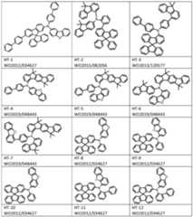


The compounds HT-1 to HT-18 can generally be used in any hole transport layer of OLEDs. As used herein, the term hole transport layer means any layer of an OLED that is located between the anode and the emitting layer. The term OLED is not specifically limited and applies to all OLEDs, in particular to OLED structures commonly used at the time of filing the present application.
Compounds HT-1 to HT-18 may be prepared according to methods disclosed in the patent applications listed in the table above under the respective compounds HT-1 to HT-18. The teachings on the use of the compounds and the methods of making the compounds contained in the above patent applications are hereby expressly incorporated by reference into the present disclosure. The compounds HT-1 to HT-18 exhibit excellent properties when used in OLEDs, in particular excellent liftime and efficiency. This is particularly the case when they are used in a hole transport layer of the OLED.
Hole-transporting layers may comprise two ore more hole-transport materials, preferably selected from the hole-transport materials listed above. Such mixtures are described, for example, in WO2024/133366. Examples of mixture of hole-transport materials in a hole- transport layer are the mixtures 1 to 16 below:


In mixture 1-16, the proportion compound 1: compound 2 is preferably between 10:90 to 90:10, more preferably between 80:20 and 30:70. Examples of suitable proportions for compound 1: compound 2 are 75:25, 70:30, 50:50, 40:60 or 30:70. The term compound 1: compound 2 is equal to 75:25 means here that the compound 1 is present in the layer in a proportion by volume of 75% and the compound 2 in a proportion of 25%.
Preferably, the first electrode is an anode and the second electrode is a cathode.
Preferred cathodes of the electronic device are metals having a low work function, metal alloys or multilayer structures composed of various metals, for example alkaline earth metals, alkali metals, main group metals or lanthanoids (e.g. Ca, Ba, Mg, Al, In, Mg, Yb, Sm, etc.). Additionally suitable are alloys composed of an alkali metal or alkaline earth metal and silver, for example an alloy composed of magnesium and silver. In the case of multilayer structures, in addition to the metals mentioned, it is also possible to use further metals having a relatively high work function, for example Ag or Al, in which case combinations of the metals such as Ca/Ag, Mg/Ag or Ba/Ag, for example, are generally used. It may also be preferable to introduce a thin interlayer of a material having a high dielectric constant between a metallic cathode and the organic semiconductor. Examples of useful materials for this purpose are alkali metal or alkaline earth metal fluorides, but also the corresponding oxides or carbonates (e.g. Li F, Li2O, BaF2, MgO, NaF, CsF, Cs2CO3, etc.). It is also possible to use lithium quinolinate (LiQ) for this purpose. The layer thickness of this layer is preferably between 0.5 and 5 nm.
Preferred anodes are materials having a high work function. Preferably, the anode has a work function of greater than 4.5 eV versus vacuum. Firstly, metals having a high redox potential are suitable for this purpose, for example Ag, Pt or Au. Secondly, metal/metal oxide electrodes (e.g. Al/N i/N iOx, AI/PtOx) may also be preferred. For some applications, at least one of the electrodes has to be transparent or partly transparent in order to enable either the irradiation of the organic material (organic solar cell) or the emission of light (OLED, O-I-ASER). Preferred anode materials here are conductive mixed metal oxides. Particular preference is given to indium tin oxide (ITO) or indium zinc oxide (IZO). Preference is further given to conductive doped organic materials, especially conductive doped polymers. In addition, the anode may also consist of two or more layers, for example of an inner layer of ITO and an outer layer of a metal oxide, preferably tungsten oxide, molybdenum oxide or vanadium oxide.
The emission layer comprises a host and a fluorescent emitter. Examples of fluorescent emitters are aromatic anthracenamines, aromatic anthracenediamines, aromatic pyrenamines, aromatic pyrenediamines, aromatic chrysenamines or aromatic chrysenediamines. An aromatic anthracenamine is taken to mean a compound in which one diarylamino group is bonded directly to an anthracene group, preferably in the 9-position. An aromatic anthracenediamine is taken to mean a com- pound in which two diarylamino groups are bonded directly to an anthracene group, preferably in the 9,10-position. Aromatic pyrenamines, pyrenediamines, chrysenamines and chrysenediamines are defined analogously thereto, where the diarylamino groups are preferably bonded to the pyrene in the 1 -position or in the 1 ,6-position. Further fluorescent emitters are indenofluorenamines or indenofluorenediamines, for example in accordance with WO 2006/108497 or WO 2006/122630, benzoindenofluorenamines or benzoindenofluorenediamines, for example in accordance with WO 2008/006449, and dibenzoindenofluorenamines or dibenzoindenofluorenediamines, for example in accordance with WO 2007/140847, and the indenofluorene derivatives containing con- densed aryl groups which are disclosed in WO 2010/012328. Still further examples of fluorescent emitters are benzanthracene derivatives as disclosed in WO 2015/158409, anthracene derivatives as disclosed in WO 2017/036573, fluorene dimers connected via heteroaryl groups like in WO 2016/150544 or phenoxazine derivatives as disclosed in WO 2017/028940 and WO 2017/028941 . Further examples of fluorescent emitters are pyren- arylamines as disclosed in WO 2012/048780 and WO 2013/185871 , benzoindenofluoren- amines as disclosed in WO 2014/037077, benzofluorenamines as disclosed in WO 2014/106522 and indenofluorenes as disclosed in WO 2014/111269 or WO 2017/036574, WO 2018/007421. Futher examples of fluorescent emitters are the emitters comprising dibenzofuran or indenodibenzofuran moieties as disclosed in WO 2018/095888, WO 2018/095940, WO 2019/076789, WO 2019/170572 as well as in WO 2020/043657, WO 2020/043646 and WO/2020/043640, boron derivatives as disclosed, for example, in WO 2015/102118, ON 108409769, ON 107266484, WO2017195669, US2018069182 as well as in WO 2020/208051 , W02021/058406, and WO 2021/094269.
Preferred fluorescent emitters are those described in WO 2021/090932, WO 2020/054676, WO 2018/212169, US 10,249,832, WO 2021/014001 , where T1 (FE) ≥ 2.30 eV. Preferably, the fluorescent emitter has an emission peak wavelength between 420-550 nm. More preferably, the fluorescent emitter is a blue fluorescent emitter and the emission layer of the device is a blue-fluorescing emitting layer.
Preferably, the fluorescent emitter has a full width at half maximum FWHM ≤ 50 nm, preferably FWHM ≤ 40 nmm, more preferably FWHM ≤ 30 nm. The optical bandwidth of a light source is measured by its full width at half maximum (FWHM). The term FWHM refers to the width of an optical signal at half its maximum intensity.
FWHM of the fluorescent emitter is determined here at the peak emission wavelengthmax, which corresponds to the wavelength of the first maximum of the emission spectrum.
To determine the peak emission wavelength of the fluorescent emitter, the fluorescent emitter is dissolved in toluene and a photoluminescent spectrum is obtained using a fluorescence spectrometer. More specifically, a concentration of 1 mg/100 mL is used. The solution is excited in a fluorescence spectrometer, for example Hitachi F-4500. Typically, the first maximum is also the global maximum of the spectrum. To determine the FWHM of the fluorescent emitter, the wavelengths values at half the maximum of the peak emission wavelength, are subtracted.
Preferably, the fluorescent emitter is selected from compounds of formula (F-1):

Formula (F-1 )
Ar30, Ar31, Ar32 stand on each occurrence, identically or differently, for a substituted or unsubstituted aromatic ring system having 6 to 30, preferably 6 to 18, more preferably 6 to 12 aromatic ring atoms or heteroaromatic ring system having 5 to 30, preferably 5 to 18, more preferably 5 to 13, even more preferably 5 to 7 aromatic ring atoms, which may be substituted by one or more radicals R30; Y30 stands for B or N;
Y31, Y32, Y33 stand on each occurrence, identically or differently, for O, S, C(R0)2, C=O, C=S, C=NR0, C=C(R0)2, Si(R0)2, BR0, NR0, PR0, SO2, SeO2 or a chemical bond, with the proviso that if Y30 is B, then at least one of the groups Y31, Y32, Y33 stands for NR° and if Y30 is N, then at least one of the groups Y31, Y32, Y33 stands for BR0;
R° stands on each occurrence, identically or differently, for H, D, F, a straight-chain alkyl group having 1 to 20 C atoms or branched or a cyclic alkyl group having 3 to 20, each of which may be substituted by one or more radicals R, where in each case one or more non- adjacent CH2 groups may be replaced by O or S and where one or more H atoms may be replaced by D or F, or an aromatic ring system having 6 to 40 aromatic ring atoms or heteroaromatic ring systems having 5 to 40 aromatic ring atoms, which may in each case be substituted by one or more radicals R, where two adjacent radicals R°, may form an aliphatic, aromatic or heteroaromatic ring system together, which may be substituted by one or more radicals R;
R30 stands on each occurrence, identically or differently, for H, D, F, Cl, Br, I, CHO, CN, C(=O)Ar, P(=O)(Ar)2, S(=O)Ar, S(=O)2Ar, NO2, Si(R)3, B(OR)2, OSO2R, a straight-chain alkyl, alkoxy or thioalkyl group having 1 to 40 C atoms or branched or a cyclic alkyl, alkoxy or thioalkyl group having 3 to 40 C atoms, each of which may be substituted by one or more radicals R, where in each case one or more non-adjacent CH2 groups may be replaced by RC=CR, C=C, Si(R)2, Ge(R)2, Sn(R)2, C=O, C=S, C=Se, P(=O)(R), SO, SO2, O or S and where one or more H atoms may be replaced by D, F, Cl, Br, I, CN or NO2, an aromatic ring system having 6 to 40 aromatic ring atoms or heteroaromatic ring system having 5 to 40 aromatic ring atoms, which may in each case be substituted by one or more radicals R; where two radicals R30 may form an aliphatic, aromatic or heteroaromatic ring system together, which may be substituted by one or more radicals R;
R has the same meaning as above; and q is 0 or 1. Preferably, the compounds of formula (F-1) are selected from the compounds of formulae (F-2) to (F-7) as depicted below:

Where Y34 stands on each occurrence, identically or differently, for O, S, C(R°)2, C=O, C=S, C=NR0, C=C(R0)2, Si(R0)2, BR0, NR0, PR0, SO2, SeO2, preferably for O, S, C(R0)2, BR0 or NR°; a, b, c stand, identically or differently for 0, 1 , 2 or 3; d stands for 0, 1 , 2, 3 or 4.
Examples of suitable fluorescent emitters are depicted in the table below:


In accordance with a preferred embodiment, the emission layer is a classical fluorescent- emitting layer comprising a host material, also called matrix material, and a dopant, where the dopant is selected from fluorescent emitters.
Suitable host materials for fluorescent emitters are selected from the classes of the oligoarylenes (e.g. 2,2’,7,7’-tetraphenylspirobifluorene), especially the oligoarylenes containing fused aromatic groups, the oligoarylenevinylenes, the polypodal metal complexes, the hole-conducting compounds, the electron-conducting compounds, especially ketones, phosphine oxides and sulfoxides; the atropisomers, the boronic acid derivatives or the benzanthracenes. Particularly preferred host materials are selected from the classes of the oligoarylenes comprising naphthalene, anthracene, benzanthracene and/or pyrene or atropisomers of these compounds, the oligoarylenevinylenes, the ketones, the phosphine oxides and the sulfoxides. Very particularly preferred host materials are selected from the classes of the oligoarylenes comprising anthracene, benzanthracene, benzophenanthrene and/or pyrene or atropisomers of these compounds. An oligoarylene in the context of this invention shall be understood to mean a compound in which at least three aryl or arylene groups are bonded to one another.
Preferably, the following condition is fulfilled: | T1 (Host) - T1 (II) | ≤ 1.0 eV. The electronic device preferably contains a single emitting layer. In this case, the emitting layer is preferably selected from blue-fluorescing emitting layers.
In a preferred embodiment, the electronic device is part of an arrangement consisting of three or more, preferably three, electronic devices, of which one device contains a blue- emitting layer, one device a green-emitting layer, and one device a red-emitting layer (called an RGB side-by-side arrangement). The electronic device according to the application is preferably the blue-emitting device in the arrangement. The electronic devices in the arrangement are preferably arranged alongside one another.
In a particularly preferred embodiment, the arrangement contains a first device according to the application containing a hole transport layer HTL, a first auxiliary layer AUX 1 and a blue-fluorescing emitting layer, and a second device according to the application containing a green-phosphorescing or green-fluorescing emitting layer. There is preferably a third electronic device in the arrangement that contains a red-emitting layer, preferably a red- phosphorescing layer. Preferably, the hole transport layer HTL is identical, especially containing the same material, in the first and second devices according to the application in the arrangement, and preferably also in the third electronic device of the arrangement.
A particularly preferred example of such an arrangement 100 containing three electronic devices, one of which is an electronic devices according to the application, is shown in Figure 1. In this figure, 100a is an electronic device, preferably the above-mentioned first device according to the application, 100b is an electronic device, preferably the above- mentioned second device, and 100c is a red-emitting electronic device. Layer 101c is the anode of the red-emitting electronic device, layer 101b is the anode of the second device according to the application, and layer 101a is the anode of the first device according to the application, layer 102 is a hole injection layer, preferably HIL as described above, in the form of a common layer, layer 103 is the hole transport layer HTL, designed as a common layer, layer 105c is a red-emitting layer, layer 105b is a green-emitting layer, layer 105a is a blue light-emitting layer, layer 106 is a hole blocker layer, designed as a common layer, layer 107 is an electron transport layer, designed as a common layer, layer 108 is an electron injection layer, designed as a common layer, layer 109c is the cathode of the red- emitting electronic device, layer 109b is the cathode of the second device according to the application, and layer 109a is the cathode of the first device according to the application. Layers 104a is the first auxiliary layer AUX 1. Layers 104c is an auxiliary layer of the red- emitting electronic device, layer 104b is an auxiliary layer of the green-emitting electronic device. What is meant by a “common layer” in the above details is that the layer contains the same material in all three layers of the arrangement. This preferably means that the layer is identical in all three devices in the arrangement, i.e. extends as one layer across all three devices in the arrangement.
Another particularly preferred example of such an arrangement 200 containing three electronic devices, one of which is an electronic devices according to the application, is shown in Figure 2. In this figure, 200a is an electronic device, preferably the above- mentioned first device according to the application, 200b is an electronic device, preferably the above-mentioned second device, and 200c is a red-emitting electronic device. Layer 201c is the anode of the red-emitting electronic device, layer 201b is the anode of the second device according to the application, and layer 201a is the anode of the first device according to the application, layer 202 is a hole injection layer, preferably HIL as described above, in the form of a common layer, layer 203 is the hole transport layer HTL, designed as a common layer, layer 205c is a red-emitting layer, layer 205b is a green-emitting layer, layer 205a is a blue light-emitting layer, layer 206 is a hole blocker layer, designed as a common layer, layer 207 is an electron transport layer, designed as a common layer, layer 208 is an electron injection layer, designed as a common layer, layer 209c is the cathode of the red-emitting electronic device, layer 209b is the cathode of the second device according to the application, and layer 209a is the cathode of the first device according to the application. Layers 204a is the first auxiliary layer AUX1. Layers 204c is an auxiliary layer of the red-emitting electronic device, layer 204b is an auxiliary layer of the green-emitting electronic device. Layers 204'a is the second auxiliary layer AUX2. Layers 204'c is a second auxiliary layer of the red-emitting electronic device, layer 104'b is a second auxiliary layer of the green-emitting electronic device.
The electronic devices of the arrangement shown in Figure 1 and in Figure 2 may contain additional layers not shown in the figure.
In an alternative, likewise preferred embodiment, the electronic device contains multiple emitting layers arranged in succession, each having different emission maxima between 380 nm and 750 nm. In other words, different emitting compounds used in each of the multiple emitting layers fluoresce or phosphoresce and emit blue, green, yellow, orange or red light. In a preferred embodiment, the electronic device contains three emitting layers in succession in a stack, of which one in each case exhibits blue emission, one green emission, and one orange or red, preferably red, emission. Preferably, in this case, the blue-emitting layer is a fluorescent layer, and the green-emitting layer is a phosphorescent layer, and the red-emitting layer is a phosphorescent layer.
An emitting layer of the electronic device may also contain systems comprising a plurality of matrix materials (mixed matrix systems) and/or a plurality of emitting compounds. When the electronic device contains a phosphorescent emitting layer, it is preferable that this layer contains two or more, preferably exactly two, different matrix materials.
Mixed matrix systems preferably comprise two or three different matrix materials, more preferably two different matrix materials. Preferably, in this case, one of the two materials is a material having hole-transporting properties and the other material is a material having electron-transporting properties. It is further preferable when one of the materials is selected from compounds having a large energy differential between HOMO and LIIMO (wide-bandgap materials). The two different matrix materials may be present in a ratio of 1 :50 to 1 : 1 , preferably 1 :20 to 1 : 1 , more preferably 1 : 10 to 1 : 1 and most preferably 1 :4 to 1 :1. The desired electron-transporting and hole-transporting properties of the mixed matrix components may, however, also be combined mainly or entirely in a single mixed matrix component, in which case the further mixed matrix component(s) fulfil(s) other functions.
As mentioned above, the electronic device may contain multiple emitting layers and, in this case, the blue-emitting layer is a preferably a fluorescent layer comprising at least one fluorescent emitter and one host as described above, whereas the green-emitting layer and the red-emitting layer are preferably phosphorescent layers comprising at least one phosphorescent emitter and one host or matrix material (host ans matrix material are used synonymously in the present application) as described below.
Phosphorescent emitters: The term "phosphorescent emitters" typically encompasses compounds where the emission of light is effected through a spin-forbidden transition, for example a transition from an excited triplet state or a state having a higher spin quantum number, for example a quintet state.
Suitable phosphorescent emitters are especially compounds which, when suitably excited, emit light, preferably in the visible region, and also contain at least one atom of atomic number greater than 20, preferably greater than 38, and less than 84, more preferably greater than 56 and less than 80. Preference is given to using, as phosphorescent emitters, compounds containing copper, molybdenum, tungsten, rhenium, ruthenium, osmium, rhodium, iridium, palladium, platinum, silver, gold or europium, especially compounds containing iridium, platinum or copper.
In the context of the present invention, all luminescent iridium, platinum or copper complexes are considered to be phosphorescent compounds.
In general, all phosphorescent complexes as used for phosphorescent OLEDs according to the prior art and as known to those skilled in the art in the field of organic electroluminescent devices are suitable for use in the devices according to the application.
Matrix materials for phosphorescent emitters:
Preferred matrix materials for phosphorescent emitters are aromatic ketones, aromatic phosphine oxides or aromatic sulfoxides or sulfones, triarylamines, carbazole derivatives, e.g. CBP (N,N-biscarbazolylbiphenyl), indolocarbazole derivatives, indenocarbazole derivatives, azacarbazole derivatives, azadibenzofuran and diazadibenzofuran derivatives, bipolar matrix materials, silanes, azaboroles or boronic esters, triazine derivatives, zinc complexes, diazasilole or tetraazasilole derivatives, diazaphosphole derivatives, bridged carbazole derivatives, triphenylene derivatives, or lactams.
Examples for suitable matrix materials are shown in the following table:


Apart from cathode, anode, emitting layer, layer HTL1 and layer HTL2, the electronic device may comprise further layers. These are selected, for example, from in each case one or more hole injection layers, hole transport layers, hole blocker layers, electron transport layers, electron injection layers, electron blocker layers, exciton blocker layers, interlayers, charge generation layers and/or organic or inorganic p/n junctions. However, it should be pointed out that not every one of these layers need necessarily be present and the choice of layers always depends on the compounds used and especially also on whether the device is a fluorescent or phosphorescent electroluminescent device.
The sequence of layers in the electronic device is preferably as follows:
- first electrode, preferably anode
- hole injection layer HIL, preferably p-doped
- Hole transport layer HTL
- optionally further hole transport layer(s), for example a second auxiliary layer AUX 2
- first auxiliary layer AUX 1
- emission layer
- optionally hole blocker layer
- electron transport layer - electron injection layer
- second electrode, preferably cathode.
It is not obligatory for all the layers mentioned to be present, and/or further layers may additionally be present.
Compounds that are preferably used in further hole-transporting layers of the device according to the application, like the second auxiliary layer AUX 2, are indenofluoreneamine derivatives, amine derivatives, hexaazatriphenylene derivatives, amine derivatives with fused aromatic systems, monobenzoindenofluoreneamines, dibenzoindenofluoreneamines, spirobifluoreneamines, fluoreneamines, spirodibenzopyranamines, dihydroacridine derivatives, spirodibenzofurans and spirodibenzothiophenes, phenanthrenediarylamines, spirotribenzotropolones, spirobifluorenes having meta-phenyldiamine groups, spirobisacridines, xanthenediarylamines, and 9,10-dihydroanthracene spiro compounds having diarylamino groups.
The electronic device preferably contains at least one electron transport layer. In addition, the electronic device preferably contains at least one electron injection layer. The electron injection layer preferably directly adjoins the cathode. In a preferred embodiment, the electron transport layer contains a triazine derivative and lithium quinolinate. In a preferred embodiment, the electron injection layer contains a triazine derivative and lithium quinolinate. In a particularly preferred embodiment, the electron transport layer and/or the electron injection layer, most preferably the electron transport layer and the electron injection layer, contain a triazine derivative and lithium quinolinate (LiQ).
In a preferred embodiment, the electronic device contains at least one hole blocker layer. This preferably has hole-blocking and electron-transporting properties, and directly adjoins this emitting layer on the cathode side in a device containing a single emitting layer. In a device comprising multiple emitting layers that are arranged in succession, the hole blocker layer directly adjoins those of the multiple emitting layers that are closest to the cathode on the cathode side. Suitable electron-transporting materials are, for example, the compounds disclosed in Y. Shirota et al., Chem. Rev. 2007, 107(4), 953-1010, or other materials used in these layers according to the prior art.
Materials used for the electron transport layer may be any materials that are used as electron transport materials in the electron transport layer according to the prior art. Especially suitable are aluminium complexes, for example Alq3, zirconium complexes, for example Zrq4, lithium complexes, for example Liq, benzimidazole derivatives, triazine derivatives, pyrimidine derivatives, pyridine derivatives, pyrazine derivatives, quinoxaline derivatives, quinoline derivatives, oxadiazole derivatives, aromatic ketones, lactams, boranes, diazaphosphole derivatives and phosphine oxide derivatives.
In a preferred embodiment, the electronic device is characterized in that one or more layers are applied by a sublimation process. In this case, the materials are applied by vapour deposition in vacuum sublimation systems at an initial pressure of less than 10'5 mbar, preferably less than 10-6 mbar. In this case, however, it is also possible that the initial pressure is even lower, for example less than 10-7 mbar.
Preference is likewise given to an electronic device, characterized in that one or more layers are coated by the OVPD (organic vapour phase deposition) method or with the aid of a carrier gas sublimation. In this case, the materials are applied at a pressure between 10-5 mbar and 1 bar. A special case of this method is the OVJP (organic vapour jet printing) method, in which the materials are applied directly by a nozzle and thus structured (for example M. S. Arnold et al., Appl. Phys. Lett. 2008, 92, 053301).
Preference is additionally given to an electronic device, characterized in that one or more layers are produced from solution, for example by spin-coating, or by any printing method, for example screen printing, flexographic printing, nozzle printing or offset printing, but more preferably LITI (light-induced thermal imaging, thermal transfer printing) or inkjet printing.
It is further preferable that an electronic device according to the application is produced by applying one or more layers from solution and one or more layers by a sublimation method. After application of the layers, according to the use, the device is structured, contact- connected and finally sealed, in order to rule out damaging effects of water and air.
The electronic device may be used in displays, as light source in lighting applications, and as light source in medical and/or cosmetic applications.
Examples
Production of the OLEDs
1) General production process for the OLEDs and characterization of the OLEDs
Glass plaques which have been coated with structured ITO (indium tin oxide) in a thickness of 50 nm are the substrates to which the OLEDs are applied.
The OLEDs basically have the following layer structure: substrate / hole injection layer (HIL) I hole transport layer (HTL) / electron blocker layer (EBL) / emission layer (EML) / electron transport layer, optionally with second layer (ETL) / electron injection layer (EIL) and finally a cathode. The cathode is formed by an aluminium layer of thickness 100 nm. The exact structure of the OLEDs can be found in the tables which follow. The materials used for production of the OLEDs are shown in a table below.
All materials are applied by thermal vapour deposition in a vacuum chamber. In this case, the emission layer consists of at least one matrix material (host material) and an emitting dopant which is added to the matrix material(s) in a particular proportion by volume by co- evaporation. Details given in such a form as H:SEB (3%) mean here that the material H is present in the layer in a proportion by volume of 97% and SEB in a proportion of 3%. In an analogous manner, the electron transport layer and the hole injection layer also consist of a mixture of two materials. The structures of the materials that are used in the OLEDs are shown in Table 1.
The OLEDs are characterized in a standard manner. For this purpose, the electroluminescence spectra, the external quantum efficiency (EQE, measured in %) as a function of the luminance, calculated from current-voltage-luminance characteristics assuming Lambertian radiation characteristics, and the lifetime are determined. The parameter EQE @ 10 mA/cm2 refers to the external quantum efficiency which is attained at 10 mA/cm2. The parameter II @ 10 mA/cm2 refers to the operating voltage at 10 mA/cm2. The lifetime LT is defined as the time after which the luminance drops from the starting luminance to a certain proportion in the course of operation with constant current density. An LT90number means here that the lifetime reported corresponds to the time after which the luminance has dropped to 90% of its starting value. The figure @60 mA/cm2 means here that the lifetime in question is measured at 60 mA/cm2. The figure Rel LT90 @ 60 mA/cm2 (%) means the LT90@60 mA/cm2 in relation to the given comparative example CE1 in percentage.


The compounds C1 and EBM1 to EBM7 have been synthesised according to the processes as described in WO2020159266, WO2022154282, KR2021123664 or WO2019048458
2) Inventive OLEDs containing a compound of the formula (I) in the HIL and HTL and compounds of formulae (II) in the EBL of blue-fluorescing OLEDs
The device architecture of OLEDs with SEB1 as dopant are shown in Table 2:


The lifetime improvement of the OLEDs, which can be achieved with SEB1 as dopant, is shown in Table 3.

The device results show, that the combination of HTL materials of formula (I) in combination with EBL materials of formula (II) with a T1 ≤ 2.7eV lead to a significant improvement in lifetime compared to the comparative example with a T1 > 2.7 eV, with similar driving voltage and efficiency.
Example CE2: Comparative example CE2 is provided by exchanging the dopant SEB1 in example CE1 by the dopant SEB2 as depicted in table 1.
Example E6: Another example according to the subject matter of the invention is provided by exchanging the dopant SEB1 in example E1 by the dopant SEB2 as depicted in table 1 Example E7: Another example according to the subject matter of the invention is provided by exchanging the dopant SEB1 in example E2 by the dopant SEB2 as depicted in table 1
Example E8: Another example according to the subject matter of the invention is provided by exchanging the dopant SEB1 in example E3 by the dopant SEB2 as depicted in table 1
Example E9: Another example according to the subject matter of the invention is provided by exchanging the dopant SEB1 in example E4 by the dopant SEB2 as depicted in table 1
Example E10: Another example according to the subject matter of the invention is provided by exchanging the dopant SEB1 in example E5 by the dopant SEB2 as depicted in table 1
Example CE3: Comparative example CE3 is provided by exchanging the dopant SEB1 in example CE1 by the dopant SEB3 as depicted in table 1.
Example E11 : Another example according to the subject matter of the invention is provided by exchanging the dopant SEB1 in example E1 by the dopant SEB3 as depicted in table 1
Example E12: Another example according to the subject matter of the invention is provided by exchanging the dopant SEB1 in example E2 by the dopant SEB3 depicted in table 1
Example E13: Another example according to the subject matter of the invention is provided by exchanging the dopant SEB1 in example E3 by the dopant SEB3 as depicted in table 1
Example E14: Another example according to the subject matter of the invention is provided by exchanging the dopant SEB1 in example E4 by the dopant SEB3 as depicted in table 1
Example E15: Another example according to the subject matter of the invention is provided by exchanging the dopant SEB1 in example E5 by the dopant SEB3 as depcited in table 1 Comparative example CE4: Comparative example CE3 is provided by exchanging the HTM1 in example CE1 by HTM2 as depicted in table 1.
Example E16: Another example according to the subject matter of the invention is provided by exchanging the HTM1 in example E1 by HTM2 as depicted in table 1.
Example E17: Another example according to the subject matter of the invention is provided by exchanging the HTM1 in example E2 by HTM2 as depicted in table 1.
Example E18: Another example according to the subject matter of the invention is provided by exchanging the HTM1 in example E3 by HTM2 as depicted in table 1.
Example E19: Another example according to the subject matter of the invention is provided by exchanging the HTM1 in example E4 by HTM2 as depicted in table 1.
Example E20: Another example according to the subject matter of the invention is provided by exchanging the HTM1 in example E5 by HTM2 as depicted in table 1.
The combination of HTL materials of formula (I) in combination with EBL materials of formula (II) with a T1≤2.7eV lead in all examples E6 to E20 to a significant improvement in lifetime compared to the comparative example with a T1 >2.7 eV, while keeping similar driving voltage and efficiency.
Claims
1. An electronic device comprising: a first electrode; a second electrode facing the first electrode; an interlayer between the first electrode and the second electrode and comprising an emission layer, wherein: the emission layer comprises a host material and a dopant, where the dopant is selected from fluorescent emitters, the interlayer further comprises a hole transport region between the emission layer and the first electrode, the hole transport region comprises a hole transport layer and a first auxiliary layer, where the first auxiliary layer is between the hole transport layer and the emission layer, the hole transport layer comprises a monoamine-based compound of formula (I),

Formula (I) where the following applies to the symbols and indices occurring:
Ar10, Ar11, Ar12 are on each occurrence, identically or differently, an aromatic ring system having 6 to 40 aromatic ring atoms or heteroaromatic ring system having 5 to 40 aromatic ring atoms, which may be substituted by one or more radicals R12; L10, L11, L12 are on eac occurrence, identically or differently, a single bond, an aromatic having 6 to 30 aromatic ring atoms or heteroaromatic ring system having 5 to 30 aromatic ring atoms, which may be substituted by one or more radicals R12;
R12 stands on each occurrence, identically or differently, for H, D, F, Cl, Br, I, CHO, CN, C(=O)Ar, P(=O)(Ar)2, S(=O)Ar, S(=O)2Ar, NO2, Si(R19)3, B(OR19)2, OSO2R19, a straight-chain alkyl, alkoxy or thioalkyl group having 1 to 40 C atoms or branched or a cyclic alkyl, alkoxy or thioalkyl group having 3 to 40 C atoms, each of which may be substituted by one or more radicals R19, where in each case one or more non-adjacent CH2 groups may be replaced by R19C=CR19, C=C, Si(R19)2, Ge(R19)2, Sn(R19)2, C=O, C=S, C=Se, P(=O)(R19), SO, SO2, O or S and where one or more H atoms may be replaced by D, F, Cl, Br, I, CN or NO2, an aromatic ring system having 6 to 40 aromatic ring atoms or heteroaromatic ring system having 5 to 40 aromatic ring atoms, which may in each case be substituted by one or more radicals R19; where two radicals R12 may form an aliphatic, aromatic or heteroaromatic ring system together, which may be substituted by one or more radicals R19;
R19 stands on each occurrence, identically or differently, for H, D, F, Cl, Br, I, CHO, CN, C(=O)Ar, P(=O)(Ar)2, S(=O)Ar, S(=O)2Ar, NO2, Si(R )3, B(OR')2, OSO2R , a straight- chain alkyl, alkoxy or thioalkyl group having 1 to 40 C atoms or branched or a cyclic alkyl, alkoxy or thioalkyl group having 3 to 40 C atoms, each of which may be substituted by one or more radicals R , where in each case one or more non-adjacent CH2 groups may be replaced by R C=CR , C=C, Si(R )2, Ge(R )2, Sn(R )2, C=O, C=S, C=Se, P(=O)(R ), SO, SO2, O or S and where one or more H atoms may be replaced by D, F, Cl, Br, I, CN or NO2, an aromatic ring system having 6 to 40 aromatic ring atoms or heteroaromatic ring system having 5 to 40 aromatic ring atoms, which may in each case be substituted by one or more radicals R ; where two radicals R19 may form an aliphatic, aromatic or heteroaromatic ring system together, which may be substituted by one or more radicals R ;
Ar is, on each occurrence, identically or differently, an aromatic ring system having 6 to 40 aromatic ring atoms or heteroaromatic ring system having 5 to 40 aromatic ring atoms, which may in each case also be substituted by one or more radicals R ; R stands on each occurrence, identically or differently, for H, D, F, Cl, Br, I, CN, a straight-chain alkyl, alkoxy or thioalkyl group having 1 to 20 C atoms or branched or cyclic alkyl, alkoxy or thioalkyl group having 3 to 20 C atoms, where in each case one or more non-adjacent CH2 groups may be replaced by SO, SO2, O, S and where one or more H atoms may be replaced by D, F, Cl, Br or I, or an aromatic ring system having 6 to 24 aromatic ring atoms or heteroaromatic ring system having 5 to 24 aromatic ring atoms; the first auxiliary layer comprises a compound of formula (II), where the following applies to the symbols and indices occurring:

Ar21, Ar22 are on each occurrence, identically or differently, an aromatic ring system having 6 to 30 aromatic ring atoms or heteroaromatic ring system having 5 to 30 aromatic ring atoms, which may be substituted by one or more radicals R22;
L20, L21, L22 are on each occurrence, identically or differently, a single bond, an aromatic ring system having 6 to 30 aromatic ring atoms or heteroaromatic ring system having 5 to 30 aromatic ring atoms, which may be substituted by one or more radicals R22;
R20, R21, R22 stand on each occurrence, identically or differently, for H, D, F, Cl,
Br, I, CHO, CN, C(=O)Ar, P(=O)(Ar)2, S(=O)Ar, S(=O)2Ar, NO2, Si(R)3, B(OR)2, N(R)2, N(Ar)2, OSO2R, a straight-chain alkyl, alkoxy or thioalkyl group having 1 to 40 C atoms or branched or a cyclic alkyl, alkoxy or thioalkyl group having 3 to 40 C atoms, each of which may be substituted by one or more radicals R, where in each case one or more non- adjacent CH2 groups may be replaced by RC=CR, C=C, Si(R)2, Ge(R)2, Sn(R)2, C=O, C=S, C=Se, P(=O)(R), SO, SO2, O or S and where one or more H atoms may be replaced by D, F, Cl, Br, I, CN or NO2, an aromatic ring system having 6 to 40 aromatic ring atoms or heteroaromatic ring system having 5 to 40 aromatic ring atoms, which may in each case be substituted by one or more radicals R; where two radicals R20, two radicals R21 and/or two radicals R22 may form an aliphatic, aromatic or heteroaromatic ring system together, which may be substituted by one or more radicals R;
R stands on each occurrence, identically or differently, for H, D, F, Cl, Br, I, CHO, CN, C(=O)Ar, P(=O)(Ar)2, S(=O)Ar, S(=O)2Ar, NO2, Si(R )3, B(OR')2, N(R')2, N(Ar)2, OSO2R , a straight-chain alkyl, alkoxy or thioalkyl group having 1 to 40 C atoms or branched or a cyclic alkyl, alkoxy or thioalkyl group having 3 to 40 C atoms, each of which may be substituted by one or more radicals R , where in each case one or more non-adjacent CH2 groups may be replaced by R C=CR , C=C, Si(R )2, Ge(R )2, Sn(R )2, C=O, C=S, C=Se, P(=O)(R ), SO, SO2, O or S and where one or more H atoms may be replaced by D, F, Cl, Br, I, CN or NO2, an aromatic ring system having 6 to 40 aromatic ring atoms or heteroaromatic ring system having 5 to 40 aromatic ring atoms, which may in each case be substituted by one or more radicals R ; where two radicals R may form an aliphatic, aromatic or heteroaromatic ring system together, which may be substituted by one or more radicals R ; p, q is, identically or differently, equal to 0, 1 , 2, 3 or 4; r is equal to 1 , 2, 3 or 4, and where the following conditions apply:
T1 (II) ≤ 2.70 eV
T1 (HOST) < T1 (FE) | T1 (FE) - T1 (II) | ≤ 0.5 eV where:
T1 (HOST) is the energy level of the lowest triplet state of the host material in the emission layer as determined by quantum-chemical calculation; T1 (FE) is the energy level of the lowest triplet state of the fluorescent emitter in the emission layer as determined by quantum-chemical calculation; and T1 (II) is the energy level of the lowest triplet state of the compound of formula (II) in the first auxiliary layer as determined by quantum-chemical calculation.
2. An electronic device according to claim 1, characterized in that:
-5.30 ≤ HOMO (I) ≤ -5.00 eV where HOMO (I) corresponds to the energy of the highest occupied molecular orbital of the monoamine-based compound of formula (I) in the hole-transport layer as determined by quantum-chemical calculation.
3. An electronic device according to claim 1 or 2, characterized in that:
-5.50 ≤ HOMO (II) ≤ -5.10 eV where HOMO (II) corresponds to the energy of the highest occupied molecular orbital of the compound of formula (II) in the first auxiliary layer as determined by quantum-chemical calculation.
4. An electronic device according to one or more of the preceding claims, characterized in that :
| T1 (FE) - T1 (II) | ≤ 0.3 eV
Where T1 (FE) and T1 (II) have the same definition as in claim 1.
5. An electronic device according to one or more of the preceding claims, characterized in that the first auxiliary layer is in direct contact with the emission layer.
6. An electronic device according to one or more of the preceding claims, characterized in that the hole transport layer is not doped with p-dopants.
7. An electronic device according to one or more of the preceding claims, characterized in that the monoamine-based compound of formula (I) does not contain any carbazole group.
8. An electronic device according to one or more of the preceding claims, characterized in that the monoamine-based compound of formula (I) is selected from compound of formula (1-1),

Formula (1-1) where the following applies to the symbols and indices occurring:
A is equal to C(R11)2 or equal to where the dashed lines represent the bonds emanating from the group A;

T1, T2 are the same or different at each instance and are selected from single bond, O, S, NR13, and C(R13)2;
R10, R11, R13 stand on each occurrence, identically or differently, for H, D, F, Cl, Br, I, CHO, CN, C(=O)Ar, P(=O)(Ar)2, S(=O)Ar, S(=O)2Ar, NO2, Si(R19)3, B(OR19)2, OSO2R19, a straight-chain alkyl, alkoxy or thioalkyl group having 1 to 40 C atoms or branched or a cyclic alkyl, alkoxy or thioalkyl group having 3 to 40 C atoms, each of which may be substituted by one or more radicals R19, where in each case one or more non-adjacent CH2 groups may be replaced by R19C=CR19, C≡C, Si(R19)2, Ge(R19)2, Sn(R19)2, C=O, C=S, C=Se, P(=O)(R19), SO, SO2, O or S and where one or more H atoms may be replaced by D, F, Cl, Br, I, CN or NO2, an aromatic ring system having 6 to 40 aromatic ring atoms or heteroaromatic ring system having 5 to 40 aromatic ring atoms, which may in each case be substituted by one or more radicals R19; where two or more radicals R10, two or more radicals R11 or two or more radicals R13 an aliphatic, aromatic or heteroaromatic ring system together, which may be substituted by one or more radicals R19; m is equal to 0, 1 , 2 or 3; n is equal to 0, 1 , 2, 3 or 4; and the other symbols have the same meaning as in claim 1.
9. An electronic device according to one or more of the preceding claims, characterized in that the monoamine-based compound of formula (I) is selected from compounds of formula (I-2),

Formula (1-2) where:
A1 is equal to C(R11)2 or equal to where the dashed lines represent the bonds emanating from the group A1; and where the others symbols and indices have the same meaning as in claims 1 and 8.

10. An electronic device according to one or more of the preceding claims, characterized in that the monoamine-based compound of formula (I) is selected from compound of formula (I-3A) or (I-3B),

Formula (I-3A)

Formula (I-3B) where the symbols and indices have the same meaning as in claims 1 and 8.
11. An electronic device according to one or more of the preceding claims, characterized in that the monoamine-based compound of formula (I) is selected from compounds of formula (I-4A) or (I-4B),

Formula (I-4B) where
A2 is equal to C(R11)2, 0, S or equal to where the dashed lines represent the bonds emanating from the group A2; and where

R14 stands on each occurrence, identically or differently, for H, D, F, Cl, Br, I, CHO, CN, C(=O)Ar, P(=O)(Ar)2, S(=O)Ar, S(=O)2Ar, NO2, Si(R19)3, B(OR19)2, OSO2R19, a straight-chain alkyl, alkoxy or thioalkyl group having 1 to 40 C atoms or branched or a cyclic alkyl, alkoxy or thioalkyl group having 3 to 40 C atoms, each of which may be substituted by one or more radicals R19, where in each case one or more non-adjacent CH2 groups may be replaced by R19C=CR19, C=C, Si(R19)2, Ge(R19)2, Sn(R19)2, C=O, C=S, C=Se, P(=O)(R19), SO, SO2, O or S and where one or more H atoms may be replaced by D, F, Cl, Br, I, CN or NO2, an aromatic ring system having 6 to 40 aromatic ring atoms or heteroaromatic ring system having 5 to 40 aromatic ring atoms, which may in each case be substituted by one or more radicals R19; where two or more radicals R14 may be linked to one another and form a substituted or unsubstituted aliphatic, aromatic ring or heteroaromatic ring, which may be substituted by one or more radicals R19; s is 0, 1 , 2, 3 or 4; t is 0, 1 , 2 or 3; and where the other symbols and indices have the same meaning as in claims 1 and 8.
12. An electronic device according to one or more of the precedings claims, characterized in that the monoamine-based compound of formula (I) is selected from compounds of formula (I-5A) or (I-5B), Formula (I-5B) where the symbols and indices have the same meaning as in claims 1 , 8 and 11.

13. An electronic device according to one or more of the preceding claims, characterized in that the monoamine-based compound of formula (I) is selected from compounds of formula (I-6A) to (I-6D),

Formula (I-6B)

Formula (I-6D) where the symbols and indices have the same meaning as in claims 1 , 8 and 11.
14. An electronic device according to one or more of the preceding claims, characterized in that the monoamine-based compound of formula (I) is a deuterated compound.
15. An electronic device according to one or more of the preceding claims, characterized in that the hole transport region further comprises a hole injection layer between the first electrode and the hole transport layer comprising the monoamine-based compound of formula (I).
16. An electronic device according to claim 15, characterized in that the hole injection layer comprises a monoamine-based compound of formula (I) as defined in claim 1 and a p- dopant.
17. An electronic device according to one or more of the preceding claims, characterized in that the hole transport layer is in direct contact with the first auxiliary layer.
18. An electronic device according to one or more of claims 1 to 16, characterized in that the hole transport region further comprises a second auxiliary layer between the hole transport layer and the first auxiliary layer.
19. An electronic device according to claim 18, characterized in that the hole transport layer is in direct contact with the second auxiliary layer, the second auxiliary layer is in direct contact with the first auxiliary layer and the first auxiliary layer is in direct contact with the emission layer.
20. An electronic device according to one of more of the preceding claims, characterized in that the hole transport layer consists of a monoamine-based compound of formula (I).
21. An electronic device according to one or more of the preceding claims, characterized in that the first auxiliary layer consists of a compounds of formula (II).
22. An electronic device according to one or more of the preceding claims, characterized in that T1 (FE) ≥ 2.30 eV.
23. An electronic device according to one or more of the preceding claims, characterized in that TI (II) ≤ 2.65 eV.
24. An electronic device according to one or more of the preceding claims, characterized in that the compound of formula (II) is selected from the compounds of formula (11-1): where the symbols and indices have the same meaning as in claim 1.

25. An electronic device according to one or more of the preceding claims, characterized in that the compound of formula (II) is selected from the compounds of formula (I I-2): where the symbols and indices have the same meaning as in claim 1.

26. An electronic device according to one or more of the preceding claims, characterized in that the compound of formula (II) is selected from the compounds of formula (11-3):

Formula (I I-3) where the symbols and indices have the same meaning as in claim 1.
27. An electronic device according to one or more of the preceding claims, characterized in that the compound of formula (II) is a deuterated compound.
28. An electronic device according to one or more of the preceding claims, characterized in that the fluorescent emitter is selected from compounds of formula (F-1):

Formula (F-1 )
Ar30, Ar31, Ar32 stand on each occurrence, identically or differently, for a substituted or unsubstituted aromatic ring system having 6 to 30 aromatic ring atoms or heteroaromatic ring system having 5 to 30 aromatic ring atoms, which may be substituted by one or more radicals R30; Y30 stands for B or N;
Y31, Y32, Y33 stand on each occurrence, identically or differently, for O, S, C(R°)2, C=O, C=S, C=NR°, C=C(R°)2, Si(R°)2, BR°, NR°, PR0, SO2, SeO2 or a chemical bond, with the proviso that if Y30 is B, then at least one of the groups Y31, Y32, Y33 stands for NR° and if Y30 is N, then at least one of the groups Y31, Y32, Y33 stands for BR°;
R° stands on each occurrence, identically or differently, for H, D, F, a straight-chain alkyl group having 1 to 20 C atoms or branched or a cyclic alkyl group having 3 to 20, each of which may be substituted by one or more radicals R, where in each case one or more non-adjacent CH2 groups may be replaced by O or S and where one or more H atoms may be replaced by D or F, or an aromatic ring system having 6 to 40 aromatic ring atoms or heteroaromatic ring systems having 5 to 40 aromatic ring atoms, which may in each case be substituted by one or more radicals R, where two adjacent radicals R°, may form an aliphatic, aromatic or heteroaromatic ring system together, which may be substituted by one or more radicals R;
R30 stands on each occurrence, identically or differently, for H, D, F, Cl, Br, I, CHO, CN, C(=O)Ar, P(=O)(Ar)2, S(=O)Ar, S(=O)2Ar, NO2, Si(R)3, B(OR)2, OSO2R, a straight- chain alkyl, alkoxy or thioalkyl group having 1 to 40 C atoms or branched or a cyclic alkyl, alkoxy or thioalkyl group having 3 to 40 C atoms, each of which may be substituted by one or more radicals R, where in each case one or more non-adjacent CH2 groups may be replaced by RC=CR, C=C, Si(R)2, Ge(R)2, Sn(R)2, C=O, C=S, C=Se, P(=O)(R), SO, SO2, O or S and where one or more H atoms may be replaced by D, F, Cl, Br, I, CN or NO2, an aromatic ring system having 6 to 40 aromatic ring atoms or heteroaromatic ring system having 5 to 40 aromatic ring atoms, which may in each case be substituted by one or more radicals R; where two radicals R30 may form an aliphatic, aromatic or heteroaromatic ring system together, which may be substituted by one or more radicals R;
R has the same meaning as in claim 1 ; and q is 0 or 1.
29. An electronic device according to one or more of the preceding claims, characterized in that the that the the emission layer of the device is a blue-fluorescing emitting layer.
30. An electronic device according to one or more of the preceding claims, characterized in that it comprises in the following sequence:
A first electrode;
A hole injection layer as defined in claim 16
A hole transport layer comprising a monoamine-based compound of formula (I) as defined in claim 1;
A first auxiliary layer comprising a compound of formula (II) as defined in claiml,
An emission layer as defined in claim 1,
A hole blocker layer,
An electron transport layer
An electron injection layer
A second electrode.
Applications Claiming Priority (2)
| Application Number | Priority Date | Filing Date | Title |
|---|---|---|---|
| EP23204653.2 | 2023-10-19 | ||
| EP23204653 | 2023-10-19 |
Publications (1)
| Publication Number | Publication Date |
|---|---|
| WO2025083015A1true WO2025083015A1 (en) | 2025-04-24 |
Family
ID=88505131
Family Applications (1)
| Application Number | Title | Priority Date | Filing Date |
|---|---|---|---|
| PCT/EP2024/079126PendingWO2025083015A1 (en) | 2023-10-19 | 2024-10-16 | Materials for organic electroluminescent devices |
Country Status (1)
| Country | Link |
|---|---|
| WO (1) | WO2025083015A1 (en) |
Citations (68)
| Publication number | Priority date | Publication date | Assignee | Title |
|---|---|---|---|---|
| US5061569A (en) | 1990-07-26 | 1991-10-29 | Eastman Kodak Company | Electroluminescent device with organic electroluminescent medium |
| WO1995009147A1 (en) | 1993-09-29 | 1995-04-06 | Idemitsu Kosan Co., Ltd. | Organic electroluminescent element and arylenediamine derivative |
| WO2001049806A1 (en) | 1999-12-31 | 2001-07-12 | Lg Chemical Co., Ltd | Electronic device comprising organic compound having p-type semiconducting characteristics |
| EP1661888A1 (en) | 2004-11-29 | 2006-05-31 | Samsung SDI Co., Ltd. | Phenylcarbazole-based compound and organic electroluminescent device employing the same |
| WO2006100896A1 (en) | 2005-03-18 | 2006-09-28 | Idemitsu Kosan Co., Ltd. | Aromatic amine derivative and organic electroluminescence device utilizing the same |
| WO2006108497A1 (en) | 2005-04-14 | 2006-10-19 | Merck Patent Gmbh | Compounds for organic electronic devices |
| WO2006122630A1 (en) | 2005-05-20 | 2006-11-23 | Merck Patent Gmbh | Compounds for organic electronic devices |
| US20070092755A1 (en) | 2005-10-26 | 2007-04-26 | Eastman Kodak Company | Organic element for low voltage electroluminescent devices |
| WO2007140847A1 (en) | 2006-06-02 | 2007-12-13 | Merck Patent Gmbh | Materials for organic electroluminescent devices |
| WO2008006449A1 (en) | 2006-07-11 | 2008-01-17 | Merck Patent Gmbh | Novel materials for organic electroluminescent devices |
| WO2010012328A1 (en) | 2008-07-29 | 2010-02-04 | Merck Patent Gmbh | Compounds for electronic devices |
| WO2012034627A1 (en) | 2010-09-15 | 2012-03-22 | Merck Patent Gmbh | Materials for organic electroluminescent devices |
| WO2012048780A1 (en) | 2010-10-15 | 2012-04-19 | Merck Patent Gmbh | Compounds for electronic devices |
| WO2012150001A1 (en) | 2011-05-05 | 2012-11-08 | Merck Patent Gmbh | Compounds for electronic devices |
| WO2013083216A1 (en) | 2011-11-17 | 2013-06-13 | Merck Patent Gmbh | Spiro dihydroacridine derivatives and the use thereof as materials for organic electroluminescence devices |
| WO2013120577A1 (en) | 2012-02-14 | 2013-08-22 | Merck Patent Gmbh | Spirobifluorene compounds for organic electroluminescent devices |
| WO2013185871A1 (en) | 2012-06-12 | 2013-12-19 | Merck Patent Gmbh | Compounds for electronic devices |
| WO2014015935A2 (en) | 2012-07-23 | 2014-01-30 | Merck Patent Gmbh | Compounds and organic electronic devices |
| WO2014015938A1 (en) | 2012-07-23 | 2014-01-30 | Merck Patent Gmbh | Derivatives of 2-diarylaminofluorene and organic electronic compounds containing them |
| WO2014015937A1 (en) | 2012-07-23 | 2014-01-30 | Merck Patent Gmbh | Compounds and organic electroluminescent devices |
| WO2014037077A1 (en) | 2012-09-04 | 2014-03-13 | Merck Patent Gmbh | Connections for electronic devices |
| WO2014072017A1 (en) | 2012-11-12 | 2014-05-15 | Merck Patent Gmbh | Materials for electronic devices |
| WO2014106522A1 (en) | 2013-01-03 | 2014-07-10 | Merck Patent Gmbh | Materials for electronic devices |
| WO2014111269A2 (en) | 2013-10-14 | 2014-07-24 | Merck Patent Gmbh | Materials for electronic devices |
| WO2015022051A1 (en) | 2013-08-15 | 2015-02-19 | Merck Patent Gmbh | Materials for electronic devices |
| WO2015082056A1 (en) | 2013-12-06 | 2015-06-11 | Merck Patent Gmbh | Compounds and organic electronic devices |
| WO2015086108A1 (en) | 2013-12-12 | 2015-06-18 | Merck Patent Gmbh | Materials for electronic devices |
| WO2015102118A1 (en) | 2014-02-18 | 2015-07-09 | 学校法人関西学院 | Polycyclic aromatic compound |
| WO2015131976A1 (en) | 2014-03-07 | 2015-09-11 | Merck Patent Gmbh | Materials for electronic devices |
| WO2015158409A1 (en) | 2014-04-16 | 2015-10-22 | Merck Patent Gmbh | Materials for electronic devices |
| WO2015158411A1 (en) | 2014-04-14 | 2015-10-22 | Merck Patent Gmbh | Materials for electronic devices |
| WO2016078738A1 (en) | 2014-11-18 | 2016-05-26 | Merck Patent Gmbh | Materials for organic electroluminescent devices |
| WO2016087017A1 (en) | 2014-12-01 | 2016-06-09 | Merck Patent Gmbh | Materials for organic electroluminescent devices |
| WO2016102048A1 (en) | 2014-12-22 | 2016-06-30 | Merck Patent Gmbh | Materials for electronic devices |
| WO2016131521A1 (en) | 2015-02-16 | 2016-08-25 | Merck Patent Gmbh | Spirobifluorene derivative-based materials for electronic devices |
| WO2016150544A1 (en) | 2015-03-25 | 2016-09-29 | Merck Patent Gmbh | Materials for organic electroluminescent devices |
| WO2017028941A1 (en) | 2015-08-14 | 2017-02-23 | Merck Patent Gmbh | Phenoxazine derivatives for organic electroluminescent devices |
| WO2017028940A1 (en) | 2015-08-14 | 2017-02-23 | Merck Patent Gmbh | Phenoxazine derivatives for organic electroluminescent devices |
| WO2017036574A1 (en) | 2015-08-28 | 2017-03-09 | Merck Patent Gmbh | 6,9,15,18-tetrahydro-s-indaceno[1,2-b:5,6-b']difluorene derivatives and use thereof in electronic devices |
| WO2017036573A1 (en) | 2015-08-28 | 2017-03-09 | Merck Patent Gmbh | Compounds for electronic devices |
| CN107266484A (en) | 2017-07-14 | 2017-10-20 | 瑞声科技(南京)有限公司 | Electroluminescent organic material and its luminescent device |
| WO2017195669A1 (en) | 2016-05-13 | 2017-11-16 | コニカミノルタ株式会社 | Organic electroluminescence element material, organic electroluminescence element, display apparatus and illumination apparatus |
| WO2018007421A1 (en) | 2016-07-08 | 2018-01-11 | Merck Patent Gmbh | Materials for organic electroluminescent devices |
| US20180069182A1 (en) | 2016-09-07 | 2018-03-08 | Kwansei Gakuin Educational Foundation | Polycyclic aromatic compound |
| WO2018095940A1 (en) | 2016-11-25 | 2018-05-31 | Merck Patent Gmbh | Bisbenzofuran-fused indeno[1,2-b]fluorene derivatives and related compounds as materials for organic electroluminescent devices (oled) |
| WO2018095888A1 (en) | 2016-11-25 | 2018-05-31 | Merck Patent Gmbh | Bisbenzofuran-fused 2,8-diaminoindeno[1,2-b]fluorene derivatives and related compounds as materials for organic electroluminescent devices (oled) |
| CN108409769A (en) | 2016-07-29 | 2018-08-17 | 江苏三月光电科技有限公司 | A kind of boracic organic electroluminescent compounds that luminous efficiency is high and its application |
| WO2018212169A1 (en) | 2017-05-16 | 2018-11-22 | 学校法人関西学院 | Polycyclic aromatic compound |
| WO2019048458A1 (en) | 2017-09-08 | 2019-03-14 | Merck Patent Gmbh | MATERIALS FOR ELECTRONIC DEVICES |
| US10249832B1 (en) | 2017-12-06 | 2019-04-02 | Idemitsu Kosan Co., Ltd. | Organic electroluminescence device and novel compound |
| WO2019076789A1 (en) | 2017-10-17 | 2019-04-25 | Merck Patent Gmbh | Materials for organic electroluminescent devices |
| WO2019170572A1 (en) | 2018-03-06 | 2019-09-12 | Merck Patent Gmbh | Materials for organic electroluminescent devices |
| WO2020043640A1 (en) | 2018-08-28 | 2020-03-05 | Merck Patent Gmbh | Materials for organic electroluminescent devices |
| WO2020043646A1 (en) | 2018-08-28 | 2020-03-05 | Merck Patent Gmbh | Materials for organic electroluminescent devices |
| WO2020043657A1 (en) | 2018-08-28 | 2020-03-05 | Merck Patent Gmbh | Materials for organic electroluminescent devices |
| WO2020054676A1 (en) | 2018-09-10 | 2020-03-19 | 学校法人関西学院 | Organic electroluminescent element |
| WO2020159266A1 (en) | 2019-01-30 | 2020-08-06 | 엘티소재주식회사 | Compound, organic optoelectronic device, and display device |
| WO2020208051A1 (en) | 2019-04-11 | 2020-10-15 | Merck Patent Gmbh | Materials for organic electroluminescent devices |
| WO2021014001A1 (en) | 2019-07-25 | 2021-01-28 | Cynora Gmbh | Organic molecules for optoelectronic devices |
| WO2021058406A1 (en) | 2019-09-24 | 2021-04-01 | Merck Patent Gmbh | Materials for organic electroluminescent devices |
| WO2021090932A1 (en) | 2019-11-08 | 2021-05-14 | 出光興産株式会社 | Organic electroluminescent element and electronic device |
| WO2021094269A1 (en) | 2019-11-12 | 2021-05-20 | Merck Patent Gmbh | Materials for organic electroluminescent devices |
| WO2021104749A1 (en) | 2019-11-26 | 2021-06-03 | Merck Patent Gmbh | Compounds for electronic devices |
| KR20210123664A (en) | 2020-04-03 | 2021-10-14 | 주식회사 엘지화학 | Novel compound and organic light emitting device comprising the same |
| WO2022154282A1 (en) | 2021-01-13 | 2022-07-21 | 주식회사 엘지화학 | Compound and organic light-emitting device comprising same |
| CN116375694A (en)* | 2023-05-31 | 2023-07-04 | 吉林奥来德光电材料股份有限公司 | A kind of benzonaphthofuran compound and its preparation method and application |
| CN116535323A (en)* | 2023-04-28 | 2023-08-04 | 浙江虹舞科技有限公司 | Novel triarylamine compound and organic electroluminescent device containing same |
| WO2024133366A1 (en) | 2022-12-23 | 2024-06-27 | Merck Patent Gmbh | Electronic device |
- 2024
- 2024-10-16WOPCT/EP2024/079126patent/WO2025083015A1/enactivePending
Patent Citations (69)
| Publication number | Priority date | Publication date | Assignee | Title |
|---|---|---|---|---|
| US5061569A (en) | 1990-07-26 | 1991-10-29 | Eastman Kodak Company | Electroluminescent device with organic electroluminescent medium |
| WO1995009147A1 (en) | 1993-09-29 | 1995-04-06 | Idemitsu Kosan Co., Ltd. | Organic electroluminescent element and arylenediamine derivative |
| WO2001049806A1 (en) | 1999-12-31 | 2001-07-12 | Lg Chemical Co., Ltd | Electronic device comprising organic compound having p-type semiconducting characteristics |
| EP1661888A1 (en) | 2004-11-29 | 2006-05-31 | Samsung SDI Co., Ltd. | Phenylcarbazole-based compound and organic electroluminescent device employing the same |
| WO2006100896A1 (en) | 2005-03-18 | 2006-09-28 | Idemitsu Kosan Co., Ltd. | Aromatic amine derivative and organic electroluminescence device utilizing the same |
| WO2006108497A1 (en) | 2005-04-14 | 2006-10-19 | Merck Patent Gmbh | Compounds for organic electronic devices |
| WO2006122630A1 (en) | 2005-05-20 | 2006-11-23 | Merck Patent Gmbh | Compounds for organic electronic devices |
| US20070092755A1 (en) | 2005-10-26 | 2007-04-26 | Eastman Kodak Company | Organic element for low voltage electroluminescent devices |
| WO2007140847A1 (en) | 2006-06-02 | 2007-12-13 | Merck Patent Gmbh | Materials for organic electroluminescent devices |
| WO2008006449A1 (en) | 2006-07-11 | 2008-01-17 | Merck Patent Gmbh | Novel materials for organic electroluminescent devices |
| WO2010012328A1 (en) | 2008-07-29 | 2010-02-04 | Merck Patent Gmbh | Compounds for electronic devices |
| WO2012034627A1 (en) | 2010-09-15 | 2012-03-22 | Merck Patent Gmbh | Materials for organic electroluminescent devices |
| WO2012048780A1 (en) | 2010-10-15 | 2012-04-19 | Merck Patent Gmbh | Compounds for electronic devices |
| WO2012150001A1 (en) | 2011-05-05 | 2012-11-08 | Merck Patent Gmbh | Compounds for electronic devices |
| WO2013083216A1 (en) | 2011-11-17 | 2013-06-13 | Merck Patent Gmbh | Spiro dihydroacridine derivatives and the use thereof as materials for organic electroluminescence devices |
| WO2013120577A1 (en) | 2012-02-14 | 2013-08-22 | Merck Patent Gmbh | Spirobifluorene compounds for organic electroluminescent devices |
| WO2013185871A1 (en) | 2012-06-12 | 2013-12-19 | Merck Patent Gmbh | Compounds for electronic devices |
| WO2014015935A2 (en) | 2012-07-23 | 2014-01-30 | Merck Patent Gmbh | Compounds and organic electronic devices |
| WO2014015938A1 (en) | 2012-07-23 | 2014-01-30 | Merck Patent Gmbh | Derivatives of 2-diarylaminofluorene and organic electronic compounds containing them |
| WO2014015937A1 (en) | 2012-07-23 | 2014-01-30 | Merck Patent Gmbh | Compounds and organic electroluminescent devices |
| WO2014037077A1 (en) | 2012-09-04 | 2014-03-13 | Merck Patent Gmbh | Connections for electronic devices |
| WO2014072017A1 (en) | 2012-11-12 | 2014-05-15 | Merck Patent Gmbh | Materials for electronic devices |
| WO2014106522A1 (en) | 2013-01-03 | 2014-07-10 | Merck Patent Gmbh | Materials for electronic devices |
| WO2015022051A1 (en) | 2013-08-15 | 2015-02-19 | Merck Patent Gmbh | Materials for electronic devices |
| WO2014111269A2 (en) | 2013-10-14 | 2014-07-24 | Merck Patent Gmbh | Materials for electronic devices |
| WO2015082056A1 (en) | 2013-12-06 | 2015-06-11 | Merck Patent Gmbh | Compounds and organic electronic devices |
| WO2015086108A1 (en) | 2013-12-12 | 2015-06-18 | Merck Patent Gmbh | Materials for electronic devices |
| WO2015102118A1 (en) | 2014-02-18 | 2015-07-09 | 学校法人関西学院 | Polycyclic aromatic compound |
| WO2015131976A1 (en) | 2014-03-07 | 2015-09-11 | Merck Patent Gmbh | Materials for electronic devices |
| WO2015158411A1 (en) | 2014-04-14 | 2015-10-22 | Merck Patent Gmbh | Materials for electronic devices |
| WO2015158409A1 (en) | 2014-04-16 | 2015-10-22 | Merck Patent Gmbh | Materials for electronic devices |
| WO2016078738A1 (en) | 2014-11-18 | 2016-05-26 | Merck Patent Gmbh | Materials for organic electroluminescent devices |
| WO2016087017A1 (en) | 2014-12-01 | 2016-06-09 | Merck Patent Gmbh | Materials for organic electroluminescent devices |
| WO2016102048A1 (en) | 2014-12-22 | 2016-06-30 | Merck Patent Gmbh | Materials for electronic devices |
| WO2016131521A1 (en) | 2015-02-16 | 2016-08-25 | Merck Patent Gmbh | Spirobifluorene derivative-based materials for electronic devices |
| WO2016150544A1 (en) | 2015-03-25 | 2016-09-29 | Merck Patent Gmbh | Materials for organic electroluminescent devices |
| WO2017028941A1 (en) | 2015-08-14 | 2017-02-23 | Merck Patent Gmbh | Phenoxazine derivatives for organic electroluminescent devices |
| WO2017028940A1 (en) | 2015-08-14 | 2017-02-23 | Merck Patent Gmbh | Phenoxazine derivatives for organic electroluminescent devices |
| WO2017036574A1 (en) | 2015-08-28 | 2017-03-09 | Merck Patent Gmbh | 6,9,15,18-tetrahydro-s-indaceno[1,2-b:5,6-b']difluorene derivatives and use thereof in electronic devices |
| WO2017036573A1 (en) | 2015-08-28 | 2017-03-09 | Merck Patent Gmbh | Compounds for electronic devices |
| WO2017195669A1 (en) | 2016-05-13 | 2017-11-16 | コニカミノルタ株式会社 | Organic electroluminescence element material, organic electroluminescence element, display apparatus and illumination apparatus |
| WO2018007421A1 (en) | 2016-07-08 | 2018-01-11 | Merck Patent Gmbh | Materials for organic electroluminescent devices |
| CN108409769A (en) | 2016-07-29 | 2018-08-17 | 江苏三月光电科技有限公司 | A kind of boracic organic electroluminescent compounds that luminous efficiency is high and its application |
| US20180069182A1 (en) | 2016-09-07 | 2018-03-08 | Kwansei Gakuin Educational Foundation | Polycyclic aromatic compound |
| WO2018095940A1 (en) | 2016-11-25 | 2018-05-31 | Merck Patent Gmbh | Bisbenzofuran-fused indeno[1,2-b]fluorene derivatives and related compounds as materials for organic electroluminescent devices (oled) |
| WO2018095888A1 (en) | 2016-11-25 | 2018-05-31 | Merck Patent Gmbh | Bisbenzofuran-fused 2,8-diaminoindeno[1,2-b]fluorene derivatives and related compounds as materials for organic electroluminescent devices (oled) |
| WO2018212169A1 (en) | 2017-05-16 | 2018-11-22 | 学校法人関西学院 | Polycyclic aromatic compound |
| CN107266484A (en) | 2017-07-14 | 2017-10-20 | 瑞声科技(南京)有限公司 | Electroluminescent organic material and its luminescent device |
| WO2019048458A1 (en) | 2017-09-08 | 2019-03-14 | Merck Patent Gmbh | MATERIALS FOR ELECTRONIC DEVICES |
| WO2019076789A1 (en) | 2017-10-17 | 2019-04-25 | Merck Patent Gmbh | Materials for organic electroluminescent devices |
| US10249832B1 (en) | 2017-12-06 | 2019-04-02 | Idemitsu Kosan Co., Ltd. | Organic electroluminescence device and novel compound |
| WO2019170572A1 (en) | 2018-03-06 | 2019-09-12 | Merck Patent Gmbh | Materials for organic electroluminescent devices |
| WO2020043646A1 (en) | 2018-08-28 | 2020-03-05 | Merck Patent Gmbh | Materials for organic electroluminescent devices |
| WO2020043657A1 (en) | 2018-08-28 | 2020-03-05 | Merck Patent Gmbh | Materials for organic electroluminescent devices |
| WO2020043640A1 (en) | 2018-08-28 | 2020-03-05 | Merck Patent Gmbh | Materials for organic electroluminescent devices |
| WO2020054676A1 (en) | 2018-09-10 | 2020-03-19 | 学校法人関西学院 | Organic electroluminescent element |
| WO2020159266A1 (en) | 2019-01-30 | 2020-08-06 | 엘티소재주식회사 | Compound, organic optoelectronic device, and display device |
| WO2020208051A1 (en) | 2019-04-11 | 2020-10-15 | Merck Patent Gmbh | Materials for organic electroluminescent devices |
| US20220278278A1 (en)* | 2019-07-25 | 2022-09-01 | Cynora Gmbh | Organic molecules for optoelectronic devices |
| WO2021014001A1 (en) | 2019-07-25 | 2021-01-28 | Cynora Gmbh | Organic molecules for optoelectronic devices |
| WO2021058406A1 (en) | 2019-09-24 | 2021-04-01 | Merck Patent Gmbh | Materials for organic electroluminescent devices |
| WO2021090932A1 (en) | 2019-11-08 | 2021-05-14 | 出光興産株式会社 | Organic electroluminescent element and electronic device |
| WO2021094269A1 (en) | 2019-11-12 | 2021-05-20 | Merck Patent Gmbh | Materials for organic electroluminescent devices |
| WO2021104749A1 (en) | 2019-11-26 | 2021-06-03 | Merck Patent Gmbh | Compounds for electronic devices |
| KR20210123664A (en) | 2020-04-03 | 2021-10-14 | 주식회사 엘지화학 | Novel compound and organic light emitting device comprising the same |
| WO2022154282A1 (en) | 2021-01-13 | 2022-07-21 | 주식회사 엘지화학 | Compound and organic light-emitting device comprising same |
| WO2024133366A1 (en) | 2022-12-23 | 2024-06-27 | Merck Patent Gmbh | Electronic device |
| CN116535323A (en)* | 2023-04-28 | 2023-08-04 | 浙江虹舞科技有限公司 | Novel triarylamine compound and organic electroluminescent device containing same |
| CN116375694A (en)* | 2023-05-31 | 2023-07-04 | 吉林奥来德光电材料股份有限公司 | A kind of benzonaphthofuran compound and its preparation method and application |
Non-Patent Citations (2)
| Title |
|---|
| M. S. ARNOLD ET AL., APPL. PHYS. LETT., vol. 92, 2008, pages 053301 |
| Y. SHIROTA ET AL., CHEM. REV., vol. 107, no. 4, 2007, pages 953 - 1010 |
Similar Documents
| Publication | Publication Date | Title |
|---|---|---|
| US9917272B2 (en) | Electronic device | |
| KR102177883B1 (en) | Organic electroluminescent device | |
| JP6567498B2 (en) | Organic electroluminescent devices with thermally activated delayed fluorescent materials | |
| KR102268695B1 (en) | Electronic devices | |
| TWI821391B (en) | Materials for organic electroluminescent devices | |
| US10407394B2 (en) | Triarylamine-substituted benzo[H]quinoline-derivatives as materials for electronic devices | |
| KR102144262B1 (en) | Organic light-emitting device having delayed fluorescence | |
| US11440925B2 (en) | Compounds for electronic devices | |
| KR102837851B1 (en) | Electronic devices | |
| JP2025063026A (en) | Electronic device | |
| US20230059210A1 (en) | Electronic device | |
| KR20220047812A (en) | electronic device | |
| US12376488B2 (en) | Electronic device | |
| WO2019170729A1 (en) | Compounds for electronic devices | |
| WO2024133366A1 (en) | Electronic device | |
| WO2025083015A1 (en) | Materials for organic electroluminescent devices | |
| WO2021074106A1 (en) | Materials for organic electroluminescent devices | |
| WO2025119813A1 (en) | Materials for organic electroluminescent devices | |
| US20240381685A1 (en) | Electronic device | |
| WO2025196145A1 (en) | Materials for organic light emitting devices | |
| WO2024132892A1 (en) | Materials for organic electroluminescent devices | |
| WO2025012253A1 (en) | Materials for electronic devices |
Legal Events
| Date | Code | Title | Description |
|---|---|---|---|
| 121 | Ep: the epo has been informed by wipo that ep was designated in this application | Ref document number:24789908 Country of ref document:EP Kind code of ref document:A1 |