WO2025069601A1 - Wireless power reception device - Google Patents
Wireless power reception deviceDownload PDFInfo
- Publication number
- WO2025069601A1 WO2025069601A1PCT/JP2024/022406JP2024022406WWO2025069601A1WO 2025069601 A1WO2025069601 A1WO 2025069601A1JP 2024022406 WJP2024022406 WJP 2024022406WWO 2025069601 A1WO2025069601 A1WO 2025069601A1
- Authority
- WO
- WIPO (PCT)
- Prior art keywords
- power receiving
- wireless power
- magnetic sheet
- receiving device
- heat
- Prior art date
- Legal status (The legal status is an assumption and is not a legal conclusion. Google has not performed a legal analysis and makes no representation as to the accuracy of the status listed.)
- Pending
Links
Images


Classifications
- H—ELECTRICITY
- H01—ELECTRIC ELEMENTS
- H01F—MAGNETS; INDUCTANCES; TRANSFORMERS; SELECTION OF MATERIALS FOR THEIR MAGNETIC PROPERTIES
- H01F27/00—Details of transformers or inductances, in general
- H01F27/08—Cooling; Ventilating
- H01F27/22—Cooling by heat conduction through solid or powdered fillings
- H—ELECTRICITY
- H01—ELECTRIC ELEMENTS
- H01F—MAGNETS; INDUCTANCES; TRANSFORMERS; SELECTION OF MATERIALS FOR THEIR MAGNETIC PROPERTIES
- H01F38/00—Adaptations of transformers or inductances for specific applications or functions
- H01F38/14—Inductive couplings
- H—ELECTRICITY
- H02—GENERATION; CONVERSION OR DISTRIBUTION OF ELECTRIC POWER
- H02J—CIRCUIT ARRANGEMENTS OR SYSTEMS FOR SUPPLYING OR DISTRIBUTING ELECTRIC POWER; SYSTEMS FOR STORING ELECTRIC ENERGY
- H02J50/00—Circuit arrangements or systems for wireless supply or distribution of electric power
- H02J50/10—Circuit arrangements or systems for wireless supply or distribution of electric power using inductive coupling
- H02J50/12—Circuit arrangements or systems for wireless supply or distribution of electric power using inductive coupling of the resonant type
- H—ELECTRICITY
- H02—GENERATION; CONVERSION OR DISTRIBUTION OF ELECTRIC POWER
- H02J—CIRCUIT ARRANGEMENTS OR SYSTEMS FOR SUPPLYING OR DISTRIBUTING ELECTRIC POWER; SYSTEMS FOR STORING ELECTRIC ENERGY
- H02J50/00—Circuit arrangements or systems for wireless supply or distribution of electric power
- H02J50/70—Circuit arrangements or systems for wireless supply or distribution of electric power involving the reduction of electric, magnetic or electromagnetic leakage fields
- H—ELECTRICITY
- H02—GENERATION; CONVERSION OR DISTRIBUTION OF ELECTRIC POWER
- H02J—CIRCUIT ARRANGEMENTS OR SYSTEMS FOR SUPPLYING OR DISTRIBUTING ELECTRIC POWER; SYSTEMS FOR STORING ELECTRIC ENERGY
- H02J7/00—Circuit arrangements for charging or depolarising batteries or for supplying loads from batteries
Definitions
- This disclosurerelates to a wireless power receiving device.
- Wireless power supply technologyis one of the charging technologies for secondary batteries installed in small electronic devices, which supplies power to electronic devices wirelessly from an external power transmission device.
- wireless power supply technologyelectronic devices no longer need to have charging terminals, so there is no problem with corrosion or deterioration of metal terminals (charging terminals) and waterproofing can be improved.
- Patent Document 1describes a power supply/reception device and a portable device.
- Patent Document 2describes a non-contact power supply device and a non-contact power transmission device.
- Small electronic devices that use wireless power transfer technologyshould preferably be housed in a sealed housing to ensure waterproofing.
- electronic devicesare equipped with a power conversion circuit to charge the secondary battery with the power obtained by the receiving coil.
- the semiconductor device (IC) that constitutes the power conversion circuitgenerates heat.
- magnetic fluxinterlinks with the wireless power receiving circuit or secondary battery of electronic devices, causing the latter to heat up or be subject to electromagnetic interference.
- the power receiving efficiency of electronic devicesdecreases as the magnetic coupling with the power transmission coil decreases.
- the present disclosurehas been made in consideration of the above, and aims to suppress local temperature increases on the surface of the housing, suppress electromagnetic interference, and increase power receiving efficiency.
- a wireless power receiving devicecomprises an annular heat conducting member extending circumferentially in one direction, a first magnetic sheet extending along the outer periphery of the heat conducting member and in thermal contact with the heat conducting member, a second magnetic sheet covering an opening on one side of the heat conducting member, a third magnetic sheet covering a side opening on the opposite side to the one direction of the heat conducting member, a receiving coil wound around the outer periphery of the first magnetic sheet, a receiving circuit board provided inside the heat conducting member and electrically connected to the receiving coil, rectifying and converting a resonant current induced in the receiving coil to direct current, and supplying power to a load, and a heat-generating electronic component mounted on the receiving circuit board and in thermal contact with the heat conducting member.
- the thermally conductive memberconducts heat generated by the heat-generating electronic components to the first magnetic sheet, and the first magnetic sheet has a length in one direction that is longer than the distance between the main surface of the second magnetic sheet in one direction and the main surface of the third magnetic sheet in the opposite direction, forms a magnetic path by the main magnetic flux that has a greater magnetic coupling with the magnetic flux generated by the external power transmission coil than the magnetic path formed in the second magnetic sheet or the third magnetic sheet, and radiates heat from the heat-generating electronic components.
- the present inventioncan suppress the temperature rise of heat-generating components mounted on the power receiving circuit, as well as the local temperature rise on the surface of the housing. It also suppresses heat generation due to eddy currents in the wireless power receiving circuit and secondary battery, suppressing electromagnetic interference, and improving power receiving efficiency.
- FIG. 1is a diagram illustrating the principle of wireless power transmission and reception.
- FIG. 2is a diagram showing a circuit block configuration of the wireless power receiving device according to the embodiment.
- FIG. 3is a diagram showing the appearance of the wireless power receiving device according to the embodiment.
- FIG. 4is a diagram showing the appearance of the wireless power receiving device according to the embodiment.
- FIG. 5is a diagram showing the internal structure of the wireless power receiving device.
- FIG. 6is a diagram showing the internal structure of the wireless power receiving device.
- FIG. 7is a diagram showing the internal structure of the wireless power receiving device.
- FIG. 8is a diagram showing an example of the first magnetic sheet.
- FIG. 9is a diagram showing an example of the second magnetic sheet.
- FIG. 10is a diagram showing an example of the third magnetic sheet.
- FIG. 11is a diagram illustrating a first example of magnetic flux linking a wireless power receiving device.
- FIG. 12is a diagram illustrating a second example of magnetic flux linking the wireless power receiving device
- [composition] 1is a diagram illustrating the principle of wireless power transmission and reception.
- a wireless power transmitting and receiving device 1includes a wireless power transmitting device 2 and a wireless power receiving device 3.
- the wireless power transmission device 2includes a DC power supply 11, a transistor 12, a transistor 13, a power transmission resonant circuit 14, and a control circuit 15. Each of the transistors 12 and 13 has a parasitic capacitance and a parasitic diode.
- the power transmission resonant circuit 14includes a power transmission coil 16 and a resonant capacitor 17.
- the wireless power receiver 3includes a power receiver resonant circuit 21, a transistor 22, a transistor 23, a smoothing capacitor 24, a load 25, and a control circuit 26.
- Each of the transistors 22 and 23has a parasitic capacitance and a parasitic diode.
- the power receiver resonant circuit 21includes a power receiver coil 27 and a resonant capacitor 28.
- the drain of the transistor 12is electrically connected to the high potential end of the DC power supply 11.
- the source of the transistor 12is electrically connected to the drain of the transistor 13.
- the source of the transistor 13is electrically connected to the low potential end of the DC power supply 11.
- One end of the resonant capacitor 17is electrically connected to the drain of the transistor 12.
- the other end of the resonant capacitor 17is electrically connected to one end of the power transmission coil 16.
- the other end of the power transmission coil 16is electrically connected to the source of the transistor 12 and the drain of the transistor 13.
- One end of the receiving coil 27is electrically connected to one end of the resonant capacitor 28.
- the other end of the resonant capacitor 28is electrically connected to the drain of the transistor 22.
- the source of the transistor 22is electrically connected to the other end of the receiving coil 27 and the drain of the transistor 23.
- One end of the smoothing capacitor 24is electrically connected to the drain of the transistor 22.
- the other end of the smoothing capacitor 24is electrically connected to the source of the transistor 23.
- One end of the load 25is electrically connected to one end of the smoothing capacitor 24.
- the other end of the load 25is electrically connected to the other end of the smoothing capacitor 24.
- the power transmitting resonant circuit 14 and the power receiving resonant circuit 21are electromagnetically coupled.
- the control circuit 15alternately turns on and off the transistor 12 and the transistor 13 at a predetermined switching frequency. As a result, a rectangular wave (pulse-shaped) voltage is applied to the power transmitting resonant circuit 14, the power transmitting resonant circuit 14 resonates, and a resonant current flows through the power transmitting resonant circuit 14.
- the power transmitting resonant circuit 14When the power transmitting resonant circuit 14 resonates, the power transmitting resonant circuit 14 and the power receiving resonant circuit 21 resonate. In other words, the power receiving resonant circuit 21 resonates. This causes a resonant current to flow through the power receiving resonant circuit 21.
- the frequency of the magnetic field generated by the power transmission resonant circuit 14is exemplified as 6.78 MHz or 13.56 MHz in the ISM (Industrial, Scientific and Medical) band, but the present disclosure is not limited to this.
- the control circuit 26alternately switches the transistors 22 and 23 on and off depending on the direction of the current flowing through the power receiving coil 27. This causes the resonant current of the power receiving resonant circuit 21 to be rectified in synchronization with the direction of the current.
- the smoothing capacitor 24smoothes the rectified current. The voltage smoothed by the smoothing capacitor 24 is applied to the load 25.
- FIG. 2is a diagram showing a circuit block configuration of the wireless power receiving device according to the embodiment.
- the wireless power receiving device 50includes a wireless power receiving circuit 51 and a load circuit 52.
- the wireless power receiving circuit 51includes a power receiving resonant circuit 61, a resonance adjustment circuit 62, a rectifying and smoothing circuit 63, a voltage conversion circuit 64, and a charging control circuit 65.
- the power receiving resonant circuit 61includes a power receiving coil 71 and a resonant capacitor 72.
- the load circuit 52includes a charging circuit 81, a secondary battery 82, and a functional circuit 83.
- the resonance adjustment circuit 62adjusts the resonance of the power receiving resonance circuit 61.
- the resonance adjustment circuit 62corresponds to the transistor 22, the transistor 23, and the control circuit 26 in FIG. 1.
- the rectifying and smoothing circuit 63rectifies and smoothes the resonant current of the power receiving resonant circuit 61.
- the rectifying and smoothing circuit 63corresponds to the smoothing capacitor 24 in FIG. 1.
- the rectifying and smoothing circuit 63may include a diode in addition to the smoothing capacitor 24.
- the voltage conversion circuit 64is exemplified by a switching regulator that boosts or lowers the voltage after it has been rectified and smoothed by the rectification and smoothing circuit 63.
- the charging control circuit 65controls the charging circuit 81 and causes the charging circuit 81 to charge the secondary battery 82.
- the functional circuit 83operates by receiving power from the secondary battery 82.
- the functional circuit 83may be a circuit that amplifies and outputs an audio signal.
- wireless power receiving deviceIn the embodiment, an example in which the wireless power receiving device of the present disclosure is applied to a hearing aid will be described, but the present disclosure is not limited thereto.
- the wireless power receiving device of the present disclosurecan be applied to various electronic devices.
- FIGS. 3 and 4are diagrams showing the external appearance of a wireless power receiving device according to an embodiment.
- the components that make up the wireless power receiving device 50are housed in a housing 100.
- the X-axis, Y-axis, and Z-axis directionsare used for explanation, but the X-axis, Y-axis, and Z-axis simply refer to three axes that are perpendicular to each other.
- the Z-axis directioncorresponds to an example of "one direction" in this disclosure.
- the housing 100has a surface 101, a surface 102, a surface 103, a surface 104, a surface 105, and a surface 106.
- the housing 100has a shape that matches the shape of the human auricle.
- Surfaces 101 and 102are parallel to the X-Y plane and are separated by a predetermined distance in the Z-axis direction. Surfaces 101 and 102 are parallel and face each other.
- Surface 103is connected to the end edges of surfaces 101 and 102 on the tip side along the Y axis.
- Surface 104is connected to the end edges of surfaces 101 and 102 on the base side along the Y axis.
- Surface 105is connected to the end edges of surfaces 101 and 102 on the tip side along the X axis.
- Surface 106is connected to the end edges of surfaces 101 and 102 on the base side along the X axis.
- Each of surfaces 103, 104, 105, and 106is perpendicular to the X-Y plane.
- the length in the Y-axis direction on the X-axis tip sideis longer than the length in the Y-axis direction on the X-axis base side.
- region 110 on the side that connects to surface 105is wider than region 120 on the side that connects to surface 106.
- the components that realize the wireless power receiving device 50are housed inside this housing 100.
- the housing 100is exemplified as being made of resin, but the present disclosure is not limited thereto.
- the housing 100is exemplified as being sealed and housing the components that realize the wireless power receiving device 50, but the present disclosure is not limited thereto.
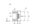
- Figures 5, 6 and 7are diagrams showing the internal structure of the wireless power receiving device.
- Figure 5is a diagram of the wireless power receiving device 50 viewed in the direction opposite to the Z-axis direction with surface 101 of the housing 100 (see Figures 3 and 4) removed.
- Figure 6is a cross-sectional view taken along line AB in Figure 5.
- Figure 7is an enlarged view of region 301 in Figure 6.
- the housing 100contains a thermally conductive member 201, a receiving circuit board 202, a first magnetic sheet 203, a second magnetic sheet 204, a third magnetic sheet 205, a receiving coil 206, a secondary battery 207, and a functional circuit board 208.
- the receiving coil 206corresponds to the receiving coil 71 in FIG. 2.
- the secondary battery 207corresponds to the secondary battery 82 in FIG. 2.
- Thermal conductive member 201may be, for example, a metal, but the present disclosure is not limited thereto.
- An example of the metalmay be copper (Cu), but the present disclosure is not limited thereto.
- the metalmay be an alloy.
- One end 201a of the heat conduction member 201 in the circumferential direction of the Z axis and the other end 201b in the circumferential direction of the Z axisare located opposite to surface 106.
- the heat conduction member 201extends clockwise in the circumferential direction of the Z axis along surfaces 103, 105, and 104, and is annular. However, a gap 401 is provided between the one end 201a and the other end 201b.
- the heat conduction member 201is C-shaped when viewed from the Z axis direction. A circulating current is suppressed from flowing through the heat conduction member 201 in the circumferential direction of the Z axis.
- the wireless power receiving device 50can prevent circulating current from flowing through the heat conducting member 201 along the circumferential direction of the Z axis by providing a gap 401 between one end 201a and the other end 201b of the heat conducting member 201. This allows the wireless power receiving device 50 to reduce losses and improve power receiving efficiency.
- the heat conducting member 201has a protrusion 201c on the inner circumference of the portion facing the surface 103.
- the first magnetic sheet 203extends in the circumferential direction of the Z-axis along the outer periphery of the heat conduction member 201, and is annular. In other words, the first magnetic sheet 203 is O-shaped when viewed from the Z-axis direction.
- the first magnetic sheet 203is in thermal contact with the heat conduction member 201.
- the first magnetic sheet 203is in close contact with the heat conduction member 201. This allows the heat of the heat conduction member 201 to be dissipated to the housing 100 side via the first magnetic sheet 203.
- Examples of the first magnetic sheet 203include ferrite sintered body and fine soft magnetic metal solidified with resin, but the present disclosure is not limited to these.
- the relative permeability of ferrite sintered bodyis large (e.g., about 200) and that of fine soft magnetic metal solidified with resin is small (e.g., about 50).
- ferriteis expensive, while that of fine soft magnetic metal solidified with resin is inexpensive.
- flexibilityease of bending, ease of processing
- that of fine soft magnetic metal solidified with resinis highly flexible, while that of ferrite sintered body is less flexible.
- FIG. 8is a diagram showing an example of the first magnetic sheet.
- the first magnetic sheet 203is exemplified as being in a strip shape.
- This strip-shaped first magnetic sheet 203is exemplified as being wrapped (e.g., attached) around the outer periphery of the heat conductive member 201 along the circumferential direction of the Z-axis.
- the receiving coil 206is wound around the outer periphery of the first magnetic sheet 203. Both ends of the receiving coil 206 are electrically connected to the receiving circuit board 202 via wiring 261.
- the power receiving circuit board 202includes a resonant capacitor 72 (see FIG. 2), a resonant adjustment circuit 62 (see FIG. 2), a rectifying and smoothing circuit 63 (see FIG. 2), a voltage conversion circuit 64 (see FIG. 2), a charging control circuit 65 (see FIG. 2), and a charging circuit 81 (see FIG. 2).
- the power receiving circuit board 202converts the resonant current of the power receiving resonant circuit (power receiving coil 206 and resonant capacitor 72) into direct current, and supplies power to the load (secondary battery 207).
- the wireless power receiving device 50can be used repeatedly without changing the battery because the power receiving circuit board 202 is equipped with a charging circuit 81 that charges the secondary battery 207.
- the power receiving circuit board 202is provided inside the heat conducting member 201, facing the surface 103.
- the power receiving circuit board 202is arranged so that its first main surface (the main surface at the tip of the Y axis, the main surface facing upward in FIG. 5) faces the heat conducting member 201.
- the power receiving circuit board 202is arranged so that its first main surface is perpendicular to the XY plane and parallel to the Z axis.
- the wireless power receiving device 50has a larger internal space because the first main surface of the power receiving circuit board 202 is arranged perpendicular to the X-Y plane and parallel to the Z axis, compared to a case in which the first main surface of the power receiving circuit board 202 is arranged parallel to the X-Y plane and perpendicular to the Z axis.
- the wireless power receiving device 50has a first main surface of the power receiving circuit board 202 arranged perpendicular to the X-Y plane and parallel to the Z axis, compared to a case in which the first main surface of the power receiving circuit board 202 is arranged parallel to the X-Y plane and perpendicular to the Z axis, compared to a case in which the first main surface of the power receiving circuit board 202 is arranged parallel to the X-Y plane and perpendicular to the Z axis.
- Heat-generating electronic component 251, electronic component 252, and electronic component 253are mounted on the first main surface of power receiving circuit board 202. Heat-generating electronic component 251, electronic component 252, and electronic component 253 are each exemplified by a semiconductor device, but the present disclosure is not limited thereto.
- the heat-generating electronic component 251is the electronic component that generates the greatest amount of heat among the components of the wireless power receiving device 50.
- An example of the heat-generating electronic component 251is a semiconductor device in which a voltage conversion circuit 64 (e.g., a switching regulator) is formed, but the present disclosure is not limited thereto.
- Each of the resonance adjustment circuit 62 (see FIG. 2), the rectification smoothing circuit 63 (see FIG. 2), the charge control circuit 65 (see FIG. 2), and the charge circuit 81 (see FIG. 2)is formed in the electronic component 252 or the electronic component 253.
- the heat-generating electronic component 251is in thermal contact with the protrusion 201c of the heat-conducting member 201.
- the first main surface (the main surface on the Y-axis tip side, the main surface facing upward in FIG. 5) of the heat-generating electronic component 251is in close contact with the protrusion 201c of the heat-conducting member 201.
- the first main surface of the power receiving circuit board 202is arranged perpendicular to the X-Y plane and parallel to the Z axis, which makes it easier to bring the heat-generating electronic component 251 into contact with the heat conducting member 201 compared to when the first main surface of the power receiving circuit board 202 is arranged parallel to the X-Y plane and perpendicular to the Z axis.
- the heat-generating electronic component 251is in thermal contact with the protrusion 201c of the heat-conducting member 201, so that the heat of the heat-generating electronic component 251 is conducted to the heat-conducting member 201.
- the heat conducted to the heat-conducting member 201is diffused throughout the heat-conducting member 201.
- the heat diffused throughout the heat-conducting member 201is conducted throughout the first magnetic sheet 203.
- the wireless power receiving device 50is able to suppress local temperature rises on the surface of the housing 100 by diffusing the heat from the heat-generating electronic component 251 throughout the thermally conductive member 201 and then through the first magnetic sheet 203 to the surfaces 103, 104, 105, and 106 of the housing 100.
- the secondary battery 207is provided inside the thermally conductive member 201 and opposite the surface 105.
- the wireless power receiving device 50can be made smaller by providing the secondary battery 207 inside the thermal conductive member 201.
- the secondary battery 207is exemplified by a coin battery or a button battery.
- the wireless power receiving device 50has a button-type or coin-type secondary battery 207, which allows for miniaturization of electronic devices and is suitable for hearing aids.
- the secondary battery 207is electrically connected to the power receiving circuit board 202 via wiring 262. When the power receiving circuit board 202 is receiving power, the secondary battery 207 is charged via wiring 262.
- the functional circuit board 208includes a functional circuit 83 (see FIG. 2).
- the functional circuit board 208is exemplified as a board that amplifies and outputs an audio signal, but the present disclosure is not limited thereto.
- the functional circuit board 208is provided inside the heat conductive member 201, facing surface 104.
- the functional circuit board 208is provided so that its first principal surface (the principal surface on the base end side of the Y-axis, the principal surface facing downward in FIG. 5) faces the heat conductive member 201.
- the first principal surface of the functional circuit board 208is disposed perpendicular to the X-Y plane and parallel to the Z-axis.
- the wireless power receiving device 50has a larger internal space because the first main surface of the functional circuit board 208 is arranged perpendicular to the X-Y plane and parallel to the Z axis, compared to a case in which the first main surface of the functional circuit board 208 is arranged parallel to the X-Y plane and perpendicular to the Z axis.
- the wireless power receiving device 50has a larger internal space because the first main surface of the functional circuit board 208 is arranged perpendicular to the X-Y plane and parallel to the Z axis, compared to a case in which the first main surface of the functional circuit board 208 is arranged parallel to the X-Y plane and perpendicular to the Z axis.
- the functional circuit board 208is electrically connected to the power receiving circuit board 202 via the wiring 263.
- the functional circuit board 208operates by receiving power from the secondary battery 207 via the wiring 263, the power receiving circuit board 202, and the wiring 262.
- the second magnetic sheet 204is disposed at the first opening of the heat conductive member 201 (the opening on the tip side of the Z axis, the opening on the side facing surface 101) and covers the first opening of the heat conductive member 201.
- the third magnetic sheet 205is disposed at the second opening of the heat conductive member 201 (the opening on the base end side of the Z axis, the opening on the side facing surface 102) and covers the second opening of the heat conductive member 201.
- FIG. 9shows an example of a second magnetic sheet.
- FIG. 10shows an example of a third magnetic sheet.
- the relative magnetic permeability of the first magnetic sheet 203is greater than the relative magnetic permeability of the second magnetic sheet 204 and the third magnetic sheet 205.
- the first magnetic sheet 203is a sintered ferrite body
- the second magnetic sheet 204 and the third magnetic sheet 205are made of fine soft magnetic metal solidified with resin.
- the first magnetic sheet 203forms a magnetic coupling with the power transmission coil 501 (described below) or the power transmission coil 521 (described below), while the second magnetic sheet 204 and the third magnetic sheet 205 form an electromagnetic seal. Therefore, it is preferable that the first magnetic seal 203 has a high relative permeability to increase the magnetic coupling and improve the power receiving efficiency, while the second magnetic sheet 204 and the third magnetic sheet 205 do not need to have a high relative permeability.
- sintered ferriteis expensive, while fine soft magnetic metal bound with resin is inexpensive.
- the first magnetic sheet 203is a sintered ferrite body
- the second magnetic sheet 204 and the third magnetic sheet 205are made of fine soft magnetic metal solidified with resin.
- the wireless power receiving device 50can increase the magnetic coupling with the power transmitting coil 501 or the power transmitting coil 521 by making the first magnetic sheet 203 a sintered ferrite body, thereby improving the power receiving efficiency. In addition, the wireless power receiving device 50 can reduce costs by making the second magnetic sheet 204 and the third magnetic sheet 205 out of fine soft magnetic metal solidified with resin.
- the end of the first magnetic sheet 203 on the Z-axis tip sideis located further toward the Z-axis tip side than the first main surface on the Z-axis tip side of the second magnetic sheet 204.
- the end of the first magnetic sheet 203 on the Z-axis base sideis located further toward the Z-axis base side than the first main surface on the Z-axis base side of the third magnetic sheet 205.
- the width d2 of the first magnetic sheet 203 in the Z-axis directionis longer than the distance d1 between the first main surface of the second magnetic sheet 204 and the first main surface of the third magnetic sheet 205.
- the wireless power receiving device 50can prevent the magnetic flux from the power transmitting coil 501 or the power transmitting coil 521 from entering the inside of the wireless power receiving device 50 through the gap between the first magnetic sheet 203 and the second magnetic sheet 204 and the gap between the first magnetic sheet 203 and the third magnetic sheet 205. Therefore, the wireless power receiving device 50 can prevent the magnetic flux from interlinking with the receiving circuit board 202, the secondary battery 207, and the functional circuit board 208, prevent the receiving circuit board 202, the secondary battery 207, and the functional circuit board 208 from generating heat, and prevent the receiving circuit board 202, the secondary battery 207, and the functional circuit board 208 from being subjected to electromagnetic interference.
- FIG. 11is a diagram illustrating a first example of magnetic flux linking the wireless power receiving device.
- the power transmitting coil 501is annular along the circumferential direction of the Z axis, and faces the surfaces 106, 103, 105, and 104 (see Fig. 3, etc.).
- the magnetic fluxtravels counterclockwise on the X-Z plane from the end of the first magnetic sheet 203 on the Z-axis tip side, surrounding the power receiving coil 206 and the power transmitting coil 501, and reaches the end of the first magnetic sheet 203 on the Z-axis base side.
- the magnetic fluxtravels clockwise on the X-Z plane from the end of the first magnetic sheet 203 on the Z-axis tip side, surrounding the power receiving coil 206 and the power transmitting coil 501, and reaches the end of the first magnetic sheet 203 on the Z-axis base side.
- the first magnetic sheet 203can form a magnetic path that efficiently links the magnetic flux to the receiving coil 206.
- the first magnetic sheet 203can suppress the magnetic flux that interlinks with the heat conductive member 201, and can suppress the generation of eddy currents in the heat conductive member 201.
- (Second Example of Magnetic Flux Linked to Wireless Power Receiving Device) 12is a diagram showing a second example of magnetic flux linking the wireless power receiving device, in which a power transmitting coil 521 is parallel to the XY plane and faces the surface 102 (see FIG. 3, etc.).
- the magnetic fluxtravels counterclockwise from the third magnetic sheet 205 on the X-Z plane, passes inside the power transmission coil 521, and reaches the third magnetic sheet 205.
- the magnetic fluxtravels clockwise from the third magnetic sheet 205 on the X-Z plane, passes inside the power transmission coil 521, and reaches the third magnetic sheet 205.
- the third magnetic sheet 205can prevent magnetic flux from interlinking with the receiving circuit board 202, the secondary battery 207, and the functional circuit board 208.
- the wireless power receiving device 50can prevent the receiving circuit board 202, the secondary battery 207, and the functional circuit board 208 from being subjected to electromagnetic interference.
- a magnetic fluxmay be generated that extends from the first magnetic sheet 203, surrounds the receiving coil 206, passes through the inside of the transmitting coil 521, and reaches the first magnetic sheet 203. Therefore, the wireless power receiving device 50 can be charged from the transmitting coil 521.
- Heat-generating electronic component 251is in thermal contact with protrusion 201c of thermal conduction member 201, so that heat from heat-generating electronic component 251 is conducted to thermal conduction member 201.
- the heat conducted to thermal conduction member 201is diffused throughout thermal conduction member 201.
- the heat diffused throughout thermal conduction member 201is conducted throughout first magnetic sheet 203.
- the wireless power receiving device 50is able to suppress local temperature rises on the surface of the housing 100 by diffusing the heat from the heat-generating electronic component 251 throughout the thermally conductive member 201 and then through the first magnetic sheet 203 to the surfaces 103, 104, 105, and 106 of the housing 100.
- first magnetic sheet 203An end portion on the Z-axis tip side of first magnetic sheet 203 is located further toward the Z-axis tip side than a first main surface on the Z-axis tip side of second magnetic sheet 204.
- An end portion on the Z-axis base side of first magnetic sheet 203is located further toward the Z-axis base side than a first main surface on the Z-axis base side of third magnetic sheet 205.
- width d2 of first magnetic sheet 203 in the Z-axis directionis longer than distance d1 between the first main surface of second magnetic sheet 204 and the first main surface of third magnetic sheet 205.
- the wireless power receiving device 50can prevent magnetic flux from the power transmitting coil 501 or the power transmitting coil 521 from entering the inside of the wireless power receiving device 50 through the gap between the first magnetic sheet 203 and the second magnetic sheet 204 and the gap between the first magnetic sheet 203 and the third magnetic sheet 205. Therefore, the wireless power receiving device 50 can prevent magnetic flux from interlinking with the receiving circuit board 202, the secondary battery 207, and the functional circuit board 208, prevent heat generation in the receiving circuit board 202, the secondary battery 207, and the functional circuit board 208, and prevent the receiving circuit board 202, the secondary battery 207, and the functional circuit board 208 from being subjected to electromagnetic interference.
- the first main surface of the power receiving circuit board 202is disposed perpendicular to the X-Y plane and parallel to the Z axis, so that the internal space can be made larger compared to a case in which the first main surface of the power receiving circuit board 202 is disposed parallel to the X-Y plane and perpendicular to the Z axis.
- the first main surface of the power receiving circuit board 202is disposed perpendicular to the X-Y plane and parallel to the Z axis, so that the wireless power receiving device 50 can be made smaller compared to a case in which the first main surface of the power receiving circuit board 202 is disposed parallel to the X-Y plane and perpendicular to the Z axis.
- the first magnetic sheet 203may be a sintered ferrite body, and the second magnetic sheet 204 and the third magnetic sheet 205 may be made of fine soft magnetic metal solidified with resin.
- the wireless power receiving device 50can increase the magnetic coupling with the power transmitting coil 501 or the power transmitting coil 521 by making the first magnetic sheet 203 a sintered ferrite body, thereby improving the power receiving efficiency. In addition, the wireless power receiving device 50 can reduce costs by making the second magnetic sheet 204 and the third magnetic sheet 205 out of fine soft magnetic metal solidified with resin.
- the wireless power receiving device 50can suppress electromagnetic interference by setting the frequency of the magnetic field generated by the power transmitting coil to 6.78 MHz or 13.56 MHz in the ISM band.
- the wireless power receiving device 50can be made smaller by providing the secondary battery 207 inside the thermal conductive member 201 .
- the electronic devicecan be made smaller, making the device suitable for a hearing aid.
- the wireless power receiving device 50can be used repeatedly without changing the battery because the power receiving circuit board 202 includes a charging circuit that charges the secondary battery 207 .
- the wireless power receiving device 50can suppress a circulating current from flowing in the circumferential direction of the Z axis through the heat conducting member 201 by providing the gap 401 between the one end 201a and the other end 201b of the heat conducting member 201. This enables the wireless power receiving device 50 to suppress loss and increase power receiving efficiency.
- the present disclosuremay also have the following configurations.
- annular heat conducting memberextending in one circumferential direction; a first magnetic sheet extending along an outer periphery of the heat conducting member and in thermal contact with the heat conducting member; a second magnetic sheet covering an opening on the one side of the heat conductive member; a third magnetic sheet covering an opening on a side of the heat conductive member opposite to the one direction;
- the first magnetic sheetis a length in the one direction is longer than a distance between a main surface of the second magnetic sheet in the one direction and a main surface of
- the wireless power receiving deviceaccording to (1) above,
- the power receiving circuit boardhas a main surface arranged parallel to the one direction. Wireless power receiving device.
- the wireless power receiving deviceaccording to (1) or (2), The relative magnetic permeability of the first magnetic sheet is greater than the relative magnetic permeability of the second magnetic sheet or the third magnetic sheet. Wireless power receiving device.
- the wireless power receiving deviceaccording to any one of (1) to (3),
- the frequency of the magnetic field generated by the power transmission coilis 6.78 MHz or 13.56 MHz in the ISM (Industrial, Scientific and Medical) band. Wireless power receiving device.
- the wireless power receiving deviceaccording to any one of (1) to (4),
- the thermal conductive memberfurther includes a secondary battery provided inside the thermal conductive member. Wireless power receiving device.
- the wireless power receiving deviceis a coin battery or a button battery. Wireless power receiving device.
- the power receiving circuit boardincludes a charging circuit that charges the secondary battery; Wireless power receiving device.
- the wireless power receiving deviceaccording to any one of (1) to (7),
- the heat conductive memberis made of copper, and a gap is provided between one end in the circumferential direction and the other end in the circumferential direction. Wireless power receiving device.
Landscapes
- Engineering & Computer Science (AREA)
- Power Engineering (AREA)
- Computer Networks & Wireless Communication (AREA)
- Physics & Mathematics (AREA)
- Electromagnetism (AREA)
- Charge And Discharge Circuits For Batteries Or The Like (AREA)
Abstract
Description
Translated fromJapanese本開示は、ワイヤレス受電装置に関する。This disclosure relates to a wireless power receiving device.
小型の電子機器に搭載されている二次電池の充電技術として、外部の送電装置からワイヤレスで電子機器に電力を供給するワイヤレス給電技術がある。電子機器は、ワイヤレス給電技術を用いることにより、充電端子を備える必要がなくなるので、金属端子(充電端子)の腐食や劣化の問題がなく、防水性を高めることができる。Wireless power supply technology is one of the charging technologies for secondary batteries installed in small electronic devices, which supplies power to electronic devices wirelessly from an external power transmission device. By using wireless power supply technology, electronic devices no longer need to have charging terminals, so there is no problem with corrosion or deterioration of metal terminals (charging terminals) and waterproofing can be improved.
ワイヤレス給電技術として、特許文献1には、受給電装置及び携帯機器が記載されている。また、特許文献2には、非接触給電装置及び非接触電力伝送装置が記載されている。As wireless power supply technology,
ワイヤレス給電技術を用いた小型の電子機器は、防水性を得るために、密閉構造の筐体を採用することが好ましい。Small electronic devices that use wireless power transfer technology should preferably be housed in a sealed housing to ensure waterproofing.
また、電子機器は、受電コイルで得られた電力を二次電池に充電するために、電力変換回路を搭載する。電力変換回路を構成する半導体装置(IC)は、発熱する。In addition, electronic devices are equipped with a power conversion circuit to charge the secondary battery with the power obtained by the receiving coil. The semiconductor device (IC) that constitutes the power conversion circuit generates heat.
このように、電子機器は、密閉構造を採用し且つ電力変換回路を構成する半導体素子が発熱すると、電子機器の筐体の表面で局所的に(電力変換回路の近傍で)温度上昇が大きくなる。In this way, when electronic devices have a sealed structure and the semiconductor elements that make up the power conversion circuit generate heat, the temperature rise increases locally (near the power conversion circuit) on the surface of the electronic device's housing.
また、電子機器は、磁束がワイヤレス受電回路や二次電池に鎖交することにより、ワイヤレス受電回路や二次電池が発熱したり、電磁干渉を受けたりする。また、電子機器は、送電コイルとの磁気結合が小さくなることにより、受電効率が低下する。In addition, magnetic flux interlinks with the wireless power receiving circuit or secondary battery of electronic devices, causing the latter to heat up or be subject to electromagnetic interference. In addition, the power receiving efficiency of electronic devices decreases as the magnetic coupling with the power transmission coil decreases.
本開示は、上記に鑑みてなされたものであって、筐体の表面の局所的な温度の上昇を抑制し、電磁干渉を抑制し、受電効率を高くすることを目的とする。The present disclosure has been made in consideration of the above, and aims to suppress local temperature increases on the surface of the housing, suppress electromagnetic interference, and increase power receiving efficiency.
本開示の一側面のワイヤレス受電装置は、一方向の周方向に延びた環状の熱伝導部材と、熱伝導部材の外周に沿って延び、熱伝導部材に熱的に接触している第1磁性シートと、熱伝導部材の一方向の側の開口部を覆う第2磁性シートと、熱伝導部材の一方向と反対方向の側開口部を覆う第3磁性シートと、第1磁性シートの外周に巻回された受電コイルと、熱伝導部材の内側に設けられ、受電コイルに電気的に接続され、受電コイルに誘導される共振電流を整流して直流に変換し、負荷に電力を供給する、受電回路基板と、受電回路基板に実装され、熱伝導部材に熱的に接触している発熱電子部品と、を備える。熱伝導部材は、発熱電子部品から発生する熱を第1磁性シートに伝導し、第1磁性シートは、一方向の長さが第2磁性シートの一方向の側の主面と第3磁性シートの一方向と反対方向の側の主面との間の距離よりも長く、外部の送電コイルから生じる磁束に対して第2磁性シート又は第3磁性シートにおいて形成される磁路よりも磁気結合が大きい主磁束による磁路を形成し、且つ、発熱電子部品の熱を熱放射する。A wireless power receiving device according to one aspect of the present disclosure comprises an annular heat conducting member extending circumferentially in one direction, a first magnetic sheet extending along the outer periphery of the heat conducting member and in thermal contact with the heat conducting member, a second magnetic sheet covering an opening on one side of the heat conducting member, a third magnetic sheet covering a side opening on the opposite side to the one direction of the heat conducting member, a receiving coil wound around the outer periphery of the first magnetic sheet, a receiving circuit board provided inside the heat conducting member and electrically connected to the receiving coil, rectifying and converting a resonant current induced in the receiving coil to direct current, and supplying power to a load, and a heat-generating electronic component mounted on the receiving circuit board and in thermal contact with the heat conducting member. The thermally conductive member conducts heat generated by the heat-generating electronic components to the first magnetic sheet, and the first magnetic sheet has a length in one direction that is longer than the distance between the main surface of the second magnetic sheet in one direction and the main surface of the third magnetic sheet in the opposite direction, forms a magnetic path by the main magnetic flux that has a greater magnetic coupling with the magnetic flux generated by the external power transmission coil than the magnetic path formed in the second magnetic sheet or the third magnetic sheet, and radiates heat from the heat-generating electronic components.
本発明によれば、受電回路に実装される発熱部品の温度上昇を抑制すると共に、筐体の表面の局所的な温度の上昇を抑制でき、かつ、ワイヤレス受電回路や二次電池の渦電流による発熱を抑止して電磁干渉を抑制でき、受電効率を高くすることができる。The present invention can suppress the temperature rise of heat-generating components mounted on the power receiving circuit, as well as the local temperature rise on the surface of the housing. It also suppresses heat generation due to eddy currents in the wireless power receiving circuit and secondary battery, suppressing electromagnetic interference, and improving power receiving efficiency.
以下に、本開示の実施の形態を図面に基づいて詳細に説明する。なお、この実施の形態により本発明が限定されるものではない。各実施の形態は例示であり、異なる実施の形態で示した構成の部分的な置換又は組み合わせが可能であることは言うまでもない。第2の実施の形態以降では第1の実施の形態と共通の事柄についての記述を省略し、異なる点についてのみ説明する。特に、同様の構成による同様の作用効果については実施形態毎には逐次言及しない。Below, embodiments of the present disclosure will be described in detail with reference to the drawings. Note that the present invention is not limited to these embodiments. Each embodiment is merely an example, and it goes without saying that partial substitution or combination of the configurations shown in different embodiments is possible. From the second embodiment onwards, a description of matters common to the first embodiment will be omitted, and only the differences will be described. In particular, similar effects resulting from similar configurations will not be mentioned in each embodiment.
<実施の形態>
(ワイヤレス送受電の原理)
実施の形態のワイヤレス受電装置の説明に先立って、ワイヤレス送受電の原理について、説明する。<Embodiment>
(Principle of wireless power transmission and reception)
Prior to describing the wireless power receiving device of the embodiment, the principle of wireless power transmission and reception will be described.
[構成]
図1は、ワイヤレス送受電の原理を説明する図である。ワイヤレス送受電装置1は、ワイヤレス送電装置2と、ワイヤレス受電装置3と、を含む。[composition]
1 is a diagram illustrating the principle of wireless power transmission and reception. A wireless power transmitting and receiving
ワイヤレス送電装置2は、直流電源11と、トランジスタ12と、トランジスタ13と、送電共振回路14と、制御回路15と、を含む。トランジスタ12及びトランジスタ13の各々は、寄生容量及び寄生ダイオードを有する。送電共振回路14は、送電コイル16と、共振コンデンサ17と、を含む。The wireless power transmission device 2 includes a
ワイヤレス受電装置3は、受電共振回路21と、トランジスタ22と、トランジスタ23と、平滑コンデンサ24と、負荷25と、制御回路26と、を含む。トランジスタ22及びトランジスタ23の各々は、寄生容量及び寄生ダイオードを有する。受電共振回路21は、受電コイル27と、共振コンデンサ28と、を含む。The wireless power receiver 3 includes a power
トランジスタ12のドレインは、直流電源11の高電位側端に電気的に接続されている。トランジスタ12のソースは、トランジスタ13のドレインに電気的に接続されている。トランジスタ13のソースは、直流電源11の低電位側端に電気的に接続されている。共振コンデンサ17の一端は、トランジスタ12のドレインに電気的に接続されている。共振コンデンサ17の他端は、送電コイル16の一端に電気的に接続されている。送電コイル16の他端は、トランジスタ12のソース及びトランジスタ13のドレインに電気的に接続されている。The drain of the
受電コイル27の一端は、共振コンデンサ28の一端に電気的に接続されている。共振コンデンサ28の他端は、トランジスタ22のドレインに電気的に接続されている。トランジスタ22のソースは、受電コイル27の他端及びトランジスタ23のドレインに電気的に接続されている。平滑コンデンサ24の一端は、トランジスタ22のドレインに電気的に接続されている。平滑コンデンサ24の他端は、トランジスタ23のソースに電気的に接続されている。負荷25の一端は、平滑コンデンサ24の一端に電気的に接続されている。負荷25の他端は、平滑コンデンサ24の他端に電気的に接続されている。One end of the
送電共振回路14と受電共振回路21とは、電磁結合している。The power transmitting
[動作]
制御回路15は、所定のスイッチング周波数で、トランジスタ12とトランジスタ13とを交互にオンオフさせる。これにより、送電共振回路14に矩形波状(パルス状)の電圧が印加され、送電共振回路14は共振し、送電共振回路14に共振電流が流れる。[Action]
The
送電共振回路14が共振すると、送電共振回路14と受電共振回路21とは、共鳴する。つまり、受電共振回路21が、共振する。これにより、受電共振回路21に共振電流が流れる。When the power transmitting
送電共振回路14から生じる磁界の周波数は、ISM(Industrial,Scientific and Medical)バンドの6.78MHz又は13.56MHzであることが例示されるが、本開示はこれに限定されない。The frequency of the magnetic field generated by the power transmission
制御回路26は、受電コイル27に流れる電流の向きに応じて、トランジスタ22とトランジスタ23とを交互にオンオフさせる。これにより、受電共振回路21の共振電流が、電流の向きに同期して整流される。平滑コンデンサ24は、整流後の電流を平滑する。平滑コンデンサ24で平滑された電圧が、負荷25に印加される。The
(ワイヤレス受電装置の回路ブロック構成)
図2は、実施の形態のワイヤレス受電装置の回路ブロック構成を示す図である。(Circuit block configuration of wireless power receiving device)
FIG. 2 is a diagram showing a circuit block configuration of the wireless power receiving device according to the embodiment.
ワイヤレス受電装置50は、ワイヤレス受電回路51と、負荷回路52と、を含む。ワイヤレス受電回路51は、受電共振回路61と、共鳴調整回路62と、整流平滑回路63と、電圧変換回路64と、充電制御回路65と、を含む。受電共振回路61は、受電コイル71と、共振コンデンサ72と、を含む。負荷回路52は、充電回路81と、二次電池82と、機能回路83と、を含む。The wireless
共鳴調整回路62は、受電共振回路61の共鳴を調整する。例えば、共鳴調整回路62は、図1のトランジスタ22、トランジスタ23及び制御回路26に相当することが例示される。The
整流平滑回路63は、受電共振回路61の共振電流を整流及び平滑する。例えば、整流平滑回路63は、図1の平滑コンデンサ24に相当することが例示される。整流平滑回路63は、平滑コンデンサ24に加えてダイオードなどを含んでも良い。The rectifying and smoothing
電圧変換回路64は、整流平滑回路63で整流平滑された後の電圧を昇圧又は降圧するスイッチングレギュレータが例示される。The
充電制御回路65は、充電回路81を制御し、二次電池82の充電を充電回路81に行わせる。The charging
機能回路83は、二次電池82から電力の供給を受けて、動作する。機能回路83は、例えば、ワイヤレス受電装置50が補聴器である場合には、音声信号を増幅して出力する回路が例示される。The
(ワイヤレス受電装置の筐体)
実施の形態では、本開示のワイヤレス受電装置を補聴器に適用した例を説明するが、本開示はこれに限定されない。本開示のワイヤレス受電装置は、種々の電子機器に適用可能である。(Housing of wireless power receiving device)
In the embodiment, an example in which the wireless power receiving device of the present disclosure is applied to a hearing aid will be described, but the present disclosure is not limited thereto. The wireless power receiving device of the present disclosure can be applied to various electronic devices.
図3及び図4は、実施の形態のワイヤレス受電装置の外観を示す図である。ワイヤレス受電装置50を実現する部品は、筐体100の中に収容されている。なお、以下では、ワイヤレス受電装置50の形状を分かり易く説明するために、X軸方向、Y軸方向、Z軸方向を用いて説明するが、X軸、Y軸、Z軸は、それぞれが直交する3軸というだけの意味である。FIGS. 3 and 4 are diagrams showing the external appearance of a wireless power receiving device according to an embodiment. The components that make up the wireless
Z軸方向が、本開示の「一方向」の一例に相当する。The Z-axis direction corresponds to an example of "one direction" in this disclosure.
筐体100は、面101、面102、面103、面104、面105、及び、面106を有する。筐体100は、人間の耳介の形状に合わせた形状を有する。The
面101と面102とは、X-Y平面に平行な面であり、Z軸方向に所定距離で離れている。面101と面102とは、平行であり、互いに対向する。面103は、面101と面102とのY軸先端側の端辺に連接する。面104は、面101と面102とのY軸基端側の端辺に連接する。面105は、面101と面102とのX軸先端側の端辺に連接する。面106は、面101と面102とのX軸基端側の端辺に連接する。面103、面104、面105及び面106の各々は、X-Y平面と垂直である。
ここで、面101及び面102では、X軸先端側のY軸方向の長さは、X軸基端側のY軸方向の長さよりも長い。すなわち、面101及び面102は、面105に連接する側の領域110が、面106に連接する側の領域120よりも広い。Here, in
この筐体100の中に、ワイヤレス受電装置50を実現する部品が収容されている。筐体100は、樹脂であることが例示されるが、本開示はこれに限定されない。筐体100は、ワイヤレス受電装置50を実現する部品を収容し、密閉されていることが例示されるが、本開示はこれに限定されない。The components that realize the wireless
(ワイヤレス受電装置の内部構造)
図5、図6及び図7は、ワイヤレス受電装置の内部構造を示す図である。図5は、筐体100の面101(図3及び図4参照)を取り除いて、Z軸方向と反対の方向にワイヤレス受電装置50を視た図である。図6は、図5中のA-B線での断面図である。図7は、図6中の領域301の拡大図である。(Internal structure of a wireless power receiving device)
Figures 5, 6 and 7 are diagrams showing the internal structure of the wireless power receiving device. Figure 5 is a diagram of the wireless
筐体100の中には、熱伝導部材201、受電回路基板202、第1磁性シート203、第2磁性シート204、第3磁性シート205、受電コイル206、二次電池207、及び、機能回路基板208が収容されている。The
受電コイル206は、図2の受電コイル71に相当する。二次電池207は、図2の二次電池82に相当する。The receiving
熱伝導部材201は、金属が例示されるが、本開示は、これに限定されない。金属は、銅(Cu)が例示されるが、本開示はこれに限定されない。金属は、合金であっても良い。Thermal
熱伝導部材201のZ軸の周方向の一端201a及びZ軸の周方向の他端201bは、面106に対向する場所に位置している。熱伝導部材201は、面103、面105及び面104に沿って、Z軸の周方向に時計回りに延び、環状となっている。但し、一端201aと他端201bとの間には、間隙401が設けられている。つまり、熱伝導部材201は、Z軸方向から視て、C字状である。循環電流がZ軸の周方向に沿って熱伝導部材201に流れることが、抑制される。One
ワイヤレス受電装置50は、間隙401が熱伝導部材201の一端201aと他端201bとの間に設けられていることにより、循環電流がZ軸の周方向に沿って熱伝導部材201に流れることを抑制できる。これにより、ワイヤレス受電装置50は、損失を抑制でき、受電効率を高めることができる。The wireless
熱伝導部材201は、面103に対向する部分の内周に、突部201cを有する。The
第1磁性シート203は、熱伝導部材201の外周に沿って、Z軸の周方向に延び、環状となっている。つまり、第1磁性シート203は、Z軸方向から視て、O字状である。第1磁性シート203は、熱伝導部材201に熱的に接触している。例えば、第1磁性シート203は、熱伝導部材201に密着している。これにより、熱伝導部材201の熱が、第1磁性シート203を介して、筐体100の側へ放熱される。The first
第1磁性シート203は、フェライト焼結体、微細な軟磁性金属が樹脂で固められたものなどが例示されるが、本開示はこれに限定されない。一般に、比透磁率は、フェライト焼結体が大きく(例えば、約200)、微細な軟磁性金属が樹脂で固められたものが小さい(例えば、約50)。コストは、フェライトが高価であり、微細な軟磁性金属が樹脂で固められたものが安価である。柔軟性(曲がりやすさ、加工しやすさ)は、微細な軟磁性金属が樹脂で固められたものが、柔軟性が高く、フェライト焼結体が、柔軟性が低い。Examples of the first
図8は、第1磁性シートの一例を示す図である。図8に示すように、第1磁性シート203は、帯状が例示される。この帯状の第1磁性シート203が、Z軸の周方向に沿って熱伝導部材201の外周に巻き付けられる(例えば、貼り付けられる)ことが、例示される。FIG. 8 is a diagram showing an example of the first magnetic sheet. As shown in FIG. 8, the first
再び図5及び図6を参照すると、受電コイル206は、第1磁性シート203の外周に巻回されている。受電コイル206の両端は、配線261を介して、受電回路基板202に電気的に接続されている。Referring again to Figures 5 and 6, the receiving
受電回路基板202は、共振コンデンサ72(図2参照)、共鳴調整回路62(図2参照)、整流平滑回路63(図2参照)、電圧変換回路64(図2参照)、充電制御回路65(図2参照)及び充電回路81(図2参照)を備える。受電回路基板202は、受電共振回路(受電コイル206及び共振コンデンサ72)の共振電流を直流に変換し、電力を負荷(二次電池207)に供給する。The power
ワイヤレス受電装置50は、受電回路基板202が二次電池207を充電する充電回路81を備えることにより、電池交換しないで繰り返し使用することが可能である。The wireless
受電回路基板202は、熱伝導部材201の内側、且つ、面103に対向する場所に設けられている。受電回路基板202は、第1主面(Y軸先端側の主面、図5中の上方向の主面)が熱伝導部材201に対向するように配置されている。つまり、受電回路基板202は、第1主面がX-Y平面と垂直且つZ軸と平行に配置されている。The power
ワイヤレス受電装置50は、受電回路基板202の第1主面がX-Y平面と垂直且つZ軸と平行に配置されていることにより、受電回路基板202の第1主面がX-Y平面と平行且つZ軸と垂直に配置された場合と比較して、内部空間を広くすることができる。或いは、ワイヤレス受電装置50は、受電回路基板202の第1主面がX-Y平面と垂直且つZ軸と平行に配置されていることにより、受電回路基板202の第1主面がX-Y平面と平行且つZ軸と垂直に配置された場合と比較して、小型化が可能である。The wireless
受電回路基板202の第1主面には、発熱電子部品251と、電子部品252と、電子部品253と、が実装されている。発熱電子部品251、電子部品252及び電子部品253の各々は、半導体装置が例示されるが、本開示はこれに限定されない。Heat-generating
発熱電子部品251は、ワイヤレス受電装置50の構成部品の中で、発熱量が最も大きい電子部品である。発熱電子部品251は、電圧変換回路64(例えば、スイッチングレギュレータ)が形成された半導体装置が例示されるが、本開示はこれに限定されない。The heat-generating
共鳴調整回路62(図2参照)、整流平滑回路63(図2参照)、充電制御回路65(図2参照)及び充電回路81(図2参照)の各々は、電子部品252又は電子部品253に形成されている。Each of the resonance adjustment circuit 62 (see FIG. 2), the rectification smoothing circuit 63 (see FIG. 2), the charge control circuit 65 (see FIG. 2), and the charge circuit 81 (see FIG. 2) is formed in the
発熱電子部品251は、熱伝導部材201の突部201cに熱的に接触している。例えば、発熱電子部品251の第1主面(Y軸先端側の主面、図5中の上方向の主面)は、熱伝導部材201の突部201cに密着している。The heat-generating
ワイヤレス受電装置50は、受電回路基板202の第1主面がX-Y平面と垂直且つZ軸と平行に配置されていることにより、受電回路基板202の第1主面がX-Y平面と平行且つZ軸と垂直に配置された場合と比較して、発熱電子部品251と熱伝導部材201とを接触させることが容易となる。In the wireless
発熱電子部品251が、熱伝導部材201の突部201cに熱的に接触していることにより、発熱電子部品251の熱が、熱伝導部材201に伝導する。熱伝導部材201に伝導した熱は、熱伝導部材201の全体に拡散する。熱伝導部材201の全体に拡散した熱は、第1磁性シート203の全体に伝導する。The heat-generating
ワイヤレス受電装置50は、発熱電子部品251の熱が熱伝導部材201の全体に拡散し、第1磁性シート203を介して筐体100の面103、面104、面105及び面106に拡散することにより、筐体100の表面の局所的な温度上昇を抑制することができる。The wireless
二次電池207は、熱伝導部材201の内側、且つ、面105に対向する場所に設けられている。The
ワイヤレス受電装置50は、二次電池207が熱伝導部材201の内側に設けられていることにより、小型化できる。The wireless
二次電池207は、コイン型電池又はボタン型電池が例示される。The
ワイヤレス受電装置50は、二次電池207がボタン型又はコイン型の形状であることにより、電子機器の小型化が可能であり、補聴器に適する。The wireless
二次電池207は、配線262を介して、受電回路基板202に電気的に接続されている。二次電池207は、受電回路基板202が受電している場合、配線262を介して、充電される。The
機能回路基板208は、機能回路83(図2参照)を備える。機能回路基板208は、本開示のワイヤレス受電装置を補聴器に適用した場合、音声信号を増幅して出力する基板が例示されるが、本開示はこれに限定されない。The
機能回路基板208は、熱伝導部材201の内側、且つ、面104に対向する場所に設けられている。そして、機能回路基板208は、第1主面(Y軸基端側の主面、図5中の下方向の主面)が熱伝導部材201に対向するように設けられている。つまり、機能回路基板208は、第1主面がX-Y平面と垂直且つZ軸と平行に配置されている。The
ワイヤレス受電装置50は、機能回路基板208の第1主面がX-Y平面と垂直且つZ軸と平行に配置されていることにより、機能回路基板208の第1主面がX-Y平面と平行且つZ軸と垂直に配置された場合と比較して、内部空間を広くすることができる。或いは、ワイヤレス受電装置50は、機能回路基板208の第1主面がX-Y平面と垂直且つZ軸と平行に配置されていることにより、機能回路基板208の第1主面がX-Y平面と平行且つZ軸と垂直に配置された場合と比較して、小型化が可能である。The wireless
機能回路基板208は、配線263を介して、受電回路基板202に電気的に接続されている。機能回路基板208は、配線263、受電回路基板202及び配線262を介して二次電池207から電力の供給を受けて、動作する。The
第2磁性シート204は、熱伝導部材201の第1開口部(Z軸先端側の開口部、面101に対向する側の開口部)に配置されており、熱伝導部材201の第1開口部を覆っている。第3磁性シート205は、熱伝導部材201の第2開口部(Z軸基端側の開口部、面102に対向する側の開口部)に配置されており、熱伝導部材201の第2開口部を覆っている。The second
図9は、第2磁性シートの一例を示す図である。図10は、第3磁性シートの一例を示す図である。FIG. 9 shows an example of a second magnetic sheet. FIG. 10 shows an example of a third magnetic sheet.
第1磁性シート203の比透磁率は、第2磁性シート204及び第3磁性シート205の比透磁率よりも大きいことが例示される。例えば、第1磁性シート203が、フェライト焼結体であり、第2磁性シート204及び第3磁性シート205が、微細な軟磁性金属が樹脂で固められたものであることが例示される。The relative magnetic permeability of the first
後述するように、第1磁性シート203は、送電コイル501(後述)又は送電コイル521(後述)と磁気結合を形成するのに対して、第2磁性シート204及び第3磁性シート205は、電磁シールを形成する。従って、第1磁性シールと203は、磁気結合を大きくして受電効率を高めるために比透磁率が高いことが好ましいのに対して、第2磁性シート204及び第3磁性シート205は、比透磁率が高くなくても良い。As described below, the first
また、先に説明したように、フェライト焼結体は、高価であり、微細な軟磁性金属が樹脂で固められたものは、安価である。Also, as explained above, sintered ferrite is expensive, while fine soft magnetic metal bound with resin is inexpensive.
そこで、例えば、第1磁性シート203が、フェライト焼結体であり、第2磁性シート204及び第3磁性シート205が、微細な軟磁性金属が樹脂で固められたものであることが例示される。For example, the first
ワイヤレス受電装置50は、第1磁性シート203がフェライト焼結体であることとすることにより、送電コイル501又は送電コイル521との磁気結合を大きくすることができ、受電効率を高くすることができる。また、ワイヤレス受電装置50は、第2磁性シート204及び第3磁性シート205が微細な軟磁性金属が樹脂で固められたものであることとすることにより、コストを抑制することができる。The wireless
図7を参照すると、第1磁性シート203のZ軸先端側の端部は、第2磁性シート204のZ軸先端側の第1主面よりも、Z軸先端側に位置している。第1磁性シート203のZ軸基端側の端部は、第3磁性シート205のZ軸基端側の第1主面よりも、Z軸基端側に位置している。つまり、第1磁性シート203のZ軸方向の幅d2は、第2磁性シート204の第1主面と第3磁性シート205の第1主面との間の距離d1よりも、長い。Referring to FIG. 7, the end of the first
これにより、ワイヤレス受電装置50は、送電コイル501又は送電コイル521からの磁束が第1磁性シート203と第2磁性シート204との間の隙間、及び、第1磁性シート203と第3磁性シート205との間の隙間からワイヤレス受電装置50の内部に進入することを抑制することができる。従って、ワイヤレス受電装置50は、磁束が受電回路基板202、二次電池207及び機能回路基板208に鎖交することを抑制し、受電回路基板202、二次電池207及び機能回路基板208の発熱を抑制し、受電回路基板202、二次電池207及び機能回路基板208が電磁干渉を受けることを抑制できる。As a result, the wireless
(ワイヤレス受電装置に鎖交する磁束の第1例)
図11は、ワイヤレス受電装置に鎖交する磁束の第1例を示す図である。図11では、送電コイル501は、Z軸の周方向に沿った環状であり、面106、面103、面105及び面104(図3等参照)に対向している。(First example of magnetic flux linking a wireless power receiving device)
Fig. 11 is a diagram illustrating a first example of magnetic flux linking the wireless power receiving device. In Fig. 11, the power transmitting coil 501 is annular along the circumferential direction of the Z axis, and faces the
例えば、磁束は、矢印511で示すように、第1磁性シート203のZ軸先端側の端部からX-Z平面を反時計回りに、受電コイル206及び送電コイル501を囲むように回って、第1磁性シート203のZ軸基端側の端部に至る。また例えば、磁束は、矢印512で示すように、第1磁性シート203のZ軸先端側の端部からX-Z平面を時計回りに、受電コイル206及び送電コイル501を囲むように回って、第1磁性シート203のZ軸基端側の端部に至る。For example, as shown by
このように、第1磁性シート203は、磁束が受電コイル206に効率良く鎖交する磁路を形成できる。In this way, the first
これにより、ワイヤレス受電装置50は、受電効率を高めることができる。This allows the wireless
また、第1磁性シート203は、熱伝導部材201に鎖交する磁束を抑制でき、熱伝導部材201に渦電流が発生することを抑制できる。In addition, the first
これにより、ワイヤレス受電装置50は、損失を抑制でき、受電効率を高めることができる。This allows the wireless
(ワイヤレス受電装置に鎖交する磁束の第2例)
図12は、ワイヤレス受電装置に鎖交する磁束の第2例を示す図である。図12では、送電コイル521は、X-Y平面に平行であり、面102(図3等参照)に対向している。(Second Example of Magnetic Flux Linked to Wireless Power Receiving Device)
12 is a diagram showing a second example of magnetic flux linking the wireless power receiving device, in which a
磁束は、例えば、矢印531で示すように、第3磁性シート205からX-Z平面を反時計回りに回って、送電コイル521の内側を通過し、第3磁性シート205に至る。また、磁束は、例えば、矢印532で示すように、第3磁性シート205からX-Z平面を時計回りに回って、送電コイル521の内側を通過し、第3磁性シート205に至る。For example, as indicated by
このように、第3磁性シート205は、磁束が受電回路基板202、二次電池207及び機能回路基板208に鎖交することを抑制することができる。In this way, the third
これにより、ワイヤレス受電装置50は、受電回路基板202、二次電池207及び機能回路基板208が電磁干渉を受けることを抑制できる。As a result, the wireless
なお、図12には図示していないが、第1磁性シート203から受電コイル206を囲み、送電コイル521の内部を通過し、第1磁性シート203に至る磁束が発生し得る。従って、ワイヤレス受電装置50は、送電コイル521からの充電が可能である。Although not shown in FIG. 12, a magnetic flux may be generated that extends from the first
(効果)
[1]
発熱電子部品251が、熱伝導部材201の突部201cに熱的に接触していることにより、発熱電子部品251の熱が、熱伝導部材201に伝導する。熱伝導部材201に伝導した熱は、熱伝導部材201の全体に拡散する。熱伝導部材201の全体に拡散した熱は、第1磁性シート203の全体に伝導する。(effect)
[1]
Heat-generating
ワイヤレス受電装置50は、発熱電子部品251の熱が熱伝導部材201の全体に拡散し、第1磁性シート203を介して筐体100の面103、面104、面105及び面106に拡散することにより、筐体100の表面の局所的な温度上昇を抑制することができる。The wireless
[2]
第1磁性シート203のZ軸先端側の端部は、第2磁性シート204のZ軸先端側の第1主面よりも、Z軸先端側に位置している。第1磁性シート203のZ軸基端側の端部は、第3磁性シート205のZ軸基端側の第1主面よりも、Z軸基端側に位置している。つまり、第1磁性シート203のZ軸方向の幅d2は、第2磁性シート204の第1主面と第3磁性シート205の第1主面との間の距離d1よりも、長い。[2]
An end portion on the Z-axis tip side of first
これにより、ワイヤレス受電装置50は、送電コイル501又は送電コイル521からの磁束が第1磁性シート203と第2磁性シート204との間の隙間、及び、第1磁性シート203と第3磁性シート205との間の隙間からワイヤレス受電装置50の内部に進入することを、抑制することができる。従って、ワイヤレス受電装置50は、磁束が受電回路基板202、二次電池207及び機能回路基板208に鎖交することを抑制し、受電回路基板202、二次電池207及び機能回路基板208の発熱を抑制し、受電回路基板202、二次電池207及び機能回路基板208が電磁干渉を受けることを抑制できる。As a result, the wireless
[3]
ワイヤレス受電装置50は、受電回路基板202の第1主面がX-Y平面と垂直且つZ軸と平行に配置されていることにより、受電回路基板202の第1主面がX-Y平面と平行且つZ軸と垂直に配置された場合と比較して、内部空間を広くすることができる。或いは、ワイヤレス受電装置50は、受電回路基板202の第1主面がX-Y平面と垂直且つZ軸と平行に配置されていることにより、受電回路基板202の第1主面がX-Y平面と平行且つZ軸と垂直に配置された場合と比較して、小型化が可能である。[3]
In the wireless
[4]
例えば、第1磁性シート203が、フェライト焼結体であり、第2磁性シート204及び第3磁性シート205が、微細な軟磁性金属が樹脂で固められたものであることが例示される。[4]
For example, the first
ワイヤレス受電装置50は、第1磁性シート203がフェライト焼結体であることとすることにより、送電コイル501又は送電コイル521との磁気結合を大きくすることができ、受電効率を高くすることができる。また、ワイヤレス受電装置50は、第2磁性シート204及び第3磁性シート205が微細な軟磁性金属が樹脂で固められたものであることとすることにより、コストを抑制することができる。The wireless
[5]
ワイヤレス受電装置50は、送電コイルから生じる磁界の周波数がISMバンドの6.78MHz又は13.56MHzであることとすることにより、電磁干渉を抑制できる。[5]
The wireless
[6]
ワイヤレス受電装置50は、二次電池207が熱伝導部材201の内側に設けられていることにより、小型化できる。[6]
The wireless
[7]
ワイヤレス受電装置50は、二次電池207がボタン型又はコイン型の形状であることにより、電子機器の小型化が可能であり、補聴器に適する。[7]
Since the
[8]
ワイヤレス受電装置50は、受電回路基板202が二次電池207を充電する充電回路を備えることにより、電池交換しないで繰り返し使用することが可能である。[8]
The wireless
[9]
ワイヤレス受電装置50は、間隙401が熱伝導部材201の一端201aと他端201bとの間に設けられていることにより、循環電流がZ軸の周方向に沿って熱伝導部材201に流れることを抑制できる。これにより、ワイヤレス受電装置50は、損失を抑制でき、受電効率を高めることができる。[9]
The wireless
<本開示の構成例>
本開示は、下記の構成をとることもできる。<Configuration Example of the Present Disclosure>
The present disclosure may also have the following configurations.
(1)
一方向の周方向に延びた環状の熱伝導部材と、
前記熱伝導部材の外周に沿って延び、前記熱伝導部材に熱的に接触している第1磁性シートと、
前記熱伝導部材の前記一方向の側の開口部を覆う第2磁性シートと、
前記熱伝導部材の前記一方向と反対方向の側の開口部を覆う第3磁性シートと、
前記第1磁性シートの外周に巻回された受電コイルと、
前記熱伝導部材の内側に設けられ、前記受電コイルに電気的に接続され、前記受電コイルに誘導される共振電流を整流して直流に変換し、負荷に電力を供給する、受電回路基板と、
前記受電回路基板に実装され、前記熱伝導部材に熱的に接触している発熱電子部品と、
を備え、
前記熱伝導部材は、
前記発熱電子部品から発生する熱を前記第1磁性シートに伝導し、
前記第1磁性シートは、
前記一方向の長さが前記第2磁性シートの前記一方向の側の主面と前記第3磁性シートの前記一方向と反対方向の側の主面との間の距離よりも長く、外部の送電コイルから生じる磁束に対して前記第2磁性シート又は前記第3磁性シートにおいて形成される磁路よりも磁気結合が大きい主磁束による磁路を形成し、且つ、前記発熱電子部品の熱を熱放射する、
ワイヤレス受電装置。(1)
an annular heat conducting member extending in one circumferential direction;
a first magnetic sheet extending along an outer periphery of the heat conducting member and in thermal contact with the heat conducting member;
a second magnetic sheet covering an opening on the one side of the heat conductive member;
a third magnetic sheet covering an opening on a side of the heat conductive member opposite to the one direction;
A receiving coil wound around an outer periphery of the first magnetic sheet;
a power receiving circuit board that is provided inside the heat conductive member, is electrically connected to the power receiving coil, rectifies a resonant current induced in the power receiving coil, converts it to direct current, and supplies power to a load;
a heat-generating electronic component mounted on the power receiving circuit board and in thermal contact with the heat conductive member;
Equipped with
The heat conductive member is
The heat generated from the heat-generating electronic component is conducted to the first magnetic sheet,
The first magnetic sheet is
a length in the one direction is longer than a distance between a main surface of the second magnetic sheet in the one direction and a main surface of the third magnetic sheet in the opposite direction to the one direction, a magnetic path is formed by a main magnetic flux having a larger magnetic coupling with respect to a magnetic flux generated from an external power transmission coil than a magnetic path formed in the second magnetic sheet or the third magnetic sheet, and the heat of the heat-generating electronic component is radiated.
Wireless power receiving device.
(2)
上記(1)に記載のワイヤレス受電装置であって、
前記受電回路基板は、主面が前記一方向と平行に配置されている、
ワイヤレス受電装置。(2)
The wireless power receiving device according to (1) above,
The power receiving circuit board has a main surface arranged parallel to the one direction.
Wireless power receiving device.
(3)
上記(1)又は(2)に記載のワイヤレス受電装置であって、
前記第1磁性シートの比透磁率は、前記第2磁性シート又は前記第3磁性シートの比透磁率よりも大きい、
ワイヤレス受電装置。(3)
The wireless power receiving device according to (1) or (2),
The relative magnetic permeability of the first magnetic sheet is greater than the relative magnetic permeability of the second magnetic sheet or the third magnetic sheet.
Wireless power receiving device.
(4)
上記(1)から(3)のいずれか1つに記載のワイヤレス受電装置であって、
前記送電コイルから生じる磁界の周波数は、ISM(Industrial,Scientific and Medical)バンドの6.78MHz又は13.56MHzである、
ワイヤレス受電装置。(4)
The wireless power receiving device according to any one of (1) to (3),
The frequency of the magnetic field generated by the power transmission coil is 6.78 MHz or 13.56 MHz in the ISM (Industrial, Scientific and Medical) band.
Wireless power receiving device.
(5)
上記(1)から(4)のいずれか1つに記載のワイヤレス受電装置であって、
前記熱伝導部材の内側に設けられた二次電池を更に含む、
ワイヤレス受電装置。(5)
The wireless power receiving device according to any one of (1) to (4),
The thermal conductive member further includes a secondary battery provided inside the thermal conductive member.
Wireless power receiving device.
(6)
上記(5)に記載のワイヤレス受電装置であって、
前記二次電池は、コイン型電池又はボタン型電池である、
ワイヤレス受電装置。(6)
The wireless power receiving device according to (5) above,
The secondary battery is a coin battery or a button battery.
Wireless power receiving device.
(7)
上記(5)又は(6)に記載のワイヤレス受電装置であって、
前記受電回路基板は、前記二次電池を充電する充電回路を含む、
ワイヤレス受電装置。(7)
The wireless power receiving device according to (5) or (6),
the power receiving circuit board includes a charging circuit that charges the secondary battery;
Wireless power receiving device.
(8)
上記(1)から(7)のいずれか1つに記載のワイヤレス受電装置であって、
前記熱伝導部材は、銅であり、前記周方向の一端と前記周方向の他端との間に間隙が設けられている、
ワイヤレス受電装置。(8)
The wireless power receiving device according to any one of (1) to (7),
The heat conductive member is made of copper, and a gap is provided between one end in the circumferential direction and the other end in the circumferential direction.
Wireless power receiving device.
なお、上記した実施の形態は、本発明の理解を容易にするためのものであり、本発明を限定して解釈するためのものではない。本発明は、その趣旨を逸脱することなく、変更/改良され得るとともに、本発明にはその等価物も含まれる。The above-described embodiment is intended to facilitate understanding of the present invention, and is not intended to limit the present invention. The present invention may be modified or improved without departing from the spirit of the present invention, and equivalents thereof are also included in the present invention.
1 ワイヤレス送受電装置
2 ワイヤレス送電装置
3、50 ワイヤレス受電装置
11 直流電源
12、13、22、23 トランジスタ
14 送電共振回路
16、501、521 送電コイル
17、28、72 共振コンデンサ
15、26 制御回路
21、61 受電共振回路
24 平滑コンデンサ
25 負荷
27、71 受電コイル
51 ワイヤレス受電回路
52 負荷回路
62 共鳴調整回路
63 整流平滑回路
64 電圧変換回路
65 充電制御回路
81 充電回路
82 二次電池
83 機能回路
100 筐体
101、102、103、104、105、106 面
201 熱伝導部材
201c 突部
202 受電回路基板
203 第1磁性シート
204 第2磁性シート
205 第3磁性シート
206 受電コイル
207 二次電池
208 機能回路基板REFERENCE SIGNS
Claims (8)
Translated fromJapanese前記熱伝導部材の外周に沿って延び、前記熱伝導部材に熱的に接触している第1磁性シートと、
前記熱伝導部材の前記一方向の側の開口部を覆う第2磁性シートと、
前記熱伝導部材の前記一方向と反対方向の側の開口部を覆う第3磁性シートと、
前記第1磁性シートの外周に巻回された受電コイルと、
前記熱伝導部材の内側に設けられ、前記受電コイルに電気的に接続され、前記受電コイルに誘導される共振電流を整流して直流に変換し、負荷に電力を供給する、受電回路基板と、
前記受電回路基板に実装され、前記熱伝導部材に熱的に接触している発熱電子部品と、
を備え、
前記熱伝導部材は、
前記発熱電子部品から発生する熱を前記第1磁性シートに伝導し、
前記第1磁性シートは、
前記一方向の長さが前記第2磁性シートの前記一方向の側の主面と前記第3磁性シートの前記一方向と反対方向の側の主面との間の距離よりも長く、外部の送電コイルから生じる磁束に対して前記第2磁性シート又は前記第3磁性シートにおいて形成される磁路よりも磁気結合が大きい主磁束による磁路を形成し、且つ、前記発熱電子部品の熱を熱放射する、
ワイヤレス受電装置。an annular heat conducting member extending in one circumferential direction;
a first magnetic sheet extending along an outer periphery of the heat conducting member and in thermal contact with the heat conducting member;
a second magnetic sheet covering an opening on the one side of the heat conductive member;
a third magnetic sheet covering an opening on a side of the heat conductive member opposite to the one direction;
A receiving coil wound around an outer periphery of the first magnetic sheet;
a power receiving circuit board that is provided inside the heat conductive member, is electrically connected to the power receiving coil, rectifies a resonant current induced in the power receiving coil, converts it to direct current, and supplies power to a load;
a heat-generating electronic component mounted on the power receiving circuit board and in thermal contact with the heat conductive member;
Equipped with
The heat conductive member is
The heat generated from the heat-generating electronic component is conducted to the first magnetic sheet,
The first magnetic sheet is
a length in the one direction is longer than a distance between a main surface of the second magnetic sheet in the one direction and a main surface of the third magnetic sheet in the opposite direction to the one direction, a magnetic path is formed by a main magnetic flux having a larger magnetic coupling with respect to a magnetic flux generated from an external power transmission coil than a magnetic path formed in the second magnetic sheet or the third magnetic sheet, and heat is radiated from the heat-generating electronic component;
Wireless power receiving device.
前記受電回路基板は、主面が前記一方向と平行に配置されている、
ワイヤレス受電装置。2. The wireless power receiving device according to claim 1,
The power receiving circuit board has a main surface arranged parallel to the one direction.
Wireless power receiving device.
前記第1磁性シートの比透磁率は、前記第2磁性シート又は前記第3磁性シートの比透磁率よりも大きい、
ワイヤレス受電装置。3. The wireless power receiving device according to claim 1,
The relative magnetic permeability of the first magnetic sheet is greater than the relative magnetic permeability of the second magnetic sheet or the third magnetic sheet.
Wireless power receiving device.
前記送電コイルから生じる磁界の周波数は、ISM(Industrial,Scientific and Medical)バンドの6.78MHz又は13.56MHzである、
ワイヤレス受電装置。4. The wireless power receiving device according to claim 1,
The frequency of the magnetic field generated by the power transmission coil is 6.78 MHz or 13.56 MHz in the ISM (Industrial, Scientific and Medical) band.
Wireless power receiving device.
前記熱伝導部材の内側に設けられた二次電池を更に含む、
ワイヤレス受電装置。5. The wireless power receiving device according to claim 1,
The thermal conductive member further includes a secondary battery provided inside the thermal conductive member.
Wireless power receiving device.
前記二次電池は、コイン型電池又はボタン型電池である、
ワイヤレス受電装置。6. The wireless power receiving device according to claim 5,
The secondary battery is a coin battery or a button battery.
Wireless power receiving device.
前記受電回路基板は、前記二次電池を充電する充電回路を含む、
ワイヤレス受電装置。7. The wireless power receiving device according to claim 5,
the power receiving circuit board includes a charging circuit that charges the secondary battery;
Wireless power receiving device.
前記熱伝導部材は、銅であり、前記周方向の一端と前記周方向の他端との間に間隙が設けられている、
ワイヤレス受電装置。8. The wireless power receiving device according to claim 1,
The heat conductive member is made of copper, and a gap is provided between one end in the circumferential direction and the other end in the circumferential direction.
Wireless power receiving device.
Applications Claiming Priority (2)
| Application Number | Priority Date | Filing Date | Title |
|---|---|---|---|
| JP2023-169841 | 2023-09-29 | ||
| JP2023169841 | 2023-09-29 |
Publications (1)
| Publication Number | Publication Date |
|---|---|
| WO2025069601A1true WO2025069601A1 (en) | 2025-04-03 |
Family
ID=95202814
Family Applications (1)
| Application Number | Title | Priority Date | Filing Date |
|---|---|---|---|
| PCT/JP2024/022406PendingWO2025069601A1 (en) | 2023-09-29 | 2024-06-20 | Wireless power reception device |
Country Status (1)
| Country | Link |
|---|---|
| WO (1) | WO2025069601A1 (en) |
Citations (3)
| Publication number | Priority date | Publication date | Assignee | Title |
|---|---|---|---|---|
| JP2012186909A (en)* | 2011-03-04 | 2012-09-27 | Nagano Japan Radio Co | Non-contact power transmission device |
| JP2015109785A (en)* | 2013-09-04 | 2015-06-11 | 日東電工株式会社 | Mobile devices, charging systems, power circuit boards, etc. |
| JP2019103232A (en)* | 2017-12-01 | 2019-06-24 | 矢崎総業株式会社 | Electronic component unit |
- 2024
- 2024-06-20WOPCT/JP2024/022406patent/WO2025069601A1/enactivePending
Patent Citations (3)
| Publication number | Priority date | Publication date | Assignee | Title |
|---|---|---|---|---|
| JP2012186909A (en)* | 2011-03-04 | 2012-09-27 | Nagano Japan Radio Co | Non-contact power transmission device |
| JP2015109785A (en)* | 2013-09-04 | 2015-06-11 | 日東電工株式会社 | Mobile devices, charging systems, power circuit boards, etc. |
| JP2019103232A (en)* | 2017-12-01 | 2019-06-24 | 矢崎総業株式会社 | Electronic component unit |
Similar Documents
| Publication | Publication Date | Title |
|---|---|---|
| US9577468B2 (en) | Wireless charging receiving device and wireless charging system using the same | |
| US10511089B2 (en) | Antenna device and electronic apparatus | |
| JP5118394B2 (en) | Non-contact power transmission equipment | |
| US20180152054A1 (en) | Power-receiving device, wireless power-feeding system including power-receiving device, and wireless communication system including power-receiving device | |
| KR102041222B1 (en) | Antenna device and electronic apparatus | |
| JP6696573B2 (en) | Wireless module, RFID system and wireless power supply device | |
| US10186875B2 (en) | Coil type unit for wireless power transmission, wireless power transmission device, electronic device and manufacturing method of coil type unit for wireless power transmission | |
| TW201421849A (en) | Method for forming magnetic field space | |
| TWI645613B (en) | Antenna device and electronic device | |
| JP5223509B2 (en) | Power conversion transmission device and non-contact type charged device | |
| WO2025069601A1 (en) | Wireless power reception device | |
| JP2019179904A (en) | Coil unit, wireless power transmission device, wireless power reception device, and wireless power transmission system | |
| JP2002170725A (en) | Power supply | |
| KR20110124578A (en) | Protective cover for mobile terminal with integrated solid-state charger | |
| JP2002231545A (en) | Non-contact power supply | |
| CN111247711B (en) | Power receiving devices and non-contact power transmission systems | |
| JP6904424B2 (en) | Power transmission device and power receiving device | |
| JP6498376B1 (en) | Power receiving device | |
| KR102494548B1 (en) | Cover and electronic device including the same | |
| WO2022004034A1 (en) | Wireless power supply system | |
| US10141772B2 (en) | Communication device | |
| JP3801850B2 (en) | Circuit board for mounting air-core coil | |
| JP6213992B2 (en) | ANTENNA DEVICE AND ELECTRONIC DEVICE | |
| WO2024090147A1 (en) | Wireless power reception apparatus and electronic device | |
| JP2018170679A (en) | Antenna device and electronic apparatus |
Legal Events
| Date | Code | Title | Description |
|---|---|---|---|
| 121 | Ep: the epo has been informed by wipo that ep was designated in this application | Ref document number:24871405 Country of ref document:EP Kind code of ref document:A1 |