WO2025046720A1 - Member for semiconductor manufacturing device - Google Patents
Member for semiconductor manufacturing deviceDownload PDFInfo
- Publication number
- WO2025046720A1 WO2025046720A1PCT/JP2023/031085JP2023031085WWO2025046720A1WO 2025046720 A1WO2025046720 A1WO 2025046720A1JP 2023031085 WJP2023031085 WJP 2023031085WWO 2025046720 A1WO2025046720 A1WO 2025046720A1
- Authority
- WO
- WIPO (PCT)
- Prior art keywords
- central
- ceramic member
- outer peripheral
- semiconductor manufacturing
- manufacturing equipment
- Prior art date
- Legal status (The legal status is an assumption and is not a legal conclusion. Google has not performed a legal analysis and makes no representation as to the accuracy of the status listed.)
- Pending
Links
Images


Classifications
- H—ELECTRICITY
- H01—ELECTRIC ELEMENTS
- H01J—ELECTRIC DISCHARGE TUBES OR DISCHARGE LAMPS
- H01J37/00—Discharge tubes with provision for introducing objects or material to be exposed to the discharge, e.g. for the purpose of examination or processing thereof
- H01J37/32—Gas-filled discharge tubes
- H01J37/32431—Constructional details of the reactor
- H01J37/32623—Mechanical discharge control means
- H01J37/32642—Focus rings
- H—ELECTRICITY
- H01—ELECTRIC ELEMENTS
- H01L—SEMICONDUCTOR DEVICES NOT COVERED BY CLASS H10
- H01L21/00—Processes or apparatus adapted for the manufacture or treatment of semiconductor or solid state devices or of parts thereof
- H01L21/67—Apparatus specially adapted for handling semiconductor or electric solid state devices during manufacture or treatment thereof; Apparatus specially adapted for handling wafers during manufacture or treatment of semiconductor or electric solid state devices or components ; Apparatus not specifically provided for elsewhere
- H01L21/67005—Apparatus not specifically provided for elsewhere
- H01L21/67011—Apparatus for manufacture or treatment
- H01L21/67098—Apparatus for thermal treatment
- H01L21/67103—Apparatus for thermal treatment mainly by conduction
- H—ELECTRICITY
- H01—ELECTRIC ELEMENTS
- H01L—SEMICONDUCTOR DEVICES NOT COVERED BY CLASS H10
- H01L21/00—Processes or apparatus adapted for the manufacture or treatment of semiconductor or solid state devices or of parts thereof
- H01L21/67—Apparatus specially adapted for handling semiconductor or electric solid state devices during manufacture or treatment thereof; Apparatus specially adapted for handling wafers during manufacture or treatment of semiconductor or electric solid state devices or components ; Apparatus not specifically provided for elsewhere
- H01L21/683—Apparatus specially adapted for handling semiconductor or electric solid state devices during manufacture or treatment thereof; Apparatus specially adapted for handling wafers during manufacture or treatment of semiconductor or electric solid state devices or components ; Apparatus not specifically provided for elsewhere for supporting or gripping
- H01L21/6831—Apparatus specially adapted for handling semiconductor or electric solid state devices during manufacture or treatment thereof; Apparatus specially adapted for handling wafers during manufacture or treatment of semiconductor or electric solid state devices or components ; Apparatus not specifically provided for elsewhere for supporting or gripping using electrostatic chucks
- H01L21/6833—Details of electrostatic chucks
- H—ELECTRICITY
- H01—ELECTRIC ELEMENTS
- H01L—SEMICONDUCTOR DEVICES NOT COVERED BY CLASS H10
- H01L21/00—Processes or apparatus adapted for the manufacture or treatment of semiconductor or solid state devices or of parts thereof
- H01L21/67—Apparatus specially adapted for handling semiconductor or electric solid state devices during manufacture or treatment thereof; Apparatus specially adapted for handling wafers during manufacture or treatment of semiconductor or electric solid state devices or components ; Apparatus not specifically provided for elsewhere
- H01L21/683—Apparatus specially adapted for handling semiconductor or electric solid state devices during manufacture or treatment thereof; Apparatus specially adapted for handling wafers during manufacture or treatment of semiconductor or electric solid state devices or components ; Apparatus not specifically provided for elsewhere for supporting or gripping
- H01L21/687—Apparatus specially adapted for handling semiconductor or electric solid state devices during manufacture or treatment thereof; Apparatus specially adapted for handling wafers during manufacture or treatment of semiconductor or electric solid state devices or components ; Apparatus not specifically provided for elsewhere for supporting or gripping using mechanical means, e.g. chucks, clamps or pinches
- H01L21/68714—Apparatus specially adapted for handling semiconductor or electric solid state devices during manufacture or treatment thereof; Apparatus specially adapted for handling wafers during manufacture or treatment of semiconductor or electric solid state devices or components ; Apparatus not specifically provided for elsewhere for supporting or gripping using mechanical means, e.g. chucks, clamps or pinches the wafers being placed on a susceptor, stage or support
- H01L21/68735—Apparatus specially adapted for handling semiconductor or electric solid state devices during manufacture or treatment thereof; Apparatus specially adapted for handling wafers during manufacture or treatment of semiconductor or electric solid state devices or components ; Apparatus not specifically provided for elsewhere for supporting or gripping using mechanical means, e.g. chucks, clamps or pinches the wafers being placed on a susceptor, stage or support characterised by edge profile or support profile
- H—ELECTRICITY
- H01—ELECTRIC ELEMENTS
- H01L—SEMICONDUCTOR DEVICES NOT COVERED BY CLASS H10
- H01L21/00—Processes or apparatus adapted for the manufacture or treatment of semiconductor or solid state devices or of parts thereof
- H01L21/67—Apparatus specially adapted for handling semiconductor or electric solid state devices during manufacture or treatment thereof; Apparatus specially adapted for handling wafers during manufacture or treatment of semiconductor or electric solid state devices or components ; Apparatus not specifically provided for elsewhere
- H01L21/683—Apparatus specially adapted for handling semiconductor or electric solid state devices during manufacture or treatment thereof; Apparatus specially adapted for handling wafers during manufacture or treatment of semiconductor or electric solid state devices or components ; Apparatus not specifically provided for elsewhere for supporting or gripping
- H01L21/687—Apparatus specially adapted for handling semiconductor or electric solid state devices during manufacture or treatment thereof; Apparatus specially adapted for handling wafers during manufacture or treatment of semiconductor or electric solid state devices or components ; Apparatus not specifically provided for elsewhere for supporting or gripping using mechanical means, e.g. chucks, clamps or pinches
- H01L21/68714—Apparatus specially adapted for handling semiconductor or electric solid state devices during manufacture or treatment thereof; Apparatus specially adapted for handling wafers during manufacture or treatment of semiconductor or electric solid state devices or components ; Apparatus not specifically provided for elsewhere for supporting or gripping using mechanical means, e.g. chucks, clamps or pinches the wafers being placed on a susceptor, stage or support
- H01L21/68757—Apparatus specially adapted for handling semiconductor or electric solid state devices during manufacture or treatment thereof; Apparatus specially adapted for handling wafers during manufacture or treatment of semiconductor or electric solid state devices or components ; Apparatus not specifically provided for elsewhere for supporting or gripping using mechanical means, e.g. chucks, clamps or pinches the wafers being placed on a susceptor, stage or support characterised by a coating or a hardness or a material
- H—ELECTRICITY
- H01—ELECTRIC ELEMENTS
- H01L—SEMICONDUCTOR DEVICES NOT COVERED BY CLASS H10
- H01L21/00—Processes or apparatus adapted for the manufacture or treatment of semiconductor or solid state devices or of parts thereof
- H01L21/67—Apparatus specially adapted for handling semiconductor or electric solid state devices during manufacture or treatment thereof; Apparatus specially adapted for handling wafers during manufacture or treatment of semiconductor or electric solid state devices or components ; Apparatus not specifically provided for elsewhere
- H01L21/683—Apparatus specially adapted for handling semiconductor or electric solid state devices during manufacture or treatment thereof; Apparatus specially adapted for handling wafers during manufacture or treatment of semiconductor or electric solid state devices or components ; Apparatus not specifically provided for elsewhere for supporting or gripping
- H01L21/687—Apparatus specially adapted for handling semiconductor or electric solid state devices during manufacture or treatment thereof; Apparatus specially adapted for handling wafers during manufacture or treatment of semiconductor or electric solid state devices or components ; Apparatus not specifically provided for elsewhere for supporting or gripping using mechanical means, e.g. chucks, clamps or pinches
- H01L21/68714—Apparatus specially adapted for handling semiconductor or electric solid state devices during manufacture or treatment thereof; Apparatus specially adapted for handling wafers during manufacture or treatment of semiconductor or electric solid state devices or components ; Apparatus not specifically provided for elsewhere for supporting or gripping using mechanical means, e.g. chucks, clamps or pinches the wafers being placed on a susceptor, stage or support
- H01L21/68785—Apparatus specially adapted for handling semiconductor or electric solid state devices during manufacture or treatment thereof; Apparatus specially adapted for handling wafers during manufacture or treatment of semiconductor or electric solid state devices or components ; Apparatus not specifically provided for elsewhere for supporting or gripping using mechanical means, e.g. chucks, clamps or pinches the wafers being placed on a susceptor, stage or support characterised by the mechanical construction of the susceptor, stage or support
- H—ELECTRICITY
- H01—ELECTRIC ELEMENTS
- H01J—ELECTRIC DISCHARGE TUBES OR DISCHARGE LAMPS
- H01J2237/00—Discharge tubes exposing object to beam, e.g. for analysis treatment, etching, imaging
- H01J2237/32—Processing objects by plasma generation
- H01J2237/33—Processing objects by plasma generation characterised by the type of processing
- H01J2237/332—Coating
- H01J2237/3322—Problems associated with coating
- H01J2237/3323—Problems associated with coating uniformity
- H—ELECTRICITY
- H01—ELECTRIC ELEMENTS
- H01J—ELECTRIC DISCHARGE TUBES OR DISCHARGE LAMPS
- H01J2237/00—Discharge tubes exposing object to beam, e.g. for analysis treatment, etching, imaging
- H01J2237/32—Processing objects by plasma generation
- H01J2237/33—Processing objects by plasma generation characterised by the type of processing
- H01J2237/334—Etching
- H01J2237/3343—Problems associated with etching
Definitions
- the present inventionrelates to components for semiconductor manufacturing equipment.
- the holding device of Patent Document 1has a central electrostatic chuck section that mainly holds the wafer and an outer periphery electrostatic chuck section that mainly holds the focus ring.
- the central electrostatic chuck sectionincludes a central ceramic member to which the wafer is attracted on the upper surface, and a metal central base member joined to the lower surface of the central ceramic member by a resin central joint.
- the outer periphery electrostatic chuck sectionincludes a peripheral ceramic member to which the focus ring is attracted on the upper surface, and a metal central base member joined to the lower surface of the peripheral ceramic member by a resin peripheral joint.
- the outer periphery electrostatic chuck sectionis a substantially annular member that surrounds the central electrostatic chuck section in a plan view.
- the outer periphery electrostatic chuck sectionis a separate body from the central electrostatic chuck section, and there is a gap between the central electrostatic chuck section and the central electrostatic chuck section.
- the present inventionwas made to solve these problems, and its main objective is to prevent the deterioration of the device's lifespan.
- the semiconductor manufacturing equipment member of the present inventioncomprises: a central ceramic member having a wafer mounting surface thereon; an annular peripheral ceramic member having a focus ring mounting surface on an upper surface thereof and disposed on an outer circumferential side of the central ceramic member; a central support part joined to a lower surface of the central ceramic member and supporting the central ceramic member, and a peripheral support part joined to a lower surface of the peripheral ceramic member and supporting the peripheral ceramic member, the central support part and the peripheral support part being separate or integral with each other;
- the diameter of the outer peripheral surface of the central ceramic member and the inner peripheral surface of the outer peripheral ceramic memberboth change in the up-down direction,
- the maximum diameter of the outer circumferential surface of the central ceramic memberis smaller than the maximum diameter of the inner circumferential surface of the outer circumferential ceramic member and is larger than the minimum diameter of the inner circumferential surface of the outer circumferential ceramic member.
- the diameters of the outer peripheral surface of the central ceramic member and the inner peripheral surface of the outer peripheral ceramic memberboth change in the vertical direction.
- the maximum diameter of the outer peripheral surface of the central ceramic memberis smaller than the maximum diameter of the inner peripheral surface of the outer peripheral ceramic member and is smaller than the minimum diameter of the inner peripheral surface of the outer peripheral ceramic member. Therefore, when the semiconductor manufacturing equipment component is viewed in a plan view, the outer peripheral portion of the central ceramic member and the inner peripheral portion of the outer peripheral ceramic member overlap.
- ions accelerated toward the semiconductor manufacturing equipment component during plasma processingcollide with the ceramic member before reaching the base member or the joint, and do not proceed beyond that. This suppresses the generation of plasma and radicals around the base member and the joint, and as a result, the deterioration of the equipment life can be suppressed.
- the minimum diameter of the outer peripheral surface of the central ceramic componentmay be smaller than the minimum diameter of the inner peripheral surface of the outer peripheral ceramic component.
- Such a central ceramic component and an outer peripheral ceramic componentcan be produced, for example, by hollowing out a single ceramic plate.
- the outer peripheral surface of the central ceramic member and the inner peripheral surface of the peripheral ceramic membermay each appear as a diagonal line in a cross section of the semiconductor manufacturing equipment component cut in a direction perpendicular to the wafer mounting surface.
- Such a central ceramic member and peripheral ceramic membermay be produced, for example, by hollowing out a single ceramic plate into a truncated cone shape or an inverted truncated cone shape.
- the outer peripheral surface of the central ceramic componentmay be a tapered surface whose diameter increases toward the top.
- the outer peripheral surface of the central ceramic componentmay be a tapered surface whose diameter decreases toward the top.
- the outer peripheral support partmay be an annular part arranged on the outer periphery of the central support part with a gap therebetween. This makes it easier to control the temperature of the outer peripheral support part and the temperature of the central support part separately, which in turn makes it easier to control the temperature of the wafer mounting surface and the temperature of the focus ring mounting surface separately.
- the central ceramic member and the central support partmay be joined by a metallic central joint part, the outer peripheral surface of the central joint part together with the outer peripheral surface of the central support part being covered by a central insulating film, and the outer peripheral ceramic member and the outer peripheral support part may be joined by a metallic outer peripheral joint part, the inner peripheral surface of the outer peripheral joint part together with the inner peripheral surface of the outer peripheral support part being covered by an outer peripheral insulating film.
- the joint part and the base memberare covered by an insulating film, corrosion of the joint part and the base member is further suppressed.
- the joint partis made of metal and not resin, the joint part is less likely to deteriorate even if an insulating film is formed by thermal spraying or the like.
- the central ceramic member and the central support partmay be joined by a central joint part made of resin, and the peripheral ceramic member and the peripheral support part may be joined by a peripheral joint part made of resin. Since the resin adhesive layer is easily corroded, it is highly meaningful to apply the present invention.
- the semiconductor manufacturing equipment member of the present inventionmay comprise an annular peripheral ceramic member having a focus ring mounting surface on its upper surface and configured to be arranged on the outer periphery of a central ceramic member having a wafer mounting surface, and a conductive base member joined to the lower surface of the peripheral ceramic member and having an outer periphery support portion that supports the peripheral ceramic member, the inner peripheral surface of the peripheral ceramic member having a diameter that changes in the vertical direction, and the inner peripheral surface of the peripheral ceramic member is a tapered surface in which the diameter increases toward the upper side or decreases toward the upper side, for mounting a focus ring.
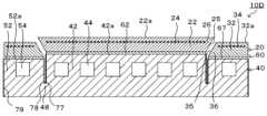
- FIG. 2is a longitudinal sectional view of a semiconductor manufacturing equipment member 10.
- FIG. 2is a plan view of a semiconductor manufacturing equipment member 10.
- FIG. 2is a partially enlarged view of FIG. 3 is a manufacturing process diagram of the central ceramic member 22 and the peripheral ceramic member 32.
- FIG. 10is a vertical cross-sectional view of a semiconductor manufacturing equipment member 10B according to another embodiment of the present invention.
- FIG. 10is a plan view of a semiconductor manufacturing equipment member 10B according to another embodiment of the present invention.
- FIG. 6is a partially enlarged view of FIG. 5 .
- FIG. 10is a longitudinal sectional view of a semiconductor manufacturing equipment member 10C according to another embodiment of the present invention.
- FIG. 10is a vertical cross-sectional view of a semiconductor manufacturing equipment member 10D according to another embodiment of the present invention.
- FIG. 4is a partial enlarged view of a semiconductor manufacturing equipment member 110 according to a comparative example.
- FIG. 1is a vertical cross-sectional view of a semiconductor manufacturing equipment member 10 (a cross-sectional view taken along a plane including the central axis of the semiconductor manufacturing equipment member 10).
- FIG. 2is a plan view of the semiconductor manufacturing equipment member 10.
- FIG. 3is a partially enlarged view of FIG. 1.
- FIG. 4is a manufacturing process diagram of the central ceramic member 22 and the peripheral ceramic member 32.
- the semiconductor manufacturing equipment member 10is used to perform CVD, etching, etc. on a wafer W using plasma, and is fixed to a mounting plate 84 provided inside a semiconductor process chamber 80.
- the semiconductor manufacturing equipment member 10includes a central ceramic member 22, a peripheral ceramic member 32, and a base member 40.
- the base member 40includes a central base member 42 as a central support portion and a peripheral base member 52 as a peripheral support portion.
- the central ceramic member 22 and the central base member 42are joined at a central joint 62.
- the peripheral ceramic member 32 and the peripheral base member 52are joined at a peripheral joint 67.
- the central ceramic member 22 and the peripheral ceramic member 32are collectively referred to as ceramic member 20.
- the central joint 62 and the peripheral joint 67are collectively referred to as joint 60.
- the semiconductor manufacturing equipment member 10may include a focus ring 70.
- focus ringis abbreviated as "FR”.
- the central ceramic member 22is a ceramic disk member having a circular wafer mounting surface 22a on the upper surface.
- the wafer Wis mounted on the wafer mounting surface 22a.
- the diameter of the wafer mounting surface 22ais smaller than the diameter of the wafer W (e.g., 300 mm).
- the central ceramic member 22is formed of a ceramic material such as alumina or aluminum nitride.
- the central ceramic member 22has a wafer adsorption electrode 24 built in.
- the wafer adsorption electrode 24is formed of a material containing, for example, W, Mo, WC, MoC, etc.
- the wafer adsorption electrode 24is a plate-shaped or mesh-shaped monopolar electrostatic electrode.
- the layer of the central ceramic member 22 above the wafer adsorption electrode 24functions as a dielectric layer.
- the wafer adsorption electrode 24is connected to a DC power source for wafer adsorption (not shown).
- the outer ceramic member 32is an annular member and has an annular FR mounting surface 32a on the upper surface.
- the outer ceramic member 32is separate from the central ceramic member 22 and is disposed on the outer periphery of the central ceramic member 22 with a gap therebetween.
- the FR mounting surface 32ais provided at a position one step lower than the wafer mounting surface 22a.
- the FR 70is mounted on the FR mounting surface 32a.
- the inner diameter of the FR mounting surface 32ais approximately the same as the inner diameter of the FR 70.
- the outer ceramic member 32is formed of a ceramic material such as alumina or aluminum nitride.
- the outer ceramic member 32has an FR adsorption electrode 34 built in.
- the FR adsorption electrode 34is formed of a material containing, for example, W, Mo, WC, MoC, etc.
- the FR adsorption electrode 34is a plate-shaped or mesh-shaped monopolar electrostatic electrode.
- the layer of the outer ceramic member 32 above the FR adsorption electrode 34functions as a dielectric layer.
- the FR adsorption electrode 34is connected to an FR adsorption DC power supply (not shown).
- the outer ceramic member 32may have the same thickness as the central ceramic member 22.
- the outer peripheral surface 25 of the central ceramic member 22is a tapered surface (the outer surface of an inverted truncated cone) whose diameter increases toward the top. As shown in FIG. 3, the outer peripheral surface 25 of the central ceramic member 22 is inclined toward the outer peripheral side by an angle ⁇ in the vertical direction starting from its lower end 25b. The angle ⁇ is, for example, 10° or more and 80° or less.
- the inner peripheral surface 35 of the outer peripheral ceramic member 32is a tapered surface (the inner surface of an inverted truncated cone carved out of a disk) whose diameter increases toward the upper side. As shown in FIG. 3, the inner peripheral surface 35 of the outer peripheral ceramic member 32 is inclined toward the outer peripheral side by an angle ⁇ in the vertical direction starting from its lower end 35b.
- the angle ⁇is, for example, 10° or more and 80° or less.
- the angle ⁇may be the same as the angle ⁇ or may be different.
- the maximum diameter Pmax of the outer peripheral surface 25 of the central ceramic member 22(the diameter of the upper end 25a of the outer peripheral surface 25 in this embodiment) is smaller than the maximum diameter Qmax of the inner peripheral surface 35 of the outer peripheral ceramic member 32 (the diameter of the upper end 35a of the inner peripheral surface 35 in this embodiment) and is larger than the minimum diameter Qmin of the inner peripheral surface 35 of the outer peripheral ceramic member 32 (the diameter of the lower end 35b of the inner peripheral surface 35 in this embodiment).
- the outer peripheral portion 26 of the central ceramic member 22 and the inner peripheral portion 36 of the outer peripheral ceramic member 32overlap. Note that when the semiconductor manufacturing equipment member 10 is viewed in a plan view, the inner peripheral surface 35 of the outer peripheral ceramic member 32 is between the wafer mounting surface 22a and the FR mounting surface 32a, and it is not possible to see through it.
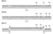
- FIG. 4is a manufacturing process diagram of the central ceramic member 22 and the peripheral ceramic member 32.
- a ceramic plate 21is prepared in which the wafer adsorption electrode 24 and the FR adsorption electrode 34 are embedded.
- This ceramic plate 21is manufactured, for example, as follows. First, two circular molded bodies of ceramic powder are manufactured. Next, a central printed electrode having the same shape as the wafer adsorption electrode 24 and a peripheral printed electrode having the same shape as the FR adsorption electrode 34 are printed on the upper surface of the first circular molded body so as to be concentric with the circular molded body.
- a second circular molded bodyis laminated on the printed electrode surface of the first circular molded body to form a laminate.
- This laminateis hot-pressed and sintered to obtain the ceramic plate 21.
- the ceramic plate 21is machined to cut out the disk-shaped central portion and separate it into an annular outer peripheral portion, thereby obtaining the central ceramic member 22 and the outer peripheral ceramic member 32.
- the disk-shaped central portionis machined to have an inverted truncated cone shape.
- the central ceramic member 22 and the outer peripheral ceramic member 32are produced from one ceramic plate, it is easier to reduce manufacturing costs than when a ceramic plate for the central ceramic member 22 and a ceramic plate for the outer peripheral ceramic member 32 are separately prepared.
- the size of the gap between the central ceramic member 22 and the outer peripheral ceramic member 32 produced in this waycan be adjusted simply by shifting their relative vertical positions, as shown in FIG. 4C.
- the outer peripheral surface 25 of the obtained central ceramic member 22 and the inner peripheral surface 35 of the outer peripheral ceramic member 32may be further machined to provide irregularities.
- the central base member 42is a conductive disk member and has a circular central support surface 42a on the upper surface.
- the central ceramic member 22is joined to the central support surface 42a.
- the diameter of the central support surface 42ais the same as the diameter of the lower surface of the central ceramic member 22.
- the central base member 42has a central refrigerant flow path 44 through which a refrigerant can circulate inside. This central refrigerant flow path 44 is provided in a single stroke across the entire central base member 42 in a plan view.
- the refrigerant flowing through the central refrigerant flow path 44is preferably a liquid and is preferably electrically insulating. Examples of electrically insulating liquids include fluorine-based inert liquids.
- the central base member 42is made of a conductive material containing, for example, a metal.
- conductive materialsinclude metals and composite materials.
- metalsinclude Al, Ti, Mo, and alloys thereof.
- composite materialsinclude metal matrix composite materials (metal matrix composites (MMC)) and ceramic matrix composite materials (ceramic matrix composites (CMC)). Specific examples of such composite materials include materials containing Si, SiC, and Ti, and materials in which a porous SiC body is impregnated with Al and/or Si.
- a material containing Si, SiC, and Tiis called SiSiCTi
- a material in which a porous SiC body is impregnated with Alis called AlSiC
- a material in which a porous SiC body is impregnated with Siis called SiSiC.
- a material having a high thermal conductivity for the central base member 42and for example, Al or an Al alloy is preferable.
- the central base member 42is also used as an RF electrode.
- a central insulating film 77 made of an insulating material (for example, alumina or yttria)is formed on the outer circumferential surface of the central base member 42.
- the central insulating film 77may be a thermal spray film.
- This outer peripheral refrigerant flow path 54is provided in a single stroke over the entire outer peripheral base member 52 in a plan view.
- the refrigerant flowing through the outer peripheral refrigerant flow path 54is preferably a liquid and is preferably electrically insulating.
- An example of an electrically insulating liquidis a fluorine-based inert liquid.
- the outer peripheral base member 52is made of a conductive material containing, for example, a metal. Examples of conductive materials include the materials exemplified for the central base member 42. From the viewpoint of increasing cooling efficiency, it is preferable to select a material with high thermal conductivity for the outer peripheral base member 52, such as Al or an Al alloy.
- the outer peripheral base member 52is also used as an RF electrode.
- An outer peripheral insulating film 78 made of an insulating material (e.g., alumina or yttria)is formed on the inner peripheral surface of the outer peripheral base member 52.
- an outermost insulating film 79 made of an insulating material (e.g., alumina or yttria)is formed on the outer peripheral surface of the outer peripheral base member 52.
- the outer peripheral insulating film 78 and the outermost insulating film 79may be thermally sprayed films.
- the central joint 62joins the lower surface of the central ceramic member 22 and the upper surface of the central base member 42.
- the central joint 62is an adhesive layer made of resin.
- the resinmay be an acrylic resin, a silicone resin, an epoxy resin, or the like.
- the adhesive layermay further contain a filler.
- the outer peripheral joint 67joins the lower surface of the outer peripheral ceramic member 32 to the upper surface of the outer peripheral base member 52.
- the outer peripheral joint 67is an adhesive layer made of resin.
- the resinmay be an acrylic resin, a silicone resin, an epoxy resin, or the like.
- the adhesive layermay further contain a filler.
- the FR 70is an annular member placed on the FR mounting surface 32a, and is made of, for example, silicon.
- a step 72is provided along the circumferential direction at the upper part of the inner surface of the FR 70. The step 72 is provided to prevent the wafer W from interfering with the FR 70.
- the inner diameter of the FR 70is approximately the same as the inner diameter of the FR mounting surface 32a.
- the chamber 80has a shower head 82 on the ceiling surface.
- the semiconductor manufacturing equipment member 10is fixed to the mounting plate 84 arranged inside the chamber 80.
- the semiconductor manufacturing equipment member 10is fixed to the mounting plate 84 by concentrically arranging O-rings 87, 88, and 89 between the lower surface of the base member 40 and the upper surface of the mounting plate 84, and fastening the mounting plate 84 and the base member 40 with a plurality of bolts 90 in this state.
- the O-ring 87has a diameter approximately the same as the diameter of the central base member 42
- the O-ring 88has a diameter approximately the same as the inner diameter of the outer peripheral base member 52
- the O-ring 89has a diameter approximately the same as the outer diameter of the outer peripheral base member 52.
- the bolt 90has a head and a foot. The bolt 90 is inserted from below into a stepped bolt insertion hole 86 that penetrates the installation plate 84 in the vertical direction, and the foot is screwed into a screw hole 41 provided on the underside of the base member 40. At this time, the head of the bolt 90 engages with the stepped portion of the bolt insertion hole 86.
- the O-rings 87, 88, and 89are compressed in the vertical direction to provide a seal. If there are other locations where sealing is required, separate O-rings are placed in those locations as well.
- the FR 70is placed on the FR placement surface 32a of the semiconductor manufacturing equipment member 10, and a disk-shaped wafer W is placed on the wafer placement surface 22a.
- a DC voltageis applied to the wafer adsorption electrode 24 to adsorb the wafer W to the wafer placement surface 22a
- a DC voltageis applied to the FR adsorption electrode 34 to adsorb the FR 70 to the FR placement surface 32a.
- the interior of the chamber 80is then set to a predetermined vacuum atmosphere (or reduced pressure atmosphere), and a high-frequency voltage is applied between the shower head 82 and the base member 40 while supplying a process gas from the shower head 82. This generates plasma between the base member 40 and the shower head 82.
- the wafer Wis then processed using this plasma.
- the FR70also wears out as the wafers W are plasma processed, but since the FR70 is thicker than the wafers W, the FR70 is replaced after multiple wafers W have been processed.
- the outer peripheral surface 25 of the central ceramic member 22 and the inner peripheral surface 35 of the outer peripheral ceramic member 32both have diameters that change in the vertical direction, and when the semiconductor manufacturing equipment component 10 is viewed in a plan view, the outer peripheral portion 26 of the central ceramic member 22 and the inner peripheral portion 36 of the outer peripheral ceramic member 32 overlap.
- accelerated ionscollide with the ceramic member 20 before reaching the base member 40 or the joint 60, as shown in Figure 3, and do not proceed beyond that. This suppresses the generation of plasma and radicals around the base member 40 and the joint 60, and suppresses corrosion of the base member 40 and the joint 60, which ultimately suppresses a decrease in the equipment life.
- the outer periphery 26 of the central ceramic member 22 and the inner periphery 36 of the outer periphery ceramic member 32overlap, so even if waferless dry cleaning is performed without placing the FR 70 on the FR placement surface 32a, corrosion of the base member 40 and the joint 60 can be suppressed. This makes it possible to improve the life of the FR 70 and suppress a decrease in the life of the entire semiconductor manufacturing equipment.
- the outer peripheral surface 25 of the central ceramic member 22 and the inner peripheral surface 35 of the outer peripheral ceramic member 32both have diameters that change in the vertical direction.
- the maximum diameter Pmax of the outer peripheral surface 25 of the central ceramic member 22is smaller than the maximum diameter Qmax of the inner peripheral surface 35 of the outer peripheral ceramic member 32, and is smaller than the minimum diameter Qmin of the inner peripheral surface 35 of the outer peripheral ceramic member 32. Therefore, when the semiconductor manufacturing equipment component 10 is viewed in a plan view, the outer peripheral portion 26 of the central ceramic member 22 and the inner peripheral portion 36 of the outer peripheral ceramic member 32 overlap. Therefore, as described above, the deterioration of the equipment life is suppressed.
- the minimum diameter Pmin of the outer peripheral surface 25 of the central ceramic member 22(in this embodiment, the diameter of the lower end 25b of the outer peripheral surface 25) is smaller than the minimum diameter Qmin of the inner peripheral surface 35 of the outer peripheral ceramic member 32.
- Such central ceramic member 22 and outer peripheral ceramic member 32can be produced, for example, by hollowing out a single ceramic plate. In this case, it is easier to keep manufacturing costs down than preparing a ceramic plate for the central ceramic member 22 and a ceramic plate for the outer peripheral ceramic member 32 separately.
- the outer peripheral surface 25 of the central ceramic member 22 and the inner peripheral surface 35 of the outer peripheral ceramic member 32each appear as a diagonal line.
- a central ceramic member 22 and outer peripheral ceramic member 32can be produced, for example, by hollowing out a single ceramic plate into a truncated cone shape or an inverted truncated cone shape. Such a shape makes the hollowing out process relatively easy, and makes it easy to keep manufacturing costs down.
- the outer peripheral base member 52 serving as the outer peripheral supportis an annular member arranged with a gap between it and the central base member 42 serving as the central support. Therefore, it is easy to control the temperature of the outer peripheral base member 52 and the temperature of the central base member 42 separately, and therefore it is easy to control the temperature of the wafer mounting surface 22a and the temperature of the FR mounting surface 32a separately.
- the central ceramic member 22 and the central base member 42 serving as the central supportare joined by a central joint 62 made of resin, and the peripheral ceramic member 32 and the peripheral base member 52 serving as the peripheral support are joined by a peripheral joint 67 made of resin. Since the resin adhesive layer is easily corroded, it is highly significant to apply the present invention.
- the outer peripheral surface 25 of the central ceramic member 22is a tapered surface with a larger diameter toward the top, but is not limited to this as long as the diameter changes in the vertical direction.
- the outer peripheral surface 25 of the central ceramic member 22may be a tapered surface (the outer surface of a truncated cone) with a smaller diameter toward the top, as in another example of a semiconductor manufacturing equipment member 10B shown in Figures 5 to 7.
- the inner peripheral surface 35 of the outer peripheral ceramic member 32is a tapered surface with a larger diameter toward the top, but is not limited to this as long as the diameter changes in the vertical direction.
- the inner peripheral surface 35 of the outer peripheral ceramic member 32may be a tapered surface with a smaller diameter toward the top (the inner surface of a truncated cone carved out of a disk), as in, for example, a semiconductor manufacturing equipment member 10B. Note that in Figures 5 to 7, the same reference numerals are used for the same components as in the above embodiment.
- the outer peripheral surface 25 of the central ceramic member 22is inclined inwardly by an angle ⁇ in the vertical direction starting from its lower end 25b as shown in Figure 7.
- the angle ⁇is, for example, 10° or more and 80° or less.
- the inner peripheral surface 35 of the outer peripheral ceramic member 32is inclined inwardly by an angle ⁇ in the vertical direction starting from its lower end 35b as shown in Figure 7.
- the angle ⁇is, for example, 10° or more and 80° or less.
- the angle ⁇may be the same as or different from the angle ⁇ .
- the maximum diameter Pmax of the outer peripheral surface 25 of the central ceramic member 22(diameter of the lower end 25b of the outer peripheral surface 25 in this example) is smaller than the maximum diameter Qmax of the inner peripheral surface 35 of the outer peripheral ceramic member 32 (diameter of the lower end 35b of the inner peripheral surface 35 in this example) and is larger than the minimum diameter Qmin of the inner peripheral surface 35 of the outer peripheral ceramic member 32 (diameter of the upper end 35a of the inner peripheral surface 35 in this example). Therefore, when the semiconductor manufacturing equipment member 10B is viewed in a plane, the outer peripheral portion 26 of the central ceramic member 22 and the inner peripheral portion 36 of the outer peripheral ceramic member 32 overlap.
- the semiconductor manufacturing equipment member 10Bwhen the semiconductor manufacturing equipment member 10B is viewed in a plane, the outer peripheral surface 25 of the central ceramic member 22 is between the wafer mounting surface 22a and the FR mounting surface 32a, and it is not possible to see through to the back.
- the accelerated ionscollide with the ceramic member 20 before reaching the base member 40 or the joint 60, and do not proceed beyond that. This suppresses the generation of plasma and radicals around the base member 40 and the joint 60, and suppresses corrosion of the base member 40 and the joint 60, and as a result, suppresses the deterioration of the equipment life.
- the minimum diameter Pmin of the outer peripheral surface 25 of the central ceramic member 22(in this embodiment, the diameter of the upper end 25a of the outer peripheral surface 25) is smaller than the minimum diameter Qmin of the inner peripheral surface 35 of the outer peripheral ceramic member 32.
- Such a central ceramic member 22 and outer peripheral ceramic member 32can be produced, for example, by hollowing out a single ceramic plate.
- the central ceramic member 22 and the peripheral ceramic member 32 of the semiconductor manufacturing equipment member 10Bmay be manufactured in accordance with FIG. 4. In that case, when hollowing out the disk-shaped center portion in FIG. 4B, the disk-shaped center portion may be processed so that it has a truncated cone shape.
- the central joint 62 and the outer peripheral joint 67are resin adhesive layers, but they may be metallic joint layers formed of solder or metal brazing material.
- the metallic joint layermay be formed by, for example, TCB (thermal compression bonding).
- TCBrefers to a known method in which a metallic joint material is sandwiched between two members to be joined, and the two members are pressurized and joined while being heated to a temperature below the solidus temperature of the metallic joint material.
- the outer peripheral surface of the central joint 62may be covered with a central insulating film 77 together with the outer peripheral surface of the central base member 42 as the central support member, and the outer peripheral surface of the outer peripheral joint 67 may be covered with an outer peripheral insulating film 78 together with the inner peripheral surface of the outer peripheral base member 52 as the outer peripheral support member.
- the outer peripheral surface of the outer peripheral joint 67may be covered with an outermost insulating film 79 together with the outer peripheral surface of the outer peripheral base member 52 as the outer peripheral support member. In this way, the joint 60 and the base member 40 are covered with an insulating film, so that corrosion of the joint 60 and the base member 40 is further suppressed.
- the joint 60is made of metal rather than resin, the joint 60 is less likely to deteriorate even if an insulating film is formed by thermal spraying or the like.
- FIG. 8the same components as those in the above-mentioned embodiment are given the same reference numerals.
- the semiconductor manufacturing equipment members 10, 10B, 10C, and 10Dinclude an annular outer ceramic member 32 having a focus ring mounting surface 32a on the upper surface and configured to be arranged on the outer periphery of a central ceramic member having a wafer mounting surface, and a conductive base member 40 bonded to the lower surface of the outer ceramic member 32 and having an outer support portion that supports the outer ceramic member 32, and the inner peripheral surface 35 of the outer ceramic member 32 may be a tapered surface in which the diameter increases toward the upper side or decreases toward the upper side, for mounting a focus ring 70.
- the central ceramic membermay be the same as the central ceramic member 22 described above, may be different, or may be omitted.
- the base member 40may be the same as the base member 40 described above, may have a central support portion different from the central base member 42 described above, or may not have a central support portion.
- a heater electrode for heating the wafermay be embedded in the central ceramic member 22. In this way, when it is necessary to heat the wafer W placed on the wafer mounting surface 22a to a high temperature, electricity can be passed through the heater electrode for heating the wafer to heat the wafer W to the desired high temperature.
- a heater electrode for heating the FRmay be embedded in the peripheral ceramic member 32. In this way, when it is necessary to heat the FR 70 placed on the FR mounting surface 32a to a high temperature, electricity can be passed through the heater electrode for heating the FR to heat the FR 70 to the desired high temperature.
- a heater electrode for heating the waferis embedded in the central ceramic member 22 and a heater electrode for heating the FR is embedded in the peripheral ceramic member 32, it is preferable to make it possible to adjust the temperature of each heater electrode individually.
- the present inventioncan be used in components used in semiconductor manufacturing equipment, such as electrostatic chuck heaters, electrostatic chucks, and ceramic heaters.
- 10, 10B, 10C, 10DSemiconductor manufacturing equipment member, 20: Ceramic member, 21: Ceramic plate, 22: Central ceramic member, 22a: Wafer mounting surface, 24: Wafer suction electrode, 25: Outer periphery, 26: Outer periphery, 32: Outer periphery ceramic member, 32a: FR mounting surface, 34: FR suction electrode, 35: Inner periphery, 36: Inner periphery, 40: Base member, 41: Screw hole, 42: Central base member, 42a: Central support surface, 44: Central refrigerant flow path, 48: Connection, 52: Outer periphery base member, 52a: Outer periphery support surface, 54: Outer periphery refrigerant flow path, 60: Joint, 62: Central joint, 67: Outer periphery joint, 70: Fo -cassing (FR), 72 step, 77 central insulating film, 78 peripheral insulating film, 79 outermost insulating film, 80 chamber, 82 shower head,
Landscapes
- Engineering & Computer Science (AREA)
- Physics & Mathematics (AREA)
- Microelectronics & Electronic Packaging (AREA)
- General Physics & Mathematics (AREA)
- Manufacturing & Machinery (AREA)
- Computer Hardware Design (AREA)
- Condensed Matter Physics & Semiconductors (AREA)
- Power Engineering (AREA)
- Plasma & Fusion (AREA)
- Chemical & Material Sciences (AREA)
- Analytical Chemistry (AREA)
- Container, Conveyance, Adherence, Positioning, Of Wafer (AREA)
- Drying Of Semiconductors (AREA)
Abstract
Description
Translated fromJapanese本発明は、半導体製造装置用部材に関する。The present invention relates to components for semiconductor manufacturing equipment.
従来、半導体製造装置用部材として、プラズマを利用してウエハにCVDやエッチングなどを行うものが知られている。こうした半導体製造装置用部材において、ウエハの外周部のプラズマの均一性を得るため、ウエハの外周にフォーカスリングを用いることがある。例えば、特許文献1の保持装置は、主としてウエハを保持する中央静電チャック部と、主としてフォーカスリングを保持する外周静電チャック部とを有している。中央静電チャック部は、上面にウエハが吸着される中央セラミック部材と、中央セラミック部材の下面に樹脂製の中央接合部で接合された金属製の中央ベース部材と、を備えている。外周静電チャック部は、上面にフォーカスリングが吸着される外周セラミック部材と、外周セラミック部材の下面に樹脂製の外周接合部で接合された金属製の中央ベース部材と、を備えている。外周静電チャック部は、平面視で中央静電チャック部を取り囲むような略円環状の部材である。外周静電チャック部は、中央静電チャック部とは別体であり、中央静電チャック部との間には隙間が存在している。Conventionally, semiconductor manufacturing equipment components that use plasma to perform CVD or etching on a wafer are known. In such semiconductor manufacturing equipment components, a focus ring may be used on the outer periphery of the wafer to obtain uniformity of plasma on the outer periphery of the wafer. For example, the holding device of
ところで、特許文献1の保持装置のように、中央静電チャック部と外周静電チャック部との間に隙間が存在する半導体製造装置用部材では、隙間に露出した金属製のベース部材や樹脂製の接合部が腐食し、装置寿命が短くなることがあった。本発明者らの知見によれば、こうした寿命の低下は、プラズマ処理に用いられるアルゴンなどのイオンが、半導体製造装置用部材に向かって加速されて隙間に侵入し、隙間内で他の原子や分子に衝突してプラズマやラジカルを生成し、その周囲の金属や樹脂を腐食することなどによって生じる。In semiconductor manufacturing equipment components in which there is a gap between the central electrostatic chuck portion and the peripheral electrostatic chuck portion, such as the holding device in
本発明は、このような課題を解決するためになされたものであり、装置寿命の低下を抑制することを主目的とする。The present invention was made to solve these problems, and its main objective is to prevent the deterioration of the device's lifespan.
[1]本発明の半導体製造装置用部材は、
上面にウエハ載置面を有する中央セラミック部材と、
上面にフォーカスリング載置面を有し、前記中央セラミック部材の外周側に配置された、環状の外周セラミック部材と、
前記中央セラミック部材の下面に接合し、前記中央セラミック部材を支持する中央支持部と、前記外周セラミック部材の下面に接合し、前記外周セラミック部材を支持する外周支持部と、を有し、前記中央支持部と前記外周支持部とが別体若しくは一体で構成されている導電性のベース部材と、を備え、
前記中央セラミック部材の外周面及び前記外周セラミック部材の内周面はいずれも上下方向で径が変化し、
前記中央セラミック部材の外周面の最大径は、前記外周セラミック部材の内周面の最大径よりも小さく、前記外周セラミック部材の内周面の最小径よりも大きいものである。[1] The semiconductor manufacturing equipment member of the present invention comprises:
a central ceramic member having a wafer mounting surface thereon;
an annular peripheral ceramic member having a focus ring mounting surface on an upper surface thereof and disposed on an outer circumferential side of the central ceramic member;
a central support part joined to a lower surface of the central ceramic member and supporting the central ceramic member, and a peripheral support part joined to a lower surface of the peripheral ceramic member and supporting the peripheral ceramic member, the central support part and the peripheral support part being separate or integral with each other;
The diameter of the outer peripheral surface of the central ceramic member and the inner peripheral surface of the outer peripheral ceramic member both change in the up-down direction,
The maximum diameter of the outer circumferential surface of the central ceramic member is smaller than the maximum diameter of the inner circumferential surface of the outer circumferential ceramic member and is larger than the minimum diameter of the inner circumferential surface of the outer circumferential ceramic member.
この半導体製造装置用部材では、中央セラミック部材の外周面及び外周セラミック部材の内周面はいずれも上下方向で径が変化している。そして、中央セラミック部材の外周面の最大径は、外周セラミック部材の内周面の最大径よりも小さく、外周セラミック部材の内周面の最小径よりも小さい。そのため、半導体製造装置用部材を平面視すると、中央セラミック部材の外周部と外周セラミック部材の内周部とが重なっている。こうした半導体製造装置用部材では、プラズマ処理の際に半導体製造装置用部材に向かって加速されたイオンは、ベース部材や接合部に至る前にセラミック部材に衝突し、その先には進まない。それにより、ベース部材や接合部の周辺でのプラズマやラジカルの生成が抑制されるため、結果として、装置寿命の低下を抑制することができる。In this semiconductor manufacturing equipment component, the diameters of the outer peripheral surface of the central ceramic member and the inner peripheral surface of the outer peripheral ceramic member both change in the vertical direction. The maximum diameter of the outer peripheral surface of the central ceramic member is smaller than the maximum diameter of the inner peripheral surface of the outer peripheral ceramic member and is smaller than the minimum diameter of the inner peripheral surface of the outer peripheral ceramic member. Therefore, when the semiconductor manufacturing equipment component is viewed in a plan view, the outer peripheral portion of the central ceramic member and the inner peripheral portion of the outer peripheral ceramic member overlap. In such a semiconductor manufacturing equipment component, ions accelerated toward the semiconductor manufacturing equipment component during plasma processing collide with the ceramic member before reaching the base member or the joint, and do not proceed beyond that. This suppresses the generation of plasma and radicals around the base member and the joint, and as a result, the deterioration of the equipment life can be suppressed.
なお、本明細書では、上下、左右、前後などを用いて本発明を説明することがあるが、上下、左右、前後は、相対的な位置関係に過ぎない。そのため、半導体製造装置用部材の向きを変えた場合には上下が左右になったり左右が上下になったりすることがあるが、そうした場合も本発明の技術的範囲に含まれる。In addition, although this specification may use terms such as up/down, left/right, front/back, etc. to describe the present invention, these terms are merely relative positional relationships. Therefore, when the orientation of a semiconductor manufacturing equipment component is changed, up/down may become left/right and left/right may become up/down, but such cases are also within the technical scope of the present invention.
[2]本発明の半導体製造装置用部材([1]に記載の半導体製造装置用部材)において、前記中央セラミック部材の外周面の最小径は、前記外周セラミック部材の内周面の最小径よりも小さいものとしてもよい。こうした中央セラミック部材及び外周セラミック部材は、例えば、1枚のセラミック板をくり抜くことで作製できる。[2] In the semiconductor manufacturing equipment component of the present invention (the semiconductor manufacturing equipment component described in [1]), the minimum diameter of the outer peripheral surface of the central ceramic component may be smaller than the minimum diameter of the inner peripheral surface of the outer peripheral ceramic component. Such a central ceramic component and an outer peripheral ceramic component can be produced, for example, by hollowing out a single ceramic plate.
[3]本発明の半導体製造装置用部材([1]又は[2]に記載の半導体製造装置用部材)において、前記半導体製造装置用部材を前記ウエハ載置面に垂直な方向に切断した断面では、前記中央セラミック部材の外周面及び前記外周セラミック部材の内周面のそれぞれが斜め線として現れるものとしてもよい。こうした中央セラミック部材及び外周セラミック部材は、例えば、1枚のセラミック板を円錐台形状や逆円錐台形状にくり抜くことで作製できる。[3] In the semiconductor manufacturing equipment component of the present invention (the semiconductor manufacturing equipment component described in [1] or [2]), the outer peripheral surface of the central ceramic member and the inner peripheral surface of the peripheral ceramic member may each appear as a diagonal line in a cross section of the semiconductor manufacturing equipment component cut in a direction perpendicular to the wafer mounting surface. Such a central ceramic member and peripheral ceramic member may be produced, for example, by hollowing out a single ceramic plate into a truncated cone shape or an inverted truncated cone shape.
[4]本発明の半導体製造装置用部材([1]~[3]のいずれか1つに記載の半導体製造装置用部材)において、前記中央セラミック部材の外周面は、上側ほど直径が大きくなるテーパ面であるものとしてもよい。[4] In the semiconductor manufacturing equipment component of the present invention (the semiconductor manufacturing equipment component described in any one of [1] to [3]), the outer peripheral surface of the central ceramic component may be a tapered surface whose diameter increases toward the top.
[5]本発明の半導体製造装置用部材([1]~[3]のいずれか1つに記載の半導体製造装置用部材)において、前記中央セラミック部材の外周面は、上側ほど直径が小さくなるテーパ面であるものとしてもよい。[5] In the semiconductor manufacturing equipment component of the present invention (the semiconductor manufacturing equipment component described in any one of [1] to [3]), the outer peripheral surface of the central ceramic component may be a tapered surface whose diameter decreases toward the top.
[6]本発明の半導体製造装置用部材([1]~[5]のいずれか1つに記載の半導体製造装置用部材)において、前記外周支持部は、前記中央支持部の外周に前記中央支持部とは隙間をあけて配置された環状の部分であるものとしてもよい。こうすれば、外周支持部の温度と中央支持部の温度とを個別に制御しやすくなり、ひいては、ウエハ載置面の温度とフォーカスリング載置面の温度とを個別に制御しやすくなる。[6] In the semiconductor manufacturing equipment member of the present invention (the semiconductor manufacturing equipment member described in any one of [1] to [5]), the outer peripheral support part may be an annular part arranged on the outer periphery of the central support part with a gap therebetween. This makes it easier to control the temperature of the outer peripheral support part and the temperature of the central support part separately, which in turn makes it easier to control the temperature of the wafer mounting surface and the temperature of the focus ring mounting surface separately.
[7]本発明の半導体製造装置用部材([6]に記載の半導体製造装置用部材)において、前記中央セラミック部材と前記中央支持部とは金属製の中央接合部で接合され、該中央接合部の外周面は前記中央支持部の外周面とともに中央絶縁膜で覆われ、前記外周セラミック部材と前記外周支持部とは金属製の外周接合部で接合され、該外周接合部の内周面は前記外周支持部の内周面とともに外周絶縁膜で覆われているものとしてもよい。こうすれば、接合部及びベース部材が絶縁膜で覆われているため、接合部及びベース部材の腐食がより抑制される。また、接合部が樹脂製ではなく金属製のため、溶射などにより絶縁膜を形成しても接合部が変質しにくい。[7] In the semiconductor manufacturing equipment member of the present invention (semiconductor manufacturing equipment member described in [6]), the central ceramic member and the central support part may be joined by a metallic central joint part, the outer peripheral surface of the central joint part together with the outer peripheral surface of the central support part being covered by a central insulating film, and the outer peripheral ceramic member and the outer peripheral support part may be joined by a metallic outer peripheral joint part, the inner peripheral surface of the outer peripheral joint part together with the inner peripheral surface of the outer peripheral support part being covered by an outer peripheral insulating film. In this way, since the joint part and the base member are covered by an insulating film, corrosion of the joint part and the base member is further suppressed. In addition, since the joint part is made of metal and not resin, the joint part is less likely to deteriorate even if an insulating film is formed by thermal spraying or the like.
[8]本発明の半導体製造装置用部材([1]~[6]のいずれか1つに記載の半導体製造装置用部材)において、前記中央セラミック部材と前記中央支持部とは樹脂製の中央接合部で接合され、前記外周セラミック部材と前記外周支持部とは樹脂製の外周接合部で接合されているものとしてもよい。樹脂製の接着層は、腐食されやすいため、本発明を適用する意義が高い。[8] In the semiconductor manufacturing equipment member of the present invention (the semiconductor manufacturing equipment member described in any one of [1] to [6]), the central ceramic member and the central support part may be joined by a central joint part made of resin, and the peripheral ceramic member and the peripheral support part may be joined by a peripheral joint part made of resin. Since the resin adhesive layer is easily corroded, it is highly meaningful to apply the present invention.
[9]あるいは、本発明の半導体製造装置用部材は、上面にフォーカスリング載置面を有し、ウエハ載置面を有する中央セラミック部材の外周側に配置可能に構成された環状の外周セラミック部材と、前記外周セラミック部材の下面に接合し、前記外周セラミック部材を支持する外周支持部を有する導電性のベース部材と、を備え、前記外周セラミック部材の内周面は上下方向で径が変化し、前記外周セラミック部材の内周面は、上側ほど直径が大きくなる、又は上側ほど直径が小さくなるテーパ面である、フォーカスリングを載置するためのものとしてもよい。[9] Alternatively, the semiconductor manufacturing equipment member of the present invention may comprise an annular peripheral ceramic member having a focus ring mounting surface on its upper surface and configured to be arranged on the outer periphery of a central ceramic member having a wafer mounting surface, and a conductive base member joined to the lower surface of the peripheral ceramic member and having an outer periphery support portion that supports the peripheral ceramic member, the inner peripheral surface of the peripheral ceramic member having a diameter that changes in the vertical direction, and the inner peripheral surface of the peripheral ceramic member is a tapered surface in which the diameter increases toward the upper side or decreases toward the upper side, for mounting a focus ring.
本発明の好適な実施形態を、図面を参照しながら以下に説明する。図1は、半導体製造装置用部材10の縦断面図(半導体製造装置用部材10の中心軸を含む平面で切断したときの断面図)である。図2は、半導体製造装置用部材10の平面図である。図3は、図1の部分拡大図である。図4は、中央セラミック部材22及び外周セラミック部材32の製造工程図である。A preferred embodiment of the present invention will be described below with reference to the drawings. FIG. 1 is a vertical cross-sectional view of a semiconductor manufacturing equipment member 10 (a cross-sectional view taken along a plane including the central axis of the semiconductor manufacturing equipment member 10). FIG. 2 is a plan view of the semiconductor
半導体製造装置用部材10は、ウエハWにプラズマを利用してCVDやエッチングなどを行うために用いられるものであり、半導体プロセス用のチャンバ80の内部に設けられた設置板84に固定されている。半導体製造装置用部材10は、中央セラミック部材22と、外周セラミック部材32と、ベース部材40とを備えている。本実施形態では、ベース部材40は、中央支持部としての中央ベース部材42と、外周支持部としての外周ベース部材52と、を有している。中央セラミック部材22と中央ベース部材42とは中央接合部62で接合されている。外周セラミック部材32と外周ベース部材52とは外周接合部67で接合されている。中央セラミック部材22と外周セラミック部材32とをまとめてセラミック部材20とも称する。中央接合部62と外周接合部67とをまとめて接合部60とも称する。半導体製造装置用部材10は、フォーカスリング70を備えていてもよい。以下、「フォーカスリング」は「FR」と略す。The semiconductor
中央セラミック部材22は、セラミック製の円板部材であり、上面に円形のウエハ載置面22aを有している。ウエハ載置面22aには、ウエハWが載置される。ウエハ載置面22aの直径は、ウエハWの直径(例えば300mm)よりも小さい。中央セラミック部材22は、アルミナ、窒化アルミニウムなどに代表されるセラミック材料で形成されている。中央セラミック部材22は、ウエハ吸着用電極24を内蔵している。ウエハ吸着用電極24は、例えばW、Mo、WC、MoCなどを含有する材料によって形成されている。ウエハ吸着用電極24は、板状又はメッシュ状の単極型の静電電極である。中央セラミック部材22のうちウエハ吸着用電極24よりも上側の層は誘電体層として機能する。ウエハ吸着用電極24には、図示しないウエハ吸着用直流電源が接続されている。The central
外周セラミック部材32は、環状部材であり、上面に環状のFR載置面32aを有している。外周セラミック部材32は、中央セラミック部材22とは別体であり、中央セラミック部材22の外周側に、中央セラミック部材22とは隙間をあけて配置されている。FR載置面32aは、ウエハ載置面22aよりも一段低い位置に設けられている。FR載置面32aには、FR70が載置される。FR載置面32aの内径は、FR70の内径と略同じである。外周セラミック部材32は、アルミナ、窒化アルミニウムなどに代表されるセラミック材料で形成されている。外周セラミック部材32は、FR吸着用電極34を内蔵している。FR吸着用電極34は、例えばW、Mo、WC、MoCなどを含有する材料によって形成されている。FR吸着用電極34は、板状又はメッシュ状の単極型の静電電極である。外周セラミック部材32のうちFR吸着用電極34よりも上側の層は誘電体層として機能する。FR吸着用電極34には、図示しないFR吸着用直流電源が接続されている。外周セラミック部材32は、中央セラミック部材22と厚みが同じであるものとしてもよい。The outer
中央セラミック部材22の外周面25は、上側ほど直径が大きくなるテーパ面(逆円錐台の外側面)である。中央セラミック部材22の外周面25は、図3に示すように、その下端25bを起点として上下方向に対して角度αだけ外周側に傾斜している。角度αは、例えば、10°以上80°以下である。また、外周セラミック部材32の内周面35は、上側ほど直径が大きくなるテーパ面(円盤から逆円錐台をくり抜いた内側面)である。外周セラミック部材32の内周面35は、図3に示すように、その下端35bを起点として上下方向に対して角度βだけ外周側に傾斜している。角度βは、例えば、10°以上80°以下である。角度βは、角度αと同じでもよいし、異なってもよい。そして、図2に示すように、中央セラミック部材22の外周面25の最大径Pmax(本実施形態では外周面25の上端25aの直径)は、外周セラミック部材32の内周面35の最大径Qmax(本実施形態では内周面35の上端35aの直径)よりも小さく、外周セラミック部材32の内周面35の最小径Qmin(本実施形態では内周面35の下端35bの直径)よりも大きい。そのため、半導体製造装置用部材10を平面視すると、中央セラミック部材22の外周部26と外周セラミック部材32の内周部36とが重なっている。なお、半導体製造装置用部材10を平面視すると、ウエハ載置面22aとFR載置面32aとの間に外周セラミック部材32の内周面35があり、その奥を見通すことはできない。The outer
中央セラミック部材22及び外周セラミック部材32は、例えば、以下のように製造してもよい。図4は、中央セラミック部材22及び外周セラミック部材32の製造工程図である。まず、図4Aに示すように、ウエハ吸着用電極24とFR吸着用電極34とが埋設された1枚のセラミック板21を準備する。このセラミック板21は、例えば以下のように作製する。まず、セラミック粉末の円板成形体を2枚作製する。続いて、1枚目の円板成形体の上面に、ウエハ吸着用電極24と同形状の中央印刷電極と、FR吸着用電極34と同形状の外周印刷電極とを、円板成形体と同心円状になるように印刷する。そして、1枚目の円板成形体の印刷電極面に2枚目の円板成形体を積層して積層体とする。この積層体をホットプレス焼成し、セラミック板21を得る。次に、図4Bに示すように、セラミック板21に対して、機械加工により円板状の中央部をくり抜いて円環状の外周部とに分離し、中央セラミック部材22及び外周セラミック部材32を得る。円板状の中央部をくり抜く際には、円板状の中央部が逆円錐台形状となるように加工する。このように、1枚のセラミック板から中央セラミック部材22及び外周セラミック部材32を作製する場合、中央セラミック部材22用のセラミック板と外周セラミック部材32用のセラミック板とを個別に準備するよりも製造コストを抑えやすい。また、こうして作製した中央セラミック部材22と外周セラミック部材32とは、図4Cに示すように、相対的な上下方向の位置をずらすだけで、両者の間の隙間の大きさを調整できる。なお、得られた中央セラミック部材22の外周面25や外周セラミック部材32の内周面35に、さらに機械加工を施して、凹凸を設けたりしてもよい。The central
中央ベース部材42は、導電性の円板部材であり、上面に円形の中央支持面42aを有している。中央支持面42aには、中央セラミック部材22が接合されている。中央支持面42aの直径は、中央セラミック部材22の下面の直径と同じである。中央ベース部材42は、内部に冷媒が循環可能な中央冷媒流路44を有する。この中央冷媒流路44は、平面視で中央ベース部材42の全体にわたって一筆書きの要領で設けられている。中央冷媒流路44を流れる冷媒は、液体が好ましく、電気絶縁性であることが好ましい。電気絶縁性の液体としては、例えばフッ素系不活性液体などが挙げられる。中央ベース部材42は、例えば金属を含有する導電材料で作製されている。導電材料としては、例えば、金属や複合材料などが挙げられる。金属としては、Al,Ti,Mo又はそれらの合金などが挙げられる。複合材料としては、金属マトリックス複合材料(メタル・マトリックス・コンポジット(MMC))やセラミックマトリックス複合材料(セラミック・マトリックス・コンポジット(CMC))などが挙げられる。こうした複合材料の具体例としては、Si,SiC及びTiを含む材料やSiC多孔質体にAl及び/又はSiを含浸させた材料などが挙げられる。Si,SiC及びTiを含む材料をSiSiCTiといい、SiC多孔質体にAlを含浸させた材料をAlSiCといい、SiC多孔質体にSiを含浸させた材料をSiSiCという。中央ベース部材42の材料としては、冷却効率を高める観点からは、熱伝導率の高いものを選択するのが好ましく、例えば、AlやAl合金が好ましい。また、中央ベース部材42の材料としては、熱応力による破損等を抑制する観点からは、中央セラミック部材22の材料と熱膨張係数の近いものを選択するのが好ましく、例えば、金属とセラミックとの複合材料が好ましい。中央ベース部材42は、RF電極としても用いられる。中央ベース部材42の外周面には、絶縁材料(例えばアルミナやイットリア)で形成された中央絶縁膜77が形成されている。中央絶縁膜77は、溶射膜としてもよい。The
外周ベース部材52は、導電性の環状部材であり、上面に環状の外周支持面52aを有している。外周ベース部材52は、中央ベース部材42とは別体であり、中央ベース部材42の外周側に、中央ベース部材42とは隙間をあけて配置されている。外周支持面52aは、中央支持面42aよりも一段低い位置に設けられている。外周支持面52aには、外周セラミック部材32が接合されている。外周支持面52aの内径及び外径は、外周セラミック部材32の下面の内径及び外径とそれぞれ同じである。外周ベース部材52は、内部に冷媒が循環可能な外周冷媒流路54を有する。この外周冷媒流路54は、平面視で外周ベース部材52の全体にわたって一筆書きの要領で設けられている。外周冷媒流路54を流れる冷媒は、液体が好ましく、電気絶縁性であることが好ましい。電気絶縁性の液体としては、例えばフッ素系不活性液体などが挙げられる。外周ベース部材52は、例えば金属を含有する導電材料で作製されている。導電材料としては、中央ベース部材42で例示した材料が挙げられる。外周ベース部材52の材料としては、冷却効率を高める観点からは、熱伝導率の高いものを選択するのが好ましく、例えば、AlやAl合金が好ましい。外周ベース部材52の材料としては、熱応力による破損等を抑制する観点からは、外周セラミック部材32の材料と熱膨張係数の近いものを選択するのが好ましく、例えば、金属とセラミックとの複合材料が好ましい。外周ベース部材52は、RF電極としても用いられる。外周ベース部材52の内周面には、絶縁材料(例えばアルミナやイットリア)で形成された外周絶縁膜78が形成されている。また、外周ベース部材52の外周面には、絶縁材料(例えばアルミナやイットリア)で形成された最外周絶縁膜79が形成されている。外周絶縁膜78や最外周絶縁膜79は、溶射膜としてもよい。The outer
中央接合部62は、中央セラミック部材22の下面と中央ベース部材42の上面とを接合している。本実施形態では、中央接合部62は、樹脂製の接着層である。樹脂としては、アクリル樹脂、シリコーン樹脂、エポキシ樹脂等の樹脂を用いることができる。また、接着層には、さらにフィラーを含有させてもよい。The central joint 62 joins the lower surface of the central
外周接合部67は、外周セラミック部材32の下面と外周ベース部材52の上面とを接合している。本実施形態では、外周接合部67は、樹脂製の接着層である。樹脂としては、アクリル樹脂、シリコーン樹脂、エポキシ樹脂等の樹脂を用いることができる。また、接着層には、さらにフィラーを含有させてもよい。The outer peripheral joint 67 joins the lower surface of the outer peripheral
FR70は、FR載置面32aに載置される環状部材であり、例えばシリコンで形成されている。FR70の内周面の上部には、円周方向に沿って段差72が設けられている。段差72は、ウエハWがFR70と干渉するのを防止するために設けられている。FR70の内径は、FR載置面32aの内径と略同じである。The
次に、半導体製造装置用部材10の使用例について図1を用いて説明する。チャンバ80は、天井面にシャワーヘッド82を有する。チャンバ80の内部に配置された設置板84には、半導体製造装置用部材10が固定される。具体的には、半導体製造装置用部材10は、ベース部材40の下面と設置板84の上面との間にOリング87,88,89を同心円状に配置し、その状態で設置板84とベース部材40とを複数のボルト90で締結することにより、設置板84に固定される。Oリング87は中央ベース部材42の直径と略同じ直径を有し、Oリング88は外周ベース部材52の内径と略同じ直径を有し、Oリング89は外周ベース部材52の外径とほぼ同じ直径を有する。ボルト90は、頭部と足部とを備える。ボルト90は、設置板84を上下方向に貫通する段差付きのボルト挿通孔86に下方から挿通され、足部がベース部材40の下面に設けられたネジ穴41に螺合される。このとき、ボルト90の頭部は、ボルト挿通孔86の段差部に係合する。Oリング87,88,89は、上下方向に押し潰されてシール性を発揮する。その他にシール性が必要な箇所があれば、その箇所にも別途Oリングを配置する。Next, an example of the use of the semiconductor
半導体製造装置用部材10を用いてウエハWを処理する場合、半導体製造装置用部材10のFR載置面32aには、FR70が載置され、ウエハ載置面22aには、円盤状のウエハWが載置された状態で行う。この状態で、ウエハ吸着用電極24に直流電圧を印加してウエハWをウエハ載置面22aに吸着させると共に、FR吸着用電極34に直流電圧を印加してFR70をFR載置面32aに吸着させる。そして、チャンバ80の内部を所定の真空雰囲気(又は減圧雰囲気)になるように設定し、シャワーヘッド82からプロセスガスを供給しながら、シャワーヘッド82とベース部材40との間に高周波電圧を印加する。すると、ベース部材40とシャワーヘッド82との間でプラズマが発生する。そして、そのプラズマを利用してウエハWに処理を施す。When processing a wafer W using the semiconductor
なお、ウエハWがプラズマ処理されるのに伴ってFR70も消耗するが、FR70はウエハWに比べて厚いため、FR70の交換は複数枚のウエハWを処理したあとに行われる。The FR70 also wears out as the wafers W are plasma processed, but since the FR70 is thicker than the wafers W, the FR70 is replaced after multiple wafers W have been processed.
半導体製造装置用部材10自体をドライクリーニングする場合、半導体製造装置用部材10のウエハ載置面22aにはウエハWが載置されていない状態で行ってもよい(ウエハレスドライクリーニング)。ウエハレスドライクリーニングは、FRリング載置面32aにFR70が載置された状態で行う場合と、FR載置面32aにFR70が載置されていない状態で行う場合とがある。FRが載置された状態で行う場合には、FR吸着用電極34に直流電圧を印加してFR70をFR載置面32aに吸着させる。そして、チャンバ80の内部を所定の真空雰囲気(又は減圧雰囲気)になるように設定し、シャワーヘッド82からクリーニングガスを供給しながら、シャワーヘッド82とベース部材40との間に高周波電圧を印加する。すると、ベース部材40とシャワーヘッド82との間でプラズマが発生する。そして、そのプラズマを利用して半導体製造装置用部材10等のクリーニングを行う。When dry cleaning the semiconductor
半導体製造装置用部材10の使用時には、ベース部材40とシャワーヘッド82との間で発生したプラズマのイオン(例えばアルゴンイオン)は、半導体製造装置用部材10に向かって、ウエハ載置面22aやFR載置面32aに略垂直な方向に加速される。加速されたイオンは、他の分子や原子(例えば腐食性ガスの原子や分子)に衝突してプラズマやラジカルを生成し、その周囲にある金属や樹脂を腐食することがある。特に、ウエハレスドライクリーニングの際にはそうした腐食の発生が懸念される。When the semiconductor
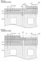
この点を以下に詳説する。図10は、比較形態(特許文献1に開示された従来技術の形態)の半導体製造装置用部材110の部分拡大図である。半導体製造装置用部材110では、中央セラミック部材122の外周面125及び外周セラミック部材132の内周面135はいずれも上下方向で径が一定であり、半導体製造装置用部材110を平面視すると、中央セラミック部材122と外周セラミック部材132とは重ならず、両者の間の隙間を奥まで見通すことができる。こうした半導体製造装置用部材110では、加速されたイオンは、図10Aに示すように、中央ベース部材142と外周ベース部材152との間や中央接合部162と外周接合部167との間の隙間に侵入する。そして、加速されたイオンが隙間内で他の原子や分子に衝突してプラズマやラジカルを生成することなどにより、その周囲のベース部材140や接合部160を腐食し、半導体製造装置用部材110の寿命を低下させる。なお、半導体製造装置用部材110では、中央セラミック部材122の外周面125には、円周方向に沿って上側が小径となるような段差125sを有し、この段差125sには、図10Bに示すように、FR170の内周部が配置されるようになっている。これにより、FR載置面132aにFR170を載置した状態でウエハレスドライクリーニングする場合においては、加速されたイオンは、FR170に衝突し、その先には進まず、ベース部材140や接合部160の腐食は抑制される。しかし、FR載置面132aにFR170を載置した状態でウエハレスドライクリーニングするため、加速されたイオンによってFR170が腐食してしまい、FR170の寿命を低下させてしまう。したがって、半導体製造装置用部材110を用いた場合には、半導体製造装置全体のランニングコストが高くなり、装置寿命が低下してしまう。This point will be explained in detail below. Figure 10 is a partially enlarged view of a semiconductor
これに対して、本実施形態では、中央セラミック部材22の外周面25及び外周セラミック部材32の内周面35はいずれも上下方向で径が変化していて、半導体製造装置用部材10を平面視すると、中央セラミック部材22の外周部26と外周セラミック部材32の内周部36とが重なっている。こうした半導体製造装置用部材10では、加速されたイオンは、図3に示すように、ベース部材40や接合部60に至る前にセラミック部材20に衝突し、その先には進まない。それにより、ベース部材40や接合部60の周辺でのプラズマやラジカルの生成が抑制され、ベース部材40や接合部60の腐食が抑制されるため、結果として、装置寿命の低下が抑制される。また、半導体製造装置用部材10を平面視して、中央セラミック部材22の外周部26と外周セラミック部材32の内周部36とが重なっているため、FR載置面32aにFR70を載置しない状態でウエハレスドライクリーニングをしても、ベース部材40や接合部60の腐食を抑制可能である。したがって、FR70の寿命を向上することができ、半導体製造装置全体の装置寿命の低下を抑制することができる。In contrast, in this embodiment, the outer
以上説明した半導体製造装置用部材10によれば、中央セラミック部材22の外周面25及び外周セラミック部材32の内周面35はいずれも上下方向で径が変化している。そして、中央セラミック部材22の外周面25の最大径Pmaxは、外周セラミック部材32の内周面35の最大径Qmaxよりも小さく、外周セラミック部材32の内周面35の最小径Qminよりも小さい。そのため、半導体製造装置用部材10を平面視すると、中央セラミック部材22の外周部26と外周セラミック部材32の内周部36とが重なっている。したがって、上述したように、装置寿命の低下が抑制される。In the semiconductor
また、中央セラミック部材22の外周面25の最小径Pmin(本実施形態では外周面25の下端25bの直径)は、外周セラミック部材32の内周面35の最小径Qminよりも小さい。こうした中央セラミック部材22及び外周セラミック部材32は、例えば、1枚のセラミック板をくり抜くことで作製できる。その場合、中央セラミック部材22用のセラミック板と、外周セラミック部材32用のセラミック板とを個別に準備するよりも、製造コストを抑えやすい。Furthermore, the minimum diameter Pmin of the outer
更に、半導体製造装置用部材10をウエハ載置面22aに垂直な方向に切断した断面では、中央セラミック部材22の外周面25及び外周セラミック部材32の内周面35のそれぞれが斜め線として現れる。こうした中央セラミック部材22及び外周セラミック部材32は、例えば、1枚のセラミック板を円錐台形状や逆円錐台形状にくり抜くことで作製できる。こうした形状であれば、くり抜き加工が比較的容易であり、製造コストを抑えやすい。Furthermore, in a cross section of the semiconductor
更にまた、外周支持部としての外周ベース部材52は、中央支持部としての中央ベース部材42とは隙間をあけて配置された環状の部材である。そのため、外周ベース部材52の温度と中央ベース部材42の温度とを個別に制御しやすく、ひいては、ウエハ載置面22aの温度とFR載置面32aの温度とを個別に制御しやすい。Furthermore, the outer
そして、中央セラミック部材22と中央支持部としての中央ベース部材42とは樹脂製の中央接合部62で接合され、外周セラミック部材32と外周支持部としての外周ベース部材52とは樹脂製の外周接合部67で接合されている。樹脂製の接着層は、腐食されやすいため、本発明を適用する意義が高い。The central
なお、本発明は上述した実施形態に何ら限定されることはなく、本発明の技術的範囲に属する限り種々の態様で実施し得ることはいうまでもない。It goes without saying that the present invention is in no way limited to the above-described embodiment, and can be implemented in various forms as long as they fall within the technical scope of the present invention.
上述した実施形態では、中央セラミック部材22の外周面25は、上側ほど直径が大きくなるテーパ面であるものとしたが、上下方向で径が変化するものであればこうしたものに限定されない。中央セラミック部材22の外周面25は、例えば、図5~7に示す別例の半導体製造装置用部材10Bのように、上側ほど直径が小さくなるテーパ面(円錐台の外側面)であるものとしてもよい。また、上述した実施形態では、外周セラミック部材32の内周面35は、上側ほど直径が大きくなるテーパ面であるものとしたが、上下方向で径が変化するものであれば特に限定されない。外周セラミック部材32の内周面35は、例えば、半導体製造装置用部材10Bのように、上側ほど直径が小さくなるテーパ面(円盤から円錐台をくり抜いた内側面)であるものとしてもよい。なお、図5~7では、上述した実施形態と同じ構成要素には同じ符号を付した。In the above embodiment, the outer
半導体製造装置用部材10Bでは、中央セラミック部材22の外周面25は、図7に示すように、その下端25bを起点として上下方向に対して角度γだけ内周側に傾斜している。角度γは、例えば、10°以上80°以下である。また、外周セラミック部材32の内周面35は、図7に示すように、その下端35bを起点として上下方向に対して角度δだけ内周側に傾斜している。角度δは、例えば、10°以上80°以下である。角度δは、角度γと同じでもよいし、異なってもよい。そして、半導体製造装置用部材10Bでは、図6に示すように、中央セラミック部材22の外周面25の最大径Pmax(本別例では外周面25の下端25bの直径)は、外周セラミック部材32の内周面35の最大径Qmax(本別例では内周面35の下端35bの直径)よりも小さく、外周セラミック部材32の内周面35の最小径Qmin(本別例では内周面35の上端35aの直径)よりも大きい。そのため、半導体製造装置用部材10Bを平面視すると、中央セラミック部材22の外周部26と外周セラミック部材32の内周部36とが重なっている。なお、半導体製造装置用部材10Bを平面視すると、ウエハ載置面22aとFR載置面32aとの間に中央セラミック部材22の外周面25があり、その奥を見通すことはできない。こうした半導体製造装置用部材10Bでは、加速されたイオンは、図7に示すように、ベース部材40や接合部60に至る前にセラミック部材20に衝突し、その先には進まない。それにより、ベース部材40や接合部60の周辺でのプラズマやラジカルの生成が抑制され、ベース部材40や接合部60の腐食が抑制されるため、結果として、装置寿命の低下が抑制される。また、FR載置面32aにFR70を載置しない状態でウエハレスドライクリーニングをしても、ベース部材40や接合部60の腐食を抑制可能なため、FR70の寿命を向上することができ、半導体製造装置全体の装置寿命の低下を抑制することができる。In semiconductor
半導体製造装置用部材10Bでは、中央セラミック部材22の外周面25の最小径Pmin(本実施形態では外周面25の上端25aの直径)は、外周セラミック部材32の内周面35の最小径Qminよりも小さい。こうした中央セラミック部材22及び外周セラミック部材32は、例えば、1枚のセラミック板をくり抜くことで作製できる。In the semiconductor
半導体製造装置用部材10Bの中央セラミック部材22及び外周セラミック部材32は、図4に準じて製造してもよい。その場合、図4Bで、円板状の中央部をくり抜く際に、円板状の中央部が円錐台形状となるように加工すればよい。The central
上述した実施形態及び別例では、中央接合部62及び外周接合部67は、樹脂製の接着層としたが、例えば、はんだや金属ロウ材で形成された金属製の接合層としてもよい。金属製の接合層は、例えばTCB(Thermal compression bonding)により形成されていてもよい。TCBとは、接合対象の2つの部材の間に金属接合材を挟み込み、金属接合材の固相線温度以下の温度に加熱した状態で2つの部材を加圧接合する公知の方法をいう。中央接合部62及び外周接合部67を金属製の接合層とした場合、図8に示す別例の半導体製造装置用部材10Cのように、中央接合部62の外周面は、中央支持部としての中央ベース部材42の外周面とともに中央絶縁膜77で覆われ、外周接合部67の外周面は外周支持部としての外周ベース部材52の内周面とともに外周絶縁膜78で覆われているものとしてもよい。また、外周接合部67の外周面は外周支持部としての外周ベース部材52の外周面とともに最外周絶縁膜79で覆われているものとしてもよい。こうすれば、接合部60及びベース部材40が絶縁膜で覆われているため、接合部60及びベース部材40の腐食がより抑制される。また、接合部60が樹脂製ではなく金属製のため、溶射などにより絶縁膜を形成しても接合部60が変質しにくい。図8では、上述した実施形態と同じ構成要素には同じ符号を付した。In the above-mentioned embodiment and other examples, the central joint 62 and the outer peripheral joint 67 are resin adhesive layers, but they may be metallic joint layers formed of solder or metal brazing material. The metallic joint layer may be formed by, for example, TCB (thermal compression bonding). TCB refers to a known method in which a metallic joint material is sandwiched between two members to be joined, and the two members are pressurized and joined while being heated to a temperature below the solidus temperature of the metallic joint material. When the central joint 62 and the outer peripheral joint 67 are metallic joint layers, as in another example semiconductor
上述した実施形態及び別例では、ベース部材40は、中央支持部としての中央ベース部材42と外周支持部としての外周ベース部材52とが別体であるものとしたが、一体品であるものとしてもよい。その場合、ベース部材40は、図9に示す別例の半導体製造装置用部材10Dのように、中央ベース部材42と外周ベース部材52とが連結部48で連結された構造を有する一体品であるものとしてもよい。半導体製造装置用部材10Dでは、連結部48の上面にも中央絶縁膜77や外周絶縁膜78と同様の絶縁膜を設けることが好ましい。なお、ベース部材40は、中央ベース部材42と外周ベース部材52との間に隙間がなくてもよいが、隙間を設けることで、外周ベース部材52の温度と中央ベース部材42の温度とを個別に制御しやすくなり、ひいては、ウエハ載置面22aの温度とFR載置面32aの温度とを個別に制御しやすくなる。図9では、上述した実施形態と同じ構成要素には同じ符号を付した。In the above-mentioned embodiment and other examples, the
上述した実施形態及び別例では、外周セラミック部材32は、中央セラミック部材22とは隙間をあけて配置したが、隙間をあけずに配置してもよい(接合部60及びベース部材40とが溶射膜で覆われて隙間がない場合も含む)。隙間をあけて配置すれば、ウエハ載置面22aの温度とフォーカスリング載置面32aの温度とを個別に制御しやすくなる。一方、隙間をあけずに配置すれば、シャワーヘッド82とベース部材40との間に高周波電圧を印加したときに、隙間を介してベース部材40の周辺で生じることのある異常放電を抑制できる。In the above-described embodiment and other examples, the peripheral
上述した実施形態及び別例において、半導体製造装置用部材10,10B,10C,10Dは、上面にフォーカスリング載置面32aを有し、ウエハ載置面を有する中央セラミック部材の外周側に配置可能に構成された環状の外周セラミック部材32と、外周セラミック部材32の下面に接合し、外周セラミック部材32を支持する外周支持部を有する導電性のベース部材40と、を備え、外周セラミック部材32の内周面35は上下方向で径が変化し、外周セラミック部材32の内周面35は、上側ほど直径が大きくなる、又は上側ほど直径が小さくなるテーパ面である、フォーカスリング70を載置するためのものとしてもよい。この場合、中央セラミック部材は、上述した中央セラミック部材22と同じものとしてもよいし、異なるものとしてもよいし、省略してもよい。また、ベース部材40は、上述したベース部材40と同じものとしてもよいし、上述の中央ベース部材42とは異なる中央支持部を有するものとしてもよいし、中央支持部を有さないものとしてもよい。In the above-mentioned embodiment and other examples, the semiconductor
上述した実施形態及び別例において、中央セラミック部材22にウエハ加熱用ヒータ電極を埋設してもよい。こうすれば、ウエハ載置面22aに載置されるウエハWを高温にする必要がある場合に、ウエハ加熱用ヒータ電極に通電してウエハWを所望の高温にすることができる。また、外周セラミック部材32にFR加熱用ヒータ電極を埋設してもよい。こうすれば、FR載置面32aに載置されるFR70を高温にする必要がある場合に、FR加熱用ヒータ電極に通電してFR70を所望の高温にすることができる。中央セラミック部材22にウエハ加熱用ヒータ電極を埋設し外周セラミック部材32にFR加熱用ヒータ電極を埋設する場合、それぞれのヒータ電極を個別に温度調整可能にするのが好ましい。In the above-described embodiment and other examples, a heater electrode for heating the wafer may be embedded in the central
本発明は、半導体製造装置に用いられる部材、例えば静電チャックヒータ、静電チャック、セラミックヒータなどに利用可能である。The present invention can be used in components used in semiconductor manufacturing equipment, such as electrostatic chuck heaters, electrostatic chucks, and ceramic heaters.
10,10B,10C,10D 半導体製造装置用部材、20 セラミック部材、21 セラミック板、22 中央セラミック部材、22a ウエハ載置面、24 ウエハ吸着用電極、25 外周面、26 外周部、32 外周セラミック部材、32a FR載置面、34 FR吸着用電極、35 内周面、36 内周部、40 ベース部材、41 ネジ穴、42 中央ベース部材、42a 中央支持面、44 中央冷媒流路、48 連結部、52 外周ベース部材、52a 外周支持面、54 外周冷媒流路、60 接合部、62 中央接合部、67 外周接合部、70 フォーカスリング(FR)、72 段差、77 中央絶縁膜、78 外周絶縁膜、79 最外周絶縁膜、80 チャンバ、82 シャワーヘッド、84 設置板、86 ボルト挿通孔、87,88,89 Oリング、90 ボルト、110 半導体製造装置用部材、120 セラミック部材、122 中央セラミック部材、125 外周面、125s 段差、132 外周セラミック部材、132a FR載置面、135 内周面、140 ベース部材、142 中央ベース部材、152 外周ベース部材、160 接合部、162 中央接合部、167 外周接合部、170 FR。10, 10B, 10C, 10D: Semiconductor manufacturing equipment member, 20: Ceramic member, 21: Ceramic plate, 22: Central ceramic member, 22a: Wafer mounting surface, 24: Wafer suction electrode, 25: Outer periphery, 26: Outer periphery, 32: Outer periphery ceramic member, 32a: FR mounting surface, 34: FR suction electrode, 35: Inner periphery, 36: Inner periphery, 40: Base member, 41: Screw hole, 42: Central base member, 42a: Central support surface, 44: Central refrigerant flow path, 48: Connection, 52: Outer periphery base member, 52a: Outer periphery support surface, 54: Outer periphery refrigerant flow path, 60: Joint, 62: Central joint, 67: Outer periphery joint, 70: Fo -cassing (FR), 72 step, 77 central insulating film, 78 peripheral insulating film, 79 outermost insulating film, 80 chamber, 82 shower head, 84 mounting plate, 86 bolt insertion hole, 87, 88, 89 O-ring, 90 bolt, 110 semiconductor manufacturing equipment component, 120 ceramic component, 122 central ceramic component, 125 peripheral surface, 125s step, 132 peripheral ceramic component, 132a FR mounting surface, 135 inner surface, 140 base component, 142 central base component, 152 peripheral base component, 160 joint, 162 central joint, 167 peripheral joint, 170 FR.
Claims (9)
Translated fromJapanese上面にフォーカスリング載置面を有し、前記中央セラミック部材の外周側に配置された、環状の外周セラミック部材と、
前記中央セラミック部材の下面に接合し、前記中央セラミック部材を支持する中央支持部と、前記外周セラミック部材の下面に接合し、前記外周セラミック部材を支持する外周支持部と、を有し、前記中央支持部と前記外周支持部とが別体若しくは一体で構成されている導電性のベース部材と、を備え、
前記中央セラミック部材の外周面及び前記外周セラミック部材の内周面はいずれも上下方向で径が変化し、
前記中央セラミック部材の外周面の最大径は、前記外周セラミック部材の内周面の最大径よりも小さく、前記外周セラミック部材の内周面の最小径よりも大きい、
半導体製造装置用部材。a central ceramic member having a wafer mounting surface thereon;
an annular peripheral ceramic member having a focus ring mounting surface on an upper surface thereof and disposed on an outer circumferential side of the central ceramic member;
a central support part joined to a lower surface of the central ceramic member and supporting the central ceramic member, and a peripheral support part joined to a lower surface of the peripheral ceramic member and supporting the peripheral ceramic member, the central support part and the peripheral support part being separate or integral with each other;
The diameter of the outer peripheral surface of the central ceramic member and the inner peripheral surface of the outer peripheral ceramic member both change in the up-down direction,
a maximum diameter of the outer peripheral surface of the central ceramic member is smaller than a maximum diameter of the inner peripheral surface of the outer peripheral ceramic member and is larger than a minimum diameter of the inner peripheral surface of the outer peripheral ceramic member;
Components for semiconductor manufacturing equipment.
請求項1に記載の半導体製造装置用部材。the minimum diameter of the outer circumferential surface of the central ceramic member is smaller than the minimum diameter of the inner circumferential surface of the outer circumferential ceramic member;
The semiconductor manufacturing equipment member according to claim 1 .
請求項1又は2に記載の半導体製造装置用部材。In a cross section of the semiconductor manufacturing equipment member cut in a direction perpendicular to the wafer mounting surface, the outer peripheral surface of the central ceramic member and the inner peripheral surface of the outer peripheral ceramic member each appear as an oblique line.
The semiconductor manufacturing equipment member according to claim 1 or 2.
請求項1又は2に記載の半導体製造装置用部材。The outer circumferential surface of the central ceramic member is a tapered surface whose diameter increases toward the upper side.
The semiconductor manufacturing equipment member according to claim 1 or 2.
請求項1又は2に記載の半導体製造装置用部材。The outer circumferential surface of the central ceramic member is a tapered surface whose diameter decreases toward the upper side.
The semiconductor manufacturing equipment member according to claim 1 or 2.
請求項1又は2に記載の半導体製造装置用部材。The outer peripheral support portion is an annular portion disposed on the outer periphery of the central support portion with a gap therebetween.
The semiconductor manufacturing equipment member according to claim 1 or 2.
請求項6に記載の半導体製造装置用部材。the central ceramic member and the central support part are joined by a central joint part made of metal, the outer peripheral surface of the central joint part and the outer peripheral surface of the central support part are covered by a central insulating film, the outer peripheral ceramic member and the outer peripheral support part are joined by a peripheral joint part made of metal, the inner peripheral surface of the outer peripheral joint part and the inner peripheral surface of the outer peripheral support part are covered by an outer peripheral insulating film.
The semiconductor manufacturing equipment member according to claim 6 .
請求項1又は2に記載の半導体製造装置用部材。the central ceramic member and the central support part are joined by a central joint part made of resin, and the peripheral ceramic member and the peripheral support part are joined by a peripheral joint part made of resin.
The semiconductor manufacturing equipment member according to claim 1 or 2.
前記外周セラミック部材の下面に接合し、前記外周セラミック部材を支持する外周支持部を有する導電性のベース部材と、を備え、
前記外周セラミック部材の内周面は上下方向で径が変化し、前記外周セラミック部材の内周面は、上側ほど直径が大きくなる、又は上側ほど直径が小さくなるテーパ面である、
フォーカスリングを載置するための半導体製造装置用部材。a central ceramic member having a wafer mounting surface and a focus ring mounting surface on an upper surface of the central ceramic member;
a conductive base member having an outer peripheral support portion bonded to a lower surface of the outer peripheral ceramic member and supporting the outer peripheral ceramic member;
The diameter of the inner peripheral surface of the outer peripheral ceramic member changes in the up-down direction, and the inner peripheral surface of the outer peripheral ceramic member is a tapered surface in which the diameter increases toward the upper side or decreases toward the upper side.
A component for semiconductor manufacturing equipment on which a focus ring is mounted.
Priority Applications (4)
| Application Number | Priority Date | Filing Date | Title |
|---|---|---|---|
| JP2024513175AJP7751079B2 (en) | 2023-08-29 | 2023-08-29 | Semiconductor manufacturing equipment components |
| PCT/JP2023/031085WO2025046720A1 (en) | 2023-08-29 | 2023-08-29 | Member for semiconductor manufacturing device |
| US18/588,280US20250079134A1 (en) | 2023-08-29 | 2024-02-27 | Member for semiconductor manufacturing apparatus |
| TW113125815ATW202512376A (en) | 2023-08-29 | 2024-07-10 | Parts for semiconductor manufacturing equipment |
Applications Claiming Priority (1)
| Application Number | Priority Date | Filing Date | Title |
|---|---|---|---|
| PCT/JP2023/031085WO2025046720A1 (en) | 2023-08-29 | 2023-08-29 | Member for semiconductor manufacturing device |
Related Child Applications (1)
| Application Number | Title | Priority Date | Filing Date |
|---|---|---|---|
| US18/588,280ContinuationUS20250079134A1 (en) | 2023-08-29 | 2024-02-27 | Member for semiconductor manufacturing apparatus |
Publications (1)
| Publication Number | Publication Date |
|---|---|
| WO2025046720A1true WO2025046720A1 (en) | 2025-03-06 |
Family
ID=94773396
Family Applications (1)
| Application Number | Title | Priority Date | Filing Date |
|---|---|---|---|
| PCT/JP2023/031085PendingWO2025046720A1 (en) | 2023-08-29 | 2023-08-29 | Member for semiconductor manufacturing device |
Country Status (4)
| Country | Link |
|---|---|
| US (1) | US20250079134A1 (en) |
| JP (1) | JP7751079B2 (en) |
| TW (1) | TW202512376A (en) |
| WO (1) | WO2025046720A1 (en) |
Citations (3)
| Publication number | Priority date | Publication date | Assignee | Title |
|---|---|---|---|---|
| JP2016027601A (en)* | 2014-06-24 | 2016-02-18 | 東京エレクトロン株式会社 | Placing table and plasma processing apparatus |
| JP2016127090A (en)* | 2014-12-26 | 2016-07-11 | 東京エレクトロン株式会社 | Mounting table and plasma processing apparatus |
| JP2023039202A (en)* | 2021-09-08 | 2023-03-20 | 東京エレクトロン株式会社 | Substrate support body assembly and plasma processing apparatus |
Family Cites Families (2)
| Publication number | Priority date | Publication date | Assignee | Title |
|---|---|---|---|---|
| JP7134104B2 (en)* | 2019-01-09 | 2022-09-09 | 東京エレクトロン株式会社 | Plasma processing apparatus and mounting table for plasma processing apparatus |
| JP7579758B2 (en)* | 2021-06-28 | 2024-11-08 | 東京エレクトロン株式会社 | SUBSTRATE SUPPORT, SUBSTRATE SUPPORT ASSEMBLY AND PLASMA PROCESSING APPARATUS - Patent application |
- 2023
- 2023-08-29WOPCT/JP2023/031085patent/WO2025046720A1/enactivePending
- 2023-08-29JPJP2024513175Apatent/JP7751079B2/enactiveActive
- 2024
- 2024-02-27USUS18/588,280patent/US20250079134A1/enactivePending
- 2024-07-10TWTW113125815Apatent/TW202512376A/enunknown
Patent Citations (3)
| Publication number | Priority date | Publication date | Assignee | Title |
|---|---|---|---|---|
| JP2016027601A (en)* | 2014-06-24 | 2016-02-18 | 東京エレクトロン株式会社 | Placing table and plasma processing apparatus |
| JP2016127090A (en)* | 2014-12-26 | 2016-07-11 | 東京エレクトロン株式会社 | Mounting table and plasma processing apparatus |
| JP2023039202A (en)* | 2021-09-08 | 2023-03-20 | 東京エレクトロン株式会社 | Substrate support body assembly and plasma processing apparatus |
Also Published As
| Publication number | Publication date |
|---|---|
| TW202512376A (en) | 2025-03-16 |
| US20250079134A1 (en) | 2025-03-06 |
| JPWO2025046720A1 (en) | 2025-03-06 |
| JP7751079B2 (en) | 2025-10-07 |
Similar Documents
| Publication | Publication Date | Title |
|---|---|---|
| KR101249654B1 (en) | Placing table structure and heat treatment apparatus | |
| US7589950B2 (en) | Detachable electrostatic chuck having sealing assembly | |
| JP6563438B2 (en) | Vacuum process chamber components and manufacturing method | |
| US7697260B2 (en) | Detachable electrostatic chuck | |
| JP7569342B2 (en) | Semiconductor manufacturing equipment parts | |
| JP4451098B2 (en) | Susceptor device | |
| JP7569343B2 (en) | Semiconductor manufacturing equipment parts | |
| CN102160167A (en) | Electrostatic chuck assembly | |
| JP2007194616A (en) | Susceptor and wafer processing method using the same | |
| JP5460184B2 (en) | Support device | |
| JP7483121B2 (en) | Semiconductor manufacturing equipment parts | |
| KR102688371B1 (en) | Member for semiconductor manufacturing apparatus | |
| JP7622002B2 (en) | Wafer placement table | |
| JP7751079B2 (en) | Semiconductor manufacturing equipment components | |
| JP7560675B1 (en) | Semiconductor manufacturing equipment parts | |
| US20230197500A1 (en) | Wafer placement table | |
| US20250069865A1 (en) | Member for semiconductor manufacturing apparatus | |
| US12211671B2 (en) | Wafer placement table | |
| JP7742945B1 (en) | Susceptor | |
| JP7747580B2 (en) | Semiconductor manufacturing equipment and holding equipment | |
| TWI856379B (en) | Wafer placement table | |
| TW202425204A (en) | Wafer placement table | |
| TW202412166A (en) | Wafer placement table | |
| TW202509998A (en) | Pressure seal method and apparatus | |
| JP2021145114A (en) | Susceptor and electrostatic chuck device |
Legal Events
| Date | Code | Title | Description |
|---|---|---|---|
| ENP | Entry into the national phase | Ref document number:2024513175 Country of ref document:JP Kind code of ref document:A | |
| WWE | Wipo information: entry into national phase | Ref document number:2024513175 Country of ref document:JP | |
| 121 | Ep: the epo has been informed by wipo that ep was designated in this application | Ref document number:23950671 Country of ref document:EP Kind code of ref document:A1 |