WO2025028971A1 - Electronic device and wearable device - Google Patents
Electronic device and wearable deviceDownload PDFInfo
- Publication number
- WO2025028971A1 WO2025028971A1PCT/KR2024/011021KR2024011021WWO2025028971A1WO 2025028971 A1WO2025028971 A1WO 2025028971A1KR 2024011021 WKR2024011021 WKR 2024011021WWO 2025028971 A1WO2025028971 A1WO 2025028971A1
- Authority
- WO
- WIPO (PCT)
- Prior art keywords
- optical amplifier
- electronic device
- laser
- output
- designated
- Prior art date
- Legal status (The legal status is an assumption and is not a legal conclusion. Google has not performed a legal analysis and makes no representation as to the accuracy of the status listed.)
- Pending
Links
Images


Classifications
- A—HUMAN NECESSITIES
- A61—MEDICAL OR VETERINARY SCIENCE; HYGIENE
- A61B—DIAGNOSIS; SURGERY; IDENTIFICATION
- A61B5/00—Measuring for diagnostic purposes; Identification of persons
- A—HUMAN NECESSITIES
- A61—MEDICAL OR VETERINARY SCIENCE; HYGIENE
- A61B—DIAGNOSIS; SURGERY; IDENTIFICATION
- A61B5/00—Measuring for diagnostic purposes; Identification of persons
- A61B5/145—Measuring characteristics of blood in vivo, e.g. gas concentration or pH-value ; Measuring characteristics of body fluids or tissues, e.g. interstitial fluid or cerebral tissue
- A61B5/1455—Measuring characteristics of blood in vivo, e.g. gas concentration or pH-value ; Measuring characteristics of body fluids or tissues, e.g. interstitial fluid or cerebral tissue using optical sensors, e.g. spectral photometrical oximeters
- G—PHYSICS
- G01—MEASURING; TESTING
- G01J—MEASUREMENT OF INTENSITY, VELOCITY, SPECTRAL CONTENT, POLARISATION, PHASE OR PULSE CHARACTERISTICS OF INFRARED, VISIBLE OR ULTRAVIOLET LIGHT; COLORIMETRY; RADIATION PYROMETRY
- G01J3/00—Spectrometry; Spectrophotometry; Monochromators; Measuring colours
- G01J3/02—Details
- G01J3/10—Arrangements of light sources specially adapted for spectrometry or colorimetry
- G—PHYSICS
- G01—MEASURING; TESTING
- G01J—MEASUREMENT OF INTENSITY, VELOCITY, SPECTRAL CONTENT, POLARISATION, PHASE OR PULSE CHARACTERISTICS OF INFRARED, VISIBLE OR ULTRAVIOLET LIGHT; COLORIMETRY; RADIATION PYROMETRY
- G01J3/00—Spectrometry; Spectrophotometry; Monochromators; Measuring colours
- G01J3/28—Investigating the spectrum
- G01J3/42—Absorption spectrometry; Double beam spectrometry; Flicker spectrometry; Reflection spectrometry
- G—PHYSICS
- G01—MEASURING; TESTING
- G01N—INVESTIGATING OR ANALYSING MATERIALS BY DETERMINING THEIR CHEMICAL OR PHYSICAL PROPERTIES
- G01N21/00—Investigating or analysing materials by the use of optical means, i.e. using sub-millimetre waves, infrared, visible or ultraviolet light
- G01N21/17—Systems in which incident light is modified in accordance with the properties of the material investigated
- G01N21/25—Colour; Spectral properties, i.e. comparison of effect of material on the light at two or more different wavelengths or wavelength bands
- G01N21/31—Investigating relative effect of material at wavelengths characteristic of specific elements or molecules, e.g. atomic absorption spectrometry
Definitions
- the present disclosurerelates to electronic devices and wearable devices.
- These electronic devicescan generally be carried in a pocket or hand and used while moving, but they can also be worn on parts of the body or various structures.
- the electronic devicescan provide health and exercise information by utilizing the wearable point on the user's body.
- the electronic devicemay include a sensor capable of noninvasively detecting blood sugar based on an optical sensor (e.g., a laser).
- the electronic devicemay output light from a light source of the optical sensor.
- the electronic devicemay analyze the object by obtaining a spectrum of light transmitted and/or reflected by the object.
- a wavelength band targeted by the optical sensormay be configured by using a plurality of light sources covering different wavelengths.
- the intensity of the light outputmay be lower than the set standard. Or, if the intensity (power) of the light output from each light source is greater than the set standard, there is a problem that the range of wavelengths that each light source can cover is reduced.
- An electronic device including an optical sensor including a plurality of light sources of the present disclosureis intended to control the power of the light sources for each defined bandwidth section.
- the electronic device of the present disclosuremay include a semiconductor optical amplifier that divides an outputtable wavelength band and outputs a plurality of laser lights having a designated wavelength band and a designated power; a fixed array distributed Bragg reflector grating that changes wavelengths of the plurality of laser lights and outputs a plurality of laser lights having changed wavelengths; and an output coupler that adjusts an output direction and/or angle of the modulated plurality of laser lights and outputs the modulated plurality of laser lights to the outside of the electronic device.
- a wearable device of the present disclosureincludes a transmitter circuit; a receiver circuit; and a processor, wherein the transmitter circuit may include a semiconductor optical amplifier that divides an outputtable wavelength band and outputs a plurality of laser lights having a designated wavelength band and a designated power; a fixed array distributed Bragg reflector grating that changes wavelengths of the plurality of laser lights and outputs a plurality of laser lights having changed wavelengths; and an output coupler that adjusts an output direction and/or angle of the modulated plurality of laser lights and outputs the modulated plurality of laser lights to the outside of the electronic device.
- the transmitter circuitmay include a semiconductor optical amplifier that divides an outputtable wavelength band and outputs a plurality of laser lights having a designated wavelength band and a designated power; a fixed array distributed Bragg reflector grating that changes wavelengths of the plurality of laser lights and outputs a plurality of laser lights having changed wavelengths; and an output coupler that adjusts an output direction and/or angle of the modulated plurality of laser lights and outputs
- the electronic device and wearable device of the present disclosurecan improve accuracy when measuring an object using light by controlling the power of a light source for each predetermined bandwidth section to output light.
- the electronic device and wearable device of the present disclosurecan improve the signal-to-noise ratio when measuring an object using light by controlling the power of a light source for each predetermined bandwidth section to output light.
- FIG. 1is a block diagram of an electronic device within a network environment according to various embodiments of the present disclosure.
- FIG. 2Ais a diagram illustrating an electronic device according to one embodiment of the present disclosure.
- FIG. 2bis a drawing showing a light output structure and a light receiving structure arranged on a second side or rear surface of an electronic device according to one embodiment of the present disclosure.
- FIG. 3is a block diagram illustrating a sensor circuit of an electronic device according to one embodiment of the present disclosure.
- Figure 4is a diagram showing a transmitter circuit implemented in a silicon-based integrated circuit.
- Figure 5is a graph showing the density of light according to wavelength after each of a plurality of optical amplifier chips included in a semiconductor optical amplifier (311) irradiates water with a laser output at the same level of power.
- FIG. 7is a graph showing the power of a laser according to a wavelength band output from a semiconductor optical amplifier including at least four optical amplifier chips according to one embodiment of the present disclosure.
- FIG. 8is a graph showing the power of a laser according to a wavelength band output from a semiconductor optical amplifier including at least three optical amplifier chips according to one embodiment of the present disclosure.
- FIG. 9is a flowchart illustrating a laser output method of an electronic device according to one embodiment of the present disclosure.
- FIG. 1is a block diagram of an electronic device (101) within a network environment (100) according to various embodiments.
- an electronic device (101)may communicate with an electronic device (102) via a first network (198) (e.g., a short-range wireless communication network), or may communicate with at least one of an electronic device (104) or a server (108) via a second network (199) (e.g., a long-range wireless communication network).
- the electronic device (101)may communicate with the electronic device (104) via the server (108).
- the electronic device (101)may include a processor (120), a memory (130), an input module (150), an audio output module (155), a display module (160), an audio module (170), a sensor module (176), an interface (177), a connection terminal (178), a haptic module (179), a camera module (180), a power management module (188), a battery (189), a communication module (190), a subscriber identification module (196), or an antenna module (197).
- the electronic device (101)may omit at least one of these components (e.g., the connection terminal (178)), or may have one or more other components added.
- some of these componentse.g., the sensor module (176), the camera module (180), or the antenna module (197) may be integrated into one component (e.g., the display module (160)).
- the processor (120)may include various processing circuits and/or multiple processors.
- processoras used herein, including in the claims, may include various processing circuits including at least one processor, one or more of which may be configured to perform various functions described herein, individually and/or collectively, in a distributed manner.
- processorat least one processor
- processorsone or more processors
- these termsmay include, by way of example and without limitation, instances where one processor performs some of the functions described and other processor(s) perform other functions described, and instances where a single processor performs all of the functions described.
- the at least one processormay include a combination of processors that perform various of the functions described/disclosed, for example, in a distributed manner.
- the at least one processormay execute program instructions to accomplish or perform various functions.
- the processor (120)may control at least one other component (e.g., a hardware or software component) of the electronic device (101) connected to the processor (120) by executing, for example, software (e.g., a program (140)), and may perform various data processing or calculations.
- softwaree.g., a program (140)
- the processor (120)may store a command or data received from another component (e.g., a sensor module (176) or a communication module (190)) in a volatile memory (132), process the command or data stored in the volatile memory (132), and store result data in a nonvolatile memory (134).
- the processor (120)may include a main processor (121) (e.g., a central processing unit or processor) or a secondary processor (123) (e.g., a graphic processing unit, a neural processing unit (NPU), an image signal processor, a sensor hub processor, or a communication processor) that can operate independently or together therewith.
- main processor (121)e.g., a central processing unit or processor
- a secondary processor (123)e.g., a graphic processing unit, a neural processing unit (NPU), an image signal processor, a sensor hub processor, or a communication processor
- the secondary processor (123)may be configured to use lower power than the main processor (121) or to be specialized for a given function.
- the secondary processor (123)may be implemented separately from the main processor (121) or as a part thereof.
- the auxiliary processor (123)may control at least a portion of functions or states associated with at least one of the components of the electronic device (101) (e.g., the display module (160), the sensor module (176), or the communication module (190)), for example, while the main processor (121) is in an inactive (e.g., sleep) state, or together with the main processor (121) while the main processor (121) is in an active (e.g., application execution) state.
- the auxiliary processor (123)e.g., an image signal processor or a communication processor
- the auxiliary processor (123)may include a hardware structure specialized for processing artificial intelligence models.
- the artificial intelligence modelsmay be generated through machine learning. Such learning may be performed, for example, in the electronic device (101) itself on which the artificial intelligence model is executed, or may be performed through a separate server (e.g., server (108)).
- the learning algorithmmay include, for example, supervised learning, unsupervised learning, semi-supervised learning, or reinforcement learning, but is not limited to the examples described above.
- the artificial intelligence modelmay include a plurality of artificial neural network layers.
- the artificial neural networkmay be one of a deep neural network (DNN), a convolutional neural network (CNN), a recurrent neural network (RNN), a restricted Boltzmann machine (RBM), a deep belief network (DBN), a bidirectional recurrent deep neural network (BRDNN), deep Q-networks, or a combination of two or more of the above, but is not limited to the examples described above.
- the artificial intelligence modelmay additionally or alternatively include a software structure.
- the memory (130)can store various data used by at least one component (e.g., processor (120) or sensor module (176)) of the electronic device (101).
- the datacan include, for example, software (e.g., program (140)) and input data or output data for commands related thereto.
- the memory (130)can include volatile memory (132) or nonvolatile memory (134).
- the program (140)may be stored as software in memory (130) and may include, for example, an operating system (142), middleware (144), or an application (146).
- the input module (150)can receive commands or data to be used in a component of the electronic device (101) (e.g., a processor (120)) from an external source (e.g., a user) of the electronic device (101).
- the input module (150)can include, for example, a microphone, a mouse, a keyboard, a key (e.g., a button), or a digital pen (e.g., a stylus pen).
- the audio output module (155)can output an audio signal to the outside of the electronic device (101).
- the audio output module (155)can include, for example, a speaker or a receiver.
- the speakercan be used for general purposes such as multimedia playback or recording playback.
- the receivercan be used to receive an incoming call. According to one embodiment, the receiver can be implemented separately from the speaker or as a part thereof.
- the display module (160)can visually provide information to an external party (e.g., a user) of the electronic device (101).
- the display module (160)can include, for example, a display, a holographic device, or a projector and a control circuit for controlling the device.
- the display module (160)can include a touch sensor configured to detect a touch, or a pressure sensor configured to measure the intensity of a force generated by the touch.
- the audio module (170)can convert sound into an electrical signal, or vice versa, convert an electrical signal into sound. According to one embodiment, the audio module (170) can obtain sound through an input module (150), or output sound through an audio output module (155), or an external electronic device (e.g., an electronic device (102)) (e.g., a speaker or a headphone) directly or wirelessly connected to the electronic device (101).
- an electronic devicee.g., an electronic device (102)
- a speaker or a headphonedirectly or wirelessly connected to the electronic device (101).
- the sensor module (176)can detect an operating state (e.g., power or temperature) of the electronic device (101) or an external environmental state (e.g., user state) and generate an electric signal or data value corresponding to the detected state.
- the sensor module (176)can include, for example, a gesture sensor, a gyro sensor, a barometric pressure sensor, a magnetic sensor, an acceleration sensor, a grip sensor, a proximity sensor, a color sensor, an IR (infrared) sensor, a biometric sensor, a temperature sensor, a humidity sensor, or an illuminance sensor.
- the interface (177)may support one or more designated protocols that may be used to directly or wirelessly connect the electronic device (101) with an external electronic device (e.g., the electronic device (102)).
- the interface (177)may include, for example, a high definition multimedia interface (HDMI), a universal serial bus (USB) interface, an SD card interface, or an audio interface.
- HDMIhigh definition multimedia interface
- USBuniversal serial bus
- SD card interfaceSecure Digital Card
- connection terminal (178)may include a connector through which the electronic device (101) may be physically connected to an external electronic device (e.g., the electronic device (102)).
- the connection terminal (178)may include, for example, an HDMI connector, a USB connector, an SD card connector, or an audio connector (e.g., a headphone connector).
- the haptic module (179)can convert an electrical signal into a mechanical stimulus (e.g., vibration or movement) or an electrical stimulus that a user can perceive through a tactile or kinesthetic sense.
- the haptic module (179)can include, for example, a motor, a piezoelectric element, or an electrical stimulation device.
- the camera module (180)can capture still images and moving images.
- the camera module (180)can include one or more lenses, image sensors, image signal processors, or flashes.
- the power management module (188)can manage power supplied to the electronic device (101).
- the power management module (188)can be implemented as, for example, at least a part of a power management integrated circuit (PMIC).
- PMICpower management integrated circuit
- the battery (189)can power at least one component of the electronic device (101).
- the battery (189)can include, for example, a non-rechargeable primary battery, a rechargeable secondary battery, or a fuel cell.
- the communication module (190)may support establishment of a direct (e.g., wired) communication channel or a wireless communication channel between the electronic device (101) and an external electronic device (e.g., the electronic device (102), the electronic device (104), or the server (108)), and performance of communication through the established communication channel.
- the communication module (190)may operate independently from the processor (120) (e.g., the application processor) and may include one or more communication processors that support direct (e.g., wired) communication or wireless communication.
- the communication module (190)may include a wireless communication module (192) (e.g., a cellular communication module, a short-range wireless communication module, or a GNSS (global navigation satellite system) communication module) or a wired communication module (194) (e.g., a local area network (LAN) communication module or a power line communication module).
- a wireless communication module (192)e.g., a cellular communication module, a short-range wireless communication module, or a GNSS (global navigation satellite system) communication module
- a wired communication module (194)e.g., a local area network (LAN) communication module or a power line communication module.
- a corresponding communication modulemay communicate with an external electronic device (104) via a first network (198) (e.g., a short-range communication network such as Bluetooth, wireless fidelity (WiFi) direct, or infrared data association (IrDA)) or a second network (199) (e.g., a long-range communication network such as a legacy cellular network, a 5G network, a next-generation communication network, the Internet, or a computer network (e.g., a LAN or WAN)).
- a first network (198)e.g., a short-range communication network such as Bluetooth, wireless fidelity (WiFi) direct, or infrared data association (IrDA)
- a second network (199)e.g., a long-range communication network such as a legacy cellular network, a 5G network, a next-generation communication network, the Internet, or a computer network (e.g., a LAN or WAN)
- a computer networke.g.,
- the wireless communication module (192)may use subscriber information (e.g., an international mobile subscriber identity (IMSI)) stored in the subscriber identification module (196) to identify or authenticate the electronic device (101) within a communication network such as the first network (198) or the second network (199).
- subscriber informatione.g., an international mobile subscriber identity (IMSI)
- IMSIinternational mobile subscriber identity
- the wireless communication module (192)can support a 5G network and next-generation communication technology after a 4G network, for example, NR access technology (new radio access technology).
- the NR access technologycan support high-speed transmission of high-capacity data (eMBB (enhanced mobile broadband)), terminal power minimization and connection of multiple terminals (mMTC (massive machine type communications)), or high reliability and low latency (URLLC (ultra-reliable and low-latency communications)).
- eMBBenhanced mobile broadband
- mMTCmassive machine type communications
- URLLCultra-reliable and low-latency communications
- the wireless communication module (192)can support, for example, a high-frequency band (e.g., mmWave band) to achieve a high data transmission rate.
- a high-frequency bande.g., mmWave band
- the wireless communication module (192)may support various technologies for securing performance in a high-frequency band, such as beamforming, massive multiple-input and multiple-output (MIMO), full dimensional MIMO (FD-MIMO), array antenna, analog beam-forming, or large scale antenna.
- the wireless communication module (192)may support various requirements specified in an electronic device (101), an external electronic device (e.g., an electronic device (104)), or a network system (e.g., a second network (199)).
- the wireless communication module (192)can support a peak data rate (e.g., 20 Gbps or more) for eMBB realization, a loss coverage (e.g., 164 dB or less) for mMTC realization, or a U-plane latency (e.g., 0.5 ms or less for downlink (DL) and uplink (UL) each, or 1 ms or less for round trip) for URLLC realization.
- a peak data ratee.g., 20 Gbps or more
- a loss coveragee.g., 164 dB or less
- U-plane latencye.g., 0.5 ms or less for downlink (DL) and uplink (UL) each, or 1 ms or less for round trip
- the antenna module (197)can transmit or receive signals or power to or from the outside (e.g., an external electronic device).
- the antenna module (197)can include an antenna including a radiator formed of a conductor or a conductive pattern formed on a substrate (e.g., a PCB).
- the antenna module (197)can include a plurality of antennas (e.g., an array antenna).
- at least one antenna suitable for a communication method used in a communication network, such as the first network (198) or the second network (199)can be selected from the plurality of antennas by, for example, the communication module (190).
- a signal or powercan be transmitted or received between the communication module (190) and the external electronic device through the selected at least one antenna.
- another componente.g., a radio frequency integrated circuit (RFIC)
- RFICradio frequency integrated circuit
- the antenna module (197)may form a mmWave antenna module.
- the mmWave antenna modulemay include a printed circuit board, an RFIC positioned on or adjacent a first side (e.g., a bottom side) of the printed circuit board and capable of supporting a designated high-frequency band (e.g., a mmWave band), and a plurality of antennas (e.g., an array antenna) positioned on or adjacent a second side (e.g., a top side or a side) of the printed circuit board and capable of transmitting or receiving signals in the designated high-frequency band.
- a first sidee.g., a bottom side
- a plurality of antennase.g., an array antenna
- peripheral devicese.g., a bus, a general purpose input and output (GPIO), a serial peripheral interface (SPI), or a mobile industry processor interface (MIPI)
- GPIOgeneral purpose input and output
- SPIserial peripheral interface
- MIPImobile industry processor interface
- commands or datamay be transmitted or received between the electronic device (101) and an external electronic device (104) via a server (108) connected to a second network (199).
- Each of the external electronic devices (102, or 104)may be the same or a different type of device as the electronic device (101).
- all or part of the operations executed in the electronic device (101)may be executed in one or more of the external electronic devices (102, 104, or 108). For example, when the electronic device (101) is to perform a certain function or service automatically or in response to a request from a user or another device, the electronic device (101) may, instead of executing the function or service itself or in addition, request one or more external electronic devices to perform at least a part of the function or service.
- One or more external electronic devices that have received the requestmay execute at least a part of the requested function or service, or an additional function or service related to the request, and transmit the result of the execution to the electronic device (101).
- the electronic device (101)may process the result as it is or additionally and provide it as at least a part of a response to the request.
- cloud computing, distributed computing, mobile edge computing (MEC), or client-server computing technologymay be used.
- the electronic device (101)may provide an ultra-low latency service by using, for example, distributed computing or mobile edge computing.
- the external electronic device (104)may include an IoT (Internet of Things) device.
- the server (108)may be an intelligent server using machine learning and/or a neural network.
- the external electronic device (104) or the server (108)may be included in the second network (199).
- the electronic device (101)can be applied to intelligent services (e.g., smart home, smart city, smart car, or healthcare) based on 5G communication technology and IoT-related technology.
- FIG. 2Ais a drawing showing the front side (231) of an electronic device (201) according to one embodiment of the present disclosure.
- FIG. 2bis a drawing showing the rear side (232) of an electronic device (201) according to one embodiment of the present disclosure.
- the electronic device (201) of FIGS. 2A and 2Bmay be identical to or similar to the components of the electronic device (101) of FIG. 1. However, it is not limited thereto, and the electronic device (201) of FIG. 2 may have additional or omitted components compared to the electronic device (101) of FIG. 1.
- the electronic device (201)may include a display (260) (e.g., the display module (160) of FIG. 1) on the front surface (231).
- the electronic device (201)may be a wearable device that can be worn by a user in the shape of a watch.
- the electronic device (201)may display an interface (210) related to the watch on at least a portion of the display (260).
- the electronic device (201)may include a case (case, 220) and a band (band, 240).
- the case (220)may include a bezel (221), a crown (222), and a display (260) on the outside.
- the case (220), referring to FIG. 1,may include a processor (e.g., including a processing circuit) (120), a memory (130), an input module (e.g., including an input circuit) (150), an audio output module (e.g., including an audio output circuit) (155), a display module (e.g., including a display) (160), an audio module (e.g., including an audio circuit) (170), a sensor module (e.g., including at least one sensor) (176), an interface (e.g., including an interface circuit) (177), a connection terminal (178), a haptic module (e.g., including a haptic circuit) (179), a camera module (e.g., including at least one camera) (180), a power management module (e.g., including a power management circuit) (188), a battery (189),
- a display (260)is disposed on the front (231) of the case (220), and at least a portion of a sensor circuit (e.g., a sensor circuit (300) of FIG. 3) (e.g., an output coupler (315) of FIG. 3 and/or a photodetector) may be exposed to the outside on the back (232).
- a sensor circuite.g., a sensor circuit (300) of FIG. 3
- the back (232) of the case (220)may be at least partially in contact with the user when the electronic device (201) is worn by the user via the band (240).
- the bezel (221)may be in a ring shape, concentric with the circular display (260).
- the inner radius of the bezel (221)may be substantially the same as the radius of the display (260).
- the bezel (221)may be positioned at a portion of the edge of the case (220) to protect the display (260) from external impact.
- the bezel (221)can rotate in at least one direction, either clockwise or counterclockwise.
- the bezel (221)can serve as an input device of the electronic device (201).
- the electronic device (201)can determine the speed and direction of rotation of the bezel (221) as user input, and control the function of the electronic device (201) according to the user input.
- the crown (222)may be positioned to protrude from at least a portion of the case (220).
- the crown (222)may have a cylindrical shape.
- the crown (222)may be connected to the case (220) and rotated about a rotational axis.
- the crown (222)may be connected to the case (220) and rotated by a stem that provides a rotational axis.
- the crown (222)can serve as an input device of the electronic device (201).
- the electronic device (201)can determine the rotation speed and rotation direction of the crown (222) as user input, and control the function of the electronic device (201) according to the user input.
- a band (or strap) (240)may allow the electronic device (201) to be worn on a user's wrist.
- the band (240)may be made of various materials, such as metal, rubber, or leather.
- the band (240)is connected to one end of the case (220), and the band (240) connected to the case (220) may be replaceable.
- the electronic device (201)may include a light output structure (270) and a plurality of light receiving structures (271, 272, 273, 274) on the rear surface (232).
- the light output structure (270)may include an output coupler (e.g., output coupler (315) of FIG. 3) on at least a portion thereof.
- the electronic device (201)may include a plurality of light receiving structures (271, 272, 273, 274) spaced apart from the light output structure (270) by a first distance (R1).
- the first distance (R1)may have a specified length.
- Each of the plurality of light receiving structures (271, 272, 273, 274)may include a receiving circuit (330) and/or a photodetector.
- the electronic device (2010)may include a photoplethysmogram (PPG) optical blood flow measurement sensor, an electrocardiogram (ECG) optical output structure (270) and a plurality of optical receiving structures (271, 272, 273, 274) on the rear (232).
- PPGphotoplethysmogram
- ECGelectrocardiogram
- a plurality of optical receiving structures(271, 272, 273, 274) on the rear (232).
- the first light receiving structure (271), the second light receiving structure (272), the third light receiving structure (273), and the fourth light receiving structure (274)can be arranged in a shape centered on the light output structure (270).
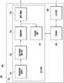
- FIG. 3is a block diagram illustrating a sensor circuit (300) of an electronic device (201) according to one embodiment of the present disclosure.
- FIG. 4is a diagram showing a transmitter circuit (310) implemented in a silicon-based integrated circuit.
- the sensor circuit (300) of FIG. 3may be identical to or similar to the sensor module (176) of FIG. 1, or may be included in the sensor module (176) of FIG. 1.
- the sensor circuit (300)may include a transmitter circuit (310), a processor (e.g., including a processing circuit) (320), and/or a receiver circuit (330).
- a transmitter circuit310
- a processore.g., including a processing circuit
- a receiver circuit330
- the transmitter circuit (310)may include a semiconductor optical amplifier (311), a fixed array distributed bragg reflector (DBR) grating (312), a modulator (313), a monitoring circuit (314), and/or an output coupler (315).
- DBRdistributed bragg reflector
- the semiconductor optical amplifier (311)may include a plurality of optical amplifier chips (optical amplifier chips) (3111, 3112, 3112). However, the present invention is not limited thereto, and the semiconductor optical amplifier (311) may include at least one optical amplifier chip.
- the semiconductor optical amplifier (311)can output and/or generate a broadband laser light under the control of the processor (320).
- the semiconductor optical amplifier (311)can output and/or generate a laser light having a wavelength in a band of about 2000 nm to about 2400 nm (or about 1500 nm to about 1850 nm).
- the laser light having a wavelength in a band of about 2000 nm to about 2400 nm (or about 1500 nm to about 1850 nm)may be a wavelength in a band appropriate for detecting blood sugar (or glucose).
- a plurality of optical amplifier chipscan output and/or generate a broadband laser light under the control of the processor (320).
- a plurality of optical amplifier chipscan output and/or generate laser light having a wavelength in a band of about 2000 nm to about 2400 nm (or about 1500 nm to about 1850 nm).
- the semiconductor optical amplifier (311)can control the output intensity of laser lights output from each of the plurality of optical amplifier chips by controlling current and/or voltage under the control of the processor (320).
- the electronic device (201)can store a setting value or setting data for the output intensity of laser lights in the memory (130). Based on the setting value or setting data, the electronic device (2011) can control the output intensity of laser lights output from each of the plurality of optical amplifier chips by controlling current and/or voltage.
- blood sugarcan absorb at least a portion of the modulated plurality of laser lights output from the sensor circuit (300).
- the electronic device (201)can receive the modulated plurality of laser lights that are not absorbed by the blood sugar but are transmitted or reflected by the blood sugar using a photodetector of the receiving circuit (330), and determine the concentration of the blood sugar under the control of the processor (320) based on the amount (or intensity) and/or wavelength of the received light.
- the semiconductor optical amplifier (311)can output and/or generate a plurality of laser lights having a wide bandwidth under the control of the processor (320).
- the semiconductor optical amplifier (311)can output and/or generate a plurality of laser lights having a broadband in a time division manner under the control of the processor (320).
- a plurality of optical amplifier chipscan output and/or generate broadband laser light in a time division manner under the control of the processor (320).
- the processor (320) of FIG. 3may be identical or similar to the processor (120) of FIG. 1, and the above description may be equally applied to the processor (120) and the processor (320). However, it is not limited thereto, and the processor (320) of FIG. 3 may be included in the sensor circuit (300) independently of the processor (120) of FIG. 1.
- the processor (320)may be implemented in the form of an application-specific integrated circuit (ASIC).
- the fixed array DBR grating (312)can change the wavelength of a broadband laser light output and/or generated from the semiconductor optical amplifier (311) to output laser light having a designated wavelength.
- the designated wavelengthcan have a shorter wavelength than the wavelength output from the semiconductor optical amplifier (311).
- a fixed array DBR grating (312)can output a plurality of laser lights having a specified wavelength by changing the wavelength of a broadband laser light output and/or generated from a plurality of semiconductor optical amplifiers (311).
- a fixed array DBR grating (312)corresponds to each optical amplifier chip and can output a plurality of laser lights having a specified wavelength by changing the wavelength of a broadband laser output and/or generated by each optical amplifier chip.
- the modulator (313)can modulate a plurality of laser lights of a specified wavelength output from the fixed array DBR grating (312) under the control of the processor (320).
- the sensor circuit (310)can modulate a plurality of laser lights of a specified wavelength output from the fixed array DBR grating (312) using the modulator (313) to improve a signal to noise ratio (SNR) of the output laser lights.
- SNRsignal to noise ratio
- the modulator (313)can modulate laser light having a specified wavelength into a continuous wave and/or a pulse wave.
- the modulator (313)may include a lock-in amplifier and/or a low pass filter (LPF).
- LPFlow pass filter
- the modulator (313)can modulate a plurality of laser lights of a specified wavelength output from a fixed array DBR grating (312) and output a plurality of modulated laser lights.
- a plurality of modulated laser lights output from the modulator (313)may be transmitted to an output coupler (315) through a waveguide (e.g., waveguide (316) of FIG. 4).
- a waveguidee.g., waveguide (316) of FIG. 4
- the output coupler (315)can change the output direction of the modulated plurality of laser lights and output them to the outside of the transmission circuit (310).
- the output coupler (315)can be output in the z-axis, which is a vertical direction of the coordinate plane.
- the output coupler (315)can, under the control of the processor (320), adjust the output direction and/or angle of the modulated laser light to output it to the outside of the transmission circuit (310).
- the monitoring circuit (314)may include, but is not limited to, an edge illuminated photodiode, a Mach-Zehnder interferometer (MZI) sensor, a ring resonator, a line coupling, and/or a splitter, for example.
- MZIMach-Zehnder interferometer
- the monitoring circuit (314)can verify and/or monitor whether a plurality of modulated laser lights transmitted through a waveguide (e.g., waveguide (316) of FIG. 4) are output according to a specified intensity (or power) and a specified wavelength.
- a waveguidee.g., waveguide (316) of FIG. 4
- the monitoring circuit (314)can detect at least some of the modulated laser light transmitted through a waveguide (e.g., waveguide (316) of FIG. 4).
- a waveguidee.g., waveguide (316) of FIG. 4
- the monitoring circuit (314)can check whether a plurality of modulated laser lights transmitted through a waveguide (e.g., the waveguide (316) of FIG. 4) are output according to the specified intensity (or power) and the specified wavelength, and can transmit the confirmed information to the processor (320).
- the processor (320)can control the intensity and wavelength of the light output from the semiconductor optical amplifier (311) based on the information received through the monitoring circuit (314).
- the informationmay include data on whether the plurality of modulated laser lights are output according to the specified intensity (or power) and the specified wavelength.
- an edge illuminated photodiode of the monitoring circuit (314)can detect the intensity of light reaching the monitoring circuit (314).
- a Mach-Zehnder interferometer sensor of the monitoring circuit (314)can detect the wavelength of light reaching the monitoring circuit (314).
- the monitoring circuit (314)may be connected between the modulator (313) and the output coupler (315). However, this is not limited to the monitoring circuit (314) and may be connected between the fixed array DBR grid (312) and the modulator (313).
- the receiving circuit (330)may include a photo detector.
- the receiving circuit (330)may include a plurality of photo detectors.
- the receiving circuit (330)may include at least one photo detector.
- the photo detectormay be spaced apart from a structure from which light is output in the transmitting circuit (310) by a specified distance.
- the structure from which light is output in the transmitting circuit (310)may be, for example, an output coupler (315).
- the present inventionis not limited thereto, and the structure from which light is output in the transmitting circuit (310) may include a light output structure and/or an opening corresponding to the output coupler (315).
- the photo detectormay detect a wavelength in a band of about 2000 nm to about 2400 nm.
- the distance between the photodetector and the structure from which light is output (e.g., the output coupler (315)) in the transmission circuit (310)can be at least one.
- the distance between the photodetector and the structure from which light is output (e.g., the output coupler (315)) in the transmission circuit (310)can vary.
- the distance between the plurality of photodetectors and the structure from which light is output (e.g., the output coupler (315)) in the transmission circuit (310)can have a plurality of designated distances, such as a first distance, a second distance, or a third distance.
- the receiving circuit (330)can receive the light output from the transmitting circuit (310).
- the receiving circuit (330)can sequentially receive the light output from the transmitting circuit (310).
- the transmitting circuit (330)can irradiate (irradiate, irradiate) a plurality of modulated laser lights having a specified wavelength onto the user's skin in a time-divisional and/or sequential manner.
- the light irradiated onto the user's skin in a time-divisional and/or sequential mannercan pass through the user's skin and be sequentially and/or time-divisionally received by the receiving circuit (330).
- the present inventionis not limited thereto, and the light irradiated onto the user's skin in a time-divisional and/or sequential manner can be reflected onto the user's skin and be sequentially and/or time-divisionally received by the receiving circuit (330).
- the processor (320)includes various circuits (e.g., see the detailed description of the processor (120) above) and can control the transmitting circuit (310) and/or the receiving circuit (330).
- the processor (320)can control a plurality of optical amplifier chips (e.g., 3111, 3112, 3113) included in the semiconductor optical amplifier (311) to output laser light having a wide bandwidth in a time-division manner.
- the processor (320)can control a plurality of laser lights modulated in the transmitting circuit (310) to output laser light in a time-division manner.
- the processor (320)can control time synchronization of the receiving circuit (330) so that the modulated plurality of laser lights can be received by the receiving circuit (330) in a time-division manner and/or sequentially.
- the processor (320)can demodulate the modulated plurality of laser lights received through the receiving circuit (330).
- the processor (320)may include an amplifier and/or a filter to demodulate the modulated plurality of laser lights received through the receiving circuit (330).
- the present inventionis not limited thereto, and the receiving circuit (330) may include an amplifier and/or a filter to demodulate the modulated plurality of laser lights.
- the processor (320)may convert the photocurrent into a digital signal.
- the processor (320)may include an analog to digital converter (ADC) that converts the photocurrent into a digital signal.
- ADCanalog to digital converter
- the present inventionis not limited thereto, and the receiving circuit (330) may include an ADC that converts the photocurrent into a digital signal.
- the processor (320)may include a memory (e.g., the memory (130) of FIG. 1) and/or an interface for communicating with the processor (120) of FIG. 1.
- the semiconductor optical amplifier (311)may include a plurality of optical amplifier chips (3111, 3112, 3113). Although FIG. 4 illustrates three optical amplifier chips (3111, 3112, 3113), the semiconductor optical amplifier (311) may include four or more optical amplifier chips.
- each of the plurality of optical amplifier chipscan output a laser at a specified wavelength band and a specified power.
- the semiconductor optical amplifier (311)may include at least five optical amplifier chips.
- the first optical amplifier chipmay output a laser with a first designated wavelength band (e.g., about 2040 to about 2090 nm) and a first designated power (e.g., about 5 mW).
- the second optical amplifier chipmay output a laser with a second designated wavelength band (e.g., about 2090 nm to about 2130 nm) and a second designated power (e.g., about 3 to about 5 mW).
- the third optical amplifier chipmay output a laser with a third designated wavelength band (e.g., about 2130 nm to about 2280 nm) and a third designated power (e.g., about 1 to about 3 mW).
- the fourth optical amplifier chipcan output a laser with a fourth designated wavelength band (e.g., about 2280 nm to about 2330 nm) and a fourth designated power (e.g., about 3 to about 5 mW).
- the fifth optical amplifier chipcan output a laser with a fifth designated wavelength band (e.g., about 2330 nm to about 2380 nm) and a fifth designated power (e.g., about 5 mW).
- the semiconductor optical amplifier (311)may include at least four optical amplifier chips.
- the sixth optical amplifier chipmay output a laser with a sixth designated wavelength band (e.g., about 2040 to about 2090 nm) and a sixth designated power (e.g., about 5 mW).
- the seventh optical amplifier chipmay output a laser with a seventh designated wavelength band (e.g., about 2090 nm to about 2210 nm) and a seventh designated power (e.g., about 1 to about 3 mW).
- the eighth optical amplifier chipmay output a laser with an eighth designated wavelength band (e.g., about 2310 nm to about 2330 nm) and an eighth designated power (e.g., about 1 to about 3 mW).
- the ninth optical amplifier chipcan output a laser at a ninth specified wavelength band (e.g., about 2330 nm to about 2380 nm) and a ninth specified power (e.g., about 5 mW).
- the entire wavelength band output by the semiconductor optical amplifier (311)can be divided to output lasers with different powers according to the designated wavelength band.
- Figure 5is a graph showing the density of light according to wavelength after each of a plurality of optical amplifier chips included in a semiconductor optical amplifier (311) irradiates water with a laser output at the same level of power.
- each of a plurality of optical amplifier chipsoutputs a laser with the same level of power, for example, in a wavelength band of about 2130 nm to about 2280 nm, even if a laser is output to water, the power of the laser is not attenuated because water relatively does not absorb light well.
- a wavelength band of about 2040 to about 2090 nm or about 2330 nm to about 2380 nmwater relatively absorbs light well, so the power of the laser is attenuated.
- the x-axisrepresents the wavelength band
- the y-axiscan represent the normalized light intensity after light passes through water.
- Fig. 5can represent the attenuation by water according to the wavelength band.
- a semiconductor optical amplifier (311)can output lasers (e.g., laser light) having different powers according to a specified wavelength band by using a plurality of optical amplifier chips.
- an optical amplifier chipthat outputs a wavelength band of about 2040 to about 2090 nm or about 2330 to about 2380 nm, in which the power attenuation of the laser due to water is relatively large, can output a laser with a power level higher than a specified level.
- An optical amplifier chip that outputs a wavelength band of about 2130 nm to about 2280 nm, in which the power attenuation of the laser due to water is relatively small,can output a laser with a power level lower than a specified level.
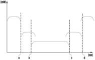
- FIG. 6is a graph showing the power of a laser by wavelength band output from a semiconductor optical amplifier (311) including at least five optical amplifier chips according to one embodiment of the present disclosure.
- the x-axismay represent the wavelength
- the y-axismay represent the intensity of the light source (unit: mW).
- Fig. 6may represent the intensity of the light source according to the wavelength of the present invention.
- the semiconductor optical amplifier (311)can output a laser at at least one designated wavelength band and at at least one designated power.
- each of the plurality of optical amplifier chipscan output a laser at a specified wavelength band and a specified power.
- the semiconductor optical amplifier (311)may include at least five optical amplifier chips.
- the semiconductor optical amplifier (311)can divide the entire band into the number of optical amplifier chips and output the laser with different power for each divided band.
- the semiconductor optical amplifier (311)can output a laser with a wavelength band of about 2000 nm to about 2400 nm.
- a semiconductor optical amplifier (311) including five optical amplifier chipscan divide the wavelength band of about 2000 nm to about 2400 nm into five.
- the semiconductor optical amplifier (311)can output a laser with power having a level lower than a specified level in a wavelength band in which power attenuation due to light absorption by water is less than a specified attenuation value, and can output a laser with power having a level higher than a specified level in a wavelength band in which power attenuation due to light absorption by water is greater than a specified attenuation value.
- the semiconductor optical amplifier (311)can output lasers of multiple designated wavelength bands simultaneously or in a time-division manner.
- a plurality of optical amplifier chips included in the semiconductor optical amplifier (311)can simultaneously or time-divisionally output lasers of a plurality of designated wavelength bands.
- the first optical amplifier chipcan output a laser at a first designated wavelength band (about 2040 nm to about a nm) (e.g., about 2040 nm to about 2090 nm) and a first designated power (e.g., about 5 mW).
- the second optical amplifier chipcan output a laser at a second designated wavelength band (about 'a' nm to about 'b' nm) (e.g., about 2090 nm to about 2130 nm) and a second designated power (e.g., about 3 to about 5 mW).
- the third optical amplifier chipcan output a laser at a third designated wavelength band (about 'b' nm to about 'c' nm) (e.g., about 2130 nm to about 2280 nm) and a third designated power (e.g., about 1 to about 3 mW).
- the fourth laser gain chipcan output a laser with a fourth designated wavelength band (about 'c' nm to about 'd' nm) (e.g., about 2280 nm to about 2330 nm) and a fourth designated power (e.g., about 3 to about 5 mW).
- the fifth optical amplifier chipcan output a laser with a fifth designated wavelength band (about 'd' nm to about 2380 nm) (e.g., about 2330 nm to about 2380 nm) and a fifth designated power (e.g., about 5 mW).
- a fifth designated wavelength bandabout 'd' nm to about 2380 nm
- a fifth designated powere.g., about 5 mW
- the semiconductor optical amplifier (311)can control one of the plurality of optical amplifier chips to output a laser at a first designated wavelength band (about 2040 nm to about 'a' nm) (e.g., about 2040 nm to about 2090 nm) and a first designated power (e.g., about 5 mW).
- the semiconductor optical amplifier (311)can control one of the plurality of optical amplifier chips to output a laser at a second designated wavelength band (about 'a' nm to about 'b' nm) (e.g., about 2090 nm to about 2130 nm) and a second designated power (e.g., about 3 to about 5 mW).
- the semiconductor optical amplifier (311)can control one of the plurality of optical amplifier chips to output a laser with a third designated wavelength band (about 'b' nm to about 'c' nm) (e.g., about 2130 nm to about 2280 nm) and a third designated power (e.g., about 1 to about 3 mW).
- the semiconductor optical amplifier (311)can control one of the plurality of optical amplifier chips to output a laser with a fourth designated wavelength band (about 'c' nm to about 'd' nm) (e.g., about 2280 nm to about 2330 nm) and a fourth designated power (e.g., about 3 to about 5 mW).
- the semiconductor optical amplifier (311)can control one of the plurality of optical amplifier chips to output a laser at a fifth designated wavelength band (about 'd' nm to about 2380 nm) (e.g., about 2330 nm to about 2380 nm) and a fifth designated power (e.g., about 5 mW).
- a fifth designated wavelength bandabout 'd' nm to about 2380 nm
- a fifth designated powere.g., about 5 mW
- the semiconductor optical amplifier (311)can output a laser with a first designated wavelength band (about 2040 nm to about 'a' nm) (e.g., about 2040 nm to about 2090 nm) and a first designated power (e.g., about 5 mW).
- the semiconductor optical amplifier (311)can output a laser with a second designated wavelength band (about 'a' nm to about 'b' 'nm) (e.g., about 2090 nm to about 2130 nm) and a second designated power (e.g., about 3 to about 5 mW).
- the semiconductor optical amplifier (311)can output a laser with a third designated wavelength band (about 'b' nm to about 'c' nm) (e.g., about 2130 nm to about 2280 nm) and a third designated power (e.g., about 1 to about 3 mW).
- the semiconductor optical amplifier (311)can output a laser with a fourth designated wavelength band (about 'c' nm to about 'd' nm) (e.g., about 2280 nm to about 2330 nm) and a fourth designated power (e.g., about 3 to about 5 mW).
- the semiconductor optical amplifier (311)can output a laser with a fifth designated wavelength band (about 'd' nm to about 2380 nm) (e.g., about 2330 nm to about 2380 nm) and a fifth designated power (e.g., about 5 mW).
- a fifth designated wavelength bandabout 'd' nm to about 2380 nm
- a fifth designated powere.g., about 5 mW
- the semiconductor optical amplifier (311)may, under the control of the processor (320), control one of the plurality of optical amplifier chips to output a laser with a first designated wavelength band (about 2040 nm to about 'a' nm) (e.g., about 2040 nm to about 2090 nm) and a first designated power (e.g., about 5 mW).
- a first designated wavelength bandabout 2040 nm to about 'a' nm
- a first designated powere.g., about 5 mW
- the semiconductor optical amplifier (311)may, under the control of the processor (320), control one of the plurality of optical amplifier chips to output a laser with a second designated wavelength band (about 'a' nm to about 'b' nm) (e.g., about 2090 nm to about 2130 nm) and a second designated power (e.g., about 3 to about 5 mW).
- a second designated wavelength bandabout 'a' nm to about 'b' nm
- a second designated powere.g., about 3 to about 5 mW
- the semiconductor optical amplifier (311)can, under the control of the processor (320), control one of the plurality of optical amplifier chips to output a laser with a third designated wavelength band (about 'b' nm to about 'c' nm) (e.g., about 2130 nm to about 2280 nm) and a third designated power (e.g., about 1 to about 3 mW).
- a third designated wavelength bandabout 'b' nm to about 'c' nm
- a third designated powere.g., about 1 to about 3 mW
- the semiconductor optical amplifier (311)can, under the control of the processor (320), control one of the plurality of optical amplifier chips to output a laser with a fourth designated wavelength band (about 'c' nm to about 'd' nm) (e.g., about 2280 nm to about 2330 nm) and a fourth designated power (e.g., about 3 to about 5 mW).
- the semiconductor optical amplifier (311)can be controlled to output a laser at a fifth designated wavelength band (about 'd' nm to about 2380 nm) (e.g., about 2330 nm to about 2380 nm) and a fifth designated power (e.g., about 5 mW) by controlling one of the plurality of optical amplifier chips.
- FIG. 7is a graph showing the power of a laser by wavelength band output from a semiconductor optical amplifier (311) including at least four optical amplifier chips according to one embodiment of the present disclosure.
- the x-axismay represent wavelength
- the y-axismay represent the intensity of the light source (unit: mW).
- Fig. 7may represent the intensity of the light source according to the wavelength of the present invention.
- the semiconductor optical amplifier (311)can divide the entire band into the number of optical amplifier chips and output the laser with different power for each divided band.
- the semiconductor optical amplifier (311)can output a laser with a wavelength band of about 2000 nm to about 2400 nm.
- the semiconductor optical amplifier (311) including four optical amplifier chipscan divide the wavelength band of about 2000 nm to about 2400 nm into four.
- the semiconductor optical amplifier (311)can output a laser with power having a level lower than a specified level in a wavelength band in which power attenuation due to light absorption by water is less than a specified attenuation value, and can output a laser with power having a level higher than a specified level in a wavelength band in which power attenuation due to light absorption by water is greater than a specified attenuation value.
- the semiconductor optical amplifier (311)can output a laser at at least one designated wavelength band and at at least one designated power.
- each of the plurality of optical amplifier chipscan output a laser at a specified wavelength band and a specified power.
- the semiconductor optical amplifier (311)may include at least four optical amplifier chips.
- the semiconductor optical amplifier (311)can output lasers of multiple designated wavelength bands simultaneously or in a time-division manner.
- a plurality of optical amplifier chips included in the semiconductor optical amplifier (311)can simultaneously or time-divisionally output lasers of a plurality of designated wavelength bands.
- the sixth optical amplifier chipcan output a laser at a sixth designated wavelength band (about 2040 nm to about 'e' nm) (e.g., about 2040 nm to about 2090 nm) and a sixth designated power (e.g., about 5 mW).
- the seventh optical amplifier chipcan output a laser at a seventh designated wavelength band (about 'e' nm to about 'f' nm) (e.g., about 2090 nm to about 2210 nm) and a seventh designated power (e.g., about 1 to about 3 mW).
- the eighth optical amplifier chipcan output a laser at an eighth designated wavelength band (about 'f' nm to about 'g' nm) (e.g., about 2210 nm to about 2330 nm) and an eighth designated power (e.g., about 1 to about 3 mW).
- the ninth optical amplifier chipcan output a laser at a ninth specified wavelength band (about 'g' nm to about 2380 nm) (e.g., about 2330 nm to about 2380 nm) and a ninth specified power (e.g., about 5 mW).
- the semiconductor optical amplifier (311)can control one of the plurality of optical amplifier chips to output a laser at a sixth designated wavelength band (about 2040 nm to about 'e' nm) (e.g., about 2040 nm to about 2090 nm) and a sixth designated power (e.g., about 5 mW).
- the semiconductor optical amplifier (311)can control one of the plurality of optical amplifier chips to output a laser at a seventh designated wavelength band (about 'e' nm to about 'f' nm) (e.g., about 2090 nm to about 2210 nm) and a seventh designated power (e.g., about 1 to about 3 mW).
- the semiconductor optical amplifier (311)can control one of the plurality of optical amplifier chips to output a laser with an eighth designated wavelength band (about 'f' nm to about 'g' nm) (e.g., about 2210 nm to about 2330 nm) and an eighth designated power (e.g., about 1 to about 3 mW).
- the semiconductor optical amplifier (311)can control one of the plurality of optical amplifier chips to output a laser with a ninth designated wavelength band (about 'g' nm to about 2030 nm) (e.g., about 2330 nm to about 2380 nm) and a ninth designated power (e.g., about 5 mW).
- the semiconductor optical amplifier (311)can output a laser with a sixth designated wavelength band (about 2040 nm to about 'e' nm) (e.g., about 2040 nm to about 2090 nm) and a sixth designated power (e.g., about 5 mW).
- the semiconductor optical amplifier (311)can output a laser with a seventh designated wavelength band (about 'e' nm to about 'f' nm) (e.g., about 2090 nm to about 2210 nm) and a seventh designated power (e.g., about 1 to about 3 mW).
- the semiconductor optical amplifier (311)can output a laser with an eighth designated wavelength band (about 'f' nm to about 'g' nm) (e.g., about 2210 nm to about 2330 nm) and an eighth designated power (e.g., about 1 to about 3 mW).
- the semiconductor optical amplifier (311)can output a laser with a ninth designated wavelength band (about 'g' nm to about 2030 nm) (e.g., about 2330 nm to about 2380 nm) and a ninth designated power (e.g., about 5 mW).
- the semiconductor optical amplifier (311)can, under the control of the processor (320), control one of the plurality of optical amplifier chips to output a laser at a sixth designated wavelength band (about 2040 nm to about 'e' nm) (e.g., about 2040 nm to about 2090 nm) and a sixth designated power (e.g., about 5 mW).
- a sixth designated wavelength bandabout 2040 nm to about 'e' nm
- a sixth designated powere.g., about 5 mW
- the semiconductor optical amplifier (311)can, under the control of the processor (320), control one of the plurality of optical amplifier chips to output a laser at a seventh designated wavelength band (about 'e' nm to about 'f' nm) (e.g., about 2090 nm to about 2210 nm) and a seventh designated power (e.g., about 1 to about 3 mW).
- a seventh designated wavelength bandabout 'e' nm to about 'f' nm
- a seventh designated powere.g., about 1 to about 3 mW
- the semiconductor optical amplifier (311)can, under the control of the processor (320), control one of the plurality of optical amplifier chips to output a laser with an eighth designated wavelength band (about 'f' nm to about 'g' nm) (e.g., about 2210 nm to about 2330 nm) and an eighth designated power (e.g., about 1 to about 3 mW).
- the semiconductor optical amplifier (311)can control one of the plurality of optical amplifier chips to output a laser with a ninth designated wavelength band (about 'g' nm to about 2030 nm) (e.g., about 2330 nm to about 2380 nm) and a ninth designated power (e.g., about 5 mW).
- FIG. 8is a graph showing the power of a laser by wavelength band output from a semiconductor optical amplifier (311) including at least three optical amplifier chips according to one embodiment of the present disclosure.
- the x-axismay represent the wavelength
- the y-axismay represent the intensity of the light source (unit: mW).
- Fig. 8may represent the intensity of the light source according to the wavelength of the present invention.
- the semiconductor optical amplifier (311)can divide the entire band into the number of optical amplifier chips and output the laser with different power for each divided band.
- the semiconductor optical amplifier (311)can output a laser with a wavelength band of about 2000 nm to about 2400 nm.
- the semiconductor optical amplifier (311) including three optical amplifier chipscan divide the wavelength band of about 2000 nm to about 2400 nm into three.
- the semiconductor optical amplifier (311)can output a laser with power having a level lower than a specified level in a wavelength band in which power attenuation due to light absorption by water is less than a specified attenuation value, and can output a laser with power having a level higher than a specified level in a wavelength band in which power attenuation due to light absorption by water is greater than a specified attenuation value.
- the semiconductor optical amplifier (311)can output a laser at at least one designated wavelength band and at at least one designated power.
- each of the plurality of optical amplifier chipscan output a laser at a specified wavelength band and a specified power.
- the semiconductor optical amplifier (311)may include at least three optical amplifier chips.
- the semiconductor optical amplifier (311)can output lasers of multiple designated wavelength bands simultaneously or in a time-division manner.
- a plurality of optical amplifier chips included in the semiconductor optical amplifier (311)can simultaneously or time-divisionally output lasers of a plurality of designated wavelength bands.
- the tenth optical amplifier chipcan output a laser at a tenth designated wavelength band (about 2040 nm to about 'h' nm) (e.g., about 2040 nm to about 2090 nm) and a tenth designated power (e.g., about 5 mW).
- the eleventh optical amplifier chipcan output a laser at a eleventh designated wavelength band (about 'h' nm to about i nm) (e.g., about 2090 nm to about 2330 nm) and an eleventh designated power (e.g., about 1 to about 3 mW).
- the twelfth optical amplifier chipcan output a laser at a twelfth designated wavelength band (about ''' nm to about 2380 nm) (e.g., about 2330 nm to about 2380 nm) and a twelfth designated power (e.g., about 5 mW).
- a twelfth designated wavelength bandabout ''' nm to about 2380 nm
- a twelfth designated powere.g., about 5 mW
- the semiconductor optical amplifier (311)can control one of the plurality of optical amplifier chips to output a laser at a tenth designated wavelength band (about 2040 nm to about 'h' nm) (e.g., about 2040 nm to about 2090 nm) and a tenth designated power (e.g., about 5 mW).
- the semiconductor optical amplifier (311)can control one of the plurality of optical amplifier chips to output a laser at an eleventh designated wavelength band (about 'h' nm to about 'i' nm) (e.g., about 2090 nm to about 2330 nm) and an eleventh designated power (e.g., about 1 to about 3 mW).
- the semiconductor optical amplifier (311)controls one of the plurality of optical amplifier chips so that the 12th optical amplifier chip can output a laser with a 12th designated wavelength band (about 'i' nm to about 2380 nm) (e.g., about 2330 nm to about 2380 nm) and a 12th designated power (e.g., about 5 mW).
- a 12th designated wavelength bandabout 'i' nm to about 2380 nm
- a 12th designated powere.g., about 5 mW
- the semiconductor optical amplifier (311)can output a laser with a tenth designated wavelength band (about 2040 nm to about 'h' nm) (e.g., about 2040 nm to about 2090 nm) and a tenth designated power (e.g., about 5 mW).
- the semiconductor optical amplifier (311)can output a laser with an eleventh designated wavelength band (about 'h' nm to about 'i' nm) (e.g., about 2090 nm to about 2330 nm) and an eleventh designated power (e.g., about 1 to about 3 mW).
- the semiconductor optical amplifier (311)can output a laser with a twelfth optical amplifier chip with a twelfth designated wavelength band (about 'i' nm to about 2380 nm) (e.g., about 2330 nm to about 2380 nm) and a twelfth designated power (e.g., about 5 mW).
- a twelfth designated wavelength bandabout 'i' nm to about 2380 nm
- a twelfth designated powere.g., about 5 mW
- the semiconductor optical amplifier (311)may, under the control of the processor (320), control one of the plurality of optical amplifier chips to output a laser at a tenth designated wavelength band (about 2040 nm to about 'h' nm) (e.g., about 2040 nm to about 2090 nm) and a tenth designated power (e.g., about 5 mW).
- a tenth designated wavelength bandabout 2040 nm to about 'h' nm
- a tenth designated powere.g., about 5 mW
- the semiconductor optical amplifier (311)may, under the control of the processor (320), control one of the plurality of optical amplifier chips to output a laser at an eleventh designated wavelength band (about 'h' nm to about 'i' nm) (e.g., about 2090 nm to about 2330 nm) and an eleventh designated power (e.g., about 1 to about 3 mW).
- the semiconductor optical amplifier (311)can be controlled so that the 12th optical amplifier chip outputs a laser with a 12th designated wavelength band (about 'i' nm to about 2380 nm) (e.g., about 2330 nm to about 2380 nm) and a 12th designated power (e.g., about 5 mW).
- FIG. 9is a flowchart illustrating a laser output method of an electronic device (201) according to one embodiment of the present disclosure.
- the electronic device (201)may, in operation 901, output laser light using two or more optical amplifier chips (e.g., 3111, 3112, 3113) each having a different wavelength band and output intensity.
- two or more optical amplifier chipse.g., 3111, 3112, 3113
- the electronic device (201)can, in operation 903, modulate the output laser light to pass through the fixed array DBR grating (312) to have a designated wavelength.
- the designated wavelengthcan have a shorter wavelength than the wavelength of the laser light output from the semiconductor optical amplifier (311).
- the electronic device (201)may, in operation 905, cause modulated laser light to be irradiated onto the skin via the output coupler (315).
- the electronic device (201)may include a semiconductor optical amplifier (311) that divides an outputtable wavelength band and outputs a plurality of laser lights having a designated wavelength band and a designated power; a fixed array distributed Bragg reflector grating (312) that changes wavelengths of the plurality of laser lights and outputs a plurality of laser lights having changed wavelengths; a modulator (313) that modulates the plurality of laser lights having changed wavelengths; a monitoring circuit (314) that determines whether the modulated plurality of laser lights are output according to the designated power and designated wavelength; and an output coupler (315) that adjusts an output direction and/or angle of the modulated plurality of laser lights and outputs the modulated plurality of laser lights to the outside of the electronic device (201).
- a semiconductor optical amplifier3111 that divides an outputtable wavelength band and outputs a plurality of laser lights having a designated wavelength band and a designated power
- a fixed array distributed Bragg reflector grating(312) that changes wavelengths of the plurality of laser lights and outputs
- the semiconductor optical amplifier (311)includes a plurality of optical amplifier chips and can time-divisionally output or generate a plurality of laser lights having a wide bandwidth.
- the semiconductor optical amplifier (311)may include a first optical amplifier chip that outputs a laser with a first designated wavelength band and a first designated power; a second optical amplifier chip that outputs a laser with a second designated wavelength band and a second designated power; a third optical amplifier chip that outputs a laser with a third designated wavelength band and a third designated power; and a fourth optical amplifier chip that outputs a laser with a fourth designated wavelength band and a fourth designated power.
- the semiconductor optical amplifier (311)may further include a fifth optical amplifier chip that outputs a laser at a fifth designated wavelength band and a fifth designated power.
- the semiconductor optical amplifier (311)can output a laser at a specified power, where a wavelength band in which power attenuation due to light absorption by water is less than a specified attenuation value has a level lower than a specified level.
- the semiconductor optical amplifier (311)can output a laser at a specified power, where a wavelength band in which power attenuation due to light absorption by water is greater than a specified attenuation value has a level higher than a specified level.
- the semiconductor optical amplifier (311)can output a wavelength band that can be output by dividing it by the number of optical amplifier chips included in the semiconductor optical amplifier (311).
- the modulator (313)may include a lock-in amplifier and/or a low pass filter.
- the monitoring circuit (314)may include an edge illuminated photodiode, a Mach-Zehnder interferometer (MZI) sensor, a ring resonator, a line coupling, and/or a splitter.
- MZIMach-Zehnder interferometer
- a monitoring circuitmay be connected between the output coupler (315) and the modulator (313).
- the electronic device (201)further includes a receiving circuit including a plurality of photodetectors, each of the plurality of photodetectors being spaced a first designated distance from the output coupler (315).
- the electronic device (201)may further include a processor.
- the processormay control the intensity and wavelength of light output from the semiconductor optical amplifier (311) based on information received from the monitoring circuit (314).
- the electronic device (201)may include a transmitter circuit; a receiver circuit; and a processor, wherein the transmitter circuit may include a semiconductor optical amplifier (311) that divides an outputtable wavelength band and outputs a plurality of laser lights having a designated wavelength band and a designated power; a fixed array distributed Bragg reflector grating (312) that changes wavelengths of the plurality of laser lights and outputs a plurality of laser lights having changed wavelengths; a modulator (313) that modulates the plurality of laser lights having changed wavelengths; a monitoring circuit (314) that determines whether the modulated plurality of laser lights are output according to the designated power and the designated wavelength; and an output coupler (315) that adjusts an output direction and/or angle of the modulated plurality of laser lights and outputs the modulated plurality of laser lights to the outside of the electronic device (201).
- the transmitter circuitmay include a semiconductor optical amplifier (311) that divides an outputtable wavelength band and outputs a plurality of laser lights having a designated wavelength band and a designated power; a
- the semiconductor optical amplifier (311)includes a plurality of optical amplifier chips and can time-divisionally output or generate a plurality of laser lights having a wide bandwidth.
- the semiconductor optical amplifier (311)can output a laser at a specified power, where a wavelength band in which power attenuation due to light absorption by water is less than a specified attenuation value has a level lower than a specified level.
- the semiconductor optical amplifier (311)can output a laser at a specified power, where a wavelength band in which power attenuation due to light absorption by water is greater than a specified attenuation value has a level higher than a specified level.
- the semiconductor optical amplifier (311)can output a wavelength band that can be output by dividing it by the number of optical amplifier chips included in the semiconductor optical amplifier (311).
- the electronic device (201)may include a case having a transmitter circuit and a receiver circuit disposed on the rear side; a display disposed on the front side of the case; and a band connected to the case to allow the electronic device (201) to be worn on a user's wrist.
- the rear of the casemay have at least a portion that contacts the user when the electronic device (201) is worn on the user via the band.
- the rear of the casemay expose at least a portion of the output coupler (315) and at least a portion of the receiver circuitry.
- the electronic devices according to various embodiments disclosed in this documentmay be devices of various forms.
- the electronic devicesmay include, for example, portable communication devices (e.g., smartphones), computer devices, portable multimedia devices, portable medical devices, cameras, wearable devices, or home appliance devices.
- portable communication devicese.g., smartphones
- computer devicesportable multimedia devices
- portable medical devicese.g., cameras
- wearable devicese.g., smart watch devices
- home appliance devicese.g., smartphones
- the electronic devices according to embodiments of this documentare not limited to the above-described devices.
- first, second, or first or secondmay be used merely to distinguish one component from another, and do not limit the components in any other respect (e.g., importance or order).
- a componente.g., a first
- another componente.g., a second
- functionallye.g., a third component
- moduleused in various embodiments of this document may include a unit implemented in hardware, software or firmware, and may be used interchangeably with terms such as logic, logic block, component, or circuit, for example.
- a modulemay be an integrally configured component or a minimum unit of the component or a part thereof that performs one or more functions.
- a modulemay be implemented in the form of an application-specific integrated circuit (ASIC).
- ASICapplication-specific integrated circuit
- Various embodiments of the present documentmay be implemented as software (e.g., a program (140)) including one or more instructions stored in a storage medium (e.g., an internal memory (136) or an external memory (138)) readable by a machine (e.g., an electronic device (101)).
- a processore.g., a processor (120)
- the machinee.g., an electronic device (101)
- the one or more instructionsmay include code generated by a compiler or code executable by an interpreter.
- the machine-readable storage mediummay be provided in the form of a non-transitory storage medium.
- 'non-transitory'simply means that the storage medium is a tangible device and does not contain signals (e.g. electromagnetic waves), and the term does not distinguish between cases where data is stored semi-permanently or temporarily on the storage medium.
- the method according to various embodiments disclosed in the present documentmay be provided as included in a computer program product.
- the computer program productmay be traded between a seller and a buyer as a commodity.
- the computer program productmay be distributed in the form of a machine-readable storage medium (e.g., a compact disc read only memory (CD-ROM)), or may be distributed online (e.g., downloaded or uploaded) via an application store (e.g., Play Store TM ) or directly between two user devices (e.g., smart phones).
- an application storee.g., Play Store TM
- at least a part of the computer program productmay be at least temporarily stored or temporarily generated in a machine-readable storage medium, such as a memory of a manufacturer's server, a server of an application store, or an intermediary server.
- each componente.g., a module or a program of the above-described components may include a single or multiple entities, and some of the multiple entities may be separately arranged in other components.
- one or more of the components or operations of the above-described componentsmay be omitted, or one or more other components or operations may be added.
- the multiple componentse.g., a module or a program
- the integrated componentmay perform one or more functions of each of the multiple components identically or similarly to those performed by the corresponding component of the multiple components before the integration.
- the operations performed by the module, program, or other componentmay be executed sequentially, in parallel, repeatedly, or heuristically, or one or more of the operations may be executed in a different order, omitted, or one or more other operations may be added.
Landscapes
- Physics & Mathematics (AREA)
- Health & Medical Sciences (AREA)
- Life Sciences & Earth Sciences (AREA)
- Spectroscopy & Molecular Physics (AREA)
- General Health & Medical Sciences (AREA)
- Pathology (AREA)
- General Physics & Mathematics (AREA)
- Heart & Thoracic Surgery (AREA)
- Molecular Biology (AREA)
- Veterinary Medicine (AREA)
- Public Health (AREA)
- Animal Behavior & Ethology (AREA)
- Biophysics (AREA)
- Engineering & Computer Science (AREA)
- Biomedical Technology (AREA)
- Surgery (AREA)
- Medical Informatics (AREA)
- Biochemistry (AREA)
- Chemical & Material Sciences (AREA)
- Optics & Photonics (AREA)
- Analytical Chemistry (AREA)
- Immunology (AREA)
- Measurement Of The Respiration, Hearing Ability, Form, And Blood Characteristics Of Living Organisms (AREA)
Abstract
Description
Translated fromKorean본 개시는 전자 장치 및 웨어러블 디바이스에 관한 것이다.The present disclosure relates to electronic devices and wearable devices.
최근 사용자의 생체 정보 및/또는 운동 데이터(fitness data)를 측정할 수 있는 센서를 포함하는 전자 장치들이 개발되고 있다.Recently, electronic devices that include sensors capable of measuring a user's biometric information and/or fitness data have been developed.
이러한 전자 장치는 일반적으로 주머니나 손에 휴대하여 이동하면서 사용할 수도 있지만, 신체의 일부 또는 각종 구조물에 착용할 수 있는 형태를 가질 수도 있다. 전자 장치는 사용자의 신체에 착용 가능한 점을 이용하여 건강 및 운동 정보를 서비스할 수 있다.These electronic devices can generally be carried in a pocket or hand and used while moving, but they can also be worn on parts of the body or various structures. The electronic devices can provide health and exercise information by utilizing the wearable point on the user's body.
상술한 정보는 본 개시에 대한 이해를 돕기 위한 목적으로 하는 배경 기술(related art)로 제공될 수 있다. 상술한 내용 중 어느 것도 본 개시와 관련된 종래 기술(prior art)로서 적용될 수 있는지에 대하여 어떠한 주장이나 결정이 제기되지 않는다.The above information may be provided as related art for the purpose of assisting in understanding the present disclosure. No claim or determination is made as to whether any of the above is applicable as prior art related to the present disclosure.
사용자의 생체 정보 중에서 혈당 정보를 감지하기 위해서, 전자 장치는 광학 센서(예: 레이저)에 기반하는 비침습적(noninvasive)으로 혈당을 감지할 수 있는 센서를 포함할 수 있다. 전자 장치는 광학 센서의 광원에서 빛을 출력할 수 있다. 전자 장치는 물체를 투과 및/또는 반사한 빛의 스펙트럼을 획득함으로써, 물체를 분석할 수 있다. 각기 다른 파장을 커버하는 복수의 광원들을 이용하여, 광학 센서가 목표로 하는 파장 대역을 구성할 수 있다.In order to detect blood sugar information among the user's biometric information, the electronic device may include a sensor capable of noninvasively detecting blood sugar based on an optical sensor (e.g., a laser). The electronic device may output light from a light source of the optical sensor. The electronic device may analyze the object by obtaining a spectrum of light transmitted and/or reflected by the object. A wavelength band targeted by the optical sensor may be configured by using a plurality of light sources covering different wavelengths.
이때, 각각의 광원이 넓은 대역의 파장을 커버하면, 출력되는 빛의 세기가 정해진 기준보다 작아질 수 있다. 또는 각각의 광원에서 출력되는 빛의 세기(power)를 정해진 기준보다 크게 하면, 각각의 광원이 커버할 수 있는 파장의 범위가 줄어드는 문제가 있다.At this time, if each light source covers a wide band of wavelengths, the intensity of the light output may be lower than the set standard. Or, if the intensity (power) of the light output from each light source is greater than the set standard, there is a problem that the range of wavelengths that each light source can cover is reduced.
본 개시의 복수의 광원들을 포함하는 광학 센서를 포함하는 전자 장치는 정해진 대역 구간 마다 광원의 파워를 제어하는데 목적이 있다.An electronic device including an optical sensor including a plurality of light sources of the present disclosure is intended to control the power of the light sources for each defined bandwidth section.
본 개시의 전자 장치는 출력 가능한 파장 대역을 분할하여, 지정된 파장 대역 및 지정된 파워를 가지는 복수의 레이저 광들을 출력하는 반도체 광학 증폭기; 상기 복수의 레이저 광들의 파장을 변경하여, 변경된 파장을 가지는 복수의 레이저 광들을 출력하는 고정 어레이 DBR 격자(fixed array distributed Bragg reflector grating); 및 상기 변조된 복수의 레이저 광들이 출력 방향 및/또는 각도를 조정하여 상기 변조된 복수의 레이저 광들을 상기 전자 장치의 외부로 출력하는 출력 커플러를 포함할 수 있다.The electronic device of the present disclosure may include a semiconductor optical amplifier that divides an outputtable wavelength band and outputs a plurality of laser lights having a designated wavelength band and a designated power; a fixed array distributed Bragg reflector grating that changes wavelengths of the plurality of laser lights and outputs a plurality of laser lights having changed wavelengths; and an output coupler that adjusts an output direction and/or angle of the modulated plurality of laser lights and outputs the modulated plurality of laser lights to the outside of the electronic device.
본 개시의 웨어러블 디바이스는 송신 회로; 수신 회로; 및 프로세서를 포함하며, 상기 송신 회로는 출력 가능한 파장 대역을 분할하여, 지정된 파장 대역 및 지정된 파워를 가지는 복수의 레이저 광들을 출력하는 반도체 광학 증폭기; 상기 복수의 레이저 광들의 파장을 변경하여, 변경된 파장을 가지는 복수의 레이저 광들을 출력하는 고정 어레이 DBR 격자(fixed array distributed Bragg reflector grating); 및 상기 변조된 복수의 레이저 광들이 출력 방향 및/또는 각도를 조정하여 상기 변조된 복수의 레이저 광들을 상기 전자 장치의 외부로 출력하는 출력 커플러를 포함할 수 있다.A wearable device of the present disclosure includes a transmitter circuit; a receiver circuit; and a processor, wherein the transmitter circuit may include a semiconductor optical amplifier that divides an outputtable wavelength band and outputs a plurality of laser lights having a designated wavelength band and a designated power; a fixed array distributed Bragg reflector grating that changes wavelengths of the plurality of laser lights and outputs a plurality of laser lights having changed wavelengths; and an output coupler that adjusts an output direction and/or angle of the modulated plurality of laser lights and outputs the modulated plurality of laser lights to the outside of the electronic device.
본 개시의 전자 장치 및 웨어러블 디바이스는 정해진 대역 구간 마다 광원의 파워를 제어하여 빛을 출력함으로써, 빛을 이용한 물체를 측정할 때 정확도를 향상할 수 있다.The electronic device and wearable device of the present disclosure can improve accuracy when measuring an object using light by controlling the power of a light source for each predetermined bandwidth section to output light.
본 개시의 전자 장치 및 웨어러블 디바이스는 정해진 대역 구간 마다 광원의 파워를 제어하여 빛을 출력함으로써, 빛을 이용한 물체를 측정할 때 신호 대 잡음비를 개선할 수 있다.The electronic device and wearable device of the present disclosure can improve the signal-to-noise ratio when measuring an object using light by controlling the power of a light source for each predetermined bandwidth section to output light.
도면의 설명과 관련하여, 동일 또는 유사한 구성 요소에 대해서는 동일 또는 유사한 참조 부호가 사용될 수 있다.In connection with the description of the drawings, the same or similar reference numerals may be used for identical or similar components.
도 1은 본 개시의 다양한 실시예에 따른 네트워크 환경 내의 전자 장치의 블록도이다.FIG. 1 is a block diagram of an electronic device within a network environment according to various embodiments of the present disclosure.
도 2a는 본 개시의 일 실시예에 따른 전자 장치를 나타내는 도면이다.FIG. 2A is a diagram illustrating an electronic device according to one embodiment of the present disclosure.
도 2b는 본 개시의 일 실시예 따른 전자 장치의 제 2 면 또는 후면에 배치되는 광 출력 구조 및 광 수신 구조를 나타내는 도면이다.FIG. 2b is a drawing showing a light output structure and a light receiving structure arranged on a second side or rear surface of an electronic device according to one embodiment of the present disclosure.
도 3은 본 개시의 일 실시예에 따른 전자 장치의 센서 회로를 나타내는 블록도이다.FIG. 3 is a block diagram illustrating a sensor circuit of an electronic device according to one embodiment of the present disclosure.
도 4는 실리콘 기반 집적 회로에 구현된 송신 회로를 나타내는 도면이다.Figure 4 is a diagram showing a transmitter circuit implemented in a silicon-based integrated circuit.
도 5는 반도체 광학 증폭기(311)에 포함된 복수의 광학 증폭기 칩들 각각이 같은 레벨의 파워로 출력되는 레이저를 물(water)에 조사(照射)한 후, 파장에 따른 빛의 밀도를 나타내는 그래프이다.Figure 5 is a graph showing the density of light according to wavelength after each of a plurality of optical amplifier chips included in a semiconductor optical amplifier (311) irradiates water with a laser output at the same level of power.
도 6은 본 개시의 일 실시예에 따른 적어도 5개 이상의 광학 증폭기 칩들을 포함하는 반도체 광학 증폭기(311)에서 출력되는 파장 대역 별 레이저의 파워를 나타내는 그래프이다.FIG. 6 is a graph showing the power of a laser by wavelength band output from a semiconductor optical amplifier (311) including at least five optical amplifier chips according to one embodiment of the present disclosure.
도 7은 본 개시의 일 실시예에 따른 적어도 4개 이상의 광학 증폭기 칩들을 포함하는 반도체 광학 증폭기에서 출력되는 파장 대역 별 레이저의 파워를 나타내는 그래프이다.FIG. 7 is a graph showing the power of a laser according to a wavelength band output from a semiconductor optical amplifier including at least four optical amplifier chips according to one embodiment of the present disclosure.
도 8은 본 개시의 일 실시예에 따른 적어도 3개 이상의 광학 증폭기 칩들을 포함하는 반도체 광학 증폭기에서 출력되는 파장 대역 별 레이저의 파워를 나타내는 그래프이다.FIG. 8 is a graph showing the power of a laser according to a wavelength band output from a semiconductor optical amplifier including at least three optical amplifier chips according to one embodiment of the present disclosure.
도 9는 본 개시의 일 실시예에 따른 전자 장치의 레이저 출력 방법을 나타내는 흐름도이다.FIG. 9 is a flowchart illustrating a laser output method of an electronic device according to one embodiment of the present disclosure.
이하에서는 도면을 참조하여 본 개시의 실시예에 대하여 본 개시가 속하는 기술 분야에서 통상의 지식을 가진 자가 용이하게 실시할 수 있도록 상세히 설명한다. 그러나 본 개시는 여러 가지 상이한 형태로 구현될 수 있으며 여기에서 설명하는 실시예에 한정되지 않는다. 도면의 설명과 관련하여, 동일하거나 유사한 구성요소에 대해서는 동일하거나 유사한 참조 부호가 사용될 수 있다. 또한, 도면 및 관련된 설명에서는, 잘 알려진 기능 및 구성에 대한 설명이 명확성과 간결성을 위해 생략될 수 있다.Hereinafter, embodiments of the present disclosure will be described in detail with reference to the drawings so that those skilled in the art can easily implement the present disclosure. However, the present disclosure may be implemented in various different forms and is not limited to the embodiments described herein. In connection with the description of the drawings, the same or similar reference numerals may be used for the same or similar components. In addition, in the drawings and related descriptions, descriptions of well-known functions and configurations may be omitted for clarity and conciseness.
도 1은, 다양한 실시예들에 따른, 네트워크 환경(100) 내의 전자 장치(101)의 블록도이다.FIG. 1 is a block diagram of an electronic device (101) within a network environment (100) according to various embodiments.
도 1을 참조하면, 네트워크 환경(100)에서 전자 장치(101)는 제 1 네트워크(198)(예: 근거리 무선 통신 네트워크)를 통하여 전자 장치(102)와 통신하거나, 또는 제 2 네트워크(199)(예: 원거리 무선 통신 네트워크)를 통하여 전자 장치(104) 또는 서버(108) 중 적어도 하나와 통신할 수 있다. 일실시예에 따르면, 전자 장치(101)는 서버(108)를 통하여 전자 장치(104)와 통신할 수 있다. 일실시예에 따르면, 전자 장치(101)는 프로세서(120), 메모리(130), 입력 모듈(150), 음향 출력 모듈(155), 디스플레이 모듈(160), 오디오 모듈(170), 센서 모듈(176), 인터페이스(177), 연결 단자(178), 햅틱 모듈(179), 카메라 모듈(180), 전력 관리 모듈(188), 배터리(189), 통신 모듈(190), 가입자 식별 모듈(196), 또는 안테나 모듈(197)을 포함할 수 있다. 어떤 실시예에서는, 전자 장치(101)에는, 이 구성요소들 중 적어도 하나(예: 연결 단자(178))가 생략되거나, 하나 이상의 다른 구성요소가 추가될 수 있다. 어떤 실시예에서는, 이 구성요소들 중 일부들(예: 센서 모듈(176), 카메라 모듈(180), 또는 안테나 모듈(197))은 하나의 구성요소(예: 디스플레이 모듈(160))로 통합될 수 있다.Referring to FIG. 1, in a network environment (100), an electronic device (101) may communicate with an electronic device (102) via a first network (198) (e.g., a short-range wireless communication network), or may communicate with at least one of an electronic device (104) or a server (108) via a second network (199) (e.g., a long-range wireless communication network). According to one embodiment, the electronic device (101) may communicate with the electronic device (104) via the server (108). According to one embodiment, the electronic device (101) may include a processor (120), a memory (130), an input module (150), an audio output module (155), a display module (160), an audio module (170), a sensor module (176), an interface (177), a connection terminal (178), a haptic module (179), a camera module (180), a power management module (188), a battery (189), a communication module (190), a subscriber identification module (196), or an antenna module (197). In some embodiments, the electronic device (101) may omit at least one of these components (e.g., the connection terminal (178)), or may have one or more other components added. In some embodiments, some of these components (e.g., the sensor module (176), the camera module (180), or the antenna module (197)) may be integrated into one component (e.g., the display module (160)).
프로세서(120)는 다양한 프로세싱 회로 및/또는 다중 프로세서를 포함할 수 있다. 예를 들어, 청구항을 포함하여 본 명세서에 사용된 용어 "프로세서"는 적어도 하나의 프로세서를 포함하는 다양한 프로세싱 회로를 포함할 수 있으며, 적어도 하나의 프로세서 중 하나 이상은 분산 방식으로 개별적으로 및/또는 집합적으로 여기에 설명된 다양한 기능을 수행하도록 구성될 수 있다. 본 명세서에서 "프로세서", "적어도 하나의 프로세서" 및 "하나 이상의 프로세서"가 다수의 기능을 수행하도록 구성된 것으로 설명될 때, 이러한 용어는 예시로서 및 제한 없이, 하나의 프로세서가 일부 기재된 기능을 수행하고 다른 프로세서(들)가 다른 기재된 기능을 수행하는 경우와 단일 프로세서가 모든 기재된 기능을 수행하는 경우를 포함할 수 있다. 추가적으로, 적어도 하나의 프로세서는 열거/개시된 다양한 기능을 예를 들어 분산 방식으로 수행하는 프로세서들의 조합을 포함할 수 있다. 적어도 하나의 프로세서는 다양한 기능을 달성하거나 수행하기 위해 프로그램 명령을 실행할 수 있다. 프로세서(120)는, 예를 들면, 소프트웨어(예: 프로그램(140))를 실행하여 프로세서(120)에 연결된 전자 장치(101)의 적어도 하나의 다른 구성요소(예: 하드웨어 또는 소프트웨어 구성요소)를 제어할 수 있고, 다양한 데이터 처리 또는 연산을 수행할 수 있다. 일실시예에 따르면, 데이터 처리 또는 연산의 적어도 일부로서, 프로세서(120)는 다른 구성요소(예: 센서 모듈(176) 또는 통신 모듈(190))로부터 수신된 명령 또는 데이터를 휘발성 메모리(132)에 저장하고, 휘발성 메모리(132)에 저장된 명령 또는 데이터를 처리하고, 결과 데이터를 비휘발성 메모리(134)에 저장할 수 있다. 일실시예에 따르면, 프로세서(120)는 메인 프로세서(121)(예: 중앙 처리 장치 또는 프로세서) 또는 이와는 독립적으로 또는 함께 운영 가능한 보조 프로세서(123)(예: 그래픽 처리 장치, 신경망 처리 장치(NPU: neural processing unit), 이미지 시그널 프로세서, 센서 허브 프로세서, 또는 커뮤니케이션 프로세서)를 포함할 수 있다. 예를 들어, 전자 장치(101)가 메인 프로세서(121) 및 보조 프로세서(123)를 포함하는 경우, 보조 프로세서(123)는 메인 프로세서(121)보다 저전력을 사용하거나, 지정된 기능에 특화되도록 설정될 수 있다. 보조 프로세서(123)는 메인 프로세서(121)와 별개로, 또는 그 일부로서 구현될 수 있다.The processor (120) may include various processing circuits and/or multiple processors. For example, the term "processor" as used herein, including in the claims, may include various processing circuits including at least one processor, one or more of which may be configured to perform various functions described herein, individually and/or collectively, in a distributed manner. When "processor," "at least one processor," and "one or more processors" are described herein as being configured to perform multiple functions, these terms may include, by way of example and without limitation, instances where one processor performs some of the functions described and other processor(s) perform other functions described, and instances where a single processor performs all of the functions described. Additionally, the at least one processor may include a combination of processors that perform various of the functions described/disclosed, for example, in a distributed manner. The at least one processor may execute program instructions to accomplish or perform various functions. The processor (120) may control at least one other component (e.g., a hardware or software component) of the electronic device (101) connected to the processor (120) by executing, for example, software (e.g., a program (140)), and may perform various data processing or calculations. According to one embodiment, as at least a part of the data processing or calculations, the processor (120) may store a command or data received from another component (e.g., a sensor module (176) or a communication module (190)) in a volatile memory (132), process the command or data stored in the volatile memory (132), and store result data in a nonvolatile memory (134). According to one embodiment, the processor (120) may include a main processor (121) (e.g., a central processing unit or processor) or a secondary processor (123) (e.g., a graphic processing unit, a neural processing unit (NPU), an image signal processor, a sensor hub processor, or a communication processor) that can operate independently or together therewith. For example, if the electronic device (101) includes a main processor (121) and a secondary processor (123), the secondary processor (123) may be configured to use lower power than the main processor (121) or to be specialized for a given function. The secondary processor (123) may be implemented separately from the main processor (121) or as a part thereof.
보조 프로세서(123)는, 예를 들면, 메인 프로세서(121)가 인액티브(예: 슬립) 상태에 있는 동안 메인 프로세서(121)를 대신하여, 또는 메인 프로세서(121)가 액티브(예: 어플리케이션 실행) 상태에 있는 동안 메인 프로세서(121)와 함께, 전자 장치(101)의 구성요소들 중 적어도 하나의 구성요소(예: 디스플레이 모듈(160), 센서 모듈(176), 또는 통신 모듈(190))와 관련된 기능 또는 상태들의 적어도 일부를 제어할 수 있다. 일실시예에 따르면, 보조 프로세서(123)(예: 이미지 시그널 프로세서 또는 커뮤니케이션 프로세서)는 기능적으로 관련 있는 다른 구성요소(예: 카메라 모듈(180) 또는 통신 모듈(190))의 일부로서 구현될 수 있다. 일실시예에 따르면, 보조 프로세서(123)(예: 신경망 처리 장치)는 인공지능 모델의 처리에 특화된 하드웨어 구조를 포함할 수 있다. 인공지능 모델은 기계 학습을 통해 생성될 수 있다. 이러한 학습은, 예를 들어, 인공지능 모델이 수행되는 전자 장치(101) 자체에서 수행될 수 있고, 별도의 서버(예: 서버(108))를 통해 수행될 수도 있다. 학습 알고리즘은, 예를 들어, 지도형 학습(supervised learning), 비지도형 학습(unsupervised learning), 준지도형 학습(semi-supervised learning) 또는 강화 학습(reinforcement learning)을 포함할 수 있으나, 전술한 예에 한정되지 않는다. 인공지능 모델은, 복수의 인공 신경망 레이어들을 포함할 수 있다. 인공 신경망은 심층 신경망(DNN: deep neural network), CNN(convolutional neural network), RNN(recurrent neural network), RBM(restricted boltzmann machine), DBN(deep belief network), BRDNN(bidirectional recurrent deep neural network), 심층 Q-네트워크(deep Q-networks) 또는 상기 중 둘 이상의 조합 중 하나일 수 있으나, 전술한 예에 한정되지 않는다. 인공지능 모델은 하드웨어 구조 이외에, 추가적으로 또는 대체적으로, 소프트웨어 구조를 포함할 수 있다.The auxiliary processor (123) may control at least a portion of functions or states associated with at least one of the components of the electronic device (101) (e.g., the display module (160), the sensor module (176), or the communication module (190)), for example, while the main processor (121) is in an inactive (e.g., sleep) state, or together with the main processor (121) while the main processor (121) is in an active (e.g., application execution) state. In one embodiment, the auxiliary processor (123) (e.g., an image signal processor or a communication processor) may be implemented as a part of another functionally related component (e.g., a camera module (180) or a communication module (190)). In one embodiment, the auxiliary processor (123) (e.g., a neural network processing device) may include a hardware structure specialized for processing artificial intelligence models. The artificial intelligence models may be generated through machine learning. Such learning may be performed, for example, in the electronic device (101) itself on which the artificial intelligence model is executed, or may be performed through a separate server (e.g., server (108)). The learning algorithm may include, for example, supervised learning, unsupervised learning, semi-supervised learning, or reinforcement learning, but is not limited to the examples described above. The artificial intelligence model may include a plurality of artificial neural network layers. The artificial neural network may be one of a deep neural network (DNN), a convolutional neural network (CNN), a recurrent neural network (RNN), a restricted Boltzmann machine (RBM), a deep belief network (DBN), a bidirectional recurrent deep neural network (BRDNN), deep Q-networks, or a combination of two or more of the above, but is not limited to the examples described above. In addition to the hardware structure, the artificial intelligence model may additionally or alternatively include a software structure.
메모리(130)는, 전자 장치(101)의 적어도 하나의 구성요소(예: 프로세서(120) 또는 센서 모듈(176))에 의해 사용되는 다양한 데이터를 저장할 수 있다. 데이터는, 예를 들어, 소프트웨어(예: 프로그램(140)) 및, 이와 관련된 명령에 대한 입력 데이터 또는 출력 데이터를 포함할 수 있다. 메모리(130)는, 휘발성 메모리(132) 또는 비휘발성 메모리(134)를 포함할 수 있다.The memory (130) can store various data used by at least one component (e.g., processor (120) or sensor module (176)) of the electronic device (101). The data can include, for example, software (e.g., program (140)) and input data or output data for commands related thereto. The memory (130) can include volatile memory (132) or nonvolatile memory (134).
프로그램(140)은 메모리(130)에 소프트웨어로서 저장될 수 있으며, 예를 들면, 운영 체제(142), 미들 웨어(144) 또는 어플리케이션(146)을 포함할 수 있다.The program (140) may be stored as software in memory (130) and may include, for example, an operating system (142), middleware (144), or an application (146).
입력 모듈(150)은, 전자 장치(101)의 구성요소(예: 프로세서(120))에 사용될 명령 또는 데이터를 전자 장치(101)의 외부(예: 사용자)로부터 수신할 수 있다. 입력 모듈(150)은, 예를 들면, 마이크, 마우스, 키보드, 키(예: 버튼), 또는 디지털 펜(예: 스타일러스 펜)을 포함할 수 있다.The input module (150) can receive commands or data to be used in a component of the electronic device (101) (e.g., a processor (120)) from an external source (e.g., a user) of the electronic device (101). The input module (150) can include, for example, a microphone, a mouse, a keyboard, a key (e.g., a button), or a digital pen (e.g., a stylus pen).
음향 출력 모듈(155)은 음향 신호를 전자 장치(101)의 외부로 출력할 수 있다. 음향 출력 모듈(155)은, 예를 들면, 스피커 또는 리시버를 포함할 수 있다. 스피커는 멀티미디어 재생 또는 녹음 재생과 같이 일반적인 용도로 사용될 수 있다. 리시버는 착신 전화를 수신하기 위해 사용될 수 있다. 일실시예에 따르면, 리시버는 스피커와 별개로, 또는 그 일부로서 구현될 수 있다.The audio output module (155) can output an audio signal to the outside of the electronic device (101). The audio output module (155) can include, for example, a speaker or a receiver. The speaker can be used for general purposes such as multimedia playback or recording playback. The receiver can be used to receive an incoming call. According to one embodiment, the receiver can be implemented separately from the speaker or as a part thereof.
디스플레이 모듈(160)은 전자 장치(101)의 외부(예: 사용자)로 정보를 시각적으로 제공할 수 있다. 디스플레이 모듈(160)은, 예를 들면, 디스플레이, 홀로그램 장치, 또는 프로젝터 및 해당 장치를 제어하기 위한 제어 회로를 포함할 수 있다. 일실시예에 따르면, 디스플레이 모듈(160)은 터치를 감지하도록 설정된 터치 센서, 또는 상기 터치에 의해 발생되는 힘의 세기를 측정하도록 설정된 압력 센서를 포함할 수 있다.The display module (160) can visually provide information to an external party (e.g., a user) of the electronic device (101). The display module (160) can include, for example, a display, a holographic device, or a projector and a control circuit for controlling the device. According to one embodiment, the display module (160) can include a touch sensor configured to detect a touch, or a pressure sensor configured to measure the intensity of a force generated by the touch.
오디오 모듈(170)은 소리를 전기 신호로 변환시키거나, 반대로 전기 신호를 소리로 변환시킬 수 있다. 일실시예에 따르면, 오디오 모듈(170)은, 입력 모듈(150)을 통해 소리를 획득하거나, 음향 출력 모듈(155), 또는 전자 장치(101)와 직접 또는 무선으로 연결된 외부 전자 장치(예: 전자 장치(102))(예: 스피커 또는 헤드폰)를 통해 소리를 출력할 수 있다.The audio module (170) can convert sound into an electrical signal, or vice versa, convert an electrical signal into sound. According to one embodiment, the audio module (170) can obtain sound through an input module (150), or output sound through an audio output module (155), or an external electronic device (e.g., an electronic device (102)) (e.g., a speaker or a headphone) directly or wirelessly connected to the electronic device (101).
센서 모듈(176)은 전자 장치(101)의 작동 상태(예: 전력 또는 온도), 또는 외부의 환경 상태(예: 사용자 상태)를 감지하고, 감지된 상태에 대응하는 전기 신호 또는 데이터 값을 생성할 수 있다. 일실시예에 따르면, 센서 모듈(176)은, 예를 들면, 제스처 센서, 자이로 센서, 기압 센서, 마그네틱 센서, 가속도 센서, 그립 센서, 근접 센서, 컬러 센서, IR(infrared) 센서, 생체 센서, 온도 센서, 습도 센서, 또는 조도 센서를 포함할 수 있다.The sensor module (176) can detect an operating state (e.g., power or temperature) of the electronic device (101) or an external environmental state (e.g., user state) and generate an electric signal or data value corresponding to the detected state. According to one embodiment, the sensor module (176) can include, for example, a gesture sensor, a gyro sensor, a barometric pressure sensor, a magnetic sensor, an acceleration sensor, a grip sensor, a proximity sensor, a color sensor, an IR (infrared) sensor, a biometric sensor, a temperature sensor, a humidity sensor, or an illuminance sensor.
인터페이스(177)는 전자 장치(101)가 외부 전자 장치(예: 전자 장치(102))와 직접 또는 무선으로 연결되기 위해 사용될 수 있는 하나 이상의 지정된 프로토콜들을 지원할 수 있다. 일실시예에 따르면, 인터페이스(177)는, 예를 들면, HDMI(high definition multimedia interface), USB(universal serial bus) 인터페이스, SD카드 인터페이스, 또는 오디오 인터페이스를 포함할 수 있다.The interface (177) may support one or more designated protocols that may be used to directly or wirelessly connect the electronic device (101) with an external electronic device (e.g., the electronic device (102)). In one embodiment, the interface (177) may include, for example, a high definition multimedia interface (HDMI), a universal serial bus (USB) interface, an SD card interface, or an audio interface.
연결 단자(178)는, 그를 통해서 전자 장치(101)가 외부 전자 장치(예: 전자 장치(102))와 물리적으로 연결될 수 있는 커넥터를 포함할 수 있다. 일실시예에 따르면, 연결 단자(178)는, 예를 들면, HDMI 커넥터, USB 커넥터, SD 카드 커넥터, 또는 오디오 커넥터(예: 헤드폰 커넥터)를 포함할 수 있다.The connection terminal (178) may include a connector through which the electronic device (101) may be physically connected to an external electronic device (e.g., the electronic device (102)). According to one embodiment, the connection terminal (178) may include, for example, an HDMI connector, a USB connector, an SD card connector, or an audio connector (e.g., a headphone connector).
햅틱 모듈(179)은 전기적 신호를 사용자가 촉각 또는 운동 감각을 통해서 인지할 수 있는 기계적인 자극(예: 진동 또는 움직임) 또는 전기적인 자극으로 변환할 수 있다. 일실시예에 따르면, 햅틱 모듈(179)은, 예를 들면, 모터, 압전 소자, 또는 전기 자극 장치를 포함할 수 있다.The haptic module (179) can convert an electrical signal into a mechanical stimulus (e.g., vibration or movement) or an electrical stimulus that a user can perceive through a tactile or kinesthetic sense. According to one embodiment, the haptic module (179) can include, for example, a motor, a piezoelectric element, or an electrical stimulation device.
카메라 모듈(180)은 정지 영상 및 동영상을 촬영할 수 있다. 일실시예에 따르면, 카메라 모듈(180)은 하나 이상의 렌즈들, 이미지 센서들, 이미지 시그널 프로세서들, 또는 플래시들을 포함할 수 있다.The camera module (180) can capture still images and moving images. According to one embodiment, the camera module (180) can include one or more lenses, image sensors, image signal processors, or flashes.
전력 관리 모듈(188)은 전자 장치(101)에 공급되는 전력을 관리할 수 있다. 일실시예에 따르면, 전력 관리 모듈(188)은, 예를 들면, PMIC(power management integrated circuit)의 적어도 일부로서 구현될 수 있다.The power management module (188) can manage power supplied to the electronic device (101). According to one embodiment, the power management module (188) can be implemented as, for example, at least a part of a power management integrated circuit (PMIC).
배터리(189)는 전자 장치(101)의 적어도 하나의 구성요소에 전력을 공급할 수 있다. 일실시예에 따르면, 배터리(189)는, 예를 들면, 재충전 불가능한 1차 전지, 재충전 가능한 2차 전지 또는 연료 전지를 포함할 수 있다.The battery (189) can power at least one component of the electronic device (101). In one embodiment, the battery (189) can include, for example, a non-rechargeable primary battery, a rechargeable secondary battery, or a fuel cell.
통신 모듈(190)은 전자 장치(101)와 외부 전자 장치(예: 전자 장치(102), 전자 장치(104), 또는 서버(108)) 간의 직접(예: 유선) 통신 채널 또는 무선 통신 채널의 수립, 및 수립된 통신 채널을 통한 통신 수행을 지원할 수 있다. 통신 모듈(190)은 프로세서(120)(예: 어플리케이션 프로세서)와 독립적으로 운영되고, 직접(예: 유선) 통신 또는 무선 통신을 지원하는 하나 이상의 커뮤니케이션 프로세서를 포함할 수 있다. 일실시예에 따르면, 통신 모듈(190)은 무선 통신 모듈(192)(예: 셀룰러 통신 모듈, 근거리 무선 통신 모듈, 또는 GNSS(global navigation satellite system) 통신 모듈) 또는 유선 통신 모듈(194)(예: LAN(local area network) 통신 모듈, 또는 전력선 통신 모듈)을 포함할 수 있다. 이들 통신 모듈 중 해당하는 통신 모듈은 제 1 네트워크(198)(예: 블루투스, WiFi(wireless fidelity) direct 또는 IrDA(infrared data association)와 같은 근거리 통신 네트워크) 또는 제 2 네트워크(199)(예: 레거시 셀룰러 네트워크, 5G 네트워크, 차세대 통신 네트워크, 인터넷, 또는 컴퓨터 네트워크(예: LAN 또는 WAN)와 같은 원거리 통신 네트워크)를 통하여 외부의 전자 장치(104)와 통신할 수 있다. 이런 여러 종류의 통신 모듈들은 하나의 구성요소(예: 단일 칩)로 통합되거나, 또는 서로 별도의 복수의 구성요소들(예: 복수 칩들)로 구현될 수 있다. 무선 통신 모듈(192)은 가입자 식별 모듈(196)에 저장된 가입자 정보(예: 국제 모바일 가입자 식별자(IMSI))를 이용하여 제 1 네트워크(198) 또는 제 2 네트워크(199)와 같은 통신 네트워크 내에서 전자 장치(101)를 확인 또는 인증할 수 있다.The communication module (190) may support establishment of a direct (e.g., wired) communication channel or a wireless communication channel between the electronic device (101) and an external electronic device (e.g., the electronic device (102), the electronic device (104), or the server (108)), and performance of communication through the established communication channel. The communication module (190) may operate independently from the processor (120) (e.g., the application processor) and may include one or more communication processors that support direct (e.g., wired) communication or wireless communication. According to one embodiment, the communication module (190) may include a wireless communication module (192) (e.g., a cellular communication module, a short-range wireless communication module, or a GNSS (global navigation satellite system) communication module) or a wired communication module (194) (e.g., a local area network (LAN) communication module or a power line communication module). Among these communication modules, a corresponding communication module may communicate with an external electronic device (104) via a first network (198) (e.g., a short-range communication network such as Bluetooth, wireless fidelity (WiFi) direct, or infrared data association (IrDA)) or a second network (199) (e.g., a long-range communication network such as a legacy cellular network, a 5G network, a next-generation communication network, the Internet, or a computer network (e.g., a LAN or WAN)). These various types of communication modules may be integrated into a single component (e.g., a single chip) or implemented as multiple separate components (e.g., multiple chips). The wireless communication module (192) may use subscriber information (e.g., an international mobile subscriber identity (IMSI)) stored in the subscriber identification module (196) to identify or authenticate the electronic device (101) within a communication network such as the first network (198) or the second network (199).
무선 통신 모듈(192)은 4G 네트워크 이후의 5G 네트워크 및 차세대 통신 기술, 예를 들어, NR 접속 기술(new radio access technology)을 지원할 수 있다. NR 접속 기술은 고용량 데이터의 고속 전송(eMBB(enhanced mobile broadband)), 단말 전력 최소화와 다수 단말의 접속(mMTC(massive machine type communications)), 또는 고신뢰도와 저지연(URLLC(ultra-reliable and low-latency communications))을 지원할 수 있다. 무선 통신 모듈(192)은, 예를 들어, 높은 데이터 전송률 달성을 위해, 고주파 대역(예: mmWave 대역)을 지원할 수 있다. 무선 통신 모듈(192)은 고주파 대역에서의 성능 확보를 위한 다양한 기술들, 예를 들어, 빔포밍(beamforming), 거대 배열 다중 입출력(massive MIMO(multiple-input and multiple-output)), 전차원 다중입출력(FD-MIMO: full dimensional MIMO), 어레이 안테나(array antenna), 아날로그 빔형성(analog beam-forming), 또는 대규모 안테나(large scale antenna)와 같은 기술들을 지원할 수 있다. 무선 통신 모듈(192)은 전자 장치(101), 외부 전자 장치(예: 전자 장치(104)) 또는 네트워크 시스템(예: 제 2 네트워크(199))에 규정되는 다양한 요구사항을 지원할 수 있다. 일실시예에 따르면, 무선 통신 모듈(192)은 eMBB 실현을 위한 Peak data rate(예: 20Gbps 이상), mMTC 실현을 위한 손실 Coverage(예: 164dB 이하), 또는 URLLC 실현을 위한 U-plane latency(예: 다운링크(DL) 및 업링크(UL) 각각 0.5ms 이하, 또는 라운드 트립 1ms 이하)를 지원할 수 있다.The wireless communication module (192) can support a 5G network and next-generation communication technology after a 4G network, for example, NR access technology (new radio access technology). The NR access technology can support high-speed transmission of high-capacity data (eMBB (enhanced mobile broadband)), terminal power minimization and connection of multiple terminals (mMTC (massive machine type communications)), or high reliability and low latency (URLLC (ultra-reliable and low-latency communications)). The wireless communication module (192) can support, for example, a high-frequency band (e.g., mmWave band) to achieve a high data transmission rate. The wireless communication module (192) may support various technologies for securing performance in a high-frequency band, such as beamforming, massive multiple-input and multiple-output (MIMO), full dimensional MIMO (FD-MIMO), array antenna, analog beam-forming, or large scale antenna. The wireless communication module (192) may support various requirements specified in an electronic device (101), an external electronic device (e.g., an electronic device (104)), or a network system (e.g., a second network (199)). According to one embodiment, the wireless communication module (192) can support a peak data rate (e.g., 20 Gbps or more) for eMBB realization, a loss coverage (e.g., 164 dB or less) for mMTC realization, or a U-plane latency (e.g., 0.5 ms or less for downlink (DL) and uplink (UL) each, or 1 ms or less for round trip) for URLLC realization.
안테나 모듈(197)은 신호 또는 전력을 외부(예: 외부의 전자 장치)로 송신하거나 외부로부터 수신할 수 있다. 일실시예에 따르면, 안테나 모듈(197)은 서브스트레이트(예: PCB) 위에 형성된 도전체 또는 도전성 패턴으로 이루어진 방사체를 포함하는 안테나를 포함할 수 있다. 일실시예에 따르면, 안테나 모듈(197)은 복수의 안테나들(예: 어레이 안테나)을 포함할 수 있다. 이런 경우, 제 1 네트워크(198) 또는 제 2 네트워크(199)와 같은 통신 네트워크에서 사용되는 통신 방식에 적합한 적어도 하나의 안테나가, 예를 들면, 통신 모듈(190)에 의하여 상기 복수의 안테나들로부터 선택될 수 있다. 신호 또는 전력은 상기 선택된 적어도 하나의 안테나를 통하여 통신 모듈(190)과 외부의 전자 장치 간에 송신되거나 수신될 수 있다. 어떤 실시예에 따르면, 방사체 이외에 다른 부품(예: RFIC(radio frequency integrated circuit))이 추가로 안테나 모듈(197)의 일부로 형성될 수 있다.The antenna module (197) can transmit or receive signals or power to or from the outside (e.g., an external electronic device). According to one embodiment, the antenna module (197) can include an antenna including a radiator formed of a conductor or a conductive pattern formed on a substrate (e.g., a PCB). According to one embodiment, the antenna module (197) can include a plurality of antennas (e.g., an array antenna). In this case, at least one antenna suitable for a communication method used in a communication network, such as the first network (198) or the second network (199), can be selected from the plurality of antennas by, for example, the communication module (190). A signal or power can be transmitted or received between the communication module (190) and the external electronic device through the selected at least one antenna. According to some embodiments, in addition to the radiator, another component (e.g., a radio frequency integrated circuit (RFIC)) can be additionally formed as a part of the antenna module (197).
다양한 실시예에 따르면, 안테나 모듈(197)은 mmWave 안테나 모듈을 형성할 수 있다. 일실시예에 따르면, mmWave 안테나 모듈은 인쇄 회로 기판, 상기 인쇄 회로 기판의 제 1 면(예: 아래 면)에 또는 그에 인접하여 배치되고 지정된 고주파 대역(예: mmWave 대역)을 지원할 수 있는 RFIC, 및 상기 인쇄 회로 기판의 제 2 면(예: 윗 면 또는 측 면)에 또는 그에 인접하여 배치되고 상기 지정된 고주파 대역의 신호를 송신 또는 수신할 수 있는 복수의 안테나들(예: 어레이 안테나)을 포함할 수 있다.According to various embodiments, the antenna module (197) may form a mmWave antenna module. According to one embodiment, the mmWave antenna module may include a printed circuit board, an RFIC positioned on or adjacent a first side (e.g., a bottom side) of the printed circuit board and capable of supporting a designated high-frequency band (e.g., a mmWave band), and a plurality of antennas (e.g., an array antenna) positioned on or adjacent a second side (e.g., a top side or a side) of the printed circuit board and capable of transmitting or receiving signals in the designated high-frequency band.
상기 구성요소들 중 적어도 일부는 주변 기기들간 통신 방식(예: 버스, GPIO(general purpose input and output), SPI(serial peripheral interface), 또는 MIPI(mobile industry processor interface))을 통해 서로 연결되고 신호(예: 명령 또는 데이터)를 상호간에 교환할 수 있다.At least some of the above components may be interconnected and exchange signals (e.g., commands or data) with each other via a communication method between peripheral devices (e.g., a bus, a general purpose input and output (GPIO), a serial peripheral interface (SPI), or a mobile industry processor interface (MIPI)).
일실시예에 따르면, 명령 또는 데이터는 제 2 네트워크(199)에 연결된 서버(108)를 통해서 전자 장치(101)와 외부의 전자 장치(104)간에 송신 또는 수신될 수 있다. 외부의 전자 장치(102, 또는 104) 각각은 전자 장치(101)와 동일한 또는 다른 종류의 장치일 수 있다. 일실시예에 따르면, 전자 장치(101)에서 실행되는 동작들의 전부 또는 일부는 외부의 전자 장치들(102, 104, 또는 108) 중 하나 이상의 외부의 전자 장치들에서 실행될 수 있다. 예를 들면, 전자 장치(101)가 어떤 기능이나 서비스를 자동으로, 또는 사용자 또는 다른 장치로부터의 요청에 반응하여 수행해야 할 경우에, 전자 장치(101)는 기능 또는 서비스를 자체적으로 실행시키는 대신에 또는 추가적으로, 하나 이상의 외부의 전자 장치들에게 그 기능 또는 그 서비스의 적어도 일부를 수행하라고 요청할 수 있다. 상기 요청을 수신한 하나 이상의 외부의 전자 장치들은 요청된 기능 또는 서비스의 적어도 일부, 또는 상기 요청과 관련된 추가 기능 또는 서비스를 실행하고, 그 실행의 결과를 전자 장치(101)로 전달할 수 있다. 전자 장치(101)는 상기 결과를, 그대로 또는 추가적으로 처리하여, 상기 요청에 대한 응답의 적어도 일부로서 제공할 수 있다. 이를 위하여, 예를 들면, 클라우드 컴퓨팅, 분산 컴퓨팅, 모바일 에지 컴퓨팅(MEC: mobile edge computing), 또는 클라이언트-서버 컴퓨팅 기술이 이용될 수 있다. 전자 장치(101)는, 예를 들어, 분산 컴퓨팅 또는 모바일 에지 컴퓨팅을 이용하여 초저지연 서비스를 제공할 수 있다. 다른 실시예에 있어서, 외부의 전자 장치(104)는 IoT(internet of things) 기기를 포함할 수 있다. 서버(108)는 기계 학습 및/또는 신경망을 이용한 지능형 서버일 수 있다. 일실시예에 따르면, 외부의 전자 장치(104) 또는 서버(108)는 제 2 네트워크(199) 내에 포함될 수 있다. 전자 장치(101)는 5G 통신 기술 및 IoT 관련 기술을 기반으로 지능형 서비스(예: 스마트 홈, 스마트 시티, 스마트 카, 또는 헬스 케어)에 적용될 수 있다.In one embodiment, commands or data may be transmitted or received between the electronic device (101) and an external electronic device (104) via a server (108) connected to a second network (199). Each of the external electronic devices (102, or 104) may be the same or a different type of device as the electronic device (101). In one embodiment, all or part of the operations executed in the electronic device (101) may be executed in one or more of the external electronic devices (102, 104, or 108). For example, when the electronic device (101) is to perform a certain function or service automatically or in response to a request from a user or another device, the electronic device (101) may, instead of executing the function or service itself or in addition, request one or more external electronic devices to perform at least a part of the function or service. One or more external electronic devices that have received the request may execute at least a part of the requested function or service, or an additional function or service related to the request, and transmit the result of the execution to the electronic device (101). The electronic device (101) may process the result as it is or additionally and provide it as at least a part of a response to the request. For this purpose, for example, cloud computing, distributed computing, mobile edge computing (MEC), or client-server computing technology may be used. The electronic device (101) may provide an ultra-low latency service by using, for example, distributed computing or mobile edge computing. In another embodiment, the external electronic device (104) may include an IoT (Internet of Things) device. The server (108) may be an intelligent server using machine learning and/or a neural network. According to one embodiment, the external electronic device (104) or the server (108) may be included in the second network (199). The electronic device (101) can be applied to intelligent services (e.g., smart home, smart city, smart car, or healthcare) based on 5G communication technology and IoT-related technology.
도 2a는 본 개시의 일 실시예에 따른 전자 장치(201)의 전면(231)을 나타내는 도면이다.FIG. 2A is a drawing showing the front side (231) of an electronic device (201) according to one embodiment of the present disclosure.
도 2b는 본 개시의 일 실시예 따른 전자 장치(201)의 후면(232)을 바라본 도면이다.FIG. 2b is a drawing showing the rear side (232) of an electronic device (201) according to one embodiment of the present disclosure.
도 2a 및 도 2b를 참조하면, 도 2a 및 도 2b의 전자 장치(201)는 도 1의 전자 장치(101)의 구성 요소와 동일하거나 유사할 수 있다. 그러나, 이에 한정되는 것은 아니며, 도 2의 전자 장치(201)는 도 1의 전자 장치(101)보다 구성요소가 추가되거나 생략될 수 있다.Referring to FIGS. 2A and 2B, the electronic device (201) of FIGS. 2A and 2B may be identical to or similar to the components of the electronic device (101) of FIG. 1. However, it is not limited thereto, and the electronic device (201) of FIG. 2 may have additional or omitted components compared to the electronic device (101) of FIG. 1.
일 실시예에서, 전자 장치(201)는 전면(231)에 디스플레이(260)(예, 도 1의 디스플레이 모듈(160))를 포함할 수 있다. 전자 장치(201)는 시계 형상으로 사용자가 착용 가능한 웨어러블 디바이스일 수 있다. 전자 장치(201)는 디스플레이(260)의 적어도 일부에 시계와 관련된 인터페이스(210)를 표시할 수 있다.In one embodiment, the electronic device (201) may include a display (260) (e.g., the display module (160) of FIG. 1) on the front surface (231). The electronic device (201) may be a wearable device that can be worn by a user in the shape of a watch. The electronic device (201) may display an interface (210) related to the watch on at least a portion of the display (260).
일 실시예에서, 전자 장치(201)는 케이스(case, 220) 및 밴드(band, 240)를 포함할 수 있다.In one embodiment, the electronic device (201) may include a case (case, 220) and a band (band, 240).
일 실시예에서, 케이스(220)는 외부에 베젤(bezel, 221), 용두(crown, 222) 및 디스플레이(260)를 포함할 수 있다. 케이스(220)는, 도 1을 참조하면, 프로세서(예: 프로세싱 회로를 포함하는)(120), 메모리(130), 입력 모듈(예: 입력 회로를 포함하는)(150), 음향 출력 모듈(예: 음향 출력 회로를 포함하는)(155), 디스플레이 모듈(예: 디스플레이를 포함하는)(160), 오디오 모듈(예: 오디오 회로를 포함하는) (170), 센서 모듈(예: 적어도 하나의 센서를 포함하는)(176), 인터페이스(예: 인터페이스 회로를 포함하는)(177), 연결 단자(178), 햅틱 모듈(예: 햅틱 회로를 포함하는)(179), 카메라 모듈(예: 적어도 하나의 카메라를 포함하는)(180), 전력 관리 모듈(예: 전력 관리 회로를 포함하는)(188), 배터리(189), 통신 모듈(예: 통신 회로를 포함하는)(190), 가입자 식별 모듈(예:SIM)(196), 및/또는 안테나 모듈(예: 적어도 하나의 안테나를 포함하는)(197)을 내부 또는 외부에 포함할 수 있다.In one embodiment, the case (220) may include a bezel (221), a crown (222), and a display (260) on the outside. The case (220), referring to FIG. 1, may include a processor (e.g., including a processing circuit) (120), a memory (130), an input module (e.g., including an input circuit) (150), an audio output module (e.g., including an audio output circuit) (155), a display module (e.g., including a display) (160), an audio module (e.g., including an audio circuit) (170), a sensor module (e.g., including at least one sensor) (176), an interface (e.g., including an interface circuit) (177), a connection terminal (178), a haptic module (e.g., including a haptic circuit) (179), a camera module (e.g., including at least one camera) (180), a power management module (e.g., including a power management circuit) (188), a battery (189), a communication module (e.g., including a communication circuit) (190), a subscriber identification module (e.g., a SIM) (196), and/or an antenna module (e.g., including at least one antenna) (197) internally or externally. may include:
일 실시예에서, 케이스(220)의 전면(231)에는 디스플레이(260)가 배치되고, 후면(232)에는 센서 회로(예: 도 3의 센서 회로(300))의 적어도 일부(예를 들어, 도 3의 출력 커플러(315) 및/또는 광 검출기)가 외부로 노출될 수 있다.In one embodiment, a display (260) is disposed on the front (231) of the case (220), and at least a portion of a sensor circuit (e.g., a sensor circuit (300) of FIG. 3) (e.g., an output coupler (315) of FIG. 3 and/or a photodetector) may be exposed to the outside on the back (232).
일 실시예에서, 케이스(220)의 후면(232)은 밴드(240)를 통해 전자 장치(201)가 사용자에 착용될 때, 적어도 일부가 사용자와 접촉될 수 있다.In one embodiment, the back (232) of the case (220) may be at least partially in contact with the user when the electronic device (201) is worn by the user via the band (240).
일 실시예에서, 베젤(221)은 원 모양의 디스플레이(260)와 동심원 모양으로서, 고리 형상일 수 있다. 베젤(221)의 내부 반지름은 디스플레이(260) 반지름과 실질적으로 동일할 수 있다. 베젤(221)은 케이스(220) 가장자리에 부분에 배치되어 외부 충격으로부터 디스플레이(260)를 보호할 수 있다.In one embodiment, the bezel (221) may be in a ring shape, concentric with the circular display (260). The inner radius of the bezel (221) may be substantially the same as the radius of the display (260). The bezel (221) may be positioned at a portion of the edge of the case (220) to protect the display (260) from external impact.
일 실시예에서, 베젤(221)은 시계 또는 반시계 방향 중 적어도 하나 이상의 방향으로 회전할 수 있다. 베젤(221)은 전자 장치(201)의 입력 장치의 역할을 수행할 수 있다. 전자 장치(201)는 베젤(221)이 회전하면, 베젤(221)이 회전하는 속도, 회전하는 방향을 사용자 입력으로 판단하고, 사용자 입력에 따라 전자 장치(201)의 기능을 제어할 수 있다.In one embodiment, the bezel (221) can rotate in at least one direction, either clockwise or counterclockwise. The bezel (221) can serve as an input device of the electronic device (201). When the bezel (221) rotates, the electronic device (201) can determine the speed and direction of rotation of the bezel (221) as user input, and control the function of the electronic device (201) according to the user input.
일 실시예에서, 용두(222)는 케이스(220)의 적어도 일부 영역에 돌출되도록 배치될 수 있다. 용두(222)는 원기둥 형상을 가질 수 있다. 용두(222)는 회전축을 중심으로 케이스(220)와 연결되어 회전할 수 있다. 용두(222)는 회전축을 제공하는 용심(stem)으로 케이스(220)와 연결되어 회전할 수 있다.In one embodiment, the crown (222) may be positioned to protrude from at least a portion of the case (220). The crown (222) may have a cylindrical shape. The crown (222) may be connected to the case (220) and rotated about a rotational axis. The crown (222) may be connected to the case (220) and rotated by a stem that provides a rotational axis.
일 실시예에서, 용두(222)는 전자 장치(201)의 입력 장치의 역할을 수행할 수 있다. 전자 장치(201)는 용두(222)가 회전하면, 용두(222)가 회전하는 속도, 회전하는 방향을 사용자 입력으로 판단하고, 사용자 입력에 따라 전자 장치(201)의 기능을 제어할 수 있다.In one embodiment, the crown (222) can serve as an input device of the electronic device (201). When the crown (222) rotates, the electronic device (201) can determine the rotation speed and rotation direction of the crown (222) as user input, and control the function of the electronic device (201) according to the user input.
일 실시예에서, 밴드(또는 스트랩)(240)는 전자 장치(201)가 사용자의 손목에 안착될 수 있게 할 수 있다. 밴드(240)는 금속, 고무, 가죽과 같은 다양한 재질로 구성될 수 있다. 밴드(240)는 케이스(220)의 일 단에 연결되고, 케이스(220)에 연결된 밴드(240)는 교체 가능할 수 있다.In one embodiment, a band (or strap) (240) may allow the electronic device (201) to be worn on a user's wrist. The band (240) may be made of various materials, such as metal, rubber, or leather. The band (240) is connected to one end of the case (220), and the band (240) connected to the case (220) may be replaceable.
일 실시예에서, 전자 장치(201)는 후면(232)에 광 출력 구조(270) 및 복수의 광 수신 구조들(271, 272, 273, 274)을 포함할 수 있다. 광 출력 구조(270)는 적어도 일부에 출력 커플러(예: 도 3의 출력 커플러(315))를 포함할 수 있다. 전자 장치(201)는 광 출력 구조(270)를 중심으로 제 1 거리(R1)로 이격된 복수의 광 수신 구조들(271, 272, 273, 274)을 포함할 수 있다. 제 1 거리(R1)는 지정된 길이를 가질 수 있다. 복수의 광 수신 구조들(271, 272, 273, 274) 각각은 수신 회로(330) 및/또는 광 검출기를 포함할 수 있다.In one embodiment, the electronic device (201) may include a light output structure (270) and a plurality of light receiving structures (271, 272, 273, 274) on the rear surface (232). The light output structure (270) may include an output coupler (e.g., output coupler (315) of FIG. 3) on at least a portion thereof. The electronic device (201) may include a plurality of light receiving structures (271, 272, 273, 274) spaced apart from the light output structure (270) by a first distance (R1). The first distance (R1) may have a specified length. Each of the plurality of light receiving structures (271, 272, 273, 274) may include a receiving circuit (330) and/or a photodetector.
그러나 이에 한정되는 것은 아니며, 전자 장치(2010는 후면(232)에 광 혈류 측정 센서(photoplethysmogram, PPG), 심박 측정 센서(electrocardiogram, ECG) 광 출력 구조(270) 및 복수의 광 수신 구조들(271, 272, 273, 274)을 포함할 수 있다.However, it is not limited thereto, and the electronic device (2010) may include a photoplethysmogram (PPG) optical blood flow measurement sensor, an electrocardiogram (ECG) optical output structure (270) and a plurality of optical receiving structures (271, 272, 273, 274) on the rear (232).
도 2b를 참조하면, 제 1 광 수신 구조(271), 제 2 광 수신 구조(272), 제 3 광 수신 구조(273) 및 제 4 광 수신 구조(274)는 광 출력 구조(270)를 중심으로 형태로 배치될 수 있다.Referring to FIG. 2b, the first light receiving structure (271), the second light receiving structure (272), the third light receiving structure (273), and the fourth light receiving structure (274) can be arranged in a shape centered on the light output structure (270).
도 3은 본 개시의 일 실시예에 따른 전자 장치(201)의 센서 회로(300)를 나타내는 블록도이다.FIG. 3 is a block diagram illustrating a sensor circuit (300) of an electronic device (201) according to one embodiment of the present disclosure.
도 4는 실리콘 기반 집적 회로에 구현된 송신 회로(310)를 나타내는 도면이다.FIG. 4 is a diagram showing a transmitter circuit (310) implemented in a silicon-based integrated circuit.
도 3 및 도 4를 참조하면, 도 3의 센서 회로(300)는 도 1의 센서 모듈(176)과 동일 또는 유사하거나, 도 1의 센서 모듈(176)에 포함될 수 있다.Referring to FIGS. 3 and 4, the sensor circuit (300) of FIG. 3 may be identical to or similar to the sensor module (176) of FIG. 1, or may be included in the sensor module (176) of FIG. 1.
일 실시예에서, 센서 회로(300)는 송신 회로(310), 프로세서(예: 프로세싱 회로를 포함하는)(320) 및/또는 수신 회로(330)을 포함할 수 있다.In one embodiment, the sensor circuit (300) may include a transmitter circuit (310), a processor (e.g., including a processing circuit) (320), and/or a receiver circuit (330).
일 실시예에서, 송신 회로(310)는 반도체 광학 증폭기(semiconductor optical amplifier)(311), 고정 어레이 DBR(distributed bragg reflector) 격자(fixed array DBR grating)(312), 모듈레이터(313), 모니터링 회로(314) 및/또는 출력 커플러(output coupler)(315)를 포함할 수 있다.In one embodiment, the transmitter circuit (310) may include a semiconductor optical amplifier (311), a fixed array distributed bragg reflector (DBR) grating (312), a modulator (313), a monitoring circuit (314), and/or an output coupler (315).
일 실시예에서, 반도체 광학 증폭기(311)는 복수의 광학 증폭기 칩(optical amplifier chip)들(3111, 3112, 3112)을 포함할 수 있다. 그러나, 이에 한정되는 것은 아니며, 반도체 광학 증폭기(311)는 적어도 하나의 광학 증폭기 칩 을 포함할 수 있다.In one embodiment, the semiconductor optical amplifier (311) may include a plurality of optical amplifier chips (optical amplifier chips) (3111, 3112, 3112). However, the present invention is not limited thereto, and the semiconductor optical amplifier (311) may include at least one optical amplifier chip.
일 실시예에서, 반도체 광학 증폭기(311)는, 프로세서(320)의 제어 하에, 광대역(broadband)의 레이저 광(light)을 출력 및/또는 생성할 수 있다. 반도체 광학 증폭기(311)는 약 2000 nm 에서 약 2400nm 대역(또는 약 1500 nm 에서 약 1850 nm)의 파장의 레이저 광을 출력 및/또는 생성할 수 있다. 약 2000 nm 에서 약 2400nm 대역(또는 약 1500 nm 에서 약 1850 nm)의 파장의 레이저 광은 혈당(또는 포도당)을 감지하기에 적절한 대역의 파장일 수 있다. 복수의 광학 증폭기 칩(optical amplifier chip)들은, 프로세서(320)의 제어 하에, 광대역(broadband)의 레이저 광(light)을 출력 및/또는 생성할 수 있다. 복수의 광학 증폭기 칩(optical amplifier chip)들은 약 2000 nm 에서 약 2400nm 대역(또는 약 1500 nm 에서 약 1850 nm)의 파장의 레이저 광을 출력 및/또는 생성할 수 있다.In one embodiment, the semiconductor optical amplifier (311) can output and/or generate a broadband laser light under the control of the processor (320). The semiconductor optical amplifier (311) can output and/or generate a laser light having a wavelength in a band of about 2000 nm to about 2400 nm (or about 1500 nm to about 1850 nm). The laser light having a wavelength in a band of about 2000 nm to about 2400 nm (or about 1500 nm to about 1850 nm) may be a wavelength in a band appropriate for detecting blood sugar (or glucose). A plurality of optical amplifier chips can output and/or generate a broadband laser light under the control of the processor (320). A plurality of optical amplifier chips can output and/or generate laser light having a wavelength in a band of about 2000 nm to about 2400 nm (or about 1500 nm to about 1850 nm).
일 실시예에서, 반도체 광학 증폭기(311)는, 프로세서(320)의 제어 하에, 전류 및/또는 전압을 제어하여 복수의 광학 증폭기 칩들 각각에서 출력되는 레이저 광(light)들의 출력 세기를 제어할 수 있다. 전자 장치(201)는 메모리(130)에 레이저 광(light)들의 출력 세기에 대한 설정 값 또는 설정 데이터를 저장할 수 있다. 설정 값 또는 설정 데이터에 기반하여, 전자 장치(2011)는 전류 및/또는 전압을 제어하여 복수의 광학 증폭기 칩들 각각에서 출력되는 레이저 광(light)들의 출력 세기를 제어할 수 있다.In one embodiment, the semiconductor optical amplifier (311) can control the output intensity of laser lights output from each of the plurality of optical amplifier chips by controlling current and/or voltage under the control of the processor (320). The electronic device (201) can store a setting value or setting data for the output intensity of laser lights in the memory (130). Based on the setting value or setting data, the electronic device (2011) can control the output intensity of laser lights output from each of the plurality of optical amplifier chips by controlling current and/or voltage.
일 실시예에서, 혈당은 센서 회로(300)에서 출력되는 변조된 복수의 레이저 광들의 적어도 일부를 흡수할 수 있다. 전자 장치(201)는 혈당에서 흡수되지 않고 투과되거나 반사되는 변조된 복수의 레이저 광들을 수신 회로(330)의 광 검출기를 이용하여 수신하고, 수신된 빛의 양(또는 세기) 및/또는 파장에 따라서 프로세서(320)의 제어 하에 혈당의 농도를 확인할 수 있다.In one embodiment, blood sugar can absorb at least a portion of the modulated plurality of laser lights output from the sensor circuit (300). The electronic device (201) can receive the modulated plurality of laser lights that are not absorbed by the blood sugar but are transmitted or reflected by the blood sugar using a photodetector of the receiving circuit (330), and determine the concentration of the blood sugar under the control of the processor (320) based on the amount (or intensity) and/or wavelength of the received light.
일 실시예에서, 반도체 광학 증폭기(311)는, 프로세서(320)의 제어 하에, 광대역을 가지는 복수의 레이저 광들을 출력 및/또는 생성할 수 있다.In one embodiment, the semiconductor optical amplifier (311) can output and/or generate a plurality of laser lights having a wide bandwidth under the control of the processor (320).
일 실시예에서, 반도체 광학 증폭기(311)는, 프로세서(320)의 제어 하에, 광대역(broadband)을 가지는 복수의 레이저 광들을 시분할(time division) 로 출력 및/또는 생성할 수 있다.In one embodiment, the semiconductor optical amplifier (311) can output and/or generate a plurality of laser lights having a broadband in a time division manner under the control of the processor (320).
일 실시예에서, 복수의 광학 증폭기 칩(optical amplifier chip)들은 프로세서(320)의 제어 하에, 광대역(broadband)의 레이저 광을 시분할(time division)로 출력 및/또는 생성할 수 있다.In one embodiment, a plurality of optical amplifier chips can output and/or generate broadband laser light in a time division manner under the control of the processor (320).
일 실시예에서, 도 3 의 프로세서(320)는 도 1의 프로세서(120)와 동일 또는 유사 할 수 있으며, 상기 설명은 프로세서(120) 및 프로세서(320)에 동일하게 적용될 수 있다.. 그러나, 이에 한정되는 것은 아니며, 도 3 의 프로세서(320)는 도 1 의 프로세서(120)와 독립되어, 센서 회로(300)에 포함될 수 있다. 프로세서(320)는 ASIC(application-specific integrated circuit)의 형태로 구현될 수 있다.In one embodiment, the processor (320) of FIG. 3 may be identical or similar to the processor (120) of FIG. 1, and the above description may be equally applied to the processor (120) and the processor (320). However, it is not limited thereto, and the processor (320) of FIG. 3 may be included in the sensor circuit (300) independently of the processor (120) of FIG. 1. The processor (320) may be implemented in the form of an application-specific integrated circuit (ASIC).
일 실시예에서, 고정 어레이 DBR 격자(312)는 반도체 광학 증폭기(311)에서 출력 및/또는 생성된 광대역의 레이저 광의 파장(wavelength)을 변경하여 지정된 파장을 가지는 레이저 광으로 출력할 수 있다. 지정된 파장은 반도체 광학 증폭기(311)에서 출력된 파장보다 짧은 파장을 가질 수 있다.In one embodiment, the fixed array DBR grating (312) can change the wavelength of a broadband laser light output and/or generated from the semiconductor optical amplifier (311) to output laser light having a designated wavelength. The designated wavelength can have a shorter wavelength than the wavelength output from the semiconductor optical amplifier (311).
일 실시예에서, 고정 어레이 DBR 격자(312)는 복수의 반도체 광학 증폭기(311)들에서 출력 및/또는 생성된 광대역의 레이저 광들의 파장을 변경하여 지정된 파장을 가지는 복수의 레이저 광들을 출력할 수 있다.In one embodiment, a fixed array DBR grating (312) can output a plurality of laser lights having a specified wavelength by changing the wavelength of a broadband laser light output and/or generated from a plurality of semiconductor optical amplifiers (311).
일 실시예에서, 고정 어레이 DBR 격자(312)는 각각의 광학 증폭기 칩에 대응하며, 각각의 광학 증폭기 칩에 출력 및/또는 생성된 광대역의 레이저의 파장을 변경하여 지정된 파장을 가지는 복수의 레이저 광들을 출력할 수 있다.In one embodiment, a fixed array DBR grating (312) corresponds to each optical amplifier chip and can output a plurality of laser lights having a specified wavelength by changing the wavelength of a broadband laser output and/or generated by each optical amplifier chip.
일 실시예에서, 모듈레이터(313)는, 프로세서(320)의 제어 하에, 고정 어레이 DBR 격자(312)에서 출력되는 지정된 파장의 복수의 레이저 광들을 변조할 수 있다. 센서 회로(310)는 출력되는 레이저 광의 신호 대 잡음비(signal to noise ratio, SNR)를 개선하기 위해서, 모듈레이터(313)를 이용하여 고정 어레이 DBR 격자(312)에서 출력되는 지정된 파장의 복수의 레이저 광들을 변조할 수 있다.In one embodiment, the modulator (313) can modulate a plurality of laser lights of a specified wavelength output from the fixed array DBR grating (312) under the control of the processor (320). The sensor circuit (310) can modulate a plurality of laser lights of a specified wavelength output from the fixed array DBR grating (312) using the modulator (313) to improve a signal to noise ratio (SNR) of the output laser lights.
일 실시예에서, 모듈레이터(313)는 지정된 파장을 가지는 레이저 광을 연속파(continuous wave) 및/또는 펄스파(pulse wave)로 변조할 수 있다.In one embodiment, the modulator (313) can modulate laser light having a specified wavelength into a continuous wave and/or a pulse wave.
일 실시예에서, 모듈레이터(313)는 락인 증폭기(lock-in amplifier) 및/또는 저역 필터(low pass filter, LPF)를 포함할 수 있다.In one embodiment, the modulator (313) may include a lock-in amplifier and/or a low pass filter (LPF).
일 실시예에서, 모듈레이터(313)는 고정 어레이 DBR 격자(312)에서 출력되는 지정된 파장의 복수의 레이저 광들을 변조하여, 변조된 복수의 레이저 광들을 출력할 수 있다.In one embodiment, the modulator (313) can modulate a plurality of laser lights of a specified wavelength output from a fixed array DBR grating (312) and output a plurality of modulated laser lights.
일 실시예에서, 모듈레이터(313)에서 출력되는 변조된 복수의 레이저 광들은 도파관(waveguide)(예: 도 4의 도파관(316))을 통해서 출력 커플러(315)로 전달될 수 있다.In one embodiment, a plurality of modulated laser lights output from the modulator (313) may be transmitted to an output coupler (315) through a waveguide (e.g., waveguide (316) of FIG. 4).
일 실시예에서, 출력 커플러(315)는 변조된 복수의 레이저 광들의 출력 방향을 변경하여 송신 회로(310)의 외부로 출력될 수 있다. 예를 들어, 도 4를 참조하면, 실리콘 기반 집적 회로에 구현된 송신 회로(310)에서, 빛이 x-y의 좌표 평면 상에서 이동하다가 출력 커플러(315)에 도달하면 좌표 평면의 수직 방향인 z 축으로 출력될 수 있다.In one embodiment, the output coupler (315) can change the output direction of the modulated plurality of laser lights and output them to the outside of the transmission circuit (310). For example, referring to FIG. 4, in a transmission circuit (310) implemented in a silicon-based integrated circuit, when light travels on an x-y coordinate plane and reaches the output coupler (315), it can be output in the z-axis, which is a vertical direction of the coordinate plane.
일 실시예에서, 출력 커플러(315)는, 프로세서(320)의 제어 하에, 변조된 레이저 광들의 출력 방향 및/또는 각도를 조정하여 송신 회로(310)의 외부로 출력하게 할 수 있다.In one embodiment, the output coupler (315) can, under the control of the processor (320), adjust the output direction and/or angle of the modulated laser light to output it to the outside of the transmission circuit (310).
일 실시예에서, 모니터링 회로(314)는, 예를 들어, 에지 엘루미네이트 포토다이오드(edge illuminated photodiode), 마하 젠더 간섭계(Mach-Zehnder interferometer, MZI) 센서, 링 공진기(ring resonator), 라인 커플링(line coupling) 및/또는 스플리터(splitter) 등을 포함할 수 있지만, 이에 국한되지 않는다.In one embodiment, the monitoring circuit (314) may include, but is not limited to, an edge illuminated photodiode, a Mach-Zehnder interferometer (MZI) sensor, a ring resonator, a line coupling, and/or a splitter, for example.
일 실시예에서, 모니터링 회로(314)는 도파관(waveguide)(예: 도 4의 도파관(316))을 통해 전달되는 변조된 복수의 레이저 광들이 지정된 세기(또는 파워) 및 지정된 파장에 따라 출력되는지 확인 및/또는 모니터링할 수 있다.In one embodiment, the monitoring circuit (314) can verify and/or monitor whether a plurality of modulated laser lights transmitted through a waveguide (e.g., waveguide (316) of FIG. 4) are output according to a specified intensity (or power) and a specified wavelength.
일 실시예에서, 모니터링 회로(314)는 도파관(waveguide)(예: 도 4의 도파관(316))을 통해 전달되는 변조된 복수의 레이저 광들 중 적어도 일부의 레이저 광을 확인할 수 있다.In one embodiment, the monitoring circuit (314) can detect at least some of the modulated laser light transmitted through a waveguide (e.g., waveguide (316) of FIG. 4).
예를 들어, 송신 회로(310)에서 출력되는 빛이 지정된 세기 및 파장에 벗어나서 출력되면, 프로세서(320) 및/또는 전자 장치(201)에서 감지되는 혈당의 농도가 부정확하게 측정될 수 있다. 모니터링 회로(314)는 도파관(waveguide))(예: 도 4의 도파관(316))을 통해 전달되는 변조된 복수의 레이저 광들이 지정된 세기(또는 파워) 및 지정된 파장에 따라 출력되는지 확인하고, 확인된 정보를 프로세서(320)에 전달할 수 있다. 프로세서(320)는 모니터링 회로(314)를 통해 전달받은 정보에 기반하여 반도체 광학 증폭기(311)에서 출력되는 빛의 세기 및 파장을 제어할 수 있다. 정보는 변조된 복수의 레이저 광들이 지정된 세기(또는 파워) 및 지정된 파장에 따라 출력되는지 여부에 대한 데이터를 포함할 수 있다.For example, if the light output from the transmission circuit (310) deviates from the specified intensity and wavelength, the concentration of blood sugar detected by the processor (320) and/or the electronic device (201) may be measured inaccurately. The monitoring circuit (314) can check whether a plurality of modulated laser lights transmitted through a waveguide (e.g., the waveguide (316) of FIG. 4) are output according to the specified intensity (or power) and the specified wavelength, and can transmit the confirmed information to the processor (320). The processor (320) can control the intensity and wavelength of the light output from the semiconductor optical amplifier (311) based on the information received through the monitoring circuit (314). The information may include data on whether the plurality of modulated laser lights are output according to the specified intensity (or power) and the specified wavelength.
일 실시예에서, 모니터링 회로(314)의 에지 엘루미네이트 포토다이오드(edge illuminated photodiode)는 모니터링 회로(314)에 도달한 빛의 세기를 감지할 수 있다. 모니터링 회로(314)의 마하 젠더 간섭계 센서는 모니터링 회로(314)에 도달한 빛의 파장을 감지할 수 있다.In one embodiment, an edge illuminated photodiode of the monitoring circuit (314) can detect the intensity of light reaching the monitoring circuit (314). A Mach-Zehnder interferometer sensor of the monitoring circuit (314) can detect the wavelength of light reaching the monitoring circuit (314).
일 실시예에서, 모니터링 회로(314)는 모듈레이터(313)와 출력 커플러(315) 사이에 연결될 수 있다. 그러나, 이에 한정되는 것은 아니며, 모니터링 회로(314)는 고정 어레이 DBR 격자(312)와 모듈레이터(313)사이에 연결될 수 있다.In one embodiment, the monitoring circuit (314) may be connected between the modulator (313) and the output coupler (315). However, this is not limited to the monitoring circuit (314) and may be connected between the fixed array DBR grid (312) and the modulator (313).
일 실시예에서, 수신 회로(330)는 광 검출기(photo detector)를 포함할 수 있다. 수신 회로(330)는 복수의 광 검출기들을 포함할 수 있다. 수신 회로(330)는 적어도 하나 이상의 광 검출기를 포함할 수 있다. 광 검출기는 송신 회로(310)에서 빛이 출력되는 구조와 지정된 거리로 이격될 수 있다. 송신 회로(310)에서 빛이 출력되는 구조는 예를 들어, 출력 커플러(315)일 수 있다. 그러나, 이에 한정되는 것은 아니며, 송신 회로(310)에서 빛이 출력되는 구조는 출력 커플러(315)에 대응하는 광 출력 구조 및/또는 오프닝(opening)을 포함할 수 있다. 광 검출기는 약 2000 nm 에서 약 2400 nm 대역의 파장을 감지할 수 있다.In one embodiment, the receiving circuit (330) may include a photo detector. The receiving circuit (330) may include a plurality of photo detectors. The receiving circuit (330) may include at least one photo detector. The photo detector may be spaced apart from a structure from which light is output in the transmitting circuit (310) by a specified distance. The structure from which light is output in the transmitting circuit (310) may be, for example, an output coupler (315). However, the present invention is not limited thereto, and the structure from which light is output in the transmitting circuit (310) may include a light output structure and/or an opening corresponding to the output coupler (315). The photo detector may detect a wavelength in a band of about 2000 nm to about 2400 nm.
일 실시예에서, 광 검출기가 송신 회로(310)에서 빛이 출력되는 구조(예, 츨력 커플러(315))와 이격되는 거리는 적어도 하나 이상일 수 있다. 광 검출기가 송신 회로(310)에서 빛이 출력되는 구조(예, 츨력 커플러(315))와 이격되는 거리는 다양할 수 있다. 예를 들어, 복수의 광 검출기들과 송신 회로(310)에서 빛이 출력되는 구조(예, 츨력 커플러(315)) 사이의 거리는 제 1 거리뿐만 아니라 제 2 거리 또는 제 3 거리와 같이 복수의 지정된 거리들을 가질 수 있다.In one embodiment, the distance between the photodetector and the structure from which light is output (e.g., the output coupler (315)) in the transmission circuit (310) can be at least one. The distance between the photodetector and the structure from which light is output (e.g., the output coupler (315)) in the transmission circuit (310) can vary. For example, the distance between the plurality of photodetectors and the structure from which light is output (e.g., the output coupler (315)) in the transmission circuit (310) can have a plurality of designated distances, such as a first distance, a second distance, or a third distance.
일 실시예에서, 수신 회로(330)는 송신 회로(310)에서 출력된 빛을 수신할 수 있다. 수신 회로(330)는 송신 회로(310)에서 출력된 빛을 순차적으로(sequential) 수광할 수 있다. 송신 회로(330)는 지정된 파장을 가지는 복수의 변조된 레이저 광들을 시분할 및/또는 순차적으로 사용자의 피부에 조사(照射, irradiation, irradiate)할 수 있다. 시분할 및/또는 순차적으로 사용자의 피부에 조사된 빛은 사용자의 피부를 투과하여 수신 회로(330)에 순차적 및/또는 시분할적으로 수신될 수 있다. 이에 한정되는 것은 아니며, 시분할 및/또는 순차적으로 사용자의 피부에 조사된 빛은 사용자의 피부에 반사되어 수신 회로(330)에 순차적 및/또는 시분할적으로 수신될 수 있다.In one embodiment, the receiving circuit (330) can receive the light output from the transmitting circuit (310). The receiving circuit (330) can sequentially receive the light output from the transmitting circuit (310). The transmitting circuit (330) can irradiate (irradiate, irradiate) a plurality of modulated laser lights having a specified wavelength onto the user's skin in a time-divisional and/or sequential manner. The light irradiated onto the user's skin in a time-divisional and/or sequential manner can pass through the user's skin and be sequentially and/or time-divisionally received by the receiving circuit (330). The present invention is not limited thereto, and the light irradiated onto the user's skin in a time-divisional and/or sequential manner can be reflected onto the user's skin and be sequentially and/or time-divisionally received by the receiving circuit (330).
일 실시예에 따른, 프로세서(320)는 다양한 회로(예를 들어, 위의 프로세서(120)에 대한 상세한 설명을 참조)를 포함하고, 송신 회로(310) 및/또는 수신 회로(330)를 제어할 수 있다. 프로세서(320)는 반도체 광학 증폭기(311)에 포함된 복수의 광학 증폭기 칩들(예: 3111, 3112, 3113)이 시분할로 광대역을 가지는 레이저 광을 출력하도록 제어할 수 있다. 프로세서(320)는 송신 회로(310)에서 변조된 복수의 레이저 광들을 시분할로 레이저 광을 출력하도록 제어할 수 있다. 프로세서(320)는 변조된 복수의 레이저 광들이 수신 회로(330)에 시분할 및/또는 순차적으로 수신될 수 있도록 수신 회로(330)의 시간 동기화를 제어할 수 있다. 프로세서(320)는 수신 회로(330)를 통해 수신된 변조된 복수의 레이저 광들을 복조(demodulation)할 수 있다. 프로세서(320)는 수신 회로(330)를 통해 수신된 변조된 복수의 레이저 광들을 복조하기 위해서 증폭기 및/또는 필터를 포함할 수 있다. 그러나, 이에 한정되는 것은 아니며, 수신 회로(330)는 변조된 복수의 레이저 광들을 복조하기 위해서 증폭기 및/또는 필터를 포함할 수 있다. 프로세서(320)는 광전류(photocurrent)를 디지털로 변환할 수 있다. 프로세서(320)는 광전류를 디지털로 변환하는 ADC(analog to digital converter)를 포함할 수 있다. 그러나, 이에 한정되는 것은 아니며, 수신 회로(330)는 광전류를 디지털로 변환하는 ADC를 포함할 수 있다. 프로세서(320)는 메모리(예: 도 1의 메모리(130)) 및/또는 도 1의 프로세서(120)와 통신하기 위한 인터페이스를 포함할 수 있다.According to one embodiment, the processor (320) includes various circuits (e.g., see the detailed description of the processor (120) above) and can control the transmitting circuit (310) and/or the receiving circuit (330). The processor (320) can control a plurality of optical amplifier chips (e.g., 3111, 3112, 3113) included in the semiconductor optical amplifier (311) to output laser light having a wide bandwidth in a time-division manner. The processor (320) can control a plurality of laser lights modulated in the transmitting circuit (310) to output laser light in a time-division manner. The processor (320) can control time synchronization of the receiving circuit (330) so that the modulated plurality of laser lights can be received by the receiving circuit (330) in a time-division manner and/or sequentially. The processor (320) can demodulate the modulated plurality of laser lights received through the receiving circuit (330). The processor (320) may include an amplifier and/or a filter to demodulate the modulated plurality of laser lights received through the receiving circuit (330). However, the present invention is not limited thereto, and the receiving circuit (330) may include an amplifier and/or a filter to demodulate the modulated plurality of laser lights. The processor (320) may convert the photocurrent into a digital signal. The processor (320) may include an analog to digital converter (ADC) that converts the photocurrent into a digital signal. However, the present invention is not limited thereto, and the receiving circuit (330) may include an ADC that converts the photocurrent into a digital signal. The processor (320) may include a memory (e.g., the memory (130) of FIG. 1) and/or an interface for communicating with the processor (120) of FIG. 1.
도 3 및 도 4를 참조하면, 반도체 광학 증폭기(311)는 복수의 광학 증폭기 칩들(3111, 3112, 3113)을 포함할 수 있다. 도 4에서는 3개의 광학 증폭기 칩들(3111, 3112, 3113)을 도시하였지만, 반도체 광학 증폭기(311)는 4 개 이상의 광학 증폭기 칩들을 포함할 수 있다.Referring to FIGS. 3 and 4, the semiconductor optical amplifier (311) may include a plurality of optical amplifier chips (3111, 3112, 3113). Although FIG. 4 illustrates three optical amplifier chips (3111, 3112, 3113), the semiconductor optical amplifier (311) may include four or more optical amplifier chips.
일 실시예에서, 복수의 광학 증폭기 칩들 각각은 지정된 파장 대역 및 지정된 파워(power)로 레이저를 출력할 수 있다.In one embodiment, each of the plurality of optical amplifier chips can output a laser at a specified wavelength band and a specified power.
예를 들어, 반도체 광학 증폭기(311)은 적어도 5개 이상의 광학 증폭기 칩을 포함할 수 있다. 이때, 제 1 광학 증폭기 칩은 제 1 지정된 파장 대역(예: 약 2040 ~ 약 2090 nm) 및 제 1 지정된 파워(예: 약 5 mW)로 레이저를 출력할 수 있다. 제 2 광학 증폭기 칩은 제 2 지정된 파장 대역(예: 약 2090 nm ~ 약 2130 nm) 및 제 2 지정된 파워(예: 약 3 ~ 약 5 mW)로 레이저를 출력할 수 있다. 제 3 광학 증폭기 칩은 제 3 지정된 파장 대역(예: 약 2130 nm ~ 약 2280 nm) 및 제 3 지정된 파워(예: 약 1 ~ 약 3 mW)로 레이저를 출력할 수 있다. 제 4 광학 증폭기 칩은 제 4 지정된 파장 대역(예: 약 2280 nm ~ 약 2330 nm) 및 제 4 지정된 파워(예: 약 3 ~ 약 5 mW)로 레이저를 출력할 수 있다. 제 5 광학 증폭기 칩은 제 5 지정된 파장 대역(예: 약 2330 nm ~ 약 2380 nm) 및 제 5 지정된 파워(예: 약 5 mW)로 레이저를 출력할 수 있다.For example, the semiconductor optical amplifier (311) may include at least five optical amplifier chips. At this time, the first optical amplifier chip may output a laser with a first designated wavelength band (e.g., about 2040 to about 2090 nm) and a first designated power (e.g., about 5 mW). The second optical amplifier chip may output a laser with a second designated wavelength band (e.g., about 2090 nm to about 2130 nm) and a second designated power (e.g., about 3 to about 5 mW). The third optical amplifier chip may output a laser with a third designated wavelength band (e.g., about 2130 nm to about 2280 nm) and a third designated power (e.g., about 1 to about 3 mW). The fourth optical amplifier chip can output a laser with a fourth designated wavelength band (e.g., about 2280 nm to about 2330 nm) and a fourth designated power (e.g., about 3 to about 5 mW). The fifth optical amplifier chip can output a laser with a fifth designated wavelength band (e.g., about 2330 nm to about 2380 nm) and a fifth designated power (e.g., about 5 mW).
예를 들어, 반도체 광학 증폭기(311)은 적어도 4개 이상의 광학 증폭기 칩을 포함할 수 있다. 이때, 제 6 광학 증폭기 칩은 제 6 지정된 파장 대역(예: 약 2040 ~ 약 2090 nm) 및 제 6 지정된 파워(예: 약 5 mW)로 레이저를 출력할 수 있다. 제 7 광학 증폭기 칩은 제 7 지정된 파장 대역(예: 약 2090 nm ~ 약 2210 nm) 및 제 7 지정된 파워(예: 약 1 ~ 약 3 mW)로 레이저를 출력할 수 있다. 제 8 광학 증폭기 칩은 제 8 지정된 파장 대역(예: 약 2310 nm ~ 약 2330 nm) 및 제 8 지정된 파워(예: 약 1 ~ 약 3 mW)로 레이저를 출력할 수 있다. 제 9 광학 증폭기 칩은 제 9지정된 파장 대역(예: 약 2330 nm ~ 약 2380 nm) 및 제 9 지정된 파워(예: 약 5 mW)로 레이저를 출력할 수 있다.For example, the semiconductor optical amplifier (311) may include at least four optical amplifier chips. At this time, the sixth optical amplifier chip may output a laser with a sixth designated wavelength band (e.g., about 2040 to about 2090 nm) and a sixth designated power (e.g., about 5 mW). The seventh optical amplifier chip may output a laser with a seventh designated wavelength band (e.g., about 2090 nm to about 2210 nm) and a seventh designated power (e.g., about 1 to about 3 mW). The eighth optical amplifier chip may output a laser with an eighth designated wavelength band (e.g., about 2310 nm to about 2330 nm) and an eighth designated power (e.g., about 1 to about 3 mW). The ninth optical amplifier chip can output a laser at a ninth specified wavelength band (e.g., about 2330 nm to about 2380 nm) and a ninth specified power (e.g., about 5 mW).
일 실시예에서, 반도체 광학 증폭기(311)가 출력하는 전체 파장 대역을 분할하여, 지정된 파장 대역에 따라 파워가 다른 레이저들을 출력할 수 있다.In one embodiment, the entire wavelength band output by the semiconductor optical amplifier (311) can be divided to output lasers with different powers according to the designated wavelength band.
도 5는 반도체 광학 증폭기(311)에 포함된 복수의 광학 증폭기 칩들 각각이 같은 레벨의 파워로 출력되는 레이저를 물(water)에 조사(照射)한 후, 파장에 따른 빛의 밀도를 나타내는 그래프이다.Figure 5 is a graph showing the density of light according to wavelength after each of a plurality of optical amplifier chips included in a semiconductor optical amplifier (311) irradiates water with a laser output at the same level of power.
도 5를 참조하면, 복수의 광학 증폭기 칩들 각각이 같은 레벨의 파워로 레이저를 출력하게 되면, 예를 들어, 약 2130 nm ~ 약 2280 nm 의 파장 대역에서는 물에 레이저를 출력하더라도 상대적으로 물이 빛을 잘 흡수하지 않아 레이저의 파워가 감쇄(attenuation)되지 않는다. 약 2040 ~ 약 2090 nm 또는 약 2330 nm ~ 약 2380 nm 상대적으로 물이 빛을 잘 흡수하여 레이저의 파워가 감쇄(attenuation)된다.Referring to FIG. 5, when each of a plurality of optical amplifier chips outputs a laser with the same level of power, for example, in a wavelength band of about 2130 nm to about 2280 nm, even if a laser is output to water, the power of the laser is not attenuated because water relatively does not absorb light well. In a wavelength band of about 2040 to about 2090 nm or about 2330 nm to about 2380 nm, water relatively absorbs light well, so the power of the laser is attenuated.
도 5에서, x 축은 파장 대역을 나타내고, y축은 빛이 물을 통과 한 후 표준화된 광도(normalized light intensity)를 나타낼 수 있다. 도 5는 파장 대역 에 따른 물에 의한 감쇄를 나타낼 수 있다.In Fig. 5, the x-axis represents the wavelength band, and the y-axis can represent the normalized light intensity after light passes through water. Fig. 5 can represent the attenuation by water according to the wavelength band.
본 개시의 일 실시예에 따른 반도체 광학 증폭기(311)는 복수의 광학 증폭기 칩들을 이용하여 지정된 파장 대역에 따라 파워(들)이 다른 레이저들(예: 레이저 빛)을 출력할 수 있다.A semiconductor optical amplifier (311) according to one embodiment of the present disclosure can output lasers (e.g., laser light) having different powers according to a specified wavelength band by using a plurality of optical amplifier chips.
예를 들어, 물에 의한 레이저의 파워 감쇄가 상대적으로 큰 약 2040 ~ 약 2090 nm 또는 약 2330 nm ~ 약 2380 nm 파장 대역을 출력하는 광학 증폭기 칩은 정해진 레벨 보다 높은 레벨의 파워로 레이저를 출력할 수 있다. 물에 의한 레이저의 파워 감쇄가 상대적으로 작은 약 2130 nm ~ 약 2280 nm 의 파장 대역을 출력하는 광학 증폭기 칩은 정해진 레벨 보다 낮은 레벨의 파워로 레이저를 출력할 수 있다.For example, an optical amplifier chip that outputs a wavelength band of about 2040 to about 2090 nm or about 2330 to about 2380 nm, in which the power attenuation of the laser due to water is relatively large, can output a laser with a power level higher than a specified level. An optical amplifier chip that outputs a wavelength band of about 2130 nm to about 2280 nm, in which the power attenuation of the laser due to water is relatively small, can output a laser with a power level lower than a specified level.
도 6은 본 개시의 일 실시예에 따른 적어도 5개 이상의 광학 증폭기 칩을 포함하는 반도체 광학 증폭기(311)에서 출력되는 파장 대역 별 레이저의 파워를 나타내는 그래프이다.FIG. 6 is a graph showing the power of a laser by wavelength band output from a semiconductor optical amplifier (311) including at least five optical amplifier chips according to one embodiment of the present disclosure.
도 6에서, x 축은 파장(wavelength)를 나타내고, y축은 광원의 세기(단위: mW)를 나타낼 수 있다. 도 6은 본 발명의 파장 별 광원 세기를 나타낼 수 있다.In Fig. 6, the x-axis may represent the wavelength, and the y-axis may represent the intensity of the light source (unit: mW). Fig. 6 may represent the intensity of the light source according to the wavelength of the present invention.
일 실시예에서, 반도체 광학 증폭기(311)는 적어도 하나 이상의 지정된 파장 대역 및 적어도 하나 이상의 지정된 파워(power)로 레이저를 출력할 수 있다.In one embodiment, the semiconductor optical amplifier (311) can output a laser at at least one designated wavelength band and at at least one designated power.
일 실시예에서, 복수의 광학 증폭기 칩들 각각은 지정된 파장 대역 및 지정된 파워(power)로 레이저를 출력할 수 있다.In one embodiment, each of the plurality of optical amplifier chips can output a laser at a specified wavelength band and a specified power.
도 6에서, 반도체 광학 증폭기(311)는 적어도 5개 이상의 광학 증폭기 칩을 포함할 수 있다.In FIG. 6, the semiconductor optical amplifier (311) may include at least five optical amplifier chips.
일 실시예에서, 반도체 광학 증폭기(311)는 전 대역을 복수의 광학 증폭기 칩들의 수만큼 분할하고, 분할된 대역별로 레이저의 파워를 다르게 하여 출력할 수 있다. 예들 들어, 반도체 광학 증폭기(311)는 약 2000 nm 에서 약 2400 nm 파장 대역을 레이저로 출력할 수 있다. 5개의 광학 증폭기 칩을 포함하는 반도체 광학 증폭기(311)는 약 2000 nm 에서 약 2400 nm 파장 대역을 5분할 할 수 있다.In one embodiment, the semiconductor optical amplifier (311) can divide the entire band into the number of optical amplifier chips and output the laser with different power for each divided band. For example, the semiconductor optical amplifier (311) can output a laser with a wavelength band of about 2000 nm to about 2400 nm. A semiconductor optical amplifier (311) including five optical amplifier chips can divide the wavelength band of about 2000 nm to about 2400 nm into five.
일 실시예에서, 반도체 광학 증폭기(311)는 물에 의한 빛 흡수로 인한 파워 감쇄가 지정된 감쇄 값보다 작은 파장 대역은 지정된 레벨보다 낮은 레벨을 가지는 파워로 레이저를 출력하고, 물에 의한 빛 흡수로 인한 파워 감쇄가 지정된 감쇄 값보다 큰 파장 대역은 지정된 레벨보다 높은 레벨을 가지는 파워로 레이저를 출력할 수 있다.In one embodiment, the semiconductor optical amplifier (311) can output a laser with power having a level lower than a specified level in a wavelength band in which power attenuation due to light absorption by water is less than a specified attenuation value, and can output a laser with power having a level higher than a specified level in a wavelength band in which power attenuation due to light absorption by water is greater than a specified attenuation value.
일 실시예에서, 반도체 광학 증폭기(311)는 복수의 지정된 파장 대역의 레이저들을 동시 또는 시분할적으로 출력할 수 있다.In one embodiment, the semiconductor optical amplifier (311) can output lasers of multiple designated wavelength bands simultaneously or in a time-division manner.
일 실시예에서, 반도체 광학 증폭기(311)에 포함된 복수의 광학 증폭기 칩들은 복수의 지정된 파장 대역의 레이저들을 동시 또는 시분할적으로 출력할 수 있다.In one embodiment, a plurality of optical amplifier chips included in the semiconductor optical amplifier (311) can simultaneously or time-divisionally output lasers of a plurality of designated wavelength bands.
일 실시예에서, 제 1 광학 증폭기 칩은 제 1 지정된 파장 대역(약 2040nm ~ 약 a nm)(예: 약 2040 ~ 약 2090 nm) 및 제 1 지정된 파워(예: 약 5 mW)로 레이저를 출력할 수 있다. 제 2 광학 증폭기 칩은 제 2 지정된 파장 대역(약 'a' nm ~ 약 'b' nm)(예: 약 2090 nm ~ 약 2130 nm) 및 제 2 지정된 파워(예: 약 3 ~ 약 5 mW)로 레이저를 출력할 수 있다. 제 3 광학 증폭기 칩은 제 3 지정된 파장 대역(약 'b' nm ~ 약 'c' nm) (예: 약 2130 nm ~ 약 2280 nm) 및 제 3 지정된 파워(예: 약 1 ~ 약 3 mW)로 레이저를 출력할 수 있다. 제 4 레이저 게인 칩은 제 4 지정된 파장 대역(약 'c' nm ~ 약 'd' nm) (예: 약 2280 nm ~ 약 2330 nm) 및 제 4 지정된 파워(예: 약 3 ~ 약 5 mW)로 레이저를 출력할 수 있다. 제 5 광학 증폭기 칩은 제 5 지정된 파장 대역(약 'd' nm ~ 약 2380 nm) (예: 약 2330 nm ~ 약 2380 nm) 및 제 5 지정된 파워(예: 약 5 mW)로 레이저를 출력할 수 있다.In one embodiment, the first optical amplifier chip can output a laser at a first designated wavelength band (about 2040 nm to about a nm) (e.g., about 2040 nm to about 2090 nm) and a first designated power (e.g., about 5 mW). The second optical amplifier chip can output a laser at a second designated wavelength band (about 'a' nm to about 'b' nm) (e.g., about 2090 nm to about 2130 nm) and a second designated power (e.g., about 3 to about 5 mW). The third optical amplifier chip can output a laser at a third designated wavelength band (about 'b' nm to about 'c' nm) (e.g., about 2130 nm to about 2280 nm) and a third designated power (e.g., about 1 to about 3 mW). The fourth laser gain chip can output a laser with a fourth designated wavelength band (about 'c' nm to about 'd' nm) (e.g., about 2280 nm to about 2330 nm) and a fourth designated power (e.g., about 3 to about 5 mW). The fifth optical amplifier chip can output a laser with a fifth designated wavelength band (about 'd' nm to about 2380 nm) (e.g., about 2330 nm to about 2380 nm) and a fifth designated power (e.g., about 5 mW).
일 실시예에서, 반도체 광학 증폭기(311)는 복수의 광학 증폭기 칩들 중 하나를 제어하여 제 1 지정된 파장 대역(약 2040nm ~ 약 'a' nm)(예: 약 2040 ~ 약 2090 nm) 및 제 1 지정된 파워(예: 약 5 mW)로 레이저를 출력할 수 있다. 반도체 광학 증폭기(311)는 복수의 광학 증폭기 칩들 중 하나를 제어하여 제 2 지정된 파장 대역(약 'a' nm ~ 약 'b' nm)(예: 약 2090 nm ~ 약 2130 nm) 및 제 2 지정된 파워(예: 약 3 ~ 약 5 mW)로 레이저를 출력할 수 있다. 반도체 광학 증폭기(311)는 복수의 광학 증폭기 칩들 중 하나를 제어하여 제 3 지정된 파장 대역(약 'b' nm ~ 약 'c' nm) (예: 약 2130 nm ~ 약 2280 nm) 및 제 3 지정된 파워(예: 약 1 ~ 약 3 mW)로 레이저를 출력할 수 있다. 반도체 광학 증폭기(311)는 복수의 광학 증폭기 칩들 중 하나를 제어하여 제 4 지정된 파장 대역(약 'c' nm ~ 약 'd' nm) (예: 약 2280 nm ~ 약 2330 nm) 및 제 4 지정된 파워(예: 약 3 ~ 약 5 mW)로 레이저를 출력할 수 있다. 반도체 광학 증폭기(311)는 복수의 광학 증폭기 칩들 중 하나를 제어하여 제 5 지정된 파장 대역(약 'd' nm ~ 약 2380 nm) (예: 약 2330 nm ~ 약 2380 nm) 및 제 5 지정된 파워(예: 약 5 mW)로 레이저를 출력할 수 있다.In one embodiment, the semiconductor optical amplifier (311) can control one of the plurality of optical amplifier chips to output a laser at a first designated wavelength band (about 2040 nm to about 'a' nm) (e.g., about 2040 nm to about 2090 nm) and a first designated power (e.g., about 5 mW). The semiconductor optical amplifier (311) can control one of the plurality of optical amplifier chips to output a laser at a second designated wavelength band (about 'a' nm to about 'b' nm) (e.g., about 2090 nm to about 2130 nm) and a second designated power (e.g., about 3 to about 5 mW). The semiconductor optical amplifier (311) can control one of the plurality of optical amplifier chips to output a laser with a third designated wavelength band (about 'b' nm to about 'c' nm) (e.g., about 2130 nm to about 2280 nm) and a third designated power (e.g., about 1 to about 3 mW). The semiconductor optical amplifier (311) can control one of the plurality of optical amplifier chips to output a laser with a fourth designated wavelength band (about 'c' nm to about 'd' nm) (e.g., about 2280 nm to about 2330 nm) and a fourth designated power (e.g., about 3 to about 5 mW). The semiconductor optical amplifier (311) can control one of the plurality of optical amplifier chips to output a laser at a fifth designated wavelength band (about 'd' nm to about 2380 nm) (e.g., about 2330 nm to about 2380 nm) and a fifth designated power (e.g., about 5 mW).
일 실시예에서, 반도체 광학 증폭기(311)는 제 1 지정된 파장 대역(약 2040nm ~ 약 'a' nm)(예: 약 2040 ~ 약 2090 nm) 및 제 1 지정된 파워(예: 약 5 mW)로 레이저를 출력할 수 있다. 반도체 광학 증폭기(311)는 제 2 지정된 파장 대역(약 'a' nm ~ 약 'b' 'nm)(예: 약 2090 nm ~ 약 2130 nm) 및 제 2 지정된 파워(예: 약 3 ~ 약 5 mW)로 레이저를 출력할 수 있다. 반도체 광학 증폭기(311)는 제 3 지정된 파장 대역(약 'b' nm ~ 약 'c' nm) (예: 약 2130 nm ~ 약 2280 nm) 및 제 3 지정된 파워(예: 약 1 ~ 약 3 mW)로 레이저를 출력할 수 있다. 반도체 광학 증폭기(311)는 제 4 지정된 파장 대역(약 'c' nm ~ 약 'd' nm) (예: 약 2280 nm ~ 약 2330 nm) 및 제 4 지정된 파워(예: 약 3 ~ 약 5 mW)로 레이저를 출력할 수 있다. 반도체 광학 증폭기(311)는 제 5 지정된 파장 대역(약 'd' nm ~ 약 2380 nm) (예: 약 2330 nm ~ 약 2380 nm) 및 제 5 지정된 파워(예: 약 5 mW)로 레이저를 출력할 수 있다.In one embodiment, the semiconductor optical amplifier (311) can output a laser with a first designated wavelength band (about 2040 nm to about 'a' nm) (e.g., about 2040 nm to about 2090 nm) and a first designated power (e.g., about 5 mW). The semiconductor optical amplifier (311) can output a laser with a second designated wavelength band (about 'a' nm to about 'b' 'nm) (e.g., about 2090 nm to about 2130 nm) and a second designated power (e.g., about 3 to about 5 mW). The semiconductor optical amplifier (311) can output a laser with a third designated wavelength band (about 'b' nm to about 'c' nm) (e.g., about 2130 nm to about 2280 nm) and a third designated power (e.g., about 1 to about 3 mW). The semiconductor optical amplifier (311) can output a laser with a fourth designated wavelength band (about 'c' nm to about 'd' nm) (e.g., about 2280 nm to about 2330 nm) and a fourth designated power (e.g., about 3 to about 5 mW). The semiconductor optical amplifier (311) can output a laser with a fifth designated wavelength band (about 'd' nm to about 2380 nm) (e.g., about 2330 nm to about 2380 nm) and a fifth designated power (e.g., about 5 mW).
일 실시예에서, 반도체 광학 증폭기(311)는, 프로세서(320)의 제어 하에, 복수의 광학 증폭기 칩들 중 하나가 제 1 지정된 파장 대역(약 2040nm ~ 약 'a' nm)(예: 약 2040 ~ 약 2090 nm) 및 제 1 지정된 파워(예: 약 5 mW)로 레이저를 출력하도록 제어할 수 있다. 반도체 광학 증폭기(311)는, 프로세서(320)의 제어 하에, 복수의 광학 증폭기 칩들 중 하나가 제 2 지정된 파장 대역(약 'a' nm ~ 약 'b' nm)(예: 약 2090 nm ~ 약 2130 nm) 및 제 2 지정된 파워(예: 약 3 ~ 약 5 mW)로 레이저를 출력하도록 제어할 수 있다. 반도체 광학 증폭기(311)는, 프로세서(320)의 제어 하에, 복수의 광학 증폭기 칩들 중 하나가 제 3 지정된 파장 대역(약 'b' nm ~ 약 'c' nm) (예: 약 2130 nm ~ 약 2280 nm) 및 제 3 지정된 파워(예: 약 1 ~ 약 3 mW)로 레이저를 출력하도록 제어할 수 있다. 반도체 광학 증폭기(311)는, 프로세서(320)의 제어 하에, 복수의 광학 증폭기 칩들 중 하나를 제어하여 제 4 지정된 파장 대역(약 'c' nm ~ 약 'd' nm) (예: 약 2280 nm ~ 약 2330 nm) 및 제 4 지정된 파워(예: 약 3 ~ 약 5 mW)로 레이저를 출력할 수 있다. 반도체 광학 증폭기(311)는 복수의 광학 증폭기 칩들 중 하나를 제어하여 제 5 지정된 파장 대역(약 'd' nm ~ 약 2380 nm) (예: 약 2330 nm ~ 약 2380 nm) 및 제 5 지정된 파워(예: 약 5 mW)로 레이저를 출력하도록 제어할 수 있다.In one embodiment, the semiconductor optical amplifier (311) may, under the control of the processor (320), control one of the plurality of optical amplifier chips to output a laser with a first designated wavelength band (about 2040 nm to about 'a' nm) (e.g., about 2040 nm to about 2090 nm) and a first designated power (e.g., about 5 mW). The semiconductor optical amplifier (311) may, under the control of the processor (320), control one of the plurality of optical amplifier chips to output a laser with a second designated wavelength band (about 'a' nm to about 'b' nm) (e.g., about 2090 nm to about 2130 nm) and a second designated power (e.g., about 3 to about 5 mW). The semiconductor optical amplifier (311) can, under the control of the processor (320), control one of the plurality of optical amplifier chips to output a laser with a third designated wavelength band (about 'b' nm to about 'c' nm) (e.g., about 2130 nm to about 2280 nm) and a third designated power (e.g., about 1 to about 3 mW). The semiconductor optical amplifier (311) can, under the control of the processor (320), control one of the plurality of optical amplifier chips to output a laser with a fourth designated wavelength band (about 'c' nm to about 'd' nm) (e.g., about 2280 nm to about 2330 nm) and a fourth designated power (e.g., about 3 to about 5 mW). The semiconductor optical amplifier (311) can be controlled to output a laser at a fifth designated wavelength band (about 'd' nm to about 2380 nm) (e.g., about 2330 nm to about 2380 nm) and a fifth designated power (e.g., about 5 mW) by controlling one of the plurality of optical amplifier chips.
도 7은 본 개시의 일 실시예에 따른 적어도 4개 이상의 광학 증폭기 칩을 포함하는 반도체 광학 증폭기(311)에서 출력되는 파장 대역 별 레이저의 파워를 나타내는 그래프이다.FIG. 7 is a graph showing the power of a laser by wavelength band output from a semiconductor optical amplifier (311) including at least four optical amplifier chips according to one embodiment of the present disclosure.
도 7에서, x 축은 파장(wavelength)를 나타내고, y축은 광원의 세기(단위: mW)를 나타낼 수 있다. 도 7은 본 발명의 파장 별 광원 세기를 나타낼 수 있다.In Fig. 7, the x-axis may represent wavelength, and the y-axis may represent the intensity of the light source (unit: mW). Fig. 7 may represent the intensity of the light source according to the wavelength of the present invention.
일 실시예에서, 반도체 광학 증폭기(311)는 전 대역을 복수의 광학 증폭기 칩들의 수만큼 분할하고, 분할된 대역별로 레이저의 파워를 다르게 하여 출력할 수 있다. 예들 들어, 반도체 광학 증폭기(311)는 약 2000 nm 에서 약 2400 nm 파장 대역을 레이저로 출력할 수 있다. 4개의 광학 증폭기 칩을 포함하는 반도체 광학 증폭기(311)는 약 2000 nm 에서 약 2400 nm 파장 대역을 4분할 할 수 있다.In one embodiment, the semiconductor optical amplifier (311) can divide the entire band into the number of optical amplifier chips and output the laser with different power for each divided band. For example, the semiconductor optical amplifier (311) can output a laser with a wavelength band of about 2000 nm to about 2400 nm. The semiconductor optical amplifier (311) including four optical amplifier chips can divide the wavelength band of about 2000 nm to about 2400 nm into four.
일 실시예에서, 반도체 광학 증폭기(311)는 물에 의한 빛 흡수로 인한 파워 감쇄가 지정된 감쇄 값보다 작은 파장 대역은 지정된 레벨보다 낮은 레벨을 가지는 파워로 레이저를 출력하고, 물에 의한 빛 흡수로 인한 파워 감쇄가 지정된 감쇄 값보다 큰 파장 대역은 지정된 레벨보다 높은 레벨을 가지는 파워로 레이저를 출력할 수 있다.In one embodiment, the semiconductor optical amplifier (311) can output a laser with power having a level lower than a specified level in a wavelength band in which power attenuation due to light absorption by water is less than a specified attenuation value, and can output a laser with power having a level higher than a specified level in a wavelength band in which power attenuation due to light absorption by water is greater than a specified attenuation value.
일 실시예에서, 반도체 광학 증폭기(311)는 적어도 하나 이상의 지정된 파장 대역 및 적어도 하나 이상의 지정된 파워(power)로 레이저를 출력할 수 있다.In one embodiment, the semiconductor optical amplifier (311) can output a laser at at least one designated wavelength band and at at least one designated power.
일 실시예에서, 복수의 광학 증폭기 칩들 각각은 지정된 파장 대역 및 지정된 파워(power)로 레이저를 출력할 수 있다.In one embodiment, each of the plurality of optical amplifier chips can output a laser at a specified wavelength band and a specified power.
도 7에서, 반도체 광학 증폭기(311)는 적어도 4개 이상의 광학 증폭기 칩을 포함할 수 있다.In Fig. 7, the semiconductor optical amplifier (311) may include at least four optical amplifier chips.
일 실시예에서, 반도체 광학 증폭기(311)는 복수의 지정된 파장 대역의 레이저들을 동시 또는 시분할적으로 출력할 수 있다.In one embodiment, the semiconductor optical amplifier (311) can output lasers of multiple designated wavelength bands simultaneously or in a time-division manner.
일 실시예에서, 반도체 광학 증폭기(311)에 포함된 복수의 광학 증폭기 칩들은 복수의 지정된 파장 대역의 레이저들을 동시 또는 시분할적으로 출력할 수 있다.In one embodiment, a plurality of optical amplifier chips included in the semiconductor optical amplifier (311) can simultaneously or time-divisionally output lasers of a plurality of designated wavelength bands.
일 실시예에서, 제 6 광학 증폭기 칩은 제 6 지정된 파장 대역(약 2040 nm ~ 'e' nm)(예: 약 2040 ~ 약 2090 nm) 및 제 6 지정된 파워(예: 약 5 mW)로 레이저를 출력할 수 있다. 제 7 광학 증폭기 칩은 제 7 지정된 파장 대역(약 'e' nm ~ 약 'f' nm)(예: 약 2090 nm ~ 약 2210 nm) 및 제 7 지정된 파워(예: 약 1 ~ 약 3 mW)로 레이저를 출력할 수 있다. 제 8 광학 증폭기 칩은 제 8 지정된 파장 대역(약 'f' nm ~ 약 'g' nm)(예: 약 2210 nm ~ 약 2330 nm) 및 제 8 지정된 파워(예: 약 1 ~ 약 3 mW)로 레이저를 출력할 수 있다. 제 9 광학 증폭기 칩은 제 9지정된 파장 대역(약 'g' nm ~ 약 2380 nm) (예: 약 2330 nm ~ 약 2380 nm) 및 제 9 지정된 파워(예: 약 5 mW)로 레이저를 출력할 수 있다.In one embodiment, the sixth optical amplifier chip can output a laser at a sixth designated wavelength band (about 2040 nm to about 'e' nm) (e.g., about 2040 nm to about 2090 nm) and a sixth designated power (e.g., about 5 mW). The seventh optical amplifier chip can output a laser at a seventh designated wavelength band (about 'e' nm to about 'f' nm) (e.g., about 2090 nm to about 2210 nm) and a seventh designated power (e.g., about 1 to about 3 mW). The eighth optical amplifier chip can output a laser at an eighth designated wavelength band (about 'f' nm to about 'g' nm) (e.g., about 2210 nm to about 2330 nm) and an eighth designated power (e.g., about 1 to about 3 mW). The ninth optical amplifier chip can output a laser at a ninth specified wavelength band (about 'g' nm to about 2380 nm) (e.g., about 2330 nm to about 2380 nm) and a ninth specified power (e.g., about 5 mW).
일 실시예에서, 반도체 광학 증폭기(311)는 복수의 광학 증폭기 칩들 중 하나를 제어하여 제 6 지정된 파장 대역(약 2040 nm ~ 'e' nm)(예: 약 2040 ~ 약 2090 nm) 및 제 6 지정된 파워(예: 약 5 mW)로 레이저를 출력할 수 있다. 반도체 광학 증폭기(311)는 복수의 광학 증폭기 칩들 중 하나를 제어하여 제 7 지정된 파장 대역(약 'e' nm ~ 약 'f' nm)(예: 약 2090 nm ~ 약 2210 nm) 및 제 7 지정된 파워(예: 약 1 ~ 약 3 mW)로 레이저를 출력할 수 있다. 반도체 광학 증폭기(311)는 복수의 광학 증폭기 칩들 중 하나를 제어하여 제 8 지정된 파장 대역(약 'f' nm ~ 약 'g' nm)(예: 약 2210 nm ~ 약 2330 nm) 및 제 8 지정된 파워(예: 약 1 ~ 약 3 mW)로 레이저를 출력할 수 있다. 반도체 광학 증폭기(311)는 복수의 광학 증폭기 칩들 중 하나를 제어하여 제 9지정된 파장 대역(약 'g' nm ~ 약 2030 nm) (예: 약 2330 nm ~ 약 2380 nm) 및 제 9 지정된 파워(예: 약 5 mW)로 레이저를 출력할 수 있다.In one embodiment, the semiconductor optical amplifier (311) can control one of the plurality of optical amplifier chips to output a laser at a sixth designated wavelength band (about 2040 nm to about 'e' nm) (e.g., about 2040 nm to about 2090 nm) and a sixth designated power (e.g., about 5 mW). The semiconductor optical amplifier (311) can control one of the plurality of optical amplifier chips to output a laser at a seventh designated wavelength band (about 'e' nm to about 'f' nm) (e.g., about 2090 nm to about 2210 nm) and a seventh designated power (e.g., about 1 to about 3 mW). The semiconductor optical amplifier (311) can control one of the plurality of optical amplifier chips to output a laser with an eighth designated wavelength band (about 'f' nm to about 'g' nm) (e.g., about 2210 nm to about 2330 nm) and an eighth designated power (e.g., about 1 to about 3 mW). The semiconductor optical amplifier (311) can control one of the plurality of optical amplifier chips to output a laser with a ninth designated wavelength band (about 'g' nm to about 2030 nm) (e.g., about 2330 nm to about 2380 nm) and a ninth designated power (e.g., about 5 mW).
일 실시예에서, 반도체 광학 증폭기(311)는 제 6 지정된 파장 대역(약 2040 nm ~ 'e' nm)(예: 약 2040 ~ 약 2090 nm) 및 제 6 지정된 파워(예: 약 5 mW)로 레이저를 출력할 수 있다. 반도체 광학 증폭기(311)는 제 7 지정된 파장 대역(약 'e' nm ~ 약 'f' nm)(예: 약 2090 nm ~ 약 2210 nm) 및 제 7 지정된 파워(예: 약 1 ~ 약 3 mW)로 레이저를 출력할 수 있다. 반도체 광학 증폭기(311)는 제 8 지정된 파장 대역(약 'f' nm ~ 약 'g' nm)(예: 약 2210 nm ~ 약 2330 nm) 및 제 8 지정된 파워(예: 약 1 ~ 약 3 mW)로 레이저를 출력할 수 있다. 반도체 광학 증폭기(311)는 제 9지정된 파장 대역(약 'g' nm ~ 약 2030 nm) (예: 약 2330 nm ~ 약 2380 nm) 및 제 9 지정된 파워(예: 약 5 mW)로 레이저를 출력할 수 있다.In one embodiment, the semiconductor optical amplifier (311) can output a laser with a sixth designated wavelength band (about 2040 nm to about 'e' nm) (e.g., about 2040 nm to about 2090 nm) and a sixth designated power (e.g., about 5 mW). The semiconductor optical amplifier (311) can output a laser with a seventh designated wavelength band (about 'e' nm to about 'f' nm) (e.g., about 2090 nm to about 2210 nm) and a seventh designated power (e.g., about 1 to about 3 mW). The semiconductor optical amplifier (311) can output a laser with an eighth designated wavelength band (about 'f' nm to about 'g' nm) (e.g., about 2210 nm to about 2330 nm) and an eighth designated power (e.g., about 1 to about 3 mW). The semiconductor optical amplifier (311) can output a laser with a ninth designated wavelength band (about 'g' nm to about 2030 nm) (e.g., about 2330 nm to about 2380 nm) and a ninth designated power (e.g., about 5 mW).
일 실시예에서, 반도체 광학 증폭기(311)는, 프로세서(320)의 제어 하에, 복수의 광학 증폭기 칩들 중 하나가 제 6 지정된 파장 대역(약 2040 nm ~ 'e' nm)(예: 약 2040 ~ 약 2090 nm) 및 제 6 지정된 파워(예: 약 5 mW)로 레이저를 출력하도록 제어할 수 있다. 반도체 광학 증폭기(311)는, 프로세서(320)의 제어 하에, 복수의 광학 증폭기 칩들 중 하나가 제 7 지정된 파장 대역(약 'e' nm ~ 약 'f' nm)(예: 약 2090 nm ~ 약 2210 nm) 및 제 7 지정된 파워(예: 약 1 ~ 약 3 mW)로 레이저를 출력하도록 제어할 수 있다. 반도체 광학 증폭기(311)는, 프로세서(320)의 제어 하에, 복수의 광학 증폭기 칩들 중 하나가 제 8 지정된 파장 대역(약 'f' nm ~ 약 'g' nm)(예: 약 2210 nm ~ 약 2330 nm) 및 제 8 지정된 파워(예: 약 1 ~ 약 3 mW)로 레이저를 출력하도록 제어할 수 있다. 반도체 광학 증폭기(311)는 복수의 광학 증폭기 칩들 중 하나를 제어하여 제 9지정된 파장 대역(약 'g' nm ~ 약 2030 nm) (예: 약 2330 nm ~ 약 2380 nm) 및 제 9 지정된 파워(예: 약 5 mW)로 레이저를 출력하도록 제어할 수 있다.In one embodiment, the semiconductor optical amplifier (311) can, under the control of the processor (320), control one of the plurality of optical amplifier chips to output a laser at a sixth designated wavelength band (about 2040 nm to about 'e' nm) (e.g., about 2040 nm to about 2090 nm) and a sixth designated power (e.g., about 5 mW). The semiconductor optical amplifier (311) can, under the control of the processor (320), control one of the plurality of optical amplifier chips to output a laser at a seventh designated wavelength band (about 'e' nm to about 'f' nm) (e.g., about 2090 nm to about 2210 nm) and a seventh designated power (e.g., about 1 to about 3 mW). The semiconductor optical amplifier (311) can, under the control of the processor (320), control one of the plurality of optical amplifier chips to output a laser with an eighth designated wavelength band (about 'f' nm to about 'g' nm) (e.g., about 2210 nm to about 2330 nm) and an eighth designated power (e.g., about 1 to about 3 mW). The semiconductor optical amplifier (311) can control one of the plurality of optical amplifier chips to output a laser with a ninth designated wavelength band (about 'g' nm to about 2030 nm) (e.g., about 2330 nm to about 2380 nm) and a ninth designated power (e.g., about 5 mW).
도 8은 본 개시의 일 실시예에 따른 적어도 3개 이상의 광학 증폭기 칩을 포함하는 반도체 광학 증폭기(311)에서 출력되는 파장 대역 별 레이저의 파워를 나타내는 그래프이다.FIG. 8 is a graph showing the power of a laser by wavelength band output from a semiconductor optical amplifier (311) including at least three optical amplifier chips according to one embodiment of the present disclosure.
도 8에서, x 축은 파장(wavelength)를 나타내고, y축은 광원의 세기(단위: mW)를 나타낼 수 있다. 도 8은 본 발명의 파장 별 광원 세기를 나타낼 수 있다.In Fig. 8, the x-axis may represent the wavelength, and the y-axis may represent the intensity of the light source (unit: mW). Fig. 8 may represent the intensity of the light source according to the wavelength of the present invention.
일 실시예에서, 반도체 광학 증폭기(311)는 전 대역을 복수의 광학 증폭기 칩들의 수만큼 분할하고, 분할된 대역별로 레이저의 파워를 다르게 하여 출력할 수 있다. 예들 들어, 반도체 광학 증폭기(311)는 약 2000 nm 에서 약 2400 nm 파장 대역을 레이저로 출력할 수 있다. 3개의 광학 증폭기 칩을 포함하는 반도체 광학 증폭기(311)는 약 2000 nm 에서 약 2400 nm 파장 대역을 3분할 할 수 있다.In one embodiment, the semiconductor optical amplifier (311) can divide the entire band into the number of optical amplifier chips and output the laser with different power for each divided band. For example, the semiconductor optical amplifier (311) can output a laser with a wavelength band of about 2000 nm to about 2400 nm. The semiconductor optical amplifier (311) including three optical amplifier chips can divide the wavelength band of about 2000 nm to about 2400 nm into three.
일 실시예에서, 반도체 광학 증폭기(311)는 물에 의한 빛 흡수로 인한 파워 감쇄가 지정된 감쇄 값보다 작은 파장 대역은 지정된 레벨보다 낮은 레벨을 가지는 파워로 레이저를 출력하고, 물에 의한 빛 흡수로 인한 파워 감쇄가 지정된 감쇄 값보다 큰 파장 대역은 지정된 레벨보다 높은 레벨을 가지는 파워로 레이저를 출력할 수 있다.In one embodiment, the semiconductor optical amplifier (311) can output a laser with power having a level lower than a specified level in a wavelength band in which power attenuation due to light absorption by water is less than a specified attenuation value, and can output a laser with power having a level higher than a specified level in a wavelength band in which power attenuation due to light absorption by water is greater than a specified attenuation value.
일 실시예에서, 반도체 광학 증폭기(311)는 적어도 하나 이상의 지정된 파장 대역 및 적어도 하나 이상의 지정된 파워(power)로 레이저를 출력할 수 있다.In one embodiment, the semiconductor optical amplifier (311) can output a laser at at least one designated wavelength band and at at least one designated power.
일 실시예에서, 복수의 광학 증폭기 칩들 각각은 지정된 파장 대역 및 지정된 파워(power)로 레이저를 출력할 수 있다.In one embodiment, each of the plurality of optical amplifier chips can output a laser at a specified wavelength band and a specified power.
도 8에서, 반도체 광학 증폭기(311)는 적어도 3개 이상의 광학 증폭기 칩을 포함할 수 있다.In Fig. 8, the semiconductor optical amplifier (311) may include at least three optical amplifier chips.
일 실시예에서, 반도체 광학 증폭기(311)는 복수의 지정된 파장 대역의 레이저들을 동시 또는 시분할적으로 출력할 수 있다.In one embodiment, the semiconductor optical amplifier (311) can output lasers of multiple designated wavelength bands simultaneously or in a time-division manner.
일 실시예에서, 반도체 광학 증폭기(311)에 포함된 복수의 광학 증폭기 칩들은 복수의 지정된 파장 대역의 레이저들을 동시 또는 시분할적으로 출력할 수 있다.In one embodiment, a plurality of optical amplifier chips included in the semiconductor optical amplifier (311) can simultaneously or time-divisionally output lasers of a plurality of designated wavelength bands.
일 실시예에서, 제 10 광학 증폭기 칩은 제 10 지정된 파장 대역(약 2040 nm ~ 'h' nm)(예: 약 2040 ~ 약 2090 nm) 및 제 10 지정된 파워(예: 약 5 mW)로 레이저를 출력할 수 있다. 제 11 광학 증폭기 칩은 제 11 지정된 파장 대역(약 'h' nm ~ 약 i nm)(예: 약 2090 nm ~ 약 2330 nm) 및 제 11 지정된 파워(예: 약 1 ~ 약 3 mW)로 레이저를 출력할 수 있다. 제 12 광학 증폭기 칩은 제 12 지정된 파장 대역(약 ''' nm ~ 약 2380 nm) (예: 약 2330 nm ~ 약 2380 nm) 및 제 12 지정된 파워(예: 약 5 mW)로 레이저를 출력할 수 있다.In one embodiment, the tenth optical amplifier chip can output a laser at a tenth designated wavelength band (about 2040 nm to about 'h' nm) (e.g., about 2040 nm to about 2090 nm) and a tenth designated power (e.g., about 5 mW). The eleventh optical amplifier chip can output a laser at a eleventh designated wavelength band (about 'h' nm to about i nm) (e.g., about 2090 nm to about 2330 nm) and an eleventh designated power (e.g., about 1 to about 3 mW). The twelfth optical amplifier chip can output a laser at a twelfth designated wavelength band (about ''' nm to about 2380 nm) (e.g., about 2330 nm to about 2380 nm) and a twelfth designated power (e.g., about 5 mW).
일 실시예에서, 반도체 광학 증폭기(311)는 복수의 광학 증폭기 칩들 중 하나를 제어하여 제 10 지정된 파장 대역(약 2040 nm ~ 'h' nm)(예: 약 2040 ~ 약 2090 nm) 및 제 10 지정된 파워(예: 약 5 mW)로 레이저를 출력할 수 있다. 반도체 광학 증폭기(311)는 복수의 광학 증폭기 칩들 중 하나를 제어하여 제 11 지정된 파장 대역(약 'h' nm ~ 약 'i' nm)(예: 약 2090 nm ~ 약 2330 nm) 및 제 11 지정된 파워(예: 약 1 ~ 약 3 mW)로 레이저를 출력할 수 있다. 반도체 광학 증폭기(311)는 복수의 광학 증폭기 칩들 중 하나를 제어하여 제 12 광학 증폭기 칩은 제 12 지정된 파장 대역(약 'i' nm ~ 약 2380 nm) (예: 약 2330 nm ~ 약 2380 nm) 및 제 12 지정된 파워(예: 약 5 mW)로 레이저를 출력할 수 있다.In one embodiment, the semiconductor optical amplifier (311) can control one of the plurality of optical amplifier chips to output a laser at a tenth designated wavelength band (about 2040 nm to about 'h' nm) (e.g., about 2040 nm to about 2090 nm) and a tenth designated power (e.g., about 5 mW). The semiconductor optical amplifier (311) can control one of the plurality of optical amplifier chips to output a laser at an eleventh designated wavelength band (about 'h' nm to about 'i' nm) (e.g., about 2090 nm to about 2330 nm) and an eleventh designated power (e.g., about 1 to about 3 mW). The semiconductor optical amplifier (311) controls one of the plurality of optical amplifier chips so that the 12th optical amplifier chip can output a laser with a 12th designated wavelength band (about 'i' nm to about 2380 nm) (e.g., about 2330 nm to about 2380 nm) and a 12th designated power (e.g., about 5 mW).
일 실시예에서, 반도체 광학 증폭기(311)는 제 10 지정된 파장 대역(약 2040 nm ~ 'h' nm)(예: 약 2040 ~ 약 2090 nm) 및 제 10 지정된 파워(예: 약 5 mW)로 레이저를 출력할 수 있다. 반도체 광학 증폭기(311)는 제 11 지정된 파장 대역(약 'h' nm ~ 약 'i' nm)(예: 약 2090 nm ~ 약 2330 nm) 및 제 11 지정된 파워(예: 약 1 ~ 약 3 mW)로 레이저를 출력할 수 있다. 반도체 광학 증폭기(311)는 제 12 광학 증폭기 칩은 제 12 지정된 파장 대역(약 'i' nm ~ 약 2380 nm) (예: 약 2330 nm ~ 약 2380 nm) 및 제 12 지정된 파워(예: 약 5 mW)로 레이저를 출력할 수 있다.In one embodiment, the semiconductor optical amplifier (311) can output a laser with a tenth designated wavelength band (about 2040 nm to about 'h' nm) (e.g., about 2040 nm to about 2090 nm) and a tenth designated power (e.g., about 5 mW). The semiconductor optical amplifier (311) can output a laser with an eleventh designated wavelength band (about 'h' nm to about 'i' nm) (e.g., about 2090 nm to about 2330 nm) and an eleventh designated power (e.g., about 1 to about 3 mW). The semiconductor optical amplifier (311) can output a laser with a twelfth optical amplifier chip with a twelfth designated wavelength band (about 'i' nm to about 2380 nm) (e.g., about 2330 nm to about 2380 nm) and a twelfth designated power (e.g., about 5 mW).
일 실시예에서, 반도체 광학 증폭기(311)는, 프로세서(320)의 제어 하에, 복수의 광학 증폭기 칩들 중 하나가 제 10 지정된 파장 대역(약 2040 nm ~ 'h' nm)(예: 약 2040 ~ 약 2090 nm) 및 제 10 지정된 파워(예: 약 5 mW)로 레이저를 출력하도록 제어할 수 있다. 반도체 광학 증폭기(311)는, 프로세서(320)의 제어 하에, 복수의 광학 증폭기 칩들 중 하나가 제 11 지정된 파장 대역(약 'h' nm ~ 약 'i' nm)(예: 약 2090 nm ~ 약 2330 nm) 및 제 11 지정된 파워(예: 약 1 ~ 약 3 mW)로 레이저를 출력하도록 제어할 수 있다. 반도체 광학 증폭기(311)는 제 12 광학 증폭기 칩은 제 12 지정된 파장 대역(약 'i' nm ~ 약 2380 nm) (예: 약 2330 nm ~ 약 2380 nm) 및 제 12 지정된 파워(예: 약 5 mW)로 레이저를 출력하도록 제어할 수 있다.In one embodiment, the semiconductor optical amplifier (311) may, under the control of the processor (320), control one of the plurality of optical amplifier chips to output a laser at a tenth designated wavelength band (about 2040 nm to about 'h' nm) (e.g., about 2040 nm to about 2090 nm) and a tenth designated power (e.g., about 5 mW). The semiconductor optical amplifier (311) may, under the control of the processor (320), control one of the plurality of optical amplifier chips to output a laser at an eleventh designated wavelength band (about 'h' nm to about 'i' nm) (e.g., about 2090 nm to about 2330 nm) and an eleventh designated power (e.g., about 1 to about 3 mW). The semiconductor optical amplifier (311) can be controlled so that the 12th optical amplifier chip outputs a laser with a 12th designated wavelength band (about 'i' nm to about 2380 nm) (e.g., about 2330 nm to about 2380 nm) and a 12th designated power (e.g., about 5 mW).
도 9는 본 개시의 일 실시예에 따른 전자 장치(201)의 레이저 출력 방법을 나타내는 흐름도이다.FIG. 9 is a flowchart illustrating a laser output method of an electronic device (201) according to one embodiment of the present disclosure.
일 실시예에서, 전자 장치(201)는, 901 동작에서, 각각 다른 파장 대역과 출력 세기를 가지는 2 개 이상의 광학 증폭기 칩들(예: 3111, 3112, 3113)을 이용하여 레이저 광들을 출력하게 할 수 있다.In one embodiment, the electronic device (201) may, in
일 실시예에서, 전자 장치(201)는, 903 동작에서, 출력된 레이저 광들이 고정 어레이 DBR 격자(312)를 통과하도록 하여 지정된 파장을 갖도록 변조할 수 있다. 지정된 파장은 반도체 광학 증폭기(311)에서 출력된 레이저 광들의 파장보다 짧은 파장을 가질 수 있다.In one embodiment, the electronic device (201) can, in
일 실시예에서, 전자 장치(201)는, 905 동작에서, 변조된 레이저 광들이 출력 커플러(315)를 통해 피부에 조사되게 할 수 있다.In one embodiment, the electronic device (201) may, in
일 실시예에서, 전자 장치(201)는 출력 가능한 파장 대역을 분할하여 지정된 파장 대역 및 지정된 파워를 가지는 복수의 레이저 광들을 출력하는 반도체 광학 증폭기(311); 복수의 레이저 광들의 파장을 변경하여, 변경된 파장을 가지는 복수의 레이저 광들을 출력하는 고정 어레이 DBR 격자(fixed array distributed Bragg reflector grating)(312); 변경된 파장을 가지는 복수의 레이저 광들을 변조하는 모듈레이터(313); 변조된 복수의 레이저 광들이 지정된 파워 및 지정된 파장에 따라 출력되는지 확인하는 모니터링 회로(314); 및 변조된 복수의 레이저 광들이 출력 방향 및/또는 각도를 조정하여 변조된 복수의 레이저 광들을 전자 장치(201)의 외부로 출력하는 출력 커플러(315)를 포함할 수 있다.In one embodiment, the electronic device (201) may include a semiconductor optical amplifier (311) that divides an outputtable wavelength band and outputs a plurality of laser lights having a designated wavelength band and a designated power; a fixed array distributed Bragg reflector grating (312) that changes wavelengths of the plurality of laser lights and outputs a plurality of laser lights having changed wavelengths; a modulator (313) that modulates the plurality of laser lights having changed wavelengths; a monitoring circuit (314) that determines whether the modulated plurality of laser lights are output according to the designated power and designated wavelength; and an output coupler (315) that adjusts an output direction and/or angle of the modulated plurality of laser lights and outputs the modulated plurality of laser lights to the outside of the electronic device (201).
일 실시예에서, 반도체 광학 증폭기(311)는 복수의 광학 증폭기 칩들을 포함하며, 광대역을 가지는 복수의 레이저 광들을 시분할로 출력 또는 생성할 수 있다.In one embodiment, the semiconductor optical amplifier (311) includes a plurality of optical amplifier chips and can time-divisionally output or generate a plurality of laser lights having a wide bandwidth.
일 실시예에서, 반도체 광학 증폭기(311)는 제 1 지정된 파장 대역 및 제 1 지정된 파워로 레이저를 출력하는 제 1 광학 증폭기 칩; 제 2 지정된 파장 대역 및 제 2 지정된 파워로 레이저를 출력하는 제 2 광학 증폭기 칩; 제 3 지정된 파장 대역 및 제 3 지정된 파워로 레이저를 출력하는 제 3 광학 증폭기 칩; 및 제 4 지정된 파장 대역 및 제 4 지정된 파워로 레이저를 출력하는 제 4 광학 증폭기 칩을 포함할 수 있다.In one embodiment, the semiconductor optical amplifier (311) may include a first optical amplifier chip that outputs a laser with a first designated wavelength band and a first designated power; a second optical amplifier chip that outputs a laser with a second designated wavelength band and a second designated power; a third optical amplifier chip that outputs a laser with a third designated wavelength band and a third designated power; and a fourth optical amplifier chip that outputs a laser with a fourth designated wavelength band and a fourth designated power.
일 실시예에서, 반도체 광학 증폭기(311)는 제 5 지정된 파장 대역 및 제 5 지정된 파워로 레이저를 출력하는 제 5 광학 증폭기 칩을 더 포함할 수 있다.In one embodiment, the semiconductor optical amplifier (311) may further include a fifth optical amplifier chip that outputs a laser at a fifth designated wavelength band and a fifth designated power.
일 실시예에서, 반도체 광학 증폭기(311)는 물에 의한 빛 흡수로 인한 파워 감쇄가 지정된 감쇄 값보다 작은 파장 대역은 지정된 레벨보다 낮은 레벨을 가지는, 지정된 파워로 레이저를 출력할 수 있다.In one embodiment, the semiconductor optical amplifier (311) can output a laser at a specified power, where a wavelength band in which power attenuation due to light absorption by water is less than a specified attenuation value has a level lower than a specified level.
일 실시예에서, 반도체 광학 증폭기(311)는 물에 의한 빛 흡수로 인한 파워 감쇄가 지정된 감쇄 값보다 큰 파장 대역은 지정된 레벨보다 높은 레벨을 가지는, 지정된 파워로 레이저를 출력할 수 있다.In one embodiment, the semiconductor optical amplifier (311) can output a laser at a specified power, where a wavelength band in which power attenuation due to light absorption by water is greater than a specified attenuation value has a level higher than a specified level.
일 실시예에서, 반도체 광학 증폭기(311)는 출력 가능한 파장 대역을 반도체 광학 증폭기(311)에 포함된 복수의 광학 증폭기 칩들의 수로 분할하여 출력할 수 있다.In one embodiment, the semiconductor optical amplifier (311) can output a wavelength band that can be output by dividing it by the number of optical amplifier chips included in the semiconductor optical amplifier (311).
일 실시예에서, 모듈레이터(313)는 락인 증폭기(lock-in amplifier) 및/또는 저역 필터(low pass filter)를 포함할 수 있다.In one embodiment, the modulator (313) may include a lock-in amplifier and/or a low pass filter.
일 실시예에서, 모니터링 회로(314)는 에지 엘루미네이트 포토다이오드(edge illuminated photodiode), 마하 젠더 간섭계(Mach-Zehnder interferometer, MZI) 센서, 링 공진기(ring resonator), 라인 커플링(line coupling) 및/또는 스플리터(splitter)를 포함할 수 있다.In one embodiment, the monitoring circuit (314) may include an edge illuminated photodiode, a Mach-Zehnder interferometer (MZI) sensor, a ring resonator, a line coupling, and/or a splitter.
일 실시예에서, 모니터링 회로(314)는 출력 커플러(315)와 모듈레이터(313) 사이에 연결될 수 있다.In one embodiment, a monitoring circuit (314) may be connected between the output coupler (315) and the modulator (313).
일 실시예에서, 전자 장치(201)는 복수의 광 검출기들을 포함하는 수신 회로를 더 포함하고, 복수의 광 검출기들 각각은 출력 커플러(315)로부터 제 1 지정된 거리로 이격될 수 있다.In one embodiment, the electronic device (201) further includes a receiving circuit including a plurality of photodetectors, each of the plurality of photodetectors being spaced a first designated distance from the output coupler (315).
일 실시예에서, 전자 장치(201)는 프로세서를 더 포함할 수 있다. 프로세서는 모니터링 회로(314)에서 전달받은 정보에 기반하여 반도체 광학 증폭기(311)에서 출력되는 빛의 세기 및 파장을 제어할 수 있다.In one embodiment, the electronic device (201) may further include a processor. The processor may control the intensity and wavelength of light output from the semiconductor optical amplifier (311) based on information received from the monitoring circuit (314).
일 실시예에서, 전자 장치(201)는 송신 회로; 수신 회로; 및 프로세서를 포함하며, 송신 회로는 출력 가능한 파장 대역을 분할하여, 지정된 파장 대역 및 지정된 파워를 가지는 복수의 레이저 광들을 출력하는 반도체 광학 증폭기(311); 복수의 레이저 광들의 파장을 변경하여, 변경된 파장을 가지는 복수의 레이저 광들을 출력하는 고정 어레이 DBR 격자(fixed array distributed Bragg reflector grating)(312); 변경된 파장을 가지는 복수의 레이저 광들을 변조하는 모듈레이터(313); 변조된 복수의 레이저 광들이 지정된 파워 및 지정된 파장에 따라 출력되는지 확인하는 모니터링 회로(314); 및 변조된 복수의 레이저 광들이 출력 방향 및/또는 각도를 조정하여 변조된 복수의 레이저 광들을 전자 장치(201)의 외부로 출력하는 출력 커플러(315)를 포함할 수 있다.In one embodiment, the electronic device (201) may include a transmitter circuit; a receiver circuit; and a processor, wherein the transmitter circuit may include a semiconductor optical amplifier (311) that divides an outputtable wavelength band and outputs a plurality of laser lights having a designated wavelength band and a designated power; a fixed array distributed Bragg reflector grating (312) that changes wavelengths of the plurality of laser lights and outputs a plurality of laser lights having changed wavelengths; a modulator (313) that modulates the plurality of laser lights having changed wavelengths; a monitoring circuit (314) that determines whether the modulated plurality of laser lights are output according to the designated power and the designated wavelength; and an output coupler (315) that adjusts an output direction and/or angle of the modulated plurality of laser lights and outputs the modulated plurality of laser lights to the outside of the electronic device (201).
일 실시예에서, 반도체 광학 증폭기(311)는 복수의 광학 증폭기 칩들을 포함하며, 광대역을 가지는 복수의 레이저 광들을 시분할로 출력 또는 생성할 수 있다.In one embodiment, the semiconductor optical amplifier (311) includes a plurality of optical amplifier chips and can time-divisionally output or generate a plurality of laser lights having a wide bandwidth.
일 실시예에서, 반도체 광학 증폭기(311)는 물에 의한 빛 흡수로 인한 파워 감쇄가 지정된 감쇄 값보다 작은 파장 대역은 지정된 레벨보다 낮은 레벨을 가지는, 지정된 파워로 레이저를 출력할 수 있다.In one embodiment, the semiconductor optical amplifier (311) can output a laser at a specified power, where a wavelength band in which power attenuation due to light absorption by water is less than a specified attenuation value has a level lower than a specified level.
일 실시예에서, 반도체 광학 증폭기(311)는 물에 의한 빛 흡수로 인한 파워 감쇄가 지정된 감쇄 값보다 큰 파장 대역은 지정된 레벨보다 높은 레벨을 가지는, 지정된 파워로 레이저를 출력할 수 있다.In one embodiment, the semiconductor optical amplifier (311) can output a laser at a specified power, where a wavelength band in which power attenuation due to light absorption by water is greater than a specified attenuation value has a level higher than a specified level.
일 실시예에서, 반도체 광학 증폭기(311)는 출력 가능한 파장 대역을 반도체 광학 증폭기(311)에 포함된 복수의 광학 증폭기 칩들의 수로 분할하여 출력할 수 있다.In one embodiment, the semiconductor optical amplifier (311) can output a wavelength band that can be output by dividing it by the number of optical amplifier chips included in the semiconductor optical amplifier (311).
일 실시예에서, 전자 장치(201)는 송신 회로 및 수신 회로를 후면에 배치하는 케이스; 케이스의 전면에 배치되는 디스플레이; 및 케이스에 연결되어 전자 장치(201)가 사용자의 손목에 안착되게 하는 밴드를 포함할 수 있다.In one embodiment, the electronic device (201) may include a case having a transmitter circuit and a receiver circuit disposed on the rear side; a display disposed on the front side of the case; and a band connected to the case to allow the electronic device (201) to be worn on a user's wrist.
일 실시예에서, 케이스의 후면은 밴드를 통해 전자 장치(201)가 사용자에 착용될 때, 적어도 일부가 사용자와 접촉할 수 있다.In one embodiment, the rear of the case may have at least a portion that contacts the user when the electronic device (201) is worn on the user via the band.
일 실시예에서, 케이스의 후면은 출력 커플러(315)의 적어도 일부 및 수신 회로의 적어도 일부가 노출될 수 있다.In one embodiment, the rear of the case may expose at least a portion of the output coupler (315) and at least a portion of the receiver circuitry.
본 문서에 개시된 다양한 실시예들에 따른 전자 장치는 다양한 형태의 장치가 될 수 있다. 전자 장치는, 예를 들면, 휴대용 통신 장치(예: 스마트폰), 컴퓨터 장치, 휴대용 멀티미디어 장치, 휴대용 의료 기기, 카메라, 웨어러블 장치, 또는 가전 장치를 포함할 수 있다. 본 문서의 실시예에 따른 전자 장치는 전술한 기기들에 한정되지 않는다.The electronic devices according to various embodiments disclosed in this document may be devices of various forms. The electronic devices may include, for example, portable communication devices (e.g., smartphones), computer devices, portable multimedia devices, portable medical devices, cameras, wearable devices, or home appliance devices. The electronic devices according to embodiments of this document are not limited to the above-described devices.
본 문서의 다양한 실시예들 및 이에 사용된 용어들은 본 문서에 기재된 기술적 특징들을 특정한 실시예들로 한정하려는 것이 아니며, 해당 실시예의 다양한 변경, 균등물, 또는 대체물을 포함하는 것으로 이해되어야 한다. 도면의 설명과 관련하여, 유사한 또는 관련된 구성요소에 대해서는 유사한 참조 부호가 사용될 수 있다. 아이템에 대응하는 명사의 단수 형은 관련된 문맥상 명백하게 다르게 지시하지 않는 한, 상기 아이템 한 개 또는 복수 개를 포함할 수 있다. 본 문서에서, "A 또는 B", "A 및 B 중 적어도 하나", "A 또는 B 중 적어도 하나", "A, B 또는 C", "A, B 및 C 중 적어도 하나", 및 "A, B, 또는 C 중 적어도 하나"와 같은 문구들 각각은 그 문구들 중 해당하는 문구에 함께 나열된 항목들 중 어느 하나, 또는 그들의 모든 가능한 조합을 포함할 수 있다. "제 1", "제 2", 또는 "첫째" 또는 "둘째"와 같은 용어들은 단순히 해당 구성요소를 다른 해당 구성요소와 구분하기 위해 사용될 수 있으며, 해당 구성요소들을 다른 측면(예: 중요성 또는 순서)에서 한정하지 않는다. 어떤(예: 제 1) 구성요소가 다른(예: 제 2) 구성요소에, "기능적으로" 또는 "통신적으로"라는 용어와 함께 또는 이런 용어 없이, "커플드" 또는 "커넥티드"라고 언급된 경우, 그것은 상기 어떤 구성요소가 상기 다른 구성요소에 직접적으로(예: 유선으로), 무선으로, 또는 제 3 구성요소를 통하여 연결될 수 있다는 것을 의미한다.It should be understood that the various embodiments of this document and the terminology used herein are not intended to limit the technical features described in this document to specific embodiments, but include various modifications, equivalents, or substitutes of the embodiments. In connection with the description of the drawings, similar reference numerals may be used for similar or related components. The singular form of a noun corresponding to an item may include one or more of the items, unless the context clearly dictates otherwise. In this document, each of the phrases "A or B", "at least one of A and B", "at least one of A or B", "A, B, or C", "at least one of A, B, and C", and "at least one of A, B, or C" can include any one of the items listed together in the corresponding phrase, or all possible combinations thereof. Terms such as "first", "second", or "first" or "second" may be used merely to distinguish one component from another, and do not limit the components in any other respect (e.g., importance or order). When a component (e.g., a first) is referred to as "coupled" or "connected" to another (e.g., a second) component, with or without the terms "functionally" or "communicatively," it means that the component can be connected to the other component directly (e.g., wired), wirelessly, or through a third component.
본 문서의 다양한 실시예들에서 사용된 용어 "모듈"은 하드웨어, 소프트웨어 또는 펌웨어로 구현된 유닛을 포함할 수 있으며, 예를 들면, 로직, 논리 블록, 부품, 또는 회로와 같은 용어와 상호 호환적으로 사용될 수 있다. 모듈은, 일체로 구성된 부품 또는 하나 또는 그 이상의 기능을 수행하는, 상기 부품의 최소 단위 또는 그 일부가 될 수 있다. 예를 들면, 일실시예에 따르면, 모듈은 ASIC(application-specific integrated circuit)의 형태로 구현될 수 있다.The term "module" used in various embodiments of this document may include a unit implemented in hardware, software or firmware, and may be used interchangeably with terms such as logic, logic block, component, or circuit, for example. A module may be an integrally configured component or a minimum unit of the component or a part thereof that performs one or more functions. For example, according to one embodiment, a module may be implemented in the form of an application-specific integrated circuit (ASIC).
본 문서의 다양한 실시예들은 기기(machine)(예: 전자 장치(101)) 의해 읽을 수 있는 저장 매체(storage medium)(예: 내장 메모리(136) 또는 외장 메모리(138))에 저장된 하나 이상의 명령어들을 포함하는 소프트웨어(예: 프로그램(140))로서 구현될 수 있다. 예를 들면, 기기(예: 전자 장치(101))의 프로세서(예: 프로세서(120))는, 저장 매체로부터 저장된 하나 이상의 명령어들 중 적어도 하나의 명령을 호출하고, 그것을 실행할 수 있다. 이것은 기기가 상기 호출된 적어도 하나의 명령어에 따라 적어도 하나의 기능을 수행하도록 운영되는 것을 가능하게 한다. 상기 하나 이상의 명령어들은 컴파일러에 의해 생성된 코드 또는 인터프리터에 의해 실행될 수 있는 코드를 포함할 수 있다. 기기로 읽을 수 있는 저장 매체는, 비일시적(non-transitory) 저장 매체의 형태로 제공될 수 있다. 여기서, '비일시적'은 저장 매체가 실재(tangible)하는 장치이고, 신호(signal)(예: 전자기파)를 포함하지 않는다는 것을 의미할 뿐이며, 이 용어는 데이터가 저장 매체에 반영구적으로 저장되는 경우와 임시적으로 저장되는 경우를 구분하지 않는다.Various embodiments of the present document may be implemented as software (e.g., a program (140)) including one or more instructions stored in a storage medium (e.g., an internal memory (136) or an external memory (138)) readable by a machine (e.g., an electronic device (101)). For example, a processor (e.g., a processor (120)) of the machine (e.g., an electronic device (101)) may call at least one instruction among the one or more instructions stored from the storage medium and execute it. This enables the machine to operate to perform at least one function according to the called at least one instruction. The one or more instructions may include code generated by a compiler or code executable by an interpreter. The machine-readable storage medium may be provided in the form of a non-transitory storage medium. Here, 'non-transitory' simply means that the storage medium is a tangible device and does not contain signals (e.g. electromagnetic waves), and the term does not distinguish between cases where data is stored semi-permanently or temporarily on the storage medium.
일실시예에 따르면, 본 문서에 개시된 다양한 실시예들에 따른 방법은 컴퓨터 프로그램 제품(computer program product)에 포함되어 제공될 수 있다. 컴퓨터 프로그램 제품은 상품으로서 판매자 및 구매자 간에 거래될 수 있다. 컴퓨터 프로그램 제품은 기기로 읽을 수 있는 저장 매체(예: compact disc read only memory(CD-ROM))의 형태로 배포되거나, 또는 어플리케이션 스토어(예: 플레이 스토어TM)를 통해 또는 두 개의 사용자 장치들(예: 스마트 폰들) 간에 직접, 온라인으로 배포(예: 다운로드 또는 업로드)될 수 있다. 온라인 배포의 경우에, 컴퓨터 프로그램 제품의 적어도 일부는 제조사의 서버, 어플리케이션 스토어의 서버, 또는 중계 서버의 메모리와 같은 기기로 읽을 수 있는 저장 매체에 적어도 일시 저장되거나, 임시적으로 생성될 수 있다.According to one embodiment, the method according to various embodiments disclosed in the present document may be provided as included in a computer program product. The computer program product may be traded between a seller and a buyer as a commodity. The computer program product may be distributed in the form of a machine-readable storage medium (e.g., a compact disc read only memory (CD-ROM)), or may be distributed online (e.g., downloaded or uploaded) via an application store (e.g., Play StoreTM ) or directly between two user devices (e.g., smart phones). In the case of online distribution, at least a part of the computer program product may be at least temporarily stored or temporarily generated in a machine-readable storage medium, such as a memory of a manufacturer's server, a server of an application store, or an intermediary server.
다양한 실시예들에 따르면, 상기 기술한 구성요소들의 각각의 구성요소(예: 모듈 또는 프로그램)는 단수 또는 복수의 개체들을 포함할 수 있으며, 복수의 개체들 중 일부는 다른 구성요소에 분리 배치될 수도 있다. 다양한 실시예들에 따르면, 전술한 해당 구성요소들 중 하나 이상의 구성요소들 또는 동작들이 생략되거나, 또는 하나 이상의 다른 구성요소들 또는 동작들이 추가될 수 있다. 대체적으로 또는 추가적으로, 복수의 구성요소들(예: 모듈 또는 프로그램)은 하나의 구성요소로 통합될 수 있다. 이런 경우, 통합된 구성요소는 상기 복수의 구성요소들 각각의 구성요소의 하나 이상의 기능들을 상기 통합 이전에 상기 복수의 구성요소들 중 해당 구성요소에 의해 수행되는 것과 동일 또는 유사하게 수행할 수 있다. 다양한 실시예들에 따르면, 모듈, 프로그램 또는 다른 구성요소에 의해 수행되는 동작들은 순차적으로, 병렬적으로, 반복적으로, 또는 휴리스틱하게 실행되거나, 상기 동작들 중 하나 이상이 다른 순서로 실행되거나, 생략되거나, 또는 하나 이상의 다른 동작들이 추가될 수 있다.According to various embodiments, each component (e.g., a module or a program) of the above-described components may include a single or multiple entities, and some of the multiple entities may be separately arranged in other components. According to various embodiments, one or more of the components or operations of the above-described components may be omitted, or one or more other components or operations may be added. Alternatively or additionally, the multiple components (e.g., a module or a program) may be integrated into one component. In such a case, the integrated component may perform one or more functions of each of the multiple components identically or similarly to those performed by the corresponding component of the multiple components before the integration. According to various embodiments, the operations performed by the module, program, or other component may be executed sequentially, in parallel, repeatedly, or heuristically, or one or more of the operations may be executed in a different order, omitted, or one or more other operations may be added.
Claims (15)
Translated fromKoreanPriority Applications (1)
| Application Number | Priority Date | Filing Date | Title |
|---|---|---|---|
| US18/793,210US20250044745A1 (en) | 2023-08-01 | 2024-08-02 | Electronic device and wearable device |
Applications Claiming Priority (4)
| Application Number | Priority Date | Filing Date | Title |
|---|---|---|---|
| KR20230100511 | 2023-08-01 | ||
| KR10-2023-0100511 | 2023-08-01 | ||
| KR10-2023-0169291 | 2023-11-29 | ||
| KR1020230169291AKR20250019550A (en) | 2023-08-01 | 2023-11-29 | electronic device and wearable device |
Related Child Applications (1)
| Application Number | Title | Priority Date | Filing Date |
|---|---|---|---|
| US18/793,210ContinuationUS20250044745A1 (en) | 2023-08-01 | 2024-08-02 | Electronic device and wearable device |
Publications (1)
| Publication Number | Publication Date |
|---|---|
| WO2025028971A1true WO2025028971A1 (en) | 2025-02-06 |
Family
ID=94395641
Family Applications (1)
| Application Number | Title | Priority Date | Filing Date |
|---|---|---|---|
| PCT/KR2024/011021PendingWO2025028971A1 (en) | 2023-08-01 | 2024-07-29 | Electronic device and wearable device |
Country Status (1)
| Country | Link |
|---|---|
| WO (1) | WO2025028971A1 (en) |
Citations (5)
| Publication number | Priority date | Publication date | Assignee | Title |
|---|---|---|---|---|
| KR20050070566A (en)* | 2003-12-30 | 2005-07-07 | 삼성전자주식회사 | Multi-wavelength light source and wavelength-division multiplexing system using the same |
| US20060193033A1 (en)* | 2005-02-28 | 2006-08-31 | Honeywell International Inc. | Ultra-low rin fiber light source |
| KR20130093787A (en)* | 2011-12-30 | 2013-08-23 | 한국전자통신연구원 | Hybrid passive optical network |
| KR20190116447A (en)* | 2017-02-23 | 2019-10-14 | 매직 립, 인코포레이티드 | Display system with variable power reflector |
| KR20220127820A (en)* | 2019-12-11 | 2022-09-20 | 록클리 포토닉스 리미티드 | optical sensing module |
- 2024
- 2024-07-29WOPCT/KR2024/011021patent/WO2025028971A1/enactivePending
Patent Citations (5)
| Publication number | Priority date | Publication date | Assignee | Title |
|---|---|---|---|---|
| KR20050070566A (en)* | 2003-12-30 | 2005-07-07 | 삼성전자주식회사 | Multi-wavelength light source and wavelength-division multiplexing system using the same |
| US20060193033A1 (en)* | 2005-02-28 | 2006-08-31 | Honeywell International Inc. | Ultra-low rin fiber light source |
| KR20130093787A (en)* | 2011-12-30 | 2013-08-23 | 한국전자통신연구원 | Hybrid passive optical network |
| KR20190116447A (en)* | 2017-02-23 | 2019-10-14 | 매직 립, 인코포레이티드 | Display system with variable power reflector |
| KR20220127820A (en)* | 2019-12-11 | 2022-09-20 | 록클리 포토닉스 리미티드 | optical sensing module |
Similar Documents
| Publication | Publication Date | Title |
|---|---|---|
| WO2022215885A1 (en) | Wearable electronic device | |
| WO2022149850A1 (en) | Electronic device having plurality of optical sensors and control method thereof | |
| WO2021101147A1 (en) | Electronic device for measuring bio-signals | |
| WO2022211311A1 (en) | Electronic device comprising module assembly | |
| WO2022065945A1 (en) | Positioning method using multiple devices and electronic device therefor | |
| WO2022025494A1 (en) | Electronic device for controlling luminance of display and operating method thereof | |
| WO2022220384A1 (en) | Biometric information detection method and electronic device for supporting same | |
| WO2023038274A1 (en) | Wearable device for sensing wearing by user | |
| WO2025028971A1 (en) | Electronic device and wearable device | |
| WO2023075078A1 (en) | Electronic device comprising structure for facilitating operation of plurality of sensors having different optical characteristics | |
| WO2023140589A1 (en) | Wearable electronic device comprising antenna | |
| WO2024035240A1 (en) | Electronic device comprising multiple antennas | |
| WO2022220409A1 (en) | Wearable electronic device | |
| WO2023277336A1 (en) | Electronic device including biometric recognition module | |
| WO2023085848A1 (en) | Signal control method and wearable device supporting same | |
| WO2022239929A1 (en) | Method for detecting biometric information, and electronic device supporting same | |
| WO2022139233A1 (en) | Electronic apparatus including sensor array, and control method therefor | |
| WO2024258126A1 (en) | Electronic device and sensor control method | |
| WO2023017972A1 (en) | Electronic device for correcting oxygen saturation and method for controlling same | |
| WO2025048273A1 (en) | Electronic device comprising light-emitting structure | |
| WO2021015454A1 (en) | Electronic device extending sensing area | |
| WO2025058228A1 (en) | Wearable electronic device comprising light emitting unit | |
| WO2025063575A1 (en) | Wearable electronic device for obtaining biometric information | |
| WO2022191385A1 (en) | Electronic device and method for improving signal stabilization time | |
| WO2025174020A1 (en) | Wearable device and method for measuring skin fluorescence using same |
Legal Events
| Date | Code | Title | Description |
|---|---|---|---|
| 121 | Ep: the epo has been informed by wipo that ep was designated in this application | Ref document number:24849539 Country of ref document:EP Kind code of ref document:A1 |