WO2024203688A1 - Optical gas sensor device - Google Patents
Optical gas sensor deviceDownload PDFInfo
- Publication number
- WO2024203688A1 WO2024203688A1PCT/JP2024/010940JP2024010940WWO2024203688A1WO 2024203688 A1WO2024203688 A1WO 2024203688A1JP 2024010940 WJP2024010940 WJP 2024010940WWO 2024203688 A1WO2024203688 A1WO 2024203688A1
- Authority
- WO
- WIPO (PCT)
- Prior art keywords
- light
- optical
- gas
- wavelength
- optical filter
- Prior art date
- Legal status (The legal status is an assumption and is not a legal conclusion. Google has not performed a legal analysis and makes no representation as to the accuracy of the status listed.)
- Pending
Links
Images


Classifications
- G—PHYSICS
- G01—MEASURING; TESTING
- G01N—INVESTIGATING OR ANALYSING MATERIALS BY DETERMINING THEIR CHEMICAL OR PHYSICAL PROPERTIES
- G01N21/00—Investigating or analysing materials by the use of optical means, i.e. using sub-millimetre waves, infrared, visible or ultraviolet light
- G01N21/01—Arrangements or apparatus for facilitating the optical investigation
- G01N21/03—Cuvette constructions
- G—PHYSICS
- G01—MEASURING; TESTING
- G01N—INVESTIGATING OR ANALYSING MATERIALS BY DETERMINING THEIR CHEMICAL OR PHYSICAL PROPERTIES
- G01N21/00—Investigating or analysing materials by the use of optical means, i.e. using sub-millimetre waves, infrared, visible or ultraviolet light
- G01N21/17—Systems in which incident light is modified in accordance with the properties of the material investigated
- G01N21/59—Transmissivity
- G01N21/61—Non-dispersive gas analysers
Definitions
- the present inventionrelates to an optical gas sensor device.
- NDIRNon Dispersive InfraRed
- gas sensors using the non-dispersive infrared absorption methodare known.
- NDIR gas sensorstake advantage of the property of many gases to absorb their own unique infrared wavelengths, and when infrared light is radiated to the gas to be detected, they detect which wavelengths are absorbed and to what extent, thereby measuring the concentration of the gas to be detected.
- a gas sensorthat has an infrared light emitter and receiver, and detects the concentration of the gas to be detected that is located in the optical path of the emitter and receiver.
- a refrigerant leak detection deviceuses an infrared sensor to detect the concentration of the refrigerant in an air conditioner that uses a refrigerant to detect refrigerant leaks (see Patent Document 1).
- This infrared sensorhas a light-emitting unit, a light-receiving unit arranged opposite the light-emitting unit, and an optical filter provided between the light-emitting unit and the light-receiving unit.
- the optical filtertransmits a specific wavelength band of infrared light that is absorbed by the refrigerant.
- the light-emitting unit and light-receiving unitare arranged opposite each other, so the angle of incidence of infrared rays to the optical filter and light-receiving unit is approximately 0°.
- the optical path of infrared raysfrom the light-emitting unit to the light-receiving unit so that the infrared rays are reflected. In such a configuration of the reflection path, the proportion of infrared rays that are incident on the light-receiving unit at angles other than 0° increases.
- Gas sensorsconventionally use bandpass filters for their optical filters, which transmit infrared light of a wavelength that shows maximum absorption in the absorption spectrum of the gas to be detected.
- bandpass filterswhich transmit infrared light of a wavelength that shows maximum absorption in the absorption spectrum of the gas to be detected.
- the angle of incidence of the infrared light entering the light-receiving section through the bandpass filtermoves away from 0°, the central wavelength of the absorption wavelength band of that infrared light shifts to the shorter wavelength side.
- the frequency band of infrared light absorptionfalls outside the transmission frequency band of the bandpass filter, reducing the amount of light received by the light-receiving section and potentially reducing the detection accuracy of the gas to be detected.
- the objective of the present inventionis to improve the detection accuracy of the target gas by using infrared light that passes through an optical path involving reflection.
- the optical gas sensor device of the present inventioncomprises: A light source that emits infrared rays to a gas to be detected; an optical filter that is a long-pass filter having a cut-on wavelength that is smaller than a center wavelength of an absorption wavelength band of the gas to be detected and a transmission wavelength that includes the center wavelength, and that transmits infrared light that has passed through the gas to be detected; a light receiving unit that detects infrared rays incident through the optical filter and generates a detection signal; an optical cover that covers the light source, the optical filter, and the light receiving unit,
- the optical coverincludes: The infrared ray incident from the light source is guided to the light receiving section via the optical filter by reflection on the inner surface, and the light guide section has a pipe shape and a cross section perpendicular to the axial direction that is circular or elliptical.
- the optical coverincludes: The infrared ray incident from the light source is guided to the light receiving section via the optical filter by reflection on the inner surface, and the light guide section has a pipe shape and a cross section perpendicular to the axial direction that is circular or elliptical.
- the detection accuracy of the target gascan be improved by using infrared light that passes through an optical path involving reflection.
- FIG. 1is a schematic diagram of an optical gas sensor device according to a first embodiment of the present invention
- FIG. 1is a perspective view of an optical gas sensor device.
- FIG. 2is a perspective view of an optical cover, a light source, an optical filter, and a light receiving unit.
- FIG. FIG. 2is a plan view of the optical gas sensor device.
- 1is a cross-sectional view of an optical gas sensor device according to a first embodiment.
- FIG. 11is a cross-sectional view of a modified optical gas sensor device.
- FIG. 4is a diagram showing the distribution of angles of incidence of light to a light receiving section.
- FIG. 4is a diagram showing the transmission characteristics of a long-pass filter.
- FIG. 13is a diagram showing the angle dependence of the transmittance of a long-pass filter.
- FIG. 1is a diagram showing the transmission characteristics of a conventional bandpass filter.
- FIG. 1is a diagram showing the angle dependence of transmittance of a conventional bandpass filter.
- FIG. 1is a diagram showing the absorption wavelengths of a plurality of types of gases.
- FIG. 4is a diagram showing the transmission characteristics of the optical filter of the first embodiment;
- FIG. 4is a diagram showing the transmission characteristics of an optical filter of a first comparative example.
- FIG. 2is a diagram showing the transmission characteristics of the optical filter of the first embodiment and the absorption spectra of R32 and R1234yf.
- FIG. 1is a diagram showing the transmission characteristics of a conventional bandpass filter.
- FIG. 11is a diagram illustrating the transmission characteristics of a bandpass filter according to a second embodiment.
- FIG. 2is a diagram showing the transmission characteristics and central wavelength of transmittance of an example of a bandpass filter.
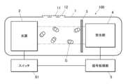
- FIG. 1is a schematic diagram of the optical gas sensor device 100 according to the present embodiment.
- the optical gas sensor device 100 of this embodimentincludes an optical cover 1, a light source 2, an optical filter 3, a light receiving unit 4, a signal processing unit 5, and a switch 81.
- the optical gas sensor device 100is an NDIR type gas sensor that radiates (emits, emits) infrared rays from the light source 2, emits the infrared rays to the gas G to be detected (measured) in the optical cover 1 through an optical path (path) in the optical cover 1, and the amount of light reaching the light receiving unit 4 is reduced as the molecules of the gas G to be detected that exist in the optical path absorb the infrared rays, detects the infrared rays partially absorbed by the gas G to be detected by the light receiving unit 4 through the optical filter 3, processes the detection signal by the signal processing unit 5, detects (measures) and outputs the concentration of the gas G to be detected.
- the switch 81is a switch that turns on/off the light emission of the light source 2, and is included in the circuit element unit 8 described later.
- the signal processing unit 5turns on the light source 2 via the switch 81 when gas detection is performed, and turns off the light source 2 via the switch 81 when gas detection is terminated.
- the optical cover 1has a gas inlet port 11 as a gas inlet that is an inlet for introducing the gas G to be detected.
- a contamination filter 12e.g., a metal mesh filter or a resin porous film
- the optical gas sensor device 100filters the infrared light emitted from the light source 2 to the gas G to be detected by the optical filter 3 and receives it by the light receiving unit 4.
- the optical filter 3is disposed in a position near the light receiving unit 4 on the optical path upstream of the light receiving unit 4. This configuration can reduce the area of the optical filter 3 and reduce costs, since it is sufficient to filter the infrared light emitted from the light source 2 on the light receiving surface of the light receiving unit 4, compared to a configuration in which the infrared light emitted from the light source 2 is filtered by an optical filter before being emitted to the gas G to be detected.
- the signal-to-noise ratio (S/N ratio) of the sensoris improved because the infrared light emitted from sources other than the light source 2 is not received before filtering.
- the optical gas sensor device 100may be configured to filter the infrared light emitted from the light source 2 by the optical filter 3 and emit it to the gas G to be detected.
- the infrared light received by the light receiving unit 4 through the optical filter 3is designed so that the optical path is not a direct optical path from the light source 2, but is reflected on the inner surface of the optical cover 1 and reaches the light receiving unit 4. It is desirable for the inner surface of the optical cover 1 to have a high reflectance, as this increases the efficiency of light (infrared rays) usage.
- the optical gas sensor device 100detects alternative fluorocarbon refrigerants, which are used in air conditioners, as the gas G to be detected.
- Alternative fluorocarbonsare synthetic compound (gas) refrigerants that are used industrially as alternatives to specific fluorocarbons (chlorofluorocarbons, abbreviated as CFCs).
- CFC refrigerantshave a high ozone depletion potential and are a cause of destruction of the Earth's ozone layer, so they have begun to be replaced by hydrochlorofluorocarbon (HCFC) refrigerants, which have a low ozone depletion potential.
- HCFChydrochlorofluorocarbon
- HFC refrigerantsR410A
- HFC refrigerantsR32
- the gas G to be detected in this embodimentis a fluorocarbon alternative refrigerant.
- Table Ishows the product groups (types of each product) of air conditioners and the corresponding main refrigerants that have been used conventionally, refrigerants that are being replaced as alternatives, and refrigerants that are being considered as alternatives.
- the flammability classification in Table IIis a classification indicating toxicity and flammability, with "A” indicating low toxicity, "2L” slightly flammable, “2" flammable, and "3" highly flammable.
- Refrigerants with a "X" to the left of the refrigerant nameare refrigerants that are the target gas G.
- Refrigerants that are the target gas Gare refrigerants that contain at least one F (fluorine) atom, and are either refrigerants consisting of a single molecule of that molecule, or refrigerants that are a mixture consisting of multiple molecules of different structures, and that have a flammability classification of "A2L” or higher.
- Alternative fluorocarbonshave maximum absorption at around 9 ⁇ m.
- R32has maximum absorption at 9.1 ⁇ m, which is the central wavelength of the absorption wavelength band.
- This absorption wavelength bandis derived from the C-F bond, which is a bond unique to fluorocarbons, and by using this absorption wavelength band, interference due to absorption by other gases can be suppressed.
- the gas G to be detectedmust be a refrigerant that is a single molecule of alternative fluorocarbons containing at least one F (fluorine) atom, or a mixture of multiple molecules with different structures.
- the optical gas sensor device 100preferably detects infrared absorption at the wavelength with the greatest absorption among multiple absorption wavelengths of the gas G to be detected. For example, when detecting R32 as the gas G whose concentration is to be detected, the optical gas sensor device 100 detects infrared absorption at the center wavelength of the absorption wavelength band with the greatest absorption of 9.1 ⁇ m among multiple absorption wavelength bands.
- the signal processing unit 5outputs various status signals based on the gas concentration of the detected gas G (for example, a fault signal indicating a fault state of the optical gas sensor device 100, an alarm signal indicating that the concentration of the detected gas G is in an abnormal state (alarm state) that requires an alarm, and a monitoring signal (normal signal) indicating that the concentration of the detected gas G is in a normal state) and the concentration of gas G (output voltage) or a value corresponding to the concentration as a detection signal of the light receiving unit 4 to equipment such as the processing unit of the air conditioner.
- a fault signalindicating a fault state of the optical gas sensor device 100
- an alarm signalindicating that the concentration of the detected gas G is in an abnormal state (alarm state) that requires an alarm
- a monitoring signalnormal signal
- concentration of gas Goutput voltage
- Figure 2is a perspective view of the optical gas sensor device 100.
- Figure 3is a see-through perspective view of the optical cover 1, light source 2, optical filter 3, and light receiving section 4.
- Figure 4is a perspective view of the light source 2.
- Figure 5is a plan view of the optical gas sensor device 100.
- Figure 6Ais a cross-sectional view of the optical gas sensor device 100.
- Figure 6Bis a cross-sectional view of a modified optical gas sensor device 100.
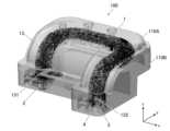
- the optical gas sensor device 100includes, for example, an optical cover 1, a light source 2, an optical filter 3, a light receiving section 4, a signal processing section 5, a substrate 6, a connector 7, and a circuit element section 8. Also, in Figures 2 and 3, the x-axis, y-axis, and z-axis of a three-dimensional space are taken and illustrated. These three axes are similarly illustrated in Figures 4 to 6B. Note that the contamination filter 12 is not illustrated in Figures 2, 3, 5 to 6B.
- the optical cover 1is mounted on the +z side of the substrate 6, covers (encompasses) the light source 2, the optical filter 3, and the light receiving unit 4, and forms a hollow portion (space) inside that can accommodate the gas G to be detected, and the gas G to be detected is introduced into and out of the hollow portion via the gas introduction port 11.
- the base of the optical cover 1is made of, for example, resin.
- the optical cover 1has cover parts 110A and 110B.
- Cover part 110Ais the upper part (+z direction side) and is butted against cover part 110B and integrated with it by methods such as gluing or thermal crimping.
- Cover part 110Bis the lower part (-z direction side) and is butted against cover part 110A and integrated with it by methods such as gluing or thermal crimping.
- the optical cover 1has a light guide section 13 as a hollow section into which the gas G to be detected is introduced.
- the light guide section 13is a pipe-shaped optical path, and its cross section perpendicular to the axial direction is circular.
- the cover section 110Ahas a half pipe section.
- the cover section 110Bhas a half pipe section.
- the light guide section 13is formed by joining the half pipe sections of the cover sections 110A and 110B. In this way, the optical cover 1 has cover sections 110A and 110B that are divided by the cross section of the light guide section 13 in the axial direction.
- the light guide section 13has a three-dimensional, approximately U-shaped shape when viewed from the top surface (the surface in the +z direction).
- the inner surface of the light guide 13is covered with an infrared reflective film.
- goldis used as the infrared reflective film, but this is not limited to this.
- the infrared reflective filmmay be silver, aluminum, a dielectric multilayer film, or a multilayer film made of an infrared-transmitting material such as Si, Ge, sulfide, or fluoride.
- a protective filmsuch as silicon oxide or silicon nitride may be formed on the infrared reflective film as necessary to prevent corrosion of the metal film of the infrared reflective film.
- the infrared reflective film and protective filmmay be formed by plating, sputtering, vacuum deposition, or the like.
- the optical cover 1may be integrally formed from a metal such as aluminum using a metal 3D printer.
- the light guide unit 13reflects the infrared light incident from the light source 2 with an infrared reflective film on the inner surface, and emits it to the light receiving unit 4 via the optical filter 3.
- the optical cover 1serves as an optical path to efficiently guide the infrared light from the light source 2 to the light receiving unit 4 by reflecting the infrared light emitted from the light source 2 with an infrared reflective film, so that at least a portion of the reflected light reaches the light receiving unit 4 via the optical filter 3.
- the light path inside the optical cover 1is made of a pipe-shaped light guide section 13 with a circular cross section, so that the reflection angle of the infrared rays is kept constant in all three dimensional directions (x-axis, y-axis, z-axis) regardless of the diameter or path of the cross section of the light guide section 13, and the infrared rays emitted from the light source 2 are reflected inside the light guide section 13, allowing them to efficiently enter the light receiving section 4.
- the optical path length of the infrared light from the light source 2 to the light receiving unit 4can be changed relatively easily by changing the cross-sectional diameter of the light guiding unit 13.
- the optical cover 1is designed and formed three-dimensionally so that the axial direction of the light guide section 13 creates a space S1 on the substrate 6 below a portion of the x-axis direction (-z direction). At least a portion of the signal processing section 5 and the circuit element section 8 are disposed in the space S1 and mounted on the substrate 6.
- the cross-sectional area of the light-guiding section 13 perpendicular to the axial directionis constant in the axial direction for the main portion (portions other than the inlet portion 131 and the outlet portion 132 described below). Since the cross-sectional area is constant, the gas concentration per unit volume of the gas G to be detected that enters the light-guiding section 13 is easily homogenized, and since the infrared rays pass through randomly without following a specific path, it is easy to react to changes in the gas concentration of the gas G.
- Figure 3shows the light path propagation state, with multiple infrared light paths within the light-guiding section 13 represented by solid lines. In this way, the infrared light paths are random within the light-guiding section 13.
- the light emitted from the light source 2is incident on the light guide 13 on the -x direction side.
- the light guide 13 on the -x direction sideextends axially from the -z direction side to the +z direction side, then curves in an R shape, and extends linearly from the -y direction side to the +y direction side.
- the end of the light guide 13 on the infrared light incident sideis the entrance section 131.
- the light guide 13 extending on the +y direction sidecurves in an R shape, extends axially from the -x direction side to the +x direction side, and curves in an R shape again.
- the light guide 13 on the +x-direction sideextends linearly from the +y-direction side to the -y-direction side in the axial direction, then curves in an R-shape and extends to the -z-direction side.
- the infrared light that passes through the light guide 13is emitted to the optical filter 3 and the light receiving unit 4.
- the end of the light guide 13 on the infrared light emission sideis called the exit unit 132.
- cover parts 110A and 110Bhave hollow parts (not shown) as spaces for removing material (stealing material). These hollow parts make it possible to reduce the weight of the optical cover 1 (optical gas sensor device 100).
- Cover part 110Balso has a fixing pin (not shown).
- the fixing pinis a convex part extending in the +z direction, and is fitted into a concave part (female hole) (not shown) of cover part 110A and integrated by a method such as gluing or thermal crimping.
- cover parts 110A and 110Bare positioned and fixed into an integrated part.
- the cover part 110Ahas gas intake ports 111 and 112 as the gas introduction port 11.
- the cover part 110Bhas gas intake ports (gas introduction holes) 113 and 114 as the gas introduction port 11.
- the gas intake ports 111 and 112are holes opened in the -z direction from the top surface of the cover part 110A and penetrate to the light guiding part 13.
- the gas intake port 113is a hole opened from the -y direction side of the cover part 110B to the +y direction side and penetrates to the space around (beside) the light source 2.
- the space around the light source 2is connected to the light guiding part 13.
- the gas intake port 114is a hole opened from the -y direction side of the cover part 110B to the +y direction side and penetrates to the space around (beside) the optical filter 3 and the light receiving part 4.
- the space around the optical filter 3 and the light receiving unit 4is connected to the light guide unit 13.
- Gas inlets 111 and 112are directly connected to light guide 13 and remove part of the inner surface of light guide 13, resulting in low infrared utilization efficiency.
- gas inlet 113is indirectly connected to light guide 13 via the space around light source 2, resulting in high infrared utilization efficiency without damaging (removing) part of the inner surface of light guide 13.
- gas inlet 114is indirectly connected to light guide 13 via the space around optical filter 3 and light receiving unit 4, resulting in high infrared utilization efficiency without damaging part of the inner surface of light guide 13.
- gas introduction port 11gas intake ports 111, 112, 113, 114
- shape, size, and position of the gas introduction port 11are merely examples and are not intended to be limiting.
- the light source 2is a MEMS (Micro Electro Mechanical Systems) type light source mounted on the upper surface (+z side surface) of the substrate 6, and has, for example, a membrane M with a membrane structure formed thereon.
- the light source 2has an electrode 231 and a pad P1 provided on the +x side, and an electrode 232 and a pad P2 provided on the -x side.
- the light source 2has a structure in which, for example, a light source layer support layer, a light source layer 21, an electrode support layer, and a protective layer (all not shown) are laminated from the -z direction side to the +z direction side as a membrane M provided on a Si substrate.
- the light source layer support layerhas, for example, a silicon oxide film, a silicon nitride film, and an HLD (High temperature Low pressure Dielectric layer) layer from the -z direction side to the +z direction side.
- the light source layer 21is a thin film heater as a light source (metal) layer (light emitting layer) that emits infrared rays, and is made of, for example, MoSi 2.
- the light source layerheats the membrane M by energization, and emits infrared rays having an intensity and wavelength dependency that depend on the surface temperature and surface emissivity.
- the electrode support layerhas, for example, two insulator layers from the -z direction side to the +z direction side, and supports the electrode.
- the protective layeris a protective layer on the upper surface made of an insulator.
- the light source layer 21is electrically connected to electrodes 231 and 232.
- Pad P1is a pad for wire bonding and is electrically connected to electrode 231.
- Pad P2is a pad for wire bonding and is electrically connected to electrode 232.
- Pads P1 and P2are wire bonded to terminals of the wiring pattern on the substrate 6, and when a voltage is applied, electricity flows through the light source layer 21, causing infrared rays to be emitted.
- the light source 2 as a MEMS type light sourceis small and low-profile, making it possible to realize a compact sensor module.
- the light source 2 as a MEMS type light sourcehas characteristics such as a long life, low power consumption, and short response time, making it possible to achieve low power consumption for the entire sensor module.
- the short response time of the MEMS type light sourcemakes it possible to shorten the standby time after power is turned on when performing intermittent driving, thereby reducing the average power consumption.
- the light source 2 as a MEMS type light sourcecan directly utilize the light emitted from the surface of the high temperature part, it can also be applied to the detection of gases that have absorption bands at long wavelengths. Furthermore, the area that emits infrared light from the light source 2 is patterned with high precision on the flat surface of the Si substrate of the membrane M, and individual variation in the direction of emission is very small. This reduces variation in the amount of light received when a sensor module is constructed using the light source 2, contributing to improved product yield. Furthermore, the light source 2 is easily mass-produced because it is produced in bulk using MEMS technology based on silicon wafers.
- the light source 2is a surface-mounted component, but is not limited to this and may be a DIP (Dual Inline Package) component (such as a CAN package).
- DIPDirect Inline Package
- the optical filter 3is a filter that is provided to cover the light receiving surface of the light receiving unit 4 and transmits light (infrared light) in a wavelength range (band) that corresponds to the absorption wavelength specific to the gas G to be detected.
- the transmission wavelength of the optical filter 3is designed to match the absorption wavelength specific to the gas G to be detected, thereby suppressing changes in the amount of light caused by gases other than the gas G to be detected, and improving the signal-to-noise ratio of the detection signal of the light receiving unit 4.
- the optical filter 3has, for example, a silicon substrate as a substrate, and a dielectric multilayer film, or a multilayer film made of an infrared-transmitting material such as Si, Ge, sulfide, or fluoride.
- the silicon substrateis a planar silicon substrate.
- the material of the substrateis not limited to silicon, and Ge (germanium), quartz, alumina, BaF2 (barium fluoride), CaF2 (calcium fluoride), etc. can be used.
- the multilayer filmis a film with multiple layers provided on both sides of the silicon substrate.
- the planar shape of the optical filter 3is rectangular, but is not limited to this and may be other shapes such as circular.
- the optical filter 3is not a bandpass filter that transmits only wavelengths in a specific frequency band, but rather a longpass filter that cuts out light with wavelengths shorter than an arbitrary wavelength and transmits light with wavelengths longer than the arbitrary wavelength.
- the light receiving unit 4is mounted on the +z side of the substrate 6 and is a thermopile type optical sensor (infrared sensor) with multiple thermocouples, which detects the amount of incident infrared light and outputs a detection signal as an analog electrical signal.
- the light receiving unit 4is not limited to a thermopile type infrared sensor, and may be an infrared sensor of various types as shown in Table III below.
- the light receiving unit 4is a surface-mounted component, but is not limited to this configuration and may be a DIP component (such as a CAN package).
- the light guide 13can efficiently obtain the amount of light for the light source 2 and the light receiving unit 4 regardless of the orientation of the surface-mounted component, DIP component, or other component.
- FIG. 5shows the planar configuration of the optical gas sensor device 100 and the cutting line VIA-VIA parallel to the y-axis direction of the optical cover 1.
- FIG. 6Ashows a side view of the cross-sectional configuration of the optical cover 1 cut along the cutting line VIA-VIA.
- the mounting position of the optical filter 3may be in the light guide section 13, which serves as the optical path from the light source 2 to the light receiving section 4.
- the end of the light guide 13 on the infrared emission sideis the outlet 132.
- the optical filter 3is disposed directly below (below and in the vicinity of) the outlet 132, with its plane parallel to the xy plane (parallel to the surface of the light receiver 4). In this configuration, the optical filter 3 is bonded, for example, to the bottom surface of the outlet 132.
- the optical filter 3ahas an area that covers at least the axial cross section of the outlet 132.
- the position of the optical filter 3is not limited to that shown in FIG. 6A.
- an optical filter 3amay be arranged in place of the optical filter 3 below the outlet 132, with its plane parallel to the xy plane and in the vicinity of the surface (light receiving surface) of the light receiving unit 4.
- the optical filter 3ais bonded to, for example, the upper surface of the light receiving unit 4.
- the optical filter 3ahas an area that covers at least the light receiving surface on the upper surface of the light receiving unit 4. In other words, the planar area of the optical filter 3a is smaller than the planar area of the optical filter 3.
- the outlet section 132has a tapered shape in which the cross-sectional area becomes smaller as the axial direction of the light-guiding section 13 moves from the +z direction to the -z direction.
- the inlet section 131has a tapered shape in which the cross-sectional area becomes smaller as the axial direction of the light-guiding section 13 moves from the +z direction to the -z direction. This makes it possible to increase the concentration of infrared light radiated through the light-guiding section 13 to the light-receiving section 4.
- the signal processing unit 5is mounted on a flat area on the surface on the +z direction side of the substrate 6, and is an AFE (Analog Front End)-IC (Integrated Circuit) that serves as an electronic component (processor) that performs signal processing on the detection signal of the light receiving unit 4.
- the signal processing unit 5amplifies and AD converts the analog detection signal of the light receiving unit 4, corrects individual variations in the optical gas sensor device 100, and uses the amplified digital detection signal to perform signal processing (calculation of gas concentration or a value corresponding to the gas concentration, the state of the optical gas sensor device 100, and generation of these various signals), and generates and outputs various digital signals.
- the substrate 6is a PCB (Printed Circuit Board) with conductor wiring printed on a plate made of glass epoxy resin or the like.
- a PCBPrint Circuit Board
- the connector 7is mounted on the planar area other than the optical cover 1 and the signal processing unit 5 on the surface on the +z direction side of the substrate 6, and is a connector for outputting various digital signals output from the signal processing unit 5 to the information processing unit of a downstream device (such as an alarm).
- the connector 7is a receptacle connector to which a cable having a plug is connected.
- the connector 7is connected to the information processing unit of the device via the cable.
- the circuit element section 8is a circuit element such as a switch 81, a chip resistor, and a chip capacitor that is mounted on a planar area on the +z direction side of the substrate 6.
- Fig. 7is a diagram showing the distribution of light incident angles on the light receiving section 4.
- Fig. 8is a diagram showing the transmission characteristics of the long-pass filter.
- Fig. 9is a diagram showing the angle dependency of the transmittance of the long-pass filter.
- Fig. 10is a diagram showing the transmission characteristics of a conventional band-pass filter.
- Fig. 11is a diagram showing the angle dependency of the transmittance of a conventional band-pass filter.
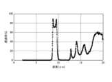
- Fig. 12is a diagram showing the absorption wavelengths of multiple types of gas.
- the infrared light beams shown by solid linesdo not travel parallel to the inner wall surface of the light path, but travel diagonally while repeatedly reflecting. Therefore, the light beams that enter the light-receiving section 4 are mainly angled beams, not perpendicular beams.
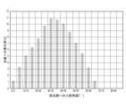
- Figure 7shows the contribution rate [%] to the amount of light for the angle of incidence ⁇ [°] to the light-receiving section 4 (light-receiving element) as the distribution of the angle of incidence of infrared light to the light-receiving section 4, obtained by ray tracing simulation.
- the incident angle ⁇is shown in Figure 6A.
- the incident angle ⁇is the angle of incidence of the light ray from the perpendicular to the light receiving surface of the light receiving unit 4.
- the results in Figure 7show that the perpendicular incident component of the light amount ( ⁇ 0°) accounts for a small proportion of the total light amount, and the components at angles greater than 30° account for half of the peak component at 30-35°.
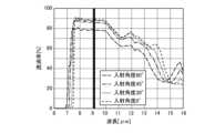
- Figure 8shows the transmittance [%] of the long-pass filter at angles of incidence of 0, 30, 45, and 60 [°] against the wavelength of light [ ⁇ m] as the transmission characteristics of the long-pass filter.
- Figure 9shows the transmittance [%] of the long-pass filter against the angle of incidence of light [°] as the angle dependency of the transmittance of the long-pass filter.
- Figure 10shows the transmittance [%] of the bandpass filter at angles of incidence of 0, 30, 45, and 60 [°] versus the wavelength of light [ ⁇ m] as the transmission characteristics of the conventional bandpass filter.
- Figure 11shows the transmittance [%] of the bandpass filter versus the angle of incidence of light [°] as the angle dependency of the transmittance of the conventional bandpass filter.
- 9.1 [ ⁇ m]is the absorption wavelength of R32 as a gas
- transmittance [%] of 9.1 [ ⁇ m]decreases. Therefore, when the optical filter 3 of this conventional bandpass filter is combined with the light guide section 13, the actual amount of infrared light received is lower than the design value.
- the conventional bandpass filter of the comparative examplehas a rapidly decreasing transmittance [%] as the incident angle ⁇ becomes larger than 40 [°].
- the longpass filter of this embodimenthas a small incidence angle dependency of the transmittance [%] at the absorption wavelength of 9.1 [ ⁇ m] of R32. Therefore, even when the optical filter 3 of this longpass filter is combined with the light guide section 13, it is possible to receive light rays reaching the light receiving section 4 at any angle, and the gas detection output signal can be increased (the concentration of the gas G to be detected can be accurately detected). As shown in FIG. 9, the longpass filter of this embodiment has a gradual decrease in transmittance [%] compared to the conventional bandpass filter of the comparative example, even when the incidence angle ⁇ is greater than 40 [°].
- the cut-on wavelength ⁇ ois defined as a wavelength with a transmittance [%] of 5 [%]
- the transmission wavelength ⁇ passis defined as a wavelength range with a transmittance of 70 [%] or more.
- the lower limit of the cut-on wavelength ⁇ o of the long-pass filteris 5 [ ⁇ m], which is longer than the main absorption wavelength of carbon dioxide, 4 [ ⁇ m], and the upper limit must be 8.5 [ ⁇ m] or less, which is the main absorption wavelength of R1234yf.
- the lower limit of the transmission wavelength ⁇ passmust be 6 [ ⁇ m] or more, which is the absorption wavelength of water vapor, and the upper limit must be 12 [ ⁇ m] or less, which is the absorption wavelength of carbon dioxide.
- Figure 12shows the absorption wavelengths [ ⁇ m] of multiple types of gases. As shown in Figure 12, in the wavelength range of 7.5 [ ⁇ m] or more, there are only a few types of gases that can be contained in living spaces, and the influence of absorption by these types of gases is low, so this does not pose a practical problem.
- the long-pass filter having the transmission characteristics of this embodimentcan also be used as a non-contact temperature sensor or a human presence sensor.
- the optical gas sensor device 100includes a light source 2 that emits infrared rays to the gas G to be detected, an optical filter 3 that is a long-pass filter having a cut-on wavelength smaller than the center wavelength of the absorption wavelength band of the gas G to be detected and a transmission wavelength including said center wavelength, and transmits infrared rays that pass through the gas G to be detected, a light receiving unit 4 that detects the infrared rays incident through the optical filter 3 and generates a detection signal, and an optical cover 1 that covers the light source 2, the optical filter 3, and the light receiving unit 4.
- the optical cover 1guides the infrared rays incident from the light source 2 through the optical filter 3 to the light receiving unit 4 by reflection on its inner surface, and has a pipe-shaped light guide unit 13 that has a circular cross section perpendicular to the axial direction.
- the optical filter 3can reduce the effect of the angle dependency of the incidence angle ⁇ on the transmittance of the target gas G, thereby increasing the output voltage of the light receiver 4, and improving the detection accuracy of the target gas G.
- the gas G to be detectedis a refrigerant consisting of a single molecule containing at least one fluorine atom, or a mixture of refrigerants consisting of multiple molecules that contain at least one fluorine atom and have different structures. Therefore, it is possible to improve the detection accuracy of refrigerants that are alternatives to fluorocarbons and have a central absorption wavelength of around 9 ⁇ m as the gas G to be detected.
- the optical filter 3has a cut-on wavelength of 5 to 8 ⁇ m and a transmission wavelength of 7 to 12 ⁇ m, with the cut-on wavelength being shorter than the transmission wavelength.
- the optical filter 3has filtering characteristics appropriate for alternative fluorocarbon refrigerants, and can improve the detection accuracy of alternative fluorocarbon refrigerants as the detection target gas G.
- the optical gas sensor device 100also includes a substrate 6 on which the light source 2, the light receiving unit 4, and the optical cover 1 are mounted. This allows the light source 2, the light receiving unit 4, and the optical cover 1 to be positioned and fixed accurately and reliably, thereby further improving the detection accuracy of the gas G to be detected.
- the light guide 13also has an entrance 131 into which the infrared light emitted from the light source 2 enters.
- the entrance 131has a tapered shape in which the cross-sectional area decreases toward the light source 2 along the axial direction. This makes it possible to increase the concentration of infrared light on the light receiver 4.
- the light guide 13also has an outlet 132 that emits the guided infrared light to the light receiver 4 via the optical filter 3.
- the outlet 132has a tapered shape in which the cross-sectional area decreases along the axial direction toward the light receiver 4. This makes it possible to increase the concentration of infrared light on the light receiver 4.
- Fig. 13is a diagram showing the transmission characteristics of the optical filter 3 of Example 1.
- Fig. 14is a diagram showing the transmission characteristics of the optical filter of Comparative Example 1.
- Fig. 15is a diagram showing the transmission characteristics of the optical filter 3 of Example 1 and the absorption spectra of R32 and R1234yf.
- An optical gas sensor device 100is used in which the optical filter 3 is disposed at the position shown in FIG. 6A.
- the resistance value of the light source 2 at room temperatureis 16 ⁇ , and the applied voltage is 3.3 V.
- the light receiving unit 4is a MEMS thermopile with a chip size of 1.3 x 0.7 mm, a height of 0.4 mm, and a membrane size of 0.71 mm.
- the resistance value of the light receiving unit 4is 44 k ⁇ .
- the output signal from the light receiving unit 4is amplified 70 times by the external amplifier circuit and the signal processing unit 5.
- the output signal from the light receiving unit 4is acquired as a digital value from the optical gas sensor device 100 via the I2C interface. More specifically, the analog voltage output from the light receiving unit 4 is AD converted by the AD converter inside the signal processing unit 5 to a digital value. The effect of the full-scale voltage and resolution of the AD converter on this digital value is calculated, and further, taking into account the gain of 70 times, it is converted into a direct output voltage from the light receiving unit 4 and acquired as a digital value.
- the optical filter 3 of Example 1is a long-pass filter.
- FIG. 13shows the transmittance [%] of the optical filter 3 of Example 1 versus wavelength [ ⁇ m] as the transmission characteristics of the optical filter 3 of Example 1.
- the optical filter 3 of Example 1has a cut-on wavelength of 7.5 [ ⁇ m] and a maximum transmittance of 90 [%] as the characteristics of a long-pass filter.
- the substrate of the optical filter 3 of Example 1is silicon with a thickness of 0.32 [mm]. After a filter film (made of Ge and ZnS) was formed on the substrate, it was diced to a 3 mm square.
- the optical filter of Comparative Example 1is a bandpass filter.
- Figure 14shows the transmittance [%] of the optical filter of Comparative Example 1 versus wavelength [ ⁇ m] as the transmission characteristics of the optical filter of Comparative Example 1.
- the optical filter of Comparative Example 1has the following bandpass filter characteristics: center wavelength: 9.1 [ ⁇ m], maximum transmittance: 89 [%], FWHM (Full Width at Half Maximum): 1 [ ⁇ m], blocking: 2 to 12 [ ⁇ m]. FWHM is used to indicate the spread of a spectrum, and is the distance between two wavelengths that corresponds to 50% of the peak transmittance.
- the substrate of the optical filter of Comparative Example 1is silicon with a thickness of 0.34 [mm]. After a filter film (made of Ge and ZnS) was formed on the substrate, it was diced to a 3 mm square.
- Table IVshows the results of the output voltage [mV] for the optical gas sensor device 100 using the optical filter 3 of Example 1 or the optical filter of Comparative Example 1 at a plurality of R32 concentrations.
- the R32 concentrations usedwere 5000, 15000, and 30000 [ppm].
- the optical filter 3 of Example 1In the case where the optical filter 3 of Example 1 is used, a higher output voltage is obtained than in the case where the optical filter of Comparative Example 1 is used, regardless of the R32 concentration. In the case where the optical filter 3 of Example 1 is used, the output voltage is about 1.3 times higher than in the case where the optical filter of Comparative Example 1 is used.
- Fig. 15shows the transmittance [%] of the optical filter 3 of Example 1 versus wavelength [ ⁇ m] as the transmission characteristics of the optical filter 3 of Example 1.
- Fig. 15shows the absorption cross-sections [cm 2 /molecule] of R32 and R1234yf versus wavelength [ ⁇ m] as the absorption spectra of R32 and R1234yf.
- R32 and R1234yfare refrigerants that make up R454B, a representative example of a mixed refrigerant, and are mixed in a mass ratio of 68.9:31.1, respectively. Both R32 and R1234yf have the strongest absorption in the transmission band of the long-pass filter, making them possible to measure with high sensitivity.
- the optical filter 3 of the first embodimentwhen the target gas G is detected using infrared light passing through the light guide section 13 as a path involving reflection, the optical filter 3 can improve the detection accuracy of the target gas G, which is R32, R1234yf, and R454B.
- Fig. 16is a diagram showing the transmission characteristics of a conventional bandpass filter.
- Fig. 17is a diagram showing the transmission characteristics of the bandpass filter of this embodiment.
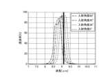
- Fig. 18is a diagram showing the transmission characteristics and central wavelength of transmittance of an example bandpass filter.
- a long-pass filteris used as the optical filter 3 or 3a.
- a band-pass filteris used as the optical filter 3 or 3a.
- the device configuration of this embodimentis the same as that of the first embodiment, and uses the optical gas sensor device 100. For this reason, the description of the components that are the same as those of the first embodiment will be omitted, and the different parts such as the optical filter 3 will be mainly described.
- the infrared transmission wavelengthwas adjusted to the wavelength showing maximum absorption in the absorption spectrum of the gas to be detected.
- the wavelength showing maximum absorption in the absorption spectrum of methaneis 3.3 [ ⁇ m].
- Conventional bandpass filters for detecting methanewere designed to have a transmission wavelength of 3.3 [ ⁇ m].
- the wavelength showing maximum absorption in the absorption spectrum of carbon dioxideis 4.26 [ ⁇ m].
- Conventional bandpass filters for detecting carbon dioxidewere designed to have a transmission wavelength of 4.26 [ ⁇ m].
- FIG. 16shows the transmittance [%] characteristic of a conventional bandpass filter versus infrared wavelength [ ⁇ m] in FIG. 10, with the wavelength range narrowed to make it easier to see.
- FIG. 17shows the transmittance [%] characteristic of the bandpass filter of this embodiment for R32 used in the optical filter 3 or 3a versus the wavelength [ ⁇ m] of infrared light.
- the bandpass filter of this embodimentis designed to shift the center wavelength of the transmittance at normal incidence by a predetermined amount toward the higher wavelength side than the wavelength (9.1 [ ⁇ m]) showing maximum absorption in the absorption spectrum of R32, compared to the conventional bandpass filter of FIG. 16.
- the bandpass filter of this embodimentdoes not have a decrease in transmittance [%] at 9.1 [ ⁇ m], which is the wavelength showing maximum absorption in the absorption spectrum of R32, as the incident angle of infrared light increases.
- the appropriate shift amount of the central wavelength of the transmittance of the bandpass filteris +0.05 to +1 [ ⁇ m], and preferably +0.1 to +0.4 [ ⁇ m] with respect to the wavelength showing maximum absorption in the absorption spectrum of the gas G to be detected.
- a light source 2that emits infrared rays to the gas G to be detected
- the optical cover 1guides the infrared rays incident from the light source 2 through the optical filter 3 or 3a to the light receiving unit 4 by reflection on the inner surface, and has a pipe-shaped light guide unit 13 with a circular cross section perpendicular to the axial direction.
- the detection accuracy of the target gas Gcan be improved by using infrared rays that pass through an optical path involving reflection, and the change in light quantity and the output of the light receiving unit 4 when the target gas G is present can be increased.
- Thismakes it possible to suppress the effects of fluctuations in the light quantity due to external disturbances, and to achieve stabilization of detection performance.
- the power input to the light source 2can be reduced.
- the optical path lengthcan be shortened, the optical gas sensor device 100 can be made more compact.
- the specified shift amountis +0.05 to +1 ⁇ m relative to the wavelength showing maximum absorption in the absorption spectrum of the gas G to be detected. This makes it possible to increase the change in light quantity and the output of the light receiving unit 4 when the gas G to be detected is present, to suppress the effects of fluctuations in the light quantity due to disturbances, to achieve more stable detection performance, and to reduce the power input to the light source 2.
- the light guide 13 of the optical cover 1is configured to have a pipe shape with a circular cross section perpendicular to the axial direction, but this is not limited to this.
- the light guide 13may be configured to have a pipe shape with an elliptical cross section perpendicular to the axial direction.
- the configuration in which the cross section of the light guide 13 is circularthe configuration in which the cross section is elliptical reduces the bias in the reflection angle of the infrared light in the optical path, and reduces the loss of the infrared light amount even if the light source 2 and the light receiving unit 4 are misaligned, making it resistant to misalignment in mounting and improving the detection accuracy of the gas G to be detected.
- the optical gas sensor device 100is configured to include one set of the light source 2, the optical filter 3, the light receiving section 4, and the light guiding section 13, but this is not limited to this.
- the optical gas sensor devicemay be configured to include multiple sets of the light source 2, the optical filter 3, the light receiving section 4, and the light guiding section 13.
- optical gas sensor device 100in the above embodiment may be modified as appropriate without departing from the spirit of the present invention.
- the optical gas sensor deviceis suitable for detecting gases such as refrigerants.
- Optical gas sensor deviceG Gas 1 Optical cover 110A, 110B Cover section 11 Gas introduction port 111, 112, 113, 114 Gas inlet 13 Light guide section 12 Contamination filter S1 Space section 2 Light source 21 Light source layer 231, 232 Electrodes P1, P2 Pad M Membrane 3, 3a Optical filter 4 Light receiving section 5 Signal processing section 6 Substrate 7 Connector 8 Circuit element section 81 Switch
Landscapes
- Physics & Mathematics (AREA)
- Health & Medical Sciences (AREA)
- Life Sciences & Earth Sciences (AREA)
- Chemical & Material Sciences (AREA)
- Analytical Chemistry (AREA)
- Biochemistry (AREA)
- General Health & Medical Sciences (AREA)
- General Physics & Mathematics (AREA)
- Immunology (AREA)
- Pathology (AREA)
- Investigating Or Analysing Materials By Optical Means (AREA)
Abstract
Description
Translated fromJapanese本発明は、光学式ガスセンサ装置に関する。The present invention relates to an optical gas sensor device.
従来、非分散赤外線吸収方式(NDIR:Non Dispersive InfraRed)によるガスセンサが知られている。NDIRのガスセンサは、多くのガスが各々固有の赤外線波長を吸収する性質を利用して、検出対象のガスに赤外線を放射した時、どの波長がどれくらい吸収されたかを検出して、検出対象のガスの濃度を測るセンサである。例えば、赤外線の発光部及び受光部を備え、発光部及び受光部の光路上にある被検出ガスの濃度を検出するガスセンサである。 Conventionally, gas sensors using the non-dispersive infrared absorption method (NDIR: Non Dispersive InfraRed) are known. NDIR gas sensors take advantage of the property of many gases to absorb their own unique infrared wavelengths, and when infrared light is radiated to the gas to be detected, they detect which wavelengths are absorbed and to what extent, thereby measuring the concentration of the gas to be detected. For example, there is a gas sensor that has an infrared light emitter and receiver, and detects the concentration of the gas to be detected that is located in the optical path of the emitter and receiver.
また、冷媒を用いた空気調和機において、赤外線センサを用いて冷媒の濃度を検出して、冷媒の漏れを検知する冷媒漏洩検知装置が知られている(特許文献1参照)。この赤外線センサは、発光部と、発光部に対向して配置された受光部と、発光部及び受光部の間に設けられた光学フィルタとを備える。光学フィルタは、赤外線が冷媒で吸収される特定の波長帯域を透過する。Also, a refrigerant leak detection device is known that uses an infrared sensor to detect the concentration of the refrigerant in an air conditioner that uses a refrigerant to detect refrigerant leaks (see Patent Document 1). This infrared sensor has a light-emitting unit, a light-receiving unit arranged opposite the light-emitting unit, and an optical filter provided between the light-emitting unit and the light-receiving unit. The optical filter transmits a specific wavelength band of infrared light that is absorbed by the refrigerant.
特許文献1の冷媒漏洩検知装置は、発光部と受光部とが対向して配置されているため、光学フィルタ及び受光部への赤外線の入射角度は、ほぼ0°になる。また、赤外線とガスとが反応する光路長を長くしかつガスセンサを小型化するために、発光部から受光部への赤外線の光路を、当該赤外線の反射を伴うものとする構成が考えられる。当該反射の経路の構成では、受光部に入射する赤外線は、入射角度が0°以外の赤外線の割合が増える。In the refrigerant leak detection device of
ガスセンサの光学フィルタには、従来、検出対象のガスの吸収スペクトルにおいて最大吸収を示す波長の赤外線を透過するバンドパスフィルタが用いられる。しかし、バンドパスフィルタを介して受光部に入射する赤外線の入射角度が0°から離れるにつれて、当該赤外線の吸収波長帯の中心波長が短波長側にシフトする。このため、赤外線の吸収の周波数帯がバンドパスフィルタの透過周波数帯から外れるので、受光部で検出する受光量が低下し、検出対象のガスの検出精度が低下するおそれがあった。 Gas sensors conventionally use bandpass filters for their optical filters, which transmit infrared light of a wavelength that shows maximum absorption in the absorption spectrum of the gas to be detected. However, as the angle of incidence of the infrared light entering the light-receiving section through the bandpass filter moves away from 0°, the central wavelength of the absorption wavelength band of that infrared light shifts to the shorter wavelength side. As a result, the frequency band of infrared light absorption falls outside the transmission frequency band of the bandpass filter, reducing the amount of light received by the light-receiving section and potentially reducing the detection accuracy of the gas to be detected.
本発明の課題は、反射を伴う光路を通る赤外線を用いて、検出対象のガスの検出精度を高めることである。The objective of the present invention is to improve the detection accuracy of the target gas by using infrared light that passes through an optical path involving reflection.
上記課題を解決するため、本発明の光学式ガスセンサ装置は、
赤外線を検出対象のガスに出射する光源と、
前記検出対象のガスの吸収波長帯の中心波長よりも小さいカットオン波長と、当該中心波長を含む透過波長とを有するロングパスフィルタであり、当該検出対象のガスを介した赤外線を透過する光学フィルタと、
前記光学フィルタを介して入射された赤外線を検出して検出信号を生成する受光部と、
前記光源、前記光学フィルタ及び前記受光部を覆う光学カバーと、を備え、
前記光学カバーは、
前記光源から入射された赤外線を内面の反射により前記光学フィルタを介して前記受光部に導き、パイプ形状であり、軸方向に垂直な断面が円形又は楕円形である導光部を有する。In order to solve the above problems, the optical gas sensor device of the present invention comprises:
A light source that emits infrared rays to a gas to be detected;
an optical filter that is a long-pass filter having a cut-on wavelength that is smaller than a center wavelength of an absorption wavelength band of the gas to be detected and a transmission wavelength that includes the center wavelength, and that transmits infrared light that has passed through the gas to be detected;
a light receiving unit that detects infrared rays incident through the optical filter and generates a detection signal;
an optical cover that covers the light source, the optical filter, and the light receiving unit,
The optical cover includes:
The infrared ray incident from the light source is guided to the light receiving section via the optical filter by reflection on the inner surface, and the light guide section has a pipe shape and a cross section perpendicular to the axial direction that is circular or elliptical.
また、本発明の光学式ガスセンサ装置は、
赤外線を検出対象のガスに出射する光源と、
垂直入射(θ=0°)における透過率の中心波長を、前記検出対象のガスの吸収スペクトルにおいて最大吸収を示す波長よりも高波長側に所定シフト量移動したバンドパスフィルタであり、当該検出対象のガスを介した赤外線を透過する光学フィルタと、
前記光学フィルタを介して入射された赤外線を検出して検出信号を生成する受光部と、
前記光源、前記光学フィルタ及び前記受光部を覆う光学カバーと、を備え、
前記光学カバーは、
前記光源から入射された赤外線を内面の反射により前記光学フィルタを介して前記受光部に導き、パイプ形状であり、軸方向に垂直な断面が円形又は楕円形である導光部を有する。The optical gas sensor device of the present invention is
A light source that emits infrared rays to a gas to be detected;
an optical filter that is a bandpass filter in which the center wavelength of transmittance at normal incidence (θ=0°) is shifted by a predetermined amount to the higher wavelength side than the wavelength showing maximum absorption in the absorption spectrum of the gas to be detected, and transmits infrared light that has passed through the gas to be detected;
a light receiving unit that detects infrared rays incident through the optical filter and generates a detection signal;
an optical cover that covers the light source, the optical filter, and the light receiving unit,
The optical cover includes:
The infrared ray incident from the light source is guided to the light receiving section via the optical filter by reflection on the inner surface, and the light guide section has a pipe shape and a cross section perpendicular to the axial direction that is circular or elliptical.
本発明によれば、反射を伴う光路を通る赤外線を用いて、検出対象のガスの検出精度を高めることができる。According to the present invention, the detection accuracy of the target gas can be improved by using infrared light that passes through an optical path involving reflection.
以下、添付図面を参照して本発明に係る第1の実施の形態及び実施例並びに第2の実施の形態を順に詳細に説明する。ただし、発明の範囲は、図示例に限定されない。Below, the first embodiment and example of the present invention, as well as the second embodiment, will be described in detail in sequence with reference to the attached drawings. However, the scope of the invention is not limited to the illustrated examples.
(第1の実施の形態)
図1~図15を参照して、本発明に係る第1の実施の形態を説明する。まず、図1を参照して、本実施の形態の光学式ガスセンサ装置100の概略構成を説明する。図1は、本実施の形態の光学式ガスセンサ装置100の概略図である。(First embodiment)
A first embodiment of the present invention will be described with reference to Figures 1 to 15. First, a schematic configuration of an optical
図1に示すように、本実施の形態の光学式ガスセンサ装置100は、光学カバー1と、光源2と、光学フィルタ3と、受光部4と、信号処理部5と、スイッチ81と、を含む。光学式ガスセンサ装置100は、光源2から赤外線を放射(出射、発光)し、光学カバー1内の光路(経路)を介して、当該赤外線を光学カバー1内の検出対象(計測対象)のガスGに出射し、光路中に存在する検出対象のガスGの分子が赤外線を吸収することで受光部4に届く光量が減少し、検出対象のガスGにより一部吸収された赤外線を光学フィルタ3を介して受光部4により検出し、その検出信号を信号処理部5により信号処理し、検出対象のガスGの濃度を検出(計測)して出力するNDIR方式のガスセンサである。スイッチ81は、光源2の発光のオン/オフを行うスイッチであり、後述する回路素子部8に含まれるものとする。信号処理部5は、ガス検出を行う場合に、スイッチ81を介して光源2をオンし、ガス検出を終了する場合に、スイッチ81を介して光源2をオフする。光学カバー1は、検出対象のガスGの導出入口であるガス導入部としてのガス導入ポート11を有する。ガス導入ポート11には、外部からの異物侵入を防止するために、コンタミフィルタ12(例えば、金属製のメッシュフィルタや樹脂製の多孔質フィルムなど)が貼付される。As shown in FIG. 1, the optical
特に、光学式ガスセンサ装置100は、光源2から検出対象のガスGに出射された赤外線を、光学フィルタ3でフィルタリングして受光部4により受光する。光学フィルタ3は、受光部4の上流の光路上で受光部4の近傍の位置に配置されている。この構成は、光源2から放射された赤外線を光学フィルタでフィルタリングしてから検出対象のガスGに出射する構成に比べて、受光部4の受光面でフィルタリングすればよいため、光学フィルタ3の面積を小さくすることができ、コストの低減になる。更には、光源2以外からの放射されるフィルタリング前の赤外線を受光することがなく、センサとしてのSN比(Signal to Noise ratio)が向上する。ただし、光学式ガスセンサ装置100は、光源2から放射された赤外線を光学フィルタ3でフィルタリングして検出対象のガスGに出射する構成としてもよい。本実施の形態では、光学フィルタ3を介して受光部4が受光する赤外線は、光源2から直接到達する光路でなく、光学カバー1の内面を反射して到達するように光路が設計されるものとする。光学カバー1の内面は反射率が高いほうが光(赤外線)の利用効率が高くなり望ましい。In particular, the optical
光学式ガスセンサ装置100は、検出対象のガスGとして、空気調和機の冷媒である代替フロン冷媒を検出するものとする。代替フロンは、特定フロン(クロロフルオロカーボン、略称:CFC)の代替として産業利用されている合成化合物(ガス)の冷媒である。CFC冷媒は、オゾン層破壊係数が高く地球のオゾン層破壊の原因となるため、オゾン層破壊係数の低いハイドロクロロフルオロカーボン(HCFC)冷媒に代替が開始された。また、先進国では、HCFC冷媒から、オゾン層破壊係数が0であるHFC冷媒(R410A)への転換が進んでいる。The optical
CFC冷媒、HCFC冷媒、HFC冷媒は、地球温暖化係数が高く、温室効果ガスとして地球温暖化の原因になることが知られている。このため、HFC冷媒(R410A)から、地球温暖化係数がより低いHFC冷媒(R32)への代替が検討されている。CFC, HCFC, and HFC refrigerants have a high global warming potential and are known to cause global warming as greenhouse gases. For this reason, there is consideration of replacing HFC refrigerants (R410A) with HFC refrigerants (R32), which have a lower global warming potential.
本実施の形態の検出対象とするガスGは、代替フロン冷媒である。ここで、次表Iに、空気調和機の製品群(各製品の種類)と、これに対応する、従来使用されてきた主な冷媒、代替として転換が実施されている冷媒、代替として検討されている冷媒を示す。
また、本実施の形態の検出対象のガスGの具体例を次表IIに挙げる。
表IIの可燃性分類とは、毒性及び燃性を示す分類であり、「A」が低毒性を示し、「2L」が微燃性を示し、「2」が可燃性を示し、「3」が強燃性を示す。冷媒名の左に「〇」が付いているものが、検出対象のガスGである冷媒である。検出対象のガスGである冷媒は、少なくとも1つのF(フッ素)原子を含む分子として、単一の当該分子からなる冷媒か、互いに構造の異なる複数の当該分子から構成される混合物としての冷媒であり、かつ可燃性分類が「A2L」以上のものとした。The flammability classification in Table II is a classification indicating toxicity and flammability, with "A" indicating low toxicity, "2L" slightly flammable, "2" flammable, and "3" highly flammable. Refrigerants with a "X" to the left of the refrigerant name are refrigerants that are the target gas G. Refrigerants that are the target gas G are refrigerants that contain at least one F (fluorine) atom, and are either refrigerants consisting of a single molecule of that molecule, or refrigerants that are a mixture consisting of multiple molecules of different structures, and that have a flammability classification of "A2L" or higher.
代替フロンは、9[μm]付近で最大の吸収となる。例えば、R32は、9.1[μm]で最大の吸収を示し、当該波長が吸収波長帯の中心波長となる。この吸収波長帯は、フロンに特有の結合である、C-F結合に由来するものであり、この吸収波長帯を用いることで、他ガスの吸収による干渉を抑制できる。このため、検出対象のガスGは、少なくとも1つのF(フッ素)原子を含む代替フロン系の単一の分子又は互いに構造の異なる複数の分子の混合物の冷媒であることを要件とした。Alternative fluorocarbons have maximum absorption at around 9 μm. For example, R32 has maximum absorption at 9.1 μm, which is the central wavelength of the absorption wavelength band. This absorption wavelength band is derived from the C-F bond, which is a bond unique to fluorocarbons, and by using this absorption wavelength band, interference due to absorption by other gases can be suppressed. For this reason, the gas G to be detected must be a refrigerant that is a single molecule of alternative fluorocarbons containing at least one F (fluorine) atom, or a mixture of multiple molecules with different structures.
また、表IIにおいて、燃焼下限濃度が低く、燃性も高いガスは、ガス漏れ時の燃焼などの事故を防ぐために、検出が重要である。このため、検出対象のガスGの冷媒は、可燃性分類が「A2L」以上であることを要件とした。In addition, in Table II, detection of gases with low lower flammable concentration limits and high flammability is important in order to prevent accidents such as combustion in the event of a gas leak. For this reason, the flammability classification of the refrigerant gas G to be detected must be "A2L" or higher.
光学式ガスセンサ装置100は、検出対象のガスGの複数の吸収波長のうち、最も吸収が大きい波長の赤外線の吸収を検出するのが好ましい。例えば、濃度の検出対象のガスGとしてR32を検出する場合は複数の吸収波長帯のうち、最も吸収が大きい吸収波長帯の中心波長が9.1[μm]の赤外線の吸収を検出する。The optical
信号処理部5は、検出したガスGのガス濃度に基づく各種の状態信号(例えば、光学式ガスセンサ装置100の故障の状態を示す故障信号、検出したガスGの濃度が警報が必要な異常状態(警報状態)であることを示す警報信号、検出したガスGの濃度が正常の状態であることを示す監視信号(正常信号))と、受光部4の検出信号としてのガスGの濃度(出力電圧)又は濃度に対応した値とを、空気調和機の処理部などの機器に出力する。The
ついで、図2~図6Bを参照して、光学式ガスセンサ装置100の具体的な装置構成を説明する。図2は、光学式ガスセンサ装置100の斜視図である。図3は、光学カバー1、光源2、光学フィルタ3及び受光部4の透過斜視図である。図4は、光源2の斜視図である。図5は、光学式ガスセンサ装置100の平面図である。図6Aは、光学式ガスセンサ装置100の断面図である。図6Bは、変形例の光学式ガスセンサ装置100の断面図である。Next, the specific device configuration of the optical
図2、図3に示すように、光学式ガスセンサ装置100は、例えば、光学カバー1と、光源2と、光学フィルタ3と、受光部4と、信号処理部5と、基板6と、コネクタ7と、回路素子部8と、を備える。また、図2、図3において、三次元空間のx軸、y軸、z軸をとり、図示する。これらの3軸は、図4~図6Bでも同様に図示されるものとする。なお、図2、図3、図5~図6Bにおいて、コンタミフィルタ12の図示を省略している。As shown in Figures 2 and 3, the optical
光学カバー1は、基板6の+z側の面上に実装され、光源2、光学フィルタ3及び受光部4を覆い(包含し)、内部に検出対象のガスGを収容可能な空洞部(空間)を形成し、ガス導入ポート11を介して検出対象のガスGが当該空洞部に導出入されるカバーである。光学カバー1の基体は、例えば樹脂製である。The
図2に示すように、光学カバー1は、カバー部110A,110Bを有する。カバー部110Aは、上側(+z方向側)のパーツであり、カバー部110Bに付き合わせて接着や熱カシメなどの方法によって一体化される。カバー部110Bは、下側(-z方向側)のパーツであり、カバー部110Aに付き合わせて接着や熱カシメなどの方法によって一体化される。As shown in FIG. 2, the
また、図3に示すように、光学カバー1は、検出対象のガスGが内部に導入される空洞部としての導光部13を有する。導光部13は、パイプ形状の光路であり、軸方向に垂直な断面が円形である。カバー部110Aは、半パイプ部を有する。カバー部110Bは、半パイプ部を有する。カバー部110A,110Bの半パイプ部が合わさることにより、導光部13が形成されている。このように、光学カバー1は、導光部13の軸方向の断面により分割されたカバー部110A,110Bを有する。図3に示すように、導光部13は、上面(+z方向の面)から見て、3次元的な略U字形状をしている。Also, as shown in FIG. 3, the
導光部13の内面には、赤外線反射膜が覆われている。本実施の形態では赤外線反射膜として、金を用いるものとするが、これに限定されるものではない。赤外線反射膜として、銀、アルミニウム、誘電体多層膜、またはSi、Ge、硫化物およびフッ化物などの赤外線透過材料による多層膜を用いてもよい。さらに、必要に応じて赤外線反射膜の金属膜の腐食を防止するために、酸化シリコン又は窒化シリコンなどの保護膜を赤外線反射膜上に成膜してもよい。赤外線反射膜、保護膜の成膜方法は、メッキ法、スパッタリング法、真空蒸着法などを用いることができる。なお、例えば、金属3Dプリンタを用いて、光学カバー1が、アルミニウムなどの金属により一体造形されている構成としてもよい。The inner surface of the
導光部13は、光源2から入射された赤外線を内面の赤外線反射膜で反射して、光学フィルタ3を介して受光部4に出射する。このように、光学カバー1は、光源2から出射された赤外線を赤外線反射膜により反射することにより、少なくとも反射光の一部が光学フィルタ3を介して受光部4へ到達するように、光路として光源2からの赤外線を受光部4に効率よく導く役割を担う。The
本実施の形態では、光学カバー1内部の光路を断面が円形のパイプ形状の導光部13とすることにより、導光部13の断面の径や経路によらず、3次元(x軸、y軸、z軸)のいずれの方向にも赤外線の反射角度を一定に保ち、光源2から出た赤外線は導光部13内部を反射し、効率よく受光部4に入光することができる。In this embodiment, the light path inside the
また、光源2から受光部4までの赤外線の光路長は、導光部13の断面の径を変えることで比較的簡単に変更できる。In addition, the optical path length of the infrared light from the
また、図2、図3に示すように、光学カバー1は、導光部13の軸方向がx軸方向の一部分の下方(-z方向)の基板6上に空間部S1ができるように、3次元的に設計、形成されている。空間部S1に、信号処理部5及び回路素子部8の少なくとも一部が配置されて基板6上に実装されている。Also, as shown in Figures 2 and 3, the
また、導光部13の軸方向に垂直な断面の断面積は、主要部分(後述する入口部131、出口部132以外の部分)が軸方向に一定である。断面積が一定のため、導光部13に入ってきた検出対象のガスGに対し単位体積当たりのガス濃度は均一化しやすく、且つ赤外線が特定の経路を通らずランダムに通過するため、ガスGのガス濃度の変化に反応しやすい。図3に、導光部13内の赤外線の複数の光線路を実線で表した光路伝搬状態を示す。このように、赤外線の光線路は、導光部13内でランダムとなる。Furthermore, the cross-sectional area of the light-guiding
また、光源2から出射された光は、-x方向側の導光部13に入射される。-x方向側の導光部13は、軸方向が-z方向側から+z方向側に延在したあと、R状に曲がり、-y方向側から+y方向側に直線状に延在している。導光部13の赤外線の入射側の端部を入口部131とする。+y方向側に延在する導光部13は、R状に曲がり、軸方向が-x方向側から+x方向側に延在し、再びR状に曲がる。In addition, the light emitted from the
そして、+x方向側の導光部13は、軸方向が+y方向側から-y方向側に直線状に延在したあと、R状に曲がり、-z方向側に延在する。導光部13を通った赤外線は、光学フィルタ3及び受光部4に出射される。導光部13の赤外線の出射側の端部を出口部132とする。The
また、カバー部110A,110Bは、肉抜き(肉盗み)用の空間として、中空部(図示略)を有する。これら中空部により、光学カバー1(光学式ガスセンサ装置100)の軽量化を実現できる。Furthermore, the
また、カバー部110Bは、固定ピン(図示略)を有する。固定ピンは、+z方向に延在する凸部であり、カバー部110Aの凹部(メス穴)(図示略)に付き合わせて接着や熱カシメなどの方法によって一体化される。カバー部110Aの凹部への固定ピンの付き合わせて接着や熱カシメなどの方法によって一体化により、カバー部110A,110Bが位置決め及び固定化され、一体の部品にされる。Cover
また、図2に示すように、カバー部110Aは、ガス導入ポート11として、ガス取入れ口111,112を有する。カバー部110Bは、ガス導入ポート11として、ガス取入れ口(ガス導入孔)113,114を有する。ガス取入れ口111,112は、カバー部110Aの上面から-z方向にあけられ、導光部13まで貫通された孔である。ガス取入れ口113は、カバー部110Bの-y方向の側面から+y方向側にあけられ、光源2の周囲(脇)の空間まで貫通された孔である。光源2の周囲の空間は、導光部13に導通されている。ガス取入れ口114は、カバー部110Bの-y方向の側面から+y方向側にあけられ、光学フィルタ3及び受光部4の周囲(脇)の空間まで貫通された孔である。光学フィルタ3及び受光部4の周囲の空間は、導光部13に導通されている。2, the
ガス取入れ口111,112は、導光部13に直接的に導通され、導光部13の内面の一部を削除するため、赤外線の利用効率が低くなる。これに対し、ガス取入れ口113は、光源2の周囲の空間を介して、導光部13に間接的に導通されるため、導光部13の内面の一部を損なう(削除する)ことなく、赤外線の利用効率が高くなる。同様に、ガス取入れ口114は、光学フィルタ3及び受光部4の周囲の空間を介して、導光部13に間接的に導通されるため、導光部13の内面の一部を損なうことなく、赤外線の利用効率が高くなる。
なお、図2の光学カバー1のガス導入ポート11(ガス取入れ口111,112,113,114)の形状、大きさ及び位置は、一例であって、これに限定されるものではない。Note that the shape, size, and position of the gas introduction port 11 (
図4に示すように、光源2は、基板6の上面(+z側の面)上に実装されたMEMS(Micro Electro Mechanical Systems)型光源であり、例えばメンブレン構造のメンブレンMが形成されている。光源2は、+x方向側に設けられた電極231及びパッドP1と、-x方向側に設けられた電極232及びパッドP2と、を有する。As shown in FIG. 4, the
光源2は、Si基板上に設けられるメンブレンMとして、-z方向側から+z方向側へ、例えば、光源層支持層、光源層21、電極支持層、保護層(いずれも図示略)が積層された構成を有する。光源層支持層は、-z方向側から+z方向側へ、例えば、シリコン酸化膜、シリコン窒化膜、HLD(High temperature Low pressure Dielectric layer)層を有する。光源層21は、赤外線を放射する光源(金属)層(発光層)としての薄膜ヒータであり、例えばMoSi2からなるものとする。光源層は、通電によりメンブレンMが加熱され、表面温度と表面放射率に依存した強度と波長依存性とを有する赤外線を放射する。電極支持層は、-z方向側から+z方向側へ、例えば、2層の絶縁体層を有し、電極を支持する。保護層は、絶縁体で構成された上面の保護層である。The
光源層21は、電極231,232に電気的に接続されている。パッドP1は、ワイヤボンディング用のパッドであり、電極231に電気的に接続されている。パッドP2は、ワイヤボンディング用のパッドであり、電極232に電気的に接続されている。パッドP1,P2は、基板6上の配線パターンの端子にワイヤボンディングされて、電圧の印加により光源層21が通電されて、赤外線が出射される。The
MEMS型光源としての光源2は、小型・低背であり、センサモジュールとしての小型化を実現することができる。また、MEMS型光源としての光源2は、長寿命、低消費電力、応答時間が短いなどの特徴があり、センサモジュール全体としての低消費電力を図ることができる。MEMS型光源の応答時間が短い特徴は、間欠駆動を行う場合に、通電後の待機時間を短くすることを可能とし、平均消費電力を低減できる。The
また、MEMS型光源としての光源2は、高温部表面からの放射光を直接利用できるため、高波長に吸収帯を持つガスの検出への応用も可能になる。また、光源2の赤外線を放射する領域は、メンブレンMのSi基板の平面上に高精度にパターニングされており、放射方向の個体ばらつきが非常に小さい。このため、光源2でセンサモジュールを構成した時の受光量のばらつきが低減され製品歩留まりの向上に寄与する。また、光源2は、シリコンウエハーを元にMEMS技術によって一括生産されるため、量産性に優れる。In addition, since the
光源2は、表面実装部品とするが、これに限定されるものではなく、DIP(Dual Inline Package)部品(CANパッケージなど)としてもよい。The
光学フィルタ3は、受光部4の受光面を覆うように設けられた、検出対象のガスGに固有の吸収波長に対応する波長域(バンド)の光(赤外線)を透過するフィルタである。このように、光学フィルタ3の透過波長は、検出対象のガスGの固有の吸収波長に一致するように設計されており、これによって検出対象のガスG以外のガスによる光量変化が抑制され、受光部4の検出信号のSN比が向上する。The
光学フィルタ3は、例えば、基板としてのシリコン基板と、誘電体多層膜、またはSi、Ge、硫化物およびフッ化物などの赤外線透過材料による多層膜と、を有する。シリコン基板は、平面状のシリコン製の基板である。基板の材質はシリコンに限らず、Ge(ゲルマニウム)、石英、アルミナ、BaF2(フッ化バリウム)、CaF2(フッ化カルシウム)などを用いることができる。多層膜は、シリコン基板の両面に設けられた複数の層状の膜である。なお、光学フィルタ3の平面形状は、矩形とするが、これに限定されるものではなく、円形など、他の形状としてもよい。The
本実施の形態では、後述するように、光学フィルタ3に、特定の周波数帯の波長のみを透過させるバンドパスフィルタでなく、任意の波長よりも短波長側の光をカットし、長波長側の光を透過させるロングパスフィルタを適用する。In this embodiment, as described below, the
受光部4は、基板6の+z側の面上に実装され、複数の熱電対を有するサーモパイル方式の光センサ(赤外線センサ)であり、入射された赤外線の光量を検出してアナログの電気信号としての検出信号を出力する。ただし、受光部4は、サーモパイル方式の赤外線センサに限定されるものではなく、次表IIIに示す各種方式の赤外線センサとしてもよい。The

また、受光部4は、表面実装部品とするが、この構成に限定されるものではなく、DIP部品(CANパッケージなど)としてもよい。また、導光部13は、光源2及び受光部4について、表面実装部品、DIP部品など部品の向きを問わず効率良く光量を得ることができる。The
図5に、光学式ガスセンサ装置100の平面構成と、光学カバー1のy軸方向に平行な切断線VIA-VIAと、を示す。図6Aに、切断線VIA-VIAにより光学カバー1が切断された部断面構成の側面図を示す。光学フィルタ3の搭載位置は、光源2から受光部4に向かう光路としての導光部13中に存在すればよい。FIG. 5 shows the planar configuration of the optical
図6Aに示すように、導光部13の赤外線の出射側の端部を出口部132とする。光学フィルタ3は、出口部132の直下(下方かつ近傍)に、その平面がxy平面に平行な位置(受光部4の表面に平行な位置)に配置されている。この構成では、光学フィルタ3は、例えば、出口部132の下面に接合されている。光学フィルタ3aは、少なくとも出口部132の軸方向の断面を覆う面積を有する。As shown in FIG. 6A, the end of the
ただし、光学フィルタ3は、図6Aの位置に限定されるものではない。例えば、図6Bに示すように、光学フィルタ3に代えた光学フィルタ3aが、出口部132の下方で、その平面がxy平面に平行かつ受光部4の表面(受光面)の近傍の位置に配置される構成といてもよい。この構成では、光学フィルタ3aは、例えば、受光部4の上面に接合される。光学フィルタ3aは、少なくとも受光部4の上面の受光面を覆う面積を有する。つまり、光学フィルタ3aの平面の面積は、光学フィルタ3の平面の面積よりも小さくなる。However, the position of the
また、出口部132は、導光部13の軸方向が+z方向側から-z方向側にいくにつれて断面積がより小さくなるテーパー形状をしている。同様に、入口部131は、導光部13の軸方向が+z方向側から-z方向側にいくにつれて断面積がより小さくなるテーパー形状をしている。このため、導光部13を通って受光部4に放射される赤外線の集光度を高めることができる。In addition, the
信号処理部5は、基板6の+z方向側の面上の平面領域に実装され、受光部4の検出信号に関する信号処理を行う電子部品(プロセッサ)としてのAFE(Analog Front End)-IC(Integrated Circuit)である。信号処理部5は、受光部4のアナログの検出信号を増幅してAD変換し、光学式ガスセンサ装置100の個体ばらつきの補正などを行い、当該増幅されたデジタルの検出信号を用いて信号処理(ガス濃度又はガス濃度に対応した値、光学式ガスセンサ装置100の状態の算出及びこれらの各種信号の生成)を行い、デジタルの各種信号を生成して出力する。The
基板6は、ガラスエポキシ樹脂などの板上に、導体の配線がプリントされたPCB(Printed Circuit Board)である。基板6は、上面(+z側の面)上に、光学カバー1、光源2、受光部4、信号処理部5、コネクタ7、回路素子部8が実装されている。The
コネクタ7は、基板6の+z方向側の面上の光学カバー1及び信号処理部5以外の平面領域に実装され、信号処理部5から出力されたデジタルの各種信号を、後段の機器(警報器など)の情報処理部に出力するためのコネクタである。コネクタ7は、プラグを有するケーブルが接続されるレセプタクルのコネクタである。コネクタ7は、当該ケーブルを介して上記機器の情報処理部に接続される。The
回路素子部8は、基板6の+z方向側の面上の平面領域に実装された、スイッチ81、チップ抵抗、チップコンデンサなどの回路素子である。The
つぎに、図7~図12を参照して、光学フィルタ3と、光学式ガスセンサ装置100との特性を説明する。図7は、受光部4への光線入射角度分布を示す図である。図8は、ロングパスフィルタの透過特性を示す図である。図9は、ロングパスフィルタの透過率の角度依存性を示す図である。図10は、従来のバンドパスフィルタの透過特性を示す図である。図11は、従来のバンドパスフィルタの透過率の角度依存性を示す図である。図12は、複数種類のガスの吸収波長を示す図である。Next, the characteristics of the
図3に示すように、導光部13において、実線で示した赤外線の光線は、光路の内壁面と平行に進むわけではなく、斜めに反射を繰り返しながら進む。よって、受光部4に入射する光線は垂直でなく、角度を持った光線が主となる。図7に、光線追跡シミュレーションにより求めた、受光部4への赤外線の光線入射角度分布として、受光部4(受光素子)への入射角度θ[°]に対する光量への寄与率[%]を示す。As shown in Figure 3, in the light-guiding
図6Aに入射角度θを示した。入射角度θは、受光部4の受光面の垂線からの光線の入射角度である。図7の結果により、光量の垂直入射成分(≒0[°])が全光量に対して占める割合は小さく、30~35[°]のピークの成分に対して、それ以上の角度の成分が半分を占める。The incident angle θ is shown in Figure 6A. The incident angle θ is the angle of incidence of the light ray from the perpendicular to the light receiving surface of the
ここで、検出対象のガスGが冷媒のR32である場合を考える。本実施の形態では、光学フィルタ3に、図8及び図9に示す特性のロングパスフィルタを用いる。図8に、ロングパスフィルタの透過特性として、光の波長[μm]に対する当該ロングパスフィルタの入射角度0,30,45,60[°]の透過率[%]を示す。図9に、ロングパスフィルタの透過率の角度依存性として、光の入射角度[°]に対する当該ロングパスフィルタの透過率[%]を示す。Here, consider the case where the gas G to be detected is the refrigerant R32. In this embodiment, a long-pass filter with the characteristics shown in Figures 8 and 9 is used for the
比較例として、光学フィルタ3に、図10及び図11に示す特性の従来のバンドパスフィルタを用いる構成を説明する。図10に、従来のバンドパスフィルタの透過特性として、光の波長[μm]に対する当該バンドパスフィルタの入射角度0,30,45,60[°]の透過率[%]を示す。図11に、従来のバンドパスフィルタの透過率の角度依存性として、光の入射角度[°]に対する当該バンドパスフィルタの透過率[%]を示す。As a comparative example, a configuration will be described in which a conventional bandpass filter with the characteristics shown in Figures 10 and 11 is used as the
比較例の従来のバンドパスフィルタは、垂直入射時(入射角度θ=0[°])に、ガスとしてのR32の吸収波長である9.1[μm]を透過するように設計されているバンドパスフィルタである。図10に示すように、入射角度θが0[°]から離れるにつれ、R32の中心波長は短波長側にシフトし、かつ9.1[μm]の透過率[%]が減少する。したがって、この従来のバンドパスフィルタの光学フィルタ3と導光部13とを組み合わせると、実質的な赤外線の受光量は、設計値よりも低下する。図11に示すように、比較例の従来のバンドパスフィルタは、入射角度θが40[°]より大きくなるにつれて、透過率[%]が急激に低下する。The conventional bandpass filter of the comparative example is a bandpass filter designed to transmit 9.1 [μm], which is the absorption wavelength of R32 as a gas, at vertical incidence (incident angle θ = 0 [°]). As shown in Figure 10, as the incident angle θ moves away from 0 [°], the central wavelength of R32 shifts to the short wavelength side, and the transmittance [%] of 9.1 [μm] decreases. Therefore, when the
これに対し、図8に示すように、本実施の形態のロングパスフィルタは、R32の吸収波長9.1[μm]における透過率[%]の入射角度依存性が小さい。よって、このロングパスフィルタの光学フィルタ3と導光部13とを組み合わせても、受光部4に到達するあらゆる角度の光線を受光することが可能で、ガス検出の出力信号を高く(検出対象のガスGの濃度を正確に検出)することができる。図9に示すように、本実施の形態のロングパスフィルタは、比較例の従来のバンドパスフィルタに比べて、入射角度θが40[°]より大きくなっても、透過率[%]の低下が緩やかである。In contrast, as shown in FIG. 8, the longpass filter of this embodiment has a small incidence angle dependency of the transmittance [%] at the absorption wavelength of 9.1 [μm] of R32. Therefore, even when the
なお、表IIの冷媒を検出対象のガスGとする場合に、本実施の形態のロングパスフィルタの入射角度θ=0[°]での透過特性として、カットオン波長λo=5~8[μm]、透過波長λpass=7~12[μm]である必要がある。ただし、λo<λpassとなるように設定する必要がある。ここで、カットオン波長λoは、透過率[%]が5[%]となる波長であり、透過波長λpassは、透過率が70[%]以上となる波長領域と定義する。ロングパスフィルタのカットオン波長λoの下限は、二酸化炭素の主吸収波長である4[μm]より長波長である5[μm]とし、上限はR1234yfの主吸収波長である8.5[μm]以下である必要がある。透過波長λpassの下限は、水蒸気の吸収波長である6[μm]以上とする必要があり、上限は、二酸化炭素の吸収波長である12[μm]以下である必要がある。好ましくは、ロングパスフィルタのカットオン波長λo=7~8[μm]、透過波長λpass=8~11[μm]である。When the refrigerant in Table II is the gas G to be detected, the transmission characteristics of the long-pass filter of this embodiment at an incident angle θ = 0 [°] must be a cut-on wavelength λo = 5 to 8 [μm] and a transmission wavelength λpass = 7 to 12 [μm]. However, it is necessary to set λo < λpass. Here, the cut-on wavelength λo is defined as a wavelength with a transmittance [%] of 5 [%], and the transmission wavelength λpass is defined as a wavelength range with a transmittance of 70 [%] or more. The lower limit of the cut-on wavelength λo of the long-pass filter is 5 [μm], which is longer than the main absorption wavelength of carbon dioxide, 4 [μm], and the upper limit must be 8.5 [μm] or less, which is the main absorption wavelength of R1234yf. The lower limit of the transmission wavelength λpass must be 6 [μm] or more, which is the absorption wavelength of water vapor, and the upper limit must be 12 [μm] or less, which is the absorption wavelength of carbon dioxide. Preferably, the cut-on wavelength of the long-pass filter is λo = 7 to 8 μm, and the transmission wavelength λpass = 8 to 11 μm.
しかし、ロングパスフィルタの光学フィルタ3を用いることで、透過帯域幅が広がることとなり、検出信号に対して検知対象のガスG以外の成分が影響する(ガスの検出信号に検知対象のガスG以外のガスの成分が含まれる)懸念がある。図12に、複数種類のガスの吸収波長[μm]を示す。図12に示すように、7.5[μm]以上の波長領域では、生活空間に含まれ得るガスの種類は少なく、その種類のガスの吸収の影響も低くなり、実用上問題になることは無い。However, by using the long-pass
本実施の形態の透過特性を持つロングパスフィルタは、非接触式の温度センサや、人感センサとしても適用可能である。温度センサや人感センサの向けと、光学フィルタ3向けとで、ロングパスフィルタを同時に製造することにより、成膜コスト(製造コスト)の低減も可能となる。The long-pass filter having the transmission characteristics of this embodiment can also be used as a non-contact temperature sensor or a human presence sensor. By simultaneously manufacturing long-pass filters for the temperature sensor or human presence sensor and for the
以上、本実施の形態によれば、光学式ガスセンサ装置100は、赤外線を検出対象のガスGに出射する光源2と、検出対象のガスGの吸収波長帯の中心波長よりも小さいカットオン波長と、当該中心波長を含む透過波長とを有するロングパスフィルタであり、検出対象のガスGを介した赤外線を透過する光学フィルタ3と、光学フィルタ3を介して入射された赤外線を検出して検出信号を生成する受光部4と、光源2、光学フィルタ3及び受光部4を覆う光学カバー1と、を備える。光学カバー1は、光源2から入射された赤外線を内面の反射により光学フィルタ3を介して受光部4に導き、パイプ形状であり、軸方向に垂直な断面が円形である導光部13を有する。As described above, according to this embodiment, the optical
このため、反射を伴う光路としての導光部13を通る赤外線を用いて、検出対象のガスGを検出する場合に、光学フィルタ3により、検出対象のガスGの透過率の入射角度θの角度依存性の影響を低減して受光部4の出力電圧を高めることができ、検出対象のガスGの検出精度を高めることができる。Therefore, when detecting the target gas G using infrared light passing through the
また、検出対象のガスGは、少なくとも1つのフッ素原子を含む単一の分子からなる冷媒、又は少なくとも1つのフッ素原子を含み互いに構造の異なる複数の分子から構成される混合物の冷媒である。このため、検出対象のガスGとして、吸収波長の中心波長が9[μm]付近の代替フロンの冷媒の検出精度を高めることができる。The gas G to be detected is a refrigerant consisting of a single molecule containing at least one fluorine atom, or a mixture of refrigerants consisting of multiple molecules that contain at least one fluorine atom and have different structures. Therefore, it is possible to improve the detection accuracy of refrigerants that are alternatives to fluorocarbons and have a central absorption wavelength of around 9 μm as the gas G to be detected.
また、光学フィルタ3は、カットオン波長が5~8[μm]であり、透過波長が7~12[μm]であり、カットオン波長が透過波長よりも短い。このため、光学フィルタ3が、代替フロンの冷媒に適切なフィルタリング特性を有し、検出対象のガスGとしての代替フロンの冷媒の検出精度を高めることができる。In addition, the
また、光学式ガスセンサ装置100は、光源2、受光部4及び光学カバー1が実装される基板6を備える。このため、光源2、受光部4及び光学カバー1を正確かつ確実に配置及び固定でき、検出対象のガスGの検出精度をより高めることができる。The optical
また、導光部13は、光源2から出射された赤外線が入射される入口部131を有する。入口部131は、軸方向に沿って、光源2側にいくにつれて断面積が小さくなるテーパー形状を有する。このため、受光部4への赤外線の集光度を高めることができる。The
また、導光部13は、導いた赤外線を、光学フィルタ3を介して受光部4に出射する出口部132を有する。出口部132は、軸方向に沿って、受光部4側にいくにつれて断面積が小さくなるテーパー形状を有する。このため、受光部4への赤外線の集光度を高めることができる。The
(実施例)
図13~図15を参照して、上記実施の形態の具体的な実施例及び比較例(実施例1、比較例1とする)を説明する。図13は、実施例1の光学フィルタ3の透過特性を示す図である。図14は、比較例1の光学フィルタの透過特性を示す図である。図15は、実施例1の光学フィルタ3の透過特性と、R32及びR1234yfの吸収スペクトルと、を示す図である。(Example)
Specific examples and comparative examples (Example 1 and Comparative Example 1) of the above embodiment will be described with reference to Fig. 13 to Fig. 15. Fig. 13 is a diagram showing the transmission characteristics of the
図6Aに示す位置に光学フィルタ3を配置した光学式ガスセンサ装置100を用いる。光源2のチップサイズを、2.5×0.4[mm]とし、メンブレンMのサイズを、φ1.6(直径=1.6[mm])とした。また、基板6上に光源2のチップを、ダイボンディング後に、所定の接続となるようパッドP1,P2にワイヤボンディングを行った。光源2の常温における抵抗値が16[Ω]であり、印加電圧を3.3[V]とした。An optical
受光部4は、MEMSのサーモパイルであり、チップサイズを1.3×0.7[mm]とし、高さを0.4[mm]とし、メンブレンのサイズを0.71[mm]とした。受光部4の抵抗値は44[kΩ]である。受光部4からの出力信号は、外付けアンプ回路と、信号処理部5とにより、70倍に増幅されるものとした。また、受光部4の出力信号は、光学式ガスセンサ装置100からI2Cインターフェースを経由して、デジタル値として取得した。より具体的には、受光部4からのアナログ電圧出力は、信号処理部5内部のADコンバータによりAD変換されてデジタル値となる。このデジタル値に対して、上記ADコンバータのフルスケール電圧及び分解能から、その影響を計算し、さらに、上記のゲイン70倍を考慮して、受光部4からの直接の出力電圧に換算してデジタル値として取得した。The
実施例1の光学フィルタ3は、ロングパスフィルタである。図13に、実施例1の光学フィルタ3の透過特性として、波長[μm]に対する実施例1の光学フィルタ3の透過率[%]を示す。実施例1の光学フィルタ3は、ロングパスフィルタの特性として、カットオン波長:7.5[μm]、最大透過率:90[%]を有する。実施例1の光学フィルタ3の基板は、厚みが0.32[mm]のシリコンである。当該基板へのフィルタ膜(構成材料はGeおよびZnS)の成膜後に、ダイシングにより3mm角に加工した。The
比較例1の光学フィルタは、バンドパスフィルタである。図14に、比較例の光学フィルタの透過特性として、波長[μm]に対する比較例1の光学フィルタの透過率[%]を示す。比較例1の光学フィルタは、バンドパスフィルタの特性として、中心波長:9.1[μm]、最大透過率:89[%]、FWHM(Full Width at Half Maximum;半値全幅):1[μm]、ブロッキング:2~12[μm]を有する。FWHMは、スペクトルの広がりを表すのに用いられ、ピーク透過率の50%に相当する2つの波長の間隔である。比較例1の光学フィルタの基板は、厚み:0.34[mm]のシリコンである。当該基板へのフィルタ膜(構成材料はGeおよびZnS)の成膜後に、ダイシングにより3mm角に加工した。The optical filter of Comparative Example 1 is a bandpass filter. Figure 14 shows the transmittance [%] of the optical filter of Comparative Example 1 versus wavelength [μm] as the transmission characteristics of the optical filter of Comparative Example 1. The optical filter of Comparative Example 1 has the following bandpass filter characteristics: center wavelength: 9.1 [μm], maximum transmittance: 89 [%], FWHM (Full Width at Half Maximum): 1 [μm], blocking: 2 to 12 [μm]. FWHM is used to indicate the spread of a spectrum, and is the distance between two wavelengths that corresponds to 50% of the peak transmittance. The substrate of the optical filter of Comparative Example 1 is silicon with a thickness of 0.34 [mm]. After a filter film (made of Ge and ZnS) was formed on the substrate, it was diced to a 3 mm square.
次表IVに、複数のR32の濃度における、実施例1の光学フィルタ3又は比較例1の光学フィルタを用いた光学式ガスセンサ装置100と、の出力電圧[mV]の結果を示す。複数のR32の濃度として、5000,15000,30000[ppm]を用いた。
実施例1の光学フィルタ3を用いるケースは、いずれのR32の濃度においても、比較例1の光学フィルタを用いるケースよりも高い出力電圧が得られている。実施例1の光学フィルタ3を用いるケースは、比較例1の光学フィルタを用いるケースよりも、出力電圧が約1.3倍高い。In the case where the
また、実施例1の光学フィルタ3の透過帯が長波長側に広がっていることにより、特定の冷媒のみに感度を持つとは限らず、様々な冷媒種やそれらの混合冷媒の検出も可能となる。図15に、実施例1の光学フィルタ3の透過特性として、波長[μm]に対する実施例1の光学フィルタ3の透過率[%]を示す。同じく、図15に、R32及びR1234yfの吸収スペクトルとして、波長[μm]に対するR32及びR1234yfの吸収断面積[cm2/分子]を示す。In addition, since the transmission band of the
R32とR1234yfとは、混合冷媒の代表例であるR454Bを構成する冷媒であり、それぞれ、質量%が68.9:31.1の割合で混合されている。R32とR1234yfとは、共に、ロングパスフィルタの透過帯に最も強い吸収を持ち、高感度に測定することが可能である。R32 and R1234yf are refrigerants that make up R454B, a representative example of a mixed refrigerant, and are mixed in a mass ratio of 68.9:31.1, respectively. Both R32 and R1234yf have the strongest absorption in the transmission band of the long-pass filter, making them possible to measure with high sensitivity.
以上、実施例1の光学フィルタ3によれば、反射を伴う経路としての導光部13を通る赤外線を用いて、検出対象のガスGを検出する場合に、光学フィルタ3により、検出対象のガスGとしてのR32、R1234yf及びR454Bの検出精度を高めることができる。As described above, according to the
(第2の実施の形態)
図16~図18を参照して、本発明に係る第2の実施の形態を説明する。図16は、従来のバンドパスフィルタの透過特性を示す図である。図17は、本実施の形態のバンドパスフィルタの透過特性を示す図である。図18は、一例のバンドパスフィルタの透過特性及び透過率の中心波長を示す図である。Second Embodiment
A second embodiment of the present invention will be described with reference to Fig. 16 to Fig. 18. Fig. 16 is a diagram showing the transmission characteristics of a conventional bandpass filter. Fig. 17 is a diagram showing the transmission characteristics of the bandpass filter of this embodiment. Fig. 18 is a diagram showing the transmission characteristics and central wavelength of transmittance of an example bandpass filter.
上記第1の実施の形態では、光学フィルタ3又は3aに、ロングパスフィルタを用いる構成であった。本実施の形態では、光学フィルタ3又は3aに、バンドパスフィルタを用いる構成である。In the first embodiment, a long-pass filter is used as the
本実施の形態の装置構成は、上記第1の実施の形態と同様に、光学式ガスセンサ装置100を用いる。このため、上記第1の実施の形態と同様の構成部分の説明は省略し、光学フィルタ3などの異なる部分を主として説明する。The device configuration of this embodiment is the same as that of the first embodiment, and uses the optical
従来のNDIRによる光学式ガスセンサ装置用の光学フィルタ用のバンドパスフィルタは、赤外線の透過波長が検出対象のガスの吸収スペクトルにおいて最大吸収を示す波長に合わせられていた。例えば、図12に示すように、メタンの吸収スペクトルにおいて最大吸収を示す波長は、3.3[μm]である。メタンを検出するための従来のバンドパスフィルタは、透過波長が3.3[μm]に設計されていた。同様に、図12に示すように、二酸化炭素の吸収スペクトルにおいて最大吸収を示す波長は、4.26[μm]である。二酸化炭素を検出するための従来のバンドパスフィルタは、透過波長が4.26[μm]に設計されていた。In the case of a bandpass filter for an optical filter in a conventional NDIR optical gas sensor device, the infrared transmission wavelength was adjusted to the wavelength showing maximum absorption in the absorption spectrum of the gas to be detected. For example, as shown in FIG. 12, the wavelength showing maximum absorption in the absorption spectrum of methane is 3.3 [μm]. Conventional bandpass filters for detecting methane were designed to have a transmission wavelength of 3.3 [μm]. Similarly, as shown in FIG. 12, the wavelength showing maximum absorption in the absorption spectrum of carbon dioxide is 4.26 [μm]. Conventional bandpass filters for detecting carbon dioxide were designed to have a transmission wavelength of 4.26 [μm].
ここで、検出対象のガスGがR32である場合のバンドパスフィルタを説明する。図16は、図10の赤外線の波長[μm]に対する従来のバンドパスフィルタの透過率[%]の特性の波長範囲を小さくして見やすくしたものである。図16に示すように、従来のバンドパスフィルタは、受光部への赤外線の垂直入射時(入射角度θ=0[°])に、検出対象ガスとしてのR32の吸収スペクトルにおいて最大吸収を示す波長である9.1[μm](太線)を透過するように設計されている。より具体的には、従来のバンドパスフィルタは、垂直入射特性(入射角度θ=0°)における透過率の中心波長を、R32の吸収スペクトルの中心波長である9.1[μm]と一致させていた。Here, a bandpass filter will be described when the gas G to be detected is R32. FIG. 16 shows the transmittance [%] characteristic of a conventional bandpass filter versus infrared wavelength [μm] in FIG. 10, with the wavelength range narrowed to make it easier to see. As shown in FIG. 16, the conventional bandpass filter is designed to transmit 9.1 [μm] (thick line), which is the wavelength that shows maximum absorption in the absorption spectrum of R32 as the gas to be detected, when infrared light is perpendicularly incident on the light receiving section (incident angle θ = 0 [°]). More specifically, the conventional bandpass filter matches the central wavelength of the transmittance at perpendicular incidence characteristics (incident angle θ = 0°) with 9.1 [μm], which is the central wavelength of the absorption spectrum of R32.
ここで、図18を参照して、バンドパスフィルタの「透過率の中心波長」を説明する。図18に、赤外線の波長[μm]に対する一例のバンドパスフィルタの垂直入射時(入射角度θ=0°)の透過率[%]の特性において、最大の透過率と、最大の透過率の50%の波長λ1,λ2と、が示されている。このバンドパスフィルタの透過率の中心波長は、波長λ1,λ2の中心の波長(=(波長λ1,λ2の和)/2)で定義される。Here, we will explain the "central wavelength of transmittance" of a bandpass filter with reference to Figure 18. Figure 18 shows the maximum transmittance and wavelengths λ1 and λ2 at 50% of the maximum transmittance in the transmittance [%] characteristics of an example bandpass filter at normal incidence (incident angle θ = 0°) relative to the wavelength [μm] of infrared light. The central wavelength of the transmittance of this bandpass filter is defined as the central wavelength of wavelengths λ1 and λ2 (= (sum of wavelengths λ1 and λ2) / 2).
図16に示すように、従来のバンドパスフィルタは、赤外線の入射角度が大きくなるにつれて、R32の吸収スペクトルにおいて最大吸収を示す波長である9.1[μm]での透過率[%]がより低下していく。As shown in Figure 16, in a conventional bandpass filter, as the angle of incidence of infrared light increases, the transmittance [%] at 9.1 [μm], the wavelength showing maximum absorption in the absorption spectrum of R32, decreases further.
光学フィルタ3又は3aに上記従来のバンドパスフィルタを用いる構成では、光学式ガスセンサ装置100において、パイプ状光路である導光部13から出射する角度を持った赤外線に対して、透過率の中心波長と、R32の吸収スペクトルにおいて最大吸収を示す波長とにずれが生じる。このため、R32のガス吸収による光量変化が減少してしまう。In a configuration in which the above-mentioned conventional bandpass filter is used for the
これに対し、図17に、赤外線の波長[μm]に対する、光学フィルタ3又は3aに用いるR32用の本実施の形態のバンドパスフィルタの透過率[%]の特性を示す。本実施の形態のバンドパスフィルタは、図16の従来のバンドパスフィルタに比べて、垂直入射時の透過率の中心波長をR32の吸収スペクトルにおいて最大吸収を示す波長(9.1[μm])よりも高波長側に所定シフト量移動するように設計している。このように、光学フィルタ3に使用する本実施の形態のバンドパスフィルタの設計時及び製造時のモニタリングにおいて、垂直入射時の透過率の中心波長を9.1[μm]よりも高波長側に設定することで、R32のガス吸収による光量変化を増大させることができる。図17に示すように、本実施の形態のバンドパスフィルタは、赤外線の入射角度が大きくなるにつれて、R32の吸収スペクトルにおいて最大吸収を示す波長である9.1[μm]での透過率[%]が低下しない。In contrast, FIG. 17 shows the transmittance [%] characteristic of the bandpass filter of this embodiment for R32 used in the
図17の本実施の形態のバンドパスフィルタの垂直入射(θ=0°)における透過率の中心波長の所定シフト量は、R32の吸収スペクトルにおいて最大吸収を示す波長に対して、+0.2[μm]である。バンドパスフィルタの透過率の中心波長の適切なシフト量は、検出対象のガスGの吸収スペクトルにおいて最大吸収を示す波長に対して、+0.05~+1[μm]であり、望ましくは+0.1~+0.4[μm]である。The predetermined shift amount of the central wavelength of the transmittance of the bandpass filter of this embodiment in Figure 17 at normal incidence (θ = 0°) is +0.2 [μm] with respect to the wavelength showing maximum absorption in the absorption spectrum of R32. The appropriate shift amount of the central wavelength of the transmittance of the bandpass filter is +0.05 to +1 [μm], and preferably +0.1 to +0.4 [μm] with respect to the wavelength showing maximum absorption in the absorption spectrum of the gas G to be detected.
以上、本実施の形態によれば、光学式ガスセンサ装置100は、赤外線を検出対象のガスGに出射する光源2と、垂直入射(θ=0°)における透過率の中心波長を、検出対象のガスGの吸収スペクトルにおいて最大吸収を示す波長よりも高波長側に所定シフト量移動したバンドパスフィルタであり、検出対象のガスGを介した赤外線を透過する光学フィルタ3又は3aと、光学フィルタ3又は3aを介して入射された赤外線を検出して検出信号を生成する受光部4と、光源2、光学フィルタ3又は3a、及び受光部4を覆う光学カバー1と、を備える。光学カバー1は、光源2から入射された赤外線を内面の反射により光学フィルタ3又は3aを介して受光部4に導き、パイプ形状であり、軸方向に垂直な断面が円形である導光部13を有する。As described above, according to this embodiment, the optical
このため、反射を伴う光路を通る赤外線を用いて、検出対象のガスGの検出精度を高めることができるとともに、検出対象のガスGが存在した時の光量変化及び受光部4の出力を増大できる。よって、外乱による光量変動の影響を抑えることができ、検出性能の安定化を実現できる。また、光源2への投入電力を減らすことができる。また、光路長を短くすることができるので、光学式ガスセンサ装置100を小型化できる。As a result, the detection accuracy of the target gas G can be improved by using infrared rays that pass through an optical path involving reflection, and the change in light quantity and the output of the
また、所定シフト量は、検出対象のガスGの吸収スペクトルにおいて最大吸収を示す波長に対して、+0.05~+1[μm]である。このため、検出対象のガスGが存在した時の光量変化及び受光部4の出力をより増大でき、外乱による光量変動の影響をより抑えることができ、検出性能の安定化をより実現でき、光源2への投入電力をより減らすことができる。The specified shift amount is +0.05 to +1 μm relative to the wavelength showing maximum absorption in the absorption spectrum of the gas G to be detected. This makes it possible to increase the change in light quantity and the output of the
なお、上記実施の形態における記述は、本発明に係る光学式ガスセンサ装置の一例であり、これに限定されるものではない。The above description of the embodiment is an example of the optical gas sensor device according to the present invention, and is not intended to be limiting.
また、上記実施の形態では、光学カバー1の導光部13が、軸方向に垂直な断面が円形のパイプ形状である構成としたが、これに限定されるものではない。例えば、導光部13が、軸方向に垂直な断面が楕円形のパイプ形状である構成としてもよい。導光部13の断面が楕円形である構成も、当該断面が円形である構成と同様に、光路における赤外線の反射角度の偏りを低減して、光源2、受光部4の実装ずれでも赤外線の光量のロスを低減して実装ずれに強く、かつ検出対象のガスGの検出精度を向上できる。In addition, in the above embodiment, the
また、上記実施の形態では、光学式ガスセンサ装置100が、一組の光源2、光学フィルタ3、受光部4及び導光部13を備える構成としたが、これに限定されるものではない。光学式ガスセンサ装置は、複数組の光源2、光学フィルタ3、受光部4及び導光部13を備える構成としてもよい。In the above embodiment, the optical
その他、上記実施の形態における光学式ガスセンサ装置100の細部構成及び詳細動作に関しても、本発明の趣旨を逸脱しない範囲で適宜変更可能である。In addition, the detailed configuration and operation of the optical
以上のように、本発明に係る光学式ガスセンサ装置は、冷媒などのガス検出に適している。As described above, the optical gas sensor device according to the present invention is suitable for detecting gases such as refrigerants.
100 光学式ガスセンサ装置
G ガス
1 光学カバー
110A,110B カバー部
11 ガス導入ポート
111,112,113,114 ガス取入れ口
13 導光部
12 コンタミフィルタ
S1 空間部
2 光源
21 光源層
231,232 電極
P1,P2 パッド
M メンブレン
3,3a 光学フィルタ
4 受光部
5 信号処理部
6 基板
7 コネクタ
8 回路素子部
81 スイッチ100 Optical gas sensor
Claims (8)
Translated fromJapanese前記検出対象のガスの吸収波長帯の中心波長よりも小さいカットオン波長と、当該中心波長を含む透過波長とを有するロングパスフィルタであり、当該検出対象のガスを介した赤外線を透過する光学フィルタと、
前記光学フィルタを介して入射された赤外線を検出して検出信号を生成する受光部と、
前記光源、前記光学フィルタ及び前記受光部を覆う光学カバーと、を備え、
前記光学カバーは、
前記光源から入射された赤外線を内面の反射により前記光学フィルタを介して前記受光部に導き、パイプ形状であり、軸方向に垂直な断面が円形又は楕円形である導光部を有する光学式ガスセンサ装置。A light source that emits infrared rays to a gas to be detected;
an optical filter that is a long-pass filter having a cut-on wavelength that is smaller than a center wavelength of an absorption wavelength band of the gas to be detected and a transmission wavelength that includes the center wavelength, and that transmits infrared light that has passed through the gas to be detected;
a light receiving unit that detects infrared rays incident through the optical filter and generates a detection signal;
an optical cover that covers the light source, the optical filter, and the light receiving unit,
The optical cover includes:
The optical gas sensor device has a pipe-shaped light guide section whose cross section perpendicular to the axial direction is circular or elliptical, and guides infrared rays incident from the light source to the light receiving section via the optical filter by internal reflection.
垂直入射(θ=0°)における透過率の中心波長を、前記検出対象のガスの吸収スペクトルにおいて最大吸収を示す波長よりも高波長側に所定シフト量移動したバンドパスフィルタであり、当該検出対象のガスを介した赤外線を透過する光学フィルタと、
前記光学フィルタを介して入射された赤外線を検出して検出信号を生成する受光部と、
前記光源、前記光学フィルタ及び前記受光部を覆う光学カバーと、を備え、
前記光学カバーは、
前記光源から入射された赤外線を内面の反射により前記光学フィルタを介して前記受光部に導き、パイプ形状であり、軸方向に垂直な断面が円形又は楕円形である導光部を有する光学式ガスセンサ装置。A light source that emits infrared rays to a gas to be detected;
an optical filter that is a bandpass filter in which the center wavelength of transmittance at normal incidence (θ=0°) is shifted by a predetermined amount to the higher wavelength side than the wavelength showing maximum absorption in the absorption spectrum of the gas to be detected, and transmits infrared light that has passed through the gas to be detected;
a light receiving unit that detects infrared rays incident through the optical filter and generates a detection signal;
an optical cover that covers the light source, the optical filter, and the light receiving unit,
The optical cover includes:
The optical gas sensor device has a pipe-shaped light guide section whose cross section perpendicular to the axial direction is circular or elliptical, and guides infrared rays incident from the light source to the light receiving section via the optical filter by internal reflection.
前記入口部は、軸方向に沿って、前記光源側にいくにつれて断面積が小さくなるテーパー形状を有する請求項1から5のいずれか一項に記載の光学式ガスセンサ装置。the light guide portion has an entrance portion into which the infrared light emitted from the light source is incident,
6. The optical gas sensor device according to claim 1, wherein the inlet portion has a tapered shape in which a cross-sectional area decreases toward the light source along an axial direction.
前記出口部は、軸方向に沿って、前記受光部側にいくにつれて断面積が小さくなるテーパー形状を有する請求項1から5のいずれか一項に記載の光学式ガスセンサ装置。the light guiding unit has an outlet unit that emits the guided infrared light to the light receiving unit via the optical filter,
6. The optical gas sensor device according to claim 1, wherein the outlet portion has a tapered shape in which a cross-sectional area decreases toward the light receiving portion along an axial direction.
Applications Claiming Priority (2)
| Application Number | Priority Date | Filing Date | Title |
|---|---|---|---|
| JP2023-059099 | 2023-03-31 | ||
| JP2023059099 | 2023-03-31 |
Publications (1)
| Publication Number | Publication Date |
|---|---|
| WO2024203688A1true WO2024203688A1 (en) | 2024-10-03 |
Family
ID=92905003
Family Applications (1)
| Application Number | Title | Priority Date | Filing Date |
|---|---|---|---|
| PCT/JP2024/010940PendingWO2024203688A1 (en) | 2023-03-31 | 2024-03-21 | Optical gas sensor device |
Country Status (1)
| Country | Link |
|---|---|
| WO (1) | WO2024203688A1 (en) |
Cited By (1)
| Publication number | Priority date | Publication date | Assignee | Title |
|---|---|---|---|---|
| JP2025117578A (en)* | 2025-02-27 | 2025-08-12 | フィガロ技研株式会社 | NDIR Freon sensor |
Citations (6)
| Publication number | Priority date | Publication date | Assignee | Title |
|---|---|---|---|---|
| JPH11237334A (en)* | 1998-02-18 | 1999-08-31 | Horiba Ltd | Sensor-mounting structure |
| JP2004101416A (en)* | 2002-09-11 | 2004-04-02 | Horiba Ltd | Multi-component analysis apparatus |
| DE10319186A1 (en)* | 2003-04-29 | 2004-11-18 | Robert Bosch Gmbh | Gas sensor, in particular for a vehicle air conditioning system |
| JP2006038721A (en)* | 2004-07-29 | 2006-02-09 | Denso Corp | Gas concentration detector |
| JP2007515621A (en)* | 2003-06-11 | 2007-06-14 | フリー ブラザーズ エルエルシィ | System and method for performing inspections and detecting chemical leaks using an infrared camera system |
| JP2007147613A (en)* | 2005-11-23 | 2007-06-14 | Tyco Electronics Raychem Gmbh | Gas sensor array |
- 2024
- 2024-03-21WOPCT/JP2024/010940patent/WO2024203688A1/enactivePending
Patent Citations (6)
| Publication number | Priority date | Publication date | Assignee | Title |
|---|---|---|---|---|
| JPH11237334A (en)* | 1998-02-18 | 1999-08-31 | Horiba Ltd | Sensor-mounting structure |
| JP2004101416A (en)* | 2002-09-11 | 2004-04-02 | Horiba Ltd | Multi-component analysis apparatus |
| DE10319186A1 (en)* | 2003-04-29 | 2004-11-18 | Robert Bosch Gmbh | Gas sensor, in particular for a vehicle air conditioning system |
| JP2007515621A (en)* | 2003-06-11 | 2007-06-14 | フリー ブラザーズ エルエルシィ | System and method for performing inspections and detecting chemical leaks using an infrared camera system |
| JP2006038721A (en)* | 2004-07-29 | 2006-02-09 | Denso Corp | Gas concentration detector |
| JP2007147613A (en)* | 2005-11-23 | 2007-06-14 | Tyco Electronics Raychem Gmbh | Gas sensor array |
Cited By (1)
| Publication number | Priority date | Publication date | Assignee | Title |
|---|---|---|---|---|
| JP2025117578A (en)* | 2025-02-27 | 2025-08-12 | フィガロ技研株式会社 | NDIR Freon sensor |
Similar Documents
| Publication | Publication Date | Title |
|---|---|---|
| KR101339076B1 (en) | Dome gas sensor | |
| US5811812A (en) | Multiple-gas NDIR analyzer | |
| US10018556B2 (en) | Gas detecting device including light emitter, light receiver, and an optical member | |
| US7880886B2 (en) | Gas sensor | |
| WO2024203688A1 (en) | Optical gas sensor device | |
| US6989549B2 (en) | Optical gas sensor | |
| US20140034840A1 (en) | Gas analyser | |
| KR101839948B1 (en) | A gas sensing apparatus and method using infrared sensor for preventing false alarms caused by interfering gases | |
| WO2021237796A1 (en) | Transverse miniature infrared gas sensor | |
| CN115236021A (en) | Parallel double-channel infrared gas sensor | |
| US20240418648A1 (en) | Optical gas sensor device, gas sensing method and storage medium | |
| JP2004294214A (en) | Gas detecting device | |
| CN119013546A (en) | Optical gas sensor device | |
| JP7553297B2 (en) | Optical Density Measuring Device | |
| WO2023189638A1 (en) | Optical gas sensor device | |
| WO2025204891A1 (en) | Light source and optical gas sensor device | |
| CN116660149A (en) | sensor | |
| WO2023053841A1 (en) | Optical gas sensor device | |
| CN110887806B (en) | Filtering-free sheet type infrared heat radiation gas concentration sensor based on metamaterial | |
| US11137282B2 (en) | Optical concentration measurement device comprising a light receiving unit with a rectangular light receiving surface | |
| JP2022151664A (en) | gas sensor | |
| JP2025012828A (en) | Optical gas sensor device and method for manufacturing the same | |
| WO2025169871A1 (en) | Optical gas sensor device | |
| US11320372B2 (en) | Component sensor | |
| US20190137387A1 (en) | Device |
Legal Events
| Date | Code | Title | Description |
|---|---|---|---|
| 121 | Ep: the epo has been informed by wipo that ep was designated in this application | Ref document number:24779811 Country of ref document:EP Kind code of ref document:A1 | |
| ENP | Entry into the national phase | Ref document number:2025510624 Country of ref document:JP Kind code of ref document:A | |
| WWE | Wipo information: entry into national phase | Ref document number:2025510624 Country of ref document:JP |