WO2024203140A1 - Magnetic detector - Google Patents
Magnetic detectorDownload PDFInfo
- Publication number
- WO2024203140A1 WO2024203140A1PCT/JP2024/008898JP2024008898WWO2024203140A1WO 2024203140 A1WO2024203140 A1WO 2024203140A1JP 2024008898 WJP2024008898 WJP 2024008898WWO 2024203140 A1WO2024203140 A1WO 2024203140A1
- Authority
- WO
- WIPO (PCT)
- Prior art keywords
- substrate
- diamond
- magnetic detector
- magnetic
- disposed
- Prior art date
- Legal status (The legal status is an assumption and is not a legal conclusion. Google has not performed a legal analysis and makes no representation as to the accuracy of the status listed.)
- Pending
Links
Images


Classifications
- G—PHYSICS
- G01—MEASURING; TESTING
- G01N—INVESTIGATING OR ANALYSING MATERIALS BY DETERMINING THEIR CHEMICAL OR PHYSICAL PROPERTIES
- G01N24/00—Investigating or analyzing materials by the use of nuclear magnetic resonance, electron paramagnetic resonance or other spin effects
- G—PHYSICS
- G01—MEASURING; TESTING
- G01R—MEASURING ELECTRIC VARIABLES; MEASURING MAGNETIC VARIABLES
- G01R33/00—Arrangements or instruments for measuring magnetic variables
- G01R33/20—Arrangements or instruments for measuring magnetic variables involving magnetic resonance
Definitions
- This disclosurerelates to a magnetic detector.
- Patent Document 1discloses a sensor that measures magnetic fields and includes a diamond having an NV center and an antenna made of a loop-shaped conductor formed on its surface. In the technology described in Patent Document 1, excitation light and its fluorescence are input and output to the NV center from the surface of the sensor opposite the surface on which the antenna is formed.
- the magnetic detectorcomprises a diamond substrate having an NV center, a transparent first substrate on which the diamond substrate is disposed, an emitter formed on a surface of the first substrate or on a surface of the diamond substrate facing opposite to the surface on which the NV center is formed, and a second substrate having an opening and on which the first substrate is disposed, with at least a portion of the diamond substrate exposed from the opening.
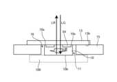
- FIG. 1is a schematic diagram illustrating an example of a magnetic detector according to a first embodiment.
- FIG. 2is a schematic diagram illustrating an example of a substrate on which a magnetic detector is arranged.
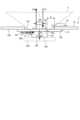
- FIG. 3Ais a schematic diagram illustrating an example of a radiator.
- FIG. 3-2is a partially enlarged view of the radiator.
- FIG. 4is a diagram showing the S11 reflection characteristic of a loop antenna.
- FIG. 5is a schematic diagram illustrating an example of a magnetic detector according to the second embodiment.
- FIG. 6is a schematic diagram illustrating an example of a magnetic detector according to the third embodiment.
- the magnetic detector 1is for detecting magnetism generated in the measured sample 100.
- Figure 1is a schematic diagram for explaining an example of the magnetic detector according to the first embodiment.
- the measured sample 100is an object to be detected by the magnetic detector 1, in other words, a specimen.
- a magnetic fieldis generated in the measured sample 100 when a current flows through a circuit.
- the magnetic field generated in the measured sample 100is detected by the magnetic detector 1.
- the magnetic detector 1is disposed between an objective lens of a microscope (not shown) and a measured sample 100.
- the magnetic detector 1includes a diamond substrate 10, a first substrate 13, a radiator 24, and a second substrate 15.
- the diamond substrate 10is a so-called diamond sensor.
- the diamond substrate 10has an NV center 11 formed in a diamond crystal.
- An NV center 11is formed in the diamond crystal.
- the length of one side of the diamond crystalis, for example, 2 mm.
- the thickness of the diamond crystalis, for example, 300 ⁇ m.
- NV center 11may be arranged singly on one face of the diamond crystal, or multiple NV centers 11 may be arranged in one direction. NV center 11 may be a crystal with multiple different orientations. NV center 11 is formed on the extreme surface of face 11b by, for example, CVD (Chemical Vapor Deposition) or ion implantation.
- CVDChemical Vapor Deposition
- ion implantationion implantation
- the NV centre 11is a complex defect in a diamond crystal where carbon would normally be present, replaced by nitrogen, with a vacancy at an adjacent position.
- the NV centre 11is missing a portion of the degenerate shared electron pair.
- the strength of the external magnetic fieldcan be detected by detecting the electron spin resonance caused by these using light waves and microwaves.
- the electron spin resonance frequency in zero magnetic fieldis known to be approximately 2.87 GHz. When microwaves with the frequency of this resonance point (resonance frequency) are irradiated, the fluorescence with a wavelength of 638 nm is quenched.
- At least a portion of surface 10a of diamond substrate 10is exposed from opening 16 of second substrate 15, which will be described later.
- surface 10a of diamond substrate 10is entirely exposed from opening 16.
- Microwaves and green lightenter from the portion of diamond substrate 10 exposed from opening 16.
- Red lightexits from the portion of diamond substrate 10 exposed from opening 16.
- FIG. 1the direction of incidence of green light is indicated by arrow LG.
- the direction of emission of red lightis indicated by arrow LR.
- the direction of incidence of microwavesis indicated by arrow LM.
- Surface 10b of diamond substrate 10is the magnetic detection surface.
- a first substrate 13is disposed on the surface 10a side of diamond substrate 10.
- the first substrate 13is an antenna substrate.
- the first substrate 13is a transparent substrate.
- the first substrate 13is a substrate that is transmissive to green light, red light, and microwaves.
- the diamond substrate 10is disposed on the surface 13b of the first substrate 13.
- the second substrate 15 and the radiator 24are disposed on the surface 13a of the first substrate 13.
- the first substrate 13has an outer shape larger than the opening 16 of the second substrate 15.
- the diamond substrate 10is bonded to the central portion of the first substrate 13 that is exposed from the opening 16.
- the outer edge of the first substrate 13is bonded to the inner edge of the surface 15b of the second substrate 15.
- the first substrate 13has an opening 16 and holds the diamond substrate 10 instead of the second substrate 15, which cannot directly hold the diamond substrate 10.
- the second substrate 15is a PCB (Printed Circuit Board).
- the second substrate 15has an opening 16 in the center.
- the first substrate 13is disposed in the center of the second substrate 15.
- the outer edge of the first substrate 13is joined to the inner edge of the surface 15b of the second substrate 15.
- the top viewis a view along the direction of incidence of the green light.
- the top viewis a view of the magnetic detector 1 from the side opposite the magnetic detection surface.
- the dashed lineindicates the viewing angle V of the objective lens, that is, the NA (Numerical Aperture) and the working distance. If the opening 16 of the second substrate 15 is narrower than the viewing angle V, a part of the excitation light incident from the objective lens is blocked by the second substrate 15, reducing the amount of light and the detection sensitivity. Therefore, the size of the opening 16 of the second substrate 15 is set so that the excitation light incident from the objective lens is not blocked, in other words, so that the viewing angle A is not blocked. As a result, the excitation light and microwaves are appropriately incident from the surface 10a of the diamond substrate 10 through the opening 16 of the second substrate 15, and act on the NV center 11 on the surface 10b side, which is the magnetic detection surface.
- the second substrate 15is provided with a high-frequency transmission line that supplies microwaves to the radiator 24.
- the high-frequency transmission linewill be described later.
- the diamond substrate 10when measuring the magnetic field of the sample 100 to be measured, the diamond substrate 10, the first substrate 13, and the second substrate 15 are stacked in that order, starting from the substrate closest to the sample 100 to be measured.
- the microwave power supply systemsupplies microwaves in the magnetic detector 1.
- the microwave power supply systemis a radiator 24.
- the radiator 24is provided on the surface 13a of the first substrate 13.
- the radiator 24applies microwaves to the NV center 11 of the diamond substrate 10.
- the radiator 24transmits microwaves to be irradiated to the NV center 11 of the diamond substrate 10.
- the radiator 24transmits microwaves from a microwave source (not shown).
- a high-frequency transmission line provided on the second substrate 15is connected to the radiator 24, and microwaves are supplied from the outside.
- the radiator 24is, for example, a micro loop antenna.
- the frequency of the radiator 24is, for example, 2.8 GHz or more and 2.9 GHz or less.
- the input power of the radiator 24is, for example, -20 dBm or more and +20 dBm or less.
- the radiator 24may be arranged in a comb-like shape as shown in FIG. 3-2.
- the comb-tooth portionforms a capacitance. By adjusting the line and space of the electrode elements and the number of pairs, the comb-tooth portion can reduce the reflection of microwaves of a specific frequency that are incident on the radiator 24.
- the optical systemdetects the magnetism of the measured sample 100 in the magnetic detector 1.
- the optical systemis a light-emitting element and a light-receiving element, not shown.
- the light-emitting element and the light-receiving elementare arranged, for example, on an objective lens arranged facing the diamond substrate 10.
- the light-emitting element and the light-receiving elementare focused on the NV center 11 provided on the diamond substrate 10.
- the light-emitting elementirradiates the diamond substrate 10 with green light.
- the light-emitting elementemits excitation light that irradiates the diamond crystal.
- the light-emitting elementis, for example, a laser diode.
- the light-emitting elementemits laser light with a wavelength of, for example, 527 nm.
- the light-emitting elementemits green excitation light.
- a green light-emitting diodeLED: Light Emitting Diode
- VCSELVertical Cavity Surface Emitting Laser
- LDGreen Edge-emitting laser diode
- the light receiving elementreceives the red light generated by inputting green light to the diamond substrate 10.
- the light receiving elementdetects the fluorescence of the diamond substrate 10.
- the light receiving elementis a photodiode.
- the light receiving elementreceives the fluorescence emitted from the diamond crystal by the excitation light.
- a Si-PIN photodiodePD: Photo Diode
- an InGaAs-PIN photodiodecan be used as the light receiving element.
- FIG. 2is a schematic diagram illustrating an example of a substrate on which a magnetic detector is disposed.
- Fig. 3-1is a schematic diagram illustrating an example of a radiator.
- Fig. 3-2is a partially enlarged view of the radiator.
- the magnetic detector 1 configured in this manneris disposed on a substrate 50.
- the substrate 50is a PCB.
- the second substrate 15 of the magnetic detector 1 and the substrate 50may be a single substrate or may be separate substrates.
- a microwave power supply systemincluding a high-frequency connector 51, a high-frequency transmission line 52, a high-frequency transmission line 53, a high-frequency transmission line 54, and a high-frequency transmission line 55 are arranged on the substrate 50.
- the width of the end 54a of the high-frequency transmission line 54gradually tapers toward the connection with the second substrate 15.
- a method of detecting the magnetic field of the sample 100 to be measured in the magnetic detector 1will be described below.
- the sample 100 to be measuredis placed close to or in close contact with the surface 10b of the diamond substrate 10 of the magnetic detector 1, which is the magnetic field acting surface.
- the microwaves generated by the microwave sourcepropagate to the radiator 24 through the high-frequency connector 51, high-frequency transmission line 52, high-frequency transmission line 53, high-frequency transmission line 54, and high-frequency transmission line 55.
- the microwavesare then radiated from the radiator 24.
- the microwaves radiated from the radiator 24act on the NV center 11 of the diamond substrate 10, causing electron spin resonance.
- the spatial change in the direction or magnitude of the magnetic field generated in the measured sample 100acts on the NV center 11 of the diamond crystal of the diamond substrate 10 of the magnetic detector 1.
- the green excitation light from the light-emitting elementis incident on the diamond crystal.
- the green excitation light that is incident on the diamond crystalthen diffuses widely within the diamond crystal, irradiating and exciting the NV center 11.
- the excited NV center 11generates red fluorescence, which enters the diamond crystal.
- the red fluorescencethen diffuses widely within the diamond crystal and enters the light receiving surface of the light receiving element.
- the light receiving elementreceives the electron spin resonance signal of the NV center 11 excited by the excitation light from the diamond crystal as fluorescence.
- Fig. 4is a diagram showing the S11 reflection characteristic of the loop antenna.
- the diamond substrate 10is exposed from the opening 16 of the second substrate 15.
- the radiator 24is provided on the surface of the first substrate 13 or on the surface of the diamond substrate 10 facing the opposite side to the magnetic detection surface.
- an optical system or a microwave power supply systemis not arranged on the surface 10b side, which is the magnetic detection surface of the diamond substrate 10.
- powercan be supplied to the radiator 24 from the surface 10a opposite to the surface 10b, which is the magnetic detection surface, via the second substrate 15.
- the measured sample 100 of various shapescan be brought close to the surface 10b, which is the magnetic detection surface. In this way, according to this embodiment, a magnetic field can be detected with high sensitivity.
- the magnetic detector 1when the magnetic detector 1 is applied to a microscope, the field of view of the objective lens is sufficiently secured, making it easier to optically bring the NV center 11 into the field of view.
- This embodimentcan be used for observing the magnetic field of a flat microcircuit, etc.
- the diamond substrate 10, the first substrate 13, and the second substrate 15are stacked in that order, starting from the substrate closest to the measured sample 100.
- the measured samples 100 of various shapescan be brought close to the surface 10b, which is the magnetic detection surface.
- the diamond substrate 10can be placed without any restrictions on thickness.
- the radiator 24is disposed on the first substrate 13.
- the antenna forming surfacecan be disposed along the surface of the second substrate 15. According to this embodiment, there is no need to provide a through hole or the like in the second substrate 15, and therefore the configuration can be easily performed.
- the surface on which the antenna is formedis the magnetic detection surface.
- the wiring that supplies power to the antenna from the outside of the diamondforms a convex portion on the magnetic detection surface side. This can make it difficult to bring the sample to be measured close to the magnetic detection surface. If the sample to be measured cannot be brought close enough to the magnetic detection surface, the detection sensitivity of the magnetic field decreases.
- [Second embodiment] 5is a schematic diagram for explaining an example of a magnetic detector according to the second embodiment.
- a diamond substrate 10, a first substrate 13, and a second substrate 15are different from those in the first embodiment.
- the diamond substrate 10 and the second substrate 15are disposed on the surface 13b of the first substrate 13.
- the diamond substrate 10is disposed inside the opening 16 of the second substrate 15.
- the diamond substrate 10may protrude beyond the surface 13b of the first substrate 13.
- the emitter 24is disposed between the diamond substrate 10 and the first substrate 13. More specifically, the emitter 24 is provided on the surface 13b of the first substrate 13 or the surface 10a of the diamond substrate 10.
- the diamond substrate 10 and the second substrate 15are disposed on the surface 13b of the first substrate 13.
- the diamond substrate 10is disposed inside the opening 16 of the second substrate 15.
- the thickness of the magnetic detector 1can be made thinner than in the first embodiment.
- the objective lenscan be brought closer to the NV center 11 of the diamond substrate 10.
- the radiator 24is disposed between the diamond substrate 10 and the first substrate 13.
- powercan be supplied to the radiator 24 from the surface 10a opposite the surface 10b, which is the magnetic detection surface.
- the measured sample 100when the diamond substrate 10 protrudes beyond the surface 13b of the first substrate 13, the measured sample 100 can be brought close to or in close contact with the surface 10b, which is the magnetic field acting surface of the diamond substrate 10 of the magnetic detector 1.
- This embodimentallows the measured samples 100 of various shapes to be brought close to the surface 10b, which is the magnetic detection surface. In this way, this embodiment allows magnetic fields to be detected with high sensitivity.
- FIG. 6is a schematic diagram illustrating an example of a magnetic detector according to a third embodiment.
- the magnetic detector 1is different from the first embodiment in that it includes a magnet 30.
- the magnet 30applies a static magnetic field to the NV center 11 of the diamond substrate 10.
- the magnet 30is disposed on the first substrate 13 or the second substrate 15.
- the magnet 30is adjusted so that the direction AM of the magnetic field is perpendicular to the direction AD of the NV center 11.
- the magnet 30can be fixed onto the surface 13b of the first substrate 13. According to this embodiment, double resonance can be stably and accurately generated by the magnet 30. This embodiment can measure the magnetic field more accurately.
Landscapes
- Physics & Mathematics (AREA)
- General Physics & Mathematics (AREA)
- Chemical & Material Sciences (AREA)
- High Energy & Nuclear Physics (AREA)
- Health & Medical Sciences (AREA)
- Life Sciences & Earth Sciences (AREA)
- Condensed Matter Physics & Semiconductors (AREA)
- Analytical Chemistry (AREA)
- Biochemistry (AREA)
- General Health & Medical Sciences (AREA)
- Immunology (AREA)
- Pathology (AREA)
- Measuring Magnetic Variables (AREA)
Abstract
Description
Translated fromJapanese本開示は、磁気検出器に関する。This disclosure relates to a magnetic detector.
特許文献1には、NVセンタを有するダイヤモンドと、その表面に形成されたループ状の導体からなるアンテナを含む磁界を計測するセンサが開示されている。特許文献1に記載の技術では、センサのアンテナ形成面の反対面から、NVセンタへの励起光とその蛍光の入出力が行われる。
1つの態様に係る磁気検出器は、NVセンタを有するダイヤモンド基板と、前記ダイヤモンド基板が配置された、透明な第1基板と、前記第1基板の面、又は、前記ダイヤモンド基板のNVセンタが形成された面と反対側を向いた面に形成された放射体と、開口を有し、前記第1基板が配置された第2基板と、を備え、前記ダイヤモンド基板は、少なくとも一部が前記開口から露出する。In one embodiment, the magnetic detector comprises a diamond substrate having an NV center, a transparent first substrate on which the diamond substrate is disposed, an emitter formed on a surface of the first substrate or on a surface of the diamond substrate facing opposite to the surface on which the NV center is formed, and a second substrate having an opening and on which the first substrate is disposed, with at least a portion of the diamond substrate exposed from the opening.
以下に実施形態に係る磁気検出器について説明する。磁気検出器1は、被測定サンプル100に発生する磁気を検出するためのものである。図1は、第1実施形態に係る磁気検出器の一例を説明する概略図である。The magnetic detector according to the embodiment will be described below. The
[第1実施形態]
(被測定サンプル)
被測定サンプル100は、磁気検出器1による検出の対象物、言い換えると、試料である。被測定サンプル100は、回路を電流が流れることによって磁界が発生する。被測定サンプル100に生じた磁気を、磁気検出器1が検出する。[First embodiment]
(Measurement sample)
The measured
(磁気検出器)
磁気検出器1は、図示しない顕微鏡の対物レンズと、被測定サンプル100との間に配置される。磁気検出器1は、ダイヤモンド基板10と、第1基板13と、放射体24と、第2基板15とを備える。(Magnetic detector)
The
ダイヤモンド基板10は、いわゆるダイヤモンドセンサである。ダイヤモンド基板10は、ダイヤモンド結晶に形成されたNVセンタ11を有する。The
ダイヤモンド結晶には、NVセンタ11が形成される。ダイヤモンド結晶は、1辺の長さが、例えば2mmである。ダイヤモンド結晶は、厚さが、例えば300μmである。An
NVセンタ11は、ダイヤモンド結晶の一面に単一で配置されていても、複数を配列してもよい。NVセンタ11は、方位が一方向にそろっていてもよい。NVセンタ11は、異なる複数の方位の結晶であってもよい。NVセンタ11は、面11bの極表面に、例えば、CVD(Chemical Vapor Deposition)法やイオン注入法によって形成される。
NVセンタ11は、ダイヤモンド結晶において、本来は炭素が存在するべきところが窒素で置換され、隣接する位置に空孔がある複合欠陥である。NVセンタ11は、縮退する共有電子対の一部が欠損する。NVセンタ11は、ゼロ磁場においてm=0とm=±1の2つの準位のスピン角運動量を持った電子を有する。m=±1の電子は磁気モーメントを持つため外部磁場の影響を受け、m=±1の縮退も解け、さらに2つのエネルギー準位を有する。これらに起因する電子スピン共鳴を光波及びマイクロ波を用いて検知することにより外部磁場の強度を検出可能である。The
NVセンタ11の電子は、532nmの波長の光で励起され、緩和の過程で638nmの波長の蛍光を放出する。この蛍光過程は電子スピン共鳴周波数においては起こりにくい。そのため、この性質を用いることにより、m=±1の電子の状態を観測することができる。ダイヤモンド結晶のNVセンタ11では、ゼロ磁場における電子スピン共鳴周波数が約2.87GHzと知られている。この共鳴点の周波数(共鳴周波数)のマイクロ波が照射されたときに638nmの波長の蛍光が消光する。また、外部磁場の大きさ等に応じたm=±1の電子の状態の変化により、マイクロ波の共鳴周波数が変化する。そして、この変化を蛍光強度の周波数変化により捉えることで、磁界及び電流を検出可能である。Electrons in the
ダイヤモンド基板10の面10aは、少なくとも一部が後述する第2基板15の開口16から露出する。本実施形態では、ダイヤモンド基板10の面10aは、全面が開口16から露出する。ダイヤモンド基板10の開口16から露出した部分から、マイクロ波及び緑色光が入射する。ダイヤモンド基板10の開口16から露出した部分から、赤色光が射出される。図1において、緑色光の入射方向を矢印LGで示す。赤色光の射出方向を矢印LRで示す。マイクロ波の入射方向を矢印LMで示す。At least a portion of
ダイヤモンド基板10の面10bは、磁気検出面である。ダイヤモンド基板10の面10a側に、第1基板13が配置されている。
第1基板13は、アンテナ基板である。第1基板13は、透明な基板である。第1基板13は、緑色光、赤色光及びマイクロ波を透過可能な基板である。第1基板13の面13bには、ダイヤモンド基板10が配置されている。第1基板13の面13aには、第2基板15及び放射体24が配置されている。第1基板13は、第2基板15の開口16より大きい外形を有する。第1基板13の中央部であって、開口16から露出する部分にダイヤモンド基板10が接合されている。第1基板13の外縁部と、第2基板15の面15bの内縁部とが接合されている。The
第1基板13は、開口16が設けられ、ダイヤモンド基板10を直接保持することができない第2基板15に代わって、ダイヤモンド基板10を保持する。The
第2基板15は、PCB(Printed Circuit Board)である。第2基板15は、中央部に開口16を有する。第2基板15の中央部には、第1基板13が配置されている。第2基板15の面15bの内縁部に、第1基板13の外縁部が接合されている。The
上面視において、開口16の周縁部16aと、ダイヤモンド基板10との間に径方向において間隔Sが存在する。When viewed from above, there is a radial gap S between the
上面視とは、緑色光の入射方向に沿った方向視である。上面視とは、磁気検出器1を磁気検出面と反対側から見ることである。The top view is a view along the direction of incidence of the green light. The top view is a view of the
第2基板15の開口16と対物レンズの視野角Vとの関係について説明する。図1において、破線は、対物レンズの視野角V、すなわち、NA(Numerical Aperture、開口数)と作動距離とを示す。視野角Vよりも第2基板15の開口16が狭い場合、対物レンズから入射する励起光の一部が第2基板15により遮られて光量が低下し、検出感度が低下する。そこで、対物レンズから入射する励起光が遮られないように、言い換えると、視野角Aを遮ることがないように、第2基板15の開口16の大きさが設定される。これにより、第2基板15の開口16を介して、ダイヤモンド基板10の面10aから励起光及びマイクロ波を適切に入射させ、磁気検出面である面10b側のNVセンタ11に作用させられる。The relationship between the opening 16 of the
第2基板15には、放射体24にマイクロ波を給電する高周波伝送線路が設けられている。高周波伝送線路については、後述する。The
このように構成された磁気検出器1において、被測定サンプル100の磁場を測定する際に、被測定サンプル100に近い順に、ダイヤモンド基板10、第1基板13、第2基板15の順番に積層されている。In the
(マイクロ波給電系)
マイクロ波給電系は、磁気検出器1において、マイクロ波を給電する。マイクロ波給電系は、放射体24である。放射体24は、第1基板13の面13aに設けられている。放射体24は、ダイヤモンド基板10のNVセンタ11にマイクロ波を印可する。放射体24は、ダイヤモンド基板10のNVセンタ11に照射するマイクロ波を伝送する。放射体24は、図示しないマイクロ波源からのマイクロ波を伝送する。放射体24には、第2基板15に設けられた高周波伝送線路が接続され、外部からマイクロ波が給電される。(Microwave power supply system)
The microwave power supply system supplies microwaves in the
放射体24は、例えば、微小ループアンテナである。放射体24は、例えば、周波数が2.8GHz以上2.9GHz以下である。放射体24は、例えば、入力電力が-20dBm以上+20dBm以下である。The
放射体24は、図3-2に示すように、櫛歯状に設けられていてもよい。櫛歯部は、キャパシタンスを構成する。櫛歯部は電極子のライン&スペースや対数を調整することにより、放射体24に入射する特定周波数のマイクロ波の反射を軽減することができる。The
(光学系)
光学系は、磁気検出器1における、被測定サンプル100の磁気を検出する。光学系は、図示しない発光素子及び受光素子である。発光素子及び受光素子は、例えば、ダイヤモンド基板10に向かい合って配置された対物レンズに配置される。発光素子及び受光素子は、ダイヤモンド基板10に設けられているNVセンタ11に焦点が合わされている。(Optical system)
The optical system detects the magnetism of the measured
発光素子は、ダイヤモンド基板10へ緑色光を照射する。発光素子は、ダイヤモンド結晶を照射する励起光を発光する。発光素子は、例えば、レーザダイオードである。発光素子は、例えば波長527nmのレーザ光を発光する。発光素子は、緑色の励起光を発光する。発光素子として、例えば緑色発光ダイオード(LED:Light Emitting Diode)、緑色面発光レーザダイオード(VCSEL:Vertical Cavity Surface Emitting Laser)及び緑色端面発光レーザダイオード(LD:Laser Diode)等を用いることができる。The light-emitting element irradiates the
受光素子は、ダイヤモンド基板10に緑色光を入力することにより発生する赤色光を受光する。受光素子は、ダイヤモンド基板10の蛍光を検出する。受光素子は、フォトダイオードである。受光素子は、励起光により発する蛍光を、ダイヤモンド結晶から受光する。受光素子は、例えばSi-PINフォトダイオード(PD:Photo Diode)及びInGaAs-PINフォトダイオード等を用いることができる。The light receiving element receives the red light generated by inputting green light to the
(基板)
図2は、磁気検出器が配置された基板の一例を説明する概略図である。図3-1は、放射体の一例を説明する概略図である。図3-2は、放射体の部分拡大図である。このように構成された磁気検出器1は、基板50上に配置されている。基板50は、PCBである。本実施形態では、磁気検出器1の第2基板15と基板50とは1枚の基板であってもよいし、別の基板であってもよい。(substrate)
Fig. 2 is a schematic diagram illustrating an example of a substrate on which a magnetic detector is disposed. Fig. 3-1 is a schematic diagram illustrating an example of a radiator. Fig. 3-2 is a partially enlarged view of the radiator. The
基板50上には、高周波コネクタ51、高周波伝送線路52、高周波伝送線路53、高周波伝送線路54、高周波伝送線路55等のマイクロ波給電系が配置されている。高周波伝送線路54は、第2基板15との接続部に向かって、端部54aの幅が徐々に傾斜している。A microwave power supply system including a high-
(磁場検出方法・作用)
磁気検出器1における、被測定サンプル100の磁場の検出方法について説明する。磁界を検出する際には、磁気検出器1のダイヤモンド基板10の磁界作用面である面10bに、被測定サンプル100を近接または密着させる。(Method and action of detecting magnetic field)
A method of detecting the magnetic field of the
マイクロ波源が発生させたマイクロ波は、高周波コネクタ51、高周波伝送線路52、高周波伝送線路53、高周波伝送線路54、高周波伝送線路55を通じて放射体24に伝搬する。そして、放射体24からマイクロ波が放射される。そして、放射体24から放射されたマイクロ波は、ダイヤモンド基板10のNVセンタ11に作用し電子スピン共鳴を生じさせる。被測定サンプル100に発生する磁界の向きまたは大きさの空間的な変化が、磁気検出器1のダイヤモンド基板10のダイヤモンド結晶のNVセンタ11に作用する。The microwaves generated by the microwave source propagate to the
発光素子の緑色の励起光は、ダイヤモンド結晶に入射する。そして、ダイヤモンド結晶に入射した緑色の励起光は、ダイヤモンド結晶内で広がりをもって拡散し、NVセンタ11を照射し励起する。The green excitation light from the light-emitting element is incident on the diamond crystal. The green excitation light that is incident on the diamond crystal then diffuses widely within the diamond crystal, irradiating and exciting the
励起されたNVセンタ11は、赤色の蛍光を発生し、赤色の蛍光は、ダイヤモンド結晶に入射する。そして、赤色の蛍光は、ダイヤモンド結晶内で広がりをもって拡散し、受光素子の受光面に入射する。The
受光素子は、ダイヤモンド結晶から、励起光で励起されたNVセンタ11の電子スピン共鳴信号を蛍光で受光する。The light receiving element receives the electron spin resonance signal of the
図4は、ループアンテナのS11反射特性を示す図である。図4は、磁気検出器1をダイヤモンド量子センサーヘッドとして実現した際に、高周波コネクタ51にベクトルネットワークアナライザーのテストポートを接続し、S11反射特性を測定した結果を示すグラフである。図4に示すように、入力周波数2.9GHzにおいてS11=-25dBと良好な特性を確認した。Fig. 4 is a diagram showing theS11 reflection characteristic of the loop antenna. Fig. 4 is a graph showing the results of measuring theS11 reflection characteristic when the
(効果)
以上により、本実施形態では、ダイヤモンド基板10は、少なくとも一部が第2基板15の開口16から露出する。放射体24は、第1基板13の面、又は、ダイヤモンド基板10の磁気検出面と反対側を向いた面に設けられている。本実施形態は、ダイヤモンド基板10が小さくても、第2基板15の開口16により光学視野を確保できる。本実施形態では、ダイヤモンド基板10の磁気検出面である面10b側に光学系やマイクロ波給電系が配置されない。本実施形態は、第2基板15を介して、磁気検出面である面10bの反対側の面10aから放射体24へ給電できる。本実施形態は、磁気検出面である面10bに様々な形状の被測定サンプル100を近接させることができる。このようにして、本実施形態によれば、高感度の磁場を検出できる。(effect)
As described above, in this embodiment, at least a part of the
本実施形態によれば、磁気検出器1を顕微鏡に適用する場合、対物レンズの視野が十分確保されるので、光学的にNVセンタ11を視野におさめやすくできる。本実施形態は、平板状の微小回路の磁場観察などに使用できる。According to this embodiment, when the
本実施形態では、上面視において、第2基板15の開口16の周縁部16aと、ダイヤモンド基板10との間に間隔Sが存在する。本実施形態によれば、上面視において、ダイヤモンド基板10の全体が第2基板15の開口16から露出することができる。本実施形態によれば、光学視野を効率よく確保できる。In this embodiment, when viewed from above, there is a gap S between the
本実施形態では、被測定サンプル100に近い順に、ダイヤモンド基板10、第1基板13、第2基板15の順番に積層されている。本実施形態によれば、磁気検出面である面10bに様々な形状の被測定サンプル100を近接させることができる。本実施形態は、ダイヤモンド基板10を厚さに制限なく、配置することができる。In this embodiment, the
本実施形態では、放射体24は、第1基板13に配置されている。本実施形態は、アンテナ形成面を第2基板15の面上に沿って配置することができる。本実施形態によれば、第2基板15にスルーホール等を設けなくてよいので、容易に構成できる。In this embodiment, the
これに対して、特許文献1に記載の技術では、アンテナ形成面側が磁気検出面である。これにより、ダイヤモンドの外側からアンテナに給電する配線が磁気検出面側に凸部を形成する。このため、被測定サンプルを磁気検出面に近接しにくくなることがある。磁気検出面に被測定サンプルを十分に近づけられない場合、磁場の検出感度が低下する。In contrast, in the technology described in
[第2実施形態]
図5は、第2実施形態に係る磁気検出器の一例を説明する概略図である。本実施形態では、ダイヤモンド基板10と、第1基板13と、第2基板15とが第一実施形態と異なる。[Second embodiment]
5 is a schematic diagram for explaining an example of a magnetic detector according to the second embodiment. In this embodiment, a
ダイヤモンド基板10及び第2基板15は、第1基板13の面13bに配置されている。第2基板15の開口16の内側に、ダイヤモンド基板10が配置されている。The
ダイヤモンド基板10は、第1基板13の面13bより突出していてもよい。The
放射体24は、ダイヤモンド基板10と第1基板13との間に配置されている。より詳しくは、放射体24は、第1基板13の面13b、又は、ダイヤモンド基板10の面10aに設けられている。The
(効果)
以上により、本実施形態では、ダイヤモンド基板10及び第2基板15は、第1基板13の面13bに配置されている。本実施形態では、第2基板15の開口16の内側に、ダイヤモンド基板10が配置されている。本実施形態は、第一実施形態に比べて、磁気検出器1の厚さを薄くできる。本実施形態によれば、対物レンズをダイヤモンド基板10のNVセンタ11に近づけることができる。(effect)
As described above, in this embodiment, the
本実施形態では、放射体24は、ダイヤモンド基板10と第1基板13との間に配置されている。本実施形態は、磁気検出面である面10bの反対側の面10aから放射体24へ給電できる。In this embodiment, the
本実施形態では、ダイヤモンド基板10が第1基板13の面13bより突出している場合、磁気検出器1のダイヤモンド基板10の磁界作用面である面10bに、被測定サンプル100を近接または密着できる。本実施形態は、磁気検出面である面10bに様々な形状の被測定サンプル100を近接させることができる。このようにして、本実施形態によれば、高感度の磁場を検出できる。In this embodiment, when the
[第3実施形態]
図6は、第3実施形態に係る磁気検出器の一例を説明する概略図である。本実施形態では、磁気検出器1は、磁石30を備える点で第一実施形態と異なる。[Third embodiment]
6 is a schematic diagram illustrating an example of a magnetic detector according to a third embodiment. In this embodiment, the
磁石30は、ダイヤモンド基板10のNVセンタ11に静磁場を印可する。磁石30は、第1基板13又は第2基板15に配置されている。磁石30は、NVセンタ11の方向ADに対して垂直に磁場の方向AMが向くように調整されている。The
(効果)
以上により、本実施形態では、磁石30を第1基板13の面13b上に固定できる。本実施形態によれば、磁石30により、安定的かつ正確に二重共鳴を発生させることができる。本実施形態は、磁場をより正確に測定できる。(effect)
As described above, in this embodiment, the
本出願の開示する実施形態は、発明の要旨及び範囲を逸脱しない範囲で変更できる。さらに、本出願の開示する実施形態及びその変形例は、適宜組み合わせることができる。The embodiments disclosed in this application may be modified without departing from the spirit and scope of the invention. Furthermore, the embodiments disclosed in this application and their variations may be combined as appropriate.
添付の請求項に係る技術を完全かつ明瞭に開示するために特徴的な実施形態に関し記載してきた。しかし、添付の請求項は、上記実施形態に限定されるべきものでなく、本明細書に示した基礎的事項の範囲内で当該技術分野の当業者が創作しうるすべての変形例及び代替可能な構成を具現化するように構成されるべきである。The appended claims have been described in terms of characteristic embodiments in order to fully and clearly disclose the technology to which they relate. However, the appended claims should not be limited to the above-described embodiments, but should be constructed to embody all modifications and alternative configurations that may be created by those skilled in the art within the scope of the basic matters set forth in this specification.
1 磁気検出器
10 ダイヤモンド基板
11 NVセンタ
13 第1基板
15 第2基板
16 開口
24 放射体
50 基板
51 高周波コネクタ
52 高周波伝送線路
53 高周波伝送線路
54 高周波伝送線路
54a 端部
55 高周波伝送線路
100 被測定サンプルREFERENCE SIGNS
Claims (7)
Translated fromJapanese前記ダイヤモンド基板が配置された、透明な第1基板と、
前記第1基板の面、又は、前記ダイヤモンド基板のNVセンタが設けられた面と反対側を向いた面に設けられた放射体と、
開口を有し、前記第1基板が配置された第2基板と、
を備え、
前記ダイヤモンド基板は、少なくとも一部が前記開口から露出する、
磁気検出器。a diamond substrate having an NV center;
a transparent first substrate on which the diamond substrate is disposed;
a radiator provided on a surface of the first substrate or a surface of the diamond substrate facing opposite to a surface on which the NV center is provided;
a second substrate having an opening and on which the first substrate is disposed;
Equipped with
At least a portion of the diamond substrate is exposed through the opening.
Magnetic detector.
請求項1に記載の磁気検出器。When viewed from above, a gap exists between the peripheral edge of the opening and the diamond substrate.
The magnetic detector according to claim 1 .
請求項1に記載の磁気検出器。The diamond substrate, the first substrate, and the second substrate are laminated in this order in order of proximity to a sample to be measured for which magnetic fields are to be detected.
The magnetic detector according to claim 1 .
請求項3に記載の磁気検出器。The radiator is disposed on the first substrate.
The magnetic detector according to claim 3 .
前記第2基板の前記開口の内側に、前記ダイヤモンド基板が配置されている、
請求項1に記載の磁気検出器。the diamond substrate and the second substrate are disposed on a surface of the first substrate;
The diamond substrate is disposed inside the opening of the second substrate.
The magnetic detector according to claim 1 .
請求項5に記載の磁気検出器。The emitter is disposed between the diamond substrate and the first substrate.
The magnetic detector according to claim 5 .
を備え、
前記NVセンタの方向に対して垂直に磁場の方向が向くように調整されている、
請求項1に記載の磁気検出器。A magnet disposed on the first substrate or the second substrate;
Equipped with
The magnetic field is adjusted so as to be oriented perpendicular to the direction of the NV center.
The magnetic detector according to claim 1 .
Applications Claiming Priority (2)
| Application Number | Priority Date | Filing Date | Title |
|---|---|---|---|
| JP2023-054219 | 2023-03-29 | ||
| JP2023054219 | 2023-03-29 |
Publications (1)
| Publication Number | Publication Date |
|---|---|
| WO2024203140A1true WO2024203140A1 (en) | 2024-10-03 |
Family
ID=92904374
Family Applications (1)
| Application Number | Title | Priority Date | Filing Date |
|---|---|---|---|
| PCT/JP2024/008898PendingWO2024203140A1 (en) | 2023-03-29 | 2024-03-07 | Magnetic detector |
Country Status (1)
| Country | Link |
|---|---|
| WO (1) | WO2024203140A1 (en) |
Cited By (1)
| Publication number | Priority date | Publication date | Assignee | Title |
|---|---|---|---|---|
| WO2025187461A1 (en)* | 2024-03-07 | 2025-09-12 | 京セラ株式会社 | Detector and microscope |
Citations (5)
| Publication number | Priority date | Publication date | Assignee | Title |
|---|---|---|---|---|
| US20160282427A1 (en)* | 2014-02-19 | 2016-09-29 | Infinitum Solutions, Inc. | Integrated optical nanoscale probe measurement of electric fields from electric charges in electronic devices |
| JP2021103093A (en)* | 2019-12-24 | 2021-07-15 | スミダコーポレーション株式会社 | Measuring apparatus and measuring method |
| WO2021200144A1 (en)* | 2020-03-31 | 2021-10-07 | 国立大学法人東京工業大学 | Physical state measurement device |
| JP2022098572A (en)* | 2020-12-22 | 2022-07-04 | 矢崎総業株式会社 | Sensor |
| WO2022249995A1 (en)* | 2021-05-25 | 2022-12-01 | 京セラ株式会社 | Detection substrate, detector, and detecting device |
- 2024
- 2024-03-07WOPCT/JP2024/008898patent/WO2024203140A1/enactivePending
Patent Citations (5)
| Publication number | Priority date | Publication date | Assignee | Title |
|---|---|---|---|---|
| US20160282427A1 (en)* | 2014-02-19 | 2016-09-29 | Infinitum Solutions, Inc. | Integrated optical nanoscale probe measurement of electric fields from electric charges in electronic devices |
| JP2021103093A (en)* | 2019-12-24 | 2021-07-15 | スミダコーポレーション株式会社 | Measuring apparatus and measuring method |
| WO2021200144A1 (en)* | 2020-03-31 | 2021-10-07 | 国立大学法人東京工業大学 | Physical state measurement device |
| JP2022098572A (en)* | 2020-12-22 | 2022-07-04 | 矢崎総業株式会社 | Sensor |
| WO2022249995A1 (en)* | 2021-05-25 | 2022-12-01 | 京セラ株式会社 | Detection substrate, detector, and detecting device |
Cited By (1)
| Publication number | Priority date | Publication date | Assignee | Title |
|---|---|---|---|---|
| WO2025187461A1 (en)* | 2024-03-07 | 2025-09-12 | 京セラ株式会社 | Detector and microscope |
Similar Documents
| Publication | Publication Date | Title |
|---|---|---|
| US8634078B2 (en) | Sensor, method for detecting the presence and/or concentration of an analyte using the sensor, and use of the method | |
| US12372487B2 (en) | Sensor device for magnetic field measurement by means of optical magnetic resonance measurement | |
| WO2024203140A1 (en) | Magnetic detector | |
| KR101931829B1 (en) | Method and arrangement for determining the heating condition of a mirror in an optical system | |
| US20240219486A1 (en) | Detection substrate, detector, and detecting device | |
| US20240302460A1 (en) | Diamond magnetic sensor unit and diamond magnetic sensor system | |
| JP7585341B2 (en) | Magnetic Sensors and Detection Systems | |
| WO2022163679A1 (en) | Diamond sensor unit | |
| US20220166185A1 (en) | Semiconductor laser device | |
| WO2022183895A1 (en) | Methods and apparatus for integrating diamond with led towards on-chip quantum sensing | |
| EP4445160A1 (en) | Sensor device comprising a source of fluorescence coupled to a fluorescence collector and magnetometer comprising said device | |
| JP7397429B2 (en) | Excitation light irradiation device and excitation light irradiation method | |
| US7385393B2 (en) | Magnetic field measuring apparatus capable of measuring at high spatial resolution | |
| US20240111008A1 (en) | Diamond sensor unit and diamond sensor system | |
| WO2025187461A1 (en) | Detector and microscope | |
| US11733264B2 (en) | Cantilever, scanning probe microscope, and measurement method using scanning probe microscope | |
| WO2024185825A1 (en) | Magnetic field detection device | |
| WO2024181575A1 (en) | Current sensor and current detection device | |
| US20250116734A1 (en) | Sensor system for detecting a medium | |
| JP3143884B2 (en) | Emission scanning tunneling microscope | |
| US12442872B2 (en) | Magnetic field gradiometer | |
| US12442876B2 (en) | Magnetic sensor, detection unit, detection system, substrate for magnetic sensor, waveguide body for magnetic sensor, opto-electric hybrid substrate for magnetic sensor, and detection substrate for detection unit | |
| CN111121962A (en) | Optical fiber photodetector, detection system, test system and preparation method | |
| US20240133979A1 (en) | Magnetic field gradiometer | |
| JP7076021B1 (en) | Light guide, electron beam detector, and charged particle device |
Legal Events
| Date | Code | Title | Description |
|---|---|---|---|
| 121 | Ep: the epo has been informed by wipo that ep was designated in this application | Ref document number:24779274 Country of ref document:EP Kind code of ref document:A1 | |
| ENP | Entry into the national phase | Ref document number:2025510185 Country of ref document:JP Kind code of ref document:A | |
| WWE | Wipo information: entry into national phase | Ref document number:2025510185 Country of ref document:JP |