WO2024191270A1 - Three-dimensional flash memory that improves leakage current - Google Patents
Three-dimensional flash memory that improves leakage currentDownload PDFInfo
- Publication number
- WO2024191270A1 WO2024191270A1PCT/KR2024/095561KR2024095561WWO2024191270A1WO 2024191270 A1WO2024191270 A1WO 2024191270A1KR 2024095561 WKR2024095561 WKR 2024095561WWO 2024191270 A1WO2024191270 A1WO 2024191270A1
- Authority
- WO
- WIPO (PCT)
- Prior art keywords
- vertical channel
- flash memory
- pattern
- channel pattern
- dimensional flash
- Prior art date
- Legal status (The legal status is an assumption and is not a legal conclusion. Google has not performed a legal analysis and makes no representation as to the accuracy of the status listed.)
- Pending
Links
Images


Classifications
- H—ELECTRICITY
- H10—SEMICONDUCTOR DEVICES; ELECTRIC SOLID-STATE DEVICES NOT OTHERWISE PROVIDED FOR
- H10B—ELECTRONIC MEMORY DEVICES
- H10B41/00—Electrically erasable-and-programmable ROM [EEPROM] devices comprising floating gates
- H10B41/10—Electrically erasable-and-programmable ROM [EEPROM] devices comprising floating gates characterised by the top-view layout
- H—ELECTRICITY
- H10—SEMICONDUCTOR DEVICES; ELECTRIC SOLID-STATE DEVICES NOT OTHERWISE PROVIDED FOR
- H10B—ELECTRONIC MEMORY DEVICES
- H10B41/00—Electrically erasable-and-programmable ROM [EEPROM] devices comprising floating gates
- H10B41/20—Electrically erasable-and-programmable ROM [EEPROM] devices comprising floating gates characterised by three-dimensional arrangements, e.g. with cells on different height levels
- H10B41/23—Electrically erasable-and-programmable ROM [EEPROM] devices comprising floating gates characterised by three-dimensional arrangements, e.g. with cells on different height levels with source and drain on different levels, e.g. with sloping channels
- H10B41/27—Electrically erasable-and-programmable ROM [EEPROM] devices comprising floating gates characterised by three-dimensional arrangements, e.g. with cells on different height levels with source and drain on different levels, e.g. with sloping channels the channels comprising vertical portions, e.g. U-shaped channels
- H—ELECTRICITY
- H10—SEMICONDUCTOR DEVICES; ELECTRIC SOLID-STATE DEVICES NOT OTHERWISE PROVIDED FOR
- H10B—ELECTRONIC MEMORY DEVICES
- H10B41/00—Electrically erasable-and-programmable ROM [EEPROM] devices comprising floating gates
- H10B41/30—Electrically erasable-and-programmable ROM [EEPROM] devices comprising floating gates characterised by the memory core region
- H—ELECTRICITY
- H10—SEMICONDUCTOR DEVICES; ELECTRIC SOLID-STATE DEVICES NOT OTHERWISE PROVIDED FOR
- H10B—ELECTRONIC MEMORY DEVICES
- H10B43/00—EEPROM devices comprising charge-trapping gate insulators
- H10B43/10—EEPROM devices comprising charge-trapping gate insulators characterised by the top-view layout
- H—ELECTRICITY
- H10—SEMICONDUCTOR DEVICES; ELECTRIC SOLID-STATE DEVICES NOT OTHERWISE PROVIDED FOR
- H10B—ELECTRONIC MEMORY DEVICES
- H10B43/00—EEPROM devices comprising charge-trapping gate insulators
- H10B43/20—EEPROM devices comprising charge-trapping gate insulators characterised by three-dimensional arrangements, e.g. with cells on different height levels
- H10B43/23—EEPROM devices comprising charge-trapping gate insulators characterised by three-dimensional arrangements, e.g. with cells on different height levels with source and drain on different levels, e.g. with sloping channels
- H10B43/27—EEPROM devices comprising charge-trapping gate insulators characterised by three-dimensional arrangements, e.g. with cells on different height levels with source and drain on different levels, e.g. with sloping channels the channels comprising vertical portions, e.g. U-shaped channels
- H—ELECTRICITY
- H10—SEMICONDUCTOR DEVICES; ELECTRIC SOLID-STATE DEVICES NOT OTHERWISE PROVIDED FOR
- H10B—ELECTRONIC MEMORY DEVICES
- H10B43/00—EEPROM devices comprising charge-trapping gate insulators
- H10B43/30—EEPROM devices comprising charge-trapping gate insulators characterised by the memory core region
Definitions
- the embodiments belowdescribe a technology for three-dimensional flash memory that improves leakage current.
- Flash memory devicesare electrically erasable programmable read-only memories (EEPROM) that control the input and output of data electrically by Fowler-Nordheimtunneling or hot electron injection, and can be commonly used in computers, digital cameras, MP3 players, game systems, memory sticks, etc.
- EEPROMelectrically erasable programmable read-only memories
- 3D flash memoryuses polysilicon material as a vertical channel pattern (VCP) that extends vertically to connect memory cell transistors (MCTs), as shown in Fig. 1.
- VCPvertical channel pattern
- MCTsmemory cell transistors
- VCPvertical channel pattern
- One embodimentproposes a three-dimensional flash memory and a method of manufacturing the same, in which the drain region and the source region are formed of different materials to reduce the contact resistance in the drain region while reducing the leakage current in the source region.
- one embodimentproposes a three-dimensional flash memory and a method for manufacturing the same, in which a vertical channel pattern is formed of a composite structure of a first vertical channel pattern and a second vertical channel pattern, and the second vertical channel pattern is formed of a material that does not have the characteristics of a grain boundary, in order to improve cell current.
- a three-dimensional flash memorymay include word lines formed to extend horizontally on a substrate and stacked while being spaced apart from each other in the vertical direction; vertical channel structures formed to extend vertically on the substrate through the word lines, each of the vertical channel structures including a vertical channel pattern formed to extend vertically and a data storage pattern formed to cover an outer wall of the vertical channel pattern, wherein the data storage pattern and the vertical channel pattern constitute memory cells corresponding to the word lines; a drain region positioned at an upper end of each of the vertical channel structures; and a source region positioned at a lower end of the vertical channel structures, wherein the drain region and the source region are formed of different materials.
- the drain regionmay be formed of a material for reducing contact resistance with a bit line contact plug connected to the upper end of each of the vertical channel structures, and the source region may be formed of a material for reducing leakage current in the source region.
- the drain regionmay be formed of at least one material among polycrystalline silicon or silicon crystal materials
- the source regionmay be formed of an oxide semiconductor material including at least one metal ion among In, Ga, Zn, Sn, Ni, Cu, Al, or Sr.
- the vertical channel patternmay be characterized by having a composite structure of a first vertical channel pattern formed of the same material as the material forming the drain region and contacting the inner wall of the data storage pattern, and a second vertical channel pattern formed of the same material as the material forming the source region and contacting the inner wall of the first vertical channel pattern.
- the second vertical channel patternmay be characterized by not having the characteristics of a grain boundary since it is formed of an oxide semiconductor material including at least one metal ion among In, Ga, Zn, Sn, Ni, Cu, Al, or Sr.
- the first vertical channel patternmay be formed of at least one of the polycrystalline silicon or silicon crystal materials to improve interface characteristics with the data storage pattern.
- a method for manufacturing a three-dimensional flash memorymay include the steps of preparing a semiconductor structure including word lines formed to extend horizontally on a substrate and stacked while being spaced apart from each other in the vertical direction; vertical channel structures formed to extend vertically on the substrate through the word lines, each of the vertical channel structures including a vertical channel pattern formed to extend vertically and a data storage pattern formed to cover an outer wall of the vertical channel pattern, wherein the data storage pattern and the vertical channel pattern form memory cells corresponding to the word lines; and a drain region positioned on an upper end of each of the vertical channel structures; and forming a source region positioned on a lower end of the vertical channel structures using a material different from a material forming the drain region.
- the preparing stepmay be a step of preparing the semiconductor structure including the drain region formed of a material for reducing contact resistance with a bit line contact plug connected to the upper end of each of the vertical channel structures
- the forming stepmay be a step of forming the source region with a material for reducing leakage current in the source region.
- the preparing stepmay be a step of preparing the semiconductor structure including the drain region formed of at least one material among polycrystalline silicon or silicon crystal materials
- the forming stepmay be a step of forming the source region with an oxide semiconductor material including at least one metal ion among In, Ga, Zn, Sn, Ni, Cu, Al, or Sr.
- the preparing stepmay be characterized as a step of preparing the semiconductor structure including the vertical channel pattern having a composite structure of a first vertical channel pattern formed of the same material as a material forming the drain region and contacting the inner wall of the data storage pattern, and a second vertical channel pattern formed of the same material as a material forming the source region and contacting the inner wall of the first vertical channel pattern.
- the forming stepmay be characterized by including: a step of etching at least a portion of the substrate corresponding to the source region; and a step of forming the source region in the etched space based on the second vertical channel pattern.
- the etching stepmay be characterized by etching at least a portion of the substrate corresponding to the source region so that a side surface of the second vertical channel pattern is exposed in each of the vertical channel structures within the substrate.
- the forming stepmay further include a step of forming a common source line in a line shape on the substrate so as to be in contact with the source region.
- the second vertical channel patternmay be characterized by not having the characteristics of a grain boundary since it is formed of an oxide semiconductor material including at least one metal ion among In, Ga, Zn, Sn, Ni, Cu, Al, or Sr.
- the first vertical channel patternmay be formed of at least one of the polycrystalline silicon or silicon crystal materials to improve interface characteristics with the data storage pattern.
- One embodimentproposes a three-dimensional flash memory in which a drain region and a source region are formed of different materials, and a method for manufacturing the same, thereby achieving a technical effect of reducing contact resistance in a drain region while reducing leakage current in a source region.
- the embodimentspropose a three-dimensional flash memory and a manufacturing method thereof in which a vertical channel pattern is formed of a composite structure of a first vertical channel pattern and a second vertical channel pattern, and the second vertical channel pattern is formed of a material that does not have the characteristics of a grain boundary, thereby achieving a technical effect of improving cell current.
- Figure 1is a cross-sectional view illustrating the structure of a conventional three-dimensional flash memory using polycrystalline silicon with a vertical channel pattern.
- FIG. 2is a simplified circuit diagram illustrating an array of three-dimensional flash memories according to embodiments.
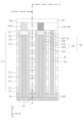
- FIG. 3ais a plan view illustrating the structure of a three-dimensional flash memory according to one embodiment.
- FIG. 3bis a cross-sectional view illustrating the structure of a three-dimensional flash memory according to one embodiment, and corresponds to a cross-section taken along line A-A' of FIG. 3a.
- FIG. 4is a flow chart illustrating a method for manufacturing a three-dimensional flash memory according to one embodiment.
- FIGS. 5A to 5Care cross-sectional views illustrating the structure of a three-dimensional flash memory to explain a method for manufacturing a three-dimensional flash memory according to one embodiment.
- FIG. 6is a perspective diagram schematically illustrating an electronic system including a three-dimensional flash memory according to one embodiment.
- the terms used in this specificationare terms used to appropriately express the preferred embodiments of the present invention, and may vary depending on the intention of the viewer, operator, or the customs of the field to which the present invention belongs. Therefore, the definitions of these terms should be made based on the contents throughout this specification. For example, in this specification, the singular includes the plural unless specifically stated in the phrase.
- the terms “comprises” and/or “comprising” used in this specificationdo not exclude the presence or addition of one or more other components, steps, operations, and/or elements mentioned.
- first, second, etc.are used in this specification to describe various regions, directions, shapes, etc., these regions, directions, and shapes should not be limited by these terms. These terms are only used to distinguish a certain region, direction, or shape from another region, direction, or shape. Therefore, a part mentioned as a first part in one embodiment may be mentioned as a second part in another embodiment.
- FIG. 2is a simplified circuit diagram illustrating an array of three-dimensional flash memories according to embodiments.
- an array of three-dimensional flash memorymay include a common source line (CSL), a plurality of bit lines (BL0, BL1, BL2), and a plurality of cell strings (CSTR) arranged between the common source line (CSL) and the bit lines (BL0, BL1, BL2).
- CSLcommon source line
- bit linesBL0, BL1, BL2
- CSTRcell strings
- the bit lines (BL0, BL1, BL2)can be arranged two-dimensionally while being spaced apart from each other along the first direction (D1) and extending in the second direction (D2).
- the first direction (D1), the second direction (D2), and the third direction (D3)are each orthogonal to each other and can form a rectangular coordinate system defined by the X, Y, and Z axes.
- a plurality of cell stringsmay be connected in parallel to each of the bit lines (BL0, BL1, BL2).
- the cell strings (CSTR)may be commonly connected to the common source line (CSL) provided between the bit lines (BL0, BL1, BL2) and one common source line (CSL).
- a plurality of common source linesmay be provided, and the plurality of common source lines (CSL) may be arranged two-dimensionally while extending in the first direction (D1) and being spaced apart from each other along the second direction (D2).
- the plurality of common source lines (CSL)may be electrically the same voltage applied, but is not limited thereto, and each of the plurality of common source lines (CSL) may be electrically independently controlled so that different voltages may be applied.
- each of the cell strings (CSTR)may be arranged to be spaced apart from each other along the second direction (D2) per bit line while being formed to extend in the third direction (D3).
- each of the cell strings (CSTR)may be composed of a ground select transistor (GST) connected to a common source line (CSL), first and second string select transistors (SST1, SST2) connected to bit lines (BL0, BL1, BL2) and connected in series, memory cell transistors (MCT) and an erase control transistor (ECT) arranged between the ground select transistor (GST) and the first and second string select transistors (SST1, SST2) and connected in series.
- each of the memory cell transistors (MCT)may include a data storage element.
- each of the cell stringsmay include first and second string select transistors (SST1, SST2) connected in series, and the second string select transistor (SST2) may be connected to one of the bit lines (BL0, BL1, BL2).
- each of the cell stringsmay include one string select transistor.
- the ground select transistor (GST) in each of the cell strings (CSTR)may be composed of a plurality of MOS transistors connected in series, similar to the first and second string select transistors (SST1, SST2).
- a cell stringmay be composed of a plurality of memory cell transistors (MCT) having different distances from common source lines (CSL). That is, the memory cell transistors (MCT) may be connected in series between a first string select transistor (SST1) and a ground select transistor (GST) along a third direction (D3). An erase control transistor (ECT) may be connected between the ground select transistor (GST) and the common source lines (CSL).
- Each of the cell strings (CSTR)may further include dummy cell transistors (DMC) each connected between the first string select transistor (SST1) and an uppermost one of the memory cell transistors (MCT) and between the ground select transistor (GST) and a lowermost one of the memory cell transistors (MCT).
- DMCdummy cell transistors
- the first string select transistor (SST1)can be controlled by the first string select lines (SSL1-1, SSL1-2, SSL1-3), and the second string select transistor (SST2) can be controlled by the second string select lines (SSL2-1, SSL2-2, SSL2-3).
- the memory cell transistors (MCT)can be controlled by the plurality of word lines (WL0-WLn), and the dummy cell transistors (DMC) can be controlled by the dummy word line (DWL), respectively.
- the ground select transistor (GST)can be controlled by the ground select lines (GSL0, GSL1, GSL2), and the erase control transistor (ECT) can be controlled by the erase control line (ECL).
- the erase control transistors (ECTs)can be provided in multiple numbers. Common source lines (CSL) can be commonly connected to the sources of the erase control transistors (ECT).
- Gate electrodes of memory cell transistors (MCT) provided at substantially the same distance from common source lines (CSL)may be commonly connected to one of the word lines (WL0-WLn, DWL) and may be in an equipotential state.
- the present inventionis not limited thereto, and even if the gate electrodes of memory cell transistors (MCT) are provided at substantially the same level from the common source lines (CSL), gate electrodes provided in different rows or columns may be independently controlled.
- the ground selection lines (GSL0, GSL1, GSL2), the first string selection lines (SSL1-1, SSL1-2, SSL1-3) and the second string selection lines (SSL2-1, SSL2-2, SSL2-3)extend along the first direction (D1), are spaced apart from each other in the second direction (D2) and can be arranged two-dimensionally.
- the ground selection lines (GSL0, GSL1, GSL2), the first string selection lines (SSL1-1, SSL1-2, SSL1-3) and the second string selection lines (SSL2-1, SSL2-2, SSL2-3), which are provided at substantially the same level from the common source lines (CSL),can be electrically isolated from each other.
- the erase control transistors (ECT) of different cell strings (CSTR)can be controlled by a common erase control line (ECL).
- the erase control transistors (ECT)may generate gate induced drain leakage (GIDL) during an erase operation of the memory cell array.
- GIDLgate induced drain leakage
- an erase voltagemay be applied to the bit lines (BL0, BL1, BL2) and/or the common source lines (CSL) during an erase operation of the memory cell array, and gate induced leakage current may be generated in the string select transistor (SST) and/or the erase control transistors (ECT).
- the string selection line (SSL) described abovemay be represented as an upper selection line (USL), and the ground selection line (GSL) may be represented as a lower selection line.
- FIG. 3ais a plan view illustrating the structure of a three-dimensional flash memory according to one embodiment
- FIG. 3bis a cross-sectional view illustrating the structure of a three-dimensional flash memory according to one embodiment, corresponding to a cross-section taken along line A-A' of FIG. 3a.
- the substrate (SUB)may be a semiconductor substrate, such as a silicon substrate, a silicon-germanium substrate, a germanium substrate, or a single crystalline silicon substrate, a single crystalline epitaxial layer, or the like.
- the substrate (SUB)may be doped with a first conductivity type impurity (e.g., a P type impurity).
- the substrate (SUB)may have source areas (SA) of vertical channel structures (VS) embedded therein, which will be described in detail below.
- SAsource areas
- VSvertical channel structures
- Laminated structures (ST)may be arranged on the substrate (SUB).
- the laminated structures (ST)may be arranged two-dimensionally along the second direction (D2) while being formed to extend in the first direction (D1).
- the laminated structures (ST)may be spaced apart from each other in the second direction (D2).
- Each of the stacked structures (ST)may include gate electrodes (EL1, EL2, EL3) and interlayer insulating films (ILD) alternately stacked in a vertical direction (e.g., a third direction (D3)) perpendicular to a top surface of a substrate (SUB).
- the stacked structures (ST)may have a substantially flat top surface. That is, the top surfaces of the stacked structures (ST) may be parallel to the top surface of the substrate (SUB).
- the vertical directionmeans the third direction (D3) or the opposite direction of the third direction (D3).
- each of the gate electrodesmay be one of the erase control line (ECL), ground select lines (GSL0, GSL1, GSL2), word lines (WL0-WLn, DWL), first string select lines (SSL1-1, SSL1-2, SSL1-3), and second string select lines (SSL2-1, SSL2-2, SSL2-3) sequentially stacked on the substrate (SUB).
- ECLerase control line
- GSL0, GSL1, GSL2ground select lines
- WL0word lines
- first string select linesSSL1-1, SSL1-2, SSL1-3
- second string select linesSSL2-1, SSL2-2, SSL2-3 sequentially stacked on the substrate (SUB).
- Each of the gate electrodes (EL1, EL2, EL3)may be formed to extend in the first direction (D1) and have substantially the same thickness in the third direction (D3).
- the thicknessmeans the thickness in the third direction (D3).
- Each of the gate electrodes (EL1, EL2, EL3)may be formed of a conductive material.
- each of the gate electrodesmay include at least one selected from a doped semiconductor (e.g., doped silicon, etc.), a metal (e.g., W (tungsten), Cu (copper), Al (aluminum), Ti (titanium), Ta (tantalum), Mo (molybdenum), Ru (ruthenium), Au (gold), etc.), or a conductive metal nitride (e.g., titanium nitride, tantalum nitride, etc.).
- a doped semiconductore.g., doped silicon, etc.
- a metale.g., W (tungsten), Cu (copper), Al (aluminum), Ti (titanium), Ta (tantalum), Mo (molybdenum), Ru (ruthenium), Au (gold), etc.
- a conductive metal nitridee.g., titanium nitride, tantalum nitride, etc.
- the gate electrodes (EL1, EL2, EL3)may include a first gate electrode (EL1) at the lowermost position, a third gate electrode (EL3) at the uppermost position, and a plurality of second gate electrodes (EL2) between the first gate electrode (EL1) and the third gate electrode (EL3).
- the first gate electrode (EL1) and the third gate electrode (EL3)are each illustrated and described as a single number, this is exemplary and is not limited thereto, and the first gate electrode (EL1) and the third gate electrode (EL3) may be provided in plural numbers as needed.
- the first gate electrode (EL1)may correspond to any one of the ground selection lines (GSL0, GSL1, GLS2) illustrated in FIG. 2.
- the second gate electrode (EL2)may correspond to any one of the word lines (WL0-WLn, DWL) illustrated in FIG. 2.
- the third gate electrode (EL3)may correspond to any one of the first string selection lines (SSL1-1, SSL1-2, SSL1-3) or any one of the second string selection lines (SSL2-1, SSL2-2, SSL2-3) of FIG. 2.
- each end of the stacked structures (ST)may have a stepwise structure along the first direction (D1). More specifically, the gate electrodes (EL1, EL2, EL3) of the stacked structures (ST) may have a length in the first direction (D1) that decreases as they move away from the substrate (SUB).
- the third gate electrode (EL3)may have the smallest length in the first direction (D1) and the largest distance from the substrate (SUB) in the third direction (D3).
- the first gate electrode (EL1)may have the largest length in the first direction (D1) and the smallest distance from the substrate (SUB) in the third direction (D3).
- each of the stacked structures (ST)can have a thickness that decreases as it gets further away from the outer-most one of the vertical channel structures (VS) described below, and the side walls of the gate electrodes (EL1, EL2, EL3) can be spaced apart at a constant interval along the first direction (D1) in a planar view.
- each of the interlayer insulating films (ILDs)may have a different thickness.
- the lowermost and uppermost of the interlayer insulating films (ILDs)may have a smaller thickness than the other interlayer insulating films (ILDs).
- the thickness of each of the interlayer insulating films (ILDs)may have a different thickness or may be set to be the same depending on the characteristics of the semiconductor device.
- the interlayer insulating films (ILDs)may be formed of an insulating material for insulation between the gate electrodes (EL1, EL2, EL3).
- the interlayer insulating films (ILDs)may be formed of silicon oxide.
- interlayer insulating filmsmay be omitted depending on the implementation example.
- an air gapmay be interposed between the gate electrodes (EL1, EL2, EL3) while the gate electrodes (EL1, EL2, EL3) are stacked while being spaced apart from each other in the vertical direction (e.g., the third direction (D3)).
- a plurality of channel holes (CH) penetrating a portion of the stacked structures (ST) and the substrate (SUB)may be provided.
- Vertical channel structures (VS)may be provided within the channel holes (CH).
- the vertical channel structures (VS)may be formed as a plurality of cell strings (CSTR) as shown in FIG. 2 and may extend in a third direction (D3) while being connected to the substrate (SUB).
- the connection of the vertical channel structures (VS) to the substrate (SUB)may be achieved by a lower surface of each of the vertical channel structures (VS) being embedded within the substrate (SUB), but is not limited thereto and may also be achieved by making contact with an upper surface of the substrate (SUB).
- the lower surfaces of the vertical channel structures (VS)may be located at a level lower than the upper surface of the substrate (SUB).
- the rows of vertical channel structures (VS) penetrating one of the stacked structures (ST)may be provided in multiple numbers. For example, as illustrated in FIG. 3a, rows of two vertical channel structures (VS) may penetrating one of the stacked structures (ST). However, without being limited thereto, rows of three or more vertical channel structures (VS) may penetrating one of the stacked structures (ST). In a pair of adjacent rows, the vertical channel structures (VS) corresponding to one row may be shifted in the first direction (D1) from the vertical channel structures (VS) corresponding to the other adjacent row. In a planar view, the vertical channel structures (VS) may be arranged in a zigzag shape along the first direction (D1). However, without being limited thereto, the vertical channel structures (VS) may also form an array in which rows and columns are arranged side by side.
- Each of the vertical channel structures (VS)may be formed to extend in a third direction (D3) from the substrate (SUB).
- each of the vertical channel structures (VS)is illustrated as having a pillar shape with the same width at the top and bottom, but is not limited thereto and may have a shape in which the width in the first direction (D1) and the second direction (D2) increases as it goes in the third direction (D3).
- the upper surface of each of the vertical channel structures (VS)may have a circular shape, an oval shape, a square shape, or a bar shape.
- Each of the vertical channel structuresmay include a data storage pattern (DSP), a vertical channel pattern (VCP), a vertical filled pattern (VFP), and a capping layer (CAP).
- the data storage pattern (DSP)may have a pipe shape or a macaroni shape with an open bottom
- the vertical filled pattern (VFP)may have a shape filling an inner space of the vertical channel pattern (VCP)
- the vertical channel pattern (VCP)may have a pipe shape or a macaroni shape with a closed bottom.
- the vertical channel pattern (VCP)may also have a pipe shape or a macaroni shape with an open bottom.
- the data storage pattern (DSP)can cover the inner sidewall of each of the channel holes (CH), surround the outer sidewall of the vertical channel pattern (VCP) toward the inner side, and contact the sidewalls of the gate electrodes (EL1, EL2, EL3) toward the outer side. Accordingly, the regions corresponding to the second gate electrodes (EL2) of the data storage pattern (DSP) can form memory cells in which a memory operation (program operation, read operation, or erase operation) is performed by a voltage applied through the second gate electrodes (EL2) together with the regions corresponding to the second gate electrodes (EL2) of the vertical channel pattern (VCP).
- the memory cellscorrespond to the memory cell transistors (MCT) illustrated in FIG. 2.
- the data storage pattern (DSP)can serve as a data storage in the three-dimensional flash memory by trapping electrons or holes by a voltage applied through the second gate electrodes (EL2), or by maintaining the state of the electrons (e.g., the polarization state of the charges).
- an ONO (tunnel oxide-nitride-blocking oxide) layer or a ferroelectric layercan be used as the data storage pattern (DSP).
- Such a data storage pattern (DSP)can represent a binary data value or a multi-valued data value by a change in the trapped charge or hole, or can represent a binary data value or a multi-valued data value by a change in the state of the charges.
- DSPdata storage pattern
- a vertical channel patternis a component that transfers charges or holes to a data storage pattern (DSP), and may be formed to extend in a vertical direction (e.g., a third direction (D3)) to cover an inner wall of the data storage pattern (DSP) to form or boost a channel by an applied voltage.
- D3a third direction
- the vertical channel patternmay be composed of an outer first vertical channel pattern (VCP1) that contacts the inner wall of the data storage pattern (DSP) and an inner second vertical channel pattern (VCP2) that contacts the inner wall of the first vertical channel pattern (VCP) (and also contacts the outer wall of the vertical buried pattern (VFP)).
- the first vertical channel pattern (VCP1)contacts the inner wall of the data storage pattern (DSP) and may be formed of the same material as the material forming the drain area (DA) described later.
- the first vertical channel pattern (VCP1)can be formed of at least one of polycrystalline silicon or silicon crystal materials, identical to the drain region (DA), thereby improving interface characteristics with the data storage pattern (DSP).
- the second vertical channel pattern (VCP2)contacts the inner wall of the first vertical channel pattern (VCP1) and may be formed of the same material as the material forming the source area (SA) described below.
- the second vertical channel pattern (VCP2)may not have the characteristics of a grain boundary since it is formed of a metal ion-based oxide semiconductor material including at least one of In, Ga, Zn, Sn, Ni, Cu, Al, or Sr, similar to the source region (SA).
- the vertical channel pattern (VCP)improves the interface characteristics with the data storage pattern (DSP) through the first vertical channel pattern (VCP1) formed of at least one material among polycrystalline silicon or silicon crystal materials, and at the same time, the cell current flowing in the vertical channel pattern (VCP2) can be improved without being affected by the characteristics of the grain boundary through the second vertical channel pattern (VCP2) formed of a metal ion-based oxide semiconductor material including at least one among In, Ga, Zn, Sn, Ni, Cu, Al, and Sr.
- the vertical channel pattern (VCP)may have a structure including a first vertical channel pattern (VCP1) and a second vertical channel pattern (VCP2), an insulating film (not shown) interposed between the first vertical channel pattern (VCP1) and the second vertical channel pattern (VCP2), or a structure in which the second vertical channel pattern (VCP2) forms a heterojunction therein.
- An upper surface of the vertical channel pattern (VCP)can be substantially coplanar with an upper surface of the vertical buried pattern (VFP) and can be positioned at a higher level than an upper surface of the uppermost one of the second gate electrodes (EL2). More specifically, the upper surface of the vertical channel pattern (VCP) can be positioned between an upper surface and a lower surface of the third gate electrode (EL3).
- the lower surface of the vertical channel pattern (VCP)can be positioned at a lower level than the uppermost surface of the substrate (SUB) (i.e., the lower surface of the lowermost one of the interlayer insulating films (ILD)).
- the lower surface of the vertical channel pattern (VCP)can also be coplanar with the uppermost surface of the substrate (SUB) (i.e., the lower surface of the lowermost one of the interlayer insulating films (ILD)).
- the vertical buried pattern (VFP)may be surrounded by a second vertical channel pattern (VCP2) of the vertical channel pattern (VCP).
- An upper surface of the vertical buried pattern (VFP)may be in contact with a capping layer (CAP), and a lower surface of the vertical buried pattern (VFP) may be located at a level lower than an uppermost surface of the substrate (SUB) (i.e., a lower surface of the lowest one of the interlayer insulating films (ILD)).
- the vertical buried pattern (VFP)may be spaced apart from the substrate (SUB) in a third direction (D3). In other words, the vertical buried pattern (VFP) may be electrically floated from the substrate (SUB).
- the three-dimensional flash memoryis not limited thereto and may have a structure including a back gate (BG; not shown) instead of the vertically filled pattern (VFP).
- the back gate (BG)may be formed to be in contact with the vertical channel pattern (VCP) while being at least partially surrounded by the vertical channel pattern (VCP) and to apply a voltage to the vertical channel pattern (VCP) for a memory operation.
- the back gate (BG)may be formed of a conductive material including at least one selected from a doped semiconductor (e.g., doped silicon), a metal (e.g., W (tungsten), Cu (copper), Al (aluminum), Ti (titanium), Ta (tantalum), Mo (molybdenum), Ru (ruthenium), Au (gold), etc.), or a conductive metal nitride (e.g., titanium nitride, tantalum nitride, etc.).
- the back gate (BG)may include at least one of all metal materials that can be formed by ALD in addition to the described metal materials.
- an insulating film(not shown) is disposed between the back gate (BG) and the vertical channel pattern (VCP), thereby preventing the back gate (BG) from directly contacting the vertical channel pattern (VCP).
- the insulating film (INS)like the interlayer insulating films (ILD), may be formed of an insulating material such as silicon oxide. However, the insulating film (INS) may be omitted depending on the implementation example.
- the vertical channel structures (VS)may correspond to channels of the erase control transistor (ECT), the first and second string select transistors (SST1, SST2), the ground select transistor (GST), and the memory cell transistors (MCT).
- ECTerase control transistor
- SST1, SST2first and second string select transistors
- GSTground select transistor
- MCTmemory cell transistors
- a capping layer (CAP)may be provided on an upper surface of a vertical channel pattern (VCP) (an upper surface of each of the vertical channel structures (VS)).
- the capping layer (CAP)may be connected to an upper portion of the vertical channel pattern (VCP).
- a sidewall of the capping layer (CAP)may be surrounded by a data storage pattern (DSP).
- An upper surface of the capping layer (CAP)may be substantially coplanar with an upper surface of each of the stacked structures (ST) (i.e., an upper surface of an uppermost one of the interlayer insulating films (ILD)).
- a lower surface of the capping layer (CAP)may be located at a level lower than an upper surface of the third gate electrode (EL3). More specifically, the lower surface of the capping layer (CAP) may be located between the upper and lower surfaces of the third gate electrode (EL3). That is, at least a portion of the capping layer (CAP) may overlap the third gate electrode (EL3) in a horizontal direction.
- the capping layer (CAP)is a component corresponding to the drain region (DA) of each of the vertical channel structures (VS), and may be formed of a material for reducing contact resistance with a bit line contact plug (BLPG) connected to the upper end of each of the vertical channel structures (VS).
- the capping layer (CAP)(drain region (DA)) may be formed of at least one of polycrystalline silicon or a silicon crystal material, thereby reducing contact resistance with the bit line contact plug (BLPG). Reducing the contact resistance means minimizing the contact resistance or reducing the contact resistance to below a preset threshold value.
- a source region (SA)may be provided on the lower surface of the vertical channel pattern (VCP) (the lower surface of the vertical channel structures (VS)).
- the source region (SA)may be connected to a common source line (CSL).
- the source region (SA)can be formed of a material for reducing leakage current in the source region (SA).
- the source region (SA)can be formed of an oxide semiconductor material including at least one metal ion of In, Ga, Zn, Sn, Ni, Cu, Al, or Sr, thereby reducing leakage current in the source region (SA). Reducing leakage current means minimizing leakage current or reducing leakage current to below a preset threshold value.
- a separation trench (TR) extending in a first direction (D1)may be provided between adjacent stacked structures (ST).
- a common source line (CSL)may be provided in the separation trench (TR) and may be positioned to be in contact with a source region (SA).
- the common source line (CSL)may have a plate shape extending in the first direction (D1) and the third direction (D3) within the substrate (SUB).
- the common source line (CSL)may be formed of a semiconductor material doped with a second conductivity type impurity (e.g., an N-type impurity).
- An upper surface of the common source line (CSL)may be substantially coplanar with an upper surface of each of the stacked structures (ST) (i.e., an upper surface of an uppermost one of the interlayer insulating films (ILD).
- the common source line (CSL)may have a shape in which a width in the second direction (D2) increases as it goes in the third direction (D3).
- Insulating spacersmay be interposed between the common source line (CSL) and the stacked structures (ST).
- the insulating spacers (SP)may be provided so as to face each other between adjacent stacked structures (ST).
- the insulating spacers (SP)may be formed of silicon oxide, silicon nitride, silicon oxynitride, or a low-k material having a low dielectric constant.
- the drain region (DA) and the source region (SA)can be formed of different materials, such as the drain region (DA) being formed of a material for reducing contact resistance with the bit line contact plug (BLPG) and the source region (SA) being formed of a material for reducing leakage current.
- the drain region (DA)being formed of a material for reducing contact resistance with the bit line contact plug (BLPG)
- the source region (SA)being formed of a material for reducing leakage current.
- a capping insulating filmmay be provided on the stacked structures (ST), the vertical channel structures (VS) and the common source line (CSL).
- the capping insulating film (CAP-INS)may cover an upper surface of an uppermost one of the interlayer insulating films (ILD), an upper surface of the capping layer (CAP) and an upper surface of the common source line (CSL).
- the capping insulating film (CAP-INS)may be formed of an insulating material different from the interlayer insulating films (ILD).
- a bit line contact plug (BLPG) electrically connected to the capping layer (CAP)may be provided inside the capping insulating film (CAP-INS).
- the bit line contact plug (BLPG)may have a shape in which a width in the first direction (D1) and the second direction (D2) increases as it goes in the third direction (D3).
- a bit line (BL)may be provided on a capping insulating film (CAP-INS) and a bit line contact plug (BLPG).
- the bit line (BL)corresponds to any one of a plurality of bit lines (BL0, BL1, BL2) illustrated in FIG. 2 and may be formed by extending along a second direction (D2) with a conductive material.
- the conductive material forming the bit line (BL)may be the same material as the conductive material forming each of the aforementioned gate electrodes (EL1, EL2, EL3).
- the bit line (BL)may be electrically connected to the vertical channel structures (VS) through a bit line contact plug (BLPG).
- the connection of the bit line (BL) to the vertical channel structures (VS)may mean that the bit line (BL) is connected to a vertical channel pattern (VCP) included in the vertical channel structures (VS).
- a three-dimensional flash memoryis not limited or restricted to the described structure, and may be implemented in various structures, assuming that it includes gate electrodes (EL1, EL2, EL3) to which voltages for memory operation are applied, a bit line (BL), a common source line (CSL), and a vertical channel pattern (VCP) forming a channel, and a data storage pattern (DSP) for data storage, according to an implementation example.
- gate electrodesEL1, EL2, EL3
- BLbit line
- CSLcommon source line
- VCPvertical channel pattern
- DSPdata storage pattern
- FIG. 4is a flow chart illustrating a method for manufacturing a three-dimensional flash memory according to one embodiment
- FIGS. 5a to 5care cross-sectional views illustrating a structure of a three-dimensional flash memory to explain a method for manufacturing a three-dimensional flash memory according to one embodiment.
- a three-dimensional flash memory manufactured through the manufacturing method described belowmay have the structure described above with reference to FIGS. 3a to 3b, and the manufacturing method described below is assumed to be performed by an automated and mechanized manufacturing system.
- step (S410)the manufacturing system can prepare a semiconductor structure (SEMI-STR).
- a semiconductor structuremay include word lines (WL0-WLn) that extend horizontally on a substrate (SUIB) and are vertically spaced apart from each other; vertical channel structures (VS) that extend vertically on a substrate (SUB) through the word lines (WL0-WLn); and a drain region (DA) positioned at an upper end of each of the vertical channel structures (VS).
- WL0-WLnword lines
- VSvertical channel structures
- DAdrain region
- Each of the vertical channel structuresincludes a vertical channel pattern (VCP) formed to extend in a vertical direction and a data storage pattern (DSP) formed to cover an outer wall of the vertical channel pattern (VCP), and the data storage pattern (DSP) and the vertical channel pattern (VCP) can configure memory cells corresponding to word lines (WL0-WLn).
- the manufacturing systemcan form the source region (SA) located at the bottom of the vertical channel structures (VS) with a material different from the material forming the drain region (DA).
- Forming the source region (SA) with a material different from the material forming the drain region (DA) at step (S420)means that, as the semiconductor structure (SEMI-STR) including the drain region (DA) formed with a material for reducing contact resistance with a bit line contact plug (BLPG) connected to the upper end of each of the vertical channel structures (VS) at step (S410) is prepared, the source region (SA) is formed with a material for reducing leakage current in the source region (SA) at step (S420).
- the semiconductor structure (SEMI-STR) including the drain region (DA) formed with a material for reducing contact resistance with a bit line contact plug (BLPG) connected to the upper end of each of the vertical channel structures (VS) at step (S410)is prepared, the source region (SA) is formed with a material for reducing leakage current in the source region (SA) at step (S420).
- a semiconductor structure (SEMI-STR) including a drain region (DA) formed of at least one material among polycrystalline silicon or silicon crystal materialsis prepared, and in step (S420), a source region (SA) can be formed of an oxide semiconductor material including at least one metal ion among In, Ga, Zn, Sn, Ni, Cu, Al, or Sr.
- the manufacturing systemcan form the source region (SA) with a different material from the drain region (DA) by performing the step (S420) by dividing it into the first step and the second step based on the vertical channel pattern (VCP) of the composite structure.
- the manufacturing systemprepares a semiconductor structure (SEMI-STR) as illustrated in FIG. 5a in step (S410), etching at least a portion of a substrate (SUB) corresponding to a source region (SA) as illustrated in FIG. 5b in a first step of step (S420), and then forming a source region (SA) in the etched space (ES) based on a second vertical channel pattern (VCP2) as illustrated in FIG. 5c in a second step of step (S420).
- SEMI-STRsemiconductor structure
- the manufacturing systemmay etch at least a portion of the substrate (SUB) corresponding to the source area (SA) so that a side surface of the second vertical channel pattern (VCP2) is exposed in each of the vertical channel structures (VS) in the substrate (SUB) through a first step of the step (S420), and may form the source area (SA) in the space (ES) with the same material as the second vertical channel pattern (VCP2) from the exposed side surface of the second vertical channel pattern (VCP2) through a technique such as side wall butting through the second step of the step (S420).
- the manufacturing systemcan form a common source line (CSL) in the form of a line on the substrate (SUB) so as to contact the source area (SA) after forming the source area (SA), as depicted in FIG. 5c.
- CSLcommon source line
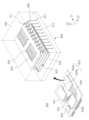
- FIG. 6is a perspective diagram schematically illustrating an electronic system including a three-dimensional flash memory according to one embodiment.
- an electronic system (600) including a three-dimensional flash memorymay include a main substrate (601), a controller (602) mounted on the main substrate (601), one or more semiconductor packages (603), and a DRAM (604).
- the semiconductor package (603) and DRAM (604)can be connected to the controller (602) by wiring patterns (605) provided on the main substrate (601).
- the main board (601)may include a connector (606) including a plurality of pins that couple with an external host.
- the number and arrangement of the plurality of pins in the connector (606)may vary depending on the communication interface between the electronic system (600) and the external host.
- the electronic system (600)may communicate with an external host according to any one of interfaces, such as, for example, Universal Serial Bus (USB), Peripheral Component Interconnect Express (PCIExpress), Serial Advanced Technology Attachment (SATA), and M-Phy for Universal Flash Storage (UFS).
- USBUniversal Serial Bus
- PCIExpressPeripheral Component Interconnect Express
- SATASerial Advanced Technology Attachment
- UFSM-Phy for Universal Flash Storage
- the electronic system (600)may be operated by power supplied from an external host through, for example, a connector (606).
- the electronic system (600)may further include a PMIC (Power Management Integrated Circuit) that distributes power supplied from the external host to the controller (602) and the semiconductor package (603).
- PMICPower Management Integrated Circuit
- the controller (602)can write data to the semiconductor package (603) or read data from the semiconductor package (603), and can improve the operating speed of the electronic system (600).
- DRAM (604)may be a buffer memory for mitigating the speed difference between the semiconductor package (603), which is a data storage space, and an external host.
- DRAM (604) included in the electronic system (600)may also function as a type of cache memory, and may provide a space for temporarily storing data in a control operation for the semiconductor package (603).
- the controller (602)may further include a DRAM controller for controlling DRAM (604) in addition to a NAND controller for controlling the semiconductor package (603).
- the semiconductor package (603)may include first and second semiconductor packages (603a, 603b) that are spaced apart from each other.
- the first and second semiconductor packages (603a, 603b)may each be a semiconductor package including a plurality of semiconductor chips (620).
- Each of the first and second semiconductor packages (603a, 603b)may include a package substrate (610), semiconductor chips (620) on the package substrate (610), adhesive layers (630) disposed on a lower surface of each of the semiconductor chips (620), connection structures (640) that electrically connect the semiconductor chips (620) and the package substrate (610), and a molding layer (650) that covers the semiconductor chips (620) and the connection structures (640) on the package substrate (610).
- the package substrate (610)may be a printed circuit board including package upper pads (611).
- Each of the semiconductor chips (620)may include input/output pads (621).
- Each of the semiconductor chips (620)may include the three-dimensional flash memory described above with reference to FIGS. 3A and 3B. More specifically, each of the semiconductor chips (620) may include gate stack structures (622) and memory channel structures (623).
- the memory channel structures (623)may correspond to the vertical channel structures (VS) described above.
- connection structures (640)may be, for example, bonding wires that electrically connect the input/output pads (621) and the package upper pads (611). Accordingly, in each of the first and second semiconductor packages (603a, 603b), the semiconductor chips (620) may be electrically connected to each other in a bonding wire manner, and may be electrically connected to the package upper pads (611) of the package substrate (610). According to embodiments, in each of the first and second semiconductor packages (603a, 603b), the semiconductor chips (620) may be electrically connected to each other by a through silicon via, instead of the bonding wire-type connection structures (640).
- the controller (602) and the semiconductor chips (620)may be included in a single package.
- the controller (602) and the semiconductor chips (620)may be mounted on a separate interposer substrate from the main substrate (601), and the controller (602) and the semiconductor chips (620) may be connected to each other by wiring provided on the interposer substrate.
Landscapes
- Non-Volatile Memory (AREA)
- Semiconductor Memories (AREA)
Abstract
Description
Translated fromKorean아래의 실시예들은 누설 전류를 개선하는 3차원 플래시 메모리에 대한 기술이다.The embodiments below describe a technology for three-dimensional flash memory that improves leakage current.
플래시 메모리 소자는 F-N 터널링(Fowler-Nordheimtunneling) 또는 열전자 주입(Hot electron injection)에 의해 전기적으로 데이터의 입출력을 제어하여 전기적으로 프로그램 및 소거가 가능한 판독 전용 메모리(Electrically Erasable Programmable Read Only Memory; EEPROM)로서, 컴퓨터, 디지털 카메라, MP3 플레이어, 게임 시스템, 메모리 스틱(Memory stick) 등에 공통적으로 이용될 수 있다.Flash memory devices are electrically erasable programmable read-only memories (EEPROM) that control the input and output of data electrically by Fowler-Nordheimtunneling or hot electron injection, and can be commonly used in computers, digital cameras, MP3 players, game systems, memory sticks, etc.
이러한 플래시 메모리 소자에서는 소비자가 요구하는 우수한 성능 및 저렴한 가격을 충족시키기 위해 집적도를 증가시키는 것이 요구된 바, 메모리 셀 트랜지스터들(MCT)이 수직 방향으로 배열되어 메모리 셀 스트링(CSTR)을 구성하는 3차원 구조가 제안되었다.In order to meet the high performance and low price demands of consumers, these flash memory devices require increased integration, and a three-dimensional structure in which memory cell transistors (MCTs) are arranged vertically to form a memory cell string (CSTR) has been proposed.
일반적으로 3차원 플래시 메모리는 메모리 셀 트랜지스터들(MCT)을 연결하도록 수직 방향의 연장 형성되는 수직 채널 패턴(VCP)으로서 도 1에 도시된 바와 같이 다결정 실리콘(Poly Silicon) 물질을 사용하고 있다.Typically, 3D flash memory uses polysilicon material as a vertical channel pattern (VCP) that extends vertically to connect memory cell transistors (MCTs), as shown in Fig. 1.
이에, 기존 3차원 플래시 메모리는 소스 영역에서 누설 전류 극심한 문제를 갖는다.Accordingly, existing 3D flash memories have extreme leakage current problems in the source area.
더욱이 기존의 3차원 플래시 메모리는 고단으로 적층되고 있는 추세로 인해 수직 채널 패턴(VCP)에 흐르는 셀 전류가 감소하는 문제를 갖는다.Moreover, existing 3D flash memories have the problem of decreasing cell current flowing in the vertical channel pattern (VCP) due to the trend of high-level stacking.
따라서, 소스 영역에서의 누설 전류를 감소시키는 기술이 제안될 필요가 있다.Therefore, a technique for reducing the leakage current in the source region needs to be proposed.
일 실시예들은 드레인 영역에서의 콘택 저항을 감소시키는 동시에 소스 영역에서의 누설 전류를 감소시키고자, 드레인 영역과 소스 영역이 서로 다른 물질로 형성되는 3차원 플래시 메모리 및 그 제조 방법을 제안한다.One embodiment proposes a three-dimensional flash memory and a method of manufacturing the same, in which the drain region and the source region are formed of different materials to reduce the contact resistance in the drain region while reducing the leakage current in the source region.
또한, 일 실시예들은 셀 전류를 개선하고자, 수직 채널 패턴을 제1 수직 채널 패턴 및 제2 수직 채널 패턴의 복합 구조로 구성하는 가운데 제2 수직 채널 패턴을 결정립계(Grain boundary)의 특성을 갖지 않는 물질로 형성하는 3차원 플래시 메모리 및 그 제조 방법을 제안한다.In addition, one embodiment proposes a three-dimensional flash memory and a method for manufacturing the same, in which a vertical channel pattern is formed of a composite structure of a first vertical channel pattern and a second vertical channel pattern, and the second vertical channel pattern is formed of a material that does not have the characteristics of a grain boundary, in order to improve cell current.
다만, 본 발명이 해결하고자 하는 기술적 과제들은 상기 과제로 한정되는 것이 아니며, 본 발명의 기술적 사상 및 영역으로부터 벗어나지 않는 범위에서 다양하게 확장될 수 있다.However, the technical problems to be solved by the present invention are not limited to the above problems, and can be expanded in various ways without departing from the technical idea and scope of the present invention.
일 실시예에 따르면, 3차원 플래시 메모리는, 기판 상 수평 방향으로 연장 형성되며 수직 방향으로 서로 이격된 채 적층되는 워드 라인들; 상기 워드 라인들을 관통하여 상기 기판 상 상기 수직 방향으로 연장 형성되는 수직 채널 구조체들-상기 수직 채널 구조체들 각각은 상기 수직 방향으로 연장 형성되는 수직 채널 패턴 및 상기 수직 채널 패턴의 외측벽을 덮으며 형성되는 데이터 저장 패턴을 포함하며, 상기 데이터 저장 패턴 및 상기 수직 채널 패턴은 상기 워드 라인들에 대응하는 메모리 셀들을 구성함-; 상기 수직 채널 구조체들 각각의 상단에 위치하는 드레인 영역; 및 상기 수직 채널 구조체들의 하단에 위치하는 소스 영역을 포함하고, 상기 드레인 영역 및 상기 소스 영역은, 서로 다른 물질로 형성되는 것을 특징으로 할 수 있다.According to one embodiment, a three-dimensional flash memory may include word lines formed to extend horizontally on a substrate and stacked while being spaced apart from each other in the vertical direction; vertical channel structures formed to extend vertically on the substrate through the word lines, each of the vertical channel structures including a vertical channel pattern formed to extend vertically and a data storage pattern formed to cover an outer wall of the vertical channel pattern, wherein the data storage pattern and the vertical channel pattern constitute memory cells corresponding to the word lines; a drain region positioned at an upper end of each of the vertical channel structures; and a source region positioned at a lower end of the vertical channel structures, wherein the drain region and the source region are formed of different materials.
일 측에 따르면, 상기 드레인 영역은, 상기 수직 채널 구조체들 각각의 상단에 연결하는 비트 라인 콘택 플러그와의 콘택 저항을 감소시키기 위한 물질로 형성되고, 상기 소스 영역은, 상기 소스 영역에서의 누설 전류를 감소시키기 위한 물질로 형성되는 것을 특징으로 할 수 있다.According to one aspect, the drain region may be formed of a material for reducing contact resistance with a bit line contact plug connected to the upper end of each of the vertical channel structures, and the source region may be formed of a material for reducing leakage current in the source region.
다른 일 측에 따르면, 상기 드레인 영역은, 다결정 실리콘 또는 실리콘 결정 물질 중 적어도 하나의 물질로 형성되고, 상기 소스 영역은, In, Ga, Zn, Sn, Ni, Cu, Al 또는 Sr 중 적어도 하나의 금속 이온이 포함된 산화물 반도체 물질로 형성되는 것을 특징으로 할 수 있다.According to another aspect, the drain region may be formed of at least one material among polycrystalline silicon or silicon crystal materials, and the source region may be formed of an oxide semiconductor material including at least one metal ion among In, Ga, Zn, Sn, Ni, Cu, Al, or Sr.
또 다른 일 측에 따르면, 상기 수직 채널 패턴은, 상기 데이터 저장 패턴의 내측벽에 접촉하며 상기 드레인 영역을 형성하는 물질과 동일한 물질로 형성되는 제1 수직 채널 패턴 및 상기 제1 수직 채널 패턴의 내측벽에 접촉하며 상기 소스 영역을 형성하는 물질과 동일한 물질로 형성되는 제2 수직 채널 패턴의 복합 구조를 갖는 것을 특징으로 할 수 있다.According to another aspect, the vertical channel pattern may be characterized by having a composite structure of a first vertical channel pattern formed of the same material as the material forming the drain region and contacting the inner wall of the data storage pattern, and a second vertical channel pattern formed of the same material as the material forming the source region and contacting the inner wall of the first vertical channel pattern.
또 다른 일 측에 따르면, 상기 제2 수직 채널 패턴은, 상기 In, Ga, Zn, Sn, Ni, Cu, Al 또는 Sr 중 적어도 하나의 금속 이온이 포함된 산화물 반도체 물질로 형성됨에 따라 결정립계(Grain boundary)의 특성을 갖지 않는 것을 특징으로 할 수 있다.According to another aspect, the second vertical channel pattern may be characterized by not having the characteristics of a grain boundary since it is formed of an oxide semiconductor material including at least one metal ion among In, Ga, Zn, Sn, Ni, Cu, Al, or Sr.
또 다른 일 측에 따르면, 상기 제1 수직 채널 패턴은, 상기 데이터 저장 패턴과의 계면 특성을 개선하기 위해, 상기 다결정 실리콘 또는 실리콘 결정 물질 중 적어도 하나의 물질로 형성되는 것을 특징으로 할 수 있다.According to another aspect, the first vertical channel pattern may be formed of at least one of the polycrystalline silicon or silicon crystal materials to improve interface characteristics with the data storage pattern.
일 실시예에 따르면, 3차원 플래시 메모리의 제조 방법은, 기판 상 수평 방향으로 연장 형성되며 수직 방향으로 서로 이격된 채 적층되는 워드 라인들; 상기 워드 라인들을 관통하여 상기 기판 상 상기 수직 방향으로 연장 형성되는 수직 채널 구조체들-상기 수직 채널 구조체들 각각은 상기 수직 방향으로 연장 형성되는 수직 채널 패턴 및 상기 수직 채널 패턴의 외측벽을 덮으며 형성되는 데이터 저장 패턴을 포함하며, 상기 데이터 저장 패턴 및 상기 수직 채널 패턴은 상기 워드 라인들에 대응하는 메모리 셀들을 구성함-; 및 상기 수직 채널 구조체들 각각의 상단에 위치하는 드레인 영역을 포함하는 반도체 구조체를 준비하는 단계; 및 상기 수직 채널 구조체들의 하단에 위치하는 소스 영역을 상기 드레인 영역을 형성하는 물질과 다른 물질로 형성하는 단계를 포함할 수 있다.According to one embodiment, a method for manufacturing a three-dimensional flash memory may include the steps of preparing a semiconductor structure including word lines formed to extend horizontally on a substrate and stacked while being spaced apart from each other in the vertical direction; vertical channel structures formed to extend vertically on the substrate through the word lines, each of the vertical channel structures including a vertical channel pattern formed to extend vertically and a data storage pattern formed to cover an outer wall of the vertical channel pattern, wherein the data storage pattern and the vertical channel pattern form memory cells corresponding to the word lines; and a drain region positioned on an upper end of each of the vertical channel structures; and forming a source region positioned on a lower end of the vertical channel structures using a material different from a material forming the drain region.
일 측에 따르면, 상기 준비하는 단계는, 상기 수직 채널 구조체들 각각의 상단에 연결하는 비트 라인 콘택 플러그와의 콘택 저항을 감소시키기 위한 물질로 형성된 상기 드레인 영역을 포함하는 상기 반도체 구조체를 준비하는 단계이고, 상기 형성하는 단계는, 상기 소스 영역에서의 누설 전류를 감소시키기 위한 물질로 상기 소스 영역을 형성하는 단계인 것을 특징으로 할 수 있다.According to one aspect, the preparing step may be a step of preparing the semiconductor structure including the drain region formed of a material for reducing contact resistance with a bit line contact plug connected to the upper end of each of the vertical channel structures, and the forming step may be a step of forming the source region with a material for reducing leakage current in the source region.
다른 일 측에 따르면, 상기 준비하는 단계는, 다결정 실리콘 또는 실리콘 결정 물질 중 적어도 하나의 물질로 형성된 상기 드레인 영역을 포함하는 상기 반도체 구조체를 준비하는 단계이고, 상기 형성하는 단계는, In, Ga, Zn, Sn, Ni, Cu, Al 또는 Sr 중 적어도 하나의 금속 이온이 포함된 산화물 반도체 물질로 상기 소스 영역을 형성하는 단계인 것을 특징으로 할 수 있다.According to another aspect, the preparing step may be a step of preparing the semiconductor structure including the drain region formed of at least one material among polycrystalline silicon or silicon crystal materials, and the forming step may be a step of forming the source region with an oxide semiconductor material including at least one metal ion among In, Ga, Zn, Sn, Ni, Cu, Al, or Sr.
또 다른 일 측에 따르면, 상기 준비하는 단계는, 상기 데이터 저장 패턴의 내측벽에 접촉하며 상기 드레인 영역을 형성하는 물질과 동일한 물질로 형성되는 제1 수직 채널 패턴 및 상기 제1 수직 채널 패턴의 내측벽에 접촉하며 상기 소스 영역을 형성하는 물질과 동일한 물질로 형성되는 제2 수직 채널 패턴의 복합 구조를 갖는 상기 수직 채널 패턴을 포함하는 상기 반도체 구조체를 준비하는 단계인 것을 특징으로 할 수 있다.According to another aspect, the preparing step may be characterized as a step of preparing the semiconductor structure including the vertical channel pattern having a composite structure of a first vertical channel pattern formed of the same material as a material forming the drain region and contacting the inner wall of the data storage pattern, and a second vertical channel pattern formed of the same material as a material forming the source region and contacting the inner wall of the first vertical channel pattern.
또 다른 일 측에 따르면, 상기 형성하는 단계는, 상기 소스 영역에 해당되는 상기 기판의 적어도 일부분을 식각하는 단계; 및 상기 제2 수직 채널 패턴을 기반으로 상기 식각된 공간에 상기 소스 영역을 형성하는 단계를 포함하는 것을 특징으로 할 수 있다.According to another aspect, the forming step may be characterized by including: a step of etching at least a portion of the substrate corresponding to the source region; and a step of forming the source region in the etched space based on the second vertical channel pattern.
또 다른 일 측에 따르면, 상기 식각하는 단계는, 상기 기판 내 상기 수직 채널 구조체들 각각에서 상기 제2 수직 채널 패턴의 측면이 노출되도록 상기 소스 영역에 해당되는 상기 기판의 적어도 일부분을 식각하는 단계인 것을 특징으로 할 수 있다.According to another aspect, the etching step may be characterized by etching at least a portion of the substrate corresponding to the source region so that a side surface of the second vertical channel pattern is exposed in each of the vertical channel structures within the substrate.
또 다른 일 측에 따르면, 상기 형성하는 단계는, 상기 소스 영역과 접촉하도록 상기 기판 상에 라인 형태의 공통 소스 라인을 형성하는 단계를 더 포함하는 것을 특징으로 할 수 있다.According to another aspect, the forming step may further include a step of forming a common source line in a line shape on the substrate so as to be in contact with the source region.
또 다른 일 측에 따르면, 상기 제2 수직 채널 패턴은, 상기 In, Ga, Zn, Sn, Ni, Cu, Al 또는 Sr 중 적어도 하나의 금속 이온이 포함된 산화물 반도체 물질로 형성됨에 따라 결정립계(Grain boundary)의 특성을 갖지 않는 것을 특징으로 할 수 있다.According to another aspect, the second vertical channel pattern may be characterized by not having the characteristics of a grain boundary since it is formed of an oxide semiconductor material including at least one metal ion among In, Ga, Zn, Sn, Ni, Cu, Al, or Sr.
또 다른 일 측에 따르면, 상기 제1 수직 채널 패턴은, 상기 데이터 저장 패턴과의 계면 특성을 개선하기 위해, 상기 다결정 실리콘 또는 실리콘 결정 물질 중 적어도 하나의 물질로 형성되는 것을 특징으로 할 수 있다.According to another aspect, the first vertical channel pattern may be formed of at least one of the polycrystalline silicon or silicon crystal materials to improve interface characteristics with the data storage pattern.
일 실시예들은 드레인 영역과 소스 영역이 서로 다른 물질로 형성되는 3차원 플래시 메모리 및 그 제조 방법을 제안함으로써, 드레인 영역에서의 콘택 저항을 감소시키는 동시에 소스 영역에서의 누설 전류를 감소시키는 기술 효과를 달성할 수 있다.One embodiment proposes a three-dimensional flash memory in which a drain region and a source region are formed of different materials, and a method for manufacturing the same, thereby achieving a technical effect of reducing contact resistance in a drain region while reducing leakage current in a source region.
또한, 일 실시예들은 수직 채널 패턴을 제1 수직 채널 패턴 및 제2 수직 채널 패턴의 복합 구조로 구성하는 가운데 제2 수직 채널 패턴을 결정립계(Grain boundary)의 특성을 갖지 않는 물질로 형성하는 3차원 플래시 메모리 및 그 제조 방법을 제안함으로써, 셀 전류를 개선하는 기술 효과를 달성할 수 있다.In addition, the embodiments propose a three-dimensional flash memory and a manufacturing method thereof in which a vertical channel pattern is formed of a composite structure of a first vertical channel pattern and a second vertical channel pattern, and the second vertical channel pattern is formed of a material that does not have the characteristics of a grain boundary, thereby achieving a technical effect of improving cell current.
다만, 본 발명의 효과는 상기 효과들로 한정되는 것이 아니며, 본 발명의 기술적 사상 및 영역으로부터 벗어나지 않는 범위에서 다양하게 확장될 수 있다.However, the effects of the present invention are not limited to the above effects, and can be expanded in various ways without departing from the technical spirit and scope of the present invention.
도 1은 수직 채널 패턴으로 다결정 실리콘을 사용하는 기존 3차원 플래시 메모리의 구조를 도시한 단면도이다.Figure 1 is a cross-sectional view illustrating the structure of a conventional three-dimensional flash memory using polycrystalline silicon with a vertical channel pattern.
도 2는 실시예들에 따른 3차원 플래시 메모리의 어레이를 도시한 간략 회로도이다.FIG. 2 is a simplified circuit diagram illustrating an array of three-dimensional flash memories according to embodiments.
도 3a는 일 실시예에 따른 3차원 플래시 메모리의 구조를 도시한 평면도이다.FIG. 3a is a plan view illustrating the structure of a three-dimensional flash memory according to one embodiment.
도 3b는 일 실시예에 따른 3차원 플래시 메모리의 구조를 도시한 단면도로, 도 3a를 A-A'선으로 자른 단면에 해당된다.FIG. 3b is a cross-sectional view illustrating the structure of a three-dimensional flash memory according to one embodiment, and corresponds to a cross-section taken along line A-A' of FIG. 3a.
도 4는 일 실시예에 따른 3차원 플래시 메모리의 제조 방법을 도시한 플로우 차트이다.FIG. 4 is a flow chart illustrating a method for manufacturing a three-dimensional flash memory according to one embodiment.
도 5a 내지 5c는 일 실시예에 따른 3차원 플래시 메모리의 제조 방법을 설명하기 위해, 3차원 플래시 메모리의 구조를 도시한 단면도이다.FIGS. 5A to 5C are cross-sectional views illustrating the structure of a three-dimensional flash memory to explain a method for manufacturing a three-dimensional flash memory according to one embodiment.
도 6은 일 실시예에 따른 3차원 플래시 메모리를 포함하는 전자 시스템을 개략적으로 도시한 사시도이다.FIG. 6 is a perspective diagram schematically illustrating an electronic system including a three-dimensional flash memory according to one embodiment.
이하, 본 발명의 실시예를 첨부된 도면을 참조하여 상세하게 설명한다. 그러나 본 발명이 실시예들에 의해 제한되거나 한정되는 것은 아니다. 또한, 각 도면에 제시된 동일한 참조 부호는 동일한 부재를 나타낸다.Hereinafter, embodiments of the present invention will be described in detail with reference to the attached drawings. However, the present invention is not limited or restricted by the embodiments. In addition, the same reference numerals presented in each drawing represent the same members.
또한, 본 명세서에서 사용되는 용어(Terminology)들은 본 발명의 바람직한 실시예를 적절히 표현하기 위해 사용된 용어들로서, 이는 시청자, 운용자의 의도 또는 본 발명이 속하는 분야의 관례 등에 따라 달라질 수 있다. 따라서, 본 용어들에 대한 정의는 본 명세서 전반에 걸친 내용을 토대로 내려져야 할 것이다. 예컨대, 본 명세서에서, 단수형은 문구에서 특별히 언급하지 않는 한 복수형도 포함한다. 또한, 본 명세서에서 사용되는 "포함한다(comprises)" 및/또는 "포함하는(comprising)"은 언급된 구성요소, 단계, 동작 및/또는 소자는 하나 이상의 다른 구성요소, 단계, 동작 및/또는 소자의 존재 또는 추가를 배제하지 않는다. 또한, 본 명세서에서 제1, 제2 등의 용어가 다양한 영역, 방향, 형상 등을 기술하기 위해서 사용되었지만, 이들 영역, 방향, 형상이 이 같은 용어들에 의해서 한정되어서는 안 된다. 이들 용어들은 단지 어느 소정 영역, 방향 또는 형상을 다른 영역, 방향 또는 형상과 구별시키기 위해서 사용되었을 뿐이다. 따라서, 어느 한 실시예에서 제1 부분으로 언급된 부분이 다른 실시예에서는 제2 부분으로 언급될 수도 있다.In addition, the terms used in this specification are terms used to appropriately express the preferred embodiments of the present invention, and may vary depending on the intention of the viewer, operator, or the customs of the field to which the present invention belongs. Therefore, the definitions of these terms should be made based on the contents throughout this specification. For example, in this specification, the singular includes the plural unless specifically stated in the phrase. In addition, the terms "comprises" and/or "comprising" used in this specification do not exclude the presence or addition of one or more other components, steps, operations, and/or elements mentioned. In addition, although the terms first, second, etc. are used in this specification to describe various regions, directions, shapes, etc., these regions, directions, and shapes should not be limited by these terms. These terms are only used to distinguish a certain region, direction, or shape from another region, direction, or shape. Therefore, a part mentioned as a first part in one embodiment may be mentioned as a second part in another embodiment.
또한, 본 발명의 다양한 실시 예는 서로 다르지만 상호 배타적일 필요는 없음이 이해되어야 한다. 예를 들어, 여기에 기재되어 있는 특정 형상, 구조 및 특성은 일 실시예에 관련하여 본 발명의 기술적 사상 및 범위를 벗어나지 않으면서 다른 실시 예로 구현될 수 있다. 또한, 제시된 각각의 실시예 범주에서 개별 구성요소의 위치, 배치, 또는 구성은 본 발명의 기술적 사상 및 범위를 벗어나지 않으면서 변경될 수 있음이 이해되어야 한다.It should also be understood that the various embodiments of the present invention, while different from one another, are not necessarily mutually exclusive. For example, specific shapes, structures, and characteristics described herein may be implemented in other embodiments without departing from the spirit and scope of the present invention. It should also be understood that the location, arrangement, or configuration of individual components within each of the disclosed embodiment categories may be changed without departing from the spirit and scope of the present invention.
이하 도면들을 참조하여, 드레인 영역에서의 콘택 저항을 감소시키는 동시에 소스 영역에서의 누설 전류를 감소시키고자, 드레인 영역과 소스 영역이 서로 다른 물질로 형성되는 3차원 플래시 메모리 및 그 제조 방법에 대해 상세히 설명한다.Referring to the drawings below, a three-dimensional flash memory and a manufacturing method thereof in which the drain region and the source region are formed of different materials to reduce contact resistance in the drain region while reducing leakage current in the source region are described in detail.
도 2는 실시예들에 따른 3차원 플래시 메모리의 어레이를 도시한 간략 회로도이다.FIG. 2 is a simplified circuit diagram illustrating an array of three-dimensional flash memories according to embodiments.
도 2를 참조하면, 일 실시예에 따른 3차원 플래시 메모리의 어레이는 공통 소스 라인(CSL), 복수의 비트 라인들(BL0, BL1, BL2) 및 공통 소스 라인(CSL)과 비트 라인들(BL0, BL1, BL2) 사이에 배치되는 복수의 셀 스트링들(CSTR)을 포함할 수 있다.Referring to FIG. 2, an array of three-dimensional flash memory according to one embodiment may include a common source line (CSL), a plurality of bit lines (BL0, BL1, BL2), and a plurality of cell strings (CSTR) arranged between the common source line (CSL) and the bit lines (BL0, BL1, BL2).
비트 라인들(BL0, BL1, BL2)은 제2 방향(D2)으로 연장 형성된 채 제1 방향(D1)을 따라 서로 이격되며 2차원적으로 배열될 수 있다. 여기서, 제1 방향(D1), 제2 방향(D2) 및 제3 방향(D3) 각각은 서로 직교하며 X, Y, Z축으로 정의되는 직각 좌표계를 형성할 수 있다.The bit lines (BL0, BL1, BL2) can be arranged two-dimensionally while being spaced apart from each other along the first direction (D1) and extending in the second direction (D2). Here, the first direction (D1), the second direction (D2), and the third direction (D3) are each orthogonal to each other and can form a rectangular coordinate system defined by the X, Y, and Z axes.
비트 라인들(BL0, BL1, BL2) 각각에는 복수의 셀 스트링들(CSTR)이 병렬로 연결될 수 있다. 셀 스트링들(CSTR)은 비트 라인들(BL0, BL1, BL2)과 하나의 공통 소스 라인(CSL) 사이에 제공된 채 공통 소스 라인(CSL)에 공통으로 연결될 수 있다. 이 때, 공통 소스 라인(CSL)은 복수 개로 제공될 수 있으며, 복수의 공통 소스 라인들(CSL)은 제1 방향(D1)으로 연장 형성된 채 제2 방향(D2)을 따라 서로 이격되며 2차원적으로 배열될 수 있다. 복수의 공통 소스 라인들(CSL)에는 전기적으로 동일한 전압이 인가될 수 있으나, 이에 제한되거나 한정되지 않고 복수의 공통 소스 라인들(CSL) 각각이 전기적으로 독립적으로 제어됨으로써 서로 다른 전압이 인가될 수도 있다.A plurality of cell strings (CSTR) may be connected in parallel to each of the bit lines (BL0, BL1, BL2). The cell strings (CSTR) may be commonly connected to the common source line (CSL) provided between the bit lines (BL0, BL1, BL2) and one common source line (CSL). At this time, a plurality of common source lines (CSL) may be provided, and the plurality of common source lines (CSL) may be arranged two-dimensionally while extending in the first direction (D1) and being spaced apart from each other along the second direction (D2). The plurality of common source lines (CSL) may be electrically the same voltage applied, but is not limited thereto, and each of the plurality of common source lines (CSL) may be electrically independently controlled so that different voltages may be applied.
셀 스트링들(CSTR)은 제3 방향(D3)으로 연장 형성된 채 비트 라인별로 제2 방향(D2)을 따라 서로 이격되며 배열될 수 있다. 실시예에 따르면, 셀 스트링들(CSTR) 각각은 공통 소스 라인(CSL)에 접속하는 접지 선택 트랜지스터(GST), 비트 라인들(BL0, BL1, BL2)에 접속하며 직렬 연결된 제1 및 제2 스트링 선택 트랜지스터들(SST1, SST2), 접지 선택 트랜지스터(GST)와 제1 및 제2 스트링 선택 트랜지스터들(SST1, SST2) 사이에 배치된 채 직렬 연결된 메모리 셀 트랜지스터들(MCT) 및 소거 제어 트랜지스터(ECT)로 구성될 수 있다. 또한, 메모리 셀 트랜지스터들(MCT) 각각은 데이터 저장 요소(Data storage element)를 포함할 수 있다.The cell strings (CSTR) may be arranged to be spaced apart from each other along the second direction (D2) per bit line while being formed to extend in the third direction (D3). According to an embodiment, each of the cell strings (CSTR) may be composed of a ground select transistor (GST) connected to a common source line (CSL), first and second string select transistors (SST1, SST2) connected to bit lines (BL0, BL1, BL2) and connected in series, memory cell transistors (MCT) and an erase control transistor (ECT) arranged between the ground select transistor (GST) and the first and second string select transistors (SST1, SST2) and connected in series. In addition, each of the memory cell transistors (MCT) may include a data storage element.
일 예로, 각각의 셀 스트링들(CSTR)은 직렬 연결된 제1 및 제2 스트링 선택 트랜지스터들(SST1, SST2)을 포함할 수 있으며, 제2 스트링 선택 트랜지스터(SST2)는 비트 라인들(BL0, BL1, BL2) 중 하나에 접속될 수 있다. 그러나 이에 제한되거나 한정되지 않고, 각각의 셀 스트링들(CSTR)은 하나의 스트링 선택 트랜지스터를 포함할 수도 있다. 다른 예로, 각각의 셀 스트링들(CSTR)에서 접지 선택 트랜지스터(GST)는, 제1 및 제2 스트링 선택 트랜지스터들(SST1, SST2)와 유사하게, 직렬 연결된 복수 개의 모스 트랜지스터들로 구성될 수도 있다.For example, each of the cell strings (CSTR) may include first and second string select transistors (SST1, SST2) connected in series, and the second string select transistor (SST2) may be connected to one of the bit lines (BL0, BL1, BL2). However, without being limited or restricted thereto, each of the cell strings (CSTR) may include one string select transistor. As another example, the ground select transistor (GST) in each of the cell strings (CSTR) may be composed of a plurality of MOS transistors connected in series, similar to the first and second string select transistors (SST1, SST2).
하나의 셀 스트링(CSTR)은 공통 소스 라인들(CSL)로부터의 거리가 서로 다른 복수 개의 메모리 셀 트랜지스터들(MCT)로 구성될 수 있다. 즉, 메모리 셀 트랜지스터들(MCT)은 제1 스트링 선택 트랜지스터(SST1)와 접지 선택 트랜지스터(GST) 사이에서 제3 방향(D3)을 따라 배치된 채 직렬 연결될 수 있다. 소거 제어 트랜지스터(ECT)는 접지 선택 트랜지스터(GST)와 공통 소스 라인들(CSL) 사이에 연결될 수 있다. 셀 스트링들(CSTR) 각각은 제1 스트링 선택 트랜지스터(SST1)와 메모리 셀 트랜지스터들(MCT) 중 최상위의 것 사이 및 접지 선택 트랜지스터(GST)와 메모리 셀 트랜지스터들(MCT) 중 최하위의 것 사이에 각각 연결된 더미 셀 트랜지스터들(DMC)을 더 포함할 수 있다.A cell string (CSTR) may be composed of a plurality of memory cell transistors (MCT) having different distances from common source lines (CSL). That is, the memory cell transistors (MCT) may be connected in series between a first string select transistor (SST1) and a ground select transistor (GST) along a third direction (D3). An erase control transistor (ECT) may be connected between the ground select transistor (GST) and the common source lines (CSL). Each of the cell strings (CSTR) may further include dummy cell transistors (DMC) each connected between the first string select transistor (SST1) and an uppermost one of the memory cell transistors (MCT) and between the ground select transistor (GST) and a lowermost one of the memory cell transistors (MCT).
실시예에 따르면, 제1 스트링 선택 트랜지스터(SST1)는 제1 스트링 선택 라인들(SSL1-1, SSL1-2, SSL1-3)에 의해 제어될 수 있으며, 제2 스트링 선택 트랜지스터(SST2)는 제2 스트링 선택 라인들(SSL2-1, SSL2-2, SSL2-3)에 의해 제어될 수 있다. 메모리 셀 트랜지스터들(MCT)은 복수의 워드 라인들(WL0-WLn)에 의해 각각 제어 될 수 있으며, 더미 셀 트랜지스터들(DMC)은 더미 워드 라인(DWL)에 의해 각각 제어될 수 있다. 접지 선택 트랜지스터(GST)는 접지 선택 라인들(GSL0, GSL1, GSL2)에 의해 제어될 수 있으며, 소거 제어 트랜지스터(ECT)는 소거 제어 라인(ECL)에 의해 제어될 수 있다. 소거 제어 트랜지스터(ECT)는 복수 개로 제공될 수 있다. 공통 소스 라인들(CSL)은 소거 제어 트랜지스터들(ECT)의 소스들에 공통으로 연결될 수 있다.According to an embodiment, the first string select transistor (SST1) can be controlled by the first string select lines (SSL1-1, SSL1-2, SSL1-3), and the second string select transistor (SST2) can be controlled by the second string select lines (SSL2-1, SSL2-2, SSL2-3). The memory cell transistors (MCT) can be controlled by the plurality of word lines (WL0-WLn), and the dummy cell transistors (DMC) can be controlled by the dummy word line (DWL), respectively. The ground select transistor (GST) can be controlled by the ground select lines (GSL0, GSL1, GSL2), and the erase control transistor (ECT) can be controlled by the erase control line (ECL). The erase control transistors (ECTs) can be provided in multiple numbers. Common source lines (CSL) can be commonly connected to the sources of the erase control transistors (ECT).
공통 소스 라인들(CSL)로부터 실질적으로 동일한 거리에 제공되는, 메모리 셀 트랜지스터들(MCT)의 게이트 전극들은 워드 라인들(WL0-WLn, DWL) 중의 하나에 공통으로 연결되어 등전위 상태에 있을 수 있다. 그러나 이에 제한되거나 한정되지 않고, 메모리 셀 트랜지스터들(MCT)의 게이트 전극들이 공통 소스 라인들(CSL)로부터 실질적으로 동일한 레벨에 제공되더라도, 서로 다른 행 또는 열에 제공되는 게이트 전극들이 독립적으로 제어될 수도 있다.Gate electrodes of memory cell transistors (MCT) provided at substantially the same distance from common source lines (CSL) may be commonly connected to one of the word lines (WL0-WLn, DWL) and may be in an equipotential state. However, the present invention is not limited thereto, and even if the gate electrodes of memory cell transistors (MCT) are provided at substantially the same level from the common source lines (CSL), gate electrodes provided in different rows or columns may be independently controlled.
접지 선택 라인들(GSL0, GSL1, GSL2), 제1 스트링 선택 라인들(SSL1-1, SSL1-2, SSL1-3) 및 제2 스트링 선택 라인들(SSL2-1, SSL2-2, SSL2-3)은 제1 방향(D1)을 따라 연장되며, 제2 방향(D2)으로 서로 이격되며 2차원적으로 배열될 수 있다. 공통 소스라인들(CSL)로부터 실질적으로 동일한 레벨에 제공되는 접지 선택 라인들(GSL0, GSL1, GSL2), 제1 스트링 선택 라인들(SSL1-1, SSL1-2, SSL1-3) 및 제2 스트링 선택 라인들(SSL2-1, SSL2-2, SSL2-3)은 전기적으로 서로 분리될 수 있다. 또한, 서로 다른 셀 스트링들(CSTR)의 소거 제어 트랜지스터들(ECT)은 공통의 소거 제어 라인(ECL)에 의해 제어될 수 있다. 소거 제어 트랜지스터들(ECT)은 메모리 셀 어레이의 소거 동작 시 게이트 유도 드레인 누설(Gate Induced Drain Leakage; 이하 GIDL)을 발생시킬 수 있다. 일부 실시예들에서, 메모리 셀 어레이의 소거 동작시 비트 라인들(BL0, BL1, BL2) 및/또는 공통 소스 라인들(CSL)에 소거 전압이 인가될 수 있으며, 스트링 선택 트랜지스터(SST) 및/또는 소거 제어 트랜지스터들(ECT)에서 게이트 유도 누설 전류가 발생될 수 있다.The ground selection lines (GSL0, GSL1, GSL2), the first string selection lines (SSL1-1, SSL1-2, SSL1-3) and the second string selection lines (SSL2-1, SSL2-2, SSL2-3) extend along the first direction (D1), are spaced apart from each other in the second direction (D2) and can be arranged two-dimensionally. The ground selection lines (GSL0, GSL1, GSL2), the first string selection lines (SSL1-1, SSL1-2, SSL1-3) and the second string selection lines (SSL2-1, SSL2-2, SSL2-3), which are provided at substantially the same level from the common source lines (CSL), can be electrically isolated from each other. In addition, the erase control transistors (ECT) of different cell strings (CSTR) can be controlled by a common erase control line (ECL). The erase control transistors (ECT) may generate gate induced drain leakage (GIDL) during an erase operation of the memory cell array. In some embodiments, an erase voltage may be applied to the bit lines (BL0, BL1, BL2) and/or the common source lines (CSL) during an erase operation of the memory cell array, and gate induced leakage current may be generated in the string select transistor (SST) and/or the erase control transistors (ECT).
이상 설명된 스트링 선택 라인(SSL)은 상부 선택 라인(USL)으로 표현될 수 있으며, 접지 선택 라인(GSL)은 하부 선택 라인으로 표현될 수도 있다.The string selection line (SSL) described above may be represented as an upper selection line (USL), and the ground selection line (GSL) may be represented as a lower selection line.
도 3a는 일 실시예에 따른 3차원 플래시 메모리의 구조를 도시한 평면도이고, 도 3b는 일 실시예에 따른 3차원 플래시 메모리의 구조를 도시한 단면도로, 도 3a를 A-A'선으로 자른 단면에 해당된다.FIG. 3a is a plan view illustrating the structure of a three-dimensional flash memory according to one embodiment, and FIG. 3b is a cross-sectional view illustrating the structure of a three-dimensional flash memory according to one embodiment, corresponding to a cross-section taken along line A-A' of FIG. 3a.
도 3a 및 3b를 참조하면, 기판(SUB)은 실리콘 기판, 실리콘-게르마늄 기판, 게르마늄 기판 또는 단결정(Single crystalline) 실리콘 기판에 성장된 단결정 에피택시얼 층(Epitaxial layer) 등의 반도체 기판일 수 있다. 기판(SUB)에는 제1 도전형 불순물(예컨대, P형의 불순물)이 도핑될 수 있다.Referring to FIGS. 3a and 3b, the substrate (SUB) may be a semiconductor substrate, such as a silicon substrate, a silicon-germanium substrate, a germanium substrate, or a single crystalline silicon substrate, a single crystalline epitaxial layer, or the like. The substrate (SUB) may be doped with a first conductivity type impurity (e.g., a P type impurity).
특히, 기판(SUB)에는 후술되는 수직 채널 구조체들(VS)의 소스 영역(SA)이 매립되어 있을 수 있다. 이에 대한 상세한 설명은 아래에서 기재하기로 한다.In particular, the substrate (SUB) may have source areas (SA) of vertical channel structures (VS) embedded therein, which will be described in detail below.
기판(SUB) 상에는 적층 구조체들(ST)이 배치될 수 있다. 적층 구조체들(ST)은 제1 방향(D1)으로 연장 형성된 채 제2 방향(D2)을 따라 2차원적으로 배치될 수 있다. 또한, 적층 구조체들(ST)은 제2 방향(D2)으로 서로 이격될 수 있다.Laminated structures (ST) may be arranged on the substrate (SUB). The laminated structures (ST) may be arranged two-dimensionally along the second direction (D2) while being formed to extend in the first direction (D1). In addition, the laminated structures (ST) may be spaced apart from each other in the second direction (D2).
적층 구조체들(ST) 각각은 기판(SUB)의 상면에 수직한 수직 방향(예컨대 제3 방향(D3))으로 교대로 적층된 게이트 전극들(EL1, EL2, EL3), 층간 절연막들(ILD)을 포함할 수 있다. 적층 구조체들(ST)은 실질적으로 평탄한 상면을 가질 수 있다. 즉, 적층 구조체들(ST)의 상면은 기판(SUB)의 상면과 평행할 수 있다. 이하, 수직 방향은 제3 방향(D3) 또는 제3 방향(D3)의 역방향을 의미한다.Each of the stacked structures (ST) may include gate electrodes (EL1, EL2, EL3) and interlayer insulating films (ILD) alternately stacked in a vertical direction (e.g., a third direction (D3)) perpendicular to a top surface of a substrate (SUB). The stacked structures (ST) may have a substantially flat top surface. That is, the top surfaces of the stacked structures (ST) may be parallel to the top surface of the substrate (SUB). Hereinafter, the vertical direction means the third direction (D3) or the opposite direction of the third direction (D3).
다시 도 2를 참조하면, 각각의 게이트 전극들(EL1, EL2, EL3)은 기판(SUB) 상에 차례로 적층된 소거 제어 라인(ECL), 접지 선택 라인들(GSL0, GSL1, GSL2), 워드 라인들(WL0-WLn, DWL), 제1 스트링 선택 라인들(SSL1-1, SSL1-2, SSL1-3) 및 제2 스트링 선택 라인들(SSL2-1, SSL2-2, SSL2-3) 중 하나일 수 있다.Referring again to FIG. 2, each of the gate electrodes (EL1, EL2, EL3) may be one of the erase control line (ECL), ground select lines (GSL0, GSL1, GSL2), word lines (WL0-WLn, DWL), first string select lines (SSL1-1, SSL1-2, SSL1-3), and second string select lines (SSL2-1, SSL2-2, SSL2-3) sequentially stacked on the substrate (SUB).
게이트 전극들(EL1, EL2, EL3) 각각은 제1 방향(D1)으로 연장 형성된 채 실질적으로 동일한 제3 방향(D3)으로의 두께를 가질 수 있다. 이하에서, 두께는 제3 방향(D3)으로의 두께를 의미한다. 게이트 전극들(EL1, EL2, EL3) 각각은, 도전성 물질로 형성될 수 있다. 예컨대, 게이트 전극들(EL1, EL2, EL3) 각각은 도핑된 반도체(ex, 도핑된 실리콘 등), 금속(ex, W(텅스텐), Cu(구리), Al(알루미늄), Ti(티타늄), Ta(탄탈륨), Mo(몰리브덴), Ru(루테늄), Au(금) 등) 또는 도전성 금속질화물(ex, 질화티타늄, 질화탄탈늄 등) 등에서 선택된 적어도 하나를 포함할 수 있다. 게이트 전극들(EL1, EL2, EL3) 각각은 설명된 금속 물질 이외에도 ALD로 형성 가능한 모든 금속 물질 중 적어도 하나를 포함할 수 있다.Each of the gate electrodes (EL1, EL2, EL3) may be formed to extend in the first direction (D1) and have substantially the same thickness in the third direction (D3). Hereinafter, the thickness means the thickness in the third direction (D3). Each of the gate electrodes (EL1, EL2, EL3) may be formed of a conductive material. For example, each of the gate electrodes (EL1, EL2, EL3) may include at least one selected from a doped semiconductor (e.g., doped silicon, etc.), a metal (e.g., W (tungsten), Cu (copper), Al (aluminum), Ti (titanium), Ta (tantalum), Mo (molybdenum), Ru (ruthenium), Au (gold), etc.), or a conductive metal nitride (e.g., titanium nitride, tantalum nitride, etc.). Each of the gate electrodes (EL1, EL2, EL3) may include at least one of all metal materials that can be formed by ALD in addition to the described metal materials.
보다 구체적으로, 게이트 전극들(EL1, EL2, EL3)은 최하부의 제1 게이트 전극(EL1), 최상부의 제3 게이트 전극(EL3) 및 제1 게이트 전극(EL1)과 제3 게이트 전극(EL3) 사이의 복수의 제2 게이트 전극들(EL2)을 포함할 수 있다. 제1 게이트 전극(EL1) 및 제3 게이트 전극(EL3)은 각각 단수로 도시 및 설명되었으나, 이는 예시적인 것으로 이에 제한되지 않으며, 필요에 따라 제1 게이트 전극(EL1) 및 제3 게이트 전극(EL3)은 복수로 제공될 수도 있다. 제1 게이트 전극(EL1)은 도 2에 도시된 접지 선택 라인들(GSL0, GSL1, GLS2) 중 어느 하나에 해당될 수 있다. 제2 게이트 전극(EL2)은 도 2에 도시된 워드 라인들(WL0-WLn, DWL) 중 어느 하나에 해당될 수 있다. 제3 게이트 전극(EL3)은 도 2에 도시된 도 2의 제1 스트링 선택 라인들(SSL1-1, SSL1-2, SSL1-3) 중 어느 하나 또는 제2 스트링 선택 라인들(SSL2-1, SSL2-2, SSL2-3) 중 어느 하나에 해당될 수 있다.More specifically, the gate electrodes (EL1, EL2, EL3) may include a first gate electrode (EL1) at the lowermost position, a third gate electrode (EL3) at the uppermost position, and a plurality of second gate electrodes (EL2) between the first gate electrode (EL1) and the third gate electrode (EL3). Although the first gate electrode (EL1) and the third gate electrode (EL3) are each illustrated and described as a single number, this is exemplary and is not limited thereto, and the first gate electrode (EL1) and the third gate electrode (EL3) may be provided in plural numbers as needed. The first gate electrode (EL1) may correspond to any one of the ground selection lines (GSL0, GSL1, GLS2) illustrated in FIG. 2. The second gate electrode (EL2) may correspond to any one of the word lines (WL0-WLn, DWL) illustrated in FIG. 2. The third gate electrode (EL3) may correspond to any one of the first string selection lines (SSL1-1, SSL1-2, SSL1-3) or any one of the second string selection lines (SSL2-1, SSL2-2, SSL2-3) of FIG. 2.
도시되지 않았으나, 적층 구조체들(ST) 각각의 단부는 제1 방향(D1)을 따라 계단 구조(Stepwise structure)를 가질 수 있다. 보다 구체적으로, 적층 구조체들(ST)의 게이트 전극들(EL1, EL2, EL3)은 기판(SUB)으로부터 멀어질수록 제1 방향(D1)으로의 길이가 감소할 수 있다. 제3 게이트 전극(EL3)은 제1 방향(D1)으로의 길이가 가장 작을 수 있고, 기판(SUB)과 제3 방향(D3)으로 이격되는 거리가 가장 클 수 있다. 제1 게이트 전극(EL1)은 제1 방향(D1)으로의 길이가 가장 클 수 있고, 기판(SUB)과 제3 방향(D3)으로 이격되는 거리가 가장 작을 수 있다. 계단식 구조에 의해, 적층 구조체들(ST) 각각은 후술하는 수직 채널 구조체들(VS) 중 최외각의 것(Outer-most one)으로부터 멀어질수록 두께가 감소할 수 있고, 게이트 전극들(EL1, EL2, EL3)의 측벽들은, 평면적 관점에서, 제1 방향(D1)을 따라 일정 간격으로 이격될 수 있다.Although not shown, each end of the stacked structures (ST) may have a stepwise structure along the first direction (D1). More specifically, the gate electrodes (EL1, EL2, EL3) of the stacked structures (ST) may have a length in the first direction (D1) that decreases as they move away from the substrate (SUB). The third gate electrode (EL3) may have the smallest length in the first direction (D1) and the largest distance from the substrate (SUB) in the third direction (D3). The first gate electrode (EL1) may have the largest length in the first direction (D1) and the smallest distance from the substrate (SUB) in the third direction (D3). By means of the step structure, each of the stacked structures (ST) can have a thickness that decreases as it gets further away from the outer-most one of the vertical channel structures (VS) described below, and the side walls of the gate electrodes (EL1, EL2, EL3) can be spaced apart at a constant interval along the first direction (D1) in a planar view.
층간 절연막들(ILD) 각각은 서로 다른 두께를 가질 수 있다. 일 예로, 층간 절연막들(ILD) 중 최하부의 것 및 최상부의 것은 다른 층간 절연막들(ILD)보다 작은 두께를 가질 수 있다. 다만, 이는 예시적인 것으로 이에 제한되지 않으며, 층간 절연막들(ILD) 각각의 두께는 반도체 장치의 특성에 따라 서로 다른 두께를 갖거나, 모두 동일하게 설정될 수도 있다. 층간 절연막들(ILD)으로는 게이트 전극들(EL1, EL2, EL3) 사이의 절연을 위해 절연 물질로 형성될 수 있다. 일 예로, 층간 절연막들(ILD)은 실리콘 산화물로 형성될 수 있다.Each of the interlayer insulating films (ILDs) may have a different thickness. For example, the lowermost and uppermost of the interlayer insulating films (ILDs) may have a smaller thickness than the other interlayer insulating films (ILDs). However, this is merely an example and is not limited thereto, and the thickness of each of the interlayer insulating films (ILDs) may have a different thickness or may be set to be the same depending on the characteristics of the semiconductor device. The interlayer insulating films (ILDs) may be formed of an insulating material for insulation between the gate electrodes (EL1, EL2, EL3). For example, the interlayer insulating films (ILDs) may be formed of silicon oxide.
또한, 구현 예시에 따라 층간 절연막들(ILD)은 생략될 수 있다. 이러한 경우, 게이트 전극들(EL1, EL2, EL3)이 수직 방향(예컨대, 제3 방향(D3))으로 서로 이격되며 적층되는 가운데 게이트 전극들(EL1, EL2, EL3) 사이에는 에어 갭(Air gap)이 개재될 수 있다.In addition, interlayer insulating films (ILDs) may be omitted depending on the implementation example. In this case, an air gap may be interposed between the gate electrodes (EL1, EL2, EL3) while the gate electrodes (EL1, EL2, EL3) are stacked while being spaced apart from each other in the vertical direction (e.g., the third direction (D3)).
적층 구조체들(ST) 및 기판(SUB)의 일부를 관통하는 복수 개의 채널 홀들(CH)이 제공될 수 있다. 채널 홀들(CH) 내에는 수직 채널 구조체들(VS)이 제공될 수 있다. 수직 채널 구조체들(VS)은 도 2에 도시된 복수의 셀 스트링들(CSTR)로서, 기판(SUB)과 연결된 채 제3 방향(D3)으로 연장 형성될 수 있다. 수직 채널 구조체들(VS)이 기판(SUB)과 연결되는 것은, 수직 채널 구조체들(VS) 각각의 일부가 하면이 기판(SUB) 내부에 매립되어 이루어질 수 있으나, 이에 제한되거나 한정되지 않고 기판(SUB)의 상면과 맞닿음으로써 이루어질 수도 있다. 수직 채널 구조체들(VS) 각각의 일부가 기판(SUB) 내부에 매립되는 경우, 수직 채널 구조체들(VS)의 하면은 기판(SUB)의 상면보다 낮은 레벨에 위치할 수 있다.A plurality of channel holes (CH) penetrating a portion of the stacked structures (ST) and the substrate (SUB) may be provided. Vertical channel structures (VS) may be provided within the channel holes (CH). The vertical channel structures (VS) may be formed as a plurality of cell strings (CSTR) as shown in FIG. 2 and may extend in a third direction (D3) while being connected to the substrate (SUB). The connection of the vertical channel structures (VS) to the substrate (SUB) may be achieved by a lower surface of each of the vertical channel structures (VS) being embedded within the substrate (SUB), but is not limited thereto and may also be achieved by making contact with an upper surface of the substrate (SUB). When a portion of each of the vertical channel structures (VS) is embedded within the substrate (SUB), the lower surfaces of the vertical channel structures (VS) may be located at a level lower than the upper surface of the substrate (SUB).
적층 구조체들(ST) 중 어느 하나를 관통하는 수직 채널 구조체들(VS)의 열들은 복수로 제공될 수 있다. 예를 들어, 도 3a에 도시된 바와 같이, 2개의 수직 채널 구조체들(VS)의 열들이 적층 구조체들(ST) 중 하나를 관통할 수 있다. 그러나 이에 제한되거나 한정되지 않고, 3개 이상의 수직 채널 구조체들(VS)의 열들이 적층 구조체들(ST) 중 하나를 관통할 수 있다. 인접한 한 쌍의 열들에 있어서, 하나의 열에 해당하는 수직 채널 구조체들(VS)은 이에 인접한 다른 하나의 열에 해당하는 수직 채널 구조체들(VS)로부터 제1 방향(D1)으로 시프트(shift)될 수 있다. 평면적 관점에서, 수직 채널 구조체들(VS)은 제1 방향(D1)을 따라서 지그재그 형태로 배열될 수 있다. 그러나 이에 제한되거나 한정되지 않고, 수직 채널 구조체들(VS)은 로우(Row) 및 컬럼(Column)으로 나란히 배치되는 배열을 형성할 수도 있다.The rows of vertical channel structures (VS) penetrating one of the stacked structures (ST) may be provided in multiple numbers. For example, as illustrated in FIG. 3a, rows of two vertical channel structures (VS) may penetrating one of the stacked structures (ST). However, without being limited thereto, rows of three or more vertical channel structures (VS) may penetrating one of the stacked structures (ST). In a pair of adjacent rows, the vertical channel structures (VS) corresponding to one row may be shifted in the first direction (D1) from the vertical channel structures (VS) corresponding to the other adjacent row. In a planar view, the vertical channel structures (VS) may be arranged in a zigzag shape along the first direction (D1). However, without being limited thereto, the vertical channel structures (VS) may also form an array in which rows and columns are arranged side by side.
수직 채널 구조체들(VS) 각각은 기판(SUB)으로부터 제3 방향(D3)으로 연장 형성될 수 있다. 도면에는 수직 채널 구조체들(VS) 각각이 상단과 하단의 너비가 동일한 기둥 형상을 갖는 것으로 도시되었으나, 이에 제한되거나 한정되지 않고 제3 방향(D3)으로 갈수록 제1 방향(D1) 및 제2 방향(D2)으로의 폭이 증가되는 형상을 가질 수 있다. 수직 채널 구조체들(VS) 각각의 상면은 원 형상, 타원 형상, 사각 형상 또는 바(Bar) 형상을 가질 수 있다.Each of the vertical channel structures (VS) may be formed to extend in a third direction (D3) from the substrate (SUB). In the drawing, each of the vertical channel structures (VS) is illustrated as having a pillar shape with the same width at the top and bottom, but is not limited thereto and may have a shape in which the width in the first direction (D1) and the second direction (D2) increases as it goes in the third direction (D3). The upper surface of each of the vertical channel structures (VS) may have a circular shape, an oval shape, a square shape, or a bar shape.
수직 채널 구조체들(VS) 각각은 데이터 저장 패턴(DSP), 수직 채널 패턴(VCP), 수직 매립 패턴(VFP) 및 캡핑층(CAP)을 포함할 수 있다. 수직 채널 구조체들(VS) 각각에서 데이터 저장 패턴(DSP)은 하단이 오픈된(Opened) 파이프 형태 또는 마카로니 형태를 가질 수 있고, 수직 매립 패턴(VFP)은 수직 채널 패턴(VCP)의 내측 공간을 채우는 형태를 가질 수 있으며, 수직 채널 패턴(VCP)은 하단이 닫힌(Closed) 파이프 형태 또는 마카로니 형태를 가질 수 있다. 그러나 이에 제한되거나 한정되지 않고, 수직 채널 패턴(VCP)은 하단이 오픈된(Opened) 파이프 형태 또는 마카로니 형태를 가질 수도 있다.Each of the vertical channel structures (VS) may include a data storage pattern (DSP), a vertical channel pattern (VCP), a vertical filled pattern (VFP), and a capping layer (CAP). In each of the vertical channel structures (VS), the data storage pattern (DSP) may have a pipe shape or a macaroni shape with an open bottom, the vertical filled pattern (VFP) may have a shape filling an inner space of the vertical channel pattern (VCP), and the vertical channel pattern (VCP) may have a pipe shape or a macaroni shape with a closed bottom. However, without being limited thereto, the vertical channel pattern (VCP) may also have a pipe shape or a macaroni shape with an open bottom.
데이터 저장 패턴(DSP)은 채널 홀들(CH) 각각의 내측벽을 덮은 채, 내측으로는 수직 채널 패턴(VCP)의 외측벽을 둘러싸며 외측으로는 게이트 전극들(EL1, EL2, EL3)의 측벽들과 접촉할 수 있다. 이에, 데이터 저장 패턴(DSP) 중 제2 게이트 전극들(EL2)에 대응하는 영역들은 수직 채널 패턴(VCP) 중 제2 게이트 전극들(EL2)에 대응하는 영역들과 함께, 제2 게이트 전극들(EL2)을 통해 인가되는 전압에 의해 메모리 동작(프로그램 동작, 판독 동작 또는 소거 동작)이 수행되는 메모리 셀들을 구성할 수 있다. 메모리 셀들은 도 2에 도시된 메모리 셀 트랜지스터들(MCT)에 해당된다.The data storage pattern (DSP) can cover the inner sidewall of each of the channel holes (CH), surround the outer sidewall of the vertical channel pattern (VCP) toward the inner side, and contact the sidewalls of the gate electrodes (EL1, EL2, EL3) toward the outer side. Accordingly, the regions corresponding to the second gate electrodes (EL2) of the data storage pattern (DSP) can form memory cells in which a memory operation (program operation, read operation, or erase operation) is performed by a voltage applied through the second gate electrodes (EL2) together with the regions corresponding to the second gate electrodes (EL2) of the vertical channel pattern (VCP). The memory cells correspond to the memory cell transistors (MCT) illustrated in FIG. 2.
이를 위해, 데이터 저장 패턴(DSP)은 제2 게이트 전극들(EL2)을 통해 인가되는 전압에 의한 전자 또는 홀을 트랩하거나, 전자들의 상태(예컨대, 전하들의 분극 상태)를 유지함으로써 3차원 플래시 메모리에서 데이터 저장소의 역할을 할 수 있다. 예를 들어, 데이터 저장 패턴(DSP)으로는 ONO(터널 산화막(Oxide)-전하 저장막(Nitride)-블로킹 산화막(Oxide))층 또는 강유전체층이 사용될 수 있다. 이와 같은 데이터 저장 패턴(DSP)은 트랩된 전하 또는 홀의 변화로 이진 데이터 값 또는 다치화된 데이터 값을 나타내거나, 전하들의 상태 변화로 이진 데이터 값 또는 다치화된 데이터 값을 나타낼 수 있다.To this end, the data storage pattern (DSP) can serve as a data storage in the three-dimensional flash memory by trapping electrons or holes by a voltage applied through the second gate electrodes (EL2), or by maintaining the state of the electrons (e.g., the polarization state of the charges). For example, an ONO (tunnel oxide-nitride-blocking oxide) layer or a ferroelectric layer can be used as the data storage pattern (DSP). Such a data storage pattern (DSP) can represent a binary data value or a multi-valued data value by a change in the trapped charge or hole, or can represent a binary data value or a multi-valued data value by a change in the state of the charges.
이상 데이터 저장 패턴(DSP)이 수직 방향으로 연결되며 연장 형성되는 것으로 설명되었으나, 이에 제한되거나 한정되지 않고 복수 개로 분절된 채 제2 게이트 전극들(EL)에 대응하는 부분에만 형성됨으로써 수직 채널 패턴(VCP) 중 제2 게이트 전극들(EL2)에 대응하는 영역들과 함께 메모리 셀들을 구성할 수도 있다.Although the above data storage pattern (DSP) has been described as being vertically connected and formed as an extension, it is not limited or restricted thereto, and may be formed only in a portion corresponding to the second gate electrodes (EL) while being segmented into a plurality of pieces, thereby forming memory cells together with regions corresponding to the second gate electrodes (EL2) among the vertical channel patterns (VCP).
수직 채널 패턴(VCP)은 데이터 저장 패턴(DSP)으로 전하 또는 홀을 전달하는 구성요소로서, 인가되는 전압에 의해 채널을 형성하거나 부스팅하도록 데이터 저장 패턴(DSP)의 내측벽을 덮으며 수직 방향(예컨대, 제3 방향(D3))으로 연장 형성될 수 있다.A vertical channel pattern (VCP) is a component that transfers charges or holes to a data storage pattern (DSP), and may be formed to extend in a vertical direction (e.g., a third direction (D3)) to cover an inner wall of the data storage pattern (DSP) to form or boost a channel by an applied voltage.
이 때, 수직 채널 패턴(VCP)은 데이터 저장 패턴(DSP)의 내측벽에 접촉하는 외곽의 제1 수직 채널 패턴(VCP1) 및 제1 수직 채널 패턴(VCP)의 내측벽에 접촉(또한 수직 매립 패턴(VFP)의 외측벽에 접촉)하는 내부의 제2 수직 채널 패턴(VCP2)으로 구성될 수 있다.At this time, the vertical channel pattern (VCP) may be composed of an outer first vertical channel pattern (VCP1) that contacts the inner wall of the data storage pattern (DSP) and an inner second vertical channel pattern (VCP2) that contacts the inner wall of the first vertical channel pattern (VCP) (and also contacts the outer wall of the vertical buried pattern (VFP)).
제1 수직 채널 패턴(VCP1)은 데이터 저장 패턴(DSP)의 내측벽에 접촉하며, 후술되는 드레인 영역(DA)을 형성하는 물질과 동일한 물질로 형성될 수 있다.The first vertical channel pattern (VCP1) contacts the inner wall of the data storage pattern (DSP) and may be formed of the same material as the material forming the drain area (DA) described later.
예를 들어, 제1 수직 채널 패턴(VCP1)은 드레인 영역(DA)과 동일하게, 다결정 실리콘 또는 실리콘 결정 물질 중 적어도 하나의 물질로 형성됨으로써, 데이터 저장 패턴(DSP)과의 계면 특성을 개선할 수 있다.For example, the first vertical channel pattern (VCP1) can be formed of at least one of polycrystalline silicon or silicon crystal materials, identical to the drain region (DA), thereby improving interface characteristics with the data storage pattern (DSP).
제2 수직 채널 패턴(VCP2)은 제1 수직 채널 패턴(VCP1)의 내측벽에 접촉하며, 후술되는 소스 영역(SA)을 형성하는 물질과 동일한 물질로 형성될 수 있다.The second vertical channel pattern (VCP2) contacts the inner wall of the first vertical channel pattern (VCP1) and may be formed of the same material as the material forming the source area (SA) described below.
예를 들어, 제2 수직 채널 패턴(VCP2)은 소스 영역(SA)과 동일하게, In, Ga, Zn, Sn, Ni, Cu, Al 또는 Sr 중 적어도 하나를 포함하는 금속 이온 기반의 산화물 반도체 물질로 형성됨에 따라, 결정립계(Grain boundary)의 특성을 갖지 않을 수 있다.For example, the second vertical channel pattern (VCP2) may not have the characteristics of a grain boundary since it is formed of a metal ion-based oxide semiconductor material including at least one of In, Ga, Zn, Sn, Ni, Cu, Al, or Sr, similar to the source region (SA).
이처럼 수직 채널 패턴(VCP)은 다결정 실리콘 또는 실리콘 결정 물질 중 적어도 하나의 물질로 형성되는 제1 수직 채널 패턴(VCP1)을 통해 데이터 저장 패턴(DSP)과의 계면 특성을 개선하는 동시에, In, Ga, Zn, Sn, Ni, Cu, Al 또는 Sr 중 적어도 하나를 포함하는 금속 이온 기반의 산화물 반도체 물질로 형성되는 제2 수직 채널 패턴(VCP2)을 통해 결정립계(Grain boundary)의 특성으로부터 영향을 받지 않아 수직 채널 패턴(VCP2)에 흐르는 셀 전류를 개선할 수 있다.In this way, the vertical channel pattern (VCP) improves the interface characteristics with the data storage pattern (DSP) through the first vertical channel pattern (VCP1) formed of at least one material among polycrystalline silicon or silicon crystal materials, and at the same time, the cell current flowing in the vertical channel pattern (VCP2) can be improved without being affected by the characteristics of the grain boundary through the second vertical channel pattern (VCP2) formed of a metal ion-based oxide semiconductor material including at least one among In, Ga, Zn, Sn, Ni, Cu, Al, and Sr.
또한, 수직 채널 패턴(VCP)은 제1 수직 채널 패턴(VCP1) 및 제2 수직 채널 패턴(VCP2)을 포함하는 아래, 제1 수직 채널 패턴(VCP1) 및 제2 수직 채널 패턴(VCP2) 사이에 개재되는 절연막(미도시)을 포함하는 구조나, 제2 수직 채널 패턴(VCP2)이 내부에 헤테로 접합(Heterojunction)을 형성하는 구조를 가질 수도 있다.In addition, the vertical channel pattern (VCP) may have a structure including a first vertical channel pattern (VCP1) and a second vertical channel pattern (VCP2), an insulating film (not shown) interposed between the first vertical channel pattern (VCP1) and the second vertical channel pattern (VCP2), or a structure in which the second vertical channel pattern (VCP2) forms a heterojunction therein.
수직 채널 패턴(VCP)의 상면은 수직 매립 패턴(VFP)의 상면과 실질적으로 공면을 이룰 수 있으며, 제2 게이트 전극들(EL2) 중 최상부의 것의 상면보다 높은 레벨에 위치할 수 있다. 보다 구체적으로, 수직 채널 패턴(VCP)의 상면은 제3 게이트 전극(EL3)의 상면과 하면 사이에 위치할 수 있다. 수직 채널 패턴(VCP)의 하면은 기판(SUB)의 최상면(즉, 층간 절연막들(ILD) 중 최하부의 것의 하면)보다 낮은 레벨에 위치할 수 있다. 그러나 이에 제한되거나 한정되지 않고 수직 채널 패턴(VCP)의 하면은 기판(SUB)의 최상면(즉, 층간 절연막들(ILD) 중 최하부의 것의 하면)과 공면을 이룰 수도 있다.An upper surface of the vertical channel pattern (VCP) can be substantially coplanar with an upper surface of the vertical buried pattern (VFP) and can be positioned at a higher level than an upper surface of the uppermost one of the second gate electrodes (EL2). More specifically, the upper surface of the vertical channel pattern (VCP) can be positioned between an upper surface and a lower surface of the third gate electrode (EL3). The lower surface of the vertical channel pattern (VCP) can be positioned at a lower level than the uppermost surface of the substrate (SUB) (i.e., the lower surface of the lowermost one of the interlayer insulating films (ILD)). However, without being limited or restricted thereto, the lower surface of the vertical channel pattern (VCP) can also be coplanar with the uppermost surface of the substrate (SUB) (i.e., the lower surface of the lowermost one of the interlayer insulating films (ILD)).
수직 매립 패턴(VFP)은 수직 채널 패턴(VCP)의 제2 수직 채널 패턴(VCP2)으로 둘러싸일 수 있다. 수직 매립 패턴(VFP)의 상면은 캡핑층(CAP)과 접촉할 수 있고, 수직 매립 패턴(VFP)의 하면은 기판(SUB)의 최상면(즉, 층간 절연막들(ILD) 중 최하부의 것의 하면)보다 낮은 레벨에 위치할 수 있다. 다만, 수직 매립 패턴(VFP)은 기판(SUB)과 제3 방향(D3)으로 이격될 수 있다. 다시 말하면, 수직 매립 패턴(VFP)은 기판(SUB)으로부터 전기적으로 플로팅될 수 있다.The vertical buried pattern (VFP) may be surrounded by a second vertical channel pattern (VCP2) of the vertical channel pattern (VCP). An upper surface of the vertical buried pattern (VFP) may be in contact with a capping layer (CAP), and a lower surface of the vertical buried pattern (VFP) may be located at a level lower than an uppermost surface of the substrate (SUB) (i.e., a lower surface of the lowest one of the interlayer insulating films (ILD)). However, the vertical buried pattern (VFP) may be spaced apart from the substrate (SUB) in a third direction (D3). In other words, the vertical buried pattern (VFP) may be electrically floated from the substrate (SUB).
이상 수직 채널 패턴(VCP)의 내부에 수직 매립 패턴(VFP)이 위치하는 구조가 설명되었으나, 3차원 플래시 메모리는 이에 제한되거나 한정되지 않고 수직 매립 패턴(VFP) 대신에 백 게이트(BG; 미도시)를 포함하는 구조를 가질 수 있다. 이러한 경우, 백 게이트(BG)는 수직 채널 패턴(VCP)에 의해 적어도 일부분이 감싸진 채 맞닿으며 메모리 동작을 위한 수직 채널 패턴(VCP)로 전압을 인가하도록 형성될 수 있다. 이를 위해, 백 게이트(BG)는 도핑된 반도체(ex, 도핑된 실리콘 등), 금속(ex, W(텅스텐), Cu(구리), Al(알루미늄), Ti(티타늄), Ta(탄탈륨), Mo(몰리브덴), Ru(루테늄), Au(금) 등) 또는 도전성 금속질화물(ex, 질화티타늄, 질화탄탈늄 등) 등에서 선택된 적어도 하나를 포함하는 도전성 물질로 형성될 수 있다. 백 게이트(BG)는 설명된 금속 물질 이외에도 ALD로 형성 가능한 모든 금속 물질 중 적어도 하나를 포함할 수 있다. 또한, 이러한 경우, 백 게이트(BG)와 수직 채널 패턴(VCP) 사이에는 절연막(미도시)이 배치됨으로써, 백 게이트(BG)가 수직 채널 패턴(VCP)과 직접적으로 맞닿는 것을 방지할 수 있다. 절연막(INS)은 층간 절연막들(ILD)과 마찬가지로 실리콘 산화물과 같은 절연 물질로 형성될 수 있다. 그러나 절연막(INS)은 구현 예시에 따라 생략 가능하다.Although a structure in which a vertically filled pattern (VFP) is positioned inside a vertically filled channel pattern (VCP) has been described, the three-dimensional flash memory is not limited thereto and may have a structure including a back gate (BG; not shown) instead of the vertically filled pattern (VFP). In this case, the back gate (BG) may be formed to be in contact with the vertical channel pattern (VCP) while being at least partially surrounded by the vertical channel pattern (VCP) and to apply a voltage to the vertical channel pattern (VCP) for a memory operation. To this end, the back gate (BG) may be formed of a conductive material including at least one selected from a doped semiconductor (e.g., doped silicon), a metal (e.g., W (tungsten), Cu (copper), Al (aluminum), Ti (titanium), Ta (tantalum), Mo (molybdenum), Ru (ruthenium), Au (gold), etc.), or a conductive metal nitride (e.g., titanium nitride, tantalum nitride, etc.). The back gate (BG) may include at least one of all metal materials that can be formed by ALD in addition to the described metal materials. In addition, in this case, an insulating film (not shown) is disposed between the back gate (BG) and the vertical channel pattern (VCP), thereby preventing the back gate (BG) from directly contacting the vertical channel pattern (VCP). The insulating film (INS), like the interlayer insulating films (ILD), may be formed of an insulating material such as silicon oxide. However, the insulating film (INS) may be omitted depending on the implementation example.
다시 도 2를 참조하면, 수직 채널 구조체들(VS)은 소거 제어 트랜지스터(ECT), 제1 및 제2 스트링 선택 트랜지스터들(SST1, SST2) 및 접지 선택 트랜지스터(GST) 및 메모리 셀 트랜지스터들(MCT)의 채널들에 해당할 수 있다.Referring again to FIG. 2, the vertical channel structures (VS) may correspond to channels of the erase control transistor (ECT), the first and second string select transistors (SST1, SST2), the ground select transistor (GST), and the memory cell transistors (MCT).
수직 채널 패턴(VCP)의 상면 상(수직 채널 구조체들(VS) 각각의 상단)에는 캡핑층(CAP)이 제공될 수 있다. 캡핑층(CAP)은 수직 채널 패턴(VCP)의 상부와 연결될 수 있다. 캡핑층(CAP)의 측벽은 데이터 저장 패턴(DSP)으로 둘러싸일 수 있다. 캡핑층(CAP)의 상면은 적층 구조체들(ST) 각각의 상면(즉, 층간 절연막들(ILD) 중 최상부의 것의 상면)과 실질적으로 공면을 이룰 수 있다. 캡핑층(CAP)의 하면은 제3 게이트 전극(EL3)의 상면보다 낮은 레벨에 위치할 수 있다. 보다 구체적으로, 캡핑층(CAP)의 하면은 제3 게이트 전극(EL3)의 상면과 하면 사이에 위치할 수 있다. 즉, 캡핑층(CAP)의 적어도 일부는 제3 게이트 전극(EL3)과 수평 방향으로 중첩될 수 있다.A capping layer (CAP) may be provided on an upper surface of a vertical channel pattern (VCP) (an upper surface of each of the vertical channel structures (VS)). The capping layer (CAP) may be connected to an upper portion of the vertical channel pattern (VCP). A sidewall of the capping layer (CAP) may be surrounded by a data storage pattern (DSP). An upper surface of the capping layer (CAP) may be substantially coplanar with an upper surface of each of the stacked structures (ST) (i.e., an upper surface of an uppermost one of the interlayer insulating films (ILD)). A lower surface of the capping layer (CAP) may be located at a level lower than an upper surface of the third gate electrode (EL3). More specifically, the lower surface of the capping layer (CAP) may be located between the upper and lower surfaces of the third gate electrode (EL3). That is, at least a portion of the capping layer (CAP) may overlap the third gate electrode (EL3) in a horizontal direction.
캡핑층(CAP)은 수직 채널 구조체들(VS) 각각의 드레인 영역(DA)에 해당되는 구성요소로서, 수직 채널 구조체들(VS) 각각의 상단에 연결하는 비트 라인 콘택 플러그(BLPG)와의 콘택 저항을 감소시키기 위한 물질로 형성될 수 있다. 예를 들어, 캡핑층(CAP)(드레인 영역(DA))은 다결정 실리콘 또는 실리콘 결정 물질 중 적어도 하나의 물질로 형성됨으로써, 비트 라인 콘택 플러그(BLPG)와의 콘택 저항을 감소시킬 수 있다. 콘택 저항을 감소시킨다는 것은, 콘택 저항을 최소화하는 것을 의미하거나, 기 설정된 임계 값 미만으로 콘택 저항을 감소시키는 것을 의미한다.The capping layer (CAP) is a component corresponding to the drain region (DA) of each of the vertical channel structures (VS), and may be formed of a material for reducing contact resistance with a bit line contact plug (BLPG) connected to the upper end of each of the vertical channel structures (VS). For example, the capping layer (CAP) (drain region (DA)) may be formed of at least one of polycrystalline silicon or a silicon crystal material, thereby reducing contact resistance with the bit line contact plug (BLPG). Reducing the contact resistance means minimizing the contact resistance or reducing the contact resistance to below a preset threshold value.
수직 채널 패턴(VCP)의 하면 상(수직 채널 구조체들(VS)의 하단)에는 소스 영역(SA)이 제공될 수 있다. 소스 영역(SA)은 공통 소스 라인(CSL)과 연결될 수 있다.A source region (SA) may be provided on the lower surface of the vertical channel pattern (VCP) (the lower surface of the vertical channel structures (VS)). The source region (SA) may be connected to a common source line (CSL).
소스 영역(SA)은 소스 영역(SA)에서의 누설 전류를 감소시키기 위한 물질로 형성될 수 있다. 예를 들어, 소스 영역(SA)은 In, Ga, Zn, Sn, Ni, Cu, Al 또는 Sr 중 적어도 하나의 금속 이온이 포함된 산화물 반도체 물질로 형성됨으로써, 소스 영역(SA)에서의 누설 전류를 감소시킬 수 있다. 누설 전류를 감소시킨다는 것은, 누설 전류는 최소화하는 것을 의미하거나, 기 설정된 임계 값 미만으로 누설 전류를 감소시키는 것을 의미한다.The source region (SA) can be formed of a material for reducing leakage current in the source region (SA). For example, the source region (SA) can be formed of an oxide semiconductor material including at least one metal ion of In, Ga, Zn, Sn, Ni, Cu, Al, or Sr, thereby reducing leakage current in the source region (SA). Reducing leakage current means minimizing leakage current or reducing leakage current to below a preset threshold value.
서로 인접한 적층 구조체들(ST) 사이에는 제1 방향(D1)으로 연장되는 분리 트렌치(TR)가 제공될 수 있다. 공통 소스 라인(CSL)은 분리 트렌치(TR) 내에 제공될 수 있으며, 소스 영역(SA)과 접촉되도록 위치할 수 있다. 공통 소스 라인(CSL)은 기판(SUB) 내에서 제1 방향(D1) 및 제3 방향(D3)으로 연장되는 플레이트(Plate) 형상을 가질 수 있다. 공통 소스 라인(CSL)은, 제2 도전형의 불순물(예컨대, N형의 불순물)이 도핑된 반도체 물질로 형성될 수 있다. 공통 소스 라인(CSL)의 상면은 적층 구조체들(ST) 각각의 상면(즉, 층간 절연막들(ILD) 중 최상부의 것의 상면)과 실질적으로 공면을 이룰 수 있다. 이 때 공통 소스 라인(CSL)은, 제3 방향(D3)으로 갈수록 제2 방향(D2)으로의 폭이 증가되는 형상을 가질 수 있다.A separation trench (TR) extending in a first direction (D1) may be provided between adjacent stacked structures (ST). A common source line (CSL) may be provided in the separation trench (TR) and may be positioned to be in contact with a source region (SA). The common source line (CSL) may have a plate shape extending in the first direction (D1) and the third direction (D3) within the substrate (SUB). The common source line (CSL) may be formed of a semiconductor material doped with a second conductivity type impurity (e.g., an N-type impurity). An upper surface of the common source line (CSL) may be substantially coplanar with an upper surface of each of the stacked structures (ST) (i.e., an upper surface of an uppermost one of the interlayer insulating films (ILD). In this case, the common source line (CSL) may have a shape in which a width in the second direction (D2) increases as it goes in the third direction (D3).
공통 소스 라인(CSL)과 적층 구조체들(ST) 사이에는 절연 스페이서들(SP)이 개재될 수 있다. 절연 스페이서들(SP)은 서로 인접하는 적층 구조체들(ST) 사이에서 서로 대향하며 제공될 수 있다. 예를 들어 절연 스페이서들(SP)은 실리콘 산화물, 실리콘 질화물, 실리콘 산질화물 또는 낮은 유전 상수를 갖는 low-k 물질로 형성될 수 있다.Insulating spacers (SP) may be interposed between the common source line (CSL) and the stacked structures (ST). The insulating spacers (SP) may be provided so as to face each other between adjacent stacked structures (ST). For example, the insulating spacers (SP) may be formed of silicon oxide, silicon nitride, silicon oxynitride, or a low-k material having a low dielectric constant.
이처럼 드레인 영역(DA) 및 소스 영역(SA)은, 드레인 영역(DA)이 비트 라인 콘택 플러그(BLPG)와의 콘택 저항을 감소시키기 위한 물질로 형성되고 소스 영역(SA)이 누설 전류를 감소시키기 위한 물질로 형성되는 것과 같이, 서로 다른 물질로 형성될 수 있다.In this way, the drain region (DA) and the source region (SA) can be formed of different materials, such as the drain region (DA) being formed of a material for reducing contact resistance with the bit line contact plug (BLPG) and the source region (SA) being formed of a material for reducing leakage current.
적층 구조체들(ST), 수직 채널 구조체들(VS) 및 공통 소스 라인(CSL) 상에 캡핑 절연막(CAP-INS)이 제공될 수 있다. 캡핑 절연막(CAP-INS)은 층간 절연막들(ILD) 중 최상부의 것의 상면, 캡핑층(CAP)의 상면 및 공통 소스 라인(CSL)의 상면을 덮을 수 있다. 캡핑 절연막(CAP-INS)은, 층간 절연막들(ILD)과 다른 절연 물질로 형성될 수 있다. 캡핑 절연막(CAP-INS) 내부에 캡핑층(CAP)와 전기적으로 연결되는 비트 라인 콘택 플러그(BLPG)가 제공될 수 있다. 비트 라인 콘택 플러그(BLPG)는, 제3 방향(D3)으로 갈수록 제1 방향(D1) 및 제2 방향(D2)으로의 폭이 증가되는 형상을 가질 수 있다.A capping insulating film (CAP-INS) may be provided on the stacked structures (ST), the vertical channel structures (VS) and the common source line (CSL). The capping insulating film (CAP-INS) may cover an upper surface of an uppermost one of the interlayer insulating films (ILD), an upper surface of the capping layer (CAP) and an upper surface of the common source line (CSL). The capping insulating film (CAP-INS) may be formed of an insulating material different from the interlayer insulating films (ILD). A bit line contact plug (BLPG) electrically connected to the capping layer (CAP) may be provided inside the capping insulating film (CAP-INS). The bit line contact plug (BLPG) may have a shape in which a width in the first direction (D1) and the second direction (D2) increases as it goes in the third direction (D3).
캡핑 절연막(CAP-INS) 및 비트 라인 콘택 플러그(BLPG) 상에 비트 라인(BL)이 제공될 수 있다. 비트 라인(BL)은 도 2에 도시된 복수의 비트 라인들(BL0, BL1, BL2) 중 어느 하나에 해당되는 것으로, 제2 방향(D2)을 따라 도전성 물질로 연장 형성될 수 있다. 비트 라인(BL)을 구성하는 도전성 물질은 전술된 게이트 전극들(EL1, EL2, EL3) 각각을 형성하는 도전성 물질과 동일한 물질일 수 있다.A bit line (BL) may be provided on a capping insulating film (CAP-INS) and a bit line contact plug (BLPG). The bit line (BL) corresponds to any one of a plurality of bit lines (BL0, BL1, BL2) illustrated in FIG. 2 and may be formed by extending along a second direction (D2) with a conductive material. The conductive material forming the bit line (BL) may be the same material as the conductive material forming each of the aforementioned gate electrodes (EL1, EL2, EL3).
비트 라인(BL)은 비트 라인 콘택 플러그(BLPG)를 통해 수직 채널 구조체들(VS)과 전기적으로 연결될 수 있다. 여기서 비트 라인(BL)이 수직 채널 구조체들(VS)과 연결된다는 것은, 수직 채널 구조체들(VS)에 포함되는 수직 채널 패턴(VCP)과 연결되는 것을 의미할 수 있다.The bit line (BL) may be electrically connected to the vertical channel structures (VS) through a bit line contact plug (BLPG). Here, the connection of the bit line (BL) to the vertical channel structures (VS) may mean that the bit line (BL) is connected to a vertical channel pattern (VCP) included in the vertical channel structures (VS).
일 실시예에 따른 3차원 플래시 메모리는 설명된 구조로 제한되거나 한정되지 않고, 구현 예시에 따라 메모리 동작을 위한 전압이 인가되는 게이트 전극들(EL1, EL2, EL3), 비트 라인(BL), 공통 소스 라인(CSL), 그리고 채널을 형성하는 수직 채널 패턴(VCP)과 데이터 저장을 위한 데이터 저장 패턴(DSP)을 포함하는 것을 전제로 다양한 구조로 구현될 수 있다.A three-dimensional flash memory according to one embodiment is not limited or restricted to the described structure, and may be implemented in various structures, assuming that it includes gate electrodes (EL1, EL2, EL3) to which voltages for memory operation are applied, a bit line (BL), a common source line (CSL), and a vertical channel pattern (VCP) forming a channel, and a data storage pattern (DSP) for data storage, according to an implementation example.
도 4는 일 실시예에 따른 3차원 플래시 메모리의 제조 방법을 도시한 플로우 차트이고, 도 5a 내지 5c는 일 실시예에 따른 3차원 플래시 메모리의 제조 방법을 설명하기 위해, 3차원 플래시 메모리의 구조를 도시한 단면도이다. 이하 설명되는 제조 방법을 통해 제조 완료되는 3차원 플래시 메모리는 도 3a 내지 3b를 참조하여 전술된 구조를 가질 수 있으며, 이하 설명되는 제조 방법은 자동화 및 기계화된 제조 시스템에 의해 수행됨을 전제로 한다.FIG. 4 is a flow chart illustrating a method for manufacturing a three-dimensional flash memory according to one embodiment, and FIGS. 5a to 5c are cross-sectional views illustrating a structure of a three-dimensional flash memory to explain a method for manufacturing a three-dimensional flash memory according to one embodiment. A three-dimensional flash memory manufactured through the manufacturing method described below may have the structure described above with reference to FIGS. 3a to 3b, and the manufacturing method described below is assumed to be performed by an automated and mechanized manufacturing system.
단계(S410)에서 제조 시스템은, 반도체 구조체(SEMI-STR)를 준비할 수 있다.In step (S410), the manufacturing system can prepare a semiconductor structure (SEMI-STR).
반도체 구조체(SEMI- STR)는, 기판(SUIB) 상 수평 방향으로 연장 형성되며 수직 방향으로 서로 이격된 채 적층되는 워드 라인들(WL0-WLn); 워드 라인들(WL0-WLn)을 관통하여 기판(SUB) 상 수직 방향으로 연장 형성되는 수직 채널 구조체들(VS); 및 수직 채널 구조체들(VS) 각각의 상단에 위치하는 드레인 영역(DA)을 포함할 수 있다.A semiconductor structure (SEMI-STR) may include word lines (WL0-WLn) that extend horizontally on a substrate (SUIB) and are vertically spaced apart from each other; vertical channel structures (VS) that extend vertically on a substrate (SUB) through the word lines (WL0-WLn); and a drain region (DA) positioned at an upper end of each of the vertical channel structures (VS).
수직 채널 구조체들(VS) 각각은 수직 방향으로 연장 형성되는 수직 채널 패턴(VCP) 및 수직 채널 패턴(VCP)의 외측벽을 덮으며 형성되는 데이터 저장 패턴(DSP)을 포함하며, 데이터 저장 패턴(DSP) 및 수직 채널 패턴(VCP)은 워드 라인들(WL0-WLn)에 대응하는 메모리 셀들을 구성할 수 있다.Each of the vertical channel structures (VS) includes a vertical channel pattern (VCP) formed to extend in a vertical direction and a data storage pattern (DSP) formed to cover an outer wall of the vertical channel pattern (VCP), and the data storage pattern (DSP) and the vertical channel pattern (VCP) can configure memory cells corresponding to word lines (WL0-WLn).
단계(S420)에서 제조 시스템은, 수직 채널 구조체들(VS)의 하단에 위치하는 소스 영역(SA)을 드레인 영역(DA)을 형성하는 물질과 다른 물질로 형성할 수 있다.In step (S420), the manufacturing system can form the source region (SA) located at the bottom of the vertical channel structures (VS) with a material different from the material forming the drain region (DA).
단계(S420)에서 소스 영역(SA)을 드레인 영역(DA)을 형성하는 물질과 다른 물질로 형성한다는 것은, 단계(S410)에서 수직 채널 구조체들(VS) 각각의 상단에 연결하는 비트 라인 콘택 플러그(BLPG)와의 콘택 저항을 감소시키기 위한 물질로 형성된 드레인 영역(DA)을 포함하는 반도체 구조체(SEMI-STR)가 준비됨에 따라, 단계(S420)에서 소스 영역(SA)에서의 누설 전류를 감소시키기 위한 물질로 소스 영역(SA)을 형성하는 것을 의미한다.Forming the source region (SA) with a material different from the material forming the drain region (DA) at step (S420) means that, as the semiconductor structure (SEMI-STR) including the drain region (DA) formed with a material for reducing contact resistance with a bit line contact plug (BLPG) connected to the upper end of each of the vertical channel structures (VS) at step (S410) is prepared, the source region (SA) is formed with a material for reducing leakage current in the source region (SA) at step (S420).
즉, 단계(410)에서 다결정 실리콘 또는 실리콘 결정 물질 중 적어도 하나의 물질로 형성된 드레인 영역(DA)을 포함하는 반도체 구조체(SEMI-STR)가 준비되고, 단계(S420)에서 In, Ga, Zn, Sn, Ni, Cu, Al 또는 Sr 중 적어도 하나의 금속 이온이 포함된 산화물 반도체 물질로 소스 영역(SA)이 형성될 수 있다.That is, in step (410), a semiconductor structure (SEMI-STR) including a drain region (DA) formed of at least one material among polycrystalline silicon or silicon crystal materials is prepared, and in step (S420), a source region (SA) can be formed of an oxide semiconductor material including at least one metal ion among In, Ga, Zn, Sn, Ni, Cu, Al, or Sr.
단계(S410)에서 준비되는 반도체 구조체(SEMI-STR)의 수직 채널 패턴(VCP)은 데이터 저장 패턴(DSP)의 내측벽에 접촉하며 드레인 영역(DA)을 형성하는 물질과 동일한 물질(다결정 실리콘 또는 실리콘 결정 물질 중 적어도 하나의 물질과 같이 데이터 저장 패턴과의 계면 특성을 개선하는 물질)로 형성되는 제1 수직 채널 패턴(VCP1) 및 제1 수직 채널 패턴(VCP1)의 내측벽에 접촉하며 소스 영역(SA)을 형성하는 물질과 동일한 물질(In, Ga, Zn, Sn, Ni, Cu, Al 또는 Sr 중 적어도 하나의 금속 이온이 포함된 산화물 반도체 물질과 같은 결정립계(Grain boundary)의 특성을 갖지 않는 물질)로 형성되는 제2 수직 채널 패턴(VCP2)의 복합 구조를 가질 수 있다.In step (S410), the vertical channel pattern (VCP) of the semiconductor structure (SEMI-STR) prepared may have a composite structure of a first vertical channel pattern (VCP1) formed of the same material (a material that improves interface characteristics with the data storage pattern, such as at least one of polycrystalline silicon or a silicon crystal material) as a material forming a drain area (DA) and contacting an inner wall of a data storage pattern (DSP), and a second vertical channel pattern (VCP2) formed of the same material (a material that does not have grain boundary characteristics, such as an oxide semiconductor material containing at least one metal ion of In, Ga, Zn, Sn, Ni, Cu, Al, or Sr) as a material forming a source area (SA) and contacting an inner wall of the first vertical channel pattern (VCP1).
따라서, 제조 시스템은, 복합 구조의 수직 채널 패턴(VCP)을 기반으로 단계(S420)를 제1 단계 및 제2 단계로 세분화하여 수행함으로써, 드레인 영역(DA)과 상이한 물질로 소스 영역(SA)을 형성할 수 있다.Accordingly, the manufacturing system can form the source region (SA) with a different material from the drain region (DA) by performing the step (S420) by dividing it into the first step and the second step based on the vertical channel pattern (VCP) of the composite structure.
보다 상세하게, 제조 시스템은 단계(S410)에서 도 5a에 도시된 바와 같이 반도체 구조체(SEMI-STR)를 준비하고, 단계(S420)의 제1 단계에서 도 5b에 도시된 바와 같이 소스 영역(SA)에 해당되는 기판(SUB)의 적어도 일부분을 식각한 뒤, 단계(S420)의 제2 단계에서 도 5c에 도시된 바와 같이 제2 수직 채널 패턴(VCP2)을 기반으로, 식각된 공간(ES)에 소스 영역(SA)을 형성할 수 있다.In more detail, the manufacturing system prepares a semiconductor structure (SEMI-STR) as illustrated in FIG. 5a in step (S410), etching at least a portion of a substrate (SUB) corresponding to a source region (SA) as illustrated in FIG. 5b in a first step of step (S420), and then forming a source region (SA) in the etched space (ES) based on a second vertical channel pattern (VCP2) as illustrated in FIG. 5c in a second step of step (S420).
예를 들어, 제조 시스템은, 단계(S420)의 제1 단계를 통해 기판(SUB) 내 수직 채널 구조체들(VS) 각각에서 제2 수직 채널 패턴(VCP2)의 측면이 노출되도록 소스 영역(SA)에 해당되는 기판(SUB)의 적어도 일부분을 식각함으로써, 단계(S420)의 제2 단계를 통해 Side wall butting 등의 기법을 이용하여 제2 수직 채널 패턴(VCP2)의 노출된 측면으로부터 제2 수직 채널 패턴(VCP2)과 동일한 물질로 공간(ES)에 소스 영역(SA)을 형성할 수 있다.For example, the manufacturing system may etch at least a portion of the substrate (SUB) corresponding to the source area (SA) so that a side surface of the second vertical channel pattern (VCP2) is exposed in each of the vertical channel structures (VS) in the substrate (SUB) through a first step of the step (S420), and may form the source area (SA) in the space (ES) with the same material as the second vertical channel pattern (VCP2) from the exposed side surface of the second vertical channel pattern (VCP2) through a technique such as side wall butting through the second step of the step (S420).
도 4에서 별도의 단계로 도시되지는 않았으나, 제조 시스템은 소스 영역(SA)을 형성한 뒤, 도 5c에 도시된 바와 같이 소스 영역(SA)과 접촉하도록 기판(SUB) 상에 라인 형태의 공통 소스 라인(CSL)을 형성할 수 있다.Although not depicted as a separate step in FIG. 4, the manufacturing system can form a common source line (CSL) in the form of a line on the substrate (SUB) so as to contact the source area (SA) after forming the source area (SA), as depicted in FIG. 5c.
도 6은 일 실시예에 따른 3차원 플래시 메모리를 포함하는 전자 시스템을 개략적으로 도시한 사시도이다.FIG. 6 is a perspective diagram schematically illustrating an electronic system including a three-dimensional flash memory according to one embodiment.
도 6을 참조하면, 실시예들에 따른 3차원 플래시 메모리를 포함하는 전자 시스템(600)은 메인 기판(601)과, 메인 기판(601)에 실장되는 컨트롤러(602), 하나 이상의 반도체 패키지(603) 및 DRAM(604)을 포함할 수 있다.Referring to FIG. 6, an electronic system (600) including a three-dimensional flash memory according to embodiments may include a main substrate (601), a controller (602) mounted on the main substrate (601), one or more semiconductor packages (603), and a DRAM (604).
반도체 패키지(603) 및 DRAM(604)은 메인 기판(601)에 제공되는 배선 패턴들(605)에 의해 컨트롤러(602)와 서로 연결될 수 있다.The semiconductor package (603) and DRAM (604) can be connected to the controller (602) by wiring patterns (605) provided on the main substrate (601).
메인 기판(601)은 외부 호스트와 결합되는 복수의 핀들을 포함하는 커넥터(606)를 포함할 수 있다. 커넥터(606)에서 복수의 핀들의 개수와 배치는, 전자 시스템(600)과 외부 호스트 사이의 통신 인터페이스에 따라 달라질 수 있다.The main board (601) may include a connector (606) including a plurality of pins that couple with an external host. The number and arrangement of the plurality of pins in the connector (606) may vary depending on the communication interface between the electronic system (600) and the external host.
전자 시스템(600)은, 예를 들어, USB(Universal Serial Bus), PCIExpress(Peripheral Component Interconnect Express), SATA(Serial Advanced Technology Attachment), UFS(Universal Flash Storage)용 M-Phy 등의 인터페이스들 중 어느 하나에 따라 외부 호스트와 통신할 수 있다. 전자 시스템(600)은 예를 들어, 커넥터(606)를 통해 외부 호스트로부터 공급받는 전원에 의해 동작할 수 있다. 전자 시스템(600)은 외부 호스트로부터 공급받는 전원을 컨트롤러(602) 및 반도체 패키지(603)에 분배하는 PMIC(Power Management Integrated Circuit)를 더 포함할 수도 있다.The electronic system (600) may communicate with an external host according to any one of interfaces, such as, for example, Universal Serial Bus (USB), Peripheral Component Interconnect Express (PCIExpress), Serial Advanced Technology Attachment (SATA), and M-Phy for Universal Flash Storage (UFS). The electronic system (600) may be operated by power supplied from an external host through, for example, a connector (606). The electronic system (600) may further include a PMIC (Power Management Integrated Circuit) that distributes power supplied from the external host to the controller (602) and the semiconductor package (603).
컨트롤러(602)는 반도체 패키지(603)에 데이터를 기록하거나, 반도체 패키지(603)로부터 데이터를 읽어올 수 있으며, 전자 시스템(600)의 동작 속도를 개선할 수 있다.The controller (602) can write data to the semiconductor package (603) or read data from the semiconductor package (603), and can improve the operating speed of the electronic system (600).
DRAM(604)은 데이터 저장 공간인 반도체 패키지(603)와 외부 호스트의 속도 차이를 완화하기 위한 버퍼 메모리일 수 있다. 전자 시스템(600)에 포함되는 DRAM(604)은 일종의 캐시 메모리로도 동작할 수 있으며, 반도체 패키지(603)에 대한 제어 동작에서 임시로 데이터를 저장하기 위한 공간을 제공할 수도 있다. 전자 시스템(600)에 DRAM(604)이 포함되는 경우, 컨트롤러(602)는 반도체 패키지(603)를 제어하기 위한 NAND 컨트롤러 외에 DRAM(604)을 제어하기 위한 DRAM 컨트롤러를 더 포함할 수 있다.DRAM (604) may be a buffer memory for mitigating the speed difference between the semiconductor package (603), which is a data storage space, and an external host. DRAM (604) included in the electronic system (600) may also function as a type of cache memory, and may provide a space for temporarily storing data in a control operation for the semiconductor package (603). When DRAM (604) is included in the electronic system (600), the controller (602) may further include a DRAM controller for controlling DRAM (604) in addition to a NAND controller for controlling the semiconductor package (603).
반도체 패키지(603)는 서로 이격된 제1 및 제2 반도체 패키지들(603a, 603b)을 포함할 수 있다. 제1 및 제2 반도체 패키지들(603a, 603b)은 각각 복수의 반도체 칩들(620)을 포함하는 반도체 패키지일 수 있다. 제1 및 제2 반도체 패키지들(603a, 603b) 각각은, 패키지 기판(610), 패키지 기판(610) 상의 반도체 칩들(620), 반도체 칩들(620) 각각의 하부면에 배치되는 접착층들(630), 반도체 칩들(620)과 패키지 기판(610)을 전기적으로 연결하는 연결 구조체들(640) 및 패키지 기판(610) 상에서 반도체 칩들(620) 및 연결 구조체들(640)을 덮는 몰딩층(650)을 포함할 수 있다.The semiconductor package (603) may include first and second semiconductor packages (603a, 603b) that are spaced apart from each other. The first and second semiconductor packages (603a, 603b) may each be a semiconductor package including a plurality of semiconductor chips (620). Each of the first and second semiconductor packages (603a, 603b) may include a package substrate (610), semiconductor chips (620) on the package substrate (610), adhesive layers (630) disposed on a lower surface of each of the semiconductor chips (620), connection structures (640) that electrically connect the semiconductor chips (620) and the package substrate (610), and a molding layer (650) that covers the semiconductor chips (620) and the connection structures (640) on the package substrate (610).
패키지 기판(610)은 패키지 상부 패드들(611)을 포함하는 인쇄회로 기판일 수 있다. 각각의 반도체 칩들(620)은 입출력 패드들(621)을 포함할 수 있다. 반도체 칩들(620) 각각은 도 3a 내지 3b를 참조하여 전술된 3차원 플래시 메모리를 포함할 수 있다. 보다 구체적으로, 반도체 칩들(620) 각각은 게이트 적층 구조체들(622) 및 메모리 채널 구조체들(623)을 포함할 수 있다. 메모리 채널 구조체들(623)은 상술한 수직 채널 구조체들(VS)에 해당할 수 있다.The package substrate (610) may be a printed circuit board including package upper pads (611). Each of the semiconductor chips (620) may include input/output pads (621). Each of the semiconductor chips (620) may include the three-dimensional flash memory described above with reference to FIGS. 3A and 3B. More specifically, each of the semiconductor chips (620) may include gate stack structures (622) and memory channel structures (623). The memory channel structures (623) may correspond to the vertical channel structures (VS) described above.
연결 구조체들(640)은 예를 들어, 입출력 패드들(621)과 패키지 상부 패드들(611)을 전기적으로 연결하는 본딩 와이어들일 수 있다. 따라서, 각각의 제1 및 제2 반도체 패키지들(603a, 603b)에서, 반도체 칩들(620)은 본딩 와이어 방식으로 서로 전기적으로 연결될 수 있으며, 패키지 기판(610)의 패키지 상부 패드들(611)과 전기적으로 연결될 수 있다. 실시예들에 따라, 각각의 제1 및 제2 반도체 패키지들(603a, 603b)에서, 반도체 칩들(620)은 본딩 와이어 방식의 연결 구조체들(640) 대신에, 관통 전극(Through Silicon Via)에 의하여 서로 전기적으로 연결될 수도 있다.The connection structures (640) may be, for example, bonding wires that electrically connect the input/output pads (621) and the package upper pads (611). Accordingly, in each of the first and second semiconductor packages (603a, 603b), the semiconductor chips (620) may be electrically connected to each other in a bonding wire manner, and may be electrically connected to the package upper pads (611) of the package substrate (610). According to embodiments, in each of the first and second semiconductor packages (603a, 603b), the semiconductor chips (620) may be electrically connected to each other by a through silicon via, instead of the bonding wire-type connection structures (640).
도시된 바와 달리, 컨트롤러(602)와 반도체 칩들(620)은 하나의 패키지에 포함될 수도 있다. 메인 기판(601)과 다른 별도의 인터포저 기판에 컨트롤러(602)와 반도체 칩들(620)이 실장되고, 인터포저 기판에 제공되는 배선에 의해 컨트롤러(602)와 반도체 칩들(620)이 서로 연결될 수도 있다.Unlike the illustrated embodiment, the controller (602) and the semiconductor chips (620) may be included in a single package. The controller (602) and the semiconductor chips (620) may be mounted on a separate interposer substrate from the main substrate (601), and the controller (602) and the semiconductor chips (620) may be connected to each other by wiring provided on the interposer substrate.
이상과 같이 실시예들이 비록 한정된 실시예와 도면에 의해 설명되었으나, 해당 기술분야에서 통상의 지식을 가진 자라면 상기의 기재로부터 다양한 수정 및 변형이 가능하다. 예를 들어, 설명된 기술들이 설명된 방법과 다른 순서로 수행되거나, 및/또는 설명된 시스템, 구조, 장치, 회로 등의 구성요소들이 설명된 방법과 다른 형태로 결합 또는 조합되거나, 다른 구성요소 또는 균등물에 의하여 대치되거나 치환되더라도 적절한 결과가 달성될 수 있다.Although the embodiments have been described above by way of limited examples and drawings, those skilled in the art may make various modifications and variations from the above description. For example, appropriate results may be achieved even if the described techniques are performed in a different order than the described method, and/or components of the described system, structure, device, circuit, etc. are combined or combined in a different form than the described method, or are replaced or substituted by other components or equivalents.
그러므로, 다른 구현들, 다른 실시예들 및 특허청구범위와 균등한 것들도 후술하는 특허청구범위의 범위에 속한다.Therefore, other implementations, other embodiments, and equivalents to the claims are also included in the scope of the claims described below.
Claims (15)
Translated fromKoreanApplications Claiming Priority (6)
| Application Number | Priority Date | Filing Date | Title |
|---|---|---|---|
| KR20230034343 | 2023-03-16 | ||
| KR10-2023-0034343 | 2023-03-16 | ||
| KR10-2023-0039613 | 2023-03-27 | ||
| KR20230039613 | 2023-03-27 | ||
| KR1020230080776AKR102842459B1 (en) | 2023-03-16 | 2023-06-23 | 3d flash memory for improving leakage current |
| KR10-2023-0080776 | 2023-06-23 |
Publications (1)
| Publication Number | Publication Date |
|---|---|
| WO2024191270A1true WO2024191270A1 (en) | 2024-09-19 |
Family
ID=92755595
Family Applications (1)
| Application Number | Title | Priority Date | Filing Date |
|---|---|---|---|
| PCT/KR2024/095561PendingWO2024191270A1 (en) | 2023-03-16 | 2024-03-15 | Three-dimensional flash memory that improves leakage current |
Country Status (1)
| Country | Link |
|---|---|
| WO (1) | WO2024191270A1 (en) |
Citations (5)
| Publication number | Priority date | Publication date | Assignee | Title |
|---|---|---|---|---|
| KR20190143691A (en)* | 2018-06-21 | 2019-12-31 | 삼성전자주식회사 | Three-dimensional semiconductor memory devices |
| KR20200078768A (en)* | 2018-12-21 | 2020-07-02 | 삼성전자주식회사 | Three-dimensional semiconductor memory devices |
| KR20210151336A (en)* | 2020-06-05 | 2021-12-14 | 한양대학교 산학협력단 | Three dimensional flash memory based on multi channel materials |
| KR20210152378A (en)* | 2020-06-05 | 2021-12-15 | 한양대학교 산학협력단 | Three-dimensional semiconductor memory device, operating method of the same and electronic system including the same |
| KR20220158425A (en)* | 2021-05-24 | 2022-12-01 | 한양대학교 산학협력단 | 3d flash memory manufactured through gate first process |
- 2024
- 2024-03-15WOPCT/KR2024/095561patent/WO2024191270A1/enactivePending
Patent Citations (5)
| Publication number | Priority date | Publication date | Assignee | Title |
|---|---|---|---|---|
| KR20190143691A (en)* | 2018-06-21 | 2019-12-31 | 삼성전자주식회사 | Three-dimensional semiconductor memory devices |
| KR20200078768A (en)* | 2018-12-21 | 2020-07-02 | 삼성전자주식회사 | Three-dimensional semiconductor memory devices |
| KR20210151336A (en)* | 2020-06-05 | 2021-12-14 | 한양대학교 산학협력단 | Three dimensional flash memory based on multi channel materials |
| KR20210152378A (en)* | 2020-06-05 | 2021-12-15 | 한양대학교 산학협력단 | Three-dimensional semiconductor memory device, operating method of the same and electronic system including the same |
| KR20220158425A (en)* | 2021-05-24 | 2022-12-01 | 한양대학교 산학협력단 | 3d flash memory manufactured through gate first process |
Similar Documents
| Publication | Publication Date | Title |
|---|---|---|
| WO2022154248A1 (en) | Three-dimensional flash memory for improving contact resistance of igzo channel layer | |
| WO2022092583A1 (en) | Three-dimensional flash memory and method for manufacturing same | |
| WO2023068833A1 (en) | 3-dimensional flash memory and operation method therefor | |
| WO2024063315A1 (en) | Three-dimensional memory having dual junction structure | |
| KR102688494B1 (en) | 3d flash memory improving integration and manufacturing method thereof | |
| WO2024191270A1 (en) | Three-dimensional flash memory that improves leakage current | |
| WO2024191272A1 (en) | Three-dimensional flash memory for improving cell current distribution | |
| WO2022085967A1 (en) | Three-dimensional flash memory having improved degree of integration, and operating method therefor | |
| KR20230005501A (en) | Improved program operation method of three dimensional flash memory | |
| WO2025127841A1 (en) | Three-dimensional flash memory with silicon-based channel structure | |
| KR20220154867A (en) | Three dimensional flash memory including connection unit and manufacturing method thereof | |
| WO2025005533A1 (en) | Three-dimensional flash memory for preventing collapse of stacked structure and manufacturing method therefor | |
| WO2023277240A1 (en) | Resistive random access memory having bics structure | |
| WO2025042013A1 (en) | 3d flash memory with improved memory operation speed | |
| KR102849454B1 (en) | 3d flash memory for improving charge trap density and memory window | |
| KR102842459B1 (en) | 3d flash memory for improving leakage current | |
| KR102872806B1 (en) | 3d flash memory for improving erase operation characteristic | |
| KR102781126B1 (en) | 3d flash memory with imporoved cell current structure | |
| KR102816050B1 (en) | 3d flash memory with connection portion for improving cell current, operation method thereof and manufacturing method thereof | |
| WO2023033338A1 (en) | Ferroelectric-based three-dimensional flash memory | |
| WO2022215917A1 (en) | Method for manufacturing ferroelectric-based three-dimensional flash memory | |
| US20240431103A1 (en) | 3d flash memory and manufacturing method thereof | |
| KR102666995B1 (en) | 3d flash memory having word line separation structure and manufacturing method thereof | |
| WO2023195688A1 (en) | Method for manufacturing three-dimensional flash memory on basis of stacking process | |
| WO2023195684A1 (en) | Stack process-based three-dimensional flash memory and manufacturing method therefor |
Legal Events
| Date | Code | Title | Description |
|---|---|---|---|
| 121 | Ep: the epo has been informed by wipo that ep was designated in this application | Ref document number:24771269 Country of ref document:EP Kind code of ref document:A1 |