WO2024142731A1 - Illumination system for inspection - Google Patents
Illumination system for inspectionDownload PDFInfo
- Publication number
- WO2024142731A1 WO2024142731A1PCT/JP2023/042693JP2023042693WWO2024142731A1WO 2024142731 A1WO2024142731 A1WO 2024142731A1JP 2023042693 WJP2023042693 WJP 2023042693WWO 2024142731 A1WO2024142731 A1WO 2024142731A1
- Authority
- WO
- WIPO (PCT)
- Prior art keywords
- led
- buffer
- board
- lighting system
- communication
- Prior art date
- Legal status (The legal status is an assumption and is not a legal conclusion. Google has not performed a legal analysis and makes no representation as to the accuracy of the status listed.)
- Pending
Links
Images


Classifications
- F—MECHANICAL ENGINEERING; LIGHTING; HEATING; WEAPONS; BLASTING
- F21—LIGHTING
- F21V—FUNCTIONAL FEATURES OR DETAILS OF LIGHTING DEVICES OR SYSTEMS THEREOF; STRUCTURAL COMBINATIONS OF LIGHTING DEVICES WITH OTHER ARTICLES, NOT OTHERWISE PROVIDED FOR
- F21V19/00—Fastening of light sources or lamp holders
- F—MECHANICAL ENGINEERING; LIGHTING; HEATING; WEAPONS; BLASTING
- F21—LIGHTING
- F21V—FUNCTIONAL FEATURES OR DETAILS OF LIGHTING DEVICES OR SYSTEMS THEREOF; STRUCTURAL COMBINATIONS OF LIGHTING DEVICES WITH OTHER ARTICLES, NOT OTHERWISE PROVIDED FOR
- F21V23/00—Arrangement of electric circuit elements in or on lighting devices
- F21V23/06—Arrangement of electric circuit elements in or on lighting devices the elements being coupling devices, e.g. connectors
- G—PHYSICS
- G01—MEASURING; TESTING
- G01B—MEASURING LENGTH, THICKNESS OR SIMILAR LINEAR DIMENSIONS; MEASURING ANGLES; MEASURING AREAS; MEASURING IRREGULARITIES OF SURFACES OR CONTOURS
- G01B11/00—Measuring arrangements characterised by the use of optical techniques
- G01B11/24—Measuring arrangements characterised by the use of optical techniques for measuring contours or curvatures
- G01B11/25—Measuring arrangements characterised by the use of optical techniques for measuring contours or curvatures by projecting a pattern, e.g. one or more lines, moiré fringes on the object
- G—PHYSICS
- G01—MEASURING; TESTING
- G01N—INVESTIGATING OR ANALYSING MATERIALS BY DETERMINING THEIR CHEMICAL OR PHYSICAL PROPERTIES
- G01N21/00—Investigating or analysing materials by the use of optical means, i.e. using sub-millimetre waves, infrared, visible or ultraviolet light
- G01N21/84—Systems specially adapted for particular applications
- H—ELECTRICITY
- H10—SEMICONDUCTOR DEVICES; ELECTRIC SOLID-STATE DEVICES NOT OTHERWISE PROVIDED FOR
- H10H—INORGANIC LIGHT-EMITTING SEMICONDUCTOR DEVICES HAVING POTENTIAL BARRIERS
- H10H20/00—Individual inorganic light-emitting semiconductor devices having potential barriers, e.g. light-emitting diodes [LED]
- H10H20/80—Constructional details
- F—MECHANICAL ENGINEERING; LIGHTING; HEATING; WEAPONS; BLASTING
- F21—LIGHTING
- F21Y—INDEXING SCHEME ASSOCIATED WITH SUBCLASSES F21K, F21L, F21S and F21V, RELATING TO THE FORM OR THE KIND OF THE LIGHT SOURCES OR OF THE COLOUR OF THE LIGHT EMITTED
- F21Y2105/00—Planar light sources
- F21Y2105/10—Planar light sources comprising a two-dimensional array of point-like light-generating elements
- F21Y2105/14—Planar light sources comprising a two-dimensional array of point-like light-generating elements characterised by the overall shape of the two-dimensional array
- F21Y2105/16—Planar light sources comprising a two-dimensional array of point-like light-generating elements characterised by the overall shape of the two-dimensional array square or rectangular, e.g. for light panels
- F—MECHANICAL ENGINEERING; LIGHTING; HEATING; WEAPONS; BLASTING
- F21—LIGHTING
- F21Y—INDEXING SCHEME ASSOCIATED WITH SUBCLASSES F21K, F21L, F21S and F21V, RELATING TO THE FORM OR THE KIND OF THE LIGHT SOURCES OR OF THE COLOUR OF THE LIGHT EMITTED
- F21Y2115/00—Light-generating elements of semiconductor light sources
- F21Y2115/10—Light-emitting diodes [LED]
Definitions
- the inspection lighting system 400includes an inspection lighting device 100 having a light-emitting surface capable of emitting light in a striped pattern, a power supply unit 200 that supplies power to the inspection lighting device 100, and a controller 300 that controls the light emission pattern of the inspection lighting device 100.
- multiple buffer boards 2are connected to one LED board 1, and each buffer board 2 is equipped with a communication IC 22, and the controller 300 is configured to transmit a control signal that controls the on/off of the switching element 21 to the communication IC 22 of each buffer board 2 by differential communication.
- the inspection lighting system 400 of the present embodimentconfigured as described above, since a plurality of buffer boards 2 are connected to one LED board 1, various sizes of LED boards 1 can be accommodated by changing the number of buffer boards 2 to be connected. This makes it easy to expand the lineup of lighting sizes. Furthermore, since the transmission of control signals from the controller 300 to each buffer board 2 is performed by differential communication, the control signals can be transmitted to each switching element 21 at high speed with little noise. As a result, in the inspection lighting system 100 that irradiates the surface of the workpiece W with light of a striped pattern while shifting its phase, it is possible to suppress the variation in light emission of each LED element 11 and improve the inspection accuracy.
- An inspection lighting systemwhich irradiates a striped pattern of light onto the surface of a workpiece while shifting the phase of the light, and which comprises an LED board on which a plurality of LED elements are mounted in a matrix, a buffer board on which a switching element which opens and closes a circuit to which the LED elements are connected is mounted, and a controller which controls the on/off of the switching element, wherein a plurality of the buffer boards are connected to the LED board, a communication IC is mounted on each of the plurality of buffer boards, and the controller transmits a control signal which controls the on/off of the switching element to the communication IC of each of the buffer boards via differential communication.
- the inspection lighting system of any one of aspects 1 to 3further includes a power supply device that applies a DC voltage to the LED elements, and each buffer board is provided with a DC/DC converter, and the DC voltage supplied from the power supply device is reduced by the DC/DC converter of each buffer board and then applied to the LED elements.
- the DC voltage supplied from the power supplyis reduced by the DC/DC converter provided in each buffer board and applied to the LED elements, so that the DC voltage value from the power supply to each buffer board can be increased and the voltage loss until power is supplied to the LED elements can be reduced. This makes it possible to reduce voltage drop even when the lighting conditions (e.g., how many rows of LED elements are lit, etc.) change, and makes it possible to more effectively reduce the light emission variation of each LED element.
- (Aspect 5)An inspection lighting system according to any one of aspects 1 to 4, wherein the buffer substrate is connected to the LED substrate via a substrate-to-substrate connector mounted on the rear side of the LED substrate.
- the impedance in the connectorcan be lowered compared to when the LED board and the buffer board are connected by a cable connector such as an FFC (flexible flat cable), and the voltage loss until power is supplied to the LED elements can be further reduced.
Landscapes
- Engineering & Computer Science (AREA)
- General Engineering & Computer Science (AREA)
- Physics & Mathematics (AREA)
- General Physics & Mathematics (AREA)
- General Health & Medical Sciences (AREA)
- Biochemistry (AREA)
- Analytical Chemistry (AREA)
- Chemical & Material Sciences (AREA)
- Immunology (AREA)
- Pathology (AREA)
- Life Sciences & Earth Sciences (AREA)
- Computer Vision & Pattern Recognition (AREA)
- Health & Medical Sciences (AREA)
- Investigating Materials By The Use Of Optical Means Adapted For Particular Applications (AREA)
Abstract
Description
Translated fromJapanese本発明は、縞状パターンの光をその位相を遷移させつつワークの表面に照射する検査用照明システムに関するものである。The present invention relates to an inspection lighting system that irradiates a striped pattern of light onto the surface of a workpiece while shifting its phase.
ワークの表面形状等を検知するのに、縞状パターンの光をその位相を遷移させつつワークの表面に照射する検査用照明システムが知られている(例えば特許文献1)。従来この検査用照明システムでは、複数の導線を縦横に交差するように設け、その交差位置にLED素子を接続することで複数のLED素子をマトリクス状に配置し、各導線に接続されたスイッチング素子をコントローラで開閉制御することで、縞状パターンの光を生成するとともにこの位相を遷移させることができる。そして従来この検査用照明システムは、多数のLED素子及び抵抗素子に加えて、多数のスイッチング素子を備える必要があるため、図5に示すように、複数のLED素子と抵抗素子を搭載したLED基板の裏面側にバッファ基板を接続し、このバッファ基板に複数のスイッチング素子を搭載するようにして構成されている。In order to detect the surface shape of a workpiece, an inspection lighting system is known that irradiates the surface of the workpiece with a striped pattern of light while shifting its phase (see, for example, Patent Document 1). Conventionally, in this inspection lighting system, multiple conductors are arranged to cross vertically and horizontally, and LED elements are connected to the intersections to arrange multiple LED elements in a matrix, and a controller is used to control the opening and closing of switching elements connected to each conductor, thereby generating light in a striped pattern and shifting its phase. Conventionally, this inspection lighting system needs to be equipped with multiple switching elements in addition to multiple LED elements and resistive elements, so that a buffer board is connected to the back side of an LED board carrying multiple LED elements and resistive elements, and multiple switching elements are mounted on this buffer board, as shown in Figure 5.
ところで、上述したような縞状パターンの光を位相を遷移させて照射する検査用照明システムでは、様々な用途に応じられるように、照明サイズが異なる豊富なラインナップを揃えることが望ましい。この場合、1枚のLED基板のサイズに合わせて、1枚のバッファ基板を特注すると、ロットをまとめて生産することができず、バッファ基板の初期費用が高くなり製造コストが増大してしまう。そのため、1枚のLED基板に対して1枚のバッファ基板を接続するのではなく、小さいサイズの同一形状のバッファ基板を複数枚組み合わせて構成することが考えられる。このようにすれば、組み合わせるバッファ基板の枚数を変えることで、様々なLED基板のサイズに対応できるため、バッファ基板を特注する必要が無くなり、製造コストを抑えることができるとともに、照明サイズのラインナップの拡充を容易に行うことができる。Incidentally, in an inspection lighting system that irradiates the above-mentioned striped pattern of light by shifting the phase, it is desirable to have a wide lineup of different lighting sizes to accommodate a variety of uses. In this case, if a single buffer board is custom-ordered to match the size of a single LED board, it is not possible to produce the lot at once, which increases the initial cost of the buffer board and manufacturing costs. For this reason, rather than connecting a single buffer board to a single LED board, it is possible to combine multiple small buffer boards of the same shape. In this way, various LED board sizes can be accommodated by changing the number of buffer boards to be combined, eliminating the need to custom-order buffer boards, reducing manufacturing costs and making it easy to expand the lineup of lighting sizes.
しかしながら、このように複数のバッファ基板を組み合わせて構成することにより生じるのが、LED素子の発光バラつき(発光タイミングのバラツキ)の問題である。つまり、このように複数のバッファ基板を組み合わせる構成では、コントローラから複数のバッファ基板にそれぞれケーブルを介して制御信号を伝送したり、あるいは、コントローラから出力された制御信号を複数のバッファ基板間でケーブルを介して伝送したりする必要が生じるが、この際複数のケーブル間で制御信号の伝送速度にバラツキがあること等に起因して、各LED素子に発光バラつきが生じてしまうのである。However, combining multiple buffer boards in this way creates the problem of variation in the light emission of the LED elements (variation in the timing of light emission). In other words, when combining multiple buffer boards in this way, it becomes necessary to transmit control signals from the controller to each of the multiple buffer boards via cables, or to transmit control signals output from the controller between the multiple buffer boards via cables. In this case, variation in the transmission speed of the control signal between the multiple cables causes variation in the light emission of each LED element.
本発明はこのような問題を解決すべくなされたものであり、縞状パターンの光をその位相を遷移させつつワークの表面に照射する検査用照明システムにおいて、照明サイズのラインナップの拡充を容易にでき、LED素子の発光バラつきを抑えることを主たる課題とするものである。The present invention was made to solve these problems, and its main objective is to make it easy to expand the lineup of lighting sizes and reduce variations in the light emission of LED elements in an inspection lighting system that irradiates the surface of a workpiece with a striped pattern of light while shifting its phase.
すなわち本発明にかかる検査用照明システムは、縞状パターンの光をその位相を遷移させつつワークの表面に照射するものであって、複数のLED素子がマトリクス状に搭載されたLED基板と、前記LED素子が接続された回路を開閉するスイッチング素子が搭載されたバッファ基板と、前記スイッチング素子のオン・オフを制御するコントローラとを備え、前記LED基板に複数の前記バッファ基板が接続されており、前記複数のバッファ基板のそれぞれに通信用ICが搭載されており、前記コントローラが、前記スイッチング素子のオン・オフを制御する制御信号を、前記各バッファ基板の通信用ICに対して差動通信により伝送することを特徴とする。In other words, the inspection lighting system of the present invention irradiates the surface of a workpiece with a striped pattern of light while shifting its phase, and is characterized in that it comprises an LED board on which multiple LED elements are mounted in a matrix, a buffer board on which switching elements that open and close a circuit to which the LED elements are connected are mounted, and a controller that controls the on/off of the switching elements, and that multiple buffer boards are connected to the LED board, each of the multiple buffer boards is mounted with a communication IC, and the controller transmits a control signal that controls the on/off of the switching elements to the communication IC of each buffer board by differential communication.
このように構成した本発明によれば、1枚のLED基板に対して複数枚のバッファ基板を接続して構成しているので、接続するバッファ基板の枚数を変えることで、様々なLED基板のサイズに対応することができる。これにより、照明サイズのラインナップの拡充を容易に行うことができる。さらに、各スイッチング素子への制御信号の伝送を差動通信により行うので、各スイッチング素子に対して制御信号を少ないノイズで高速で伝送できるので、縞状パターンの光をその位相を遷移させつつワークの表面に照射する検査用照明システムにおいて、LED素子の発光バラつきを抑えることができる。 According to the present invention configured in this manner, multiple buffer boards are connected to one LED board, so by changing the number of buffer boards connected, it is possible to accommodate a variety of LED board sizes. This makes it easy to expand the lineup of lighting sizes. Furthermore, since the control signal to each switching element is transmitted by differential communication, the control signal can be transmitted to each switching element at high speed with little noise, so that in an inspection lighting system that irradiates the surface of a workpiece with a striped pattern of light while shifting its phase, it is possible to suppress variations in the light emission of LED elements.
以下に本発明の検査用照明システムの一実施形態について図面を参照して説明する。Below, one embodiment of the inspection lighting system of the present invention will be described with reference to the drawings.
<装置構成>
本実施形態の検査用照明システム400は、例えばワークWの表面の凹凸形状を検知するのに用いられるものであり、ワークWの表面に縞状パターンの光を照射するとともに、この縞状パターンの位相を遷移させるものである。本実施形態の検査用照明システム400は、照射する縞状パターンの光が並ぶ方向とその遷移方向を、縦横で切り替えられるように構成されており、所謂2軸位相シフト照明と称されるものである。<Device Configuration>
The
具体的にこの検査用照明システム400は、図1に示すように、縞状パターンで発光可能な発光面を有する検査用照明器100と、検査用照明器100に電力を供給する電源装置200と、検査用照明器100の発光パターンを制御するコントローラ300とを備えている。Specifically, as shown in FIG. 1, the
検査用照明器100は、複数のLED素子11と複数の抵抗素子12とが搭載されたLED基板1と、LED基板1に重ねて配置された、複数のスイッチング素子21が搭載されたバッファ基板2とを備えている。The
LED基板1は、平面視で矩形状を成すプリント基板であり、その一方の表面(搭載面)に複数のLED素子11が縦横マトリクス状に配置されている。各LED素子11は、例えば白色光等の任意の色調の光を発するものであり、平面視において縦方向及び横方向に沿って等間隔に並べられている。The
LED基板1の裏面側には、複数の抵抗素子12が搭載されている。抵抗素子12は、LED素子11に流れる電流を制限するためのものであり、複数のLED素子11の各々に対応して1つずつ設けられている。各抵抗素子12と各LED素子11は互いに直列に接続されている。この複数のLED素子11と複数の抵抗素子12とは、基板を貫通するビアにより電気的に接続されている。A number of
またLED基板1の裏面側には、基板と基板とを信号接続する基板実装コネクタ13が搭載されている。具体的にこの基板実装コネクタ13は、基板対基板コネクタとも称されるものであり、プリント基板に嵌合する複数の接続ピン(図示しない)を有している。バッファ基板2は、LED基板1に取り付けられたこの基板実装コネクタ13の接続ピンに接続されることで、LED基板1に対して重ねて取付けられる。Also, on the back side of the
バッファ基板2は、LED基板1の裏面側に配置されたプリント基板であり、LED基板1に対して重ねる(スタックする)ように配置されている。バッファ基板2には、各LED素子11が接続された回路を開閉する複数のスイッチング素子21が設けられている。このスイッチング素子21は、例えばMOSFET等の電界効果トランジスタが挙げられるがこれに限らない。本実施形態では、複数のバッファ基板2は互いに同じ構成のものである。すなわち複数のバッファ基板2は、いずれも同じ大きさであり、かつ同種類の素子が同数かつ同じ配置で搭載されている。The
この検査用照明器100の回路構成の一例について説明する。図2に示すように、このLED駆動回路100Cでは、複数の導線が縦横に交差するように設けられている。この縦横に並ぶ導線が互いに交差する箇所は絶縁されている。横の導線Y1~Ynと縦の導線X1~Xnの各交差位置に、LED素子11と抵抗素子12とが直列に接続されている。より具体的には、LED素子11のアノード側とカソード側の一方が横の導線Y1~Ynに接続され、他方が縦の導線X1~Xnに接続されている。各縦の導線X1~Xnと各横の導線Y1~Ynの端にはスイッチング素子21が接続されている。An example of the circuit configuration of this
このようなLED駆動回路100Cにおいて、縦方向に沿った縞状パターンで発光させるには、横方向の導線に接続されたスイッチング素子21に信号を入力していずれもオンにし、縦方向の導線に接続されたスイッチング素子21を例えば1つ飛ばしでオンにすればよい。そして、例えば縦方向の導線に接続されたスイッチング素子21のオン・オフを交互に切り替えることで、縞状パターンを横方向に遷移させることができる。スイッチング素子21のオン・オフを、縦方向と横方向とで切り替えることで、横方向に沿った縞状パターンで発光させ、これを縦方向に遷移させることができる。In this type of
電源装置200は、検査用照明器100が備えるLED駆動回路100Cに直流電圧を入力するものであり、具体的にはCVCC電源等である。The
コントローラ300は、検査用照明器100が備えるスイッチング素子21のオン・オフを制御するものであり、予め記憶した所定のパターンに従って、バッファ基板2に搭載されたスイッチング素子21のオン・オフを制御する制御信号を伝送するものである。The
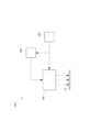
しかして本実施形態の検査用照明システム400では、複数のLED素子11の発光バラつきを抑えるべく、図3に示すように、1つのLED基板1に対して複数のバッファ基板2が接続され、各バッファ基板2には通信用IC22がそれぞれ搭載されており、コントローラ300は、スイッチング素子21のオン・オフを制御する制御信号を各バッファ基板2の通信用IC22に対して差動通信により伝送するよう構成されている。In the
より具体的にこの検査用照明システム400では、LED基板1の裏面側が複数(具体的には縦2×横2の4つ)のエリアに区分けされており、図3及び図4に示すように、エリア毎に基板実装コネクタ13を介してバッファ基板2が接続されている。つまりこの検査用照明器100では、1枚のLED基板1の裏面に複数(4つ)の基板実装コネクタ13が搭載されており、この基板実装コネクタ13を介して複数枚(4枚)のバッファ基板2が接続されている。またLED基板1の表面側にマトリクス状に配置される複数のLED素子11も、これらの区分けされた複数のエリアに均等に配置されている。そして各バッファ基板2には、対応する各エリアに設けられた縦又は横の複数の導線の開閉を行う複数スイッチング素子21と、1つの通信用IC22が設けられている。More specifically, in this
この検査用照明システム400ではコントローラ300もまた通信用IC310を備えており、当該コントローラ300の通信用IC310から、各バッファ基板2に設けられた通信用IC22に、スイッチング素子21のオン・オフを制御する制御信号が差動通信により伝送される。具体的にこの差動通信では、対をなす2本の信号線にそれぞれ逆相の電流を流し、信号線間の電位差を用いてデータが伝送される。In this
本実施形態では各バッファ基板2が備える複数の通信用IC22は、コントローラ300が備える通信用IC310に対して互いにシリアルに接続されており、コントローラ300の通信用IC310から伝送された制御信号が、複数のバッファ基板2の通信用IC22間で順に伝送されるように構成されている。つまり、ある1つのバッファ基板2に搭載された通信用IC22は、制御信号を受信すると、これを隣り合う他の1つのバッファ基板2の通信用IC22に対して差動通信により伝送する。In this embodiment, the
また各バッファ基板2には、電源装置200から供給された直流電圧(ここでは24V)を所定の直流電圧(ここでは3.6V)に低下させるDC/DCコンバータ23が搭載されている。電源装置200から供給された直流電圧は、バッファ基板2において電圧値が低下された後、LED駆動回路100Cに印加される。Each
<作用効果>
このように構成された本実施形態の検査用照明システム400によれば、1枚のLED基板1に対して複数枚のバッファ基板2を接続して構成しているので、接続するバッファ基板2の枚数を変えることで、様々なLED基板1のサイズに対応することができる。これにより、照明サイズのラインナップの拡充を容易に行うことができる。さらに、コントローラ300から各バッファ基板2への制御信号の伝送を差動通信により行うので、各スイッチング素子21に対して制御信号を少ないノイズで高速で伝送することができる。これにより、縞状パターンの光をその位相を遷移させつつワークWの表面に照射する検査用照明システム100において、各LED素子11の発光バラつきを抑え、検査精度を高めることができる。<Action and effect>
According to the
<その他の実施形態>
なお、本願発明は前記実施形態に限られるものではない。
例えば、前記実施形態では、各バッファ基板2にDC/DCコンバータ23が接続されていたがこれに限らない。他の実施形態では、各バッファ基板2にDC/DCコンバータ23が接続されていなくてもよく、予め所定の電圧値に低下させた直流電圧が、電源装置200から各バッファ基板2に供給されてもよい。<Other embodiments>
The present invention is not limited to the above-described embodiment.
For example, in the above embodiment, the DC/
また前記実施形態の基板実装コネクタ13は、接続ピン等を介してLED基板1とバッファ基板2の両方に接続できる基板対基板コネクタであったが、これに限らない。他の実施形態の基板実装コネクタ13としては、フラットケーブルやフレキシブル基板等が接続されるコネクタであってもよい。In addition, the board-mounted
その他、本願発明は前記実施形態に限られず、その趣旨を逸脱しない範囲で種々の変形が可能である。例えば、本明細書の開示は以下の態様1~6を含む。The present invention is not limited to the above-described embodiment, and various modifications are possible without departing from the spirit of the invention. For example, the disclosure of this specification includes the following
(態様1)
縞状パターンの光をその位相を遷移させつつワークの表面に照射するものであって、複数のLED素子がマトリクス状に搭載されたLED基板と、前記LED素子が接続された回路を開閉するスイッチング素子が搭載されたバッファ基板と、前記スイッチング素子のオン・オフを制御するコントローラとを備え、前記LED基板に複数の前記バッファ基板が接続されており、前記複数のバッファ基板のそれぞれに通信用ICが搭載されており、前記コントローラが、前記スイッチング素子のオン・オフを制御する制御信号を、前記各バッファ基板の通信用ICに対して差動通信により伝送する検査用照明システム。(Aspect 1)
An inspection lighting system which irradiates a striped pattern of light onto the surface of a workpiece while shifting the phase of the light, and which comprises an LED board on which a plurality of LED elements are mounted in a matrix, a buffer board on which a switching element which opens and closes a circuit to which the LED elements are connected is mounted, and a controller which controls the on/off of the switching element, wherein a plurality of the buffer boards are connected to the LED board, a communication IC is mounted on each of the plurality of buffer boards, and the controller transmits a control signal which controls the on/off of the switching element to the communication IC of each of the buffer boards via differential communication.
このような態様であれば、1枚のLED基板に対して複数枚のバッファ基板を接続して構成しているので、接続するバッファ基板の枚数を変えることで、様々なLED基板のサイズに対応することができる。これにより、照明サイズのラインナップの拡充を容易に行うことができる。さらに、各バッファ基板への制御信号の伝送を差動通信により行うので、各スイッチング素子に対して制御信号を少ないノイズで高速で伝送できるので、縞状パターンの光をその位相を遷移させつつワークの表面に照射する検査用照明システムにおいて、LED素子の発光バラつきを抑えることができる。In this configuration, multiple buffer boards are connected to one LED board, so by changing the number of buffer boards connected, it is possible to accommodate a variety of LED board sizes. This makes it easy to expand the lineup of lighting sizes. Furthermore, since the control signals to each buffer board are transmitted by differential communication, the control signals can be transmitted to each switching element at high speed with little noise, so that in an inspection lighting system that irradiates the surface of a workpiece with a striped pattern of light while shifting its phase, it is possible to suppress variations in the light emission of LED elements.
(態様2)
前記LED基板が平面視において複数のエリアに区分けされており、当該エリア毎に前記バッファ基板が接続され、各バッファ基板には複数のスイッチング素子が搭載されている態様1に記載の検査用照明システム。
このような態様であれば、上述した本発明の効果がより顕著になる。(Aspect 2)
The inspection lighting system according to
In this embodiment, the above-mentioned effects of the present invention become more pronounced.
(態様3)
前記コントローラから伝送された制御信号が、前記複数のバッファ基板の通信用IC間で順に伝送されるよう構成された態様1又は2に記載の検査用照明システム。
差動通信により各バッファ基板に制御信号を伝送するための具体的態様としては、このようなものが挙げられる。(Aspect 3)
3. The inspection lighting system according to
Specific examples of the manner in which control signals are transmitted to each buffer board by differential communication include the following.
(態様4)
前記LED素子に直流電圧を印加する電源装置を更に備え、各バッファ基板にDC/DCコンバータが設けられており、前記電源装置から供給される直流電圧が、前記各バッファ基板のDC/DCコンバータにより低下された後前記LED素子に印加される態様1~3のいずれかに記載の検査用照明システム。
このような態様であれば、電源装置から供給される直流電圧を各バッファ基板に設けたDC/DCコンバータにより低下してLED素子に印加するようにしているので、電源装置から各バッファ基板への直流電圧値を高くし、LED素子への給電に至るまでの電圧損失を低減できる。これにより、点灯条件(例えばLED素子を何列点灯させるか等)が変化した場合であっても、電圧のドロップを低減でき、各LED素子の発光ばらつきをより効果的に低減できる。(Aspect 4)
The inspection lighting system of any one of
In this embodiment, the DC voltage supplied from the power supply is reduced by the DC/DC converter provided in each buffer board and applied to the LED elements, so that the DC voltage value from the power supply to each buffer board can be increased and the voltage loss until power is supplied to the LED elements can be reduced. This makes it possible to reduce voltage drop even when the lighting conditions (e.g., how many rows of LED elements are lit, etc.) change, and makes it possible to more effectively reduce the light emission variation of each LED element.
(態様5)
前記バッファ基板が、前記LED基板の裏面側に搭載された基板対基板コネクタを介して、前記LED基板に接続されている態様1~4のいずれかに記載の検査用照明システム。
このような態様であれば、LED基板とバッファ基板との間を、例えばFFC(フレキシブルフラットケーブル)等のケーブル接続用コネクタにより接続する場合に比べて、コネクタにおけるインピーダンスを低くすることができ、LED素子への給電に至るまでの電圧損失をより一層低減できる。(Aspect 5)
An inspection lighting system according to any one of
In this configuration, the impedance in the connector can be lowered compared to when the LED board and the buffer board are connected by a cable connector such as an FFC (flexible flat cable), and the voltage loss until power is supplied to the LED elements can be further reduced.
(態様6)
照射する縞状パターンの光が並ぶ方向とその遷移方向を、縦横で切り替えられるように構成された態様1~5のいずれかに記載の検査用照明システム。
このような態様であれば、より複雑なスイッチング制御が求められるため、上述した本発明の効果がより顕著になる。(Aspect 6)
An inspection illumination system according to any one of
In such an embodiment, more complicated switching control is required, so that the above-described effect of the present invention becomes more pronounced.
上記した本発明によれば、縞状パターンの光をその位相を遷移させつつワークの表面に照射する検査用照明システムにおいて、LED素子の発光バラつきを低減することができる。According to the present invention described above, it is possible to reduce variations in the light emission of LED elements in an inspection lighting system that irradiates a striped pattern of light onto the surface of a workpiece while shifting its phase.
400・・・検査用照明システム
1 ・・・LED基板
11 ・・・LED素子
12 ・・・抵抗素子
2 ・・・バッファ基板
21 ・・・スイッチング素子
22 ・・・通信用IC
23 ・・・DC/DCコンバータ
300・・・コントローラ
310・・・通信用IC
W ・・・ワーク
400...
23 DC/
W...Work
Claims (6)
Translated fromJapanese複数のLED素子がマトリクス状に搭載されたLED基板と、
前記LED素子が接続された回路を開閉するスイッチング素子が搭載されたバッファ基板と、
前記スイッチング素子のオン・オフを制御するコントローラとを備え、
前記LED基板に複数の前記バッファ基板が接続されており、
前記複数のバッファ基板のそれぞれに通信用ICが搭載されており、
前記コントローラが、前記スイッチング素子のオン・オフを制御する制御信号を、前記各バッファ基板の通信用ICに対して差動通信により伝送する検査用照明システム。A stripe pattern of light is irradiated onto the surface of a workpiece while shifting the phase of the light,
An LED substrate on which a plurality of LED elements are mounted in a matrix;
a buffer substrate on which a switching element for opening and closing a circuit to which the LED element is connected is mounted;
A controller for controlling the on/off of the switching element,
A plurality of the buffer substrates are connected to the LED substrate,
Each of the plurality of buffer boards is equipped with a communication IC,
The inspection lighting system wherein the controller transmits a control signal for controlling the on/off of the switching element to a communication IC of each of the buffer boards by differential communication.
各バッファ基板にDC/DCコンバータが設けられており、
前記電源装置から供給される直流電圧が、前記各バッファ基板のDC/DCコンバータにより低下された後前記LED素子に印加される請求項1に記載の検査用照明システム。Further comprising a power supply device that applies a DC voltage to the LED element,
Each buffer board is provided with a DC/DC converter.
2. The inspection lighting system according to claim 1, wherein a DC voltage supplied from the power supply device is lowered by a DC/DC converter of each of the buffer boards and then applied to the LED elements.
Priority Applications (1)
| Application Number | Priority Date | Filing Date | Title |
|---|---|---|---|
| JP2024567329AJPWO2024142731A1 (en) | 2022-12-27 | 2023-11-29 |
Applications Claiming Priority (2)
| Application Number | Priority Date | Filing Date | Title |
|---|---|---|---|
| JP2022-209344 | 2022-12-27 | ||
| JP2022209344 | 2022-12-27 |
Publications (1)
| Publication Number | Publication Date |
|---|---|
| WO2024142731A1true WO2024142731A1 (en) | 2024-07-04 |
Family
ID=91717207
Family Applications (1)
| Application Number | Title | Priority Date | Filing Date |
|---|---|---|---|
| PCT/JP2023/042693PendingWO2024142731A1 (en) | 2022-12-27 | 2023-11-29 | Illumination system for inspection |
Country Status (2)
| Country | Link |
|---|---|
| JP (1) | JPWO2024142731A1 (en) |
| WO (1) | WO2024142731A1 (en) |
Citations (3)
| Publication number | Priority date | Publication date | Assignee | Title |
|---|---|---|---|---|
| JP2006030127A (en)* | 2004-07-21 | 2006-02-02 | Japan Science & Technology Agency | Camera calibration system and three-dimensional measurement system |
| JP2020042053A (en)* | 2019-12-23 | 2020-03-19 | 株式会社キーエンス | Image inspection device and image inspection method |
| JP2022163640A (en)* | 2021-04-14 | 2022-10-26 | 富士フイルムビジネスイノベーション株式会社 | Light emitting device and measuring device |
- 2023
- 2023-11-29JPJP2024567329Apatent/JPWO2024142731A1/jaactivePending
- 2023-11-29WOPCT/JP2023/042693patent/WO2024142731A1/enactivePending
Patent Citations (3)
| Publication number | Priority date | Publication date | Assignee | Title |
|---|---|---|---|---|
| JP2006030127A (en)* | 2004-07-21 | 2006-02-02 | Japan Science & Technology Agency | Camera calibration system and three-dimensional measurement system |
| JP2020042053A (en)* | 2019-12-23 | 2020-03-19 | 株式会社キーエンス | Image inspection device and image inspection method |
| JP2022163640A (en)* | 2021-04-14 | 2022-10-26 | 富士フイルムビジネスイノベーション株式会社 | Light emitting device and measuring device |
Also Published As
| Publication number | Publication date |
|---|---|
| JPWO2024142731A1 (en) | 2024-07-04 |
Similar Documents
| Publication | Publication Date | Title |
|---|---|---|
| JP5666097B2 (en) | Backlight assembly and driving method thereof | |
| JP4895898B2 (en) | LED array drive device | |
| US10546807B2 (en) | Chip on file display device including the same | |
| US11257444B2 (en) | Backlight apparatus | |
| US20110310590A1 (en) | Light emitting module, light emitting module unit, and backlight system | |
| US9589501B2 (en) | Display drive circuit including an output terminal | |
| CN108761904A (en) | Back lighting device | |
| CN116343692A (en) | LED backlight panel and display module | |
| CN114220825B (en) | Light-emitting drive substrate, light-emitting panel and display device | |
| WO2024142731A1 (en) | Illumination system for inspection | |
| US11710464B2 (en) | Display device and backlight apparatus thereof | |
| CN109473047B (en) | Micro light emitting diode display panel and driving method thereof | |
| JP2024093164A (en) | Inspection Lighting System | |
| KR100804368B1 (en) | Plasma display device | |
| JP2011228205A (en) | Display device | |
| US8998437B2 (en) | Light emitting component board group, light emitting device and liquid crystal display device | |
| KR102510375B1 (en) | Display device | |
| KR20080025882A (en) | Organic light emitting display | |
| CN119029126A (en) | Wiring substrate, light-emitting substrate and display panel | |
| KR20230031576A (en) | Lamp apparatus for an automobile | |
| US20110227494A1 (en) | Circuit board including light-emitting elements and display apparatus including the circuit board | |
| CN114334926A (en) | Display device | |
| US20200051498A1 (en) | Circuit board and display device | |
| CN120526707A (en) | Pixel driver, LED display module and LED display | |
| CN116052531A (en) | Display substrate and display device |
Legal Events
| Date | Code | Title | Description |
|---|---|---|---|
| 121 | Ep: the epo has been informed by wipo that ep was designated in this application | Ref document number:23911512 Country of ref document:EP Kind code of ref document:A1 | |
| WWE | Wipo information: entry into national phase | Ref document number:2024567329 Country of ref document:JP | |
| NENP | Non-entry into the national phase | Ref country code:DE |