WO2024142641A1 - Optical multilayer body and article - Google Patents
Optical multilayer body and articleDownload PDFInfo
- Publication number
- WO2024142641A1 WO2024142641A1PCT/JP2023/041037JP2023041037WWO2024142641A1WO 2024142641 A1WO2024142641 A1WO 2024142641A1JP 2023041037 WJP2023041037 WJP 2023041037WWO 2024142641 A1WO2024142641 A1WO 2024142641A1
- Authority
- WO
- WIPO (PCT)
- Prior art keywords
- layer
- refractive index
- film
- resin substrate
- barrier layer
- Prior art date
- Legal status (The legal status is an assumption and is not a legal conclusion. Google has not performed a legal analysis and makes no representation as to the accuracy of the status listed.)
- Pending
Links
Images


Classifications
- B—PERFORMING OPERATIONS; TRANSPORTING
- B32—LAYERED PRODUCTS
- B32B—LAYERED PRODUCTS, i.e. PRODUCTS BUILT-UP OF STRATA OF FLAT OR NON-FLAT, e.g. CELLULAR OR HONEYCOMB, FORM
- B32B9/00—Layered products comprising a layer of a particular substance not covered by groups B32B11/00 - B32B29/00
- G—PHYSICS
- G02—OPTICS
- G02B—OPTICAL ELEMENTS, SYSTEMS OR APPARATUS
- G02B1/00—Optical elements characterised by the material of which they are made; Optical coatings for optical elements
- G02B1/10—Optical coatings produced by application to, or surface treatment of, optical elements
- G02B1/11—Anti-reflection coatings
- G02B1/113—Anti-reflection coatings using inorganic layer materials only
- G02B1/115—Multilayers
- G—PHYSICS
- G02—OPTICS
- G02B—OPTICAL ELEMENTS, SYSTEMS OR APPARATUS
- G02B1/00—Optical elements characterised by the material of which they are made; Optical coatings for optical elements
- G02B1/10—Optical coatings produced by application to, or surface treatment of, optical elements
- G02B1/14—Protective coatings, e.g. hard coatings
Definitions
- the present inventionrelates to an optical laminate and an article. This application has priority to the contents described in Japanese Patent Application No. 2022-209242 filed in Japan on December 27, 2022.
- anti-reflection filmsare sometimes provided on the surfaces of flat panel displays (FPDs), touch panels, solar cells, etc.
- FPDsflat panel displays
- solar cellsetc.
- anti-reflection films using optical laminates in which low refractive index layers and high refractive index layers are alternately stackedare known.
- Patent Document 1describes the formation of a barrier layer when depositing a dielectric film on a metal film in order to suppress changes in the characteristics of the metal film when the dielectric film is deposited on the metal film.
- the present inventionwas made in consideration of the above problems, and aims to provide an optical laminate and article with excellent scratch resistance.
- the present inventionprovides the following means to solve the above problems.
- the article according to the second aspectcomprises the optical laminate according to the above aspect.
- the resin substrate 1may contain a reinforcing material as long as the optical properties are not significantly impaired.
- reinforcing materialsinclude cellulose nanofibers and nanosilica.
- the surface of the resin substrate 1may be previously subjected to an etching treatment such as sputtering, corona discharge, ultraviolet irradiation, electron beam irradiation, conversion, oxidation, and/or an undercoat treatment. By previously performing these treatments, the adhesion of the hard coat layer 2 formed on the resin substrate 1 is improved. Furthermore, before forming the hard coat layer 2 on the resin substrate 1, the surface of the resin substrate 1 may be subjected to solvent washing, ultrasonic washing, etc., as necessary, to remove dust and clean the surface of the resin substrate 1.
- an etching treatmentsuch as sputtering, corona discharge, ultraviolet irradiation, electron beam irradiation, conversion, oxidation, and/or an undercoat treatment.
- thermosetting resin that is the binder resinmay be, for example, a phenol resin, a urea resin, a diallyl phthalate resin, a melamine resin, a guanamine resin, an unsaturated polyester resin, a polyurethane resin, an epoxy resin, an aminoalkyd resin, a melamine-urea co-condensation resin, a silicon resin, a polysiloxane resin (including so-called silsesquioxanes such as cage-shaped and ladder-shaped ones), etc.
- the hard coat layer 2may contain an organic resin and an inorganic material, or may be an organic-inorganic hybrid material.
- An example of an organic-inorganic hybrid materialis one formed by the sol-gel method.
- examples of inorganic materialsinclude silica, alumina, zirconia, and titania.
- examples of organic materialsinclude acrylic resin.
- the first layer 5is laminated, for example, on one surface of the barrier layer 4.
- the first layer 5is a part of an optical function layer.
- the first layer 5 and the alternating laminate film 6form the optical function layer.
- the optical function layeris a layer that exhibits an optical function.
- the optical functionis a function that controls the properties of light, namely, reflection, transmission, and refraction, and examples of such functions include an anti-reflection function, a selective reflection function, an anti-glare function, and a lens function.
- Silicon nitrideis represented by, for example, SixNy . Silicon nitride is, for example, Si3N4 . When the first layer 5 is made of silicon nitride, the oxygen content of the first layer 5 is 0 atm %.
- Silicon oxynitrideis represented, for example, by Si x N y O z .
- the oxygen content of the first layer 5is low, the first layer 5 exhibits performance equivalent to that of a film made of high-hardness silicon nitride, and the scratch resistance of the optical laminate 10 is improved.
- the alternating laminate film 6is, for example, a laminate film in which low refractive index layers and high refractive index layers are alternately laminated in order from the side closest to the first layer 5.
- the low refractive index layerhas a lower refractive index than the first layer 5.
- the high refractive index layerhas a higher refractive index than the low refractive index layer.
- the refractive indexes of the high refractive index layersmay be the same or different.
- the refractive indexes of the low refractive index layersmay be the same or different.
- the low refractive index layer 61 and the low refractive index layer 63contain, for example, an oxide of Si.
- the low refractive index layer 61b and the low refractive index layer 63are layers mainly composed of, for example, SiO 2 (oxide of Si).
- the low refractive index layer 61 and the low refractive index layer 63preferably contain an oxide of Si from the viewpoint of availability and cost, are preferably layers mainly composed of SiO 2 (dioxide of Si) or the like, and are preferably composed of SiO 2.
- the SiO 2 single layer filmis colorless and transparent.
- the main componentis a component that occupies 50 mass % or more of the components contained in the layer.
- the high refractive index layer 62examples include silicon nitride (SiN, refractive index 2.0), niobium pentoxide (Nb 2 O 5 , refractive index 2.33), titanium oxide (TiO 2 , refractive index 2.33 to 2.55), tungsten oxide (WO 3 , refractive index 2.2), cerium oxide (CeO 2 , refractive index 2.2), tantalum pentoxide (Ta 2 O 5 , refractive index 2.16), zinc oxide (ZnO, refractive index 2.1), indium tin oxide (ITO, refractive index 2.06), zirconium oxide (ZrO 2 , refractive index 2.2), etc.
- the high refractive index layer 62is, for example, niobium pentoxide.
- a low refractive index layer 63is disposed on the side of the antifouling layer 7.
- the antireflection performance of the optical functional layeris improved.
- the total thickness of the entire optical functional layeris, for example, 80 nm or more and 480 nm or less, preferably 160 nm or more and 240 nm or less, and more preferably 165 nm or more and 225 nm or less.
- the anti-stain layer 7is, for example, a vapor deposition film formed by vapor-depositing an anti-stain material.
- the anti-stain layer 7is formed, for example, by vacuum-depositing a fluorine-based compound as an anti-stain material on one surface of the low refractive index layer 63.
- the anti-stain layer 7contains a fluorine-based compound, the sliding of the pen during input becomes smoother and the pen sliding resistance of the optical laminate 10 is further improved.
- the fluorine-based compound contained in the anti-soiling layer 7is, for example, a fluorine-based organic compound.
- the fluorine-based organic compoundis, for example, a compound consisting of a fluorine-modified organic group and a reactive silyl group (e.g., alkoxysilane).
- Commercially available products that can be used for the anti-soiling layer 7include Optool DSX (manufactured by Daikin Corporation) and the KY-100 series (manufactured by Shin-Etsu Chemical Co., Ltd.).
- a siloxane bondis formed between the silanol group generated from the reactive silyl group of the fluorine-based organic compound and the SiO 2.
- the siloxane bondenhances the adhesion between the layer-by-layer laminate film 6 and the antifouling layer 7.
- the thickness of the antifouling layer 7is, for example, 1 nm or more and 20 nm or less, and preferably 3 nm or more and 10 nm or less. If the thickness of the antifouling layer 7 is 1 nm or more, sufficient abrasion resistance can be ensured when the optical laminate 10 is applied to touch panel applications, etc. If the thickness of the antifouling layer 7 is 20 nm or less, the time required for vapor deposition is short, and the antifouling layer 7 can be produced efficiently.
- the stain-resistant layer 7may contain additives such as light stabilizers, ultraviolet absorbers, colorants, antistatic agents, lubricants, leveling agents, defoamers, antioxidants, flame retardants, infrared absorbers, and surfactants, as necessary.
- additivessuch as light stabilizers, ultraviolet absorbers, colorants, antistatic agents, lubricants, leveling agents, defoamers, antioxidants, flame retardants, infrared absorbers, and surfactants, as necessary.
- the anti-fouling layer 7 formed by vapor depositionis firmly bonded to the layer-by-layer film 6 and is dense with few voids. Therefore, the anti-fouling layer 7 formed by vapor deposition exhibits different characteristics from the anti-fouling layer 7 formed by other methods, such as coating with an anti-fouling material.
- the anti-fouling layer 7 formed by vapor depositionis resistant to wear.
- Each layer of the optical laminate 10is, for example, a sputtered film.
- the primer layer 3, the barrier layer 4, the first layer 5, and the alternating laminate film 6are, for example, sputtered films.
- the sputtered filmis denser than a film formed using a general vacuum deposition method or a coating method.
- the water vapor permeability of the optical functional layeris 1.0 g/m 2 /day or less.
- a dense sputtered filmhas a low water vapor permeability.
- the sputtered filmis dense and does not easily leave a sliding mark. For example, even if a part of the antifouling layer 7 is peeled off due to pen sliding, the optical functional layer is dense, so that the pen sliding mark is not easily left.
- a resin substrate 1is prepared.
- the resin substrate 1can be obtained, for example, by purchasing a commercially available product.
- the resin substrate 1does not need to be subjected to a degassing process.
- a hard coat layer 2is formed on one surface of the resin substrate 1.
- a slurry containing a material for the hard coat layer 2is applied onto the resin substrate 1, and the material for the hard coat layer 2 is cured by a known method to obtain the hard coat layer 2.
- the surfaceBefore forming the hard coat layer 2 on the resin substrate 1, the surface may be washed as necessary. Examples of methods for washing the surface of the resin substrate 1 include solvent washing and ultrasonic washing. Washing the resin substrate 1 is preferable because it removes dust from the surface of the resin substrate 1 and cleans the surface. Alternatively, a commercially available resin substrate 1 with a hard coat layer 2 formed thereon may be purchased.
- the primer layer 3is formed on the hard coat layer 2.
- the method for manufacturing the primer layer 3is not particularly limited, and it can be manufactured using a known manufacturing method.
- the primer layer 3can be formed, for example, by a sputtering method.
- the primer layer 3is produced by using a silicon target and performing sputtering in an atmosphere of a mixed gas of argon and oxygen.
- the barrier layer 4is formed on the primer layer 3.
- the method for manufacturing the barrier layer 4is not particularly limited, and it can be manufactured using a known manufacturing method.
- the barrier layer 4can be formed, for example, by a sputtering method.
- the barrier layer 4is produced by sputtering using a silicon target in an atmosphere of a mixed gas of argon and oxygen.
- the manufacturing method of the first layer 5is not particularly limited, and it can be manufactured using a known manufacturing method.
- the first layer 5can be formed by, for example, a sputtering method.
- the first layer 5is produced by sputtering using a silicon target in an atmosphere of a mixed gas of argon and nitrogen.
- the alternating laminate film 6is formed on the first layer 5.
- the alternating laminate film 6is formed, for example, in the order of a low refractive index layer 61, a high refractive index layer 62, and a low refractive index layer 63. These layers are produced, for example, by using a sputtering method. Examples of power supply methods for the sputtering method include DC (direct current), RF (high frequency), and MF (medium frequency).
- DCdirect current
- RFhigh frequency
- MFmedium frequency
- the frequency during sputteringis preferably 20 KHz to 60 KHz.
- the degree of vacuum during sputteringis, for example, 1.0 Pa or less.
- the conveying speed(line speed) is, for example, 0.5 m/min or more and 20 m/min or less.
- an antifouling layer 7is formed on the layer-by-layer film 6.
- a plasma treatmentit is preferable to perform a plasma treatment on the surface of the layer-by-layer film 6. Modifying the surface of the low refractive index layer 63 by the plasma treatment increases the adhesion between the layer-by-layer film 6 and the antifouling layer 7.
- the anti-fouling layer 7is formed, for example, by vapor deposition. Vapor deposition is performed by heating the material that will become the anti-fouling layer 7 to its vapor pressure temperature. The degree of vacuum during vapor deposition is, for example, 1.0 Pa or less. When the anti-fouling layer 7 is formed under these conditions, it becomes dense and less susceptible to wear.
- the deposition of the primer layer 3, barrier layer 4, first layer 5, alternating laminate film 6, and antifouling layer 7is preferably performed roll-to-roll in a reduced pressure environment.
- the optical laminate 10can be produced.
- the optical laminate 10has a barrier layer 4, and therefore can suppress outgassing from the resin substrate 1 from adversely affecting the first layer 5.
- the barrier layer 4can prevent oxygen from being taken up into the first layer 5.
- oxygenis taken up into the first layer 5
- the refractive index of the first layer 5decreases, and the hardness also decreases.
- the refractive index of the first layer 5decreases, the optical properties of the optical laminate 10 decrease.
- the scratch resistance of the optical laminate 10decreases.
- the optical laminate 10may have layers other than the resin substrate 1, the hard coat layer 2, the primer layer 3, the barrier layer 4, the first layer 5, the alternating laminate film 6, and the antifouling layer 7.
- the optical laminate 10may also have layers having various properties as necessary on the surface of the resin substrate 1 opposite the surface on which the barrier layer 4 and the like are formed.
- an adhesive layer used for adhesion to other membersmay be provided.
- another optical filmmay be provided via this adhesive layer. Examples of other optical films include a polarizing film, a retardation compensation film, a film that functions as a 1/2 wavelength plate, or a 1/4 wavelength plate.
- a layer having functions such as anti-reflection, selective reflection, anti-glare, polarization, phase difference compensation, viewing angle compensation or expansion, light guiding, diffusion, brightness improvement, hue adjustment, and electrical conductivitymay be formed on one side of the resin substrate 1.
- a nano-order uneven structure that exhibits moth-eye and anti-glare functionsmay be formed on the surface of the optical laminate 10.
- Micro to millimeter-order geometric shapessuch as lenses and prisms may be formed on the surface of the optical laminate 10.
- the optical laminate 10can also be applied to a variety of products.
- the optical laminate 10may be provided on the screen of an image display unit, such as a liquid crystal display panel or an organic EL display panel. This allows, for example, the touch panel display unit of a smartphone or other operating device to exhibit high scratch resistance, resulting in an image display device that is suitable for practical use.
- the articleis not limited to image display devices, and the optical laminate 10 can be applied to window glass, goggles, the light receiving surface of a solar cell, the screen of a smartphone or a personal computer display, information input terminals, tablet terminals, AR (augmented reality) devices, VR (virtual reality) devices, electronic display boards, glass table surfaces, gaming machines, operation support devices for aircraft and trains, navigation systems, instrument panels, the surface of optical sensors, etc.
- ARaugmented reality
- VRvirtual reality
- Example 1In Example 1, the change in composition of the first layer 5 when the thickness of the barrier layer 4 was changed was measured.
- a primer layer 3 represented by SiOx (0 ⁇ x ⁇ 2)was formed on the hard coat layer 2 to a thickness of 4 nm by a reactive sputtering method using a Si target as a sputtering target and a mixed gas of Ar gas and O2 gas.
- a barrier layer 4 represented by SiO2was formed on the primer layer 3 by reactive sputtering using a mixed gas of Ar gas and O2 gas, using a Si target as the sputtering target.
- the deposition pressurewas 0.3 Pa
- the Ar flow rate during depositionwas 3.2 sccm
- the O2 flow ratewas 1.8 sccm
- the configuration of the barrier layer 4 of each sampleis shown below.
- Sample 10 nm (barrier layer 4 was not formed)
- Sample 21 0 nm (barrier layer 4 was not formed)
- Sample 21 nm
- Sample 32 nm
- Sample 44 nm
- Sample 56 nm
- Sample 68 nm
- Sample 710 nm
- a first layer 5was formed on the barrier layer 4 by reactive sputtering using a Si target as a sputtering target and a mixed gas of Ar gas and N2 gas.
- the film formation pressurewas 0.3 Pa, and the film thickness of the first layer 5 was 50 nm.
- an X-ray photoelectron spectroscopy device(Electron Spectroscopy for Chemical Analysis, ESCA; Versaprobe III, manufactured by ULVAC-PHI, Inc.) was used to analyze the composition of the first layer 5 of each of the prepared samples 1 to 7.
- a comparative sample(sample 8) was also prepared in which the first layer 5 was prepared under the same conditions as sample 1, using a resin substrate 1 that had been degassed for 18 hours.
- the composition of the first layer 5 of sample 8was also measured using ESCA.
- sample 8which underwent a degassing process, there was little outgassing from the resin substrate 1, so the first layer 5 was a silicon nitride film. In contrast, it was confirmed that even in samples 1 to 7, which did not undergo a degassing process, if the thickness of the barrier layer 4 was 4 nm or more, the film had a composition that could be roughly considered to be silicon nitride.
- Example 2In Example 2, changes in the characteristics of the first layer 5 due to differences in the oxygen content of the first layer 5 were measured.
- the resin substrate 1 on which the hard coat layer 2 was formedwas depressurized to 1.0E-4 Pa or less, and a degassing process was carried out for 18 hours.
- the configurations of the resin substrate 1 and the hard coat layer 2were the same as in Example 1.
- a primer layer 3 and a barrier layer 4were formed on the hard coat layer 2.
- the configurations of the primer layer 3 and the barrier layer 4were the same as in Example 1.
- a first layer 5 represented by Si x N y O zwas produced on the barrier layer 4 by reactive sputtering using a Si target as a sputtering target and a mixed gas of Ar gas, N 2 gas and O 2 gas.
- the film formation pressurewas 0.3 Pa, and the film formation time was 1818 seconds to produce the first layer 5.
- the film thickness of the first layer 5was about 200 nm.
- the Ar flow rate during film formationwas 3 sccm
- the N 2 flow ratewas 2 sccm
- the O 2 flow ratewas changed to prepare several samples with different oxygen contents.
- the O 2 flow rate during the production of each sample and the composition ratio of the first layer 5 after productionare shown in Table 3 below.
- the composition of the first layer 5 of each samplewas analyzed by ESCA.
- Figure 3shows the composition analysis results of each sample measured in Example 2.
- the vertical axis of Figure 3shows the energy of the Si 2p electrons measured by ESCA.
- the horizontal axis of Figure 3shows the oxygen content of the first layer 5.
- the first layer 5can be considered as a nitride film, and if the oxygen content in the first layer 5 is high, the first layer 5 becomes an oxide film. If the oxygen content in the first layer 5 is 40 atm% or less, the first layer 5 can be said to be a film whose composition can be roughly considered as silicon nitride.
- Example 3In Example 3, the first layer 5 represented by Si x N y O z was formed on a slide glass under the same conditions as the samples of the first layer 5 prepared in Example 2, and the Martens hardness of the first layer 5 formed on the slide glass plate was measured.
- FIG. 4shows the Martens hardness of each sample in Example 3. The Martens hardness was measured at a load of 0.05 mN using a microcompression tester (ENT-NEXUS manufactured by Elionix Co., Ltd., measuring indenter: Berkovich indenter) in accordance with ISO14577-1. As shown in FIG. 4, the Martens hardness decreases as the oxygen content in the first layer 5 increases. If the oxygen content of the first layer 5 is 40 atm% or less, the first layer 5 exhibits a hardness of 5000 N/cm 2 or more.
- the refractive index of the first layer 5 of each of the prepared sampleswas measured.
- the refractive index of the first layer 5was measured using a J. A. Woollam M-2000 spectroscopic ellipsometer.
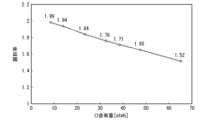
- Figure 5shows the refractive index of the first layer 5 of each sample in Example 3. As shown in Figure 5, the refractive index of the first layer 5 decreases as the oxygen content in the first layer 5 increases.
- the scratch resistance testwas conducted as follows. First, the optical laminate 10 was attached to a 1 mm thick glass plate using a transparent adhesive sheet (manufactured by Lintec Corporation) so that the low refractive index layer 63 of the optical laminate 10 was on the surface. Then, a linear sliding test was conducted using a stylus pen tip (refill for Bamboo Sketch/Bamboo Tip (medium type) manufactured by Wacom Corporation). The load was 250 gf, the number of sliding strokes was 20,000 (10,000 back and forth strokes), the back and forth distance was 50 mm, and the back and forth speed was two strokes per second (one back and forth stroke).
Landscapes
- Physics & Mathematics (AREA)
- General Physics & Mathematics (AREA)
- Optics & Photonics (AREA)
- Chemical & Material Sciences (AREA)
- Inorganic Chemistry (AREA)
- Laminated Bodies (AREA)
- Surface Treatment Of Optical Elements (AREA)
Abstract
Description
Translated fromJapanese本発明は、光学積層体及び物品に関する。本出願は、2022年12月27日に日本で出願された特願2022-209242に記載の内容に対して優先権を有する。The present invention relates to an optical laminate and an article. This application has priority to the contents described in Japanese Patent Application No. 2022-209242 filed in Japan on December 27, 2022.
例えば、フラットパネルディスプレイ(FPD)、タッチパネル、太陽電池等の表面に、反射防止フィルムを設けることがある。例えば、低屈折率層と高屈折率層とが交互に積層された光学積層体を用いた反射防止フィルムが知られている。For example, anti-reflection films are sometimes provided on the surfaces of flat panel displays (FPDs), touch panels, solar cells, etc. For example, anti-reflection films using optical laminates in which low refractive index layers and high refractive index layers are alternately stacked are known.
光学積層体は、異なる材料を含む層が積層されたものであり、製造時にそれぞれの層が他の層に影響を及ぼす場合がある。例えば、特許文献1には、金属膜上に誘電体膜を成膜した際に、金属膜の特性変化が生じることを抑制するために、金属膜上に誘電体膜を成膜する際にバリア層を形成することが記載されている。An optical laminate is a stack of layers containing different materials, and each layer may affect the other layers during manufacturing. For example, Patent Document 1 describes the formation of a barrier layer when depositing a dielectric film on a metal film in order to suppress changes in the characteristics of the metal film when the dielectric film is deposited on the metal film.
例えば、ペンタッチ方式のタッチパネルの場合、光学積層体の表面をペンが摺動する。ペン摺動時に光学積層体に傷が入ると、光学積層体の光学特性が変化する。そのため、耐擦傷性の高い光学積層体が求められている。For example, in the case of a pen-touch type touch panel, a pen slides over the surface of the optical laminate. If the optical laminate is scratched when the pen slides, the optical properties of the optical laminate change. For this reason, there is a demand for an optical laminate with high scratch resistance.
本発明は上記問題に鑑みてなされたものであり、耐擦傷性に優れた、光学積層体及び物品を提供することを目的とする。The present invention was made in consideration of the above problems, and aims to provide an optical laminate and article with excellent scratch resistance.
本発明は、上記課題を解決するため、以下の手段を提供する。The present invention provides the following means to solve the above problems.
(1)第1の態様にかかる光学積層体は、樹脂基材とバリア層と第1層とを備える。前記バリア層は、前記樹脂基材と前記第1層とに挟まれる。前記バリア層は、酸化ケイ素を含む。前記第1層は、窒化ケイ素又は酸窒化ケイ素を含む。前記バリア層の膜厚は、4nm以上である。前記第1層の酸素含有量が40atm%以下である。(1) The optical laminate according to the first aspect comprises a resin substrate, a barrier layer, and a first layer. The barrier layer is sandwiched between the resin substrate and the first layer. The barrier layer contains silicon oxide. The first layer contains silicon nitride or silicon oxynitride. The barrier layer has a thickness of 4 nm or more. The first layer has an oxygen content of 40 atm % or less.
(2)上記態様に係る光学積層体は、前記第1層に接する交互積層膜をさらに備えてもよい。前記交互積層膜は、前記第1層より屈折率の低い低屈折率層と、前記低屈折率層より屈折率の高い高屈折率層と、を備える。(2) The optical laminate according to the above aspect may further include an alternating laminate film in contact with the first layer. The alternating laminate film includes a low refractive index layer having a refractive index lower than that of the first layer, and a high refractive index layer having a refractive index higher than that of the low refractive index layer.
(3)上記態様に係る光学積層体は、ハードコート層とプライマー層をさらに備えてもよい。前記ハードコート層は、前記樹脂基材と前記バリア層との間にあり、前記プライマー層は、前記ハードコート層と前記バリア層との間にある。(3) The optical laminate according to the above aspect may further include a hard coat layer and a primer layer. The hard coat layer is between the resin substrate and the barrier layer, and the primer layer is between the hard coat layer and the barrier layer.
(4)上記態様に係る光学積層体において、前記バリア層及び前記第1層は、スパッタリング膜でもよい。(4) In the optical laminate according to the above aspect, the barrier layer and the first layer may be sputtered films.
(5)上記態様に係る光学積層体において、前記交互積層膜は、スパッタリング膜でもよい。(5) In the optical laminate according to the above aspect, the alternating laminate film may be a sputtering film.
(6)上記態様に係る光学積層体において、前記プライマー層は、スパッタリング膜でもよい。(6) In the optical laminate according to the above aspect, the primer layer may be a sputtering film.
(7)第2の態様にかかる物品は、上記態様に係る光学積層体を備える。(7) The article according to the second aspect comprises the optical laminate according to the above aspect.
上記態様にかかる光学積層体及び物品は、擦傷性に優れる。The optical laminate and article according to the above embodiment have excellent scratch resistance.
以下、本実施形態について、図を適宜参照しながら詳細に説明する。以下の説明で用いる図面は、特徴をわかりやすくするために便宜上特徴となる部分を拡大して示している場合があり、各構成要素の寸法比率などは実際とは異なっていることがある。以下の説明において例示される材料、寸法等は一例であって、本発明はそれらに限定されるものではなく、本発明の効果を奏する範囲で適宜変更して実施することが可能である。The present embodiment will now be described in detail with reference to the drawings as appropriate. The drawings used in the following description may show characteristic parts in an enlarged scale for the sake of clarity, and the dimensional ratios of each component may differ from the actual ones. The materials, dimensions, etc. exemplified in the following description are merely examples, and the present invention is not limited to them. Appropriate modifications can be made within the scope of the effects of the present invention.
「光学積層体」
図1は、第1実施形態に係る光学積層体10の一例の断面図である。光学積層体10は、例えば、樹脂基材1とハードコート層2とプライマー層3とバリア層4と第1層5と交互積層膜6と防汚層7とを備える。第1層5と交互積層膜6とは合わせて光学機能層として機能する。なお、以下の記載で厚みに係る記載はいずれも物理的な膜厚である。"Optical laminate"
1 is a cross-sectional view of an example of an
(樹脂基材)
樹脂基材1は、可視光域の光を透過可能な透明材料からなる。樹脂基材1は、例えば、樹脂を含むプラスチックフィルムである。プラスチックフィルムの構成材料は、例えば、ポリエステル系樹脂、アセテート系樹脂、ポリエーテルスルホン系樹脂、ポリカーボネート系樹脂、ポリアミド系樹脂、ポリイミド系樹脂、ポリオレフィン系樹脂、(メタ)アクリル系樹脂、ポリ塩化ビニル系樹脂、ポリ塩化ビニリデン系樹脂、ポリスチレン系樹脂、ポリビニルアルコール系樹脂、ポリアリレート系樹脂、ポリフェニレンサルファイド系樹脂、である。(Resin substrate)
The resin substrate 1 is made of a transparent material capable of transmitting light in the visible light range. The resin substrate 1 is, for example, a plastic film containing a resin. Examples of the constituent material of the plastic film include polyester-based resins, acetate-based resins, polyethersulfone-based resins, polycarbonate-based resins, polyamide-based resins, polyimide-based resins, polyolefin-based resins, (meth)acrylic-based resins, polyvinyl chloride-based resins, polyvinylidene chloride-based resins, polystyrene-based resins, polyvinyl alcohol-based resins, polyarylate-based resins, and polyphenylene sulfide-based resins.
樹脂基材1の構成材料は、好ましくは、ポリエステル系樹脂、アセテート系樹脂、ポリカーボネート系樹脂、ポリオレフィン系樹脂である。樹脂基材1は、例えば、ポリエチレンテレフタラート(PET)基材又はトリアセチルセルロース(TAC)基材が好ましい。The material constituting the resin substrate 1 is preferably a polyester resin, an acetate resin, a polycarbonate resin, or a polyolefin resin. For example, the resin substrate 1 is preferably a polyethylene terephthalate (PET) substrate or a triacetyl cellulose (TAC) substrate.
なお、本実施形態でいう「透明材料」とは、本実施形態の効果を損なわない範囲で、使用波長域の光の透過率が80%以上の材料であることをいう。また、本実施形態において「(メタ)アクリル」は、メタクリル及びアクリルを意味する。In this embodiment, the term "transparent material" refers to a material that has a light transmittance of 80% or more in the wavelength range used, as long as the effect of this embodiment is not impaired. In this embodiment, "(meth)acrylic" refers to methacryl and acrylic.
樹脂基材1は、極性基に水分およびガスが吸着していることが多い。吸着した水分およびガスは、スパッタリングによる成膜の際にアウトガスとして放出することがある。例えば、常温常圧条件下で保管されたTACフィルムを真空環境下でスパッタリングする際に、TACフィルムから放出されるガス成分を、ガス分析計(ULVAC社製qulee)を用いて分析した結果を以下の表1に示す。The resin substrate 1 often has moisture and gas adsorbed to its polar groups. The adsorbed moisture and gas may be released as outgassing during film formation by sputtering. For example, when a TAC film stored under normal temperature and pressure conditions is sputtered in a vacuum environment, the gas components released from the TAC film were analyzed using a gas analyzer (qulee, manufactured by ULVAC) and the results are shown in Table 1 below.

表1における到達真空度は、最終的に到達したチャンバー内の真空度である。表1におけるデガス行程中の真空度は、フィルムからアウトガスが生じている際のチャンバー内の真空度である。表1に示すように、TACフィルムからは、様々な種類のガスが発生しており、特に水分(H2O)が多いことが分かる。樹脂基材1は、上記のようにデガス(脱気)工程を行うことで、内部に含まれている水分やガスの多くを除去することはできる。しかしながら、基材形態にもよるが、デガス工程には少なくとも1時間から12時間以上を要する。The ultimate vacuum in Table 1 is the final vacuum in the chamber. The vacuum during the degassing process in Table 1 is the vacuum in the chamber when outgassing is occurring from the film. As shown in Table 1, various types of gases are generated from the TAC film, and it can be seen that moisture (H2 O) is particularly abundant. By performing the degassing process as described above, it is possible to remove most of the moisture and gas contained inside the resin substrate 1. However, the degassing process takes at least 1 hour to 12 hours or more, depending on the substrate form.
樹脂基材1は、光学特性を著しく損なわない限りにおいて、補強材料を含んでいてもよい。補強材料は、例えば、セルロースナノファイバー、ナノシリカ等である。The resin substrate 1 may contain a reinforcing material as long as the optical properties are not significantly impaired. Examples of reinforcing materials include cellulose nanofibers and nanosilica.
樹脂基材1は、光学的機能および/または物理的機能が付与されたフィルムであっても良い。光学的および/または物理的な機能を有するフィルムは、例えば、偏光板、位相差補償フィルム、熱線遮断フィルム、透明導電フィルム、輝度向上フィルム、バリア性向上フィルム、レンズシートなどである。またこれらのフィルムに帯電防止機能を付与してもよい。The resin substrate 1 may be a film to which optical and/or physical functions have been imparted. Films having optical and/or physical functions include, for example, polarizing plates, phase difference compensation films, heat-shielding films, transparent conductive films, brightness-improving films, barrier-improving films, lens sheets, etc. These films may also be imparted with an antistatic function.
樹脂基材1の厚みは、特に限定されないが、例えば25μm以上であり、好ましくは40μm以上である。樹脂基材1の厚みが25μm以上であると、基材自体の剛性が確保され、光学積層体10に応力が加わっても皺が発生し難くなる。また樹脂基材1の厚みが25μm以上であると、樹脂基材1上にハードコート層2を連続的に形成しても、皺が生じにくく製造上の懸念が少ない。樹脂基材1の厚みが25μm以上であると、光学積層体10を製造途中にカールしにくく、取り扱いやすい。The thickness of the resin substrate 1 is not particularly limited, but is, for example, 25 μm or more, and preferably 40 μm or more. When the thickness of the resin substrate 1 is 25 μm or more, the rigidity of the substrate itself is ensured, and wrinkles are less likely to occur even when stress is applied to the
樹脂基材1の厚みは、1mm以下であることが好ましく、500μm以下であることがより好ましく、300μm以下であることが特に好ましい。樹脂基材1の厚みが1mm以下であると、樹脂基材1の実質的な光学透明性を担保しやすい。また、樹脂基材1の厚みが1mm以下であると、樹脂基材1上に、枚葉方式であってもロールトウロール方式であっても、光学機能層を成膜しやすい。特に、樹脂基材1の厚みが300μm以下であると、ロールトウロール方式で光学積層体10を製造する場合に、1回の製造処理で用いられるロールに投入可能な樹脂基材1の長さを長くできる。このため、樹脂基材1の厚みが300μm以下であると、ロールトウロール方式で光学積層体10を連続的に生産する場合に、生産性に優れる。また、樹脂基材1の厚みが300μm以下であると、品質の良好な光学積層体10となるため、好ましい。The thickness of the resin substrate 1 is preferably 1 mm or less, more preferably 500 μm or less, and particularly preferably 300 μm or less. When the thickness of the resin substrate 1 is 1 mm or less, it is easy to ensure the substantial optical transparency of the resin substrate 1. In addition, when the thickness of the resin substrate 1 is 1 mm or less, it is easy to form an optical functional layer on the resin substrate 1, whether by a sheet-fed method or a roll-to-roll method. In particular, when the thickness of the resin substrate 1 is 300 μm or less, when the
樹脂基材1は、表面に予めスパッタリング、コロナ放電、紫外線照射、電子線照射、化成、酸化等のエッチング処理および/または下塗り処理が施されていてもよい。これらの処理が予め施されていることで、樹脂基材1の上に形成されるハードコート層2の密着性が向上する。また樹脂基材1上にハードコート層2を形成する前に、必要に応じて、樹脂基材1の表面に対して溶剤洗浄、超音波洗浄等を行うことにより、樹脂基材1の表面を除塵、清浄化させてもよい。The surface of the resin substrate 1 may be previously subjected to an etching treatment such as sputtering, corona discharge, ultraviolet irradiation, electron beam irradiation, conversion, oxidation, and/or an undercoat treatment. By previously performing these treatments, the adhesion of the
(ハードコート層)
ハードコート層2は、特に限定されず、公知のものを用いることができる。ハードコート層2は、樹脂基材1の耐擦傷性を向上させる。ハードコート層2は、例えば、バインダー樹脂とフィラーとを含んでもよい。ハードコート層2は、この他、レベリング剤を含んでもよい。(Hard Coat Layer)
The
バインダー樹脂は、好ましくは透明性を有するものであり、例えば、紫外線、電子線により硬化する樹脂である電離放射線硬化型樹脂、熱可塑性樹脂、熱硬化性樹脂などである。The binder resin is preferably transparent, and is, for example, an ionizing radiation curable resin that is cured by ultraviolet light or electron beams, a thermoplastic resin, or a thermosetting resin.
バインダー樹脂である電離放射線硬化型樹脂の一例は、エチル(メタ)アクリレート、エチルヘキシル(メタ)アクリレート、スチレン、メチルスチレン、N-ビニルピロリドン等である。また電離放射線硬化型樹脂は、2以上の不飽和結合を有する化合物でもよい。2以上の不飽和結合を有する電離放射線硬化型樹脂は、例えば、トリメチロールプロパントリ(メタ)アクリレート、トリプロピレングリコールジ(メタ)アクリレート、ジエチレングリコールジ(メタ)アクリレート、ジプロピレングリコールジ(メタ)アクリレート、ペンタエリスリトールトリ(メタ)アクリレート、ペンタエリスリトールテトラ(メタ)アクリレート、ジペンタエリスリトールヘキサ(メタ)アクリレート、1,6-ヘキサンジオールジ(メタ)アクリレート、ネオペンチルグリコールジ(メタ)アクリレート、トリメチロールプロパントリ(メタ)アクリレート、ジトリメチロールプロパンテトラ(メタ)アクリレート、ジペンタエリスリトールペンタ(メタ)アクリレート、トリペンタエリスリトールオクタ(メタ)アクリレート、テトラペンタエリスリトールデカ(メタ)アクリレート、イソシアヌル酸トリ(メタ)アクリレート、イソシアヌル酸ジ(メタ)アクリレート、ポリエステルトリ(メタ)アクリレート、ポリエステルジ(メタ)アクリレート、ビスフェノールジ(メタ)アクリレート、ジグリセリンテトラ(メタ)アクリレート、アダマンチルジ(メタ)アクリレート、イソボロニルジ(メタ)アクリレート、ジシクロペンタンジ(メタ)アクリレート、トリシクロデカンジ(メタ)アクリレート、ジトリメチロールプロパンテトラ(メタ)アクリレート等の多官能化合物等である。これらのなかでも、ペンタエリスリトールトリアクリレート(PETA)、ジペンタエリスリトールヘキサアクリレート(DPHA)及びペンタエリスリトールテトラアクリレート(PETTA)が、バインダー樹脂に好適に用いられる。なお、「(メタ)アクリレート」は、メタクリレート及びアクリレートを指すものである。また、電離放射線硬化型樹脂として、上述した化合物をPO(プロピレンオキサイド)、EO(エチレンオキサイド)、CL(カプロラクトン)等で変性したものでもよい。電離放射線硬化型樹脂は、アクリル系の紫外線硬化型樹脂組成物が好ましい。Examples of ionizing radiation curable resins that are binder resins include ethyl (meth)acrylate, ethylhexyl (meth)acrylate, styrene, methylstyrene, and N-vinylpyrrolidone. The ionizing radiation curable resin may also be a compound having two or more unsaturated bonds. Examples of ionizing radiation curable resins having two or more unsaturated bonds include trimethylolpropane tri(meth)acrylate, tripropylene glycol di(meth)acrylate, diethylene glycol di(meth)acrylate, dipropylene glycol di(meth)acrylate, pentaerythritol tri(meth)acrylate, pentaerythritol tetra(meth)acrylate, dipentaerythritol hexa(meth)acrylate, 1,6-hexanediol di(meth)acrylate, neopentyl glycol di(meth)acrylate, trimethylolpropane tri(meth)acrylate, ditrimethylolpropane tetra(meth)acrylate, dipentaerythritol ... Polyfunctional compounds such as tetrapentaerythritol penta(meth)acrylate, tripentaerythritol octa(meth)acrylate, tetrapentaerythritol deca(meth)acrylate, isocyanuric acid tri(meth)acrylate, isocyanuric acid di(meth)acrylate, polyester tri(meth)acrylate, polyester di(meth)acrylate, bisphenol di(meth)acrylate, diglycerin tetra(meth)acrylate, adamantyl di(meth)acrylate, isobornyl di(meth)acrylate, dicyclopentane di(meth)acrylate, tricyclodecane di(meth)acrylate, ditrimethylolpropane tetra(meth)acrylate, etc. Among these, pentaerythritol triacrylate (PETA), dipentaerythritol hexaacrylate (DPHA) and pentaerythritol tetraacrylate (PETTA) are preferably used as the binder resin. In addition, "(meth)acrylate" refers to methacrylate and acrylate. In addition, the ionizing radiation curable resin may be one obtained by modifying the above-mentioned compounds with PO (propylene oxide), EO (ethylene oxide), CL (caprolactone), etc. The ionizing radiation curable resin is preferably an acrylic ultraviolet curable resin composition.
またバインダー樹脂である熱可塑性樹脂の一例は、スチレン系樹脂、(メタ)アクリル系樹脂、酢酸ビニル系樹脂、ビニルエーテル系樹脂、ハロゲン含有樹脂、脂環式オレフィン系樹脂、ポリカーボネート系樹脂、ポリエステル系樹脂、ポリアミド系樹脂、セルロース誘導体、及びゴム又はエラストマー等である。上記熱可塑性樹脂は、非結晶性で、かつ有機溶媒(特に複数のポリマー、硬化性化合物を溶解可能な共通溶媒)に可溶である。特に、透明性および耐候性という観点から、バインダー樹脂は、スチレン系樹脂、(メタ)アクリル系樹脂、脂環式オレフィン系樹脂、ポリエステル系樹脂、セルロース誘導体(セルロースエステル類等)等であることが好ましい。Examples of thermoplastic resins that are binder resins include styrene-based resins, (meth)acrylic resins, vinyl acetate-based resins, vinyl ether-based resins, halogen-containing resins, alicyclic olefin-based resins, polycarbonate-based resins, polyester-based resins, polyamide-based resins, cellulose derivatives, and rubber or elastomers. The above-mentioned thermoplastic resins are non-crystalline and soluble in organic solvents (particularly common solvents that can dissolve multiple polymers and curable compounds). In particular, from the viewpoints of transparency and weather resistance, it is preferable that the binder resin is a styrene-based resin, a (meth)acrylic resin, an alicyclic olefin-based resin, a polyester-based resin, a cellulose derivative (cellulose esters, etc.), etc.
バインダー樹脂である熱硬化性樹脂は、例えば、フェノール樹脂、尿素樹脂、ジアリルフタレート樹脂、メラミン樹脂、グアナミン樹脂、不飽和ポリエステル樹脂、ポリウレタン樹脂、エポキシ樹脂、アミノアルキッド樹脂、メラミン-尿素共縮合樹脂、ケイ素樹脂、ポリシロキサン樹脂(かご状、ラダー状などのいわゆるシルセスキオキサン等を含む)等でもよい。The thermosetting resin that is the binder resin may be, for example, a phenol resin, a urea resin, a diallyl phthalate resin, a melamine resin, a guanamine resin, an unsaturated polyester resin, a polyurethane resin, an epoxy resin, an aminoalkyd resin, a melamine-urea co-condensation resin, a silicon resin, a polysiloxane resin (including so-called silsesquioxanes such as cage-shaped and ladder-shaped ones), etc.
ハードコート層2は、有機樹脂と無機材料を含んでいても良く、有機無機ハイブリッド材料でもよい。有機無機ハイブリッド材料の一例としては、ゾルゲル法で形成されたものが挙げられる。無機材料としては、例えば、シリカ、アルミナ、ジルコニア、チタニアが挙げられる。有機材料としては、例えば、アクリル樹脂が挙げられる。The
フィラーは、有機物からなるものでもよいし、無機物からなるものでもよいし、有機物および無機物からなるものでもよい。ハードコート層2に含まれるフィラーは、防眩性、光学機能層との密着性、アンチブロッキング性の観点等から、光学積層体10の用途に応じて種々のものを選択できる。具体的にはフィラーとして、例えば、シリカ(Siの酸化物)粒子、アルミナ(酸化アルミニウム)粒子、有機微粒子など公知のものを用いることができる。The filler may be made of an organic substance, an inorganic substance, or a mixture of organic and inorganic substances. Various fillers can be selected for the
フィラーがシリカ粒子および/またはアルミナ粒子の場合、フィラーの平均粒子径は、例えば800nm以下であり、好ましくは100nm以下であり、より好ましくは40nm以上70nm以下である。フィラーが有機微粒子の場合、有機微粒子の平均粒子径は、例えば10μm以下であり、好ましくは5μm以下であり、より好ましくは3μm以下である。When the filler is silica particles and/or alumina particles, the average particle size of the filler is, for example, 800 nm or less, preferably 100 nm or less, and more preferably 40 nm or more and 70 nm or less. When the filler is organic fine particles, the average particle size of the organic fine particles is, for example, 10 μm or less, preferably 5 μm or less, and more preferably 3 μm or less.
ハードコート層2の厚みは、例えば、0.5μm以上であることが好ましく、より好ましくは1μm以上である。ハードコート層2の厚みは、100μm以下であることが好ましい。ハードコート層2の厚みは、物理膜厚である。ハードコート層2は、単一の層からなるものであってもよいし、複数の層が積層されたものであってもよい。The thickness of the
(プライマー層)
プライマー層3は、ハードコート層2と第1層5との間にある。プライマー層3は、ハードコート層2と第1層5との密着を良好にする。(Primer layer)
The
プライマー層3は、例えば、シリコン、ニッケル、クロム、スズ、金、銀、白金、亜鉛、チタン、タングステン、アルミニウム、ジルコニウム、パラジウム、インジウム等の金属、これらの金属の合金、これらの金属の酸化物、フッ化物、硫化物または窒化物、から選ばれるいずれか1種または2種以上からなるものである。The
プライマー層3は、非化学量論組成の無機酸化物を含んでもよい。プライマー層3は、例えば、酸素欠乏状態にある金属酸化物でもよく、例えばSiOx(Si酸化物)を主成分とするものでもよい。プライマー層3がSi酸化物の場合、他の層と同じターゲットを用いてプライマー層3を作製することが可能であり、光学積層体10の作製プロセスの複雑化を防ぐことができる。プライマー層3は、Si酸化物のみからなるものであってもよいし、Si酸化物とは別に、50質量%以下の範囲、好ましくは10質量%以下の範囲で、別の元素を含んでいてもよい。別の元素としては、プライマー層3の耐久性を向上させるためにNaを含んでいてもよいし、プライマー層3の硬度を向上させるためにZr、Al、Nから選ばれる1種または2種以上の元素を含んでいてもよい。The
プライマー層3の厚みは、例えば、1nm以上10nm以下であることが好ましく、1nm以上5nm以下であることがより好ましい。プライマー層3の厚みが上記範囲内であると、バリア層4とハードコート層2との密着性が高まる。The thickness of the
(バリア層)
バリア層4は、樹脂基材1と第1層5とに挟まれる。バリア層4は、例えば、プライマー層3の第1層5側の一面に積層される。バリア層4は、例えば、樹脂基材1又はハードコート層2の一面に積層されてもよい。バリア層4は、樹脂基材1からのアウトガスを抑制する層である。樹脂基材1と第1層5との間にあるバリア層4は、第1層5の成膜時に、樹脂基材1からのアウトガスが第1層5に及ぼす影響を低減する。(Barrier Layer)
The
バリア層4は、酸化ケイ素(SiO2)を含む。バリア層4は、酸化ケイ素からなっていてもよい。バリア層4が酸化ケイ素の場合、他の層と同じターゲットを用いてバリア層4を作製することが可能であり、光学積層体10の作製プロセスの複雑化を防ぐことができる。またバリア層4が酸化ケイ素を含むと、バリア層4の組成が他の層との組成と近くなり、光学積層体10の反射防止性能を向上させることができる。The
バリア層4の厚みは、4nm以上である。バリア層4の厚みが十分厚いと、第1層5の成膜時に、アウトガスが第1層5に与える影響を小さくできる。バリア層4は、成膜時に第1層5に樹脂基材1からのアウトガスが取り込まれることを防ぐ。バリア層4の厚みは、例えば、20nm以下であり、好ましくは10nm以下である。バリア層4の厚みが厚すぎないことで、バリア層4を成膜するのに要する時間を短縮できる。The thickness of the
(第1層)
第1層5は、例えば、バリア層4の一面に積層されている。第1層5は、光学機能層の一部である。第1層5と交互積層膜6とで光学機能層となる。光学機能層は、光学機能を発現させる層である。光学機能とは、光の性質である反射と透過、屈折をコントロールする機能であり、例えば、反射防止機能、選択反射機能、防眩機能、レンズ機能などが挙げられる。(First layer)
The
第1層5は、酸素含有量が40atm%以下である。第1層5は、窒化ケイ素又は酸窒化ケイ素を含む。第1層5は、窒化ケイ素又は酸窒化ケイ素からなってもよい。The
窒化ケイ素又は酸窒化ケイ素は、光学機能層の高屈折率層として機能する。高屈折率層としてNb2O5も一般に用いられることも多いが、窒化ケイ素又は酸窒化ケイ素は、Nb2O5よりも硬度が高い。第1層5の硬度が高いと、光学積層体10の耐擦傷性が向上する。ここで、硬度は、例えばマルテンス硬度で示すことができる。Silicon nitride or silicon oxynitride functions as a high refractive index layer of the optical functional layer. Although Nb2 O5 is also commonly used as a high refractive index layer, silicon nitride or silicon oxynitride has a higher hardness than Nb2 O5. When the hardness of the
窒化ケイ素は、例えば、SixNyで表される。窒化ケイ素は、例えば、Si3N4である。第1層5が窒化ケイ素からなる場合、第1層5の酸素含有量は0atm%である。Silicon nitride is represented by, for example,SixNy . Silicon nitride is, for example,Si3N4 . When the
酸窒化ケイ素は、例えば、SixNyOzで表される。第1層5が酸窒化ケイ素からなり、x+y+z=1とした場合に、zは0.4以下である。第1層5の酸素含有量が少ないと、第1層5は高硬度な窒化ケイ素からなる膜と同等の性能を示すため、光学積層体10の耐擦傷性が高まる。Silicon oxynitride is represented, for example, by Six Ny Oz . When the
第1層5の膜厚は、例えば、20nm以上60nm以下である。第1層5の膜厚がこの範囲であると、光学積層体10の耐擦傷性を高めると共に、光学機能層の高屈折率層の一つとして適切に機能する。The film thickness of the
第1層5の屈折率は、例えば、2.00以上2.60以下であり、好ましくは2.10以上2.45以下である。The refractive index of the
(交互積層膜)
交互積層膜6は、第1層5に接する。交互積層膜6は、第1層5の一面に積層されている。交互積層膜6は、光学機能層の一部である。(Layer-by-layer film)
The alternate
交互積層膜6は、例えば、第1層5に近い側から順に、低屈折率層と高屈折率層とが交互に積層された積層膜である。低屈折率層は、第1層5より屈折率が低い。高屈折率層は、低屈折率層より屈折率が高い。それぞれの高屈折率層の屈折率は、同じでも異なっていてもよい。それぞれの低屈折率層の屈折率は、同じでも異なっていてもよい。The alternating
交互積層膜6は、低屈折率層と高屈折率層とが交互に積層された積層体の界面のそれぞれで反射した反射光が干渉すること、及び、防汚層7側から入射した光を拡散することで、反射防止機能を示す。The alternately
交互積層膜6における低屈折率層と高屈折率層の積層数の合計は、特に問わない。例えば、図1に示すように、各層の積層数は3層でもよく、2層以下でもよく、4層以上でもよい。交互積層膜6における低屈折率層と高屈折率層の積層数の合計は、3層以上9層以下であることが好ましく、3層以上5層以下であることがより好ましく、3層であることが最も好ましい。交互積層膜6の積層数が3層の場合、積層数が少なく、厚みが薄いため、積層数が4層以上である場合と比較して、生産性に優れる。また、交互積層膜6の積層数が3層の場合、積層数が2層以下である場合と比較して、反射防止性が高く、反射光の色相をより一層ニュートラル(無彩色)に近づけることができる。The total number of low-refractive index layers and high-refractive index layers in the alternating
交互積層膜6は、例えば、低屈折率層61と高屈折率層62と低屈折率層63とを備える。低屈折率層61と低屈折率層63のそれぞれは、第1層5及び高屈折率層62より屈折率が低い。高屈折率層62は、低屈折率層61及び低屈折率層63より屈折率が高い。The alternating
低屈折率層61及び低屈折率層63の屈折率は、例えば1.20以上1.60以下であり、好ましくは1.30以上1.50以下である。低屈折率層61と低屈折率層63の屈折率は、同じでも、異なっていてもよい。The refractive index of the low
低屈折率層61及び低屈折率層63は、例えば、Siの酸化物を含む。低屈折率層61b及び低屈折率層63は、例えば、SiO2(Siの酸化物)を主成分とした層である。低屈折率層61及び低屈折率層63は、入手の容易さとコストの点からSiの酸化物を含むことが好ましく、SiO2(Siの二酸化物)等を主成分とした層であることが好ましく、SiO2で構成されていることが好ましい。SiO2単層膜は、無色透明である。本実施形態において、主成分とは、層に含まれる成分のうち50質量%以上を占める成分である。The low
低屈折率層61及び低屈折率層63は、Siの酸化物が主成分の場合に、50質量%未満の別の元素を含んでも良い。Siの酸化物とは別の元素の含有量は、好ましくは10%以下である。別の元素は、例えば、Na、Zr、Al、Nである。Naは、低屈折率層61及び低屈折率層63の耐久性を高める。Zr、Al、Nは、低屈折率層61及び低屈折率層63の硬度を高め、耐アルカリ性を高める。When the low refractive index layers 61 and 63 are mainly composed of an oxide of Si, they may contain less than 50 mass% of another element. The content of the element other than the oxide of Si is preferably 10% or less. The other elements are, for example, Na, Zr, Al, and N. Na increases the durability of the low refractive index layers 61 and 63. Zr, Al, and N increase the hardness and alkali resistance of the low refractive index layers 61 and 63.
高屈折率層62の屈折率は、例えば、2.00以上2.60以下であり、好ましくは2.10以上2.45以下である。高屈折率層62の屈折率は、第1層5の屈折率と同じでも、異なっていてもよい。The refractive index of the high
高屈折率層62は、例えば、窒化シリコン(SiN、屈折率2.0)、五酸化ニオブ(Nb2O5、屈折率2.33)、酸化チタン(TiO2、屈折率2.33~2.55)、酸化タングステン(WO3、屈折率2.2)、酸化セリウム(CeO2、屈折率2.2)、五酸化タンタル(Ta2O5、屈折率2.16)、酸化亜鉛(ZnO、屈折率2.1)、酸化インジウムスズ(ITO、屈折率2.06)、酸化ジルコニウム(ZrO2、屈折率2.2)などが挙げられる。高屈折率層62は、例えば、五酸化ニオブである。Examples of the high
低屈折率層61の膜厚は、例えば、10nm以上80nm以下である。高屈折率層62の膜厚は、例えば、20nm以上200nm以下である。低屈折率層63の膜厚は、例えば、50nm以上200nm以下である。The film thickness of the low
交互積層膜6を形成している層のうち防汚層7側には、例えば、低屈折率層63が配置される。交互積層膜6の低屈折率層63が防汚層7と接している場合、光学機能層の反射防止性能が良好となる。Among the layers forming the alternating
光学機能層の全体の総厚は、例えば80nm以上480nm以下であり、好ましくは160nm以上240nm以下であり、より好ましくは165nm以上225nm以下である。光学機能層の総厚が所定の範囲内であることで、反射光の色相をニュートラルに近づけることができると共に、効率的に生産できる。The total thickness of the entire optical functional layer is, for example, 80 nm or more and 480 nm or less, preferably 160 nm or more and 240 nm or less, and more preferably 165 nm or more and 225 nm or less. By having the total thickness of the optical functional layer within a specified range, the hue of the reflected light can be made closer to neutral and production can be made efficient.
(防汚層)
防汚層7は、交互積層膜6の第1層5と接する面と反対側の面上にある。防汚層7は、交互積層膜6の最外面上にある。防汚層7は、交互積層膜6の汚損を防止する。また、防汚層7は、タッチパネル等に適用する際のペン摺動によって交互積層膜6が損耗することを抑制する。(Anti-stain layer)
The
防汚層7は、例えば、防汚性材料を蒸着させた蒸着膜である。防汚層7は、例えば、低屈折率層63の一面に、防汚性材料としてフッ素系化合物を真空蒸着することによって形成される。防汚層7がフッ素系化合物を含むと、ペンによる入力時の摺動が滑らかになると同時に光学積層体10のペン摺動耐性がより向上する。The
防汚層7に含まれるフッ素系化合物は、例えばフッ素系有機化合物である。フッ素系有機化合物は、例えば、フッ素変性有機基と反応性シリル基(例えば、アルコキシシラン)とからなる化合物である。防汚層7に用いることができる市販品としては、オプツールDSX(ダイキン株式会社製)、KY-100シリーズ(信越化学工業株式会社製)などが挙げられる。The fluorine-based compound contained in the
防汚層7にフッ素変性有機基と反応性シリル基(例えば、アルコキシシラン)とからなる化合物を用い、低屈折率層63にSiO2を用いた場合、フッ素系有機化合物の反応性シリル基から生じるシラノール基とSiO2と間でシロキサン結合が形成される。シロキサン結合は、交互積層膜6と防汚層7との密着性を高める。When a compound consisting of a fluorine-modified organic group and a reactive silyl group (e.g., alkoxysilane) is used for the
防汚層7の厚みは、例えば、1nm以上20nm以下であり、好ましくは3nm以上10nm以下である。防汚層7の厚みが1nm以上であると、光学積層体10をタッチパネル用途などに適用した際に、耐摩耗性を十分に確保できる。また防汚層7の厚みが20nm以下であると、蒸着に要する時間が短時間で済み、防汚層7を効率よく製造できる。The thickness of the
防汚層7は、必要に応じて、光安定剤、紫外線吸収剤、着色剤、帯電防止剤、滑剤、レベリング剤、消泡剤、酸化防止剤、難燃剤、赤外線吸収剤、界面活性剤などの添加剤を含んでいてもよい。The stain-
蒸着によって形成された防汚層7は、交互積層膜6と強固に結合し、空隙が少なく緻密である。そのため蒸着によって形成された防汚層7は、防汚性材料の塗布などの他の方法によって形成された防汚層7とは異なる特性を示す。蒸着によって形成された防汚層7は、摩耗しにくい。The
光学積層体10の各層は、例えば、スパッタリング膜である。例えば、プライマー層3、バリア層4、第1層5、交互積層膜6のそれぞれは、例えば、スパッタリング膜である。スパッタリング膜は、一般的な真空蒸着法または塗布法を用いて形成された膜と比較して、緻密である。例えば、光学機能層の水蒸気透過性は、1.0g/m2/day以下となる。緻密なスパッタリング膜は、水蒸気透過率が低い。スパッタリング膜は、緻密であり、摺動跡が残りにくい。例えば、ペン摺動により防汚層7の一部が剥離した場合でも、光学機能層が緻密であることでペン摺動の跡が付きにくくなる。Each layer of the
次いで、本実施形態に係る光学積層体の製造方法について説明する。まず樹脂基材1を準備する。樹脂基材1は、例えば、市販品を購入することで入手できる。樹脂基材1は、デガス工程を行わなくてもよい。Next, a method for producing the optical laminate according to this embodiment will be described. First, a resin substrate 1 is prepared. The resin substrate 1 can be obtained, for example, by purchasing a commercially available product. The resin substrate 1 does not need to be subjected to a degassing process.
次いで、樹脂基材1の一面にハードコート層2を形成する。樹脂基材1上にハードコート層2となる材料を含むスラリーを塗布し、ハードコート層2となる材料を公知の方法により硬化させることで、ハードコート層2が得られる。樹脂基材1上にハードコート層2を形成する前に、必要に応じて表面を洗浄してもよい。樹脂基材1の表面の洗浄方法としては、例えば、溶剤洗浄、超音波洗浄などが挙げられる。樹脂基材1の洗浄を行うことにより、樹脂基材1の表面を除塵でき、表面が清浄化されるため、好ましい。また市販されているハードコート層2が形成された樹脂基材1を購入してもよい。Then, a
次いで、ハードコート層2上に、プライマー層3を形成する。プライマー層3の製造方法は、特に限定されるものではなく、公知の製造方法を用いて製造できる。プライマー層3は、例えば、スパッタリング法により形成できる。例えば、シリコンターゲットを用いて、アルゴンと酸素の混合ガス雰囲気中でスパッタリングを行うことでプライマー層3が作製される。Next, the
次いで、プライマー層3上に、バリア層4を形成する。バリア層4の製造方法は、特に限定されるものではなく、公知の製造方法を用いて製造できる。バリア層4は、例えば、スパッタリング法により形成できる。例えば、シリコンターゲットを用いて、アルゴンと酸素の混合ガス雰囲気中でスパッタリングを行うことでバリア層4が作製される。Then, the
次いで、バリア層4上に、第1層5を形成する。第1層5の製造方法は、特に限定されるものではなく、公知の製造方法を用いて製造できる。第1層5は、例えば、スパッタリング法により形成できる。例えば、シリコンターゲットを用いて、アルゴンと窒素の混合ガス雰囲気中でスパッタリングを行うことで第1層5が作製される。Then, the
次いで、第1層5上に、交互積層膜6を形成する。交互積層膜6は、例えば、低屈折率層61、高屈折率層62、低屈折率層63の順に成膜される。これらの層は、例えば、スパッタリング法を用いて作製される。スパッタリング法の電源方法としてはDC(直流)、RF(高周波)、MF(中周波)が挙げられる。交互積層膜6が酸化物膜を含む場合、DCではスパッタリングできず、RFでは生産性に劣る。このため、酸化物膜をスパッタリングする場合、スパッタリング装置としてはMF電源を使用したデュアルマグネトロンスパッタ装置が好ましい。スパッタリング時の周波数として、20KHzから60KHzが好ましい。スパッタリング時の真空度は、例えば1.0Pa以下である。またロールトゥロール方式で交互積層膜6を形成する場合は、搬送速度(ラインスピード)を例えば、0.5m/min以上20m/min以下とする。このような条件で交互積層膜6を形成すると、交互積層膜6の各層が緻密になる。Next, the alternating
次いで、交互積層膜6上に、防汚層7を形成する。防汚層7の形成前に、交互積層膜6の表面に対してプラズマ処理を行うことが好ましい。プラズマ処理によって低屈折率層63の表面を改質すると、交互積層膜6と防汚層7との密着性が高まる。Then, an
防汚層7は、例えば、蒸着によって形成する。蒸着は、防汚層7となる材料を蒸気圧温度に加熱することで行う。蒸着時の真空度は、例えば1.0Pa以下である。このような条件で防汚層7を形成すると、防汚層7が緻密になり、摩耗しにくくなる。The
プライマー層3、バリア層4、第1層5、交互積層膜6、防汚層7の成膜は、ロールトゥロールで、減圧環境下で行うことが好ましい。上記手順を経ることで、光学積層体10を作製できる。The deposition of the
本実施形態に係る光学積層体10は、バリア層4を有するため、樹脂基材1からのアウトガスが第1層5に悪影響を及ぼすことを抑制できる。バリア層4は、第1層5に酸素が取り込まれることを防ぐことができる。第1層5に酸素が取り込まれると、第1層5の屈折率が低下すると共に、硬度が低下する。第1層5の屈折率が低下すると、光学積層体10の光学特性が低下する。第1層5の硬度が低下すると、光学積層体10の耐擦傷性が低下する。The
以上、本発明は上記の実施形態に限定されるものではなく、特許請求の範囲内に記載された本発明の要旨の範囲内において、種々の変形・変更が可能である。The present invention is not limited to the above-described embodiment, and various modifications and variations are possible within the scope of the gist of the invention as described in the claims.
光学積層体10は、樹脂基材1、ハードコート層2、プライマー層3、バリア層4、第1層5、交互積層膜6及び防汚層7以外の層を有してもよい。また光学積層体10は、樹脂基材1のバリア層4などが形成された面と対向する面に、必要に応じて各種の特性を有する層を有してもよい。例えば、他の部材との接着に用いられる粘着剤層が設けられていても良い。また、この粘着剤層を介して他の光学フィルムが設けられていても良い。他の光学フィルムは、例えば偏光フィルム、位相差補償フィルム、1/2波長板、1/4波長板として機能するフィルムなどがある。The
また樹脂基材1の一面に、反射防止、選択反射、防眩、偏光、位相差補償、視野角補償又は拡大、導光、拡散、輝度向上、色相調整、導電などの機能を有する層が形成されていても良い。光学積層体10の表面には、モスアイ、防眩機能を発現するナノオーダーの凹凸構造を形成してもよい。光学積層体10の表面には、レンズ、プリズムなどのマイクロからミリオーダーの幾何学形状が形成されていてもよい。Furthermore, a layer having functions such as anti-reflection, selective reflection, anti-glare, polarization, phase difference compensation, viewing angle compensation or expansion, light guiding, diffusion, brightness improvement, hue adjustment, and electrical conductivity may be formed on one side of the resin substrate 1. A nano-order uneven structure that exhibits moth-eye and anti-glare functions may be formed on the surface of the
また光学積層体10は、様々な物品に適用できる。例えば、液晶表示パネル、有機EL表示パネルなど、画像表示部の画面に光学積層体10を設けてもよい。これにより、例えば、スマートフォンや操作機器のタッチパネル表示部が高い耐擦傷性を示し、実使用に好適な画像表示装置が得られる。The
また物品は画像表示装置に限定されず、窓ガラス、ゴーグル、太陽電池の受光面、スマートフォンの画面やパーソナルコンピューターのディスプレイ、情報入力端末、タブレット端末、AR(拡張現実)デバイス、VR(仮想現実)デバイス、電光表示板、ガラステーブル表面、遊技機、航空機や電車などの運行支援装置、ナビゲーションシステム、計器盤、光学センサーの表面などに光学積層体10を適用できる。In addition, the article is not limited to image display devices, and the
「実施例1」
実施例1では、バリア層4の膜厚を変更した際の第1層5の組成変化を測定した。"Example 1"
In Example 1, the change in composition of the
樹脂基材1として、厚さ80μmのTACフィルムを用意した。そして、樹脂基材1上に、膜厚5μmのハードコート層2を形成した。ハードコート層2は、表2に示す組成を有する塗布液を、バーコーターを用いて、樹脂基材1上に塗布し、紫外線を照射して光重合させて、硬化させる方法により形成した。A TAC film with a thickness of 80 μm was prepared as the resin substrate 1. A

続いて、ハードコート層2上に、スパッタリングターゲットとしてSiターゲットを用い、ArガスとO2ガスとの混合ガスを用いて反応性スパッタ法により、SiOx(0<x<2)で表されるプライマー層3を膜厚4nmで作製した。Next, a
続いて、プライマー層3上に、スパッタリングターゲットとしてSiターゲットを用い、ArガスとO2ガスとの混合ガスを用いて反応性スパッタ法により、SiO2で表されるバリア層4を作製した。成膜圧力は0.3Paとし、成膜時のAr流量は3.2sccm、O2流量は1.8sccmとし成膜時間を変更させて、バリア層4の膜厚が異なるサンプルをいくつか準備した。各サンプルのバリア層4の構成を示す。
サンプル1:0nm(バリア層4を形成しなかった)
サンプル2:1nm
サンプル3:2nm
サンプル4:4nm
サンプル5:6nm
サンプル6:8nm
サンプル7:10nmNext, a
Sample 1: 0 nm (
Sample 2: 1 nm
Sample 3: 2 nm
Sample 4: 4 nm
Sample 5: 6 nm
Sample 6: 8 nm
Sample 7: 10 nm
続いて、バリア層4上に、スパッタリングターゲットとしてSiターゲットを用い、ArガスとN2ガスとの混合ガスを用いて反応性スパッタ法により、第1層5を作製した。成膜圧力は0.3Paとし、第1層5の膜厚は、50nmとした。Next, a
次いで、X線光電子分光装置(Electron Spectroscopy for Chemical Analysis。ESCA。アルバック・ファイ株式会社製VersaprobeIII)を用い、作製したサンプル1~7のそれぞれの第1層5の組成分析を行った。また18時間脱気した樹脂基材1を用いて、サンプル1と同じ条件で第1層5を作製した比較サンプル(サンプル8)も準備した。サンプル8の第1層5の組成もESCAを用いて測定した。Next, an X-ray photoelectron spectroscopy device (Electron Spectroscopy for Chemical Analysis, ESCA; Versaprobe III, manufactured by ULVAC-PHI, Inc.) was used to analyze the composition of the
図2は、実施例1で測定した各サンプルの組成分析結果を示す。図2の縦軸は、ESCAで測定したSiの2p電子のエネルギーを示す。第1層5の組成が変化するとSiの2p電子のピーク位置が化学シフトする。窒化シリコンは、Siの2p電子のエネルギーが101.4eV以上102.3eV以下の範囲であり、酸化シリコンは、Siの2p電子のエネルギーが103.2eV以上104.0eV以下の範囲である。図2の横軸は、バリア層4の厚みと脱気工程の有無を示す。Figure 2 shows the composition analysis results of each sample measured in Example 1. The vertical axis of Figure 2 shows the energy of Si 2p electrons measured by ESCA. When the composition of the
脱気工程を行ったサンプル8は、樹脂基材1からのアウトガスが少ないため、第1層5は窒化シリコン膜となっている。これに対し、脱気工程を行っていないサンプル1~7でも、バリア層4の膜厚が4nm以上であれば、概ね窒化シリコンとみなせる組成の膜となっていることが確認できた。In sample 8, which underwent a degassing process, there was little outgassing from the resin substrate 1, so the
「実施例2」
実施例2では、第1層5の酸素含有量の違いに伴う、第1層5の特性変化を測定した。"Example 2"
In Example 2, changes in the characteristics of the
まず、ハードコート層2を形成した樹脂基材1に対し、1.0E-4Pa以下まで減圧し、18時間脱気工程を行った。樹脂基材1及びハードコート層2の構成は、実施例1と同じとした。次いで、ハードコート層2上に、プライマー層3、バリア層4を作製した。プライマー層3及びバリア層4の構成は、実施例1と同じとした。First, the resin substrate 1 on which the
続いて、バリア層4上に、スパッタリングターゲットとしてSiターゲットを用い、ArガスとN2ガスとO2ガスの混合ガスを用いて反応性スパッタ法により、SixNyOzで表される第1層5を作製した。成膜圧力は0.3Paとし、成膜時間1818秒かけて第1層5を作製した。第1層5の膜厚は、約200nmであった。成膜時のAr流量は3sccm、N2流量は2sccmとし、O2流量を変化させて、酸素含有量の異なるサンプルをいくつか準備した。各サンプルを作製する際のO2流量と作製後の第1層5の組成比を以下の表3に示す。Next, a

作製した各サンプルのそれぞれの第1層5の組成分析をESCAで行った。図3は、実施例2で測定した各サンプルの組成分析結果を示す。図3の縦軸は、ESCAで測定したSiの2p電子のエネルギーを示す。図3の横軸は、第1層5の酸素含有量を示す。The composition of the
図3に示すように、第1層5に含まれる酸素含有量が少ないと第1層5は窒化膜とみなすことができ、第1層5に含まれる酸素含有量が多いと第1層5は酸化膜となる。第1層5に含まれる酸素含有量が40atm%以下であれば、第1層5は、概ね窒化シリコンとみなせる組成の膜と言える。As shown in Figure 3, if the oxygen content in the
「実施例3」
実施例3では、実施例2で作製した第1層5の各サンプルと同条件で、スライドガラス上にSixNyOzで表される第1層5を形成し、スライドガラス板上に形成した第1層5のマルテンス硬度を測定した。図4は、実施例3における各サンプルのマルテンス硬度を示す。マルテンス硬度は、ISO14577-1に準拠して、微小圧縮試験機(株式会社エリオニクス製ENT-NEXUS、測定圧子:バーコビッチ圧子)を用いて荷重0.05mNにて測定した。図4に示すように、第1層5に含まれる酸素含有量が増える程、マルテンス硬度が低下している。第1層5の酸素含有量が40atm%以下であれば、第1層5は5000N/cm2以上の硬度を示す。"Example 3"
In Example 3, the
次いで、作製した各サンプルのそれぞれの第1層5の屈折率を測定した。第1層5の屈折率は、J.A.Woollam社製 M-2000 分光エリプソメーターで測定した。図5は、実施例3における各サンプルの第1層5の屈折率を示す。図5に示すように、第1層5に含まれる酸素含有量が増える程、第1層5の屈折率が低下している。Then, the refractive index of the
「実施例4」
実施例4では、バリア層4の膜厚の異なる光学積層体10を作製し、それぞれの光学積層体10の耐擦傷性試験を行った。"Example 4"
In Example 4,
まず、樹脂基材1上にハードコート層2を形成した。樹脂基材1及びハードコート層2の構成は、実施例1と同じとした。次いで、脱気工程を行なうことなく、ハードコート層2上に、プライマー層3、バリア層4を作製した。プライマー層3は膜厚3nmのSiOx膜とした。バリア層4は、SiO2膜とし、膜厚の異なるサンプルを準備した。各サンプルのバリア層4の膜厚を下記に示す。
サンプル16:4nm
サンプル17:8nm
サンプル18:20nm
サンプル19:2nm
サンプル20:0nm(バリア層4を成膜しなかった)First, a
Sample 16: 4 nm
Sample 17: 8 nm
Sample 18: 20 nm
Sample 19: 2 nm
Sample 20: 0 nm (
そして、バリア層4上に、第1層5、低屈折率層61、高屈折率層62、低屈折率層63を順に積層した。第1層5の膜厚は23nmとし、低屈折率層61の膜厚は33nmとし、高屈折率層62の膜厚は103nmとし、低屈折率層63の膜厚は80nmとした。Then, the
低屈折率層61と低屈折率層63は、SiO2膜とし、高屈折率層62は、Nb2O5膜とした。SixNyOzで表される第1層5は、スパッタリングターゲットとしてSiターゲットを用い、ArガスとN2ガスとO2ガスの混合ガスを用いて作製した。反応性スパッタ法の条件は、成膜圧力は0.3Pa、成膜時間は150秒とした。第1層5の膜厚は、23nmであった。成膜時のAr流量は3sccm、N2流量は2sccmとし、O2流量を変化させて、実施例2と同様に酸素含有量の異なるサンプルをいくつか準備した。The low
低屈折率層(SiO2膜)は、Siをスパッタリングターゲットとして成膜した。成膜条件は、成膜圧力を0.3Paとし、成膜時のAr流量は3.2sccm、O2流量は1.8sccmとし、膜厚に合わせて成膜時間を変更した。高屈折率層(Nb2O5膜)は、酸素欠損を有するNb2Ox(4.8≦x<5)をスパッタリングターゲットして成膜した。成膜条件は、成膜圧力を0.3Paとし、成膜時のAr流量は3.5sccm、O2流量は1.5sccmとし、膜厚に合わせて成膜時間を変更した。The low refractive index layer (SiO2 film) was formed using Si as a sputtering target. The film formation conditions were a film formation pressure of 0.3 Pa, an Ar flow rate during film formation of 3.2sccm , and anO2 flow rate of 1.8 sccm, and the film formation time was changed according to the film thickness.The high refractive index layer (Nb2O5 film) was formed usingNb2Ox (4.8≦x<5) with oxygen deficiency as a sputtering target. The film formation conditions were a film formation pressure of 0.3 Pa, an Ar flow rate during film formation of 3.5 sccm, and anO2 flow rate of 1.5 sccm, and the film formation time was changed according to the film thickness.
そして作製したそれぞれの光学積層体10の耐擦傷性試験を行った。耐擦傷性試験は、以下の手順で行った。まず、光学積層体10の低屈折率層63が表面にくるように、透明粘着剤シート(リンテック株式会社製)を用いて、1mm厚のガラスに貼合した。そして、スタイラスペン用ペン先(Bamboo Sketch/Bamboo Tip用替え芯(ミディアムタイプ)株式会社ワコム製)を用いて、直線的に摺動試験を行った。荷重は250gf、摺動回数は20000回(10000回往復)、往復距離は50mm、往復の速さは1秒間に2回(1往復)摺動した。耐擦傷試験では、摺動回数500回ごとに、摺動痕及び傷の有無を確認した。摺動痕は、交互積層膜6の最表層が削り取られた状態であり、傷とは、交互積層膜6ならびにプライマー層3までがハードコート層2から剥離した状態をいう。以下の表4に実施例4の耐擦傷性試験結果をまとめた。Then, a scratch resistance test was conducted on each of the

バリア層4の膜厚が4nm以上であるサンプル16~18は、耐擦傷性試験を行っても傷は確認されなかった。サンプル16~18は、試験途中で摺動痕が確認されたが、いずれも4000回までは摺動痕も確認されなかった。これに対し、バリア層4の膜厚がが4nm未満であるサンプル19及びサンプル20は、耐擦傷試験で傷が確認された。Samples 16 to 18, in which the thickness of the
実施例1~4で示すように、バリア層4の膜厚が4nm以上であれば、第1層5は概ね窒化シリコンとみなせる組成の膜となり、光学積層体10の耐擦傷性が向上する。As shown in Examples 1 to 4, if the thickness of the
1…樹脂基材、2…ハードコート層、3…プライマー層、4…バリア層、5…第1層、6…交互積層膜、61…低屈折率層、62…高屈折率層、63…低屈折率層、7…防汚層、10…光学積層体1...resin substrate, 2...hard coat layer, 3...primer layer, 4...barrier layer, 5...first layer, 6...alternate laminate film, 61...low refractive index layer, 62...high refractive index layer, 63...low refractive index layer, 7...anti-fouling layer, 10...optical laminate
Claims (7)
Translated fromJapanese前記バリア層は、前記樹脂基材と前記第1層とに挟まれ、
前記バリア層は、酸化ケイ素を含み、
前記第1層は、窒化ケイ素又は酸窒化ケイ素を含み、
前記バリア層の膜厚は、4nm以上であり、
前記第1層の酸素含有量が40atm%以下である、光学積層体。A film comprising a resin substrate, a barrier layer, and a first layer,
the barrier layer is sandwiched between the resin substrate and the first layer,
the barrier layer comprises silicon oxide;
the first layer comprises silicon nitride or silicon oxynitride;
The barrier layer has a thickness of 4 nm or more.
An optical laminate, wherein the first layer has an oxygen content of 40 atm % or less.
前記交互積層膜は、前記第1層より屈折率の低い低屈折率層と、前記低屈折率層より屈折率の高い高屈折率層と、を備える、請求項1に記載の光学積層体。Further comprising an alternating laminate film in contact with the first layer,
The optical laminate according to claim 1 , wherein the alternately laminated film comprises a low refractive index layer having a refractive index lower than that of the first layer, and a high refractive index layer having a refractive index higher than that of the low refractive index layer.
前記ハードコート層は、前記樹脂基材と前記バリア層との間にあり、
前記プライマー層は、前記ハードコート層と前記バリア層との間にある、請求項1に記載の光学積層体。Further comprising a hard coat layer and a primer layer,
the hard coat layer is between the resin substrate and the barrier layer,
The optical laminate according to claim 1 , wherein the primer layer is between the hard coat layer and the barrier layer.
Applications Claiming Priority (2)
| Application Number | Priority Date | Filing Date | Title |
|---|---|---|---|
| JP2022-209242 | 2022-12-27 | ||
| JP2022209242AJP2024093092A (en) | 2022-12-27 | 2022-12-27 | Optical laminates and articles |
Publications (1)
| Publication Number | Publication Date |
|---|---|
| WO2024142641A1true WO2024142641A1 (en) | 2024-07-04 |
Family
ID=91716950
Family Applications (1)
| Application Number | Title | Priority Date | Filing Date |
|---|---|---|---|
| PCT/JP2023/041037PendingWO2024142641A1 (en) | 2022-12-27 | 2023-11-15 | Optical multilayer body and article |
Country Status (3)
| Country | Link |
|---|---|
| JP (1) | JP2024093092A (en) |
| TW (1) | TW202438302A (en) |
| WO (1) | WO2024142641A1 (en) |
Citations (8)
| Publication number | Priority date | Publication date | Assignee | Title |
|---|---|---|---|---|
| JP2002331613A (en)* | 2001-05-08 | 2002-11-19 | Nippon Zeon Co Ltd | Alicyclic structure-containing polymer resin laminate |
| JP2008096828A (en)* | 2006-10-13 | 2008-04-24 | Seiko Epson Corp | Optical article manufacturing method and optical article |
| JP2014167651A (en)* | 2014-05-12 | 2014-09-11 | Canon Electronics Inc | Nd filter, aperture device, and image capturing device |
| JP6407487B1 (en)* | 2017-11-08 | 2018-10-17 | 堺ディスプレイプロダクト株式会社 | Display device and manufacturing method of display device |
| WO2019187416A1 (en)* | 2018-03-29 | 2019-10-03 | 富士フイルム株式会社 | Antireflection film and optical member |
| WO2021156023A1 (en)* | 2020-02-06 | 2021-08-12 | Saint-Gobain Glass France | Vehicle pane with reduced emissivity and light reflection |
| US20210261457A1 (en)* | 2018-06-27 | 2021-08-26 | Saint-Gobain Glass France | Glazing comprising a stack of thin layers acting on solar radiation and a barrier layer |
| JP2022028685A (en)* | 2016-01-12 | 2022-02-16 | Agc株式会社 | Glass substrate with antifouling layer and front plate for display device |
- 2022
- 2022-12-27JPJP2022209242Apatent/JP2024093092A/enactivePending
- 2023
- 2023-11-15WOPCT/JP2023/041037patent/WO2024142641A1/enactivePending
- 2023-12-07TWTW112147654Apatent/TW202438302A/enunknown
Patent Citations (8)
| Publication number | Priority date | Publication date | Assignee | Title |
|---|---|---|---|---|
| JP2002331613A (en)* | 2001-05-08 | 2002-11-19 | Nippon Zeon Co Ltd | Alicyclic structure-containing polymer resin laminate |
| JP2008096828A (en)* | 2006-10-13 | 2008-04-24 | Seiko Epson Corp | Optical article manufacturing method and optical article |
| JP2014167651A (en)* | 2014-05-12 | 2014-09-11 | Canon Electronics Inc | Nd filter, aperture device, and image capturing device |
| JP2022028685A (en)* | 2016-01-12 | 2022-02-16 | Agc株式会社 | Glass substrate with antifouling layer and front plate for display device |
| JP6407487B1 (en)* | 2017-11-08 | 2018-10-17 | 堺ディスプレイプロダクト株式会社 | Display device and manufacturing method of display device |
| WO2019187416A1 (en)* | 2018-03-29 | 2019-10-03 | 富士フイルム株式会社 | Antireflection film and optical member |
| US20210261457A1 (en)* | 2018-06-27 | 2021-08-26 | Saint-Gobain Glass France | Glazing comprising a stack of thin layers acting on solar radiation and a barrier layer |
| WO2021156023A1 (en)* | 2020-02-06 | 2021-08-12 | Saint-Gobain Glass France | Vehicle pane with reduced emissivity and light reflection |
Also Published As
| Publication number | Publication date |
|---|---|
| JP2024093092A (en) | 2024-07-09 |
| TW202438302A (en) | 2024-10-01 |
Similar Documents
| Publication | Publication Date | Title |
|---|---|---|
| JP7113160B1 (en) | OPTICAL LAMINATED PRODUCT, ARTICLE, AND OPTICAL LAMINATED MANUFACTURING METHOD | |
| JP7089609B2 (en) | Manufacturing method of optical laminate, article, optical laminate | |
| JP7688609B2 (en) | Optical laminate, article, and method for producing optical laminate | |
| JP7684934B2 (en) | Method for producing optical laminate | |
| JP7273238B2 (en) | Method for manufacturing optical laminate | |
| JP7303954B2 (en) | Method for manufacturing optical laminate | |
| EP4491393A1 (en) | Optical laminate, article, and image display device | |
| CN115812032A (en) | Manufacturing method of optical laminated body | |
| WO2023218894A1 (en) | Optical multilayer body and article | |
| WO2024142641A1 (en) | Optical multilayer body and article | |
| KR20230007488A (en) | Optical laminate, article, manufacturing method of optical laminate | |
| JP7248830B2 (en) | Method for manufacturing optical laminate | |
| JP7241949B1 (en) | OPTICAL LAMINATE, ARTICLE AND IMAGE DISPLAY DEVICE |
Legal Events
| Date | Code | Title | Description |
|---|---|---|---|
| 121 | Ep: the epo has been informed by wipo that ep was designated in this application | Ref document number:23911423 Country of ref document:EP Kind code of ref document:A1 | |
| NENP | Non-entry into the national phase | Ref country code:DE |