WO2024142528A1 - Temperature control method, semiconductor device manufacturing method, substrate treatment device, and program - Google Patents
Temperature control method, semiconductor device manufacturing method, substrate treatment device, and programDownload PDFInfo
- Publication number
- WO2024142528A1 WO2024142528A1PCT/JP2023/036229JP2023036229WWO2024142528A1WO 2024142528 A1WO2024142528 A1WO 2024142528A1JP 2023036229 WJP2023036229 WJP 2023036229WWO 2024142528 A1WO2024142528 A1WO 2024142528A1
- Authority
- WO
- WIPO (PCT)
- Prior art keywords
- temperature
- reaction tube
- substrate
- heater wire
- control method
- Prior art date
- Legal status (The legal status is an assumption and is not a legal conclusion. Google has not performed a legal analysis and makes no representation as to the accuracy of the status listed.)
- Pending
Links
Images


Classifications
- H—ELECTRICITY
- H01—ELECTRIC ELEMENTS
- H01L—SEMICONDUCTOR DEVICES NOT COVERED BY CLASS H10
- H01L21/00—Processes or apparatus adapted for the manufacture or treatment of semiconductor or solid state devices or of parts thereof
- H01L21/67—Apparatus specially adapted for handling semiconductor or electric solid state devices during manufacture or treatment thereof; Apparatus specially adapted for handling wafers during manufacture or treatment of semiconductor or electric solid state devices or components ; Apparatus not specifically provided for elsewhere
- H01L21/67005—Apparatus not specifically provided for elsewhere
- H01L21/67011—Apparatus for manufacture or treatment
- H01L21/67098—Apparatus for thermal treatment
- H01L21/67109—Apparatus for thermal treatment mainly by convection
- C—CHEMISTRY; METALLURGY
- C23—COATING METALLIC MATERIAL; COATING MATERIAL WITH METALLIC MATERIAL; CHEMICAL SURFACE TREATMENT; DIFFUSION TREATMENT OF METALLIC MATERIAL; COATING BY VACUUM EVAPORATION, BY SPUTTERING, BY ION IMPLANTATION OR BY CHEMICAL VAPOUR DEPOSITION, IN GENERAL; INHIBITING CORROSION OF METALLIC MATERIAL OR INCRUSTATION IN GENERAL
- C23C—COATING METALLIC MATERIAL; COATING MATERIAL WITH METALLIC MATERIAL; SURFACE TREATMENT OF METALLIC MATERIAL BY DIFFUSION INTO THE SURFACE, BY CHEMICAL CONVERSION OR SUBSTITUTION; COATING BY VACUUM EVAPORATION, BY SPUTTERING, BY ION IMPLANTATION OR BY CHEMICAL VAPOUR DEPOSITION, IN GENERAL
- C23C16/00—Chemical coating by decomposition of gaseous compounds, without leaving reaction products of surface material in the coating, i.e. chemical vapour deposition [CVD] processes
- C23C16/44—Chemical coating by decomposition of gaseous compounds, without leaving reaction products of surface material in the coating, i.e. chemical vapour deposition [CVD] processes characterised by the method of coating
- C23C16/46—Chemical coating by decomposition of gaseous compounds, without leaving reaction products of surface material in the coating, i.e. chemical vapour deposition [CVD] processes characterised by the method of coating characterised by the method used for heating the substrate
- C—CHEMISTRY; METALLURGY
- C23—COATING METALLIC MATERIAL; COATING MATERIAL WITH METALLIC MATERIAL; CHEMICAL SURFACE TREATMENT; DIFFUSION TREATMENT OF METALLIC MATERIAL; COATING BY VACUUM EVAPORATION, BY SPUTTERING, BY ION IMPLANTATION OR BY CHEMICAL VAPOUR DEPOSITION, IN GENERAL; INHIBITING CORROSION OF METALLIC MATERIAL OR INCRUSTATION IN GENERAL
- C23C—COATING METALLIC MATERIAL; COATING MATERIAL WITH METALLIC MATERIAL; SURFACE TREATMENT OF METALLIC MATERIAL BY DIFFUSION INTO THE SURFACE, BY CHEMICAL CONVERSION OR SUBSTITUTION; COATING BY VACUUM EVAPORATION, BY SPUTTERING, BY ION IMPLANTATION OR BY CHEMICAL VAPOUR DEPOSITION, IN GENERAL
- C23C16/00—Chemical coating by decomposition of gaseous compounds, without leaving reaction products of surface material in the coating, i.e. chemical vapour deposition [CVD] processes
- C23C16/44—Chemical coating by decomposition of gaseous compounds, without leaving reaction products of surface material in the coating, i.e. chemical vapour deposition [CVD] processes characterised by the method of coating
- C23C16/52—Controlling or regulating the coating process
- H—ELECTRICITY
- H01—ELECTRIC ELEMENTS
- H01L—SEMICONDUCTOR DEVICES NOT COVERED BY CLASS H10
- H01L21/00—Processes or apparatus adapted for the manufacture or treatment of semiconductor or solid state devices or of parts thereof
- H01L21/02—Manufacture or treatment of semiconductor devices or of parts thereof
- H01L21/04—Manufacture or treatment of semiconductor devices or of parts thereof the devices having potential barriers, e.g. a PN junction, depletion layer or carrier concentration layer
- H01L21/18—Manufacture or treatment of semiconductor devices or of parts thereof the devices having potential barriers, e.g. a PN junction, depletion layer or carrier concentration layer the devices having semiconductor bodies comprising elements of Group IV of the Periodic Table or AIIIBV compounds with or without impurities, e.g. doping materials
- H01L21/22—Diffusion of impurity materials, e.g. doping materials, electrode materials, into or out of a semiconductor body, or between semiconductor regions; Interactions between two or more impurities; Redistribution of impurities
- H—ELECTRICITY
- H01—ELECTRIC ELEMENTS
- H01L—SEMICONDUCTOR DEVICES NOT COVERED BY CLASS H10
- H01L21/00—Processes or apparatus adapted for the manufacture or treatment of semiconductor or solid state devices or of parts thereof
- H01L21/02—Manufacture or treatment of semiconductor devices or of parts thereof
- H01L21/04—Manufacture or treatment of semiconductor devices or of parts thereof the devices having potential barriers, e.g. a PN junction, depletion layer or carrier concentration layer
- H01L21/18—Manufacture or treatment of semiconductor devices or of parts thereof the devices having potential barriers, e.g. a PN junction, depletion layer or carrier concentration layer the devices having semiconductor bodies comprising elements of Group IV of the Periodic Table or AIIIBV compounds with or without impurities, e.g. doping materials
- H01L21/30—Treatment of semiconductor bodies using processes or apparatus not provided for in groups H01L21/20 - H01L21/26
- H01L21/31—Treatment of semiconductor bodies using processes or apparatus not provided for in groups H01L21/20 - H01L21/26 to form insulating layers thereon, e.g. for masking or by using photolithographic techniques; After treatment of these layers; Selection of materials for these layers
- H—ELECTRICITY
- H01—ELECTRIC ELEMENTS
- H01L—SEMICONDUCTOR DEVICES NOT COVERED BY CLASS H10
- H01L21/00—Processes or apparatus adapted for the manufacture or treatment of semiconductor or solid state devices or of parts thereof
- H01L21/02—Manufacture or treatment of semiconductor devices or of parts thereof
- H01L21/04—Manufacture or treatment of semiconductor devices or of parts thereof the devices having potential barriers, e.g. a PN junction, depletion layer or carrier concentration layer
- H01L21/18—Manufacture or treatment of semiconductor devices or of parts thereof the devices having potential barriers, e.g. a PN junction, depletion layer or carrier concentration layer the devices having semiconductor bodies comprising elements of Group IV of the Periodic Table or AIIIBV compounds with or without impurities, e.g. doping materials
- H01L21/30—Treatment of semiconductor bodies using processes or apparatus not provided for in groups H01L21/20 - H01L21/26
- H01L21/324—Thermal treatment for modifying the properties of semiconductor bodies, e.g. annealing, sintering
- H—ELECTRICITY
- H01—ELECTRIC ELEMENTS
- H01L—SEMICONDUCTOR DEVICES NOT COVERED BY CLASS H10
- H01L21/00—Processes or apparatus adapted for the manufacture or treatment of semiconductor or solid state devices or of parts thereof
- H01L21/67—Apparatus specially adapted for handling semiconductor or electric solid state devices during manufacture or treatment thereof; Apparatus specially adapted for handling wafers during manufacture or treatment of semiconductor or electric solid state devices or components ; Apparatus not specifically provided for elsewhere
- H01L21/67005—Apparatus not specifically provided for elsewhere
- H01L21/67011—Apparatus for manufacture or treatment
- H01L21/67098—Apparatus for thermal treatment
- H01L21/67103—Apparatus for thermal treatment mainly by conduction
- H—ELECTRICITY
- H01—ELECTRIC ELEMENTS
- H01L—SEMICONDUCTOR DEVICES NOT COVERED BY CLASS H10
- H01L21/00—Processes or apparatus adapted for the manufacture or treatment of semiconductor or solid state devices or of parts thereof
- H01L21/67—Apparatus specially adapted for handling semiconductor or electric solid state devices during manufacture or treatment thereof; Apparatus specially adapted for handling wafers during manufacture or treatment of semiconductor or electric solid state devices or components ; Apparatus not specifically provided for elsewhere
- H01L21/67005—Apparatus not specifically provided for elsewhere
- H01L21/67011—Apparatus for manufacture or treatment
- H01L21/67098—Apparatus for thermal treatment
- H01L21/67115—Apparatus for thermal treatment mainly by radiation
- H—ELECTRICITY
- H01—ELECTRIC ELEMENTS
- H01L—SEMICONDUCTOR DEVICES NOT COVERED BY CLASS H10
- H01L21/00—Processes or apparatus adapted for the manufacture or treatment of semiconductor or solid state devices or of parts thereof
- H01L21/67—Apparatus specially adapted for handling semiconductor or electric solid state devices during manufacture or treatment thereof; Apparatus specially adapted for handling wafers during manufacture or treatment of semiconductor or electric solid state devices or components ; Apparatus not specifically provided for elsewhere
- H01L21/67005—Apparatus not specifically provided for elsewhere
- H01L21/67242—Apparatus for monitoring, sorting or marking
- H01L21/67248—Temperature monitoring
- H—ELECTRICITY
- H05—ELECTRIC TECHNIQUES NOT OTHERWISE PROVIDED FOR
- H05B—ELECTRIC HEATING; ELECTRIC LIGHT SOURCES NOT OTHERWISE PROVIDED FOR; CIRCUIT ARRANGEMENTS FOR ELECTRIC LIGHT SOURCES, IN GENERAL
- H05B1/00—Details of electric heating devices
- H05B1/02—Automatic switching arrangements specially adapted to apparatus ; Control of heating devices
- H05B1/0227—Applications
- H05B1/023—Industrial applications
- H05B1/0233—Industrial applications for semiconductors manufacturing
Definitions
- This disclosurerelates to a temperature control method, a method for manufacturing a semiconductor device, and a substrate processing apparatus and program.
- a temperature control methodhaving a process temperature setting process for controlling the heating inside a reaction tube and the cooling inside the reaction tube to set the temperature of a substrate placed inside the reaction tube to a preset process temperature, the process temperature setting process having a heating process for supplying a predetermined electric power and raising the temperature of a heater wire placed outside the reaction tube to a temperature higher than the process temperature, and a cooling gas supply process for supplying a cooling gas toward the reaction tube.
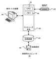
- FIG. 1is a cross-sectional view illustrating a substrate processing apparatus according to an embodiment of the present disclosure.
- 1is a diagram illustrating a configuration of a control device in a substrate processing apparatus according to an embodiment of the present disclosure, and a relationship between the control device and a semiconductor manufacturing apparatus.
- FIG. 2is a diagram illustrating a hardware configuration of a control computer in the substrate processing apparatus according to an embodiment of the present disclosure.
- FIG. 2is a cross-sectional view showing a heating unit and a reaction tube containing a substrate.
- FIG. 1is a diagram showing an example of temperature control performed during substrate processing in the substrate processing apparatus 10 according to an embodiment of the present disclosure.
- FIG. 1is a graph showing the relationship between substrate temperature and heater output. 13 is a graph showing the relationship between heater output and time according to a modified example of the present disclosure.
- FIG. 4is a flowchart showing an example of a process related to temperature in a film forming process according to an embodiment of the present disclosure.
- FIG. 9is a diagram showing temperature changes in a furnace in the flowchart shown in FIG. 8 .
- the heating device 12further includes a cylindrically shaped side wall portion 32 as an insulating portion, and an upper wall portion 33 as an insulating portion formed to cover the upper end of the side wall portion 32.
- an openable and closable valve 39ais provided near the cooling gas supply port 36. Also, an openable and closable valve 39b is provided near the quenching gas exhaust port 42 and the duct 50.
- the first to fourth substrate temperature sensors 27-1, 27-2, 27-3, and 27-4 in the processing chamber 24are disposed in the temperature adjustment parts 72-1, 72-2, 72-3, and 72-4, which are heat generating areas of the heating device 12, respectively, and measure the temperatures of the substrates 18 corresponding to the temperature adjustment parts 72-1, 72-2, 72-3, and 72-4, respectively.
- the first to fourth reaction tube temperature sensors 70-1, 70-2, 70-3, and 70-4are disposed in the cylindrical space 34 in correspondence with the temperature adjustment parts 72-1, 72-2, 72-3, and 72-4, respectively, and measure the temperature distribution inside the cylindrical space 34.
- theysince they are disposed near the reaction tube 16, they are configured to be able to measure the temperature of the reaction tube 16.
- the flow rate sensor 64measures the flow rate of gas supplied into the reaction tube 16 through the gas introduction nozzle.
- the pressure regulator 66adjusts the pressure inside the reaction tube 16.
- the pressure sensor 68measures the pressure inside the reaction tube 16.
- the supply of power to the heater wire 30ais stopped, so that the temperature of the heater wire 30a returns from a temperature higher than the processing temperature to the original temperature, i.e., the temperature is lowered, before the temperature inside the reaction tube 16 reaches the processing temperature. This makes it possible to suppress overshooting, which is an excessive increase in temperature, and to stabilize the processing temperature.
Landscapes
- Engineering & Computer Science (AREA)
- Manufacturing & Machinery (AREA)
- General Physics & Mathematics (AREA)
- Power Engineering (AREA)
- Microelectronics & Electronic Packaging (AREA)
- Computer Hardware Design (AREA)
- Physics & Mathematics (AREA)
- Condensed Matter Physics & Semiconductors (AREA)
- Chemical & Material Sciences (AREA)
- Toxicology (AREA)
- Health & Medical Sciences (AREA)
- Chemical Kinetics & Catalysis (AREA)
- Organic Chemistry (AREA)
- Metallurgy (AREA)
- Mechanical Engineering (AREA)
- Materials Engineering (AREA)
- General Chemical & Material Sciences (AREA)
- Chemical Vapour Deposition (AREA)
Abstract
Description
Translated fromJapanese本開示は、温度制御方法、半導体装置の製造方法、および基板処理装置並びにプログラムに関する。This disclosure relates to a temperature control method, a method for manufacturing a semiconductor device, and a substrate processing apparatus and program.
半導体装置の製造工程の一工程として、ウエハ(以後、基板ともいう)上に所定の処理が行われる(例えば特許文献1-3参照)。これらの文献には、ウエハを処理する処理温度に制御する技術が記載されている。近年は、ウエハを処理する温度が低下傾向である。低温で温度制御に用いられるヒータ素線の温度は低いため、主に長波長の輻射が放射される。この長波長の輻射が反応管に吸収されウエハの昇温速度の低下に繋がることがある。As one step in the manufacturing process of semiconductor devices, a specific process is performed on a wafer (hereinafter also referred to as a substrate) (see, for example,
本開示は、低温度域での昇温速度の向上を実現することができる技術を提供する。This disclosure provides technology that can improve the heating rate in low temperature ranges.
本開示の一態様によれば、反応管内の加熱と反応管内への冷却を制御して、前記反応管内に配置される基板の温度を予め設定した処理温度にする処理温度設定工程を有する温度制御方法であって、前記処理温度設定工程は、所定の電力を供給し、前記反応管の外部に配置されたヒータ素線の温度を前記処理温度よりも高くする昇温工程と、前記反応管に向けて冷却ガスを供給する冷却ガス供給工程と、を有する技術が提供される。According to one aspect of the present disclosure, there is provided a temperature control method having a process temperature setting process for controlling the heating inside a reaction tube and the cooling inside the reaction tube to set the temperature of a substrate placed inside the reaction tube to a preset process temperature, the process temperature setting process having a heating process for supplying a predetermined electric power and raising the temperature of a heater wire placed outside the reaction tube to a temperature higher than the process temperature, and a cooling gas supply process for supplying a cooling gas toward the reaction tube.
本開示によれば、低温度域での昇温速度を向上させることができる。According to this disclosure, it is possible to improve the heating rate in the low temperature range.
以下、本開示の一態様について、図面を参照しながら説明する。なお、以下の説明において用いられる図面は、いずれも模式的なものであり、図面に示される各要素の寸法の関係、各要素の比率等は、現実のものとは必ずしも一致していない。また、複数の図面の相互間においても、各要素の寸法の関係、各要素の比率は必ずしも一致していない。また、各図において、同一構成には同一符号を付している。Below, one embodiment of the present disclosure will be described with reference to the drawings. Note that all drawings used in the following description are schematic, and the dimensional relationships and ratios of each element shown in the drawings do not necessarily match those in reality. Furthermore, the dimensional relationships and ratios of each element do not necessarily match between multiple drawings. Furthermore, the same components are given the same symbols in each drawing.
本実施形態に係る基板処理装置10は、図1に示すように、円筒状の加熱装置12と、加熱装置12の内部に炉内空間14をもって収容された円筒状の反応管16と、反応管16内に処理対象の基板18を保持するボート20とを備えている。ボート20は基板18を水平状態で隙間をもって多段に装填でき、この状態で複数枚の基板18を反応管16内で保持する。ボート20はボートキャップ22を介して図外のエレベータ上に載置されており、このエレベータにより昇降可能となっている。したがって、基板18の反応管16内への装填および反応管16からの取り出しはエレベータの作動により行われる。また、反応管16は基板18を収容する処理室24を形成しており、反応管16内には図示しないガス導入管が連通され、ガス導入管には図外の反応ガス供給源が接続されている。また、反応管16内にはガス排気管56が連通され、処理室24の排気を行っている。As shown in FIG. 1, the substrate processing apparatus 10 according to this embodiment includes a cylindrical heating device 12, a
ヒータユニットとしての加熱装置12は、円筒形状であって、複数の断熱体が積層された構造の断熱構造体の内側に、図1に示すように、加熱部30を少なくとも有する構成となっている。加熱部30は、図示しない断熱材部と該断熱材部の炉内空間14側にヒータ素線30aを備えている。The heating device 12 as a heater unit has a cylindrical shape and is configured to have at least a
また、加熱装置12は、円筒形状に形成された断熱部としての側壁部32と、側壁部32の上端を覆うように形成された断熱部としての上壁部33と、を更に有している。The heating device 12 further includes a cylindrically shaped side wall portion 32 as an insulating portion, and an upper wall portion 33 as an insulating portion formed to cover the upper end of the side wall portion 32.
側壁部32は複数層構造に形成され、側壁部32の複数層のうち外側に形成された側壁外層32aと、複数層のうち内側に形成された側壁内層32bから構成される。側壁外層32aと側壁内層32bとの間には冷却ガス通路としての円筒空間34が形成されている。そして、側壁内層32bの内側に加熱部30が設けられ、加熱部30の内側が後述する発熱部を含む発熱領域となっている。炉内空間14と円筒空間34とは、吹出孔35を介して連通している。尚、側壁部32は、複数の断熱体が積層された構造であるが、このような構造に限定されないのはいうまでもない。The sidewall portion 32 is formed in a multiple layer structure, and is composed of a sidewall
側壁外層32aの上部には、冷却ガス供給口36が形成されている。A cooling gas supply port 36 is formed at the top of the side wall
炉内空間14と連通する急冷排気口40が、冷却ガス供給口36の略水平方向の中央部分に設けられている。The rapid cooling exhaust port 40, which communicates with the furnace space 14, is provided in the approximately horizontal center of the cooling gas supply port 36.
また、図2Bに示されているように、冷却ガス供給口36下方の側壁内層32bには、円筒空間34と炉内空間14とを連通する吹出孔35が所要の分布で複数形成されており、図1に示すように円筒空間34と炉内空間14とを略水平に連通している。すなわち、吹出孔35を介して円筒空間34から炉内空間14へ冷却ガスを吹出し、反応管16を冷却可能に構成されている。
吹出孔35は、図1に示すように水平方向に形成されているが、この形態に限定されない。例えば、急冷排気口40へ向けるように傾斜をつけてもよい。2B, a plurality of blowing holes 35 communicating between the cylindrical space 34 and the furnace space 14 are formed at a required distribution in the side wall
1, the blowing holes 35 are formed in a horizontal direction, but are not limited to this form. For example, the blowing holes 35 may be inclined so as to face the rapid cooling exhaust port 40.
図2Aに示すように、上壁部33には、円形の急冷排気口40が形成されており、この急冷排気口40は加熱装置12の中心軸上に位置している。また、上壁部33の上方側面には、急冷ガス排出口42が形成され、急冷排気口40に連通している。As shown in FIG. 2A, a circular quenching exhaust port 40 is formed in the upper wall portion 33, and this quenching exhaust port 40 is located on the central axis of the heating device 12. In addition, a quenching gas exhaust port 42 is formed on the upper side surface of the upper wall portion 33, and is connected to the quenching exhaust port 40.
又、急冷ガス排出口42は、ダクト50に接続されて、ダクト50には、上流側からラジエータ52及び排気ファン54が接続されており、これらダクト50、ラジエータ52及び排気ファン54を介して加熱装置12の熱せられた冷却ガスが装置外へ排出される。The quenching gas outlet 42 is connected to a duct 50, to which a radiator 52 and an exhaust fan 54 are connected from the upstream side. The heated cooling gas from the heating device 12 is exhausted outside the device via the duct 50, the radiator 52, and the exhaust fan 54.
ここで、冷却ガス供給口36の近傍には、開閉可能な弁39aが設けられている。また、急冷ガス排出口42及びダクト50の近傍には、開閉可能な弁39bが設けられている。Here, an openable and closable valve 39a is provided near the cooling gas supply port 36. Also, an openable and closable valve 39b is provided near the quenching gas exhaust port 42 and the duct 50.
更に、弁39aの開閉及び排気ファン54のON/OFFにより冷却ガスの供給が操作され、冷却ガス通路としての円筒空間34を介して、急冷ガス排出口42から冷却ガスを排出することができる。ここで、排気ファン54を作動させ、冷却ガスが急冷ガス排出口42を介して排出されると、炉内空間14が負圧となり、冷却ガス供給口36から低温の冷却ガスが吸引される。冷却ガス供給口36から吸引された低温の冷却ガスは、円筒空間34、及び吹出孔35を介して冷却ガスが炉内空間14の反応管16に向けて吹き出され、反応管16の冷却が行われる。本実施形態の排気ファン54、急冷ガス排出口42、吹出孔35、円筒空間34、冷却ガス供給口36等が本開示の冷却機構の一例である。Furthermore, the supply of cooling gas is controlled by opening and closing the valve 39a and turning the exhaust fan 54 on and off, and the cooling gas can be discharged from the quenching gas outlet 42 through the cylindrical space 34 as a cooling gas passage. Here, when the exhaust fan 54 is operated and the cooling gas is discharged through the quenching gas outlet 42, the furnace space 14 becomes negative pressure, and low-temperature cooling gas is sucked in from the cooling gas supply port 36. The low-temperature cooling gas sucked in from the cooling gas supply port 36 is blown out through the cylindrical space 34 and the blowing hole 35 toward the
図1に示すように、反応管16内には、ボート20と共に回転可能に設けられ、基板18の温度を検知する検知部(第1検知部)27が設けられている。検知部27は、例えば、ボート20に多段に保持されている基板18と基板18との間にその測定部が配置されている。また、検知部27は、4つの温度センサを備え、上端から順に第1の基板温度センサ27-1、第2の基板温度センサ27-2、第3の基板温度センサ27-3、第4の基板温度センサ27-4が備えられている。また、反応管16近傍には、第2検知部としての第1~4の反応管温度センサ70-1,70-2,70-3,70-4が設けられている。図1において、これらの温度センサは4つ設けられているが、この数に限定されず、膜種やプロセス条件に応じて適宜センサの数は変更可能される。なお、基板温度センサ(第1検知部)27、反応管温度センサ(第2検知部)70と称することがある。ここで、第1基板温度センサ27は、第1の基板温度センサ27-1、第2の基板温度センサ27-2、第3の基板温度センサ27-3、第4の基板温度センサ27-4の総称である。更に、図示されていないが、第3検知部として加熱部30近傍に温度センサが設けられている。As shown in FIG. 1, a detector (first detector) 27 is provided in the
図3は、制御装置60の構成と、制御装置60と基板処理装置10との関係を模式的に示す図である。図3に示すように、処理室24は、基板温度センサ27と、反応管温度センサ70と、ガス流量調整器62と、流量センサ64と、圧力調整装置66と、圧力センサ68を有する。FIG. 3 is a diagram showing the configuration of the control device 60 and the relationship between the control device 60 and the substrate processing apparatus 10. As shown in FIG. 3, the processing chamber 24 has a substrate temperature sensor 27, a reaction tube temperature sensor 70, a gas flow regulator 62, a flow sensor 64, a pressure regulator 66, and a pressure sensor 68.
図3に示すように、処理室24の第1~4の基板温度センサ27-1、27-2、27-3、27-4のそれぞれは、加熱装置12の発熱領域としての温度調整部分72-1,72-2,72-3,72-4のそれぞれに配設され、温度調整部分72-1,72-2,72-3,72-4のそれぞれに対応する基板18の温度を測定する。As shown in FIG. 3, the first to fourth substrate temperature sensors 27-1, 27-2, 27-3, and 27-4 in the processing chamber 24 are disposed in the temperature adjustment parts 72-1, 72-2, 72-3, and 72-4, which are heat generating areas of the heating device 12, respectively, and measure the temperatures of the
第1~4の反応管温度センサ70-1,70-2,70-3,70-4のそれぞれは、円筒空間34に、温度調整部分72-1,72-2,72-3,72-4に対応して配設され、円筒空間34の内部の温度分布を測定する。また、本実施形態の場合、反応管16近傍に設けられている為、反応管16の温度を測定することが可能に構成されている。The first to fourth reaction tube temperature sensors 70-1, 70-2, 70-3, and 70-4 are disposed in the cylindrical space 34 in correspondence with the temperature adjustment parts 72-1, 72-2, 72-3, and 72-4, respectively, and measure the temperature distribution inside the cylindrical space 34. In addition, in the case of this embodiment, since they are disposed near the
ガス流量調整器62は、不図示のガス導入ノズルを介して反応管16内に導かれるガスの流量を調節する。The gas flow regulator 62 adjusts the flow rate of the gas introduced into the
流量センサ64は、ガス導入ノズルを介して反応管16内に供給されるガスの流量を測定する。The flow rate sensor 64 measures the flow rate of gas supplied into the
圧力調整装置66は、反応管16内の圧力を調整する。The pressure regulator 66 adjusts the pressure inside the
圧力センサ68は、反応管16内の圧力を測定する。The pressure sensor 68 measures the pressure inside the
(制御装置)
制御装置60は、温度制御装置74と、本開示の電力供給部の一例としてヒータ駆動装置76と、流量制御装置78と、圧力制御装置80とを有する。
制御装置60は、これらの構成部分により、制御用コンピュータ82から設定された温度および圧力・流量の設定値に基づいて基板処理装置10としての半導体製造装置の各構成部分を制御する。(Control device)
The control device 60 includes a temperature control device 74 , a heater driving device 76 as an example of a power supply unit of the present disclosure, a flow rate control device 78 , and a pressure control device 80 .
The controller 60 uses these components to control each component of the semiconductor manufacturing apparatus serving as the substrate processing apparatus 10 based on the set values of temperature, pressure, and flow rate set by the
温度制御装置74は、第1~4の基板温度センサ27-1、27-2、27-3、27-4それぞれにより測定される温度調整部分72-1,72-2,72-3,72-4それぞれの基板18温度が、制御用コンピュータ82により温度調整部分72-1,72-2,72-3,72-4それぞれに対して設定された温度になるように、ヒータ駆動装置76-1、76-2、76-3、76-4それぞれが温度調整部分72-1,72-2,72-3,72-4それぞれに供給する電力を制御する。本実施形態のヒータ駆動装置76を加熱部に加えてもよく、また、ヒータ駆動装置76及びヒータ素線30aが、本開示の加熱機構の一例である。The temperature control device 74 controls the power supplied by the heater driving devices 76-1, 76-2, 76-3, and 76-4 to the temperature adjustment parts 72-1, 72-2, 72-3, and 72-4, respectively, so that the
流量制御装置78は、流量センサ64が測定するガスの流量の値が、制御用コンピュータ82により設定されるガス流量の値に等しくなるように、ガス流量調整器62を制御して、処理室24の反応管16内に導入されるガスの流量を制御する。The flow control device 78 controls the gas flow regulator 62 so that the gas flow rate measured by the flow sensor 64 is equal to the gas flow rate set by the
圧力制御装置80は、圧力センサ68が測定する反応管16内部の圧力が、制御用コンピュータ82により設定される圧力の値に等しくなるように、圧力調整装置66を制御して、処理室24の反応管16内の圧力を制御する。The pressure control device 80 controls the pressure regulator 66 to control the pressure inside the
[ハードウェア構成]
図4は、制御用コンピュータ82の構成を示す図である。
制御用コンピュータ82は、CPU84およびメモリ86などを含むコンピュータ本体88と、通信IF(Interface)90と、記録装置92と、表示・入力装置94とを有する。つまり、制御用コンピュータ82は一般的なコンピュータとしての構成部分を含んでいる。[Hardware configuration]
FIG. 4 is a diagram showing the configuration of the
The
CPU(Central Precessing Unit)は、操作部の中枢を構成し、記録装置92に記憶された制御プログラムを実行し、表示・入力装置94からの指示に従って、記録装置92に記録されているレシピ(例えば、プロセス用レシピ)を実行する。The CPU (Central Processing Unit) constitutes the core of the operation section, executes the control program stored in the
また、CPUの動作プログラム等を記憶する記録媒体96として、ROM(Read Only Memory)、EEPROM(Electrically Erasable Programmable Read Only Memory)、フラッシュメモリ、ハードディスク等が用いられる。ここで、RAM(Random Access Memory)は、CPUのワークエリアなどとして機能する。Also, as the
本開示の実施形態において、制御用コンピュータ82を例に挙げて説明したが、これに限らず、通常のコンピュータシステムを用いて実現可能である。例えば、汎用コンピュータに、上述の処理を実行するためのプログラムを格納したフレキシブルディスク、CD-ROM、USB等の記録媒体96から当該プログラムをインストールすることにより、上述の処理を実行することもできる。In the embodiment of the present disclosure, the
また、通信回線、通信ネットワーク、通信システム等の通信IF90を用いてもよい。この場合、例えば、通信ネットワークの掲示板に当該プログラムを掲示し、これをネットワークを介して搬送波に重畳して提供してもよい。そして、このように提供されたプログラムを起動し、OS(Operating System)の制御下で、他のアプリケーションプログラムと同様に実行することにより、上述の処理を実行することができる。Furthermore, a communication IF 90 such as a communication line, a communication network, or a communication system may be used. In this case, for example, the program may be posted on a bulletin board in the communication network and provided via the network by superimposing it on a carrier wave. The program thus provided can then be started and executed under the control of the OS (Operating System) in the same way as other application programs, thereby executing the above-mentioned processing.
例えば、記録装置92に記憶された制御プログラムは、反応管16内の加熱部30による加熱、及び反応管16を冷却する冷却ガスを供給する上記排気ファン54等の冷却機構による反応管16への冷却を制御して、反応管16内の基板18の温度を処理温度にすることが可能に構成される制御部としての制御用コンピュータ82を備えた基板処理装置10で実行されるプログラムである。このプログラムにより、制御用コンピュータ82に、加熱部30に一定の電力を供給し、加熱部30に含まれるヒータ素線30aの温度を処理温度よりも高くする手順と、排気ファン54等の冷却機構に反応管16に向けて冷却ガスを供給させる手順と、が実行される。For example, the control program stored in the
これにより、ヒータ素線30aに所定の電力が加えられ、ヒータ素線30aが基板18の処理温度よりも高くすることができ、ヒータ素線30aから輻射される種々の波長のうち短波長の割合を多くすることができる。さらに、冷却機構から反応管16に向けて冷却ガスが供給され、ヒータ素線30aに電力を加えつつ、反応管16を冷却することができる。As a result, a predetermined amount of power is applied to the heater wire 30a, the heater wire 30a can be heated to a temperature higher than the processing temperature of the
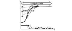
次に、図6Aを用いて基板処理装置10で行われる基板処理時に行う温度制御の一例について説明する。
図6Aは、各部(ヒータ素線30a、反応管16、基板18、ボート20)の温度変化を示すグラフ、ヒータ出力(即ち、ヒータ素線30aの出力)の変化を示すグラフ、及びブロア周波数(排気ファン54のモータ回転数)を示すグラフである。Next, an example of temperature control performed during substrate processing in the substrate processing apparatus 10 will be described with reference to FIG. 6A.
FIG. 6A is a graph showing temperature changes in each part (the heater wire 30a, the
本実施形態の温度制御では、一例として、図6Aに示すように、ボート20に保持された基板18を炉内へ配置(ボートロード終了)した後、反応管16内を効率よく加熱し、反応管16内の基板18の温度の昇温レート、言い換えれば昇温速度を向上させるようにフィードバック制御が行われる。最初に、図6Aにおける温度制御の概略を説明する。As an example, in the temperature control of this embodiment, as shown in FIG. 6A, after the
工程(1)(昇温工程)
先ず、基板18をボートアンロード完了時の温度から安定目標温度(処理温度)まで昇温させる場合に、ヒータ素線30aを素早く高温とするために、ヒータ素線30aが高出力(一例として、フルパワー(加熱部30の最大出力))となるように制御を行い、所定時間高出力以上を維持する。例えば、ヒータ素線30aをフルパワーの電力で一定出力とする。
高出力の電力とは、加熱部30の最大出力に限らず、基板18を処理ガス等で処理する処理温度の維持よりも大きな電力であって、その電力の値は予め装置に設定されているものである。
なお、本明細書における処理温度とは、基板18の温度のことを意味するが、反応管16内に形成される処理室24の温度のことを意味する場合もある。Step (1) (heating step)
First, when the temperature of the
The high-output power is not limited to the maximum output of the
In this specification, the processing temperature means the temperature of the
ここで、加熱部30を高出力以上に所定時間維持すると、ヒータ素線30aの温度が予め設定された温度(第1設定温度)まで上昇するように構成されている。この設定温度は、少なくとも基板18の温度が処理温度を上回ることがない(オーバシュートが発生しない)温度に決定される。設定温度についての詳細は後述する。Here, when the
ところで、加熱部30のヒータ素線30aの温度は、ヒータ素線30aに供給する電力によって容易、かつ迅速に制御できるが、一方、反応管16は、ヒータ素線30aのように温度制御を行って迅速にその温度を変更することが困難である。言い換えれば、反応管16からの二次輻射(比較的長波長の赤外線が多い)を制御することは困難である。The temperature of the heater wire 30a of the
したがって、反応管16の温度をなるべく上昇させないために少なくとも工程(1)では、冷却ガスを供給して反応管16を冷却しながら基板18の加熱を実施する。即ち、本実施形態では、ヒータ素線30aを高出力とし、制御し易いヒータ素線30aからの一次輻射(比較的短波長が多い)を基板18に付与し、反応管16からの二次輻射を抑制するために、ヒータ素線30aによる基板18の加熱中に、反応管16の冷却を行っている。反応管16の冷却は、前述したように、排気ファン54を作動させ、冷却ガスを反応管16に向けて吹出孔35から吹き出すことで効率的に行うことができる。Therefore, in order to minimize the increase in the temperature of the
このように、ヒータ素線30aに所定の電力を加え、ヒータ素線30aの温度を基板18の処理温度よりも高くすることにより、ヒータ素線30aから輻射される種々の波長のうち短波長(例えば、4μmより小さい波長)の割合を多くすることができる。さらに、反応管16に向けて冷却ガスを供給すること、即ち、冷却ガス供給工程により、ヒータ素線30aに電力を加えつつ、反応管16からの長波長の二次輻射を抑制するように反応管16を冷却することができる。したがって、反応管16からの長波長の二次輻射を抑制し、反応管16を透過する短波長の輻射波の量を多くすることができるため、反応管16内を効率よく加熱することができ、反応管16内の基板18温度の昇温レート、言い換えれば昇温速度を向上させことができる。In this way, by applying a predetermined power to the heater wire 30a and raising the temperature of the heater wire 30a above the processing temperature of the
工程(2)(調整工程)
工程(1)後、基板18の温度が安定目標温度(処理温度)に到達するように調整する工程であり、具体的には、ヒータ素線30aへの電力供給が調整される。例えば、電力供給量を零にしてもよい。また、ブロア周波数が調整され、基板18の温度が処理温度近傍になると、ブロア周波数が抑えられ、冷却ガスの供給が調整される。これにより、ヒータ素線30aおよびブロア周波数の両方をフィードバック制御することにより、基板18の温度がオーバシュートすることなく処理温度に収束するように制御される。Step (2) (Adjustment Step)
After step (1), this is a step of adjusting the temperature of the
工程(3)(安定化工程)
工程(2)後に、基板18の温度が処理温度に達した後に、基板18の温度を安定目標温度に安定させるようにフィードバック制御にて温度制御(基板18の温度を測定しヒータ素線30aの出力を制御)を行う。なお、工程(3)においても、低温の冷却ガスの供給を継続して反応管16を冷却しながら温度制御を行うことができる。つまり、ブロアをオンにして冷却ガスを供給してもよい。Step (3) (Stabilization step)
After the step (2), when the temperature of the
なお、上記工程(1)、(2)において、基板18の昇温をフィードバック制御しながら実施することで、周囲環境の変動要因にも追従することができる。例えば、工程(1)のようにヒータ素線30aの出力が高出力となるよう温度設定値を指定すると、変動要因が影響したとしてもフィードバック制御とすることでヒータ素線30aを高出力とする時間が調節される。工程(2)では基板18の目標安定温度を温度設定値としてフィードバック制御することで、基板18の温度が目標安定温度に到達するまでの待機時間が調節される。In addition, in the above steps (1) and (2), by performing feedback control while raising the temperature of the
なお、基板18を加熱するヒータ素線30aは、複数のゾーン(複数の発熱領域)に分けて制御を行うことができる。本温度制御方式に関しても工程(1)、(2)、(3)はゾーン毎にそれぞれ独立して制御を行うことで、ボート20に置かれた複数の基板18に対し、温度が均等になる様に制御することも可能である。The heater wire 30a that heats the
(温度制御の補足)
基板18の温度を調整する調整工程では、冷却ガスの供給量とヒータ素線30aに供給する電力とを調整して基板18を処理温度に制御することで、反応管16内に配置される基板18の温度の昇温レートが向上され、反応管16内の温度が昇温開始から処理温度に安定されるまでの時間を短縮することができる。これにより、例えば、短時間で基板温度を処理温度に安定させることができる。(Supplementary information on temperature control)
In the adjustment process for adjusting the temperature of the
図6Aに示すように、ヒータ素線30aによる加熱、即ち昇温工程と、反応管16を冷却する冷却ガス供給工程とを同時に開始することで、昇温工程よりも冷却ガス供給工程の開始を遅くした場合に比較して、基板18の温度の昇温レートを向上することができ、且つ短時間で基板温度を処理温度に安定させることができる。As shown in FIG. 6A, by simultaneously starting the heating by the heater wire 30a, i.e., the heating process, and the cooling gas supply process for cooling the
そして、昇温工程におけるヒータ素線30aに対する所定の電力の供給を、フルパワーで行うことで、フルパワーで行わない場合に比較して、基板18に対して短波長の輻射による加熱を迅速に行うことができる。Furthermore, by supplying a specified amount of power to the heater wire 30a during the heating process at full power, the
昇温工程におけるヒータ素線30aに対する所定の電力の供給を、ヒータ素線30aの温度が処理温度よりも高い設定温度になるまで継続することで、反応管16内を効率よく加熱することができ、例えば、反応管16内の基板18温度の昇温レートを向上させことができる。By continuing to supply a predetermined amount of power to the heater wire 30a during the heating process until the temperature of the heater wire 30a reaches a set temperature higher than the processing temperature, the inside of the
図6Aに示すように、昇温工程におけるヒータ素線30aの温度が処理温度よりも高い設定温度になってから、一定の電力から電力を低下させることで、ヒータ素線30aの温度を、反応管16内の温度が処理温度になる前に、処理温度よりも高い温度から元の温度に戻すこと、即ち、温度を低下させることができる。これにより、図6Bに示すように、温度が過剰に高くなるオーバシュート(上側のグラフ線で示す)を抑制することができ、処理温度を安定化することができる。As shown in FIG. 6A, by reducing the power from a constant level after the temperature of the heater wire 30a in the heating process reaches a set temperature higher than the processing temperature, the temperature of the heater wire 30a can be returned from a temperature higher than the processing temperature to the original temperature before the temperature inside the
昇温工程におけるヒータ素線30aの温度が処理温度よりも高い設定温度になると、ヒータ素線30aへの電力の供給が停止されるので、ヒータ素線30aの温度は、反応管16内の温度が処理温度になる前に、処理温度よりも高い温度から元の温度に戻る、即ち、温度低下される。これにより、温度が過剰に高くなるオーバシュートを抑制することができ、処理温度を安定化することができる。When the temperature of the heater wire 30a during the heating process reaches a set temperature higher than the processing temperature, the supply of power to the heater wire 30a is stopped, so that the temperature of the heater wire 30a returns from a temperature higher than the processing temperature to the original temperature, i.e., the temperature is lowered, before the temperature inside the
昇温工程におけるヒータ素線30aに対する所定の電力の供給は、ヒータ素線30aの温度が処理温度よりも高い設定温度になるまで継続させるが、設定温度は、ヒータ素線の輻射波から短波長を得られるように設定すること、即ち、ヒータ素線30aを基板18の処理温度よりも高くすることが好ましい。このため、短波長の輻射波で、反応管16内(特に基板18)を効率よく加熱することができ、例えば、反応管16内の基板18温度の昇温レートを向上させことができる。The supply of a predetermined amount of power to the heater wire 30a during the heating process continues until the temperature of the heater wire 30a reaches a set temperature higher than the processing temperature, but the set temperature is preferably set so that a short wavelength is obtained from the radiant waves of the heater wire, that is, the heater wire 30a is set to a temperature higher than the processing temperature of the
ヒータ素線30aの設定温度は、450℃以上に設定することが好ましい(但し、必須ではない)。ヒータ素線30aの温度が450℃未満であれば、ヒータ素線30aから輻射される種々の波長のうち短波長(例えば、4μmより小さい波長)が十分得られないことがある。そうすると、ヒータ素線30aから輻射された長波長の赤外線が反応管16に吸収され、反応管16が加熱される一方、反応管16内に配置されている基板18が十分加熱されないことがある。
これに対して、ヒータ素線30aの温度が450℃以上になると、ヒータ素線30aから輻射される種々の波長のうち短波長の割合が増えてくる。この短波長の輻射波は反応管16を透過し反応管16内に配置される基板18に吸収されるため昇温効率を向上に寄与させることができる。更に、ヒータ素線30aの温度が、例えば、800℃以上になると、ヒータ素線30aから輻射される種々の波長の多くが短波長となる。このように、ヒータ素線30aの温度を上昇させることにより短波長の赤外線を多く放射させ、放射された短波長の赤外線が反応管16を透過し反応管16内に配置される基板18に吸収されるため昇温効率を向上させることができる。The set temperature of the heater wire 30a is preferably set to 450° C. or higher (but is not essential). If the temperature of the heater wire 30a is lower than 450° C., the short wavelengths (e.g., wavelengths shorter than 4 μm) of the various wavelengths radiated from the heater wire 30a may not be sufficiently obtained. In that case, the long wavelength infrared rays radiated from the heater wire 30a are absorbed by the
On the other hand, when the temperature of the heater wire 30a becomes 450°C or higher, the ratio of short wavelengths among the various wavelengths radiated from the heater wire 30a increases. The short wavelength radiation waves penetrate the
ヒータ素線30aに対する一定の電力の供給時間は、処理温度に応じて決定することができる。ヒータ素線30aの温度を処理温度より高い状態で反応管16内の温度を昇温させると、例えば、ヒータ素線30aからの赤外線のうち、短波長の赤外線の割合を多くすることができ、この短波長の赤外線が反応管16を透過し反応管16内に配置される基板18に吸収され昇温効率を向上させることができる。また、ヒータ素線30aの温度は、処理温度よりも高い設定温度から元の温度、例えば、処理温度まで低下させることができる。
このように、ヒータ素線30aに対する一定の電力の供給時間を、処理温度に応じて決定することで、昇温効率と温度安定化との両立が可能となる。The time for supplying a constant power to the heater wire 30a can be determined according to the processing temperature. When the temperature inside the
In this manner, by determining the time for which a constant power is supplied to the heater wire 30a in accordance with the processing temperature, it is possible to achieve both efficient temperature rise and temperature stabilization.
冷却ガス供給工程における冷却ガスの供給量は、ヒータ素線30aの温度が設定温度になるまで制御することができる。これにより、ヒータ素線30aの温度が設定温度になるまで反応管16が冷却されて、ヒータ素線30aの温度が設定温度になるまで反応管16からの長波長の赤外線の輻射が抑制される。The amount of cooling gas supplied in the cooling gas supply process can be controlled until the temperature of the heater wire 30a reaches the set temperature. This allows the
冷却ガス供給工程における冷却ガスの供給量は、ヒータ素線30aの温度がボートロード完了時の温度から処理温度になるまで制御することができる。これにより、ヒータ素線30aの温度が設定温度になる前から反応管16を冷却することができ、ヒータ素線30aの温度が処理温度よりも高い設定温度になっても反応管16からの長波長の赤外線の輻射を抑制することができる。The amount of cooling gas supplied in the cooling gas supply process can be controlled from the temperature at which the heater wire 30a is loaded at the completion of boat loading until it reaches the processing temperature. This allows the
冷却ガス供給工程における冷却ガスの供給量は、反応管16内の温度が処理温度になってから減少させることができる。これにより、基板18の温度が過剰に高くなるオーバシュートを抑制することができ、処理温度を安定化することができる。The amount of cooling gas supplied during the cooling gas supply process can be reduced after the temperature inside the
反応管16内の温度を昇温させる開始時期と、反応管16内の温度が処理温度に到達した時期におけるヒータ素線30aの温度と処理温度とを同じにすることで、反応管16からの長波長の二次輻射を抑制し、反応管16を透過する短波長の輻射波の量を増やすことができ、反応管16内を効率よく加熱することができる。By making the temperature of the heater wire 30a the same as the processing temperature when the temperature inside the
処理温度を、反応管16内に基板18が配置されていない状態(例えば、ボート20に保持された基板18を炉内へ配置する前の待機状態)で保持されるヒータ素線30aの待機温度よりも低くすることができる。これにより、反応管16内に基板18が配置されていない状態で保持されるヒータ素線30aの待機温度よりも低いような低温領域のプロセスにおける温度制御において、ヒータ素線30aの温度を、ヒータ素線30aから輻射される種々の波長のうち短波長、例えば、4μmより小さい波長の割合を多くできる。これにより、例えば、ヒータ素線30aからの短波長の割合が多い赤外線を反応管16に透過させ、反応管16内の基板温度の昇温レートを向上させることができる。The processing temperature can be made lower than the standby temperature of the heater wire 30a held when no
図7では、フィードバック制御をせずにヒータ素線30aを所定時間高出力とし、その後、ヒータ素線30aを零として所定時間維持した後、フィードバック制御する例を示す。そして、基板18の温度が安定目標温度を上回る(許容した範囲以上)場合は、加熱部30の出力を高出力とする時間(所定時間)を短くし、基板18の温度が安定目標温度を下回る場合は、加熱部30の出力を高出力とする時間(所定時間)を長くするように制御され、最適な所定時間が決定される。なお、ブロア出力は一定である。FIG. 7 shows an example in which the heater wire 30a is set to high output for a predetermined time without feedback control, and then the heater wire 30a is set to zero and maintained for a predetermined time, after which feedback control is performed. If the temperature of the
また、図6Aでは、工程(I)を高出力一定、工程(II)を低出力一定(図7では電力ゼロの例)にする例を示す。図6Aによれば、工程(I)、工程(II)の時間を設定するだけで、ある程度の知識と技量があるオペレータであれば、簡単に最適な所定時間が導き出せることができる。なお、工程(III)からフィードバック制御が実行されるが、本実施形態のように、工程(II)の途中から加熱部30、または、加熱部30およびブロアをフィードバック制御してもよい。FIG. 6A also shows an example in which step (I) is constant at high output, and step (II) is constant at low output (zero power in FIG. 7). According to FIG. 6A, an operator with a certain level of knowledge and skill can easily derive the optimum predetermined time simply by setting the times for step (I) and step (II). Note that feedback control is performed from step (III), but as in this embodiment, feedback control of the
以下に、図8、及び図9を用いて基板処理装置10で行われる成膜処理の一例について説明する。本一例は、待機温度T0<目標温度T1とする場合の一例である。Below, an example of a film formation process performed in the substrate processing apparatus 10 will be described with reference to Figures 8 and 9. This example is an example in which the standby temperature T0 is smaller than the target temperature T1.
ステップS1は、炉内の温度を比較的低い温度T0に安定させる処理である。ステップS1では、基板18はまだ炉内に挿入されていない。Step S1 is a process for stabilizing the temperature inside the furnace at a relatively low temperature T0. In step S1, the
ステップS2は、ボート20に保持された基板18を炉内へ挿入する処理である。基板18の温度は、この時点で炉内の温度T0より低いので、基板18を炉内へ挿入した結果、炉内の温度は一時的にT0より低くなるが、温度制御装置74等により炉内の温度は若干の時間を経て再び温度T0に安定する。Step S2 is a process of inserting the
ステップS3は、温度T0から基板18に成膜処理を施すための目標温度T1まで、徐々に炉内の温度を上昇させる処理である。Step S3 is a process of gradually increasing the temperature inside the furnace from temperature T0 to a target temperature T1 for performing a film formation process on the
ステップS4は、基板18に成膜処理を施すために炉内の温度を目標温度T1で維持して安定させる処理である。Step S4 is a process for maintaining and stabilizing the temperature inside the furnace at the target temperature T1 in order to perform a film formation process on the
ステップS5は、成膜処理終了後に温度T1から再び比較的低い温度T0まで徐々に炉内の温度を下降させる処理である。Step S5 is a process in which the temperature inside the furnace is gradually lowered from temperature T1 back to the relatively low temperature T0 after the film formation process is completed.
ステップS6は、成膜処理が施された基板18をボート20と共に炉内から引き出す処理である。Step S6 is the process of removing the
成膜処理を施すべき未処理の基板18が残っている場合には、ボート20上の処理済の基板18が未処理の基板18と入れ替えられ、これらステップS1~S6の一連の処理が繰り返される。If there are any
ステップS1~S6の処理は、いずれも目標温度に対し、炉内温度が予め定められた微小温度範囲にあり、且つ予め定められた時間だけその状態が続くといった安定状態を得た後、次のステップへ進むようになっている。あるいは、最近では、一定時間での基板18の成膜処理枚数を大きくすることを目的として、ステップS1,S2,S5,S6等においては安定状態を得ずして次のステップへ移行することも行われている。In each of steps S1 to S6, the process proceeds to the next step after a stable state is reached in which the temperature inside the furnace is within a predetermined micro-temperature range relative to the target temperature and this state continues for a predetermined period of time. Alternatively, in recent years, in order to increase the number of
ここで、ステップS3(昇温)、ステップS5(降温)は必須ではなく、待機温度T0と目標温度T1(処理温度)が異なるため、実施される。従い、待機温度T0と目標温度T1(処理温度)が同じ場合、ステップS3(昇温)、ステップS5(降温)は省略される。また、待機温度T0よりも目標温度T1が低い場合、ステップS3(昇温)を省略することができる。Here, step S3 (heating up) and step S5 (cooling down) are not essential and are performed because the standby temperature T0 and the target temperature T1 (processing temperature) are different. Therefore, if the standby temperature T0 and the target temperature T1 (processing temperature) are the same, step S3 (heating up) and step S5 (cooling down) are omitted. Also, if the target temperature T1 is lower than the standby temperature T0, step S3 (heating up) can be omitted.
[その他の実施形態]
本開示は、半導体製造装置だけでなくLCD装置のようなガラス基板を処理する装置にも適用することができる。例えば、ヒータ素線でガラス基板を加熱して処理する装置等においても、本開示と同様の効果を得ることができる。[Other embodiments]
The present disclosure can be applied not only to semiconductor manufacturing equipment but also to equipment for processing glass substrates, such as LCD equipment. For example, the same effects as those of the present disclosure can be obtained in equipment that heats and processes glass substrates using heater wires.
また、本開示は、半導体製造技術、特に、被処理基板を処理室に収容して加熱装置によって加熱した状態で処理を施す熱処理技術に関し、例えば、半導体集積回路装置(半導体装置、半導体デバイス)が作り込まれる半導体基板に酸化処理や拡散処理、イオン打ち込み後のキャリア活性化や平坦化のためのリフローやアニール及び熱CVD反応による成膜処理などに使用される基板処理装置に利用して有効なものに適用することができる。The present disclosure also relates to semiconductor manufacturing technology, particularly heat treatment technology in which a substrate to be processed is placed in a processing chamber and heated by a heating device, and can be effectively applied to substrate processing equipment used for oxidation and diffusion processing of semiconductor substrates in which semiconductor integrated circuit devices (semiconductor devices) are fabricated, reflow and annealing for carrier activation and planarization after ion implantation, and film formation processing by thermal CVD reaction.
本明細書において用いる「基板」という用語は、基板そのものを意味する場合や、基板とその表面上に形成された所定の層や膜との積層体を意味する場合がある。The term "substrate" as used in this specification can refer to the substrate itself or to a laminate of the substrate and a specific layer or film formed on its surface.
2022年12月26日に出願された日本国特許出願2022-209067号の開示は、その全体が参照により本明細書に取り込まれる。本明細書に記載されたすべての文献、特許出願、及び技術規格は、個々の文献、特許出願、及び技術規格が参照により取り込まれることが具体的かつ個々に記された場合と同程度に、本明細書中に参照により取り込まれる。The disclosure of Japanese Patent Application No. 2022-209067, filed on December 26, 2022, is incorporated herein by reference in its entirety. All documents, patent applications, and technical standards described herein are incorporated herein by reference to the same extent as if each individual document, patent application, and technical standard was specifically and individually indicated to be incorporated by reference.
本発明は、 複数の基板保持具を有し、 この基板保持具に保持した基板を処理する基板処理装置に適用できる。特に、基板を低温で処理する基板処理装置に適用できる。The present invention can be applied to a substrate processing apparatus that has a plurality of substrate holders and processes substrates held by the substrate holders. In particular, the present invention can be applied to a substrate processing apparatus that processes substrates at low temperatures.
16 反応管18 基板16
Claims (18)
Translated fromJapanese前記処理温度設定工程は、
一定の電力を供給し、前記反応管の外部に配置されたヒータ素線の温度を前記処理温度よりも高くする昇温工程と、
前記反応管に向けて冷却ガスを供給する冷却ガス供給工程と、
を有する温度制御方法。1. A temperature control method comprising a process temperature setting step of controlling heating and cooling in a reaction tube to set a temperature of a substrate placed in the reaction tube to a preset process temperature,
The processing temperature setting step includes:
a heating step of supplying a constant electric power to raise the temperature of a heater wire disposed outside the reaction tube to a temperature higher than the treatment temperature;
a cooling gas supplying step of supplying a cooling gas toward the reaction tube;
The temperature control method includes the steps of:
請求項1に記載の温度制御方法。The method further includes an adjustment step of adjusting the supply amount of the cooling gas and the power to control the temperature of the substrate to the processing temperature.
The temperature control method according to claim 1 .
請求項1に記載の温度制御方法。The temperature increasing step and the cooling gas supplying step are started simultaneously.
The temperature control method according to claim 1 .
請求項2に記載の温度制御方法。The adjusting step and the cooling gas supplying step are performed simultaneously.
The temperature control method according to claim 2 .
請求項1に記載の温度制御方法。The supply of the constant power in the heating process is continued until the temperature of the heater wire reaches a set temperature higher than the treatment temperature.
The temperature control method according to claim 1 .
請求項1に記載の温度制御方法。When the temperature of the heater wire in the heating process reaches a set temperature higher than the treatment temperature, the power supplied is controlled to be reduced from the constant power.
The temperature control method according to claim 1 .
請求項6に記載の温度制御方法。When the temperature of the heater wire in the heating process reaches a set temperature higher than the processing temperature, the supply of power is stopped.
The temperature control method according to claim 6.
請求項5に記載の温度制御方法。The set temperature is set so as to obtain a short wavelength from the radiation wave of the heater wire.
The temperature control method according to claim 5 .
請求項2に記載の温度制御方法。The temperature of the heater wire is set to be reduced to the treatment temperature before the adjustment step is completed.
The temperature control method according to claim 2 .
請求項5に記載の温度制御方法。The supply time of the constant power is determined according to the processing temperature.
The temperature control method according to claim 5 .
請求項1に記載の温度制御方法。The supply amount of the cooling gas in the cooling gas supplying step is controlled until the temperature of the heater wire reaches a set temperature higher than the processing temperature.
The temperature control method according to claim 1 .
請求項1に記載の温度制御方法。The supply amount of the cooling gas in the cooling gas supplying step is controlled from before the temperature of the heater wire reaches a set temperature higher than the processing temperature until the temperature reaches the processing temperature.
The temperature control method according to claim 1 .
請求項1に記載の温度制御方法。The amount of the cooling gas supplied in the cooling gas supplying step is reduced when the temperature in the reaction tube approaches the processing temperature.
The temperature control method according to claim 1 .
請求項1に記載の温度制御方法。the temperature of the heater wire is equal to the treatment temperature at a start time of increasing the temperature inside the reaction tube and a time when the temperature inside the reaction tube reaches the treatment temperature;
The temperature control method according to claim 1 .
請求項14に記載の温度制御方法。the processing temperature is lower than a standby temperature of the heater wire when the substrate is not placed in the reaction tube;
The temperature control method according to claim 14.
前記処理温度を維持しつつ、前記反応管内に配置される前記基板を処理する、
半導体装置の製造方法。The temperature control method of claim 1 includes a step of controlling the temperature of the substrate to a processing temperature,
treating the substrate disposed in the reaction tube while maintaining the treatment temperature;
A method for manufacturing a semiconductor device.
前記加熱部に所定の電力を供給し、前記加熱部に含まれるヒータ素線の温度を前記処理温度よりも高くする手順と、前記冷却機構に前記反応管に向けて冷却ガスを供給させる手順と、
をコンピュータによって前記基板処理装置に実行させるプログラム。A program executed in a substrate processing apparatus including a control unit configured to control heating of an inside of a reaction tube by a heating unit and cooling of the reaction tube by a cooling mechanism that supplies a cooling gas for cooling the reaction tube, thereby enabling a temperature of a substrate in the reaction tube to be set at a processing temperature, the program comprising:
a step of supplying a predetermined electric power to the heating unit to raise a temperature of a heater wire included in the heating unit to a temperature higher than the processing temperature; and a step of causing the cooling mechanism to supply a cooling gas toward the reaction tube.
A program for causing a computer to execute the above-mentioned substrate processing apparatus.
前記反応管内の前記基板を加熱する加熱部と、前記加熱部に電力を供給する電力供給部と、を有する加熱機構と、
前記反応管に冷却ガスを供給する冷却機構と、
前記反応管内の加熱と前記反応管への冷却を制御して、前記反応管内の前記基板の温度を処理温度にすることが可能なように構成される制御部と、
を備え、
前記制御部は、前記電力供給部により所定の電力を供給し、前記加熱部に含まれるヒータ素線の温度を前記処理温度よりも高くする処理と、前記冷却機構により前記反応管に向けて前記冷却ガスを供給させる処理と、を少なくとも実行することが可能に構成されている、
基板処理装置。A reaction tube in which a substrate is placed;
a heating mechanism including a heating unit that heats the substrate in the reaction tube and a power supply unit that supplies power to the heating unit;
a cooling mechanism for supplying a cooling gas to the reaction tube;
a control unit configured to control heating and cooling in the reaction tube so as to adjust the temperature of the substrate in the reaction tube to a processing temperature;
Equipped with
the control unit is configured to be capable of executing at least a process of causing the power supply unit to supply a predetermined power to raise a temperature of a heater wire included in the heating unit to a temperature higher than the processing temperature, and a process of causing the cooling mechanism to supply the cooling gas toward the reaction tube.
Substrate processing equipment.
Priority Applications (5)
| Application Number | Priority Date | Filing Date | Title |
|---|---|---|---|
| CN202380066899.4ACN119895548A (en) | 2022-12-26 | 2023-10-04 | Temperature control method, semiconductor device manufacturing method, substrate processing apparatus, and program |
| KR1020257018182AKR20250128957A (en) | 2022-12-26 | 2023-10-04 | Temperature control method, semiconductor device manufacturing method, substrate processing device and program |
| JP2024567223AJPWO2024142528A1 (en) | 2022-12-26 | 2023-10-04 | |
| TW112148771ATW202431056A (en) | 2022-12-26 | 2023-12-14 | Temperature control method, semiconductor device manufacturing method, substrate processing device and program |
| US19/090,046US20250226244A1 (en) | 2022-12-26 | 2025-03-25 | Temperature control method, method of manufacturing semiconductor device, substrate processing apparatus and non-transitory computer-readable recording medium |
Applications Claiming Priority (2)
| Application Number | Priority Date | Filing Date | Title |
|---|---|---|---|
| JP2022209067 | 2022-12-26 | ||
| JP2022-209067 | 2022-12-26 |
Related Child Applications (1)
| Application Number | Title | Priority Date | Filing Date |
|---|---|---|---|
| US19/090,046ContinuationUS20250226244A1 (en) | 2022-12-26 | 2025-03-25 | Temperature control method, method of manufacturing semiconductor device, substrate processing apparatus and non-transitory computer-readable recording medium |
Publications (1)
| Publication Number | Publication Date |
|---|---|
| WO2024142528A1true WO2024142528A1 (en) | 2024-07-04 |
Family
ID=91717266
Family Applications (1)
| Application Number | Title | Priority Date | Filing Date |
|---|---|---|---|
| PCT/JP2023/036229PendingWO2024142528A1 (en) | 2022-12-26 | 2023-10-04 | Temperature control method, semiconductor device manufacturing method, substrate treatment device, and program |
Country Status (6)
| Country | Link |
|---|---|
| US (1) | US20250226244A1 (en) |
| JP (1) | JPWO2024142528A1 (en) |
| KR (1) | KR20250128957A (en) |
| CN (1) | CN119895548A (en) |
| TW (1) | TW202431056A (en) |
| WO (1) | WO2024142528A1 (en) |
Citations (7)
| Publication number | Priority date | Publication date | Assignee | Title |
|---|---|---|---|---|
| JP2000181549A (en) | 1998-12-17 | 2000-06-30 | Kokusai Electric Co Ltd | Temperature control method of heat treatment furnace |
| JP2006012985A (en)* | 2004-06-23 | 2006-01-12 | Hitachi Kokusai Electric Inc | Substrate processing equipment |
| JP2014042042A (en)* | 2007-09-06 | 2014-03-06 | Hitachi Kokusai Electric Inc | Semiconductor manufacturing apparatus and substrate processing method |
| WO2014088026A1 (en)* | 2012-12-07 | 2014-06-12 | 株式会社日立国際電気 | Substrate treatment device, substrate treatment method, semiconductor-device manufacturing method, and control program |
| JP2014209569A (en) | 2013-03-25 | 2014-11-06 | 株式会社日立国際電気 | Thermal insulation structure and method for manufacturing semiconductor device |
| WO2018100826A1 (en) | 2016-11-30 | 2018-06-07 | 株式会社日立国際電気 | Substrate processing device, method of manufacturing semiconductor device, and program |
| JP2019110312A (en)* | 2019-02-08 | 2019-07-04 | 株式会社日立ハイテクノロジーズ | Plasma processing method |
Family Cites Families (1)
| Publication number | Priority date | Publication date | Assignee | Title |
|---|---|---|---|---|
| KR20180100826A (en) | 2017-03-02 | 2018-09-12 | 정상준 | Heating system |
- 2023
- 2023-10-04CNCN202380066899.4Apatent/CN119895548A/enactivePending
- 2023-10-04WOPCT/JP2023/036229patent/WO2024142528A1/enactivePending
- 2023-10-04KRKR1020257018182Apatent/KR20250128957A/enactivePending
- 2023-10-04JPJP2024567223Apatent/JPWO2024142528A1/jaactivePending
- 2023-12-14TWTW112148771Apatent/TW202431056A/enunknown
- 2025
- 2025-03-25USUS19/090,046patent/US20250226244A1/enactivePending
Patent Citations (7)
| Publication number | Priority date | Publication date | Assignee | Title |
|---|---|---|---|---|
| JP2000181549A (en) | 1998-12-17 | 2000-06-30 | Kokusai Electric Co Ltd | Temperature control method of heat treatment furnace |
| JP2006012985A (en)* | 2004-06-23 | 2006-01-12 | Hitachi Kokusai Electric Inc | Substrate processing equipment |
| JP2014042042A (en)* | 2007-09-06 | 2014-03-06 | Hitachi Kokusai Electric Inc | Semiconductor manufacturing apparatus and substrate processing method |
| WO2014088026A1 (en)* | 2012-12-07 | 2014-06-12 | 株式会社日立国際電気 | Substrate treatment device, substrate treatment method, semiconductor-device manufacturing method, and control program |
| JP2014209569A (en) | 2013-03-25 | 2014-11-06 | 株式会社日立国際電気 | Thermal insulation structure and method for manufacturing semiconductor device |
| WO2018100826A1 (en) | 2016-11-30 | 2018-06-07 | 株式会社日立国際電気 | Substrate processing device, method of manufacturing semiconductor device, and program |
| JP2019110312A (en)* | 2019-02-08 | 2019-07-04 | 株式会社日立ハイテクノロジーズ | Plasma processing method |
Also Published As
| Publication number | Publication date |
|---|---|
| JPWO2024142528A1 (en) | 2024-07-04 |
| KR20250128957A (en) | 2025-08-28 |
| US20250226244A1 (en) | 2025-07-10 |
| TW202431056A (en) | 2024-08-01 |
| CN119895548A (en) | 2025-04-25 |
Similar Documents
| Publication | Publication Date | Title |
|---|---|---|
| JP6170847B2 (en) | Thermal insulation structure, heating apparatus, substrate processing apparatus, and semiconductor device manufacturing method | |
| KR101070667B1 (en) | Substrate processing apparatus, heating device and semiconductor device manufacturing method | |
| US9587313B2 (en) | Substrate processing apparatus, method of manufacturing semiconductor device, and non-transitory computer-readable recording medium | |
| US11018033B2 (en) | Substrate processing apparatus, method of manufacturing semiconductor device, and recording medium | |
| JP6912497B2 (en) | Manufacturing method for substrate processing equipment, ceiling heaters and semiconductor equipment | |
| US20170051402A1 (en) | Susceptor and substrate processing apparatus | |
| KR20190067250A (en) | Substrate processing apparatus, semiconductor device manufacturing method and program | |
| US20150147894A1 (en) | Substrate Processing Apparatus, Method of Manufacturing Semiconductor Device and Non-Transitory Computer-Readable Recording Medium | |
| JP7033651B2 (en) | Substrate processing equipment, semiconductor device manufacturing methods, programs, and substrate processing methods | |
| US9324591B2 (en) | Heat treatment apparatus and heat treatment method | |
| US20220139760A1 (en) | Substrate processing apparatus, susceptor cover, method of manufacturing semiconductor device and substrate processing method | |
| US9666494B2 (en) | Method of manufacturing semiconductor device | |
| KR102424677B1 (en) | Substrate processing apparatus, method of manufacturing semiconductor device and computer program | |
| JP7101718B2 (en) | Manufacturing method for heating unit, temperature control system, processing equipment and semiconductor equipment | |
| CN112086378B (en) | Heating unit, temperature control system, processing device, and method for manufacturing semiconductor device | |
| WO2024142528A1 (en) | Temperature control method, semiconductor device manufacturing method, substrate treatment device, and program | |
| KR100788081B1 (en) | Heat treating device and method for wafer | |
| JP2008153592A (en) | Substrate processing apparatus and substrate processing method | |
| JP7079317B2 (en) | Substrate processing equipment, semiconductor equipment manufacturing methods and programs | |
| JP2002141347A (en) | Method and device for batch heat treatment | |
| JP2005136370A (en) | Substrate processing equipment | |
| JP2005217317A (en) | Substrate processing equipment | |
| JP2008218490A (en) | Manufacturing method of semiconductor device | |
| KR20070020752A (en) | Rapid heat treatment device for semiconductor manufacturing | |
| JP2002270601A (en) | Heat treatment equipment |
Legal Events
| Date | Code | Title | Description |
|---|---|---|---|
| 121 | Ep: the epo has been informed by wipo that ep was designated in this application | Ref document number:23911312 Country of ref document:EP Kind code of ref document:A1 | |
| WWE | Wipo information: entry into national phase | Ref document number:202380066899.4 Country of ref document:CN | |
| WWP | Wipo information: published in national office | Ref document number:202380066899.4 Country of ref document:CN | |
| WWE | Wipo information: entry into national phase | Ref document number:2024567223 Country of ref document:JP | |
| WWE | Wipo information: entry into national phase | Ref document number:2023911312 Country of ref document:EP | |
| NENP | Non-entry into the national phase | Ref country code:DE | |
| WWP | Wipo information: published in national office | Ref document number:1020257018182 Country of ref document:KR |