WO2024111385A1 - Scintillator array, radiation detection device, and positron emission tomographic device - Google Patents
Scintillator array, radiation detection device, and positron emission tomographic deviceDownload PDFInfo
- Publication number
- WO2024111385A1 WO2024111385A1PCT/JP2023/039817JP2023039817WWO2024111385A1WO 2024111385 A1WO2024111385 A1WO 2024111385A1JP 2023039817 WJP2023039817 WJP 2023039817WWO 2024111385 A1WO2024111385 A1WO 2024111385A1
- Authority
- WO
- WIPO (PCT)
- Prior art keywords
- scintillator
- light receiving
- receiving element
- optically connected
- array
- Prior art date
- Legal status (The legal status is an assumption and is not a legal conclusion. Google has not performed a legal analysis and makes no representation as to the accuracy of the status listed.)
- Ceased
Links
Images


Classifications
- G—PHYSICS
- G01—MEASURING; TESTING
- G01T—MEASUREMENT OF NUCLEAR OR X-RADIATION
- G01T1/00—Measuring X-radiation, gamma radiation, corpuscular radiation, or cosmic radiation
- G01T1/16—Measuring radiation intensity
- G01T1/161—Applications in the field of nuclear medicine, e.g. in vivo counting
- G—PHYSICS
- G01—MEASURING; TESTING
- G01T—MEASUREMENT OF NUCLEAR OR X-RADIATION
- G01T1/00—Measuring X-radiation, gamma radiation, corpuscular radiation, or cosmic radiation
- G01T1/16—Measuring radiation intensity
- G01T1/20—Measuring radiation intensity with scintillation detectors
Definitions
- the present inventionrelates to a scintillator array including a plurality of scintillators, a radiation detection device including such a scintillator array, and a positron emission tomography device including such a radiation detection device.
- Positron emission tomography devicesare widely used to generate tomographic images of living organisms by detecting gamma rays emitted from within the organism.
- gamma raysare usually detected using a radiation detection device in which detection units made of scintillators and light receiving elements are arranged in a matrix.
- Patent Document 1discloses a radiation detection device capable of measuring DOI.
- the radiation detection device described in Patent Document 1increases the number of scintillators per unit area without increasing the number of light receiving elements per unit area, thereby successfully improving the spatial resolution of gamma ray detection while suppressing increases in costs.
- the radiation detection device described in Patent Document 1leaves room for improvement in that it is not easy to achieve both time resolution and DOI resolution.
- the time resolution for gamma ray detectiontends to be high but the DOI resolution tends to be low.
- the side surface of the scintillatoris roughened, the DOI resolution tends to be high but the time resolution tends to be low.
- One aspect of the present inventionwas made in consideration of the above problems, and its purpose is to achieve both time resolution and DOI resolution in a radiation detection device capable of measuring DOI.
- a scintillator arrayincluding a plurality of scintillator units, each of which is composed of a first scintillator whose bottom surface is optically connected to one of two adjacent light receiving surfaces of a light receiving element in a light receiving element array, and a second scintillator whose side surface is at least partially optically connected to at least partially the side surface of the first scintillator and whose bottom surface is optically connected to the other light receiving surface of the two light receiving elements, and the first scintillator and the second scintillator have one or two side surfaces roughened.
- FIG. 1is a perspective view showing a configuration of a radiation detection device according to an embodiment of the present invention
- 2is a perspective view showing an example of the configuration of a scintillator unit included in the radiation detection device shown in FIG. 1 .
- FIG. 4is a perspective view showing another example of the configuration of the scintillator unit included in the radiation detection device shown in FIG. 2 is a block diagram showing the configuration of a positron emission tomography apparatus including the radiation detection device shown in FIG. 1
- 4A to 4Dare diagrams for explaining an outline of a first identification process executed by the positron emission tomography apparatus shown in Fig. 3.
- Fig. 4A to 4Dare plan views of the radiation detection apparatus shown in Fig. 1.
- FIG. 4is a diagram for explaining an overview of a second identification process executed by the positron emission tomography apparatus shown in Fig. 3.
- Figs. 4(a) to 4(d)are side views of the scintillator unit shown in Fig. 2.
- Fig. 4(e)is a graph showing a ratio of fluorescence intensities detected by two light receiving elements optically connected to the scintillator unit.
- 1Ais a side view of a radiation detection device according to an embodiment of the present invention, and FIGS. 1B to 1D are cross-sectional views of the radiation detection device.
- 1A to 1Care cross-sectional views showing the configurations of radiation detection devices according to examples and comparative examples of the present invention;
- Fig. 1is a perspective view showing the configuration of the radiation detection device 1.
- the radiation detection device 1includes a scintillator array 11 and a light receiving element array 12.
- the radiation detection device 1is used, for example, to detect gamma rays in a positron emission tomography apparatus.
- the scintillator array 11includes a plurality of scintillator units 11U1 to 11Un (n is any natural number equal to or greater than 2).
- Each scintillator unit 11Ui(i is a natural number equal to or greater than 1 and equal to or less than n) is composed of a first scintillator 11Uia and a second scintillator 11Uib.
- the first scintillator 11Uia and the second scintillator 11Uibare columnar crystals with square bottoms, and a portion of one side surface and a portion of the other side surface are optically connected to each other.
- Ca-doped LYSOLitium Yttrium Orthosilicate
- LYSOLitium Yttrium Orthosilicate
- Other scintillatorsinclude, for example, GAGG ( Gd3 (Ga,Al )5O12 ( Ce)), LGSO (Ce:Lu x Gd2 - xSiO5 ), and LFS (Lutetium Fine Silicate).
- GAGGGd3 (Ga,Al )5O12 ( Ce)
- LGSOCe:Lu x Gd2 - xSiO5
- LFSLiutetium Fine Silicate
- the light receiving element array 12includes a plurality of light receiving elements 12U1 to 12Um (m is any natural number equal to or greater than 2) arranged in a matrix.
- Each light receiving element 12Uj(j is a natural number equal to or greater than 1 and equal to or less than m) is a plate-shaped element with a square light receiving surface.
- the area of the bottom surface of each light receiving element 12Ujis four times the area of the bottom surfaces of the first scintillator 11Uia and the second scintillator 11Uib.
- a SiPMSilicon Photo Multiplier
- Other examples of light receiving elementsinclude, for example, PSPMTs (Position Sensitive Photo Multiplier Tubes).
- One bottom surface of the first scintillator 11U1a of the first scintillator unit 11U1is optically connected to the light receiving surface of the first light receiving element 12U1 arranged in the center of the light receiving element array 12.
- one bottom surface of the second scintillator 11U1b of the first scintillator unit 11U1is optically connected to the light receiving surface of the second light receiving element 12U2 adjacent to the first light receiving element 12U1 in the light receiving element array 12.
- the first scintillator unit 11U1is arranged to straddle the first side of the first light receiving element 12U1, which is the boundary with the second light receiving element 12U2.
- One bottom surface of the first scintillator 11U2a of the second scintillator unit 11U2is optically connected to the light receiving surface of the first light receiving element 12U1 arranged in the center of the light receiving element array 12, similar to one bottom surface of the first scintillator 11U1a of the first scintillator unit 11U1. Also, one bottom surface of the second scintillator 11U2b of the second scintillator unit 11U2 is optically connected to the light receiving surface of the third light receiving element 12U3 adjacent to the first light receiving element 12U1 in the light receiving element array 12.
- the second scintillator unit 11U2is arranged so as to straddle the second side of the first light receiving element 12U1, which is the boundary with the third light receiving element 12U3.
- the third light receiving element 12U3is a different light receiving element from the second light receiving element 12U2.
- One bottom surface of the first scintillator 11U3a of the third scintillator unit 11U3is optically connected to the light receiving surface of the first light receiving element 12U1 arranged in the center of the light receiving element array 12, similar to one bottom surface of the first scintillator 11U1a of the first scintillator unit 11U1. Also, one bottom surface of the second scintillator 11U3b of the third scintillator unit 11U3 is optically connected to the light receiving surface of the fourth light receiving element 12U4 adjacent to the first light receiving element 12U1 in the light receiving element array 12.
- the third scintillator unit 11U3is arranged so as to straddle the boundary between the first light receiving element 12U1 and the fourth light receiving element 12U4. That is, the third scintillator unit 11U3 is arranged so as to straddle the third side of the first light receiving element 12U1, which is the boundary with the fourth light receiving element 12U4.
- the fourth light receiving element 12U4is a different light receiving element from the second light receiving element 12U2 and the third light receiving element 12U3.
- One bottom surface of the first scintillator 11U4a of the fourth scintillator unit 11U4is optically connected to the light receiving surface of the first light receiving element 12U1 arranged in the center of the light receiving element array 12, similar to one bottom surface of the first scintillator 11U1a of the first scintillator unit 11U1. Also, one bottom surface of the second scintillator 11U4b of the fourth scintillator unit 11U4 is optically connected to the light receiving surface of the fifth light receiving element 12U5 adjacent to the first light receiving element 12U1 in the light receiving element array 12.
- the fourth scintillator unit 11U4is arranged so as to straddle the fourth side of the first light receiving element 12U1, which is the boundary with the fifth light receiving element 12U5.
- the fifth light receiving element 12U5is a light receiving element different from the second light receiving element 12U2, the third light receiving element 12U3, and the fourth light receiving element 12U4.
- Conventional radiation detection devices capable of measuring DOIemploy a configuration in which the two bottom surfaces of the scintillator array are each optically connected to the light receiving surface of the light receiving element array.
- the radiation detection device 1 according to this embodimentemploys a configuration in which only one bottom surface of the scintillator array 11 is optically connected to the light receiving surface of the light receiving element array 12.
- the radiation detection device 1is composed of a smaller number of light receiving element arrays. This allows for cost reduction.
- the scintillator unit 11Uiis composed of a first scintillator 11Uia and a second scintillator 11Uib, and the first scintillator 11Uia and the second scintillator 11Uib have one or two sides roughened.
- Figure 2is a perspective view showing the configuration of the scintillator unit 11Ui when one side of each of the first scintillator 11Uia and the second scintillator 11Uib is roughened.
- the side surface 11Uia1 of the first scintillator 11Uiais roughened and is optically connected to the second scintillator 11Uib.
- the second scintillator 11Uibhas a roughened side surface 11Uib1 and is optically connected to the first scintillator 11Uia.
- a region of the side surface 11Uia1 of the first scintillator 11Uia that is not covered with reflecting material and a region of the side surface 11Uib1 of the second scintillator 11Uib that is not covered with reflecting materialare bonded with an optical adhesive. This allows the fluorescence generated when radiation is incident on the first scintillator 11Uia to enter the second scintillator 11Uib via the region of the side surface 11Uia1 of the first scintillator 11Uia that is not covered with reflecting material.
- the fluorescence generated when radiation is incident on the second scintillator 11Uibcan enter the first scintillator 11Uia via the region of the side surface 11Uib1 of the second scintillator 11Uib that is not covered with reflecting material.
- the bottom surface 11Uia5 of the first scintillator 11Uia and the bottom surface 11Uib5 of the second scintillator 11Uibare optically connected to the light receiving elements 12Uj and 12Uk, respectively.
- the fluorescence generated in the first scintillator 11Uia and the fluorescence generated in the second scintillator 11Uib and incident on the first scintillator 11Uiaare incident on the light receiving element 12Uj via the bottom surface 11Uia5 of the first scintillator 11Uia.
- the fluorescence generated in the second scintillator 11Uib and the fluorescence generated in the first scintillator 11Uia and incident on the second scintillator 11Uibare incident on the light receiving element 12Uk via the bottom surface 11Uib5 of the second scintillator 11Uib.
- Figure 3is a perspective view showing the configuration of the scintillator unit 11Ui when two side surfaces of the first scintillator 11Uia and the second scintillator 11Uib are roughened.
- the second scintillator 11Uibhas side surfaces 11Uib1 and 11Uib3 roughened. Of the two roughened sides, side surface 11Uia1 is optically connected to the second scintillator 11Uia.
- the area of the side surface 11Uia1 of the first scintillator 11Uia that is not covered with reflective material and the area of the side surface 11Uib1 of the second scintillator 11Uib that is not covered with reflective materialare bonded with an optical adhesive.
- the roughened side surface 11Uia4 of the first scintillator 11Uia and the roughened side surface 11Uib3 of the second scintillator 11Uibare bonded so as to be adjacent to each other. This allows each of the first scintillator 11Uia and the second scintillator 11Uib to have the same function as when one side surface is roughened.
- the bottom surface 11Uia5 of the first scintillator 11Uia and the bottom surface 11Uib5 of the second scintillator 11Uibare optically connected to the light receiving elements 12Uj and 12Uk, respectively.
- the roughened side surface 11Uia4 of the first scintillator unit 11Uiis located on the outer edge of the light receiving element 12Uj, and the roughened side surface 11Uib3 of the second scintillator 11Uib is optically connected to the outer edge of the light receiving element 12Uk. This provides the same functionality as when one side surface of each of the first scintillator 11Uia and the second scintillator 11Uib is roughened.
- the radiation detection device 1has the following distinctive features: (1) Of the four side surfaces 11Uia1 to 11Uia4 of the first scintillator 11Uia, one or two are roughened, and the remaining three or two are mirror-finished or chemically etched. (2) Of the four side surfaces 11Uib1 to 11Uib4 of the second scintillator 11Uib, one or two are roughened, and the remaining three or two are mirror-finished or chemically etched.
- the time resolutiontends to be high while the DOI resolution tends to be low.
- the boundary surface of each scintillatorcontains an air layer, which prevents leakage of fluorescence from the light receiving element boundary surface and causes diffuse reflection of the fluorescence in the air layer, which tends to increase the DOI resolution while decreasing the time resolution.
- one or two side surfaces of the first scintillator 11Uia and the second scintillator 11Uibare roughened, so that both the time resolution and the DOI resolution can be increased.
- the roughened side 11Uia1 of the first scintillator 11Uia and the roughened side 11Uib1 of the second scintillator 11Uibare optically connected.
- the roughened connection surface between the first scintillator 11Uia and the second scintillator 11Uib that constitute the scintillator unit 11Uiis located on the boundary between the light receiving element 12Uj and the light receiving element 12Uk.
- the other roughened side surface 11Uia4 of the first scintillator 11Uia and the other roughened side surface 11Uib3 of the second scintillator 11Uibare adjacent to each other, and the side surface 11Uia4 of the first scintillator 11Uia is located on the outer edge of the light receiving element 12Uj, and the roughened side surface 11Uib3 of the second scintillator 11Uib is located on the outer edge of the light receiving element 12Uk.
- the roughened side surfacesare located on all boundaries of each light receiving element 12Uj that constitutes the light receiving element array. This prevents leakage of fluorescence from the boundaries between each light receiving element 12Uj and each scintillator, further increasing the light collection rate to the light receiving element.
- FIG. 4is a block diagram of a positron emission tomography apparatus 10.
- the positron emission tomography apparatus 10includes the radiation detection apparatus 1 described above and a signal processing apparatus 2 that processes an output signal from the radiation detection apparatus 1 described above.
- the signal processing apparatus 2executes a first identification process and a second identification process.
- the first identification processis a process of identifying the scintillator unit 11Ux (x is 1, 2, 3, or 4) on which the gamma ray is incident, among the scintillator units 11U1 to 11U4.
- the second identification processis a process of (1) identifying the scintillator 11Uxy (y is a or b) on which the gamma ray is incident, among the two scintillators 11Uxa and 11Uxb that make up the scintillator unit 11Ux, and identifying the position (height) at which an interaction with the gamma ray occurs in the scintillator 11Uxy.
- FIG. 5is a diagram for explaining an overview of the first identification process, and (a) to (d) in FIG. 5 are each a plan view of the radiation detection device 1.
- the signal processing device 2uses this property to execute the first identification process described above.
- the signal processing device 2identifies the scintillator unit 11Ux into which the gamma rays are incident, for example, as follows: That is, (1) if the combination of light receiving elements that detected the fluorescence is the combination of the first light receiving element 12U1 and the second light receiving element 12U2, the first scintillator unit 11U1 is identified as the scintillator unit Ux into which the gamma rays are incident. Also, (2) if the combination of light receiving elements that detected the fluorescence is the combination of the first light receiving element 12U1 and the third light receiving element 12U3, the second scintillator unit 11U2 is identified as the scintillator unit Ux into which the gamma rays are incident.
- the third scintillator unit 11U3is identified as the scintillator unit Ux into which the gamma rays are incident. Furthermore, (4) if the combination of light receiving elements that detected the fluorescence is the combination of the first light receiving element 12U1 and the fifth light receiving element 12U5, the fourth scintillator unit 11U4 is identified as the scintillator unit Ux into which the gamma rays were incident.
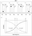
- FIG. 6is a diagram for explaining an outline of the second identification process, and (a) to (d) of FIG. 6 are side views of the scintillator unit 11Ux on which gamma rays are incident.
- (e) of FIG. 6is a graph showing the ratios Ia/(Ia+Ib) and Ia/(Ia+Ib) of the fluorescence intensities Ia and Ib.
- the second identification processis as follows: 6A, when an interaction with a gamma ray occurs near the bottom surface (lower surface) of the first scintillator 11Uxa, most of the generated fluorescence is incident on the light receiving element 12Uj optically connected to the first scintillator 11Uxa. Therefore, the relationship between the fluorescence intensities Ia and Ib is Ia>>Ib. As a result, the ratio Ia/(Ia+Ib) is approximately 1, and the ratio Ib/(Ia+Ib) is approximately 0.
- the fluorescence intensity Ia detected by the light receiving element 12Uj optically connected to the first scintillator 11Uxais weaker than when an interaction with gamma rays occurs near the bottom surface of the first scintillator 11Uxa.
- the fluorescence intensity Ib detected by the light receiving element 12Uk optically connected to the second scintillator 11Uxbis stronger than when an interaction with gamma rays occurs near the bottom surface of the first scintillator 11Uxa.
- the fluorescence intensity Ia detected by the light receiving element 12Uj optically connected to the first scintillator 11Uxais weaker than when an interaction with gamma rays occurs at a position away from the bottom surface of the first scintillator 11Uxb.
- the fluorescence intensity Ib detected by the light receiving element 12Uk optically connected to the second scintillator 11Uxbis stronger than when an interaction with gamma rays occurs at a position away from the bottom surface of the first scintillator 11Uxa.
- the magnitude of the fluorescence intensities Ia, Ibis determined depending on which of the scintillators 11Uxa, 11Uxb constituting the scintillator unit 11Ux on which the gamma rays are incident, the scintillator into which the gamma rays are incident. Also, the ratios Ia/(Ia+Ib), Ib/(Ia+Ib) are determined depending on the position (height) at which the gamma rays interact with the scintillator on which the gamma rays are incident. The signal processing device 2 uses these properties to execute the second identification process described above.
- the signal processing device 2identifies the scintillator 11Uxy on which the gamma rays are incident, for example, as follows: That is, (1) if the relationship Ia>Ib holds between the fluorescence intensities Ia and Ib detected by the light receiving elements 12Uj and 12Uk, the first scintillator 11Uxa is identified as the scintillator 11Uxy on which the gamma rays are incident.
- the second scintillator 11Uxbis identified as the scintillator 11Uxy on which the gamma rays are incident.
- the signal processing device 2also identifies the position in the scintillator 11Uxy where an interaction with a gamma ray occurs, for example, as follows. That is, a table showing the correspondence between the ratio Ia/(Ia+Ib) and the interaction position is created in advance. Then, each time a gamma ray is incident on the scintillator 11Uxy, (1) the ratio Ia/(Ia+Ib) is calculated from the fluorescence intensities Ia and Ib detected by the light receiving elements 12Uj and 12Uk, and (2) the interaction position corresponding to the calculated ratio Ia/(Ia+Ib) is identified by referring to this table.
- a function showing the correspondence between the ratio Ia/(Ia+Ib) and the interaction positionis created in advance. Then, each time a gamma ray is incident on the scintillator 11Uxy, (1) the ratio Ia/(Ia+Ib) is calculated from the fluorescence intensities Ia and Ib detected by the light receiving elements 12Uj and 12Uk, and (2) the interaction position corresponding to the calculated ratio Ia/(Ia+Ib) is identified by substituting the ratio Ia/(Ia+Ib) into this function. Note that although an example using the ratio Ia/(Ia+Ib) is shown here, the ratio Ib/(Ia+Ib) may also be used.
- FIG. 7(a) is a side view showing the configuration of the radiation detection device 1 according to the embodiment and the comparative example, (b) is a cross-sectional view showing the AA' section of the radiation detection device 1, (c) is a cross-sectional view showing the BB' section of the radiation detection device 1, and (d) is a cross-sectional view showing the CC' section of the radiation detection device 1.
- the thick linesindicate the boundary surface between two adjacent scintillators where no reflective material is provided and which is optically connected by optical bonding.
- the scintillatorwas a prismatic LYSO:Ca crystal having a height of 15 mm and a square base with sides of 1.45 mm.
- the scintillator array 11was made up of three layers of reflector material consisting of a lower layer, a middle layer, and an upper layer, each of which had a height of 5 mm.
- two adjacent scintillatorswere optically connected at the boundary surface indicated by the thick line by an optical adhesive, and optically separated at the other boundary surfaces by a reflector.
- the scintillators that make up the scintillator array 11 shown in Figure 1are hatched in the same way. It can be seen from Figures 6 and 1 that the upper and middle layers of the scintillator array 11 shown in Figure 7 are made by combining the scintillator arrays 11 shown in Figure 1.
- the lower layer of the scintillator array 11 shown in Figure 7combines the scintillator arrays 11 shown in Figure 1, and is optically connected at a position up to a height of 5 mm from the bottom surface where it is optically connected to each light receiving element 12Uj, as shown in Figure 7(d). Note that the reflective material has been removed from the optically connected locations.
- the function of the lower layer of the scintillator array 11 shown in FIG. 7, which is newly added in this embodiment and the comparative example,will be described.
- the radiation detection device 1 according to the present disclosurefour scintillators are optically connected to one light receiving element. Therefore, the fluorescence generated when radiation is incident on the scintillator is incident on 1/4 of the total area of the light receiving element to which the scintillator is optically connected. In other words, only 1/4 of the light receiving element is utilized (the light receiving element cannot be used for a certain period of time after one detection has been performed).
- the fluorescence that has passed through the upper and middle layerscan be spread within the light receiving element, and it becomes possible to detect the fluorescence over the entire surface of the light receiving element to which the scintillator is optically connected. This increases the fluorescence detection efficiency in the light receiving element.
- FIG. 8is a cross-sectional view of the radiation detection device 1 according to the first embodiment.
- the thick lineindicates the side of the scintillator that has been roughened.
- the radiation detection device 1 according to the first embodimentuses a scintillator that has one side roughened and three sides mirror-finished.
- FIG. 8is a cross-sectional view of the radiation detection device 1 according to the second embodiment.
- the thick lineindicates the side of the scintillator that has been roughened.
- the radiation detection device 1 according to the second embodimentuses a scintillator with two sides that are roughened and two sides that are mirror-finished.
- FIG. 8is a cross-sectional view of the radiation detection device 1 according to the comparative example.
- the radiation detection device 1 according to the comparative exampleuses a scintillator with four mirror-finished sides.
- the results of evaluating the performance of the radiation detection devices 1 according to the comparative example, the first embodiment, and the second embodimentare shown in Table 1.
- the CRT resolutionwas evaluated as the time resolution. It can be seen from Table 1 that the radiation detection devices 1 according to the first and second embodiments can improve the DOI resolution while suppressing degradation of the CRT resolution. Note that the radiation detection device 1 according to the first embodiment has a superior CRT resolution compared to the radiation detection device 1 according to the second embodiment.
- the scintillator array of aspect 1 of this embodimentis a scintillator array including a plurality of scintillator units, each of which is composed of a first scintillator whose bottom surface is optically connected to one of the light receiving surfaces of two adjacent light receiving elements in the light receiving element array, and a second scintillator whose side surface at least a portion of which is optically connected to at least a portion of the side surface of the first scintillator and whose bottom surface is optically connected to the other light receiving surface of the two light receiving elements, and the first scintillator and the second scintillator have one or two side surfaces roughened.
- the scintillator array according to aspect 2 of this embodimentis the same as in aspect 1 above, in that the area of the bottom surface of the first scintillator is 1/4 or less of the area of the light receiving surface of the light receiving element that is optically connected to the bottom surface of the two light receiving elements, and the area of the bottom surface of the second scintillator is 1/4 or less of the area of the light receiving surface of the light receiving element that is optically connected to the bottom surface of the two light receiving elements.
- the above configurationmakes it possible to increase the number of scintillators per unit area of the light receiving element, thereby improving the spatial resolution of gamma ray detection.
- the scintillator array according to aspect 3 of this embodimentis the same as in aspect 1 or 2 above, and includes a first scintillator unit, a second scintillator unit, a third scintillator unit, and a fourth scintillator unit as the plurality of scintillator units, and the bottom surfaces of the first scintillators of the first scintillator unit, the second scintillator unit, the third scintillator unit, and the fourth scintillator unit are optically connected to the light receiving surface of the first light receiving element included in the light receiving element array, and the bottom surface of the second scintillator of the first scintillator unit is optically connected to the light receiving surface of the first light receiving element included in the light receiving element array.
- the bottom surface of the second scintillator of the second scintillator unitis optically connected to the light receiving surface of the second light receiving element adjacent to the first light receiving element in the light receiving element array
- the bottom surface of the second scintillator of the third scintillator unitis optically connected to the light receiving surface of the fourth light receiving element adjacent to the first light receiving element in the light receiving element array
- the bottom surface of the second scintillator of the fourth scintillator unitis optically connected to the light receiving surface of the fifth light receiving element adjacent to the first light receiving element in the light receiving element array.
- the above configurationallows the number of scintillators per unit area to be increased without increasing the number of light receiving elements per unit area, thereby improving the spatial resolution of gamma ray detection while suppressing increases in costs.
- the scintillator array according to aspect 4 of this embodimentis any one of aspects 1 to 3 above, in which a portion of the roughened side surface of the first scintillator and a portion of the roughened side surface of the second scintillator are optically connected.
- the above configurationprevents leakage of fluorescence outside the scintillator unit and improves the detection efficiency of the light receiving element.
- a scintillator array according to aspect 5 of the present embodimentis any one of aspects 1 to 4 above,
- the above-described configurationmakes it possible to prevent leakage of fluorescence outside the scintillator unit and improve the detection efficiency in the light receiving element.
- the scintillator array according to aspect 6 of this embodimentis any one of aspects 1 to 5 above, in which the non-roughened side surfaces of the first scintillator and the second scintillator are mirror-finished.
- the scintillator array according to aspect 7 of this embodimentis any one of aspects 1 to 6 above, in which the non-roughened sides of the first scintillator and the second scintillator are chemically etched.
- the radiation detection deviceincludes a scintillator array according to any one of aspects 1 to 7 above, and the light receiving element array.
- the above configurationallows the radiation detection device to achieve both time resolution and DOI resolution.
- the positron emission tomography apparatuscomprises the radiation detection apparatus according to aspect 8 above, and a signal processing device that processes the output signal from the light receiving element array, and the signal processing device executes a first identification process that identifies the scintillator unit on which the radiation is incident based on a combination of two light receiving elements that detect fluorescence in the light receiving element array, and a second identification process that identifies the scintillator on which the radiation is incident and the position of incidence of the radiation on the scintillator based on the ratio of the fluorescence intensities detected by each of the two light receiving elements.
- the above configurationmakes it possible to achieve both time resolution and DOI resolution in a positron emission tomography device.
Landscapes
- Physics & Mathematics (AREA)
- Health & Medical Sciences (AREA)
- Life Sciences & Earth Sciences (AREA)
- General Physics & Mathematics (AREA)
- High Energy & Nuclear Physics (AREA)
- Molecular Biology (AREA)
- Spectroscopy & Molecular Physics (AREA)
- Engineering & Computer Science (AREA)
- Biomedical Technology (AREA)
- General Health & Medical Sciences (AREA)
- Medical Informatics (AREA)
- Nuclear Medicine, Radiotherapy & Molecular Imaging (AREA)
- Optics & Photonics (AREA)
- Measurement Of Radiation (AREA)
Abstract
Description
Translated fromJapanese本発明は、複数のシンチレータを含むシンチレータアレイ、そのようなシンチレータアレイを含む放射線検出装置、及び、そのような放射線検出装置を含む陽電子放出断層撮影装置に関する。The present invention relates to a scintillator array including a plurality of scintillators, a radiation detection device including such a scintillator array, and a positron emission tomography device including such a radiation detection device.
生体の内部から放出されたγ線を検出することによって、その生体の断層画像を生成する陽電子放出断層撮影装置が広く利用されている。陽電子放出断層撮影装置においては、通常、シンチレータと受光素子とからなる検出ユニットをマトリクス状に配置した放射線検出装置を用いて、γ線の検出を行う。Positron emission tomography devices are widely used to generate tomographic images of living organisms by detecting gamma rays emitted from within the organism. In positron emission tomography devices, gamma rays are usually detected using a radiation detection device in which detection units made of scintillators and light receiving elements are arranged in a matrix.
断層画像の画質を向上させるためには、単位面積あたりのシンチレータの個数を増やして、γ線検出の空間分解能を向上させることに加えて、時間分解能を向上させることが重要になる。時間分解能の向上が断層画像の画質の向上に繋がるのは、時間分解能が向上するとγ線発生位置の同時計数線上における位置推定精度が改善するためである。In order to improve the image quality of tomographic images, it is important to increase the number of scintillators per unit area and improve the spatial resolution of gamma ray detection, as well as to improve the temporal resolution. Improved temporal resolution leads to improved image quality of tomographic images, because improved temporal resolution improves the accuracy of estimating the position of gamma ray generation on the coincidence line.
また、シンチレータにおいてγ線との相互作用が生じた点の深さ(以下、DOI:Depth of Interactionとも記載する)を参照することによって、視差誤差を低減し得ることも知られている。特許文献1には、DOIを測定可能な放射線検出装置が開示されている。特許文献1に記載の放射線検出装置においては、単位面積あたりの受光素子の個数を増やすことなく単位面積あたりのシンチレータの個数を増やすことによって、コストの上昇を抑えながらγ線検出の空間分解能を向上させることに成功している。It is also known that parallax error can be reduced by referring to the depth of the point where interaction occurs in the scintillator with gamma rays (hereinafter also referred to as DOI: Depth of Interaction).
しかしながら、特許文献1に記載の放射線検出装置には、時間分解能とDOI分解能との両立を図ることが容易ではないという点で改善の余地が残されていた。例えば、シンチレータの側面を鏡面加工した場合、γ線検出の時間分解能は高くなるものの、DOI分解能は低くなる傾向がある。逆に、シンチレータの側面を粗面加工した場合、DOI分解能は高くなるものの、時間分解能は低くなる傾向がある。However, the radiation detection device described in
本発明の一態様は、上記の問題に鑑みてなされたものであり、その目的は、DOIを測定可能な放射線検出装置において、時間分解能とDOI分解能との両立を図ることにある。One aspect of the present invention was made in consideration of the above problems, and its purpose is to achieve both time resolution and DOI resolution in a radiation detection device capable of measuring DOI.
複数のシンチレータユニットを含むシンチレータアレイであって、前記複数のシンチレータユニットの各々は、その底面が受光素子アレイにおいて互いに隣接する2つの受光素子の一方の受光面と光学接続される第1シンチレータと、その側面の少なくとも一部が前記第1シンチレータの側面の少なくとも一部と光学接続され、その底面が前記2つの受光素子の他方の受光面と光学接続される第2シンチレータと、により構成されており、前記第1シンチレータ及び前記第2シンチレータは、1側面又は2側面が粗面加工されている。A scintillator array including a plurality of scintillator units, each of which is composed of a first scintillator whose bottom surface is optically connected to one of two adjacent light receiving surfaces of a light receiving element in a light receiving element array, and a second scintillator whose side surface is at least partially optically connected to at least partially the side surface of the first scintillator and whose bottom surface is optically connected to the other light receiving surface of the two light receiving elements, and the first scintillator and the second scintillator have one or two side surfaces roughened.
本発明の一態様によれば、時間分解能とDOI分解能との両立を図ることができる。According to one aspect of the present invention, it is possible to achieve both time resolution and DOI resolution.
(放射線検出装置の構成)
本発明の一実施形態に係る放射線検出装置1の構成について、図1を参照して説明する。図1は、放射線検出装置1の構成を示す斜視図である。(Configuration of Radiation Detection Device)
The configuration of a
放射線検出装置1は、シンチレータアレイ11と、受光素子アレイ12と、を備えている。放射線検出装置1は、例えば、陽電子放出断層撮影装置においてγ線を検出するために利用される。The
シンチレータアレイ11は、複数のシンチレータユニット11U1~11Un(nは2以上の任意の自然数)を含んでいる。各シンチレータユニット11Ui(iは1以上n以下の各自然数)は、第1シンチレータ11Uiaと、第2シンチレータ11Uibと、により構成されている。第1シンチレータ11Uia及び第2シンチレータ11Uibは、底面が正方形である柱状の結晶であり、一方の側面の一部と他方の側面の一部とが互いに光学接続されている。本実施形態においては、各シンチレータユニット11Uiを構成する第1シンチレータUia及び第2シンチレータUibとして、CaをドープしたLYSO(Lutetium Yttrium Orthosilicate)を用いているが、本発明は、これに限定されない。その他のシンチレータとしては、例えば、GAGG(Gd3(Ga,Al)5O12(Ce))、LGSO(Ce:LuxGd2-xSiO5)及びLFS(Lutetium Fine Silicate)が挙げられる。図1においては、4個のシンチレータユニット11U1~11U4を図示している。The
受光素子アレイ12は、マトリクス状に配置された複数の受光素子12U1~12Um(mは2以上の任意の自然数)を含んでいる。各受光素子12Uj(jは1以上m以下の各自然数)は、受光面が正方形の板状の素子である。各受光素子12Ujの底面の面積は、第1シンチレータ11Uia及び第2シンチレータ11Uibの底面の面積の4倍である。本実施形態においては、各受光素子12Ujとして、SiPM(Silicon Photo Multiplier)を用いているが、本発明は、これに限定されない。その他の受光素子の例としては、例えば、PSPMT(Position Sensitive Photo Multiplier Tubes)が挙げられる。図1においては、9個の受光素子12U1~12U9を図示している。The light
第1シンチレータユニット11U1の第1シンチレータ11U1aの一方の底面は、受光素子アレイ12の中央に配置された第1受光素子12U1の受光面に光学接続されている。また、第1シンチレータユニット11U1の第2シンチレータ11U1bの一方の底面は、受光素子アレイ12において第1受光素子12U1に隣接する第2受光素子12U2の受光面と光学接続されている。すなわち、第1シンチレータユニット11U1は、第2受光素子12U2との境界となる第1受光素子12U1の第1の辺を跨ぐように配置されている。One bottom surface of the first scintillator 11U1a of the first scintillator unit 11U1 is optically connected to the light receiving surface of the first light receiving element 12U1 arranged in the center of the light
第2シンチレータユニット11U2の第1シンチレータ11U2aの一方の底面は、第1シンチレータユニット11U1の第1シンチレータ11U1aの一方の底面と同様、受光素子アレイ12の中央に配置された第1受光素子12U1の受光面に光学接続されている。また、第2シンチレータユニット11U2の第2シンチレータ11U2bの一方の底面は、受光素子アレイ12において第1受光素子12U1に隣接する第3受光素子12U3の受光面と光学接続されている。すなわち、第2シンチレータユニット11U2は、第3受光素子12U3との境界となる第1受光素子12U1の第2の辺を跨ぐように配置されている。なお、第3受光素子12U3は、第2受光素子12U2とは異なる受光素子である。One bottom surface of the first scintillator 11U2a of the second scintillator unit 11U2 is optically connected to the light receiving surface of the first light receiving element 12U1 arranged in the center of the light
第3シンチレータユニット11U3の第1シンチレータ11U3aの一方の底面は、第1シンチレータユニット11U1の第1シンチレータ11U1aの一方の底面と同様、受光素子アレイ12の中央に配置された第1受光素子12U1の受光面に光学接続されている。また、第3シンチレータユニット11U3の第2シンチレータ11U3bの一方の底面は、受光素子アレイ12において第1受光素子12U1に隣接する第4受光素子12U4の受光面と光学接続されている。すなわち、第3シンチレータユニット11U3は、第1受光素子12U1と第4受光素子12U4との境界を跨ぐように配置されている。すなわち、第3シンチレータユニット11U3は、第4受光素子12U4との境界となる第1受光素子12U1の第3の辺を跨ぐように配置されている。なお、第4受光素子12U4は、第2受光素子12U2とも、第3受光素子12U3とも異なる受光素子である。One bottom surface of the first scintillator 11U3a of the third scintillator unit 11U3 is optically connected to the light receiving surface of the first light receiving element 12U1 arranged in the center of the light
第4シンチレータユニット11U4の第1シンチレータ11U4aの一方の底面は、第1シンチレータユニット11U1の第1シンチレータ11U1aの一方の底面と同様、受光素子アレイ12の中央に配置された第1受光素子12U1の受光面に光学接続されている。また、第4シンチレータユニット11U4の第2シンチレータ11U4bの一方の底面は、受光素子アレイ12において第1受光素子12U1に隣接する第5受光素子12U5の受光面と光学接続されている。すなわち、第4シンチレータユニット11U4は、第5受光素子12U5との境界となる第1受光素子12U1の第4の辺を跨ぐように配置されている。なお、第5受光素子12U5は、第2受光素子12U2とも、第3受光素子12U3とも、第4受光素子12U4とも異なる受光素子である。One bottom surface of the first scintillator 11U4a of the fourth scintillator unit 11U4 is optically connected to the light receiving surface of the first light receiving element 12U1 arranged in the center of the light
DOIを測定可能な従来の放射線検出装置は、シンチレータアレイの2底面がそれぞれ受光素子アレイの受光面と光学接続される構成を採用している。一方で、本実施形態に係る放射線検出装置1は、上述したように、シンチレータアレイ11の一方の底面のみが受光素子アレイ12の受光面と光学接続される構成を採用している。この構成を採用することにより、放射線検出装置1は、より少ない数の受光素子アレイで構成される。これにより、コスト削減を図ることができる。Conventional radiation detection devices capable of measuring DOI employ a configuration in which the two bottom surfaces of the scintillator array are each optically connected to the light receiving surface of the light receiving element array. On the other hand, as described above, the
(シンチレータユニットの構成)
シンチレータユニット11Uiの構成について、図2および図3を参照して説明する。(Configuration of scintillator unit)
The configuration of the scintillator unit 11Ui will be described with reference to FIGS.
シンチレータユニット11Uiは、第1シンチレータ11Uiaと、第2シンチレータ11Uibと、により構成されており、第1シンチレータ11Uia及び第2シンチレータ11Uibは、1側面又は2側面が粗面加工されている。The scintillator unit 11Ui is composed of a first scintillator 11Uia and a second scintillator 11Uib, and the first scintillator 11Uia and the second scintillator 11Uib have one or two sides roughened.
図2は、第1シンチレータ11Uia及び第2シンチレータ11Uibの各々において、1側面が粗面加工されている場合のシンチレータユニット11Uiの構成を示す斜視図である。Figure 2 is a perspective view showing the configuration of the scintillator unit 11Ui when one side of each of the first scintillator 11Uia and the second scintillator 11Uib is roughened.
図2に示すように、第1シンチレータ11Uiaの側面11Uia1は、粗面加工されており、第2シンチレータ11Uibと光学接続される。また、第1シンチレータ11Uiaは、第2シンチレータ11Uibと光学接続される側面11Uia1以外の側面11Uia2~11Uia4及び受光素子12Uj(図1の構成ではj=1)と光学接続される底面11Uia5と反対側の底面11Uia6の全体が反射材で覆われており、第2シンチレータ11Uibと光学接続される側面11Uia1は、高さがh以下となる領域のみが反射材で覆われている。As shown in FIG. 2, the side surface 11Uia1 of the first scintillator 11Uia is roughened and is optically connected to the second scintillator 11Uib. In addition, the first scintillator 11Uia has all of its sides 11Uia2 to 11Uia4 other than the side surface 11Uia1 that is optically connected to the second scintillator 11Uib, and the bottom surface 11Uia5 that is optically connected to the light receiving element 12Uj (j=1 in the configuration of FIG. 1) and the bottom surface 11Uia6 opposite the bottom surface 11Uia5 are covered with a reflective material, and only the area of the side surface 11Uia1 that is optically connected to the second scintillator 11Uib that is equal to or less in height is covered with a reflective material.
同様に、第2シンチレータ11Uibは、側面11Uib1が粗面加工されており、第1シンチレータ11Uiaと光学接続される。また、第2シンチレータ11Uibは、第1シンチレータ11Uiaと光学接続される側面11Uib1以外の側面11Uib2~11Uib4及び受光素子12Uk(図1の構成ではk=j+1)と光学接続される底面11Uib5と反対側の底面11Uib6の全体が反射材で覆われており、第1シンチレータ11Uiaと光学接続される側面11Uib1は、高さがh以下となる領域のみが反射材で覆われている。Similarly, the second scintillator 11Uib has a roughened side surface 11Uib1 and is optically connected to the first scintillator 11Uia. In addition, the second scintillator 11Uib has sides 11Uib2 to 11Uib4 other than the side surface 11Uib1 that is optically connected to the first scintillator 11Uia, and the bottom surface 11Uib5 that is optically connected to the light receiving element 12Uk (k=j+1 in the configuration of FIG. 1) and the bottom surface 11Uib6 opposite are entirely covered with a reflective material, and only the area of the side surface 11Uib1 that is optically connected to the first scintillator 11Uia that is equal to or less than h in height is covered with a reflective material.
第1シンチレータ11Uiaの側面11Uia1のうち、反射材で覆われていない領域と、第2シンチレータ11Uibの側面11Uib1のうち、反射材で覆われていない領域とが光学接着剤によって接着される。これにより、第1シンチレータ11Uiaに放射線が入射したときに生じる蛍光は、第1シンチレータ11Uiaの側面11Uia1のうち、反射材で覆われていない領域を介して第2シンチレータ11Uibに入射することが可能になる。また、第2シンチレータ11Uibに放射線が入射したときに生じる蛍光は、第2シンチレータ11Uibの側面11Uib1のうち、反射材で覆われていない領域を介して第1シンチレータ11Uiaに入射することが可能になる。A region of the side surface 11Uia1 of the first scintillator 11Uia that is not covered with reflecting material and a region of the side surface 11Uib1 of the second scintillator 11Uib that is not covered with reflecting material are bonded with an optical adhesive. This allows the fluorescence generated when radiation is incident on the first scintillator 11Uia to enter the second scintillator 11Uib via the region of the side surface 11Uia1 of the first scintillator 11Uia that is not covered with reflecting material. Also, the fluorescence generated when radiation is incident on the second scintillator 11Uib can enter the first scintillator 11Uia via the region of the side surface 11Uib1 of the second scintillator 11Uib that is not covered with reflecting material.
上述のように構成されたシンチレータユニット11Uiは、第1シンチレータ11Uiaの底面11Uia5及び第2シンチレータ11Uibの底面11Uib5がそれぞれ受光素子12Uj及び12Ukと光学接続される。これにより、第1シンチレータ11Uiaで発生した蛍光、及び、第2シンチレータ11Uibで発生し、第1シンチレータ11Uiaに入射した蛍光は、第1シンチレータ11Uiaの底面11Uia5を介して受光素子12Ujに入射する。また、第2シンチレータ11Uibで発生した蛍光、及び、第1シンチレータ11Uiaで発生し、第2シンチレータ11Uibに入射した蛍光は、第2シンチレータ11Uibの底面11Uib5を介して受光素子12Ukに入射する。In the scintillator unit 11Ui configured as described above, the bottom surface 11Uia5 of the first scintillator 11Uia and the bottom surface 11Uib5 of the second scintillator 11Uib are optically connected to the light receiving elements 12Uj and 12Uk, respectively. As a result, the fluorescence generated in the first scintillator 11Uia and the fluorescence generated in the second scintillator 11Uib and incident on the first scintillator 11Uia are incident on the light receiving element 12Uj via the bottom surface 11Uia5 of the first scintillator 11Uia. In addition, the fluorescence generated in the second scintillator 11Uib and the fluorescence generated in the first scintillator 11Uia and incident on the second scintillator 11Uib are incident on the light receiving element 12Uk via the bottom surface 11Uib5 of the second scintillator 11Uib.
図3は、第1シンチレータ11Uia及び第2シンチレータ11Uibの各々において、2側面が粗面加工されている場合のシンチレータユニット11Uiの構成を示す斜視図である。Figure 3 is a perspective view showing the configuration of the scintillator unit 11Ui when two side surfaces of the first scintillator 11Uia and the second scintillator 11Uib are roughened.
図3に示すように、第1シンチレータ11Uiaは、側面11Uia1及び側面11Uia4が粗面加工されている。粗面加工されている2側面のうち、側面11Uia1は、第2シンチレータ11Uibと光学接続される。また、第1シンチレータ11Uiaは、第2シンチレータ11Uibと光学接続される側面11Uia1以外の側面11Uia2~11Uia4及び受光素子12Uj(図1の構成ではj=1)と光学接続される底面11Uia5と反対側の底面11Uia6の全体が反射材で覆われており、第2シンチレータ11Uibと光学接続される側面11Uia1は、高さがh以下となる領域のみが反射材で覆われている。As shown in FIG. 3, the first scintillator 11Uia has side surfaces 11Uia1 and 11Uia4 roughened. Of the two roughened side surfaces, side surface 11Uia1 is optically connected to the second scintillator 11Uib. In addition, the first scintillator 11Uia has side surfaces 11Uia2 to 11Uia4 other than side surface 11Uia1 that is optically connected to the second scintillator 11Uib, and the bottom surface 11Uia5 that is optically connected to the light receiving element 12Uj (j=1 in the configuration of FIG. 1) and the bottom surface 11Uia6 opposite are entirely covered with a reflective material, and only the area of side surface 11Uia1 that is optically connected to the second scintillator 11Uib that is equal to or less in height is covered with a reflective material.
同様に、第2シンチレータ11Uibは、側面11Uib1及び側面11Uib3が粗面加工されている。粗面加工されている2側面のうち、側面11Uia1は、第2シンチレータ11Uiaと光学接続される。また、第2シンチレータ11Uibは、第1シンチレータ11Uiaと光学接続される側面11Uib1以外の側面11Uib2~11Uib4及び受光素子12Uk(図1の構成ではk=j+1)と光学接続される底面11Uib5と反対側の底面11Uib6の全体が反射材で覆われており、第1シンチレータ11Uiaと光学接続される側面11Uib1は、高さがh以下となる領域のみが反射材で覆われている。Similarly, the second scintillator 11Uib has side surfaces 11Uib1 and 11Uib3 roughened. Of the two roughened sides, side surface 11Uia1 is optically connected to the second scintillator 11Uia. In addition, the second scintillator 11Uib has side surfaces 11Uib2 to 11Uib4 other than side surface 11Uib1 that is optically connected to the first scintillator 11Uia, and the bottom surface 11Uib5 that is optically connected to the light receiving element 12Uk (k=j+1 in the configuration of FIG. 1) and the bottom surface 11Uib6 opposite are entirely covered with a reflective material, and only the area of side surface 11Uib1 that is optically connected to the first scintillator 11Uia that is equal to or less than h in height is covered with a reflective material.
第1シンチレータ11Uiaの側面11Uia1のうち、反射材で覆われていない領域と、第2シンチレータ11Uibの側面11Uib1のうち、反射材で覆われていない領域とが光学接着剤によって接着される。なお、この時、第1シンチレータ11Uiaの粗面加工されている側面11Uia4と第2シンチレータ11Uibの粗面加工されている側面11Uib3とは、隣接するように接着される。これにより、第1シンチレータ11Uia及び第2シンチレータ11Uibの各々において、1側面が粗面加工されている場合と同様の機能を有する。The area of the side surface 11Uia1 of the first scintillator 11Uia that is not covered with reflective material and the area of the side surface 11Uib1 of the second scintillator 11Uib that is not covered with reflective material are bonded with an optical adhesive. At this time, the roughened side surface 11Uia4 of the first scintillator 11Uia and the roughened side surface 11Uib3 of the second scintillator 11Uib are bonded so as to be adjacent to each other. This allows each of the first scintillator 11Uia and the second scintillator 11Uib to have the same function as when one side surface is roughened.
上述のように構成されたシンチレータユニット11Uiは、第1シンチレータ11Uiaの底面11Uia5及び第2シンチレータ11Uibの底面11Uib5がそれぞれ受光素子12Uj及び12Ukと光学接続される。この時、第1シンチレータユニット11Uiの粗面加工されている側面11Uia4が受光素子12Ujの外縁上に位置し、第2シンチレータ11Uibの粗面加工されている側面11Uib3が、受光素子12Ukの外縁上に位置するように光学接続される。これにより、第1シンチレータ11Uia及び第2シンチレータ11Uibの各々において、1側面が粗面加工されている場合と同様の機能を有する。In the scintillator unit 11Ui configured as described above, the bottom surface 11Uia5 of the first scintillator 11Uia and the bottom surface 11Uib5 of the second scintillator 11Uib are optically connected to the light receiving elements 12Uj and 12Uk, respectively. At this time, the roughened side surface 11Uia4 of the first scintillator unit 11Ui is located on the outer edge of the light receiving element 12Uj, and the roughened side surface 11Uib3 of the second scintillator 11Uib is optically connected to the outer edge of the light receiving element 12Uk. This provides the same functionality as when one side surface of each of the first scintillator 11Uia and the second scintillator 11Uib is roughened.
本実施形態に係る放射線検出装置1において特徴的な点は、以下の点である。(1)第1シンチレータ11Uiaの4つの側面11Uia1~11Uia4のうち、1つ又は2つの側面が粗面加工されており、残りの3つ又は2つの側面は鏡面加工又はケミカルエッチングされている。(2)第2シンチレータ11Uibの4つの側面11Uib1~11Uib4のうち、1つ又は2つの側面が粗面加工されており、残りの3つ又は2つの側面は鏡面加工又はケミカルエッチングされている。The
第1シンチレータ11Uia及び第2シンチレータ11Uibの4つの側面が全て鏡面加工又は化学エッチングされている場合、時間分解能が高くなる一方で、DOI分解能が低下する傾向がある。一方、第1シンチレータ11Uia及び第2シンチレータ11Uibの4つの側面が全て粗面加工されている場合、各シンチレータの境界面に空気層を含んでいるため、受光素子境界面からの蛍光の漏れを防ぐ、かつ、空気層での蛍光の乱反射により、DOI分解能が高くなる一方で時間分解能が低下する傾向がある。これに対して、本実施形態に係る放射線検出装置1においては、第1シンチレータ11Uia及び第2シンチレータ11Uibの1側面又は2側面が粗面加工されているので、時間分解能とDOI分解能とを共に高くすることができる。If all four side surfaces of the first scintillator 11Uia and the second scintillator 11Uib are mirror-finished or chemically etched, the time resolution tends to be high while the DOI resolution tends to be low. On the other hand, if all four side surfaces of the first scintillator 11Uia and the second scintillator 11Uib are roughened, the boundary surface of each scintillator contains an air layer, which prevents leakage of fluorescence from the light receiving element boundary surface and causes diffuse reflection of the fluorescence in the air layer, which tends to increase the DOI resolution while decreasing the time resolution. In contrast, in the
なお、本実施形態においては、第1シンチレータ11Uia及び第2シンチレータ11Uibの各々の1側面が粗面加工されている場合、第1シンチレータ11Uiaの粗面加工されている側面11Uia1と第2シンチレータ11Uibの粗面加工されている側面11Uib1とが光学接続されている。この構成により、シンチレータユニット11Uiを構成する第1シンチレータ11Uiaと第2シンチレータ11Uibとの接続面であって、粗面加工されている接続面は、受光素子12Ujと受光素子12Ukとの境界上に位置している。これにより、第1シンチレータ11Uiaと第2シンチレータ11Uibとの接続面及び受光素子12Ujと受光素子12Ukとの境界からの蛍光の漏れを防ぎ、受光素子への集光率を上昇させる。In this embodiment, when one side of each of the first scintillator 11Uia and the second scintillator 11Uib is roughened, the roughened side 11Uia1 of the first scintillator 11Uia and the roughened side 11Uib1 of the second scintillator 11Uib are optically connected. With this configuration, the roughened connection surface between the first scintillator 11Uia and the second scintillator 11Uib that constitute the scintillator unit 11Ui is located on the boundary between the light receiving element 12Uj and the light receiving element 12Uk. This prevents leakage of fluorescence from the connection surface between the first scintillator 11Uia and the second scintillator 11Uib and the boundary between the light receiving element 12Uj and the light receiving element 12Uk, and increases the light collection rate to the light receiving element.
また、本実施形態においては、第1シンチレータ11Uia及び第2シンチレータ11Uibの各々の2側面が粗面加工されている場合、第1シンチレータ11Uiaの粗面加工されている側面11Uia1と第2シンチレータ11Uibの粗面加工されている側面11Uib1とが光学接続されている。さらに、第1シンチレータ11Uiaの粗面加工されている他の側面11Uia4と第2シンチレータ11Uibの粗面加工されている他の側面11Uib3とは隣接し、第1シンチレータ11Uiaの側面11Uia4は、受光素子12Ujの外縁上に位置し、第2シンチレータ11Uibの粗面加工されている側面11Uib3は、受光素子12Ukの外縁上に位置している。この構成により、受光素子アレイを構成する各受光素子12Ujの全ての境界上に粗面加工されている側面が位置する。これにより、各受光素子12Ujの境界及び各シンチレータの境界からの蛍光の漏れを防ぎ、受光素子への集光率をさらに上昇させる。In addition, in this embodiment, when two side surfaces of each of the first scintillator 11Uia and the second scintillator 11Uib are roughened, the roughened side surface 11Uia1 of the first scintillator 11Uia and the roughened side surface 11Uib1 of the second scintillator 11Uib are optically connected. Furthermore, the other roughened side surface 11Uia4 of the first scintillator 11Uia and the other roughened side surface 11Uib3 of the second scintillator 11Uib are adjacent to each other, and the side surface 11Uia4 of the first scintillator 11Uia is located on the outer edge of the light receiving element 12Uj, and the roughened side surface 11Uib3 of the second scintillator 11Uib is located on the outer edge of the light receiving element 12Uk. With this configuration, the roughened side surfaces are located on all boundaries of each light receiving element 12Uj that constitutes the light receiving element array. This prevents leakage of fluorescence from the boundaries between each light receiving element 12Uj and each scintillator, further increasing the light collection rate to the light receiving element.
ただし、第1シンチレータ11Uiaの4つの側面11Uia1~11Uia4のうち、どの側面を粗面加工した場合であっても、また、第2シンチレータ11Uibの4つの側面11Uib1~11Uib4のうち、どの側面を粗面加工した場合であっても、程度の差はあれ上述した効果が得られる。However, regardless of which of the four side surfaces 11Uia1 to 11Uia4 of the first scintillator 11Uia is roughened, and regardless of which of the four side surfaces 11Uib1 to 11Uib4 of the second scintillator 11Uib is roughened, the above-mentioned effects can be obtained to varying degrees.
(陽電子放出断層撮影装置の構成及び動作)
上述した放射線検出装置1を備えた陽電子放出断層撮影装置10の構成及び動作について、図4~図6を参照して説明する。(Configuration and operation of positron emission tomography apparatus)
The configuration and operation of a positron emission tomography apparatus 10 including the above-described
図4は、陽電子放出断層撮影装置10のブロック図である。陽電子放出断層撮影装置10は、上述した放射線検出装置1と、上述した放射線検出装置1からの出力信号を処理する信号処理装置2と、を備えている。シンチレータアレイ11を構成するシンチレータの何れかにγ線が入射すると、信号処理装置2は、1特定処理及び第2特定処理を実行する。ここで、第1特定処理は、シンチレータユニット11U1~11U4のうち、γ線が入射したシンチレータユニット11Ux(xは1,2,3,4の何れか)を特定する処理である。また、第2特定処理は、(1)シンチレータユニット11Uxを構成する2つのシンチレータ11Uxa,11Uxbのうち、γ線が入射したシンチレータ11Uxy(yはa,bの何れか)を特定すると共に、シンチレータ11Uxyにおいてγ線との相互作用が生じた位置(高さ)を特定する処理である。FIG. 4 is a block diagram of a positron emission tomography apparatus 10. The positron emission tomography apparatus 10 includes the
図5は、第1特定処理の概要を説明するための図であり、図5の(a)~(d)は、それぞれ、放射線検出装置1の平面図である。FIG. 5 is a diagram for explaining an overview of the first identification process, and (a) to (d) in FIG. 5 are each a plan view of the
図5の(a)の示すように、第1シンチレータユニット11U1を構成する2つのシンチレータ11U1a,11U1bの何れかにγ線が入射すると、γ線が入射した方のシンチレータにおいて発生した蛍光が第1受光素子12U1及び第2受光素子12U2により検出される。As shown in FIG. 5(a), when gamma rays are incident on one of the two scintillators 11U1a, 11U1b that make up the first scintillator unit 11U1, the fluorescence generated in the scintillator on which the gamma rays are incident is detected by the first light receiving element 12U1 and the second light receiving element 12U2.
また、図5の(b)に示すように、第2シンチレータユニット11U2を構成する2つのシンチレータ11U2a,11U2bの何れかにγ線が入射すると、γ線が入射した方のシンチレータにおいて発生した蛍光が第1受光素子12U1及び第3受光素子12U3により検出される。Also, as shown in FIG. 5(b), when gamma rays are incident on one of the two scintillators 11U2a, 11U2b that make up the second scintillator unit 11U2, the fluorescence generated in the scintillator on which the gamma rays are incident is detected by the first light receiving element 12U1 and the third light receiving element 12U3.
また、図5の(c)に示すように、第3シンチレータユニット11U3を構成する2つのシンチレータ11U3a,11U3bの何れかにγ線が入射すると、γ線が入射した方のシンチレータにおいて発生した蛍光が第1受光素子12U1及び第4受光素子12U4により検出される。Also, as shown in FIG. 5(c), when gamma rays are incident on either of the two scintillators 11U3a, 11U3b that make up the third scintillator unit 11U3, the fluorescence generated in the scintillator on which the gamma rays are incident is detected by the first light receiving element 12U1 and the fourth light receiving element 12U4.
また、図5の(d)に示すように、第4シンチレータユニット11U4を構成する2つのシンチレータ11U4a,11U4bの何れかにγ線が入射すると、γ線が入射した方のシンチレータにおいて発生した蛍光が第1受光素子12U1及び第5受光素子12U5により検出される。Also, as shown in FIG. 5(d), when gamma rays are incident on either of the two scintillators 11U4a, 11U4b that make up the fourth scintillator unit 11U4, the fluorescence generated in the scintillator on which the gamma rays are incident is detected by the first light receiving element 12U1 and the fifth light receiving element 12U5.
すなわち、シンチレータユニット11U1~11U4のうち、何れのシンチレータユニットにγ線が入射するかに応じて、受光素子12U1~12U5のうち、何れの受光素子にて蛍光を検出するかが決まる。信号処理装置2は、この性質を利用して、上述した第1特定処理を実行する。In other words, depending on which of the scintillator units 11U1 to 11U4 the gamma rays are incident on, which of the light receiving elements 12U1 to 12U5 will detect the fluorescence. The
より具体的に言うと、信号処理装置2は、例えば以下のようにして、γ線が入射したシンチレータユニット11Uxを特定する。すなわち、(1)蛍光を検出した受光素子の組み合わせが、第1受光素子12U1と第2受光素子12U2との組み合わせである場合、γ線が入射したシンチレータユニットUxとして第1シンチレータユニット11U1を特定する。また、(2)蛍光を検出した受光素子の組み合わせが、第1受光素子12U1と第3受光素子12U3との組み合わせである場合、γ線が入射したシンチレータユニットUxとして第2シンチレータユニット11U2を特定する。また、(3)蛍光を検出した受光素子の組み合わせが、第1受光素子12U1と第4受光素子12U4との組み合わせである場合、γ線が入射したシンチレータユニットUxとして第3シンチレータユニット11U3を特定する。また、(4)蛍光を検出した受光素子の組み合わせが、第1受光素子12U1と第5受光素子12U5との組み合わせである場合、γ線が入射したシンチレータユニットUxとして第4シンチレータユニット11U4を特定する。More specifically, the
図6は、第2特定処理の概要を説明するための図であり、図6の(a)~(d)は、それぞれ、γ線が入射したシンチレータユニット11Uxの側面図である。図6の(e)は、蛍光強度Ia,Ibの比Ia/(Ia+Ib),Ia/(Ia+Ib)を表すグラフである。ここで、蛍光強度Iaは、γ線が入射したシンチレータユニット11Uxの第1シンチレータ11Uxaに光学接続された受光素子12Uj(図1の構成ではj=1)が検出する蛍光強度である。また、蛍光強度Ibは、γ線が入射したシンチレータユニット11Uxの第2シンチレータ11Uxbに光学接続された受光素子12Uk(図1の構成ではk=x+1)が検出する蛍光強度である。第2特定処理は、
図6の(a)に示すように、第1シンチレータ11Uxaの底面(下面)近傍においてγ線との相互作用が生じた場合、発生する蛍光の大部分は、第1シンチレータ11Uxaと光学接続された受光素子12Ujに入射する。したがって、蛍光強度Ia,Ibの間には、Ia≫Ibという関係が成り立つ。その結果、比Ia/(Ia+Ib)は略1になり、比Ib/(Ia+Ib)は略0になる。FIG. 6 is a diagram for explaining an outline of the second identification process, and (a) to (d) of FIG. 6 are side views of the scintillator unit 11Ux on which gamma rays are incident. (e) of FIG. 6 is a graph showing the ratios Ia/(Ia+Ib) and Ia/(Ia+Ib) of the fluorescence intensities Ia and Ib. Here, the fluorescence intensity Ia is the fluorescence intensity detected by the light receiving element 12Uj (j=1 in the configuration of FIG. 1) optically connected to the first scintillator 11Uxa of the scintillator unit 11Ux on which gamma rays are incident. Also, the fluorescence intensity Ib is the fluorescence intensity detected by the light receiving element 12Uk (k=x+1 in the configuration of FIG. 1) optically connected to the second scintillator 11Uxb of the scintillator unit 11Ux on which gamma rays are incident. The second identification process is as follows:
6A, when an interaction with a gamma ray occurs near the bottom surface (lower surface) of the first scintillator 11Uxa, most of the generated fluorescence is incident on the light receiving element 12Uj optically connected to the first scintillator 11Uxa. Therefore, the relationship between the fluorescence intensities Ia and Ib is Ia>>Ib. As a result, the ratio Ia/(Ia+Ib) is approximately 1, and the ratio Ib/(Ia+Ib) is approximately 0.
図6の(b)に示すように、第1シンチレータ11Uxaの底面から離れた位置においてγ線との相互作用が生じた場合、第1シンチレータ11Uxaと光学接続された受光素子12Ujにて検出される蛍光強度Iaは、第1シンチレータ11Uxaの底面近傍においてγ線との相互作用が生じた場合と比べて弱くなる。一方、第2シンチレータ11Uxbと光学接続された受光素子12Ukにて検出される蛍光強度Ibは、第1シンチレータ11Uxaの底面近傍においてγ線との相互作用が生じた場合と比べて強くなる。したがって、蛍光強度Ia,Ibの間には、Ia≒Ib(ただし、Ia>Ib)という関係が成り立つ。その結果、比Ia/(Ia+Ib),Ib/(Ia+Ib)は、略0.5(ただし、Ia/(Ia+Ib)>Ib/(Ia+Ib))になる。As shown in FIG. 6B, when an interaction with gamma rays occurs at a position away from the bottom surface of the first scintillator 11Uxa, the fluorescence intensity Ia detected by the light receiving element 12Uj optically connected to the first scintillator 11Uxa is weaker than when an interaction with gamma rays occurs near the bottom surface of the first scintillator 11Uxa. On the other hand, the fluorescence intensity Ib detected by the light receiving element 12Uk optically connected to the second scintillator 11Uxb is stronger than when an interaction with gamma rays occurs near the bottom surface of the first scintillator 11Uxa. Therefore, the relationship Ia ≒ Ib (where Ia > Ib) holds between the fluorescence intensities Ia and Ib. As a result, the ratios Ia/(Ia + Ib) and Ib/(Ia + Ib) are approximately 0.5 (where Ia/(Ia + Ib) > Ib/(Ia + Ib)).
図6の(c)に示すように、第2シンチレータ11Uxbの底面から離れた位置においてγ線との相互作用が生じた場合、第1シンチレータ11Uxaと光学接続された受光素子12Ujにて検出される蛍光強度Iaは、第1シンチレータ11Uxbの底面から離れた位置においてγ線との相互作用が生じた場合と比べて更に弱くなる。一方、第2シンチレータ11Uxbと光学接続された受光素子12Ukにて検出される蛍光強度Ibは、第1シンチレータ11Uxaの底面から離れた位置においてγ線との相互作用が生じた場合と比べて更に強くなる。したがって、蛍光強度Ia,Ibの間には、Ia≒Ib(ただし、Ia<Ib)という関係が成り立つ。その結果、比Ia/(Ia+Ib),Ib/(Ia+Ib)は、略0.5(ただし、Ia/(Ia+Ib)<Ib/(Ia+Ib))になる。As shown in FIG. 6(c), when an interaction with gamma rays occurs at a position away from the bottom surface of the second scintillator 11Uxb, the fluorescence intensity Ia detected by the light receiving element 12Uj optically connected to the first scintillator 11Uxa is weaker than when an interaction with gamma rays occurs at a position away from the bottom surface of the first scintillator 11Uxb. On the other hand, the fluorescence intensity Ib detected by the light receiving element 12Uk optically connected to the second scintillator 11Uxb is stronger than when an interaction with gamma rays occurs at a position away from the bottom surface of the first scintillator 11Uxa. Therefore, the relationship Ia ≒ Ib (where Ia < Ib) holds between the fluorescence intensities Ia and Ib. As a result, the ratios Ia/(Ia + Ib) and Ib/(Ia + Ib) are approximately 0.5 (where Ia/(Ia + Ib) < Ib/(Ia + Ib)).
図6の(d)に示すように、第2シンチレータ11Uxbの底面近傍においてγ線との相互作用が生じた場合、発生する蛍光の大部分は、第2シンチレータ11Uxbと光学接続された受光素子12Ukに入射する。したがって、蛍光強度Ia,Ibの間には、Ia≪Ibという関係が成り立つ。その結果、比Ia/(Ia+Ib)は略0になり、比Ib/(Ia+Ib)は略1になる。As shown in FIG. 6(d), when interaction with gamma rays occurs near the bottom surface of the second scintillator 11Uxb, most of the generated fluorescence is incident on the light receiving element 12Uk optically connected to the second scintillator 11Uxb. Therefore, the relationship Ia<<Ib holds between the fluorescence intensities Ia and Ib. As a result, the ratio Ia/(Ia+Ib) is approximately 0, and the ratio Ib/(Ia+Ib) is approximately 1.
すなわち、γ線が入射するシンチレータユニット11Uxを構成するシンチレータ11Uxa,11Uxbのうち、何れのシンチレータにγ線が入射するかに応じて、蛍光強度Ia,Ibの大小が決まる。また、γ線が入射するシンチレータにおいてγ線との相互作用が生じる位置(高さ)に応じて、比Ia/(Ia+Ib),Ib/(Ia+Ib)が決まる。信号処理装置2は、これらの性質を利用して、上述した第2特定処理を実行する。In other words, the magnitude of the fluorescence intensities Ia, Ib is determined depending on which of the scintillators 11Uxa, 11Uxb constituting the scintillator unit 11Ux on which the gamma rays are incident, the scintillator into which the gamma rays are incident. Also, the ratios Ia/(Ia+Ib), Ib/(Ia+Ib) are determined depending on the position (height) at which the gamma rays interact with the scintillator on which the gamma rays are incident. The
より具体的に言うと、信号処理装置2は、例えば以下のようにして、γ線が入射したシンチレータ11Uxyを特定する。すなわち、(1)受光素子12Uj,12Ukが検出した蛍光強度Ia,Ibの間に関係Ia>Ibが成立する場合、γ線が入射したシンチレータ11Uxyとして第1シンチレータ11Uxaを特定する。また、(2)受光素子12Uj,12Ukが検出した蛍光強度Ia,Ibの間に関係Ia<Ibが成立する場合、γ線が入射したシンチレータ11Uxyとして第2シンチレータ11Uxbを特定する。More specifically, the
また、信号処理装置2は、例えば以下のようにして、シンチレータ11Uxyにおいてγ線との相互作用が生じた位置を特定する。すなわち、比Ia/(Ia+Ib)と相互作用位置との対応関係を示すテーブルを予め作成しておく。そして、γ線がシンチレータ11Uxyに入射する度に、(1)受光素子12Uj,12Ukが検出した蛍光強度Ia,Ibから比Ia/(Ia+Ib)を算出し、(2)算出した比Ia/(Ia+Ib)に対応する相互作用位置を、このテーブルを参照することによって特定する。あるいは、比Ia/(Ia+Ib)と相互作用位置との対応関係を示す関数を予め作成しておく。そして、γ線がシンチレータ11Uxyに入射する度に、(1)受光素子12Uj,12Ukが検出した蛍光強度Ia,Ibから比Ia/(Ia+Ib)を算出し、(2)算出した比Ia/(Ia+Ib)に対応する相互作用位置を、この関数に比Ia/(Ia+Ib)を代入することによって特定する。なお、ここでは、比Ia/(Ia+Ib)を用いる例を示したが、比Ib/(Ia+Ib)を用いてもよい。The
(放射線検出装置の実施例)
放射線検出装置1の実施例について、図6及び図7を参照して説明する。(Example of Radiation Detection Apparatus)
An embodiment of the
図7において、(a)は、実施例及び比較例に係る放射線検出装置1の構成を示す側面図であり、(b)は、それらの放射線検出装置1のAA’断面を示す断面図であり、(c)は、それらの放射線検出装置1のBB’断面を示す断面図であり、(d)は、それらの放射線検出装置1のCC’断面を示す断面図である。図7において、太線は、隣接する2つのシンチレータの境界面のうち、反射材が設けられておらず、光学接着によって光学接続された境界面を示す。In FIG. 7, (a) is a side view showing the configuration of the
実施例及び比較例に係る放射線検出装置1においては、シンチレータアレイ11として、14×14=196個のシンチレータにより構成されたシンチレータアレイを用いた。シンチレータとしては、1辺1.45mmの正方形の底面を有する高さ15mmの角柱状のLYSO:Ca結晶を用いた。シンチレータアレイ11は、高さ5mmの下層、中層、及び上層からなる3層の反射材の構成とした。上層においては、図7の(b)に示すように、互いに隣接する2つのシンチレータを、太線で示す境界面において光学接着剤により光学接続し、その他の境界面において反射材により光学分離した。中層においては、図7の(c)に示すように、互いに隣接する2つのシンチレータを、全ての境界面において反射材により光学分離した。下層においては、各受光素子12Uj内で隣接するシンチレータを、太線で示す境界面において光学接着剤により光学接続し、その他の境界面において反射材により光学分離した。また、受光素子としては、1辺3mmの正方形の受光面を有するSiPMを用いた。In the
なお、図7においては、図1に示すシンチレータアレイ11を構成するシンチレータに同じハッチングを付している。図7に示すシンチレータアレイ11の上層及び中層は、図1に示すシンチレータアレイ11を組み合わせることにより構成されていることが、図6及び図1から見て取れる。図7に示すシンチレータアレイ11の下層は、図1に示すシンチレータアレイ11を組み合わせ、各受光素子12Ujと光学接続される底面から高さ5mmまでの位置に図7(d)に示すように光学接続した。なお、光学接続される箇所においては、反射材を取り除いた。In addition, in Figure 7, the scintillators that make up the
上述のように、本実施例及び比較例において新たに追加された図7に示すシンチレータアレイ11の下層の機能について説明する。本開示に係る放射線検出装置1は、1つの受光素子に対し4つのシンチレータが光学接続されている。そのため、放射線がシンチレータに入射したときに生じる蛍光は、当該シンチレータが光学接続されている受光素子の全面積の1/4に入射する。すなわち、受光素子の1/4しか活用できていない(受光素子は1度検出を行うと一定時間利用できない)。図7に示すシンチレータアレイ11の下層を新たに追加することで、上層及び中層を通過した蛍光を受光素子内で広げることができ、当該シンチレータが光学接続されている受光素子の全面において蛍光の検出が可能になる。これにより、受光素子における蛍光の検出効率が上昇する。As described above, the function of the lower layer of the
図8の(a)は、第1の実施例に係る放射線検出装置1の断面図である。図8の(a)において太線は、粗面加工されたシンチレータの側面を示す。図8の(a)から見て取れるように、第1の実施例に係る放射線検出装置1においては、シンチレータとして、一側面が粗面加工され、三側面が鏡面加工されたシンチレータを用いた。(a) in FIG. 8 is a cross-sectional view of the
図8の(b)は、第2の実施例に係る放射線検出装置1の断面図である。図8の(b)において太線は、粗面加工されたシンチレータの側面を示す。図8の(b)から見て取れるように、第2の実施例に係る放射線検出装置1においては、シンチレータとして、二側面が粗面加工され、二側面が鏡面加工されたシンチレータを用いた。(b) of FIG. 8 is a cross-sectional view of the
図8の(c)は、比較例に係る放射線検出装置1の断面図である。図8の(c)から見て取れるように、比較例に係る放射線検出装置1においては、シンチレータとして、四側面が鏡面加工されたシンチレータを用いた。(c) of FIG. 8 is a cross-sectional view of the
比較例、第1の実施例、及び第2の実施例に係る放射線検出装置1の性能を評価した結果を表1に示す。本実施例及び比較例においては、時間分解能としてCRT分解能を評価した。
(まとめ)
本実施形態の態様1に係るシンチレータアレイは、複数のシンチレータユニットを含むシンチレータアレイであって、前記複数のシンチレータユニットの各々は、その底面が受光素子アレイにおいて互いに隣接する2つの受光素子の一方の受光面と光学接続される第1シンチレータと、その側面の少なくとも一部が前記第1シンチレータの側面の少なくとも一部と光学接続され、その底面が前記2つの受光素子の他方の受光面と光学接続される第2シンチレータと、により構成されており、前記第1シンチレータ及び前記第2シンチレータは、1側面又は2側面が粗面加工されている。(summary)
The scintillator array of
上記の構成により、時間分解能とDOI分解能との両立を図ることができる。The above configuration makes it possible to achieve both time resolution and DOI resolution.
本実施形態の態様2に係るシンチレータアレイは、上記態様1において、前記第1シンチレータの前記底面の面積は、前記2つの受光素子のうち当該底面と光学接続される受光素子の受光面の面積の1/4以下であり、前記第2シンチレータの前記底面の面積は、前記2つの受光素子のうち当該底面と光学接続される受光素子の受光面の面積の1/4以下である。The scintillator array according to
上記の構成により、受光素子の単位面積あたりのシンチレータの個数を増やすことができる。これにより、γ線検出の空間分解能を向上させることができる。The above configuration makes it possible to increase the number of scintillators per unit area of the light receiving element, thereby improving the spatial resolution of gamma ray detection.
本実施形態の態様3に係るシンチレータアレイは、上記態様1又は2において、前記複数のシンチレータユニットとして、第1シンチレータユニット、第2シンチレータユニット、第3シンチレータユニット、及び第4シンチレータユニットを含み第1シンチレータユニット、第2シンチレータユニット、第3シンチレータユニット、及び第4シンチレータユニットの第1シンチレータの底面は、前記受光素子アレイに含まれる第1受光素子の受光面と光学接続され、第1シンチレータユニットの第2シンチレータの底面は、前記受光素子アレイにおいて前記第1受光素子と隣接する第2受光素子の受光面と光学接続され、第2シンチレータユニットの第2シンチレータの底面は、前記受光素子アレイにおいて前記第1受光素子と隣接する第3受光素子の受光面と光学接続され、第3シンチレータユニットの第2シンチレータの底面は、前記受光素子アレイにおいて前記第1受光素子と隣接する第4受光素子の受光面と光学接続され、第4シンチレータユニットの第2シンチレータの底面は、前記受光素子アレイにおいて前記第1受光素子と隣接する第5受光素子の受光面と光学接続される。The scintillator array according to aspect 3 of this embodiment is the same as in
上記の構成により、単位面積あたりの受光素子の個数を増やすことなく、単位面積あたりのシンチレータの個数を増やすことによって、コストの上昇を抑えながらγ線検出の空間分解能を向上させることができる。The above configuration allows the number of scintillators per unit area to be increased without increasing the number of light receiving elements per unit area, thereby improving the spatial resolution of gamma ray detection while suppressing increases in costs.
本実施形態の態様4に係るシンチレータアレイは、上記態様1~3の何れか1つにおいて、前記第1シンチレータの粗面加工された側面の一部と前記第2シンチレータの粗面加工された側面の一部とが光学接続されている。The scintillator array according to aspect 4 of this embodiment is any one of
上記の構成により、シンチレータユニット外への蛍光の漏れを防ぎ、受光素子における検出効率を向上させることができる。The above configuration prevents leakage of fluorescence outside the scintillator unit and improves the detection efficiency of the light receiving element.
本実施形態の態様5に係るシンチレータアレイは、上記態様1~4の何れか1つにおいて、
上記の構成により、シンチレータユニット外への蛍光の漏れを防ぎ、受光素子における検出効率を向上させることができる。A scintillator array according to aspect 5 of the present embodiment is any one of
The above-described configuration makes it possible to prevent leakage of fluorescence outside the scintillator unit and improve the detection efficiency in the light receiving element.
本実施形態の態様6に係るシンチレータアレイは、上記態様1~5の何れか1つにおいて、前記第1シンチレータ及び前記第2シンチレータにおいて、粗面加工されていない側面が鏡面加工されている。The scintillator array according to aspect 6 of this embodiment is any one of
上記の構成により、時間分解能とDOI分解能との両立を図ることができる。The above configuration makes it possible to achieve both time resolution and DOI resolution.
本実施形態の態様7に係るシンチレータアレイは、上記態様1~6の何れか1つにおいて、前記第1シンチレータ及び前記第2シンチレータにおいて、粗面加工されていない側面が化学エッチングされている。The scintillator array according to aspect 7 of this embodiment is any one of
上記の構成により、時間分解能とDOI分解能との両立を図ることができる。The above configuration makes it possible to achieve both time resolution and DOI resolution.
本実施形態の態様8に係る放射線検出装置は、上記態様1~7の何れか1つに記載のシンチレータアレイと、前記受光素子アレイと、を備えている。The radiation detection device according to aspect 8 of this embodiment includes a scintillator array according to any one of
上記の構成により、放射線検出装置において、時間分解能とDOI分解能との両立を図ることができる。The above configuration allows the radiation detection device to achieve both time resolution and DOI resolution.
本実施形態の態様9に係る陽電子放出断層撮影装置は、上記態様8に記載の放射線検出装置と、前記受光素子アレイからの出力信号を処理する信号処理装置と、を備え、前記信号処理装置は、前記受光素子アレイにおいて蛍光を検出した2つの受光素子の組合せに基づいて、放射線が入射したシンチレータユニットを特定する第1特定処理と、前記2つの受光素子の各々が検出した蛍光強度の比に基づいて、前記放射線が入射したシンチレータ、及び、該シンチレータにおける該放射線の入射位置を特定する第2特定処理と、を実行する。The positron emission tomography apparatus according to aspect 9 of this embodiment comprises the radiation detection apparatus according to aspect 8 above, and a signal processing device that processes the output signal from the light receiving element array, and the signal processing device executes a first identification process that identifies the scintillator unit on which the radiation is incident based on a combination of two light receiving elements that detect fluorescence in the light receiving element array, and a second identification process that identifies the scintillator on which the radiation is incident and the position of incidence of the radiation on the scintillator based on the ratio of the fluorescence intensities detected by each of the two light receiving elements.
上記の構成により、陽電子放出断層撮影装置において、時間分解能とDOI分解能との両立を図ることができる。The above configuration makes it possible to achieve both time resolution and DOI resolution in a positron emission tomography device.
(付記事項)
本発明は上述した各実施形態に限定されるものではなく、請求項に示した範囲で種々の変更が可能であり、異なる実施形態にそれぞれ開示された技術的手段を適宜組み合わせて得られる実施形態についても本発明の技術的範囲に含まれる。(Additional Notes)
The present invention is not limited to the above-described embodiments, and various modifications are possible within the scope of the claims. Embodiments obtained by appropriately combining the technical means disclosed in different embodiments are also included in the technical scope of the present invention.
1 放射線検出装置
2 信号処理装置
10 陽電子放出断層撮影装置
11 シンチレータアレイ
12 受光素子アレイ
Claims (9)
Translated fromJapanese前記複数のシンチレータユニットの各々は、
その底面が受光素子アレイにおいて互いに隣接する2つの受光素子の一方の受光面と光学接続される第1シンチレータと、その側面の少なくとも一部が前記第1シンチレータの側面の少なくとも一部と光学接続され、その底面が前記2つの受光素子の他方の受光面と光学接続される第2シンチレータと、により構成されており、
前記第1シンチレータ及び前記第2シンチレータは、1側面又は2側面が粗面加工されている、
ことを特徴とするシンチレータアレイ。A scintillator array including a plurality of scintillator units,
Each of the plurality of scintillator units is
a first scintillator whose bottom surface is optically connected to one light receiving surface of two adjacent light receiving elements in the light receiving element array, and a second scintillator whose side surface at least partially is optically connected to at least a part of the side surface of the first scintillator and whose bottom surface is optically connected to the other light receiving surface of the two light receiving elements,
The first scintillator and the second scintillator have one or two side surfaces roughened.
1. A scintillator array comprising:
前記第2シンチレータの前記底面の面積は、前記2つの受光素子のうち当該底面と光学接続される受光素子の受光面の面積の1/4以下である、
ことを特徴とする請求項1に記載のシンチレータアレイ。an area of the bottom surface of the first scintillator is ¼ or less of an area of a light receiving surface of one of the two light receiving elements that is optically connected to the bottom surface of the first scintillator;
The area of the bottom surface of the second scintillator is ¼ or less of the area of the light receiving surface of the light receiving element that is optically connected to the bottom surface of the two light receiving elements.
2. The scintillator array of claim 1.
第1シンチレータユニット、第2シンチレータユニット、第3シンチレータユニット、及び第4シンチレータユニットの第1シンチレータの底面は、前記受光素子アレイに含まれる第1受光素子の受光面と光学接続され、
第1シンチレータユニットの第2シンチレータの底面は、前記受光素子アレイにおいて前記第1受光素子と隣接する第2受光素子の受光面と光学接続され、
第2シンチレータユニットの第2シンチレータの底面は、前記受光素子アレイにおいて前記第1受光素子と隣接する第3受光素子の受光面と光学接続され、
第3シンチレータユニットの第2シンチレータの底面は、前記受光素子アレイにおいて前記第1受光素子と隣接する第4受光素子の受光面と光学接続され、
第4シンチレータユニットの第2シンチレータの底面は、前記受光素子アレイにおいて前記第1受光素子と隣接する第5受光素子の受光面と光学接続される、
ことを特徴とする請求項1に記載のシンチレータアレイ。the plurality of scintillator units include a first scintillator unit, a second scintillator unit, a third scintillator unit, and a fourth scintillator unit;
a bottom surface of the first scintillator of each of the first scintillator unit, the second scintillator unit, the third scintillator unit, and the fourth scintillator unit is optically connected to a light receiving surface of a first light receiving element included in the light receiving element array;
a bottom surface of the second scintillator of the first scintillator unit is optically connected to a light receiving surface of a second light receiving element adjacent to the first light receiving element in the light receiving element array;
a bottom surface of the second scintillator of the second scintillator unit is optically connected to a light receiving surface of a third light receiving element adjacent to the first light receiving element in the light receiving element array;
a bottom surface of the second scintillator of the third scintillator unit is optically connected to a light receiving surface of a fourth light receiving element adjacent to the first light receiving element in the light receiving element array;
a bottom surface of the second scintillator of the fourth scintillator unit is optically connected to a light receiving surface of a fifth light receiving element adjacent to the first light receiving element in the light receiving element array;
2. The scintillator array of claim 1.
ことを特徴とする請求項1に記載のシンチレータアレイ。A portion of the roughened side surface of the first scintillator and a portion of the roughened side surface of the second scintillator are optically connected.
2. The scintillator array of claim 1.
前記第1シンチレータにおいて粗面加工されている側面は、前記第2シンチレータと光学接続される第1側面、及び、該第1側面に隣接する第2側面であって、前記第1シンチレータと光学接続された受光素子の外縁上に位置する第2側面であり、
前記第2シンチレータにおいて側面加工されている側面は、前記第1シンチレータと光学接続される第3側面、及び、該第3側面に隣接する第4側面であって、前記第2シンチレータと光学接続された受光素子の外縁上に位置する第4側面である、
ことを特徴とする請求項4に記載のシンチレータアレイ。The first scintillator and the second scintillator have two side surfaces roughened,
the side surfaces of the first scintillator that are roughened include a first side surface that is optically connected to the second scintillator, and a second side surface that is adjacent to the first side surface and is located on an outer edge of a light receiving element that is optically connected to the first scintillator;
The side surfaces of the second scintillator that are processed include a third side surface that is optically connected to the first scintillator, and a fourth side surface that is adjacent to the third side surface and is located on an outer edge of a light receiving element that is optically connected to the second scintillator.
5. The scintillator array of claim 4.
ことを特徴とする請求項1に記載のシンチレータアレイ。In the first scintillator and the second scintillator, the side surfaces that are not roughened are mirror-finished.
2. The scintillator array of claim 1.
ことを特徴とする請求項1に記載のシンチレータアレイ。The first scintillator and the second scintillator have non-roughened sides chemically etched;
2. The scintillator array of claim 1.
前記受光素子アレイと、を備えている、
ことを特徴とする放射線検出装置。A scintillator array according to any one of claims 1 to 7;
The light receiving element array,
A radiation detection device comprising:
前記受光素子アレイからの出力信号を処理する信号処理装置と、を備え、
前記信号処理装置は、前記受光素子アレイにおいて蛍光を検出した2つの受光素子の組合せに基づいて、放射線が入射したシンチレータユニットを特定する第1特定処理と、
前記2つの受光素子の各々が検出した蛍光強度の比に基づいて、前記放射線が入射したシンチレータ、及び、該シンチレータにおける該放射線の入射位置を特定する第2特定処理と、を実行する、
ことを特徴とする陽電子放出断層撮影装置。The radiation detection device according to claim 8 ;
a signal processing device for processing an output signal from the light receiving element array,
the signal processing device performs a first identification process of identifying a scintillator unit into which radiation is incident based on a combination of two light receiving elements in the light receiving element array that detect fluorescence;
and performing a second identification process to identify the scintillator on which the radiation is incident and the incident position of the radiation on the scintillator based on a ratio of the fluorescence intensities detected by the two light receiving elements.
A positron emission tomography apparatus comprising:
Priority Applications (1)
| Application Number | Priority Date | Filing Date | Title |
|---|---|---|---|
| JP2024560045AJPWO2024111385A1 (en) | 2022-11-24 | 2023-11-06 |
Applications Claiming Priority (2)
| Application Number | Priority Date | Filing Date | Title |
|---|---|---|---|
| JP2022187745 | 2022-11-24 | ||
| JP2022-187745 | 2022-11-24 |
Publications (1)
| Publication Number | Publication Date |
|---|---|
| WO2024111385A1true WO2024111385A1 (en) | 2024-05-30 |
Family
ID=91195542
Family Applications (1)
| Application Number | Title | Priority Date | Filing Date |
|---|---|---|---|
| PCT/JP2023/039817CeasedWO2024111385A1 (en) | 2022-11-24 | 2023-11-06 | Scintillator array, radiation detection device, and positron emission tomographic device |
Country Status (2)
| Country | Link |
|---|---|
| JP (1) | JPWO2024111385A1 (en) |
| WO (1) | WO2024111385A1 (en) |
Citations (6)
| Publication number | Priority date | Publication date | Assignee | Title |
|---|---|---|---|---|
| JPH0651069A (en)* | 1992-07-28 | 1994-02-25 | Hamamatsu Photonics Kk | Radiation sensor |
| JPH11142523A (en)* | 1997-11-07 | 1999-05-28 | National Institute Of Radiological Sciences | Radiation incident position 3D detector |
| JP2007093376A (en)* | 2005-09-28 | 2007-04-12 | Natl Inst Of Radiological Sciences | Radiation position detection method and apparatus |
| WO2012105292A1 (en)* | 2011-02-02 | 2012-08-09 | 浜松ホトニクス株式会社 | Radiation detector |
| JP2017072573A (en)* | 2015-01-30 | 2017-04-13 | 浜松ホトニクス株式会社 | Radiation detector |
| WO2021006061A1 (en)* | 2019-07-08 | 2021-01-14 | 国立研究開発法人量子科学技術研究開発機構 | Radiation position detector |
- 2023
- 2023-11-06WOPCT/JP2023/039817patent/WO2024111385A1/ennot_activeCeased
- 2023-11-06JPJP2024560045Apatent/JPWO2024111385A1/jaactivePending
Patent Citations (6)
| Publication number | Priority date | Publication date | Assignee | Title |
|---|---|---|---|---|
| JPH0651069A (en)* | 1992-07-28 | 1994-02-25 | Hamamatsu Photonics Kk | Radiation sensor |
| JPH11142523A (en)* | 1997-11-07 | 1999-05-28 | National Institute Of Radiological Sciences | Radiation incident position 3D detector |
| JP2007093376A (en)* | 2005-09-28 | 2007-04-12 | Natl Inst Of Radiological Sciences | Radiation position detection method and apparatus |
| WO2012105292A1 (en)* | 2011-02-02 | 2012-08-09 | 浜松ホトニクス株式会社 | Radiation detector |
| JP2017072573A (en)* | 2015-01-30 | 2017-04-13 | 浜松ホトニクス株式会社 | Radiation detector |
| WO2021006061A1 (en)* | 2019-07-08 | 2021-01-14 | 国立研究開発法人量子科学技術研究開発機構 | Radiation position detector |
Also Published As
| Publication number | Publication date |
|---|---|
| JPWO2024111385A1 (en) | 2024-05-30 |
Similar Documents
| Publication | Publication Date | Title |
|---|---|---|
| US7750306B2 (en) | Reduced edge effect detector | |
| US11378702B2 (en) | Apparatus and method for PET detector | |
| JP5944903B2 (en) | Interaction depth scintillation detector | |
| US6909097B2 (en) | Scintillation detector, system and method providing energy and position information | |
| CN101446644B (en) | Radiation detector | |
| US8884239B2 (en) | High resolution medical imaging detector | |
| JP5011590B2 (en) | Radiation position detector | |
| JP4332613B2 (en) | Pulse wave height alignment radiation position detector | |
| JP2024167236A (en) | Prismatoid Lightpipe | |
| CN110031884B (en) | Detector, ECT system, and method for determining location of scintillation events | |
| CN104155673B (en) | Gamma ray imaging detector and system employing same | |
| JP5146072B2 (en) | Radiation detector and positron emission tomography apparatus including the same | |
| WO2024111385A1 (en) | Scintillator array, radiation detection device, and positron emission tomographic device | |
| CN219126405U (en) | Crystal array detector and emission imaging device | |
| CN117518225A (en) | Detectors and emission imaging equipment | |
| WO2024131738A1 (en) | Crystal array detector and emission imaging device | |
| JP3950964B2 (en) | Actuated radiation position detector in strong magnetic field | |
| JP7584141B2 (en) | Radiation detector, scintillator unit, image generating device, and method for manufacturing scintillator unit | |
| WO2025094506A1 (en) | Radiation detection device and positron emission tomography device | |
| EP4095565A1 (en) | Device for the detection of gamma rays with interaction depth and time-of-flight encoding | |
| JP2001208854A (en) | Radiation detector and medical image diagnosis device | |
| CN117148414A (en) | PET detector unit and PET detector | |
| JP2020067400A (en) | Radiation detector and imaging system |
Legal Events
| Date | Code | Title | Description |
|---|---|---|---|
| 121 | Ep: the epo has been informed by wipo that ep was designated in this application | Ref document number:23894397 Country of ref document:EP Kind code of ref document:A1 | |
| WWE | Wipo information: entry into national phase | Ref document number:2024560045 Country of ref document:JP | |
| NENP | Non-entry into the national phase | Ref country code:DE |