WO2024085004A1 - Method for producing ceramic/metal bonded object - Google Patents
Method for producing ceramic/metal bonded objectDownload PDFInfo
- Publication number
- WO2024085004A1 WO2024085004A1PCT/JP2023/036573JP2023036573WWO2024085004A1WO 2024085004 A1WO2024085004 A1WO 2024085004A1JP 2023036573 WJP2023036573 WJP 2023036573WWO 2024085004 A1WO2024085004 A1WO 2024085004A1
- Authority
- WO
- WIPO (PCT)
- Prior art keywords
- ceramic
- laser
- metal
- laser beam
- metal layer
- Prior art date
- Legal status (The legal status is an assumption and is not a legal conclusion. Google has not performed a legal analysis and makes no representation as to the accuracy of the status listed.)
- Ceased
Links
Images


Classifications
- C—CHEMISTRY; METALLURGY
- C23—COATING METALLIC MATERIAL; COATING MATERIAL WITH METALLIC MATERIAL; CHEMICAL SURFACE TREATMENT; DIFFUSION TREATMENT OF METALLIC MATERIAL; COATING BY VACUUM EVAPORATION, BY SPUTTERING, BY ION IMPLANTATION OR BY CHEMICAL VAPOUR DEPOSITION, IN GENERAL; INHIBITING CORROSION OF METALLIC MATERIAL OR INCRUSTATION IN GENERAL
- C23C—COATING METALLIC MATERIAL; COATING MATERIAL WITH METALLIC MATERIAL; SURFACE TREATMENT OF METALLIC MATERIAL BY DIFFUSION INTO THE SURFACE, BY CHEMICAL CONVERSION OR SUBSTITUTION; COATING BY VACUUM EVAPORATION, BY SPUTTERING, BY ION IMPLANTATION OR BY CHEMICAL VAPOUR DEPOSITION, IN GENERAL
- C23C26/00—Coating not provided for in groups C23C2/00 - C23C24/00
- B—PERFORMING OPERATIONS; TRANSPORTING
- B23—MACHINE TOOLS; METAL-WORKING NOT OTHERWISE PROVIDED FOR
- B23K—SOLDERING OR UNSOLDERING; WELDING; CLADDING OR PLATING BY SOLDERING OR WELDING; CUTTING BY APPLYING HEAT LOCALLY, e.g. FLAME CUTTING; WORKING BY LASER BEAM
- B23K26/00—Working by laser beam, e.g. welding, cutting or boring
- B23K26/02—Positioning or observing the workpiece, e.g. with respect to the point of impact; Aligning, aiming or focusing the laser beam
- B23K26/06—Shaping the laser beam, e.g. by masks or multi-focusing
- B23K26/062—Shaping the laser beam, e.g. by masks or multi-focusing by direct control of the laser beam
- B23K26/0626—Energy control of the laser beam
- B—PERFORMING OPERATIONS; TRANSPORTING
- B23—MACHINE TOOLS; METAL-WORKING NOT OTHERWISE PROVIDED FOR
- B23K—SOLDERING OR UNSOLDERING; WELDING; CLADDING OR PLATING BY SOLDERING OR WELDING; CUTTING BY APPLYING HEAT LOCALLY, e.g. FLAME CUTTING; WORKING BY LASER BEAM
- B23K26/00—Working by laser beam, e.g. welding, cutting or boring
- B23K26/34—Laser welding for purposes other than joining
- B23K26/342—Build-up welding
- C—CHEMISTRY; METALLURGY
- C23—COATING METALLIC MATERIAL; COATING MATERIAL WITH METALLIC MATERIAL; CHEMICAL SURFACE TREATMENT; DIFFUSION TREATMENT OF METALLIC MATERIAL; COATING BY VACUUM EVAPORATION, BY SPUTTERING, BY ION IMPLANTATION OR BY CHEMICAL VAPOUR DEPOSITION, IN GENERAL; INHIBITING CORROSION OF METALLIC MATERIAL OR INCRUSTATION IN GENERAL
- C23C—COATING METALLIC MATERIAL; COATING MATERIAL WITH METALLIC MATERIAL; SURFACE TREATMENT OF METALLIC MATERIAL BY DIFFUSION INTO THE SURFACE, BY CHEMICAL CONVERSION OR SUBSTITUTION; COATING BY VACUUM EVAPORATION, BY SPUTTERING, BY ION IMPLANTATION OR BY CHEMICAL VAPOUR DEPOSITION, IN GENERAL
- C23C24/00—Coating starting from inorganic powder
- C23C24/08—Coating starting from inorganic powder by application of heat or pressure and heat
- C23C24/10—Coating starting from inorganic powder by application of heat or pressure and heat with intermediate formation of a liquid phase in the layer
- C—CHEMISTRY; METALLURGY
- C23—COATING METALLIC MATERIAL; COATING MATERIAL WITH METALLIC MATERIAL; CHEMICAL SURFACE TREATMENT; DIFFUSION TREATMENT OF METALLIC MATERIAL; COATING BY VACUUM EVAPORATION, BY SPUTTERING, BY ION IMPLANTATION OR BY CHEMICAL VAPOUR DEPOSITION, IN GENERAL; INHIBITING CORROSION OF METALLIC MATERIAL OR INCRUSTATION IN GENERAL
- C23C—COATING METALLIC MATERIAL; COATING MATERIAL WITH METALLIC MATERIAL; SURFACE TREATMENT OF METALLIC MATERIAL BY DIFFUSION INTO THE SURFACE, BY CHEMICAL CONVERSION OR SUBSTITUTION; COATING BY VACUUM EVAPORATION, BY SPUTTERING, BY ION IMPLANTATION OR BY CHEMICAL VAPOUR DEPOSITION, IN GENERAL
- C23C26/00—Coating not provided for in groups C23C2/00 - C23C24/00
- C23C26/02—Coating not provided for in groups C23C2/00 - C23C24/00 applying molten material to the substrate
Definitions
- the present inventionrelates to a method for producing a ceramic-metal joint in which a metal material melted by a laser beam is directly joined to the surface of a ceramic substrate.
- Ceramic-metal jointsi.e. composite materials in which ceramic and metal are integrated through a joint between the two, are useful in applications such as insulated circuit boards for mounting semiconductor elements.
- Insulated circuit boardsare generally manufactured by joining a copper or aluminum metal sheet member to the surface of a ceramic substrate, and then etching away unnecessary areas of the metal sheet member to form a circuit pattern. In this case, the process of forming the circuit pattern requires steps involving the formation of a resist film, etching, and removal of the resist film, resulting in increased manufacturing load and costs.
- the "molten metal bonding method”is known as a technique for directly forming a metal layer on the surface of a ceramic plate with a layout corresponding to a specified circuit pattern.
- molten metalis solidified on the surface of a ceramic plate placed in a mold, and the layout of the metal layer to be bonded to the surface of the ceramic plate can be set by the void pattern in the mold.
- the molten metal bonding methodcan be applied to aluminum-based metals, it is not industrially easy to apply it to copper-based metals, which have a high melting point.
- Patent Document 1shows an example in which a copper layer of 75 ⁇ m (Example 1) or 30 ⁇ m (Example 2) was formed on the surface of a roughened aluminum oxide plate by a plasma spraying method in which copper powder was supplied into a hot gas flow produced by a plasma burner.
- Patent Document 2shows examples (Examples 1, 6, and 7) in which a conductive film of 50 ⁇ m to 1.5 mm in thickness was formed by spraying metals such as aluminum, nickel, copper, and stainless steel onto the surface of a ceramic substrate such as aluminum nitride using a spraying method such as arc spraying, plasma spraying, and flame spraying.
- a spraying methodsuch as arc spraying, plasma spraying, and flame spraying.
- Brazingis a method for joining ceramic plates and metal materials by surface bonding.
- a brazing materialis applied to the bonding interface between the materials to be joined.
- Typical brazing materialsinclude silver paste and Ag-Cu alloy sheets.
- a processis required prior to brazing, such as applying the brazing material paste to the bonding surfaces of the materials to be joined, or preparing a brazing material sheet of a specified shape and placing it in a specified position between the materials to be joined. If it were possible to prepare a "brazing material integrated ceramic plate" in advance, in which a specified amount of brazing material is selectively bonded to the portion of the ceramic plate that will become the bonding surface, this would help reduce the load of the brazing process. It is not easy to form a thin brazing material layer made of a small amount of silver-based metal in a specified position on a ceramic plate using a thermal spray method.
- laser metal depositionis known as a method for coating the surface of a metal substrate with a different metal. This is a technology in which a laser beam is used to melt metal powder, which is the coating material, near the surface of the metal substrate, and the molten metal is then deposited on the metal substrate.
- Patent Document 3discloses a powder deposition device that uses multiple laser beams simultaneously.
- Patent Document 4discloses a coating method in which a copper build-up layer is formed on the surface of a stainless steel substrate by feeding copper powder, a coating material, into a laser beam. Specifically, an example is given in which a mixed powder made of two types of pure copper with different particle sizes is used, the focused diameter of the blue laser is set to approximately 0.5 mm, the scanning speed is 4 mm/s, and the laser output is changed in the range of 20 to 80 W to form a linear build-up layer on the surface of the target object (substrate) SUS304 (paragraphs 0054 to 0057).
- An object of the present inventionis to provide a ceramic-metal bonded body using a technique that enables a metal layer to be directly bonded in the form of fine wires to the surface of a ceramic base material.
- the inventorsfound that by using a laser beam to sufficiently heat the surface of a ceramic substrate, it is possible to realize bonding of ceramics and metals using the laser metal deposition technique.
- the substrateis a metal, as taught in Patent Document 4, by setting conditions such that the sprayed coating metal (molten material) is preferentially melted and melting of the metal substrate (object) is minimized, the molten coating metal (molten material) adheres to the surface of the metal substrate (object) and then naturally cools and solidifies, and the surface of the metal substrate (object) can be coated with a build-up layer made of a metal film without forming a molten pool (paragraph 0034 of Patent Document 4).
- molten metaladheres relatively easily to the surface of a solid dissimilar metal.
- the substrateis a ceramic, it is difficult to bond the ceramic to the solidified coating metal under laser irradiation conditions such that the coating metal simply melts directly above the ceramic substrate.
- a method for producing a ceramic-metal bonded bodycomprising: irradiating a surface of a ceramic substrate with a laser beam while sweeping the surface; feeding a solid metal material toward a region on the surface of the ceramic substrate where the laser beam is irradiated (hereinafter referred to as an "irradiation area"), so that the metal material being fed is also irradiated with the laser beam; heating the surface of the ceramic substrate located in the irradiation area to melt the metal material; and depositing the molten metal material on the surface of the ceramic substrate and then solidifying it.
- the solid metal materialis a powder.
- a light sourceselected from the group consisting of a Yb-doped solid-state laser, a Nd-doped solid-state laser, a GaN semiconductor laser, a copper vapor laser, an Ar gas laser, a N2 gas laser, and an excimer laser.
- Eaverage irradiation energy density
- Li (iinteger between 1 and n, n is the total number of laser beams used): Identification code of each laser beam used
- P LiLaser output (W) of laser beam
- D LiIrradiation spot diameter (mm) perpendicular to the sweep direction of the laser beam
- Li vlaser beam sweep speed (mm/s) [9]
- Eaverage irradiation energy density
- Li (iinteger between 1 and n, n is the total number of laser beams used): Identification code of each laser beam used
- P LiLaser output (W) of laser beam
- D LiIrradiation spot diameter (mm) perpendicular to the sweep direction of the laser beam
- Li vlaser beam sweep speed (mm/s)
- irradiation spotmeans an area on the ceramic substrate surface that is irradiated by the path of one laser beam. At least one of the laser beams used must hit the metal material being fed. For a laser beam that hits the metal material being fed, the area on the ceramic substrate surface that is irradiated when it is assumed that the laser beam reaches the ceramic substrate surface without being blocked by the metal material being fed along its path is the “irradiation spot” of that laser beam.
- Irradiation areameans an area consisting of positions on the ceramic substrate surface that belong to one of the irradiation spots. When only one laser beam is used, the "irradiation area” and the “irradiation spot” necessarily coincide.
- each "irradiation spot"coincides with or is smaller than the range of the "irradiation area”, but when all the irradiation spots by each laser beam coincide, the "irradiation area” and each "irradiation spot” coincide.
- Main componentmeans a component that is contained in a substance in a mass percentage ratio of 50% or more.
- a solid metal material whose main component is Cumeans a solid metal material whose Cu content is 50% or more by mass.
- a ceramic base material whose main component is AlNmeans a ceramic base material whose AlN content is 50% or more by mass.
- metal materials whose main component is Cuare called “copper-based” and those whose main component is Ag are called “silver-based.”
- a ceramic-metal bonded bodyin which a metal layer is formed directly on the surface of a ceramic base material by the laser metal deposition method.
- the metal layercan be formed into a thin line shape, for example, with a width of 0.5 mm or less, so the present invention can be used as a method for directly forming a copper-based metal circuit pattern on an insulating substrate for mounting semiconductor elements. It can also be used as a manufacturing method for a "brazing material integrated ceramic plate" in which a silver-based brazing material is selectively bonded to a predetermined position.
- FIG. 1is a schematic diagram illustrating the configuration of a laser metal deposition apparatus that can be used in the present invention.
- 4is an example of a height profile of the linear metal layer obtained in Example 1, measured in the width direction by a laser microscope.
- 4is an example of a height profile of the linear metal layer obtained in Example 2, measured in the width direction by a laser microscope.
- 1is an example of a height profile of the linear metal layer obtained in Example 3, measured in the width direction by a laser microscope.
- 1is an example of a height profile of the linear metal layer obtained in Example 4, measured in the width direction by a laser microscope.
- 1is an example of a height profile of the linear metal layer obtained in Example 5, measured in the width direction by a laser microscope. Photographs illustrating the appearance of the ceramic plate after the metal layer production test of each example was performed.
- FIG. 1shows a schematic diagram of a laser metal deposition apparatus that can be used in the present invention.
- a typical configuration of a two-beam irradiation typeis shown here as an example, but it is also possible to adopt an apparatus that irradiates only one beam or three or more beams.
- the processing head 10is a unit that has a means for spraying metal powder, which is a coating material, in a predetermined direction and a means for irradiating a laser beam in a predetermined direction, and is capable of moving horizontally above the ceramic substrate 1 while maintaining a predetermined distance from the surface of the ceramic substrate 1.
- the metal powderwhich is a coating material, is guided from a powder supply device 20 to the processing head 10 by a powder supply pipe 21, and is discharged from a powder supply nozzle 22 attached to the processing head 10 toward the surface of the ceramic substrate 1.
- the flying metal powder discharged from the powder supply nozzle 22is indicated by the reference symbol 200 in the figure.
- the laser light generated by the laser generators 30a and 30bis guided to the processing head 10 by optical fibers 31a and 31b, respectively, and laser beams 300a and 300b are emitted in a predetermined direction from a lens (not shown) built into the processing head 10.
- the metal powderis ejected and the laser beam is emitted while the processing head 10 is moved in the direction of the arrow.
- the laser beams 300a, 300bare irradiated onto the metal powder 200 in flight, heating the solid metal powder 200, and are also irradiated onto the surface of the ceramic substrate 1, heating the irradiation area 310, which is the region on the surface of the ceramic substrate 1 that is irradiated with the laser beams.
- Most of the particles of the metal powder 200melt during flight, but some particles may melt when they reach the irradiation area 310.
- the solid metal material that is the coating materialis melted during feeding while being irradiated with the laser beam, or when it reaches the surface of the ceramic substrate. Note that the particle size of the metal powder 200 in the figure is exaggerated.
- the obtained molten metalis deposited on the surface of the ceramic substrate 1 while remaining in a molten state because the irradiation area 310 is sufficiently heated.
- it is important that the molten metaldoes not immediately solidify and fly off when it reaches the ceramic substrate 1, but remains in a molten state on the surface of the ceramic substrate 1 for a short time.
- the surface of the ceramic substrate 1remains wet with the molten metal.
- the molten metal deposited on the ceramic substrate 1solidifies after the irradiation area 310, which is swept along with the movement of the processing head 10, leaves, and a metal layer 2 is formed linearly in the area on the surface of the ceramic substrate 1 where the irradiation area 310 passed.
- This metal layer 2is firmly bonded to the ceramic substrate 1 during the solidification process.
- a "ceramic-metal bonded body"is constructed in which the metal layer 2 is bonded to the surface of the ceramic substrate 1. If the irradiation area 310 is swept across the ceramic substrate 1 in a direction perpendicular to the sweep, a planar metal layer 2 can also be formed.
- the space between the processing head 10 and the ceramic substrate 1 where the molten metal is generated, and the surface of the ceramic substrate 1 including the irradiation area 310are preferably shielded with an inert gas such as Ar to prevent oxidation of the metal.
- an inert gassuch as Ar
- the gas shielding mechanismis not shown in FIG. 1, for example, a mechanism can be adopted in which a sleeve surrounding each laser beam and the powder feed nozzle 22 is provided at the bottom of the processing head 10 so that the bottom end does not come into contact with the ceramic substrate 1, a shielding gas is supplied from the processing head 10 into the sleeve, and the shielding gas discharged from the bottom end of the sleeve is sprayed onto the surface region including the irradiation area 310 of the ceramic substrate 1.
- irradiation area 310is formed by a common irradiation spot created by two laser beams 300a, 300b, but other irradiation methods may be used, for example, by adjusting the focus of some of the multiple laser beams to aim at a position where the powder in flight is likely to melt, and adjusting the focus of the other laser beams so that the surface of ceramic substrate 1 is heated most efficiently.
- a methodis shown in which metal powder is sprayed from powder delivery nozzle 22 as a method of delivering the solid metal coating material, but it is also possible to employ a method of delivering, for example, a wire instead of powder.
- the raw solid metal material used as the coating materialcan be one mainly composed of elements such as Cu, Ag, Ti, Ni, Al, Fe, Au, and Pt.
- a method for directly bonding metals mainly composed of these elements in the form of thin wires to a ceramic substratehas not been established so far.
- copper-based metalsare widely used as circuit metals for insulating circuit boards, and silver-based metals are widely used as brazing materials, so that when applying to such applications, it is sufficient to use one mainly composed of Cu or Ag. More specifically, it is preferable to use pure copper with a Cu content of 99.9 mass % or more as the copper-based metal for the circuits.
- the silver-based metal for the brazing materialis preferably an Ag-Cu-based near-eutectic composition. More preferably, it contains 0.5 to 5 mass% Ti as an active metal.
- a brazing material made of an Ag-Cu-Ti alloy with 23 to 33 mass% Cu, 0.5 to 5 mass% Ti, and the remainder Agcan be used.
- various Ag brazing materials specified in JIS Z3261:1998can be used.
- powder with a cumulative 50% particle diameter D50 in the volume-based particle size distribution measured by the laser diffraction/scattering method of, for example, 5 to 100 ⁇ mcan be used, and powder in the range of 10 to 30 ⁇ m is more preferable.
- a mixed powder in which two or more types of metal powders are mixed in a specified ratiomay also be used.
- Ceramic substratescan be made of various materials, such as those mainly composed of aluminum nitride (AlN), silicon nitride (Si 3 N 4 ), and aluminum oxide (Al 2 O 3 ).
- AlNaluminum nitride
- Si 3 N 4silicon nitride
- Al 2 O 3aluminum oxide
- a ceramic plate with a thickness of, for example, about 0.25 to 1.0 mmcan be used.
- laserIn the present invention, solid metal materials of various metals including copper and silver are melted by the energy of a laser beam.
- a metal material containing Cuit is effective to use a laser with a wavelength of 600 nm or less.
- a representative laser with a wavelength of 600 nm or lessis a blue laser with a wavelength of about 450 nm.
- the energy of the laser beam applied to the irradiation area on the ceramic substrate surfaceis sufficient if it is strong enough to realize the deposition of the molten metal, but more specifically, when the coating metal is mainly composed of Cu and the ceramic substrate is mainly composed of AlN, it is effective to use one or more laser beams to set the average irradiation energy density E expressed by the following formula (1) to 80 to 160 J/mm 2. Also, when the coating metal is mainly composed of Ag and the ceramic substrate is mainly composed of AlN or Si 3 N 4 , it is effective to use one or more laser beams to set the average irradiation energy density E expressed by the following formula (1) to 25 to 160 J/mm 2 .
- the trajectory through which the center point of the irradiation spot passes on the ceramic substrate surfaceis called the "sweep axis"
- the above Eis called the "average irradiation energy density E". Since the laser beam hits the coating metal being fed on the way to the irradiation spot on the ceramic substrate surface, a part of the laser output P L1 is consumed for heating and melting the coating metal.
- the average irradiation energy density Ecan be considered as a value obtained by converting the laser output P L1 distributed between the portion irradiated to the coating metal and the portion directly irradiated to the ceramic substrate surface into the average energy irradiated per unit area of the irradiation spot passing region on the ceramic substrate surface in one second.
- the average irradiation energy density Ecan be considered as the sum of the individual average irradiation energy densities E imparted to the irradiation area by the irradiation spots of each laser beam, as expressed by the above formula (2).
- the coating metalis mainly composed of Cu and the ceramic substrate is mainly composed of AlN, it is preferable to use a single or multiple laser beams to set the average irradiation energy density E of the above formula (1) to 80 J/mm 2 or more, and more preferably to set it to 90 J/mm 2 or more.
- the coating metalis mainly composed of Ag (for example, Ag-Cu-based brazing material such as Ag-Cu-Ti alloy)
- the ceramic substrateis mainly composed of AlN or Si 3 N 4
- the ceramic substrateis mainly composed of AlN, it is more preferable to set it to 50 J/mm 2 or more, and even more preferable to set it to 60 J/mm 2 or more.
- the average irradiation energy density Eis large, the ceramic substrate is easily damaged.
- the average irradiation energy density Eis preferably set in the range of 160 J/mm 2 or less, and more preferably set in the range of 120 J/mm 2 or less.
- the amount of metal material fed per unit timeneeds to be adjusted according to the irradiation conditions of the laser beam so that the fed metal material is sufficiently melted.
- an aluminum nitride (AlN) plate(manufactured by TD Power Materials Co., Ltd.) measuring 30 mm square and 1 mm thick, and a silicon nitride (Si 3 N 4 ) plate (manufactured by Maruwa Co., Ltd.) measuring 30 mm square and 1 mm thick were prepared.
- copper powdermanufactured by Sanyo Special Steel Co., Ltd.
- an Ag-Cu-Ti alloy powdermanufactured by High Purity Chemical Laboratory Co., Ltd.
- a composition of Ag: 70.92 mass%, Cu: 27.58 mass%, Ti: 1.50 mass%were prepared.
- the aluminum nitride plate or silicon nitride plate(hereinafter, these may be simply referred to as “ceramic plate”) was fixed on a horizontal board with one surface facing vertically upward, and the processing head (10 in FIG. 1) of the laser metal deposition device was moved horizontally (in the direction of the arrow in FIG. 1) at a constant speed to melt the copper powder or Ag-Cu-Ti alloy powder (hereinafter, these may be simply referred to as "metal powder”) as follows. Blue lasers were generated by two laser generators (30a, 30b in FIG. 1) of the laser metal deposition device, and two laser beams were irradiated from the processing head toward the surface of the ceramic plate (1 in FIG. 1), while the metal powder contained in the powder supply device (20 in FIG.
- the two laser beamswere irradiated so that the respective irradiation spots formed on the ceramic plate surface were aligned. That is, the irradiation area formed by the two laser beams (reference numeral 310 in FIG. 1) was the same size as each irradiation spot. In addition, the irradiation spots of each laser beam were circular.
- the metal powderwhich is the coating material, was discharged and fed in the direction toward the irradiation area, and at least one of the two laser beams was struck on the metal powder being fed, so that almost all of the metal powder being fed was melted by the time it reached the irradiation area.
- a sleeve surrounding each laser beam and the powder feed nozzlewas provided so that its bottom end was about 5 mm from the surface of the ceramic plate, and Ar gas was constantly supplied from the processing head into the sleeve as a shielding gas during laser beam irradiation, and the Ar gas discharged from the bottom end of the sleeve was sprayed onto the surface area including the irradiation area of the ceramic plate.
- the formation of the metal layerwas evaluated according to the following criteria, with a rating of ⁇ being judged as passing.
- ⁇A linear metal layer was bonded to the surface of the ceramic plate.
- ⁇Linear metal solidification was formed on the surface of the ceramic plate, but did not result in bonding with the ceramic plate.
- ⁇The molten metal was scattered on the surface of the ceramic plate, and no linear metal solidification was formed.
- the aluminum nitride platewas used as the ceramic plate.
- a blue laser with a wavelength of 450 nmwas used for both beams 1 and 2, and the laser output was 40 W and the irradiation spot diameter was 0.26 mm.
- the copper powderwas fed at a feed rate of 10 mg/s, and the sweep speed of the irradiation spot was 5.0 mm/s.
- the flow rate of the shielding gaswas 10 L/min.
- the average irradiation energy density E calculated by the above formula (1-2)was 61.5 J/ mm2 . Under these conditions, the molten metal did not adhere to the ceramic plate, and linear metal solidification was not formed (evaluated as x).
- Comparative Example 2An attempt was made to form a metal layer under the same conditions as in Comparative Example 1, except that the laser output for both Beams 1 and 2 was 45 W. The average irradiation energy density E was 69.2 J/ mm2 . Even under these conditions, the molten metal did not adhere to the ceramic plate, and linear metal solidification was not formed (evaluated as x).
- Example 1An attempt was made to form a metal layer under the same conditions as in Comparative Example 1, except that the laser output for both Beams 1 and 2 was 55 W. The average irradiation energy density E was 84.6 J/ mm2 . Under these conditions, the molten metal was able to sufficiently adhere to the ceramic plate, and the linear metal layer was bonded to the ceramic plate (evaluated as ⁇ ).
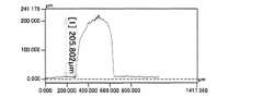
- Figure 2shows an example of a height profile of the linear metal layer bonded to the ceramic plate obtained in this example, measured in the width direction of the linear metal layer using a laser microscope.
- Example 2An attempt was made to form a metal layer under the same conditions as in Comparative Example 1, except that the laser output for both Beams 1 and 2 was 60 W. The average irradiation energy density E was 92.3 J/ mm2 . Even under these conditions, the molten metal was able to sufficiently adhere to the ceramic plate, and the linear metal layer was bonded to the ceramic plate (evaluated as ⁇ ).
- Figure 3shows an example of a height profile of the linear metal layer bonded to the ceramic plate obtained in this example, measured in the width direction of the linear metal layer using a laser microscope.
- the line widthroughly corresponds to the diameter of the irradiation area of the laser beam, and the thickness (top height) of the metal layer was approximately 180 ⁇ m.
- the shear strengthwas examined by the following method.
- Method of measuring shear strengthThe ceramic-metal bonded body was cut into an evaluation sample with a width of 10 mm perpendicular to the longitudinal direction of the linear metal layer of the ceramic-metal bonded body.
- the evaluation samplewas attached to a shear tester (model: SPST2000N) manufactured by Adwells Co., Ltd., and the shear strength was measured by applying an external force to the linear metal layer in a direction perpendicular to the longitudinal direction of the linear metal layer and parallel to the ceramic surface with a shear tool at a feed rate of 0.25 mm/sec.
- the shear strengthwas 26.6 MPa.
- Example 3An attempt was made to form a metal layer under the same conditions as in Comparative Example 1, except that the laser output for both Beams 1 and 2 was 65 W. The average irradiation energy density E was 100.0 J/ mm2 . Even under these conditions, the molten metal could be sufficiently adhered to the ceramic plate, and the linear metal layer was bonded to the ceramic plate (evaluated as ⁇ ). When the shear strength of the ceramic-metal bonded body in which the linear metal layer was bonded under the same conditions as in this example was examined by the above-mentioned method, the shear strength was 38.1 MPa.
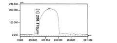
- Figure 4shows an example of the height profile of the linear metal layer bonded to the ceramic plate obtained in this example, measured in the width direction of the linear metal layer using a laser microscope.
- the line widthroughly corresponds to the diameter of the irradiation area of the laser beam, and the thickness (top height) of the metal layer was approximately 206 ⁇ m.
- Example 4An attempt was made to form a metal layer under the same conditions as in Comparative Example 1, except that the laser output for both Beams 1 and 2 was 70 W. The average irradiation energy density E was 107.7 J/ mm2 . Even under these conditions, the molten metal was able to sufficiently adhere to the ceramic plate, and the linear metal layer was bonded to the ceramic plate (evaluated as ⁇ ).
- Figure 5shows an example of a height profile of the linear metal layer bonded to the ceramic plate obtained in this example, measured in the width direction of the linear metal layer using a laser microscope.
- the line widthroughly corresponds to the diameter of the irradiation area of the laser beam, and the thickness (top height) of the metal layer was approximately 215 ⁇ m.
- Example 5An attempt was made to form a metal layer under the same conditions as in Comparative Example 1, except that the laser output for both Beams 1 and 2 was 75 W. The average irradiation energy density E was 115.4 J/ mm2 . Even under these conditions, the molten metal was able to sufficiently adhere to the ceramic plate, and the linear metal layer was bonded to the ceramic plate (evaluated as ⁇ ).
- Figure 6shows an example of a height profile of the linear metal layer bonded to the ceramic plate obtained in this example, measured in the width direction of the linear metal layer using a laser microscope.
- the line widthroughly corresponds to the diameter of the irradiation area of the laser beam, and the thickness (top height) of the metal layer was approximately 206 ⁇ m.
- Example 6The silicon nitride plate was used as the ceramic plate.
- a blue laser with a wavelength of 450 nmwas used for both beams 1 and 2, and the laser output was 20 W and the irradiation spot diameter was 0.26 mm.
- the Ag-Cu-Ti alloy powderwas fed at a feed rate of 10 mg/s, and the sweep speed of the irradiation spot was 5.0 mm/s.
- the flow rate of the shielding gaswas 10 L/min.
- the average irradiation energy density E calculated by the above formula (1-2)was 30.8 J/ mm2 . Under these conditions, the molten metal was able to sufficiently adhere to the ceramic plate, and the linear metal layer was bonded to the ceramic plate (evaluated as ⁇ ).
- the height profile measured in the width direction of the linear metal layer using a laser microscopeshowed that the line width roughly corresponded to the diameter of the irradiation area of the laser beam, and the thickness (top height) of the metal layer was approximately 94 ⁇ m.
- Example 7An attempt was made to form a metal layer under the same conditions as in Example 6, except that the laser output for both beams 1 and 2 was 25 W. The average irradiation energy density E was 38.5 J/ mm2 . Even under these conditions, the molten metal was able to sufficiently adhere to the ceramic plate, and the linear metal layer was bonded to the ceramic plate (evaluated as ⁇ ). Regarding the linear metal layer bonded to the ceramic plate obtained in this example, the height profile measured in the width direction of the linear metal layer using a laser microscope showed that the line width roughly corresponded to the diameter of the irradiation area of the laser beam, and the thickness (top height) of the metal layer was approximately 117 ⁇ m.
- Example 8An attempt was made to form a metal layer under the same conditions as in Example 6, except that the Ag-Cu-Ti alloy powder was fed at a feed rate of 5 mg/s. The average irradiation energy density E was 30.8 J/ mm2 . Even under these conditions, the molten metal was able to sufficiently adhere to the ceramic plate, and the linear metal layer was bonded to the ceramic plate (evaluated as ⁇ ). Regarding the linear metal layer bonded to the ceramic plate obtained in this example, the height profile measured in the width direction of the linear metal layer using a laser microscope showed that the line width roughly corresponded to the diameter of the irradiation area of the laser beam, and the thickness (top height) of the metal layer was approximately 83 ⁇ m.
- Example 9An attempt was made to form a metal layer under the same conditions as in Example 6, except that the Ag-Cu-Ti alloy powder was fed at a feed rate of 12.5 mg/s. The average irradiation energy density E was 30.8 J/ mm2 . Even under these conditions, the molten metal was able to sufficiently adhere to the ceramic plate, and the linear metal layer was bonded to the ceramic plate (evaluated as ⁇ ). Regarding the linear metal layer bonded to the ceramic plate obtained in this example, the height profile measured in the width direction of the linear metal layer using a laser microscope showed that the line width roughly corresponded to the diameter of the irradiation area of the laser beam, and the thickness (top height) of the metal layer was approximately 110 ⁇ m.
- Example 10An attempt was made to form a metal layer under the same conditions as in Example 6, except that the Ag-Cu-Ti alloy powder was fed at a feed rate of 15 mg/s. The average irradiation energy density E was 30.8 J/ mm2 . Even under these conditions, the molten metal was able to sufficiently adhere to the ceramic plate, and the linear metal layer was bonded to the ceramic plate (evaluated as ⁇ ). Regarding the linear metal layer bonded to the ceramic plate obtained in this example, the height profile measured in the width direction of the linear metal layer using a laser microscope showed that the line width roughly corresponded to the diameter of the irradiation area of the laser beam, and the thickness (top height) of the metal layer was approximately 107 ⁇ m.
- Example 11Except for the laser output of both beams 1 and 2 being 40 W and the supply rate of the Ag-Cu-Ti alloy powder being 15 mg/s, the formation of a metal layer was attempted under the same conditions as in Example 6.
- the average irradiation energy density Ewas 61.5 J/ mm2 . Even under these conditions, the molten metal could be sufficiently adhered to the ceramic plate, and the linear metal layer was bonded to the ceramic plate (evaluated as ⁇ ).
- the shear strength of the ceramic-metal bonded body in which the linear metal layer was bonded under the same conditions as in this examplewas examined in the same manner as in Example 2, the shear strength was 92.0 MPa or more.
- the height profile measured in the width direction of the linear metal layer using a laser microscopeshowed that the line width roughly corresponded to the diameter of the irradiation area of the laser beam, and the thickness (top height) of the metal layer was approximately 167 ⁇ m.
- Example 12A metal layer was formed under the same conditions as in Example 6, except that the laser output for both beams 1 and 2 was set to 35 W and the Ag-Cu-Ti alloy powder was fed at a feed rate of 12.5 mg/s. The average irradiation energy density E was 53.8 J/ mm2 . Even under these conditions, the molten metal could be sufficiently adhered to the ceramic plate, and the linear metal layer was bonded to the ceramic plate (evaluated as ⁇ ). When the shear strength of the ceramic-metal bonded body in which the linear metal layer was bonded under the same conditions as in this example was examined in the same manner as in Example 2, the shear strength was 42.2 MPa or more.
- the height profile measured in the width direction of the linear metal layer using a laser microscopeshowed that the line width roughly corresponded to the diameter of the irradiation area of the laser beam, and the thickness (top height) of the metal layer was approximately 165 ⁇ m.
- Example 13The aluminum nitride plate was used as the ceramic plate.
- a blue laser with a wavelength of 450 nmwas used for both beams 1 and 2, and the laser output was 45 W and the irradiation spot diameter was 0.26 mm.
- the Ag-Cu-Ti alloy powderwas fed at a feed rate of 5 mg/s, and the sweep speed of the irradiation spot was 5.0 mm/s.
- the flow rate of the shielding gaswas 10 L/min.
- the average irradiation energy density E calculated by the above formula (1-2)was 69.2 J/ mm2 . Even under these conditions, the molten metal was able to sufficiently adhere to the ceramic plate, and the linear metal layer was bonded to the ceramic plate (evaluated as ⁇ ).
- the height profile measured in the width direction of the linear metal layer using a laser microscopeshowed that the line width roughly corresponded to the diameter of the irradiation area of the laser beam, and the thickness (top height) of the metal layer was approximately 74 ⁇ m.
- Example 14An attempt was made to form a metal layer under the same conditions as in Example 13, except that the laser output for both beams 1 and 2 was 55 W. The average irradiation energy density E was 84.6 J/ mm2 . Even under these conditions, the molten metal was able to sufficiently adhere to the ceramic plate, and the linear metal layer was bonded to the ceramic plate (evaluated as ⁇ ). Regarding the linear metal layer bonded to the ceramic plate obtained in this example, the height profile measured in the width direction of the linear metal layer using a laser microscope showed that the line width roughly corresponded to the diameter of the irradiation area of the laser beam, and the thickness (top height) of the metal layer was approximately 60 ⁇ m.
- Example 15A metal layer was formed under the same conditions as in Example 13, except that the laser output for both beams 1 and 2 was set to 50 W and the Ag-Cu-Ti alloy powder was fed at a feed rate of 10 mg/s. The average irradiation energy density E was 76.9 J/ mm2 . Even under these conditions, the molten metal was able to sufficiently adhere to the ceramic plate, and the linear metal layer was bonded to the ceramic plate (evaluated as ⁇ ).
- the height profile measured in the width direction of the linear metal layer using a laser microscopeshowed that the line width roughly corresponded to the diameter of the irradiation area of the laser beam, and the thickness (top height) of the metal layer was approximately 64 ⁇ m.
- Example 16A metal layer was formed under the same conditions as in Example 13, except that the laser output for both beams 1 and 2 was set to 55 W and the Ag-Cu-Ti alloy powder was fed at a feed rate of 7.5 mg/s. The average irradiation energy density E was 84.6 J/ mm2 . Even under these conditions, the molten metal was able to sufficiently adhere to the ceramic plate, and the linear metal layer was bonded to the ceramic plate (evaluated as ⁇ ).
- the height profile measured in the width direction of the linear metal layer using a laser microscopeshowed that the line width roughly corresponded to the diameter of the irradiation area of the laser beam, and the thickness (top height) of the metal layer was approximately 73 ⁇ m.
- FIG 7shows photographs of the appearance of the ceramic plates after conducting the metal layer production tests for each example.
- the ceramic plate on the leftshows the results of Comparative Examples 1, 2, and 3, and Example 1, while the ceramic plate on the right shows the results of Examples 2, 3, 4, and 5.
- the numbers (watts) written on the platesare the total laser output (W) of Beams 1 and 2.
Landscapes
- Chemical & Material Sciences (AREA)
- Engineering & Computer Science (AREA)
- Optics & Photonics (AREA)
- Physics & Mathematics (AREA)
- Mechanical Engineering (AREA)
- Organic Chemistry (AREA)
- Chemical Kinetics & Catalysis (AREA)
- Materials Engineering (AREA)
- Metallurgy (AREA)
- Plasma & Fusion (AREA)
- Laser Beam Processing (AREA)
- Ceramic Products (AREA)
- Other Surface Treatments For Metallic Materials (AREA)
Abstract
Description
Translated fromJapanese本発明は、レーザービームにより溶融させた金属材料をセラミックス基材の表面に直接接合するセラミックス-金属接合体の製造方法に関する。The present invention relates to a method for producing a ceramic-metal joint in which a metal material melted by a laser beam is directly joined to the surface of a ceramic substrate.
セラミックス-金属接合体、すなわちセラミックスと金属とが両者の接合部を介して一体化した複合材料は、例えば半導体素子を搭載するための絶縁回路基板などの用途に有用である。一般に絶縁回路基板の製造では、銅系あるいはアルミニウム系の金属シート部材をセラミックス基板の表面に接合した後、その金属シート部材の不要箇所をエッチングにより除去して回路パターンを形成する手法が採用される。この場合、回路パターンを形成する工程ではレジスト膜の形成、エッチング加工およびレジスト膜の除去を伴う手順が必要となり、製造負荷およびコストの上昇が生じている。Ceramic-metal joints, i.e. composite materials in which ceramic and metal are integrated through a joint between the two, are useful in applications such as insulated circuit boards for mounting semiconductor elements. Insulated circuit boards are generally manufactured by joining a copper or aluminum metal sheet member to the surface of a ceramic substrate, and then etching away unnecessary areas of the metal sheet member to form a circuit pattern. In this case, the process of forming the circuit pattern requires steps involving the formation of a resist film, etching, and removal of the resist film, resulting in increased manufacturing load and costs.
セラミックス板の表面に、所定の回路パターンに応じたレイアウトの金属層を直接形成させる手法として「溶湯接合法」が知られている。溶湯接合法は、鋳型内に設置されたセラミックス板の表面で溶融金属を凝固させるものであり、鋳型内の空隙パターンによって、セラミックス板の表面に接合される金属層のレイアウトを設定することができる。しかし、溶湯接合法により細線形状の金属層を形成させることは困難である。また、溶湯接合法はアルミニウム系金属には適用できるが、融点の高い銅系金属に適用することは工業的に容易でない。The "molten metal bonding method" is known as a technique for directly forming a metal layer on the surface of a ceramic plate with a layout corresponding to a specified circuit pattern. In this method, molten metal is solidified on the surface of a ceramic plate placed in a mold, and the layout of the metal layer to be bonded to the surface of the ceramic plate can be set by the void pattern in the mold. However, it is difficult to form a metal layer with a thin wire shape using the molten metal bonding method. Also, while the molten metal bonding method can be applied to aluminum-based metals, it is not industrially easy to apply it to copper-based metals, which have a high melting point.
銅系の金属をセラミックスの表面に直接接合させる手法として、溶射の技術が知られている。例えば特許文献1には、プラズマバーナーによる熱ガス流中に銅粉末を供給するプラズマ溶射法により、粗面化された酸化アルミニウム板の表面に厚さ75μm(実施例1)あるいは30μm(実施例2)の銅層を形成した例が示されている。特許文献2には、アーク溶射、プラズマ溶射、フレーム溶射などの溶射法により、窒化アルミニウムなどのセラミックス基板の表面にアルミニウム、ニッケル、銅、ステンレスなどの金属を溶射して、厚さ50μm~1.5mmの導電膜を形成した例(実施例1、6、7)が示されている。しかし、溶射法により細線形状の金属層を形成させることは困難である。Thermal spraying technology is known as a method for directly bonding copper-based metals to the surface of ceramics. For example, Patent Document 1 shows an example in which a copper layer of 75 μm (Example 1) or 30 μm (Example 2) was formed on the surface of a roughened aluminum oxide plate by a plasma spraying method in which copper powder was supplied into a hot gas flow produced by a plasma burner.
セラミックス板と金属材料とを面接合させる手法として「ろう付け」がある。ろう付けでは、被接合材同士の接合界面にろう材を適用する。代表的なろう材として、銀ペーストやAg-Cu系合金のシートが挙げられる。このようなろう材を使用するためには、ろう付けに先がけ、ろう材のペーストを被接合材の接合面に塗布したり、所定形状のろう材シートを用意して被接合材間の所定位置に配置したりする工程が必要となる。もし、所定量のろう材を、セラミックス板の接合面となる部位に選択的に接合させた、「ろう材一体型セラミックス板」を予め用意しておくことができると、ろう付け工程の負荷軽減に寄与できる。溶射法により、少量の銀系金属からなる薄いろう材層をセラミックス板の所定位置に形成することは容易でない。Brazing is a method for joining ceramic plates and metal materials by surface bonding. In brazing, a brazing material is applied to the bonding interface between the materials to be joined. Typical brazing materials include silver paste and Ag-Cu alloy sheets. In order to use such brazing materials, a process is required prior to brazing, such as applying the brazing material paste to the bonding surfaces of the materials to be joined, or preparing a brazing material sheet of a specified shape and placing it in a specified position between the materials to be joined. If it were possible to prepare a "brazing material integrated ceramic plate" in advance, in which a specified amount of brazing material is selectively bonded to the portion of the ceramic plate that will become the bonding surface, this would help reduce the load of the brazing process. It is not easy to form a thin brazing material layer made of a small amount of silver-based metal in a specified position on a ceramic plate using a thermal spray method.
一方、金属基材の表面を異種金属で被覆する手法として「レーザー・メタル・デポジション」が知られている。これは、レーザービームにより被覆材である金属の粉体を金属基材表面の近傍で溶融させ、その溶融金属を金属基材に被着させる技術である。例えば特許文献3には、複数のレーザービームを同時に用いる粉体肉盛装置が開示されている。On the other hand, "laser metal deposition" is known as a method for coating the surface of a metal substrate with a different metal. This is a technology in which a laser beam is used to melt metal powder, which is the coating material, near the surface of the metal substrate, and the molten metal is then deposited on the metal substrate. For example, Patent Document 3 discloses a powder deposition device that uses multiple laser beams simultaneously.
特許文献4には、被覆材である銅粉をレーザービーム中に供給することによって基材であるステンレス鋼の表面に銅の肉盛層を形成させるコーティング方法が開示されている。具体的には、粒径の異なる2種類の純銅からなる混合粉を使用し、青色レーザーの集光径を約0.5mmとして、4mm/sの走査速度で、レーザー出力を20~80Wの範囲で変化させて、対象物(基材)であるSUS304の表面に直線状の肉盛層を形成させた例が示されている(段落0054~0057)。Patent Document 4 discloses a coating method in which a copper build-up layer is formed on the surface of a stainless steel substrate by feeding copper powder, a coating material, into a laser beam. Specifically, an example is given in which a mixed powder made of two types of pure copper with different particle sizes is used, the focused diameter of the blue laser is set to approximately 0.5 mm, the scanning speed is 4 mm/s, and the laser output is changed in the range of 20 to 80 W to form a linear build-up layer on the surface of the target object (substrate) SUS304 (paragraphs 0054 to 0057).
レーザー・メタル・デポジションの技術によれば、特許文献4の例に見られるように、金属基材の表面に線幅が例えば0.5mm程度といった細線形状の純銅の肉盛層を形成させることが可能である。しかしながら、セラミックス基材の表面に銅系、銀系をはじめとする各種金属の層を細線形状で接合することは、基材が金属である場合と比べ難しく、その技術は確立されていない。
本発明は、セラミックス基材の表面に、金属の層を細線形状で直接接合することが可能な技術によってセラミックス-金属接合体を提供することを目的とする。According to the technology of laser metal deposition, it is possible to form a fine line-shaped build-up layer of pure copper with a line width of, for example, about 0.5 mm on the surface of a metal substrate, as shown in the example of Patent Document 4. However, bonding a layer of various metals, including copper-based and silver-based, in a fine line shape to the surface of a ceramic substrate is more difficult than when the substrate is a metal, and the technology has not been established.
An object of the present invention is to provide a ceramic-metal bonded body using a technique that enables a metal layer to be directly bonded in the form of fine wires to the surface of a ceramic base material.
発明者らは研究の結果、レーザービームを用いてセラミックス基材の表面を十分に加熱した状態とすることにより、レーザー・メタル・デポジションの手法を利用してセラミックスと金属の接合を実現することができることを見出した。基材が金属であれば、特許文献4に教示されるように、噴射された被覆材金属(溶材)が優先的に溶融され、かつ金属基材(対象物)の溶融が最小限に抑制される条件とすることにより、溶融された被覆材金属(溶材)は金属基材(対象物)の表面に付着した後に自然冷却されて凝固し、溶融プールを伴わずに金属膜からなる肉盛層により金属基材(対象物) の表面をコーティングすることができる(特許文献4の段落0034)。すなわち、溶融金属は固体である異種金属の表面上に比較的容易に付着する。しかし、基材がセラミックスである場合には、被覆材金属がセラミックス基板の直上で単に溶融する程度のレーザー照射条件では、セラミックスと被覆材金属の凝固物とを接合させることは困難である。レーザー・メタル・デポジションの手法でセラミックス-金属接合体を得るためには、基材であるセラミックスの表面を十分に加熱し、順次供給される被覆材金属の溶融物をセラミックスの表面上に被着させることが重要となる。本発明はこのような知見に基づいて成されたものである。具体的には、本明細書では以下の発明を開示する。As a result of their research, the inventors found that by using a laser beam to sufficiently heat the surface of a ceramic substrate, it is possible to realize bonding of ceramics and metals using the laser metal deposition technique. If the substrate is a metal, as taught in Patent Document 4, by setting conditions such that the sprayed coating metal (molten material) is preferentially melted and melting of the metal substrate (object) is minimized, the molten coating metal (molten material) adheres to the surface of the metal substrate (object) and then naturally cools and solidifies, and the surface of the metal substrate (object) can be coated with a build-up layer made of a metal film without forming a molten pool (paragraph 0034 of Patent Document 4). In other words, molten metal adheres relatively easily to the surface of a solid dissimilar metal. However, if the substrate is a ceramic, it is difficult to bond the ceramic to the solidified coating metal under laser irradiation conditions such that the coating metal simply melts directly above the ceramic substrate. In order to obtain a ceramic-metal joint using the laser metal deposition technique, it is important to sufficiently heat the surface of the ceramic substrate and to deposit the molten coating metal that is supplied in sequence onto the ceramic surface. The present invention was made based on this finding. Specifically, the following inventions are disclosed in this specification.
[1]レーザービームをセラミックス基材表面に掃引させながら照射するとともに、前記セラミックス基材の表面上のレーザービームが照射される領域(以下「照射エリア」という。)に向けて固体金属材料を送給して、送給中の前記金属材料にもレーザービームが照射される状態とし、前記照射エリアに位置するセラミックス基材表面を加熱しながら前記金属材料を溶融させ、溶融した金属材料をセラミックス基材表面に被着させたのち凝固させる、セラミックス-金属接合体の製造方法。
[2]前記固体金属材料が粉体である、上記[1]に記載のセラミックス-金属接合体の製造方法。
[3]前記固体金属材料がCu、Ag、Ti、Ni、Al、Fe、Au、Ptのいずれかを主成分とするものである、上記[1]または[2]に記載のセラミックス-金属接合体の製造方法。
[4]前記固体金属材料がCuまたはAgを主成分とするものである、上記[1]または[2]に記載のセラミックス-金属接合体の製造方法。
[5]単数または複数のレーザービームを使用し、送給中の前記金属材料に照射されるレーザービームのうち少なくとも1つを波長600nm以下のものとする、上記[1]~[4]のいずれかに記載のセラミックス-金属接合体の製造方法。
[6]単数または複数のレーザービームを使用し、送給中の前記金属材料に照射されるレーザービームのうち少なくとも1つが、Ybドープ固体レーザー、Ndドープ固体レーザー、GaN半導体レーザー、銅蒸気レーザー、Arガスレーザー、N2ガスレーザー、エキシマレーザーのいずれかを光源とするものである、上記[1]~[4]のいずれかに記載のセラミックス-金属接合体の製造方法。
[7]前記固体金属材料がCuを主成分とするものであり、前記セラミックス基材がAlNを主成分とするものである、上記[1]~[6]のいずれかに記載のセラミックス-金属接合体の製造方法。
[8]単数または複数のレーザービームを使用し、下記(1)式で表される平均照射エネルギー密度Eが80~160J/mm2となるようにレーザービームをセラミックス基材表面に照射する、上記[7]に記載のセラミックス-金属接合体の製造方法。
E=(PL1/DL1+PL2/DL2+・・・+PLn/DLn)/v …(1)
ここで、
E:平均照射エネルギー密度E(J/mm2)
符号Li(i=1以上n以下の整数、nは使用するレーザービームの総数):使用する個々のレーザービームの識別符号
PLi:レーザービームLiのレーザー出力(W)
DLi:レーザービームLiの掃引方向に対して直角方向の照射スポット径(mm)
v:レーザービームの掃引速度(mm/s)
[9]前記固体金属材料がAgを主成分とするものであり、前記セラミックス基材がAlNまたはSi3N4を主成分とするものである、上記[1]~[6]のいずれかに記載のセラミックス-金属接合体の製造方法。
[10]単数または複数のレーザービームを使用し、下記(1)式で表される平均照射エネルギー密度Eが25~160J/mm2となるようにレーザービームをセラミックス基材表面に照射する、上記[9]に記載のセラミックス-金属接合体の製造方法。
E=(PL1/DL1+PL2/DL2+・・・+PLn/DLn)/v …(1)
ここで、
E:平均照射エネルギー密度E(J/mm2)
符号Li(i=1以上n以下の整数、nは使用するレーザービームの総数):使用する個々のレーザービームの識別符号
PLi:レーザービームLiのレーザー出力(W)
DLi:レーザービームLiの掃引方向に対して直角方向の照射スポット径(mm)
v:レーザービームの掃引速度(mm/s)[1] A method for producing a ceramic-metal bonded body, comprising: irradiating a surface of a ceramic substrate with a laser beam while sweeping the surface; feeding a solid metal material toward a region on the surface of the ceramic substrate where the laser beam is irradiated (hereinafter referred to as an "irradiation area"), so that the metal material being fed is also irradiated with the laser beam; heating the surface of the ceramic substrate located in the irradiation area to melt the metal material; and depositing the molten metal material on the surface of the ceramic substrate and then solidifying it.
[2] The method for producing a ceramic-metal bonded body according to the above [1], wherein the solid metal material is a powder.
[3] The method for producing a ceramic-metal bonded body according to the above [1] or [2], wherein the solid metal material is mainly composed of any one of Cu, Ag, Ti, Ni, Al, Fe, Au, and Pt.
[4] The method for producing a ceramic-metal bonded body according to the above [1] or [2], wherein the solid metal material is mainly composed of Cu or Ag.
[5] The method for producing a ceramic-metal joined body according to any one of the above [1] to [4], wherein a single or multiple laser beams are used, and at least one of the laser beams irradiated to the metal material during feeding has a wavelength of 600 nm or less.
[6] A method for producing a ceramic-metal joint according to any one of the above [1] to [4], wherein a single or multiple laser beams are used, and at least one of the laser beams irradiated to the metal material during feeding has a light source selected from the group consisting of a Yb-doped solid-state laser, a Nd-doped solid-state laser, a GaN semiconductor laser, a copper vapor laser, an Ar gas laser, aN2 gas laser, and an excimer laser.
[7] The method for producing a ceramic-metal bonded body according to any one of [1] to [6] above, wherein the solid metal material is mainly composed of Cu, and the ceramic base material is mainly composed of AlN.
[8] The method for producing a ceramic-metal bonded body according to the above [7], wherein a single or multiple laser beams are used to irradiate the ceramic substrate surface with the laser beam so that the average irradiation energy density E represented by the following formula (1) is 80 to 160 J / mm2 .
E = (PL1 /DL1 +PL2 /DL2 + ... +PLn /DLn ) / v ... (1)
here,
E: average irradiation energy density E (J/mm2 )
Symbol Li (i = integer between 1 and n, n is the total number of laser beams used): Identification code of each laser beam used PLi : Laser output (W) of laser beam Li
DLi : Irradiation spot diameter (mm) perpendicular to the sweep direction of the laser beam Li
v: laser beam sweep speed (mm/s)
[9] The method for producing a ceramic-metal bonded body according to any one of [1] to [6] above, wherein the solid metal material is mainly composed of Ag, and the ceramic base material is mainly composed of AlN or Si3 N4 .
[10] The method for producing a ceramic-metal bonded body according to the above [9], wherein a single or multiple laser beams are used to irradiate the ceramic substrate surface with the laser beam so that the average irradiation energy density E represented by the following formula (1) is 25 to 160 J / mm2 .
E = (PL1 /DL1 +PL2 /DL2 + ... +PLn /DLn ) / v ... (1)
here,
E: average irradiation energy density E (J/mm2 )
Symbol Li (i = integer between 1 and n, n is the total number of laser beams used): Identification code of each laser beam used PLi : Laser output (W) of laser beam Li
DLi : Irradiation spot diameter (mm) perpendicular to the sweep direction of the laser beam Li
v: laser beam sweep speed (mm/s)
本明細書において、「照射スポット」とは、ある1つのレーザービームの進路によって照射されるセラミックス基材表面上の領域を意味する。使用するレーザービームのうち少なくとも1つは、送給中の金属材料に当たる必要がある。送給中の金属材料に当たるレーザービームについては、その進路の途中で送給中の金属材料によって遮られることなくセラミックス基材表面に到達すると仮定した場合に照射されることになるセラミックス基材表面上の領域を当該レーザービームの「照射スポット」とする。「照射エリア」とは、いずれかの照射スポットに属するセラミックス基材表面上の位置からなる領域を意味する。1つのレーザービームのみを使用する場合、「照射エリア」と「照射スポット」は必然的に一致する。複数のレーザービームを使用する場合、各「照射スポット」の範囲は「照射エリア」の範囲と一致するかそれより小さいが、各レーザービームによる全ての照射スポットが一致するときは「照射エリア」と各「照射スポット」は一致する。In this specification, "irradiation spot" means an area on the ceramic substrate surface that is irradiated by the path of one laser beam. At least one of the laser beams used must hit the metal material being fed. For a laser beam that hits the metal material being fed, the area on the ceramic substrate surface that is irradiated when it is assumed that the laser beam reaches the ceramic substrate surface without being blocked by the metal material being fed along its path is the "irradiation spot" of that laser beam. "Irradiation area" means an area consisting of positions on the ceramic substrate surface that belong to one of the irradiation spots. When only one laser beam is used, the "irradiation area" and the "irradiation spot" necessarily coincide. When multiple laser beams are used, the range of each "irradiation spot" coincides with or is smaller than the range of the "irradiation area", but when all the irradiation spots by each laser beam coincide, the "irradiation area" and each "irradiation spot" coincide.
「主成分」は、その物質を構成する成分のうち、質量割合での含有量が50%以上である成分を意味する。例えば、「Cuを主成分とする固体金属材料」は、Cu含有量が50質量%以上である固体金属材料を意味する。「AlNを主成分とするセラミックス基材」とは、AlNの含有量が50質量%以上であるセラミックス基材を意味する。なお、本明細書では、金属材料のうちCuを主成分とするものを「銅系」、Agを主成分とするものを「銀系」と呼んでいる。"Main component" means a component that is contained in a substance in a mass percentage ratio of 50% or more. For example, "a solid metal material whose main component is Cu" means a solid metal material whose Cu content is 50% or more by mass. "A ceramic base material whose main component is AlN" means a ceramic base material whose AlN content is 50% or more by mass. In this specification, metal materials whose main component is Cu are called "copper-based" and those whose main component is Ag are called "silver-based."
本発明によれば、レーザー・メタル・デポジションの手法によってセラミックス基材の表面上に金属の層を直接形成した「セラミックス-金属接合体」を得ることが可能となった。上記の金属層は例えば幅0.5mm以下といった細線形状とすることができるので、本発明は、半導体素子搭載用の絶縁基板へ銅系金属の回路パターンを直接的に形成する手法として利用できる。また、銀系のろう材を所定位置に選択的に接合させた「ろう材一体型セラミックス板」の製造手法として利用できる。According to the present invention, it is now possible to obtain a "ceramic-metal bonded body" in which a metal layer is formed directly on the surface of a ceramic base material by the laser metal deposition method. The metal layer can be formed into a thin line shape, for example, with a width of 0.5 mm or less, so the present invention can be used as a method for directly forming a copper-based metal circuit pattern on an insulating substrate for mounting semiconductor elements. It can also be used as a manufacturing method for a "brazing material integrated ceramic plate" in which a silver-based brazing material is selectively bonded to a predetermined position.
図1に、本発明に使用できるレーザー・メタル・デポジション装置の構成を模式的に例示する。ここでは一例として2ビーム照射型における代表的な構成を示すが、1つのビームのみを照射するタイプや3ビーム以上を照射するタイプの装置を採用することも可能である。プロセシング・ヘッド10は、被覆材である金属粉体を所定の方向に噴射する手段と、レーザービームを所定の方向に照射する手段を持つユニットであり、セラミックス基材1の表面から所定の距離を保ちながら、セラミックス基材1の上方を水平方向に移動できるようになっている。被覆材である金属粉体は、粉体供給装置20から粉体供給管21によってプロセシング・ヘッド10に導かれ、プロセシング・ヘッド10に装着されている粉体送給ノズル22から、セラミックス基材1の表面に向けて吐出される。粉体送給ノズル22から吐出された飛行中の金属粉体を図中に符号200で表している。一方、レーザー発生装置30a、30bで生成されたレーザー光は、それぞれ光ファイバー31a、31bによってプロセシング・ヘッド10に導かれ、プロセシング・ヘッド10に内蔵される図示しないレンズから、所定の方向にレーザービーム300a、300bが照射される。図1の例では、プロセシング・ヘッド10を矢印の方向に移動させながら、金属粉体の吐出とレーザービームの照射を行っている。FIG. 1 shows a schematic diagram of a laser metal deposition apparatus that can be used in the present invention. A typical configuration of a two-beam irradiation type is shown here as an example, but it is also possible to adopt an apparatus that irradiates only one beam or three or more beams. The
レーザービーム300a、300bは、飛行中の金属粉体200に照射され、固体の金属粉体200を加熱するとともに、セラミックス基材1の表面上にも照射され、それらのレーザービームが照射されるセラミックス基材1の表面上の領域である照射エリア310を加熱する。金属粉体200は、粒子のほとんどは飛行中に溶融するが、照射エリア310に到達した時点で溶融する粒子が含まれていても構わない。すなわち、被覆材である固体金属材料を、レーザービームの照射を受けている送給中、またはセラミックス基材表面上への到達時に溶融させる。なお、図中の金属粉体200は、粒子サイズを誇張して描いてある。The
得られた溶融金属は、照射エリア310が十分に加熱されていることにより、セラミックス基材1の表面上に溶融状態を保ちながら被着する。すなわち、上記の溶融金属はセラミックス基材1に到達した時点で直ちに凝固して弾け飛ぶのではなく、セラミックス基材1の表面上に溶融状態のまま、短い時間ではあるが、留まることが重要である。その短い時間においてセラミックス基材1の表面は溶融金属で濡れた状態を維持する。セラミックス基材1に被着した溶融金属は、プロセシング・ヘッド10の移動に伴って掃引される照射エリア310が去ったのちに凝固し、セラミックス基材1の表面上の照射エリア310が通り過ぎた領域に金属層2が線状に形成される。この金属層2は、凝固過程でセラミックス基材1に対して強固に接合する。このようにして、セラミックス基材1の表面上に金属層2が接合した「セラミックス-金属接合体」が構築される。照射エリア310の掃引をセラミックス基材1上で掃引直角方向にスキャンさせると、面状の金属層2を形成させることもできる。The obtained molten metal is deposited on the surface of the ceramic substrate 1 while remaining in a molten state because the
プロセシング・ヘッド10とセラミックス基材1の間の溶融金属が生じる空間、およびセラミックス基材1の照射エリア310を含む表面は、金属の酸化を防ぐためにArなどの不活性ガスでシールドすることが好ましい。ガスシールド機構については図1では記載を省略してあるが、例えば、プロセシング・ヘッド10の下部に各レーザービームと粉体送給ノズル22を取り囲むスリーブを、その下端がセラミックス基材1に接触しないように設け、プロセシング・ヘッド10から上記スリーブ内にシールドガスを供給し、セラミックス基材1の照射エリア310を含む表面領域に上記スリーブの下端から吐出したシールドガスを吹き付ける機構を採用することができる。The space between the processing
図1には、2本のレーザービーム300a、300bによる共通の照射スポットによって照射エリア310を形成させる例を示したが、その他の照射方法として、例えば、複数のレーザービームのうち、一部のレーザービームを飛行中の粉体が溶融しやすい位置に照準を合わせて焦点調整し、他のレーザービームをセラミックス基材1の表面が最も効率的に加熱されるように焦点調整する手法を採用してもよい。また、図1の例では、被覆材である固体金属の送給方法として金属粉体を粉体送給ノズル22から噴射させる手法を示したが、粉体に代えて例えば線材を送給する手法を採用することも可能である。In FIG. 1, an example is shown in which
[固体金属材料]
被覆材として使用する原料の固体金属材料としては、Cu、Ag、Ti、Ni、Al、Fe、Au、Ptなどの元素を主成分とするものが使用できる。これらの元素を主成分とする金属を細線形状でセラミックス基板上に直接接合する手法は、これまで確立されていなかった。特に銅系の金属は絶縁回路基板の回路用金属として広く使用され、また銀系の金属はろう材として広く使用されていることから、そのような用途に適用する場合はCuまたはAgを主成分とするものを使用すればよい。
より具体的には、回路用の銅系の金属としては、Cu含有量が99.9質量%以上の純銅を適用することが好ましい。
ろう材用の銀系の金属としては、Ag-Cu系の共晶近傍組成のものが好ましい。活性金属としてTiを0.5~5質量%含むものがより好ましい。例えば、Cu:23~33質量%、Ti:0.5~5質量%、残部がAgであるAg-Cu-Ti合金のろう材を挙げることができる。その他、JIS Z3261:1998に規定される各種Agろうを適用することができる。[Solid metal materials]
The raw solid metal material used as the coating material can be one mainly composed of elements such as Cu, Ag, Ti, Ni, Al, Fe, Au, and Pt. A method for directly bonding metals mainly composed of these elements in the form of thin wires to a ceramic substrate has not been established so far. In particular, copper-based metals are widely used as circuit metals for insulating circuit boards, and silver-based metals are widely used as brazing materials, so that when applying to such applications, it is sufficient to use one mainly composed of Cu or Ag.
More specifically, it is preferable to use pure copper with a Cu content of 99.9 mass % or more as the copper-based metal for the circuits.
The silver-based metal for the brazing material is preferably an Ag-Cu-based near-eutectic composition. More preferably, it contains 0.5 to 5 mass% Ti as an active metal. For example, a brazing material made of an Ag-Cu-Ti alloy with 23 to 33 mass% Cu, 0.5 to 5 mass% Ti, and the remainder Ag can be used. In addition, various Ag brazing materials specified in JIS Z3261:1998 can be used.
固体金属材料として金属粉体を使用する場合、レーザー回折・散乱法による体積基準の粒度分布における累積50%粒子径D50が例えば5~100μmである粉体を使用することができ、10~30μmの範囲のものがより好ましい。2種以上の金属粉体を所定割合で配合させた混合粉を使用してもよい。When using metal powder as the solid metal material, powder with a cumulative 50% particle diameter D50 in the volume-based particle size distribution measured by the laser diffraction/scattering method of, for example, 5 to 100 μm can be used, and powder in the range of 10 to 30 μm is more preferable. A mixed powder in which two or more types of metal powders are mixed in a specified ratio may also be used.
[セラミックス基材]
セラミックス基材としては種々の材質のものが適用対象となる。例えば、窒化アルミニウム(AlN)を主成分とするもの、窒化ケイ素(Si3N4)を主成分とするもの、酸化アルミニウム(Al2O3)を主成分とするものなどが挙げられる。絶縁回路基板を構築する場合は、厚さが例えば0.25~1.0mm程度のセラミックス板を使用すればよい。[Ceramic substrate]
Ceramic substrates can be made of various materials, such as those mainly composed of aluminum nitride (AlN), silicon nitride (Si3 N4 ), and aluminum oxide (Al2 O3 ). When constructing an insulating circuit board, a ceramic plate with a thickness of, for example, about 0.25 to 1.0 mm can be used.
[レーザー]
本発明ではレーザービームのエネルギーによって銅系、銀系をはじめとする各種金属の固体金属材料を溶融させる。Cuを含有する金属材料を適用する場合、波長600nm以下のレーザーを使用することが効果的である。複数のレーザービームを使用する場合は、そのうちの少なくとも1つを波長600nm以下のレーザーとすることが望ましい。波長600nm以下の代表的なレーザーとして、波長が450nm付近である青色レーザーを挙げることができる。[laser]
In the present invention, solid metal materials of various metals including copper and silver are melted by the energy of a laser beam. When applying a metal material containing Cu, it is effective to use a laser with a wavelength of 600 nm or less. When using multiple laser beams, it is desirable that at least one of them is a laser with a wavelength of 600 nm or less. A representative laser with a wavelength of 600 nm or less is a blue laser with a wavelength of about 450 nm.
[平均照射エネルギー密度E]
本発明では、セラミックスと金属を接合するために、溶融金属をセラミックス表面に被着させること、すなわちセラミックス表面が溶融金属で濡れた状態を作ることが重要である。セラミックスは高融点の無機化合物を主体とする物質であり、これは金属とは異質の物質であることから、短い時間であっても、セラミックス基材の表面が溶融金属と濡れた状態を経なければ、セラミックス基材と凝固後の金属との接合を実現することは難しい。溶射法であれば、セラミックス基材の表面に吹き付けられる溶融金属の量が多く、またプラズマ等によりセラミックス基材に付与される熱量も多いことから、セラミックスと溶融金属の濡れは確保しやすい。これに対し、レーザーのエネルギーで幅が例えば0.5mm以下といった細線形状の金属層を形成するに足る少量の金属を溶融させる場合には、溶融金属はセラミックス基材表面に到達した時点で直ちに凝固しやすいという問題がある。そこで検討の結果、レーザービームをセラミックス基材の表面に意図的に照射して、その照射エリアを十分に加熱することで、溶融金属をセラミックス表面に被着させることが可能となり、セラミックス基材と細線形状の金属層との接合を実現できることが確認された。[Average irradiation energy density E]
In the present invention, in order to bond ceramics and metal, it is important to deposit molten metal on the ceramic surface, that is, to make the ceramic surface wet with molten metal. Since ceramics are mainly composed of inorganic compounds with high melting points and are different from metals, it is difficult to realize bonding between the ceramic substrate and the metal after solidification unless the surface of the ceramic substrate is wet with molten metal even for a short time. In the case of the thermal spraying method, the amount of molten metal sprayed on the surface of the ceramic substrate is large, and the amount of heat applied to the ceramic substrate by plasma or the like is also large, so that the wetting of the ceramic and the molten metal is easily ensured. On the other hand, when a small amount of metal sufficient to form a thin-line metal layer with a width of, for example, 0.5 mm or less is melted by the energy of the laser, there is a problem that the molten metal is likely to solidify immediately when it reaches the surface of the ceramic substrate. As a result of the investigation, it was confirmed that it is possible to deposit molten metal on the ceramic surface by intentionally irradiating the surface of the ceramic substrate with a laser beam and sufficiently heating the irradiated area, and it is possible to realize bonding between the ceramic substrate and the thin-line metal layer.
セラミックス基材表面の照射エリアに付与するレーザービームのエネルギーは、溶融金属の被着を実現できる強度とすれば十分であるが、より具体的には、被覆材金属がCuを主成分とするものであり、セラミックス基材がAlNを主成分とするものである場合、単数または複数のレーザービームを使用して下記(1)式で表される平均照射エネルギー密度Eが80~160J/mm2となるように設定することが効果的である。また、被覆材金属がAgを主成分とするものであり、セラミックス基材がAlNまたはSi3N4を主成分とするものである場合、単数または複数のレーザービームを使用して下記(1)式で表される平均照射エネルギー密度Eが25~160J/mm2となるように設定することが効果的である。
E=(PL1/DL1+PL2/DL2+・・・+PLn/DLn)/v …(1)
ここで、
E:平均照射エネルギー密度E(J/mm2)
符号Li(i=1以上n以下の整数、nは使用するレーザービームの総数):使用する個々のレーザービームの識別符号
PLi:レーザービームLiのレーザー出力(W)
DLi:レーザービームLiの掃引方向に対して直角方向の照射スポット径(mm)
v:レーザービームの掃引速度(mm/s)The energy of the laser beam applied to the irradiation area on the ceramic substrate surface is sufficient if it is strong enough to realize the deposition of the molten metal, but more specifically, when the coating metal is mainly composed of Cu and the ceramic substrate is mainly composed of AlN, it is effective to use one or more laser beams to set the average irradiation energy density E expressed by the following formula (1) to 80 to 160 J/mm2. Also, when the coating metal is mainly composed of Ag and the ceramic substrate is mainly composed of AlN or Si3 N4 , it is effective to use one or more laser beams to set the average irradiation energy density E expressed by the following formula (1) to 25 to 160 J/mm2 .
E = (PL1 /DL1 +PL2 /DL2 + ... +PLn /DLn ) / v ... (1)
here,
E: average irradiation energy density E (J/mm2 )
Symbol Li (i = integer between 1 and n, n is the total number of laser beams used): Identification code of each laser beam used PLi : Laser output (W) of laser beam Li
DLi : Irradiation spot diameter (mm) perpendicular to the sweep direction of the laser beam Li
v: laser beam sweep speed (mm/s)
上記(1)式は、右辺を展開すると下記(2)式として表される。
E=PL1/(DL1×v)+PL2/(DL2×v)+・・・+PLn/(DLn×v) ………(2)
ここで、レーザービームを1本だけ使用する場合を例に挙げると、上記(2)式は下記(2-1)式として表される。
E=PL1/(DL1×v) …(2-1)
分子のPL1は、レーザー出力(W)であり、これは1秒あたりのエネルギー(単位;[J/s])に相当する。分母のDL1×vは、1秒あたりのビーム掃引面積(単位;[mm]・[mm/s]=[mm2/s])を表す項である。セラミックス基材表面上で照射スポットの中心点が通過した軌跡を「掃引軸」と呼ぶとき、照射スポットが1秒間に通過した領域の中でも、掃引軸に近い位置ほど照射スポットが通過する時間が長くなるので付与されるエネルギーは高くなる。したがって、上記(2-1)式で表されるE(単位;[J/s]/[mm2/s]=[J/mm2])は、単位面積あたりに1秒間で照射される平均的なエネルギーを表す指標であると考えることができる。そこで本発明では上記Eを「平均照射エネルギー密度E」と呼んでいる。レーザービームはセラミックス基材表面の照射スポットに届く途中で送給中の被覆材金属にも当たるので、レーザー出力PL1の一部は被覆材金属の加熱・溶融に消費される。上記の平均照射エネルギー密度Eは、被覆材金属への照射分とセラミックス基材表面への直接的照射分とに分配されるレーザー出力PL1を、セラミックス基材表面上の照射スポット通過領域の単位面積あたりに1秒間で照射される平均エネルギーに換算した値であると捉えることができる。When the right hand side of the above formula (1) is expanded, it is expressed as the following formula (2).
E = PL1 / (DL1 × v) + PL2 / (DL2 × v) + ... + PLn / (DLn × v) ... (2)
Here, taking the case where only one laser beam is used as an example, the above formula (2) can be expressed as the following formula (2-1).
E = PL1 / (DL1 × v) ... (2-1)
The numerator PL1 is the laser output (W), which corresponds to the energy per second (unit: [J/s]). The denominator DL1 ×v is a term that represents the beam sweep area per second (unit: [mm] · [mm/s] = [mm2 /s]). When the trajectory through which the center point of the irradiation spot passes on the ceramic substrate surface is called the "sweep axis", the closer to the sweep axis the longer the time the irradiation spot passes through the area through which the irradiation spot passes in one second, and therefore the higher the energy imparted. Therefore, E (unit: [J/s] / [mm2 /s] = [J/mm2 ]) represented by the above formula (2-1) can be considered to be an index representing the average energy irradiated per unit area in one second. Therefore, in the present invention, the above E is called the "average irradiation energy density E". Since the laser beam hits the coating metal being fed on the way to the irradiation spot on the ceramic substrate surface, a part of the laser output PL1 is consumed for heating and melting the coating metal. The average irradiation energy density E can be considered as a value obtained by converting the laser output PL1 distributed between the portion irradiated to the coating metal and the portion directly irradiated to the ceramic substrate surface into the average energy irradiated per unit area of the irradiation spot passing region on the ceramic substrate surface in one second.
複数のレーザービームを使用する場合の平均照射エネルギー密度Eは、上記(2)式で表されるように、各レーザービームの照射スポットによって照射エリアに付与される個々の平均照射エネルギー密度Eの総和として捉えることができる。When multiple laser beams are used, the average irradiation energy density E can be considered as the sum of the individual average irradiation energy densities E imparted to the irradiation area by the irradiation spots of each laser beam, as expressed by the above formula (2).
セラミックス基材表面への溶融金属の被着を実現するためには、平均照射エネルギー密度Eを大きくすることが有利となる。発明者らの検討によれば、被覆材金属がCuを主成分とするものであり、セラミックス基材がAlNを主成分とするものである場合、単数または複数のレーザービームを使用して上記(1)式の平均照射エネルギー密度Eを80J/mm2以上とすることが好ましく、90J/mm2以上とすることがより好ましい。また、被覆材金属がAgを主成分とするもの(例えばAg-Cu-Ti合金などのAg-Cu系ろう材)であれば、セラミックス基材がAlNまたはSi3N4を主成分とするものである場合、単数または複数のレーザービームを使用して上記(1)式の平均照射エネルギー密度Eを25J/mm2以上とすることが好ましく、40J/mm2以上とすることがより好ましく、特に、セラミックス基材がAlNを主成分とするものである場合には、50J/mm2以上とすることがより好ましく、60J/mm2以上とすることが更に好ましい。一方、平均照射エネルギー密度Eが大きくなると、セラミックス基材の損傷が生じ易くなる。セラミックス基材の主成分がAlN、Si3N4のいずれであっても、平均照射エネルギー密度Eは160J/mm2以下の範囲で設定することが好ましく、120J/mm2以下の範囲で設定することがより好ましい。なお、金属材料の単位時間あたりの送給量は、レーザービームの照射条件に応じて、送給される金属材料が十分に溶融するように調整されている必要がある。In order to realize the deposition of molten metal on the ceramic substrate surface, it is advantageous to increase the average irradiation energy density E. According to the study by the inventors, when the coating metal is mainly composed of Cu and the ceramic substrate is mainly composed of AlN, it is preferable to use a single or multiple laser beams to set the average irradiation energy density E of the above formula (1) to 80 J/mm2 or more, and more preferably to set it to 90 J/mm2 or more. In addition, if the coating metal is mainly composed of Ag (for example, Ag-Cu-based brazing material such as Ag-Cu-Ti alloy), and the ceramic substrate is mainly composed of AlN or Si3 N4 , it is preferable to use a single or multiple laser beams to set the average irradiation energy density E of the above formula (1) to 25 J/mm2 or more, and more preferably to set it to 40 J/mm2 or more. In particular, when the ceramic substrate is mainly composed of AlN, it is more preferable to set it to 50 J/mm2 or more, and even more preferable to set it to 60 J/mm2 or more. On the other hand, when the average irradiation energy density E is large, the ceramic substrate is easily damaged. Whether the main component of the ceramic substrate is AlN or Si3 N4 , the average irradiation energy density E is preferably set in the range of 160 J/mm2 or less, and more preferably set in the range of 120 J/mm2 or less. The amount of metal material fed per unit time needs to be adjusted according to the irradiation conditions of the laser beam so that the fed metal material is sufficiently melted.
図1に示した構成を有する2ビーム照射型のレーザー・メタル・デポジション装置を用いて、セラミックス基材の表面に、細線形状の銅系金属または銀系金属からなる金属層の接合を試みた。以下に実験方法を説明する。Using a two-beam laser metal deposition device with the configuration shown in Figure 1, we attempted to bond a thin wire-shaped metal layer made of copper-based metal or silver-based metal to the surface of a ceramic substrate. The experimental method is explained below.
セラミックス基材として、30mm角、厚さ1mmの窒化アルミニウム(AlN)板(TDパワーマテリアル株式会社製)、および30mm角、厚さ1mmの窒化ケイ素(Si3N4)板(株式会社MARUWA製)を用意した。被覆材の金属材料として、レーザー回折・散乱法による体積基準の粒度分布における累積50%粒子径D50が29.0μm、純度99.96%の銅粉(山陽特殊製鋼株式会社製)、およびレーザー回折・散乱法による体積基準の粒度分布における累積50%粒子径D50が24.3μm、組成がAg:70.92質量%、Cu:27.58質量%、Ti:1.50質量%であるAg-Cu-Ti合金粉(株式会社高純度化学研究所製)を用意した。As the ceramic substrate, an aluminum nitride (AlN) plate (manufactured by TD Power Materials Co., Ltd.) measuring 30 mm square and 1 mm thick, and a silicon nitride (Si3 N4 ) plate (manufactured by Maruwa Co., Ltd.) measuring 30 mm square and 1 mm thick were prepared. As the metal material for the coating material, copper powder (manufactured by Sanyo Special Steel Co., Ltd.) having a cumulative 50% particle diameter D50 of 29.0 μm in a volume-based particle size distribution measured by a laser diffraction/scattering method and a purity of 99.96% and an Ag-Cu-Ti alloy powder (manufactured by High Purity Chemical Laboratory Co., Ltd.) having a cumulative 50% particle diameter D50 of 24.3 μm in a volume-based particle size distribution measured by a laser diffraction/scattering method and a composition of Ag: 70.92 mass%, Cu: 27.58 mass%, Ti: 1.50 mass% were prepared.
上記の窒化アルミニウム板あるいは窒化ケイ素板(以下、これらを単に「セラミックス板」と言うことがある。)を、その片側表面が鉛直上方に向くように水平な盤上に固定し、レーザー・メタル・デポジション装置のプロセシング・ヘッド(図1の符号10)を水平方向(図1の矢印の方向)に一定速度で移動させながら、以下のようにして上記の銅粉あるいはAg-Cu-Ti合金粉(以下、これらを単に「金属粉」と言うことがある。) を溶融させた。レーザー・メタル・デポジション装置の2系統のレーザー発生装置(図1の符号30a、30b)によってそれぞれ青色レーザーを発生させ、プロセシング・ヘッドからセラミックス板(図1の符号1)の表面に向けて2つのレーザービームを照射するとともに、粉体供給装置(図1の符号20)に収容された上記金属粉を粉体送給ノズル(図1の符号22)からArガスによって吐出させた。粉体送給ノズルの吐出口(下端)とセラミックス板表面の距離は約5mmとした。上記2つのレーザービームは、セラミックス板表面上に形成されるそれぞれの照射スポットが一致するように照射した。すなわち2つのレーザービームによって形成される照射エリア(図1の符号310)は、各照射スポットと同じ大きさである。また、各レーザービームの照射スポットは円形である。被覆材である金属粉は上記の照射エリアに向かう方向に吐出させて送給し、その送給中の金属粉に上記2つのレーザービームのうち少なくとも一方のビームが当たるようにして、送給中の金属粉のほぼ全部を照射エリアに到達する時点までに溶融させた。プロセシング・ヘッドの下部には、各レーザービームと粉体送給ノズルを取り囲むスリーブを、その下端がセラミックス板の表面から約5mmとなるように設け、レーザービーム照射中には常時、プロセシング・ヘッドから上記スリーブ内にシールドガスとしてArガスを供給し、セラミックス板の照射エリアを含む表面領域に上記スリーブの下端から吐出したArガスを吹き付けた。The aluminum nitride plate or silicon nitride plate (hereinafter, these may be simply referred to as "ceramic plate") was fixed on a horizontal board with one surface facing vertically upward, and the processing head (10 in FIG. 1) of the laser metal deposition device was moved horizontally (in the direction of the arrow in FIG. 1) at a constant speed to melt the copper powder or Ag-Cu-Ti alloy powder (hereinafter, these may be simply referred to as "metal powder") as follows. Blue lasers were generated by two laser generators (30a, 30b in FIG. 1) of the laser metal deposition device, and two laser beams were irradiated from the processing head toward the surface of the ceramic plate (1 in FIG. 1), while the metal powder contained in the powder supply device (20 in FIG. 1) was discharged from the powder supply nozzle (22 in FIG. 1) by Ar gas. The distance between the discharge port (lower end) of the powder supply nozzle and the surface of the ceramic plate was about 5 mm. The two laser beams were irradiated so that the respective irradiation spots formed on the ceramic plate surface were aligned. That is, the irradiation area formed by the two laser beams (
このようにして金属粉を溶融させながら照射エリアを約20mm掃引させ、セラミックス板の表面に線状の金属層の接合を試みた。各例の試験条件および結果を表1、表2にまとめて示してある。表1、表2中には、2つのレーザービームをそれぞれビーム1、2として区別してある。上述(1)は、ここでは下記(1-2)式として表される。
E=(PL1/DL1+PL2/DL2)/v …(1-2)
E:平均照射エネルギー密度(J/mm2)
PL1、PL2:それぞれビーム1、2のレーザー出力(W)
DL1、DL2:それぞれビーム1、2の照射スポット径(mm)
v:レーザービームの掃引速度(mm/s)In this way, the irradiation area was swept about 20 mm while the metal powder was melted, and an attempt was made to bond a linear metal layer to the surface of the ceramic plate. The test conditions and results for each example are summarized in Tables 1 and 2. In Tables 1 and 2, the two laser beams are distinguished as
E = (PL1 /DL1 +PL2 /DL2 ) / v ... (1-2)
E: average irradiation energy density (J/mm2 )
PL1 , PL2 : Laser output (W) of
DL1 , DL2 : Irradiation spot diameters of beams 1 and 2 (mm)
v: laser beam sweep speed (mm/s)
金属層の形成評価を以下の基準で示し、○評価を合格と判定した。
○:セラミックス板表面に線状の金属層が接合された。
△:セラミックス板表面で線状の金属凝固物が形成されたが、セラミックス板との接合には至らなかった。
×:セラミックス板表面で溶融金属が飛び散り、線状の金属凝固物が形成されなかった。The formation of the metal layer was evaluated according to the following criteria, with a rating of ◯ being judged as passing.
◯: A linear metal layer was bonded to the surface of the ceramic plate.
Δ: Linear metal solidification was formed on the surface of the ceramic plate, but did not result in bonding with the ceramic plate.
×: The molten metal was scattered on the surface of the ceramic plate, and no linear metal solidification was formed.
[比較例1]
セラミックス板として前記窒化アルミニウム板を使用した。ビーム1、2ともに波長450nmの青色レーザーを使用し、いずれもレーザー出力を40W、照射スポット径を0.26mmとした。上記の銅粉を供給速度10mg/sで送給し、照射スポットの掃引速度を5.0mm/sとした。シールドガスの流量は10L/minである。上記(1-2)式により算出される平均照射エネルギー密度Eは61.5J/mm2である。
この条件では溶融金属がセラミックス板に被着せず、線状の金属凝固物が形成されなかった(×評価)。[Comparative Example 1]
The aluminum nitride plate was used as the ceramic plate. A blue laser with a wavelength of 450 nm was used for both
Under these conditions, the molten metal did not adhere to the ceramic plate, and linear metal solidification was not formed (evaluated as x).
[比較例2]
ビーム1、2ともにレーザー出力を45Wとしたことを除き、比較例1と同様の条件で金属層の形成を試みた。平均照射エネルギー密度Eは69.2J/mm2である。
この条件でも溶融金属がセラミックス板に被着せず、線状の金属凝固物が形成されなかった(×評価)。[Comparative Example 2]
An attempt was made to form a metal layer under the same conditions as in Comparative Example 1, except that the laser output for both
Even under these conditions, the molten metal did not adhere to the ceramic plate, and linear metal solidification was not formed (evaluated as x).
[比較例3]
ビーム1、2ともにレーザー出力を50Wとしたことを除き、比較例1と同様の条件で金属層の形成を試みた。平均照射エネルギー密度Eは76.9J/mm2である。
この条件では溶融金属をセラミックス板に十分に被着させることができなかったと考えられ、線状の金属凝固物は形成されたが、セラミックス板との接合には至らなかった(△評価)。[Comparative Example 3]
An attempt was made to form a metal layer under the same conditions as in Comparative Example 1, except that the laser output for both
It is believed that under these conditions, the molten metal could not be sufficiently adhered to the ceramic plate, and although linear metal solidification was formed, it did not bond to the ceramic plate (evaluated as △).
[実施例1]
ビーム1、2ともにレーザー出力を55Wとしたことを除き、比較例1と同様の条件で金属層の形成を試みた。平均照射エネルギー密度Eは84.6J/mm2である。
この条件では溶融金属をセラミックス板に十分に被着させることができ、線状金属層がセラミックス板に接合されていた(○評価)。[Example 1]
An attempt was made to form a metal layer under the same conditions as in Comparative Example 1, except that the laser output for both
Under these conditions, the molten metal was able to sufficiently adhere to the ceramic plate, and the linear metal layer was bonded to the ceramic plate (evaluated as ◯).
図2に、本例で得られた、セラミックス板上に接合されている線状金属層について、レーザー顕微鏡により線状金属層の幅方向に測定した高さプロファイルの一例を示す。線幅はレーザービームの照射エリア径(=ビーム1、2の照射スポット径)に概ね対応しており、金属層の厚さ(頂部高さ)は約160μmであった。細線形状の金属層をセラミックス基材表面に接合できることが確認された(以下の各実施例において同様)。Figure 2 shows an example of a height profile of the linear metal layer bonded to the ceramic plate obtained in this example, measured in the width direction of the linear metal layer using a laser microscope. The line width roughly corresponds to the diameter of the laser beam irradiation area (= the irradiation spot diameter of beams 1 and 2), and the thickness (top height) of the metal layer was approximately 160 μm. It was confirmed that a thin linear metal layer can be bonded to the surface of the ceramic substrate (the same applies to each of the following examples).
[実施例2]
ビーム1、2ともにレーザー出力を60Wとしたことを除き、比較例1と同様の条件で金属層の形成を試みた。平均照射エネルギー密度Eは92.3J/mm2である。
この条件でも溶融金属をセラミックス板に十分に被着させることができ、線状金属層がセラミックス板に接合されていた(○評価)。[Example 2]
An attempt was made to form a metal layer under the same conditions as in Comparative Example 1, except that the laser output for both
Even under these conditions, the molten metal was able to sufficiently adhere to the ceramic plate, and the linear metal layer was bonded to the ceramic plate (evaluated as ◯).
図3に、本例で得られた、セラミックス板上に接合されている線状金属層について、レーザー顕微鏡により線状金属層の幅方向に測定した高さプロファイルの一例を示す。線幅はレーザービームの照射エリア径に概ね対応しており、金属層の厚さ(頂部高さ)は約180μmであった。Figure 3 shows an example of a height profile of the linear metal layer bonded to the ceramic plate obtained in this example, measured in the width direction of the linear metal layer using a laser microscope. The line width roughly corresponds to the diameter of the irradiation area of the laser beam, and the thickness (top height) of the metal layer was approximately 180 μm.
本例と同条件で線状金属層を接合させたセラミックス-金属接合体について、以下の方法でシェア強度(接合強度)を調べた。
(シェア強度の測定方法)
セラミックス-金属接合体の線状金属層の長さ方向に対して垂直に、セラミックス-金属接合体を幅10mmで切断して評価サンプルとした。株式会社アドウェルズ製シェアテスター(型式:SPST2000N)に評価サンプルを取り付け、シェアツールにより送り速度0.25mm/秒にて線状金属層の長さ方向に対して直角方向かつセラミックス表面に平行方向の外力を線状金属層に負荷する方法でシェア強度を測定した。
その結果、シェア強度は26.6MPaであった。For ceramic-metal joints in which linear metal layers were joined under the same conditions as in this example, the shear strength (joint strength) was examined by the following method.
(Method of measuring shear strength)
The ceramic-metal bonded body was cut into an evaluation sample with a width of 10 mm perpendicular to the longitudinal direction of the linear metal layer of the ceramic-metal bonded body. The evaluation sample was attached to a shear tester (model: SPST2000N) manufactured by Adwells Co., Ltd., and the shear strength was measured by applying an external force to the linear metal layer in a direction perpendicular to the longitudinal direction of the linear metal layer and parallel to the ceramic surface with a shear tool at a feed rate of 0.25 mm/sec.
As a result, the shear strength was 26.6 MPa.
[実施例3]
ビーム1、2ともにレーザー出力を65Wとしたことを除き、比較例1と同様の条件で金属層の形成を試みた。平均照射エネルギー密度Eは100.0J/mm2である。
この条件でも溶融金属をセラミックス板に十分に被着させることができ、線状金属層がセラミックス板に接合されていた(○評価)。本例と同条件で線状金属層を接合させたセラミックス-金属接合体について、上記の方法でシェア強度を調べたところ、シェア強度は38.1MPaであった。[Example 3]
An attempt was made to form a metal layer under the same conditions as in Comparative Example 1, except that the laser output for both
Even under these conditions, the molten metal could be sufficiently adhered to the ceramic plate, and the linear metal layer was bonded to the ceramic plate (evaluated as ○). When the shear strength of the ceramic-metal bonded body in which the linear metal layer was bonded under the same conditions as in this example was examined by the above-mentioned method, the shear strength was 38.1 MPa.
図4に、本例で得られた、セラミックス板上に接合されている線状金属層について、レーザー顕微鏡により線状金属層の幅方向に測定した高さプロファイルの一例を示す。線幅はレーザービームの照射エリア径に概ね対応しており、金属層の厚さ(頂部高さ)は約206μmであった。Figure 4 shows an example of the height profile of the linear metal layer bonded to the ceramic plate obtained in this example, measured in the width direction of the linear metal layer using a laser microscope. The line width roughly corresponds to the diameter of the irradiation area of the laser beam, and the thickness (top height) of the metal layer was approximately 206 μm.
[実施例4]
ビーム1、2ともにレーザー出力を70Wとしたことを除き、比較例1と同様の条件で金属層の形成を試みた。平均照射エネルギー密度Eは107.7J/mm2である。
この条件でも溶融金属をセラミックス板に十分に被着させることができ、線状金属層がセラミックス板に接合されていた(○評価)。[Example 4]
An attempt was made to form a metal layer under the same conditions as in Comparative Example 1, except that the laser output for both
Even under these conditions, the molten metal was able to sufficiently adhere to the ceramic plate, and the linear metal layer was bonded to the ceramic plate (evaluated as ◯).
図5に、本例で得られた、セラミックス板上に接合されている線状金属層について、レーザー顕微鏡により線状金属層の幅方向に測定した高さプロファイルの一例を示す。線幅はレーザービームの照射エリア径に概ね対応しており、金属層の厚さ(頂部高さ)は約215μmであった。Figure 5 shows an example of a height profile of the linear metal layer bonded to the ceramic plate obtained in this example, measured in the width direction of the linear metal layer using a laser microscope. The line width roughly corresponds to the diameter of the irradiation area of the laser beam, and the thickness (top height) of the metal layer was approximately 215 μm.
[実施例5]
ビーム1、2ともにレーザー出力を75Wとしたことを除き、比較例1と同様の条件で金属層の形成を試みた。平均照射エネルギー密度Eは115.4J/mm2である。
この条件でも溶融金属をセラミックス板に十分に被着させることができ、線状金属層がセラミックス板に接合されていた(○評価)。[Example 5]
An attempt was made to form a metal layer under the same conditions as in Comparative Example 1, except that the laser output for both
Even under these conditions, the molten metal was able to sufficiently adhere to the ceramic plate, and the linear metal layer was bonded to the ceramic plate (evaluated as ◯).
図6に、本例で得られた、セラミックス板上に接合されている線状金属層について、レーザー顕微鏡により線状金属層の幅方向に測定した高さプロファイルの一例を示す。線幅はレーザービームの照射エリア径に概ね対応しており、金属層の厚さ(頂部高さ)は約206μmであった。Figure 6 shows an example of a height profile of the linear metal layer bonded to the ceramic plate obtained in this example, measured in the width direction of the linear metal layer using a laser microscope. The line width roughly corresponds to the diameter of the irradiation area of the laser beam, and the thickness (top height) of the metal layer was approximately 206 μm.
[実施例6]
セラミックス板として前記窒化ケイ素板を使用した。ビーム1、2ともに波長450nmの青色レーザーを使用し、いずれもレーザー出力を20W、照射スポット径を0.26mmとした。上記のAg-Cu-Ti合金粉を供給速度10mg/sで送給し、照射スポットの掃引速度を5.0mm/sとした。シールドガスの流量は10L/minである。上記(1-2)式により算出される平均照射エネルギー密度Eは30.8J/mm2である。
この条件で溶融金属をセラミックス板に十分に被着させることができ、線状金属層がセラミックス板に接合されていた(○評価)。
本例で得られた、セラミックス板上に接合されている線状金属層について、レーザー顕微鏡により線状金属層の幅方向に測定した高さプロファイルによれば、線幅はレーザービームの照射エリア径に概ね対応しており、金属層の厚さ(頂部高さ)は約94μmであった。[Example 6]
The silicon nitride plate was used as the ceramic plate. A blue laser with a wavelength of 450 nm was used for both
Under these conditions, the molten metal was able to sufficiently adhere to the ceramic plate, and the linear metal layer was bonded to the ceramic plate (evaluated as ◯).
Regarding the linear metal layer bonded to the ceramic plate obtained in this example, the height profile measured in the width direction of the linear metal layer using a laser microscope showed that the line width roughly corresponded to the diameter of the irradiation area of the laser beam, and the thickness (top height) of the metal layer was approximately 94 μm.
[実施例7]
ビーム1、2ともにレーザー出力を25Wとしたことを除き、実施例6と同様の条件で金属層の形成を試みた。平均照射エネルギー密度Eは38.5J/mm2である。
この条件でも溶融金属をセラミックス板に十分に被着させることができ、線状金属層がセラミックス板に接合されていた(○評価)。
本例で得られた、セラミックス板上に接合されている線状金属層について、レーザー顕微鏡により線状金属層の幅方向に測定した高さプロファイルによれば、線幅はレーザービームの照射エリア径に概ね対応しており、金属層の厚さ(頂部高さ)は約117μmであった。[Example 7]
An attempt was made to form a metal layer under the same conditions as in Example 6, except that the laser output for both
Even under these conditions, the molten metal was able to sufficiently adhere to the ceramic plate, and the linear metal layer was bonded to the ceramic plate (evaluated as ◯).
Regarding the linear metal layer bonded to the ceramic plate obtained in this example, the height profile measured in the width direction of the linear metal layer using a laser microscope showed that the line width roughly corresponded to the diameter of the irradiation area of the laser beam, and the thickness (top height) of the metal layer was approximately 117 μm.
[実施例8]
Ag-Cu-Ti合金粉を供給速度5mg/sで送給としたことを除き、実施例6と同様の条件で金属層の形成を試みた。平均照射エネルギー密度Eは30.8J/mm2である。
この条件でも溶融金属をセラミックス板に十分に被着させることができ、線状金属層がセラミックス板に接合されていた(○評価)。
本例で得られた、セラミックス板上に接合されている線状金属層について、レーザー顕微鏡により線状金属層の幅方向に測定した高さプロファイルによれば、線幅はレーザービームの照射エリア径に概ね対応しており、金属層の厚さ(頂部高さ)は約83μmであった。[Example 8]
An attempt was made to form a metal layer under the same conditions as in Example 6, except that the Ag-Cu-Ti alloy powder was fed at a feed rate of 5 mg/s. The average irradiation energy density E was 30.8 J/mm2 .
Even under these conditions, the molten metal was able to sufficiently adhere to the ceramic plate, and the linear metal layer was bonded to the ceramic plate (evaluated as ◯).
Regarding the linear metal layer bonded to the ceramic plate obtained in this example, the height profile measured in the width direction of the linear metal layer using a laser microscope showed that the line width roughly corresponded to the diameter of the irradiation area of the laser beam, and the thickness (top height) of the metal layer was approximately 83 μm.
[実施例9]
Ag-Cu-Ti合金粉を供給速度12.5mg/sで送給としたことを除き、実施例6と同様の条件で金属層の形成を試みた。平均照射エネルギー密度Eは30.8J/mm2である。
この条件でも溶融金属をセラミックス板に十分に被着させることができ、線状金属層がセラミックス板に接合されていた(○評価)。
本例で得られた、セラミックス板上に接合されている線状金属層について、レーザー顕微鏡により線状金属層の幅方向に測定した高さプロファイルによれば、線幅はレーザービームの照射エリア径に概ね対応しており、金属層の厚さ(頂部高さ)は約110μmであった。[Example 9]
An attempt was made to form a metal layer under the same conditions as in Example 6, except that the Ag-Cu-Ti alloy powder was fed at a feed rate of 12.5 mg/s. The average irradiation energy density E was 30.8 J/mm2 .
Even under these conditions, the molten metal was able to sufficiently adhere to the ceramic plate, and the linear metal layer was bonded to the ceramic plate (evaluated as ◯).
Regarding the linear metal layer bonded to the ceramic plate obtained in this example, the height profile measured in the width direction of the linear metal layer using a laser microscope showed that the line width roughly corresponded to the diameter of the irradiation area of the laser beam, and the thickness (top height) of the metal layer was approximately 110 μm.
[実施例10]
Ag-Cu-Ti合金粉を供給速度15mg/sで送給としたことを除き、実施例6と同様の条件で金属層の形成を試みた。平均照射エネルギー密度Eは30.8J/mm2である。
この条件でも溶融金属をセラミックス板に十分に被着させることができ、線状金属層がセラミックス板に接合されていた(○評価)。
本例で得られた、セラミックス板上に接合されている線状金属層について、レーザー顕微鏡により線状金属層の幅方向に測定した高さプロファイルによれば、線幅はレーザービームの照射エリア径に概ね対応しており、金属層の厚さ(頂部高さ)は約107μmであった。[Example 10]
An attempt was made to form a metal layer under the same conditions as in Example 6, except that the Ag-Cu-Ti alloy powder was fed at a feed rate of 15 mg/s. The average irradiation energy density E was 30.8 J/mm2 .
Even under these conditions, the molten metal was able to sufficiently adhere to the ceramic plate, and the linear metal layer was bonded to the ceramic plate (evaluated as ◯).
Regarding the linear metal layer bonded to the ceramic plate obtained in this example, the height profile measured in the width direction of the linear metal layer using a laser microscope showed that the line width roughly corresponded to the diameter of the irradiation area of the laser beam, and the thickness (top height) of the metal layer was approximately 107 μm.
[実施例11]
ビーム1、2ともにレーザー出力を40Wとし、Ag-Cu-Ti合金粉を供給速度15mg/sで送給としたことを除き、実施例6と同様の条件で金属層の形成を試みた。平均照射エネルギー密度Eは61.5J/mm2である。
この条件でも溶融金属をセラミックス板に十分に被着させることができ、線状金属層がセラミックス板に接合されていた(○評価)。本例と同条件で線状金属層を接合させたセラミックス-金属接合体について、実施例2と同様の方法でシェア強度を調べたところ、シェア強度は92.0MPa以上であった。
本例で得られた、セラミックス板上に接合されている線状金属層について、レーザー顕微鏡により線状金属層の幅方向に測定した高さプロファイルによれば、線幅はレーザービームの照射エリア径に概ね対応しており、金属層の厚さ(頂部高さ)は約167μmであった。[Example 11]
Except for the laser output of both
Even under these conditions, the molten metal could be sufficiently adhered to the ceramic plate, and the linear metal layer was bonded to the ceramic plate (evaluated as ○). When the shear strength of the ceramic-metal bonded body in which the linear metal layer was bonded under the same conditions as in this example was examined in the same manner as in Example 2, the shear strength was 92.0 MPa or more.
Regarding the linear metal layer bonded to the ceramic plate obtained in this example, the height profile measured in the width direction of the linear metal layer using a laser microscope showed that the line width roughly corresponded to the diameter of the irradiation area of the laser beam, and the thickness (top height) of the metal layer was approximately 167 μm.
[実施例12]
ビーム1、2ともにレーザー出力を35Wとし、Ag-Cu-Ti合金粉を供給速度12.5mg/sで送給としたことを除き、実施例6と同様の条件で金属層の形成を試みた。平均照射エネルギー密度Eは53.8J/mm2である。
この条件でも溶融金属をセラミックス板に十分に被着させることができ、線状金属層がセラミックス板に接合されていた(○評価)。本例と同条件で線状金属層を接合させたセラミックス-金属接合体について、実施例2と同様の方法でシェア強度を調べたところ、シェア強度は42.2MPa以上であった。
本例で得られた、セラミックス板上に接合されている線状金属層について、レーザー顕微鏡により線状金属層の幅方向に測定した高さプロファイルによれば、線幅はレーザービームの照射エリア径に概ね対応しており、金属層の厚さ(頂部高さ)は約165μmであった。[Example 12]
A metal layer was formed under the same conditions as in Example 6, except that the laser output for both
Even under these conditions, the molten metal could be sufficiently adhered to the ceramic plate, and the linear metal layer was bonded to the ceramic plate (evaluated as ○). When the shear strength of the ceramic-metal bonded body in which the linear metal layer was bonded under the same conditions as in this example was examined in the same manner as in Example 2, the shear strength was 42.2 MPa or more.
Regarding the linear metal layer bonded to the ceramic plate obtained in this example, the height profile measured in the width direction of the linear metal layer using a laser microscope showed that the line width roughly corresponded to the diameter of the irradiation area of the laser beam, and the thickness (top height) of the metal layer was approximately 165 μm.
[実施例13]
セラミックス板として前記窒化アルミニウム板を使用した。ビーム1、2ともに波長450nmの青色レーザーを使用し、いずれもレーザー出力を45W、照射スポット径を0.26mmとした。上記のAg-Cu-Ti合金粉を供給速度5mg/sで送給し、照射スポットの掃引速度を5.0mm/sとした。シールドガスの流量は10L/minである。上記(1-2)式により算出される平均照射エネルギー密度Eは69.2J/mm2である。
この条件でも溶融金属をセラミックス板に十分に被着させることができ、線状金属層がセラミックス板に接合されていた(○評価)。
本例で得られた、セラミックス板上に接合されている線状金属層について、レーザー顕微鏡により線状金属層の幅方向に測定した高さプロファイルによれば、線幅はレーザービームの照射エリア径に概ね対応しており、金属層の厚さ(頂部高さ)は約74μmであった。[Example 13]
The aluminum nitride plate was used as the ceramic plate. A blue laser with a wavelength of 450 nm was used for both
Even under these conditions, the molten metal was able to sufficiently adhere to the ceramic plate, and the linear metal layer was bonded to the ceramic plate (evaluated as ◯).
Regarding the linear metal layer bonded to the ceramic plate obtained in this example, the height profile measured in the width direction of the linear metal layer using a laser microscope showed that the line width roughly corresponded to the diameter of the irradiation area of the laser beam, and the thickness (top height) of the metal layer was approximately 74 μm.
[実施例14]
ビーム1、2ともにレーザー出力を55Wとしたことを除き、実施例13と同様の条件で金属層の形成を試みた。平均照射エネルギー密度Eは84.6J/mm2である。
この条件でも溶融金属をセラミックス板に十分に被着させることができ、線状金属層がセラミックス板に接合されていた(○評価)。
本例で得られた、セラミックス板上に接合されている線状金属層について、レーザー顕微鏡により線状金属層の幅方向に測定した高さプロファイルによれば、線幅はレーザービームの照射エリア径に概ね対応しており、金属層の厚さ(頂部高さ)は約60μmであった。[Example 14]
An attempt was made to form a metal layer under the same conditions as in Example 13, except that the laser output for both
Even under these conditions, the molten metal was able to sufficiently adhere to the ceramic plate, and the linear metal layer was bonded to the ceramic plate (evaluated as ◯).
Regarding the linear metal layer bonded to the ceramic plate obtained in this example, the height profile measured in the width direction of the linear metal layer using a laser microscope showed that the line width roughly corresponded to the diameter of the irradiation area of the laser beam, and the thickness (top height) of the metal layer was approximately 60 μm.
[実施例15]
ビーム1、2ともにレーザー出力を50Wとし、Ag-Cu-Ti合金粉を供給速度10mg/sで送給としたことを除き、実施例13と同様の条件で金属層の形成を試みた。平均照射エネルギー密度Eは76.9J/mm2である。
この条件でも溶融金属をセラミックス板に十分に被着させることができ、線状金属層がセラミックス板に接合されていた(○評価)。
本例で得られた、セラミックス板上に接合されている線状金属層について、レーザー顕微鏡により線状金属層の幅方向に測定した高さプロファイルによれば、線幅はレーザービームの照射エリア径に概ね対応しており、金属層の厚さ(頂部高さ)は約64μmであった。[Example 15]
A metal layer was formed under the same conditions as in Example 13, except that the laser output for both
Even under these conditions, the molten metal was able to sufficiently adhere to the ceramic plate, and the linear metal layer was bonded to the ceramic plate (evaluated as ◯).
Regarding the linear metal layer bonded to the ceramic plate obtained in this example, the height profile measured in the width direction of the linear metal layer using a laser microscope showed that the line width roughly corresponded to the diameter of the irradiation area of the laser beam, and the thickness (top height) of the metal layer was approximately 64 μm.
[実施例16]
ビーム1、2ともにレーザー出力を55Wとし、Ag-Cu-Ti合金粉を供給速度7.5mg/sで送給としたことを除き、実施例13と同様の条件で金属層の形成を試みた。平均照射エネルギー密度Eは84.6J/mm2である。
この条件でも溶融金属をセラミックス板に十分に被着させることができ、線状金属層がセラミックス板に接合されていた(○評価)。
本例で得られた、セラミックス板上に接合されている線状金属層について、レーザー顕微鏡により線状金属層の幅方向に測定した高さプロファイルによれば、線幅はレーザービームの照射エリア径に概ね対応しており、金属層の厚さ(頂部高さ)は約73μmであった。[Example 16]
A metal layer was formed under the same conditions as in Example 13, except that the laser output for both
Even under these conditions, the molten metal was able to sufficiently adhere to the ceramic plate, and the linear metal layer was bonded to the ceramic plate (evaluated as ◯).
Regarding the linear metal layer bonded to the ceramic plate obtained in this example, the height profile measured in the width direction of the linear metal layer using a laser microscope showed that the line width roughly corresponded to the diameter of the irradiation area of the laser beam, and the thickness (top height) of the metal layer was approximately 73 μm.


図7に、各例の金属層作製試験を行った後のセラミックス板の外観写真を例示する。左のセラミックス板が比較例1、2、3、実施例1の結果を示したものであり、右のセラミックス板が実施例2、3、4、5の結果を示したものである。板上に記入された数値(ワット数)は、ビーム1と2の合計レーザー出力(W)である。Figure 7 shows photographs of the appearance of the ceramic plates after conducting the metal layer production tests for each example. The ceramic plate on the left shows the results of Comparative Examples 1, 2, and 3, and Example 1, while the ceramic plate on the right shows the results of Examples 2, 3, 4, and 5. The numbers (watts) written on the plates are the total laser output (W) of
1 セラミックス基材
2 金属層
10 プロセシング・ヘッド
20 粉体供給装置
21 粉体供給管
22 粉体送給ノズル
30a、30b レーザー発生装置
31a、31b 光ファイバー
200 金属粉体
300a、300b レーザービーム
310 照射エリアREFERENCE SIGNS LIST 1
Claims (10)
Translated fromJapaneseE=(PL1/DL1+PL2/DL2+・・・+PLn/DLn)/v …(1)
ここで、
E:平均照射エネルギー密度E(J/mm2)
符号Li(i=1以上n以下の整数、nは使用するレーザービームの総数):使用する個々のレーザービームの識別符号
PLi:レーザービームLiのレーザー出力(W)
DLi:レーザービームLiの掃引方向に対して直角方向の照射スポット径(mm)
v:レーザービームの掃引速度(mm/s)The method for producing a ceramic-metal joint according to claim 7, wherein a single or multiple laser beams are used to irradiate the ceramic base surface with the laser beam so that the average irradiation energy density E represented by the following formula (1) is 80 to 160 J / mm2 .
E = (PL1 /DL1 +PL2 /DL2 + ... +PLn /DLn ) / v ... (1)
here,
E: average irradiation energy density E (J/mm2 )
Symbol Li (i = integer between 1 and n, n is the total number of laser beams used): Identification code of each laser beam used PLi : Laser output (W) of laser beam Li
DLi : Irradiation spot diameter (mm) perpendicular to the sweep direction of the laser beam Li
v: laser beam sweep speed (mm/s)
E=(PL1/DL1+PL2/DL2+・・・+PLn/DLn)/v …(1)
ここで、
E:平均照射エネルギー密度E(J/mm2)
符号Li(i=1以上n以下の整数、nは使用するレーザービームの総数):使用する個々のレーザービームの識別符号
PLi:レーザービームLiのレーザー出力(W)
DLi:レーザービームLiの掃引方向に対して直角方向の照射スポット径(mm)
v:レーザービームの掃引速度(mm/s)The method for producing a ceramic-metal joint according to claim 9, wherein a single or multiple laser beams are used to irradiate the ceramic base surface with the laser beam so that the average irradiation energy density E represented by the following formula (1) is 25 to 160 J / mm2 .
E = (PL1 /DL1 +PL2 /DL2 + ... +PLn /DLn ) / v ... (1)
here,
E: average irradiation energy density E (J/mm2 )
Symbol Li (i = integer between 1 and n, n is the total number of laser beams used): Identification code of each laser beam used PLi : Laser output (W) of laser beam Li
DLi : Irradiation spot diameter (mm) perpendicular to the sweep direction of the laser beam Li
v: laser beam sweep speed (mm/s)
Priority Applications (3)
| Application Number | Priority Date | Filing Date | Title |
|---|---|---|---|
| CN202380053998.9ACN119654211A (en) | 2022-10-20 | 2023-10-06 | Method for manufacturing ceramic-metal joint body |
| DE112023002699.8TDE112023002699T5 (en) | 2022-10-20 | 2023-10-06 | METHOD FOR PRODUCING A CERAMIC-METAL COMPOSITE OBJECT |
| KR1020257001165AKR20250022193A (en) | 2022-10-20 | 2023-10-06 | Method for manufacturing ceramic-metal joints |
Applications Claiming Priority (2)
| Application Number | Priority Date | Filing Date | Title |
|---|---|---|---|
| JP2022-168200 | 2022-10-20 | ||
| JP2022168200AJP2024060734A (en) | 2022-10-20 | 2022-10-20 | Method for manufacturing ceramic-metal joined body |
Publications (1)
| Publication Number | Publication Date |
|---|---|
| WO2024085004A1true WO2024085004A1 (en) | 2024-04-25 |
Family
ID=90737446
Family Applications (1)
| Application Number | Title | Priority Date | Filing Date |
|---|---|---|---|
| PCT/JP2023/036573CeasedWO2024085004A1 (en) | 2022-10-20 | 2023-10-06 | Method for producing ceramic/metal bonded object |
Country Status (5)
| Country | Link |
|---|---|
| JP (1) | JP2024060734A (en) |
| KR (1) | KR20250022193A (en) |
| CN (1) | CN119654211A (en) |
| DE (1) | DE112023002699T5 (en) |
| WO (1) | WO2024085004A1 (en) |
Citations (6)
| Publication number | Priority date | Publication date | Assignee | Title |
|---|---|---|---|---|
| JPH0192381A (en)* | 1987-10-02 | 1989-04-11 | Inoue Japax Res Inc | Micro plasma fusion |
| JPH05335725A (en)* | 1992-05-29 | 1993-12-17 | Kusuo Sato | Electric circuit formation by laser beam irradiation |
| JPH0970676A (en)* | 1995-09-07 | 1997-03-18 | Kawai Musical Instr Mfg Co Ltd | Cladding material and its manufacturing method |
| JP2001205478A (en)* | 2000-01-27 | 2001-07-31 | Asahi Tec Corp | Metal having multiple eutectic structure |
| JP2006038999A (en)* | 2004-07-23 | 2006-02-09 | Sumitomo Electric Ind Ltd | Method for forming conductive circuit using laser irradiation and conductive circuit |
| JP2022095671A (en)* | 2014-08-27 | 2022-06-28 | ヌブル インク | Applications, methods and systems for processing materials with visible raman laser |
Family Cites Families (4)
| Publication number | Priority date | Publication date | Assignee | Title |
|---|---|---|---|---|
| DE4210900A1 (en) | 1992-04-02 | 1993-10-14 | Hoechst Ag | Process for producing an adhesive bond between copper layers and ceramic |
| JP4140593B2 (en) | 2004-09-21 | 2008-08-27 | 住友電気工業株式会社 | Metallized substrate |
| ES2927973T3 (en) | 2016-03-31 | 2022-11-14 | Muratani Machine Inc | Laser machining apparatus and laser machining method |
| JP7504363B2 (en) | 2020-06-30 | 2024-06-24 | 大阪富士工業株式会社 | Coating Method |
- 2022
- 2022-10-20JPJP2022168200Apatent/JP2024060734A/enactivePending
- 2023
- 2023-10-06DEDE112023002699.8Tpatent/DE112023002699T5/enactivePending
- 2023-10-06CNCN202380053998.9Apatent/CN119654211A/enactivePending
- 2023-10-06KRKR1020257001165Apatent/KR20250022193A/enactivePending
- 2023-10-06WOPCT/JP2023/036573patent/WO2024085004A1/ennot_activeCeased
Patent Citations (6)
| Publication number | Priority date | Publication date | Assignee | Title |
|---|---|---|---|---|
| JPH0192381A (en)* | 1987-10-02 | 1989-04-11 | Inoue Japax Res Inc | Micro plasma fusion |
| JPH05335725A (en)* | 1992-05-29 | 1993-12-17 | Kusuo Sato | Electric circuit formation by laser beam irradiation |
| JPH0970676A (en)* | 1995-09-07 | 1997-03-18 | Kawai Musical Instr Mfg Co Ltd | Cladding material and its manufacturing method |
| JP2001205478A (en)* | 2000-01-27 | 2001-07-31 | Asahi Tec Corp | Metal having multiple eutectic structure |
| JP2006038999A (en)* | 2004-07-23 | 2006-02-09 | Sumitomo Electric Ind Ltd | Method for forming conductive circuit using laser irradiation and conductive circuit |
| JP2022095671A (en)* | 2014-08-27 | 2022-06-28 | ヌブル インク | Applications, methods and systems for processing materials with visible raman laser |
Also Published As
| Publication number | Publication date |
|---|---|
| DE112023002699T5 (en) | 2025-04-17 |
| KR20250022193A (en) | 2025-02-14 |
| CN119654211A (en) | 2025-03-18 |
| JP2024060734A (en) | 2024-05-07 |
Similar Documents
| Publication | Publication Date | Title |
|---|---|---|
| US7170028B1 (en) | Continuous metal matrix composite consolidation | |
| KR102267761B1 (en) | Sputtering Target Assemblies with Graded Interlayers and Methods of Making | |
| JP5611593B2 (en) | Method for manufacturing an amorphous metal product | |
| TWI292355B (en) | ||
| EP0875331B1 (en) | Method of bonding an electronic part to a substrate. | |
| US20180229332A1 (en) | Foil-based additive manufacturing system and method | |
| US20030219576A1 (en) | Copper Circuit formed by kinetic spray | |
| KR20170008768A (en) | Printing of 3D structures by laser-induced forward transfer | |
| DE19740205A1 (en) | Process for applying a coating by means of plasma spraying | |
| CN104704931B (en) | The method and system of electric component and manufacture electric component | |
| JPS62250162A (en) | Noble metal coating method | |
| JP5494158B2 (en) | Laser arc brazing method | |
| US10384285B2 (en) | Method of selective laser brazing | |
| Brandt et al. | Laser cladding with a pulsed Nd: YAG laser and optical fibers | |
| Volpp et al. | Powder particle attachment mechanisms onto liquid material | |
| JP2021186867A (en) | Parts for electrical and electronic equipment | |
| WO2024085004A1 (en) | Method for producing ceramic/metal bonded object | |
| JPH055586B2 (en) | ||
| JP2021074773A (en) | Conjoined steel and titanium via additive manufacture | |
| JP2023529317A (en) | high resolution soldering | |
| JP2024124718A (en) | Ceramic-metal bonded body and its manufacturing method | |
| CN111545755A (en) | Method and device for 3D printing of copper and copper alloy by ultraviolet laser | |
| JP2025534056A (en) | Method for the deposition of metallic materials on ceramic or mineral substrates with a coating device | |
| JPS62253778A (en) | Method for cladding noble metal to copper member | |
| JP7442238B1 (en) | Brazing filler metals, brazing materials, and methods of manufacturing them |
Legal Events
| Date | Code | Title | Description |
|---|---|---|---|
| 121 | Ep: the epo has been informed by wipo that ep was designated in this application | Ref document number:23879649 Country of ref document:EP Kind code of ref document:A1 | |
| ENP | Entry into the national phase | Ref document number:20257001165 Country of ref document:KR Kind code of ref document:A | |
| WWE | Wipo information: entry into national phase | Ref document number:1020257001165 Country of ref document:KR | |
| WWE | Wipo information: entry into national phase | Ref document number:202380053998.9 Country of ref document:CN | |
| WWP | Wipo information: published in national office | Ref document number:1020257001165 Country of ref document:KR | |
| WWE | Wipo information: entry into national phase | Ref document number:112023002699 Country of ref document:DE | |
| WWP | Wipo information: published in national office | Ref document number:202380053998.9 Country of ref document:CN | |
| WWP | Wipo information: published in national office | Ref document number:112023002699 Country of ref document:DE |