WO2024071471A1 - Transformer and llc resonant converter comprising same - Google Patents
Transformer and llc resonant converter comprising sameDownload PDFInfo
- Publication number
- WO2024071471A1 WO2024071471A1PCT/KR2022/014600KR2022014600WWO2024071471A1WO 2024071471 A1WO2024071471 A1WO 2024071471A1KR 2022014600 WKR2022014600 WKR 2022014600WWO 2024071471 A1WO2024071471 A1WO 2024071471A1
- Authority
- WO
- WIPO (PCT)
- Prior art keywords
- bobbin
- transformer
- secondary coil
- primary coil
- core member
- Prior art date
- Legal status (The legal status is an assumption and is not a legal conclusion. Google has not performed a legal analysis and makes no representation as to the accuracy of the status listed.)
- Ceased
Links
Images


Classifications
- H—ELECTRICITY
- H02—GENERATION; CONVERSION OR DISTRIBUTION OF ELECTRIC POWER
- H02M—APPARATUS FOR CONVERSION BETWEEN AC AND AC, BETWEEN AC AND DC, OR BETWEEN DC AND DC, AND FOR USE WITH MAINS OR SIMILAR POWER SUPPLY SYSTEMS; CONVERSION OF DC OR AC INPUT POWER INTO SURGE OUTPUT POWER; CONTROL OR REGULATION THEREOF
- H02M3/00—Conversion of DC power input into DC power output
- H02M3/01—Resonant DC/DC converters
- H—ELECTRICITY
- H01—ELECTRIC ELEMENTS
- H01F—MAGNETS; INDUCTANCES; TRANSFORMERS; SELECTION OF MATERIALS FOR THEIR MAGNETIC PROPERTIES
- H01F27/00—Details of transformers or inductances, in general
- H01F27/08—Cooling; Ventilating
- H—ELECTRICITY
- H01—ELECTRIC ELEMENTS
- H01F—MAGNETS; INDUCTANCES; TRANSFORMERS; SELECTION OF MATERIALS FOR THEIR MAGNETIC PROPERTIES
- H01F27/00—Details of transformers or inductances, in general
- H01F27/28—Coils; Windings; Conductive connections
- H—ELECTRICITY
- H01—ELECTRIC ELEMENTS
- H01F—MAGNETS; INDUCTANCES; TRANSFORMERS; SELECTION OF MATERIALS FOR THEIR MAGNETIC PROPERTIES
- H01F27/00—Details of transformers or inductances, in general
- H01F27/28—Coils; Windings; Conductive connections
- H01F27/30—Fastening or clamping coils, windings, or parts thereof together; Fastening or mounting coils or windings on core, casing, or other support
- H01F27/306—Fastening or mounting coils or windings on core, casing or other support
- H—ELECTRICITY
- H01—ELECTRIC ELEMENTS
- H01F—MAGNETS; INDUCTANCES; TRANSFORMERS; SELECTION OF MATERIALS FOR THEIR MAGNETIC PROPERTIES
- H01F27/00—Details of transformers or inductances, in general
- H01F27/28—Coils; Windings; Conductive connections
- H01F27/32—Insulating of coils, windings, or parts thereof
- H01F27/324—Insulation between coil and core, between different winding sections, around the coil; Other insulation structures
- H01F27/325—Coil bobbins
- H—ELECTRICITY
- H01—ELECTRIC ELEMENTS
- H01F—MAGNETS; INDUCTANCES; TRANSFORMERS; SELECTION OF MATERIALS FOR THEIR MAGNETIC PROPERTIES
- H01F27/00—Details of transformers or inductances, in general
- H01F27/40—Structural association with built-in electric component, e.g. fuse
- H—ELECTRICITY
- H02—GENERATION; CONVERSION OR DISTRIBUTION OF ELECTRIC POWER
- H02M—APPARATUS FOR CONVERSION BETWEEN AC AND AC, BETWEEN AC AND DC, OR BETWEEN DC AND DC, AND FOR USE WITH MAINS OR SIMILAR POWER SUPPLY SYSTEMS; CONVERSION OF DC OR AC INPUT POWER INTO SURGE OUTPUT POWER; CONTROL OR REGULATION THEREOF
- H02M3/00—Conversion of DC power input into DC power output
- H02M3/22—Conversion of DC power input into DC power output with intermediate conversion into AC
- H02M3/24—Conversion of DC power input into DC power output with intermediate conversion into AC by static converters
- H02M3/28—Conversion of DC power input into DC power output with intermediate conversion into AC by static converters using discharge tubes with control electrode or semiconductor devices with control electrode to produce the intermediate AC
- H02M3/325—Conversion of DC power input into DC power output with intermediate conversion into AC by static converters using discharge tubes with control electrode or semiconductor devices with control electrode to produce the intermediate AC using devices of a triode or a transistor type requiring continuous application of a control signal
- H02M3/335—Conversion of DC power input into DC power output with intermediate conversion into AC by static converters using discharge tubes with control electrode or semiconductor devices with control electrode to produce the intermediate AC using devices of a triode or a transistor type requiring continuous application of a control signal using semiconductor devices only
- H02M3/33569—Conversion of DC power input into DC power output with intermediate conversion into AC by static converters using discharge tubes with control electrode or semiconductor devices with control electrode to produce the intermediate AC using devices of a triode or a transistor type requiring continuous application of a control signal using semiconductor devices only having several active switching elements
- H02M3/33571—Half-bridge at primary side of an isolation transformer
- Y—GENERAL TAGGING OF NEW TECHNOLOGICAL DEVELOPMENTS; GENERAL TAGGING OF CROSS-SECTIONAL TECHNOLOGIES SPANNING OVER SEVERAL SECTIONS OF THE IPC; TECHNICAL SUBJECTS COVERED BY FORMER USPC CROSS-REFERENCE ART COLLECTIONS [XRACs] AND DIGESTS
- Y02—TECHNOLOGIES OR APPLICATIONS FOR MITIGATION OR ADAPTATION AGAINST CLIMATE CHANGE
- Y02B—CLIMATE CHANGE MITIGATION TECHNOLOGIES RELATED TO BUILDINGS, e.g. HOUSING, HOUSE APPLIANCES OR RELATED END-USER APPLICATIONS
- Y02B70/00—Technologies for an efficient end-user side electric power management and consumption
- Y02B70/10—Technologies improving the efficiency by using switched-mode power supplies [SMPS], i.e. efficient power electronics conversion e.g. power factor correction or reduction of losses in power supplies or efficient standby modes
Definitions
- the present disclosurerelates to a transformer and an LLC resonant converter including the same.
- Conventional LLC resonant convertersmainly used an operating frequency of 80 to 120 kHz, considering the characteristics of the control operation IC and switching device.
- This disclosureseeks to propose a method of miniaturizing a transformer that occupies a large volume in an LLC resonant converter.
- the LLC resonant converterincludes a resonance circuit consisting of a square wave generator, a resonance capacitor, a resonance inductance, and a transformer, and a rectifier circuit
- the transformerincludes a bobbin, a primary coil wound on the bobbin, and a primary coil wound on the bobbin.
- the transformerincludes a bobbin, a primary coil wound around the bobbin, a secondary coil wound around the bobbin, and an upper core member and a lower core member coupled around the primary coil and the secondary coil. It includes a core, and the bobbin may include a first bobbin member and a second bobbin member that guide the winding areas of the primary coil and the secondary coil outside the core.
- the upper core member and the lower core membermay be assembled between the first bobbin member and the second bobbin member.
- the first bobbin member and the second bobbin membercan guide each of the primary and secondary coils disposed between the upper core member and the lower core member to be arranged flat.
- the primary coil and the secondary coilmay be arranged to be spaced apart from each other by a predetermined distance or more.
- the secondary coilmay include a flat winding portion disposed flat and a connection portion extending from the flat winding portion and dipping to the power board.
- connection partincludes at least a first connection part and a second connection part, and the length of the first connection part and the length of the second connection part may be different.
- One of the first connection and the second connectionmay be connected closer to the rectifier circuit than the other connection.
- the transformermay further include a heat dissipation portion disposed between the other connection portion and the rectifier circuit.
- Only the primary coil and secondary coilmay be disposed between the upper core member and the lower core member.
- the bobbinis composed of a first bobbin member and a second bobbin member that guide the winding areas of the primary coil and the secondary coil from the outside of the core, thereby increasing the winding window area within the core.
- partssuch as a heat dissipation part can be added by forming the length of the connection part connected from the secondary coil to the power board to be different.
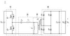
- FIG. 1is a circuit diagram showing an example of a power supply device including an LLC resonant converter.
- Figure 2is a cross-sectional view of a conventional transformer.
- Figure 3is a plan view showing the bobbin of a conventional transformer.
- Figure 4is a cross-sectional view of a transformer according to an embodiment of the present disclosure.
- Figure 5is a diagram showing the bobbin of a transformer according to an embodiment of the present disclosure.
- FIG. 6is a diagram showing a primary coil and a secondary coil wound around the bobbin shown in FIG. 5.
- Figure 7is an example diagram showing how the secondary coil of the transformer according to the first embodiment of the present disclosure is connected to the power board.
- Figure 8is an example diagram showing how the secondary coil of the transformer according to the second embodiment of the present disclosure is connected to the power board.
- connectionbetween components includes not only direct connection of components, but also indirect connection through at least one other component, unless otherwise specified.
- Various electronic devicessuch as TVs include power supplies, and these power supplies may use LLC topology. That is, an LLC resonant converter can be used in the power supply.
- FIG. 1is a circuit diagram showing an example of a power supply device including an LLC resonant converter.
- the LLC resonant converter 1may include a square wave generator 10, a resonant circuit 20, and a rectifier circuit 40.
- the square wave generator 10includes a plurality of switch elements, and the plurality of switch elements may be turned on alternately to generate a square wave voltage.
- the resonance circuit 20is composed of a resonance capacitor, a resonance inductance, and a transformer 30, and can filter high-order harmonic currents. In other words, the resonance circuit 20 can only allow sinusoidal current to flow even when a square wave voltage is applied.
- the resonance circuit 20includes a transformer 30, which is a device that changes the value of alternating current voltage or current using electromagnetic induction.
- the rectifier circuit 40includes a rectifier diode and a capacitor, and can rectify AC current through these to generate DC voltage.
- the rectifier circuit 40may be a synchronous rectifier (SR) circuit, but since this is only an example, it is reasonable that the circuit is not limited thereto.
- SRsynchronous rectifier
- the square wave generator 10 and the rectifier circuit 40are merely examples, they may be formed in configurations other than those shown in FIG. 1 .
- the present disclosureseeks to propose a method for miniaturizing the transformer 30, which occupies a large volume in a power supply device.
- the present disclosurecan provide a miniaturized transformer 30 by increasing the operating frequency of the LLC resonant converter 1.
- the resonance frequency of the LLC resonant converter 1increases, the peak current decreases, and thus the magnetizing inductance (Lm) of the transformer 30 may decrease. Accordingly, the number of turns of the core and the first and second coils can be reduced, making it possible to reduce the size of the transformer 30.
- the resonance frequency of the LLC resonant converter (1)increases from 100kHz to 250kHz
- the magnetizing inductance (Lm)decreases from 210uH to 100uH
- the primary coilis accordingly reduced from 24 turns to 12 turns
- the size of the transformer 30can be reduced by reducing the secondary coil from 2 turns to 1 turn.
- the LLC resonant converter 1was equipped with a plurality of transformers.
- the present disclosureseeks to reduce the size of the transformer 30 by implementing a plurality of transformers into one transformer 30.
- three transformers with an effective cross-sectional area (Ae) of the existing core of 144 eachwere used, and this is to be implemented with one transformer with a core effective cross-sectional area of 450.
- the winding window areabecomes narrow, which may cause heat generation problems in the first and second coils.
- the present disclosureseeks to propose a method for increasing the winding window area while minimizing the increase in volume of the core itself.
- an attemptis made to increase the actual winding window area while minimizing the increase in volume of the core itself by removing the bobbin within the winding window area.
- Figure 2is a cross-sectional view of a conventional transformer
- Figure 3is a diagram showing the bobbin of a conventional transformer.
- Conventional transformersare assembled on a bobbin 300, a primary coil 32 and a secondary coil 33 wound on the bobbin 300, and a bobbin 300 on which the primary coil 32 and the secondary coil 33 are wound. It may include a core 34 that is.
- the core 34is made of a ferrite material and may include an upper core member 34a and a lower core member 34b having an 'E' shape.
- the upper core member 34a and the lower core member 34bmay each be coupled to the upper and lower sides of the bobbin 10.
- a hollow portion (S1) in which the upper core member (34a) and the lower core member (34b) are in close contactmay be formed in the center of the bobbin 300.
- a first section bobbin 301 around which the primary coil 32 is woundis formed around the hollow portion S1, and a secondary coil 33 is wound with a gap S2 between the first section bobbin 301 and the gap S2.
- a second section bobbin 303may be formed.
- the first section bobbin 301surrounds the inside, top, and bottom of the primary coil 32
- the second section bobbin 302surrounds the secondary coil 32. It can surround the inside, top, and bottom of the coil 33. That is, according to the prior art, since at least a portion of the bobbin 300 occupies the winding window area of the core 34, the heat generation problem is aggravated, and there is a limit to increasing the size of the core 34 to increase the winding. there is.
- the present disclosureimproves the heat generation problem by securing the winding window area by providing a transformer that removes the bobbin within the winding window area of the core 34, and increases the thickness of the core 34 in the direction of the winding window area. We want to increase the power capacity while maintaining the actual volume of (34).
- FIG. 4is a cross-sectional view of a transformer according to an embodiment of the present disclosure
- FIG. 5is a diagram showing a bobbin of a transformer according to an embodiment of the present disclosure
- FIG. 6is a diagram showing a primary coil and a secondary coil in the bobbin shown in FIG. 5. This diagram shows a coil wound.
- the transformer 3000includes a bobbin 100, a primary coil 32 wound around the bobbin 100, a secondary coil 33 wound around the bobbin 100, and a core 34. It can be included.
- the core 34may include an upper core member 34a and a lower core member 34b coupled around the primary coil 32 and the secondary coil 33. That is, the upper core member 34a and lower core member 34b can be assembled on the upper and lower sides of the primary coil 32 and the secondary coil 33, respectively. Only the primary coil 32 and the secondary coil 33 may be disposed between the upper core member 34a and the lower core member 34b.
- the bobbin 100may include a first bobbin member 101 and a second bobbin member 102 that guide the winding areas of the primary coil 32 and the secondary coil 33 outside the core 34. there is. That is, the core 34 may be disposed between the first bobbin member 101 and the second bobbin member 102.
- the upper core member 34a and lower core member 34bmay be assembled between the first bobbin member 101 and the second bobbin member 102.
- the first bobbin member 101 and the second bobbin member 102can guide the area where the primary coil 32 and the secondary coil 33 are wound, respectively.
- each of the first bobbin member 101 and the second bobbin member 102has a groove (not shown) for guiding the area where the primary coil 32 is wound and the area where the secondary coil 33 is wound. ) or a partition wall (not shown) may be formed, but since this is only an example, it is reasonable that it is not limited thereto. That is, the first bobbin member 101 and the second bobbin member 102 have grooves (grooves) so that the primary coil 32 and the secondary coil 33 are arranged flat or spaced apart by a predetermined distance or more, as will be described later. (not shown) or a partition wall (not shown) may be formed.
- first bobbin member 101 and the second bobbin member 102have a primary coil 32 disposed inside the core 34, that is, between the upper core member 34a and the lower core member 34b.
- Each of the secondary coils 33can be guided to be placed flat. Referring to FIG. 6, it can be seen that the primary coil 32 and the secondary coil 33 are arranged flat in the y-direction.
- first bobbin member 101 and the second bobbin member 102have a primary coil 32 and a secondary coil (33) so that the primary coil 32 and the secondary coil 33 are spaced apart from each other by a predetermined distance or more.
- 33)can guide the winding area. That is, when the primary coil 32 and the secondary coil 33 are wound along a groove (not shown) or a partition (not shown) formed in the first bobbin member 101 and the second bobbin member 102, The primary coil 32 and the secondary coil 33 may be arranged to be spaced apart from each other by a predetermined distance or more. As shown in FIGS. 4 and 6, a gap S3 may be formed between the primary coil 32 and the secondary coil 33.
- leakage inductancecan be created by separating the primary coil 32 and the secondary coil 33 by a predetermined distance or more, and the primary coil Since (32) and the secondary coil 33 are arranged flat, the separation distance between the primary coil 32 and the secondary coil 33 is not fixed, which has the advantage of minimizing the problem of variable leakage inductance. That is, the first bobbin member 101 and the second bobbin member 102 disposed outside the core 34 guide the primary coil 32 and the secondary coil 33 to be spaced apart by a predetermined distance and arranged flatly. This has the advantage of being able to generate stable leakage inductance.
- first bobbin member 101 and the second bobbin member 102may be formed in a structure in which the lower plate 1010 and the upper plate 1020 are combined, but this is only an example and is not limited thereto. It is valid.
- the primary coil 32may be arranged flatly between the first bobbin member 101 and the second bobbin member 102, and may be arranged curved on the first bobbin member 101 and the second bobbin member 102. there is.
- the primary coil 32is arranged flatly between the upper core member 34a and the lower core member 34b, and is arranged curved along a semicircular shape on the first bobbin member 101 and the second bobbin member 102. It can be.
- the secondary coil 33may be arranged flatly between the first bobbin member 101 and the second bobbin member 102.
- the secondary coil 33may be arranged flat between the upper core member 34a and the lower core member 34b.
- the flat portion of the secondary coil 33may be referred to as the flat winding portion 331, but this name is only an example for convenience of explanation, and is not limited thereto.
- the secondary coil 33 disposed on the first bobbin member 101may be disposed in a curved shape.
- the secondary coil 33may be arranged along a semicircular shape on the first bobbin member 101.
- the secondary coil 33 disposed on the first bobbin member 101may be a curved part (not shown) connecting the flat winding parts 331 with the primary coil 31 interposed therebetween.
- the secondary coil 33 disposed on the second bobbin member 102may be a connection portion 332 connected to the power board 500 (see FIG. 7). That is, the connection part 332 may extend from the flat winding part 331 and be dipped into the power board 500 (see FIG. 7).
- the secondary coil 33extends from the flat winding part 331, the curved part (not shown) between the flat winding parts 331, and the flat winding part 331 to form the power board 500, FIG. 7) may include at least one of the connection portions 332 connected to the terminal.
- FIG. 7is an example diagram showing how the secondary coil of the transformer according to the first embodiment of the present disclosure is connected to the power board
- FIG. 8is an example diagram showing the secondary coil of the transformer according to the second embodiment of the present disclosure being connected to the power board. This is an example drawing showing how it is connected.
- the bobbin 100is not shown for convenience of explanation. However, since this is only for convenience of explanation, it is reasonable that the invention is not limited thereto.
- connection part 332 of the secondary coil 33may include a first connection part 332a and a second connection part 332b.
- One of the first connection part 332a and the second connection part 332bmay be one end of the secondary coil 33, and the other may be the other end of the secondary coil 33. That is, the first connection part 332a may be one end of the secondary coil 33, and the second connection part 332b may be the other end of the secondary coil 33.
- the secondary coil 33is formed of 2-layers disposed on the upper and lower layers, respectively, and the first connection portion corresponding to the secondary coil 33 disposed on the upper layer (332a) and the second connection portion (332b), the first connection portion (332a) and the second connection portion (332b) corresponding to the secondary coil 33 disposed in the lower layer are shown. That is, in the examples of FIGS. 7 and 8, two first connection parts 332a and two second connection parts 332b are shown, but since this is only an example, it is reasonable that the present invention is not limited thereto.
- the first connection part 332a and the second connection part 332bmay be connected to the power board 500 by a method such as soldering.
- a dipping area 501 connected to the first connection part 332a and the second connection part 332bmay be formed in the power board 500.
- a plurality of strandsmay be dipped together. That is, conventionally, each of the secondary coils 33 was soldered to a pin and fastened to the PCB. However, in this case, unsold parts were generated, causing heat generation problems, and there were disadvantages in that contact resistance increased. Accordingly, according to an embodiment of the present disclosure, the secondary coil 33 has a plurality of strands dipped directly into the PCB in the form of a flat winding, which has the advantage of minimizing the occurrence of unpaid portions and minimizing contact resistance problems. .
- the first connection part 332a and the second connection part 332bmay be connected to the power board 500 so as to be adjacent to the rectifier circuit 40.
- the rectifier circuit 40operates by sensing the voltage that passes the PCB pattern at the output of the transformer 3000.
- the PCB patterncauses an inductance component, which may affect the sensing of the rectifier circuit 40 and cause unstable operation. . Therefore, by arranging at least one of the first connection part 332a and the second connection part 332b adjacent to the rectifier circuit 40, the leakage inductance component due to the PCB pattern can be minimized and operation stability can be improved.
- both the first connection part 332a and the second connection part 332bcan be placed adjacent to the rectifier circuit 40. That is, both the first connection part 332a and the second connection part 332b can be dipped in the power board 500 so that the separation distance from the rectifier circuit 40 is minimized.
- the length of the first connection part 332a and the length of the second connection part 332bmay be different.
- One of the first connection part 332a and the second connection part 332bmay be connected closer to the rectifier circuit 40 than the other one.
- the length d1 of the second connection part 332bis longer than the length d2 of the first connection part 332a. That is, in the case of the secondary coil 33 disposed on the upper layer, the dipping area 501 in which the second connection part 332b is connected to the power board 500 is a dipping area in which the first connection part 332a is connected to the power board 500. It can be seen that it is closer to the rectifier circuit 40 than the area 501.
- the length d1 of the first connection part 332ais longer than the length d2 of the second connection part 332b. That is, in the case of the secondary coil 33 disposed in the lower layer, the dipping area 501 in which the first connection part 332a is connected to the power board 500 is a dipping area in which the second connection part 332b is connected to the power board 500. It can be seen that it is closer to the rectifier circuit 40 than the area 501.
- the transformer 3000is positioned between the other one and the rectifier circuit 40. It may further include a heat dissipation unit 400 disposed in . Through this, there is an advantage of increasing the heat dissipation effect for the output of the secondary coil 33.
Landscapes
- Engineering & Computer Science (AREA)
- Power Engineering (AREA)
- Dc-Dc Converters (AREA)
Abstract
Description
Translated fromKorean본 개시는 트랜스포머 및 이를 포함하는 LLC 공진형 컨버터에 관한 것이다.The present disclosure relates to a transformer and an LLC resonant converter including the same.
고효율(High Efficiency) 및 고전력밀도(High power density) 구현을 위해 전원 공급 장치에 ZVS(Zero Voltage Switching) 동작이 가능한 LLC 공진형 컨버터의 사용이 증가하는 추세이다.In order to realize high efficiency and high power density, the use of LLC resonant converters capable of ZVS (Zero Voltage Switching) operation in power supplies is increasing.
종래 LLC 공진형 컨버터는 제어 동작 IC 및 스위칭 장치의 특성을 고려하여 주로 80~120kHz의 동작 주파수를 사용하였다.Conventional LLC resonant converters mainly used an operating frequency of 80 to 120 kHz, considering the characteristics of the control operation IC and switching device.
그런데, 최근 TV의 해상도가 4K/8K로 발전하면서 동작 주파수가 커지고, 이러한 TV의 전원 공급 장치는 파워 용량이 커지게 되고, 이에 따라 종래와 동일 방식으로 설계 시 크기가 커지는 문제가 있다.However, recently, as the resolution of TVs has developed to 4K/8K, the operating frequency has increased, and the power capacity of the power supply devices of these TVs has increased, and accordingly, there is a problem of increasing the size when designing in the same manner as before.
본 개시는 LLC 공진형 컨버터에서 많은 부피를 차지하는 트랜스포머를 소형화하는 방안을 제안하고자 한다.This disclosure seeks to propose a method of miniaturizing a transformer that occupies a large volume in an LLC resonant converter.
본 개시의 실시 예에 따른 LLC 공진형 컨버터는 구형파 발생기, 공진 커패시터, 공진 인덕턴스 및 트랜스포머로 구성되는 공진 회로, 및 정류 회로를 포함하고, 트랜스포머는 보빈, 보빈에 감기는 1차 코일, 보빈에 감기는 2차 코일, 및 1차 코일과 2차 코일의 주변에서 결합되는 상부코어부재와 하부코어부재를 포함하는 코어를 포함하고, 보빈은 코어의 바깥에서 1차 코일과 2차 코일의 권선 영역을 안내하는 제1 보빈부재와 제2 보빈부재를 포함할 수 있다.The LLC resonant converter according to an embodiment of the present disclosure includes a resonance circuit consisting of a square wave generator, a resonance capacitor, a resonance inductance, and a transformer, and a rectifier circuit, and the transformer includes a bobbin, a primary coil wound on the bobbin, and a primary coil wound on the bobbin. Includes a core including a secondary coil and an upper core member and a lower core member coupled around the primary coil and the secondary coil, and the bobbin connects the winding area of the primary coil and the secondary coil outside the core. It may include a first bobbin member and a second bobbin member for guiding.
본 개시의 실시 예에 따른 트랜스포머는 보빈, 보빈에 감기는 1차 코일, 보빈에 감기는 2차 코일, 및 1차 코일과 2차 코일의 주변에서 결합되는 상부코어부재와 하부코어부재를 포함하는 코어를 포함하고, 보빈은 코어의 바깥에서 1차 코일과 2차 코일의 권선 영역을 안내하는 제1 보빈부재와 제2 보빈부재를 포함할 수 있다.The transformer according to an embodiment of the present disclosure includes a bobbin, a primary coil wound around the bobbin, a secondary coil wound around the bobbin, and an upper core member and a lower core member coupled around the primary coil and the secondary coil. It includes a core, and the bobbin may include a first bobbin member and a second bobbin member that guide the winding areas of the primary coil and the secondary coil outside the core.
상부코어부재와 하부코어부재는 제1 보빈부재와 제2 보빈부재 사이에서 조립될 수 있다.The upper core member and the lower core member may be assembled between the first bobbin member and the second bobbin member.
제1 보빈부재와 제2 보빈부재는 상부코어부재와 하부코어부재 사이에 배치되는 1차 코일과 2차 코일 각각이 플랫하게 배치되도록 안내할 수 있다.The first bobbin member and the second bobbin member can guide each of the primary and secondary coils disposed between the upper core member and the lower core member to be arranged flat.
1차 코일과 2차 코일은 소정 거리 이상 이격되어 배치될 수 있다.The primary coil and the secondary coil may be arranged to be spaced apart from each other by a predetermined distance or more.
2차 코일은 플랫하게 배치되는 플랫 권선부, 플랫 권선부에서 연장되어 파워 보드에 디핑되는 연결부를 포함할 수 있다.The secondary coil may include a flat winding portion disposed flat and a connection portion extending from the flat winding portion and dipping to the power board.
연결부는 적어도 제1 연결부 및 제2 연결부를 포함하고, 제1 연결부의 길이와 제2 연결부의 길이는 상이할 수 있다.The connection part includes at least a first connection part and a second connection part, and the length of the first connection part and the length of the second connection part may be different.
제1 연결부와 제2 연결부 중 어느 하나의 연결부는 다른 하나의 연결부 보다 정류 회로에 가깝게 연결될 수 있다.One of the first connection and the second connection may be connected closer to the rectifier circuit than the other connection.
트랜스포머는 다른 하나의 연결부와 정류 회로 사이에 배치되는 방열부를 더 포함할 수 있다.The transformer may further include a heat dissipation portion disposed between the other connection portion and the rectifier circuit.
상부코어부재와 상기하부코어부재 사이에는 1차 코일과 2차 코일만 배치될 수 있다.Only the primary coil and secondary coil may be disposed between the upper core member and the lower core member.
본 개시의 실시 예에 따르면, 보빈은 코어의 바깥에서 상기 1차 코일과 상기 2차 코일의 권선 영역을 안내하는 제1 보빈부재와 제2 보빈부재로 구성되는 바, 코어 내 권선 창 면적을 늘려 발열 문제를 개선 가능하고, 코어의 두께를 증가시킴으로써 코어의 실제 부피를 늘리지 않으면서 파워 용량을 늘릴 수 있는 이점이 있다.According to an embodiment of the present disclosure, the bobbin is composed of a first bobbin member and a second bobbin member that guide the winding areas of the primary coil and the secondary coil from the outside of the core, thereby increasing the winding window area within the core. There is an advantage in that the heat generation problem can be improved and the power capacity can be increased without increasing the actual volume of the core by increasing the thickness of the core.
본 개시의 실시 예에 따르면, 1차 코일 및 2차 코일 사이를 이격시켜 플랫하게 배치함으로써, 안정적인 누설 인덕턴스의 생성이 가능한 이점이 있다.According to an embodiment of the present disclosure, there is an advantage in that a stable leakage inductance can be generated by spacing the primary coil and the secondary coil and arranging them flatly.
본 개시의 실시 예에 따르면, 2차 코일에서 파워 보드에 연결되는 연결부를 정류 회로와 가깝게 배치하여 PCB pattern에 의한 누설 인덕턴스 성분을 최소화하여, 동작 안정성을 향상시키는 이점이 있다.According to an embodiment of the present disclosure, there is an advantage in improving operational stability by minimizing the leakage inductance component due to the PCB pattern by arranging the connection portion connected to the power board from the secondary coil close to the rectifier circuit.
본 개시의 실시 예에 따르면, 2차 코일에서 파워 보드에 연결되는 연결부의 길이를 상이하게 형성하여, 방열부 등의 부품 추가가 가능한 이점이 있다.According to an embodiment of the present disclosure, there is an advantage that parts such as a heat dissipation part can be added by forming the length of the connection part connected from the secondary coil to the power board to be different.
도 1은 LLC 공진형 컨버터를 포함하는 전원공급장치의 일 예가 도시된 회로도이다.1 is a circuit diagram showing an example of a power supply device including an LLC resonant converter.
도 2는 종래 트랜스포머의 단면도이다.Figure 2 is a cross-sectional view of a conventional transformer.
도 3은 종래 트랜스포머의 보빈이 도시된 평면도이다.Figure 3 is a plan view showing the bobbin of a conventional transformer.
도 4는 본 개시의 실시 예에 따른 트랜스포머의 단면도이다.Figure 4 is a cross-sectional view of a transformer according to an embodiment of the present disclosure.
도 5는 본 개시의 실시 예에 따른 트랜스포머의 보빈이 도시된 도면이다.Figure 5 is a diagram showing the bobbin of a transformer according to an embodiment of the present disclosure.
도 6은 도 5에 도시된 보빈에 1차 코일과 2차 코일이 감긴 모습이 도시된 도면이다.FIG. 6 is a diagram showing a primary coil and a secondary coil wound around the bobbin shown in FIG. 5.
도 7은 본 개시의 제1 실시 예에 따른 트랜스포머의 2차 코일이 파워 보드에 연결되는 모습을 나타내는 예시 도면이다.Figure 7 is an example diagram showing how the secondary coil of the transformer according to the first embodiment of the present disclosure is connected to the power board.
도 8은 본 개시의 제2 실시 예에 따른 트랜스포머의 2차 코일이 파워 보드에 연결되는 모습을 나타내는 예시 도면이다.Figure 8 is an example diagram showing how the secondary coil of the transformer according to the second embodiment of the present disclosure is connected to the power board.
이하, 첨부된 도면을 참조하여 본 개시에 따른 바람직한 실시 예를 상세히 설명하기로 한다. 도면에서 동일한 참조부호는 동일 또는 유사한 구성요소를 가리키는 것으로 사용된다.Hereinafter, preferred embodiments according to the present disclosure will be described in detail with reference to the attached drawings. In the drawings, identical reference numerals are used to indicate identical or similar components.
이하의 설명에서 사용되는 구성요소에 대한 접미사 "모듈" 및 "부"는 명세서 작성의 용이함만이 고려되어 부여되거나 혼용되는 것으로서, 그 자체로 서로 구별되는 의미 또는 역할을 갖는 것은 아니다.The suffixes “module” and “part” for components used in the following description are given or used interchangeably only for the ease of preparing the specification, and do not have distinct meanings or roles in themselves.
이하의 설명에서 구성요소 간에 “연결”된다는 것은 별도로 명시되지 않는 한 구성요소들이 직접 연결되는 것뿐만 아니라, 적어도 하나의 다른 구성요소를 통해 간접적으로 연결되는 것을 포함한다.In the following description, “connected” between components includes not only direct connection of components, but also indirect connection through at least one other component, unless otherwise specified.
TV 등과 같은 각종 전자기기는 전원공급장치를 포함하는데, 이러한 전원공급장치는 LLC 토폴로지를 사용할 수 있다. 즉, 전원공급장치에 LLC 공진형 컨버터가 사용될 수 있다.Various electronic devices such as TVs include power supplies, and these power supplies may use LLC topology. That is, an LLC resonant converter can be used in the power supply.
도 1은 LLC 공진형 컨버터를 포함하는 전원공급장치의 일 예가 도시된 회로도이다.1 is a circuit diagram showing an example of a power supply device including an LLC resonant converter.
도 1을 참고하면, LLC 공진형 컨버터(1)는 구형파 발생기(10), 공진 회로(20) 및 정류 회로(40)를 포함할 수 있다.Referring to FIG. 1, the LLC
구형파 발생기(10)는 복수개의 스위치 소자를 포함하고, 복수개의 스위치 소자가 교번적으로 온되어 구형파 전압을 발생시킬 수 있다.The
공진 회로(20)는 공진 커패시터, 공진 인덕턴스 및 트랜스포머(30)로 구성되어, 높은 차수의 고조파 전류를 필터링할 수 있다. 즉, 공진 회로(20)는 구형파 전압이 인가되어도 정현파 전류만 흐르게 할 수 있다.The
공진 회로(20)는 트랜스포머(30)를 포함하는데, 트랜스포머(30)는 전자기유도현상을 이용하여 교류의 전압이나 전류의 값을 변화시키는 장치이다.The
정류 회로(40)는 정류 다이오드와 커패시터를 포함하고, 이들을 통해 AC 전류를 정류하여 DC 전압을 발생시킬 수 있다. 일 실시 예에 따르면, 정류 회로(40)는 SR(Synchronous Rectifier) 회로일 수 있으나, 이는 예시에 불과하므로, 이에 제한되지 않음이 타당하다.The
구형파 발생기(10) 및 정류 회로(40) 등은 예시에 불과하므로, 도 1에 도시된 구성 외 다른 구성으로 형성될 수도 있다.Since the
한편, 전자기기의 부하가 증가할 경우 전원공급장치의 파워 용량이 커지게 되고, 이에 따라 전원공급장치의 크기가 증가하는 문제가 발생할 수 있다. 이에, 본 개시는 전원공급장치에서 큰 부피를 차지하는 트랜스포머(30)의 소형화 방안을 제안하고자 한다.Meanwhile, when the load of an electronic device increases, the power capacity of the power supply device increases, which may lead to an increase in the size of the power supply device. Accordingly, the present disclosure seeks to propose a method for miniaturizing the
일 실시 예에 따르면, 본 개시는 LLC 공진형 컨버터(1)의 동작 주파수를 증가시켜 소형화된 트랜스포머(30)를 제공할 수 있다.According to one embodiment, the present disclosure can provide a miniaturized
구체적으로, LLC 공진형 컨버터(1)의 공진 주파수가 증가하면, 피크 전류가 감소하고, 이에 따라 트랜스포머(30)의 자화 인덕턴스(Lm)가 감소할 수 있다. 따라서, 코어 및 1, 2차 코일의 턴 수를 줄일 수 있는 바, 트랜스포머(30)의 크기 축소가 가능하다. 예를 들어, LLC 공진형 컨버터(1)의 공진 주파수가 100kHz에서 250kHz로 증가할 경우, 자화 인덕턴스(Lm)는 210uH에서 100uH로 감소하고, 이에 다라 1차 코일을 24턴에서 12턴으로 줄이고, 2차 코일을 2턴에서 1턴으로 줄여 트랜스포머(30)의 크기를 줄일 수 있다.Specifically, when the resonance frequency of the
한편, 종래에는 LLC 공진형 컨버터(1)에 복수개의 트랜스포머가 구비되곤 했다. 본 개시는 복수개의 트랜스포머를 한 개의 트랜스포머(30)로 구현함으로써, 트랜스포머(30)의 크기를 축소시키고자 한다. 예를 들어, 기존 코어의 유효 단면적(Ae: Effective corss-sectional area)이 각각 144인 3개의 트랜스포머가 사용되었는데, 이를 코어의 유효 단면적이 450인 1개의 트랜스포머로 구현하고자 한다. 그런데, 이 경우 권선 창 면적이 좁아져 1, 2차 코일에서 발열 문제가 발생할 수 있다. 또한, 기존 코어 1개와 제안하고자 하는 코어 1개의 사이즈만 비교할 경우, 코어의 사이즈가 커지는 바 크랙이나 휨이 발생할 우려가 있다. 따라서, 본 개시는 코어 자체의 부피 증가를 최소화하면서 권선 창 면적을 늘릴 수 있는 방안을 제안하고자 한다. 일 실시 예에 따르면, 권선 창 면적 내 보빈을 제거함으로써 코어 자체의 부피 증가를 최소화하면서 실제 권선 창 면적을 늘리고자 한다. 이를 설명하기에 앞서, 종래 트랜스포머의 구조에 대해 설명한다.Meanwhile, conventionally, the LLC
도 2는 종래 트랜스포머의 단면도이고, 도 3은 종래 트랜스포머의 보빈이 도시된 도면이다.Figure 2 is a cross-sectional view of a conventional transformer, and Figure 3 is a diagram showing the bobbin of a conventional transformer.
종래 트랜스포머는 보빈(300), 보빈(300)에 감기는 1차 코일(32)과 2차 코일(33), 1차 코일(32)과 2차 코일(33)이 감긴 보빈(300)에 조립되는 코어(34)를 포함할 수 있다.Conventional transformers are assembled on a
코어(34)는 페라이트 재질로 형성되고, 'E'자 형상을 갖는 상부코어부재(34a) 및 하부코어부재(34b)를 포함할 수 있다. 상부코어부재(34a) 및 하부코어부재(34b) 각각이 보빈(10)의 상측과 하측에서 결합될 수 있다.The
보빈(300)의 중심부에는 상부코어부재(34a)와 하부코어부재(34b)가 밀착되는 중공부(S1)가 형성될 수 있다. 중공부(S1)의 주변에는 1차 코일(32)이 감기는 제1 섹션 보빈(301)이 형성되고, 제1 섹션 보빈(301)과 갭(S2)을 두고 2차 코일(33)이 감기는 제2 섹션 보빈(303)이 형성될 수 있다.A hollow portion (S1) in which the upper core member (34a) and the lower core member (34b) are in close contact may be formed in the center of the
도 2의 단면도에 도시된 바와 같이, 코어(34)의 안쪽에서 제1 섹션 보빈(301)이 1차 코일(32)의 내측과 상부 및 하부를 둘러싸고, 제2 섹션 보빈(302)이 2차 코일(33)의 내측과 상부 및 하부를 둘러쌀 수 있다. 즉, 종래에 따르면 보빈(300)의 적어도 일부가 코어(34)의 권선 창 면적을 차지하기 때문에 발열 문제가 심해지는 문제가 있고, 권선을 늘리기 위해 코어(34)의 크기를 증가시켜야 하는 한계가 있다.As shown in the cross-sectional view of FIG. 2, inside the
따라서, 본 개시는 코어(34)의 권선 창 면적 내 보빈을 제거한 트랜스포머를 제공함으로써, 권선 창 면적을 확보하여 발열 문제를 개선하고, 권선 창 면적 방향으로의 코어(34)의 두께를 증가시킴으로써 코어(34)의 실제 부피를 유지하면서 파워 용량을 늘리고자 한다.Therefore, the present disclosure improves the heat generation problem by securing the winding window area by providing a transformer that removes the bobbin within the winding window area of the core 34, and increases the thickness of the core 34 in the direction of the winding window area. We want to increase the power capacity while maintaining the actual volume of (34).
도 4는 본 개시의 실시 예에 따른 트랜스포머의 단면도이고, 도 5는 본 개시의 실시 예에 따른 트랜스포머의 보빈이 도시된 도면이고, 도 6은 도 5에 도시된 보빈에 1차 코일과 2차 코일이 감긴 모습이 도시된 도면이다.FIG. 4 is a cross-sectional view of a transformer according to an embodiment of the present disclosure, FIG. 5 is a diagram showing a bobbin of a transformer according to an embodiment of the present disclosure, and FIG. 6 is a diagram showing a primary coil and a secondary coil in the bobbin shown in FIG. 5. This diagram shows a coil wound.
본 개시의 실시 예에 따른 트랜스포머(3000)는 보빈(100), 보빈(100)에 감기는 1차 코일(32), 보빈(100)에 감기는 2차 코일(33) 및 코어(34)를 포함할 수 있다.The
코어(34)는 1차 코일(32)과 2차 코일(33)의 주변에서 결합되는 상부코어부재(34a)와 하부코어부재(34b)를 포함할 수 있다. 즉, 상부코어부재(34a)와 하부코어부재(34b)은 각각 1차 코일(32)과 2차 코일(33)의 상측과 하측에서 조립될 수 있다. 상부코어부재(34a)와 하부코어부재(34b) 사이에는 1차 코일(32)과 2차 코일(33)만 배치될 수 있다.The core 34 may include an
보빈(100)은 코어(34)의 바깥에서 1차 코일(32)과 2차 코일(33)의 권선 영역을 안내하는 제1 보빈부재(101)와 제2 보빈부재(102)를 포함할 수 있다. 즉, 코어(34)는 제1 보빈부재(101)와 제2 보빈부재(102) 사이에 배치될 수 있다. 상부코어부재(34a)와 하부코어부재(34b)는 제1 보빈부재(101)와 제2 보빈부재(102) 사이에서 조립될 수 있다.The
제1 보빈부재(101)와 제2 보빈부재(102)는 1차 코일(32)과 2차 코일(33) 각각이 감기는 영역을 안내할 수 있다. 예를 들어, 제1 보빈부재(101)와 제2 보빈부재(102) 각각에는 1차 코일(32)이 감기는 영역과 2차 코일(33)이 감기는 영역을 안내하기 위한 홈(미도시) 또는 격벽(미도시)이 형성되어 있을 수 있으나, 이는 예시에 불과하므로, 이에 제한되지 않음이 타당하다. 즉, 제1 보빈부재(101)와 제2 보빈부재(102)는 후술하는 바와 같이 1차 코일(32)과 2차 코일(33)이 플랫하게 배치되거나, 소정 거리 이상 이격되어 배치되도록 홈(미도시)이나 격벽(미도시)이 형성되어 있을 수 있다.The
특히, 제1 보빈부재(101)와 제2 보빈부재(102)는 코어(34)의 내측, 즉 상부코어부재(34a)와 하부코어부재(34b) 사이에 배치되는 1차 코일(32)과 2차 코일(33) 각각이 플랫하게 배치되도록 안내할 수 있다. 도 6을 참고하면, 1차 코일(32)과 2차 코일(33)이 y방향으로 평평하게 배치된 것을 확인할 수 있다.In particular, the
또한, 제1 보빈부재(101)와 제2 보빈부재(102)는 1차 코일(32)과 2차 코일(33)이 소정 거리 이상 이격되어 배치되도록 1차 코일(32)과 2차 코일(33)이 감기는 영역을 안내할 수 있다. 즉, 제1 보빈부재(101)와 제2 보빈부재(102)에 형성된 홈(미도시) 또는 격벽(미도시) 등을 따라 1차 코일(32)과 2차 코일(33)이 감길 경우, 1차 코일(32)과 2차 코일(33)은 소정 거리 이상 이격되어 배치될 수 있다. 도 4 및 도 6에 도시된 바와 같이, 1차 코일(32)과 2차 코일(33) 사이에는 틈(S3)이 형성될 수 있다.In addition, the
이와 같이, 본 개시의 실시 예에 따르면, 섹션 보빈이 없어도 1차 코일(32)과 2차 코일(33)이 소정 거리 이상 이격되는 바 누설 인덕턴스(leakage inductance)의 생성이 가능하며, 1차 코일(32)과 2차 코일(33)이 플랫하게 배치되는 바 1차 코일(32)과 2차 코일(33) 사이의 이격 거리가 고정되지 않아 누설 인덕턴스가 가변되는 문제를 최소화하는 이점이 있다. 즉, 코어(34)의 바깥쪽에 배치되는 제1 보빈부재(101)와 제2 보빈부재(102)로 1차 코일(32)과 2차 코일(33)이 소정 거리 이격되어 플랫하게 배치되도록 가이드함으로써 안정적인 누설 인덕턴스의 생성이 가능한 이점이 있다.As such, according to the embodiment of the present disclosure, even without a section bobbin, leakage inductance can be created by separating the
한편, 제1 보빈부재(101)와 제2 보빈부재(102)는 각각 하판부(1010)와 상판부(1020)가 결합되는 구조로 형성될 수 있으나, 이는 예시에 불과하므로, 이에 제한되지 않음이 타당하다.Meanwhile, the
1차 코일(32)은 제1 보빈부재(101)와 제2 보빈부재(102) 사이에서 플랫하게 배치되고, 제1 보빈부재(101)와 제2 보빈부재(102) 상에서는 굽어서 배치될 수 있다. 1차 코일(32)은 상부코어부재(34a)와 하부코어부재(34b) 사이에서 플랫하게 배치되고, 제1 보빈부재(101)와 제2 보빈부재(102) 상에서 반원 형상을 따라 굴곡지게 배치될 수 있다.The
2차 코일(33)은 제1 보빈부재(101)와 제2 보빈부재(102) 사이에서 플랫하게 배치될 수 있다. 상부코어부재(34a)와 하부코어부재(34b) 사이에서 2차 코일(33)은 플랫하게 배치될 수 있다. 2차 코일(33) 중 플랫하게 배치되는 부분을 플랫 권선부(331)라고 명할 수 있으나, 이러한 명칭은 설명의 편의를 위한 예시에 불과하므로, 이에 제한되지 않음이 타당하다.The
그리고, 제1 보빈부재(101) 상에 배치되는 2차 코일(33)은 굽은 형태로 배치될 수 있다. 예를 들어, 제1 보빈부재(101) 상에서 2차 코일(33)은 반원 형상을 따라 배치될 수 있다. 제1 보빈부재(101) 상에 배치되는 2차 코일(33)은 1차 코일(31)을 사이에 두고 있는 플랫 권선부(331)들을 연결하는 굴곡부(미도시)일 수 있다.Additionally, the
제2 보빈부재(102) 상에 배치되는 2차 코일(33)은 파워 보드(500, 도 7 참고)에 연결되는 연결부(332)일 수 있다. 즉, 연결부(332)는 플랫 권선부(331)에서 연장되어 파워 보드(500, 도 7 참고)에 디핑될 수 있다.The
즉, 2차 코일(33)은 플랫하게 배치되는 플랫 권선부(331), 플랫 권선부(331)들 사이의 굴곡부(미도시), 플랫 권선부(331)에서 연장되어 파워 보드(500, 도 7 참고)에 연결되는 연결부(332) 중 적어도 하나를 포함할 수 있다.That is, the
다음으로, 도 7 및 도 8을 참고하여, 본 개시의 실시 예에 따른 트랜스포머의 2차 코일이 파워 보드에 연결되는 모습에 대해 설명한다.Next, with reference to FIGS. 7 and 8, how the secondary coil of the transformer according to an embodiment of the present disclosure is connected to the power board will be described.
도 7은 본 개시의 제1 실시 예에 따른 트랜스포머의 2차 코일이 파워 보드에 연결되는 모습을 나타내는 예시 도면이고, 도 8은 본 개시의 제2 실시 예에 따른 트랜스포머의 2차 코일이 파워 보드에 연결되는 모습을 나타내는 예시 도면이다.FIG. 7 is an example diagram showing how the secondary coil of the transformer according to the first embodiment of the present disclosure is connected to the power board, and FIG. 8 is an example diagram showing the secondary coil of the transformer according to the second embodiment of the present disclosure being connected to the power board. This is an example drawing showing how it is connected.
도 7 및 도 8에서는 설명의 편의를 위해 보빈(100)을 도시하지 않았으나, 이는 설명의 편의를 위한 것에 불과하므로, 이에 제한되지 않음이 타당하다.In FIGS. 7 and 8 , the
먼저, 2차 코일(33)의 연결부(332)는 제1 연결부(332a)와 제2 연결부(332b)를 포함할 수 있다. 제1 연결부(332a)와 제2 연결부(332b) 중 어느 하나는 2차 코일(33)의 일단이고, 다른 하나는 2차 코일(33)의 타단일 수 있다. 즉, 제1 연결부(332a)는 2차 코일(33)의 어느 한쪽 끝이고, 제2 연결부(332b)는 2차 코일(33)의 다른 한쪽 끝일 수 있다.First, the
도 7 및 도 8의 예시에서는 2차 코일(33)이 상층과 하층 각각에 배치되는 2-레이어(2-layer)로 형성된 바, 상층에 배치된 2차 코일(33)에 해당하는 제1 연결부(332a)와 제2 연결부(332b), 하층에 배치된 2차 코일(33)에 해당하는 제1 연결부(332a)와 제2 연결부(332b)가 도시되어 있다. 즉, 도 7 및 도 8의 예시에서는 제1 연결부(332a)와 제2 연결부(332b) 각각이 2개씩 도시되어 있으나, 이는 예시에 불과하므로, 이에 제한되지 않음이 타당하다.In the examples of FIGS. 7 and 8, the
제1 연결부(332a)와 제2 연결부(332b)는 납땜 등의 방법으로 파워 보드(500)와 연결될 수 있다. 파워 보드(500)에는 제1 연결부(332a)와 제2 연결부(332b)와 연결되는 디핑 영역(501)이 형성될 수 있다.The
일 실시 예에 따르면, 제1 연결부(332a)와 제2 연결부(332b)를 파워 보드(500)에 디핑 시, 복수의 가닥을 함께 디핑할 수 있다. 즉, 종래에는 2차 코일(33) 각각을 핀(pin)에 납땜하여 PCB에 체결하는 구조였으나, 이 경우 미납 부위가 발생하여 발열 문제가 있고, 접촉 저항이 증가하는 단점이 있다. 이에, 본 개시의 일 실시 예에 따르면, 2차 코일(33)은 플랫 권선의 형태로 복수의 가닥이 PCB에 직접 디핑되어, 미납 부위의 발생을 취소화하고 접촉 저항 문제를 최소화하는 이점이 있다.According to one embodiment, when dipping the
한편, 제1 연결부(332a)와 제2 연결부(332b) 중 적어도 하나는 정류 회로(40)와 인접하도록 파워 보드(500)에 연결될 수 있다. 정류 회로(40)는 트랜스포머(3000)의 출력에서 PCB pattern을 지난 전압을 센싱하여 동작하는 바, PCB pattern이 인덕턴스 성분을 유발하여 정류 회로(40)의 센싱에 영향을 주어 불안정한 동작을 유발할 수 있다. 따라서, 제1 연결부(332a)와 제2 연결부(332b) 중 적어도 하나를 정류 회로(40)와 인접하게 배치함으로써, PCB pattern에 의한 누설 인덕턴스 성분을 최소화하여, 동작 안정성을 향상시킬 수 있다.Meanwhile, at least one of the
제1 실시 예에 따르면, 도 7에 도시된 바와 같이, 제1 연결부(332a)와 제2 연결부(332b) 모두를 정류 회로(40)와 인접하게 배치할 수 있다. 즉, 제1 연결부(332a)와 제2 연결부(332b) 모두가 정류 회로(40)와의 이격 거리가 최소화되도록 파워 보드(500)에 디핑될 수 있다.According to the first embodiment, as shown in FIG. 7, both the
제2 실시 예에 따르면, 도 8에 도시된 바와 같이, 제1 연결부(332a)와 제2 연결부(332b) 중 어느 하나만 정류 회로(40)와 인접하게 배치할 수 있다. 즉, 제1 연결부(332a)의 길이와 제2 연결부(332b)의 길이는 상이할 수 있다. 제1 연결부(332a)와 제2 연결부(332b) 중 어느 하나는 다른 하나 보다 정류 회로(40)에 가깝게 연결될 수 있다.According to the second embodiment, as shown in FIG. 8, only one of the
구체적으로, 먼저 상층에 배치된 2차 코일(33)을 살펴보면, 제2 연결부(332b)의 길이(d1)가 제1 연결부(332a)의 길이(d2) 보다 긴 것을 확인할 수 있다. 즉, 상층에 배치된 2차 코일(33)의 경우, 제2 연결부(332b)가 파워 보드(500)에 연결된 디핑 영역(501)이 제1 연결부(332a)가 파워 보드(500)에 연결된 디핑 영역(501) 보다 정류 회로(40)에 가까운 것을 확인할 수 있다.Specifically, looking at the
하층에 배치된 2차 코일(33)을 살펴보면, 제1 연결부(332a)의 길이(d1)가 제2 연결부(332b)의 길이(d2) 보다 긴 것을 확인할 수 있다. 즉, 하층에 배치된 2차 코일(33)의 경우, 제1 연결부(332a)가 파워 보드(500)에 연결된 디핑 영역(501)이 제2 연결부(332b)가 파워 보드(500)에 연결된 디핑 영역(501) 보다 정류 회로(40)에 가까운 것을 확인할 수 있다.Looking at the
상술한 바와 같이, 제1 연결부(332a)와 제2 연결부(332b)중 어느 하나만을 정류 회로(40)에 가깝게 배치할 경우, 다른 하나와 정류 회로(40) 사이의 공간에 부품의 추가가 가능한 이점이 있다. 도 8의 예시를 참고하면, 트랜스포머(3000)는 제1 연결부(332a)와 제2 연결부(332b)중 어느 하나만을 정류 회로(40)에 가깝게 배치할 경우, 다른 하나와 정류 회로(40) 사이에 배치되는 방열부(400)를 더 포함할 수 있다. 이를 통해, 2차 코일(33)의 출력에 대한 방열 효과를 높일 수 있는 이점이 있다.As described above, when either the
이상의 설명은 본 개시의 기술 사상을 예시적으로 설명한 것에 불과한 것으로서, 본 개시가 속하는 기술 분야에서 통상의 지식을 가진 자라면 본 개시의 본질적인 특성에서 벗어나지 않는 범위에서 다양한 수정 및 변형이 가능할 것이다.The above description is merely an illustrative explanation of the technical idea of the present disclosure, and those skilled in the art will be able to make various modifications and variations without departing from the essential characteristics of the present disclosure.
따라서, 본 개시에 개시된 실시 예들은 본 개시의 기술 사상을 한정하기 위한 것이 아니라 설명하기 위한 것이고, 이러한 실시 예에 의하여 본 개시의 기술 사상의 범위가 한정되는 것은 아니다.Accordingly, the embodiments disclosed in the present disclosure are not intended to limit the technical idea of the present disclosure but are for illustrative purposes, and the scope of the technical idea of the present disclosure is not limited by these embodiments.
본 개시의 보호 범위는 아래의 청구범위에 의하여 해석되어야 하며, 그와 동등한 범위 내에 있는 모든 기술 사상은 본 개시의 권리범위에 포함되는 것으로 해석되어야 할 것이다.The scope of protection of this disclosure should be interpreted in accordance with the claims below, and all technical ideas within the equivalent scope should be interpreted as being included in the scope of rights of this disclosure.
Claims (10)
Translated fromKoreanPriority Applications (4)
| Application Number | Priority Date | Filing Date | Title |
|---|---|---|---|
| EP22961074.6AEP4583131A1 (en) | 2022-09-28 | 2022-09-28 | Transformer and llc resonant converter comprising same |
| CN202280100606.5ACN119998898A (en) | 2022-09-28 | 2022-09-28 | Transformer and LLC resonant converter including the transformer |
| PCT/KR2022/014600WO2024071471A1 (en) | 2022-09-28 | 2022-09-28 | Transformer and llc resonant converter comprising same |
| KR1020257008424AKR20250048784A (en) | 2022-09-28 | 2022-09-28 | Transformer and LLC resonant converter including same |
Applications Claiming Priority (1)
| Application Number | Priority Date | Filing Date | Title |
|---|---|---|---|
| PCT/KR2022/014600WO2024071471A1 (en) | 2022-09-28 | 2022-09-28 | Transformer and llc resonant converter comprising same |
Publications (1)
| Publication Number | Publication Date |
|---|---|
| WO2024071471A1true WO2024071471A1 (en) | 2024-04-04 |
Family
ID=90478240
Family Applications (1)
| Application Number | Title | Priority Date | Filing Date |
|---|---|---|---|
| PCT/KR2022/014600CeasedWO2024071471A1 (en) | 2022-09-28 | 2022-09-28 | Transformer and llc resonant converter comprising same |
Country Status (4)
| Country | Link |
|---|---|
| EP (1) | EP4583131A1 (en) |
| KR (1) | KR20250048784A (en) |
| CN (1) | CN119998898A (en) |
| WO (1) | WO2024071471A1 (en) |
Citations (5)
| Publication number | Priority date | Publication date | Assignee | Title |
|---|---|---|---|---|
| US20110037554A1 (en)* | 2009-08-12 | 2011-02-17 | Tsung-Yen Tsai | Vertical Double Deck Transformer for Power Supply |
| KR20120030883A (en)* | 2010-09-20 | 2012-03-29 | 삼성전기주식회사 | Transformer |
| KR101153515B1 (en)* | 2010-12-20 | 2012-06-12 | 삼성전기주식회사 | Transformer, Power module and Flat panel display device using the same |
| KR20170056160A (en)* | 2015-11-13 | 2017-05-23 | 김명덕 | Transformer for LLC Circuit |
| KR20220111029A (en)* | 2021-02-01 | 2022-08-09 | 엘지이노텍 주식회사 | Transformer and flat panel display device including the same |
- 2022
- 2022-09-28CNCN202280100606.5Apatent/CN119998898A/enactivePending
- 2022-09-28WOPCT/KR2022/014600patent/WO2024071471A1/ennot_activeCeased
- 2022-09-28KRKR1020257008424Apatent/KR20250048784A/enactivePending
- 2022-09-28EPEP22961074.6Apatent/EP4583131A1/enactivePending
Patent Citations (5)
| Publication number | Priority date | Publication date | Assignee | Title |
|---|---|---|---|---|
| US20110037554A1 (en)* | 2009-08-12 | 2011-02-17 | Tsung-Yen Tsai | Vertical Double Deck Transformer for Power Supply |
| KR20120030883A (en)* | 2010-09-20 | 2012-03-29 | 삼성전기주식회사 | Transformer |
| KR101153515B1 (en)* | 2010-12-20 | 2012-06-12 | 삼성전기주식회사 | Transformer, Power module and Flat panel display device using the same |
| KR20170056160A (en)* | 2015-11-13 | 2017-05-23 | 김명덕 | Transformer for LLC Circuit |
| KR20220111029A (en)* | 2021-02-01 | 2022-08-09 | 엘지이노텍 주식회사 | Transformer and flat panel display device including the same |
Also Published As
| Publication number | Publication date |
|---|---|
| EP4583131A1 (en) | 2025-07-09 |
| KR20250048784A (en) | 2025-04-10 |
| CN119998898A (en) | 2025-05-13 |
Similar Documents
| Publication | Publication Date | Title |
|---|---|---|
| CN100570768C (en) | Transformer structure | |
| TWI420286B (en) | Power module and printed circuit board assembly thereof | |
| US11587718B2 (en) | Integrated transformer and power converter | |
| WO2021177801A1 (en) | Magnetic part using winding coil and pattern coil | |
| EP4162778B1 (en) | Electronic circuit with isolation | |
| WO2025071358A1 (en) | Integrated transformer | |
| WO2021154048A1 (en) | Transformer and flat panel display device including same | |
| WO2024071471A1 (en) | Transformer and llc resonant converter comprising same | |
| CN212113411U (en) | A Planar Transformer with Multiple Outputs on a Multilayer Board | |
| US20240146187A1 (en) | Power device | |
| WO2022059823A1 (en) | Reactor for reducing harmonic waves | |
| WO2020040618A1 (en) | Planar transformer including y-capacitor | |
| CN212392127U (en) | Transformer device | |
| WO2022240124A1 (en) | Connector having built-in filter, and power module | |
| CN114373613A (en) | A planar transformer, power conversion circuit and adapter | |
| WO2025206729A1 (en) | Magnetic element | |
| WO2021006539A1 (en) | Inductor and dc converter including same | |
| TWI824841B (en) | Magnetic device and llc series resonant converter having the same | |
| CN115359998B (en) | Planar transformer with compensation capacitor | |
| WO2025206730A1 (en) | Transformer | |
| WO2024210474A2 (en) | Transformer | |
| WO2025206756A1 (en) | Transformer | |
| CN219610191U (en) | A high-frequency high-voltage planar transformer | |
| US20250273384A1 (en) | Planar transformer assembly and power adapter | |
| WO2024076196A1 (en) | Transformer |
Legal Events
| Date | Code | Title | Description |
|---|---|---|---|
| 121 | Ep: the epo has been informed by wipo that ep was designated in this application | Ref document number:22961074 Country of ref document:EP Kind code of ref document:A1 | |
| ENP | Entry into the national phase | Ref document number:20257008424 Country of ref document:KR Kind code of ref document:A | |
| WWE | Wipo information: entry into national phase | Ref document number:1020257008424 Country of ref document:KR | |
| WWE | Wipo information: entry into national phase | Ref document number:202280100606.5 Country of ref document:CN | |
| WWE | Wipo information: entry into national phase | Ref document number:2022961074 Country of ref document:EP | |
| ENP | Entry into the national phase | Ref document number:2022961074 Country of ref document:EP Effective date:20250404 | |
| WWP | Wipo information: published in national office | Ref document number:1020257008424 Country of ref document:KR | |
| NENP | Non-entry into the national phase | Ref country code:DE | |
| WWP | Wipo information: published in national office | Ref document number:202280100606.5 Country of ref document:CN | |
| WWP | Wipo information: published in national office | Ref document number:2022961074 Country of ref document:EP |