WO2024053003A1 - Display device and method for driving same - Google Patents
Display device and method for driving sameDownload PDFInfo
- Publication number
- WO2024053003A1 WO2024053003A1PCT/JP2022/033521JP2022033521WWO2024053003A1WO 2024053003 A1WO2024053003 A1WO 2024053003A1JP 2022033521 WJP2022033521 WJP 2022033521WWO 2024053003 A1WO2024053003 A1WO 2024053003A1
- Authority
- WO
- WIPO (PCT)
- Prior art keywords
- bias
- switching element
- period
- voltage
- data
- Prior art date
- Legal status (The legal status is an assumption and is not a legal conclusion. Google has not performed a legal analysis and makes no representation as to the accuracy of the status listed.)
- Ceased
Links
Images


Classifications
- G—PHYSICS
- G09—EDUCATION; CRYPTOGRAPHY; DISPLAY; ADVERTISING; SEALS
- G09G—ARRANGEMENTS OR CIRCUITS FOR CONTROL OF INDICATING DEVICES USING STATIC MEANS TO PRESENT VARIABLE INFORMATION
- G09G3/00—Control arrangements or circuits, of interest only in connection with visual indicators other than cathode-ray tubes
- G09G3/20—Control arrangements or circuits, of interest only in connection with visual indicators other than cathode-ray tubes for presentation of an assembly of a number of characters, e.g. a page, by composing the assembly by combination of individual elements arranged in a matrix no fixed position being assigned to or needed to be assigned to the individual characters or partial characters
- G09G3/22—Control arrangements or circuits, of interest only in connection with visual indicators other than cathode-ray tubes for presentation of an assembly of a number of characters, e.g. a page, by composing the assembly by combination of individual elements arranged in a matrix no fixed position being assigned to or needed to be assigned to the individual characters or partial characters using controlled light sources
- G09G3/30—Control arrangements or circuits, of interest only in connection with visual indicators other than cathode-ray tubes for presentation of an assembly of a number of characters, e.g. a page, by composing the assembly by combination of individual elements arranged in a matrix no fixed position being assigned to or needed to be assigned to the individual characters or partial characters using controlled light sources using electroluminescent panels
- G09G3/32—Control arrangements or circuits, of interest only in connection with visual indicators other than cathode-ray tubes for presentation of an assembly of a number of characters, e.g. a page, by composing the assembly by combination of individual elements arranged in a matrix no fixed position being assigned to or needed to be assigned to the individual characters or partial characters using controlled light sources using electroluminescent panels semiconductive, e.g. using light-emitting diodes [LED]
- G09G3/3208—Control arrangements or circuits, of interest only in connection with visual indicators other than cathode-ray tubes for presentation of an assembly of a number of characters, e.g. a page, by composing the assembly by combination of individual elements arranged in a matrix no fixed position being assigned to or needed to be assigned to the individual characters or partial characters using controlled light sources using electroluminescent panels semiconductive, e.g. using light-emitting diodes [LED] organic, e.g. using organic light-emitting diodes [OLED]
- G09G3/3225—Control arrangements or circuits, of interest only in connection with visual indicators other than cathode-ray tubes for presentation of an assembly of a number of characters, e.g. a page, by composing the assembly by combination of individual elements arranged in a matrix no fixed position being assigned to or needed to be assigned to the individual characters or partial characters using controlled light sources using electroluminescent panels semiconductive, e.g. using light-emitting diodes [LED] organic, e.g. using organic light-emitting diodes [OLED] using an active matrix
- G09G3/3233—Control arrangements or circuits, of interest only in connection with visual indicators other than cathode-ray tubes for presentation of an assembly of a number of characters, e.g. a page, by composing the assembly by combination of individual elements arranged in a matrix no fixed position being assigned to or needed to be assigned to the individual characters or partial characters using controlled light sources using electroluminescent panels semiconductive, e.g. using light-emitting diodes [LED] organic, e.g. using organic light-emitting diodes [OLED] using an active matrix with pixel circuitry controlling the current through the light-emitting element
Definitions
- the present inventionrelates to a display device, and more specifically to a current-driven display device including a display element driven by current, such as an organic EL (Electro Luminescence) element, and a method for driving the same.
- a display element driven by currentsuch as an organic EL (Electro Luminescence) element
- a pixel circuit of an organic EL display deviceincludes, in addition to an organic EL element, a drive transistor, a write control transistor, a holding capacitor, and the like. Thin film transistors are used for the drive transistor and write control transistor, and a holding capacitor is connected to the gate terminal of the drive transistor as a control terminal. Then, a voltage corresponding to a video signal representing an image to be displayed (more specifically, a voltage representing a gradation value of a pixel to be formed by the pixel circuit) is applied as a data voltage.
- An organic EL elementis a self-luminous display element that emits light with a brightness that corresponds to the current flowing through it.
- the drive transistoris provided in series with the organic EL element, and controls the current flowing through the organic EL element according to the voltage held in the holding capacitor.
- VRR methodvariable refresh rate method
- Such VRR display devicesemploy a configuration in which the refresh rate is changed by inserting a frame period in which no refresh operation is performed between adjacent frame periods in which a refresh operation is performed.For example, when displaying a still image, the refresh rate is changed.
- This VRR methodcan be effectively applied when a transistor in a pixel circuit has a small off-leak current, such as a transistor using an oxide semiconductor.
- the organic EL element in each pixel circuitis The light is turned off by the light emission control transistor during the non-emission period provided for each period, but the operation of the drive circuit is disabled during the frame period in which no refresh operation is performed (hereinafter referred to as “non-refresh frame period” or “NRF frame period”).
- the organic EL element in each pixel circuitcontinues to emit light at a brightness corresponding to the data voltage written in the previous refresh frame period.
- the period during which the display continues without performing a refresh operation(this consists of a plurality of consecutive NRF frame periods, hereinafter referred to as the "NRF operation period”) is as follows: It is much longer than the period in which a refresh operation is performed (consisting of one RF frame period or a plurality of consecutive RF frame periods, hereinafter referred to as the "RF operation period"), and during display operation, such RF operation period and NRF The operating periods appear alternately. Therefore, when a still image is displayed on a VRR display device, the turning off of the organic EL element during the RF operation period is visually recognized as flicker.
- Patent Document 1discloses an RF operation period (data A pixel circuit configured such that in addition to a reduction in brightness due to turning off an organic EL element (light emitting diode 304) during a refresh period T_refresh), a reduction in brightness occurs at an appropriate frequency during an NRF operation period (extended blanking period T_blank). and its driving method are described (see paragraphs [0049] to [0052] and FIGS. 8A, 8B, 9A, and 9B).
- the thin film transistor used as the drive transistor in the pixel circuithas hysteresis characteristics. Therefore, flicker is still visible in low frequency driving.
- this periodic light-off configurationthe voltage stress applied to the thin film transistor as a drive transistor differs between the RF operation period and the NRF operation period, so the hysteresis characteristics of the drive transistor cause the RF operation period and NRF operation period to differ.
- the light-off waveformis slightly different, and flicker is visible due to this.
- the refresh rateis lowered and the power consumption of the drive circuit is reduced. be done.
- the refresh cyclecan be changed in units of one frame period depending on the number of NRF frame periods inserted into adjacent RF frame periods.
- a refresh requestmay occur in the middle of an NRF frame period for video display.
- a refresh operationcannot be started until the end of the NRF frame period.
- a display deviceis a display device having at least two operating modes including a low refresh mode and a high refresh mode, a display section including a plurality of data signal lines, a plurality of control scanning lines, and a plurality of pixel circuits arranged along the plurality of data signal lines and the plurality of control scanning lines; a data side drive circuit that generates a plurality of data signals based on image data input from the outside and applies them to the plurality of data signal lines; a scanning side drive circuit that controls the plurality of pixel circuits by selectively driving the plurality of control scanning lines; a display control circuit that controls the data side drive circuit and the scanning side drive circuit so that an image represented by the image data is displayed by the plurality of pixel circuits in either of the at least two operation modes.
- Each of the plurality of pixel circuitsis corresponding to one of the plurality of data signal lines, A display element driven by a current, a holding capacitor, a drive transistor that controls the amount of current supplied to the display element, and a control that controls whether or not a voltage of a corresponding data signal line is written to the holding capacitor as a data voltage. and a bias application circuit that applies a bias voltage to the drive transistor to reduce the influence of the hysteresis characteristic of the drive transistor on the brightness of the display element, When the voltage of the data signal line corresponding to the pixel circuit is written as a data voltage to the holding capacitor of another pixel circuit, the bias voltage is applied from the bias application circuit to the drive transistor in the pixel circuit simultaneously or in parallel.
- the display control circuitincludes: In the low refresh mode, one or more refresh frame periods in which a plurality of data voltages based on the image data are written to the plurality of pixel circuits, and writing of the plurality of data voltages to the plurality of pixel circuits is stopped.
- the data side drive circuit and the scanning side drive circuitare controlled so that refresh frame periods in which a plurality of data voltages based on the image data are respectively written to the plurality of pixel circuits are continuous;
- the scanning side drive circuitis In each refresh frame period, in each of the plurality of pixel circuits, the write control switching element is controlled so that the voltage of the corresponding data signal line is written to the holding capacitor as a data voltage during a predetermined data write period.
- each non-refresh frame periodin each of the plurality of pixel circuits, controlling the bias application circuit so that the bias voltage is applied to the drive transistor during a predetermined bias period;
- a new refresh frame periodis started at a predetermined point before the end of the non-refresh frame period.
- a plurality of data voltages based on the new image dataare respectively written to the plurality of pixel circuits, and the bias voltage is not applied to the drive transistor of the plurality of pixel circuits in the non-refresh frame period.
- the circuitcontrols the write control switching element and the bias application circuit so that the bias voltage is applied to the drive transistor during the bias period from the predetermined time to the end time.
- Display devicesinclude: The display section further includes a bias voltage line for supplying the bias voltage, The bias application circuit is connected to the bias voltage line, The scanning side drive circuit controls the bias application circuit so that the bias voltage is applied from the bias voltage line to the drive transistor during the bias period in each of the plurality of pixel circuits.
- Display devicesinclude: The display section further includes an initialization voltage line for supplying an initialization voltage for initializing the display element,
- the bias application circuitis connected to the initialization voltage line,
- the scanning side drive circuitcontrols the bias application circuit so that the voltage of the initialization voltage line is applied as the bias voltage to the drive transistor during the bias period in each of the plurality of pixel circuits.
- Display devicesinclude: a plurality of multiplexers provided outside or inside the data-side drive circuit corresponding to the plurality of data signal lines, each multiplexer configured to combine a data signal to be applied to a corresponding data signal line and the bias voltage; further comprising a plurality of multiplexers that output the data to the corresponding data signal lines in a time-sharing manner,
- the write control switching elementconstitutes the bias application circuit
- the scanning side drive circuitis In each refresh frame period, in each of the plurality of pixel circuits, a predetermined period during which a data signal is applied to a data signal line corresponding to the pixel circuit is defined as the data write period, and during the data write period, the write operation is performed.
- a control switching elementis controlled to be in an on state, and the bias voltage is applied to the drive transistor during a predetermined period during which the bias voltage is applied to a data signal line corresponding to the pixel circuit for a predetermined period. controls the write control switching element to be in an on state, In each non-refresh frame period, in each of the plurality of pixel circuits, the bias period is a predetermined period in which the bias voltage is applied to the data signal line corresponding to the pixel circuit, and the write control switching is performed during the bias period. Control the element to be in the on state.
- a method for driving a display deviceis a method for driving a display device having at least two operation modes including a low refresh mode and a high refresh mode, the method comprising:
- the display deviceincludes a display section including a plurality of data signal lines, a plurality of control scanning lines, and a plurality of pixel circuits arranged along the plurality of data signal lines and the plurality of control scanning lines, Each of the plurality of pixel circuits is corresponding to one of the plurality of data signal lines,
- the bias application circuitthat applies a bias voltage to the drive transistor to reduce the influence of the hysteresis characteristic of the drive transistor on the brightness of the display element
- the driving methodincludes: a data side driving step of generating a plurality of data signals based on image data input from the outside and applying them to the plurality of data signal lines; a scanning side driving step of controlling the plurality of pixel circuits by selectively driving the plurality of control scanning lines,
- the scanning side driving stepincludes: In the low refresh mode, one or more refresh frame periods in which a plurality of data voltages based on the image data are written to the plurality of pixel circuits, and writing of the plurality of data voltages to the plurality of pixel circuits is stopped.
- the bias application circuitis controlled so that the bias voltage is applied to the drive transistor during a predetermined bias period;
- the scanning side driving stepwhen new image data is input from the outside during any non-refresh frame period in the low refresh mode, new image data is inputted at a predetermined time point before the end of the non-refresh frame period.
- a refresh frame periodstarts, and a plurality of data voltages based on the new image data are respectively written to the plurality of pixel circuits, and the bias voltage is applied to the drive voltage in the non-refresh frame period among the plurality of pixel circuits.
- the write control switching element and the bias application circuitare arranged so that the bias voltage is applied to the drive transistor during the bias period from the predetermined time point to the end time point.
- the methodfurther includes a mode switching driving step for controlling.
- each pixel circuitfurther includes a bias application circuit that applies a bias voltage to the drive transistor to reduce the influence of the hysteresis characteristic of the drive transistor on the brightness of the display element.
- each pixel circuitsimultaneously or in parallel sends a bias application circuit to a drive transistor in the pixel circuit when the voltage of the data signal line corresponding to the pixel circuit is written to the holding capacitor of another pixel circuit as a data voltage.
- the structureis such that the above bias voltage can be applied to.
- a bias voltage line for supplying the above-mentioned bias voltage to the display section or an initialization voltage line for supplying the initialization voltage for initializing the display elementis provided, the bias voltage line or the A bias application circuit in each pixel circuit is connected to the initialization voltage line, and the bias voltage is simultaneously applied to the drive transistor in the pixel circuit when writing the data voltage to the holding capacitor of the other pixel circuit. Can be done.
- a multiplexeris provided for each data signal line to output the data signal to be applied to the data signal line and the bias voltage to the data signal line in a time-sharing manner, and the pixel circuit
- the bias application circuitis configured with a write control switching element, and when writing the data voltage to the holding capacitor of the other pixel circuit, the bias voltage is applied in parallel from the data signal line to the drive transistor in the pixel circuit. It can be applied (time-divisionally).
- one or more refresh frame periodsare provided, in which a plurality of data voltages based on externally inputted image data are respectively written into the plurality of pixel circuits, and the plurality of data voltages are applied to the plurality of pixel circuits.
- new image datais externally input during the non-refresh frame period.
- a new refresh frame periodis started at a predetermined time point before the end of the non-refresh frame period, and a plurality of data voltages based on the new image data are respectively written to the plurality of pixel circuits, and In a pixel circuit in which the bias voltage is not applied to the drive transistor during the non-refresh frame period among the plurality of pixel circuits, the bias voltage is applied to the drive transistor during the predetermined bias period from the predetermined time point to the end time point. applied to the transistor.
- the application of the bias voltagecauses It is possible to quickly switch the operating mode from low refresh mode to high refresh mode while suppressing the occurrence of flicker, and to suppress the delay in switching from still image display at a low refresh rate to video display at a high refresh rate.
- FIG. 1is a block diagram showing the overall configuration of a display device according to a first embodiment.
- 3is a timing chart for explaining the general operation of a display device as a comparative example of a variable refresh rate method.
- FIG. 2is a circuit diagram showing the configuration of a pixel circuit in a display device as a comparative example of a variable refresh rate method.
- FIGS. 3A and 3Bare circuit diagrams (A to C) for explaining a data write operation, an anode initialization operation, and an on-bias application operation of the pixel circuit in the comparative example.
- FIGS. 7is a timing chart for explaining driving of the pixel circuit in the comparative example. 7 is a timing chart for explaining problems with the display device according to the comparative example.
- FIG. 1is a block diagram showing the overall configuration of a display device according to a first embodiment.
- 3is a timing chart for explaining the general operation of a display device as a comparative example of a variable refresh rate method.
- FIG. 3is a circuit diagram showing the configuration of a pixel circuit in the first embodiment.
- FIGS. 3A and 3Bare circuit diagrams (A to C) for explaining a data initialization operation, a data write operation, and a lighting operation of the pixel circuit in the first embodiment;
- FIGS. FIG. 6is a circuit diagram (A, B) for explaining an anode initialization operation and an on-bias application operation of the pixel circuit in the first embodiment.
- 5is a timing chart for explaining a first driving example of the pixel circuit in the first embodiment.
- 7is a timing chart for explaining a second driving example of the pixel circuit in the first embodiment. 7 is a timing chart for explaining a third driving example of the pixel circuit in the first embodiment.
- FIG. 3A and 3Bare circuit diagrams (A to C) for explaining a data initialization operation, a data write operation, and a lighting operation of the pixel circuit in the first embodiment
- FIGS. FIG. 6is a circuit diagram (A, B)
- FIG. 4is a block diagram (A, B) showing a connection relationship with a drive circuit for driving a pixel circuit in the first embodiment.
- 5is a timing chart for explaining a first operation example of the display device according to the first embodiment.
- 7is a timing chart for explaining a second operation example of the display device according to the first embodiment.
- 7is a timing chart for explaining a third operation example of the display device according to the first embodiment.
- FIG. 2is a circuit diagram showing the configuration of a pixel circuit in a display device according to a second embodiment.
- FIG. 7is a circuit diagram (A to C) for explaining a data write operation, an anode initialization operation, and an on-bias application operation of the pixel circuit in the second embodiment.
- FIG. 7is a circuit diagram showing the configuration of a pixel circuit in a display device according to a third embodiment.
- FIG. 7is a circuit diagram (A to C) for explaining a data write operation, an anode initialization operation, and an on-bias application operation of the pixel circuit in the third embodiment.
- 7is a timing chart for explaining driving of a pixel circuit in the third embodiment.
- FIG. 3is a block diagram showing the overall configuration of a display device according to a fourth embodiment.
- FIG. 7is a circuit diagram showing the configuration of a pixel circuit in the display device according to the fourth embodiment.
- FIG. 7is a circuit diagram (A to C) for explaining a data initialization operation, a data write operation, and a lighting operation of the pixel circuit in the fourth embodiment.
- FIG. 7is a circuit diagram (A, B) for explaining an anode initialization operation and an on-bias application operation of the pixel circuit in the fourth embodiment.
- 12is a timing chart for explaining driving of the pixel circuit in the fourth embodiment.
- FIG. 7is a circuit diagram showing the configuration of a pixel circuit in a display device according to a fifth embodiment.
- FIG. 7is a circuit diagram (A, B) for explaining a data write operation and an on-bias application operation of the pixel circuit in the fifth embodiment.
- 12is a timing chart for explaining driving of the pixel circuit in the fifth embodiment.
- FIG. 7is a timing chart (A, B) for explaining driving of the pixel circuit when switching the operation mode (refresh rate) in the fifth embodiment.
- a gate terminalcorresponds to a control terminal
- one of a drain terminal and a source terminalcorresponds to a first conduction terminal
- the othercorresponds to a second conduction terminal.
- connectionin this specification means “electrical connection” unless otherwise specified, and does not only mean direct connection but also other connections within the scope of the gist of the present invention. It shall also include cases where it means an indirect connection via an element.
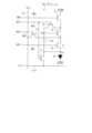
- FIG. 1is a block diagram showing the overall configuration of a display device 10 according to the first embodiment.
- This display device 10is an organic EL display device that performs internal compensation. That is, in this display device 10, each pixel circuit 15 has a function of compensating for variations and fluctuations in the threshold voltage of the internal drive transistor.
- this display device 10employs a variable refresh rate method (VRR method), and depending on the content to be displayed (for example, still images or moving images), a non-refresh frame period is set between adjacent refresh frame periods. The refresh rate can be changed by inserting .
- VRR methodvariable refresh rate method
- the display device 10is configured such that the refresh rate is switched between a low refresh rate for displaying still images and a high refresh rate for displaying moving images. It is assumed that only the period (RF frame period) is continuous, and the non-refresh frame period (NRF frame period) is not inserted. However, the present invention is not limited to this, and the display device 10 may be configured to switch between three or more refresh rates depending on the image to be displayed. Further, below, the explanation will proceed by introducing an operation mode according to the refresh rate. That is, the display device 10 has at least two operation modes including a low refresh mode in which display operations are performed at a low refresh rate, and a high refresh mode in which display operations are performed in a high refresh rate.
- this display device 10includes a display section 11, a display control circuit 20, a data side drive circuit 30, a scanning side drive circuit 40, and a power supply circuit 50.
- the data side drive circuit 30functions as a data signal line drive circuit (also referred to as a "data driver”).
- the scanning side drive circuit 40functions as a scanning signal line drive circuit (also called a “gate driver”) and a light emission control circuit (also called an "emission driver”).
- these two scanning side circuitsare realized as one scanning side drive circuit 40, but these two circuits may be separated as appropriate, or these two circuits may be separated as appropriate. may be arranged separately on one side and the other side of the display section 11.
- the power supply circuit 50supplies a high level power supply voltage ELVDD, a low level power supply voltage ELVSS, and an initialization voltage Vini, which will be described later, to the display section 11, a display control circuit 20, a data side drive circuit 30, and a scanning side drive circuit 40. and a power supply voltage (not shown) to be supplied to the
- the display unit 11includes m data signal lines D1, D2, ..., Dm (m is an integer of 2 or more) and n first scanning signal lines NS11 (n is an integer of 2 or more) intersecting these lines. , N12, . . . , NS1n, n second scanning signal lines NS21, NS22, . . . , NS2n, and n third scanning signal lines NS31, NS32, .
- first emission control lines (first emission lines) EM11 to EM1nare arranged along the n first scanning signal lines NS11 to NS1n, respectively, and n second emission control lines (second emission lines) EM21 to EM2n are arranged along the lines NS1n to NS1n, respectively.
- the display unit 11is also provided with m ⁇ n pixel circuits 15 arranged in a matrix along m data signal lines D1 to Dm and n first scanning signal lines NS11 to NS1n. .
- Each pixel circuit 15corresponds to one of m data signal lines D1 to Dm and also corresponds to one of n first scanning signal lines NS11 to NS1n (hereinafter, each pixel circuit 15 When distinguishing between )”).
- each pixel circuit 15corresponds to one of the n second scanning signal lines NS21 to NS2n, corresponds to one of the n third scanning signal lines NS31 to NS3n, and corresponds to one of the n second scanning signal lines NS21 to NS2n, and It corresponds to any one of the first emission control lines EM11 to EM1n, and corresponds to any one of the n second emission control lines EM21 to EM2n.
- a power supply line(not shown) common to each pixel circuit 15 is arranged in the display section 11. That is, the first power line (hereinafter referred to as the "high level power supply line” and designated by the same symbol as the high level power supply voltage) serves as a fixed voltage line for supplying a high level power supply voltage ELVDD for driving an organic EL element, which will be described later. ELVDD”), and a second power supply line (hereinafter referred to as "low-level power supply line”) as a fixed voltage line for supplying the low-level power supply voltage ELVSS for driving the organic EL element (hereinafter referred to as "low-level power supply line").
- ELVDDhigh level power supply voltage
- low-level power supply linea second power supply line
- the display unit 11is provided with an initialization voltage as a fixed voltage line (not shown) for supplying an initialization voltage Vini used for a reset operation (also referred to as "initialization operation") for initializing each pixel circuit 15.
- a line Liniis provided, and an on-bias voltage line Lobs for supplying an on-bias voltage Vobs to each pixel circuit 15 is also provided.
- High level power supply voltage ELVDD, low level power supply voltage ELVSS, and initialization voltage Viniare supplied from power supply circuit 50.
- the on-bias voltage Vobsis supplied from the display control circuit 20 in this embodiment, but may be supplied from the power supply circuit 50.
- the display control circuit 20receives an input signal Sin containing image information representing an image to be displayed and timing control information for image display from outside the display device 10, and controls a data-side control signal Scd and a scanning signal based on this input signal Sin. side control signal Scs, and outputs the data side control signal Scd to the data side drive circuit 30 and the scanning side control signal Scs to the scanning side drive circuit 40, respectively.
- the operation modeis set to high refresh mode, and after that, when no new image data is input for a predetermined period of time or more, the operation mode is set to low. It is assumed that the display control circuit 20 controls the data side drive circuit 30 and the scanning side drive circuit 40 so as to switch to the refresh mode.
- the input signal Sinincludes an operation mode signal Sm indicating which operation mode to drive the display section 11 between the low refresh mode and the high refresh mode.
- the control circuit 20may control the data side drive circuit 30 and the scanning side drive circuit 40 so that the display section 11 is driven in the operation mode indicated by the operation mode signal Sm.
- the data side drive circuit 30drives the data signal lines D1 to Dm based on the data side control signal Scd from the display control circuit 20. That is, the data side drive circuit 30 generates m data signals D(1) to D(m) representing images to be displayed based on the data side control signal Scd, and applies them to the data signal lines D1 to Dm, respectively. .
- the scanning side drive circuit 40includes first scanning signal lines NS11 to NS1n, second scanning signal lines NS21 to NS2n, third scanning signal lines NS31 to NS3n, first emission control lines EM11 to EM1n, and second emission control line EM21.
- the control scanning lines consisting of ⁇ EM2nBy selectively driving the control scanning lines consisting of ⁇ EM2n, the m ⁇ n pixel circuits 15 in the display section 11 are controlled (more specifically, each transistor functioning as a switching element in each pixel circuit 15 is controlled). do).
- the scanning side drive circuit 40generates first scanning signals NS1(1) to NS1(n) based on the scanning side control signal Scs from the display control circuit 20, and sends them to the first scanning signal lines NS11 to NS1n.
- first emission control signals EM1(1) to EM1(n)are generated and applied to the first emission control lines EM11 to EM1n, respectively, and the second emission control signals are applied to the third scanning signal lines NS31 to NS3n, respectively.
- EM2(1) to EM2(n)are generated and applied to second emission control lines EM21 to EM2n, respectively.
- the scanning side drive circuit 40functions as a scanning signal line drive circuit that drives the first scanning signal lines NS11 to NS1n, the second scanning signal lines NS21 to NS2n, and the third scanning signal lines NS31 to NS3n. It functions as a light emission control circuit that drives the first light emission control lines EM11 to EM1n and the second light emission control lines EM21 to EM2n.
- the scanning side drive circuit 40as a scanning signal line drive circuit, generates the first scanning signals NS1(1) to NS1(n) generated based on the scanning side control signal Scs. , second scanning signals NS2(1) to NS2(n), and third scanning signals NS3(1) to NS3(n), the n first scanning signal lines NS11 to NS1n correspond to one horizontal period.
- the n second scanning signal lines NS21 to NS2nare sequentially selected for each predetermined period corresponding to one horizontal period, and the n third scanning signal lines NS31 to NS3n are sequentially selected for one horizontal period.
- the scanning side drive circuit 40controls the first emission control lines EM11 to EM1n and the second emission control lines EM21 to EM2n so that they are connected to the first scanning signal lines NS11 to NS1n and the second scanning signal line NS21 during the RF frame period Trf. ⁇ NS2n and the third scanning signal lines NS31 to NS3n are driven to be selectively inactivated in conjunction with the above driving. That is, the scanning side drive circuit 40, as a light emission control circuit, generates the above-mentioned first emission control signals EM1(1) to EM1(n) and second emission control signal EM2(1) based on the scanning side control signal Scs.
- ⁇ EM2(n)makes the i-th first emission control line EM1i inactive for a predetermined period including the i-th horizontal period, and makes it active in other periods, and EM2i is kept inactive for a predetermined period including the i-th horizontal period, and kept active for other periods (i is an integer such that 1 ⁇ i ⁇ n).
- iis an integer such that 1 ⁇ i ⁇ n).
- the period in which the i-th first emission control line EM1i is in the active state and the period in which the i-th second emission control line EM2i is in the active stateare slightly different (see FIG. 10 described later for details).
- the organic EL elements in the pixel circuits Pix (i, 1) to Pix (i, m) corresponding to the i-th first scanning signal line NS1iare While both the first emission control line EM1i and the second emission control line EM2i are in the active state, the data voltages written in the i-th pixel circuits Pix(i,1) to Pix(i,m), respectively, are It emits light depending on the brightness.
- the scanning side drive circuit 40stops driving the first scanning signal lines NS11 to NS1n and the second scanning signal lines NS21 to NS2n, but the driving of the third scanning signal lines NS31 to NS3n, the first The light emission control lines EM11 to EM1n and the second light emission control lines EM21 to EM2n are driven in the same manner as in the refresh frame period Trf (see FIG. 10 described later).
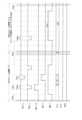
- FIG. 2is a timing chart for explaining the general operation of a display device as a comparative example of a variable refresh rate method (VRR method).
- Dataindicates the data signals D(1) to D (n) generically
- "ACT"indicates the signal state for data writing (data voltage)
- "BLK”indicates the blanking signal state
- OBSindicates the on-bias application.
- the example shown in FIG. 2shows the operation of the display device when a refresh request Rq_mv for displaying a moving image occurs while operating in a low refresh mode in which an RF frame period Trf is followed by a plurality of NRF frame periods Tnrf. ing.
- the refresh request Rq_mv for video displayoccurs in the middle of the NRF frame period Tnrf, but the operation mode of the display device as the comparative example is At the time point shown), the high refresh mode is switched to, and the RF frame period Trf starts from the end point of the high refresh mode. Thereafter, the RF frame period Trf continues while operating in the high refresh mode.
- the display devicewhen a refresh request for displaying a moving image occurs during the NRF frame period Tnrf in the low refresh mode, the display device immediately shifts to the high refresh mode and starts the RF frame period Trf. I can't. The reason for this will be explained below.
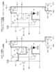
- FIG. 3is a circuit diagram showing the configuration of the pixel circuit 15a in the display device as the comparative example, and more specifically, the pixel circuit corresponding to the i-th first scanning signal line NS1i and the j-th data signal line Dj.
- FIG. 15ais a circuit diagram showing the configuration of the pixel circuit Pix(i,j) in the i-th row and j-th column (1 ⁇ i ⁇ n, 1 ⁇ j ⁇ m). This pixel circuit 15a is an internal compensation type pixel circuit, and as shown in FIG.
- transistor T1includes one organic EL element OL as a display element and six transistors T1 to T6 (hereinafter referred to as "transistor T1", “threshold compensation transistor T2”, “write control transistor T3”, “drive transistor T4", “second light emission control transistor T5", “first light emission control transistor T6”), and a holding capacitor Cst. Contains.
- transistors T1 to T6are N-channel transistors.
- Thin film transistors(hereinafter referred to as “oxide TFTs”) whose channel layers are formed of an oxide semiconductor are used as these N-channel transistors T1 to T6.
- oxide TFTa thin film transistor containing indium gallium zinc oxide (InGaZnO) (hereinafter referred to as “IGZO-TFT”) can be used.
- ITZO-TFTindium gallium zinc oxide
- the transistors T1 to T3, T5, and T6 other than the drive transistor T4operate as switching elements.
- the pixel circuit Pix(i,j) in the comparative examplehas a corresponding first scanning signal line (hereinafter also referred to as “corresponding first scanning signal line” in the explanation focusing on the pixel circuit).
- NS1i and the corresponding second scanning signal linehereinafter also referred to as “corresponding second scanning signal line” in the explanation focusing on the pixel circuit
- NS2i and the corresponding third scanning signal linehereinafter referred to as the "corresponding second scanning signal line”
- NS3ialso referred to as "corresponding third scanning signal line” in the focused explanation
- EM1ihereinafter also referred to as "corresponding first emission control line” in the explanation focused on the pixel circuit
- the corresponding second light emission control linehereinafter also referred to as “corresponding second light emission control line” in the explanation focusing on the pixel circuit
- EM2iand the corresponding data signal line
- the on-bias voltage Vobsis supplied to each pixel circuit Pix(i,j) via the data signal line Dj,
- the display section 11is not provided with an on-bias voltage line Lobs for supplying the voltage Vobs.
- the drain terminal as the first conduction terminal of the drive transistor T4is connected to the high level power supply line ELVDD via the second light emission control transistor T5. It is connected.
- a source terminal as a second conduction terminal of the drive transistor T4is connected to an anode electrode as a first terminal of the organic EL element OL via a first light emission control transistor T6, and a corresponding one is connected via a write control transistor T3. It is connected to the data signal line Dj.
- the gate terminal as a control terminal of the drive transistor T4is connected to the first terminal of the organic EL element OL via the holding capacitor Cst, and is also connected to the drain terminal of the drive transistor via the threshold compensation transistor T2. . Further, the anode electrode of the organic EL element OL is also connected to the initialization voltage line Lini via the initialization transistor T1, and the cathode electrode as the second terminal of the organic EL element OL is connected to the low level power supply line ELVSS. It is connected to the.
- the gate terminals of the initialization transistor T1 and the threshold compensation transistor T2are both connected to the corresponding first scanning signal line NS1i, and the gate terminal of the write control transistor T3 is connected to the corresponding second scanning signal line NS2i.
- the gate terminal of the transistor T6is connected to the corresponding first emission control line EM1i
- the gate terminal of the second emission control transistor T5is connected to the corresponding second emission control line EM2i.
- FIG. 4a dotted circle indicates that the transistor therein is in the on state, and a dotted line x indicates that the transistor marked with it is in the off state.
- FIGS. 8, 9, 18, 20, 24, 25, and 28Such an expression method is also adopted in FIGS. 8, 9, 18, 20, 24, 25, and 28.
- FIG. 4Ashows a data write period Twr(i ) shows the circuit state.
- the write control transistor T3, the threshold compensation transistor T2, and the initialization transistor T1are in the on state, and the first light emission control transistor T6 and the second light emission control transistor T5 are in the off state. be.
- the voltage of the corresponding data signal line Djis written as the data voltage Vdata to the holding capacitor Cst via the drive transistor T4 which is diode-connected by the threshold compensation transistor T2 in the on state, and the data is written to the holding capacitor Cst.
- a voltage corresponding to the difference Vdata ⁇ Vini between the voltage Vdata and the initialization voltage(more precisely, the voltage Vdata+Vth ⁇ Vini corresponding to the difference between the threshold-compensated data voltage and the initialization voltage) is held.
- FIG. 4Bshows an anode initialization period (“anode reset period” or “display element initialization period”) during which the anode electrode of the organic EL element OL in the pixel circuit Pix(i,j) is initialized during the NRF frame period. ) shows the circuit state at Tanr(i).
- Tanr(i)the write control transistor T3 and the first light emission control transistor T6 are in the on state, and the second light emission control transistor T5, the threshold compensation transistor T2, and the initialization transistor T1 are in the off state.
- the voltage of the corresponding data signal line Djis applied as the anode initialization voltage Vanr to the anode electrode of the organic EL element OL via the write control transistor T3 and the first light emission control transistor T6, and the voltage of the organic EL element OL is applied as the anode initialization voltage Vanr.
- the voltage of the anode electrode (hereinafter referred to as "anode voltage”) Vais initialized. This blocks the influence of past display history on the light emitting operation of the organic EL element OL.
- FIG. 4(C)shows the circuit state during the on-bias period Tobs(i) in which the on-bias voltage Vobs is applied to the source terminal of the drive transistor T4 in the pixel circuit Pix(i, j) in the NRF frame period.
- the write control transistor T3is in the on state
- the first light emission control transistor T6, the second light emission control transistor T5, the threshold compensation transistor T2, and the initialization transistor T1are in the off state.
- the voltage of the corresponding data signal line Djis applied as the on-bias voltage Vobs to the source terminal of the drive transistor T4 via the write control transistor T3. This reduces the influence of the hysteresis characteristic of the drive transistor T4 on display brightness.
- FIG. 5shows changes in the drive signals for operating each pixel circuit Pix(i,j) as shown in FIG.
- Signals NS2(i), NS2(i-1), first emission control signals EM1(i), EM1(i-1), second emission control signals EM2(i), EM2(i-1), and data signal 5is a timing chart showing changes in D(j).
- the drive signalchanges as shown in FIG.
- the holding capacitor Cst in the pixel circuit Pix (i, j)is initialized (data initialization) in the data initialization period Tini (i) included in the RF frame period Trf, and the RF frame period In the data write period Twr(i) included in Trf, the voltage of the data signal D(j) is written to the pixel circuit Pix(i,j) as the data voltage Vdata (see FIG. 4(A)).
- Emission control lines EM11 to EM1n and second emission control lines EM21 to EM2nare selectively driven, and anode initialization voltage Vanr and on-bias voltage Vobs are applied as the same voltage to data signal lines D1 to Dm.
- the voltage of the data signal D(j)is applied as the on-bias voltage Vobs to the source terminal of the drive transistor T4 in the pixel circuit Pix(i, j) during the on-bias period Tobs(i) (see FIG. 4(C)).
- the anode voltage Va of the organic EL element OL in the pixel circuit Pix(i,j)is initialized in the anode initialization period Tanr(i) (see FIG. 4(B)).
- pixel circuits Pix(1,j) to The structureis such that data writing and anode initialization or on-bias application can be executed simultaneously at Pix(n,j). The pixel circuit in this embodiment will be described below.
- FIG. 7is a circuit diagram showing the configuration of the pixel circuit 15 in this embodiment. More specifically, the pixel circuit 15 corresponding to the i-th first scanning signal line NS1i and the j-th data signal line Dj, that is, the i-th row
- FIG. 3is a circuit diagram showing the configuration of a pixel circuit Pix (i, j) in the j-th column (1 ⁇ i ⁇ n, 1 ⁇ j ⁇ m). Similar to the pixel circuit 15a in the comparative example shown in FIG. 3, this pixel circuit 15 includes one organic EL element OL as a display element, an initialization transistor T1, a threshold compensation transistor T2, a write control transistor T3, and a drive transistor.
- the transistors T1 to T6are N-channel thin film transistors (more specifically, oxide TFTs), and the transistors T1 to T3, T5, and T6 other than the drive transistor T4 operate as switching elements.
- the pixel circuit 15 in this embodimentis an N-channel thin film transistor (more specifically, an oxide TFT) that operates as a switching element. ) is further provided with a bias control transistor T8.
- the pixel circuit Pix(i,j) in this embodimenthas a corresponding first scanning signal line (corresponding first scanning signal line) as in the pixel circuit Pix(i,j) in the comparative example in FIG. scanning signal line) NS1i, a second scanning signal line corresponding to it (corresponding second scanning signal line) NS2i, a first emission control line corresponding to it (corresponding first emission control line) EM1i, a second emission control line corresponding to it (Corresponding second light emission control line) EM2i, its corresponding data signal line (corresponding data signal line) Dj, initialization voltage line Lini, high level power supply line ELVDD, and low level power supply line ELVSS are connected.
- the pixel circuit Pix(i,j) in this embodimenthas a corresponding third scanning signal line NS3i (hereinafter also referred to as "corresponding third scanning signal line” in the explanation focusing on the pixel circuit). , and the on-bias voltage line Lobs are also connected (see FIGS. 1 and 7).
- the connection relationships between NS2i, EM1i, EM2i, Dj, power supply lines ELVDD, ELVSS, initialization voltage line Lini, and the relevant components T1 to T6, Cst, and OLare as shown in FIG. This is the same as the connection relationship of the circuit Pix(i,j) (see FIG. 3).
- the bias control transistor T8 as a switching element provided in the pixel circuit 15 in this embodimenthas its first conduction terminal connected to the on-bias voltage line Lobs, and its second conduction terminal connected to the drive transistor T4.
- a gate terminal as a control terminalis connected to a corresponding third scanning signal line NS3i.
- the bias control transistor T8constitutes a bias application circuit for reducing the influence on display brightness due to the hysteresis characteristic of the drive transistor T4.
- FIG. 8(A)shows the circuit state of the pixel circuit Pix(i,j) during the data initialization period Tini in the RF frame period Trf.
- This data initialization period Tiniis a period for initializing the voltage held in the holding capacitor Cst of the pixel circuit Pix (i, j), and the initialization of the voltage held in the holding capacitor Cst is performed by driving This corresponds to initializing the voltage Vg at the gate terminal of the transistor T4.
- the second light emission control transistor T5, the threshold compensation transistor T2, and the initialization transistor T1are in the on state
- the write control transistor T3, the first light emission control transistor T6, and the bias control transistor T8are in the on state. It is off.
- the holding capacitor Cstis initialized to the voltage ELVDD-Vini, which is the difference between the high-level power supply voltage ELVDD and the initialization voltage Vini, and the voltage at the gate terminal of the drive transistor T4 (hereinafter referred to as "gate voltage") Vg is It is initialized to high level power supply voltage ELVDD.
- the voltage of the anode electrode (anode voltage) Va of the organic EL element OLis also initialized to the initialization voltage Vini by the initialization transistor T1 in the on state.
- FIG. 8Bshows the circuit state of the pixel circuit Pix(i,j) during the data write period Twr in the RF frame period Trf.
- the write control transistor T3, the threshold compensation transistor T2, and the initialization transistor T1are in the on state
- the first light emission control transistor T6, the second light emission control transistor T5, and the bias control transistor T8are in the on state. It is off.
- the voltage of the corresponding data signal line Djis written as the data voltage Vdata to the holding capacitor Cst via the driving transistor T4 which is diode-connected by the threshold compensation transistor T2 in the on state, and the data is written to the holding capacitor Cst.
- a voltage corresponding to the difference Vdata-Vini between the voltage and the initialization voltage(more precisely, a voltage Vdata+Vth-Vini corresponding to the difference between the threshold-compensated data voltage and the initialization voltage) is held (Vth> 0). Note that in the data write period Twr, the anode voltage Va of the organic EL element OL is also initialized to the initialization voltage Vini by the initialization transistor T1 in the on state.
- FIG. 8Cshows the circuit state of the pixel circuit Pix(i,j) during the light emission period Tem in the RF frame period Trf and the NRF frame period Tnrf.
- This light emitting period Temis a period during which the organic EL element OL in the pixel circuit Pix(i,j) lights up.
- the first light emission control transistor T6 and the second light emission control transistor T5are in the on state, and the write control transistor T3, the threshold compensation transistor T2, the initialization transistor T1, and the bias control transistor T8 are in the off state. be.
- a current I1 of an amount corresponding to the voltage held in the holding capacitor Cstis transmitted from the high-level power supply line ELVDD to the second light emission control transistor T5, the drive transistor T4, the first light emission control transistor T6, and the organic EL element OL.
- the currentflows to the low-level power supply line ELVSS via the current I1, and the organic EL element OL emits light with a brightness corresponding to this current I1.
- FIG. 9Ashows the circuit state of the pixel circuit Pix(i,j) during the anode initialization period Tanr as the display element initialization period in the NRF frame period Tnrf.
- the bias control transistor T8 and the first light emission control transistor T6are on, and the second light emission control transistor T5, the threshold compensation transistor T2, the initialization transistor T1, and the write control transistor T3 are off. state.
- the write control transistoris in the off state, unlike the circuit state (FIG. 4(B)) during the anode initialization period Tanr(i) in the comparative example.
- Bias control transistor T8is in an on state.
- the voltage Vobs of the on-bias voltage line Lobsis applied as the anode initialization voltage Vanr to the anode electrode of the organic EL element OL via the bias control transistor T8 and the first light emission control transistor T6, and the anode of the organic EL element OL is Voltage Va is initialized.
- the anode voltage VaBy initializing the anode voltage Va in this manner, the influence of the past display history on the light emitting operation of the organic EL element OL is blocked, and deterioration in display quality is suppressed.
- FIG. 9Bshows the circuit state of the pixel circuit Pix(i,j) during the on-bias period Tobs in the RF frame period Trf and the NRF frame period Tnrf.
- the bias control transistor T8is in the on state, and the first light emission control transistor T6, the second light emission control transistor T5, the threshold compensation transistor T2, the initialization transistor T1, and the write control transistor T3 are in the off state. It is.
- the write control transistoris in the off state and the bias control Transistor T8 is on.
- the voltage of the on-bias voltage line Lobsis applied as the on-bias voltage Vobs to the source terminal of the drive transistor T4 via the bias control transistor T8.
- the influence of the hysteresis characteristic of the drive transistor T4 on display brightnessis reduced. In this way, even when displaying while switching the refresh rate, a good display with no visible flicker can be obtained.
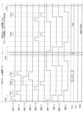
- FIG. 10is a timing chart for explaining a first driving example for operating each pixel circuit Pix(i,j) as shown in FIGS. 8 and 9. Changes in signals, namely, first scanning signal NS1(i), NS1(i-1), second scanning signal NS2(i), NS2(i-1), third scanning signal NS3(i), first light emission It shows changes in control signals EM1(i), EM1(i-1), second light emission control signals EM2(i), EM2(i-1), and data signal D(j).
- the scanning side drive circuit 40includes a first scanning signal line drive circuit, a second scanning signal line drive circuit, a third scanning signal line drive circuit, which constitute the scanning signal line drive circuit, and a first light emitting line drive circuit.
- Each of the first scanning signal line drive circuit, the second scanning signal line drive circuit, the third scanning signal line drive circuit, the first light emission control circuit, and the second light emission control circuitincludes a control circuit and a second light emission control circuit. It has n stages of cascade-connected bistable circuits (hereinafter referred to as "unit circuits"), and these unit circuits and each pixel circuit are connected as shown in FIG. 13(A).
- the pixel circuits Pix (k, 1) to Pix (k, m) in the k-th rowinclude a first scanning signal line driving circuit, a second scanning signal line driving circuit, a third scanning signal line driving circuit, and a first scanning signal line driving circuit.
- FIG. 10shows changes in the drive signal in one RF frame period Trf and one subsequent NRF frame period Tnrf.
- a large number of NRF frame periods Tnrfare continuous, and a plurality of RF frame periods Trf may also be continuous. This point also applies to FIGS. 11 and 12 for explaining other driving examples.
- the drive signalchanges as shown in FIG.
- the control lines EM11 to EM1n and the second light emission control lines EM21 to EM2nare selectively driven, and the data signal lines D1 to Dm contain data to be written to the pixel circuits Pix(i,1) to Pix(i,m).
- Such drive signalsinitialize the holding capacitor Cst (data initialization) in the pixel circuit Pix(i,j) in the data initialization period Tini, and initialize the holding capacitor Cst in the pixel circuit Pix(i,j) in the data write period Twr. ), the voltage of the data signal D(j) is written as the data voltage Vdata (see FIG.
- an on-bias period Tobsis provided between the data initialization period Tini and the data write period Twr, and each pixel circuit Pix(i, In the on-bias period Tobs in j), the signal NS1(i) of the corresponding first scanning signal line NS1i, the signal NS2(i) of the corresponding second scanning signal line NS2i, and the signal EM1(i) of the corresponding first emission control line EM1i.
- the signal EM2(i) on the corresponding second light emission control line EM2iare both at L level (inactive), and the signal NS3(i) on the corresponding third scanning signal line NS3i is at H level (active).
- the pixel circuit Pix(i,j)operates as shown in FIG. 9B, and the voltage of the on-bias voltage line Lobs is applied to the source terminal of the drive transistor T4 as the on-bias voltage Vobs.
- the drive signalchanges as shown in FIG.
- Control lines EM11 to EM1n and second emission control lines EM21 to EM2nare selectively driven, and data signal lines D1 to Dm are maintained in a high impedance state. Due to such a drive signal, an on-bias period Tobs and an anode initialization period Tanr are provided in the NRF frame period Tnrf for each pixel circuit Pix(i,j).
- the signal NS1(i) of the corresponding first scanning signal line NS1i, the signal NS2(i) of the corresponding second scanning signal line NS2i, Signal EM1(i) of corresponding first emission control line EM1i and signal EM2(i) of corresponding second emission control line EM2iare both at L level (inactive), and signal NS3( of corresponding third scanning signal line NS3i) is at L level (inactive). i) is at H level (active).
- the pixel circuit Pix(i,j)operates as shown in FIG.
- the voltage of the on-bias voltage line Lobsis applied to the source terminal of the drive transistor T4 as the on-bias voltage Vobs.
- the signal NS1(i) of the corresponding first scanning signal line NS1i, the signal NS2(i) of the corresponding second scanning signal line NS2i, and the signal EM2(i) of the corresponding second emission control line EM2i.are both at L level (inactive), and signal NS3(i) of the corresponding third scanning signal line NS3i and signal EM1(i) of the corresponding first emission control line EM1i are at H level (active).
- the pixel circuit Pix (i, j)operates as shown in FIG.
- the anode voltage Vais initialized by being applied to the anode electrode of the OL.
- FIG. 11is a timing chart for explaining a second driving example for operating each pixel circuit Pix(i,j) as shown in FIGS. 8 and 9. Changes in signals, namely, first scanning signal NS1(i), NS1(i-1), second scanning signal NS2(i), NS2(i-1), third scanning signal NS3(i), first light emission It shows changes in control signals EM1(i), EM1(i-1), second light emission control signals EM2(i), EM2(i-1), and data signal D(j). Also in this driving example, as shown in FIG.
- the k-th pixel circuits Pix (k, 1) to Pix (k, m)have a first scanning signal line driving circuit and a second scanning signal line driving circuit.
- the drive signalchanges as shown in FIG.
- the control lines EM11 to EM1n and the second light emission control lines EM21 to EM2nare selectively driven, and the data signal lines D1 to Dm contain data to be written to the pixel circuits Pix(i,1) to Pix(i,m).
- the holding capacitor Cst in the pixel circuit Pix(i,j)is initialized (data initialization) in the data initialization period Tini, as in the first drive example (see FIG. 8(A). ), the voltage of the data signal D(j) is written to the pixel circuit Pix(i,j) as the data voltage Vdata in the data write period Twr (see FIG. 8B).
- two on-bias periods Tobsare provided within the RF frame period Trf. That is, in the RF frame period Trf, not only is the on-bias period Tobs provided between the data initialization period Tini and the data write period Twr, but also the on-bias period Tobs is provided after the data write period Twr.
- the signal NS1(i) of the corresponding first scanning signal line NS1i, the signal NS2(i) of the corresponding second scanning signal line NS2i, The signal EM1(i) of the corresponding first emission control line EM1i and the signal EM2(i) of the corresponding second emission control line EM2iare at L level (inactive), and the signal NS3(i) of the corresponding third scanning signal line NS3i is at L level (inactive). ) is at H level (active).
- the pixel circuit Pix(i,j)operates as shown in FIG.
- the influence on display brightness due to the hysteresis characteristic of the driving transistor T4can be further reduced compared to the first driving example.
- the drive signalchanges as shown in FIG.
- the third scanning signal lines NS31 to NS3n, the first emission control lines EM11 to EM1n, and the second emission control lines EM21 to EM2nare selectively driven, and the data signal lines D1 to Dm are maintained in a high impedance state.
- an on-bias period Tobs and an anode initialization period Tanrare provided in the NRF frame period Tnrf for each pixel circuit Pix (i, j), and as in the first driving example, the pixel circuit Pix In (i, j), during the on-bias period Tobs, the on-bias voltage Vobs is applied to the source terminal of the drive transistor T4 (see FIG. 9(B)), and during the anode initialization period Tanr, the on-bias voltage Vobs is applied to the anode electrode of the organic EL element OL.
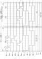
- FIG. 12is a timing chart for explaining a third driving example for operating each pixel circuit Pix(i,j) as shown in FIGS. 8 and 9. Changes in signals, namely, first scanning signal NS1(i), NS1(i-1), second scanning signal NS2(i), NS2(i-1), third scanning signal NS3(i), first light emission It shows changes in control signals EM1(i), EM1(i-1), second light emission control signals EM2(i), EM2(i-1), and data signal D(j).
- each of the first scanning signal line driving circuit, the second scanning signal line driving circuit, and the third scanning signal line driving circuitis a cascade-connected n-stage bistable circuit (unit circuit), as in the first driving example.
- each of the first light emission control circuit and the second light emission control circuithas n/2 stage bistable circuits (hereinafter also referred to as "unit circuits") connected in cascade (here, n is (assumed to be an even number), these unit circuits and each pixel circuit are connected as shown in FIG. 13(B).
- the pixel circuits Pix (2k-1, 1) to Pix (2k-1, m) on the 2k-1st rowhave a first scanning signal line drive circuit, a second scanning signal line drive circuit, and a third scanning signal line drive circuit.
- 2k-1st stage unit circuits NS1 (U2k-1), NS2 (U2k-1), NS3 (U2k-1) in the line drive circuit and k-th stage units in the first light emission control circuit and the second light emission control circuit Circuits EM1 (Uk) and EM2 (Uk)are connected, and the 2kth row pixel circuits Pix (2k, 1) to Pix (2k, m) have a first scanning signal line drive circuit and a second scanning signal line drive circuit.
- the drive signalchanges as shown in FIG.
- the control lines EM11 to EM1n and the second light emission control lines EM21 to EM2nare selectively driven, and the data signal lines D1 to Dm contain data to be written to the pixel circuits Pix(i,1) to Pix(i,m).
- the first light emission control signal EM1(i) and the second light emission control signal EM2(i)change at different timings from those in the first drive example.
- the data initialization period Tini, data write period Twr, and on-bias period of the drive signals NS1(i), NS2(i), NS3(i), EM1(i), and EM2(i)are the data initialization period Tini and data write period of the drive signals NS1(i), NS2(i), NS3(i), EM1(i), and EM2(i) in the first drive example, respectively.
- Twr and the level in the on-bias period Tobssee FIG. 10).
- the holding capacitor Cst in the pixel circuit Pix(i,j)is initialized (data initialization) in the data initialization period Tini (see FIG. 8(A)), and the data In the write period Twr, the voltage of the data signal D(j) is written to the pixel circuit Pix(i, j) as the data voltage Vdata (see FIG. 8(B)), and in the on-bias period Tobs, the voltage of the data signal D(j) is written to the pixel circuit Pix(i, An on-bias voltage Vobs is applied to the source terminal of the drive transistor T4 in the transistor T4 (see FIG. 9B).
- the first emission control signal EM1(i) and the second emission control signal EM2(i)change at different timings from the first driving example.
- the levels of the drive signals NS1(i), NS2(i), NS3(i), EM1(i), EM2(i) during the on-bias period Tobs and the anode initialization period Tanrare respectively The levels of the drive signals NS1(i), NS2(i), NS3(i), EM1(i), EM2(i) in the on-bias period Tobs and the anode initialization period Tanr in the drive example 1 (see FIG. 10) and It's the same.
- the on-bias voltage Vobsis applied to the source terminal of the drive transistor T4 in the pixel circuit Pix(i,j) during the on-bias period Tobs (see FIG. 9(B)), and the anode During the initialization period Tanr, the voltage of the on-bias voltage line Lobs is applied as the anode initialization voltage Vanr to the anode electrode of the organic EL element OL in the pixel circuit Pix(i,j) (see FIG. 9(A)).
- the pixel circuit Pix(i,j)is driven in the same way as in the first driving example, but the scanning side drive circuit 40 controls the first light emission control circuit and the second light emission control circuit.
- Each of themis composed of n/2 stage unit circuits (see FIG. 13(B)), so compared to the first drive example (see FIG. 13(A)), the amount of circuitry of the light emission control circuit is reduced (approximately 1/2). Ru.
- FIG. 14is a timing chart for explaining a first operation example of the display device according to this embodiment.
- the display device according to the present embodimentis configured such that the refresh rate can be changed in units of 1/2 frame period.
- Datagenerically indicates the data signals D(1) to D(n), "ACT" indicates the signal state (data voltage) for data writing, and "BLK” indicates the blanking signal. Each state is shown.
- the on-bias voltage Vobs and the anode initialization voltage Vanrare applied to each pixel circuit Pix(i,j) from the on-bias voltage line Lobs provided separately from the data signal line Dj. (See (A) and (B) of FIG. 9). Therefore, in FIG. 14, "OBS" indicates that the voltage of the on-bias voltage line Lobs is used as the on-bias voltage Vobs for applying an on-bias to the drive transistor T4, and "ANR" indicates that the voltage of the on-bias voltage line Lobs is used as the on-bias voltage Vobs for applying an on-bias to the drive transistor T4.
- a refresh request Rq_mv for displaying a moving imageis issued within the first half of a certain NRF frame period Tnrf.
- the operation of the display device when this occursis shown. Since the display device in this operation example is configured to be able to change the refresh rate in units of 1/2 frame period, in this case, as shown in FIG.
- the modeis switched to the high refresh mode. That is, the RF frame period Trf starts from the end point, and the RF frame period Trf continues while operating in the high refresh mode.
- a refresh request Rq_mv for video displayoccurs in the first half of the NRF frame period Tnrf, and the operation mode switches to high refresh mode at the end of the first half Cg_mod.
- the on-bias application and anode initialization that have been performedare also performed in the second half of the NRF frame period Tnrf. That is, as shown in FIG. 14, the second half of the NRF frame period Tnrf overlaps with the first half of the first RF frame period Trf after switching the operation mode.
- the pixel circuit Pix(i1,j) to which data is writtenis connected to the anode initialization or on-bias application.
- the pixel circuits Pix(i2,j) that are used in the pixel circuit Pix(i2,j)coexist.
- the on-bias voltage Vobs and the anode initialization voltage Vanrare supplied from the data signal line Dj to each pixel circuit Pix(i,j) ((B) and (C) of FIG. ), it was not possible to realize the operation in such an overlapping period Tov.
- the on-bias voltage Vobs and the anode initialization voltage Vanrare supplied from the on-bias voltage line Lobs to each pixel circuit Pix(i,j) ((A) and (B) in FIG. 9). ), among the pixel circuits Pix(1,j) to Pix(n,j) in the same column, the pixel circuit Pix(i1,j) to which data is written and the pixel to which anode initialization or on-bias application is performed. It is possible to operate in the overlapping period Tov in which the circuit Pix(i2,j) coexists.
- each of the first light emission control signals EM1(1) to EM1(n) and the second light emission control signals EM2(1) to EM2(n)is in an inactive state (L level) during one frame period.
- L levelthe operation mode is switched from the low refresh mode to the high refresh mode in units of 1/2 frame period.
- the scanning side control signal Scsgiven from the display control circuit 20 to the scanning side drive circuit 40, it is possible to enter the high refresh mode. It is also possible to switch the operation mode in shorter time units.
- the operation modecan be switched to high refresh mode in units of 1/4 frame period, and by setting the above number of times to 8, the operation mode can be switched to high refresh mode in units of 1/8 frame period. You can also switch to high refresh mode. This point also applies to other embodiments.
- FIG. 15is a timing chart for explaining a second operation example of the display device according to this embodiment.
- the display device according to the present embodimentis configured such that the refresh rate can be changed in units of 1/4 frame period.
- the example shown in FIG. 15shows that when operating in a low refresh mode in which an RF frame period Trf is followed by a plurality of NRF frame periods Tnrf, the video display is performed within the first quarter frame period of a certain NRF frame period Tnrf.
- 3shows the operation of the display device when a refresh request Rq_mv is generated. Since the display device in this operation example is configured to be able to change the refresh rate in units of 1/4 frame period, in this case, as shown in FIG.
- the high refresh modeis switched to the high refresh mode at the end point Cg_mod of the 1/4 frame period. That is, the RF frame period Trf starts from the end point, and the RF frame period Trf continues while operating in the high refresh mode.
- the operation modeis switched to the high refresh mode at the end point Cg_mod of the first 1/4 frame period in the NRF frame period Tnrf, but the operation mode is not executed in the first 1/4 frame period.
- the on-bias application and anode initialization that were previously performedare also performed in the remaining 3/4 frame period of the NRF frame period Tnrf. That is, as shown in FIG. 15, the remaining 3/4 frame period in the NRF frame period Tnrf overlaps with the 3/4 frame period from the start point of the first RF frame period Trf after switching the operation mode.
- the pixel circuit Pix(i1,j) to which data is writtenis connected to the anode initialization or on-bias application.
- the pixel circuits Pix(i2,j) that are used in the pixel circuit Pix(i2,j)coexist.
- the on-bias voltage Vobs and the anode initialization voltage Vanrare supplied from the on-bias voltage line Lobs to each pixel circuit Pix(i,j) (see (A) and (B) in FIG. 9).
- pixel circuit Pix(i1,j)to which data is written in pixel circuits Pix(1,j) to Pix(n,j) in the same column, and pixel circuit Pix(i1,j) to which anode initialization or on-bias application is performed.
- i2, j)can be operated in the overlapping period Tov.
- FIG. 16is a timing chart for explaining a third example of operation of the display device according to this embodiment. Also in this operation example, it is assumed that the display device according to this embodiment is configured to be able to change the refresh rate in units of 1/4 frame period.
- a videois displayed within the third 1/4 frame period in a certain NRF frame period Tnrf.
- 3shows the operation of the display device when a refresh request Rq_mv is generated. Since the display device in this operation example is configured to be able to change the refresh rate in units of 1/4 frame period, in this case, as shown in FIG.
- the high refresh modeis switched to the high refresh mode at the end point Cg_mod of the 1/4th frame period. That is, the RF frame period Trf starts from the end point, and the RF frame period Trf continues while operating in the high refresh mode.
- the operation modeis switched to the high refresh mode at the end point Cg_mod of the third 1/4 frame period in the NRF frame period Tnrf.
- the on-bias application and anode initialization that were performed in the aboveare also performed in the remaining 1/4 frame period of the NRF frame period Tnrf. That is, as shown in FIG. 16, the fourth 1/4 frame period in the NRF frame period Tnrf overlaps with the first 1/4 frame period in the first RF frame period Trf after switching the operation mode.
- the on-bias voltage Vobs and the anode initialization voltage Vanrare connected to the on-bias voltage line Lobs provided separately from the data signal line Dj. 9 to each pixel circuit Pix(i,j) (see (A) and (B) in FIG. 9). Therefore, when switching the operation mode, the pixel circuits Pix(1,j) to Pix( n,j), the pixel circuit Pix(i1,j) to which data is written as shown in FIG. i2, j) (see the overlapping period Tov in FIGS. 14 to 16).
- Second embodiment>the on-bias voltage Vobs and the anode initialization voltage Vanr are applied to each pixel circuit Pix(i,j) from the on-bias voltage line Lobs provided separately from the data signal line Dj (see FIG. 9 (A) and (B)).
- the on-bias voltage Vobs and the anode initialization voltage Vanrare applied to each pixel circuit Pix (i, j) from the initialization voltage line Lini without providing the on-bias voltage line Lobs.
- the second embodimentwill be described below with reference to FIGS. 17 and 18.
- the overall configuration of the display device according to the second embodimentis basically the same as that of the display device according to the first embodiment, except that the on-bias voltage line Lobs is not provided. , the same or corresponding parts are given the same reference numerals and detailed explanations will be omitted.
- FIG. 17is a circuit diagram showing the configuration of the pixel circuit 16 in the display device 10 according to the present embodiment, and more specifically, the pixel circuit corresponding to the i-th first scanning signal line NS1i and the j-th data signal line Dj It is a circuit diagram showing the configuration of the circuit 16, that is, the pixel circuit Pix (i, j) in the i-th row and j-th column (1 ⁇ i ⁇ n, 1 ⁇ j ⁇ m). Similar to the pixel circuit 15 in the first embodiment shown in FIG. 7, this pixel circuit 16 includes one organic EL element OL as a display element, an initialization transistor T1, a threshold compensation transistor T2, and a write control transistor T3.
- a drive transistor T4a first light emission control transistor T6, a second light emission control transistor T5, a bias control transistor T8, and a holding capacitor Cst.
- the transistors T1 to T6 and T8are N-channel thin film transistors (more specifically, oxide TFTs), and the transistors T1 to T3, T5, T6 and T8 other than the drive transistor T4 operate as switching elements.
- the source terminal of the drive transistor T4is connected to the on-bias voltage line Lobs via the bias control transistor T8.
- the source terminal of the drive transistor T4is connected to the initialization voltage line Lini via the bias control transistor T8.
- the other configuration of the pixel circuit 16 in this embodimentis the same as the configuration of the pixel circuit 15 in the first embodiment.
- the pixel circuit 16 in this embodimentuses the drive signals of the pixel circuit 15 (Pix(i,j)) in the first embodiment, that is, the first scanning signal NS1(i), the second scanning signal NS2( i), the third scanning signal NS3(i), the first light emission control signal EM1(i), the second light emission control signal EM2(i), and the same drive signal as the data signal D(j) (Fig. 10 to 12).
- the operation of the pixel circuit Pix(i,j) in the i-th row and j-th column in this embodimentwill be described with reference to FIG. 18 as well as FIG. 17.
- the operation of the display device according to this embodimentis basically the same as the operation of the display device according to the first embodiment, the following description will be made regarding the pixel circuit Pix(i,j) in this embodiment. Only the main operations will be explained.
- the pixel circuit Pix(i,j) in this embodimentoperates in the same manner as in the first embodiment in the data initialization period Tini in the RF frame period Trf (see FIG. 8(A)).
- FIG. 18Ashows the circuit state of the pixel circuit Pix(i,j) during the data write period Twr in the RF frame period.
- the circuit state during this data write period Twris the same as the circuit state of the pixel circuit Pix(i,j) in the data write period Twr in the first embodiment (see FIG. 8B).
- the voltage of the corresponding data signal line Djis written as the data voltage Vdata into the holding capacitor Cst via the drive transistor T4 which is diode-connected by the threshold compensation transistor T2 in the on state, and is held.
- a voltage corresponding to the difference Vdata-Vini between the data voltage Vdata and the initialization voltage(more precisely, a voltage Vdata+Vth-Vini corresponding to the difference subjected to threshold compensation) is held in the capacitor Cst.
- FIG. 18Bshows the circuit state of the pixel circuit Pix(i,j) during the anode initialization period Tanr in the NRF frame period Tnrf.
- the bias control transistor T8 and the first light emission control transistor T6are on, and the second light emission control transistor T5, the threshold compensation transistor T2, the initialization transistor T1, and the write control transistor T3 are off. state.
- the circuit state of the pixel circuit Pix(i,j)(see FIG. 9(A)) is similar to the circuit state of the pixel circuit Pix(i,j) during the anode initialization period Tanr in the first embodiment.
- the anode voltage Va of the organic EL element OLis initialized.
- the anode electrode of the organic EL element OLis connected to the initialization voltage line Lini via the first light emission control transistor T6 and the bias control transistor T8. Therefore, the voltage of the initialization voltage line Lini rather than the voltage of the on-bias voltage line Lobs is used as the anode initialization voltage Vanr to control the organic It is applied to the anode electrode of the EL element OL (see FIG. 18(B)).
- FIG. 18Cshows the circuit state of the pixel circuit Pix(i,j) during the on-bias period Tobs in the RF frame period Trf and the NRF frame period Tnrf.
- the bias control transistor T8is in the on state, and the first light emission control transistor T6, the second light emission control transistor T5, the threshold compensation transistor T2, the initialization transistor T1, and the write control transistor T3 are in the off state. It is.
- the voltage on the initialization voltage line Linirather than the voltage on the on-bias voltage line Lobs is used as the on-bias voltage Vobs for the bias control transistor in the on state. It is applied to the source terminal of the drive transistor T4 via T8. This reduces the influence of the hysteresis characteristic of the drive transistor T4 on display brightness.
- the voltage of the initialization voltage line Liniis the voltage of the anode initialization voltage Vanr and the on-bias voltage Vobs. is applied to the anode electrode of the organic EL element OL and the source terminal of the drive transistor T4 in the pixel circuit Pix(i,j), respectively.
- the anode initialization operation and on-bias operationcan be performed in each pixel circuit Pix (i, j) as in the first embodiment.
- the on-bias voltage line Lobsis The same effect as the first embodiment can be obtained without providing this.
- the on-bias voltage Vobs and the anode initialization voltage Vanrare both given to each pixel circuit 15 from the on-bias voltage line Lobs in the first embodiment (see FIG. 9), and In the embodiment, the voltage is applied to each pixel circuit 16 from the initialization voltage line Lini (see (B) and (C) in FIG. 18). In contrast, in the third embodiment, different voltage lines are used for providing the on-bias voltage Vobs and the voltage line for providing the anode initialization voltage Vanr. The third embodiment will be described below with reference to FIGS. 19, 20, and 21.
- the overall configuration of the display device according to the third embodimentis such that n fourth scanning signal lines NS41 to NS4n are arranged along n first scanning signal lines NS11 to NS1n, respectively, in the display section 11. Since the display device is basically the same as the display device according to the first embodiment except for the above, the same reference numerals are given to the same or corresponding parts, and detailed explanation will be omitted.
- FIG. 19is a circuit diagram showing the configuration of the pixel circuit 17 in the display device 10 according to the present embodiment. More specifically, the pixel circuit corresponding to the i-th first scanning signal line NS1i and the j-th data signal line Dj It is a circuit diagram showing the configuration of the circuit 17, that is, the pixel circuit Pix (i, j) in the i-th row and j-th column (1 ⁇ i ⁇ n, 1 ⁇ j ⁇ m). Similar to the pixel circuit 15 in the first embodiment shown in FIG. 7, this pixel circuit 17 includes one organic EL element OL as a display element, an initialization transistor T1, a threshold compensation transistor T2, and a write control transistor T3.
- a drive transistor T4a first light emission control transistor T6, a second light emission control transistor T5, a bias control transistor T8, and a holding capacitor Cst.
- the transistors T1 to T6 and T8are N-channel thin film transistors (more specifically, oxide TFTs), and the transistors T1 to T3, T5, T6 and T8 other than the drive transistor T4 operate as switching elements.
- the first scanning signal line NS1i connected to the gate terminal of the threshold compensation transistor T2is connected to the gate terminal of the initialization transistor T1.
- the fourth scanning signal line NS4iwhich is different from the first scanning signal line NS1i connected to the gate terminal of the threshold compensation transistor T2, is initially It is connected to the gate terminal of the switching transistor T1.
- the initialization transistor T1is controlled independently of the threshold compensation transistor T2, the voltage of the initialization voltage line Lini is applied as the anode initialization voltage Vanr during the anode initialization period Tanr, and the voltage of the on-bias voltage line Lobs is applied during the on-bias period Tobs. can be given as the on-bias voltage Vobs.
- the operation of the pixel circuit Pix(i,j) in the i-th row and j-th column in this embodimentwill be described with reference to FIG. 20 as well as FIG. 19.
- the operation of the display device according to this embodimentis basically the same as the operation of the display device according to the first embodiment, below, the pixel circuit 17 (Pix(i, j )), operations that are different from the operations of the pixel circuit 15 (Pix(i,j)) in the first embodiment will be mainly explained.
- the pixel circuit Pix(i,j) in this embodimentoperates in the same manner as in the first embodiment in the data initialization period Tini in the RF frame period (see FIG. 8(A)).
- FIG. 20(A)shows the circuit state of the pixel circuit Pix(i,j) during the data write period Twr in the RF frame period Trf.
- the circuit state during this data write period Twris the same as the circuit state during the data write period Twr of the pixel circuit Pix(i,j) in the first embodiment (see FIG. 8(B)).
- FIG. 20(B)shows the circuit state of the pixel circuit Pix(i,j) during the anode initialization period Tanr in the NRF frame period Tnrf.
- the initialization transistor T1is in the on state, and the first light emission control transistor T6, the second light emission control transistor T5, the threshold compensation transistor T2, the write control transistor T3, and the bias control transistor T8 are turned off. state.
- the anode initialization period Tanr in this embodimentdiffers from the circuit state of the pixel circuit Pix(i,j) in the anode initialization period Tanr in the first embodiment (see FIG. 9(A)).
- the initialization transistor T1is on and the bias control transistor T8 is off.
- the voltage of the initialization voltage line Liniis applied as the anode initialization voltage Vanr to the anode electrode of the organic EL element OL via the transistor T1.
- This pointdiffers from the first embodiment in which the voltage of the on-bias voltage line Lobs is applied to the anode electrode of the organic EL element OL as the anode initialization voltage Vanr during the anode initialization period Tanr (see FIG. 9A).
- FIG. 20Cshows the circuit state of the pixel circuit Pix(i,j) during the on-bias period Tobs in the RF frame period Trf and the NRF frame period Tnrf.
- the bias control transistor T8is in the on state, similar to the pixel circuit Pix (i, j) in the first embodiment (see FIG. 9(B)), and the first light emission control transistor T6,
- the second light emission control transistor T5, the threshold compensation transistor T2, the initialization transistor T1, and the write control transistor T3are in an off state.
- the voltage of the on-bias voltage line Lobsis applied to the source terminal of the drive transistor T4 as the on-bias voltage Vobs.
- FIG. 21is a timing chart for explaining a driving example for operating each pixel circuit Pix(i,j) in this embodiment as shown in FIG. , first scanning signal NS1(i), NS1(i-1), second scanning signal NS2(i), third scanning signal NS3(i), fourth scanning signal NS4(i), first emission control signal EM1 (i) shows changes in the second light emission control signal EM2(i) and the data signal D(j). Note that the voltage Vini of the initialization voltage line Lini and the voltage Vobs of the on-bias voltage line Lobs are fixed voltages.
- the drive signalchanges as shown in FIG.
- Signal lines NS41 to NS4n, first emission control lines EM11 to EM1n, and second emission control lines EM21 to EM2nare selectively driven, and data signal lines D1 to Dm are connected to pixel circuits Pix(i,1) to Pix.
- Such a drive signalinitializes the holding capacitor Cst (data initialization) in the pixel circuit Pix(i,j) in the data initialization period Tini, and initializes the holding capacitor Cst in the pixel circuit Pix(i,j) in the data write period Twr. ), the voltage of the data signal D(j) is written as the data voltage Vdata (see FIG. 20(A)).
- an on-bias period Tobsis provided between the data initialization period Tini and the data write period Twr, and each pixel circuit Pix(i, j), during the on-bias period Tobs, the signal NS1(i) of the corresponding first scanning signal line NS1i, the signal NS2(i) of the corresponding second scanning signal line NS2i, and the signal NS4(i) of the corresponding fourth scanning signal line NS4i.
- the signal EM1(i) of the corresponding first emission control line EM1i and the signal EM2(i) of the corresponding second emission control line EM2iare at L level (inactive), and the signal NS3( of the corresponding third scanning signal line NS3i) i) is at H level (active).
- the pixel circuit Pix(i,j)operates as shown in FIG. 20C, and the voltage of the on-bias voltage line Lobs is applied to the source terminal of the drive transistor T4 as the on-bias voltage Vobs.
- the drive signalchanges as shown in FIG.
- Signal lines NS41 to NS4n, first emission control lines EM11 to EM1n, and second emission control lines EM21 to EM2nare selectively driven, and data signal lines D1 to Dm are maintained in a high impedance state. Due to such a drive signal, an on-bias period Tobs and an anode initialization period Tanr are provided in the NRF frame period Tnrf for each pixel circuit Pix(i,j).
- the signal NS3(i) of the corresponding third scanning signal line NS3iis at H level (active), similar to the on-bias period Tobs included in the RF frame period Trf, and the corresponding first scanning signal line Signal NS1(i) of NS1i, signal NS2(i) of corresponding second scanning signal line NS2i, signal NS4(i) of corresponding fourth scanning signal line NS4i, signal EM1(i) of corresponding first emission control line EM1i, corresponding Signal EM2(i) of second light emission control line EM2i is at L level (inactive).
- the pixel circuit Pix(i,j)operates as shown in FIG. 20C, and the voltage of the on-bias voltage line Lobs is applied to the source terminal of the drive transistor T4 as the on-bias voltage Vobs.
- the signal NS4(i) of the fourth scanning signal line NS4iis at H level (active), the signal NS1(i) of the corresponding first scanning signal line NS1i, and the signal NS1(i) of the corresponding second scanning signal line
- Signal NS2(i) of NS2i, signal NS3(i) of corresponding third scanning signal line NS3i, signal EM1(i) of corresponding first emission control line EM1i, and signal EM2(i) of corresponding second emission control line EM2i.is at L level (inactive).
- the pixel circuit Pix(i,j)operates as shown in FIG. 20(B), and the voltage of the initialization voltage line Lini is applied to the organic EL element via the initialization transistor T1 as the anode initialization voltage Vanr. Provided to the anode electrode of the OL.
- the on/off of the threshold compensation transistor T2 and the initialization transistor T1are both controlled by the signal NS2(i) of the second scanning signal line NS2i (FIG. 7). ), the on/off of the initialization transistor T1 is controlled by the signal NS4(i) of the fourth scanning signal line NS4i. Further, the on/off state of the bias control transistor T8 is controlled by the signal NS3(i) of the third scanning signal line NS3i, as in the first embodiment. As a result, during the on-bias period Tobs, the voltage Vobs of the on-bias voltage line Lobs is applied to the source terminal of the drive transistor T4 via the bias control transistor T8 (see FIG.
- the voltage of the initialization voltage line Liniis applied as an anode initialization voltage Vanr to the anode electrode of the organic EL element OL via the initialization transistor T1 (see FIG. 20(B)). Therefore, regarding the on-bias voltage Vobs for reducing the influence on display brightness due to the hysteresis characteristic of the drive transistor T4, and the anode initialization voltage Vanr for blocking the influence of past display history by initializing the anode voltage Va. , suitable voltage values can be selected individually.
- the transistors used in each pixel circuit 15 to 17were only N-channel transistors, but N-channel transistors and P-channel transistors
- a pixel circuitmay be configured using both.
- a transistor whose on-resistance is preferably as low as possibleis a P-channel transistor whose channel layer is a thin film transistor (hereinafter referred to as "LTPS-TFT") formed of low-temperature polysilicon.
- LTPS-TFTthin film transistor
- the thin film transistor whose channel layer is formed of an oxide semiconductorthat is, the oxide TFT
- a thin film transistor containing indium gallium zinc oxide (InGaZnO), that is, IGZO-TFTcan be used.
- a display device using a pixel circuit including such a P-channel transistor, which is an LTPS-TFT, and an N-channel transistor, which is an oxide TFTwill be described as a fourth embodiment.
- FIG. 22is a block diagram showing the overall configuration of a display device 10b according to the fourth embodiment.
- This display device 10bis a variable refresh rate type (VRR type) organic EL display device that performs internal compensation, as in the first embodiment, and includes a display section 11, a display control circuit 20, a data side drive circuit 30, It includes a scanning side drive circuit 40 and a power supply circuit 50. Therefore, parts of the configuration of the display device 10b according to the present embodiment that are the same as or correspond to the configuration of the display device 10 according to the first embodiment (see FIGS. 1 and 7) are given the same reference numerals. In the following, parts of the display device 10b according to the present embodiment that are different from the display device 10 according to the first embodiment will be mainly described.
- VRR typevariable refresh rate type
- the display section 11displays on/off information for the P-channel transistor in the pixel circuit.
- n first scanning signal lines PS11, P12, ..., PS1n and n second scanning signal lines PS21, P22, ..., PS2nfor controlling and on/off of N-channel transistors in the pixel circuit.
- n+2 third scanning signal lines NS-1, NS0, NS1, . . . , NSnare provided for control.
- n light emission control lines EM1 to EMnare arranged in the display section 11 along the n first scanning signal lines PS11 to PS1n, respectively.
- the m data signal lines D1 to Dm, the on-bias voltage line Lobs, the initialization voltage line Lini, the high-level power line ELVDD, and the low-level power line ELVSSare in the same form as in the first embodiment. It is arranged in the display section 11 (see FIGS. 1 and 22).
- the scanning side drive circuit 40 in the first embodimentincludes first scanning signal lines NS11 to NS1n, second scanning signal lines NS21 to NS2n, third scanning signal lines NS31 to NS3n, and first emission control lines EM11 to NS1n.
- the scanning side drive circuit 40 in this embodimentdrives the first scanning signal lines PS11 to PS1n, the second scanning signal lines PS21 to PS2n, and the second scanning signal lines PS21 to PS2n.
- 3 scanning signal lines NS-1 to NSn and emission control lines EM1 to EMnare driven. Therefore, although the two drive circuits 40 and 40 are slightly different, they are basically the same, and since the details will be clear from the later explanation (see FIGS. 23 to 26), the explanation will be omitted.
- the display section 11has a matrix pattern along m data signal lines D1 to Dm and n first scanning signal lines PS11 to PS1n.
- Each pixel circuit 18corresponds to one of the m data signal lines D1 to Dm and also corresponds to one of the n first scanning signal lines PS11 to PS1n (hereinafter, in this embodiment, Also, when distinguishing each pixel circuit 18, the pixel circuit corresponding to the i-th first scanning signal line NS1i and the j-th data signal line Dj is referred to as "the pixel circuit in the i-th row and j-th column", and the symbol is used.
- each pixel circuit 18corresponds to one of the n second scanning signal lines PS21 to PS2n, corresponds to one of the n third scanning signal lines NS1 to NSn, and corresponds to one of the n second scanning signal lines PS21 to PS2n, and It corresponds to any one of the light emission control lines EM1 to EMn.
- FIG. 23is a circuit diagram showing the configuration of the pixel circuit 18 in this embodiment. More specifically, the pixel circuit 18 corresponding to the i-th first scanning signal line NS1i and the j-th data signal line Dj, that is, the i-th row
- FIG. 3is a circuit diagram showing the configuration of a pixel circuit Pix (i, j) in the j-th column (1 ⁇ i ⁇ n, 1 ⁇ j ⁇ m). Similar to the pixel circuit 15 in the first embodiment shown in FIG.
- this pixel circuit 18includes one organic EL element OL as a display element, a first initialization transistor T1, a threshold compensation transistor T2, and a write control It includes a transistor T3, a drive transistor T4, a first light emission control transistor T6, a second light emission control transistor T5, a bias control transistor T8, and a holding capacitor Cst.
- this pixel circuit 18differs from the pixel circuit 15 in the first embodiment in that it further includes a second initialization transistor T7 and includes transistors of different conductivity types. That is, in this pixel circuit 18, N-channel oxide TFTs (for example, IGZO-TFTs) are used for the first initialization transistor T1, the second initialization transistor T7, and the threshold compensation transistor T2.
- P-channel type LTPS-TFTsare used for the drive transistor T4, the write control transistor T3, the first light emission control transistor T6, the second light emission control transistor T5, and the bias control transistor T8.
- the pixel circuit Pix(i,j) in this embodimentincludes a first scanning signal line (corresponding first scanning signal line) PS1i and a second scanning signal line (corresponding to it) PS1i.
- a corresponding second scanning signal line) PS2ia corresponding third scanning signal line (corresponding third scanning signal line) NSi, a corresponding emission control line (corresponding emission control line) EMi, and a corresponding data signal line.
- (corresponding data signal line) Dj and the third scanning signal line two lines before the corresponding third scanning signal line NSithe scanning signal line two lines before the third scanning signal lines NS-1 to NSn in the scanning order), i.e.
- the i-2th third scanning signal line NSi-2(hereinafter also simply referred to as "preceding third scanning signal line” in the explanation focusing on the pixel circuit), the initialization voltage line Lini, and the on-bias voltage line Lobs. , a high level power line ELVDD and a low level power line ELVSS are connected.
- the source terminal of the drive transistor T4is connected to the corresponding data signal line Dj via the write control transistor T3, and It is connected to a high level power supply line ELVDD via a light emission control transistor T5, and is connected to an on-bias voltage line Lobs via a bias control transistor T8.
- a drain terminal of the drive transistor T4is connected to an anode electrode serving as a first terminal of the organic EL element OL via a first light emission control transistor T6.
- the gate terminal of the drive transistor T4 as a control terminalis connected to the high level power supply line ELVDD via the holding capacitor Cst, and is connected to the drain terminal of the drive transistor via the threshold compensation transistor T2, and the first It is connected to the initialization voltage line Lini via the initialization transistor T1. Further, the anode electrode of the organic EL element OL is connected to the initialization voltage line Lini via the second initialization transistor T7, and the cathode electrode as a second terminal of the organic EL element OL is connected to the low level power supply line ELVSS. It is connected.
- the gate terminal of the write control transistor T3is connected to the corresponding first scanning signal line PS1i
- the gate terminal of the bias control transistor T8is connected to the corresponding second scanning signal line PS2i
- the gate terminals of the threshold compensation transistor T2are connected to the corresponding third scanning signal line NSi
- the gate terminals of the first light emission control transistor T6, the second light emission control transistor T5, and the second initialization transistor T7are connected to the corresponding third scanning signal line NSi.
- the control line EMiis connected, and the preceding third scanning signal line NS(i-2) is connected to the gate terminal of the first initialization transistor T1.
- FIG. 24(A)shows the circuit state of the pixel circuit Pix(i,j) during the data initialization period Tini in the RF frame period Trf.
- the first initialization transistor T1, the second initialization transistor T7, and the bias control transistor T8are in the on state
- the first light emission control transistor T6are in the on state.
- the second light emission control transistor T5are in the off state.
- the holding capacitor Cstis initialized to the voltage ELVDD-Vini, which is the difference between the high-level power supply voltage ELVDD and the initialization voltage Vini, and the voltage (gate voltage) Vg at the gate terminal of the drive transistor T4 is set to the initialization voltage Vini. is initialized to .
- the initialization voltage Viniis applied to the anode electrode of the organic EL element OL via the second initialization transistor T7 to initialize the anode voltage Va, and the on-bias voltage Vobs is applied via the bias control transistor T8. It is applied to the source terminal of the drive transistor T4.
- FIG. 24Bshows the circuit state of the pixel circuit Pix(i,j) during the data write period Twr in the RF frame period Trf.
- the write control transistor T3, the threshold compensation transistor T2, and the second initialization transistor T7are in the on state
- the first initialization transistor T1the first light emission control transistor T6, and the second light emission control Transistor T5 and bias control transistor T8 are in an off state.
- the voltage of the corresponding data signal line Djis written as the data voltage Vdata to the holding capacitor Cst via the drive transistor T4 which is diode-connected by the threshold compensation transistor T2 in the on state, and the data is written to the holding capacitor Cst.
- (more precisely, a voltage corresponding to the difference between the threshold-compensated data voltage and the high-level power supply voltage ELVDD
- FIG. 24(C)shows the circuit state of the pixel circuit Pix(i,j) during the light emission period Tem in the RF frame period Trf and the NRF frame period Tnrf.
- the first light emission control transistor T6 and the second light emission control transistor T5are in the on state
- the write control transistor T3, the threshold compensation transistor T2the first initialization transistor T1, the second initialization transistor T7, and bias control transistor T8 is in an off state.
- a current I1 of an amount corresponding to the voltage held in the holding capacitor Cstis transmitted from the high-level power supply line ELVDD to the second light emission control transistor T5, the drive transistor T4, the first light emission control transistor T6, and the organic EL element OL.
- the currentflows to the low-level power supply line ELVSS via the current I1, and the organic EL element OL emits light with a brightness corresponding to this current I1.
- FIG. 25(A)shows the circuit state of the pixel circuit Pix(i,j) during the anode initialization period Tanr in the NRF frame period Tnrf.
- the second initialization transistor T7is in the on state
- the first light emission control transistor T6, the second light emission control transistor T5, the threshold compensation transistor T2, the first initialization transistor T1, the write control transistor T3 and bias control transistor T8are in an off state.
- the write control transistoris in the off state, unlike the circuit state (FIG. 4(B)) during the anode initialization period Tanr(i) in the comparative example.
- the second initialization transistor T7is in an on state.
- the voltage Vini of the initialization voltage line Liniis applied as the anode initialization voltage Vanr to the anode electrode of the organic EL element OL via the second initialization transistor T7, and the anode voltage Va of the organic EL element OL is initialized. be done.
- FIG. 25(B)shows the circuit state of the pixel circuit Pix(i,j) during the on-bias period Tobs in the NRF frame period Tnrf.
- the bias control transistor T8 and the second initialization transistor T7are in the on state, and the first light emission control transistor T6, the second light emission control transistor T5, the write control transistor T3, the threshold compensation transistor T2, and The first initialization transistor T1 is in an off state.
- the on-bias voltage Vobsis applied from the on-bias voltage line Lobs to the source terminal of the drive transistor T4 via the bias control transistor T8.
- the voltage Vini of the initialization voltage line Liniis applied as the anode initialization voltage Vanr to the anode electrode of the organic EL element OL via the second initialization transistor T7.
- FIG. 26is a timing chart for explaining a driving example for operating each pixel circuit Pix (i, j) as shown in FIGS. 24 and 25 in this embodiment, and the timing chart of the driving signal in the driving example changes, that is, first scanning signal PS1(i), second scanning signal PS2(i), third scanning signal NS(i), preceding third scanning signal NS(i-2), and light emission control signal EM(i). , and changes in the data signal D(j).
- the holding capacitor Cst in the pixel circuit Pix (i, j)is initialized (data initialization) in the data initialization period Tini (see FIG.
- the voltage of the data signal D(j)is written to the pixel circuit Pix(i,j) as the data voltage Vdata (see FIG. 24(B)).
- the anode voltage Vais also initialized by the second initialization transistor T7 in the on state, and the bias control transistor T8 in the on state is also initialized.
- the on-bias voltage Vobsis applied to the source terminal of the drive transistor T4. Therefore, this data initialization period Tini is also an anode initialization period Tanr, and this data initialization period Tini includes an on-bias period Tobs.
- the first scanning signal lines PS11 to PS1n, the second scanning signal lines PS21 to PS2n, and the third scanning signal line NS- 1 to NSn and emission control lines EM1 to EMnare selectively driven, and data signal lines D1 to Dm are maintained in a high impedance state. Due to such a drive signal, an on-bias period Tobs and an anode initialization period Tanr are provided in the NRF frame period Tnrf for each pixel circuit Pix(i,j).
- the on-bias voltage Vobsis applied from the on-bias voltage line Lobs to the source terminal of the drive transistor T4 via the bias control transistor T8, and the voltage Vini of the initialization voltage line Lini is applied to the anode initialization.
- the voltage Vanris applied to the anode electrode of the organic EL element OL via the second initialization transistor T7 (see FIG. 25(B)).
- the on-bias period Tobs in the NRF frame period Tnrfis included in the anode initialization period Tanr.
- the second initialization transistor T7is in the on state in the pixel circuit Pix(i,j), but the bias control transistor T8 is in the off state. It is. Therefore, although the initialization voltage Vini is applied to the anode electrode of the organic EL element OL, the on-bias voltage Vobs is not applied to the source terminal of the drive transistor T4 (see FIG. 25(A)).
- the on-bias voltage Vobs and the anode initialization voltage Vanrare applied to each pixel circuit Pix(i, j) (see FIG. 25). Therefore, similarly to the first embodiment, when switching the operation mode, in the pixel circuits Pix (1, j) to Pix (n, j) in the same column, A pixel circuit Pix (i1, j) to which data is written as shown in FIG. 24(B) and a pixel circuit Pix (i2, j) to which anode initialization or on-bias application is performed as shown in FIG. They can be mixed (see overlapping period Tov in FIGS. 14 to 16).
- the above-described first embodimentwhen a variable refresh rate method is adopted for reducing power consumption in still image display in a current-driven display device such as an organic EL display device, the above-described first embodiment can be used. The same effect can be obtained.
- the voltage Vobs of the on-bias voltage line Lobsis applied to the source terminal of the drive transistor T4 via the bias control transistor T8, and during the anode initialization period Tanr, the initialization voltage
- the voltage Vini on the line Liniis applied as the anode initialization voltage Vanr to the anode electrode of the organic EL element OL via the second initialization transistor T7 (see FIG. 25). Therefore, as in the third embodiment (see FIGS. 19 and 20), the on-bias voltage Vobs and the anode voltage Va are initialized to reduce the influence of the hysteresis characteristic of the drive transistor T4 on the display brightness.
- a suitable voltage valuecan be individually selected for the anode initialization voltage Vanr for blocking the influence of the display history.
- the threshold compensation transistor T2the first initialization transistor T1, and the second initialization transistor T7 are made of an oxide material such as an IGZO-TFT with a small off-leak current. TFTs are used, and LTPS-TFTs with low on-resistance are used for the drive transistor T4, the first light emission control transistor T6, the second light emission control transistor T5, and the write control transistor T3. As a result, good display can be achieved not only when operating at a high refresh rate but also when operating at a low refresh rate.
- the on-bias voltage Vobsis applied to each pixel circuit Pix(i,j) from the data signal lines D1 to Dm, but the pixel circuits Pix(1, j) in the same column are
- the pixel circuit Pix (i1, j) to which data is written and the pixel circuit Pix (i2, j) to which on-bias is appliedcan coexist in pixel circuits Pix (i1, j) to Pix (n, j).
- the fifth embodimentwill be described below with reference to FIGS. 27 to 30.
- the display deviceis basically the same as the display device according to the fourth embodiment (FIGS. 22 and 23) except that the display device shown in FIG. do.
- FIG. 27is a circuit diagram showing the configuration of the pixel circuit 19 in the display device 10b according to the present embodiment. More specifically, the pixel circuit corresponding to the i-th first scanning signal line PS1i and the j-th data signal line Dj It is a circuit diagram showing the configuration of the circuit 19, that is, the pixel circuit Pix (i, j) in the i-th row and j-th column (1 ⁇ i ⁇ n, 1 ⁇ j ⁇ m). Similar to the pixel circuit 18 in the fourth embodiment shown in FIG.
- this pixel circuit 19includes one organic EL element OL as a display element, a first initialization transistor T1, a threshold compensation transistor T2, and a write control It includes a transistor T3, a drive transistor T4, a first light emission control transistor T6, a second light emission control transistor T5, a second initialization transistor T7, and a holding capacitor Cst. However, this pixel circuit 19 does not include the bias control transistor T8. Further, like the pixel circuit 18 in the fourth embodiment, among these transistors T1 to T7, the first initialization transistor T1, the second initialization transistor T7, and the threshold compensation transistor T2 are N-channel type transistors.
- An oxide TFT(for example, an IGZO-TFT) is used, and a P-channel type LTPS-TFT is used for the drive transistor T4, the write control transistor T3, the first light emission control transistor T6, and the second light emission control transistor T5. There is.
- the pixel circuit 19 (Pix(i,j)) in this embodimentincludes a P-type scanning signal line (corresponding P-type scanning signal line) PSi and a corresponding N-type scanning signal line PSi.
- the initialization voltage line Liniis connected in the same manner as the pixel circuit 18 (FIG. 23) in the fourth embodiment.
- the P-type scanning signal line PSi and the N-type scanning signal line NSi in this embodimentcorrespond to the first scanning signal line PS1i and the third scanning signal line NSi in the fourth embodiment, respectively, and the second scanning signal line A signal line corresponding to signal line PS2i is not provided in this embodiment.
- each data signal line Djthe data signal D(j) and the on-bias voltage Vobs are time-division multiplexed and output to each data signal line.
- each multiplexer MXjis arranged between a pixel matrix made up of n ⁇ m pixel circuits Pix (1, 1) to Pix (n, m) in the display section 11 and the data side drive circuit 30.
- each multiplexer MXjmay be provided within the data side drive circuit 30.
- Multiplexer MXjincludes a first selection transistor Ta and a second selection transistor Tb, which are two P-channel transistors that operate as switching elements.
- the first conduction terminals of these first and second selection transistors Ta, Tbare both connected to the corresponding data signal line Dj, and the second conduction terminal of the first selection transistor Ta is connected to a data side drive circuit.
- a data signal D(j)is applied from 30, and an on-bias voltage Vobs is applied to the second conduction terminal of the second selection transistor Tb.
- a first multiplexing control signal Cmx1 and a second multiplexing control signal Cmx2 as shown in FIG. 29are generated by the display control circuit 20, and the gates of the first selection transistor Ta and the second selection transistor Tb in each multiplexer MXj are given to each terminal.
- the data signal D(j) output from the data side drive circuit 30 and the on-bias voltage Vobs generated by the display control circuit 20are time-division multiplexed (hereinafter referred to as "on-on").
- the on-bias multiplexed data signal Dmx(j)is applied to the data signal line Dj also during the NRF frame period Tnrf, and the on-bias multiplexed data signal Dmx(j) is applied to the data signal line Dj during the NRF frame period Tnrf. It is assumed that the voltage is maintained at the on-bias voltage Vobs.
- FIG. 28Ashows the circuit state of the pixel circuit Pix(i,j) during the data write period Twr in the RF frame period Trf.
- the write control transistor T3, the threshold compensation transistor T2, and the second initialization transistor T7are in the on state
- the first initialization transistor T1the first light emission control transistor T6, and the second light emission control Transistor T5 and bias control transistor T8 are in an off state.
- the first selection transistor Tais in the on state and the second selection transistor Tb is in the off state.
- the data signal D(j)is applied from the data side drive circuit 30 to the corresponding data signal line Dj via the first selection transistor Ta, and the data which is the voltage of the corresponding data signal line Dj is applied.
- the voltage of the signal D(j)is written as the data voltage Vdata to the holding capacitor Cst via the drive transistor T4 which is diode-connected by the threshold compensation transistor T2 in the on state, and the holding capacitor Cst has the data voltage and the high voltage.
- (to be more precise, a voltage corresponding to the difference between the threshold-compensated data voltage and the high-level power supply voltage ELVDD
- FIG. 28(B)shows the circuit state of the pixel circuit Pix(i,j) during the on-bias period Tobs in the RF frame period Trf and the NRF frame period Tnrf.
- the write control transistor T3 and the second initialization transistor T7are in the on state
- the first light emission control transistor T6, the second light emission control transistor T5, the threshold compensation transistor T2, and the initialization transistor T1are in the on state. It is off.
- the first selection transistor Tais in the off state and the second selection transistor Tb is in the on state.
- the on-bias voltage Vobs applied to the corresponding data signal line Dj via the second selection transistor Tbis applied to the source terminal of the drive transistor T4 via the write control transistor T3.
- the voltage Va of the anode electrode of the organic EL element OLis also initialized by the initialization transistor T1 in the on state.
- FIG. 29is a timing chart for explaining a driving example for operating each pixel circuit Pix (i, j) in the present embodiment as shown in FIG. , P-type scanning signal PS(i), N-type scanning signal NS(i), preceding N-type scanning signal NS(i-2), emission control signal EM(i), on-bias multiplexed data signal Dmx(j), and shows changes in data signal D(j).
- each data signal line Djreceives an on-bias multiplexed data signal Dmx(j) generated by a multiplexer MXj using a first multiplexing control signal Cmx1 and a second multiplexing control signal Cmx2. is applied.
- a drive signalas shown in FIG. 29, a data initialization period Tini, a data write period Twr, and an on-bias period Tobs are provided in the RF frame period Trf for each pixel circuit Pix (i, j). .
- the pixel circuit Pix(i,j)in the data initialization period Tini, the pixel circuit Pix(i,j) operates in the same manner as in the fourth embodiment (see FIG. 24(A)), and as a result, the holding capacitor Cst Initialization (data initialization) is performed.
- the pixel circuit Pix(i,j) and the multiplexer MXjoperate as shown in FIG.
- the voltageis written as the data voltage Vdata.
- the pixel circuit Pix (i, j) and the multiplexer MXjoperate as shown in FIG.
- An on-bias voltage Vobsis applied from the signal line Dj.
- the P-type scanning signal lines PS1 to PSn and the emission control lines EM1 to EMnare selectively driven, and the N-type scanning Signal lines NS-1 to NSn are maintained in a non-selected state (N-type scanning signals NS(-1) to NS(n) are maintained at L level), and data signal lines D1 to Dm are maintained in a high impedance state.
- a drive signalas shown in FIG. 29, an on-bias period Tobs and an anode initialization period Tanr are provided in the NRF frame period Tnrf for each pixel circuit Pix (i, j).
- the pixel circuit Pix (i, j) and the multiplexer MXjoperate as shown in FIG.
- An on-bias voltage Vobsis applied to the source terminal of the drive transistor T4 from the corresponding data signal line Dj.
- this on-bias period Tobsis included in the anode initialization period Tanr, and in this on-bias period Tobs, the anode voltage Va of the organic EL element OL is also initialized. It will be done.
- the pixel circuit Pix(i,j)operates in the same manner as in the fourth embodiment (see FIG. 25(A)). ), thereby initializing the anode voltage Va of the organic EL element OL.
- the pixel circuit Pix(i,j)operates in the same manner as in the fourth embodiment (FIG. 24(C) ), as a result, a current I1 of an amount corresponding to the voltage held in the holding capacitor Cst is transferred from the high-level power supply line ELVDD to the second light emission control transistor T5, the drive transistor T4, the first light emission control transistor T6, and The current flows to the low level power supply line ELVSS via the organic EL element OL, and the organic EL element OL emits light with a brightness corresponding to this current I1.
- FIG. 30is a timing chart for explaining driving of the pixel circuit when switching the operation mode from the low refresh mode to the high refresh mode in this embodiment. More specifically, FIG. 30(A) is a timing chart for explaining driving of the pixel circuit 19 operating in the low refresh mode in the latter half of the last NRF frame period (overlapping period Tov described later). (B) is a timing chart showing an example of the operation of the display device when switching the operation mode (refresh rate) from low refresh mode to high refresh mode in this embodiment.
- FIG. 30Bshows a refresh request Rq_mv for displaying a moving image within the first half of a certain NRF frame period Tnrf when operating in a low refresh mode in which an RF frame period Trf is followed by a plurality of NRF frame periods Tnrf.
- the operation of the display device when this occursis shown. Since the display device in this embodiment is configured to be able to change the refresh rate in units of 1/2 frame period, in this case, the operation mode of the display device is set to high at the end point Cg_mod of the first half of the NRF frame period Tnrf. Switch to refresh mode. That is, the RF frame period Trf starts from the end point, and the RF frame period Trf continues while operating in the high refresh mode.
- a refresh request Rq_mv for video displayoccurs during the first half of the NRF frame period Tnrf, and the operation mode changes to high refresh mode at the end of the first half period Cg_mod.
- the on-bias application that was performed in the first half periodis also performed in the second half period of the NRF frame period Tnrf. That is, as shown in FIG. 30(B), the second half of the NRF frame period Tnrf overlaps with the first half of the first RF frame period Trf after switching the operation mode.
- the drive signal of the pixel circuit Pix (i, j) to which data is written among the pixel circuits Pix (1, j) to Pix (n, j) in the same columnthat is, the P-type
- the scanning signal PS(i), the N-type scanning signal NS(i), the preceding N-type scanning signal NS(i-2), the emission control signal EM(i), and the on-bias multiplexed data signal Dmx(j)are already described. (See the drive signal in the RF frame period Trf in FIG. 29).
- data initialization and data writingare performed on the pixel circuit Pix(i,j) in the same manner as in the normal RF frame period Trf.
- the drive signal of the pixel circuit Pix (i, j) to which on-bias is applied among the pixel circuits Pix (1, j) to Pix (n, j) in the same columnthat is, P
- the type scanning signal PS(i) and the emission control signal EM(i)change as shown in FIG. 30(A), and the N type scanning signal NS(i) and the preceding N type scanning signal NS(i-2) change to level (inactive state).
- the pixel circuit Pix(i2,j) to which bias is appliedis not affected by the N-type scanning signal NS(i2) and the preceding N-type scanning signal NS(i2). Since the type scanning signal NS (i2-2) is maintained at L level, data initialization and data writing are not performed, and the on-bias voltage Vobs is applied to the drive transistor T4 during the on-bias period Tobs.
- the light emission control line EM (j)is at H level, so in the pixel circuit Pix (i2, j), the initialization voltage Vini turns on the second initialization transistor T7.
- the anode voltage Vais also applied to the anode electrode of the organic EL element OL through the voltage source OL to initialize the anode voltage Va (see FIG. 28(B)).
- the on-bias multiplexed data signal Dmx(j), which is a signal obtained by time-division multiplexing of the on-bias voltage Vobs and the data signal D(j),is applied to the data signal line Dj, ( 30(A))
- the voltage line for supplying the on-bias voltage Vobs to the pixel circuit Pix(i,j)is not provided separately from the data signal line Dj, and when switching the operation mode, Among the pixel circuits Pix(1,j) to Pix(n,j), the pixel circuit Pix(i1,j) to which data is written as shown in FIG. 28(A) and the pixel circuit Pix(i1,j) to which data is written as shown in FIG.
- the pixel circuit Pix(i2,j) to which on-bias is appliedcan be mixed with the pixel circuit Pix(i2,j) (see the overlapping period Tov in FIG. 30(B)).
- on-bias application during the NRF frame period and data writing during the RF frame periodare performed in parallel based on the on-bias multiplexed data signal Dmx(j).
- the on-bias voltage Vobsis supplied. The same effects as in the first embodiment can be obtained without providing a separate voltage line from the data signal line Dj.
- the on-bias voltage Vobsis applied to the drive transistor T4 in the pixel circuit Pix(i,j) via the bias control transistor T8, unlike the first to fourth embodiments.
- the on-bias voltage Vobsis applied from the corresponding data signal line Dj to the drive transistor T4 via the write control transistor T3 (see FIG. 28(B)). That is, in this embodiment, the write control transistor T3 constitutes a bias application circuit, and the bias control transistor T8 is unnecessary (see FIG. 27). Therefore, the same effects as in the first embodiment and the like can be obtained without increasing the number of elements in the pixel circuit Pix(i,j).
- the on-bias multiplexed data signal Dmx(j)which is a signal obtained by time-division multiplexing the on-bias voltage Vobs and the data signal D(j), is applied to the data signal line Dj, the on-bias voltage Vobs and the anode initial A suitable voltage value can be independently selected for the voltage Vini for the conversion.
- an internal compensation type pixel circuit Pix(i,j)is used (FIG. 7, FIG. 17, FIG. 19, FIG. 23, FIG. 27).
- the present inventionis not limited to display devices using compensation type pixel circuits.
- the display deviceuses a pixel circuit that does not use an internal compensation method, it can be used as a VRR current drive display device configured to control the drive current of a display element such as an organic EL element using a drive transistor.
- the pixel circuit Pix(i,j)is configured using only N-channel transistors or using both N-channel transistors and P-channel transistors.
- FIG. 7, FIG. 17, FIG. 19, FIG. 23, FIG. 27the combination of the N-channel transistor and the P-channel transistor in the configuration of the pixel circuit Pix(i,j) is similar to that of the pixel circuit in these embodiments.
- the present inventionis not limited to the above combinations, and may be configured to operate in the same manner by appropriately changing the conductivity type of the transistor to be used between a P-channel type and an N-channel type.
- only P-channel LTPS-TFTsmay be used as transistors forming the pixel circuit Pix(i,j).
- a P-channel transistoris used as the drive transistor T4 (see FIG. 27), but a pixel circuit Pix(i,j) using an N-channel drive transistor T4 is used.
- the data signal D(j) and the on-bias voltage Vobsare transmitted to the pixel circuit Pix(i,j) in a time-sharing manner by the data signal line Dj. ).
- Display elementsthat can be used here include, for example, organic EL elements (organic light emitting diodes (OLEDs)), inorganic light emitting diodes, quantum dot light emitting diodes (QLEDs), etc. be.
- organic EL elementsorganic light emitting diodes (OLEDs)
- inorganic light emitting diodesinorganic light emitting diodes
- QLEDsquantum dot light emitting diodes
Landscapes
- Engineering & Computer Science (AREA)
- Physics & Mathematics (AREA)
- Computer Hardware Design (AREA)
- General Physics & Mathematics (AREA)
- Theoretical Computer Science (AREA)
- Control Of Indicators Other Than Cathode Ray Tubes (AREA)
Abstract
Description
Translated fromJapanese本発明は表示装置に関し、より詳しくは、有機EL(Electro Luminescence)素子等の電流で駆動される表示素子を備えた電流駆動型の表示装置、および、その駆動方法に関する。The present invention relates to a display device, and more specifically to a current-driven display device including a display element driven by current, such as an organic EL (Electro Luminescence) element, and a method for driving the same.
近年、有機EL素子(有機発光ダイオード(Organic Light Emitting Diode: OLED)とも呼ばれる)を含む画素回路を備えた有機EL表示装置が実用化されている。有機EL表示装置の画素回路は、有機EL素子に加えて、駆動トランジスタや、書込制御トランジスタ、保持キャパシタ等を含んでいる。駆動トランジスタや書込制御トランジスタには、薄膜トランジスタ(Thin Film Transistor)が使用され、駆動トランジスタの制御端子としてのゲート端子に保持キャパシタが接続され、この保持キャパシタには、駆動回路からデータ信号線を介して、表示すべき画像を表す映像信号に応じた電圧(より詳しくは、当該画素回路で形成すべき画素の階調値を示す電圧)がデータ電圧として与えられる。有機EL素子は、それに流れる電流に応じた輝度で発光する自発光型表示素子である。駆動トランジスタは、有機EL素子と直列に設けられ、保持キャパシタに保持される電圧にしたがって、有機EL素子に流れる電流を制御する。In recent years, organic EL display devices equipped with pixel circuits including organic EL elements (also called organic light emitting diodes (OLEDs)) have been put into practical use. A pixel circuit of an organic EL display device includes, in addition to an organic EL element, a drive transistor, a write control transistor, a holding capacitor, and the like. Thin film transistors are used for the drive transistor and write control transistor, and a holding capacitor is connected to the gate terminal of the drive transistor as a control terminal. Then, a voltage corresponding to a video signal representing an image to be displayed (more specifically, a voltage representing a gradation value of a pixel to be formed by the pixel circuit) is applied as a data voltage. An organic EL element is a self-luminous display element that emits light with a brightness that corresponds to the current flowing through it. The drive transistor is provided in series with the organic EL element, and controls the current flowing through the organic EL element according to the voltage held in the holding capacitor.
一方、表示内容に応じてリフレッシュレートを変更することにより消費電力を低減できる可変リフレッシュレート方式(以下「VRR方式」ともいう)の表示装置が知られている。このようなVRR方式の表示装置では、リフレッシュ動作を行う隣接するフレーム期間の間にリフレッシュ動作を行わないフレーム期間を挿入することによりリフレッシュレートを変更する構成が採用されており、例えば静止画を表示するときには動画表示の場合に比べリフレッシュレートを大きく低下させることで、消費電力を大幅に低減することができる。このVRR方式は、画素回路内のトランジスタが酸化物半導体を用いたトランジスタのようにオフリーク電流が小さい場合に有効に適用できる。On the other hand, display devices using a variable refresh rate method (hereinafter also referred to as "VRR method") are known, which can reduce power consumption by changing the refresh rate depending on display content. Such VRR display devices employ a configuration in which the refresh rate is changed by inserting a frame period in which no refresh operation is performed between adjacent frame periods in which a refresh operation is performed.For example, when displaying a still image, the refresh rate is changed. By significantly lowering the refresh rate compared to when displaying a video, power consumption can be significantly reduced. This VRR method can be effectively applied when a transistor in a pixel circuit has a small off-leak current, such as a transistor using an oxide semiconductor.
有機EL表示装置において上記のようなVRR方式を採用した場合、リフレッシュ動作を行うフレーム期間(以下「リフレッシュフレーム期間」または「RFフレーム期間」という)では、各画素回路内の有機EL素子は、フレーム期間毎に設けられる非発光期間に発光制御トランジスタにより消灯状態とされるが、リフレッシュ動作を行わないフレーム期間(以下「非リフレッシュフレーム期間」または「NRFフレーム期間」という)では、駆動回路の動作が停止し、各画素回路内の当該有機EL素子は、その前のリフレッシュフレーム期間において書き込まれたデータ電圧に応じた輝度で発光を続ける。一般に、VRR方式の表示装置において静止画表示を行う場合、リフレッシュ動作を行わずに表示を継続する期間(これは連続する複数のNRFフレーム期間から構成され、以下「NRF動作期間」という)は、リフレッシュ動作を行う期間(1つのRFフレーム期間または連続する複数のRFフレーム期間から構成され、以下「RF動作期間」という)に比べ格段に長く、表示動作中に、そのようなRF動作期間とNRF動作期間とが交互に現れる。このため、VRR方式の表示装置において静止画を表示すると、RF動作期間における有機EL素子の消灯がフリッカとして視認されることになる。When the above-mentioned VRR method is adopted in an organic EL display device, during a frame period in which a refresh operation is performed (hereinafter referred to as a "refresh frame period" or "RF frame period"), the organic EL element in each pixel circuit is The light is turned off by the light emission control transistor during the non-emission period provided for each period, but the operation of the drive circuit is disabled during the frame period in which no refresh operation is performed (hereinafter referred to as "non-refresh frame period" or "NRF frame period"). The organic EL element in each pixel circuit continues to emit light at a brightness corresponding to the data voltage written in the previous refresh frame period. Generally, when displaying still images on a VRR display device, the period during which the display continues without performing a refresh operation (this consists of a plurality of consecutive NRF frame periods, hereinafter referred to as the "NRF operation period") is as follows: It is much longer than the period in which a refresh operation is performed (consisting of one RF frame period or a plurality of consecutive RF frame periods, hereinafter referred to as the "RF operation period"), and during display operation, such RF operation period and NRF The operating periods appear alternately. Therefore, when a still image is displayed on a VRR display device, the turning off of the organic EL element during the RF operation period is visually recognized as flicker.
これに対し特許文献1(米国特許出願公開第2019/0057646号明細書)には、低リフレッシュレートによる駆動(低周波駆動)を行う場合に視認されるフリッカを解消すべく、RF動作期間(データリフレッシュ期間T_refrech)での有機EL素子(発光ダイオード304)の消灯による輝度低下に加えて、NRF動作期間(拡張ブランキング期間T_blank)においても適切な頻度で輝度低下が生じるように構成された画素回路とその駆動方法が記載されている(段落[0049]~[0052]、図8A,8B,9A,9B参照)。On the other hand, Patent Document 1 (US Patent Application Publication No. 2019/0057646) discloses an RF operation period (data A pixel circuit configured such that in addition to a reduction in brightness due to turning off an organic EL element (light emitting diode 304) during a refresh period T_refresh), a reduction in brightness occurs at an appropriate frequency during an NRF operation period (extended blanking period T_blank). and its driving method are described (see paragraphs [0049] to [0052] and FIGS. 8A, 8B, 9A, and 9B).
しかし、NRF動作期間においても適切な頻度で輝度低下が生じるように構成されていても(以下、このような構成を「周期的消灯構成」という)、画素回路における駆動トランジスタとしての薄膜トランジスタはヒステリシス特性を有することから、低周波駆動において依然としてフリッカが視認される。すなわち、この周期的消灯構成では、駆動トランジスタとしての薄膜トランジスタに加えられる電圧ストレスがRF動作期間とNRF動作期間とで異なることから、その駆動トランジスタのヒステリシス特性のためにRF動作期間とNRF動作期間とで消灯波形が若干異なり、これによりフリッカが視認される。However, even if the configuration is such that luminance decreases at an appropriate frequency during the NRF operation period (hereinafter, such a configuration is referred to as a "periodic light-off configuration"), the thin film transistor used as the drive transistor in the pixel circuit has hysteresis characteristics. Therefore, flicker is still visible in low frequency driving. In other words, in this periodic light-off configuration, the voltage stress applied to the thin film transistor as a drive transistor differs between the RF operation period and the NRF operation period, so the hysteresis characteristics of the drive transistor cause the RF operation period and NRF operation period to differ. The light-off waveform is slightly different, and flicker is visible due to this.
これに対し上記の特許文献1には、RF動作期間(データリフレッシュ期間T_refrech)のみならずNRF動作期間(拡張ブランキング期間T_blank)においても、駆動トランジスタに意図的にバイアスストレス電圧(以下「オンバイアスストレス電圧」または「オンバイアス電圧」という)を印加して、ヒステリシス特性による(有機EL素子の輝度への)影響をバランスさせることが記載されている(同文献の図5、図10、段落[0053]参照)。このようにすれば、低周波駆動においても、駆動トランジスタのヒステリシス特性に起因するフリッカの発生を抑制することができる。On the other hand, in the above-mentioned
上記のようなVRR方式の有機EL表示装置では、静止画を表示する場合において、隣接するRFフレーム期間の間にNRFフレーム期間を挿入することにより、リフレッシュレートが低下し駆動回路の消費電力が低減される。このような有機EL表示装置では、リフレッシュ周期は、隣接するRFフレーム期間に挿入されるNRFフレーム期間の数によって1フレーム期間を単位として変更できる。しかし、動画表示のためにNRFフレーム期間の途中でリフレッシュ要求が生じることがある。この場合、上記のようにオンバイアス電圧を印加する構成を有する従来の有機EL表示装置では、当該NRFフレーム期間の終了時点まではリフレッシュ動作を開始することができなかった。その結果、低いリフレッシュレートで静止画表示を行っている場合に高リフレッシュレートの動画表示への切り替わり時の応答が遅くなるという問題があった。In the above VRR organic EL display device, when displaying a still image, by inserting an NRF frame period between adjacent RF frame periods, the refresh rate is lowered and the power consumption of the drive circuit is reduced. be done. In such an organic EL display device, the refresh cycle can be changed in units of one frame period depending on the number of NRF frame periods inserted into adjacent RF frame periods. However, a refresh request may occur in the middle of an NRF frame period for video display. In this case, in a conventional organic EL display device having a configuration in which an on-bias voltage is applied as described above, a refresh operation cannot be started until the end of the NRF frame period. As a result, when a still image is displayed at a low refresh rate, there is a problem in that the response when switching to a moving image display at a high refresh rate becomes slow.
そこで、有機EL表示装置のような電流駆動型の表示装置において、静止画表示等における消費電力の低減のために可変リフレッシュレート方式(VRR方式)を採用した場合に、フリッカの発生を抑えつつ低リフレッシュレートから高リフレッシュレートへの素早い切り替えを可能にすることが望まれる。Therefore, in current-driven display devices such as organic EL display devices, when a variable refresh rate method (VRR method) is adopted to reduce power consumption when displaying still images, etc., it is possible to reduce flickering while suppressing flickering. It is desirable to be able to quickly switch from a refresh rate to a high refresh rate.
本発明の幾つかの実施形態に係る表示装置は、低リフレッシュモードと高リフレッシュモードを含む少なくとも2つの動作モードを有する表示装置であって、
複数のデータ信号線と、複数の制御走査線と、前記複数のデータ信号線および前記複数の制御走査線に沿って配置された複数の画素回路とを含む表示部と、
外部から入力される画像データに基づき複数のデータ信号を生成して前記複数のデータ信号線に印加するデータ側駆動回路と、
前記複数の制御走査線を選択的に駆動することにより前記複数の画素回路を制御する走査側駆動回路と、
前記少なくとも2つの動作モードのいずれかで、前記画像データの表す画像が前記複数の画素回路により表示されるように、前記データ側駆動回路および前記走査側駆動回路を制御する表示制御回路と
を備え、
前記複数の画素回路のそれぞれは、
前記複数のデータ信号線の1つに対応し、
電流によって駆動される表示素子と、保持キャパシタと、前記表示素子への電流の供給量を制御する駆動トランジスタと、対応するデータ信号線の電圧を前記保持キャパシタにデータ電圧として書き込むか否かを制御する書込制御スイッチング素子と、前記駆動トランジスタのヒステリシス特性による前記表示素子の輝度への影響を低減するためのバイアス電圧を前記駆動トランジスタに印加するバイアス印加回路とを含み、
当該画素回路に対応するデータ信号線の電圧がデータ電圧として他の画素回路の前記保持キャパシタに書き込まれるときに当該画素回路において前記バイアス印加回路から前記駆動トランジスタに対し同時または並行的に前記バイアス電圧を印加できるように構成されており、
前記表示制御回路は、
前記低リフレッシュモードでは、前記画像データに基づく複数のデータ電圧を前記複数の画素回路にそれぞれ書き込む1つまたは複数のリフレッシュフレーム期間と前記複数の画素回路への前記複数のデータ電圧の書き込みを停止する1つまたは複数の非リフレッシュフレーム期間とが交互に現れるように前記データ側駆動回路および前記走査側駆動回路を制御し、
前記高リフレッシュモードでは、前記画像データに基づく複数のデータ電圧を前記複数の画素回路にそれぞれ書き込むリフレッシュフレーム期間が連続するように前記データ側駆動回路および前記走査側駆動回路を制御し、
前記走査側駆動回路は、
各リフレッシュフレーム期間では、前記複数の画素回路のそれぞれにおいて、所定のデータ書込期間に前記対応するデータ信号線の電圧がデータ電圧として前記保持キャパシタに書き込まれるように前記書込制御スイッチング素子を制御し、
各非リフレッシュフレーム期間では、前記複数の画素回路のそれぞれにおいて、所定のバイアス期間の間は前記バイアス電圧が前記駆動トランジスタに印加されるように前記バイアス印加回路を制御し、
前記低リフレッシュモードにおいていずれかの非リフレッシュフレーム期間中に外部から新たな画像データが入力された場合に、当該非リフレッシュフレーム期間の終了時点よりも前の所定時点で新たなリフレッシュフレーム期間が開始されて当該新たな画像データに基づく複数のデータ電圧が前記複数の画素回路にそれぞれ書き込まれるとともに、前記複数の画素回路のうち当該非リフレッシュフレーム期間において前記バイアス電圧が前記駆動トランジスタに印加されていない画素回路では、前記所定時点から前記終了時点までにおいて前記バイアス期間の間は前記バイアス電圧が前記駆動トランジスタに印加されるように、前記書込制御スイッチング素子と前記バイアス印加回路とを制御する。A display device according to some embodiments of the present invention is a display device having at least two operating modes including a low refresh mode and a high refresh mode,
a display section including a plurality of data signal lines, a plurality of control scanning lines, and a plurality of pixel circuits arranged along the plurality of data signal lines and the plurality of control scanning lines;
a data side drive circuit that generates a plurality of data signals based on image data input from the outside and applies them to the plurality of data signal lines;
a scanning side drive circuit that controls the plurality of pixel circuits by selectively driving the plurality of control scanning lines;
a display control circuit that controls the data side drive circuit and the scanning side drive circuit so that an image represented by the image data is displayed by the plurality of pixel circuits in either of the at least two operation modes. ,
Each of the plurality of pixel circuits is
corresponding to one of the plurality of data signal lines,
A display element driven by a current, a holding capacitor, a drive transistor that controls the amount of current supplied to the display element, and a control that controls whether or not a voltage of a corresponding data signal line is written to the holding capacitor as a data voltage. and a bias application circuit that applies a bias voltage to the drive transistor to reduce the influence of the hysteresis characteristic of the drive transistor on the brightness of the display element,
When the voltage of the data signal line corresponding to the pixel circuit is written as a data voltage to the holding capacitor of another pixel circuit, the bias voltage is applied from the bias application circuit to the drive transistor in the pixel circuit simultaneously or in parallel. It is configured so that it can apply
The display control circuit includes:
In the low refresh mode, one or more refresh frame periods in which a plurality of data voltages based on the image data are written to the plurality of pixel circuits, and writing of the plurality of data voltages to the plurality of pixel circuits is stopped. controlling the data side drive circuit and the scanning side drive circuit so that one or more non-refresh frame periods appear alternately;
In the high refresh mode, the data side drive circuit and the scanning side drive circuit are controlled so that refresh frame periods in which a plurality of data voltages based on the image data are respectively written to the plurality of pixel circuits are continuous;
The scanning side drive circuit is
In each refresh frame period, in each of the plurality of pixel circuits, the write control switching element is controlled so that the voltage of the corresponding data signal line is written to the holding capacitor as a data voltage during a predetermined data write period. death,
in each non-refresh frame period, in each of the plurality of pixel circuits, controlling the bias application circuit so that the bias voltage is applied to the drive transistor during a predetermined bias period;
When new image data is input from the outside during any non-refresh frame period in the low refresh mode, a new refresh frame period is started at a predetermined point before the end of the non-refresh frame period. A plurality of data voltages based on the new image data are respectively written to the plurality of pixel circuits, and the bias voltage is not applied to the drive transistor of the plurality of pixel circuits in the non-refresh frame period. The circuit controls the write control switching element and the bias application circuit so that the bias voltage is applied to the drive transistor during the bias period from the predetermined time to the end time.
本発明の他の幾つかの実施形態に係る表示装置は、上記幾つかの実施形態に係る表示装置において、
前記表示部は、前記バイアス電圧を供給するためのバイアス電圧線を更に含み、
前記バイアス印加回路は、前記バイアス電圧線に接続されており、
前記走査側駆動回路は、前記複数の画素回路のそれぞれにおいて前記バイアス期間の間は前記バイアス電圧線から前記バイアス電圧が前記駆動トランジスタに印加されるように前記バイアス印加回路を制御する。Display devices according to some other embodiments of the present invention include:
The display section further includes a bias voltage line for supplying the bias voltage,
The bias application circuit is connected to the bias voltage line,
The scanning side drive circuit controls the bias application circuit so that the bias voltage is applied from the bias voltage line to the drive transistor during the bias period in each of the plurality of pixel circuits.
本発明の更に他の幾つかの実施形態に係る表示装置は、上記幾つかの実施形態に係る表示装置において、
前記表示部は、前記表示素子を初期化する初期化電圧を供給するための初期化電圧線を更に含み、
前記バイアス印加回路は、前記初期化電圧線に接続されており、
前記走査側駆動回路は、前記複数の画素回路のそれぞれにおいて前記バイアス期間の間は前記初期化電圧線の電圧が前記バイアス電圧として前記駆動トランジスタに印加されるように前記バイアス印加回路を制御する。Display devices according to some other embodiments of the present invention include:
The display section further includes an initialization voltage line for supplying an initialization voltage for initializing the display element,
The bias application circuit is connected to the initialization voltage line,
The scanning side drive circuit controls the bias application circuit so that the voltage of the initialization voltage line is applied as the bias voltage to the drive transistor during the bias period in each of the plurality of pixel circuits.
本発明の更に他の幾つかの実施形態に係る表示装置は、上記幾つかの実施形態に係る表示装置において、
前記複数のデータ信号線にそれぞれ対応して前記データ側駆動回路の外部または内部に設けられた複数のマルチプレクサであって、それぞれが、対応するデータ信号線に印加すべきデータ信号と前記バイアス電圧とを時分割的に当該対応するデータ信号線に出力する複数のマルチプレクサを更に備え、
前記書込制御スイッチング素子は、前記バイアス印加回路を構成し、
前記走査側駆動回路は、
各リフレッシュフレーム期間では、前記複数の画素回路のそれぞれにおいて、当該画素回路に対応するデータ信号線にデータ信号が与えられる所定期間を前記データ書込期間として前記データ書込期間の間は前記書込制御スイッチング素子をオン状態に制御し、かつ、当該画素回路に対応するデータ信号線に前記バイアス電圧が与えられる所定期間に前記駆動トランジスタに対し前記バイアス電圧が印加されるように当該所定期間の間は前記書込制御スイッチング素子をオン状態に制御し、
各非リフレッシュフレーム期間では、前記複数の画素回路のそれぞれにおいて、当該画素回路に対応するデータ信号線に前記バイアス電圧が与えられる所定期間を前記バイアス期間として前記バイアス期間の間は前記書込制御スイッチング素子をオン状態に制御する。Display devices according to some other embodiments of the present invention include:
a plurality of multiplexers provided outside or inside the data-side drive circuit corresponding to the plurality of data signal lines, each multiplexer configured to combine a data signal to be applied to a corresponding data signal line and the bias voltage; further comprising a plurality of multiplexers that output the data to the corresponding data signal lines in a time-sharing manner,
The write control switching element constitutes the bias application circuit,
The scanning side drive circuit is
In each refresh frame period, in each of the plurality of pixel circuits, a predetermined period during which a data signal is applied to a data signal line corresponding to the pixel circuit is defined as the data write period, and during the data write period, the write operation is performed. A control switching element is controlled to be in an on state, and the bias voltage is applied to the drive transistor during a predetermined period during which the bias voltage is applied to a data signal line corresponding to the pixel circuit for a predetermined period. controls the write control switching element to be in an on state,
In each non-refresh frame period, in each of the plurality of pixel circuits, the bias period is a predetermined period in which the bias voltage is applied to the data signal line corresponding to the pixel circuit, and the write control switching is performed during the bias period. Control the element to be in the on state.
本発明の幾つかの実施形態に係る表示装置の駆動方法は、低リフレッシュモードと高リフレッシュモードを含む少なくとも2つの動作モードを有する表示装置の駆動方法であって、
前記表示装置は、複数のデータ信号線と、複数の制御走査線と、前記複数のデータ信号線および前記複数の制御走査線に沿って配置された複数の画素回路とを含む表示部を備え、
前記複数の画素回路のそれぞれは、
前記複数のデータ信号線の1つに対応し、
電流によって駆動される表示素子と、保持キャパシタと、前記表示素子への電流の供給量を制御する駆動トランジスタと、対応するデータ信号線の電圧を前記保持キャパシタにデータ電圧として書き込むか否かを制御する書込制御スイッチング素子と、前記駆動トランジスタのヒステリシス特性による前記表示素子の輝度への影響を低減するためのバイアス電圧を前記駆動トランジスタに印加するバイアス印加回路とを含み、
当該画素回路に対応するデータ信号線の電圧がデータ電圧として他の画素回路の前記保持キャパシタに書き込まれるときに当該画素回路において前記バイアス印加回路から前記駆動トランジスタに対し同時または並行的に前記バイアス電圧を印加できるように構成されており、
前記駆動方法は、
外部から入力される画像データに基づき複数のデータ信号を生成して前記複数のデータ信号線に印加するデータ側駆動ステップと、
前記複数の制御走査線を選択的に駆動することにより前記複数の画素回路を制御する走査側駆動ステップとを含み、
前記走査側駆動ステップは、
前記低リフレッシュモードにおいて、前記画像データに基づく複数のデータ電圧を前記複数の画素回路にそれぞれ書き込む1つまたは複数のリフレッシュフレーム期間と前記複数の画素回路への前記複数のデータ電圧の書き込みを停止する1つまたは複数の非リフレッシュフレーム期間とが交互に現れるように前記複数の画素回路を制御する低リフレッシュ駆動ステップと、
前記高リフレッシュモードにおいて、前記画像データに基づく複数のデータ電圧を前記複数の画素回路にそれぞれ書き込むリフレッシュフレーム期間が連続するように前記複数の画素回路を制御する高リフレッシュ駆動ステップとを含み、
前記低リフレッシュ駆動ステップでは、
各リフレッシュフレーム期間において、前記複数の画素回路のそれぞれで、所定のデータ書込期間に前記対応するデータ信号線の電圧がデータ電圧として前記保持キャパシタに書き込まれるように前記書込制御スイッチング素子が制御され、
各非リフレッシュフレーム期間において、前記複数の画素回路のそれぞれで、所定のバイアス期間の間は前記バイアス電圧が前記駆動トランジスタに印加されるように前記バイアス印加回路が制御され、
前記走査側駆動ステップは、前記低リフレッシュモードにおいていずれかの非リフレッシュフレーム期間中に外部から新たな画像データが入力された場合に、当該非リフレッシュフレーム期間の終了時点よりも前の所定時点で新たなリフレッシュフレーム期間が開始されて当該新たな画像データに基づく複数のデータ電圧が前記複数の画素回路にそれぞれ書き込まれるとともに、前記複数の画素回路のうち当該非リフレッシュフレーム期間において前記バイアス電圧が前記駆動トランジスタに印加されていない画素回路では、前記所定時点から前記終了時点までにおいて前記バイアス期間の間は前記バイアス電圧が前記駆動トランジスタに印加されるように、前記書込制御スイッチング素子と前記バイアス印加回路とを制御するモード切替駆動ステップを更に含む。A method for driving a display device according to some embodiments of the present invention is a method for driving a display device having at least two operation modes including a low refresh mode and a high refresh mode, the method comprising:
The display device includes a display section including a plurality of data signal lines, a plurality of control scanning lines, and a plurality of pixel circuits arranged along the plurality of data signal lines and the plurality of control scanning lines,
Each of the plurality of pixel circuits is
corresponding to one of the plurality of data signal lines,
A display element driven by a current, a holding capacitor, a drive transistor that controls the amount of current supplied to the display element, and a control that controls whether or not a voltage of a corresponding data signal line is written to the holding capacitor as a data voltage. and a bias application circuit that applies a bias voltage to the drive transistor to reduce the influence of the hysteresis characteristic of the drive transistor on the brightness of the display element,
When the voltage of the data signal line corresponding to the pixel circuit is written as a data voltage to the holding capacitor of another pixel circuit, the bias voltage is applied from the bias application circuit to the drive transistor in the pixel circuit simultaneously or in parallel. It is configured so that it can apply
The driving method includes:
a data side driving step of generating a plurality of data signals based on image data input from the outside and applying them to the plurality of data signal lines;
a scanning side driving step of controlling the plurality of pixel circuits by selectively driving the plurality of control scanning lines,
The scanning side driving step includes:
In the low refresh mode, one or more refresh frame periods in which a plurality of data voltages based on the image data are written to the plurality of pixel circuits, and writing of the plurality of data voltages to the plurality of pixel circuits is stopped. a low refresh drive step of controlling the plurality of pixel circuits to alternate with one or more non-refresh frame periods;
in the high refresh mode, controlling the plurality of pixel circuits so that refresh frame periods in which a plurality of data voltages based on the image data are respectively written to the plurality of pixel circuits are continuous;
In the low refresh driving step,
In each refresh frame period, the write control switching element controls each of the plurality of pixel circuits so that the voltage of the corresponding data signal line is written to the holding capacitor as a data voltage during a predetermined data write period. is,
In each non-refresh frame period, in each of the plurality of pixel circuits, the bias application circuit is controlled so that the bias voltage is applied to the drive transistor during a predetermined bias period;
In the scanning side driving step, when new image data is input from the outside during any non-refresh frame period in the low refresh mode, new image data is inputted at a predetermined time point before the end of the non-refresh frame period. A refresh frame period starts, and a plurality of data voltages based on the new image data are respectively written to the plurality of pixel circuits, and the bias voltage is applied to the drive voltage in the non-refresh frame period among the plurality of pixel circuits. In a pixel circuit where no voltage is applied to the transistor, the write control switching element and the bias application circuit are arranged so that the bias voltage is applied to the drive transistor during the bias period from the predetermined time point to the end time point. The method further includes a mode switching driving step for controlling.
本発明の上記幾つかの実施形態によれば、電流によって駆動される表示素子、駆動トランジスタ、書込制御スイッチング素子、および、保持キャパシタを含む画素回路を複数備え、低リフレッシュモードと高リフレッシュモードを含む少なくとも2つの動作モードを有する表示装置において、各画素回路は、駆動トランジスタのヒステリシス特性による表示素子の輝度への影響を低減するためのバイアス電圧を駆動トランジスタに印加するバイアス印加回路を更に含んでいる。また、各画素回路は、当該画素回路に対応するデータ信号線の電圧がデータ電圧として他の画素回路の保持キャパシタに書き込まれるときに当該画素回路においてバイアス印加回路から駆動トランジスタに対し同時または並行的に上記バイアス電圧を印加できるように構成されている。例えば、表示部に上記バイアス電圧を供給するためのバイアス電圧線または表示素子を初期化する初期化電圧を供給するための初期化電圧線が設けられている場合には、当該バイアス電圧線または当該初期化電圧線に各画素回路内のバイアス印加回路を接続しておき、上記他の画素回路の保持キャパシタにデータ電圧を書き込むときに同時に当該画素回路内の駆動トランジスタに上記バイアス電圧を印加することができる。また、これに代えて、各データ信号線につき、当該データ信号線に印加すべきデータ信号と上記バイアス電圧とを時分割的に当該データ信号線に出力するマルチプレクサを設けておき、当該画素回路において書込制御スイッチング素子で上記バイアス印加回路を構成し、上記他の画素回路の保持キャパシタに上記データ電圧を書き込むときに当該データ信号線から当該画素回路内の駆動トランジスタに上記バイアス電圧を並行的に(時分割的に)印加することができる。According to the above embodiments of the present invention, a plurality of pixel circuits including a display element driven by a current, a drive transistor, a write control switching element, and a holding capacitor are provided, and a low refresh mode and a high refresh mode are provided. In the display device having at least two operation modes, each pixel circuit further includes a bias application circuit that applies a bias voltage to the drive transistor to reduce the influence of the hysteresis characteristic of the drive transistor on the brightness of the display element. There is. In addition, each pixel circuit simultaneously or in parallel sends a bias application circuit to a drive transistor in the pixel circuit when the voltage of the data signal line corresponding to the pixel circuit is written to the holding capacitor of another pixel circuit as a data voltage. The structure is such that the above bias voltage can be applied to. For example, if a bias voltage line for supplying the above-mentioned bias voltage to the display section or an initialization voltage line for supplying the initialization voltage for initializing the display element is provided, the bias voltage line or the A bias application circuit in each pixel circuit is connected to the initialization voltage line, and the bias voltage is simultaneously applied to the drive transistor in the pixel circuit when writing the data voltage to the holding capacitor of the other pixel circuit. Can be done. In addition, instead of this, a multiplexer is provided for each data signal line to output the data signal to be applied to the data signal line and the bias voltage to the data signal line in a time-sharing manner, and the pixel circuit The bias application circuit is configured with a write control switching element, and when writing the data voltage to the holding capacitor of the other pixel circuit, the bias voltage is applied in parallel from the data signal line to the drive transistor in the pixel circuit. It can be applied (time-divisionally).
このように構成された表示装置では、外部から入力される画像データに基づく複数のデータ電圧を上記複数の画素回路にそれぞれ書き込む1つまたは複数のリフレッシュフレーム期間と上記複数の画素回路への当該複数のデータ電圧の書き込みを停止する1つまたは複数の非リフレッシュフレーム期間とが交互に現れる低リフレッシュモードで動作しているときに、非リフレッシュフレーム期間中に外部から新たな画像データが入力された場合には、当該非リフレッシュフレーム期間の終了時点よりも前の所定時点で新たなリフレッシュフレーム期間が開始されて当該新たな画像データに基づく複数のデータ電圧が上記複数の画素回路にそれぞれ書き込まれるとともに、上記複数の画素回路のうち当該非リフレッシュフレーム期間において上記バイアス電圧が駆動トランジスタに印加されていない画素回路では、当該所定時点から当該終了時点までにおいて所定のバイアス期間の間は前記バイアス電圧が前記駆動トランジスタに印加される。In the display device configured in this way, one or more refresh frame periods are provided, in which a plurality of data voltages based on externally inputted image data are respectively written into the plurality of pixel circuits, and the plurality of data voltages are applied to the plurality of pixel circuits. When operating in a low refresh mode that alternates with one or more non-refresh frame periods in which writing of data voltages is stopped, new image data is externally input during the non-refresh frame period. A new refresh frame period is started at a predetermined time point before the end of the non-refresh frame period, and a plurality of data voltages based on the new image data are respectively written to the plurality of pixel circuits, and In a pixel circuit in which the bias voltage is not applied to the drive transistor during the non-refresh frame period among the plurality of pixel circuits, the bias voltage is applied to the drive transistor during the predetermined bias period from the predetermined time point to the end time point. applied to the transistor.
このような本発明の上記幾つかの実施形態によれば、低リフレッシュモードで静止画を表示しているときに動画表示用の新たな画像データが入力された場合に、上記バイアス電圧の印加によってフリッカの発生を抑えつつ動作モードを低リフレッシュモードから高リフレッシュモードに素早く切り替え、低リフレッシュレートでの静止画表示から高リフレッシュレートでの動画表示への切り替わりの遅延を抑えることができる。According to the above embodiments of the present invention, when new image data for displaying a moving image is input while displaying a still image in the low refresh mode, the application of the bias voltage causes It is possible to quickly switch the operating mode from low refresh mode to high refresh mode while suppressing the occurrence of flicker, and to suppress the delay in switching from still image display at a low refresh rate to video display at a high refresh rate.
以下、添付図面を参照しつつ実施形態について説明する。なお、以下で言及する各トランジスタにおいて、ゲート端子は制御端子に相当し、ドレイン端子およびソース端子の一方は第1導通端子に相当し、他方は第2導通端子に相当する。また、以下の各実施形態におけるトランジスタは例えば薄膜トランジスタであるが、本発明はこれに限定されない。さらにまた、本明細書における「接続」とは、特に断らない限り「電気的接続」を意味し、本発明の要旨を逸脱しない範囲において、直接的な接続を意味する場合のみならず、他の素子を介した間接的な接続を意味する場合も含むものとする。Hereinafter, embodiments will be described with reference to the accompanying drawings. Note that in each transistor mentioned below, a gate terminal corresponds to a control terminal, one of a drain terminal and a source terminal corresponds to a first conduction terminal, and the other corresponds to a second conduction terminal. Further, although the transistor in each embodiment below is, for example, a thin film transistor, the present invention is not limited thereto. Furthermore, "connection" in this specification means "electrical connection" unless otherwise specified, and does not only mean direct connection but also other connections within the scope of the gist of the present invention. It shall also include cases where it means an indirect connection via an element.
<1.第1の実施形態>
<1.1 全体構成>
図1は、第1の実施形態に係る表示装置10の全体構成を示すブロック図である。この表示装置10は、内部補償を行う有機EL表示装置である。すなわち、この表示装置10において、各画素回路15は、その内部の駆動トランジスタの閾値電圧のばらつきや変動を補償する機能を有している。また、この表示装置10は、可変リフレッシュレート方式(VRR方式)を採用しており、表示すべき内容(例えば静止画か動画か)に応じて、隣接するリフレッシュフレーム期間の間に非リフレッシュフレーム期間を適宜に挿入することによってリフレッシュレートを変更することができる。<1. First embodiment>
<1.1 Overall configuration>
FIG. 1 is a block diagram showing the overall configuration of a
以下では、表示装置10は、静止画を表示するための低リフレッシュレートと動画を表示するための高リフレッシュレートとの間でリフレッシュレートが切り替わるように構成されており、高リフレッシュレートでは、リフレッシュフレーム期間(RFフレーム期間)のみが連続し、非リフレッシュフレーム期間(NRFフレーム期間)は挿入されないものとする。しかし、これに限らず、表示すべき画像に応じて3つ以上のリフレッシュレートの間で切り替わるように表示装置10が構成されていてもよい。また以下では、リフレッシュレートに応じた動作モードを導入して説明を進める。すなわち表示装置10は、低リフレッシュレートで表示動作を行う低リフレッシュモードと、高リフレッシュモードで表示動作を行う高リフレッシュモードとを含む少なくとも2つの動作モードを有するものとする。In the following, the
図1に示すように、この表示装置10は、表示部11、表示制御回路20、データ側駆動回路30、走査側駆動回路40、および、電源回路50を備えている。データ側駆動回路30は、データ信号線駆動回路(「データドライバ」とも呼ばれる)として機能する。走査側駆動回路40は、走査信号線駆動回路(「ゲートドライバ」とも呼ばれる)および発光制御回路(「エミッションドライバ」とも呼ばれる)として機能する。図1に示す構成ではこれら走査側の2つの回路が1つの走査側駆動回路40として実現されているが、これら2つの回路が適宜分離された構成であってもよく、また、これら2つの回路が表示部11の一方側と他方側に分離されて配置される構成であってもよい。また、データ側駆動回路および走査側駆動回路の少なくとも一部が表示部11と一体的に形成されていてもよい。これらの点は、後述の他の実施形態や変形例においても同様である。電源回路50は、表示部11に供給すべき後述のハイレベル電源電圧ELVDD、ローレベル電源電圧ELVSS、および初期化電圧Viniと、表示制御回路20、データ側駆動回路30、および走査側駆動回路40に供給すべき電源電圧(不図示)とを生成する。As shown in FIG. 1, this
表示部11には、m本(mは2以上の整数)のデータ信号線D1,D2,…,Dmと、これらに交差するn本(nは2以上の整数)の第1走査信号線NS11,N12,…,NS1n、n本の第2走査信号線NS21,NS22,…,NS2n、および、n本の第3走査信号線NS31,NS32,…,NS3nとが配設されている。また、n本の第1走査信号線NS11~NS1nにそれぞれ沿ってn本の第1発光制御線(第1エミッションライン)EM11~EM1nが配設され、さらに、n本の第1走査信号線NS11~NS1nにそれぞれ沿ってn本の第2発光制御線(第2エミッションライン)EM21~EM2nが配設されている。The
また表示部11には、m本のデータ信号線D1~Dmおよびn本の第1走査信号線NS11~NS1nに沿ってマトリクス状に配置されたm×n個の画素回路15が設けられている。各画素回路15は、m本のデータ信号線D1~Dmのいずれか1つに対応するとともにn本の第1走査信号線NS11~NS1nのいずれか1つに対応する(以下、各画素回路15を区別する場合には、i番目の第1走査信号線NS1iおよびj番目のデータ信号線Djに対応する画素回路を「i行j列目の画素回路」といい、符号“Pix(i,j)”で示す)。また各画素回路15は、n本の第2走査信号線NS21~NS2nのいずれか1つに対応し、n本の第3走査信号線NS31~NS3nのいずれか1つに対応し、n本の第1発光制御線EM11~EM1nのいずれか1つに対応し、n本の第2発光制御線EM21~EM2nのいずれか1つに対応する。The
また表示部11には、各画素回路15に共通の図示しない電源線が配設されている。すなわち、後述の有機EL素子を駆動するためのハイレベル電源電圧ELVDDを供給するための固定電圧線としての第1電源線(以下「ハイレベル電源線」といい、ハイレベル電源電圧と同じく符号“ELVDD”で示す)、および、有機EL素子を駆動するためのローレベル電源電圧ELVSSを供給するための固定電圧線としての第2電源線(以下「ローレベル電源線」といい、ローレベル電源電圧と同じく符号“ELVSS”で示す)が配設されている。さらに表示部11には、各画素回路15の初期化のためのリセット動作(「初期化動作」ともいう)に使用する初期化電圧Viniを供給するための図示しない固定電圧線としての初期化電圧線Liniが配設されるとともに、各画素回路15にオンバイアス電圧Vobsを供給するためのオンバイアス電圧線Lobsが配設されている。ハイレベル電源電圧ELVDD、ローレベル電源電圧ELVSS、および初期化電圧Viniは、電源回路50から供給される。オンバイアス電圧Vobsは、本実施形態では表示制御回路20から供給されるが、電源回路50から供給されてもよい。Further, a power supply line (not shown) common to each
表示制御回路20は、表示すべき画像を表す画像情報および画像表示のためのタイミング制御情報を含む入力信号Sinを表示装置10の外部から受け取り、この入力信号Sinに基づきデータ側制御信号Scdおよび走査側制御信号Scsを生成し、データ側制御信号Scdをデータ側駆動回路30に、走査側制御信号Scsを走査側駆動回路40にそれぞれ出力する。なお以下では、入力信号Sinにおける画像情報として新たな画像データが入力されたときに高リフレッシュモードで動作し、その後、新たな画像データが入力されない状態が所定時間以上続いたときに動作モードが低リフレッシュモードに切り替わるように、表示制御回路20がデータ側駆動回路30および走査側駆動回路40を制御するものとする。しかし、これに代えて又はこれと共に、低リフレッシュモードと高リフレッシュモードのうちいずれの動作モードで表示部11を駆動するかを示す動作モード信号Smが入力信号Sinに含まれているものとし、表示制御回路20は、この動作モード信号Smの示す動作モードで表示部11が駆動されるようにデータ側駆動回路30および走査側駆動回路40を制御するようにしてもよい。The
データ側駆動回路30は、表示制御回路20からのデータ側制御信号Scdに基づきデータ信号線D1~Dmを駆動する。すなわちデータ側駆動回路30は、データ側制御信号Scdに基づき、表示すべき画像を表すm個のデータ信号D(1)~D(m)を生成してデータ信号線D1~Dmにそれぞれ印加する。The data
走査側駆動回路40は、第1走査信号線NS11~NS1n、第2走査信号線NS21~NS2n、第3走査信号線NS31~NS3n、第1発光制御線EM11~EM1n、および第2発光制御線EM21~EM2nからなる制御走査線を選択的に駆動することにより、表示部11におけるm×n個の画素回路15を制御する(より詳しくは、各画素回路15においてスイッチング素子として機能する各トランジスタを制御する)。このために走査側駆動回路40は、表示制御回路20からの走査側制御信号Scsに基づき、第1走査信号NS1(1)~NS1(n)を生成して第1走査信号線NS11~NS1nにそれぞれ印加し、第2走査信号NS2(1)~NS2(n)を生成して第2走査信号線NS21~NS2nにそれぞれ印加し、第3走査信号NS3(1)~NS3(n)を生成して第3走査信号線NS31~NS3nにそれぞれ印加し、第1発光制御信号EM1(1)~EM1(n)を生成して第1発光制御線EM11~EM1nにそれぞれ印加し、第2発光制御信号EM2(1)~EM2(n)を生成して第2発光制御線EM21~EM2nにそれぞれ印加する。これにより走査側駆動回路40は、第1走査信号線NS11~NS1n、第2走査信号線NS21~NS2n、および第3走査信号線NS31~NS3nを駆動する走査信号線駆動回路として機能するとともに、第1発光制御線EM11~EM1nおよび第2発光制御線EM21~EM2nを駆動する発光制御回路として機能する。The scanning
より詳細には、走査側駆動回路40は、リフレッシュフレーム期間Trfでは、走査信号線駆動回路として、走査側制御信号Scsに基づき生成される上記の第1走査信号NS1(1)~NS1(n)、第2走査信号NS2(1)~NS2(n)、および、第3走査信号NS3(1)~NS3(n)により、n本の第1走査信号線NS11~NS1nを1水平期間に対応する所定期間ずつ順次に選択し、n本の第2走査信号線NS21~NS2nを1水平期間に対応する所定期間ずつ順次に選択し、n本の第3走査信号線NS31~NS3nを1水平期間に対応する所定期間ずつ順次に選択する(これらの選択タイミングの詳細は図10を参照して後述する)。これにより、選択された第1走査信号線NS1kに対応したm個の画素回路Pix(k,1)~Pix(k,m)が一括して選択される。そして、この第1走査信号線NS1kとともに第2走査信号線NS2kが選択されているときに、データ側駆動回路30からデータ信号線D1~Dmに印加されたm個のデータ信号D(1)~D(m)の電圧(以下では、これらの電圧を区別せずに単に「データ電圧」と呼ぶことがある)が画素データとして、画素回路Pix(k,1)~Pix(k,m)にそれぞれ書き込まれる。また、第3走査信号NS3kが選択されているときに、画素回路Pix(k,1)~Pix(k,m)のそれぞれに含まれる駆動トランジスタ(のソース端子)にオンバイアス電圧Vobsが印加される。More specifically, during the refresh frame period Trf, the scanning
また走査側駆動回路40は、RFフレーム期間Trfにおいて、第1発光制御線EM11~EM1nおよび第2発光制御線EM21~EM2nを、それらが第1走査信号線NS11~NS1n、第2走査信号線NS21~NS2n,および第3走査信号線NS31~NS3nの上記駆動に連動して選択的に非活性化されるように駆動する。すなわち、走査側駆動回路40は、発光制御回路として、走査側制御信号Scsに基づき生成される上記の第1発光制御信号EM1(1)~EM1(n)および第2発光制御信号EM2(1)~EM2(n)により、i番目の第1発光制御線EM1iを第i水平期間を含む所定期間だけ非活性状態とし、それ以外の期間では活性状態とし、また、i番目の第2発光制御線EM2iを第i水平期間を含む所定期間だけ非活性状態とし、それ以外の期間では活性状態とする(iは1≦i≦nなる整数)。i番目の第1発光制御線EM1iが活性状態である期間とi番目の第2発光制御線EM2iが活性状態である期間とは若干異なる(詳細は後述の図10参照)。i番目の第1走査信号線NS1iに対応する画素回路(以下「i行目の画素回路」ともいう)Pix(i,1)~Pix(i,m)内の有機EL素子は、i番目の第1発光制御線EM1iおよび第2発光制御線EM2iが共に活性状態である間、i行目の画素回路Pix(i,1)~Pix(i,m)にそれぞれ書き込まれたデータ電圧に応じた輝度で発光する。In addition, the scanning
一方、NRFフレーム期間Tnrfでは、走査側駆動回路40は、第1走査信号線NS11~NS1nおよび第2走査信号線NS21~NS2nの駆動を停止するが、第3走査信号線NS31~NS3n、第1発光制御線EM11~EM1n、および第2発光制御線EM21~EM2nをリフレッシュフレーム期間Trfと同様に駆動する(後述の図10参照)。On the other hand, during the NRF frame period Tnrf, the scanning
<1.2 比較例>
本実施形態に係る表示装置10の動作を説明する前に、比較例として従来の表示装置の概略動作を図2を参照して以下に説明する。図2は、可変リフレッシュレート方式(VRR方式)の比較例としての表示装置の概略動作を説明するためのタイミングチャートである。図2において、PX(i)は、i行目の画素回路Pix(i,1)~Pix(i,m)を示し(i=1~n)、Dataは、データ信号D(1)~D(n)を総称的に示しており、“ACT”はデータ書込のための信号状態(データ電圧)を示し、“BLK”はブランキングの信号状態を示し、“OBS”はオンバイアス印加のための信号状態(オンバイアス電圧Vobs)を示し、“ANR”を有機EL素子のアノード初期化のための信号状態(アノード初期化電圧Vanr)示している。また、リフレッシュフレーム期間Trfにおいて斜め方向に延びる太い実線は、各行の画素回路PX(i)=Pix(i,1)~Pix(i,m)においてデータ書込が行われるタイミングを示し(i=1~n)、非リフレッシュフレーム期間Tnrfにおいて斜め方向に延びる太い点線は、各行の画素回路PX(i)においてオンバイアス印加またはアノード初期化が行われるタイミングを示している(i=1~n)。<1.2 Comparative example>
Before explaining the operation of the
図2に示す例は、RFフレーム期間Trfの後に複数のNRFフレーム期間Tnrfが続く低リフレッシュモードで動作しているときに動画表示のためのリフレッシュ要求Rq_mvが発生した場合の表示装置の動作を示している。この例では、NRFフレーム期間Tnrfの途中で動画表示のためのリフレッシュ要求Rq_mvが発生するが、上記比較例としての表示装置の動作モードは、当該NRFフレーム期間Tnrfの終了時点(図2においてCg_modで示される時点)において高リフレッシュモードに切り替わり、その終了時点からRFフレーム期間Trfが始まる。その後、高リフレッシュモードで動作している間はRFフレーム期間Trfが連続する。このように上記比較例としての表示装置では、低リフレッシュモードでのNRFフレーム期間Tnrfにおいて動画表示のためのリフレッシュ要求が発生した場合、直ちに高リフレッシュモードに移行してRFフレーム期間Trfを開始することはできない。以下、この理由について説明する。The example shown in FIG. 2 shows the operation of the display device when a refresh request Rq_mv for displaying a moving image occurs while operating in a low refresh mode in which an RF frame period Trf is followed by a plurality of NRF frame periods Tnrf. ing. In this example, the refresh request Rq_mv for video display occurs in the middle of the NRF frame period Tnrf, but the operation mode of the display device as the comparative example is At the time point shown), the high refresh mode is switched to, and the RF frame period Trf starts from the end point of the high refresh mode. Thereafter, the RF frame period Trf continues while operating in the high refresh mode. As described above, in the display device as the comparative example, when a refresh request for displaying a moving image occurs during the NRF frame period Tnrf in the low refresh mode, the display device immediately shifts to the high refresh mode and starts the RF frame period Trf. I can't. The reason for this will be explained below.
図3は、上記比較例としての表示装置における画素回路15aの構成を示す回路図であり、より詳しくは、i番目の第1走査信号線NS1iおよびj番目のデータ信号線Djに対応する画素回路15aすなわちi行j列目の画素回路Pix(i,j)の構成を示す回路図である(1≦i≦n、1≦j≦m)。この画素回路15aは、内部補償方式の画素回路であり、図3に示すように、表示素子としての1個の有機EL素子OLと、6個のトランジスタT1~T6(以下、これらを「初期化トランジスタT1」、「閾値補償トランジスタT2」、「書込制御トランジスタT3」、「駆動トランジスタT4」、「第2発光制御トランジスタT5」、「第1発光制御トランジスタT6」という)と、保持キャパシタCstとを含んでいる。FIG. 3 is a circuit diagram showing the configuration of the
この画素回路15aにおいて、トランジスタT1~T6はNチャネル型トランジスタである。これらのNチャネル型トランジスタT1~T6として、チャネル層が酸化物半導体で形成された薄膜トランジスタ(以下「酸化物TFT」という)が使用される。酸化物TFTとしては、酸化インジウムガリウム亜鉛(InGaZnO)を含む薄膜トランジスタ(以下「IGZO-TFT」という)を使用することができる。なお、駆動トランジスタT4以外のトランジスタT1~T3,T5,T6はスイッチング素子として動作する。In this
図3に示すように、上記比較例における画素回路Pix(i,j)には、それに対応する第1走査信号線(以下、画素回路に注目した説明において「対応第1走査信号線」ともいう)NS1iと、それに対応する第2走査信号線(以下、画素回路に注目した説明において「対応第2走査信号線」ともいう)NS2iと、それに対応する第3走査信号線(以下、画素回路に注目した説明において「対応第3走査信号線」ともいう)NS3iと、それに対応する第1発光制御線(以下、画素回路に注目した説明において「対応第1発光制御線」ともいう)EM1iと、それに対応する第2発光制御線(以下、画素回路に注目した説明において「対応第2発光制御線」ともいう)EM2iと、それに対応するデータ信号線(以下、画素回路に注目した説明において「対応データ信号線」ともいう)Djと、初期化電圧線Liniと、ハイレベル電源線ELVDDと、ローレベル電源線ELVSSとが接続されている。なお、上記比較例では、図1に示した上記第1の実施形態とは異なり、オンバイアス電圧Vobsは、データ信号線Djを介して各画素回路Pix(i,j)に供給され、オンバイアス電圧Vobsを供給するためのオンバイアス電圧線Lobsは表示部11には設けられていない。As shown in FIG. 3, the pixel circuit Pix(i,j) in the comparative example has a corresponding first scanning signal line (hereinafter also referred to as "corresponding first scanning signal line" in the explanation focusing on the pixel circuit). ) NS1i and the corresponding second scanning signal line (hereinafter also referred to as "corresponding second scanning signal line" in the explanation focusing on the pixel circuit) NS2i and the corresponding third scanning signal line (hereinafter referred to as the "corresponding second scanning signal line") NS3i (also referred to as "corresponding third scanning signal line" in the focused explanation), and a corresponding first emission control line EM1i (hereinafter also referred to as "corresponding first emission control line" in the explanation focused on the pixel circuit); The corresponding second light emission control line (hereinafter also referred to as "corresponding second light emission control line" in the explanation focusing on the pixel circuit) EM2i, and the corresponding data signal line (hereinafter "corresponding second emission control line" in the explanation focusing on the pixel circuit) EM2i A data signal line (also referred to as a data signal line) Dj, an initialization voltage line Lini, a high level power line ELVDD, and a low level power line ELVSS are connected. Note that in the above comparative example, unlike the first embodiment shown in FIG. 1, the on-bias voltage Vobs is supplied to each pixel circuit Pix(i,j) via the data signal line Dj, The
図3に示すように、上記比較例における画素回路Pix(i,j)では、駆動トランジスタT4の第1導通端子としてのドレイン端子は、第2発光制御トランジスタT5を介してハイレベル電源線ELVDDに接続されている。駆動トランジスタT4の第2導通端子としてのソース端子は、第1発光制御トランジスタT6を介して有機EL素子OLの第1端子としてのアノード電極に接続されるとともに、書込制御トランジスタT3を介して対応データ信号線Djに接続されている。駆動トランジスタT4の制御端子としてのゲート端子は、保持キャパシタCstを介して有機EL素子OLの第1端子に接続されるとともに、閾値補償トランジスタT2を介して当該駆動トランジスタのドレイン端子に接続されている。また、有機EL素子OLの上記アノード電極は、初期化トランジスタT1を介して初期化電圧線Liniにも接続されており、有機EL素子OLの第2端子としてのカソード電極は、ローレベル電源線ELVSSに接続されている。初期化トランジスタT1および閾値補償トランジスタT2のゲート端子は、共に対応第1走査信号線NS1iに接続されており、書込制御トランジスタT3のゲート端子は対応第2走査信号線NS2iに、第1発光制御トランジスタT6のゲート端子は対応第1発光制御線EM1iに、第2発光制御トランジスタT5のゲート端子は対応第2発光制御線EM2iに、それぞれ接続されている。As shown in FIG. 3, in the pixel circuit Pix(i,j) in the comparative example, the drain terminal as the first conduction terminal of the drive transistor T4 is connected to the high level power supply line ELVDD via the second light emission control transistor T5. It is connected. A source terminal as a second conduction terminal of the drive transistor T4 is connected to an anode electrode as a first terminal of the organic EL element OL via a first light emission control transistor T6, and a corresponding one is connected via a write control transistor T3. It is connected to the data signal line Dj. The gate terminal as a control terminal of the drive transistor T4 is connected to the first terminal of the organic EL element OL via the holding capacitor Cst, and is also connected to the drain terminal of the drive transistor via the threshold compensation transistor T2. . Further, the anode electrode of the organic EL element OL is also connected to the initialization voltage line Lini via the initialization transistor T1, and the cathode electrode as the second terminal of the organic EL element OL is connected to the low level power supply line ELVSS. It is connected to the. The gate terminals of the initialization transistor T1 and the threshold compensation transistor T2 are both connected to the corresponding first scanning signal line NS1i, and the gate terminal of the write control transistor T3 is connected to the corresponding second scanning signal line NS2i. The gate terminal of the transistor T6 is connected to the corresponding first emission control line EM1i, and the gate terminal of the second emission control transistor T5 is connected to the corresponding second emission control line EM2i.
次に、図3に示した画素回路15aすなわち比較例におけるi行j列目の画素回路Pix(i,j)における動作を、図3とともに図4を参照して説明する。ただし、ここでは、リフレッシュレートの変更に関連する動作についてのみ説明する。図4において、点線の円は、その中のトランジスタがオン状態であることを示し、点線の×印は、それを付されたトランジスタがオフ状態であることを示している。このような表現方法は、図8、図9、図18、図20、図24、図25、および、図28においても採用されている。Next, the operation of the
図4(A)は、RFフレーム期間において画素回路Pix(i,j)に対応データ信号線Djの電圧(データ信号D(j)の電圧)がデータ電圧として書き込まれるデータ書込期間Twr(i)での回路状態を示している。このデータ書込期間Twr(i)では、書込制御トランジスタT3、閾値補償トランジスタT2、および初期化トランジスタT1がオン状態であり、第1発光制御トランジスタT6および第2発光制御トランジスタT5がオフ状態である。これにより、対応データ信号線Djの電圧が、データ電圧Vdataとして、オン状態の閾値補償トランジスタT2によってダイオード接続状態となった駆動トランジスタT4を介して保持キャパシタCstに書き込まれ、保持キャパシタCstにはデータ電圧Vdataと初期化電圧と差Vdata-Viniに相当する電圧(正確には、閾値補償の施されたデータ電圧と初期化電圧との差に相当する電圧Vdata+Vth-Vini)が保持される。FIG. 4A shows a data write period Twr(i ) shows the circuit state. In this data write period Twr(i), the write control transistor T3, the threshold compensation transistor T2, and the initialization transistor T1 are in the on state, and the first light emission control transistor T6 and the second light emission control transistor T5 are in the off state. be. As a result, the voltage of the corresponding data signal line Dj is written as the data voltage Vdata to the holding capacitor Cst via the drive transistor T4 which is diode-connected by the threshold compensation transistor T2 in the on state, and the data is written to the holding capacitor Cst. A voltage corresponding to the difference Vdata−Vini between the voltage Vdata and the initialization voltage (more precisely, the voltage Vdata+Vth−Vini corresponding to the difference between the threshold-compensated data voltage and the initialization voltage) is held.
図4(B)は、NRFフレーム期間において画素回路Pix(i,j)における有機EL素子OLのアノード電極が初期化されるアノード初期化期間(「アノードリセット期間」または「表示素子初期化期間」ともいう)Tanr(i)での回路状態を示している。このアノード初期化期間Tanr(i)では、書込制御トランジスタT3および第1発光制御トランジスタT6がオン状態であり、第2発光制御トランジスタT5、閾値補償トランジスタT2、および初期化トランジスタT1がオフ状態である。これにより、対応データ信号線Djの電圧が、アノード初期化電圧Vanrとして、書込制御トランジスタT3および第1発光制御トランジスタT6を介して有機EL素子OLのアノード電極に与えられ、有機EL素子OLのアノード電極の電圧(以下「アノード電圧」という)Vaが初期化される。これにより、有機EL素子OLの発光動作に対する過去の表示履歴の影響が遮断される。FIG. 4B shows an anode initialization period (“anode reset period” or “display element initialization period”) during which the anode electrode of the organic EL element OL in the pixel circuit Pix(i,j) is initialized during the NRF frame period. ) shows the circuit state at Tanr(i). In this anode initialization period Tanr(i), the write control transistor T3 and the first light emission control transistor T6 are in the on state, and the second light emission control transistor T5, the threshold compensation transistor T2, and the initialization transistor T1 are in the off state. be. As a result, the voltage of the corresponding data signal line Dj is applied as the anode initialization voltage Vanr to the anode electrode of the organic EL element OL via the write control transistor T3 and the first light emission control transistor T6, and the voltage of the organic EL element OL is applied as the anode initialization voltage Vanr. The voltage of the anode electrode (hereinafter referred to as "anode voltage") Va is initialized. This blocks the influence of past display history on the light emitting operation of the organic EL element OL.
図4(C)は、NRFフレーム期間において画素回路Pix(i,j)における駆動トランジスタT4のソース端子にオンバイアス電圧Vobsが印加されるオンバイアス期間Tobs(i)での回路状態を示している。このオンバイアス期間Tobs(i)では、書込制御トランジスタT3がオン状態であり、第1発光制御トランジスタT6、第2発光制御トランジスタT5、閾値補償トランジスタT2、および初期化トランジスタT1がオフ状態である。これにより、対応データ信号線Djの電圧が、オンバイアス電圧Vobsとして、書込制御トランジスタT3を介して駆動トランジスタT4のソース端子に印加される。これにより、駆動トランジスタT4のヒステリシス特性による表示輝度への影響が低減される。FIG. 4(C) shows the circuit state during the on-bias period Tobs(i) in which the on-bias voltage Vobs is applied to the source terminal of the drive transistor T4 in the pixel circuit Pix(i, j) in the NRF frame period. . In this on-bias period Tobs(i), the write control transistor T3 is in the on state, and the first light emission control transistor T6, the second light emission control transistor T5, the threshold compensation transistor T2, and the initialization transistor T1 are in the off state. . Thereby, the voltage of the corresponding data signal line Dj is applied as the on-bias voltage Vobs to the source terminal of the drive transistor T4 via the write control transistor T3. This reduces the influence of the hysteresis characteristic of the drive transistor T4 on display brightness.
図5は、図4に示すように各画素回路Pix(i,j)を動作させるための駆動信号の変化、すなわち、第1走査信号NS1(i),NS1(i-1)、第2走査信号NS2(i),NS2(i-1)、第1発光制御信号EM1(i),EM1(i-1)、第2発光制御信号EM2(i),EM2(i-1)、およびデータ信号D(j)の変化を示すタイミングチャートである。図5において、符号“Tini(k)”は、k行目の画素回路PX(k)=Pix(k,1)~Pix(k,m)のデータ初期化期間を示し、符号“Twr(k)”は、k行目の画素回路PX(k)のデータ書込期間を示し、符号“Tanr(k)”は、k行目の画素回路PX(k)のアノード初期化期間を示し、符号“Tem(k)”は、k行目の画素回路PX(k)の発光期間を示す。FIG. 5 shows changes in the drive signals for operating each pixel circuit Pix(i,j) as shown in FIG. Signals NS2(i), NS2(i-1), first emission control signals EM1(i), EM1(i-1), second emission control signals EM2(i), EM2(i-1), and data signal 5 is a timing chart showing changes in D(j). In FIG. 5, the code “Tini(k)” indicates the data initialization period of the k-th pixel circuit PX(k)=Pix(k,1) to Pix(k,m), and the code “Tini(k)” )” indicates the data writing period of the k-th pixel circuit PX(k), the symbol “Tanr(k)” indicates the anode initialization period of the k-th pixel circuit PX(k), and the symbol “Tanr(k)” indicates the anode initialization period of the k-th pixel circuit PX(k). “Tem(k)” indicates the light emission period of the k-th pixel circuit PX(k).
RFフレーム期間Trfでは、図5に示すように駆動信号が変化することにより、第1走査信号線NS11~NS1n、第2走査信号線NS21~NS2n、第1発光制御線EM11~EM1n、および第2発光制御線EM21~EM2nが選択的に駆動され、データ信号線D1~Dmには、画素回路Pix(i,1)~Pix(i,m)に書き込むべきデータ電圧がそれぞれ与えられる(i=1~n)。このような駆動信号により、RFフレーム期間Trfに含まれるデータ初期化期間Tini(i)において画素回路Pix(i,j)における保持キャパシタCstの初期化(データ初期化)が行われ、RFフレーム期間Trfに含まれるデータ書込期間Twr(i)において画素回路Pix(i,j)に対しデータ信号D(j)の電圧がデータ電圧Vdataとして書き込まれる(図4(A)参照)。During the RF frame period Trf, the drive signal changes as shown in FIG. The light emission control lines EM21 to EM2n are selectively driven, and data voltages to be written to the pixel circuits Pix(i,1) to Pix(i,m) are applied to the data signal lines D1 to Dm, respectively (i=1 ~n). With such a drive signal, the holding capacitor Cst in the pixel circuit Pix (i, j) is initialized (data initialization) in the data initialization period Tini (i) included in the RF frame period Trf, and the RF frame period In the data write period Twr(i) included in Trf, the voltage of the data signal D(j) is written to the pixel circuit Pix(i,j) as the data voltage Vdata (see FIG. 4(A)).
アノード初期化のみが行われるNRFフレーム期間Tnrfでは、図5に示すように、第1走査信号線NS11~NS1nおよび第1発光制御線EM11~EM1nの駆動が停止されるが、第2走査信号線NS21~NS2nおよび第2発光制御線EM21~EM2nの駆動は継続し、データ信号線D1~Dmには、アノード初期化電圧Vanrが与えられる。これにより、アノード初期化期間Tanr(i)において画素回路Pix(i,j)における有機EL素子OLのアノード電圧Vaが初期化される(図4(B)参照)。In the NRF frame period Tnrf in which only anode initialization is performed, as shown in FIG. 5, driving of the first scanning signal lines NS11 to NS1n and first emission control lines EM11 to EM1n is stopped, but Driving of NS21 to NS2n and second light emission control lines EM21 to EM2n continues, and anode initialization voltage Vanr is applied to data signal lines D1 to Dm. As a result, the anode voltage Va of the organic EL element OL in the pixel circuit Pix(i,j) is initialized in the anode initialization period Tanr(i) (see FIG. 4(B)).
アノード初期化およびオンバイアス印加が行われるNRFフレーム期間Tnrfでは、図5に示すように、第1走査信号線NS11~NS1nの駆動が停止されるが、第2走査信号線NS21~NS2n、第1発光制御線EM11~EM1n、および第2発光制御線EM21~EM2nが選択的に駆動され、データ信号線D1~Dmには、アノード初期化電圧Vanrおよびオンバイアス電圧Vobsが同一の電圧として与えられる。これにより、オンバイアス期間Tobs(i)において画素回路Pix(i,j)における駆動トランジスタT4のソース端子にデータ信号D(j)の電圧がオンバイアス電圧Vobsとして与えられ(図4(C)参照)、アノード初期化期間Tanr(i)において画素回路Pix(i,j)における有機EL素子OLのアノード電圧Vaが初期化される(図4(B)参照)。During the NRF frame period Tnrf during which anode initialization and on-bias application are performed, as shown in FIG. Emission control lines EM11 to EM1n and second emission control lines EM21 to EM2n are selectively driven, and anode initialization voltage Vanr and on-bias voltage Vobs are applied as the same voltage to data signal lines D1 to Dm. As a result, the voltage of the data signal D(j) is applied as the on-bias voltage Vobs to the source terminal of the drive transistor T4 in the pixel circuit Pix(i, j) during the on-bias period Tobs(i) (see FIG. 4(C)). ), the anode voltage Va of the organic EL element OL in the pixel circuit Pix(i,j) is initialized in the anode initialization period Tanr(i) (see FIG. 4(B)).
次に、図6を参照して、上記のような比較例としての表示装置において低リフレッシュモードにおけるNRFフレーム期間Tnrfの途中で動画表示のためのリフレッシュ要求Rq_mvが発生した場合の問題点について説明する。ここでは、このようにNRFフレーム期間Tnrfの途中で動画表示のためのリフレッシュ要求Rq_mvが発生した場合、図6に示すように当該NRFフレーム期間Tnrfの終了まで待たず終了前の時点前(Cg_modで示される時点)において高リフレッシュモードに移行し、当該時点からからRFフレーム期間Trfが始まるという動作例を仮に想定する。Next, with reference to FIG. 6, a problem will be described when a refresh request Rq_mv for displaying a moving image occurs in the middle of the NRF frame period Tnrf in the low refresh mode in the display device as a comparative example as described above. . Here, when the refresh request Rq_mv for video display occurs in the middle of the NRF frame period Tnrf, as shown in FIG. Assume an operation example in which a transition is made to the high refresh mode at the time point shown), and the RF frame period Trf starts from that time point.
このような動作例では、図6に示すように、当該NRFフレーム期間Tnrfの途中で高リフレッシュモードに切り替わってから当該NRFフレーム期間Tnrfの終了時点までの期間Tmxでは、アノード初期化とデータ書込とを並行して実行する必要がある。すなわち、この期間Tmxでは、同一列の画素回路Pix(1,j)~Pix(n,j)において、データ書込が行われる画素回路Pix(i1,j)とアノード初期化またはオンバイアス印加が行われる画素回路Pix(i2,j)とを混在させる必要がある(1≦i1<i2≦n)。しかし、図4および図5に示すように、上記比較例における画素回路Pix(i,j)には、アノード初期化電圧Vanr,オンバイアス電圧Vobs、および、データ電圧Vdataのいずれもが、データ信号線Djを介して与えられる。したがって、同一のデータ信号線Djに接続される画素回路Pix(1,j)~Pix(n,j)すなわち同一列の画素回路Pix(1,j)~Pix(n,j)において、データ書込が行われる画素回路Pix(i1,j)とアノード初期化またはオンバイアス印加が行われる画素回路Pix(i2,j)とを混在させることができない。このため、上記比較例に係る表示装置では、図6に示すようにNRFフレーム期間Tnrfの途中で高リフレッシュモードに移行することはできず、図2に示すように、当該NRFフレーム期間Tnrfの終了時点で高リフレッシュモードに切り替わることになる。In such an operation example, as shown in FIG. 6, during the period Tmx from switching to the high refresh mode in the middle of the NRF frame period Tnrf to the end of the NRF frame period Tnrf, anode initialization and data writing are performed. must be executed in parallel. That is, during this period Tmx, in the pixel circuits Pix (1, j) to Pix (n, j) in the same column, the pixel circuit Pix (i1, j) to which data writing is performed and the anode initialization or on-bias application are performed. It is necessary to mix the pixel circuit Pix (i2, j) that is performed (1≦i1<i2≦n). However, as shown in FIGS. 4 and 5, in the pixel circuit Pix(i,j) in the comparative example, all of the anode initialization voltage Vanr, on-bias voltage Vobs, and data voltage Vdata are connected to the data signal. is given via line Dj. Therefore, in pixel circuits Pix(1,j) to Pix(n,j) connected to the same data signal line Dj, that is, pixel circuits Pix(1,j) to Pix(n,j) in the same column, data writing is The pixel circuit Pix (i1, j) to which the loading is performed and the pixel circuit Pix (i2, j) to which the anode initialization or on-bias application is performed cannot coexist. Therefore, in the display device according to the comparative example, as shown in FIG. 6, it is not possible to shift to the high refresh mode in the middle of the NRF frame period Tnrf, and as shown in FIG. At this point, it will switch to high refresh mode.
上記のように、上記比較例に係る表示装置では、低リフレッシュモードで静止画を表示しているときに動画表示のためのリフレッシュ要求Rq_mvが発生しても直ちに高リフレッシュモードに移行してリフレッシュ動作を開始することはできない。その結果、低リフレッシュモードで静止画を表示している場合において高リフレッシュモードでの動画表示への切り替わりが遅くなるという問題があった。そこで、本実施形態に係る表示装置は、低リフレッシュモードで静止画を表示している場合において高リフレッシュモードでの動画表示へ素早く切り替えられるように、同一列の画素回路Pix(1,j)~Pix(n,j)においてデータ書込とアノード初期化またはオンバイアス印加とを同時に実行できるように構成されている。以下、このような本実施形態における画素回路について説明する。As described above, in the display device according to the comparative example, even if a refresh request Rq_mv for displaying a moving image occurs while displaying a still image in the low refresh mode, the display device immediately shifts to the high refresh mode and performs a refresh operation. cannot be started. As a result, there is a problem in that when a still image is displayed in the low refresh mode, switching to moving image display in the high refresh mode is delayed. Therefore, in the display device according to the present embodiment, pixel circuits Pix(1,j) to The structure is such that data writing and anode initialization or on-bias application can be executed simultaneously at Pix(n,j). The pixel circuit in this embodiment will be described below.
<1.3 第1の実施形態における画素回路の構成および動作>
図7は、本実施形態における画素回路15の構成を示す回路図であり、より詳しくは、i番目の第1走査信号線NS1iおよびj番目のデータ信号線Djに対応する画素回路15すなわちi行j列目の画素回路Pix(i,j)の構成を示す回路図である(1≦i≦n、1≦j≦m)。この画素回路15は、図3に示した比較例における画素回路15aと同様、表示素子としての1個の有機EL素子OL、初期化トランジスタT1、閾値補償トランジスタT2、書込制御トランジスタT3、駆動トランジスタT4、第1発光制御トランジスタT6、第2発光制御トランジスタT5、および、保持キャパシタCstを備えている。トランジスタT1~T6はNチャネル型の薄膜トランジスタ(より詳しくは酸化物TFT)であり、駆動トランジスタT4以外のトランジスタT1~T3,T5,T6はスイッチング素子として動作する。<1.3 Configuration and operation of pixel circuit in first embodiment>
FIG. 7 is a circuit diagram showing the configuration of the
図7を図3と比較すればわかるように、本実施形態における画素回路15は、上記比較例における画素回路15aとは異なり、スイッチング素子として動作するNチャネル型の薄膜トランジスタ(より詳しくは酸化物TFT)であるバイアス制御トランジスタT8を更に備えている。As can be seen by comparing FIG. 7 with FIG. 3, the
図7に示すように本実施形態における画素回路Pix(i,j)には、図3の比較例における画素回路Pix(i,j)と同様、それに対応する第1走査信号線(対応第1走査信号線)NS1i、それに対応する第2走査信号線(対応第2走査信号線)NS2i、それに対応する第1発光制御線(対応第1発光制御線)EM1i、それに対応する第2発光制御線(対応第2発光制御線)EM2i、それに対応するデータ信号線(対応データ信号線)Dj、初期化電圧線Lini、ハイレベル電源線ELVDD、および、ローレベル電源線ELVSSが接続されている。これに加えて、本実施形態における画素回路Pix(i,j)には、それに対応する第3走査信号線NS3i(以下、画素回路に注目した説明において「対応第3走査信号線」ともいう)、および、オンバイアス電圧線Lobsも接続されている(図1、図7参照)。As shown in FIG. 7, the pixel circuit Pix(i,j) in this embodiment has a corresponding first scanning signal line (corresponding first scanning signal line) as in the pixel circuit Pix(i,j) in the comparative example in FIG. scanning signal line) NS1i, a second scanning signal line corresponding to it (corresponding second scanning signal line) NS2i, a first emission control line corresponding to it (corresponding first emission control line) EM1i, a second emission control line corresponding to it (Corresponding second light emission control line) EM2i, its corresponding data signal line (corresponding data signal line) Dj, initialization voltage line Lini, high level power supply line ELVDD, and low level power supply line ELVSS are connected. In addition, the pixel circuit Pix(i,j) in this embodiment has a corresponding third scanning signal line NS3i (hereinafter also referred to as "corresponding third scanning signal line" in the explanation focusing on the pixel circuit). , and the on-bias voltage line Lobs are also connected (see FIGS. 1 and 7).
本実施形態における画素回路Pix(i,j)内における構成要素T1~T6,Cst,OLの間の接続関係、および、当該画素回路Pix(i,j)に接続される上記の信号線NS1i,NS2i,EM1i,EM2i,Dj、電源線ELVDD,ELVSS、初期化電圧線Liniと当該構成要素T1~T6,Cst,OLとの接続関係は、図7に示す通りであって、上記比較例における画素回路Pix(i,j)の接続関係(図3参照)と同様である。The connection relationships among the components T1 to T6, Cst, and OL in the pixel circuit Pix(i,j) in this embodiment, and the above-mentioned signal lines NS1i, connected to the pixel circuit Pix(i,j), The connection relationships between NS2i, EM1i, EM2i, Dj, power supply lines ELVDD, ELVSS, initialization voltage line Lini, and the relevant components T1 to T6, Cst, and OL are as shown in FIG. This is the same as the connection relationship of the circuit Pix(i,j) (see FIG. 3).
図7に示すように、本実施形態における画素回路15に設けられたスイッチング素子としてのバイアス制御トランジスタT8は、第1導通端子をオンバイアス電圧線Lobsに接続され、第2導通端子を駆動トランジスタT4の第2導通端子としてのソース端子に接続され、制御端子としてのゲート端子を対応第3走査信号線NS3iに接続されている。本実施形態では、このバイアス制御トランジスタT8が、駆動トランジスタT4のヒステリシス特性による表示輝度への影響を低減するためのバイアス印加回路を構成する。As shown in FIG. 7, the bias control transistor T8 as a switching element provided in the
次に、図7に示した画素回路15すなわち本実施形態におけるi行j列目の画素回路Pix(i,j)における動作を、図7とともに図8および図9を参照して説明する。Next, the operation of the
図8(A)は、RFフレーム期間Trfにおけるデータ初期化期間Tiniでの画素回路Pix(i,j)の回路状態を示している。このデータ初期化期間Tiniは、画素回路Pix(i,j)の保持キャパシタCstに保持された電圧を初期化するための期間であり、保持キャパシタCstに保持されている電圧の初期化は、駆動トランジスタT4のゲート端子の電圧Vgの初期化に相当する。このデータ初期化期間Tiniでは、第2発光制御トランジスタT5、閾値補償トランジスタT2、および初期化トランジスタT1がオン状態であり、書込制御トランジスタT3、第1発光制御トランジスタT6、およびバイアス制御トランジスタT8がオフ状態である。これにより、保持キャパシタCstが、ハイレベル電源電圧ELVDDと初期化電圧Viniとの差の電圧ELVDD-Viniに初期化され、駆動トランジスタT4のゲート端子の電圧(以下「ゲート電圧」という)Vgは、ハイレベル電源電圧ELVDDに初期化される。このとき、オン状態の初期化トランジスタT1により、有機EL素子OLのアノード電極の電圧(アノード電圧)Vaも初期化電圧Viniに初期化される。FIG. 8(A) shows the circuit state of the pixel circuit Pix(i,j) during the data initialization period Tini in the RF frame period Trf. This data initialization period Tini is a period for initializing the voltage held in the holding capacitor Cst of the pixel circuit Pix (i, j), and the initialization of the voltage held in the holding capacitor Cst is performed by driving This corresponds to initializing the voltage Vg at the gate terminal of the transistor T4. In this data initialization period Tini, the second light emission control transistor T5, the threshold compensation transistor T2, and the initialization transistor T1 are in the on state, and the write control transistor T3, the first light emission control transistor T6, and the bias control transistor T8 are in the on state. It is off. As a result, the holding capacitor Cst is initialized to the voltage ELVDD-Vini, which is the difference between the high-level power supply voltage ELVDD and the initialization voltage Vini, and the voltage at the gate terminal of the drive transistor T4 (hereinafter referred to as "gate voltage") Vg is It is initialized to high level power supply voltage ELVDD. At this time, the voltage of the anode electrode (anode voltage) Va of the organic EL element OL is also initialized to the initialization voltage Vini by the initialization transistor T1 in the on state.
図8(B)は、RFフレーム期間Trfにおけるデータ書込期間Twrでの画素回路Pix(i,j)の回路状態を示している。このデータ書込期間Twrでは、書込制御トランジスタT3、閾値補償トランジスタT2、および初期化トランジスタT1がオン状態であり、第1発光制御トランジスタT6、第2発光制御トランジスタT5、およびバイアス制御トランジスタT8がオフ状態である。これにより、対応データ信号線Djの電圧が、データ電圧Vdataとして、オン状態の閾値補償トランジスタT2によってダイオード接続状態となった駆動トランジスタT4を介して保持キャパシタCstに書き込まれ、保持キャパシタCstにはデータ電圧と初期化電圧との差Vdata-Viniに相当する電圧(正確には、閾値補償の施されたデータ電圧と初期化電圧との差に相当する電圧Vdata+Vth-Vini)が保持される(Vth>0)。なおデータ書込期間Twrでは、オン状態の初期化トランジスタT1により、有機EL素子OLのアノード電圧Vaも初期化電圧Viniに初期化される。FIG. 8B shows the circuit state of the pixel circuit Pix(i,j) during the data write period Twr in the RF frame period Trf. In this data write period Twr, the write control transistor T3, the threshold compensation transistor T2, and the initialization transistor T1 are in the on state, and the first light emission control transistor T6, the second light emission control transistor T5, and the bias control transistor T8 are in the on state. It is off. As a result, the voltage of the corresponding data signal line Dj is written as the data voltage Vdata to the holding capacitor Cst via the driving transistor T4 which is diode-connected by the threshold compensation transistor T2 in the on state, and the data is written to the holding capacitor Cst. A voltage corresponding to the difference Vdata-Vini between the voltage and the initialization voltage (more precisely, a voltage Vdata+Vth-Vini corresponding to the difference between the threshold-compensated data voltage and the initialization voltage) is held (Vth> 0). Note that in the data write period Twr, the anode voltage Va of the organic EL element OL is also initialized to the initialization voltage Vini by the initialization transistor T1 in the on state.
図8(C)は、RFフレーム期間TrfおよびNRFフレーム期間Tnrfにおける発光期間Temでの画素回路Pix(i,j)の回路状態を示している。この発光期間Temは、画素回路Pix(i,j)における有機EL素子OLが点灯する期間である。この発光期間Temでは、第1発光制御トランジスタT6および第2発光制御トランジスタT5がオン状態であり、書込制御トランジスタT3、閾値補償トランジスタT2、初期化トランジスタT1、およびバイアス制御トランジスタT8がオフ状態である。これにより、保持キャパシタCstに保持された電圧に応じた量の電流I1が、ハイレベル電源線ELVDDから第2発光制御トランジスタT5、駆動トランジスタT4、第1発光制御トランジスタT6、および、有機EL素子OLを経由してローレベル電源線ELVSSに流れ、有機EL素子OLは、この電流I1に応じた輝度で発光する。FIG. 8C shows the circuit state of the pixel circuit Pix(i,j) during the light emission period Tem in the RF frame period Trf and the NRF frame period Tnrf. This light emitting period Tem is a period during which the organic EL element OL in the pixel circuit Pix(i,j) lights up. In this light emission period Tem, the first light emission control transistor T6 and the second light emission control transistor T5 are in the on state, and the write control transistor T3, the threshold compensation transistor T2, the initialization transistor T1, and the bias control transistor T8 are in the off state. be. As a result, a current I1 of an amount corresponding to the voltage held in the holding capacitor Cst is transmitted from the high-level power supply line ELVDD to the second light emission control transistor T5, the drive transistor T4, the first light emission control transistor T6, and the organic EL element OL. The current flows to the low-level power supply line ELVSS via the current I1, and the organic EL element OL emits light with a brightness corresponding to this current I1.
図9(A)は、NRFフレーム期間Tnrfにおける表示素子初期化期間としてのアノード初期化期間Tanrでの画素回路Pix(i,j)の回路状態を示している。このアノード初期化期間Tanrでは、バイアス制御トランジスタT8および第1発光制御トランジスタT6がオン状態であり、第2発光制御トランジスタT5、閾値補償トランジスタT2、初期化トランジスタT1、および書込制御トランジスタT3がオフ状態である。このように本実施形態におけるアノード初期化期間Tanrでは、上記比較例におけるアノード初期化期間Tanr(i)での回路状態(図4(B))とは異なり、書込制御トランジスタはオフ状態でありバイアス制御トランジスタT8がオン状態である。これにより、オンバイアス電圧線Lobsの電圧Vobsがアノード初期化電圧Vanrとして、バイアス制御トランジスタT8および第1発光制御トランジスタT6を介して有機EL素子OLのアノード電極に与えられ、有機EL素子OLのアノード電圧Vaが初期化される。このようなアノード電圧Vaの初期化により、有機EL素子OLの発光動作に対する過去の表示履歴の影響が遮断されて表示品質の低下が抑えられる。FIG. 9A shows the circuit state of the pixel circuit Pix(i,j) during the anode initialization period Tanr as the display element initialization period in the NRF frame period Tnrf. During this anode initialization period Tanr, the bias control transistor T8 and the first light emission control transistor T6 are on, and the second light emission control transistor T5, the threshold compensation transistor T2, the initialization transistor T1, and the write control transistor T3 are off. state. In this way, during the anode initialization period Tanr in this embodiment, the write control transistor is in the off state, unlike the circuit state (FIG. 4(B)) during the anode initialization period Tanr(i) in the comparative example. Bias control transistor T8 is in an on state. As a result, the voltage Vobs of the on-bias voltage line Lobs is applied as the anode initialization voltage Vanr to the anode electrode of the organic EL element OL via the bias control transistor T8 and the first light emission control transistor T6, and the anode of the organic EL element OL is Voltage Va is initialized. By initializing the anode voltage Va in this manner, the influence of the past display history on the light emitting operation of the organic EL element OL is blocked, and deterioration in display quality is suppressed.
図9(B)は、RFフレーム期間TrfおよびNRFフレーム期間Tnrfにおけるオンバイアス期間Tobsでの画素回路Pix(i,j)の回路状態を示している。このオンバイアス期間Tobsでは、バイアス制御トランジスタT8がオン状態であり、第1発光制御トランジスタT6、第2発光制御トランジスタT5、閾値補償トランジスタT2、初期化トランジスタT1、および書込制御トランジスタT3がオフ状態である。このように本実施形態におけるオンバイアス期間Tobsでは、上記比較例におけるオンバイアス期間Tobs(i)での回路状態(図4(C))とは異なり、書込制御トランジスタはオフ状態でありバイアス制御トランジスタT8がオン状態である。これにより、オンバイアス電圧線Lobsの電圧がオンバイアス電圧Vobsとして、バイアス制御トランジスタT8を介して駆動トランジスタT4のソース端子に印加される。その結果、駆動トランジスタT4のヒステリシス特性による表示輝度への影響が低減される。このようにして、リフレッシュレートを切り替えつつ表示を行う場合であっても、フリッカの視認されない良好な表示が得られる。FIG. 9B shows the circuit state of the pixel circuit Pix(i,j) during the on-bias period Tobs in the RF frame period Trf and the NRF frame period Tnrf. In this on-bias period Tobs, the bias control transistor T8 is in the on state, and the first light emission control transistor T6, the second light emission control transistor T5, the threshold compensation transistor T2, the initialization transistor T1, and the write control transistor T3 are in the off state. It is. In this way, during the on-bias period Tobs in this embodiment, unlike the circuit state (FIG. 4(C)) during the on-bias period Tobs(i) in the comparative example, the write control transistor is in the off state and the bias control Transistor T8 is on. Thereby, the voltage of the on-bias voltage line Lobs is applied as the on-bias voltage Vobs to the source terminal of the drive transistor T4 via the bias control transistor T8. As a result, the influence of the hysteresis characteristic of the drive transistor T4 on display brightness is reduced. In this way, even when displaying while switching the refresh rate, a good display with no visible flicker can be obtained.
<1.3.1 第1の駆動例>
図10は、図8および図9に示すように各画素回路Pix(i,j)を動作させるための第1の駆動例を説明するためのタイミングチャートであり、当該第1の駆動例における駆動信号の変化、すなわち、第1走査信号NS1(i),NS1(i-1)、第2走査信号NS2(i),NS2(i-1)、第3走査信号NS3(i)、第1発光制御信号EM1(i),EM1(i-1)、第2発光制御信号EM2(i),EM2(i-1)、およびデータ信号D(j)の変化を示している。本駆動例では、走査側駆動回路40は、走査信号線駆動回路を構成する第1走査信号線駆動回路、第2走査信号線駆動回路、および第3走査信号線駆動回路、ならびに、第1発光制御回路および第2発光制御回路を含み、第1走査信号線駆動回路と第2走査信号線駆動回路と第3走査信号線駆動回路と第1発光制御回路と第2発光制御回路のそれぞれは、縦続接続されたn段の双安定回路(以下「単位回路」という)を有し、これらの単位回路と各画素回路とは、図13(A)に示すように接続されている。すなわち、k行目の画素回路Pix(k,1)~Pix(k,m)には、第1走査信号線駆動回路と第2走査信号線駆動回路と第3走査信号線駆動回路と第1発光制御回路と第2発光制御回路におけるk段目の単位回路NS1(Uk),NS2(Uk),NS3(Uk),EM1(Uk),EM2(Uk)が接続される(k=1~n)。なお、説明の便宜上、図10では、1つのRFフレーム期間Trfと、それに続く1つのNRFフレーム期間Tnrfにおける当該駆動信号の変化を示している。通常は多数のNRFフレーム期間Tnrfが連続し、また、RFフレーム期間Trfも複数続いてもよい。この点は、他の駆動例を説明するための図11、図12においても同様である。<1.3.1 First driving example>
FIG. 10 is a timing chart for explaining a first driving example for operating each pixel circuit Pix(i,j) as shown in FIGS. 8 and 9. Changes in signals, namely, first scanning signal NS1(i), NS1(i-1), second scanning signal NS2(i), NS2(i-1), third scanning signal NS3(i), first light emission It shows changes in control signals EM1(i), EM1(i-1), second light emission control signals EM2(i), EM2(i-1), and data signal D(j). In this drive example, the scanning
RFフレーム期間Trfでは、図10に示すように駆動信号が変化することにより、第1走査信号線NS11~NS1n、第2走査信号線NS21~NS2n、第3走査信号線NS31~NS3n、第1発光制御線EM11~EM1n、および第2発光制御線EM21~EM2nが選択的に駆動され、データ信号線D1~Dmには、画素回路Pix(i,1)~Pix(i,m)に書き込むべきデータ電圧がそれぞれ与えられる(i=1~n)。このような駆動信号により、データ初期化期間Tiniにおいて画素回路Pix(i,j)における保持キャパシタCstの初期化(データ初期化)が行われ、データ書込期間Twrにおいて画素回路Pix(i,j)に対しデータ信号D(j)の電圧がデータ電圧Vdataとして書き込まれる(図8(A)参照)。本駆動例では、図10に示すように、RFフレーム期間Trfにおいて、データ初期化期間Tiniとデータ書込期間Twrとの間にオンバイアス期間Tobsが設けられており、各画素回路Pix(i,j)におけるオンバイアス期間Tobsでは、対応第1走査信号線NS1iの信号NS1(i)、対応第2走査信号線NS2iの信号NS2(i)、対応第1発光制御線EM1iの信号EM1(i)、対応第2発光制御線EM2iの信号EM2(i)がいずれもLレベル(非アクティブ)であり、対応第3走査信号線NS3iの信号NS3(i)がHレベル(アクティブ)である。これにより、当該画素回路Pix(i,j)は図9(B)に示すように動作し、オンバイアス電圧線Lobsの電圧がオンバイアス電圧Vobsとして駆動トランジスタT4のソース端子に印加される。During the RF frame period Trf, the drive signal changes as shown in FIG. The control lines EM11 to EM1n and the second light emission control lines EM21 to EM2n are selectively driven, and the data signal lines D1 to Dm contain data to be written to the pixel circuits Pix(i,1) to Pix(i,m). A voltage is applied to each (i=1 to n). Such drive signals initialize the holding capacitor Cst (data initialization) in the pixel circuit Pix(i,j) in the data initialization period Tini, and initialize the holding capacitor Cst in the pixel circuit Pix(i,j) in the data write period Twr. ), the voltage of the data signal D(j) is written as the data voltage Vdata (see FIG. 8(A)). In this driving example, as shown in FIG. 10, in the RF frame period Trf, an on-bias period Tobs is provided between the data initialization period Tini and the data write period Twr, and each pixel circuit Pix(i, In the on-bias period Tobs in j), the signal NS1(i) of the corresponding first scanning signal line NS1i, the signal NS2(i) of the corresponding second scanning signal line NS2i, and the signal EM1(i) of the corresponding first emission control line EM1i. , the signal EM2(i) on the corresponding second light emission control line EM2i are both at L level (inactive), and the signal NS3(i) on the corresponding third scanning signal line NS3i is at H level (active). As a result, the pixel circuit Pix(i,j) operates as shown in FIG. 9B, and the voltage of the on-bias voltage line Lobs is applied to the source terminal of the drive transistor T4 as the on-bias voltage Vobs.
NRFフレーム期間Tnrfでは、図10に示すように駆動信号が変化することにより、第1走査信号線NS11~NS1n、第2走査信号線NS21~NS2n、第3走査信号線NS31~NS3n、第1発光制御線EM11~EM1n、および第2発光制御線EM21~EM2nが選択的に駆動され、データ信号線D1~Dmは、高インピーダンス状態に維持される。このような駆動信号により、各画素回路Pix(i,j)につき、NRFフレーム期間Tnrfにおいて、オンバイアス期間Tobsおよびアノード初期化期間Tanrが設けられる。このうちオンバイアス期間Tobsでは、RFフレーム期間Trfに含まれるオンバイアス期間Tobsと同様、対応第1走査信号線NS1iの信号NS1(i)、対応第2走査信号線NS2iの信号NS2(i)、対応第1発光制御線EM1iの信号EM1(i)、対応第2発光制御線EM2iの信号EM2(i)がいずれもLレベル(非アクティブ)であり、対応第3走査信号線NS3iの信号NS3(i)がHレベル(アクティブ)である。これにより、当該画素回路Pix(i,j)は図9(B)に示すように動作し、駆動トランジスタT4のソース端子にオンバイアス電圧線Lobsの電圧がオンバイアス電圧Vobsとして印加される。また、アノード初期化期間Tanrでは、対応第1走査信号線NS1iの信号NS1(i)、対応第2走査信号線NS2iの信号NS2(i)、対応第2発光制御線EM2iの信号EM2(i)がいずれもLレベル(非アクティブ)であり、対応第3走査信号線NS3iの信号NS3(i)および対応第1発光制御線EM1iの信号EM1(i)がHレベル(アクティブ)である。これにより、当該画素回路Pix(i,j)は図9(A)に示すように動作し、オンバイアス電圧線Lobsの電圧がアノード初期化電圧Vanrとして、バイアス制御トランジスタT8を介して有機EL素子OLのアノード電極に与えられてアノード電圧Vaが初期化される。During the NRF frame period Tnrf, the drive signal changes as shown in FIG. Control lines EM11 to EM1n and second emission control lines EM21 to EM2n are selectively driven, and data signal lines D1 to Dm are maintained in a high impedance state. Due to such a drive signal, an on-bias period Tobs and an anode initialization period Tanr are provided in the NRF frame period Tnrf for each pixel circuit Pix(i,j). Among these, in the on-bias period Tobs, like the on-bias period Tobs included in the RF frame period Trf, the signal NS1(i) of the corresponding first scanning signal line NS1i, the signal NS2(i) of the corresponding second scanning signal line NS2i, Signal EM1(i) of corresponding first emission control line EM1i and signal EM2(i) of corresponding second emission control line EM2i are both at L level (inactive), and signal NS3( of corresponding third scanning signal line NS3i) is at L level (inactive). i) is at H level (active). As a result, the pixel circuit Pix(i,j) operates as shown in FIG. 9B, and the voltage of the on-bias voltage line Lobs is applied to the source terminal of the drive transistor T4 as the on-bias voltage Vobs. Furthermore, during the anode initialization period Tanr, the signal NS1(i) of the corresponding first scanning signal line NS1i, the signal NS2(i) of the corresponding second scanning signal line NS2i, and the signal EM2(i) of the corresponding second emission control line EM2i. are both at L level (inactive), and signal NS3(i) of the corresponding third scanning signal line NS3i and signal EM1(i) of the corresponding first emission control line EM1i are at H level (active). As a result, the pixel circuit Pix (i, j) operates as shown in FIG. The anode voltage Va is initialized by being applied to the anode electrode of the OL.
<1.3.2 第2の駆動例>
図11は、図8および図9に示すように各画素回路Pix(i,j)を動作させるための第2の駆動例を説明するためのタイミングチャートであり、当該第2の駆動例における駆動信号の変化、すなわち、第1走査信号NS1(i),NS1(i-1)、第2走査信号NS2(i),NS2(i-1)、第3走査信号NS3(i)、第1発光制御信号EM1(i),EM1(i-1)、第2発光制御信号EM2(i),EM2(i-1)、およびデータ信号D(j)の変化を示している。本駆動例においても、図13(A)に示すように、k行目の画素回路Pix(k,1)~Pix(k,m)には、第1走査信号線駆動回路と第2走査信号線駆動回路と第3走査信号線駆動回路と第1発光制御回路と第2発光制御回路におけるk段目の単位回路NS1(Uk),NS2(Uk),NS3(Uk),EM1(Uk),EM2(Uk)が接続される(k=1~n)。<1.3.2 Second driving example>
FIG. 11 is a timing chart for explaining a second driving example for operating each pixel circuit Pix(i,j) as shown in FIGS. 8 and 9. Changes in signals, namely, first scanning signal NS1(i), NS1(i-1), second scanning signal NS2(i), NS2(i-1), third scanning signal NS3(i), first light emission It shows changes in control signals EM1(i), EM1(i-1), second light emission control signals EM2(i), EM2(i-1), and data signal D(j). Also in this driving example, as shown in FIG. 13(A), the k-th pixel circuits Pix (k, 1) to Pix (k, m) have a first scanning signal line driving circuit and a second scanning signal line driving circuit. k-th unit circuits NS1 (Uk), NS2 (Uk), NS3 (Uk), EM1 (Uk) in the line drive circuit, the third scanning signal line drive circuit, the first light emission control circuit, and the second light emission control circuit, EM2 (Uk) is connected (k=1 to n).
RFフレーム期間Trfでは、図11に示すように駆動信号が変化することにより、第1走査信号線NS11~NS1n、第2走査信号線NS21~NS2n、第3走査信号線NS31~NS3n、第1発光制御線EM11~EM1n、および第2発光制御線EM21~EM2nが選択的に駆動され、データ信号線D1~Dmには、画素回路Pix(i,1)~Pix(i,m)に書き込むべきデータ電圧がそれぞれ与えられる(i=1~n)。このような駆動信号により、上記第1の駆動例と同様、データ初期化期間Tiniにおいて画素回路Pix(i,j)における保持キャパシタCstの初期化(データ初期化)が行われ(図8(A)参照)、データ書込期間Twrにおいて画素回路Pix(i,j)に対しデータ信号D(j)の電圧がデータ電圧Vdataとして書き込まれる(図8(B)参照)。During the RF frame period Trf, the drive signal changes as shown in FIG. The control lines EM11 to EM1n and the second light emission control lines EM21 to EM2n are selectively driven, and the data signal lines D1 to Dm contain data to be written to the pixel circuits Pix(i,1) to Pix(i,m). A voltage is applied to each (i=1 to n). With such a drive signal, the holding capacitor Cst in the pixel circuit Pix(i,j) is initialized (data initialization) in the data initialization period Tini, as in the first drive example (see FIG. 8(A). ), the voltage of the data signal D(j) is written to the pixel circuit Pix(i,j) as the data voltage Vdata in the data write period Twr (see FIG. 8B).
本駆動例では、第1の駆動例とは異なり、図11に示すように、RFフレーム期間Trf内に2つのオンバイアス期間Tobsが設けられている。すなわち、RFフレーム期間Trfにおいて、データ初期化期間Tiniとデータ書込期間Twrとの間にオンバイアス期間Tobsが設けられているだけでなく、データ書込期間Twrの後にもオンバイアス期間Tobsが設けられている。各画素回路Pix(i,j)につき、これら2つのオンバイアス期間Tobsのいずれにおいても対応第1走査信号線NS1iの信号NS1(i)、対応第2走査信号線NS2iの信号NS2(i)、対応第1発光制御線EM1iの信号EM1(i)、および対応第2発光制御線EM2iの信号EM2(i)がLレベル(非アクティブ)であり、対応第3走査信号線NS3iの信号NS3(i)がHレベル(アクティブ)である。これにより、当該画素回路Pix(i,j)は図9(B)に示すように動作し、オンバイアス電圧線Lobsの電圧がオンバイアス電圧Vobsとして駆動トランジスタT4に印加される。したがって、本駆動例によれば、第1の駆動例に比べ、駆動トランジスタT4のヒステリシス特性による表示輝度への影響を更に低減することできる。In this driving example, unlike the first driving example, as shown in FIG. 11, two on-bias periods Tobs are provided within the RF frame period Trf. That is, in the RF frame period Trf, not only is the on-bias period Tobs provided between the data initialization period Tini and the data write period Twr, but also the on-bias period Tobs is provided after the data write period Twr. It is being For each pixel circuit Pix(i,j), in any of these two on-bias periods Tobs, the signal NS1(i) of the corresponding first scanning signal line NS1i, the signal NS2(i) of the corresponding second scanning signal line NS2i, The signal EM1(i) of the corresponding first emission control line EM1i and the signal EM2(i) of the corresponding second emission control line EM2i are at L level (inactive), and the signal NS3(i) of the corresponding third scanning signal line NS3i is at L level (inactive). ) is at H level (active). As a result, the pixel circuit Pix(i,j) operates as shown in FIG. 9B, and the voltage of the on-bias voltage line Lobs is applied to the drive transistor T4 as the on-bias voltage Vobs. Therefore, according to this driving example, the influence on display brightness due to the hysteresis characteristic of the driving transistor T4 can be further reduced compared to the first driving example.
NRFフレーム期間Tnrfでは、第1の駆動例と同様(図10)、図11に示すように駆動信号が変化することにより、第1走査信号線NS11~NS1n、第2走査信号線NS21~NS2n、第3走査信号線NS31~NS3n、第1発光制御線EM11~EM1n、および第2発光制御線EM21~EM2nが選択的に駆動され、データ信号線D1~Dmは、高インピーダンス状態に維持される。このような駆動信号により、各画素回路Pix(i,j)につき、NRFフレーム期間Tnrfにおいて、オンバイアス期間Tobsおよびアノード初期化期間Tanrが設けられ、第1の駆動例と同様、当該画素回路Pix(i,j)において、オンバイアス期間Tobsでは駆動トランジスタT4のソース端子にオンバイアス電圧Vobsが印加され(図9(B)参照)、アノード初期化期間Tanrでは、有機EL素子OLのアノード電極にアノード初期化電圧Vanr(=Vobs)が与えられる(図9(A)参照)。In the NRF frame period Tnrf, as in the first driving example (FIG. 10), the drive signal changes as shown in FIG. The third scanning signal lines NS31 to NS3n, the first emission control lines EM11 to EM1n, and the second emission control lines EM21 to EM2n are selectively driven, and the data signal lines D1 to Dm are maintained in a high impedance state. With such a drive signal, an on-bias period Tobs and an anode initialization period Tanr are provided in the NRF frame period Tnrf for each pixel circuit Pix (i, j), and as in the first driving example, the pixel circuit Pix In (i, j), during the on-bias period Tobs, the on-bias voltage Vobs is applied to the source terminal of the drive transistor T4 (see FIG. 9(B)), and during the anode initialization period Tanr, the on-bias voltage Vobs is applied to the anode electrode of the organic EL element OL. An anode initialization voltage Vanr (=Vobs) is applied (see FIG. 9(A)).
<1.3.3 第3の駆動例>
図12は、図8および図9に示すように各画素回路Pix(i,j)を動作させるための第3の駆動例を説明するためのタイミングチャートであり、当該第3の駆動例における駆動信号の変化、すなわち、第1走査信号NS1(i),NS1(i-1)、第2走査信号NS2(i),NS2(i-1)、第3走査信号NS3(i)、第1発光制御信号EM1(i),EM1(i-1)、第2発光制御信号EM2(i),EM2(i-1)、およびデータ信号D(j)の変化を示している。本駆動例では、走査側駆動回路40における第1走査信号線駆動回路、第2走査信号線駆動回路、第3走査信号線駆動回路、第1発光制御回路、および第2発光制御回路のうち、第1走査信号線駆動回路、第2走査信号線駆動回路、および第3走査信号線駆動回路のそれぞれは、第1の駆動例と同様、縦続接続されたn段の双安定回路(単位回路)を有するが、第1発光制御回路および第2発光制御回路のそれぞれは、縦続接続されたn/2段の双安定回路(以下これも「単位回路」という)を有し(ここでは、nは偶数であるものとする)、これらの単位回路と各画素回路とは、図13(B)に示すように接続されている。すなわち、2k-1行目の画素回路Pix(2k-1,1)~Pix(2k-1,m)には、第1走査信号線駆動回路と第2走査信号線駆動回路と第3走査信号線駆動回路における2k-1段目の単位回路NS1(U2k-1),NS2(U2k-1),NS3(U2k-1)および第1発光制御回路と第2発光制御回路におけるk段目の単位回路EM1(Uk),EM2(Uk)が接続され、2k行目の画素回路Pix(2k,1)~Pix(2k,m)には、第1走査信号線駆動回路と第2走査信号線駆動回路と第3走査信号線駆動回路における2k段目の単位回路NS1(U2k),NS2(U2k),NS3(U2k)および第1発光制御回路と第2発光制御回路におけるk段目の単位回路EM1(Uk),EM2(Uk)が接続される(k=1~n/2)。<1.3.3 Third driving example>
FIG. 12 is a timing chart for explaining a third driving example for operating each pixel circuit Pix(i,j) as shown in FIGS. 8 and 9. Changes in signals, namely, first scanning signal NS1(i), NS1(i-1), second scanning signal NS2(i), NS2(i-1), third scanning signal NS3(i), first light emission It shows changes in control signals EM1(i), EM1(i-1), second light emission control signals EM2(i), EM2(i-1), and data signal D(j). In this drive example, among the first scan signal line drive circuit, second scan signal line drive circuit, third scan signal line drive circuit, first light emission control circuit, and second light emission control circuit in the scanning
RFフレーム期間Trfでは、図12に示すように駆動信号が変化することにより、第1走査信号線NS11~NS1n、第2走査信号線NS21~NS2n、第3走査信号線NS31~NS3n、第1発光制御線EM11~EM1n、および第2発光制御線EM21~EM2nが選択的に駆動され、データ信号線D1~Dmには、画素回路Pix(i,1)~Pix(i,m)に書き込むべきデータ電圧がそれぞれ与えられる(i=1~n)。図12に示すように本駆動例では、第1発光制御信号EM1(i)および第2発光制御信号EM2(i)が第1の駆動例とは異なるタイミングで変化する。しかし、本駆動例における駆動信号NS1(i),NS2(i),NS3(i),EM1(i),EM2(i)のデータ初期化期間Tini、データ書込期間Twr、および、オンバイアス期間Tobsにおけるレベルは、それぞれ、第1の駆動例における駆動信号NS1(i),NS2(i),NS3(i),EM1(i),EM2(i)のデータ初期化期間Tini、データ書込期間Twr、および、オンバイアス期間Tobsにおけるレベル(図10参照)と同じである。したがって、上記第1の駆動例と同様、データ初期化期間Tiniにおいて画素回路Pix(i,j)における保持キャパシタCstの初期化(データ初期化)が行われ(図8(A)参照)、データ書込期間Twrにおいて画素回路Pix(i,j)に対しデータ信号D(j)の電圧がデータ電圧Vdataとして書き込まれ(図8(B)参照)、オンバイアス期間Tobsにおいて画素回路Pix(i,j)内の駆動トランジスタT4のソース端子にオンバイアス電圧Vobsが印加される(図9(B)参照)。During the RF frame period Trf, the drive signal changes as shown in FIG. The control lines EM11 to EM1n and the second light emission control lines EM21 to EM2n are selectively driven, and the data signal lines D1 to Dm contain data to be written to the pixel circuits Pix(i,1) to Pix(i,m). A voltage is applied to each (i=1 to n). As shown in FIG. 12, in this drive example, the first light emission control signal EM1(i) and the second light emission control signal EM2(i) change at different timings from those in the first drive example. However, in this drive example, the data initialization period Tini, data write period Twr, and on-bias period of the drive signals NS1(i), NS2(i), NS3(i), EM1(i), and EM2(i) The levels in Tobs are the data initialization period Tini and data write period of the drive signals NS1(i), NS2(i), NS3(i), EM1(i), and EM2(i) in the first drive example, respectively. Twr and the level in the on-bias period Tobs (see FIG. 10). Therefore, as in the first driving example above, the holding capacitor Cst in the pixel circuit Pix(i,j) is initialized (data initialization) in the data initialization period Tini (see FIG. 8(A)), and the data In the write period Twr, the voltage of the data signal D(j) is written to the pixel circuit Pix(i, j) as the data voltage Vdata (see FIG. 8(B)), and in the on-bias period Tobs, the voltage of the data signal D(j) is written to the pixel circuit Pix(i, An on-bias voltage Vobs is applied to the source terminal of the drive transistor T4 in the transistor T4 (see FIG. 9B).
NRFフレーム期間Tnrfにおいても、図12に示すように、第1発光制御信号EM1(i)および第2発光制御信号EM2(i)が第1の駆動例とは異なるタイミングで変化する。しかし、本駆動例における駆動信号NS1(i),NS2(i),NS3(i),EM1(i),EM2(i)のオンバイアス期間Tobsおよびアノード初期化期間Tanrにおけるレベルは、それぞれ、第1の駆動例における駆動信号NS1(i),NS2(i),NS3(i),EM1(i),EM2(i)のオンバイアス期間Tobsおよびアノード初期化期間Tanrにおけるレベル(図10参照)と同じである。したがって、上記第1の駆動例と同様、オンバイアス期間Tobsにおいて画素回路Pix(i,j)内の駆動トランジスタT4のソース端子にオンバイアス電圧Vobsが印加され(図9(B)参照)、アノード初期化期間Tanrにおいてオンバイアス電圧線Lobsの電圧がアノード初期化電圧Vanrとして画素回路Pix(i,j)内の有機EL素子OLのアノード電極に与えられる(図9(A)参照)。Also in the NRF frame period Tnrf, as shown in FIG. 12, the first emission control signal EM1(i) and the second emission control signal EM2(i) change at different timings from the first driving example. However, in this drive example, the levels of the drive signals NS1(i), NS2(i), NS3(i), EM1(i), EM2(i) during the on-bias period Tobs and the anode initialization period Tanr are respectively The levels of the drive signals NS1(i), NS2(i), NS3(i), EM1(i), EM2(i) in the on-bias period Tobs and the anode initialization period Tanr in the drive example 1 (see FIG. 10) and It's the same. Therefore, as in the first driving example, the on-bias voltage Vobs is applied to the source terminal of the drive transistor T4 in the pixel circuit Pix(i,j) during the on-bias period Tobs (see FIG. 9(B)), and the anode During the initialization period Tanr, the voltage of the on-bias voltage line Lobs is applied as the anode initialization voltage Vanr to the anode electrode of the organic EL element OL in the pixel circuit Pix(i,j) (see FIG. 9(A)).
このような本駆動例によれば、画素回路Pix(i,j)が第1の駆動例と同様に駆動されるが、走査側駆動回路40において第1発光制御回路および第2発光制御回路のそれぞれはn/2段の単位回路により構成されるので(図13(B)参照)、第1の駆動例に比べ(図13(A)参照)発光制御回路の回路量が低減される(略1/2となる)。
る。According to this driving example, the pixel circuit Pix(i,j) is driven in the same way as in the first driving example, but the scanning
Ru.
<1.4 第1の実施形態に係る表示装置の動作>
次に、図14から図16を参照して本実施形態に係る表示装置の動作を説明する。<1.4 Operation of display device according to first embodiment>
Next, the operation of the display device according to this embodiment will be described with reference to FIGS. 14 to 16.
<1.4.1 第1の動作例>
図14は、本実施形態に係る表示装置の第1の動作例を説明するためのタイミングチャートである。本動作例では、本実施形態に係る表示装置は1/2フレーム期間単位でリフレッシュレートが変更可能に構成されているものとする。図14においても、図2に示す比較例のタイミングチャートと同様、PX(i)は、i行目の画素回路Pix(i,1)~Pix(i,m)を示し(i=1~n)、Dataは、データ信号D(1)~D(n)を総称的に示しており、“ACT”はデータ書込のための信号状態(データ電圧)を、“BLK”はブランキングの信号状態をそれぞれ示している。本実施形態では、オンバイアス電圧Vobsおよびアノード初期化電圧Vanrは、上記比較例とは異なり、データ信号線Djとは別に設けられたオンバイアス電圧線Lobsから各画素回路Pix(i,j)に与えられる(図9の(A)および(B)参照)。そこで図14では、“OBS”は、オンバイアス電圧線Lobsの電圧が駆動トランジスタT4へのオンバイアス印加のためのオンバイアス電圧Vobsとして使用され、“ANR”は、オンバイアス電圧線Lobsの電圧が有機EL素子のアノード初期化のためのアノード初期化電圧Vanrとして使用されることを示している。また、図2に示す比較例のタイミングチャートと同様、リフレッシュフレーム期間Trfにおいて斜め方向に延びる太い実線は、各行の画素回路PX(i)=Pix(i,1)~Pix(i,m)においてデータ書込が行われるタイミングを示し(i=1~n)、非リフレッシュフレーム期間Tnrfにおいて斜め方向に延びる太い点線は、各行の画素回路PX(i)においてオンバイアス印加またはアノード初期化が行われるタイミングを示している(i=1~n)。なお、表示装置の動作例を示すために図14で使用されている表現方法は、後述の図15、図16、および図30(B)においても使用されている。<1.4.1 First operation example>
FIG. 14 is a timing chart for explaining a first operation example of the display device according to this embodiment. In this operation example, it is assumed that the display device according to the present embodiment is configured such that the refresh rate can be changed in units of 1/2 frame period. In FIG. 14, similarly to the timing chart of the comparative example shown in FIG. ), Data generically indicates the data signals D(1) to D(n), "ACT" indicates the signal state (data voltage) for data writing, and "BLK" indicates the blanking signal. Each state is shown. In this embodiment, unlike the above comparative example, the on-bias voltage Vobs and the anode initialization voltage Vanr are applied to each pixel circuit Pix(i,j) from the on-bias voltage line Lobs provided separately from the data signal line Dj. (See (A) and (B) of FIG. 9). Therefore, in FIG. 14, "OBS" indicates that the voltage of the on-bias voltage line Lobs is used as the on-bias voltage Vobs for applying an on-bias to the drive transistor T4, and "ANR" indicates that the voltage of the on-bias voltage line Lobs is used as the on-bias voltage Vobs for applying an on-bias to the drive transistor T4. This shows that it is used as an anode initialization voltage Vanr for initializing the anode of an organic EL element. Also, similar to the timing chart of the comparative example shown in FIG. 2, the thick solid lines extending diagonally during the refresh frame period Trf indicate the pixel circuits PX(i)=Pix(i,1) to Pix(i,m) in each row. Indicates the timing at which data writing is performed (i = 1 to n), and the thick dotted line extending diagonally in the non-refresh frame period Tnrf indicates when on-bias application or anode initialization is performed in the pixel circuit PX(i) of each row. The timing is shown (i=1 to n). Note that the expression method used in FIG. 14 to show an example of the operation of the display device is also used in FIGS. 15, 16, and 30(B), which will be described later.
図14に示す例は、RFフレーム期間Trfの後に複数のNRFフレーム期間Tnrfが続く低リフレッシュモードで動作しているときに或るNRFフレーム期間Tnrfの前半期間内で動画表示のためのリフレッシュ要求Rq_mvが発生した場合の表示装置の動作を示している。本動作例における表示装置は1/2フレーム期間単位でリフレッシュレートが変更可能に構成されているので、この場合、図14に示すように、表示装置の動作モードは、当該NRFフレーム期間Tnrfの前半期間の終了時点Cg_modで高リフレッシュモードに切り替わる。すなわち、その終了時点からRFフレーム期間Trfが始まり、高リフレッシュモードで動作している間はRFフレーム期間Trfが連続する。したがって、本動作例では、表示装置の動作モードが当該NRFフレーム期間Tnrfの終了時点で高リフレッシュモードに切り替わる上記比較例の動作例(図2)に比べ、高リフレッシュモードへの切り替わりが1/2フレーム期間だけ早くなる。In the example shown in FIG. 14, when operating in a low refresh mode in which a plurality of NRF frame periods Tnrf follows an RF frame period Trf, a refresh request Rq_mv for displaying a moving image is issued within the first half of a certain NRF frame period Tnrf. The operation of the display device when this occurs is shown. Since the display device in this operation example is configured to be able to change the refresh rate in units of 1/2 frame period, in this case, as shown in FIG. At the end of the period Cg_mod, the mode is switched to the high refresh mode. That is, the RF frame period Trf starts from the end point, and the RF frame period Trf continues while operating in the high refresh mode. Therefore, in this operation example, compared to the operation example of the comparative example (FIG. 2) in which the operation mode of the display device is switched to the high refresh mode at the end of the relevant NRF frame period Tnrf, the switching to the high refresh mode is 1/2. Only the frame period becomes faster.
図14に示すように、上記NRFフレーム期間Tnrfの前半期間で動画表示のためのリフレッシュ要求Rq_mvが発生し、その前半期間の終了時点Cg_modで動作モードが高リフレッシュモードに切り替わるが、その前半期間で実行されていたオンバイアス印加およびアノード初期化は、当該NRFフレーム期間Tnrfの後半期間においても行われる。すなわち図14に示すように、当該NRFフレーム期間Tnrfの後半期間と動作モードの切り替わり後の最初のRFフレーム期間Trfの前半期間とは重複する。この重複期間Tovでは、同一列の画素回路Pix(1,j)~Pix(n,j)において、データ書込が行われる画素回路Pix(i1,j)とアノード初期化またはオンバイアス印加が行われる画素回路Pix(i2,j)とが混在することになる。既述のように上記比較例では、オンバイアス電圧Vobsおよびアノード初期化電圧Vanrがデータ信号線Djから各画素回路Pix(i,j)に供給されるので(図4の(B)および(C)参照)、このような重複期間Tovでの動作を実現できなかった。これに対し本実施形態では、オンバイアス電圧Vobsおよびアノード初期化電圧Vanrは、オンバイアス電圧線Lobsから各画素回路Pix(i,j)に供給されるので(図9の(A)および(B)参照)、同一列の画素回路Pix(1,j)~Pix(n,j)において、データ書込が行われる画素回路Pix(i1,j)とアノード初期化またはオンバイアス印加が行われる画素回路Pix(i2,j)とが混在する上記重複期間Tovでの動作が可能である。As shown in FIG. 14, a refresh request Rq_mv for video display occurs in the first half of the NRF frame period Tnrf, and the operation mode switches to high refresh mode at the end of the first half Cg_mod. The on-bias application and anode initialization that have been performed are also performed in the second half of the NRF frame period Tnrf. That is, as shown in FIG. 14, the second half of the NRF frame period Tnrf overlaps with the first half of the first RF frame period Trf after switching the operation mode. During this overlapping period Tov, in the pixel circuits Pix(1,j) to Pix(n,j) in the same column, the pixel circuit Pix(i1,j) to which data is written is connected to the anode initialization or on-bias application. The pixel circuits Pix(i2,j) that are used in the pixel circuit Pix(i2,j) coexist. As described above, in the above comparative example, the on-bias voltage Vobs and the anode initialization voltage Vanr are supplied from the data signal line Dj to each pixel circuit Pix(i,j) ((B) and (C) of FIG. ), it was not possible to realize the operation in such an overlapping period Tov. On the other hand, in this embodiment, the on-bias voltage Vobs and the anode initialization voltage Vanr are supplied from the on-bias voltage line Lobs to each pixel circuit Pix(i,j) ((A) and (B) in FIG. 9). ), among the pixel circuits Pix(1,j) to Pix(n,j) in the same column, the pixel circuit Pix(i1,j) to which data is written and the pixel to which anode initialization or on-bias application is performed. It is possible to operate in the overlapping period Tov in which the circuit Pix(i2,j) coexists.
なお、本動作例は、1フレーム期間において第1発光制御信号EM1(1)~EM1(n)および第2発光制御信号EM2(1)~EM2(n)のそれぞれが非アクティブ状態(Lレベル)になるタイミングが2回であることを前提としており、これにより、低リフレッシュモードから高リフレッシュモードへの動作モードの切り替えは1/2フレーム期間単位となっている。しかし、表示制御回路20から走査側駆動回路40に与えられる走査側制御信号Scsによって、1フレーム期間においてこれらの発光制御信号のそれぞれが非アクティブ状態になる回数を変えることにより、高リフレッシュモードへの動作モードの切り替えをより短い時間単位で行うことも可能である。例えば、上記回数を4とすることで1/4フレーム期間単位で動作モードを高リフレッシュモードへと切り替えることができ、また、上記回数を8とすることで1/8フレーム期間単位で動作モードを高リフレッシュモードへと切り替えることもできる。この点は、他の実施形態においても同様である。Note that in this operation example, each of the first light emission control signals EM1(1) to EM1(n) and the second light emission control signals EM2(1) to EM2(n) is in an inactive state (L level) during one frame period. This is based on the assumption that the timing is twice, and as a result, the operation mode is switched from the low refresh mode to the high refresh mode in units of 1/2 frame period. However, by changing the number of times each of these light emission control signals becomes inactive in one frame period using the scanning side control signal Scs given from the
<1.4.2 第2の動作例>
図15は、本実施形態に係る表示装置の第2の動作例を説明するためのタイミングチャートである。本動作例では、本実施形態に係る表示装置は1/4フレーム期間単位でリフレッシュレートが変更可能に構成されているものとする。<1.4.2 Second operation example>
FIG. 15 is a timing chart for explaining a second operation example of the display device according to this embodiment. In this operation example, it is assumed that the display device according to the present embodiment is configured such that the refresh rate can be changed in units of 1/4 frame period.
図15に示す例は、RFフレーム期間Trfの後に複数のNRFフレーム期間Tnrfが続く低リフレッシュモードで動作しているときに或るNRFフレーム期間Tnrfにおける最初の1/4フレーム期間内で動画表示のためのリフレッシュ要求Rq_mvが発生した場合の表示装置の動作を示している。本動作例における表示装置は1/4フレーム期間単位でリフレッシュレートが変更可能に構成されているので、この場合、図15に示すように、表示装置の動作モードは、当該NRFフレーム期間Tnrfにおける最初の1/4フレーム期間の終了時点Cg_modで高リフレッシュモードに切り替わる。すなわち、その終了時点からRFフレーム期間Trfが始まり、高リフレッシュモードで動作している間はRFフレーム期間Trfが連続する。したがって、本動作例では、表示装置の動作モードが当該NRFフレーム期間Tnrfの終了時点で高リフレッシュモードに切り替わる比較例の動作例(図2)に比べ、高リフレッシュモードへの切り替わりが3/4フレーム期間だけ早くなる。The example shown in FIG. 15 shows that when operating in a low refresh mode in which an RF frame period Trf is followed by a plurality of NRF frame periods Tnrf, the video display is performed within the first quarter frame period of a certain NRF frame period Tnrf. 3 shows the operation of the display device when a refresh request Rq_mv is generated. Since the display device in this operation example is configured to be able to change the refresh rate in units of 1/4 frame period, in this case, as shown in FIG. The high refresh mode is switched to the high refresh mode at the end point Cg_mod of the 1/4 frame period. That is, the RF frame period Trf starts from the end point, and the RF frame period Trf continues while operating in the high refresh mode. Therefore, in this operation example, compared to the operation example of the comparative example (FIG. 2) in which the operation mode of the display device is switched to the high refresh mode at the end of the relevant NRF frame period Tnrf, the switch to the high refresh mode takes 3/4 frames. Only the period will be earlier.
図15に示すように、本動作例では、上記NRFフレーム期間Tnrfにおける最初の1/4フレーム期間の終了時点Cg_modで動作モードが高リフレッシュモードに切り替わるが、当該最初の1/4フレーム期間で実行されていたオンバイアス印加およびアノード初期化は、当該NRFフレーム期間Tnrfにおける残余の3/4フレーム期間においても行われる。すなわち図15に示すように、当該NRFフレーム期間Tnrfにおける残余の3/4フレーム期間と動作モードの切り替わり後の最初のRFフレーム期間Trfにおける開始時点からの3/4フレーム期間とは重複する。この重複期間Tovでは、同一列の画素回路Pix(1,j)~Pix(n,j)において、データ書込が行われる画素回路Pix(i1,j)とアノード初期化またはオンバイアス印加が行われる画素回路Pix(i2,j)とが混在することになる。しかし本実施形態では、オンバイアス電圧Vobsおよびアノード初期化電圧Vanrは、オンバイアス電圧線Lobsから各画素回路Pix(i,j)に供給されるので(図9の(A)および(B)参照)、同一列の画素回路Pix(1,j)~Pix(n,j)においてデータ書込が行われる画素回路Pix(i1,j)とアノード初期化またはオンバイアス印加が行われる画素回路Pix(i2,j)とが混在する上記重複期間Tovでの動作が可能である。As shown in FIG. 15, in this operation example, the operation mode is switched to the high refresh mode at the end point Cg_mod of the first 1/4 frame period in the NRF frame period Tnrf, but the operation mode is not executed in the first 1/4 frame period. The on-bias application and anode initialization that were previously performed are also performed in the remaining 3/4 frame period of the NRF frame period Tnrf. That is, as shown in FIG. 15, the remaining 3/4 frame period in the NRF frame period Tnrf overlaps with the 3/4 frame period from the start point of the first RF frame period Trf after switching the operation mode. During this overlapping period Tov, in the pixel circuits Pix(1,j) to Pix(n,j) in the same column, the pixel circuit Pix(i1,j) to which data is written is connected to the anode initialization or on-bias application. The pixel circuits Pix(i2,j) that are used in the pixel circuit Pix(i2,j) coexist. However, in this embodiment, the on-bias voltage Vobs and the anode initialization voltage Vanr are supplied from the on-bias voltage line Lobs to each pixel circuit Pix(i,j) (see (A) and (B) in FIG. 9). ), pixel circuit Pix(i1,j) to which data is written in pixel circuits Pix(1,j) to Pix(n,j) in the same column, and pixel circuit Pix(i1,j) to which anode initialization or on-bias application is performed. i2, j) can be operated in the overlapping period Tov.
<1.4.3 第3の動作例>
図16は、本実施形態に係る表示装置の第3の動作例を説明するためのタイミングチャートである。本動作例においても、本実施形態に係る表示装置は1/4フレーム期間単位でリフレッシュレートが変更可能に構成されているものとする。<1.4.3 Third operation example>
FIG. 16 is a timing chart for explaining a third example of operation of the display device according to this embodiment. Also in this operation example, it is assumed that the display device according to this embodiment is configured to be able to change the refresh rate in units of 1/4 frame period.
図16に示す例は、RFフレーム期間Trfの後に複数のNRFフレーム期間Tnrfが続く低リフレッシュモードで動作しているときに或るNRFフレーム期間Tnrfにおける3番目の1/4フレーム期間内で動画表示のためのリフレッシュ要求Rq_mvが発生した場合の表示装置の動作を示している。本動作例における表示装置は1/4フレーム期間単位でリフレッシュレートが変更可能に構成されているので、この場合、図16に示すように、表示装置の動作モードは、当該NRFフレーム期間Tnrfにおける3番目の1/4フレーム期間の終了時点Cg_modで高リフレッシュモードに切り替わる。すなわち、その終了時点からRFフレーム期間Trfが始まり、高リフレッシュモードで動作している間はRFフレーム期間Trfが連続する。したがって、本動作例では、表示装置の動作モードが当該NRFフレーム期間Tnrfの終了時点で高リフレッシュモードに切り替わる比較例の動作例(図2)に比べ、高リフレッシュモードへの切り替わりが1/4フレーム期間だけ早くなる。In the example shown in FIG. 16, when operating in a low refresh mode in which an RF frame period Trf is followed by a plurality of NRF frame periods Tnrf, a video is displayed within the third 1/4 frame period in a certain NRF frame period Tnrf. 3 shows the operation of the display device when a refresh request Rq_mv is generated. Since the display device in this operation example is configured to be able to change the refresh rate in units of 1/4 frame period, in this case, as shown in FIG. The high refresh mode is switched to the high refresh mode at the end point Cg_mod of the 1/4th frame period. That is, the RF frame period Trf starts from the end point, and the RF frame period Trf continues while operating in the high refresh mode. Therefore, in this operation example, compared to the operation example of the comparative example (FIG. 2) in which the operation mode of the display device is switched to the high refresh mode at the end of the NRF frame period Tnrf, the switch to the high refresh mode takes 1/4 frame. Only the period will be earlier.
図16に示すように、本動作例では、上記NRFフレーム期間Tnrfにおける3番目の1/4フレーム期間の終了時点Cg_modで動作モードが高リフレッシュモードに切り替わるが、当該3番目の1/4フレーム期間で実行されていたオンバイアス印加およびアノード初期化は、当該NRFフレーム期間Tnrfにおける残余の1/4フレーム期間においても行われる。すなわち図16に示すように、当該NRFフレーム期間Tnrfにおける4番目の1/4フレーム期間と動作モードの切り替わり後の最初のRFフレーム期間Trfにおける最初の1/4フレーム期間とは重複する。この重複期間Tovでは、同一列の画素回路Pix(1,j)~Pix(n,j)において、データ書込が行われる画素回路Pix(i1,j)とアノード初期化またはオンバイアス印加が行われる画素回路Pix(i2,j)とが混在することになる。As shown in FIG. 16, in this operation example, the operation mode is switched to the high refresh mode at the end point Cg_mod of the third 1/4 frame period in the NRF frame period Tnrf. The on-bias application and anode initialization that were performed in the above are also performed in the remaining 1/4 frame period of the NRF frame period Tnrf. That is, as shown in FIG. 16, the fourth 1/4 frame period in the NRF frame period Tnrf overlaps with the first 1/4 frame period in the first RF frame period Trf after switching the operation mode. During this overlapping period Tov, in pixel circuits Pix (1, j) to Pix (n, j) in the same column, anode initialization or on-bias application is performed with pixel circuit Pix (i1, j) to which data is written. The pixel circuits Pix(i2,j) that are used in the pixel circuit Pix(i2,j) coexist.
<1.5 効果>
上記のように本実施形態では、図2から図5により示される比較例とは異なり、オンバイアス電圧Vobsおよびアノード初期化電圧Vanrは、データ信号線Djとは別に設けられたオンバイアス電圧線Lobsから各画素回路Pix(i,j)に与えられるので(図9の(A)および(B)参照)、動作モードの切り替えの際に、同一列の画素回路Pix(1,j)~Pix(n,j)において、図8(B)に示すようにデータ書込が行われる画素回路Pix(i1,j)と図9に示すようにアノード初期化またはオンバイアス印加が行われる画素回路Pix(i2,j)とを混在させることができる(図14~図16における重複期間Tov参照)。これにより本実施形態によれば、有機EL表示装置等の電流駆動方式の表示装置において静止画表示等における消費電力の低減のために可変リフレッシュレート方式を採用した場合に、オンバイアス印加によってフリッカの発生を抑えつつ動作モードを低リフレッシュモードから高リフレッシュモードに素早く切り替え、低リフレッシュレートでの静止画表示から高リフレッシュレートでの動画表示への切り替わりの遅延を抑えることができる。<1.5 Effects>
As described above, in this embodiment, unlike the comparative examples shown in FIGS. 2 to 5, the on-bias voltage Vobs and the anode initialization voltage Vanr are connected to the on-bias voltage line Lobs provided separately from the data signal line Dj. 9 to each pixel circuit Pix(i,j) (see (A) and (B) in FIG. 9). Therefore, when switching the operation mode, the pixel circuits Pix(1,j) to Pix( n,j), the pixel circuit Pix(i1,j) to which data is written as shown in FIG. i2, j) (see the overlapping period Tov in FIGS. 14 to 16). As a result, according to this embodiment, when a variable refresh rate method is adopted for reducing power consumption in still image display in a current-driven display device such as an organic EL display device, flicker can be reduced by applying an on-bias. It is possible to quickly switch the operating mode from low refresh mode to high refresh mode while suppressing the occurrence of such occurrences, and to suppress the delay in switching from still image display at a low refresh rate to video display at a high refresh rate.
<2.第2の実施形態>
上記第1の実施形態では、オンバイアス電圧Vobsおよびアノード初期化電圧Vanrは、データ信号線Djとは別に設けられたオンバイアス電圧線Lobsから各画素回路Pix(i,j)に与えられる(図9の(A)および(B)参照)。これに対し、第2の実施形態では、オンバイアス電圧線Lobsを設けずに初期化電圧線Liniからオンバイアス電圧Vobsおよびアノード初期化電圧Vanrが各画素回路Pix(i,j)に与えられる。以下、このような第2の実施形態につき図17および図18を参照して説明する。なお、第2の実施形態に係る表示装置の全体的な構成は、オンバイアス電圧線Lobsが設けられていない点を除き、上記第1の実施形態に係る表示装置と基本的に同一であるので、同一または対応する部分には同一の参照符号を付して詳しい説明を省略する。<2. Second embodiment>
In the first embodiment, the on-bias voltage Vobs and the anode initialization voltage Vanr are applied to each pixel circuit Pix(i,j) from the on-bias voltage line Lobs provided separately from the data signal line Dj (see FIG. 9 (A) and (B)). In contrast, in the second embodiment, the on-bias voltage Vobs and the anode initialization voltage Vanr are applied to each pixel circuit Pix (i, j) from the initialization voltage line Lini without providing the on-bias voltage line Lobs. The second embodiment will be described below with reference to FIGS. 17 and 18. Note that the overall configuration of the display device according to the second embodiment is basically the same as that of the display device according to the first embodiment, except that the on-bias voltage line Lobs is not provided. , the same or corresponding parts are given the same reference numerals and detailed explanations will be omitted.
図17は、本実施形態に係る表示装置10における画素回路16の構成を示す回路図であり、より詳しくは、i番目の第1走査信号線NS1iおよびj番目のデータ信号線Djに対応する画素回路16すなわちi行j列目の画素回路Pix(i,j)の構成を示す回路図である(1≦i≦n、1≦j≦m)。この画素回路16は、図7に示した第1の実施形態における画素回路15と同様、表示素子としての1個の有機EL素子OL、初期化トランジスタT1、閾値補償トランジスタT2、書込制御トランジスタT3、駆動トランジスタT4、第1発光制御トランジスタT6、第2発光制御トランジスタT5、バイアス制御トランジスタT8、および、保持キャパシタCstを備えている。トランジスタT1~T6,T8はNチャネル型の薄膜トランジスタ(より詳しくは酸化物TFT)であり、駆動トランジスタT4以外のトランジスタT1~T3,T5,T6,T8はスイッチング素子として動作する。FIG. 17 is a circuit diagram showing the configuration of the
図17を図7と比較すればわかるように、上記第1の実施形態における画素回路15では、駆動トランジスタT4のソース端子がバイアス制御トランジスタT8を介してオンバイアス電圧線Lobsに接続されているのに対し、本実施形態における画素回路16では、駆動トランジスタT4のソース端子がバイアス制御トランジスタT8を介して初期化電圧線Liniに接続されている。本実施形態における画素回路16の他の構成は、上記第1の実施形態における画素回路15の構成と同じである。また、本実施形態における画素回路16は、上記第1の実施形態における画素回路15(Pix(i,j))の駆動信号、すなわち、第1走査信号NS1(i)、第2走査信号NS2(i)、第3走査信号NS3(i)、第1発光制御信号EM1(i)、第2発光制御信号EM2(i)、およびデータ信号D(j)と同様の駆動信号により駆動される(図10~図12参照)。As can be seen by comparing FIG. 17 with FIG. 7, in the
次に、本実施形態におけるi行j列目の画素回路Pix(i,j)における動作を、図17とともに図18を参照して説明する。ただし、本実施形態に係る表示装置の動作は上記第1の実施形態に係る表示装置の動作と基本的には同じであるので、以下では、本実施形態における画素回路Pix(i,j)につき主要動作のみを説明する。なお、本実施形態における画素回路Pix(i,j)は、RFフレーム期間Trfにおけるデータ初期化期間Tiniでは上記第1の実施形態と同様に動作する(図8(A)参照)。Next, the operation of the pixel circuit Pix(i,j) in the i-th row and j-th column in this embodiment will be described with reference to FIG. 18 as well as FIG. 17. However, since the operation of the display device according to this embodiment is basically the same as the operation of the display device according to the first embodiment, the following description will be made regarding the pixel circuit Pix(i,j) in this embodiment. Only the main operations will be explained. Note that the pixel circuit Pix(i,j) in this embodiment operates in the same manner as in the first embodiment in the data initialization period Tini in the RF frame period Trf (see FIG. 8(A)).
図18(A)は、RFフレーム期間におけるデータ書込期間Twrでの画素回路Pix(i,j)の回路状態を示している。このデータ書込期間Twrでの回路状態は、上記第1の実施形態における画素回路Pix(i,j)のデータ書込期間Twrでの回路状態(図8(B)参照)と同じである。このデータ書込期間Twrでは、対応データ信号線Djの電圧が、データ電圧Vdataとして、オン状態の閾値補償トランジスタT2によってダイオード接続状態となった駆動トランジスタT4を介して保持キャパシタCstに書き込まれ、保持キャパシタCstにはデータ電圧Vdataと初期化電圧と差Vdata-Viniに相当する電圧(正確には、閾値補償の施された当該差に相当する電圧Vdata+Vth-Vini)が保持される。FIG. 18A shows the circuit state of the pixel circuit Pix(i,j) during the data write period Twr in the RF frame period. The circuit state during this data write period Twr is the same as the circuit state of the pixel circuit Pix(i,j) in the data write period Twr in the first embodiment (see FIG. 8B). In this data write period Twr, the voltage of the corresponding data signal line Dj is written as the data voltage Vdata into the holding capacitor Cst via the drive transistor T4 which is diode-connected by the threshold compensation transistor T2 in the on state, and is held. A voltage corresponding to the difference Vdata-Vini between the data voltage Vdata and the initialization voltage (more precisely, a voltage Vdata+Vth-Vini corresponding to the difference subjected to threshold compensation) is held in the capacitor Cst.
図18(B)は、NRFフレーム期間Tnrfにおけるアノード初期化期間Tanrでの画素回路Pix(i,j)の回路状態を示している。このアノード初期化期間Tanrでは、バイアス制御トランジスタT8および第1発光制御トランジスタT6がオン状態であり、第2発光制御トランジスタT5、閾値補償トランジスタT2、初期化トランジスタT1、および書込制御トランジスタT3がオフ状態である。このように本実施形態におけるアノード初期化期間Tanrでは、上記第1の実施形態におけるアノード初期化期間Tanrでの画素回路Pix(i,j)の回路状態(図9(A)参照)と同様の回路状態であり、有機EL素子OLのアノード電圧Vaが初期化される。ただし、図17に示すように本実施形態における画素回路Pix(i,j)では、有機EL素子OLのアノード電極は、第1発光制御トランジスタT6およびバイアス制御トランジスタT8を介して初期化電圧線Liniに接続されているので、オンバイアス電圧線Lobsの電圧ではなく初期化電圧線Liniの電圧が、アノード初期化電圧Vanrとして、オン状態のバイアス制御トランジスタT8および第1発光制御トランジスタT6を介して有機EL素子OLのアノード電極に与えられる(図18(B)参照)。FIG. 18B shows the circuit state of the pixel circuit Pix(i,j) during the anode initialization period Tanr in the NRF frame period Tnrf. During this anode initialization period Tanr, the bias control transistor T8 and the first light emission control transistor T6 are on, and the second light emission control transistor T5, the threshold compensation transistor T2, the initialization transistor T1, and the write control transistor T3 are off. state. In this way, during the anode initialization period Tanr in this embodiment, the circuit state of the pixel circuit Pix(i,j) (see FIG. 9(A)) is similar to the circuit state of the pixel circuit Pix(i,j) during the anode initialization period Tanr in the first embodiment. This is the circuit state, and the anode voltage Va of the organic EL element OL is initialized. However, as shown in FIG. 17, in the pixel circuit Pix(i,j) in this embodiment, the anode electrode of the organic EL element OL is connected to the initialization voltage line Lini via the first light emission control transistor T6 and the bias control transistor T8. Therefore, the voltage of the initialization voltage line Lini rather than the voltage of the on-bias voltage line Lobs is used as the anode initialization voltage Vanr to control the organic It is applied to the anode electrode of the EL element OL (see FIG. 18(B)).
図18(C)は、RFフレーム期間TrfおよびNRFフレーム期間Tnrfにおけるオンバイアス期間Tobsでの画素回路Pix(i,j)の回路状態を示している。このオンバイアス期間Tobsでは、バイアス制御トランジスタT8がオン状態であり、第1発光制御トランジスタT6、第2発光制御トランジスタT5、閾値補償トランジスタT2、初期化トランジスタT1、および書込制御トランジスタT3がオフ状態である。このように本実施形態におけるオンバイアス期間Tobsでは、図17に示すように、オンバイアス電圧線Lobsの電圧ではなく初期化電圧線Liniの電圧が、オンバイアス電圧Vobsとして、オン状態のバイアス制御トランジスタT8を介して駆動トランジスタT4のソース端子に印加される。これにより、駆動トランジスタT4のヒステリシス特性による表示輝度への影響が低減される。FIG. 18C shows the circuit state of the pixel circuit Pix(i,j) during the on-bias period Tobs in the RF frame period Trf and the NRF frame period Tnrf. In this on-bias period Tobs, the bias control transistor T8 is in the on state, and the first light emission control transistor T6, the second light emission control transistor T5, the threshold compensation transistor T2, the initialization transistor T1, and the write control transistor T3 are in the off state. It is. In this way, during the on-bias period Tobs in this embodiment, as shown in FIG. 17, the voltage on the initialization voltage line Lini rather than the voltage on the on-bias voltage line Lobs is used as the on-bias voltage Vobs for the bias control transistor in the on state. It is applied to the source terminal of the drive transistor T4 via T8. This reduces the influence of the hysteresis characteristic of the drive transistor T4 on display brightness.
上記のように本実施形態によれば、上記第1の実施形態とは異なり、オンバイアス電圧線Lobsの電圧ではなく、初期化電圧線Liniの電圧が、アノード初期化電圧Vanrおよびオンバイアス電圧Vobsとして、画素回路Pix(i,j)における有機EL素子OLのアノード電極および駆動トランジスタT4のソース端子にそれぞれ与えられる。しかし、本実施形態においても、各画素回路Pix(i,j)において、上記第1の実施形態と同様にアノード初期化動作およびオンバイアス動作を行うことができる。したがって、本実施形態によれば、有機EL表示装置等の電流駆動方式の表示装置において静止画表示等における消費電力の低減のために可変リフレッシュレート方式を採用した場合に、オンバイアス電圧線Lobsを設けることなく、上記第1の実施形態と同様の効果を得ることができる。As described above, according to the present embodiment, unlike the first embodiment, the voltage of the initialization voltage line Lini, not the voltage of the on-bias voltage line Lobs, is the voltage of the anode initialization voltage Vanr and the on-bias voltage Vobs. is applied to the anode electrode of the organic EL element OL and the source terminal of the drive transistor T4 in the pixel circuit Pix(i,j), respectively. However, in this embodiment as well, the anode initialization operation and on-bias operation can be performed in each pixel circuit Pix (i, j) as in the first embodiment. Therefore, according to the present embodiment, when a variable refresh rate method is adopted for reducing power consumption in still image display in a current-driven display device such as an organic EL display device, the on-bias voltage line Lobs is The same effect as the first embodiment can be obtained without providing this.
<3.第3の実施形態>
上記のように、オンバイアス電圧Vobsおよびアノード初期化電圧Vanrは、いずれも、上記第1の実施形態ではオンバイアス電圧線Lobsから各画素回路15に与えられ(図9参照)、上記第2の実施形態では初期化電圧線Liniから各画素回路16に与えられる(図18の(B)および(C)参照)。これに対し第3の実施形態では、オンバイアス電圧Vobsを与えるための電圧線とアノード初期化電圧Vanrを与えるための電圧線とにつき異なる電圧線が使用される。以下、このような第3の実施形態につき図19、図20、および図21を参照して説明する。なお、第3の実施形態に係る表示装置の全体的な構成は、表示部11においてn本の第1走査信号線NS11~NS1nにそれぞれ沿ってn本の第4走査信号線NS41~NS4nが配設されている点を除き、上記第1の実施形態に係る表示装置と基本的に同一であるので、同一または対応する部分には同一の参照符号を付して詳しい説明を省略する。<3. Third embodiment>
As described above, the on-bias voltage Vobs and the anode initialization voltage Vanr are both given to each
図19は、本実施形態に係る表示装置10における画素回路17の構成を示す回路図であり、より詳しくは、i番目の第1走査信号線NS1iおよびj番目のデータ信号線Djに対応する画素回路17すなわちi行j列目の画素回路Pix(i,j)の構成を示す回路図である(1≦i≦n、1≦j≦m)。この画素回路17は、図7に示した第1の実施形態における画素回路15と同様、表示素子としての1個の有機EL素子OL、初期化トランジスタT1、閾値補償トランジスタT2、書込制御トランジスタT3、駆動トランジスタT4、第1発光制御トランジスタT6、第2発光制御トランジスタT5、バイアス制御トランジスタT8、および、保持キャパシタCstを備えている。トランジスタT1~T6,T8はNチャネル型の薄膜トランジスタ(より詳しくは酸化物TFT)であり、駆動トランジスタT4以外のトランジスタT1~T3,T5,T6,T8はスイッチング素子として動作する。FIG. 19 is a circuit diagram showing the configuration of the
図19を図7と比較すればわかるように、上記第1の実施形態における画素回路15では、閾値補償トランジスタT2のゲート端子に接続されている第1走査信号線NS1iが初期化トランジスタT1のゲート端子にも接続されているのに対し、本実施形態における画素回路17では、閾値補償トランジスタT2のゲート端子に接続されている第1走査信号線NS1iとは異なる第4走査信号線NS4iが、初期化トランジスタT1のゲート端子に接続されている。これにより、初期化トランジスタT1を閾値補償トランジスタT2と独立に制御し、アノード初期化期間Tanrでは初期化電圧線Liniの電圧をアノード初期化電圧Vanrとして与え、オンバイアス期間Tobsではオンバイアス電圧線Lobsの電圧をオンバイアス電圧Vobsとして与えることができる。As can be seen by comparing FIG. 19 with FIG. 7, in the
次に、本実施形態におけるi行j列目の画素回路Pix(i,j)における動作を、図19とともに図20を参照して説明する。ただし、本実施形態に係る表示装置の動作は上記第1の実施形態に係る表示装置の動作と基本的には同じであるので、以下では、本実施形態における画素回路17(Pix(i,j))の動作のうち上記第1の実施形態における画素回路15(Pix(i,j))の動作と異なる動作を中心に説明する。なお、本実施形態における画素回路Pix(i,j)は、RFフレーム期間におけるデータ初期化期間Tiniでは上記第1の実施形態と同様に動作する(図8(A)参照)。Next, the operation of the pixel circuit Pix(i,j) in the i-th row and j-th column in this embodiment will be described with reference to FIG. 20 as well as FIG. 19. However, since the operation of the display device according to this embodiment is basically the same as the operation of the display device according to the first embodiment, below, the pixel circuit 17 (Pix(i, j )), operations that are different from the operations of the pixel circuit 15 (Pix(i,j)) in the first embodiment will be mainly explained. Note that the pixel circuit Pix(i,j) in this embodiment operates in the same manner as in the first embodiment in the data initialization period Tini in the RF frame period (see FIG. 8(A)).
図20(A)は、RFフレーム期間Trfにおけるデータ書込期間Twrでの画素回路Pix(i,j)の回路状態を示している。このデータ書込期間Twrでの回路状態は、上記第1の実施形態における画素回路Pix(i,j)のデータ書込期間Twrでの回路状態(図8(B)参照)と同じである。FIG. 20(A) shows the circuit state of the pixel circuit Pix(i,j) during the data write period Twr in the RF frame period Trf. The circuit state during this data write period Twr is the same as the circuit state during the data write period Twr of the pixel circuit Pix(i,j) in the first embodiment (see FIG. 8(B)).
図20(B)は、NRFフレーム期間Tnrfにおけるアノード初期化期間Tanrでの画素回路Pix(i,j)の回路状態を示している。このアノード初期化期間Tanrでは、初期化トランジスタT1がオン状態であり、第1発光制御トランジスタT6、第2発光制御トランジスタT5、閾値補償トランジスタT2、書込制御トランジスタT3、およびバイアス制御トランジスタT8がオフ状態である。このように本実施形態におけるアノード初期化期間Tanrでは、上記第1の実施形態におけるアノード初期化期間Tanrでの画素回路Pix(i,j)の回路状態(図9(A)参照)とは異なり、初期化トランジスタT1がオン状態であってバイアス制御トランジスタT8がオフ状態である。これにより、初期化電圧線Liniの電圧がアノード初期化電圧VanrとしてトランジスタT1を介して有機EL素子OLのアノード電極に与えられる。この点、アノード初期化期間Tanrにおいてオンバイアス電圧線Lobsの電圧がアノード初期化電圧Vanrとして有機EL素子OLのアノード電極に与えられる第1の実施形態とは異なる(図9(A)参照)。FIG. 20(B) shows the circuit state of the pixel circuit Pix(i,j) during the anode initialization period Tanr in the NRF frame period Tnrf. In this anode initialization period Tanr, the initialization transistor T1 is in the on state, and the first light emission control transistor T6, the second light emission control transistor T5, the threshold compensation transistor T2, the write control transistor T3, and the bias control transistor T8 are turned off. state. In this way, the anode initialization period Tanr in this embodiment differs from the circuit state of the pixel circuit Pix(i,j) in the anode initialization period Tanr in the first embodiment (see FIG. 9(A)). , the initialization transistor T1 is on and the bias control transistor T8 is off. Thereby, the voltage of the initialization voltage line Lini is applied as the anode initialization voltage Vanr to the anode electrode of the organic EL element OL via the transistor T1. This point differs from the first embodiment in which the voltage of the on-bias voltage line Lobs is applied to the anode electrode of the organic EL element OL as the anode initialization voltage Vanr during the anode initialization period Tanr (see FIG. 9A).
図20(C)は、RFフレーム期間TrfおよびNRFフレーム期間Tnrfにおけるオンバイアス期間Tobsでの画素回路Pix(i,j)の回路状態を示している。このオンバイアス期間Tobsでは、上記第1の実施形態における画素回路Pix(i,j)と同様(図9(B)参照)、バイアス制御トランジスタT8がオン状態であり、第1発光制御トランジスタT6、第2発光制御トランジスタT5、閾値補償トランジスタT2、初期化トランジスタT1、および書込制御トランジスタT3がオフ状態である。これにより、オンバイアス電圧線Lobsの電圧がオンバイアス電圧Vobsとして駆動トランジスタT4のソース端子に印加される。FIG. 20C shows the circuit state of the pixel circuit Pix(i,j) during the on-bias period Tobs in the RF frame period Trf and the NRF frame period Tnrf. During this on-bias period Tobs, the bias control transistor T8 is in the on state, similar to the pixel circuit Pix (i, j) in the first embodiment (see FIG. 9(B)), and the first light emission control transistor T6, The second light emission control transistor T5, the threshold compensation transistor T2, the initialization transistor T1, and the write control transistor T3 are in an off state. Thereby, the voltage of the on-bias voltage line Lobs is applied to the source terminal of the drive transistor T4 as the on-bias voltage Vobs.
図21は、本実施形態における各画素回路Pix(i,j)を図20に示すように動作させるための駆動例を説明するためのタイミングチャートであり、当該駆動例における駆動信号の変化、すなわち、第1走査信号NS1(i),NS1(i-1)、第2走査信号NS2(i),第3走査信号NS3(i)、第4走査信号NS4(i)、第1発光制御信号EM1(i)、第2発光制御信号EM2(i)、およびデータ信号D(j)の変化を示している。なお、初期化電圧線Liniの電圧Viniおよびオンバイアス電圧線Lobsの電圧Vobsは固定電圧である。FIG. 21 is a timing chart for explaining a driving example for operating each pixel circuit Pix(i,j) in this embodiment as shown in FIG. , first scanning signal NS1(i), NS1(i-1), second scanning signal NS2(i), third scanning signal NS3(i), fourth scanning signal NS4(i), first emission control signal EM1 (i) shows changes in the second light emission control signal EM2(i) and the data signal D(j). Note that the voltage Vini of the initialization voltage line Lini and the voltage Vobs of the on-bias voltage line Lobs are fixed voltages.
RFフレーム期間Trfでは、図21に示すように駆動信号が変化することにより、第1走査信号線NS11~NS1n、第2走査信号線NS21~NS2n、第3走査信号線NS31~NS3n、第4走査信号線NS41~NS4n、第1発光制御線EM11~EM1n、および第2発光制御線EM21~EM2nが選択的に駆動され、データ信号線D1~Dmには、画素回路Pix(i,1)~Pix(i,m)に書き込むべきデータ電圧がそれぞれ与えられる(i=1~n)。このような駆動信号により、データ初期化期間Tiniにおいて画素回路Pix(i,j)における保持キャパシタCstの初期化(データ初期化)が行われ、データ書込期間Twrにおいて画素回路Pix(i,j)に対しデータ信号D(j)の電圧がデータ電圧Vdataとして書き込まれる(図20(A)参照)。During the RF frame period Trf, the drive signal changes as shown in FIG. Signal lines NS41 to NS4n, first emission control lines EM11 to EM1n, and second emission control lines EM21 to EM2n are selectively driven, and data signal lines D1 to Dm are connected to pixel circuits Pix(i,1) to Pix. Data voltages to be written to (i, m) are respectively given (i=1 to n). Such a drive signal initializes the holding capacitor Cst (data initialization) in the pixel circuit Pix(i,j) in the data initialization period Tini, and initializes the holding capacitor Cst in the pixel circuit Pix(i,j) in the data write period Twr. ), the voltage of the data signal D(j) is written as the data voltage Vdata (see FIG. 20(A)).
本駆動例では、図21に示すように、RFフレーム期間Trfにおいて、データ初期化期間Tiniとデータ書込期間Twrとの間にオンバイアス期間Tobsが設けられており、各画素回路Pix(i,j)につき、オンバイアス期間Tobsでは、対応第1走査信号線NS1iの信号NS1(i)、対応第2走査信号線NS2iの信号NS2(i)、対応第4走査信号線NS4iの信号NS4(i)、対応第1発光制御線EM1iの信号EM1(i)、対応第2発光制御線EM2iの信号EM2(i)がLレベル(非アクティブ)であり、対応第3走査信号線NS3iの信号NS3(i)がHレベル(アクティブ)である。これにより、当該画素回路Pix(i,j)は図20(C)に示すように動作し、オンバイアス電圧線Lobsの電圧がオンバイアス電圧Vobsとして駆動トランジスタT4のソース端子に印加される。In this driving example, as shown in FIG. 21, in the RF frame period Trf, an on-bias period Tobs is provided between the data initialization period Tini and the data write period Twr, and each pixel circuit Pix(i, j), during the on-bias period Tobs, the signal NS1(i) of the corresponding first scanning signal line NS1i, the signal NS2(i) of the corresponding second scanning signal line NS2i, and the signal NS4(i) of the corresponding fourth scanning signal line NS4i. ), the signal EM1(i) of the corresponding first emission control line EM1i and the signal EM2(i) of the corresponding second emission control line EM2i are at L level (inactive), and the signal NS3( of the corresponding third scanning signal line NS3i) i) is at H level (active). As a result, the pixel circuit Pix(i,j) operates as shown in FIG. 20C, and the voltage of the on-bias voltage line Lobs is applied to the source terminal of the drive transistor T4 as the on-bias voltage Vobs.
NRFフレーム期間Tnrfでは、図21に示すように駆動信号が変化することにより、第1走査信号線NS11~NS1n、第2走査信号線NS21~NS2n、第3走査信号線NS31~NS3n、第4走査信号線NS41~NS4n、第1発光制御線EM11~EM1n、および第2発光制御線EM21~EM2nが選択的に駆動され、データ信号線D1~Dmは、高インピーダンス状態に維持される。このような駆動信号により、各画素回路Pix(i,j)につき、NRFフレーム期間Tnrfにおいて、オンバイアス期間Tobsおよびアノード初期化期間Tanrが設けられる。In the NRF frame period Tnrf, the drive signal changes as shown in FIG. Signal lines NS41 to NS4n, first emission control lines EM11 to EM1n, and second emission control lines EM21 to EM2n are selectively driven, and data signal lines D1 to Dm are maintained in a high impedance state. Due to such a drive signal, an on-bias period Tobs and an anode initialization period Tanr are provided in the NRF frame period Tnrf for each pixel circuit Pix(i,j).
このうちオンバイアス期間Tobsでは、RFフレーム期間Trfに含まれるオンバイアス期間Tobsと同様、対応第3走査信号線NS3iの信号NS3(i)がHレベル(アクティブ)であり、対応第1走査信号線NS1iの信号NS1(i)、対応第2走査信号線NS2iの信号NS2(i)、第4走査信号線NS4iの信号NS4(i)、対応第1発光制御線EM1iの信号EM1(i)、対応第2発光制御線EM2iの信号EM2(i)がLレベル(非アクティブ)である。これにより、当該画素回路Pix(i,j)は図20(C)に示すように動作し、駆動トランジスタT4のソース端子にオンバイアス電圧線Lobsの電圧がオンバイアス電圧Vobsとして印加される。Of these, during the on-bias period Tobs, the signal NS3(i) of the corresponding third scanning signal line NS3i is at H level (active), similar to the on-bias period Tobs included in the RF frame period Trf, and the corresponding first scanning signal line Signal NS1(i) of NS1i, signal NS2(i) of corresponding second scanning signal line NS2i, signal NS4(i) of corresponding fourth scanning signal line NS4i, signal EM1(i) of corresponding first emission control line EM1i, corresponding Signal EM2(i) of second light emission control line EM2i is at L level (inactive). As a result, the pixel circuit Pix(i,j) operates as shown in FIG. 20C, and the voltage of the on-bias voltage line Lobs is applied to the source terminal of the drive transistor T4 as the on-bias voltage Vobs.
また、アノード初期化期間Tanrでは、第4走査信号線NS4iの信号NS4(i)がHレベル(アクティブ)であり、対応第1走査信号線NS1iの信号NS1(i)、対応第2走査信号線NS2iの信号NS2(i)、対応第3走査信号線NS3iの信号NS3(i)、対応第1発光制御線EM1iの信号EM1(i)、および対応第2発光制御線EM2iの信号EM2(i)がLレベル(非アクティブ)である。これにより、当該画素回路Pix(i,j)は図20(B)に示すように動作し、初期化電圧線Liniの電圧がアノード初期化電圧Vanrとして、初期化トランジスタT1を介して有機EL素子OLのアノード電極に与えられる。In addition, during the anode initialization period Tanr, the signal NS4(i) of the fourth scanning signal line NS4i is at H level (active), the signal NS1(i) of the corresponding first scanning signal line NS1i, and the signal NS1(i) of the corresponding second scanning signal line Signal NS2(i) of NS2i, signal NS3(i) of corresponding third scanning signal line NS3i, signal EM1(i) of corresponding first emission control line EM1i, and signal EM2(i) of corresponding second emission control line EM2i. is at L level (inactive). As a result, the pixel circuit Pix(i,j) operates as shown in FIG. 20(B), and the voltage of the initialization voltage line Lini is applied to the organic EL element via the initialization transistor T1 as the anode initialization voltage Vanr. Provided to the anode electrode of the OL.
上記のような本実施形態によれば、閾値補償トランジスタT2および初期化トランジスタT1のオン/オフが共に第2走査信号線NS2iの信号NS2(i)により制御される第1の実施形態(図7参照)とは異なり、初期化トランジスタT1のオン/オフは第4走査信号線NS4iの信号NS4(i)により制御される。また、バイアス制御トランジスタT8のオン/オフは、上記第1の実施形態と同様、第3走査信号線NS3iの信号NS3(i)により制御される。これにより、オンバイアス期間Tobsでは、オンバイアス電圧線Lobsの電圧Vobsがバイアス制御トランジスタT8を介して駆動トランジスタT4のソース端子に印加され(図20(C)参照)、アノード初期化期間Tanrでは、初期化電圧線Liniの電圧がアノード初期化電圧Vanrとして初期化トランジスタT1を介して有機EL素子OLのアノード電極に与えられる(図20(B)参照)。したがって、駆動トランジスタT4のヒステリシス特性による表示輝度への影響を軽減するためのオンバイアス電圧Vobsと、アノード電圧Vaの初期化により過去の表示履歴の影響を遮断するためのアノード初期化電圧Vanrとにつき、好適な電圧値を個別に選定することができる。According to the present embodiment as described above, the on/off of the threshold compensation transistor T2 and the initialization transistor T1 are both controlled by the signal NS2(i) of the second scanning signal line NS2i (FIG. 7). ), the on/off of the initialization transistor T1 is controlled by the signal NS4(i) of the fourth scanning signal line NS4i. Further, the on/off state of the bias control transistor T8 is controlled by the signal NS3(i) of the third scanning signal line NS3i, as in the first embodiment. As a result, during the on-bias period Tobs, the voltage Vobs of the on-bias voltage line Lobs is applied to the source terminal of the drive transistor T4 via the bias control transistor T8 (see FIG. 20(C)), and during the anode initialization period Tanr, The voltage of the initialization voltage line Lini is applied as an anode initialization voltage Vanr to the anode electrode of the organic EL element OL via the initialization transistor T1 (see FIG. 20(B)). Therefore, regarding the on-bias voltage Vobs for reducing the influence on display brightness due to the hysteresis characteristic of the drive transistor T4, and the anode initialization voltage Vanr for blocking the influence of past display history by initializing the anode voltage Va. , suitable voltage values can be selected individually.
<4.第4の実施形態>
上記のように、第1の実施形態から第3の実施形態では、各画素回路15~17において使用されるトランジスタはNチャネル型のトランジスタのみであったが、Nチャネル型トランジスタとPチャネル型トランジスタの双方を使用して画素回路が構成されていてもよい。例えば、画素回路に含まれるトランジスタのうち、オン抵抗をできるだけ低くすることが好ましいトランジスタについては、チャネル層が低温ポリシリコンで形成された薄膜トランジスタ(以下「LTPS-TFT」という)であるPチャネル型トランジスタを使用し、オフリーク電流をできるだけ小さくすることが好ましいトランジスタについては、チャネル層が酸化物半導体で形成された薄膜トランジスタであるNチャネル型トランジスタを使用することが考えられる。なお、チャネル層が酸化物半導体で形成された薄膜トランジスタすなわち酸化物TFTとしては、酸化インジウムガリウム亜鉛(InGaZnO)を含む薄膜トランジスタすなわちIGZO-TFTを使用することができる。以下では、このようなLTPS-TFTであるPチャネル型トランジスタと酸化物TFTであるNチャネル型トランジスタとを含む画素回路を使用した表示装置を第4の実施形態として説明する。<4. Fourth embodiment>
As described above, in the first to third embodiments, the transistors used in each
図22は、第4の実施形態に係る表示装置10bの全体構成を示すブロック図である。この表示装置10bは、上記第1の実施形態と同様、内部補償を行う可変リフレッシュレート方式(VRR方式)の有機EL表示装置であり、表示部11、表示制御回路20、データ側駆動回路30、走査側駆動回路40、および、電源回路50を備えている。そこで、本実施形態に係る表示装置10bの構成のうち上記第1の実施形態に係る表示装置10(図1、図7参照)の構成と同一または対応する部分については同一の参照符号を付し、以下では、本実施形態に係る表示装置10bのうち上記第1の実施形態に係る表示装置10と異なる部分を中心に説明する。FIG. 22 is a block diagram showing the overall configuration of a
本実施形態における画素回路は、Nチャネル型トランジスタとPチャネル型トランジスタの双方を含むことから(後述の図23参照)、表示部11には、画素回路内のPチャネル型トランジスタのオン/オフを制御するためのn本の第1走査信号線PS11,P12,…,PS1nおよびn本の第2走査信号線PS21,P22,…,PS2nと、画素回路内のNチャネル型トランジスタのオン/オフを制御するためのn+2本の第3走査信号線NS-1,NS0,NS1,…,NSnとが配設されている。また、n本の第1走査信号線PS11~PS1nにそれぞれ沿ってn本の発光制御線EM1~EMnが表示部11に配設されている。さらに、m本のデータ信号線D1~Dm、オンバイアス電圧線Lobs、初期化電圧線Lini、ハイレベル電源線ELVDD、および、ローレベル電源線ELVSSが、上記第1の実施形態と同様の形態で表示部11に配設されている(図1、図22参照)。なお、上記第1の実施形態における走査側駆動回路40は、第1走査信号線NS11~NS1n、第2走査信号線NS21~NS2n、第3走査信号線NS31~NS3n、第1発光制御線EM11~EM1n、および第2発光制御線EM21~EM2nを駆動するのに対し、本実施形態における走査側駆動回路40は、上記の第1走査信号線PS11~PS1n、第2走査信号線PS21~PS2n、第3走査信号線NS-1~NSn、および、発光制御線EM1~EMnを駆動する。このため、両駆動回路40,40は若干相違するが、基本的には同様であり、その詳細は後述の説明(図23~図26参照)から明らかであるので説明を省略する。Since the pixel circuit in this embodiment includes both an N-channel transistor and a P-channel transistor (see FIG. 23, which will be described later), the
また図22に示すように、表示部11には、上記第1の実施形態と同様、m本のデータ信号線D1~Dmおよびn本の第1走査信号線PS11~PS1nに沿ってマトリクス状に配置されたm×n個の画素回路18が設けられている。各画素回路18は、m本のデータ信号線D1~Dmのいずれか1つに対応するとともにn本の第1走査信号線PS11~PS1nのいずれか1つに対応する(以下、本実施形態においても、各画素回路18を区別する場合には、i番目の第1走査信号線NS1iおよびj番目のデータ信号線Djに対応する画素回路を「i行j列目の画素回路」といい、符号“Pix(i,j)”で示す)。また各画素回路18は、n本の第2走査信号線PS21~PS2nのいずれか1つに対応し、n本の第3走査信号線NS1~NSnのいずれか1つに対応し、n本の発光制御線EM1~EMnのいずれか1つに対応する。Further, as shown in FIG. 22, similar to the first embodiment, the
図23は、本実施形態における画素回路18の構成を示す回路図であり、より詳しくは、i番目の第1走査信号線NS1iおよびj番目のデータ信号線Djに対応する画素回路18すなわちi行j列目の画素回路Pix(i,j)の構成を示す回路図である(1≦i≦n、1≦j≦m)。この画素回路18は、図7に示した第1の実施形態における画素回路15と同様、表示素子としての1個の有機EL素子OL、第1初期化トランジスタT1、閾値補償トランジスタT2、書込制御トランジスタT3、駆動トランジスタT4、第1発光制御トランジスタT6、第2発光制御トランジスタT5、バイアス制御トランジスタT8、および、保持キャパシタCstを備えている。しかし、この画素回路18は、第2初期化トランジスタT7を更に備えるとともに、導電型の互いに異なるトランジスタを含む点において、上記第1の実施形態における画素回路15とは異なる。すなわち、この画素回路18では、第1初期化トランジスタT1、第2初期化トランジスタT7、および閾値補償トランジスタT2には、Nチャネル型の酸化物TFT(例えばIGZO-TFT)が使用されているが、駆動トランジスタT4、書込制御トランジスタT3、第1発光制御トランジスタT6、第2発光制御トランジスタT5、バイアス制御トランジスタT8には、Pチャネル型のLTPS-TFTが使用されている。FIG. 23 is a circuit diagram showing the configuration of the
図23に示すように、本実施形態における画素回路Pix(i,j)には、それに対応する第1走査信号線(対応第1走査信号線)PS1iと、それに対応する第2走査信号線(対応第2走査信号線)PS2iと、それに対応する第3走査信号線(対応第3走査信号線)NSiと、それに対応する発光制御線(対応発光制御線)EMiと、それに対応するデータ信号線(対応データ信号線)Djと、対応第3走査信号線NSiの2つ前の第3走査信号線(第3走査信号線NS-1~NSnの走査順における2つ前の走査信号線)すなわちi-2番目の第3走査信号線NSi-2(以下、画素回路に注目した説明において単に「先行第3走査信号線」ともいう)と、初期化電圧線Liniと、オンバイアス電圧線Lobsと、ハイレベル電源線ELVDDと、ローレベル電源線ELVSSとが接続されている。As shown in FIG. 23, the pixel circuit Pix(i,j) in this embodiment includes a first scanning signal line (corresponding first scanning signal line) PS1i and a second scanning signal line (corresponding to it) PS1i. A corresponding second scanning signal line) PS2i, a corresponding third scanning signal line (corresponding third scanning signal line) NSi, a corresponding emission control line (corresponding emission control line) EMi, and a corresponding data signal line. (corresponding data signal line) Dj and the third scanning signal line two lines before the corresponding third scanning signal line NSi (the scanning signal line two lines before the third scanning signal lines NS-1 to NSn in the scanning order), i.e. The i-2th third scanning signal line NSi-2 (hereinafter also simply referred to as "preceding third scanning signal line" in the explanation focusing on the pixel circuit), the initialization voltage line Lini, and the on-bias voltage line Lobs. , a high level power line ELVDD and a low level power line ELVSS are connected.
図23に示すように、本実施形態における画素回路Pix(i,j)では、駆動トランジスタT4のソース端子は、書込制御トランジスタT3を介して対応データ信号線Djに接続され、かつ、第2発光制御トランジスタT5を介してハイレベル電源線ELVDDに接続され、かつ、バイアス制御トランジスタT8を介してオンバイアス電圧線Lobsに接続されている。駆動トランジスタT4のドレイン端子は、第1発光制御トランジスタT6を介して有機EL素子OLの第1端子としてのアノード電極に接続されている。駆動トランジスタT4の制御端子としてのゲート端子は、保持キャパシタCstを介してハイレベル電源線ELVDDに接続され、かつ、閾値補償トランジスタT2を介して当該駆動トランジスタのドレイン端子に接続され、かつ、第1初期化トランジスタT1を介して初期化電圧線Liniに接続されている。また、有機EL素子OLの上記アノード電極は、第2初期化トランジスタT7を介して初期化電圧線Liniに接続され、有機EL素子OLの第2端子としてのカソード電極は、ローレベル電源線ELVSSに接続されている。As shown in FIG. 23, in the pixel circuit Pix(i,j) in this embodiment, the source terminal of the drive transistor T4 is connected to the corresponding data signal line Dj via the write control transistor T3, and It is connected to a high level power supply line ELVDD via a light emission control transistor T5, and is connected to an on-bias voltage line Lobs via a bias control transistor T8. A drain terminal of the drive transistor T4 is connected to an anode electrode serving as a first terminal of the organic EL element OL via a first light emission control transistor T6. The gate terminal of the drive transistor T4 as a control terminal is connected to the high level power supply line ELVDD via the holding capacitor Cst, and is connected to the drain terminal of the drive transistor via the threshold compensation transistor T2, and the first It is connected to the initialization voltage line Lini via the initialization transistor T1. Further, the anode electrode of the organic EL element OL is connected to the initialization voltage line Lini via the second initialization transistor T7, and the cathode electrode as a second terminal of the organic EL element OL is connected to the low level power supply line ELVSS. It is connected.
また、本実施形態における画素回路Pix(i,j)では、書込制御トランジスタT3のゲート端子は対応第1走査信号線PS1iに、バイアス制御トランジスタT8のゲート端子は対応第2走査信号線PS2iに、閾値補償トランジスタT2のゲート端子は対応第3走査信号線NSiにそれぞれ接続されており、第1発光制御トランジスタT6と第2発光制御トランジスタT5と第2初期化トランジスタT7のゲート端子には対応発光制御線EMiが接続され、第1初期化トランジスタT1のゲート端子には先行第3走査信号線NS(i-2)が接続されている。Furthermore, in the pixel circuit Pix(i,j) in this embodiment, the gate terminal of the write control transistor T3 is connected to the corresponding first scanning signal line PS1i, and the gate terminal of the bias control transistor T8 is connected to the corresponding second scanning signal line PS2i. , the gate terminals of the threshold compensation transistor T2 are connected to the corresponding third scanning signal line NSi, and the gate terminals of the first light emission control transistor T6, the second light emission control transistor T5, and the second initialization transistor T7 are connected to the corresponding third scanning signal line NSi. The control line EMi is connected, and the preceding third scanning signal line NS(i-2) is connected to the gate terminal of the first initialization transistor T1.
次に、図23に示した画素回路18すなわち本実施形態におけるi行j列目の画素回路Pix(i,j)における動作を、図23とともに図24および図25を参照して説明する。Next, the operation of the
図24(A)は、RFフレーム期間Trfにおけるデータ初期化期間Tiniでの画素回路Pix(i,j)の回路状態を示している。このデータ初期化期間Tiniでは、第1初期化トランジスタT1、第2初期化トランジスタT7、およびバイアス制御トランジスタT8がオン状態であり、書込制御トランジスタT3、閾値補償トランジスタT2、第1発光制御トランジスタT6、および第2発光制御トランジスタT5がオフ状態である。これにより、保持キャパシタCstが、ハイレベル電源電圧ELVDDと初期化電圧Viniとの差の電圧ELVDD-Viniに初期化され、駆動トランジスタT4のゲート端子の電圧(ゲート電圧)Vgは、初期化電圧Viniに初期化される。このとき、初期化電圧Viniが第2初期化トランジスタT7を介して有機EL素子OLのアノード電極に与えられてアノード電圧Vaが初期化されるとともに、オンバイアス電圧Vobsがバイアス制御トランジスタT8を介して駆動トランジスタT4のソース端子に印加される。FIG. 24(A) shows the circuit state of the pixel circuit Pix(i,j) during the data initialization period Tini in the RF frame period Trf. In this data initialization period Tini, the first initialization transistor T1, the second initialization transistor T7, and the bias control transistor T8 are in the on state, and the write control transistor T3, the threshold compensation transistor T2, and the first light emission control transistor T6 are in the on state. , and the second light emission control transistor T5 are in the off state. As a result, the holding capacitor Cst is initialized to the voltage ELVDD-Vini, which is the difference between the high-level power supply voltage ELVDD and the initialization voltage Vini, and the voltage (gate voltage) Vg at the gate terminal of the drive transistor T4 is set to the initialization voltage Vini. is initialized to . At this time, the initialization voltage Vini is applied to the anode electrode of the organic EL element OL via the second initialization transistor T7 to initialize the anode voltage Va, and the on-bias voltage Vobs is applied via the bias control transistor T8. It is applied to the source terminal of the drive transistor T4.
図24(B)は、RFフレーム期間Trfにおけるデータ書込期間Twrでの画素回路Pix(i,j)の回路状態を示している。このデータ書込期間Twrでは、書込制御トランジスタT3、閾値補償トランジスタT2、および第2初期化トランジスタT7がオン状態であり、第1初期化トランジスタT1、第1発光制御トランジスタT6、第2発光制御トランジスタT5、およびバイアス制御トランジスタT8がオフ状態である。これにより、対応データ信号線Djの電圧が、データ電圧Vdataとして、オン状態の閾値補償トランジスタT2によってダイオード接続状態となった駆動トランジスタT4を介して保持キャパシタCstに書き込まれ、保持キャパシタCstにはデータ電圧とハイレベル電源電圧ELVDDとの差|Vdata-ELVDD|に相当する電圧(正確には、閾値補償の施されたデータ電圧とハイレベル電源電圧ELVDDとの差に相当する電圧|Vdata+Vth-ELVDD|)が保持される(Vth<0)。なお、データ書込期間Twrにおいても、オン状態の第2初期化トランジスタT7により有機EL素子OLのアノード電極に初期化電圧Viniが与えられる。FIG. 24B shows the circuit state of the pixel circuit Pix(i,j) during the data write period Twr in the RF frame period Trf. In this data write period Twr, the write control transistor T3, the threshold compensation transistor T2, and the second initialization transistor T7 are in the on state, and the first initialization transistor T1, the first light emission control transistor T6, and the second light emission control Transistor T5 and bias control transistor T8 are in an off state. As a result, the voltage of the corresponding data signal line Dj is written as the data voltage Vdata to the holding capacitor Cst via the drive transistor T4 which is diode-connected by the threshold compensation transistor T2 in the on state, and the data is written to the holding capacitor Cst. A voltage corresponding to the difference between the voltage and the high-level power supply voltage ELVDD |Vdata-ELVDD| (more precisely, a voltage corresponding to the difference between the threshold-compensated data voltage and the high-level power supply voltage ELVDD |Vdata+Vth-ELVDD| ) is maintained (Vth<0). Note that also in the data write period Twr, the second initialization transistor T7 in the on state applies the initialization voltage Vini to the anode electrode of the organic EL element OL.
図24(C)は、RFフレーム期間TrfおよびNRFフレーム期間Tnrfにおける発光期間Temでの画素回路Pix(i,j)の回路状態を示している。この発光期間Temでは、第1発光制御トランジスタT6および第2発光制御トランジスタT5がオン状態であり、書込制御トランジスタT3、閾値補償トランジスタT2、第1初期化トランジスタT1、第2初期化トランジスタT7、およびバイアス制御トランジスタT8がオフ状態である。これにより、保持キャパシタCstに保持された電圧に応じた量の電流I1が、ハイレベル電源線ELVDDから第2発光制御トランジスタT5、駆動トランジスタT4、第1発光制御トランジスタT6、および、有機EL素子OLを経由してローレベル電源線ELVSSに流れ、有機EL素子OLは、この電流I1に応じた輝度で発光する。FIG. 24(C) shows the circuit state of the pixel circuit Pix(i,j) during the light emission period Tem in the RF frame period Trf and the NRF frame period Tnrf. In this light emission period Tem, the first light emission control transistor T6 and the second light emission control transistor T5 are in the on state, and the write control transistor T3, the threshold compensation transistor T2, the first initialization transistor T1, the second initialization transistor T7, and bias control transistor T8 is in an off state. As a result, a current I1 of an amount corresponding to the voltage held in the holding capacitor Cst is transmitted from the high-level power supply line ELVDD to the second light emission control transistor T5, the drive transistor T4, the first light emission control transistor T6, and the organic EL element OL. The current flows to the low-level power supply line ELVSS via the current I1, and the organic EL element OL emits light with a brightness corresponding to this current I1.
図25(A)は、NRFフレーム期間Tnrfにおけるアノード初期化期間Tanrでの画素回路Pix(i,j)の回路状態を示している。このアノード初期化期間Tanrでは、第2初期化トランジスタT7がオン状態であり、第1発光制御トランジスタT6、第2発光制御トランジスタT5、閾値補償トランジスタT2、第1初期化トランジスタT1、書込制御トランジスタT3、およびバイアス制御トランジスタT8がオフ状態である。このように本実施形態におけるアノード初期化期間Tanrでは、上記比較例におけるアノード初期化期間Tanr(i)での回路状態(図4(B))とは異なり、書込制御トランジスタはオフ状態であり第2初期化トランジスタT7がオン状態である。これにより、初期化電圧線Liniの電圧Viniがアノード初期化電圧Vanrとして、第2初期化トランジスタT7を介して有機EL素子OLのアノード電極に与えられ、有機EL素子OLのアノード電圧Vaが初期化される。FIG. 25(A) shows the circuit state of the pixel circuit Pix(i,j) during the anode initialization period Tanr in the NRF frame period Tnrf. In this anode initialization period Tanr, the second initialization transistor T7 is in the on state, the first light emission control transistor T6, the second light emission control transistor T5, the threshold compensation transistor T2, the first initialization transistor T1, the write control transistor T3 and bias control transistor T8 are in an off state. In this way, during the anode initialization period Tanr in this embodiment, the write control transistor is in the off state, unlike the circuit state (FIG. 4(B)) during the anode initialization period Tanr(i) in the comparative example. The second initialization transistor T7 is in an on state. As a result, the voltage Vini of the initialization voltage line Lini is applied as the anode initialization voltage Vanr to the anode electrode of the organic EL element OL via the second initialization transistor T7, and the anode voltage Va of the organic EL element OL is initialized. be done.
図25(B)は、NRFフレーム期間Tnrfにおけるオンバイアス期間Tobsでの画素回路Pix(i,j)の回路状態を示している。このオンバイアス期間Tobsでは、バイアス制御トランジスタT8および第2初期化トランジスタT7がオン状態であり、第1発光制御トランジスタT6、第2発光制御トランジスタT5、書込制御トランジスタT3、閾値補償トランジスタT2、および第1初期化トランジスタT1がオフ状態である。これにより、駆動トランジスタT4のヒステリシス特性による表示輝度への影響を低減すべく、オンバイアス電圧線Lobsからオンバイアス電圧Vobsがバイアス制御トランジスタT8を介して駆動トランジスタT4のソース端子に印加される。なお、このオンバイアス期間Tobsにおいても、初期化電圧線Liniの電圧Viniがアノード初期化電圧Vanrとして第2初期化トランジスタT7を介して有機EL素子OLのアノード電極に与えられる。FIG. 25(B) shows the circuit state of the pixel circuit Pix(i,j) during the on-bias period Tobs in the NRF frame period Tnrf. In this on-bias period Tobs, the bias control transistor T8 and the second initialization transistor T7 are in the on state, and the first light emission control transistor T6, the second light emission control transistor T5, the write control transistor T3, the threshold compensation transistor T2, and The first initialization transistor T1 is in an off state. Thereby, in order to reduce the influence of the hysteresis characteristic of the drive transistor T4 on display brightness, the on-bias voltage Vobs is applied from the on-bias voltage line Lobs to the source terminal of the drive transistor T4 via the bias control transistor T8. Also during this on-bias period Tobs, the voltage Vini of the initialization voltage line Lini is applied as the anode initialization voltage Vanr to the anode electrode of the organic EL element OL via the second initialization transistor T7.
図26は、本実施形態における各画素回路Pix(i,j)を図24および図25に示すように動作させるための駆動例を説明するためのタイミングチャートであり、当該駆動例における駆動信号の変化、すなわち、第1走査信号PS1(i)、第2走査信号PS2(i)、第3走査信号NS(i)、先行第3走査信号NS(i-2)、発光制御信号EM(i)、およびデータ信号D(j)の変化を示している。なお、初期化電圧線Liniの電圧Vini(=Vanr)およびオンバイアス電圧線Lobsの電圧Vobsは固定電圧である。FIG. 26 is a timing chart for explaining a driving example for operating each pixel circuit Pix (i, j) as shown in FIGS. 24 and 25 in this embodiment, and the timing chart of the driving signal in the driving example changes, that is, first scanning signal PS1(i), second scanning signal PS2(i), third scanning signal NS(i), preceding third scanning signal NS(i-2), and light emission control signal EM(i). , and changes in the data signal D(j). Note that the voltage Vini (=Vanr) of the initialization voltage line Lini and the voltage Vobs of the on-bias voltage line Lobs are fixed voltages.
本実施形態では、RFフレーム期間Trfにおいて図26に示すように駆動信号が変化することにより、第1走査信号線PS11~PS1n、第2走査信号線PS21~PS2n、第3走査信号線NS-1~NSn、および発光制御線EM1~EMnが選択的に駆動され、データ信号線D1~Dmには、画素回路Pix(i,1)~Pix(i,m)に書き込むべきデータ電圧がそれぞれ与えられる(i=1~n)。このような駆動信号により、データ初期化期間Tiniにおいて画素回路Pix(i,j)における保持キャパシタCstの初期化(データ初期化)が行われ(図24(A)参照)、データ書込期間Twrにおいて画素回路Pix(i,j)に対しデータ信号D(j)の電圧がデータ電圧Vdataとして書き込まれる(図24(B)参照)。なお本実施形態では、図24(A)に示すように、データ初期化期間Tiniにおいて、オン状態の第2初期化トランジスタT7によってアノード電圧Vaも初期化され、さらに、オン状態のバイアス制御トランジスタT8によってオンバイアス電圧Vobsが駆動トランジスタT4のソース端子に印加される。このため、このデータ初期化期間Tiniはアノード初期化期間Tanrでもあり、このデータ初期化期間Tiniにオンバイアス期間Tobsが含まれている。In this embodiment, by changing the drive signal as shown in FIG. 26 during the RF frame period Trf, the first scanning signal lines PS11 to PS1n, the second scanning signal lines PS21 to PS2n, and the third scanning signal line NS-1 ~NSn and the light emission control lines EM1 to EMn are selectively driven, and data voltages to be written to the pixel circuits Pix(i,1) to Pix(i,m) are applied to the data signal lines D1 to Dm, respectively. (i=1~n). With such a drive signal, the holding capacitor Cst in the pixel circuit Pix (i, j) is initialized (data initialization) in the data initialization period Tini (see FIG. 24(A)), and the data write period Twr In this step, the voltage of the data signal D(j) is written to the pixel circuit Pix(i,j) as the data voltage Vdata (see FIG. 24(B)). In this embodiment, as shown in FIG. 24(A), during the data initialization period Tini, the anode voltage Va is also initialized by the second initialization transistor T7 in the on state, and the bias control transistor T8 in the on state is also initialized. The on-bias voltage Vobs is applied to the source terminal of the drive transistor T4. Therefore, this data initialization period Tini is also an anode initialization period Tanr, and this data initialization period Tini includes an on-bias period Tobs.
また本実施形態では、NRFフレーム期間Tnrfにおいて図26に示すように駆動信号が変化することにより、第1走査信号線PS11~PS1n、第2走査信号線PS21~PS2n、第3走査信号線NS-1~NSn、および発光制御線EM1~EMnが選択的に駆動され、データ信号線D1~Dmは、高インピーダンス状態に維持される。このような駆動信号により、各画素回路Pix(i,j)につき、NRFフレーム期間Tnrfにおいて、オンバイアス期間Tobsおよびアノード初期化期間Tanrが設けられる。Further, in this embodiment, by changing the drive signal as shown in FIG. 26 during the NRF frame period Tnrf, the first scanning signal lines PS11 to PS1n, the second scanning signal lines PS21 to PS2n, and the third scanning signal line NS- 1 to NSn and emission control lines EM1 to EMn are selectively driven, and data signal lines D1 to Dm are maintained in a high impedance state. Due to such a drive signal, an on-bias period Tobs and an anode initialization period Tanr are provided in the NRF frame period Tnrf for each pixel circuit Pix(i,j).
このうちオンバイアス期間Tobsでは、オンバイアス電圧Vobsがオンバイアス電圧線Lobsからバイアス制御トランジスタT8を介して駆動トランジスタT4のソース端子に印加され、また、初期化電圧線Liniの電圧Viniがアノード初期化電圧Vanrとして第2初期化トランジスタT7を介して有機EL素子OLのアノード電極に与えられる(図25(B)参照)。このように図26に示す駆動例では、NRFフレーム期間Tnrfにおけるオンバイアス期間Tobsはアノード初期化期間Tanrに含まれている。During the on-bias period Tobs, the on-bias voltage Vobs is applied from the on-bias voltage line Lobs to the source terminal of the drive transistor T4 via the bias control transistor T8, and the voltage Vini of the initialization voltage line Lini is applied to the anode initialization. The voltage Vanr is applied to the anode electrode of the organic EL element OL via the second initialization transistor T7 (see FIG. 25(B)). In this way, in the driving example shown in FIG. 26, the on-bias period Tobs in the NRF frame period Tnrf is included in the anode initialization period Tanr.
NRFフレーム期間Tnrfにおけるアノード初期化期間Tanrのうちオンバイアス期間Tobsと重複しない期間では、画素回路Pix(i,j)において第2初期化トランジスタT7はオン状態であるがバイアス制御トランジスタT8はオフ状態である。このため、有機EL素子OLのアノード電極に初期化電圧Viniが与えられるが、駆動トランジスタT4のソース端子へのオンバイアス電圧Vobsの印加は行われない(図25(A)参照)。During the anode initialization period Tanr in the NRF frame period Tnrf that does not overlap with the on-bias period Tobs, the second initialization transistor T7 is in the on state in the pixel circuit Pix(i,j), but the bias control transistor T8 is in the off state. It is. Therefore, although the initialization voltage Vini is applied to the anode electrode of the organic EL element OL, the on-bias voltage Vobs is not applied to the source terminal of the drive transistor T4 (see FIG. 25(A)).
上記のように本実施形態では、オンバイアス電圧Vobsおよびアノード初期化電圧Vanrは、データ信号線Djとは別に設けられたオンバイアス電圧線Lobsおよび初期化電圧線Liniから各画素回路Pix(i,j)にそれぞれ与えられるので(図25参照)、上記第1の実施形態と同様、動作モードの切り替えの際に、同一列の画素回路Pix(1,j)~Pix(n,j)において、図24(B)に示すようにデータ書込が行われる画素回路Pix(i1,j)と図25に示すようにアノード初期化またはオンバイアス印加が行われる画素回路Pix(i2,j)とを混在させることができる(図14~図16における重複期間Tov参照)。これにより本実施形態によれば、有機EL表示装置等の電流駆動方式の表示装置において静止画表示等における消費電力の低減のために可変リフレッシュレート方式を採用した場合に、上記第1の実施形態と同様の効果が得られる。As described above, in this embodiment, the on-bias voltage Vobs and the anode initialization voltage Vanr are applied to each pixel circuit Pix(i, j) (see FIG. 25). Therefore, similarly to the first embodiment, when switching the operation mode, in the pixel circuits Pix (1, j) to Pix (n, j) in the same column, A pixel circuit Pix (i1, j) to which data is written as shown in FIG. 24(B) and a pixel circuit Pix (i2, j) to which anode initialization or on-bias application is performed as shown in FIG. They can be mixed (see overlapping period Tov in FIGS. 14 to 16). As a result, according to the present embodiment, when a variable refresh rate method is adopted for reducing power consumption in still image display in a current-driven display device such as an organic EL display device, the above-described first embodiment can be used. The same effect can be obtained.
また本実施形態によれば、オンバイアス期間Tobsでは、オンバイアス電圧線Lobsの電圧Vobsがバイアス制御トランジスタT8を介して駆動トランジスタT4のソース端子に印加され、アノード初期化期間Tanrでは、初期化電圧線Liniの電圧Viniがアノード初期化電圧Vanrとして第2初期化トランジスタT7を介して有機EL素子OLのアノード電極に与えられる(図25参照)。したがって、上記第3の実施形態と同様(図19~図20参照)、駆動トランジスタT4のヒステリシス特性による表示輝度への影響を軽減するためのオンバイアス電圧Vobsと、アノード電圧Vaの初期化により過去の表示履歴の影響を遮断するためのアノード初期化電圧Vanrとにつき、好適な電圧値を個別に選定することができる。Further, according to the present embodiment, during the on-bias period Tobs, the voltage Vobs of the on-bias voltage line Lobs is applied to the source terminal of the drive transistor T4 via the bias control transistor T8, and during the anode initialization period Tanr, the initialization voltage The voltage Vini on the line Lini is applied as the anode initialization voltage Vanr to the anode electrode of the organic EL element OL via the second initialization transistor T7 (see FIG. 25). Therefore, as in the third embodiment (see FIGS. 19 and 20), the on-bias voltage Vobs and the anode voltage Va are initialized to reduce the influence of the hysteresis characteristic of the drive transistor T4 on the display brightness. A suitable voltage value can be individually selected for the anode initialization voltage Vanr for blocking the influence of the display history.
さらに本実施形態では、各画素回路18に含まれるトランジスタのうち、閾値補償トランジスタT2,第1初期化トランジスタT1、および第2初期化トランジスタT7には、オフリーク電流の小さいIGZO-TFT等の酸化物TFTが使用され、駆動トランジスタT4、第1発光制御トランジスタT6、第2発光制御トランジスタT5,および書込制御トランジスタT3には、オン抵抗の小さいLTPS-TFTが使用されている。これにより、高リフレッシュレートで動作する場合のみならず低リフレッシュレートで動作する場合において良好な表示を行うことができる。Furthermore, in the present embodiment, among the transistors included in each
<5.第5の実施形態>
上記第1から第4の実施形態では、同一列の画素回路Pix(1,j)~Pix(n,j)において、データ書込が行われる画素回路Pix(i1,j)とオンバイアス印加が行われる画素回路Pix(i2,j)とを混在可能とするために(1≦i1<i2≦n)、データ信号線D1~Dmとは別に設けられた電圧線(オンバイアス電圧線Lobsまたは初期化電圧線Lini)から各画素回路Pix(i,j)にオンバイアス電圧Vobsが与えられるように構成されている(図9(B)、図18(C)、図20(C)、図25(B)参照)。これに対し、第5の実施形態に係る表示装置では、データ信号線D1~Dmから各画素回路Pix(i,j)にオンバイアス電圧Vobsを与えられるが、同一列の画素回路Pix(1,j)~Pix(n,j)においてデータ書込が行われる画素回路Pix(i1,j)とオンバイアス印加が行われる画素回路Pix(i2,j)とを混在できるように構成されている。以下、このような第5の実施形態につき図27から図30を参照して説明する。なお、第5の実施形態に係る表示装置の全体的な構成は、オンバイアス電圧線Lobsおよびバイアス制御トランジスタT8が設けられておらず、後述のマルチプレクサMXj(j=1~m)が設けられている点を除き、上記第4の実施形態に係る表示装置(図22、図23)と基本的に同一であるので、同一または対応する部分には同一の参照符号を付して詳しい説明を省略する。<5. Fifth embodiment>
In the first to fourth embodiments described above, in the pixel circuits Pix(1,j) to Pix(n,j) in the same column, the on-bias application is different from the pixel circuit Pix(i1,j) to which data is written. In order to make it possible to mix the pixel circuit Pix(i2,j) (1≦i1<i2≦n), a voltage line (on-bias voltage line Lobs or initial The on-bias voltage Vobs is applied to each pixel circuit Pix (i, j) from the on-bias voltage line Lini) (FIG. 9(B), FIG. 18(C), FIG. 20(C), FIG. 25 (See (B)). On the other hand, in the display device according to the fifth embodiment, the on-bias voltage Vobs is applied to each pixel circuit Pix(i,j) from the data signal lines D1 to Dm, but the pixel circuits Pix(1, j) in the same column are The pixel circuit Pix (i1, j) to which data is written and the pixel circuit Pix (i2, j) to which on-bias is applied can coexist in pixel circuits Pix (i1, j) to Pix (n, j). The fifth embodiment will be described below with reference to FIGS. 27 to 30. Note that the overall configuration of the display device according to the fifth embodiment is such that the on-bias voltage line Lobs and the bias control transistor T8 are not provided, and a multiplexer MXj (j=1 to m), which will be described later, is provided. The display device is basically the same as the display device according to the fourth embodiment (FIGS. 22 and 23) except that the display device shown in FIG. do.
図27は、本実施形態に係る表示装置10bにおける画素回路19の構成を示す回路図であり、より詳しくは、i番目の第1走査信号線PS1iおよびj番目のデータ信号線Djに対応する画素回路19すなわちi行j列目の画素回路Pix(i,j)の構成を示す回路図である(1≦i≦n、1≦j≦m)。この画素回路19は、図23に示した第4の実施形態における画素回路18と同様、表示素子としての1個の有機EL素子OL、第1初期化トランジスタT1、閾値補償トランジスタT2、書込制御トランジスタT3、駆動トランジスタT4、第1発光制御トランジスタT6、第2発光制御トランジスタT5、第2初期化トランジスタT7、および、保持キャパシタCstを備えている。ただし、この画素回路19にはバイアス制御トランジスタT8は含まれない。また、上記第4の実施形態における画素回路18と同様、これらのトランジスタT1~T7のうち、第1初期化トランジスタT1、第2初期化トランジスタT7、および閾値補償トランジスタT2には、Nチャネル型の酸化物TFT(例えばIGZO-TFT)が使用され、駆動トランジスタT4、書込制御トランジスタT3、第1発光制御トランジスタT6、第2発光制御トランジスタT5には、Pチャネル型のLTPS-TFTが使用されている。FIG. 27 is a circuit diagram showing the configuration of the
図27に示すように、本実施形態における画素回路19(Pix(i,j))には、それに対応するP型走査信号線(対応P型走査信号線)PSiと、それに対応するN型走査信号線(対応N型走査信号線)NSiと、それに対応する発光制御線(対応発光制御線)EMiと、それに対応するデータ信号線(対応データ信号線)Djと、対応N型走査信号線NSiの2つ前のN型走査信号線(以下、画素回路に注目した説明において単に「先行N型走査信号線」ともいう)と、初期化電圧線Liniと、ハイレベル電源線ELVDDと、ローレベル電源線ELVSSとが、上記第4の実施形態における画素回路18(図23)と同様の形態で接続されている。ただし、本実施形態におけるP型走査信号線PSiおよびN型走査信号線NSiは、それぞれ、上記第4の実施形態における第1走査信号線PS1iおよび第3走査信号線NSiに相当し、第2走査信号線PS2iに相当する信号線は本実施形態では設けられていない。As shown in FIG. 27, the pixel circuit 19 (Pix(i,j)) in this embodiment includes a P-type scanning signal line (corresponding P-type scanning signal line) PSi and a corresponding N-type scanning signal line PSi. A signal line (corresponding N-type scanning signal line) NSi, a corresponding emission control line (corresponding emission control line) EMi, a corresponding data signal line (corresponding data signal line) Dj, and a corresponding N-type scanning signal line NSi. (Hereinafter, in the explanation focusing on the pixel circuit, it is also simply referred to as the "preceding N-type scanning signal line"), the initialization voltage line Lini, the high-level power supply line ELVDD, and the low-level The power supply line ELVSS is connected in the same manner as the pixel circuit 18 (FIG. 23) in the fourth embodiment. However, the P-type scanning signal line PSi and the N-type scanning signal line NSi in this embodiment correspond to the first scanning signal line PS1i and the third scanning signal line NSi in the fourth embodiment, respectively, and the second scanning signal line A signal line corresponding to signal line PS2i is not provided in this embodiment.
また本実施形態では、図27に示すように、各データ信号線Djにつき、データ信号D(j)とオンバイアス電圧Vobsとを時分割多重化して当該各データ信号線に出力するように構成されたマルチプレクサMXjが設けられている(j=1~m)。ここでは、各マルチプレクサMXjは、表示部11におけるn×m個の画素回路Pix(1,1)~Pix(n,m)からなる画素マトリクスとデータ側駆動回路30との間に配設されているが、これに代えて、データ側駆動回路30内に各マルチプレクサMXjが設けられていてもよい。マルチプレクサMXjは、スイッチング素子として動作する2個のPチャネル型トランジスタである第1選択トランジスタTaおよび第2選択トランジスタTbを含む。これらの第1および第2選択トランジスタTa,Tbの第1導通端子は、いずれも、対応するデータ信号線Djに接続されており、第1選択トランジスタTaの第2導通端子にはデータ側駆動回路30からデータ信号D(j)が与えられ、第2選択トランジスタTbの第2導通端子にはオンバイアス電圧Vobsが与えられる。また、図29に示すような第1多重化制御信号Cmx1および第2多重化制御信号Cmx2が表示制御回路20により生成されて、各マルチプレクサMXjにおける第1選択トランジスタTaおよび第2選択トランジスタTbのゲート端子にそれぞれ与えられる。これにより、RFフレーム期間Trfでは、データ側駆動回路30から出力されるデータ信号D(j)と表示制御回路20により生成されるオンバイアス電圧Vobsとが時分割多重化された信号(以下「オンバイアス多重化データ信号」という)Dmx(j)がマルチプレクサMXjからデータ信号線Djに印加され(j=1~m)、NRFフレーム期間Tnrfでは、当該オンバイアス電圧Vobsがデータ信号線Djに印加される(詳細は図29を参照して後述する)。なお以下では、便宜上、NRFフレーム期間Tnrfにおいてもデータ信号線Djにオンバイアス多重化データ信号Dmx(j)が印加されるものとし、NRFフレーム期間Tnrfにおいてオンバイアス多重化データ信号Dmx(j)の電圧はオンバイアス電圧Vobsに維持されるものとする。Further, in this embodiment, as shown in FIG. 27, for each data signal line Dj, the data signal D(j) and the on-bias voltage Vobs are time-division multiplexed and output to each data signal line. A multiplexer MXj (j=1 to m) is provided. Here, each multiplexer MXj is arranged between a pixel matrix made up of n×m pixel circuits Pix (1, 1) to Pix (n, m) in the
次に、図27に示した画素回路19すなわち本実施形態におけるi行j列目の画素回路Pix(i,j)における動作を、図27とともに図28を参照して説明する。ただし、ここでは、本実施形態における画素回路Pix(i,j)につき主要動作のみを説明し、他の動作は図29を参照して後述する。Next, the operation of the
図28(A)は、RFフレーム期間Trfにおけるデータ書込期間Twrでの画素回路Pix(i,j)の回路状態を示している。このデータ書込期間Twrでは、書込制御トランジスタT3、閾値補償トランジスタT2、および第2初期化トランジスタT7がオン状態であり、第1初期化トランジスタT1、第1発光制御トランジスタT6、第2発光制御トランジスタT5、およびバイアス制御トランジスタT8がオフ状態である。また、対応データ信号線Djに接続されたマルチプレクサMXjでは、第1選択トランジスタTaがオン状態であって第2選択トランジスタTbがオフ状態である。したがって、このデータ書込期間Twrでは、データ側駆動回路30からデータ信号D(j)が第1選択トランジスタTaを介して対応データ信号線Djに印加され、対応データ信号線Djの電圧であるデータ信号D(j)の電圧が、データ電圧Vdataとして、オン状態の閾値補償トランジスタT2によってダイオード接続状態となった駆動トランジスタT4を介して保持キャパシタCstに書き込まれ、保持キャパシタCstにはデータ電圧とハイレベル電源電圧ELVDDとの差|Vdata-ELVDD|に相当する電圧(正確には、閾値補償の施されたデータ電圧とハイレベル電源電圧ELVDDとの差に相当する電圧|Vdata+Vth-ELVDD|)が保持される。なおデータ書込期間Twrでは、オン状態の初期化トランジスタT1により、有機EL素子OLのアノード電極の電圧Vaの初期化も行われる。FIG. 28A shows the circuit state of the pixel circuit Pix(i,j) during the data write period Twr in the RF frame period Trf. In this data write period Twr, the write control transistor T3, the threshold compensation transistor T2, and the second initialization transistor T7 are in the on state, and the first initialization transistor T1, the first light emission control transistor T6, and the second light emission control Transistor T5 and bias control transistor T8 are in an off state. Furthermore, in the multiplexer MXj connected to the corresponding data signal line Dj, the first selection transistor Ta is in the on state and the second selection transistor Tb is in the off state. Therefore, in this data write period Twr, the data signal D(j) is applied from the data
図28(B)は、RFフレーム期間TrfおよびNRFフレーム期間Tnrfにおけるオンバイアス期間Tobsでの画素回路Pix(i,j)の回路状態を示している。このオンバイアス期間Tobsでは、書込制御トランジスタT3および第2初期化トランジスタT7がオン状態であり、第1発光制御トランジスタT6、第2発光制御トランジスタT5、閾値補償トランジスタT2、および初期化トランジスタT1がオフ状態である。また、対応データ信号線Djに接続されたマルチプレクサMXjでは、第1選択トランジスタTaがオフ状態であって第2選択トランジスタTbがオン状態である。したがって、このオンバイアス期間Tobsでは、第2選択トランジスタTbを介して対応データ信号線Djに与えられるオンバイアス電圧Vobsが、書込制御トランジスタT3を介して駆動トランジスタT4のソース端子に印加される。なおオンバイアス期間Tobsでは、オン状態の初期化トランジスタT1により、有機EL素子OLのアノード電極の電圧Vaの初期化も行われる。FIG. 28(B) shows the circuit state of the pixel circuit Pix(i,j) during the on-bias period Tobs in the RF frame period Trf and the NRF frame period Tnrf. In this on-bias period Tobs, the write control transistor T3 and the second initialization transistor T7 are in the on state, and the first light emission control transistor T6, the second light emission control transistor T5, the threshold compensation transistor T2, and the initialization transistor T1 are in the on state. It is off. Further, in the multiplexer MXj connected to the corresponding data signal line Dj, the first selection transistor Ta is in the off state and the second selection transistor Tb is in the on state. Therefore, in this on-bias period Tobs, the on-bias voltage Vobs applied to the corresponding data signal line Dj via the second selection transistor Tb is applied to the source terminal of the drive transistor T4 via the write control transistor T3. Note that during the on-bias period Tobs, the voltage Va of the anode electrode of the organic EL element OL is also initialized by the initialization transistor T1 in the on state.
図29は、本実施形態における各画素回路Pix(i,j)を図28に示すように動作させるための駆動例を説明するためのタイミングチャートであり、当該駆動例における駆動信号の変化、すなわち、P型走査信号PS(i)、N型走査信号NS(i)、先行N型走査信号NS(i-2)、発光制御信号EM(i)、オンバイアス多重化データ信号Dmx(j)、およびデータ信号D(j)の変化を示している。なお、初期化電圧線Liniの電圧Vini(=Vanr)の電圧Vobsは固定電圧である。FIG. 29 is a timing chart for explaining a driving example for operating each pixel circuit Pix (i, j) in the present embodiment as shown in FIG. , P-type scanning signal PS(i), N-type scanning signal NS(i), preceding N-type scanning signal NS(i-2), emission control signal EM(i), on-bias multiplexed data signal Dmx(j), and shows changes in data signal D(j). Note that the voltage Vobs of the voltage Vini (=Vanr) of the initialization voltage line Lini is a fixed voltage.
本実施形態では、RFフレーム期間Trfにおいて図29に示すように駆動信号が変化することにより、P型走査信号線PS1~PSn、N型走査信号線NS-1~NSn、および発光制御線EM1~EMnが選択的に駆動され、各データ信号線Djには、第1多重化制御信号Cmx1および第2多重化制御信号Cmx2を用いてマルチプレクサMXjにより生成されるオンバイアス多重化データ信号Dmx(j)が印加される。このような駆動信号により、図29に示すように、各画素回路Pix(i,j)につき、RFフレーム期間Trfにおいて、データ初期化期間Tini、データ書込期間Twr、オンバイアス期間Tobsが設けられる。In this embodiment, by changing the drive signal as shown in FIG. 29 during the RF frame period Trf, the P-type scanning signal lines PS1 to PSn, the N-type scanning signal lines NS-1 to NSn, and the emission control lines EM1 to EMn is selectively driven, and each data signal line Dj receives an on-bias multiplexed data signal Dmx(j) generated by a multiplexer MXj using a first multiplexing control signal Cmx1 and a second multiplexing control signal Cmx2. is applied. With such a drive signal, as shown in FIG. 29, a data initialization period Tini, a data write period Twr, and an on-bias period Tobs are provided in the RF frame period Trf for each pixel circuit Pix (i, j). .
このようなRFフレーム期間Trfにおいて、データ初期化期間Tiniでは、画素回路Pix(i,j)が上記第4の実施形態と同様に動作し(図24(A)参照)、これにより保持キャパシタCstの初期化(データ初期化)が行われる。データ書込期間Twrでは、画素回路Pix(i,j)およびマルチプレクサMXjが図28(A)に示すように動作し、これにより画素回路Pix(i,j)に対しデータ信号D(j)の電圧がデータ電圧Vdataとして書き込まれる。オンバイアス期間Tobsでは、画素回路Pix(i,j)およびマルチプレクサMXjが図28(B)に示すように動作し、これにより画素回路Pix(i,j)における駆動トランジスタT4のソース端子に対応データ信号線Djからオンバイアス電圧Vobsが印加される。なお、これらのデータ初期化期間Tini、データ書込期間Twr、オンバイアス期間Tobsでは、対応発光制御信号EM(i)がHレベルであって第2初期化トランジスタT7がオン状態であるので、有機EL素子OLのアノード電圧Vaの初期化も行われる。In such an RF frame period Trf, in the data initialization period Tini, the pixel circuit Pix(i,j) operates in the same manner as in the fourth embodiment (see FIG. 24(A)), and as a result, the holding capacitor Cst Initialization (data initialization) is performed. During the data write period Twr, the pixel circuit Pix(i,j) and the multiplexer MXj operate as shown in FIG. The voltage is written as the data voltage Vdata. During the on-bias period Tobs, the pixel circuit Pix (i, j) and the multiplexer MXj operate as shown in FIG. An on-bias voltage Vobs is applied from the signal line Dj. Note that during these data initialization period Tini, data write period Twr, and on-bias period Tobs, the corresponding light emission control signal EM(i) is at H level and the second initialization transistor T7 is in the on state, so the organic The anode voltage Va of the EL element OL is also initialized.
また本実施形態では、NRFフレーム期間Tnrfにおいて図29に示すように駆動信号が変化することにより、P型走査信号線PS1~PSnおよび発光制御線EM1~EMnが選択的に駆動され、N型走査信号線NS-1~NSnは非選択状態に維持され(N型走査信号NS(-1)~NS(n)がLレベルに維持され)、データ信号線D1~Dmは、高インピーダンス状態に維持される。このような駆動信号により、図29に示すように、各画素回路Pix(i,j)につき、NRFフレーム期間Tnrfにおいて、オンバイアス期間Tobsおよびアノード初期化期間Tanrが設けられる。Further, in this embodiment, by changing the drive signal as shown in FIG. 29 during the NRF frame period Tnrf, the P-type scanning signal lines PS1 to PSn and the emission control lines EM1 to EMn are selectively driven, and the N-type scanning Signal lines NS-1 to NSn are maintained in a non-selected state (N-type scanning signals NS(-1) to NS(n) are maintained at L level), and data signal lines D1 to Dm are maintained in a high impedance state. be done. With such a drive signal, as shown in FIG. 29, an on-bias period Tobs and an anode initialization period Tanr are provided in the NRF frame period Tnrf for each pixel circuit Pix (i, j).
このようなNRFフレーム期間Tnrfにおいて、オンバイアス期間Tobsでは、画素回路Pix(i,j)およびマルチプレクサMXjが図28(B)に示すように動作し、これにより画素回路Pix(i,j)における駆動トランジスタT4のソース端子に対応データ信号線Djからオンバイアス電圧Vobsが印加される。なお、NRFフレーム期間Tnrfでは、図29に示すように、このオンバイアス期間Tobsはアノード初期化期間Tanrに含まれており、このオンバイアス期間Tobsでは有機EL素子OLのアノード電圧Vaの初期化も行われる。NRFフレーム期間Tnrfにおけるアノード初期化期間Tanrのうちオンバイアス期間Tobsと重複しない期間では、画素回路Pix(i,j)は、上記第4の実施形態と同様に動作し(図25(A)参照)、これにより有機EL素子OLのアノード電圧Vaの初期化が行われる。In such an NRF frame period Tnrf, in the on-bias period Tobs, the pixel circuit Pix (i, j) and the multiplexer MXj operate as shown in FIG. An on-bias voltage Vobs is applied to the source terminal of the drive transistor T4 from the corresponding data signal line Dj. In the NRF frame period Tnrf, as shown in FIG. 29, this on-bias period Tobs is included in the anode initialization period Tanr, and in this on-bias period Tobs, the anode voltage Va of the organic EL element OL is also initialized. It will be done. During the anode initialization period Tanr in the NRF frame period Tnrf that does not overlap with the on-bias period Tobs, the pixel circuit Pix(i,j) operates in the same manner as in the fourth embodiment (see FIG. 25(A)). ), thereby initializing the anode voltage Va of the organic EL element OL.
なお、RFフレーム期間TrfおよびNRFフレーム期間Tnrfにおいて図29に示すように設けられる発光期間Temでは、画素回路Pix(i,j)は上記第4の実施形態と同様に動作し(図24(C)参照)、これにより、保持キャパシタCstに保持された電圧に応じた量の電流I1が、ハイレベル電源線ELVDDから第2発光制御トランジスタT5、駆動トランジスタT4、第1発光制御トランジスタT6、および、有機EL素子OLを経由してローレベル電源線ELVSSに流れ、有機EL素子OLは、この電流I1に応じた輝度で発光する。Note that during the light emission period Tem provided as shown in FIG. 29 in the RF frame period Trf and the NRF frame period Tnrf, the pixel circuit Pix(i,j) operates in the same manner as in the fourth embodiment (FIG. 24(C) ), as a result, a current I1 of an amount corresponding to the voltage held in the holding capacitor Cst is transferred from the high-level power supply line ELVDD to the second light emission control transistor T5, the drive transistor T4, the first light emission control transistor T6, and The current flows to the low level power supply line ELVSS via the organic EL element OL, and the organic EL element OL emits light with a brightness corresponding to this current I1.
次に、本実施形態において動作モードが低リフレッシュモードから高リフレッシュモードへと切り替わる場合の動作例につき、図28および図29に加えて図30を参照して説明する。本動作例では、本実施形態に係る表示装置は1/2フレーム期間単位でリフレッシュレートが変更可能に構成されているものとする。Next, an example of the operation when the operation mode is switched from the low refresh mode to the high refresh mode in this embodiment will be described with reference to FIG. 30 in addition to FIGS. 28 and 29. In this operation example, it is assumed that the display device according to the present embodiment is configured such that the refresh rate can be changed in units of 1/2 frame period.
図30は、本実施形態において動作モードを低リフレッシュモードから高リフレッシュモードに切り替えるときの画素回路の駆動を説明するためのタイミングチャートである。より詳しくは、図30(A)は、低リフレッシュモードで動作する画素回路19の最後のNRFフレーム期間の後半(後述の重複期間Tov)での駆動を説明するためのタイミングチャートであり、図30(B)は、本実施形態において動作モード(リフレッシュレート)を低リフレッシュモードから高リフレッシュモードに切り替えるときの表示装置の動作例を示すタイミングチャートである。FIG. 30 is a timing chart for explaining driving of the pixel circuit when switching the operation mode from the low refresh mode to the high refresh mode in this embodiment. More specifically, FIG. 30(A) is a timing chart for explaining driving of the
図30(B)は、RFフレーム期間Trfの後に複数のNRFフレーム期間Tnrfが続く低リフレッシュモードで動作しているときに或るNRFフレーム期間Tnrfの前半期間内で動画表示のためのリフレッシュ要求Rq_mvが発生した場合の表示装置の動作を示している。本実施形態における表示装置は1/2フレーム期間単位でリフレッシュレートが変更可能に構成されているので、この場合、表示装置の動作モードは、当該NRFフレーム期間Tnrfの前半期間の終了時点Cg_modで高リフレッシュモードに切り替わる。すなわち、その終了時点からRFフレーム期間Trfが始まり、高リフレッシュモードで動作している間はRFフレーム期間Trfが連続する。FIG. 30B shows a refresh request Rq_mv for displaying a moving image within the first half of a certain NRF frame period Tnrf when operating in a low refresh mode in which an RF frame period Trf is followed by a plurality of NRF frame periods Tnrf. The operation of the display device when this occurs is shown. Since the display device in this embodiment is configured to be able to change the refresh rate in units of 1/2 frame period, in this case, the operation mode of the display device is set to high at the end point Cg_mod of the first half of the NRF frame period Tnrf. Switch to refresh mode. That is, the RF frame period Trf starts from the end point, and the RF frame period Trf continues while operating in the high refresh mode.
図30(B)に示すように本動作例では、上記NRFフレーム期間Tnrfの前半期間で動画表示のためのリフレッシュ要求Rq_mvが発生し、その前半期間の終了時点Cg_modで動作モードが高リフレッシュモードに切り替わるが、その前半期間で実行されていたオンバイアス印加は、当該NRFフレーム期間Tnrfの後半期間においても行われる。すなわち図30(B)に示すように、当該NRFフレーム期間Tnrfの後半期間と動作モードの切り替わり後の最初のRFフレーム期間Trfの前半期間とは重複する。この重複期間Tovでは、同一列の画素回路Pix(1,j)~Pix(n,j)において、データ書込が行われる画素回路Pix(i1,j)とオンバイアス印加が行われる画素回路Pix(i2,j)とが混在することになる(1≦i1<i2≦n)。As shown in FIG. 30(B), in this operation example, a refresh request Rq_mv for video display occurs during the first half of the NRF frame period Tnrf, and the operation mode changes to high refresh mode at the end of the first half period Cg_mod. However, the on-bias application that was performed in the first half period is also performed in the second half period of the NRF frame period Tnrf. That is, as shown in FIG. 30(B), the second half of the NRF frame period Tnrf overlaps with the first half of the first RF frame period Trf after switching the operation mode. During this overlapping period Tov, among the pixel circuits Pix (1, j) to Pix (n, j) in the same column, the pixel circuit Pix (i1, j) to which data is written and the pixel circuit Pix to which on-bias is applied (i2, j) (1≦i1<i2≦n).
すなわち、この重複期間Tovでは、上記同一列の画素回路Pix(1,j)~Pix(n,j)のうちデータ書込が行われる画素回路Pix(i,j)の駆動信号、すなわちP型走査信号PS(i)、N型走査信号NS(i)、先行N型走査信号NS(i-2)、発光制御信号EM(i)、およびオンバイアス多重化データ信号Dmx(j)が既述のように変化する(図29におけるRFフレーム期間Trfでの当該駆動信号参照)。これにより、当該画素回路Pix(i,j)に対し、通常のRFフレーム期間Trfと同様に、データ初期化とデータ書込が行われる。That is, in this overlapping period Tov, the drive signal of the pixel circuit Pix (i, j) to which data is written among the pixel circuits Pix (1, j) to Pix (n, j) in the same column, that is, the P-type The scanning signal PS(i), the N-type scanning signal NS(i), the preceding N-type scanning signal NS(i-2), the emission control signal EM(i), and the on-bias multiplexed data signal Dmx(j) are already described. (See the drive signal in the RF frame period Trf in FIG. 29). As a result, data initialization and data writing are performed on the pixel circuit Pix(i,j) in the same manner as in the normal RF frame period Trf.
また、この重複期間Tovでは、上記同一列の画素回路Pix(1,j)~Pix(n,j)のうちオンバイアス印加が行われる画素回路Pix(i,j)の駆動信号、すなわち、P型走査信号PS(i)および発光制御信号EM(i)は図30(A)に示すように変化し、N型走査信号NS(i)および先行N型走査信号NS(i-2)はLレベル(非アクティブ状態)に維持される。なお、上記NRF期間Tnrfのうち上記RFフレーム期間Trfと重複する期間Tovでは、通常のNRFフレーム期間Tnrfとは異なり、同一列の画素回路Pix(1,j)~Pix(n,j)において、データ書込が行われる画素回路Pix(i1,j)とオンバイアス印加が行われる画素回路Pix(i2,j)とが混在する。このため、図30(A)に示す第1および第2多重化制御信号Cmx1,Cmx2に基づくマルチプレクサMXjの動作により、データ信号線Djには、オンバイアス電圧Vobsとデータ信号D(j)とが時分割多重化された信号であるオンバイアス多重化データ信号Dmx(j)が印加されている。しかし、上記同一列の画素回路Pix(1,j)~Pix(n,j)のうちバイアス印加が行われる画素回路Pix(i2,j)については、N型走査信号NS(i2)および先行N型走査信号NS(i2-2)がLレベルに維持されるのでデータ初期化やデータ書込は行われず、オンバイアス期間Tobsにおいて駆動トランジスタT4へのオンバイアス電圧Vobsの印加が行われる。なお、このオンバイアス期間Tobsでは、発光制御線EM(j)はHレベルであるので、当該画素回路Pix(i2,j)おいて、初期化電圧Viniがオン状態の第2初期化トランジスタT7を介して有機EL素子OLのアノード電極に与えられアノード電圧Vaの初期化も行われる(図28(B)参照)。In addition, during this overlapping period Tov, the drive signal of the pixel circuit Pix (i, j) to which on-bias is applied among the pixel circuits Pix (1, j) to Pix (n, j) in the same column, that is, P The type scanning signal PS(i) and the emission control signal EM(i) change as shown in FIG. 30(A), and the N type scanning signal NS(i) and the preceding N type scanning signal NS(i-2) change to level (inactive state). Note that in the period Tov of the NRF period Tnrf that overlaps with the RF frame period Trf, unlike the normal NRF frame period Tnrf, in the pixel circuits Pix (1, j) to Pix (n, j) in the same column, A pixel circuit Pix (i1, j) to which data is written and a pixel circuit Pix (i2, j) to which on-bias is applied coexist. Therefore, due to the operation of the multiplexer MXj based on the first and second multiplex control signals Cmx1 and Cmx2 shown in FIG. 30(A), the on-bias voltage Vobs and the data signal D(j) are applied to the data signal line Dj. An on-bias multiplexed data signal Dmx(j), which is a time-division multiplexed signal, is applied. However, among the pixel circuits Pix(1,j) to Pix(n,j) in the same column, the pixel circuit Pix(i2,j) to which bias is applied is not affected by the N-type scanning signal NS(i2) and the preceding N-type scanning signal NS(i2). Since the type scanning signal NS (i2-2) is maintained at L level, data initialization and data writing are not performed, and the on-bias voltage Vobs is applied to the drive transistor T4 during the on-bias period Tobs. Note that during this on-bias period Tobs, the light emission control line EM (j) is at H level, so in the pixel circuit Pix (i2, j), the initialization voltage Vini turns on the second initialization transistor T7. The anode voltage Va is also applied to the anode electrode of the organic EL element OL through the voltage source OL to initialize the anode voltage Va (see FIG. 28(B)).
上記のように本実施形態では、オンバイアス電圧Vobsとデータ信号D(j)を時分割多重化した信号であるオンバイアス多重化データ信号Dmx(j)がデータ信号線Djに印加されるので(図30(A)参照)、オンバイアス電圧Vobsを画素回路Pix(i,j)に供給するための電圧線をデータ信号線Djとは別に設けることなく、動作モードの切り替えの際に、同一列の画素回路Pix(1,j)~Pix(n,j)において、図28(A)に示すようにデータ書込が行われる画素回路Pix(i1,j)と図28(B)に示すようにオンバイアス印加が行われる画素回路Pix(i2,j)とを混在させることができる(図30(B)の重複期間Tov参照)。このようにして、重複期間Tovでは、オンバイアス多重化データ信号Dmx(j)に基づきNRFフレーム期間でのオンバイアス印加とRFフレーム期間でのデータ書き込みとが並行的に行われる。これにより本実施形態によれば、有機EL表示装置等の電流駆動方式の表示装置において静止画表示等における消費電力の低減のために可変リフレッシュレート方式を採用した場合に、オンバイアス電圧Vobsの供給のための電圧線をデータ信号線Djとは別に設けることなく、上記第1の実施形態と同様の効果を得ることができる。As described above, in this embodiment, since the on-bias multiplexed data signal Dmx(j), which is a signal obtained by time-division multiplexing of the on-bias voltage Vobs and the data signal D(j), is applied to the data signal line Dj, ( 30(A)), the voltage line for supplying the on-bias voltage Vobs to the pixel circuit Pix(i,j) is not provided separately from the data signal line Dj, and when switching the operation mode, Among the pixel circuits Pix(1,j) to Pix(n,j), the pixel circuit Pix(i1,j) to which data is written as shown in FIG. 28(A) and the pixel circuit Pix(i1,j) to which data is written as shown in FIG. 28(B) The pixel circuit Pix(i2,j) to which on-bias is applied can be mixed with the pixel circuit Pix(i2,j) (see the overlapping period Tov in FIG. 30(B)). In this manner, in the overlapping period Tov, on-bias application during the NRF frame period and data writing during the RF frame period are performed in parallel based on the on-bias multiplexed data signal Dmx(j). As a result, according to this embodiment, when a variable refresh rate method is adopted for reducing power consumption in still image display in a current-driven display device such as an organic EL display device, the on-bias voltage Vobs is supplied. The same effects as in the first embodiment can be obtained without providing a separate voltage line from the data signal line Dj.
また、本実施形態によれば、画素回路Pix(i,j)内の駆動トランジスタT4に対しバイアス制御トランジスタT8を介してオンバイアス電圧Vobsが与えられていた第1から第4の実施形態とは異なり、オンバイアス電圧Vobsは対応データ信号線Djから書込制御トランジスタT3を介して駆動トランジスタT4に与えられる(図28(B)参照)。すなわち本実施形態では、書込制御トランジスタT3がバイアス印加回路を構成し、バイアス制御トランジスタT8は不要である(図27参照)。このため、画素回路Pix(i,j)内の素子数を増やすことなく第1の実施形態等と同様の効果が得られる。さらに、オンバイアス電圧Vobsとデータ信号D(j)を時分割多重化した信号であるオンバイアス多重化データ信号Dmx(j)がデータ信号線Djに印加されるので、オンバイアス電圧Vobsとアノード初期化のための電圧Viniにつき好適な電圧値を独立して選定することができる。Furthermore, according to the present embodiment, the on-bias voltage Vobs is applied to the drive transistor T4 in the pixel circuit Pix(i,j) via the bias control transistor T8, unlike the first to fourth embodiments. Differently, the on-bias voltage Vobs is applied from the corresponding data signal line Dj to the drive transistor T4 via the write control transistor T3 (see FIG. 28(B)). That is, in this embodiment, the write control transistor T3 constitutes a bias application circuit, and the bias control transistor T8 is unnecessary (see FIG. 27). Therefore, the same effects as in the first embodiment and the like can be obtained without increasing the number of elements in the pixel circuit Pix(i,j). Furthermore, since the on-bias multiplexed data signal Dmx(j), which is a signal obtained by time-division multiplexing the on-bias voltage Vobs and the data signal D(j), is applied to the data signal line Dj, the on-bias voltage Vobs and the anode initial A suitable voltage value can be independently selected for the voltage Vini for the conversion.
<6.変形例>
本発明は上記各実施形態に限定されるものではなく、本発明の範囲を逸脱しない限りにおいて種々の変形を施すことができる。例えば、下記のような変形例が考えられる。<6. Modified example>
The present invention is not limited to the above embodiments, and various modifications can be made without departing from the scope of the present invention. For example, the following modifications can be considered.
上記各実施形態に係る表示装置では、内部補償方式の画素回路Pix(i,j)が使用されているが(図7、図17、図19、図23、図27)、本発明は、内部補償方式の画素回路を使用した表示装置に限定されない。すなわち、内部補償方式でない画素回路を使用する表示装置であっても、駆動トランジスタにより有機EL素子等の表示素子の駆動電流を制御するように構成されたVRR方式の電流駆動型表示装置であれば、低リフレッシュモードから高リフレッシュモードへの動作モード切替時におけるオンバイアス印加に関して上記各実施形態と同様の構成を組み込むことにより上記各実施形態と同様の効果を得ることができる。In the display device according to each of the embodiments described above, an internal compensation type pixel circuit Pix(i,j) is used (FIG. 7, FIG. 17, FIG. 19, FIG. 23, FIG. 27). The present invention is not limited to display devices using compensation type pixel circuits. In other words, even if the display device uses a pixel circuit that does not use an internal compensation method, it can be used as a VRR current drive display device configured to control the drive current of a display element such as an organic EL element using a drive transistor. By incorporating the same configuration as in each of the above embodiments regarding the application of on-bias when switching the operation mode from low refresh mode to high refresh mode, the same effects as in each of the above embodiments can be obtained.
上記第1から第5の実施形態では、画素回路Pix(i,j)は、Nチャネル型トランジスタのみを用いて、または、Nチャネル型トランジスタとPチャネル型トランジスタの双方を用いて構成されているが(図7、図17、図19、図23、図27)、画素回路Pix(i,j)の構成におけるNチャネル型トランジスタとPチャネル型トランジスタの組み合わせ方は、これらの実施形態における画素回路での組み合わせに限定されず、使用すべきトランジスタの導電型をPチャネル型とNチャネル型の間で適宜に変更して同様に動作するように構成されていてもよい。例えば、画素回路Pix(i,j)を構成するトランジスタとしてPチャネル型のLTPS-TFTのみを用いてもよい。また上記第5の実施形態では、駆動トランジスタT4としてPチャネル型トランジスタが使用されているが(図27参照)、Nチャネル型の駆動トランジスタT4を用いた画素回路Pix(i,j)を使用する表示装置において、上記第5の実施形態のように(図27~図30)、データ信号D(j)とオンバイアス電圧Vobsとをデータ信号線Djによって時分割的に画素回路Pix(i,j)に供給されるように構成されていてもよい。In the first to fifth embodiments described above, the pixel circuit Pix(i,j) is configured using only N-channel transistors or using both N-channel transistors and P-channel transistors. (FIG. 7, FIG. 17, FIG. 19, FIG. 23, FIG. 27), the combination of the N-channel transistor and the P-channel transistor in the configuration of the pixel circuit Pix(i,j) is similar to that of the pixel circuit in these embodiments. The present invention is not limited to the above combinations, and may be configured to operate in the same manner by appropriately changing the conductivity type of the transistor to be used between a P-channel type and an N-channel type. For example, only P-channel LTPS-TFTs may be used as transistors forming the pixel circuit Pix(i,j). Further, in the fifth embodiment, a P-channel transistor is used as the drive transistor T4 (see FIG. 27), but a pixel circuit Pix(i,j) using an N-channel drive transistor T4 is used. In the display device, as in the fifth embodiment (FIGS. 27 to 30), the data signal D(j) and the on-bias voltage Vobs are transmitted to the pixel circuit Pix(i,j) in a time-sharing manner by the data signal line Dj. ).
以上においては、有機EL表示装置を例に挙げて各実施形態が説明されたが、本発明は、有機EL表示装置に限定されるものではなく、VRR方式の電流駆動型の表示装置であれば適用可能である。ここで使用可能な表示素子は、例えば、有機EL素子すなわち有機発光ダイオード(Organic Light Emitting Diode(OLED))の他、無機発光ダイオードや量子ドット発光ダイオード(Quantum dot Light Emitting Diode(QLED))等である。Although each embodiment has been described above using an organic EL display device as an example, the present invention is not limited to an organic EL display device, and can be applied to any VRR type current-driven display device. Applicable. Display elements that can be used here include, for example, organic EL elements (organic light emitting diodes (OLEDs)), inorganic light emitting diodes, quantum dot light emitting diodes (QLEDs), etc. be.
なお、以上に述べた表示装置の特徴をその性質に反せず本発明の趣旨を逸脱しない範囲において任意に組み合せて、上記実施形態および変形例のうちの幾つかの特徴を併せ持つ表示装置を構成してもよい。Note that the features of the display device described above may be arbitrarily combined within the scope of not going against the nature of the display device and departing from the spirit of the present invention to configure a display device that has some of the features of the embodiments and modifications described above. It's okay.
10,10b …有機EL表示装置
11 …表示部
15~19 …画素回路
20 …表示制御回路
30 …データ側駆動回路(データ信号線駆動回路)
40 …走査側駆動回路(走査信号線駆動回路/発光制御回路)
Pix(j,i)…画素回路(i=1~n、j=1~m)
NS1i …第1走査信号線(i=1~n)
NS2i …第2走査信号線(i=1~n)
NS3i …第3走査信号線(i=1~n)
NS4i …第4走査信号線(i=1~n)
PS1i …第1走査信号線(i=1~n)
PS2i …第2走査信号線(i=1~n)
NSi …第3走査信号線(i=-1~n)
PS2i …第2走査信号線(i=1~n)
PS2i …第2走査信号線(i=1~n)
PSi …P型走査信号線(i=1~n)
NSi …N型走査信号線(i=1~n)
EM1i …第1発光制御線(i=1~n)
EM2i …第2発光制御線(i=1~n)
EMi …発光制御線(i=1~n)
Dj …データ信号線(j=1~m)
Lini …初期化電圧線
Lobs …オンバイアス電圧線(バイアス電圧線)
MXj …マルチプレクサ(j=1~m)
ELVDD…ハイレベル電源線(第1電源線)、ハイレベル電源電圧
ELVSS…ローレベル電源線(第2電源線)、ローレベル電源電圧
OL …有機EL素子(表示素子)
Cst …保持キャパシタ
T1 …初期化トランジスタ、第1初期化トランジスタ
T2 …閾値補償トランジスタ
T3 …書込制御トランジスタ
T4 …駆動トランジスタ
T6 …第1発光制御トランジスタ
T5 …第2発光制御トランジスタ
T7 …第2初期化トランジスタ
T8 …バイアス制御トランジスタ
Ta …第1選択トランジスタ
Tb …第2選択トランジスタ
Trf …リフレッシュフレーム期間(RFフレーム期間)
Tnrf…非リフレッシュフレーム期間(NRFフレーム期間)
Va …アノード電圧
Vini…初期化電圧
Vanr…アノード初期化電圧
Vobs…オンバイアス電圧(バイアス電圧)10, 10b...Organic
40...Scanning side drive circuit (scanning signal line drive circuit/light emission control circuit)
Pix (j, i)...Pixel circuit (i=1 to n, j=1 to m)
NS1i...first scanning signal line (i=1 to n)
NS2i...Second scanning signal line (i=1 to n)
NS3i...Third scanning signal line (i=1 to n)
NS4i...Fourth scanning signal line (i=1 to n)
PS1i...first scanning signal line (i=1 to n)
PS2i...Second scanning signal line (i=1 to n)
NSi...Third scanning signal line (i=-1 to n)
PS2i...Second scanning signal line (i=1 to n)
PS2i...Second scanning signal line (i=1 to n)
PSi...P type scanning signal line (i=1 to n)
NSi...N type scanning signal line (i=1 to n)
EM1i...First emission control line (i=1 to n)
EM2i...Second emission control line (i=1 to n)
EMi...Emission control line (i=1 to n)
Dj...Data signal line (j=1 to m)
Lini...Initialization voltage line Lobs...On-bias voltage line (bias voltage line)
MXj...Multiplexer (j=1 to m)
ELVDD...High level power supply line (first power supply line), High level power supply voltage ELVSS...Low level power supply line (second power supply line), Low level power supply voltage OL...Organic EL element (display element)
Cst...Holding capacitor T1...Initialization transistor, first initialization transistor T2...Threshold compensation transistor T3...Write control transistor T4...Drive transistor T6...First light emission control transistor T5...Second light emission control transistor T7...Second initialization Transistor T8...Bias control transistor Ta...First selection transistor Tb...Second selection transistor Trf...Refresh frame period (RF frame period)
Tnrf...non-refresh frame period (NRF frame period)
Va...Anode voltage Vini...Initialization voltage Vanr...Anode initialization voltage Vobs...On bias voltage (bias voltage)
Claims (20)
Translated fromJapanese複数のデータ信号線と、複数の制御走査線と、前記複数のデータ信号線および前記複数の制御走査線に沿って配置された複数の画素回路とを含む表示部と、
外部から入力される画像データに基づき複数のデータ信号を生成して前記複数のデータ信号線に印加するデータ側駆動回路と、
前記複数の制御走査線を選択的に駆動することにより前記複数の画素回路を制御する走査側駆動回路と、
前記少なくとも2つの動作モードのいずれかで、前記画像データの表す画像が前記複数の画素回路により表示されるように、前記データ側駆動回路および前記走査側駆動回路を制御する表示制御回路と
を備え、
前記複数の画素回路のそれぞれは、
前記複数のデータ信号線の1つに対応し、
電流によって駆動される表示素子と、保持キャパシタと、前記表示素子への電流の供給量を制御する駆動トランジスタと、対応するデータ信号線の電圧を前記保持キャパシタにデータ電圧として書き込むか否かを制御する書込制御スイッチング素子と、前記駆動トランジスタのヒステリシス特性による前記表示素子の輝度への影響を低減するためのバイアス電圧を前記駆動トランジスタに印加するバイアス印加回路とを含み、
当該画素回路に対応するデータ信号線の電圧がデータ電圧として他の画素回路の前記保持キャパシタに書き込まれるときに当該画素回路において前記バイアス印加回路から前記駆動トランジスタに対し同時または並行的に前記バイアス電圧を印加できるように構成されており、
前記表示制御回路は、
前記低リフレッシュモードでは、前記画像データに基づく複数のデータ電圧を前記複数の画素回路にそれぞれ書き込む1つまたは複数のリフレッシュフレーム期間と前記複数の画素回路への前記複数のデータ電圧の書き込みを停止する1つまたは複数の非リフレッシュフレーム期間とが交互に現れるように前記データ側駆動回路および前記走査側駆動回路を制御し、
前記高リフレッシュモードでは、前記画像データに基づく複数のデータ電圧を前記複数の画素回路にそれぞれ書き込むリフレッシュフレーム期間が連続するように前記データ側駆動回路および前記走査側駆動回路を制御し、
前記走査側駆動回路は、
各リフレッシュフレーム期間では、前記複数の画素回路のそれぞれにおいて、所定のデータ書込期間に前記対応するデータ信号線の電圧がデータ電圧として前記保持キャパシタに書き込まれるように前記書込制御スイッチング素子を制御し、
各非リフレッシュフレーム期間では、前記複数の画素回路のそれぞれにおいて、所定のバイアス期間の間は前記バイアス電圧が前記駆動トランジスタに印加されるように前記バイアス印加回路を制御し、
前記低リフレッシュモードにおいていずれかの非リフレッシュフレーム期間中に外部から新たな画像データが入力された場合に、当該非リフレッシュフレーム期間の終了時点よりも前の所定時点で新たなリフレッシュフレーム期間が開始されて当該新たな画像データに基づく複数のデータ電圧が前記複数の画素回路にそれぞれ書き込まれるとともに、前記複数の画素回路のうち当該非リフレッシュフレーム期間において前記バイアス電圧が前記駆動トランジスタに印加されていない画素回路では、前記所定時点から前記終了時点までにおいて前記バイアス期間の間は前記バイアス電圧が前記駆動トランジスタに印加されるように、前記書込制御スイッチング素子と前記バイアス印加回路とを制御する、表示装置。A display device having at least two operating modes including a low refresh mode and a high refresh mode,
a display section including a plurality of data signal lines, a plurality of control scanning lines, and a plurality of pixel circuits arranged along the plurality of data signal lines and the plurality of control scanning lines;
a data side drive circuit that generates a plurality of data signals based on image data input from the outside and applies them to the plurality of data signal lines;
a scanning side drive circuit that controls the plurality of pixel circuits by selectively driving the plurality of control scanning lines;
a display control circuit that controls the data side drive circuit and the scanning side drive circuit so that an image represented by the image data is displayed by the plurality of pixel circuits in either of the at least two operation modes. ,
Each of the plurality of pixel circuits is
corresponding to one of the plurality of data signal lines,
A display element driven by a current, a holding capacitor, a drive transistor that controls the amount of current supplied to the display element, and a control that controls whether or not a voltage of a corresponding data signal line is written to the holding capacitor as a data voltage. and a bias application circuit that applies a bias voltage to the drive transistor to reduce the influence of the hysteresis characteristic of the drive transistor on the brightness of the display element,
When the voltage of the data signal line corresponding to the pixel circuit is written as a data voltage to the holding capacitor of another pixel circuit, the bias voltage is applied from the bias application circuit to the drive transistor in the pixel circuit simultaneously or in parallel. It is configured so that it can apply
The display control circuit includes:
In the low refresh mode, one or more refresh frame periods in which a plurality of data voltages based on the image data are written to the plurality of pixel circuits, and writing of the plurality of data voltages to the plurality of pixel circuits is stopped. controlling the data side drive circuit and the scanning side drive circuit so that one or more non-refresh frame periods appear alternately;
In the high refresh mode, the data side drive circuit and the scanning side drive circuit are controlled so that refresh frame periods in which a plurality of data voltages based on the image data are respectively written to the plurality of pixel circuits are continuous;
The scanning side drive circuit is
In each refresh frame period, in each of the plurality of pixel circuits, the write control switching element is controlled so that the voltage of the corresponding data signal line is written to the holding capacitor as a data voltage during a predetermined data write period. death,
in each non-refresh frame period, in each of the plurality of pixel circuits, controlling the bias application circuit so that the bias voltage is applied to the drive transistor during a predetermined bias period;
When new image data is input from the outside during any non-refresh frame period in the low refresh mode, a new refresh frame period is started at a predetermined point before the end of the non-refresh frame period. A plurality of data voltages based on the new image data are respectively written to the plurality of pixel circuits, and the bias voltage is not applied to the drive transistor of the plurality of pixel circuits in the non-refresh frame period. In the circuit, the display device controls the write control switching element and the bias application circuit so that the bias voltage is applied to the drive transistor during the bias period from the predetermined time to the end time. .
前記バイアス印加回路は、前記バイアス電圧線に接続されており、
前記走査側駆動回路は、前記複数の画素回路のそれぞれにおいて前記バイアス期間の間は前記バイアス電圧線から前記バイアス電圧が前記駆動トランジスタに印加されるように前記バイアス印加回路を制御する、請求項1に記載の表示装置。The display section further includes a bias voltage line for supplying the bias voltage,
The bias application circuit is connected to the bias voltage line,
2. The scanning side drive circuit controls the bias application circuit so that the bias voltage is applied from the bias voltage line to the drive transistor during the bias period in each of the plurality of pixel circuits. The display device described in .
前記バイアス印加回路は、前記初期化電圧線に接続されており、
前記走査側駆動回路は、前記複数の画素回路のそれぞれにおいて前記バイアス期間の間は前記初期化電圧線の電圧が前記バイアス電圧として前記駆動トランジスタに印加されるように前記バイアス印加回路を制御する、請求項1に記載の表示装置。The display section further includes an initialization voltage line for supplying an initialization voltage for initializing the display element,
The bias application circuit is connected to the initialization voltage line,
The scanning side drive circuit controls the bias application circuit so that the voltage of the initialization voltage line is applied as the bias voltage to the drive transistor during the bias period in each of the plurality of pixel circuits. The display device according to claim 1.
前記書込制御スイッチング素子は、前記バイアス印加回路を構成し、
前記走査側駆動回路は、
各リフレッシュフレーム期間では、前記複数の画素回路のそれぞれにおいて、当該画素回路に対応するデータ信号線にデータ信号が与えられる所定期間を前記データ書込期間として前記データ書込期間の間は前記書込制御スイッチング素子をオン状態に制御し、かつ、当該画素回路に対応するデータ信号線に前記バイアス電圧が与えられる所定期間に前記駆動トランジスタに対し前記バイアス電圧が印加されるように当該所定期間の間は前記書込制御スイッチング素子をオン状態に制御し、
各非リフレッシュフレーム期間では、前記複数の画素回路のそれぞれにおいて、当該画素回路に対応するデータ信号線に前記バイアス電圧が与えられる所定期間を前記バイアス期間として前記バイアス期間の間は前記書込制御スイッチング素子をオン状態に制御する、請求項1に記載の表示装置。a plurality of multiplexers provided outside or inside the data-side drive circuit corresponding to the plurality of data signal lines, each multiplexer configured to combine a data signal to be applied to a corresponding data signal line and the bias voltage; further comprising a plurality of multiplexers that output the data to the corresponding data signal lines in a time-sharing manner,
The write control switching element constitutes the bias application circuit,
The scanning side drive circuit is
In each refresh frame period, in each of the plurality of pixel circuits, a predetermined period during which a data signal is applied to a data signal line corresponding to the pixel circuit is defined as the data write period, and during the data write period, the write operation is performed. A control switching element is controlled to be in an on state, and the bias voltage is applied to the drive transistor during a predetermined period during which the bias voltage is applied to a data signal line corresponding to the pixel circuit for a predetermined period. controls the write control switching element to be in an on state,
In each non-refresh frame period, in each of the plurality of pixel circuits, the bias period is a predetermined period in which the bias voltage is applied to the data signal line corresponding to the pixel circuit, and the write control switching is performed during the bias period. The display device according to claim 1, wherein the display device controls the element to be in an on state.
前記複数の画素回路のそれぞれは、閾値補償スイッチング素子と第1初期化スイッチング素子と第1発光制御スイッチング素子と第2発光制御スイッチング素子とを更に含み、
前記表示素子は、第1端子と、前記第2電源線に接続された第2端子とを有し、
前記駆動トランジスタは、
Nチャネル型トランジスタであり、
前記第2発光制御スイッチング素子を介して前記第1電源線に接続された第1導通端子と、
前記第1発光制御スイッチング素子を介して前記表示素子の前記第1端子に接続され、かつ、前記書込制御スイッチング素子を介して前記対応するデータ信号線に接続され、かつ、前記バイアス印加回路に接続された第2導通端子と、
前記閾値補償スイッチング素子を介して前記駆動トランジスタの前記第1導通端子に接続されるとともに、前記保持キャパシタを介して前記表示素子の前記第1端子に接続された制御端子とを有し、
前記第1初期化スイッチング素子は、前記保持キャパシタを介して前記駆動トランジスタの前記制御端子に接続された第1導通端子と、前記初期化電圧線に接続された第2導通端子とを有し、
前記走査側駆動回路は、
各リフレッシュフレーム期間では、前記複数の画素回路のそれぞれにおいて、前記データ書込期間の前に設けられたデータ初期化期間の間は前記第1初期化スイッチング素子と前記閾値補償スイッチング素子と前記第2発光制御スイッチング素子とをオン状態に制御するとともに前記書込制御スイッチング素子と前記第1発光制御スイッチング素子とをオフ状態に制御し、前記データ書込期間の間は前記書込制御スイッチング素子と前記閾値補償スイッチング素子と前記第1初期化スイッチング素子とをオン状態に制御するとともに前記第1発光制御スイッチング素子と前記第2発光制御スイッチング素子とをオフ状態に制御し、
各非リフレッシュフレーム期間では、前記複数の画素回路のそれぞれにおいて、前記バイアス期間の間は、前記バイアス電圧が前記駆動トランジスタの前記第2導通端子に印加されるように前記バイアス印加回路を制御するとともに前記第1発光制御スイッチング素子と前記第2発光制御スイッチング素子と前記閾値補償スイッチング素子とをオフ状態に制御する、請求項1に記載の表示装置。The display further includes a first power line, a second power line, and an initialization voltage line,
Each of the plurality of pixel circuits further includes a threshold compensation switching element, a first initialization switching element, a first emission control switching element, and a second emission control switching element,
The display element has a first terminal and a second terminal connected to the second power supply line,
The drive transistor is
It is an N-channel transistor,
a first conduction terminal connected to the first power supply line via the second light emission control switching element;
connected to the first terminal of the display element via the first light emission control switching element, connected to the corresponding data signal line via the write control switching element, and connected to the bias application circuit. a connected second continuity terminal;
a control terminal connected to the first conduction terminal of the drive transistor via the threshold compensation switching element and connected to the first terminal of the display element via the holding capacitor;
The first initialization switching element has a first conduction terminal connected to the control terminal of the drive transistor via the holding capacitor, and a second conduction terminal connected to the initialization voltage line,
The scanning side drive circuit is
In each refresh frame period, in each of the plurality of pixel circuits, during the data initialization period provided before the data write period, the first initialization switching element, the threshold compensation switching element, and the second The light emission control switching element is controlled to be on, and the write control switching element and the first light emission control switching element are controlled to be off, and during the data write period, the write control switching element and the first light emission control switching element are controlled to be in the off state. controlling the threshold compensation switching element and the first initialization switching element to be in the on state, and controlling the first light emission control switching element and the second light emission control switching element to be in the off state;
In each non-refresh frame period, in each of the plurality of pixel circuits, during the bias period, the bias application circuit is controlled so that the bias voltage is applied to the second conduction terminal of the drive transistor; The display device according to claim 1, wherein the first emission control switching element, the second emission control switching element, and the threshold compensation switching element are controlled to be in an OFF state.
前記バイアス印加回路は、前記バイアス電圧線に接続された第1導通端子と、前記駆動トランジスタの前記第2導通端子に接続された第2導通端子とを有するバイアス制御スイッチング素子を含み、
前記走査側駆動回路は、前記複数の画素回路のそれぞれにおいて、前記表示素子の初期化のために設けられた表示素子初期化期間の間は前記バイアス制御スイッチング素子と前記第1発光制御スイッチング素子とをオン状態に制御するとともに前記第2発光制御スイッチング素子と前記第1初期化スイッチング素子とをオフ状態に制御する、請求項6に記載の表示装置。The display section further includes a bias voltage line for supplying the bias voltage,
The bias application circuit includes a bias control switching element having a first conduction terminal connected to the bias voltage line and a second conduction terminal connected to the second conduction terminal of the drive transistor,
In each of the plurality of pixel circuits, the scanning side drive circuit controls the bias control switching element and the first light emission control switching element during a display element initialization period provided for initializing the display element. 7. The display device according to claim 6, wherein the second light emission control switching element and the first initialization switching element are controlled to be turned off.
前記走査側駆動回路は、前記複数の画素回路のそれぞれにおいて、前記表示素子の初期化のために設けられた表示素子初期化期間の間は前記バイアス制御スイッチング素子と前記第1発光制御スイッチング素子とをオン状態に制御するとともに前記第2発光制御スイッチング素子をオフ状態に制御する、請求項6に記載の表示装置。The bias application circuit includes a bias control switching element having a first conduction terminal connected to the initialization voltage line and a second conduction terminal connected to the second conduction terminal of the drive transistor,
In each of the plurality of pixel circuits, the scanning side drive circuit controls the bias control switching element and the first light emission control switching element during a display element initialization period provided for initializing the display element. 7. The display device according to claim 6, wherein the display device controls the second light emission control switching element to be turned on and the second light emission control switching element to be turned off.
前記複数の画素回路のそれぞれは、閾値補償スイッチング素子と第1初期化スイッチング素子と第1発光制御スイッチング素子と第2発光制御スイッチング素子とを更に含み、
前記表示素子は、第1端子と、前記第2電源線に接続された第2端子とを有し、
前記駆動トランジスタは、
Pチャネル型トランジスタであり、
前記第1発光制御スイッチング素子を介して前記表示素子の前記第1端子に接続された第1導通端子と、
前記第2発光制御スイッチング素子を介して前記第1電源線に接続され、かつ、前記書込制御スイッチング素子を介して前記対応するデータ信号線に接続され、かつ、前記バイアス印加回路に接続された第2導通端子と、
前記閾値補償スイッチング素子を介して前記駆動トランジスタの前記第1導通端子に接続され、かつ、前記保持キャパシタを介して前記第1電源線に接続され、かつ、前記第1初期化スイッチング素子を介して前記初期化電圧線に接続された制御端子とを有し、
前記走査側駆動回路は、
各リフレッシュフレーム期間では、前記複数の画素回路のそれぞれにおいて、前記データ書込期間の前に設けられたデータ初期化期間の間は前記第1初期化スイッチング素子をオン状態に制御するとともに前記第1発光制御スイッチング素子と前記第2発光制御スイッチング素子とをオフ状態に制御し、前記データ書込期間の間は前記書込制御スイッチング素子と前記閾値補償スイッチング素子とをオン状態に制御するとともに前記第1初期化スイッチング素子と前記第1発光制御スイッチング素子と前記第2発光制御スイッチング素子とをオフ状態に制御し、
各非リフレッシュフレーム期間では、前記複数の画素回路のそれぞれにおいて、前記バイアス期間の間は、前記バイアス電圧が前記駆動トランジスタの前記第2導通端子に印加されるように前記バイアス印加回路を制御するとともに前記第1発光制御スイッチング素子と前記第2発光制御スイッチング素子と前記閾値補償スイッチング素子とをオフ状態に制御する、請求項1に記載の表示装置。The display further includes a first power line, a second power line, and an initialization voltage line,
Each of the plurality of pixel circuits further includes a threshold compensation switching element, a first initialization switching element, a first emission control switching element, and a second emission control switching element,
The display element has a first terminal and a second terminal connected to the second power supply line,
The drive transistor is
It is a P-channel transistor,
a first conduction terminal connected to the first terminal of the display element via the first light emission control switching element;
connected to the first power supply line via the second light emission control switching element, connected to the corresponding data signal line via the write control switching element, and connected to the bias application circuit. a second continuity terminal;
connected to the first conduction terminal of the drive transistor via the threshold compensation switching element, connected to the first power supply line via the holding capacitor, and connected via the first initialization switching element. and a control terminal connected to the initialization voltage line,
The scanning side drive circuit is
In each refresh frame period, in each of the plurality of pixel circuits, the first initialization switching element is controlled to be on during the data initialization period provided before the data write period, and the first The light emission control switching element and the second light emission control switching element are controlled to be in an off state, and during the data write period, the write control switching element and the threshold compensation switching element are controlled to be in an on state. 1, controlling the initialization switching element, the first light emission control switching element, and the second light emission control switching element to an OFF state;
In each non-refresh frame period, in each of the plurality of pixel circuits, during the bias period, the bias application circuit is controlled so that the bias voltage is applied to the second conduction terminal of the drive transistor; The display device according to claim 1, wherein the first emission control switching element, the second emission control switching element, and the threshold compensation switching element are controlled to be in an OFF state.
前記表示素子の前記第1端子は、前記第2初期化スイッチング素子を介して前記初期化電圧線に接続されており、
前記表示制御回路は、前記複数の画素回路のそれぞれにおいて、前記表示素子の初期化のために設けられた表示素子初期化期間の間は前記第2初期化スイッチング素子をオン状態に制御するとともに前記第1発光制御スイッチング素子をオフ状態に制御する、請求項11に記載の表示装置。Each of the plurality of pixel circuits further includes a second initialization switching element,
The first terminal of the display element is connected to the initialization voltage line via the second initialization switching element,
In each of the plurality of pixel circuits, the display control circuit controls the second initialization switching element to be in an on state during a display element initialization period provided for initializing the display element, and controls the second initialization switching element to be in an on state. The display device according to claim 11, wherein the first light emission control switching element is controlled to be in an off state.
前記閾値補償スイッチング素子および前記第1初期化スイッチング素子は、いずれも、チャネル層が酸化物半導体により形成された薄膜トランジスタである、請求項11または12に記載の表示装置。The drive transistor, the write control switching element, the first emission control switching element, and the second emission control switching element are all thin film transistors whose channel layers are formed of low-temperature polysilicon,
13. The display device according to claim 11, wherein the threshold compensation switching element and the first initialization switching element are both thin film transistors whose channel layers are formed of an oxide semiconductor.
前記バイアス印加回路は、前記バイアス電圧線に接続された第1導通端子と、前記駆動トランジスタの前記第2導通端子に接続された第2導通端子とを有するバイアス制御スイッチング素子を含み、
前記走査側駆動回路は、前記複数の画素回路のそれぞれにおいて前記バイアス期間の間は前記バイアス制御スイッチング素子をオン状態に制御するとともに前記書込制御スイッチング素子をオフ状態に制御する、請求項6または11に記載の表示装置。The display section further includes a bias voltage line for supplying the bias voltage,
The bias application circuit includes a bias control switching element having a first conduction terminal connected to the bias voltage line and a second conduction terminal connected to the second conduction terminal of the drive transistor,
7. The scanning side drive circuit controls the bias control switching element to be in an on state and controls the write control switching element to be in an off state during the bias period in each of the plurality of pixel circuits. 12. The display device according to 11.
前記走査側駆動回路は、前記複数の画素回路のそれぞれにおいて前記バイアス期間の間は前記バイアス制御スイッチング素子をオン状態に制御するとともに前記書込制御スイッチング素子をオフ状態に制御する、請求項6に記載の表示装置。The bias application circuit includes a bias control switching element having a first conduction terminal connected to the initialization voltage line and a second conduction terminal connected to the second conduction terminal of the drive transistor,
7. The scanning side drive circuit controls the bias control switching element to be in an on state and controls the write control switching element to be in an off state during the bias period in each of the plurality of pixel circuits. Display device as described.
前記書込制御スイッチング素子は、前記バイアス印加回路を構成し、
前記走査側駆動回路は、
各リフレッシュフレーム期間では、前記複数の画素回路のそれぞれにおいて、当該画素回路に対応するデータ信号線にデータ信号が与えられる所定期間を前記データ書込期間として前記データ書込期間の間は前記書込制御スイッチング素子をオン状態に制御し、かつ、当該画素回路に対応するデータ信号線に前記バイアス電圧が与えられる所定期間に前記駆動トランジスタに対し前記バイアス電圧が印加されるように当該所定期間の間は前記書込制御スイッチング素子をオン状態に制御し、
各非リフレッシュフレーム期間では、前記複数の画素回路のそれぞれにおいて、当該画素回路に対応するデータ信号線に前記バイアス電圧が与えられる所定期間を前記バイアス期間として前記バイアス期間の間は前記書込制御スイッチング素子をオン状態に制御する、請求項6または11に記載の表示装置。a plurality of multiplexers provided outside or inside the data-side drive circuit corresponding to the plurality of data signal lines, each multiplexer configured to combine a data signal to be applied to a corresponding data signal line and the bias voltage; further comprising a plurality of multiplexers that output the data to the corresponding data signal lines in a time-sharing manner,
The write control switching element constitutes the bias application circuit,
The scanning side drive circuit is
In each refresh frame period, in each of the plurality of pixel circuits, a predetermined period during which a data signal is applied to a data signal line corresponding to the pixel circuit is defined as the data write period, and during the data write period, the write operation is performed. A control switching element is controlled to be in an on state, and the bias voltage is applied to the drive transistor during a predetermined period during which the bias voltage is applied to a data signal line corresponding to the pixel circuit for a predetermined period. controls the write control switching element to be in an on state,
In each non-refresh frame period, in each of the plurality of pixel circuits, the bias period is a predetermined period in which the bias voltage is applied to the data signal line corresponding to the pixel circuit, and the write control switching is performed during the bias period. The display device according to claim 6 or 11, wherein the display device controls the element to be in an on state.
前記表示装置は、複数のデータ信号線と、複数の制御走査線と、前記複数のデータ信号線および前記複数の制御走査線に沿って配置された複数の画素回路とを含む表示部を備え、
前記複数の画素回路のそれぞれは、
前記複数のデータ信号線の1つに対応し、
電流によって駆動される表示素子と、保持キャパシタと、前記表示素子への電流の供給量を制御する駆動トランジスタと、対応するデータ信号線の電圧を前記保持キャパシタにデータ電圧として書き込むか否かを制御する書込制御スイッチング素子と、前記駆動トランジスタのヒステリシス特性による前記表示素子の輝度への影響を低減するためのバイアス電圧を前記駆動トランジスタに印加するバイアス印加回路とを含み、
当該画素回路に対応するデータ信号線の電圧がデータ電圧として他の画素回路の前記保持キャパシタに書き込まれるときに当該画素回路において前記バイアス印加回路から前記駆動トランジスタに対し同時または並行的に前記バイアス電圧を印加できるように構成されており、
前記駆動方法は、
外部から入力される画像データに基づき複数のデータ信号を生成して前記複数のデータ信号線に印加するデータ側駆動ステップと、
前記複数の制御走査線を選択的に駆動することにより前記複数の画素回路を制御する走査側駆動ステップとを含み、
前記走査側駆動ステップは、
前記低リフレッシュモードにおいて、前記画像データに基づく複数のデータ電圧を前記複数の画素回路にそれぞれ書き込む1つまたは複数のリフレッシュフレーム期間と前記複数の画素回路への前記複数のデータ電圧の書き込みを停止する1つまたは複数の非リフレッシュフレーム期間とが交互に現れるように前記複数の画素回路を制御する低リフレッシュ駆動ステップと、
前記高リフレッシュモードにおいて、前記画像データに基づく複数のデータ電圧を前記複数の画素回路にそれぞれ書き込むリフレッシュフレーム期間が連続するように前記複数の画素回路を制御する高リフレッシュ駆動ステップとを含み、
前記低リフレッシュ駆動ステップでは、
各リフレッシュフレーム期間において、前記複数の画素回路のそれぞれで、所定のデータ書込期間に前記対応するデータ信号線の電圧がデータ電圧として前記保持キャパシタに書き込まれるように前記書込制御スイッチング素子が制御され、
各非リフレッシュフレーム期間において、前記複数の画素回路のそれぞれで、所定のバイアス期間の間は前記バイアス電圧が前記駆動トランジスタに印加されるように前記バイアス印加回路が制御され、
前記走査側駆動ステップは、前記低リフレッシュモードにおいていずれかの非リフレッシュフレーム期間中に外部から新たな画像データが入力された場合に、当該非リフレッシュフレーム期間の終了時点よりも前の所定時点で新たなリフレッシュフレーム期間が開始されて当該新たな画像データに基づく複数のデータ電圧が前記複数の画素回路にそれぞれ書き込まれるとともに、前記複数の画素回路のうち当該非リフレッシュフレーム期間において前記バイアス電圧が前記駆動トランジスタに印加されていない画素回路では、前記所定時点から前記終了時点までにおいて前記バイアス期間の間は前記バイアス電圧が前記駆動トランジスタに印加されるように、前記書込制御スイッチング素子と前記バイアス印加回路とを制御するモード切替駆動ステップを更に含む、駆動方法。A method of driving a display device having at least two operation modes including a low refresh mode and a high refresh mode, the method comprising:
The display device includes a display section including a plurality of data signal lines, a plurality of control scanning lines, and a plurality of pixel circuits arranged along the plurality of data signal lines and the plurality of control scanning lines,
Each of the plurality of pixel circuits is
corresponding to one of the plurality of data signal lines,
A display element driven by a current, a holding capacitor, a drive transistor that controls the amount of current supplied to the display element, and a control that controls whether or not a voltage of a corresponding data signal line is written to the holding capacitor as a data voltage. and a bias application circuit that applies a bias voltage to the drive transistor to reduce the influence of the hysteresis characteristic of the drive transistor on the brightness of the display element,
When the voltage of the data signal line corresponding to the pixel circuit is written as a data voltage to the holding capacitor of another pixel circuit, the bias voltage is applied from the bias application circuit to the drive transistor in the pixel circuit simultaneously or in parallel. It is configured so that it can apply
The driving method includes:
a data side driving step of generating a plurality of data signals based on image data input from the outside and applying them to the plurality of data signal lines;
a scanning side driving step of controlling the plurality of pixel circuits by selectively driving the plurality of control scanning lines,
The scanning side driving step includes:
In the low refresh mode, one or more refresh frame periods in which a plurality of data voltages based on the image data are written to the plurality of pixel circuits, and writing of the plurality of data voltages to the plurality of pixel circuits is stopped. a low refresh drive step of controlling the plurality of pixel circuits to alternate with one or more non-refresh frame periods;
in the high refresh mode, controlling the plurality of pixel circuits so that refresh frame periods in which a plurality of data voltages based on the image data are respectively written to the plurality of pixel circuits are continuous;
In the low refresh driving step,
In each refresh frame period, the write control switching element controls each of the plurality of pixel circuits so that the voltage of the corresponding data signal line is written to the holding capacitor as a data voltage during a predetermined data write period. is,
In each non-refresh frame period, in each of the plurality of pixel circuits, the bias application circuit is controlled so that the bias voltage is applied to the drive transistor during a predetermined bias period;
In the scanning side driving step, when new image data is input from the outside during any non-refresh frame period in the low refresh mode, new image data is inputted at a predetermined time point before the end of the non-refresh frame period. A refresh frame period starts, and a plurality of data voltages based on the new image data are respectively written to the plurality of pixel circuits, and the bias voltage is applied to the drive voltage in the non-refresh frame period among the plurality of pixel circuits. In a pixel circuit where no voltage is applied to the transistor, the write control switching element and the bias application circuit are arranged so that the bias voltage is applied to the drive transistor during the bias period from the predetermined time point to the end time point. A driving method further comprising a mode switching driving step of controlling.
前記バイアス印加回路は、前記バイアス電圧線に接続されており、
前記低リフレッシュ駆動ステップでは、前記複数の画素回路のそれぞれにおいて前記バイアス期間の間は前記バイアス電圧線から前記バイアス電圧が前記駆動トランジスタに印加されるように前記バイアス印加回路が制御される、請求項17に記載の駆動方法。The display section further includes a bias voltage line for supplying the bias voltage,
The bias application circuit is connected to the bias voltage line,
5. In the low refresh drive step, the bias application circuit is controlled so that the bias voltage is applied from the bias voltage line to the drive transistor during the bias period in each of the plurality of pixel circuits. 18. The driving method according to 17.
前記バイアス印加回路は、前記初期化電圧線に接続されており、
前記低リフレッシュ駆動ステップでは、前記複数の画素回路のそれぞれにおいて前記バイアス期間の間は前記初期化電圧線の電圧が前記バイアス電圧として前記駆動トランジスタに印加されるように前記バイアス印加回路が制御される、請求項17に記載の駆動方法。The display section further includes an initialization voltage line for supplying an initialization voltage for initializing the display element,
The bias application circuit is connected to the initialization voltage line,
In the low refresh drive step, the bias application circuit is controlled such that the voltage of the initialization voltage line is applied as the bias voltage to the drive transistor during the bias period in each of the plurality of pixel circuits. 18. The driving method according to claim 17.
前記書込制御スイッチング素子は、前記バイアス印加回路を構成し、
前記低リフレッシュ駆動ステップでは、
各リフレッシュフレーム期間において、前記複数の画素回路のそれぞれで、当該画素回路に対応するデータ信号線にデータ信号が与えられる所定期間を前記データ書込期間として前記データ書込期間の間は前記書込制御スイッチング素子がオン状態に制御され、かつ、当該画素回路に対応するデータ信号線に前記バイアス電圧が与えられる所定期間に前記駆動トランジスタに対し前記バイアス電圧が印加されるように当該所定期間の間は前記書込制御スイッチング素子がオン状態に制御され、
各非リフレッシュフレーム期間では、前記複数の画素回路のそれぞれにおいて、当該画素回路に対応するデータ信号線に前記バイアス電圧が与えられる所定期間を前記バイアス期間として前記バイアス期間の間は前記書込制御スイッチング素子がオン状態に制御される、請求項17に記載の駆動方法。For each of the plurality of data signal lines, further comprising a time division multiplexing drive step of outputting the data signal to be applied to the data signal line and the bias voltage to the data signal line in a time division manner,
The write control switching element constitutes the bias application circuit,
In the low refresh driving step,
In each refresh frame period, in each of the plurality of pixel circuits, a predetermined period during which a data signal is applied to the data signal line corresponding to the pixel circuit is defined as the data write period, and during the data write period, the write operation is performed. for a predetermined period such that the bias voltage is applied to the drive transistor during a predetermined period in which the control switching element is controlled to be on and the bias voltage is applied to the data signal line corresponding to the pixel circuit; The write control switching element is controlled to be in an on state,
In each non-refresh frame period, in each of the plurality of pixel circuits, the bias period is a predetermined period in which the bias voltage is applied to the data signal line corresponding to the pixel circuit, and the write control switching is performed during the bias period. The driving method according to claim 17, wherein the element is controlled to be in an on state.
Priority Applications (1)
| Application Number | Priority Date | Filing Date | Title |
|---|---|---|---|
| PCT/JP2022/033521WO2024053003A1 (en) | 2022-09-07 | 2022-09-07 | Display device and method for driving same |
Applications Claiming Priority (1)
| Application Number | Priority Date | Filing Date | Title |
|---|---|---|---|
| PCT/JP2022/033521WO2024053003A1 (en) | 2022-09-07 | 2022-09-07 | Display device and method for driving same |
Publications (1)
| Publication Number | Publication Date |
|---|---|
| WO2024053003A1true WO2024053003A1 (en) | 2024-03-14 |
Family
ID=90192426
Family Applications (1)
| Application Number | Title | Priority Date | Filing Date |
|---|---|---|---|
| PCT/JP2022/033521CeasedWO2024053003A1 (en) | 2022-09-07 | 2022-09-07 | Display device and method for driving same |
Country Status (1)
| Country | Link |
|---|---|
| WO (1) | WO2024053003A1 (en) |
Citations (4)
| Publication number | Priority date | Publication date | Assignee | Title |
|---|---|---|---|---|
| JP2020112795A (en)* | 2019-01-11 | 2020-07-27 | アップル インコーポレイテッドApple Inc. | Electronic display with hybrid in-pixel and external compensation |
| US20210118368A1 (en)* | 2019-10-18 | 2021-04-22 | Samsung Display Co., Ltd. | Display panel of an organic light emitting diode display device, and organic light emitting diode display device |
| US20210327352A1 (en)* | 2020-12-31 | 2021-10-21 | Shanghai Tianma AM-OLED Co., Ltd. | Display panel, driving method and display device |
| JP2022034553A (en)* | 2020-08-18 | 2022-03-03 | エルジー ディスプレイ カンパニー リミテッド | Drive circuit and display device using it |
- 2022
- 2022-09-07WOPCT/JP2022/033521patent/WO2024053003A1/ennot_activeCeased
Patent Citations (4)
| Publication number | Priority date | Publication date | Assignee | Title |
|---|---|---|---|---|
| JP2020112795A (en)* | 2019-01-11 | 2020-07-27 | アップル インコーポレイテッドApple Inc. | Electronic display with hybrid in-pixel and external compensation |
| US20210118368A1 (en)* | 2019-10-18 | 2021-04-22 | Samsung Display Co., Ltd. | Display panel of an organic light emitting diode display device, and organic light emitting diode display device |
| JP2022034553A (en)* | 2020-08-18 | 2022-03-03 | エルジー ディスプレイ カンパニー リミテッド | Drive circuit and display device using it |
| US20210327352A1 (en)* | 2020-12-31 | 2021-10-21 | Shanghai Tianma AM-OLED Co., Ltd. | Display panel, driving method and display device |
Similar Documents
| Publication | Publication Date | Title |
|---|---|---|
| KR102482335B1 (en) | Display apparatus, method of driving display panel using the same | |
| US7515126B2 (en) | Driving circuit for display device, and display device | |
| US8462087B2 (en) | Organic light emitting diode display | |
| JP7512444B2 (en) | PIXEL CIRCUIT, DISPLAY DEVICE, AND DRIVING METHOD THEREOF | |
| JP7615160B2 (en) | Display device and driving method thereof | |
| WO2019186765A1 (en) | Display device and method for driving same | |
| WO2017115713A1 (en) | Pixel circuit, and display device and driving method therefor | |
| KR20050046469A (en) | Pixel circuit in display device and driving method thereof | |
| US20060208976A1 (en) | Active matrix type display device and driving method thereof | |
| KR102659608B1 (en) | Pixel and display device having the same | |
| US11094254B2 (en) | Display device and method for driving same | |
| WO2021152823A1 (en) | Pixel circuit, display device, and drive method therefor | |
| JP7590588B2 (en) | Display device and driving method thereof | |
| CN113658557B (en) | Display device | |
| US11935473B2 (en) | Display device and method for driving same | |
| WO2024166236A1 (en) | Display device and method for driving same | |
| KR20180066629A (en) | Gate Driver and Display Device using the same | |
| WO2024053003A1 (en) | Display device and method for driving same | |
| KR101348406B1 (en) | Drive Circuit And AMOLED Having The Same | |
| WO2023127167A1 (en) | Display device | |
| JP4655497B2 (en) | Pixel circuit driving method, pixel circuit, electro-optical device, and electronic apparatus | |
| US12236862B2 (en) | Display device and method for driving same | |
| WO2025158553A1 (en) | Display device and method for driving same | |
| WO2025074543A1 (en) | Pixel circuit, display device, and method for driving same | |
| WO2025004127A1 (en) | Display device and method for driving same |
Legal Events
| Date | Code | Title | Description |
|---|---|---|---|
| 121 | Ep: the epo has been informed by wipo that ep was designated in this application | Ref document number:22958082 Country of ref document:EP Kind code of ref document:A1 | |
| NENP | Non-entry into the national phase | Ref country code:DE | |
| 122 | Ep: pct application non-entry in european phase | Ref document number:22958082 Country of ref document:EP Kind code of ref document:A1 |