WO2024044989A1 - Display module and display apparatus - Google Patents
Display module and display apparatusDownload PDFInfo
- Publication number
- WO2024044989A1 WO2024044989A1PCT/CN2022/115964CN2022115964WWO2024044989A1WO 2024044989 A1WO2024044989 A1WO 2024044989A1CN 2022115964 WCN2022115964 WCN 2022115964WWO 2024044989 A1WO2024044989 A1WO 2024044989A1
- Authority
- WO
- WIPO (PCT)
- Prior art keywords
- display panel
- display
- retaining wall
- display module
- support platform
- Prior art date
- Legal status (The legal status is an assumption and is not a legal conclusion. Google has not performed a legal analysis and makes no representation as to the accuracy of the status listed.)
- Ceased
Links
Images


Classifications
- G—PHYSICS
- G02—OPTICS
- G02F—OPTICAL DEVICES OR ARRANGEMENTS FOR THE CONTROL OF LIGHT BY MODIFICATION OF THE OPTICAL PROPERTIES OF THE MEDIA OF THE ELEMENTS INVOLVED THEREIN; NON-LINEAR OPTICS; FREQUENCY-CHANGING OF LIGHT; OPTICAL LOGIC ELEMENTS; OPTICAL ANALOGUE/DIGITAL CONVERTERS
- G02F1/00—Devices or arrangements for the control of the intensity, colour, phase, polarisation or direction of light arriving from an independent light source, e.g. switching, gating or modulating; Non-linear optics
- G02F1/01—Devices or arrangements for the control of the intensity, colour, phase, polarisation or direction of light arriving from an independent light source, e.g. switching, gating or modulating; Non-linear optics for the control of the intensity, phase, polarisation or colour
- G02F1/13—Devices or arrangements for the control of the intensity, colour, phase, polarisation or direction of light arriving from an independent light source, e.g. switching, gating or modulating; Non-linear optics for the control of the intensity, phase, polarisation or colour based on liquid crystals, e.g. single liquid crystal display cells
- G02F1/133—Constructional arrangements; Operation of liquid crystal cells; Circuit arrangements
- G02F1/1333—Constructional arrangements; Manufacturing methods
- G02F1/1335—Structural association of cells with optical devices, e.g. polarisers or reflectors
- G02F1/1336—Illuminating devices
- G02F1/133602—Direct backlight
- G02F1/133603—Direct backlight with LEDs
- G—PHYSICS
- G02—OPTICS
- G02F—OPTICAL DEVICES OR ARRANGEMENTS FOR THE CONTROL OF LIGHT BY MODIFICATION OF THE OPTICAL PROPERTIES OF THE MEDIA OF THE ELEMENTS INVOLVED THEREIN; NON-LINEAR OPTICS; FREQUENCY-CHANGING OF LIGHT; OPTICAL LOGIC ELEMENTS; OPTICAL ANALOGUE/DIGITAL CONVERTERS
- G02F1/00—Devices or arrangements for the control of the intensity, colour, phase, polarisation or direction of light arriving from an independent light source, e.g. switching, gating or modulating; Non-linear optics
- G02F1/01—Devices or arrangements for the control of the intensity, colour, phase, polarisation or direction of light arriving from an independent light source, e.g. switching, gating or modulating; Non-linear optics for the control of the intensity, phase, polarisation or colour
- G02F1/13—Devices or arrangements for the control of the intensity, colour, phase, polarisation or direction of light arriving from an independent light source, e.g. switching, gating or modulating; Non-linear optics for the control of the intensity, phase, polarisation or colour based on liquid crystals, e.g. single liquid crystal display cells
- G02F1/133—Constructional arrangements; Operation of liquid crystal cells; Circuit arrangements
- G02F1/1333—Constructional arrangements; Manufacturing methods
- G02F1/133308—Support structures for LCD panels, e.g. frames or bezels
- G02F1/133317—Intermediate frames, e.g. between backlight housing and front frame
- G—PHYSICS
- G02—OPTICS
- G02F—OPTICAL DEVICES OR ARRANGEMENTS FOR THE CONTROL OF LIGHT BY MODIFICATION OF THE OPTICAL PROPERTIES OF THE MEDIA OF THE ELEMENTS INVOLVED THEREIN; NON-LINEAR OPTICS; FREQUENCY-CHANGING OF LIGHT; OPTICAL LOGIC ELEMENTS; OPTICAL ANALOGUE/DIGITAL CONVERTERS
- G02F1/00—Devices or arrangements for the control of the intensity, colour, phase, polarisation or direction of light arriving from an independent light source, e.g. switching, gating or modulating; Non-linear optics
- G02F1/01—Devices or arrangements for the control of the intensity, colour, phase, polarisation or direction of light arriving from an independent light source, e.g. switching, gating or modulating; Non-linear optics for the control of the intensity, phase, polarisation or colour
- G02F1/13—Devices or arrangements for the control of the intensity, colour, phase, polarisation or direction of light arriving from an independent light source, e.g. switching, gating or modulating; Non-linear optics for the control of the intensity, phase, polarisation or colour based on liquid crystals, e.g. single liquid crystal display cells
- G02F1/133—Constructional arrangements; Operation of liquid crystal cells; Circuit arrangements
- G02F1/1333—Constructional arrangements; Manufacturing methods
- G02F1/1335—Structural association of cells with optical devices, e.g. polarisers or reflectors
- G02F1/1336—Illuminating devices
- G02F1/133602—Direct backlight
- G02F1/133606—Direct backlight including a specially adapted diffusing, scattering or light controlling members
- G02F1/133607—Direct backlight including a specially adapted diffusing, scattering or light controlling members the light controlling member including light directing or refracting elements, e.g. prisms or lenses
- G—PHYSICS
- G02—OPTICS
- G02F—OPTICAL DEVICES OR ARRANGEMENTS FOR THE CONTROL OF LIGHT BY MODIFICATION OF THE OPTICAL PROPERTIES OF THE MEDIA OF THE ELEMENTS INVOLVED THEREIN; NON-LINEAR OPTICS; FREQUENCY-CHANGING OF LIGHT; OPTICAL LOGIC ELEMENTS; OPTICAL ANALOGUE/DIGITAL CONVERTERS
- G02F1/00—Devices or arrangements for the control of the intensity, colour, phase, polarisation or direction of light arriving from an independent light source, e.g. switching, gating or modulating; Non-linear optics
- G02F1/01—Devices or arrangements for the control of the intensity, colour, phase, polarisation or direction of light arriving from an independent light source, e.g. switching, gating or modulating; Non-linear optics for the control of the intensity, phase, polarisation or colour
- G02F1/13—Devices or arrangements for the control of the intensity, colour, phase, polarisation or direction of light arriving from an independent light source, e.g. switching, gating or modulating; Non-linear optics for the control of the intensity, phase, polarisation or colour based on liquid crystals, e.g. single liquid crystal display cells
- G02F1/133—Constructional arrangements; Operation of liquid crystal cells; Circuit arrangements
- G02F1/1333—Constructional arrangements; Manufacturing methods
- G02F1/1335—Structural association of cells with optical devices, e.g. polarisers or reflectors
- G02F1/1336—Illuminating devices
- G02F1/133602—Direct backlight
- G02F1/133608—Direct backlight including particular frames or supporting means
Definitions
- the present applicationrelates to the field of display technology, and in particular to a display module and a display device.
- a display deviceusually includes: a backlight module and a liquid crystal display panel.
- the types of the backlight modulemay include a direct-type backlight module and an edge-type backlight module.
- the direct-type backlight moduleis more It is easy to prepare a display device with a narrow frame.
- a traditional direct-lit backlight moduleusually includes: an optical film, a light panel, a frame and a back panel.
- the optical film and the light panelare usually stacked up and down.
- the frameis used to wrap the optical film and the light panel.
- the back panelis used to support the light panel.
- an adhesive layerneeds to be provided between the display panel and the frame in the backlight module. The adhesive layer can be bonded to the display panel and the frame respectively.
- the borders of current display devicesare getting narrower and narrower, and the distance between the outer boundary of the display area of the display device and the inner boundary of the frame in the backlight module is getting smaller and smaller.
- the adhesive layer located between the display panel and the frameis easily prone to glue overflow, and the overflowed glue will be distributed in the display area, resulting in The display effect of the display device is poor.
- the embodiment of the present applicationprovides a display module and a display device, which can solve the problem of poor display effect of the display module in the prior art.
- the technical solutionis as follows:
- a display moduleincluding:
- the backlight moduleincludes: a backlight source, a frame and an optical film;
- the frameincludes: a bearing platform, a support platform and a retaining wall.
- the bearing platformincludes a bearing surface for carrying the optical film.
- the support platformis fixed on the bearing surface;
- the retaining wallis fixed on On the side of the support platform facing away from the bearing surface;
- the adhesive layerincludes: a first adhesive part and a second adhesive part, the first adhesive part is located between the retaining wall and the display panel, and is connected to the retaining wall and the display panel respectively.
- the display panelis bonded, and the second bonding part is located between the support platform and the display panel, and is bonded to the support platform and the display panel respectively;
- the second bonding partis closer to the edge of the display module than the first bonding part.
- the minimum width d 1 of the section of the retaining wall and the width d 3 of the section of the support platform close to the retaining wallsatisfy: d 1 ⁇ d 3 /2.
- the side of the retaining wall close to the optical filmis flush with the side of the support platform close to the optical film.
- the minimum width d 1 of the section of the retaining wall and the width d 3 of the section of the support platform on the side close to the retaining wallalso satisfy: d 1 ⁇ d 3 /4.
- the minimum height h of the blocking wall in the direction perpendicular to the plane where the light exit surface of the display panel is located, and the minimum distance H between the support platform and the display panelsatisfy: H/4 ⁇ h ⁇ 3H/4.
- the minimum distance between the display panel and the support platformis greater than or equal to 0.2 mm; and/or, in a direction perpendicular to the plane of the display panel In the direction of the plane where the light-emitting surface of the panel is located, the minimum distance between the display panel and the support platform is less than or equal to 0.5 mm.
- the maximum cross-sectional width of the portion of the adhesive layer close to the retaining wallis greater than or equal to 1 mm.
- the adhesive layerfurther includes: an adhesive overflow portion located on the side of the first adhesive portion facing away from the second adhesive portion, and the adhesive overflow portion is bonded to the display panel;
- the display panelincludes a plurality of effective sub-pixels arranged in an array, and the maximum cross-sectional width of the overflow portion is less than or equal to the overall width of the two effective sub-pixels closest to the edge of the display area of the display panel.
- the maximum thickness of the glue overflow portionis less than or equal to twice the minimum distance between the display panel and the blocking wall.
- the cross-section of the glue overflow partincludes: an adhesive surface and an arc-shaped surface.
- the adhesive surfaceis bonded to the display panel.
- the arc-shaped surfaceis located on the adhesive surface away from the display panel.
- the maximum distance between the arcuate surface and the display panelis greater than or equal to the maximum distance between the support platform and the display panel.
- cross-sectional area S1' of the glue overflow part and the cross-sectional area S2' of the retaining wallmeet the following conditions:
- His the minimum distance between the support platform and the display panel.
- the relevant dimensions of the retaining wallmeet the following conditions:
- the relevant dimensions of the retaining wallmeet the following conditions:
- the shear strength P of the adhesive layermeets the following conditions:
- the adhesive layeris formed by curing optical glue.
- At least two retaining wallsare distributed side by side on the side of the support platform away from the bearing surface, and there is a gap between any two adjacent retaining walls;
- the adhesive layerfurther includes: an auxiliary adhesive portion located in the gap.
- the display panelhas a display area and a non-display area located on the periphery of the display area, and the width of the cross-section of the support platform close to the retaining wall is less than or equal to the width of the non-display area.
- the boundary of the display areais aligned with a side of the support platform close to the optical film.
- the display moduleincludes a plurality of blocking walls extending along the edge of the display module, and the plurality of blocking walls are respectively located on multiple sides of the display module;
- Orthographic projections of the plurality of retaining walls on the display panelare distributed around the display area of the display panel.
- the non-display areaincludes a binding area, the binding area is distributed on the first side of the display area, and the orthographic projection of the blocking wall on the display panel is distributed on the other side of the display area. other side than the first side.
- the backlight modulefurther includes: a light guide structure located on the bearing surface of the bearing platform, the support platform being closer to the edge of the display module than the light guide structure; the optical The diaphragm is located on a side of the light guide structure facing away from the carrying surface.
- the backlight modulefurther includes a backplane, which is located on a side of the optical film facing away from the display panel; the frame is fixedly connected to the backplane; the backlight source is configured between the back plate and the optical film.
- a backplanewhich is located on a side of the optical film facing away from the display panel; the frame is fixedly connected to the backplane; the backlight source is configured between the back plate and the optical film.
- the framefurther includes: a surrounding body fixedly connected to the carrying platform, the surrounding body is distributed around the backlight source, and the surrounding frame body has a reflective layer on one side close to the light panel. .
- the optical filmincludes: at least one of a diffusion plate, a lower prism sheet, and an upper prism sheet.
- a display moduleincluding:
- a framelocated on the side of the optical film facing away from the display panel.
- the frameincludes: a support platform and a retaining wall.
- the retaining wallis fixed on a side of the support platform close to the optical film;
- Adhesive layerincludes: a first adhesive part and a second adhesive part, the first adhesive part is located between the blocking wall and the optical film, and is connected to the blocking wall respectively.
- the wallis bonded to the optical film board, and the second bonding part is located between the support platform and the optical film sheet, and is bonded to the support platform and the optical film sheet respectively;
- the second bonding partis closer to the edge of the display module than the first bonding part.
- a display deviceincluding: a plurality of spliced display modules, where the display modules include: the above-mentioned display module.
- a display moduleincludes: a display panel, an adhesive layer and a backlight module.
- a retaining wallis provided on the side of the support platform away from the bearing surface of the bearing platform. During the bonding process between the display panel and the frame through the adhesive layer, the retaining wall can block the adhesive layer.
- the amount of glue overflowis applied to the display area of the display module so that the maximum cross-sectional width of the glue overflow portion subsequently formed in the adhesive layer is smaller.
- the maximum cross-sectional width of the overflow portion in the adhesive layeris less than or equal to the overall width of the two effective sub-pixels closest to the edge of the display area of the display panel.
- the light emitted from the backlight module and directed to each pixelcan emit from the corresponding pixel normally.
- the probability of dark lines appearing at the edge of the image displayed on the display panelcan be effectively reduced, thereby effectively improving the display effect of the display panel.
- Figure 1is a schematic structural diagram of a display module
- Figure 2is an optical path diagram of the light emitted by the backlight module in the display module shown in Figure 1;
- Figure 3is a schematic structural diagram of a display module provided by an embodiment of the present application.
- Figure 4is an optical path diagram of the light emitted by the backlight module in the display module shown in Figure 3;
- Figure 5is a partial enlarged view of the display module shown in Figure 3 at E;
- Figure 6is a partial enlarged view of another display module provided by an embodiment of the present application.
- Figure 7is a partially enlarged view of another display module provided by an embodiment of the present application.
- Figure 8is a partial enlarged view of yet another display module provided by an embodiment of the present application.
- Figure 9is a schematic structural diagram of a display module provided by another embodiment of the present application.
- Figure 10is a schematic structural diagram of another display module provided by another embodiment of the present application.
- Figure 11is a schematic structural diagram of a display module provided by another embodiment of the present application.
- FIG. 12is a schematic structural diagram of a backlight module provided by an embodiment of the present application.
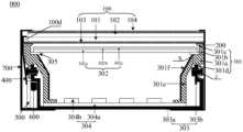
- the display module 00may include a display panel 01 , an adhesive layer 02 and a backlight module 03 .
- the display panel 01has a display area 01a and a non-display area 01b located at the periphery of the display area 01a.
- the display area 01a of the display panel 01may overlap with the display area of the display module.
- the display area 01a of the display panel 01may include: a plurality of sub-pixel areas 01c arranged in an array. One sub-pixel can be distributed in each sub-pixel area 01c. Every three adjacent sub-pixels in the display panel 01 are used to form a pixel.
- the three pixels distributed at the edge of the display panel 01 in Figure 1are: pixel B1, pixel B2 and pixel B3, and Pixel B1 is closest to the non-display area 01b.
- the row of pixels where the pixel B1 is locatedcan be called the first row of pixels close to the non-display area 01b
- the row of pixels where the pixel B2 is locatedcan be called the second row of pixels close to the non-display area 01b
- the row of pixels where the pixel B3 is locatedcan be called the second row of pixels close to the non-display area 01b.
- This row of pixelsmay be called the third row of pixels close to the non-display area 01b.
- the backlight module 03may include: a frame 031 and an optical film 032 .
- the frame 031may include: a bearing platform 031a and a support platform 031b.
- the bearing platform 031ahas a bearing surface 031c for bearing the optical film 032.
- the support platform 031bmay be fixed on the bearing surface 031c of the bearing platform 031a.
- the display panel 01can be bonded to the support base 031b in the frame 031 through the adhesive layer 02 to realize the connection between the display panel 01 and the backlight module 03 .
- the borders of current display modulesare getting narrower and narrower.
- the boundary of the display area of the display moduleis flush with the side of the support platform 031b in the backlight module 03 close to the optical film 032, and the support platform 031b is away from the optical film.
- One side of 032will not exceed display panel 01. Therefore, the width of the support platform 031b is small.
- the adhesive layer 02 between the display panel 01 and the support platform 031bis easily prone to glue overflow.
- the adhesive layer 02may include: an adhesive portion 02a located between the display panel 01 and the supporting platform 031b, and an adhesive overflow portion 02b located on one side of the adhesive portion 02a.
- the glue overflow portion 02b in the adhesive layer 02can be distributed in the display area of the display module, and the width of the glue overflow portion 02b is usually larger.
- the width of the glue overflow portion 02bis usually greater than the width of 2 pixels (that is, the 6 sub-pixel areas 01c).
- the adhesive layer 02The glue overflow part 02b in 02 stops overflowing only when it reaches the third row of pixels close to the non-display area 01b.
- FIG. 2is an optical path diagram of the light emitted by the backlight module in the display module shown in FIG. 1 .
- the side of the overflow portion 02b in the adhesive layer 02 facing away from the display panel 01is a curved surface, so the light emitted from the backlight module 03 and directed towards the second row of pixels close to the non-display area 01b will be refracted after passing through this curved surface. , most of the refracted light will emerge from the first row of pixels close to the non-display area 01b.
- FIG. 3is a schematic structural diagram of a display module provided by an embodiment of the present application.
- the display module 000may include: a display panel 100, an adhesive layer 200, and a backlight module 300.
- the backlight module 300 in the display module 000may include: a backlight source 304, a frame 301 and an optical film 302.
- the frame 301can be distributed around the backlight 304 and the optical film 302 , and the optical film 302 can be connected to the frame 301 .
- the optical film 302may, for example, play a role in smoothing the backlight.
- the adhesive layer 200 in the display module 000can be bonded to the frame 301 and the display panel 100 respectively.
- the optical film 302 in the backlight module 300is closer to the display panel 100 than the backlight source 304 .
- the adhesive layer 200is formed by curing optical glue; the optical glue is, for example, viscous. For this reason, during the process of assembling the frame 301 and the display panel 100 through the adhesive layer 200, there will be a certain amount of glue overflow in the adhesive layer 200.
- the adhesive layer 200may include: an adhesive portion located between the display panel 100 and the frame 301 (ie, the first adhesive portion 201 and the second adhesive portion 202 in subsequent embodiments), and an adhesive portion located between the display panel 100 and the frame 301 .
- Glue overflow part 203on one side of the connecting part.
- the overflow portion 203 of the adhesive layer 200can be distributed in the display area of the display module.
- the display panel 100 in the display module 000may have a display area 100a and a non-display area 100b located at the periphery of the display area 100a.
- the display area 100a of the display panel 100overlaps with the display area of the display module.
- the display panel 100may include: a plurality of effective sub-pixels 100c arranged in an array. Each effective sub-pixel 100c is distributed in the display area 100a. Among them, every three adjacent effective sub-pixels can form a pixel. For example, the three effective sub-pixels in each pixel can be distributed as: red sub-pixel, green sub-pixel and blue sub-pixel.
- the pixels C1 and pixels C2 distributed at the edge of the display panel 100each include three sub-pixels, and the pixel C1 is closest to the non-display area 100b.
- the row of pixels where the pixel C1 is locatedmay be called the first row of pixels close to the non-display area 100b
- the row of pixels where the pixel C2 is locatedmay be called the second row of pixels close to the non-display area 100b.
- the first row of pixelscan be understood as a row of pixels located in the display area closest to the edge of the display area 100a.
- the second row of pixelscan be understood as a row of pixels located in the display area next to the first row of pixels and closest to the edge of the display area 100a.
- the degree of glue overflow at different positions in the adhesive layer 200is basically the same.
- the cross-sectional shape and size of the glue overflow portion 203 of the adhesive layer 200can be considered to be the same at most positions except for these few positions.
- the cross-sections of the glue overflow portion 203 in the following embodimentsrefer to the cross-sections taken at these most locations.
- the distance from the edge of the adhesive layer 200 away from the edge of the display module 000 from the orthographic projection of the display area 100a to the edge of the display area 100ais less than or equal to the distance closest to the edge of the display area 100a.
- the first row of pixels at the edge of the display area 100ais away from the edge of the display area 100a by a distance from the edge of the display area 100a.
- the distance from the edge of the adhesive layer 200 away from the edge of the display module 000 from the orthographic projection of the display area 100a to the edge of the display area 100ais less than or equal to the distance closest to the edge of the display area 100a.
- the distance from the second effective sub-pixel 100c at the edge of the display area 100a to the edge of the display area 100a; preferably, the edge of the adhesive layer 200 away from the edge of the display module 000is at the front of the display area 100a.
- the distance projected to the edge of the display area 100ais greater than the distance from the first effective sub-pixel 100c closest to the edge of the display area 100a to the edge of the display area 100a.
- the effective sub-pixel 100cmay be strip-shaped, and at least one side of the display module 000 includes the side where the extension direction of the adhesive layer 200 is the same as the extension direction of the strip-shaped sub-pixel; for example, the shape of the effective sub-pixel 100c is a rectangle. , which includes a long side and a short side, and at least one side of the display module 000 includes a side where the extending direction of the adhesive layer 200 is the same as the extending direction of the long side of the rectangle.
- at least one side of the display module 000includes opposite two sides of the display module 000.
- the distance from the edge of the adhesive layer 200 away from the display module 000 from the front projection of the display area 100a to the edge of the display area 100ais the same.
- the maximum cross-sectional width d0 of the overflow portion 203may be less than or equal to the overall width of the two effective sub-pixels 100c closest to the edge of the display area 100a. It should be noted that the glue overflow portion 203 has different cross-sectional widths at different heights. For this reason, the area of the cross-section at a certain height in the glue overflow portion 203 is the largest. The width of the cross section at this position is the width of the glue overflow portion 203 . Maximum cross-sectional width; for example, in FIG. 3 , the glue overflow portion 203 has the maximum cross-sectional width at the position closest to the display panel 100 .
- the overall width of two effective sub-pixels 100ccan be understood as the overall spanned distance in the width direction of two continuously distributed sub-pixels 100c; for example, the shape of the effective sub-pixel 100c is a rectangle, which includes long sides and short sides, The width direction is the extension direction of the short side of the effective sub-pixel 100c.
- the cross-section of a certain structure in the embodiment of the present applicationrefers to the cross-section perpendicular to the plane where the light-emitting surface of the display panel 100 is located and perpendicular to the extension direction of the structure.
- the cross section of the glue overflow portion 203is a cross section perpendicular to the plane of the light exit surface of the display panel 100 and perpendicular to the extension direction of the glue overflow portion 203 .
- a black matrix with multiple light holesis usually provided in the display panel 100, and the multiple light holes in the black matrix can be connected to the multiple effective sub-pixels 100c provided in the display panel 100.
- the area where the effective sub-pixel 100c is locatedincludes: the area where the corresponding light-transmitting hole is located, and the area where the light-shielding part surrounding the light-transmitting hole is located.
- the light-shielding portion surrounding the light-transmitting holeis a part of the black matrix, and the width of the light-shielding portion surrounding the light-transmitting hole is equal to half the width of the black matrix located between two adjacent light-transmitting holes.
- the width of the effective sub-pixel 100cis equal to: the sum of the width of the area where the corresponding light-transmitting hole is located, the width of the light-shielding portion located on one side of the light-transmitting hole, and the width of the light-shielding portion located on the other side of the light-transmitting hole. . It should be noted that for the effective sub-pixel 100c closest to the edge of the display area 100a, it can be considered that the width of the light-shielding portion close to the edge of the display area 100a is equal to the width of the light-shielding portion far from the edge of the display area 100a.
- the widths of each effective sub-pixel 100cmay be the same, and the overall width of the two effective sub-pixels 100c closest to the edge of the display area 100a is equal to twice the width of a single effective sub-pixel 100c.
- one boundary of the active sub-pixel 100c closest to the edge of the display area 100acoincides with the edge of the display area 100a.
- the overflow portion 200c in the adhesive layer 200stops when it reaches the first row of pixels close to the non-display area 100b. Glue overflow. In this way, even if the display panel 100 and the frame 301 in the embodiment of the present application are bonded through the adhesive layer 200, although the adhesive layer 200 will still overflow, the maximum glue overflow portion 203 of the adhesive layer 200 will The cross-sectional width d0 is small, so that the glue overflow portion 203 will not affect the normal display of the display panel 100 .
- FIG. 4is an optical path diagram of the light emitted by the backlight module in the display module shown in FIG. 3 .
- the maximum cross-sectional width d0 of the glue overflow portion 203 in the adhesive layer 200is small, the light emitted from the backlight module 300 and directed to the second row of pixels close to the non-display area 100b will not be interfered by the glue overflow portion 203.
- FIG. 5is a partial enlarged view of the display module shown in FIG. 3 at E.
- the frame 301 in the backlight module 300may include: a carrying platform 301a, a supporting platform 301b and a retaining wall 301c.
- the carrying platform 301a in the frame 301includes a carrying surface S for carrying the optical film 302.
- the support platform 301b in the frame 301can be fixed on the bearing surface S.
- the retaining wall 301c in the frame 301can be fixed on the side of the support platform 301b away from the bearing surface S.
- the adhesive layer 200may include: a first adhesive part 201 and a second adhesive part 202.
- the first bonding part 201may be located between the blocking wall 301c and the display panel 100 in the frame 301, and the first bonding part 201 may be bonded to the blocking wall 301c and the display panel 100 respectively.
- the second bonding part 202is located between the support platform 301b and the display panel 100 in the frame 301, and the second bonding part 202 can be bonded to the support platform 301b and the display panel 100 respectively.
- the glue overflow portion 203 in the adhesive layer 200can be located on a side of the first bonding portion 201 away from the second bonding portion 202 , and the glue overflow portion in the adhesive layer 200 can be bonded to the display panel 100 .
- the second bonding part 202is closer to the edge of the display module 000 than the first bonding part 201 .
- the edge of the display module 000refers to: the side edge of the display module 000; for example, when the display module 000 is a rectangular display module, it includes 4 sides, and the 4 sides are in the display
- the shape enclosed by the orthographic projection on the light exit surface of the panel 000is a rectangle.
- the retaining walls 301ccan be distributed on the side of the supporting platform 301b away from the edge of the display module 000.
- the glue overflow amount in the adhesive layer 200is applied to the display area of the display module 000 so that the maximum cross-sectional width d0 of the glue overflow portion 203 subsequently formed in the adhesive layer 200 is smaller.
- the display moduleprovided by the embodiment of the present application includes: a display panel, an adhesive layer and a backlight module.
- a retaining wallis provided on the side of the support platform away from the bearing surface of the bearing platform.
- the retaining wallcan block the adhesive layer.
- the amount of glue overflowis applied to the display area of the display module so that the maximum cross-sectional width of the glue overflow portion subsequently formed in the adhesive layer is smaller.
- the maximum cross-sectional width of the overflow portion in the adhesive layeris less than or equal to the overall width of the two effective sub-pixels closest to the edge of the display area of the display panel.
- the light emitted from the backlight module and directed to each pixelcan emit from the corresponding pixel normally.
- the probability of dark lines appearing at the edge of the image displayed on the display panelcan be effectively reduced, thereby effectively improving the display effect of the display panel.
- FIG. 6is a partial enlarged view of another display module provided by the embodiment of the present application.
- the ratio of the minimum width d 1 of the section of the retaining wall 301 c in the frame 301 to the minimum distance d 2 between the side of the retaining wall 301 c close to the edge of the display module 000 and the side of the supporting platform 301 b close to the edge of the display module 000is less than or equal to 1. That is to say, the minimum width d 1 of the section of the retaining wall 301 c and the width d 3 of the section of the supporting platform 301 b on the side close to the retaining wall 301 c satisfy: d 1 ⁇ d 3 /2.
- the retaining wall in the frame 301when the side of the retaining wall 301c in the frame 301 away from the edge of the display module 000 and the side of the support platform 301b in the frame 301 away from the edge of the display module 000 are both flat, the retaining wall in the frame 301
- the side of 301c away from the edge of the display module 000may be flush with the side of the support platform 301b in the frame 301 away from the edge of the display module 000.
- the minimum width d 1 of the section of the retaining wall 301 c and the width d 3 of the section of the supporting platform 301 b on the side close to the retaining wall 301 calso satisfy: d 1 ⁇ d 3 /4.
- the retaining wall 301ccan effectively block the amount of glue overflowing from the adhesive layer 200 to the display area of the display module 000, and ensure that the glue overflow portion 203 formed after the adhesive layer 200 is cured is parallel to the optical film.
- the width in the direction of sheet 302is smaller.
- the minimum height h of the blocking wall 301 in the frame 301is less than the minimum distance between the display panel 100 and the support platform 301b in the frame 301 H.
- the minimum height h of the blocking wall 301 and the minimum distance H between the support platform 301b and the display panel 100satisfy: H/4 ⁇ h ⁇ 3H/ 4.
- the first adhesive portion 201 in the adhesive layer 200can be distributed between the retaining wall 301c and the display panel 100, and the cross-sectional width of the first adhesive portion 201 in the adhesive layer 200 is equal to that of the retaining wall 301c.
- the second bonding portion 202 in the bonding layer 200is distributed between the support platform 301b and the display panel 100, and the cross-sectional width of the second bonding portion 202 can be equal to the side of the retaining wall 301c close to the edge of the display module 000.
- the display panel 100can be bonded to the frame 301 through the first bonding part 201 and the second bonding part 202 at the same time to ensure that the display panel 100 and the frame 301 can be firmly bonded, thereby ensuring that the display panel 100
- the assembly strength after being assembled with the backlight module 300is high.
- the amount of glue overflowing from the adhesive layer 200 to the display area of the display module 000will be greater.
- the maximum cross-sectional width d0 of the glue overflow portion 203 subsequently formed in the adhesive layer 200will be larger.
- the adhesive layer after curing The adhesive force of 200is insufficient to fix the display panel 100 on the frame 301 , resulting in weak assembly strength between the display panel 100 and the backlight module 300 .
- the minimum distance H between the support platform 301b and the display panel 100is greater than or equal to 0.2 mm; and/or, in a direction perpendicular to the light-emitting surface of the display panel 100 In the direction of the plane, the minimum distance H between the support platform 301b and the display panel 100 is less than or equal to 0.5 mm. That is, in the direction perpendicular to the plane where the light-emitting surface of the display panel 100 is located, the minimum distance H between the supporting platform 301b and the display panel 100 ranges from 0.2 mm to 0.5 mm.
- the adhesive layer 200 to be coatedwill not be too large or too small, and it can be ensured that the maximum cross-sectional width d0 of the glue overflow portion 203 in the adhesive layer 200 is small, so that the adhesive layer can be
- the second bonding part 202 in the bonding layer 200can firmly bond the display panel 100 and the support base 301b together to ensure that the display panel 100 and the frame 301 can be firmly bonded.
- the use of the minimum width (or minimum height) of the cross-section of a certain structure in the above embodimentstakes into account the situation that the shape of the cross-section of the structure is not a regular shape; it can be understood that if the cross-section of a certain structure is a regular shape, then the width at any position of the cross-section of this structure is the same (or the height at any position is the same), and the minimum width (or minimum height) is the width of the cross-section (or high).
- the width d 1 at any position of the cross-section of the retaining wall 301cis the same, and the height h at any position of the cross-section of the retaining wall 301c is also the same.
- the minimum distance between two structures in the above embodimentstakes into account the situation that the surfaces of these structures are not planar; it can be understood that if the surfaces of these structures are all planar, then the distance between the two structures The distance is the same at any position, and the minimum distance is the distance between the two structures. For example, when the side of the supporting platform 301b close to the display panel is flat and the side of the display panel 100 close to the frame 301 is flat, the distance H at any position between the supporting platform 301b and the display panel 100 is the same.
- the maximum cross-sectional width D of the portion of the adhesive layer 200 close to the retaining wall 301cis greater than or equal to 1 mm.
- the cross-sectional shape of the retaining wall 301cis a rectangle, and the side of the supporting platform 301b close to the display panel 100 is parallel to the plane where the light-emitting surface of the display panel 100 is located, then the maximum cross-sectional width D of the adhesive layer 200 can be equal to: The width of the part 201 (that is, the width d 1 of the retaining wall), the width of the second bonding part 201 (that is, the side of the retaining wall 301 c close to the edge of the display module 000 and the side of the supporting platform 301 b close to the edge of the display module 000 The sum of the distance d 2 ) and the maximum cross-sectional width d0 of the glue overflow part 203.
- the bonding strength between the display panel 100 and the frame 301can be further improved.
- the glue overflow portion 203 in the adhesive layer 200can also play a role in improving the bonding strength between the display panel 100 and the frame 301 .
- the maximum cross-sectional width d0 of the glue overflow portion 203 in the adhesive layer 200is less than or equal to the entirety of the two effective sub-pixels 100c closest to the edge of the display area 100a. width. For this reason, during the process of using the adhesive layer 200 to bond the display panel 100 and the frame 301 , the amount of glue overflowing from the adhesive layer 200 to the display area of the display module 000 reaches the third area close to the non-display area 100b. A row of pixels will stop overflowing to ensure that the light emitted from the backlight module 300 and directed to each pixel can emit from the corresponding pixel normally.
- the retaining wall 301c provided in the frame 301can reduce the amount of glue overflow in the adhesive layer 200 during the process of bonding the display panel 100 and the frame 301. Therefore, not only the width of the glue overflow portion 203 is smaller, but also the maximum thickness of the glue overflow portion 203 is smaller. For example, in the direction perpendicular to the plane of the light exit surface of the display panel 100, the maximum thickness h0 of the glue overflow portion 203 in the adhesive layer 200 is less than or equal to 2 of the minimum distance b between the blocking wall 301c and the display panel 100. times.
- the maximum thickness h0 of the glue overflow portion 203 in the adhesive layer 200is less than or equal to 1.6 times the minimum distance b between the blocking wall 301c and the display panel 100. . In this way, it can be ensured that the overflow part 203 has weak refraction of light, so that the light emitted from the backlight module 300 and directed toward the first row of pixels close to the non-display area 100b can normally emit from this row of pixels.
- the shear strength P of the adhesive layer 200meets the following conditions:
- the shear strength P of the adhesive layer 200meets the above conditions, it can be ensured that the adhesive layer 200 is not prone to breakage, thereby ensuring that the display panel 100 and the backlight module 300 can be bonded together. Layer 200 is firmly bonded.
- the shear strength P of the adhesive layer 200needs to be greater than or equal to 5.1 MPa.
- the cross-sectional area S1’ of the glue overflow portion 203 in the adhesive layer 200 and the cross-sectional area S2’ of the retaining wall 301csatisfy the following conditions:
- His the minimum distance between the support platform 301b and the display panel 100.
- cross-sectional area S0 of the glue overflow portion in the adhesive layercan be approximately expressed as follows:
- the difference between the cross-sectional area S0 of the glue overflow part when the retaining wall is not set and the cross-sectional area S1' of the glue overflow part when the retaining wall is setneeds to be less than or equal to the retaining wall.
- the cross-sectional area of wall 301cis S2'.
- the cross section of the glue overflow portion 203 in the adhesive layer 200may include: an adhesive surface S01 and an arcuate surface S02.
- the bonding surface S01can be bonded to the display panel 100
- the arcuate surface S02can be located on a side of the bonding surface S01 away from the display panel 100
- the maximum distance between the arcuate surface S02 and the display panel 100can be greater than or equal to The maximum distance H between display panels 100 .
- the maximum distance between the arc surface S02 and the display panel 100is: the maximum thickness h0 of the glue overflow portion 203 in the adhesive layer 200 in a direction perpendicular to the plane of the light emitting surface of the display panel 100 .
- the cross-sectional shape of the glue overflow portion 203 in the adhesive layer 200can be approximately regarded as consisting of a fan shape 203a and a trapezoid 203b.
- the arc surface S02is the arc surface of the sector 203a
- the bonding surface S01is the side of the sector 203a close to the display panel 100 and the side of the trapezoid 203b close to the display panel 100.
- the sector central angle of the sector 203ais approximately 90°
- the radius r of the sector 203acan be equal to the maximum thickness h0 of the glue overflow portion 203.
- the radius r of this sector 203amay be related to the minimum distance b between the retaining wall 301c and the display panel 100.
- the radius r of this sector 203amay also be less than or equal to 1.6 times the minimum distance b between the retaining wall 301c and the display panel 100.
- the length of the top and bottom of the trapezoid 203bis approximately equal to the distance b between the retaining wall 301c and the display panel 100.
- the length of the bottom of the trapezoid 203bis approximately equal to the radius r of the sector 203a.
- the height of the trapezoid 203bis equal to the width of the effective sub-pixel 100c and the width of the sector 203a. Radius r is related.
- the height of this trapezoid 203bcan be approximately It is equal to the difference between the overall width a of the two effective sub-pixels 100c closest to the edge of the display area 100a and the radius r of the sector 203a. For this reason, the maximum effective area S1 of the cross-section of the glue overflow portion 203 can be approximately calculated through these relationships.
- the maximum effective area S1 of the cross-section of the glue overflow part 203refers to: when the maximum cross-sectional width d0 of the glue overflow part 203 is equal to the overall width of the two effective sub-pixels 100c closest to the edge of the display area 100a, this glue overflow part Equivalent area of 203.
- retaining wall 301ccan meet the following conditions:
- the overall width of the two effective sub-pixels on the edge; S2can be considered as the effective cross-sectional area of the retaining wall 301c.
- the cross-sectional area of the glue overflow portion 203 in the adhesive layer 200can be used to determine whether the size of the glue overflow portion 203 meets the design requirements.
- the embodiments of the present applicationare schematically explained by taking the cross-section shape of the retaining wall 201c as a rectangle as an example.
- the cross-section shape of the retaining wall 201ccan also be a regular shape such as a trapezoid or a semicircle, or other irregular shapes. This is not limited in the embodiment of the present application, but it is required Ensure that the cross-sectional area of the retaining wall 201c can meet the above conditions.
- the design of retaining wall 301ccan also meet the following conditions:
- His the minimum distance between the support platform 301b and the display panel 100; d 1 is the minimum width of the section of the blocking wall 301c; h is the minimum width of the blocking wall 301c in the direction perpendicular to the plane where the light exit surface of the display panel 100 is located.
- S2can be considered is the effective cross-sectional area of the retaining wall 301c.
- the above embodimentsare all schematically explained by taking the number of retaining walls 201c distributed on the support platform 201b as one example.
- the number of retaining walls 201ccan also be multiple. This is not limited in the embodiment of the present application, but it is necessary to ensure that the sum of the cross-sectional areas of each retaining wall 201c distributed on the support platform 201b can meet the above conditions.
- FIG. 8is a partially enlarged view of yet another display module provided by an embodiment of the present application.
- At least two retaining walls 201care distributed side by side on the side of the support platform 301b in the frame 301 away from the bearing surface S, and each retaining wall 201c can be distributed in parallel.
- the adhesive layer 200may also include: an auxiliary adhesive portion 204 located in the gap. In this way, through the auxiliary bonding portion 204 located in the gap in the adhesive layer 200, the firmness when the display panel 100 and the frame 301 are bonded can be further improved.
- each retaining wall 201 cmay be distributed side by side on the side of the support platform 301 b in the frame 301 away from the bearing surface S, on a plane perpendicular to the light emitting surface of the display panel 100 .
- the minimum heightmay be the same as the minimum height h of the retaining wall 201c in the above embodiment; the sum of the cross-sectional widths of each retaining wall 201c is equal to the minimum width d 1 of the cross-section of the retaining wall 201c and the retaining wall 301c in the above embodiment.
- the side of the display panel 100is aligned with the side of the frame 301 close to the edge of the display module 000 , or protrudes from the frame 301 .
- the orthographic projection of the supporting platform 301b on the display panel 100is located in the non-display area 100b of the display panel 100.
- the width d 3 of the side of the support platform 301 b close to the retaining wall 301 cis less than or equal to the width d 4 of the non-display area 100 b.
- the boundary of the display area 100acan be aligned with the side of the supporting platform 301b away from the edge of the display module 000. In this way, not only can it be ensured that the frame 301 will not block the display area 100a of the display panel 100, so that the display panel 100 can display images normally, but it can also be ensured that the width of the frame of the display module 000 is small.
- the alignment setting of certain two planes in the embodiments of this applicationmeans that the two planes are flush, but if there are assembly errors in the actual reference, the two planes may not be set exactly to each other, but It is necessary to ensure that one plane is offset by ⁇ 0.2 mm relative to the other plane.
- the display module 000may include a plurality of blocking walls 301 extending along the edge of the display module 000.
- the plurality of blocking walls 301are respectively located on multiple sides of the display module, and the plurality of blocking walls 301 are displayed on the screen.
- the orthographic projection on the panel 100is distributed around the display area 100a.
- orthographic projections of the plurality of blocking walls 301 on the display panel 100surround at least two sides of the display area 100a.
- the orthographic projections of these blocking walls on the display panel 100surround the opposite sides or adjacent sides of the display area 100a; when the number of blocking walls 301 is When the number of blocking walls is three, the orthographic projections of these blocking walls on the display panel 100 surround three sides of the display area 100a; when the number of blocking walls 301 is four, the orthographic projections of these blocking walls on the display panel 100 surround On the four sides of the display area 100a, at this time, the orthographic projection of the blocking wall 301c on the display panel 100 is defined to surround the display area 100a.
- FIG. 9is a schematic structural diagram of a display module provided by another embodiment of the present application.
- the display module 000includes a plurality of blocking walls 301c extending along the edge of the display module 000.
- the plurality of blocking walls 301care located on each side of the display module 000, that is, the plurality of blocking walls 301c are located directly on the display panel 100.
- the projectionis distributed around the display area of the display panel 100 .
- the retaining wall 301c in the frame 301may be annular, and the orthographic projection of the retaining wall 301c on the display panel 100 may be distributed around the display area 100a of the display panel 100. In this way, the retaining walls 301c are distributed at any position of the frame 301, so that the width of the glue overflow portion 203 at any position in the adhesive layer 200 is relatively small.
- the second possible implementationis as shown in Figure 10, which is a schematic structural diagram of another display module provided by another embodiment of the present application.
- the non-display 100b of the display panel 100may include a binding area 100d.
- the display panel 100may include: an array substrate 101 and a color filter substrate 102 arranged opposite each other, and at least one side of the array substrate 101 protrudes from the color filter substrate 102, and one of the array substrates 101 protrudes from the color filter substrate 102.
- the partis the part where the binding area 100d is located.
- the binding area 100dmay be distributed on the first side of the display area 100a, and the orthographic projection of the blocking wall 301c in the frame 301 on the display panel 100 is distributed on other parts of the display area 100a except the first side. side.
- the width of the non-display area 100b of the display panel 100is larger on the side where the binding area 100d is provided. Therefore, even if the retaining wall 301c is not provided on this side, it can be ensured that the adhesive layer 200 has less glue overflow on this side, so the glue overflow on this side will not affect the normal display of the display panel 100.
- the width of the other side of the non-display area 100b of the display panel 100 where the binding area 100d is not providedis smaller. Therefore, it is necessary to set retaining walls 301c on these sides to reduce the amount of glue overflow of the adhesive layer 200 on these sides to ensure that the glue overflow on these sides will not affect the normal display of the display panel 100 .
- the backlight module 300 in the display module 000may further include: a backplane 303 .
- the back plate 303may be located on a side of the optical film 302 facing away from the display panel 100 , and the back plate 303 may be fixedly connected to the frame 301 .
- the backlight 304may be disposed between the back plate 303 and the optical film 302 .
- the backlight source 304may be disposed on the back panel 303, and the backlight source 304 is also generally referred to as a light panel.
- the frame 301may also include: a connecting portion 301d fixedly connected to the side of the carrying platform 301a facing away from the supporting platform 301b.
- the backplane 303may include: a backplane body 303a for supporting the backlight 304, and an adapter portion 303b fixedly connected to an edge of the backplane body 303a.
- the connecting portion 301d in the frame 301 and the adapter portion 303b in the back plate 303can be fixedly connected through screws F, so that the frame 301 can be fixedly connected to the back plate 303.
- the backlight 304may include: a circuit board 304a located on the side of the backplane body 303a close to the optical film 302, and a plurality of circuit boards 304a located on the side of the circuit board 304a away from the backplane body 303a and electrically connected to the circuit board 304a.
- the light-emitting element 304bcan be a light-emitting diode (English: Light-Emitting Diode; abbreviation: LED).
- the frame 301 in the backlight module 300can also include: a surrounding body 301e fixedly connected to the carrying platform 301a.
- the surrounding body 301ecan be distributed around the edge of the backlight source 304, and the surrounding body 301e is close to the edge of the backlight source 304.
- One sidehas a reflective layer 301f.
- one end of the surrounding body 301e close to the backplane body 303acan limit the edge of the circuit board 304a in the backlight 304.
- the light rays emitted by the backlight source 304 and directed toward the surrounding body 301ecan be reflected by the reflective layer 301f, so that these light rays can pass through the optical film 302 and then be directed toward the display panel 100.
- the backlight module 300may further include: a light guide structure 305 located on the bearing surface S of the bearing platform 301a.
- the support platform 301b in the frame 301is closer to the edge of the display module than the light guide structure 305.
- the optical film 302 in the backlight module 300may be located on the side of the light guide structure 305 away from the carrying surface S.
- the light guide structure 305may be in a ring shape. In this way, among the light emitted by the backlight 304, the light directed to the edge of the display module 000 can be guided by the light guide structure 305, so that the light guided by the light guide structure 305 can pass through the optical film 302 and then be emitted.
- the pixelsare arranged at the edge position of the display panel 100 to ensure that light can still be emitted normally at the edge position of the display area 100a of the display panel 100 .
- the optical film 302 in the backlight module 300may include: at least one of a diffusion plate 302a, a lower prism sheet 302b, and an upper prism sheet 302c.
- the diffusion plate 302a, the lower prism sheet 302b and the upper prism sheet 302cmay be stacked in a direction away from the bearing surface S.
- the display panel 100 in the display module 000may also include: a first polarizer 103 located on the side of the array substrate 101 facing away from the color filter substrate 102, and a second polarizer 103 located on the side of the color filter substrate 102 facing away from the array substrate 101.
- Polarizer 104located on the side of the color filter substrate 102 facing away from the array substrate 101.
- the polarization direction of the first polarizer 103may be perpendicular to the polarization direction of the second polarizer 104 .
- the display module 000may also include: a chip on flex (English: Chip On Flex; referred to as: COF) 400 that is bound and connected to the array substrate 101, and a printed circuit board that is electrically connected to the side of the COF 400 away from the array substrate 101.
- Printed circuit boards(English: Printed circuit boards; abbreviation: PCB) 500.
- PCB 500There is a buffer layer 600 between the PCB 500 and the adapter portion 303b in the backplane 303. The PCB 500 can be buffered through the buffer layer 600 to prevent the PCB 400 from being damaged after the display module 000 is stressed.
- the display module 000may further include: an auxiliary adhesive layer 700 wrapped around the edge area of the display panel 100 and the edge area of the backlight module 300 .
- the auxiliary adhesive layer 700can improve the firmness when the display panel 100 and the backlight module 300 are assembled.
- the display moduleprovided by the embodiment of the present application includes: a display panel, an adhesive layer and a backlight module.
- a retaining wallis provided on the side of the support platform away from the bearing surface of the bearing platform.
- the retaining wallcan block the adhesive layer.
- the amount of glue overflowis applied to the display area of the display module so that the maximum cross-sectional width of the glue overflow portion subsequently formed in the adhesive layer is smaller.
- the maximum cross-sectional width of the overflow portion in the adhesive layeris less than or equal to the overall width of the two effective sub-pixels closest to the edge of the display area of the display panel.
- the light emitted from the backlight module and directed to each pixelcan emit from the corresponding pixel normally.
- the probability of dark lines appearing at the edge of the image displayed on the display panelcan be effectively reduced, thereby effectively improving the display effect of the display panel.
- FIG. 11is a schematic structural diagram of a display module provided by yet another embodiment of the present application.
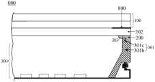
- the display module 000may include: a display panel 100, an optical film 302, a frame 301 and an adapter layer 200.
- the optical film 302 in the display module 000can be bonded to the light incident surface of the display panel 100 (that is, the side opposite to the display surface).
- the display panel 100 and the optical film 302may be bonded through an optical adhesive layer 800 .
- the optical film 302may, for example, play a role in smoothing the backlight.
- the frame 301 in the display module 000may be located on the side of the optical film 302 facing away from the display panel 100 .
- the frame 302may include: a support platform 301b, and a retaining wall 301c fixed on a side of the support platform 301b close to the optical film 301.
- the outer surface of the support base 301bprotrudes from the outer surface of the retaining wall 301c.
- the width of the retaining wall 301cis smaller than the width of the supporting platform 301b.
- the support platform 301b in the frame 301 of the display module 000is usually annular. Therefore, the outer side of the support platform 301b refers to the side of the support platform 301b that is away from the annular area enclosed by the support platform 301b.
- the outer surface of the retaining wall 301c and the outer surface of the support base 301bare located on the same side.
- the frame 301 and the optical film 302 in the display module 000are used to form the backlight module 300 in the display module 000 .
- the adhesive layer 200 in the display module 000may include: a first adhesive part 201 and a second adhesive part 202 .
- the first bonding part 201may be located between the blocking wall 301c and the display panel 100 in the frame 301, and the first bonding part 201 may be bonded to the blocking wall 301c and the display panel 100 respectively.
- the second bonding part 202is located between the support platform 301b and the display panel 100 in the frame 301, and the second bonding part 202 can be bonded to the support platform 301b and the display panel 100 respectively.
- the adhesive layer 200may also include: located on the side of the first adhesive part 201 facing away from the second adhesive part 202, and the glue overflow part in the adhesive layer 200 may be adhered to the display panel 100.
- the second bonding part 202is closer to the edge of the display module 000 than the first bonding part 201 .
- the minimum width d 1 of the section of the retaining wall and the width d 3 of the section of the support platform close to the retaining wallsatisfy: d 1 ⁇ d 3 /2.
- the side of the retaining wall close to the optical filmis flush with the side of the support platform close to the optical film.
- the minimum width d 1 of the section of the retaining wall and the width d 3 of the section of the supporting platform on the side close to the retaining wallalso satisfy: d 1 ⁇ d 3 /4.
- the minimum height h of the retaining wall in the direction perpendicular to the plane where the light exit surface of the display panel is located, and the minimum distance H between the support platform and the display panelsatisfy: H/4 ⁇ h ⁇ 3H/4.
- the minimum distance between the display panel and the support platformis greater than or equal to 0.2 mm; and/or, in the direction perpendicular to the plane of the light-emitting surface of the display panel On the screen, the minimum distance between the display panel and the support platform is less than or equal to 0.5 mm.
- the maximum cross-sectional width of the portion of the bonding layer close to the retaining wallis greater than or equal to 1 mm.
- the adhesive layeralso includes: an adhesive overflow portion located on the side of the first adhesive portion facing away from the second adhesive portion, and the adhesive overflow portion is bonded to the display panel;
- the display panelincludes a plurality of effective sub-pixels arranged in an array, and the maximum cross-sectional width of the overflow portion is less than or equal to the overall width of the two effective sub-pixels closest to the edge of the display area of the display panel.
- the maximum thickness of the overflow partis less than or equal to 2 times the minimum distance between the display panel and the retaining wall.
- the cross-section of the glue overflow partincludes: an adhesive surface and an arcuate surface.
- the adhesive surfaceis bonded to the display panel.
- the arcuate surfaceis located on the side of the adhesive surface away from the display panel, between the arcuate surface and the display panel.
- the maximum distanceis greater than or equal to the maximum distance between the support platform and the display panel.
- cross-sectional area S1’ of the glue overflow part and the cross-sectional area S2’ of the retaining wallmeet the following conditions:
- His the minimum distance between the support platform and the display panel.
- the relevant dimensions of the retaining wallmeet the following conditions:
- His the minimum distance between the support platform and the display panel
- d 1is the minimum width of the section of the retaining wall
- his the minimum height of the retaining wall in the direction perpendicular to the plane of the light exit surface of the display panel
- ris the arc The radius of the surface
- h0is the maximum thickness of the glue overflow part
- bis the minimum distance between the retaining wall and the display panel
- ais the overall width of the two effective sub-pixels closest to the edge of the display area.
- the relevant dimensions of the retaining wallmeet the following conditions:
- His the minimum distance between the support platform and the display panel
- d 1is the minimum width of the section of the retaining wall
- his the minimum height of the retaining wall in the direction perpendicular to the plane of the light exit surface of the display panel
- ris the arc The radius of the surface
- h0is the maximum thickness of the glue overflow part
- bis the minimum distance between the retaining wall and the display panel
- a'is the second effective sub-pixel closest to the edge of the display area of the display panel and away from the edge of the display area The distance between the orthographic projection of one side on the display panel and the orthographic projection of the retaining wall on the display panel.
- the shear strength P of the adhesive layermeets the following conditions:
- the adhesive layeris formed by curing optical glue.
- the bonding layeralso includes: an auxiliary bonding part located in the gap.
- the display panelhas a display area and a non-display area located on the periphery of the display area, and the width of the cross section of the support platform close to the retaining wall is less than or equal to the width of the non-display area.
- the boundary support platform of the display areais aligned with a side close to the optical film.
- the display moduleincludes multiple retaining walls extending along the edge of the display module.
- the multiple retaining wallsare located on multiple sides of the display module.
- the orthographic projections of the multiple retaining walls on the display panelsurround the display area of the display panel. distributed.
- the non-display areaincludes a binding area, the binding area is distributed on the first side of the display area, and the orthographic projection of the blocking wall on the display panel is distributed on other sides of the display area except the first side.
- the backlight modulealso includes a backplane, which is located on the side of the optical film facing away from the display panel; the frame is fixedly connected to the backplane; and the backlight source is arranged between the backplane and the optical film.
- the framealso includes: a surrounding body fixedly connected to the support platform, the surrounding body is distributed around the backlight source, and the surrounding frame body has a reflective layer on a side close to the light panel.
- the optical filmincludes: at least one of a diffusion plate, a lower prism sheet, and an upper prism sheet.
- FIG. 12is a schematic structural diagram of a backlight module provided by an embodiment of the present application.
- the backlight assembly 300may include: a backlight source 304, a frame 301, and an optical film 302.
- the frame 301 in the backlight module 300may include: a carrying platform 301a, a supporting platform 301b and a retaining wall 301c.
- the carrying platform 301a in the frame 301includes a carrying surface S for carrying the optical film 302.
- the support platform 301b in the frame 301can be fixed on the bearing surface S.
- the retaining wall 301c in the frame 301can be fixed on the side of the support platform 301b away from the bearing surface S.
- An embodiment of the present applicationalso provides a display device, which may include a plurality of spliced display modules.
- Each display moduleincludes: the display module shown in Figure 3, Figure 6, Figure 7, Figure 8, Figure 9, Figure 10 or Figure 11.
- first and secondare used for descriptive purposes only and are not to be construed as indicating or implying relative importance.
- pluralityrefers to two or more than two, unless expressly limited otherwise.
Landscapes
- Physics & Mathematics (AREA)
- Nonlinear Science (AREA)
- Mathematical Physics (AREA)
- Chemical & Material Sciences (AREA)
- Crystallography & Structural Chemistry (AREA)
- General Physics & Mathematics (AREA)
- Optics & Photonics (AREA)
- Liquid Crystal (AREA)
- Devices For Indicating Variable Information By Combining Individual Elements (AREA)
Abstract
Description
Translated fromChinese本申请涉及显示技术领域,特别涉及一种显示模组及显示装置。The present application relates to the field of display technology, and in particular to a display module and a display device.
为了提高用户使用显示装置的舒适度,出现了屏幕尺寸较大,且边框较窄的窄边框的显示装置。相关技术中,显示装置通常可以包括:背光模组和液晶显示面板,该背光模组的种类可以包括直下式的背光模组和侧入式的背光模组,其中,直下式的背光模组更容易制备出窄边框的显示装置。In order to improve the user's comfort when using a display device, a display device with a larger screen size and a narrow frame has emerged. In the related art, a display device usually includes: a backlight module and a liquid crystal display panel. The types of the backlight module may include a direct-type backlight module and an edge-type backlight module. The direct-type backlight module is more It is easy to prepare a display device with a narrow frame.
传统的直下式的背光模组通常可以包括:光学膜片、灯板、框体和背板,光学膜片和灯板通常是上下叠加设置的,框体用于包裹光学膜片和灯板,背板用于对灯板进行支撑。在背光模组与显示面板的装配过程中,需要在显示面板与背光模组中的框体之间设置粘接层,粘接层可以分别与显示面板与框体粘接。A traditional direct-lit backlight module usually includes: an optical film, a light panel, a frame and a back panel. The optical film and the light panel are usually stacked up and down. The frame is used to wrap the optical film and the light panel. The back panel is used to support the light panel. During the assembly process of the backlight module and the display panel, an adhesive layer needs to be provided between the display panel and the frame in the backlight module. The adhesive layer can be bonded to the display panel and the frame respectively.
然而,目前的显示装置的边框越来越窄,显示装置的显示区的外边界与背光模组中的框体的内边界之间的距离越来越小。这样,在采用粘接层粘接显示面板与框体的过程中,位于显示面板与框体之间的粘接层极易出现溢胶的现象,而溢出的胶体会分布在显示区内,导致显示装置的显示效果较差。However, the borders of current display devices are getting narrower and narrower, and the distance between the outer boundary of the display area of the display device and the inner boundary of the frame in the backlight module is getting smaller and smaller. In this way, during the process of using an adhesive layer to bond the display panel and the frame, the adhesive layer located between the display panel and the frame is easily prone to glue overflow, and the overflowed glue will be distributed in the display area, resulting in The display effect of the display device is poor.
发明内容Contents of the invention
本申请实施例提供了一种显示模组及显示装置,可以解决现有技术的显示模组的显示效果较差的问题,所述技术方案如下:The embodiment of the present application provides a display module and a display device, which can solve the problem of poor display effect of the display module in the prior art. The technical solution is as follows:
一方面,提供了一种显示模组,包括:On the one hand, a display module is provided, including:
显示面板;display panel;
粘接层;adhesive layer;
背光模组,所述背光模组包括:背光源、框体和光学膜片;Backlight module, the backlight module includes: a backlight source, a frame and an optical film;
所述框体包括:承载台、支撑台和挡墙,所述承载台包括用于承载所述光学膜片的承载面,所述支撑台固定在所述承载面上;所述挡墙固定在所述支撑台背离所述承载面的一面上;The frame includes: a bearing platform, a support platform and a retaining wall. The bearing platform includes a bearing surface for carrying the optical film. The support platform is fixed on the bearing surface; the retaining wall is fixed on On the side of the support platform facing away from the bearing surface;
其中,所述粘接层包括:第一粘接部分和第二粘接部分,所述第一粘接部分位于所述挡墙与所述显示面板之间,且分别与所述挡墙和所述显示面板粘接,所述第二粘接部分位于所述支撑台与所述显示面板之间,且分别与所述支撑台与所述显示面板粘接;Wherein, the adhesive layer includes: a first adhesive part and a second adhesive part, the first adhesive part is located between the retaining wall and the display panel, and is connected to the retaining wall and the display panel respectively. The display panel is bonded, and the second bonding part is located between the support platform and the display panel, and is bonded to the support platform and the display panel respectively;
所述第二粘接部分相对于所述第一粘接部分更靠近所述显示模组的边缘。The second bonding part is closer to the edge of the display module than the first bonding part.
可选的,所述挡墙的截面的最小宽度d1,与所述支撑台的截面中靠近所述挡墙一侧的宽度d3满足:d1≤d3/2。Optionally, the minimum width d1 of the section of the retaining wall and the width d3 of the section of the support platform close to the retaining wall satisfy: d1 ≤d 3 /2.
可选的,所述挡墙靠近所述光学膜片的一面与所述支撑台靠近所述光学膜片的一面齐平。Optionally, the side of the retaining wall close to the optical film is flush with the side of the support platform close to the optical film.
可选的,所述挡墙的截面的最小宽度d1,与所述支撑台的截面中靠近所述挡墙一侧的宽度d3还满足:d1≥d3/4。Optionally, the minimum width d1 of the section of the retaining wall and the width d3 of the section of the support platform on the side close to the retaining wall also satisfy: d1 ≥d 3 /4.
可选的,在垂直于所述显示面板的出光面所在平面的方向上所述挡墙的最小高度h,与所述支撑台和所述显示面板之间的最小距离H满足:H/4≤h≤3H/4。Optionally, the minimum height h of the blocking wall in the direction perpendicular to the plane where the light exit surface of the display panel is located, and the minimum distance H between the support platform and the display panel satisfy: H/4≤ h≤3H/4.
可选的,在垂直于所述显示面板的出光面所在平面的方向上,所述显示面板与所述支撑台之间的最小距离大于或等于0.2毫米;和/或,在垂直于所述显示面板的出光面所在平面的方向上,所述显示面板与所述支撑台之间的最小距离小于或等于0.5毫米。Optionally, in a direction perpendicular to the plane of the light exit surface of the display panel, the minimum distance between the display panel and the support platform is greater than or equal to 0.2 mm; and/or, in a direction perpendicular to the plane of the display panel In the direction of the plane where the light-emitting surface of the panel is located, the minimum distance between the display panel and the support platform is less than or equal to 0.5 mm.
可选的,所述粘接层中靠近所述挡墙的部分的最大截面宽度大于或等于1毫米。Optionally, the maximum cross-sectional width of the portion of the adhesive layer close to the retaining wall is greater than or equal to 1 mm.
可选的,所述粘接层还包括:位于所述第一粘接部分背离所述第二粘接部分一侧的溢胶部分,所述溢胶部分与所述显示面板粘接;Optionally, the adhesive layer further includes: an adhesive overflow portion located on the side of the first adhesive portion facing away from the second adhesive portion, and the adhesive overflow portion is bonded to the display panel;
所述显示面板包括多个阵列排布的有效子像素,所述溢胶部分的最大截面宽度小于或等于最靠近所述显示面板的显示区的边缘的两个有效子像素的整体宽度。The display panel includes a plurality of effective sub-pixels arranged in an array, and the maximum cross-sectional width of the overflow portion is less than or equal to the overall width of the two effective sub-pixels closest to the edge of the display area of the display panel.
可选的,在垂直于所述显示面板的出光面所在平面的方向上,所述溢胶部分的最大厚度小于或等于所述显示面板与所述挡墙之间的最小距离的2倍。Optionally, in a direction perpendicular to the plane of the light exit surface of the display panel, the maximum thickness of the glue overflow portion is less than or equal to twice the minimum distance between the display panel and the blocking wall.
可选的,所述溢胶部分的截面包括:粘接面和弧形面,所述粘接面与所述显示面板粘接,所述弧形面位于所述粘接面背离所述显示面板的一侧,所述弧形面与显示面板之间的最大距离大于或等于所述支撑台与所述显示面板之间的最大距离。Optionally, the cross-section of the glue overflow part includes: an adhesive surface and an arc-shaped surface. The adhesive surface is bonded to the display panel. The arc-shaped surface is located on the adhesive surface away from the display panel. On one side, the maximum distance between the arcuate surface and the display panel is greater than or equal to the maximum distance between the support platform and the display panel.
可选的,所述溢胶部分的截面面积S1’与所述挡墙的截面面积S2’满足以下 条件:Optionally, the cross-sectional area S1' of the glue overflow part and the cross-sectional area S2' of the retaining wall meet the following conditions:

其中,H是所述支撑台与所述显示面板之间的最小距离。Wherein, H is the minimum distance between the support platform and the display panel.
可选的,所述挡墙的相关尺寸满足以下条件:Optionally, the relevant dimensions of the retaining wall meet the following conditions:

其中,H是所述支撑台与所述显示面板之间的最小距离;d1是所述挡墙的截面的最小宽度;h是在垂直于所述显示面板的出光面所在平面的方向上所述挡墙的最小高度;r是所述弧形面的半径;h0是所述溢胶部分的最大厚度;b是所述挡墙与所述显示面板之间的最小距离;a是最靠近所述显示区的边缘的两个有效子像素的整体宽度。Wherein, H is the minimum distance between the support platform and the display panel; d1 is the minimum width of the section of the retaining wall; h is the distance perpendicular to the plane where the light exit surface of the display panel is located. The minimum height of the retaining wall; r is the radius of the arcuate surface; h0 is the maximum thickness of the glue overflow part; b is the minimum distance between the retaining wall and the display panel; a is the closest distance to the The overall width of the two effective sub-pixels at the edge of the display area.
可选的,所述挡墙的相关尺寸满足以下条件:Optionally, the relevant dimensions of the retaining wall meet the following conditions:

其中,H是所述支撑台与所述显示面板之间的最小距离;d1是所述挡墙的截面的最小宽度;h是在垂直于所述显示面板的出光面所在平面的方向上所述挡墙的最小高度;r是所述弧形面的半径;h0是所述溢胶部分的最大厚度;b是所述挡墙与所述显示面板之间的最小距离;a’是最靠近所述显示面板的显示区的边缘的第二个有效子像素远离所述显示区边缘的一边在所述显示面板上的正投影,与所述挡墙在所述显示面板上的正投影之间的距离。Wherein, H is the minimum distance between the support platform and the display panel; d1 is the minimum width of the section of the retaining wall; h is the distance perpendicular to the plane where the light exit surface of the display panel is located. The minimum height of the retaining wall; r is the radius of the arcuate surface; h0 is the maximum thickness of the glue overflow part; b is the minimum distance between the retaining wall and the display panel; a' is the closest Between the orthographic projection of the second effective sub-pixel on the edge of the display area of the display panel away from the edge of the display area on the display panel and the orthographic projection of the blocking wall on the display panel distance.
可选的,所述粘接层的抗剪切强度P满足以下条件:Optionally, the shear strength P of the adhesive layer meets the following conditions:

其中,m是所述显示面板质量;g是重力加速度;s是所述粘接层的最小截面面积。Wherein, m is the mass of the display panel; g is the acceleration of gravity; s is the minimum cross-sectional area of the adhesive layer.
可选的,所述粘接层是由光学胶固化后形成的。Optionally, the adhesive layer is formed by curing optical glue.
可选的,所述支撑台背离所述承载面的一面上并排分布有至少两个所述挡墙,任意两个相邻的所述挡墙之间包括空隙;Optionally, at least two retaining walls are distributed side by side on the side of the support platform away from the bearing surface, and there is a gap between any two adjacent retaining walls;
所述粘接层还包括:位于所述空隙内的辅助粘接部分。The adhesive layer further includes: an auxiliary adhesive portion located in the gap.
可选的,所述显示面板具有显示区,以及位于所述显示区外围的非显示区,所述支撑台的截面中靠近所述挡墙一侧的宽度小于或等于所述非显示区的宽度。Optionally, the display panel has a display area and a non-display area located on the periphery of the display area, and the width of the cross-section of the support platform close to the retaining wall is less than or equal to the width of the non-display area. .
可选的,所述显示区的边界与所述支撑台靠近所述光学膜片的一面对齐设置。Optionally, the boundary of the display area is aligned with a side of the support platform close to the optical film.
可选的,所述显示模组包括沿所述显示模组边缘延伸的多个所述挡墙,所述多个挡墙分别位于所述显示模组的多个侧面;Optionally, the display module includes a plurality of blocking walls extending along the edge of the display module, and the plurality of blocking walls are respectively located on multiple sides of the display module;
所述多个挡墙在所述显示面板上的正投影围绕所述显示面板显示区分布。Orthographic projections of the plurality of retaining walls on the display panel are distributed around the display area of the display panel.
可选的,所述非显示区包括绑定区域,所述绑定区域分布在所述显示区的第一侧,所述挡墙在所述显示面板上的正投影分布在所述显示区除所述第一侧之外的其他侧。Optionally, the non-display area includes a binding area, the binding area is distributed on the first side of the display area, and the orthographic projection of the blocking wall on the display panel is distributed on the other side of the display area. other side than the first side.
可选的,所述背光模组还包括:位于所述承载台的承载面上的导光结构,所述支撑台相对于所述导光结构更靠近所述显示模组的边缘;所述光学膜片位于所述导光结构背离所述承载面的一侧。Optionally, the backlight module further includes: a light guide structure located on the bearing surface of the bearing platform, the support platform being closer to the edge of the display module than the light guide structure; the optical The diaphragm is located on a side of the light guide structure facing away from the carrying surface.
可选的,所述背光模组还包括背板,所述背板位于所述光学膜片背离所述显示面板的一侧;所述框体与所述背板固定连接;所述背光源设置在所述背板与所述光学膜片之间。Optionally, the backlight module further includes a backplane, which is located on a side of the optical film facing away from the display panel; the frame is fixedly connected to the backplane; the backlight source is configured between the back plate and the optical film.
可选的,所述框体还包括:与所述承载台固定连接的环绕体,所述环绕体环绕所述背光源分布,且所述环绕框本体靠近所述灯板的一侧具有反光层。Optionally, the frame further includes: a surrounding body fixedly connected to the carrying platform, the surrounding body is distributed around the backlight source, and the surrounding frame body has a reflective layer on one side close to the light panel. .
可选的,所述光学膜片包括:扩散板、下棱镜片和上棱镜片中的至少一者。Optionally, the optical film includes: at least one of a diffusion plate, a lower prism sheet, and an upper prism sheet.
另一方面,提供了一种显示模组,包括:On the other hand, a display module is provided, including:
显示面板;display panel;
与所述显示面板的入光面贴合的光学膜片;An optical film bonded to the light incident surface of the display panel;
位于所述光学膜片背离所述显示面板一侧的框体,所述框体包括:支撑台和挡墙,所述挡墙固定在所述支撑台靠近所述光学膜片的一面上;A frame located on the side of the optical film facing away from the display panel. The frame includes: a support platform and a retaining wall. The retaining wall is fixed on a side of the support platform close to the optical film;
粘接层,所述粘接层包括:第一粘接部分和第二粘接部分,所述第一粘接部分位于所述挡墙与所述光学膜片之间,且分别与所述挡墙和所述光学膜片板粘接,所述第二粘接部分位于所述支撑台与所述光学膜片之间,且分别与所述支撑台与所述光学膜片粘接;Adhesive layer, the adhesive layer includes: a first adhesive part and a second adhesive part, the first adhesive part is located between the blocking wall and the optical film, and is connected to the blocking wall respectively. The wall is bonded to the optical film board, and the second bonding part is located between the support platform and the optical film sheet, and is bonded to the support platform and the optical film sheet respectively;
其中,所述第二粘接部分相对于所述第一粘接部分更靠近所述显示模组的边缘。Wherein, the second bonding part is closer to the edge of the display module than the first bonding part.
又一方面,提供了一种显示装置,包括:多个拼接的显示模组,所述显示模组包括:上述的显示模组。In another aspect, a display device is provided, including: a plurality of spliced display modules, where the display modules include: the above-mentioned display module.
本申请实施例提供的技术方案带来的有益效果至少包括:The beneficial effects brought by the technical solutions provided by the embodiments of this application at least include:
一种显示模组包括:显示面板、粘接层和背光模组。在背光模组中的框体内,支撑台背离承载台的承载面一侧设置有挡墙,在显示面板与框体之间通过粘接层粘接过程中,通过挡墙能够阻挡粘接层中向显示模组的显示区进行溢胶的溢胶量,以使后续在粘接层中形成的溢胶部分的最大截面宽度较小。例如,粘接层中的溢胶部分的最大截面宽度小于或等于最靠近显示面板的显示区的边缘的两个有效子像素的整体宽度。为此,背光模组出射的光线中射向各个像素的光线均能够正常从相应的像素出射。如此,可以有效的降低显示面板显示的画面的边缘部分出现暗线的不良现象的概率,进而可以有效的提高了显示面板的显示效果。A display module includes: a display panel, an adhesive layer and a backlight module. In the frame of the backlight module, a retaining wall is provided on the side of the support platform away from the bearing surface of the bearing platform. During the bonding process between the display panel and the frame through the adhesive layer, the retaining wall can block the adhesive layer. The amount of glue overflow is applied to the display area of the display module so that the maximum cross-sectional width of the glue overflow portion subsequently formed in the adhesive layer is smaller. For example, the maximum cross-sectional width of the overflow portion in the adhesive layer is less than or equal to the overall width of the two effective sub-pixels closest to the edge of the display area of the display panel. For this reason, the light emitted from the backlight module and directed to each pixel can emit from the corresponding pixel normally. In this way, the probability of dark lines appearing at the edge of the image displayed on the display panel can be effectively reduced, thereby effectively improving the display effect of the display panel.
为了更清楚地说明本申请实施例中的技术方案,下面将对实施例描述中所需要使用的附图作简单地介绍,显而易见地,下面描述中的附图仅仅是本申请的一些实施例,对于本领域普通技术人员来讲,在不付出创造性劳动的前提下,还可以根据这些附图获得其他的附图。In order to more clearly illustrate the technical solutions in the embodiments of the present application, the drawings needed to be used in the description of the embodiments will be briefly introduced below. Obviously, the drawings in the following description are only some embodiments of the present application. For those of ordinary skill in the art, other drawings can also be obtained based on these drawings without exerting creative efforts.
图1是一种显示模组的结构示意图;Figure 1 is a schematic structural diagram of a display module;
图2是图1示出的显示模组内的背光模组所发出的光线的光路图;Figure 2 is an optical path diagram of the light emitted by the backlight module in the display module shown in Figure 1;
图3是本申请实施例提供的一种显示模组的结构示意图;Figure 3 is a schematic structural diagram of a display module provided by an embodiment of the present application;
图4是图3示出的显示模组内的背光模组所发出的光线的光路图;Figure 4 is an optical path diagram of the light emitted by the backlight module in the display module shown in Figure 3;
图5是图3示出的显示模组在E出的局部放大图;Figure 5 is a partial enlarged view of the display module shown in Figure 3 at E;
图6是本申请实施例提供的另一种显示模组的局部放大图;Figure 6 is a partial enlarged view of another display module provided by an embodiment of the present application;
图7是本申请实施例提供的又一种显示模组的局部放大图;Figure 7 is a partially enlarged view of another display module provided by an embodiment of the present application;
图8是本申请实施例提供的再一种显示模组的局部放大图;Figure 8 is a partial enlarged view of yet another display module provided by an embodiment of the present application;
图9是本申请另一实施例提供的一种显示模组的结构示意图;Figure 9 is a schematic structural diagram of a display module provided by another embodiment of the present application;
图10是本申请另一实施例提供的另一种显示模组的结构示意图;Figure 10 is a schematic structural diagram of another display module provided by another embodiment of the present application;
图11是本申请又一实施例提供的一种显示模组的结构示意图;Figure 11 is a schematic structural diagram of a display module provided by another embodiment of the present application;
图12是本申请实施例提供的一种背光模组的结构示意图。FIG. 12 is a schematic structural diagram of a backlight module provided by an embodiment of the present application.
为使本申请的目的、技术方案和优点更加清楚,下面将结合附图对本申请实施方式作进一步地详细描述。In order to make the purpose, technical solutions and advantages of the present application clearer, the embodiments of the present application will be further described in detail below with reference to the accompanying drawings.
请参考图1,图1是一种显示模组的结构示意图。显示模组00可以包括显示面板01、粘结层02和背光模组03。Please refer to Figure 1, which is a schematic structural diagram of a display module. The
其中,显示面板01具有显示区01a,以及位于显示区01a外围的非显示区01b。这里,显示面板01的显示区01a可以与显示模组的显示区重合。显示面板01的显示区01a可以包括:多个阵列排布的子像素区域01c。每个子像素区域01c内可以分布一个子像素。显示面板01内的每三个相邻的子像素用于组成一个像素,例如,图1中的显示面板01的边缘部分处分布的三个像素分别为:像素B1、像素B2和像素B3,且像素B1距离非显示区01b最近。这里,像素B1所在的这一排像素可以称为靠近非显示区01b的第一排像素,像素B2所在的这一排像素可以称为靠近非显示区01b的第二排像素,像素B3所在的这一排像素可以称为靠近非显示区01b的第三排像素。Among them, the
背光模组03可以包括:框体031和光学膜片032。框体031可以包括:承载台031a和支撑台031b,承载台031a具有用于承载光学膜片032的承载面031c,支撑台031b可以固定在承载台031a的承载面031c上。The
这里,在背光模组03与显示面板01的装配过程中,需要在显示面板01与背光模组03中的框体031中的支撑台031b之间设置粘接层02。如此,显示面板01可以通过粘接层02与框体031中的支撑台031b粘接,以实现显示面板01与背光模组03之间的连接。Here, during the assembly process of the
然而,目前的显示模组的边框越来越窄,显示模组的显示区的边界与背光模组03中的支撑台031b靠近光学膜片032的一面齐平,且支撑台031b背离光学膜片032的一面不会超过显示面板01。因此,支撑台031b的宽度较小,在采用粘接层02粘接显示面板01与支撑台031b的过程中,显示面板01与支撑台 031b之间的粘接层02极易出现溢胶的现象。例如,粘接层02可以包括:位于显示面板01与支撑台031b之间的粘接部分02a,以及位于粘接部分02a一侧的溢胶部分02b。其中,粘接层02中的溢胶部分02b可以分布在显示模组显示区内,且溢胶部分02b的宽度通常较大。例如,溢胶部分02b的宽度通常大于2个像素(也即6个子像素区域01c)的宽度,为此,在采用粘接层02粘接显示面板01与支撑台031b的过程中,粘接层02内的溢胶部分02b达到靠近非显示区01b的第三排像素才停止溢胶。However, the borders of current display modules are getting narrower and narrower. The boundary of the display area of the display module is flush with the side of the support platform 031b in the
当粘接层02中的溢胶部分02b的宽度较大时,粘接层02中的溢胶部分02b会影响显示面板01的显示效果。例如,请参考图2,图2是图1示出的显示模组内的背光模组所发出的光线的光路图。粘接层02中的溢胶部分02b背离显示面板01的一面为曲面,则背光模组03出射的光线中射向靠近非显示区01b的第二排像素的光线会在经过这个曲面后被折射,折射后的大部分光线会从靠近非显示区01b的第一排像素出射。这样,背光模组03发出的光线中从靠近非显示区01b的第二排像素出射的光线较少,进而导致显示面板01显示的画面中的边缘部分可能会暗线的不良现象。如此,会导致显示面板01的显示效果变差。When the width of the glue overflow portion 02b in the
请参考图3,图3是本申请实施例提供的一种显示模组的结构示意图。显示模组000可以包括:显示面板100、粘接层200和背光模组300。Please refer to FIG. 3 , which is a schematic structural diagram of a display module provided by an embodiment of the present application. The
显示模组000中的背光模组300可以包括:背光源304、框体301和光学膜片302。其中,框体301可以环绕背光源304和光学膜片302分布,且光学膜片302可以与框体301连接。光学膜片302例如可以对背光的起到匀化作用。The
显示模组000中的粘接层200可以分别与框体301和显示面板100粘接。其中,背光模组300中的光学膜片302相对于背光源304更靠近显示面板100。这里,粘接层200是由光学胶固化后形成的;光学胶例如为粘稠状的。为此,在通过粘接层200装配框体301和显示面板100的过程中,粘接层200会存在一定的溢胶。示例的,粘接层200可以包括:位于显示面板100与框体301之间的粘接部分(即为后续实施例中的第一粘接部分201和第二粘接部分202),以及位于粘接部分一侧的溢胶部分203。其中,粘接层200的溢胶部分203可以分布在显示模组的显示区内。The
显示模组000中的显示面板100可以具有显示区100a,以及位于显示区100a外围的非显示区100b。显示面板100的显示区100a与显示模组的显示区重合。 显示面板100可以包括:多个阵列排布的有效子像素100c。各个有效子像素100c均分布在显示区100a内。其中,每三个相邻的有效子像素可以组成一个像素,例如,每个像素内的三个有效子像素可以分布为:红色子像素、绿色子像素和蓝色子像素,在图3中的显示面板100的边缘部分处分布的像素C1和像素C2均包含三个子像素,且像素C1距离非显示区100b最近。这里,像素C1所在的这一排像素可以称为靠近非显示区100b的第一排像素,像素C2所在的这一排像素可以称为靠近非显示区100b的第二排像素。第一排像素可以理解为位于显示区内最靠近显示区100a边缘的一排像素。第二排像素可以理解为位于显示区内仅次于所述第一排像素的最靠近显示区100a边缘的一排像素。The
需要说明的是,在显示面板100与背光模组300之间通过粘接层200粘接的过程中,粘接层200内在不同位置处的溢胶程度,除了少数位置外(例如,通过点胶工艺形成粘接层200的时,在点胶起始位置处),其他大部分位置的溢胶程度基本都是相同的。为此,粘接层200的溢胶部分203的截面形状和大小,除了这些少数位置处外在大部分位置处的的截面形状和大小可以认为是相同的。以下实施例中的溢胶部分203的截面是指在这些大部分位置处进行的截面。It should be noted that during the bonding process between the
在一些实施例中,在显示模组000的至少一侧,粘接层200远离显示模组000边缘的一侧边界在显示区100a的正投影到显示区100a边缘的距离,小于或等于最靠近显示区100a边缘的第一排像素远离显示区100a的边缘到显示区100a边缘的距离。In some embodiments, on at least one side of the
在一些实施例中,在显示模组000的至少一侧,粘接层200远离显示模组000边缘的一侧边界在显示区100a的正投影到显示区100a边缘的距离,小于或等于最靠近显示区100a边缘的第二个有效子像素100c远离显示区100a的边缘到显示区100a边缘的距离;优选地,粘接层200远离显示模组000的边缘的一侧边界在显示区100a的正投影到显示区100a边缘的距离,大于最靠近显示区100a的边缘的第一个有效子像素100c远离显示区100a的边缘到显示区100a边缘的距离,如此,在不影响光学效果的情况下保证了结构的粘接强度。具体地,有效子像素100c为可以为条状,显示模组000的至少一侧包括粘接层200的延伸方向与条状子像素的延伸方向相同一侧;例如,有效子像素100c的形状为矩形,其包括长边和短边,显示模组000的至少一侧包括粘接层200的延伸方向与矩形的长边延伸方向相同的一侧。优选地,显示模组000的至少一侧包括显 示模组000相对的两侧。In some embodiments, on at least one side of the
在一些实施例中,显示模组000的每一侧,粘接层200远离显示模组000的边缘在显示区100a的正投影到显示区100a边缘的距离都相同。In some embodiments, on each side of the
在一些实施例中,溢胶部分203的最大截面宽度d0可以小于或等于最靠近显示区100a的边缘的两个有效子像素100c的整体宽度。需要说明的是,溢胶部分203从不同高度的截面宽度不同,为此,溢胶部分203中存在一个高度的截面的面积是最大的,在这个位置处的截面的宽度为溢胶部分203的最大截面宽度;例如,在图3中,溢胶部分203在最靠近显示面板100的位置具有最大截面宽度。两个有效子像素100c的整体宽度可以理解为在两个连续分布的子像素100c的宽度方向上的整体跨越的距离;例如,有效子像素100c的形状为矩形,其包括长边和短边,宽度方向为有效子像素100c的短边延伸方向。In some embodiments, the maximum cross-sectional width d0 of the
本申请实施例中的某个结构的截面是指:垂直于显示面板100的出光面所在平面且垂直于这个结构的延伸方向的横截面。例如,溢胶部分203的截面为垂直于显示面板100的出光面所在平面且垂直于溢胶部分203的延伸方向的横截面。The cross-section of a certain structure in the embodiment of the present application refers to the cross-section perpendicular to the plane where the light-emitting surface of the
还需要说明的是,显示面板100内通常设置有带有多个通光孔的黑矩阵,且黑矩阵内的多个通光孔可以与显示面板100内设置的多个有效子像素100c一一对应;如此设计下,有效子像素100c所在区域包括:对应的透光孔所在的区域,以及环绕这个透光孔的遮光部分所在的区域。其中,环绕透光孔的遮光部分为黑矩阵中的一部分,且环绕透光孔的遮光部分的宽度等于位于两个相邻的透光孔之间的黑矩阵的宽度的一半。为此,有效子像素100c的宽度等于:对应的透光孔所在的区域的宽度、位于这个透光孔一侧的遮光部分的宽度与位于这个透光孔另一侧的遮光部分的宽度之和。需要说明的是,对于最靠近显示区100a边缘的有效子像素100c,可以认为其靠近显示区100a边缘一侧的遮光部分宽度与远离显示区100a边缘一侧的遮光部分宽度相等。It should also be noted that a black matrix with multiple light holes is usually provided in the
在一些实施例中,各个有效子像素100c的宽度可以是相同的,最靠近显示区100a的边缘的两个有效子像素100c的整体宽度是等于单个有效子像素100c的宽度的两倍。In some embodiments, the widths of each
在一些实施例中,最靠近显示区100a的边缘的有效子像素100c的一个边界与显示区100a的边缘重合。In some embodiments, one boundary of the
在本申请实施例中,在采用粘接层200粘接显示面板100与框体301的过 程中,粘接层200内的溢胶部分200c达到靠近非显示区100b的第一排像素便停止继续溢胶。如此,即使本申请实施例中的显示面板100与框体301在通过粘接层200粘接的过程中,虽然粘接层200仍然会溢胶,但粘接层200的溢胶部分203的最大截面宽度d0较小,使得这个溢胶部分203不会影响显示面板100的正常显示。In the embodiment of the present application, during the process of using the
示例的,请参考图4,图4是图3示出的显示模组内的背光模组所发出的光线的光路图。当粘接层200中的溢胶部分203的最大截面宽度d0较小时,背光模组300出射的光线中射向靠近非显示区100b的第二排像素的光线不会被溢胶部分203干扰,其可以正常从靠近非显示区100b的第二排像素出射,且射向靠近非显示区100b的第一排像素的光线虽然仍然会被溢胶部分203折射,但因溢胶部分203的最大截面宽度d0较小,光线被溢胶部分203折射的现象较弱,因此,射向靠近非显示区100b的第一排像素的光线也可以正常从这排像素出射。如此,可以有效的降低显示面板100显示的画面的边缘部分出现暗线的不良现象的概率,进而有效的提高了显示面板100的显示效果。For example, please refer to FIG. 4 , which is an optical path diagram of the light emitted by the backlight module in the display module shown in FIG. 3 . When the maximum cross-sectional width d0 of the
在一种可能的实现方式中,请参考图3和图5,图5是图3示出的显示模组在E出的局部放大图。背光模组300中的框体301可以包括:承载台301a、支撑台301b和挡墙301c。In a possible implementation, please refer to FIG. 3 and FIG. 5 . FIG. 5 is a partial enlarged view of the display module shown in FIG. 3 at E. The
框体301中的承载台301a包括用于承载光学膜片302的承载面S。框体301中的支撑台301b可以固定在承载面S上。框体301中的挡墙301c可以固定在支撑台301b背离承载面S的一面上。The carrying
其中,粘接层200可以包括:第一粘接部分201和第二粘接部分202。这里第一粘接部分201可以位于框体301中的挡墙301c与显示面板100之间,且第一粘接部分201可以分别与挡墙301c和显示面板100粘接。第二粘接部分202位于框体301中的支撑台301b与显示面板100之间,且第二粘接部分202可以分别与支撑台301b与显示面板100粘接。粘接层200中的溢胶部分203可以位于第一粘接部分201背离第二粘接部分202的一侧,且粘接层200中的溢胶部分可以与显示面板100粘接。Wherein, the
这里,第二粘接部分202相对于第一粘接部分201根靠近显示模组000的边缘。需要说明的是,显示模组000的边缘是指:显示模组000的侧边边缘;例如,当显示模组000为矩形显示模组时,其包括4个侧边,4个侧边在显示面板000的出光面所在上的正投影所围成的形状为矩形。为此,挡墙301c可以分 布在支撑台301b远离显示模组000边缘的这一侧。Here, the
在本申请实施例中,通过在框体301中的支撑台301b背离承载面S一侧设置挡墙301c,能够在显示面板100与框体301之间通过粘接层200粘接过程中,阻挡粘接层200中向显示模组000的显示区进行溢胶的溢胶量,以使后续在粘接层200中形成的溢胶部分203的最大截面宽度d0较小。In the embodiment of the present application, by setting a
综上所述,本申请实施例提供的显示模组包括:显示面板、粘接层和背光模组。在背光模组中的框体内,支撑台背离承载台的承载面一侧设置有挡墙,在显示面板与框体之间通过粘接层粘接过程中,通过挡墙能够阻挡粘接层中向显示模组的显示区进行溢胶的溢胶量,以使后续在粘接层中形成的溢胶部分的最大截面宽度较小。例如,粘接层中的溢胶部分的最大截面宽度小于或等于最靠近显示面板的显示区的边缘的两个有效子像素的整体宽度。为此,背光模组出射的光线中射向各个像素的光线均能够正常从相应的像素出射。如此,可以有效的降低显示面板显示的画面的边缘部分出现暗线的不良现象的概率,进而可以有效的提高了显示面板的显示效果。To sum up, the display module provided by the embodiment of the present application includes: a display panel, an adhesive layer and a backlight module. In the frame of the backlight module, a retaining wall is provided on the side of the support platform away from the bearing surface of the bearing platform. During the bonding process between the display panel and the frame through the adhesive layer, the retaining wall can block the adhesive layer. The amount of glue overflow is applied to the display area of the display module so that the maximum cross-sectional width of the glue overflow portion subsequently formed in the adhesive layer is smaller. For example, the maximum cross-sectional width of the overflow portion in the adhesive layer is less than or equal to the overall width of the two effective sub-pixels closest to the edge of the display area of the display panel. For this reason, the light emitted from the backlight module and directed to each pixel can emit from the corresponding pixel normally. In this way, the probability of dark lines appearing at the edge of the image displayed on the display panel can be effectively reduced, thereby effectively improving the display effect of the display panel.
在本申请实施例中,请参考图6,图6是本申请实施例提供的另一种显示模组的局部放大图。框体301中的挡墙301c的截面的最小宽度d1,与挡墙301c靠近显示模组000边缘的一面和支撑台301b靠近显示模组000边缘的一面之间的最小距离d2之比小于或等于1。也即是,挡墙301c的截面的最小宽度d1,与支撑台301b的截面中靠近挡墙301c一侧的宽度d3满足:d1≤d3/2。In the embodiment of the present application, please refer to FIG. 6 , which is a partial enlarged view of another display module provided by the embodiment of the present application. The ratio of the minimum width d1 of the section of the
可选的,当框体301中的挡墙301c远离显示模组000边缘的一面与框体301中的支撑台301b远离显示模组000边缘的一面均为平面时,框体301中的挡墙301c远离显示模组000边缘的一面可以与框体301中的支撑台301b远离显示模组000边缘的一面齐平。在这种情况下,挡墙301c的截面的最小宽度d1,与支撑台301b的截面中靠近挡墙301c一侧的宽度d3还满足:d1≥d3/4。Optionally, when the side of the
这样,可以保证挡墙301c能够有效的阻挡粘接层200中向显示模组000的显示区进行溢胶的溢胶量,保证粘接层200固化后形成的溢胶部分203在平行于光学膜片302的方向上的宽度较小。In this way, it can be ensured that the
在本申请中,在垂直于显示面板100的出光面所在平面的方向上,框体301中的挡墙301的最小高度h小于显示面板100与框体301中的支撑台301b之间的最小距离H。示例的,在垂直于显示面板100的出光面所在平面的方向上,挡墙301的最小高度h,与支撑台301b和显示面板100之间的最小距离H满足: H/4≤h≤3H/4。如此,可以保证挡墙301c与显示面板100之间可以分布有粘接层200中的第一粘接部分201,且粘接层200中的第一粘接部分201的截面宽度等于挡墙301c的截面中最靠近显示面板100的宽度d1。又由于支撑台301b与显示面板100之间分布有粘接层200中的第二粘接部分202,且第二粘接部分202的截面宽度,可以等于挡墙301c靠近显示模组000边缘的一面和支撑台301b靠近显示模组000边缘的一面之间的最小距离d2。因此,显示面板100可以同时通过第一粘接部分201与第二粘接部分202与框体301粘接,以保证显示面板100与框体301之间能够牢固的粘接,进而保证显示面板100与背光模组300装配后的装配强度较高。In this application, in the direction perpendicular to the plane where the light exit surface of the
在本申请实施例中,在垂直于显示面板100的出光面所在平面的方向上,支撑台301b和显示面板100之间的最小距离H越大,需要涂覆的粘接层200的厚度便越大,此时,在显示面板100与框体301之间通过粘接层200粘接的过程中,粘接层200中向显示模组000的显示区进行溢胶的溢胶量便越多,后续在粘接层200中形成的溢胶部分203的最大截面宽度d0也就越大。在垂直于显示面板100的出光面所在平面的方向上,支撑台301b和显示面板100之间的最小距离H越小,需要涂覆的粘接层200的厚度便越小,此时,在显示面板100与框体301之间通过粘接层200粘接的过程中,虽然粘接层200中向显示模组000的显示区进行溢胶的溢胶量较少,但固化后的粘接层200的粘合力不足以将显示面板100固定在框体301上,导致显示面板100与背光模组300装配强度较弱。In the embodiment of the present application, in the direction perpendicular to the plane of the light-emitting surface of the
为此,在垂直于显示面板100的出光面所在平面的方向上,支撑台301b和显示面板100之间的最小距离H大于或等于0.2毫米;和/或,在垂直于显示面板100的出光面所在平面的方向上,支撑台301b和显示面板100之间的最小距离H小于或等于0.5毫米。也即是,在垂直于显示面板100的出光面所在平面的方向上,支撑台301b和显示面板100之间的最小距离H的范围为:0.2毫米至0.5毫米。这样,可以保证需要涂覆的粘接层200的厚度不会过大,也不会过小,可以保证粘接层200中的溢胶部分203的最大截面宽度d0较小的前提小,让粘接层200中的第二粘接部分202能够牢固的将显示面板100与支撑台301b粘接在一起,以保证显示面板100与框体301之间能够牢固的粘接。To this end, in a direction perpendicular to the plane of the light-emitting surface of the
需要说明的是,上述实施例中使用某个结构的截面的最小宽度(或最小高度)是考虑了这个结构的截面的形状不是规则的形状的情况;可以理解的是, 若某个结构的截面是规则的形状,则这个结构的截面任一位置处的宽度均是相同的(或任一位置处的高度均是相同的),所述最小宽度(或最小高度)即为截面的宽度(或高度)。例如,当挡墙301c的截面为矩形时,这个挡墙301c的截面的任一位置处的宽度d1均是相同的,这个挡墙301c的截面的任一位置处的高度h也均是相同的。同样的,上述实施例中的某两个结构之间的最小距离是考虑了这些结构的表面不是平面的情况;可以理解的是,若这些结构的表面都是平面,则两个结构之间的任一位置处的距离均是相同的,所述最小距离即为两个结构之间的距离。例如,当支撑台301b靠近显示面板的一面为平面,且显示面板100靠近框体301的一面为平面时,支撑台301b和显示面板100之间任一位置处的距离H均是相同的。It should be noted that the use of the minimum width (or minimum height) of the cross-section of a certain structure in the above embodiments takes into account the situation that the shape of the cross-section of the structure is not a regular shape; it can be understood that if the cross-section of a certain structure is a regular shape, then the width at any position of the cross-section of this structure is the same (or the height at any position is the same), and the minimum width (or minimum height) is the width of the cross-section (or high). For example, when the cross-section of the
在本申请实施例中,粘接层200中靠近挡墙301c的部分的最大截面宽度D大于或等于1毫米。例如,挡墙301c的截面形状为矩形,且支撑台301b靠近显示面板100的一面与显示面板100的出光面所在平面平行,则,粘接层200的最大截面宽度D可以等于:第一粘接部分201的宽度(也即挡墙的宽度d1)、第二粘接部分201的宽度(也即,挡墙301c靠近显示模组000边缘的一面和支撑台301b靠近显示模组000边缘的一面之间的距离d2)和溢胶部分203的最大截面宽度d0之和。这样,可以进一步的提高显示面板100与框体301之间粘接的牢固性。需要说明的是,粘接层200中的溢胶部分203也能够起到提高显示面板100与框体301之间粘接的牢固性的作用。In the embodiment of the present application, the maximum cross-sectional width D of the portion of the
在本申请中,在平行于光学膜片302的方向上,粘接层200中的溢胶部分203的最大截面宽度d0小于或等于最靠近显示区100a的边缘的两个有效子像素100c的整体宽度。为此,在采用粘接层200粘接显示面板100与框体301的过程中,粘接层200中向显示模组000的显示区进行溢胶的溢胶量达到靠近非显示区100b的第一排像素便停止溢胶,以保证背光模组300出射的光线中射向各个像素的光线均能够正常从相应的像素出射。In this application, in the direction parallel to the
在本申请实施例中,由于框体301中设置的挡墙301c可以减少粘接层200在粘接显示面板100与框体301过程中的溢胶量。因此,不仅溢胶部分203的宽度较小,溢胶部分203的最大厚度也较小。示例的,在垂直于显示面板100的出光面所在平面的方向上,粘接层200中的溢胶部分203的最大厚度h0小于或等于挡墙301c和显示面板100之间的最小距离b的2倍。例如,在垂直于显示面板100的出光面所在平面的方向上,粘接层200中的溢胶部分203的最大 厚度h0小于或等于挡墙301c和显示面板100之间的最小距离b的1.6倍。这样,可以保证溢胶部分203对光线的折射现象较弱,以保证背光模组300出射的光线中射向靠近非显示区100b的第一排像素能够正常从这一排像素出射。In the embodiment of the present application, the retaining
可选的,粘接层200的抗剪切强度P满足以下条件:Optionally, the shear strength P of the adhesive layer 200 meets the following conditions:

其中,m是所述显示面板100质量;g是重力加速度;s是粘接层200的截面面积。需要说明的是,上述公式中的常数12是指与粘接层200的材料相关的一个特定的系数。Wherein, m is the mass of the
在本申请中,当粘接层200的抗剪切强度P满足上述条件时,可以保证粘接层200不易出现断裂的不良现象,以保证显示面板100与背光模组300之间能够通过粘接层200牢固的进行粘接。In this application, when the shear strength P of the
示例的,当显示面板100的质量为2.5千克,粘接层200的截面面积为0.4平方毫米时,粘接层200的抗剪切强度P需要大于或等于5.1兆帕。For example, when the mass of the
在本申请实施例中,粘接层200中的溢胶部分203的截面面积S1’与挡墙301c的截面面积S2’满足以下条件:In the embodiment of the present application, the cross-sectional area S1’ of the glue overflow portion 203 in the adhesive layer 200 and the cross-sectional area S2’ of the retaining wall 301c satisfy the following conditions:

其中,H是支撑台301b与显示面板100之间的最小距离。Wherein, H is the minimum distance between the
需要说明的是,若不在框体301内挡墙301c,则粘接层中的溢胶部分的截面面积S0可以近似为如下表示:It should be noted that if there is no retaining wall 301c in the frame 301, the cross-sectional area S0 of the glue overflow portion in the adhesive layer can be approximately expressed as follows:

为此,在框体301内设置挡墙301c后,未设置挡墙时溢胶部分的截面面积S0与设置挡墙时溢胶部分的截面面积S1’之间的差值,需要小于或等于挡墙301c的截面面积S2’。For this reason, after the
在本申请中,为了方便计算出上述溢胶部分203的截面面积S1’,需要对溢胶部分203的形状进行分析。请参考图7,图7是本申请实施例提供的又一种显示模组的局部放大图。粘接层200中的溢胶部分203的截面可以包括:粘接面S01和弧形面S02。其中,粘接面S01可以与显示面板100粘接,弧形面S02可以位于粘接面S01背离显示面板100的一侧,且弧形面S02与显示面板100之 间的最大距离可以大于或等于显示面板100之间的最大距离H。这里,弧形面S02与显示面板100之间的最大距离即为:在垂直于显示面板100的出光面所在平面的方向上,粘接层200中的溢胶部分203的最大厚度h0。In this application, in order to conveniently calculate the cross-sectional area S1' of the above-mentioned
示例的,粘接层200中的溢胶部分203的截面的形状可以近似看作由一个扇形203a和一个梯形203b组成的。其中,弧形面S02即为这个扇形203a的弧面,粘接面S01即为扇形203a靠近显示面板100的一面与梯形203b靠近显示面板100的一面。这里,这个扇形203a的扇形圆心角近似为90°,且这个扇形203a的半径r可以与溢胶部分203的最大厚度h0相等。为此,这个扇形203a的半径r可以与挡墙301c和显示面板100之间的最小距离b相关。示例的,这个扇形203a的半径r也可以小于或等于挡墙301c和显示面板100之间的最小距离b的1.6倍。梯形203b的上底长度近似等于挡墙301c和显示面板100之间的距离b,梯形203b的下底长度近似等于扇形203a的半径r,梯形203b的高与有效子像素100c的宽度和扇形203a的半径r相关。示例的,由于粘接层200中的溢胶部分203的最大截面宽度d0需要小于或等于最靠近显示区100a的边缘的两个有效子像素100c的整体宽度,因此,这个梯形203b的高可以近似等于最靠近显示区100a的边缘的两个有效子像素100c的整体宽度a与扇形203a的半径r之间的差值。为此,通过这些关系即可近似计算出溢胶部分203的截面的最大有效面积S1。这里,溢胶部分203的截面的最大有效面积S1是指:当溢胶部分203的最大截面宽度d0等于最靠近显示区100a的边缘的两个有效子像素100c的整体宽度时,这个溢胶部分203的等效面积。For example, the cross-sectional shape of the
因此,挡墙301c的设计可以满足以下条件:Therefore, the design of retaining wall 301c can meet the following conditions:

其中,H是支撑台301b与显示面板100之间的最小距离;d1是挡墙301c的截面的最小宽度;h是在垂直于显示面板100的出光面所在平面的方向上挡墙301c的最小高度;r是溢胶部分203的截面中的弧形面的半径;h0是溢胶部分203的最大厚度;b是挡墙301c与显示面板100之间的最小距离;a是最靠近显示区100a的边缘的两个有效子像素的整体宽度;S2可以认为是挡墙301c的有 效截面面积。Wherein, H is the minimum distance between the
这样,在显示面板100与框体301之间通过粘接层200粘接之前,可以根据预先设置的挡墙301c的尺寸,预测出显示面板100与支撑台301b通过粘接层200粘接后,粘接层200中的溢胶部分203的截面面积,从而可以判断溢胶部分203的尺寸是否满足设计需要。In this way, before the
需要说明的是,本申请实施例均是以挡墙201c的截面的形状为矩形为例进行示意性说明的。在其他的可能的实现方式中,挡墙201c的截面的形状还可以为梯形或半圆形等规则的形状,也可以为其他不规则的形状,本申请实施例对此不做限定,但需要保证挡墙201c的截面面积能够满足上述条件。It should be noted that the embodiments of the present application are schematically explained by taking the cross-section shape of the retaining wall 201c as a rectangle as an example. In other possible implementations, the cross-section shape of the retaining wall 201c can also be a regular shape such as a trapezoid or a semicircle, or other irregular shapes. This is not limited in the embodiment of the present application, but it is required Ensure that the cross-sectional area of the retaining wall 201c can meet the above conditions.
在其他一些示例中,挡墙301c的设计还可以满足以下条件:In some other examples, the design of retaining wall 301c can also meet the following conditions:

其中,H是支撑台301b与显示面板100之间的最小距离;d1是挡墙301c的截面的最小宽度;h是在垂直于显示面板100的出光面所在平面的方向上挡墙301c的最小高度;r是溢胶部分203的截面中的弧形面的半径;h0是溢胶部分203的最大厚度;b是挡墙301c与显示面板100之间的最小距离;a’是最靠近显示面板100的显示区100a的边缘的第二个有效子像素远离显示区100a边缘的一边在显示面板100上的正投影,与挡墙301c在显示面板100上的正投影之间的距离;S2可以认为是挡墙301c的有效截面面积。Wherein, H is the minimum distance between the
还需要说明的是,上述实施例均是以支撑台201b上分布的挡墙的201c的个数为一个为例进行示意性说明的。在其他的可能的实现方式中,挡墙201c的个数还可以为多个,本申请实施例对此不做限定,但需要保证支撑台201b上分布的各个挡墙201c的截面面积之和能够满足上述条件。It should also be noted that the above embodiments are all schematically explained by taking the number of retaining walls 201c distributed on the support platform 201b as one example. In other possible implementations, the number of retaining walls 201c can also be multiple. This is not limited in the embodiment of the present application, but it is necessary to ensure that the sum of the cross-sectional areas of each retaining wall 201c distributed on the support platform 201b can meet the above conditions.
示例的,请参考图8,图8是本申请实施例提供的再一种显示模组的局部放大图。框体301中的支撑台301b背离承载面S的一面上并排分布有至少两个挡墙201c,且各个挡墙201c可以平行分布。任意两个相邻的挡墙201c之间包括空隙。粘接层200还可以包括:位于空隙内的辅助粘接部分204。如此,通过粘接层200中位于空隙内的辅助粘接部分204,可以进一步的提高显示面板100与 框体301粘接时的牢固性。For example, please refer to FIG. 8 , which is a partially enlarged view of yet another display module provided by an embodiment of the present application. At least two retaining walls 201c are distributed side by side on the side of the
需要说明的是,当框体301中的支撑台301b背离承载面S的一面上并排分布有至少两个挡墙201c时,在垂直于显示面板100的出光面所在平面上,各个挡墙201c的最小高度可以与上述实施例中的挡墙201c的最小高度h相同;各个挡墙201c的截面宽度之和与上述实施例中的挡墙201c挡墙301c的截面的最小宽度d1。It should be noted that when at least two retaining walls 201 c are distributed side by side on the side of the
可选的,如图6所示,显示面板100的侧面与框体301靠近显示模组000边缘的一面对齐设置,或者凸出于框体301。例如,支撑台301b在显示面板100上的正投影位于显示面板100的非显示区100b内。例如,支撑台301b的截面中靠近挡墙301c一侧的宽度d3小于或等于非显示区100b的宽度d4。示例的,当支撑台301b远离显示模组000边缘的一面为平面时,显示区100a的边界可以与支撑台301b远离显示模组000边缘的一面对齐设置。这样,不仅可以保证框体301不会对显示面板100的显示区100a进行遮挡,使得显示面板100能够正常显示画面,还可以保证显示模组000的边框的宽度较小。需要说明的是,本申请实施例中的某两个平面对齐设置是指:这两个平面是齐平的,但实际引用中存在装配误差,则这两个平面可能无法正好对其设置,但需要保证一个平面相对与另一个平面偏移±0.2毫米。Optionally, as shown in FIG. 6 , the side of the
在本申请实施例中,显示模组000可以包括沿显示模组000边缘延伸的多个挡墙301,多个挡墙301分别位于显示模组的多个侧面,且多个挡墙301在显示面板100上的正投影围绕显示区100a分布。In the embodiment of the present application, the
示例的,多个挡墙301在显示面板100上的正投影围绕在显示区100a的至少两侧。例如,当挡墙301的个数为两个时,这些挡墙在显示面板100上的正投影围绕在显示区100a的相对设置的两侧或相邻设置的两侧;当挡墙301的个数为三个时,这些挡墙在显示面板100上的正投影围绕在显示区100a的三侧;当挡墙301的个数为四个时,这些挡墙在显示面板100上的正投影围绕在显示区100a的四侧,此时,定义挡墙301c在显示面板100上的正投影环绕显示区100a。For example, orthographic projections of the plurality of blocking
为此,框体301内的挡墙301c的形态有多种可能的实现方式,本申请实施例以以下两种可能的实现方式为例进行示意性的说明:To this end, there are many possible ways to implement the shape of the
第一种可能的实现方式,如图9所示,图9是本申请另一实施例提供的一种显示模组的结构示意图。显示模组000包括沿显示模组000边缘延伸的多个 挡墙301c,多个挡墙301c分别位于显示模组的000的每一个侧面,也即多个挡墙301c在显示面板100上的正投影环绕显示面板100的显示区分布。在一个具体实施例中,框体301内的挡墙301c可以呈环形,且挡墙301c在显示面板100上的正投影,可以环绕显示面板100的显示区100a分布。这样,在框体301的任一位置处均分布有挡墙301c,使得粘接层200中在任一位置处的溢胶部分203的宽度均比较小。The first possible implementation is as shown in Figure 9. Figure 9 is a schematic structural diagram of a display module provided by another embodiment of the present application. The
第二种可能的实现方式,如图10所示,图10是本申请另一实施例提供的另一种显示模组的结构示意图。显示面板100的非显示100b可以包括绑定区域100d。示例的,显示面板100可以包括:相对设置的阵列基板101和彩膜基板102,且阵列基板101中的至少一侧会凸出于彩膜基板102,阵列基板101中凸出于彩膜基板102的部分即为绑定区域100d所在的部分。在本申请中,绑定区域100d可以分布在显示区100a的第一侧,而框体301内的挡墙301c在显示面板100上的正投影分布在显示区100a除第一侧之外的其他侧。The second possible implementation is as shown in Figure 10, which is a schematic structural diagram of another display module provided by another embodiment of the present application. The non-display 100b of the
在这种情况下,由于显示面板100的非显示区100b中设置绑定区域100d这一侧的宽度较大。因此,即使不在这一侧设置挡墙301c,也可以保证粘接层200在这一侧的溢胶量较少,因此这一侧的溢胶部分不会影响显示面板100的正常显示。又由于显示面板100的非显示区100b中未设置绑定区域100d的其他侧的宽度较小。因此,需要在这些侧设置挡墙301c,以较小粘接层200在这些侧的溢胶量,保证这些侧的溢胶部分不会影响显示面板100的正常显示。In this case, the width of the
在本申请实施例中,如图9和图10所示,显示模组000中的背光模组300还可以包括:背板303。背板303可以位于光学膜片302背离显示面板100的一侧,且背板303可以与框体301固定连接。背光源304可以设置的背板303与光学膜片302之间。这里,背光源304可以设置在背板303上,且背光源304通常也被称为灯板。In the embodiment of the present application, as shown in FIGS. 9 and 10 , the
示例的,框体301还可以包括:与承载台301a背离支撑台301b的一侧固定连接的连接部301d。背板303可以包括:用于支撑背光源304的背板本体303a,以及与背板本体303a的边缘固定连接的转接部303b。这里,框体301中的连接部301d与背板303中的转接部303b之间可以通过螺钉F固定连接,以使框体301能够与背板303固定连接。By way of example, the
在本申请中,背光源304可以包括:位于背板本体303a靠近光学膜片302一侧的电路板304a,以及位于电路板304a背离背板本体303a的一侧且与电路 板304a电连接的多个阵列排布的发光元件304b。其中,发光元件304b可以为发光二极管(英文:Light-Emitting Diode;简称:LED)。In this application, the
可选的,背光模组300中的框体301还可以包括:与承载台301a固定连接的环绕体301e,环绕体301e可以环绕背光源304的边缘部分分布,且环绕体301e靠近背光源304的一侧具有反光层301f。这里,环绕体301e靠近背板本体303a的一端可以对背光源304中的电路板304a的边缘部分限位。Optionally, the
在本申请中,背光源304发出的光线中射向环绕体301e的光线,可以被反光层301f反射,使得这些光线能够经过光学膜片302后射向显示面板100。In this application, the light rays emitted by the
在本申请实施例中,背光模组300还可以包括:位于承载台301a的承载面S上的导光结构305。框体301中的支撑台301b相对于导光结构305更靠近显示模组的边缘。背光模组300中的光学膜片302可以位于导光结构305背离承载面S的一侧。这里,导光结构305可以呈环形。这样,背光源304发出的光线中,射向显示模组000的边缘位置处的光线可以被这个导光结构305导光,使得被导光结构305导光的光线能够经过光学膜片302后射向显示面板100中在边缘位置处排布的像素,以保证显示面板100的显示区100a的边缘位置仍然能够有光线正常出射。In the embodiment of the present application, the
可选的,背光模组300中的光学膜片302可以包括:扩散板302a、下棱镜片302b和上棱镜片302c中的至少一者。示例的,扩散板302a、下棱镜片302b和上棱镜片302c可以沿远离承载面S的方向层叠设置的。Optionally, the
在本申请中,显示模组000中的显示面板100还可以包括:位于阵列基板101背离彩膜基板102一侧的第一偏光片103,以及位于彩膜基板102背离阵列基板101一侧第二偏光片104。其中,第一偏光片103的偏振方向可以与第二偏光片104的偏振方向垂直。In this application, the
可选的,显示模组000还可以包括:与阵列基板101绑定连接的覆晶薄膜(英文:Chip On Flex;简称:COF)400,以及与COF 400背离阵列基板101一侧电连接的印制电路板(英文:Printed circuit boards;简称:PCB)500。PCB 500与背板303中的转接部303b之间具有缓冲层600,通过缓冲层600可以对PCB 500进行缓冲,以防止显示模组000在受力后出现PCB 400被损坏的现象。Optionally, the
在本申请实施例中,显示模组000还可以包括:包裹在显示面板100的边缘区域和背光模组300的边缘区域的辅助粘接胶层700。通过辅助粘接胶层700可以实现提高显示面板100与背光模组300组装时的牢固性。In the embodiment of the present application, the
综上所述,本申请实施例提供的显示模组包括:显示面板、粘接层和背光模组。在背光模组中的框体内,支撑台背离承载台的承载面一侧设置有挡墙,在显示面板与框体之间通过粘接层粘接过程中,通过挡墙能够阻挡粘接层中向显示模组的显示区进行溢胶的溢胶量,以使后续在粘接层中形成的溢胶部分的最大截面宽度较小。例如,粘接层中的溢胶部分的最大截面宽度小于或等于最靠近显示面板的显示区的边缘的两个有效子像素的整体宽度。为此,背光模组出射的光线中射向各个像素的光线均能够正常从相应的像素出射。如此,可以有效的降低显示面板显示的画面的边缘部分出现暗线的不良现象的概率,进而可以有效的提高了显示面板的显示效果。To sum up, the display module provided by the embodiment of the present application includes: a display panel, an adhesive layer and a backlight module. In the frame of the backlight module, a retaining wall is provided on the side of the support platform away from the bearing surface of the bearing platform. During the bonding process between the display panel and the frame through the adhesive layer, the retaining wall can block the adhesive layer. The amount of glue overflow is applied to the display area of the display module so that the maximum cross-sectional width of the glue overflow portion subsequently formed in the adhesive layer is smaller. For example, the maximum cross-sectional width of the overflow portion in the adhesive layer is less than or equal to the overall width of the two effective sub-pixels closest to the edge of the display area of the display panel. For this reason, the light emitted from the backlight module and directed to each pixel can emit from the corresponding pixel normally. In this way, the probability of dark lines appearing at the edge of the image displayed on the display panel can be effectively reduced, thereby effectively improving the display effect of the display panel.
本申请实施例还提供了另一种显示模组。如图11所示,图11是本申请又一实施例提供的一种显示模组的结构示意图。显示模组000可以包括:显示面板100、光学膜片302、框体301和转接层200。The embodiment of the present application also provides another display module. As shown in Figure 11, Figure 11 is a schematic structural diagram of a display module provided by yet another embodiment of the present application. The
显示模组000中的光学膜片302可以与显示面板100的入光面(也即与显示面相对的一面)贴合。示例的,显示面板100与光学膜片302之间可以通过光学胶层800粘接。光学膜片302例如可以对背光的起到匀化作用。The
显示模组000中的框体301可以位于光学膜片302背离显示面板100的一侧。框体302可以包括:支撑台301b,以及固定在支撑台301b靠近光学膜片301的一面的挡墙301c。The
这里,支撑台301b的外侧面凸出于挡墙301c的外侧面。且挡墙301c的宽度小于支撑台301b的宽度。需要说明的是,显示模组000中的框体301中的支撑台301b通常呈环形,因此,支撑台301b的外侧面是指支撑台301b中背离支撑台301b所围成的环形区域的一面。挡墙301c的外侧面与支撑台301b的外侧面位于同一侧。还需要说明的是,显示模组000中的框体301与光学膜片302用于组成显示模组000中的背光模组300。Here, the outer surface of the
显示模组000中的粘接层200可以包括:第一粘接部分201和第二粘接部分202。这里,第一粘接部分201可以位于框体301中的挡墙301c与显示面板100之间,且第一粘接部分201可以分别与挡墙301c和显示面板100粘接。第二粘接部分202位于框体301中的支撑台301b与显示面板100之间,且第二粘接部分202可以分别与支撑台301b与显示面板100粘接。粘接层200还可以包括:位于第一粘接部分201背离第二粘接部分202的一侧,且粘接层200中的 溢胶部分可以与显示面板100粘接。其中,第二粘接部分202相对于第一粘接部分201更靠近显示模组000的边缘。The
可选的,挡墙的截面的最小宽度d1,与支撑台的截面中靠近挡墙一侧的宽度d3满足:d1≤d3/2。Optionally, the minimum width d1 of the section of the retaining wall and the width d3 of the section of the support platform close to the retaining wall satisfy: d1 ≤ d3 /2.
可选的,挡墙靠近光学膜片的一面与支撑台靠近光学膜片的一面齐平。Optionally, the side of the retaining wall close to the optical film is flush with the side of the support platform close to the optical film.
可选的,挡墙的截面的最小宽度d1,与支撑台的截面中靠近挡墙一侧的宽度d3还满足:d1≥d3/4。Optionally, the minimum width d1 of the section of the retaining wall and the width d3 of the section of the supporting platform on the side close to the retaining wall also satisfy: d1 ≥d 3 /4.
可选的,在垂直于显示面板的出光面所在平面的方向上挡墙的最小高度h,与支撑台和显示面板之间的最小距离H满足:H/4≤h≤3H/4。Optionally, the minimum height h of the retaining wall in the direction perpendicular to the plane where the light exit surface of the display panel is located, and the minimum distance H between the support platform and the display panel satisfy: H/4 ≤ h ≤ 3H/4.
可选的,在垂直于显示面板的出光面所在平面的方向上,显示面板与支撑台之间的最小距离大于或等于0.2毫米;和/或,在垂直于显示面板的出光面所在平面的方向上,显示面板与支撑台之间的最小距离小于或等于0.5毫米。Optionally, in the direction perpendicular to the plane of the light-emitting surface of the display panel, the minimum distance between the display panel and the support platform is greater than or equal to 0.2 mm; and/or, in the direction perpendicular to the plane of the light-emitting surface of the display panel On the screen, the minimum distance between the display panel and the support platform is less than or equal to 0.5 mm.
可选的,粘接层中靠近挡墙的部分的最大截面宽度大于或等于1毫米。Optionally, the maximum cross-sectional width of the portion of the bonding layer close to the retaining wall is greater than or equal to 1 mm.
可选的,粘接层还包括:位于第一粘接部分背离第二粘接部分一侧的溢胶部分,溢胶部分与显示面板粘接;Optionally, the adhesive layer also includes: an adhesive overflow portion located on the side of the first adhesive portion facing away from the second adhesive portion, and the adhesive overflow portion is bonded to the display panel;
显示面板包括多个阵列排布的有效子像素,溢胶部分的最大截面宽度小于或等于最靠近显示面板的显示区的边缘的两个有效子像素的整体宽度。The display panel includes a plurality of effective sub-pixels arranged in an array, and the maximum cross-sectional width of the overflow portion is less than or equal to the overall width of the two effective sub-pixels closest to the edge of the display area of the display panel.
可选的,在垂直于显示面板的出光面所在平面的方向上,溢胶部分的最大厚度小于或等于显示面板与挡墙之间的最小距离的2倍。Optionally, in the direction perpendicular to the plane where the light-emitting surface of the display panel is located, the maximum thickness of the overflow part is less than or equal to 2 times the minimum distance between the display panel and the retaining wall.
可选的,溢胶部分的截面包括:粘接面和弧形面,粘接面与显示面板粘接,弧形面位于粘接面背离显示面板的一侧,弧形面与显示面板之间的最大距离大于或等于支撑台与显示面板之间的最大距离。Optionally, the cross-section of the glue overflow part includes: an adhesive surface and an arcuate surface. The adhesive surface is bonded to the display panel. The arcuate surface is located on the side of the adhesive surface away from the display panel, between the arcuate surface and the display panel. The maximum distance is greater than or equal to the maximum distance between the support platform and the display panel.
可选的,溢胶部分的截面面积S1’与挡墙的截面面积S2’满足以下条件:Optionally, the cross-sectional area S1’ of the glue overflow part and the cross-sectional area S2’ of the retaining wall meet the following conditions:

其中,H是支撑台与显示面板之间的最小距离。Where, H is the minimum distance between the support platform and the display panel.
可选的,挡墙的相关尺寸满足以下条件:Optional, the relevant dimensions of the retaining wall meet the following conditions:

其中,H是支撑台与显示面板之间的最小距离;d1是挡墙的截面的最小宽度;h是在垂直于显示面板的出光面所在平面的方向上挡墙的最小高度;r是弧形面的半径;h0是溢胶部分的最大厚度;b是挡墙与显示面板之间的最小距离;a是最靠近显示区的边缘的两个有效子像素的整体宽度。Among them, H is the minimum distance between the support platform and the display panel; d1 is the minimum width of the section of the retaining wall; h is the minimum height of the retaining wall in the direction perpendicular to the plane of the light exit surface of the display panel; r is the arc The radius of the surface; h0 is the maximum thickness of the glue overflow part; b is the minimum distance between the retaining wall and the display panel; a is the overall width of the two effective sub-pixels closest to the edge of the display area.
可选的,挡墙的相关尺寸满足以下条件:Optional, the relevant dimensions of the retaining wall meet the following conditions:

其中,H是支撑台与显示面板之间的最小距离;d1是挡墙的截面的最小宽度;h是在垂直于显示面板的出光面所在平面的方向上挡墙的最小高度;r是弧形面的半径;h0是溢胶部分的最大厚度;b是挡墙与显示面板之间的最小距离;a’是最靠近显示面板的显示区的边缘的第二个有效子像素远离显示区边缘的一边在显示面板上的正投影,与挡墙在显示面板上的正投影之间的距离。Among them, H is the minimum distance between the support platform and the display panel; d1 is the minimum width of the section of the retaining wall; h is the minimum height of the retaining wall in the direction perpendicular to the plane of the light exit surface of the display panel; r is the arc The radius of the surface; h0 is the maximum thickness of the glue overflow part; b is the minimum distance between the retaining wall and the display panel; a' is the second effective sub-pixel closest to the edge of the display area of the display panel and away from the edge of the display area The distance between the orthographic projection of one side on the display panel and the orthographic projection of the retaining wall on the display panel.
可选的,粘接层的抗剪切强度P满足以下条件:Optionally, the shear strength P of the adhesive layer meets the following conditions:

其中,m是显示面板质量;g是重力加速度;s是粘接层的最小截面面积。Among them, m is the mass of the display panel; g is the acceleration of gravity; s is the minimum cross-sectional area of the adhesive layer.
可选的,粘接层是由光学胶固化后形成的。Optionally, the adhesive layer is formed by curing optical glue.
可选的,支撑台背离承载面的一面上并排分布有至少两个挡墙,任意两个相邻的挡墙之间包括空隙;粘接层还包括:位于空隙内的辅助粘接部分。Optionally, at least two retaining walls are distributed side by side on the side of the support platform away from the bearing surface, and there is a gap between any two adjacent retaining walls; the bonding layer also includes: an auxiliary bonding part located in the gap.
可选的,显示面板具有显示区,以及位于显示区外围的非显示区,支撑台的截面中靠近挡墙一侧的宽度小于或等于非显示区的宽度。Optionally, the display panel has a display area and a non-display area located on the periphery of the display area, and the width of the cross section of the support platform close to the retaining wall is less than or equal to the width of the non-display area.
可选的,显示区的边界支撑台靠近光学膜片的一面对齐设置。Optionally, the boundary support platform of the display area is aligned with a side close to the optical film.
可选的,显示模组包括沿显示模组边缘延伸的多个挡墙,多个挡墙分别位于显示模组的多个侧面;多个挡墙在显示面板上的正投影围绕显示面板显示区分布。Optionally, the display module includes multiple retaining walls extending along the edge of the display module. The multiple retaining walls are located on multiple sides of the display module. The orthographic projections of the multiple retaining walls on the display panel surround the display area of the display panel. distributed.
可选的,显示模组包括沿显示模组边缘延伸的多个挡墙,多个挡墙分别位于显示模组的多个侧面;多个挡墙在显示面板上的正投影环绕显示面板显示区分布。Optionally, the display module includes multiple retaining walls extending along the edge of the display module. The multiple retaining walls are located on multiple sides of the display module. The orthographic projections of the multiple retaining walls on the display panel surround the display area of the display panel. distributed.
可选的,非显示区包括绑定区域,绑定区域分布在显示区的第一侧,挡墙在显示面板上的正投影分布在显示区除第一侧之外的其他侧。Optionally, the non-display area includes a binding area, the binding area is distributed on the first side of the display area, and the orthographic projection of the blocking wall on the display panel is distributed on other sides of the display area except the first side.
可选的,背光模组还包括背板,背板位于光学膜片背离显示面板的一侧;框体与背板固定连接;背光源设置在背板与光学膜片之间。Optionally, the backlight module also includes a backplane, which is located on the side of the optical film facing away from the display panel; the frame is fixedly connected to the backplane; and the backlight source is arranged between the backplane and the optical film.
可选的,框体还包括:与支撑台固定连接的环绕体,环绕体环绕背光源分布,且环绕框本体靠近灯板的一侧具有反光层。Optionally, the frame also includes: a surrounding body fixedly connected to the support platform, the surrounding body is distributed around the backlight source, and the surrounding frame body has a reflective layer on a side close to the light panel.
可选的,光学膜片包括:扩散板、下棱镜片和上棱镜片中的至少一者。Optionally, the optical film includes: at least one of a diffusion plate, a lower prism sheet, and an upper prism sheet.
需要说明的是,上述实施例中的显示模组仅有部分结构与前述实施例示出的显示模组的不同,而显示模组内的溢胶部分的宽度较小的原理是相同的。为此,这里不再对显示模组的原理进行赘述,可以参考前述实施例中的显示模组。It should be noted that only part of the structure of the display module in the above embodiment is different from the display module shown in the previous embodiment, and the principle that the width of the glue overflow part in the display module is smaller is the same. For this reason, the principle of the display module will not be described in detail here, and reference can be made to the display module in the previous embodiment.
本申请实施例还提供了一种背光模组。如图12所示,图12是本申请实施例提供的一种背光模组的结构示意图。背光组件300可以包括:背光源304、框体301和光学膜片302。An embodiment of the present application also provides a backlight module. As shown in Figure 12, Figure 12 is a schematic structural diagram of a backlight module provided by an embodiment of the present application. The
背光模组300中的框体301可以包括:承载台301a、支撑台301b和挡墙301c。框体301中的承载台301a包括用于承载光学膜片302的承载面S。框体301中的支撑台301b可以固定在承载面S上。框体301中的挡墙301c可以固定在支撑台301b背离承载面S的一面上。The
需要说明的是,这里示出的背光模组的结构原理可以参考前述显示模组的实施例中对应的内容。这里不再进行赘述。It should be noted that the structural principles of the backlight module shown here can refer to the corresponding content in the embodiments of the aforementioned display module. No further details will be given here.
本申请实施例还提供了一种显示装置,该显示装置可以包括:多个拼接的显示模组。每个显示模组包括:图3、图6、图7、图8、图9、图10或图11示出的显示模组。An embodiment of the present application also provides a display device, which may include a plurality of spliced display modules. Each display module includes: the display module shown in Figure 3, Figure 6, Figure 7, Figure 8, Figure 9, Figure 10 or Figure 11.
需要指出的是,在附图中,为了图示的清晰可能夸大了层和区域的尺寸。而且可以理解,当元件或层被称为在另一元件或层“上”时,它可以直接在其他元件上,或者可以存在中间的层。另外,可以理解,当元件或层被称为在另一元件或层“下”时,它可以直接在其他元件下,或者可以存在一个以上的中间的层或元件。另外,还可以理解,当层或元件被称为在两层或两个元件“之间”时,它可以为两层或两个元件之间唯一的层,或还可以存在一个以上的中间层或元件。通篇相似的参考标记指示相似的元件。It should be noted that in the accompanying drawings, the dimensions of layers and regions may be exaggerated for clarity of illustration. Also, it will be understood that when an element or layer is referred to as being "on" another element or layer, it can be directly on the other element or intervening layers may be present. In addition, it will be understood that when an element or layer is referred to as being "under" another element or layer, it can be directly under the other element or more intervening layers or elements may be present. In addition, it will also be understood that when a layer or element is referred to as being "between" two layers or elements, it can be the only layer between the two layers or elements, or more intervening layers may also be present. or component. Similar reference numbers indicate similar elements throughout.
在本申请中,术语“第一”和“第二”仅用于描述目的,而不能理解为指示或暗示相对重要性。术语“多个”指两个或两个以上,除非另有明确的限定。In this application, the terms "first" and "second" are used for descriptive purposes only and are not to be construed as indicating or implying relative importance. The term "plurality" refers to two or more than two, unless expressly limited otherwise.
以上所述仅为本申请的可选的实施例,并不用以限制本申请,凡在本申请的精神和原则之内,所作的任何修改、等同替换、改进等,均应包含在本申请的保护范围之内。The above are only optional embodiments of the present application and are not intended to limit the present application. Any modifications, equivalent substitutions, improvements, etc. made within the spirit and principles of the present application shall be included in the present application. within the scope of protection.
Claims (26)
Translated fromChinese


Priority Applications (3)
| Application Number | Priority Date | Filing Date | Title |
|---|---|---|---|
| US18/283,825US12411382B2 (en) | 2022-08-30 | 2022-08-30 | Display module and display device |
| CN202280002958.7ACN117957483A (en) | 2022-08-30 | 2022-08-30 | Display module and display device |
| PCT/CN2022/115964WO2024044989A1 (en) | 2022-08-30 | 2022-08-30 | Display module and display apparatus |
Applications Claiming Priority (1)
| Application Number | Priority Date | Filing Date | Title |
|---|---|---|---|
| PCT/CN2022/115964WO2024044989A1 (en) | 2022-08-30 | 2022-08-30 | Display module and display apparatus |
Publications (1)
| Publication Number | Publication Date |
|---|---|
| WO2024044989A1true WO2024044989A1 (en) | 2024-03-07 |
Family
ID=90100227
Family Applications (1)
| Application Number | Title | Priority Date | Filing Date |
|---|---|---|---|
| PCT/CN2022/115964CeasedWO2024044989A1 (en) | 2022-08-30 | 2022-08-30 | Display module and display apparatus |
Country Status (3)
| Country | Link |
|---|---|
| US (1) | US12411382B2 (en) |
| CN (1) | CN117957483A (en) |
| WO (1) | WO2024044989A1 (en) |
Citations (8)
| Publication number | Priority date | Publication date | Assignee | Title |
|---|---|---|---|---|
| CN206991655U (en)* | 2017-05-25 | 2018-02-09 | 群创光电股份有限公司 | Display device |
| CN208255580U (en)* | 2018-02-28 | 2018-12-18 | 维沃移动通信有限公司 | A kind of display module and mobile terminal |
| CN110379303A (en)* | 2019-07-29 | 2019-10-25 | 武汉华星光电技术有限公司 | Display device |
| CN111562695A (en)* | 2020-06-08 | 2020-08-21 | 厦门天马微电子有限公司 | Display device and preparation method thereof |
| CN112764254A (en)* | 2021-01-22 | 2021-05-07 | 合肥京东方显示技术有限公司 | Liquid crystal display device having a plurality of pixel electrodes |
| CN215067622U (en)* | 2021-03-30 | 2021-12-07 | 京东方科技集团股份有限公司 | Display device and video wall |
| CN114839809A (en)* | 2022-04-22 | 2022-08-02 | 北京京东方显示技术有限公司 | A backlight module and display device |
| CN217112995U (en)* | 2022-04-01 | 2022-08-02 | Tcl华星光电技术有限公司 | Display module and electronic device |
Family Cites Families (14)
| Publication number | Priority date | Publication date | Assignee | Title |
|---|---|---|---|---|
| CN104460136B (en)* | 2014-12-30 | 2017-06-23 | 京东方科技集团股份有限公司 | Liquid crystal grating and preparation method thereof and driving method, mosaic screen |
| KR102395088B1 (en)* | 2015-11-26 | 2022-05-04 | 엘지디스플레이 주식회사 | Backlight unit and liquid crystal dispaly device including the same |
| KR102529717B1 (en)* | 2016-04-29 | 2023-05-04 | 엘지디스플레이 주식회사 | display device |
| CN105954928B (en)* | 2016-06-22 | 2019-03-22 | 武汉华星光电技术有限公司 | Narrow frame backlight module and liquid crystal display |
| CN107966843B (en)* | 2016-10-20 | 2021-03-26 | 群创光电股份有限公司 | display device |
| CN207232584U (en) | 2017-05-25 | 2018-04-13 | 吉山东 | A kind of full attaching type backlight module of multilayer and liquid crystal module |
| CN208027039U (en) | 2018-04-24 | 2018-10-30 | 信利半导体有限公司 | A kind of display module |
| CN209946590U (en)* | 2019-05-10 | 2020-01-14 | 北京京东方显示技术有限公司 | Display device, backlight module and splicing screen |
| CN210155469U (en) | 2019-08-30 | 2020-03-17 | 四川长虹电器股份有限公司 | Frame connected with back plate in liquid crystal module |
| KR102711182B1 (en)* | 2019-11-15 | 2024-09-30 | 엘지디스플레이 주식회사 | Back light unit and display device using the same |
| CN211741773U (en) | 2020-03-13 | 2020-10-23 | 海信视像科技股份有限公司 | Display device |
| CN213634045U (en) | 2020-10-19 | 2021-07-06 | 广州视源电子科技股份有限公司 | A frame assembly and a display device |
| CN214795497U (en) | 2021-03-09 | 2021-11-19 | 京东方科技集团股份有限公司 | Support frame, backlight module and display device |
| CN116931318A (en)* | 2022-03-31 | 2023-10-24 | 京东方科技集团股份有限公司 | Support frame, sub-backlight module, display device and spliced display module |
- 2022
- 2022-08-30WOPCT/CN2022/115964patent/WO2024044989A1/ennot_activeCeased
- 2022-08-30USUS18/283,825patent/US12411382B2/enactiveActive
- 2022-08-30CNCN202280002958.7Apatent/CN117957483A/enactivePending
Patent Citations (8)
| Publication number | Priority date | Publication date | Assignee | Title |
|---|---|---|---|---|
| CN206991655U (en)* | 2017-05-25 | 2018-02-09 | 群创光电股份有限公司 | Display device |
| CN208255580U (en)* | 2018-02-28 | 2018-12-18 | 维沃移动通信有限公司 | A kind of display module and mobile terminal |
| CN110379303A (en)* | 2019-07-29 | 2019-10-25 | 武汉华星光电技术有限公司 | Display device |
| CN111562695A (en)* | 2020-06-08 | 2020-08-21 | 厦门天马微电子有限公司 | Display device and preparation method thereof |
| CN112764254A (en)* | 2021-01-22 | 2021-05-07 | 合肥京东方显示技术有限公司 | Liquid crystal display device having a plurality of pixel electrodes |
| CN215067622U (en)* | 2021-03-30 | 2021-12-07 | 京东方科技集团股份有限公司 | Display device and video wall |
| CN217112995U (en)* | 2022-04-01 | 2022-08-02 | Tcl华星光电技术有限公司 | Display module and electronic device |
| CN114839809A (en)* | 2022-04-22 | 2022-08-02 | 北京京东方显示技术有限公司 | A backlight module and display device |
Also Published As
| Publication number | Publication date |
|---|---|
| US20250076709A1 (en) | 2025-03-06 |
| CN117957483A (en) | 2024-04-30 |
| US12411382B2 (en) | 2025-09-09 |
Similar Documents
| Publication | Publication Date | Title |
|---|---|---|
| US11353648B2 (en) | Backlight module and display device | |
| KR101541352B1 (en) | Liquid crystal display device | |
| CN108132565A (en) | A kind of backlight module and display device | |
| CN111338108B (en) | Display device | |
| TW201040620A (en) | Protective plate integrated display apparatus | |
| US11320696B2 (en) | Backlight module, display, and mobile terminal | |
| CN102914904B (en) | Liquid crystal display device | |
| WO2017071416A1 (en) | Backlight module and display device | |
| WO2023116402A1 (en) | Backlight module and liquid crystal display apparatus | |
| CN108279533A (en) | A kind of backlight module and display device | |
| WO2021190414A1 (en) | Display device | |
| US20210215965A1 (en) | Display device | |
| WO2023185313A1 (en) | Support, sub-backlight module, display device, and tiled display module | |
| KR101962612B1 (en) | Liquid crystal display device | |
| CN104791715A (en) | Rubber frame, backlight module and display device | |
| KR20150050050A (en) | A monolithic optical sheet and liquid crystal display device including the same | |
| US10969621B2 (en) | Display assembly and display device | |
| WO2022033234A1 (en) | Side-type light source, backlight module and display device | |
| WO2024044989A1 (en) | Display module and display apparatus | |
| WO2013021933A1 (en) | Lighting device, display device, and television receiver | |
| KR20190062889A (en) | Liquid crystal display device | |
| EP4321927A1 (en) | Reflective paper, backlight module and display device | |
| KR102047223B1 (en) | Backlight unit using LED and liquid crystal display device including the same | |
| KR101749750B1 (en) | Backlight Unit And Liquid Crystal Diplay | |
| KR102486414B1 (en) | Liquid crystal display device |
Legal Events
| Date | Code | Title | Description |
|---|---|---|---|
| WWE | Wipo information: entry into national phase | Ref document number:202280002958.7 Country of ref document:CN | |
| WWE | Wipo information: entry into national phase | Ref document number:18283825 Country of ref document:US | |
| 121 | Ep: the epo has been informed by wipo that ep was designated in this application | Ref document number:22956821 Country of ref document:EP Kind code of ref document:A1 | |
| WWP | Wipo information: published in national office | Ref document number:18283825 Country of ref document:US | |
| NENP | Non-entry into the national phase | Ref country code:DE | |
| WWG | Wipo information: grant in national office | Ref document number:18283825 Country of ref document:US | |
| 32PN | Ep: public notification in the ep bulletin as address of the adressee cannot be established | Free format text:NOTING OF LOSS OF RIGHTS PURSUANT TO RULE 112(1) EPC (EPO FORM 1205A DATED 16/06/2025) |