WO2024033742A1 - Shift register - Google Patents
Shift registerDownload PDFInfo
- Publication number
- WO2024033742A1 WO2024033742A1PCT/IB2023/057662IB2023057662WWO2024033742A1WO 2024033742 A1WO2024033742 A1WO 2024033742A1IB 2023057662 WIB2023057662 WIB 2023057662WWO 2024033742 A1WO2024033742 A1WO 2024033742A1
- Authority
- WO
- WIPO (PCT)
- Prior art keywords
- transistor
- layer
- conductive layer
- pixel
- light
- Prior art date
- Legal status (The legal status is an assumption and is not a legal conclusion. Google has not performed a legal analysis and makes no representation as to the accuracy of the status listed.)
- Ceased
Links
Images


Classifications
- G—PHYSICS
- G09—EDUCATION; CRYPTOGRAPHY; DISPLAY; ADVERTISING; SEALS
- G09F—DISPLAYING; ADVERTISING; SIGNS; LABELS OR NAME-PLATES; SEALS
- G09F9/00—Indicating arrangements for variable information in which the information is built-up on a support by selection or combination of individual elements
- G—PHYSICS
- G09—EDUCATION; CRYPTOGRAPHY; DISPLAY; ADVERTISING; SEALS
- G09F—DISPLAYING; ADVERTISING; SIGNS; LABELS OR NAME-PLATES; SEALS
- G09F9/00—Indicating arrangements for variable information in which the information is built-up on a support by selection or combination of individual elements
- G09F9/30—Indicating arrangements for variable information in which the information is built-up on a support by selection or combination of individual elements in which the desired character or characters are formed by combining individual elements
- G—PHYSICS
- G09—EDUCATION; CRYPTOGRAPHY; DISPLAY; ADVERTISING; SEALS
- G09G—ARRANGEMENTS OR CIRCUITS FOR CONTROL OF INDICATING DEVICES USING STATIC MEANS TO PRESENT VARIABLE INFORMATION
- G09G3/00—Control arrangements or circuits, of interest only in connection with visual indicators other than cathode-ray tubes
- G09G3/20—Control arrangements or circuits, of interest only in connection with visual indicators other than cathode-ray tubes for presentation of an assembly of a number of characters, e.g. a page, by composing the assembly by combination of individual elements arranged in a matrix no fixed position being assigned to or needed to be assigned to the individual characters or partial characters
- G09G3/22—Control arrangements or circuits, of interest only in connection with visual indicators other than cathode-ray tubes for presentation of an assembly of a number of characters, e.g. a page, by composing the assembly by combination of individual elements arranged in a matrix no fixed position being assigned to or needed to be assigned to the individual characters or partial characters using controlled light sources
- G09G3/30—Control arrangements or circuits, of interest only in connection with visual indicators other than cathode-ray tubes for presentation of an assembly of a number of characters, e.g. a page, by composing the assembly by combination of individual elements arranged in a matrix no fixed position being assigned to or needed to be assigned to the individual characters or partial characters using controlled light sources using electroluminescent panels
- G09G3/32—Control arrangements or circuits, of interest only in connection with visual indicators other than cathode-ray tubes for presentation of an assembly of a number of characters, e.g. a page, by composing the assembly by combination of individual elements arranged in a matrix no fixed position being assigned to or needed to be assigned to the individual characters or partial characters using controlled light sources using electroluminescent panels semiconductive, e.g. using light-emitting diodes [LED]
- G09G3/3208—Control arrangements or circuits, of interest only in connection with visual indicators other than cathode-ray tubes for presentation of an assembly of a number of characters, e.g. a page, by composing the assembly by combination of individual elements arranged in a matrix no fixed position being assigned to or needed to be assigned to the individual characters or partial characters using controlled light sources using electroluminescent panels semiconductive, e.g. using light-emitting diodes [LED] organic, e.g. using organic light-emitting diodes [OLED]
- G09G3/3225—Control arrangements or circuits, of interest only in connection with visual indicators other than cathode-ray tubes for presentation of an assembly of a number of characters, e.g. a page, by composing the assembly by combination of individual elements arranged in a matrix no fixed position being assigned to or needed to be assigned to the individual characters or partial characters using controlled light sources using electroluminescent panels semiconductive, e.g. using light-emitting diodes [LED] organic, e.g. using organic light-emitting diodes [OLED] using an active matrix
- G—PHYSICS
- G11—INFORMATION STORAGE
- G11C—STATIC STORES
- G11C19/00—Digital stores in which the information is moved stepwise, e.g. shift registers
- G11C19/28—Digital stores in which the information is moved stepwise, e.g. shift registers using semiconductor elements
- H—ELECTRICITY
- H03—ELECTRONIC CIRCUITRY
- H03K—PULSE TECHNIQUE
- H03K19/00—Logic circuits, i.e. having at least two inputs acting on one output; Inverting circuits
- H03K19/0175—Coupling arrangements; Interface arrangements
- H—ELECTRICITY
- H03—ELECTRONIC CIRCUITRY
- H03K—PULSE TECHNIQUE
- H03K19/00—Logic circuits, i.e. having at least two inputs acting on one output; Inverting circuits
- H03K19/02—Logic circuits, i.e. having at least two inputs acting on one output; Inverting circuits using specified components
- H03K19/08—Logic circuits, i.e. having at least two inputs acting on one output; Inverting circuits using specified components using semiconductor devices
- H03K19/094—Logic circuits, i.e. having at least two inputs acting on one output; Inverting circuits using specified components using semiconductor devices using field-effect transistors
- H—ELECTRICITY
- H03—ELECTRONIC CIRCUITRY
- H03K—PULSE TECHNIQUE
- H03K3/00—Circuits for generating electric pulses; Monostable, bistable or multistable circuits
- H03K3/02—Generators characterised by the type of circuit or by the means used for producing pulses
- H03K3/353—Generators characterised by the type of circuit or by the means used for producing pulses by the use, as active elements, of field-effect transistors with internal or external positive feedback
- H03K3/356—Bistable circuits
- H—ELECTRICITY
- H10—SEMICONDUCTOR DEVICES; ELECTRIC SOLID-STATE DEVICES NOT OTHERWISE PROVIDED FOR
- H10D—INORGANIC ELECTRIC SEMICONDUCTOR DEVICES
- H10D30/00—Field-effect transistors [FET]
- H10D30/01—Manufacture or treatment
- H10D30/021—Manufacture or treatment of FETs having insulated gates [IGFET]
- H—ELECTRICITY
- H10—SEMICONDUCTOR DEVICES; ELECTRIC SOLID-STATE DEVICES NOT OTHERWISE PROVIDED FOR
- H10D—INORGANIC ELECTRIC SEMICONDUCTOR DEVICES
- H10D30/00—Field-effect transistors [FET]
- H10D30/60—Insulated-gate field-effect transistors [IGFET]
- H10D30/67—Thin-film transistors [TFT]
- H—ELECTRICITY
- H10—SEMICONDUCTOR DEVICES; ELECTRIC SOLID-STATE DEVICES NOT OTHERWISE PROVIDED FOR
- H10D—INORGANIC ELECTRIC SEMICONDUCTOR DEVICES
- H10D84/00—Integrated devices formed in or on semiconductor substrates that comprise only semiconducting layers, e.g. on Si wafers or on GaAs-on-Si wafers
- H10D84/01—Manufacture or treatment
- H10D84/0123—Integrating together multiple components covered by H10D12/00 or H10D30/00, e.g. integrating multiple IGBTs
- H10D84/0126—Integrating together multiple components covered by H10D12/00 or H10D30/00, e.g. integrating multiple IGBTs the components including insulated gates, e.g. IGFETs
- H—ELECTRICITY
- H10—SEMICONDUCTOR DEVICES; ELECTRIC SOLID-STATE DEVICES NOT OTHERWISE PROVIDED FOR
- H10D—INORGANIC ELECTRIC SEMICONDUCTOR DEVICES
- H10D84/00—Integrated devices formed in or on semiconductor substrates that comprise only semiconducting layers, e.g. on Si wafers or on GaAs-on-Si wafers
- H10D84/01—Manufacture or treatment
- H10D84/02—Manufacture or treatment characterised by using material-based technologies
- H10D84/03—Manufacture or treatment characterised by using material-based technologies using Group IV technology, e.g. silicon technology or silicon-carbide [SiC] technology
- H10D84/038—Manufacture or treatment characterised by using material-based technologies using Group IV technology, e.g. silicon technology or silicon-carbide [SiC] technology using silicon technology, e.g. SiGe
- H—ELECTRICITY
- H10—SEMICONDUCTOR DEVICES; ELECTRIC SOLID-STATE DEVICES NOT OTHERWISE PROVIDED FOR
- H10D—INORGANIC ELECTRIC SEMICONDUCTOR DEVICES
- H10D84/00—Integrated devices formed in or on semiconductor substrates that comprise only semiconducting layers, e.g. on Si wafers or on GaAs-on-Si wafers
- H10D84/80—Integrated devices formed in or on semiconductor substrates that comprise only semiconducting layers, e.g. on Si wafers or on GaAs-on-Si wafers characterised by the integration of at least one component covered by groups H10D12/00 or H10D30/00, e.g. integration of IGFETs
- H10D84/82—Integrated devices formed in or on semiconductor substrates that comprise only semiconducting layers, e.g. on Si wafers or on GaAs-on-Si wafers characterised by the integration of at least one component covered by groups H10D12/00 or H10D30/00, e.g. integration of IGFETs of only field-effect components
- H10D84/83—Integrated devices formed in or on semiconductor substrates that comprise only semiconducting layers, e.g. on Si wafers or on GaAs-on-Si wafers characterised by the integration of at least one component covered by groups H10D12/00 or H10D30/00, e.g. integration of IGFETs of only field-effect components of only insulated-gate FETs [IGFET]
Definitions
- One embodiment of the invention disclosed in this specification and the likerelates to a product, a method, or a manufacturing method.
- one embodiment of the invention disclosed in this specification and the likerelates to a process, a machine, a manufacture, or a composition of matter.
- One aspect of the inventionis not limited to the technical fields described above.
- Technical fields of one embodiment of the invention disclosed in this specification etc.include semiconductor devices, display devices, light emitting devices, power storage devices, storage devices, electronic devices, lighting devices, input devices (e.g. touch sensors), and input/output devices.
- Examplesinclude touch panels (for example, touch panels), their driving methods, or their manufacturing methods.
- a semiconductor deviceis a device that utilizes semiconductor characteristics, and refers to a circuit including a semiconductor element (transistor, diode, photodiode, etc.), a device having the same circuit, and the like. It also refers to any device that can function by utilizing the characteristics of semiconductors. For example, an integrated circuit, a chip including an integrated circuit, and an electronic component containing a chip in a package are examples of semiconductor devices. Further, storage devices, display devices, light emitting devices, lighting devices, electronic devices, and the like may themselves be semiconductor devices, and each may include a semiconductor device.
- Oxide semiconductors using metal oxidesare attracting attention as semiconductor materials applicable to transistors.
- a plurality of oxide semiconductor layersare stacked, and among the plurality of oxide semiconductor layers, an oxide semiconductor layer serving as a channel contains indium and gallium, and the proportion of indium is set to a proportion of gallium.
- a semiconductor devicehas been disclosed in which field effect mobility (sometimes simply referred to as mobility or ⁇ FE) is increased by increasing the field effect mobility.
- An object of one embodiment of the present inventionis to provide a semiconductor device that occupies a small area.
- one of the challengesis to provide a semiconductor device with low power consumption.
- one of the challengesis to provide a semiconductor device with good reliability.
- one of the challengesis to provide a new semiconductor device.
- One embodiment of the present inventionincludes a plurality of signal output circuits, at least one of the plurality of signal output circuits includes a first transistor, and at least one of the plurality of signal output circuits transmits a first signal to a first transistor.
- a shift registerhaving a function of outputting through a transistor, the shift register having a first conductive layer having a region functioning as either a source electrode or a drain electrode of the first transistor, and a region disposed on the first conductive layer.
- a first insulating layera first insulating layer
- a second conductive layerhaving a region functioning as the other of the source electrode or the drain electrode of the first transistor and disposed on the first insulating layer
- a third conductive layerhaving a semiconductor layer, a region functioning as a gate electrode of the first transistor, and a region functioning as a gate insulating film of the first transistor; a second insulating layer having a region sandwiched by one opening, the first signal being a shift register input to one of the source electrode or the drain electrode of the first transistor.
- the third conductive layerhas a region overlapping with the first conductive layer in the first opening and a region overlapping with the second conductive layer on the first insulating layer.
- At least one of the plurality of signal output circuitsmay include a second transistor.
- a second transistorFor example, a fourth conductive layer having a region functioning as one of a source electrode or a drain electrode of the second transistor, a first insulating layer having a region disposed on the fourth conductive layer, and a source electrode or a drain electrode of the first transistor; a fifth conductive layer having a region functioning as the other drain electrode and disposed on the first insulating layer; and a fourth conductive layer penetrating the first insulating layer and the fifth conductive layer; an overlapping second opening, a second semiconductor layer having a region in contact with the first insulating layer, a region in contact with the fourth conductive layer, and a region in contact with the fifth conductive layer, and a gate electrode of the second transistor.
- a sixth conductive layerhaving a region functioning as a gate insulating layer of the second transistor and having a region disposed on the second insulating layer; and a region functioning as a gate insulating film of the second transistor; and a second insulating layer having a region sandwiched by the second opening.
- the fourth conductive layer and the third conductive layerare electrically connected to each other.
- the height of the top surface of the fourth conductive layermay be different from the height of the bottom surface of the sixth conductive layer.
- the first semiconductor layercontains an oxide semiconductor.
- the second semiconductor layercontains an oxide semiconductor.
- a semiconductor device that occupies a small areacan be provided.
- a semiconductor device with low power consumptioncan be provided.
- a semiconductor device with good reliabilitycan be provided.
- a new semiconductor devicecan be provided.
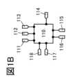
- FIG. 1Ais a diagram showing an example of a shift register.
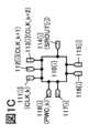
- FIG. 1B and FIG. 1Care diagrams showing an example of a signal output circuit.
- FIG. 2is a diagram showing an example of a signal output circuit.
- FIG. 3is a diagram showing an example of a signal output circuit.
- FIG. 4is a diagram showing an example of a signal output circuit.
- FIG. 5is a diagram showing an example of a signal output circuit.
- FIG. 6is a diagram showing an example of a signal output circuit.
- FIG. 7is a diagram showing an example of a signal output circuit.
- FIG. 8is a diagram showing an example of a signal output circuit.
- FIG. 9is a diagram showing an example of a signal output circuit.
- FIG. 10is a diagram showing an example of a signal output circuit.
- FIG. 11Ais a plan view of the transistor.
- FIG. 11Bis a cross-sectional view of the transistor.
- FIG. 11Cis a perspective view of the transistor.
- FIG. 11Dis an equivalent circuit diagram of a transistor.
- 12A and 12Bare cross-sectional views of the transistor.
- 12C to 12Fare plan views of the opening.
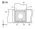
- 13A and 13Bare plan views of the transistor.
- FIG. 14Ais a cross-sectional view of the transistor.
- FIG. 14Bis an equivalent circuit diagram of the transistor.
- FIG. 15Ais a plan view of the transistor.
- FIG. 15Bis a cross-sectional view of the transistor.
- FIG. 15Cis a perspective view of the transistor.
- FIG. 15Dis an equivalent circuit diagram of a transistor.
- FIG. 15Ais a plan view of the transistor.
- FIG. 15Bis a cross-sectional view of the transistor.
- FIG. 15Cis a perspective view of the transistor.
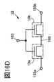
- FIG. 16Ais a plan view of the transistor.
- FIG. 16Bis a cross-sectional view of the transistor.
- FIG. 16Cis a perspective view of the transistor.
- FIG. 16Dis an equivalent circuit diagram of a transistor.
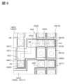
- FIG. 17is a plan view of the signal output circuit.
- FIG. 18is a plan view of the signal output circuit.
- 19A and 19Bare cross-sectional views of the signal output circuit.
- 20A and 20Bare cross-sectional views of the signal output circuit.
- 21A and 21Bare cross-sectional views of the signal output circuit.
- FIG. 22is a diagram showing an example of a signal output circuit.
- FIG. 23is a timing chart for explaining an example of the operation of the signal output circuit.
- FIG. 24is a circuit diagram for explaining an example of the operation of the signal output circuit.
- FIG. 25is a circuit diagram for explaining an example of the operation of the signal output circuit.
- FIG. 26is a circuit diagram for explaining an example of the operation of the signal output circuit.
- FIG. 27is a circuit diagram for explaining an example of the operation of the signal output circuit.
- FIG. 28is a circuit diagram for explaining an example of the operation of the signal output circuit.
- FIG. 29is a circuit diagram for explaining an example of the operation of the signal output circuit.
- FIG. 30is a circuit diagram for explaining an example of the operation of the signal output circuit.
- FIG. 31is a diagram showing an example of a signal output circuit.
- FIG. 32is a diagram showing an example of a signal output circuit.
- FIG. 33is a timing chart for explaining an example of the operation of the shift register.
- FIG. 33is a timing chart for explaining an example of the operation of the shift register.
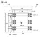
- 34Ais a perspective view of the display device.
- FIG. 34Bis a block diagram of the display device.
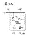
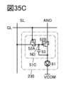
- 35A to 35Dare circuit diagrams of pixel circuits.
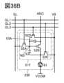
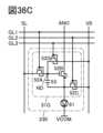
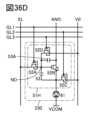
- 36A to 36Dare circuit diagrams of pixel circuits.
- 37A and 37Bare circuit diagrams of pixel circuits.
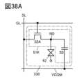
- 38A and 38Bare circuit diagrams of pixel circuits.
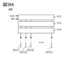
- 39A and 39Bare diagrams illustrating a configuration example of a drive circuit.
- 40A to 40Gare diagrams showing examples of pixels.
- 41A to 41Kare diagrams showing examples of pixels.
- 42A to 42Fare diagrams illustrating configuration examples of light emitting devices.
- 43A to 43Care diagrams illustrating configuration examples of light emitting devices.
- 44A to 44Dare diagrams illustrating configuration examples of light emitting elements.
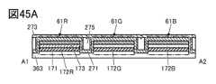
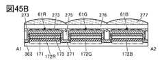
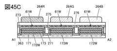
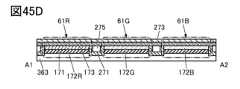
- 45A to 45Dare diagrams showing configuration examples of light emitting elements.
- 46A to 46Care diagrams illustrating configuration examples of light emitting elements.
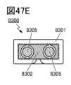
- 47A to 47Fare diagrams illustrating an example of an electronic device.
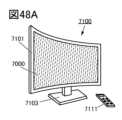
- 48A to 48Fare diagrams illustrating an example of an electronic device.
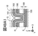
- 49A1 and 49A2are schematic cross-sectional views of transistors.
- FIG. 49B1 and FIG. 49B2are diagrams showing Id-Vg characteristics of a transistor.
- FIGS. 49C1 and 49C2are diagrams showing Id-Vd characteristics of transistors.
- the resist maskis one that is removed after the etching process is completed. shall be.
- top viewsalso referred to as “top views”
- perspective viewsdescriptions of some components may be omitted.
- some hidden linesmay be omitted.
- ordinal numberssuch as “first” and “second” are added to avoid confusion of constituent elements, and do not indicate any order or rank such as process order or lamination order. Further, even if a term is not attached with an ordinal number in this specification, etc., an ordinal number may be attached in the claims to avoid confusion of constituent elements. Further, the ordinal numbers used in this specification and the like may be different from the ordinal numbers used in the claims. Further, even if a term is attached with an ordinal number in this specification or the like, the ordinal number may be omitted in the claims or the like.
- the terms “electrode,” “wiring,” and “terminal”do not functionally limit these components.
- an “electrode”may be used as part of a “wiring” and vice versa.
- the terms “electrode” and “wiring”also include a case where a plurality of “electrodes” and “wiring” are provided as one.
- a “terminal”may be used as part of a “wiring” or “electrode,” and vice versa.
- the term “terminal”also includes cases where a plurality of "electrodes", “wirings", “terminals”, etc. are formed integrally.
- an “electrode”can be a part of a “wiring” or a “terminal,” and, for example, a “terminal” can be a part of a “wiring” or a “electrode.”
- terms such as “electrode,” “wiring,” and “terminal”may be replaced with terms such as "region” depending on the case.
- supplying a signalrefers to supplying a predetermined potential to a wiring or the like. Therefore, it may be possible to read "signal” as a term such as “potential”. In addition, terms such as “potential” may sometimes be read as “signal.” Further, the "signal” may be a variable potential or a fixed potential. For example, it may be a power supply potential.
- filmand “layer” can be interchanged depending on the situation or circumstances.
- conductive layermay be changed to the term “conductive film.”
- insulating filmmay be changed to the term “insulating layer.”
- a “capacitive element”refers to, for example, a circuit element having a capacitance value higher than 0F, a wiring region having a capacitance value higher than 0F, a parasitic capacitance, or It can be the gate capacitance of a transistor.
- capacitor elementcan sometimes be replaced with the term “capacitance.”
- capacitormay be translated into the terms “capacitive element,” “parasitic capacitance,” or “gate capacitance.”
- a “capacitor”(including a “capacitor” having three or more terminals) has a configuration including an insulator and a pair of conductive layers sandwiching the insulator.
- a pair of conductive layers in “capacitance”can be translated into a "pair of electrodes," a “pair of conductive regions,” a “pair of regions,” or a “pair of terminals.”
- the term “one of a pair of terminals”may also be referred to as “one terminal” or “first terminal.”
- the term “the other of a pair of terminals”may be referred to as “the other terminal” or “the second terminal.”
- the value of the capacitancecan be, for example, 0.05 fF or more and 10 pF or less. Further, for example, it may be set to 1 pF or more and 10 ⁇ F or less.
- source and drainmay be interchanged, such as when using transistors of different polarity or when the direction of current changes during circuit operation. Therefore, in this specification and the like, the terms “source” and “drain” can be used interchangeably.
- gaterefers to part or all of a gate electrode and a gate wiring.
- the gate wiringrefers to a wiring for electrically connecting the gate electrode of at least one transistor to another electrode or another wiring.
- sourcerefers to part or all of a source region, a source electrode, and a source wiring.
- the source regionrefers to a region of the semiconductor layer where the resistivity is below a certain value.
- a source electroderefers to a conductive layer including a portion connected to a source region.
- the source wiringrefers to a wiring for electrically connecting the source electrode of at least one transistor to another electrode or another wiring.
- drainrefers to part or all of a drain region, a drain electrode, and a drain wiring.
- the drain regionrefers to a region of the semiconductor layer where the resistivity is below a certain value.
- a drain electroderefers to a conductive layer including a portion connected to a drain region.
- the drain wiringrefers to a wiring for electrically connecting the drain electrode of at least one transistor to another electrode or another wiring.
- the transistors shown in this specification and the likeare enhancement type (normally-off type) field effect transistors.
- the transistors described in this specification and the likeare n-channel transistors, and unless otherwise specified, the threshold voltage (also referred to as "Vth") of the transistors is greater than 0V.
- the transistor shown in this specification and the likeis a p-channel transistor, and unless otherwise specified, the threshold voltage (also referred to as "Vth”) of the transistor is 0V or less.
- the Vth of a plurality of transistors of the same conductivity typeare all equal.
- off-state currentrefers to the current (current) that flows between the source and drain when the transistor is in the off state (also referred to as the "non-conducting state” or “blocking state”).
- drain currentalso referred to as “drain current” or “Id.”
- an off stateis defined as an n-channel transistor in which the potential difference between the gate and source (also referred to as “gate voltage” or “Vg”) with respect to the source is lower than the threshold voltage.
- Vggate voltage
- the off-state current of an n-channel transistormay refer to the drain current when Vg is lower than Vth.
- off-state currentmay refer to, for example, a current flowing between a source and a drain when a transistor is in an off state.
- on-currentrefers to Id when a transistor is in an on-state (also referred to as a "conductive state").
- the on-staterefers to a state in which Vg is greater than or equal to Vth for an n-channel transistor, and a state in which Vg is less than or equal to Vth for a p-channel transistor.
- the on-current of an n-channel transistormay refer to the drain current when Vg is equal to or higher than Vth.
- a high power supply potential VDD(hereinafter also simply referred to as “VDD” or “potential H”) indicates a power supply potential higher than the low power supply potential VSS.
- the low power supply potential VSS(hereinafter also simply referred to as “VSS” or “potential L”) indicates a power supply potential lower than the high power supply potential VDD.
- the ground potential GND(hereinafter also simply referred to as “GND”) can also be used as VDD or VSS.
- VDDis GND
- VSSis a potential lower than GND
- VDDis a potential higher than GND. Note that in this specification and the like, VSS is used as a reference potential unless explicitly stated.
- voltageoften refers to a potential difference between a certain potential and a reference potential (for example, a ground potential or a source potential). Further, “potential” is relative, and the potential applied to wiring etc. may change depending on the reference potential. Therefore, “voltage” and “potential” may sometimes be interchangeable.
- electrode Bdoes not need to be formed directly on insulating layer A, and there is no need to form another structure between insulating layer A and electrode B. Do not exclude things that contain elements.
- electrode B overlapping insulating layer Ais not limited to the state in which electrode B is formed on insulating layer A, but also the state in which electrode B is formed under insulating layer A, or A state in which the electrode B is formed on the right side (or left side) of the insulating layer A is not excluded.
- the terms “adjacent” and “nearby”do not limit that components are in direct contact.
- insulating layer A and electrode Bdo not need to be formed in direct contact with each other, and other components may be placed between insulating layer A and electrode B. Do not exclude what is included.
- parallelrefers to a state in which two straight lines are arranged at an angle of -10° or more and 10° or less. Therefore, the case where the angle is greater than or equal to -5° and less than or equal to 5° is also included.
- substantially parallelor “substantially parallel” refers to a state in which two straight lines are arranged at an angle of -30° or more and 30° or less.
- perpendicularrefers to a state in which two straight lines are arranged at an angle of 80° or more and 100° or less. Therefore, the case where the angle is 85° or more and 95° or less is also included.
- substantially perpendicularor “substantially perpendicular” refers to a state in which two straight lines are arranged at an angle of 60° or more and 120° or less.
- the term “the end of the object has a tapered shape”means that the angle formed between the formed surface (bottom surface) and the side surface (surface) in the end region is greater than 0 degrees and less than 90 degrees. , having a cross-sectional shape in which the thickness continuously increases from the end. Further, the taper angle refers to the angle formed between the bottom surface (formed surface) and the side surface (surface) at the end of the object.
- arrows indicating the X direction, Y direction, and Z directionmay be attached.
- the "X direction”refers to the direction along the X axis, and the forward direction and reverse direction may not be distinguished unless explicitly stated.
- the X direction, the Y direction, and the Z directionare directions that intersect with each other. More specifically, the X direction, the Y direction, and the Z direction are directions that are orthogonal to each other.
- one of the X direction, the Y direction, or the Z directionmay be referred to as a "first direction” or a “first direction.” Further, the other direction may be referred to as a “second direction” or “second direction”. Further, the remaining one may be referred to as a "third direction” or "third direction.”
- the EL layer 172may be shown divided into an EL layer 172R, an EL layer 172G, an EL layer 172B, and an EL layer 172W.
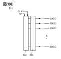
- the shift register 100 shown in FIG. 1Ahas n signal output circuits 110 (n is an integer of 1 or more).
- the first stage (first) signal output circuit 110is sometimes referred to as a signal output circuit 110 [1]
- the nth stage (nth) signal output circuit 110is sometimes referred to as a signal output circuit 110 [1]. It may be written as 110[n].
- the signal output circuit 110 at the i-th stagemay be referred to as a signal output circuit 110[i].
- ian integer from 1 to n
- ian integer from 1 to n
- ian integer from 1 to n
- ian integer from 1 to n
- i- ⁇an arbitrary number of stages
- i- ⁇an arbitrary number of stages
- i- ⁇an arbitrary number of stages
- the shift register 100also includes two signal output circuits 110 (signal output circuit 110[n+1] and signal output circuit 110[n+2]) which are dummy circuits.
- the terminals, input/output signals, etc. of the signal output circuit 110may also be described in the same manner as above.
- the signal OUT of the signal output circuit 110[i]may be referred to as the signal OUT[i].
- the shift register 100also includes wirings 101 to 104 to which four signals CLK (signals CLK_1 to CLK_4), which are clock signals, are supplied, and wirings 105 to which four signals PWC (signals PWC_1 to signals PWC_4) are supplied. to wiring 108.
- a signal CLK_1is supplied to the wiring 101
- a signal CLK_2is supplied to the wiring 102
- a signal CLK_3is supplied to the wiring 103
- a signal CLK_4is supplied to the wiring 104.
- a signal PWC_1is supplied to the wiring 105
- a signal PWC_2is supplied to the wiring 106
- a signal PWC_3is supplied to the wiring 107
- a signal PWC_4is supplied to the wiring 108.
- the signal output circuit 110has terminals 111 to 118 (see FIG. 1B).
- the terminal 111, the terminal 112, and the terminal 113are each electrically connected to one of the wirings 101 to 104 and a different wiring.
- the first stage signal output circuit 110[1]has a terminal 111 electrically connected to the wiring 101, a terminal 112 electrically connected to the wiring 102, and a terminal 113 electrically connected to the wiring 103. connected. That is, the signal CLK_1 is supplied to the terminal 111, the signal CLK_2 is supplied to the terminal 112, and the signal CLK_3 is supplied to the terminal 113.
- the terminal 111is electrically connected to the wiring 102
- the terminal 112is electrically connected to the wiring 103
- the terminal 113is electrically connected to the wiring 104. ing. That is, the signal CLK_2 is supplied to the terminal 111, the signal CLK_3 is supplied to the terminal 112, and the signal CLK_4 is supplied to the terminal 113.
- the signal CLK_kis supplied to the terminal 111[i] of the signal output circuit 110[i] (see FIG. 1C).
- kis an integer from 1 to 4, and when i is 4 or less, k is equal to i, and when i is 5 or more, k is equal to i-4 ⁇ g.
- gis the quotient of i divided by 4.
- the signal CLK_k+1is supplied to the terminal 112[i] of the signal output circuit 110[i].
- kis an integer from 1 to 4, and when k+1 is 5, k is set to 1.
- iis 3 or less, k is equal to i, and when i is 4 or more, k is equal to i-4 ⁇ g.
- the signal CLK_k+2is supplied to the terminal 113[i] of the signal output circuit 110[i].
- k+1is an integer from 1 to 4, and when k+2 becomes 5, k+2 is set to 1, and when k+2 becomes 6, k+2 is set to 2.
- iis 2 or less, k is equal to i, and when i is 3 or more, k is equal to i-4 ⁇ g.
- terminal 114[i]is electrically connected to the terminal 117[i+1] (not shown) of the next stage signal output circuit 110[i+1] (not shown). Therefore, terminal 117[i] is electrically connected to terminal 114[i-1].
- terminal 114 of signal output circuit 110[1]is electrically connected to terminal 117 of signal output circuit 110[2]. Further, a start pulse SP is supplied to the terminal 117 of the signal output circuit 110[1].
- the terminal 115[i]is electrically connected to the terminal 114[i+2] (not shown) of the signal output circuit 110[i+2] (not shown) two stages later.
- the terminal 115 of the signal output circuit 110[1]is electrically connected to the terminal 114 of the signal output circuit 110[3]
- the terminal 115 of the signal output circuit 110[2]is electrically connected to the terminal 114 of the signal output circuit 110[4]. It is electrically connected to the terminal 114 of. Therefore, the terminal 115 of the signal output circuit 110[n-1] is electrically connected to the terminal 114 of the signal output circuit 110[n+1], and the terminal 115 of the signal output circuit 110[n] is electrically connected to the terminal 114 of the signal output circuit 110[n+1]. n+2] terminal 114. Note that the signal output circuit 110[n+1] and the signal output circuit 110[n+2] do not need to have the terminal 115.
- the terminal 118[i]is electrically connected to any of the wirings 105 to 108.
- the terminal 118 of the signal output circuit 110[1]is electrically connected to the wiring 105
- the terminal 118 of the signal output circuit 110[2]is electrically connected to the wiring 106.
- the signal PWC_kis supplied to the terminal 118[i] of the signal output circuit 110[i].
- kis an integer from 1 to 4, and when i is 4 or less, k is equal to i, and when i is 5 or more, k is equal to i-4 ⁇ g.
- a signal OUT[i]is output from the terminal 116[i].
- the signal OUT[1]is output from the terminal 116 of the signal output circuit 110[1].
- the signal OUT[n]is output from the terminal 116 of the n-th stage signal output circuit 110[n]. Note that "signal OUT[i] is output from terminal 116[i]” can be read as “signal OUT[i] is supplied to terminal 116[i]."
- a signal SROUT[i]is supplied to the terminal 114[i].
- the signal SROUT[i]is output from the terminal 114[i].
- the signal SROUT[1]is output from the terminal 114 of the signal output circuit 110[1].
- the signal SROUT[n]is output from the terminal 114 of the n-th stage signal output circuit 110[n]. Note that "signal SROUT[i] is output from terminal 114[i]” can be read as "signal SROUT[i] is supplied to terminal 114[i]."
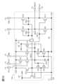
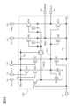
- the signal output circuit 110includes transistors 10[1] to 10[11] and capacitors 20[1] to 20[3].
- the gate of transistor 10[1]is electrically connected to terminal 117 and the gate of transistor 10[6].
- the source of the transistor 10[1]is electrically connected to the drain of the transistor 10[2], and the drain of the transistor 10[1] is electrically connected to the wiring 131.
- the gate of transistor 10[2]is electrically connected to one terminal of capacitor 20[1].
- the source of transistor 10[2]is electrically connected to the other terminal of capacitor 20[1], the source of transistor 10[6], and wiring 132.
- the gate of the transistor 10[3]is electrically connected to the terminal 113, the drain of the transistor 10[3] is electrically connected to the wiring 131, and the source of the transistor 10[3] is electrically connected to the drain of the transistor 10[4]. electrically connected.
- the gate of transistor 10[4]is electrically connected to terminal 112, and the drain of transistor 10[4] is electrically connected to the source of transistor 10[3].
- the source of transistor 10[4]is electrically connected to the gates of transistor 10[2], transistor 10[9], and transistor 10[11], and one terminal of capacitor 20[1].
- the gates of transistors 10[2], 10[9], and 10[11], the source of transistor 10[4], and one terminal of capacitor 20[1]are electrically connected.
- the area connected to the node ND[1]is called the node ND[1].
- the capacitor 20[1]has a function of suppressing potential fluctuations of the node ND[1] when the node ND[1] is in a floating state and maintaining the potential of the node ND[1].
- the gate of the transistor 10[5]is electrically connected to the terminal 115, and the drain of the transistor 10[5] is electrically connected to the wiring 131.
- the source of transistor 10[5]is electrically connected to the gate of transistor 10[2], the gate of transistor 10[9], the gate of transistor 10[11], and the drain of transistor 10[6].
- the gate of the transistor 10[7]is electrically connected to the wiring 131, and one of the source or drain of the transistor 10[7] is electrically connected to the source of the transistor 10[1] and the drain of the transistor 10[2]. be done.
- the other source or drain of transistor 10[7]is connected to the gate of transistor 10[8], one terminal of capacitor 20[2], the gate of transistor 10[10], and one terminal of capacitor 20[3]. electrically connected.
- node ND[2]a region where one of the source or drain of the transistor 10[7], the source of the transistor 10[1], and the drain of the transistor 10[2] are electrically connected.
- the drain of transistor 10[8]is electrically connected to terminal 111.
- the source of transistor 10[8]is electrically connected to the other terminal of capacitor 20[2], terminal 114, and the drain of transistor 10[9].
- the drain of transistor 10[10]is electrically connected to terminal 118.
- the source of transistor 10[10]is electrically connected to the other terminal of capacitor 20[3], terminal 116, and the drain of transistor 10[11].
- the source of transistor 10[9] and the source of transistor 10[11]are electrically connected to wiring 132.
- drain of transistor 10[1], the drain of transistor 10[3], the drain of transistor 10[5], and the gate of transistor 10[7]may be electrically connected to different wirings.
- source of transistor 10[6], the source of transistor 10[9], and the source of transistor 10[11]may be electrically connected to different wirings.
- the drain of transistor 10[1]is electrically connected to wiring 131[1]
- the drain of transistor 10[3]is electrically connected to wiring 131[2]
- the transistor The drain of transistor 10[5]may be electrically connected to wiring 131[3]
- the gate of transistor 10[7]may be electrically connected to wiring 131[4].
- the source of transistor 10[6]is electrically connected to wiring 132[1]
- the source of transistor 10[9]is electrically connected to wiring 132[2]
- the source of transistor 10[11]is electrically connected to wiring 132[2]. It may be electrically connected to the wiring 132[3]. Note that, as shown in FIG. 4, if a sufficient capacitance value of the capacitor 20[3] can be secured, the formation of the capacitor 20[2] may be omitted.
- a terminal 115is supplied with a signal RIN, a terminal 117 is supplied with a signal LIN, a terminal 114 is supplied with a signal SROUT, and a terminal 116 is supplied with a signal OUT. Further, in the first stage signal output circuit 110a, the signal CLK_1 is supplied to the terminal 111, the signal CLK_2 is supplied to the terminal 112, the signal CLK_3 is supplied to the terminal 113, and the signal PWC_1 is supplied to the terminal 118.
- the signal CLK_2is supplied to the terminal 111
- the signal CLK_3is supplied to the terminal 112
- the signal CLK_4is supplied to the terminal 113
- the signal PWC_2is supplied to the terminal 118.
- FIG. 5shows a circuit diagram of a signal output circuit 110b which is a modification of the signal output circuit 110a.
- the signal output circuit 110bhas a configuration in which the transistor 10[4] is removed from the signal output circuit 110a. Further, the source of transistor 10[3] is electrically connected to node ND[1]. By omitting either the transistor 10[3] or the transistor 10[4], it is possible to realize the signal output circuit 110b occupying a small area.
- FIG. 6shows a circuit diagram of a signal output circuit 110c which is a modification of the signal output circuit 110a.
- Each of the transistor 10[2] and the transistor 10[6]may be a multi-gate transistor.
- FIG. 6shows an example in which each of the transistor 10[2] and the transistor 10[6] is a double-gate transistor, which is a type of multi-gate transistor.
- the source of transistor 10[2]ais electrically connected to the drain of transistor 10[2]b, and the drain of transistor 10[2]a is connected to the source of transistor 10[1] and the source of transistor 10[7] or Electrically connected to one side of the drain.
- the source of transistor 10[2]bis electrically connected to the other terminal of capacitor 20[1], the source of transistor 10[6]b, and wiring 132.
- the gate of transistor 10[2]a and the gate of transistor 10[2]bare electrically connected. That is, transistor 10[2]a and transistor 10[2]b are connected in series, and both function as one transistor 10[2]. Furthermore, the gate of transistor 10[2]a and the gate of transistor 10[2]b are electrically connected to node ND[1].
- the transistor 10[2]may be a multi-gate transistor configured by connecting three or more transistors in series.
- the source of the transistor 10[6]ais electrically connected to the drain of the transistor 10[6]b, and the drain of the transistor 10[6]a is electrically connected to the node ND[1].
- the source of transistor 10[6]bis electrically connected to the other terminal of capacitor 20[1], the source of transistor 10[2]b, and wiring 132.
- the gate of transistor 10[6]a and the gate of transistor 10[6]bare electrically connected. That is, the transistor 10[6]a and the transistor 10[6]b are connected in series, and both function as one transistor 10[6].
- the gate of transistor 10[6]a and the gate of transistor 10[6]bare electrically connected to the gate of transistor 10[1] and terminal 117.
- the transistor 10[6]may be a multi-gate transistor configured by connecting three or more transistors in series.
- Multi-gate transistorshave high dielectric strength between the source and drain. Therefore, the reliability of a circuit using multi-gate transistors can be improved. Therefore, the reliability of a semiconductor device including the circuit can be improved. Multi-gate transistors may be applied to transistors other than transistor 10[2] and transistor 10[6].
- FIG. 7shows a circuit diagram of a signal output circuit 110d that is a modification of the signal output circuit 110c. Note that the signal output circuit 110d is also a modification of the signal output circuit 110a.
- the signal output circuit 110dincludes a transistor 10[12].
- the source of the transistor 10[12]is electrically connected to the node ND[1], and the drain is electrically connected to the wiring 131. Further, the gate of the transistor 10 [12] is electrically connected to the terminal 119.
- a signal INIRESis supplied to terminal 119.
- the signal INIRESfunctions as a reset signal, and while the potential H is being supplied to the terminal 119 as the signal INIRES, the signal OUT and the signal SROUT are at the potential L.
- the transistor 10[12]is turned on, and the potential of the node ND1 becomes the potential H.
- the transistor 10[9]is turned on, and the potential L is supplied to the terminal 114. Further, the transistor 10 [11] is turned on, and the potential L is supplied to the terminal 116.
- the operation of the signal output circuit 110dcan be stopped at any timing.
- FIG. 8shows a circuit diagram of a signal output circuit 110e that is a modification of the signal output circuit 110a.
- the signal output circuit 110euses transistors with back gates as the transistor 10[2], the transistor 10[6], the transistor 10[9], and the transistor 10[11].
- the back gates of transistor 10[2], transistor 10[6], transistor 10[9], and transistor 10[11]are electrically connected to terminal 121 via wiring 133.
- a signal SELis supplied to the terminal 121.
- the signal SELmay have a fixed potential or a variable potential.
- the signal SELWhen the signal SEL is set to a fixed potential, it may be the potential L (VSS) or a potential lower than the potential L.
- GBTSGallium Bias Temperature Stress
- PBTSPositive Bias Temperature Stress
- NBTSNegative Bias Temperature Stress
- PBTS test and NBTS test performed under light irradiationare respectively PBTIS (Positive Bias Temperature Illumination Stress) test and NBTIS (Negative Bias Temperature I) test. Illumination Stress) test.
- n-type transistorsIn n-type transistors, a positive potential is applied to the gate when the transistor is turned on, so the amount of variation in threshold voltage in the PBTS test is an important indicator of transistor reliability. This is one of the items.
- a negative potentialis applied to the gate of a p-type transistor when the transistor is turned on, it is important to pay attention to the amount of variation in the threshold voltage in the NBTS test as an indicator of the reliability of the transistor. This is one of the important items. It can be said that the smaller the amount of variation in threshold voltage before and after the GBTS test, the higher the reliability of the transistor.
- the potential H (VDD)is held at the node ND[1] of the signal output circuit 110 (signal output circuit 110a, etc.) for a long period of time. Therefore, PBTS is applied to transistor 10[2], transistor 10[9], and transistor 10[11] for a long period of time. Furthermore, NBTS is applied to the transistor 10[6] for a long period of time. By using transistors with back gates for transistor 10[2], transistor 10[6], transistor 10[9], and transistor 10[11], deterioration of transistor characteristics due to NBTS and PBTS is suppressed.
- the transistorcan be turned off reliably by supplying a potential lower than the potential L to the back gate. can be in a state. Therefore, the potential of node ND[1] can be held reliably. Therefore, the operation of the signal output circuit 110 is stabilized, and the reliability of the semiconductor device including the signal output circuit 110 can be improved.
- the operating speed of the shift register 100is slow (the driving frequency is low)
- the period during which the node ND[1] and the like are in a floating statebecomes long.
- the potential of the node ND[1] etc.can be reliably maintained. Therefore, the operation of the signal output circuit 110 is stabilized, and the reliability of the semiconductor device including the signal output circuit 110 can be improved.
- PBTSis applied to transistor 10[2], transistor 10[9], and transistor 10[11] for a long period of time
- NBTSis applied to transistor 10[6] for a long period of time. Therefore, there is a possibility that the deterioration of transistor characteristics differs between transistor 10[2], transistor 10[9], transistor 10[11], and transistor 10[6].
- the back gates of transistor 10[2], transistor 10[9], and transistor 10[11]are electrically connected to terminal 121 via wiring 133, and transistor 10[ 6] may be electrically connected to the terminal 122 via the wiring 134.
- the signal SEL_Ais supplied to the terminal 121 as the signal SEL
- the signal SEL_Bis supplied to the terminal 122 as the signal SEL.
- the potential of the signal SEL_A and the potential of the signal SEL_Bmay be the same or different.
- the transistor characteristics of the transistor 10[2], the transistor 10[9], and the transistor 10[11] and the transistor characteristics of the transistor 10[6]are made different. It's okay.
- the signal SEL_Amay be synchronized with the signal RIN. For example, when the signal RIN is at the potential H, the signal SEL_A may be set at the potential H. Further, when the signal RIN is at the potential L, the signal SEL_A may be set to the potential L or a potential lower than the potential L. By setting both the signal SEL_A and the signal RIN to the potential H, the operating speed of the transistor 10[2], the transistor 10[9], and the transistor 10[11] can be increased.
- the signal SEL_Bmay be synchronized with the signal LIN. For example, when the signal LIN is at the potential H, the signal SEL_B may be set at the potential H. Further, when the signal LIN is at the potential L, the signal SEL_B may be set to the potential L or a potential lower than the potential L. By setting both the signal SEL_B and the signal LIN to the potential H, the operating speed of the transistor 10[6] can be increased.
- FIG. 10shows a circuit diagram of a signal output circuit 110f that is a modification of the signal output circuit 110c.
- the signal output circuit 110fhas a configuration in which a transistor 10 [13] and a transistor 10 [14] are added to the signal output circuit 110c.
- the gate of transistor 10[13]is electrically connected to the source of transistor 10[1], the drain of transistor 10[2]a, and one of the source or drain of transistor 10[7].
- the source of transistor 10[13]is electrically connected to the source of transistor 10[2]a and the drain of transistor 10[2]b.
- the drain of transistor 10[13]is electrically connected to wiring 135.
- the gate of transistor 10[14]is electrically connected to node ND[1].
- the source of transistor 10[14]is electrically connected to the source of transistor 10[6]a and the drain of transistor 10[6]b.
- the drain of transistor 10[14]is electrically connected to wiring 136.
- a potential SMPis supplied to the wiring 135 and the wiring 136.
- the potential SMPis preferably higher than the potential L+Vth, and more preferably higher than the potential L+2 ⁇ Vth.
- potential H(more precisely, potential H-Vth) is supplied to node ND[2]
- transistor 10[13]is turned on, and potential SMP is supplied to the source of transistor 10[2]a. Ru.
- the potential His supplied to the node ND[1]
- the transistor 10[14]is turned on, and the potential SMP is supplied to the source of the transistor 10[6]a.
- the potential SMPis preferably a fixed potential, but may be a variable potential.
- the signal output circuit 110(signal output circuit 110a, signal output circuit 110c, and signal output circuit 110d) according to one embodiment of the present invention is a unipolar circuit configured using transistors of the same conductivity type (n-channel type). It is. Since there is no need to use transistors of different conductivity types (p-channel type), manufacturing costs are reduced and a highly productive signal output circuit can be realized. Further, since a process for forming transistors of different conductivity types is not necessary, the manufacturing period is shortened and the yield is improved.
- a p-channel transistormay be used as a part of the signal output circuit 110 if necessary. That is, transistors of different conductivity types may be used as part of the signal output circuit 110.
- the signal output circuit 110may include a CMOS (Complementary Metal-Oxide-Semiconductor) circuit including an n-channel transistor and a p-channel transistor. Note that although this embodiment shows an example in which the signal output circuit 110 is composed of all n-channel transistors, it is also possible to replace all of these transistors with p-channel transistors.
- CMOSComplementary Metal-Oxide-Semiconductor
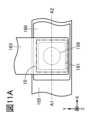
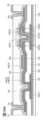
- FIG. 11Ais a plan view of the transistor 10.
- FIG. 11Bis a cross-sectional view of the portion indicated by the dashed line A1-A2 in FIG. 11A.
- FIG. 11Cis a perspective view of the transistor 10.
- FIG. 11Dis an equivalent circuit diagram of the transistor 10.
- some of the components of the transistor 10are omitted in FIGS. 11A and 11C.
- the insulating layer 164 shown in FIG. 11B and the likeare omitted.
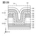
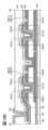
- FIG. 12A and 12Bare enlarged views of the transistor 10 shown in FIG. 11B.
- FIG. 12Cis a diagram of the opening 159 viewed from the Z direction.
- the transistor 10includes an insulating layer 154 over a substrate 153 and a conductive layer 155 over the insulating layer 154. Further, an insulating layer 156 is provided over the conductive layer 155, an insulating layer 157 is provided over the insulating layer 156, and an insulating layer 158 is provided over the insulating layer 157. Further, a conductive layer 160 is provided on the insulating layer 158. In this specification and the like, the insulating layer 156, the insulating layer 157, and the insulating layer 158 may be collectively referred to as the insulating layer 145.
- openings 159are provided in the conductive layer 160, the insulating layer 158, the insulating layer 157, and the insulating layer 156 in a region overlapping with a part of the conductive layer 155 (see FIG. 11B and FIG. 12A). Further, a semiconductor layer 161 is provided in the opening 159 . The semiconductor layer 161 has a region overlapping with the bottom of the opening 159 and a region overlapping with the side surface of the opening 159. The semiconductor layer 161 has a region in contact with the insulating layer 145 at the opening 159.
- the semiconductor layer 161has a region in contact with the side surface of the insulating layer 158, a region in contact with the side surface of the insulating layer 157, and a region in contact with the side surface of the insulating layer 156. Further, in the opening 159, a part of the semiconductor layer 161 is in contact with the conductive layer 160, and another part of the semiconductor layer 161 is in contact with the conductive layer 155. That is, a portion of the semiconductor layer 161 is electrically connected to the conductive layer 160, and another portion of the semiconductor layer 161 is electrically connected to the conductive layer 155.
- an insulating layer 162is provided over the insulating layer 158 , the conductive layer 160 , and the semiconductor layer 161 , and a conductive layer 163 is provided over the insulating layer 162 .
- an insulating layer 164is provided over the insulating layer 162 and the conductive layer 163.
- the insulating layer 162has a region that overlaps the side surface of the opening 159 with the semiconductor layer 161 interposed therebetween.
- a conductive layer 163is provided to cover the semiconductor layer 161. Therefore, conductive layer 163 has a region that extends beyond the edge of semiconductor layer 161. Furthermore, the conductive layer 163 has a region that overlaps with the side surface of the opening 159 via the insulating layer 162 and the semiconductor layer 161.
- the conductive layer 155has a region that functions as either a source electrode or a drain electrode of the transistor 10. Further, the conductive layer 160 has a region that functions as the other of the source electrode and the drain electrode of the transistor 10. For example, if conductive layer 155 functions as a drain electrode of transistor 10, conductive layer 160 functions as a source electrode of transistor 10.
- the semiconductor layer 161has a region functioning as a semiconductor layer in which a channel of the transistor 10 is formed, the insulating layer 162 has a region functioning as a gate insulating layer, and the conductive layer 163 has a region functioning as a gate electrode. .
- the transistor 10is provided in a region including the opening 159.
- the transistor 10has a source electrode and a drain electrode arranged in the Z direction. Therefore, the source and drain of the transistor 10 are arranged at different positions in the Z direction. For example, when the top surface of the substrate 153 is used as a reference, the source and drain of the transistor 10 are arranged at different distances from the top surface of the substrate 153, which is the reference. Note that being placed at different positions in the Z direction is also referred to as "being placed at different heights.” Such a transistor is also referred to as a “vertical channel transistor,” “vertical channel transistor,” “vertical transistor,” or “VFET (Vertical Field Effect Transistor).” In a vertical channel transistor, the direction in which Id flows includes a component in the Z direction (vertical direction).
- the cross section of the semiconductor layer 161 on the conductive layer 155 when viewed from the X direction or the Y directionis a cross section passing through the center (or center of gravity) of the opening 159 when viewed from the Z direction.
- the angle ⁇ (see FIG. 12A) between the surface to be formed and the flow direction of Idis 5 degrees or more and 110 degrees or less, or 10 degrees or more and 90 degrees or less, or 30 degrees or more and 90 degrees or less, or 60 degrees or more and 90 degrees or less.
- the semiconductor layer 161has a region in contact with the side surface of the insulating layer 157. Therefore, Id flows along the side surfaces of the insulating layer 157. Therefore, the angle ⁇ between the surface of the semiconductor layer 161 on the conductive layer 155 and the direction in which Id flows can be read as the angle ⁇ between the surface of the semiconductor layer 161 on the conductive layer 155 and the side surface of the insulating layer 157. be able to.
- a vertical channel transistorhas a source electrode and a drain electrode arranged in the Z direction, the area occupied by the transistor can be reduced.
- the area occupied by the semiconductor devicecan be significantly reduced.
- substrateThere are no major restrictions on the materials used for the substrate 153 and the substrates 148 and 152 described below. Depending on the purpose, the material may be determined by taking into account the presence or absence of translucency and heat resistance to withstand heat treatment. For example, insulating substrates such as glass substrates such as barium borosilicate glass and aluminoborosilicate glass, ceramic substrates, quartz substrates, and sapphire substrates can be used. Further, a semiconductor substrate, a flexible substrate, a bonded film, a base film, etc. may be used.
- the semiconductor substrateexamples include a semiconductor substrate made of silicon or germanium, or a compound semiconductor substrate made of silicon carbide, silicon germanium, gallium arsenide, indium phosphide, zinc oxide, or gallium oxide.
- the semiconductor substratemay be a single crystal semiconductor or a polycrystalline semiconductor.
- Examples of substrates used when the transistor 10 or the like according to one embodiment of the present invention is used in a display deviceinclude 6th generation (1500 mm x 1850 mm), 7th generation (1870 mm x 2200 mm), 8th generation (2200 mm x 2400 mm), and Glass substrates with large areas such as 9th generation (2400 mm x 2800 mm) and 10th generation (2950 mm x 3400 mm) can be used. Thereby, a large-sized display device can be manufactured. Furthermore, by increasing the size of the substrate, more display devices can be produced from one substrate, and production costs can be reduced.
- polyesterssuch as polyethylene terephthalate (PET) and polyethylene naphthalate (PEN), polyacrylonitrile, acrylic resins, polyimide, polymethyl methacrylate, and polycarbonate ( PC), polyethersulfone (PES), polyamide (nylon, aramid, etc.), polysiloxane, cycloolefin resin, polystyrene, polyamideimide, polyurethane, polyvinyl chloride, polyvinylidene chloride, polypropylene, polytetrafluoroethylene (PTFE), ABS resin, cellulose nanofiber, etc. can be used.
- PETpolyethylene terephthalate
- PENpolyethylene naphthalate
- PCpolycarbonate
- PESpolyethersulfone
- polyamidenylon, aramid, etc.
- polysiloxanepolystyrene
- polyamideimidepolyurethane
- polyvinyl chloridepolyvinylidene chloride
- PTFEpoly
- a lightweight semiconductor device including the transistor 10can be provided. Furthermore, by using the above material as a substrate, a semiconductor device that is resistant to impact can be provided. Further, by using the above material as a substrate, a semiconductor device that is less likely to be damaged can be provided.
- the flexible substrate used for the substratehas a lower coefficient of linear expansion, since deformation caused by the environment is suppressed.
- the flexible substrate used for the substratemay be made of a material having a coefficient of linear expansion of, for example, 1 ⁇ 10 ⁇ 3 /K or less, 5 ⁇ 10 ⁇ 5 /K or less, or 1 ⁇ 10 ⁇ 5 /K or less.
- aramidis suitable as a flexible substrate because it has a low coefficient of linear expansion.
- [Conductive layer]Aluminum (Al), chromium (Cr), copper (Cu), Silver (Ag), gold (Au), platinum (Pt), tantalum (Ta), nickel (Ni), titanium (Ti), molybdenum (Mo), tungsten (W), hafnium (Hf), vanadium (V), A metal element selected from niobium (Nb), manganese (Mn), magnesium (Mg), zirconium (Zr), beryllium (Be), etc., an alloy containing the above-mentioned metal elements, or a combination of the above-mentioned metal elements. An alloy or the like can be used.
- a semiconductorsuch as polycrystalline silicon containing an impurity element such as phosphorus, or a silicide such as nickel silicide may be used.
- the method for forming the conductive materialis not particularly limited, and various formation methods such as vapor deposition, atomic layer deposition (ALD), chemical vapor deposition (CVD), sputtering, and spin coating may be used. A method can be used.
- a Cu-X alloy(X is Mn, Ni, Cr, Fe, Co, Mo, Ta, or Ti) may be applied as the conductive material. Since the layer formed of the Cu-X alloy can be processed by a wet etching process, it is possible to suppress manufacturing costs.
- an aluminum alloy containing one or more elements selected from titanium, tantalum, tungsten, molybdenum, chromium, neodymium, and scandiummay be used as the conductive material.
- conductive materials that can be used for the conductive layerindium tin oxide, indium oxide containing tungsten oxide, indium zinc oxide containing tungsten oxide, indium oxide containing titanium oxide, indium tin containing titanium oxide, etc.
- Conductive materials with oxygencan also be used, such as oxides, indium zinc oxide, indium tin oxide doped with silicon oxide.
- conductive materials containing nitrogensuch as titanium nitride, tantalum nitride, and tungsten nitride can also be used.
- the conductive layercan also have a laminated structure in which a conductive material containing oxygen, a conductive material containing nitrogen, and a material containing the metal element described above are appropriately combined.
- the conductive layermay have a single-layer structure of an aluminum layer containing silicon, a two-layer structure in which a titanium layer is stacked on an aluminum layer, a two-layer structure in which a titanium layer is stacked on a titanium nitride layer, or a tungsten layer on a titanium nitride layer.
- a two-layer structure in which a tungsten layer is laminated on a tantalum nitride layera two-layer structure in which a tungsten layer is laminated on a tantalum nitride layer, and a three-layer structure in which a titanium layer is laminated, an aluminum layer is laminated on the titanium layer, and a titanium layer is laminated on top of that. good.
- a plurality of conductive layers formed of the above-mentioned conductive materialsmay be laminated and used.
- the conductive layermay have a laminated structure in which a material containing the aforementioned metal element and a conductive material containing oxygen are combined.
- a layered structuremay be used in which a material containing the aforementioned metal element and a conductive material containing nitrogen are combined.
- a laminated structuremay be used in which a material containing the aforementioned metal element, a conductive material containing oxygen, and a conductive material containing nitrogen are combined.
- a conductive layeris formed by laminating a conductive layer containing copper on a conductive layer containing at least one of indium or zinc and oxygen, and further laminating a conductive layer containing at least one of indium or zinc and oxygen on top of the conductive layer containing at least one of indium or zinc and oxygen. It may also have a three-layer structure. In this case, it is preferable that the side surfaces of the conductive layer containing copper are also covered with a conductive layer containing at least one of indium or zinc and oxygen. Further, for example, a plurality of conductive layers containing at least one of indium or zinc and oxygen may be stacked and used as the conductive layer.
- Each insulating layerincludes aluminum nitride, aluminum oxide, aluminum nitride oxide, aluminum oxynitride, magnesium oxide, silicon nitride, silicon oxide, silicon nitride oxide, silicon oxynitride, gallium oxide, germanium oxide, yttrium oxide, zirconium oxide, and lanthanum oxide.
- An insulating material selected from , neodymium oxide, hafnium oxide, tantalum oxide, aluminum silicate, etc.is used in a single layer or in a stacked manner. Alternatively, a mixture of a plurality of materials among oxide materials, nitride materials, oxynitride materials, and nitrided oxide materials may be used.
- the method for forming the insulating materialis not particularly limited, and various methods such as vapor deposition, ALD, CVD, sputtering, and spin coating can be used.
- nitrided oxiderefers to a material containing more nitrogen than oxygen.
- oxynitriderefers to a material containing more oxygen than nitrogen. Note that the content of each element can be measured using, for example, Rutherford Backscattering Spectrometry (RBS).
- RBSRutherford Backscattering Spectrometry
- the insulating layer 154 and the insulating layer 164are preferably formed using an insulating material through which impurities hardly pass.
- insulating materialscontaining boron, carbon, nitrogen, oxygen, fluorine, magnesium, aluminum, silicon, phosphorous, chlorine, argon, gallium, germanium, yttrium, zirconium, lanthanum, neodymium, hafnium or tantalum, in a single layer or It may be used in a laminated manner.
- Examples of insulating materials that are difficult for impurities to pass throughinclude aluminum oxide, aluminum nitride, aluminum oxynitride, aluminum nitride oxide, gallium oxide, germanium oxide, yttrium oxide, zirconium oxide, lanthanum oxide, neodymium oxide, hafnium oxide, tantalum oxide, Examples include silicon nitride.
- the reliability of the semiconductor device including the transistor 10can be improved.
- an insulating material through which impurities are difficult to pass through for the insulating layer 154diffusion of impurities from the substrate 153 side can be suppressed, and reliability of the transistor 10 can be improved. That is, the reliability of the semiconductor device including the transistor 10 can be improved.
- an insulating material through which impurities hardly pass through the insulating layer 164diffusion of impurities from above the insulating layer 164 can be suppressed, and the reliability of the transistor 10 can be improved. That is, the reliability of the semiconductor device including the transistor 10 can be improved.
- an insulating layer that can function as a planarization layermay be used as the insulating layer.
- the material for the insulating layer that functions as the planarization layerinclude acrylic resin, polyimide, epoxy resin, polyamide, polyimide amide, siloxane resin, benzocyclobutene resin, phenol resin, and precursors thereof.
- low dielectric constant materialslow-k materials
- siloxane resinsPSG (phosphorus glass), BPSG (phosphorus boron glass), etc.
- a plurality of insulating layers formed of these materialsmay be stacked.
- the siloxane resincorresponds to a resin containing Si-O-Si bonds formed using a siloxane-based material as a starting material.
- an organic groupfor example, an alkyl group or an aryl group
- a fluoro groupmay be used as a substituent. Further, the organic group may have a fluoro group.
- CMP treatmentmay be performed on the surface of the insulating layer or the like. By performing the CMP treatment, it is possible to reduce the unevenness of the surface of the insulating layer, etc., and improve the coverage of the insulating layer and conductive layer that will be formed later.
- the semiconductor layer 161a single crystal semiconductor, a polycrystalline semiconductor, a microcrystalline semiconductor, an amorphous semiconductor, or the like can be used alone or in combination.
- the semiconductor materialfor example, a semiconductor material having a band gap (semiconductor material that is not a zero-gap semiconductor) such as silicon or germanium can be used.
- a semiconductor material having a band gapsemiconductor material that is not a zero-gap semiconductor
- silicon or germaniumsilicon or germanium
- the compound semiconductoran organic substance having semiconductor characteristics or a metal oxide having semiconductor characteristics (also referred to as an oxide semiconductor) can be used. Note that these semiconductor materials may contain impurities as dopants.
- the semiconductor layer 161may be made of single crystal silicon, polycrystalline silicon, microcrystalline silicon, or amorphous silicon.
- polycrystalline siliconfor example, low temperature polysilicon (LTPS) may be used.
- a transistor using amorphous silicon for the semiconductor layer 161can be formed over a large glass substrate and can be manufactured at low cost.
- a transistor using polycrystalline silicon for the semiconductor layer 161has high field effect mobility and can operate at high speed.
- a transistor using microcrystalline silicon for the semiconductor layer 161has higher field effect mobility than a transistor using amorphous silicon, and can operate at high speed.
- Compound semiconductors that can be used as semiconductor materialsinclude silicon carbide, silicon germanium, gallium arsenide, indium phosphide, boron nitride, and boron arsenide.
- Boron nitride that can be used for the semiconductor layerpreferably includes an amorphous structure.
- Boron arsenide that can be used in the semiconductor layerpreferably contains crystals with a cubic crystal structure.
- the semiconductor layer 161may include a layered material that functions as a semiconductor.
- a layered materialis a general term for a group of materials having a layered crystal structure.
- a layered crystal structureis a structure in which layers formed by covalent bonds or ionic bonds are laminated via bonds that are weaker than covalent bonds or ionic bonds, such as van der Waals forces.
- a layered materialhas high electrical conductivity within a unit layer, that is, high two-dimensional electrical conductivity. By using a material that functions as a semiconductor and has high two-dimensional electrical conductivity for the channel formation region, a transistor with high on-state current can be provided.
- Examples of the layered materialinclude graphene, silicene, boron carbonitride, and chalcogenide.
- boron carbonitrideas a layered material, carbon atoms, nitrogen atoms, and boron atoms are arranged in a hexagonal lattice structure on a plane.
- a chalcogenideis a compound containing chalcogen.
- chalcogenis a general term for elements belonging to Group 16, and includes oxygen, sulfur, selenium, tellurium, polonium, and livermorium.
- examples of chalcogenidesinclude transition metal chalcogenides, group 13 chalcogenides, and the like.
- transition metal chalcogenidesthat can be used as semiconductor layers of transistors include molybdenum sulfide (typically MoS 2 ), molybdenum selenide (typically MoSe 2 ), and molybdenum tellurium (typically MoTe 2 ) .
- MoS 2molybdenum sulfide
- MoSe 2molybdenum selenide
- MoTe 2molybdenum tellurium
- tungsten sulfidetypically WS 2
- tungsten selenidetypically WSe 2
- tungsten telluriumtypically WTe 2
- hafnium sulfidetypically HfS 2
- hafnium selenidetypically HfSe 2
- zirconium sulfidetypically ZrS 2
- zirconium selenidetypically ZrSe 2
- ZrSe 2zirconium selenide
- an oxide semiconductorhas a band gap of 2 eV or more
- a transistor (also referred to as an "OS transistor") using an oxide semiconductor, which is a type of metal oxide, for the semiconductor layer in which a channel is formedhas an off-state current of are significantly less. Therefore, power consumption of a semiconductor device including an OS transistor can be reduced.
- the OS transistoroperates stably even in a high-temperature environment, with little variation in characteristics. For example, the off-state current hardly increases even in a high-temperature environment. Specifically, the off-state current hardly increases even under an environmental temperature of room temperature or higher and 200° C. or lower. Furthermore, the on-state current is less likely to decrease even in a high-temperature environment. Therefore, a semiconductor device including an OS transistor operates stably even in a high-temperature environment and has high reliability.
- an OS transistoras the transistor 10. Since the OS transistor has a high dielectric strength voltage between the source and the drain, the channel length can be shortened. Therefore, the on-state current can be increased.
- the OS transistoris suitable for a vertical channel type transistor.
- the channel lengthis 5 nm or more, 7 nm or more, or 10 nm or more, but less than 3 ⁇ m, 2.5 ⁇ m or less, 2 ⁇ m or less, 1.5 ⁇ m or less, 1.2 ⁇ m or less, 1 ⁇ m or less, 500 nm or less, 300 nm or less, or 200 nm.
- the thicknessmay be 100 nm or less, 50 nm or less, 30 nm or less, or 20 nm or less.
- the channel length Lcan be set to 100 nm or more and 1 ⁇ m or less.
- the metal oxidecontains at least indium (In) or zinc (Zn).
- the metal oxidehas two or three selected from indium, element M, and zinc.
- the element Mis a metal element or a metalloid element that has a high bonding energy with oxygen, for example, a metal element or a metalloid element that has a higher bonding energy with oxygen than indium.
- the element Mincludes aluminum, gallium, tin, yttrium, titanium, vanadium, chromium, manganese, iron, cobalt, nickel, zirconium, molybdenum, hafnium, tantalum, tungsten, lanthanum, cerium, neodymium, magnesium, and calcium. , strontium, barium, boron, silicon, germanium, and antimony.
- the element M included in the metal oxideis preferably one or more of the above elements, more preferably one or more selected from aluminum, gallium, tin, and yttrium, and further gallium. preferable. Note that in this specification, etc., metal elements and metalloid elements may be collectively referred to as "metal elements," and the "metal elements" described in this specification, etc. may include semimetal elements.
- indium zinc oxideIn-Zn oxide
- indium tin oxideIn-Sn oxide
- indium titanium oxideIn-Ti oxide
- indium gallium oxideIn-Ga oxide
- Indium gallium aluminum oxideIn-Ga-Al oxide
- indium gallium tin oxideIn-Ga-Sn oxide
- gallium zinc oxideGa-Zn oxide, also referred to as GZO
- aluminum zinc oxidealso written as Al-Zn oxide, AZO
- indium aluminum zinc oxidealso written as In-Al-Zn oxide, IAZO
- indium tin zinc oxideIn-Sn-Zn oxide
- indium titanium zinc oxideIn-Ti-Zn oxide
- indium gallium zinc oxidealso referred to as In-Ga-Zn oxide, IGZO
- indium gallium tin zinc oxideIn-Ga-Sn-Zn oxide, also referred to as IGZTO)
- indium gallium aluminum zinc oxidealso referred to as In-Ga-A
- the field effect mobility of the transistorcan be increased.
- the metal oxidemay contain one or more metal elements having a large number of periods instead of or in addition to indium.
- metal elements having a large number of periodsinclude metal elements belonging to the fifth period and metal elements belonging to the sixth period.
- Specific examples of the metal elementinclude yttrium, zirconium, silver, cadmium, tin, antimony, barium, lead, bismuth, lanthanum, cerium, praseodymium, neodymium, promethium, samarium, and europium. Note that lanthanum, cerium, praseodymium, neodymium, promethium, samarium, and europium are called light rare earth elements.
- the metal oxidemay contain one or more types of nonmetallic elements.
- the metal oxidecontains a nonmetal element, the field effect mobility of the transistor can be increased in some cases.
- nonmetallic elementsinclude carbon, nitrogen, phosphorus, sulfur, selenium, fluorine, chlorine, bromine, and hydrogen.
- the metal oxidebecomes highly crystalline, and impurities in the metal oxide can be reduced. It can suppress the spread. Therefore, fluctuations in the electrical characteristics of the transistor are suppressed, and reliability can be improved.
- the electrical characteristics and reliability of a transistorvary depending on the composition of the metal oxide applied to the semiconductor layer. Therefore, by varying the composition of the metal oxide depending on the electrical characteristics and reliability required of the transistor, a semiconductor device that has both excellent electrical characteristics and high reliability can be realized.
- the atomic ratio of indiumis greater than or equal to the atomic ratio of zinc.
- the atomic ratio of indiumis greater than or equal to the atomic ratio of tin.
- a metal oxide in which the atomic ratio of indium is higher than the atomic ratio of tincan be used. Furthermore, it is preferable to use a metal oxide in which the atomic ratio of zinc is higher than the atomic ratio of tin.
- a metal oxide in which the atomic ratio of indium is higher than the atomic ratio of aluminumcan be used. Furthermore, it is preferable to use a metal oxide in which the atomic ratio of zinc is higher than that of aluminum.
- a metal oxide in which the atomic ratio of indium to the number of atoms of the metal element is higher than the atomic ratio of galliumcan be used. Furthermore, it is more preferable to use a metal oxide in which the atomic ratio of zinc is higher than the atomic ratio of gallium.
- a metal oxide in which the atomic ratio of indium to the number of atoms of the metal element is higher than the atomic ratio of the element Mcan be used. Furthermore, it is more preferable to use a metal oxide in which the atomic ratio of zinc is higher than the atomic ratio of element M.
- the sum of the atomic ratios of the metal elementscan be the atomic ratio of the element M.
- the atomic ratio of the element Mcan be the sum of the atomic ratio of gallium and the atomic ratio of aluminum.
- the atomic ratio of indium, element M, and zincis within the above range.
- the ratio of the number of atoms of indium to the sum of the number of atoms of metal elementsis 30 atom % or more and 100 atom % or less, preferably 30 atom % or more and 95 atom % or less, more preferably is from 35 atom % to 95 atom %, more preferably from 35 atom % to 90 atom %, more preferably from 40 atom % to 90 atom %, more preferably from 45 atom % to 90 atom %, more preferably from 50 atom % to 90 atom %.
- the ratio of the number of indium atoms to the total number of atoms of indium, element M, and zincis within the above range.
- the field effect mobility of the transistorcan be increased by increasing the ratio of the number of indium atoms to the sum of the number of atoms of the metal elements.
- a circuit that can operate at high speedcan be manufactured. Furthermore, it becomes possible to reduce the area occupied by the circuit. For example, when applying the transistor to a large display device or a high-definition display device, even if the number of wires increases, signal delay in each wire can be reduced, and display unevenness can be suppressed. . Furthermore, since the area occupied by the circuit can be reduced, the frame of the display device can be made narrower.
- the analysis of the composition of the composition of metal oxidesfor example, the energy distributed X -ray optical method (EDX: ENERGY DISPERSIVE X -RAY SPECTROSCOPY), X -ray optical electron division of light (XPS: X -Ray PhotoElECTRON SPECTROSCOP). Y), guidance bond plasma mass analysis method (ICP-MS: Inductively Coupled Plasma-Mass Spectrometry), or Inductively Coupled Plasma-Atomic Emis (ICP-AES) sion Spectrometry) can be used. Alternatively, analysis may be performed by combining two or more of these methods. Note that for elements with low content rates, the actual content rate and the content rate obtained by analysis may differ due to the influence of analysis accuracy. For example, when the content of element M is low, the content of element M obtained by analysis may be lower than the actual content.
- a sputtering method or an ALD methodis suitable for forming the metal oxide.
- the atomic ratio of the target and the atomic ratio of the metal oxidemay be different.
- the atomic ratio of the metal oxidemay be smaller than the atomic ratio of the target.
- the atomic ratio of zinc contained in the targetmay be about 40% or more and 90% or less.
- a transistor with high reliability against application of a positive biascan be obtained.
- a transistor with a small threshold voltage variation in the PBTS testcan be obtained.
- the gallium contentis lower than the indium content.
- One of the factors that causes the threshold voltage to fluctuate in the PBTS testis the defect level at or near the interface between the semiconductor layer and the gate insulating layer.
- gallium contained in metal oxideshas a property of attracting oxygen more easily than other metal elements (for example, indium or zinc). Therefore, it is presumed that at the interface between the metal oxide containing a large amount of gallium and the gate insulating layer, gallium combines with excess oxygen in the gate insulating layer, making it easier to generate carrier (electron in this case) trap sites. . Therefore, when a positive potential is applied to the gate, carriers are trapped at the interface between the semiconductor layer and the gate insulating layer, which may cause the threshold voltage to fluctuate.
- a metal oxide in which the atomic ratio of indium is higher than the atomic ratio of galliumcan be applied to the semiconductor layer.
- a metal oxide in which the atomic ratio of zinc is higher than the atomic ratio of galliumit is preferable to apply a metal oxide in which the atomic ratio of metal elements satisfies In>Ga and Zn>Ga to the semiconductor layer.
- the ratio of the number of gallium atoms to the number of atoms of the metal element containedis greater than 0 atom % and less than 50 atom %, preferably from 0.1 atom % to 40 atom %, more preferably 0.1 atomic % or more and 35 atomic % or less, more preferably 0.1 atomic % or more and 30 atomic % or less, more preferably 0.1 atomic % or more and 25 atomic % or less, more preferably 0.1 atomic % or more and 20 atomic % or less % or less, more preferably 0.1 atomic % or more and 15 atomic % or less, more preferably 0.1 atomic % or more and 10 atomic % or less.
- a metal oxide that does not contain galliummay be applied to the semiconductor layer of the OS transistor.
- In--Zn oxidecan be applied to the semiconductor layer.
- the field effect mobility of the transistorcan be increased by increasing the ratio of the number of atoms of indium to the number of atoms of the metal element contained in the metal oxide.
- the metal oxidebecomes highly crystalline, which suppresses fluctuations in the electrical characteristics of the transistor and increases reliability. be able to.
- a metal oxide that does not contain gallium and zinc, such as indium oxidemay be applied to the semiconductor layer. By using a metal oxide that does not contain gallium, it is possible to make threshold voltage fluctuations extremely small, especially in PBTS tests.
- an oxide containing indium and zinccan be used for the semiconductor layer.
- the present inventioncan also be applied to a case where element M is used instead of gallium. It is preferable to use a metal oxide in which the atomic ratio of indium is higher than the atomic ratio of element M to the semiconductor layer. Further, it is preferable to use a metal oxide in which the atomic ratio of zinc is higher than the atomic ratio of element M.
- the electrical characteristics of the transistormay change.
- a transistor applied to a region where light can enterhas small fluctuations in electrical characteristics under light irradiation and high reliability against light. Reliability with respect to light can be evaluated, for example, by the amount of variation in threshold voltage in an NBTIS test.
- a transistor with high reliability against lightcan be obtained.
- a transistor whose threshold voltage fluctuates in the NBTIS testcan be small.
- a metal oxide in which the atomic ratio of element M is greater than or equal to that of indiumhas a larger band gap, which can reduce the amount of variation in threshold voltage in transistor NBTIS tests.
- the band gap of the metal oxide of the semiconductor layeris preferably 2.0 eV or more, more preferably 2.5 eV or more, further preferably 3.0 eV or more, further preferably 3.2 eV or more, and still more preferably 3.0 eV or more. It is preferably 3 eV or more, more preferably 3.4 eV or more, and even more preferably 3.5 eV or more.
- the ratio of the number of atoms of the element M to the number of atoms of the metal element containedis 20 atom % or more and 70 atom % or less, preferably 30 atom % or more and 70 atom % or less, more preferably 30 atom %.
- Metal oxides having a content of at least 40 at % and no more than 60 at %, more preferably at least 40 at % and no more than 60 at %, and even more preferably at least 50 at % and no more than 60 at %are suitable.
- a metal oxidecan be used in which the atomic ratio of indium to the number of atoms of the metal element is equal to or lower than the atomic ratio of gallium.
- the ratio of the number of gallium atoms to the number of atoms of the metal element containedis 20 atom % or more and 60 atom % or less, preferably 20 atom % or more and 50 atom % or less, more preferably 30 atom % or more.
- Suitable metal oxideshave a content of 50 at % or less, more preferably 40 at % or more and 60 at % or less, and more preferably 50 at % or more and 60 at % or less.
- the semiconductor layermay have a stacked structure having two or more metal oxide layers.
- the two or more metal oxide layers included in the semiconductor layermay have the same or approximately the same composition.
- the same sputtering targetcan be used to form the layers, thereby reducing manufacturing costs.
- the two or more metal oxide layers included in the semiconductor layermay have different compositions.
- the element Mit is particularly preferable to use gallium or aluminum. For example, using a laminated structure of one selected from indium oxide, indium gallium oxide, and IGZO and one selected from IAZO, IAGZO, and ITZO (registered trademark), etc. Good too.
- a first metal oxide layer having a composition of In:M:Zn1:1:1 [atomic ratio] or a composition close to that, and an In:Zn layer provided on the first metal oxide layer.
- a metal oxide layer having crystallinityAs the semiconductor layer, a metal oxide layer having crystallinity can be used.
- a metal oxide layer having a CAAC (c-axis aligned crystal) structure, a polycrystalline structure, a microcrystalline (NC: nano-crystal) structure, etc.can be used.
- a crystalline metal oxide layerAs a semiconductor layer, the density of defect levels in the semiconductor layer can be reduced, and a highly reliable display device can be realized.
- the semiconductor layer of the OS transistormay have a stacked structure of two or more metal oxide layers having different crystallinity.
- the layered structureincludes a first metal oxide layer and a second metal oxide layer provided on the first metal oxide layer, and the second metal oxide layer
- the structurecan include a region having higher crystallinity than the oxide layer.
- the second metal oxide layermay have a region having lower crystallinity than the first metal oxide layer.
- the two or more metal oxide layers included in the semiconductor layermay have the same or approximately the same composition.
- a stacked structure of two or more metal oxide layers having different crystallinitycan be formed.
- the two or more metal oxide layers included in the semiconductor layermay have different compositions.
- the channel length Lis determined by the thickness of the insulating layer provided between the conductive layer 160 and the conductive layer 155. Therefore, a transistor with a short channel length L can be manufactured with high precision. Furthermore, variations in characteristics among the plurality of transistors 10 are also reduced. Therefore, the operation of the semiconductor device including the transistor 10 is stabilized, and reliability can be improved. Further, when characteristic variations are reduced, the degree of freedom in circuit design of the semiconductor device increases, and the operating voltage can also be reduced. Therefore, power consumption of the semiconductor device can be reduced.
- a material containing hydrogenis preferably used for the insulating layer 156 and the insulating layer 158.
- the oxide semiconductor in the region in contact with the insulating layeris made n-type and can function as a source region or a drain region.
- a material containing silicon, nitrogen, and hydrogenmay be used as the insulating layer.
- silicon nitride containing hydrogen, silicon nitride oxide containing hydrogen, or the likemay be used.
- the conductive layer 155 in contact with the semiconductor layer 161 and the conductive layer 160 in contact with the semiconductor layer 161can be formed using a conductive material that converts the oxide semiconductor into n-type.
- a conductive material containing nitrogenmay be used.
- a conductive material containing titanium or tantalum and nitrogenmay be used.
- another conductive materialmay be provided over the conductive material containing nitrogen.
- a material containing reduced hydrogen and oxygenfor the insulating layer 157.
- a material containing silicon and oxygenmay be used. Specifically, silicon oxide, silicon oxynitride, or the like may be used. Since hydrogen is an impurity element in an oxide semiconductor, the semiconductor layer 161 that is an oxide semiconductor and the insulating layer 157 with reduced hydrogen are in contact with each other, making it difficult for the semiconductor layer 161 to become n-type. Further, because the semiconductor layer 161 that is an oxide semiconductor and the insulating layer 157 containing oxygen are in contact with each other, oxygen vacancies in the semiconductor layer 161 are reduced, the characteristics of the transistor 10 are stabilized, and reliability is improved.
- the insulating layer 157preferably contains excess oxygen.
- excess oxygenrefers to oxygen released by heating.
- a material containing excess oxygenit is preferable that a material through which oxygen does not easily permeate is used for the insulating layer 156 and the insulating layer 158.
- an oxide containing one or both of aluminum and hafnium, silicon nitride, and the likecan be used as the material that is difficult for oxygen to pass through.
- an insulating layer containing silicon and oxygenmay be provided between two insulating layers (insulating layer 156, insulating layer 158) containing silicon and nitrogen.
- the region of the semiconductor layer 161 in contact with the conductive layer 160 and the region of the semiconductor layer 161 in contact with the insulating layer 158functions as either a source (source region) or a drain (drain region).
- a region of the semiconductor layer 161 in contact with the conductive layer 155 and a region of the semiconductor layer 161 in contact with the insulating layer 156function as the other of the source (source region) and the drain (drain region). Therefore, the channel length L of the transistor 10 is determined by the thickness t of the insulating layer 157 (see FIG. 12A).
- the insulating layer 156 and the insulating layer 158may be made of a material that does not contain hydrogen or contains very little hydrogen.
- silicon nitride with extremely low hydrogen content or silicon nitride oxide with extremely low hydrogen contentmay be used.
- the region where the semiconductor layer 161 contacts the insulating layer 156 and the region where the semiconductor layer 161 contacts the insulating layer 158are not converted to n-type. Therefore, a region of the semiconductor layer 161 in contact with the conductive layer 160 functions as either a source (source region) or a drain (drain region). Further, a region of the semiconductor layer 161 in contact with the conductive layer 155 functions as the other of a source (source region) and a drain (drain region).
- the total thickness ts of the insulating layer 156, the insulating layer 157, and the insulating layer 158corresponds to the channel length L of the transistor 10 (see FIG. 12A).
- the channel length Lcan be controlled by adjusting the thicknesses of the insulating layer 156, the insulating layer 157, and the insulating layer 158.
- the channel length Lis 5 nm or more, 7 nm or more, or 10 nm or more, but less than 3 ⁇ m, 2.5 ⁇ m or less, 2 ⁇ m or less, 1.5 ⁇ m or less, 1.2 ⁇ m or less, 1 ⁇ m or less, 500 nm or less, 300 nm or less, It can be 200 nm or less, 100 nm or less, 50 nm or less, 30 nm or less, or 20 nm or less.
- the channel length Lcan be set to 100 nm or more and 1 ⁇ m or less.
- insulating layer 156insulating layer 156, insulating layer 157, and insulating layer 1528 are provided between conductive layer 155 and conductive layer 160 is shown;
- the number of insulating layers between layers 160is not limited to this.
- the number of insulating layers between the conductive layer 155 and the conductive layer 160may be one or two layers, or may be four or more layers.
- the circumferential length p of the opening 159becomes the channel width W of the transistor 10 (see FIG. 12C).
- the circumferential length pmay be determined, for example, at a position at half the thickness t (t/2) of the insulating layer 157 or at a position at half the thickness ts (ts/2).
- the circumferential length of any position of the opening 159may be set as the channel width W.
- the circumferential length p at the bottom of the opening 159may be the channel width W
- the circumferential length p at the top of the opening 159may be the channel width W.
- the outline (planar shape) of the opening 159 viewed from the Z directionis shown as a circle, but the shape is not limited to this.
- the outline of the opening 159 viewed from the Z directionmay be elliptical (see FIG. 12D) or rectangular (see FIG. 12E).
- FIG. 12Eshows a rectangle with curved corners.
- the outline of the opening 159 when viewed from the Z directionmay have a shape including one or both of a straight part and a curved part (see FIG. 12F).
- the capacitance value of the parasitic capacitance occurring between the gate and the sourceis different from the capacitance value of the parasitic capacitance occurring between the gate and the drain.
- the capacitance value of capacitance C1is the capacitance C1 that occurs in the region where conductive layer 160 and conductive layer 163 overlap on insulating layer 145, and the capacitance C2 that occurs in the region where conductive layer 155 and conductive layer 163 overlap in opening 159. becomes larger than the capacitance value of the capacitor C2 (see FIG. 11D and FIG. 12B).
- FIG. 13A and 13Bshow plan views similar to FIG. 11A.
- the conductive layer 163overlaps with the conductive layer 160 at the periphery of the opening 159 so as to surround the opening 159, and overlaps with the conductive layer 160 at the bottom of the opening 159.
- FIG. 13Athe region functioning as the capacitor C1 when viewed from the Z direction is hatched.
- FIG. 13Bthe region functioning as the capacitor C2 when viewed from the Z direction is hatched.
- a region where the conductive layer 155 and the conductive layer 163 overlap with each other via the semiconductor layer 161 and the insulating layer 162functions as a capacitor C2 (see FIGS. 12B and 13B).
- the insulating layer 145 and the insulating layer 162are not illustrated in FIG. 13B.
- the area of the region functioning as the capacitor C1is larger than the area of the region functioning as the capacitor C2.
- the capacitance value of the capacitor C1becomes larger than that of the capacitor C2.
- the shape of the opening 159will be changed, and the circumferential length p of the opening 159 will change. Since a change in the circumferential length p directly affects the electrical characteristics of the transistor 10, it is difficult to adjust the capacitance value of the capacitor C2.
- the overlapping area of the conductive layer 163 and the conductive layer 160can be easily adjusted, and the electrical characteristics of the transistor 10 are hardly affected.
- the capacitance value of the capacitor C1can be increased.
- a conductive layer 166 close to the semiconductor layer 161may be provided in the insulating layer 157. Further, the conductive layer 166 is provided without contacting the semiconductor layer 161. Further, the conductive layer 166 is preferably provided surrounding the semiconductor layer 161. By providing the conductive layer 166 close to the semiconductor layer 161 without being in contact with the semiconductor layer 161, the conductive layer 166 can function as a back gate electrode of the transistor 10. Therefore, the transistor 10 shown in FIG. 14A functions as a transistor having a back gate (back gate electrode). Note that FIG. 14B is an equivalent circuit diagram of the transistor 10 shown in FIG. 14A.
- the back gate electrodewill be explained.
- the back gate electrodeis formed of a conductive layer, and is arranged so that the channel forming region of the semiconductor layer is sandwiched between the gate electrode and the back gate electrode. Therefore, the back gate electrode can function similarly to the gate electrode.
- the potential of the back gate electrodemay be the same potential as that of the gate electrode, or may be a GND potential or an arbitrary potential.
- the threshold voltage of the transistorcan be changed by changing the potential of the back gate electrode independently of the potential of the gate electrode instead of making it the same as that of the gate electrode.
- the gate electrode and the back gate electrodeare formed of a conductive layer, they have a function of preventing an electric field generated outside the transistor from acting on the channel formation region of the semiconductor layer (particularly an electric field shielding function against static electricity, etc.). As a result, variations in characteristics among transistors are reduced. Further, deterioration of transistor characteristics due to the GBTS test is suppressed. For example, by having a back gate electrode, fluctuations in threshold voltage before and after a GBTS test can be suppressed. Further, a transistor having a back gate electrode has a smaller change in threshold voltage before and after a GBTS test than a transistor having no back gate electrode.
- the GBTS (NBTS and PBTS) testis a type of accelerated test, and can evaluate changes in transistor characteristics (changes over time) caused by long-term use in a short time.
- the amount of variation in the threshold voltage of a transistor before and after a GBTS testis an important index for examining reliability. It can be said that the smaller the amount of variation in the threshold voltage before and after the GBTS test, the more reliable the transistor is.
- the back gate electrode sidewhen light is incident from the back gate electrode side, by forming the back gate electrode with a conductive film having a light-blocking property, it is possible to prevent light from entering the semiconductor layer from the back gate electrode side.
- the gate electrodeby forming the gate electrode using a conductive film having light-blocking properties, it is possible to prevent light from entering the semiconductor layer from the gate electrode side.
- photodeterioration of the semiconductor layeris prevented, and deterioration of electrical characteristics such as a shift in the threshold voltage of the transistor is prevented. Can be done.
- the gate electrode and the back gate electrodecan block the electric field generated from the drain electrode from acting on the semiconductor layer. Therefore, it is possible to suppress fluctuations in the rise voltage of the on-current caused by fluctuations in the drain voltage. Note that this effect occurs significantly when a potential is supplied to the gate electrode and the back gate electrode.
- the apparent channel width W of the transistor 10can be increased.
- the resistance value between the source and drain when the transistor 10 is in the on statebecomes smaller, and Id when the transistor 10 is in the on state can be increased.
- FIG. 15Ais a plan view of transistor 10 including transistor 10a and transistor 10b.
- FIG. 15Bis a cross-sectional view of the portion indicated by the dashed line A1-A2 in FIG. 15A.
- FIG. 15Cis a perspective view of transistor 10 including transistor 10a and transistor 10b.
- FIG. 15Dis an equivalent circuit diagram of transistor 10 including transistor 10a and transistor 10b. In order to make it easier to understand the configuration of the transistor 10, some of the components of the transistor 10 are omitted in FIGS. 15A and 15C.
- Transistor 10a and transistor 10bhave the same configuration as transistor 10 described using FIGS. 11 and 12.
- Transistor 10ais provided in a region including opening 159a
- transistor 10bis provided in a region including opening 159b. Opening 159a and opening 159b can be formed similarly to opening 159.
- a part of the conductive layer 155functions as one of the source electrode or the drain electrode of the transistor 10a, and another part of the conductive layer 155 functions as one of the source electrode or the drain electrode of the transistor 10b. Further, a part of the conductive layer 160 functions as the other of the source electrode or the drain electrode of the transistor 10a, and another part of the conductive layer 160 functions as the other of the source electrode or the drain electrode of the transistor 10b. Further, a part of the conductive layer 163 functions as a gate electrode of the transistor 10a, and another part of the conductive layer 163 functions as a gate electrode of the transistor 10b.
- one of the source or drain of the transistor 10a and one of the source or drain of the transistor 10bare electrically connected, and the other source or drain of the transistor 10a and the source or drain of the transistor 10b are electrically connected.
- the other drainis electrically connected.
- the gate of the transistor 10a and the gate of the transistor 10bare electrically connected. Therefore, the transistor 10a and the transistor 10b are switched between the on state and the off state at the same time, and function as one transistor 10.
- the apparent channel length L of transistor 10can be increased.
- the saturation characteristics of the transistor 10can be improved.
- FIG. 16Ais a plan view of transistor 10 including transistor 10a and transistor 10b.
- FIG. 16Bis a cross-sectional view of the portion indicated by the dashed line A1-A2 in FIG. 16A.
- FIG. 16Cis a perspective view of transistor 10 including transistor 10a and transistor 10b.
- FIG. 16Dis an equivalent circuit diagram of transistor 10 including transistor 10a and transistor 10b. To make it easier to understand the configuration of the transistor 10, some of the components of the transistor 10 are omitted in FIGS. 16A and 16C.
- the transistor 10a and the transistor 10bhave a similar structure to the transistor 10 described using FIG. 15, except that the conductive layer 155 is separated into a conductive layer 155a and a conductive layer 155b.
- the conductive layer 155afunctions as one of the source electrode and the drain electrode of the transistor 10a, and part of the conductive layer 160 functions as the other of the source electrode and the drain electrode of the transistor 10a. Further, another part of the conductive layer 160 functions as one of the source electrode or the drain electrode of the transistor 10b, and the conductive layer 155b functions as the other of the source electrode or the drain electrode of the transistor 10b. Further, similarly to the transistor 10 described using FIG. 15, a part of the conductive layer 163 functions as a gate electrode of the transistor 10a, and another part of the conductive layer 163 functions as a gate electrode of the transistor 10b.
- the other of the source or drain of the transistor 10a and one of the source or drain of the transistor 10bare electrically connected, and the gate of the transistor 10a and the gate of the transistor 10b are electrically connected. Ru. Therefore, the transistor 10a and the transistor 10b are switched between the on state and the off state at the same time, and function as one transistor 10.
- planar and cross-sectional configuration of signal output circuit 110[Example of planar and cross-sectional configuration of signal output circuit 110] Next, examples of the planar and cross-sectional configurations of the signal output circuit 110 will be described using the drawings. In this embodiment, a planar and cross-sectional configuration example of the signal output circuit 110a shown in FIG. 2 among the signal output circuits 110 will be described.
- FIG. 17is a diagram showing an example of the planar configuration of the signal output circuit 110a.
- FIG. 18is an enlarged plan view of a region including transistors 10[7] to 10[11] from FIG. 17.
- FIG. 19Ais a diagram showing an example of a cross-sectional configuration of a portion indicated by a dashed line passing through A1-A2 in FIG. 17.
- FIG. 19Bis a diagram showing an example of a cross-sectional configuration of a portion indicated by a dashed line passing through A2-A3 in FIG. 17.
- FIG. FIG. 20Ais a diagram showing an example of a cross-sectional configuration of a portion indicated by a dashed line passing through A4-A5 in FIG. 17.
- FIG. 20Ais a diagram showing an example of a cross-sectional configuration of a portion indicated by a dashed line passing through A4-A5 in FIG. 17.
- FIG. 20Bis a diagram showing an example of a cross-sectional configuration of a portion indicated by a dashed line passing through A6-A7 in FIG. 17.
- FIG. 21Ais a diagram illustrating an example of a cross-sectional configuration of a portion indicated by a dashed-dotted line passing through A8-A9 in FIG. 18.
- FIG. 21Bis a diagram showing an example of a cross-sectional configuration of a portion indicated by a dashed line passing through A9-A10 in FIG. 18.
- the signal output circuit 110ahas an insulating layer 154 on a substrate 148, and a conductive layer 155 on the insulating layer 154 (for example, the conductive layer 155[1] and the conductive layer 155[3] in FIG. 19A, the conductive layer in FIG. 19B). 155[3] and a conductive layer 155[4], and a conductive layer 155[10] and a conductive layer 155[11] in FIG.
- the stacked structure of the signal output circuit 110a using the VFET described above for the transistor 10has common parts with the example of the structure of the transistor 10 described above. Therefore, here, mainly the parts that are different from the configuration example of the transistor 10 described above will be explained.
- the identification code [1]may be added to the reference numeral of the component related to the transistor 10[1].
- the conductive layer 163 that functions as a gate electrode of the transistor 10[1]may be referred to as a conductive layer 163[1].
- a reference numeral for identifying any one of the plurality of transistors 10may be attached to the reference numeral of a component common to the plurality of transistors 10.
- the conductive layer 163 that functions as a gate electrode of each of the transistors 10[2], 10[9], and 10[11]may be referred to as a conductive layer 163[2].
- the opening 159 and the semiconductor layer 161 related to the transistor 10[3]may be referred to as the opening 159[3] and the semiconductor layer 161[3].
- the opening 159 and the semiconductor layer 161 related to the transistor 10[4]may be referred to as the opening 159[4] and the semiconductor layer 161[4].
- the opening 159 and the semiconductor layer 161 related to the transistor 10[7]may be referred to as the opening 159[7] and the semiconductor layer 161[7].
- the opening 159 and the semiconductor layer 161 related to the transistor 10[8]may be referred to as the opening 159[8] and the semiconductor layer 161[8].
- the opening 159 and the semiconductor layer 161 related to the transistor 10[10]may be referred to as the opening 159[10] and the semiconductor layer 161[10].
- the signal output circuit 110ahas conductive layers 181[1] to 181[4] on the insulating layer 158 (see FIG. 17 and FIG. 20A).
- the conductive layer 181(conductive layer 181[1] to conductive layer 181[4]) can be formed using the same material and method as the conductive layer 160. Further, the conductive layer 181 can be formed at the same time as the conductive layer 160.
- the signal output circuit 110ahas an insulating layer 187 on the insulating layer 164.
- the insulating layer 187preferably functions as a planarization layer that reduces steps caused by transistors, capacitors, wiring, etc. formed in the underlying layer.
- An organic insulating filmis suitable as a material that functions as a planarization layer.
- the insulating layer 187may be subjected to planarization treatment using a chemical mechanical polishing (CMP) method or the like.
- CMPchemical mechanical polishing
- the signal output circuit 110aincludes conductive layers 191 to 199, wiring 131, and wiring 132 on the insulating layer 187 (see FIGS. 17, 19A, 19B, and 20A).
- the conductive layers 191 to 199, the wiring 131, and the wiring 132can be formed using the same material and method as the other conductive layers.
- the conductive layer 191functions as the terminal 111
- the conductive layer 192functions as the terminal 112
- the conductive layer 193functions as the terminal 113
- the conductive layer 194functions as the terminal 114
- the conductive layer 195functions as the terminal 115
- Conductive layer 196functions as terminal 116
- conductive layer 197functions as terminal 117
- conductive layer 198functions as terminal 118.
- the signal output circuit 110aincludes a conductive layer 160[2], a conductive layer 160[3], a conductive layer 181[1], a conductive layer 181[2], a conductive layer 181[3], and a conductive layer 181[4].
- An opening passing through the insulating layer 162, the insulating layer 164, and the insulating layer 187is provided above each.
- the wiring 132 and the conductive layer 160[2]are electrically connected through the opening provided on the conductive layer 160[2]. More specifically, the wiring 132 and the conductive layer 160[2] are electrically connected at the bottom of the opening provided on the conductive layer 160[2].
- Two openingsare provided on the conductive layer 160[3].
- the wiring 131 and the conductive layer 160[3]are electrically connected in one of the two openings. Further, in the other of the two openings, the conductive layer 199 and the conductive layer 160[3] are electrically connected.
- the conductive layer 191 and the conductive layer 181[1]are electrically connected through the opening provided on the conductive layer 181[1]. Furthermore, the conductive layer 194 and the conductive layer 181[2] are electrically connected through the opening provided on the conductive layer 181[2]. Furthermore, the conductive layer 198 and the conductive layer 181[3] are electrically connected through the opening provided on the conductive layer 181[3]. Further, the conductive layer 196 and the conductive layer 181[4] are electrically connected through the opening provided on the conductive layer 181[4].
- the signal output circuit 110aalso includes an insulating layer on each of the conductive layer 163[1], the conductive layer 163[3], the conductive layer 163[4], the conductive layer 163[5], and the conductive layer 163[7]. An opening is provided through 164 and insulating layer 187.
- the conductive layer 197 and the conductive layer 163[1]are electrically connected through the opening provided on the conductive layer 163[1]. Further, the conductive layer 193 and the conductive layer 163[3] are electrically connected through the opening provided on the conductive layer 163[3]. Furthermore, the conductive layer 192 and the conductive layer 163[4] are electrically connected through the opening provided on the conductive layer 163[4]. Further, the conductive layer 195 and the conductive layer 163[5] are electrically connected through the opening provided on the conductive layer 163[5]. Furthermore, the conductive layer 199 and the conductive layer 163[7] are electrically connected through the opening provided on the conductive layer 163[7]. Note that the conductive layer 160[3] and the conductive layer 163[7] are electrically connected via the conductive layer 199.
- the signal output circuit 110aincludes a conductive layer 155[1], a conductive layer 155[2], a conductive layer 155[3], a conductive layer 155[4], a conductive layer 155[8], a conductive layer 155[9], Openings that penetrate through the insulating layer 156, the insulating layer 157, and the insulating layer 158 are provided above the conductive layer 155[10] and the conductive layer 155[11], respectively.
- the conductive layer 160[3] and the conductive layer 155[1]are electrically connected. Furthermore, the conductive layer 160[1] and the conductive layer 155[2] are electrically connected through the opening provided on the conductive layer 155[2]. Furthermore, the conductive layer 160[4] and the conductive layer 155[3] are electrically connected through the opening provided on the conductive layer 155[3].
- the conductive layer 181[1] and the conductive layer 155[8]are electrically connected through the opening provided on the conductive layer 155[8]. Furthermore, the conductive layer 181[3] and the conductive layer 155[10] are electrically connected through the opening provided on the conductive layer 155[10].
- Two openingsare provided on the conductive layer 155[9]. In one of the two openings, conductive layer 160[8] and conductive layer 155[9] are electrically connected. Further, in the other of the two openings, the conductive layer 181[2] and the conductive layer 155[9] are electrically connected.
- Two openingsare provided on the conductive layer 155[11]. In one of the two openings, conductive layer 160[10] and conductive layer 155[11] are electrically connected. Further, in the other of the two openings, the conductive layer 181[4] and the conductive layer 155[11] are electrically connected.
- openings that penetrate through the insulating layer 156, the insulating layer 157, and the insulating layer 158are provided on each of the conductive layer 155[4] and the conductive layer 155[7].
- the conductive layer 163[2] and the conductive layer 155[4]are electrically connected (see FIG. 20B).
- the conductive layer 163[8] and the conductive layer 155[7]are electrically connected (see FIGS. 21A and 21B).
- the conductive layer 155[4]also functions as the conductive layer 155[5] and the conductive layer 155[6].
- the conductive layer 160[1]also functions as the conductive layer 160[7].
- the conductive layer 160[2]also functions as the conductive layer 160[6], the conductive layer 160[9], and the conductive layer 160[11].
- the conductive layer 160[3]also functions as the conductive layer 160[5].
- the conductive layer 163[1]also functions as the conductive layer 163[6].
- the conductive layer 163[2]also functions as the conductive layer 163[9] and the conductive layer 163[11].
- the conductive layer 163[8]also functions as the conductive layer 163[10].
- the capacitor C1 of the transistor 10[8]can be used as the capacitor 20[2].
- the capacitor C1 of the transistor 10[8]As the capacitor 20[2], there is no need to separately provide the capacitor 20[2], so a semiconductor device that occupies less space can be realized (see FIG. 17). Therefore, it is preferable to use a VFET according to one embodiment of the present invention as the transistor 10[8].
- the capacitor C1 of the transistor 10[10]can be used as the capacitor 20[3].
- the capacitor C1 of the transistor 10[10]As the capacitor 20[3], there is no need to separately provide the capacitor 20[3], so a semiconductor device that occupies less area can be realized (see FIG. 17 and FIG. 20A). Therefore, it is preferable to use a VFET according to one embodiment of the present invention as the transistor 10 [10].
- FIG. 22shows a circuit diagram of the signal output circuit 110a when the capacitor C1 of the transistor 10[8] is used as the capacitor 20[2], and the capacitor C1 of the transistor 10[10] is used as the capacitor 20[3]. .
- Transistors other than transistor 10[10] and transistor 10[10]may be configured with transistors other than VFETs. However, in order to realize a semiconductor device with a reduced occupied area, it is preferable to use many transistors according to one embodiment of the present invention in the signal output circuit 110a. Therefore, it is preferable to use transistors according to one embodiment of the present invention for all transistors included in the signal output circuit 110a.
- FIG. 23is a timing chart for explaining an example of the operation of the signal output circuit 110a[i].
- 24 to 30are circuit diagrams for explaining operation examples of the signal output circuit 110a[i].
- Hindicating potential H or "L” indicating potential L
- H or Lmay be added adjacent to the interconnect.
- H or Lmay be added in enclosed letters to an electrode or the like where a potential change has occurred.
- an "x" symbolmay be added over the transistor.
- the wiring 131is supplied with a potential H (VDD), and the wiring 132 is supplied with a potential L (VSS). Further, it is assumed that the signal CLK_1 is supplied to the terminal 111, the signal CLK_2 is supplied to the terminal 112, the signal CLK_3 is supplied to the terminal 113, and the signal PWC_1 is supplied to the terminal 118.
- the signal CLK_1is at the potential L
- the signal CLK_2is at the potential H
- the signal CLK_3is at the potential H
- the signal PWC_1is at the potential L
- the signal LINis at the potential L.
- transistor 10[2], transistor 10[3], transistor 10[4], transistor 10[9], and transistor 10[11]are in an on state.
- transistor 10[1], transistor 10[5], transistor 10[6], transistor 10[7], transistor 10[8], and transistor 10[10]are in an off state.
- the signal CLK_4 and the signals PWC_2 to PWC_4are at the potential L.
- the signal CLK_4 and the signals PWC_2 to PWC_4are not related to the operation of the signal output circuit 110a[i] described here, and therefore will not be used to explain the operation of the signal output circuit 110a[i].
- the signal CLK_2becomes the potential L and the signal LIN becomes the potential H (see FIGS. 23 and 24). Then, transistor 10[1] and transistor 10[6] are turned on. Then, the potential of node ND[1] becomes potential L, and transistor 10[2], transistor 10[9], and transistor 10[11] are turned off.
- the potentials of the nodes ND[2] and ND[3]become a potential (potential H ⁇ Vth) lower than the potential H by the amount of Vth of the transistor 10[1].
- the value of the potential H-Vthis assumed to be greater than or equal to the Vth of the transistor. Therefore, transistor 10[8] and transistor 10[10] are turned on.
- Potential Lis output from terminal 116 as signal OUT, and potential L is output from terminal 114 as signal SROUT.
- the signal CLK_1becomes the potential H
- the signal CLK_3becomes the potential L
- the signal PWC_1becomes the potential H.
- transistor 10[3]is turned off.
- the potential of the node ND[3]is the potential H-Vth, so the potential of the terminal 114 becomes the potential H-Vth-Vth, and the terminal The potential of 116 becomes the potential H-Vth-Vth.
- the terminal 114 and the node ND[3]are connected (capacitively coupled) via the capacitor 20[2]. Further, the terminal 116 and the node ND[3] are connected through a capacitor 20[3]. Capacitor 20[2] and capacitor 20[3] function as bootstrap capacitors. Therefore, as the potentials of terminals 114 and 116 increase, the potential of node ND[3] increases.
- the potential of the node ND[2]also rises, but at the moment the potential of the node ND[2] exceeds the potential H-Vth, the transistor 10[1] and the transistor 10[7] are turned off. Node ND[2] and node ND[3] become floating. Further, the potential of the node ND[3] rises to potential H-Vth+potential H (2 ⁇ potential H-Vth) (time T2b; see FIGS. 23 and 26). Since this potential is higher than the potential H+Vth, the potentials of the terminals 114 and 116 can be set to the potential H.
- the signal output circuit 110adoes not include the transistor 10[7]
- a voltage of 2 ⁇ potential H ⁇ Vth ⁇ Vssis applied to the drain of the transistor 10[2]. Since Vss is applied to the source of the transistor 10[2], an excessive voltage (2 ⁇ potential H ⁇ Vth ⁇ Vss) is applied between the source and drain of the transistor 10[2]. As a result, the characteristics of transistor 10[2] are likely to deteriorate or be damaged.
- the transistor 10[7]between the drain of the transistor 10[2] and the node ND[3]
- the signal CLK_2becomes the potential H
- the signal PWC_1becomes the potential L
- the signal LINbecomes the potential L (see FIGS. 23 and 27).
- transistor 10[4]is turned on. Further, the potential of the terminal 116 becomes the potential L. Further, transistor 10[6] is turned off, and node ND[1] and node ND[2] are placed in a floating state.
- the signal CLK_1becomes the potential L
- the signal CLK_3becomes the potential H
- the signal RINbecomes the potential H (see FIGS. 23 and 28).
- transistor 10[3] and transistor 10[5]are turned on, and the potential of node ND[1] becomes potential H.
- transistor 10[2], transistor 10[9], and transistor 10[11]are turned on.
- transistor 10[2]When the transistor 10[2] is turned on, the potential of the node ND[2] becomes the potential L. Then, the transistor 10[7] is turned on, and the potential of the node ND[3] also becomes the potential L. Therefore, transistor 10[8] and transistor 10[10] are turned off. Further, by turning on the transistor 10[9] and the transistor 10[11], the potential L is supplied to the terminal 114, and the potential of the terminal 116 (potential L) is maintained.
- the conductive layer 163[8] and the conductive layer 155[7]are electrically connected.
- the conductive layer 163[8]functions as a gate electrode of the transistor 10[8] and the transistor 10[10].
- the conductive layer 155[7]functions as a drain electrode (or source electrode) of the transistor 10[7].
- the conductive layer 155[7]functions as a node ND[3].
- the conductive layer 160[1]functions as a source electrode (or drain electrode) of the transistor 10[7].
- the conductive layer 160[1]functions as a node ND[2].
- the on-current of the transistor 10[7]can be increased more than when it is used as a source (source electrode).
- capacitor 20[2] and capacitor 20[3]When one or both of capacitor 20[2] and capacitor 20[3] is connected to node ND[3], the charging time and discharging time required to change the potential of node ND[3] becomes longer. The charging time and discharging time required to change the potential of node ND[3] become shorter as the on-current of transistor 10[7] increases.
- conductive layer 155[7]functions as a drain and conductive layer 160[1] functions as a source in period T3. Therefore, when the transistor 10[7] is turned on in the period T4, the potential of the node ND[3] can be quickly brought to the potential L. Therefore, the operating speed of the signal output circuit 110a can be increased. Further, the operating speed of a semiconductor device using the signal output circuit 110a can be increased.
- a through currentmay flow between the terminal 118 and the wiring 132.
- a through currentmay flow between the terminal 111 and the wiring 132.
- the conductive layer 155[7]functions as a source in the period immediately before the period T1
- the conductive layer 160[1]functions as a drain. Therefore, the time required to change the potential of node ND[3] during period T1 can be shortened. That is, the potential of the node ND[3] can be quickly brought to the potential H-Vth. Therefore, the operating speed of the signal output circuit 110a can be increased. Further, the operating speed of a semiconductor device using the signal output circuit 110a can be increased.
- the conductive layer 155[7]functions as the source of the transistor 10[7] and the conductive layer 160[1] functions as the drain of the transistor 10[7]
- the conductive layer 155[7]preferably functions as the drain of the transistor 10[7]
- the conductive layer 160[1]preferably functions as the source of the transistor 10[7]. It is preferable that the conductive layer 163[8] and the conductive layer 155[7] are electrically connected.
- signal CLK_2becomes potential L (see FIGS. 23 and 29). Then, transistor 10[4] is turned off.
- the potential Lis supplied to the terminal 114 and the terminal 116 until the potential H is supplied to the terminal 117 as the signal LIN. That is, until potential H is supplied to terminal 117 as signal LIN, potential L is output as signal OUT and signal SROUT.
- the signal output circuit [i]can output pulse signals from the terminals 114 and 116 in synchronization with a specific combination of signals.
- the pulse width (time during which the potential H is output) of the signal SROUTwhich is a pulse signal output from the terminal 114, is linked to the signal CLK.
- the pulse width (time during which the potential H is output) of the signal OUTwhich is a pulse signal output from the terminal 116, is linked to the signal PWC.
- the signal output circuit [i]includes a capacitor that functions as a bootstrap capacitor, so that the power supply potential (potential H) can be reliably output from the terminal 114 and the terminal 116. Therefore, the signal output circuit [i] according to one embodiment of the present invention has a low output impedance and can reliably supply the potential H to a load such as a circuit connected to the terminal 114 or the terminal 116. Therefore, the operation of the semiconductor device including the signal output circuit [i] according to one embodiment of the present invention is stabilized, and the reliability of the semiconductor device can be improved.
- Capacitor C1 of transistor 10[1]is preferably formed between node ND[1] and the gate of transistor 10[1]. Further, the capacitor C2 of the transistor 10[1] is preferably formed between the wiring 131 to which the power supply potential is supplied and the gate of the transistor 10[1] (see FIG. 31).
- the node ND[1]is in a floating state during a period other than when both the signal CLK_2 and the signal CLK_3 are at the potential H.
- the transistor 10[2], the transistor 10[6], the transistorIt is preferable that the capacitance C1 of each transistor 10[9] and transistor 10[11] is formed between the gate and the wiring 132 to which the power supply potential is supplied.
- the conductive layer 160[2]is electrically connected to the wiring 132 (see FIG. 17).
- the conductive layer 160[2]functions as a source electrode of each of the transistor 10[2], the transistor 10[6], the transistor 10[9], and the transistor 10[11].
- each capacitor C1 of transistor 10[2], transistor 10[9], and transistor 10[11]is connected in parallel with capacitor 20[1]. Ru. Therefore, the effect of suppressing the potential fluctuation of the node ND[1] can be enhanced (see FIG. 31).
- the capacitor C2 of the transistor 10[6]can be formed between the node ND[1] and the gate of the transistor 10[6].
- the influence of the potential fluctuation of the signal input to the gate of the transistor 10[6] on the node ND[1]can be reduced compared to the case where the transistor 10[6] is formed as a gate.
- each of the transistors 10[4] and 10[5]Preferably, capacitor C2 is formed between node ND[1] and the gate. Further, it is preferable that the capacitor C1 of the transistor 10[5] is formed between the wiring 131 to which a power supply potential is supplied and the gate. Specifically, it is preferable that the conductive layer 160[3] is electrically connected to the wiring 131 (see FIG. 17). The conductive layer 160[3] functions as a drain electrode of the transistor 10[5].
- the capacitor C1 of the transistor 10[4]be formed between the drain and gate of the transistor 10[4]. Further, the capacitor C1 of the transistor 10[3] is preferably formed between the wiring 131 and the gate of the transistor 10[3]. Specifically, it is preferable that the conductive layer 160[3] is electrically connected to the wiring 131 (see FIG. 17). The conductive layer 160[3] functions as a drain electrode of the transistor 10[3]. Further, it is preferable that the capacitor C2 of the transistor 10[3] be formed between the source and gate of the transistor 10[3].
- the capacitance value of the parasitic capacitance generated between the node ND[3] and the gate of the transistor 10[7]is It is preferable that the capacitance value is smaller than the capacitance value of [2] and capacitance 20[3]. Therefore, in the transistor 10[7], a capacitance C1 is generated between the gate and one of the source or drain of the transistor 10[7], and a capacitance C2 is generated between the other of the source or drain of the transistor 10[7] and the gate. It is preferable (see FIG. 31).
- the signal output circuit 110f shown in FIG. 10includes a transistor 10[13] and a transistor 10[14].
- the capacitor C1 of the transistor 10[13]is preferably formed between the wiring 135 and the gate of the transistor 10[13] (see FIG. 32). That is, it is preferably formed between the drain and gate of the transistor 10 [13]. Therefore, the capacitor C2 of the transistor 10[13] is preferably formed between the source and gate of the transistor 10[13].
- the potential SMP supplied to the wiring 135is a fixed potential, and the gate of the transistor 10[13] is electrically connected to the node ND[2].
- the capacitor C1 of the transistor 10[14]is preferably formed between the wiring 136 and the gate of the transistor 10[14]. That is, it is preferably formed between the drain and gate of the transistor 10 [14] (see FIG. 32). Therefore, the capacitor C2 of the transistor 10[14] is preferably formed between the source and gate of the transistor 10[14].
- the potential SMP supplied to the wiring 136is a fixed potential, and the gate of the transistor 10[14] is electrically connected to the node ND[1].
- FIG. 33is a timing chart illustrating an example of the operation of the shift register 100.
- signals CLK_1 to CLK_4which are clock signals
- signals PWC_1 to PWC_4that determine the pulse width of the signal OUT
- a signal LIN[1] input to the signal output circuit 110[1]and a signal LIN[1] input to the signal output circuit 110[1] ] to signal OUT[1] to signal OUT[4] outputted from signal output circuit 110[4]
- signal OUT[n] outputted from signal output circuit 110[n+1]It shows potential changes in the signal OUT[n+1] that is output and the signal OUT[n+2] that is output from the signal output circuit 110[n+2].
- a signal LIN[1] of potential His supplied to the signal output circuit 110[1].
- potential His output as signal OUT[1] in synchronization with signal LIN[1], signal CLK_1, signal CLK_4, and signal PWC_1.
- potential Lis output as signal OUT[1]. Furthermore, potential H is output as signal OUT[2] in synchronization with signal CLK_1, signal CLK_2, and signal PWC_2.
- potential Lis output as signal OUT[2]. Furthermore, potential H is output as signal OUT[3] in synchronization with signal CLK_3, signal CLK_4, and signal PWC_3.
- potential Lis output as signal OUT[3].
- potential His output as signal OUT[4] in synchronization with signal CLK_3, signal CLK_4, and signal PWC_4. In this way, the potential H is sequentially output as the signal OUT from the first stage to the (n+2)th stage.
- the shift register 100can be caused to repeatedly perform the above operation.
- the period from when the potential H is input as the signal LIN[1] to the signal output circuit 110[1] until the potential H is inputted again as the signal LIN[1]may be referred to as a frame period 176.
- the signal LIN input to the signal output circuit 110[1]may be referred to as a "start pulse SP".
- a transistor used in a semiconductor devicesuch as a signal output circuit according to one embodiment of the present invention
- a transistor having a structure other than a VFETsuch as a planar transistor or a staggered transistor
- a combination of a VFET and a transistor having a structure other than a VFETmay be used.
- the signal output circuit 110 used in the shift register 100is not limited to the configuration disclosed in this specification and the like. Various circuit configurations can be used as the signal output circuit 110 used in the shift register 100.
- This embodiment modedescribes a metal oxide (hereinafter also referred to as an oxide semiconductor) that can be used for the OS transistor described in the above embodiment mode.
- the metal oxide used in the OS transistorpreferably contains at least indium or zinc, more preferably indium and zinc.
- metal oxidesinclude indium and M (M is gallium, aluminum, yttrium, tin, silicon, boron, copper, vanadium, beryllium, titanium, iron, nickel, germanium, zirconium, molybdenum, lanthanum, cerium, neodymium). , hafnium, tantalum, tungsten, magnesium, and cobalt) and zinc.
- Mis preferably one or more selected from gallium, aluminum, yttrium, antimony, and tin, with gallium being more preferred.
- the metal oxidecan be formed by a sputtering method, a CVD method such as a metal organic chemical vapor deposition (MOCVD) method, an ALD method, or the like.
- a CVD methodsuch as a metal organic chemical vapor deposition (MOCVD) method, an ALD method, or the like.
- the ALD methodcan deposit atoms one layer at a time, it is possible to form extremely thin films, to form structures with high aspect ratios, to form films with few defects such as pinholes, and to improve coverage. It has the advantage of being able to form an excellent film and being able to form a film at low temperatures.
- the ALD methodalso includes a thermal ALD (thermal ALD) method, which is a film formation method that uses heat, and a plasma enhanced ALD (PEALD) method, which is a film formation method that uses plasma. By using plasma, it is possible to form a film at a lower temperature, which may be preferable.
- some precursors used in the ALD methodinclude elements such as carbon or chlorine. For this reason, a film formed by the ALD method may contain more elements such as carbon or chlorine than films formed by other film formation methods. Note that these elements can be quantified using XPS or secondary ion mass spectrometry (SIMS).
- the ALD methodis a film forming method in which a film is formed by a reaction on the surface of an object to be processed, unlike a film forming method in which particles emitted from a target or the like are deposited. Therefore, this is a film forming method that is not easily affected by the shape of the object to be processed and has good step coverage.
- the ALD methodhas excellent step coverage and excellent thickness uniformity, and is therefore suitable for coating the surface of an opening with a high aspect ratio.
- oxides containing indium (In), gallium (Ga), and zinc (Zn)will be described as examples of metal oxides.
- an oxide containing indium (In), gallium (Ga), and zinc (Zn)may be referred to as an In-Ga-Zn oxide.
- the crystal structures of oxide semiconductorsinclude amorphous (including completely amorphous), CAAC (c-axis-aligned crystalline), nc (nanocrystalline), CAC (cloud-aligned composite), and single crystal ( single crystal), and polycrystalline (poly crystal), etc.
- the crystal structure of the film or substratecan be evaluated using an X-ray diffraction (XRD) spectrum.
- XRDX-ray diffraction
- itcan be evaluated using an XRD spectrum obtained by GIXD (Grazing-Incidence XRD) measurement.
- GIXDGram-Incidence XRD
- the GIXD methodis also referred to as a thin film method or Seemann-Bohlin method.
- the XRD spectrum obtained by GIXD measurementmay be simply referred to as an XRD spectrum.
- the shape of the peak in the XRD spectrumis approximately symmetrical.
- the peak shape of the XRD spectrumis asymmetrical.
- the fact that the peak shape of the XRD spectrum is asymmetricalindicates the presence of crystals in the film or substrate. In other words, if the shape of the peak in the XRD spectrum is not bilaterally symmetrical, the film or substrate cannot be said to be in an amorphous state.
- the crystal structure of a film or substratecan be evaluated based on a diffraction pattern (also referred to as a nanobeam electron diffraction pattern) observed by nanobeam electron diffraction (NBED).
- a diffraction patternalso referred to as a nanobeam electron diffraction pattern
- NBEDnanobeam electron diffraction
- the In-Ga-Zn oxide film formed at room temperatureis neither single crystal nor polycrystalline, nor is it in an amorphous state, but in an intermediate state, and it cannot be concluded that it is in an amorphous state. be done.
- oxide semiconductorsmay be classified into a different classification from the above.
- oxide semiconductorsare classified into single-crystal oxide semiconductors and other non-single-crystal oxide semiconductors.
- non-single crystal oxide semiconductorsinclude the above-mentioned CAAC-OS and nc-OS.
- non-single crystal oxide semiconductorsinclude polycrystalline oxide semiconductors, pseudo-amorphous oxide semiconductors (a-like OS), amorphous oxide semiconductors, and the like.
- CAAC-OSis an oxide semiconductor that has a plurality of crystal regions, and the c-axes of the plurality of crystal regions are oriented in a specific direction.
- the specific directionis the thickness direction of the CAAC-OS film, the normal direction to the surface on which the CAAC-OS film is formed, or the normal direction to the surface of the CAAC-OS film.
- a crystal regionis a region having periodicity in atomic arrangement. Note that if the atomic arrangement is regarded as a lattice arrangement, a crystal region is also a region with a uniform lattice arrangement.
- the CAAC-OShas a region where a plurality of crystal regions are connected in the a-b plane direction, and this region may have distortion.
- CAAC-OSis an oxide semiconductor that has c-axis orientation and no obvious orientation in the a-b plane direction.
- each of the plurality of crystal regionsis composed of one or more minute crystals (crystals with a maximum diameter of less than 10 nm).
- the maximum diameter of the crystal regionis less than 10 nm.
- the maximum diameter of the crystal regionmay be about several tens of nanometers.
- CAAC-OSindium (In) and oxygen (hereinafter referred to as In layer), and a layer containing gallium (Ga), zinc (Zn), and oxygen (hereinafter referred to as In layer).
- In layera layer containing indium (In) and oxygen
- In layera layer containing gallium (Ga), zinc (Zn), and oxygen
- the (Ga, Zn) layermay contain indium.
- the In layermay contain gallium.
- the In layermay contain zinc.
- the layered structureis observed, for example, as a lattice image in a high-resolution TEM (Transmission Electron Microscope) image.
- the position of the peak indicating c-axis orientation (2 ⁇ value)may vary depending on the type, composition, etc. of the metal element constituting the CAAC-OS.
- a plurality of bright pointsare observed in the electron diffraction pattern of the CAAC-OS film. Note that a certain spot and another spot are observed at points symmetrical positions with the spot of the incident electron beam transmitted through the sample (also referred to as a direct spot) as the center of symmetry.
- the lattice arrangement within the crystal regionis basically a hexagonal lattice, but the unit cell is not necessarily a regular hexagon but may be a non-regular hexagon. Further, the above distortion may have a pentagonal, heptagonal, etc. lattice arrangement.
- CAAC-OSclear grain boundaries cannot be confirmed even in the vicinity of strain. That is, it can be seen that the formation of grain boundaries is suppressed by the distortion of the lattice arrangement. This is because CAAC-OS can tolerate distortion due to the fact that the arrangement of oxygen atoms is not dense in the a-b plane direction, the bond distance between atoms changes due to substitution of metal atoms, etc. It is thought that this is because of this.
- CAAC-OSin which clear grain boundaries are not confirmed, is one of the crystalline oxides having a crystal structure suitable for a semiconductor layer of a transistor.
- a configuration including Znis preferable.
- In--Zn oxide and In--Ga--Zn oxideare more suitable than In oxide because they can suppress the generation of grain boundaries.
- CAAC-OSis an oxide semiconductor with high crystallinity and no clear grain boundaries. Therefore, it can be said that in CAAC-OS, reduction in electron mobility due to grain boundaries is less likely to occur. Further, since the crystallinity of an oxide semiconductor may be reduced due to the incorporation of impurities and/or the generation of defects, CAAC-OS can also be said to be an oxide semiconductor with few impurities and defects (such as oxygen vacancies). Therefore, the oxide semiconductor having CAAC-OS has stable physical properties. Therefore, an oxide semiconductor including a CAAC-OS is resistant to heat and has high reliability. Furthermore, CAAC-OS is stable even at high temperatures (so-called thermal budget) during the manufacturing process. Therefore, if CAAC-OS is used for the OS transistor, the degree of freedom in the manufacturing process can be expanded.
- nc-OShas periodicity in the atomic arrangement in a minute region (for example, a region of 1 nm or more and 10 nm or less, particularly a region of 1 nm or more and 3 nm or less).
- the nc-OShas minute crystals.
- the size of the microcrystalis, for example, 1 nm or more and 10 nm or less, particularly 1 nm or more and 3 nm or less, the microcrystal is also referred to as a nanocrystal.
- no regularityis observed in crystal orientation between different nanocrystals. Therefore, no orientation is observed throughout the film.
- nc-OSmay be indistinguishable from a-like OS and amorphous oxide semiconductor.
- a-like OS and amorphous oxide semiconductorFor example, when an nc-OS film is subjected to structural analysis using an XRD device, no peak indicating crystallinity is detected in out-of-plane XRD measurement using a ⁇ /2 ⁇ scan.
- electron diffractionalso called selected area electron diffraction
- an electron beam with a probe diameter larger than that of nanocrystalsfor example, 50 nm or more
- an nc-OS filmis subjected to electron beam diffraction (also referred to as nanobeam electron diffraction) using an electron beam with a probe diameter that is close to the size of a nanocrystal or smaller than a nanocrystal (for example, from 1 nm to 30 nm)
- An electron diffraction pattern in which a plurality of spots are observed within a ring-shaped region centered on a direct spotmay be obtained.
- the a-like OSis an oxide semiconductor having a structure between that of an nc-OS and an amorphous oxide semiconductor.
- A-like OShas holes or low density areas. That is, a-like OS has lower crystallinity than nc-OS and CAAC-OS. Furthermore, the a-like OS has a higher hydrogen concentration in the film than the nc-OS and the CAAC-OS.
- CAC-OSrelates to material composition.
- CAC-OSis, for example, a structure of a material in which elements constituting a metal oxide are unevenly distributed in a size of 0.5 nm or more and 10 nm or less, preferably 1 nm or more and 3 nm or less, or in the vicinity thereof.
- the metal oxideone or more metal elements are unevenly distributed, and the region having the metal element has a size of 0.5 nm or more and 10 nm or less, preferably 1 nm or more and 3 nm or less, or a size in the vicinity thereof.
- the mixed stateis also called a mosaic or a patch.
- CAC-OShas a structure in which the material is separated into a first region and a second region, resulting in a mosaic shape, and the first region is distributed throughout the film (hereinafter also referred to as cloud shape). ). That is, CAC-OS is a composite metal oxide having a configuration in which the first region and the second region are mixed.
- the atomic ratios of In, Ga, and Zn to the metal elements constituting the CAC-OS in the In-Ga-Zn oxideare expressed as [In], [Ga], and [Zn], respectively.
- the first regionis a region where [In] is larger than [In] in the composition of the CAC-OS film.
- the second regionis a region where [Ga] is larger than [Ga] in the composition of the CAC-OS film.
- [In]is larger than [In] in the second region
- [Ga]is smaller than [Ga] in the second region.
- the second regionis a region in which [Ga] is larger than [Ga] in the first region, and [In] is smaller than [In] in the first region.
- the first regionis a region whose main component is indium oxide, indium zinc oxide, or the like.
- the second regionis a region whose main component is gallium oxide, gallium zinc oxide, or the like.
- the first regioncan be rephrased as a region containing In as a main component.
- the second regioncan be rephrased as a region containing Ga as a main component.
- CAC-OS in In-Ga-Zn oxideis a material composition containing In, Ga, Zn, and O, with a region mainly composed of Ga and a region mainly composed of In. Each area has a mosaic shape, and these areas exist randomly. Therefore, it is presumed that CAC-OS has a structure in which metal elements are unevenly distributed.
- the CAC-OScan be formed, for example, by sputtering without intentionally heating the substrate.
- one or more selected from inert gas (typically argon), oxygen gas, and nitrogen gasmay be used as the film-forming gas. good.
- the lower the flow rate ratio of oxygen gas to the total flow rate of film-forming gas during film formationthe more preferable it is.
- the flow rate ratio of oxygen gas to the total flow rate of film forming gas during film formationis set to 0% or more and less than 30%, preferably 0% or more and 10% or less.
- EDX mappingobtained using energy dispersive X-ray spectroscopy (EDX) reveals regions mainly composed of In. It can be confirmed that the structure has a structure in which the (first region) and the region (second region) whose main component is Ga are unevenly distributed and mixed.
- the first regionis a region with higher conductivity than the second region.
- carriersflow through the first region, thereby exhibiting conductivity as a metal oxide. Therefore, by distributing the first region in a cloud shape in the metal oxide, high field effect mobility ( ⁇ ) can be achieved.
- the second regionis a region with higher insulation than the first region. That is, by distributing the second region in the metal oxide, leakage current can be suppressed.
- CAC-OSwhen CAC-OS is used in a transistor, the conductivity caused by the first region and the insulation caused by the second region act complementary to each other, thereby providing a switching function (on/off). functions) can be added to CAC-OS.
- a part of the materialhas a conductive function
- a part of the materialhas an insulating function
- the entire materialhas a semiconductor function.
- CAC-OSis optimal for various semiconductor devices including display devices.
- Oxide semiconductorshave a variety of structures, each with different properties.
- the oxide semiconductor of one embodiment of the present inventionincludes two or more of an amorphous oxide semiconductor, a polycrystalline oxide semiconductor, an a-like OS, a CAC-OS, an nc-OS, and a CAAC-OS. It's okay.
- an oxide containing indium (In), gallium (Ga), and zinc (Zn)also referred to as "IGZO"
- IGZOoxide containing indium (In), gallium (Ga), and zinc (Zn)
- IAZOoxide containing indium (In), aluminum (Al), and zinc (Zn)
- IAGZOoxide containing indium (In), aluminum (Al), gallium (Ga), and zinc (Zn)
- the carrier concentration of the oxide semiconductoris 1 ⁇ 10 17 cm ⁇ 3 or less, preferably 1 ⁇ 10 15 cm ⁇ 3 or less, more preferably 1 ⁇ 10 13 cm ⁇ 3 or less, and more preferably 1 ⁇ 10 11 cm ⁇ 3 or less, more preferably less than 1 ⁇ 10 10 cm ⁇ 3 and 1 ⁇ 10 ⁇ 9 cm ⁇ 3 or more.
- the impurity concentration in the oxide semiconductor filmmay be lowered to lower the defect level density.
- low impurity concentration and low defect level densityare referred to as high purity intrinsic or substantially high purity intrinsic.
- an oxide semiconductor with a low carrier concentrationis sometimes referred to as a high-purity intrinsic oxide semiconductor or a substantially high-purity intrinsic oxide semiconductor.
- the trap level densitymay also be low.
- a transistor in which a channel formation region is formed in an oxide semiconductor with a high trap level densitymay have unstable electrical characteristics.
- Impuritiesinclude hydrogen, nitrogen, alkali metals, alkaline earth metals, iron, nickel, silicon, and the like.
- the impurity in the oxide semiconductorrefers to, for example, a substance other than the main component that constitutes the oxide semiconductor.
- an element having a concentration of less than 0.1 atomic %can be considered an impurity.
- the carbon concentration in the channel formation region of the oxide semiconductor obtained by SIMSis set to 1 ⁇ 10 20 atoms/cm 3 or less, preferably 5 ⁇ 10 19 atoms/cm 3 or less, more preferably 3 ⁇ 10 19 atoms /cm 3 or less, more preferably 1 ⁇ 10 19 atoms/cm 3 or less, more preferably 3 ⁇ 10 18 atoms/cm 3 or less, even more preferably 1 ⁇ 10 18 atoms/cm 3 or less.
- the silicon concentration in the channel formation region of the oxide semiconductor obtained by SIMSis 1 ⁇ 10 20 atoms/cm 3 or less, preferably 5 ⁇ 10 19 atoms/cm 3 or less, and more preferably 3 ⁇ 10 19 atoms/cm 3 or less. cm 3 or less, more preferably 1 ⁇ 10 19 atoms/cm 3 or less, more preferably 3 ⁇ 10 18 atoms/cm 3 or less, even more preferably 1 ⁇ 10 18 atoms/cm 3 or less.
- the concentration of alkali metal or alkaline earth metal in the channel formation region of the oxide semiconductor obtained by SIMSis set to 1 ⁇ 10 18 atoms/cm 3 or less, preferably 2 ⁇ 10 16 atoms/cm 3 or less.
- the nitrogen concentration in the channel formation region of the oxide semiconductor obtained by SIMSis 1 ⁇ 10 20 atoms/cm 3 or less, preferably 5 ⁇ 10 19 atoms/cm 3 or less, and more preferably 1 ⁇ 10 19 atoms/cm 3 or less. cm 3 or less, more preferably 5 ⁇ 10 18 atoms/cm 3 or less, more preferably 1 ⁇ 10 18 atoms/cm 3 or less, even more preferably 5 ⁇ 10 17 atoms/cm 3 or less.
- Hydrogen contained in an oxide semiconductorreacts with oxygen bonded to metal atoms to become water, which may result in the formation of oxygen vacancies.
- oxygen vacanciesWhen hydrogen enters the oxygen vacancies, electrons, which are carriers, may be generated. Further, a portion of hydrogen may combine with oxygen that is bonded to a metal atom to generate electrons, which are carriers. Therefore, a transistor using an oxide semiconductor containing hydrogen tends to have normally-on characteristics. Therefore, it is preferable that hydrogen in the channel formation region in the oxide semiconductor be reduced as much as possible.
- the hydrogen concentration in the channel formation region of the oxide semiconductor obtained by SIMSis 1 ⁇ 10 20 atoms/cm 3 or less, preferably 5 ⁇ 10 19 atoms/cm 3 or less, more preferably 1 ⁇ 10 19 atoms/cm 3 or less, more preferably 5 ⁇ 10 18 atoms/cm 3 or less, more preferably 1 ⁇ 10 18 atoms/cm 3 or less, still more preferably 5 ⁇ 10 17 atoms/cm 3 or less.
- Microwave processingrefers to processing using, for example, a device having a power source that generates high-density plasma using microwaves.
- oxygen gasBy performing microwave treatment in an atmosphere containing oxygen, oxygen gas can be turned into plasma using microwaves or high frequency waves such as RF, and the oxygen plasma can be applied.
- oxygen that acts on an oxide semiconductorhas various forms such as oxygen atoms, oxygen molecules, oxygen ions, and oxygen radicals (also referred to as O radicals; atoms, molecules, or ions with unpaired electrons). Note that the oxygen that acts on the oxide semiconductor may be any one or more of the above-mentioned forms, and oxygen radicals are particularly preferable.
- heating the substrate when performing microwave treatment in the above-described oxygen-containing atmosphereis preferable because the impurity concentration in the oxide semiconductor can be further reduced.
- the temperature at which the above-mentioned substrate is heatedmay be 100°C or more and 650°C or less, preferably 200°C or more and 600°C or less, and more preferably 300°C or more and 450°C or less.
- the carbon concentration of the oxide semiconductor obtained by SIMScan be reduced to 1 ⁇ 10 20 atoms/cm 3 or less, preferably 1 ⁇ 10 19 atoms. /cm 3 or less, more preferably 1 ⁇ 10 18 atoms/cm 3 or less.
- microwave treatmentmay be performed on an insulating layer located near an oxide semiconductor, specifically a silicon oxide layer, in an atmosphere containing oxygen.
- an insulating layer located near an oxide semiconductorspecifically a silicon oxide layer
- hydrogen contained in the silicon oxide layercan be released to the outside as H 2 O.
- reliability of a transistor using an oxide semiconductor as a semiconductor layercan be improved. Therefore, a highly reliable semiconductor device can be provided.
- crystallization of an oxide semiconductormay be promoted by performing microwave treatment. That is, by performing microwave treatment on the oxide semiconductor or an insulating layer located near the oxide semiconductor, the crystallinity of the oxide semiconductor can be improved.
- FIG. 34Ashows a perspective view of the display device 200.
- the display device 200has a configuration in which a substrate 152 and a substrate 148 are bonded together.
- the substrate 152is indicated by a broken line.
- the display device 200includes a display section 235, a connection section 140, a first drive circuit section 231, a second drive circuit section 232, wiring 165, and the like.
- FIG. 34Ashows an example in which an IC 178 and an FPC 179 are mounted on the display device 200. Therefore, the configuration shown in FIG. 34A can also be called a display module that includes the display device 200, an IC (integrated circuit), and an FPC.
- the connecting portion 140is provided outside the display portion 235.
- the connecting portion 140can be provided along one side or a plurality of sides of the display portion 235.
- the connecting portion 140may be singular or plural.
- FIG. 34Ashows an example in which connection parts 140 are provided so as to surround the four sides of the display part.
- the connection part 140the common electrode of the light emitting device and the conductive layer are electrically connected, and a potential can be supplied to the common electrode.
- the wiring 165has a function of supplying signals and power to the display section 235, the first drive circuit section 231, and the second drive circuit section 232.
- the signal and powerare input to the wiring 165 from the outside via the FPC 179, or input to the wiring 165 from the IC 178.
- FIG. 34Ashows an example in which the IC 178 is provided on the substrate 148 using a COG (Chip On Glass) method, a COF (Chip On Film) method, or the like.
- the IC 178may include, for example, a scanning line drive circuit or a signal line drive circuit.
- the display device 200 and the display modulemay have a configuration in which no IC is provided.
- the ICmay be mounted on the FPC using a COF method or the like.
- the display section 235has a plurality of pixels 230 arranged in a matrix of m rows (m is an integer of 1 or more) and n columns (n is an integer of 1 or more). Further, the plurality of pixels 230 are classified into, for example, a pixel 230a, a pixel 230b, and a pixel 230c.
- the pixel 230a, the pixel 230b, and the pixel 230ceach have a function of emitting light of a different color.
- the pixel 230ahas a function of emitting red (R) light
- the pixel 230bhas a function of emitting green (G) light
- the pixel 230chas a function of emitting blue (B) light. Good too.
- the pixel 230ahas a function of emitting yellow (Y) light
- the pixel 230bhas a function of emitting cyan (C) light
- the pixel 230chas a function of emitting magenta (M) light. You may.
- Full-color displaycan be achieved by configuring one pixel 240 with one pixel 230a, one pixel 230b, and one pixel 230c. Therefore, pixel 230 functions as a subpixel. Further, the display device 200 shown in FIG. 34A shows an example in which pixels 230 functioning as sub-pixels are arranged in a stripe arrangement.
- the number of subpixels constituting one pixel 240is not limited to three, but may be four or more. For example, it may have four subpixels that exhibit R, G, B, and white (W) light. Alternatively, it may have four subpixels that exhibit four colors of light: R, G, B, and Y.
- FIG. 34Bis a block diagram illustrating the display device 200.
- the display device 200includes a display section 235, a first drive circuit section 231, and a second drive circuit section 232.
- the pixel 230 in the 1st row and nth columnis shown as pixel 230[1,n]
- the pixel 230 in the mth row and 1st columnis shown as pixel 230[m,1]
- the pixel 230 in the mth row and nth columnis shown as pixel 230[1,n].
- pixel 230[m, n]is indicated as pixel 230 [m, n].
- an arbitrary pixel 230 included in the display section 235may be referred to as a pixel 230[r,s].
- ris an integer of 1 or more and m or less
- sis an integer of 1 or more and n or less.
- the circuit included in the first drive circuit section 231functions as, for example, a scanning line drive circuit.
- the circuit included in the second drive circuit section 232functions as, for example, a signal line drive circuit. Note that some kind of circuit may be provided at a position facing the first drive circuit section 231 with the display section 235 in between. Some kind of circuit may be provided at a position facing the second drive circuit section 232 with the display section 235 in between. Note that the circuits included in the first drive circuit section 231 and the second drive circuit section 232 are collectively referred to as a peripheral drive circuit 233.
- the first drive circuit section 231which functions as a scanning line drive circuit, has a function of selecting pixels 230 row by row.
- the first drive circuit section 231sequentially selects the plurality of pixels 230 arranged in the first row to the plurality of pixels 230 arranged in the m-th row, and the second drive circuit section 232 selects the plurality of pixels 230 arranged in the m-th row.
- the period from when the first drive circuit section 231 selects the pixel 230 in the first row to when the pixel 230 in the m-th row is selectedis referred to as a "frame period.” Therefore, the frame period is a period required to rewrite the image displayed on the display unit 235 once. Furthermore, the number of times an image is rewritten per second is called a "frame frequency.” The frame frequency corresponds to the reciprocal of the frame period. Note that the "frame frequency" is sometimes referred to as the "driving frequency.”
- the frame frequencyis high.
- the frame frequencymay be set to 60 Hz or more, preferably 120 Hz or more, and more preferably 240 Hz or more.
- the power consumption of the display device 200increases.
- peripheral drive circuit 233various circuits such as a shift register circuit, a level shifter circuit, an inverter circuit, a latch circuit, an analog switch circuit, a multiplexer circuit, a demultiplexer circuit, a logic circuit, etc. can be used.
- the transistor 10 according to one embodiment of the present invention or the likecan be used for the peripheral driver circuit 233. Further, the shift register 100 or the signal output circuit 110 according to one embodiment of the present invention can be used as the shift register circuit. Note that the transistor included in the peripheral driver circuit and the transistor included in the pixel 230 may be formed in the same process. By using the transistor 10 according to one embodiment of the present invention in the peripheral drive circuit 233, the area occupied by the peripheral drive circuit 233 can be reduced.
- the display device 200is provided with m wires 236, each of which is arranged substantially in parallel, and whose potential is controlled by a circuit included in the first drive circuit section 231, It also includes n wires 237 whose potentials are controlled by a circuit included in the second drive circuit section 232.
- FIG. 34Bshows an example in which a wiring 236 and a wiring 237 are connected to the pixel 230.
- the wiring 236 and the wiring 237are just an example, and the wiring connected to the pixel 230 is not limited to the wiring 236 and the wiring 237.
- Display device 200can take various forms or have various display elements.
- Examples of display elementsinclude EL (electroluminescence) elements (organic EL elements, inorganic EL elements, or EL elements containing organic and inorganic substances), LEDs (white LEDs, red LEDs, green LEDs, blue LEDs, etc.), and transistors.
- CMOScomplementary metal-oxide-semiconductor
- LCDliquid crystal device
- electrophoretic deviceelectrophoretic device
- grating light valveGLV
- display device using MEMSmicro electro mechanical systems
- DMDdigital micromirror device
- DMSdigital micro shutter
- MIRASOLregistered trademark
- IMODinterferometric modulation
- shutter type MEMS display elementoptical interference type MEMS display element
- electrowetting elementSome display media, such as piezoelectric ceramic displays and display elements using carbon nanotubes, have display media whose contrast, brightness, reflectance, transmittance, etc. change due to electrical or magnetic action. Furthermore, quantum dots may be used as the display element.
- An example of a display device using an EL elementis an EL display.
- Examples of display devices using electron-emitting devicesinclude field emission displays (FEDs) and SED type flat displays (SEDs).
- An example of a display device using quantum dotsis a quantum dot display.
- Examples of display devices using liquid crystal elementsinclude liquid crystal displays (transmissive liquid crystal displays, transflective liquid crystal displays, reflective liquid crystal displays, direct-view liquid crystal displays, and projection liquid crystal displays).
- An example of a display device using electronic ink, electronic powder (registered trademark), or an electrophoretic elementis electronic paper.
- the display devicemay be a plasma display panel (PDP).
- part or all of the pixel electrodemay function as a reflective electrode.
- part or all of the pixel electrodemay contain aluminum, silver, or the like.
- graphene or graphitemay be placed under the electrode of the LED or the nitride semiconductor.
- Graphene or graphitemay be formed into a multilayer film by stacking a plurality of layers.
- a nitride semiconductorsuch as an n-type GaN semiconductor layer having crystals can be easily formed thereon.
- an LEDcan be constructed by providing a p-type GaN semiconductor layer having crystals thereon.
- an AlN layermay be provided between graphene or graphite and the n-type GaN semiconductor layer having crystals.
- the GaN semiconductor layer included in the LEDmay be formed by MOCVD.
- the GaN semiconductor layer included in the LEDcan also be formed by sputtering.
- the pixel 230includes the pixel circuits 51 (pixel circuit 51A, pixel circuit 51B, pixel circuit 51C, pixel circuit 51D, pixel circuit 51E, pixel circuit 51F, pixel circuit 51G, pixel circuit 51H, pixel circuit 51I, pixel circuit 51J, pixel circuit 51K) , or a pixel circuit 51L) and a light emitting element 61.
- a light-emitting element(also referred to as a light-emitting device) described in this embodiment mode and the like refers to a self-emissive display element such as an organic EL element (also referred to as an organic light emitting diode (OLED)).
- OLEDorganic light emitting diode
- the light emitting element electrically connected to the pixel circuitcan be a self-emitting type light emitting element such as an LED (Light Emitting Diode), a micro LED, a QLED (Quantum-dot Light Emitting Diode), or a semiconductor laser. It is.
- a pixel circuit 51A shown in FIG. 35Ais a 2Tr1C type pixel circuit including a transistor 52A, a transistor 52B, and a capacitor 53.
- One of the source and drain of the transistor 52Ais electrically connected to the wiring SL, and the gate of the transistor 52A is electrically connected to the wiring GL.
- One of the source and drain of the transistor 52Ais electrically connected to the gate of the transistor 52B and one terminal of the capacitor 53.
- One of the source and drain of the transistor 52Bis electrically connected to the wiring ANO.
- the other of the source and drain of transistor 52Bis electrically connected to the other terminal of capacitor 53 and the anode of light emitting element 61.
- the cathode of the light emitting element 61is electrically connected to the wiring VCOM.
- a region to which the other of the source or drain of transistor 52A, the gate of transistor 52B, and one terminal of capacitor 53are electrically connected functions as node ND.
- the wiring GLcorresponds to the wiring 236, and the wiring SL corresponds to the wiring 237.
- the wiring VCOMis a wiring that provides a potential for supplying current to the light emitting element 61.
- the transistor 52Ahas a function of controlling the conducting state or non-conducting state between the wiring SL and the gate of the transistor 52B based on the potential of the wiring GL. For example, VDD is supplied to the wiring ANO, and VSS is supplied to the wiring VCOM.
- an image signalis supplied from the wiring SL to the node ND. Thereafter, by turning off the transistor 52A, the image signal is held at the node ND.
- a transistor with low off-state currentit is preferable to use a transistor with low off-state current as the transistor 52A.
- an OS transistorit is preferable to use an OS transistor as the transistor 52A.
- an OS transistorBy applying an OS transistor to the transistor 52A, it is possible to maintain image display on the display section 235 even if the frame frequency is significantly reduced (for example, 1 Hz or less). Further, for example, when displaying a still image that does not require rewriting every frame, it is possible to continue displaying the image even if the operation of the peripheral drive circuit 233 is stopped.
- Such a driving method for stopping the operation of the peripheral drive circuit 233 while displaying a still imageis also referred to as "idling stop driving.” By performing idling stop driving, power consumption of the display device can be reduced.
- the transistor 52Bhas a function of controlling the amount of current flowing through the light emitting element 61.
- Capacitor 53has a function of holding the gate potential of transistor 52B. The intensity of light emitted by the light emitting element 61 is controlled according to the image signal supplied to the gate (node ND) of the transistor 52B.
- the pixel circuit 51B shown in FIG. 35Bis a 3Tr1C type pixel circuit including a transistor 52A, a transistor 52B, a transistor 52C, and a capacitor 53.
- a pixel circuit 51B shown in FIG. 35Bhas a configuration in which a transistor 52C is added to the pixel circuit 51A shown in FIG. 35A.
- One of the source and drain of transistor 52Cis electrically connected to the other source and drain of transistor 52B.
- the gate of the transistor 52Cis electrically connected to the wiring GL.
- the other of the source and drain of the transistor 52Cis electrically connected to the wiring V0.
- a reference potentialis supplied to the wiring V0.
- the transistor 52Chas a function of controlling the conducting state or non-conducting state between the other of the source or drain of the transistor 52B and the wiring V0 based on the potential of the wiring GL.
- the wiring V0is a wiring for applying a reference potential.
- variations in the gate-source potential of the transistor 52Bcan be suppressed by the reference potential of the wiring V0 applied via the transistor 52C.
- the wiring V0can function as a monitor line for outputting the current flowing through the transistor 52B or the current flowing through the light emitting element 61 to the outside.
- the current output to the wiring V0is converted into a voltage by a source follower circuit or the like, and can be output to the outside. Alternatively, it can be converted into a digital signal by an A-D converter or the like and output to the outside.
- a pixel circuit 51C shown in FIG. 35Cis an example in which a transistor having a back gate and the back gate is electrically connected to the gate is applied to the transistor 52A and the transistor 52B of the pixel circuit 51A.
- a pixel circuit 51D shown in FIG. 35Dis an example in which the transistor is applied to the pixel circuit 51B.
- the current that can flow through the transistorcan be increased.
- all the transistors hereare transistors whose gates and back gates are electrically connected, the present invention is not limited to this.
- a transistor having a gate and a back gate and electrically connected to different wiringsmay be used. For example, reliability can be improved by using a transistor in which either the gate or the back gate and the source are electrically connected.
- a pixel circuit 51E shown in FIG. 36Ahas a configuration in which a transistor 52D is added to the pixel circuit 51B shown in FIG. 35B.
- a pixel circuit 51E shown in FIG. 36Ais a 4Tr1C type pixel circuit including a transistor 52A, a transistor 52B, a transistor 52C, a transistor 52D, and a capacitor 53.
- One of the source and drain of the transistor 52Dis electrically connected to the node ND, and the other is electrically connected to the wiring V0.
- a wiring GL1, a wiring GL2, and a wiring GL3are electrically connected to the pixel circuit 51E.
- the wiring GL1is electrically connected to the gate of the transistor 52A
- the wiring GL2is electrically connected to the gate of the transistor 52C
- the wiring GL3is electrically connected to the gate of the transistor 52D.
- the wiring GL1, the wiring GL2, and the wiring GL3may be collectively referred to as the wiring GL. Therefore, the number of wiring GL is not limited to one, but may be multiple.
- the source and gate of the transistor 52Bare at the same potential, and the transistor 52B can be made non-conductive. Thereby, the current flowing through the light emitting element 61 can be forcibly cut off.
- Such a pixel circuitis suitable when using a display method in which display periods and light-off periods are provided alternately.
- a pixel circuit 51F shown in FIG. 36Bis an example in which a capacitor 53A is added to the pixel circuit 51E.
- the capacitor 53Afunctions as a holding capacitor.
- the pixel circuit 51E shown in FIG. 36Ais a 4Tr1C type pixel circuit.
- the pixel circuit 51F shown in FIG. 36Bis a 4Tr2C type pixel circuit.
- a pixel circuit 51G shown in FIG. 36C and a pixel circuit 51H shown in FIG. 36Dare examples in which a transistor having a back gate is applied to the pixel circuit 51E or 51F, respectively.
- the transistors 52A, 52C, and 52Dare transistors whose gates and backgates are electrically connected, and the transistor 52B is a transistor whose gate or backgate is electrically connected to the source. has been done.
- a pixel circuit 51I shown in FIG. 37Ais a 6Tr1C type pixel circuit including a transistor 52A, a transistor 52B, a transistor 52C, a transistor 52D, a transistor 52E, a transistor 52F, and a capacitor 53.
- One of the source and drain of the transistor 52Ais electrically connected to the wiring SL, and the gate of the transistor 52A is electrically connected to the wiring GL1.
- One of the source and drain of the transistor 52Dis electrically connected to the wiring ANO, and the gate of the transistor 52D is electrically connected to the wiring GL2.
- the other one of the source and drain of transistor 52Dis electrically connected to one of the source and drain of transistor 52B.
- the other of the source or drain of transistor 52Bis electrically connected to the other of the source or drain of transistor 52A and one of the source or drain of transistor 52F.
- the gate of the transistor 52Fis electrically connected to the wiring GL3.
- One of the source or drain of transistor 52Eis electrically connected to the other source or drain of transistor 52D and one of the source or drain of transistor 52B.
- the other of the source and drain of transistor 52Eis electrically connected to the gate of transistor 52B and one terminal of capacitor 53.
- the other terminal of the capacitor 53is electrically connected to the other of the source or drain of the transistor 52F, the anode of the light emitting element 61, and one of the source or drain of the transistor 52C.
- the gate of transistor 52E and the gate of transistor 52Care electrically connected to wiring GL4.
- the other of the source and drain of the transistor 52Cis electrically connected to the wiring V0.
- a region to which the other of the source or drain of transistor 52E, the gate of transistor 52B, and one terminal of capacitor 53 are electrically connectedfunctions as node ND.
- a transistor having a back gatemay be used as a transistor included in the pixel circuit 51J.
- the transistor 52A, the transistor 52C, the transistor 52D, the transistor 52E, and the transistor 52Fare transistors in which the gate and the back gate are electrically connected, and the transistor 52B has the back gate electrically connected to the other of the source and the drain. A transistor connected to is applied.
- the transistor 10 according to one embodiment of the present inventioncan be used as the transistor 52A, the transistor 52C, the transistor 52D, the transistor 52E, and the transistor 52F.
- the pixel 230 shown in FIG. 38Aincludes a pixel circuit 51K and a liquid crystal element 62. Further, the pixel circuit 51K includes a transistor 52A and a capacitor 53. Further, in FIG. 38A, one of the source and drain of the transistor 52A is electrically connected to the wiring SL, and the gate of the transistor 52A is electrically connected to the wiring GL. The other of the source and drain of the transistor 52A is electrically connected to one terminal of the capacitor 53 and the liquid crystal element 62. The other terminal of the capacitor 53 is electrically connected to the wiring VCOM. A region to which the other source or drain of transistor 52A, one terminal of capacitor 53, and liquid crystal element 62 are electrically connected functions as node ND. The alignment state of the liquid crystal element 62 is set by data written to the node ND.
- Examples of driving methods for the display device including the liquid crystal element 62include TN (Twisted Nematic) mode, STN (Super Twisted Nematic) mode, VA mode, and ASM (Axially Symmetrically Aligned Micro-cell). ) mode, OCB (Optically Compensated Birefringence) mode, FLC (Ferroelectric Liquid Crystal) mode, AFLC (AntiFerroelectric Liquid Crystal) mode, MVA mode, PVA (Patterned Vertical) gnment) mode, IPS mode, FFS mode, TBA (Transverse Bend Alignment) mode, etc. may be used.
- the display devicecan be driven using ECB (Electrically Controlled Birefringence) mode, PDLC (Polymer Dispersed Liquid Crystal) mode, and PNLC (Polymer Dispersed Crystal) mode.
- ECBElectrically Controlled Birefringence
- PDLCPolymer Dispersed Liquid Crystal
- PNLCPolymer Dispersed Crystal
- rNetwork Liquid Crystalguest host mode, etc.
- the inventionis not limited to this, and various liquid crystal elements and driving methods can be used.
- thermotropic liquid crystallow molecular liquid crystal
- polymer liquid crystalpolymer dispersed liquid crystal
- ferroelectric liquid crystalantiferroelectric liquid crystal, etc.
- These liquid crystal materialsexhibit a cholesteric phase, a smectic phase, a cubic phase, a chiral nematic phase, an isotropic phase, etc. depending on the conditions.
- a liquid crystal exhibiting a blue phase without using an alignment filmmay be used.
- the blue phaseis one of the liquid crystal phases, and is a phase that appears just before the cholesteric phase transitions to the isotropic phase when the cholesteric liquid crystal is heated. Since a blue phase occurs only in a narrow temperature range, a liquid crystal composition containing 5% by weight or more of a chiral agent is used in the liquid crystal layer in order to improve the temperature range.
- a liquid crystal composition containing a liquid crystal exhibiting a blue phase and a chiral agenthas a short response speed of 1 msec or less, is optically isotropic, requires no alignment treatment, and has small viewing angle dependence.
- multi-domain designin which a pixel is divided into several regions (sub-pixels) and molecules are tilted in different directions, can be used.
- the specific resistance of the liquid crystal materialis 1 ⁇ 10 9 ⁇ cm or more, preferably 1 ⁇ 10 11 ⁇ cm or more, and more preferably 1 ⁇ 10 12 ⁇ cm or more. Note that the value of specific resistance in this specification is a value measured at 20°C.
- the pixel 230may include a pixel circuit 51L instead of the pixel circuit 51K.
- the pixel circuit 51Lincludes a transistor 52A having a back gate.
- a transistor 52A shown in FIG. 38Bhas a gate electrically connected to a back gate. Therefore, the gate and back gate are always at the same potential.
- the definition of the display devicecan be improved.
- the definitionis 1000 ppi or more, preferably 2000 ppi or more, more preferably 3000 ppi or more, still more preferably 4000 ppi or more, even more preferably 5000 ppi or more, still more preferably 6000 ppi or more, and 10000 ppi or less, 9000 ppi or less, or 8000 ppi or less.
- a certain display devicecan be realized.
- the number of pixels of the display devicecan be increased (resolution can be increased). For example, HD (1280 x 720 pixels), FHD (1920 x 1080 pixels), WQHD (2560 x 1440 pixels), WQXGA (2560 x 1600 pixels), 4K2K (3840 x 2160 pixels), or 8K4K ( It is possible to realize a display device with extremely high resolution (pixel count: 7680 x 4320).
- the display quality of the display devicecan be improved.
- the aperture ratio of the pixelcan be increased.
- a pixel with a high aperture ratiocan achieve light emission with the same brightness as a pixel with a low aperture ratio, but with a lower current density than the pixel with a low aperture ratio. Therefore, the reliability of the display device can be improved.
- FIG. 39Ashows a configuration example of the second drive circuit section 232.
- the second drive circuit section 232includes a shift register 512, a latch circuit 513, and a buffer 514. Further, as the wiring 237, a wiring 237[1], a wiring 237[2], a wiring 237[3], and a wiring 237[n] are shown. Further, an example of the configuration of the first drive circuit section 231 is shown in FIG. 39B.
- the first drive circuit section 231includes a shift register 522 and a buffer 523. Further, as the wiring 236, a wiring 236[1], a wiring 236[2], a wiring 236[3], and a wiring 236[n] are shown.
- a start pulse SP, a signal CLK, etc.are input to the shift register 512 and the shift register 522.
- the shift register 100 disclosed in the above embodimentcan be used as the shift register 512 and the shift register 522.
- FIG. 34AA pixel layout different from that in FIG. 34A will be mainly described using FIGS. 40A to 40G and FIGS. 41A to 41K.
- the arrangement of subpixelsThere are no particular limitations on the arrangement of subpixels, and various pixel layouts can be applied. Examples of the sub-pixel arrangement include a stripe arrangement, an S-stripe arrangement, a matrix arrangement, a delta arrangement, a Bayer arrangement, and a pentile arrangement.
- planar shape of the subpixel shown in FIGS. 34A, 40A to 40G, and 41A to 41Kcorresponds to the planar shape of the light emitting region.
- planar shape of the subpixelincludes, for example, polygons such as triangles, quadrilaterals (including rectangles and squares), and pentagons, shapes with rounded corners of these polygons, ellipses, and circles.
- the pixel circuit 51 included in the subpixel (pixel 230)may be placed overlapping the light emitting region or may be placed outside the light emitting region.
- the S stripe arrangementis applied to the pixel 240 shown in FIG. 40A.
- the pixel 240 shown in FIG. 40Ais composed of three types of subpixels: a pixel 230a, a pixel 230b, and a pixel 230c.
- the pixels 240 shown in FIG. 40Bhave a pixel 230a having a substantially trapezoidal planar shape with rounded corners, a pixel 230b having a substantially triangular planar shape with rounded corners, and a substantially quadrangular or substantially hexagonal planar shape with rounded corners. It has a pixel 230c. Further, the pixel 230a has a larger light emitting area than the pixel 230b. In this way, the shape and size of each subpixel can be determined independently. For example, a subpixel having a more reliable light emitting device can be made smaller in size.
- FIG. 40Cshows an example in which a pixel 240A having a pixel 230a and a pixel 230b and a pixel 240B having a pixel 230b and a pixel 230c are arranged alternately.
- a delta arrangementis applied to the pixels 240A and 240B shown in FIGS. 40D to 40F.
- the pixel 240Ahas two subpixels (pixel 230a and pixel 230b) in the upper row (first row), and one subpixel (pixel 230c) in the lower row (second row).
- Pixel 240Bhas one subpixel (pixel 230c) in the top row (first row) and two subpixels (pixel 230a and pixel 230b) in the bottom row (second row).
- FIG. 40Dshows an example in which each subpixel has a substantially rectangular planar shape with rounded corners
- FIG. 40Eshows an example in which each subpixel has a circular planar shape
- FIG. 40Fshows an example in which each subpixel has a substantially rectangular planar shape with rounded corners.
- each sub-pixelis arranged inside a hexagonal area that is most densely arranged.
- Each subpixelis arranged so as to be surrounded by six subpixels when focusing on that one subpixel. Further, sub-pixels exhibiting the same color of light are provided so as not to be adjacent to each other. For example, when focusing on the pixel 230a, three pixels 230b and three pixels 230c are arranged so as to surround the pixel 230a, and the respective sub-pixels are provided so as to be arranged alternately.
- FIG. 40Gis an example in which subpixels of each color are arranged in a zigzag pattern. Specifically, in plan view, the positions of the upper sides of two sub-pixels (for example, pixel 230a and pixel 230b, or pixel 230b and pixel 230c) aligned in the column direction are shifted.
- two sub-pixelsfor example, pixel 230a and pixel 230b, or pixel 230b and pixel 230c
- the pixel 230ais a subpixel R that emits red light
- the pixel 230bis a subpixel G that emits green light
- the pixel 230cis a subpixel B that emits blue light. It is preferable that Note that the configuration of the subpixels is not limited to this, and the colors exhibited by the subpixels and the order in which they are arranged can be determined as appropriate.
- the pixel 230bmay be a subpixel R that emits red light
- the pixel 230amay be a subpixel G that emits green light.
- the planar shape of the subpixelmay be a polygon with rounded corners, an ellipse, or a circle.
- the resist film formed on the EL layerneeds to be cured at a temperature lower than the heat resistance temperature of the EL layer. Therefore, depending on the heat resistance temperature of the material of the EL layer and the curing temperature of the resist material, curing of the resist film may be insufficient.
- a resist film that is insufficiently curedmay take a shape that deviates from the desired shape during processing.
- the planar shape of the EL layermay be a polygon with rounded corners, an ellipse, or a circle. For example, when attempting to form a resist mask with a square planar shape, a circular resist mask may be formed, and the planar shape of the EL layer may become circular.
- a technique(Optical Proximity Correction) technique is used to correct the mask pattern in advance so that the design pattern and the transferred pattern match. ) may be used. Specifically, in the OPC technique, a correction pattern is added to a corner of a figure on a mask pattern.
- a pixelcan have a configuration including four types of subpixels.
- a stripe arrangementis applied to the pixels 240 shown in FIGS. 41A to 41C.
- FIG. 41Ais an example in which each subpixel has a rectangular planar shape
- FIG. 41Bis an example in which each subpixel has a planar shape in which two semicircles and a rectangle are connected
- FIG. 41Cis an example in which each subpixel has a rectangular planar shape. This is an example in which the subpixel has an elliptical planar shape.
- a matrix arrangementis applied to the pixels 240 shown in FIGS. 41D to 41F.
- FIG. 41Dshows an example in which each subpixel has a square planar shape
- FIG. 41Eshows an example in which each subpixel has a substantially square planar shape with rounded corners
- FIG. 41Fshows an example in which each subpixel has a substantially square planar shape with rounded corners.
- 41G and 41Hshow an example in which one pixel 240 is composed of subpixels arranged in two rows and three columns.
- the pixel 240 shown in FIG. 41Ghas three sub-pixels (pixel 230a, pixel 230b, pixel 230c) in the upper row (first row) within the pixel 240, and in the lower row (second row), It has one subpixel (pixel 230d).
- the pixel 240has a pixel 230a in the left column (first column), a pixel 230b in the center column (second column), and a pixel 230c in the right column (third column). Furthermore, pixels 230d are provided over these three columns.
- the pixel 240 shown in FIG. 41Hhas three sub-pixels (pixel 230a, pixel 230b, pixel 230c) in the upper row (first row), and three sub-pixels 230d in the lower row (second row). has.
- the pixel 240has a pixel 230a and a pixel 230d in the left column (first column), a pixel 230b and a pixel 230d in the center column (second column), and a pixel 230b and a pixel 230d in the center column (second column).
- a column (third column)has a pixel 230c and a pixel 230d.
- FIG. 41Hby arranging the subpixels in the upper and lower rows in the same manner, it is possible to efficiently remove dust and the like that may occur during the manufacturing process. Therefore, a display device with high display quality can be provided.
- FIG. 41Ishows an example in which one pixel 240 is composed of subpixels arranged in three rows and two columns.
- the pixel 240 shown in FIG. 41Ihas a pixel 230a in the upper row (first row) within the pixel 240, has a pixel 230b in the middle row (second row), and has a pixel 230b in the middle row (second row). It has a pixel 230c across the eyes, and has one subpixel (pixel 230d) in the lower row (third row).
- the pixel 240has a pixel 230a and a pixel 230b in the left column (first column) within the pixel 240, a pixel 230c in the right column (second column), and It has pixels 230d across the columns.
- the pixel 240 shown in FIGS. 41A to 41Iis composed of four subpixels: a pixel 230a, a pixel 230b, a pixel 230c, and a pixel 230d.
- the pixel 230a, the pixel 230b, the pixel 230c, and the pixel 230dcan be configured to include light-emitting devices that emit light of different colors.
- the pixel 230a, pixel 230b, pixel 230c, and pixel 230dare subpixels of four colors R, G, B, and white (W), subpixels of four colors R, G, B, and Y, or R, G , B, and infrared light (IR) subpixels.
- the pixel 230ais a subpixel R that emits red light
- the pixel 230bis a subpixel G that emits green light
- the pixel 230cis a subpixel that emits blue light.
- Band the pixel 230d may be a sub-pixel W that emits white light, a sub-pixel that emits yellow light, or a sub-pixel that emits near-infrared light.
- the layout of R, G, and Bbecomes a stripe arrangement, so that display quality can be improved.
- the layout of R, G, and Bis a so-called S stripe arrangement, so that display quality can be improved.
- the pixel 240may include a subpixel having a light receiving element (also referred to as a light receiving device).
- any one of pixels 230a to 230dmay be a subpixel having a light receiving device.
- the pixel 230ais a subpixel R that emits red light
- the pixel 230bis a subpixel G that emits green light
- the pixel 230cis a subpixel that emits blue light.
- Band the pixel 230d may be a subpixel S having a light receiving device.
- the layout of R, G, and Bbecomes a stripe arrangement, so that display quality can be improved.
- the layout of R, G, and Bis a so-called S stripe arrangement, so that display quality can be improved.
- the wavelength of light detected by the subpixel S having the light receiving deviceis not particularly limited.
- the subpixel Scan be configured to detect one or both of visible light and infrared light.
- one pixel 240may have five types of subpixels.
- FIG. 41Jshows an example in which one pixel 240 is composed of subpixels arranged in two rows and three columns.
- the pixel 240 shown in FIG. 41Jhas three sub-pixels (pixel 230a, pixel 230b, pixel 230c) in the upper row (first row) within the pixel 240, and in the lower row (second row), It has two subpixels (pixel 230d and pixel 230e).
- the pixel 240has a pixel 230a and a pixel 230d in the left column (first column), a pixel 230b in the center column (second column), and a pixel 230b in the right column (third column).
- a pixel 230cis provided in the second column (column), and a pixel 230e is further provided from the second column to the third column.
- FIG. 41Kshows an example in which one pixel 240 is composed of subpixels arranged in three rows and two columns.
- the pixel 240 shown in FIG. 41Khas a pixel 230a in the upper row (first row) within the pixel 240, a pixel 230b in the middle row (second row), and the second row from the first row. It has a pixel 230c across the eyes, and has two sub-pixels (pixel 230d, pixel 230e) in the lower row (third row).
- the pixel 240has a pixel 230a, a pixel 230b, and a pixel 230d in the left column (first column), and a pixel 230c and a pixel 230e in the right column (second column).
- the pixel 230ais a subpixel R that emits red light
- the pixel 230bis a subpixel G that emits green light
- the pixel 230cis a subpixel that emits blue light. B is preferable.
- the layout of the sub-pixelsis a striped arrangement, so that display quality can be improved.
- the subpixel layoutis a so-called S stripe arrangement, so that display quality can be improved.
- a subpixel S having a light receiving devicemay be applied to at least one of the pixel 230d and the pixel 230e.
- the structures of the light receiving devicesmay be different from each other.
- at least some of the wavelength ranges of the lights detectedmay be different from each other.
- one of the pixels 230d and 230emay have a light receiving device that mainly detects visible light, and the other may have a light receiving device that mainly detects infrared light.
- each pixel 240 shown in FIGS. 41J and 41Kfor example, one of the pixels 230d and 230e has a subpixel S having a light receiving device, and the other has a light emitting device that can be used as a light source. Subpixels may also be applied. For example, among the pixel 230d and the pixel 230e, one may be a subpixel IR (not shown) that emits infrared light, and the other may be a subpixel S (not shown) that has a light receiving device that detects infrared light. .
- the subpixel IRis used as a light source, and the subpixel IR is displayed in the subpixel S.
- the reflected light of the emitted infrared lightcan be detected.
- various subpixel (pixel 230) layoutscan be applied to the pixel 240. Further, a configuration in which the pixel 240 includes both a light emitting device and a light receiving device may be applied. Even in this case, various layouts can be applied.
- the light emitting devicehas an EL layer 763 between a pair of electrodes (a lower electrode 761 and an upper electrode 762).
- the EL layer 763can be composed of multiple layers such as a layer 780, a light emitting layer 771, and a layer 790.
- the light-emitting layer 771includes at least a light-emitting substance (also referred to as a light-emitting material).
- the layer 780includes a layer containing a substance with high hole injection property (hole injection layer), a layer containing a substance with high hole transport property (hole injection layer), and a layer containing a substance with high hole transport property (hole injection layer). hole transport layer) and a layer containing a substance with high electron blocking properties (electron blocking layer).
- the layer 790also includes a layer containing a substance with high electron injection property (electron injection layer), a layer containing a substance with high electron transport property (electron transport layer), and a layer containing a substance with high hole blocking property (electron injection layer). pore blocking layer).
- the layers 780 and 790have the opposite configuration.
- a structure having layer 780, light-emitting layer 771, and layer 790 provided between a pair of electrodescan function as a single light-emitting unit, and the structure of FIG. 42A is referred to herein as a single structure.
- FIG. 42Bshows a modification of the EL layer 763 included in the light emitting device shown in FIG. 42A.
- the light emitting device shown in FIG. 42Bincludes a layer 781 on the lower electrode 761, a layer 782 on the layer 781, a light emitting layer 771 on the layer 782, a layer 791 on the light emitting layer 771, and a layer 791 on the layer 781. an upper layer 792 and an upper electrode 762 on layer 792.
- the layer 781is a hole injection layer
- the layer 782is a hole transport layer
- the layer 791is an electron transport layer
- the layer 792is an electron injection layer.
- the layer 781is an electron injection layer
- the layer 782is an electron transport layer
- the layer 791is a hole transport layer
- the layer 792is a hole injection layer.
- a structure in which a plurality of light emitting layers (light emitting layers 771, 772, 773) are provided between the layer 780 and the layer 790is also a variation of the single structure.
- FIGS. 42C and 42Dshow an example having three light emitting layers, the light emitting layer in a single structure light emitting device may have two layers, or four or more layers.
- a single structure light emitting devicemay have a buffer layer between two light emitting layers.
- a carrier transport layera hole transport layer and an electron transport layer
- tandem structurea structure in which a plurality of light emitting units (a light emitting unit 763a and a light emitting unit 763b) are connected in series via a charge generation layer 785 (also referred to as an intermediate layer) is herein referred to as a tandem structure. It is called. Note that the tandem structure may also be referred to as a stack structure. By forming a tandem structure, a light emitting device capable of emitting high-intensity light can be obtained. Further, compared to a single structure, the tandem structure can reduce the current required to obtain the same brightness, so reliability can be improved.
- FIGS. 42D and 42Fare examples in which the display device includes a layer 764 that overlaps with the light-emitting device.
- FIG. 42Dis an example in which layer 764 overlaps the light emitting device shown in FIG. 42C
- FIG. 42Fis an example in which layer 764 overlaps the light emitting device shown in FIG. 42E.
- a conductive film that transmits visible lightis used for the upper electrode 762 in order to extract light to the upper electrode 762 side.
- a color conversion layerFor the layer 764, one or both of a color conversion layer and a color filter (colored layer) can be used.
- the light-emitting layer 771, the light-emitting layer 772, and the light-emitting layer 773may use a light-emitting substance that emits light of the same color, or even the same light-emitting substance.
- a light-emitting substance that emits blue lightmay be used for the light-emitting layer 771, the light-emitting layer 772, and the light-emitting layer 773.
- a subpixel that emits blue lightcan extract blue light emitted by a light emitting device.
- a color conversion layeris provided as a layer 764 shown in FIG.
- the layer 764uses both a color conversion layer and a colored layer. A part of the light emitted by the light emitting device may be transmitted as is without being converted by the color conversion layer. By extracting the light transmitted through the color conversion layer through the colored layer, the colored layer absorbs light of a color other than the desired color, thereby increasing the color purity of the light exhibited by the subpixel.
- the light-emitting layer 771, the light-emitting layer 772, and the light-emitting layer 773may each use light-emitting substances that emit light of different colors.
- white light emissionis obtained.
- a single structure light emitting devicepreferably has a light emitting layer containing a light emitting substance that emits blue light and a light emitting layer containing a light emitting substance that emits visible light with a longer wavelength than blue light.
- a color filtermay be provided as the layer 764 shown in FIG. 42D. By transmitting white light through a color filter, light of a desired color can be obtained.
- a light-emitting layer containing a light-emitting substance that emits red (R) lighta light-emitting layer containing a light-emitting substance that emits green (G) light, and a light-emitting layer containing a light-emitting substance that emits green (G) light
- Rred
- Ggreen
- Glight-emitting layer
- Blight-emitting layer containing a light-emitting substance that emits light
- the stacking order of the light emitting layerscan be R, G, B from the anode side, or R, B, G from the anode side.
- a buffer layermay be provided between R and G or B.
- the light emitting layerhas a light emitting substance that emits blue (B) light
- the light emitting layerhas a light emitting substance that emits yellow (Y) light.
- Bblue
- Yyellow
- This configurationmay be referred to as a BY single structure light emitting device.
- a light emitting device that emits white lightpreferably contains two or more types of light emitting substances.
- two or more light-emitting substancesmay be selected such that each of the light-emitting substances has a complementary color relationship. For example, by making the light emitting color of the first light emitting layer and the light emitting color of the second light emitting layer complementary, a light emitting device that emits white light as a whole can be obtained. The same applies to a light emitting device having three or more light emitting layers.
- the layer 780 and the layer 790may each independently have a stacked structure consisting of two or more layers, as shown in FIG. 42B.
- the light-emitting layer 771 and the light-emitting layer 772may use a light-emitting substance that emits light of the same color, or even the same light-emitting substance.
- a light-emitting substance that emits blue lightmay be used for the light-emitting layer 771 and the light-emitting layer 772, respectively.
- a subpixel that emits blue lightcan extract blue light emitted by a light emitting device.
- a color conversion layeris provided as a layer 764 shown in FIG. 42F to convert the blue light emitted by the light emitting device into light with a longer wavelength. It can extract red or green light. Further, it is preferable that the layer 764 uses both a color conversion layer and a colored layer.
- a light emitting device having the configuration shown in FIG. 42E or 42Ffor subpixels that exhibit light of each color
- different light emitting substancesmay be used depending on the subpixel.
- a light emitting substance that emits red lightmay be used for the light emitting layer 771 and the light emitting layer 772, respectively.
- a light emitting substance that emits green lightmay be used for the light emitting layer 771 and the light emitting layer 772, respectively.
- a light-emitting substance that emits blue lightmay be used for the light-emitting layer 771 and the light-emitting layer 772, respectively.
- a display device having such a configurationuses a tandem structure light emitting device and can be said to have an SBS (Side By Side) structure. Therefore, it is possible to have both the advantages of the tandem structure and the advantages of the SBS structure. Thereby, it is possible to realize a highly reliable light emitting device that can emit light with high brightness.
- the light-emitting layer 771 and the light-emitting layer 772may use light-emitting substances that emit light in different colors.
- white light emissionis obtained.
- a color filtermay be provided as the layer 764 shown in FIG. 42F. By transmitting white light through a color filter, light of a desired color can be obtained.
- FIGS. 42E and 42Fshow an example in which the light emitting unit 763a has one light emitting layer 771 and the light emitting unit 763b has one light emitting layer 772, the present invention is not limited to this.
- the light emitting unit 763a and the light emitting unit 763bmay each have two or more light emitting layers.
- the light emitting devicemay have three or more light emitting units. Note that a configuration having two light emitting units may be referred to as a two-stage tandem structure, and a configuration having three light emitting units may be referred to as a three-stage tandem structure.
- the light emitting unit 763ahas a layer 780a, a light emitting layer 771, and a layer 790a
- the light emitting unit 763bhas a layer 780b, a light emitting layer 772, and a layer 790b.
- layer 780a and layer 780beach include one or more of a hole injection layer, a hole transport layer, and an electron blocking layer. Further, the layer 790a and the layer 790b each include one or more of an electron injection layer, an electron transport layer, and a hole blocking layer.
- the layers 780a and 790ahave the opposite configurations, and the layers 780b and 790b also have the opposite configurations.
- the layer 780ahas a hole injection layer and a hole transport layer on the hole injection layer, and further has a hole transport layer. It may have an electronic blocking layer on top of the layer.
- the layer 790aincludes an electron transport layer, and may further include a hole blocking layer between the light emitting layer 771 and the electron transport layer.
- the layer 780bincludes a hole transport layer and may further include an electron blocking layer on the hole transport layer.
- the layer 790bincludes an electron transport layer, an electron injection layer on the electron transport layer, and may further include a hole blocking layer between the light emitting layer 772 and the electron transport layer.
- the layer 780ahas an electron injection layer, an electron transport layer on the electron injection layer, and a positive electrode on the electron transport layer. It may also have a pore blocking layer.
- the layer 790aincludes a hole transport layer, and may further include an electron blocking layer between the light emitting layer 771 and the hole transport layer.
- the layer 780bincludes an electron transport layer and may further include a hole blocking layer on the electron transport layer.
- the layer 790bmay include a hole transport layer, a hole injection layer on the hole transport layer, and may further include an electron blocking layer between the light emitting layer 772 and the hole transport layer. good.
- Charge generation layer 785has at least a charge generation region.
- the charge generation layer 785has a function of injecting electrons into one of the two light emitting units and injecting holes into the other when a voltage is applied between the pair of electrodes.
- An example of a light emitting device with a tandem structureincludes the configurations shown in FIGS. 43A to 43C.
- FIG. 43Ashows a configuration including three light emitting units.
- a plurality of light emitting units(light emitting unit 763a, light emitting unit 763b, and light emitting unit 763c) are connected in series through charge generation layers 785, respectively.
- the light emitting unit 763aincludes a layer 780a, a light emitting layer 771, and a layer 790a
- the light emitting unit 763bincludes a layer 780b, a light emitting layer 772, and a layer 790b
- the light emitting unit 763cincludes a layer 780b, a light emitting layer 772, and a layer 790b.
- the layer 780ccan use a structure that is applicable to the layer 780a and the layer 780b
- the layer 790ccan use a structure that is applicable to the layer 790a and the layer 790b.
- the light-emitting layer 771, the light-emitting layer 772, and the light-emitting layer 773preferably include light-emitting substances that emit light of the same color.
- the light-emitting layer 771, the light-emitting layer 772, and the light-emitting layer 773each have a red (R) light-emitting substance (so-called R ⁇ R ⁇ R three-stage tandem structure)
- the light-emitting layer 771, the light-emitting layer 772 and the light-emitting layer 773each have a green (G) light-emitting substance (so-called G ⁇ G ⁇ G three-stage tandem structure)
- the light-emitting layer 771, the light-emitting layer 772, and the light-emitting layer 773each have a blue light-emitting substance.
- a structure having the light emitting substance (B)(so-called B ⁇ B ⁇ B three-stage tandem structure) can be used.
- a ⁇ bmeans that a light-emitting unit having a light-emitting substance that emits light b is provided on a light-emitting unit having a light-emitting substance emitting light b, with a charge generation layer interposed therebetween.
- a, bmean color.
- light-emitting substances emitting light of different colorsmay be used for some or all of the light-emitting layer 771, the light-emitting layer 772, and the light-emitting layer 773.
- the combinations of the emitted light colors of the light-emitting layer 771, the light-emitting layer 772, and the light-emitting layer 773include, for example, two of them are blue (B) and the other one is yellow (Y), and one of them is red (R). ), the other one is green (G), and the remaining one is blue (B).
- FIG. 43Bshows a configuration in which two light emitting units (a light emitting unit 763a and a light emitting unit 763b) are connected in series via a charge generation layer 785.
- the light emitting unit 763aincludes a layer 780a, a light emitting layer 771a, a light emitting layer 771b, a light emitting layer 771c, and a layer 790a
- the light emitting unit 763bincludes a layer 780b, a light emitting layer 772a, a light emitting layer 772b, and a light-emitting layer 772c and a layer 790b.
- the light-emitting unit 763ais configured to be capable of emitting white light (W).
- the light-emitting unit 763bis configured to be capable of emitting white light (W). That is, the configuration shown in FIG. 43B is a two-stage tandem structure of W ⁇ W.
- the stacking order of the luminescent substancesthat have a complementary color relationship.
- the operatorcan select the optimal stacking order as appropriate.
- a three-stage tandem structure of W ⁇ W ⁇ W or a tandem structure of four or more stagesmay also be used.
- a two-stage tandem structure of B ⁇ Y or Y ⁇ Bhaving a light emitting unit that emits yellow (Y) light and a light emitting unit that emits blue (B) light, a red (R ), a light emitting unit that emits green (G) light, and a light emitting unit that emits blue (B) light, a two-stage tandem structure of R/G ⁇ B or B ⁇ R/G, blue (B) light.
- a three-stage tandem structure of B ⁇ Y ⁇ Bwhich has a light-emitting unit that emits yellow (Y) light, a light-emitting unit that emits yellow (Y) light, and a light-emitting unit that emits blue (B) light in this order
- a three-stage tandem structure of B ⁇ YG ⁇ Bwhich has a light-emitting unit that emits light, a light-emitting unit that emits yellow-green (YG) light, and a light-emitting unit that emits blue (B) light in this order.
- a/bmeans that one light-emitting unit includes a light-emitting substance that emits light of a and a light-emitting substance that emits light of b.
- a light emitting unit having one light emitting layer and a light emitting unit having multiple light emitting layersmay be combined.
- a plurality of light emitting unitsare each connected in series via a charge generation layer 785.
- the light emitting unit 763aincludes a layer 780a, a light emitting layer 771, and a layer 790a
- the light emitting unit 763bincludes a layer 780b, a light emitting layer 772a, a light emitting layer 772b, a light emitting layer 772c, and a layer 790b.
- the light emitting unit 763chas a layer 780c, a light emitting layer 773, and a layer 790c.
- the light emitting unit 763ais a light emitting unit that emits blue (B) light
- the light emitting unit 763bis a light emitting unit that emits red (R), green (G), and yellow-green (YG) light
- a three-stage tandem structure of B ⁇ R, G, and YG ⁇ B, in which the light emitting unit 763c is a light emitting unit that emits blue (B) light,can be applied.
- the order of the number of stacked layers and the colors of the light-emitting unitsis a two-tier structure of B and Y from the anode side, a two-tier structure of B and light-emitting unit X, a three-tier structure of B, Y, and B, and a three-tier structure of B, X, B.
- the number of laminated layers and the order of colors in the light emitting unitA three-layer structure of G, R, and G, or a three-layer structure of R, G, and R can be used. Further, another layer may be provided between the two light emitting layers.
- a conductive film that transmits visible lightis used for the electrode on the side from which light is taken out. Further, it is preferable to use a conductive film that reflects visible light for the electrode on the side from which light is not extracted.
- the display devicehas a light emitting device that emits infrared light
- a conductive film that transmits visible light and infrared lightis used for the electrode on the side from which light is extracted
- a conductive film that transmits visible light and infrared lightis used for the electrode on the side from which light is not extracted. It is preferable to use a conductive film that reflects visible light and infrared light.
- a conductive film that transmits visible lightmay also be used for the electrode on the side from which light is not extracted.
- the electrodeis preferably disposed between the reflective layer and the EL layer 763. That is, the light emitted from the EL layer 763 may be reflected by the reflective layer and extracted from the display device.
- the material for forming the pair of electrodes of the light emitting devicemetals, alloys, electrically conductive compounds, mixtures thereof, and the like can be used as appropriate.
- the materialsinclude aluminum, magnesium, titanium, chromium, manganese, iron, cobalt, nickel, copper, gallium, zinc, indium, tin, molybdenum, tantalum, tungsten, palladium, gold, platinum, silver, and yttrium. , metals such as neodymium, and alloys containing these in appropriate combinations.
- such materialsinclude indium tin oxide (In-Sn oxide, also referred to as ITO), In-Si-Sn oxide (also referred to as ITSO), indium zinc oxide (In-Zn oxide), and In- Examples include W--Zn oxide.
- such materialsinclude alloys containing aluminum (aluminum alloys) such as alloys of aluminum, nickel, and lanthanum (Al-Ni-La), alloys of silver and magnesium, and alloys of silver, palladium, and copper ( Examples include alloys containing silver such as Ag-Pd-Cu (also referred to as APC).
- such materialsinclude elements belonging to Group 1 or Group 2 of the Periodic Table of Elements not listed above (e.g., lithium, cesium, calcium, strontium), rare earth metals such as europium, ytterbium, and appropriate combinations of these. Examples include alloys and graphene.
- a micro optical resonator (microcavity) structureis applied to the light emitting device. Therefore, one of the pair of electrodes included in the light emitting device is preferably an electrode that is transparent and reflective for visible light (semi-transparent/semi-reflective electrode), and the other is an electrode that is reflective for visible light ( A reflective electrode) is preferable. Since the light emitting device has a microcavity structure, the light emitted from the light emitting layer can resonate between both electrodes, and the light emitted from the light emitting device can be intensified.
- the light transmittance of the electrode that is transparent to visible lightis 40% or more.
- an electrode that has a transmittance of visible light(light with a wavelength of 400 nm or more and less than 750 nm) of 40% or more.
- the visible light reflectance of the semi-transparent/semi-reflective electrodeis 10% or more and 95% or less, preferably 30% or more and 80% or less.
- the visible light reflectance of the reflective electrodeis 40% or more and 100% or less, preferably 70% or more and 100% or less.
- the resistivity of these electrodesis preferably 1 ⁇ 10 ⁇ 2 ⁇ cm or less.
- a light emitting devicehas at least a light emitting layer.
- the light emitting devicemay contain a material with high hole injection property, a substance with high hole transport property, a hole blocking material, a substance with high electron transport property, an electron block material, a material with high electron injection property, as a layer other than the light emitting layer. It may further include a layer containing a substance, a bipolar substance (a substance with high electron transport properties and hole transport properties), or the like.
- the light emitting devicehas one or more of a hole injection layer, a hole transport layer, a hole blocking layer, a charge generation layer, an electron block layer, an electron transport layer, and an electron injection layer. It can be configured as follows.
- the light-emitting devicecan use either a low-molecular compound or a high-molecular compound, and may also contain an inorganic compound.
- the layers constituting the light emitting devicecan be formed by a method such as a vapor deposition method (including a vacuum vapor deposition method), a transfer method, a printing method, an inkjet method, a coating method, or the like.
- the light-emitting layerhas one or more types of light-emitting substances.
- the luminescent substancea substance exhibiting a luminescent color such as blue, violet, blue-violet, green, yellow-green, yellow, orange, or red is appropriately used.
- a substance that emits near-infrared lightcan also be used as the light-emitting substance.
- Examples of the light-emitting substanceinclude fluorescent materials, phosphorescent materials, TADF materials, quantum dot materials, and the like.
- fluorescent materialsinclude pyrene derivatives, anthracene derivatives, triphenylene derivatives, fluorene derivatives, carbazole derivatives, dibenzothiophene derivatives, dibenzofuran derivatives, dibenzoquinoxaline derivatives, quinoxaline derivatives, pyridine derivatives, pyrimidine derivatives, phenanthrene derivatives, and naphthalene derivatives. It will be done.
- an organometallic complex(especially an iridium complex) having a 4H-triazole skeleton, 1H-triazole skeleton, imidazole skeleton, pyrimidine skeleton, pyrazine skeleton, or pyridine skeleton, or a phenylpyridine derivative having an electron-withdrawing group
- organometallic complexesespecially iridium complexes
- platinum complexesplatinum complexes
- rare earth metal complexesrare earth metal complexes.
- the light-emitting layermay contain one or more types of organic compounds (host material, assist material, etc.) in addition to the light-emitting substance (guest material).
- organic compoundshost material, assist material, etc.
- one or more types of organic compoundsone or both of a substance with high hole transport properties (hole transport material) and a substance with high electron transport property (electron transport material) can be used.
- hole transport materiala material with high hole-transporting properties that can be used for a hole-transporting layer, which will be described later, can be used.
- As the electron-transporting materiala material with high electron-transporting properties that can be used for an electron-transporting layer, which will be described later, can be used.
- a bipolar material or a TADF materialmay be used as one or more kinds of organic compounds.
- the light-emitting layerpreferably includes, for example, a phosphorescent material and a hole-transporting material and an electron-transporting material that are a combination that tends to form an exciplex.
- ExTETExciplex-Triplet Energy Transfer
- a combination that forms an exciplex that emits light that overlaps with the wavelength of the lowest energy absorption band of the light-emitting substanceenergy transfer becomes smoother and luminescence can be efficiently obtained.
- high efficiency, low voltage drive, and long life of the light emitting devicecan be achieved at the same time.
- the hole injection layeris a layer that injects holes from the anode to the hole transport layer, and is a layer containing a material with high hole injection properties.
- materials with high hole-injecting propertiesinclude aromatic amine compounds and composite materials containing a hole-transporting material and an acceptor material (electron-accepting material).
- hole-transporting materiala material with high hole-transporting properties that can be used for a hole-transporting layer, which will be described later, can be used.
- oxides of metals belonging to Groups 4 to 8 in the periodic table of elementscan be used.
- specific examplesinclude molybdenum oxide, vanadium oxide, niobium oxide, tantalum oxide, chromium oxide, tungsten oxide, manganese oxide, and rhenium oxide.
- molybdenum oxideis particularly preferred because it is stable in the atmosphere, has low hygroscopicity, and is easy to handle.
- an organic acceptor material containing fluorinecan also be used.
- organic acceptor materialssuch as quinodimethane derivatives, chloranil derivatives, and hexaazatriphenylene derivatives can also be used.
- a material with high hole injection propertya material containing a hole transporting material and an oxide of a metal belonging to Group 4 to Group 8 in the periodic table of elements (typically molybdenum oxide) is used. May be used.
- the hole transport layeris a layer that transports holes injected from the anode to the light emitting layer by the hole injection layer.
- the hole transport layeris a layer containing a hole transporting material.
- the hole transporting materialis preferably a substance having a hole mobility of 1 ⁇ 10 ⁇ 6 cm 2 /Vs or more. Note that materials other than these can also be used as long as they have a higher transportability for holes than for electrons.
- Hole-transporting materialsinclude materials with high hole-transporting properties such as ⁇ -electron-rich heteroaromatic compounds (e.g., carbazole derivatives, thiophene derivatives, furan derivatives, etc.) and aromatic amines (compounds having an aromatic amine skeleton). preferable.
- the electron block layeris provided in contact with the light emitting layer.
- the electron blocking layeris a layer containing a material that has hole transport properties and is capable of blocking electrons.
- a material having electron blocking properties among the above-mentioned hole transporting materialscan be used.
- the electron block layerhas hole transport properties, it can also be called a hole transport layer. Further, among the hole transport layers, a layer having electron blocking properties can also be referred to as an electron blocking layer.
- the electron transport layeris a layer that transports electrons injected from the cathode to the light emitting layer by the electron injection layer.
- the electron transport layeris a layer containing an electron transport material.
- the electron transporting materialis preferably a substance having an electron mobility of 1 ⁇ 10 ⁇ 6 cm 2 /Vs or more. Note that materials other than these can also be used as long as they have a higher transportability for electrons than for holes.
- metal complexes having a quinoline skeletonmetal complexes having a benzoquinoline skeleton, metal complexes having an oxazole skeleton, metal complexes having a thiazole skeleton, etc., as well as oxadiazole derivatives, triazole derivatives, imidazole derivatives, oxazole derivatives, thiazole derivatives, phenanthroline derivatives, quinoline derivatives with quinoline ligands, benzoquinoline derivatives, quinoxaline derivatives, dibenzoquinoxaline derivatives, pyridine derivatives, bipyridine derivatives, pyrimidine derivatives, and other ⁇ -electron deficient types including nitrogen-containing heteroaromatic compounds Materials with high electron transport properties such as heteroaromatic compounds can be used.
- the hole blocking layeris provided in contact with the light emitting layer.
- the hole blocking layeris a layer containing a material that has electron transport properties and is capable of blocking holes.
- a material having hole blocking properties among the above electron transporting materialscan be used.
- the hole blocking layerhas an electron transporting property, it can also be called an electron transporting layer. Further, among the electron transport layers, a layer having hole blocking properties can also be referred to as a hole blocking layer.
- the electron injection layeris a layer that injects electrons from the cathode to the electron transport layer, and is a layer containing a material with high electron injection properties.
- Alkali metals, alkaline earth metals, or compounds thereofcan be used as materials with high electron injection properties.
- a composite material containing an electron transport material and a donor material (electron donating material)can also be used as a material with high electron injection properties.
- the lowest unoccupied molecular orbital (LUMO) level of a material with high electron injection propertiesshould have a small difference from the work function value of the material used for the cathode (specifically, 0.5 eV or less). preferable.
- the electron injection layerexamples include lithium, cesium, ytterbium, lithium fluoride (LiF), cesium fluoride (CsF), calcium fluoride (CaF x , where X is an arbitrary number), and 8-(quinolinolato) lithium (abbreviation: Liq), 2-(2-pyridyl)phenolatlithium (abbreviation: LiPP), 2-(2-pyridyl)-3-pyridinolatlithium (abbreviation: LiPPy), 4-phenyl-2-(2-pyridyl)pheno Alkali metals, alkaline earth metals, or compounds thereof, such as latium (abbreviation: LiPPP), lithium oxide (LiO x ), cesium carbonate, etc., can be used.
- the electron injection layermay have a laminated structure of two or more layers.
- the laminated structureincludes, for example, a structure in which lithium fluoride is used in the first layer and ytterbium is provided
- the electron injection layermay include an electron transporting material.
- an electron transporting materialfor example, a compound having a lone pair of electrons and an electron-deficient heteroaromatic ring can be used as the electron-transporting material.
- a compound having at least one of a pyridine ring, a diazine ring (pyrimidine ring, pyrazine ring, pyridazine ring), and a triazine ringcan be used.
- the LUMO level of the organic compound having a lone pair of electronsis preferably ⁇ 3.6 eV or more and ⁇ 2.3 eV or less.
- the highest occupied molecular orbital (HOMO) level and LUMO level of organic compoundsare generally measured by CV (cyclic voltammetry), photoelectron spectroscopy, optical absorption spectroscopy, inverse photoelectron spectroscopy, etc. can be estimated.
- BPhen4,7-diphenyl-1,10-phenanthroline
- NBPhen2,9-di(naphthalen-2-yl)-4,7-diphenyl-1,10-phenanthroline
- mPPhen2P2,9-di(naphthalen-2-yl)-4,7-diphenyl-1,10-phenanthroline
- mPPhen2P2,9-di(naphthalen-2-yl)-4,7-diphenyl-1,10-phenanthroline
- mPPhen2P2,9-di(naphthalen-2-yl)-4,7-diphenyl-1,10-phenanthroline
- mPPhen2P2,4-tris[3'-(pyridin-3-yl)biphenyl-3-yl]-1,3,5-triazine
- TmPPPyTz2,4,6-tris[3'-(pyridin-3-yl)biphenyl-3-yl]
- the charge generation layerhas at least a charge generation region.
- the charge generation regionpreferably contains an acceptor material, for example, preferably contains a hole transport material and an acceptor material that can be applied to the hole injection layer described above.
- the charge generation layerpreferably has a layer containing a material with high electron injection properties. This layer can also be called an electron injection buffer layer.
- the electron injection buffer layeris preferably provided between the charge generation region and the electron transport layer. By providing the electron injection buffer layer, the injection barrier between the charge generation region and the electron transport layer can be relaxed, so that electrons generated in the charge generation region can be easily injected into the electron transport layer.
- the electron injection buffer layerpreferably contains an alkali metal or an alkaline earth metal, and can be configured to contain, for example, an alkali metal compound or an alkaline earth metal compound.
- the electron injection buffer layerpreferably has an inorganic compound containing an alkali metal and oxygen, or an inorganic compound containing an alkaline earth metal and oxygen, and an inorganic compound containing lithium and oxygen (oxidized It is more preferable to include lithium (such as lithium (Li 2 O)).
- materials applicable to the above-mentioned electron injection layerare suitable for the electron injection buffer layer.
- the charge generation layerpreferably has a layer containing a material with high electron transport properties. This layer can also be called an electronic relay layer.
- the electron relay layeris provided between the charge generation region and the electron injection buffer layer.
- an electron relay layeris preferably provided between the charge generation region and the electron transport layer.
- the electron relay layerhas the function of preventing interaction between the charge generation region and the electron injection buffer layer (or electron transport layer) and smoothly transferring electrons.
- the electron relay layerpreferably uses a phthalocyanine-based material such as copper (II) phthalocyanine (abbreviation: CuPc), or a metal complex having a metal-oxygen bond and an aromatic ligand.
- a phthalocyanine-based materialsuch as copper (II) phthalocyanine (abbreviation: CuPc)
- CuPccopper phthalocyanine
- metal complexhaving a metal-oxygen bond and an aromatic ligand.
- charge generation regionelectron injection buffer layer, and electron relay layer described above may not be clearly distinguishable depending on their cross-sectional shape or characteristics.
- the charge generation layermay have a donor material instead of an acceptor material.
- the charge generation layermay include a layer containing an electron transporting material and a donor material, which is applicable to the above-described electron injection layer.
- FIG. 44Ashows a schematic plan view of the light emitting element 61.
- the light emitting element 61includes a plurality of light emitting elements 61R that exhibit red, a plurality of light emitting elements 61G that exhibit green, and a plurality of light emitting elements 61B that exhibit blue.
- the symbols R, G, and Bare attached within the light emitting region of each light emitting element.
- FIG. 44Aa configuration having three emission colors of red (R), green (G), and blue (B) is illustrated, but the present invention is not limited to this. For example, it may be configured to have four or more colors.
- the light emitting elements 61R, 61G, and 61Bare each arranged in a matrix.
- FIG. 44Ashows a so-called stripe arrangement in which light emitting elements of the same color are arranged in one direction, the method of arranging the light emitting elements is not limited to this.
- the light-emitting element 61R, the light-emitting element 61G, and the light-emitting element 61Bmay be an OLED (Organic Light Emitting Diode) or a QOLED (Quantum-dot Organic Light Emitting Diode). It is preferable to use an organic EL device.
- the light-emitting substances included in the EL elementinclude a substance that emits fluorescence (fluorescent material), a substance that emits phosphorescence (phosphorescent material), and a substance that exhibits thermally activated delayed fluorescence (thermally activated delayed fluorescence (TADF) material). ), etc.
- As the light-emitting substance included in the EL elementnot only organic compounds but also inorganic compounds (such as quantum dot materials) can be used.
- FIG. 44Bis a schematic cross-sectional view corresponding to the dashed line A1-A2 in FIG. 44A.
- FIG. 44Bshows cross sections of the light emitting element 61R, the light emitting element 61G, and the light emitting element 61B.
- the light emitting element 61R, the light emitting element 61G, and the light emitting element 61Bare each provided on an insulator 363 and have a conductor 171 functioning as a pixel electrode and a conductor 173 functioning as a common electrode.
- the insulator 363one or both of an inorganic insulating film and an organic insulating film can be used. It is preferable to use an inorganic insulating film as the insulator 363.
- the inorganic insulating filmexamples include oxide insulating films and nitride insulating films such as silicon oxide film, silicon oxynitride film, silicon nitride oxide film, silicon nitride film, aluminum oxide film, aluminum oxynitride film, and hafnium oxide film. Can be mentioned.
- the light emitting element 61Rhas an EL layer 172R between a conductor 171 functioning as a pixel electrode and a conductor 173 functioning as a common electrode.
- the EL layer 172Rincludes a luminescent organic compound that emits light having a peak in at least a red wavelength range.
- the EL layer 172G included in the light emitting element 61Gincludes a luminescent organic compound that emits light having a peak in at least a green wavelength range.
- the EL layer 172B included in the light emitting element 61Bincludes a luminescent organic compound that emits light having a peak in at least a blue wavelength range.
- the EL layer 172R, the EL layer 172G, and the EL layer 172Beach include a layer containing a luminescent substance (emitting layer), an electron injection layer, an electron transport layer, a hole injection layer, and a hole transport layer. , may have one or more.
- a conductor 171 functioning as a pixel electrodeis provided for each light emitting element. Further, the conductor 173 functioning as a common electrode is provided as a continuous layer common to each light emitting element. A conductive film that is transparent to visible light is used for one of the conductor 171 that functions as a pixel electrode and a conductor 173 that functions as a common electrode, and a conductive film that is reflective is used for the other. By making the conductor 171 that functions as a pixel electrode transparent and the conductor 173 that functions as a common electrode reflective, a bottom emission type display device can be obtained.
- a top emission type (top emission type) display deviceBy making the conductor 171, which functions as a common electrode, reflective, and the conductor 173, which functions as a common electrode, transparent, a top emission type (top emission type) display device can be obtained. Note that by making both the conductor 171 functioning as a pixel electrode and the conductor 173 functioning as a common electrode transparent, a dual-emission display device can be obtained.
- the light emitting element 61Rwhen the light emitting element 61R is a top emission type, the light 175R emitted from the light emitting element 61R is emitted to the conductor 173 side.
- the light emitting element 61Gis a top emission type
- light 175G emitted from the light emitting element 61Gis emitted to the conductor 173 side.
- the light emitting element 61Bis a top emission type
- light 175B emitted from the light emitting element 61Bis emitted to the conductor 173 side.
- An insulator 272is provided to cover the end of the conductor 171 that functions as a pixel electrode.
- the ends of the insulator 272have a tapered shape.
- the same material as that for the insulator 363can be used.
- the insulator 272is provided to prevent adjacent light emitting elements 61 from unintentionally electrically shorting and emitting erroneous light. Further, when a metal mask is used to form the EL layer 172, it also has a function of preventing the metal mask from coming into contact with the conductor 171.
- the EL layer 172R, EL layer 172G, and EL layer 172Beach have a region in contact with the plane of the conductor 171 that functions as a pixel electrode, and a region in contact with the surface of the insulator 272. Furthermore, the ends of the EL layer 172R, EL layer 172G, and EL layer 172B are located on the insulator 272.
- a gapis provided between two EL layers between light emitting elements that emit light of different colors.
- the EL layer 172R, EL layer 172G, and EL layer 172Bare provided so as not to be in contact with each other. This can prevent current from flowing through two adjacent EL layers and causing unintended light emission (also referred to as crosstalk). Therefore, contrast can be increased and a display device with high display quality can be realized.
- the EL layer 172R, EL layer 172G, and EL layer 172Bcan be separately formed by a vacuum evaporation method using a shadow mask such as a metal mask. Alternatively, these may be separately manufactured using a photolithography method. By using a photolithography method, it is possible to realize a high-definition display device that is difficult to achieve using a metal mask. Furthermore, since leakage current between adjacent EL layers is reduced, a display device with extremely bright colors, high contrast, and high display quality can be realized.
- the distance between adjacent light emitting elements 61can be reduced to 8 ⁇ m or less, 3 ⁇ m or less, 2 ⁇ m or less, or 1 ⁇ m or less. It can be narrowed down to:
- the distance between adjacent light emitting elements 61can be defined by the distance from end to end of two adjacent pixel electrodes.
- the distance between adjacent light emitting elements 61can be defined by the distance from end to end of two adjacent EL layers.
- a device manufactured using a metal mask or an FMMfine metal mask, high-definition metal mask
- a device with an MM (metal mask) structureis sometimes referred to as a device with an MML (metal maskless) structure.
- the aperture ratiocan be 50% or more, 60% or more, 70% or more, 80% or more, or even 90% or more, but less than 100%.
- the pattern of the EL layer itself(which can also be called the processing size) can be made much smaller than when a metal mask is used.
- the thicknessvaries between the center and the edges of the EL layer, so the effective area that can be used as a light emitting region is small compared to the area of the EL layer.
- the EL layeris formed by processing a film formed to a uniform thickness, so the thickness can be made uniform within the EL layer, and even if the pattern is minute, almost the entire area of the EL layer can be made uniform. can be used as a light emitting region. Therefore, according to the above manufacturing method, it is possible to have both high definition and high aperture ratio.
- Organic films formed using FMMare often films with extremely small taper angles (for example, greater than 0 degrees and less than 30 degrees), with the thickness becoming thinner toward the ends. Therefore, in an organic film formed using FMM, the side surface and the plane are continuously connected, so that it is difficult to clearly confirm the side surface.
- an EL layer processed without using FMMhas distinct sides.
- the side surface of the EL layerpreferably has a portion with a taper angle of 30 degrees or more and 120 degrees or less, preferably 60 degrees or more and 120 degrees or less.
- a protective layer 271is provided on the conductor 173 functioning as a common electrode, covering the light emitting element 61R, the light emitting element 61G, and the light emitting element 61B.
- the protective layer 271has a function of preventing impurities such as water from diffusing into each light emitting element from above.
- the protective layer 271can have, for example, a single layer structure or a multilayer structure including at least an inorganic insulating film.
- the inorganic insulating filminclude oxide films or nitride films such as a silicon oxide film, a silicon oxynitride film, a silicon nitride oxide film, a silicon nitride film, an aluminum oxide film, an aluminum oxynitride film, and a hafnium oxide film.
- a semiconductor materialsuch as indium gallium oxide or indium gallium zinc oxide (IGZO) may be used as the protective layer 271.
- the protective layer 271may be formed using an ALD method, a CVD method, or a sputtering method.
- the protective layer 271may have a stacked structure of an inorganic insulating film and an organic insulating film.
- a nitrided oxiderefers to a compound containing more nitrogen than oxygen.
- oxynitriderefers to a compound containing more oxygen than nitrogen. Note that the content of each element can be measured using, for example, Rutherford Backscattering Spectrometry (RBS).
- RBSRutherford Backscattering Spectrometry
- indium gallium zinc oxideWhen using indium gallium zinc oxide as the protective layer 271, it can be processed using a wet etching method or a dry etching method.
- a chemical solutionsuch as oxalic acid, phosphoric acid, or a mixed chemical solution (for example, a mixed chemical solution of phosphoric acid, acetic acid, nitric acid, and water (also referred to as a mixed acid aluminum etching solution)) is used.
- FIG. 44Bmay be referred to as an SBS structure.
- FIG. 44Cshows an example different from the above. Specifically, in FIG. 44C, a light emitting element 61W that emits white light is included.
- the light emitting element 61Whas an EL layer 172W that emits white light between a conductor 171 functioning as a pixel electrode and a conductor 173 functioning as a common electrode.
- the EL layer 172Wcan have, for example, a structure in which two or more light emitting layers are stacked, each of which is selected so that each light emitting color has a complementary color relationship.
- a stacked EL layer in which a charge generation layer is sandwiched between light emitting layersmay be used.
- FIG. 44Cthree light emitting elements 61W are shown side by side.
- a colored layer 264Ris provided above the left light emitting element 61W.
- the colored layer 264Rfunctions as a bandpass filter that transmits red light.
- a colored layer 264G that transmits green lightis provided above the center light emitting element 61W
- a colored layer 264B that transmits blue lightis provided above the right light emitting element 61W. This allows the display device to display a color image.
- the EL layer 172W and the conductor 173 functioning as a common electrodeare separated between two adjacent light emitting elements 61W. This can prevent unintended light emission due to current flowing through the EL layer 172W in the two adjacent light emitting elements 61W.
- the EL layer 172W and the conductor 173 functioning as a common electrodeare preferably separated by photolithography. As a result, the distance between the light emitting elements can be narrowed, so that a display device with a higher aperture ratio can be realized, for example, compared to the case where a shadow mask such as a metal mask is used.
- a colored layermay be provided between the conductor 171 functioning as a pixel electrode and the insulator 363.
- FIG. 44Dshows an example different from the above. Specifically, FIG. 44D shows a configuration in which the insulator 272 is not provided between the light emitting element 61R, the light emitting element 61G, and the light emitting element 61B. With this configuration, a display device with a high aperture ratio can be obtained. Moreover, since the insulator 272 is not provided, the unevenness of the light emitting element 61 is reduced, so that the viewing angle of the display device is improved. Specifically, the viewing angle can be set to 150 degrees or more and less than 180 degrees, preferably 160 degrees or more and less than 180 degrees.
- the protective layer 271covers the side surfaces of the EL layer 172R, EL layer 172G, and EL layer 172B.
- impuritiestypically water and the like
- leakage current between adjacent light emitting elements 61is reduced, saturation and contrast ratio are improved, and power consumption is reduced.
- the planar shapes of the conductor 171, the EL layer 172R, and the conductor 173approximately match.
- Such a structurecan be formed all at once using a resist mask or the like after forming the conductor 171, the EL layer 172R, and the conductor 173.
- Such a processcan also be called self-align patterning because the EL layer 172R and the conductor 173 are processed using the conductor 173 as a mask.
- the EL layer 172Rhas been described here, the EL layer 172G and EL layer 172B can also have a similar configuration.
- a protective layer 273is further provided on the protective layer 271.
- the protective layer 271is formed using a device (typically an ALD device, etc.) capable of forming a film with high coverage
- the protective layer 273is formed using a film with lower coverage than the protection layer 271.
- the region 275can be provided between the protective layer 271 and the protective layer 273 by forming the region 275 using a device (typically, a sputtering device or the like). In other words, the region 275 is located between the EL layer 172R and the EL layer 172G and between the EL layer 172G and the EL layer 172B.
- the region 275contains one or more of air, nitrogen, oxygen, carbon dioxide, and Group 18 elements (typically helium, neon, argon, xenon, krypton, etc.). . Further, the region 275 may contain, for example, a gas used when forming the protective layer 273. For example, when forming the protective layer 273 by sputtering, the region 275 may contain one or more of the Group 18 elements described above. Note that if the region 275 contains gas, the gas can be identified by gas chromatography or the like. Alternatively, when the protective layer 273 is formed by a sputtering method, the gas used during sputtering may also be contained in the protective layer 273. In this case, when the protective layer 273 is analyzed by energy dispersive X-ray analysis (EDX analysis) or the like, elements such as argon may be detected.
- EDX analysisenergy dispersive X-ray analysis
- the refractive index of the region 275is lower than the refractive index of the protective layer 271
- light emitted from the EL layer 172R, EL layer 172G, or EL layer 172Bis reflected at the interface between the protective layer 271 and the region 275. This may prevent light emitted from the EL layer 172R, 172G, or 172B from entering adjacent pixels. This makes it possible to suppress the mixing of different emitted light colors from neighboring pixels, thereby improving the display quality of the display device.
- the distance between the light emitting elementsis 1 ⁇ m or less, preferably 500 nm or less, more preferably 200 nm or less, 100 nm or less, 90 nm or less, 70 nm or less, 50 nm or less, 30 nm or less, 20 nm or less, 15 nm or less, or 10 nm. It can be as follows.
- the distance between the side surface of the EL layer 172R and the side surface of the EL layer 172G or the distance between the side surface of the EL layer 172G and the side surface of the EL layer 172Bis 1 ⁇ m or less, preferably 0.5 ⁇ m (500 nm). ), more preferably a region of 100 nm or less.
- region 275contains gas, it is possible to isolate the light emitting elements while suppressing color mixing or crosstalk of light from each light emitting element.
- the region 275may be a space or may be filled with a filler.
- the fillerinclude epoxy resin, acrylic resin, silicone resin, phenol resin, polyimide, PVC (polyvinyl chloride) resin, PVB (polyvinyl butyral) resin, EVA (ethylene vinyl acetate) resin, and the like.
- a photoresistmay be used as the filler.
- the photoresist used as the fillermay be a positive type photoresist or a negative type photoresist.
- FIG. 45Ashows an example different from the above. Specifically, the configuration shown in FIG. 45A differs from the configuration shown in FIG. 44D in the configuration of the insulator 363. A portion of the plane of the insulator 363 is shaved off during processing of the light emitting element 61R, the light emitting element 61G, and the light emitting element 61B, and has a recessed portion. Furthermore, a protective layer 271 is formed in the recess. In other words, in cross-sectional view, the lower surface of the protective layer 271 has a region located lower than the lower surface of the conductor 171.
- impuritiestypically, water, etc.
- the above-mentioned recessesare used to remove impurities (also referred to as residues) that may adhere to the side surfaces of the light emitting elements 61R, 61G, and 61B by wet etching or the like. can be formed. After removing the above-mentioned residue, by covering the side surfaces of each light emitting element with a protective layer 271, a highly reliable display device can be obtained.
- FIG. 45Bshows an example different from the above.
- the configuration shown in FIG. 45Bincludes an insulator 276 and a microlens array 277 in addition to the configuration shown in FIG. 45A.
- the insulator 276functions as an adhesive layer.
- the microlens array 277can collect light emitted from the light emitting elements 61R, 61G, and 61B. . Thereby, the light extraction efficiency of the display device can be improved.
- a bright imagecan be visually recognized, which is preferable.
- various curable adhesivessuch as a photo-curing adhesive such as an ultraviolet curable adhesive, a reaction-curing adhesive, a thermosetting adhesive, and an anaerobic adhesive can be used.
- these adhesivesinclude epoxy resin, acrylic resin, silicone resin, phenol resin, polyimide, PVC (polyvinyl chloride) resin, PVB (polyvinyl butyral) resin, and EVA (ethylene vinyl acetate) resin.
- materials with low moisture permeabilitysuch as epoxy resin are preferred.
- a two-liquid mixed type resinmay be used.
- an adhesive sheet or the likemay be used.
- FIG. 45Cshows an example different from the above.
- the configuration shown in FIG. 45Cincludes three light emitting elements 61W instead of the light emitting element 61R, light emitting element 61G, and light emitting element 61B in the configuration shown in FIG. 45A.
- an insulator 276is provided above the three light emitting elements 61W, and a colored layer 264R, a colored layer 264G, and a colored layer 264B are provided above the insulator 276.
- a colored layer 264R that transmits red lightis provided at a position that overlaps with the left light emitting element 61W
- a colored layer 264G that transmits green lightis provided at a position that overlaps with the center light emitting element 61W
- a colored layer 264G that transmits green lightis provided at a position that overlaps with the center light emitting element 61W.
- a colored layer 264B that transmits blue lightis provided at a position overlapping with the light emitting element 61W. This allows the semiconductor device to display a color image.
- the configuration shown in FIG. 45Cis also a modification of the configuration shown in FIG. 44C.
- FIG. 45Dshows an example different from the above. Specifically, in the configuration shown in FIG. 45D, the protective layer 271 is provided adjacent to the side surfaces of the conductor 171 and the EL layer 172. Further, the conductor 173 is provided as a continuous layer common to each light emitting element. Further, in the configuration shown in FIG. 45D, it is preferable that the region 275 is filled with a filler.
- the color purity of the emitted light colorcan be improved.
- the product (optical distance) of the distance d between the conductors 171 and 173 and the refractive index n of the EL layer 172must be m times 1/2 of the wavelength ⁇ . (m is an integer of 1 or more).
- the distance dcan be determined using Equation 1.
- the distance d of the light emitting element 61 having the microcavity structureis determined according to the wavelength (emission color) of the emitted light.
- the distance dcorresponds to the thickness of the EL layer 172. Therefore, the EL layer 172G may be provided thicker than the EL layer 172B, and the EL layer 172R may be provided thicker than the EL layer 172G.
- the distance dis from the reflective region of the conductor 171 functioning as a reflective electrode to the distance of the conductor 173 functioning as an electrode (semi-transmissive/semi-reflective electrode) that is transparent and reflective for emitted light. This is the distance to the reflective area.
- the conductor 171is a stack of silver and ITO (Indium Tin Oxide), which is a transparent conductive film, and the ITO is on the EL layer 172 side, by adjusting the thickness of the ITO, the distance d can be adjusted according to the color of the emitted light. can be set.
- the light emitting element 61includes a hole injection layer, a hole transport layer, a light emitting layer, an electron transport layer, an electron injection layer, and the like. Detailed configuration examples of the light emitting element 61 will be described in other embodiments.
- the optical distance from the conductor 171 functioning as a reflective electrode to the light emitting layerbe an odd multiple of ⁇ /4. In order to achieve the optical distance, it is preferable to adjust the thickness of each layer constituting the light emitting element 61 as appropriate.
- the reflectance of the conductor 173is higher than the transmittance.
- the light transmittance of the conductor 173is preferably 2% or more and 50% or less, more preferably 2% or more and 30% or less, and still more preferably 2% or more and 10% or less.
- FIG. 46Ashows an example different from the above.
- the EL layer 172extends beyond the end of the conductor 171 in each of the light emitting element 61R, the light emitting element 61G, and the light emitting element 61B.
- the EL layer 172Rextends beyond the end of the conductor 171.
- the EL layer 172Gextends beyond the end of the conductor 171.
- the EL layer 172Bextends beyond the end of the conductor 171.
- the EL layer 172 and the protective layer 271have regions that overlap with each other with the insulator 270 interposed therebetween. Furthermore, an insulator 278 is provided on the protective layer 271 in a region between adjacent light emitting elements 61 .
- Examples of the insulator 278include epoxy resin, acrylic resin, silicone resin, phenol resin, polyimide, PVC (polyvinyl chloride) resin, PVB (polyvinyl butyral) resin, EVA (ethylene vinyl acetate) resin, and the like. Further, a photoresist may be used as the insulator 278. The photoresist used as the insulator 278 may be a positive type photoresist or a negative type photoresist.
- a common layer 174is provided on the light emitting element 61R, the light emitting element 61G, the light emitting element 61B, and the insulator 278, and a conductor 173 is provided on the common layer 174.
- the common layer 174has a region in contact with the EL layer 172R, a region in contact with the EL layer 172G, and a region in contact with the EL layer 172B.
- the common layer 174is shared by the light emitting element 61R, the light emitting element 61G, and the light emitting element 61B.
- the common layer 174one or more of a hole injection layer, a hole transport layer, a hole block layer, an electron block layer, an electron transport layer, and an electron injection layer can be applied.
- the common layer 174may be a carrier injection layer (hole injection layer or electron injection layer).
- the common layer 174can also be said to be a part of the EL layer 172. Note that the common layer 174 may be provided as necessary. When the common layer 174 is provided, a layer having the same function as the common layer 174 among the layers included in the EL layer 172 may not be provided.
- a protective layer 273is provided on the conductor 173, and an insulator 276 is provided on the protective layer 273.
- FIG. 46Bshows an example different from the above.
- the configuration shown in FIG. 46Bincludes three light emitting elements 61W instead of the light emitting element 61R, light emitting element 61G, and light emitting element 61B in the configuration shown in FIG. 46A.
- an insulator 276is provided above the three light emitting elements 61W, and a colored layer 264R, a colored layer 264G, and a colored layer 264B are provided above the insulator 276.
- a colored layer 264R that transmits red lightis provided at a position that overlaps with the left light emitting element 61W
- a colored layer 264G that transmits green lightis provided at a position that overlaps with the center light emitting element 61W
- a colored layer 264G that transmits green lightis provided at a position that overlaps with the center light emitting element 61W.
- a colored layer 264B that transmits blue lightis provided at a position overlapping with the light emitting element 61W. This allows the semiconductor device to display a color image.
- the configuration shown in FIG. 46Bis also a modification of the configuration shown in FIG. 45C.
- a light emitting element 61R, a light emitting element 61G, and a light receiving element 71may be provided on the insulator 363.
- the light receiving element 71 shown in FIG. 46Ccan be realized by replacing the EL layer 172 of the light emitting element 61 with an active layer 182 (also referred to as a "light receiving layer") that functions as a photoelectric conversion layer.
- the active layer 182has a function of changing its resistance value depending on the wavelength and intensity of incident light.
- the active layer 182can be formed of an organic compound similarly to the EL layer 172. Note that an inorganic material such as silicon may be used as the active layer 182.
- the light receiving element 71has a function of detecting light DLin that is incident from outside the display device through the protective layer 273, the conductor 173, and the common layer 174.
- a colored layer that transmits light in an arbitrary wavelength rangemay be provided on the incident side of the light DLin, overlapping with the light receiving element 71.
- a display devicecan be applied to a display portion of an electronic device. Therefore, an electronic device with high display quality can be realized. Alternatively, extremely high-definition electronic devices can be realized. Alternatively, highly reliable electronic devices can be realized.
- Examples of electronic devices using a display device, a shift register, a signal output circuit, or the likeinclude display devices such as televisions and monitors, lighting devices, desktop or notebook personal computers, word processors, DVDs (Digital Image playback devices that play still images or videos stored on recording media such as Versatile Disc, portable CD players, radios, tape recorders, headphone stereos, stereos, table clocks, wall clocks, cordless telephone handsets, transceivers, car phones , mobile phones, personal digital assistants, tablet devices, portable game machines, fixed game machines such as pachinko machines, calculators, electronic notebooks, electronic book terminals, electronic translators, voice input devices, video cameras, digital still cameras, High-frequency heating devices such as electric shavers and microwave ovens, electric rice cookers, electric washing machines, vacuum cleaners, water heaters, electric fans, hair dryers, air conditioning equipment such as air conditioners, humidifiers, and dehumidifiers, dishwashers, and dish dryers.
- display devicessuch as televisions and monitors, lighting devices, desktop
- Examplesinclude dryers, clothes dryers, futon dryers, electric refrigerators, electric freezers, electric refrigerator-freezers, DNA storage freezers, flashlights, tools such as chainsaws, smoke detectors, medical equipment such as dialysis machines, etc. Further examples include industrial equipment such as guide lights, traffic lights, conveyor belts, elevators, escalators, industrial robots, power storage systems, and power storage devices for power leveling and smart grids. Furthermore, a moving object that is propelled by an engine that uses fuel or an electric motor that uses electric power from a power storage device may also be included in the category of electronic equipment.
- Examples of the above-mentioned moving objectsinclude electric vehicles (EV), hybrid vehicles (HV) that have both an internal combustion engine and an electric motor, plug-in hybrid vehicles (PHV), tracked vehicles whose tires and wheels have been changed to endless tracks, and electric assist vehicles.
- EVelectric vehicles
- HVhybrid vehicles
- PSVplug-in hybrid vehicles
- tracked vehicleswhose tires and wheels have been changed to endless tracks
- electric assist vehiclesexamples include motorized bicycles including bicycles, motorcycles, electric wheelchairs, golf carts, small or large ships, submarines, helicopters, aircraft, rockets, artificial satellites, space probes, planetary probes, and spacecraft.
- the electronic devicemay include a secondary battery (battery), and it is preferable that the secondary battery can be charged using non-contact power transmission.
- a secondary batterybattery
- Examples of the secondary batteryinclude a lithium ion secondary battery, a nickel-metal hydride battery, a nickel-cadmium battery, an organic radical battery, a lead-acid battery, an air secondary battery, a nickel-zinc battery, and a silver-zinc battery.
- the electronic devicemay have an antenna. By receiving signals with the antenna, images, information, etc. can be displayed on the display unit. Further, when the electronic device has an antenna and a secondary battery, the antenna may be used for contactless power transmission.
- Electronic equipmentuses sensors (force, displacement, position, velocity, acceleration, angular velocity, rotation speed, distance, light, liquid, magnetism, temperature, chemicals, sound, time, hardness, electric field, current, voltage, power, radiation, (including the ability to detect, detect, or measure flow rate, humidity, slope, vibration, odor, or infrared radiation).
- An electronic device including a display device, a shift register, a signal output circuit, or the likecan have various functions. For example, functions that display various information (still images, videos, text images, etc.) on the display, touch panel functions, calendars, functions that display date or time, etc., functions that execute various software (programs), wireless communication. It can have a function, a function of reading a program or data recorded on a recording medium, etc.
- electronic devices that have multiple display sectionsthere is a function that mainly displays image information on one part of the display section and text information on another section, or an image that takes into account parallax on multiple display sections.
- displayingit is possible to have a function of displaying a three-dimensional image.
- electronic devices with image receptorshave the ability to shoot still images or videos, automatically or manually correct the captured images, and save the captured images on a recording medium (external or internal to the electronic device). , a function of displaying a photographed image on a display unit, etc.
- the functions that the electronic device of one embodiment of the present invention hasare not limited to these, and can have various functions.
- a display device including a display device, a shift register, a signal output circuit, or the likecan display a high-definition image. Therefore, it is particularly suitable for portable electronic devices, wearable electronic devices, electronic book terminals, and the like. For example, it is suitable for VR (Virtual Reality) equipment or AR (Augmented Reality) equipment.
- VRVirtual Reality
- ARAugmented Reality
- FIG. 47Ais a diagram showing the appearance of camera 8000 with finder 8100 attached.
- the camera 8000includes a housing 8001, a display portion 8002, operation buttons 8003, a shutter button 8004, and the like. Further, a detachable lens 8006 is attached to the camera 8000. Note that in the camera 8000, the lens 8006 and the housing may be integrated.
- the camera 8000can capture an image by pressing a shutter button 8004 or by touching a display portion 8002 that functions as a touch panel.
- the housing 8001has a mount with electrodes, and can be connected to a strobe device or the like in addition to the finder 8100.
- the finder 8100includes a housing 8101, a display portion 8102, buttons 8103, and the like.
- the housing 8101is attached to the camera 8000 by a mount that engages with the mount of the camera 8000.
- the finder 8100can display images and the like received from the camera 8000 on the display unit 8102.
- the button 8103has a function such as a power button.
- the display devicecan be applied to the display portion 8002 of the camera 8000 and the display portion 8102 of the finder 8100. Note that the finder 8100 may be built into the camera 8000.
- FIG. 47Bis a diagram showing the appearance of head mounted display 8200.
- the head mounted display 8200includes a mounting portion 8201, a lens 8202, a main body 8203, a display portion 8204, a cable 8205, and the like. Furthermore, a battery 8206 is built into the mounting portion 8201.
- a cable 8205supplies power to the main body 8203 from a battery 8206.
- the main body 8203includes a wireless receiver and the like, and can display received video information on a display unit 8204. Further, the main body 8203 is equipped with a camera, and information on the movement of the user's eyeballs or eyelids can be used as an input means.
- the mounting portion 8201may be provided with a plurality of electrodes at positions that touch the user and can detect a current flowing in accordance with the movement of the user's eyeballs, and may have a function of recognizing line of sight. Further, the device may have a function of monitoring the user's pulse using the current flowing through the electrode.
- the mounting portion 8201may also include various sensors such as a temperature sensor, a pressure sensor, and an acceleration sensor, and may have a function of displaying the user's biological information on the display portion 8204 and monitoring the user's head movements. It may also have a function of changing the image displayed on the display section 8204.
- a display device according to one embodiment of the present inventioncan be applied to the display portion 8204.
- the head mounted display 8300includes a housing 8301, a display portion 8302, a band-shaped fixture 8304, and a pair of lenses 8305.
- the usercan visually check the display on the display portion 8302 through the lens 8305.
- three-dimensional display using parallax or the likecan be performed.
- the configurationis not limited to providing one display portion 8302, and two display portions 8302 may be provided, one display portion for each eye of the user.
- a display devicecan be applied to the display portion 8302.
- a display devicecan also achieve extremely high definition. For example, even when the display is enlarged and viewed using a lens 8305 as shown in FIG. 47E, it is difficult for the user to see the pixels. In other words, using the display section 8302, the user can view a highly realistic image.
- FIG. 47Fis a diagram showing the appearance of a goggle-type head-mounted display 8400.
- the head mounted display 8400includes a pair of housings 8401, a mounting portion 8402, and a buffer member 8403.
- a display portion 8404 and a lens 8405are provided inside the pair of housings 8401, respectively.
- a display device according to one embodiment of the present inventioncan be applied to the display portion 8404. By displaying mutually different images on the pair of display units 8404, three-dimensional display using parallax can be performed.
- the usercan view the display portion 8404 through the lens 8405.
- the lens 8405has a focus adjustment mechanism, and its position can be adjusted according to the user's visual acuity.
- the display portion 8404is preferably a square or a horizontally long rectangle. This can enhance the sense of realism.
- the mounting portion 8402preferably has plasticity and elasticity so that it can be adjusted according to the size of the user's face and does not slip off. Moreover, it is preferable that a part of the mounting part 8402 has a vibration mechanism that functions as a bone conduction earphone. This allows you to enjoy video and audio just by wearing the device, without the need for separate audio equipment such as earphones or speakers. Note that the housing 8401 may have a function of outputting audio data via wireless communication.
- the mounting portion 8402 and the buffer member 8403are parts that come into contact with the user's face (forehead, cheeks, etc.). By bringing the cushioning member 8403 into close contact with the user's face, light leakage can be prevented and the immersive feeling can be further enhanced. It is preferable that the cushioning member 8403 is made of a soft material so that it comes into close contact with the user's face when the user wears the head-mounted display 8400. For example, materials such as rubber, silicone rubber, urethane, and sponge can be used.
- the members that come into contact with the user's skinsuch as the buffer member 8403 or the mounting portion 8402, be configured to be removable so that they can be easily cleaned or replaced.
- FIG. 48Ashows an example of a television device.
- a television device 7100has a display section 7000 built into a housing 7101. Here, a configuration in which a casing 7101 is supported by a stand 7103 is shown.
- a display device according to one embodiment of the present inventioncan be applied to the display portion 7000.
- the television device 7100 shown in FIG. 48Acan be operated using an operation switch included in the housing 7101 and a separate remote controller 7111.
- the display section 7000may include a touch sensor, and the television device 7100 may be operated by touching the display section 7000 with a finger or the like.
- the remote control device 7111may have a display unit that displays information output from the remote control device 7111. Using operation keys or a touch panel included in the remote controller 7111, the channel and volume can be controlled, and the video displayed on the display section 7000 can be controlled.
- the television device 7100is configured to include a receiver, a modem, and the like.
- the receivercan receive general television broadcasts. Also, by connecting to a wired or wireless communication network via a modem, information can be communicated in one direction (from a sender to a receiver) or in two directions (between a sender and a receiver, or between receivers, etc.). is also possible.
- FIG. 48Bshows an example of a notebook personal computer.
- the notebook personal computer 7200includes a housing 7211, a keyboard 7212, a pointing device 7213, an external connection port 7214, and the like.
- a display unit 7000is incorporated into the housing 7211.
- a display device according to one embodiment of the present inventioncan be applied to the display portion 7000.
- FIGS. 48C and 48DAn example of digital signage is shown in FIGS. 48C and 48D.
- Digital signage 7300 shown in FIG. 48Cincludes a housing 7301, a display portion 7000, a speaker 7303, and the like. Furthermore, it can have an LED lamp, an operation key (including a power switch or an operation switch), a connection terminal, various sensors, a microphone, and the like.
- FIG. 48Dshows a digital signage 7400 attached to a cylindrical pillar 7401.
- Digital signage 7400has a display section 7000 provided along the curved surface of pillar 7401.
- a display deviceaccording to one embodiment of the present invention can be applied to the display portion 7000.
- the wider the display section 7000is, the more information that can be provided at once can be increased. Furthermore, the wider the display section 7000 is, the easier it is to attract people's attention, and for example, the effectiveness of advertising can be increased.
- a touch panelto the display section 7000, not only images or videos can be displayed on the display section 7000, but also the user can operate the display section 7000 intuitively, which is preferable. Further, when used for providing information such as route information or traffic information, usability can be improved by intuitive operation.
- the digital signage 7300 or the digital signage 7400can cooperate with an information terminal 7311 or an information terminal 7411 such as a smartphone owned by the user by wireless communication.
- advertisement information displayed on the display unit 7000can be displayed on the screen of the information terminal 7311 or the information terminal 7411.
- the display on the display unit 7000can be switched.
- the digital signage 7300 or the digital signage 7400can execute a game using the screen of the information terminal 7311 or the information terminal 7411 as an operation means (controller). This allows an unspecified number of users to participate in and enjoy the game at the same time.
- the information terminal 7550 shown in FIG. 48Eincludes a housing 7551, a display section 7552, a microphone 7557, a speaker section 7554, a camera 7553, an operation switch 7555, and the like.
- a display devicecan be applied to the display portion 7552.
- the display portion 7552has a function as a touch panel.
- the information terminal 7550includes an antenna, a battery, and the like inside the housing 7551.
- the information terminal 7550can be used as, for example, a smartphone, a mobile phone, a tablet information terminal, a tablet personal computer, an electronic book terminal, or the like.
- FIG. 48Fshows an example of a wristwatch-type information terminal.
- the information terminal 7660includes a housing 7661, a display section 7662, a band 7663, a buckle 7664, an operation switch 7665, an input/output terminal 7666, and the like. Furthermore, the information terminal 7660 includes an antenna, a battery, and the like inside the housing 7661. Information terminal 7660 can run various applications such as mobile telephony, e-mail, text viewing and creation, music playback, Internet communication, computer games, etc.
- the display section 7662includes a touch sensor, and can be operated by touching the screen with a finger, a stylus, or the like. For example, by touching an icon 7667 displayed on the display section 7662, an application can be started.
- the operation switch 7665can have various functions such as turning on and off the power, turning on and off wireless communication, executing and canceling silent mode, and executing and canceling power saving mode. .
- the functions of the operation switch 7665can be set using an operating system built into the information terminal 7660.
- the information terminal 7660can perform short-range wireless communication according to communication standards. For example, by communicating with a headset capable of wireless communication, it is also possible to make hands-free calls. Further, the information terminal 7660 includes an input/output terminal 7666 and can send and receive data to and from other information terminals via the input/output terminal 7666. Charging can also be performed via the input/output terminal 7666. Note that the charging operation may be performed by wireless power supply without using the input/output terminal 7666.
- the transistor 10 described using FIG. 11 and the likewas manufactured, and its transistor characteristics were measured. In this example, results of measuring transistor characteristics of the manufactured transistor 10 will be shown.
- Table 1shows the stacked structure of the fabricated transistor. Further, as the opening 159, an opening having a diameter of 2 ⁇ m was formed.
- a 100 nm thick ITSO filmis formed on the substrate by sputtering, a resist mask is formed on the ITSO film by photolithography, and the ITSO film is selectively removed using the resist mask as a mask. Then, a conductive layer 155 was formed. After forming the conductive layer 155, the resist mask was removed.
- a 30 nm thick silicon nitride filmis formed as an insulating layer 156 on the conductive layer 155 by a CVD method, and a 500 nm thick silicon oxynitride film is formed as an insulating layer 157 on the insulating layer 156 by a CVD method.
- a 30 nm thick silicon nitride filmwas formed as an insulating layer 158 on the insulating layer 157 by CVD.
- a 100 nm thick ITSO filmis formed on the insulating layer 158 by sputtering, a resist mask is formed on the ITSO film by photolithography, and the ITSO film is selectively removed using the resist mask as a mask. Then, a conductive layer 160 was formed. After forming the conductive layer 160, the resist mask was removed.
- a resist maskis formed on the conductive layer 160 and the insulating layer 158 using a photolithography method, and the conductive layer 160, the insulating layer 158, the insulating layer 157, and the insulating layer 156 are selectively formed using the resist mask as a mask. Then, an opening 159 was formed. After forming the opening 159, the resist mask was removed.
- a resist maskwas formed on the IGZO film using a photolithography method, and the IGZO film was selectively removed using the resist mask as a mask to form a semiconductor layer 161.
- a silicon oxynitride film with a thickness of 100 nmwas formed as an insulating layer 162 over the semiconductor layer 161, the conductive layer 160, and the insulating layer 158 by a CVD method.
- a titanium (Ti) film with a thickness of 50 nm, an aluminum (Al) film with a thickness of 200 nm, and a titanium (Ti) film with a thickness of 50 nmwere sequentially laminated on the insulating layer 162 as metal films.
- a resist maskwas formed on the metal film using a photolithography method, and the metal film was selectively removed using the resist mask as a mask to form a conductive layer 163.
- a 300 nm thick silicon nitride filmwas formed as an insulating layer 164 on the conductive layer 163 and the insulating layer 162 by CVD.
- Transistor 10which is a VFET, uses one of conductive layer 155 and conductive layer 160 as a source and the other as a drain. At this time, transistor characteristics may change depending on which of the conductive layer 155 and the conductive layer 160 is used as a source.
- 49A1 and 49A2show schematic cross-sectional views of the transistor 10.
- 49B1, FIG. 49C1, FIG. 49B2, and FIG. 49C2show measurement results of transistor characteristics of the manufactured transistor 10.
- 49B1 and 49C1show the transistor characteristics of the transistor 10 when the conductive layer 163 is used as the gate (G), the conductive layer 155 is used as the source (S), and the conductive layer 160 is used as the drain (D) (see FIG. 49A1).
- 49B2 and 49C2show the transistor characteristics of the transistor 10 when the conductive layer 163 is used as the gate (G), the conductive layer 155 is used as the drain (D), and the conductive layer 160 is used as the source (S) (see FIG. 49A2). ing.
- FIG. 49B1 and FIG. 49B2show Id-Vg characteristics, which are a type of transistor characteristics.
- the horizontal axis of FIGS. 49B1 and 49B2represents the gate voltage (Vg), and the vertical axis represents the drain current (Id) logarithmically.
- the potential difference between the drain and the sourcealso referred to as “drain voltage” or "Vd" was set at five levels of 1V, 2V, 3V, 4V, and 5V, and measurements were taken for each level. It shows Id-Vg characteristics.
- FIGS. 49C1 and 49C2show Id-Vd characteristics, which are a type of transistor characteristics.
- the horizontal axis in FIGS. 49C1 and 49C2represents the drain voltage (Vd), and the vertical axis represents Id. Further, in FIGS. 49C1 and 49C2, five levels of Vg are set, 1V, 2V, 3V, 4V, and 5V, and Id-Vd characteristics measured for each level are shown.
- Both the Id-Vg characteristics in FIGS. 49B1 and 49B2 and the Id-Vd characteristics in FIGS. 49C1 and 49C2show that the on-current Id increases when the conductive layer 155 is used as a drain and the conductive layer 160 is used as a source. It is shown. Specifically, by using the conductive layer 155 as a drain and the conductive layer 160 as a source, the on-off ratio of the transistor 10 is improved (see FIG. 49B1 and FIG. 49B2), and the source and drain when the transistor is in the on state are improved. The resistance between them (also referred to as "on resistance") becomes smaller (see FIGS. 49C1 and 49C2). It was confirmed that the transistor characteristics of the transistor 10 were improved by using the conductive layer 155 as a drain and the conductive layer 160 as a source.
- the asymmetry in transistor characteristics, in which the on-current changes when the source and drain are swapped,is thought to be due to the structure of the VFET.
- the top surface of the conductive layer 155 and the bottom surface of the conductive layer 163are located at different heights with respect to the bottom surface of the conductive layer 155 (see FIG. 49A1, etc.). Therefore, at the bottom of the opening 159, a region 169 that does not overlap with the conductive layer 163 functioning as a gate is generated in a part of the semiconductor layer 161.
- the resistance value of the region 169is unlikely to decrease even if the potential H is supplied to the conductive layer 163. It is presumed that by using the conductive layer 155 as a drain, DIBL (Drain-induced barrier lowering) occurs, the resistance value of the region 169 decreases, and the on-current increases.
- DIBLDrain-induced barrier lowering
Landscapes
- Engineering & Computer Science (AREA)
- Physics & Mathematics (AREA)
- Computer Hardware Design (AREA)
- General Physics & Mathematics (AREA)
- Theoretical Computer Science (AREA)
- Computing Systems (AREA)
- General Engineering & Computer Science (AREA)
- Mathematical Physics (AREA)
- Power Engineering (AREA)
- Thin Film Transistor (AREA)
- Logic Circuits (AREA)
Abstract
Description
Translated fromJapanese本明細書等で開示する発明の一態様は、物、方法、または、製造方法に関する。または、本明細書等で開示する発明の一態様は、プロセス、マシン、マニュファクチャ、または、組成物(コンポジション・オブ・マター)に関する。One embodiment of the invention disclosed in this specification and the like relates to a product, a method, or a manufacturing method. Alternatively, one embodiment of the invention disclosed in this specification and the like relates to a process, a machine, a manufacture, or a composition of matter.
本発明の一態様は、上記の技術分野に限定されない。本明細書等で開示する発明の一態様の技術分野としては、半導体装置、表示装置、発光装置、蓄電装置、記憶装置、電子機器、照明装置、入力装置(例えば、タッチセンサ)、入出力装置(例えば、タッチパネル)、それらの駆動方法、またはそれらの製造方法を一例として挙げることができる。One aspect of the invention is not limited to the technical fields described above. Technical fields of one embodiment of the invention disclosed in this specification etc. include semiconductor devices, display devices, light emitting devices, power storage devices, storage devices, electronic devices, lighting devices, input devices (e.g. touch sensors), and input/output devices. Examples include touch panels (for example, touch panels), their driving methods, or their manufacturing methods.
なお、本明細書等において、半導体装置とは、半導体特性を利用した装置であり、半導体素子(トランジスタ、ダイオード、フォトダイオード等)を含む回路、同回路を有する装置等をいう。また、半導体特性を利用することで機能しうる装置全般をいう。例えば、集積回路、集積回路を備えたチップ、パッケージにチップを収納した電子部品は半導体装置の一例である。また、記憶装置、表示装置、発光装置、照明装置および電子機器等は、それ自体が半導体装置であり、かつ、それぞれが半導体装置を有している場合がある。Note that in this specification and the like, a semiconductor device is a device that utilizes semiconductor characteristics, and refers to a circuit including a semiconductor element (transistor, diode, photodiode, etc.), a device having the same circuit, and the like. It also refers to any device that can function by utilizing the characteristics of semiconductors. For example, an integrated circuit, a chip including an integrated circuit, and an electronic component containing a chip in a package are examples of semiconductor devices. Further, storage devices, display devices, light emitting devices, lighting devices, electronic devices, and the like may themselves be semiconductor devices, and each may include a semiconductor device.
近年、電子機器の小型化、軽量化に伴い、トランジスタなどを高密度に集積した集積回路の要求が高まっている。トランジスタを高密度に集積する手段の一つとして、トランジスタの微細化および占有面積の低減が進められている。In recent years, as electronic devices have become smaller and lighter, there has been an increasing demand for integrated circuits in which transistors and the like are integrated at high density. 2. Description of the Related Art As one means of integrating transistors at a high density, advances are being made to miniaturize transistors and reduce the area they occupy.
トランジスタに適用可能な半導体材料として、金属酸化物を用いた酸化物半導体が注目されている。例えば、特許文献1では、複数の酸化物半導体層を積層し、当該複数の酸化物半導体層の中で、チャネルとなる酸化物半導体層がインジウム及びガリウムを含み、且つインジウムの割合をガリウムの割合よりも大きくすることにより、電界効果移動度(単に移動度、またはμFEという場合がある)を高めた半導体装置が開示されている。Oxide semiconductors using metal oxides are attracting attention as semiconductor materials applicable to transistors. For example, in
本発明の一態様は、占有面積が小さい半導体装置を提供することを課題の一つとする。または、消費電力の少ない半導体装置を提供することを課題の一つとする。または、信頼性が良好な半導体装置を提供することを課題の一つとする。または、新規な半導体装置を提供することを課題の一つとする。An object of one embodiment of the present invention is to provide a semiconductor device that occupies a small area. Alternatively, one of the challenges is to provide a semiconductor device with low power consumption. Alternatively, one of the challenges is to provide a semiconductor device with good reliability. Alternatively, one of the challenges is to provide a new semiconductor device.
なお、これらの課題の記載は、他の課題の存在を妨げるものではない。なお、本発明の一態様は、これらの課題の全てを解決する必要はないものとする。なお、これら以外の課題は、明細書、図面、請求項などの記載から、自ずと明らかとなるものであり、明細書、図面、請求項などの記載から、これら以外の課題を抽出することが可能である。Note that the description of these issues does not preclude the existence of other issues. Note that one embodiment of the present invention does not need to solve all of these problems. Note that issues other than these will naturally become clear from the description, drawings, claims, etc., and it is possible to extract issues other than these from the description, drawings, claims, etc. It is.
本発明の一態様は、複数の信号出力回路を有し、複数の信号出力回路の少なくとも一は、第1トランジスタを有し、複数の信号出力回路の少なくとも一は、第1信号を、第1トランジスタを介して出力する機能を有するシフトレジスタであって、第1トランジスタのソース電極またはドレイン電極の一方として機能する領域を有する第1導電層と、第1導電層上に配置された領域を有する第1絶縁層と、第1トランジスタのソース電極またはドレイン電極の他方として機能する領域を有し、第1絶縁層上に配置された領域を有する第2導電層と、第1絶縁層および第2導電層を貫通し、かつ第1導電層と重なる第1開口と、第1絶縁層と接する領域を有し、第1導電層と接する領域を有し第2導電層と接する領域を有する第1半導体層と、第1のトランジスタのゲート電極として機能する領域を有する第3導電層と、第1トランジスタのゲート絶縁膜として機能する領域を有し、第1半導体層と第3導電層とに第1開口において挟まれた領域を有する第2絶縁層、を有し、第1信号は、第1トランジスタのソース電極またはドレイン電極の一方に入力されるシフトレジスタである。One embodiment of the present invention includes a plurality of signal output circuits, at least one of the plurality of signal output circuits includes a first transistor, and at least one of the plurality of signal output circuits transmits a first signal to a first transistor. A shift register having a function of outputting through a transistor, the shift register having a first conductive layer having a region functioning as either a source electrode or a drain electrode of the first transistor, and a region disposed on the first conductive layer. a first insulating layer; a second conductive layer having a region functioning as the other of the source electrode or the drain electrode of the first transistor and disposed on the first insulating layer; A first opening that penetrates the conductive layer and has a first opening that overlaps with the first conductive layer, a region that is in contact with the first insulating layer, a region that is in contact with the first conductive layer, and a region that is in contact with the second conductive layer. a third conductive layer having a semiconductor layer, a region functioning as a gate electrode of the first transistor, and a region functioning as a gate insulating film of the first transistor; a second insulating layer having a region sandwiched by one opening, the first signal being a shift register input to one of the source electrode or the drain electrode of the first transistor.
例えば、第3導電層は、第1開口において第1導電層と重なる領域と、第1絶縁層上において第2導電層と重なる領域と、を有する。For example, the third conductive layer has a region overlapping with the first conductive layer in the first opening and a region overlapping with the second conductive layer on the first insulating layer.
複数の信号出力回路の少なくとも一は、第2トランジスタを有してもよい。例えば、第2トランジスタのソース電極またはドレイン電極の一方として機能する領域を有する第4導電層と、第4導電層上に配置された領域を有する第1絶縁層と、第1トランジスタのソース電極またはドレイン電極の他方として機能する領域を有し、第1絶縁層上に配置された領域を有する第5導電層と、第1絶縁層および第5導電層を貫通し、かつ、第4導電層と重なる第2開口と、第1絶縁層と接する領域を有し、第4導電層と接する領域を有し、第5導電層と接する領域を有する第2半導体層と、第2のトランジスタのゲート電極として機能する領域を有し、第2絶縁層上に配置された領域を有する第6導電層と、第2トランジスタのゲート絶縁膜として機能する領域を有し、第2半導体層と第6導電層とに第2開口において挟まれた領域を有する第2絶縁層と、を有してもよい。また、第4導電層と第3導電層は、互いに電気的に接続することが好ましい。At least one of the plurality of signal output circuits may include a second transistor. For example, a fourth conductive layer having a region functioning as one of a source electrode or a drain electrode of the second transistor, a first insulating layer having a region disposed on the fourth conductive layer, and a source electrode or a drain electrode of the first transistor; a fifth conductive layer having a region functioning as the other drain electrode and disposed on the first insulating layer; and a fourth conductive layer penetrating the first insulating layer and the fifth conductive layer; an overlapping second opening, a second semiconductor layer having a region in contact with the first insulating layer, a region in contact with the fourth conductive layer, and a region in contact with the fifth conductive layer, and a gate electrode of the second transistor. a sixth conductive layer having a region functioning as a gate insulating layer of the second transistor and having a region disposed on the second insulating layer; and a region functioning as a gate insulating film of the second transistor; and a second insulating layer having a region sandwiched by the second opening. Moreover, it is preferable that the fourth conductive layer and the third conductive layer are electrically connected to each other.
また、第4導電層の底面を基準としたときに、第4導電層の上面の高さと、第6導電層の底面の高さが異なる場合がある。第1半導体層は酸化物半導体を含むことが好ましい。第2半導体層は酸化物半導体を含むことが好ましい。Furthermore, when the bottom surface of the fourth conductive layer is used as a reference, the height of the top surface of the fourth conductive layer may be different from the height of the bottom surface of the sixth conductive layer. Preferably, the first semiconductor layer contains an oxide semiconductor. Preferably, the second semiconductor layer contains an oxide semiconductor.
本発明の一態様によれば、占有面積が小さい半導体装置を提供できる。または、消費電力の少ない半導体装置を提供できる。または、信頼性が良好な半導体装置を提供できる。または、新規な半導体装置を提供できる。According to one aspect of the present invention, a semiconductor device that occupies a small area can be provided. Alternatively, a semiconductor device with low power consumption can be provided. Alternatively, a semiconductor device with good reliability can be provided. Alternatively, a new semiconductor device can be provided.
なお、これらの効果の記載は、他の効果の存在を妨げるものではない。なお、本発明の一態様は、これらの効果の全てを有する必要はない。なお、これら以外の効果は、明細書、図面、請求項などの記載から、自ずと明らかとなるものであり、明細書、図面、請求項などの記載から、これら以外の効果を抽出することが可能である。Note that the description of these effects does not preclude the existence of other effects. Note that one embodiment of the present invention does not need to have all of these effects. Note that effects other than these will become obvious from the description, drawings, claims, etc., and effects other than these can be extracted from the description, drawings, claims, etc. It is.
図1Aは、シフトレジスタの一例を示す図である。図1Bおよび図1Cは、信号出力回路の一例を示す図である。
図2は、信号出力回路の一例を示す図である。
図3は、信号出力回路の一例を示す図である。
図4は、信号出力回路の一例を示す図である。
図5は、信号出力回路の一例を示す図である。
図6は、信号出力回路の一例を示す図である。
図7は、信号出力回路の一例を示す図である。
図8は、信号出力回路の一例を示す図である。
図9は、信号出力回路の一例を示す図である。
図10は、信号出力回路の一例を示す図である。
図11Aは、トランジスタの平面図である。図11Bは、トランジスタの断面図である。図11Cは、トランジスタの斜視図である。図11Dは、トランジスタの等価回路図である。
図12Aおよび図12Bは、トランジスタの断面図である。図12C乃至図12Fは、開口の平面図である。
図13Aおよび図13Bは、トランジスタの平面図である。
図14Aは、トランジスタの断面図である。図14Bは、トランジスタの等価回路図である。
図15Aは、トランジスタの平面図である。図15Bは、トランジスタの断面図である。図15Cは、トランジスタの斜視図である。図15Dは、トランジスタの等価回路図である。
図16Aは、トランジスタの平面図である。図16Bは、トランジスタの断面図である。図16Cは、トランジスタの斜視図である。図16Dは、トランジスタの等価回路図である。
図17は、信号出力回路の平面図である。
図18は、信号出力回路の平面図である。
図19Aおよび図19Bは、信号出力回路の断面図である。
図20Aおよび図20Bは、信号出力回路の断面図である。
図21Aおよび図21Bは、信号出力回路の断面図である。
図22は、信号出力回路の一例を示す図である。
図23は、信号出力回路の動作例を説明するためのタイミングチャートである。
図24は、信号出力回路の動作例を説明するための回路図である。
図25は、信号出力回路の動作例を説明するための回路図である。
図26は、信号出力回路の動作例を説明するための回路図である。
図27は、信号出力回路の動作例を説明するための回路図である。
図28は、信号出力回路の動作例を説明するための回路図である。
図29は、信号出力回路の動作例を説明するための回路図である。
図30は、信号出力回路の動作例を説明するための回路図である。
図31は、信号出力回路の一例を示す図である。
図32は、信号出力回路の一例を示す図である。
図33は、シフトレジスタの動作例を説明するためのタイミングチャートである。
図34Aは表示装置の斜視図である。図34Bは表示装置のブロック図である。
図35A乃至図35Dは画素回路の回路図である。
図36A乃至図36Dは画素回路の回路図である。
図37Aおよび図37Bは画素回路の回路図である。
図38Aおよび図38Bは画素回路の回路図である。
図39Aおよび図39Bは、駆動回路の構成例を説明する図である。
図40A乃至図40Gは、画素の一例を示す図である。
図41A乃至図41Kは、画素の一例を示す図である。
図42A乃至図42Fは、発光デバイスの構成例を示す図である。
図43A乃至図43Cは、発光デバイスの構成例を示す図である。
図44A乃至図44Dは、発光素子の構成例を説明する図である。
図45A乃至図45Dは、発光素子の構成例を示す図である。
図46A乃至図46Cは、発光素子の構成例を説明する図である。
図47A乃至図47Fは、電子機器の一例を示す図である。
図48A乃至図48Fは、電子機器の一例を示す図である。
図49A1および図49A2は、トランジスタの断面概略図である。図49B1および図49B2は、トランジスタのId−Vg特性を示す図である。図49C1および図49C2は、トランジスタのId−Vd特性を示す図である。FIG. 1A is a diagram showing an example of a shift register. FIG. 1B and FIG. 1C are diagrams showing an example of a signal output circuit.
FIG. 2 is a diagram showing an example of a signal output circuit.
FIG. 3 is a diagram showing an example of a signal output circuit.
FIG. 4 is a diagram showing an example of a signal output circuit.
FIG. 5 is a diagram showing an example of a signal output circuit.
FIG. 6 is a diagram showing an example of a signal output circuit.
FIG. 7 is a diagram showing an example of a signal output circuit.
FIG. 8 is a diagram showing an example of a signal output circuit.
FIG. 9 is a diagram showing an example of a signal output circuit.
FIG. 10 is a diagram showing an example of a signal output circuit.
FIG. 11A is a plan view of the transistor. FIG. 11B is a cross-sectional view of the transistor. FIG. 11C is a perspective view of the transistor. FIG. 11D is an equivalent circuit diagram of a transistor.
12A and 12B are cross-sectional views of the transistor. 12C to 12F are plan views of the opening.
13A and 13B are plan views of the transistor.
FIG. 14A is a cross-sectional view of the transistor. FIG. 14B is an equivalent circuit diagram of the transistor.
FIG. 15A is a plan view of the transistor. FIG. 15B is a cross-sectional view of the transistor. FIG. 15C is a perspective view of the transistor. FIG. 15D is an equivalent circuit diagram of a transistor.
FIG. 16A is a plan view of the transistor. FIG. 16B is a cross-sectional view of the transistor. FIG. 16C is a perspective view of the transistor. FIG. 16D is an equivalent circuit diagram of a transistor.
FIG. 17 is a plan view of the signal output circuit.
FIG. 18 is a plan view of the signal output circuit.
19A and 19B are cross-sectional views of the signal output circuit.
20A and 20B are cross-sectional views of the signal output circuit.
21A and 21B are cross-sectional views of the signal output circuit.
FIG. 22 is a diagram showing an example of a signal output circuit.
FIG. 23 is a timing chart for explaining an example of the operation of the signal output circuit.
FIG. 24 is a circuit diagram for explaining an example of the operation of the signal output circuit.
FIG. 25 is a circuit diagram for explaining an example of the operation of the signal output circuit.
FIG. 26 is a circuit diagram for explaining an example of the operation of the signal output circuit.
FIG. 27 is a circuit diagram for explaining an example of the operation of the signal output circuit.
FIG. 28 is a circuit diagram for explaining an example of the operation of the signal output circuit.
FIG. 29 is a circuit diagram for explaining an example of the operation of the signal output circuit.
FIG. 30 is a circuit diagram for explaining an example of the operation of the signal output circuit.
FIG. 31 is a diagram showing an example of a signal output circuit.
FIG. 32 is a diagram showing an example of a signal output circuit.
FIG. 33 is a timing chart for explaining an example of the operation of the shift register.
FIG. 34A is a perspective view of the display device. FIG. 34B is a block diagram of the display device.
35A to 35D are circuit diagrams of pixel circuits.
36A to 36D are circuit diagrams of pixel circuits.
37A and 37B are circuit diagrams of pixel circuits.
38A and 38B are circuit diagrams of pixel circuits.
39A and 39B are diagrams illustrating a configuration example of a drive circuit.
40A to 40G are diagrams showing examples of pixels.
41A to 41K are diagrams showing examples of pixels.
42A to 42F are diagrams illustrating configuration examples of light emitting devices.
43A to 43C are diagrams illustrating configuration examples of light emitting devices.
44A to 44D are diagrams illustrating configuration examples of light emitting elements.
45A to 45D are diagrams showing configuration examples of light emitting elements.
46A to 46C are diagrams illustrating configuration examples of light emitting elements.
47A to 47F are diagrams illustrating an example of an electronic device.
48A to 48F are diagrams illustrating an example of an electronic device.
49A1 and 49A2 are schematic cross-sectional views of transistors. FIG. 49B1 and FIG. 49B2 are diagrams showing Id-Vg characteristics of a transistor. FIGS. 49C1 and 49C2 are diagrams showing Id-Vd characteristics of transistors.
実施の形態について、図面を用いて詳細に説明する。但し、本発明は以下の説明に限定されず、本発明の趣旨およびその範囲から逸脱することなくその形態および詳細を様々に変更し得ることは当業者であれば容易に理解される。従って、本発明は以下に示す実施の形態の記載内容に限定して解釈されるものではない。なお、以下に説明する発明の構成において、同一部分または同様な機能を有する部分には同一の符号を異なる図面間で共通して用い、その繰り返しとなる説明を省略する場合がある。Embodiments will be described in detail using the drawings. However, those skilled in the art will easily understand that the present invention is not limited to the following description, and that the form and details thereof can be changed in various ways without departing from the spirit and scope of the present invention. Therefore, the present invention should not be interpreted as being limited to the contents described in the embodiments shown below. In the configuration of the invention described below, the same parts or parts having similar functions may be designated by the same reference numerals in different drawings, and repeated description thereof may be omitted.
また、図面などにおいて示す各構成の、位置、大きさ、範囲などは、発明の理解を容易とするため、実際の位置、大きさ、範囲などを表していない場合がある。このため、開示する発明は、必ずしも、図面などに開示された位置、大きさ、範囲などに限定されない。例えば、実際の製造工程において、エッチングなどの処理により層およびレジストマスクなどが意図せずに目減りすることがあるが、発明の理解を容易とするため、記載を省略する場合がある。Further, the position, size, range, etc. of each structure shown in the drawings etc. may not represent the actual position, size, range, etc. in order to facilitate understanding of the invention. Therefore, the disclosed invention is not necessarily limited to the position, size, range, etc. disclosed in the drawings or the like. For example, in actual manufacturing processes, layers, resist masks, etc. may be unintentionally reduced due to treatments such as etching, but this description may be omitted to facilitate understanding of the invention.
また、本明細書等において、フォトリソグラフィ法によりレジストマスクを形成し、その後にエッチング工程(除去工程)を行う場合は、特段の説明がない限り、当該レジストマスクは、エッチング工程終了後に除去するものとする。In addition, in this specification, etc., when a resist mask is formed by photolithography and then an etching process (removal process) is performed, unless otherwise specified, the resist mask is one that is removed after the etching process is completed. shall be.
また、特に平面図(「上面図」ともいう。)および斜視図などにおいて、発明の理解を容易とするため、一部の構成要素の記載を省略する場合がある。また、一部の隠れ線などの記載を省略する場合がある。In addition, in order to facilitate understanding of the invention, particularly in plan views (also referred to as "top views") and perspective views, descriptions of some components may be omitted. In addition, some hidden lines may be omitted.
本明細書等において、「第1」、「第2」などの序数詞は、構成要素の混同を避けるために付すものであり、工程順または積層順など、なんらかの順番または順位を示すものではない。また、本明細書等において序数詞が付されていない用語であっても、構成要素の混同を避けるため、特許請求の範囲において序数詞が付される場合がある。また、本明細書等において付された序数詞と、特許請求の範囲において付された序数詞が異なる場合がある。また、本明細書等において序数詞が付されている用語であっても、特許請求の範囲などにおいて序数詞を省略する場合がある。In this specification and the like, ordinal numbers such as "first" and "second" are added to avoid confusion of constituent elements, and do not indicate any order or rank such as process order or lamination order. Further, even if a term is not attached with an ordinal number in this specification, etc., an ordinal number may be attached in the claims to avoid confusion of constituent elements. Further, the ordinal numbers used in this specification and the like may be different from the ordinal numbers used in the claims. Further, even if a term is attached with an ordinal number in this specification or the like, the ordinal number may be omitted in the claims or the like.
また、本明細書等において「電極」、「配線」、および「端子」の用語は、これらの構成要素を機能的に限定するものではない。例えば、「電極」は「配線」の一部として用いられることがあり、その逆もまた同様である。さらに、「電極」および「配線」の用語は、複数の「電極」および「配線」が一体となって設けられている場合なども含む。また、例えば、「端子」は「配線」または「電極」の一部として用いられることがあり、その逆もまた同様である。更に、「端子」の用語は、複数の「電極」「配線」「端子」などが一体となって形成されている場合なども含む。そのため、例えば、「電極」は「配線」または「端子」の一部とすることができ、また、例えば、「端子」は「配線」または「電極」の一部とすることができる。また、「電極」、「配線」、および「端子」などの用語は、場合によって、「領域」などの用語に置き換え可能な場合がある。Furthermore, in this specification and the like, the terms "electrode," "wiring," and "terminal" do not functionally limit these components. For example, an "electrode" may be used as part of a "wiring" and vice versa. Furthermore, the terms "electrode" and "wiring" also include a case where a plurality of "electrodes" and "wiring" are provided as one. Also, for example, a "terminal" may be used as part of a "wiring" or "electrode," and vice versa. Furthermore, the term "terminal" also includes cases where a plurality of "electrodes", "wirings", "terminals", etc. are formed integrally. Therefore, for example, an "electrode" can be a part of a "wiring" or a "terminal," and, for example, a "terminal" can be a part of a "wiring" or a "electrode." Further, terms such as "electrode," "wiring," and "terminal" may be replaced with terms such as "region" depending on the case.
また、本明細書等において、信号の供給とは、配線などに所定の電位を供給することをいう。よって、「信号」を「電位」などの用語に読み替えることが可能な場合がある。また、「電位」などの用語を「信号」に読み替えることが可能な場合がある。また、「信号」は変動電位であってもよく、固定電位であってもよい。例えば、電源電位であってもよい。Furthermore, in this specification and the like, supplying a signal refers to supplying a predetermined potential to a wiring or the like. Therefore, it may be possible to read "signal" as a term such as "potential". In addition, terms such as "potential" may sometimes be read as "signal." Further, the "signal" may be a variable potential or a fixed potential. For example, it may be a power supply potential.
なお、「膜」という言葉と、「層」という言葉とは、場合によっては、または、状況に応じて、互いに入れ替えることが可能である。例えば、「導電層」という用語を、「導電膜」という用語に変更することが可能な場合がある。または、例えば、「絶縁膜」という用語を、「絶縁層」という用語に変更することが可能な場合がある。Note that the words "film" and "layer" can be interchanged depending on the situation or circumstances. For example, the term "conductive layer" may be changed to the term "conductive film." Alternatively, for example, the term "insulating film" may be changed to the term "insulating layer."
また、本明細書等において、「容量素子」とは、例えば、0Fよりも高い静電容量の値を有する回路素子、0Fよりも高い静電容量の値を有する配線の領域、寄生容量、またはトランジスタのゲート容量とすることができる。また、「容量素子」、「寄生容量」、または「ゲート容量」という用語は、「容量」という用語に言い換えることができる場合がある。逆に、「容量」という用語は、「容量素子」、「寄生容量」、または「ゲート容量」という用語に言い換えることができる場合がある。また、「容量」(3端子以上の「容量」を含む)は、絶縁体と、当該絶縁体を挟んだ一対の導電層と、を含む構成となっている。そのため、「容量」の「一対の導電層」という用語は、「一対の電極」、「一対の導電領域」、「一対の領域」、または「一対の端子」に言い換えることができる。また、「一対の端子の一方」という用語は、「一方の端子」または「第1端子」と呼称する場合がある。また、「一対の端子の他方」という用語は、「他方の端子」または「第2端子」と呼称する場合がある。なお、静電容量の値としては、例えば、0.05fF以上10pF以下とすることができる。また、例えば、1pF以上10μF以下としてもよい。In addition, in this specification and the like, a "capacitive element" refers to, for example, a circuit element having a capacitance value higher than 0F, a wiring region having a capacitance value higher than 0F, a parasitic capacitance, or It can be the gate capacitance of a transistor. Further, the term "capacitive element," "parasitic capacitance," or "gate capacitance" can sometimes be replaced with the term "capacitance." Conversely, the term "capacitance" may be translated into the terms "capacitive element," "parasitic capacitance," or "gate capacitance." Further, a "capacitor" (including a "capacitor" having three or more terminals) has a configuration including an insulator and a pair of conductive layers sandwiching the insulator. Therefore, the term "a pair of conductive layers" in "capacitance" can be translated into a "pair of electrodes," a "pair of conductive regions," a "pair of regions," or a "pair of terminals." Further, the term "one of a pair of terminals" may also be referred to as "one terminal" or "first terminal." Moreover, the term "the other of a pair of terminals" may be referred to as "the other terminal" or "the second terminal." Note that the value of the capacitance can be, for example, 0.05 fF or more and 10 pF or less. Further, for example, it may be set to 1 pF or more and 10 μF or less.
トランジスタの「ソース」および「ドレイン」の機能は、異なる極性のトランジスタを採用する場合、もしくは、回路動作において電流の方向が変化する場合などで入れ替わることがある。このため、本明細書等においては、「ソース」および「ドレイン」の用語は、入れ替えて用いることができるものとする。The functions of a transistor's "source" and "drain" may be interchanged, such as when using transistors of different polarity or when the direction of current changes during circuit operation. Therefore, in this specification and the like, the terms "source" and "drain" can be used interchangeably.
本明細書などにおいて、「ゲート」とは、ゲート電極およびゲート配線の一部または全部のことをいう。ゲート配線とは、少なくとも一つのトランジスタのゲート電極と、別の電極または別の配線とを電気的に接続させるための配線のことをいう。In this specification and the like, the term "gate" refers to part or all of a gate electrode and a gate wiring. The gate wiring refers to a wiring for electrically connecting the gate electrode of at least one transistor to another electrode or another wiring.
本明細書などにおいて、「ソース」とは、ソース領域、ソース電極、およびソース配線の一部または全部のことをいう。ソース領域とは、半導体層のうち、抵抗率が一定値以下の領域のことをいう。ソース電極とは、ソース領域に接続される部分を含む導電層のことをいう。ソース配線とは、少なくとも一つのトランジスタのソース電極と、別の電極または別の配線とを電気的に接続させるための配線のことをいう。In this specification and the like, the term "source" refers to part or all of a source region, a source electrode, and a source wiring. The source region refers to a region of the semiconductor layer where the resistivity is below a certain value. A source electrode refers to a conductive layer including a portion connected to a source region. The source wiring refers to a wiring for electrically connecting the source electrode of at least one transistor to another electrode or another wiring.
本明細書などにおいて、「ドレイン」とは、ドレイン領域、ドレイン電極、およびドレイン配線の一部または全部のことをいう。ドレイン領域とは、半導体層のうち、抵抗率が一定値以下の領域のことをいう。ドレイン電極とは、ドレイン領域に接続される部分を含む導電層のことをいう。ドレイン配線とは、少なくとも一つのトランジスタのドレイン電極と、別の電極または別の配線とを電気的に接続させるための配線のことをいう。In this specification and the like, the term "drain" refers to part or all of a drain region, a drain electrode, and a drain wiring. The drain region refers to a region of the semiconductor layer where the resistivity is below a certain value. A drain electrode refers to a conductive layer including a portion connected to a drain region. The drain wiring refers to a wiring for electrically connecting the drain electrode of at least one transistor to another electrode or another wiring.
また、本明細書等に示すトランジスタは、特に断りがない場合、エンハンスメント型(ノーマリーオフ型)の電界効果トランジスタとする。また、本明細書等に示すトランジスタがnチャネル型トランジスタであり、特に断りがない場合、該トランジスタのしきい値電圧(「Vth」ともいう。)は、0Vよりも大きいものとする。また、本明細書等に示すトランジスタがpチャネル型トランジスタであり、特に断りがない場合、該トランジスタのしきい値電圧(「Vth」ともいう。)は、0V以下であるものとする。また、特に断りがない場合、同じ導電型の複数のトランジスタのVthは、全て等しいものとする。Further, unless otherwise specified, the transistors shown in this specification and the like are enhancement type (normally-off type) field effect transistors. Furthermore, the transistors described in this specification and the like are n-channel transistors, and unless otherwise specified, the threshold voltage (also referred to as "Vth") of the transistors is greater than 0V. Further, the transistor shown in this specification and the like is a p-channel transistor, and unless otherwise specified, the threshold voltage (also referred to as "Vth") of the transistor is 0V or less. Furthermore, unless otherwise specified, the Vth of a plurality of transistors of the same conductivity type are all equal.
また、本明細書等において、特に断りがない場合、オフ電流とは、トランジスタがオフ状態(「非導通状態」または「遮断状態」ともいう)にあるときにソースとドレインの間に流れる電流(「ドレイン電流」または「Id」ともいう。)をいう。オフ状態とは、特に断りがない場合、nチャネル型トランジスタでは、ソースを基準とした時のゲートとソースの間の電位差(「ゲート電圧」または「Vg」ともいう。)がしきい値電圧よりも低い状態、pチャネル型トランジスタでは、Vgがしきい値電圧よりも高い状態をいう。例えば、nチャネル型のトランジスタのオフ電流とは、VgがVthよりも低いときのドレイン電流を言う場合がある。In addition, in this specification, etc., unless otherwise specified, off-state current refers to the current (current) that flows between the source and drain when the transistor is in the off state (also referred to as the "non-conducting state" or "blocking state"). (Also referred to as "drain current" or "Id.") Unless otherwise specified, an off state is defined as an n-channel transistor in which the potential difference between the gate and source (also referred to as "gate voltage" or "Vg") with respect to the source is lower than the threshold voltage. For p-channel transistors, this is a state in which Vg is higher than the threshold voltage. For example, the off-state current of an n-channel transistor may refer to the drain current when Vg is lower than Vth.
また、本明細書等では、オフ電流と同じ意味で、リーク電流と記載する場合がある。また、本明細書等において、オフ電流とは、例えば、トランジスタがオフ状態にあるときに、ソースとドレインとの間に流れる電流を指す場合がある。Further, in this specification and the like, it may be referred to as leak current to have the same meaning as off-state current. Further, in this specification and the like, off-state current may refer to, for example, a current flowing between a source and a drain when a transistor is in an off state.
また、本明細書等において、特に断りがない場合、オン電流とは、トランジスタがオン状態(「導通状態」ともいう。)にあるときのIdをいう。オン状態とは、特に断りがない場合、nチャネル型トランジスタでは、VgがVth以上である状態、pチャネル型トランジスタでは、VgがVth以下である状態をいう。例えば、nチャネル型のトランジスタのオン電流とは、VgがVth以上であるときのドレイン電流を言う場合がある。Further, in this specification and the like, unless otherwise specified, on-current refers to Id when a transistor is in an on-state (also referred to as a "conductive state"). Unless otherwise specified, the on-state refers to a state in which Vg is greater than or equal to Vth for an n-channel transistor, and a state in which Vg is less than or equal to Vth for a p-channel transistor. For example, the on-current of an n-channel transistor may refer to the drain current when Vg is equal to or higher than Vth.
また、本明細書等において、高電源電位VDD(以下、単に「VDD」または「電位H」ともいう。)とは、低電源電位VSSよりも高い電位の電源電位を示す。また、低電源電位VSS(以下、単に「VSS」または「電位L」ともいう。)とは、高電源電位VDDよりも低い電位の電源電位を示す。また、接地電位GND(以下、単に「GND」ともいう。)をVDDまたはVSSとして用いることもできる。例えばVDDがGNDの場合には、VSSはGNDより低い電位であり、VSSがGNDの場合には、VDDはGNDより高い電位である。なお、本明細書等では、明示される場合を除き、VSSを基準の電位とする。Furthermore, in this specification and the like, a high power supply potential VDD (hereinafter also simply referred to as "VDD" or "potential H") indicates a power supply potential higher than the low power supply potential VSS. Further, the low power supply potential VSS (hereinafter also simply referred to as "VSS" or "potential L") indicates a power supply potential lower than the high power supply potential VDD. Further, the ground potential GND (hereinafter also simply referred to as "GND") can also be used as VDD or VSS. For example, when VDD is GND, VSS is a potential lower than GND, and when VSS is GND, VDD is a potential higher than GND. Note that in this specification and the like, VSS is used as a reference potential unless explicitly stated.
また、一般に「電圧」とは、ある電位と基準の電位(例えば、接地電位またはソース電位など)との電位差のことを示す場合が多い。また、「電位」は相対的なものであり、基準となる電位によって配線等に与える電位が変化する場合がある。よって「電圧」と「電位」は互いに言い換えることが可能な場合がある。Further, in general, "voltage" often refers to a potential difference between a certain potential and a reference potential (for example, a ground potential or a source potential). Further, "potential" is relative, and the potential applied to wiring etc. may change depending on the reference potential. Therefore, "voltage" and "potential" may sometimes be interchangeable.
本明細書等において、「上に」、「下に」、「上方に」、または「下方に」などの配置を示す語句は、構成要素同士の位置関係を、図面を参照して説明するために、便宜上用いている場合がある。また、構成要素同士の位置関係は、各構成を描写する方向に応じて適宜変化するものである。従って、明細書等で説明した語句に限定されず、状況に応じて適切に言い換えることができる。例えば、「導電層の上に位置する絶縁層」の表現では、示している図面の向きを180度回転することによって、「導電層の下に位置する絶縁層」と言い換えることができる。例えば、「開口の上に位置する絶縁層」の表現には、「開口の側面に位置する絶縁層」が含まれる場合がある。In this specification, etc., words indicating arrangement such as "above," "below," "above," or "below" are used to explain the positional relationship between constituent elements with reference to the drawings. In some cases, it is used for convenience. Further, the positional relationship between the components changes as appropriate depending on the direction in which each component is depicted. Therefore, the terms are not limited to those explained in the specification, etc., and can be appropriately rephrased depending on the situation. For example, the expression "insulating layer located above the conductive layer" can be translated into "insulating layer located below the conductive layer" by rotating the orientation of the drawing by 180 degrees. For example, the expression "insulating layer located over the opening" may include "insulating layer located on the side surface of the opening."
また、「上」および「下」の用語は、構成要素の位置関係が直上または直下で、かつ、直接接していることを限定するものではない。例えば、「絶縁層A上の電極B」の表現であれば、絶縁層Aの上に電極Bが直接接して形成されている必要はなく、絶縁層Aと電極Bとの間に他の構成要素を含むものを除外しない。Further, the terms "above" and "below" do not limit the positional relationship of the components to be directly above or below, and directly in contact with each other. For example, if the expression is "electrode B on insulating layer A," electrode B does not need to be formed directly on insulating layer A, and there is no need to form another structure between insulating layer A and electrode B. Do not exclude things that contain elements.
本明細書等において、「重なる」などの用語は、構成要素の積層順などの状態を限定するものではない。例えば、「絶縁層Aに重なる電極B」の表現であれば、絶縁層Aの上に電極Bが形成されている状態に限らず、絶縁層Aの下に電極Bが形成されている状態または絶縁層Aの右側(もしくは左側)に電極Bが形成されている状態などを除外しない。In this specification and the like, terms such as "overlapping" do not limit the state such as the stacking order of components. For example, the expression "electrode B overlapping insulating layer A" is not limited to the state in which electrode B is formed on insulating layer A, but also the state in which electrode B is formed under insulating layer A, or A state in which the electrode B is formed on the right side (or left side) of the insulating layer A is not excluded.
本明細書等において、「隣接」および「近接」の用語は、構成要素が直接接していることを限定するものではない。例えば、「絶縁層Aに隣接する電極B」の表現であれば、絶縁層Aと電極Bが直接接して形成されている必要はなく、絶縁層Aと電極Bの間に他の構成要素を含むものを除外しない。In this specification and the like, the terms "adjacent" and "nearby" do not limit that components are in direct contact. For example, in the expression "electrode B adjacent to insulating layer A", insulating layer A and electrode B do not need to be formed in direct contact with each other, and other components may be placed between insulating layer A and electrode B. Do not exclude what is included.
本明細書において、「平行」とは、二つの直線が−10°以上10°以下の角度で配置されている状態をいう。したがって、−5°以上5°以下の場合も含まれる。また、「略平行」または「概略平行」とは、二つの直線が−30°以上30°以下の角度で配置されている状態をいう。また、「垂直」とは、二つの直線が80°以上100°以下の角度で配置されている状態をいう。したがって、85°以上95°以下の場合も含まれる。また、「略垂直」または「概略垂直」とは、二つの直線が60°以上120°以下の角度で配置されている状態をいう。In this specification, "parallel" refers to a state in which two straight lines are arranged at an angle of -10° or more and 10° or less. Therefore, the case where the angle is greater than or equal to -5° and less than or equal to 5° is also included. Moreover, "substantially parallel" or "substantially parallel" refers to a state in which two straight lines are arranged at an angle of -30° or more and 30° or less. Moreover, "perpendicular" refers to a state in which two straight lines are arranged at an angle of 80° or more and 100° or less. Therefore, the case where the angle is 85° or more and 95° or less is also included. Moreover, "substantially perpendicular" or "substantially perpendicular" refers to a state in which two straight lines are arranged at an angle of 60° or more and 120° or less.
本明細書等において、計数値および計量値に関して「同一」、「同じ」、「等しい」または「均一」(これらの同意語を含む)などと言う場合は、明示されている場合を除き、プラスマイナス20%の誤差を含むものとする。In this specification, etc., when we refer to count values and measurement values as "same", "same", "equal", "uniform", etc. (including synonyms), we use plus, unless explicitly stated otherwise. It is assumed that an error of -20% is included.
本明細書等において、対象物の端部がテーパー形状であるとは、その端部の領域において被形成面(底面)と側面(表面)との成す角度が0度より大きく90度未満であり、端部から連続的に厚さが増加するような断面形状を有することをいう。また、テーパー角とは、対象物の端部における、底面(被形成面)と側面(表面)との成す角をいう。In this specification, etc., the term "the end of the object has a tapered shape" means that the angle formed between the formed surface (bottom surface) and the side surface (surface) in the end region is greater than 0 degrees and less than 90 degrees. , having a cross-sectional shape in which the thickness continuously increases from the end. Further, the taper angle refers to the angle formed between the bottom surface (formed surface) and the side surface (surface) at the end of the object.
また、本明細書に係る図面等において、X方向、Y方向、およびZ方向を示す矢印を付す場合がある。本明細書等において、「X方向」とはX軸に沿う方向であり、明示する場合を除き順方向と逆方向を区別しない場合がある。「Y方向」および「Z方向」についても同様である。また、X方向、Y方向、およびZ方向は、それぞれが互いに交差する方向である。より具体的には、X方向、Y方向、およびZ方向は、それぞれが互いに直交する方向である。本明細書などでは、X方向、Y方向、またはZ方向の1つを「第1方向」または「第1の方向」と呼ぶ場合がある。また、他の1つを「第2方向」または「第2の方向」と呼ぶ場合がある。また、残りの1つを「第3方向」または「第3の方向」と呼ぶ場合がある。Further, in the drawings and the like related to this specification, arrows indicating the X direction, Y direction, and Z direction may be attached. In this specification and the like, the "X direction" refers to the direction along the X axis, and the forward direction and reverse direction may not be distinguished unless explicitly stated. The same applies to the "Y direction" and the "Z direction". Further, the X direction, the Y direction, and the Z direction are directions that intersect with each other. More specifically, the X direction, the Y direction, and the Z direction are directions that are orthogonal to each other. In this specification and the like, one of the X direction, the Y direction, or the Z direction may be referred to as a "first direction" or a "first direction." Further, the other direction may be referred to as a "second direction" or "second direction". Further, the remaining one may be referred to as a "third direction" or "third direction."
本明細書等において、複数の要素に同じ符号を用いる場合、特に、それらを区別する必要があるときには、符号に“A”、“b”、“_1”、“[n]”、“[m,n]”などの識別用の符号を付記して記載する場合がある。例えば、EL層172を、EL層172R、EL層172G、EL層172B、およびEL層172Wに分けて示す場合がある。In this specification, etc., when the same code is used for multiple elements, especially when it is necessary to distinguish between them, the code is "A", "b", "_1", "[n]", "[m , n]" may be added and described. For example, the EL layer 172 may be shown divided into an
(実施の形態1)
本実施の形態では、半導体装置の一種である信号出力回路、該信号出力回路を含むシフトレジスタの一例について、図面を参照して説明する。(Embodiment 1)
In this embodiment, an example of a signal output circuit, which is a type of semiconductor device, and a shift register including the signal output circuit will be described with reference to the drawings.
<シフトレジスタ100の構成>
図1Aに示すシフトレジスタ100は、n個(nは1以上の整数)の信号出力回路110を有する。本明細書等では、1段目(1個目)の信号出力回路110を信号出力回路110[1]と記す場合があり、n段目(n個目)の信号出力回路110を信号出力回路110[n]と記す場合がある。<Configuration of
The
また、i段目(iは1以上n以下の整数)の信号出力回路110を信号出力回路110[i]と記す場合がある。なお、任意の段数をi+αと示し、かつ、αが正の時、i+αはnを越えないものとする。また、任意の段数をi−αと示し、かつ、αが正の時i−αは1を下回らないものとする。Further, the
また、シフトレジスタ100は、ダミー回路である2つの信号出力回路110(信号出力回路110[n+1]、信号出力回路110[n+2])を有する。The
なお、信号出力回路110が有する端子ならびに入出力信号などについても上記と同様に記す場合がある。例えば、信号出力回路110[i]の信号OUTを信号OUT[i]と記す場合がある。Note that the terminals, input/output signals, etc. of the
また、シフトレジスタ100は、クロック信号である4つの信号CLK(信号CLK_1乃至信号CLK_4)が供給される配線101乃至配線104と、4つの信号PWC(信号PWC_1乃至信号PWC_4)が供給される配線105乃至配線108と、を有している。配線101には信号CLK_1が供給され、配線102には信号CLK_2が供給され、配線103には信号CLK_3が供給され、配線104には信号CLK_4が供給される。配線105には信号PWC_1が供給され、配線106には信号PWC_2が供給され、配線107には信号PWC_3が供給され、配線108には信号PWC_4が供給される。The
信号出力回路110は、端子111乃至端子118を有している(図1B参照。)。端子111、端子112、および端子113は、それぞれが配線101乃至配線104のいずれかかつ異なる配線と電気的に接続されている。例えば、図1Aにおいて、1段目の信号出力回路110[1]は、端子111が配線101と電気的に接続され、端子112が配線102と電気的に接続され、端子113が配線103と電気的に接続されている。すなわち、端子111に信号CLK_1が供給され、端子112に信号CLK_2が供給され、端子113に信号CLK_3が供給される。The
また、2段目の信号出力回路110[2]は、端子111が配線102と電気的に接続され、端子112が配線103と電気的に接続され、端子113が配線104と電気的に接続されている。すなわち、端子111に信号CLK_2が供給され、端子112に信号CLK_3が供給され、端子113に信号CLK_4が供給される。Further, in the second stage signal output circuit 110[2], the terminal 111 is electrically connected to the
すなわち、信号出力回路110[i]の端子111[i]に、信号CLK_kが供給される(図1C参照)。ここで、kは1以上4以下の整数であり、iが4以下のときkはiと等しく、iが5以上のときkはi−4×gと等しい。gはiを4で除算した商である。That is, the signal CLK_k is supplied to the terminal 111[i] of the signal output circuit 110[i] (see FIG. 1C). Here, k is an integer from 1 to 4, and when i is 4 or less, k is equal to i, and when i is 5 or more, k is equal to i-4×g. g is the quotient of i divided by 4.
また、信号出力回路110[i]の端子112[i]に、信号CLK_k+1が供給される。ここで、kは1以上4以下の整数であり、k+1が5になる場合はkを1とする。また、iが3以下のときkはiと等しく、iが4以上のときkはi−4×gと等しい。Further, the signal CLK_k+1 is supplied to the terminal 112[i] of the signal output circuit 110[i]. Here, k is an integer from 1 to 4, and when k+1 is 5, k is set to 1. Moreover, when i is 3 or less, k is equal to i, and when i is 4 or more, k is equal to i-4×g.
また、信号出力回路110[i]の端子113[i]に、信号CLK_k+2が供給される。ここで、k+1は1以上4以下の整数であり、k+2が5になる場合はk+2を1とし、k+2が6になる場合はk+2を2とする。また、iが2以下のときkはiと等しく、iが3以上のときkはi−4×gと等しい。Further, the signal CLK_k+2 is supplied to the terminal 113[i] of the signal output circuit 110[i]. Here, k+1 is an integer from 1 to 4, and when k+2 becomes 5, k+2 is set to 1, and when k+2 becomes 6, k+2 is set to 2. Moreover, when i is 2 or less, k is equal to i, and when i is 3 or more, k is equal to i-4×g.
また、端子114[i]は次段の信号出力回路110[i+1](図示せず)の端子117[i+1](図示せず)と電気的に接続されている。よって、端子117[i]は端子114[i−1]と電気的に接続される。例えば、信号出力回路110[1]の端子114は、信号出力回路110[2]の端子117と電気的に接続される。また、信号出力回路110[1]の端子117にはスタートパルスSPが供給される。Further, the terminal 114[i] is electrically connected to the terminal 117[i+1] (not shown) of the next stage signal output circuit 110[i+1] (not shown). Therefore, terminal 117[i] is electrically connected to terminal 114[i-1]. For example,
また、端子115[i]は2段後の信号出力回路110[i+2](図示せず)の端子114[i+2](図示せず)と電気的に接続されている。例えば、信号出力回路110[1]の端子115は、信号出力回路110[3]の端子114と電気的に接続され、信号出力回路110[2]の端子115は、信号出力回路110[4]の端子114と電気的に接続される。よって、信号出力回路110[n−1]の端子115は、信号出力回路110[n+1]の端子114と電気的に接続され、信号出力回路110[n]の端子115は、信号出力回路110[n+2]の端子114と電気的に接続される。なお、信号出力回路110[n+1]および信号出力回路110[n+2]は、端子115を有さなくてもよい。Further, the terminal 115[i] is electrically connected to the terminal 114[i+2] (not shown) of the signal output circuit 110[i+2] (not shown) two stages later. For example, the
また、端子118[i]は配線105乃至配線108のいずれかと電気的に接続される。例えば、信号出力回路110[1]の端子118は、配線105と電気的に接続され、信号出力回路110[2]の端子118は、配線106と電気的に接続される。言い換えると、信号出力回路110[i]の端子118[i]に、信号PWC_kが供給される。ここで、kは1以上4以下の整数であり、iが4以下のときkはiと等しく、iが5以上のときkはi−4×gと等しい。Further, the terminal 118[i] is electrically connected to any of the
また、端子116[i]から信号OUT[i]が出力される。例えば、信号出力回路110[1]の端子116から信号OUT[1]が出力される。また、n段目の信号出力回路110[n]の端子116からは、信号OUT[n]が出力される。なお、「端子116[i]から信号OUT[i]が出力される。」は、「端子116[i]に信号OUT[i]が供給される。」と読み換えることができる。Further, a signal OUT[i] is output from the terminal 116[i]. For example, the signal OUT[1] is output from the
また、端子114[i]には信号SROUT[i]が供給される。言い換えると、端子114[i]から信号SROUT[i]が出力される。例えば、信号出力回路110[1]の端子114から信号SROUT[1]が出力される。また、n段目の信号出力回路110[n]の端子114からは、信号SROUT[n]が出力される。なお、「端子114[i]から信号SROUT[i]が出力される。」は、「端子114[i]に信号SROUT[i]が供給される。」と読み換えることができる。Further, a signal SROUT[i] is supplied to the terminal 114[i]. In other words, the signal SROUT[i] is output from the terminal 114[i]. For example, the signal SROUT[1] is output from the
〔信号出力回路110の構成例〕
次に、信号出力回路110に用いることができる信号出力回路110aの構成について説明する(図2参照。)。信号出力回路110aは、トランジスタ10[1]乃至トランジスタ10[11]、容量20[1]乃至容量20[3]を有する。[Configuration example of signal output circuit 110]
Next, the configuration of a
トランジスタ10[1]のゲートは、端子117およびトランジスタ10[6]のゲートと電気的に接続される。トランジスタ10[1]のソースはトランジスタ10[2]のドレインと電気的に接続され、トランジスタ10[1]のドレインは配線131と電気的に接続される。トランジスタ10[2]のゲートは容量20[1]の一方の端子と電気的に接続される。トランジスタ10[2]のソースは、容量20[1]の他方の端子、トランジスタ10[6]のソース、および配線132と電気的に接続される。The gate of transistor 10[1] is electrically connected to
トランジスタ10[3]のゲートは端子113と電気的に接続され、トランジスタ10[3]のドレインは配線131と電気的に接続され、トランジスタ10[3]のソースはトランジスタ10[4]のドレインと電気的に接続される。トランジスタ10[4]のゲートは端子112と電気的に接続され、トランジスタ10[4]のドレインはトランジスタ10[3]のソースと電気的に接続される。トランジスタ10[4]のソースは、トランジスタ10[2]、トランジスタ10[9]、およびトランジスタ10[11]それぞれのゲート、ならびに容量20[1]の一方の端子と電気的に接続される。The gate of the transistor 10[3] is electrically connected to the terminal 113, the drain of the transistor 10[3] is electrically connected to the
なお、本明細書等では、トランジスタ10[2]、トランジスタ10[9]、およびトランジスタ10[11]それぞれのゲート、トランジスタ10[4]のソース、ならびに容量20[1]の一方の端子が電気的に接続される領域をノードND[1]と呼ぶ。容量20[1]は、ノードND[1]がフローティング状態になった時のノードND[1]の電位変動を抑制し、ノードND[1]の電位を維持する機能を有する。Note that in this specification and the like, the gates of transistors 10[2], 10[9], and 10[11], the source of transistor 10[4], and one terminal of capacitor 20[1] are electrically connected. The area connected to the node ND[1] is called the node ND[1]. The capacitor 20[1] has a function of suppressing potential fluctuations of the node ND[1] when the node ND[1] is in a floating state and maintaining the potential of the node ND[1].
トランジスタ10[5]のゲートは端子115と電気的に接続され、トランジスタ10[5]のドレインは配線131と電気的に接続される。トランジスタ10[5]のソースは、トランジスタ10[2]のゲート、トランジスタ10[9]のゲート、トランジスタ10[11]のゲート、およびトランジスタ10[6]のドレインと電気的に接続される。The gate of the transistor 10[5] is electrically connected to the terminal 115, and the drain of the transistor 10[5] is electrically connected to the
トランジスタ10[7]のゲートは配線131と電気的に接続され、トランジスタ10[7]のソースまたはドレインの一方は、トランジスタ10[1]のソースおよびトランジスタ10[2]のドレインと電気的に接続される。トランジスタ10[7]のソースまたはドレインの他方は、トランジスタ10[8]のゲート、容量20[2]の一方の端子、トランジスタ10[10]のゲート、および容量20[3]の一方の端子と電気的に接続される。The gate of the transistor 10[7] is electrically connected to the
なお、本明細書等では、トランジスタ10[7]のソースまたはドレインの一方、トランジスタ10[1]のソース、トランジスタ10[2]のドレインが電気的に接続される領域をノードND[2]と呼ぶ。また、本明細書等では、トランジスタ10[7]のソースまたはドレインの他方、トランジスタ10[8]のゲート、容量20[2]の一方の端子、トランジスタ10[10]のゲート、および容量20[3]の一方の端子が電気的に接続される領域をノードND[3]と呼ぶ。Note that in this specification and the like, a region where one of the source or drain of the transistor 10[7], the source of the transistor 10[1], and the drain of the transistor 10[2] are electrically connected is referred to as a node ND[2]. call. In addition, in this specification and the like, the other of the source or drain of the transistor 10[7], the gate of the transistor 10[8], one terminal of the capacitor 20[2], the gate of the transistor 10[10], and the capacitor 20[ The region to which one terminal of node ND[3] is electrically connected is called node ND[3].
トランジスタ10[8]のドレインは端子111と電気的に接続される。トランジスタ10[8]のソースは、容量20[2]の他方の端子、端子114、およびトランジスタ10[9]のドレインと電気的に接続される。トランジスタ10[10]のドレインは端子118と電気的に接続される。トランジスタ10[10]のソースは、容量20[3]の他方の端子、端子116、およびトランジスタ10[11]のドレインと電気的に接続される。The drain of transistor 10[8] is electrically connected to
トランジスタ10[9]のソースおよびトランジスタ10[11]のソースは、配線132と電気的に接続される。The source of transistor 10[9] and the source of transistor 10[11] are electrically connected to
なお、トランジスタ10[1]のドレイン、トランジスタ10[3]のドレイン、トランジスタ10[5]のドレイン、およびトランジスタ10[7]のゲートはそれぞれ異なる配線と電気的に接続してもよい。また、トランジスタ10[6]のソース、トランジスタ10[9]のソース、およびトランジスタ10[11]のソースはそれぞれ異なる配線と電気的に接続してもよい。Note that the drain of transistor 10[1], the drain of transistor 10[3], the drain of transistor 10[5], and the gate of transistor 10[7] may be electrically connected to different wirings. Furthermore, the source of transistor 10[6], the source of transistor 10[9], and the source of transistor 10[11] may be electrically connected to different wirings.
例えば、図3に示すように、トランジスタ10[1]のドレインが配線131[1]と電気的に接続し、トランジスタ10[3]のドレインが配線131[2]と電気的に接続し、トランジスタ10[5]のドレインが配線131[3]と電気的に接続し、トランジスタ10[7]のゲートが配線131[4]と電気的に接続してもよい。また、トランジスタ10[6]のソースが配線132[1]と電気的に接続し、トランジスタ10[9]のソースが配線132[2]と電気的に接続し、トランジスタ10[11]のソースが配線132[3]と電気的に接続してもよい。なお、図4に示すように、容量20[3]の容量値が十分確保できる場合は、容量20[2]の形成を省略してもよい。For example, as shown in FIG. 3, the drain of transistor 10[1] is electrically connected to wiring 131[1], the drain of transistor 10[3] is electrically connected to wiring 131[2], and the transistor The drain of transistor 10[5] may be electrically connected to wiring 131[3], and the gate of transistor 10[7] may be electrically connected to wiring 131[4]. Further, the source of transistor 10[6] is electrically connected to wiring 132[1], the source of transistor 10[9] is electrically connected to wiring 132[2], and the source of transistor 10[11] is electrically connected to wiring 132[2]. It may be electrically connected to the wiring 132[3]. Note that, as shown in FIG. 4, if a sufficient capacitance value of the capacitor 20[3] can be secured, the formation of the capacitor 20[2] may be omitted.
端子115には信号RINが供給され、端子117には信号LINが供給され、端子114には信号SROUTが供給され、端子116には信号OUTが供給される。また、1段目の信号出力回路110aでは、端子111に信号CLK_1が供給され、端子112に信号CLK_2が供給され、端子113に信号CLK_3が供給され、端子118に信号PWC_1が供給される。A terminal 115 is supplied with a signal RIN, a terminal 117 is supplied with a signal LIN, a terminal 114 is supplied with a signal SROUT, and a terminal 116 is supplied with a signal OUT. Further, in the first stage
なお、2段目の信号出力回路110aでは、端子111に信号CLK_2が供給され、端子112に信号CLK_3が供給され、端子113に信号CLK_4が供給され、端子118に信号PWC_2が供給される。Note that in the second stage
[変形例1]
また、トランジスタ10[3]またはトランジスタ10[4]の一方を省略してもよい。図5に、信号出力回路110aの変形例である信号出力回路110bの回路図を示す。信号出力回路110bは、信号出力回路110aからトランジスタ10[4]を除いた構成を有する。また、トランジスタ10[3]のソースがノードND[1]と電気的に接続される。トランジスタ10[3]またはトランジスタ10[4]の一方を省略することで、占有面積の小さい信号出力回路110bを実現できる。[Modification 1]
Further, one of the transistor 10[3] and the transistor 10[4] may be omitted. FIG. 5 shows a circuit diagram of a
[変形例2]
図6に、信号出力回路110aの変形例である信号出力回路110cの回路図を示す。トランジスタ10[2]およびトランジスタ10[6]のそれぞれは、マルチゲート型のトランジスタであってもよい。図6では、トランジスタ10[2]およびトランジスタ10[6]のそれぞれを、マルチゲート型のトランジスタの一種であるダブルゲート型のトランジスタで構成した例を示している。[Modification 2]
FIG. 6 shows a circuit diagram of a
トランジスタ10[2]aのソースはトランジスタ10[2]bのドレインと電気的に接続され、トランジスタ10[2]aのドレインは、トランジスタ10[1]のソースおよびトランジスタ10[7]のソースまたはドレインの一方と電気的に接続される。トランジスタ10[2]bのソースは、容量20[1]の他方の端子、トランジスタ10[6]bのソース、および配線132と電気的に接続される。トランジスタ10[2]aのゲートおよびトランジスタ10[2]bのゲートは電気的に接続される。すなわち、トランジスタ10[2]aとトランジスタ10[2]bは直列に接続され、両者で1つのトランジスタ10[2]として機能する。また、トランジスタ10[2]aのゲートおよびトランジスタ10[2]bのゲートはノードND[1]と電気的に接続される。トランジスタ10[2]は、3つ以上のトランジスタを直列に接続して構成したマルチゲート型のトランジスタであってもよい。The source of transistor 10[2]a is electrically connected to the drain of transistor 10[2]b, and the drain of transistor 10[2]a is connected to the source of transistor 10[1] and the source of transistor 10[7] or Electrically connected to one side of the drain. The source of transistor 10[2]b is electrically connected to the other terminal of capacitor 20[1], the source of transistor 10[6]b, and
また、トランジスタ10[6]aのソースはトランジスタ10[6]bのドレインと電気的に接続され、トランジスタ10[6]aのドレインは、ノードND[1]と電気的に接続される。トランジスタ10[6]bのソースは、容量20[1]の他方の端子、トランジスタ10[2]bのソース、および配線132と電気的に接続される。トランジスタ10[6]aのゲートおよびトランジスタ10[6]bのゲートは電気的に接続される。すなわち、トランジスタ10[6]aとトランジスタ10[6]bは直列に接続され、両者で1つのトランジスタ10[6]として機能する。また、トランジスタ10[6]aのゲートおよびトランジスタ10[6]bのゲートはトランジスタ10[1]のゲートおよび端子117と電気的に接続される。トランジスタ10[6]は、3つ以上のトランジスタを直列に接続して構成したマルチゲート型のトランジスタであってもよい。Further, the source of the transistor 10[6]a is electrically connected to the drain of the transistor 10[6]b, and the drain of the transistor 10[6]a is electrically connected to the node ND[1]. The source of transistor 10[6]b is electrically connected to the other terminal of capacitor 20[1], the source of transistor 10[2]b, and
マルチゲート型のトランジスタは、ソースとドレインの間の絶縁耐圧が高い。よって、マルチゲート型のトランジスタを用いた回路の信頼性を高めることができる。よって、当該回路を含む半導体装置の信頼性を高めることができる。トランジスタ10[2]およびトランジスタ10[6]以外のトランジスタに、マルチゲート型のトランジスタを適用してもよい。Multi-gate transistors have high dielectric strength between the source and drain. Therefore, the reliability of a circuit using multi-gate transistors can be improved. Therefore, the reliability of a semiconductor device including the circuit can be improved. Multi-gate transistors may be applied to transistors other than transistor 10[2] and transistor 10[6].
[変形例3]
図7に、信号出力回路110cの変形例である信号出力回路110dの回路図を示す。なお、信号出力回路110dは信号出力回路110aの変形例でもある。信号出力回路110dは、トランジスタ10[12]を有する。トランジスタ10[12]のソースはノードND[1]と電気的に接続され、ドレインは配線131と電気的に接続される。また、トランジスタ10[12]のゲートは端子119と電気的に接続される。[Modification 3]
FIG. 7 shows a circuit diagram of a
端子119には信号INIRESが供給される。信号INIRESはリセット信号として機能し、信号INIRESとして電位Hが端子119に供給されている間、信号OUTおよび信号SROUTが電位Lになる。具体的には、信号INIRESとして電位Hが端子119に供給されると、トランジスタ10[12]がオン状態になり、ノードND1の電位が電位Hになる。ノードND1の電位が電位Hになると、トランジスタ10[9]がオン状態になり、端子114に電位Lが供給される。また、トランジスタ10[11]がオン状態になり、端子116に電位Lが供給される。A signal INIRES is supplied to
トランジスタ10[12]を設けることで、信号出力回路110dの動作を任意のタイミングで停止することができる。By providing the transistor 10 [12], the operation of the
[変形例4]
図8に、信号出力回路110aの変形例である信号出力回路110eの回路図を示す。信号出力回路110eは、トランジスタ10[2]、トランジスタ10[6]、トランジスタ10[9]、およびトランジスタ10[11]として、バックゲートを有するトランジスタを用いる。トランジスタ10[2]、トランジスタ10[6]、トランジスタ10[9]、およびトランジスタ10[11]それぞれのバックゲートは、配線133を介して端子121と電気的に接続される。[Modification 4]
FIG. 8 shows a circuit diagram of a
端子121には信号SELが供給される。信号SELは固定電位であってもよく、変動電位であってもよい。信号SELを固定電位にする場合は、電位L(VSS)または電位Lよりも低い電位であればよい。A signal SEL is supplied to the terminal 121. The signal SEL may have a fixed potential or a variable potential. When the signal SEL is set to a fixed potential, it may be the potential L (VSS) or a potential lower than the potential L.
ここで、トランジスタの信頼性について説明しておく。トランジスタの信頼性を評価する指標の1つとして、ゲートに電界を印加した状態で保持する、GBTS(Gate Bias Temperature Stress)試験がある。その中でも、ソース電位およびドレイン電位に対して、ゲートに正の電位(正バイアス)を与えた状態で、高温下で保持する試験をPBTS(Positive Bias Temperature Stress)試験、ゲートに負の電位(負バイアス)を与えた状態で、高温下で保持する試験をNBTS(Negative Bias Temperature Stress)試験と呼ぶ。また、光を照射した状態で行うPBTS試験およびNBTS試験をそれぞれ、PBTIS(Positive Bias Temperature Illumination Stress)試験、NBTIS(Negative Bias Temperature Illumination Stress)試験と呼ぶ。Here, the reliability of transistors will be explained. One of the indicators for evaluating the reliability of a transistor is a GBTS (Gate Bias Temperature Stress) test in which an electric field is applied to the gate and maintained. Among them, the PBTS (Positive Bias Temperature Stress) test is a test in which a positive potential (positive bias) is applied to the gate with respect to the source potential and drain potential, and the test is held at high temperature. A test in which the sample is held at a high temperature while applying a bias is called an NBTS (Negative Bias Temperature Stress) test. In addition, the PBTS test and NBTS test performed under light irradiation are respectively PBTIS (Positive Bias Temperature Illumination Stress) test and NBTIS (Negative Bias Temperature I) test. Illumination Stress) test.
n型のトランジスタにおいては、トランジスタをオン状態とする際にゲートに正の電位が与えられるため、PBTS試験でのしきい値電圧の変動量が、トランジスタの信頼性の指標として着目すべき重要な項目の1つとなる。また、p型のトランジスタにおいては、トランジスタをオン状態とする際にゲートに負の電位が与えられるため、NBTS試験でのしきい値電圧の変動量が、トランジスタの信頼性の指標として着目すべき重要な項目の1つとなる。GBTS試験前後でのしきい値電圧の変動量が少ないほど、トランジスタの信頼性が高いと言える。In n-type transistors, a positive potential is applied to the gate when the transistor is turned on, so the amount of variation in threshold voltage in the PBTS test is an important indicator of transistor reliability. This is one of the items. In addition, since a negative potential is applied to the gate of a p-type transistor when the transistor is turned on, it is important to pay attention to the amount of variation in the threshold voltage in the NBTS test as an indicator of the reliability of the transistor. This is one of the important items. It can be said that the smaller the amount of variation in threshold voltage before and after the GBTS test, the higher the reliability of the transistor.
シフトレジスタ100の動作期間中、信号出力回路110(信号出力回路110aなど)のノードND[1]に電位H(VDD)が長期間保持される。このため、トランジスタ10[2]、トランジスタ10[9]、およびトランジスタ10[11]にはPBTSが長期間印加される。また、トランジスタ10[6]にはNBTSが長期間印加される。トランジスタ10[2]、トランジスタ10[6]、トランジスタ10[9]、およびトランジスタ10[11]にバックゲートを有するトランジスタを用いることで、NBTSおよびPBTSによるトランジスタ特性の劣化が抑制される。During the operation period of the
また、トランジスタ特性の劣化によって、トランジスタのしきい値電圧がマイナス方向に変化(ノーマリーオン化)した場合においても、バックゲートに電位Lより低い電位を供給することで、該トランジスタを確実にオフ状態にすることができる。よって、ノードND[1]の電位を確実に保持できる。よって、信号出力回路110の動作が安定し、信号出力回路110を含む半導体装置の信頼性を高めることができる。Furthermore, even if the threshold voltage of a transistor changes in the negative direction (normally-on state) due to deterioration of transistor characteristics, the transistor can be turned off reliably by supplying a potential lower than the potential L to the back gate. can be in a state. Therefore, the potential of node ND[1] can be held reliably. Therefore, the operation of the
また、シフトレジスタ100の動作速度が遅い(駆動周波数が低い)場合は、ノードND[1]などがフローティング状態になっている期間が長くなる。このような状況下においてもバックゲートに電位Lより低い電位を供給することで、ノードND[1]などの電位を確実に保持できる。よって、信号出力回路110の動作が安定し、信号出力回路110を含む半導体装置の信頼性を高めることができる。Furthermore, when the operating speed of the
前述した通り、トランジスタ10[2]、トランジスタ10[9]、およびトランジスタ10[11]にはPBTSが長期間印加され、トランジスタ10[6]にはNBTSが長期間印加される。このため、トランジスタ10[2]、トランジスタ10[9]、およびトランジスタ10[11]と、トランジスタ10[6]で、トランジスタ特性の劣化に差異が生じる可能性がある。As described above, PBTS is applied to transistor 10[2], transistor 10[9], and transistor 10[11] for a long period of time, and NBTS is applied to transistor 10[6] for a long period of time. Therefore, there is a possibility that the deterioration of transistor characteristics differs between transistor 10[2], transistor 10[9], transistor 10[11], and transistor 10[6].
このため、図9に示すように、トランジスタ10[2]、トランジスタ10[9]、およびトランジスタ10[11]のバックゲートを、配線133を介して端子121と電気的に接続し、トランジスタ10[6]のバックゲートを、配線134を介して端子122と電気的に接続してもよい。この場合、信号SELとして端子121に信号SEL_Aが供給され、信号SELとして端子122に信号SEL_Bが供給される。信号SEL_Aの電位と信号SEL_Bの電位は同じでもよいし、異なってもよい。例えば、信号SEL_Aの電位と信号SEL_Bの電位を異ならせて、トランジスタ10[2]、トランジスタ10[9]、およびトランジスタ10[11]のトランジスタ特性と、トランジスタ10[6]のトランジスタ特性を異ならせてもよい。Therefore, as shown in FIG. 9, the back gates of transistor 10[2], transistor 10[9], and transistor 10[11] are electrically connected to
また、信号SEL_Aを信号RINと同期させてもよい。例えば、信号RINが電位Hのとき、信号SEL_Aを電位Hとすればよい。また、信号RINが電位Lのとき、信号SEL_Aを電位Lまたは電位Lよりも低い電位とすればよい。信号SEL_Aと信号RINの双方が電位Hとなることで、トランジスタ10[2]、トランジスタ10[9]、およびトランジスタ10[11]の動作速度を高めることができる。Further, the signal SEL_A may be synchronized with the signal RIN. For example, when the signal RIN is at the potential H, the signal SEL_A may be set at the potential H. Further, when the signal RIN is at the potential L, the signal SEL_A may be set to the potential L or a potential lower than the potential L. By setting both the signal SEL_A and the signal RIN to the potential H, the operating speed of the transistor 10[2], the transistor 10[9], and the transistor 10[11] can be increased.
また、信号SEL_Bを信号LINと同期させてもよい。例えば、信号LINが電位Hのとき、信号SEL_Bを電位Hとすればよい。また、信号LINが電位Lのとき、信号SEL_Bを電位Lまたは電位Lよりも低い電位とすればよい。信号SEL_Bと信号LINの双方が電位Hとなることで、トランジスタ10[6]の動作速度を高めることができる。Further, the signal SEL_B may be synchronized with the signal LIN. For example, when the signal LIN is at the potential H, the signal SEL_B may be set at the potential H. Further, when the signal LIN is at the potential L, the signal SEL_B may be set to the potential L or a potential lower than the potential L. By setting both the signal SEL_B and the signal LIN to the potential H, the operating speed of the transistor 10[6] can be increased.
[変形例5]
図10に、信号出力回路110cの変形例である信号出力回路110fの回路図を示す。信号出力回路110fは、信号出力回路110cにトランジスタ10[13]およびトランジスタ10[14]を追加した構成を有する。[Modification 5]
FIG. 10 shows a circuit diagram of a
トランジスタ10[13]のゲートは、トランジスタ10[1]のソース、トランジスタ10[2]aのドレイン、およびトランジスタ10[7]のソースまたはドレインの一方と電気的に接続される。トランジスタ10[13]のソースは、トランジスタ10[2]aのソースおよびトランジスタ10[2]bのドレインと電気的に接続される。トランジスタ10[13]のドレインは配線135と電気的に接続される。The gate of transistor 10[13] is electrically connected to the source of transistor 10[1], the drain of transistor 10[2]a, and one of the source or drain of transistor 10[7]. The source of transistor 10[13] is electrically connected to the source of transistor 10[2]a and the drain of transistor 10[2]b. The drain of transistor 10[13] is electrically connected to
トランジスタ10[14]のゲートは、ノードND[1]と電気的に接続される。トランジスタ10[14]のソースは、トランジスタ10[6]aのソースおよびトランジスタ10[6]bのドレインと電気的に接続される。トランジスタ10[14]のドレインは配線136と電気的に接続される。The gate of transistor 10[14] is electrically connected to node ND[1]. The source of transistor 10[14] is electrically connected to the source of transistor 10[6]a and the drain of transistor 10[6]b. The drain of transistor 10[14] is electrically connected to
配線135および配線136には、電位SMPが供給される。電位SMPは、電位L+Vthより高い電位であることが好ましく、電位L+2×Vthより高い電位であることがより好ましい。A potential SMP is supplied to the
ノードND[2]に電位H(より正確には電位H−Vth。)が供給されると、トランジスタ10[13]がオン状態になり、トランジスタ10[2]aのソースに電位SMPが供給される。また、ノードND[1]に電位Hが供給されると、トランジスタ10[14]がオン状態になり、トランジスタ10[6]aのソースに電位SMPが供給される。電位SMPは固定電位が好ましいが、変動電位であってもよい。When potential H (more precisely, potential H-Vth) is supplied to node ND[2], transistor 10[13] is turned on, and potential SMP is supplied to the source of transistor 10[2]a. Ru. Furthermore, when the potential H is supplied to the node ND[1], the transistor 10[14] is turned on, and the potential SMP is supplied to the source of the transistor 10[6]a. The potential SMP is preferably a fixed potential, but may be a variable potential.
電位SMPを電位Lよりも高い電位にすることで、トランジスタ10[13]およびトランジスタ10[14]のゲートに電位Lが供給されたときに、ソースの電位を基準とした時のソースとゲート間の電位差がマイナスになる。よって、トランジスタ10[13]およびトランジスタ10[14]をより確実にオフ状態にすることができる。By setting the potential SMP to a higher potential than the potential L, when the potential L is supplied to the gates of the transistor 10 [13] and the transistor 10 [14], the voltage between the source and the gate when the potential of the source is referenced is The potential difference becomes negative. Therefore, transistor 10[13] and transistor 10[14] can be turned off more reliably.
本発明の一態様にかかる信号出力回路110(信号出力回路110a、信号出力回路110c、および信号出力回路110d)は、全て同じ導電型(nチャネル型)のトランジスタを用いて構成する単極性の回路である。異なる導電型(pチャネル型)のトランジスタを用いる必要がないため、製造コストが低減され、生産性の良い信号出力回路が実現できる。また、異なる導電型のトランジスタを形成するための工程が不要であるため、製造期間が短縮され、歩留まりも向上する。The signal output circuit 110 (
なお、必要に応じて信号出力回路110の一部にpチャネル型トランジスタを用いてもよい。すなわち、信号出力回路110の一部に異なる導電型のトランジスタを用いてもよい。例えば、信号出力回路110は、nチャネル型トランジスタとpチャネル型トランジスタを含むCMOS(Complementary Metal−Oxide−Semiconductor)回路を有してもよい。なお、本実施の形態では、信号出力回路110を全てnチャネル型のトランジスタで構成する例を示しているが、これらのトランジスタを全てpチャネル型のトランジスタに置き換えることも可能である。Note that a p-channel transistor may be used as a part of the
〔トランジスタの構成例〕
トランジスタ10に用いることができるトランジスタの構成例について説明する。図11Aは、トランジスタ10の平面図である。図11Bは、図11AにA1−A2の一点鎖線で示した部位の断面図である。図11Cは、トランジスタ10の斜視図である。図11Dは、トランジスタ10の等価回路図である。トランジスタ10の構成を理解しやすくするため、図11Aおよび図11Cでは、トランジスタ10の構成要素の記載の一部を省略している。例えば、図11Aおよび図11Cにおいて、図11Bに示す絶縁層164などの記載を省略している。[Example of transistor configuration]
A configuration example of a transistor that can be used as the
また、図12Aおよび図12Bは、図11Bに示すトランジスタ10の拡大図である。また、図12Cは、開口159をZ方向から見た図である。12A and 12B are enlarged views of the
トランジスタ10は、基板153上に絶縁層154を有し、絶縁層154上に導電層155を有する。また、導電層155上に絶縁層156を有し、絶縁層156の上に絶縁層157を有し、絶縁層157の上に絶縁層158を有する。また、絶縁層158の上に導電層160を有する。本明細書などでは、絶縁層156、絶縁層157、絶縁層158をまとめて絶縁層145と呼ぶ場合がある。The
また、導電層155の一部と重なる領域において、導電層160、絶縁層158、絶縁層157、および絶縁層156に開口159が設けられている(図11Bおよび図12A参照)。また、開口159に半導体層161を有する。半導体層161は、開口159の底部と重なる領域と、開口159の側面と重なる領域と、を有する。半導体層161は、開口159において、絶縁層145と接する領域を有する。具体的には、半導体層161は、絶縁層158の側面と接する領域と、絶縁層157の側面と接する領域と、絶縁層156の側面と接する領域と、を有する。また、開口159において、半導体層161の一部が導電層160と接し、半導体層161の他の一部が導電層155と接する。すなわち、半導体層161の一部が導電層160と電気的に接続し、半導体層161の他の一部が導電層155と電気的に接続する。Further,
また、絶縁層158、導電層160、および半導体層161の上に絶縁層162を有し、絶縁層162の上に導電層163を有する。また、絶縁層162および導電層163の上に絶縁層164を有する。絶縁層162は、半導体層161を介して開口159の側面と重なる領域を有する。導電層163は半導体層161を覆って設けられる。よって、導電層163は、半導体層161の端部を越えて延在する領域を有する。また、導電層163は、絶縁層162および半導体層161を介して開口159の側面と重なる領域を有する。Further, an insulating
導電層155は、トランジスタ10のソース電極またはドレイン電極の一方として機能する領域を有する。また、導電層160は、トランジスタ10のソース電極またはドレイン電極の他方として機能する領域を有する。例えば、導電層155がトランジスタ10のドレイン電極として機能する場合、導電層160はトランジスタ10のソース電極として機能する。The
半導体層161は、トランジスタ10のチャネルが形成される半導体層として機能する領域を有し、絶縁層162はゲート絶縁層として機能する領域を有し、導電層163はゲート電極として機能する領域を有する。トランジスタ10は、開口159を含む領域に設けられている。The
トランジスタ10はソース電極とドレイン電極がZ方向に配置される。よって、トランジスタ10のソースとドレインは、それぞれがZ方向の異なる位置に配置される。例えば、基板153の上面を基準としたときに、トランジスタ10のソースとドレインは、基準である基板153の上面から、それぞれ異なる距離に配置される。なお、Z方向の異なる位置に配置されることを、「異なる高さに配置される」ともいう。このようなトランジスタを、「縦チャネル型トランジスタ」、「縦型チャネルトランジスタ」、「縦型トランジスタ」、または「VFET(Vertical Field Effect Transistor)」ともいう。縦チャネル型トランジスタでは、Idの流れる方向にZ方向(縦方向)の成分を含む。例えば、縦チャネル型トランジスタであるトランジスタ10において、Z方向から見た開口159の中心(または重心)を通る断面を、X方向またはY方向から見た時の、導電層155上の半導体層161の被形成面とIdの流れる方向がなす角度θ(図12A参照)は、5度以上110度以下、もしくは10度以上90度以下、もしくは30度以上90度以下、もしくは60度以上90度以下となる。The
また、前述したように半導体層161は、絶縁層157の側面と接する領域を有する。よって、Idは絶縁層157の側面に沿って流れる。このため、導電層155上の半導体層161の被形成面とIdの流れる方向がなす角度θは、導電層155上の半導体層161の被形成面と絶縁層157の側面がなす角度θと読み替えることができる。Further, as described above, the
縦チャネル型トランジスタは、ソース電極とドレイン電極がZ方向に配置されるため、トランジスタの占有面積を低減できる。半導体装置に縦チャネル型トランジスタを用いることにより、半導体装置の占有面積を著しく低減できる。Since a vertical channel transistor has a source electrode and a drain electrode arranged in the Z direction, the area occupied by the transistor can be reduced. By using a vertical channel transistor in a semiconductor device, the area occupied by the semiconductor device can be significantly reduced.
ここで、本発明の一態様に係るトランジスタ10または半導体装置に用いることができる材料の一例について説明しておく。Here, an example of a material that can be used for the
[基板]
基板153ならびに後述する基板148および基板152に用いる材料に大きな制限はない。目的に応じて、透光性の有無および加熱処理に耐えうる程度の耐熱性などを勘案して決定すればよい。例えばバリウムホウケイ酸ガラスおよびアルミノホウケイ酸ガラスなどのガラス基板、セラミック基板、石英基板、サファイア基板などの絶縁性基板を用いることができる。また、半導体基板、可撓性基板(フレキシブル基板)、貼り合わせフィルム、基材フィルムなどを用いてもよい。[substrate]
There are no major restrictions on the materials used for the
半導体基板としては、例えば、シリコン、もしくはゲルマニウムなどを材料とした半導体基板、または炭化シリコン、シリコンゲルマニウム、ヒ化ガリウム、リン化インジウム、酸化亜鉛、もしくは酸化ガリウムを材料とした化合物半導体基板などがある。また、半導体基板は、単結晶半導体であってもよいし、多結晶半導体であってもよい。Examples of the semiconductor substrate include a semiconductor substrate made of silicon or germanium, or a compound semiconductor substrate made of silicon carbide, silicon germanium, gallium arsenide, indium phosphide, zinc oxide, or gallium oxide. . Further, the semiconductor substrate may be a single crystal semiconductor or a polycrystalline semiconductor.
本発明の一態様に係るトランジスタ10などを表示装置に用いる場合の基板として、例えば、第6世代(1500mm×1850mm)、第7世代(1870mm×2200mm)、第8世代(2200mm×2400mm)、第9世代(2400mm×2800mm)、第10世代(2950mm×3400mm)等の面積が大きなガラス基板を用いることができる。これにより、大型の表示装置を作製できる。また、基板が大型化されることで、1枚の基板からより多くの表示装置を生産でき、生産コストを削減できる。Examples of substrates used when the
可撓性基板、貼り合わせフィルム、基材フィルムなどの材料としては、例えば、ポリエチレンテレフタレート(PET)、ポリエチレンナフタレート(PEN)等のポリエステル、ポリアクリロニトリル、アクリル樹脂、ポリイミド、ポリメチルメタクリレート、ポリカーボネイト(PC)、ポリエーテルスルホン(PES)、ポリアミド(ナイロン、アラミド等)、ポリシロキサン、シクロオレフィン樹脂、ポリスチレン、ポリアミドイミド、ポリウレタン、ポリ塩化ビニル、ポリ塩化ビニリデン、ポリプロピレン、ポリテトラフルオロエチレン(PTFE)、ABS樹脂、セルロースナノファイバーなどを用いることができる。Examples of materials for flexible substrates, bonded films, base films, etc. include polyesters such as polyethylene terephthalate (PET) and polyethylene naphthalate (PEN), polyacrylonitrile, acrylic resins, polyimide, polymethyl methacrylate, and polycarbonate ( PC), polyethersulfone (PES), polyamide (nylon, aramid, etc.), polysiloxane, cycloolefin resin, polystyrene, polyamideimide, polyurethane, polyvinyl chloride, polyvinylidene chloride, polypropylene, polytetrafluoroethylene (PTFE), ABS resin, cellulose nanofiber, etc. can be used.
基板として上記材料を用いることにより、トランジスタ10を含む軽量な半導体装置を提供できる。また、基板として上記材料を用いることにより、衝撃に強い半導体装置を提供できる。また、基板として上記材料を用いることにより、破損しにくい半導体装置を提供できる。By using the above material as the substrate, a lightweight semiconductor device including the
基板に用いる可撓性基板は、線膨張率が低いほど環境による変形が抑制されて好ましい。基板に用いる可撓性基板は、例えば、線膨張率が1×10⁻³/K以下、5×10−5/K以下、または1×10−5/K以下である材質を用いればよい。特に、アラミドは、線膨張率が低いため、可撓性基板として好適である。It is preferable that the flexible substrate used for the substrate has a lower coefficient of linear expansion, since deformation caused by the environment is suppressed. The flexible substrate used for the substrate may be made of a material having a coefficient of linear expansion of, for example, 1×10⁻³ /K or less, 5×10⁻⁵ /K or less, or 1×10⁻⁵ /K or less. In particular, aramid is suitable as a flexible substrate because it has a low coefficient of linear expansion.
[導電層]
トランジスタ10のゲート電極、ソース電極およびドレイン電極だけでなく、半導体装置を構成する各種配線および電極などの導電層に用いる導電性材料として、アルミニウム(Al)、クロム(Cr)、銅(Cu)、銀(Ag)、金(Au)、白金(Pt)、タンタル(Ta)、ニッケル(Ni)、チタン(Ti)、モリブデン(Mo)、タングステン(W)、ハフニウム(Hf)、バナジウム(V)、ニオブ(Nb)、マンガン(Mn)、マグネシウム(Mg)、ジルコニウム(Zr)、ベリリウム(Be)等から選ばれた金属元素、上述した金属元素を成分とする合金、または上述した金属元素を組み合わせた合金などを用いることができる。また、リン等の不純物元素を含有させた多結晶シリコンに代表される半導体、ニッケルシリサイドなどのシリサイドを用いてもよい。導電性材料の形成方法は特に限定されず、蒸着法、原子層堆積(ALD:Atomic Layer Deposition)法、化学気相成長(CVD:Chemical Vapor Deposition)法、スパッタリング法、スピンコート法などの各種形成方法を用いることができる。[Conductive layer]
Aluminum (Al), chromium (Cr), copper (Cu), Silver (Ag), gold (Au), platinum (Pt), tantalum (Ta), nickel (Ni), titanium (Ti), molybdenum (Mo), tungsten (W), hafnium (Hf), vanadium (V), A metal element selected from niobium (Nb), manganese (Mn), magnesium (Mg), zirconium (Zr), beryllium (Be), etc., an alloy containing the above-mentioned metal elements, or a combination of the above-mentioned metal elements. An alloy or the like can be used. Further, a semiconductor such as polycrystalline silicon containing an impurity element such as phosphorus, or a silicide such as nickel silicide may be used. The method for forming the conductive material is not particularly limited, and various formation methods such as vapor deposition, atomic layer deposition (ALD), chemical vapor deposition (CVD), sputtering, and spin coating may be used. A method can be used.
また、導電性材料として、Cu−X合金(Xは、Mn、Ni、Cr、Fe、Co、Mo、Ta、またはTi)を適用してもよい。Cu−X合金で形成した層は、ウエットエッチングプロセスで加工できるため、製造コストを抑制することが可能となる。また、導電性材料として、チタン、タンタル、タングステン、モリブデン、クロム、ネオジム、スカンジウムから選ばれた一または複数の元素を含むアルミニウム合金を用いてもよい。Moreover, a Cu-X alloy (X is Mn, Ni, Cr, Fe, Co, Mo, Ta, or Ti) may be applied as the conductive material. Since the layer formed of the Cu-X alloy can be processed by a wet etching process, it is possible to suppress manufacturing costs. Alternatively, an aluminum alloy containing one or more elements selected from titanium, tantalum, tungsten, molybdenum, chromium, neodymium, and scandium may be used as the conductive material.
また、導電層に用いることのできる導電性材料として、インジウム錫酸化物、酸化タングステンを含むインジウム酸化物、酸化タングステンを含むインジウム亜鉛酸化物、酸化チタンを含むインジウム酸化物、酸化チタンを含むインジウム錫酸化物、インジウム亜鉛酸化物、酸化ケイ素を添加したインジウム錫酸化物などの、酸素を有する導電性材料を用いることもできる。また、窒化チタン、窒化タンタル、窒化タングステンなどの、窒素を含む導電性材料を用いることもできる。また、導電層を、酸素を有する導電性材料、窒素を含む導電性材料、前述した金属元素を含む材料を適宜組み合わせた積層構造とすることもできる。In addition, as conductive materials that can be used for the conductive layer, indium tin oxide, indium oxide containing tungsten oxide, indium zinc oxide containing tungsten oxide, indium oxide containing titanium oxide, indium tin containing titanium oxide, etc. Conductive materials with oxygen can also be used, such as oxides, indium zinc oxide, indium tin oxide doped with silicon oxide. Further, conductive materials containing nitrogen such as titanium nitride, tantalum nitride, and tungsten nitride can also be used. Further, the conductive layer can also have a laminated structure in which a conductive material containing oxygen, a conductive material containing nitrogen, and a material containing the metal element described above are appropriately combined.
例えば、導電層を、シリコンを含むアルミニウム層の単層構造、アルミニウム層上にチタン層を積層する二層構造、窒化チタン層上にチタン層を積層する二層構造、窒化チタン層上にタングステン層を積層する二層構造、窒化タンタル層上にタングステン層を積層する二層構造、チタン層と、そのチタン層上にアルミニウム層を積層し、さらにその上にチタン層を積層する三層構造としてもよい。For example, the conductive layer may have a single-layer structure of an aluminum layer containing silicon, a two-layer structure in which a titanium layer is stacked on an aluminum layer, a two-layer structure in which a titanium layer is stacked on a titanium nitride layer, or a tungsten layer on a titanium nitride layer. A two-layer structure in which a tungsten layer is laminated on a tantalum nitride layer, a two-layer structure in which a tungsten layer is laminated on a tantalum nitride layer, and a three-layer structure in which a titanium layer is laminated, an aluminum layer is laminated on the titanium layer, and a titanium layer is laminated on top of that. good.
また、上記の導電性材料で形成される導電層を複数積層して用いてもよい。例えば、導電層を前述した金属元素を含む材料と酸素を含む導電性材料を組み合わせた積層構造としてもよい。また、前述した金属元素を含む材料と、窒素を含む導電性材料を組み合わせた積層構造としてもよい。また、前述した金属元素を含む材料、酸素を含む導電性材料、および窒素を含む導電性材料を組み合わせた積層構造としてもよい。Further, a plurality of conductive layers formed of the above-mentioned conductive materials may be laminated and used. For example, the conductive layer may have a laminated structure in which a material containing the aforementioned metal element and a conductive material containing oxygen are combined. Alternatively, a layered structure may be used in which a material containing the aforementioned metal element and a conductive material containing nitrogen are combined. Alternatively, a laminated structure may be used in which a material containing the aforementioned metal element, a conductive material containing oxygen, and a conductive material containing nitrogen are combined.
例えば、導電層を、インジウムまたは亜鉛の少なくとも一方と酸素とを含む導電層上に、銅を含む導電層を積層し、さらにその上にインジウムまたは亜鉛の少なくとも一方と酸素とを含む導電層を積層する三層構造としてもよい。この場合、銅を含む導電層の側面もインジウムまたは亜鉛の少なくとも一方と酸素とを含む導電層で覆うことが好ましい。また、例えば、導電層としてインジウムまたは亜鉛の少なくとも一方と酸素とを含む導電層を複数積層して用いてもよい。For example, a conductive layer is formed by laminating a conductive layer containing copper on a conductive layer containing at least one of indium or zinc and oxygen, and further laminating a conductive layer containing at least one of indium or zinc and oxygen on top of the conductive layer containing at least one of indium or zinc and oxygen. It may also have a three-layer structure. In this case, it is preferable that the side surfaces of the conductive layer containing copper are also covered with a conductive layer containing at least one of indium or zinc and oxygen. Further, for example, a plurality of conductive layers containing at least one of indium or zinc and oxygen may be stacked and used as the conductive layer.
[絶縁層]
各絶縁層は、窒化アルミニウム、酸化アルミニウム、窒化酸化アルミニウム、酸化窒化アルミニウム、酸化マグネシウム、窒化シリコン、酸化シリコン、窒化酸化シリコン、酸化窒化シリコン、酸化ガリウム、酸化ゲルマニウム、酸化イットリウム、酸化ジルコニウム、酸化ランタン、酸化ネオジム、酸化ハフニウム、酸化タンタル、アルミニウムシリケートなどから選ばれた絶縁性材料を、単層でまたは積層して用いる。また、酸化物材料、窒化物材料、酸化窒化物材料、窒化酸化物材料のうち、複数の材料を混合した材料を用いてもよい。[Insulating layer]
Each insulating layer includes aluminum nitride, aluminum oxide, aluminum nitride oxide, aluminum oxynitride, magnesium oxide, silicon nitride, silicon oxide, silicon nitride oxide, silicon oxynitride, gallium oxide, germanium oxide, yttrium oxide, zirconium oxide, and lanthanum oxide. An insulating material selected from , neodymium oxide, hafnium oxide, tantalum oxide, aluminum silicate, etc. is used in a single layer or in a stacked manner. Alternatively, a mixture of a plurality of materials among oxide materials, nitride materials, oxynitride materials, and nitrided oxide materials may be used.
絶縁性材料の形成方法は特に限定されず、蒸着法、ALD法、CVD法、スパッタリング法、スピンコート法などの各種形成方法を用いることができる。The method for forming the insulating material is not particularly limited, and various methods such as vapor deposition, ALD, CVD, sputtering, and spin coating can be used.
なお、本明細書などにおいて、窒化酸化物とは、酸素よりも窒素の含有量が多い材料をいう。また、酸化窒化物とは、窒素よりも酸素の含有量が多い材料をいう。なお、各元素の含有量は、例えば、ラザフォード後方散乱法(RBS:Rutherford Backscattering Spectrometry)等を用いて測定することができる。Note that in this specification and the like, nitrided oxide refers to a material containing more nitrogen than oxygen. Further, oxynitride refers to a material containing more oxygen than nitrogen. Note that the content of each element can be measured using, for example, Rutherford Backscattering Spectrometry (RBS).
例えば、絶縁層154および絶縁層164は、不純物が透過しにくい絶縁性材料を用いて形成することが好ましい。例えば、ホウ素、炭素、窒素、酸素、フッ素、マグネシウム、アルミニウム、シリコン、リン、塩素、アルゴン、ガリウム、ゲルマニウム、イットリウム、ジルコニウム、ランタン、ネオジム、ハフニウムまたはタンタルを含む絶縁材料を、単層で、または積層で用いればよい。不純物が透過しにくい絶縁性材料の一例として、酸化アルミニウム、窒化アルミニウム、酸化窒化アルミニウム、窒化酸化アルミニウム、酸化ガリウム、酸化ゲルマニウム、酸化イットリウム、酸化ジルコニウム、酸化ランタン、酸化ネオジム、酸化ハフニウム、酸化タンタル、窒化シリコンなどを挙げることができる。For example, the insulating
絶縁層154に不純物が透過しにくい絶縁性材料を用いることで、基板153側からの不純物の拡散を抑制し、トランジスタ10の信頼性を高めることができる。すなわち、トランジスタ10を含む半導体装置の信頼性を高めることができる。絶縁層164に不純物が透過しにくい絶縁性材料を用いることで、絶縁層164よりも上側からの不純物の拡散を抑制し、トランジスタ10の信頼性を高めることができる。すなわち、トランジスタ10を含む半導体装置の信頼性を高めることができる。By using an insulating material through which impurities are difficult to pass through for the insulating
また、絶縁層としては、平坦化層として機能できる絶縁層を用いてもよい。平坦化層として機能する絶縁層の材料としては、アクリル樹脂、ポリイミド、エポキシ樹脂、ポリアミド、ポリイミドアミド、シロキサン樹脂、ベンゾシクロブテン樹脂、フェノール樹脂、およびこれらの前駆体等が挙げられる。また上記有機材料の他に、低誘電率材料(low−k材料)、シロキサン樹脂、PSG(リンガラス)、BPSG(リンボロンガラス)等を用いることができる。なお、これらの材料で形成される絶縁層を複数積層してもよい。Further, as the insulating layer, an insulating layer that can function as a planarization layer may be used. Examples of the material for the insulating layer that functions as the planarization layer include acrylic resin, polyimide, epoxy resin, polyamide, polyimide amide, siloxane resin, benzocyclobutene resin, phenol resin, and precursors thereof. In addition to the above organic materials, low dielectric constant materials (low-k materials), siloxane resins, PSG (phosphorus glass), BPSG (phosphorus boron glass), etc. can be used. Note that a plurality of insulating layers formed of these materials may be stacked.
なお、シロキサン樹脂とは、シロキサン系材料を出発材料として形成されたSi−O−Si結合を含む樹脂に相当する。シロキサン樹脂は置換基としては有機基(例えばアルキル基またはアリール基)またはフルオロ基を用いても良い。また、有機基はフルオロ基を有していても良い。Note that the siloxane resin corresponds to a resin containing Si-O-Si bonds formed using a siloxane-based material as a starting material. In the siloxane resin, an organic group (for example, an alkyl group or an aryl group) or a fluoro group may be used as a substituent. Further, the organic group may have a fluoro group.
また、絶縁層などの表面にCMP処理を行なってもよい。CMP処理を行うことにより、絶縁層などの表面の凹凸を低減し、この後形成される絶縁層および導電層の被覆性を高めることができる。Further, CMP treatment may be performed on the surface of the insulating layer or the like. By performing the CMP treatment, it is possible to reduce the unevenness of the surface of the insulating layer, etc., and improve the coverage of the insulating layer and conductive layer that will be formed later.
[半導体層]
半導体層161として、単結晶半導体、多結晶半導体、微結晶半導体、または非晶質半導体などを、単体でまたは組み合わせて用いることができる。半導体材料としては、例えば、シリコン、ゲルマニウムなどのバンドギャップを有する半導体材料(ゼロギャップ半導体ではない半導体材料)を用いることができる。例えば、単体元素の半導体、化合物半導体、または層状物質(原子層物質、2次元材料などともいう)などを半導体材料に用いることが好ましい。また、化合物半導体として、半導体特性を有する有機物、または半導体特性を有する金属酸化物(酸化物半導体ともいう)を用いることができる。なお、これらの半導体材料に、ドーパントとして不純物が含まれてもよい。[Semiconductor layer]
As the
例えば、半導体層161として、単結晶シリコン、多結晶シリコン、微結晶シリコン、及び非晶質シリコンを用いてもよい。多結晶シリコンとして、例えば、低温ポリシリコン(LTPS:Low Temperature Poly Silicon)を用いてもよい。For example, the
半導体層161に非晶質シリコンを用いたトランジスタは、大型のガラス基板上に形成でき、低コストで作製することができる。半導体層161に多結晶シリコンを用いたトランジスタは、電界効果移動度が高く、高速動作が可能である。また、半導体層161に微結晶シリコンを用いたトランジスタは、非晶質シリコンを用いたトランジスタより電界効果移動度が高く、高速動作が可能である。A transistor using amorphous silicon for the
半導体材料に用いることができる化合物半導体として、炭化シリコン、シリコンゲルマニウム、ヒ化ガリウム、リン化インジウム、窒化ホウ素、及びヒ化ホウ素などが挙げられる。半導体層に用いることができる窒化ホウ素は、アモルファス構造を含むことが好ましい。半導体層に用いることができるヒ化ホウ素は、立方晶構造の結晶を含むことが好ましい。Compound semiconductors that can be used as semiconductor materials include silicon carbide, silicon germanium, gallium arsenide, indium phosphide, boron nitride, and boron arsenide. Boron nitride that can be used for the semiconductor layer preferably includes an amorphous structure. Boron arsenide that can be used in the semiconductor layer preferably contains crystals with a cubic crystal structure.
半導体層161は、半導体として機能する層状物質を有してもよい。層状物質とは、層状の結晶構造を有する材料群の総称である。層状の結晶構造は、共有結合またはイオン結合によって形成される層が、ファンデルワールス力のような、共有結合またはイオン結合よりも弱い結合を介して積層している構造である。層状物質は、単位層内における電気伝導性が高く、つまり、2次元電気伝導性が高い。半導体として機能し、かつ、2次元電気伝導性の高い材料をチャネル形成領域に用いることで、オン電流の大きいトランジスタを提供することができる。The
層状物質として、例えば、グラフェン、シリセン、炭窒化ホウ素、カルコゲン化物などが挙げられる。層状物質としての炭窒化ホウ素は、炭素原子、窒素原子、およびホウ素原子が平面上に六角形格子構造で配列している。カルコゲン化物は、カルコゲンを含む化合物である。また、カルコゲンは、第16族に属する元素の総称であり、酸素、硫黄、セレン、テルル、ポロニウム、リバモリウムが含まれる。また、カルコゲン化物として、遷移金属カルコゲナイド、13族カルコゲナイドなどが挙げられる。トランジスタの半導体層として適用可能な遷移金属カルコゲナイドとして、具体的には、硫化モリブデン(代表的にはMoS2)、セレン化モリブデン(代表的にはMoSe2)、モリブデンテルル(代表的にはMoTe2)、硫化タングステン(代表的にはWS2)、セレン化タングステン(代表的にはWSe2)、タングステンテルル(代表的にはWTe2)、硫化ハフニウム(代表的にはHfS2)、セレン化ハフニウム(代表的にはHfSe2)、硫化ジルコニウム(代表的にはZrS2)、セレン化ジルコニウム(代表的にはZrSe2)などが挙げられる。上述の遷移金属カルコゲナイドを、半導体層に適用することで、オン電流が大きい記憶装置を提供できる。Examples of the layered material include graphene, silicene, boron carbonitride, and chalcogenide. In boron carbonitride as a layered material, carbon atoms, nitrogen atoms, and boron atoms are arranged in a hexagonal lattice structure on a plane. A chalcogenide is a compound containing chalcogen. Further, chalcogen is a general term for elements belonging to Group 16, and includes oxygen, sulfur, selenium, tellurium, polonium, and livermorium. Furthermore, examples of chalcogenides include transition metal chalcogenides,
また、酸化物半導体はバンドギャップが2eV以上であるため、チャネルが形成される半導体層に金属酸化物の一種である酸化物半導体を用いたトランジスタ(「OSトランジスタ」ともいう。)は、オフ電流が著しく少ない。よって、OSトランジスタを含む半導体装置の消費電力を低減できる。また、OSトランジスタは高温環境下においても動作が安定し、特性変動が少ない。例えば、高温環境下でもオフ電流がほとんど増加しない。具体的には、室温以上200℃以下の環境温度下でもオフ電流がほとんど増加しない。また、高温環境下でもオン電流が低下しにくい。よって、OSトランジスタを含む半導体装置は、高温環境下においても動作が安定し、高い信頼性が得られる。Furthermore, since an oxide semiconductor has a band gap of 2 eV or more, a transistor (also referred to as an "OS transistor") using an oxide semiconductor, which is a type of metal oxide, for the semiconductor layer in which a channel is formed has an off-state current of are significantly less. Therefore, power consumption of a semiconductor device including an OS transistor can be reduced. Furthermore, the OS transistor operates stably even in a high-temperature environment, with little variation in characteristics. For example, the off-state current hardly increases even in a high-temperature environment. Specifically, the off-state current hardly increases even under an environmental temperature of room temperature or higher and 200° C. or lower. Furthermore, the on-state current is less likely to decrease even in a high-temperature environment. Therefore, a semiconductor device including an OS transistor operates stably even in a high-temperature environment and has high reliability.
なお、本実施の形態などでは、トランジスタ10としてOSトランジスタを用いることが好ましい。OSトランジスタはソースとドレイン間の絶縁耐圧が高いため、チャネル長を短くすることができる。よって、オン電流を大きくすることができる。OSトランジスタは、縦チャネル型トランジスタに好適である。Note that in this embodiment and the like, it is preferable to use an OS transistor as the
例えば、チャネル長を、5nm以上、7nm以上、または10nm以上であって、3μm未満、2.5μm以下、2μm以下、1.5μm以下、1.2μm以下、1μm以下、500nm以下、300nm以下、200nm以下、100nm以下、50nm以下、30nm以下、または20nm以下とすることができる。例えば、チャネル長Lを、100nm以上1μm以下とすることもできる。For example, the channel length is 5 nm or more, 7 nm or more, or 10 nm or more, but less than 3 μm, 2.5 μm or less, 2 μm or less, 1.5 μm or less, 1.2 μm or less, 1 μm or less, 500 nm or less, 300 nm or less, or 200 nm. Hereinafter, the thickness may be 100 nm or less, 50 nm or less, 30 nm or less, or 20 nm or less. For example, the channel length L can be set to 100 nm or more and 1 μm or less.
OSトランジスタの半導体層に用いることができる金属酸化物として、例えば、インジウム酸化物、ガリウム酸化物、および亜鉛酸化物が挙げられる。金属酸化物は、少なくともインジウム(In)または亜鉛(Zn)を含むことが好ましい。また、金属酸化物は、インジウムと、元素Mと、亜鉛と、の中から選ばれる二または三を有することが好ましい。なお、元素Mは、酸素との結合エネルギーが高い金属元素または半金属元素であり、例えば、酸素との結合エネルギーがインジウムよりも高い金属元素または半金属元素である。Examples of metal oxides that can be used in the semiconductor layer of the OS transistor include indium oxide, gallium oxide, and zinc oxide. Preferably, the metal oxide contains at least indium (In) or zinc (Zn). Moreover, it is preferable that the metal oxide has two or three selected from indium, element M, and zinc. Note that the element M is a metal element or a metalloid element that has a high bonding energy with oxygen, for example, a metal element or a metalloid element that has a higher bonding energy with oxygen than indium.
元素Mとして、具体的には、アルミニウム、ガリウム、スズ、イットリウム、チタン、バナジウム、クロム、マンガン、鉄、コバルト、ニッケル、ジルコニウム、モリブデン、ハフニウム、タンタル、タングステン、ランタン、セリウム、ネオジム、マグネシウム、カルシウム、ストロンチウム、バリウム、ホウ素、シリコン、ゲルマニウム、及びアンチモンなどが挙げられる。金属酸化物が有する元素Mは、上記元素のいずれか一種または複数種であることが好ましく、アルミニウム、ガリウム、スズ、及びイットリウムから選ばれた一種または複数種であることがより好ましく、ガリウムがさらに好ましい。なお、本明細書等において、金属元素と半金属元素をまとめて「金属元素」と呼ぶことがあり、本明細書等に記載の「金属元素」には半金属元素が含まれることがある。Specifically, the element M includes aluminum, gallium, tin, yttrium, titanium, vanadium, chromium, manganese, iron, cobalt, nickel, zirconium, molybdenum, hafnium, tantalum, tungsten, lanthanum, cerium, neodymium, magnesium, and calcium. , strontium, barium, boron, silicon, germanium, and antimony. The element M included in the metal oxide is preferably one or more of the above elements, more preferably one or more selected from aluminum, gallium, tin, and yttrium, and further gallium. preferable. Note that in this specification, etc., metal elements and metalloid elements may be collectively referred to as "metal elements," and the "metal elements" described in this specification, etc. may include semimetal elements.
例えば、インジウム亜鉛酸化物(In−Zn酸化物)、インジウムスズ酸化物(In−Sn酸化物)、インジウムチタン酸化物(In−Ti酸化物)、インジウムガリウム酸化物(In−Ga酸化物)、インジウムガリウムアルミニウム酸化物(In−Ga−Al酸化物)、インジウムガリウムスズ酸化物(In−Ga−Sn酸化物)、ガリウム亜鉛酸化物(Ga−Zn酸化物、GZOとも記す)、アルミニウム亜鉛酸化物(Al−Zn酸化物、AZOとも記す。)、インジウムアルミニウム亜鉛酸化物(In−Al−Zn酸化物、IAZOとも記す)、インジウムスズ亜鉛酸化物(In−Sn−Zn酸化物)、インジウムチタン亜鉛酸化物(In−Ti−Zn酸化物)、インジウムガリウム亜鉛酸化物(In−Ga−Zn酸化物、IGZOとも記す)、インジウムガリウムスズ亜鉛酸化物(In−Ga−Sn−Zn酸化物、IGZTOとも記す)、インジウムガリウムアルミニウム亜鉛酸化物(In−Ga−Al−Zn酸化物、IGAZOまたはIAGZOとも記す)などを用いることができる。または、シリコンを含むインジウムスズ酸化物、ガリウムスズ酸化物(Ga−Sn酸化物)、アルミニウムスズ酸化物(Al−Sn酸化物)などを用いることができる。For example, indium zinc oxide (In-Zn oxide), indium tin oxide (In-Sn oxide), indium titanium oxide (In-Ti oxide), indium gallium oxide (In-Ga oxide), Indium gallium aluminum oxide (In-Ga-Al oxide), indium gallium tin oxide (In-Ga-Sn oxide), gallium zinc oxide (Ga-Zn oxide, also referred to as GZO), aluminum zinc oxide (also written as Al-Zn oxide, AZO), indium aluminum zinc oxide (also written as In-Al-Zn oxide, IAZO), indium tin zinc oxide (In-Sn-Zn oxide), indium titanium zinc oxide (In-Ti-Zn oxide), indium gallium zinc oxide (also referred to as In-Ga-Zn oxide, IGZO), indium gallium tin zinc oxide (In-Ga-Sn-Zn oxide, also referred to as IGZTO) ), indium gallium aluminum zinc oxide (also referred to as In-Ga-Al-Zn oxide, IGAZO or IAGZO), etc. can be used. Alternatively, indium tin oxide, gallium tin oxide (Ga-Sn oxide), aluminum tin oxide (Al-Sn oxide), etc. containing silicon can be used.
金属酸化物に含まれる全ての金属元素の原子数の和に対するインジウムの原子数の割合を高くすることにより、トランジスタの電界効果移動度を高めることができる。By increasing the ratio of the number of indium atoms to the sum of the numbers of atoms of all metal elements contained in the metal oxide, the field effect mobility of the transistor can be increased.
なお、金属酸化物は、インジウムに代えて、または、インジウムに加えて、周期の数が大きい金属元素の一種または複数種を有してもよい。金属元素の軌道の重なりが大きいほど、金属酸化物におけるキャリア伝導は大きくなる傾向がある。よって、周期の数が大きい金属元素を含むことで、トランジスタの電界効果移動度を高めることができる場合がある。周期の数が大きい金属元素として、第5周期に属する金属元素、及び第6周期に属する金属元素などが挙げられる。当該金属元素として、具体的には、イットリウム、ジルコニウム、銀、カドミウム、スズ、アンチモン、バリウム、鉛、ビスマス、ランタン、セリウム、プラセオジム、ネオジム、プロメチウム、サマリウム、及びユウロピウムなどが挙げられる。なお、ランタン、セリウム、プラセオジム、ネオジム、プロメチウム、サマリウム、及びユウロピウムは、軽希土類元素と呼ばれる。Note that the metal oxide may contain one or more metal elements having a large number of periods instead of or in addition to indium. The greater the overlap between the orbits of the metal elements, the greater the carrier conduction in the metal oxide tends to be. Therefore, by including a metal element with a large number of periods, the field effect mobility of the transistor may be increased. Examples of metal elements having a large number of periods include metal elements belonging to the fifth period and metal elements belonging to the sixth period. Specific examples of the metal element include yttrium, zirconium, silver, cadmium, tin, antimony, barium, lead, bismuth, lanthanum, cerium, praseodymium, neodymium, promethium, samarium, and europium. Note that lanthanum, cerium, praseodymium, neodymium, promethium, samarium, and europium are called light rare earth elements.
また、金属酸化物は、非金属元素の一種または複数種を有してもよい。金属酸化物が非金属元素を有することで、トランジスタの電界効果移動度を高めることができる場合がある。非金属元素として、例えば、炭素、窒素、リン、硫黄、セレン、フッ素、塩素、臭素、及び水素などが挙げられる。Further, the metal oxide may contain one or more types of nonmetallic elements. When the metal oxide contains a nonmetal element, the field effect mobility of the transistor can be increased in some cases. Examples of nonmetallic elements include carbon, nitrogen, phosphorus, sulfur, selenium, fluorine, chlorine, bromine, and hydrogen.
また、金属酸化物に含まれる主成分元素のうち、金属元素の原子数の和に対する亜鉛の原子数の割合を高くすることにより、結晶性の高い金属酸化物となり、金属酸化物中の不純物の拡散を抑制できる。したがって、トランジスタの電気特性の変動が抑制され、信頼性を高めることができる。In addition, among the main component elements contained in the metal oxide, by increasing the ratio of the number of zinc atoms to the sum of the number of atoms of the metal elements, the metal oxide becomes highly crystalline, and impurities in the metal oxide can be reduced. It can suppress the spread. Therefore, fluctuations in the electrical characteristics of the transistor are suppressed, and reliability can be improved.
また、金属酸化物に含まれる主成分元素のうち、金属元素の原子数の和に対する元素Mの原子数の割合を高くすることにより、金属酸化物に酸素欠損が形成されるのを抑制できる。したがって、酸素欠損に起因するキャリア生成が抑制され、オフ電流の小さいトランジスタとすることができる。また、トランジスタの電気特性の変動が抑制され、信頼性を高めることができる。Further, by increasing the ratio of the number of atoms of element M to the sum of the number of atoms of metal elements among the main component elements contained in the metal oxide, it is possible to suppress the formation of oxygen vacancies in the metal oxide. Therefore, carrier generation due to oxygen vacancies is suppressed, and a transistor with low off-state current can be obtained. Further, fluctuations in the electrical characteristics of the transistor are suppressed, and reliability can be improved.
半導体層に適用する金属酸化物の組成により、トランジスタの電気特性、および信頼性が異なる。したがって、トランジスタに求められる電気特性、および信頼性に応じて金属酸化物の組成を異ならせることにより、優れた電気特性と高い信頼性を両立した半導体装置が実現できる。The electrical characteristics and reliability of a transistor vary depending on the composition of the metal oxide applied to the semiconductor layer. Therefore, by varying the composition of the metal oxide depending on the electrical characteristics and reliability required of the transistor, a semiconductor device that has both excellent electrical characteristics and high reliability can be realized.
OSトランジスタの半導体層にIn−Zn酸化物を用いる場合、インジウムの原子数比が亜鉛の原子数比以上である金属酸化物を適用することが好ましい。例えば、金属元素の原子数比が、In:Zn=1:1、In:Zn=2:1、In:Zn=3:1、In:Zn=4:1、In:Zn=5:1、In:Zn=7:1、In:Zn=10:1、またはこれらの近傍の金属酸化物を用いることができる。When using an In-Zn oxide for the semiconductor layer of an OS transistor, it is preferable to use a metal oxide in which the atomic ratio of indium is greater than or equal to the atomic ratio of zinc. For example, the atomic ratio of the metal elements is In:Zn=1:1, In:Zn=2:1, In:Zn=3:1, In:Zn=4:1, In:Zn=5:1, In:Zn=7:1, In:Zn=10:1, or a metal oxide in the vicinity thereof can be used.
OSトランジスタの半導体層にIn−Sn酸化物を用いる場合、インジウムの原子数比がスズの原子数比以上である金属酸化物を適用することが好ましい。例えば、金属元素の原子数比が、In:Sn=1:1、In:Sn=2:1、In:Sn=3:1、In:Sn=4:1、In:Sn=5:1、In:Sn=7:1、In:Sn=10:1、またはこれらの近傍の金属酸化物を用いることができる。When using an In-Sn oxide for the semiconductor layer of an OS transistor, it is preferable to use a metal oxide in which the atomic ratio of indium is greater than or equal to the atomic ratio of tin. For example, the atomic ratio of the metal elements is In:Sn=1:1, In:Sn=2:1, In:Sn=3:1, In:Sn=4:1, In:Sn=5:1, In:Sn=7:1, In:Sn=10:1, or a metal oxide in the vicinity thereof can be used.
OSトランジスタの半導体層にIn−Sn−Zn酸化物を用いる場合、インジウムの原子数比が、スズの原子数比よりも高い金属酸化物を適用することができる。さらには、亜鉛の原子数比が、スズの原子数比よりも高い金属酸化物を用いることが好ましい。例えば、金属元素の原子数比が、In:Sn:Zn=2:1:3、In:Sn:Zn=3:1:2、In:Sn:Zn=4:2:3、In:Sn:Zn=4:2:4.1、In:Sn:Zn=5:1:3、In:Sn:Zn=5:1:6、In:Sn:Zn=5:1:7、In:Sn:Zn=5:1:8、In:Sn:Zn=6:1:6、In:Sn:Zn=10:1:3、In:Sn:Zn=10:1:6、In:Sn:Zn=10:1:7、In:Sn:Zn=10:1:8、In:Sn:Zn=5:2:5、In:Sn:Zn=10:1:10、In:Sn:Zn=20:1:10、In:Sn:Zn=40:1:10、またはこれらの近傍の金属酸化物を用いることができる。When using In-Sn-Zn oxide for the semiconductor layer of the OS transistor, a metal oxide in which the atomic ratio of indium is higher than the atomic ratio of tin can be used. Furthermore, it is preferable to use a metal oxide in which the atomic ratio of zinc is higher than the atomic ratio of tin. For example, the atomic ratio of the metal elements is In:Sn:Zn=2:1:3, In:Sn:Zn=3:1:2, In:Sn:Zn=4:2:3, In:Sn: Zn=4:2:4.1, In:Sn:Zn=5:1:3, In:Sn:Zn=5:1:6, In:Sn:Zn=5:1:7, In:Sn: Zn=5:1:8, In:Sn:Zn=6:1:6, In:Sn:Zn=10:1:3, In:Sn:Zn=10:1:6, In:Sn:Zn= 10:1:7, In:Sn:Zn=10:1:8, In:Sn:Zn=5:2:5, In:Sn:Zn=10:1:10, In:Sn:Zn=20: 1:10, In:Sn:Zn=40:1:10, or a metal oxide in the vicinity thereof can be used.
OSトランジスタの半導体層にIn−Al−Zn酸化物を用いる場合、インジウムの原子数比が、アルミニウムの原子数比よりも高い金属酸化物を適用することができる。さらには、亜鉛の原子数比が、アルミニウムの原子数比よりも高い金属酸化物を用いることが好ましい。例えば、金属元素の原子数比が、In:Al:Zn=2:1:3、In:Al:Zn=3:1:2、In:Al:Zn=4:2:3、In:Al:Zn=4:2:4.1、In:Al:Zn=5:1:3、In:Al:Zn=5:1:6、In:Al:Zn=5:1:7、In:Al:Zn=5:1:8、In:Al:Zn=6:1:6、In:Al:Zn=10:1:3、In:Al:Zn=10:1:6、In:Al:Zn=10:1:7、In:Al:Zn=10:1:8、In:Al:Zn=5:2:5、In:Al:Zn=10:1:10、In:Al:Zn=20:1:10、In:Al:Zn=40:1:10、またはこれらの近傍の金属酸化物を用いることができる。When using In-Al-Zn oxide for the semiconductor layer of the OS transistor, a metal oxide in which the atomic ratio of indium is higher than the atomic ratio of aluminum can be used. Furthermore, it is preferable to use a metal oxide in which the atomic ratio of zinc is higher than that of aluminum. For example, the atomic ratio of the metal elements is In:Al:Zn=2:1:3, In:Al:Zn=3:1:2, In:Al:Zn=4:2:3, In:Al: Zn=4:2:4.1, In:Al:Zn=5:1:3, In:Al:Zn=5:1:6, In:Al:Zn=5:1:7, In:Al: Zn=5:1:8, In:Al:Zn=6:1:6, In:Al:Zn=10:1:3, In:Al:Zn=10:1:6, In:Al:Zn= 10:1:7, In:Al:Zn=10:1:8, In:Al:Zn=5:2:5, In:Al:Zn=10:1:10, In:Al:Zn=20: 1:10, In:Al:Zn=40:1:10, or a metal oxide in the vicinity thereof can be used.
OSトランジスタの半導体層にIn−Ga−Zn酸化物を用いる場合、金属元素の原子数に対するインジウムの原子数比が、ガリウムの原子数比よりも高い金属酸化物を適用することができる。さらには、亜鉛の原子数比が、ガリウムの原子数比よりも高い金属酸化物を用いることが、より好ましい。例えば、金属元素の原子数比が、In:Ga:Zn=2:1:3、In:Ga:Zn=3:1:2、In:Ga:Zn=4:2:3、In:Ga:Zn=4:2:4.1、In:Ga:Zn=5:1:3、In:Ga:Zn=5:1:6、In:Ga:Zn=5:1:7、In:Ga:Zn=5:1:8、In:Ga:Zn=6:1:6、In:Ga:Zn=10:1:3、In:Ga:Zn=10:1:6、In:Ga:Zn=10:1:7、In:Ga:Zn=10:1:8、In:Ga:Zn=5:2:5、In:Ga:Zn=10:1:10、In:Ga:Zn=20:1:10、In:Ga:Zn=40:1:10、またはこれらの近傍の金属酸化物を用いることができる。When using an In-Ga-Zn oxide for the semiconductor layer of the OS transistor, a metal oxide in which the atomic ratio of indium to the number of atoms of the metal element is higher than the atomic ratio of gallium can be used. Furthermore, it is more preferable to use a metal oxide in which the atomic ratio of zinc is higher than the atomic ratio of gallium. For example, the atomic ratio of the metal elements is In:Ga:Zn=2:1:3, In:Ga:Zn=3:1:2, In:Ga:Zn=4:2:3, In:Ga: Zn=4:2:4.1, In:Ga:Zn=5:1:3, In:Ga:Zn=5:1:6, In:Ga:Zn=5:1:7, In:Ga: Zn=5:1:8, In:Ga:Zn=6:1:6, In:Ga:Zn=10:1:3, In:Ga:Zn=10:1:6, In:Ga:Zn= 10:1:7, In:Ga:Zn=10:1:8, In:Ga:Zn=5:2:5, In:Ga:Zn=10:1:10, In:Ga:Zn=20: 1:10, In:Ga:Zn=40:1:10, or a metal oxide in the vicinity thereof can be used.
OSトランジスタの半導体層にIn−M−Zn酸化物を用いる場合、金属元素の原子数に対するインジウムの原子数比が、元素Mの原子数比よりも高い金属酸化物を適用することができる。さらには、亜鉛の原子数比が、元素Mの原子数比よりも高い金属酸化物を用いることが、より好ましい。例えば、金属元素の原子数比が、In:M:Zn=2:1:3、In:M:Zn=3:1:2、In:M:Zn=4:2:3、In:M:Zn=4:2:4.1、In:M:Zn=5:1:3、In:M:Zn=5:1:6、In:M:Zn=5:1:7、In:M:Zn=5:1:8、In:M:Zn=6:1:6、In:M:Zn=10:1:3、In:M:Zn=10:1:6、In:M:Zn=10:1:7、In:M:Zn=10:1:8、In:M:Zn=5:2:5、In:M:Zn=10:1:10、In:M:Zn=20:1:10、In:M:Zn=40:1:10、またはこれらの近傍の金属酸化物を用いることができる。When using an In-M-Zn oxide for the semiconductor layer of the OS transistor, a metal oxide in which the atomic ratio of indium to the number of atoms of the metal element is higher than the atomic ratio of the element M can be used. Furthermore, it is more preferable to use a metal oxide in which the atomic ratio of zinc is higher than the atomic ratio of element M. For example, the atomic ratio of the metal elements is In:M:Zn=2:1:3, In:M:Zn=3:1:2, In:M:Zn=4:2:3, In:M: Zn=4:2:4.1, In:M:Zn=5:1:3, In:M:Zn=5:1:6, In:M:Zn=5:1:7, In:M: Zn=5:1:8, In:M:Zn=6:1:6, In:M:Zn=10:1:3, In:M:Zn=10:1:6, In:M:Zn= 10:1:7, In:M:Zn=10:1:8, In:M:Zn=5:2:5, In:M:Zn=10:1:10, In:M:Zn=20: 1:10, In:M:Zn=40:1:10, or a metal oxide in the vicinity thereof can be used.
なお、元素Mとして複数の金属元素を有する場合は、当該金属元素の原子数比の合計を、元素Mの原子数比とすることができる。例えば、元素Mとしてガリウムとアルミニウムを有するIn−Ga−Al−Zn酸化物の場合、ガリウムの原子数比とアルミニウムの原子数比の合計を元素Mの原子数比とすることができる。また、インジウム、元素M、および亜鉛の原子数比が前述の範囲であることが好ましい。Note that when the element M includes a plurality of metal elements, the sum of the atomic ratios of the metal elements can be the atomic ratio of the element M. For example, in the case of an In-Ga-Al-Zn oxide having gallium and aluminum as the element M, the atomic ratio of the element M can be the sum of the atomic ratio of gallium and the atomic ratio of aluminum. Further, it is preferable that the atomic ratio of indium, element M, and zinc is within the above range.
金属酸化物に含まれる主成分元素のうち、金属元素の原子数の和に対するインジウムの原子数の割合が、30原子%以上100原子%以下、好ましくは30原子%以上95原子%以下、より好ましくは35原子%以上95原子%以下、より好ましくは35原子%以上90原子%以下、より好ましくは40原子%以上90原子%以下、より好ましくは45原子%以上90原子%以下、より好ましくは50原子%以上80原子%以下、より好ましくは60原子%以上80原子%以下、より好ましくは70原子%以上80原子%以下である金属酸化物を用いることが好ましい。例えば、半導体層にIn−M−Zn酸化物を用いる場合、インジウム、元素M、および亜鉛の原子数の合計に対する、インジウムの原子数の割合が前述の範囲であることが好ましい。Among the main component elements contained in the metal oxide, the ratio of the number of atoms of indium to the sum of the number of atoms of metal elements is 30 atom % or more and 100 atom % or less, preferably 30 atom % or more and 95 atom % or less, more preferably is from 35 atom % to 95 atom %, more preferably from 35 atom % to 90 atom %, more preferably from 40 atom % to 90 atom %, more preferably from 45 atom % to 90 atom %, more preferably from 50 atom % to 90 atom %. It is preferable to use a metal oxide having a content of at least 60 at % and no more than 80 at %, more preferably at least 60 at % and no more than 80 at %. For example, when using In-M-Zn oxide for the semiconductor layer, it is preferable that the ratio of the number of indium atoms to the total number of atoms of indium, element M, and zinc is within the above range.
前述した通り、金属酸化物に含まれる主成分元素のうち、金属元素の原子数の和に対するインジウムの原子数の割合を高くすることにより、トランジスタの電界効果移動度を高めることができる。当該トランジスタを用いることにより、高速動作が可能な回路を作製することができる。さらには回路の占有面積を縮小することが可能となる。例えば、当該トランジスタを大型の表示装置、または高精細な表示装置に適用する際、配線数が増加した場合においても、各配線における信号遅延を低減することができ、表示ムラを抑制することができる。また、回路の占有面積を縮小できるため、表示装置の額縁を狭くすることができる。As described above, among the main component elements contained in the metal oxide, the field effect mobility of the transistor can be increased by increasing the ratio of the number of indium atoms to the sum of the number of atoms of the metal elements. By using this transistor, a circuit that can operate at high speed can be manufactured. Furthermore, it becomes possible to reduce the area occupied by the circuit. For example, when applying the transistor to a large display device or a high-definition display device, even if the number of wires increases, signal delay in each wire can be reduced, and display unevenness can be suppressed. . Furthermore, since the area occupied by the circuit can be reduced, the frame of the display device can be made narrower.
金属酸化物の組成の分析は、例えば、エネルギー分散型X線分光法(EDX:Energy Dispersive X−ray spectroscopy)、X線光電子分光法(XPS:X−ray Photoelectron Spectroscopy)、誘導結合プラズマ質量分析法(ICP−MS:Inductively Coupled Plasma−Mass Spectrometry)、または誘導結合高周波プラズマ発光分光法(ICP−AES:Inductively Coupled Plasma−Atomic Emission Spectrometry)を用いることができる。または、これらの手法を複数組み合わせて分析を行ってもよい。なお、含有率が低い元素は、分析精度の影響により、実際の含有率と分析によって得られた含有率が異なる場合がある。例えば、元素Mの含有率が低い場合、分析によって得られた元素Mの含有率が、実際の含有率より低くなる場合がある。The analysis of the composition of the composition of metal oxides, for example, the energy distributed X -ray optical method (EDX: ENERGY DISPERSIVE X -RAY SPECTROSCOPY), X -ray optical electron division of light (XPS: X -Ray PhotoElECTRON SPECTROSCOP). Y), guidance bond plasma mass analysis method (ICP-MS: Inductively Coupled Plasma-Mass Spectrometry), or Inductively Coupled Plasma-Atomic Emis (ICP-AES) sion Spectrometry) can be used. Alternatively, analysis may be performed by combining two or more of these methods. Note that for elements with low content rates, the actual content rate and the content rate obtained by analysis may differ due to the influence of analysis accuracy. For example, when the content of element M is low, the content of element M obtained by analysis may be lower than the actual content.
金属酸化物の形成は、スパッタリング法、またはALD法が好適である。なお、金属酸化物をスパッタリング法で形成する場合、ターゲットの原子数比と、当該金属酸化物の原子数比が異なる場合がある。特に、亜鉛は、ターゲットの原子数比よりも金属酸化物の原子数比が小さくなる場合がある。具体的には、ターゲットに含まれる亜鉛の原子数比の40%以上90%以下程度となる場合がある。A sputtering method or an ALD method is suitable for forming the metal oxide. Note that when a metal oxide is formed by a sputtering method, the atomic ratio of the target and the atomic ratio of the metal oxide may be different. In particular, for zinc, the atomic ratio of the metal oxide may be smaller than the atomic ratio of the target. Specifically, the atomic ratio of zinc contained in the target may be about 40% or more and 90% or less.
半導体層にガリウムを含まない、またはガリウムの含有率の低い金属酸化物を用いることにより、正バイアス印加に対する信頼性が高いトランジスタとすることができる。つまり、PBTS試験でのしきい値電圧の変動量が小さいトランジスタとすることができる。また、ガリウムを含む金属酸化物を用いる場合は、インジウムの含有率よりも、ガリウムの含有率を低くすることが好ましい。これにより、信頼性の高いトランジスタを実現することができる。By using a metal oxide that does not contain gallium or has a low gallium content in the semiconductor layer, a transistor with high reliability against application of a positive bias can be obtained. In other words, a transistor with a small threshold voltage variation in the PBTS test can be obtained. Further, when using a metal oxide containing gallium, it is preferable that the gallium content is lower than the indium content. Thereby, a highly reliable transistor can be realized.
PBTS試験でのしきい値電圧の変動の1つの要因として、半導体層とゲート絶縁層の界面、または界面近傍における欠陥準位が挙げられる。欠陥準位密度が大きいほど、PBTS試験での劣化が顕著になる。半導体層の、ゲート絶縁層と接する領域におけるガリウムの含有率を低くすることにより、当該欠陥準位の生成を抑制できる。One of the factors that causes the threshold voltage to fluctuate in the PBTS test is the defect level at or near the interface between the semiconductor layer and the gate insulating layer. The greater the defect level density, the more significant the deterioration in the PBTS test. By lowering the gallium content in the region of the semiconductor layer that is in contact with the gate insulating layer, generation of the defect level can be suppressed.
ガリウムを含まない、またはガリウムの含有率の低い金属酸化物を半導体層に用いることによりPBTS試験でのしきい値電圧の変動を抑制できる理由として、例えば、以下のようなことが考えられる。金属酸化物に含まれるガリウムは、他の金属元素(例えば、インジウムまたは亜鉛)と比較して、酸素を誘引しやすい性質を有する。そのため、ガリウムを多く含む金属酸化物と、ゲート絶縁層との界面において、ガリウムがゲート絶縁層中の余剰酸素と結合することにより、キャリア(ここでは電子)トラップサイトを生じさせやすくなると推察される。そのため、ゲートに正の電位を与えた際に、半導体層とゲート絶縁層との界面にキャリアがトラップされることにより、しきい値電圧が変動することが考えられる。Possible reasons for suppressing threshold voltage fluctuations in the PBTS test by using a metal oxide that does not contain gallium or has a low gallium content in the semiconductor layer are as follows, for example. Gallium contained in metal oxides has a property of attracting oxygen more easily than other metal elements (for example, indium or zinc). Therefore, it is presumed that at the interface between the metal oxide containing a large amount of gallium and the gate insulating layer, gallium combines with excess oxygen in the gate insulating layer, making it easier to generate carrier (electron in this case) trap sites. . Therefore, when a positive potential is applied to the gate, carriers are trapped at the interface between the semiconductor layer and the gate insulating layer, which may cause the threshold voltage to fluctuate.
より具体的には、半導体層にIn−Ga−Zn酸化物を用いた場合、インジウムの原子数比が、ガリウムの原子数比よりも高い金属酸化物を、半導体層に適用することができる。また、亜鉛の原子数比が、ガリウムの原子数比よりも高い金属酸化物を用いることが、より好ましい。言い換えると、金属元素の原子数比が、In>Ga、且つZn>Gaを満たす金属酸化物を、半導体層に適用することが好ましい。More specifically, when an In-Ga-Zn oxide is used for the semiconductor layer, a metal oxide in which the atomic ratio of indium is higher than the atomic ratio of gallium can be applied to the semiconductor layer. Further, it is more preferable to use a metal oxide in which the atomic ratio of zinc is higher than the atomic ratio of gallium. In other words, it is preferable to apply a metal oxide in which the atomic ratio of metal elements satisfies In>Ga and Zn>Ga to the semiconductor layer.
例えば、OSトランジスタの半導体層に、金属元素の原子数比が、In:Ga:Zn=2:1:3、In:Ga:Zn=3:1:2、In:Ga:Zn=4:2:3、In:Ga:Zn=4:2:4.1、In:Ga:Zn=5:1:3、In:Ga:Zn=5:1:6、In:Ga:Zn=5:1:7、In:Ga:Zn=5:1:8、In:Ga:Zn=6:1:6、In:Ga:Zn=10:1:3、In:Ga:Zn=10:1:6、In:Ga:Zn=10:1:7、In:Ga:Zn=10:1:8、In:Ga:Zn=5:2:5、In:Ga:Zn=10:1:10、In:Ga:Zn=20:1:10、In:Ga:Zn=40:1:10、またはこれらの近傍の金属酸化物を用いることができる。For example, in the semiconductor layer of an OS transistor, the atomic ratio of metal elements is In:Ga:Zn=2:1:3, In:Ga:Zn=3:1:2, In:Ga:Zn=4:2. :3, In:Ga:Zn=4:2:4.1, In:Ga:Zn=5:1:3, In:Ga:Zn=5:1:6, In:Ga:Zn=5:1 :7, In:Ga:Zn=5:1:8, In:Ga:Zn=6:1:6, In:Ga:Zn=10:1:3, In:Ga:Zn=10:1:6 , In:Ga:Zn=10:1:7, In:Ga:Zn=10:1:8, In:Ga:Zn=5:2:5, In:Ga:Zn=10:1:10, In :Ga:Zn=20:1:10, In:Ga:Zn=40:1:10, or metal oxides in the vicinity thereof can be used.
OSトランジスタの半導体層は、含有される金属元素の原子数に対するガリウムの原子数の割合が、0原子%より高く50原子%以下、好ましくは0.1原子%以上40原子%以下、より好ましくは0.1原子%以上35原子%以下、より好ましくは0.1原子%以上30原子%以下、より好ましくは0.1原子%以上25原子%以下、より好ましくは0.1原子%以上20原子%以下、より好ましくは0.1原子%以上15原子%以下、より好ましくは0.1原子%以上10原子%以下である金属酸化物を用いることが好ましい。半導体層中の金属元素の原子数に対するガリウムの原子数の割合を低くすることにより、PBTS試験に対する耐性の高いトランジスタとすることができる。なお、金属酸化物にガリウムを含有させることにより、金属酸化物に酸素欠損(VO:Oxygen Vacancy)が生じにくくなるといった効果を奏する。In the semiconductor layer of the OS transistor, the ratio of the number of gallium atoms to the number of atoms of the metal element contained is greater than 0 atom % and less than 50 atom %, preferably from 0.1 atom % to 40 atom %, more preferably 0.1 atomic % or more and 35 atomic % or less, more preferably 0.1 atomic % or more and 30 atomic % or less, more preferably 0.1 atomic % or more and 25 atomic % or less, more preferably 0.1 atomic % or more and 20 atomic % or less % or less, more preferably 0.1 atomic % or more and 15 atomic % or less, more preferably 0.1 atomic % or more and 10 atomic % or less. By lowering the ratio of the number of gallium atoms to the number of metal element atoms in the semiconductor layer, a transistor with high resistance to the PBTS test can be obtained. Note that by including gallium in the metal oxide, there is an effect that oxygen vacancy (VO ) is less likely to occur in the metal oxide.
OSトランジスタの半導体層に、ガリウムを含まない金属酸化物を適用してもよい。例えば、In−Zn酸化物を半導体層に適用することができる。このとき、金属酸化物に含まれる金属元素の原子数に対するインジウムの原子数比を高くすることにより、トランジスタの電界効果移動度を高めることができる。一方、金属酸化物に含まれる金属元素の原子数に対する亜鉛の原子数比を高くすることにより、結晶性の高い金属酸化物となるため、トランジスタの電気特性の変動が抑制され、信頼性を高めることができる。また、半導体層には、酸化インジウムなどの、ガリウムおよび亜鉛を含まない金属酸化物を適用してもよい。ガリウムを含まない金属酸化物を用いることにより、特に、PBTS試験におけるしきい値電圧の変動を極めて小さなものとすることができる。A metal oxide that does not contain gallium may be applied to the semiconductor layer of the OS transistor. For example, In--Zn oxide can be applied to the semiconductor layer. At this time, the field effect mobility of the transistor can be increased by increasing the ratio of the number of atoms of indium to the number of atoms of the metal element contained in the metal oxide. On the other hand, by increasing the ratio of the number of zinc atoms to the number of atoms of the metal elements contained in the metal oxide, the metal oxide becomes highly crystalline, which suppresses fluctuations in the electrical characteristics of the transistor and increases reliability. be able to. Furthermore, a metal oxide that does not contain gallium and zinc, such as indium oxide, may be applied to the semiconductor layer. By using a metal oxide that does not contain gallium, it is possible to make threshold voltage fluctuations extremely small, especially in PBTS tests.
例えば、半導体層に、インジウムと亜鉛を含む酸化物を用いることができる。このとき、金属元素の原子数比が、例えばIn:Zn=2:3、In:Zn=4:1、またはこれらの近傍である金属酸化物を用いることができる。For example, an oxide containing indium and zinc can be used for the semiconductor layer. At this time, a metal oxide in which the atomic ratio of metal elements is, for example, In:Zn=2:3, In:Zn=4:1, or in the vicinity thereof can be used.
なお、代表的にガリウムを挙げて説明したが、ガリウムに代えて元素Mを用いた場合にも適用できる。半導体層には、インジウムの原子数比が元素Mの原子数比よりも高い金属酸化物を適用することが好ましい。また、亜鉛の原子数比が元素Mの原子数比よりも高い金属酸化物を適用することが好ましい。Although the explanation has been given using gallium as a representative example, the present invention can also be applied to a case where element M is used instead of gallium. It is preferable to use a metal oxide in which the atomic ratio of indium is higher than the atomic ratio of element M to the semiconductor layer. Further, it is preferable to use a metal oxide in which the atomic ratio of zinc is higher than the atomic ratio of element M.
半導体層に元素Mの含有率が低い金属酸化物を適用することにより、正バイアス印加に対する信頼性が高いトランジスタが実現できる。当該トランジスタを正バイアス印加に対する高い信頼性が求められるトランジスタに適用することにより、高い信頼性を有する半導体装置が実現できる。By applying a metal oxide with a low content of element M to the semiconductor layer, a transistor with high reliability against application of a positive bias can be realized. By applying this transistor to a transistor that requires high reliability against application of a positive bias, a highly reliable semiconductor device can be realized.
続いて、光に対するトランジスタの信頼性について、説明する。Next, the reliability of transistors against light will be explained.
トランジスタに光が入射することにより、トランジスタの電気特性が変動してしまう場合がある。特に、光が入射しうる領域に適用されるトランジスタは、光照射下での電気特性の変動が小さく、光に対する信頼性が高いことが好ましい。光に対する信頼性は、例えば、NBTIS試験でのしきい値電圧の変動量により評価することができる。When light enters a transistor, the electrical characteristics of the transistor may change. In particular, it is preferable that a transistor applied to a region where light can enter has small fluctuations in electrical characteristics under light irradiation and high reliability against light. Reliability with respect to light can be evaluated, for example, by the amount of variation in threshold voltage in an NBTIS test.
半導体層に用いる金属酸化物の元素Mの含有率を高くすることにより、光に対する信頼性の高いトランジスタとすることができる。つまり、NBTIS試験でのしきい値電圧の変動量が小さいトランジスタとすることができる。具体的には、元素Mの原子数比がインジウムの原子数比以上である金属酸化物はバンドギャップがより大きくなり、トランジスタのNBTIS試験でのしきい値電圧の変動量を小さくすることができる。半導体層が有する金属酸化物のバンドギャップは、2.0eV以上が好ましく、さらには2.5eV以上が好ましく、さらには3.0eV以上が好ましく、さらには3.2eV以上が好ましく、さらには3.3eV以上が好ましく、さらには3.4eV以上が好ましく、さらには3.5eV以上が好ましい。By increasing the content of element M in the metal oxide used in the semiconductor layer, a transistor with high reliability against light can be obtained. In other words, a transistor whose threshold voltage fluctuates in the NBTIS test can be small. Specifically, a metal oxide in which the atomic ratio of element M is greater than or equal to that of indium has a larger band gap, which can reduce the amount of variation in threshold voltage in transistor NBTIS tests. . The band gap of the metal oxide of the semiconductor layer is preferably 2.0 eV or more, more preferably 2.5 eV or more, further preferably 3.0 eV or more, further preferably 3.2 eV or more, and still more preferably 3.0 eV or more. It is preferably 3 eV or more, more preferably 3.4 eV or more, and even more preferably 3.5 eV or more.
例えば、半導体層に、金属元素の原子数比が、In:M:Zn=1:1:1、In:M:Zn=1:1:1.2、In:M:Zn=1:3:2、In:M:Zn=1:3:3、In:M:Zn=1:3:4、またはこれらの近傍の金属酸化物を用いることができる。For example, in the semiconductor layer, the atomic ratio of metal elements is In:M:Zn=1:1:1, In:M:Zn=1:1:1.2, In:M:Zn=1:3: 2, In:M:Zn=1:3:3, In:M:Zn=1:3:4, or metal oxides in the vicinity thereof can be used.
特に、半導体層として、含有される金属元素の原子数に対する元素Mの原子数の割合が、20原子%以上70原子%以下、好ましくは30原子%以上70原子%以下、より好ましくは30原子%以上60原子%以下、より好ましくは40原子%以上60原子%以下、より好ましくは50原子%以上60原子%以下である金属酸化物が好適である。In particular, in the semiconductor layer, the ratio of the number of atoms of the element M to the number of atoms of the metal element contained is 20 atom % or more and 70 atom % or less, preferably 30 atom % or more and 70 atom % or less, more preferably 30 atom %. Metal oxides having a content of at least 40 at % and no more than 60 at %, more preferably at least 40 at % and no more than 60 at %, and even more preferably at least 50 at % and no more than 60 at % are suitable.
半導体層にIn−Ga−Zn酸化物を用いた場合、金属元素の原子数に対するインジウムの原子数比が、ガリウムの原子数比以下の金属酸化物を適用することができる。例えば、金属元素の原子数比が、In:Ga:Zn=1:1:1、In:Ga:Zn=1:1:1.2、In:Ga:Zn=1:3:2、In:Ga:Zn=1:3:3、In:Ga:Zn=1:3:4、またはこれらの近傍の金属酸化物を用いることができる。When an In-Ga-Zn oxide is used for the semiconductor layer, a metal oxide can be used in which the atomic ratio of indium to the number of atoms of the metal element is equal to or lower than the atomic ratio of gallium. For example, the atomic ratio of the metal elements is In:Ga:Zn=1:1:1, In:Ga:Zn=1:1:1.2, In:Ga:Zn=1:3:2, In: Ga:Zn=1:3:3, In:Ga:Zn=1:3:4, or metal oxides in the vicinity thereof can be used.
半導体層として、特に、含有される金属元素の原子数に対するガリウムの原子数の割合が、20原子%以上60原子%以下、好ましくは20原子%以上50原子%以下、より好ましくは30原子%以上50原子%以下、より好ましくは40原子%以上60原子%以下、より好ましくは50原子%以上60原子%以下である金属酸化物が好適である。In particular, as a semiconductor layer, the ratio of the number of gallium atoms to the number of atoms of the metal element contained is 20 atom % or more and 60 atom % or less, preferably 20 atom % or more and 50 atom % or less, more preferably 30 atom % or more. Suitable metal oxides have a content of 50 at % or less, more preferably 40 at % or more and 60 at % or less, and more preferably 50 at % or more and 60 at % or less.
半導体層に元素Mの含有率が高い金属酸化物を適用することにより、光に対する信頼性が高いトランジスタとすることができる。当該トランジスタを光に対する高い信頼性が求められるトランジスタに適用することにより、高い信頼性を有する半導体装置とすることができる。By using a metal oxide with a high content of element M in the semiconductor layer, a transistor with high reliability against light can be obtained. By applying the transistor to a transistor that requires high reliability with respect to light, a highly reliable semiconductor device can be obtained.
半導体層は、2以上の金属酸化物層を有する積層構造としてもよい。半導体層が有する2以上の金属酸化物層は、組成が互いに同じ、または概略同じであってもよい。組成が同じ金属酸化物層の積層構造とすることで、例えば、同じスパッタリングターゲットを用いて形成できるため、製造コストを削減できる。The semiconductor layer may have a stacked structure having two or more metal oxide layers. The two or more metal oxide layers included in the semiconductor layer may have the same or approximately the same composition. By forming a stacked structure of metal oxide layers having the same composition, for example, the same sputtering target can be used to form the layers, thereby reducing manufacturing costs.
半導体層が有する2以上の金属酸化物層は、組成が互いに異なってもよい。例えば、In:M:Zn=1:3:4[原子数比]もしくはその近傍の組成の第1の金属酸化物層と、当該第1の金属酸化物層に重なるIn:M:Zn=1:1:1[原子数比]もしくはその近傍の組成の第2の金属酸化物層と、の2層積層構造を用いてもよい。また、元素Mとして、ガリウムまたはアルミニウムを用いることが特に好ましい。例えば、インジウム酸化物、インジウムガリウム酸化物、およびIGZOの中から選ばれるいずれか一と、IAZO、IAGZO、およびITZO(登録商標)の中から選ばれるいずれか一と、の積層構造などを用いてもよい。The two or more metal oxide layers included in the semiconductor layer may have different compositions. For example, a first metal oxide layer having a composition of In:M:Zn=1:3:4 [atomic ratio] or a composition close to this and In:M:Zn=1 overlapping the first metal oxide layer. :1:1 [atomic ratio] or a second metal oxide layer having a composition close to this may be used. Further, as the element M, it is particularly preferable to use gallium or aluminum. For example, using a laminated structure of one selected from indium oxide, indium gallium oxide, and IGZO and one selected from IAZO, IAGZO, and ITZO (registered trademark), etc. Good too.
また、例えば、In:M:Zn=1:1:1[原子数比]もしくはその近傍の組成の第1の金属酸化物層と、当該第1の金属酸化物層上に設けられるIn:Zn=4:1[原子数比]もしくはその近傍の組成の第2の金属酸化物層と、の積層構造を用いてもよい。Further, for example, a first metal oxide layer having a composition of In:M:Zn=1:1:1 [atomic ratio] or a composition close to that, and an In:Zn layer provided on the first metal oxide layer. A stacked structure with a second metal oxide layer having a composition of =4:1 [atomic ratio] or a composition close to this may also be used.
また、例えば、金属元素の原子数比がIn:Ga:Zn=1:1:1の半導体層を1層目とし、金属元素の原子数比がIn:Zn=4:1の半導体層を2層目とし、金属元素の原子数比がIn:Ga:Zn=1:1:1の半導体層を3層目とする3層積層構造を用いてもよい。なお、1層目および3層目の半導体層のバンドギャップが、2層目の半導体層のバンドギャップより大きい構成が好ましい。当該構成とすることで、主な電流経路を2層目とすることが可能となり、所謂埋め込みチャネルの構造とすることができる。Furthermore, for example, a semiconductor layer in which the atomic ratio of metal elements is In:Ga:Zn=1:1:1 is used as the first layer, and a semiconductor layer in which the atomic ratio of metal elements is In:Zn=4:1 is used as the second layer. A three-layer stacked structure may be used in which the third layer is a semiconductor layer having an atomic ratio of metal elements of In:Ga:Zn=1:1:1. Note that it is preferable that the band gaps of the first and third semiconductor layers are larger than the band gaps of the second semiconductor layer. With this configuration, the main current path can be provided in the second layer, resulting in a so-called buried channel structure.
半導体層は、結晶性を有する金属酸化物層を用いることが好ましい。例えば、CAAC(c−axis aligned crystal)構造、多結晶構造、微結晶(nc:nano−crystal)構造等を有する金属酸化物層を用いることができる。結晶性を有する金属酸化物層を半導体層に用いることにより、半導体層中の欠陥準位密度を低減でき、信頼性の高い表示装置を実現できる。It is preferable to use a metal oxide layer having crystallinity as the semiconductor layer. For example, a metal oxide layer having a CAAC (c-axis aligned crystal) structure, a polycrystalline structure, a microcrystalline (NC: nano-crystal) structure, etc. can be used. By using a crystalline metal oxide layer as a semiconductor layer, the density of defect levels in the semiconductor layer can be reduced, and a highly reliable display device can be realized.
半導体層に用いる金属酸化物層の結晶性が高いほど、半導体層中の欠陥準位密度を低減できる。一方、結晶性の低い金属酸化物層を用いることで、大きな電流を流すことができるトランジスタを実現することができる。The higher the crystallinity of the metal oxide layer used in the semiconductor layer, the more the density of defect levels in the semiconductor layer can be reduced. On the other hand, by using a metal oxide layer with low crystallinity, a transistor that can flow a large current can be realized.
金属酸化物層をスパッタリング法により形成する場合、形成時の基板温度(ステージ温度)が高いほど、結晶性の高い金属酸化物層を形成することができる。また、形成時に用いる成膜ガス全体に対する酸素ガスの流量の割合(以下、酸素流量比ともいう)が高いほど、結晶性の高い金属酸化物層を形成することができる。When forming a metal oxide layer by a sputtering method, the higher the substrate temperature (stage temperature) during formation, the more crystalline the metal oxide layer can be formed. Furthermore, the higher the ratio of the flow rate of oxygen gas to the entire film-forming gas used during formation (hereinafter also referred to as oxygen flow rate ratio), the more crystalline the metal oxide layer can be formed.
OSトランジスタの半導体層は、結晶性が異なる2以上の金属酸化物層の積層構造であってもよい。例えば、第1の金属酸化物層と、当該第1の金属酸化物層上に設けられる第2の金属酸化物層と、の積層構造とし、第2の金属酸化物層は、第1の金属酸化物層より結晶性が高い領域を有する構成とすることができる。または、第2の金属酸化物層は、第1の金属酸化物層より結晶性が低い領域を有する構成とすることができる。半導体層が有する2以上の金属酸化物層は、組成が互いに同じ、または概略同じであってもよい。組成が同じ金属酸化物層の積層構造とすることで、例えば、同じスパッタリングターゲットを用いて形成できるため、製造コストを削減できる。例えば、同じスパッタリングターゲットを用いて、酸素流量比を異ならせることにより、結晶性が異なる2以上の金属酸化物層の積層構造を形成することができる。なお、半導体層が有する2以上の金属酸化物層は、組成が互いに異なってもよい。The semiconductor layer of the OS transistor may have a stacked structure of two or more metal oxide layers having different crystallinity. For example, the layered structure includes a first metal oxide layer and a second metal oxide layer provided on the first metal oxide layer, and the second metal oxide layer The structure can include a region having higher crystallinity than the oxide layer. Alternatively, the second metal oxide layer may have a region having lower crystallinity than the first metal oxide layer. The two or more metal oxide layers included in the semiconductor layer may have the same or approximately the same composition. By forming a stacked structure of metal oxide layers having the same composition, for example, the same sputtering target can be used to form the layers, thereby reducing manufacturing costs. For example, by using the same sputtering target and varying the oxygen flow rate ratio, a stacked structure of two or more metal oxide layers having different crystallinity can be formed. Note that the two or more metal oxide layers included in the semiconductor layer may have different compositions.
本実施の形態に示すトランジスタ10は、導電層160と導電層155の間に設けられる絶縁層の厚さでチャネル長Lが決定される。よって、チャネル長Lが短いトランジスタを精度よく作製できる。また、複数のトランジスタ10間の特性ばらつきも低減される。よって、トランジスタ10を含む半導体装置の動作が安定し、信頼性を高めることができる。また、特性ばらつきが減ると、半導体装置の回路設計自由度が高くなり、動作電圧も低減できる。よって、半導体装置の消費電力を低減できる。In the
半導体層161に酸化物半導体を用いる場合は、絶縁層156と絶縁層158に水素を含む材料を用いることが好ましい。水素を含む絶縁層が酸化物半導体に接することで、該絶縁層が接する領域の酸化物半導体がn型化され、ソース領域またはドレイン領域として機能できる。該絶縁層として、例えば、シリコン、窒素、および水素を含む材料を用いればよい。具体的には、水素を含む窒化シリコンまたは水素を含む窒化酸化シリコンなどを用いればよい。When an oxide semiconductor is used for the
また、半導体層161に酸化物半導体を用いる場合は、半導体層161と接する導電層155、および、半導体層161と接する導電層160は、酸化物半導体をn型化する導電性材料を用いることが好ましい。例えば、窒素を含む導電性材料を用いればよい。例えば、チタンまたはタンタルと、窒素と、を含む導電性材料を用いればよい。また、窒素を含む導電性材料に重ねて、他の導電性材料を設けてもよい。Further, when an oxide semiconductor is used for the
一方で、絶縁層157には水素が低減され、酸素を含む材料を用いることが好ましい。例えば、シリコンおよび酸素を含む材料を用いればよい。具体的には、酸化シリコンまたは酸化窒化シリコンなどを用いればよい。酸化物半導体において水素は不純物元素であるため、酸化物半導体である半導体層161と水素が低減された絶縁層157が接することで、半導体層161がn型化されにくくなる。また、酸化物半導体である半導体層161と酸素を含む絶縁層157が接することで、半導体層161の酸素欠損が低減され、トランジスタ10の特性が安定し、信頼性が向上する。On the other hand, it is preferable to use a material containing reduced hydrogen and oxygen for the insulating
また、半導体層161に酸化物半導体を用いる場合は、絶縁層157は過剰酸素を含むことが好ましい。本明細書等において、「過剰酸素」とは、加熱により離脱する酸素のことを示す。また、絶縁層157に過剰酸素を含む材料を用いる場合、絶縁層156と絶縁層158に酸素が透過しにくい材料を用いることが好ましい。酸素が透過しにくい材料として、例えば、アルミニウムおよびハフニウムの一方または双方を含む酸化物、シリコンの窒化物などを用いることができる。絶縁層156と絶縁層158に酸素が透過しにくい材料を用いることで、絶縁層157に含まれる過剰酸素が下層または上層に脱離しにくくなる。よって、酸化物半導体に十分な酸素を供給できる。例えば、シリコンおよび窒素を含む2層の絶縁層(絶縁層156、絶縁層158)の間に、シリコンおよび酸素を含む絶縁層(絶縁層157)を有する構成とすればよい。Further, when an oxide semiconductor is used for the
また、半導体層161に酸化物半導体を用いて、絶縁層156と絶縁層158に水素を含む材料を用いる場合、半導体層161の導電層160と接する領域、および、半導体層161の絶縁層158と接する領域が、ソース(ソース領域)またはドレイン(ドレイン領域)の一方として機能する。また、半導体層161の導電層155と接する領域、および、半導体層161の絶縁層156と接する領域が、ソース(ソース領域)またはドレイン(ドレイン領域)の他方として機能する。よって、絶縁層157の厚さtでトランジスタ10のチャネル長Lが決定される(図12A参照)。Further, when an oxide semiconductor is used for the
また、絶縁層156と絶縁層158に、水素を含まないまたは水素が極めて少ない材料を用いてもよい。例えば、水素が極めて少ない窒化シリコンまたは水素が極めて少ない窒化酸化シリコンなどを用いてもよい。この場合は、半導体層161が絶縁層156と接する領域および半導体層161が絶縁層158と接する領域がn型化されない。よって、半導体層161の導電層160と接する領域が、ソース(ソース領域)またはドレイン(ドレイン領域)の一方として機能する。また、半導体層161の導電層155と接する領域が、ソース(ソース領域)またはドレイン(ドレイン領域)の他方として機能する。この場合、絶縁層156、絶縁層157、および絶縁層158それぞれの厚さを合算した厚さtsがトランジスタ10のチャネル長Lに相当する(図12A参照)。Further, the insulating
絶縁層156、絶縁層157、および絶縁層158の厚さを調整することで、チャネル長Lを制御できる。例えば、チャネル長Lを、5nm以上、7nm以上、または10nm以上であって、3μm未満、2.5μm以下、2μm以下、1.5μm以下、1.2μm以下、1μm以下、500nm以下、300nm以下、200nm以下、100nm以下、50nm以下、30nm以下、または20nm以下とすることができる。例えば、チャネル長Lを、100nm以上1μm以下とすることもできる。The channel length L can be controlled by adjusting the thicknesses of the insulating
なお、本実施の形態では、導電層155と導電層160の間に3層の絶縁層(絶縁層156、絶縁層157、絶縁層158)を有する構成を示しているが、導電層155と導電層160の間の絶縁層の層数はこれに限定されない。導電層155と導電層160の間の絶縁層は1層または2層でもよいし、4層以上であってもよい。Note that in this embodiment, a structure in which three insulating layers (insulating
また、半導体層161は開口159に設けられているため、開口159の周の長さpがトランジスタ10のチャネル幅Wとなる(図12C参照)。周の長さpは、例えば、絶縁層157の厚さtの半分(t/2)の位置もしくは、厚さtsの半分(ts/2)の位置で求めればよい。なお、必要に応じて、開口159の任意の位置の周の長さをチャネル幅Wとしてもよい。例えば、開口159の最下部の周の長さpをチャネル幅Wとしてもよいし、開口159の最上部の周の長さpをチャネル幅Wとしてもよい。Further, since the
また、図12Cでは、Z方向から見た開口159の輪郭(平面形状)を円形で示しているが、これに限定されない。例えば、Z方向から見た開口159の輪郭は、楕円形(図12D参照)でもよいし、矩形(図12E参照)でもよい。なお、図12Eでは角部が湾曲した矩形を示している。また、例えば、Z方向から見た開口159の輪郭は、直線部と曲線部の一方または双方を含む形状(図12F参照)であってもよい。Further, in FIG. 12C, the outline (planar shape) of the
本発明の一態様に係るトランジスタ10は、ゲートとソース間に生じる寄生容量の容量値とゲートとドレイン間に生じる寄生容量の容量値が異なる。具体的には、絶縁層145上で導電層160と導電層163が重なる領域に生じる容量C1と、開口159で導電層155と導電層163が重なる領域に生じる容量C2において、容量C1の容量値が容量C2の容量値よりも大きくなる(図11Dおよび図12B参照)。In the
図13Aおよび図13Bに、図11Aと同様の平面図を示す。本発明の一態様に係るトランジスタ10をZ方向から見ると、導電層163は開口159の周辺部で開口159を取り囲むように導電層160に重なり、開口159の底部で導電層160と重なる。13A and 13B show plan views similar to FIG. 11A. When the
図13Aにおいて、Z方向から見たときに容量C1として機能する領域にハッチングを付している。導電層160と導電層163が、絶縁層145上で半導体層161および絶縁層162を介して互いに重なる領域が容量C1として機能する(図12Bおよび図13A参照)。なお、図13Aでは絶縁層145および絶縁層162の記載を省略している。In FIG. 13A, the region functioning as the capacitor C1 when viewed from the Z direction is hatched. A region where the
図13Bにおいて、Z方向から見たときに容量C2として機能する領域にハッチングを付している。開口159の底部において、導電層155と導電層163が、半導体層161および絶縁層162を介して互いに重なる領域が容量C2として機能する(図12Bおよび図13B参照)。なお、図13Bでは絶縁層145および絶縁層162の記載を省略している。In FIG. 13B, the region functioning as the capacitor C2 when viewed from the Z direction is hatched. At the bottom of the
図13Aおよび図13Bより、容量C2として機能する領域の面積よりも、容量C1として機能する領域の面積が大きいことがわかる。容量C2として機能する領域の面積よりも、容量C1として機能する領域の面積を大きくすることにより、容量C2よりも容量C1の容量値が大きくなる。It can be seen from FIGS. 13A and 13B that the area of the region functioning as the capacitor C1 is larger than the area of the region functioning as the capacitor C2. By making the area of the region functioning as the capacitor C1 larger than the area of the region functioning as the capacitor C2, the capacitance value of the capacitor C1 becomes larger than that of the capacitor C2.
また、容量C2の容量値を変えるため導電層155と導電層163の重畳面積を変えようとすると、開口159の形状を変えることになり、開口159の周の長さpが変化する。周の長さpの変化はトランジスタ10の電気特性に直接影響するため、容量C2の容量値の調整は困難である。Further, if an attempt is made to change the overlapping area of the
一方で、導電層163と導電層160の重畳面積の調整は容易であり、トランジスタ10の電気特性への影響も生じにくい。例えば、導電層163と導電層160の重畳面積を増やすことで、容量C1の容量値を大きくすることができる。On the other hand, the overlapping area of the
また、図14Aの断面図に示すように、絶縁層157中に半導体層161に近接する導電層166を設けてもよい。また、導電層166は半導体層161と接することなく設ける。また、導電層166は半導体層161を囲んで設けることが好ましい。導電層166を半導体層161に接することなく、半導体層161に近接して設けることで、導電層166をトランジスタ10のバックゲート電極として機能させることができる。よって、図14Aに示すトランジスタ10は、バックゲート(バックゲート電極)を有するトランジスタとして機能する。なお、図14Bは、図14Aに示すトランジスタ10の等価回路図である。Further, as shown in the cross-sectional view of FIG. 14A, a
ここで、バックゲート電極について説明しておく。一般に、バックゲート電極は導電層で形成され、ゲート電極とバックゲート電極で半導体層のチャネル形成領域を挟むように配置される。よって、バックゲート電極は、ゲート電極と同様に機能させることができる。バックゲート電極の電位は、ゲート電極と同電位としてもよいし、GND電位もしくは任意の電位としてもよい。ゲート電極とバックゲート電極を電気的に接続することで、トランジスタのオン電流を大きくすることができる。また、バックゲート電極の電位をゲート電極と同じにせず、独立して変化させることで、トランジスタのしきい値電圧を変化させることができる。Here, the back gate electrode will be explained. Generally, the back gate electrode is formed of a conductive layer, and is arranged so that the channel forming region of the semiconductor layer is sandwiched between the gate electrode and the back gate electrode. Therefore, the back gate electrode can function similarly to the gate electrode. The potential of the back gate electrode may be the same potential as that of the gate electrode, or may be a GND potential or an arbitrary potential. By electrically connecting the gate electrode and the back gate electrode, the on-state current of the transistor can be increased. Furthermore, the threshold voltage of the transistor can be changed by changing the potential of the back gate electrode independently of the potential of the gate electrode instead of making it the same as that of the gate electrode.
また、ゲート電極とバックゲート電極は導電層で形成されるため、トランジスタの外部で生じる電界が、半導体層のチャネル形成領域に作用しないようにする機能(特に静電気などに対する電界遮蔽機能)を有する。この結果、トランジスタ毎の特性ばらつきが低減される。また、GBTS試験によるトランジスタ特性の劣化が抑制される。例えば、バックゲート電極を有することで、GBTS試験前後におけるしきい値電圧の変動を抑制できる。また、バックゲート電極を有するトランジスタは、GBTS試験前後におけるしきい値電圧の変動も、バックゲート電極を有さないトランジスタより小さい。Furthermore, since the gate electrode and the back gate electrode are formed of a conductive layer, they have a function of preventing an electric field generated outside the transistor from acting on the channel formation region of the semiconductor layer (particularly an electric field shielding function against static electricity, etc.). As a result, variations in characteristics among transistors are reduced. Further, deterioration of transistor characteristics due to the GBTS test is suppressed. For example, by having a back gate electrode, fluctuations in threshold voltage before and after a GBTS test can be suppressed. Further, a transistor having a back gate electrode has a smaller change in threshold voltage before and after a GBTS test than a transistor having no back gate electrode.
なお、GBTS(NBTSおよびPBTS)試験は加速試験の一種であり、長期間の使用によって起こるトランジスタの特性変化(経年変化)を短時間で評価することができる。特に、GBTS試験前後におけるトランジスタのしきい値電圧の変動量は、信頼性を調べるための重要な指標となる。GBTS試験前後において、しきい値電圧の変動量が少ないほど、信頼性が高いトランジスタであるといえる。Note that the GBTS (NBTS and PBTS) test is a type of accelerated test, and can evaluate changes in transistor characteristics (changes over time) caused by long-term use in a short time. In particular, the amount of variation in the threshold voltage of a transistor before and after a GBTS test is an important index for examining reliability. It can be said that the smaller the amount of variation in the threshold voltage before and after the GBTS test, the more reliable the transistor is.
また、バックゲート電極側から光が入射する場合に、バックゲート電極を、遮光性を有する導電膜で形成することで、バックゲート電極側から半導体層に光が入射することを防ぐことができる。同様に、ゲート電極を、遮光性を有する導電膜で形成することで、ゲート電極側から半導体層に光が入射することを防ぐことができる。ゲート電極およびバックゲート電極の一方または双方を、遮光性を有する導電膜で形成することで、半導体層の光劣化を防ぎ、トランジスタのしきい値電圧がシフトするなどの電気特性の劣化を防ぐことができる。Further, when light is incident from the back gate electrode side, by forming the back gate electrode with a conductive film having a light-blocking property, it is possible to prevent light from entering the semiconductor layer from the back gate electrode side. Similarly, by forming the gate electrode using a conductive film having light-blocking properties, it is possible to prevent light from entering the semiconductor layer from the gate electrode side. By forming one or both of the gate electrode and the back gate electrode with a conductive film that has light-shielding properties, photodeterioration of the semiconductor layer is prevented, and deterioration of electrical characteristics such as a shift in the threshold voltage of the transistor is prevented. Can be done.
また、ゲート電極およびバックゲート電極は、ドレイン電極から生じる電界が半導体層に作用しないように遮断することができる。よって、ドレイン電圧の変動に起因する、オン電流の立ち上がり電圧の変動を抑制することができる。なお、この効果は、ゲート電極およびバックゲート電極に電位が供給されている場合において顕著に生じる。Furthermore, the gate electrode and the back gate electrode can block the electric field generated from the drain electrode from acting on the semiconductor layer. Therefore, it is possible to suppress fluctuations in the rise voltage of the on-current caused by fluctuations in the drain voltage. Note that this effect occurs significantly when a potential is supplied to the gate electrode and the back gate electrode.
複数のトランジスタ10を並列に接続することにより、見かけ上のトランジスタ10のチャネル幅Wを大きくすることができる。チャネル幅Wが大きくなることにより、トランジスタ10がオン状態の時のソースとドレイン間の抵抗値が小さくなり、オン状態の時のIdを増やすことができる。By connecting a plurality of
図15Aは、トランジスタ10aおよびトランジスタ10bを含むトランジスタ10の平面図である。図15Bは、図15AにA1−A2の一点鎖線で示した部位の断面図である。図15Cは、トランジスタ10aおよびトランジスタ10bを含むトランジスタ10の斜視図である。図15Dは、トランジスタ10aおよびトランジスタ10bを含むトランジスタ10の等価回路図である。トランジスタ10の構成を理解しやすくするため、図15Aおよび図15Cでは、トランジスタ10の構成要素の記載の一部を省略している。FIG. 15A is a plan view of
トランジスタ10aおよびトランジスタ10bは、図11および図12を用いて説明したトランジスタ10と同様の構成を有する。トランジスタ10aは、開口159aを含む領域に設けられ、トランジスタ10bは、開口159bを含む領域に設けられている。開口159aおよび開口159bは、開口159と同様に形成できる。
導電層155の一部がトランジスタ10aのソース電極またはドレイン電極の一方として機能し、導電層155の他の一部がトランジスタ10bのソース電極またはドレイン電極の一方として機能する。また、導電層160の一部がトランジスタ10aのソース電極またはドレイン電極の他方として機能し、導電層160の他の一部がトランジスタ10bのソース電極またはドレイン電極の他方として機能する。また、導電層163の一部がトランジスタ10aのゲート電極として機能し、導電層163の他の一部がトランジスタ10bのゲート電極として機能する。A part of the
図15Dの等価回路図で説明すると、トランジスタ10aのソースまたはドレインの一方と、トランジスタ10bのソースまたはドレインの一方は電気的に接続され、トランジスタ10aのソースまたはドレインの他方と、トランジスタ10bのソースまたはドレインの他方は電気的に接続される。また、トランジスタ10aのゲートとトランジスタ10bのゲートは電気的に接続される。よって、トランジスタ10aおよびトランジスタ10bは、オン状態とオフ状態が同時に切り換わり、1つのトランジスタ10として機能する。Explaining with the equivalent circuit diagram of FIG. 15D, one of the source or drain of the
複数のトランジスタ10(ここでは、トランジスタ10aおよびトランジスタ10b)を直列に接続することにより、見かけ上のトランジスタ10のチャネル長Lを大きくすることができる。チャネル長Lが大きくなることにより、トランジスタ10の飽和特性を向上することができる。By connecting a plurality of transistors 10 (here,
図16Aは、トランジスタ10aおよびトランジスタ10bを含むトランジスタ10の平面図である。図16Bは、図16AにA1−A2の一点鎖線で示した部位の断面図である。図16Cは、トランジスタ10aおよびトランジスタ10bを含むトランジスタ10の斜視図である。図16Dは、トランジスタ10aおよびトランジスタ10bを含むトランジスタ10の等価回路図である。トランジスタ10の構成を理解しやすくするため、図16Aおよび図16Cでは、トランジスタ10の構成要素の記載の一部を省略している。FIG. 16A is a plan view of
トランジスタ10aおよびトランジスタ10bは、図15を用いて説明したトランジスタ10と似た構成を有するが、導電層155が導電層155aと導電層155bに分離している点が異なる。The
導電層155aがトランジスタ10aのソース電極またはドレイン電極の一方として機能し、導電層160の一部がトランジスタ10aのソース電極またはドレイン電極の他方として機能する。また、導電層160の他の一部がトランジスタ10bのソース電極またはドレイン電極の一方として機能し、導電層155bがトランジスタ10bのソース電極またはドレイン電極の他方として機能する。また、図15を用いて説明したトランジスタ10と同様に、導電層163の一部がトランジスタ10aのゲート電極として機能し、導電層163の他の一部がトランジスタ10bのゲート電極として機能する。The
図16Dの等価回路図で説明すると、トランジスタ10aのソースまたはドレインの他方と、トランジスタ10bのソースまたはドレインの一方が電気的に接続され、トランジスタ10aのゲートとトランジスタ10bのゲートが電気的に接続される。よって、トランジスタ10aおよびトランジスタ10bは、オン状態とオフ状態が同時に切り換わり、1つのトランジスタ10として機能する。Explaining with the equivalent circuit diagram of FIG. 16D, the other of the source or drain of the
〔信号出力回路110の平面および断面構成例〕
続いて、信号出力回路110の平面および断面構成例を、図面を用いて説明する。本実施の形態では、信号出力回路110うち、図2に示した信号出力回路110aの平面および断面構成例について説明する。[Example of planar and cross-sectional configuration of signal output circuit 110]
Next, examples of the planar and cross-sectional configurations of the
図17は、信号出力回路110aの平面構成例を示す図である。図18は、図17からトランジスタ10[7]乃至トランジスタ10[11]を含む領域を拡大した平面図である。また、図19Aは、図17にA1−A2を通る一点鎖線で示した部位の断面構成例を示す図である。図19Bは、図17にA2−A3を通る一点鎖線で示した部位の断面構成例を示す図である。図20Aは、図17にA4−A5を通る一点鎖線で示した部位の断面構成例を示す図である。図20Bは、図17にA6−A7を通る一点鎖線で示した部位の断面構成例を示す図である。図21Aは、図18にA8−A9を通る一点鎖線で示した部位の断面構成例を示す図である。図21Bは、図18にA9−A10を通る一点鎖線で示した部位の断面構成例を示す図である。FIG. 17 is a diagram showing an example of the planar configuration of the
本実施の形態では、信号出力回路110aのトランジスタ10に、前述したVFETを用いる構成例を説明する。信号出力回路110aは、基板148上に絶縁層154を有し、絶縁層154上に導電層155(例えば、図19Aの導電層155[1]および導電層155[3]、図19Bの導電層155[3]および導電層155[4]、図20の導電層155[10]および導電層155[11]。)を有する。In this embodiment, a configuration example will be described in which the above-mentioned VFET is used as the
なお、トランジスタ10に前述したVFETを用いる信号出力回路110aの積層構成は、前述したトランジスタ10の構成例と共通部分を有する。このため、ここでは主に前述したトランジスタ10の構成例と異なる部分について説明する。Note that the stacked structure of the
また、本明細書などでは、トランジスタ10[1]に係る構成要素の符号に[1]の識別用の符号を付す場合がある。例えば、トランジスタ10[1]のゲート電極として機能する導電層163を導電層163[1]と記す場合がある。なお、複数のトランジスタ10に共通して係る構成要素の符号に、該複数のトランジスタ10のいずれかの識別用の符号を付す場合がある。例えば、トランジスタ10[2]、トランジスタ10[9]、およびトランジスタ10[11]それぞれのゲート電極として機能する導電層163を導電層163[2]と記す場合がある。Further, in this specification and the like, the identification code [1] may be added to the reference numeral of the component related to the transistor 10[1]. For example, the
例えば、トランジスタ10[3]に係る開口159および半導体層161を、開口159[3]および半導体層161[3]と記す場合がある。例えば、トランジスタ10[4]に係る開口159および半導体層161を、開口159[4]および半導体層161[4]と記す場合がある。例えば、トランジスタ10[7]に係る開口159および半導体層161を、開口159[7]および半導体層161[7]と記す場合がある。例えば、トランジスタ10[8]に係る開口159および半導体層161を、開口159[8]および半導体層161[8]と記す場合がある。例えば、トランジスタ10[10]に係る開口159および半導体層161を、開口159[10]および半導体層161[10]と記す場合がある。For example, the
信号出力回路110aは、絶縁層158上に導電層181[1]乃至導電層181[4]を有する(図17および図20A参照)。導電層181(導電層181[1]乃至導電層181[4])は、導電層160と同様の材料および方法で形成できる。また、導電層181は導電層160と同時に形成できる。The
また、信号出力回路110aは、絶縁層164の上に絶縁層187を有する。絶縁層187は、下層に形成されたトランジスタ、容量、配線などによって生じた段差を軽減する平坦化層として機能することが好ましい。平坦化層として機能する材料としては、有機絶縁膜が好適である。また、絶縁層187を無機材料または有機材料を用いて形成した後、絶縁層187に化学機械研磨(CMP:Chemical Mechanical Polishing)法等を用いた平坦化処理を行なってもよい。Further, the
また、信号出力回路110aは、絶縁層187上に導電層191乃至導電層199、配線131、および配線132を有する(図17、図19A、図19B、および図20A参照)。導電層191乃至導電層199、配線131、および配線132は、他の導電層と同様の材料および方法で形成できる。導電層191は端子111として機能し、導電層192は端子112として機能し、導電層193は端子113として機能し、導電層194は端子114として機能し、導電層195は端子115として機能し、導電層196は端子116として機能し、導電層197は端子117として機能し、導電層198は端子118として機能する。Further, the
また、信号出力回路110aは、導電層160[2]、導電層160[3]、導電層181[1]、導電層181[2]、導電層181[3]、および導電層181[4]それぞれの上に、絶縁層162、絶縁層164、および絶縁層187を貫通する開口が設けられている。Further, the
導電層160[2]上に設けられた開口において、配線132と導電層160[2]が電気的に接続される。より具体的には、導電層160[2]上に設けられた開口の底部において、配線132と導電層160[2]が電気的に接続される。The
導電層160[3]上には2つの開口が設けられている。当該2つの開口の一方において、配線131と導電層160[3]が電気的に接続される。また、当該2つの開口の他方において、導電層199と導電層160[3]が電気的に接続される。Two openings are provided on the conductive layer 160[3]. The
また、導電層181[1]上に設けられた開口において、導電層191と導電層181[1]が電気的に接続される。また、導電層181[2]上に設けられた開口において、導電層194と導電層181[2]が電気的に接続される。また、導電層181[3]上に設けられた開口において、導電層198と導電層181[3]が電気的に接続される。また、導電層181[4]上に設けられた開口において、導電層196と導電層181[4]が電気的に接続される。Furthermore, the
また、信号出力回路110aは、導電層163[1]、導電層163[3]、導電層163[4]、導電層163[5]、および導電層163[7]それぞれの上に、絶縁層164および絶縁層187を貫通する開口が設けられている。The
導電層163[1]上に設けられた開口において、導電層197と導電層163[1]が電気的に接続される。また、導電層163[3]上に設けられた開口において、導電層193と導電層163[3]が電気的に接続される。また、導電層163[4]上に設けられた開口において、導電層192と導電層163[4]が電気的に接続される。また、導電層163[5]上に設けられた開口において、導電層195と導電層163[5]が電気的に接続される。また、導電層163[7]上に設けられた開口において、導電層199と導電層163[7]が電気的に接続される。なお、導電層160[3]と導電層163[7]は、導電層199を介して電気的に接続される。The
また、信号出力回路110aは、導電層155[1]、導電層155[2]、導電層155[3]、導電層155[4]、導電層155[8]、導電層155[9]、導電層155[10]、および導電層155[11]、それぞれの上に、絶縁層156、絶縁層157、および絶縁層158を貫通する開口が設けられている。Further, the
導電層155[1]上に設けられた開口において、導電層160[3]と導電層155[1]が電気的に接続される。また、導電層155[2]上に設けられた開口において、導電層160[1]と導電層155[2]が電気的に接続される。また、導電層155[3]上に設けられた開口において、導電層160[4]と導電層155[3]が電気的に接続される。In the opening provided on the conductive layer 155[1], the conductive layer 160[3] and the conductive layer 155[1] are electrically connected. Furthermore, the conductive layer 160[1] and the conductive layer 155[2] are electrically connected through the opening provided on the conductive layer 155[2]. Furthermore, the conductive layer 160[4] and the conductive layer 155[3] are electrically connected through the opening provided on the conductive layer 155[3].
また、導電層155[8]上に設けられた開口において、導電層181[1]と導電層155[8]が電気的に接続される。また、導電層155[10]上に設けられた開口において、導電層181[3]と導電層155[10]が電気的に接続される。Furthermore, the conductive layer 181[1] and the conductive layer 155[8] are electrically connected through the opening provided on the conductive layer 155[8]. Furthermore, the conductive layer 181[3] and the conductive layer 155[10] are electrically connected through the opening provided on the conductive layer 155[10].
導電層155[9]上には2つの開口が設けられている。当該2つの開口の一方において、導電層160[8]と導電層155[9]が電気的に接続される。また、当該2つの開口の他方において、導電層181[2]と導電層155[9]が電気的に接続される。Two openings are provided on the conductive layer 155[9]. In one of the two openings, conductive layer 160[8] and conductive layer 155[9] are electrically connected. Further, in the other of the two openings, the conductive layer 181[2] and the conductive layer 155[9] are electrically connected.
導電層155[11]上には2つの開口が設けられている。当該2つの開口の一方において、導電層160[10]と導電層155[11]が電気的に接続される。また、当該2つの開口の他方において、導電層181[4]と導電層155[11]が電気的に接続される。Two openings are provided on the conductive layer 155[11]. In one of the two openings, conductive layer 160[10] and conductive layer 155[11] are electrically connected. Further, in the other of the two openings, the conductive layer 181[4] and the conductive layer 155[11] are electrically connected.
また、信号出力回路110aは、導電層155[4]および導電層155[7]それぞれの上に、絶縁層156、絶縁層157、および絶縁層158を貫通する開口が設けられている。Furthermore, in the
導電層155[4]上に設けられた開口において、導電層163[2]と導電層155[4]が電気的に接続される(図20B参照)。導電層155[7]上に設けられた開口において、導電層163[8]と導電層155[7]が電気的に接続される(図21Aおよび図21B参照)。In the opening provided on the conductive layer 155[4], the conductive layer 163[2] and the conductive layer 155[4] are electrically connected (see FIG. 20B). In the opening provided on the conductive layer 155[7], the conductive layer 163[8] and the conductive layer 155[7] are electrically connected (see FIGS. 21A and 21B).
なお、導電層155[4]は、導電層155[5]および導電層155[6]としても機能する。また、導電層160[1]は、導電層160[7]としても機能する。また、導電層160[2]は、導電層160[6]、導電層160[9]、および導電層160[11]としても機能する。また、導電層160[3]は、導電層160[5]としても機能する。また、導電層163[1]は、導電層163[6]としても機能する。また、導電層163[2]は、導電層163[9]および導電層163[11]としても機能する。また、導電層163[8]は、導電層163[10]としても機能する。Note that the conductive layer 155[4] also functions as the conductive layer 155[5] and the conductive layer 155[6]. Further, the conductive layer 160[1] also functions as the conductive layer 160[7]. Further, the conductive layer 160[2] also functions as the conductive layer 160[6], the conductive layer 160[9], and the conductive layer 160[11]. Further, the conductive layer 160[3] also functions as the conductive layer 160[5]. Further, the conductive layer 163[1] also functions as the conductive layer 163[6]. Further, the conductive layer 163[2] also functions as the conductive layer 163[9] and the conductive layer 163[11]. Further, the conductive layer 163[8] also functions as the conductive layer 163[10].
導電層155[4]と導電層160[6]が、絶縁層156、絶縁層157、および絶縁層158を介して重なる領域が、容量20[1]として機能する。A region where the conductive layer 155[4] and the conductive layer 160[6] overlap with each other via the insulating
また、導電層160[8]と導電層155[9]を電気的に接続することで、容量20[2]としてトランジスタ10[8]の容量C1を用いることができる。容量20[2]としてトランジスタ10[8]の容量C1を用いることで、容量20[2]を別途設ける必要がなくなるため、占有面積の少ない半導体装置を実現できる(図17参照)。よって、トランジスタ10[8]として本発明の一態様に係るVFETを用いることが好ましい。Further, by electrically connecting the conductive layer 160[8] and the conductive layer 155[9], the capacitor C1 of the transistor 10[8] can be used as the capacitor 20[2]. By using the capacitor C1 of the transistor 10[8] as the capacitor 20[2], there is no need to separately provide the capacitor 20[2], so a semiconductor device that occupies less space can be realized (see FIG. 17). Therefore, it is preferable to use a VFET according to one embodiment of the present invention as the transistor 10[8].
また、導電層160[10]と導電層155[11]を電気的に接続することで、容量20[3]としてトランジスタ10[10]の容量C1を用いることができる。容量20[3]としてトランジスタ10[10]の容量C1を用いることで、容量20[3]を別途設ける必要がなくなるため、占有面積の少ない半導体装置を実現できる(図17および図20A参照)。よって、トランジスタ10[10]として本発明の一態様に係るVFETを用いることが好ましい。Further, by electrically connecting the conductive layer 160[10] and the conductive layer 155[11], the capacitor C1 of the transistor 10[10] can be used as the capacitor 20[3]. By using the capacitor C1 of the transistor 10[10] as the capacitor 20[3], there is no need to separately provide the capacitor 20[3], so a semiconductor device that occupies less area can be realized (see FIG. 17 and FIG. 20A). Therefore, it is preferable to use a VFET according to one embodiment of the present invention as the transistor 10 [10].
図22に、容量20[2]としてトランジスタ10[8]の容量C1を用い、容量20[3]としてトランジスタ10[10]の容量C1を用いた場合の、信号出力回路110aの回路図を示す。FIG. 22 shows a circuit diagram of the
トランジスタ10[10]およびトランジスタ10[10]以外のトランジスタを、VFET以外のトランジスタで構成してもよい。ただし、占有面積が低減された半導体装置を実現するため、信号出力回路110aに本発明の一態様に係るトランジスタを多く用いることが好ましい。よって、信号出力回路110aに含まれる全てのトランジスタに本発明の一態様に係るトランジスタを用いることが好ましい。Transistors other than transistor 10[10] and transistor 10[10] may be configured with transistors other than VFETs. However, in order to realize a semiconductor device with a reduced occupied area, it is preferable to use many transistors according to one embodiment of the present invention in the
〔信号出力回路の動作例〕
続いて、信号出力回路110の動作例を、図面を用いて説明する。本実施の形態では、信号出力回路110のうち、図2に示した信号出力回路110aの動作例について説明する。[Operation example of signal output circuit]
Next, an example of the operation of the
図23は信号出力回路110a[i]の動作例を説明するためのタイミングチャートである。図24乃至図30は信号出力回路110a[i]の動作例を説明するための回路図である。FIG. 23 is a timing chart for explaining an example of the operation of the
また、図面などにおいて、配線などの電位を示すため、配線などに隣接して電位Hを示す“H”、または電位Lを示す“L”を付記する場合がある。また、電位変化が生じた電極などに、“H”または“L”を囲み文字で付記する場合がある。また、トランジスタがオフ状態である場合、当該トランジスタに重ねて“×”記号を付記する場合がある。Further, in drawings and the like, in order to indicate the potential of wiring, etc., "H" indicating potential H or "L" indicating potential L may be added adjacent to the interconnect. In addition, "H" or "L" may be added in enclosed letters to an electrode or the like where a potential change has occurred. Furthermore, when a transistor is in an off state, an "x" symbol may be added over the transistor.
配線131には電位H(VDD)が供給され、配線132には電位L(VSS)が供給されるものとする。また、端子111に信号CLK_1が供給され、端子112に信号CLK_2が供給され、端子113に信号CLK_3が供給され、端子118に信号PWC_1が供給されるものとする。It is assumed that the
また、期間T1直前の状態として、信号CLK_1が電位L、信号CLK_2が電位H、信号CLK_3が電位H、信号PWC_1が電位L、信号LINが電位Lであるものとする。また、トランジスタ10[2]、トランジスタ10[3]、トランジスタ10[4]、トランジスタ10[9]、およびトランジスタ10[11]がオン状態であるものとする。また、トランジスタ10[1]、トランジスタ10[5]、トランジスタ10[6]、トランジスタ10[7]、トランジスタ10[8]、およびトランジスタ10[10]がオフ状態であるものとする。Further, it is assumed that, as a state immediately before the period T1, the signal CLK_1 is at the potential L, the signal CLK_2 is at the potential H, the signal CLK_3 is at the potential H, the signal PWC_1 is at the potential L, and the signal LIN is at the potential L. Further, it is assumed that transistor 10[2], transistor 10[3], transistor 10[4], transistor 10[9], and transistor 10[11] are in an on state. Further, it is assumed that transistor 10[1], transistor 10[5], transistor 10[6], transistor 10[7], transistor 10[8], and transistor 10[10] are in an off state.
また、信号CLK_4および信号PWC_2乃至信号PWC_4が電位Lであるものとする。ただし、信号CLK_4および信号PWC_2乃至信号PWC_4は、ここで説明する信号出力回路110a[i]の動作に関係しないため、信号出力回路110a[i]の動作説明に使用しない。Further, it is assumed that the signal CLK_4 and the signals PWC_2 to PWC_4 are at the potential L. However, the signal CLK_4 and the signals PWC_2 to PWC_4 are not related to the operation of the
期間T1において、信号CLK_2が電位L、信号LINが電位Hになる(図23および図24参照)。すると、トランジスタ10[1]、トランジスタ10[6]、がオン状態になる。すると、ノードND[1]の電位が電位Lになり、トランジスタ10[2]、トランジスタ10[9]、およびトランジスタ10[11]がオフ状態になる。In the period T1, the signal CLK_2 becomes the potential L and the signal LIN becomes the potential H (see FIGS. 23 and 24). Then, transistor 10[1] and transistor 10[6] are turned on. Then, the potential of node ND[1] becomes potential L, and transistor 10[2], transistor 10[9], and transistor 10[11] are turned off.
また、ノードND[2]およびノードND[3]の電位が、電位Hからトランジスタ10[1]のVth分低い電位(電位H−Vth)になる。ここで、電位H−Vthの値はトランジスタのVth以上とする。よって、トランジスタ10[8]およびトランジスタ10[10]がオン状態になる。端子116から信号OUTとして電位Lが出力され、端子114から信号SROUTとして電位Lが出力される。Further, the potentials of the nodes ND[2] and ND[3] become a potential (potential H−Vth) lower than the potential H by the amount of Vth of the transistor 10[1]. Here, the value of the potential H-Vth is assumed to be greater than or equal to the Vth of the transistor. Therefore, transistor 10[8] and transistor 10[10] are turned on. Potential L is output from
期間T2において、信号CLK_1が電位H、信号CLK_3が電位L、信号PWC_1が電位Hになる。すると、トランジスタ10[3]がオフ状態になる。また、期間T2開始時点の時刻T2a(図23および図25参照)では、ノードND[3]の電位が電位H−Vthであるため、端子114の電位が電位H−Vth−Vthになり、端子116の電位が電位H−Vth−Vthになる。In the period T2, the signal CLK_1 becomes the potential H, the signal CLK_3 becomes the potential L, and the signal PWC_1 becomes the potential H. Then, transistor 10[3] is turned off. Furthermore, at time T2a (see FIGS. 23 and 25) at the start of period T2, the potential of the node ND[3] is the potential H-Vth, so the potential of the terminal 114 becomes the potential H-Vth-Vth, and the terminal The potential of 116 becomes the potential H-Vth-Vth.
一方で、端子114とノードND[3]は容量20[2]を介して接続(容量結合)している。また、端子116とノードND[3]は容量20[3]を介して接続している。容量20[2]および容量20[3]はブートストラップ容量として機能する。よって、端子114および端子116の電位上昇に伴って、ノードND[3]の電位が上昇する。On the other hand, the terminal 114 and the node ND[3] are connected (capacitively coupled) via the capacitor 20[2]. Further, the terminal 116 and the node ND[3] are connected through a capacitor 20[3]. Capacitor 20[2] and capacitor 20[3] function as bootstrap capacitors. Therefore, as the potentials of
この時、ノードND[2]の電位も上昇するが、ノードND[2]の電位が電位H−Vthを上回った瞬間に、トランジスタ10[1]とトランジスタ10[7]がオフ状態になり、ノードND[2]とノードND[3]がフローティング状態になる。また、ノードND[3]の電位は電位H−Vth+電位H(2×電位H−Vth)まで上昇する(時刻T2b。図23および図26参照)。当該電位は電位H+Vthよりも高い電位であるため、端子114および端子116の電位を電位Hとすることができる。At this time, the potential of the node ND[2] also rises, but at the moment the potential of the node ND[2] exceeds the potential H-Vth, the transistor 10[1] and the transistor 10[7] are turned off. Node ND[2] and node ND[3] become floating. Further, the potential of the node ND[3] rises to potential H-Vth+potential H (2×potential H-Vth) (time T2b; see FIGS. 23 and 26). Since this potential is higher than the potential H+Vth, the potentials of the
ここで、信号出力回路110aがトランジスタ10[7]を有さない場合、トランジスタ10[2]のドレインに2×電位H−Vth−Vssの電圧が印加される。トランジスタ10[2]のソースにはVssが印加されているため、トランジスタ10[2]のソースとドレインの間に過大な電圧(2×電位H−Vth−Vss)が印加される。その結果、トランジスタ10[2]の特性劣化または破損が生じやすくなる。Here, when the
トランジスタ10[2]のドレインとノードND[3]の間にトランジスタ10[7]を有することで、ノードND[3]の電位が2×電位H−VthになってもノードND[2](トランジスタ10[2]のドレイン)の電位は上昇しないため、トランジスタ10[2]の特性劣化および破損を防ぐことができる。By having the transistor 10[7] between the drain of the transistor 10[2] and the node ND[3], the node ND[2]( Since the potential of the drain of the transistor 10[2] does not increase, deterioration and damage to the characteristics of the transistor 10[2] can be prevented.
期間T3において、信号CLK_2が電位H、信号PWC_1が電位L、信号LINが電位Lになる(図23および図27参照)。すると、トランジスタ10[4]がオン状態になる。また、端子116の電位が電位Lになる。また、トランジスタ10[6]がオフ状態になり、ノードND[1]およびノードND[2]がフローティング状態になる。In the period T3, the signal CLK_2 becomes the potential H, the signal PWC_1 becomes the potential L, and the signal LIN becomes the potential L (see FIGS. 23 and 27). Then, transistor 10[4] is turned on. Further, the potential of the terminal 116 becomes the potential L. Further, transistor 10[6] is turned off, and node ND[1] and node ND[2] are placed in a floating state.
期間T4において、信号CLK_1が電位L、信号CLK_3が電位H、信号RINが電位Hになる(図23および図28参照)。すると、トランジスタ10[3]およびトランジスタ10[5]がオン状態になり、ノードND[1]の電位が電位Hになる。ノードND[1]の電位が電位Hになると、トランジスタ10[2]、トランジスタ10[9]、およびトランジスタ10[11]がオン状態になる。In period T4, the signal CLK_1 becomes the potential L, the signal CLK_3 becomes the potential H, and the signal RIN becomes the potential H (see FIGS. 23 and 28). Then, transistor 10[3] and transistor 10[5] are turned on, and the potential of node ND[1] becomes potential H. When the potential of node ND[1] becomes potential H, transistor 10[2], transistor 10[9], and transistor 10[11] are turned on.
トランジスタ10[2]がオン状態になると、ノードND[2]の電位が電位Lになる。すると、トランジスタ10[7]がオン状態になり、ノードND[3]の電位も電位Lになる。よって、トランジスタ10[8]およびトランジスタ10[10]がオフ状態になる。また、トランジスタ10[9]およびトランジスタ10[11]がオン状態になることにより、端子114に電位Lが供給され、端子116の電位(電位L)が維持される。When the transistor 10[2] is turned on, the potential of the node ND[2] becomes the potential L. Then, the transistor 10[7] is turned on, and the potential of the node ND[3] also becomes the potential L. Therefore, transistor 10[8] and transistor 10[10] are turned off. Further, by turning on the transistor 10[9] and the transistor 10[11], the potential L is supplied to the terminal 114, and the potential of the terminal 116 (potential L) is maintained.
図18、図21A、および図21Bに示した通り、本発明の一態様に係る信号出力回路110aでは、導電層163[8]と導電層155[7]が電気的に接続される。導電層163[8]は、トランジスタ10[8]およびトランジスタ10[10]のゲート電極として機能する。導電層155[7]は、トランジスタ10[7]のドレイン電極(またはソース電極)として機能する。また、導電層155[7]は、ノードND[3]として機能する。また導電層160[1]は、トランジスタ10[7]のソース電極(またはドレイン電極)として機能する。また、導電層160[1]は、ノードND[2]として機能する。As shown in FIGS. 18, 21A, and 21B, in the
後述する実施例に示す通り、導電層155[7]をドレイン(ドレイン電極)として用いると、ソース(ソース電極)として用いる場合よりも、トランジスタ10[7]のオン電流を増やすことができる。As shown in Examples described later, when the conductive layer 155[7] is used as a drain (drain electrode), the on-current of the transistor 10[7] can be increased more than when it is used as a source (source electrode).
容量20[2]および容量20[3]の一方または双方がノードND[3]と接続すると、ノードND[3]の電位を変化させるために必要な充電時間および放電時間が長くなる。ノードND[3]の電位を変化させるために必要な充電時間および放電時間は、トランジスタ10[7]のオン電流が大きくなると短くなる。When one or both of capacitor 20[2] and capacitor 20[3] is connected to node ND[3], the charging time and discharging time required to change the potential of node ND[3] becomes longer. The charging time and discharging time required to change the potential of node ND[3] become shorter as the on-current of transistor 10[7] increases.
導電層163[8]と導電層155[7]を電気的に接続することで、期間T3において、導電層155[7]がドレインとして機能し、導電層160[1]がソースとして機能する。よって、期間T4においてトランジスタ10[7]がオン状態なったときに、ノードND[3]の電位を迅速に電位Lにすることができる。よって、信号出力回路110aの動作速度を高めることができる。また、信号出力回路110aを用いた半導体装置の動作速度を高めることができる。By electrically connecting conductive layer 163[8] and conductive layer 155[7], conductive layer 155[7] functions as a drain and conductive layer 160[1] functions as a source in period T3. Therefore, when the transistor 10[7] is turned on in the period T4, the potential of the node ND[3] can be quickly brought to the potential L. Therefore, the operating speed of the
また、期間T4以降においてノードND[3]の電位が確実に電位Lになっていないと、端子118と配線132の間に貫通電流が流れる場合がある。同様に、端子111と配線132の間に貫通電流が流れる場合がある。導電層163[8]と導電層155[7]を電気的に接続することで、期間T4においてノードND[3]の電位を確実に電位Lにすることができる。よって、信号出力回路110aの消費電力を低減できる。また、信号出力回路110aを用いた半導体装置の消費電力を低減できる。Further, if the potential of the node ND[3] is not reliably at the potential L after the period T4, a through current may flow between the terminal 118 and the
また、導電層163[8]と導電層160[1](導電層160[7])を電気的に接続することで、期間T1直前の期間で導電層155[7]がソースとして機能し、導電層160[1]がドレインとして機能する。よって、期間T1においてノードND[3]の電位変化に必要な時間を短縮できる。すなわち、ノードND[3]の電位を迅速に電位H−Vthにすることができる。よって、信号出力回路110aの動作速度を高めることができる。また、信号出力回路110aを用いた半導体装置の動作速度を高めることができる。Further, by electrically connecting the conductive layer 163[8] and the conductive layer 160[1] (conductive layer 160[7]), the conductive layer 155[7] functions as a source in the period immediately before the period T1, The conductive layer 160[1] functions as a drain. Therefore, the time required to change the potential of node ND[3] during period T1 can be shortened. That is, the potential of the node ND[3] can be quickly brought to the potential H-Vth. Therefore, the operating speed of the
一方で、導電層155[7]をトランジスタ10[7]のソースとして機能させ、導電層160[1]をトランジスタ10[7]のドレインとして機能させた場合は、消費電力の低減効果が得られにくい。よって、導電層155[7]がトランジスタ10[7]のドレインとして機能し、導電層160[1]がトランジスタ10[7]のソースとして機能することが好ましい。導電層163[8]と導電層155[7]が電気的に接続することが好ましい。On the other hand, when the conductive layer 155[7] functions as the source of the transistor 10[7] and the conductive layer 160[1] functions as the drain of the transistor 10[7], the effect of reducing power consumption can be obtained. Hateful. Therefore, the conductive layer 155[7] preferably functions as the drain of the transistor 10[7], and the conductive layer 160[1] preferably functions as the source of the transistor 10[7]. It is preferable that the conductive layer 163[8] and the conductive layer 155[7] are electrically connected.
期間T5において、信号CLK_2が電位Lになる(図23および図29参照)。すると、トランジスタ10[4]がオフ状態になる。In period T5, signal CLK_2 becomes potential L (see FIGS. 23 and 29). Then, transistor 10[4] is turned off.
期間T6において、信号CLK_3および信号RINが電位Lになる(図23および図30参照)。すると、トランジスタ10[3]およびトランジスタ10[5]がオフ状態になる。トランジスタ10[5]がオフ状態になる事により、ノードND[1]がフローティング状態になる。In period T6, signal CLK_3 and signal RIN become potential L (see FIGS. 23 and 30). Then, transistor 10[3] and transistor 10[5] are turned off. By turning off the transistor 10[5], the node ND[1] becomes a floating state.
以降、端子117に信号LINとして電位Hが供給されるまで、端子114および端子116に電位Lが供給される。すなわち、端子117に信号LINとして電位Hが供給されるまで、信号OUTおよび信号SROUTとして電位Lが出力される。Thereafter, the potential L is supplied to the terminal 114 and the terminal 116 until the potential H is supplied to the terminal 117 as the signal LIN. That is, until potential H is supplied to
この様にして、信号出力回路[i]は特定の信号の組み合わせと同期して端子114と端子116からパルス信号を出力することができる。なお、端子114から出力されるパルス信号である信号SROUTのパルス幅(電位Hが出力されている間の時間)は、信号CLKと連動する。また、端子116から出力されるパルス信号である信号OUTのパルス幅(電位Hが出力されている間の時間)は、信号PWCと連動する。In this way, the signal output circuit [i] can output pulse signals from the
本発明の一態様に係る信号出力回路[i]は、ブートストラップ容量として機能する容量素子を備えることで、端子114および端子116から確実に電源電位(電位H)を出力できる。よって、本発明の一態様に係る信号出力回路[i]は、出力インピーダンスが小さく、端子114または端子116と接続する回路などの負荷に、確実に電位Hを供給できる。よって、本発明の一態様に係る信号出力回路[i]を含む半導体装置の動作が安定し、該半導体装置の信頼性を高めることができる。The signal output circuit [i] according to one embodiment of the present invention includes a capacitor that functions as a bootstrap capacitor, so that the power supply potential (potential H) can be reliably output from the terminal 114 and the terminal 116. Therefore, the signal output circuit [i] according to one embodiment of the present invention has a low output impedance and can reliably supply the potential H to a load such as a circuit connected to the terminal 114 or the terminal 116. Therefore, the operation of the semiconductor device including the signal output circuit [i] according to one embodiment of the present invention is stabilized, and the reliability of the semiconductor device can be improved.
トランジスタ10[1]の容量C1は、ノードND[1]とトランジスタ10[1]のゲートの間に形成されることが好ましい。また、トランジスタ10[1]の容量C2は、電源電位が供給される配線131とトランジスタ10[1]のゲートの間に形成されることが好ましい(図31参照)。Capacitor C1 of transistor 10[1] is preferably formed between node ND[1] and the gate of transistor 10[1]. Further, the capacitor C2 of the transistor 10[1] is preferably formed between the
また、ノードND[1]は、信号CLK_2および信号CLK_3の両方が電位Hである以外の期間はフローティング状態になる。この期間のノードND[1]の電位変動を抑制し、本発明の一態様に係る信号出力回路[i]をより安定して動作させるため、トランジスタ10[2]、トランジスタ10[6]、トランジスタ10[9]、およびトランジスタ10[11]それぞれの容量C1が、電源電位が供給される配線132とゲートの間に形成されることが好ましい。具体的には、導電層160[2]が配線132と電気的に接続することが好ましい(図17参照)。導電層160[2]は、トランジスタ10[2]、トランジスタ10[6]、トランジスタ10[9]、およびトランジスタ10[11]それぞれのソース電極として機能する。Further, the node ND[1] is in a floating state during a period other than when both the signal CLK_2 and the signal CLK_3 are at the potential H. In order to suppress the potential fluctuation of the node ND[1] during this period and operate the signal output circuit [i] according to one embodiment of the present invention more stably, the transistor 10[2], the transistor 10[6], the transistor It is preferable that the capacitance C1 of each transistor 10[9] and transistor 10[11] is formed between the gate and the
トランジスタ10[2]、トランジスタ10[9]、およびトランジスタ10[11]それぞれの容量C1を配線132とゲートの間に形成することで、それぞれの容量C1が容量20[1]と並列に接続される。このため、ノードND[1]の電位変動を抑制する効果を高めることができる(図31参照)。By forming each capacitor C1 of transistor 10[2], transistor 10[9], and transistor 10[11] between the
また、トランジスタ10[6]の容量C2をノードND[1]とトランジスタ10[6]のゲートの間に形成することで、容量C1をノードND[1]とトランジスタ10[6]のゲートの間に形成する場合よりも、トランジスタ10[6]のゲートに入力される信号の電位変動がノードND[1]に与える影響を低減できる。Furthermore, by forming the capacitor C2 of the transistor 10[6] between the node ND[1] and the gate of the transistor 10[6], the capacitor C1 can be formed between the node ND[1] and the gate of the transistor 10[6]. The influence of the potential fluctuation of the signal input to the gate of the transistor 10[6] on the node ND[1] can be reduced compared to the case where the transistor 10[6] is formed as a gate.
また、ノードND[1]の電位変動を抑制し、本発明の一態様に係る信号出力回路[i]をより安定して動作させるため、トランジスタ10[4]およびトランジスタ10[5]のそれぞれの容量C2をノードND[1]とゲートの間に形成することが好ましい。また、トランジスタ10[5]の容量C1を電源電位が供給される配線131とゲートの間に形成することが好ましい。具体的には、導電層160[3]が配線131と電気的に接続することが好ましい(図17参照)。導電層160[3]はトランジスタ10[5]のドレイン電極として機能する。Further, in order to suppress potential fluctuations of the node ND[1] and operate the signal output circuit [i] according to one embodiment of the present invention more stably, each of the transistors 10[4] and 10[5] Preferably, capacitor C2 is formed between node ND[1] and the gate. Further, it is preferable that the capacitor C1 of the transistor 10[5] is formed between the
また、トランジスタ10[4]の容量C1をトランジスタ10[4]のドレインとゲートの間に形成することが好ましい。また、トランジスタ10[3]の容量C1を配線131とトランジスタ10[3]のゲートの間に形成することが好ましい。具体的には、導電層160[3]が配線131と電気的に接続することが好ましい(図17参照)。導電層160[3]はトランジスタ10[3]のドレイン電極として機能する。また、トランジスタ10[3]の容量C2をトランジスタ10[3]のソースとゲートの間に形成することが好ましい。Further, it is preferable that the capacitor C1 of the transistor 10[4] be formed between the drain and gate of the transistor 10[4]. Further, the capacitor C1 of the transistor 10[3] is preferably formed between the
また、本発明の一態様に係る信号出力回路[i]をより安定して動作させるため、ノードND[3]とトランジスタ10[7]のゲートの間に生じる寄生容量の容量値は、容量20[2]および容量20[3]の容量値よりも小さいことが好ましい。よって、トランジスタ10[7]において、容量C1がトランジスタ10[7]のソースまたはドレインの一方とゲートの間に生じ、容量C2がトランジスタ10[7]のソースまたはドレインの他方とゲートの間に生じることが好ましい(図31参照)。Further, in order to operate the signal output circuit [i] according to one embodiment of the present invention more stably, the capacitance value of the parasitic capacitance generated between the node ND[3] and the gate of the transistor 10[7] is It is preferable that the capacitance value is smaller than the capacitance value of [2] and capacitance 20[3]. Therefore, in the transistor 10[7], a capacitance C1 is generated between the gate and one of the source or drain of the transistor 10[7], and a capacitance C2 is generated between the other of the source or drain of the transistor 10[7] and the gate. It is preferable (see FIG. 31).
また、図10に示した信号出力回路110fは、トランジスタ10[13]およびトランジスタ10[14]を有する。トランジスタ10[13]の容量C1は、配線135とトランジスタ10[13]のゲートの間に形成されることが好ましい(図32参照)。すなわち、トランジスタ10[13]のドレインとゲートの間に形成されることが好ましい。よって、トランジスタ10[13]の容量C2は、トランジスタ10[13]のソースとゲートの間に形成されることが好ましい。Further, the
配線135に供給される電位SMPを固定電位とし、トランジスタ10[13]のゲートはノードND[2]と電気的に接続される。配線135とトランジスタ10[13]のゲートの間に容量C1が形成されることで、ノードND[2]がフローティング状態になった時の、ノードND[2]の電位変動を抑制する効果を高めることができる。The potential SMP supplied to the
また、トランジスタ10[14]の容量C1は、配線136とトランジスタ10[14]のゲートの間に形成されることが好ましい。すなわち、トランジスタ10[14]のドレインとゲートの間に形成されることが好ましい(図32参照)。よって、トランジスタ10[14]の容量C2は、トランジスタ10[14]のソースとゲートの間に形成されることが好ましい。Further, the capacitor C1 of the transistor 10[14] is preferably formed between the
配線136に供給される電位SMPを固定電位とし、トランジスタ10[14]のゲートはノードND[1]と電気的に接続される。配線136とトランジスタ10[14]のゲートの間に容量C1が形成されることで、ノードND[1]がフローティング状態になった時のノードND[1]の電位変動を抑制する効果を高めることができる。The potential SMP supplied to the
<シフトレジスタ100の動作例>
次に、図1Aに示したシフトレジスタ100の動作例について、図33を参照して説明する。図33はシフトレジスタ100の動作例を説明するタイミングチャートである。図33では、クロック信号である信号CLK_1乃至信号CLK_4、信号OUTのパルス幅を決める信号PWC_1乃至信号PWC_4、信号出力回路110[1]に入力される信号LIN[1]、信号出力回路110[1]乃至信号出力回路110[4]から出力される信号OUT[1]乃至信号OUT[4]、信号出力回路110[n]から出力される信号OUT[n]、信号出力回路110[n+1]から出力される信号OUT[n+1]、および信号出力回路110[n+2]から出力される信号OUT[n+2]の電位変化を示している。<Example of operation of
Next, an example of the operation of the
まず、期間T51で、信号出力回路110[1]に電位Hの信号LIN[1]が供給される。期間T52で、信号LIN[1]、信号CLK_1、信号CLK_4、および信号PWC_1と同期して、信号OUT[1]として電位Hが出力される。First, in period T51, a signal LIN[1] of potential H is supplied to the signal output circuit 110[1]. In period T52, potential H is output as signal OUT[1] in synchronization with signal LIN[1], signal CLK_1, signal CLK_4, and signal PWC_1.
続いて、期間T53で、信号OUT[1]として電位Lが出力される。また、信号CLK_1、信号CLK_2、および信号PWC_2と同期して、信号OUT[2]として電位Hが出力される。Subsequently, in period T53, potential L is output as signal OUT[1]. Furthermore, potential H is output as signal OUT[2] in synchronization with signal CLK_1, signal CLK_2, and signal PWC_2.
続いて、期間T54で、信号OUT[2]として電位Lが出力される。また、信号CLK_3、信号CLK_4、および信号PWC_3と同期して、信号OUT[3]として電位Hが出力される。Subsequently, in period T54, potential L is output as signal OUT[2]. Furthermore, potential H is output as signal OUT[3] in synchronization with signal CLK_3, signal CLK_4, and signal PWC_3.
続いて、期間T55で、信号OUT[3]として電位Lが出力される。また、信号CLK_3、信号CLK_4、および信号PWC_4と同期して、信号OUT[4]として電位Hが出力される。このようにして、1段目からn+2段目まで、順番に信号OUTとして電位Hが出力される。Subsequently, in period T55, potential L is output as signal OUT[3]. Furthermore, potential H is output as signal OUT[4] in synchronization with signal CLK_3, signal CLK_4, and signal PWC_4. In this way, the potential H is sequentially output as the signal OUT from the first stage to the (n+2)th stage.
その後、再度信号LIN[1]として信号出力回路110[1]に電位Hが供給されることで、シフトレジスタ100に上記動作を繰り返し行なわせることができる。なお、信号出力回路110[1]に信号LIN[1]として電位Hが入力されてから、再度信号LIN[1]として電位Hが入力されるまでの期間をフレーム期間176と呼ぶ場合がある。また、信号出力回路110[1]に入力される信号LINを、「スタートパルスSP」と呼ぶ場合がある。Thereafter, by supplying the potential H to the signal output circuit 110[1] again as the signal LIN[1], the
なお、本発明の一態様に係る信号出力回路などの半導体装置に用いるトランジスタとして、プレーナ型またはスタガ型トランジスタなどのVFET以外の構造のトランジスタを用いてもよい。または、VFETと、VFET以外の構造のトランジスタを組み合わせて用いてもよい。Note that as a transistor used in a semiconductor device such as a signal output circuit according to one embodiment of the present invention, a transistor having a structure other than a VFET, such as a planar transistor or a staggered transistor, may be used. Alternatively, a combination of a VFET and a transistor having a structure other than a VFET may be used.
なお、シフトレジスタ100に用いる信号出力回路110は、本明細書等に開示した構成に限定するものではない。シフトレジスタ100に用いる信号出力回路110として様々な回路構成を用いることができる。Note that the
本実施の形態に示す構成は、他の実施の形態に示す構成と適宜組み合わせて用いることができる。The structure shown in this embodiment can be used in combination with the structures shown in other embodiments as appropriate.
(実施の形態2)
本実施の形態では、上記の実施の形態で説明したOSトランジスタに用いることができる金属酸化物(以下、酸化物半導体ともいう。)について説明する。(Embodiment 2)
This embodiment mode describes a metal oxide (hereinafter also referred to as an oxide semiconductor) that can be used for the OS transistor described in the above embodiment mode.
OSトランジスタに用いる金属酸化物は、少なくともインジウムまたは亜鉛を有することが好ましく、インジウムおよび亜鉛を有することがより好ましい。例えば、金属酸化物は、インジウムと、M(Mは、ガリウム、アルミニウム、イットリウム、スズ、シリコン、ホウ素、銅、バナジウム、ベリリウム、チタン、鉄、ニッケル、ゲルマニウム、ジルコニウム、モリブデン、ランタン、セリウム、ネオジム、ハフニウム、タンタル、タングステン、マグネシウム、およびコバルトから選ばれた一種または複数種)と、亜鉛と、を有することが好ましい。特に、Mは、ガリウム、アルミニウム、イットリウム、アンチモン、およびスズから選ばれた一種または複数種であることが好ましく、ガリウムがより好ましい。The metal oxide used in the OS transistor preferably contains at least indium or zinc, more preferably indium and zinc. For example, metal oxides include indium and M (M is gallium, aluminum, yttrium, tin, silicon, boron, copper, vanadium, beryllium, titanium, iron, nickel, germanium, zirconium, molybdenum, lanthanum, cerium, neodymium). , hafnium, tantalum, tungsten, magnesium, and cobalt) and zinc. In particular, M is preferably one or more selected from gallium, aluminum, yttrium, antimony, and tin, with gallium being more preferred.
金属酸化物は、スパッタリング法、有機金属化学気相成長(MOCVD:Metal Organic Chemical Vapor Deposition)法などのCVD法、または、ALD法などにより形成することができる。The metal oxide can be formed by a sputtering method, a CVD method such as a metal organic chemical vapor deposition (MOCVD) method, an ALD method, or the like.
ALD法は、一層ずつ原子を堆積することができるため、極薄の成膜が可能、アスペクト比の高い構造への成膜が可能、ピンホールなどの欠陥の少ない成膜が可能、被覆性に優れた成膜が可能、および低温での成膜が可能、などの効果がある。また、ALD法には、熱を利用した成膜方法である、熱ALD(thermal ALD)法、及びプラズマを利用した成膜方法である、プラズマALD(PEALD:Plasma Enhanced ALD)法も含まれる。プラズマを利用することで、より低温での成膜が可能となり好ましい場合がある。なお、ALD法で用いるプリカーサには炭素または塩素などの元素を含むものがある。このため、ALD法により設けられた膜は、他の成膜法により設けられた膜と比較して、炭素または塩素などの元素を多く含む場合がある。なお、これらの元素の定量は、XPSまたは二次イオン質量分析法(SIMS:Secondary Ion Mass Spectrometry)を用いて行うことができる。Since the ALD method can deposit atoms one layer at a time, it is possible to form extremely thin films, to form structures with high aspect ratios, to form films with few defects such as pinholes, and to improve coverage. It has the advantage of being able to form an excellent film and being able to form a film at low temperatures. The ALD method also includes a thermal ALD (thermal ALD) method, which is a film formation method that uses heat, and a plasma enhanced ALD (PEALD) method, which is a film formation method that uses plasma. By using plasma, it is possible to form a film at a lower temperature, which may be preferable. Note that some precursors used in the ALD method include elements such as carbon or chlorine. For this reason, a film formed by the ALD method may contain more elements such as carbon or chlorine than films formed by other film formation methods. Note that these elements can be quantified using XPS or secondary ion mass spectrometry (SIMS).
ALD法は、ターゲットなどから放出される粒子が堆積する成膜方法とは異なり、被処理物の表面における反応により膜が形成される成膜方法である。したがって、被処理物の形状の影響を受けにくく、良好な段差被覆性を有する成膜方法である。特に、ALD法は、優れた段差被覆性と、優れた厚さの均一性を有するため、アスペクト比の高い開口部の表面を被覆する場合などに好適である。The ALD method is a film forming method in which a film is formed by a reaction on the surface of an object to be processed, unlike a film forming method in which particles emitted from a target or the like are deposited. Therefore, this is a film forming method that is not easily affected by the shape of the object to be processed and has good step coverage. In particular, the ALD method has excellent step coverage and excellent thickness uniformity, and is therefore suitable for coating the surface of an opening with a high aspect ratio.
以降では、金属酸化物の一例として、インジウム(In)、ガリウム(Ga)、および亜鉛(Zn)を含む酸化物について説明する。なお、インジウム(In)、ガリウム(Ga)、および亜鉛(Zn)を含む酸化物を、In−Ga−Zn酸化物と呼ぶ場合がある。Hereinafter, oxides containing indium (In), gallium (Ga), and zinc (Zn) will be described as examples of metal oxides. Note that an oxide containing indium (In), gallium (Ga), and zinc (Zn) may be referred to as an In-Ga-Zn oxide.
<結晶構造の分類>
酸化物半導体の結晶構造としては、アモルファス(completely amorphousを含む)、CAAC(c−axis−aligned crystalline)、nc(nanocrystalline)、CAC(cloud−aligned composite)、単結晶(single crystal)、および多結晶(poly crystal)等が挙げられる。<Crystal structure classification>
The crystal structures of oxide semiconductors include amorphous (including completely amorphous), CAAC (c-axis-aligned crystalline), nc (nanocrystalline), CAC (cloud-aligned composite), and single crystal ( single crystal), and polycrystalline (poly crystal), etc.
なお、膜または基板の結晶構造は、X線回折(XRD:X−Ray Diffraction)スペクトルを用いて評価することができる。例えば、GIXD(Grazing−Incidence XRD)測定で得られるXRDスペクトルを用いて評価することができる。なお、GIXD法は、薄膜法またはSeemann−Bohlin法ともいう。また、以下では、GIXD測定で得られるXRDスペクトルを、単に、XRDスペクトルと記す場合がある。Note that the crystal structure of the film or substrate can be evaluated using an X-ray diffraction (XRD) spectrum. For example, it can be evaluated using an XRD spectrum obtained by GIXD (Grazing-Incidence XRD) measurement. Note that the GIXD method is also referred to as a thin film method or Seemann-Bohlin method. Moreover, below, the XRD spectrum obtained by GIXD measurement may be simply referred to as an XRD spectrum.
例えば、石英ガラス基板では、XRDスペクトルのピークの形状がほぼ左右対称である。一方で、結晶構造を有するIn−Ga−Zn酸化物膜では、XRDスペクトルのピークの形状が左右非対称である。XRDスペクトルのピークの形状が左右非対称であることは、膜中または基板中の結晶の存在を明示している。別言すると、XRDスペクトルのピークの形状で左右対称でないと、膜または基板は非晶質状態であるとは言えない。For example, in the case of a quartz glass substrate, the shape of the peak in the XRD spectrum is approximately symmetrical. On the other hand, in an In-Ga-Zn oxide film having a crystal structure, the peak shape of the XRD spectrum is asymmetrical. The fact that the peak shape of the XRD spectrum is asymmetrical indicates the presence of crystals in the film or substrate. In other words, if the shape of the peak in the XRD spectrum is not bilaterally symmetrical, the film or substrate cannot be said to be in an amorphous state.
また、膜または基板の結晶構造は、極微電子線回折法(NBED:Nano Beam Electron Diffraction)によって観察される回折パターン(極微電子線回折パターンともいう)にて評価することができる。例えば、石英ガラス基板の回折パターンでは、ハローが観察され、石英ガラスは、非晶質状態であることが確認できる。また、室温成膜したIn−Ga−Zn酸化物膜の回折パターンでは、ハローではなく、スポット状のパターンが観察される。このため、室温成膜したIn−Ga−Zn酸化物は、単結晶または多結晶でもなく、非晶質状態でもない、中間状態であり、非晶質状態であると結論することはできないと推定される。Further, the crystal structure of a film or substrate can be evaluated based on a diffraction pattern (also referred to as a nanobeam electron diffraction pattern) observed by nanobeam electron diffraction (NBED). For example, a halo is observed in the diffraction pattern of a quartz glass substrate, confirming that the quartz glass is in an amorphous state. Moreover, in the diffraction pattern of the In-Ga-Zn oxide film formed at room temperature, a spot-like pattern is observed instead of a halo. Therefore, it is assumed that the In-Ga-Zn oxide film formed at room temperature is neither single crystal nor polycrystalline, nor is it in an amorphous state, but in an intermediate state, and it cannot be concluded that it is in an amorphous state. be done.
〔酸化物半導体の構造〕
なお、酸化物半導体は、構造に着目した場合、上記とは異なる分類となる場合がある。例えば、酸化物半導体は、単結晶酸化物半導体と、それ以外の非単結晶酸化物半導体と、に分けられる。非単結晶酸化物半導体として、例えば、上述のCAAC−OS、およびnc−OSがある。また、非単結晶酸化物半導体には、多結晶酸化物半導体、擬似非晶質酸化物半導体(a−like OS:amorphous−like oxide semiconductor)、非晶質酸化物半導体、等が含まれる。[Structure of oxide semiconductor]
Note that when focusing on the structure, oxide semiconductors may be classified into a different classification from the above. For example, oxide semiconductors are classified into single-crystal oxide semiconductors and other non-single-crystal oxide semiconductors. Examples of non-single crystal oxide semiconductors include the above-mentioned CAAC-OS and nc-OS. Further, non-single crystal oxide semiconductors include polycrystalline oxide semiconductors, pseudo-amorphous oxide semiconductors (a-like OS), amorphous oxide semiconductors, and the like.
ここで、上述のCAAC−OS、nc−OS、およびa−like OSの詳細について、説明を行う。Here, details of the above-mentioned CAAC-OS, nc-OS, and a-like OS will be explained.
[CAAC−OS]
CAAC−OSは、複数の結晶領域を有し、当該複数の結晶領域はc軸が特定の方向に配向している酸化物半導体である。なお、特定の方向とは、CAAC−OS膜の厚さ方向、CAAC−OS膜の被形成面の法線方向、またはCAAC−OS膜の表面の法線方向である。また、結晶領域とは、原子配列に周期性を有する領域である。なお、原子配列を格子配列とみなすと、結晶領域とは、格子配列の揃った領域でもある。さらに、CAAC−OSは、a−b面方向において複数の結晶領域が連結する領域を有し、当該領域は歪みを有する場合がある。なお、歪みとは、複数の結晶領域が連結する領域において、格子配列の揃った領域と、別の格子配列の揃った領域と、の間で格子配列の向きが変化している箇所を指す。つまり、CAAC−OSは、c軸配向し、a−b面方向には明らかな配向をしていない酸化物半導体である。[CAAC-OS]
CAAC-OS is an oxide semiconductor that has a plurality of crystal regions, and the c-axes of the plurality of crystal regions are oriented in a specific direction. Note that the specific direction is the thickness direction of the CAAC-OS film, the normal direction to the surface on which the CAAC-OS film is formed, or the normal direction to the surface of the CAAC-OS film. Further, a crystal region is a region having periodicity in atomic arrangement. Note that if the atomic arrangement is regarded as a lattice arrangement, a crystal region is also a region with a uniform lattice arrangement. Further, the CAAC-OS has a region where a plurality of crystal regions are connected in the a-b plane direction, and this region may have distortion. Note that distortion refers to a region where a plurality of crystal regions are connected, where the direction of the lattice arrangement changes between a region with a uniform lattice arrangement and another region with a uniform lattice arrangement. In other words, CAAC-OS is an oxide semiconductor that has c-axis orientation and no obvious orientation in the a-b plane direction.
なお、上記複数の結晶領域のそれぞれは、1つまたは複数の微小な結晶(最大径が10nm未満である結晶)で構成される。結晶領域が1つの微小な結晶で構成されている場合、当該結晶領域の最大径は10nm未満となる。また、結晶領域が多数の微小な結晶で構成されている場合、当該結晶領域の最大径は、数十nm程度となる場合がある。Note that each of the plurality of crystal regions is composed of one or more minute crystals (crystals with a maximum diameter of less than 10 nm). When the crystal region is composed of one minute crystal, the maximum diameter of the crystal region is less than 10 nm. Further, when the crystal region is composed of many minute crystals, the maximum diameter of the crystal region may be about several tens of nanometers.
また、In−Ga−Zn酸化物において、CAAC−OSは、インジウム(In)、および酸素を有する層(以下、In層)と、ガリウム(Ga)、亜鉛(Zn)、および酸素を有する層(以下、(Ga,Zn)層)とが積層した、層状の結晶構造(層状構造ともいう)を有する傾向がある。なお、インジウムとガリウムは、互いに置換可能である。よって、(Ga,Zn)層にはインジウムが含まれる場合がある。また、In層にはガリウムが含まれる場合がある。なお、In層には亜鉛が含まれる場合もある。当該層状構造は、例えば、高分解能TEM(Transmission Electron Microscope)像において、格子像として観察される。In addition, in In-Ga-Zn oxide, CAAC-OS consists of a layer containing indium (In) and oxygen (hereinafter referred to as In layer), and a layer containing gallium (Ga), zinc (Zn), and oxygen (hereinafter referred to as In layer). Hereinafter, it tends to have a layered crystal structure (also referred to as a layered structure) in which (Ga, Zn) layers are laminated. Note that indium and gallium can be substituted for each other. Therefore, the (Ga, Zn) layer may contain indium. Further, the In layer may contain gallium. Note that the In layer may contain zinc. The layered structure is observed, for example, as a lattice image in a high-resolution TEM (Transmission Electron Microscope) image.
CAAC−OS膜に対し、例えば、XRD装置を用いて構造解析を行うと、θ/2θスキャンを用いたOut−of−plane XRD測定では、c軸配向を示すピークが2θ=31°またはその近傍に検出される。なお、c軸配向を示すピークの位置(2θの値)は、CAAC−OSを構成する金属元素の種類、組成等により変動する場合がある。For example, when structural analysis is performed on a CAAC-OS film using an XRD device, an out-of-plane XRD measurement using a θ/2θ scan shows that the peak indicating the c-axis orientation is at or near 2θ=31°. detected. Note that the position of the peak indicating c-axis orientation (2θ value) may vary depending on the type, composition, etc. of the metal element constituting the CAAC-OS.
また、例えば、CAAC−OS膜の電子線回折パターンにおいて、複数の輝点(スポット)が観測される。なお、あるスポットと別のスポットとは、試料を透過した入射電子線のスポット(ダイレクトスポットともいう。)を対称中心として、点対称の位置に観測される。Further, for example, a plurality of bright points (spots) are observed in the electron diffraction pattern of the CAAC-OS film. Note that a certain spot and another spot are observed at points symmetrical positions with the spot of the incident electron beam transmitted through the sample (also referred to as a direct spot) as the center of symmetry.
上記特定の方向から結晶領域を観察した場合、当該結晶領域内の格子配列は、六方格子を基本とするが、単位格子は正六角形とは限らず、非正六角形である場合がある。また、上記歪みにおいて、五角形、七角形等の格子配列を有する場合がある。なお、CAAC−OSにおいて、歪み近傍においても、明確な結晶粒界(グレインバウンダリー)を確認することはできない。即ち、格子配列の歪みによって、結晶粒界の形成が抑制されていることがわかる。これは、CAAC−OSが、a−b面方向において酸素原子の配列が稠密でないこと、金属原子が置換することで原子間の結合距離が変化すること、などによって、歪みを許容することができるためと考えられる。When a crystal region is observed from the above-mentioned specific direction, the lattice arrangement within the crystal region is basically a hexagonal lattice, but the unit cell is not necessarily a regular hexagon but may be a non-regular hexagon. Further, the above distortion may have a pentagonal, heptagonal, etc. lattice arrangement. Note that in CAAC-OS, clear grain boundaries cannot be confirmed even in the vicinity of strain. That is, it can be seen that the formation of grain boundaries is suppressed by the distortion of the lattice arrangement. This is because CAAC-OS can tolerate distortion due to the fact that the arrangement of oxygen atoms is not dense in the a-b plane direction, the bond distance between atoms changes due to substitution of metal atoms, etc. It is thought that this is because of this.
なお、明確な結晶粒界が確認される結晶構造は、いわゆる多結晶と呼ばれる。結晶粒界は、再結合中心となり、キャリアが捕獲されトランジスタのオン電流の低下、電界効果移動度の低下等を引き起こす可能性が高い。よって、明確な結晶粒界が確認されないCAAC−OSは、トランジスタの半導体層に好適な結晶構造を有する結晶性の酸化物の一つである。なお、CAAC−OSを構成するには、Znを有する構成が好ましい。例えば、In−Zn酸化物、およびIn−Ga−Zn酸化物は、In酸化物よりも結晶粒界の発生を抑制できるため好適である。Note that a crystal structure in which clear grain boundaries are confirmed is called polycrystalline. The crystal grain boundaries become centers of recombination, and carriers are likely to be captured, resulting in a decrease in the on-current of the transistor, a decrease in field effect mobility, and the like. Therefore, CAAC-OS, in which clear grain boundaries are not confirmed, is one of the crystalline oxides having a crystal structure suitable for a semiconductor layer of a transistor. Note that in order to configure the CAAC-OS, a configuration including Zn is preferable. For example, In--Zn oxide and In--Ga--Zn oxide are more suitable than In oxide because they can suppress the generation of grain boundaries.
CAAC−OSは、結晶性が高く、明確な結晶粒界が確認されない酸化物半導体である。よって、CAAC−OSは、結晶粒界に起因する電子移動度の低下が起こりにくいといえる。また、酸化物半導体の結晶性は不純物の混入および/または欠陥の生成等によって低下する場合があるため、CAAC−OSは不純物および欠陥(酸素欠損等)の少ない酸化物半導体ともいえる。従って、CAAC−OSを有する酸化物半導体は、物理的性質が安定する。そのため、CAAC−OSを有する酸化物半導体は熱に強く、信頼性が高い。また、CAAC−OSは、製造工程における高い温度(所謂サーマルバジェット)に対しても安定である。したがって、OSトランジスタにCAAC−OSを用いると、製造工程の自由度を広げることが可能となる。CAAC-OS is an oxide semiconductor with high crystallinity and no clear grain boundaries. Therefore, it can be said that in CAAC-OS, reduction in electron mobility due to grain boundaries is less likely to occur. Further, since the crystallinity of an oxide semiconductor may be reduced due to the incorporation of impurities and/or the generation of defects, CAAC-OS can also be said to be an oxide semiconductor with few impurities and defects (such as oxygen vacancies). Therefore, the oxide semiconductor having CAAC-OS has stable physical properties. Therefore, an oxide semiconductor including a CAAC-OS is resistant to heat and has high reliability. Furthermore, CAAC-OS is stable even at high temperatures (so-called thermal budget) during the manufacturing process. Therefore, if CAAC-OS is used for the OS transistor, the degree of freedom in the manufacturing process can be expanded.
[nc−OS]
nc−OSは、微小な領域(例えば、1nm以上10nm以下の領域、特に1nm以上3nm以下の領域)において原子配列に周期性を有する。別言すると、nc−OSは、微小な結晶を有する。なお、当該微小な結晶の大きさは、例えば、1nm以上10nm以下、特に1nm以上3nm以下であることから、当該微小な結晶をナノ結晶ともいう。また、nc−OSは、異なるナノ結晶間で結晶方位に規則性が見られない。そのため、膜全体で配向性が見られない。したがって、nc−OSは、分析方法によっては、a−like OSおよび非晶質酸化物半導体と区別が付かない場合がある。例えば、nc−OS膜に対し、XRD装置を用いて構造解析を行うと、θ/2θスキャンを用いたOut−of−plane XRD測定では、結晶性を示すピークが検出されない。また、nc−OS膜に対し、ナノ結晶よりも大きいプローブ径(例えば50nm以上)の電子線を用いる電子線回折(制限視野電子線回折ともいう。)を行うと、ハローパターンのような回折パターンが観測される。一方、nc−OS膜に対し、ナノ結晶の大きさと近いかナノ結晶より小さいプローブ径(例えば1nm以上30nm以下)の電子線を用いる電子線回折(ナノビーム電子線回折ともいう。)を行うと、ダイレクトスポットを中心とするリング状の領域内に複数のスポットが観測される電子線回折パターンが取得される場合がある。[nc-OS]
The nc-OS has periodicity in the atomic arrangement in a minute region (for example, a region of 1 nm or more and 10 nm or less, particularly a region of 1 nm or more and 3 nm or less). In other words, the nc-OS has minute crystals. In addition, since the size of the microcrystal is, for example, 1 nm or more and 10 nm or less, particularly 1 nm or more and 3 nm or less, the microcrystal is also referred to as a nanocrystal. Further, in nc-OS, no regularity is observed in crystal orientation between different nanocrystals. Therefore, no orientation is observed throughout the film. Therefore, depending on the analysis method, nc-OS may be indistinguishable from a-like OS and amorphous oxide semiconductor. For example, when an nc-OS film is subjected to structural analysis using an XRD device, no peak indicating crystallinity is detected in out-of-plane XRD measurement using a θ/2θ scan. Furthermore, when electron diffraction (also called selected area electron diffraction) using an electron beam with a probe diameter larger than that of nanocrystals (for example, 50 nm or more) is performed on the nc-OS film, a halo-like diffraction pattern is observed. is observed. On the other hand, when an nc-OS film is subjected to electron beam diffraction (also referred to as nanobeam electron diffraction) using an electron beam with a probe diameter that is close to the size of a nanocrystal or smaller than a nanocrystal (for example, from 1 nm to 30 nm), An electron diffraction pattern in which a plurality of spots are observed within a ring-shaped region centered on a direct spot may be obtained.
[a−like OS]
a−like OSは、nc−OSと非晶質酸化物半導体との間の構造を有する酸化物半導体である。a−like OSは、鬆または低密度領域を有する。即ち、a−like OSは、nc−OSおよびCAAC−OSと比べて、結晶性が低い。また、a−like OSは、nc−OSおよびCAAC−OSと比べて、膜中の水素濃度が高い。[a-like OS]
The a-like OS is an oxide semiconductor having a structure between that of an nc-OS and an amorphous oxide semiconductor. A-like OS has holes or low density areas. That is, a-like OS has lower crystallinity than nc-OS and CAAC-OS. Furthermore, the a-like OS has a higher hydrogen concentration in the film than the nc-OS and the CAAC-OS.
[酸化物半導体の構成]
次に、上述のCAC−OSの詳細について、説明を行う。なお、CAC−OSは材料構成に関する。[Structure of oxide semiconductor]
Next, details of the above-mentioned CAC-OS will be explained. Note that CAC-OS relates to material composition.
[CAC−OS]
CAC−OSとは、例えば、金属酸化物を構成する元素が、0.5nm以上10nm以下、好ましくは、1nm以上3nm以下、またはその近傍のサイズで偏在した材料の一構成である。なお、以下では、金属酸化物において、一つまたは複数の金属元素が偏在し、該金属元素を有する領域が、0.5nm以上10nm以下、好ましくは、1nm以上3nm以下、またはその近傍のサイズで混合した状態をモザイク状、またはパッチ状ともいう。[CAC-OS]
CAC-OS is, for example, a structure of a material in which elements constituting a metal oxide are unevenly distributed in a size of 0.5 nm or more and 10 nm or less, preferably 1 nm or more and 3 nm or less, or in the vicinity thereof. In addition, in the following, in the metal oxide, one or more metal elements are unevenly distributed, and the region having the metal element has a size of 0.5 nm or more and 10 nm or less, preferably 1 nm or more and 3 nm or less, or a size in the vicinity thereof. The mixed state is also called a mosaic or a patch.
さらに、CAC−OSとは、第1の領域と、第2の領域と、に材料が分離することでモザイク状となり、当該第1の領域が、膜中に分布した構成(以下、クラウド状ともいう。)である。つまり、CAC−OSは、当該第1の領域と、当該第2の領域とが、混合している構成を有する複合金属酸化物である。Furthermore, CAC-OS has a structure in which the material is separated into a first region and a second region, resulting in a mosaic shape, and the first region is distributed throughout the film (hereinafter also referred to as cloud shape). ). That is, CAC-OS is a composite metal oxide having a configuration in which the first region and the second region are mixed.
ここで、In−Ga−Zn酸化物におけるCAC−OSを構成する金属元素に対するIn、Ga、およびZnの原子数比のそれぞれを、[In]、[Ga]、および[Zn]と表記する。例えば、In−Ga−Zn酸化物におけるCAC−OSにおいて、第1の領域は、[In]が、CAC−OS膜の組成における[In]よりも大きい領域である。また、第2の領域は、[Ga]が、CAC−OS膜の組成における[Ga]よりも大きい領域である。または、例えば、第1の領域は、[In]が、第2の領域における[In]よりも大きく、且つ、[Ga]が、第2の領域における[Ga]よりも小さい領域である。また、第2の領域は、[Ga]が、第1の領域における[Ga]よりも大きく、且つ、[In]が、第1の領域における[In]よりも小さい領域である。Here, the atomic ratios of In, Ga, and Zn to the metal elements constituting the CAC-OS in the In-Ga-Zn oxide are expressed as [In], [Ga], and [Zn], respectively. For example, in a CAC-OS made of In-Ga-Zn oxide, the first region is a region where [In] is larger than [In] in the composition of the CAC-OS film. Further, the second region is a region where [Ga] is larger than [Ga] in the composition of the CAC-OS film. Or, for example, in the first region, [In] is larger than [In] in the second region, and [Ga] is smaller than [Ga] in the second region. Further, the second region is a region in which [Ga] is larger than [Ga] in the first region, and [In] is smaller than [In] in the first region.
具体的には、上記第1の領域は、インジウム酸化物、インジウム亜鉛酸化物等が主成分である領域である。また、上記第2の領域は、ガリウム酸化物、ガリウム亜鉛酸化物等が主成分である領域である。つまり、上記第1の領域を、Inを主成分とする領域と言い換えることができる。また、上記第2の領域を、Gaを主成分とする領域と言い換えることができる。Specifically, the first region is a region whose main component is indium oxide, indium zinc oxide, or the like. Further, the second region is a region whose main component is gallium oxide, gallium zinc oxide, or the like. In other words, the first region can be rephrased as a region containing In as a main component. Further, the second region can be rephrased as a region containing Ga as a main component.
なお、上記第1の領域と、上記第2の領域とは、明確な境界が観察できない場合がある。Note that a clear boundary may not be observed between the first region and the second region.
また、In−Ga−Zn酸化物におけるCAC−OSとは、In、Ga、Zn、およびOを含む材料構成において、一部にGaを主成分とする領域と、一部にInを主成分とする領域とが、それぞれモザイク状であり、これらの領域がランダムに存在している構成をいう。よって、CAC−OSは、金属元素が不均一に分布した構造を有していると推測される。In addition, CAC-OS in In-Ga-Zn oxide is a material composition containing In, Ga, Zn, and O, with a region mainly composed of Ga and a region mainly composed of In. Each area has a mosaic shape, and these areas exist randomly. Therefore, it is presumed that CAC-OS has a structure in which metal elements are unevenly distributed.
CAC−OSは、例えば基板を意図的に加熱しない条件で、スパッタリング法により形成することができる。また、CAC−OSをスパッタリング法で形成する場合、成膜ガスとして、不活性ガス(代表的にはアルゴン)、酸素ガス、および窒素ガスの中から選ばれたいずれか一つまたは複数を用いればよい。また、成膜時の成膜ガスの総流量に対する酸素ガスの流量比は低いほど好ましい。例えば、成膜時の成膜ガスの総流量に対する酸素ガスの流量比を0%以上30%未満、好ましくは0%以上10%以下とする。The CAC-OS can be formed, for example, by sputtering without intentionally heating the substrate. In addition, when forming the CAC-OS by sputtering, one or more selected from inert gas (typically argon), oxygen gas, and nitrogen gas may be used as the film-forming gas. good. Furthermore, the lower the flow rate ratio of oxygen gas to the total flow rate of film-forming gas during film formation, the more preferable it is. For example, the flow rate ratio of oxygen gas to the total flow rate of film forming gas during film formation is set to 0% or more and less than 30%, preferably 0% or more and 10% or less.
また、例えば、In−Ga−Zn酸化物におけるCAC−OSでは、エネルギー分散型X線分光法(EDX:Energy Dispersive X−ray spectroscopy)を用いて取得したEDXマッピングにより、Inを主成分とする領域(第1の領域)と、Gaを主成分とする領域(第2の領域)とが、偏在し、混合している構造を有することが確認できる。In addition, for example, in CAC-OS in In-Ga-Zn oxide, EDX mapping obtained using energy dispersive X-ray spectroscopy (EDX) reveals regions mainly composed of In. It can be confirmed that the structure has a structure in which the (first region) and the region (second region) whose main component is Ga are unevenly distributed and mixed.
ここで、第1の領域は、第2の領域と比較して、導電性が高い領域である。つまり、第1の領域を、キャリアが流れることにより、金属酸化物としての導電性が発現する。従って、第1の領域が、金属酸化物中にクラウド状に分布することで、高い電界効果移動度(μ)が実現できる。Here, the first region is a region with higher conductivity than the second region. In other words, carriers flow through the first region, thereby exhibiting conductivity as a metal oxide. Therefore, by distributing the first region in a cloud shape in the metal oxide, high field effect mobility (μ) can be achieved.
一方、第2の領域は、第1の領域と比較して、絶縁性が高い領域である。つまり、第2の領域が、金属酸化物中に分布することで、リーク電流を抑制することができる。On the other hand, the second region is a region with higher insulation than the first region. That is, by distributing the second region in the metal oxide, leakage current can be suppressed.
したがって、CAC−OSをトランジスタに用いる場合、第1の領域に起因する導電性と、第2の領域に起因する絶縁性とが、相補的に作用することにより、スイッチングさせる機能(On/Offさせる機能)をCAC−OSに付与することができる。つまり、CAC−OSとは、材料の一部では導電性の機能と、材料の一部では絶縁性の機能とを有し、材料の全体では半導体としての機能を有する。導電性の機能と絶縁性の機能とを分離させることで、双方の機能を最大限に高めることができる。よって、CAC−OSをトランジスタに用いることで、高いオン電流(Ion)、高い電界効果移動度(μ)、および良好なスイッチング動作を実現することができる。Therefore, when CAC-OS is used in a transistor, the conductivity caused by the first region and the insulation caused by the second region act complementary to each other, thereby providing a switching function (on/off). functions) can be added to CAC-OS. In other words, in CAC-OS, a part of the material has a conductive function, a part of the material has an insulating function, and the entire material has a semiconductor function. By separating the conductive function and the insulating function, both functions can be maximized. Therefore, by using CAC-OS in a transistor, high on-current (Ion ), high field-effect mobility (μ), and good switching operation can be achieved.
また、CAC−OSを用いたトランジスタは、信頼性が高い。従って、CAC−OSは、表示装置をはじめとするさまざまな半導体装置に最適である。Furthermore, transistors using CAC-OS have high reliability. Therefore, CAC-OS is optimal for various semiconductor devices including display devices.
酸化物半導体は、多様な構造をとり、それぞれが異なる特性を有する。本発明の一態様の酸化物半導体は、非晶質酸化物半導体、多結晶酸化物半導体、a−like OS、CAC−OS、nc−OS、CAAC−OSのうち、二種以上を有していてもよい。Oxide semiconductors have a variety of structures, each with different properties. The oxide semiconductor of one embodiment of the present invention includes two or more of an amorphous oxide semiconductor, a polycrystalline oxide semiconductor, an a-like OS, a CAC-OS, an nc-OS, and a CAAC-OS. It's okay.
<酸化物半導体を有するトランジスタ>
続いて、上記酸化物半導体をトランジスタに用いる場合について説明する。<Transistor with oxide semiconductor>
Next, a case where the above oxide semiconductor is used in a transistor will be described.
上記酸化物半導体をトランジスタに用いることで、高い電界効果移動度のトランジスタを実現することができる。また、信頼性の高いトランジスタを実現することができる。By using the above oxide semiconductor for a transistor, a transistor with high field-effect mobility can be realized. Further, a highly reliable transistor can be realized.
特に、チャネルが形成される半導体層として、インジウム(In)、ガリウム(Ga)、および亜鉛(Zn)を含む酸化物(「IGZO」とも記す)を用いることが好ましい。または、半導体層としては、インジウム(In)、アルミニウム(Al)、および亜鉛(Zn)を含む酸化物(「IAZO」とも記す)を用いてもよい。または、半導体層としては、インジウム(In)、アルミニウム(Al)、ガリウム(Ga)、および亜鉛(Zn)を含む酸化物(「IAGZO」とも記す)を用いてもよい。In particular, it is preferable to use an oxide containing indium (In), gallium (Ga), and zinc (Zn) (also referred to as "IGZO") as the semiconductor layer in which the channel is formed. Alternatively, as the semiconductor layer, an oxide containing indium (In), aluminum (Al), and zinc (Zn) (also referred to as "IAZO") may be used. Alternatively, as the semiconductor layer, an oxide containing indium (In), aluminum (Al), gallium (Ga), and zinc (Zn) (also referred to as "IAGZO") may be used.
トランジスタには、キャリア濃度の低い酸化物半導体を用いることが好ましい。例えば、酸化物半導体のキャリア濃度は1×1017cm−3以下、好ましくは1×1015cm−3以下、さらに好ましくは1×1013cm−3以下、より好ましくは1×1011cm−3以下、さらに好ましくは1×1010cm−3未満であり、1×10⁻⁹cm−3以上である。なお、酸化物半導体膜のキャリア濃度を低くする場合においては、酸化物半導体膜中の不純物濃度を低くし、欠陥準位密度を低くすればよい。本明細書等において、不純物濃度が低く、欠陥準位密度の低いことを高純度真性または実質的に高純度真性と言う。なお、キャリア濃度の低い酸化物半導体を、高純度真性または実質的に高純度真性な酸化物半導体と呼ぶ場合がある。It is preferable to use an oxide semiconductor with a low carrier concentration for the transistor. For example, the carrier concentration of the oxide semiconductor is 1×1017 cm−3 or less, preferably 1×1015 cm−3 or less, more preferably 1×1013 cm−3 or less, and more preferably 1×1011 cm− 3 or less, more preferably less than 1×1010 cm−3 and 1×10⁻⁹ cm−3 or more. Note that in the case of lowering the carrier concentration of the oxide semiconductor film, the impurity concentration in the oxide semiconductor film may be lowered to lower the defect level density. In this specification and the like, low impurity concentration and low defect level density are referred to as high purity intrinsic or substantially high purity intrinsic. Note that an oxide semiconductor with a low carrier concentration is sometimes referred to as a high-purity intrinsic oxide semiconductor or a substantially high-purity intrinsic oxide semiconductor.
高純度真性または実質的に高純度真性である酸化物半導体膜は、欠陥準位密度が低いため、トラップ準位密度も低くなる場合がある。Since an oxide semiconductor film that is highly pure or substantially pure has a low defect level density, the trap level density may also be low.
酸化物半導体のトラップ準位に捕獲された電荷は、消失するまでに要する時間が長く、あたかも固定電荷のように振る舞うことがある。そのため、トラップ準位密度の高い酸化物半導体にチャネル形成領域が形成されるトランジスタは、電気特性が不安定となる場合がある。Charges trapped in trap levels of an oxide semiconductor take a long time to disappear, and may behave as if they were fixed charges. Therefore, a transistor in which a channel formation region is formed in an oxide semiconductor with a high trap level density may have unstable electrical characteristics.
従って、トランジスタの電気特性を安定にするためには、酸化物半導体中の不純物濃度を低減することが有効である。また、酸化物半導体中の不純物濃度を低減するためには、近接する膜中の不純物濃度も低減することが好ましい。不純物は、水素、窒素、アルカリ金属、アルカリ土類金属、鉄、ニッケル、シリコン等がある。なお、酸化物半導体中の不純物とは、例えば、酸化物半導体を構成する主成分以外をいう。例えば、濃度が0.1原子%未満の元素は不純物と言える。Therefore, in order to stabilize the electrical characteristics of a transistor, it is effective to reduce the impurity concentration in the oxide semiconductor. Further, in order to reduce the impurity concentration in the oxide semiconductor, it is preferable to also reduce the impurity concentration in an adjacent film. Impurities include hydrogen, nitrogen, alkali metals, alkaline earth metals, iron, nickel, silicon, and the like. Note that the impurity in the oxide semiconductor refers to, for example, a substance other than the main component that constitutes the oxide semiconductor. For example, an element having a concentration of less than 0.1 atomic % can be considered an impurity.
<不純物>
ここで、酸化物半導体中における各不純物の影響について説明する。<Impurities>
Here, the influence of each impurity in the oxide semiconductor will be described.
酸化物半導体において、第14族元素の一つであるシリコンまたは炭素が含まれると、酸化物半導体において欠陥準位が形成される。このため、SIMSにより得られる酸化物半導体のチャネル形成領域における炭素の濃度を、1×10²⁰atoms/cm3以下、好ましくは5×1019atoms/cm3以下、より好ましくは3×1019atoms/cm3以下、より好ましくは1×1019atoms/cm3以下、より好ましくは3×1018atoms/cm3以下、さらに好ましくは1×1018atoms/cm3以下とする。また、SIMSにより得られる酸化物半導体のチャネル形成領域におけるシリコンの濃度は、1×1020atoms/cm3以下、好ましくは5×1019atoms/cm3以下、より好ましくは3×1019atoms/cm3以下、より好ましくは1×1019atoms/cm3以下、より好ましくは3×1018atoms/cm3以下、さらに好ましくは1×1018atoms/cm3以下とする。When an oxide semiconductor contains silicon or carbon, which is one of the
酸化物半導体にアルカリ金属またはアルカリ土類金属が含まれると、欠陥準位を形成し、キャリアを生成する場合がある。従って、アルカリ金属またはアルカリ土類金属が含まれている酸化物半導体を用いたトランジスタはノーマリーオン特性となりやすい。このため、SIMSにより得られる酸化物半導体のチャネル形成領域中のアルカリ金属またはアルカリ土類金属の濃度を、1×10¹⁸atoms/cm3以下、好ましくは2×1016atoms/cm3以下にする。When an alkali metal or alkaline earth metal is contained in an oxide semiconductor, defect levels may be formed and carriers may be generated. Therefore, a transistor using an oxide semiconductor containing an alkali metal or an alkaline earth metal tends to have normally-on characteristics. Therefore, the concentration of alkali metal or alkaline earth metal in the channel formation region of the oxide semiconductor obtained by SIMS is set to 1×10¹⁸ atoms/cm3 or less, preferably 2×10¹⁶ atoms/cm3 or less. .
酸化物半導体において、窒素が含まれると、キャリアである電子が生じ、キャリア濃度が増加し、n型化しやすい。この結果、窒素が含まれている酸化物半導体を半導体に用いたトランジスタはノーマリーオン特性となりやすい。または、酸化物半導体において、窒素が含まれると、トラップ準位が形成される場合がある。この結果、トランジスタの電気特性が不安定となる場合がある。このため、SIMSにより得られる酸化物半導体のチャネル形成領域における窒素濃度は、1×10²⁰atoms/cm3以下、好ましくは5×1019atoms/cm3以下、より好ましくは1×1019atoms/cm3以下、より好ましくは5×1018atoms/cm3以下、より好ましくは1×1018atoms/cm3以下、さらに好ましくは5×1017atoms/cm3以下とする。When an oxide semiconductor contains nitrogen, electrons as carriers are generated, the carrier concentration increases, and the semiconductor becomes n-type. As a result, a transistor using an oxide semiconductor containing nitrogen as a semiconductor tends to have normally-on characteristics. Alternatively, when an oxide semiconductor contains nitrogen, a trap level may be formed in some cases. As a result, the electrical characteristics of the transistor may become unstable. Therefore, the nitrogen concentration in the channel formation region of the oxide semiconductor obtained by SIMS is 1×10²⁰ atoms/cm3 or less, preferably 5×10¹⁹ atoms/cm3 or less, and more preferably 1×10¹⁹ atoms/
酸化物半導体に含まれる水素は、金属原子と結合する酸素と反応して水になるため、酸素欠損を形成する場合がある。該酸素欠損に水素が入ることで、キャリアである電子が生成される場合がある。また、水素の一部が金属原子と結合する酸素と結合して、キャリアである電子を生成することがある。従って、水素が含まれている酸化物半導体を用いたトランジスタはノーマリーオン特性となりやすい。このため、酸化物半導体中のチャネル形成領域における水素はできる限り低減されていることが好ましい。具体的には、SIMSにより得られる酸化物半導体のチャネル形成領域における水素濃度は、1×10²⁰atoms/cm3以下、好ましくは5×1019atoms/cm3以下、より好ましくは1×1019atoms/cm3以下、より好ましくは5×1018atoms/cm3以下、より好ましくは1×1018atoms/cm3以下、さらに好ましくは5×1017atoms/cm3以下とする。Hydrogen contained in an oxide semiconductor reacts with oxygen bonded to metal atoms to become water, which may result in the formation of oxygen vacancies. When hydrogen enters the oxygen vacancies, electrons, which are carriers, may be generated. Further, a portion of hydrogen may combine with oxygen that is bonded to a metal atom to generate electrons, which are carriers. Therefore, a transistor using an oxide semiconductor containing hydrogen tends to have normally-on characteristics. Therefore, it is preferable that hydrogen in the channel formation region in the oxide semiconductor be reduced as much as possible. Specifically, the hydrogen concentration in the channel formation region of the oxide semiconductor obtained by SIMS is 1×10²⁰ atoms/cm3 or less, preferably 5×10¹⁹ atoms/cm3 or less, more preferably 1×10¹⁹ atoms/cm3 or less, more preferably 5×10¹⁸ atoms/cm3 or less, more preferably 1×10¹⁸ atoms/cm3 or less, still more preferably 5×10¹⁷ atoms/cm3 or less.
不純物が十分に低減された酸化物半導体をトランジスタのチャネル形成領域に用いることで、安定した電気特性を付与することができる。By using an oxide semiconductor in which impurities are sufficiently reduced for a channel formation region of a transistor, stable electrical characteristics can be provided.
<マイクロ波処理>
なお、酸化物半導体を形成後に、酸素を含む雰囲気でマイクロ波処理を行うことで、当該酸化物半導体の不純物濃度を低減できる。マイクロ波処理とは、例えばマイクロ波を用いて高密度プラズマを発生させる電源を有する装置を用いた処理のことを指す。<Microwave processing>
Note that by performing microwave treatment in an atmosphere containing oxygen after forming the oxide semiconductor, the impurity concentration of the oxide semiconductor can be reduced. Microwave processing refers to processing using, for example, a device having a power source that generates high-density plasma using microwaves.
酸素を含む雰囲気でマイクロ波処理を行うことで、マイクロ波、またはRF等の高周波を用いて酸素ガスをプラズマ化し、当該酸素プラズマを作用させることができる。また、酸化物半導体に作用する酸素は、酸素原子、酸素分子、酸素イオン、及び酸素ラジカル(Oラジカルともいう、不対電子をもつ原子、分子、またはイオン)など様々な形態がある。なお、酸化物半導体に作用する酸素は、上述の形態のいずれか一または複数であればよく、特に酸素ラジカルであると好適である。By performing microwave treatment in an atmosphere containing oxygen, oxygen gas can be turned into plasma using microwaves or high frequency waves such as RF, and the oxygen plasma can be applied. Further, oxygen that acts on an oxide semiconductor has various forms such as oxygen atoms, oxygen molecules, oxygen ions, and oxygen radicals (also referred to as O radicals; atoms, molecules, or ions with unpaired electrons). Note that the oxygen that acts on the oxide semiconductor may be any one or more of the above-mentioned forms, and oxygen radicals are particularly preferable.
また、上述の酸素を含む雰囲気でマイクロ波処理を行う際に、基板を加熱することで、酸化物半導体中の不純物濃度を、さらに低減させることができるため好適である。上述の基板を加熱する温度としては、100℃以上650℃以下、好ましくは200℃以上600℃以下、さらに好ましくは300℃以上450℃以下で行えばよい。Furthermore, heating the substrate when performing microwave treatment in the above-described oxygen-containing atmosphere is preferable because the impurity concentration in the oxide semiconductor can be further reduced. The temperature at which the above-mentioned substrate is heated may be 100°C or more and 650°C or less, preferably 200°C or more and 600°C or less, and more preferably 300°C or more and 450°C or less.
上述の酸素を含む雰囲気でマイクロ波処理を行う際に基板を加熱することで、SIMSにより得られる酸化物半導体の炭素濃度を、1×10²⁰atoms/cm3以下、好ましくは1×1019atoms/cm3以下、さらに好ましくは1×1018atoms/cm3以下とすることができる。By heating the substrate during microwave treatment in the above-mentioned oxygen-containing atmosphere, the carbon concentration of the oxide semiconductor obtained by SIMS can be reduced to 1×10²⁰ atoms/cm3 or less, preferably 1×10¹⁹ atoms. /cm3 or less, more preferably 1×10¹⁸ atoms/cm3 or less.
なお、上記においては、酸化物半導体に対して、酸素を含む雰囲気でマイクロ波処理を行う構成について例示したが、これに限定されない。例えば、酸化物半導体近傍に位置する絶縁層、具体的には酸化シリコン層に対して、酸素を含む雰囲気でマイクロ波処理を行なってもよい。酸化シリコン層に対して、酸素を含む雰囲気でマイクロ波処理を行うことで、当該酸化シリコン層中に含まれる水素をH2Oとして、外部に放出させることができる。酸化物半導体近傍に位置する、酸化シリコン層から水素を放出させることで、半導体層として酸化物半導体を用いたトランジスタの信頼性を高めることができる。よって、信頼性の高い半導体装置を提供できる。Note that although the above example illustrates a configuration in which an oxide semiconductor is subjected to microwave treatment in an atmosphere containing oxygen, the present invention is not limited to this. For example, microwave treatment may be performed on an insulating layer located near an oxide semiconductor, specifically a silicon oxide layer, in an atmosphere containing oxygen. By performing microwave treatment on the silicon oxide layer in an atmosphere containing oxygen, hydrogen contained in the silicon oxide layer can be released to the outside as H2 O. By releasing hydrogen from a silicon oxide layer located near an oxide semiconductor, reliability of a transistor using an oxide semiconductor as a semiconductor layer can be improved. Therefore, a highly reliable semiconductor device can be provided.
また、マイクロ波処理を行うことによって、酸化物半導体の結晶化が促進される場合がある。すなわち、酸化物半導体または酸化物半導体近傍に位置する絶縁層に対してマイクロ波処理を行うことによって、酸化物半導体の結晶性を高めることができる。Further, crystallization of an oxide semiconductor may be promoted by performing microwave treatment. That is, by performing microwave treatment on the oxide semiconductor or an insulating layer located near the oxide semiconductor, the crystallinity of the oxide semiconductor can be improved.
本実施の形態に示す構成は、他の実施の形態に示す構成と適宜組み合わせて用いることができる。The structure shown in this embodiment can be used in combination with the structures shown in other embodiments as appropriate.
(実施の形態3)
本実施の形態では、本発明の一態様に係るトランジスタ10、シフトレジスタ100、および信号出力回路110などを用いることができる表示装置200の構成例について説明する。(Embodiment 3)
In this embodiment, a configuration example of a
図34Aに、表示装置200の斜視図を示す。表示装置200は、基板152と基板148とが貼り合わされた構成を有する。図34Aでは、基板152を破線で示している。FIG. 34A shows a perspective view of the
表示装置200は、表示部235、接続部140、第1駆動回路部231、第2駆動回路部232、配線165等を有する。図34Aでは表示装置200にIC178およびFPC179が実装されている例を示している。そのため、図34Aに示す構成は、表示装置200と、IC(集積回路)と、FPCと、を有する表示モジュールということもできる。The
接続部140は、表示部235の外側に設けられる。接続部140は、表示部235の一辺または複数の辺に沿って設けることができる。接続部140は、単数であっても複数であってもよい。図34Aでは、表示部の四辺を囲むように接続部140が設けられている例を示す。接続部140では、発光デバイスの共通電極と、導電層とが電気的に接続されており、共通電極に電位を供給することができる。The connecting
配線165は、表示部235、第1駆動回路部231、および第2駆動回路部232に、信号および電力を供給する機能を有する。当該信号および電力は、FPC179を介して外部から配線165に入力される、またはIC178から配線165に入力される。The
図34Aでは、COG(Chip On Glass)方式またはCOF(Chip On Film)方式等により、基板148にIC178が設けられている例を示す。IC178は、例えば走査線駆動回路または信号線駆動回路などを有してもよい。なお、表示装置200および表示モジュールは、ICを設けない構成としてもよい。また、ICを、COF方式等により、FPCに実装してもよい。FIG. 34A shows an example in which the
表示部235は、m行(mは1以上の整数)n列(nは1以上の整数)のマトリクス状に配置された複数の画素230を有する。また、複数の画素230は、例えば、画素230a、画素230b、および画素230cに分類される。画素230a、画素230b、および画素230cは、それぞれ異なる色の光を呈する機能を有する。例えば、画素230aが赤色(R)の光を呈する機能を有し、画素230bが緑色(G)の光を呈する機能を有し、画素230cが青色(B)の光を呈する機能を有してもよい。または、例えば、画素230aが黄色(Y)の光を呈する機能を有し、画素230bがシアン(C)の光を呈する機能を有し、画素230cがマゼンタ(M)の光を呈する機能を有してもよい。The
1つの画素230a、1つの画素230b、および1つの画素230cで1つの画素240を構成することで、フルカラー表示を実現できる。よって、画素230は副画素として機能する。また、図34Aに示す表示装置200では、副画素として機能する画素230をストライプ配列で配置する例を示している。1つの画素240を構成する副画素の数は3つに限られず、4つ以上としてもよい。例えば、R、G、B、白色(W)の光を呈する4つの副画素を有してもよい。または、R、G、B、Yの4色の光を呈する4つの副画素を有してもよい。Full-color display can be achieved by configuring one
図34Bは、表示装置200を説明するブロック図である。表示装置200は、表示部235、第1駆動回路部231、および第2駆動回路部232を有する。図34Bでは、1行n列目の画素230を画素230[1,n]と示し、m行1列目の画素230を画素230[m,1]と示し、m行n列目の画素230を画素230[m,n]と示している。また、表示部235に含まれる任意の画素230を画素230[r,s]と示す場合がある。rは1以上m以下の整数であり、sは1以上n以下の整数である。FIG. 34B is a block diagram illustrating the
第1駆動回路部231に含まれる回路は、例えば走査線駆動回路として機能する。第2駆動回路部232に含まれる回路は、例えば信号線駆動回路として機能する。なお、表示部235を挟んで第1駆動回路部231と向き合う位置に、何らかの回路を設けてもよい。表示部235を挟んで第2駆動回路部232と向き合う位置に、何らかの回路を設けてもよい。なお、第1駆動回路部231および第2駆動回路部232に含まれる回路をまとめて、周辺駆動回路233という。The circuit included in the first
走査線駆動回路として機能する第1駆動回路部231は、画素230を1行毎に選択する機能を有する。第1駆動回路部231によって1行目に配置されている複数の画素230からm行目に配置されている複数の画素230を順次選択し、選択された画素230に第2駆動回路部232から供給される画像信号を書き込むことで、表示部235に表示する画像を書き換えることができる。The first
第1駆動回路部231によって1行目の画素230を選択してからm行目の画素230を選択するまでの期間を「フレーム期間」という。よって、フレーム期間とは、表示部235に表示する画像を1回書き換えるために必要な期間である。また、1秒あたりの画像の書き換え回数を「フレーム周波数」という。フレーム周波数はフレーム期間の逆数に相当する。なお、「フレーム周波数」を「駆動周波数」と言う場合がある。The period from when the first
表示装置200で動画を表示する場合は、フレーム周波数が高い方が好ましい。具体的には、フレーム周波数を60Hz以上、好ましくは120Hz以上、より好ましくは240Hz以上とすればよい。一方で、フレーム周波数が高くなると、表示装置200の消費電力が大きくなる。When displaying a moving image on the
周辺駆動回路233には、シフトレジスタ回路、レベルシフタ回路、インバータ回路、ラッチ回路、アナログスイッチ回路、マルチプレクサ回路、デマルチプレクサ回路、論理回路等の様々な回路を用いることができる。As the
周辺駆動回路233に、本発明の一態様に係るトランジスタ10などを用いることができる。また、シフトレジスタ回路に本発明の一態様に係るシフトレジスタ100または信号出力回路110などを用いることができる。なお、周辺駆動回路が有するトランジスタと画素230に含まれるトランジスタを同じ工程で形成してもよい。周辺駆動回路233に、本発明の一態様に係るトランジスタ10などを用いることにより、周辺駆動回路233の占有面積を低減できる。The
また、表示装置200は、各々が略平行に配設され、且つ、第1駆動回路部231に含まれる回路によって電位が制御されるm本の配線236と、各々が略平行に配設され、且つ、第2駆動回路部232に含まれる回路によって電位が制御されるn本の配線237と、を有する。In addition, the
なお、図34Bでは、画素230に配線236と配線237が接続している例を示している。ただし、配線236と配線237は一例であり、画素230と接続する配線は、配線236と配線237に限らない。Note that FIG. 34B shows an example in which a
<表示素子>
表示装置200は、様々な形態を用いること、または様々な表示素子を有することが出来る。表示素子の一例としては、EL(エレクトロルミネッセンス)素子(有機EL素子、無機EL素子、または、有機物及び無機物を含むEL素子)、LED(白色LED、赤色LED、緑色LED、青色LEDなど)、トランジスタ(電流に応じて発光するトランジスタ)、電子放出素子、液晶素子、電子インク、電気泳動素子、グレーティングライトバルブ(GLV)、MEMS(マイクロ・エレクトロ・メカニカル・システムズ)を用いた表示素子、デジタルマイクロミラーデバイス(DMD)、DMS(デジタル・マイクロ・シャッター)、MIRASOL(登録商標)、IMOD(インターフェロメトリック・モジュレーション)素子、シャッター方式のMEMS表示素子、光干渉方式のMEMS表示素子、エレクトロウェッティング素子、圧電セラミックスディスプレイ、カーボンナノチューブを用いた表示素子、など、電気的または磁気的作用により、コントラスト、輝度、反射率、透過率などが変化する表示媒体を有するものがある。また、表示素子として量子ドットを用いてもよい。<Display element>
EL素子を用いた表示装置の一例としては、ELディスプレイなどがある。電子放出素子を用いた表示装置の一例としては、フィールドエミッションディスプレイ(FED)又はSED方式平面型ディスプレイ(SED:Surface−conduction Electron−emitter Display)などがある。量子ドットを用いた表示装置の一例としては、量子ドットディスプレイなどがある。液晶素子を用いた表示装置の一例としては、液晶ディスプレイ(透過型液晶ディスプレイ、半透過型液晶ディスプレイ、反射型液晶ディスプレイ、直視型液晶ディスプレイ、投射型液晶ディスプレイ)などがある。電子インク、電子粉流体(登録商標)、又は電気泳動素子を用いた表示装置の一例としては、電子ペーパーなどがある。表示装置はプラズマディスプレイパネル(PDP)であってもよい。An example of a display device using an EL element is an EL display. Examples of display devices using electron-emitting devices include field emission displays (FEDs) and SED type flat displays (SEDs). An example of a display device using quantum dots is a quantum dot display. Examples of display devices using liquid crystal elements include liquid crystal displays (transmissive liquid crystal displays, transflective liquid crystal displays, reflective liquid crystal displays, direct-view liquid crystal displays, and projection liquid crystal displays). An example of a display device using electronic ink, electronic powder (registered trademark), or an electrophoretic element is electronic paper. The display device may be a plasma display panel (PDP).
なお、半透過型液晶ディスプレイまたは反射型液晶ディスプレイを実現する場合には、画素電極の一部、または、全部が、反射電極としての機能を有するようにすればよい。例えば、画素電極の一部、または、全部が、アルミニウム、銀、などを有するようにすればよい。さらに、その場合、反射電極の下に、SRAMなどの記憶回路を設けることも可能である。これにより、さらに、消費電力を低減することができる。Note that when realizing a transflective liquid crystal display or a reflective liquid crystal display, part or all of the pixel electrode may function as a reflective electrode. For example, part or all of the pixel electrode may contain aluminum, silver, or the like. Furthermore, in that case, it is also possible to provide a memory circuit such as an SRAM under the reflective electrode. Thereby, power consumption can be further reduced.
なお、LEDを用いる場合、LEDの電極または窒化物半導体の下に、グラフェンまたはグラファイトを配置してもよい。グラフェンまたはグラファイトは、複数の層を重ねて、多層膜としてもよい。このように、グラフェンまたはグラファイトを設けることにより、その上に、窒化物半導体、例えば、結晶を有するn型GaN半導体層などを容易に成膜することができる。さらに、その上に、結晶を有するp型GaN半導体層などを設けて、LEDを構成することができる。なお、グラフェンまたはグラファイトと、結晶を有するn型GaN半導体層との間に、AlN層を設けてもよい。なお、LEDが有するGaN半導体層は、MOCVDで成膜してもよい。ただし、グラフェンを設けることにより、LEDが有するGaN半導体層は、スパッタ法で成膜することも可能である。Note that when using an LED, graphene or graphite may be placed under the electrode of the LED or the nitride semiconductor. Graphene or graphite may be formed into a multilayer film by stacking a plurality of layers. By providing graphene or graphite in this way, a nitride semiconductor such as an n-type GaN semiconductor layer having crystals can be easily formed thereon. Furthermore, an LED can be constructed by providing a p-type GaN semiconductor layer having crystals thereon. Note that an AlN layer may be provided between graphene or graphite and the n-type GaN semiconductor layer having crystals. Note that the GaN semiconductor layer included in the LED may be formed by MOCVD. However, by providing graphene, the GaN semiconductor layer included in the LED can also be formed by sputtering.
<画素回路の構成例>
図35A乃至図35D、図36A乃至図36D、図37A、図37B、図38A、および図38Bに画素230の構成例を示す。画素230は画素回路51(画素回路51A、画素回路51B、画素回路51C、画素回路51D、画素回路51E、画素回路51F、画素回路51G、画素回路51H、画素回路51I、画素回路51J、画素回路51K、または画素回路51L)および発光素子61を有する。<Example of configuration of pixel circuit>
Examples of the configuration of the
本実施の形態などで説明する発光素子(発光デバイスともいう)とは、有機EL素子(OLED(Organic Light Emitting Diode)ともいう)などの自発光型の表示素子をいう。なお画素回路に電気的に接続される発光素子は、LED(Light Emitting Diode)、マイクロLED、QLED(Quantum−dot Light Emitting Diode)、半導体レーザー等の、自発光型の発光素子とすることが可能である。A light-emitting element (also referred to as a light-emitting device) described in this embodiment mode and the like refers to a self-emissive display element such as an organic EL element (also referred to as an organic light emitting diode (OLED)). Note that the light emitting element electrically connected to the pixel circuit can be a self-emitting type light emitting element such as an LED (Light Emitting Diode), a micro LED, a QLED (Quantum-dot Light Emitting Diode), or a semiconductor laser. It is.
図35Aに示す画素回路51Aは、トランジスタ52A、トランジスタ52B、および容量53を有する2Tr1C型の画素回路である。A pixel circuit 51A shown in FIG. 35A is a 2Tr1C type pixel circuit including a
トランジスタ52Aのソースまたはドレインの一方は配線SLと電気的に接続され、トランジスタ52Aのゲートは配線GLと電気的に接続される。トランジスタ52Aのソースまたはドレインの一方は、トランジスタ52Bのゲートおよび容量53の一方の端子と電気的に接続される。トランジスタ52Bのソースまたはドレインの一方は配線ANOと電気的に接続される。トランジスタ52Bのソースまたはドレインの他方は、容量53の他方の端子および発光素子61のアノードと電気的に接続される。発光素子61のカソードは、配線VCOMと電気的に接続される。トランジスタ52Aのソースまたはドレインの他方、トランジスタ52Bのゲート、および容量53の一方の端子が電気的に接続される領域が、ノードNDとして機能する。One of the source and drain of the
配線GLは配線236に相当し、配線SLは配線237に相当する。配線VCOMは、発光素子61に電流を供給するための電位を与える配線である。トランジスタ52Aは、配線GLの電位に基づいて、配線SLとトランジスタ52Bのゲート間の導通状態または非導通状態を制御する機能を有する。例えば、配線ANOにはVDDが供給され、配線VCOMにはVSSが供給される。The wiring GL corresponds to the
トランジスタ52Aをオン状態にすることで、配線SLからノードNDに画像信号が供給される。その後、トランジスタ52Aをオフ状態にすることで、画像信号がノードNDに保持される。ノードNDに供給された画像信号を確実に保持するため、トランジスタ52Aはオフ電流が少ないトランジスタを用いることが好ましい。例えば、トランジスタ52AとしてOSトランジスタを用いることが好ましい。By turning on the
トランジスタ52AにOSトランジスタを適用することにより、フレーム周波数を著しく小さく(例えば1Hz以下)しても、表示部235の画像表示を維持することができる。また例えば、フレームごとの書き換えが不要な静止画像を表示する場合に、周辺駆動回路233の動作を停止しても画像表示を継続することが可能になる。このような、静止画像の表示中に周辺駆動回路233の動作を停止する駆動方法を「アイドリングストップ駆動」ともいう。アイドリングストップ駆動を行うことにより、表示装置の消費電力を低減できる。By applying an OS transistor to the
トランジスタ52Bは発光素子61に流れる電流量を制御する機能を有する。容量53は、トランジスタ52Bのゲート電位を保持する機能を有する。発光素子61が射出する光の強度は、トランジスタ52Bのゲート(ノードND)に供給される画像信号に応じて制御される。The
図35Bに示す画素回路51Bは、トランジスタ52A、トランジスタ52B、トランジスタ52C、および容量53を有する3Tr1C型の画素回路である。図35Bに示す画素回路51Bは、図35Aに示す画素回路51Aにトランジスタ52Cを追加した構成を有する。The
トランジスタ52Cのソースまたはドレインの一方は、トランジスタ52Bのソースまたはドレインの他方と電気的に接続される。トランジスタ52Cのゲートは、配線GLと電気的に接続される。トランジスタ52Cのソースまたはドレインの他方は、配線V0と電気的に接続される。例えば、配線V0には基準電位が供給される。One of the source and drain of
トランジスタ52Cは、配線GLの電位に基づいて、トランジスタ52Bのソースまたはドレインの他方と配線V0間の導通状態または非導通状態を制御する機能を有する。配線V0は、基準電位を与えるための配線である。トランジスタ52Bにnチャネル型トランジスタを用いる場合は、トランジスタ52Cを介して与えられる配線V0の基準電位によって、トランジスタ52Bのゲート−ソース間電位のばらつきを抑制できる。The
また配線V0を用いて、画素パラメータの設定に用いることのできる電流値を取得できる。より具体的には、配線V0は、トランジスタ52Bに流れる電流、または発光素子61に流れる電流を、外部に出力するためのモニタ線として機能させることができる。配線V0に出力された電流は、ソースフォロア回路などにより電圧に変換され、外部に出力することができる。または、A−Dコンバータなどによりデジタル信号に変換され、外部に出力することができる。Further, by using the wiring V0, it is possible to obtain a current value that can be used for setting pixel parameters. More specifically, the wiring V0 can function as a monitor line for outputting the current flowing through the
図35Cに示す画素回路51Cは、上記画素回路51Aのトランジスタ52Aおよびトランジスタ52Bに、バックゲートを有し該バックゲートがゲートと電気的に接続するトランジスタを適用した場合の例である。また、図35Dに示す画素回路51Dは、画素回路51Bに当該トランジスタを適用した場合の例である。これにより、トランジスタが流すことのできる電流を増大させることができる。なお、ここでは全てのトランジスタに、ゲートとバックゲートが電気的に接続されたトランジスタを適用したが、これに限られない。また、ゲートとバックゲートを有し、且つこれらが異なる配線と電気的に接続されるトランジスタを適用してもよい。例えば、ゲートまたはバックゲートの一方とソースとが電気的に接続されたトランジスタを用いることで、信頼性を高めることができる。A
図36Aに示す画素回路51Eは、図35Bに示す画素回路51Bにトランジスタ52Dを追加した構成を有する。図36Aに示す画素回路51Eは、トランジスタ52A、トランジスタ52B、トランジスタ52C、トランジスタ52D、および容量53を有する4Tr1C型の画素回路である。A
トランジスタ52Dのソースまたはドレインの一方はノードNDと電気的に接続され、他方は配線V0と電気的に接続されている。One of the source and drain of the
また、画素回路51Eには、配線GL1、配線GL2、および配線GL3が電気的に接続されている。配線GL1はトランジスタ52Aのゲートと電気的に接続され、配線GL2はトランジスタ52Cのゲートと電気的に接続され、配線GL3はトランジスタ52Dのゲートと電気的に接続されている。なお、本実施の形態などにおいて、配線GL1、配線GL2、および配線GL3をまとめて配線GLと呼ぶ場合がある。よって、配線GLは1本に限らず、複数本の場合がある。Furthermore, a wiring GL1, a wiring GL2, and a wiring GL3 are electrically connected to the
トランジスタ52Cとトランジスタ52Dを同時に導通状態とさせることで、トランジスタ52Bのソースとゲートが同電位となり、トランジスタ52Bを非導通状態とすることができる。これにより、発光素子61に流れる電流を強制的に遮断することができる。このような画素回路は、表示期間と消灯期間を交互に設ける表示方法を用いる場合に適している。By simultaneously making the
図36Bに示す画素回路51Fは、上記画素回路51Eに容量53Aを追加した場合の例である。容量53Aは保持容量として機能する。図36Aに示す画素回路51Eは、4Tr1C型の画素回路である。また、図36Bに示す画素回路51Fは、4Tr2C型の画素回路である。A
図36Cに示す画素回路51G、および図36Dに示す画素回路51Hは、それぞれ上記画素回路51Eまたは画素回路51Fに、バックゲートを有するトランジスタを適用した場合の例である。トランジスタ52A、トランジスタ52C、トランジスタ52Dには、ゲートとバックゲートが電気的に接続されたトランジスタが適用され、トランジスタ52Bには、ゲートまたはバックゲートの一方がソースと電気的に接続されたトランジスタが適用されている。A
図37Aに示す画素回路51Iは、トランジスタ52A、トランジスタ52B、トランジスタ52C、トランジスタ52D、トランジスタ52E、トランジスタ52F、および容量53を有する6Tr1C型の画素回路である。A pixel circuit 51I shown in FIG. 37A is a 6Tr1C type pixel circuit including a
トランジスタ52Aのソースまたはドレインの一方は配線SLと電気的に接続され、トランジスタ52Aのゲートは配線GL1と電気的に接続される。トランジスタ52Dのソースまたはドレインの一方は配線ANOと電気的に接続され、トランジスタ52Dのゲートは配線GL2と電気的に接続される。トランジスタ52Dのソースまたはドレインの他方はトランジスタ52Bのソースまたはドレインの一方と電気的に接続される。トランジスタ52Bのソースまたはドレインの他方は、トランジスタ52Aのソースまたはドレインの他方、および、トランジスタ52Fのソースまたはドレインの一方と電気的に接続される。トランジスタ52Fのゲートは配線GL3と電気的に接続される。One of the source and drain of the
トランジスタ52Eのソースまたはドレインの一方は、トランジスタ52Dのソースまたはドレインの他方、および、トランジスタ52Bのソースまたはドレインの一方と電気的に接続される。トランジスタ52Eのソースまたはドレインの他方は、トランジスタ52Bのゲート、および、容量53の一方の端子と電気的に接続される。容量53の他方の端子は、トランジスタ52Fのソースまたはドレインの他方、発光素子61のアノード、およびトランジスタ52Cのソースまたはドレインの一方と電気的に接続される。One of the source or drain of
トランジスタ52Eのゲートおよびトランジスタ52Cのゲートは配線GL4と電気的に接続される。トランジスタ52Cのソースまたはドレインの他方は、配線V0と電気的に接続される。トランジスタ52Eのソースまたはドレインの他方、トランジスタ52Bのゲート、および、容量53の一方の端子が電気的に接続される領域が、ノードNDとして機能する。画素回路51Iでは、特にトランジスタ52EにOSトランジスタを用いることが好ましい。The gate of
また、図37Bに示すように、画素回路51Jが有するトランジスタにバックゲートを有するトランジスタを用いてもよい。トランジスタ52A、トランジスタ52C、トランジスタ52D、トランジスタ52E、およびトランジスタ52Fには、ゲートとバックゲートが電気的に接続されたトランジスタが適用され、トランジスタ52Bには、バックゲートがソースまたはドレインの他方と電気的に接続されたトランジスタが適用されている。Further, as shown in FIG. 37B, a transistor having a back gate may be used as a transistor included in the
トランジスタ52A、トランジスタ52C、トランジスタ52D、トランジスタ52E、およびトランジスタ52Fとして、本発明の一態様に係るトランジスタ10を用いることができる。The
図38Aに示す画素230は、画素回路51Kおよび液晶素子62を有する。また画素回路51Kは、トランジスタ52Aと、容量53と、を有する。また、図38Aにおいて、トランジスタ52Aのソースまたはドレインの一方は配線SLと電気的に接続され、トランジスタ52Aのゲートは配線GLと電気的に接続される。トランジスタ52Aのソースまたはドレインの他方は、容量53の一方の端子および液晶素子62と電気的に接続される。容量53の他方の端子は配線VCOMと電気的に接続される。トランジスタ52Aのソースまたはドレインの他方、容量53の一方の端子、および液晶素子62が電気的に接続される領域が、ノードNDとして機能する。液晶素子62は、ノードNDに書き込まれるデータにより配向状態が設定される。The
液晶素子62を備える表示装置の駆動方法としては、例えば、TN(Twisted Nematic)モード、STN(Super Twisted Nematic)モード、VAモード、ASM(Axially Symmetric Aligned Micro−cell)モード、OCB(Optically Compensated Birefringence)モード、FLC(Ferroelectric Liquid Crystal)モード、AFLC(AntiFerroelectric Liquid Crystal)モード、MVAモード、PVA(Patterned Vertical Alignment)モード、IPSモード、FFSモード、またはTBA(Transverse Bend Alignment)モードなどを用いてもよい。また、表示装置の駆動方法としては、上述した駆動方法の他、ECB(Electrically Controlled Birefringence)モード、PDLC(Polymer Dispersed Liquid Crystal)モード、PNLC(Polymer Network Liquid Crystal)モード、ゲストホストモードなどがある。ただし、これに限定されず、液晶素子およびその駆動方式として様々なものを用いることができる。Examples of driving methods for the display device including the
表示素子として、液晶素子を用いる場合、サーモトロピック液晶、低分子液晶、高分子液晶、高分子分散型液晶、強誘電性液晶、反強誘電性液晶等を用いることができる。これらの液晶材料は、条件により、コレステリック相、スメクチック相、キュービック相、カイラルネマチック相、等方相等を示す。When using a liquid crystal element as a display element, thermotropic liquid crystal, low molecular liquid crystal, polymer liquid crystal, polymer dispersed liquid crystal, ferroelectric liquid crystal, antiferroelectric liquid crystal, etc. can be used. These liquid crystal materials exhibit a cholesteric phase, a smectic phase, a cubic phase, a chiral nematic phase, an isotropic phase, etc. depending on the conditions.
また、配向膜を用いないブルー相(Blue Phase)を示す液晶を用いてもよい。ブルー相は液晶相の一つであり、コレステリック液晶を昇温していくと、コレステリック相から等方相へ転移する直前に発現する相である。ブルー相は狭い温度範囲でしか発現しないため、温度範囲を改善するために5重量%以上のカイラル剤を混合させた液晶組成物を液晶層に用いる。ブルー相を示す液晶とカイラル剤とを含む液晶組成物は、応答速度が1msec以下と短く、光学的等方性であるため配向処理が不要であり、かつ、視野角依存性が小さい。また配向膜を設けなくてもよいのでラビング処理も不要となるため、ラビング処理によって引き起こされる静電破壊を防止することができ、作製工程中の液晶表示装置の不良および破損を軽減できる。よって液晶表示装置の生産性を向上させることが可能となる。Alternatively, a liquid crystal exhibiting a blue phase without using an alignment film may be used. The blue phase is one of the liquid crystal phases, and is a phase that appears just before the cholesteric phase transitions to the isotropic phase when the cholesteric liquid crystal is heated. Since a blue phase occurs only in a narrow temperature range, a liquid crystal composition containing 5% by weight or more of a chiral agent is used in the liquid crystal layer in order to improve the temperature range. A liquid crystal composition containing a liquid crystal exhibiting a blue phase and a chiral agent has a short response speed of 1 msec or less, is optically isotropic, requires no alignment treatment, and has small viewing angle dependence. Further, since there is no need to provide an alignment film, there is no need for rubbing treatment, so that electrostatic damage caused by rubbing treatment can be prevented, and defects and damage to the liquid crystal display device during the manufacturing process can be reduced. Therefore, it becomes possible to improve the productivity of the liquid crystal display device.
また、画素(ピクセル)をいくつかの領域(サブピクセル)に分け、それぞれ別の方向に分子を倒すよう工夫されているマルチドメイン化あるいはマルチドメイン設計といわれる方法を用いることができる。Furthermore, a method called multi-domain design or multi-domain design, in which a pixel is divided into several regions (sub-pixels) and molecules are tilted in different directions, can be used.
また、液晶材料の固有抵抗は、1×10⁹Ω・cm以上であり、好ましくは1×10¹¹Ω・cm以上であり、さらに好ましくは1×10¹²Ω・cm以上である。なお、本明細書における固有抵抗の値は、20℃で測定した値とする。Further, the specific resistance of the liquid crystal material is 1×10⁹ Ω·cm or more, preferably 1×10¹¹ Ω·cm or more, and more preferably 1×10¹² Ω·cm or more. Note that the value of specific resistance in this specification is a value measured at 20°C.
また、図38Bに示すように、画素230は画素回路51Kに替えて画素回路51Lを有してもよい。画素回路51Lはバックゲートを有するトランジスタ52Aを有する。図38Bに示すトランジスタ52Aは、ゲートがバックゲートと電気的に接続されている。よって、ゲートとバックゲートが常に同じ電位となる。Furthermore, as shown in FIG. 38B, the
本発明の一態様に係るトランジスタ10を表示装置の画素回路に用いることで、画素回路の占有面積を低減できる。よって、表示装置の精細度を高めることができる。例えば、精細度が1000ppi以上、好ましくは2000ppi以上、より好ましくは3000ppi以上、さらに好ましくは4000ppi以上、さらに好ましくは5000ppi以上、さらに好ましくは6000ppi以上であって、10000ppi以下、9000ppi以下、または8000ppi以下である表示装置を実現できる。By using the
また、画素回路の占有面積が低減することで、表示装置の画素数を多く(解像度を高く)することができる。例えば、HD(画素数1280×720)、FHD(画素数1920×1080)、WQHD(画素数2560×1440)、WQXGA(画素数2560×1600)、4K2K(画素数3840×2160)、または8K4K(画素数7680×4320)といった極めて高い解像度の表示装置を実現できる。Further, by reducing the area occupied by the pixel circuit, the number of pixels of the display device can be increased (resolution can be increased). For example, HD (1280 x 720 pixels), FHD (1920 x 1080 pixels), WQHD (2560 x 1440 pixels), WQXGA (2560 x 1600 pixels), 4K2K (3840 x 2160 pixels), or 8K4K ( It is possible to realize a display device with extremely high resolution (pixel count: 7680 x 4320).
よって、本発明の一態様に係るトランジスタ10を表示装置の画素回路に用いることで、表示装置の表示品位を高めることができる。また、EL素子を用いたボトムエミッション型の表示装置では、画素の開口率を高めることができる。開口率の高い画素は、開口率の低い画素と同じ輝度の発光を、開口率の低い画素よりも少ない電流密度で実現できる。よって、表示装置の信頼性を高めることができる。Therefore, by using the
〔周辺回路の構成例〕
図39Aに第2駆動回路部232の構成例を示す。第2駆動回路部232は、シフトレジスタ512、ラッチ回路513、およびバッファ514を有する。また、配線237として、配線237[1]、配線237[2]、配線237[3]、および配線237[n]を示している。また、図39Bに第1駆動回路部231の構成例を示す。第1駆動回路部231は、シフトレジスタ522、およびバッファ523を有する。また、配線236として、配線236[1]、配線236[2]、配線236[3]、および配線236[n]を示している。[Example of peripheral circuit configuration]
FIG. 39A shows a configuration example of the second
シフトレジスタ512およびシフトレジスタ522にはスタートパルスSP、信号CLKなどが入力される。シフトレジスタ512およびシフトレジスタ522として、上記実施の形態に開示したシフトレジスタ100を用いることができる。A start pulse SP, a signal CLK, etc. are input to the
<画素レイアウト>
図40A乃至図40G、および図41A乃至図41Kを用いて、主に、図34Aとは異なる画素レイアウトについて説明する。副画素の配列に特段の限定はなく、様々な画素レイアウトを適用できる。副画素の配列として、例えば、ストライプ配列、Sストライプ配列、マトリクス配列、デルタ配列、ベイヤー配列、ペンタイル配列などが挙げられる。<Pixel layout>
A pixel layout different from that in FIG. 34A will be mainly described using FIGS. 40A to 40G and FIGS. 41A to 41K. There are no particular limitations on the arrangement of subpixels, and various pixel layouts can be applied. Examples of the sub-pixel arrangement include a stripe arrangement, an S-stripe arrangement, a matrix arrangement, a delta arrangement, a Bayer arrangement, and a pentile arrangement.
なお、図34A、図40A乃至図40G、および図41A乃至図41Kに示す副画素の平面形状は、発光領域の平面形状に相当する。Note that the planar shape of the subpixel shown in FIGS. 34A, 40A to 40G, and 41A to 41K corresponds to the planar shape of the light emitting region.
なお、副画素の平面形状として、例えば、三角形、四角形(長方形、正方形を含む)、五角形などの多角形、これら多角形の角が丸い形状、楕円形、または円形などが挙げられる。Note that the planar shape of the subpixel includes, for example, polygons such as triangles, quadrilaterals (including rectangles and squares), and pentagons, shapes with rounded corners of these polygons, ellipses, and circles.
副画素(画素230)が有する画素回路51は、発光領域と重ねて配置されてもよく、発光領域の外側に配置されてもよい。The pixel circuit 51 included in the subpixel (pixel 230) may be placed overlapping the light emitting region or may be placed outside the light emitting region.
図40Aに示す画素240には、Sストライプ配列が適用されている。図40Aに示す画素240は、画素230a、画素230b、および画素230cの3種類の副画素で構成される。The S stripe arrangement is applied to the
図40Bに示す画素240は、角が丸い略台形の平面形状を有する画素230aと、角が丸い略三角形の平面形状を有する画素230bと、角が丸い略四角形または略六角形の平面形状を有する画素230cと、を有する。また、画素230aは、画素230bよりも発光面積が広い。このように、各副画素の形状およびサイズはそれぞれ独立に決定することができる。例えば、信頼性の高い発光デバイスを有する副画素ほど、サイズを小さくすることができる。The
図40Cに示す画素240A、および画素240Bには、ペンタイル配列が適用されている。図40Cでは、画素230aおよび画素230bを有する画素240Aと、画素230bおよび画素230cを有する画素240Bと、が交互に配置されている例を示す。A pen tile array is applied to the
図40D乃至図40Fに示す画素240A、および画素240Bは、デルタ配列が適用されている。画素240Aは上の行(1行目)に、2つの副画素(画素230a、および画素230b)を有し、下の行(2行目)に、1つの副画素(画素230c)を有する。画素240Bは上の行(1行目)に、1つの副画素(画素230c)を有し、下の行(2行目)に、2つの副画素(画素230a、および画素230b)を有する。A delta arrangement is applied to the
図40Dは、各副画素が、角が丸い略四角形の平面形状を有する例であり、図40Eは、各副画素が、円形の平面形状を有する例であり、図40Fは、各副画素が、角が丸い略六角形の平面形状を有する例である。40D shows an example in which each subpixel has a substantially rectangular planar shape with rounded corners, FIG. 40E shows an example in which each subpixel has a circular planar shape, and FIG. 40F shows an example in which each subpixel has a substantially rectangular planar shape with rounded corners. , is an example having a substantially hexagonal planar shape with rounded corners.
図40Fでは、各副画素が、最密に配列した六角形の領域の内側に配置されている。各副画素は、その1つの副画素に着目したとき、6つの副画素に囲まれるように、配置されている。また、同じ色の光を呈する副画素が隣り合わないように設けられている。例えば、画素230aに着目したとき、これを囲むように3つの画素230bと3つの画素230cが、交互に配置されるように、それぞれの副画素が設けられている。In FIG. 40F, each sub-pixel is arranged inside a hexagonal area that is most densely arranged. Each subpixel is arranged so as to be surrounded by six subpixels when focusing on that one subpixel. Further, sub-pixels exhibiting the same color of light are provided so as not to be adjacent to each other. For example, when focusing on the
図40Gは、各色の副画素がジグザグに配置されている例である。具体的には、平面視において、列方向に並ぶ2つの副画素(例えば、画素230aと画素230b、または、画素230bと画素230c)の上辺の位置がずれている。FIG. 40G is an example in which subpixels of each color are arranged in a zigzag pattern. Specifically, in plan view, the positions of the upper sides of two sub-pixels (for example,
図40A乃至図40Gに示す各画素において、例えば、画素230aを赤色の光を呈する副画素Rとし、画素230bを緑色の光を呈する副画素Gとし、画素230cを青色の光を呈する副画素Bとすることが好ましい。なお、副画素の構成はこれに限定されず、副画素が呈する色とその並び順は適宜決定することができる。例えば、画素230bを赤色の光を呈する副画素Rとし、画素230aを緑色の光を呈する副画素Gとしてもよい。In each pixel shown in FIGS. 40A to 40G, for example, the
フォトリソグラフィ法では、加工するパターンが微細になるほど、光の回折の影響を無視できなくなるため、露光によりフォトマスクのパターンを転写する際に忠実性が損なわれ、レジストマスクを所望の形状に加工することが困難になる。そのため、フォトマスクのパターンが矩形であっても、角が丸まったパターンが形成されやすい。したがって、副画素の平面形状が、多角形の角が丸い形状、楕円形、または円形などになることがある。In the photolithography method, as the pattern to be processed becomes finer, the effect of light diffraction cannot be ignored, so the fidelity is lost when the pattern on the photomask is transferred by exposure, making it difficult to process the resist mask into the desired shape. things become difficult. Therefore, even if the photomask pattern is rectangular, a pattern with rounded corners is likely to be formed. Therefore, the planar shape of the subpixel may be a polygon with rounded corners, an ellipse, or a circle.
また、レジストマスクを用いてEL層を島状に加工する場合、EL層上に形成したレジスト膜は、EL層の耐熱温度よりも低い温度で硬化する必要がある。そのため、EL層の材料の耐熱温度およびレジスト材料の硬化温度によっては、レジスト膜の硬化が不十分になる場合がある。硬化が不十分なレジスト膜は、加工時に所望の形状から離れた形状をとることがある。その結果、EL層の平面形状が、多角形の角が丸い形状、楕円形、または円形などになることがある。例えば、平面形状が正方形のレジストマスクを形成しようとした場合に、円形の平面形状のレジストマスクが形成され、EL層の平面形状が円形になることがある。Further, when processing the EL layer into an island shape using a resist mask, the resist film formed on the EL layer needs to be cured at a temperature lower than the heat resistance temperature of the EL layer. Therefore, depending on the heat resistance temperature of the material of the EL layer and the curing temperature of the resist material, curing of the resist film may be insufficient. A resist film that is insufficiently cured may take a shape that deviates from the desired shape during processing. As a result, the planar shape of the EL layer may be a polygon with rounded corners, an ellipse, or a circle. For example, when attempting to form a resist mask with a square planar shape, a circular resist mask may be formed, and the planar shape of the EL layer may become circular.
なお、EL層の平面形状を所望の形状とするために、設計パターンと、転写パターンとが、一致するように、あらかじめマスクパターンを補正する技術(OPC(Optical Proximity Correction:光近接効果補正)技術)を用いてもよい。具体的には、OPC技術では、マスクパターン上の図形コーナー部などに補正用のパターンを追加する。In order to make the planar shape of the EL layer a desired shape, a technique (OPC (Optical Proximity Correction) technique) is used to correct the mask pattern in advance so that the design pattern and the transferred pattern match. ) may be used. Specifically, in the OPC technique, a correction pattern is added to a corner of a figure on a mask pattern.
図41A乃至図41Iに示すように、画素は副画素を4種類有する構成とすることができる。As shown in FIGS. 41A to 41I, a pixel can have a configuration including four types of subpixels.
図41A乃至図41Cに示す画素240は、ストライプ配列が適用されている。A stripe arrangement is applied to the
図41Aは、各副画素が、長方形の平面形状を有する例であり、図41Bは、各副画素が、2つの半円と長方形をつなげた平面形状を有する例であり、図41Cは、各副画素が、楕円形の平面形状を有する例である。41A is an example in which each subpixel has a rectangular planar shape, FIG. 41B is an example in which each subpixel has a planar shape in which two semicircles and a rectangle are connected, and FIG. 41C is an example in which each subpixel has a rectangular planar shape. This is an example in which the subpixel has an elliptical planar shape.
図41D乃至図41Fに示す画素240は、マトリクス配列が適用されている。A matrix arrangement is applied to the
図41Dは、各副画素が、正方形の平面形状を有する例であり、図41Eは、各副画素が、角が丸い略正方形の平面形状を有する例であり、図41Fは、各副画素が、円形の平面形状を有する例である。FIG. 41D shows an example in which each subpixel has a square planar shape, FIG. 41E shows an example in which each subpixel has a substantially square planar shape with rounded corners, and FIG. 41F shows an example in which each subpixel has a substantially square planar shape with rounded corners. , is an example having a circular planar shape.
図41Gおよび図41Hでは、1つの画素240が、2行3列に配置された副画素で構成されている例を示す。41G and 41H show an example in which one
図41Gに示す画素240は、画素240内の上の行(1行目)に、3つの副画素(画素230a、画素230b、画素230c)を有し、下の行(2行目)に、1つの副画素(画素230d)を有する。言い換えると、画素240は、左の列(1列目)に、画素230aを有し、中央の列(2列目)に画素230bを有し、右の列(3列目)に画素230cを有し、さらに、この3列にわたって、画素230dを有する。The
図41Hに示す画素240は、上の行(1行目)に、3つの副画素(画素230a、画素230b、画素230c)を有し、下の行(2行目)に、3つの画素230dを有する。言い換えると、画素240は、画素240内の左の列(1列目)に、画素230aおよび画素230dを有し、中央の列(2列目)に画素230bおよび画素230dを有し、右の列(3列目)に画素230cおよび画素230dを有する。図41Hに示すように、上の行と下の行との副画素の配置を揃える構成とすることで、製造プロセスで生じうるゴミなどを効率よく除去することが可能となる。したがって、表示品位の高い表示装置を提供することができる。The
図41Iでは、1つの画素240が、3行2列に配置された副画素で構成されている例を示す。FIG. 41I shows an example in which one
図41Iに示す画素240は、画素240内の上の行(1行目)に、画素230aを有し、中央の行(2行目)に、画素230bを有し、1行目から2行目にわたって画素230cを有し、下の行(3行目)に、1つの副画素(画素230d)を有する。言い換えると、画素240は、画素240内の左の列(1列目)に、画素230a、および画素230bを有し、右の列(2列目)に画素230cを有し、さらに、この2列にわたって、画素230dを有する。The
図41A乃至図41Iに示す画素240は、画素230a、画素230b、画素230c、および画素230dの4つの副画素で構成される。The
画素230a、画素230b、画素230c、および画素230dは、それぞれの発光色が異なる発光デバイスを有する構成とすることができる。画素230a、画素230b、画素230c、および画素230dとして、R、G、B、白色(W)の4色の副画素、R、G、B、Yの4色の副画素、または、R、G、B、赤外光(IR)の副画素などが挙げられる。The
図41A乃至図41Iに示す各画素240において、例えば、画素230aを赤色の光を呈する副画素Rとし、画素230bを緑色の光を呈する副画素Gとし、画素230cを青色の光を呈する副画素Bとし、画素230dを白色の光を呈する副画素W、黄色の光を呈する副画素、または近赤外光を呈する副画素のいずれかとしてもよい。このような構成とする場合、図41Gおよび図41Hに示す画素240では、R、G、Bのレイアウトがストライプ配列となるため、表示品位を高めることができる。また、図41Iに示す画素240では、R、G、BのレイアウトがいわゆるSストライプ配列となるため、表示品位を高めることができる。In each
なお、画素240は、受光素子(受光デバイスともいう)を有する副画素を有してもよい。Note that the
図41A乃至図41Iに示す各画素240において、画素230a乃至画素230dのいずれか一つを、受光デバイスを有する副画素としてもよい。In each
図41A乃至図41Iに示す各画素240において、例えば、画素230aを赤色の光を呈する副画素Rとし、画素230bを緑色の光を呈する副画素Gとし、画素230cを青色の光を呈する副画素Bとし、画素230dを、受光デバイスを有する副画素Sとしてもよい。このような構成とする場合、図41Gおよび図41Hに示す画素240では、R、G、Bのレイアウトがストライプ配列となるため、表示品位を高めることができる。また、図41Iに示す画素240では、R、G、BのレイアウトがいわゆるSストライプ配列となるため、表示品位を高めることができる。In each
受光デバイスを有する副画素Sが検出する光の波長は特に限定されない。副画素Sは、可視光および赤外光の一方または双方を検出する構成とすることができる。The wavelength of light detected by the subpixel S having the light receiving device is not particularly limited. The subpixel S can be configured to detect one or both of visible light and infrared light.
図41Jおよび図41Kに示すように、1つの画素240が5種類の副画素を有する構成としてもよい。As shown in FIGS. 41J and 41K, one
図41Jでは、1つの画素240が、2行3列に配置された副画素で構成されている例を示す。FIG. 41J shows an example in which one
図41Jに示す画素240は、画素240内の上の行(1行目)に、3つの副画素(画素230a、画素230b、画素230c)を有し、下の行(2行目)に、2つの副画素(画素230d、画素230e)を有する。言い換えると、画素240は、画素240内の左の列(1列目)に、画素230a、画素230dを有し、中央の列(2列目)に画素230bを有し、右の列(3列目)に画素230cを有し、さらに、2列目から3列目にわたって、画素230eを有する。The
図41Kでは、1つの画素240が、3行2列に配置された副画素で構成されている例を示す。FIG. 41K shows an example in which one
図41Kに示す画素240は、画素240内の上の行(1行目)に、画素230aを有し、中央の行(2行目)に、画素230bを有し、1行目から2行目にわたって画素230cを有し、下の行(3行目)に、2つの副画素(画素230d、画素230e)を有する。言い換えると、画素240は、左の列(1列目)に、画素230a、画素230b、画素230dを有し、右の列(2列目)に画素230c、画素230eを有する。The
図41Jおよび図41Kに示す各画素240において、例えば、画素230aを赤色の光を呈する副画素Rとし、画素230bを緑色の光を呈する副画素Gとし、画素230cを青色の光を呈する副画素Bとすることが好ましい。このような構成とする場合、図41Jに示す画素240では、副画素のレイアウトがストライプ配列となるため、表示品位を高めることができる。また、図41Kに示す画素240では、副画素のレイアウトがいわゆるSストライプ配列となるため、表示品位を高めることができる。In each
図41Jおよび図41Kに示す各画素240において、例えば、画素230dと画素230eのうち、少なくとも一方に、受光デバイスを有する副画素Sを適用してもよい。画素230dと画素230eの両方に受光デバイスを用いる場合、受光デバイスの構成が互いに異なっていてもよい。例えば、互いに検出する光の波長域の少なくとも一部が異なっていてもよい。具体的には、画素230dと画素230eのうち、一方は主に可視光を検出する受光デバイスを有し、他方は主に赤外光を検出する受光デバイスを有してもよい。In each
図41Jおよび図41Kに示す各画素240において、例えば、画素230dと画素230eのうち、一方に、受光デバイスを有する副画素Sを適用し、他方に、光源として用いることが可能な発光デバイスを有する副画素を適用してもよい。例えば、画素230dと画素230eのうち、一方は赤外光を呈する副画素IR(図示せず)とし、他方は赤外光を検出する受光デバイスを有する副画素S(図示せず)としてもよい。In each
副画素R、G、B、IR、Sを有する画素では、副画素R、G、Bを用いて画像を表示しながら、副画素IRを光源として用いて、副画素Sにて副画素IRが発する赤外光の反射光を検出できる。In a pixel having subpixels R, G, B, IR, and S, while displaying an image using the subpixels R, G, and B, the subpixel IR is used as a light source, and the subpixel IR is displayed in the subpixel S. The reflected light of the emitted infrared light can be detected.
以上のように、本発明の一態様の表示装置は、画素240に様々な副画素(画素230)のレイアウトを適用できる。また、画素240に発光デバイスと受光デバイスの双方を有する構成を適用してもよい。この場合においても、様々なレイアウトを適用できる。As described above, in the display device of one embodiment of the present invention, various subpixel (pixel 230) layouts can be applied to the
本実施の形態に示す構成は、他の実施の形態に示す構成と適宜組み合わせて用いることができる。The structure shown in this embodiment can be used in combination with the structures shown in other embodiments as appropriate.
(実施の形態4)
本実施の形態では、発光素子61に用いることができる発光デバイスについて説明する。(Embodiment 4)
In this embodiment, a light-emitting device that can be used as the light-emitting
図42Aに示すように、発光デバイスは、一対の電極(下部電極761および上部電極762)の間に、EL層763を有する。EL層763は、層780、発光層771、および、層790などの複数の層で構成することができる。As shown in FIG. 42A, the light emitting device has an
発光層771は、少なくとも発光物質(発光材料ともいう)を有する。The light-emitting
下部電極761が陽極であり、上部電極762が陰極である場合、層780は、正孔注入性の高い物質を含む層(正孔注入層)、正孔輸送性の高い物質を含む層(正孔輸送層)、および、電子ブロック性の高い物質を含む層(電子ブロック層)のうち一つまたは複数を有する。また、層790は、電子注入性の高い物質を含む層(電子注入層)、電子輸送性の高い物質を含む層(電子輸送層)、および、正孔ブロック性の高い物質を含む層(正孔ブロック層)のうち一つまたは複数を有する。下部電極761が陰極であり、上部電極762が陽極である場合、層780と層790は互いに上記と逆の構成になる。When the
一対の電極間に設けられた層780、発光層771、および層790を有する構成は単一の発光ユニットとして機能することができ、本明細書では図42Aの構成をシングル構造と呼ぶ。A
図42Bは、図42Aに示す発光デバイスが有するEL層763の変形例である。具体的には、図42Bに示す発光デバイスは、下部電極761上の層781と、層781上の層782と、層782上の発光層771と、発光層771上の層791と、層791上の層792と、層792上の上部電極762と、を有する。FIG. 42B shows a modification of the
下部電極761が陽極であり、上部電極762が陰極である場合、例えば、層781を正孔注入層、層782を正孔輸送層、層791を電子輸送層、層792を電子注入層とすることができる。また、下部電極761が陰極であり、上部電極762が陽極である場合、層781を電子注入層、層782を電子輸送層、層791を正孔輸送層、層792を正孔注入層とすることができる。このような層構造とすることで、発光層771に効率よくキャリアを注入し、発光層771内におけるキャリアの再結合の効率を高めることができる。When the
なお、図42Cおよび図42Dに示すように、層780と層790との間に複数の発光層(発光層771、772、773)が設けられる構成もシングル構造のバリエーションである。なお、図42Cおよび図42Dでは、発光層を3層有する例を示すが、シングル構造の発光デバイスにおける発光層は、2層であってもよく、4層以上であってもよい。また、シングル構造の発光デバイスは、2つの発光層の間に、バッファ層を有してもよい。バッファ層として、例えば、キャリア輸送層(正孔輸送層および電子輸送層)を用いることができる。Note that, as shown in FIGS. 42C and 42D, a structure in which a plurality of light emitting layers (
図42Eおよび図42Fに示すように、複数の発光ユニット(発光ユニット763aおよび発光ユニット763b)が電荷発生層785(中間層ともいう)を介して直列に接続された構成を本明細書ではタンデム構造と呼ぶ。なお、タンデム構造をスタック構造と呼んでもよい。タンデム構造とすることで、高輝度発光が可能な発光デバイスとすることができる。また、タンデム構造は、シングル構造と比べて、同じ輝度を得るために必要な電流を低減できるため、信頼性を高めることができる。As shown in FIGS. 42E and 42F, a structure in which a plurality of light emitting units (a
なお、図42Dおよび図42Fは、表示装置が、発光デバイスと重なる層764を有する例である。図42Dは、層764が、図42Cに示す発光デバイスと重なる例であり、図42Fは、層764が、図42Eに示す発光デバイスと重なる例である。図42Dおよび図42Fでは、上部電極762側に光を取り出すため、上部電極762には、可視光を透過する導電膜を用いる。Note that FIGS. 42D and 42F are examples in which the display device includes a
層764は、色変換層およびカラーフィルタ(着色層)の一方または双方を用いることができる。For the
図42Cおよび図42Dにおいて、発光層771、発光層772、および発光層773に、同じ色の光を発する発光物質、さらには、同じ発光物質を用いてもよい。例えば、発光層771、発光層772、および発光層773に、青色の光を発する発光物質を用いてもよい。青色の光を呈する副画素においては、発光デバイスが発する青色の光を取り出すことができる。また、赤色の光を呈する副画素および緑色の光を呈する副画素においては、図42Dに示す層764として色変換層を設けることで、発光デバイスが発する青色の光をより長波長の光に変換し、赤色または緑色の光を取り出すことができる。また、層764は、色変換層と着色層との双方を用いることが好ましい。発光デバイスが発する光の一部は、色変換層で変換されずにそのまま透過してしまうことがある。色変換層を透過した光を、着色層を介して取り出すことで、所望の色の光以外を着色層で吸収し、副画素が呈する光の色純度を高めることができる。In FIGS. 42C and 42D, the light-emitting
図42Cおよび図42Dにおいて、発光層771、発光層772、および発光層773に、それぞれ発光色が異なる発光物質を用いてもよい。発光層771、発光層772、および発光層773がそれぞれ発する光が補色の関係である場合、白色発光が得られる。例えば、シングル構造の発光デバイスは、青色の光を発する発光物質を有する発光層、および、青色よりも長波長の可視光を発する発光物質を有する発光層を有することが好ましい。In FIGS. 42C and 42D, the light-emitting
図42Dに示す層764として、カラーフィルタを設けてもよい。白色光がカラーフィルタを透過することで、所望の色の光を得ることができる。A color filter may be provided as the
例えば、シングル構造の発光デバイスが3層の発光層を有する場合、赤色(R)の光を発する発光物質を有する発光層、緑色(G)の光を発する発光物質を有する発光層、および、青色(B)の光を発する発光物質を有する発光層を有することが好ましい。発光層の積層順は、陽極側からR、G、B、または、陽極側からR、B、Gなどとすることができる。このとき、RとGまたはBとの間にバッファ層が設けられていてもよい。For example, when a light-emitting device with a single structure has three light-emitting layers, a light-emitting layer containing a light-emitting substance that emits red (R) light, a light-emitting layer containing a light-emitting substance that emits green (G) light, and a light-emitting layer containing a light-emitting substance that emits green (G) light; It is preferable to have a light-emitting layer containing a light-emitting substance that emits light (B). The stacking order of the light emitting layers can be R, G, B from the anode side, or R, B, G from the anode side. At this time, a buffer layer may be provided between R and G or B.
例えば、シングル構造の発光デバイスが2層の発光層を有する場合、青色(B)の光を発する発光物質を有する発光層、および、黄色(Y)の光を発する発光物質を有する発光層を有する構成が好ましい。当該構成をBYシングル構造の発光デバイスと呼称する場合がある。For example, when a light emitting device with a single structure has two light emitting layers, the light emitting layer has a light emitting substance that emits blue (B) light, and the light emitting layer has a light emitting substance that emits yellow (Y) light. configuration is preferred. This configuration may be referred to as a BY single structure light emitting device.
白色の光を発する発光デバイスは、2種類以上の発光物質を含むことが好ましい。白色発光を得るには、2以上の発光物質の各々の発光が補色の関係となるような発光物質を選択すればよい。例えば、第1の発光層の発光色と第2の発光層の発光色を補色の関係になるようにすることで、発光デバイス全体として白色発光する発光デバイスを得ることができる。また、発光層を3つ以上有する発光デバイスの場合も同様である。A light emitting device that emits white light preferably contains two or more types of light emitting substances. In order to obtain white light emission, two or more light-emitting substances may be selected such that each of the light-emitting substances has a complementary color relationship. For example, by making the light emitting color of the first light emitting layer and the light emitting color of the second light emitting layer complementary, a light emitting device that emits white light as a whole can be obtained. The same applies to a light emitting device having three or more light emitting layers.
なお、図42C、図42Dにおいても、図42Bに示すように、層780と、層790とを、それぞれ独立に、2層以上の層からなる積層構造としてもよい。Note that also in FIGS. 42C and 42D, the
図42Eおよび図42Fにおいて、発光層771と、発光層772とに、同じ色の光を発する発光物質、さらには、同じ発光物質を用いてもよい。例えば、各色の光を呈する副画素が有する発光デバイスにおいて、発光層771と、発光層772に、それぞれ青色の光を発する発光物質を用いてもよい。青色の光を呈する副画素においては、発光デバイスが発する青色の光を取り出すことができる。また、赤色の光を呈する副画素および緑色の光を呈する副画素においては、図42Fに示す層764として色変換層を設けることで、発光デバイスが発する青色の光をより長波長の光に変換し、赤色または緑色の光を取り出すことができる。また、層764は、色変換層と着色層との双方を用いることが好ましい。In FIGS. 42E and 42F, the light-emitting
各色の光を呈する副画素に、図42Eまたは図42Fに示す構成の発光デバイスを用いる場合、副画素によって、異なる発光物質を用いてもよい。具体的には、赤色の光を呈する副画素が有する発光デバイスにおいて、発光層771と、発光層772に、それぞれ赤色の光を発する発光物質を用いてもよい。同様に、緑色の光を呈する副画素が有する発光デバイスにおいて、発光層771と、発光層772に、それぞれ緑色の光を発する発光物質を用いてもよい。青色の光を呈する副画素が有する発光デバイスにおいて、発光層771と、発光層772に、それぞれ青色の光を発する発光物質を用いてもよい。このような構成の表示装置は、タンデム構造の発光デバイスが適用されており、かつ、SBS(Side By Side)構造であるといえる。そのため、タンデム構造のメリットと、SBS構造のメリットの両方を併せ持つことができる。これにより、高輝度発光が可能であり、信頼性の高い発光デバイスを実現することができる。When using a light emitting device having the configuration shown in FIG. 42E or 42F for subpixels that exhibit light of each color, different light emitting substances may be used depending on the subpixel. Specifically, in a light emitting device included in a subpixel that emits red light, a light emitting substance that emits red light may be used for the
図42Eおよび図42Fにおいて、発光層771および発光層772に、互いに発光色が異なる発光物質を用いてもよい。発光層771が発する光と、発光層772が発する光が補色の関係である場合、白色発光が得られる。図42Fに示す層764として、カラーフィルタを設けてもよい。白色光がカラーフィルタを透過することで、所望の色の光を得ることができる。In FIGS. 42E and 42F, the light-emitting
なお、図42Eおよび図42Fにおいて、発光ユニット763aが1層の発光層771を有し、発光ユニット763bが1層の発光層772を有する例を示すが、これに限られない。発光ユニット763aおよび発光ユニット763bは、それぞれ、2層以上の発光層を有してもよい。Note that although FIGS. 42E and 42F show an example in which the
図42Eおよび図42Fでは、発光ユニットを2つ有する発光デバイスを例示したが、これに限られない。発光デバイスは、発光ユニットを3つ以上有してもよい。なお、発光ユニットを2つ有する構成を2段タンデム構造と、発光ユニットを3つ有する構成を3段タンデム構造と、それぞれ呼称してもよい。Although a light emitting device having two light emitting units is illustrated in FIGS. 42E and 42F, the present invention is not limited thereto. The light emitting device may have three or more light emitting units. Note that a configuration having two light emitting units may be referred to as a two-stage tandem structure, and a configuration having three light emitting units may be referred to as a three-stage tandem structure.
図42Eおよび図42Fにおいて、発光ユニット763aは、層780a、発光層771、および、層790aを有し、発光ユニット763bは、層780b、発光層772、および、層790bを有する。In FIGS. 42E and 42F, the
下部電極761が陽極であり、上部電極762が陰極である場合、層780aおよび層780bは、それぞれ、正孔注入層、正孔輸送層、および、電子ブロック層のうち一つまたは複数を有する。また、層790aおよび層790bは、それぞれ、電子注入層、電子輸送層、および、正孔ブロック層のうち一つまたは複数を有する。下部電極761が陰極であり、上部電極762が陽極である場合、層780aと層790aは互いに上記と逆の構成になり、層780bと層790bも互いに上記と逆の構成になる。When
下部電極761が陽極であり、上部電極762が陰極である場合、例えば、層780aは、正孔注入層と、正孔注入層上の正孔輸送層と、を有し、さらに、正孔輸送層上の電子ブロック層を有してもよい。また、層790aは、電子輸送層を有し、さらに、発光層771と電子輸送層との間の正孔ブロック層を有してもよい。また、層780bは、正孔輸送層を有し、さらに、正孔輸送層上の電子ブロック層を有してもよい。また、層790bは、電子輸送層と、電子輸送層上の電子注入層と、を有し、さらに、発光層772と電子輸送層との間の正孔ブロック層を有してもよい。下部電極761が陰極であり、上部電極762が陽極である場合、例えば、層780aは、電子注入層と、電子注入層上の電子輸送層と、を有し、さらに、電子輸送層上の正孔ブロック層を有してもよい。また、層790aは、正孔輸送層を有し、さらに、発光層771と正孔輸送層との間の電子ブロック層を有してもよい。また、層780bは、電子輸送層を有し、さらに、電子輸送層上の正孔ブロック層を有してもよい。また、層790bは、正孔輸送層と、正孔輸送層上の正孔注入層と、を有し、さらに、発光層772と正孔輸送層との間の電子ブロック層を有してもよい。When the
タンデム構造の発光デバイスを作製する場合、2つの発光ユニットは、電荷発生層785を介して積層される。電荷発生層785は、少なくとも電荷発生領域を有する。電荷発生層785は、一対の電極間に電圧を印加したときに、2つの発光ユニットの一方に電子を注入し、他方に正孔を注入する機能を有する。When manufacturing a light emitting device with a tandem structure, two light emitting units are stacked with the
タンデム構造の発光デバイスの一例として、図43A乃至図43Cに示す構成が挙げられる。An example of a light emitting device with a tandem structure includes the configurations shown in FIGS. 43A to 43C.
図43Aは、発光ユニットを3つ有する構成である。図43Aでは、複数の発光ユニット(発光ユニット763a、発光ユニット763b、および発光ユニット763c)がそれぞれ電荷発生層785を介して、直列に接続されている。また、発光ユニット763aは、層780aと、発光層771と、層790aと、を有し、発光ユニット763bは、層780bと、発光層772と、層790bと、を有し、発光ユニット763cは、層780cと、発光層773と、層790cと、を有する。なお、層780cは、層780aおよび層780bに適用可能な構成を用いることができ、層790cは、層790aおよび層790bに適用可能な構成を用いることができる。FIG. 43A shows a configuration including three light emitting units. In FIG. 43A, a plurality of light emitting units (
図43Aにおいて、発光層771、発光層772、および発光層773は、同じ色の光を発する発光物質を有すると好ましい。具体的には、発光層771、発光層772、および発光層773が、それぞれ赤色(R)の発光物質を有する構成(いわゆるR\R\Rの3段タンデム構造)、発光層771、発光層772、および発光層773が、それぞれ緑色(G)の発光物質を有する構成(いわゆるG\G\Gの3段タンデム構造)、または発光層771、発光層772、および発光層773が、それぞれ青色(B)の発光物質を有する構成(いわゆるB\B\Bの3段タンデム構造)とすることができる。なお、「a\b」は、aの光を発する発光物質を有する発光ユニット上に、電荷発生層を介して、bの光を発する発光物質を有する発光ユニットが設けられていることを意味し、a、bは、色を意味する。In FIG. 43A, the light-emitting
図43Aにおいて、発光層771、発光層772、および発光層773のうち、一部または全てに発光色が異なる発光物質を用いてもよい。発光層771、発光層772、および発光層773の発光色の組み合わせは、例えば、いずれか2つが青色(B)、残りの一つが黄色(Y)の構成、並びに、いずれか一つが赤色(R)、他の一つが緑色(G)、残りの一つが青色(B)の構成が挙げられる。In FIG. 43A, light-emitting substances emitting light of different colors may be used for some or all of the light-emitting
なお、それぞれ同じ色の光を発する発光物質は、上記の構成に限定されない。例えば、図43Bに示すように、複数の発光層を有する発光ユニットを積層したタンデム型の発光デバイスとしてもよい。図43Bは、2つの発光ユニット(発光ユニット763a、および発光ユニット763b)が電荷発生層785を介して直列に接続された構成である。また、発光ユニット763aは、層780aと、発光層771a、発光層771b、および発光層771cと、層790aと、を有し、発光ユニット763bは、層780bと、発光層772a、発光層772b、および発光層772cと、層790bと、を有する。Note that the light-emitting substances that each emit light of the same color are not limited to the above configuration. For example, as shown in FIG. 43B, a tandem light emitting device may be used in which light emitting units having a plurality of light emitting layers are stacked. FIG. 43B shows a configuration in which two light emitting units (a
図43Bにおいては、発光層771a、発光層771b、および発光層771cについて、補色の関係となる発光物質を選択し、発光ユニット763aを白色発光(W)が可能な構成とする。また、発光層772a、発光層772b、および発光層772cについても、補色の関係となる発光物質を選択し、発光ユニット763bを白色発光(W)が可能な構成とする。すなわち、図43Bに示す構成は、W\Wの2段タンデム構造である。なお、補色の関係となる発光物質の積層順については、特に限定はない。実施者が適宜最適な積層順を選択することができる。また、図示しないが、W\W\Wの3段タンデム構造、または4段以上のタンデム構造としてもよい。In FIG. 43B, for the light-emitting
タンデム構造の発光デバイスを用いる場合、黄色(Y)の光を発する発光ユニットと、青色(B)の光を発する発光ユニットとを有するB\YまたはY\Bの2段タンデム構造、赤色(R)と緑色(G)の光を発する発光ユニットと、青色(B)の光を発する発光ユニットとを有するR・G\BまたはB\R・Gの2段タンデム構造、青色(B)の光を発する発光ユニットと、黄色(Y)の光を発する発光ユニットと、青色(B)の光を発する発光ユニットとをこの順で有するB\Y\Bの3段タンデム構造、青色(B)の光を発する発光ユニットと、黄緑色(YG)の光を発する発光ユニットと、青色(B)の光を発する発光ユニットとをこの順で有するB\YG\Bの3段タンデム構造、青色(B)の光を発する発光ユニットと、緑色(G)の光を発する発光ユニットと、青色(B)の光を発する発光ユニットとをこの順で有するB\G\Bの3段タンデム構造などが挙げられる。なお、「a・b」は、1つの発光ユニットにaの光を発する発光物質とbの光を発する発光物質とを有することを意味する。When using a light emitting device with a tandem structure, a two-stage tandem structure of B\Y or Y\B having a light emitting unit that emits yellow (Y) light and a light emitting unit that emits blue (B) light, a red (R ), a light emitting unit that emits green (G) light, and a light emitting unit that emits blue (B) light, a two-stage tandem structure of R/G\B or B\R/G, blue (B) light. A three-stage tandem structure of B\Y\B, which has a light-emitting unit that emits yellow (Y) light, a light-emitting unit that emits yellow (Y) light, and a light-emitting unit that emits blue (B) light in this order, A three-stage tandem structure of B\YG\B, which has a light-emitting unit that emits light, a light-emitting unit that emits yellow-green (YG) light, and a light-emitting unit that emits blue (B) light in this order. ), a light-emitting unit that emits green (G) light, and a light-emitting unit that emits blue (B) light in this order, such as a three-stage tandem structure of B\G\B. It will be done. Note that "a/b" means that one light-emitting unit includes a light-emitting substance that emits light of a and a light-emitting substance that emits light of b.
図43Cに示すように、1つの発光層を有する発光ユニットと、複数の発光層を有する発光ユニットと、を組み合わせてもよい。As shown in FIG. 43C, a light emitting unit having one light emitting layer and a light emitting unit having multiple light emitting layers may be combined.
具体的には、図43Cに示す構成においては、複数の発光ユニット(発光ユニット763a、発光ユニット763b、および発光ユニット763c)がそれぞれ電荷発生層785を介して直列に接続された構成である。また、発光ユニット763aは、層780aと、発光層771と、層790aと、を有し、発光ユニット763bは、層780bと、発光層772a、発光層772b、および発光層772cと、層790bと、を有し、発光ユニット763cは、層780cと、発光層773と、層790cと、を有する。Specifically, in the configuration shown in FIG. 43C, a plurality of light emitting units (
例えば、図43Cに示す構成において、発光ユニット763aが青色(B)の光を発する発光ユニットであり、発光ユニット763bが赤色(R)、緑色(G)、および黄緑色(YG)の光を発する発光ユニットであり、発光ユニット763cが青色(B)の光を発する発光ユニットである、B\R・G・YG\Bの3段タンデム構造などを適用することができる。For example, in the configuration shown in FIG. 43C, the
例えば、発光ユニットの積層数と色の順番は、陽極側からB、Yの2段構造、Bと発光ユニットXとの2段構造、B、Y、Bの3段構造、B、X、Bの3段構造が挙げられ、発光ユニットXにおける発光層の積層数と色の順番は、陽極側からR、Yの2層構造、R、Gの2層構造、G、Rの2層構造、G、R、Gの3層構造、または、R、G、Rの3層構造などとすることができる。また、2つの発光層の間に他の層が設けられていてもよい。For example, the order of the number of stacked layers and the colors of the light-emitting units is a two-tier structure of B and Y from the anode side, a two-tier structure of B and light-emitting unit X, a three-tier structure of B, Y, and B, and a three-tier structure of B, X, B. The number of laminated layers and the order of colors in the light emitting unit A three-layer structure of G, R, and G, or a three-layer structure of R, G, and R can be used. Further, another layer may be provided between the two light emitting layers.
次に、発光デバイスに用いることができる材料について説明する。Next, materials that can be used in light emitting devices will be explained.
下部電極761と上部電極762のうち、光を取り出す側の電極には、可視光を透過する導電膜を用いる。また、光を取り出さない側の電極には、可視光を反射する導電膜を用いることが好ましい。また、表示装置が赤外光を発する発光デバイスを有する場合には、光を取り出す側の電極には、可視光および赤外光を透過する導電膜を用い、光を取り出さない側の電極には、可視光および赤外光を反射する導電膜を用いることが好ましい。Of the
光を取り出さない側の電極にも可視光を透過する導電膜を用いてもよい。この場合、反射層と、EL層763との間に当該電極を配置することが好ましい。つまり、EL層763の発光は、当該反射層によって反射されて、表示装置から取り出されてもよい。A conductive film that transmits visible light may also be used for the electrode on the side from which light is not extracted. In this case, the electrode is preferably disposed between the reflective layer and the
発光デバイスの一対の電極を形成する材料として、金属、合金、電気伝導性化合物、およびこれらの混合物などを適宜用いることができる。当該材料として、具体的には、アルミニウム、マグネシウム、チタン、クロム、マンガン、鉄、コバルト、ニッケル、銅、ガリウム、亜鉛、インジウム、スズ、モリブデン、タンタル、タングステン、パラジウム、金、白金、銀、イットリウム、ネオジムなどの金属、およびこれらを適宜組み合わせて含む合金が挙げられる。また、当該材料として、インジウムスズ酸化物(In−Sn酸化物、ITOともいう)、In−Si−Sn酸化物(ITSOともいう)、インジウム亜鉛酸化物(In−Zn酸化物)、およびIn−W−Zn酸化物などを挙げることができる。また、当該材料として、アルミニウム、ニッケル、およびランタンの合金(Al−Ni−La)等のアルミニウムを含む合金(アルミニウム合金)、並びに、銀とマグネシウムの合金、および、銀とパラジウムと銅の合金(Ag−Pd−Cu、APCとも記す)等の銀を含む合金が挙げられる。その他、当該材料として、上記例示のない元素周期表の第1族または第2族に属する元素(例えば、リチウム、セシウム、カルシウム、ストロンチウム)、ユウロピウム、イッテルビウムなどの希土類金属およびこれらを適宜組み合わせて含む合金、グラフェン等が挙げられる。As the material for forming the pair of electrodes of the light emitting device, metals, alloys, electrically conductive compounds, mixtures thereof, and the like can be used as appropriate. Specifically, the materials include aluminum, magnesium, titanium, chromium, manganese, iron, cobalt, nickel, copper, gallium, zinc, indium, tin, molybdenum, tantalum, tungsten, palladium, gold, platinum, silver, and yttrium. , metals such as neodymium, and alloys containing these in appropriate combinations. In addition, such materials include indium tin oxide (In-Sn oxide, also referred to as ITO), In-Si-Sn oxide (also referred to as ITSO), indium zinc oxide (In-Zn oxide), and In- Examples include W--Zn oxide. In addition, such materials include alloys containing aluminum (aluminum alloys) such as alloys of aluminum, nickel, and lanthanum (Al-Ni-La), alloys of silver and magnesium, and alloys of silver, palladium, and copper ( Examples include alloys containing silver such as Ag-Pd-Cu (also referred to as APC). In addition, such materials include elements belonging to
発光デバイスには、微小光共振器(マイクロキャビティ)構造が適用されていることが好ましい。したがって、発光デバイスが有する一対の電極の一方は、可視光に対する透過性および反射性を有する電極(半透過・半反射電極)であることが好ましく、他方は、可視光に対する反射性を有する電極(反射電極)であることが好ましい。発光デバイスがマイクロキャビティ構造を有することで、発光層から得られる発光を両電極間で共振させ、発光デバイスから射出される光を強めることができる。Preferably, a micro optical resonator (microcavity) structure is applied to the light emitting device. Therefore, one of the pair of electrodes included in the light emitting device is preferably an electrode that is transparent and reflective for visible light (semi-transparent/semi-reflective electrode), and the other is an electrode that is reflective for visible light ( A reflective electrode) is preferable. Since the light emitting device has a microcavity structure, the light emitted from the light emitting layer can resonate between both electrodes, and the light emitted from the light emitting device can be intensified.
可視光に対して透過性を有する電極の光の透過率は、40%以上とする。例えば、発光デバイスに可視光に対して透過性を有する電極を用いる場合には、可視光(波長400nm以上750nm未満の光)の透過率が40%以上である電極を用いることが好ましい。半透過・半反射電極の可視光の反射率は、10%以上95%以下、好ましくは30%以上80%以下とする。反射電極の可視光の反射率は、40%以上100%以下、好ましくは70%以上100%以下とする。また、これらの電極の抵抗率は、1×10⁻²Ωcm以下が好ましい。The light transmittance of the electrode that is transparent to visible light is 40% or more. For example, when using an electrode that is transparent to visible light in a light emitting device, it is preferable to use an electrode that has a transmittance of visible light (light with a wavelength of 400 nm or more and less than 750 nm) of 40% or more. The visible light reflectance of the semi-transparent/semi-reflective electrode is 10% or more and 95% or less, preferably 30% or more and 80% or less. The visible light reflectance of the reflective electrode is 40% or more and 100% or less, preferably 70% or more and 100% or less. Moreover, the resistivity of these electrodes is preferably 1×10⁻² Ωcm or less.
発光デバイスは少なくとも発光層を有する。また、発光デバイスは、発光層以外の層として、正孔注入性の高い物質、正孔輸送性の高い物質、正孔ブロック材料、電子輸送性の高い物質、電子ブロック材料、電子注入性の高い物質、またはバイポーラ性の物質(電子輸送性および正孔輸送性が高い物質)等を含む層をさらに有してもよい。例えば、発光デバイスは、発光層の他に、正孔注入層、正孔輸送層、正孔ブロック層、電荷発生層、電子ブロック層、電子輸送層、および電子注入層のうち1層以上を有する構成とすることができる。A light emitting device has at least a light emitting layer. In addition, the light emitting device may contain a material with high hole injection property, a substance with high hole transport property, a hole blocking material, a substance with high electron transport property, an electron block material, a material with high electron injection property, as a layer other than the light emitting layer. It may further include a layer containing a substance, a bipolar substance (a substance with high electron transport properties and hole transport properties), or the like. For example, in addition to the light emitting layer, the light emitting device has one or more of a hole injection layer, a hole transport layer, a hole blocking layer, a charge generation layer, an electron block layer, an electron transport layer, and an electron injection layer. It can be configured as follows.
発光デバイスには低分子化合物および高分子化合物のいずれを用いることもでき、無機化合物を含んでいてもよい。発光デバイスを構成する層は、それぞれ、蒸着法(真空蒸着法を含む)、転写法、印刷法、インクジェット法、塗布法等の方法で形成することができる。The light-emitting device can use either a low-molecular compound or a high-molecular compound, and may also contain an inorganic compound. The layers constituting the light emitting device can be formed by a method such as a vapor deposition method (including a vacuum vapor deposition method), a transfer method, a printing method, an inkjet method, a coating method, or the like.
発光層は、1種または複数種の発光物質を有する。発光物質として、青色、紫色、青紫色、緑色、黄緑色、黄色、橙色、または赤色などの発光色を呈する物質を適宜用いる。また、発光物質として、近赤外光を発する物質を用いることもできる。The light-emitting layer has one or more types of light-emitting substances. As the luminescent substance, a substance exhibiting a luminescent color such as blue, violet, blue-violet, green, yellow-green, yellow, orange, or red is appropriately used. Moreover, a substance that emits near-infrared light can also be used as the light-emitting substance.
発光物質として、蛍光材料、燐光材料、TADF材料、および量子ドット材料などが挙げられる。Examples of the light-emitting substance include fluorescent materials, phosphorescent materials, TADF materials, quantum dot materials, and the like.
蛍光材料として、例えば、ピレン誘導体、アントラセン誘導体、トリフェニレン誘導体、フルオレン誘導体、カルバゾール誘導体、ジベンゾチオフェン誘導体、ジベンゾフラン誘導体、ジベンゾキノキサリン誘導体、キノキサリン誘導体、ピリジン誘導体、ピリミジン誘導体、フェナントレン誘導体、およびナフタレン誘導体などが挙げられる。Examples of fluorescent materials include pyrene derivatives, anthracene derivatives, triphenylene derivatives, fluorene derivatives, carbazole derivatives, dibenzothiophene derivatives, dibenzofuran derivatives, dibenzoquinoxaline derivatives, quinoxaline derivatives, pyridine derivatives, pyrimidine derivatives, phenanthrene derivatives, and naphthalene derivatives. It will be done.
燐光材料として、例えば、4H−トリアゾール骨格、1H−トリアゾール骨格、イミダゾール骨格、ピリミジン骨格、ピラジン骨格、またはピリジン骨格を有する有機金属錯体(特にイリジウム錯体)、電子吸引基を有するフェニルピリジン誘導体を配位子とする有機金属錯体(特にイリジウム錯体)、白金錯体、および希土類金属錯体等が挙げられる。As a phosphorescent material, for example, an organometallic complex (especially an iridium complex) having a 4H-triazole skeleton, 1H-triazole skeleton, imidazole skeleton, pyrimidine skeleton, pyrazine skeleton, or pyridine skeleton, or a phenylpyridine derivative having an electron-withdrawing group can be used. Examples include organometallic complexes (especially iridium complexes), platinum complexes, and rare earth metal complexes.
発光層は、発光物質(ゲスト材料)に加えて、1種または複数種の有機化合物(ホスト材料、アシスト材料等)を有してもよい。1種または複数種の有機化合物として、正孔輸送性の高い物質(正孔輸送性材料)および電子輸送性の高い物質(電子輸送性材料)の一方または双方を用いることができる。正孔輸送性材料として、後述の、正孔輸送層に用いることができる正孔輸送性の高い材料を用いることができる。電子輸送性材料として、後述の、電子輸送層に用いることができる電子輸送性の高い材料を用いることができる。また、1種または複数種の有機化合物として、バイポーラ性材料、またはTADF材料を用いてもよい。The light-emitting layer may contain one or more types of organic compounds (host material, assist material, etc.) in addition to the light-emitting substance (guest material). As one or more types of organic compounds, one or both of a substance with high hole transport properties (hole transport material) and a substance with high electron transport property (electron transport material) can be used. As the hole-transporting material, a material with high hole-transporting properties that can be used for a hole-transporting layer, which will be described later, can be used. As the electron-transporting material, a material with high electron-transporting properties that can be used for an electron-transporting layer, which will be described later, can be used. Furthermore, a bipolar material or a TADF material may be used as one or more kinds of organic compounds.
発光層は、例えば、燐光材料と、励起錯体を形成しやすい組み合わせである正孔輸送性材料および電子輸送性材料と、を有することが好ましい。このような構成とすることにより、励起錯体から発光物質(燐光材料)へのエネルギー移動であるExTET(Exciplex−Triplet Energy Transfer)を用いた発光を効率よく得ることができる。発光物質の最も低エネルギー側の吸収帯の波長と重なるような発光を呈する励起錯体を形成するような組み合わせを選択することで、エネルギー移動がスムーズとなり、効率よく発光を得ることができる。この構成により、発光デバイスの高効率、低電圧駆動、長寿命を同時に実現できる。The light-emitting layer preferably includes, for example, a phosphorescent material and a hole-transporting material and an electron-transporting material that are a combination that tends to form an exciplex. With such a configuration, it is possible to efficiently obtain light emission using ExTET (Exciplex-Triplet Energy Transfer), which is energy transfer from an exciplex to a light-emitting substance (phosphorescent material). By selecting a combination that forms an exciplex that emits light that overlaps with the wavelength of the lowest energy absorption band of the light-emitting substance, energy transfer becomes smoother and luminescence can be efficiently obtained. With this configuration, high efficiency, low voltage drive, and long life of the light emitting device can be achieved at the same time.
正孔注入層は、陽極から正孔輸送層に正孔を注入する層であり、正孔注入性の高い材料を含む層である。正孔注入性の高い材料として、芳香族アミン化合物、および、正孔輸送性材料とアクセプター性材料(電子受容性材料)とを含む複合材料などが挙げられる。The hole injection layer is a layer that injects holes from the anode to the hole transport layer, and is a layer containing a material with high hole injection properties. Examples of materials with high hole-injecting properties include aromatic amine compounds and composite materials containing a hole-transporting material and an acceptor material (electron-accepting material).
正孔輸送性材料として、後述の、正孔輸送層に用いることができる正孔輸送性の高い材料を用いることができる。As the hole-transporting material, a material with high hole-transporting properties that can be used for a hole-transporting layer, which will be described later, can be used.
アクセプター性材料は、例えば、元素周期表における第4族乃至第8族に属する金属の酸化物を用いることができる。具体的には、酸化モリブデン、酸化バナジウム、酸化ニオブ、酸化タンタル、酸化クロム、酸化タングステン、酸化マンガン、および、酸化レニウムが挙げられる。中でも特に、酸化モリブデンは大気中でも安定であり、吸湿性が低く、扱いやすいため好ましい。また、フッ素を含む有機アクセプター性材料を用いることもできる。また、キノジメタン誘導体、クロラニル誘導体、および、ヘキサアザトリフェニレン誘導体などの有機アクセプター性材料を用いることもできる。As the acceptor material, for example, oxides of metals belonging to
例えば、正孔注入性の高い材料として、正孔輸送性材料と、上述の元素周期表における第4族乃至第8族に属する金属の酸化物(代表的には酸化モリブデン)とを含む材料を用いてもよい。For example, as a material with high hole injection property, a material containing a hole transporting material and an oxide of a metal belonging to
正孔輸送層は、正孔注入層によって、陽極から注入された正孔を発光層に輸送する層である。正孔輸送層は、正孔輸送性材料を含む層である。正孔輸送性材料は、1×10⁻⁶cm2/Vs以上の正孔移動度を有する物質が好ましい。なお、電子よりも正孔の輸送性の高い物質であれば、これら以外のものも用いることができる。正孔輸送性材料は、π電子過剰型複素芳香族化合物(例えばカルバゾール誘導体、チオフェン誘導体、フラン誘導体など)、芳香族アミン(芳香族アミン骨格を有する化合物)等の正孔輸送性の高い材料が好ましい。The hole transport layer is a layer that transports holes injected from the anode to the light emitting layer by the hole injection layer. The hole transport layer is a layer containing a hole transporting material. The hole transporting material is preferably a substance having a hole mobility of 1×10⁻⁶ cm2 /Vs or more. Note that materials other than these can also be used as long as they have a higher transportability for holes than for electrons. Hole-transporting materials include materials with high hole-transporting properties such as π-electron-rich heteroaromatic compounds (e.g., carbazole derivatives, thiophene derivatives, furan derivatives, etc.) and aromatic amines (compounds having an aromatic amine skeleton). preferable.
電子ブロック層は、発光層に接して設けられる。電子ブロック層は、正孔輸送性を有し、かつ、電子をブロックすることが可能な材料を含む層である。電子ブロック層には、上記正孔輸送性材料のうち、電子ブロック性を有する材料を用いることができる。The electron block layer is provided in contact with the light emitting layer. The electron blocking layer is a layer containing a material that has hole transport properties and is capable of blocking electrons. For the electron blocking layer, a material having electron blocking properties among the above-mentioned hole transporting materials can be used.
電子ブロック層は、正孔輸送性を有するため、正孔輸送層と呼ぶこともできる。また、正孔輸送層のうち、電子ブロック性を有する層を、電子ブロック層と呼ぶこともできる。Since the electron block layer has hole transport properties, it can also be called a hole transport layer. Further, among the hole transport layers, a layer having electron blocking properties can also be referred to as an electron blocking layer.
電子輸送層は、電子注入層によって、陰極から注入された電子を発光層に輸送する層である。電子輸送層は、電子輸送性材料を含む層である。電子輸送性材料は、1×10⁻⁶cm2/Vs以上の電子移動度を有する物質が好ましい。なお、正孔よりも電子の輸送性の高い物質であれば、これら以外のものも用いることができる。電子輸送性材料として、キノリン骨格を有する金属錯体、ベンゾキノリン骨格を有する金属錯体、オキサゾール骨格を有する金属錯体、チアゾール骨格を有する金属錯体等の他、オキサジアゾール誘導体、トリアゾール誘導体、イミダゾール誘導体、オキサゾール誘導体、チアゾール誘導体、フェナントロリン誘導体、キノリン配位子を有するキノリン誘導体、ベンゾキノリン誘導体、キノキサリン誘導体、ジベンゾキノキサリン誘導体、ピリジン誘導体、ビピリジン誘導体、ピリミジン誘導体、その他含窒素複素芳香族化合物を含むπ電子不足型複素芳香族化合物等の電子輸送性の高い材料を用いることができる。The electron transport layer is a layer that transports electrons injected from the cathode to the light emitting layer by the electron injection layer. The electron transport layer is a layer containing an electron transport material. The electron transporting material is preferably a substance having an electron mobility of 1×10⁻⁶ cm2 /Vs or more. Note that materials other than these can also be used as long as they have a higher transportability for electrons than for holes. As electron transporting materials, metal complexes having a quinoline skeleton, metal complexes having a benzoquinoline skeleton, metal complexes having an oxazole skeleton, metal complexes having a thiazole skeleton, etc., as well as oxadiazole derivatives, triazole derivatives, imidazole derivatives, oxazole derivatives, thiazole derivatives, phenanthroline derivatives, quinoline derivatives with quinoline ligands, benzoquinoline derivatives, quinoxaline derivatives, dibenzoquinoxaline derivatives, pyridine derivatives, bipyridine derivatives, pyrimidine derivatives, and other π-electron deficient types including nitrogen-containing heteroaromatic compounds Materials with high electron transport properties such as heteroaromatic compounds can be used.
正孔ブロック層は、発光層に接して設けられる。正孔ブロック層は、電子輸送性を有し、かつ、正孔をブロックすることが可能な材料を含む層である。正孔ブロック層には、上記電子輸送性材料のうち、正孔ブロック性を有する材料を用いることができる。The hole blocking layer is provided in contact with the light emitting layer. The hole blocking layer is a layer containing a material that has electron transport properties and is capable of blocking holes. For the hole blocking layer, a material having hole blocking properties among the above electron transporting materials can be used.
正孔ブロック層は、電子輸送性を有するため、電子輸送層と呼ぶこともできる。また、電子輸送層のうち、正孔ブロック性を有する層を、正孔ブロック層と呼ぶこともできる。Since the hole blocking layer has an electron transporting property, it can also be called an electron transporting layer. Further, among the electron transport layers, a layer having hole blocking properties can also be referred to as a hole blocking layer.
電子注入層は、陰極から電子輸送層に電子を注入する層であり、電子注入性の高い材料を含む層である。電子注入性の高い材料として、アルカリ金属、アルカリ土類金属、またはそれらの化合物を用いることができる。電子注入性の高い材料として、電子輸送性材料とドナー性材料(電子供与性材料)とを含む複合材料を用いることもできる。The electron injection layer is a layer that injects electrons from the cathode to the electron transport layer, and is a layer containing a material with high electron injection properties. Alkali metals, alkaline earth metals, or compounds thereof can be used as materials with high electron injection properties. A composite material containing an electron transport material and a donor material (electron donating material) can also be used as a material with high electron injection properties.
電子注入性の高い材料の最低空軌道(LUMO:Lowest Unoccupied Molecular Orbital)準位は、陰極に用いる材料の仕事関数の値との差が小さい(具体的には0.5eV以下)であることが好ましい。The lowest unoccupied molecular orbital (LUMO) level of a material with high electron injection properties should have a small difference from the work function value of the material used for the cathode (specifically, 0.5 eV or less). preferable.
電子注入層には、例えば、リチウム、セシウム、イッテルビウム、フッ化リチウム(LiF)、フッ化セシウム(CsF)、フッ化カルシウム(CaFx、Xは任意数)、8−(キノリノラト)リチウム(略称:Liq)、2−(2−ピリジル)フェノラトリチウム(略称:LiPP)、2−(2−ピリジル)−3−ピリジノラトリチウム(略称:LiPPy)、4−フェニル−2−(2−ピリジル)フェノラトリチウム(略称:LiPPP)、リチウム酸化物(LiOx)、炭酸セシウム等のようなアルカリ金属、アルカリ土類金属、またはこれらの化合物を用いることができる。また、電子注入層は、2以上の積層構造としてもよい。当該積層構造として、例えば、1層目にフッ化リチウムを用い、2層目にイッテルビウムを設ける構成が挙げられる。Examples of the electron injection layer include lithium, cesium, ytterbium, lithium fluoride (LiF), cesium fluoride (CsF), calcium fluoride (CaFx , where X is an arbitrary number), and 8-(quinolinolato) lithium (abbreviation: Liq), 2-(2-pyridyl)phenolatlithium (abbreviation: LiPP), 2-(2-pyridyl)-3-pyridinolatlithium (abbreviation: LiPPy), 4-phenyl-2-(2-pyridyl)pheno Alkali metals, alkaline earth metals, or compounds thereof, such as latium (abbreviation: LiPPP), lithium oxide (LiOx ), cesium carbonate, etc., can be used. Further, the electron injection layer may have a laminated structure of two or more layers. The laminated structure includes, for example, a structure in which lithium fluoride is used in the first layer and ytterbium is provided in the second layer.
電子注入層は、電子輸送性材料を有してもよい。例えば、非共有電子対を備え、電子不足型複素芳香環を有する化合物を、電子輸送性材料に用いることができる。具体的には、ピリジン環、ジアジン環(ピリミジン環、ピラジン環、ピリダジン環)、トリアジン環の少なくとも1つを有する化合物を用いることができる。The electron injection layer may include an electron transporting material. For example, a compound having a lone pair of electrons and an electron-deficient heteroaromatic ring can be used as the electron-transporting material. Specifically, a compound having at least one of a pyridine ring, a diazine ring (pyrimidine ring, pyrazine ring, pyridazine ring), and a triazine ring can be used.
なお、非共有電子対を備える有機化合物のLUMO準位は、−3.6eV以上−2.3eV以下であると好ましい。また、一般にCV(サイクリックボルタンメトリ)、光電子分光法、光吸収分光法、逆光電子分光法等により、有機化合物の最高被占有軌道(HOMO:Highest Occupied Molecular Orbital)準位およびLUMO準位を見積もることができる。Note that the LUMO level of the organic compound having a lone pair of electrons is preferably −3.6 eV or more and −2.3 eV or less. In addition, the highest occupied molecular orbital (HOMO) level and LUMO level of organic compounds are generally measured by CV (cyclic voltammetry), photoelectron spectroscopy, optical absorption spectroscopy, inverse photoelectron spectroscopy, etc. can be estimated.
例えば、4,7−ジフェニル−1,10−フェナントロリン(略称:BPhen)、2,9−ジ(ナフタレン−2−イル)−4,7−ジフェニル−1,10−フェナントロリン(略称:NBPhen)、2,2’−(1,3−フェニレン)ビス(9−フェニル−1,10−フェナントロリン)(略称:mPPhen2P)、ジキノキサリノ[2,3−a:2’,3’−c]フェナジン(略称:HATNA)、2,4,6−トリス[3’−(ピリジン−3−イル)ビフェニル−3−イル]−1,3,5−トリアジン(略称:TmPPPyTz)等を、非共有電子対を備える有機化合物に用いることができる。なお、NBPhenはBPhenと比較して、高いガラス転移点(Tg)を備え、耐熱性に優れる。For example, 4,7-diphenyl-1,10-phenanthroline (abbreviation: BPhen), 2,9-di(naphthalen-2-yl)-4,7-diphenyl-1,10-phenanthroline (abbreviation: NBPhen), 2 , 2'-(1,3-phenylene)bis(9-phenyl-1,10-phenanthroline) (abbreviation: mPPhen2P), diquinoxalino[2,3-a:2',3'-c]phenazine (abbreviation: HATNA ), 2,4,6-tris[3'-(pyridin-3-yl)biphenyl-3-yl]-1,3,5-triazine (abbreviation: TmPPPyTz), etc., as an organic compound with a lone pair of electrons. It can be used for. Note that NBPhen has a higher glass transition point (Tg) and excellent heat resistance than BPhen.
電荷発生層は、上述の通り、少なくとも電荷発生領域を有する。電荷発生領域は、アクセプター性材料を含むことが好ましく、例えば、上述の正孔注入層に適用可能な、正孔輸送性材料とアクセプター性材料とを含むことが好ましい。As described above, the charge generation layer has at least a charge generation region. The charge generation region preferably contains an acceptor material, for example, preferably contains a hole transport material and an acceptor material that can be applied to the hole injection layer described above.
電荷発生層は、電子注入性の高い材料を含む層を有することが好ましい。当該層は、電子注入バッファ層と呼ぶこともできる。電子注入バッファ層は、電荷発生領域と電子輸送層との間に設けられることが好ましい。電子注入バッファ層を設けることで、電荷発生領域と電子輸送層との間の注入障壁を緩和することができるため、電荷発生領域で生じた電子を電子輸送層に容易に注入することができる。The charge generation layer preferably has a layer containing a material with high electron injection properties. This layer can also be called an electron injection buffer layer. The electron injection buffer layer is preferably provided between the charge generation region and the electron transport layer. By providing the electron injection buffer layer, the injection barrier between the charge generation region and the electron transport layer can be relaxed, so that electrons generated in the charge generation region can be easily injected into the electron transport layer.
電子注入バッファ層は、アルカリ金属またはアルカリ土類金属を含むことが好ましく、例えば、アルカリ金属の化合物またはアルカリ土類金属の化合物を含む構成とすることができる。具体的には、電子注入バッファ層は、アルカリ金属と酸素とを含む無機化合物、または、アルカリ土類金属と酸素とを含む無機化合物を有することが好ましく、リチウムと酸素とを含む無機化合物(酸化リチウム(Li2O)など)を有することがより好ましい。その他、電子注入バッファ層には、上述の電子注入層に適用可能な材料が好適である。The electron injection buffer layer preferably contains an alkali metal or an alkaline earth metal, and can be configured to contain, for example, an alkali metal compound or an alkaline earth metal compound. Specifically, the electron injection buffer layer preferably has an inorganic compound containing an alkali metal and oxygen, or an inorganic compound containing an alkaline earth metal and oxygen, and an inorganic compound containing lithium and oxygen (oxidized It is more preferable to include lithium (such as lithium (Li2 O)). In addition, materials applicable to the above-mentioned electron injection layer are suitable for the electron injection buffer layer.
電荷発生層は、電子輸送性の高い材料を含む層を有することが好ましい。当該層は、電子リレー層と呼ぶこともできる。電子リレー層は、電荷発生領域と電子注入バッファ層との間に設けられることが好ましい。電荷発生層が電子注入バッファ層を有さない場合、電子リレー層は、電荷発生領域と電子輸送層との間に設けられることが好ましい。電子リレー層は、電荷発生領域と電子注入バッファ層(または電子輸送層)との相互作用を防いで、電子をスムーズに受け渡す機能を有する。The charge generation layer preferably has a layer containing a material with high electron transport properties. This layer can also be called an electronic relay layer. Preferably, the electron relay layer is provided between the charge generation region and the electron injection buffer layer. When the charge generation layer does not have an electron injection buffer layer, an electron relay layer is preferably provided between the charge generation region and the electron transport layer. The electron relay layer has the function of preventing interaction between the charge generation region and the electron injection buffer layer (or electron transport layer) and smoothly transferring electrons.
電子リレー層は、銅(II)フタロシアニン(略称:CuPc)などのフタロシアニン系の材料、または、金属−酸素結合と芳香族配位子を有する金属錯体を用いることが好ましい。The electron relay layer preferably uses a phthalocyanine-based material such as copper (II) phthalocyanine (abbreviation: CuPc), or a metal complex having a metal-oxygen bond and an aromatic ligand.
なお、上述の電荷発生領域、電子注入バッファ層、および電子リレー層は、断面形状、または特性などによって明確に区別できない場合がある。Note that the charge generation region, electron injection buffer layer, and electron relay layer described above may not be clearly distinguishable depending on their cross-sectional shape or characteristics.
なお、電荷発生層は、アクセプター性材料の代わりに、ドナー性材料を有してもよい。例えば、電荷発生層は、上述の電子注入層に適用可能な、電子輸送性材料とドナー性材料とを含む層を有してもよい。Note that the charge generation layer may have a donor material instead of an acceptor material. For example, the charge generation layer may include a layer containing an electron transporting material and a donor material, which is applicable to the above-described electron injection layer.
発光ユニットを積層する際、2つの発光ユニットの間に電荷発生層を設けることで、駆動電圧の上昇を抑制することができる。When stacking the light emitting units, an increase in driving voltage can be suppressed by providing a charge generation layer between two light emitting units.
本実施の形態に示す構成は、他の実施の形態に示す構成と適宜組み合わせて用いることができる。The structure shown in this embodiment can be used in combination with the structures shown in other embodiments as appropriate.
(実施の形態5)
本実施の形態では、発光素子61の形成方法の一例について説明する。(Embodiment 5)
In this embodiment, an example of a method for forming the
図44Aに、発光素子61の平面概略図を示す。発光素子61は、赤色を呈する発光素子61R、緑色を呈する発光素子61G、および青色を呈する発光素子61Bをそれぞれ複数有する。図44Aでは、各発光素子の区別を簡単にするため、各発光素子の発光領域内にR、G、Bの符号を付している。また、図44Aでは、赤色(R)、緑色(G)、および青色(B)の3つの発光色を有する構成について例示したがこれに限定されない。例えば、4つ以上の色を有する構成としてもよい。FIG. 44A shows a schematic plan view of the
発光素子61R、発光素子61G、および発光素子61Bは、それぞれマトリクス状に配列している。図44Aは、一方向に同一の色の発光素子を配置する、いわゆるストライプ配置を示しているが、発光素子の配置方法はこれに限定されない。The
発光素子61R、発光素子61G、および発光素子61Bとしては、OLED(Organic Light Emitting Diode)、またはQOLED(Quantum−dot Organic Light Emitting Diode)などの有機ELデバイスを用いることが好ましい。EL素子が有する発光物質としては、蛍光を発する物質(蛍光材料)、燐光を発する物質(燐光材料)、熱活性化遅延蛍光を示す物質(熱活性化遅延蛍光(Thermally activated delayed fluorescence:TADF)材料)などが挙げられる。EL素子が有する発光物質としては、有機化合物だけでなく、無機化合物(量子ドット材料など)を用いることができる。The light-emitting
図44Bは、図44A中の一点鎖線A1−A2に対応する断面概略図である。図44Bには、発光素子61R、発光素子61G、および発光素子61Bの断面を示している。発光素子61R、発光素子61G、および発光素子61Bは、それぞれ絶縁体363上に設けられ、画素電極として機能する導電体171、および共通電極として機能する導電体173を有する。絶縁体363としては、無機絶縁膜および有機絶縁膜の一方または双方を用いることができる。絶縁体363として、無機絶縁膜を用いることが好ましい。無機絶縁膜としては、例えば、酸化シリコン膜、酸化窒化シリコン膜、窒化酸化シリコン膜、窒化シリコン膜、酸化アルミニウム膜、酸化窒化アルミニウム膜、酸化ハフニウム膜などの酸化物絶縁膜および窒化物絶縁膜が挙げられる。FIG. 44B is a schematic cross-sectional view corresponding to the dashed line A1-A2 in FIG. 44A. FIG. 44B shows cross sections of the
発光素子61Rは、画素電極として機能する導電体171と共通電極として機能する導電体173との間に、EL層172Rを有する。EL層172Rは、少なくとも赤色の波長域にピークを有する光を発する発光性の有機化合物を有する。発光素子61Gが有するEL層172Gは、少なくとも緑色の波長域にピークを有する光を発する発光性の有機化合物を有する。発光素子61Bが有するEL層172Bは、少なくとも青色の波長域にピークを有する光を発する発光性の有機化合物を有する。The
EL層172R、EL層172G、およびEL層172Bは、それぞれ発光性の物質を含む層(発光層)のほかに、電子注入層、電子輸送層、正孔注入層、および正孔輸送層のうち、一以上を有していてもよい。The
画素電極として機能する導電体171は、発光素子毎に設けられている。また、共通電極として機能する導電体173は、各発光素子に共通な一続きの層として設けられている。画素電極として機能する導電体171と共通電極として機能する導電体173のいずれか一方に可視光に対して透光性を有する導電膜を用い、他方に反射性を有する導電膜を用いる。画素電極として機能する導電体171を透光性、共通電極として機能する導電体173を反射性とすることで、下面射出型(ボトムエミッション型)の表示装置とすることができ、反対に画素電極として機能する導電体171を反射性、共通電極として機能する導電体173を透光性とすることで、上面射出型(トップエミッション型)の表示装置とすることができる。なお、画素電極として機能する導電体171と共通電極として機能する導電体173の双方を透光性とすることで、両面射出型(デュアルエミッション型)の表示装置とすることもできる。A
例えば、発光素子61Rがトップエミッション型である場合、発光素子61Rから射出される光175Rは、導電体173側に射出される。発光素子61Gがトップエミッション型である場合、発光素子61Gから射出される光175Gは、導電体173側に射出される。発光素子61Bがトップエミッション型である場合、発光素子61Bから射出される光175Bは、導電体173側に射出される。For example, when the
画素電極として機能する導電体171の端部を覆って、絶縁体272が設けられている。絶縁体272の端部は、テーパー形状であることが好ましい。絶縁体272には、絶縁体363に用いることができる材料と同様の材料を用いることができる。An
絶縁体272は、隣接する発光素子61が意図せず電気的に短絡し、誤発光することを防ぐために設ける。また、EL層172の形成にメタルマスクを用いる場合、メタルマスクが導電体171に接触しないようにする機能も有する。The
EL層172R、EL層172G、およびEL層172Bは、それぞれ画素電極として機能する導電体171の平面に接する領域と、絶縁体272の表面に接する領域と、を有する。また、EL層172R、EL層172G、およびEL層172Bの端部は、絶縁体272上に位置する。The
図44Bに示すように、発光色の異なる発光素子間において、2つのEL層の間に隙間が設けられている。このように、EL層172R、EL層172G、およびEL層172Bが、互いに接しないように設けられていることが好ましい。これにより、隣接する2つのEL層を介して電流が流れ、意図しない発光が生じること(クロストークともいう)を防ぐことができる。そのため、コントラストを高めることができ、表示品位の高い表示装置を実現できる。As shown in FIG. 44B, a gap is provided between two EL layers between light emitting elements that emit light of different colors. In this way, it is preferable that the
EL層172R、EL層172G、およびEL層172Bは、メタルマスクなどのシャドーマスクを用いた真空蒸着法などにより、作り分けることができる。または、フォトリソグラフィ法により、これらを作り分けてもよい。フォトリソグラフィ法を用いることで、メタルマスクを用いた場合では実現することが困難である高い精細度の表示装置を実現することができる。さらに、隣接するEL層間のリーク電流が低減されるため、極めて鮮やかで、コントラストが高く、表示品位の高い表示装置を実現できる。The
例えばメタルマスクを用いた形成方法では、隣接する発光素子61間の距離を10μm未満にすることは困難であるが、フォトリソグラフィ法を用いることで、8μm以下、3μm以下、2μm以下、または、1μm以下にまで狭めることができる。ここで、隣接する発光素子61間の距離は、隣接する2つの画素電極の端部から端部までの距離で規定できる。または、隣接する発光素子61間の距離は、隣接する2つのEL層の端部から端部までの距離で規定できる。For example, with a formation method using a metal mask, it is difficult to reduce the distance between adjacent
なお、本明細書等において、メタルマスク、またはFMM(ファインメタルマスク、高精細なメタルマスク)を用いて作製されるデバイスをMM(メタルマスク)構造のデバイスと呼称する場合がある。また、本明細書等において、メタルマスク、またはFMMを用いることなく作製されるデバイスをMML(メタルマスクレス)構造のデバイスと呼称する場合がある。Note that in this specification and the like, a device manufactured using a metal mask or an FMM (fine metal mask, high-definition metal mask) is sometimes referred to as a device with an MM (metal mask) structure. Further, in this specification and the like, a device manufactured without using a metal mask or FMM may be referred to as a device with an MML (metal maskless) structure.
隣接する発光素子61間の間隔を上記のように縮小することにより、2つの発光素子間に存在しうる非発光領域の面積を大幅に縮小することができ、開口率を100%に近づけることが可能となる。例えば、開口率は、50%以上、60%以上、70%以上、80%以上、さらには90%以上であって、100%未満を実現することもできる。By reducing the distance between adjacent
さらに、EL層自体のパターン(加工サイズともいえる)についても、メタルマスクを用いた場合に比べて極めて小さくすることができる。また、例えばEL層の作り分けにメタルマスクを用いた場合では、EL層の中央と端で厚さのばらつきが生じるため、EL層の面積に対して、発光領域として使用できる有効な面積は小さくなる。一方、上記作製方法では、均一な厚さに成膜した膜を加工することでEL層を形成するため、EL層内で厚さを均一にでき、微細なパターンであっても、そのほぼ全域を発光領域として用いることができる。そのため、上記作製方法によれば、高い精細度と高い開口率を兼ね備えることができる。Furthermore, the pattern of the EL layer itself (which can also be called the processing size) can be made much smaller than when a metal mask is used. In addition, for example, when a metal mask is used to create separate EL layers, the thickness varies between the center and the edges of the EL layer, so the effective area that can be used as a light emitting region is small compared to the area of the EL layer. Become. On the other hand, in the above manufacturing method, the EL layer is formed by processing a film formed to a uniform thickness, so the thickness can be made uniform within the EL layer, and even if the pattern is minute, almost the entire area of the EL layer can be made uniform. can be used as a light emitting region. Therefore, according to the above manufacturing method, it is possible to have both high definition and high aperture ratio.
FMMを用いて形成された有機膜は、端部に近いほど厚さが薄くなるような、極めてテーパー角の小さな(例えば0度より大きく30度未満)膜となる場合が多い。そのため、FMMを用いて形成された有機膜は、その側面と平面が連続的につながるため、側面を明確に確認することは困難である。一方、FMMを用いることなく加工されたEL層は、明確な側面を有する。EL層の側面は、テーパー角が、30度以上120度以下、好ましくは60度以上120度以下である部分を有することが好ましい。Organic films formed using FMM are often films with extremely small taper angles (for example, greater than 0 degrees and less than 30 degrees), with the thickness becoming thinner toward the ends. Therefore, in an organic film formed using FMM, the side surface and the plane are continuously connected, so that it is difficult to clearly confirm the side surface. On the other hand, an EL layer processed without using FMM has distinct sides. The side surface of the EL layer preferably has a portion with a taper angle of 30 degrees or more and 120 degrees or less, preferably 60 degrees or more and 120 degrees or less.
共通電極として機能する導電体173上には、発光素子61R、発光素子61G、および発光素子61Bを覆って、保護層271が設けられている。保護層271は、上方から各発光素子に水などの不純物が拡散することを防ぐ機能を有する。A
保護層271としては、例えば、少なくとも無機絶縁膜を含む単層構造または積層構造とすることができる。無機絶縁膜としては、例えば、酸化シリコン膜、酸化窒化シリコン膜、窒化酸化シリコン膜、窒化シリコン膜、酸化アルミニウム膜、酸化窒化アルミニウム膜、酸化ハフニウム膜などの酸化物膜または窒化物膜が挙げられる。または、保護層271としてインジウムガリウム酸化物、インジウムガリウム亜鉛酸化物(IGZO)などの半導体材料を用いてもよい。なお、保護層271としては、ALD法、CVD法、およびスパッタリング法を用いて形成すればよい。なお、保護層271として、無機絶縁膜を含む構成について例示したがこれに限定されない。例えば、保護層271として、無機絶縁膜と、有機絶縁膜との積層構造としてもよい。The
なお、本明細書中において、窒化酸化物とは、酸素よりも窒素の含有量が多い化合物をいう。また、酸化窒化物とは、窒素よりも酸素の含有量が多い化合物をいう。なお、各元素の含有量は、例えば、ラザフォード後方散乱法(RBS:Rutherford Backscattering Spectrometry)等を用いて測定することができる。Note that in this specification, a nitrided oxide refers to a compound containing more nitrogen than oxygen. Further, oxynitride refers to a compound containing more oxygen than nitrogen. Note that the content of each element can be measured using, for example, Rutherford Backscattering Spectrometry (RBS).
保護層271として、インジウムガリウム亜鉛酸化物を用いる場合、ウェットエッチング法、またはドライエッチング法を用いて加工することができる。例えば、保護層271として、IGZOを用いる場合、シュウ酸、リン酸、または混合薬液(例えば、リン酸、酢酸、硝酸、および水の混合薬液(混酸アルミニウムエッチング液ともいう))などの薬液を用いることができる。なお、当該混酸アルミニウムエッチング液は、体積比にて、リン酸:酢酸:硝酸:水=53.3:6.7:3.3:36.7およびその近傍の配合とすることができる。When using indium gallium zinc oxide as the
なお、図44Bに示す構造をSBS構造と呼称してもよい。Note that the structure shown in FIG. 44B may be referred to as an SBS structure.
図44Cには、上記とは異なる例を示している。具体的には、図44Cでは、白色の光を呈する発光素子61Wを有する。発光素子61Wは、画素電極として機能する導電体171と共通電極として機能する導電体173との間に白色の光を呈するEL層172Wを有する。FIG. 44C shows an example different from the above. Specifically, in FIG. 44C, a
EL層172Wとしては、例えば、それぞれの発光色が補色の関係になるように選択された、2以上の発光層を積層した構成とすることができる。また、発光層間に電荷発生層を挟持した、積層型のEL層を用いてもよい。The
図44Cには、3つの発光素子61Wを並べて示している。左の発光素子61Wの上部には着色層264Rが設けられている。着色層264Rは、赤色の光を透過するバンドパスフィルタとして機能する。同様に、中央の発光素子61Wの上部には緑色の光を透過する着色層264Gが設けられ、右の発光素子61Wの上部には、青色の光を透過する着色層264Bが設けられている。これにより、表示装置はカラーの画像を表示することができる。In FIG. 44C, three
ここで、隣接する2つの発光素子61W間において、EL層172Wと、共通電極として機能する導電体173とがそれぞれ分離されている。これにより、隣接する2つの発光素子61Wにおいて、EL層172Wを介して電流が流れて意図しない発光が生じることを防ぐことができる。特に、EL層172Wとして、2つの発光層の間に電荷発生層が設けられる積層型のEL層を用いた場合では、精細度が高いほど、すなわち隣接画素間の距離が小さいほど、クロストークの影響が顕著となり、コントラストが低下してしまうといった問題がある。そのため、このような構成とすることで、高い精細度と、高いコントラストを兼ね備える表示装置を実現できる。Here, the
EL層172Wおよび共通電極として機能する導電体173の分離は、フォトリソグラフィ法により行うことが好ましい。これにより、発光素子間の間隔を狭めることができるため、例えばメタルマスク等のシャドーマスクを用いた場合と比較して、高い開口率の表示装置を実現することができる。The
なお、ボトムエミッション型の発光素子の場合は、画素電極として機能する導電体171と絶縁体363との間に、着色層を設ければよい。Note that in the case of a bottom emission type light emitting element, a colored layer may be provided between the
図44Dには、上記とは異なる例を示している。具体的には、図44Dは、発光素子61R、発光素子61G、および発光素子61Bの間に絶縁体272が設けられていない構成である。当該構成とすることで、開口率の高い表示装置とすることができる。また、絶縁体272を設けないことで、発光素子61の凹凸が低減されるため、表示装置の視野角が向上する。具体的には、視野角を150度以上180度未満、好ましくは160度以上180度未満にできる。FIG. 44D shows an example different from the above. Specifically, FIG. 44D shows a configuration in which the
また、保護層271は、EL層172R、EL層172G、およびEL層172Bの側面を覆っている。当該構成とすることで、EL層172R、EL層172G、およびEL層172Bの側面から入り込みうる不純物(代表的には水など)を抑制することができる。また、隣接する発光素子61間のリーク電流が低減されるため、彩度およびコントラスト比が向上し、かつ、消費電力が低減する。Furthermore, the
また、図44Dに示す構成においては、導電体171、EL層172R、および導電体173の平面形状が概略一致する。このような構造は、導電体171、EL層172R、および導電体173を形成したのち、レジストマスクなどを用いて一括して形成することができる。このようなプロセスは、導電体173をマスクとして、EL層172R、および導電体173を加工することから、セルフアラインパターニングと呼称することもできる。なお、ここではEL層172Rについて説明したが、EL層172G、およびEL層172Bについても同様の構成とすることができる。Further, in the configuration shown in FIG. 44D, the planar shapes of the
また、図44Dにおいては、保護層271上に、さらに保護層273が設けられる構造である。例えば、保護層271を被覆性の高い膜を成膜可能な装置(代表的にはALD装置など)を用いて形成し、保護層273を保護層271よりも被覆性の低い膜が成膜される装置(代表的には、スパッタリング装置など)にて形成することにより、保護層271と、保護層273との間に領域275を設けることができる。なお、別言すると、領域275は、EL層172RとEL層172Gとの間、およびEL層172GとEL層172Bとの間に位置する。Further, in FIG. 44D, a
なお、領域275は、例えば空気、窒素、酸素、二酸化炭素、および第18族元素(代表的には、ヘリウム、ネオン、アルゴン、キセノン、クリプトン等)の中から選ばれるいずれか一または複数を有する。また、領域275には、例えば保護層273の成膜時に用いる気体が含まれる場合がある。例えば、スパッタリング法により保護層273を成膜する場合、領域275には上記の第18族元素のいずれか一または複数が含まれる場合がある。なお、領域275に気体が含まれる場合、ガスクロマトグラフィー法等により気体の同定等を行うことができる。または、スパッタリング法により保護層273を成膜する場合、保護層273の膜中にもスパッタリング時に用いたガスが含まれる場合がある。この場合、保護層273をエネルギー分散型X線分析(EDX分析)等により解析した際に、アルゴン等の元素が検出される場合がある。Note that the
また、領域275の屈折率が、保護層271の屈折率より低い場合、EL層172R、EL層172G、またはEL層172Bから発せられる光が、保護層271と領域275との界面で反射する。これにより、EL層172R、EL層172G、またはEL層172Bから発せられる光が、隣接する画素に入射することを抑制できる場合がある。これにより、近隣画素からの異なる発光色の混入が抑制できるため、表示装置の表示品位を高めることができる。Further, when the refractive index of the
なお、図44Dに示す構成の場合、発光素子61Rと発光素子61Gとの間の領域、または、発光素子61Gと発光素子61Bとの間の領域(以下では、単に発光素子間の距離とする)を狭くすることができる。具体的には、発光素子間の距離を、1μm以下、好ましくは500nm以下、さらに好ましくは、200nm以下、100nm以下、90nm以下、70nm以下、50nm以下、30nm以下、20nm以下、15nm以下、または10nm以下とすることができる。別言すると、EL層172Rの側面とEL層172Gの側面との間隔、またはEL層172Gの側面とEL層172Bの側面との間隔が1μm以下の領域を有し、好ましくは0.5μm(500nm)以下の領域を有し、さらに好ましくは100nm以下の領域を有する。Note that in the case of the configuration shown in FIG. 44D, the area between the light emitting
また、例えば、領域275が気体を有する場合、発光素子の間を素子分離しつつ、且つ各発光素子からの光の混色またはクロストークなどを抑制できる。Further, for example, when the
また、領域275は空間であってもよいし、充填材で埋めてもよい。充填材としては、エポキシ樹脂、アクリル樹脂、シリコーン樹脂、フェノール樹脂、ポリイミド、PVC(ポリビニルクロライド)樹脂、PVB(ポリビニルブチラール)樹脂、EVA(エチレンビニルアセテート)樹脂等が挙げられる。また、充填材として、フォトレジストを用いてもよい。充填材として用いるフォトレジストは、ポジ型のフォトレジストであってもよいし、ネガ型のフォトレジストであってもよい。Further, the
図45Aには、上記とは異なる例を示している。具体的には、図45Aに示す構成は、図44Dに示す構成と、絶縁体363の構成が異なる。絶縁体363は、発光素子61R、発光素子61G、および発光素子61Bの加工の際に、平面の一部が削れ、凹部を有する。また、当該凹部には、保護層271が形成される。別言すると、断面視において、導電体171の下面よりも保護層271の下面の方が下に位置する領域を有する。当該領域を有することで、下方から発光素子61R、発光素子61G、および発光素子61Bに入り込みうる不純物(代表的には、水など)を抑制することができる。なお、上記の凹部としては、発光素子61R、発光素子61G、および発光素子61Bの加工の際に各発光素子の側面に付着しうる不純物(残渣物ともいう)をウェットエッチングなどにより除去する際に形成されうる。上記の残渣物を除去したのち、各発光素子の側面を保護層271で覆うことにより、信頼性の高い表示装置とすることができる。FIG. 45A shows an example different from the above. Specifically, the configuration shown in FIG. 45A differs from the configuration shown in FIG. 44D in the configuration of the
また、図45Bには、上記とは異なる例を示している。具体的には、図45Bに示す構成は、図45Aに示す構成に加え、絶縁体276と、マイクロレンズアレイ277と、を有する。絶縁体276は、接着層としての機能を有する。なお、絶縁体276の屈折率がマイクロレンズアレイ277の屈折率よりも低い場合、マイクロレンズアレイ277は、発光素子61R、発光素子61G、および発光素子61Bから発せられる光を集光することができる。これにより、表示装置の光取り出し効率を高めることができる。特に、ユーザが表示装置の表示面の正面から当該表示面を見る場合において、明るい画像を視認することができ、好適である。なお、絶縁体276としては、紫外線硬化型等の光硬化型接着剤、反応硬化型接着剤、熱硬化型接着剤、嫌気型接着剤等の各種硬化型接着剤を用いることができる。これら接着剤としてはエポキシ樹脂、アクリル樹脂、シリコーン樹脂、フェノール樹脂、ポリイミド、PVC(ポリビニルクロライド)樹脂、PVB(ポリビニルブチラール)樹脂、EVA(エチレンビニルアセテート)樹脂等が挙げられる。特に、エポキシ樹脂等の透湿性が低い材料が好ましい。また、二液混合型の樹脂を用いてもよい。また、接着シート等を用いてもよい。Further, FIG. 45B shows an example different from the above. Specifically, the configuration shown in FIG. 45B includes an
また、図45Cには、上記とは異なる例を示している。具体的には、図45Cに示す構成は、図45Aに示す構成における発光素子61R、発光素子61G、および発光素子61Bに替えて、3つの発光素子61Wを有する。また、3つの発光素子61Wの上方に絶縁体276を有し、絶縁体276の上方に着色層264R、着色層264G、および着色層264Bを有する。具体的には、左の発光素子61Wと重なる位置に赤色の光を透過する着色層264Rが設けられ、中央の発光素子61Wと重なる位置に緑色の光を透過する着色層264Gが設けられ、右の発光素子61Wと重なる位置に青色の光を透過する着色層264Bが設けられている。これにより、半導体装置はカラーの画像を表示することができる。図45Cに示す構成は、図44Cに示す構成の変形例でもある。Further, FIG. 45C shows an example different from the above. Specifically, the configuration shown in FIG. 45C includes three light emitting
また、図45Dには、上記とは異なる例を示している。具体的には、図45Dに示す構成は、保護層271が導電体171およびEL層172の側面に隣接して設けられている。また、導電体173は、各発光素子に共通な一続きの層として設けられている。また、図45Dに示す構成では、領域275が充填材で埋められていることが好ましい。Further, FIG. 45D shows an example different from the above. Specifically, in the configuration shown in FIG. 45D, the
発光素子61に微小光共振器(マイクロキャビティ)構造を付与することにより発光色の色純度を高めることができる。発光素子61にマイクロキャビティ構造を付与するには、導電体171と導電体173間の距離dとEL層172の屈折率nの積(光学距離)が、波長λの2分の1のm倍(mは1以上の整数)になるように構成すればよい。距離dは数式1で求めることができる。By providing the
d=m×λ/(2×n) ・・・ 数式1。d=m×λ/(2×n)...
数式1より、マイクロキャビティ構造の発光素子61は、発光する光の波長(発光色)に応じて距離dが決定される。距離dは、EL層172の厚さに相当する。よって、EL層172GはEL層172Bよりも厚く設けられ、EL層172RはEL層172Gよりも厚く設けられる場合がある。According to
なお、厳密には、距離dは、反射電極として機能する導電体171における反射領域から、発光する光に対する透過性および反射性を有する電極(半透過・半反射電極)として機能する導電体173における反射領域までの距離である。例えば、導電体171が銀と透明導電膜であるITO(Indium Tin Oxide)の積層であり、ITOがEL層172側にある場合、ITOの膜厚を調整することで発光色に応じた距離dを設定できる。すなわち、EL層172R、EL層172G、およびEL層172Bの厚さが同じであっても、該ITOの厚さを変えることで、発光色に適した距離dを得ることができる。Strictly speaking, the distance d is from the reflective region of the
しかしながら、導電体171および導電体173における反射領域の位置を厳密に決定することが困難な場合がある。この場合、導電体171と導電体173の任意の位置を反射領域と仮定することで、充分にマイクロキャビティの効果を得ることができるものとする。However, it may be difficult to accurately determine the positions of the reflective regions in the
発光素子61は、正孔注入層、正孔輸送層、発光層、電子輸送層、電子注入層などにより構成される。発光素子61の詳細な構成例については、他の実施の形態で説明する。マイクロキャビティ構造において光の取り出し効率を高めるため、反射電極として機能する導電体171から発光層までの光学距離をλ/4の奇数倍にすることが好ましい。当該光学距離を実現するため、発光素子61を構成する各層の厚さを適宜調整することが好ましい。The
また、光を導電体173側へ射出する場合は、導電体173の反射率が透過率よりも大きいことが好ましい。導電体173の光の透過率を好ましくは2%以上50%以下、より好ましくは2%以上30%以下、さらに好ましくは2%以上10%以下にするとよい。導電体173の透過率を小さく(反射率を大きく)することで、マイクロキャビティの効果を高めることができる。Moreover, when emitting light to the
図46Aには、上記とは異なる例を示している。具体的には、図46Aに示す構成は、発光素子61R、発光素子61G、および発光素子61Bのそれぞれにおいて、EL層172が導電体171の端部を越えて延在している。例えば、発光素子61RにおいてEL層172Rが導電体171の端部を越えて延在している。また、発光素子61GにおいてEL層172Gが導電体171の端部を越えて延在している。発光素子61BにおいてEL層172Bが導電体171の端部を越えて延在している。FIG. 46A shows an example different from the above. Specifically, in the configuration shown in FIG. 46A, the EL layer 172 extends beyond the end of the
また、発光素子61R、発光素子61G、および発光素子61Bのそれぞれにおいて、EL層172と保護層271は、絶縁体270を介して重なる領域を有する。また、隣接する発光素子61の間の領域において、保護層271の上に絶縁体278が設けられている。Further, in each of the
絶縁体278としては、エポキシ樹脂、アクリル樹脂、シリコーン樹脂、フェノール樹脂、ポリイミド、PVC(ポリビニルクロライド)樹脂、PVB(ポリビニルブチラール)樹脂、EVA(エチレンビニルアセテート)樹脂等が挙げられる。また、絶縁体278として、フォトレジストを用いてもよい。絶縁体278として用いるフォトレジストは、ポジ型のフォトレジストであってもよいし、ネガ型のフォトレジストであってもよい。Examples of the
また、発光素子61R、発光素子61G、発光素子61B、および絶縁体278の上に共通層174が設けられ、共通層174上に導電体173が設けられている。共通層174は、EL層172Rと接する領域と、EL層172Gと接する領域と、EL層172Bと接する領域と、を有する。共通層174は、発光素子61R、発光素子61G、および発光素子61Bで共有されている。Further, a
共通層174としては、正孔注入層、正孔輸送層、正孔ブロック層、電子ブロック層、電子輸送層、および電子注入層のうち1つ以上を適用することができる。例えば、共通層174は、キャリア注入層(正孔注入層または電子注入層)であってもよい。また、共通層174は、EL層172の一部と言うこともできる。なお、共通層174は必要に応じて設ければよい。共通層174を設ける場合、EL層172に含まれる層のうち、共通層174と同じ機能を有する層を設けなくてもよい。As the
また、導電体173上に保護層273が設けられ、保護層273上に絶縁体276が設けられている。Further, a
また、図46Bには、上記とは異なる例を示している。具体的には、図46Bに示す構成は、図46Aに示す構成における発光素子61R、発光素子61G、および発光素子61Bに替えて、3つの発光素子61Wを有する。また、3つの発光素子61Wの上方に絶縁体276を有し、絶縁体276の上方に着色層264R、着色層264G、および着色層264Bを有する。具体的には、左の発光素子61Wと重なる位置に赤色の光を透過する着色層264Rが設けられ、中央の発光素子61Wと重なる位置に緑色の光を透過する着色層264Gが設けられ、右の発光素子61Wと重なる位置に青色の光を透過する着色層264Bが設けられている。これにより、半導体装置はカラーの画像を表示することができる。図46Bに示す構成は、図45Cに示す構成の変形例でもある。Further, FIG. 46B shows an example different from the above. Specifically, the configuration shown in FIG. 46B includes three light emitting
また、図46Cに示すように、絶縁体363の上に発光素子61R、発光素子61G、および受光素子71を設けてもよい。図46Cに示す受光素子71は、発光素子61のEL層172を光電変換層として機能する活性層182(「受光層」ともいう。)に置き換えることで実現できる。活性層182は、入射した光の波長および強度に応じて抵抗値が変化する機能を有する。活性層182は、EL層172と同様に有機化合物で形成できる。なお、活性層182としてシリコンなどの無機材料を用いてもよい。Further, as shown in FIG. 46C, a
受光素子71は、表示装置の外部から保護層273、導電体173、および共通層174を介して入射した光DLinを検出する機能を有する。受光素子71と重ねて、光DLinの入射側に任意の波長域の光を透過する着色層を設けてもよい。The
本実施の形態に示す構成は、他の実施の形態に示す構成と適宜組み合わせて用いることができる。The structure shown in this embodiment can be used in combination with the structures shown in other embodiments as appropriate.
(実施の形態6)
本実施の形態では、上記実施の形態に示した本発明の一態様に係る表示装置を適用可能な電子機器について説明する。(Embodiment 6)
In this embodiment, an electronic device to which the display device according to one embodiment of the present invention described in the above embodiment can be applied will be described.
本発明の一態様に係る表示装置を、電子機器の表示部に適用することができる。したがって、表示品位の高い電子機器を実現できる。または、極めて高精細な電子機器を実現できる。または、信頼性の高い電子機器を実現できる。A display device according to one embodiment of the present invention can be applied to a display portion of an electronic device. Therefore, an electronic device with high display quality can be realized. Alternatively, extremely high-definition electronic devices can be realized. Alternatively, highly reliable electronic devices can be realized.
本発明の一態様に係る表示装置、シフトレジスタ、または信号出力回路などを用いた電子機器として、テレビ、モニタ等の表示装置、照明装置、デスクトップ型或いはノート型のパーソナルコンピュータ、ワードプロセッサ、DVD(Digital Versatile Disc)などの記録媒体に記憶された静止画または動画を再生する画像再生装置、ポータブルCDプレーヤ、ラジオ、テープレコーダ、ヘッドホンステレオ、ステレオ、置き時計、壁掛け時計、コードレス電話子機、トランシーバ、自動車電話、携帯電話、携帯情報端末、タブレット型端末、携帯型ゲーム機、パチンコ機などの固定式ゲーム機、電卓、電子手帳、電子書籍端末、電子翻訳機、音声入力機器、ビデオカメラ、デジタルスチルカメラ、電気シェーバ、電子レンジ等の高周波加熱装置、電気炊飯器、電気洗濯機、電気掃除機、温水器、扇風機、毛髪乾燥機、エアコンディショナー、加湿器、除湿器などの空調設備、食器洗い器、食器乾燥器、衣類乾燥器、布団乾燥器、電気冷蔵庫、電気冷凍庫、電気冷凍冷蔵庫、DNA保存用冷凍庫、懐中電灯、チェーンソー等の工具、煙感知器、透析装置等の医療機器などが挙げられる。さらに、誘導灯、信号機、ベルトコンベア、エレベータ、エスカレータ、産業用ロボット、電力貯蔵システム、電力の平準化とスマートグリッドのための蓄電装置等の産業機器が挙げられる。また、燃料を用いたエンジン、または蓄電体からの電力を用いた電動機により推進する移動体なども、電子機器の範疇に含まれる場合がある。上記移動体として、例えば、電気自動車(EV)、内燃機関と電動機を併せ持ったハイブリッド車(HV)、プラグインハイブリッド車(PHV)、これらのタイヤ車輪を無限軌道に変えた装軌車両、電動アシスト自転車を含む原動機付自転車、自動二輪車、電動車椅子、ゴルフ用カート、小型または大型船舶、潜水艦、ヘリコプター、航空機、ロケット、人工衛星、宇宙探査機、惑星探査機、宇宙船などが挙げられる。Examples of electronic devices using a display device, a shift register, a signal output circuit, or the like according to one embodiment of the present invention include display devices such as televisions and monitors, lighting devices, desktop or notebook personal computers, word processors, DVDs (Digital Image playback devices that play still images or videos stored on recording media such as Versatile Disc, portable CD players, radios, tape recorders, headphone stereos, stereos, table clocks, wall clocks, cordless telephone handsets, transceivers, car phones , mobile phones, personal digital assistants, tablet devices, portable game machines, fixed game machines such as pachinko machines, calculators, electronic notebooks, electronic book terminals, electronic translators, voice input devices, video cameras, digital still cameras, High-frequency heating devices such as electric shavers and microwave ovens, electric rice cookers, electric washing machines, vacuum cleaners, water heaters, electric fans, hair dryers, air conditioning equipment such as air conditioners, humidifiers, and dehumidifiers, dishwashers, and dish dryers. Examples include dryers, clothes dryers, futon dryers, electric refrigerators, electric freezers, electric refrigerator-freezers, DNA storage freezers, flashlights, tools such as chainsaws, smoke detectors, medical equipment such as dialysis machines, etc. Further examples include industrial equipment such as guide lights, traffic lights, conveyor belts, elevators, escalators, industrial robots, power storage systems, and power storage devices for power leveling and smart grids. Furthermore, a moving object that is propelled by an engine that uses fuel or an electric motor that uses electric power from a power storage device may also be included in the category of electronic equipment. Examples of the above-mentioned moving objects include electric vehicles (EV), hybrid vehicles (HV) that have both an internal combustion engine and an electric motor, plug-in hybrid vehicles (PHV), tracked vehicles whose tires and wheels have been changed to endless tracks, and electric assist vehicles. Examples include motorized bicycles including bicycles, motorcycles, electric wheelchairs, golf carts, small or large ships, submarines, helicopters, aircraft, rockets, artificial satellites, space probes, planetary probes, and spacecraft.
電子機器は、二次電池(バッテリ)を有していてもよく、非接触電力伝送を用いて、二次電池を充電することができると好ましい。The electronic device may include a secondary battery (battery), and it is preferable that the secondary battery can be charged using non-contact power transmission.
二次電池としては、例えば、リチウムイオン二次電池、ニッケル水素電池、ニカド電池、有機ラジカル電池、鉛蓄電池、空気二次電池、ニッケル亜鉛電池、銀亜鉛電池などが挙げられる。Examples of the secondary battery include a lithium ion secondary battery, a nickel-metal hydride battery, a nickel-cadmium battery, an organic radical battery, a lead-acid battery, an air secondary battery, a nickel-zinc battery, and a silver-zinc battery.
電子機器は、アンテナを有していてもよい。アンテナで信号を受信することで、表示部で映像および情報等の表示を行うことができる。また、電子機器がアンテナおよび二次電池を有する場合、アンテナを、非接触電力伝送に用いてもよい。The electronic device may have an antenna. By receiving signals with the antenna, images, information, etc. can be displayed on the display unit. Further, when the electronic device has an antenna and a secondary battery, the antenna may be used for contactless power transmission.
電子機器は、センサ(力、変位、位置、速度、加速度、角速度、回転数、距離、光、液、磁気、温度、化学物質、音声、時間、硬度、電場、電流、電圧、電力、放射線、流量、湿度、傾度、振動、においまたは赤外線を検知、検出、または測定する機能を含むもの)を有していてもよい。Electronic equipment uses sensors (force, displacement, position, velocity, acceleration, angular velocity, rotation speed, distance, light, liquid, magnetism, temperature, chemicals, sound, time, hardness, electric field, current, voltage, power, radiation, (including the ability to detect, detect, or measure flow rate, humidity, slope, vibration, odor, or infrared radiation).
本発明の一態様に係る表示装置、シフトレジスタ、または信号出力回路などを含む電子機器は、様々な機能を有することができる。例えば、様々な情報(静止画、動画、テキスト画像など)を表示部に表示する機能、タッチパネル機能、カレンダー、日付または時刻などを表示する機能、様々なソフトウェア(プログラム)を実行する機能、無線通信機能、記録媒体に記録されているプログラムまたはデータを読み出す機能等を有することができる。An electronic device including a display device, a shift register, a signal output circuit, or the like according to one embodiment of the present invention can have various functions. For example, functions that display various information (still images, videos, text images, etc.) on the display, touch panel functions, calendars, functions that display date or time, etc., functions that execute various software (programs), wireless communication. It can have a function, a function of reading a program or data recorded on a recording medium, etc.
さらに、複数の表示部を有する電子機器においては、表示部の一部を主として画像情報を表示し、別の一部を主として文字情報を表示する機能、または複数の表示部に視差を考慮した画像を表示することで立体的な画像を表示する機能等を有することができる。さらに、受像部を有する電子機器においては、静止画または動画を撮影する機能、撮影した画像を自動または手動で補正する機能、撮影した画像を記録媒体(外部または電子機器に内蔵)に保存する機能、撮影した画像を表示部に表示する機能等を有することができる。なお、本発明の一態様の電子機器が有する機能はこれらに限定されず、様々な機能を有することができる。Furthermore, in electronic devices that have multiple display sections, there is a function that mainly displays image information on one part of the display section and text information on another section, or an image that takes into account parallax on multiple display sections. By displaying , it is possible to have a function of displaying a three-dimensional image. Furthermore, electronic devices with image receptors have the ability to shoot still images or videos, automatically or manually correct the captured images, and save the captured images on a recording medium (external or internal to the electronic device). , a function of displaying a photographed image on a display unit, etc. Note that the functions that the electronic device of one embodiment of the present invention has are not limited to these, and can have various functions.
本発明の一態様に係る表示装置、シフトレジスタ、または信号出力回路などを含む表示装置は、高精細な画像を表示することができる。そのため、特に携帯型の電子機器、装着型の電子機器(ウェアラブル機器)、および電子書籍端末などに好適である。例えば、VR(Virtual Reality)機器またはAR(Augmented Reality)機器などに好適である。A display device including a display device, a shift register, a signal output circuit, or the like according to one embodiment of the present invention can display a high-definition image. Therefore, it is particularly suitable for portable electronic devices, wearable electronic devices, electronic book terminals, and the like. For example, it is suitable for VR (Virtual Reality) equipment or AR (Augmented Reality) equipment.
図47Aは、ファインダー8100を取り付けた状態のカメラ8000の外観を示す図である。FIG. 47A is a diagram showing the appearance of
カメラ8000は、筐体8001、表示部8002、操作ボタン8003、シャッターボタン8004等を有する。またカメラ8000には、着脱可能なレンズ8006が取り付けられている。なお、カメラ8000は、レンズ8006と筐体とが一体となっていてもよい。The
カメラ8000は、シャッターボタン8004を押す、またはタッチパネルとして機能する表示部8002をタッチすることにより撮像することができる。The
筐体8001は、電極を有するマウントを有し、ファインダー8100のほか、ストロボ装置等を接続することができる。The
ファインダー8100は、筐体8101、表示部8102、ボタン8103等を有する。The
筐体8101は、カメラ8000のマウントと係合するマウントにより、カメラ8000に取り付けられている。ファインダー8100はカメラ8000から受信した映像等を表示部8102に表示させることができる。The
ボタン8103は、電源ボタン等としての機能を有する。The
カメラ8000の表示部8002、およびファインダー8100の表示部8102に、本発明の一態様に係る表示装置を適用できる。なお、ファインダー8100は、カメラ8000に内蔵されていてもよい。The display device according to one embodiment of the present invention can be applied to the
図47Bは、ヘッドマウントディスプレイ8200の外観を示す図である。FIG. 47B is a diagram showing the appearance of head mounted display 8200.
ヘッドマウントディスプレイ8200は、装着部8201、レンズ8202、本体8203、表示部8204、ケーブル8205等を有している。また装着部8201には、バッテリ8206が内蔵されている。The head mounted display 8200 includes a mounting
ケーブル8205は、バッテリ8206から本体8203に電力を供給する。本体8203は無線受信機等を備え、受信した映像情報を表示部8204に表示させることができる。また、本体8203はカメラを備え、使用者の眼球またはまぶたの動きの情報を入力手段として用いることができる。A
また、装着部8201には、使用者に触れる位置に、使用者の眼球の動きに伴って流れる電流を検知可能な複数の電極が設けられ、視線を認識する機能を有していてもよい。また、当該電極に流れる電流により、使用者の脈拍をモニタする機能を有していてもよい。また、装着部8201には、温度センサ、圧力センサ、加速度センサ等の各種センサを有していてもよく、使用者の生体情報を表示部8204に表示する機能、使用者の頭部の動きに合わせて表示部8204に表示する映像を変化させる機能などを有していてもよい。表示部8204に、本発明の一態様に係る表示装置を適用できる。Further, the mounting
図47C乃至図47Eは、ヘッドマウントディスプレイ8300の外観を示す図である。ヘッドマウントディスプレイ8300は、筐体8301と、表示部8302と、バンド状の固定具8304と、一対のレンズ8305と、を有する。47C to 47E are diagrams showing the appearance of head mounted
使用者は、レンズ8305を通して、表示部8302の表示を視認することができる。なお、表示部8302を湾曲して配置させると、使用者が高い臨場感を感じることができるため好ましい。また、表示部8302の異なる領域に表示された別の画像を、レンズ8305を通して視認することで、視差を用いた3次元表示等を行うこともできる。なお、表示部8302を1つ設ける構成に限られず、表示部8302を2つ設け、使用者の片方の目につき1つの表示部を配置してもよい。The user can visually check the display on the
表示部8302に、本発明の一態様に係る表示装置を適用できる。本発明の一態様に係る表示装置は、極めて高い精細度を実現することも可能である。例えば、図47Eのようにレンズ8305を用いて表示を拡大して視認される場合でも、使用者に画素が視認されにくい。つまり、表示部8302を用いて、使用者に現実感の高い映像を視認させることができる。A display device according to one embodiment of the present invention can be applied to the
図47Fは、ゴーグル型のヘッドマウントディスプレイ8400の外観を示す図である。ヘッドマウントディスプレイ8400は、一対の筐体8401と、装着部8402と、緩衝部材8403と、を有する。一対の筐体8401内には、それぞれ、表示部8404およびレンズ8405が設けられる。表示部8404に、本発明の一態様に係る表示装置を適用できる。一対の表示部8404に互いに異なる画像を表示させることで、視差を用いた3次元表示を行うことができる。FIG. 47F is a diagram showing the appearance of a goggle-type head-mounted display 8400. The head mounted display 8400 includes a pair of
使用者は、レンズ8405を通して表示部8404を視認することができる。レンズ8405はピント調整機構を有し、使用者の視力に応じて位置を調整することができる。表示部8404は、正方形または横長の長方形であることが好ましい。これにより、臨場感を高めることができる。The user can view the
装着部8402は、使用者の顔のサイズに応じて調整でき、かつ、ずれ落ちることのないよう、可塑性および弾性を有することが好ましい。また、装着部8402の一部は、骨伝導イヤフォンとして機能する振動機構を有していることが好ましい。これにより、別途イヤフォン、スピーカなどの音響機器を必要とせず、装着しただけで映像と音声を楽しむことができる。なお、筐体8401内に、無線通信により音声データを出力する機能を有していてもよい。The mounting
装着部8402と緩衝部材8403は、使用者の顔(額、頬など)に接触する部分である。緩衝部材8403が使用者の顔と密着することにより、光漏れを防ぐことができ、より没入感を高めることができる。緩衝部材8403は、使用者がヘッドマウントディスプレイ8400を装着した際に使用者の顔に密着するよう、柔らかな素材を用いることが好ましい。例えばゴム、シリコーンゴム、ウレタン、スポンジなどの素材を用いることができる。また、スポンジ等の表面を布、革(天然皮革または合成皮革)、などで覆ったものを用いると、使用者の顔と緩衝部材8403との間に隙間が生じにくく光漏れを防ぐことができる。また、このような素材を用いると、肌触りが良いことに加え、寒い季節などに装着した際に、使用者に冷たさを感じさせないため好ましい。緩衝部材8403または装着部8402などの、使用者の肌に触れる部材は、取り外し可能な構成とすると、クリーニングまたは交換が容易となるため好ましい。The mounting
図48Aにテレビジョン装置の一例を示す。テレビジョン装置7100は、筐体7101に表示部7000が組み込まれている。ここでは、スタンド7103により筐体7101を支持した構成を示している。表示部7000に、本発明の一態様に係る表示装置を適用できる。FIG. 48A shows an example of a television device. A
図48Aに示すテレビジョン装置7100の操作は、筐体7101が備える操作スイッチ、および、別体のリモコン操作機7111により行うことができる。または、表示部7000にタッチセンサを備えていてもよく、指等で表示部7000に触れることでテレビジョン装置7100を操作してもよい。リモコン操作機7111は、当該リモコン操作機7111から出力する情報を表示する表示部を有していてもよい。リモコン操作機7111が備える操作キーまたはタッチパネルにより、チャンネルおよび音量の操作を行うことができ、表示部7000に表示される映像を操作することができる。The
なお、テレビジョン装置7100は、受信機およびモデムなどを備えた構成とする。受信機により一般のテレビ放送の受信を行うことができる。また、モデムを介して有線または無線による通信ネットワークに接続することにより、一方向(送信者から受信者)または双方向(送信者と受信者間、あるいは受信者同士など)の情報通信を行うことも可能である。Note that the
図48Bに、ノート型パーソナルコンピュータの一例を示す。ノート型パーソナルコンピュータ7200は、筐体7211、キーボード7212、ポインティングデバイス7213、外部接続ポート7214等を有する。筐体7211に、表示部7000が組み込まれている。表示部7000に、本発明の一態様に係る表示装置を適用できる。FIG. 48B shows an example of a notebook personal computer. The notebook
図48Cおよび図48Dに、デジタルサイネージの一例を示す。An example of digital signage is shown in FIGS. 48C and 48D.
図48Cに示すデジタルサイネージ7300は、筐体7301、表示部7000、およびスピーカ7303等を有する。さらに、LEDランプ、操作キー(電源スイッチ、または操作スイッチを含む)、接続端子、各種センサ、マイク等を有することができる。
図48Dは円柱状の柱7401に取り付けられたデジタルサイネージ7400である。デジタルサイネージ7400は、柱7401の曲面に沿って設けられた表示部7000を有する。FIG. 48D shows a
図48Cおよび図48Dにおいて、表示部7000に、本発明の一態様に係る表示装置を適用できる。In FIGS. 48C and 48D, a display device according to one embodiment of the present invention can be applied to the
表示部7000が広いほど、一度に提供できる情報量を増やすことができる。また、表示部7000が広いほど、人の目につきやすく、例えば、広告の宣伝効果を高めることができる。The wider the
表示部7000にタッチパネルを適用することで、表示部7000に画像または動画を表示するだけでなく、使用者が直感的に操作することができ、好ましい。また、路線情報もしくは交通情報などの情報を提供するための用途に用いる場合には、直感的な操作によりユーザビリティを高めることができる。By applying a touch panel to the
また、図48Cおよび図48Dに示すように、デジタルサイネージ7300またはデジタルサイネージ7400は、ユーザが所持するスマートフォン等の情報端末機7311または情報端末機7411と無線通信により連携可能であることが好ましい。例えば、表示部7000に表示される広告の情報を、情報端末機7311または情報端末機7411の画面に表示させることができる。また、情報端末機7311または情報端末機7411を操作することで、表示部7000の表示を切り替えることができる。Further, as shown in FIGS. 48C and 48D, it is preferable that the
また、デジタルサイネージ7300またはデジタルサイネージ7400に、情報端末機7311または情報端末機7411の画面を操作手段(コントローラ)としたゲームを実行させることもできる。これにより、不特定多数のユーザが同時にゲームに参加し、楽しむことができる。Further, it is also possible to cause the
図48Eに示す情報端末7550は、筐体7551、表示部7552、マイク7557、スピーカ部7554、カメラ7553、および操作スイッチ7555などを有する。表示部7552に、本発明の一態様に係る表示装置を適用できる。また、表示部7552は、タッチパネルとしての機能を有する。また、情報端末7550は、筐体7551の内側にアンテナ、バッテリなどを備える。情報端末7550は、例えば、スマートフォン、携帯電話、タブレット型情報端末、タブレット型パーソナルコンピュータ、電子書籍端末等として用いることができる。The
図48Fに腕時計型の情報端末の一例を示す。情報端末7660は、筐体7661、表示部7662、バンド7663、バックル7664、操作スイッチ7665、入出力端子7666などを備える。また、情報端末7660は、筐体7661の内側にアンテナおよびバッテリなどを備える。情報端末7660は、移動電話、電子メール、文章閲覧および作成、音楽再生、インターネット通信、コンピュータゲームなどの種々のアプリケーションを実行することができる。FIG. 48F shows an example of a wristwatch-type information terminal. The
また、表示部7662はタッチセンサを備え、指またはスタイラスなどで画面に触れることで操作できる。例えば、表示部7662に表示されたアイコン7667に触れることで、アプリケーションを起動できる。操作スイッチ7665は、時刻設定のほか、電源のオン、オフ動作、無線通信のオン、オフ動作、マナーモードの実行および解除、省電力モードの実行および解除など、様々な機能を持たせることができる。例えば、情報端末7660に組み込まれたオペレーティングシステムにより、操作スイッチ7665の機能を設定することもできる。Further, the display section 7662 includes a touch sensor, and can be operated by touching the screen with a finger, a stylus, or the like. For example, by touching an
また、情報端末7660は、通信規格された近距離無線通信を実行することが可能である。例えば無線通信可能なヘッドセットと相互通信することによって、ハンズフリーで通話することもできる。また、情報端末7660は入出力端子7666を備え、入出力端子7666を介して他の情報端末とデータの送受信を行うことができる。また入出力端子7666を介して充電を行うこともできる。なお、充電動作は入出力端子7666を介さずに無線給電により行ってもよい。Further, the
本実施の形態に示す構成は、他の実施の形態に示す構成と適宜組み合わせて用いることができる。The structure shown in this embodiment can be used in combination with the structures shown in other embodiments as appropriate.
図11などを用いて説明したトランジスタ10を作製し、そのトランジスタ特性を測定した。本実施例では、作製したトランジスタ10のトランジスタ特性測定結果を示す。The
表1に作製したトランジスタの積層構成を示す。また、開口159として、直径2μmの開口を形成した。Table 1 shows the stacked structure of the fabricated transistor. Further, as the

具体的には、基板上に厚さ100nmのITSO膜をスパッタリング法で形成し、ITSO膜上にフォトリソグラフィ法を用いてレジストマスクを形成し、レジストマスクをマスクとして用いてITSO膜を選択に除去し、導電層155を形成した。導電層155の形成後、レジストマスクは除去した。Specifically, a 100 nm thick ITSO film is formed on the substrate by sputtering, a resist mask is formed on the ITSO film by photolithography, and the ITSO film is selectively removed using the resist mask as a mask. Then, a
次に、導電層155上に絶縁層156として厚さ30nmの窒化珪素膜をCVD法で形成し、絶縁層156上に絶縁層157として厚さ500nmの酸化窒化珪素膜をCVD法で形成し、絶縁層157上に絶縁層158として厚さ30nmの窒化珪素膜をCVD法で形成した。Next, a 30 nm thick silicon nitride film is formed as an insulating
次に、絶縁層158上に厚さ100nmのITSO膜をスパッタリング法で形成し、ITSO膜上にフォトリソグラフィ法を用いてレジストマスクを形成し、レジストマスクをマスクとして用いてITSO膜を選択に除去し、導電層160を形成した。導電層160の形成後、レジストマスクは除去した。Next, a 100 nm thick ITSO film is formed on the insulating
次に、導電層160および絶縁層158上にフォトリソグラフィ法を用いてレジストマスクを形成し、レジストマスクをマスクとして用いて導電層160、絶縁層158、絶縁層157、および絶縁層156を選択的に除去し、開口159を形成した。開口159の形成後、レジストマスクは除去した。Next, a resist mask is formed on the
次に、開口159、導電層160、および絶縁層158上に、厚さ20nmかつ金属元素の原子数比がIn:Ga:Zn=1:1:1のIGZO膜を、スパッタリング法で形成した。続いて、IGZO膜上にフォトリソグラフィ法を用いてレジストマスクを形成し、レジストマスクをマスクとして用いてIGZO膜を選択的に除去し、半導体層161を形成した。Next, an IGZO film having a thickness of 20 nm and an atomic ratio of metal elements of In:Ga:Zn=1:1:1 was formed on the
次に、半導体層161、導電層160、および絶縁層158上に、絶縁層162として厚さ100nmの酸化窒化珪素膜をCVD法で形成した。Next, a silicon oxynitride film with a thickness of 100 nm was formed as an insulating
次に、絶縁層162上に金属膜として厚さ50nmのチタン(Ti)膜、厚さ200nmのアルミニウム(Al)膜、および厚さ50nmのチタン(Ti)膜を順に積層した。次に金属膜上にフォトリソグラフィ法を用いてレジストマスクを形成し、レジストマスクをマスクとして用いて金属膜を選択的に除去し、導電層163を形成した。Next, a titanium (Ti) film with a thickness of 50 nm, an aluminum (Al) film with a thickness of 200 nm, and a titanium (Ti) film with a thickness of 50 nm were sequentially laminated on the insulating
次に、導電層163および絶縁層162上に、絶縁層164として厚さ300nmの窒化珪素膜をCVD法で形成した。Next, a 300 nm thick silicon nitride film was formed as an insulating
VFETであるトランジスタ10は、導電層155および導電層160の一方をソースとして用い、他方をドレインとして用いる。この時、導電層155および導電層160のうち、どちらをソースとして用いるかによって、トランジスタ特性が変化する場合がある。
図49A1および図49A2に、トランジスタ10の断面模式図を示す。図49B1、図49C1、図49B2、および図49C2に、作製したトランジスタ10のトランジスタ特性の測定結果を示す。49A1 and 49A2 show schematic cross-sectional views of the
図49B1および図49C1は、導電層163をゲート(G)、導電層155をソース(S)、導電層160をドレイン(D)として用いた場合(図49A1参照)のトランジスタ10のトランジスタ特性を示している。図49B2および図49C2は、導電層163をゲート(G)、導電層155をドレイン(D)、導電層160をソース(S)として用いた場合(図49A2参照)のトランジスタ10のトランジスタ特性を示している。49B1 and 49C1 show the transistor characteristics of the
図49B1および図49B2は、トランジスタ特性の一種であるId−Vg特性を示している。図49B1および図49B2の横軸はゲート電圧(Vg)を示し、縦軸はドレイン電流(Id)を対数で示している。また、図49B1および図49B2では、ドレインとソースの間の電位差(「ドレイン電圧」または「Vd」ともいう。)を1V、2V、3V、4V、5Vの5水準設定し、水準毎に測定したId−Vg特性を示している。FIG. 49B1 and FIG. 49B2 show Id-Vg characteristics, which are a type of transistor characteristics. The horizontal axis of FIGS. 49B1 and 49B2 represents the gate voltage (Vg), and the vertical axis represents the drain current (Id) logarithmically. In addition, in FIGS. 49B1 and 49B2, the potential difference between the drain and the source (also referred to as "drain voltage" or "Vd") was set at five levels of 1V, 2V, 3V, 4V, and 5V, and measurements were taken for each level. It shows Id-Vg characteristics.
図49C1および図49C2は、トランジスタ特性の一種であるId−Vd特性を示している。図49C1および図49C2の横軸はドレイン電圧(Vd)を示し、縦軸はIdを示している。また、図49C1および図49C2では、Vgを1V、2V、3V、4V、5Vの5水準設定し、水準毎に測定したId−Vd特性を示している。FIGS. 49C1 and 49C2 show Id-Vd characteristics, which are a type of transistor characteristics. The horizontal axis in FIGS. 49C1 and 49C2 represents the drain voltage (Vd), and the vertical axis represents Id. Further, in FIGS. 49C1 and 49C2, five levels of Vg are set, 1V, 2V, 3V, 4V, and 5V, and Id-Vd characteristics measured for each level are shown.
図49B1および図49B2のId−Vg特性、図49C1および図49C2のId−Vd特性ともに、導電層155をドレインとして用い、導電層160をソースとして用いた場合にオン電流であるIdが増加することが示されている。具体的には、導電層155をドレインとして用い、導電層160をソースとして用いることにより、トランジスタ10のオンオフ比が向上し(図49B1および図49B2参照)、トランジスタがオン状態の時のソースとドレイン間の抵抗(「オン抵抗」ともいう)が小さくなる(図49C1および図49C2参照)。導電層155をドレインとして用い、導電層160をソースとして用いることにより、トランジスタ10のトランジスタ特性が向上することが確認できた。Both the Id-Vg characteristics in FIGS. 49B1 and 49B2 and the Id-Vd characteristics in FIGS. 49C1 and 49C2 show that the on-current Id increases when the
ソースとドレインを入れ替えるとオン電流が変化するトランジスタ特性の非対称性は、VFETの構造に起因すると考えられる。例えば、導電層155の底面を基準としたときに、導電層155の上面と導電層163の底面が異なる高さに位置する(図49A1など参照)。このため、開口159の底部において、半導体層161の一部にゲートとして機能する導電層163と重ならない領域169が生じる。The asymmetry in transistor characteristics, in which the on-current changes when the source and drain are swapped, is thought to be due to the structure of the VFET. For example, the top surface of the
半導体層161の領域169は、導電層163と重ならないため、導電層163に電位Hが供給されても領域169の抵抗値が下がりにくい。導電層155をドレインとして用いることにより、DIBL(Drain−induced barrier lowering)が生じ、領域169の抵抗値が下がり、オン電流が増加したと推測される。Since the
10:トランジスタ、51:画素回路、53:容量、61:発光素子、62:液晶素子、71:受光素子、100:シフトレジスタ、110:信号出力回路、111:端子10: Transistor, 51: Pixel circuit, 53: Capacitor, 61: Light emitting element, 62: Liquid crystal element, 71: Light receiving element, 100: Shift register, 110: Signal output circuit, 111: Terminal
Claims (7)
Translated fromJapanese前記複数の信号出力回路の少なくとも一は、第1トランジスタを有し、
前記複数の信号出力回路の少なくとも一は、第1信号を、前記第1トランジスタを介して出力する機能を有するシフトレジスタであって、
前記第1トランジスタのソース電極またはドレイン電極の一方として機能する領域を有する第1導電層と、
前記第1導電層上に配置された領域を有する第1絶縁層と、
前記第1トランジスタのソース電極またはドレイン電極の他方として機能する領域を有し、前記第1絶縁層上に配置された領域を有する第2導電層と、
前記第1絶縁層および前記第2導電層を貫通し、かつ前記第1導電層と重なる第1開口と、
前記第1絶縁層と接する領域を有し、前記第1導電層と接する領域を有し、前記第2導電層と接する領域を有する第1半導体層と、
前記第1のトランジスタのゲート電極として機能する領域を有する第3導電層と、
前記第1トランジスタのゲート絶縁膜として機能する領域を有し、前記第1半導体層と前記第3導電層とに前記第1開口において挟まれた領域を有する第2絶縁層と、を有し、
前記第1信号は、前記第1トランジスタのソース電極またはドレイン電極の一方に入力されるシフトレジスタ。Has multiple signal output circuits,
At least one of the plurality of signal output circuits has a first transistor,
At least one of the plurality of signal output circuits is a shift register having a function of outputting a first signal via the first transistor,
a first conductive layer having a region functioning as either a source electrode or a drain electrode of the first transistor;
a first insulating layer having a region disposed on the first conductive layer;
a second conductive layer having a region functioning as the other of the source electrode or the drain electrode of the first transistor and having a region disposed on the first insulating layer;
a first opening that penetrates the first insulating layer and the second conductive layer and overlaps the first conductive layer;
a first semiconductor layer having a region in contact with the first insulating layer, a region in contact with the first conductive layer, and a region in contact with the second conductive layer;
a third conductive layer having a region functioning as a gate electrode of the first transistor;
a second insulating layer having a region functioning as a gate insulating film of the first transistor and having a region sandwiched between the first semiconductor layer and the third conductive layer in the first opening;
A shift register in which the first signal is input to one of a source electrode and a drain electrode of the first transistor.
前記第3導電層は、
前記第1開口において前記第1導電層と重なる領域と、
前記第1絶縁層上において前記第2導電層と重なる領域と、を有するシフトレジスタ。In claim 1,
The third conductive layer is
a region overlapping the first conductive layer in the first opening;
A shift register comprising: a region on the first insulating layer that overlaps with the second conductive layer.
前記複数の信号出力回路の少なくとも一は、第2トランジスタを有するシフトレジスタであって、
前記第2トランジスタのソース電極またはドレイン電極の一方として機能する領域を有する第4導電層と、
前記第4導電層上に配置された領域を有する前記第1絶縁層と、
前記第1トランジスタのソース電極またはドレイン電極の他方として機能する領域を有し、前記第1絶縁層上に配置された領域を有する第5導電層と、
前記第1絶縁層および前記第5導電層を貫通し、かつ、前記第4導電層と重なる第2開口と、
前記第1絶縁層と接する領域を有し、前記第4導電層と接する領域を有し、前記第5導電層と接する領域を有する第2半導体層と、
前記第2のトランジスタのゲート電極として機能する領域を有し、前記第2絶縁層上に配置された領域を有する第6導電層と、
前記第2トランジスタのゲート絶縁膜として機能する領域を有し、前記第2半導体層と前記第6導電層とに前記第2開口において挟まれた領域を有する前記第2絶縁層と、を有し、
前記第4導電層と前記第3導電層が互いに電気的に接続するシフトレジスタ。In claim 1 or claim 2,
At least one of the plurality of signal output circuits is a shift register having a second transistor,
a fourth conductive layer having a region functioning as either a source electrode or a drain electrode of the second transistor;
the first insulating layer having a region disposed on the fourth conductive layer;
a fifth conductive layer having a region functioning as the other of the source electrode or the drain electrode of the first transistor and having a region disposed on the first insulating layer;
a second opening that penetrates the first insulating layer and the fifth conductive layer and overlaps the fourth conductive layer;
a second semiconductor layer having a region in contact with the first insulating layer, a region in contact with the fourth conductive layer, and a region in contact with the fifth conductive layer;
a sixth conductive layer having a region functioning as a gate electrode of the second transistor and having a region disposed on the second insulating layer;
the second insulating layer having a region functioning as a gate insulating film of the second transistor and having a region sandwiched between the second semiconductor layer and the sixth conductive layer in the second opening; ,
A shift register in which the fourth conductive layer and the third conductive layer are electrically connected to each other.
前記第4導電層の底面を基準としたときに、前記第4導電層の上面の高さと、前記第6導電層の底面の高さが異なるシフトレジスタ。In claim 3,
A shift register in which the height of the top surface of the fourth conductive layer is different from the height of the bottom surface of the sixth conductive layer, with respect to the bottom surface of the fourth conductive layer.
前記第1半導体層は酸化物半導体を含むシフトレジスタ。In claim 1 or claim 2,
A shift register in which the first semiconductor layer includes an oxide semiconductor.
前記第2半導体層は酸化物半導体を含むシフトレジスタ。In claim 3,
A shift register in which the second semiconductor layer includes an oxide semiconductor.
前記第2半導体層は酸化物半導体を含むシフトレジスタ。In claim 4,
A shift register in which the second semiconductor layer includes an oxide semiconductor.
Priority Applications (3)
| Application Number | Priority Date | Filing Date | Title |
|---|---|---|---|
| CN202380058071.4ACN119678669A (en) | 2022-08-10 | 2023-07-28 | Shift Register |
| KR1020257006415AKR20250049301A (en) | 2022-08-10 | 2023-07-28 | Shift register |
| JP2024540073AJPWO2024033742A1 (en) | 2022-08-10 | 2023-07-28 |
Applications Claiming Priority (6)
| Application Number | Priority Date | Filing Date | Title |
|---|---|---|---|
| JP2022-127806 | 2022-08-10 | ||
| JP2022127806 | 2022-08-10 | ||
| JP2022-145287 | 2022-09-13 | ||
| JP2022145287 | 2022-09-13 | ||
| JP2022181214 | 2022-11-11 | ||
| JP2022-181214 | 2022-11-11 |
Publications (1)
| Publication Number | Publication Date |
|---|---|
| WO2024033742A1true WO2024033742A1 (en) | 2024-02-15 |
Family
ID=89851089
Family Applications (1)
| Application Number | Title | Priority Date | Filing Date |
|---|---|---|---|
| PCT/IB2023/057662CeasedWO2024033742A1 (en) | 2022-08-10 | 2023-07-28 | Shift register |
Country Status (5)
| Country | Link |
|---|---|
| JP (1) | JPWO2024033742A1 (en) |
| KR (1) | KR20250049301A (en) |
| CN (1) | CN119678669A (en) |
| TW (1) | TW202407709A (en) |
| WO (1) | WO2024033742A1 (en) |
Cited By (1)
| Publication number | Priority date | Publication date | Assignee | Title |
|---|---|---|---|---|
| CN119993012A (en)* | 2025-03-12 | 2025-05-13 | 武汉华星光电半导体显示技术有限公司 | Display device |
Citations (9)
| Publication number | Priority date | Publication date | Assignee | Title |
|---|---|---|---|---|
| WO2006038504A1 (en)* | 2004-10-04 | 2006-04-13 | Matsushita Electric Industrial Co., Ltd. | Vertical field effect transistor and method for making the same |
| JP2013211537A (en)* | 2012-02-29 | 2013-10-10 | Semiconductor Energy Lab Co Ltd | Semiconductor device |
| JP2015167247A (en)* | 2009-12-04 | 2015-09-24 | 株式会社半導体エネルギー研究所 | semiconductor element |
| US20160268382A1 (en)* | 2015-03-13 | 2016-09-15 | Taiwan Semiconductor Manufacturing Company, Ltd. | Devices having a semiconductor material that is semimetal in bulk and methods of forming the same |
| JP2017168764A (en)* | 2016-03-18 | 2017-09-21 | 株式会社ジャパンディスプレイ | Semiconductor device |
| US20200161312A1 (en)* | 2018-11-16 | 2020-05-21 | International Business Machines Corporation | Buried conductive layer supplying digital circuits |
| JP2020155495A (en)* | 2019-03-18 | 2020-09-24 | キオクシア株式会社 | Semiconductor devices and their manufacturing methods |
| JP2021106276A (en)* | 2009-10-21 | 2021-07-26 | 株式会社半導体エネルギー研究所 | Transistor |
| JP2022153051A (en)* | 2021-03-29 | 2022-10-12 | 株式会社ジャパンディスプレイ | Display device |
Family Cites Families (1)
| Publication number | Priority date | Publication date | Assignee | Title |
|---|---|---|---|---|
| CN104380473B (en) | 2012-05-31 | 2017-10-13 | 株式会社半导体能源研究所 | Semiconductor device |
- 2023
- 2023-07-28CNCN202380058071.4Apatent/CN119678669A/enactivePending
- 2023-07-28WOPCT/IB2023/057662patent/WO2024033742A1/ennot_activeCeased
- 2023-07-28KRKR1020257006415Apatent/KR20250049301A/enactivePending
- 2023-07-28JPJP2024540073Apatent/JPWO2024033742A1/jaactivePending
- 2023-08-02TWTW112129044Apatent/TW202407709A/enunknown
Patent Citations (9)
| Publication number | Priority date | Publication date | Assignee | Title |
|---|---|---|---|---|
| WO2006038504A1 (en)* | 2004-10-04 | 2006-04-13 | Matsushita Electric Industrial Co., Ltd. | Vertical field effect transistor and method for making the same |
| JP2021106276A (en)* | 2009-10-21 | 2021-07-26 | 株式会社半導体エネルギー研究所 | Transistor |
| JP2015167247A (en)* | 2009-12-04 | 2015-09-24 | 株式会社半導体エネルギー研究所 | semiconductor element |
| JP2013211537A (en)* | 2012-02-29 | 2013-10-10 | Semiconductor Energy Lab Co Ltd | Semiconductor device |
| US20160268382A1 (en)* | 2015-03-13 | 2016-09-15 | Taiwan Semiconductor Manufacturing Company, Ltd. | Devices having a semiconductor material that is semimetal in bulk and methods of forming the same |
| JP2017168764A (en)* | 2016-03-18 | 2017-09-21 | 株式会社ジャパンディスプレイ | Semiconductor device |
| US20200161312A1 (en)* | 2018-11-16 | 2020-05-21 | International Business Machines Corporation | Buried conductive layer supplying digital circuits |
| JP2020155495A (en)* | 2019-03-18 | 2020-09-24 | キオクシア株式会社 | Semiconductor devices and their manufacturing methods |
| JP2022153051A (en)* | 2021-03-29 | 2022-10-12 | 株式会社ジャパンディスプレイ | Display device |
Cited By (1)
| Publication number | Priority date | Publication date | Assignee | Title |
|---|---|---|---|---|
| CN119993012A (en)* | 2025-03-12 | 2025-05-13 | 武汉华星光电半导体显示技术有限公司 | Display device |
Also Published As
| Publication number | Publication date |
|---|---|
| JPWO2024033742A1 (en) | 2024-02-15 |
| CN119678669A (en) | 2025-03-21 |
| KR20250049301A (en) | 2025-04-11 |
| TW202407709A (en) | 2024-02-16 |
Similar Documents
| Publication | Publication Date | Title |
|---|---|---|
| JP7274635B2 (en) | Display device | |
| JP2023157870A (en) | semiconductor equipment | |
| JP7514903B2 (en) | Display device | |
| JP7685109B2 (en) | Light-emitting device | |
| US20250160123A1 (en) | Semiconductor device | |
| TW202407444A (en) | Semiconductor device and method for manufacturing the semiconductor device | |
| US20250169175A1 (en) | Semiconductor device | |
| JP2025090649A (en) | display device | |
| WO2021130585A1 (en) | Display apparatus and electronic equipment | |
| WO2024033742A1 (en) | Shift register | |
| US20240054955A1 (en) | Display device | |
| US20250275182A1 (en) | Semiconductor device and display apparatus | |
| US20250232723A1 (en) | Display apparatus | |
| CN116913926A (en) | Semiconductor device with a semiconductor device having a plurality of semiconductor chips | |
| WO2022249001A1 (en) | Semiconductor device, display device and electronic apparatus | |
| WO2023084356A1 (en) | Display device and electronic instrument | |
| WO2022219447A1 (en) | Display device | |
| US20250234707A1 (en) | Display device and electronic device | |
| WO2023067456A1 (en) | Display apparatus and electronic instrument | |
| WO2023017362A1 (en) | Correction method for display device | |
| WO2023037203A1 (en) | Semiconductor device | |
| TW202502178A (en) | Semiconductor device and display device | |
| TW202445879A (en) | Semiconductor Devices | |
| WO2023144644A1 (en) | Display device and method for driving display device | |
| TW202447929A (en) | Semiconductor device, display device, display module, electronic device, and method for manufacturing semiconductor device |
Legal Events
| Date | Code | Title | Description |
|---|---|---|---|
| 121 | Ep: the epo has been informed by wipo that ep was designated in this application | Ref document number:23852082 Country of ref document:EP Kind code of ref document:A1 | |
| WWE | Wipo information: entry into national phase | Ref document number:2024540073 Country of ref document:JP | |
| WWE | Wipo information: entry into national phase | Ref document number:202380058071.4 Country of ref document:CN | |
| ENP | Entry into the national phase | Ref document number:20257006415 Country of ref document:KR Kind code of ref document:A | |
| WWE | Wipo information: entry into national phase | Ref document number:112023003398 Country of ref document:DE | |
| WWP | Wipo information: published in national office | Ref document number:202380058071.4 Country of ref document:CN | |
| WWP | Wipo information: published in national office | Ref document number:1020257006415 Country of ref document:KR | |
| 122 | Ep: pct application non-entry in european phase | Ref document number:23852082 Country of ref document:EP Kind code of ref document:A1 |