WO2024024492A1 - Electrical connection device - Google Patents
Electrical connection deviceDownload PDFInfo
- Publication number
- WO2024024492A1 WO2024024492A1PCT/JP2023/025541JP2023025541WWO2024024492A1WO 2024024492 A1WO2024024492 A1WO 2024024492A1JP 2023025541 WJP2023025541 WJP 2023025541WWO 2024024492 A1WO2024024492 A1WO 2024024492A1
- Authority
- WO
- WIPO (PCT)
- Prior art keywords
- wiring board
- probe
- flatness
- electrical connection
- connection device
- Prior art date
- Legal status (The legal status is an assumption and is not a legal conclusion. Google has not performed a legal analysis and makes no representation as to the accuracy of the status listed.)
- Ceased
Links
Images


Classifications
- G—PHYSICS
- G01—MEASURING; TESTING
- G01R—MEASURING ELECTRIC VARIABLES; MEASURING MAGNETIC VARIABLES
- G01R31/00—Arrangements for testing electric properties; Arrangements for locating electric faults; Arrangements for electrical testing characterised by what is being tested not provided for elsewhere
- G01R31/28—Testing of electronic circuits, e.g. by signal tracer
- G01R31/2851—Testing of integrated circuits [IC]
- G01R31/2855—Environmental, reliability or burn-in testing
- G01R31/286—External aspects, e.g. related to chambers, contacting devices or handlers
- G01R31/2863—Contacting devices, e.g. sockets, burn-in boards or mounting fixtures
- G—PHYSICS
- G01—MEASURING; TESTING
- G01R—MEASURING ELECTRIC VARIABLES; MEASURING MAGNETIC VARIABLES
- G01R1/00—Details of instruments or arrangements of the types included in groups G01R5/00 - G01R13/00 and G01R31/00
- G01R1/02—General constructional details
- G01R1/06—Measuring leads; Measuring probes
- G01R1/067—Measuring probes
- G01R1/073—Multiple probes
- G01R1/07307—Multiple probes with individual probe elements, e.g. needles, cantilever beams or bump contacts, fixed in relation to each other, e.g. bed of nails fixture or probe card
- G01R1/07314—Multiple probes with individual probe elements, e.g. needles, cantilever beams or bump contacts, fixed in relation to each other, e.g. bed of nails fixture or probe card the body of the probe being perpendicular to test object, e.g. bed of nails or probe with bump contacts on a rigid support
- G—PHYSICS
- G01—MEASURING; TESTING
- G01R—MEASURING ELECTRIC VARIABLES; MEASURING MAGNETIC VARIABLES
- G01R31/00—Arrangements for testing electric properties; Arrangements for locating electric faults; Arrangements for electrical testing characterised by what is being tested not provided for elsewhere
- G01R31/26—Testing of individual semiconductor devices
- G—PHYSICS
- G01—MEASURING; TESTING
- G01R—MEASURING ELECTRIC VARIABLES; MEASURING MAGNETIC VARIABLES
- G01R31/00—Arrangements for testing electric properties; Arrangements for locating electric faults; Arrangements for electrical testing characterised by what is being tested not provided for elsewhere
- G01R31/28—Testing of electronic circuits, e.g. by signal tracer
- G01R31/2851—Testing of integrated circuits [IC]
- G01R31/2853—Electrical testing of internal connections or -isolation, e.g. latch-up or chip-to-lead connections
- G—PHYSICS
- G01—MEASURING; TESTING
- G01R—MEASURING ELECTRIC VARIABLES; MEASURING MAGNETIC VARIABLES
- G01R31/00—Arrangements for testing electric properties; Arrangements for locating electric faults; Arrangements for electrical testing characterised by what is being tested not provided for elsewhere
- G01R31/28—Testing of electronic circuits, e.g. by signal tracer
- G01R31/2851—Testing of integrated circuits [IC]
- G01R31/2886—Features relating to contacting the IC under test, e.g. probe heads; chucks
- G01R31/2887—Features relating to contacting the IC under test, e.g. probe heads; chucks involving moving the probe head or the IC under test; docking stations
- G—PHYSICS
- G01—MEASURING; TESTING
- G01R—MEASURING ELECTRIC VARIABLES; MEASURING MAGNETIC VARIABLES
- G01R31/00—Arrangements for testing electric properties; Arrangements for locating electric faults; Arrangements for electrical testing characterised by what is being tested not provided for elsewhere
- G01R31/28—Testing of electronic circuits, e.g. by signal tracer
- G01R31/2851—Testing of integrated circuits [IC]
- G01R31/2886—Features relating to contacting the IC under test, e.g. probe heads; chucks
- G01R31/2889—Interfaces, e.g. between probe and tester
- G—PHYSICS
- G01—MEASURING; TESTING
- G01R—MEASURING ELECTRIC VARIABLES; MEASURING MAGNETIC VARIABLES
- G01R31/00—Arrangements for testing electric properties; Arrangements for locating electric faults; Arrangements for electrical testing characterised by what is being tested not provided for elsewhere
- G01R31/28—Testing of electronic circuits, e.g. by signal tracer
- G01R31/2851—Testing of integrated circuits [IC]
- G01R31/2886—Features relating to contacting the IC under test, e.g. probe heads; chucks
- G01R31/2891—Features relating to contacting the IC under test, e.g. probe heads; chucks related to sensing or controlling of force, position, temperature
Definitions
- the present inventionrelates to an electrical connection device, and can be applied to, for example, an electrical connection device used for conduction tests of semiconductor integrated circuits.
- a testing deviceIn electrical testing of semiconductor integrated circuits (objects to be tested) on semiconductor wafers, a testing device (tester) is used in which a probe card having a plurality of probes (electrical contacts) is attached to a test head. Then, by electrically contacting the electrode terminals of the semiconductor integrated circuit with the probe, the tester can supply electrical signals to the semiconductor integrated circuit through the probe, or the semiconductor integrated circuit can output signals to the tester through the probe. Then, the semiconductor integrated circuit is electrically inspected.
- testerIn electrical testing of semiconductor integrated circuits (objects to be tested) on semiconductor wafers, a testing device (tester) is used in which a probe card having a plurality of probes (electrical contacts) is attached to a test head. Then, by electrically contacting the electrode terminals of the semiconductor integrated circuit with the probe, the tester can supply electrical signals to the semiconductor integrated circuit through the probe, or the semiconductor integrated circuit can output signals to the tester through the probe. Then, the semiconductor integrated circuit is electrically inspected.
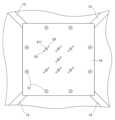
- probe cardsthere are various types of probe cards, one of which includes the one described in Patent Document 1 and the probe card illustrated in FIG. 9. Here, for convenience of explanation, the structure of a conventional probe card 100 will be explained using FIG. 9.
- the probe card 100 in FIG. 9includes a wiring board 11 and a multilayer wiring board 12 having a plurality of probes on the lower side of the wiring board 11.
- the substrate 12is bonded to the substrate 12.
- a reinforcing member 13 and a cover member 94are provided on the upper surface of the wiring board 11 of the probe card 100, and are placed at positions corresponding to the probe pad areas 121 of the multilayer wiring board 12 in order to support the load of the probe.
- a block member 95is provided.
- the multilayer wiring board 12when joining the multilayer wiring board 12 and the wiring board 11 with the joining member 31, applying heat may cause the multilayer wiring board 12 to warp. Further, the multilayer wiring board 12 may be joined to the wiring board 11 in an inclined state. In such a case, the heights of the probes mounted on the probe pad area of the multilayer wiring board 12 vary, so that the probes may not be able to contact the electrode terminals properly.
- the electrical connection device of the present inventionincludes (1) a wiring board electrically connected to the inspection device side, and (2) one or more electrodes provided on the lower surface side of the wiring board. (3) a probe board having one or more probe mounting portions on which a plurality of probes are mounted for electrically contacting the corresponding electrode terminals for each electrode terminal of the test object having the terminal; and (3) flatness of the probe board.
- the adjusting memberis characterized by comprising at least a cover member having one or more flatness adjustment mechanisms provided corresponding to each probe mounting portion of the probe board.
- the flatness of a substrate on which a plurality of probes are mountedcan be adjusted in order to improve the electrical contact of the probes to the electrode terminals of the object to be inspected.
- FIG. 1is a diagram schematically showing the main configuration of an electrical connection device according to an embodiment.
- FIG. 1is a plan view of an electrical connection device according to an embodiment.
- FIG. 3is a bottom view of the electrical connection device according to the embodiment.
- FIG. 2is a configuration diagram showing the configuration of a multilayer wiring board provided on the lower surface of the wiring board according to the embodiment.
- FIG. 3is a diagram showing the arrangement of indenters 22 on the wiring board according to the embodiment.
- FIG. 3is a configuration diagram showing the top surface of the cover member according to the embodiment.
- FIG. 2is a perspective configuration diagram of an indenter according to an embodiment when viewed from below.
- FIG. 3is a diagram visualizing flatness measurement results of a multilayer wiring board in an embodiment.
- FIG. 1is a diagram schematically showing the configuration of a conventional electrical connection device.
- FIG. 3is a configuration diagram showing the configuration of an indenter according to a modified embodiment (Part 1).
- Part 2is a configuration diagram showing the configuration of an indenter according to a modified embodiment (part 2).
- each of a plurality of semiconductor integrated circuits formed on a semiconductor waferis an object to be inspected.
- the electrical connection device of the present inventionis applied to a probe card used in an inspection device that inspects the electrical characteristics of such an object to be inspected.
- “Flatness”generally refers to the amount of deviation of a planar shape from a geometrically correct plane.
- flatnessis a numerical value that indicates the smoothness (uniformity) of a plane, and is a value that indicates how accurately a plane should be flat.
- the value of the vertical distance between the plane containing the most protruding part and the plane containing the most concave part of a planar shapecan be used as the flatness.
- "flatness”includes not only the overall flatness of the probe substrate but also the flatness of a partial region (e.g., probe region) of the probe substrate where a plurality of probes are arranged. It's the intention.
- FIG. 1is a diagram schematically showing the main configuration of an electrical connection device according to an embodiment.
- FIG. 2is a plan view of the electrical connection device, and
- FIG. 3is a bottom view of the electrical connection device.
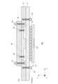
- the electrical connection device 10includes a wiring board 11, a multilayer wiring board 12, a reinforcing member 13, and a cover member 14 having a flatness adjustment mechanism 20.
- the electrical connection device 10is provided in a test header of an inspection device when electrically inspecting a plurality of objects to be inspected 43 formed on a semiconductor wafer.
- the multilayer wiring board 12 of the electrical connection device 10has a plurality of electrical contacts (probes). When performing an electrical test, each probe of the electrical connection device 10 is brought into electrical contact with the corresponding electrode terminal of the test object 43, and the test device electrically tests the test object 43. .
- the object to be inspected 43is placed on the upper surface of the chuck 42 that holds the wafer and is held by the chuck 42.
- the chuck 42is connected to, for example, an inspection stage 41 that is a multi-axis stage, and the position of the object to be inspected 43 held by the chuck 42 can be adjusted by driving the inspection stage 41.
- the multilayer wiring board 12is a probe board on which a plurality of electrical contacts (probes) are mounted.
- the multilayer wiring board 12is bonded to the center of the lower surface of the wiring board 11 by a large number of bonding members 31 such as solder balls.
- the multilayer wiring board 12is, for example, a substantially square board made of an electrically insulating material such as polyimide resin.
- the multilayer wiring board 12can use, for example, a board using resin as an MLO (Multi-Layer Organic) base material in order to enable fine wiring.
- MLOMulti-Layer Organic
- a probe pad area 121 to which a plurality of probes can be attachedis formed on the lower surface of the multilayer wiring board 12, and a plurality of wiring paths are further formed inside the multilayer wiring board 12.
- Each wiring path of the multilayer wiring board 12connects each probe of the probe pad area 121 to a connection terminal provided on the multilayer wiring board 12 and connected to the wiring board 11.
- a plurality of probescan be attached to the probe pad area 121 for each target device (DUT: Device Under Test) as the object to be tested 43.
- DUTDevice Under Test
- FIG. 3illustrates a case where six probe pad areas 121 are formed on the multilayer wiring board 12. This is because there are six DUTs as the test object 43, and in order to electrically contact each DUT with a plurality of probes, each probe pad area 121 is arranged at the position of the corresponding DUT. There is. In this way, the probe pad areas 121 are arranged at the positions of the corresponding DUTs, and the plurality of probes in each probe pad area 121 are arranged so as to be able to make electrical contact with the corresponding DUTs. Note that the probe pad area 121 is also called a probe head.
- FIG. 3illustrates a case where the multilayer wiring board 12 includes six probe pad areas 121
- the number of probe pad areas 121is not limited to this. Since the probe pad area 121 is provided for each DUT, as many probe pad areas 121 as there are DUTs are provided.
- the wiring board 11is a board for connecting to a test head of a tester and transmitting and receiving electrical signals.
- a large number of electrodesare provided on the upper surface of the wiring board 11, and are connected to the test head via the electrodes on the upper surface of the wiring board 11.
- a wiring patternis formed on the lower surface of the wiring board 11, and is connected to the multilayer wiring board 12 via the wiring pattern. Further, wiring paths are formed inside the wiring board 11 to connect each terminal on the upper surface of the wiring board 11 and each terminal on the lower surface of the wiring board 11. Therefore, the wiring board 11 has a structure in which each terminal on the upper surface and each terminal on the lower surface can be electrically connected via the internal wiring path.
- a reinforcing member 13 and a cover member 14 having a flatness adjustment mechanism 20are arranged on the upper surface of the wiring board 11 in order to suppress deformation of the wiring board 11.
- each of the wiring board 11 and the reinforcing member 13has a through hole 531 and a through hole 532, such as a screw hole, which are connected to the fixing member 53.
- the through holes 531 of the wiring board 11 and the through holes 532 of the reinforcing member 13are aligned, and fixing members 53 such as screws are inserted into the through holes 531 and 532 to couple them.
- the reinforcing member 13is a member attached to the upper surface side of the wiring board 11 in order to suppress deformation such as bending of the wiring board 11.
- the reinforcing member 13is also called a stiffener.
- the reinforcing member 13is a member that is thick in the Z direction.
- the reinforcing member 13can take various shapes, but in this embodiment, as shown in FIG. has.
- the plurality of radial sectionshave four inner radial sections extending radially from the center of the annular section toward the annular section and eight outer radial sections extending radially outward from the annular section.
- a square frame connected to the square cover member 14is provided in the central portion of the reinforcing member 13 in order to provide a cover member 14 to be described later. Further, the shape of the reinforcing member 13 is not limited to the shape shown in FIG. 3.
- the cover member 14is a member attached to the upper side of the reinforcing member 13.
- the cover member 14is a member that is removable from the reinforcing member 13.
- the cover member 14has a flatness adjustment mechanism 20 that adjusts the flatness of the multilayer wiring board 12 on the lower surface of the wiring board 11.
- the cover member 14also has the function of supporting the load when the probe provided on the multilayer wiring board 12 contacts (when the probe contacts the electrode terminal of the object to be inspected 43).
- the cover member 14is a square plate-like member disposed at the center of the wiring board 11.
- the size of the square cover member 14is slightly larger than the size of the multilayer wiring board 12 on the lower surface of the wiring board 11. Note that the shape of the cover member 14 is not limited to a square.
- each of the reinforcing member 13 and the cover member 14has a through hole 511 and a through hole 512 such as a screw hole. It can be fixed by aligning the cover member 14 with the through hole 512 and inserting a fixing member 51 such as a screw into the through hole 511 and the through hole 512.
- the flatness adjustment mechanism 20 of the cover member 14adjusts the flatness of the multilayer wiring board 12 on the lower surface of the wiring board 11.
- the multilayer wiring board 12when attaching the multilayer wiring board 12 to the lower surface of the wiring board 11, a large number of bonding members 31 such as solder balls are placed in the center of the lower surface of the wiring board 11, and the multilayer wiring board is mounted on the large number of bonding members 31. 12 and join.
- the joining member 31such as a solder ball
- heatis applied, so the multilayer wiring board 12 may warp. Further, depending on the multilayer wiring board 12, the board may be warped even before bonding.
- the tip positions of the plurality of electrical contactsmay vary (that is, the height of the probes may vary). variation), the contact of the probe with the electrode terminal of the object to be inspected 43 may not be good. In this case, the accuracy of electrical testing of the object to be tested 43 will also be affected.
- the cover member 14is provided with a flatness adjustment mechanism 20 that adjusts the flatness of the multilayer wiring board 12.
- the flatness adjustment mechanism 20applies a concentrated load to the multilayer wiring board 12 via the wiring board 11 to correct warpage. Thereby, warping of the wiring board 11 and the multilayer wiring board 12 can be suppressed, and variations in the tip positions of the plurality of probes can be suppressed. As a result, the contact of the probe with the electrode terminal of the object to be inspected 43 can be improved, and the electrical testing of the object to be inspected 43 can also be performed with high precision.
- the flatness adjustment mechanism 20 of the cover member 14includes one or more indenters 22 that apply a load to the multilayer wiring board 12 via the wiring board 11, and an adjustment member 21 that adjusts the load of each of the one or more indenters 22. has.
- the indenter 22is a contact member placed on the top surface of the wiring board 11.
- the indenter 22is a member that applies a load to the wiring board 11 and the multilayer wiring board 12 under load adjustment by the adjustment member 21 .
- the adjustment member 21adjusts the amount of depression of the indenter 22 according to the degree of warpage of the wiring board 11 and the multilayer wiring board 12, and the indenter 22 applies a load corresponding to the amount of depression adjusted by the adjustment member 21 to the wiring. Add to the board 11 and multilayer wiring board 12. By changing the magnitude of the load, the wiring board 11 and the multilayer wiring board 12 are deformed, and the warpage is corrected.
- the position where the indenter 22 is providedis preferably a position where the flatness of the wiring board 11 and the multilayer wiring board 12 is improved, and/or a position where the contact between the probe and the DUT is improved.
- the indenters 22are placed at positions corresponding to the center of the multilayer wiring board 12 (for example, the center of gravity) and at positions corresponding to the center of each probe pad area 121.
- the multilayer wiring board 12 to be balancedcan be supported at the center.
- the indenter 22by arranging the indenter 22 at a position corresponding to the position of the probe pad area 121 (in other words, providing an indenter 22 for each DUT of the test object 43), Since the indenter 22 can apply a load, flatness control can be stabilized and the contact of the probe with the DUT can also be improved.
- the test object 43has six DUTs and the multilayer wiring board 12 has six probe pad areas 121
- one Seven indenters 22are provided, including six indenters 22 and six indenters 22 arranged at respective positions for six probe pad areas 121.
- the indenter 22has various shapes (types) such as a flat cylindrical indenter, a flat prismatic indenter, a spherical indenter, and a conical indenter. , various types of indenters can be used.
- an indenter 22is provided to apply a substantially uniform load to the surface of the probe pad area 121. Note that the material of the indenter 22 is not particularly limited either.
- the adjustment member 21is for adjusting the amount of depression of the corresponding indenter 22.
- the adjustment member 21is provided for each indenter 22.
- the adjustment member 21fixes the upper part of the indenter 22 and adjusts the amount by which the indenter 22 is pushed in the vertical direction, and may be a clamping screw, a screw, or the like, for example.
- a crimp screw, a screw, or the likeis used as the adjustment member 21, it is possible to adjust the amount of rotation and the amount of indentation load that can be applied to the indenter 22.
- FIG. 4is a configuration diagram showing the configuration of the multilayer wiring board 12 on the lower surface of the wiring board 11.
- FIG. 5is a diagram showing the arrangement of the indenters 22 on the wiring board 11.
- FIG. 6is a configuration diagram showing the top surface of the cover member 14 according to the embodiment.
- the multilayer wiring board 12 usedhas six probe pad areas 121 (121a to 121f).
- the probe pad area 121when referring to a specific probe pad area 121, it is expressed as probe pad area 121a or the like.
- FIG. 7is a perspective configuration diagram of the indenter 22 viewed from below. Regarding the indenter 22, when referring to a specific indenter 22, it is written as indenter 22a or the like.
- the indenter 22(22a to 22g) has a pressure receiving part 222 that receives pushing pressure from the adjustment member 21, and a flat prismatic contact part 221 that applies a load to the wiring board 11 and the multilayer wiring board 12.
- the shape of the contact portion 221 that is in contact with the wiring board 11is the same as the shape of the probe pad area 121, and the size of the contact portion 221 is also the same as the size of the probe pad area 121. Thereby, a load can be reliably applied to the probe pad area 121, and as a result, the contactability of the probe to the electrode terminal of the object to be inspected 43 can be improved.
- the tip of the contact portion 221 of the indenter 22is flattened to distribute the load. I'm letting you do it.
- one indenter 22g out of the seven indenters 22corresponds to the center position (i.e., the center of gravity) of the multilayer wiring board 12 in order to maintain balance. place in position. Further, each of the remaining six indenters 22a to 22f is arranged at a position corresponding to the central position of each of the six probe pad areas 121a to 121f of the multilayer wiring board 12.
- the cover member 14has an adjustment hole 211 such as a screw hole for receiving the adjustment member 21, and two positioning holes 23 for each indenter 22 (22a to 22g).
- each positioning hole 23 of the cover member 14is aligned with the positioning hole 24 of the corresponding indenter 22, and a fixing member such as a screw is inserted between the positioning hole 23 of the cover member 14 and the positioning hole 24 of the corresponding indenter 22. It is inserted into the positioning hole 23 of the indenter 22. In this way, each indenter 22 is aligned.
- the number of positioning holes 24 and positioning holes 23is not limited to two, but may be one or three or more.
- the adjustment member 21When adjusting the magnitude of the load applied by the indenter 22, the adjustment member 21 is inserted into the adjustment hole 211 of the cover member 14.
- the pressure receiving part 222 of the indenter 22is The tip portion (lower end portion) of the adjustment member 21 is brought into contact with the center portion (that is, the position corresponding to the center position of the contact portion 221).
- the multilayer wiring board 12is bonded to the lower surface of the wiring board 11 using a large number of bonding members 31 such as solder balls.
- a plurality of probesare attached to each probe pad area 121 of the multilayer wiring board 12, and the reinforcing member 13 is attached to the upper side of the wiring board 11 with necessary electronic components set on the wiring board 11. do.
- the flatness adjustment mechanism 20has been aligned and the cover member 14 has been attached to the reinforcing member 13.
- the flatness of the multilayer wiring board 12 bonded to the wiring board 11is measured, and while determining whether the measured flatness value is equal to or less than the target value, the flatness adjustment mechanism is adjusted. 20 to adjust the flatness.
- the flatness measurement methodis to measure the flatness of the multilayer wiring board 12 using an existing flatness measuring machine.
- the flatness values at a plurality of arbitrary pointsare measured in the board region of a certain probe pad area 121, and the pad average value of the flatness values is determined. Furthermore, the flatness is measured over the entire surface of the multilayer wiring board 12, and the value with the largest deviation is taken as the maximum value. Then, the difference value between the maximum value and the area average value is adjusted to be equal to or less than the target value.
- FIG. 8is a diagram visualizing the flatness measurement results of the multilayer wiring board 12.
- 8Aillustrates the flatness of the multilayer wiring board 12 before adjustment by the flatness adjustment mechanism 20
- FIG. 8Billustrates the flatness of the multilayer wiring board 12 after adjustment.
- the difference value near the right edge(the difference value between the maximum value and the area average value mentioned above) is different from the center part to the left side. It can be seen that it is larger than the difference value.
- a flatness adjustment mechanismis provided for the probe pad areas 121c and 121f existing on the left side of the multilayer wiring board 12, as shown in FIG. 20 is used. That is, in order to increase the load of the indenters 22c and 22f on the probe pad areas 121c and 121f, the amount of pushing of the adjusting member 21 of each of the indenters 22c and 22f is adjusted to be large.
- the indenters 22c and 22fapply a large load to the left side of the multilayer wiring board 12, deforming the multilayer wiring board 12, suppressing warping of the entire board, and reducing the flatness value of the board as a whole. (See FIG. 8B).
- the cover member 14includes the flatness adjustment mechanism 20 that can apply a plurality of concentrated loads to the multilayer wiring board 12. Accordingly, the flatness value of the multilayer wiring board 12 can be adjusted.
- the tip positions of the plurality of probes provided on the multilayer wiring board 12can be aligned, so that contact with the terminals (DUT) of the object to be inspected 43 can be improved, and inspection accuracy can be increased.
- the cover member 14is removable from the reinforcing member 13, so as long as the cover member 14 equipped with the flatness adjustment mechanism 20 can be mounted, it can be provided on the reinforcing member 13 of various shapes. be able to.
- the electronic component 6may be present at a position corresponding to the probe pad area 121 on the upper surface of the wiring board 11 where the indenter 22 is arranged. If this happens, the indenter 22 and the electronic component 6 will come into contact with each other. Therefore, the indenter 22 may be configured to apply a load to the probe pad area 121 of the wiring board 11 and the multilayer wiring board 12 while avoiding collision with the electronic component 6 on the wiring board 11.
- a recessed portion (conflict avoidance portion) 2211may be provided in the center of the contact portion 221 of the indenter 22 in order to avoid collision with the electronic component 6.
- a loadcan be applied to the wiring board 11 and the multilayer wiring board 12 while avoiding collision between the contact portion 221 of the indenter 22 and the electronic component 6.
- the flatness of the wiring board 11can be adjusted.
- FIG. 22may be provided with a recessed portion (conflict avoidance portion) 2212. Similar effects can be obtained in this case as well.
- the recesses (conflict avoidance parts) 2211 and 2212 in FIGS. 10(B) and 11(B)are square prism recesses, but if collision with the electronic component 6 can be avoided.
- the shapeis not limited, and may be, for example, a cylindrical shape, a polygonal prism, or the like.
- one recessed portion 2211 and 2212is provided in the contact portion 221 of the indenter 22, but two or more recessed portions may be provided. Further, it is not necessary to provide the recesses 2211 and 2212 in all of the indenters 22, and it is possible to provide recesses 2211 and 2212 in some of the indenters 22 that come into contact with the electronic component 6.
- cover member 14In the first embodiment described above, the case where the cover member 14 is provided on the reinforcing member 13 is illustrated. However, the arrangement of the cover member 14 is not limited to this. For example, if the cover member 14 can adjust the flatness of the multilayer wiring board 12 as a probe board (or the flatness of each probe pad area 121 of the multilayer wiring board 12), the cover member 14 may be placed on the top surface of the multilayer wiring board 12. It's okay.
- SYMBOLS 10Electrical connection device, 11... Wiring board, 12... Multilayer wiring board, 13... Reinforcement member, 14... Cover member, 20... Flatness adjustment mechanism, 21... Adjustment member, 22 (22a-22g)... Indenter, 211 ...Adjustment hole, 221...Contact part, 2211 and 2212...Concave part (conflict avoidance part), 222...Pressure receiving part, 23...Positioning hole, 24...Positioning hole, 31...Joining member, 41...Inspection stage, 42...Chuck, 43...Test object, 51...Fixing member, 53...Fixing member, 100...Probe card, 121 (121a to 121f)...Probe pad area, 511...Through hole, 512...Through hole, 531...Through hole, 532...Through Hole.
Landscapes
- Engineering & Computer Science (AREA)
- Physics & Mathematics (AREA)
- General Physics & Mathematics (AREA)
- General Engineering & Computer Science (AREA)
- Computer Hardware Design (AREA)
- Microelectronics & Electronic Packaging (AREA)
- Environmental & Geological Engineering (AREA)
- Measuring Leads Or Probes (AREA)
- Testing Or Measuring Of Semiconductors Or The Like (AREA)
- Tests Of Electronic Circuits (AREA)
- Testing Of Individual Semiconductor Devices (AREA)
Abstract
Description
Translated fromJapanese本発明は、電気的接続装置に関し、例えば、半導体集積回路の通電試験等に用いられる電気的接続装置に適用し得るものである。The present invention relates to an electrical connection device, and can be applied to, for example, an electrical connection device used for conduction tests of semiconductor integrated circuits.
半導体ウェハ上の半導体集積回路(被検査体)の電気的検査では、テストヘッドに、複数のプローブ(電気的接触子)を有するプローブカードを取り付けた検査装置(テスター)が用いられる。そして、半導体集積回路の電極端子とプローブとを電気的に接触させて、テスターがプローブを介して半導体集積回路に電気信号を供給したり、半導体集積回路がプローブを介してテスター側に出力したりして、半導体集積回路の電気的検査を行なう。In electrical testing of semiconductor integrated circuits (objects to be tested) on semiconductor wafers, a testing device (tester) is used in which a probe card having a plurality of probes (electrical contacts) is attached to a test head. Then, by electrically contacting the electrode terminals of the semiconductor integrated circuit with the probe, the tester can supply electrical signals to the semiconductor integrated circuit through the probe, or the semiconductor integrated circuit can output signals to the tester through the probe. Then, the semiconductor integrated circuit is electrically inspected.
プローブカードには様々な種類があるが、その1つの種類として、特許文献1に記載されているものや、図9に例示するようなプローブカードなどがある。ここでは、説明便宜上、図9を用いて、従来のプローブカード100の構造を説明する。There are various types of probe cards, one of which includes the one described in Patent Document 1 and the probe card illustrated in FIG. 9. Here, for convenience of explanation, the structure of a
図9のプローブカード100は、配線基板11と、当該配線基板11の下側に複数のプローブを有する多層配線基板12とを備え、多数の接合部材(はんだボール)31によって配線基板11と多層配線基板12とを接合している。また、プローブカード100の配線基板11の上面には、補強部材13と、カバー部材94とが設けられており、プローブの荷重を支えるため、多層配線基板12のプローブパッドエリア121に対応する位置にブロック部材95が設けられている。The
しかしながら、多層配線基板12と配線基板11とを接合部材31で接合する際に、熱を加えることにより、多層配線基板12に反りが生じてしまうことがある。また、多層配線基板12が傾いた状態で配線基板11に接合してしまうことがある。そのような場合、多層配線基板12のプローブパッドエリアに実装されるプローブの高さにばらつきが生じるため、電極端子に対するプローブのコンタクトが正常にできないことが生じ得る。However, when joining the
そのため、被検査体の電極端子に対するプローブの電気的接触性を向上させるため、複数のプローブを実装する基板(例えば、多層配線基板など)の平面度を調整することができる電気的接続装置が求められている。Therefore, in order to improve the electrical contact of the probes to the electrode terminals of the test object, there is a need for an electrical connection device that can adjust the flatness of a board (for example, a multilayer wiring board) on which multiple probes are mounted. It is being
かかる課題を解決するために、本発明の電気的接続装置は、(1)検査装置側と電気的に接続する配線基板と、(2)配線基板の下面側に設けられ、1又は複数の電極端子を有する被検査体の電極端子毎に、対応する電極端子と電気的に接触させる複数のプローブを搭載する1又は複数のプローブ取付部を有するプローブ基板と、(3)プローブ基板の平面度を調整する部材であって、少なくとも、プローブ基板のそれぞれのプローブ取付部に対応させて設けた1又は複数の平面度調整機構を有するカバー部材とを備えることを特徴とする。In order to solve such problems, the electrical connection device of the present invention includes (1) a wiring board electrically connected to the inspection device side, and (2) one or more electrodes provided on the lower surface side of the wiring board. (3) a probe board having one or more probe mounting portions on which a plurality of probes are mounted for electrically contacting the corresponding electrode terminals for each electrode terminal of the test object having the terminal; and (3) flatness of the probe board. The adjusting member is characterized by comprising at least a cover member having one or more flatness adjustment mechanisms provided corresponding to each probe mounting portion of the probe board.
本発明によれば、被検査体の電極端子に対するプローブの電気的接触性を向上させるため、複数のプローブを実装する基板の平面度を調整することができる。According to the present invention, the flatness of a substrate on which a plurality of probes are mounted can be adjusted in order to improve the electrical contact of the probes to the electrode terminals of the object to be inspected.
(A)実施形態
以下では、本発明に係る電気的接続装置の実施形態を、図面を参照しながら詳細に説明する。(A) Embodiment Below, embodiments of the electrical connection device according to the present invention will be described in detail with reference to the drawings.
この実施形態では、半導体ウェハ上に形成された複数の半導体集積回路のそれぞれを被検査体とする。また、そのような被検査体の電気的特性を検査する検査装置に用いられるプローブカードに、本発明の電気的接続装置を適用する場合を例示する。In this embodiment, each of a plurality of semiconductor integrated circuits formed on a semiconductor wafer is an object to be inspected. Further, a case will be illustrated in which the electrical connection device of the present invention is applied to a probe card used in an inspection device that inspects the electrical characteristics of such an object to be inspected.
「平面度」とは、一般的に、平面形体の幾何学的に正しい平面からの狂いの大きさをいう。つまり、平面度は、平面の滑らかさ(均一性)を示す数値であり、どれくらい正確に平らな面であるべきかを示す値である。例えば、平面形体で最も出っ張った部分を含む平面と、最もへこんだ部分を含む平面との間の上下の距離の値などを平面度とすることができる。例えば、この開示では、「平面度」が、プローブ基板の全体の平坦度だけでなく、プローブ基板のうち、複数のプローブが配置されている一部領域(例えば、プローブ領域)の平坦度も含む意図である。"Flatness" generally refers to the amount of deviation of a planar shape from a geometrically correct plane. In other words, flatness is a numerical value that indicates the smoothness (uniformity) of a plane, and is a value that indicates how accurately a plane should be flat. For example, the value of the vertical distance between the plane containing the most protruding part and the plane containing the most concave part of a planar shape can be used as the flatness. For example, in this disclosure, "flatness" includes not only the overall flatness of the probe substrate but also the flatness of a partial region (e.g., probe region) of the probe substrate where a plurality of probes are arranged. It's the intention.
(A-1)実施形態の構成
図1は、実施形態に係る電気的接続装置の主な構成の概略を示す図である。図2は、電気的接続装置の平面図であり、図3は、電気的接続装置の底面図である。(A-1) Configuration of Embodiment FIG. 1 is a diagram schematically showing the main configuration of an electrical connection device according to an embodiment. FIG. 2 is a plan view of the electrical connection device, and FIG. 3 is a bottom view of the electrical connection device.
図1~図3において、実施形態に係る電気的接続装置10は、配線基板11、多層配線基板12、補強部材13、平面度調整機構20を有するカバー部材14を備える。In FIGS. 1 to 3, the
電気的接続装置10は、半導体ウェハに形成された複数の被検査体43の電気的な検査を行なう際に、検査装置のテストヘッダに備えられる。電気的接続装置10の多層配線基板12は、複数の電気的接触子(プローブ)を有している。そして、電気的な検査を行なう際、電気的接続装置10の各プローブと、被検査体43の対応する電極端子とを電気的接触させて、検査装置が被検査体43の電気的検査を行なう。The
被検査体43は、ウェハを保持するチャック42の上面に置かれてチャック42により保持される。チャック42は例えば多軸ステージの検査ステージ41と接続しており、検査ステージ41の駆動により、チャック42に保持されている被検査体43の位置が調整可能となっている。The object to be inspected 43 is placed on the upper surface of the
[多層配線基板12]
多層配線基板12は、複数の電気的接触子(プローブ)を実装するプローブ基板である。[Multilayer wiring board 12]
The
多層配線基板12は、配線基板11の下面中央部に、多数のはんだボール等の接合部材31によって接合される。多層配線基板12は、例えば、ポリイミド樹脂等の電気的絶縁材料で形成された略正方形の基板である。多層配線基板12は、微細配線を可能とするため、例えばMLO(Multi-Layer Organic)基材として樹脂を用いた基板を用いることができる。The
多層配線基板12の下面には、複数のプローブを取り付け可能なプローブパッドエリア121が形成されており、更に多層配線基板12の内部には、複数の配線路が形成されている。多層配線基板12の各配線路は、プローブパッドエリア121の各プローブと、多層配線基板12上に設けた、配線基板11と接続する接続端子とを接続している。A
プローブパッドエリア121は、被検査体43としての対象デバイス(DUT:Device Under Test)毎に、複数のプローブを取り付け可能となっている。例えば、図3では、6個のプローブパッドエリア121が多層配線基板12に形成されている場合を例示している。これは、被検査体43として6個のDUTがあり、それぞれのDUTに複数のプローブを電気的に接触させるために、各プローブパッドエリア121は、対応するDUTの位置となるように配置されている。このように、プローブパッドエリア121は対応するDUTの位置に配置され、各プローブパッドエリア121の複数のプローブは、対応するDUTに対して電気的に接触できるように配置される。なお、プローブパッドエリア121をプローブヘッドとも呼ぶ。A plurality of probes can be attached to the
なお、図3では、6個のプローブパッドエリア121を多層配線基板12が備える場合を例示しているが、プローブパッドエリア121の数はこれに限定されない。プローブパッドエリア121はDUT毎に設けられるため、DUTの数だけ、プローブパッドエリア121が設けられる。Although FIG. 3 illustrates a case where the
[配線基板11]
配線基板11は、テスターのテストヘッドと接続して、電気信号を授受するための基板である。配線基板11の上面には、多数の電極があり、配線基板11の上面の電極を介してテストヘッドと接続している。配線基板11の下面には、配線パターンが形成されており、配線パターンを介して多層配線基板12と接続している。さらに、配線基板11の内部には、配線基板11の上面の各端子と、配線基板11の下面の各端子とを接続する配線路が形成されている。従って、配線基板11は、内部の配線路を介して、上面の各端子と下面の各端子とが電気的に接続可能な構造となっている。[Wiring board 11]
The
配線基板11の上面には、配線基板11の変形を抑制するため、補強部材13と、平面度調整機構20を有するカバー部材14とが配置されている。A reinforcing
配線基板11に補強部材13を組み立てるため、配線基板11及び補強部材13のそれぞれには、固定部材53と結合するネジ穴等の貫通孔531及び貫通孔532がある。組み立てる際に、配線基板11の貫通孔531と、補強部材13の貫通孔532との位置を合わせ、貫通孔531及び貫通孔532に、ネジ等の固定部材53を差し込み結合することで固定できる。In order to assemble the reinforcing
[補強部材13]
補強部材13は、配線基板11の撓み等の変形を抑えるために、配線基板11の上面側に取り付けられる部材である。補強部材13は、スティフナとも呼ばれる。[Reinforcement member 13]
The reinforcing
補強部材13は、Z方向に厚みを持つ部材である。補強部材13は、様々な形状を取り得るが、この実施形態では、例えば図3のように、1個の環状部分と、環状部分の中心から環状部分に向けて放射状に延びる複数の放射状部分とを有する。さらに、複数の放射状部分は、環状部分の中心から環状部分に向けて放射状に延びる4個の内側放射状部分と、環状部分から外側に向けて放射状に延びる8個の外側放射状部分とを有する。The reinforcing
なお、補強部材13の中央部分には、後述するカバー部材14が設けるため、正方形のカバー部材14と連結する正方形のフレームが設けられている。また、補強部材13の形状は図3に示す形状に限定されない。Note that a square frame connected to the
[カバー部材14]
カバー部材14は、補強部材13の上側に取り付けられる部材である。カバー部材14は、補強部材13に対して取り外し可能な部材である。[Cover member 14]
The
また、カバー部材14は、配線基板11に下面にある多層配線基板12の平面度を調整する平面度調整機構20を有する。また、カバー部材14は、多層配線基板12に設けられるプローブのコンタクト時(被検査体43の電極端子に対するプローブの接触時)の荷重を支持する機能も有する。Additionally, the
図2に例示するように、カバー部材14は、配線基板11の中央部に配置され、正方形の形状をした板状部材である。正方形のカバー部材14のサイズは、配線基板11下面の多層配線基板12のサイズよりもわずかに大きい。なお、カバー部材14の形状は、正方形に限定されない。As illustrated in FIG. 2, the
補強部材13にカバー部材14を組み立てるため、補強部材13及びカバー部材14のそれぞれには、ネジ穴等の貫通孔511及び貫通孔512があり、組み立てる際に、補強部材13の貫通孔511と、カバー部材14の貫通孔512との位置を合わせて、ネジ等の固定部材51を、貫通孔511及び貫通孔512に差し込むことで固定できる。In order to assemble the
[平面度調整機構20]
カバー部材14の平面度調整機構20は、配線基板11下面の多層配線基板12の平面度を調整するものである。[Flatness adjustment mechanism 20]
The
従来、多層配線基板12を配線基板11の下面に取り付ける際、配線基板11の下面中央部に、多数のはんだボール等の接合部材31を配置し、それら多数の接合部材31の上に多層配線基板12を載せて接合する。はんだボールなどの接合部材31で多層配線基板12を接合する際、熱を印加するため、多層配線基板12に反りが生じてしまうことがある。また、多層配線基板12によっては、接合前であっても基板が反っているものもある。Conventionally, when attaching the
配線基板11への接合後、基板が反っていて平面度が良好でない多層配線基板12を検査に用いると、複数の電気的接触子(プローブ)の先端位置がばらつき(すなわち、プローブの高さがばらつき)、被検査体43の電極端子に対するプローブの接触性が良好でなくなることがある。そうすると、被検査体43の電気的検査の精度にも影響が生じることになる。When a
そこで、この実施形態では、カバー部材14に、多層配線基板12の平面度を調整する平面度調整機構20を備える。Therefore, in this embodiment, the
平面度調整機構20は、配線基板11下面に多層配線基板12を接合後、配線基板11を介して多層配線基板12に対して集中荷重を加えて、反りを矯正する。これにより、配線基板11及び多層配線基板12の反りが抑えられ、複数のプローブの先端位置のばらつきを抑えることができる。その結果、被検査体43の電極端子に対するプローブの接触性も良好にでき、被検査体43の電気的検査も高精度となる。After the
カバー部材14の平面度調整機構20は、配線基板11を介して多層配線基板12に荷重を加える1又は複数の圧子22と、1又は複数の圧子22のそれぞれの荷重を調整する調整部材21とを有する。The
圧子22は、配線基板11の上面に置かれる接触部材である。圧子22は、調整部材21による荷重調整を受けて、配線基板11及び多層配線基板12に荷重を加える部材である。つまり、配線基板11及び多層配線基板12の反りの程度に応じて、調整部材21が圧子22の押し込み量を調整し、調整部材21により調整された押し込み量に応じた荷重を、圧子22が配線基板11及び多層配線基板12に加える。荷重の大きさが変わることで、配線基板11及び多層配線基板12の基板が変形し、反りが矯正される。The
圧子22を設ける位置は、配線基板11及び多層配線基板12の平面度を良好にする位置、及び又は、プローブとDUTとの接触性を良好にできる位置が望ましい。The position where the
例えば、多層配線基板12の中央部の位置(例えば重心位置)に対応する位置と、各プローブパッドエリア121の中央部の位置に対応する位置とに、圧子22を配置する。前者のように、多層配線基板12の中央部に対応する位置に圧子22を配置することで、バランスをとるべき多層配線基板12を中央部で支持できる。また、後者のように、プローブパッドエリア121の位置に対応する位置に圧子22を配置する(言い換えると、被検査体43のDUT毎に圧子22を備える)ことで、対応するプローブパッドエリア121に圧子22が荷重を加えることができるので、平面度の制御を安定させることができ、DUTに対するプローブの接触性も向上できる。For example, the
例えば、図2及び図3のように、被検査体43が6個のDUTを持ち、多層配線基板12が6個のプローブパッドエリア121を備える場合、多層配線基板12の中央部に配置する1個の圧子22と、6個のプローブパッドエリア121用のそれぞれの位置に配置する6個の圧子22とを合わせて、7個の圧子22を設ける。For example, as shown in FIGS. 2 and 3, when the
圧子22には、平坦円柱圧子、平坦角柱圧子、球形圧子、円錐圧子など様々な形状(種類)があるが、配線基板11を介して多層配線基板12に荷重を加えることができるものであれば、様々な種類の圧子を用いることができる。この実施形態では、プローブパッドエリア121の面に略均等な荷重を加えるようにするため圧子22を設ける。なお圧子22の材質も特に限定されない。The
調整部材21は、対応する圧子22の押し込み量を調整するものである。調整部材21は圧子22毎に設ける。調整部材21は、圧子22の上部を固定して、圧子22の上下方向の押し込み量を調整するものであり、例えば、クランピングスクリュー、ネジ等を用いることができる。例えば、調整部材21として、クラインピングスクリューやネジ等を用いる場合、どれだけの回転量で、圧子22に対してどれだけの押し込み荷重を加えることができるか等の調整が可能となる。The
[平面度調整機構20における圧子22の位置合わせ]
次に、カバー部材14の平面度調整機構20のうち、圧子22の位置合わせについて説明する。[Positioning of
Next, positioning of the
図4は、配線基板11下面の多層配線基板12の構成を示す構成図である。図5は、配線基板11上の圧子22の配置を示す図である。図6は、実施形態に係るカバー部材14の上面を示す構成図である。FIG. 4 is a configuration diagram showing the configuration of the
ここでは、被検査体43が6個のDUTを備えるものとする。そのため、図4に示すように、多層配線基板12は、6個のプローブパッドエリア121(121a~121f)を有するものを用いる。なお、プローブパッドエリア121について、特定のプローブパッドエリア121を指すときには、プローブパッドエリア121a等のように表記する。Here, it is assumed that the
圧子22は、図7に示すような平坦角柱圧子を用いるものとする。図7は、圧子22を下側から見たときの斜視構成図である。なお、圧子22について、特定の圧子22を指すときには、圧子22a等のように表記する。As the
図7において、圧子22(22a~22g)は、調整部材21から押し込み圧力を受ける圧力受け部222と、配線基板11及び多層配線基板12に対して荷重を加える平坦角柱形の接触部221とを有する。In FIG. 7, the indenter 22 (22a to 22g) has a
配線基板11に接触している接触部221の形状はプローブパッドエリア121の形状と同じ形状とし、接触部221のサイズもプローブパッドエリア121のサイズと同じサイズとしている。これにより、確実にプローブパッドエリア121に荷重を加えることができ、その結果、被検査体43の電極端子に対するプローブの接触性を向上できる。The shape of the
また、圧子22が配線基板11及び多層配線基板12に荷重を加える際に、配線基板11及び多層配線基板12の破損を回避するため、圧子22の接触部221の先端を平坦にして荷重を分散させている。In addition, in order to avoid damage to the
圧子22の配置例を説明する。この例の場合、図5に示すように、7個の圧子22のうち、1個の圧子22gは、バランスをとるため、多層配線基板12の中央部の位置(すなわち重心の位置)に対応する位置に配置する。また、残りの6個の圧子22a~22fのそれぞれは、多層配線基板12の6個のプローブパッドエリア121a~121fのそれぞれの中央部の位置に対応する位置に配置する。An example of the arrangement of the
図6に示すように、カバー部材14は、圧子22(22a~22g)毎に、調整部材21を受け入れるネジ穴等の調整孔211と、2個の位置決め孔23とを有する。As shown in FIG. 6, the
各圧子22の位置合わせをするため、カバー部材14の各位置決め孔23と、対応する圧子22の位置決め孔24との位置を合わせて、ネジ等の固定部材を、カバー部材14の位置決め孔23及び圧子22の位置決め孔23に挿通する。このようにして、各圧子22の位置合わせを行なう。なお、圧子22の位置決めが可能であれば、位置決め孔24及び位置決め孔23の数は2個に限定されず1個又は3個以上でもよい。In order to align each
圧子22が加える荷重の大きさを調整する際、カバー部材14の調整孔211に調整部材21を挿入する。When adjusting the magnitude of the load applied by the
ここで、圧子22の位置合わせに関して、圧子22の接触部221が、目標通りの荷重を、配線基板11及び多層配線基板12に加えることができるようにするため、圧子22の圧力受け部222の中央部(すなわち、接触部221の中心位置に相当する位置)に、調整部材21の先端部(下端部)が当たるようにする。Here, regarding the positioning of the
[平面度調整機構20を用いた平面度調整方法]
次に、カバー部材14の平面度調整機構20を用いた平面度調整方法を説明する。[Flatness adjustment method using flatness adjustment mechanism 20]
Next, a method of adjusting the flatness of the
ここでは、多数の半田ボール等の接合部材31を用いて、配線基板11の下面に、多層配線基板12が接合されているものとする。多層配線基板12の各プローブパッドエリア121に複数のプローブが取り付けられ、配線基板11に必要な電子部品がセットされている状態で、補強部材13が配線基板11の上側に取り付けられているものとする。そして、平面度調整機構20の位置合わせが行なわれて、カバー部材14が補強部材13に取り付けられているものとする。Here, it is assumed that the
このような状態で、配線基板11に接合している多層配線基板12の平面度を測定し、その測定した平面度の値が目標値以下となるか否かを判断しながら、平面度調整機構20を用いた平面度調整を行なう。なお、平面度の測定方法は、既存の平面度測定機を用いて、多層配線基板12の平面度を測定する。In this state, the flatness of the
より具体的に、例えば、多層配線基板12において、あるプローブパッドエリア121の基板領域で、複数の任意の点の平面度の値を測定し、平面度の値のパッド平均値を求める。さらに、多層配線基板12の基板全面で平面度を測定していき、最も偏差が大きい値を最大値とする。そして、最大値とエリア平均値との差分値が目標値以下となるように調整する。More specifically, for example, in the
図8は、多層配線基板12の平面度測定結果を可視化した図である。図8Aは、平面度調整機構20による調整前の多層配線基板12の平面度を図示しており、図8Bは、調整後の多層配線基板12の平面度を図示している。FIG. 8 is a diagram visualizing the flatness measurement results of the
図8Aにおいて、調整前の多層配線基板12の基板全体の平面度を観察すると、右側の端部付近の差分値(上述した最大値とエリア平均値との差分値)が、中央部から左側の差分値よりも大きくなっていることがわかる。In FIG. 8A, when observing the flatness of the entire board of the
したがって、多層配線基板12の基板全体の反りを矯正するため、例えば図8Bのように、多層配線基板12の左側に存在しているプローブパッドエリア121c及び121fに対して設けて、平面度調整機構20を用いる。つまり、プローブパッドエリア121c及び121fに対する圧子22c及び22fの荷重を大きくするため、圧子22c及び22fのそれぞれの調整部材21の押し込み量が大きくなるように調整する。Therefore, in order to correct the warpage of the entire board of the
これにより、圧子22c及び22fが多層配線基板12の左側に対して大きな荷重を加えることで、多層配線基板12が変形して、基板全体の反りが抑えられ、基板全体として平面度の値が小さくすることができる(図8B参照)。As a result, the
また、図8Aの調整前の多層配線基板12に設けたプローブ高さの差(プローブの高さのばらつき)と、図8Bの調整後の多層配線基板12に設けたプローブ高さの差とを比較した。その結果、図8Bの調整後のプローブ高さの差は、図8Aの調整前のプローブ高さの差よりも小さくなくっていることを確認できた。In addition, the difference in the height of the probes provided on the
(A-2)実施形態の効果
以上のように、この実施形態によれば、カバー部材14が、多層配線基板12に対して複数の集中荷重を加えることができる平面度調整機構20を備えることにより、多層配線基板12の平面度の値を調整できる。(A-2) Effects of Embodiment As described above, according to this embodiment, the
その結果、多層配線基板12に設けられる複数のプローブのそれぞれの先端位置を揃えることができるので、被検査体43の端子(DUT)に対する接触性を向上させ、検査精度を高くすることができる。As a result, the tip positions of the plurality of probes provided on the
この実施形態によれば、カバー部材14は、補強部材13に対して取り外し可能なので、平面度調整機構20を備えたカバー部材14を載置可能であれば、様々な形状の補強部材13に設けることができる。According to this embodiment, the
(B)他の実施形態
上述した第1の実施形態においても本開示の種々の変形例を言及したが、本開示は、以下の変形実施形態にも適用できる。(B) Other Embodiments Although various modifications of the present disclosure have been mentioned in the first embodiment described above, the present disclosure can also be applied to the following modified embodiments.
(B-1)上述した第1の実施形態では、圧子22の接触部221の形状が、対応するプローブパッドエリア121の形状に対応している場合を例示した。しかし、圧子22の接触部221の形状は、これに限らない。(B-1) In the first embodiment described above, the case where the shape of the
例えば、配線基板11の上面には、コンデンサ等のような電子部品6が多数設けられるのが一般的である。そのため、圧子22が配置される、配線基板11の上面であって、プローブパッドエリア121に対応する位置に、電子部品6が存在してしまうことがある。そうすると、圧子22と電子部品6とが抵触してしまう。そこで、配線基板11上の電子部品6への抵触を回避し、圧子22が、配線基板11及び多層配線基板12のプローブパッドエリア121に荷重を加えられるようにしてもよい。For example, a large number of
例えば、図10(B)に例示するように、電子部品6との抵触を回避するため、圧子22の接触部221の中央部に、凹部(抵触回避部)2211を設けるようにしても良い。これにより、図10(A)に示すように、圧子22の接触部221と、電子部品6との抵触を回避しながら、配線基板11及び多層配線基板12への荷重を加えることができる。この場合でも配線基板11(複数のプローブが配置されているプローブパッドエリア)の平面度を調整可能である。For example, as illustrated in FIG. 10(B), a recessed portion (conflict avoidance portion) 2211 may be provided in the center of the
また別の変形例として、図11(B)に例示するように、圧子22の接触部221の抵触面の一部領域(この例は、接触部221の正方形の抵触面の端部を含む領域)に、凹部(抵触回避部)2212を設けるようにしても良い。この場合も同様の効果を得ることができる。As another modification example, as illustrated in FIG. ) may be provided with a recessed portion (conflict avoidance portion) 2212. Similar effects can be obtained in this case as well.
なお、図10(B)及び図11(B)の凹部(抵触回避部)2211及び2212は、四角柱の凹部とする場合を例示したが、電子部品6との抵触を回避できるのであれば、形状は限定されず、例えば円柱形、多角柱等でもよい。Note that the recesses (conflict avoidance parts) 2211 and 2212 in FIGS. 10(B) and 11(B) are square prism recesses, but if collision with the
また、図10(B)及び図11(B)の例では、圧子22の接触部221に、1個の凹部2211及び2212を設ける場合を例示したが、2個以上でもよい。さらに、全ての圧子22に、凹部2211、2212を設ける必要はなく、電子部品6と抵触する一部の圧子22に、凹部2211、2212を設けたものを適用してよい。Furthermore, in the examples of FIGS. 10(B) and 11(B), one recessed
(B-2)上述した第1の実施形態では、カバー部材14が、補強部材13に設けられる場合を例示した。しかし、カバー部材14の配置はこれに限らない。例えば、カバー部材14が、プローブ基板としての多層配線基板12の平面度(又は多層配線基板12の各プローブパッドエリア121の平面度)を調整可能であれば、多層配線基板12の上面に配置されてもよい。(B-2) In the first embodiment described above, the case where the
10…電気的接続装置、11…配線基板、12…多層配線基板、13…補強部材、14…カバー部材、20…平面度調整機構、21…調整部材、22(22a~22g)…圧子、211…調整孔、221…接触部、2211及び2212…凹部(抵触回避部)、222…圧力受け部、23…位置決め孔、24…位置決め孔、31…接合部材、41…検査ステージ、42…チャック、43…被検査体、51…固定部材、53…固定部材、100…プローブカード、121(121a~121f)…プローブパッドエリア、511…貫通孔、512…貫通孔、531…貫通孔、532…貫通孔。DESCRIPTION OF
Claims (8)
Translated fromJapanese前記配線基板の下面側に設けられ、1又は複数の電極端子を有する被検査体の前記電極端子毎に、対応する前記電極端子と電気的に接触させる複数のプローブを搭載する1又は複数のプローブ取付部を有するプローブ基板と、
前記プローブ基板の平面度を調整する部材であって、少なくとも、前記プローブ基板のそれぞれの前記プローブ取付部に対応させて設けた1又は複数の平面度調整機構を有するカバー部材と
を備えることを特徴とする電気的接続装置。A wiring board electrically connected to the inspection equipment side,
One or more probes provided on the lower surface side of the wiring board and equipped with a plurality of probes that are brought into electrical contact with the corresponding electrode terminals for each of the electrode terminals of the test object having one or more electrode terminals. a probe board having a mounting part;
A member for adjusting the flatness of the probe substrate, comprising at least a cover member having one or more flatness adjustment mechanisms provided corresponding to each of the probe mounting portions of the probe substrate. electrical connection device.
前記配線基板の上面に置かれて、前記配線基板を介して前記プローブ基板に荷重を加える接触部材と、
前記接触部材が前記プローブ基板に対して加える荷重を調整する調整部材と
を有することを特徴とする請求項1に記載の電気的接続装置。Each of the flatness adjustment mechanisms,
a contact member placed on the top surface of the wiring board and applying a load to the probe board via the wiring board;
The electrical connection device according to claim 1, further comprising an adjustment member that adjusts the load that the contact member applies to the probe substrate.
前記接触部の形状が、前記プローブ取付部の形状に対応している
ことを特徴とする請求項2に記載の電気的接続装置。The contact member has a contact portion that contacts the wiring board, and a pressure receiving portion that transmits pressure from the adjustment member to the contact portion,
The electrical connection device according to claim 2, wherein the shape of the contact portion corresponds to the shape of the probe attachment portion.
前記接触部が、前記配線基板上の電子部品との抵触を回避する抵触回避部を有する
ことを特徴とする請求項2に記載の電気的接続装置。The contact member has a contact portion that contacts the wiring board, and a pressure receiving portion that transmits pressure from the adjustment member to the contact portion,
The electrical connection device according to claim 2, wherein the contact portion has a collision avoidance portion that avoids collision with an electronic component on the wiring board.
前記配線基板上の前記補強部材の中央部に空間があり、前記補強部材の中央部に、1又は複数の前記平面度調整機構を有する前記カバー部材が設けられることを特徴とする請求項1に記載の電気的接続装置。A reinforcing member is provided on the upper surface side of the wiring board,
According to claim 1, there is a space in the center of the reinforcing member on the wiring board, and the cover member having one or more flatness adjustment mechanisms is provided in the center of the reinforcing member. Electrical connection device as described.
Priority Applications (2)
| Application Number | Priority Date | Filing Date | Title |
|---|---|---|---|
| KR1020247041785AKR20250011658A (en) | 2022-07-28 | 2023-07-11 | Electrical connection device |
| CN202380057082.0ACN119654563A (en) | 2022-07-28 | 2023-07-11 | Electrical connection device |
Applications Claiming Priority (2)
| Application Number | Priority Date | Filing Date | Title |
|---|---|---|---|
| JP2022120167AJP2024017497A (en) | 2022-07-28 | 2022-07-28 | electrical connection device |
| JP2022-120167 | 2022-07-28 |
Publications (1)
| Publication Number | Publication Date |
|---|---|
| WO2024024492A1true WO2024024492A1 (en) | 2024-02-01 |
Family
ID=89706242
Family Applications (1)
| Application Number | Title | Priority Date | Filing Date |
|---|---|---|---|
| PCT/JP2023/025541CeasedWO2024024492A1 (en) | 2022-07-28 | 2023-07-11 | Electrical connection device |
Country Status (5)
| Country | Link |
|---|---|
| JP (1) | JP2024017497A (en) |
| KR (1) | KR20250011658A (en) |
| CN (1) | CN119654563A (en) |
| TW (1) | TWI884484B (en) |
| WO (1) | WO2024024492A1 (en) |
Citations (7)
| Publication number | Priority date | Publication date | Assignee | Title |
|---|---|---|---|---|
| JP2003528459A (en)* | 2000-03-17 | 2003-09-24 | フォームファクター,インコーポレイテッド | Method and apparatus for planarizing semiconductor contactors |
| JP2006023271A (en)* | 2004-07-05 | 2006-01-26 | Yulim Hitech Inc | Semiconductor inspection probe card |
| US20080061808A1 (en)* | 2006-09-12 | 2008-03-13 | Sammy Mok | Compliance partitioning in testing of integrated circuits |
| KR20090014755A (en)* | 2007-08-07 | 2009-02-11 | (주) 미코티엔 | Probe Card and Wafer Inspection Device Having the Same |
| JP2009133722A (en)* | 2007-11-30 | 2009-06-18 | Tokyo Electron Ltd | Probe device |
| JP2010511873A (en)* | 2006-12-01 | 2010-04-15 | フォームファクター, インコーポレイテッド | Probing device with guarded signal trace |
| JP2020112487A (en)* | 2019-01-15 | 2020-07-27 | 株式会社日本マイクロニクス | Probe board and electrical connection device |
Family Cites Families (1)
| Publication number | Priority date | Publication date | Assignee | Title |
|---|---|---|---|---|
| WO2019021749A1 (en) | 2017-07-24 | 2019-01-31 | 株式会社ヨコオ | Inspection jig |
- 2022
- 2022-07-28JPJP2022120167Apatent/JP2024017497A/enactivePending
- 2023
- 2023-07-11WOPCT/JP2023/025541patent/WO2024024492A1/ennot_activeCeased
- 2023-07-11CNCN202380057082.0Apatent/CN119654563A/enactivePending
- 2023-07-11KRKR1020247041785Apatent/KR20250011658A/enactivePending
- 2023-07-19TWTW112126877Apatent/TWI884484B/enactive
Patent Citations (7)
| Publication number | Priority date | Publication date | Assignee | Title |
|---|---|---|---|---|
| JP2003528459A (en)* | 2000-03-17 | 2003-09-24 | フォームファクター,インコーポレイテッド | Method and apparatus for planarizing semiconductor contactors |
| JP2006023271A (en)* | 2004-07-05 | 2006-01-26 | Yulim Hitech Inc | Semiconductor inspection probe card |
| US20080061808A1 (en)* | 2006-09-12 | 2008-03-13 | Sammy Mok | Compliance partitioning in testing of integrated circuits |
| JP2010511873A (en)* | 2006-12-01 | 2010-04-15 | フォームファクター, インコーポレイテッド | Probing device with guarded signal trace |
| KR20090014755A (en)* | 2007-08-07 | 2009-02-11 | (주) 미코티엔 | Probe Card and Wafer Inspection Device Having the Same |
| JP2009133722A (en)* | 2007-11-30 | 2009-06-18 | Tokyo Electron Ltd | Probe device |
| JP2020112487A (en)* | 2019-01-15 | 2020-07-27 | 株式会社日本マイクロニクス | Probe board and electrical connection device |
Also Published As
| Publication number | Publication date |
|---|---|
| CN119654563A (en) | 2025-03-18 |
| TW202422082A (en) | 2024-06-01 |
| TWI884484B (en) | 2025-05-21 |
| KR20250011658A (en) | 2025-01-21 |
| JP2024017497A (en) | 2024-02-08 |
Similar Documents
| Publication | Publication Date | Title |
|---|---|---|
| US6975127B2 (en) | Planarizing and testing of BGA packages | |
| KR102123989B1 (en) | Tester and testing equipment for semiconductor devices having the same | |
| TWI387030B (en) | Probe card, manufacturing method thereof, and alignment method | |
| KR101115548B1 (en) | Parallelism adjusting mechanism of probe card | |
| JP3388307B2 (en) | Probe card and method for assembling the same | |
| JP5991823B2 (en) | Electrical connection device and method of assembling the same | |
| US9797928B2 (en) | Probe card assembly | |
| KR20200007659A (en) | Circuit device, tester, inspection device, and method of adjusting bending of circuit board | |
| JP2006349692A (en) | Probe card | |
| KR20100069300A (en) | Probe card, and apparatus and method for testing semiconductor device | |
| KR20220009087A (en) | Probe card | |
| JP3864201B2 (en) | Probe card | |
| TWI884484B (en) | Electrical connecting apparatus | |
| JP2023507914A (en) | Probe card pad layout for automatic inspection equipment | |
| JP7175179B2 (en) | Intermediate connection member and inspection device | |
| KR100906345B1 (en) | Probe card of semiconductor inspection device and probe block position correction method in probe card | |
| KR20110139827A (en) | Probe card and its manufacturing method | |
| KR20100071750A (en) | Probe card with planarization module | |
| TWI874599B (en) | Inspection jig, substrate inspection device, and inspection device | |
| US10935570B2 (en) | Intermediate connection member and inspection apparatus | |
| CN101297445A (en) | Assembly method of electrical connection device | |
| JP2933331B2 (en) | Inspection equipment for semiconductor devices | |
| KR200446581Y1 (en) | Needle insertion device on the probe card | |
| KR102852590B1 (en) | Electrical contactor, electrical connecting structure and electrical connecting apparatus | |
| US20250231219A1 (en) | Testing method, device under test, probe card and probe system for micro-bump test |
Legal Events
| Date | Code | Title | Description |
|---|---|---|---|
| 121 | Ep: the epo has been informed by wipo that ep was designated in this application | Ref document number:23846223 Country of ref document:EP Kind code of ref document:A1 | |
| WWE | Wipo information: entry into national phase | Ref document number:18868460 Country of ref document:US | |
| ENP | Entry into the national phase | Ref document number:20247041785 Country of ref document:KR Kind code of ref document:A | |
| WWE | Wipo information: entry into national phase | Ref document number:1020247041785 Country of ref document:KR | |
| WWE | Wipo information: entry into national phase | Ref document number:202380057082.0 Country of ref document:CN | |
| NENP | Non-entry into the national phase | Ref country code:DE | |
| WWP | Wipo information: published in national office | Ref document number:202380057082.0 Country of ref document:CN | |
| 122 | Ep: pct application non-entry in european phase | Ref document number:23846223 Country of ref document:EP Kind code of ref document:A1 |