WO2024009185A1 - Energy storage system - Google Patents
Energy storage systemDownload PDFInfo
- Publication number
- WO2024009185A1 WO2024009185A1PCT/IB2023/056820IB2023056820WWO2024009185A1WO 2024009185 A1WO2024009185 A1WO 2024009185A1IB 2023056820 WIB2023056820 WIB 2023056820WWO 2024009185 A1WO2024009185 A1WO 2024009185A1
- Authority
- WO
- WIPO (PCT)
- Prior art keywords
- voltage
- positive electrode
- charging
- active material
- electrode active
- Prior art date
- Legal status (The legal status is an assumption and is not a legal conclusion. Google has not performed a legal analysis and makes no representation as to the accuracy of the status listed.)
- Ceased
Links
Images


Classifications
- H—ELECTRICITY
- H02—GENERATION; CONVERSION OR DISTRIBUTION OF ELECTRIC POWER
- H02J—CIRCUIT ARRANGEMENTS OR SYSTEMS FOR SUPPLYING OR DISTRIBUTING ELECTRIC POWER; SYSTEMS FOR STORING ELECTRIC ENERGY
- H02J7/00—Circuit arrangements for charging or depolarising batteries or for supplying loads from batteries
- H02J7/02—Circuit arrangements for charging or depolarising batteries or for supplying loads from batteries for charging batteries from AC mains by converters
- H—ELECTRICITY
- H01—ELECTRIC ELEMENTS
- H01M—PROCESSES OR MEANS, e.g. BATTERIES, FOR THE DIRECT CONVERSION OF CHEMICAL ENERGY INTO ELECTRICAL ENERGY
- H01M4/00—Electrodes
- H01M4/02—Electrodes composed of, or comprising, active material
- H01M4/36—Selection of substances as active materials, active masses, active liquids
- H01M4/48—Selection of substances as active materials, active masses, active liquids of inorganic oxides or hydroxides
- H01M4/52—Selection of substances as active materials, active masses, active liquids of inorganic oxides or hydroxides of nickel, cobalt or iron
- H01M4/525—Selection of substances as active materials, active masses, active liquids of inorganic oxides or hydroxides of nickel, cobalt or iron of mixed oxides or hydroxides containing iron, cobalt or nickel for inserting or intercalating light metals, e.g. LiNiO2, LiCoO2 or LiCoOxFy
- H—ELECTRICITY
- H01—ELECTRIC ELEMENTS
- H01M—PROCESSES OR MEANS, e.g. BATTERIES, FOR THE DIRECT CONVERSION OF CHEMICAL ENERGY INTO ELECTRICAL ENERGY
- H01M10/00—Secondary cells; Manufacture thereof
- H01M10/05—Accumulators with non-aqueous electrolyte
- H01M10/052—Li-accumulators
- H—ELECTRICITY
- H01—ELECTRIC ELEMENTS
- H01M—PROCESSES OR MEANS, e.g. BATTERIES, FOR THE DIRECT CONVERSION OF CHEMICAL ENERGY INTO ELECTRICAL ENERGY
- H01M10/00—Secondary cells; Manufacture thereof
- H01M10/05—Accumulators with non-aqueous electrolyte
- H01M10/052—Li-accumulators
- H01M10/0525—Rocking-chair batteries, i.e. batteries with lithium insertion or intercalation in both electrodes; Lithium-ion batteries
- H—ELECTRICITY
- H01—ELECTRIC ELEMENTS
- H01M—PROCESSES OR MEANS, e.g. BATTERIES, FOR THE DIRECT CONVERSION OF CHEMICAL ENERGY INTO ELECTRICAL ENERGY
- H01M10/00—Secondary cells; Manufacture thereof
- H01M10/42—Methods or arrangements for servicing or maintenance of secondary cells or secondary half-cells
- H01M10/425—Structural combination with electronic components, e.g. electronic circuits integrated to the outside of the casing
- H—ELECTRICITY
- H01—ELECTRIC ELEMENTS
- H01M—PROCESSES OR MEANS, e.g. BATTERIES, FOR THE DIRECT CONVERSION OF CHEMICAL ENERGY INTO ELECTRICAL ENERGY
- H01M10/00—Secondary cells; Manufacture thereof
- H01M10/42—Methods or arrangements for servicing or maintenance of secondary cells or secondary half-cells
- H01M10/44—Methods for charging or discharging
- H—ELECTRICITY
- H01—ELECTRIC ELEMENTS
- H01M—PROCESSES OR MEANS, e.g. BATTERIES, FOR THE DIRECT CONVERSION OF CHEMICAL ENERGY INTO ELECTRICAL ENERGY
- H01M10/00—Secondary cells; Manufacture thereof
- H01M10/42—Methods or arrangements for servicing or maintenance of secondary cells or secondary half-cells
- H01M10/48—Accumulators combined with arrangements for measuring, testing or indicating the condition of cells, e.g. the level or density of the electrolyte
- H—ELECTRICITY
- H01—ELECTRIC ELEMENTS
- H01M—PROCESSES OR MEANS, e.g. BATTERIES, FOR THE DIRECT CONVERSION OF CHEMICAL ENERGY INTO ELECTRICAL ENERGY
- H01M4/00—Electrodes
- H01M4/02—Electrodes composed of, or comprising, active material
- H01M4/36—Selection of substances as active materials, active masses, active liquids
- H01M4/362—Composites
- H01M4/366—Composites as layered products
- H—ELECTRICITY
- H01—ELECTRIC ELEMENTS
- H01M—PROCESSES OR MEANS, e.g. BATTERIES, FOR THE DIRECT CONVERSION OF CHEMICAL ENERGY INTO ELECTRICAL ENERGY
- H01M4/00—Electrodes
- H01M4/02—Electrodes composed of, or comprising, active material
- H01M4/36—Selection of substances as active materials, active masses, active liquids
- H01M4/38—Selection of substances as active materials, active masses, active liquids of elements or alloys
- H01M4/381—Alkaline or alkaline earth metals elements
- H01M4/382—Lithium
- H—ELECTRICITY
- H01—ELECTRIC ELEMENTS
- H01M—PROCESSES OR MEANS, e.g. BATTERIES, FOR THE DIRECT CONVERSION OF CHEMICAL ENERGY INTO ELECTRICAL ENERGY
- H01M4/00—Electrodes
- H01M4/02—Electrodes composed of, or comprising, active material
- H01M4/62—Selection of inactive substances as ingredients for active masses, e.g. binders, fillers
- H01M4/628—Inhibitors, e.g. gassing inhibitors, corrosion inhibitors
- H—ELECTRICITY
- H02—GENERATION; CONVERSION OR DISTRIBUTION OF ELECTRIC POWER
- H02J—CIRCUIT ARRANGEMENTS OR SYSTEMS FOR SUPPLYING OR DISTRIBUTING ELECTRIC POWER; SYSTEMS FOR STORING ELECTRIC ENERGY
- H02J7/00—Circuit arrangements for charging or depolarising batteries or for supplying loads from batteries
- H02J7/0047—Circuit arrangements for charging or depolarising batteries or for supplying loads from batteries with monitoring or indicating devices or circuits
- H—ELECTRICITY
- H01—ELECTRIC ELEMENTS
- H01M—PROCESSES OR MEANS, e.g. BATTERIES, FOR THE DIRECT CONVERSION OF CHEMICAL ENERGY INTO ELECTRICAL ENERGY
- H01M4/00—Electrodes
- H01M4/02—Electrodes composed of, or comprising, active material
- H01M2004/021—Physical characteristics, e.g. porosity, surface area
- H—ELECTRICITY
- H01—ELECTRIC ELEMENTS
- H01M—PROCESSES OR MEANS, e.g. BATTERIES, FOR THE DIRECT CONVERSION OF CHEMICAL ENERGY INTO ELECTRICAL ENERGY
- H01M4/00—Electrodes
- H01M4/02—Electrodes composed of, or comprising, active material
- H01M2004/026—Electrodes composed of, or comprising, active material characterised by the polarity
- H01M2004/028—Positive electrodes
- Y—GENERAL TAGGING OF NEW TECHNOLOGICAL DEVELOPMENTS; GENERAL TAGGING OF CROSS-SECTIONAL TECHNOLOGIES SPANNING OVER SEVERAL SECTIONS OF THE IPC; TECHNICAL SUBJECTS COVERED BY FORMER USPC CROSS-REFERENCE ART COLLECTIONS [XRACs] AND DIGESTS
- Y02—TECHNOLOGIES OR APPLICATIONS FOR MITIGATION OR ADAPTATION AGAINST CLIMATE CHANGE
- Y02E—REDUCTION OF GREENHOUSE GAS [GHG] EMISSIONS, RELATED TO ENERGY GENERATION, TRANSMISSION OR DISTRIBUTION
- Y02E60/00—Enabling technologies; Technologies with a potential or indirect contribution to GHG emissions mitigation
- Y02E60/10—Energy storage using batteries
Definitions
- One aspect of the present inventionrelates to a power storage system, a method of operating the power storage system, a secondary battery, and a method of operating the secondary battery. Further, one embodiment of the present invention relates to a method for charging a secondary battery. Further, one embodiment of the present invention relates to a semiconductor device and a method of operating the semiconductor device. Further, one embodiment of the present invention relates to a battery control circuit, a battery protection circuit, a power storage device, an electronic device, and an operating method thereof.
- one embodiment of the present inventionis not limited to the above technical field.
- the technical field of one embodiment of the invention disclosed in this specification and the likerelates to a product, method, driving method, or manufacturing method.
- one aspect of the present inventionrelates to a process, machine, manufacture, or composition of matter. Therefore, more specifically, the technical fields of one embodiment of the present invention disclosed in this specification etc. include semiconductor devices, display devices, light emitting devices, power storage devices, optical devices, imaging devices, lighting devices, arithmetic devices, Examples include a control device, a storage device, an input device, an output device, an input/output device, a signal processing device, an electronic computer, an electronic device, a driving method thereof, or a manufacturing method thereof.
- lithium ion secondary batterieslithium ion capacitors
- air batteriesair batteries
- all-solid-state batterieslithium ion secondary batteries
- demand for high-output, high-capacity lithium-ion secondary batteriesis rapidly expanding along with the development of the semiconductor industry, and they have become indispensable in today's information society as a source of rechargeable energy. It has become.
- Power storage deviceshave come to be used in a wide range of fields from small electronic devices to automobiles. As the range of applications for batteries expands, applications using multi-cell battery stacks in which multiple battery cells are connected in series are increasing.
- the power storage deviceincludes a circuit for detecting abnormalities during charging and discharging, such as overdischarging, overcharging, overcurrent, or short circuit.
- a circuit for detecting abnormalities during charging and dischargingsuch as overdischarging, overcharging, overcurrent, or short circuit.
- datasuch as voltage and current is acquired, and based on the data, control such as stopping charging/discharging or cell balancing is performed. This makes it possible to protect and control the battery.
- Patent Document 1discloses a protection IC that functions as a battery protection circuit. Specifically, in Patent Document 1, a plurality of comparators are provided internally, and a reference voltage is compared with the voltage of a terminal to which a battery is connected to detect abnormalities during charging and discharging. The IC is disclosed.
- Patent Document 2discloses a battery condition detection device that detects a micro short circuit (also referred to as an internal short circuit or micro short circuit) of a secondary battery, and a battery pack incorporating the same.
- a micro short circuitalso referred to as an internal short circuit or micro short circuit
- Patent Document 3discloses a protective semiconductor device that protects a battery pack in which secondary battery cells are connected in series.
- various circuits for detecting abnormalities during charging and discharging of secondary batteries and protecting and controlling the batteriesare transistors. It is also a semiconductor device constructed using.
- Patent Document 4 and Patent Document 5disclose a central processing unit (CPU) that can reduce power consumption by applying the characteristic that the off-state current of a transistor using an oxide semiconductor is small. , a storage device capable of retaining stored contents for a long period of time, and the like have been disclosed.
- CPUcentral processing unit
- Non-Patent Document 1discloses a crystal structure of positive electrode active materials included in positive electrodes of secondary batteries.
- an XRD (X-ray diffraction) patternis one of the methods used to analyze the crystal structure of a positive electrode active material.
- XRD datacan be analyzed by using ICSD (Inorganic Crystal Structure Database) introduced in Non-Patent Document 3.
- ICSDInorganic Crystal Structure Database
- RIETAN-FPNon-Patent Document 4
- RIETAN-FPNon-Patent Document 4
- ImageJNon-Patent Documents 5 to 7
- the shape of the positive electrode active materialcan be analyzed.
- Motohashi, T. et al“Electronic phase diagram of the layered cobalt oxide system LixCoO2 (0.0 ⁇ x ⁇ 1.0)”, Physical R view B, 80 (16); 165114 Zhaohui Chen et al, “Staging Phase Transitions in LixCoO2”, Journal of The Electrochemical Society, 20 02,149(12)A1604-A1609 Belsky, A. etal. , “New developments in the Inorganic Crystal Structure Database (ICSD): accessibility in support of mate reals research and design”, Acta Cryst. , (2002) B58 364-369. F. Izumi and K. Momma, Solid State Phenom. , 130, 15-20 (2007) Rasband, W. S. , ImageJ, U. S.
- An object of one embodiment of the present inventionis to provide a power storage system with high energy density. Alternatively, an object of one embodiment of the present invention is to provide a highly safe power storage system. Another object of one embodiment of the present invention is to provide a method for charging a power storage system with high energy density. Alternatively, an object of one embodiment of the present invention is to provide a highly safe charging method for a power storage system. Alternatively, an object of one embodiment of the present invention is to provide a secondary battery with high energy density. Alternatively, an object of one embodiment of the present invention is to provide a highly safe secondary battery. Alternatively, an object of one embodiment of the present invention is to provide a novel method for charging a secondary battery.
- an object of one embodiment of the present inventionis to provide a power storage system using a highly reliable positive electrode active material.
- an object of one embodiment of the present inventionis to provide a highly reliable positive electrode active material.
- an object of one embodiment of the present inventionis to provide an excellent power storage system by applying a positive electrode active material of one embodiment of the present invention to a power storage system of one embodiment of the present invention.
- an object of one embodiment of the present inventionis to estimate the state of a secondary battery.
- an object of one embodiment of the present inventionis to estimate the depth of charge of a secondary battery.
- an object of one embodiment of the present inventionis to estimate the fully chargeable capacity of a secondary battery and estimate the state of deterioration of the secondary battery.
- an object of one embodiment of the present inventionis to estimate the dischargeable capacity of a secondary battery.
- an object of one embodiment of the present inventionis to provide a novel charger, charging control circuit, battery control circuit, battery protection circuit, power storage device, semiconductor device, vehicle, electronic device, or the like.
- an object of one embodiment of the present inventionis to provide a charger, a charging control circuit, a battery control circuit, a battery protection circuit, a power storage device, a semiconductor device, a vehicle, an electronic device, etc. that consume low power.
- an object of one embodiment of the present inventionis to provide a charger, a charging control circuit, a battery control circuit, a battery protection circuit, a power storage device, a semiconductor device, a vehicle, an electronic device, etc. with a high degree of integration. .
- the charger of one embodiment of the present inventioncan be used particularly preferably in combination with a secondary battery using the positive electrode active material of one embodiment of the present invention.
- the charger according to one embodiment of the present inventionmeasures the charging voltage and charging current of a secondary battery, and analyzes the measured charging voltage and charging current. It has the ability to detect changes in the crystal structure of substances.
- the discharge capacitycan be increased by increasing the charging voltage to the maximum during repeated charging and discharging. Furthermore, in order to realize a secondary battery with a long life, it is preferable that the change in the crystal structure of the positive electrode active material is approximately reversible even at a high charging voltage. In the charging method of one embodiment of the present invention, the change in the crystal structure of the positive electrode active material is approximately reversible, so that collapse of the crystal structure of the positive electrode active material during charging is suppressed, the discharge capacity is large, and the life is shortened. This is a charging method that uses a long secondary battery.
- changes in the crystal structure of the positive electrode active materialcan be substantially reversible even at an increased charging voltage.
- a charger according to one embodiment of the present inventioncan provide a high charging voltage and a crystalline battery by suitably using a positive electrode active material according to one embodiment of the present invention in a secondary battery. It has a function of detecting a change in the crystal structure of the positive electrode active material and controlling charging within a range where the change in structure is approximately reversible.
- the positive electrode active material of one embodiment of the present inventionchanges from an O3 type crystal structure to an O3' type crystal structure described below. Further, this change in crystal structure occurs when the secondary battery is deeply charged.
- a charger according to one embodiment of the present inventionhas a function of detecting a change from an O3 type crystal structure to an O3' type crystal structure and controlling charging.
- One aspect of the present inventionincludes a secondary battery and a difference device, the difference device includes a register, and the difference device converts a first voltage of the secondary battery into first voltage data by analog-to-digital conversion.
- the difference devicehas a function of measuring the time required for the first voltage to change by the first voltage value, and the register has a function of measuring a data value corresponding to the first voltage value from the first voltage data.
- the difference deviceis a power storage system that has a function of storing second voltage data that is higher than the first voltage value, and has a function of stopping power supply to the register until the first voltage changes by the first voltage value. .
- the difference deviceincludes a digital-analog conversion circuit
- the digital-analog conversion circuithas a function of outputting the second voltage based on the second voltage data
- the difference devicehas a function of outputting the second voltage based on the second voltage data.
- the digital-to-analog conversion circuitmay have a function of stopping power supply to the digital-to-analog conversion circuit until the first voltage changes by the first voltage value.
- the differentiatormay include a transistor containing an oxide semiconductor in a channel formation region.
- the differentiatormay include a transistor containing an oxide semiconductor in a channel formation region.
- the secondary batteryhas a positive electrode, the positive electrode has lithium cobalt oxide, and the crystal structure identified by X-ray diffraction has a space group R. It is preferable to have a crystal structure represented by -3m.
- the lithium cobalt oxidemay have magnesium in the surface layer.
- a power storage system with high energy densitycan be provided.
- a highly safe power storage systemcan be provided.
- a secondary battery with high energy densitycan be provided.
- a highly safe secondary batterycan be provided.
- a novel method for charging a secondary batterycan be provided.
- a power storage system using a highly reliable positive electrode active materialcan be provided.
- a highly reliable positive electrode active materialcan be provided.
- the positive electrode active material of one embodiment of the present inventioncan be applied to the power storage system of one embodiment of the present invention, and an excellent power storage system can be provided.
- the state of a secondary batterycan be estimated.
- the depth of charge of a secondary batterycan be estimated.
- the fully chargeable capacity of a secondary batterycan be estimated, and the state of deterioration of the secondary battery can be estimated.
- the dischargeable capacity of a secondary batterycan be estimated.
- a novel charger, a charging control circuit, a battery control circuit, a battery protection circuit, a power storage device, a semiconductor device, a vehicle, an electronic device, and the likecan be provided.
- a charger, a charging control circuit, a battery control circuit, a battery protection circuit, a power storage device, a semiconductor device, a vehicle, an electronic device, and the like that consume low powercan be provided.
- a highly integrated charger, charging control circuit, battery control circuit, battery protection circuit, power storage device, semiconductor device, vehicle, electronic device, and the likecan be provided.
- FIG. 1A and FIG. 1Bare block diagrams showing an example of a power storage system.
- 2A and 2Bare block diagrams illustrating an example of a power storage system.
- 3A and 3Bare block diagrams illustrating an example of a power storage system.
- 4A and 4Bare block diagrams illustrating an example of a power storage system.
- FIG. 5is a flow diagram illustrating a method for charging a secondary battery.
- FIG. 6is a flow diagram illustrating a method for charging a secondary battery.
- FIG. 7is a flow diagram showing a method for charging a secondary battery.
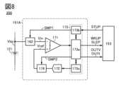
- FIG. 8is a block diagram illustrating a configuration example of a power storage system.
- FIG. 9is a flow diagram showing an example of the operation of the power storage system.
- FIG. 1A and FIG. 1Bare block diagrams showing an example of a power storage system.
- FIG. 5is a flow diagram illustrating a method for charging a secondary battery.
- FIG. 6is a
- FIG. 10is a block diagram illustrating a configuration example of a power storage system.
- FIG. 11is a schematic diagram showing an example of the operation of the power storage system.
- FIG. 12is a flow diagram illustrating an example of the operation of the power storage system.
- 13A to 13Care block diagrams illustrating an example of a power storage system.
- 14A and 14Bare cross-sectional views of the positive electrode active material.
- FIGS. 14C to 14Fare part of cross-sectional views of the positive electrode active material.
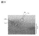
- FIG. 15is an example of a TEM image in which the crystal orientations are approximately the same.
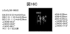
- FIG. 16Ais an example of a STEM image in which the crystal orientations are approximately the same.
- FIG. 16Bis an FFT pattern of a region with a rock salt type crystal structure RS.
- FIG. 16Cis an FFT pattern of a region of the layered rock salt type crystal structure LRS.
- FIG. 17is a diagram illustrating the crystal structure of the positive electrode active material.
- FIG. 18is a diagram illustrating the crystal structure of a conventional positive electrode active material.
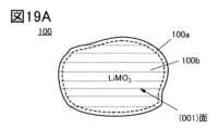
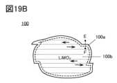
- 19A and 19Bare cross-sectional views of the positive electrode active material.
- FIGS. 19C and 19Dare part of cross-sectional views of the positive electrode active material.
- FIG. 20is a diagram showing an XRD pattern calculated from the crystal structure.
- FIG. 21is a diagram showing an XRD pattern calculated from the crystal structure.
- FIG. 22is a cross-sectional view of the positive electrode active material.
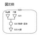
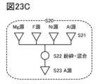
- 23A to 23Care diagrams illustrating a method for producing a positive electrode active material.
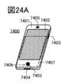
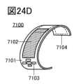
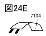
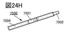
- 24A to 24Hare diagrams illustrating an example of an electronic device.
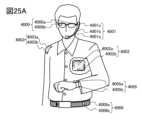
- 25A to 25Dare diagrams illustrating an example of an electronic device.
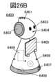
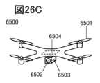
- 26A to 26Care diagrams illustrating an example of an electronic device.
- 27A to 27Care diagrams illustrating an example of a vehicle.
- 28A and 28Bare dQ/dV-V curves.
- 29A and 29Bare dQ/dV-V curves.
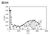
- FIG. 30Ais a VC curve.
- FIG. 30Bis a ⁇ V-t curve.
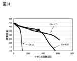
- FIG. 31shows the evaluation results of the cycle characteristics of the secondary battery.
- FIG. 32is a diagram showing the relationship between the number of charge/discharge cycles and the end-of-charge voltage.
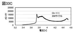
- 33A to 33Care dQ/dV-V curves of the secondary battery.
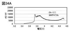
- 34A and 34Bare dQ/dV-V curves of the secondary battery.
- a semiconductor deviceis a device that utilizes semiconductor characteristics, and refers to, for example, a circuit including a semiconductor element (eg, a transistor, a diode, etc.), or a device having the same circuit. It also refers to any device that can function by utilizing the characteristics of semiconductors. For example, an integrated circuit including a semiconductor element, a chip including an integrated circuit, an electronic component in which a chip is housed in a package, or an electronic device in which an electronic component is mounted are examples of semiconductor devices.
- a display devicemay itself be a semiconductor device, and may include a semiconductor device.
- each embodimentcan be appropriately combined with the structure shown in other embodiments to form one embodiment of the present invention. Further, when a plurality of configurations are shown in one embodiment, it is possible to combine these configurations as appropriate to form one aspect of the present invention.
- the size, layer thickness, or regionmay be exaggerated for clarity.
- the drawingsare not limited, eg, in size or aspect ratio.
- the drawingsschematically show ideal examples, and are not limited to, for example, the shapes or values shown in the drawings.
- a layer or a resist maskmay be unintentionally reduced due to a process such as etching, but this may not be reflected in the drawings to make it easier to understand.
- variations in voltage or currentmay occur due to noise or timing shifts, but these may not be reflected in the drawings in order to facilitate understanding.
- the "conducting state” or “on state” of a transistorrefers to, for example, a state where the source and drain of the transistor can be considered to be electrically short-circuited, or a state where the source and drain of the transistor are considered to be electrically short-circuited, or A state in which current can flow.
- the voltage between the gate and sourceis higher than the threshold voltage
- the voltage between the gate and sourceis lower than the threshold voltage.
- non-conducting staterefers to a state in which the source and drain of the transistor can be considered to be electrically disconnected.
- the voltage between the gate and sourceis lower than the threshold voltage, or in a p-channel transistor, the voltage between the gate and source is higher than the threshold voltage.
- the state, etc.may be referred to as a “non-conducting state", “blocking state”, or “off state”.
- on current of a transistorrefers to a current flowing between a source and a drain (also referred to as drain current) when the transistor is in an on state.
- drain currentalso referred to as drain current
- off-state currentrefers to the drain current when the transistor is in an off-state, unless otherwise specified.
- a drain current and a current flowing between a gate and a source or drainalso referred to as gate leakage current
- leakage currenta drain current and a current flowing between a gate and a source or drain
- space groupsare expressed using short notation in international notation (or Hermann-Mauguin symbol).
- crystal planes and crystal directionsare expressed using Miller indices.
- space groups, crystal planes, and crystal directionsare expressed by adding a superscript bar to the number, but in this specification, etc., due to format constraints, the notation is expressed by adding a bar to the number instead. In some cases, the number is expressed by adding a - (minus sign) in front of the number.
- the individual orientation that indicates the direction within the crystalis [ ]
- the collective orientation that indicates all equivalent directionsis ⁇ >
- the individual plane that indicates the crystal planeis ( )
- the collective plane that has equivalent symmetryis ⁇ ⁇ . And express each.
- the trigonal crystal represented by the space group R-3mis generally represented by a complex hexagonal lattice of hexagonal crystals for ease of understanding the structure.
- the space group R-3mis represented by a complex hexagonal lattice.
- iis -(h+k).
- the term "particle”is not limited to only a spherical shape (having a circular cross-sectional shape).
- the cross-sectional shape of each particlemay be, for example, an ellipse, a rectangle, a trapezoid, a pyramid, a square with rounded corners, or an asymmetric shape. Note that each particle may have an amorphous shape.
- homogeneousmeans that a certain element (e.g., A) is distributed with similar characteristics in a specific region in a solid composed of multiple elements (e.g., A, B, and C). refers to a phenomenon. Note that it is only necessary that the concentration of the element be substantially the same in the specific regions. For example, it is sufficient that the difference in element concentration between specific regions is within 10%. Examples of the specific region include a surface layer portion, a surface, a convex portion, a concave portion, a bulk, and the like.
- segregationrefers to a phenomenon in which a certain element (for example, B) is spatially non-uniformly distributed in a solid composed of a plurality of elements (for example, A, B, and C).
- a secondary battery of one embodiment of the present inventionhas, for example, a positive electrode and a negative electrode.
- a positive electrode active materialas a material constituting the positive electrode.
- the positive electrode active materialis, for example, a substance that performs a reaction that contributes to charging and discharging a secondary battery. Note that the positive electrode active material may partially include a substance that does not contribute to charging and discharging the secondary battery.
- a positive electrode active materialrefers to a compound containing a transition metal and oxygen that can insert and deintercalate lithium.
- the positive electrode active materialdoes not contain, for example, carbonate or hydroxyl groups that are adsorbed after the positive electrode active material is produced. Further, it is assumed that the positive electrode active material does not include, for example, an electrolyte, an organic solvent, a binder, a conductive material, or a compound derived from these, which is attached after the positive electrode active material is produced.
- a positive electrode active material to which an additive element is addedmay be expressed as, for example, a composite oxide, a positive electrode material, a positive electrode material, a positive electrode material for a secondary battery, or the like.
- the positive electrode active material of one embodiment of the present inventionpreferably contains a compound.
- the positive electrode active material of one embodiment of the present inventionpreferably has a composition.
- the positive electrode active material of one embodiment of the present inventionpreferably has a composite.
- the positive electrode active materialrefers to, for example, a collection of particles of lithium cobalt nickelate.
- the theoretical capacity of the positive electrode active materialrefers to the amount of electricity when all the lithium that can be intercalated and deintercalated from the positive electrode active material is desorbed.
- the theoretical capacity of lithium cobalt oxide (LiCoO 2 )is 274 mAh/g
- the theoretical capacity of lithium nickel oxide (LiNiO 2 )is 274 mAh/g
- the theoretical capacity of lithium manganate (LiMn 2 O 4 )is 148 mAh/g. /g.
- the state of chargerefers to how charged the positive electrode active material is, based on the theoretical capacity of the positive electrode active material, or in other words, how much lithium has been released from the positive electrode. This is the value shown.
- LiCoO 2lithium cobalt oxide
- the amount of lithium remaining in the positive electrode active material compared to the theoretical capacityis indicated by x in the composition formula, for example, x in Li x CoO 2 or x in Li x MO 2 .
- Mmeans a transition metal that undergoes oxidation-reduction upon intercalation and desorption of lithium.
- Li x CoO 2can be read as Li x MO 2 as appropriate.
- x(theoretical capacity ⁇ charging capacity (charging amount of electricity))/theoretical capacity.
- LiCoO 2as a positive electrode active material
- x0.2
- x in Li x CoO 2it means, for example, that 0.1 ⁇ x ⁇ 0.24.
- discharge completedrefers to a state in which the voltage is 2.5 V (counter electrode lithium) or less at a current of 100 mA/g, for example.
- the charge capacity (charging amount of electricity) and discharge capacity used to calculate x in Li x CoO 2can be measured under conditions where there is no short circuit (also referred to as short circuit) and where there is no or little influence of electrolyte decomposition. preferable. For example, data from a secondary battery that has undergone a sudden change in capacity that appears to be a short circuit must not be used to calculate x.
- the space group of the crystal structureis identified by, for example, an XRD pattern, an electron beam diffraction pattern, a neutron diffraction pattern, or the like. Therefore, in this specification and the like, expressions such as belonging to a certain space group, belonging to a certain space group, or being a certain space group can be rephrased as being identified with a certain space group.
- Cubic close-packed anion arrangementmeans that the anions in the second layer are placed above the voids of the anions filled in the first layer, and the anions in the third layer are placed above the voids of the anions filled in the first layer. Refers to a state in which the anion is placed directly above the void and not directly above the anion in the first layer. Therefore, the anion does not have to have a strictly cubic lattice. Furthermore, since actual crystals always have defects, the analysis results do not necessarily have to be as theoretical.
- a spotmay appear at a position slightly different from the theoretical position. For example, if the orientation with respect to the theoretical position is 5 degrees or less, or 2.5 degrees or less, it can be said that the structure has a cubic close-packed structure.
- the positive electrode active material of one embodiment of the present inventionhas a stable crystal structure even at high charging voltage. Since the crystal structure of the positive electrode active material is stable in the charged state, it is possible to suppress a decrease in the fully chargeable capacity due to repeated charging and discharging.
- a short circuit in the secondary batterynot only causes a problem in at least one of the charging operation and discharging operation of the secondary battery, but also may cause heat generation and ignition.
- short currentis suppressed even at high charging voltage. Therefore, it is possible to obtain a secondary battery that has both high discharge capacity and safety.
- materials included in the secondary batterywill be described in terms of their state before deterioration.
- the secondary batteryhas a fully chargeable capacity of 97% or more of its rated capacity, it can be said to be in a state before deterioration.
- the rated capacityis based on JISC 8711:2019.
- the state of the materials of a secondary battery before deteriorationis referred to as the initial product or initial state
- the state after deterioration(fully charged to less than 97% of the rated capacity of the secondary battery) is referred to as the initial product or initial state. (a state in which the product has a certain capacity) is sometimes referred to as a used product or in-use state, or a used product or used state.
- FIG. 1Ais a block diagram illustrating an example of a power storage system 200.
- Power storage system 200includes a charger 201 and a secondary battery 121.
- Charger 201is electrically connected to a positive electrode and a negative electrode of secondary battery 121, respectively.
- Charger 201includes a control circuit 153, a current measurement circuit 152, and a voltage measurement circuit 151. Moreover, it is preferable that the charger 201 has a temperature sensor TS.
- the temperature sensor TScan measure the environmental temperature of the secondary battery.
- the temperature sensor TSis set, for example, to be in contact with the exterior body or casing of the secondary battery. Control of charging using the temperature sensor TS will be described later.
- the current measurement circuit 152has a function of measuring the current of the secondary battery 121 (current flowing through the secondary battery 121). In particular, it is preferable that the current measurement circuit 152 has a function of measuring the charging current of the secondary battery 121 (the current that flows when charging the secondary battery 121). The current measurement circuit 152 can provide the measured current value to the control circuit 153.
- the voltage measurement circuit 151has a function of measuring the voltage of the secondary battery 121 (the potential difference generated between the positive electrode and the negative electrode of the secondary battery 121). In particular, it is preferable that the voltage measurement circuit 151 has a function of measuring the charging voltage of the secondary battery 121 (the potential difference that occurs between the positive electrode and the negative electrode when charging the secondary battery 121). The voltage measurement circuit 151 can provide the measured voltage value to the control circuit 153.
- the control circuit 153has a function of controlling the start and stop of charging the secondary battery 121. Further, the control circuit 153 has a function of controlling charging conditions of the secondary battery 121. Specifically, for example, the control circuit 153 has a function of controlling the charging current of the secondary battery 121.
- control circuit 153for example, a CPU (Central Processing Unit) or an MCU (Micro Controller Unit) can be used.
- a CPUCentral Processing Unit
- MCUMicro Controller Unit
- control circuit 153has a function of calculating a temporal change in the voltage of the secondary battery 121 provided from the voltage measuring circuit 151, or a function of calculating a time differential of the voltage. Calculating the time change of voltage or calculating the time differential of voltage means, for example, acquiring multiple sets of voltage value and time data and performing calculations using the acquired multiple sets of data. Point.
- the control circuit 153preferably includes an analog-digital conversion circuit. When the obtained voltage value of the secondary battery 121 is an analog value, the control circuit 153 can convert it into a digital value using an analog-digital conversion circuit.
- control circuit 153can also be configured to include the voltage measurement circuit 151 and an analog-to-digital conversion circuit section. Furthermore, the analog-to-digital conversion circuit may be prepared separately from the control circuit 153.
- control circuit 153has a function of calculating the time integral of the current of the secondary battery 121 given from the current measuring circuit 152, that is, a function of calculating the amount of electricity of the secondary battery 121.
- Calculating the time integral of currentthat is, calculating the quantity of electricity, refers to, for example, acquiring multiple sets of current value and time data, and performing calculations using the acquired multiple sets of data.
- the control circuit 153has a function of calculating the voltage differential (dQ/dV) of the amount of electricity of the secondary battery 121. Calculating a voltage differential of an amount of electricity refers to, for example, acquiring a plurality of set data of a voltage value, a current value, and a time, and performing a calculation using the acquired plurality of set data.
- control circuit 153has a memory circuit.
- the memory circuithas a function as a register or a cache memory within the CPU or MCU, for example. Further, the memory circuit has a function of holding various programs used in the power storage system 200, various data necessary for the operation of the power storage system 200, and the like, for example.
- FIG. 1Bis a block diagram showing another example of the power storage system 200.
- the charger 201 included in the power storage system 200 shown in FIG. 1Bincludes a detection circuit 185, a detection circuit 186, a short detection circuit SD, a micro short detection circuit MSD, a transistor 140, A transistor 150. Details of the detection circuit 185, the detection circuit 186, the short detection circuit SD, the micro short detection circuit MSD, the transistor 140, and the transistor 150 will be described later.
- FIGS. 2A and 2Bare block diagrams showing specific configuration examples of current measurement circuit 152 in charger 201 included in power storage system 200 shown in FIGS. 1A and 1B.
- current measurement circuit 152includes a resistor 152a and a circuit 152b.
- the resistor 152ahas a function as a shunt resistor.
- the circuit 152bhas the function of measuring the voltage across the resistor 152a.
- the current measurement circuit 152is not limited to a resistance detection type configuration using a shunt resistor (resistance 152a) as shown in FIGS. 2A and 2B.
- the current measurement circuit 152may have a magnetic field detection type configuration using, for example, a coil, a Hall element, a magnetoresistive element, a magnetoresistive element, a flux gate, or the like.
- FIGS. 3A and 3Bare block diagrams showing other examples of power storage system 200.
- Power storage system 200 shown in FIGS. 3A and 3Bincludes a DC-DC converter 157, a circuit 158, and a diode 159 in addition to the configuration shown in FIGS. 2A and 2B.
- power storage system 200may include a DC-DC converter 157.
- DC-DC converter 157includes a voltage conversion circuit (not shown) and a control circuit (not shown).
- the DC-DC converter 157has a function of converting the voltage of the secondary battery 121 and outputting it.
- power storage system 200may include a circuit 158.
- the circuit 158has a function as an AC adapter. That is, the circuit 158 has a function of converting AC power into DC power, for example. Further, the circuit 158 has a function of converting voltage, for example. Further, the circuit 158 has a function of providing the secondary battery 121 with electric power converted to direct current. Note that the circuit 158 may have a function of controlling the current value and voltage value to be applied when power is applied to the secondary battery 121. Further, the circuit 158 may have a function of controlling the current value and voltage value provided to the secondary battery 121 based on the signal provided from the control circuit 153.
- a diode 159may be provided between the circuit 158 and the charger 201.
- Diode 159has a function of suppressing reverse current flowing from charger 201 to circuit 158.
- FIG. 4A and 4Bare block diagrams illustrating measurement of the voltage of secondary battery 121 by voltage measurement circuit 151 in power storage system 200.
- the voltage measurement circuit 151measures the voltage Vb1 between the positive and negative electrodes of the secondary battery 121, and as shown in FIG. 4B, it divides the voltage Vb1 with resistance. There are two ways to measure the applied voltage.
- voltage Vb1is resistively divided into voltage Vb2 and voltage Vb3 by resistor 122 and resistor 123.
- the voltage measurement circuit 151measures the resistance-divided voltage Vb3.
- the voltage measurement circuit 151 or the control circuit 153uses a resistor.
- the voltage Vb1 between the positive electrode and the negative electrode of the secondary battery 121may be estimated from the divided voltage Vb3.
- the charger 201has a function as a coulomb counter.
- the charger 201uses the current measurement circuit 152 and the control circuit 153 to calculate the integrated quantity of electricity of the secondary battery 121, thereby determining the charging capacity (charging quantity of electricity) and discharging capacity of the secondary battery 121. It has a calculation function.
- the charger 201may have a function of analyzing the charging depth using the calculated charging capacity (charging amount of electricity) and discharging capacity.
- the crystal structure of the positive electrode active material included in the secondary batterychanges. If this change in crystal structure is irreversible, repeated charging may reduce the fully chargeable capacity of the secondary battery.
- the depth of charge of the secondary batteryshould be deepened, and the change in the crystal structure should be within a roughly reversible range. It is necessary to maintain the depth of charge of the battery.
- the charging depth of the secondary batterycan be maintained so that the change in the crystal structure is approximately within a reversible range.
- the state of secondary batterieschanges when they are repeatedly charged and discharged, so even when charging is performed with the same voltage as the upper limit, the depth of charge of the secondary battery increases as the number of charge/discharge cycles increases. It becomes difficult to make them the same. Therefore, in order to maintain the charging depth of the secondary battery so that the change in crystal structure is approximately within a reversible range, a means for monitoring the charging process is required.
- the charger of one embodiment of the present inventionit is possible to monitor the charging process and maintain the depth of charge of the secondary battery so that the depth of charge is deep and the change in crystal structure is within a generally reversible range. can. Further, it is preferable to apply the positive electrode active material of one embodiment of the present invention to a secondary battery.
- the charger of one embodiment of the present inventioncan suppress collapse of the crystal structure of a positive electrode active material included in the secondary battery by controlling the charging conditions of the secondary battery. More specifically, for example, the charger of one embodiment of the present invention can increase the charging voltage of the secondary battery to the maximum within a range where collapse of the crystal structure can be suppressed, and can increase the reliability of the secondary battery. , high energy density can be achieved by efficiently utilizing secondary batteries to their limits.
- the charger of one embodiment of the present inventioncan suppress collapse of the crystal structure of the positive electrode active material having a layered crystal structure.
- a positive electrode active material having a layered crystal structurefor example, metals serving as carrier ions are arranged in layers.
- metals serving as carrier ionsare arranged in layers.
- lithium cobalt oxidelithium exists in a layered form between two CoO layers.
- when carrier ions are detached during chargingdistortion of the crystal, a change in the crystal structure due to the detachment of carrier ions, etc. may occur.
- lithium cobalt oxidewhen lithium ions are desorbed during charging, changes such as displacement of the two CoO layers and shortening of the interlayer distance between the two CoO layers may occur.
- a charging voltagemay cause constituent elements of the positive electrode active material to be eluted into the electrolytic solution, leading to collapse of the crystal structure of the positive electrode active material. Furthermore, charging at a high voltage may cause decomposition reactions of elements constituting the electrolyte.
- a charger according to one embodiment of the present inventionuses a simple method to detect changes in crystal structure, increases charging voltage to the maximum within a range that can ensure high reliability, and efficiently utilizes a secondary battery to the limit. be able to.
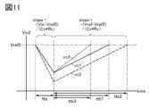
- the upper limit voltage for chargingcan be determined based on a waveform obtained during charging.
- the waveformcan have various shapes, such as a curved line, a straight line, a combination of a curved line and a straight line, and the like.
- the waveformis not limited to a periodic wave. Examples of waveforms acquired during charging include a dQ/dV-V curve or a ⁇ V-t curve created from data on voltage, time, and current during charging.
- the charging voltage during repeated charging and dischargingis preferably increased to the maximum, and even at the increased charging voltage, the crystal structure of the positive electrode active material
- the change inis substantially reversible.
- substantially reversiblemeans that even if it is reversible or irreversible, deterioration due to repeated crystal structure changes is extremely small.
- the positive electrode active material of one embodiment of the present inventionchanges from the O3 type crystal structure to the O3' type crystal structure described below when the depth of charge of the secondary battery is approximately 80% or around 80%. Furthermore, when this change occurs, extreme values are observed in the dQ/dV curve and the like.
- a charger according to one embodiment of the present inventionhas a function of detecting this extreme value and controlling charging.
- the extreme valueis near the upper limit voltage for charging.
- the extreme value caused by a change in the crystal structureis lower than the upper limit voltage for charging, and that the difference between the voltage at which the extreme value is detected and the upper limit voltage for charging is 0.15 V or less.
- the crystal structure of the positive electrode active materialis approximately reversible during charging and discharging even if charging is performed for a predetermined time beyond the voltage at which the extreme value is detected. It is preferable to be able to change the Since the secondary battery to which the charger of one embodiment of the present invention is applied has such characteristics, the charger of one embodiment of the present invention can easily increase the efficiency of the secondary battery to the limit using the above extreme value.
- the upper limit voltage for chargingcan be controlled for better utilization.
- An extreme value caused by a change in the crystal structureis detected, for example, in a voltage time change curve of a secondary battery. Alternatively, it is detected in the time differential curve (dV/dt curve) of the voltage of the secondary battery.
- extreme values caused by changes in the crystal structureare detected, for example, in the voltage differential curve (dQ/dV curve) of the amount of electricity of the secondary battery.
- CCCVconstant current, constant voltage
- constant current chargingis performed, and after reaching the upper limit voltage of charging in constant current charging, constant voltage charging is performed.
- CCCV chargingfor example, by performing constant voltage charging at the upper limit voltage of constant current charging, charging can be carried out over time at the upper limit voltage, and the charging capacity (charging amount of electricity) is reduced due to deterioration of the secondary battery. It is less susceptible to changes in impedance, etc., and a charging capacity (charging amount of electricity) with small variations can be obtained.
- the charging capacity(charging amount of electricity) can be increased.
- charging at a high voltagemay cause collapse of the crystal structure of the positive electrode active material, and may cause decomposition reactions of elements constituting the electrolyte. Therefore, constant voltage charging at the upper limit voltage may increase deterioration of the secondary battery.
- constant current chargingbecause it can reduce the charging time at the upper limit voltage and extend the life of the secondary battery.
- the environmental temperature of the secondary batteryexceeds 40° C.
- the secondary batterymay significantly deteriorate during constant voltage charging at the upper limit voltage. Therefore, when the environmental temperature of the secondary battery is high, it is more preferable to perform constant current charging. Further, when the environmental temperature of the secondary battery is high, it is preferable not to use constant voltage charging at a high voltage or to shorten the time for constant voltage charging at a high voltage as much as possible.
- a positive electrode active material represented by the chemical formula AM y O Z(y > 0, z > 0), more specifically, for example, a positive electrode active material represented by the chemical formula AMO 2 .
- the positive electrode active material represented by the chemical formula AM y O Z (y>0, z>0), as well as element A and metal Mwill be described later.
- the positive electrode active materialis expressed by the chemical formula AMO2
- the composition of A:M:Ois not limited to 1:1:2.
- lithium cobalt oxidemay be expressed as LiCoO 2 .
- lithium nickelatemay be expressed as LiNiO 2 .
- a secondary batteryis charged at a temperature of 35° C. or higher and 55° C. or lower so that the charging depth is 85% or less, or 80% or less, or 77% or less.
- the degree of chargingcan be expressed by using x in the compositional formula, for example, x in Li x CoO 2 , to indicate how much lithium that can be intercalated and deintercalated remains in the positive electrode active material.
- x(theoretical capacity ⁇ charging capacity (charging amount of electricity))/theoretical capacity.
- x in Li x CoO 2is small, for example, 0.1 ⁇ x ⁇ 0.24.
- chargingmay be performed such that x is 0.2 or less, or 0.24 or less, or 0.3 or less.
- the upper limit voltage for chargingis preferably 4.8 V or less, more preferably 4.8 V or less, with the positive electrode potential based on the lithium potential (Li/Li + ) at 35° C. or higher and 55° C. or lower. Charging is performed so that the voltage is .75V or less, more preferably 4.7V or less, even more preferably 4.65V or less.
- the charging rate(also referred to as capacity rate) is preferably 0.35C or higher, more preferably 0.45C or higher, and even more preferably 0.
- Chargingis performed to a temperature of .7C or higher, more preferably 0.9C or higher.
- Chere is a unit of rate.
- chargingis performed to achieve the charging rate. conduct.
- the charging rate 1Cis, for example, about 0.7 times the amount of electricity for charging and reacting the entire amount of element A (in the case of lithium cobalt oxide, element A is lithium) possessed by the positive electrode active material. Let be the current density for charging in 1 hour.
- the depth of chargeis, for example, preferably 50% or more, more preferably 60% or more, even more preferably 70% or more, and even more preferably 73% or more. Further, the depth of charge may be higher than 75%.
- the method for calculating the depth of charge in a secondary batteryis not limited to the example shown above.
- the charging depth corresponding to the rated capacity of the secondary batterymay be set to 100%.
- the standardization of charging capacity (charging amount of electricity) used for charging depthis not limited to the example shown above. Standards are based on the volume of the secondary battery, the internal volume of the secondary battery, the volume of a portion of the secondary battery, the weight of the secondary battery, the weight of the contents of the secondary battery, the weight of a portion of the secondary battery, etc. may be converted into
- an extreme value caused by a change in the crystal structure of the positive electrode active materialcan be detected in a dQ/dV curve or the like, and constant current charging can be performed. Further, constant current charging using detection of the extreme value is simple and has good controllability. Therefore, by using the charger of one embodiment of the present invention, it is possible to realize a secondary battery with small variations in charging capacity (charging amount of electricity) and with suppressed deterioration due to high voltage charging.
- step S100processing is started.
- step S101constant current charging of the secondary battery is started at time t1. Note that the constant current charging is performed continuously until charging is stopped in step S107.
- step S102the voltage measurement circuit 151 starts measuring the voltage of the secondary battery. Further, the current measurement circuit 152 starts measuring the current of the secondary battery. Voltage measurement circuit 151 provides the measured voltage value to control circuit 153. Current measurement circuit 152 provides the measured current value to control circuit 153.
- step S103the control circuit 153 accumulates the voltage value measured by the voltage measurement circuit 151 and the current value measured by the current measurement circuit 152 from step S102 onwards, as set data with time.
- a memory circuit or the like included in the control circuit 153can be used to accumulate data.
- the time from the start of chargingmay be used as the time associated with the voltage value and the current value.
- step S104the control circuit 153 calculates a voltage differential curve (dQ/dV curve) of the amount of electricity of the secondary battery using the set data of the voltage value, current value, and time that are accumulated from time to time.
- step S103may calculate a voltage differential curve of the amount of electricity of the secondary battery after accumulating data sets of a certain predetermined time, voltage value, current value, and time. For example, set data may be accumulated for a period sufficient to detect extreme values.
- step S105the control circuit 153 analyzes a curve (hereinafter referred to as a dQ/dV-V curve) in which the horizontal axis is the voltage V and the vertical axis is the voltage differential dQ/dV of the quantity of electricity Q, and the extreme value ( (also referred to as a peak) is detected. If an extreme value, for example a local maximum (also referred to as an upwardly convex peak) is detected in the dQ/dV-V curve, the process advances to step S106. If not detected, the process returns to step S103. Note that a plurality of extreme values may be detected in the dQ/dV-V curve. In such a case, the highest extreme value among the plurality of extreme values is detected. Alternatively, among the plurality of extreme values, the top r extreme values (r is an integer of 2 or more) may be detected, and one of the r extreme values may be selected.
- a dQ/dV-V curvea curve in which the horizontal axis
- the upper extreme valuerefers to the higher value among the ranks determined based on predetermined conditions. For example, it may be arranged in descending order of the height of the extreme value.
- control circuit 153continues to accumulate the set data of voltage value, current value, and time while repeating the steps from step S103 to step S105. That is, when repeating the steps from step S103 to step S105 n times, the dQ/dV-V curve can be calculated using all the data n times. Alternatively, among the n times, only the latest one or only the latest several times may be used.
- step S106the control circuit 153 determines whether the voltage of the secondary battery is equal to or higher than a predetermined voltage. If the voltage V of the secondary battery is equal to or higher than the voltage V2, the process advances to step S107. If the voltage V is less than the voltage V2, the process returns to step S103.
- the voltage V2is, for example, 4.25V or more, or 4.25 or more and less than 4.8V.
- the magnitude of the voltage V and the voltage V2 in step S106may be determined based on the depth of charge of the secondary battery. For example, if the depth of charge of the secondary battery is S1% or more, the process may proceed to step S107, and if it is less than S1%, the process may return to step S103.
- S1is 60[%] or more, or 60[%] or more and 95[%] or less.
- the control circuit 153can continuously accumulate set data of voltage value, current value, and time from the first step S103 of the plurality of repeated steps S103 until proceeding to step S107.
- step S107a time tp at which the dQ/dV-V curve takes an extreme value is detected by analysis, and charging is stopped at time t2, which is a predetermined time elapsed from time tp.
- the predetermined timeis, for example, the time required for the control circuit 153 to stop charging.
- a region having a desired voltage width centered around the voltage that takes the extreme valueis determined as time t2, and the time corresponding to the voltage at the upper end of the region is determined as time t2. You can. Note that if no extreme value is detected in step S107, charging may be stopped when a predetermined charging voltage is reached.
- step S107Although detection of an extreme value is mentioned here as a condition for stopping charging in step S107, for example, an inflection point may be detected and charging stop may be controlled based on the elapsed time from the detected inflection point. Good too.
- the curve to be analyzedmay be smoothed.
- a moving averagemay be used as the smoothing method.
- the inflection point detected at time tpis, for example, an inflection point resulting from a change in the crystal structure of the positive electrode active material included in the positive electrode of the secondary battery.
- the positive electrode active material of one embodiment of the present inventionis used as the positive electrode active material and charging of the secondary battery is stopped at a time near time tp, the crystal structure of the positive electrode active material will not collapse due to repeated charging and discharging. can be suppressed.
- the crystal structure of the positive electrode active materialchanges from an O3 type crystal structure to an O3' type crystal structure.
- An inflection point corresponding tocan be used.
- the positive electrode active materialis, for example, lithium cobalt oxide.
- the charging voltage or charging depth at time t2is preferably lower than the charging voltage at which the crystal structure of the positive electrode active material changes to the H1-3 type crystal structure, or shallower than the charging depth. Details of the O3 type crystal structure, O3' type crystal structure, and H1-3 type crystal structure will be described later. Note that this change from the O3 type crystal structure to the O3' type crystal structure may be expressed as a phase change.
- the crystal structure at time t2can be controlled to be an O3' type crystal structure. Thereby, collapse of the crystal structure of the positive electrode active material during repeated charging and discharging of the secondary battery can be suppressed.
- the crystal structure determinedis expressed by the space group R-3m. Further, it is more preferable that the determined crystal structure is expressed by the space group R-3m and that an O3' type crystal structure is suggested.
- the positive electrodewhen a positive electrode obtained by disassembling a secondary battery charged with the power storage system of one embodiment of the present invention in a charging state corresponding to time t2 is evaluated using an XRD pattern, the positive electrode corresponds to space group R-3m. A spectrum is observed. Regarding the measurement conditions, measurement method, etc., the description below can be referred to.
- the determined crystal structureis expressed by the space group R-3m.
- the crystal structure determinedis expressed by the space group R-3m, so that the charge/discharge cycle is A secondary battery with less decrease in discharge capacity can be obtained.
- step S101 to step S107are repeated s times.
- sis an integer of 2 or more.
- the time tp and time t2 determined based on the extreme values detected in steps S102 to S106may be used in the next charging cycle.
- the time tp and time t2 obtained in the (s-1)th chargingmay be used as the conditions for stopping charging in step S107 of the sth charging.
- step S199the process ends.
- the current value of constant current chargingis set as a constant current value, for example, from when charging is started in step S101 until charging is stopped in step S107.
- the current value in constant current chargingmay be changed in stages after charging is started in step S101 until charging is stopped in step S107.
- steps S103 to S105are repeated n times, the current value may be changed after a certain number of times.
- the charger of one embodiment of the present inventionanalyzes the charging characteristics of the secondary battery in steps S103 to S106, and changes the charging conditions of the secondary battery in step S107 according to the analyzed results. can. Specifically, for example, charging of the secondary battery can be stopped.
- the charging characteristics analyzed in steps S103 to S106change depending on the environmental temperature during charging and discharging of the secondary battery, deterioration of the secondary battery due to charging and discharging cycles, and the like.
- the charger of one embodiment of the present inventionsuppresses deterioration of the secondary battery by changing the charging conditions of the secondary battery, such as the charging voltage of the secondary battery, in accordance with such changes in charging characteristics. be able to.
- the charger of one embodiment of the present inventioncan perform charging to the maximum within a range where deterioration of the secondary battery is suppressed.
- step S107after time t2, constant voltage charging may be performed at a voltage lower than the upper limit charging voltage of constant current charging at time t2.
- Example 2 of charging method>An example of a charging method using the charger of one embodiment of the present invention will be described with reference to the flow diagram shown in FIG. Note that in the charging method shown in FIG. 6, the calculations performed by the control circuit 153 are simpler than those in the charging method shown in FIG. 5, and may be performed on a smaller circuit scale.
- dQ/dVcan be expressed as in the following formula.
- dQ/dtis constant, so dQ/dV is proportional to dt/dV. Therefore, by evaluating the dt/dV characteristics during constant current charging, information similar to the dQ/dV characteristics can be obtained.
- dt/dV characteristicsare evaluated in a region where constant current charging is performed.
- dt/dV characteristicit is not necessary to acquire the current value of the secondary battery every time, and it may be possible to acquire the dt/dV characteristic more easily than dQ/dV.
- calculationsare simple and the circuit scale can be reduced in some cases.
- the scale of the storage circuitcan be reduced in some cases.
- dQ/dV in constant current chargingmay change more slowly than dQ/dV in constant voltage charging.
- step S000the process starts.
- step S001constant current charging of the secondary battery is started at time t3. Note that the constant current charging is performed continuously until charging is stopped in step S007.
- step S002the voltage measurement circuit 151 starts measuring the voltage of the secondary battery.
- Voltage measurement circuit 151provides the measured voltage value to control circuit 153.
- step S003the control circuit 153 accumulates the voltage values measured by the voltage measurement circuit 151 from step S002 onward as set data with the time.
- a memory circuit or the like included in the control circuit 153can be used to accumulate data.
- the time from the start of chargingmay be used as the time associated with the voltage value.
- the obtained voltage valueis converted from an analog value to a digital value in the control circuit 153.
- the control circuit 153may use the obtained analog value for calculation without converting it into a digital value.
- an MCUis used as the control circuit 153 and a voltage value is converted using an analog-to-digital conversion circuit installed in the MCU.
- an MCU equipped with an analog-to-digital conversion circuit having 12-bit voltage resolutionis used.
- the predetermined valuemay be, for example, the minimum value of the voltage resolution of the analog-to-digital conversion circuit, or may be a higher value.
- step S004the control circuit 153 calculates the temporal change in the voltage of the secondary battery using the set data of the voltage value and time that are accumulated from time to time.
- the time change in voltagecan be expressed as voltage [V(t)-V(t- ⁇ t1)] using voltage V(t) at time t and voltage V(t- ⁇ t1) at time (t- ⁇ t1). can be expressed.
- a curve of voltage change over timeis sometimes called a ⁇ V-t curve.
- step S003may calculate the time change after accumulating the set data of voltage value and time for a certain predetermined time. For example, set data may be accumulated for a period sufficient to detect extreme values.
- step S005the control circuit 153 analyzes the time change curve (for example, ⁇ V-t curve) of the voltage of the secondary battery, and determines whether an extreme value is detected. If an extreme value, for example a minimum (also referred to as a downwardly convex peak) is detected in the time change curve, the process advances to step S006. If not detected, the process returns to step S003.
- a plurality of extreme valuesmay be detected. In such a case, the highest extreme value among the plurality of extreme values is detected. Alternatively, among the plurality of extreme values, the top r extreme values (r is an integer of 2 or more) may be detected, and one of the r extreme values may be selected.
- control circuit 153continuously accumulates the set data of voltage value and time while repeating the steps from step S003 to step S005. That is, when repeating the steps from step S003 to step S005 n times, the time change curve can be calculated using all the data n times. Alternatively, among the n times, only the latest one or only the latest several times may be used. Here, n is an integer of 1 or more.
- step S006the control circuit 153 determines whether the voltage of the secondary battery is equal to or higher than a predetermined voltage. If the voltage V of the secondary battery is equal to or higher than the voltage V1, the process advances to step S007. If the voltage V is less than the voltage V1, the process returns to step S003.
- the voltage V1is, for example, 4.25V or more, or 4.25V or more and less than 4.8V.
- the voltage measurement circuit 151measures the voltage obtained by dividing the voltage between the positive electrode and the negative electrode of the secondary battery by resistance
- the voltage measured from the voltage obtained by dividing the voltage by resistanceis used as the voltage V1.
- an estimated value of the voltage between the positive and negative electrodes of the next batteryis used.
- the magnitude of the voltage V and the voltage V1 in step S006may be determined based on the depth of charge of the secondary battery. For example, if the depth of charge of the secondary battery is S1% or more, the process may proceed to step S007, and if it is less than S1%, the process may return to step S003.
- S1is 60[%] or more, or 60[%] or more and 95[%] or less.
- the control circuit 153can continuously accumulate the set data of voltage value and time from the first step S003 of the plurality of repeated steps S003 until proceeding to step S007.
- step S007a time tq at which the ⁇ V-t curve takes an extreme value is detected by analysis, and charging is stopped at time t4, which is a time when a predetermined time has elapsed from time tq.
- time t4for example, a region having a desired width of time centered on the time at which the extreme value is obtained in the ⁇ V-t curve may be determined, and the time at the upper end of the region may be determined as time t4.
- the predetermined timeis, for example, the time required for the control circuit 153 to stop charging. Note that if no extreme value is detected in step S007, charging may be stopped when a predetermined charging voltage is reached.
- step S007detection of an extreme value is mentioned here as a condition for stopping charging in step S007, for example, an inflection point may be detected and charging stop may be controlled based on the elapsed time from the detected inflection point. Good too.
- time tq and time t4 determined based on the extreme values detected in steps S002 to S006may be used in the next charging cycle.
- time tq and time t4 obtained in the (w-1)th chargingmay be used as conditions for stopping charging in step S007 of the w-th charging.
- step S099the process ends.
- the current value of constant current chargingis set as a constant current value, for example, from when charging is started in step S001 until charging is stopped in step S007.
- the current value in constant current chargingmay be changed in stages after charging is started in step S001 until charging is stopped in step S007.
- steps S003 to S005are repeated n times, the current value may be changed after a certain number of times.
- step S200the process starts.
- step S201constant current charging of the secondary battery is started. Note that the constant current charging is performed continuously until charging is stopped in step S206.
- step S202the voltage measurement circuit 151 starts measuring the voltage of the secondary battery.
- the measured voltage Vis provided from the voltage measurement circuit 151 to the control circuit 153.
- step S203the control circuit 153 compares the measured voltage V and a predetermined voltage V3. If the voltage V is equal to or higher than the voltage V3, the process advances to step S204, and if the voltage V is lower than the voltage V3, the process returns to step S202.
- step S204the control circuit 153 evaluates dQ/dV.
- the value of dt/dVis measured.
- the value of dt/dVcan be accumulated at any time during the charging process. Using the accumulated data set of voltage V and time t, a moving average [dt/dV] mean of dt/dV and a maximum value [dt/dV] max are calculated.
- the time required for the voltage to change by a predetermined valuemay be calculated as the value equivalent to dt/dV.
- the predetermined valuemay be, for example, 0.5 mV or more and 10 mV or less.
- step S205the moving average [dt/dV] mean is compared with the value obtained by multiplying the maximum value [dt/dV] max by a constant Rt. If the moving average [dt/dV]mean is smaller than the value obtained by multiplying the maximum value [dt/dV]max by the constant Rt, the process advances to step S206. If the moving average [dt/dV]mean is greater than or equal to the value obtained by multiplying the maximum value [dt/dV]max by the constant Rt, the process returns to step S204.
- the time when the moving average [dt/dV] mean becomes smaller than the value obtained by multiplying the maximum value [dt/dV] max by the constant Rtis, for example, on the dt/dV curve, from the maximum value near voltage V3, This corresponds to the time when the value decreases to (Rt ⁇ 100) [%] of the maximum value.
- step S206charging of the secondary battery is stopped.
- step S299the process ends.
- FIG. 7shows an example of constant current charging, but when the charging current is not constant, for example, the moving average of dt/dV [dt/dV] mean and the maximum value of voltage [dt /dV]max multiplied by a constant Rt, instead of comparing the average value of the quantity of electricity Q at the measurement time and times in its vicinity, and the value obtained by multiplying the maximum value of the quantity of electricity Q by a constant. All you have to do is compare.
- Example 1 of voltage measurement circuitAs an example of the voltage measurement circuit 151 included in the charger 201, a voltage measurement circuit 151A will be described.
- FIG. 8is a block diagram illustrating a configuration example of the voltage measurement circuit 151A.
- the voltage measurement circuit 151Aincludes a sample and hold circuit (S/H) 162, an S/H 174, a digital-to-analog conversion circuit (DAC) 172, a comparator 171, a control section 173, Equipped with
- the control unit 173includes a signal processing circuit 173a, a timing circuit 173b, and a register 173c.
- FIG. 8illustrates a secondary battery 121 and a control circuit 153 that are electrically connected to the voltage measurement circuit 151A in the power storage system 200.
- the voltageis a voltage based on the potential of the negative electrode of the secondary battery 121.
- the voltage measurement circuit 151Ahas a function as a successive approximation type analog-to-digital conversion circuit (ADC). Further, the voltage measurement circuit 151A has a function of calculating the time required for the input voltage to change by a predetermined voltage value (for example, 1 mV) (also referred to as a time difference or a time difference), and outputting the time. Therefore, the voltage measurement circuit 151A may be called, for example, a difference device or a time measurement circuit.
- ADCsuccessive approximation type analog-to-digital conversion circuit
- the S/H 162has a function of acquiring (sampling) and holding the voltage Vbp of the positive electrode of the secondary battery 121 in accordance with the signal SMP1. It also has a function of supplying the held voltage Vin to the inverting input terminal of the comparator 171.
- the S/H 174has a function of acquiring and holding the voltage output from the DAC 172 in accordance with the signal SMP2. It also has a function of supplying the held voltage Vref to the non-inverting input terminal of the comparator 171.
- the DAC 172has a function of outputting an analog voltage based on digital voltage data stored in the register 173c.
- the comparator 171compares the magnitude of the voltage Vin and the voltage Vref, and based on the comparison result, a voltage (H level) corresponding to digital data "1” or a voltage (H level) corresponding to digital data "0" It has the function of outputting (L level).
- the signal processing circuit 173ahas a function of performing various processes depending on, for example, the output of the comparator 171 and the signal from the timing circuit 173b. As various types of processing, the signal processing circuit 173a has a function of updating voltage data stored in the register 173c, for example. Further, the signal processing circuit 173a has a function of outputting, for example, voltage data (data OUTV) stored in the register 173c and time data (data OUTt) from the timing circuit 173b to the control circuit 153. Further, the signal processing circuit 173a has a function of outputting a signal SMP2 for controlling the operation of the S/H 174, for example. Further, the signal processing circuit 173a has a function of outputting a signal WKUP and a signal SLEP for transmitting the operating state of the voltage measurement circuit 151A to the control circuit 153, for example.
- the timing circuit 173bhas a function of performing various processes according to, for example, a signal from the signal processing circuit 173a and a signal STUP given from the control circuit 153. As various processes, the timing circuit 173b has a function of outputting a signal SMP1 for controlling the operation of the S/H 162, for example. Further, the timing circuit 173b has a function of measuring time, for example. In the timing circuit 173b, for example, a counter (not shown), an oscillator (not shown), etc. can be used to measure the time. Further, for example, the count value of the counter can be used as time data.
- the register 173chas a function of storing voltage data.
- Each circuit(for example, S/H 162, S/H 174, DAC 172, comparator 171, signal processing circuit 173a, timing circuit 173b, register 173c, etc.) constituting the voltage measurement circuit 151A is a transistor containing silicon in a channel formation region ( (Si transistor) or a circuit including a Si transistor.
- the voltage measurement circuit 151Acan be said to be a semiconductor device.
- part or all of each of the circuitsmay include a transistor including an oxide semiconductor in a channel formation region (OS transistor), or a circuit including the OS transistor.
- the OS transistorSince the band gap of the oxide semiconductor in which the channel is formed is 2 eV or more, the OS transistor has a characteristic that off-state current (current flowing between the source and drain when the transistor is off) is extremely low.
- the off-state current value of the OS transistor per 1 ⁇ m channel width at room temperatureis 1aA (1 ⁇ 10 ⁇ 18 A) or less, 1zA (1 ⁇ 10 ⁇ 21 A) or less, or 1yA (1 ⁇ 10 ⁇ 24 A) or less It can be done.
- the off-state current value per 1 ⁇ m of channel width at room temperatureis 1 fA (1 ⁇ 10 ⁇ 15 A) or more and 1 pA (1 ⁇ 10 ⁇ 12 A) or less. Therefore, it can be said that the off-state current of an OS transistor is about 10 orders of magnitude lower than that of a Si transistor.
- the off-state current of the OS transistorhardly increases even in a high temperature environment. Specifically, the off-state current hardly increases even under an environmental temperature of room temperature or higher and 200° C. or lower. Furthermore, the on-state current of the OS transistor does not easily decrease even in a high-temperature environment.
- the on-state current of a Si transistordecreases in a high-temperature environment. That is, an OS transistor has a higher on-state current than a Si transistor in a high-temperature environment. Furthermore, the OS transistor can perform a good switching operation even under an environmental temperature of 125° C. or higher and 150° C. or lower because it has a large ratio of on-current to off-current. Therefore, a semiconductor device including an OS transistor operates stably even in a high-temperature environment and has high reliability.
- the semiconductor layer of the OS transistorcontains at least one of indium and zinc.
- the semiconductor layer of the OS transistoris made of, for example, indium, M (M is gallium, aluminum, yttrium, tin, silicon, boron, copper, vanadium, beryllium, titanium, iron, nickel, germanium, zirconium, molybdenum, lanthanum). , cerium, neodymium, hafnium, tantalum, tungsten, magnesium, and cobalt) and zinc.
- Mis preferably one or more selected from gallium, aluminum, yttrium, and tin.
- an oxide containing indium (In), gallium (Ga), and zinc (Zn)also referred to as "IGZO”
- an oxide containing indium (In), aluminum (Al), and zinc (Zn)also referred to as "IAZO”
- an oxide containing indium (In), aluminum (Al), gallium (Ga), and zinc (Zn)also referred to as "IAGZO”
- IAGZOoxide containing indium (In), aluminum (Al), gallium (Ga), and zinc (Zn)
- the atomic ratio of In in the In-M-Zn oxideis preferably equal to or higher than the atomic ratio of M.
- the atomic ratio of In in the In-M-Zn oxidemay be smaller than the atomic ratio of M.
- the nearby compositionincludes a range of plus or minus 30% of the desired atomic ratio.
- the off-state current of the OS transistoris extremely low, so that charges accumulated in the capacitor can be retained for a long period of time. Therefore, the storage circuit can continue to store data for a long period of time by associating the level of potential depending on the amount of charge held in the capacitor with digital data of "1" or "0". Thereby, for example, a non-volatile memory can also be constructed.
- An OS transistor or a memory circuit using an OS transistorcan be provided in part or all of each circuit constituting the voltage measurement circuit 151A.
- an OS transistoras a transistor constituting the S/H 174
- the voltage Vref held in the S/H 174can be maintained for a long period of time even when the power supply to the DAC 172 is stopped.
- the voltage data stored in the register 173ccan be continued to be stored for a long period of time even when the power supply to the register 173c is stopped. be able to.
- the voltage measurement circuit 151Acan be placed in sleep mode until the input voltage changes by a predetermined voltage value, in other words, while the change in the input voltage is smaller than the predetermined voltage value.
- a predetermined voltage valuein other words, while the change in the input voltage is smaller than the predetermined voltage value.
- the supply of power to the DAC 172 and the register 173ccan be stopped.
- part of the operation of the signal processing circuit 173amay be stopped by, for example, power gating or clock gating.
- the signal processing circuit 173acan output the signal SLEP.
- the voltage measurement circuit 151Acan maintain the voltage Vref held in the S/H 174 and continue to store the voltage data stored in the register 173c. Therefore, even in the sleep mode, the S/H 162 can acquire the voltage Vbp, and the comparator 171 can compare the voltage Vin and the voltage Vref.
- the voltage measurement circuit 151Acan wake up from the sleep mode by changing the output of the comparator 171 when the input voltage changes by a predetermined voltage value in the sleep mode. By waking up, for example, the supply of power to the DAC 172 and the register 173c can be restarted. Further, the operation of the signal processing circuit 173a can be restarted. Furthermore, upon wake-up, the signal processing circuit 173a can output the signal WKUP.
- an OS transistor or a memory circuit using an OS transistormay be provided as part of the control circuit 153.
- the control circuit 153when the signal SLEP is applied, a part of the operation is stopped by power gating or clock gating, and when the signal WKUP is applied, the operation is restarted. Good too.
- FIG. 9is a flow diagram illustrating an example of the operation of the voltage measurement circuit 151A.
- step S300a signal STUP is applied from the control circuit 153 to start processing. Note that it is assumed that the secondary battery 121 is being charged with a constant current.
- steps S301 to S303the analog input voltage is converted to digital voltage data and stored in the register 173c.
- steps S301 to S303"1" or "0" is determined by successively comparing bit by bit from the most significant bit to the least significant bit.
- step S301the register 173c is initialized. That is, only the most significant bit of the register 173c is set to "1", and the rest are all set to "0". For example, if the register 173c is 16 bits, the data in the register 173c is "1000000000000000”. The data in the register 173c is converted into an analog voltage by the DAC 172, and the S/H 174 holds this voltage as the voltage Vref. Further, the S/H 162 acquires the voltage Vbp of the positive electrode of the secondary battery 121 and holds it as the voltage Vin. After completing step S301, the process advances to step S302.
- step S302it is determined whether the voltage Vbp (the voltage Vin acquired and held by the S/H 162 in step S301) is greater than the voltage Vref. That is, if the voltage Vin is larger than the voltage Vref, the comparison bit is determined to be "1" in step S3021. Alternatively, if the voltage Vin is less than or equal to the voltage Vref, the comparison bit is determined to be "0" in step S3022. After completing step S3021 or step S3022, the process advances to step S303.
- step S303it is determined whether the data in the register 173c has been determined down to the least significant bit. If the lowest bit has not been determined, the next lower bit of the register 173c is set to "1" and the process returns to step S302. Alternatively, if the least significant bit has been determined, the process advances to step S304. For example, if the register 173c has 16 bits, it is possible to determine up to the least significant bit by repeating steps S302 and S303 16 times.
- step S304the voltage data of the register 173c and the time data (count value of the counter) of the timing circuit 173b are outputted, and the process shifts to sleep mode.
- a signal SLEPis output.
- the data in the register 173cis updated to a higher value by a predetermined data value (for example, a data value corresponding to 1 mV).
- the voltage output from the DAC 172increases by a predetermined voltage value (for example, 1 mV), and the voltage is held in the S/H 174.
- the voltage Vref held in the S/H 174is increased by a predetermined voltage value, and then the sleep mode is entered.
- steps S311 to S314the time required for the input voltage to change by a predetermined voltage value is calculated, and the time is output.
- step S311the voltage Vbp is acquired by the S/H 162 at regular intervals (for example, 100 ms) and held as the voltage Vin. Further, the comparator 171 compares the voltage Vin and the voltage Vref. After completing step S311, the process advances to step S312.
- step S312voltage Vbp (voltage Vin acquired and held by S/H 162 in step S311) becomes higher than voltage Vref, so that the output of comparator 171 changes (for example, changes from H level to L level).
- a signal WKUPis output.
- voltage data from the register 173c and time data from the timing circuit 173bare output.
- step S313the process advances to step S313.
- difference time datamay be output by calculating the difference between the count value of the counter when outputting last time and the count value of the counter when outputting this time.
- the data on the time differenceis data on the time required for the input voltage to change by a predetermined voltage value.
- step S313it is determined whether the conditions for stopping charging are met.
- the conditions for stopping chargingfor example, the conditions described in the above-mentioned charging method example 1 to charging method example 3 can be used as appropriate. If the conditions for stopping charging are met, the process ends in step S399. Alternatively, if the conditions for stopping charging are not met, the process advances to step S314.
- step S399in the power storage system 200, a signal is sent to the control circuit 153 to notify that the conditions for stopping charging are satisfied so that the constant current charging of the secondary battery 121 by the charger 201 is stopped. good.
- step S314the data in the register 173c is updated to a higher value by a predetermined data value.
- the voltage output from the DAC 172increases by a predetermined voltage value, and the voltage is held in the S/H 174. That is, the voltage Vref held in the S/H 174 is increased by a predetermined voltage value. After that, it outputs the signal SLEP and shifts to sleep mode again. After completing step S314, the process returns to step S311.
- the voltage measurement circuit 151Acan calculate the time required for the voltage Vbp of the secondary battery 121 to change by a predetermined voltage value (for example, 1 mV), and can output the time. Further, the voltage measurement circuit 151A can be placed in sleep mode until the voltage Vbp changes by a predetermined voltage value, in other words, while the change in the voltage Vbp is smaller than the predetermined voltage value.
- the voltage measurement circuit 151Acan stop supplying power to the DAC 172 and the register 173c, and also stop part of the operation of the signal processing circuit 173a. This allows the power consumption of the voltage measurement circuit 151A to be reduced.
- the time required for the voltage Vbp to increase by a predetermined voltage valuecan be calculated.
- the time required for the voltage Vbp to decrease by a predetermined voltage valuemay be calculated.
- the data in the register 173cmay be updated to data that is lower by a predetermined data value.
- the voltage Vref held in the S/H 174may be lowered by a predetermined voltage value.
- a charger that can be used in the power storage system of one embodiment of the present inventioncan reduce power consumption by including the voltage measurement circuit 151A.
- Example 2 of voltage measurement circuit>As another configuration example of the voltage measurement circuit 151 included in the charger 201, a voltage measurement circuit 151B will be described.
- the voltage measurement circuit 151Bis a modification of the voltage measurement circuit 151A described above. Therefore, in order to reduce the repetition of explanation, mainly the differences between the voltage measurement circuit 151B and the voltage measurement circuit 151A will be explained. Note that the description of the voltage measurement circuit 151A mentioned above can be referred to as appropriate.
- FIG. 10is a block diagram illustrating a configuration example of the voltage measurement circuit 151B.
- the voltage measurement circuit 151Bincludes an integration circuit 175 and a selection circuit 176 in addition to the configuration of the voltage measurement circuit 151A described above. Further, the voltage measurement circuit 151B differs from the voltage measurement circuit 151A in that it does not need to include the S/H 162. Further, the voltage measurement circuit 151B includes, in the control unit 173, an oscillator 173d in the timing circuit 173b, an AND circuit 173e, and a counter 173f, in addition to the configuration of the voltage measurement circuit 151A described above.
- the voltage measurement circuit 151Bhas a function as a double integration type analog-to-digital conversion circuit (ADC). Further, the voltage measurement circuit 151B has a function of calculating the time (also referred to as difference time or time difference) required for the input voltage to change by a predetermined voltage value (for example, 1 mV) and outputting the time. Therefore, the voltage measurement circuit 151B may be called, for example, a difference device or a time measurement circuit.
- ADCanalog-to-digital conversion circuit
- the selection circuit 176has a function of applying either the voltage Vin (voltage Vbp) or the voltage Vref to the input terminal of the integrating circuit 175 in accordance with the signal SEL.
- the integrating circuit 175has a function of integrating the voltage (either voltage Vin or voltage Vref) applied to the input terminal and providing the integrated voltage Vin2 to the output terminal.
- Integrating circuit 175includes an operational amplifier 175a, a resistor 175r, and a capacitor 175c.
- the inverting input terminal of the operational amplifier 175ais electrically connected to one terminal of a resistor 175r and one terminal of a capacitor 175c.
- a non-inverting input terminal of the operational amplifier 175ais electrically connected to the wiring to which the voltage Vref2 is applied.
- the output terminal of the operational amplifier 175ais electrically connected to the other terminal of the capacitor 175c and the output terminal of the integrating circuit 175.
- the other terminal of the resistor 175ris electrically connected to the input terminal of the integrating circuit 175. Note that in the integrating circuit 175, it is preferable to provide a switch (not shown) having a function of making conductive or non-conductive between one terminal and the other terminal of the capacitor 175c.
- the output terminal of the integrating circuit 175is electrically connected to the inverting input terminal of the comparator 171. That is, the voltage Vin2 applied to the output terminal of the integrating circuit 175 is applied to the inverting input terminal of the comparator.
- the comparator 171has a function of comparing the magnitude of the voltage Vin2 applied to the inverting input terminal and the voltage Vref2 applied to the non-inverting input terminal, and outputs an H level or an L level based on the comparison result. .
- the oscillator 173dhas a function of outputting clock pulses.
- the AND circuit 173ehas a function of calculating the logical product of the clock pulse given from the oscillator 173d and the signal given from the signal processing circuit 173a, and outputting a signal CCK.
- the counter 173fhas a function of counting the number of clock pulses given as the signal CCK. Further, the counter 173f has a function of resetting the count value in response to the signal CRE. Further, the counter 173f has a function of outputting a count value (data OUTC).
- the signal processing circuit 173ahas a function of outputting a signal SEL for controlling the operation of the selection circuit 176, for example. Further, the signal processing circuit 173a has a function of controlling, for example, whether or not the clock pulse output from the oscillator 173d is applied to the counter 173f using an AND circuit 173e. Further, the signal processing circuit 173a has a function of outputting a signal CRE for controlling the operation of the counter 173f, for example. Further, the signal processing circuit 173a has a function of outputting voltage data (data OUTV) based on the data OUTC output from the counter 173f to the control circuit 153, for example.
- data OUTVvoltage data
- the register 173cmay have a function of storing data OUTC output from the counter 173f.
- a storage circuit(not shown) may be provided in the register 173c to store the data OUTC.
- each circuit constituting the voltage measurement circuit 151Bcan be provided with an OS transistor or a memory circuit using an OS transistor, similarly to the voltage measurement circuit 151A described above.
- the voltage measurement circuit 151Benters the sleep mode until the input voltage changes by a predetermined voltage value, in other words, while the change in the input voltage is smaller than the predetermined voltage value. It can be done.
- the voltage measurement circuit 151Bcan perform analog-to-digital conversion (A/D conversion), which will be described later, even in sleep mode.
- FIG. 11is a schematic diagram illustrating analog-to-digital conversion (A/D conversion) in the voltage measurement circuit 151B.
- FIG. 11shows how the voltage Vin2 output from the integrating circuit 175 changes over time when performing A/D conversion.
- the case where the voltage Vin is increasedis shown by a broken line (vc2) with respect to the solid line (vc1).
- a dotted line (vc3)indicates the case where the voltage Vref is higher than the solid line (vc1).
- the selection circuit 176is controlled and the voltage Vin is input to the integration circuit 175. Then, the voltage Vin2 decreases with a slope of "-(voltage Vin-voltage Vref2)/(Cv ⁇ Rv)".
- the selection circuit 176is controlled and the voltage Vref is input to the integration circuit 175. Then, the voltage Vin2 increases with a slope of "-(voltage Vref-voltage Vref2)/(Cv ⁇ Rv)". At this time, control is performed so that the clock pulse output from the oscillator 173d is applied to the counter 173f. Then, the counter 173f starts counting.
- the output of the comparator 171changes (for example, changes from H level to L level). At this time, the count value of the counter 173f is output.
- the count value output from the counter 173fis the value counted during the period ttb (period ttb1, period ttb2, or period ttb3) from inputting the voltage Vref to the integrating circuit 175 until the voltage Vin2 reaches the voltage Vref2. , and has a positive correlation with the voltage Vin input to the integrating circuit 175.
- the count value of the counter 173fis a value based on the voltage Vin.
- FIG. 12is a flow diagram illustrating an example of the operation of the voltage measurement circuit 151B.
- step S400a signal STUP is applied from the control circuit 153 to start processing. Note that it is assumed that the secondary battery 121 is being charged with a constant current.
- voltage Vin2voltage Vref2.
- a switch provided between one terminal and the other terminal of the capacitor 175cis controlled to be in a conductive state.
- step S401analog input voltage is converted into digital voltage data.
- step S401the above-mentioned A/D conversion is performed to obtain data OUTC based on the voltage Vbp (voltage Vin).
- Vbpvoltage Vin
- a switch provided between one terminal and the other terminal of the capacitor 175cis controlled to be in a non-conducting state.
- the data OUTC obtained hereis stored as a predetermined count value.
- the predetermined count valuemay be stored in a storage circuit provided in the register 173c for storing data OUTC.
- step S402the voltage data based on the data OUTC and the time data of the timing circuit 173b are outputted, and a transition is made to sleep mode.
- a signal SLEPis output.
- the data in the register 173cis updated to a higher value by a predetermined data value (for example, a data value corresponding to 1 mV).
- the voltage output from the DAC 172increases by a predetermined voltage value (for example, 1 mV), and the voltage is held in the S/H 174.
- the voltage Vref held in the S/H 174is increased by a predetermined voltage value, and then the sleep mode is entered.
- steps S411 to S414the time required for the input voltage to change by a predetermined voltage value is calculated, and the time is output.
- step S411the above-mentioned A/D conversion is performed at fixed time intervals (for example, 100 ms) to obtain data OUTC based on the voltage Vbp. At this time, since the voltage Vref was increased by a predetermined voltage value in the previous step, the data OUTC becomes a value lower than the predetermined count value even if the voltage Vbp is the same value. After completing step S411, the process advances to step S412.
- step S412the voltage Vbp increases by a predetermined voltage value, so that the data OUTC becomes a predetermined count value. This causes the computer to return (wake up) from sleep mode. At this time, a signal WKUP is output. After returning from the sleep mode, voltage data based on the data OUTC and time data of the timing circuit 173b are output. After completing step S412, the process advances to step S413.
- step S412data on the difference in time between the previous output and the current output may be output as the time data, similar to the voltage measurement circuit 151A described above. That is, the data on the time difference is data on the time required for the input voltage to change by a predetermined voltage value.
- step S413it is determined whether the conditions for stopping charging are met.
- the conditions for stopping chargingfor example, the conditions described in the above-mentioned charging method example 1 to charging method example 3 can be used as appropriate. If the conditions for stopping charging are met, the process ends in step S499. Alternatively, if the conditions for stopping charging are not met, the process advances to step S414.
- step S414the data in the register 173c is updated to higher data by a predetermined data value.
- the voltage output from the DAC 172increases by a predetermined voltage value, and the voltage is held in the S/H 174. That is, the voltage Vref held in the S/H 174 is increased by a predetermined voltage value. After that, it outputs the signal SLEP and shifts to sleep mode again. After completing step S414, the process returns to step S411.
- the voltage measurement circuit 151Bcan calculate the time required for the voltage Vbp of the secondary battery 121 to change by a predetermined voltage value (for example, 1 mV) and output the time. Further, the voltage measurement circuit 151B can be placed in sleep mode until the voltage Vbp changes by a predetermined voltage value, in other words, while the change in the voltage Vbp is smaller than the predetermined voltage value.
- the voltage measurement circuit 151Bcan stop supplying power to the DAC 172 and the register 173c, and also stop part of the operation of the signal processing circuit 173a. This allows the power consumption of the voltage measurement circuit 151B to be reduced.
- the time required for the voltage Vbp to increase by a predetermined voltage valuecan be calculated.
- the time required for the voltage Vbp to decrease by a predetermined voltage valuemay be calculated.
- the data in the register 173cmay be updated to data that is lower by a predetermined data value.
- the voltage Vref held in the S/H 174may be lowered by a predetermined voltage value.
- a charger that can be used in the power storage system of one embodiment of the present inventioncan reduce power consumption by including the voltage measurement circuit 151B.
- the charger according to one embodiment of the present inventionpreferably has a function of estimating the SOH (State of Health) of the secondary battery.
- SOHis an index representing the capacity that can be fully charged at a certain point in time, based on the capacity that can be fully charged in a new state.
- SOHis a numerical value expressed as a value smaller than 100 as the secondary battery deteriorates, with the fully chargeable capacity of the secondary battery in a new state being 100, and the unit is "%".
- the intensity of the extreme valuesmay decrease. This decrease in strength may be due to a phase change corresponding to the extreme value becoming less likely to occur in the positive electrode active material, and may have a correlation with, for example, SOH.
- the charger according to one embodiment of the present inventionpreferably has a function of estimating the SOH by observing the intensity of the extreme value of the dQ/dV-V curve.
- the charger according to one embodiment of the present inventionpreferably has a function of estimating the dischargeable capacity of the secondary battery by observing the intensity of the extreme value of the dQ/dV-V curve.
- the charger 201preferably controls charging using temperature.
- control circuit 153changes the charging conditions according to the environmental temperature of the secondary battery measured by the temperature sensor TS.
- the memory circuit included in the control circuit 153has, for example, a table in which the environmental temperature of the secondary battery and charging conditions are linked.
- the storage circuit included in the control circuit 153stores charging characteristics associated with the environmental temperature of the secondary battery.
- the charging characteristicmay be a past measured value of the secondary battery 121, a measured value of another secondary battery having similar characteristics, or a waveform obtained by calculation. Good too.
- extreme values (peaks)may be estimated using these measured values. For example, machine learning or the like can be used for the estimation.
- the control circuit 153may use the charging characteristics of the secondary battery stored in the memory circuit to analyze extreme values in the differential curves of voltage and quantity of electricity.
- the charging characteristicfor example, a capacity-voltage curve, a voltage-dQ/dV curve, a ⁇ V-t curve, an impedance characteristic, etc. can be used.
- the temperature sensor TSmay be, for example, a temperature measuring resistor (for example, platinum, nickel, or copper), a thermistor (PTC (Positive Temperature Coefficient) thermistor, or NTC (Negative Temperature Coefficient) thermistor). , thermocouple, or An IC temperature sensor or the like may be used.
- a configuration using a semiconductor temperature sensorfor example, a silicon diode temperature sensor, etc.
- a configuration using a bandgap circuitmay be used as the temperature sensor TS.
- NTC thermistorhas a characteristic that its resistance value gradually decreases as the temperature rises. Therefore, it can be used, for example, for detailed temperature detection or simple inrush current suppression. Further, a PTC thermistor (PTC element) has a characteristic that its resistance value increases rapidly when a certain temperature is exceeded. Therefore, it can be used for overheat detection, overcurrent protection, inrush current suppression, etc., for example.
- FIG. 1Bshows that the charger 201 has, in addition to the configuration shown in FIG. An example including a detection circuit SD, a micro short detection circuit MSD, a transistor 140, and a transistor 150 is shown.
- the charger 201 shown in FIG. 1Bhas a function of suppressing overcharging, overdischarging, charging overcurrent, discharging overcurrent, short circuit, micro short circuit, etc., and can function as a protection circuit for a secondary battery.
- a micro shortrefers to a minute short circuit inside the secondary battery, and the short circuit current is not so great that the positive and negative electrodes of the secondary battery are shorted and cannot be charged, but the short circuit current is small at the minute short circuit. Refers to the phenomenon of flowing away. A large voltage change may occur even in a relatively short period of time and at a small location.
- a transistor called a power MOSFETcan be used as the transistor 140 and the transistor 150.
- the control circuit 153has a function of cutting off the current flowing to the secondary battery 121 by applying signals to the gates of the transistor 140 and the transistor 150, respectively.
- the detection circuit 185monitors the voltage of the secondary battery, and when overcharging or overdischarging is detected, it can provide a signal indicating the detection to the control circuit 153.
- the control circuitcan receive the signal, apply the signal to at least one of the gate of transistor 140 and the gate of transistor 150, and cut off the current flowing to secondary battery 121.
- the detection circuit 186monitors the current of the secondary battery 121, and when detecting an overcurrent during charging or discharging, can provide a signal indicating the detection to the control circuit 153.
- the control circuitcan receive the signal, apply the signal to at least one of the gate of transistor 140 and the gate of transistor 150, and cut off the current flowing to secondary battery 121.
- Overcharging detected by the detection circuit 185corresponds to the extreme value of the charging voltage time change curve (for example, ⁇ V-t curve) or the extreme value of the voltage differential curve of charging electricity (dQ/dV curve). may be used for detection.
- overcharging detected by the detection circuit 185may be detected by comparing it with a predetermined voltage value using a comparison circuit. Different values may be used as the predetermined voltage value depending on the environmental temperature of the secondary battery.
- the voltage value corresponding to the environmental temperature of the secondary batteryis stored, for example, in a memory circuit included in the control circuit 153.
- the power storage system 200 shown in FIGS. 13A to 13Cshows an example in which a charger 201 is connected to each of m secondary batteries 121 connected in series.
- FIG. 13Ashows an example of the power storage system 200 where m is an integer of 4 or more, and among m secondary batteries 121, the first, second, third, and m-th secondary batteries 121 are Secondary battery 121(1), secondary battery 121(2), secondary battery 121(3), and secondary battery 121(m) are illustrated, and other secondary batteries are omitted.
- FIG. 13Bshows an example of the power storage system 200 when m is 3
- FIG. 13Cshows an example of the power storage system 200 when m is 2.
- the detection circuit 185 included in the charger 201has a terminal 124 electrically connected to the positive electrode of the secondary battery 121(1), and a terminal 125 electrically connected to the negative electrode of the secondary battery 121(m). Overcharging may be detected at voltages between . Further, for example, the detection circuit 186 and the short detection circuit SD included in the charger 201 may detect overcharging or short circuit based on the current between the terminal 124 and the terminal 125.
- the power storage system 200can independently control the m secondary batteries 121 using the chargers 201 connected to each one.
- a path connected in parallel to the secondary battery 121for example, a transistor, a resistance element, or Allow the current to flow through a diode, etc. Therefore, it is preferable that the charger 201 has, as a current path, a switch that switches between the secondary battery 121 and the current path.
- the power storage system 200has m secondary batteries 121 connected in series, the total voltage of the m secondary batteries (for example, in FIG. 13A, the positive electrode of the secondary battery 121(1) and the Charging may be controlled using the voltage across the negative electrode of the battery 121 (m). In such a case, a voltage value multiplied by m can be used as the voltage used to control charging.
- the secondary battery of one embodiment of the present inventionpreferably includes a positive electrode, a negative electrode, and an electrolyte.
- a positive electrode according to one embodiment of the present inventionincludes a positive electrode active material.
- a positive electrode active material that can be used in a secondary battery of one embodiment of the present invention and a method for manufacturing the samewill be described with reference to FIGS. 14A to 23C.
- FIGS. 14A and 14Bare cross-sectional views of a positive electrode active material 100 that can be used in a secondary battery according to one embodiment of the present invention.
- FIGS. 14C and 14Dare enlarged views of the area around AB in FIG. 14A.
- FIGS. 14E and 14Fare enlarged views of the area around CD in FIG. 14A.
- the positive electrode active material 100has a surface layer portion 100a and a bulk 100b.
- the boundary between the surface layer portion 100a and the bulk 100bis indicated by a broken line.
- FIG. 14Ba part of the grain boundary 101 is shown by a dashed line.
- the positive electrode active material 100is a compound containing oxygen and a transition metal capable of intercalating and deintercalating lithium. Therefore, the interface between the region where the transition metal M (for example, Co, Ni, Mn, Fe, etc.) or oxygen, which is oxidized and reduced as lithium is intercalated and deintercalated, and the region where oxygen is not present is defined as the surface of the positive electrode active material.
- a surface caused by at least one of slips, cracks, and crackscan also be referred to as the surface of the positive electrode active material.
- the surface of the positive electrode active material in line analysis of EDX(Energy Dispersive The measurement point showing the measurement value closest to 50% of the value is taken as the measurement point.
- the intersection pointis the tangent drawn to the intensity profile of the EDX-ray analysis of the transition metal or oxygen and the axis in the depth direction.
- the measured value closest to 50% of the average value of the detected amounts of the transition metal and oxygen in the bulkis different, the one located on the outer side can be adopted.
- the surface layer portion 100a of the positive electrode active material 100refers to a region within 10 nm perpendicularly or substantially perpendicularly from the surface toward the inside. Or it refers to a region within 50 nm. Or a region within 5 nm.
- Surface layer portionis synonymous with near surface, near surface region, or shell. Note that "substantially perpendicular” is defined as 80° or more and 100° or less.
- a region deeper than the surface layer portion 100a of the positive electrode active materialis referred to as a bulk 100b.
- Bulk 100bis synonymous with interior or core.
- the surface of the positive electrode active material 100refers to the surface of the composite oxide including the surface layer portion 100a, the bulk 100b, the convex portions 103, and the like. Note that the positive electrode active material 100 does not contain carbonate, hydroxyl groups, etc. that were chemically adsorbed after the positive electrode active material 100 was produced. Further, it is assumed that the electrolyte, organic solvent, binder, conductive material, or compounds derived from these that adhere to the cathode active material 100 after the fabrication thereof are not included in the cathode active material 100. In addition, the surface of the positive electrode active material 100 in a cross-sectional STEM image, etc.
- the pointshould be the outermost area of the area to be checked.
- the surface in a cross-sectional STEM image or the likemay be determined in conjunction with the results of analysis with higher spatial resolution, such as EELS (Electron Energy Loss Spectroscopy).
- the crystal grain boundaries 101are, for example, areas where the positive electrode active materials 100 are stuck to each other, or areas where the crystal orientation changes inside the positive electrode active materials 100, that is, where the repetition of bright lines and dark lines in a STEM image etc. becomes discontinuous.
- crystal defectsrefer to defects that can be observed in cross-sectional TEM images, cross-sectional STEM images, etc., that is, structures where other atoms enter between lattices, cavities, etc.
- the grain boundary 101can be said to be one of the planar defects.
- the vicinity of the grain boundary 101refers to a region within 10 nm from the grain boundary 101.
- the positive electrode active material 100includes lithium, a transition metal M, oxygen, and an additive element A.
- the positive electrode active material 100can include a composite oxide (LiMO 2 ) containing lithium and a transition metal M to which an additive element A is added.
- a positive electrode active material to which additive element A is addedmay also be referred to as a composite oxide.
- the positive electrode active material of a lithium ion secondary batterymust contain a transition metal capable of redox in order to maintain charge neutrality even when lithium ions are intercalated and deintercalated.
- cobaltis preferably mainly used as the transition metal M responsible for the redox reaction.
- at least one or more selected from nickel and manganesemay be used.
- the transition metal M included in the positive electrode active material 100if cobalt accounts for 75 atomic % or more, preferably 90 atomic % or more, and more preferably 95 atomic % or more, it is relatively easy to synthesize, easy to handle, and has excellent cycle characteristics. It is preferable because it has many advantages.
- nickelsuch as lithium nickelate (LiNiO 2 ) is the transition metal M.
- the stabilityis better when x in Li x CoO 2 is small compared to complex oxides that account for the majority of the oxides. This may be because cobalt is less affected by distortion due to the Jahn-Teller effect than nickel.
- the strength of the Jahn-Teller effect in transition metal compoundsdiffers depending on the number of electrons in the d orbital of the transition metal.
- Layered rock salt type composite oxidessuch as lithium nickelate, in which octahedral-coordinated low-spin nickel (III) accounts for the majority of the transition metal M, are strongly influenced by the Jahn-Teller effect, and the octahedral structure of nickel and oxygen Distortion is likely to occur in the layer consisting of. Therefore, there is a growing concern that the crystal structure will collapse during charge/discharge cycles. Also, nickel ions are larger than cobalt ions and are close to the size of lithium ions. Therefore, in a layered rock salt type composite oxide in which nickel accounts for the majority of the transition metal M, such as lithium nickelate, there is a problem that cation mixing of nickel and lithium tends to occur.
- the raw materialbecomes cheaper compared to when the amount of cobalt is large. This is preferable because it may increase the discharge capacity per weight.
- Additional elements A included in the positive electrode active material 100include magnesium, fluorine, nickel, aluminum, titanium, zirconium, vanadium, iron, manganese, chromium, niobium, arsenic, zinc, silicon, sulfur, phosphorus, boron, bromine, and beryllium. It is preferable to use one or more selected from the following.
- the sum of the transition metals in the additive elements Ais preferably less than 25 atom %, more preferably less than 10 atom %, and even more preferably less than 5 atom %.
- the positive electrode active material 100includes lithium cobalt oxide to which magnesium and fluorine are added, lithium cobalt oxide to which magnesium, fluorine and titanium are added, lithium cobalt oxide to which magnesium, fluorine and aluminum are added, magnesium, fluorine and nickel. It can have added lithium cobalt oxide, lithium cobalt oxide added with magnesium, fluorine, nickel and aluminum, and the like.
- additive elements Afurther stabilize the crystal structure of the positive electrode active material 100, as described below. Note that in this specification and the like, the additive element A has the same meaning as a mixture or a part of raw materials.
- the additive element Adoes not necessarily include magnesium, fluorine, nickel, aluminum, titanium, zirconium, vanadium, iron, manganese, chromium, niobium, arsenic, zinc, silicon, sulfur, phosphorus, boron, bromine, or beryllium. good.
- the positive electrode active material 100is substantially free of manganese, the above-mentioned advantages such as being relatively easy to synthesize, easy to handle, and having excellent cycle characteristics are further enhanced. It is preferable that the weight of manganese contained in the positive electrode active material 100 is, for example, 600 ppm or less, more preferably 100 ppm or less. The weight of manganese can be analyzed using, for example, GD-MS (Glow Discharge Mass Spectrometry).
- Layered rock salt type composite oxideshave high discharge capacity, have two-dimensional lithium ion diffusion paths, are suitable for lithium ion insertion and desorption reactions, and are excellent as positive electrode active materials for secondary batteries. Therefore, it is particularly preferable that the bulk 100b, which occupies most of the volume of the positive electrode active material 100, has a layered rock salt crystal structure.
- FIG. 17shows the layered rock salt type crystal structure with R-3m O3 attached.
- the surface layer portion 100a of the positive electrode active material 100 of one embodiment of the present inventioneven if a large amount of lithium is removed from the positive electrode active material 100 due to charging, the layered structure consisting of the octahedron of transition metal M and oxygen in the bulk 100b does not break. It is preferable to have a reinforcing function. Alternatively, it is preferable that the surface layer portion 100a functions as a barrier film for the positive electrode active material 100. Alternatively, it is preferable that the surface layer portion 100a, which is the outer peripheral portion of the positive electrode active material 100, reinforces the positive electrode active material 100.
- Reinforcement hererefers to suppressing structural changes in the surface layer 100a and bulk 100b of the positive electrode active material 100, including desorption of oxygen, and oxidative decomposition of the electrolyte on the surface of the positive electrode active material 100. refers to at least one of the following:
- the surface layer portion 100ahas a different composition and crystal structure from the bulk 100b. Further, the surface layer portion 100a preferably has a composition and crystal structure that are more stable at room temperature (25° C.) than the bulk 100b. For example, it is preferable that at least a portion of the surface layer portion 100a of the positive electrode active material 100 according to one embodiment of the present invention has a rock salt crystal structure. Alternatively, the surface layer portion 100a preferably has both a layered rock salt type crystal structure and a rock salt type crystal structure. Alternatively, the surface layer portion 100a preferably has characteristics of both a layered rock salt type and a rock salt type crystal structure.
- the surface layer portion 100ais a region where lithium ions are first desorbed during charging, and is a region where the lithium concentration tends to be lower than that of the bulk 100b. It can also be said that some bonds of atoms on the surface of the positive electrode active material 100 having the surface layer portion 100a are broken. Therefore, the surface layer portion 100a tends to become unstable, and can be said to be a region where the crystal structure tends to deteriorate.
- the surface layer 100acan be made sufficiently stable, even when x in Li x CoO 2 is small, for example, even if x is 0.24 or less, the layered structure consisting of the octahedron of the transition metal M and oxygen in the bulk 100b will be difficult to break. can do. Furthermore, it is possible to suppress misalignment of the octahedral layer of transition metal M and oxygen in the bulk 100b.
- the surface layer portion 100apreferably contains an additive element A, and more preferably contains a plurality of additive elements A. Further, it is preferable that the concentration of one or more of the additive elements A is higher in the surface layer portion 100a than in the bulk 100b. Further, it is preferable that one or more selected from the additive elements A included in the positive electrode active material 100 have a concentration gradient. Further, it is more preferable that the distribution of the positive electrode active material 100 differs depending on the additive element A. For example, it is more preferable that the depth of the concentration peak from the surface differs depending on the additive element A.
- the concentration peakhere refers to the maximum value of the detected amount in the surface layer portion 100a or at a distance of 50 nm or less from the surface.
- some of the additive elements Asuch as magnesium, fluorine, nickel, titanium, silicon, phosphorus, boron, calcium, etc., preferably have a concentration gradient that increases from the bulk 100b toward the surface, as shown by the gradation in FIG. 14C. .
- An element having such a concentration gradientwill be referred to as an additive element X.
- another additive element Asuch as aluminum or manganese
- the concentration peakmay exist in the surface layer portion 100a or may be deeper than the surface layer portion 100a.
- An element having such a concentration gradientwill be referred to as an additive element Y.
- magnesiumwhich is one of the additive elements X, is divalent, and since magnesium ions are more stable in the lithium site than in the transition metal M site in the layered rock salt crystal structure, they easily enter the lithium site.
- the presence of magnesium at an appropriate concentration in the lithium sites of the surface layer 100amakes it easier to maintain the layered rock salt crystal structure. This is presumed to be because the magnesium present at the lithium site functions as a pillar that supports the two CoO layers.
- the presence of magnesiumcan suppress desorption of oxygen around magnesium when x in Li x CoO 2 is, for example, 0.24 or less.
- the presence of magnesiummay increase the density of the positive electrode active material 100. Further, when the magnesium concentration in the surface layer portion 100a is high, corrosion resistance against hydrofluoric acid produced by decomposition of the electrolytic solution may be improved.
- magnesiumis at an appropriate concentration, it will not adversely affect insertion and desorption of lithium during charging and discharging, and the above advantages can be enjoyed.
- an excess of magnesiummay have an adverse effect on lithium intercalation and deintercalation.
- the effect on stabilizing the crystal structuremay be reduced. This may be because magnesium enters the transition metal M site in addition to the lithium site.
- unnecessary magnesium compoundsoxides or fluorides, etc.
- the discharge capacity of the positive electrode active materialmay decrease. This may be because too much magnesium enters the lithium site, reducing the amount of lithium that contributes to charging and discharging.
- the entire positive electrode active material 100has an appropriate amount of magnesium.
- the ratio of magnesium to the sum of transition metals M (Mg/Co) in the positive electrode active material 100 of one embodiment of the present inventionis preferably 0.25% or more and 5% or less, and 0.5% or more and 2% or less. More preferably, about 1% is even more preferable.
- the amount of magnesium contained in the entire positive electrode active material 100refers to the amount of magnesium contained in the entire positive electrode active material 100 using, for example, GD-MS, ICP-MS (Inductively Coupled Plasma Mass Spectrometry), etc.
- the valuemay be an analyzed value, or it may be based on the value of the blend of raw materials in the process of producing the positive electrode active material 100.
- nickelwhich is one of the additive elements X, can exist at both the transition metal M site and the lithium site.
- the redox potentialbecomes lower than that of cobalt, which leads to an increase in discharge capacity, which is preferable.
- the crystal structuremay become more stable particularly in a charged state at a high temperature, for example, 45° C. or higher, which is preferable.
- the entire positive electrode active material 100has an appropriate amount of nickel.
- the number of nickel atoms contained in the positive electrode active material 100is preferably more than 0% and less than 7.5% of the number of cobalt atoms, preferably 0.05% or more and 4% or less, and preferably 0.1% or more and 2% or less. is preferable, and more preferably 0.2% or more and 1% or less.
- itis preferably more than 0% and 4% or less.
- itis preferably more than 0% and 2% or less.
- preferably 0.05% or more and 2% or lessOr preferably 0.1% or more and 7.5% or less.
- the amount of nickel shown heremay be, for example, a value obtained by elemental analysis of the entire positive electrode active material using GD-MS, ICP-MS, etc., or a value obtained by mixing raw materials in the process of producing the positive electrode active material. may be based on the value of
- aluminumwhich is one of the additive elements Y, may exist at the transition metal M site in the layered rock salt crystal structure.
- Aluminumis a typical trivalent element and its valence does not change, so lithium around aluminum is difficult to move during charging and discharging. Therefore, aluminum and the lithium surrounding it function as pillars and can suppress changes in the crystal structure. Furthermore, aluminum has the effect of suppressing the elution of surrounding transition metal M and improving continuous charging resistance. Furthermore, since the Al--O bond is stronger than the Co--O bond, desorption of oxygen around aluminum can be suppressed. These effects improve thermal stability. Therefore, when aluminum is included as the additive element Y, safety can be improved when used in a secondary battery. Moreover, the positive electrode active material 100 can be made such that the crystal structure does not easily collapse even after repeated charging and discharging.
- the entire positive electrode active material 100has an appropriate amount of aluminum.
- the number of aluminum atoms contained in the entire positive electrode active material 100is preferably 0.05% or more and 4% or less of the number of cobalt atoms, preferably 0.1% or more and 2% or less, and 0.3% or more and 1.5% or less. % or less is more preferable. Or preferably 0.05% or more and 2% or less. Or preferably 0.1% or more and 4% or less.
- the amount that the entire positive electrode active material 100 has heremay be, for example, a value obtained by elemental analysis of the entire positive electrode active material 100 using GD-MS, ICP-MS, etc. It may also be based on the value of the composition of raw materials during the production process.
- fluorinewhich is one of the additive elements X
- fluorineis a monovalent anion
- fluorine in the surface layer portion 100awhen a part of oxygen is replaced with fluorine in the surface layer portion 100a, the lithium desorption energy becomes small.
- the valence of cobalt ionschanges from trivalent to tetravalent when fluorine is not present, and from divalent to trivalent when fluorine is present, resulting in a difference in redox potential. Therefore, if part of the oxygen in the surface layer 100a of the positive electrode active material 100 is replaced with fluorine, it can be said that desorption and insertion of lithium ions near fluorine are likely to occur smoothly. Therefore, when used in a secondary battery, charging/discharging characteristics, current characteristics, etc. can be improved.
- the presence of fluorine in the surface layer portion 100awhich is the portion in contact with the electrolytic solution, effectively improves the corrosion resistance against hydrofluoric acid.
- the melting point of fluoridesuch as lithium fluoride
- itcan function as a fluxing agent (also referred to as a fluxing agent) that lowers the melting point of the other additive element A sources.
- titanium oxidewhich is one of the additive elements X, has superhydrophilicity. Therefore, by using the positive electrode active material 100 having titanium oxide in the surface layer portion 100a, the wettability with respect to a highly polar solvent may be improved. When used as a secondary battery, the interface between the positive electrode active material 100 and the highly polar electrolytic solution becomes good, and there is a possibility that an increase in internal resistance can be suppressed.
- phosphoruswhich is one of the additive elements X
- the positive electrode active material 100contains phosphorus
- hydrogen fluoride generated by decomposition of the electrolyte and phosphorusmay react, and the hydrogen fluoride concentration in the electrolyte may be reduced, which is preferable.
- hydrogen fluoridemay be generated due to hydrolysis. Furthermore, there is a possibility that hydrogen fluoride may be generated due to the reaction between polyvinylidene fluoride (PVDF) used as a component of the positive electrode and an alkali.
- PVDFpolyvinylidene fluoride
- the positive electrode active material 100contains phosphorus together with magnesium because stability in a state where x in Li x CoO 2 is small is extremely high.
- the number of phosphorus atomsis preferably 1% or more and 20% or less of the number of cobalt atoms, more preferably 2% or more and 10% or less, and even more preferably 3% or more and 8% or less. Or preferably 1% or more and 10% or less. Or preferably 1% or more and 8% or less. Or preferably 2% or more and 20% or less. Or preferably 2% or more and 8% or less. Or preferably 3% or more and 20% or less. Or preferably 3% or more and 10% or less.
- the number of magnesium atomsis preferably 0.1% or more and 10% or less of the number of cobalt atoms, more preferably 0.5% or more and 5% or less, and more preferably 0.7% or more and 4% or less. Or preferably 0.1% or more and 5% or less. Or preferably 0.1% or more and 4% or less. Or preferably 0.5% or more and 10% or less. Or preferably 0.5% or more and 4% or less. Or preferably 0.7% or more and 10% or less. Or preferably 0.7% or more and 5% or less.
- concentrations of phosphorus and magnesium shown heremay be, for example, values obtained by elemental analysis of the entire positive electrode active material 100 using GD-MS, ICP-MS, etc., or values obtained during the manufacturing process of the positive electrode active material 100. It may be based on the value of the raw material composition in .
- the positive electrode active material 100has a crack
- the presence of phosphorus, or more specifically, a compound containing phosphorus and oxygen, in the vicinity of the center of the positive electrode active material with the crack as the surface, for example, in the buried portion 102,may cause the crack to occur. Progress may be inhibited.
- the surface layer portion 100acontains both magnesium and nickel, there is a possibility that divalent magnesium can exist more stably near divalent nickel. Therefore, elution of magnesium can be suppressed even when x in Li x CoO 2 is small. Therefore, it can contribute to stabilization of the surface layer portion 100a.
- an additive element A having a different distributionsuch as additive element X and additive element Y
- the crystal structurecan be stabilized over a wider region.
- the positive electrode active material 100contains both magnesium and nickel, which are part of the additive element can also stabilize the crystal structure over a wide range.
- the additive elementdo not have.
- each additive element AWhen a plurality of additive elements A are included as described above, the effects of each additive element A are synergized and can contribute to further stabilization of the surface layer portion 100a.
- magnesium, nickel and aluminumare highly effective in providing a stable composition and crystal structure.
- the surface layer portion 100ais occupied only by the compound of the additive element A and oxygen, it is not preferable because insertion and desorption of lithium becomes difficult.
- the surface layer portion 100ais occupied only by at least one of MgO, a structure in which MgO and NiO(II) are dissolved in solid solution, and a structure in which MgO and CoO(II) are dissolved in solid solution. Therefore, the surface layer portion 100a must contain at least cobalt, also contain lithium in the discharge state, and have a path for inserting and deintercalating lithium.
- the surface layer portion 100ahas a higher concentration of cobalt than magnesium.
- the ratio Mg/Co of the number of atoms of magnesium, Mg, and the number of atoms of cobalt, Cois preferably 0.62 or less.
- the surface layer portion 100ahas a higher concentration of cobalt than nickel.
- the surface layer portion 100ahas a higher concentration of cobalt than aluminum.
- the surface layer portion 100ahas a higher concentration of cobalt than fluorine.
- the surface layer portion 100ahas a higher concentration of magnesium than nickel.
- the number of nickel atomsis preferably 1/6 or less of the number of magnesium atoms.
- some of the additive elements Aparticularly magnesium, nickel, and aluminum, preferably have a higher concentration in the surface layer portion 100a than in the bulk 100b, but preferably also exist randomly and dilutely in the bulk 100b.
- magnesium and aluminumare present at appropriate concentrations in the lithium sites of the bulk 100b, there is an effect that the layered rock salt type crystal structure can be easily maintained, similar to the above.
- nickelis present in the bulk 100b at an appropriate concentration, the shift of the layered structure consisting of the octahedron of the transition metal M and oxygen can be suppressed in the same way as described above.
- divalent magnesiummay exist more stably near divalent nickel, so there is a possibility that a synergistic effect of suppressing the elution of magnesium may be brought about.
- the crystal structurechanges continuously from the bulk 100b toward the surface due to the concentration gradient of the additive element A as described above.
- the crystal orientations of the surface layer portion 100a and the bulk 100bare approximately the same.
- the crystal structurechanges continuously from the layered rock salt bulk 100b toward the surface and surface layer portion 100a that has the characteristics of the rock salt type or both the rock salt type and the layered rock salt type.
- the orientations of the surface layer portion 100a, which has characteristics of rock salt type or both rock salt type and layered rock salt type, and the layered rock salt type bulk 100bare approximately the same.
- the layered rock-salt crystal structure belonging to space group R-3mwhich a composite oxide containing a transition metal M such as lithium and cobalt has, is defined as a structure in which cations and anions alternate. It has a rock salt-type ion arrangement, and the transition metal M and lithium are regularly arranged to form a two-dimensional plane, so it is a crystal structure that allows two-dimensional diffusion of lithium. Note that there may be defects such as cation or anion deficiency. Strictly speaking, the layered rock salt crystal structure may have a structure in which the lattice of the rock salt crystal structure is distorted.
- the rock salt type crystal structurehas a cubic crystal structure including a space group Fm-3m, and refers to a structure in which cations and anions are arranged alternately. Note that there may be a deficiency of cations or anions.
- the presence of both layered rock salt type and rock salt type crystal structure characteristicscan be determined by an electron beam diffraction pattern, a TEM image, a cross-sectional STEM image, etc.
- the rock salt typehas no distinction in cation sites, but the layered rock salt type has two types of cation sites in its crystal structure, one mostly occupied by lithium and the other occupied by the transition metal M.
- the layered structure in which two-dimensional planes of cations and two-dimensional planes of anions are arranged alternatelyis the same for both the rock salt type and the layered rock salt type.
- the bright spots of the electron beam diffraction pattern corresponding to the crystal planes forming this two-dimensional planewhen the central spot (transparent spot) is set as the origin 000, the bright spot closest to the central spot is the ideal one.
- a state rock salt typehas a (111) plane
- a layered rock salt typehas a (003) plane, for example.
- the bright spot on the (003) plane of LiCoO 2is approximately half the distance of the bright spot on the (111) plane of MgO. be observed. Therefore, when the analysis region has two phases, for example, rock salt type MgO and layered rock salt type LiCoO2 , the electron diffraction pattern has a plane orientation in which bright spots with strong brightness and bright spots with weak brightness are arranged alternately. do. Bright spots common to the halite type and layered halite type have strong brightness, and bright spots that occur only in the layered halite type have weak brightness.
- the layered rock salt crystal structure and the anions of the rock salt crystal structurehave a cubic close-packed structure (face-centered cubic lattice structure).
- the anionshave a cubic close-packed structure. Therefore, when a layered rock-salt crystal structure and a rock-salt crystal structure come into contact, there is a crystal plane in which the cubic close-packed structure composed of anions is oriented in the same direction.
- Anions in the ⁇ 111 ⁇ plane of the cubic crystal structurehave a triangular lattice.
- the layered rock salt typehas a space group R-3m and has a rhombohedral structure, but to facilitate understanding of the structure, it is generally expressed as a complex hexagonal lattice, and the (0001) plane of the layered rock salt type has a hexagonal lattice.
- the triangular lattice of the cubic ⁇ 111 ⁇ planehas an atomic arrangement similar to the hexagonal lattice of the (0001) plane of the layered rock salt type. When both lattices are consistent, it can be said that the orientations of the cubic close-packed structures are aligned.
- the space group of the layered rock salt type crystal structure and O3' type crystal structureis R-3m, which is different from the space group Fm-3m of the rock salt type crystal structure (the space group of the general rock salt type crystal structure).
- the Miller index of a crystal plane that satisfies the above conditionsis different between a layered rock salt type crystal structure and an O3' type crystal structure, and a rock salt type crystal structure.
- a layered rock salt type crystal structure, an O3' type crystal structure, and a rock salt type crystal structurewhen the directions of the cubic close-packed structures constituted by anions are aligned, the orientations of the crystals approximately match, or It is sometimes referred to as topotaxy or epitaxy.
- Topotaxisrefers to having three-dimensional structural similarity such that the crystal orientations roughly match, or having the same crystallographic orientation.
- epitaxyrefers to the structural similarity of two-dimensional interfaces.
- TEM imagesSTEM images, HAADF-STEM (High-Angle Annular Dark-Field STEM) images, ABF-STEM (Annular Dark-Field Scanning Transmission Electron Microscope) images, FFT (Fast Four ier Transformation, Fast Fourier Conversion) can be determined from patterns, etc.
- XRD patternselectron beam diffraction patterns, neutron diffraction patterns, etc. can also be used as materials for judgment.
- FIG. 15shows an example of a TEM image in which the orientations of the layered rock salt crystal structure LRS and the rock salt crystal structure RS approximately match.
- a TEM image, a STEM image, a HAADF-STEM image, an ABF-STEM image, etc.provide images that reflect the crystal structure.
- contrast derived from crystal planesis obtained. Due to electron beam diffraction and interference, for example, when an electron beam is incident perpendicularly to the c-axis of a layered rock-salt complex hexagonal lattice, the contrast originating from the (0003) plane is divided into bright bands (bright strips) and dark bands (dark strips). ) is obtained as a repetition of Therefore, repeating bright lines and dark lines are observed in the TEM image, and the angle between the bright lines (for example, L RS and L LRS shown in FIG. 15) is 0 degrees or more and 5 degrees or less, or 0 degrees or more and 2.5 degrees or less.
- contrastis obtained in proportion to the atomic number, and elements with larger atomic numbers are observed brighter.
- cobaltatomic number 27
- the electron beamis strongly scattered at the position of the cobalt atoms, making the arrangement of the cobalt atoms clear. It can be observed as a line or as an array of bright points.
- lithium cobalt oxidewhich has a layered rock salt crystal structure
- the arrangement of cobalt atoms perpendicular to the c-axisis observed as a bright line or an arrangement of strong bright points, and lithium atoms and oxygen atoms are observed perpendicularly to the c-axis.
- the arrangementis observed as a dark line or region of low brightness.
- lithium cobalt oxidecontains fluorine (atomic number 9) and magnesium (atomic number 12) as additive elements.
- FIG. 16Ashows an example of a STEM image in which the orientations of the layered rock salt crystal structure LRS and the rock salt crystal structure RS approximately match.
- FIG. 16Bshows the FFT pattern of the region with the rock salt crystal structure RS
- FIG. 16Cshows the FFT pattern of the region with the layered rock salt crystal structure LRS.
- the left side of FIGS. 16B and 16Cshows the composition, the JCPDS (Joint Committee on Powder Diffraction Standard) card number, and the d value and angle calculated from this. Actual values are shown on the right.
- the spot marked with Ois the 0th order of diffraction, and the center position of the spot is marked with X.
- the spots labeled A in FIG. 16Boriginate from the 11-1 reflection of the cubic crystal.
- the spots labeled A in FIG. 16Care derived from layered rock salt type 0003 reflection. It can be seen from FIGS. 16B and 16C that the orientation of the 11-1 reflection of the cubic crystal and the orientation of the 0003 reflection of the layered rock salt type roughly match. That is, it can be seen that the straight line passing through AO in FIG. 16B and the straight line passing through AO in FIG. 16C are approximately parallel.
- the direction of the 11-1 reflection of the cubic crystal and the direction of the 0003 reflection of the layered rock salt typemay vary.
- a spot that is not derived from layered rock salt type 0003 reflectionmay be observed.
- the spot labeled B in FIG. 16Cis derived from a layered rock salt type 10-14 reflection.
- ⁇ AOBis 52° or more and 56° or less
- dmay be observed at a location of 0.19 nm or more and 0.21 nm or less.
- this indexis just an example, and does not necessarily have to match this index.
- equivalent reciprocal lattice points in eachmay be used.
- a spot that is not derived from the 11-1 reflection of the cubic crystalmay be observed on a reciprocal space different from the direction in which the 11-1 reflection of the cubic crystal is observed.
- the spot labeled B in FIG. 16Bis derived from 200 reflections of a cubic crystal. This is a diffraction spot at a location that is at an angle of 54° or more and 56° or less (that is, ⁇ AOB is 54° or more and 56° or less) from the direction of the reflection derived from cubic crystal 11-1 (A in Figure 16B). may be observed.
- this indexis just an example, and does not necessarily have to match this index.
- equivalent reciprocal lattice points in eachmay be used.
- the positive electrode active material 100 of one embodiment of the present inventionhas at least one of the distribution of the additive element A and the crystal structure described above in the discharge state , and therefore The crystal structure is different from conventional positive electrode active materials. Note that x is small here, which means 0.1 ⁇ x ⁇ 0.24.
- FIGS. 17 to 21A change in the crystal structure due to a change in x in Li x CoO 2 will be explained using FIGS. 17 to 21 while comparing a conventional cathode active material and the cathode active material 100 of one embodiment of the present invention.
- FIG. 18shows changes in the crystal structure of a conventional positive electrode active material.
- the conventional positive electrode active material shown in FIG. 18is lithium cobalt oxide (LiCoO 2 ) that does not particularly contain additive element A.
- LiCoO 2lithium cobalt oxide
- changes in the crystal structure of lithium cobalt oxide without additive element Aare described in Non-Patent Document 1 and Non-Patent Document 2.
- this crystal structurethree two CoO layers exist in the unit cell, and lithium is located between the two CoO layers. Further, lithium occupies octahedral sites in which six oxygen atoms are coordinated. Therefore, this crystal structure is sometimes called an O3 type crystal structure.
- the CoO 2 layerrefers to a structure in which an octahedral structure in which six oxygen atoms are coordinated with cobalt is continuous in a plane in a shared edge state. This is sometimes referred to as a layer consisting of an octahedron of cobalt and oxygen.
- R-3m O3can express the coordinates of lithium, cobalt and oxygen in the unit cell as Li(0,0,0)Co(0,0,0.5)O(0,0,0.23951) .
- one CoO 2 layerexists in the unit cell. Therefore, it is sometimes called O1 type or monoclinic O1 type.
- the positive electrode active materialhas a crystal structure of trigonal space group P-3m1, and one CoO 2 layer is also present in the unit cell. Therefore, this crystal structure is sometimes called O1 type or trigonal O1 type.
- the trigonal crystalis sometimes converted into a complex hexagonal lattice and is called the hexagonal O1 type.
- This structurecan also be said to be a structure in which a CoO 2 structure like trigonal O1 type and a LiCoO 2 structure like R-3m O3 are stacked alternately. Therefore, this crystal structure is sometimes called an H1-3 type crystal structure.
- the H1-3 type crystal structurehas twice the number of cobalt atoms per unit cell as other structures.
- the c-axis of the H1-3 type crystal structureis shown as 1/2 of the unit cell in order to facilitate comparison with other crystal structures.
- the coordinates of cobalt and oxygen in the unit cellare Co(0, 0, 0.42150 ⁇ 0.00016), O1(0, 0, 0.27671 ⁇ 0.00045), O2 (0, 0, 0.11535 ⁇ 0.00045).
- O1 and O2are each oxygen atoms.
- Which unit cell should be used to represent the crystal structure of the positive electrode active materialcan be determined, for example, by Rietveld analysis of the XRD pattern. In this case, a unit cell with a small GOF (goodness of fit) value may be used.
- conventional lithium cobalt oxidehas an H1-3 type crystal structure, an R-3m O3 structure in a discharged state, The crystal structure changes (that is, non-equilibrium phase changes) repeatedly between the two.
- the crystal structure of conventional lithium cobalt oxidecollapses.
- the collapse of the crystal structurecauses deterioration of cycle characteristics. This is because as the crystal structure collapses, the number of sites where lithium can exist stably decreases, and insertion and extraction of lithium becomes difficult.
- the change in crystal structure between the discharge state where x in Li x CoO 2 is 1 and the state where x is 0.24 or lessis different from that of the conventional cathode active material. less than. More specifically, the deviation between the two CoO layers between the state where x is 1 and the state where x is 0.24 or less can be reduced. Further, the change in volume when compared per cobalt atom can be reduced. Therefore, in the cathode active material 100 of one embodiment of the present invention, even if charging and discharging are repeated such that x becomes 0.24 or less, the crystal structure does not easily collapse, and excellent cycle characteristics can be achieved.
- the positive electrode active material 100 of one embodiment of the present inventioncan have a more stable crystal structure than conventional positive electrode active materials when x in Li x CoO 2 is 0.24 or less. Therefore, in the cathode active material 100 of one embodiment of the present invention, short circuits are unlikely to occur when x in Li x CoO 2 is maintained at 0.24 or less. In such a case, the safety of the secondary battery is further improved, which is preferable.
- FIG. 17shows the crystal structure that the bulk 100b of the positive electrode active material 100 has when x in Li x CoO 2 is about 1 and 0.2. Since the bulk 100b occupies most of the volume of the positive electrode active material 100 and is a part that greatly contributes to charging and discharging, it can be said that the displacement of the CoO 2 layer and the change in volume are the part that poses the most problems.
- the positive electrode active material 100has the same R-3mO3 crystal structure as conventional lithium cobalt oxide.
- the positive electrode active material 100forms a crystal with a different structure.
- the crystal structure of the O3' typehas the coordinates of cobalt and oxygen in the unit cell within the range of Co(0,0,0.5), O(0,0,x), 0.20 ⁇ x ⁇ 0.25. It can be shown as
- ionssuch as cobalt, nickel, and magnesium occupy six oxygen coordination positions. Note that a light element such as lithium may occupy the 4-coordination position of oxygen.
- the difference in volume per same number of cobalt atoms between R-3m(O3) in the discharge state and the O3' type crystal structureis 2.5% or less, more specifically 2.2% or less, typically 1. It is 8%.
- the cathode active material 100 of one embodiment of the present inventionchanges in the crystal structure when x in Li x CoO 2 is small, that is, when a large amount of lithium is released, are suppressed more than in conventional cathode active materials. has been done.
- changes in volumeare also suppressed when comparing the same number of cobalt atoms. Therefore, the crystal structure of the positive electrode active material 100 does not easily collapse even after repeated charging and discharging such that x becomes 0.24 or less. Therefore, the decrease in discharge capacity of the positive electrode active material 100 during charge/discharge cycles is suppressed.
- the positive electrode active material 100since more lithium can be stably utilized than conventional positive electrode active materials, the positive electrode active material 100 has a large discharge capacity per weight and per volume. Therefore, by using the positive electrode active material 100, a secondary battery with high discharge capacity per weight and per volume can be manufactured.
- the positive electrode active material 100may have an O3' type crystal structure when x in Li x CoO 2 is 0.15 or more and 0.24 or less, and when x exceeds 0.24 and 0. It is estimated that even if it is less than .27, it has an O3' type crystal structure.
- the crystal structureis influenced not only by x in Li x CoO 2 but also by the number of charge/discharge cycles, charge/discharge current, temperature, electrolyte, etc., it is not necessarily limited to the above range of x.
- the entire bulk 100b of the positive electrode active material 100does not need to have an O3' type crystal structure. It may contain other crystal structures, or may be partially amorphous.
- a state in which x in Li x CoO 2 is smallcan be rephrased as a state in which the battery is charged at a high charging voltage.
- a charging voltage of 4.6 V or morecan be said to be a high charging voltage with reference to the potential of lithium metal.
- the charging voltageis expressed based on the potential of lithium metal.
- the positive electrode active material 100 of one embodiment of the present inventioncan maintain a crystal structure having R-3mO3 symmetry even when charged at a high charging voltage, for example, 4.6 V or higher at 25° C., and therefore is preferable. It can be rephrased as In addition, it can be said that it is preferable because an O3' type crystal structure can be obtained when charged at a higher charging voltage, for example, a voltage of 4.65 V or more and 4.7 V or less at 25° C.
- the H1-3 type crystal structuremay be finally observed when the charging voltage is further increased. Furthermore, as mentioned above, the crystal structure is affected by the number of charge/discharge cycles, charge/discharge current, temperature, electrolyte, etc., so if the charging voltage is lower, for example, if the charging voltage is 4.5 V or more and less than 4.6 V at 25°C, In some cases, the positive electrode active material 100 of one embodiment of the present invention can have an O3' type crystal structure.
- the voltage of the secondary batteryis lowered by the difference between the potential of graphite and the potential of lithium metal.
- the potential of graphiteis about 0.05V to 0.2V based on the potential of lithium metal. Therefore, in the case of a secondary battery using graphite as a negative electrode active material, it has a similar crystal structure when the voltage obtained by subtracting the potential of graphite from the above voltage is applied.
- lithiumis shown to exist at all lithium sites with equal probability, but the present invention is not limited to this. It may be concentrated in some lithium sites, or it may have a symmetry such as monoclinic O1 (Li 0.5 CoO 2 ) shown in FIG. 18, for example.
- the distribution of lithiumcan be analyzed, for example, by neutron diffraction patterns.
- the O3' type crystal structurecan also be said to have a crystal structure similar to the CdCl2 type crystal structure, although it has lithium randomly between the layers.
- This crystal structure similar to CdCl type 2is close to the crystal structure when lithium nickelate is charged to Li 0.06 NiO 2 , but pure lithium cobalt oxide or a layered rock salt type positive electrode active material containing a large amount of cobalt is It is known that CdCl does not normally have a type 2 crystal structure.
- the concentration gradient of the additive element Abe the same at a plurality of locations in the surface layer portion 100a of the positive electrode active material 100.
- the reinforcement derived from the additive element Aexists homogeneously in the surface layer portion 100a. Even if a portion of the surface layer portion 100a is reinforced, if there is a portion without reinforcement, stress may be concentrated on the portion without reinforcement. When stress is concentrated on a portion of the positive electrode active material 100, defects such as cracks may occur there, leading to cracking of the positive electrode active material and a decrease in discharge capacity.
- the additive element Adoes not necessarily have to have the same concentration gradient in all the surface layer portions 100a of the positive electrode active material 100.
- An example of the distribution of the additive element X near CD in FIG. 14Ais shown in FIG. 14E, and an example of the distribution of the additive element Y near CD in FIG. 14F is shown.
- the area near CDhas a layered rock salt type crystal structure of R-3m, and the surface has a (001) orientation.
- the (001) oriented surfacemay have a different distribution of the additive element A from other surfaces.
- the distribution of the concentration peak of one or more selected from the additive element X and the additive element Yis limited to a shallow part from the surface compared to other orientations. may have been done.
- the (001) oriented surface and its surface layer portion 100amay have a lower concentration of one or more selected from additive element X and additive element Y compared to other orientations.
- one or more selected from the additive element X and the additive element Ymay be below the lower limit of detection.
- the (001) plane where the CoO 2 layer is present on the surfaceis relatively stable.
- the main diffusion path of lithium ions during charging and dischargingis not exposed on the (001) plane.
- the surface other than the (001) orientation and the surface layer portion 100aare important regions for maintaining the diffusion path of lithium ions, and at the same time are the regions from which lithium ions are first desorbed, so they tend to become unstable. Therefore, it is extremely important to reinforce the surface other than the (001) orientation and the surface layer portion 100a in order to maintain the crystal structure of the entire positive electrode active material 100.
- the positive electrode active material 100it is important that the distribution of the additive element A on the surface other than (001) and the surface layer 100a is as shown in FIGS. 14C and 14D. It is. On the other hand, in the (001) plane and its surface layer portion 100a, the concentration of the additive element A may be low or absent as described above.
- the additive element Aspreads mainly through the diffusion path of lithium ions. Therefore, the distribution of the additive element A on the surface other than (001) and its surface layer 100a can be easily set within a preferable range.
- the surface of the positive electrode active material 100is smooth and has few irregularities, the surface of the positive electrode active material 100 does not necessarily have to be smooth.
- a composite oxide having an R-3m layered rock salt crystal structuretends to slip easily in a plane parallel to the (001) plane, for example, a plane in which lithium is arranged. For example, if there is a (001) plane as shown in Figure 19A, slipping may occur in parallel to the (001) plane as shown by the arrow in Figure 19B through a process such as pressing, resulting in deformation. .
- the additive element Amay not be present or be below the detection limit on the surface newly generated as a result of the slip and its surface layer portion 100a.
- E-F in FIG. 19Bis an example of the surface newly generated as a result of slipping and its surface layer portion 100a.
- FIGS. 19C and 19Dshow enlarged views of the vicinity of E-F.
- the additive element X and the additive element Yare not distributed.
- maldistributionmeans that the concentration of an element in a certain region is different from that in another region. It has the same meaning as segregation, precipitation, non-uniformity, deviation, or a mixture of areas with high concentration and areas with low concentration.
- the magnesium concentration at and near the grain boundaries 101 of the positive electrode active material 100is higher than in other regions of the bulk 100b.
- the fluorine concentration at the grain boundary 101 and its vicinityis also higher than that in other regions of the bulk 100b.
- the nickel concentration in the grain boundaries 101 and the vicinity thereofis also higher than in other regions of the bulk 100b.
- the aluminum concentration in the grain boundaries 101 and the vicinity thereofis also higher than in other regions of the bulk 100b.
- Grain boundaries 101are one type of planar defect. Therefore, like the surface, it tends to become unstable and the crystal structure tends to change. Therefore, if the concentration of the additive element A at the grain boundary 101 and its vicinity is high, changes in the crystal structure can be suppressed more effectively.
- the magnesium concentration and fluorine concentration at the grain boundary 101 and the vicinity thereofare high, even if a crack occurs along the grain boundary 101 of the positive electrode active material 100 of one embodiment of the present invention, the surface Magnesium and fluorine concentrations increase in the vicinity. Therefore, the corrosion resistance against hydrofluoric acid can be improved even in the positive electrode active material after cracks have occurred.
- the median diameter (D50)is preferably 1 ⁇ m or more and 100 ⁇ m or less, more preferably 2 ⁇ m or more and 40 ⁇ m or less, and even more preferably 5 ⁇ m or more and 30 ⁇ m or less.
- the thicknessis preferably 1 ⁇ m or more and 40 ⁇ m or less.
- the thicknessis preferably 1 ⁇ m or more and 30 ⁇ m or less.
- the thicknessis preferably 2 ⁇ m or more and 100 ⁇ m or less. Or preferably 2 ⁇ m or more and 30 ⁇ m or less.
- the thicknessis preferably 5 ⁇ m or more and 100 ⁇ m or less.
- the thicknessis preferably 5 ⁇ m or more and 40 ⁇ m or less.
- Whether a certain positive electrode active material is the positive electrode active material 100 of one embodiment of the present invention having an O3' type crystal structure when x in Li x CoO 2 is smallis determined by whether x in Li x CoO 2 is small. Analyzing a positive electrode having a positive electrode active material using an XRD pattern, an electron beam diffraction pattern, a neutron diffraction pattern, an ESR (Electron Spin Resonance) spectrum, an NMR (Nuclear Magnetic Resonance) spectrum, etc. You can judge by.
- XRD patternscan be used to analyze the symmetry of the transition metal M such as cobalt in the positive electrode active material with high resolution, to compare the height of crystallinity and crystal orientation, and to determine the periodic strain of the lattice and the crystallite size. This is preferable because analysis can be performed and sufficient accuracy can be obtained even if the positive electrode obtained by disassembling the secondary battery is directly measured.
- the powder XRD patternprovides a diffraction peak that reflects the crystal structure of the bulk 100b of the positive electrode active material 100, which occupies most of the volume of the positive electrode active material 100.
- the positive electrode active material 100 of one embodiment of the present inventionis characterized by a small change in crystal structure between when x in Li x CoO 2 is 1 and when x is 0.24 or less. If a material with a large change in crystal structure accounts for 50% or more of the battery when charged at a high voltage, that material is not preferred because it cannot withstand high voltage charging and discharging.
- additive element Amay not result in an O3' type crystal structure.
- x in Li x CoO 2may be 0. 24 or less, the O3' type crystal structure accounts for 50% or more, and the H1-3 type crystal structure accounts for 50% or more.
- the crystal structure of the H1-3 type or trigonal O1 typewill change. This may occur in some cases. Therefore, in order to determine whether or not the cathode active material 100 is one embodiment of the present invention, analysis of the crystal structure including analysis of the XRD pattern, and analysis of the charging capacity (charging amount of electricity), charging voltage, etc. Information is needed.
- the positive electrode active material in a state where x is smallmay undergo a change in crystal structure when exposed to the atmosphere.
- the O3' type crystal structuremay change to the H1-3 type crystal structure. Therefore, it is preferable that all samples subjected to crystal structure analysis be handled in an inert atmosphere such as an argon atmosphere.
- Whether the distribution of the additive element A in a certain positive electrode active material is as explained abovecan be determined by, for example, XPS (X-ray Photoelectron Spectroscopy), EDX, EPMA (Electron Probe). This can be determined by analysis using a method such as Micro Analysis (electron probe microanalysis).
- the crystal structure of the surface layer portion 100a, grain boundaries 101, etc.can be analyzed using an electron beam diffraction pattern of a cross section of the positive electrode active material 100.
- Whether a certain composite oxide is the positive electrode active material 100 of one embodiment of the present inventioncan be determined by performing high voltage charging.
- a coin cell(CR2032 type, diameter 20 mm, height 3.2 mm) may be fabricated using the composite oxide for the positive electrode and counter electrode lithium for the negative electrode, and high voltage charging may be performed.
- the positive electrodemay be prepared by coating a positive electrode current collector made of aluminum foil with a slurry in which a positive electrode active material, a conductive material, and a binder are mixed.
- Lithium metalcan be used for the counter electrode. Note that when a material other than lithium metal is used for the counter electrode, the potential of the secondary battery and the potential of the positive electrode are different. Voltages and potentials in this specification and the like are the potentials of the positive electrode unless otherwise mentioned.
- LiPF 6lithium hexafluorophosphate
- DECdiethyl carbonate
- VCvinylene carbonate
- a polypropylene porous film with a thickness of 25 ⁇ mcan be used as the separator.
- the positive electrode can and the negative electrodecan may be made of stainless steel (SUS).
- the coin cell produced under the above conditionsis regulated at a current value of 10 mA/g up to an arbitrary voltage (for example, 4.5 V, 4.55 V, 4.6 V, 4.65 V, 4.7 V, 4.75 V or 4.8 V). Charge current.
- an arbitrary voltagefor example, 4.5 V, 4.55 V, 4.6 V, 4.65 V, 4.7 V, 4.75 V or 4.8 V.
- the temperatureis 25°C or 45°C.
- the coin cellis disassembled in a glove box with an argon atmosphere and the positive electrode is taken out, thereby obtaining the positive electrode active material in any charged state.
- the measurement of the XRD patterncan be performed by sealing the container in an argon atmosphere. Further, it is preferable to take out the positive electrode immediately after charging is completed and use it for analysis. Specifically, it is preferably within 1 hour, more preferably within 30 minutes after charging is completed.
- the conditions for charging and discharging the plurality of timesmay be different from the above-mentioned charging conditions.
- chargingis performed by constant current charging at a current value of 100 mA/g to an arbitrary voltage (for example, 4.6 V, 4.65 V, 4.7 V, 4.75 V or 4.8 V), and then the current value becomes 10 mA/g.
- the batterycan be charged at a constant voltage up to 2.5 V and discharged at a constant current of 100 mA/g.
- constant current dischargecan be performed at, for example, 2.5 V and a current value of 100 mA/g.
- the equipment and conditions for measuring the XRD patternare not particularly limited. For example, it can be measured using the following equipment and conditions.
- XRD deviceD8 ADVANCE manufactured by Bruker AXS X-ray source: Cu Output: 40kV, 40mA Divergence angle: Div.
- the sample to be measuredis a powder, it can be set by placing it on a glass sample holder or by sprinkling the sample on a greased silicone non-reflective plate.
- the positive electrodecan be attached to the substrate with double-sided tape, and the positive electrode active material layer can be set according to the measurement surface required by the apparatus.
- a filter or the likemay be used to make the characteristic X-rays monochromatic, or it may be performed using XRD data analysis software after obtaining an XRD pattern.
- XRD data analysis softwareFor example, DEFFRAC.
- EVAXRD data analysis software manufactured by Bruker
- crystal structure analysis software used for fittingis not particularly limited, but for example, TOPASver. 3 (crystal structure analysis software manufactured by Bruker) can be used.
- FIGS. 20 and 21show ideal powder XRD patterns using the CuK ⁇ 1 line, which are calculated from the models of the O3' type crystal structure and the H1-3 type crystal structure.
- the patterns of LiCoO 2 (O3) and CoO 2 (O1)are one of the modules of Materials Studio (BIOVIA) from crystal structure information obtained from ICSD (Inorganic Crystal Structure Database) (see Non-Patent Document 3). It was created using Reflex Powder Diffraction.
- the pattern of the H1-3 type crystal structurewas similarly created from the crystal structure information described in Non-Patent Document 2.
- the crystal structure pattern of the O3' typewas determined by estimating the crystal structure from the XRD pattern of the positive electrode active material of one embodiment of the present invention, and using TOPAS ver. 3 was used for fitting, and an XRD pattern was created in the same manner as the others.
- the positive electrode active material 100has an O3' type crystal structure when x in Li x CoO 2 is small, all of the positive electrode active material 100 does not have to have an O3' type crystal structure. It may contain other crystal structures, or may be partially amorphous. However, when Rietveld analysis is performed on the XRD pattern, the O3' type crystal structure is preferably 50% or more, more preferably 60% or more, and even more preferably 66% or more. If the O3' type crystal structure is 50% or more, more preferably 60% or more, even more preferably 66% or more, the positive electrode active material can have sufficiently excellent cycle characteristics.
- the O3' type crystal structureis preferably 35% or more, more preferably 40% or more, and 43% or more when subjected to Rietveld analysis. It is more preferable that it is above.
- the analysis program RIETAN-FP(see Non-Patent Document 4) can be used.
- each diffraction peak after chargingbe sharp, that is, have a narrow half-width.
- the half widthvaries depending on the measurement conditions of the XRD pattern or the 2 ⁇ value even for peaks generated from the same crystal phase.
- the half-widthis preferably 0.2° or less, more preferably 0.15° or less, and 0.12° or less. More preferred. Note that not all peaks necessarily satisfy this requirement. If some peaks satisfy this requirement, it can be said that the crystallinity of the crystal phase is high. Such high crystallinity sufficiently contributes to stabilizing the crystal structure after charging.
- XPS ⁇In the case of inorganic oxides, if monochromatic aluminum K ⁇ rays are used as the X-ray source, it is possible to analyze a region from the surface to a depth of approximately 2 nm to 8 nm (typically 5 nm or less). , it is possible to quantitatively analyze the concentration of each element in a region approximately half of the depth of the surface layer 100a. Additionally, narrow scan analysis allows the bonding state of elements to be analyzed. Note that the quantitative accuracy of XPS is about ⁇ 1 atomic % in most cases, and the lower limit of detection is about 1 atomic %, although it depends on the element.
- the concentration of one or more selected from the additive elements Ais higher in the surface layer portion 100a than in the bulk 100b.
- concentration of one or more selected additive elements A in the surface layer portion 100ais preferably higher than the average concentration of the entire positive electrode active material 100. Therefore, for example, the concentration of one or more selected additive elements A in the surface layer 100a measured by It can be said that it is preferable that the concentration is higher than the concentration.
- the magnesium concentration of at least a portion of the surface layer portion 100a measured by XPS or the likeis higher than the magnesium concentration of the entire positive electrode active material 100.
- the nickel concentration in at least a portion of the surface layer portion 100ais higher than the nickel concentration in the entire positive electrode active material 100.
- the aluminum concentration in at least a portion of the surface layer portion 100ais higher than the aluminum concentration in the entire positive electrode active material 100.
- the fluorine concentration in at least a portion of the surface layer portion 100ais higher than the fluorine concentration in the entire positive electrode active material 100.
- the surface and surface layer portion 100a of the positive electrode active material 100do not contain carbonate, hydroxyl groups, etc. that are chemically adsorbed after the positive electrode active material 100 is manufactured. It is also assumed that the electrolytic solution, binder, conductive material, or compounds derived from these adhered to the surface of the positive electrode active material 100 are not included. Therefore, when quantifying the elements contained in the positive electrode active material, correction may be made to exclude carbon, hydrogen, excess oxygen, excess fluorine, etc. that can be detected by surface analysis such as XPS. For example, in XPS, it is possible to separate the types of bonds by analysis, and correction may be performed to exclude binder-derived C-F bonds.
- samples such as the positive electrode active material and the positive electrode active material layerare washed to remove the electrolyte, binder, conductive material, or compounds derived from these that have adhered to the surface of the positive electrode active material. You may do so. At this time, lithium may dissolve into the solvent used for cleaning, but even in that case, the additive element A is difficult to dissolve, so the atomic ratio of the additive element A is not affected.
- the concentration of the additive element Amay be compared in terms of its ratio to cobalt.
- the ratio to cobaltit is possible to reduce the influence of carbonate, etc. chemically adsorbed after the positive electrode active material is produced, and to make a comparison, which is preferable.
- the ratio Mg/Co of the number of atoms of magnesium and cobalt as determined by XPS analysisis preferably 0.4 or more and 1.5 or less.
- Mg/Co as determined by ICP-MS analysisis preferably 0.001 or more and 0.06 or less.
- the concentration of lithium and cobaltis higher than that of each additive element A in the surface layer portion 100a in order to sufficiently secure a path for insertion and desorption of lithium.
- concentration of lithium and cobalt in the surface layer portion 100ais preferably higher than the concentration of one or more selected from the additive elements A that the surface layer portion 100a has as measured by XPS or the like.
- concentration of cobalt in at least a portion of the surface layer portion 100a measured by XPS or the likeis higher than the concentration of magnesium in at least a portion of the surface layer portion 100a measured by XPS or the like.
- the concentration of lithiumis higher than the concentration of magnesium.
- the concentration of cobaltis higher than the concentration of nickel.
- the concentration of lithiumis higher than the concentration of nickel.
- the concentration of cobaltis higher than that of aluminum.
- the concentration of lithiumis higher than the concentration of aluminum.
- the concentration of cobaltis higher than that of fluorine.
- the concentration of lithiumis higher than that of fluorine.
- the additive element Y including aluminumis widely distributed in a deep region, for example, in a region with a depth of 5 nm or more and 50 nm or less from the surface. Therefore, although the additive element Y including aluminum is detected in the analysis of the entire positive electrode active material 100 using ICP-MS, GD-MS, etc., it is more preferable that this is below the detection limit in XPS etc.
- the number of magnesium atomsis preferably 0.4 times or more and 1.2 times or less, and 0.65 times or more and 1 times or less, relative to the number of cobalt atoms. More preferably, it is .0 times or less.
- the number of nickel atomsis preferably 0.15 times or less, more preferably 0.03 times or more and 0.13 times or less relative to the number of cobalt atoms.
- the number of aluminum atomsis preferably 0.12 times or less, more preferably 0.09 times or less, relative to the number of cobalt atoms.
- the number of fluorine atomsis preferably 0.3 times or more and 0.9 times or less, more preferably 0.1 times or more and 1.1 times or less, relative to the number of cobalt atoms.
- the take-out anglemay be, for example, 45°.
- the take-out anglemay be, for example, 45°.
- itcan be measured using the following equipment and conditions.
- the peak indicating the bond energy between fluorine and another elementis preferably 682 eV or more and less than 685 eV, and more preferably about 684.3 eV. This value is different from both the binding energy of lithium fluoride, 685 eV, and the binding energy of magnesium fluoride, 686 eV.
- the peak indicating the bond energy between magnesium and other elementsis preferably 1302 eV or more and less than 1304 eV, and more preferably about 1303 eV. This value is different from the binding energy of magnesium fluoride, 1305 eV, and is close to the binding energy of magnesium oxide.
- ⁇ EDX ⁇It is preferable that one or more selected from the additive elements A included in the positive electrode active material 100 have a concentration gradient. Further, it is more preferable that the depth of the concentration peak from the surface of the positive electrode active material 100 differs depending on the additive element A.
- the concentration gradient of the additive element Acan be evaluated by, for example, exposing a cross section of the positive electrode active material 100 using FIB or the like, and analyzing the cross section using EDX, EPMA, or the like.
- EDX surface analysismeasuring while scanning the area and evaluating the area two-dimensionally. Also, measuring while scanning linearly and evaluating the distribution of atomic concentration within the positive electrode active material is called line analysis. Furthermore, data on a linear region extracted from the EDX surface analysis is sometimes called line analysis. Also, measuring a certain area without scanning it is called point analysis.
- the concentration of the additive element A in the surface layer 100a, the bulk 100b, the vicinity of the grain boundaries 101, etc. of the positive electrode active material 100can be semi-quantitatively analyzed. Furthermore, the concentration distribution and maximum value of the additive element A can be analyzed by EDX-ray analysis. In addition, analysis in which the sample is sliced into thin sections, such as STEM-EDX, can analyze the concentration distribution in the depth direction from the surface of the positive electrode active material toward the center in a specific region without being affected by the distribution in the depth direction. More suitable.
- the concentration of each additive element A, especially the additive element X, in the surface layer portion 100ais higher than that in the bulk 100b.
- the magnesium concentration in the surface layer portion 100ais higher than the magnesium concentration in the bulk 100b.
- the peak of the magnesium concentration in the surface layer 100apreferably exists within a depth of 3 nm from the surface of the positive electrode active material 100 toward the center, and more preferably exists within a depth of 1 nm. Preferably, it is more preferable to exist at a depth of 0.5 nm.
- the magnesium concentrationattenuates to 60% or less of the peak at a depth of 1 nm from the peak top. Further, it is preferable that the attenuation decreases to 30% or less of the peak at a depth of 2 nm from the peak top.
- the peak of concentrationherein refers to the maximum value of concentration.
- the distribution of fluorinepreferably overlaps with the distribution of magnesium.
- the difference in the depth direction between the peak of fluorine concentration and the peak of magnesium concentrationis preferably within 10 nm, more preferably within 3 nm, and even more preferably within 1 nm.
- the peak of fluorine concentration in the surface layer 100apreferably exists within a depth of 3 nm from the surface of the positive electrode active material 100 toward the center, and more preferably exists within a depth of 1 nm. Preferably, it is more preferable to exist at a depth of 0.5 nm. Further, it is more preferable that the peak of the fluorine concentration be present slightly closer to the surface than the peak of the magnesium concentration, since this increases resistance to hydrofluoric acid. For example, the peak of fluorine concentration is more preferably 0.5 nm or more closer to the surface than the peak of magnesium concentration, and even more preferably 1.5 nm or more closer to the surface.
- the positive electrode active material 100 having nickel as the additive elementIt is more preferable that it exists within a depth of 0.5 nm, and even more preferably that it exists within a depth of 0.5 nm. Further, in the positive electrode active material 100 containing magnesium and nickel, the distribution of nickel preferably overlaps with the distribution of magnesium. For example, the difference in the depth direction between the peak of nickel concentration and the peak of magnesium concentration is preferably within 10 nm, more preferably within 3 nm, and even more preferably within 1 nm.
- the peak of the concentration of magnesium, nickel, or fluorineis closer to the surface than the peak of the aluminum concentration in the surface layer 100a when subjected to EDX-ray analysis.
- the peak of aluminum concentrationpreferably exists at a depth of 0.5 nm or more and 50 nm or less from the surface of the positive electrode active material 100 toward the center, and more preferably exists at a depth of 5 nm or more and 50 nm or less.
- the ratio of the number of atoms of magnesium Mg and cobalt Co (Mg/Co) at the peak of magnesium concentrationis preferably 0.05 or more and 0.6 or less. , more preferably 0.1 or more and 0.4 or less.
- the ratio of the number of atoms of aluminum Al and cobalt Co (Al/Co) at the peak of the aluminum concentrationis preferably 0.05 or more and 0.6 or less, more preferably 0.1 or more and 0.45 or less.
- the ratio of the number of atoms of nickel Ni and cobalt Co (Ni/Co) at the peak of the nickel concentrationis preferably 0 or more and 0.2 or less, more preferably 0.01 or more and 0.1 or less.
- the ratio of the number of atoms of fluorine F and cobalt Co (F/Co) at the peak of the fluorine concentrationis preferably 0 or more and 1.6 or less, more preferably 0.1 or more and 1.4 or less.
- the surface of the positive electrode active material 100 in the EDX-ray analysis resultscan be estimated as follows, for example.
- an element that is uniformly present in the bulk 100b of the positive electrode active material 100such as oxygen or cobalt
- the point at which the amount detected in the bulk 100b is 1/2is defined as the surface.
- the surfacecan be estimated using the detected amount of oxygen. Specifically, first, the average value O ave of oxygen concentration is determined from a region where the detected amount of oxygen in the bulk 100b is stable. At this time, if oxygen O background , which may be due to chemical adsorption or background, is detected in an area that can be clearly determined to be outside the surface, subtract O background from the measured value to obtain the average value of oxygen concentration O ave . Can be done. The measurement point showing the value of 1/2 of this average value O ave , that is, the measurement value closest to 1/2 O ave , can be estimated to be the surface of the positive electrode active material.
- the surfacecan also be estimated using the detected amount of cobalt in the same manner as above. Alternatively, similar estimation can be made using the sum of detected amounts of multiple transition metals.
- the detected amounts of transition metals such as cobaltare not easily affected by chemisorption, making them suitable for surface estimation.
- the ratio of the additive element A to cobalt Co (A/Co) near the grain boundary 101is preferably 0.020 or more and 0.50 or less. More preferably, it is 0.025 or more and 0.30 or less. More preferably, it is 0.030 or more and 0.20 or less. Or preferably 0.020 or more and 0.30 or less. Or preferably 0.020 or more and 0.20 or less. Or preferably 0.025 or more and 0.50 or less. Or preferably 0.025 or more and 0.20 or less. Or preferably 0.030 or more and 0.50 or less. Or preferably 0.030 or more and 0.30 or less.
- the added element 50 or lessis preferable. More preferably, it is 0.025 or more and 0.30 or less. More preferably, it is 0.030 or more and 0.20 or less. Or preferably 0.020 or more and 0.30 or less. Or preferably 0.020 or more and 0.20 or less. Or preferably 0.025 or more and 0.50 or less. Or preferably 0.025 or more and 0.20 or less. Or preferably 0.030 or more and 0.50 or less. Or preferably 0.030 or more and 0.30 or less.
- ⁇ EPMA ⁇ EPMAis also capable of quantifying elements. Area analysis allows analysis of the distribution of each element.
- EPMAanalyzes a region from the surface to a depth of about 1 ⁇ m. Therefore, the quantitative value of each element may differ from the measurement results using other analysis methods. For example, when the surface of the positive electrode active material 100 is analyzed by EPMA, the concentration of each additive element A present in the surface layer portion 100a may be lower than the result of XPS.
- the positive electrode active material 100 of one embodiment of the present inventionmay exhibit a characteristic voltage change when being charged. Changes in voltage can be read from a dQ/dV curve obtained by differentiating capacitance (Q) with voltage (V) (dQ/dV) from the charging curve. For example, there is a possibility that a non-equilibrium phase change occurs before and after the peak in the dQ/dV curve, resulting in a large change in the crystal structure. Note that in this specification and the like, non-equilibrium phase change refers to a phenomenon that causes a nonlinear change in a physical quantity.
- the positive electrode active material 100 of one embodiment of the present inventionmay have a broad peak around 4.55 V in the dQ/dV curve.
- the peak around 4.55Vreflects the change in voltage during phase change from O3 type to O3' type. Therefore, the fact that this peak is broad means that there is less change in the energy required to extract lithium than when the peak is sharp, that is, there is less change in the crystal structure. It is preferable that these changes be small, since the influence of the displacement of the CoO 2 layer and the change in volume is small.
- the half width of the first peakis 0.10 V or more. It can be said that it is sufficiently broad, which is preferable.
- the half-width of the first peakis the width between the first peak and the first peak, when the minimum value of the dQ/dV value that appears between 4.3V and 4.5V is the first minimum value.
- the average value HWHM 1 with the minimum value, and the average of the first peak and the second minimum value when the minimum value of the dQ/dV value that appears between 4.6V and 4.8Vis the second minimum value.
- Charging when acquiring the dQ/dV curvecan be, for example, constant current charging at 10 mA/g up to 4.9V. Moreover, when acquiring dQ/dV of the first charge, it is preferable to start the above-mentioned charge after discharging to 2.5V at 100 mA/g before measurement.
- the data capture interval during chargingcan be set to capture voltage and current at 1 second intervals or when there is a voltage fluctuation of 1 mV, for example.
- the value obtained by integrating the current value and timeis the charging capacity (charging amount of electricity).
- the difference between the nth and (n+1)th data of the charging capacity (charging amount of electricity)is set as the nth value of the capacitance change dQ.
- the difference between the n-th and n+1-th voltage datais set as the n-th value of the voltage change dV.
- dQ/dVmay be calculated from a moving average of a certain number of sections for the difference in voltage and charging capacity (charging amount of electricity).
- the number of sectionscan be 500, for example.
- the average value of dQ from nth to n+500this calculated, and the average value of dV from nth to n+500th is similarly calculated.
- dQ (average of 500 pieces)/dV (average of 500 pieces)can be set as dQ/dV.
- a moving average value of 500 sectionscan be used for the voltage on the horizontal axis in the dQ/dV graph. Note that when using a moving average of 500 sections as described above, it is preferable not to use the 501st data from the last data to the last data in the dQ/dV graph because the influence of noise becomes large.
- the conditions for charging and discharging the plurality of timesmay be different from the above-mentioned charging conditions.
- chargingis performed at an arbitrary voltage (for example, 4.6V, 4.65V, 4.7V, 4.75V or 4.8V), constant current charging at 100mA/g, and then constant voltage charging until the current value reaches 10mA/g.
- the batterycan be charged and discharged at a constant current of 2.5V and 100mA/g.
- ⁇ Discharge curve and dQ/dV curve ⁇Further, when the positive electrode active material 100 of one embodiment of the present invention is charged at a high voltage and then discharged at a low current of, for example, 40 mA/g or less, a characteristic voltage change may appear near the end of discharge. This change can be clearly confirmed by the presence of at least one peak in the range up to 3.5V at a lower voltage than the peak that appears around 3.9V in dQ/dV determined from the discharge curve. can.
- the positive electrode active material 100preferably contains cobalt, and preferably contains nickel and magnesium as additive elements A.
- Co 3+be replaced with Ni 3+ and some Li + be replaced with Mg 2+ .
- the Ni 3+may be reduced and become Ni 2+ .
- some Li +may be substituted with Mg 2+ , and Co 3+ near Mg 2+ may be reduced to become Co 2+ .
- some Co 3+may be substituted with Mg 2+ , and as a result, Co 3+ near Mg 2+ may be oxidized to become Co 4+ .
- the positive electrode active material 100preferably contains any one or more of Ni 2+ , Ni 3+ , Co 2+ , and Co 4+ . Further, the spin density due to any one or more of Ni 2+ , Ni 3+ , Co 2+ and Co 4+ per weight of the positive electrode active material 100 is 2.0 ⁇ 10 17 spins/g or more and 1.0 ⁇ 10 21 spins. /g or less is preferable. By using the positive electrode active material 100 having the spin density described above, the crystal structure is particularly stable in a charged state, which is preferable. Note that if the magnesium concentration is too high, the spin density due to any one or more of Ni 2+ , Ni 3+ , Co 2+ , and Co 4+ may become low.
- the spin density in the positive electrode active materialcan be analyzed using, for example, an ESR spectrum.
- the positive electrode active material 100preferably has a smooth surface with few irregularities.
- the fact that the surface is smooth and has few irregularitiesindicates that the effect of the flux described below was sufficiently exerted to melt the additive element A source and the surface of the composite oxide. Therefore, this is one factor indicating that the distribution of the additive element A in the surface layer portion 100a is good.
- Good distributionmeans, for example, that the concentration distribution of the additive element A in the surface layer portion 100a is uniform.
- the fact that the surface is smooth and has few irregularitiescan be determined from, for example, a cross-sectional SEM image or a cross-sectional TEM image of the positive electrode active material 100, the specific surface area of the positive electrode active material 100, and the like.
- the surface smoothnesscan be quantified from a cross-sectional SEM image of the positive electrode active material 100.
- the positive electrode active material 100is processed by FIB or the like to expose a cross section. At this time, it is preferable to cover the positive electrode active material 100 with a protective film, a protective agent, or the like.
- a SEM image of the interface between the protective film and the like and the positive electrode active material 100is taken.
- interface extractionis performed using image processing software.
- the interface line between the protective film or the like and the positive electrode active material 100is selected using an automatic selection tool or the like, and the data is extracted into spreadsheet software or the like.
- this surface roughnessis the surface roughness at least in 400 nm of the outer periphery of the positive electrode active material.
- the root mean square (RMS) surface roughnesswhich is an index of roughness, is less than 3 nm, preferably less than 1 nm, and more preferably less than 0.5 nm. (RMS) surface roughness is preferred.
- image processing software that performs noise processing, interface extraction, etc.is not particularly limited, but for example, "ImageJ" described in Non-Patent Documents 5 to 7 can be used. Further, spreadsheet software and the like are not particularly limited, but Microsoft Office Excel can be used, for example.
- the smoothness of the surface of the positive electrode active material 100can also be quantified from the ratio of the actual specific surface area S R measured by a gas adsorption method using a constant volume method and the ideal specific surface area S i . .
- the ideal specific surface area S iis calculated by assuming that all positive electrode active materials have the same diameter as the median diameter (D50), the same weight, and are ideally spherical in shape.
- the median diameter (D50)can be measured by a particle size distribution meter using a laser diffraction/scattering method.
- the specific surface areacan be measured by, for example, a specific surface area measuring device using a gas adsorption method using a constant volume method.
- the ratio S R / S i of the ideal specific surface area S i determined from the median diameter (D50) and the actual specific surface area S Ris 2.1 or less. is preferred.
- the surface smoothnesscan be quantified from a cross-sectional SEM image of the positive electrode active material 100 by the following method.
- a surface SEM image of the positive electrode active material 100is obtained.
- a conductive coatingmay be applied as a pretreatment for observation.
- the observation planeis perpendicular to the electron beam.
- a grayscale imageincludes luminance (brightness information).
- the number of gradationsis low in dark areas, and the number of gradations is high in bright areas.
- Luminance changescan be quantified in association with the number of gradations. This numerical value is called a grayscale value.
- the histogramhere is a graph showing the frequency distribution of brightness in the target area, and is also called a brightness histogram. Obtaining a brightness histogram makes it possible to visually understand and evaluate the unevenness of the positive electrode active material.
- the difference between the maximum value and the minimum value of the gray scale valueis preferably 120 or less, more preferably 115 or less, and 70 or more and 115 or less. is even more preferable.
- the standard deviation of the gray scale valueis preferably 11 or less, more preferably 8 or less, and even more preferably 4 or more and 8 or less.
- the distribution of the additive element A including magnesium included in the surface layer portionmay change slightly during the process of repeated charging and discharging. For example, the distribution of the additive element A may become better and the electrical resistance may be lowered. Therefore, at the beginning of the charge/discharge cycle, the electrical resistance, that is, the resistance component R (0.1 s), which has a quick response measured by the current pause method, may decrease.
- the resistance component R(0.1 s), which has a faster response as measured by the current pause method, is larger at the n+1-th charge than at the n-th charge. It may be lower. Accordingly, the n+1-th discharge capacity may be higher than the n-th discharge capacity.
- n1, that is, when comparing the first charge and the second charge, the second discharge capacity is larger, especially when the positive electrode active material does not contain any additive elements. It is preferable that it is below. However, it is not limited to this if it is at the beginning of the charge/discharge cycle. When the discharge capacity is the same as the rated capacity, for example, 97% or more of the rated capacity, it can be said that the charging/discharging cycle is at the beginning.
- the positive electrode active material 100may have a covering portion.
- the covering portiondoes not need to cover all of the positive electrode active material.
- the covering portionmay be an inorganic compound formed during the production of the positive electrode active material, or may be formed by depositing decomposition products of the electrolyte and organic electrolyte during charging and discharging.
- the covering portioncontains an electrolyte and a decomposition product of an organic electrolyte, it preferably contains carbon, oxygen, and fluorine. Furthermore, when at least one of LiBOB and SUN (suberonitrile) is used as a part of the electrolyte, it is easy to obtain a high-quality film. Therefore, a coating having one or more selected from boron, nitrogen, sulfur, and fluorine is preferable because it may be a high-quality coating.
- the positive electrode active material 100may have a recess, a crack, a depression, a V-shape in cross section, or the like. These are one type of defects, and when charging and discharging are repeated, there is a risk that the transition metal M will be eluted, the crystal structure will collapse, the main body will crack, oxygen will be eliminated, etc. However, if a buried portion 102 as shown in FIG. 14B exists to bury these, elution of the transition metal M can be suppressed. Therefore, the positive electrode active material 100 can have excellent reliability and cycle characteristics.
- the positive electrode active material 100may have a convex portion 103 as a region where the additive element A is unevenly distributed, as shown in FIG. 14B.
- the additive element A included in the positive electrode active material 100is in excess, there is a risk that insertion and desorption of lithium will be adversely affected. Furthermore, when used as a secondary battery, there is a risk of an increase in internal resistance, a decrease in discharge capacity, etc. On the other hand, if it is insufficient, it may not be distributed throughout the surface layer portion 100a, and the effect of suppressing the deterioration of the crystal structure may become insufficient. As described above, the additive element A needs to have an appropriate concentration in the positive electrode active material 100, but adjustment thereof is not easy.
- the positive electrode active material 100has a region where the additive element A is unevenly distributed, a part of the excessive additive element A is removed from the bulk 100b of the positive electrode active material 100, and an appropriate additive element A concentration is achieved in the bulk 100b. It can be done. This can suppress an increase in internal resistance, a decrease in discharge capacity, etc. when used as a secondary battery. Being able to suppress an increase in internal resistance of a secondary battery is an extremely desirable characteristic, particularly in charging and discharging at a large current, for example, at 400 mA/g or more.
- the positive electrode active material 100 having a region where the additive element A is unevenly distributedit is permissible to mix the additive element A in a certain amount of excess during the manufacturing process. Therefore, the production margin is wide, which is preferable.
- the positive electrode active materialwhen the positive electrode active material is charged at a voltage of 4.5 V or higher, or charged and discharged at a high temperature (for example, 45°C or higher), progressive defects that progress from the surface to the inside may occur. be.
- the phenomenon in which defects progress and form holes in the positive electrode active materialcan also be called pitting corrosion, and the holes generated due to this phenomenon are also referred to as pits in this specification and the like.
- FIG. 22shows a schematic cross-sectional view of a positive electrode active material 51 having pits. A crystal plane 55 parallel to the cation arrangement is also shown. Since FIG. 22 is a cross-sectional view, the pits 54 and 58 are shown as holes, but the shape of these openings is not circular but deep and groove-like. Further, as shown in pits 54 and pits 58, unlike the recesses 52, they tend to occur parallel to the arrangement of lithium ions.
- the surface layer portions of the positive electrode active material 51 where the additive element A is presentare indicated by 53 and 56.
- the surface layer portion where the pits were formedcontained less additive element A than 53 and 56, or was below the detection limit, and it is expected that the function of the barrier film was reduced.
- the crystal structure of the composite oxidemay collapse near the formation of pits, resulting in a crystal structure different from that of the layered rock salt type. If the crystal structure collapses, the diffusion and release of lithium ions, which are carrier ions, will be inhibited, so pits may become a factor in deteriorating cycle characteristics.
- the source of the pitsmay be point defects. Point defects in the positive electrode active material change due to repeated charging and discharging, and may be chemically or electrochemically eroded by surrounding electrolyte or the like, or may occur due to material deterioration. This deterioration does not occur uniformly on the surface of the positive electrode active material, but occurs locally and concentratedly.
- defects such as cracksmay occur due to expansion and contraction of the positive electrode active material due to charging and discharging.
- cracks and pitsare different. Even if cracks are present immediately after the positive electrode active material is prepared, no pits are present.
- a pitcan be said to be a hole where several layers of transition metal M and oxygen have escaped, for example, by charging and discharging under high voltage conditions of 4.5V or higher or high temperature (45°C or higher), and is a place where transition metal M has eluted. You can say that.
- a crackrefers to, for example, a new surface caused by the application of physical pressure, or a crack caused by a grain boundary 101. Cracks may also occur due to expansion and contraction of the positive electrode active material due to charging and discharging. Furthermore, pits may occur from at least one of cracks and cavities inside the positive electrode active material.
- Method for producing positive electrode active materialIn order to produce the positive electrode active material 100 having at least one of the distribution, composition, and crystal structure of the additive element A as described above, the method of adding the additive element A is important. At the same time, it is also important that the bulk 100b has good crystallinity.
- the positive electrode active material 100it is preferable to first synthesize a composite oxide containing lithium and a transition metal, and then mix the additive element A source and perform heat treatment.
- the concentration of additive element A in the surface layer portion 100ais Difficult to increase. Further, after synthesizing a composite oxide containing lithium and transition metal M, if the additive element A source is only mixed and no heating is performed, the additive element A will only adhere to the composite oxide without being dissolved in solid form. Without sufficient heating, it is difficult to distribute the additive element A well. Therefore, it is preferable to synthesize the composite oxide, mix the additive element A source, and perform heat treatment. The heat treatment after mixing the additive element A source is sometimes called annealing.
- the annealing temperatureis too high, cation mixing will occur, increasing the possibility that the additive element A, such as magnesium, will enter the transition metal M site.
- the additive element Asuch as magnesium
- Magnesium present in the transition metal M sitehas no effect in maintaining the layered rock salt crystal structure of R-3m when x in Li x CoO 2 is small.
- the temperature of the heat treatmentis too high, there are concerns that there will be adverse effects such as cobalt being reduced to become divalent and lithium evaporating.
- the melting pointis lower than that of the composite oxide containing lithium and transition metal M, it can be said that the material functions as a fluxing agent.
- fluorine compoundssuch as lithium fluoride are suitable.
- the composite oxide containing lithium and the transition metal Mis synthesized, it is more preferable to heat it also before mixing the additive element A. This heating may be called initial heating.
- lithiumDue to the initial heating, lithium is eliminated from a part of the surface layer 100a of the composite oxide containing lithium and the transition metal M, so that the distribution of the additive element A becomes even better.
- the initial heatingmay make it easier to cause the distribution to vary depending on the additive element A.
- lithiumis desorbed from a portion of the surface layer portion 100a due to initial heating.
- this composite oxide containing lithium and transition metal M having the surface layer portion 100a deficient in lithium, and sources of additive elements A including a nickel source, an aluminum source, and a magnesium sourceare mixed and heated.
- sources of additive elements Aincluding a nickel source, an aluminum source, and a magnesium source are mixed and heated.
- magnesiumis a typical divalent element
- nickelis a transition metal but tends to become a divalent ion. Therefore, a rock salt-type phase containing Mg 2+ , Ni 2+ , and Co 2+ reduced due to lithium deficiency is formed in a part of the surface layer 100a.
- nickeleasily dissolves in solid solution when the surface layer 100a is a composite oxide containing layered rock salt-type lithium and transition metal M, but when a part of the surface layer 100a is layered rock salt-type, nickel diffuses into the bulk 100b. In this case, it tends to remain in the surface layer portion 100a.
- the Me-O distance in rock salt type Ni 0.5 Mg 0.5 Ois 2.09 ⁇
- the Me-O distance in rock salt type MgOis 2.11 ⁇ .
- the Me-O distance of spinel type NiAl 2 O 4is 2.0125 ⁇
- the bond distance between metals other than lithium and oxygenis shorter than the above.
- the Al-O distance in layered rock salt type LiAlO 2is 1.905 ⁇ (Li-O distance is 2.11 ⁇ ).
- the Co-O distance in layered rock salt type LiCoO 2is 1.9224 ⁇ (Li-O distance is 2.0916 ⁇ ).
- the ionic radius of six-coordinated aluminumis 0.535 ⁇
- the ionic radius of six-coordinated oxygenis 1. 4 ⁇
- the sum of theseis 1.935 ⁇ .
- the initial heatingmay have the effect of increasing the crystallinity of the layered rock salt crystal structure of the bulk 100b.
- initial heatingdoes not necessarily have to be performed.
- other heating stepssuch as annealing, by controlling the atmosphere, temperature, time, etc., it may be possible to produce the positive electrode active material 100 having an O3' type when x in Li x CoO 2 is small.
- FIGS. 23A to 23CAn example of a manufacturing flow of the positive electrode active material 100 through annealing and initial heating will be described with reference to FIGS. 23A to 23C.
- Step S11In step S11 shown in FIG. 23A, a lithium source (Li source) and a transition metal M source (M source) are prepared as starting materials for lithium and transition metal M, respectively.
- Li sourceLi source
- M sourcetransition metal M source
- the lithium sourceit is preferable to use a compound containing lithium, such as lithium carbonate, lithium hydroxide, lithium nitrate, or lithium fluoride. It is preferable that the lithium source has high purity; for example, a material with a purity of 99.99% or more may be used.
- the transition metal Mcan be selected from elements listed in Groups 4 to 13 of the periodic table, and for example, at least one of manganese, cobalt, and nickel is used.
- the transition metal Mwhen using only cobalt, when using only nickel, when using two types of cobalt and manganese, when using two types of cobalt and nickel, or when using three types of cobalt, manganese, and nickel There is.
- the obtained positive electrode active materialhas lithium cobalt oxide (LCO), and when three types of cobalt, manganese, and nickel are used, the obtained positive electrode active material has nickel-cobalt-lithium manganate (NCM). ).
- the transition metal M sourceit is preferable to use a compound having the transition metal M described above, and for example, an oxide of the metal exemplified as the transition metal M or a hydroxide of the metal exemplified above can be used.
- an oxide of the metal exemplified as the transition metal M or a hydroxide of the metal exemplified abovecan be used.
- a cobalt sourcecobalt oxide, cobalt hydroxide, etc.
- manganese sourcemanganese oxide, manganese hydroxide, etc.
- nickel sourcenickel oxide, nickel hydroxide, etc.
- an aluminum sourcealuminum oxide, aluminum hydroxide, etc. can be used.
- the transition metal M sourcepreferably has a high purity, for example, the purity is 3N (99.9%) or higher, preferably 4N (99.99%) or higher, more preferably 4N5 (99.995%) or higher, even more preferably 5N. (99.999%) or more of the material is preferably used.
- the purityis 3N (99.9%) or higher, preferably 4N (99.99%) or higher, more preferably 4N5 (99.995%) or higher, even more preferably 5N. (99.999%) or more of the material is preferably used.
- the transition metal M sourcehas high crystallinity, and preferably has single crystal grains, for example.
- the crystallinity of the transition metal M sourcecan be evaluated using a TEM image, a STEM image, a HAADF-STEM image, an ABF-STEM image, or an XRD pattern, an electron beam diffraction pattern, a neutron diffraction pattern, or the like. Note that the above method for evaluating crystallinity can be applied not only to transition metal M sources but also to evaluating other crystallinities.
- transition metal M sourceswhen two or more transition metal M sources are used, it is preferable to prepare them in such a ratio (mixing ratio) that the two or more transition metal M sources can have a layered rock salt type crystal structure.
- step S12the lithium source and the transition metal M source are ground and mixed to produce a mixed material. Grinding and mixing can be done dry or wet. The wet method is preferable because it can be crushed into smaller pieces. If using a wet method, prepare a solvent.
- the solventketones such as acetone, alcohols such as ethanol and isopropanol, ethers, dioxane, acetonitrile, N-methyl-2-pyrrolidone (NMP), etc. can be used. It is more preferable to use an aprotic solvent that hardly reacts with lithium. In this embodiment, dehydrated acetone with a purity of 99.5% or more is used.
- dehydrated acetone of the purity described abovepossible impurities can be reduced.
- a ball mill, a bead mill, or the likecan be used for mixing.
- aluminum oxide balls or zirconium oxide ballsmay be used as the grinding media.
- Zirconium oxide ballsare preferable because they emit fewer impurities.
- the circumferential speedis preferably 100 mm/s or more and 2000 mm/s or less in order to suppress contamination from the media. In this embodiment, the peripheral speed is 838 mm/s (rotation speed 400 rpm, ball mill diameter 40 mm).
- step S13 shown in FIG. 23Athe mixed material is heated.
- the heating temperatureis preferably 800°C or higher and 1100°C or lower, more preferably 900°C or higher and 1000°C or lower, and even more preferably about 950°C. If the temperature is too low, the lithium source and the transition metal M source may be insufficiently decomposed and melted. On the other hand, if the temperature is too high, defects may occur due to, for example, evaporation of lithium from the lithium source or excessive reduction of the metal used as the transition metal M source. For example, when cobalt is used as the transition metal M, when cobalt is excessively reduced, cobalt changes from trivalent to divalent, which may induce oxygen defects and the like.
- the heating timeis preferably 1 hour or more and 100 hours or less, and preferably 2 hours or more and 20 hours or less.
- the temperature increase ratedepends on the temperature reached by the heating temperature, but is preferably 80° C./h or more and 250° C./h or less. For example, when heating at 1000°C for 10 hours, the temperature should be increased at 200°C/h.
- the heating atmosphereis preferably an atmosphere containing little water such as dry air, for example, an atmosphere with a dew point of -50°C or less, more preferably -80°C or less. In this embodiment, heating is performed in an atmosphere with a dew point of -93°C. Further, in order to suppress impurities that may be mixed into the material, the concentration of impurities such as CH 4 , CO, CO 2 , H 2 , etc. in the heating atmosphere is preferably set to 5 ppb (parts per billion) or less.
- An atmosphere containing oxygenis preferable as the heating atmosphere.
- the heating atmospherethere is a method of continuously introducing dry air into the reaction chamber.
- the flow rate of dry airis preferably 10 L/min.
- the method in which oxygen is continuously introduced into the reaction chamber and the oxygen flows within the reaction chamberis called flow.
- a method without flowmay be used.
- a methodmay be used in which the reaction chamber is depressurized and then filled with oxygen to prevent the oxygen from entering or exiting the reaction chamber, and this is called purge.
- the reaction chambermay be depressurized to -970 hPa and then filled with oxygen to 50 hPa.
- Cooling after heatingmay be allowed to cool naturally, but it is preferable that the time for cooling from the specified temperature to room temperature falls within 10 hours or more and 50 hours or less. However, cooling to room temperature is not necessarily required, and cooling to a temperature permitted by the next step is sufficient.
- the heating in this stepmay be performed using a rotary kiln or a roller hearth kiln. Heating with a rotary kiln can be carried out while stirring in either a continuous type or a batch type.
- the crucible or sheath used during heatingis preferably made of a material with high heat resistance, such as alumina (aluminum oxide), mullite/cordierite, magnesia, or zirconia.
- aluminaaluminum oxide
- mullite/cordieritemullite/cordierite
- magnesiaor zirconia
- the purity of the alumina crucible or podis 99% or more, preferably 99.5% or more.
- a crucible made of aluminum oxide with a purity of 99.9%is used. It is preferable to heat the crucible or pod with a lid on it. It can prevent material volatilization.
- step S13After heating, it may be pulverized and further sieved if necessary. When recovering the heated material, it may be transferred from the crucible to the mortar and then recovered. Further, it is preferable to use an aluminum oxide mortar as the mortar.
- a mortar made of aluminum oxideis a material that does not easily release impurities. Specifically, an aluminum oxide mortar with a purity of 90% or more, preferably 99% or more is used. Note that the same heating conditions as in step S13 can be applied to heating steps other than step S13, which will be described later.
- a composite oxide (LiMO 2 ) having a transition metal Mcan be obtained in step S14 shown in FIG. 23A.
- cobaltis used as the transition metal M, it is called a composite oxide containing cobalt and is represented by LiCoO 2 .
- the composite oxidemay also be produced by a coprecipitation method.
- the composite oxidemay be produced by a hydrothermal method.
- step S15 shown in FIG. 23Athe composite oxide is heated. Since the complex oxide is heated for the first time, the heating in step S15 may be referred to as initial heating. Alternatively, since it is heated before step S20 described below, it may be called preheating or pretreatment.
- lithiumDue to the initial heating, lithium is desorbed from a part of the surface layer of the composite oxide as described above. It may also have the effect of increasing bulk crystallinity. Further, impurities may be mixed into one or both of the lithium source and the transition metal M prepared in step S11 and the like. It is possible to reduce impurities from the composite oxide completed in step S14 by initial heating.
- the initial heatinghas the effect of smoothing the surface of the composite oxide.
- a smooth surfacemeans that there are few irregularities, that the composite oxide is rounded overall, and that the corners are rounded. Furthermore, a state in which there are few foreign substances attached to the surface is called smooth. Foreign matter may cause unevenness, and it is preferable that it not adhere to the surface.
- This initial heatingdoes not require the provision of a lithium compound source. Alternatively, it is not necessary to prepare the additive element A source. Alternatively, there is no need to prepare a material that functions as a flux.
- the heating conditionscan be selected from the heating conditions explained in step S13. Adding to the heating conditions, the heating temperature in this step is preferably lower than the temperature in step S13 in order to maintain the crystal structure of the composite oxide. Further, the heating time in this step is preferably shorter than the time in step S13 in order to maintain the crystal structure of the composite oxide. For example, heating is preferably performed at a temperature of 700° C. or more and 1000° C. or less for 2 hours or more and 20 hours or less.
- the effect of increasing bulk crystallinityis, for example, the effect of alleviating distortions, deviations, etc. resulting from differential shrinkage of the composite oxide produced in step S13.
- a temperature differencemay occur between the surface and the bulk of the composite oxide due to the heating in step S13. Temperature differences can induce differential shrinkage. Temperature differences may cause differences in shrinkage due to differences in fluidity between the surface and the bulk.
- the energy associated with differential shrinkageimparts differential internal stress to the composite oxide.
- the difference in internal stressis also called strain, and the energy is sometimes called strain energy.
- the internal stressmay be removed by the initial heating in step S15, and in other words, the strain energy may be homogenized by the initial heating in step S15. When the strain energy is homogenized, the strain in the composite oxide is relaxed. Therefore, the surface of the composite oxide may become smooth after step S15. It is also said that the surface has been improved. In other words, after step S15, the difference in shrinkage that occurs in the composite oxide is alleviated, and the surface of the composite oxide may become smooth.
- the difference in shrinkagemay cause micro-shifts in the composite oxide, such as crystal shifts.
- This stepmay also be carried out in order to reduce the deviation. Through this step, it is possible to equalize the deviation of the composite oxide. If the misalignment is made uniform, the surface of the composite oxide may become smooth. It is also said that crystal grains have been aligned. In other words, after step S15, the displacement of crystals, etc. that occurs in the composite oxide is alleviated, and the surface of the composite oxide may become smooth.
- a state in which the surface of the composite oxide is smoothcan be said to have a surface roughness of at least 10 nm or less when surface unevenness information is quantified from measurement data in one cross section of the composite oxide.
- One cross section of the composite oxideis a cross section obtained when observing with STEM, for example.
- step S14a composite oxide containing lithium, transition metal M, and oxygen that has been synthesized in advance may be used. In this case, steps S11 to S13 can be omitted.
- step S15By performing step S15 on a composite oxide synthesized in advance, a composite oxide with a smooth surface can be obtained.
- Additive element Amay be added to the composite oxide having a smooth surface within a range that allows it to have a layered rock salt type crystal structure.
- additive element AWhen additive element A is added to a composite oxide with a smooth surface, additive element A can be added evenly. Therefore, it is preferable to add the additive element A after the initial heating. The step of adding additive element A will be explained using FIG. 23B and FIG. 23C.
- step S21 shown in FIG. 23Ban additive element A source (A source) to be added to the composite oxide is prepared.
- a lithium sourcemay be prepared together with the additive element A source.
- Additional elements Ainclude nickel, cobalt, magnesium, calcium, chlorine, fluorine, aluminum, manganese, titanium, zirconium, yttrium, vanadium, iron, chromium, niobium, lanthanum, hafnium, zinc, silicon, sulfur, phosphorus, boron, and arsenic can be used.
- the additive elementone or more selected from bromine and beryllium can be used. However, since bromine and beryllium are elements that are toxic to living things, it is preferable to use the additive elements described above.
- the source of additive element Acan be called a magnesium source.
- the magnesium sourcemagnesium fluoride, magnesium oxide, magnesium hydroxide, magnesium carbonate, or the like can be used. Further, a plurality of the above-mentioned magnesium sources may be used.
- the source of the additive element Acan be called a fluorine source.
- the fluorine sourceinclude lithium fluoride, magnesium fluoride, aluminum fluoride, titanium fluoride, cobalt fluoride, nickel fluoride, zirconium fluoride, vanadium fluoride, manganese fluoride, iron fluoride, and chromium fluoride. , niobium fluoride, zinc fluoride, calcium fluoride, sodium fluoride, potassium fluoride, barium fluoride, cerium fluoride, lanthanum fluoride, or sodium aluminum hexafluoride.
- lithium fluorideis preferable because it has a relatively low melting point of 848° C. and is easily melted in the heating step described below.
- Magnesium fluoridecan be used both as a fluorine source and as a magnesium source. Lithium fluoride can also be used as a lithium source. Another lithium source used in step S21 is lithium carbonate.
- the fluorine sourcemay be a gas, and fluorine, carbon fluoride, sulfur fluoride, oxygen fluoride, or the like may be used and mixed in the atmosphere in the heating step described later. Further, a plurality of the above-mentioned fluorine sources may be used.
- lithium fluorideis prepared as a fluorine source
- magnesium fluorideis prepared as a fluorine source and a magnesium source.
- lithium fluoride and magnesium fluorideare mixed at a molar ratio of about 65:35 (LiF:MgF 2 )
- the effect of lowering the melting pointis maximized.
- the amount of lithium fluorideincreases, there is a concern that the amount of lithium will be too much and the cycle characteristics will deteriorate.
- the term “near”means a value greater than 0.9 times and less than 1.1 times that value.
- the amount of magnesium addedis preferably more than 0.1 atomic % and 3 atomic % or less, more preferably 0.5 atomic % or more and 2 atomic % or less, and 0.5 atomic % or more and 1 atomic % or less based on LiCoO2 . More preferably, it is less than atomic %.
- the amount of magnesium addedis 0.1 atomic % or less, although the initial discharge capacity is high, the discharge capacity rapidly decreases by repeating charging and discharging such that the depth of charge increases.
- the amount of magnesium addedis more than 0.1 atomic % and 3 atomic % or less, both the initial discharge characteristics and the charge/discharge cycle characteristics are good even if charging and discharging are repeated to increase the depth of charge.
- the amount of magnesium addedexceeds 3 atomic %, both the initial discharge capacity and charge/discharge cycle characteristics tend to gradually deteriorate.
- step S22 shown in FIG. 23Bthe magnesium source and the fluorine source are ground and mixed. This step can be carried out by selecting from the pulverization and mixing conditions described in step S12.
- a heating stepmay be performed after step S22.
- the heating stepcan be performed by selecting from the heating conditions explained in step S13.
- the heating timeis preferably 2 hours or more, and the heating temperature is preferably 800°C or more and 1100°C or less.
- step S23 shown in FIG. 23Bthe materials crushed and mixed above can be recovered to obtain an additive element A source (A source).
- a sourcean additive element A source
- the additive element A source shown in step S23has a plurality of starting materials and can be called a mixture.
- the particle size of the above mixturepreferably has a median diameter (D50) of 600 nm or more and 20 ⁇ m or less, more preferably 1 ⁇ m or more and 10 ⁇ m or less. Even when one type of material is used as the source of additive element A, the median diameter (D50) is preferably 600 nm or more and 20 ⁇ m or less, more preferably 1 ⁇ m or more and 10 ⁇ m or less.
- Such a finely powdered mixturemakes it easier to uniformly adhere the mixture to the surface of the composite oxide when mixed with the composite oxide in a later step. . It is preferable that the mixture is uniformly adhered to the surface of the composite oxide because it is easy to uniformly distribute or diffuse fluorine and magnesium on the surface layer of the composite oxide after heating.
- the region where fluorine and magnesium are distributedcan also be called a surface layer. If there is a region in the surface layer that does not contain fluorine and magnesium, there is a possibility that the above-mentioned O3' type crystal structure is difficult to form in the charged state.
- fluorinefluorine may also be chlorine, and can be read as halogen as a substance containing these.
- step S20(step S21 to step S23) ⁇ A process different from that in FIG. 23B will be explained using FIG. 23C.
- step S21 shown in FIG. 23Cfour types of additive element A sources to be added to the composite oxide are prepared. That is, FIG. 23C is different from FIG. 23B in the type of source of additive element A.
- a lithium sourcemay be prepared together with the additive element A source.
- a magnesium sourceMg source
- a fluorine sourceF source
- a nickel sourceNi source
- an aluminum sourceAl source
- the magnesium source and the fluorine sourcecan be selected from the compounds described in FIG. 23B.
- the nickel sourcenickel oxide, nickel hydroxide, etc.
- the aluminum sourcealuminum oxide, aluminum hydroxide, etc. can be used.
- steps S22 and S23 shown in FIG. 23Care similar to the steps described in FIG. 23B.
- step S31 shown in FIG. 23Athe composite oxide and the additive element A source (A source) are mixed.
- the mixing in step S31is preferably performed under milder conditions than the mixing in step S12 so as not to destroy the composite oxide.
- the rotational speedis lower or the time is shorter than the mixing in step S12.
- the dry methodhas milder conditions than the wet method.
- a ball mill, a bead mill, etc.can be used for mixing.
- zirconium oxide ballsit is preferable to use, for example, zirconium oxide balls as the media.
- dry mixingis performed at 150 rpm for 1 hour using a ball mill using zirconium oxide balls with a diameter of 1 mm. Further, the mixing is performed in a dry room with a dew point of -100°C or more and -10°C or less.
- step S32 of FIG. 23Athe materials mixed above are collected to obtain a mixture 903. During recovery, sieving may be performed after crushing if necessary.
- this embodimentdescribes a method in which lithium fluoride as a fluorine source and magnesium fluoride as a magnesium source are added later to a composite oxide that has undergone initial heating.
- a magnesium source, a fluorine source, etc.can be added to the lithium source and the transition metal M source at the stage of step S11, that is, at the stage of the starting material of the composite oxide.
- LiMO 2 added with magnesium and fluorinecan be obtained by heating in step S13. In this case, there is no need to separate the steps S11 to S14 from the steps S21 to S23. It can be said that this is a simple and highly productive method.
- a composite oxide to which magnesium and fluorine are added in advancemay be used. If a composite oxide to which magnesium and fluorine are added is used, steps S11 to S32 and step S20 can be omitted. It can be said that this is a simple and highly productive method.
- a magnesium source and a fluorine sourceor a magnesium source, a fluorine source, a nickel source, and an aluminum source may be added to the composite oxide to which magnesium and fluorine have been added in advance in step S20.
- Step S33the mixture 903 is heated.
- the heating conditionscan be selected from the heating conditions explained in step S13.
- the heating timeis preferably 2 hours or more.
- the lower limit of the heating temperature in step S33needs to be equal to or higher than the temperature at which the reaction between the composite oxide (LiMO 2 ) and the additive element A source proceeds.
- the temperature at which the reaction proceedsmay be any temperature at which interdiffusion of the elements of LiMO 2 and the additive element A source occurs, and may be lower than the melting temperature of these materials. This will be explained using an oxide as an example, and it is known that solid phase diffusion occurs from 0.757 times the melting temperature T m (Tammann temperature T d ). Therefore, the heating temperature in step S33 may be 500° C. or higher.
- the temperatureis higher than the temperature at which at least a portion of the mixture 903 melts, the reaction will more easily proceed.
- the eutectic point of LiF and MgF 2is around 742°C, so the lower limit of the heating temperature in step S33 is preferably 742°C or higher.
- a higher heating temperatureis preferable because the reaction progresses more easily, heating time is shorter, and productivity is higher.
- the upper limit of the heating temperatureis less than the decomposition temperature of LiMO 2 (the decomposition temperature of LiCoO 2 is 1130° C.). At temperatures near the decomposition temperature, there is concern that LiMO 2 will decompose, albeit in a small amount. Therefore, the temperature is more preferably 1000°C or lower, even more preferably 950°C or lower, and even more preferably 900°C or lower.
- the heating temperature in step S33is preferably 500°C or more and 1130°C or less, more preferably 500°C or more and 1000°C or less, even more preferably 500°C or more and 950°C or less, and even more preferably 500°C or more and 900°C or less.
- the temperatureis preferably 742°C or more and 1130°C or less, more preferably 742°C or more and 1000°C or less, even more preferably 742°C or more and 950°C or less, and even more preferably 742°C or more and 900°C or less.
- the temperatureis preferably 800°C or more and 1100°C or less, 830°C or more and 1130°C or less, more preferably 830°C or more and 1000°C or less, even more preferably 830°C or more and 950°C or less, and even more preferably 830°C or more and 900°C or less.
- the heating temperature in step S33is preferably lower than that in step S13.
- some materialsfor example, LiF, which is a fluorine source, may function as a flux.
- the heating temperaturecan be lowered to below the decomposition temperature of the composite oxide (LiMO 2 ), for example, from 742°C to 950°C, and by distributing additive elements A such as magnesium in the surface layer, good characteristics can be achieved.
- a positive electrode active materialcan be produced.
- LiFhas a lower specific gravity than oxygen in a gaseous state
- LiFmay volatilize or sublimate due to heating, and if volatilized or sublimed, LiF in the mixture 903 will decrease. This weakens its function as a flux. Therefore, it is necessary to heat LiF while suppressing volatilization or sublimation.
- LiFis not used as a fluorine source or the like
- there is a possibility that Li on the surface of LiMO 2 and F of the fluorine sourcereact to generate LiF, which is volatilized or sublimed. Therefore, even if a fluoride having a melting point higher than that of LiF is used, it is necessary to similarly suppress volatilization or sublimation.
- the mixture 903in an atmosphere containing LiF, that is, to heat the mixture 903 in a state where the partial pressure of LiF in the heating furnace is high.
- Such heatingcan suppress volatilization or sublimation of LiF in the mixture 903.
- the mixture 903it is preferable to heat the mixture 903 in this step so that the mixture 903 does not stick to each other. If the mixture 903 sticks to each other during heating, the contact area with oxygen in the atmosphere decreases, and the diffusion path of the additive element A (for example, fluorine) is inhibited, thereby preventing the addition of the additive element A (for example, magnesium and fluorine) to the surface layer. Fluorine) distribution may deteriorate.
- the additive element Afor example, fluorine
- the additive element Afor example, fluorine
- the additive element Afor example, fluorine
- the flow rate of the atmosphere containing oxygen in the kilnit is preferable to control the flow rate of the atmosphere containing oxygen in the kiln. For example, it is preferable to reduce the flow rate of the atmosphere containing oxygen, to purge the atmosphere first, and to not allow the atmosphere to flow after introducing the oxygen atmosphere into the kiln. Flowing oxygen may cause the fluorine source to evaporate, which is not preferable for maintaining surface smoothness.
- the mixture 903can be heated in an atmosphere containing LiF by placing a lid on the container containing the mixture 903, for example.
- heating timevaries depending on conditions such as the heating temperature, the size of LiMO 2 in step S14, and the composition. If LiMO2 is small, lower temperatures or shorter times may be more preferred than if it is large.
- the heating temperatureis preferably, for example, 600° C. or more and 950° C. or less.
- the heating timeis preferably 3 hours or more, more preferably 10 hours or more, and even more preferably 60 hours or more. Note that the time for cooling down after heating is preferably 10 hours or more and 50 hours or less, for example.
- the heating temperatureis preferably 600° C. or more and 950° C. or less, for example.
- the heating timeis preferably, for example, 1 hour or more and 10 hours or less, and more preferably about 2 hours. Note that the time for cooling down after heating is preferably 10 hours or more and 50 hours or less, for example.
- step S34 shown in FIG. 23Athe heated material is collected and crushed as necessary to obtain the positive electrode active material 100. At this time, it is preferable to further sieve the recovered positive electrode active material 100.
- the positive electrode active material 100 of one embodiment of the present inventioncan be manufactured.
- the positive electrode active material 100 according to one embodiment of the present inventionhas a smooth surface.
- a negative electrode according to one embodiment of the present inventionincludes a negative electrode active material.
- negative electrode active materialsmaterials that can react with carrier ions of secondary batteries, materials that can insert and deintercalate carrier ions, materials that can undergo alloying reactions with metals that become carrier ions, and become carrier ions. It is preferable to use a material that can dissolve and precipitate metal.
- carbon materialssuch as graphite, graphitizable carbon, non-graphitizable carbon, carbon nanotubes, carbon black, and graphene can be used as the negative electrode active material.
- the negative electrode active materialfor example, a material containing one or more elements selected from silicon, tin, gallium, aluminum, germanium, lead, antimony, bismuth, silver, zinc, cadmium, and indium can be used.
- phosphorus, arsenic, boron, aluminum, gallium, or the likemay be added to silicon as an impurity element to lower the resistance.
- the material containing siliconfor example, a material represented by SiO x (x is preferably smaller than 2, more preferably 0.5 or more and 1.6 or less) can be used.
- a material containing siliconfor example, a form in which one particle has a plurality of crystal grains can be used.
- a form in which one particle has one or more silicon crystal grainscan be used.
- the one particlemay have silicon oxide around silicon crystal grains.
- the silicon oxidemay be amorphous.
- Li 2 SiO 3 and Li 4 SiO 4can be used as a compound containing silicon.
- Li 2 SiO 3 and Li 4 SiO 4may each have crystallinity or may be amorphous.
- Analysis of compounds containing siliconcan be performed using NMR spectra, XRD patterns, Raman spectroscopy, and the like.
- Examples of materials that can be used as the negative electrode active materialinclude oxides containing one or more elements selected from titanium, niobium, tungsten, and molybdenum.
- a combination of a plurality of the metals, materials, compounds, etc. shown abovecan be used as the negative electrode active material.
- the negative electrode active material of one embodiment of the present inventionmay have halogen in the surface layer.
- a halogen in the surface layer of the negative electrode active materialBy having a halogen in the surface layer of the negative electrode active material, a decrease in charge/discharge efficiency can be suppressed. Furthermore, the reaction with the electrolyte on the surface of the active material may be suppressed. Further, at least a portion of the surface of the negative electrode active material of one embodiment of the present invention may be covered with a region containing halogen.
- the regionmay be, for example, membranous. Fluorine is particularly preferred as the halogen.
- the electrolyteincludes a solvent and a metal salt serving as a carrier ion.
- aprotic organic solventsare preferable, such as ethylene carbonate (EC), propylene carbonate (PC), butylene carbonate, chloroethylene carbonate, vinylene carbonate, ⁇ -butyrolactone, ⁇ -valerolactone, dimethyl carbonate ( DMC), diethyl carbonate (DEC), ethyl methyl carbonate (EMC), methyl formate, methyl acetate, ethyl acetate, methyl propionate, ethyl propionate, propyl propionate, methyl butyrate, 1,3-dioxane, 1,4- One of dioxane, dimethoxyethane (DME), dimethyl sulfoxide, diethyl ether, methyl diglyme, acetonitrile, benzonitrile, te
- DMCdiethyl carbonate
- EMCeth
- Ionic liquidsare composed of cations and anions, and include organic cations and anions.
- organic cations used in the electrolyteinclude aliphatic onium cations such as quaternary ammonium cations, tertiary sulfonium cations, and quaternary phosphonium cations, and aromatic cations such as imidazolium cations and pyridinium cations.
- anions used in the electrolyteinclude monovalent amide anions, monovalent methide anions, fluorosulfonic acid anions, perfluoroalkylsulfonic acid anions, tetrafluoroborate anions, perfluoroalkylborate anions, hexafluorophosphate anions, or perfluoroalkyl phosphate anion.
- Examples of salts to be dissolved in the above solventsinclude LiPF 6 , LiClO 4 , LiAsF 6 , LiBF 4 , LiAlCl 4 , LiSCN, LiBr, LiI, Li 2 SO 4 , Li 2 B 10 Cl 10 , Li 2 B 12 Cl12 , LiCF3SO3 , LiC4F9SO3 , LiC (CF3SO2 ) 3 , LiC( C2F5SO2 ) 3 , LiN ( CF3SO2 ) 2 , LiN ( C4F9
- One type of lithium saltsuch as SO 2 )(CF 3 SO 2 ), LiN(C 2 F 5 SO 2 ) 2 or any combination of two or more thereof in any ratio can be used.
- the electrolyte used in the secondary batteryit is preferable to use a highly purified electrolytic solution with a low content of particulate dust and elements other than the constituent elements of the electrolyte (hereinafter also simply referred to as "impurities").
- the weight ratio of impurities to the electrolyteis preferably 1% or less, preferably 0.1% or less, and more preferably 0.01% or less.
- electrolytessuch as vinylene carbonate, propane sultone (PS), tert-butylbenzene (TBB), fluoroethylene carbonate (FEC), lithium bis(oxalate) borate (LiBOB), and dinitrile compounds such as succinonitrile and adiponitrile are used.
- Additivesmay also be added.
- the concentration of the added materialmay be, for example, 0.1 wt% or more and 5 wt% or less based on the entire solvent.
- VC or LiBOBis particularly preferable because it easily forms a good film.
- a solution containing a solvent and a salt serving as a carrier ionis sometimes called an electrolytic solution.
- a polymer gel electrolyte in which a polymer is swollen with an electrolytic solutionmay also be used.
- silicone gelacrylic gel, acrylonitrile gel, polyethylene oxide gel, polypropylene oxide gel, fluorine polymer gel, etc. can be used.
- polymers having a polyalkylene oxide structuresuch as polyethylene oxide (PEO), PVDF, polyacrylonitrile, and copolymers containing them can be used.
- PVDF-HFPwhich is a copolymer of PVDF and hexafluoropropylene (HFP)
- the polymer formedmay also have a porous shape.
- a solid electrolyte containing an inorganic materialcan be used as the electrolyte.
- a sulfide-based solid electrolyte, an oxide-based solid electrolyte, a halide-based solid electrolyte, etc.can be used.
- a solid electrolyte containing a polymeric materialsuch as PEO (polyethylene oxide) can be used.
- Sulfide-based solid electrolytesinclude thiolisicone-based (Li 10 GeP 2 S 12 , Li 3.25 Ge 0.25 P 0.75 S 4 , etc.), sulfide glass (70Li 2 S ⁇ 30P 2 S 5 , 30Li 2 S ⁇ 26B 2 S 3 ⁇ 44LiI, 63Li 2 S ⁇ 36SiS 2 ⁇ 1Li 3 PO 4 , 57Li 2 S ⁇ 38SiS 2 ⁇ 5Li 4 SiO 4 , 50Li 2 S ⁇ 50GeS 2, etc.), sulfide crystallized glass (Li 7 P 3 S 11 , Li 3.25 P 0.95 S 4 , etc.). Sulfide-based solid electrolytes have advantages such as having materials with high conductivity, being able to be synthesized at low temperatures, and being relatively soft so that conductive paths are easily maintained even after charging and discharging.
- Oxide-based solid electrolytesinclude materials with a perovskite crystal structure (such as La 2/3-x Li 3x TiO 3 ) and materials with a NASICON-type crystal structure (Li 1+X Al X Ti 2-X (PO 4 ) 3 ), materials with a garnet-type crystal structure (Li 7 La 3 Zr 2 O 12 , etc.), materials with a LISICON-type crystal structure (Li 14 ZnGe 4 O 16 , etc.), LLZO (Li 7 La 3 Zr 2 O 12 ) , oxide glass (Li 3 PO 4 -Li 4 SiO 4 , 50Li 4 SiO 4 .50Li 3 BO 3 etc.), oxide crystallized glass (Li 1.07 Al 0.69 Ti 1.46 (PO 4 ) 3 , Li 1.5 Al 0.5 Ge 1.5 (PO 4 ) 3 , etc.). Oxide-based solid electrolytes have the advantage of being stable in the atmosphere.
- Oxide-based solid electrolyteshave the advantage of being stable in
- Halide-based solid electrolytesinclude LiAlCl 4 , Li 3 InBr 6 , LiF, LiCl, LiBr, LiI, and the like. Moreover, a composite material in which the pores of porous aluminum oxide or porous silica are filled with these halide-based solid electrolytes can also be used as the solid electrolyte.
- Li 1+x Al x Ti 2-x (PO 4 ) 3 (0 ⁇ x ⁇ 1)(hereinafter referred to as LATP) having a NASICON type crystal structure is suitable for the secondary battery of one embodiment of the present invention, which is made of aluminum and titanium. Since it contains an element that the positive electrode active material used may have, it is preferable because it may have a synergistic effect on improving cycle characteristics. Furthermore, productivity may be improved by reducing the number of steps.
- the NASICON type crystal structureis a compound represented by M 2 (AO 4 ) 3 (M: transition metal, A: S, P, As, Mo, W, etc.), and MO 6 It has a structure in which an octahedron and an AO4 tetrahedron share a vertex and are arranged three-dimensionally.
- the upper limit charging voltage of the secondary batteryis 4.2V or more. It is preferably higher, more preferably higher than 4.3V. Further, the charging upper limit voltage of the secondary battery is, for example, 4.8V or less, or 4.7V or less, or 4.65V or less.
- the secondary batteryhas a compound represented by the chemical formula LiMO2 as a positive electrode active material, and 40 mol% or more of M is nickel, and has 70% or more by weight of graphite as a negative electrode active material
- the charging upper limit voltageis preferably higher than 4.1V, more preferably higher than 4.2V. Further, the charging upper limit voltage of the secondary battery is, for example, 4.8V or less, or 4.7V or less, or 4.65V or less.
- the charging capacity(charging amount of electricity) is, for example, 200 mAh/g or more, more preferably 210 mAh/g or more, and even more preferably 215 mAh/g per weight of the positive electrode active material. g or more (at 45° C. and charging rate of 0.5 C).
- FIGS. 24A to 24GExamples of mounting a secondary battery having a positive electrode active material according to one embodiment of the present invention in an electronic device are shown in FIGS. 24A to 24G.
- Electronic devices that use secondary batteriesinclude, for example, television devices (also called televisions or television receivers), computer monitors, digital cameras, digital video cameras, digital photo frames, mobile phones (mobile phones, Examples include mobile phone devices (also referred to as mobile phone devices), portable game machines, personal digital assistants, audio playback devices, and large game machines such as pachinko machines.
- a secondary batteryhaving a flexible shape along the curved surface of the inner or outer wall of a house, building, etc., or the interior or exterior of an automobile.
- FIG. 24Ashows an example of a mobile phone.
- the mobile phone 7400includes a display section 7402 built into a housing 7401, as well as operation buttons 7403, an external connection port 7404, a speaker 7405, a microphone 7406, and the like.
- the mobile phone 7400includes a secondary battery 7407.
- the secondary battery of one embodiment of the present inventionas the above-described secondary battery 7407, a lightweight and long-life mobile phone can be provided.
- FIG. 24Bshows the mobile phone 7400 in a curved state.
- the secondary battery 7407 provided inside the mobile phone 7400is also curved.
- the state of the secondary battery 7407 bent at that timeis shown in FIG. 24C.
- the secondary battery 7407is a thin storage battery.
- the secondary battery 7407is fixed in a bent state.
- the secondary battery 7407has a lead electrode electrically connected to the current collector.
- the current collectoris a copper foil, which is partially alloyed with gallium to improve the adhesion between the current collector and the active material layer in contact with it, thereby increasing the reliability of the secondary battery 7407 when it is bent. It has a high composition.
- FIG. 24Dshows an example of a bangle-type display device.
- the portable display device 7100includes a housing 7101, a display portion 7102, operation buttons 7103, and a secondary battery 7104.
- FIG. 24Eshows a bent state of the secondary battery 7104.
- the housingdeforms and the curvature of part or all of the secondary battery 7104 changes.
- the degree of curvature at any point of a curve expressed by the value of the radius of the corresponding circleis called the radius of curvature, and the reciprocal of the radius of curvature is called the curvature.
- part or all of the main surface of the casing or secondary battery 7104changes within a radius of curvature of 40 mm or more and 150 mm or less. High reliability can be maintained as long as the radius of curvature on the main surface of the secondary battery 7104 is in the range of 40 mm or more and 150 mm or less.
- FIG. 24Fshows an example of a wristwatch-type portable information terminal.
- the mobile information terminal 7200includes a housing 7201, a display portion 7202, a band 7203, a buckle 7204, an operation button 7205, an input/output terminal 7206, and the like.
- the mobile information terminal 7200also includes a secondary battery (not shown).
- the portable information terminal 7200can run various applications such as mobile telephony, e-mail, text viewing and creation, music playback, Internet communication, computer games, and so on.
- the display portion 7202is provided with a curved display surface, and can perform display along the curved display surface. Further, the display portion 7202 includes a touch sensor, and can be operated by touching the screen with a finger, a stylus, or the like. For example, by touching an icon 7207 displayed on the display portion 7202, an application can be started.
- the operation button 7205can have various functions such as turning the power on and off, turning on and off wireless communication, executing and canceling silent mode, and executing and canceling power saving mode.
- the functions of the operation buttons 7205can be freely set using the operating system built into the mobile information terminal 7200.
- the mobile information terminal 7200can perform short-range wireless communication according to communication standards. For example, by communicating with a headset capable of wireless communication, it is also possible to make hands-free calls.
- the portable information terminal 7200is equipped with an input/output terminal 7206, and can directly exchange data with other information terminals via a connector. Charging can also be performed via the input/output terminal 7206. Note that the charging operation may be performed by wireless power supply without using the input/output terminal 7206.
- the secondary battery of one embodiment of the present inventioncan be included in the mobile information terminal 7200.
- a lightweight and long-life mobile information terminalcan be provided.
- the secondary battery 7104 shown in FIG. 24Ecan be incorporated inside the housing 7201 in a curved state or inside the band 7203 in a bendable state.
- the mobile information terminal 7200has a sensor.
- the sensorincludes, for example, a human body sensor such as a fingerprint sensor, a pulse sensor, and a body temperature sensor, a touch sensor, a pressure sensor, an acceleration sensor, and the like.
- FIG. 24Gshows an example of an armband-shaped display device.
- the display device 7300includes a display portion 7304.
- the display device 7300also includes a secondary battery (not shown). Further, the display device 7300 can include a touch sensor in the display portion 7304, and can also function as a mobile information terminal.
- the display portion 7304has a curved display surface, and can perform display along the curved display surface. Further, the display device 7300 can change the display status using short-range wireless communication based on communication standards.
- the display device 7300is equipped with an input/output terminal and can directly exchange data with other information terminals via a connector. Charging can also be performed via the input/output terminals. Note that the charging operation may be performed by wireless power supply without using the input/output terminal.
- the secondary battery of one embodiment of the present inventionas the secondary battery included in the display device 7300, a lightweight and long-life display device can be provided.
- the secondary battery of one embodiment of the present inventionas a secondary battery in everyday electronic devices, a product that is lightweight and has a long life can be provided.
- everyday electronic devicesinclude electric toothbrushes, electric shavers, electric beauty devices, etc.
- the secondary batteries for these productsare stick-shaped, small, and compact to make them easier to hold.
- a secondary battery that is lightweight and has a large discharge capacityis desired.
- FIG. 24His a perspective view of a device also referred to as a cigarette containing smoking device (electronic cigarette).
- an electronic cigarette 7500includes an atomizer 7501 including a heating element, a secondary battery 7504 that supplies power to the atomizer, and a cartridge 7502 including a liquid supply bottle, a sensor, and the like.
- the secondary battery of one embodiment of the present inventioncan be used as the secondary battery 7504.
- a protection circuitthat prevents at least one of overcharging and overdischarging of the secondary battery 7504 may be electrically connected to the secondary battery 7504.
- the secondary battery 7504 shown in FIG. 24Hhas an external terminal so that it can be connected to a charging device.
- the secondary battery 7504becomes a tip when held, it is desirable that the total length is short and the weight is light. Since the secondary battery of one embodiment of the present invention has a high discharge capacity and good cycle characteristics, it is possible to provide a small and lightweight electronic cigarette 7500 that can be used for a long time.
- FIG. 25Ashows an example of a wearable device.
- Wearable devicesuse secondary batteries as a power source.
- wearable devicesthat can be charged wirelessly in addition to wired charging with exposed connectors are being developed to improve splash-proof, water-resistant, and dust-proof performance when used in daily life or outdoors. desired.
- a secondary batterywhich is one embodiment of the present invention, can be mounted in a glasses-type device 4000 as shown in FIG. 25A.
- Glasses-type device 4000includes a frame 4000a and a display portion 4000b.
- the eyeglass-type device 4000can be lightweight, have good weight balance, and can be used for a long time.
- a secondary batterywhich is one embodiment of the present invention, a configuration that can save space due to downsizing of the housing can be realized.
- a secondary batterywhich is one embodiment of the present invention, can be mounted in the headset type device 4001.
- the headset type device 4001includes at least a microphone section 4001a, a flexible pipe 4001b, and an earphone section 4001c.
- a secondary batterycan be provided in at least one of the flexible pipe 4001b and the earphone part 4001c.
- a secondary batterywhich is one embodiment of the present invention, can be mounted in the device 4002 that can be directly attached to the body.
- a secondary battery 4002bcan be provided in a thin housing 4002a of the device 4002.
- a secondary batterywhich is one embodiment of the present invention, can be mounted on the device 4003 that can be attached to clothing.
- a secondary battery 4003bcan be provided in a thin housing 4003a of the device 4003.
- a secondary batterywhich is one embodiment of the present invention, can be mounted on the belt-type device 4006.
- the belt-type device 4006includes a belt portion 4006a and a wireless power receiving portion 4006b, and a secondary battery can be mounted inside the belt portion 4006a.
- a secondary batterywhich is one embodiment of the present invention, a configuration that can save space due to downsizing of the housing can be realized.
- the wristwatch-type device 4005can be equipped with a secondary battery, which is one embodiment of the present invention.
- the wristwatch type device 4005has a display portion 4005a and a belt portion 4005b, and a secondary battery can be provided in the display portion 4005a or the belt portion 4005b.
- a secondary batterywhich is one embodiment of the present invention, a configuration that can save space due to downsizing of the housing can be realized.
- the display section 4005acan display not only the time but also various information such as incoming mail and telephone calls.
- the wristwatch-type device 4005is a wearable device that is worn directly around the arm, it may be equipped with a sensor that measures the user's pulse, blood pressure, and the like. Data on the amount of exercise and health of the user can be accumulated to manage the user's health.
- FIG. 25Bshows a perspective view of wristwatch type device 4005 removed from the wrist.
- FIG. 25Cshows a state in which a secondary battery 913 is built inside.
- Secondary battery 913is a secondary battery of one embodiment of the present invention.
- the secondary battery 913is provided at a position overlapping the display portion 4005a, and is small and lightweight.
- FIG. 25Dshows an example of a wireless earphone. Although a wireless earphone having a pair of main bodies 4100a and 4100b is illustrated here, the pair does not necessarily have to be a pair.
- Main bodies 4100a and 4100binclude a driver unit 4101, an antenna 4102, and a secondary battery 4103. It may also include a display section 4104. Further, it is preferable to have a board on which a circuit such as a wireless IC is mounted, a charging terminal, and the like. It may also have a microphone.
- Case 4110includes a secondary battery 4111. Further, it is preferable to have a board on which circuits such as a wireless IC and a charging control IC are mounted, and a charging terminal. It may also have a display section, buttons, etc.
- Main bodies 4100a and 4100bcan wirelessly communicate with other electronic devices such as smartphones. This allows the main bodies 4100a and 4100b to reproduce sound data and the like sent from other electronic devices. Furthermore, if the main bodies 4100a and 4100b have microphones, the sound acquired by the microphones can be sent to another electronic device, and the sound data processed by the electronic device can be sent again to the main bodies 4100a and 4100b for playback. . This allows it to be used, for example, as a translator.
- the secondary battery 4111 included in the case 4110can charge the secondary battery 4103 included in the main body 4100a.
- a coin-shaped secondary battery, a cylindrical secondary battery, or the like having a secondary battery of one embodiment of the present inventioncan be used.
- a secondary battery using the positive electrode active material of one embodiment of the present invention as a positive electrodehas high energy density, and its use in secondary battery 4103 and secondary battery 4111 can save space as wireless earphones become smaller. A compatible configuration can be realized.
- FIG. 26Ashows an example of a cleaning robot.
- the cleaning robot 6300includes a display portion 6302 placed on the top surface of a housing 6301, a plurality of cameras 6303 placed on the side, a brush 6304, an operation button 6305, a secondary battery 6306, various sensors, and the like.
- the cleaning robot 6300is equipped with tires, a suction port, and the like.
- the cleaning robot 6300is self-propelled, detects dirt 6310, and can suck the dirt from a suction port provided on the bottom surface.
- the cleaning robot 6300can analyze the image taken by the camera 6303 and determine the presence or absence of obstacles such as walls, furniture, or steps. Furthermore, if an object such as wiring that is likely to become entangled with the brush 6304 is detected through image analysis, the rotation of the brush 6304 can be stopped.
- the cleaning robot 6300includes therein a secondary battery 6306 according to one embodiment of the present invention, and a semiconductor device or an electronic component. By using the secondary battery according to one embodiment of the present invention in the cleaning robot 6300, the cleaning robot 6300 can be an electronic device with a long operating time and high reliability.
- FIG. 26Bshows an example of a robot.
- the robot 6400 shown in FIG. 26Bincludes a secondary battery 6409, an illuminance sensor 6401, a microphone 6402, an upper camera 6403, a speaker 6404, a display portion 6405, a lower camera 6406, an obstacle sensor 6407, a movement mechanism 6408, a calculation device, and the like.
- the microphone 6402has a function of detecting the user's speaking voice, environmental sounds, and the like. Furthermore, the speaker 6404 has a function of emitting sound. Robot 6400 can communicate with a user using microphone 6402 and speaker 6404.
- the display unit 6405has a function of displaying various information.
- the robot 6400can display information desired by the user on the display section 6405.
- the display unit 6405may include a touch panel. Further, the display unit 6405 may be a removable information terminal, and by installing it at a fixed position on the robot 6400, charging and data exchange are possible.
- the upper camera 6403 and the lower camera 6406have a function of capturing images around the robot 6400. Further, the obstacle sensor 6407 can detect the presence or absence of an obstacle in the direction of movement of the robot 6400 when the robot 6400 moves forward using the moving mechanism 6408.
- the robot 6400uses an upper camera 6403, a lower camera 6406, and an obstacle sensor 6407 to recognize the surrounding environment and can move safely.
- the robot 6400includes therein a secondary battery 6409 according to one embodiment of the present invention, and a semiconductor device or an electronic component.
- the robot 6400can be an electronic device with a long operating time and high reliability.
- FIG. 26Cshows an example of an aircraft.
- the flying object 6500 shown in FIG. 26Cincludes a propeller 6501, a camera 6502, a secondary battery 6503, and the like, and has the ability to fly autonomously.
- the flying object 6500includes therein a secondary battery 6503 according to one embodiment of the present invention.
- the flying object 6500can be made into an electronic device with a long operating time and high reliability.
- This embodimentcan be implemented in combination with other embodiments as appropriate.
- next-generation clean energy vehiclessuch as hybrid vehicles (HV), electric vehicles (EV), or plug-in hybrid vehicles (PHV) can be realized.
- HVhybrid vehicles
- EVelectric vehicles
- PSVplug-in hybrid vehicles
- FIG. 27A to 27Cillustrate a vehicle using the secondary battery of one embodiment of the present invention.
- a car 8400 shown in FIG. 27Ais an electric car that uses an electric motor as a power source for driving. Alternatively, it is a hybrid vehicle that can appropriately select and use an electric motor and an engine as a power source for driving.
- the automobile 8400has a secondary battery (not shown).
- secondary battery modulescan be lined up on the floor of a car.
- the secondary batterynot only drives the electric motor 8406, but can also supply power to light emitting devices such as the headlight 8401 and a room light (not shown).
- the secondary battery of one embodiment of the present inventionas the secondary battery included in the automobile 8400, a vehicle with a long cruising distance can be realized.
- the secondary batterycan supply power to display devices such as a speedometer and a tachometer that the automobile 8400 has. Further, the secondary battery can supply power to a semiconductor device such as a navigation system included in the automobile 8400.
- the automobile 8500 shown in FIG. 27Bhas a secondary battery 8024.
- the secondary battery of one embodiment of the present inventioncan be used as the secondary battery 8024.
- the secondary battery 8024 included in the automobile 8500can be charged by receiving power from an external charging facility using, for example, a plug-in method or a non-contact power supply method.
- FIG. 27Bshows a state in which a ground-mounted charging device 8021 is charging a secondary battery 8024 mounted on an automobile 8500 via a cable 8022.
- a predetermined charging method and connector standardsuch as CHAdeMO (registered trademark) or combo may be used as appropriate.
- the charging device 8021may be a charging station provided at a commercial facility, or may be a home power source.
- the secondary battery 8024 mounted on the automobile 8500can be charged by external power supply. Charging can be performed by converting AC power into DC power via a conversion device such as an ACDC converter.
- a power receiving devicecan be mounted on a vehicle and electrical power can be supplied from a ground power transmitting device in a non-contact manner for charging.
- this contactless power supply methodfor example, by incorporating a power transmission device into the road or an outer wall, charging can be performed not only while the vehicle is stopped but also while the vehicle is running. Further, electric power may be transmitted and received between vehicles using this non-contact power feeding method.
- a solar cellmay be provided on the exterior of the vehicle, and the secondary battery may be charged, for example, when the vehicle is stopped or when the vehicle is running.
- an electromagnetic induction method or a magnetic resonance methodcan be used for such non-contact power supply.
- FIG. 27Cis an example of a two-wheeled vehicle using the secondary battery of one embodiment of the present invention.
- a scooter 8600 shown in FIG. 27Cincludes a secondary battery 8602, a side mirror 8601, and a direction indicator light 8603.
- the secondary battery 8602can supply electricity to the direction indicator light 8603.
- the secondary battery of one embodiment of the present inventioncan be used as the secondary battery 8602.
- the scooter 8600 shown in FIG. 27Ccan store a secondary battery 8602 in an under-seat storage 8604.
- the secondary battery 8602can be stored in the under-seat storage 8604 even if the under-seat storage 8604 is small.
- the secondary battery 8602is removable, and when charging, the secondary battery 8602 can be carried indoors, charged, and stored before driving.
- the cycle characteristics of the secondary batterycan be improved, and the discharge capacity of the secondary battery can be increased. Therefore, the secondary battery itself can be made smaller and lighter. If the secondary battery itself can be made smaller and lighter, it will contribute to reducing the weight of the vehicle and improve its cruising range. Further, a secondary battery mounted on a vehicle can also be used as a power supply source other than the vehicle. In this case, it is possible to avoid using a commercial power source, for example, at times of peak power demand. If it is possible to avoid using a commercial power source during times of peak power demand, it can contribute to energy conservation and reduction of carbon dioxide emissions. Furthermore, if the cycle characteristics are good, the secondary battery can be used for a long period of time, so the amount of rare metals such as cobalt used can be reduced.
- This embodimentcan be implemented in combination with other embodiments as appropriate.
- lithium cobalt oxidecommercially available lithium cobalt oxide (Cellseed C-10N, manufactured by Nihon Kagaku Kogyo Co., Ltd.) was prepared. Next, the prepared lithium cobalt oxide was heated at 850° C. for 2 hours in an oxygen atmosphere.
- magnesium as a magnesium sourcewas weighed to be 1 at % of cobalt in lithium cobalt oxide, and mixed with heated lithium cobalt oxide to obtain mixture A1.
- mixture A1was heated at 900° C. for 20 hours in an oxygen atmosphere to obtain composite oxide B1.
- nickel hydroxidewas prepared as a nickel source
- aluminum hydroxidewas prepared as an aluminum source.
- the nickel in nickel hydroxideis 0.5 at% of the cobalt in the composite oxide B1
- the aluminum in the aluminum hydroxideis 0.5 at% of the cobalt in the composite oxide B1.
- the mixture C1was heated at 850° C. for 10 hours in an oxygen atmosphere to produce a sample Sa1.
- a slurrywas prepared by mixing sample Sa1, acetylene black (AB), polyvinylidene fluoride (PVDF), and NMP.
- the prepared slurrywas applied to one side of aluminum foil. Thereafter, heating was performed at 80° C. to volatilize NMP. After heating, pressing was performed to obtain a positive electrode.
- a slurrywas prepared by mixing graphite, VGCF (registered trademark), carboxymethyl cellulose sodium salt (CMC-Na), styrene butadiene rubber (SBR), and water.
- the prepared slurrywas applied to one side of copper foil. Thereafter, heating was performed at 50° C. to obtain a negative electrode.
- a secondary batterywas produced using the positive electrode and negative electrode produced above.
- Polypropylenewas used as a separator.
- As the film for the exterior bodya film in which a polypropylene layer, an acid-modified polypropylene layer, an aluminum layer, and a nylon layer were laminated in this order was used. Prepare one negative electrode with a negative electrode active material layer formed on one side and one positive electrode with a positive electrode active material layer formed on one side, so that the negative electrode active material layer and the positive electrode active material layer face each other with a separator in between. Placed.
- a secondary batterywas produced through the above steps.
- ⁇ dQ/dV-V curve>A charge/discharge cycle test was conducted on the prepared secondary battery.
- the environmental temperature in the measurementwas 45° C.
- the charging conditionswere constant current charging at 0.5 C
- the upper limit voltagewas 4.55 V.
- the discharge conditionsconstant current discharge was performed at 0.5C
- the lower limit voltagewas set to 3.0V.
- FIG. 28Ashows the dQ/dV-V curves during charging at the 1st cycle, FIG. 28B at the 3rd cycle, and FIG. 29A at the 40th cycle. Further, FIG. 29B shows a 5-point moving average curve for the data in FIG. 29A. Note that during charging, the data acquisition interval was approximately 2 minutes.
- the location indicated by the arrow in FIG. 29Acan be determined to be the maximum.
- FIG. 30Ashows a voltage V-capacity C curve in the 40th cycle of charging
- FIG. 30Bshows the voltage change over time ( ⁇ V-t curve) in the 40th charging cycle.
- the vertical axisis ⁇ V
- the horizontal axisis time from the start of charging.
- ⁇ Vwas the difference from the voltage acquired immediately before.
- Locations corresponding to the locations indicated by arrows in FIG. 29Aare indicated by arrows in FIGS. 30A and 30B, respectively.
- a secondary batterywas charged using a charger of one embodiment of the present invention, and the characteristics of the secondary battery were evaluated.
- Lithium cobalt oxidewas heated at 850° C. for 2 hours in an oxygen atmosphere.
- the magnesium sourcewas weighed so that it was 1 at % of the cobalt in the lithium cobalt oxide, and mixed with the heated lithium cobalt oxide to obtain a mixture A3.
- mixture A3was heated at 900° C. for 20 hours in an oxygen atmosphere to obtain composite oxide B3.
- nickel hydroxidewas prepared as a nickel source
- aluminum hydroxidewas prepared as an aluminum source.
- the nickel in the nickel hydroxideis 0.5 at% of the cobalt in the composite oxide B3
- the aluminum in the aluminum hydroxideis 0.5 at% of the cobalt in the composite oxide A. was weighed and mixed with composite oxide B3 to obtain mixture C3.
- mixture C3was heated at 850° C. for 10 hours in an oxygen atmosphere to produce sample Sa3.
- a slurrywas prepared by mixing sample Sa3, acetylene black (AB), polyvinylidene fluoride (PVDF), and NMP.
- the prepared slurrywas applied to one side of aluminum foil. Thereafter, heating was performed at 80° C. to volatilize NMP. After heating, pressing was performed to obtain a positive electrode.
- a slurrywas prepared by mixing graphite, VGCF (registered trademark), carboxymethyl cellulose sodium salt (CMC-Na), styrene butadiene rubber (SBR), and water.
- the prepared slurrywas applied to one side of copper foil. Thereafter, heating was performed at 50° C. to obtain a negative electrode.
- a secondary batterywas produced using the positive electrode and negative electrode produced above.
- Polypropylenewas used as a separator.
- As the film for the exterior bodya film in which a polypropylene layer, an acid-modified polypropylene layer, an aluminum layer, and a nylon layer were laminated in this order was used. Prepare one negative electrode with a negative electrode active material layer formed on one side and one positive electrode with a positive electrode active material layer formed on one side, so that the negative electrode active material layer and the positive electrode active material layer face each other with a separator in between. Placed.
- the area of the positive electrode active material layerwas 20.493 cm 2 , and the weight of the positive electrode active material layer was 0.11995 g.
- the area of the negative electrode active material layerwas 23.841 cm 2 , and the positive electrode and negative electrode were arranged so as to minimize the area where the positive electrode active material layer did not face the negative electrode active material layer.
- the supported amount of the positive electrode active material layerwas approximately 10.6 mg/cm 2 , and the film thickness was 54 ⁇ m or more and 56 ⁇ m or less.
- the supported amount of the negative electrode active material layerwas 7.8 mg/cm 2 or more and 7.9 mg/cm 2 or less, and the film thickness was 83 ⁇ m or more and 85 ⁇ m or less.
- a secondary batterywas produced through the above steps. Note that four secondary batteries were manufactured using the above steps.
- the secondary batterywas charged using a charger according to one embodiment of the present invention based on the flow shown in FIG. 7.
- step S200the process is started.
- step S201constant current charging of the secondary battery was started.
- the charging current valuewas 20 mA.
- step S202the voltage of the secondary battery was measured by the voltage measurement circuit. Voltage values were acquired at 100 [ms] intervals. The measured voltage was converted into a 16-bit digital value by an analog-to-digital conversion circuit and provided to a control circuit. As a control circuit, an MCU (Micro Controller Unit) was used.
- MCUMicro Controller Unit
- step S203the control circuit compared the voltage measured by the voltage measurement circuit with a predetermined voltage (here, 4.4V).
- step S203Based on the comparison result in step S203, if the measured voltage was lower than 4.4V, the process returned to step S202, and if it was 4.4V or higher, the process proceeded to the next step (step S204).
- step S204the value of dt/dV was obtained.
- the time required for the voltage to change by 1 mVwas calculated as a value corresponding to dt/dV.
- the calculation of the moving averagewas performed using a total of three points: the measurement point at which the calculation is performed, the measurement point immediately before the measurement point, and the measurement point two points before the measurement point.
- step S205the moving average of dt/dV was compared with a value 0.8 times the maximum value of dt/dV.
- steps S204 and S205were repeated.
- step S206the process proceeded to step S206 and charging was stopped.
- step S299charging was stopped.
- charging conditions Ch-1The charging conditions shown above are referred to as charging conditions Ch-1.
- Cycle characteristicswere evaluated using each of the charging conditions described above (charging conditions Ch-1) and constant current charging conditions with an upper limit voltage of 4.6 V (hereinafter referred to as charging conditions Ch-2). .
- the charging currentwas 20 mA.
- the discharge conditionswere constant current discharge, the discharge lower limit voltage was 3.0V, and the discharge current was 20mA.
- the n number of secondary batteries evaluated under charging condition Ch-1is set to 2 (two secondary batteries are evaluated under each charging condition), and in the graph, Ch-1 (1), Ch-1 (2 ), respectively. Further, the n number of the secondary battery evaluated under charging condition Ch-2 was set to 1.
- Figure 31shows the results of cycle characteristics.
- the horizontal axisshows the number of charge/discharge cycles, and the vertical axis shows the discharge capacity. From the results in FIG. 31, the secondary battery that was charged under charging condition Ch-1 using the charger of one embodiment of the present invention had a suppressed decrease in discharge capacity due to cycling, and a marked improvement in cycle characteristics. It was seen. In addition, in the secondary battery charged under charging condition Ch-1, when the number of cycles exceeded 300, a decrease in discharge capacity was observed, but the slope was gentler than under charging condition Ch-2.
- FIG. 32shows the relationship between the end-of-charge voltage of the secondary battery and the charge/discharge cycle.
- the horizontal axisshows the number of charge/discharge cycles, and the vertical axis shows the end-of-charge voltage. From the results in FIG. 32, the end-of-charge voltage is suppressed to a low level in the secondary battery charged under the charging condition Ch-1. This suggests that the cycle characteristics were improved.
- the secondary batteriesWhen charging using the charger of one embodiment of the present invention, even if there are variations in the internal resistance of the secondary batteries among multiple secondary batteries due to the manufacturing process of the secondary batteries, etc., the secondary batteries A sufficient discharge capacity can be obtained in each secondary battery without impairing its reliability.
- FIGS. 33A to 34Bshow dQ/dV-V curves of secondary batteries charged using the first charging condition.
- FIG. 33Ashows the data of the 1st cycle
- FIG. 33Bshows the data of the 20th cycle
- FIG. 33Cshows the data of the 200th cycle
- FIG. 34Ashows the data of the 300th cycle
- FIG. 34Bshows the data of the 400th cycle.
- the decrease in the height of the maximum value in the dQ/dV-V curvemay be due to the fact that the phase change of the crystal corresponding to the maximum value becomes difficult to occur in the positive electrode active material.
- X and Ywhen it is stated that X and Y are connected, it may mean that X and Y are electrically connected, or that X and Y are functionally connected.
- the case where X and Y are directly connected and the case where X and Y are directly connectedare disclosed in this specification and the like. Therefore, the present invention is not limited to predetermined connection relationships, for example, the connection relationships shown in the diagrams or text, and connection relationships other than those shown in the diagrams or text are also disclosed in the diagrams or text. It is assumed that X and Y are each objects (eg, a device, an element, a circuit, a wiring, an electrode, a terminal, a conductive film, a layer, etc.).
- X and Y are electrically connectedmeans that when there is an object that has some kind of electrical effect between X and Y, it is possible to send and receive electrical signals between X and Y. means.
- An example of a case where X and Y are electrically connectedis an element that enables electrical connection between X and Y (for example, a switch, a transistor, a capacitive element, an inductor, a resistive element, a diode, a display device, light emitting device, or load) can be connected between X and Y.
- An example of a case where X and Y are functionally connectedis a circuit (for example, a logic circuit (for example, an inverter, a NAND circuit, or a NOR circuit) that enables a functional connection between X and Y).
- a circuitfor example, a logic circuit (for example, an inverter, a NAND circuit, or a NOR circuit) that enables a functional connection between X and Y).
- signal conversion circuitfor example, digital-to-analog conversion circuit, analog-to-digital conversion circuit, or gamma correction circuit
- potential level conversion circuitfor example, power supply circuit (for example, boost circuit, step-down circuit, etc.), or signal potential level voltage sources, current sources, switching circuits, amplifier circuits (e.g.
- circuitsthat can increase signal amplitude or current amount, operational amplifiers, differential amplifier circuits, source follower circuits, buffer circuits, etc.), signal One or more generation circuits, storage circuits, control circuits, etc.
- X and Ycan be connected between X and Y.
- X and Ycan be connected between X and Y.
- X and Yare electrically connected, it means that or when X and Y are connected directly (i.e., when X and Y are connected without another element or circuit between them). (if applicable).
- X, Y, the source of the transistorin this specification, etc., may be referred to as one of the first terminal and the second terminal
- the drainin this specification, etc., the first terminal and the other of the second terminal
- X, Y, the source of the transistorin this specification, etc., may be referred to as one of the first terminal and the second terminal
- the drainin this specification, etc., the first terminal and the other of the second terminal
- Xis electrically connected to Y via the source and drain of the transistor, and X, the source of the transistor, the drain of the transistor, and Y are provided in this connection order.” Can be done.
- X and Yare each objects (for example, a device, an element, a circuit, a wiring, an electrode, a terminal, a conductive film, a layer, etc.).
- the term “resistance element”can be, for example, a circuit element or wiring having a resistance value higher than 0 ⁇ . Therefore, in this specification and the like, a “resistance element” includes, for example, a wiring having a resistance value, a transistor through which a current flows between a source and a drain, a diode, a coil, and the like. Therefore, the term “resistance element” can be translated into terms such as “resistance”, “load”, or “region having a resistance value”, for example. Conversely, the terms “resistance,””load,” or “region having a resistance value” can be translated into terms such as “resistance element,” for example.
- the resistance valuecan be, for example, preferably 1 m ⁇ or more and 10 ⁇ or less, more preferably 5 m ⁇ or more and 5 ⁇ or less, and still more preferably 10 m ⁇ or more and 1 ⁇ or less. Further, for example, the resistance may be greater than or equal to 1 ⁇ and less than or equal to 1 ⁇ 10 9 ⁇ .
- the resistance value of the resistance elementmay be determined depending on the length of the wiring.
- the resistance elementmay use a conductor having a different resistivity from that of the conductor used as the wiring.
- the resistance value of the resistance elementmay be determined by doping the semiconductor with an impurity.
- a “capacitive element”refers to, for example, a circuit element having a capacitance value higher than 0F, a wiring region having a capacitance value higher than 0F, a parasitic capacitance, or It can be the gate capacitance of a transistor, etc. Therefore, in this specification and the like, a “capacitive element” is not limited to a circuit element that includes a pair of electrodes and a dielectric material included between the electrodes. The term “capacitive element” includes, for example, parasitic capacitance that occurs between wirings, or gate capacitance that occurs between one of the source or drain of a transistor and the gate.
- capacitor elementterms such as “capacitive element,” “parasitic capacitance,” or “gate capacitance” can be replaced with terms such as “capacitance.”
- the term “capacitance”can be translated into terms such as “capacitive element,” “parasitic capacitance,” or “gate capacitance,” for example.
- the term “a pair of electrodes” in “capacitance”can be translated into, for example, a “pair of conductors,” a “pair of conductive regions,” or a “pair of regions.”
- the value of the capacitancecan be, for example, 0.05 fF or more and 10 pF or less. Further, for example, it may be set to 1 pF or more and 10 ⁇ F or less.
- a transistorhas a gate (also referred to as a gate terminal, gate region, or gate electrode), a source (also referred to as a source terminal, source region, or source electrode), and a drain (drain terminal, drain region, or It has three terminals called drain electrodes. Further, the transistor includes a region where a channel is formed between the drain and the source (also referred to as a channel formation region). A transistor allows current to flow between a source and a drain through a channel formation region. Note that the channel forming region is a region through which current mainly flows.
- the gateis a control terminal that controls the amount of current flowing in the channel formation region between the source and the drain.
- the two terminals that function as sources or drainsare input/output terminals of the transistor.
- a gaterefers to a part or all of a gate electrode and a gate wiring.
- a gate wiringrefers to a wiring for electrically connecting the gate electrode of at least one transistor to another electrode or another wiring.
- a sourcerefers to part or all of a source region, a source electrode, and a source wiring.
- the source regionrefers to a region of the semiconductor layer where the resistivity is below a certain value.
- the source electroderefers to a portion of the conductive layer connected to the source region.
- the source wiringrefers to a wiring for electrically connecting the source electrode of at least one transistor to another electrode or another wiring.
- drainrefers to part or all of a drain region, a drain electrode, and a drain wiring.
- the drain regionrefers to a region of the semiconductor layer where the resistivity is below a certain value.
- the drain electroderefers to a portion of the conductive layer connected to the drain region.
- the drain wiringrefers to a wiring for electrically connecting the drain electrode of at least one transistor to another electrode or another wiring.
- one of the two input/output terminalsbecomes a source and the other becomes a drain depending on the conductivity type of the transistor (n-channel type or p-channel type) and the level of potential applied to the three terminals of the transistor.
- the function as a source and the function as a drainmay be interchanged. Therefore, in this specification and the like, the terms “source” and “drain” can be used interchangeably.
- the connection relationship of a transistorwhen describing the connection relationship of a transistor, "one of the source or the drain” (or the first electrode or the first terminal), or “the other of the source or the drain” (or the second electrode, or second terminal).
- the transistormay have a back gate in addition to the three terminals described above.
- one of the gate or back gate of the transistoris sometimes referred to as a first gate
- the other of the gate or back gate of the transistoris sometimes referred to as a second gate.
- the terms "gate” and “backgate”may be interchangeable.
- each gateis sometimes referred to as a first gate, a second gate, a third gate, or the like in this specification and the like.
- a transistor with a multi-gate structure having two or more gate electrodescan be used as a transistor.
- a transistor with a multi-gate structurechannel formation regions are connected in series, so that a transistor with a multi-gate structure has a structure in which a plurality of transistors are connected in series. Therefore, a transistor with a multi-gate structure can reduce off-state current and improve the breakdown voltage (improve reliability) of the transistor.
- a transistor with a multi-gate structureoperates in the saturation region, even if the voltage between the drain and source changes, the current between the drain and source does not change much, and the slope is flat. ⁇ Current characteristics can be obtained.
- Transistors with voltage-current characteristics with flat slopescan create ideal current source circuits or active loads with extremely high resistance values.
- a transistor having voltage/current characteristics with a flat slopecan realize, for example, a differential circuit or a current mirror circuit with good characteristics.
- the circuit elementmay include a plurality of circuit elements.
- the resistorincludes two or more resistors electrically connected in series.
- the capacitorincludes a case where two or more capacitors are electrically connected in parallel.
- the transistorhas two or more transistors electrically connected in series, and the gates of each transistor are electrically connected to each other.
- the switchhas two or more transistors, and two or more transistors are connected electrically in series or in parallel.
- the gates of the respective transistorsare electrically connected to each other.
- Voltagerefers to a potential difference from a reference potential.
- the reference potentialis a ground potential (earth potential)
- “voltage”can be translated into “potential”. Note that the ground potential does not necessarily mean 0V.
- potentialis relative. That is, as the reference potential changes, for example, the potential applied to the wiring, the potential applied to the circuit, or the potential output from the circuit also changes.
- high level potentialalso referred to as “high level potential”, “H potential”, or “H”
- low level potentiallow level potential
- Llevel potential
- a high power supply potential VDD(also simply referred to as “VDD” or “H potential”) indicates a power supply potential higher than the low power supply potential VSS unless otherwise specified.
- the low power supply potential VSS(also simply referred to as “VSS” or “L potential”) indicates a power supply potential lower than the high power supply potential VDD unless otherwise specified.
- the potential difference (voltage) between VDD and VSSis preferably larger than the threshold voltage of the transistor, for example.
- the ground potentialcan also be used as VDD or VSS. For example, when VDD is a ground potential, VSS is a potential lower than the ground potential. Alternatively, for example, when VSS is a ground potential, VDD is a potential higher than the ground potential.
- currentrefers to a charge movement phenomenon (electrical conduction).
- electrical conductionelectrical conduction
- the statement that "electrical conduction of a positively charged body is occurring”can be translated into “electrical conduction of a negatively charged body is occurring in the opposite direction.” Therefore, in this specification and the like, “current” refers to a charge movement phenomenon (electrical conduction) accompanying the movement of carriers, unless otherwise specified.
- the carrierhere include electrons, holes, anions, cations, and complex ions. Note that carriers differ depending on the system in which current flows (eg, semiconductor, metal, electrolyte, vacuum, etc.).
- the "direction of current" in, for example, wiringis the direction in which positive carriers move, and is expressed in terms of the amount of positive current.
- the direction in which negative carriers moveis opposite to the direction of current, and is expressed by a negative amount of current. Therefore, in this specification, etc., when there is no mention of the positive or negative current (or the direction of the current), for example, a statement such as “current flows from element A to element B” is replaced with “current flows from element B to element A.” This can be translated into words such as "flowing”.
- a statement such as "current is input to element A”can be paraphrased to "current is output from element A”.
- semiconductoreven when a material is described as a "semiconductor", it has characteristics as a “conductor” if, for example, the electrical conductivity is sufficiently high. Therefore, in some cases, “semiconductor” can be replaced with “conductor”. In this case, the boundary between “semiconductor” and “conductor” is ambiguous, and it is difficult to strictly distinguish between the two. Therefore, the terms “semiconductor” and “conductor” described in this specification and the like may be interchangeable.
- words such as “film” and “layer”may be interchangeable depending on the situation.
- the term “conductive layer”may be changed to the term “conductive film.”
- the term “insulating film”may be changed to the term “insulating layer.”
- words such as “film” or “layer”may not be used and can be replaced with other words depending on the situation.
- the term “conductive layer” or “conductive film”may be changed to the term “conductor.” Further, the term “conductor” may be changed to the term “conductive layer” or “conductive film.” For example, the term “insulating layer” or “insulating film” may be changed to the term “insulator.” Further, the term “insulator” may be changed to the term “insulating layer” or “insulating film.”
- a “node”may be, for example, a “terminal,” “wiring,” “electrode,” “conductive layer,” “conductor,” or “conductor,” depending on the circuit configuration or device structure. It is possible to paraphrase it as “impurity region”. Furthermore, for example, “terminal” or “wiring” can be translated into “node”.
- Electrodemay be used as part of a “wiring” and vice versa.
- the term “electrode” or “wiring”includes, for example, a case where a plurality of “electrodes” or “wirings” are formed integrally.
- a “terminal”may be used as part of a “wiring” or “electrode,” and vice versa.
- the term “terminal”includes, for example, cases where a plurality of "electrodes", “wirings”, or “terminals” are formed integrally.
- an “electrode”can be part of a “wiring” or a “terminal.” Further, for example, a “terminal” can be a part of a “wiring” or an “electrode.” Furthermore, for example, terms such as “electrode,” “wiring,” or “terminal” may be replaced with terms such as "region.”
- terms such as “wiring,” “signal line,” or “power line”may be interchangeable depending on the situation.
- the term “wiring”may be changed to the term “signal line.”
- the term “wiring”may be changed to a term such as "power line”.
- the reverseis also true; for example, terms such as “signal line” or “power line” may be changed to the term “wiring”.
- a term such as “power line”may be changed to a term such as "signal line”.
- the reverseis also true; for example, a term such as “signal line” may be changed to a term such as "power line”.
- the term “potential” applied to the wiringmay be changed to a term such as "signal”, for example.
- the reverseis also true; for example, a term such as “signal” may be changed to the term “potential”.
- a “switch”includes a plurality of terminals and has a function of switching (selecting) conduction or non-conduction between the terminals. For example, if a switch has two terminals and is electrically conductive between the two terminals, the switch is said to be “in a conducting state” or “in an on state.” Further, when there is no conduction between both terminals, the switch is said to be “in a non-conducting state” or "in an off state.” Note that switching the switch to one of a conductive state and a non-conductive state, or maintaining one of a conductive state and a non-conductive state, is sometimes referred to as "controlling a conductive state.”
- a switchis a device that has the function of controlling whether or not current flows.
- a switchrefers to a device that has the function of selecting and switching the path through which current flows.
- the switchfor example, an electrical switch or a mechanical switch can be used.
- the switchis not limited to a specific type as long as it can control the current.
- switchesthat are normally in a non-conducting state, but become conductive by controlling the conductive state, and such switches are sometimes referred to as "A contacts.”
- switchesare sometimes referred to as "B contacts.”
- Examples of electrical switchesinclude transistors (e.g. bipolar transistors or MOS transistors), diodes (e.g. PN diode, PIN diode, Schottky diode, MIM (Metal Insulator Metal) diode, MIS (Metal Insulator Semiconductor) diode). de , diode-connected transistors, etc.), or logic circuits that combine these. Note that when a transistor is operated as a simple switch, the polarity (conductivity type) of the transistor is not particularly limited.
- Examples of mechanical switchesinclude switches using MEMS (micro electro mechanical systems) technology.
- the switchincludes a mechanically movable electrode, and movement of the electrode selects a conducting state or a non-conducting state.
- the "channel length" of a transistorrefers to, for example, the source in the region where the semiconductor (or the part of the semiconductor through which current flows when the transistor is on) and the gate overlap in a top view of the transistor. and the drain, or the distance between the source and drain in a region where a channel is formed.
- the "channel width" of a transistorrefers to, for example, the area where the semiconductor (or the part of the semiconductor through which current flows when the transistor is on) and the gate overlap in a top view of the transistor. or the length of the portion where the source and drain face each other in a region where a channel is formed.
- ordinal numbers such as “first,” “second,” or “third”are added to avoid confusion of constituent elements. Therefore, the number of components is not limited. Further, the order of the constituent elements is not limited. For example, a component referred to as “first” in one embodiment of this specification etc. may be referred to as “second” in other embodiments or claims, etc. It is possible that Further, for example, a component referred to as “first” in one of the embodiments of this specification etc. may be omitted in other embodiments or claims.
- words indicating arrangementsuch as “above,” “below,” “above,” or “below” refer to the positional relationship between components. It is sometimes used for convenience to explain things. Further, the positional relationship between the constituent elements changes as appropriate depending on the direction in which each constituent element is depicted. Therefore, the words and phrases indicating the arrangement described in this specification and the like are not limited thereto, and can be appropriately rephrased depending on the situation. For example, the expression “insulator located on the upper surface of the conductor” can be translated into “insulator located on the lower surface of the conductor” by rotating the orientation of the drawing by 180 degrees. Additionally, the expression “insulator located on the top surface of the conductor” can be translated into “insulator located on the left (or right) surface of the conductor” by rotating the orientation of the drawing 90 degrees. can.
- electrode B on insulating layer Adoes not necessarily mean that electrode B is formed on insulating layer A in direct contact with it, but that other components are provided between insulating layer A and electrode B. Do not exclude what is included.
- words such as “row” or “column”may be used to describe components arranged in a matrix and their positional relationships. Further, the positional relationship between the constituent elements changes as appropriate depending on the direction in which each constituent element is depicted. Therefore, the terms such as “row” and “column” described in this specification and the like are not limited thereto, and can be appropriately rephrased depending on the situation. For example, the expression “row direction” can be translated into “column direction” by rotating the orientation of the drawing by 90 degrees.
- electrode B overlapping insulating layer Ais not limited to the state in which electrode B is formed on insulating layer A.
- electrode B overlapping insulating layer Arefers to, for example, a state in which electrode B is formed under insulating layer A, or a state in which electrode B is formed on the right (or left) side of insulating layer A. , etc. are not excluded.
- the term “adjacent” or “nearby”does not limit that components are in direct contact.
- the expression “electrode B adjacent to insulating layer A”does not require that insulating layer A and electrode B be in direct contact with each other, and that other components may be present between insulating layer A and electrode B. Do not exclude what is included.
- parallelrefers to a state in which two straight lines are arranged at an angle of -10° or more and 10° or less. Therefore, the case where the angle is greater than or equal to -5° and less than or equal to 5° is also included.
- substantially parallelor “substantially parallel” refers to a state in which two straight lines are arranged at an angle of -30° or more and 30° or less.
- perpendicularrefers to a state in which two straight lines are arranged at an angle of 80° or more and 100° or less. Therefore, the case where the angle is 85° or more and 95° or less is also included.
- substantially perpendicularor “substantially perpendicular” refers to a state in which two straight lines are arranged at an angle of 60° or more and 120° or less.
- the heights match or approximately matchmeans that the heights from the reference plane (for example, a flat surface such as the substrate surface) are the same in cross-sectional view.
- the surface of a single layer or multiple layersmay be exposed by performing planarization treatment.
- the surfaces to be flattenedhave the same height from the reference surface.
- the heights of the plurality of layers on the surface to be processedmay not be strictly equal depending on the processing apparatus, processing method, or material of the surface to be processed during the planarization process.
- the heights match or approximately matchFor example, if there are two layers with different heights (here, the first layer and the second layer) with respect to the reference plane, the height of the top surface of the first layer and the height of the second layer A case where the difference between the top surface height and the top surface height is 20 nm or less is also referred to as “the heights match or approximately match”.
- the ends match or roughly matchmeans that at least a part of the outlines of the stacked layers overlap when viewed from above.
- the upper layer and the lower layermay be processed using the same mask pattern or partially the same mask pattern.
- the contoursdo not overlap, and the contour of the upper layer may be located inside the contour of the lower layer, or the contour of the upper layer may be located outside the contour of the lower layer. In this specification and the like, this case is also referred to as "the ends match or roughly match.”
- arrows indicating the X direction, Y direction, and Z directionmay be attached.
- the "X direction”refers to the direction along the X axis, and the forward direction and reverse direction may not be distinguished unless explicitly stated.
- the X direction, the Y direction, and the Z directionare directions that intersect with each other. More specifically, the X direction, the Y direction, and the Z direction are directions that are orthogonal to each other.
- one of the X direction, the Y direction, or the Z directionmay be referred to as a "first direction” or a “first direction.” Further, the other direction may be referred to as a “second direction” or “second direction”. Further, the remaining one may be referred to as a "third direction” or "third direction.”
- a semiconductor impurityrefers to, for example, a substance other than the main component constituting a semiconductor layer.
- an element having a concentration of less than 0.1 atomic %is an impurity.
- examples of impurities that change the properties of the semiconductorinclude Group 1 elements, Group 2 elements, Group 13 elements, Group 14 elements, Group 15 elements, or oxides.
- transition metals other than the main components of semiconductorsIn particular, for example, hydrogen (also present in water), lithium, sodium, silicon, boron, phosphorus, carbon or nitrogen. Oxygen vacancies (also referred to as V O ) may be formed in the oxide semiconductor due to, for example, mixing of impurities.
- metal oxiderefers to a metal oxide in a broad sense.
- Metal oxidesare classified into, for example, oxide insulators, oxide conductors (including transparent oxide conductors), oxide semiconductors (also referred to as oxide semiconductors or simply OS), and the like.
- oxide semiconductorsalso referred to as oxide semiconductors or simply OS
- the metal oxideis sometimes called an oxide semiconductor.
- the metal oxideis a metal oxide semiconductor (metal oxide semiconductor). semiconductor).
- OS transistorcan be translated as a transistor including a metal oxide or an oxide semiconductor.
- metal oxides containing nitrogenmay also be collectively referred to as metal oxides. Further, a metal oxide containing nitrogen may be called a metal oxynitride.
Landscapes
- Chemical & Material Sciences (AREA)
- Chemical Kinetics & Catalysis (AREA)
- Electrochemistry (AREA)
- General Chemical & Material Sciences (AREA)
- Engineering & Computer Science (AREA)
- Manufacturing & Machinery (AREA)
- Composite Materials (AREA)
- Inorganic Chemistry (AREA)
- Power Engineering (AREA)
- Materials Engineering (AREA)
- Microelectronics & Electronic Packaging (AREA)
- Secondary Cells (AREA)
Abstract
Description
Translated fromJapanese本発明の一態様は、蓄電システム、蓄電システムの動作方法、二次電池、及び二次電池の動作方法に関する。また、本発明の一態様は、二次電池の充電方法に関する。また、本発明の一態様は、半導体装置、及び半導体装置の動作方法に関する。また、本発明の一態様は、電池制御回路、電池保護回路、蓄電装置、電子機器、及びそれらの動作方法に関する。One aspect of the present invention relates to a power storage system, a method of operating the power storage system, a secondary battery, and a method of operating the secondary battery. Further, one embodiment of the present invention relates to a method for charging a secondary battery. Further, one embodiment of the present invention relates to a semiconductor device and a method of operating the semiconductor device. Further, one embodiment of the present invention relates to a battery control circuit, a battery protection circuit, a power storage device, an electronic device, and an operating method thereof.
なお、本発明の一態様は、上記の技術分野に限定されない。本明細書等で開示する発明の一態様の技術分野は、物、方法、駆動方法、または、製造方法に関するものである。または、本発明の一態様は、プロセス、マシン、マニュファクチャ、または、組成物(コンポジション・オブ・マター)に関するものである。そのため、より具体的には、本明細書等で開示する本発明の一態様の技術分野としては、半導体装置、表示装置、発光装置、蓄電装置、光学装置、撮像装置、照明装置、演算装置、制御装置、記憶装置、入力装置、出力装置、入出力装置、信号処理装置、電子計算機、電子機器、それらの駆動方法、または、それらの製造方法、を一例として挙げることができる。Note that one embodiment of the present invention is not limited to the above technical field. The technical field of one embodiment of the invention disclosed in this specification and the like relates to a product, method, driving method, or manufacturing method. Alternatively, one aspect of the present invention relates to a process, machine, manufacture, or composition of matter. Therefore, more specifically, the technical fields of one embodiment of the present invention disclosed in this specification etc. include semiconductor devices, display devices, light emitting devices, power storage devices, optical devices, imaging devices, lighting devices, arithmetic devices, Examples include a control device, a storage device, an input device, an output device, an input/output device, a signal processing device, an electronic computer, an electronic device, a driving method thereof, or a manufacturing method thereof.
近年、例えば、リチウムイオン二次電池、リチウムイオンキャパシタ、空気電池、または全固体電池など、種々の蓄電装置(バッテリ、または二次電池ともいう)の開発が盛んに行われている。特に、高出力、かつ高容量であるリチウムイオン二次電池は、半導体産業の発展と併せて急速にその需要が拡大し、充電可能なエネルギーの供給源として現代の情報化社会に不可欠なものとなっている。In recent years, various power storage devices (also referred to as batteries or secondary batteries), such as lithium ion secondary batteries, lithium ion capacitors, air batteries, and all-solid-state batteries, have been actively developed. In particular, demand for high-output, high-capacity lithium-ion secondary batteries is rapidly expanding along with the development of the semiconductor industry, and they have become indispensable in today's information society as a source of rechargeable energy. It has become.
蓄電装置は、小型の電子機器から自動車に至るまで幅広い分野で利用されるようになっている。電池の応用範囲が広がるにつれて、複数の電池セルを直列に接続したマルチセル構成のバッテリスタックを使ったアプリケーションが増えている。Power storage devices have come to be used in a wide range of fields from small electronic devices to automobiles. As the range of applications for batteries expands, applications using multi-cell battery stacks in which multiple battery cells are connected in series are increasing.
蓄電装置は、過放電、過充電、過電流、または短絡といった充放電時の異常を把握するための回路を備えている。このような回路では、例えば、電圧および電流などのデータを取得し、当該データに基づいて、充放電の停止またはセル・バランシングなどの制御を行う。これにより、電池の保護、および制御を行うことができる。The power storage device includes a circuit for detecting abnormalities during charging and discharging, such as overdischarging, overcharging, overcurrent, or short circuit. In such a circuit, for example, data such as voltage and current is acquired, and based on the data, control such as stopping charging/discharging or cell balancing is performed. This makes it possible to protect and control the battery.
特許文献1には、電池保護回路として機能する保護ICについて開示されている。具体的には、特許文献1では、内部に複数のコンパレータ(比較器)を設け、参照電圧と、電池が接続された端子の電圧と、を比較して、充放電時の異常を検出する保護ICについて開示されている。
また、特許文献2では、二次電池の微小短絡(内部短絡、またはマイクロショートともいう)を検出する電池状態検知装置、およびそれを内蔵する電池パックが開示されている。Further,
また、特許文献3では、二次電池のセルが直列接続された組電池を保護する保護用半導体装置が開示されている。Furthermore,
また、上述したような、二次電池の充放電時の異常を把握し、電池の保護および制御を行うための各種回路、および当該回路を備えた各種集積回路(IC:Integrated Circuit)は、トランジスタを用いて構成された半導体装置でもある。In addition, as described above, various circuits for detecting abnormalities during charging and discharging of secondary batteries and protecting and controlling the batteries, as well as various integrated circuits (ICs) equipped with such circuits, are transistors. It is also a semiconductor device constructed using.
トランジスタに適用可能な半導体材料としてシリコン系の半導体が広く知られているが、その他の材料として酸化物半導体が注目されている。酸化物半導体を用いたトランジスタは、非導通状態において極めてオフ電流が小さいことが知られている。例えば、特許文献4および特許文献5には、酸化物半導体を用いたトランジスタのオフ電流が小さいという特性を応用して、消費電力を低減することができる中央演算処理装置(CPU:Central Processing Unit)、および、長期にわたり記憶内容を保持することができる記憶装置、などが開示されている。Although silicon-based semiconductors are widely known as semiconductor materials applicable to transistors, oxide semiconductors are attracting attention as other materials. It is known that a transistor using an oxide semiconductor has extremely low off-state current in a non-conducting state. For example,
また、例えばモバイル電子機器向け二次電池などでは、重量あたりの放電容量が大きく、サイクル特性に優れた二次電池の需要が高い。これらの需要に応えるため、二次電池の正極が有する正極活物質の改良が盛んに行われている。また、正極活物質の結晶構造に関する研究も行われている(非特許文献1および非特許文献2)。In addition, for example, in secondary batteries for mobile electronic devices, there is a high demand for secondary batteries that have a large discharge capacity per weight and excellent cycle characteristics. In order to meet these demands, improvements are being actively made to positive electrode active materials included in positive electrodes of secondary batteries. Research on the crystal structure of positive electrode active materials has also been conducted (Non-Patent
また、XRD(X−ray Diffraction、X線回折)パターンは、正極活物質の結晶構造の解析に用いられる手法の一つである。例えば、非特許文献3に紹介されているICSD(Inorganic Crystal Structure Database)を用いることにより、XRDデータの解析を行うことができる。また、リートベルト法解析には、例えば、解析プログラムRIETAN−FP(非特許文献4)を用いることができる。Further, an XRD (X-ray diffraction) pattern is one of the methods used to analyze the crystal structure of a positive electrode active material. For example, XRD data can be analyzed by using ICSD (Inorganic Crystal Structure Database) introduced in Non-Patent
また、画像処理ソフトとして、例えば、ImageJ(非特許文献5乃至非特許文献7)が知られている。当該ソフトを用いることで、例えば、正極活物質の形状について分析することができる。Further, as image processing software, for example, ImageJ (
本発明の一態様は、エネルギー密度の高い蓄電システムを提供することを課題の一とする。または、本発明の一態様は、安全性の高い蓄電システムを提供することを課題の一とする。または本発明の一態様は、エネルギー密度の高い蓄電システムの充電方法を提供することを課題の一とする。または、本発明の一態様は、安全性の高い蓄電システムの充電方法を提供することを課題の一とする。または、本発明の一態様は、エネルギー密度の高い二次電池を提供することを課題の一とする。または、本発明の一態様は、安全性の高い二次電池を提供することを課題の一とする。または、本発明の一態様は、二次電池の、新規な充電方法を提供することを課題の一とする。または、本発明の一態様は、信頼性の高い正極活物質を用いた蓄電システムを提供することを課題の一とする。または、本発明の一態様は、信頼性の高い正極活物質を提供することを課題の一とする。または、本発明の一態様は、本発明の一態様の正極活物質を本発明の一態様の蓄電システムに適用し、優れた蓄電システムを提供することを課題の一とする。または、本発明の一態様は、二次電池の状態推定を行うことを課題の一とする。または、本発明の一態様は、二次電池の充電深度の推定を行うことを課題の一とする。または、本発明の一態様は、二次電池の満充電可能な容量を推定し、二次電池の劣化状態を推定することを課題の一とする。または、本発明の一態様は、二次電池が放電可能な容量を推定することを課題の一とする。An object of one embodiment of the present invention is to provide a power storage system with high energy density. Alternatively, an object of one embodiment of the present invention is to provide a highly safe power storage system. Another object of one embodiment of the present invention is to provide a method for charging a power storage system with high energy density. Alternatively, an object of one embodiment of the present invention is to provide a highly safe charging method for a power storage system. Alternatively, an object of one embodiment of the present invention is to provide a secondary battery with high energy density. Alternatively, an object of one embodiment of the present invention is to provide a highly safe secondary battery. Alternatively, an object of one embodiment of the present invention is to provide a novel method for charging a secondary battery. Alternatively, an object of one embodiment of the present invention is to provide a power storage system using a highly reliable positive electrode active material. Alternatively, an object of one embodiment of the present invention is to provide a highly reliable positive electrode active material. Alternatively, an object of one embodiment of the present invention is to provide an excellent power storage system by applying a positive electrode active material of one embodiment of the present invention to a power storage system of one embodiment of the present invention. Alternatively, an object of one embodiment of the present invention is to estimate the state of a secondary battery. Alternatively, an object of one embodiment of the present invention is to estimate the depth of charge of a secondary battery. Alternatively, an object of one embodiment of the present invention is to estimate the fully chargeable capacity of a secondary battery and estimate the state of deterioration of the secondary battery. Alternatively, an object of one embodiment of the present invention is to estimate the dischargeable capacity of a secondary battery.
または、本発明の一態様は、新規な、充電器、充電制御回路、電池制御回路、電池保護回路、蓄電装置、半導体装置、車両、電子機器等を提供することを課題の一とする。または、本発明の一態様は、消費電力の低い、充電器、充電制御回路、電池制御回路、電池保護回路、蓄電装置、半導体装置、車両、電子機器等を提供することを課題の一とする。または、本発明の一態様は、集積度の高い、充電器、充電制御回路、電池制御回路、電池保護回路、蓄電装置、半導体装置、車両、電子機器等を提供することを課題の一とする。Alternatively, an object of one embodiment of the present invention is to provide a novel charger, charging control circuit, battery control circuit, battery protection circuit, power storage device, semiconductor device, vehicle, electronic device, or the like. Alternatively, an object of one embodiment of the present invention is to provide a charger, a charging control circuit, a battery control circuit, a battery protection circuit, a power storage device, a semiconductor device, a vehicle, an electronic device, etc. that consume low power. . Alternatively, an object of one embodiment of the present invention is to provide a charger, a charging control circuit, a battery control circuit, a battery protection circuit, a power storage device, a semiconductor device, a vehicle, an electronic device, etc. with a high degree of integration. .
なお、本発明の一態様の課題は、上記列挙した課題に限定されない。上記列挙した課題は、他の課題の存在を妨げるものではない。なお、他の課題は、以下の記載で述べる、本項目で言及していない課題である。本項目で言及していない課題は、当業者であれば本明細書または図面等の記載から導き出せるものであり、これらの記載から適宜抽出することができる。なお、本発明の一態様は、上記列挙した課題および他の課題のうち、少なくとも一つの課題を解決するものである。Note that the problems of one embodiment of the present invention are not limited to the problems listed above. The issues listed above do not preclude the existence of other issues. Other issues are those not mentioned in this section, which will be discussed below. Problems not mentioned in this section can be derived from the descriptions in this specification, drawings, etc. by those skilled in the art, and can be extracted as appropriate from these descriptions. Note that one embodiment of the present invention solves at least one of the problems listed above and other problems.
本発明の一態様の充電器は、本発明の一態様の正極活物質を用いた二次電池と組み合わせることにより特に、好適に用いることができる。本発明の一態様の充電器は、二次電池の充電電圧及び充電電流の測定を行い、測定された充電電圧及び充電電流を解析することにより、充電過程における、本発明の一態様の正極活物質の結晶構造の変化を検出する機能を有する。The charger of one embodiment of the present invention can be used particularly preferably in combination with a secondary battery using the positive electrode active material of one embodiment of the present invention. The charger according to one embodiment of the present invention measures the charging voltage and charging current of a secondary battery, and analyzes the measured charging voltage and charging current. It has the ability to detect changes in the crystal structure of substances.
二次電池において、繰り返しの充放電における充電電圧が極限まで高められることにより、放電容量を高めることができる。また、寿命の長い二次電池を実現するためには、高められた充電電圧においても、正極活物質の結晶構造の変化が概略可逆的であることが好ましい。本発明の一態様の充電方法は、正極活物質の結晶構造の変化が概略可逆的であることにより、充電における正極活物質の結晶構造の崩れを抑制し、放電容量が大きく、かつ、寿命の長い二次電池とする、充電方法である。In a secondary battery, the discharge capacity can be increased by increasing the charging voltage to the maximum during repeated charging and discharging. Furthermore, in order to realize a secondary battery with a long life, it is preferable that the change in the crystal structure of the positive electrode active material is approximately reversible even at a high charging voltage. In the charging method of one embodiment of the present invention, the change in the crystal structure of the positive electrode active material is approximately reversible, so that collapse of the crystal structure of the positive electrode active material during charging is suppressed, the discharge capacity is large, and the life is shortened. This is a charging method that uses a long secondary battery.
本発明の一態様の正極活物質は、高められた充電電圧においても、正極活物質の結晶構造の変化を概略可逆的とすることができる。本発明の一態様の充電器は、本発明の一態様の正極活物質を二次電池に好適に用いることにより、本発明の一態様の充電器を用いて、充電電圧が高く、かつ、結晶構造の変化が概略可逆的である範囲において、正極活物質の結晶構造の変化を検出し、充電を制御する機能を有する。In the positive electrode active material of one embodiment of the present invention, changes in the crystal structure of the positive electrode active material can be substantially reversible even at an increased charging voltage. A charger according to one embodiment of the present invention can provide a high charging voltage and a crystalline battery by suitably using a positive electrode active material according to one embodiment of the present invention in a secondary battery. It has a function of detecting a change in the crystal structure of the positive electrode active material and controlling charging within a range where the change in structure is approximately reversible.
本発明の一態様の正極活物質は、O3型結晶構造から、後述するO3’型結晶構造へ変化する。また、この結晶構造の変化は、二次電池の充電深度が深い状態において生じる。本発明の一態様の充電器は、O3型結晶構造からO3’型結晶構造への変化を検出し、充電を制御する機能を有する。The positive electrode active material of one embodiment of the present invention changes from an O3 type crystal structure to an O3' type crystal structure described below. Further, this change in crystal structure occurs when the secondary battery is deeply charged. A charger according to one embodiment of the present invention has a function of detecting a change from an O3 type crystal structure to an O3' type crystal structure and controlling charging.
(1)
本発明の一態様は、二次電池と、差分器と、を備え、差分器は、レジスタを備え、差分器は、アナログ−デジタル変換によって二次電池の第1電圧を第1電圧データに変換する機能を有し、差分器は、第1電圧が第1電圧値だけ変化するために要する時間を計測する機能を有し、レジスタは、第1電圧データより第1電圧値に相当するデータ値だけ高い第2電圧データを格納する機能を有し、差分器は、第1電圧が第1電圧値だけ変化するまでの間においてレジスタへの電源の供給を停止する機能を有する、蓄電システムである。(1)
One aspect of the present invention includes a secondary battery and a difference device, the difference device includes a register, and the difference device converts a first voltage of the secondary battery into first voltage data by analog-to-digital conversion. The difference device has a function of measuring the time required for the first voltage to change by the first voltage value, and the register has a function of measuring a data value corresponding to the first voltage value from the first voltage data. The difference device is a power storage system that has a function of storing second voltage data that is higher than the first voltage value, and has a function of stopping power supply to the register until the first voltage changes by the first voltage value. .
(2)
また、上記(1)において、差分器は、デジタル−アナログ変換回路を備え、デジタル−アナログ変換回路は、第2電圧データに基づいて第2電圧を出力する機能を有し、差分器は、第1電圧が第1電圧値だけ変化するまでの間においてデジタル−アナログ変換回路への電源の供給を停止する機能を有してもよい。(2)
Further, in (1) above, the difference device includes a digital-analog conversion circuit, the digital-analog conversion circuit has a function of outputting the second voltage based on the second voltage data, and the difference device has a function of outputting the second voltage based on the second voltage data. The digital-to-analog conversion circuit may have a function of stopping power supply to the digital-to-analog conversion circuit until the first voltage changes by the first voltage value.
(3)
また、上記(1)において、差分器は、チャネル形成領域に酸化物半導体を含むトランジスタを備えてもよい。(3)
Further, in (1) above, the differentiator may include a transistor containing an oxide semiconductor in a channel formation region.
(4)
また、上記(2)において、差分器は、チャネル形成領域に酸化物半導体を含むトランジスタを備えてもよい。(4)
Further, in (2) above, the differentiator may include a transistor containing an oxide semiconductor in a channel formation region.
(5)
また、上記(1)乃至上記(4)のいずれか一において、二次電池は、正極を有し、正極は、コバルト酸リチウムを有し、X線回折により同定される結晶構造は空間群R−3mで表される結晶構造であるとよい。(5)
Further, in any one of (1) to (4) above, the secondary battery has a positive electrode, the positive electrode has lithium cobalt oxide, and the crystal structure identified by X-ray diffraction has a space group R. It is preferable to have a crystal structure represented by -3m.
(6)
また、上記(5)において、コバルト酸リチウムは、マグネシウムを表層部に有してもよい。(6)
Moreover, in the above (5), the lithium cobalt oxide may have magnesium in the surface layer.
本発明の一態様により、エネルギー密度の高い蓄電システムを提供することができる。また、本発明の一態様により、安全性の高い蓄電システムを提供することができる。また、本発明の一態様により、エネルギー密度の高い二次電池を提供することができる。また、本発明の一態様により、安全性の高い二次電池を提供することができる。また、本発明の一態様により、二次電池の、新規な充電方法を提供することができる。また、本発明の一態様により、信頼性の高い正極活物質を用いた蓄電システムを提供することができる。また、本発明の一態様により、信頼性の高い正極活物質を提供することができる。また、本発明の一態様により、本発明の一態様の正極活物質を本発明の一態様の蓄電システムに適用し、優れた蓄電システムを提供することができる。また、本発明の一態様により、二次電池の状態推定を行うことができる。また、本発明の一態様により、二次電池の充電深度の推定を行うことができる。また、本発明の一態様により、二次電池の満充電可能な容量を推定し、二次電池の劣化状態を推定することができる。また、本発明の一態様により、二次電池が放電可能な容量を推定することができる。According to one embodiment of the present invention, a power storage system with high energy density can be provided. Further, according to one embodiment of the present invention, a highly safe power storage system can be provided. Further, according to one embodiment of the present invention, a secondary battery with high energy density can be provided. Further, according to one embodiment of the present invention, a highly safe secondary battery can be provided. Further, according to one embodiment of the present invention, a novel method for charging a secondary battery can be provided. Further, according to one embodiment of the present invention, a power storage system using a highly reliable positive electrode active material can be provided. Further, according to one embodiment of the present invention, a highly reliable positive electrode active material can be provided. Further, according to one embodiment of the present invention, the positive electrode active material of one embodiment of the present invention can be applied to the power storage system of one embodiment of the present invention, and an excellent power storage system can be provided. Further, according to one embodiment of the present invention, the state of a secondary battery can be estimated. Further, according to one embodiment of the present invention, the depth of charge of a secondary battery can be estimated. Further, according to one embodiment of the present invention, the fully chargeable capacity of a secondary battery can be estimated, and the state of deterioration of the secondary battery can be estimated. Further, according to one embodiment of the present invention, the dischargeable capacity of a secondary battery can be estimated.
また、本発明の一態様により、新規な、充電器、充電制御回路、電池制御回路、電池保護回路、蓄電装置、半導体装置、車両、電子機器等を提供することができる。また、本発明の一態様により、消費電力の低い、充電器、充電制御回路、電池制御回路、電池保護回路、蓄電装置、半導体装置、車両、電子機器等を提供することができる。また、本発明の一態様により、集積度の高い、充電器、充電制御回路、電池制御回路、電池保護回路、蓄電装置、半導体装置、車両、電子機器等を提供することができる。Further, according to one embodiment of the present invention, a novel charger, a charging control circuit, a battery control circuit, a battery protection circuit, a power storage device, a semiconductor device, a vehicle, an electronic device, and the like can be provided. Further, according to one embodiment of the present invention, a charger, a charging control circuit, a battery control circuit, a battery protection circuit, a power storage device, a semiconductor device, a vehicle, an electronic device, and the like that consume low power can be provided. Further, according to one embodiment of the present invention, a highly integrated charger, charging control circuit, battery control circuit, battery protection circuit, power storage device, semiconductor device, vehicle, electronic device, and the like can be provided.
なお、本発明の一態様の効果は、上記列挙した効果に限定されない。上記列挙した効果は、他の効果の存在を妨げるものではない。なお、他の効果は、以下の記載で述べる、本項目で言及していない効果である。本項目で言及していない効果は、当業者であれば本明細書または図面等の記載から導き出せるものであり、これらの記載から適宜抽出することができる。なお、本発明の一態様は、上記列挙した効果および他の効果のうち、少なくとも一つの効果を有するものである。したがって、本発明の一態様は、上記列挙した効果を有さない場合もある。Note that the effects of one embodiment of the present invention are not limited to the effects listed above. The effects listed above do not preclude the existence of other effects. Note that other effects are those not mentioned in this item, which will be described below. Those skilled in the art can derive effects not mentioned in this item from the descriptions in this specification, drawings, etc., and can extract them as appropriate from these descriptions. Note that one embodiment of the present invention has at least one of the effects listed above and other effects. Therefore, one embodiment of the present invention may not have the effects listed above.
図1A及び図1Bは、蓄電システムの一例を示すブロック図である。
図2A及び図2Bは、蓄電システムの一例を示すブロック図である。
図3A及び図3Bは、蓄電システムの一例を示すブロック図である。
図4A及び図4Bは、蓄電システムの一例を示すブロック図である。
図5は、二次電池の充電方法を説明するフロー図である。
図6は、二次電池の充電方法を説明するフロー図である。
図7は、二次電池の充電方法を示すフロー図である。
図8は、蓄電システムの構成例を示すブロック図である。
図9は、蓄電システムの動作例を示すフロー図である。
図10は、蓄電システムの構成例を示すブロック図である。
図11は、蓄電システムの動作例を示す模式図である。
図12は、蓄電システムの動作例を説明するフロー図である。
図13A乃至図13Cは、蓄電システムの一例を示すブロック図である。
図14A及び図14Bは、正極活物質の断面図である。図14C乃至図14Fは、正極活物質の断面図の一部である。
図15は、結晶の配向が概略一致しているTEM像の例である。
図16Aは、結晶の配向が概略一致しているSTEM像の例である。図16Bは、岩塩型結晶構造RSの領域のFFTパターンである。図16Cは、層状岩塩型結晶構造LRSの領域のFFTパターンである。
図17は、正極活物質の結晶構造を説明する図である。
図18は、従来の正極活物質の結晶構造を説明する図である。
図19A及び図19Bは、正極活物質の断面図である。図19C及び図19Dは、正極活物質の断面図の一部である。
図20は、結晶構造から計算されるXRDパターンを示す図である。
図21は、結晶構造から計算されるXRDパターンを示す図である。
図22は、正極活物質の断面図である。
図23A乃至図23Cは、正極活物質の作製方法を説明する図である。
図24A乃至図24Hは、電子機器の一例を説明する図である。
図25A乃至図25Dは、電子機器の一例を説明する図である。
図26A乃至図26Cは、電子機器の一例を説明する図である。
図27A乃至図27Cは、車両の一例を説明する図である。
図28A及び図28Bは、dQ/dV−V曲線である。
図29A及び図29Bは、dQ/dV−V曲線である。
図30Aは、V−C曲線である。図30Bは、ΔV−t曲線である。
図31は、二次電池のサイクル特性の評価結果である。
図32は、充放電サイクル数と充電終止電圧の関係を示す図である。
図33A乃至図33Cは、二次電池のdQ/dV−V曲線である。
図34A及び図34Bは、二次電池のdQ/dV−V曲線である。FIG. 1A and FIG. 1B are block diagrams showing an example of a power storage system.
2A and 2B are block diagrams illustrating an example of a power storage system.
3A and 3B are block diagrams illustrating an example of a power storage system.
4A and 4B are block diagrams illustrating an example of a power storage system.
FIG. 5 is a flow diagram illustrating a method for charging a secondary battery.
FIG. 6 is a flow diagram illustrating a method for charging a secondary battery.
FIG. 7 is a flow diagram showing a method for charging a secondary battery.
FIG. 8 is a block diagram illustrating a configuration example of a power storage system.
FIG. 9 is a flow diagram showing an example of the operation of the power storage system.
FIG. 10 is a block diagram illustrating a configuration example of a power storage system.
FIG. 11 is a schematic diagram showing an example of the operation of the power storage system.
FIG. 12 is a flow diagram illustrating an example of the operation of the power storage system.
13A to 13C are block diagrams illustrating an example of a power storage system.
14A and 14B are cross-sectional views of the positive electrode active material. FIGS. 14C to 14F are part of cross-sectional views of the positive electrode active material.
FIG. 15 is an example of a TEM image in which the crystal orientations are approximately the same.
FIG. 16A is an example of a STEM image in which the crystal orientations are approximately the same. FIG. 16B is an FFT pattern of a region with a rock salt type crystal structure RS. FIG. 16C is an FFT pattern of a region of the layered rock salt type crystal structure LRS.
FIG. 17 is a diagram illustrating the crystal structure of the positive electrode active material.
FIG. 18 is a diagram illustrating the crystal structure of a conventional positive electrode active material.
19A and 19B are cross-sectional views of the positive electrode active material. FIGS. 19C and 19D are part of cross-sectional views of the positive electrode active material.
FIG. 20 is a diagram showing an XRD pattern calculated from the crystal structure.
FIG. 21 is a diagram showing an XRD pattern calculated from the crystal structure.
FIG. 22 is a cross-sectional view of the positive electrode active material.
23A to 23C are diagrams illustrating a method for producing a positive electrode active material.
24A to 24H are diagrams illustrating an example of an electronic device.
25A to 25D are diagrams illustrating an example of an electronic device.
26A to 26C are diagrams illustrating an example of an electronic device.
27A to 27C are diagrams illustrating an example of a vehicle.
28A and 28B are dQ/dV-V curves.
29A and 29B are dQ/dV-V curves.
FIG. 30A is a VC curve. FIG. 30B is a ΔV-t curve.
FIG. 31 shows the evaluation results of the cycle characteristics of the secondary battery.
FIG. 32 is a diagram showing the relationship between the number of charge/discharge cycles and the end-of-charge voltage.
33A to 33C are dQ/dV-V curves of the secondary battery.
34A and 34B are dQ/dV-V curves of the secondary battery.
本明細書等において、半導体装置とは、半導体特性を利用した装置であり、例えば、半導体素子(例えば、トランジスタ、またはダイオードなど)を含む回路、または同回路を有する装置などをいう。また、半導体特性を利用することで機能しうる装置全般をいう。例えば、半導体素子を含む集積回路、集積回路を備えたチップ、チップをパッケージに収納した電子部品、または電子部品を実装した電子機器などは、半導体装置の一例である。また、例えば、表示装置、発光装置、蓄電装置、光学装置、撮像装置、照明装置、演算装置、制御装置、記憶装置、入力装置、出力装置、入出力装置、信号処理装置、電子計算機、または電子機器などは、それ自体が半導体装置であり、かつ、半導体装置を有している場合がある。In this specification and the like, a semiconductor device is a device that utilizes semiconductor characteristics, and refers to, for example, a circuit including a semiconductor element (eg, a transistor, a diode, etc.), or a device having the same circuit. It also refers to any device that can function by utilizing the characteristics of semiconductors. For example, an integrated circuit including a semiconductor element, a chip including an integrated circuit, an electronic component in which a chip is housed in a package, or an electronic device in which an electronic component is mounted are examples of semiconductor devices. Also, for example, a display device, a light emitting device, a power storage device, an optical device, an imaging device, a lighting device, an arithmetic device, a control device, a storage device, an input device, an output device, an input/output device, a signal processing device, an electronic computer, or an electronic A device or the like may itself be a semiconductor device, and may include a semiconductor device.
以下、実施の形態について、図面を参照しながら説明する。ただし、実施の形態は多くの異なる態様で実施することが可能である。よって、その趣旨および範囲から逸脱することなくその形態および詳細を様々に変更し得ることは、当業者であれば容易に理解される。したがって、本発明は、実施の形態の記載内容に限定して解釈されるものではない。Embodiments will be described below with reference to the drawings. However, the embodiments can be implemented in many different ways. Therefore, those skilled in the art will readily understand that the form and details can be changed in various ways without departing from the spirit and scope of the invention. Therefore, the present invention should not be interpreted as being limited to the contents described in the embodiments.
また、本明細書等において、各実施の形態に示す構成を、他の実施の形態に示す構成と適宜組み合わせて、本発明の一態様とすることが可能である。また、1つの実施の形態の中に複数の構成が示される場合、それらの構成を適宜組み合わせて、本発明の一態様とすることが可能である。Further, in this specification and the like, the structure shown in each embodiment can be appropriately combined with the structure shown in other embodiments to form one embodiment of the present invention. Further, when a plurality of configurations are shown in one embodiment, it is possible to combine these configurations as appropriate to form one aspect of the present invention.
なお、実施の形態を説明する図面は、発明の構成において、同一部分または同様な機能を有する部分に、同一の符号を異なる図面間で共通して用いることで、その繰り返しの説明を省略する場合がある。また、図面は、同様の機能を指す場合、例えば、ハッチングパターンなどを同じくし、特に符号を付さない場合がある。また、図面は、理解しやすくするため、例えば、斜視図または上面図(「平面図」ともいう)などにおいて、一部の構成要素の記載を省略する場合がある。また、図面は、例えば、一部の隠れ線の記載を省略する場合がある。また、図面は、例えば、ハッチングパターンなどの記載を省略する場合がある。In addition, in the drawings explaining the embodiments, the same reference numerals are commonly used for the same parts or parts having the same function in different drawings in the structure of the invention, and the repeated explanation thereof is omitted. There is. Furthermore, when the drawings refer to similar functions, for example, the hatching patterns and the like are the same, and no particular reference numerals are given. Further, in order to make the drawings easier to understand, some components may be omitted in, for example, perspective views or top views (also referred to as "plan views"). Further, in the drawings, for example, some hidden lines may be omitted. Further, the drawings may omit descriptions such as hatching patterns, for example.
また、図面において、大きさ、層の厚さ、または領域は、明瞭化のために誇張されている場合がある。よって、図面は、例えば、その大きさまたは縦横比などに限定されない。なお、図面は、理想的な例を模式的に示したものであり、例えば、図面に示す形状または値などに限定されない。例えば、実際の製造工程において、エッチングなどの処理により、層またはレジストマスクなどが意図せずに目減りすることがあるが、理解を容易にするため、これらを図面に反映しない場合がある。また、例えば、実際の回路動作において、ノイズまたはタイミングのずれなどにより、電圧または電流などのばらつきが生じることがあるが、理解を容易にするため、これらを図面に反映しない場合がある。Additionally, in the drawings, the size, layer thickness, or region may be exaggerated for clarity. Thus, the drawings are not limited, eg, in size or aspect ratio. Note that the drawings schematically show ideal examples, and are not limited to, for example, the shapes or values shown in the drawings. For example, in an actual manufacturing process, a layer or a resist mask may be unintentionally reduced due to a process such as etching, but this may not be reflected in the drawings to make it easier to understand. Further, for example, in actual circuit operation, variations in voltage or current may occur due to noise or timing shifts, but these may not be reflected in the drawings in order to facilitate understanding.
また、本明細書および図面等において、本発明の構成要素を機能毎に分類し、互いに独立した要素として示す場合がある。しかしながら、構成要素を機能毎に切り分けることが難しく、一つの要素に複数の機能が関わる場合、または、複数の要素にわたって一つの機能が関わる場合、がある。そのため、本明細書および図面等に示す要素は、その説明に限定されず、状況に応じて適切に言い換えることができる場合がある。Further, in this specification, drawings, etc., the constituent elements of the present invention may be classified by function and shown as mutually independent elements. However, it is difficult to separate components into functional parts, and there are cases where one element involves multiple functions, or one function involves multiple elements. Therefore, the elements shown in this specification, drawings, etc. are not limited to the explanation thereof, and may be appropriately rephrased depending on the situation.
また、本明細書および図面等において、複数の要素に同じ符号を用いる場合、特に、それらを区別する必要があるときには、符号に、例えば、“A”、“b”、“_1”、“[n]”、または“[m,n]”などの識別用の符号を付して記載する場合がある。In addition, in this specification, drawings, etc., when the same reference numerals are used for multiple elements, especially when it is necessary to distinguish between them, the reference numerals are, for example, "A", "b", "_1", "[ It may be written with an identification code such as "n]" or "[m, n]".
なお、本明細書等において、トランジスタの「導通状態」または「オン状態」とは、例えば、トランジスタのソースとドレインが電気的に短絡されているとみなせる状態、または、ソースとドレインとの間に電流を流すことができる状態、などをいう。例えば、nチャネル型トランジスタにおいて、ゲートとソースとの間の電圧がしきい値電圧よりも高い状態、または、pチャネル型トランジスタにおいて、ゲートとソースとの間の電圧がしきい値電圧よりも低い状態、などを、「導通状態」または「オン状態」という場合がある。また、トランジスタの「非導通状態」、「遮断状態」、または「オフ状態」とは、トランジスタのソースとドレインが電気的に遮断されているとみなせる状態をいう。例えば、nチャネル型トランジスタにおいて、ゲートとソースとの間の電圧がしきい値電圧よりも低い状態、または、pチャネル型トランジスタにおいて、ゲートとソースとの間の電圧がしきい値電圧よりも高い状態、などを、「非導通状態」、「遮断状態」、または「オフ状態」という場合がある。Note that in this specification, etc., the "conducting state" or "on state" of a transistor refers to, for example, a state where the source and drain of the transistor can be considered to be electrically short-circuited, or a state where the source and drain of the transistor are considered to be electrically short-circuited, or A state in which current can flow. For example, in an n-channel transistor, the voltage between the gate and source is higher than the threshold voltage, or in a p-channel transistor, the voltage between the gate and source is lower than the threshold voltage. This state is sometimes referred to as a "conducting state" or an "on state." Furthermore, the term "non-conducting state", "blocking state", or "off state" of a transistor refers to a state in which the source and drain of the transistor can be considered to be electrically disconnected. For example, in an n-channel transistor, the voltage between the gate and source is lower than the threshold voltage, or in a p-channel transistor, the voltage between the gate and source is higher than the threshold voltage. The state, etc. may be referred to as a "non-conducting state", "blocking state", or "off state".
また、本明細書等において、トランジスタの「オン電流」とは、特に断りがない場合、トランジスタがオン状態にあるときの、ソースとドレインの間に流れる電流(ドレイン電流ともいう)をいう。また、本明細書等において、トランジスタの「オフ電流」とは、特に断りがない場合、トランジスタがオフ状態にあるときの、ドレイン電流をいう。なお、本明細書等において、トランジスタがオフ状態にあるときの、ドレイン電流、および、ゲートとソースまたはドレインの間に流れる電流(ゲートリーク電流ともいう)を、リーク電流という場合がある。Furthermore, in this specification and the like, unless otherwise specified, "on current" of a transistor refers to a current flowing between a source and a drain (also referred to as drain current) when the transistor is in an on state. Furthermore, in this specification and the like, the "off-state current" of a transistor refers to the drain current when the transistor is in an off-state, unless otherwise specified. Note that in this specification and the like, a drain current and a current flowing between a gate and a source or drain (also referred to as gate leakage current) when a transistor is in an off state are sometimes referred to as leakage current.
本明細書等において、空間群は、国際表記(またはHermann−Mauguin記号)のShort notationを用いて表記する。また、ミラー指数を用いて結晶面および結晶方向を表記する。空間群、結晶面、および結晶方向の表記は、結晶学上、数字に上付きのバーを付して表現するが、本明細書等では、書式の制約上、数字の上にバーを付す代わりに、数字の前に−(マイナス符号)を付して表現する場合がある。また、結晶内の方向を示す個別方位は[ ]で、等価な方向すべてを示す集合方位は< >で、結晶面を示す個別面は( )で、等価な対称性を有する集合面は{ }で、それぞれ表現する。また、空間群R−3mで表される三方晶は、構造の理解のしやすさのため、一般に六方晶の複合六方格子で表される。本明細書等も、特に言及しない限り、空間群R−3mは、複合六方格子で表すこととする。また、ミラー指数として、(hkl)だけでなく、(hkil)を用いることがある。ここで、iは、−(h+k)である。In this specification and the like, space groups are expressed using short notation in international notation (or Hermann-Mauguin symbol). In addition, crystal planes and crystal directions are expressed using Miller indices. In crystallography, space groups, crystal planes, and crystal directions are expressed by adding a superscript bar to the number, but in this specification, etc., due to format constraints, the notation is expressed by adding a bar to the number instead. In some cases, the number is expressed by adding a - (minus sign) in front of the number. Also, the individual orientation that indicates the direction within the crystal is [ ], the collective orientation that indicates all equivalent directions is < >, the individual plane that indicates the crystal plane is ( ), and the collective plane that has equivalent symmetry is { }. And express each. Further, the trigonal crystal represented by the space group R-3m is generally represented by a complex hexagonal lattice of hexagonal crystals for ease of understanding the structure. In this specification and the like, unless otherwise specified, the space group R-3m is represented by a complex hexagonal lattice. Furthermore, not only (hkl) but also (hkil) may be used as the Miller index. Here, i is -(h+k).
本明細書等において、粒子とは、球形(断面形状が円)のみを指すことに限定されない。個々の粒子の断面形状が、例えば、楕円形、長方形、台形、錐形、角が丸まった四角形、または非対称の形状などであってもよい。なお、個々の粒子は、不定形であってもよい。In this specification and the like, the term "particle" is not limited to only a spherical shape (having a circular cross-sectional shape). The cross-sectional shape of each particle may be, for example, an ellipse, a rectangle, a trapezoid, a pyramid, a square with rounded corners, or an asymmetric shape. Note that each particle may have an amorphous shape.
本明細書等において、均質とは、複数の元素(例えば、A、B、および、C)からなる固体において、ある元素(例えば、A)が特定の領域に同様の特徴を有して分布する現象をいう。なお、元素の濃度が、特定の領域同士で、実質的に同一であればよい。例えば、元素の濃度の差が、特定の領域同士で、10%以内であればよい。特定の領域としては、例えば、表層部、表面、凸部、凹部、またはバルクなどが挙げられる。In this specification, etc., homogeneous means that a certain element (e.g., A) is distributed with similar characteristics in a specific region in a solid composed of multiple elements (e.g., A, B, and C). refers to a phenomenon. Note that it is only necessary that the concentration of the element be substantially the same in the specific regions. For example, it is sufficient that the difference in element concentration between specific regions is within 10%. Examples of the specific region include a surface layer portion, a surface, a convex portion, a concave portion, a bulk, and the like.
本明細書等において、偏析とは、複数の元素(例えば、A、B、および、C)からなる固体において、ある元素(例えば、B)が空間的に不均一に分布する現象をいう。In this specification and the like, segregation refers to a phenomenon in which a certain element (for example, B) is spatially non-uniformly distributed in a solid composed of a plurality of elements (for example, A, B, and C).
本明細書等において、本発明の一態様の二次電池は、例えば、正極および負極を有する。正極を構成する材料として、正極活物質がある。正極活物質は、例えば、二次電池の充放電に寄与する反応を行う物質である。なお、正極活物質は、その一部に、二次電池の充放電に寄与しない物質を含んでもよい。In this specification and the like, a secondary battery of one embodiment of the present invention has, for example, a positive electrode and a negative electrode. There is a positive electrode active material as a material constituting the positive electrode. The positive electrode active material is, for example, a substance that performs a reaction that contributes to charging and discharging a secondary battery. Note that the positive electrode active material may partially include a substance that does not contribute to charging and discharging the secondary battery.
また、本明細書等において、正極活物質とは、リチウムの挿入および脱離が可能な、遷移金属と酸素を有する化合物をいう。なお、正極活物質の作製後に吸着した、例えば、炭酸塩、またはヒドロキシ基などは、正極活物質に含まないとする。また、正極活物質の作製後に付着した、例えば、電解質、有機溶媒、バインダ、導電材、またはこれら由来の化合物も、正極活物質に含まないとする。Furthermore, in this specification and the like, a positive electrode active material refers to a compound containing a transition metal and oxygen that can insert and deintercalate lithium. Note that the positive electrode active material does not contain, for example, carbonate or hydroxyl groups that are adsorbed after the positive electrode active material is produced. Further, it is assumed that the positive electrode active material does not include, for example, an electrolyte, an organic solvent, a binder, a conductive material, or a compound derived from these, which is attached after the positive electrode active material is produced.
また、本明細書等において、添加元素が添加された正極活物質を、例えば、複合酸化物、正極材、正極材料、または、二次電池用正極材、などと表現する場合がある。また、本明細書等において、本発明の一態様の正極活物質は、化合物を有することが好ましい。また、本明細書等において、本発明の一態様の正極活物質は、組成物を有することが好ましい。また、本明細書等において、本発明の一態様の正極活物質は、複合体を有することが好ましい。また、正極活物質は、例えば、コバルトニッケル酸リチウムの粒子の集合を指す。Further, in this specification and the like, a positive electrode active material to which an additive element is added may be expressed as, for example, a composite oxide, a positive electrode material, a positive electrode material, a positive electrode material for a secondary battery, or the like. Further, in this specification and the like, the positive electrode active material of one embodiment of the present invention preferably contains a compound. Further, in this specification and the like, the positive electrode active material of one embodiment of the present invention preferably has a composition. Further, in this specification and the like, the positive electrode active material of one embodiment of the present invention preferably has a composite. Further, the positive electrode active material refers to, for example, a collection of particles of lithium cobalt nickelate.
また、正極活物質の理論容量とは、正極活物質が有する挿入および脱離が可能なリチウムが全て脱離した場合の電気量をいう。例えば、コバルト酸リチウム(LiCoO2)の理論容量は274mAh/gであり、ニッケル酸リチウム(LiNiO2)の理論容量は274mAh/gであり、マンガン酸リチウム(LiMn2O4)の理論容量は148mAh/gである。Further, the theoretical capacity of the positive electrode active material refers to the amount of electricity when all the lithium that can be intercalated and deintercalated from the positive electrode active material is desorbed. For example, the theoretical capacity of lithium cobalt oxide (LiCoO2 ) is 274 mAh/g, the theoretical capacity of lithium nickel oxide (LiNiO2 ) is 274 mAh/g, and the theoretical capacity of lithium manganate (LiMn2 O4 ) is 148 mAh/g. /g.
また、充電深度(SOC:State of Charge)とは、正極活物質の理論容量を基準として、どの程度充電された状態か、換言すると、どれほどの量のリチウムが正極から脱離した状態か、を示す値である。例えば、コバルト酸リチウム(LiCoO2)、または、ニッケル−コバルト−マンガン酸リチウム(LiNixCoyMnzO2(x+y+z=1))、などの層状岩塩型の結晶構造を有する正極活物質の場合、理論容量の274mAh/gを基準として、充電深度が0の場合は正極活物質からリチウムが脱離していない状態をいい、充電深度が0.5の場合は137mAh/gに相当するリチウムが正極から脱離した状態をいい、充電深度が0.8の場合は219.2mAh/gに相当するリチウムが正極から脱離した状態をいう。In addition, the state of charge (SOC) refers to how charged the positive electrode active material is, based on the theoretical capacity of the positive electrode active material, or in other words, how much lithium has been released from the positive electrode. This is the value shown. For example, in the case of a positive electrode active material having a layered rock salt crystal structure such as lithium cobalt oxide (LiCoO2 ) or lithium nickel-cobalt-manganese oxide (LiNixCoy Mnz O2 (x+y+z=1)) , based on the theoretical capacity of 274 mAh/g, when the depth of charge is 0, lithium has not been desorbed from the positive electrode active material, and when the depth of charge is 0.5, lithium equivalent to 137 mAh/g is in the positive electrode. When the depth of charge is 0.8, lithium equivalent to 219.2 mAh/g is released from the positive electrode.
また、正極活物質中に理論容量に比してリチウムがどの程度残っているかを、組成式中のx、例えば、LixCoO2中のx、または、LixMO2中のx、で示す。ここで、Mは、リチウムの挿入および脱離に伴い酸化還元する遷移金属を意味する。本明細書等では、LixCoO2は、適宜、LixMO2に読み替えることができる。二次電池中の正極活物質の場合、x=(理論容量−充電容量(充電電気量))/理論容量とすることができる。例えば、LiCoO2を正極活物質に用いた二次電池を219.2mAh/g充電した場合、Li0.2CoO2、または、x=0.2、ということができる。LixCoO2中のxが小さいとは、例えば、0.1<x≦0.24であることをいう。In addition, the amount of lithium remaining in the positive electrode active material compared to the theoretical capacity is indicated by x in the composition formula, for example, x in Lix CoO2 or x in Lix MO2 . Here, M means a transition metal that undergoes oxidation-reduction upon intercalation and desorption of lithium. In this specification and the like, Lix CoO2 can be read as Lix MO2 as appropriate. In the case of a positive electrode active material in a secondary battery, x=(theoretical capacity−charging capacity (charging amount of electricity))/theoretical capacity. For example, when a secondary battery using LiCoO2 as a positive electrode active material is charged at 219.2 mAh/g, it can be said that Li0.2 CoO2 or x=0.2. When x in Lix CoO2 is small, it means, for example, that 0.1<x≦0.24.
コバルト酸リチウムが化学量論比をおよそ満たす場合、LiCoO2であり、リチウムサイトのリチウムの占有率はx=1である。また、放電が終了した二次電池に含まれるコバルト酸リチウムも、LiCoO2であり、x=1といってよい。ここでいう放電が終了したとは、例えば、100mA/gの電流で、電圧が2.5V(対極リチウム)以下となった状態をいう。リチウムイオン二次電池では、リチウムサイトのリチウムの占有率がx=1となり、それ以上リチウムが入らなくなると、電圧が急激に低下する。このとき、放電が終了したといえる。一般的にLiCoO2を用いたリチウムイオン二次電池では、放電電圧が2.5Vになるまでに放電電圧が急激に降下するため、上記の条件で放電が終了したとする。また、放電が終了した正極は、例えば、XRDパターンなどで分析すると、一般的なLiCoO2の結晶構造を有することが確認できる。When lithium cobalt oxide approximately satisfies the stoichiometric ratio, it is LiCoO2 and the occupancy rate of lithium at the lithium site is x=1. Moreover, the lithium cobalt oxide contained in the secondary battery that has finished discharging is also LiCoO2 , and it can be said that x=1. Here, the term "discharge completed" refers to a state in which the voltage is 2.5 V (counter electrode lithium) or less at a current of 100 mA/g, for example. In a lithium ion secondary battery, the occupancy rate of lithium in a lithium site is x=1, and when no more lithium can enter, the voltage drops rapidly. At this time, it can be said that the discharge has ended. In general, in a lithium ion secondary battery using LiCoO2 , the discharge voltage rapidly drops by the time the discharge voltage reaches 2.5V, so it is assumed that the discharge is completed under the above conditions. Further, when the positive electrode after discharge is analyzed by, for example, an XRD pattern, it can be confirmed that it has a general LiCoO2 crystal structure.
LixCoO2中のxの算出に用いる充電容量(充電電気量)および放電容量は、ショート(短絡ともいう)していない、かつ、電解質の分解の影響がないまたは少ない条件で計測することが好ましい。例えばショートとみられる急激な容量の変化が生じた二次電池のデータはxの算出に使用してはならない。The charge capacity (charging amount of electricity) and discharge capacity used to calculate x in Lix CoO2 can be measured under conditions where there is no short circuit (also referred to as short circuit) and where there is no or little influence of electrolyte decomposition. preferable. For example, data from a secondary battery that has undergone a sudden change in capacity that appears to be a short circuit must not be used to calculate x.
また、結晶構造の空間群は、例えば、XRDパターン、電子線回折パターン、または中性子回折パターンなどによって同定されるものである。そのため、本明細書等において、ある空間群に帰属する、ある空間群に属する、または、ある空間群である、といった表現は、ある空間群に同定される、と言い換えることができる。Further, the space group of the crystal structure is identified by, for example, an XRD pattern, an electron beam diffraction pattern, a neutron diffraction pattern, or the like. Therefore, in this specification and the like, expressions such as belonging to a certain space group, belonging to a certain space group, or being a certain space group can be rephrased as being identified with a certain space group.
また、陰イオンの配置がおおむね立方最密充填に近ければ、立方最密充填とみなすことができる。立方最密充填の陰イオンの配置とは、一層目に充填された陰イオンの空隙の上に二層目の陰イオンが配置され、三層目の陰イオンが、二層目の陰イオンの空隙の直上であって、一層目の陰イオンの直上でない位置に配置された状態を指す。そのため、陰イオンは、厳密に立方格子でなくてもよい。また、現実の結晶は必ず欠陥を有するため、分析結果が必ずしも理論通りでなくてもよい。例えば、電子線回折パターン、またはTEM(Transmission Electron Microscope、透過電子顕微鏡)像などのFFT(Fast Fourier Transformation、高速フーリエ変換)パターンにおいて、理論上の位置と若干異なる位置にスポットが現れてもよい。例えば、理論上の位置との方位が5度以下、または2.5度以下であれば立方最密充填構造をとるといってよい。Furthermore, if the arrangement of anions is approximately close to cubic close-packing, it can be regarded as cubic close-packing. Cubic close-packed anion arrangement means that the anions in the second layer are placed above the voids of the anions filled in the first layer, and the anions in the third layer are placed above the voids of the anions filled in the first layer. Refers to a state in which the anion is placed directly above the void and not directly above the anion in the first layer. Therefore, the anion does not have to have a strictly cubic lattice. Furthermore, since actual crystals always have defects, the analysis results do not necessarily have to be as theoretical. For example, in an FFT (Fast Fourier Transformation) pattern such as an electron beam diffraction pattern or a TEM (Transmission Electron Microscope) image, a spot may appear at a position slightly different from the theoretical position. For example, if the orientation with respect to the theoretical position is 5 degrees or less, or 2.5 degrees or less, it can be said that the structure has a cubic close-packed structure.
二次電池の充電電圧の上昇に伴い、正極の電位は一般的に上昇する。本発明の一態様の正極活物質は、高い充電電圧においても安定な結晶構造を有する。充電状態において正極活物質の結晶構造が安定であることにより、充放電の繰り返しに伴う満充電可能な容量の低下を抑制することができる。As the charging voltage of the secondary battery increases, the potential of the positive electrode generally increases. The positive electrode active material of one embodiment of the present invention has a stable crystal structure even at high charging voltage. Since the crystal structure of the positive electrode active material is stable in the charged state, it is possible to suppress a decrease in the fully chargeable capacity due to repeated charging and discharging.
また、二次電池のショートは、二次電池の充電動作および放電動作の少なくとも一における不具合を引き起こすのみでなく、発熱および発火を招く恐れがある。安全な二次電池を実現するためには、高い充電電圧においてもショート電流が抑制されることが好ましい。本発明の一態様の正極活物質は、高い充電電圧においてもショート電流が抑制される。そのため、高い放電容量と、安全性と、を両立した二次電池とすることができる。Further, a short circuit in the secondary battery not only causes a problem in at least one of the charging operation and discharging operation of the secondary battery, but also may cause heat generation and ignition. In order to realize a safe secondary battery, it is preferable that short-circuit current be suppressed even at a high charging voltage. In the positive electrode active material of one embodiment of the present invention, short current is suppressed even at high charging voltage. Therefore, it is possible to obtain a secondary battery that has both high discharge capacity and safety.
また、特に言及しない限り、二次電池が有する材料(例えば、正極活物質、負極活物質、および電解質など)は、劣化前の状態について説明するものとする。例えば、二次電池の定格容量の97%以上の満充電可能な容量を有する場合は、劣化前の状態と言うことができる。定格容量は、JISC 8711:2019に準拠する。なお、本明細書等において、二次電池が有する材料の劣化前の状態を、初期品、または初期状態と呼称し、劣化後の状態(二次電池の定格容量の97%未満の満充電可能な容量を有する場合の状態)を、使用中品または使用中の状態、あるいは使用済み品または使用済み状態と呼称する場合がある。Furthermore, unless otherwise specified, materials included in the secondary battery (for example, positive electrode active material, negative electrode active material, electrolyte, etc.) will be described in terms of their state before deterioration. For example, if the secondary battery has a fully chargeable capacity of 97% or more of its rated capacity, it can be said to be in a state before deterioration. The rated capacity is based on JISC 8711:2019. In this specification, etc., the state of the materials of a secondary battery before deterioration is referred to as the initial product or initial state, and the state after deterioration (fully charged to less than 97% of the rated capacity of the secondary battery) is referred to as the initial product or initial state. (a state in which the product has a certain capacity) is sometimes referred to as a used product or in-use state, or a used product or used state.
(実施の形態1)
本実施の形態では、本発明の一態様の充電器、および本発明の一態様の充電器を有する蓄電システムについて説明する。(Embodiment 1)
In this embodiment, a charger according to one embodiment of the present invention and a power storage system including the charger according to one embodiment of the present invention will be described.
<蓄電システムの例1>
図1Aは、蓄電システム200の一例を示すブロック図である。蓄電システム200は、充電器201と、二次電池121と、を有する。充電器201は、二次電池121の正極と、負極と、にそれぞれ電気的に接続される。<Example 1 of power storage system>
FIG. 1A is a block diagram illustrating an example of a
充電器201は、制御回路153と、電流測定回路152と、電圧測定回路151と、を有する。また、充電器201は、温度センサTSを有することが好ましい。温度センサTSは、二次電池の環境温度を測定することができる。温度センサTSは、例えば、二次電池の外装体、または筐体と接するように設定される。温度センサTSを用いた充電の制御については、後述する。
電流測定回路152は、二次電池121の電流(二次電池121に流れる電流)を測定する機能を有する。特に、電流測定回路152は、二次電池121の充電電流(二次電池121の充電時に流れる電流)を測定する機能を有することが好ましい。電流測定回路152は、測定した電流値を制御回路153に与えることができる。The
電圧測定回路151は、二次電池121の電圧(二次電池121の正極と負極との間に生じる電位差)を測定する機能を有する。特に、電圧測定回路151は、二次電池121の充電電圧(二次電池121の充電時に正極と負極との間に生じる電位差)を測定する機能を有することが好ましい。電圧測定回路151は、測定した電圧値を制御回路153に与えることができる。The
制御回路153は、二次電池121の充電の開始および停止を制御する機能を有する。また、制御回路153は、二次電池121の充電条件を制御する機能を有する。具体的には、例えば、制御回路153は、二次電池121の充電電流を制御する機能を有する。The
制御回路153として、例えば、CPU(Central Processing Unit)、またはMCU(Micro Controller Unit)などを用いることができる。As the
また、制御回路153は、電圧測定回路151から与えられる二次電池121の電圧の時間変化を演算する機能、または電圧の時間微分を演算する機能を有する。電圧の時間変化を演算する、または、電圧の時間微分を演算する、とは、例えば、電圧値と時間との組データを複数取得し、取得した複数の組データを用いて演算を行うことを指す。なお、制御回路153は、アナログ−デジタル変換回路を有することが好ましい。制御回路153は、得られた二次電池121の電圧値がアナログ値の場合、アナログ−デジタル変換回路を用いてデジタル値に変換することができる。なお、制御回路153としてMCUを用いる場合、制御回路153が電圧測定回路151と、アナログ−デジタル変換回路部と、を有する構成とすることもできる。また、アナログ−デジタル変換回路は、制御回路153と別に、準備してもよい。Further, the
また、制御回路153は、電流測定回路152から与えられる二次電池121の電流の時間積分を演算する機能、すなわち二次電池121の電気量を演算する機能を有する。電流の時間積分を演算する、すなわち、電気量を演算する、とは、例えば、電流値と時間との組データを複数取得し、取得した複数の組データを用いて、演算を行うことを指す。また、制御回路153は、二次電池121の電気量の電圧微分(dQ/dV)を演算する機能を有する。電気量の電圧微分を演算する、とは、例えば、電圧値と電流値と時間との組データを複数取得し、取得した複数の組データを用いて、演算を行うことを指す。Further, the
また、制御回路153は、記憶回路を有する。記憶回路は、例えば、CPUまたはMCU内の、レジスタまたはキャッシュメモリとしての機能を有する。また、記憶回路は、例えば、蓄電システム200で用いられる各種のプログラム、および、蓄電システム200の動作に必要な各種のデータ、などを保持する機能を有する。Further, the
図1Bは、蓄電システム200の他の例を示すブロック図である。図1Bに示す蓄電システム200が有する充電器201は、図1Aに示す構成に加えて、検出回路185と、検出回路186と、ショート検出回路SDと、マイクロショート検出回路MSDと、トランジスタ140と、トランジスタ150と、を有する。検出回路185と、検出回路186と、ショート検出回路SDと、マイクロショート検出回路MSDと、トランジスタ140と、トランジスタ150と、について、詳細は後述する。FIG. 1B is a block diagram showing another example of the
図2Aおよび図2Bは、図1Aおよび図1Bに示す蓄電システム200が有する充電器201において、電流測定回路152の具体的な構成例を示すブロック図である。図2Aおよび図2Bに示すように、電流測定回路152は、抵抗152aと、回路152bと、を有する。2A and 2B are block diagrams showing specific configuration examples of
抵抗152aは、シャント抵抗としての機能を有する。回路152bは、抵抗152aの両端の電圧を測定する機能を有する。The
なお、電流測定回路152は、図2Aおよび図2Bに示すような、シャント抵抗(抵抗152a)を用いた抵抗検出型の構成に限らない。電流測定回路152は、例えば、コイル、ホール素子、磁気抵抗効果素子、磁気インピーダンス素子、またはフラックスゲートなどを用いた磁場検出型の構成でもよい。Note that the
図3Aおよび図3Bは、蓄電システム200の他の例を示すブロック図である。図3Aおよび図3Bに示す蓄電システム200は、図2Aおよび図2Bに示す構成に加えて、DC−DCコンバータ157と、回路158と、ダイオード159と、を有する。3A and 3B are block diagrams showing other examples of
図3Aおよび図3Bに示すように、蓄電システム200は、DC−DCコンバータ157を有してもよい。DC−DCコンバータ157は、電圧変換回路(図示せず)と、制御回路(図示せず)と、を有する。DC−DCコンバータ157は、二次電池121の電圧を変換し、出力する機能を有する。As shown in FIGS. 3A and 3B,
また、図3Aおよび図3Bに示すように、蓄電システム200は、回路158を有してもよい。回路158は、ACアダプタとしての機能を有することが好ましい。すなわち、回路158は、例えば、交流電力を直流電力に変換する機能を有する。また、回路158は、例えば、電圧を変換する機能を有する。また、回路158は、直流に変換された電力を二次電池121に与える機能を有する。なお、回路158は、二次電池121に電力を与える際に、与える電流値、および与える電圧値を制御する機能を有してもよい。また、回路158は、制御回路153から与えられる信号に基づいて、二次電池121に与える電流値、および与える電圧値を制御する機能を有してもよい。Furthermore, as shown in FIGS. 3A and 3B,
また、図3Aおよび図3Bに示す蓄電システム200において、回路158と充電器201との間にダイオード159が設けられてもよい。ダイオード159は、充電器201から回路158への逆流電流を抑制する機能を有する。Furthermore, in the
図4Aおよび図4Bは、蓄電システム200において、電圧測定回路151による、二次電池121の電圧の測定について説明するブロック図である。電圧測定回路151は、図4Aに示すように、二次電池121の正極と負極との間の電圧Vb1を測定する場合と、図4Bに示すように、電圧Vb1を抵抗分圧し、抵抗分圧された電圧を測定する場合と、がある。4A and 4B are block diagrams illustrating measurement of the voltage of
図4Bにおいて、電圧Vb1は、抵抗122と抵抗123とによって、電圧Vb2と電圧Vb3とに抵抗分圧される。電圧測定回路151は、抵抗分圧された電圧Vb3を測定する。In FIG. 4B, voltage Vb1 is resistively divided into voltage Vb2 and voltage Vb3 by
なお、図4Bのように、二次電池121の正極と負極との間の電圧Vb1を抵抗分圧し、抵抗分圧された電圧Vb3を測定する場合、電圧測定回路151または制御回路153は、抵抗分圧された電圧Vb3から、二次電池121の正極と負極との間の電圧Vb1を推定してもよい。Note that, as shown in FIG. 4B, when the voltage Vb1 between the positive and negative electrodes of the
また、充電器201は、クーロンカウンタとしての機能を有することが好ましい。例えば、充電器201は、電流測定回路152および制御回路153を用いて、二次電池121の積算の電気量を算出することにより、二次電池121の充電容量(充電電気量)および放電容量を算出する機能を有する。また、充電器201は、算出された充電容量(充電電気量)および放電容量を用いて、充電深度の解析を行う機能を有してもよい。Moreover, it is preferable that the
{充電}
次に、本発明の一態様の充電器を用いた二次電池の充電について説明する。{charging}
Next, charging of a secondary battery using the charger of one embodiment of the present invention will be described.
二次電池において、充電深度が深くなる(充電容量(充電電気量)が高くなる)ことに伴い、二次電池が有する正極活物質の結晶構造が変化する。この結晶構造の変化が不可逆である場合には、充電を繰り返し行うことにより、二次電池における、満充電可能な容量が減少してしまう場合がある。In a secondary battery, as the depth of charge becomes deeper (the charging capacity (charged amount of electricity) becomes higher), the crystal structure of the positive electrode active material included in the secondary battery changes. If this change in crystal structure is irreversible, repeated charging may reduce the fully chargeable capacity of the secondary battery.
よって、放電容量が大きく、かつ、寿命の長い二次電池の実現のためには例えば、二次電池の充電深度を深め、かつ、結晶構造の変化が概略可逆的な範囲となるように二次電池の充電深度をとどめることが求められる。Therefore, in order to realize a secondary battery with a large discharge capacity and a long life, for example, the depth of charge of the secondary battery should be deepened, and the change in the crystal structure should be within a roughly reversible range. It is necessary to maintain the depth of charge of the battery.
例えば所定の電圧を二次電池の充電電圧の上限として定めて充電を行うことにより、結晶構造の変化が概略可逆的な範囲となるように二次電池の充電深度をとどめることができる。しかしながら、二次電池では、充放電を繰り返し行うことにより状態が変化するため、同じ電圧を上限として充電を行った場合においても、充放電サイクルが増加することに伴い、二次電池の充電深度を同じとすることが困難になる。よって、結晶構造の変化が概略可逆的な範囲となるように二次電池の充電深度をとどめるには、充電過程を監視する手段が必要となる。For example, by setting a predetermined voltage as the upper limit of the charging voltage of the secondary battery and performing charging, the charging depth of the secondary battery can be maintained so that the change in the crystal structure is approximately within a reversible range. However, the state of secondary batteries changes when they are repeatedly charged and discharged, so even when charging is performed with the same voltage as the upper limit, the depth of charge of the secondary battery increases as the number of charge/discharge cycles increases. It becomes difficult to make them the same. Therefore, in order to maintain the charging depth of the secondary battery so that the change in crystal structure is approximately within a reversible range, a means for monitoring the charging process is required.
本発明の一態様の充電器を用いることにより、充電過程を監視し、充電深度が深く、かつ、結晶構造の変化が概略可逆的な範囲となるように二次電池の充電深度をとどめることができる。また、二次電池には、本発明の一態様の正極活物質を適用することが好ましい。By using the charger of one embodiment of the present invention, it is possible to monitor the charging process and maintain the depth of charge of the secondary battery so that the depth of charge is deep and the change in crystal structure is within a generally reversible range. can. Further, it is preferable to apply the positive electrode active material of one embodiment of the present invention to a secondary battery.
本発明の一態様の充電器は、二次電池の充電条件を制御することにより、二次電池が有する正極活物質の結晶構造の崩れを抑制することができる。より具体的には例えば、本発明の一態様の充電器は、二次電池の充電電圧を、結晶構造の崩れが抑制できる範囲において極限まで高めることができ、二次電池の信頼性を高めつつ、二次電池を限界まで効率よく利用することにより高いエネルギー密度を実現することができる。The charger of one embodiment of the present invention can suppress collapse of the crystal structure of a positive electrode active material included in the secondary battery by controlling the charging conditions of the secondary battery. More specifically, for example, the charger of one embodiment of the present invention can increase the charging voltage of the secondary battery to the maximum within a range where collapse of the crystal structure can be suppressed, and can increase the reliability of the secondary battery. , high energy density can be achieved by efficiently utilizing secondary batteries to their limits.
また本発明の一態様の充電器は特に、層状の結晶構造を有する正極活物質の結晶構造の崩れを抑制することができる。層状の結晶構造を有する正極活物質においては例えば、キャリアイオンとなる金属が層状に配列する。例えば、コバルト酸リチウムにおいては、CoO2層の間に、リチウムが層状に存在する。層状の結晶構造を有する正極活物質において、充電に伴うキャリアイオンの脱離の際に、結晶の歪み、キャリアイオンの脱離による結晶構造の変化、等が生じる場合がある。例えば、コバルト酸リチウムにおいては、充電に伴うリチウムイオンの脱離の際に、CoO2層のズレ、CoO2層の層間距離の縮み、等の変化が生じる場合がある。正極活物質の結晶構造において、このような変化が可逆的である場合には、充放電の繰り返しにおける満充電可能な容量、および放電容量の低下を抑制することができる。一方、充電電圧を高くしすぎると、充電深度が深くなり、キャリアイオンの脱離量が多くなる。充電深度が深くなることにより、充電に伴う結晶構造の変化が不可逆となり、充放電の繰り返しにおいて、満充電可能な容量、および放電容量が低下する懸念がある。Further, in particular, the charger of one embodiment of the present invention can suppress collapse of the crystal structure of the positive electrode active material having a layered crystal structure. In a positive electrode active material having a layered crystal structure, for example, metals serving as carrier ions are arranged in layers. For example, in lithium cobalt oxide, lithium exists in a layered form betweentwo CoO layers. In a positive electrode active material having a layered crystal structure, when carrier ions are detached during charging, distortion of the crystal, a change in the crystal structure due to the detachment of carrier ions, etc. may occur. For example, in lithium cobalt oxide, when lithium ions are desorbed during charging, changes such as displacement of thetwo CoO layers and shortening of the interlayer distance betweenthe two CoO layers may occur. When such a change in the crystal structure of the positive electrode active material is reversible, it is possible to suppress a decrease in the fully chargeable capacity and the discharge capacity during repeated charging and discharging. On the other hand, if the charging voltage is set too high, the charging depth will become deep and the amount of carrier ions released will increase. As the depth of charge becomes deeper, changes in the crystal structure due to charging become irreversible, and there is a concern that the fully chargeable capacity and discharge capacity will decrease during repeated charging and discharging.
また、高すぎる充電電圧は、正極活物質の構成要素の電解液への溶出を引き起こし、正極活物質の結晶構造の崩れを招く可能性がある。また、高い電圧における充電は、電解質を構成する要素の分解反応等を引き起こす可能性がある。Furthermore, too high a charging voltage may cause constituent elements of the positive electrode active material to be eluted into the electrolytic solution, leading to collapse of the crystal structure of the positive electrode active material. Furthermore, charging at a high voltage may cause decomposition reactions of elements constituting the electrolyte.
本発明の一態様の充電器は、簡便な方法を用いて、結晶構造の変化を検知し、高い信頼性が確保できる範囲において極限まで充電電圧を高め、二次電池を限界まで効率よく利用することができる。A charger according to one embodiment of the present invention uses a simple method to detect changes in crystal structure, increases charging voltage to the maximum within a range that can ensure high reliability, and efficiently utilizes a secondary battery to the limit. be able to.
本発明の一態様の充電器を適用する二次電池は、充電時に取得される波形により、充電の上限電圧を決定することが可能であることが好ましい。ここで、波形とは例えば、曲線、直線、曲線と直線を組み合わせた形状、等の様々な形状を有することができる。また、波形は、周期的な波には限定されない。充電時に取得される波形として例えば充電時の電圧、時間、電流のデータから作成したdQ/dV−V曲線またはΔV−t曲線等が挙げられる。すなわち、本発明の一態様の充電器を適用する二次電池は、充電時に取得される波形において、正極活物質の結晶構造の変化に起因する極値が検出されることが好ましい。さらに、本発明の一態様の充電器を適用する二次電池において、繰り返しの充放電における充電電圧は極限まで高められることが好ましく、かつ、高められた充電電圧においても、正極活物質の結晶構造の変化が概略可逆的であることが好ましい。ここで、概略可逆的であるとは、可逆的である、あるいは不可逆であった場合においても、結晶構造変化の繰り返しによる劣化が極めて小さいことを指す。本発明の一態様の正極活物質は、二次電池の充電深度がおよそ80%、またはその近傍において、O3型結晶構造から、後述するO3’型結晶構造へと変化する。またこの変化が生じる際に、dQ/dV曲線などに極値が観測される。本発明の一態様の充電器は、この極値を検出し、充電を制御する機能を有する。In a secondary battery to which the charger of one embodiment of the present invention is applied, it is preferable that the upper limit voltage for charging can be determined based on a waveform obtained during charging. Here, the waveform can have various shapes, such as a curved line, a straight line, a combination of a curved line and a straight line, and the like. Further, the waveform is not limited to a periodic wave. Examples of waveforms acquired during charging include a dQ/dV-V curve or a ΔV-t curve created from data on voltage, time, and current during charging. That is, in a secondary battery to which the charger of one embodiment of the present invention is applied, it is preferable that an extreme value due to a change in the crystal structure of the positive electrode active material be detected in a waveform obtained during charging. Furthermore, in a secondary battery to which the charger of one embodiment of the present invention is applied, the charging voltage during repeated charging and discharging is preferably increased to the maximum, and even at the increased charging voltage, the crystal structure of the positive electrode active material Preferably, the change in is substantially reversible. Here, the term "substantially reversible" means that even if it is reversible or irreversible, deterioration due to repeated crystal structure changes is extremely small. The positive electrode active material of one embodiment of the present invention changes from the O3 type crystal structure to the O3' type crystal structure described below when the depth of charge of the secondary battery is approximately 80% or around 80%. Furthermore, when this change occurs, extreme values are observed in the dQ/dV curve and the like. A charger according to one embodiment of the present invention has a function of detecting this extreme value and controlling charging.
また本発明の一態様の充電器を適用する二次電池において、結晶構造の変化が概略可逆的な範囲で、二次電池を限界まで効率良く利用するためには、結晶構造の変化に起因する上記極値が、充電の上限電圧の近傍であることが好ましい。例えば、結晶構造の変化に起因する上記極値が、充電の上限電圧より低く、かつ、上記極値が検出される電圧と、充電の上限電圧との差が0.15V以下であることが好ましい。In addition, in a secondary battery to which the charger of one embodiment of the present invention is applied, in order to efficiently utilize the secondary battery to the limit within a range where the change in crystal structure is approximately reversible, it is necessary to It is preferable that the extreme value is near the upper limit voltage for charging. For example, it is preferable that the extreme value caused by a change in the crystal structure is lower than the upper limit voltage for charging, and that the difference between the voltage at which the extreme value is detected and the upper limit voltage for charging is 0.15 V or less. .
また本発明の一態様の充電器を適用する二次電池において、正極活物質の結晶構造は、上記極値が検出される電圧を超えて所定時間の充電を行っても、充放電において概略可逆的に変化できることが好ましい。本発明の一態様の充電器を適用する二次電池がこのような特性を有することにより、本発明の一態様の充電器は、上記極値を用いて簡便に、二次電池を限界まで効率良く利用するための充電の上限電圧を制御することができる。In addition, in a secondary battery to which the charger of one embodiment of the present invention is applied, the crystal structure of the positive electrode active material is approximately reversible during charging and discharging even if charging is performed for a predetermined time beyond the voltage at which the extreme value is detected. It is preferable to be able to change the Since the secondary battery to which the charger of one embodiment of the present invention is applied has such characteristics, the charger of one embodiment of the present invention can easily increase the efficiency of the secondary battery to the limit using the above extreme value. The upper limit voltage for charging can be controlled for better utilization.
該結晶構造の変化に起因する極値は例えば、二次電池の電圧の時間変化曲線において検出される。あるいは、二次電池の電圧の時間微分曲線(dV/dt曲線)において、検出される。An extreme value caused by a change in the crystal structure is detected, for example, in a voltage time change curve of a secondary battery. Alternatively, it is detected in the time differential curve (dV/dt curve) of the voltage of the secondary battery.
また、該結晶構造の変化に起因する極値は例えば、二次電池の電気量の電圧微分曲線(dQ/dV曲線)において、検出される。Furthermore, extreme values caused by changes in the crystal structure are detected, for example, in the voltage differential curve (dQ/dV curve) of the amount of electricity of the secondary battery.
二次電池の充電において、定電流定電圧(CCCV:Constant Current, Constant Voltage)充電が用いられる場合がある。CCCV充電は、定電流充電を行い、定電流充電において充電の上限電圧に達した後、定電圧充電を行う。CCCV充電において例えば、定電圧充電を、定電流充電の上限電圧において行うことにより、上限電圧において時間をかけて充電を行うことができ、充電容量(充電電気量)が、二次電池の劣化によるインピーダンスの変化等の影響を受けにくくなり、ばらつきの小さい充電容量(充電電気量)を得ることができる。In charging a secondary battery, constant current, constant voltage (CCCV) charging may be used. In CCCV charging, constant current charging is performed, and after reaching the upper limit voltage of charging in constant current charging, constant voltage charging is performed. In CCCV charging, for example, by performing constant voltage charging at the upper limit voltage of constant current charging, charging can be carried out over time at the upper limit voltage, and the charging capacity (charging amount of electricity) is reduced due to deterioration of the secondary battery. It is less susceptible to changes in impedance, etc., and a charging capacity (charging amount of electricity) with small variations can be obtained.
充電電圧を高めることにより、充電容量(充電電気量)を高めることができる。しかしながら、正極活物質の性能によっては、高い電圧における充電は、正極活物質の結晶構造の崩れを招く可能性、および電解質を構成する要素の分解反応等を引き起こす可能性がある。よって、上限電圧における定電圧充電は、二次電池の劣化を増大する懸念がある。定電流充電を用いることにより上限電圧における充電時間を減少させ、二次電池の寿命を長くすることができるため、好ましい。特に、二次電池の環境温度が40℃を超える高温条件においては、上限電圧での定電圧充電において、二次電池の劣化が顕著に生じる場合がある。よって、二次電池の環境温度が高い場合には、定電流充電を行うことがより好ましい。また、二次電池の環境温度が高い場合には、高い電圧における定電圧充電を用いない、あるいは、高い電圧における定電圧充電の時間を極力、短くすることが好ましい。By increasing the charging voltage, the charging capacity (charging amount of electricity) can be increased. However, depending on the performance of the positive electrode active material, charging at a high voltage may cause collapse of the crystal structure of the positive electrode active material, and may cause decomposition reactions of elements constituting the electrolyte. Therefore, constant voltage charging at the upper limit voltage may increase deterioration of the secondary battery. It is preferable to use constant current charging because it can reduce the charging time at the upper limit voltage and extend the life of the secondary battery. In particular, under high-temperature conditions where the environmental temperature of the secondary battery exceeds 40° C., the secondary battery may significantly deteriorate during constant voltage charging at the upper limit voltage. Therefore, when the environmental temperature of the secondary battery is high, it is more preferable to perform constant current charging. Further, when the environmental temperature of the secondary battery is high, it is preferable not to use constant voltage charging at a high voltage or to shorten the time for constant voltage charging at a high voltage as much as possible.
ここで、化学式AMyOZ(y>0、z>0)で表される正極活物質、より具体的には例えば、化学式AMO2で表される正極活物質を用いる場合の充電について説明する。化学式AMyOZ(y>0、z>0)で表される正極活物質の詳細、ならびに、元素Aおよび金属Mについては後述する。なお、該正極活物質は化学式AMO2と表記されるが、A:M:Oの組成は1:1:2には限定されない。また、コバルト酸リチウムはLiCoO2と表される場合がある。また、ニッケル酸リチウムはLiNiO2と表される場合がある。Here, we will explain charging when using a positive electrode active material represented by the chemical formula AMy OZ (y > 0, z > 0), more specifically, for example, a positive electrode active material represented by the chemical formula AMO2 . . Details of the positive electrode active material represented by the chemical formula AMy OZ (y>0, z>0), as well as element A and metal M will be described later. Note that although the positive electrode active material is expressed by the chemical formulaAMO2 , the composition of A:M:O is not limited to 1:1:2. Moreover, lithium cobalt oxide may be expressed as LiCoO2 . Moreover, lithium nickelate may be expressed as LiNiO2 .
本発明の一態様の充電器を用いて例えば、35℃以上55℃以下において、充電深度が85%以下、あるいは80%以下、あるいは77%以下となるように、二次電池の充電を行う。Using the charger of one embodiment of the present invention, for example, a secondary battery is charged at a temperature of 35° C. or higher and 55° C. or lower so that the charging depth is 85% or less, or 80% or less, or 77% or less.
また、充電の程度は、正極活物質中に挿入および脱離が可能なリチウムがどの程度残っているかを、組成式中のx、たとえばLixCoO2中のxを用いて示すことができる。二次電池中の正極活物質の場合、x=(理論容量−充電容量(充電電気量))/理論容量とすることができる。たとえばLiCoO2を正極活物質に用いた二次電池を219.2mAh/g充電した場合、Li0.2CoO2またはx=0.2ということができる。LixCoO2中のxが小さいとは、たとえば0.1<x≦0.24をいう。Furthermore, the degree of charging can be expressed by using x in the compositional formula, for example, x in Lix CoO2 , to indicate how much lithium that can be intercalated and deintercalated remains in the positive electrode active material. In the case of a positive electrode active material in a secondary battery, x=(theoretical capacity−charging capacity (charging amount of electricity))/theoretical capacity. For example, when a secondary battery using LiCoO2 as the positive electrode active material is charged at 219.2 mAh/g, it can be said that Li0.2 CoO2 or x=0.2. When x in Lix CoO2 is small, for example, 0.1<x≦0.24.
本発明の一態様の蓄電システムにおいては、xが0.2以下、あるいは0.24以下、あるいは0.3以下となるように充電を行えばよい。In the power storage system of one embodiment of the present invention, charging may be performed such that x is 0.2 or less, or 0.24 or less, or 0.3 or less.
また、このような場合には例えば、35℃以上55℃以下において、充電の上限電圧が、リチウム電位(Li/Li+)を基準として正極の電位が好ましくは4.8V以下、より好ましくは4.75V以下、さらに好ましくは4.7V以下、さらに好ましくは4.65V以下となるように充電を行う。In addition, in such a case, for example, the upper limit voltage for charging is preferably 4.8 V or less, more preferably 4.8 V or less, with the positive electrode potential based on the lithium potential (Li/Li+ ) at 35° C. or higher and 55° C. or lower. Charging is performed so that the voltage is .75V or less, more preferably 4.7V or less, even more preferably 4.65V or less.
また、このような場合には例えば、40℃以上55℃以下において、充電レート(C rate,capacity rateとも言う)は、好ましくは0.35C以上、より好ましくは0.45C以上、さらに好ましくは0.7C以上、さらに好ましくは0.9C以上となるように充電を行う。なおここで「C」はレートの単位である。特に、充電において、リチウム電位(Li/Li+)を基準として正極の電位が4.2V以上、あるいは4.3V以上、あるいは4.4V以上となる電圧において、該充電レートとなるように充電を行う。ここで、充電レート1Cは例えば、正極活物質が有する元素A(コバルト酸リチウムの場合には、元素Aはリチウム)の全量を充電反応させる電気量を1として、0.7倍程度の電気量を1時間で充電する電流密度とする。Further, in such a case, for example, at a temperature of 40°C or higher and 55°C or lower, the charging rate (also referred to as capacity rate) is preferably 0.35C or higher, more preferably 0.45C or higher, and even more preferably 0. Charging is performed to a temperature of .7C or higher, more preferably 0.9C or higher. Note that "C" here is a unit of rate. In particular, during charging, at a voltage where the potential of the positive electrode is 4.2V or higher, 4.3V or higher, or 4.4V or higher with respect to the lithium potential (Li/Li+ ), charging is performed to achieve the charging rate. conduct. Here, the charging rate 1C is, for example, about 0.7 times the amount of electricity for charging and reacting the entire amount of element A (in the case of lithium cobalt oxide, element A is lithium) possessed by the positive electrode active material. Let be the current density for charging in 1 hour.
なお、充電深度を浅くすることにより二次電池の寿命を長くすることができるが、浅くしすぎると二次電池の放電容量が低くなる。よって、充電深度は例えば、50%以上が好ましく、60%以上がより好ましく、70%以上がさらに好ましく、73%以上がさらに好ましい。また、充電深度を75%より高くしてもよい。Note that by making the depth of charge shallow, the life of the secondary battery can be extended; however, if the depth of charge is made too shallow, the discharge capacity of the secondary battery will be reduced. Therefore, the depth of charge is, for example, preferably 50% or more, more preferably 60% or more, even more preferably 70% or more, and even more preferably 73% or more. Further, the depth of charge may be higher than 75%.
ここで充電深度は、正極活物質重量あたりの充電容量(充電電気量)を用いて規格化し、正極活物質が有するリチウムの全てが脱離した状態を充電深度=100%とする。Here, the charging depth is standardized using the charging capacity (charging amount of electricity) per weight of the positive electrode active material, and the state in which all of the lithium contained in the positive electrode active material is desorbed is defined as charging depth = 100%.
なお、二次電池における充電深度の算出方法は、上記に示す例に限らない。例えば、二次電池の定格容量に相当する充電を、充電深度=100%としてもよい。また、充電深度に用いる充電容量(充電電気量)の規格化は、上記に示す例に限らない。二次電池の容積、二次電池の内容積、二次電池の一部分の容積、二次電池の重量、二次電池の内容物の重量、または二次電池の一部分の重量、などを用いて規格化してもよい。Note that the method for calculating the depth of charge in a secondary battery is not limited to the example shown above. For example, the charging depth corresponding to the rated capacity of the secondary battery may be set to 100%. Further, the standardization of charging capacity (charging amount of electricity) used for charging depth is not limited to the example shown above. Standards are based on the volume of the secondary battery, the internal volume of the secondary battery, the volume of a portion of the secondary battery, the weight of the secondary battery, the weight of the contents of the secondary battery, the weight of a portion of the secondary battery, etc. may be converted into
本発明の一態様の充電器においては、dQ/dV曲線などにおいて正極活物質の結晶構造の変化に起因する極値を検出し、定電流充電を行うことができる。また、該極値の検出を用いた定電流充電は簡便で、かつ制御性がよい。よって、本発明の一態様の充電器を用いることにより、充電容量(充電電気量)のばらつきが小さく、かつ高電圧の充電による劣化が抑制された二次電池を実現することができる。In the charger of one embodiment of the present invention, an extreme value caused by a change in the crystal structure of the positive electrode active material can be detected in a dQ/dV curve or the like, and constant current charging can be performed. Further, constant current charging using detection of the extreme value is simple and has good controllability. Therefore, by using the charger of one embodiment of the present invention, it is possible to realize a secondary battery with small variations in charging capacity (charging amount of electricity) and with suppressed deterioration due to high voltage charging.
二次電池121として用いることのできる二次電池の詳細については、後述する。Details of the secondary battery that can be used as the
<充電方法の例1>
次に、図5に示すフロー図を用いて、本発明の一態様の充電器を用いた充電方法の一例を説明する。<Example 1 of charging method>
Next, an example of a charging method using the charger of one embodiment of the present invention will be described with reference to the flow diagram shown in FIG.
まず、ステップS100において、処理を開始する。First, in step S100, processing is started.
次に、ステップS101において、時刻t1において二次電池の定電流充電を開始する。なお、該定電流充電は、ステップS107において充電が停止されるまで、連続して行われる。Next, in step S101, constant current charging of the secondary battery is started at time t1. Note that the constant current charging is performed continuously until charging is stopped in step S107.
次に、ステップS102において、電圧測定回路151が二次電池の電圧の測定を開始する。また、電流測定回路152が二次電池の電流の測定を開始する。電圧測定回路151は、測定した電圧値を制御回路153に与える。電流測定回路152は、測定した電流値を制御回路153に与える。Next, in step S102, the
次に、ステップS103において、制御回路153は、ステップS102より以降、電圧測定回路151が測定した電圧値と、電流測定回路152が測定した電流値を、時刻との組データとして蓄積する。データの蓄積には、制御回路153が有する記憶回路等を用いることができる。電圧値および電流値と紐付けされる時刻として例えば、充電開始からの時刻を用いればよい。Next, in step S103, the
次に、ステップS104において、制御回路153が、随時蓄積される電圧値、電流値および時刻との組データを用いて、二次電池の電気量の電圧微分曲線(dQ/dV曲線)を演算する。ここで、ステップS103は、ある所定の時間、電圧値、電流値および時刻との組データを蓄積した後、二次電池の電気量の電圧微分曲線を演算してもよい。例えば、極値の検出に充分な期間において、組データを蓄積してもよい。Next, in step S104, the
次に、ステップS105において、制御回路153は、横軸を電圧V、縦軸を電気量Qの電圧微分dQ/dVとした曲線(以下、dQ/dV−V曲線)を解析し、極値(ピークともいう)が検出されるかどうかの判定を行う。dQ/dV−V曲線に極値、ここでは例えば極大(上に凸のピークともいう)が検出される場合にはステップS106へ進む。検出されない場合には、ステップS103に戻る。なお、dQ/dV−V曲線において、極値は複数、検出される場合がある。そのような場合には、複数の極値のうち、最上位の極値を検出する。あるいは、複数の極値のうち、上位r個(rは2以上の整数)の極値を検出し、r個のうち、いずれかの極値を選択してもよい。Next, in step S105, the
ここで、上位の極値とは、定められた条件に基づき、決定された順位のうち、上位のものを指す。例えば、極値の高さが高い順、としてもよい。Here, the upper extreme value refers to the higher value among the ranks determined based on predetermined conditions. For example, it may be arranged in descending order of the height of the extreme value.
制御回路153は、ステップS103からステップS105までのステップを繰り返す間、継続して、電圧値、電流値および時刻の組データを蓄積することが好ましい。すなわち、ステップS103からステップS105までのステップをn回繰り返す場合には、n回のデータ全てを用いてdQ/dV−V曲線を演算することができる。あるいは、n回のうち、最新の1回のみ、または最新の数回のみを用いてもよい。It is preferable that the
次に、ステップS106において、制御回路153は、二次電池の電圧が所定の電圧以上であるかどうかの判定を行う。二次電池の電圧Vが電圧V2以上である場合にはステップS107に進む。電圧Vが電圧V2未満である場合には、ステップS103に戻る。ここで電圧V2は例えば、4.25V以上、あるいは4.25以上4.8V未満である。Next, in step S106, the
あるいは、ステップS106における電圧Vと電圧V2との大小の判定を、二次電池の充電深度に基づき行ってもよい。例えば、二次電池の充電深度がS1%以上である場合にはステップS107に進み、S1%未満である場合にはステップS103に戻ればよい。ここでS1は60[%]以上、あるいは60[%]以上95[%]以下である。Alternatively, the magnitude of the voltage V and the voltage V2 in step S106 may be determined based on the depth of charge of the secondary battery. For example, if the depth of charge of the secondary battery is S1% or more, the process may proceed to step S107, and if it is less than S1%, the process may return to step S103. Here, S1 is 60[%] or more, or 60[%] or more and 95[%] or less.
制御回路153は、複数繰り返されるステップS103のうち初回のステップS103から、ステップS107に進むまでの間、継続して、電圧値、電流値および時刻の組データを蓄積することができる。The
次に、ステップS107において、dQ/dV−V曲線において極値をとる時刻tpを解析により検出し、時刻tpから所定の時間経過した時刻である時刻t2において、充電を停止する。ここで所定の時間とは例えば、制御回路153が充電を停止するために要する時間である。あるいは、時刻t2として例えば、dQ/dV−V曲線において、極値をとる電圧を中心として所望の電圧幅を有する領域を決定し、該領域の上端の電圧に対応する時刻を、時刻t2と定めてもよい。なお、ステップS107において、極値が検出されない場合は、あらかじめ決められた充電電圧に達した場合に充電を停止してもよい。Next, in step S107, a time tp at which the dQ/dV-V curve takes an extreme value is detected by analysis, and charging is stopped at time t2, which is a predetermined time elapsed from time tp. Here, the predetermined time is, for example, the time required for the
また、ステップS107において充電を停止する条件としてここでは極値の検出を挙げたが、例えば、変曲点を検出し、検出された変曲点からの経過時間等により充電の停止を制御してもよい。Although detection of an extreme value is mentioned here as a condition for stopping charging in step S107, for example, an inflection point may be detected and charging stop may be controlled based on the elapsed time from the detected inflection point. Good too.
解析を行う曲線のスムージングを行ってもよい。スムージングの方法として例えば、移動平均を用いてもよい。The curve to be analyzed may be smoothed. For example, a moving average may be used as the smoothing method.
ここで、時刻tpにおいて検出される変曲点は例えば、二次電池の正極が有する正極活物質における結晶構造の変化に起因する変曲点である。Here, the inflection point detected at time tp is, for example, an inflection point resulting from a change in the crystal structure of the positive electrode active material included in the positive electrode of the secondary battery.
正極活物質として例えば、本発明の一態様の正極活物質を用いることにより、二次電池の充電を時刻tpの近傍の時刻で停止すれば、充放電の繰り返しによる正極活物質の結晶構造の崩れを抑制することができる。For example, if the positive electrode active material of one embodiment of the present invention is used as the positive electrode active material and charging of the secondary battery is stopped at a time near time tp, the crystal structure of the positive electrode active material will not collapse due to repeated charging and discharging. can be suppressed.
時刻tpにおいて検出される変曲点の具体的な一例として、本発明の一態様の正極活物質を用いることにより、正極活物質の結晶構造がO3型結晶構造からO3’型結晶構造への変化に対応する変曲点を用いることができる。ここで正極活物質は例えば、コバルト酸リチウムである。また、時刻t2における充電電圧、あるいは充電深度は、正極活物質の結晶構造がH1−3型結晶構造へ変化する充電電圧より低い、あるいは充電深度より浅いことが好ましい。O3型結晶構造、O3’型結晶構造、およびH1−3型結晶構造について、詳細は後述する。なお、このO3型結晶構造からO3’型結晶構造への変化は、相変化と表現される場合がある。As a specific example of the inflection point detected at time tp, by using the positive electrode active material of one embodiment of the present invention, the crystal structure of the positive electrode active material changes from an O3 type crystal structure to an O3' type crystal structure. An inflection point corresponding to can be used. Here, the positive electrode active material is, for example, lithium cobalt oxide. Further, the charging voltage or charging depth at time t2 is preferably lower than the charging voltage at which the crystal structure of the positive electrode active material changes to the H1-3 type crystal structure, or shallower than the charging depth. Details of the O3 type crystal structure, O3' type crystal structure, and H1-3 type crystal structure will be described later. Note that this change from the O3 type crystal structure to the O3' type crystal structure may be expressed as a phase change.
本発明の一態様の蓄電システムでは例えば、二次電池の正極活物質において、時刻t2における結晶構造がO3’型結晶構造となるように制御することができる。これにより、二次電池の充放電の繰り返しにおける正極活物質の結晶構造の崩れを抑制することができる。In the power storage system of one embodiment of the present invention, for example, in the positive electrode active material of the secondary battery, the crystal structure at time t2 can be controlled to be an O3' type crystal structure. Thereby, collapse of the crystal structure of the positive electrode active material during repeated charging and discharging of the secondary battery can be suppressed.
なお、時刻t2に相当する充電状態において、XRDパターンにより正極の解析を行った場合において、決定づけられる結晶構造が空間群R−3mで表されることが好ましい。また、決定づけられる結晶構造が空間群R−3mで表され、かつ、O3’型結晶構造が示唆されることがさらに好ましい。Note that when the positive electrode is analyzed using an XRD pattern in the charging state corresponding to time t2, it is preferable that the crystal structure determined is expressed by the space group R-3m. Further, it is more preferable that the determined crystal structure is expressed by the space group R-3m and that an O3' type crystal structure is suggested.
例えば、時刻t2に相当する充電状態で、本発明の一態様の蓄電システムで充電を行った二次電池を解体して得た正極をXRDパターンで評価した場合、空間群R−3mに対応するスペクトルが観測される。測定条件および測定方法等については、後述の記載を参照することができる。For example, when a positive electrode obtained by disassembling a secondary battery charged with the power storage system of one embodiment of the present invention in a charging state corresponding to time t2 is evaluated using an XRD pattern, the positive electrode corresponds to space group R-3m. A spectrum is observed. Regarding the measurement conditions, measurement method, etc., the description below can be referred to.
また、二次電池の充電前の状態においても、XRDパターンにより正極の解析を行った場合において、決定づけられる結晶構造が空間群R−3mで表されることが好ましい。Further, even in the state before charging the secondary battery, when the positive electrode is analyzed using an XRD pattern, it is preferable that the determined crystal structure is expressed by the space group R-3m.
本発明の一態様の蓄電システムでは、時刻t2、および充電前に、XRDパターンにより正極の解析を行った場合において、決定づけられる結晶構造が空間群R−3mで表されることにより、充放電サイクルにおける放電容量の低下が少ない二次電池とすることができる。In the power storage system of one embodiment of the present invention, when the positive electrode is analyzed using an XRD pattern at time t2 and before charging, the crystal structure determined is expressed by the space group R-3m, so that the charge/discharge cycle is A secondary battery with less decrease in discharge capacity can be obtained.
ここでステップS101からステップS107までのステップが、s回繰り返される場合を考える。sは2以上の整数である。このような場合において、ステップS102乃至ステップS106において検出される極値に基づき求められる時刻tpおよび時刻t2は、次の充電サイクルにおいて、用いられてもよい。具体的には、第(s−1)回目の充電において求められる時刻tpおよび時刻t2を、第s回目の充電のステップS107において、充電を停止する条件として用いてもよい。Here, consider a case where the steps from step S101 to step S107 are repeated s times. s is an integer of 2 or more. In such a case, the time tp and time t2 determined based on the extreme values detected in steps S102 to S106 may be used in the next charging cycle. Specifically, the time tp and time t2 obtained in the (s-1)th charging may be used as the conditions for stopping charging in step S107 of the sth charging.
次に、ステップS199において、処理を終了する。Next, in step S199, the process ends.
なお、上記においては、ステップS101において充電が開始されてからステップS107において充電が停止されるまで、定電流充電が継続して行われる例について説明を行った。このとき、定電流充電の電流値は例えば、ステップS101において充電が開始されてからステップS107において充電が停止されるまで、一定の電流値として設定される。あるいは、ステップS101において充電が開始されてからステップS107において充電が停止されるまでの間に、定電流充電における電流値を段階的に変化させてもよい。具体的な例としては、ステップS103乃至ステップS105のステップがn回繰り返される場合において、ある回数以降の電流値を変化させてもよい。Note that, in the above, an example has been described in which constant current charging is continuously performed after charging is started in step S101 until charging is stopped in step S107. At this time, the current value of constant current charging is set as a constant current value, for example, from when charging is started in step S101 until charging is stopped in step S107. Alternatively, the current value in constant current charging may be changed in stages after charging is started in step S101 until charging is stopped in step S107. As a specific example, when steps S103 to S105 are repeated n times, the current value may be changed after a certain number of times.
本発明の一態様の充電器は、ステップS103乃至ステップS106において二次電池の充電特性の解析を行い、解析された結果に応じて、ステップS107において、二次電池の充電条件を変更することができる。具体的には例えば、二次電池の充電を停止することができる。ステップS103乃至ステップS106において解析される充電特性は、二次電池の充放電の環境温度、充放電サイクルに伴う二次電池の劣化、等に応じて変化する。本発明の一態様の充電器は、このような充電特性の変化に合わせて、二次電池の充電条件、例えば二次電池の充電電圧等を変更することにより、二次電池の劣化を抑制することができる。The charger of one embodiment of the present invention analyzes the charging characteristics of the secondary battery in steps S103 to S106, and changes the charging conditions of the secondary battery in step S107 according to the analyzed results. can. Specifically, for example, charging of the secondary battery can be stopped. The charging characteristics analyzed in steps S103 to S106 change depending on the environmental temperature during charging and discharging of the secondary battery, deterioration of the secondary battery due to charging and discharging cycles, and the like. The charger of one embodiment of the present invention suppresses deterioration of the secondary battery by changing the charging conditions of the secondary battery, such as the charging voltage of the secondary battery, in accordance with such changes in charging characteristics. be able to.
さらに、本発明の一態様の充電器は、充電特性の解析を行うことにより、二次電池の劣化が抑制される範囲において、極限まで充電を行うことができる。Furthermore, by analyzing charging characteristics, the charger of one embodiment of the present invention can perform charging to the maximum within a range where deterioration of the secondary battery is suppressed.
あるいは、ステップS107において、時刻t2以後、時刻t2における定電流充電の上限充電電圧よりも低い電圧において、定電圧充電を行ってもよい。Alternatively, in step S107, after time t2, constant voltage charging may be performed at a voltage lower than the upper limit charging voltage of constant current charging at time t2.
<充電方法の例2>
図6に示すフロー図を用いて、本発明の一態様の充電器を用いた充電方法の一例を説明する。なお、図6に示す充電方法においては、図5に示す充電方法に比べて、制御回路153が行う演算が簡便であり、より小さい回路規模において行える場合がある。<Example 2 of charging method>
An example of a charging method using the charger of one embodiment of the present invention will be described with reference to the flow diagram shown in FIG. Note that in the charging method shown in FIG. 6, the calculations performed by the
dQ/dVは、下記の数式のように表すことができる。dQ/dV can be expressed as in the following formula.
dQ/dV=(dQ/dt)×(dt/dV)dQ/dV=(dQ/dt)×(dt/dV)
定電流充電の際には、dQ/dtは一定であるため、dQ/dVはdt/dVに比例する。よって、定電流充電の際にはdt/dV特性の評価を行うことにより、dQ/dV特性と同様な情報を取得することができる。During constant current charging, dQ/dt is constant, so dQ/dV is proportional to dt/dV. Therefore, by evaluating the dt/dV characteristics during constant current charging, information similar to the dQ/dV characteristics can be obtained.
以下では定電流充電を行っている領域において、dt/dV特性を評価する例を示す。dt/dV特性の取得においては、二次電池の電流値を都度、取得せずともよく、dQ/dVと比較して簡便に行うことができる場合がある。また、取得するパラメータが電圧と時間の2つのパラメータのみであるため、演算も簡便であり、回路規模を縮小できる場合がある。また、取得するデータ量も少なくできるため、記憶回路の規模を縮小できる場合がある。Below, an example will be shown in which dt/dV characteristics are evaluated in a region where constant current charging is performed. In acquiring the dt/dV characteristic, it is not necessary to acquire the current value of the secondary battery every time, and it may be possible to acquire the dt/dV characteristic more easily than dQ/dV. Furthermore, since only two parameters, voltage and time, are acquired, calculations are simple and the circuit scale can be reduced in some cases. Furthermore, since the amount of data to be acquired can be reduced, the scale of the storage circuit can be reduced in some cases.
また、定電流充電におけるdQ/dVは、定電圧充電におけるdQ/dVよりも変化が緩やかな場合がある。Further, dQ/dV in constant current charging may change more slowly than dQ/dV in constant voltage charging.
上記を鑑みて、本発明の一態様の蓄電システムにおいて、定電流充電においてdt/dV特性の取得等を行う回路の電圧分解能が、例えば12ビット以下であっても、充分な評価を行うことができる。特に本発明の一態様の正極活物質を適用した二次電池においては、定電流充電において、dQ/dV曲線に極値が安定して観測される。よって、より簡略な測定系においても高い精度で充電の制御を行うことができる。In view of the above, in the power storage system of one embodiment of the present invention, even if the voltage resolution of the circuit that acquires dt/dV characteristics during constant current charging is, for example, 12 bits or less, sufficient evaluation can be performed. can. In particular, in a secondary battery to which the positive electrode active material of one embodiment of the present invention is applied, extreme values are stably observed in the dQ/dV curve during constant current charging. Therefore, charging can be controlled with high accuracy even with a simpler measurement system.
まず、ステップS000において、処理を開始する。First, in step S000, the process starts.
次に、ステップS001において、時刻t3において二次電池の定電流充電を開始する。なお、該定電流充電は、ステップS007において充電が停止されるまで、連続して行われる。Next, in step S001, constant current charging of the secondary battery is started at time t3. Note that the constant current charging is performed continuously until charging is stopped in step S007.
次に、ステップS002において、電圧測定回路151が二次電池の電圧の測定を開始する。電圧測定回路151は、測定した電圧値を制御回路153に与える。Next, in step S002, the
次に、ステップS003において、制御回路153は、ステップS002より以降、電圧測定回路151が測定した電圧値を、時刻との組データとして蓄積する。データの蓄積には、制御回路153が有する記憶回路等を用いることができる。電圧値と紐付けされる時刻として例えば、充電開始からの時刻を用いればよい。Next, in step S003, the
取得される電圧値は、制御回路153においてアナログ値からデジタル値に変換される。あるいは、制御回路153は、取得されたアナログ値をデジタル値に変換せずに、演算に用いてもよい。ここでは、制御回路153としてMCUを用い、MCUに搭載されたアナログ−デジタル変換回路を用いて電圧値を変換する例について説明する。The obtained voltage value is converted from an analog value to a digital value in the
ここでは例として、12ビットの電圧分解能を有するアナログ−デジタル変換回路が搭載されたMCUを用いる。Here, as an example, an MCU equipped with an analog-to-digital conversion circuit having 12-bit voltage resolution is used.
電圧値の変化、あるいは電圧値の変化の絶対値が所定の値以上となったら、電圧値と時刻の組データを取得し、蓄積する。所定の値は例えば、アナログ−デジタル変換回路の電圧分解能の最小値とすることができ、あるいはそれ以上の値でもよい。When the change in voltage value or the absolute value of the change in voltage value exceeds a predetermined value, set data of voltage value and time is acquired and stored. The predetermined value may be, for example, the minimum value of the voltage resolution of the analog-to-digital conversion circuit, or may be a higher value.
電圧値の変化、あるいは電圧値の変化の絶対値が所定の値未満である場合には、前回の組データの取得から所定の時間が経過したら、電圧値と時刻の組データを取得し、蓄積する。If the change in voltage value or the absolute value of the change in voltage value is less than a predetermined value, a set of voltage value and time data is obtained and stored after a predetermined time has elapsed since the previous set of data was obtained. do.
次に、ステップS004において、制御回路153が、随時蓄積される電圧値と時刻との組データを用いて、二次電池の電圧の時間変化を演算する。電圧の時間変化は例えば、時刻tにおける電圧V(t)と、時刻(t−Δt1)における電圧V(t−Δt1)を用いて、電圧[V(t)−V(t−Δt1)]と表すことができる。電圧の時間変化の曲線を、ΔV−t曲線と呼ぶ場合がある。また例えば、電圧の時間変化として、電圧の時間微分(dV/dt)を用いてもよい。なお、時間変化の演算は、時刻tがt=Δt1となる時間より後に行われる。ここで、ステップS003は、ある所定の時間、電圧値と時刻との組データを蓄積した後、時間変化を演算してもよい。例えば、極値の検出に充分な期間において、組データを蓄積してもよい。Next, in step S004, the
次に、ステップS005において、制御回路153は、二次電池の電圧の時間変化曲線(例えばΔV−t曲線)を解析し、極値が検出されるかどうかの判定を行う。時間変化曲線に極値、ここでは例えば極小(下に凸のピークともいう)が検出される場合にはステップS006へ進む。検出されない場合には、ステップS003に戻る。なお、ΔV−t曲線において、極値は複数、検出される場合がある。そのような場合には、複数の極値のうち、最上位の極値を検出する。あるいは、複数の極値のうち、上位r個(rは2以上の整数)の極値を検出し、r個のうち、いずれかの極値を選択してもよい。Next, in step S005, the
制御回路153は、ステップS003からステップS005までのステップを繰り返す間、継続して、電圧値と時刻の組データを蓄積することが好ましい。すなわち、ステップS003からステップS005までのステップをn回繰り返す場合には、n回のデータ全てを用いて時間変化曲線を演算することができる。あるいは、n回のうち、最新の1回のみ、または最新の数回のみを用いてもよい。ここで、nは1以上の整数である。It is preferable that the
次に、ステップS006において、制御回路153は、二次電池の電圧が所定の電圧以上であるかどうかの判定を行う。二次電池の電圧Vが電圧V1以上である場合にはステップS007に進む。電圧Vが電圧V1未満である場合には、ステップS003に戻る。ここで電圧V1は例えば、4.25V以上、あるいは4.25V以上4.8V未満である。ここで、電圧測定回路151が、二次電池の正極と負極の間の電圧が抵抗分圧された電圧を測定する場合には、電圧V1として、抵抗分圧された電圧から推定された、二次電池の正極と負極の間の電圧の推定値を用いることが好ましい。Next, in step S006, the
あるいは、ステップS006における電圧Vと電圧V1との大小の判定を、二次電池の充電深度に基づき行ってもよい。例えば、二次電池の充電深度がS1%以上である場合にはステップS007に進み、S1%未満である場合にはステップS003に戻ればよい。ここでS1は60[%]以上、あるいは60[%]以上95[%]以下である。Alternatively, the magnitude of the voltage V and the voltage V1 in step S006 may be determined based on the depth of charge of the secondary battery. For example, if the depth of charge of the secondary battery is S1% or more, the process may proceed to step S007, and if it is less than S1%, the process may return to step S003. Here, S1 is 60[%] or more, or 60[%] or more and 95[%] or less.
制御回路153は、複数繰り返されるステップS003のうち初回のステップS003から、ステップS007に進むまでの間、継続して、電圧値と時刻の組データを蓄積することができる。The
次に、ステップS007において、ΔV−t曲線において極値をとる時刻tqを解析により検出し、時刻tqから所定の時間経過した時刻である時刻t4において、充電を停止する。あるいは、時刻t4として例えば、ΔV−t曲線において、極値をとる時刻を中心として所望の時刻の幅を有する領域を決定し、該領域の上端の時刻を、時刻t4と定めてもよい。ここで所定の時間とは例えば、制御回路153が充電を停止するために要する時間である。なお、ステップS007において、極値が検出されない場合は、あらかじめ決められた充電電圧に達した場合に充電を停止してもよい。Next, in step S007, a time tq at which the ΔV-t curve takes an extreme value is detected by analysis, and charging is stopped at time t4, which is a time when a predetermined time has elapsed from time tq. Alternatively, as time t4, for example, a region having a desired width of time centered on the time at which the extreme value is obtained in the ΔV-t curve may be determined, and the time at the upper end of the region may be determined as time t4. Here, the predetermined time is, for example, the time required for the
また、ステップS007において充電を停止する条件としてここでは極値の検出を挙げたが、例えば、変曲点を検出し、検出された変曲点からの経過時間等により充電の停止を制御してもよい。In addition, although detection of an extreme value is mentioned here as a condition for stopping charging in step S007, for example, an inflection point may be detected and charging stop may be controlled based on the elapsed time from the detected inflection point. Good too.
ここでステップS001からステップS007までのステップが、w回繰り返される場合を考える。wは2以上の整数である。このような場合において、ステップS002乃至ステップS006において検出される極値に基づき求められる時刻tqおよび時刻t4は、次の充電サイクルにおいて、用いられてもよい。具体的には、第(w−1)回目の充電において求められる時刻tqおよび時刻t4を、第w回目の充電のステップS007において、充電を停止する条件として用いてもよい。Here, consider a case where the steps from step S001 to step S007 are repeated w times. w is an integer of 2 or more. In such a case, time tq and time t4 determined based on the extreme values detected in steps S002 to S006 may be used in the next charging cycle. Specifically, time tq and time t4 obtained in the (w-1)th charging may be used as conditions for stopping charging in step S007 of the w-th charging.
次に、ステップS099において、処理を終了する。Next, in step S099, the process ends.
なお、上記においては、ステップS001において充電が開始されてからステップS007において充電が停止されるまで、定電流充電が継続して行われる例について説明を行った。このとき、定電流充電の電流値は例えば、ステップS001において充電が開始されてからステップS007において充電が停止されるまで、一定の電流値として設定される。あるいは、ステップS001において充電が開始されてからステップS007において充電が停止されるまでの間に、定電流充電における電流値を段階的に変化させてもよい。具体的な例としては、ステップS003乃至ステップS005のステップがn回繰り返される場合において、ある回数以降の電流値を変化させてもよい。Note that, in the above, an example has been described in which constant current charging is continuously performed from when charging is started in step S001 until charging is stopped in step S007. At this time, the current value of constant current charging is set as a constant current value, for example, from when charging is started in step S001 until charging is stopped in step S007. Alternatively, the current value in constant current charging may be changed in stages after charging is started in step S001 until charging is stopped in step S007. As a specific example, when steps S003 to S005 are repeated n times, the current value may be changed after a certain number of times.
<充電方法の例3>
図7に示すフロー図を用いて、本発明の一態様の充電器を用いた充電方法の一例を説明する。<Example 3 of charging method>
An example of a charging method using the charger of one embodiment of the present invention will be described with reference to the flow diagram shown in FIG.
まず、ステップS200において、処理を開始する。First, in step S200, the process starts.
次に、ステップS201において、二次電池の定電流充電を開始する。なお、該定電流充電は、ステップS206において充電が停止されるまで、連続して行われる。Next, in step S201, constant current charging of the secondary battery is started. Note that the constant current charging is performed continuously until charging is stopped in step S206.
次に、ステップS202において、電圧測定回路151が二次電池の電圧の測定を開始する。測定された電圧Vは、電圧測定回路151から制御回路153に与えられる。Next, in step S202, the
次に、ステップS203において、制御回路153は、測定された電圧Vと、所定の電圧V3との比較を行う。電圧Vが電圧V3以上の場合にはステップS204に進み、電圧Vが電圧V3より低い場合にはステップS202に戻る。Next, in step S203, the
ステップS204では、制御回路153は、dQ/dVの評価を行う。ここで、充電の電流は一定であるため、dt/dVの値を測定する。dt/dVの値は、充電過程において随時、蓄積することができる。蓄積された電圧Vと時間tの組データを用いて、dt/dVの移動平均[dt/dV]meanと、最大値[dt/dV]maxと、を算出する。In step S204, the
なお、dt/dVに相当する値として例えば、電圧が所定の値だけ変化するために要する時間を算出してもよい。所定の値は例えば0.5mV以上10mV以下とすればよい。Note that, for example, the time required for the voltage to change by a predetermined value may be calculated as the value equivalent to dt/dV. The predetermined value may be, for example, 0.5 mV or more and 10 mV or less.
次に、ステップS205において、移動平均[dt/dV]meanと、最大値[dt/dV]maxに定数Rtを掛けた値と、を比較する。移動平均[dt/dV]meanが、最大値[dt/dV]maxに定数Rtを掛けた値よりも小さい場合にはステップS206に進む。移動平均[dt/dV]meanが、最大値[dt/dV]maxに定数Rtを掛けた値以上の場合には、ステップS204に戻る。Next, in step S205, the moving average [dt/dV] mean is compared with the value obtained by multiplying the maximum value [dt/dV] max by a constant Rt. If the moving average [dt/dV]mean is smaller than the value obtained by multiplying the maximum value [dt/dV]max by the constant Rt, the process advances to step S206. If the moving average [dt/dV]mean is greater than or equal to the value obtained by multiplying the maximum value [dt/dV]max by the constant Rt, the process returns to step S204.
移動平均[dt/dV]meanが、最大値[dt/dV]maxに定数Rtを掛けた値よりも小さくなった時の時刻は例えば、dt/dV曲線において、電圧V3近傍の極大値から、極大値の(Rt×100)[%]まで減少した時の時刻に相当する。The time when the moving average [dt/dV] mean becomes smaller than the value obtained by multiplying the maximum value [dt/dV] max by the constant Rt is, for example, on the dt/dV curve, from the maximum value near voltage V3, This corresponds to the time when the value decreases to (Rt×100) [%] of the maximum value.
ステップS206では、二次電池の充電を停止する。In step S206, charging of the secondary battery is stopped.
次に、ステップS299において、処理を終了する。Next, in step S299, the process ends.
なお図7に示すフロー図には定電流充電の場合の一例を示すが、充電電流が一定でない場合においては例えば、dt/dVの移動平均[dt/dV]meanと、電圧の最大値[dt/dV]maxに定数Rtを掛けた値と、を比較する代わりに、電気量Qの測定時刻およびその近傍の時刻における平均値と、電気量Qの最大値に定数を掛けた値と、を比較すればよい。Note that the flowchart shown in FIG. 7 shows an example of constant current charging, but when the charging current is not constant, for example, the moving average of dt/dV [dt/dV] mean and the maximum value of voltage [dt /dV]max multiplied by a constant Rt, instead of comparing the average value of the quantity of electricity Q at the measurement time and times in its vicinity, and the value obtained by multiplying the maximum value of the quantity of electricity Q by a constant. All you have to do is compare.
<電圧測定回路の例1>
充電器201が有する電圧測定回路151の一例として、電圧測定回路151Aについて説明する。<Example 1 of voltage measurement circuit>
As an example of the
{構成例}
図8は、電圧測定回路151Aの構成例を説明するブロック図である。{Configuration example}
FIG. 8 is a block diagram illustrating a configuration example of the
図8に示すように、電圧測定回路151Aは、サンプル&ホールド回路(S/H)162と、S/H174と、デジタル−アナログ変換回路(DAC)172と、コンパレータ171と、制御部173と、を備える。制御部173は、信号処理回路173aと、タイミング回路173bと、レジスタ173cと、を備える。また、図8には、蓄電システム200において、電圧測定回路151Aと電気的に接続される、二次電池121と、制御回路153と、を図示している。As shown in FIG. 8, the
なお、以下に述べる電圧測定回路151Aの説明において、電圧とは、特に断りがない場合、二次電池121の負極の電位を基準にした電圧であるとする。In addition, in the description of the
電圧測定回路151Aは、逐次比較型のアナログ−デジタル変換回路(ADC)としての機能を有する。また、電圧測定回路151Aは、入力電圧が所定の電圧値(例えば、1mV)だけ変化するために要する時間(差時間、または時間差分ともいう)を算出し、当該時間を出力する機能を有する。よって、電圧測定回路151Aを、例えば、差分器、または時間測定回路などと呼称してもよい。The
S/H162は、信号SMP1に応じて、二次電池121の正極の電圧Vbpを取得(サンプリング)し、かつ保持(ホールド)する機能を有する。また、保持された電圧Vinをコンパレータ171の反転入力端子に与える機能を有する。The S/
S/H174は、信号SMP2に応じて、DAC172から出力される電圧を取得し、かつ保持する機能を有する。また、保持された電圧Vrefをコンパレータ171の非反転入力端子に与える機能を有する。The S/
DAC172は、レジスタ173cに格納されているデジタルの電圧データに基づいて、アナログの電圧を出力する機能を有する。The
コンパレータ171は、電圧Vinと電圧Vrefとの大小を比較し、比較結果に基づいて、デジタルデータの“1”に対応する電圧(Hレベル)、または、デジタルデータの“0”に対応する電圧(Lレベル)、を出力する機能を有する。The
信号処理回路173aは、例えば、コンパレータ171の出力、およびタイミング回路173bからの信号などに応じて、各種処理を行う機能を有する。各種処理として、信号処理回路173aは、例えば、レジスタ173cに格納されている電圧データを更新する機能を有する。また、信号処理回路173aは、例えば、レジスタ173cに格納されている電圧データ(データOUTV)、およびタイミング回路173bからの時間データ(データOUTt)を、制御回路153に出力する機能を有する。また、信号処理回路173aは、例えば、S/H174の動作を制御するための、信号SMP2を出力する機能を有する。また、信号処理回路173aは、例えば、電圧測定回路151Aの動作状態を制御回路153に伝えるための、信号WKUP、および信号SLEPを出力する機能を有する。The
タイミング回路173bは、例えば、信号処理回路173aからの信号、および制御回路153から与えられる信号STUPなどに応じて、各種処理を行う機能を有する。各種処理として、タイミング回路173bは、例えば、S/H162の動作を制御するための、信号SMP1を出力する機能を有する。また、タイミング回路173bは、例えば、時間の計測を行う機能を有する。タイミング回路173bにおいて、当該時間の計測を行うために、例えば、カウンタ(図示せず)、および発振器(図示せず)などを用いることができる。かつ、例えば、当該カウンタのカウント値を、時間データとすることができる。The
レジスタ173cは、電圧データを格納する機能を有する。The
電圧測定回路151Aを構成する各回路(例えば、S/H162、S/H174、DAC172、コンパレータ171、信号処理回路173a、タイミング回路173b、およびレジスタ173cなど)は、チャネル形成領域にシリコンを含むトランジスタ(Siトランジスタ)、またはSiトランジスタを含む回路を備える。すなわち、電圧測定回路151Aは、半導体装置であるといえる。また、当該各回路の一部または全部は、チャネル形成領域に酸化物半導体を含むトランジスタ(OSトランジスタ)、またはOSトランジスタを含む回路を備えてもよい。Each circuit (for example, S/
OSトランジスタは、チャネルが形成される酸化物半導体のバンドギャップが2eV以上であるため、オフ電流(トランジスタがオフ状態であるときにソースとドレインの間に流れる電流)が極めて低いという特性を有する。室温下における、チャネル幅1μmあたりのOSトランジスタのオフ電流値は、1aA(1×10⁻¹⁸A)以下、1zA(1×10⁻²¹A)以下、または1yA(1×10⁻²⁴A)以下とすることができる。なお、Siトランジスタの場合、室温下における、チャネル幅1μmあたりのオフ電流値は、1fA(1×10⁻¹⁵A)以上かつ1pA(1×10⁻¹²A)以下である。したがって、OSトランジスタのオフ電流は、Siトランジスタのオフ電流よりも10桁程度低いともいえる。Since the band gap of the oxide semiconductor in which the channel is formed is 2 eV or more, the OS transistor has a characteristic that off-state current (current flowing between the source and drain when the transistor is off) is extremely low. The off-state current value of the OS transistor per 1 μm channel width at room temperature is 1aA (1×10⁻¹⁸ A) or less, 1zA (1×10⁻²¹ A) or less, or 1yA (1×10⁻²⁴ A) or less It can be done. Note that in the case of a Si transistor, the off-state current value per 1 μm of channel width at room temperature is 1 fA (1×10⁻¹⁵ A) or more and 1 pA (1×10⁻¹² A) or less. Therefore, it can be said that the off-state current of an OS transistor is about 10 orders of magnitude lower than that of a Si transistor.
また、OSトランジスタは、高温環境下でもオフ電流がほとんど増加しない。具体的には、室温以上200℃以下の環境温度下でもオフ電流がほとんど増加しない。また、OSトランジスタは、高温環境下でもオン電流が低下しにくい。一方で、Siトランジスタは、高温環境下においてオン電流が低下する。すなわち、OSトランジスタは、高温環境下において、Siトランジスタよりも、オン電流が高くなる。また、OSトランジスタは、125℃以上かつ150℃以下といった環境温度下においても、オン電流とオフ電流の比が大きいため、良好なスイッチング動作を行うことができる。よって、OSトランジスタを含む半導体装置は、高温環境下においても動作が安定し、高い信頼性が得られる。Further, the off-state current of the OS transistor hardly increases even in a high temperature environment. Specifically, the off-state current hardly increases even under an environmental temperature of room temperature or higher and 200° C. or lower. Furthermore, the on-state current of the OS transistor does not easily decrease even in a high-temperature environment. On the other hand, the on-state current of a Si transistor decreases in a high-temperature environment. That is, an OS transistor has a higher on-state current than a Si transistor in a high-temperature environment. Furthermore, the OS transistor can perform a good switching operation even under an environmental temperature of 125° C. or higher and 150° C. or lower because it has a large ratio of on-current to off-current. Therefore, a semiconductor device including an OS transistor operates stably even in a high-temperature environment and has high reliability.
OSトランジスタの半導体層は、インジウムおよび亜鉛の少なくとも一を含むと好ましい。また、OSトランジスタの半導体層は、例えば、インジウムと、M(Mは、ガリウム、アルミニウム、イットリウム、スズ、シリコン、ホウ素、銅、バナジウム、ベリリウム、チタン、鉄、ニッケル、ゲルマニウム、ジルコニウム、モリブデン、ランタン、セリウム、ネオジム、ハフニウム、タンタル、タングステン、マグネシウム、およびコバルト、から選ばれた一種または複数種)と、亜鉛と、を有することが好ましい。特に、Mは、ガリウム、アルミニウム、イットリウム、およびスズ、から選ばれた一種または複数種であることが好ましい。Preferably, the semiconductor layer of the OS transistor contains at least one of indium and zinc. Further, the semiconductor layer of the OS transistor is made of, for example, indium, M (M is gallium, aluminum, yttrium, tin, silicon, boron, copper, vanadium, beryllium, titanium, iron, nickel, germanium, zirconium, molybdenum, lanthanum). , cerium, neodymium, hafnium, tantalum, tungsten, magnesium, and cobalt) and zinc. In particular, M is preferably one or more selected from gallium, aluminum, yttrium, and tin.
特に、半導体層としては、インジウム(In)、ガリウム(Ga)、および亜鉛(Zn)を含む酸化物(「IGZO」とも記す)を用いることが好ましい。または、半導体層としては、インジウム(In)、アルミニウム(Al)、および亜鉛(Zn)を含む酸化物(「IAZO」とも記す)を用いてもよい。または、半導体層としては、インジウム(In)、アルミニウム(Al)、ガリウム(Ga)、および亜鉛(Zn)を含む酸化物(「IAGZO」とも記す)を用いてもよい。In particular, as the semiconductor layer, it is preferable to use an oxide containing indium (In), gallium (Ga), and zinc (Zn) (also referred to as "IGZO"). Alternatively, as the semiconductor layer, an oxide containing indium (In), aluminum (Al), and zinc (Zn) (also referred to as "IAZO") may be used. Alternatively, as the semiconductor layer, an oxide containing indium (In), aluminum (Al), gallium (Ga), and zinc (Zn) (also referred to as "IAGZO") may be used.
半導体層がIn−M−Zn酸化物の場合、当該In−M−Zn酸化物におけるInの原子数比は、Mの原子数比以上であることが好ましい。このようなIn−M−Zn酸化物の金属元素の原子数比としては、例えば、In:M:Zn=1:1:1またはその近傍の組成、In:M:Zn=1:1:1.2またはその近傍の組成、In:M:Zn=2:1:3またはその近傍の組成、In:M:Zn=3:1:2またはその近傍の組成、In:M:Zn=4:2:3またはその近傍の組成、In:M:Zn=4:2:4.1またはその近傍の組成、In:M:Zn=5:1:3またはその近傍の組成、In:M:Zn=5:1:6またはその近傍の組成、In:M:Zn=5:1:7またはその近傍の組成、In:M:Zn=5:1:8またはその近傍の組成、In:M:Zn=6:1:6またはその近傍の組成、または、In:M:Zn=5:2:5またはその近傍の組成、などが挙げられる。また、当該In−M−Zn酸化物におけるInの原子数比は、Mの原子数比より小さくてもよい場合がある。このようなIn−M−Zn酸化物の金属元素の原子数比としては、例えば、In:M:Zn=1:3:2またはその近傍の組成、または、In:M:Zn=1:3:4またはその近傍の組成、などが挙げられる。なお、近傍の組成とは、所望の原子数比の、プラスマイナス30%の範囲を含む。When the semiconductor layer is an In-M-Zn oxide, the atomic ratio of In in the In-M-Zn oxide is preferably equal to or higher than the atomic ratio of M. The atomic ratio of metal elements in such an In-M-Zn oxide is, for example, In:M:Zn=1:1:1 or a composition close to that, In:M:Zn=1:1:1. .2 or a composition near it, In:M:Zn=2:1:3 or a composition near it, In:M:Zn=3:1:2 or a composition near it, In:M:Zn=4: Composition of 2:3 or its vicinity, In:M:Zn=4:2:4.1 or a composition of its vicinity, In:M:Zn=5:1:3 or a composition of its vicinity, In:M:Zn = 5:1:6 or a composition near it, In:M:Zn=5:1:7 or a composition near it, In:M:Zn=5:1:8 or a composition near it, In:M: Examples include a composition of Zn=6:1:6 or a vicinity thereof, or a composition of In:M:Zn=5:2:5 or a vicinity thereof. Further, the atomic ratio of In in the In-M-Zn oxide may be smaller than the atomic ratio of M. The atomic ratio of metal elements in such an In-M-Zn oxide is, for example, In:M:Zn=1:3:2 or a composition in the vicinity thereof, or In:M:Zn=1:3. :4 or a composition near it. Note that the nearby composition includes a range of plus or minus 30% of the desired atomic ratio.
例えば、OSトランジスタと容量とを用いた記憶回路(または記憶装置)では、OSトランジスタのオフ電流が極めて低いため、容量に蓄積された電荷を、長期間保持することができる。よって、当該記憶回路は、容量に保持された電荷量に応じた電位の高低を、“1”または“0”のデジタルデータに対応させることで、当該データを長期間記憶し続けることができる。それによって、例えば、不揮発性のメモリを構成することもできる。For example, in a memory circuit (or memory device) using an OS transistor and a capacitor, the off-state current of the OS transistor is extremely low, so that charges accumulated in the capacitor can be retained for a long period of time. Therefore, the storage circuit can continue to store data for a long period of time by associating the level of potential depending on the amount of charge held in the capacitor with digital data of "1" or "0". Thereby, for example, a non-volatile memory can also be constructed.
電圧測定回路151Aを構成する各回路の一部または全部に、OSトランジスタ、またはOSトランジスタを用いた記憶回路を設けることができる。例えば、S/H174を構成するトランジスタにOSトランジスタを用いることで、DAC172への電源の供給が停止された状態でも、当該S/H174に保持された電圧Vrefを、長期間維持することができる。また、例えば、レジスタ173cにOSトランジスタを用いた記憶回路を設けることで、当該レジスタ173cへの電源の供給が停止された状態でも、当該レジスタ173cに格納された電圧データを、長期間記憶し続けることができる。An OS transistor or a memory circuit using an OS transistor can be provided in part or all of each circuit constituting the
電圧測定回路151Aは、入力電圧が所定の電圧値だけ変化するまでの間において、換言すると、入力電圧の変化が所定の電圧値より小さい間において、スリープモードとすることができる。スリープモードとすることで、例えば、DAC172、およびレジスタ173cへの電源の供給を停止することができる。また、例えば、パワーゲーティング、またはクロックゲーティングなどにより、信号処理回路173aの動作の一部を停止してもよい。また、電圧測定回路151Aがスリープモードに移行する際に、信号処理回路173aは、信号SLEPを出力することができる。The
電圧測定回路151Aは、スリープモードにおいても、S/H174に保持された電圧Vrefを維持し、レジスタ173cに格納された電圧データを記憶し続けることができる。よって、スリープモードにおいても、S/H162による電圧Vbpの取得と、コンパレータ171による電圧Vinと電圧Vrefとの比較を行うことができる。Even in the sleep mode, the
電圧測定回路151Aは、スリープモードにおいて、入力電圧が所定の電圧値だけ変化した場合、コンパレータ171の出力が変化することで、スリープモードから復帰(ウェイクアップ)することができる。ウェイクアップすることで、例えば、DAC172、およびレジスタ173cへの電源の供給を再開することができる。また、信号処理回路173aの動作を再開することができる。また、ウェイクアップの際に、信号処理回路173aは、信号WKUPを出力することができる。The
なお、例えば、制御回路153の一部に、OSトランジスタ、またはOSトランジスタを用いた記憶回路を設けてもよい。また、例えば、制御回路153において、信号SLEPが与えられることで、パワーゲーティング、またはクロックゲーティングなどにより、動作の一部を停止し、かつ、信号WKUPが与えられることで、動作を再開してもよい。Note that, for example, an OS transistor or a memory circuit using an OS transistor may be provided as part of the
{動作例}
図9は、電圧測定回路151Aの動作例を説明するフロー図である。{Operation example}
FIG. 9 is a flow diagram illustrating an example of the operation of the
まず、ステップS300において、制御回路153から信号STUPが与えられることで、処理を開始する。なお、二次電池121は、定電流充電されているとする。First, in step S300, a signal STUP is applied from the
次に、ステップS301乃至ステップS303において、アナログの入力電圧を、デジタルの電圧データに変換し、レジスタ173cに格納する。ステップS301乃至ステップS303では、最上位ビットから最下位ビットまで、1ビットずつ逐次比較しながら、“1”または“0”を決定する。Next, in steps S301 to S303, the analog input voltage is converted to digital voltage data and stored in the
ステップS301では、レジスタ173cを初期化する。すなわち、レジスタ173cの最上位ビットだけ“1”にし、残りをすべて“0”にする。例えば、レジスタ173cが16ビットの場合、レジスタ173cのデータは、“1000000000000000”となる。レジスタ173cのデータを、DAC172でアナログの電圧に変換し、かつ、当該電圧を、S/H174で電圧Vrefとして保持する。また、S/H162で二次電池121の正極の電圧Vbpを取得し、電圧Vinとして保持する。ステップS301を終えると、ステップS302に進む。In step S301, the
ステップS302では、電圧Vbp(ステップS301においてS/H162で取得され保持された電圧Vin)が電圧Vrefより大きいかどうか判定する。すなわち、電圧Vinが電圧Vrefより大きい場合、ステップS3021において、比較ビットを“1”に決定する。または、電圧Vinが電圧Vref以下の場合、ステップS3022において、比較ビットを“0”に決定する。ステップS3021またはステップS3022を終えると、ステップS303に進む。In step S302, it is determined whether the voltage Vbp (the voltage Vin acquired and held by the S/
ステップS303では、レジスタ173cのデータが最下位ビットまで決定したかどうか判定する。最下位ビットまで決定していない場合、レジスタ173cの1つ下位のビットを“1”とし、ステップS302に戻る。または、最下位ビットまで決定した場合、ステップS304に進む。例えば、レジスタ173cが16ビットの場合、ステップS302乃至ステップS303を16回繰り返すことで、最下位ビットまで決定することができる。In step S303, it is determined whether the data in the
次に、ステップS304において、レジスタ173cの電圧データと、タイミング回路173bの時間データ(カウンタのカウント値)と、を出力し、スリープモードに移行する。このとき、信号SLEPを出力する。ここで、スリープモードに移行する前に、レジスタ173cのデータを、所定のデータ値(例えば、1mVに相当するデータ値)だけ高いデータに更新する。これによって、DAC172から出力される電圧が、所定の電圧値(例えば、1mV)だけ高くなり、かつ、当該電圧が、S/H174に保持される。つまり、S/H174に保持される電圧Vrefを、所定の電圧値だけ高くした後、スリープモードに移行する。ステップS304を終えると、ステップS311に進む。Next, in step S304, the voltage data of the
次に、ステップS311乃至ステップS314において、入力電圧が所定の電圧値だけ変化するために要する時間を算出し、当該時間を出力する。Next, in steps S311 to S314, the time required for the input voltage to change by a predetermined voltage value is calculated, and the time is output.
ステップS311では、一定時間(例えば、100ms)ごとに、電圧VbpをS/H162で取得し、電圧Vinとして保持する。かつ、コンパレータ171で電圧Vinと電圧Vrefとの比較を行う。ステップS311を終えると、ステップS312に進む。In step S311, the voltage Vbp is acquired by the S/
ステップS312では、電圧Vbp(ステップS311においてS/H162で取得され保持された電圧Vin)が電圧Vrefより高くなることで、コンパレータ171の出力が変化(例えば、HレベルからLレベルに変化)する。それによって、スリープモードから復帰(ウェイクアップ)する。このとき、信号WKUPを出力する。スリープモードから復帰した後、レジスタ173cの電圧データと、タイミング回路173bの時間データと、を出力する。ステップS312を終えると、ステップS313に進む。In step S312, voltage Vbp (voltage Vin acquired and held by S/
なお、ステップS312では、時間データとして、前回出力した際のカウンタのカウント値と、今回出力する際のカウンタのカウント値と、の差分を算出することで、差時間のデータを出力してもよい。すなわち、当該差時間のデータは、入力電圧が所定の電圧値だけ変化するために要した時間のデータとなる。Note that in step S312, as time data, difference time data may be output by calculating the difference between the count value of the counter when outputting last time and the count value of the counter when outputting this time. . That is, the data on the time difference is data on the time required for the input voltage to change by a predetermined voltage value.
ステップS313では、充電を停止する条件を満たしたかどうか判定する。充電を停止する条件として、例えば、上述の充電方法の例1乃至充電方法の例3で説明した条件を適宜用いることができる。充電を停止する条件を満たしている場合、ステップS399において、処理を終了する。または、充電を停止する条件を満たしていない場合、ステップS314に進む。In step S313, it is determined whether the conditions for stopping charging are met. As the conditions for stopping charging, for example, the conditions described in the above-mentioned charging method example 1 to charging method example 3 can be used as appropriate. If the conditions for stopping charging are met, the process ends in step S399. Alternatively, if the conditions for stopping charging are not met, the process advances to step S314.
なお、ステップS399では、蓄電システム200において、充電器201による二次電池121の定電流充電が停止されるように、充電を停止する条件を満たしたことを伝える信号を、制御回路153に送るとよい。Note that in step S399, in the
ステップS314では、レジスタ173cのデータを、所定のデータ値だけ高いデータに更新する。これによって、DAC172から出力される電圧が、所定の電圧値だけ高くなり、かつ、当該電圧が、S/H174に保持される。つまり、S/H174に保持される電圧Vrefを、所定の電圧値だけ高くする。その後、信号SLEPを出力し、再度スリープモードに移行する。ステップS314を終えると、ステップS311に戻る。In step S314, the data in the
以上、説明したように、電圧測定回路151Aは、二次電池121の電圧Vbpが所定の電圧値(例えば、1mV)だけ変化するために要する時間を算出し、当該時間を出力することができる。また、電圧測定回路151Aは、電圧Vbpが所定の電圧値だけ変化するまでの間において、換言すると、電圧Vbpの変化が所定の電圧値より小さい間において、スリープモードとすることができる。電圧測定回路151Aは、スリープモードとすることで、例えば、DAC172、およびレジスタ173cへの電源の供給を停止し、かつ、信号処理回路173aの動作の一部を停止することができる。これによって、電圧測定回路151Aの消費電力を下げることができる。As described above, the
なお、上述した説明では、例えば、二次電池121の充電時において、電圧Vbpが所定の電圧値だけ高くなるために要する時間を算出することができる。一方で、例えば、二次電池121の放電時において、電圧Vbpが所定の電圧値だけ低くなるために要する時間を算出してもよい。その場合、例えば、ステップS304とステップS314とにおいて、レジスタ173cのデータを、所定のデータ値だけ低いデータに更新すればよい。つまり、S/H174に保持される電圧Vrefを、所定の電圧値だけ低くすればよい。Note that in the above description, for example, when charging the
本発明の一態様の蓄電システムに用いることができる充電器は、電圧測定回路151Aを備えることで、消費電力の低減を図ることができる。A charger that can be used in the power storage system of one embodiment of the present invention can reduce power consumption by including the
<電圧測定回路の例2>
充電器201が有する電圧測定回路151の他の構成例として、電圧測定回路151Bについて説明する。電圧測定回路151Bは、上述した電圧測定回路151Aの変形例である。よって、説明の繰り返しを減らすため、主に、電圧測定回路151Bの、電圧測定回路151Aと異なる点について説明する。なお、上述した電圧測定回路151Aの説明を適宜参酌することができる。<Example 2 of voltage measurement circuit>
As another configuration example of the
{構成例}
図10は、電圧測定回路151Bの構成例を説明するブロック図である。{Configuration example}
FIG. 10 is a block diagram illustrating a configuration example of the voltage measurement circuit 151B.
図10に示すように、電圧測定回路151Bは、上述した電圧測定回路151Aの構成に加えて、積分回路175と、選択回路176と、を備える。また、電圧測定回路151Bは、S/H162を備えなくてもよい点が、電圧測定回路151Aと異なる。また、電圧測定回路151Bは、制御部173において、上述した電圧測定回路151Aの構成に加えて、タイミング回路173b内の発振器173dと、AND回路173eと、カウンタ173fと、を備える。As shown in FIG. 10, the voltage measurement circuit 151B includes an
電圧測定回路151Bは、二重積分型のアナログ−デジタル変換回路(ADC)としての機能を有する。また、電圧測定回路151Bは、入力電圧が所定の電圧値(例えば、1mV)だけ変化するために要する時間(差時間、または時間差分ともいう)を算出し、当該時間を出力する機能を有する。よって、電圧測定回路151Bを、例えば、差分器、または時間測定回路などと呼称してもよい。The voltage measurement circuit 151B has a function as a double integration type analog-to-digital conversion circuit (ADC). Further, the voltage measurement circuit 151B has a function of calculating the time (also referred to as difference time or time difference) required for the input voltage to change by a predetermined voltage value (for example, 1 mV) and outputting the time. Therefore, the voltage measurement circuit 151B may be called, for example, a difference device or a time measurement circuit.
選択回路176は、信号SELに応じて、電圧Vin(電圧Vbp)または電圧Vrefのいずれか一を、積分回路175の入力端子に与える機能を有する。The
積分回路175は、入力端子に与えられた電圧(電圧Vinまたは電圧Vrefのいずれか一)を積分し、積分された電圧Vin2を出力端子に与える機能を有する。The integrating
積分回路175は、オペアンプ175aと、抵抗175rと、容量175cと、を備える。積分回路175において、オペアンプ175aの反転入力端子は、抵抗175rの一方の端子と、容量175cの一方の端子と、に電気的に接続される。オペアンプ175aの非反転入力端子は、電圧Vref2が与えられる配線に電気的に接続される。オペアンプ175aの出力端子は、容量175cの他方の端子と、積分回路175の出力端子と、に電気的に接続される。抵抗175rの他方の端子は、積分回路175の入力端子に電気的に接続される。なお、積分回路175において、容量175cの一方の端子と他方の端子との間を、導通状態または非導通状態にする機能を有するスイッチ(図示せず)を設けるとよい。Integrating
積分回路175の出力端子は、コンパレータ171の反転入力端子に電気的に接続される。すなわち、積分回路175の出力端子に与えられた電圧Vin2は、コンパレータの反転入力端子に与えられる。The output terminal of the integrating
コンパレータ171は、反転入力端子に与えられた電圧Vin2と、非反転入力端子に与えられた電圧Vref2と、の大小を比較し、比較結果に基づいて、HレベルまたはLレベルを出力する機能を有する。The
発振器173dは、クロックパルスを出力する機能を有する。The
AND回路173eは、発振器173dから与えられるクロックパルスと、信号処理回路173aから与えられる信号と、の論理積を演算し、信号CCKを出力する機能を有する。The AND
カウンタ173fは、信号CCKとして与えられるクロックパルスの数をカウントする機能を有する。また、カウンタ173fは、信号CREに応じて、カウント値をリセットする機能を有する。また、カウンタ173fは、カウント値(データOUTC)を出力する機能を有する。The
信号処理回路173aは、例えば、選択回路176の動作を制御するための、信号SELを出力する機能を有する。また、信号処理回路173aは、例えば、発振器173dから出力されたクロックパルスをカウンタ173fに与えるかどうか、AND回路173eを用いて制御する機能を有する。また、信号処理回路173aは、例えば、カウンタ173fの動作を制御するための、信号CREを出力する機能を有する。また、信号処理回路173aは、例えば、カウンタ173fから出力されたデータOUTCに基づいた電圧データ(データOUTV)を、制御回路153に出力する機能を有する。The
レジスタ173cは、カウンタ173fから出力されたデータOUTCを格納する機能を有してもよい。レジスタ173cにおいて、データOUTCを格納するために、例えば、記憶回路(図示せず)を設けてもよい。The
電圧測定回路151Bを構成する各回路の一部または全部に、上述した電圧測定回路151Aと同様に、OSトランジスタ、またはOSトランジスタを用いた記憶回路を設けることができる。Part or all of each circuit constituting the voltage measurement circuit 151B can be provided with an OS transistor or a memory circuit using an OS transistor, similarly to the
電圧測定回路151Bは、上述した電圧測定回路151Aと同様に、入力電圧が所定の電圧値だけ変化するまでの間において、換言すると、入力電圧の変化が所定の電圧値より小さい間において、スリープモードとすることができる。Like the
電圧測定回路151Bは、スリープモードにおいても、後述する、アナログ−デジタル変換(A/D変換)を行うことができる。The voltage measurement circuit 151B can perform analog-to-digital conversion (A/D conversion), which will be described later, even in sleep mode.
{動作例}
図11は、電圧測定回路151Bにおける、アナログ−デジタル変換(A/D変換)を説明する模式図である。{Operation example}
FIG. 11 is a schematic diagram illustrating analog-to-digital conversion (A/D conversion) in the voltage measurement circuit 151B.
図11には、A/D変換を行う際に、積分回路175から出力される電圧Vin2の時間変化の様子を示している。図11では、実線(vc1)に対して、電圧Vinを高くした場合について、破線(vc2)で示している。また、実線(vc1)に対して、電圧Vrefを高くした場合について、点線(vc3)で示している。FIG. 11 shows how the voltage Vin2 output from the integrating
電圧測定回路151Bでは、A/D変換を行うために、電圧Vin>電圧Vref2>電圧Vrefとなるように、電圧Vrefと電圧Vref2とを設定する。また、初期状態として、電圧Vin2=電圧Vref2とする。また、カウンタ173fのカウント値が0にリセットされているとする。また、抵抗175rの電気抵抗値をRvとし、容量175cの静電容量値をCvとする。In the voltage measuring circuit 151B, in order to perform A/D conversion, voltage Vref and voltage Vref2 are set so that voltage Vin>voltage Vref2>voltage Vref. Further, as an initial state, voltage Vin2=voltage Vref2. It is also assumed that the count value of the
なお、本動作例の説明において、電圧Vinと電圧Vref2との電位差が大きく(または、小さく)なるように電圧Vinを変化させることを、電圧Vinを高く(または、低く)するという場合がある。また、電圧Vrefと電圧Vref2との電位差が大きく(または、小さく)なるように電圧Vrefを変化させることを、電圧Vrefを高く(または、低く)するという場合がある。Note that in the description of this operation example, changing the voltage Vin so that the potential difference between the voltage Vin and the voltage Vref2 increases (or decreases) is sometimes referred to as increasing (or decreasing) the voltage Vin. Further, changing the voltage Vref so that the potential difference between the voltage Vref and the voltage Vref2 becomes larger (or smaller) may be referred to as increasing (or lowering) the voltage Vref.
まず、選択回路176を制御し、電圧Vinを積分回路175に入力する。すると、“−(電圧Vin−電圧Vref2)/(Cv×Rv)”の傾き(slope)で、電圧Vin2が下降する。First, the
次に、一定期間(期間tta)が経過した後、選択回路176を制御し、電圧Vrefを積分回路175に入力する。すると、“−(電圧Vref−電圧Vref2)/(Cv×Rv)”の傾きで、電圧Vin2が上昇する。このとき、発振器173dから出力されたクロックパルスがカウンタ173fに与えられるように制御する。すると、カウンタ173fのカウントが開始する。Next, after a certain period (period tta) has elapsed, the
次に、電圧Vin2が電圧Vref2に達するまで上昇することで、コンパレータ171の出力が変化(例えば、HレベルからLレベルに変化)する。このとき、カウンタ173fのカウント値を出力する。Next, as the voltage Vin2 increases until it reaches the voltage Vref2, the output of the
カウンタ173fから出力されたカウント値は、電圧Vrefを積分回路175に入力してから、電圧Vin2が電圧Vref2に達するまで、の期間ttb(期間ttb1、期間ttb2、または期間ttb3)にカウントされた値であり、積分回路175に入力された電圧Vinと正の相関がある。The count value output from the
例えば、電圧Vinを、実線(vc1)の場合よりも高くすると、破線(vc2)に示すように、期間ttaにおける電圧Vin2の下降の傾きが大きくなる。その結果、期間ttb2>期間ttb1となり、カウンタ173fのカウント値が高くなる。このように、カウンタ173fのカウント値は、電圧Vinに基づいた値となる。For example, if the voltage Vin is made higher than that shown by the solid line (vc1), the slope of the fall of the voltage Vin2 during the period tta becomes larger, as shown by the broken line (vc2). As a result, period ttb2>period ttb1, and the count value of the
ここで、例えば、電圧Vrefを、実線(vc1)の場合よりも高くすると、点線(vc3)に示すように、期間ttbにおける、電圧Vin2の上昇の傾きが大きくなる。その結果、期間ttb3<期間ttb1となり、カウンタ173fのカウント値が低くなる。これを利用することで、後述するように、入力電圧Vinが所定の電圧値だけ変化するために要する時間を算出することができる。Here, for example, if the voltage Vref is made higher than in the case of the solid line (vc1), the slope of the increase in the voltage Vin2 during the period ttb becomes larger, as shown by the dotted line (vc3). As a result, period ttb3<period ttb1, and the count value of the
図12は、電圧測定回路151Bの動作例を説明するフロー図である。FIG. 12 is a flow diagram illustrating an example of the operation of the voltage measurement circuit 151B.
まず、ステップS400において、制御回路153から信号STUPが与えられることで、処理を開始する。なお、二次電池121は、定電流充電されているとする。First, in step S400, a signal STUP is applied from the
また、初期状態として、電圧Vin2=電圧Vref2とする。例えば、容量175cの一方の端子と他方の端子との間に設けられたスイッチが導通状態になるように制御する。Further, as an initial state, voltage Vin2=voltage Vref2. For example, a switch provided between one terminal and the other terminal of the
次に、ステップS401において、アナログの入力電圧を、デジタルの電圧データに変換する。ステップS401では、上述したA/D変換を行い、電圧Vbp(電圧Vin)に基づいたデータOUTCを得る。このとき、例えば、容量175cの一方の端子と他方の端子との間に設けられたスイッチが非導通状態になるように制御する。ここで得られたデータOUTCを、所定のカウント値として記憶する。例えば、レジスタ173c内に設けられた、データOUTCを格納するための記憶回路に、当該所定のカウント値を記憶してもよい。ステップS401を終えると、ステップS402に進む。Next, in step S401, analog input voltage is converted into digital voltage data. In step S401, the above-mentioned A/D conversion is performed to obtain data OUTC based on the voltage Vbp (voltage Vin). At this time, for example, a switch provided between one terminal and the other terminal of the
次に、ステップS402において、データOUTCに基づいた電圧データと、タイミング回路173bの時間データと、を出力し、スリープモードに移行する。このとき、信号SLEPを出力する。ここで、スリープモードに移行する前に、レジスタ173cのデータを、所定のデータ値(例えば、1mVに相当するデータ値)だけ高いデータに更新する。これによって、DAC172から出力される電圧が、所定の電圧値(例えば、1mV)だけ高くなり、かつ、当該電圧が、S/H174に保持される。つまり、S/H174に保持される電圧Vrefを、所定の電圧値だけ高くした後、スリープモードに移行する。ステップS402を終えると、ステップS411に進む。Next, in step S402, the voltage data based on the data OUTC and the time data of the
次に、ステップS411乃至ステップS414において、入力電圧が所定の電圧値だけ変化するために要する時間を算出し、当該時間を出力する。Next, in steps S411 to S414, the time required for the input voltage to change by a predetermined voltage value is calculated, and the time is output.
ステップS411では、一定時間(例えば、100ms)ごとに、上述したA/D変換を行い、電圧Vbpに基づいたデータOUTCを得る。このとき、一つ前のステップにおいて電圧Vrefを所定の電圧値だけ高くしたため、電圧Vbpが同じ値であっても、データOUTCが所定のカウント値よりも低い値となる。ステップS411を終えると、ステップS412に進む。In step S411, the above-mentioned A/D conversion is performed at fixed time intervals (for example, 100 ms) to obtain data OUTC based on the voltage Vbp. At this time, since the voltage Vref was increased by a predetermined voltage value in the previous step, the data OUTC becomes a value lower than the predetermined count value even if the voltage Vbp is the same value. After completing step S411, the process advances to step S412.
ステップS412では、電圧Vbpが所定の電圧値だけ高くなることで、データOUTCが所定のカウント値になる。それによって、スリープモードから復帰(ウェイクアップ)する。このとき、信号WKUPを出力する。スリープモードから復帰した後、データOUTCに基づいた電圧データと、タイミング回路173bの時間データと、を出力する。ステップS412を終えると、ステップS413に進む。In step S412, the voltage Vbp increases by a predetermined voltage value, so that the data OUTC becomes a predetermined count value. This causes the computer to return (wake up) from sleep mode. At this time, a signal WKUP is output. After returning from the sleep mode, voltage data based on the data OUTC and time data of the
なお、ステップS412では、上述した電圧測定回路151Aと同様に、時間データとして、前回出力した際と、今回出力する際と、の差時間のデータを出力してもよい。すなわち、当該差時間のデータは、入力電圧が所定の電圧値だけ変化するために要した時間のデータとなる。Note that in step S412, data on the difference in time between the previous output and the current output may be output as the time data, similar to the
ステップS413では、充電を停止する条件を満たしたかどうか判定する。充電を停止する条件として、例えば、上述の充電方法の例1乃至充電方法の例3で説明した条件を適宜用いることができる。充電を停止する条件を満たしている場合、ステップS499において、処理を終了する。または、充電を停止する条件を満たしていない場合、ステップS414に進む。In step S413, it is determined whether the conditions for stopping charging are met. As the conditions for stopping charging, for example, the conditions described in the above-mentioned charging method example 1 to charging method example 3 can be used as appropriate. If the conditions for stopping charging are met, the process ends in step S499. Alternatively, if the conditions for stopping charging are not met, the process advances to step S414.
ステップS414では、レジスタ173cのデータを、所定のデータ値だけ高いデータに更新する。これによって、DAC172から出力される電圧が、所定の電圧値だけ高くなり、かつ、当該電圧が、S/H174に保持される。つまり、S/H174に保持される電圧Vrefを、所定の電圧値だけ高くする。その後、信号SLEPを出力し、再度スリープモードに移行する。ステップS414を終えると、ステップS411に戻る。In step S414, the data in the
以上、説明したように、電圧測定回路151Bは、二次電池121の電圧Vbpが所定の電圧値(例えば、1mV)だけ変化するために要する時間を算出し、当該時間を出力することができる。また、電圧測定回路151Bは、電圧Vbpが所定の電圧値だけ変化するまでの間において、換言すると、電圧Vbpの変化が所定の電圧値より小さい間において、スリープモードとすることができる。電圧測定回路151Bは、スリープモードとすることで、例えば、DAC172、およびレジスタ173cへの電源の供給を停止し、かつ、信号処理回路173aの動作の一部を停止することができる。これによって、電圧測定回路151Bの消費電力を下げることができる。As described above, the voltage measurement circuit 151B can calculate the time required for the voltage Vbp of the
なお、上述した説明では、例えば、二次電池121の充電時において、電圧Vbpが所定の電圧値だけ高くなるために要する時間を算出することができる。一方で、例えば、二次電池121の放電時において、電圧Vbpが所定の電圧値だけ低くなるために要する時間を算出してもよい。その場合、例えば、ステップS402とステップS414とにおいて、レジスタ173cのデータを、所定のデータ値だけ低いデータに更新すればよい。つまり、S/H174に保持される電圧Vrefを、所定の電圧値だけ低くすればよい。Note that in the above description, for example, when charging the
本発明の一態様の蓄電システムに用いることができる充電器は、電圧測定回路151Bを備えることで、消費電力の低減を図ることができる。A charger that can be used in the power storage system of one embodiment of the present invention can reduce power consumption by including the voltage measurement circuit 151B.
<SOHの推定>
本発明の一態様の充電器は、二次電池のSOH(State Of Health:健全度とも呼ぶ)を推定する機能を有することが好ましい。SOHは、新品の状態における満充電可能な容量を基準とし、ある時点において満充電可能な容量を表す指標である。SOHは二次電池が新品の状態における満充電可能な容量を100として、その二次電池の劣化が進行するにつれて100よりも小さな値として表される数値であり、単位は「%」である。<Estimation of SOH>
The charger according to one embodiment of the present invention preferably has a function of estimating the SOH (State of Health) of the secondary battery. SOH is an index representing the capacity that can be fully charged at a certain point in time, based on the capacity that can be fully charged in a new state. SOH is a numerical value expressed as a value smaller than 100 as the secondary battery deteriorates, with the fully chargeable capacity of the secondary battery in a new state being 100, and the unit is "%".
先に示した例で解析したdQ/dV−V曲線が有する極値について、極値の強度(例えば上に凸のピークの高さ)が低下する場合がある。この強度の低下は、正極活物質において、該極値に対応する相変化が生じづらくなることに起因する場合があり、例えばSOHとの相関を有する場合がある。Regarding the extreme values of the dQ/dV-V curves analyzed in the example shown above, the intensity of the extreme values (for example, the height of the upwardly convex peak) may decrease. This decrease in strength may be due to a phase change corresponding to the extreme value becoming less likely to occur in the positive electrode active material, and may have a correlation with, for example, SOH.
本発明の一態様の充電器は、dQ/dV−V曲線が有する極値の強度を観測することにより、SOHを推定する機能を有することが好ましい。The charger according to one embodiment of the present invention preferably has a function of estimating the SOH by observing the intensity of the extreme value of the dQ/dV-V curve.
また、先に示した例で解析したdQ/dV−V曲線が有する極値について、極値となる電圧は、充電を行った後の満放電容量(二次電池が放電可能な容量)との相関を有する場合がある。本発明の一態様の充電器は、dQ/dV−V曲線が有する極値の強度を観測することにより、二次電池が放電可能な容量を推定する機能を有することが好ましい。In addition, regarding the extreme values of the dQ/dV-V curve analyzed in the example shown above, the voltage at the extreme value is the same as the full discharge capacity (the capacity that the secondary battery can discharge) after charging. There may be a correlation. The charger according to one embodiment of the present invention preferably has a function of estimating the dischargeable capacity of the secondary battery by observing the intensity of the extreme value of the dQ/dV-V curve.
<温度を用いた充電の制御>
充電器201は、温度を用いた充電の制御を行うことが好ましい。<Charging control using temperature>
The
制御回路153は、温度センサTSにより測定された二次電池の環境温度に応じて、充電条件を変更することが好ましい。It is preferable that the
制御回路153が有する記憶回路は例えば、二次電池の環境温度と、充電条件が紐付けされたテーブルを有することが好ましい。It is preferable that the memory circuit included in the
また、制御回路153が有する記憶回路には、二次電池の環境温度と紐付けされた充電特性が保存されることが好ましい。該充電特性は、二次電池121の過去の測定値であってもよいし、同様の特性を有する他の二次電池の測定値であってもよいし、計算により得られた波形であってもよい。また、図5および図6に示すフロー図において、これらの測定値を用いて、極値(ピーク)の推定を行ってもよい。推定には例えば、機械学習等を用いることができる。Further, it is preferable that the storage circuit included in the
制御回路153は、電圧および電気量の微分曲線における極値の解析に、記憶回路に保存された二次電池の充電特性を用いてもよい。ここで充電特性として例えば、容量−電圧曲線、電圧−dQ/dV曲線、ΔV−t曲線、インピーダンス特性、等を用いることができる。The
なお、温度センサTSとして、例えば、測温抵抗体(例えば、白金、ニッケル、または銅など)、サーミスタ(PTC(Positive Temperature Coefficient)サーミスタ、または、NTC(Negative Temperature Coefficient)サーミスタ)、熱電対、またはIC温度センサなどを用いればよい。または、温度センサTSとして、例えば、半導体温度センサ(例えば、シリコンダイオード温度センサなど)を用いた構成、またはバンドギャップ回路を用いた構成などを用いてもよい。Note that the temperature sensor TS may be, for example, a temperature measuring resistor (for example, platinum, nickel, or copper), a thermistor (PTC (Positive Temperature Coefficient) thermistor, or NTC (Negative Temperature Coefficient) thermistor). , thermocouple, or An IC temperature sensor or the like may be used. Alternatively, as the temperature sensor TS, for example, a configuration using a semiconductor temperature sensor (for example, a silicon diode temperature sensor, etc.) or a configuration using a bandgap circuit may be used.
NTCサーミスタ(NTC素子)は、温度の上昇に対して抵抗値が緩やかに減少する特性を持つ。そのため、例えば、細かい温度検知、または簡易的な突入電流抑制などに用いることができる。また、PTCサーミスタ(PTC素子)は、ある温度を超えると抵抗値が急激に増加する特性を持つ。そのため、例えば、過熱検知、過電流保護、または突入電流抑制などに用いることができる。An NTC thermistor (NTC element) has a characteristic that its resistance value gradually decreases as the temperature rises. Therefore, it can be used, for example, for detailed temperature detection or simple inrush current suppression. Further, a PTC thermistor (PTC element) has a characteristic that its resistance value increases rapidly when a certain temperature is exceeded. Therefore, it can be used for overheat detection, overcurrent protection, inrush current suppression, etc., for example.
<蓄電システムの例2>
図1Bは、充電器201が図1Aに示す構成に加えて、過充電および過放電を検出する機能を有する検出回路185、充電過電流および放電過電流を検出する機能を有する検出回路186、ショート検出回路SD、マイクロショート検出回路MSD、トランジスタ140およびトランジスタ150を有する例を示す。<Example 2 of power storage system>
FIG. 1B shows that the
図1Bに示す充電器201は、過充電、過放電、充電過電流、放電過電流、ショート、マイクロショート等を抑制する機能を有し、二次電池の保護回路として機能することができる。ここで、マイクロショートとは、二次電池の内部の微小な短絡を指し、二次電池の正極と負極が短絡して充電不可能な状態になるほどではなく、微小な短絡部でわずかに短絡電流が流れてしまう現象を指す。比較的短時間、かつ、わずかな箇所であっても大きな電圧変化が生じる場合がある。The
トランジスタ140およびトランジスタ150として例えば、パワーMOSFET(Power MOSFET)と呼ばれるトランジスタを用いることができる。For example, a transistor called a power MOSFET can be used as the
制御回路153は、トランジスタ140およびトランジスタ150のゲートにそれぞれ信号を与えることにより、二次電池121に流れる電流を遮断する機能を有する。The
検出回路185は二次電池の電圧を監視し、過充電または過放電を検出すると、制御回路153に検出を示す信号を与えることができる。制御回路は該信号を受信し、トランジスタ140のゲートおよびトランジスタ150のゲートの少なくとも一方に信号を与え、二次電池121に流れる電流を遮断することができる。The
検出回路186は二次電池121の電流を監視し、充電または放電において過電流を検出すると、制御回路153に検出を示す信号を与えることができる。制御回路は該信号を受信し、トランジスタ140のゲートおよびトランジスタ150のゲートの少なくとも一方に信号を与え、二次電池121に流れる電流を遮断することができる。The
検出回路185において検出される過充電は、先に述べた充電電圧の時間変化曲線(例えばΔV−t曲線)の極値、あるいは充電電気量の電圧微分曲線(dQ/dV曲線)の極値を用いて、検出されてもよい。あるいは、検出回路185において検出される過充電は、比較回路を用いて、あらかじめ決められた電圧値との比較を行うことにより検出されてもよい。あらかじめ決められた電圧値は、二次電池の環境温度に応じて異なる値が用いられてもよい。二次電池の環境温度に応じた電圧値は例えば、制御回路153が有する記憶回路に格納される。Overcharging detected by the
図13A乃至図13Cに示す蓄電システム200は、直列に接続されたm個の二次電池121のそれぞれに充電器201を接続する例を示す。図13Aにはmが4以上の整数の場合の蓄電システム200の例を示し、m個の二次電池121のうち、第1、第2、第3、および第mの二次電池121として二次電池121(1)、二次電池121(2)、二次電池121(3)、および二次電池121(m)を図示し、他の二次電池は省略する。また、図13Bにはmが3の場合の蓄電システム200の例を示し、図13Cにはmが2の場合の蓄電システム200の例を示す。The
m個の充電器201において、一部の機能は共有されていてもよい。例えば、充電器201が有する検出回路185は二次電池121(1)の正極と電気的に接続される端子124と、二次電池121(m)の負極に電気的に接続される端子125との間の電圧における過充電を検出してもよい。また例えば、充電器201が有する検出回路186およびショート検出回路SDは、端子124と端子125の間の電流に基づき、過充電またはショートを検出してもよい。Some functions may be shared among the
また蓄電システム200は、m個の二次電池121を、それぞれに接続される充電器201を用いて独立に制御することができる。このとき、先に充電が完了する二次電池121においては、充電完了後には、二次電池121に並列に接続される経路、例えば二次電池121に並列に接続されたトランジスタ、抵抗素子、あるいはダイオード等を流れるようにする。よって、充電器201は、電流経路として、二次電池121と、該経路とを切り替えるスイッチを有することが好ましい。Furthermore, the
また蓄電システム200は、直列に接続されるm個の二次電池121において、m個の2次電池の合計の電圧(例えば、図13Aにおいて、二次電池121(1)の正極と、二次電池121(m)の負極の間の電圧))を用いて、充電の制御をおこなってもよい。そのような場合には、充電の制御に用いる電圧として、m倍の電圧値を用いることができる。In addition, the
本実施の形態は、他の実施の形態等の記載と適宜組み合わせることができる。This embodiment mode can be combined with the descriptions of other embodiment modes, etc., as appropriate.
(実施の形態2)
本実施の形態は、本発明の一態様の二次電池の一例について説明する。(Embodiment 2)
In this embodiment, an example of a secondary battery according to one embodiment of the present invention will be described.
本発明の一態様の二次電池は、正極と、負極と、電解質と、を有することが好ましい。The secondary battery of one embodiment of the present invention preferably includes a positive electrode, a negative electrode, and an electrolyte.
<正極>
本発明の一態様の正極は、正極活物質を有する。<Positive electrode>
A positive electrode according to one embodiment of the present invention includes a positive electrode active material.
本発明の一態様の二次電池に用いることのできる正極活物質およびその作製方法について、図14A乃至図23Cを用いて説明する。A positive electrode active material that can be used in a secondary battery of one embodiment of the present invention and a method for manufacturing the same will be described with reference to FIGS. 14A to 23C.
[正極活物質]
図14Aおよび図14Bは本発明の一態様の二次電池に用いることのできる正極活物質100の断面図である。図14A中のA−B付近を拡大した図を図14Cおよび図14Dに示す。図14A中のC−D付近を拡大した図を図14Eおよび図14Fに示す。[Cathode active material]
14A and 14B are cross-sectional views of a positive electrode
図14A乃至図14Fに示すように、正極活物質100は、表層部100aと、バルク100bを有する。これらの図中に破線で表層部100aとバルク100bの境界を示す。また図14Bに一点破線で結晶粒界101の一部を示す。As shown in FIGS. 14A to 14F, the positive electrode
なお、本明細書等において、正極活物質100はリチウムの挿入および脱離が可能な遷移金属と酸素を有する化合物である。そのため、リチウムの挿入および脱離に伴い酸化還元する遷移金属M(たとえばCo、Ni、Mn、Fe等)または酸素が存在する領域と、存在しない領域の界面を、正極活物質の表面とする。スリップ、ひび、およびクラックの少なくとも一により生じた面も正極活物質の表面といってよい。Note that in this specification and the like, the positive electrode
また、本明細書等において、EDX(Energy Dispersive X−ray Spectroscopy、エネルギー分散型X線分光法)の線分析等における正極活物質の表面とは、上記遷移金属または酸素がバルクの検出量の平均値の50%の値に最も近い測定値を示した測定点とする。または接線法により、上記遷移金属または酸素のEDX線分析の強度プロファイルに引いた接線と、深さ方向の軸の交点とする。なお、上記遷移金属と酸素のバルクの検出量の平均値の50%の値に最も近い測定値が異なった場合、より外側にある方を採用することができる。STEM(Scanning Transmission Electron Microscope、走査透過電子顕微鏡)像等における正極活物質の表面とは、正極活物質の結晶構造に由来する像が観察される領域と、観察されない領域の境界であって、リチウムより原子番号の大きな金属元素の原子核に由来する原子カラムが確認される領域の最も外側とする。またはSTEM像の、表面からバルクに向かった輝度のプロファイルに引いた接線と、深さ方向の軸の交点とする。STEM像等における表面は、より空間分解能の高い分析と併せて判断してもよい。In addition, in this specification and the like, the surface of the positive electrode active material in line analysis of EDX (Energy Dispersive The measurement point showing the measurement value closest to 50% of the value is taken as the measurement point. Alternatively, by the tangent method, the intersection point is the tangent drawn to the intensity profile of the EDX-ray analysis of the transition metal or oxygen and the axis in the depth direction. In addition, if the measured value closest to 50% of the average value of the detected amounts of the transition metal and oxygen in the bulk is different, the one located on the outer side can be adopted. The surface of a positive electrode active material in a STEM (Scanning Transmission Electron Microscope) image, etc. is the boundary between a region where an image derived from the crystal structure of the positive electrode active material is observed and a region where it is not observed, and is This is the outermost region in which an atomic column originating from the nucleus of a metal element with a higher atomic number is confirmed. Alternatively, it is the intersection of a tangent drawn to the brightness profile from the surface toward the bulk of the STEM image and the axis in the depth direction. Surfaces in STEM images and the like may be determined in conjunction with analysis with higher spatial resolution.
また、本明細書等において、正極活物質100の表層部100aとは、表面から内部に向かって、表面から垂直または略垂直に10nm以内の領域をいう。または50nm以内の領域をいう。または5nm以内の領域をいう。表層部は、表面近傍、表面近傍領域またはシェルと同義である。なお略垂直とは、80°以上100°以下とする。Furthermore, in this specification and the like, the
また正極活物質の表層部100aより深い領域を、バルク100bと呼ぶ。バルク100bは、内部またはコアと同義である。Further, a region deeper than the
また正極活物質100の表面とは、上記表層部100a、バルク100b、および凸部103等を含む複合酸化物の表面をいうこととする。なお正極活物質100の作製後に化学吸着した炭酸塩、ヒドロキシ基等は、正極活物質100に含まないとする。また正極活物質100の作製後に付着した電解質、有機溶剤、バインダ、導電材、またはこれら由来の化合物も、正極活物質100に含まないとする。また断面STEM像等における正極活物質100の表面とは、電子線の結合像が観察される領域と、観察されない領域の境界であって、リチウムより原子番号の大きな金属元素の原子核に由来する輝点が確認される領域の最も外側とする。断面STEM像等における表面は、より空間分解能の高い分析、たとえばEELS(Electron Energy Loss Spectroscopy、電子エネルギー損失分光法)等の分析結果と併せて判断してもよい。Furthermore, the surface of the positive electrode
また結晶粒界101とは、たとえば正極活物質100同士が固着している部分、正極活物質100内部で結晶方位が変わる部分、つまりSTEM像等における明線と暗線の繰り返しが不連続になった部分、結晶欠陥を多く含む部分、結晶構造が乱れている部分等をいう。また結晶欠陥とは断面TEM像、断面STEM像等で観察可能な欠陥、つまり格子間に他の原子が入り込んだ構造、空洞等をいうこととする。結晶粒界101は、面欠陥の一つといえる。また結晶粒界101の近傍とは、結晶粒界101から10nm以内の領域をいうこととする。In addition, the
{含有元素}
正極活物質100は、リチウムと、遷移金属Mと、酸素と、添加元素Aと、を有する。または正極活物質100はリチウムと遷移金属Mを有する複合酸化物(LiMO2)に添加元素Aが加えられたもの有することができる。ただし複合酸化物の組成は厳密にLi:M:O=1:1:2に限定されるものではない。また添加元素Aが添加された正極活物質も複合酸化物という場合がある。{Containing elements}
The positive electrode
リチウムイオン二次電池の正極活物質は、リチウムイオンが挿入および脱離しても電荷中性を保つために、酸化還元が可能な遷移金属を有する必要がある。本発明の一態様の正極活物質100は酸化還元反応を担う遷移金属Mとして主にコバルトを用いることが好ましい。コバルトに加えて、ニッケルおよびマンガンから選ばれる少なくとも一または二以上を用いてもよい。正極活物質100が有する遷移金属Mのうち、コバルトが75原子%以上、好ましくは90原子%以上、さらに好ましくは95原子%以上であると、合成が比較的容易で取り扱いやすく優れたサイクル特性を有するなど利点が多く好ましい。The positive electrode active material of a lithium ion secondary battery must contain a transition metal capable of redox in order to maintain charge neutrality even when lithium ions are intercalated and deintercalated. In the positive electrode
また正極活物質100の遷移金属Mのうちコバルトが75原子%以上、好ましくは90原子%以上、さらに好ましくは95原子%以上であると、ニッケル酸リチウム(LiNiO2)等のニッケルが遷移金属Mの過半を占めるような複合酸化物と比較して、LixCoO2中のxが小さいときの安定性がより優れる。これはニッケルよりもコバルトの方が、ヤーン・テラー効果による歪みの影響が小さいためである可能性がある。遷移金属化合物におけるヤーン・テラー効果は、遷移金属のd軌道の電子の数により、その効果の強さが異なる。ニッケル酸リチウム等の8面体配位の低スピンニッケル(III)が遷移金属Mの過半を占めるような層状岩塩型の複合酸化物は、ヤーン・テラー効果の影響が大きく、ニッケルと酸素の8面体からなる層に歪みが生じやすい。そのため充放電サイクルにおいて結晶構造の崩れが生じる懸念が高まる。またニッケルイオンはコバルトイオンと比較して大きく、リチウムイオンの大きさに近い。そのためニッケル酸リチウムのようにニッケルが遷移金属Mの過半を占めるような層状岩塩型の複合酸化物ではニッケルとリチウムのカチオンミキシングが生じやすいという課題がある。In addition, when cobalt is 75 atomic % or more, preferably 90 atomic % or more, and more preferably 95 atomic % or more of the transition metal M of the positive electrode
一方、正極活物質100が有する遷移金属Mとしてニッケルを33原子%以上、好ましくは60原子%以上、さらに好ましくは80原子%以上用いると、コバルトが多い場合と比較して原料が安価になる場合があり、また重量あたりの放電容量が増加する場合があり好ましい。On the other hand, if 33 atom % or more, preferably 60 atom % or more, and more preferably 80 atom % or more of nickel is used as the transition metal M in the positive electrode
正極活物質100が有する添加元素Aとしては、マグネシウム、フッ素、ニッケル、アルミニウム、チタン、ジルコニウム、バナジウム、鉄、マンガン、クロム、ニオブ、ヒ素、亜鉛、ケイ素、硫黄、リン、ホウ素、臭素、及びベリリウムから選ばれた一または二以上を用いることが好ましい。また添加元素Aのうち遷移金属の和は、25原子%未満が好ましく、10原子%未満がより好ましく、5原子%未満がさらに好ましい。Additional elements A included in the positive electrode
つまり正極活物質100は、マグネシウムおよびフッ素が添加されたコバルト酸リチウム、マグネシウム、フッ素およびチタンが添加されたコバルト酸リチウム、マグネシウム、フッ素およびアルミニウムが添加されたコバルト酸リチウム、マグネシウム、フッ素およびニッケルが添加されたコバルト酸リチウム、マグネシウム、フッ素、ニッケルおよびアルミニウムが添加されたコバルト酸リチウム、等を有することができる。In other words, the positive electrode
これらの添加元素Aが、後述するように正極活物質100が有する結晶構造をより安定化させる。なお本明細書等において添加元素Aは混合物、原料の一部と同義である。These additive elements A further stabilize the crystal structure of the positive electrode
なお添加元素Aとして、必ずしもマグネシウム、フッ素、ニッケル、アルミニウム、チタン、ジルコニウム、バナジウム、鉄、マンガン、クロム、ニオブ、ヒ素、亜鉛、ケイ素、硫黄、リン、ホウ素、臭素、またはベリリウムを含まなくてもよい。Note that the additive element A does not necessarily include magnesium, fluorine, nickel, aluminum, titanium, zirconium, vanadium, iron, manganese, chromium, niobium, arsenic, zinc, silicon, sulfur, phosphorus, boron, bromine, or beryllium. good.
たとえばマンガンを実質的に含まない正極活物質100とすると、合成が比較的容易で取り扱いやすく、優れたサイクル特性を有するといった上記の利点がより大きくなる。正極活物質100に含まれるマンガンの重量はたとえば600ppm以下、より好ましくは100ppm以下であることが好ましい。マンガンの重量はたとえばGD−MS(Glow Discharge Mass Spectrometry、グロー放電質量分析法)を用いて分析することができる。For example, if the positive electrode
{結晶構造}
≪LixCoO2中のxが1のとき≫
本発明の一態様の正極活物質100は放電状態、つまりLixCoO2中のx=1の場合に、空間群R−3mに帰属する層状岩塩型の結晶構造を有することが好ましい。層状岩塩型の複合酸化物は、放電容量が高く、二次元的なリチウムイオンの拡散経路を有しリチウムイオンの挿入および脱離の反応に適しており、二次電池の正極活物質として優れる。そのため特に、正極活物質100の体積の大半を占めるバルク100bが層状岩塩型の結晶構造を有することが好ましい。図17に層状岩塩型の結晶構造をR−3m O3を付して示す。{Crystal structure}
≪When x in Lix CoO2 is 1≫
The positive electrode
一方、本発明の一態様の正極活物質100の表層部100aは、充電により正極活物質100からリチウムが多く抜けても、バルク100bの遷移金属Mと酸素の8面体からなる層状構造が壊れないよう補強する機能を有することが好ましい。または表層部100aが正極活物質100のバリア膜として機能することが好ましい。または正極活物質100の外周部である表層部100aが正極活物質100を補強することが好ましい。ここでいう補強とは、酸素の脱離をはじめとする正極活物質100の表層部100aおよびバルク100bの構造変化を抑制すること、および、電解質が正極活物質100の表面で酸化分解されることを抑制すること、の少なくとも一をいう。On the other hand, in the
そのため表層部100aは、バルク100bと異なる組成および結晶構造を有していることが好ましい。また表層部100aは、バルク100bよりも室温(25℃)で安定な組成および結晶構造であることが好ましい。例えば、本発明の一態様の正極活物質100の表層部100aの少なくとも一部が、岩塩型の結晶構造を有することが好ましい。または表層部100aは、層状岩塩型と岩塩型の結晶構造の両方の結晶構造を有していることが好ましい。または表層部100aは、層状岩塩型と岩塩型の結晶構造の両方の特徴を有することが好ましい。Therefore, it is preferable that the
表層部100aは充電時にリチウムイオンが最初に脱離する領域であり、バルク100bよりもリチウム濃度が低くなりやすい領域である。また表層部100aを有する正極活物質100の表面の原子は、一部の結合が切断された状態ともいえる。そのため表層部100aは不安定になりやすく、結晶構造の劣化が始まりやすい領域といえる。一方で表層部100aを十分に安定にできれば、LixCoO2中のxが小さいときでも、たとえばxが0.24以下でもバルク100bの遷移金属Mと酸素の8面体からなる層状構造を壊れにくくすることができる。さらには、バルク100bの遷移金属Mと酸素の8面体からなる層のずれを抑制することができる。The
表層部100aを安定な組成および結晶構造とするために、表層部100aは添加元素Aを有することが好ましく、添加元素Aを複数有することがより好ましい。また表層部100aはバルク100bよりも添加元素Aから選ばれた一または二以上の濃度が高いことが好ましい。また正極活物質100が有する添加元素Aから選ばれた一または二以上は濃度勾配を有していることが好ましい。また正極活物質100は添加元素Aによって分布が異なっていることがより好ましい。たとえば添加元素Aによって濃度ピークの表面からの深さが異なっていることがより好ましい。ここでいう濃度ピークとは、表層部100aまたは表面から50nm以下における検出量の極大値をいうこととする。In order to make the
たとえば添加元素Aの一部、マグネシウム、フッ素、ニッケル、チタン、ケイ素、リン、ホウ素、カルシウム等は図14Cにグラデーションで示すように、バルク100bから表面に向かって高くなる濃度勾配を有することが好ましい。このような濃度勾配を有する元素を添加元素Xと呼ぶこととする。For example, some of the additive elements A, such as magnesium, fluorine, nickel, titanium, silicon, phosphorus, boron, calcium, etc., preferably have a concentration gradient that increases from the bulk 100b toward the surface, as shown by the gradation in FIG. 14C. . An element having such a concentration gradient will be referred to as an additive element X.
別の添加元素A、たとえばアルミニウム、マンガン等は図14Dにハッチの濃さで示すように、濃度勾配を有しかつ図14Cよりも深い領域に濃度のピークを有することが好ましい。濃度のピークは表層部100aに存在してもよいし、表層部100aより深くてもよい。たとえば表面から垂直または略垂直に5nm以上30nm以下の領域にピークを有することが好ましい。このような濃度勾配を有する元素を添加元素Yと呼ぶこととする。It is preferable that another additive element A, such as aluminum or manganese, has a concentration gradient and a concentration peak in a deeper region than in FIG. 14C, as shown by the hatched density in FIG. 14D. The concentration peak may exist in the
たとえば添加元素Xの一つであるマグネシウムは2価で、マグネシウムイオンは層状岩塩型の結晶構造における遷移金属Mサイトよりもリチウムサイトに存在する方が安定であるため、リチウムサイトに入りやすい。マグネシウムが表層部100aのリチウムサイトに適切な濃度で存在することで、層状岩塩型の結晶構造を保持しやすくできる。これはリチウムサイトに存在するマグネシウムが、CoO2層同士を支える柱として機能するためと推測される。またマグネシウムが存在することで、LixCoO2中のxがたとえば0.24以下の状態においてマグネシウムの周囲の酸素の脱離を抑制することができる。またマグネシウムが存在することで正極活物質100の密度が高くなる可能性がある。また表層部100aのマグネシウム濃度が高いと、電解液が分解して生じたフッ酸に対する耐食性が向上する可能性がある。For example, magnesium, which is one of the additive elements X, is divalent, and since magnesium ions are more stable in the lithium site than in the transition metal M site in the layered rock salt crystal structure, they easily enter the lithium site. The presence of magnesium at an appropriate concentration in the lithium sites of the
マグネシウムは、適切な濃度であれば充放電に伴うリチウムの挿入および脱離に悪影響を及ぼさず上記のメリットを享受できる。しかしマグネシウムが過剰であるとリチウムの挿入および脱離に悪影響が出る恐れがある。さらに結晶構造の安定化への効果が小さくなってしまう場合がある。これはマグネシウムが、リチウムサイトに加えて遷移金属Mサイトにも入るようになるためである可能性がある。加えて、リチウムサイトにも遷移金属Mサイトにも置換しない、不要なマグネシウム化合物(酸化物またはフッ化物等)が正極活物質の表面等に偏析し、二次電池の抵抗成分となる恐れがある。また正極活物質のマグネシウム濃度が高くなることに伴って正極活物質の放電容量が減少することがある。これはリチウムサイトにマグネシウムが入りすぎることで、充放電に寄与するリチウム量が減少するためである可能性がある。If magnesium is at an appropriate concentration, it will not adversely affect insertion and desorption of lithium during charging and discharging, and the above advantages can be enjoyed. However, an excess of magnesium may have an adverse effect on lithium intercalation and deintercalation. Furthermore, the effect on stabilizing the crystal structure may be reduced. This may be because magnesium enters the transition metal M site in addition to the lithium site. In addition, unnecessary magnesium compounds (oxides or fluorides, etc.) that do not substitute for either the lithium site or the transition metal M site may segregate on the surface of the positive electrode active material and become a resistance component of the secondary battery. . Furthermore, as the magnesium concentration of the positive electrode active material increases, the discharge capacity of the positive electrode active material may decrease. This may be because too much magnesium enters the lithium site, reducing the amount of lithium that contributes to charging and discharging.
そのため、正極活物質100全体が有するマグネシウムが適切な量であることが好ましい。たとえば本発明の一態様の正極活物質100が有する、遷移金属Mの和に対するマグネシウムの比(Mg/Co)は、0.25%以上5%以下が好ましく、0.5%以上2%以下がより好ましく、1%程度がさらに好ましい。ここでいう正極活物質100全体が有するマグネシウムの量とは、例えばGD−MS、ICP−MS(Inductively Coupled Plasma Mass Spectrometry、誘導結合プラズマ質量分析法)等を用いて正極活物質100の全体の元素分析を行った値であってもよいし、正極活物質100の作製の過程における原料の配合の値に基づいたものであってもよい。Therefore, it is preferable that the entire positive electrode
また添加元素Xの一つであるニッケルは、遷移金属Mサイトとリチウムサイトのどちらにも存在しうる。遷移金属Mサイトに存在する場合、コバルトと比較して酸化還元電位が低くなるため放電容量増加につながり好ましい。Further, nickel, which is one of the additive elements X, can exist at both the transition metal M site and the lithium site. When it exists in the transition metal M site, the redox potential becomes lower than that of cobalt, which leads to an increase in discharge capacity, which is preferable.
またニッケルがリチウムサイトに存在する場合、遷移金属Mと酸素の8面体からなる層状構造のずれが抑制されうる。また充放電に伴う体積の変化が抑制される。また弾性係数が大きくなる、つまり硬くなる。これはリチウムサイトに存在するニッケルも、CoO2層同士を支える柱として機能するためと推測される。そのため特に高温、たとえば45℃以上での充電状態において結晶構造がより安定になる可能性があり好ましい。Further, when nickel exists at the lithium site, deviation of the layered structure consisting of an octahedron of transition metal M and oxygen can be suppressed. Further, changes in volume due to charging and discharging are suppressed. Also, the elastic modulus becomes larger, that is, it becomes harder. This is presumably because nickel present at the lithium site also functions as a pillar supporting thetwo CoO layers. Therefore, the crystal structure may become more stable particularly in a charged state at a high temperature, for example, 45° C. or higher, which is preferable.
一方でニッケルが過剰であるとヤーン・テラー効果による歪みの影響が強まる恐れが生じる。またニッケルが過剰であるとリチウムの挿入および脱離に悪影響が出る恐れがある。On the other hand, if nickel is in excess, there is a risk that the influence of distortion due to the Jahn-Teller effect will become stronger. Moreover, if nickel is in excess, there is a possibility that intercalation and deintercalation of lithium will be adversely affected.
そのため正極活物質100全体が有するニッケルが適切な量であることが好ましい。たとえば正極活物質100が有するニッケルの原子数は、コバルトの原子数の0%を超えて7.5%以下が好ましく、0.05%以上4%以下が好ましく、0.1%以上2%以下が好ましく、0.2%以上1%以下がより好ましい。または0%を超えて4%以下が好ましい。または0%を超えて2%以下が好ましい。または0.05%以上7.5%以下が好ましい。または0.05%以上2%以下が好ましい。または0.1%以上7.5%以下が好ましい。または0.1%以上4%以下が好ましい。ここで示すニッケルの量は例えば、GD−MS、ICP−MS等を用いて正極活物質の全体の元素分析を行った値であってもよいし、正極活物質の作製の過程における原料の配合の値に基づいてもよい。Therefore, it is preferable that the entire positive electrode
また添加元素Yの一つであるアルミニウムは層状岩塩型の結晶構造における遷移金属Mサイトに存在しうる。アルミニウムは3価の典型元素であり価数が変化しないため、充放電の際もアルミニウム周辺のリチウムは移動しにくい。そのためアルミニウムとその周辺のリチウムが柱として機能し、結晶構造の変化を抑制しうる。またアルミニウムは周囲の遷移金属Mの溶出を抑制し、連続充電耐性を向上する効果がある。またAl−Oの結合はCo−O結合よりも強いため、アルミニウムの周囲の酸素の脱離を抑制することができる。これらの効果により、熱安定性が向上する。そのため添加元素Yとしてアルミニウムを有すると、二次電池に用いたときの安全性を向上できる。また充放電を繰り返しても結晶構造が崩れにくい正極活物質100とすることができる。Further, aluminum, which is one of the additive elements Y, may exist at the transition metal M site in the layered rock salt crystal structure. Aluminum is a typical trivalent element and its valence does not change, so lithium around aluminum is difficult to move during charging and discharging. Therefore, aluminum and the lithium surrounding it function as pillars and can suppress changes in the crystal structure. Furthermore, aluminum has the effect of suppressing the elution of surrounding transition metal M and improving continuous charging resistance. Furthermore, since the Al--O bond is stronger than the Co--O bond, desorption of oxygen around aluminum can be suppressed. These effects improve thermal stability. Therefore, when aluminum is included as the additive element Y, safety can be improved when used in a secondary battery. Moreover, the positive electrode
一方でアルミニウムが過剰であるとリチウムの挿入および脱離に悪影響が出る恐れがある。On the other hand, if aluminum is in excess, there is a possibility that insertion and deintercalation of lithium will be adversely affected.
そのため正極活物質100全体が有するアルミニウムが適切な量であることが好ましい。たとえば正極活物質100の全体が有するアルミニウムの原子数は、コバルトの原子数の0.05%以上4%以下が好ましく、0.1%以上2%以下が好ましく、0.3%以上1.5%以下がより好ましい。または0.05%以上2%以下が好ましい。または0.1%以上4%以下が好ましい。ここでいう正極活物質100全体が有する量とはたとえば、GD−MS、ICP−MS等を用いて正極活物質100の全体の元素分析を行った値であってもよいし、正極活物質100の作製の過程における原料の配合の値に基づいてもよい。Therefore, it is preferable that the entire positive electrode
また添加元素Xの一つであるフッ素は1価の陰イオンであり、表層部100aにおいて酸素の一部がフッ素に置換されていると、リチウム脱離エネルギーが小さくなる。これは、リチウム脱離に伴うコバルトイオンの価数の変化が、フッ素を有さない場合は3価から4価、フッ素を有する場合は2価から3価となり、酸化還元電位が異なることによる。そのため正極活物質100の表層部100aにおいて酸素の一部がフッ素に置換されていると、フッ素近傍のリチウムイオンの脱離および挿入がスムースに起きやすいと言える。そのため二次電池に用いたときに充放電特性、電流特性等を向上させることができる。また電解液に接する部分である表面を有する表層部100aにフッ素が存在することで、フッ酸に対する耐食性を効果的に向上させることができる。また、フッ化リチウムをはじめとするフッ化物の融点が、他の添加元素A源の融点より低い場合、その他の添加元素A源の融点を下げる融剤(フラックス剤ともいう)として機能しうる。Further, fluorine, which is one of the additive elements X, is a monovalent anion, and when a part of oxygen is replaced with fluorine in the
また添加元素Xの一つであるチタンの酸化物は超親水性を有することが知られている。そのため、表層部100aにチタン酸化物を有する正極活物質100とすることで、極性の高い溶媒に対して濡れ性がよくなる可能性がある。二次電池としたときに正極活物質100と、極性の高い電解液との界面の接触が良好となり、内部抵抗の上昇を抑制できる可能性がある。Further, it is known that titanium oxide, which is one of the additive elements X, has superhydrophilicity. Therefore, by using the positive electrode
また添加元素Xの一つであるリンを表層部100aに有すると、LixCoO2中のxが小さい状態を保持した場合において、ショートを抑制できる場合があり好ましい。たとえばリンと酸素を含む化合物として表層部100aに存在することが好ましい。Further, it is preferable to include phosphorus, which is one of the additive elements X, in the
正極活物質100がリンを有する場合には、電解質の分解により発生したフッ化水素とリンが反応し、電解質中のフッ化水素濃度を低下できる可能性があり好ましい。When the positive electrode
電解質がLiPF6を有する場合、加水分解により、フッ化水素が発生する恐れがある。また、正極の構成要素として用いられるポリフッ化ビニリデン(PVDF)とアルカリとの反応によりフッ化水素が発生する恐れもある。電解質中のフッ化水素濃度が低下することにより、集電体の腐食および被膜のはがれの少なくとも一を抑制できる場合がある。また、PVDFのゲル化および不溶化の少なくとも一による接着性の低下を抑制できる場合がある。When the electrolyte contains LiPF6 , hydrogen fluoride may be generated due to hydrolysis. Furthermore, there is a possibility that hydrogen fluoride may be generated due to the reaction between polyvinylidene fluoride (PVDF) used as a component of the positive electrode and an alkali. By reducing the hydrogen fluoride concentration in the electrolyte, at least one of corrosion of the current collector and peeling of the coating may be suppressed. Further, it may be possible to suppress a decrease in adhesiveness due to at least one of gelation and insolubilization of PVDF.
正極活物質100がマグネシウムと共にリンを有すると、LixCoO2中のxが小さい状態における安定性が極めて高くなり好ましい。正極活物質100がリンを有する場合、リンの原子数は、コバルトの原子数の1%以上20%以下が好ましく、2%以上10%以下がより好ましく、3%以上8%以下がさらに好ましい。または1%以上10%以下が好ましい。または1%以上8%以下が好ましい。または2%以上20%以下が好ましい。または2%以上8%以下が好ましい。または3%以上20%以下が好ましい。または3%以上10%以下が好ましい。加えてマグネシウムの原子数は、コバルトの原子数の0.1%以上10%以下が好ましく、0.5%以上5%以下がより好ましく、0.7%以上4%以下がより好ましい。または0.1%以上5%以下が好ましい。または0.1%以上4%以下が好ましい。または0.5%以上10%以下が好ましい。または0.5%以上4%以下が好ましい。または0.7%以上10%以下が好ましい。または0.7%以上5%以下が好ましい。ここで示すリンおよびマグネシウムの濃度は例えば、GD−MS、ICP−MS等を用いて正極活物質100の全体の元素分析を行った値であってもよいし、正極活物質100の作製の過程における原料の配合の値に基づいてもよい。It is preferable that the positive electrode
また正極活物質100がクラックを有する場合、クラックを表面とした正極活物質の中心付近、たとえば埋め込み部102にリン、より具体的には例えばリンと酸素を含む化合物が存在することにより、クラックの進行が抑制されうる。Further, when the positive electrode
さらに表層部100aにマグネシウムとニッケルを併せて有する場合、2価のニッケルの近くでは2価のマグネシウムがより安定に存在できる可能性がある。そのためLixCoO2中のxが小さい状態でもマグネシウムの溶出が抑制されうる。そのため表層部100aの安定化に寄与しうる。Furthermore, when the
また添加元素Xと添加元素Yのように分布が異なる添加元素Aを併せて有すると、より広い領域の結晶構造を安定化でき好ましい。たとえば正極活物質100は添加元素Xの一部であるマグネシウムおよびニッケルと、添加元素Yの一部であるアルミニウムと、を共に有すると、添加元素Xと添加元素Yの一方しか有さない場合よりも広い領域の結晶構造を安定化できる。このように正極活物質100が添加元素Xと添加元素Yを併せて有する場合は、表面の安定化はマグネシウム等の添加元素Xによって十分に果たせるため、アルミニウムなどの添加元素Yは表面に必須ではない。むしろアルミニウムは深い領域、たとえば表面からの深さが5nm以上50nm以内の領域に広く分布する方が、より広い領域の結晶構造を安定化でき好ましい。Further, it is preferable to have an additive element A having a different distribution, such as additive element X and additive element Y, because the crystal structure can be stabilized over a wider region. For example, if the positive electrode
上記のように複数の添加元素Aを有すると、それぞれの添加元素Aの効果が相乗し表層部100aのさらなる安定化に寄与しうる。特にマグネシウム、ニッケルおよびアルミニウムを有すると安定な組成および結晶構造とする効果が高く好ましい。When a plurality of additive elements A are included as described above, the effects of each additive element A are synergized and can contribute to further stabilization of the
ただし表層部100aが添加元素Aと酸素の化合物のみで占められると、リチウムの挿入および脱離が難しくなってしまうため好ましくない。たとえば表層部100aが、MgO、MgOとNiO(II)が固溶した構造、および、MgOとCoO(II)が固溶した構造、の少なくとも一のみで占められるのは好ましくない。そのため表層部100aは少なくともコバルトを有し、放電状態においてはリチウムも有し、リチウムの挿入および脱離の経路を有している必要がある。However, if the
十分にリチウムの挿入および脱離の経路を確保するために、表層部100aはマグネシウムよりもコバルトの濃度が高いことが好ましい。たとえばマグネシウムの原子数Mgとコバルトの原子数Coの比Mg/Coは0.62以下であることが好ましい。また表層部100aはニッケルよりもコバルトの濃度が高いことが好ましい。また表層部100aはアルミニウムよりもコバルトの濃度が高いことが好ましい。また表層部100aはフッ素よりもコバルトの濃度が高いことが好ましい。In order to ensure a sufficient path for insertion and desorption of lithium, it is preferable that the
さらにニッケルが多すぎるとリチウムの拡散を阻害する恐れがあるため、表層部100aはニッケルよりもマグネシウムの濃度が高いことが好ましい。たとえばニッケルの原子数はマグネシウムの原子数の1/6以下であることが好ましい。Furthermore, since too much nickel may inhibit the diffusion of lithium, it is preferable that the
また添加元素Aの一部、特にマグネシウム、ニッケルおよびアルミニウムは、バルク100bよりも表層部100aの濃度が高いことが好ましいものの、バルク100bにもランダムかつ希薄に存在することが好ましい。マグネシウムおよびアルミニウムがバルク100bのリチウムサイトに適切な濃度で存在すると、上記と同様に層状岩塩型の結晶構造を保持しやすくできるといった効果がある。またニッケルがバルク100bに適切な濃度で存在すると、上記と同様に遷移金属Mと酸素の8面体からなる層状構造のずれが抑制されうる。またマグネシウムとニッケルを併せて有する場合も、2価のニッケルの近くでは2価のマグネシウムがより安定に存在できる可能性があるため、マグネシウムの溶出を抑制する相乗効果をもたらす可能性がある。Further, some of the additive elements A, particularly magnesium, nickel, and aluminum, preferably have a higher concentration in the
また上述のような添加元素Aの濃度勾配に起因して、バルク100bから、表面に向かって結晶構造が連続的に変化することが好ましい。または表層部100aとバルク100bの結晶の配向が概略一致していることが好ましい。Further, it is preferable that the crystal structure changes continuously from the bulk 100b toward the surface due to the concentration gradient of the additive element A as described above. Alternatively, it is preferable that the crystal orientations of the
たとえば層状岩塩型のバルク100bから、岩塩型、または岩塩型と層状岩塩型の両方の特徴を有する表面および表層部100aに向かって結晶構造が連続的に変化することが好ましい。または岩塩型、または岩塩型と層状岩塩型の両方の特徴を有する表層部100aと、層状岩塩型のバルク100bの配向が概略一致していることが好ましい。For example, it is preferable that the crystal structure changes continuously from the layered
なお本明細書等において、リチウムとコバルトをはじめとする遷移金属Mを含む複合酸化物が有する、空間群R−3mに帰属する層状岩塩型の結晶構造とは、陽イオンと陰イオンが交互に配列する岩塩型のイオン配列を有し、遷移金属Mとリチウムが規則配列して二次元平面を形成するため、リチウムの二次元的拡散が可能である結晶構造をいう。なお陽イオンまたは陰イオンの欠損等の欠陥があってもよい。また、層状岩塩型結晶構造は、厳密に言えば、岩塩型結晶構造の格子が歪んだ構造となっている場合がある。In this specification, etc., the layered rock-salt crystal structure belonging to space group R-3m, which a composite oxide containing a transition metal M such as lithium and cobalt has, is defined as a structure in which cations and anions alternate. It has a rock salt-type ion arrangement, and the transition metal M and lithium are regularly arranged to form a two-dimensional plane, so it is a crystal structure that allows two-dimensional diffusion of lithium. Note that there may be defects such as cation or anion deficiency. Strictly speaking, the layered rock salt crystal structure may have a structure in which the lattice of the rock salt crystal structure is distorted.
また岩塩型の結晶構造とは、空間群Fm−3mをはじめとする立方晶系の結晶構造を有し、陽イオンと陰イオンが交互に配列している構造をいう。なお陽イオンまたは陰イオンの欠損があってもよい。The rock salt type crystal structure has a cubic crystal structure including a space group Fm-3m, and refers to a structure in which cations and anions are arranged alternately. Note that there may be a deficiency of cations or anions.
また層状岩塩型と岩塩型の結晶構造の特徴の両方を有することは、電子線回折パターン、TEM像、断面STEM像等によって判断することができる。Further, the presence of both layered rock salt type and rock salt type crystal structure characteristics can be determined by an electron beam diffraction pattern, a TEM image, a cross-sectional STEM image, etc.
岩塩型は陽イオンのサイトに区別がないが、層状岩塩型は結晶構造の陽イオンのサイトが2種あり、1つはリチウムが大半を占有し、もう1つは遷移金属Mが占有する。陽イオンの二次元平面と陰イオンの二次元平面とが交互に配列する積層構造は、岩塩型も層状岩塩型も同じである。この二次元平面を形成する結晶面に対応する電子線回折パターンの輝点の中で、中心のスポット(透過斑点)を原点000とした際、中心のスポットに最も近い輝点は、理想的な状態の岩塩型ではたとえば(111)面、層状岩塩型ではたとえば(003)面になる。たとえば岩塩型MgOと層状岩塩型LiCoO2の電子線回折パターンを比較する場合、LiCoO2の(003)面の輝点は、MgOの(111)面の輝点の距離のおよそ半分程度の距離に観察される。そのため分析領域に、たとえば岩塩型MgOと層状岩塩型LiCoO2の2相を有する場合、電子線回折パターンでは、強い輝度の輝点と、弱い輝度の輝点とが交互に配列する面方位が存在する。岩塩型と層状岩塩型で共通する輝点は強い輝度となり、層状岩塩型のみで生じる輝点は弱い輝度となる。The rock salt type has no distinction in cation sites, but the layered rock salt type has two types of cation sites in its crystal structure, one mostly occupied by lithium and the other occupied by the transition metal M. The layered structure in which two-dimensional planes of cations and two-dimensional planes of anions are arranged alternately is the same for both the rock salt type and the layered rock salt type. Among the bright spots of the electron beam diffraction pattern corresponding to the crystal planes forming this two-dimensional plane, when the central spot (transparent spot) is set as the origin 000, the bright spot closest to the central spot is the ideal one. For example, a state rock salt type has a (111) plane, and a layered rock salt type has a (003) plane, for example. For example, when comparing the electron diffraction patterns of rock salt type MgO and layered rock salt type LiCoO2 , the bright spot on the (003) plane of LiCoO2 is approximately half the distance of the bright spot on the (111) plane of MgO. be observed. Therefore, when the analysis region has two phases, for example, rock salt type MgO and layered rock salt typeLiCoO2 , the electron diffraction pattern has a plane orientation in which bright spots with strong brightness and bright spots with weak brightness are arranged alternately. do. Bright spots common to the halite type and layered halite type have strong brightness, and bright spots that occur only in the layered halite type have weak brightness.
また断面STEM像等では、層状岩塩型の結晶構造をc軸に垂直な方向から観察したとき、強い輝度で観察される層と、弱い輝度で観察される層が交互に観察される。岩塩型は陽イオンのサイトに区別がないためこのような特徴はみられない。岩塩型と層状岩塩型の両方の特徴を有する結晶構造の場合、特定の結晶方位から観察すると、断面STEM像等では強い輝度で観察される層と、弱い輝度で観察される層が交互に観察され、さらに弱い輝度の層、すなわちリチウム層の一部にリチウムより原子番号の大きい金属が存在する。Further, in a cross-sectional STEM image or the like, when a layered rock salt crystal structure is observed from a direction perpendicular to the c-axis, layers observed with strong brightness and layers observed with weak brightness are observed alternately. The rock salt type does not have these characteristics because there is no distinction in the cation sites. In the case of a crystal structure that has the characteristics of both a rock salt type and a layered rock salt type, when observed from a specific crystal orientation, layers that are observed with strong brightness and layers that are observed with weak brightness are observed alternately in cross-sectional STEM images, etc. In addition, a metal with a higher atomic number than lithium exists in a part of the lithium layer, which has an even weaker brightness.
層状岩塩型結晶構造、および岩塩型結晶構造の陰イオンは立方最密充填構造(面心立方格子構造)をとる。後述するO3’型結晶構造も、陰イオンは立方最密充填構造をとると推定される。そのため層状岩塩型結晶構造と岩塩型結晶構造が接するとき、陰イオンにより構成される立方最密充填構造の向きが揃う結晶面が存在する。The layered rock salt crystal structure and the anions of the rock salt crystal structure have a cubic close-packed structure (face-centered cubic lattice structure). In the O3' type crystal structure described below, it is estimated that the anions have a cubic close-packed structure. Therefore, when a layered rock-salt crystal structure and a rock-salt crystal structure come into contact, there is a crystal plane in which the cubic close-packed structure composed of anions is oriented in the same direction.
または、以下のように説明することもできる。立方晶の結晶構造の{111}面における陰イオンは三角格子を有する。層状岩塩型は空間群R−3mであって、菱面体構造であるが、構造の理解を容易にするため一般に複合六方格子で表現され、層状岩塩型の(0001)面は六角格子を有する。立方晶{111}面の三角格子は、層状岩塩型の(0001)面の六角格子と同様の原子配列を有する。両者の格子が整合性を持つことを、立方最密充填構造の向きが揃うということができる。Alternatively, it can also be explained as follows. Anions in the {111} plane of the cubic crystal structure have a triangular lattice. The layered rock salt type has a space group R-3m and has a rhombohedral structure, but to facilitate understanding of the structure, it is generally expressed as a complex hexagonal lattice, and the (0001) plane of the layered rock salt type has a hexagonal lattice. The triangular lattice of the cubic {111} plane has an atomic arrangement similar to the hexagonal lattice of the (0001) plane of the layered rock salt type. When both lattices are consistent, it can be said that the orientations of the cubic close-packed structures are aligned.
ただし、層状岩塩型結晶構造およびO3’型結晶構造の空間群はR−3mであり、岩塩型結晶構造の空間群Fm−3m(一般的な岩塩型結晶構造の空間群)とは異なるため、上記の条件を満たす結晶面のミラー指数は層状岩塩型結晶構造およびO3’型結晶構造と、岩塩型結晶構造では異なる。本明細書等では、層状岩塩型結晶構造、O3’型結晶構造および岩塩型結晶構造において、陰イオンにより構成される立方最密充填構造の向きが揃うとき、結晶の配向が概略一致する、またはトポタキシ(topotaxy)である、またはエピタキシ(epitaxy)である、と言う場合がある。However, the space group of the layered rock salt type crystal structure and O3' type crystal structure is R-3m, which is different from the space group Fm-3m of the rock salt type crystal structure (the space group of the general rock salt type crystal structure). The Miller index of a crystal plane that satisfies the above conditions is different between a layered rock salt type crystal structure and an O3' type crystal structure, and a rock salt type crystal structure. In this specification and the like, in a layered rock salt type crystal structure, an O3' type crystal structure, and a rock salt type crystal structure, when the directions of the cubic close-packed structures constituted by anions are aligned, the orientations of the crystals approximately match, or It is sometimes referred to as topotaxy or epitaxy.
トポタキシとは結晶の配向が概略一致するような三次元的な構造上の類似性を有すること、または結晶学的に同じ配向であることをいう。またエピタキシとは二次元界面の構造上の類似性をいう。Topotaxis refers to having three-dimensional structural similarity such that the crystal orientations roughly match, or having the same crystallographic orientation. In addition, epitaxy refers to the structural similarity of two-dimensional interfaces.
二つの領域の結晶の配向が概略一致することは、TEM像、STEM像、HAADF−STEM(High−Angle Annular Dark−Field STEM、高角散乱環状暗視野走査透過電子顕微鏡)像、ABF−STEM(Annular Bright−Field STEM、環状明視野走査透過電子顕微鏡)像、eHCI−TEM(enhanced Hollow−Cone Illumination TEM、改良ホローコーン照明透過電子顕微鏡)像、TEM像およびSTEM像等のFFT(Fast Fourier Transformation、高速フーリエ変換)パターン等から判断することができる。XRDパターン、電子線回折パターン、中性子回折パターン等も判断の材料にすることができる。The fact that the orientations of the crystals in the two regions roughly match means that TEM images, STEM images, HAADF-STEM (High-Angle Annular Dark-Field STEM) images, ABF-STEM (Annular Dark-Field Scanning Transmission Electron Microscope) images, FFT (Fast Four ier Transformation, Fast Fourier Conversion) can be determined from patterns, etc. XRD patterns, electron beam diffraction patterns, neutron diffraction patterns, etc. can also be used as materials for judgment.
図15に、層状岩塩型結晶構造LRSと岩塩型結晶構造RSの配向が概略一致しているTEM像の例を示す。TEM像、STEM像、HAADF−STEM像、ABF−STEM像等では、結晶構造を反映した像が得られる。FIG. 15 shows an example of a TEM image in which the orientations of the layered rock salt crystal structure LRS and the rock salt crystal structure RS approximately match. A TEM image, a STEM image, a HAADF-STEM image, an ABF-STEM image, etc., provide images that reflect the crystal structure.
たとえばTEMの高分解能像等では、結晶面に由来するコントラストが得られる。電子線の回折および干渉によって、たとえば層状岩塩型の複合六方格子のc軸と垂直に電子線が入射した場合、(0003)面に由来するコントラストが明るい帯(明るいストリップ)と暗い帯(暗いストリップ)の繰り返しとして得られる。そのためTEM像において明線と暗線の繰り返しが観察され、明線同士(たとえば図15に示すLRSとLLRS)の角度が0度以上5度以下、または0度以上2.5度以下である場合、結晶面が概略一致している、すなわち結晶の配向が概略一致していると判断することができる。同様に、暗線同士の角度が5度以下、または2.5度以下である場合も、結晶の配向が概略一致していると判断することができる。なお、一般に、「完全一致」と「概略一致」の差を明確に区分けするのは困難である。このため、本明細書等において「一致」とは、完全に一致している場合(たとえば明線同士の角度が0度の場合)と、概略一致している場合のいずれも含むものとする。For example, in a high resolution TEM image, contrast derived from crystal planes is obtained. Due to electron beam diffraction and interference, for example, when an electron beam is incident perpendicularly to the c-axis of a layered rock-salt complex hexagonal lattice, the contrast originating from the (0003) plane is divided into bright bands (bright strips) and dark bands (dark strips). ) is obtained as a repetition of Therefore, repeating bright lines and dark lines are observed in the TEM image, and the angle between the bright lines (for example, LRS and LLRS shown in FIG. 15) is 0 degrees or more and 5 degrees or less, or 0 degrees or more and 2.5 degrees or less. In this case, it can be determined that the crystal planes approximately match, that is, the crystal orientations approximately match. Similarly, when the angle between the dark lines is 5 degrees or less, or 2.5 degrees or less, it can be determined that the orientations of the crystals approximately match. Note that, in general, it is difficult to clearly distinguish between "perfect match" and "approximate match." Therefore, in this specification and the like, "match" includes both a complete match (for example, when the angle between bright lines is 0 degrees) and a roughly match.
またHAADF−STEM像では、原子番号に比例したコントラストが得られ、原子番号が大きい元素ほど明るく観察される。たとえば空間群R−3mに属する層状岩塩型のコバルト酸リチウムの場合、コバルト(原子番号27)が最も原子番号が大きいため、コバルト原子の位置で電子線が強く散乱され、コバルト原子の配列が明線もしくは強い輝度の点の配列として観察される。そのため層状岩塩型の結晶構造を有するコバルト酸リチウムをc軸と垂直に観察した場合、c軸と垂直にコバルト原子の配列が明線もしくは強い輝度の点の配列として観察され、リチウム原子、酸素原子の配列は暗線もしくは輝度の低い領域として観察される。コバルト酸リチウムの添加元素としてフッ素(原子番号9)およびマグネシウム(原子番号12)を有する場合も同様である。Furthermore, in the HAADF-STEM image, contrast is obtained in proportion to the atomic number, and elements with larger atomic numbers are observed brighter. For example, in the case of layered rock salt type lithium cobalt oxide belonging to space group R-3m, cobalt (atomic number 27) has the highest atomic number, so the electron beam is strongly scattered at the position of the cobalt atoms, making the arrangement of the cobalt atoms clear. It can be observed as a line or as an array of bright points. Therefore, when lithium cobalt oxide, which has a layered rock salt crystal structure, is observed perpendicular to the c-axis, the arrangement of cobalt atoms perpendicular to the c-axis is observed as a bright line or an arrangement of strong bright points, and lithium atoms and oxygen atoms are observed perpendicularly to the c-axis. The arrangement is observed as a dark line or region of low brightness. The same applies to the case where lithium cobalt oxide contains fluorine (atomic number 9) and magnesium (atomic number 12) as additive elements.
そのためHAADF−STEM像において、結晶構造の異なる二つの領域で明線と暗線の繰り返しが観察され、明線同士の角度が5度以下、または2.5度以下である場合、原子の配列が概略一致している、すなわち結晶の配向が概略一致していると判断することができる。同様に、暗線同士の角度が5度以下、または2.5度以下である場合も、結晶の配向が概略一致していると判断することができる。Therefore, in a HAADF-STEM image, repeating bright lines and dark lines are observed in two regions with different crystal structures, and if the angle between the bright lines is 5 degrees or less or 2.5 degrees or less, the atomic arrangement is approximately It can be determined that they match, that is, the crystal orientations approximately match. Similarly, when the angle between the dark lines is 5 degrees or less, or 2.5 degrees or less, it can be determined that the orientations of the crystals approximately match.
なおABF−STEM像では原子番号が小さい元素ほど明るく観察されるが、原子番号に応じたコントラストが得られる点ではHAADF−STEM像と同様であるため、HAADF−STEM像と同様に結晶の配向を判断することができる。Note that in ABF-STEM images, elements with smaller atomic numbers are observed brighter, but since they are similar to HAADF-STEM images in that they provide contrast depending on the atomic number, crystal orientation is determined in the same way as in HAADF-STEM images. can be judged.
図16Aに層状岩塩型結晶構造LRSと岩塩型結晶構造RSの配向が概略一致しているSTEM像の例を示す。岩塩型結晶構造RSの領域のFFTパターンを図16Bに、層状岩塩型結晶構造LRSの領域のFFTパターンを図16Cに示す。図16Bおよび図16Cの左に組成、JCPDS(Joint Committee on Powder Diffraction Standard)のカードナンバー、およびこれから計算されるd値および角度を示す。右に実測値を示す。Oを付したスポットは0次回折であり、該スポットの中心位置にXを付す。FIG. 16A shows an example of a STEM image in which the orientations of the layered rock salt crystal structure LRS and the rock salt crystal structure RS approximately match. FIG. 16B shows the FFT pattern of the region with the rock salt crystal structure RS, and FIG. 16C shows the FFT pattern of the region with the layered rock salt crystal structure LRS. The left side of FIGS. 16B and 16C shows the composition, the JCPDS (Joint Committee on Powder Diffraction Standard) card number, and the d value and angle calculated from this. Actual values are shown on the right. The spot marked with O is the 0th order of diffraction, and the center position of the spot is marked with X.
図16BでAを付したスポットは立方晶の11−1反射に由来するものである。図16CでAを付したスポットは層状岩塩型の0003反射に由来するものである。図16Bおよび図16Cから、立方晶の11−1反射の方位と、層状岩塩型の0003反射の方位と、が概略一致していることがわかる。すなわち図16BのAOを通る直線と、図16CのAOを通る直線と、が概略平行であることがわかる。ここでいう概略一致および概略平行とは、角度が0度以上5度以下、または0度以上2.5度以下であることをいう。The spots labeled A in FIG. 16B originate from the 11-1 reflection of the cubic crystal. The spots labeled A in FIG. 16C are derived from layered
このようにFFTパターンおよび電子線回折パターンでは、層状岩塩型結晶構造と岩塩型結晶構造の配向が概略一致していると、層状岩塩型の〈0003〉方位と、岩塩型の〈11−1〉方位と、が概略一致する場合がある。このとき、これらの逆格子点はスポット状であること、つまり他の逆格子点と連続していないことが好ましい。逆格子点がスポット状で、他の逆格子点と連続していないことは、結晶性が高いことを意味する。In this way, in the FFT pattern and the electron diffraction pattern, if the orientations of the layered rock salt type crystal structure and the rock salt type crystal structure roughly match, the <0003> orientation of the layered rock salt type and the <11-1> orientation of the rock salt type. There are cases where the direction and the direction roughly match. At this time, it is preferable that these reciprocal lattice points are spot-like, that is, not continuous with other reciprocal lattice points. The fact that the reciprocal lattice points are spot-like and not continuous with other reciprocal lattice points means that the crystallinity is high.
また、上述のように立方晶の11−1反射の方位と、層状岩塩型の0003反射の方位と、が概略一致している場合、電子線の入射方位によっては、層状岩塩型の0003反射の方位とは異なる逆格子空間上に、層状岩塩型の0003反射由来ではないスポットが観測されることがある。例えば図16CでBを付したスポットは、層状岩塩型の10−14反射に由来するものである。これは、層状岩塩型の0003反射由来の逆格子点(図16CのA)の方位から、52°以上56°以下の角度であり(すなわち∠AOBが52°以上56°以下であり)、dが0.19nm以上0.21nm以下の箇所に観測されることがある。なおこの指数は一例であり、必ずしもこれに一致している必要は無い。例えば、それぞれにおける等価な逆格子点でも良い。Furthermore, if the direction of the 11-1 reflection of the cubic crystal and the direction of the 0003 reflection of the layered rock salt type are approximately the same as described above, depending on the incident direction of the electron beam, the direction of the 0003 reflection of the layered rock salt type may vary. On a reciprocal lattice space different from the orientation, a spot that is not derived from layered
同様に立方晶の11−1反射が観測された方位とは別の逆格子空間上に、立方晶の11−1反射由来ではないスポットが観測されることがある。例えば、図16BでBを付したスポットは、立方晶の200反射に由来するものである。これは、立方晶の11−1由来の反射(図16BのA)の方位から、54°以上56°以下の角度である(すなわち∠AOBが54°以上56°以下である)箇所に回折スポットが観測されることがある。なおこの指数は一例であり、必ずしもこれに一致している必要は無い。例えば、それぞれにおける等価な逆格子点でも良い。Similarly, a spot that is not derived from the 11-1 reflection of the cubic crystal may be observed on a reciprocal space different from the direction in which the 11-1 reflection of the cubic crystal is observed. For example, the spot labeled B in FIG. 16B is derived from 200 reflections of a cubic crystal. This is a diffraction spot at a location that is at an angle of 54° or more and 56° or less (that is, ∠AOB is 54° or more and 56° or less) from the direction of the reflection derived from cubic crystal 11-1 (A in Figure 16B). may be observed. Note that this index is just an example, and does not necessarily have to match this index. For example, equivalent reciprocal lattice points in each may be used.
なお、結晶の配向の一致について判断したいときは、層状岩塩型の(0003)面が観察しやすいよう薄片化することが好ましい。そのためTEM像等において電子線がたとえば[1−210]入射となるように観察サンプルをFIB(Focused Ion Beam、集束イオンビーム)等で薄片加工することが好ましい。コバルト酸リチウムをはじめとする層状岩塩型の正極活物質は、(0003)面およびこれと等価な面、並びに(10−14)面およびこれと等価な面が結晶面として現れやすいことが知られている。そのため正極活物質の形状をSEM(Scanning Electron Microscope、走査電子顕微鏡)像等でよく観察することで、(0003)面が観察しやすいように観察サンプルを薄片化することが可能である。Note that when it is desired to judge whether the orientation of the crystals matches, it is preferable to thin the layered rock salt so that the (0003) plane can be easily observed. Therefore, it is preferable to process the observation sample into a thin section using an FIB (Focused Ion Beam) or the like so that the electron beam has, for example, [1-210] incidence in a TEM image or the like. It is known that in layered rock salt type positive electrode active materials such as lithium cobalt oxide, the (0003) plane and planes equivalent to this, and the (10-14) plane and planes equivalent to this tend to appear as crystal planes. ing. Therefore, by carefully observing the shape of the positive electrode active material using an SEM (Scanning Electron Microscope) image, etc., it is possible to thin the observation sample so that the (0003) plane can be easily observed.
≪LixCoO2中のxが小さい状態≫
本発明の一態様の正極活物質100は、放電状態において上述のような添加元素Aの分布および結晶構造の少なくとも一を有することに起因して、LixCoO2中のxが小さい状態での結晶構造が、従来の正極活物質と異なる。なおここでxが小さいとは、0.1<x≦0.24をいうこととする。≪State where x in Lix CoO2 is small≫
The positive electrode
図17乃至図21を用いて、LixCoO2中のxの変化に伴う結晶構造の変化について、従来の正極活物質と本発明の一態様の正極活物質100を比較しながら説明する。A change in the crystal structure due to a change in x in Lix CoO2 will be explained using FIGS. 17 to 21 while comparing a conventional cathode active material and the cathode
従来の正極活物質の結晶構造の変化を図18に示す。図18に示す従来の正極活物質は、特に添加元素Aを有さないコバルト酸リチウム(LiCoO2)である。特に添加元素Aを有さないコバルト酸リチウムの結晶構造の変化は非特許文献1及び非特許文献2等に述べられている。FIG. 18 shows changes in the crystal structure of a conventional positive electrode active material. The conventional positive electrode active material shown in FIG. 18 is lithium cobalt oxide (LiCoO2 ) that does not particularly contain additive element A. In particular, changes in the crystal structure of lithium cobalt oxide without additive element A are described in
図18にR−3m O3を付してLixCoO2中のx=1のコバルト酸リチウムが有する結晶構造を示す。この結晶構造は、ユニットセル中にCoO2層が3層存在し、リチウムがCoO2層間に位置する。またリチウムは酸素が6配位した8面体(Octahedral)サイトを占有する。そのためこの結晶構造をO3型結晶構造と呼ぶ場合がある。なお、CoO2層とはコバルトに酸素が6配位した8面体構造が、稜共有の状態で平面に連続した構造をいうこととする。これをコバルトと酸素の8面体からなる層、という場合もある。R−3m O3はユニットセルにおけるリチウム、コバルトおよび酸素の座標を、Li(0、0、0)Co(0、0、0.5)O(0、0、0.23951)と表すことができる。FIG. 18 shows the crystal structure of lithium cobalt oxide with x=1 in Lix CoO2 with R-3m O3. In this crystal structure, threetwo CoO layers exist in the unit cell, and lithium is located betweenthe two CoO layers. Further, lithium occupies octahedral sites in which six oxygen atoms are coordinated. Therefore, this crystal structure is sometimes called an O3 type crystal structure. Note that the CoO2 layer refers to a structure in which an octahedral structure in which six oxygen atoms are coordinated with cobalt is continuous in a plane in a shared edge state. This is sometimes referred to as a layer consisting of an octahedron of cobalt and oxygen. R-3m O3 can express the coordinates of lithium, cobalt and oxygen in the unit cell as Li(0,0,0)Co(0,0,0.5)O(0,0,0.23951) .
また従来のコバルト酸リチウムは、x=0.5程度のときリチウムの対称性が高まり、単斜晶系の空間群P2/mに帰属する結晶構造を有することが知られている。この構造はユニットセル中にCoO2層が1層存在する。そのためO1型、または単斜晶O1型と呼ぶ場合がある。Furthermore, it is known that conventional lithium cobalt oxide has a crystal structure in which the symmetry of lithium increases when x=0.5 and belongs to the monoclinic space group P2/m. In this structure, one CoO2 layer exists in the unit cell. Therefore, it is sometimes called O1 type or monoclinic O1 type.
またx=0のときの正極活物質は、三方晶系の空間群P−3m1の結晶構造を有し、やはりユニットセル中にCoO2層が1層存在する。そのためこの結晶構造を、O1型、または三方晶O1型と呼ぶ場合がある。また三方晶を複合六方格子に変換し、六方晶O1型と呼ぶ場合もある。Further, when x=0, the positive electrode active material has a crystal structure of trigonal space group P-3m1, and one CoO2 layer is also present in the unit cell. Therefore, this crystal structure is sometimes called O1 type or trigonal O1 type. In addition, the trigonal crystal is sometimes converted into a complex hexagonal lattice and is called the hexagonal O1 type.
またx=0.12程度のときの従来のコバルト酸リチウムは、空間群R−3mの結晶構造を有する。この構造は、三方晶O1型のようなCoO2の構造と、R−3m O3のようなLiCoO2の構造と、が交互に積層された構造ともいえる。そのためこの結晶構造を、H1−3型結晶構造と呼ぶ場合がある。なお、実際のリチウムの挿入および脱離にはムラが生じうるため、実験的にはx=0.25程度からH1−3型結晶構造が観測される。また実際にはH1−3型結晶構造は、ユニットセルあたりのコバルト原子の数が他の構造の2倍となっている。しかし図18をはじめ本明細書等では、他の結晶構造と比較しやすくするためH1−3型結晶構造のc軸をユニットセルの1/2にした図で示すこととする。Furthermore, conventional lithium cobalt oxide when x=about 0.12 has a crystal structure of space group R-3m. This structure can also be said to be a structure in which a CoO2 structure like trigonal O1 type and a LiCoO2 structure like R-3m O3 are stacked alternately. Therefore, this crystal structure is sometimes called an H1-3 type crystal structure. Note that since actual intercalation and deintercalation of lithium may be uneven, an H1-3 type crystal structure is experimentally observed from about x=0.25. In fact, the H1-3 type crystal structure has twice the number of cobalt atoms per unit cell as other structures. However, in this specification and the like including FIG. 18, the c-axis of the H1-3 type crystal structure is shown as 1/2 of the unit cell in order to facilitate comparison with other crystal structures.
H1−3型結晶構造は一例として、非特許文献2に記載があるように、ユニットセルにおけるコバルトと酸素の座標を、Co(0、0、0.42150±0.00016)、O1(0、0、0.27671±0.00045)、O2(0、0、0.11535±0.00045)と表すことができる。O1およびO2はそれぞれ酸素原子である。正極活物質が有する結晶構造をいずれのユニットセルを用いて表すべきかを、例えばXRDパターンのリートベルト解析により判断することができる。この場合はGOF(goodness of fit)の値が小さくなるユニットセルを採用すればよい。As an example of the H1-3 type crystal structure, as described in
LixCoO2中のxが0.24以下になるような充電と、放電とを繰り返すと、従来のコバルト酸リチウムはH1−3型結晶構造と、放電状態のR−3m O3の構造と、の間で結晶構造の変化(つまり非平衡な相変化)を繰り返すことになる。When charging and discharging are repeated such that x in Lix CoO2 becomes 0.24 or less, conventional lithium cobalt oxide has an H1-3 type crystal structure, an R-3m O3 structure in a discharged state, The crystal structure changes (that is, non-equilibrium phase changes) repeatedly between the two.
しかしながら、これらの2つの結晶構造は、CoO2層のずれが大きい。図18に点線および矢印で示すように、H1−3型結晶構造では、CoO2層が放電状態のR−3m O3から大きくずれている。このようなダイナミックな構造変化は、結晶構造の安定性に悪影響を与えうる。However, these two crystal structures have a large misalignment of the CoO2 layers. As shown by the dotted line and arrow in FIG. 18, in the H1-3 type crystal structure, theCoO2 layer is largely shifted from the R-3mO3 in the discharge state. Such dynamic structural changes can adversely affect the stability of the crystal structure.
さらにこれらの2つの結晶構造は体積の差も大きい。同数のコバルト原子あたりで比較した場合、H1−3型結晶構造と放電状態のR−3m O3型結晶構造の体積の差は3.5%を超え、代表的には3.9%以上である。Furthermore, there is a large difference in volume between these two crystal structures. When compared for the same number of cobalt atoms, the difference in volume between the H1-3 type crystal structure and the R-3m O3 type crystal structure in the discharge state exceeds 3.5%, typically 3.9% or more. .
加えて、H1−3型結晶構造が有する、三方晶O1型のようにCoO2層が連続した構造は不安定である可能性が高い。In addition, a structure in whichtwo CoO layers are continuous, such as the trigonal O1 type, which the H1-3 type crystal structure has, is likely to be unstable.
そのため、xが0.24以下になるような充電と、放電とを繰り返すと従来のコバルト酸リチウムの結晶構造は崩れていく。結晶構造の崩れが、サイクル特性の悪化を引き起こす。これは、結晶構造が崩れることで、リチウムが安定して存在できるサイトが減少し、またリチウムの挿入および脱離が難しくなるためである。Therefore, if charging and discharging are repeated so that x becomes 0.24 or less, the crystal structure of conventional lithium cobalt oxide collapses. The collapse of the crystal structure causes deterioration of cycle characteristics. This is because as the crystal structure collapses, the number of sites where lithium can exist stably decreases, and insertion and extraction of lithium becomes difficult.
一方図17に示す本発明の一態様の正極活物質100では、LixCoO2中のxが1の放電状態と、xが0.24以下の状態における結晶構造の変化が従来の正極活物質よりも少ない。より具体的には、xが1の状態と、xが0.24以下の状態におけるCoO2層のずれを小さくすることができる。またコバルト原子あたりで比較した場合の体積の変化を小さくすることができる。よって、本発明の一態様の正極活物質100は、xが0.24以下になるような充電と、放電とを繰り返しても結晶構造が崩れにくく、優れたサイクル特性を実現することができる。また、本発明の一態様の正極活物質100は、LixCoO2中のxが0.24以下の状態において従来の正極活物質よりも安定な結晶構造を取り得る。よって、本発明の一態様の正極活物質100は、LixCoO2中のxが0.24以下の状態を保持した場合において、ショートが生じづらい。そのような場合には二次電池の安全性がより向上し好ましい。On the other hand, in the cathode
LixCoO2中のxが1および0.2程度のときに正極活物質100のバルク100bが有する結晶構造を図17に示す。バルク100bは正極活物質100の体積の大半を占め、充放電に大きく寄与する部分であるため、CoO2層のずれおよび体積の変化が最も問題となる部分といえる。FIG. 17 shows the crystal structure that the bulk 100b of the positive electrode
正極活物質100はx=1のとき、従来のコバルト酸リチウムと同じR−3m O3の結晶構造を有する。When x=1, the positive electrode
しかし正極活物質100は、従来のコバルト酸リチウムがH1−3型結晶構造となるようなxが0.24以下、たとえば0.2程度または0.12程度のとき、これと異なる構造の結晶を有する。However, when x is 0.24 or less, for example, about 0.2 or 0.12, where conventional lithium cobalt oxide has an H1-3 type crystal structure, the positive electrode
x=0.2程度のときの本発明の一態様の正極活物質100は、三方晶系の空間群R−3mに帰属される結晶構造を有する。これはCoO2層の対称性がO3と同じである。よって、この結晶構造をO3’型結晶構造と呼ぶこととする。図17にR−3m O3’を付してこの結晶構造を示す。The positive electrode
O3’型の結晶構造は、ユニットセルにおけるコバルトと酸素の座標を、Co(0,0,0.5)、O(0,0,x)、0.20≦x≦0.25の範囲内で示すことができる。またユニットセルの格子定数は、a軸は2.797≦a≦2.837(Å)が好ましく、2.807≦a≦2.827(Å)がより好ましく、代表的にはa=2.817(Å)である。c軸は13.681≦c≦13.881(Å)が好ましく、13.751≦c≦13.811(Å)がより好ましく、代表的にはc=13.781(Å)である。The crystal structure of the O3' type has the coordinates of cobalt and oxygen in the unit cell within the range of Co(0,0,0.5), O(0,0,x), 0.20≦x≦0.25. It can be shown as The lattice constant of the unit cell is preferably 2.797≦a≦2.837 (Å) on the a-axis, more preferably 2.807≦a≦2.827 (Å), and typically a=2. It is 817 (Å). The c-axis preferably satisfies 13.681≦c≦13.881 (Å), more preferably 13.751≦c≦13.811 (Å), and typically c=13.781 (Å).
O3’型結晶構造は、コバルト、ニッケル、マグネシウム等のイオンが酸素6配位位置を占める。なおリチウムなどの軽元素は酸素4配位位置を占める場合がありうる。In the O3' type crystal structure, ions such as cobalt, nickel, and magnesium occupy six oxygen coordination positions. Note that a light element such as lithium may occupy the 4-coordination position of oxygen.
図17中に点線で示すように、放電状態のR−3m(O3)と、O3’型結晶構造とではCoO2層のずれがほとんどない。As shown by the dotted line in FIG. 17, there is almost no displacement of the CoO2 layer between R-3m(O3) in the discharge state and the O3' type crystal structure.
また放電状態のR−3m(O3)と、O3’型結晶構造の同数のコバルト原子あたりの体積の差は2.5%以下、より詳細には2.2%以下、代表的には1.8%である。Further, the difference in volume per same number of cobalt atoms between R-3m(O3) in the discharge state and the O3' type crystal structure is 2.5% or less, more specifically 2.2% or less, typically 1. It is 8%.
このように本発明の一態様の正極活物質100では、LixCoO2中のxが小さいとき、つまり多くのリチウムが脱離したときの結晶構造の変化が、従来の正極活物質よりも抑制されている。また同数のコバルト原子あたりで比較した場合の体積の変化も抑制されている。そのため正極活物質100は、xが0.24以下になるような充電と、放電とを繰り返しても結晶構造が崩れにくい。そのため、正極活物質100は充放電サイクルにおける放電容量の低下が抑制される。また従来の正極活物質よりも多くのリチウムを安定して利用できるため、正極活物質100は重量あたりおよび体積あたりの放電容量が大きい。そのため正極活物質100を用いることで、重量あたりおよび体積あたりの放電容量の高い二次電池を作製できる。As described above, in the cathode
なお正極活物質100は、LixCoO2中のxが0.15以上0.24以下のときO3’型の結晶構造を有する場合があることが確認され、xが0.24を超えて0.27以下でもO3’型の結晶構造を有すると推定されている。しかし結晶構造はLixCoO2中のxだけでなく充放電サイクル数、充放電電流、温度、電解質等の影響を受けるため、必ずしも上記のxの範囲に限定されない。It has been confirmed that the positive electrode
そのため正極活物質100はLixCoO2中のxが0.1を超えて0.24以下のとき、正極活物質100のバルク100bのすべてがO3’型の結晶構造でなくてもよい。他の結晶構造を含んでいてもよいし、一部が非晶質であってもよい。Therefore, in the positive electrode
またLixCoO2中のxが小さい状態にするには、一般的には高い充電電圧で充電する必要がある。そのためLixCoO2中のxが小さい状態を、高い充電電圧で充電した状態と言い換えることができる。たとえばリチウム金属の電位を基準として4.6V以上の電圧で、25℃の環境でCCCV充電すると、従来の正極活物質ではH1−3型結晶構造が現れる。そのためリチウム金属の電位を基準として4.6V以上の充電電圧は高い充電電圧ということができる。また本明細書等において、特に言及しない場合、充電電圧はリチウム金属の電位を基準として表すとする。Furthermore, in order to make x in Lix CoO2 small, it is generally necessary to charge at a high charging voltage. Therefore, a state in which x in Lix CoO2 is small can be rephrased as a state in which the battery is charged at a high charging voltage. For example, when CCCV charging is performed in an environment of 25° C. at a voltage of 4.6 V or more based on the potential of lithium metal, an H1-3 type crystal structure appears in a conventional positive electrode active material. Therefore, a charging voltage of 4.6 V or more can be said to be a high charging voltage with reference to the potential of lithium metal. Further, in this specification and the like, unless otherwise specified, the charging voltage is expressed based on the potential of lithium metal.
そのため本発明の一態様の正極活物質100は、高い充電電圧、たとえば25℃において4.6V以上の電圧で充電しても、R−3m O3の対称性を有する結晶構造を保持できるため好ましい、と言い換えることができる。またより高い充電電圧、例えば25℃において4.65V以上4.7V以下の電圧で充電したときO3’型の結晶構造を取り得るため好ましい、と言い換えることができる。Therefore, the positive electrode
正極活物質100でもさらに充電電圧を高めるとようやく、H1−3型結晶構造が観測される場合がある。また上述したように結晶構造は充放電サイクル数、充放電電流、温度、電解質等の影響を受けるため、充電電圧がより低い場合、たとえば充電電圧が25℃において4.5V以上4.6V未満でも、本発明の一態様の正極活物質100はO3’型結晶構造を取り得る場合が有る。Even in the case of the positive electrode
なお、二次電池において例えば負極活物質として黒鉛を用いる場合、上記よりも黒鉛の電位とリチウム金属の電位の差分だけ二次電池の電圧が低下する。黒鉛の電位はリチウム金属の電位を基準として0.05V乃至0.2V程度である。そのため負極活物質として黒鉛を用いた二次電池の場合は、上記の電圧から黒鉛の電位を差し引いた電圧のとき同様の結晶構造を有する。In addition, when graphite is used as a negative electrode active material in a secondary battery, for example, the voltage of the secondary battery is lowered by the difference between the potential of graphite and the potential of lithium metal. The potential of graphite is about 0.05V to 0.2V based on the potential of lithium metal. Therefore, in the case of a secondary battery using graphite as a negative electrode active material, it has a similar crystal structure when the voltage obtained by subtracting the potential of graphite from the above voltage is applied.
また図17のO3’ではリチウムが全てのリチウムサイトに等しい確率で存在するように示したが、これに限らない。一部のリチウムサイトに偏って存在していてもよいし、たとえば図18に示す単斜晶O1(Li0.5CoO2)のような対称性を有していてもよい。リチウムの分布は、たとえば中性子回折パターンにより分析することができる。Further, in O3' of FIG. 17, lithium is shown to exist at all lithium sites with equal probability, but the present invention is not limited to this. It may be concentrated in some lithium sites, or it may have a symmetry such as monoclinic O1 (Li0.5 CoO2 ) shown in FIG. 18, for example. The distribution of lithium can be analyzed, for example, by neutron diffraction patterns.
またO3’型の結晶構造は、層間にランダムにリチウムを有するものの、CdCl2型の結晶構造に類似する結晶構造であるということもできる。このCdCl2型に類似した結晶構造は、ニッケル酸リチウムをLi0.06NiO2まで充電したときの結晶構造と近いが、純粋なコバルト酸リチウム、またはコバルトを多く含む層状岩塩型の正極活物質では通常CdCl2型の結晶構造を取らないことが知られている。The O3' type crystal structure can also be said to have a crystal structure similar to theCdCl2 type crystal structure, although it has lithium randomly between the layers. This crystal structure similar to CdCl type2 is close to the crystal structure when lithium nickelate is charged to Li0.06 NiO2 , but pure lithium cobalt oxide or a layered rock salt type positive electrode active material containing a large amount of cobalt is It is known that CdCl does not normally have a type2 crystal structure.
また添加元素Aの濃度勾配は、正極活物質100の表層部100aの複数個所において同じような勾配であることが好ましい。つまり添加元素Aに由来する補強が表層部100aに均質に存在することが好ましい。表層部100aの一部に補強があっても、補強のない部分が存在すれば、ない部分に応力が集中する恐れがある。正極活物質100の一部に応力が集中すると、そこからクラック等の欠陥が生じ、正極活物質の割れおよび放電容量の低下につながる恐れがある。Further, it is preferable that the concentration gradient of the additive element A be the same at a plurality of locations in the
ただし必ずしも、正極活物質100の表層部100a全てにおいて添加元素Aが同じような濃度勾配を有していなくてもよい。図14AのC−D付近の添加元素Xの分布の例を図14Eに、C−D付近の添加元素Yの分布の例を図14Fに示す。However, the additive element A does not necessarily have to have the same concentration gradient in all the
ここで、C−D付近はR−3mの層状岩塩型の結晶構造を有し、表面は(001)配向であるとする。(001)配向した表面は、その他の表面と添加元素Aの分布が異なっていてもよい。たとえば、(001)配向した表面とその表層部100aは、添加元素Xおよび添加元素Yから選ばれた一または二以上の濃度ピークの分布が、その他の配向と比較して表面から浅い部分に限定されていてもよい。または、(001)配向した表面とその表層部100aは、その他の配向と比較して添加元素Xおよび添加元素Yから選ばれた一または二以上の濃度が低くてもよい。または、(001)配向した表面とその表層部100aは、添加元素Xおよび添加元素Yから選ばれた一または二以上が検出下限以下であってもよい。Here, it is assumed that the area near CD has a layered rock salt type crystal structure of R-3m, and the surface has a (001) orientation. The (001) oriented surface may have a different distribution of the additive element A from other surfaces. For example, in the (001) oriented surface and its
R−3mの層状岩塩型の結晶構造では、(001)面に平行に陽イオンが配列している。これはCoO2層と、リチウム層と、が(001)面と平行に交互に積層した構造であるということができる。そのためリチウムイオンの拡散経路も(001)面に平行に存在する。In the layered rock salt crystal structure of R-3m, cations are arranged parallel to the (001) plane. This can be said to be a structure in whichtwo CoO layers and a lithium layer are alternately stacked parallel to the (001) plane. Therefore, the diffusion path of lithium ions also exists parallel to the (001) plane.
CoO2層は比較的安定であるため、CoO2層が表面に存在する(001)面は比較的安定である。(001)面には充放電におけるリチウムイオンの主な拡散経路は露出していない。Since the CoO2 layer is relatively stable, the (001) plane where the CoO2 layer is present on the surface is relatively stable. The main diffusion path of lithium ions during charging and discharging is not exposed on the (001) plane.
一方、(001)配向以外の表面ではリチウムイオンの拡散経路が露出している。そのため(001)配向以外の表面および表層部100aは、リチウムイオンの拡散経路を保つために重要な領域であると同時に、リチウムイオンが最初に脱離する領域であるため不安定になりやすい。そのため(001)配向以外の表面および表層部100aを補強することが、正極活物質100全体の結晶構造を保つために極めて重要である。On the other hand, lithium ion diffusion paths are exposed on surfaces other than the (001) orientation. Therefore, the surface other than the (001) orientation and the
そのため本発明の別の一態様の正極活物質100では、(001)以外の面およびその表層部100aの添加元素Aの分布が図14Cおよび図14Dに示すような分布となっていることが重要である。一方、(001)面およびその表層部100aでは上述のように添加元素Aの濃度は低くてもよいし、またはなくてもよい。Therefore, in the positive electrode
なお、純度の高いLiCoO2を作製した後に、添加元素Aを後から混合して加熱する作製方法は、主にリチウムイオンの拡散経路を介して添加元素Aが広がる。そのため(001)以外の面およびその表層部100aの添加元素Aの分布を好ましい範囲にしやすい。Note that in the production method in which LiCoO2 with high purity is produced and then the additive element A is mixed and heated later, the additive element A spreads mainly through the diffusion path of lithium ions. Therefore, the distribution of the additive element A on the surface other than (001) and its
また、正極活物質100の表面はなめらかで凹凸が少ないことが好ましいが、必ずしも、正極活物質100の全てがそうでなくてもよい。R−3mの層状岩塩型の結晶構造を有する複合酸化物は、(001)面に平行な面、たとえばリチウムが配列した面においてスリップが生じやすい。たとえば図19Aのように(001)面が存在する場合は、プレス等の工程を経ることで図19B中に矢印で示したように(001)面と平行にスリップが起こり、変形する場合がある。Further, although it is preferable that the surface of the positive electrode
この場合、スリップした結果新たに生じた表面およびその表層部100aには、添加元素Aが存在しないか、検出下限以下である場合がある。図19B中のE−Fはスリップした結果新たに生じた表面およびその表層部100aの例である。E−F付近を拡大した図を図19Cおよび図19Dに示す。図19Cおよび図19Dでは、図14C乃至図14Fと異なり添加元素Xおよび添加元素Yが分布しない。In this case, the additive element A may not be present or be below the detection limit on the surface newly generated as a result of the slip and its
しかしスリップは(001)面に平行に生じやすいため、新たに生じた表面およびその表層部100aは(001)配向となりやすい。この場合リチウムイオンの拡散経路が露出せず、比較的安定であるため、添加元素Aが存在しないか、検出下限以下であっても問題がほとんどない。However, since slip tends to occur parallel to the (001) plane, the newly generated surface and its
なお上述のように、組成がLiCoO2、結晶構造がR−3mの層状岩塩型を有する複合酸化物では、(001)面と平行にコバルトが配列する。またHAADF−STEM像では、LiCoO2のうち原子番号の最も大きいコバルトの輝度が最も高くなる。そのためHAADF−STEM像において、輝度の高い原子の配列はコバルトの配列とみなしてよい。この輝度の高い配列の繰り返しは、結晶縞または格子縞と同義である。As described above, in a composite oxide having a layered rock salt type having a composition of LiCoO2 and a crystal structure of R-3m, cobalt is arranged parallel to the (001) plane. Furthermore, in the HAADF-STEM image, the brightness of cobalt, which has the largest atomic number among LiCoO2 , is the highest. Therefore, in the HAADF-STEM image, the arrangement of atoms with high brightness may be regarded as the arrangement of cobalt. This repeated arrangement of high brightness is synonymous with crystal fringes or lattice fringes.
≪結晶粒界≫
本発明の一態様の正極活物質100が有する添加元素Aは、上記のような分布に加え、少なくとも一部は結晶粒界101およびその近傍に偏在していることがより好ましい。≪Grain boundaries≫
In addition to the distribution as described above, it is more preferable that at least a portion of the additive element A that the positive electrode
なお本明細書等において、偏在とはある領域における元素の濃度が他の領域と異なることをいう。偏析、析出、不均一、偏り、または濃度が高い箇所と濃度が低い箇所が混在する、と同義である。Note that in this specification and the like, maldistribution means that the concentration of an element in a certain region is different from that in another region. It has the same meaning as segregation, precipitation, non-uniformity, deviation, or a mixture of areas with high concentration and areas with low concentration.
たとえば正極活物質100の結晶粒界101およびその近傍のマグネシウム濃度が、バルク100bの他の領域よりも高いことが好ましい。また結晶粒界101およびその近傍のフッ素濃度もバルク100bの他の領域より高いことが好ましい。また結晶粒界101およびその近傍のニッケル濃度もバルク100bの他の領域より高いことが好ましい。また結晶粒界101およびその近傍のアルミニウム濃度もバルク100bの他の領域より高いことが好ましい。For example, it is preferable that the magnesium concentration at and near the
結晶粒界101は面欠陥の一つである。そのため表面と同様不安定になりやすく結晶構造の変化が始まりやすい。そのため、結晶粒界101およびその近傍の添加元素A濃度が高ければ、結晶構造の変化をより効果的に抑制することができる。
また、結晶粒界101およびその近傍のマグネシウム濃度およびフッ素濃度が高い場合、本発明の一態様の正極活物質100の結晶粒界101に沿ってクラックが生じた場合でも、クラックにより生じた表面の近傍でマグネシウム濃度およびフッ素濃度が高くなる。そのためクラックが生じた後の正極活物質においてもフッ酸に対する耐食性を高めることができる。Further, when the magnesium concentration and fluorine concentration at the
{粒径}
本発明の一態様の正極活物質100の粒径は、大きすぎるとリチウムの拡散が難しくなる、集電体に塗工したときに活物質層の表面が粗くなりすぎる、等の問題がある。一方、小さすぎると、集電体への塗工時に活物質層を担持しにくくなる、電解液との反応が過剰に進む等の問題点も生じる。そのため、メディアン径(D50)が、1μm以上100μm以下が好ましく、2μm以上40μm以下であることがより好ましく、5μm以上30μm以下がさらに好ましい。または1μm以上40μm以下が好ましい。または1μm以上30μm以下が好ましい。または2μm以上100μm以下が好ましい。または2μm以上30μm以下が好ましい。または5μm以上100μm以下が好ましい。または5μm以上40μm以下が好ましい。{Particle size}
If the particle size of the positive electrode
{分析方法}
ある正極活物質が、LixCoO2中のxが小さいときO3’型の結晶構造を有する本発明の一態様の正極活物質100であるか否かは、LixCoO2中のxが小さい正極活物質を有する正極を、XRDパターン、電子線回折パターン、中性子回折パターン、ESR(Electron Spin Resonance、電子スピン共鳴)スペクトル、NMR(Nuclear Magnetic Resonance、核磁気共鳴)スペクトル等を用いて解析することで判断できる。{Analysis method}
Whether a certain positive electrode active material is the positive electrode
特にXRDパターンは、正極活物質が有するコバルト等の遷移金属Mの対称性を高分解能で解析できる、結晶性の高さおよび結晶の配向性を比較できる、格子の周期性歪みおよび結晶子サイズの解析ができる、二次電池を解体して得た正極をそのまま測定しても十分な精度を得られる、等の点で好ましい。XRDパターンのなかでも粉体XRDパターンでは、正極活物質100の体積の大半を占める正極活物質100のバルク100bの結晶構造を反映した回折ピークが得られる。In particular, XRD patterns can be used to analyze the symmetry of the transition metal M such as cobalt in the positive electrode active material with high resolution, to compare the height of crystallinity and crystal orientation, and to determine the periodic strain of the lattice and the crystallite size. This is preferable because analysis can be performed and sufficient accuracy can be obtained even if the positive electrode obtained by disassembling the secondary battery is directly measured. Among the XRD patterns, the powder XRD pattern provides a diffraction peak that reflects the crystal structure of the bulk 100b of the positive electrode
本発明の一態様の正極活物質100は、これまで述べたようにLixCoO2中のxが1のときと、0.24以下のときで結晶構造の変化が小さいことが特徴である。高電圧で充電したときに、結晶構造の変化が大きい材料が50%以上を占める場合、その材料は、高電圧の充放電に耐えられないため好ましくない。As described above, the positive electrode
また添加元素Aを添加するだけではO3’型の結晶構造をとらない場合があることに注意が必要である。例えばマグネシウムおよびフッ素を有するコバルト酸リチウム、または、マグネシウムおよびアルミニウムを有するコバルト酸リチウム、という点で共通していても、添加元素Aの濃度および分布次第で、LixCoO2中のxが0.24以下でO3’型の結晶構造が50%以上を占める場合と、H1−3型結晶構造が50%以上を占める場合と、がある。Furthermore, it should be noted that simply adding the additive element A may not result in an O3' type crystal structure. For example, even if lithium cobalt oxide has magnesium and fluorine, or lithium cobalt oxide has magnesium and aluminum, depending on the concentration and distribution of additive element A, x in Lix CoO2 may be 0. 24 or less, the O3' type crystal structure accounts for 50% or more, and the H1-3 type crystal structure accounts for 50% or more.
また本発明の一態様の正極活物質100でも、xが0.1以下など小さすぎる場合、または充電電圧が4.9Vを超えるような条件ではH1−3型または三方晶O1型の結晶構造が生じる場合もある。そのため、本発明の一態様の正極活物質100であるか否かを判断するには、XRDパターンの解析をはじめとする結晶構造についての解析と、充電容量(充電電気量)または充電電圧等の情報が必要である。In addition, even with the positive electrode
ただし、xが小さい状態の正極活物質は、大気に触れると結晶構造の変化を起こす場合がある。例えばO3’型の結晶構造からH1−3型結晶構造に変化する場合がある。そのため、結晶構造の分析に供するサンプルはすべてアルゴン雰囲気等の不活性雰囲気でハンドリングすることが好ましい。However, the positive electrode active material in a state where x is small may undergo a change in crystal structure when exposed to the atmosphere. For example, the O3' type crystal structure may change to the H1-3 type crystal structure. Therefore, it is preferable that all samples subjected to crystal structure analysis be handled in an inert atmosphere such as an argon atmosphere.
またある正極活物質が有する添加元素Aの分布が、上記で説明したような状態であるか否かは、たとえばXPS(X−ray Photoelectron Spectroscopy、X線光電子分光法)、EDX、EPMA(Electron Probe Micro Analysis、電子プローブ微小分析)等を用いて解析することで判断できる。Whether the distribution of the additive element A in a certain positive electrode active material is as explained above can be determined by, for example, XPS (X-ray Photoelectron Spectroscopy), EDX, EPMA (Electron Probe). This can be determined by analysis using a method such as Micro Analysis (electron probe microanalysis).
また表層部100a、結晶粒界101等の結晶構造は、正極活物質100の断面の電子線回折パターン等で分析することができる。Further, the crystal structure of the
≪充電方法≫
ある複合酸化物が、本発明の一態様の正極活物質100であるか否かは、高電圧充電を行うことにより判断できる。例えば、正極に当該複合酸化物を用い、負極に対極リチウムを用いてコインセル(CR2032タイプ、直径20mm高さ3.2mm)を作製し、高電圧充電を行えばよい。≪Charging method≫
Whether a certain composite oxide is the positive electrode
より具体的には、正極には、正極活物質、導電材およびバインダを混合したスラリーを、アルミニウム箔の正極集電体に塗工したものを用いることができる。More specifically, the positive electrode may be prepared by coating a positive electrode current collector made of aluminum foil with a slurry in which a positive electrode active material, a conductive material, and a binder are mixed.
対極にはリチウム金属を用いることができる。なお対極にリチウム金属以外の材料を用いたときは、二次電池の電位と正極の電位が異なる。本明細書等における電圧および電位は、特に言及しない場合、正極の電位である。Lithium metal can be used for the counter electrode. Note that when a material other than lithium metal is used for the counter electrode, the potential of the secondary battery and the potential of the positive electrode are different. Voltages and potentials in this specification and the like are the potentials of the positive electrode unless otherwise mentioned.
電解液が有する電解質には、1mol/Lの六フッ化リン酸リチウム(LiPF6)を用い、電解液には、エチレンカーボネート(EC)とジエチルカーボネート(DEC)がEC:DEC=3:7(体積比)、ビニレンカーボネート(VC)が2wt%で混合されたものを用いることができる。The electrolytic solution contains 1 mol/L lithium hexafluorophosphate (LiPF6 ), and the electrolytic solution contains ethylene carbonate (EC) and diethyl carbonate (DEC) at EC:DEC=3:7 ( (volume ratio), vinylene carbonate (VC) mixed at 2 wt % can be used.
セパレータには厚さ25μmのポリプロピレン多孔質フィルムを用いることができる。A polypropylene porous film with a thickness of 25 μm can be used as the separator.
正極缶及び負極缶には、ステンレス(SUS)で形成されているものを用いることができる。The positive electrode can and the negative electrode can may be made of stainless steel (SUS).
上記条件で作製したコインセルを、任意の電圧(たとえば4.5V、4.55V、4.6V、4.65V、4.7V、4.75Vまたは4.8V)まで、電流値10mA/gで定電流充電する。正極活物質の相変化を観測するためには、このような小さい電流値で充電を行うことが望ましい。温度は25℃または45℃とする。このようにして充電した後に、コインセルをアルゴン雰囲気のグローブボックス中で解体して正極を取り出せば、任意の充電状態の正極活物質を得られる。この後に各種分析を行う際、外界成分との反応を抑制するため、アルゴン雰囲気で密封することが好ましい。例えばXRDパターンの測定は、アルゴン雰囲気の密閉容器内に封入して行うことができる。また充電完了後、速やかに正極を取り出し分析に供することが好ましい。具体的には充電完了後1時間以内が好ましく、30分以内がより好ましい。The coin cell produced under the above conditions is regulated at a current value of 10 mA/g up to an arbitrary voltage (for example, 4.5 V, 4.55 V, 4.6 V, 4.65 V, 4.7 V, 4.75 V or 4.8 V). Charge current. In order to observe the phase change of the positive electrode active material, it is desirable to perform charging at such a small current value. The temperature is 25°C or 45°C. After charging in this manner, the coin cell is disassembled in a glove box with an argon atmosphere and the positive electrode is taken out, thereby obtaining the positive electrode active material in any charged state. When performing various analyzes after this, it is preferable to seal the chamber with an argon atmosphere in order to suppress reactions with external components. For example, the measurement of the XRD pattern can be performed by sealing the container in an argon atmosphere. Further, it is preferable to take out the positive electrode immediately after charging is completed and use it for analysis. Specifically, it is preferably within 1 hour, more preferably within 30 minutes after charging is completed.
また複数回充放電した後の充電状態の結晶構造を分析する場合、該複数回の充放電条件は上記の充電条件と異なっていてもよい。たとえば充電は任意の電圧(たとえば4.6V、4.65V、4.7V、4.75Vまたは4.8V)まで、電流値100mA/gで定電流充電し、その後電流値が10mA/gとなるまで定電圧充電し、放電は2.5V、100mA/gで定電流放電とすることができる。Furthermore, when analyzing the crystal structure of a charged state after charging and discharging a plurality of times, the conditions for charging and discharging the plurality of times may be different from the above-mentioned charging conditions. For example, charging is performed by constant current charging at a current value of 100 mA/g to an arbitrary voltage (for example, 4.6 V, 4.65 V, 4.7 V, 4.75 V or 4.8 V), and then the current value becomes 10 mA/g. The battery can be charged at a constant voltage up to 2.5 V and discharged at a constant current of 100 mA/g.
さらに複数回充放電した後の放電状態の結晶構造を分析する場合も、たとえば2.5V、電流値100mA/gで定電流放電とすることができる。Furthermore, when analyzing the crystal structure in a discharged state after charging and discharging a plurality of times, constant current discharge can be performed at, for example, 2.5 V and a current value of 100 mA/g.
≪XRD≫
適切な調整と較正があればXRDパターンを測定する装置および条件は特に限定されない。たとえば下記のような装置および条件で測定することができる。
XRD装置 :Bruker AXS社製 D8 ADVANCE
X線源 :Cu
出力 :40kV、40mA
発散角 :Div.Slit、0.5°
検出器 :LynxEye
スキャン方式 :2θ/θ連続スキャン
測定範囲(2θ) :15°以上90°以下
ステップ幅(2θ) :0.01°設定
計数時間 :1秒間/ステップ
試料台回転 :15rpm
調整と較正に用いる標準試料には、たとえばNIST(アメリカ国立標準技術研究所)の標準酸化アルミニウム焼結板SRM 1976等を用いることができる。≪XRD≫
With appropriate adjustment and calibration, the equipment and conditions for measuring the XRD pattern are not particularly limited. For example, it can be measured using the following equipment and conditions.
XRD device: D8 ADVANCE manufactured by Bruker AXS
X-ray source: Cu
Output: 40kV, 40mA
Divergence angle: Div. Slit, 0.5°
Detector: LynxEye
Scan method: 2θ/θ continuous scan Measurement range (2θ): 15° or more and 90° or less Step width (2θ): 0.01° Setting Counting time: 1 second/step Sample table rotation: 15 rpm
As a standard sample used for adjustment and calibration, for example, a standard aluminum oxide sintered plate SRM 1976 from NIST (National Institute of Standards and Technology) can be used.
測定サンプルが粉末の場合は、ガラスのサンプルフォルダーに載せる、またはグリースを塗ったシリコン無反射板にサンプルを振りかける、等の手法でセッティングすることができる。測定サンプルが正極の場合は、正極を基板に両面テープで貼り付け、正極活物質層を装置の要求する測定面に合わせてセッティングすることができる。If the sample to be measured is a powder, it can be set by placing it on a glass sample holder or by sprinkling the sample on a greased silicone non-reflective plate. When the measurement sample is a positive electrode, the positive electrode can be attached to the substrate with double-sided tape, and the positive electrode active material layer can be set according to the measurement surface required by the apparatus.
特性X線の単色化にはフィルタなどを用いてもよいし、XRDパターンを得た後にXRDデータ解析用ソフトウェアにて行ってもよい。たとえばDEFFRAC.EVA(Bruker社製XRDデータ解析ソフトウェア)を用いてCuKα2線によるピークを除き、CuKα1線によるピークのみを抽出することができる。また、同ソフトを用いて、バックグラウンドの除去なども行う事ができる。A filter or the like may be used to make the characteristic X-rays monochromatic, or it may be performed using XRD data analysis software after obtaining an XRD pattern. For example, DEFFRAC. Using EVA (XRD data analysis software manufactured by Bruker), it is possible to remove the peak due to the CuKα2 line and extract only the peak due to the CuKα1 line. You can also use this software to remove the background.
本明細書等において、ある回折ピークの2θの値に言及するときは、計算モデルをフィッティングした後のXRDパターンにおいて、該回折ピークのピークトップが出現する2θの値をいうこととする。フィッティングに用いる結晶構造解析ソフトウェアは特に限定されないが、たとえばTOPASver.3(Bruker社製結晶構造解析ソフトウェア)を用いることができる。In this specification and the like, when referring to the 2θ value of a certain diffraction peak, it refers to the 2θ value at which the top of the diffraction peak appears in the XRD pattern after fitting a calculation model. The crystal structure analysis software used for fitting is not particularly limited, but for example, TOPASver. 3 (crystal structure analysis software manufactured by Bruker) can be used.
O3’型の結晶構造と、H1−3型結晶構造のモデルから計算される、CuKα1線による理想的な粉末XRDパターンを図20および図21に示す。また比較のためLixCoO2中のx=1のLiCoO2 O3と、H1−3型、およびx=0の三方晶O1の結晶構造から計算される理想的なXRDパターンも示す。なお、LiCoO2(O3)およびCoO2(O1)のパターンはICSD(Inorganic Crystal Structure Database)(非特許文献3参照)より入手した結晶構造情報からMaterials Studio(BIOVIA)のモジュールの一つである、Reflex Powder Diffractionを用いて作成した。2θの範囲は15°から75°とし、Step size=0.01、波長λ1=1.540562×10⁻¹⁰m、λ2は設定なし、Monochromatorはsingleとした。H1−3型結晶構造のパターンは非特許文献2に記載の結晶構造情報から同様に作成した。O3’型の結晶構造のパターンは本発明の一態様の正極活物質のXRDパターンから結晶構造を推定し、TOPAS ver.3を用いてフィッティングし、他と同様にXRDパターンを作成した。FIGS. 20 and 21 show ideal powder XRD patterns using the CuKα1 line, which are calculated from the models of the O3' type crystal structure and the H1-3 type crystal structure. For comparison, ideal XRD patterns calculated from the crystal structures of LiCoO2 O3 with x=1 in Lix CoO2 , the H1-3 type, and trigonal O1 with x=0 are also shown. Note that the patterns of LiCoO2 (O3) and CoO2 (O1) are one of the modules of Materials Studio (BIOVIA) from crystal structure information obtained from ICSD (Inorganic Crystal Structure Database) (see Non-Patent Document 3). It was created using Reflex Powder Diffraction. The range of 2θ was 15° to 75°, Step size=0.01, wavelength λ1=1.540562×10⁻¹⁰ m, λ2 was not set, and the monochromator was single. The pattern of the H1-3 type crystal structure was similarly created from the crystal structure information described in
図20に示すように、O3’型の結晶構造では、2θ=19.25±0.12°(19.13°以上19.37°未満)、および2θ=45.47±0.10°(45.37°以上45.57°未満)に回折ピークが出現する。As shown in Figure 20, in the O3' type crystal structure, 2θ = 19.25 ± 0.12° (19.13° or more and less than 19.37°), and 2θ = 45.47 ± 0.10° ( A diffraction peak appears at an angle of 45.37° or more and less than 45.57°).
しかし図21に示すように、H1−3型結晶構造および三方晶O1ではこれらの位置にピークは出現しない。そのため、LixCoO2中のxが小さい状態で2θ=19.25±0.12°(19.13°以上19.37°未満)、および2θ=45.47±0.10°(45.37°以上45.57°未満)に回折ピークが出現することは、本発明の一態様の正極活物質100の特徴であるといえる。However, as shown in FIG. 21, no peaks appear at these positions in the H1-3 crystal structure and trigonal O1. Therefore, when x in Lix CoO2 is small, 2θ = 19.25 ± 0.12° (19.13° or more and less than 19.37°), and 2θ = 45.47 ± 0.10° (45. It can be said that the appearance of a diffraction peak at an angle of 37° or more and less than 45.57° is a feature of the positive electrode
これは、x=1と、x≦0.24の結晶構造で、XRDパターンの回折ピークが出現する位置が近いということもできる。より具体的には、x=1と、x≦0.24の結晶構造の主な回折ピークのうち2θが42°以上46°以下に出現するピークについて、2θの差が、0.7°以下、より好ましくは0.5°以下であるということができる。This can also be said to be the crystal structure where x=1 and x≦0.24, and the positions where the diffraction peaks of the XRD pattern appear are close to each other. More specifically, among the main diffraction peaks of the crystal structure where x=1 and x≦0.24, the difference in 2θ is 0.7° or less between the peaks that appear at 2θ of 42° or more and 46° or less. , more preferably 0.5° or less.
なお、本発明の一態様の正極活物質100はLixCoO2中のxが小さいときO3’型の結晶構造を有するが、すべてがO3’型の結晶構造でなくてもよい。他の結晶構造を含んでいてもよいし、一部が非晶質であってもよい。ただし、XRDパターンについてリートベルト解析を行ったとき、O3’型の結晶構造が50%以上であることが好ましく、60%以上であることがより好ましく、66%以上であることがさらに好ましい。O3’型の結晶構造が50%以上、より好ましくは60%以上、さらに好ましくは66%以上あれば、十分にサイクル特性に優れた正極活物質とすることができる。Note that, although the positive electrode
また、測定開始から100サイクル以上の充放電を経ても、リートベルト解析を行ったときO3’型の結晶構造が35%以上であることが好ましく、40%以上であることがより好ましく、43%以上であることがさらに好ましい。Furthermore, even after 100 cycles or more of charging and discharging from the start of measurement, the O3' type crystal structure is preferably 35% or more, more preferably 40% or more, and 43% or more when subjected to Rietveld analysis. It is more preferable that it is above.
リートベルト法による解析には、たとえば解析プログラムRIETAN−FP(非特許文献4参照)を用いることができる。For the analysis using the Rietveld method, for example, the analysis program RIETAN-FP (see Non-Patent Document 4) can be used.
またXRDパターンにおける回折ピークの鋭さは結晶性の高さを示す。そのため、充電後の各回折ピークは鋭い、すなわち半値幅が狭い方が好ましい。半値幅は、同じ結晶相から生じたピークでも、XRDパターンの測定条件または2θの値によっても異なる。上述した測定条件の場合は、2θ=43°以上46°以下に観測されるピークにおいて、半値幅は例えば0.2°以下が好ましく、0.15°以下がより好ましく、0.12°以下がさらに好ましい。なお必ずしも全てのピークがこの要件を満たしていなくてもよい。一部のピークがこの要件を満たせば、その結晶相の結晶性が高いことがいえる。このような高い結晶性は、充電後の結晶構造の安定化に十分に寄与する。Further, the sharpness of the diffraction peak in the XRD pattern indicates the high degree of crystallinity. Therefore, it is preferable that each diffraction peak after charging be sharp, that is, have a narrow half-width. The half width varies depending on the measurement conditions of the XRD pattern or the 2θ value even for peaks generated from the same crystal phase. In the case of the measurement conditions described above, in the peak observed at 2θ=43° or more and 46° or less, the half-width is preferably 0.2° or less, more preferably 0.15° or less, and 0.12° or less. More preferred. Note that not all peaks necessarily satisfy this requirement. If some peaks satisfy this requirement, it can be said that the crystallinity of the crystal phase is high. Such high crystallinity sufficiently contributes to stabilizing the crystal structure after charging.
また、正極活物質100が有するO3’型の結晶構造の結晶子サイズは、放電状態のLiCoO2(O3)の1/20程度までしか低下しない。そのため、充放電前の正極と同じXRDパターンの測定条件であっても、LixCoO2中のxが小さいとき明瞭なO3’型の結晶構造のピークが確認できる。一方従来のLiCoO2では、一部がO3’型の結晶構造に似た構造を取りえたとしても、結晶子サイズが小さくなり、ピークはブロードで小さくなる。結晶子サイズは、XRDパターンのピークの半値幅から求めることができる。Further, the crystallite size of the O3' type crystal structure that the positive electrode
≪XPS≫
XPSでは、無機酸化物の場合で、X線源として単色化アルミニウムのKα線を用いると、表面から2nm乃至8nm程度(代表的には5nm以下)の深さまでの領域の分析が可能であるため、表層部100aの深さに対して約半分の領域について、各元素の濃度を定量的に分析することができる。また、ナロースキャン分析をすれば元素の結合状態を分析することができる。なおXPSの定量精度は多くの場合±1原子%程度、検出下限は元素にもよるが約1原子%である。≪XPS≫
With XPS, in the case of inorganic oxides, if monochromatic aluminum Kα rays are used as the X-ray source, it is possible to analyze a region from the surface to a depth of approximately 2 nm to 8 nm (typically 5 nm or less). , it is possible to quantitatively analyze the concentration of each element in a region approximately half of the depth of the
本発明の一態様の正極活物質100は、添加元素Aから選ばれた一または二以上の濃度がバルク100bよりも表層部100aにおいて高いことが好ましい。これは表層部100aが有する添加元素Aから選ばれた一または二以上の濃度が、正極活物質100全体の平均の濃度よりも高いことが好ましい、と同義である。そのためたとえば、XPS等で測定される表層部100aが有する添加元素Aから選ばれた一または二以上の濃度が、ICP−MS、あるいはGD−MS等で測定される正極活物質100全体の平均の濃度よりも高いことが好ましい、ということができる。たとえばXPS等で測定される表層部100aの少なくとも一部のマグネシウムの濃度が、正極活物質100全体のマグネシウム濃度よりも高いことが好ましい。また表層部100aの少なくとも一部のニッケルの濃度が、正極活物質100全体のニッケル濃度よりも高いことが好ましい。また表層部100aの少なくとも一部のアルミニウムの濃度が、正極活物質100全体のアルミニウム濃度よりも高いことが好ましい。また表層部100aの少なくとも一部のフッ素の濃度が、正極活物質100全体のフッ素濃度よりも高いことが好ましい。In the positive electrode
なお本発明の一態様の正極活物質100の表面および表層部100aには、正極活物質100作製後に化学吸着した炭酸塩、ヒドロキシ基等は含まないとする。また正極活物質100の表面に付着した電解液、バインダ、導電材、またはこれら由来の化合物も含まないとする。そのため正極活物質が有する元素を定量するときは、XPSをはじめとする表面分析で検出されうる炭素、水素、過剰な酸素、過剰なフッ素等を除外する補正をしてもよい。例えば、XPSでは結合の種類を解析で分離することが可能であり、バインダ由来のC−F結合を除外する補正をおこなってもよい。Note that the surface and
さらに各種分析に供する前に、正極活物質の表面に付着した電解液、バインダ、導電材、またはこれら由来の化合物を除くために、正極活物質および正極活物質層等の試料に対して洗浄等を行ってもよい。このとき洗浄に用いる溶媒等にリチウムが溶け出す場合があるが、たとえその場合であっても、添加元素Aは溶け出しにくいため、添加元素Aの原子数比に影響があるものではない。Furthermore, before subjecting to various analyses, samples such as the positive electrode active material and the positive electrode active material layer are washed to remove the electrolyte, binder, conductive material, or compounds derived from these that have adhered to the surface of the positive electrode active material. You may do so. At this time, lithium may dissolve into the solvent used for cleaning, but even in that case, the additive element A is difficult to dissolve, so the atomic ratio of the additive element A is not affected.
また添加元素Aの濃度は、コバルトとの比で比較してもよい。コバルトとの比を用いることにより、正極活物質を作製後に化学吸着した炭酸塩等の影響を減じて比較することができ好ましい。たとえばXPSの分析によるマグネシウムとコバルトの原子数の比Mg/Coは、0.4以上1.5以下であることが好ましい。一方ICP−MSの分析によるMg/Coは0.001以上0.06以下であることが好ましい。Further, the concentration of the additive element A may be compared in terms of its ratio to cobalt. By using the ratio to cobalt, it is possible to reduce the influence of carbonate, etc. chemically adsorbed after the positive electrode active material is produced, and to make a comparison, which is preferable. For example, the ratio Mg/Co of the number of atoms of magnesium and cobalt as determined by XPS analysis is preferably 0.4 or more and 1.5 or less. On the other hand, Mg/Co as determined by ICP-MS analysis is preferably 0.001 or more and 0.06 or less.
同様に正極活物質100は、十分にリチウムの挿入および脱離の経路を確保するために、表層部100aにおいて各添加元素Aよりもリチウムおよびコバルトの濃度が高いことが好ましい。これはXPS等で測定される表層部100aが有する添加元素Aから選ばれた一または二以上の濃度よりも、表層部100aのリチウムおよびコバルトの濃度が高いことが好ましい、ということができる。たとえばXPS等で測定される表層部100aの少なくとも一部のマグネシウムの濃度よりも、XPS等で測定される表層部100aの少なくとも一部のコバルトの濃度が高いことが好ましい。同様にマグネシウムの濃度よりも、リチウムの濃度が高いことが好ましい。またニッケルの濃度よりも、コバルトの濃度が高いことが好ましい。同様にニッケルの濃度よりも、リチウムの濃度が高いことが好ましい。またアルミニウムよりもコバルトの濃度が高いことが好ましい。同様にアルミニウムの濃度よりも、リチウムの濃度が高いことが好ましい。またフッ素よりもコバルトの濃度が高いことが好ましい。同様にフッ素よりもリチウムの濃度が高いことが好ましい。Similarly, in the positive electrode
さらにアルミニウムをはじめとする添加元素Yは深い領域、たとえば表面からの深さが5nm以上50nm以内の領域に広く分布する方がより好ましい。そのため、ICP−MS、GD−MS等を用いた正極活物質100全体の分析ではアルミニウムをはじめとする添加元素Yが検出されるものの、XPS等ではこれが検出下限以下であると、より好ましい。Furthermore, it is more preferable that the additive element Y including aluminum is widely distributed in a deep region, for example, in a region with a depth of 5 nm or more and 50 nm or less from the surface. Therefore, although the additive element Y including aluminum is detected in the analysis of the entire positive electrode
さらに本発明の一態様の正極活物質100についてXPS分析をしたとき、コバルトの原子数に対して、マグネシウムの原子数は0.4倍以上1.2倍以下が好ましく、0.65倍以上1.0倍以下がより好ましい。またコバルトの原子数に対して、ニッケルの原子数は0.15倍以下が好ましく、0.03倍以上0.13倍以下がより好ましい。またコバルトの原子数に対して、アルミニウムの原子数は0.12倍以下が好ましく、0.09倍以下がより好ましい。またコバルトの原子数に対して、フッ素の原子数は0.3倍以上0.9倍以下が好ましく、0.1倍以上1.1倍以下がより好ましい。Furthermore, when performing XPS analysis on the positive electrode
XPS分析を行う場合には例えば、X線源として単色化アルミニウムKα線を用いることができる。また、取出角は例えば45°とすればよい。たとえば下記の装置および条件で測定することができる。
測定装置 :PHI社製 QuanteraII
X線源 :単色化Al Kα(1486.6eV)
検出領域 :100μmφ
検出深さ :約4~5nm(取出角45°)
測定スペクトル :ワイドスキャン、各検出元素のナロースキャンWhen performing XPS analysis, for example, monochromatic aluminum Kα rays can be used as the X-ray source. Further, the take-out angle may be, for example, 45°. For example, it can be measured using the following equipment and conditions.
Measuring device: Quantera II manufactured by PHI
X-ray source: Monochromatic Al Kα (1486.6eV)
Detection area: 100μmφ
Detection depth: Approximately 4~5 nm (
Measurement spectrum: wide scan, narrow scan for each detected element
また本発明の一態様の正極活物質100についてXPS分析したとき、フッ素と他の元素の結合エネルギーを示すピークは682eV以上685eV未満であることが好ましく、684.3eV程度であることがさらに好ましい。これは、フッ化リチウムの結合エネルギーである685eV、およびフッ化マグネシウムの結合エネルギーである686eVのいずれとも異なる値である。Further, when the positive electrode
さらに、本発明の一態様の正極活物質100についてXPS分析したとき、マグネシウムと他の元素の結合エネルギーを示すピークは、1302eV以上1304eV未満であることが好ましく、1303eV程度であることがさらに好ましい。これは、フッ化マグネシウムの結合エネルギーである1305eVと異なる値であり、酸化マグネシウムの結合エネルギーに近い値である。Furthermore, when the positive electrode
≪EDX≫
正極活物質100が有する添加元素Aから選ばれた一または二以上は濃度勾配を有していることが好ましい。また正極活物質100は添加元素Aによって、濃度ピークの表面からの深さが異なっていることがより好ましい。添加元素Aの濃度勾配はたとえば、FIB等により正極活物質100の断面を露出させ、その断面をEDX、EPMA等を用いて分析することで評価できる。≪EDX≫
It is preferable that one or more selected from the additive elements A included in the positive electrode
EDX測定のうち、領域内を走査しながら測定し、領域内を2次元に評価することをEDX面分析と呼ぶ。また線状に走査しながら測定し、原子濃度について正極活物質内の分布を評価することを線分析と呼ぶ。さらにEDXの面分析から、線状の領域のデータを抽出したものを線分析と呼ぶ場合もある。またある領域について走査せずに測定することを点分析と呼ぶ。Among EDX measurements, measuring while scanning the area and evaluating the area two-dimensionally is called EDX surface analysis. Also, measuring while scanning linearly and evaluating the distribution of atomic concentration within the positive electrode active material is called line analysis. Furthermore, data on a linear region extracted from the EDX surface analysis is sometimes called line analysis. Also, measuring a certain area without scanning it is called point analysis.
EDX面分析(例えば元素マッピング)により、正極活物質100の表層部100a、バルク100bおよび結晶粒界101近傍等における、添加元素Aの濃度を半定量的に分析することができる。また、EDX線分析により、添加元素Aの濃度分布および最大値を分析することができる。またSTEM−EDXのようにサンプルを薄片化する分析は、奥行き方向の分布の影響を受けずに、特定の領域における正極活物質の表面から中心に向かった深さ方向の濃度分布を分析でき、より好適である。By EDX plane analysis (for example, elemental mapping), the concentration of the additive element A in the
そのため本発明の一態様の正極活物質100についてEDX面分析またはEDX点分析したとき、表層部100aの各添加元素A、特に添加元素Xの濃度が、バルク100bのそれよりも高いことが好ましい。Therefore, when the positive electrode
たとえば添加元素Xとしてマグネシウムを有する正極活物質100についてEDX面分析またはEDX点分析したとき、表層部100aのマグネシウム濃度が、バルク100bのマグネシウム濃度よりも高いことが好ましい。またEDX線分析をしたとき、表層部100aのマグネシウム濃度のピークは、正極活物質100の表面から中心に向かった深さ3nmまでに存在することが好ましく、深さ1nmまでに存在することがより好ましく、深さ0.5nmまでに存在することがさらに好ましい。またマグネシウムの濃度はピークトップから深さ1nmの点でピークの60%以下に減衰することが好ましい。またピークトップから深さ2nmの点でピークの30%以下に減衰することが好ましい。なおここでいう濃度のピークとは、濃度の極大値をいうこととする。For example, when the positive electrode
また添加元素Xとしてマグネシウムおよびフッ素を有する正極活物質100では、フッ素の分布は、マグネシウムの分布と重畳することが好ましい。たとえばフッ素濃度のピークと、マグネシウム濃度のピークの深さ方向の差が10nm以内であると好ましく、3nm以内であるとより好ましく、1nm以内であるとさらに好ましい。In the positive electrode
またEDX線分析をしたとき、表層部100aのフッ素濃度のピークは、正極活物質100の表面から中心に向かった深さ3nmまでに存在することが好ましく、深さ1nmまでに存在することがより好ましく、深さ0.5nmまでに存在することがさらに好ましい。またフッ素濃度のピークはマグネシウムの濃度のピークよりもわずかに表面側に存在すると、フッ酸への耐性が増してより好ましい。たとえばフッ素濃度のピークはマグネシウムの濃度のピークよりも0.5nm以上表面側であるとより好ましく、1.5nm以上表面側であるとさらに好ましい。Furthermore, when EDX-ray analysis is performed, the peak of fluorine concentration in the
また添加元素Xとしてニッケルを有する正極活物質100では、表層部100aのニッケル濃度のピークは、正極活物質100の表面から中心に向かった深さ3nmまでに存在することが好ましく、深さ1nmまでに存在することがより好ましく、深さ0.5nmまでに存在することがさらに好ましい。またマグネシウムおよびニッケルを有する正極活物質100では、ニッケルの分布は、マグネシウムの分布と重畳することが好ましい。たとえばニッケル濃度のピークと、マグネシウム濃度のピークの深さ方向の差が10nm以内であると好ましく、3nm以内であるとより好ましく、1nm以内であるとさらに好ましい。Further, in the positive electrode
また正極活物質100が添加元素Yとしてアルミニウムを有する場合は、EDX線分析をしたとき、表層部100aのアルミニウム濃度のピークよりも、マグネシウム、ニッケルまたはフッ素の濃度のピークが表面に近いことが好ましい。例えばアルミニウム濃度のピークは正極活物質100の表面から中心に向かった深さ0.5nm以上50nm以下に存在することが好ましく、深さ5nm以上50nm以下に存在することがより好ましい。Further, when the positive electrode
また正極活物質100についてEDX線分析、面分析または点分析をしたとき、マグネシウム濃度のピークにおけるマグネシウムMgとコバルトCoの原子数の比(Mg/Co)は0.05以上0.6以下が好ましく、0.1以上0.4以下がより好ましい。アルミニウム濃度のピークにおけるアルミニウムAlとコバルトCoの原子数の比(Al/Co)は0.05以上0.6以下が好ましく、0.1以上0.45以下がより好ましい。ニッケル濃度のピークにおけるニッケルNiとコバルトCoの原子数の比(Ni/Co)は0以上0.2以下が好ましく、0.01以上0.1以下がより好ましい。フッ素濃度のピークにおけるフッ素FとコバルトCoの原子数の比(F/Co)は0以上1.6以下が好ましく、0.1以上1.4以下がより好ましい。Further, when the positive electrode
なおEDX線分析結果における正極活物質100の表面は、たとえば以下のように推定することができる。正極活物質100のバルク100bにおいて均一に存在する元素、たとえば酸素またはコバルトについて、バルク100bの検出量の1/2となった点を表面とする。Note that the surface of the positive electrode
正極活物質100は複合酸化物であるため、酸素の検出量を用いて表面を推定することができる。具体的には、まずバルク100bの酸素の検出量が安定している領域から酸素濃度の平均値Oaveを求める。このとき明らかに表面より外と判断できる領域に化学吸着またはバックグラウンドによる可能性がある酸素Obackgroundが検出される場合は、測定値からObackgroundを減じて酸素濃度の平均値Oaveとすることができる。この平均値Oaveの1/2の値、つまり1/2Oaveに最も近い測定値を示した測定点を、正極活物質の表面であると推定することができる。Since the positive electrode
またコバルトの検出量を用いても上記と同様に表面を推定することができる。または複数の遷移金属の検出量の和を用いて同様に推定することもできる。コバルトをはじめとする遷移金属の検出量は化学吸着の影響を受けにくい点で、表面の推定に好適である。The surface can also be estimated using the detected amount of cobalt in the same manner as above. Alternatively, similar estimation can be made using the sum of detected amounts of multiple transition metals. The detected amounts of transition metals such as cobalt are not easily affected by chemisorption, making them suitable for surface estimation.
また正極活物質100について線分析または面分析をしたとき、結晶粒界101近傍における添加元素AとコバルトCoの比(A/Co)は0.020以上0.50以下が好ましい。さらには0.025以上0.30以下が好ましい。さらには0.030以上0.20以下が好ましい。または0.020以上0.30以下が好ましい。または0.020以上0.20以下が好ましい。または0.025以上0.50以下が好ましい。または0.025以上0.20以下が好ましい。または0.030以上0.50以下が好ましい。または0.030以上0.30以下が好ましい。Further, when line analysis or surface analysis is performed on the positive electrode
たとえば添加元素Xがマグネシウムのとき、正極活物質100について線分析または面分析をしたとき、結晶粒界101近傍におけるマグネシウムとコバルトの原子数の比(Mg/Co)は、0.020以上0.50以下が好ましい。さらには0.025以上0.30以下が好ましい。さらには0.030以上0.20以下が好ましい。または0.020以上0.30以下が好ましい。または0.020以上0.20以下が好ましい。または0.025以上0.50以下が好ましい。または0.025以上0.20以下が好ましい。または0.030以上0.50以下が好ましい。または0.030以上0.30以下が好ましい。For example, when the added
≪EPMA≫
EPMAも元素の定量が可能である。面分析ならば各元素の分布を分析することができる。≪EPMA≫
EPMA is also capable of quantifying elements. Area analysis allows analysis of the distribution of each element.
本発明の一態様の正極活物質100の断面についてEPMAで面分析をしたとき、EDXの分析結果と同様に、添加元素Aから選ばれた一または二以上は濃度勾配を有していることが好ましい。また添加元素Aによって、濃度ピークの表面からの深さが異なっていることがより好ましい。各添加元素Aの濃度ピークの好ましい範囲も、EDXの場合と同様である。When a cross section of the positive electrode
ただしEPMAでは表面から1μm程度の深さまでの領域を分析する。そのため、各元素の定量値が他の分析法を用いた測定結果と異なる場合がある。たとえば正極活物質100の表面分析をEPMAで行ったとき、表層部100aに存在する各添加元素Aの濃度が、XPSの結果より低くなる場合がある。However, EPMA analyzes a region from the surface to a depth of about 1 μm. Therefore, the quantitative value of each element may differ from the measurement results using other analysis methods. For example, when the surface of the positive electrode
≪充電曲線とdQ/dV曲線≫
本発明の一態様の正極活物質100は、充電していくとき特徴的な電圧の変化が表れることがある。電圧の変化は、充電曲線から容量(Q)を電圧(V)で微分(dQ/dV)することで得られるdQ/dV曲線から読み取ることができる。たとえばdQ/dV曲線におけるピークの前後では、非平衡な相変化が起き、結晶構造が大きく変わっている可能性がある。なお本明細書等において、非平衡な相変化とは、物理量の非線形変化を起こす現象をいうこととする。≪Charge curve and dQ/dV curve≫
The positive electrode
本発明の一態様の正極活物質100は、dQ/dV曲線において、4.55V付近にブロードなピークを有する場合がある。4.55V付近のピークは、O3型からO3’型へと相変化する際の電圧の変化を反映している。そのためこのピークがブロードであることは、ピークが鋭い場合よりもリチウムが引き抜かれるために必要なエネルギーの変化が少ない、すなわち結晶構造の変化が少ないことを意味する。これらの変化は少ない方が、CoO2層のずれおよび体積の変化の影響が少なく、好ましい。The positive electrode
より具体的には、充電曲線のdQ/dV曲線において、4.5V以上4.6V以下に現れる最大値を第1のピークとしたとき、第1のピークの半値幅が0.10V以上であると十分にブロードであるといえ、好ましい。本明細書等において第1のピークの半値幅は、4.3V以上4.5V以下に現れるdQ/dV値の最小値を第1の最小値としたときの、第1のピークと第1の最小値との平均値HWHM1と、4.6V以上4.8V以下に現れるdQ/dV値の最小値を第2の最小値としたときの第1のピークと第2の最小値との平均値HWHM2と、の差とする。More specifically, in the dQ/dV curve of the charging curve, when the maximum value appearing at 4.5 V or more and 4.6 V or less is the first peak, the half width of the first peak is 0.10 V or more. It can be said that it is sufficiently broad, which is preferable. In this specification, etc., the half-width of the first peak is the width between the first peak and the first peak, when the minimum value of the dQ/dV value that appears between 4.3V and 4.5V is the first minimum value. The average value HWHM1 with the minimum value, and the average of the first peak and the second minimum value when the minimum value of the dQ/dV value that appears between 4.6V and 4.8V is the second minimum value. The difference between the value HWHM2 and
dQ/dV曲線を取得する際の充電は、たとえば4.9Vまで10mA/gで定電流充電とすることができる。また初回充電のdQ/dVを取得するときは、測定前に100mA/gで2.5Vまで放電したのちに上記充電を開始することが好ましい。Charging when acquiring the dQ/dV curve can be, for example, constant current charging at 10 mA/g up to 4.9V. Moreover, when acquiring dQ/dV of the first charge, it is preferable to start the above-mentioned charge after discharging to 2.5V at 100 mA/g before measurement.
充電時のデータ取り込み間隔の設定は、たとえば1秒間隔または1mVの電圧変動があったときの電圧および電流を取り込む設定とすることができる。電流値と時間を積算した値を充電容量(充電電気量)とする。The data capture interval during charging can be set to capture voltage and current at 1 second intervals or when there is a voltage fluctuation of 1 mV, for example. The value obtained by integrating the current value and time is the charging capacity (charging amount of electricity).
上記充電容量(充電電気量)のデータの、n番目とn+1番目データの差分を、容量の変化dQのn番目の値とする。同様に上記電圧データの、n番目とn+1番目データの差分を、電圧の変化dVのn番目の値とする。The difference between the nth and (n+1)th data of the charging capacity (charging amount of electricity) is set as the nth value of the capacitance change dQ. Similarly, the difference between the n-th and n+1-th voltage data is set as the n-th value of the voltage change dV.
ただし上記のデータを用いると微細なノイズの影響が大きいため、電圧および充電容量(充電電気量)の差分について、ある区間数の移動平均からdQ/dVを求めてもよい。区間数はたとえば500とすることができる。However, if the above data is used, the influence of fine noise is large, so dQ/dV may be calculated from a moving average of a certain number of sections for the difference in voltage and charging capacity (charging amount of electricity). The number of sections can be 500, for example.
具体的には、dQのn番目からn+500番目までの平均値を算出し、同様にdVのn番目からn+500番目までの平均値を算出する。dQ(500個平均)/dV(500個平均)を、dQ/dVとすることができる。dQ/dVグラフにおける横軸の電圧も、同じように区間数500の移動平均の値を用いることができる。なお上記のような区間数500の移動平均を用いる場合は、最後から501番目のデータから最後のデータはノイズの影響が大きくなるため、dQ/dVグラフには用いないことが好ましい。Specifically, the average value of dQ from nth to n+500th is calculated, and the average value of dV from nth to n+500th is similarly calculated. dQ (average of 500 pieces)/dV (average of 500 pieces) can be set as dQ/dV. Similarly, for the voltage on the horizontal axis in the dQ/dV graph, a moving average value of 500 sections can be used. Note that when using a moving average of 500 sections as described above, it is preferable not to use the 501st data from the last data to the last data in the dQ/dV graph because the influence of noise becomes large.
また複数回充放電した後のdQ/dV曲線を分析する場合、該複数回の充放電条件は上記の充電条件と異なっていてもよい。たとえば充電は任意の電圧(たとえば4.6V、4.65V、4.7V、4.75Vまたは4.8V)、100mA/gで定電流充電し、その後電流値が10mA/gとなるまで定電圧充電し、放電は2.5V、100mA/gで定電流放電とすることができる。Further, when analyzing a dQ/dV curve after charging and discharging a plurality of times, the conditions for charging and discharging the plurality of times may be different from the above-mentioned charging conditions. For example, charging is performed at an arbitrary voltage (for example, 4.6V, 4.65V, 4.7V, 4.75V or 4.8V), constant current charging at 100mA/g, and then constant voltage charging until the current value reaches 10mA/g. The battery can be charged and discharged at a constant current of 2.5V and 100mA/g.
なお、4.55V付近においてO3型からO3’型へと相変化するが、このときのO3型はLixCoO2中のxが0.3程度である。これは図17で説明したx=1のO3型と同じ対称性を有するが、CoO2層間の距離は若干異なる。本明細書等において、xの大きさの異なるO3型を区別する場合、x=1のO3型をO3(2θ=18.85)、x=0.3程度のO3型をO3(2θ=18.57)ということとする。これは、XRDパターンの測定において2θが19°付近に現れるピークの位置が、CoO2層間距離と対応するためである。Note that the phase changes from the O3 type to the O3' type at around 4.55V, and in the O3 type at this time, x in Lix CoO2 is about 0.3. This has the same symmetry as the O3 type with x=1 explained in FIG. 17, but the distance betweenthe two CoO layers is slightly different. In this specification, etc., when distinguishing O3 types with different sizes of x, the O3 type with x = 1 is O3 (2θ = 18.85), and the O3 type with x = 0.3 is O3 (2θ = 18.85). .57). This is because the position of the peak that appears near 2θ of 19° in the measurement of the XRD pattern corresponds to the distance betweentwo CoO layers.
≪放電曲線とdQ/dV曲線≫
また、本発明の一態様の正極活物質100は、高電圧で充電した後、たとえば40mA/g以下の低い電流で放電すると、放電終了間近に特徴的な電圧の変化が表れることがある。この変化は、放電曲線から求めたdQ/dVにおいて、3.9V前後に出現するピークよりも低電圧で、3.5Vまでの範囲に、少なくとも1つのピークが存在することで明瞭に確かめることができる。≪Discharge curve and dQ/dV curve≫
Further, when the positive electrode
≪ESR≫
本発明の一態様の正極活物質100はコバルトを有し、添加元素Aとしてニッケルおよびマグネシウムを有することが好ましい。その結果一部のCo3+がNi3+に置換され、また一部のLi+がMg2+に置換されることが好ましい。Li+がMg2+に置換されることに伴い、当該Ni3+は還元されて、Ni2+になることがある。また、一部のLi+がMg2+に置換され、それに伴いMg2+近傍のCo3+が還元されてCo2+になる場合がある。また、一部のCo3+がMg2+に置換され、それに伴いMg2+近傍のCo3+が酸化されてCo4+になる場合がある。≪ESR≫
The positive electrode
したがって正極活物質100は、Ni2+、Ni3+、Co2+及びCo4+のいずれか一以上を有することが好ましい。また、正極活物質100の重量当たりのNi2+、Ni3+、Co2+及びCo4+のいずれか一以上に起因するスピン密度が、2.0×10¹⁷spins/g以上1.0×1021spins/g以下であることが好ましい。前述のスピン密度を有する正極活物質100とすることで、特に充電状態での結晶構造が安定となり好ましい。なお、マグネシウム濃度が高すぎると、Ni2+、Ni3+、Co2+及びCo4+のいずれか一以上に起因するスピン密度が低くなる場合がある。Therefore, the positive electrode
正極活物質中のスピン密度は、例えば、ESRスペクトルなどを用いて分析することができる。The spin density in the positive electrode active material can be analyzed using, for example, an ESR spectrum.
≪表面粗さと比表面積≫
本発明の一態様の正極活物質100は、表面がなめらかで凹凸が少ないことが好ましい。表面がなめらかで凹凸が少ないことは、後述する融剤の効果が十分に発揮されて、添加元素A源と複合酸化物の表面が溶融したことを示す。そのため表層部100aにおける添加元素Aの分布が良好であることを示す一つの要素である。分布が良好であるとは、たとえば表層部100aにおける添加元素Aの濃度の分布が均一であることをいう。≪Surface roughness and specific surface area≫
The positive electrode
表面がなめらかで凹凸が少ないことは、たとえば正極活物質100の断面SEM像または断面TEM像、正極活物質100の比表面積等から判断することができる。The fact that the surface is smooth and has few irregularities can be determined from, for example, a cross-sectional SEM image or a cross-sectional TEM image of the positive electrode
たとえば以下のように、正極活物質100の断面SEM像から表面のなめらかさを数値化することができる。For example, as shown below, the surface smoothness can be quantified from a cross-sectional SEM image of the positive electrode
まず正極活物質100をFIB等により加工して断面を露出させる。このとき保護膜、保護剤等で正極活物質100を覆うことが好ましい。次に保護膜等と正極活物質100との界面のSEM像を撮影する。該SEM像に画像処理ソフトでノイズ処理を行う。たとえばガウスぼかし(σ=2)を行った後、二値化を行う。さらに画像処理ソフトで界面抽出を行う。さらに自動選択ツール等で保護膜等と正極活物質100との界面ラインを選択し、データを表計算ソフト等に抽出する。表計算ソフト等の機能を用いて、回帰曲線(二次回帰)から補正を行い、傾き補正後データからラフネス算出用パラメータを求め、標準偏差を算出した二乗平均平方根(RMS)表面粗さを求める。また、この表面粗さは、正極活物質の少なくとも外周の400nmにおける表面粗さである。First, the positive electrode
本実施の形態で説明する正極活物質100の表面においては、ラフネスの指標である二乗平均平方根(RMS)表面粗さは3nm未満、好ましくは1nm未満、さらに好ましくは0.5nm未満の二乗平均平方根(RMS)表面粗さであることが好ましい。On the surface of the positive electrode
なおノイズ処理、界面抽出等を行う画像処理ソフトについては特に限定されないが、たとえば非特許文献5乃至非特許文献7に記載の「ImageJ」を用いることができる。また表計算ソフト等についても特に限定されないが、たとえばMicrosoft Office Excelを用いることができる。Note that the image processing software that performs noise processing, interface extraction, etc. is not particularly limited, but for example, "ImageJ" described in
またたとえば、定容法によるガス吸着法によって測定した実際の比表面積SRと、理想的な比表面積Siとの比からも、正極活物質100の表面のなめらかさを数値化することができる。For example, the smoothness of the surface of the positive electrode
理想的な比表面積Siは、すべての正極活物質の直径がメディアン径(D50)と同じであり、重量が同じであり、形状は理想的な球であるとして計算して求める。The ideal specific surface area Si is calculated by assuming that all positive electrode active materials have the same diameter as the median diameter (D50), the same weight, and are ideally spherical in shape.
メディアン径(D50)は、レーザ回折・散乱法を用いた粒度分布計等によって測定することができる。比表面積は、たとえば定容法によるガス吸着法を用いた比表面積測定装置等によって測定することができる。The median diameter (D50) can be measured by a particle size distribution meter using a laser diffraction/scattering method. The specific surface area can be measured by, for example, a specific surface area measuring device using a gas adsorption method using a constant volume method.
本発明の一態様の正極活物質100は、メディアン径(D50)から求めた理想的な比表面積Siと、実際の比表面積SRの比SR/Siが2.1以下であることが好ましい。In the positive electrode
または、下記のような方法によっても正極活物質100の断面SEM像から表面のなめらかさを数値化することができる。Alternatively, the surface smoothness can be quantified from a cross-sectional SEM image of the positive electrode
まず正極活物質100の表面SEM像を取得する。このとき観察前処理として導電性コーティングを施してもよい。観察面は電子線と垂直であることが好ましい。複数のサンプルを比較する場合は測定条件および観察面積を同じとする。First, a surface SEM image of the positive electrode
次に画像処理ソフト(たとえば「ImageJ」)を用いて上記のSEM像をたとえば8ビットに変換した画像(これをグレースケール画像と呼ぶ)を取得する。グレースケール画像は輝度(明るさ情報)を含んでいる。たとえば8ビットのグレースケール画像では、輝度を2の8乗=256階調で表すことができる。暗い部分は階調数が低くなり、明るい部分は階調数が高くなる。階調数と関連付けて輝度変化を数値化することができる。当該数値をグレースケール値と呼ぶ。グレースケール値を取得することで正極活物質の凹凸を数値として評価することが可能となる。Next, an image obtained by converting the above SEM image into, for example, 8 bits (this is called a grayscale image) is obtained using image processing software (eg, "ImageJ"). A grayscale image includes luminance (brightness information). For example, in an 8-bit gray scale image, brightness can be represented by 2 to the 8th power = 256 gradations. The number of gradations is low in dark areas, and the number of gradations is high in bright areas. Luminance changes can be quantified in association with the number of gradations. This numerical value is called a grayscale value. By obtaining the gray scale value, it becomes possible to evaluate the unevenness of the positive electrode active material numerically.
さらに対象領域の輝度変化をヒストグラムで表すことも可能となる。ここでいうヒストグラムとは対象領域における輝度の度数分布をグラフに示したものであり、輝度ヒストグラムとも呼ぶ。輝度ヒストグラムを取得することで正極活物質の凹凸を視覚的にわかりやすく、評価することが可能となる。Furthermore, it is also possible to represent the brightness changes in the target area using a histogram. The histogram here is a graph showing the frequency distribution of brightness in the target area, and is also called a brightness histogram. Obtaining a brightness histogram makes it possible to visually understand and evaluate the unevenness of the positive electrode active material.
本発明の一態様の正極活物質100は、上記グレースケール値の最大値と最小値との差が120以下であることが好ましく、115以下であることがより好ましく、70以上115以下であることがさらに好ましい。またグレースケール値の標準偏差は、11以下となることが好ましく、8以下であることがより好ましく、4以上8以下であることがさらに好ましい。In the positive electrode
≪電流休止法≫
本発明の一態様の正極活物質100では、表層部が有するマグネシウムをはじめとする添加元素Aは、充放電を繰り返す過程で分布が若干変化する場合がある。たとえば添加元素Aの分布がより良好になり、電気抵抗が低下する場合がある。そのため充放電サイクルの初期において電気的な抵抗、すなわち電流休止法により測定される応答が速い抵抗成分R(0.1s)が下がる場合がある。≪Current pause method≫
In the positive electrode
たとえばn(nは2以上の整数)回目の充電と、n+1回目の充電を比較したとき、電流休止法により測定される応答が速い抵抗成分R(0.1s)がn回目よりもn+1回目で低くなる場合がある。これに伴い、n回目の放電容量よりも、n+1回目の放電容量が高い場合がある。nが1の場合、つまり初回充電と2回目の充電を比較したとき、2回目の放電容量が大きくなることは、特に添加元素を含まない正極活物質でもありうるため、nはたとえば2以上10以下であることが好ましい。ただし充放電サイクルの初期であればこれに限らない。定格容量と同程度、たとえば定格容量の97%以上の放電容量を有する場合は充放電サイクルの初期ということができる。For example, when comparing the n-th charge (n is an integer greater than or equal to 2) and the n+1-th charge, the resistance component R (0.1 s), which has a faster response as measured by the current pause method, is larger at the n+1-th charge than at the n-th charge. It may be lower. Accordingly, the n+1-th discharge capacity may be higher than the n-th discharge capacity. When n is 1, that is, when comparing the first charge and the second charge, the second discharge capacity is larger, especially when the positive electrode active material does not contain any additive elements. It is preferable that it is below. However, it is not limited to this if it is at the beginning of the charge/discharge cycle. When the discharge capacity is the same as the rated capacity, for example, 97% or more of the rated capacity, it can be said that the charging/discharging cycle is at the beginning.
{その他の特徴}
本発明の一態様の正極活物質のその他の特長について説明する。{Other features}
Other features of the positive electrode active material of one embodiment of the present invention will be described.
正極活物質100は被覆部を有する場合がある。被覆部は正極活物質の全てを覆っていなくてもよい。被覆部は、正極活物質の作製時に形成される無機化合物である場合もあるし、充放電に伴い電解質および有機電解液の分解物が堆積して形成されたものである場合もある。The positive electrode
被覆部が電解質および有機電解液の分解物を有する場合、炭素、酸素およびフッ素を有することが好ましい。さらに電解液の一部にLiBOB、および、SUN(スベロニトリル)の少なくとも一を用いた場合などは良質な被膜を得られやすい。そのため、ホウ素、窒素、硫黄およびフッ素から選ばれた一または二以上を有する被覆部は良質な被膜である場合があり好ましい。When the covering portion contains an electrolyte and a decomposition product of an organic electrolyte, it preferably contains carbon, oxygen, and fluorine. Furthermore, when at least one of LiBOB and SUN (suberonitrile) is used as a part of the electrolyte, it is easy to obtain a high-quality film. Therefore, a coating having one or more selected from boron, nitrogen, sulfur, and fluorine is preferable because it may be a high-quality coating.
また正極活物質100は凹部、クラック、窪み、断面V字形などを有する場合がある。これらは欠陥の一つであり、充放電を繰り返すとこれらから遷移金属Mの溶出、結晶構造の崩れ、本体の割れ、酸素の脱離などが生じる恐れがある。しかしこれらを埋め込むように図14Bに示すような埋め込み部102が存在すると、遷移金属Mの溶出などを抑制することができる。そのため信頼性およびサイクル特性の優れた正極活物質100とすることができる。Further, the positive electrode
また正極活物質100は添加元素Aが偏在する領域として図14Bに示すように凸部103を有していてもよい。Further, the positive electrode
上述したように正極活物質100が有する添加元素Aは、過剰であるとリチウムの挿入および脱離に悪影響が出る恐れがある。また二次電池としたときに内部抵抗の上昇、放電容量の低下等を招く恐れもある。一方、不足であると表層部100a全体に分布せず、結晶構造の劣化を抑制する効果が不十分になる恐れがある。このように添加元素Aは正極活物質100において適切な濃度である必要があるが、その調整は容易ではない。As described above, if the additive element A included in the positive electrode
そのため正極活物質100が、添加元素Aが偏在する領域を有していると、過剰な添加元素Aの一部が正極活物質100のバルク100bから除かれ、バルク100bにおいて適切な添加元素A濃度とすることができる。これにより二次電池としたときの内部抵抗の上昇、放電容量の低下等を抑制することができる。二次電池の内部抵抗の上昇を抑制できることは、特に大電流での充放電、たとえば400mA/g以上での充放電において極めて好ましい特性である。Therefore, if the positive electrode
また添加元素Aが偏在している領域を有する正極活物質100では、作製工程においてある程度過剰に添加元素Aを混合することが許容される。そのため生産におけるマージンが広くなり好ましい。Further, in the positive electrode
また正極活物質は、4.5V以上で充電するような条件、または高温、たとえば45℃以上の環境で充放電することにより、表面から内部に向かって深くまで進む進行性の欠陥が生じる場合がある。正極活物質において欠陥が進行して穴を形成する現象を孔食(Pitting Corrosion)とも呼ぶことができ、この現象で発生した穴を本明細書等ではピットとも呼ぶ。In addition, when the positive electrode active material is charged at a voltage of 4.5 V or higher, or charged and discharged at a high temperature (for example, 45°C or higher), progressive defects that progress from the surface to the inside may occur. be. The phenomenon in which defects progress and form holes in the positive electrode active material can also be called pitting corrosion, and the holes generated due to this phenomenon are also referred to as pits in this specification and the like.
図22にピットを有する正極活物質51の断面模式図を示す。陽イオンの配列と平行な結晶面55を併せて示した。図22は断面図であるためピット54およびピット58を穴として示しているが、これらの開口形状は円ではなく奥行きがあり溝のような形状を有する。またピット54およびピット58に示すように、凹部52と異なりリチウムイオンの配列と平行に生じやすい。FIG. 22 shows a schematic cross-sectional view of a positive electrode
また正極活物質51のうち添加元素Aの存在する表層部を53および56で示す。ピットが生じた表層部は添加元素Aが53および56よりも少ないか検出下限以下であり、バリア膜の機能が減じていると予想される。またピットができる近傍では複合酸化物の結晶構造が崩れ、層状岩塩型とは異なった結晶構造になる可能性がある。結晶構造が崩れるとキャリアイオンであるリチウムイオンの拡散及び放出を阻害するため、ピットはサイクル特性劣化の要因となる可能性がある。Furthermore, the surface layer portions of the positive electrode
ピットの発生源は点欠陥の可能性がある。正極活物質が有する点欠陥が充放電を繰り返すことで変化し、周囲の電解質等によって化学的または電気化学的に侵食されるか、若しくは材質が劣化して生じる可能性がある。この劣化は、正極活物質の表面で均一に発生するのではなく、局部的に集中して生じる。The source of the pits may be point defects. Point defects in the positive electrode active material change due to repeated charging and discharging, and may be chemically or electrochemically eroded by surrounding electrolyte or the like, or may occur due to material deterioration. This deterioration does not occur uniformly on the surface of the positive electrode active material, but occurs locally and concentratedly.
また、図22のクラック57に示すように、充放電による正極活物質の膨張および収縮によりクラック(割れ目とも呼ぶ)などの欠陥が発生する場合もある。本明細書等において、クラックとピットは異なる。正極活物質の作製直後にクラックは存在してもピットは存在しない。ピットは、たとえば4.5V以上の高電圧条件または高温(45℃以上)下で充放電することにより、遷移金属Mおよび酸素が何層分か抜けた穴とも言え、遷移金属Mが溶出した箇所ともいえる。クラックはたとえば物理的な圧力が加えられることで生じる新たな面、或いは結晶粒界101が起因となって生じた割れ目を指す。充放電による正極活物質の膨張および収縮によりクラックが発生する場合もある。また、クラックおよび正極活物質内部の空洞の少なくとも一からピットが発生する場合もある。Further, as shown in the
[正極活物質の作製方法]
上述のような添加元素Aの分布、組成、および結晶構造の少なくとも一を有する正極活物質100を作製するためには、添加元素Aの加え方が重要である。同時にバルク100bの結晶性が良好であることも重要である。[Method for producing positive electrode active material]
In order to produce the positive electrode
そのため正極活物質100の作製工程において、まずリチウムと遷移金属を有する複合酸化物を合成し、その後添加元素A源を混合して加熱処理を行うことが好ましい。Therefore, in the manufacturing process of the positive electrode
遷移金属M源と、リチウム源と同時に添加元素A源を混合して、添加元素Aと、リチウムと遷移金属Mを有する複合酸化物を合成する方法では、表層部100aの添加元素Aの濃度を高めることが難しい。またリチウムと遷移金属Mを有する複合酸化物を合成した後、添加元素A源を混合するのみで加熱を行わなければ、添加元素Aは複合酸化物に固溶することなく付着するのみである。十分な加熱を経なければ、やはり添加元素Aを良好に分布させることが難しい。そのため複合酸化物を合成してから添加元素A源を混合し、加熱処理を行うことが好ましい。この添加元素A源を混合した後の加熱処理をアニールという場合がある。In the method of mixing a transition metal M source, a lithium source, and an additive element A source at the same time to synthesize a composite oxide containing additive element A, lithium, and transition metal M, the concentration of additive element A in the
しかしながらアニールの温度が高すぎると、カチオンミキシングが生じて添加元素A、たとえばマグネシウムが遷移金属Mサイトに入る可能性が高まる。遷移金属Mサイトに存在するマグネシウムは、LixCoO2中のxが小さいときR−3mの層状岩塩型の結晶構造を保つ効果がない。さらに、加熱処理の温度が高すぎると、コバルトが還元されて2価になってしまう、リチウムが蒸散するなどの悪影響も懸念される。However, if the annealing temperature is too high, cation mixing will occur, increasing the possibility that the additive element A, such as magnesium, will enter the transition metal M site. Magnesium present in the transition metal M site has no effect in maintaining the layered rock salt crystal structure of R-3m when x in Lix CoO2 is small. Furthermore, if the temperature of the heat treatment is too high, there are concerns that there will be adverse effects such as cobalt being reduced to become divalent and lithium evaporating.
そこで添加元素A源と共に、融剤として機能する材料を混合することが好ましい。リチウムと遷移金属Mを有する複合酸化物より融点が低ければ、融剤として機能する材料といえる。たとえばフッ化リチウムをはじめとするフッ素化合物が好適である。融剤を加えることで、添加元素A源と、リチウムと遷移金属Mを有する複合酸化物の融点降下が起こる。融点降下させることでカチオンミキシングが生じにくい温度で、添加元素Aを良好に分布させることが容易となる。Therefore, it is preferable to mix a material that functions as a flux together with the source of additive element A. If the melting point is lower than that of the composite oxide containing lithium and transition metal M, it can be said that the material functions as a fluxing agent. For example, fluorine compounds such as lithium fluoride are suitable. By adding the flux, the melting point of the composite oxide containing the additive element A source, lithium, and transition metal M is lowered. By lowering the melting point, it becomes easier to distribute the additive element A well at a temperature at which cation mixing is less likely to occur.
さらにリチウムと遷移金属Mを有する複合酸化物を合成した後、添加元素Aを混合する前にも加熱を行うとより好ましい。この加熱を初期加熱という場合がある。Furthermore, after the composite oxide containing lithium and the transition metal M is synthesized, it is more preferable to heat it also before mixing the additive element A. This heating may be called initial heating.
初期加熱により、リチウムと遷移金属Mを有する複合酸化物の表層部100aの一部からリチウムが脱離する影響で、添加元素Aの分布がさらに良好になる。Due to the initial heating, lithium is eliminated from a part of the
より詳細には以下のような機序で、初期加熱により添加元素Aによって分布を異ならせやすくなる可能性がある。まず初期加熱により表層部100aの一部からリチウムが脱離する。次にこのリチウムが欠乏した表層部100aを有するリチウムと遷移金属Mを有する複合酸化物と、ニッケル源、アルミニウム源、マグネシウム源をはじめとする添加元素A源を混合し加熱する。添加元素Aのうちマグネシウムは2価の典型元素であり、ニッケルは遷移金属であるが2価のイオンになりやすい。そのため表層部100aの一部に、Mg2+およびNi2+と、リチウムの欠乏により還元されたCo2+と、を有する岩塩型の相が形成される。More specifically, due to the following mechanism, the initial heating may make it easier to cause the distribution to vary depending on the additive element A. First, lithium is desorbed from a portion of the
添加元素Aのうちニッケルは、表層部100aが層状岩塩型のリチウムと遷移金属Mを有する複合酸化物の場合は固溶しやすくバルク100bまで拡散するが、表層部100aの一部が岩塩型の場合は表層部100aにとどまりやすい。Among the additive elements A, nickel easily dissolves in solid solution when the
またこれらの岩塩型では、金属Meと酸素の結合距離(Me−O距離)が層状岩塩型よりも長くなる傾向にある。Furthermore, in these rock salt types, the bond distance between metal Me and oxygen (Me-O distance) tends to be longer than in the layered rock salt type.
たとえば岩塩型Ni0.5Mg0.5OにおけるMe−O距離は2.09Å、岩塩型MgOにおけるMe−O距離は2.11Åである。また仮に表層部100aの一部にスピネル型の相が形成されたとしても、スピネル型NiAl2O4のMe−O距離は2.0125Å、スピネル型MgAl2O4のMe−O距離は2.02Åである。いずれもMe−O距離は2Åを超える。なお1Å=10−10mである。For example, the Me-O distance in rock salt type Ni0.5 Mg0.5 O is 2.09 Å, and the Me-O distance in rock salt type MgO is 2.11 Å. Even if a spinel type phase is formed in a part of the
一方、層状岩塩型では、リチウム以外の金属と酸素の結合距離は上記より短い。たとえば層状岩塩型LiAlO2におけるAl−O距離は1.905Å(Li−O距離は2.11Å)である。また層状岩塩型LiCoO2におけるCo−O距離は1.9224Å(Li−O距離は2.0916Å)である。On the other hand, in the layered rock salt type, the bond distance between metals other than lithium and oxygen is shorter than the above. For example, the Al-O distance in layered rock salt type LiAlO2 is 1.905 Å (Li-O distance is 2.11 Å). Further, the Co-O distance in layered rock salt type LiCoO2 is 1.9224 Å (Li-O distance is 2.0916 Å).
なおシャノンのイオン半径(Shannon, R. D. Acta Crystallogr.1976, A32, 751.)によれば、6配位のアルミニウムのイオン半径は0.535Å、6配位の酸素のイオン半径は1.4Åであり、これらの和は1.935Åである。According to Shannon's ionic radius (Shannon, R. D. Acta Crystallogr. 1976, A32, 751.), the ionic radius of six-coordinated aluminum is 0.535 Å, and the ionic radius of six-coordinated oxygen is 1. 4 Å, and the sum of these is 1.935 Å.
以上から、アルミニウムは、岩塩型よりも層状岩塩型のリチウム以外のサイトでより安定に存在する可能性がある。そのため、アルミニウムは表層部100aの中でも岩塩型の相を有する表面に近い領域よりも、層状岩塩型を有するより深い領域、または、バルク100b、の一方または双方に分布しやすい。From the above, it is possible that aluminum exists more stably at sites other than lithium in the layered rock salt type than in the rock salt type. Therefore, aluminum is more likely to be distributed in one or both of the deeper region having a layered rock salt phase and the bulk 100b than in the region near the surface having a rock salt phase in the
また初期加熱により、バルク100bの層状岩塩型の結晶構造の結晶性を高める効果をもたらす可能性がある。In addition, the initial heating may have the effect of increasing the crystallinity of the layered rock salt crystal structure of the bulk 100b.
しかし、必ずしも初期加熱は行わなくてもよい。他の加熱工程、たとえばアニールにおいて、雰囲気、温度、時間等を制御することで、LixCoO2中のxが小さいときにO3’型を有する正極活物質100を作製できる場合がある。However, initial heating does not necessarily have to be performed. In other heating steps, such as annealing, by controlling the atmosphere, temperature, time, etc., it may be possible to produce the positive electrode
アニールおよび初期加熱を経る正極活物質100の作製フローの一例について、図23A乃至図23Cを用いて説明する。An example of a manufacturing flow of the positive electrode
{ステップS11}
図23Aに示すステップS11では、出発材料であるリチウム及び遷移金属Mの材料として、それぞれリチウム源(Li源)及び遷移金属M源(M源)を準備する。{Step S11}
In step S11 shown in FIG. 23A, a lithium source (Li source) and a transition metal M source (M source) are prepared as starting materials for lithium and transition metal M, respectively.
リチウム源としては、リチウムを有する化合物を用いると好ましく、例えば炭酸リチウム、水酸化リチウム、硝酸リチウム、又はフッ化リチウム等を用いることができる。リチウム源は純度が高いと好ましく、例えば純度が99.99%以上の材料を用いるとよい。As the lithium source, it is preferable to use a compound containing lithium, such as lithium carbonate, lithium hydroxide, lithium nitrate, or lithium fluoride. It is preferable that the lithium source has high purity; for example, a material with a purity of 99.99% or more may be used.
遷移金属Mは、周期表に示す4族乃至13族に記載された元素から選ぶことができ、例えば、マンガン、コバルト、及びニッケルのうち少なくとも一つを用いる。遷移金属Mとして、コバルトのみを用いる場合、ニッケルのみを用いる場合、コバルトとマンガンの2種を用いる場合、コバルトとニッケルの2種を用いる場合、または、コバルト、マンガン、ニッケルの3種を用いる場合がある。コバルトのみを用いる場合、得られる正極活物質はコバルト酸リチウム(LCO)を有し、コバルト、マンガン、及びニッケルの3種を用いる場合、得られる正極活物質はニッケル−コバルト−マンガン酸リチウム(NCM)を有する。The transition metal M can be selected from elements listed in
遷移金属M源としては、上記遷移金属Mを有する化合物を用いると好ましく、例えば上記遷移金属Mとして例示した金属の酸化物、又は例示した金属の水酸化物等を用いることができる。コバルト源であれば、酸化コバルト、水酸化コバルト等を用いることができる。マンガン源であれば、酸化マンガン、水酸化マンガン等を用いることができる。ニッケル源であれば、酸化ニッケル、水酸化ニッケル等を用いることができる。アルミニウム源であれば、酸化アルミニウム、水酸化アルミニウム等を用いることができる。As the transition metal M source, it is preferable to use a compound having the transition metal M described above, and for example, an oxide of the metal exemplified as the transition metal M or a hydroxide of the metal exemplified above can be used. As long as it is a cobalt source, cobalt oxide, cobalt hydroxide, etc. can be used. As long as it is a manganese source, manganese oxide, manganese hydroxide, etc. can be used. As long as it is a nickel source, nickel oxide, nickel hydroxide, etc. can be used. As long as it is an aluminum source, aluminum oxide, aluminum hydroxide, etc. can be used.
遷移金属M源は純度が高いと好ましく、例えば純度が3N(99.9%)以上、好ましくは4N(99.99%)以上、より好ましくは4N5(99.995%)以上、さらに好ましくは5N(99.999%)以上の材料を用いるとよい。高純度の材料を用いることで、正極活物質の不純物を制御することができる。その結果、二次電池の放電容量が高まる。また、二次電池の信頼性が向上する。The transition metal M source preferably has a high purity, for example, the purity is 3N (99.9%) or higher, preferably 4N (99.99%) or higher, more preferably 4N5 (99.995%) or higher, even more preferably 5N. (99.999%) or more of the material is preferably used. By using high-purity materials, impurities in the positive electrode active material can be controlled. As a result, the discharge capacity of the secondary battery increases. Furthermore, the reliability of the secondary battery is improved.
加えて、遷移金属M源の結晶性が高いと好ましく、例えば単結晶粒を有するとよい。遷移金属M源の結晶性の評価としては、TEM像、STEM像、HAADF−STEM像、ABF−STEM像等による判断、またはXRDパターン、電子線回折パターン、中性子回折パターン等の判断がある。なお、上記の結晶性の評価に関する手法は、遷移金属M源だけではなく、その他の結晶性の評価にも適用することができる。In addition, it is preferable that the transition metal M source has high crystallinity, and preferably has single crystal grains, for example. The crystallinity of the transition metal M source can be evaluated using a TEM image, a STEM image, a HAADF-STEM image, an ABF-STEM image, or an XRD pattern, an electron beam diffraction pattern, a neutron diffraction pattern, or the like. Note that the above method for evaluating crystallinity can be applied not only to transition metal M sources but also to evaluating other crystallinities.
また、2以上の遷移金属M源を用いる場合、当該2以上の遷移金属M源が層状岩塩型の結晶構造をとりうるような割合(混合比)で用意すると好ましい。Furthermore, when two or more transition metal M sources are used, it is preferable to prepare them in such a ratio (mixing ratio) that the two or more transition metal M sources can have a layered rock salt type crystal structure.
{ステップS12}
次に、図23Aに示すステップS12として、リチウム源及び遷移金属M源を粉砕及び混合して、混合材料を作製する。粉砕及び混合は、乾式または湿式で行うことができる。湿式はより小さく解砕することができるため好ましい。湿式で行う場合は、溶媒を準備する。溶媒としてはアセトン等のケトン、エタノール及びイソプロパノール等のアルコール、エーテル、ジオキサン、アセトニトリル、N−メチル−2−ピロリドン(NMP)等を用いることができる。リチウムと反応が起こりにくい、非プロトン性溶媒を用いることがより好ましい。本実施の形態では、純度が99.5%以上の脱水アセトンを用いることとする。水分含有量を10ppm以下まで抑えた、純度が99.5%以上の脱水アセトンにリチウム源及び遷移金属M源を混合して、解砕及び混合を行うと好適である。上記のような純度の脱水アセトンを用いることで、混入しうる不純物を低減することができる。{Step S12}
Next, in step S12 shown in FIG. 23A, the lithium source and the transition metal M source are ground and mixed to produce a mixed material. Grinding and mixing can be done dry or wet. The wet method is preferable because it can be crushed into smaller pieces. If using a wet method, prepare a solvent. As the solvent, ketones such as acetone, alcohols such as ethanol and isopropanol, ethers, dioxane, acetonitrile, N-methyl-2-pyrrolidone (NMP), etc. can be used. It is more preferable to use an aprotic solvent that hardly reacts with lithium. In this embodiment, dehydrated acetone with a purity of 99.5% or more is used. It is preferable to mix the lithium source and the transition metal M source with dehydrated acetone having a purity of 99.5% or more and suppressing the water content to 10 ppm or less, and perform the crushing and mixing. By using dehydrated acetone of the purity described above, possible impurities can be reduced.
混合等の手段にはボールミル、またはビーズミル等を用いることができる。ボールミルを用いる場合は、粉砕メディアとして酸化アルミニウムボール又は酸化ジルコニウムボールを用いるとよい。酸化ジルコニウムボールは不純物の排出が少なく好ましい。また、ボールミル、またはビーズミル等を用いる場合、メディアからのコンタミネーションを抑制するために、周速を、100mm/s以上2000mm/s以下とするとよい。本実施の形態では、周速838mm/s(回転数400rpm、ボールミルの直径40mm)として実施する。A ball mill, a bead mill, or the like can be used for mixing. When using a ball mill, aluminum oxide balls or zirconium oxide balls may be used as the grinding media. Zirconium oxide balls are preferable because they emit fewer impurities. Furthermore, when using a ball mill, bead mill, or the like, the circumferential speed is preferably 100 mm/s or more and 2000 mm/s or less in order to suppress contamination from the media. In this embodiment, the peripheral speed is 838 mm/s (
{ステップS13}
次に、図23Aに示すステップS13として、上記混合材料を加熱する。加熱温度は、800℃以上1100℃以下で行うことが好ましく、900℃以上1000℃以下で行うことがより好ましく、950℃程度がさらに好ましい。温度が低すぎると、リチウム源及び遷移金属M源の分解及び溶融が不十分となるおそれがある。一方温度が高すぎると、例えば、リチウム源からリチウムが蒸散する、または、遷移金属M源として用いる金属が過剰に還元される、などが原因となり欠陥が生じるおそれがある。当該欠陥とは、例えば遷移金属Mとしてコバルトを用いる場合、過剰に還元されるとコバルトが3価から2価へ変化し、酸素欠陥などを誘発することがある。{Step S13}
Next, in step S13 shown in FIG. 23A, the mixed material is heated. The heating temperature is preferably 800°C or higher and 1100°C or lower, more preferably 900°C or higher and 1000°C or lower, and even more preferably about 950°C. If the temperature is too low, the lithium source and the transition metal M source may be insufficiently decomposed and melted. On the other hand, if the temperature is too high, defects may occur due to, for example, evaporation of lithium from the lithium source or excessive reduction of the metal used as the transition metal M source. For example, when cobalt is used as the transition metal M, when cobalt is excessively reduced, cobalt changes from trivalent to divalent, which may induce oxygen defects and the like.
加熱時間は短すぎるとLiMO2が合成されないが、長すぎると生産性が低下する。たとえば加熱時間は1時間以上100時間以下とするとよく、2時間以上20時間以下とすることが好ましい。If the heating time is too short, LiMO2 will not be synthesized, but if the heating time is too long, productivity will decrease. For example, the heating time is preferably 1 hour or more and 100 hours or less, and preferably 2 hours or more and 20 hours or less.
昇温レートは、加熱温度の到達温度によるが、80℃/h以上250℃/h以下がよい。たとえば1000℃で10時間加熱する場合、昇温は200℃/hとするとよい。The temperature increase rate depends on the temperature reached by the heating temperature, but is preferably 80° C./h or more and 250° C./h or less. For example, when heating at 1000°C for 10 hours, the temperature should be increased at 200°C/h.
加熱雰囲気は、乾燥空気等の水が少ない雰囲気で行うことが好ましく、例えば露点が−50℃以下、より好ましくは露点が−80℃以下の雰囲気がよい。本実施の形態においては、露点−93℃の雰囲気にて、加熱を行うこととする。また材料中に混入しうる不純物を抑制するためには、加熱雰囲気におけるCH4、CO、CO2、及びH2等の不純物濃度を、それぞれ5ppb(parts per billion)以下にするとよい。The heating atmosphere is preferably an atmosphere containing little water such as dry air, for example, an atmosphere with a dew point of -50°C or less, more preferably -80°C or less. In this embodiment, heating is performed in an atmosphere with a dew point of -93°C. Further, in order to suppress impurities that may be mixed into the material, the concentration of impurities such as CH4 , CO, CO2 , H2 , etc. in the heating atmosphere is preferably set to 5 ppb (parts per billion) or less.
加熱雰囲気として酸素を有する雰囲気が好ましい。例えば反応室に乾燥空気を導入し続ける方法がある。この場合、乾燥空気の流量は10L/minとすることが好ましい。酸素を反応室へ導入し続け、酸素が反応室内を流れている方法をフローと呼ぶ。An atmosphere containing oxygen is preferable as the heating atmosphere. For example, there is a method of continuously introducing dry air into the reaction chamber. In this case, the flow rate of dry air is preferably 10 L/min. The method in which oxygen is continuously introduced into the reaction chamber and the oxygen flows within the reaction chamber is called flow.
加熱雰囲気を、酸素を有する雰囲気とする場合、フローさせないやり方でもよい。例えば反応室を減圧してから酸素を充填し、当該酸素が反応室から出入りしないようにする方法でもよく、これをパージと呼ぶ。たとえば反応室を−970hPaまで減圧してから、50hPaまで酸素を充填すればよい。When the heating atmosphere is an atmosphere containing oxygen, a method without flow may be used. For example, a method may be used in which the reaction chamber is depressurized and then filled with oxygen to prevent the oxygen from entering or exiting the reaction chamber, and this is called purge. For example, the reaction chamber may be depressurized to -970 hPa and then filled with oxygen to 50 hPa.
加熱後の冷却は自然放冷でよいが、規定温度から室温までの降温時間が10時間以上50時間以下に収まると好ましい。ただし、必ずしも室温までの冷却は要せず、次のステップが許容する温度まで冷却されればよい。Cooling after heating may be allowed to cool naturally, but it is preferable that the time for cooling from the specified temperature to room temperature falls within 10 hours or more and 50 hours or less. However, cooling to room temperature is not necessarily required, and cooling to a temperature permitted by the next step is sufficient.
本工程の加熱は、ロータリーキルン又はローラーハースキルンによる加熱を行ってもよい。ロータリーキルンによる加熱は、連続式、バッチ式いずれの場合でも攪拌しながら加熱することができる。The heating in this step may be performed using a rotary kiln or a roller hearth kiln. Heating with a rotary kiln can be carried out while stirring in either a continuous type or a batch type.
加熱の際に用いる、るつぼ又はさやは、アルミナ(酸化アルミニウム)製、ムライト・コーディライト製、マグネシア製、ジルコニア製等の耐熱性が高い材料を有すると好ましい。さらに酸化アルミニウムは不純物が混入しづらい材料のため、アルミナ製のるつぼ又はさやの純度は99%以上、好ましくは99.5%以上となる。本実施の形態においては、純度が99.9%の酸化アルミニウム製のるつぼを用いる。るつぼ又はさやには蓋を配して加熱すると好ましい。材料の揮発を防ぐことができる。The crucible or sheath used during heating is preferably made of a material with high heat resistance, such as alumina (aluminum oxide), mullite/cordierite, magnesia, or zirconia. Furthermore, since aluminum oxide is a material that is difficult to mix with impurities, the purity of the alumina crucible or pod is 99% or more, preferably 99.5% or more. In this embodiment, a crucible made of aluminum oxide with a purity of 99.9% is used. It is preferable to heat the crucible or pod with a lid on it. It can prevent material volatilization.
加熱が終わったあと、必要に応じで粉砕し、さらにふるいを実施してもよい。加熱後の材料を回収する際に、るつぼから乳鉢へ移動させたのち回収してもよい。また、当該乳鉢は酸化アルミニウム製の乳鉢を用いると好適である。酸化アルミニウム製の乳鉢は不純物を放出しにくい材質である。具体的には、純度が90%以上、好ましくは純度が99%以上の酸化アルミニウムの乳鉢を用いる。なお、ステップS13以外の後述の加熱の工程においても、ステップS13と同等の加熱条件を適用できる。After heating, it may be pulverized and further sieved if necessary. When recovering the heated material, it may be transferred from the crucible to the mortar and then recovered. Further, it is preferable to use an aluminum oxide mortar as the mortar. A mortar made of aluminum oxide is a material that does not easily release impurities. Specifically, an aluminum oxide mortar with a purity of 90% or more, preferably 99% or more is used. Note that the same heating conditions as in step S13 can be applied to heating steps other than step S13, which will be described later.
{ステップS14}
以上の工程により、図23Aに示すステップS14で遷移金属Mを有する複合酸化物(LiMO2)を得ることができる。複合酸化物は、LiMO2で表されるリチウム複合酸化物の結晶構造を有すればよく、その組成が厳密にLi:M:O=1:1:2に限定されるものではない。遷移金属Mとしてコバルトを用いた場合、コバルトを有する複合酸化物と称し、LiCoO2で表される。組成については厳密にLi:Co:O=1:1:2に限定されるものではない。{Step S14}
Through the above steps, a composite oxide (LiMO2 ) having a transition metal M can be obtained in step S14 shown in FIG. 23A. The composite oxide only needs to have a crystal structure of a lithium composite oxide represented byLiMO2 , and its composition is not strictly limited to Li:M:O=1:1:2. When cobalt is used as the transition metal M, it is called a composite oxide containing cobalt and is represented by LiCoO2 . The composition is not strictly limited to Li:Co:O=1:1:2.
ステップS11乃至ステップS14のように固相法で複合酸化物を作製する例を示したが、共沈法で複合酸化物を作製してもよい。また水熱法で複合酸化物を作製してもよい。Although an example has been shown in which the composite oxide is produced by a solid phase method as in steps S11 to S14, the composite oxide may also be produced by a coprecipitation method. Alternatively, the composite oxide may be produced by a hydrothermal method.
{ステップS15}
次に、図23Aに示すステップS15として、上記複合酸化物を加熱する。複合酸化物に対する最初の加熱のため、ステップS15の加熱を初期加熱と呼ぶことがある。または以下に示すステップS20の前に加熱するものであるため、予備加熱又は前処理と呼ぶことがある。{Step S15}
Next, in step S15 shown in FIG. 23A, the composite oxide is heated. Since the complex oxide is heated for the first time, the heating in step S15 may be referred to as initial heating. Alternatively, since it is heated before step S20 described below, it may be called preheating or pretreatment.
初期加熱により、上述したように複合酸化物の表層部の一部からリチウムが脱離する。またバルクの結晶性を高める効果をもたらす可能性がある。またステップS11等で準備したリチウム源または遷移金属Mの、一方または双方には、不純物が混入していることがある。ステップS14で完成した複合酸化物から不純物を低減させることが、初期加熱によって可能である。Due to the initial heating, lithium is desorbed from a part of the surface layer of the composite oxide as described above. It may also have the effect of increasing bulk crystallinity. Further, impurities may be mixed into one or both of the lithium source and the transition metal M prepared in step S11 and the like. It is possible to reduce impurities from the composite oxide completed in step S14 by initial heating.
さらに初期加熱を経ることで、複合酸化物の表面がなめらかになる効果がある。表面がなめらかとは、凹凸が少なく、複合酸化物が全体的に丸みを帯び、さらに角部が丸みを帯びる様子をいう。さらに、表面へ付着した異物が少ない状態をなめらかと呼ぶ。異物は凹凸の要因となる可能性があり、表面へ付着しない方が好ましい。Furthermore, the initial heating has the effect of smoothing the surface of the composite oxide. A smooth surface means that there are few irregularities, that the composite oxide is rounded overall, and that the corners are rounded. Furthermore, a state in which there are few foreign substances attached to the surface is called smooth. Foreign matter may cause unevenness, and it is preferable that it not adhere to the surface.
この初期加熱には、リチウム化合物源を用意しなくてよい。または、添加元素A源を用意しなくてよい。または、融剤として機能する材料を用意しなくてよい。This initial heating does not require the provision of a lithium compound source. Alternatively, it is not necessary to prepare the additive element A source. Alternatively, there is no need to prepare a material that functions as a flux.
本工程の加熱時間は短すぎると十分な効果が得られないが、長すぎると生産性が低下する。たとえばステップS13で説明した加熱条件から選択して実施することができる。当該加熱条件に補足すると、本工程の加熱温度は、複合酸化物の結晶構造を維持するため、ステップS13の温度より低くするとよい。また本工程の加熱時間は、複合酸化物の結晶構造を維持するため、ステップS13の時間より短くするとよい。例えば700℃以上1000℃以下の温度で、2時間以上20時間以下の加熱を行うとよい。If the heating time in this step is too short, a sufficient effect will not be obtained, but if it is too long, productivity will decrease. For example, the heating conditions can be selected from the heating conditions explained in step S13. Adding to the heating conditions, the heating temperature in this step is preferably lower than the temperature in step S13 in order to maintain the crystal structure of the composite oxide. Further, the heating time in this step is preferably shorter than the time in step S13 in order to maintain the crystal structure of the composite oxide. For example, heating is preferably performed at a temperature of 700° C. or more and 1000° C. or less for 2 hours or more and 20 hours or less.
またバルクの結晶性を高める効果とは、たとえばステップS13で作製した複合酸化物が有する収縮差等に由来する歪み、ずれ等を緩和する効果である。The effect of increasing bulk crystallinity is, for example, the effect of alleviating distortions, deviations, etc. resulting from differential shrinkage of the composite oxide produced in step S13.
上記複合酸化物は、ステップS13の加熱によって、複合酸化物の表面とバルクに温度差が生じることがある。温度差が生じると収縮差が誘発されることがある。温度差により、表面とバルクの流動性が異なるため収縮差が生じる可能性もある。収縮差に関連するエネルギーは、複合酸化物に内部応力の差を与えてしまう。内部応力の差は歪みとも称され、当該エネルギーを歪みエネルギーと呼ぶことがある。内部応力はステップS15の初期加熱により除去され、別言すると歪みエネルギーはステップS15の初期加熱により均質化される可能性がある。歪みエネルギーが均質化されると複合酸化物の歪みが緩和される。そのためステップS15を経ると複合酸化物の表面がなめらかになる可能性がある。表面が改善されたとも称する。別言すると、ステップS15を経ると複合酸化物に生じた収縮差が緩和され、複合酸化物の表面がなめらかになる可能性がある。In the composite oxide, a temperature difference may occur between the surface and the bulk of the composite oxide due to the heating in step S13. Temperature differences can induce differential shrinkage. Temperature differences may cause differences in shrinkage due to differences in fluidity between the surface and the bulk. The energy associated with differential shrinkage imparts differential internal stress to the composite oxide. The difference in internal stress is also called strain, and the energy is sometimes called strain energy. The internal stress may be removed by the initial heating in step S15, and in other words, the strain energy may be homogenized by the initial heating in step S15. When the strain energy is homogenized, the strain in the composite oxide is relaxed. Therefore, the surface of the composite oxide may become smooth after step S15. It is also said that the surface has been improved. In other words, after step S15, the difference in shrinkage that occurs in the composite oxide is alleviated, and the surface of the composite oxide may become smooth.
また収縮差は上記複合酸化物にミクロなずれ、例えば結晶のずれを生じさせることがある。当該ずれを低減するためにも、本工程を実施するとよい。本工程を経ると、上記複合酸化物のずれを均一化させることが可能である。ずれが均一化されると、複合酸化物の表面がなめらかになる可能性がある。結晶粒の整列が行われたとも称する。別言すると、ステップS15を経ると複合酸化物に生じた結晶等のずれが緩和され、複合酸化物の表面がなめらかになる可能性がある。Further, the difference in shrinkage may cause micro-shifts in the composite oxide, such as crystal shifts. This step may also be carried out in order to reduce the deviation. Through this step, it is possible to equalize the deviation of the composite oxide. If the misalignment is made uniform, the surface of the composite oxide may become smooth. It is also said that crystal grains have been aligned. In other words, after step S15, the displacement of crystals, etc. that occurs in the composite oxide is alleviated, and the surface of the composite oxide may become smooth.
表面がなめらかな複合酸化物を正極活物質として用いると、二次電池として充放電した際の劣化が少なくなり、正極活物質の割れを防ぐことができる。When a composite oxide with a smooth surface is used as a positive electrode active material, deterioration during charging and discharging as a secondary battery is reduced, and cracking of the positive electrode active material can be prevented.
複合酸化物の表面がなめらかな状態は、複合酸化物の一断面において、表面の凹凸情報を測定データより数値化したとき、少なくとも10nm以下の表面粗さを有するということができる。複合酸化物の一断面は、例えばSTEMで観察する際に取得する断面である。A state in which the surface of the composite oxide is smooth can be said to have a surface roughness of at least 10 nm or less when surface unevenness information is quantified from measurement data in one cross section of the composite oxide. One cross section of the composite oxide is a cross section obtained when observing with STEM, for example.
なお、ステップS14では、あらかじめ合成されたリチウム、遷移金属M及び酸素を有する複合酸化物を用いてもよい。この場合、ステップS11乃至ステップS13を省略することができる。あらかじめ合成された複合酸化物に対してステップS15を実施することで、表面がなめらかな複合酸化物を得ることができる。Note that in step S14, a composite oxide containing lithium, transition metal M, and oxygen that has been synthesized in advance may be used. In this case, steps S11 to S13 can be omitted. By performing step S15 on a composite oxide synthesized in advance, a composite oxide with a smooth surface can be obtained.
初期加熱により複合酸化物のリチウムが減少する場合があり得る。次のステップS20等で説明する添加元素Aが減少したリチウムのおかげで複合酸化物に入りやすくなる可能性がある。There may be cases where lithium in the composite oxide decreases due to initial heating. There is a possibility that lithium with reduced amount of additive element A, which will be explained in the next step S20 etc., becomes easier to enter into the composite oxide.
{ステップS20}
層状岩塩型の結晶構造をとりうる範囲で、表面がなめらかな複合酸化物に添加元素Aを加えてもよい。表面がなめらかな複合酸化物に添加元素Aを加えると、添加元素Aをムラなく添加することができる。よって、初期加熱後に添加元素Aを添加する順が好ましい。添加元素Aを添加するステップについて、図23B、及び図23Cを用いて説明する。{Step S20}
Additive element A may be added to the composite oxide having a smooth surface within a range that allows it to have a layered rock salt type crystal structure. When additive element A is added to a composite oxide with a smooth surface, additive element A can be added evenly. Therefore, it is preferable to add the additive element A after the initial heating. The step of adding additive element A will be explained using FIG. 23B and FIG. 23C.
{ステップS21}
図23Bに示すステップS21では、複合酸化物に添加する添加元素A源(A源)を用意する。添加元素A源と合わせて、リチウム源を準備してもよい。{Step S21}
In step S21 shown in FIG. 23B, an additive element A source (A source) to be added to the composite oxide is prepared. A lithium source may be prepared together with the additive element A source.
添加元素Aとしては、ニッケル、コバルト、マグネシウム、カルシウム、塩素、フッ素、アルミニウム、マンガン、チタン、ジルコニウム、イットリウム、バナジウム、鉄、クロム、ニオブ、ランタン、ハフニウム、亜鉛、ケイ素、硫黄、リン、ホウ素、及びヒ素の中から選ばれる一または複数を用いることができる。また、添加元素としては、臭素、及びベリリウムから選ばれる一または複数を用いることができる。ただし、臭素、及びベリリウムについては、生物に対し毒性を有する元素であるため、先に述べた添加元素を用いる方が好適である。Additional elements A include nickel, cobalt, magnesium, calcium, chlorine, fluorine, aluminum, manganese, titanium, zirconium, yttrium, vanadium, iron, chromium, niobium, lanthanum, hafnium, zinc, silicon, sulfur, phosphorus, boron, and arsenic can be used. Further, as the additive element, one or more selected from bromine and beryllium can be used. However, since bromine and beryllium are elements that are toxic to living things, it is preferable to use the additive elements described above.
添加元素Aにマグネシウムを選んだとき、添加元素A源はマグネシウム源と呼ぶことができる。当該マグネシウム源としては、フッ化マグネシウム、酸化マグネシウム、水酸化マグネシウム、又は炭酸マグネシウム等を用いることができる。また上述したマグネシウム源を複数用いてもよい。When magnesium is selected as additive element A, the source of additive element A can be called a magnesium source. As the magnesium source, magnesium fluoride, magnesium oxide, magnesium hydroxide, magnesium carbonate, or the like can be used. Further, a plurality of the above-mentioned magnesium sources may be used.
添加元素Aにフッ素を選んだとき、添加元素A源はフッ素源と呼ぶことができる。当該フッ素源としては、例えばフッ化リチウム、フッ化マグネシウム、フッ化アルミニウム、フッ化チタン、フッ化コバルト、フッ化ニッケル、フッ化ジルコニウム、フッ化バナジウム、フッ化マンガン、フッ化鉄、フッ化クロム、フッ化ニオブ、フッ化亜鉛、フッ化カルシウム、フッ化ナトリウム、フッ化カリウム、フッ化バリウム、フッ化セリウム、フッ化ランタン、又は六フッ化アルミニウムナトリウム等を用いることができる。なかでも、フッ化リチウムは融点が848℃と比較的低く、後述する加熱工程で溶融しやすいため好ましい。When fluorine is selected as the additive element A, the source of the additive element A can be called a fluorine source. Examples of the fluorine source include lithium fluoride, magnesium fluoride, aluminum fluoride, titanium fluoride, cobalt fluoride, nickel fluoride, zirconium fluoride, vanadium fluoride, manganese fluoride, iron fluoride, and chromium fluoride. , niobium fluoride, zinc fluoride, calcium fluoride, sodium fluoride, potassium fluoride, barium fluoride, cerium fluoride, lanthanum fluoride, or sodium aluminum hexafluoride. Among these, lithium fluoride is preferable because it has a relatively low melting point of 848° C. and is easily melted in the heating step described below.
フッ化マグネシウムはフッ素源としてもマグネシウム源としても用いることができる。またフッ化リチウムはリチウム源としても用いることができる。ステップS21に用いられるその他のリチウム源は炭酸リチウムがある。Magnesium fluoride can be used both as a fluorine source and as a magnesium source. Lithium fluoride can also be used as a lithium source. Another lithium source used in step S21 is lithium carbonate.
またフッ素源は気体でもよく、フッ素、フッ化炭素、フッ化硫黄、又はフッ化酸素等を用い、後述する加熱工程において雰囲気中に混合させてもよい。また上述したフッ素源を複数用いてもよい。Further, the fluorine source may be a gas, and fluorine, carbon fluoride, sulfur fluoride, oxygen fluoride, or the like may be used and mixed in the atmosphere in the heating step described later. Further, a plurality of the above-mentioned fluorine sources may be used.
本実施の形態では、フッ素源としてフッ化リチウムを準備し、フッ素源及びマグネシウム源としてフッ化マグネシウムを準備する。フッ化リチウムとフッ化マグネシウムは、LiF:MgF2=65:35(モル比)程度で混合すると融点を下げる効果が最も高くなる。一方、フッ化リチウムが多くなると、リチウムが過剰になりすぎサイクル特性が悪化する懸念がある。そのため、フッ化リチウムとフッ化マグネシウムのモル比は、LiF:MgF2=x:1(0≦x≦1.9)であることが好ましく、LiF:MgF2=x:1(0.1≦x≦0.5)がより好ましく、LiF:MgF2=x:1(x=0.33またはその近傍)がさらに好ましい。なお本明細書等において近傍とは、その値の0.9倍より大きく1.1倍より小さい値とする。In this embodiment, lithium fluoride is prepared as a fluorine source, and magnesium fluoride is prepared as a fluorine source and a magnesium source. When lithium fluoride and magnesium fluoride are mixed at a molar ratio of about 65:35 (LiF:MgF2 ), the effect of lowering the melting point is maximized. On the other hand, if the amount of lithium fluoride increases, there is a concern that the amount of lithium will be too much and the cycle characteristics will deteriorate. Therefore, the molar ratio of lithium fluoride and magnesium fluoride is preferably LiF:MgF2 =x:1 (0≦x≦1.9), and LiF:MgF2 =x:1 (0.1≦ x≦0.5) is more preferable, and LiF:MgF2 =x:1 (x=0.33 or its vicinity) is even more preferable. Note that in this specification and the like, the term "near" means a value greater than 0.9 times and less than 1.1 times that value.
また、マグネシウムの添加量は、LiCoO2を基準にして0.1原子%を超えて3原子%以下が好ましく、0.5原子%以上2原子%以下がより好ましく、0.5原子%以上1原子%以下がさらに好ましい。マグネシウムの添加量が0.1原子%以下であると、初回の放電容量は高いものの、充電深度が高くなるような充放電を繰り返すことで急激に放電容量が低下する。マグネシウムの添加量が0.1原子%を超えて3原子%以下の場合は、充電深度が高くなるような充放電を繰り返しても初回放電特性および充放電サイクル特性共に良好である。一方、マグネシウムの添加量が3原子%を超えると初回の放電容量、充放電サイクル特性ともに徐々に悪化する傾向がある。Further, the amount of magnesium added is preferably more than 0.1 atomic % and 3 atomic % or less, more preferably 0.5 atomic % or more and 2 atomic % or less, and 0.5 atomic % or more and 1 atomic % or less based onLiCoO2 . More preferably, it is less than atomic %. When the amount of magnesium added is 0.1 atomic % or less, although the initial discharge capacity is high, the discharge capacity rapidly decreases by repeating charging and discharging such that the depth of charge increases. When the amount of magnesium added is more than 0.1 atomic % and 3 atomic % or less, both the initial discharge characteristics and the charge/discharge cycle characteristics are good even if charging and discharging are repeated to increase the depth of charge. On the other hand, if the amount of magnesium added exceeds 3 atomic %, both the initial discharge capacity and charge/discharge cycle characteristics tend to gradually deteriorate.
{ステップS22}
次に、図23Bに示すステップS22では、マグネシウム源及びフッ素源を粉砕及び混合する。本工程は、ステップS12で説明した粉砕及び混合の条件から選択して実施することができる。{Step S22}
Next, in step S22 shown in FIG. 23B, the magnesium source and the fluorine source are ground and mixed. This step can be carried out by selecting from the pulverization and mixing conditions described in step S12.
必要に応じてステップS22の後に加熱工程を行ってもよい。加熱工程はステップS13で説明した加熱条件から選択して実施することができる。加熱時間は2時間以上が好ましく、加熱温度は800℃以上1100℃以下が好ましい。If necessary, a heating step may be performed after step S22. The heating step can be performed by selecting from the heating conditions explained in step S13. The heating time is preferably 2 hours or more, and the heating temperature is preferably 800°C or more and 1100°C or less.
{ステップS23}
次に、図23Bに示すステップS23では、上記で粉砕、混合した材料を回収して、添加元素A源(A源)を得ることができる。なお、ステップS23に示す添加元素A源は、複数の出発材料を有するものであり、混合物と呼ぶことができる。{Step S23}
Next, in step S23 shown in FIG. 23B, the materials crushed and mixed above can be recovered to obtain an additive element A source (A source). Note that the additive element A source shown in step S23 has a plurality of starting materials and can be called a mixture.
上記混合物の粒径は、メディアン径(D50)が600nm以上20μm以下であることが好ましく、1μm以上10μm以下であることがより好ましい。添加元素A源として、一種の材料を用いた場合においても、メディアン径(D50)が600nm以上20μm以下であることが好ましく、1μm以上10μm以下であることがより好ましい。The particle size of the above mixture preferably has a median diameter (D50) of 600 nm or more and 20 μm or less, more preferably 1 μm or more and 10 μm or less. Even when one type of material is used as the source of additive element A, the median diameter (D50) is preferably 600 nm or more and 20 μm or less, more preferably 1 μm or more and 10 μm or less.
このような微粉化された混合物(添加元素Aが1種の場合も含む)であると、後の工程で複合酸化物と混合したときに、複合酸化物の表面に混合物を均一に付着させやすい。複合酸化物の表面に混合物が均一に付着していると、加熱後に複合酸化物の表層部に均一にフッ素及びマグネシウムを、分布又は拡散させやすいため好ましい。フッ素及びマグネシウムが分布した領域を表層部と呼ぶこともできる。表層部にフッ素及びマグネシウムが含まれない領域があると、充電状態において上述したO3’型結晶構造になりにくいおそれがある。なおフッ素を用いて説明したが、フッ素は塩素でもよく、これらを含むものとしてハロゲンと読み替えることができる。Such a finely powdered mixture (including cases where only one type of additive element A is present) makes it easier to uniformly adhere the mixture to the surface of the composite oxide when mixed with the composite oxide in a later step. . It is preferable that the mixture is uniformly adhered to the surface of the composite oxide because it is easy to uniformly distribute or diffuse fluorine and magnesium on the surface layer of the composite oxide after heating. The region where fluorine and magnesium are distributed can also be called a surface layer. If there is a region in the surface layer that does not contain fluorine and magnesium, there is a possibility that the above-mentioned O3' type crystal structure is difficult to form in the charged state. Although the explanation has been made using fluorine, fluorine may also be chlorine, and can be read as halogen as a substance containing these.
{ステップS20(ステップS21乃至ステップS23)の別の例}
図23Bとは異なる工程について図23Cを用いて説明する。図23Cに示すステップS21では、複合酸化物に添加する添加元素A源を4種用意する。すなわち図23Cは図23Bとは添加元素A源の種類が異なる。添加元素A源と合わせて、リチウム源を準備してもよい。{Another example of step S20 (step S21 to step S23)}
A process different from that in FIG. 23B will be explained using FIG. 23C. In step S21 shown in FIG. 23C, four types of additive element A sources to be added to the composite oxide are prepared. That is, FIG. 23C is different from FIG. 23B in the type of source of additive element A. A lithium source may be prepared together with the additive element A source.
4種の添加元素A源として、マグネシウム源(Mg源)、フッ素源(F源)、ニッケル源(Ni源)、及びアルミニウム源(Al源)を準備する。なお、マグネシウム源及びフッ素源は図23Bで説明した化合物等から選択することができる。ニッケル源としては、酸化ニッケル、水酸化ニッケル等を用いることができる。アルミニウム源としては、酸化アルミニウム、水酸化アルミニウム、等を用いることができる。As four types of additive element A sources, a magnesium source (Mg source), a fluorine source (F source), a nickel source (Ni source), and an aluminum source (Al source) are prepared. Note that the magnesium source and the fluorine source can be selected from the compounds described in FIG. 23B. As the nickel source, nickel oxide, nickel hydroxide, etc. can be used. As the aluminum source, aluminum oxide, aluminum hydroxide, etc. can be used.
次に、図23Cに示すステップS22及びステップS23は、図23Bで説明したステップと同様である。Next, steps S22 and S23 shown in FIG. 23C are similar to the steps described in FIG. 23B.
{ステップS31}
次に、図23Aに示すステップS31では、複合酸化物と、添加元素A源(A源)とを混合する。リチウム、遷移金属M及び酸素を有する複合酸化物中の遷移金属Mの原子数AMと、添加元素Aが有するマグネシウムの原子数AMgとの比は、AM:AMg=100:y(0.1≦y≦6)であることが好ましく、AM:AMg=100:y(0.3≦y≦3)であることがより好ましい。{Step S31}
Next, in step S31 shown in FIG. 23A, the composite oxide and the additive element A source (A source) are mixed. The ratio of the number of atoms A M of transition metal M in the composite oxide containing lithium, transition metal M, and oxygen to the number AMg of magnesium atoms contained in additive elementA is A M: AMg = 100:y( It is preferable that 0.1≦y≦6), and more preferably that AM :AMg =100:y (0.3≦y≦3).
ステップS31の混合は、複合酸化物を破壊させないためにステップS12の混合よりも穏やかな条件とすることが好ましい。例えば、ステップS12の混合よりも回転数が少ない、または時間が短い条件とすることが好ましい。また湿式よりも乾式のほうが穏やかな条件であると言える。混合には例えばボールミル、ビーズミル等を用いることができる。ボールミルを用いる場合は、例えばメディアとして酸化ジルコニウムボールを用いることが好ましい。The mixing in step S31 is preferably performed under milder conditions than the mixing in step S12 so as not to destroy the composite oxide. For example, it is preferable that the rotational speed is lower or the time is shorter than the mixing in step S12. It can also be said that the dry method has milder conditions than the wet method. For example, a ball mill, a bead mill, etc. can be used for mixing. When using a ball mill, it is preferable to use, for example, zirconium oxide balls as the media.
本実施の形態では、直径1mmの酸化ジルコニウムボールを用いたボールミルで、150rpm、1時間、乾式で混合することとする。また該混合は、露点が−100℃以上−10℃以下のドライルームで行うこととする。In this embodiment, dry mixing is performed at 150 rpm for 1 hour using a ball mill using zirconium oxide balls with a diameter of 1 mm. Further, the mixing is performed in a dry room with a dew point of -100°C or more and -10°C or less.
{ステップS32}
次に、図23AのステップS32において、上記で混合した材料を回収し、混合物903を得る。回収の際、必要に応じて解砕した後にふるいを実施してもよい。{Step S32}
Next, in step S32 of FIG. 23A, the materials mixed above are collected to obtain a mixture 903. During recovery, sieving may be performed after crushing if necessary.
なお、本実施の形態では、フッ素源としてフッ化リチウム、及びマグネシウム源としてフッ化マグネシウムを、初期加熱を経た複合酸化物にあとから添加する方法について説明している。しかしながら、本発明の一態様は上記方法に限定されない。ステップS11の段階、つまり複合酸化物の出発材料の段階でマグネシウム源及びフッ素源等をリチウム源及び遷移金属M源へ添加することができる。その後ステップS13で加熱してマグネシウム及びフッ素が添加されたLiMO2を得ることができる。この場合は、ステップS11乃至ステップS14の工程と、ステップS21乃至ステップS23の工程を分ける必要がない。簡便で生産性が高い方法であるといえる。Note that this embodiment describes a method in which lithium fluoride as a fluorine source and magnesium fluoride as a magnesium source are added later to a composite oxide that has undergone initial heating. However, one embodiment of the present invention is not limited to the above method. A magnesium source, a fluorine source, etc. can be added to the lithium source and the transition metal M source at the stage of step S11, that is, at the stage of the starting material of the composite oxide. Thereafter, LiMO2 added with magnesium and fluorine can be obtained by heating in step S13. In this case, there is no need to separate the steps S11 to S14 from the steps S21 to S23. It can be said that this is a simple and highly productive method.
また、あらかじめマグネシウム及びフッ素が添加された複合酸化物を用いてもよい。マグネシウム及びフッ素が添加された複合酸化物を用いれば、ステップS11乃至ステップS32、及びステップS20の工程を省略することができる。簡便で生産性が高い方法であるといえる。Alternatively, a composite oxide to which magnesium and fluorine are added in advance may be used. If a composite oxide to which magnesium and fluorine are added is used, steps S11 to S32 and step S20 can be omitted. It can be said that this is a simple and highly productive method.
または、あらかじめマグネシウム及びフッ素が添加された複合酸化物に対して、ステップS20に従いさらにマグネシウム源及びフッ素源、又は、マグネシウム源、フッ素源、ニッケル源、及びアルミニウム源を添加してもよい。Alternatively, a magnesium source and a fluorine source, or a magnesium source, a fluorine source, a nickel source, and an aluminum source may be added to the composite oxide to which magnesium and fluorine have been added in advance in step S20.
{ステップS33}
次に、図23Aに示すステップS33では、混合物903を加熱する。ステップS13で説明した加熱条件から選択して実施することができる。加熱時間は2時間以上が好ましい。{Step S33}
Next, in step S33 shown in FIG. 23A, the mixture 903 is heated. The heating conditions can be selected from the heating conditions explained in step S13. The heating time is preferably 2 hours or more.
ここで加熱温度について補足する。ステップS33の加熱温度の下限は、複合酸化物(LiMO2)と添加元素A源との反応が進む温度以上である必要がある。反応が進む温度とは、LiMO2と添加元素A源との有する元素の相互拡散が起きる温度であればよく、これらの材料の溶融温度よりも低くてもよい。酸化物を例にして説明するが、溶融温度Tmの0.757倍(タンマン温度Td)から固相拡散が起こることがわかっている。そのため、ステップS33における加熱温度としては、500℃以上であればよい。Here is some additional information about heating temperature. The lower limit of the heating temperature in step S33 needs to be equal to or higher than the temperature at which the reaction between the composite oxide (LiMO2 ) and the additive element A source proceeds. The temperature at which the reaction proceeds may be any temperature at which interdiffusion of the elements of LiMO2 and the additive element A source occurs, and may be lower than the melting temperature of these materials. This will be explained using an oxide as an example, and it is known that solid phase diffusion occurs from 0.757 times the melting temperature Tm (Tammann temperature Td ). Therefore, the heating temperature in step S33 may be 500° C. or higher.
勿論、混合物903の少なくとも一部が溶融する温度以上であると、より反応が進みやすい。例えば、添加元素A源として、LiF及びMgF2を有する場合、LiFとMgF2の共融点は742℃付近であるため、ステップS33の加熱温度の下限は742℃以上とすると好ましい。Of course, if the temperature is higher than the temperature at which at least a portion of the mixture 903 melts, the reaction will more easily proceed. For example, when LiF and MgF2 are used as the additive element A source, the eutectic point of LiF and MgF2 is around 742°C, so the lower limit of the heating temperature in step S33 is preferably 742°C or higher.
また、LiCoO2:LiF:MgF2=100:0.33:1(モル比)となるように混合して得られた混合物903は、示差走査熱量測定(DSC:Differential Scanning Calorimetry)において830℃付近に吸熱ピークが観測される。よって、加熱温度の下限は830℃以上がより好ましい。In addition, the mixture 903 obtained by mixing LiCoO2 :LiF:MgF2 = 100:0.33:1 (molar ratio) has a temperature of around 830° C. in differential scanning calorimetry (DSC). An endothermic peak is observed. Therefore, the lower limit of the heating temperature is more preferably 830°C or higher.
加熱温度は高い方が、反応が進みやすく、加熱時間が短く済み、生産性が高く好ましい。A higher heating temperature is preferable because the reaction progresses more easily, heating time is shorter, and productivity is higher.
加熱温度の上限はLiMO2の分解温度(LiCoO2の分解温度は1130℃)未満とする。分解温度の近傍の温度では、微量ではあるがLiMO2の分解が懸念される。そのため、1000℃以下であるとより好ましく、950℃以下であるとさらに好ましく、900℃以下であるとさらに好ましい。The upper limit of the heating temperature is less than the decomposition temperature of LiMO2 (the decomposition temperature of LiCoO2 is 1130° C.). At temperatures near the decomposition temperature, there is concern that LiMO2 will decompose, albeit in a small amount. Therefore, the temperature is more preferably 1000°C or lower, even more preferably 950°C or lower, and even more preferably 900°C or lower.
これらを踏まえると、ステップS33における加熱温度としては、500℃以上1130℃以下が好ましく、500℃以上1000℃以下がより好ましく、500℃以上950℃以下がさらに好ましく、500℃以上900℃以下がさらに好ましい。また、742℃以上1130℃以下が好ましく、742℃以上1000℃以下がより好ましく、742℃以上950℃以下がさらに好ましく、742℃以上900℃以下がさらに好ましい。また、800℃以上1100℃以下、830℃以上1130℃以下が好ましく、830℃以上1000℃以下がより好ましく、830℃以上950℃以下がさらに好ましく、830℃以上900℃以下がさらに好ましい。なおステップS33における加熱温度は、ステップS13よりも低いとよい。Based on these, the heating temperature in step S33 is preferably 500°C or more and 1130°C or less, more preferably 500°C or more and 1000°C or less, even more preferably 500°C or more and 950°C or less, and even more preferably 500°C or more and 900°C or less. preferable. Further, the temperature is preferably 742°C or more and 1130°C or less, more preferably 742°C or more and 1000°C or less, even more preferably 742°C or more and 950°C or less, and even more preferably 742°C or more and 900°C or less. Further, the temperature is preferably 800°C or more and 1100°C or less, 830°C or more and 1130°C or less, more preferably 830°C or more and 1000°C or less, even more preferably 830°C or more and 950°C or less, and even more preferably 830°C or more and 900°C or less. Note that the heating temperature in step S33 is preferably lower than that in step S13.
さらに混合物903を加熱する際、フッ素源等に起因するフッ素またはフッ化物の分圧を適切な範囲に制御することが好ましい。Furthermore, when heating the mixture 903, it is preferable to control the partial pressure of fluorine or fluoride caused by a fluorine source or the like within an appropriate range.
本実施の形態で説明する作製方法では、一部の材料、例えばフッ素源であるLiFが融剤として機能する場合がある。この機能により加熱温度を複合酸化物(LiMO2)の分解温度未満、例えば742℃以上950℃以下にまで低温化でき、表層部にマグネシウムをはじめとする添加元素Aを分布させ、良好な特性の正極活物質を作製できる。In the manufacturing method described in this embodiment, some materials, for example, LiF, which is a fluorine source, may function as a flux. With this function, the heating temperature can be lowered to below the decomposition temperature of the composite oxide (LiMO2 ), for example, from 742°C to 950°C, and by distributing additive elements A such as magnesium in the surface layer, good characteristics can be achieved. A positive electrode active material can be produced.
しかし、LiFは酸素よりも気体状態での比重が軽いため、加熱によりLiFが揮発又は昇華する可能性があり、揮発又は昇華すると混合物903中のLiFが減少してしまう。すると融剤としての機能が弱くなってしまう。よって、LiFの揮発又は昇華を抑制しつつ、加熱する必要がある。なお、フッ素源等としてLiFを用いなかったとしても、LiMO2表面のLiとフッ素源のFが反応して、LiFが生じ、揮発又は昇華する可能性もある。そのため、LiFより融点が高いフッ化物を用いたとしても、同じように揮発又は昇華の抑制が必要である。However, since LiF has a lower specific gravity than oxygen in a gaseous state, LiF may volatilize or sublimate due to heating, and if volatilized or sublimed, LiF in the mixture 903 will decrease. This weakens its function as a flux. Therefore, it is necessary to heat LiF while suppressing volatilization or sublimation. Note that even if LiF is not used as a fluorine source or the like, there is a possibility that Li on the surface of LiMO2 and F of the fluorine source react to generate LiF, which is volatilized or sublimed. Therefore, even if a fluoride having a melting point higher than that of LiF is used, it is necessary to similarly suppress volatilization or sublimation.
そこで、LiFを含む雰囲気で混合物903を加熱すること、すなわち、加熱炉内のLiFの分圧が高い状態で混合物903を加熱することが好ましい。このような加熱により混合物903中のLiFの揮発又は昇華を抑制することができる。Therefore, it is preferable to heat the mixture 903 in an atmosphere containing LiF, that is, to heat the mixture 903 in a state where the partial pressure of LiF in the heating furnace is high. Such heating can suppress volatilization or sublimation of LiF in the mixture 903.
本工程の加熱は、混合物903同士が固着しないように加熱すると好ましい。加熱中に混合物903同士が固着すると、雰囲気中の酸素との接触面積が減る、及び添加元素A(例えばフッ素)が拡散する経路を阻害することにより、表層部への添加元素A(例えばマグネシウム及びフッ素)の分布が悪化する可能性がある。It is preferable to heat the mixture 903 in this step so that the mixture 903 does not stick to each other. If the mixture 903 sticks to each other during heating, the contact area with oxygen in the atmosphere decreases, and the diffusion path of the additive element A (for example, fluorine) is inhibited, thereby preventing the addition of the additive element A (for example, magnesium and fluorine) to the surface layer. Fluorine) distribution may deteriorate.
また、添加元素A(例えばフッ素)が表層部に均一に分布するとなめらかで凹凸が少ない正極活物質を得られる可能性がある。そのため本工程でステップS15の加熱を経た、表面がなめらかな状態を維持する又はより一層なめらかになるためには、混合物903同士が固着しない方がよい。Furthermore, if the additive element A (for example, fluorine) is uniformly distributed in the surface layer, it is possible to obtain a positive electrode active material that is smooth and has less irregularities. Therefore, in order for the surface to remain smooth or to become even smoother after heating in step S15 in this process, it is better that the mixtures 903 do not stick to each other.
また、ロータリーキルンによって加熱する場合は、キルン内の酸素を含む雰囲気の流量を制御して加熱することが好ましい。例えば酸素を含む雰囲気の流量を少なくする、最初に雰囲気をパージしキルン内に酸素雰囲気を導入した後は雰囲気のフローはしない、等が好ましい。酸素をフローするとフッ素源が蒸散する可能性があり、表面のなめらかさを維持するためには好ましくない。Further, when heating is performed using a rotary kiln, it is preferable to control the flow rate of the atmosphere containing oxygen in the kiln. For example, it is preferable to reduce the flow rate of the atmosphere containing oxygen, to purge the atmosphere first, and to not allow the atmosphere to flow after introducing the oxygen atmosphere into the kiln. Flowing oxygen may cause the fluorine source to evaporate, which is not preferable for maintaining surface smoothness.
ローラーハースキルンによって加熱する場合は、例えば混合物903の入った容器に蓋を配することでLiFを含む雰囲気で混合物903を加熱することができる。In the case of heating with a roller hearth kiln, the mixture 903 can be heated in an atmosphere containing LiF by placing a lid on the container containing the mixture 903, for example.
加熱時間について補足する。加熱時間は、加熱温度、ステップS14のLiMO2の大きさ、及び組成等の条件により変化する。LiMO2が小さい場合は、大きい場合よりも低い温度または短い時間がより好ましい場合がある。A note about heating time. The heating time varies depending on conditions such as the heating temperature, the size of LiMO2 in step S14, and the composition. IfLiMO2 is small, lower temperatures or shorter times may be more preferred than if it is large.
図23AのステップS14の複合酸化物(LiMO2)のメディアン径(D50)が12μm程度の場合、加熱温度は、例えば600℃以上950℃以下が好ましい。加熱時間は例えば3時間以上が好ましく、10時間以上がより好ましく、60時間以上がさらに好ましい。なお、加熱後の降温時間は、例えば10時間以上50時間以下とすることが好ましい。When the median diameter (D50) of the composite oxide (LiMO2 ) in step S14 of FIG. 23A is about 12 μm, the heating temperature is preferably, for example, 600° C. or more and 950° C. or less. The heating time is preferably 3 hours or more, more preferably 10 hours or more, and even more preferably 60 hours or more. Note that the time for cooling down after heating is preferably 10 hours or more and 50 hours or less, for example.
一方、ステップS14の複合酸化物(LiMO2)のメディアン径(D50)が5μm程度の場合、加熱温度は例えば600℃以上950℃以下が好ましい。加熱時間は例えば1時間以上10時間以下が好ましく、2時間程度がより好ましい。なお、加熱後の降温時間は、例えば10時間以上50時間以下とすることが好ましい。On the other hand, when the median diameter (D50) of the composite oxide (LiMO2 ) in step S14 is about 5 μm, the heating temperature is preferably 600° C. or more and 950° C. or less, for example. The heating time is preferably, for example, 1 hour or more and 10 hours or less, and more preferably about 2 hours. Note that the time for cooling down after heating is preferably 10 hours or more and 50 hours or less, for example.
{ステップS34}
次に、図23Aに示すステップS34では、加熱した材料を回収し、必要に応じて解砕して、正極活物質100を得る。このとき、回収された正極活物質100をさらに、ふるいにかけると好ましい。以上の工程により、本発明の一態様の正極活物質100を作製することができる。本発明の一態様の正極活物質100は表面がなめらかである。{Step S34}
Next, in step S34 shown in FIG. 23A, the heated material is collected and crushed as necessary to obtain the positive electrode
<負極>
本発明の一態様の負極は、負極活物質を有する。<Negative electrode>
A negative electrode according to one embodiment of the present invention includes a negative electrode active material.
負極活物質として、二次電池のキャリアイオンとの反応が可能な材料、キャリアイオンの挿入および脱離が可能な材料、キャリアイオンとなる金属との合金化反応が可能な材料、キャリアイオンとなる金属の溶解および析出が可能な材料等を用いることが好ましい。As negative electrode active materials, materials that can react with carrier ions of secondary batteries, materials that can insert and deintercalate carrier ions, materials that can undergo alloying reactions with metals that become carrier ions, and become carrier ions. It is preferable to use a material that can dissolve and precipitate metal.
負極活物質として例えば、黒鉛、易黒鉛化性炭素、難黒鉛化性炭素、カーボンナノチューブ、カーボンブラックおよびグラフェンなどの炭素材料を用いることができる。For example, carbon materials such as graphite, graphitizable carbon, non-graphitizable carbon, carbon nanotubes, carbon black, and graphene can be used as the negative electrode active material.
また負極活物質として例えば、シリコン、スズ、ガリウム、アルミニウム、ゲルマニウム、鉛、アンチモン、ビスマス、銀、亜鉛、カドミウム、インジウムから選ばれる一以上の元素を有する材料を用いることができる。Further, as the negative electrode active material, for example, a material containing one or more elements selected from silicon, tin, gallium, aluminum, germanium, lead, antimony, bismuth, silver, zinc, cadmium, and indium can be used.
また、シリコンに不純物元素としてリン、ヒ素、ホウ素、アルミニウム、ガリウム等を添加し、低抵抗化してもよい。Alternatively, phosphorus, arsenic, boron, aluminum, gallium, or the like may be added to silicon as an impurity element to lower the resistance.
シリコンを有する材料として例えば、SiOx(xは好ましくは2より小さく、より好ましくは0.5以上1.6以下)で表される材料を用いることができる。As the material containing silicon, for example, a material represented by SiOx (x is preferably smaller than 2, more preferably 0.5 or more and 1.6 or less) can be used.
シリコンを有する材料として例えば、一つの粒子内に複数の結晶粒を有する形態を用いることができる。例えば、一つの粒子内に、シリコンの結晶粒を一または複数有する形態を用いることができる。また、該一つの粒子は、シリコンの結晶粒の周囲に酸化シリコンを有してもよい。また、該酸化シリコンは非晶質であってもよい。As a material containing silicon, for example, a form in which one particle has a plurality of crystal grains can be used. For example, it is possible to use a form in which one particle has one or more silicon crystal grains. Further, the one particle may have silicon oxide around silicon crystal grains. Further, the silicon oxide may be amorphous.
また、シリコンを有する化合物として例えば、Li2SiO3およびLi4SiO4を用いることができる。Li2SiO3およびLi4SiO4はそれぞれ結晶性を有してもよく、非晶質であってもよい。Further, as a compound containing silicon, for example, Li2 SiO3 and Li4 SiO4 can be used. Li2 SiO3 and Li4 SiO4 may each have crystallinity or may be amorphous.
シリコンを有する化合物の分析は、NMRスペクトル、XRDパターン、ラマン分光スペクトル等を用いて行うことができる。Analysis of compounds containing silicon can be performed using NMR spectra, XRD patterns, Raman spectroscopy, and the like.
また負極活物質に用いることのできる材料として例えば、チタン、ニオブ、タングステンおよびモリブデンから選ばれる一以上の元素を有する酸化物が挙げられる。Examples of materials that can be used as the negative electrode active material include oxides containing one or more elements selected from titanium, niobium, tungsten, and molybdenum.
負極活物質として上記に示す金属、材料、化合物等を複数組み合わせて用いることができる。A combination of a plurality of the metals, materials, compounds, etc. shown above can be used as the negative electrode active material.
本発明の一態様の負極活物質が表層部にハロゲンを有してもよい。負極活物質が表層部にハロゲンを有することにより、充放電効率の低下を抑制することができる。また、活物質表面における電解質との反応が抑制される可能性がある。また、本発明の一態様の負極活物質は、ハロゲンを含む領域により、表面の少なくとも一部が覆われている場合がある。該領域は例えば、膜状であってもよい。ハロゲンとして特にフッ素が好ましい。The negative electrode active material of one embodiment of the present invention may have halogen in the surface layer. By having a halogen in the surface layer of the negative electrode active material, a decrease in charge/discharge efficiency can be suppressed. Furthermore, the reaction with the electrolyte on the surface of the active material may be suppressed. Further, at least a portion of the surface of the negative electrode active material of one embodiment of the present invention may be covered with a region containing halogen. The region may be, for example, membranous. Fluorine is particularly preferred as the halogen.
<電解質>
電解質は、溶媒と、キャリアイオンとなる金属の塩と、を有することが好ましい。電解質の溶媒としては、非プロトン性有機溶媒が好ましく、例えば、エチレンカーボネート(EC)、プロピレンカーボネート(PC)、ブチレンカーボネート、クロロエチレンカーボネート、ビニレンカーボネート、γ−ブチロラクトン、γ−バレロラクトン、ジメチルカーボネート(DMC)、ジエチルカーボネート(DEC)、エチルメチルカーボネート(EMC)、ギ酸メチル、酢酸メチル、酢酸エチル、プロピオン酸メチル、プロピオン酸エチル、プロピオン酸プロピル、酪酸メチル、1,3−ジオキサン、1,4−ジオキサン、ジメトキシエタン(DME)、ジメチルスルホキシド、ジエチルエーテル、メチルジグライム、アセトニトリル、ベンゾニトリル、テトラヒドロフラン、スルホラン、スルトン等のうちの1種、またはこれらのうちの2種以上を任意の組み合わせおよび比率で用いることができる。<Electrolyte>
Preferably, the electrolyte includes a solvent and a metal salt serving as a carrier ion. As the electrolyte solvent, aprotic organic solvents are preferable, such as ethylene carbonate (EC), propylene carbonate (PC), butylene carbonate, chloroethylene carbonate, vinylene carbonate, γ-butyrolactone, γ-valerolactone, dimethyl carbonate ( DMC), diethyl carbonate (DEC), ethyl methyl carbonate (EMC), methyl formate, methyl acetate, ethyl acetate, methyl propionate, ethyl propionate, propyl propionate, methyl butyrate, 1,3-dioxane, 1,4- One of dioxane, dimethoxyethane (DME), dimethyl sulfoxide, diethyl ether, methyl diglyme, acetonitrile, benzonitrile, tetrahydrofuran, sulfolane, sultone, etc., or two or more of these in any combination and ratio Can be used.
また、電解質の溶媒として、難燃性および難揮発性であるイオン液体(常温溶融塩)を、一つまたは複数用いることで、二次電池の内部短絡または過充電等によって内部温度が上昇しても、二次電池の破裂および発火などを防ぐことができる。イオン液体は、カチオンとアニオンからなり、有機カチオンとアニオンとを含む。電解質に用いる有機カチオンとして、四級アンモニウムカチオン、三級スルホニウムカチオン、および四級ホスホニウムカチオン等の脂肪族オニウムカチオン、ならびにイミダゾリウムカチオンおよびピリジニウムカチオン等の芳香族カチオンが挙げられる。また、電解質に用いるアニオンとして、1価のアミド系アニオン、1価のメチド系アニオン、フルオロスルホン酸アニオン、パーフルオロアルキルスルホン酸アニオン、テトラフルオロボレートアニオン、パーフルオロアルキルボレートアニオン、ヘキサフルオロホスフェートアニオン、またはパーフルオロアルキルホスフェートアニオン等が挙げられる。In addition, by using one or more flame-retardant and non-volatile ionic liquids (room-temperature molten salts) as the electrolyte solvent, internal temperature increases due to internal short circuits or overcharging of the secondary battery can be avoided. This can also prevent secondary batteries from exploding and catching fire. Ionic liquids are composed of cations and anions, and include organic cations and anions. Examples of organic cations used in the electrolyte include aliphatic onium cations such as quaternary ammonium cations, tertiary sulfonium cations, and quaternary phosphonium cations, and aromatic cations such as imidazolium cations and pyridinium cations. In addition, examples of anions used in the electrolyte include monovalent amide anions, monovalent methide anions, fluorosulfonic acid anions, perfluoroalkylsulfonic acid anions, tetrafluoroborate anions, perfluoroalkylborate anions, hexafluorophosphate anions, or perfluoroalkyl phosphate anion.
また、上記の溶媒に溶解させる塩としては、例えばLiPF6、LiClO4、LiAsF6、LiBF4、LiAlCl4、LiSCN、LiBr、LiI、Li2SO4、Li2B10Cl10、Li2B12Cl12、LiCF3SO3、LiC4F9SO3、LiC(CF3SO2)3、LiC(C2F5SO2)3、LiN(CF3SO2)2、LiN(C4F9SO2)(CF3SO2)、LiN(C2F5SO2)2等のリチウム塩を一種、またはこれらのうちの二種以上を任意の組み合わせおよび比率で用いることができる。Examples of salts to be dissolved in the above solvents include LiPF6 , LiClO4 , LiAsF6 , LiBF4 , LiAlCl4 , LiSCN, LiBr, LiI, Li2 SO4 , Li2 B10 Cl10 , Li2 B12Cl12,LiCF3SO3,LiC4F9SO3 , LiC(CF3SO2 )3 , LiC(C2F5SO2)3,LiN(CF3SO2)2 ,LiN (C4F9 One type of lithium salt such as SO2 )(CF3 SO2 ), LiN(C2 F5 SO2 )2 or any combination of two or more thereof in any ratio can be used.
二次電池に用いる電解質は、粒状のごみおよび電解質の構成元素以外の元素(以下、単に「不純物」ともいう。)の含有量が少ない高純度化された電解液を用いることが好ましい。具体的には、電解質に対する不純物の重量比を1%以下、好ましくは0.1%以下、より好ましくは0.01%以下とすることが好ましい。As the electrolyte used in the secondary battery, it is preferable to use a highly purified electrolytic solution with a low content of particulate dust and elements other than the constituent elements of the electrolyte (hereinafter also simply referred to as "impurities"). Specifically, the weight ratio of impurities to the electrolyte is preferably 1% or less, preferably 0.1% or less, and more preferably 0.01% or less.
また、電解質にビニレンカーボネート、プロパンスルトン(PS)、tert−ブチルベンゼン(TBB)、フルオロエチレンカーボネート(FEC)、リチウムビス(オキサレート)ボレート(LiBOB)、またスクシノニトリル、アジポニトリル等のジニトリル化合物などの添加剤を添加してもよい。添加する材料の濃度は、例えば溶媒全体に対して0.1wt%以上5wt%以下とすればよい。VCまたはLiBOBは良好な被膜を形成しやすく、特に好ましい。In addition, electrolytes such as vinylene carbonate, propane sultone (PS), tert-butylbenzene (TBB), fluoroethylene carbonate (FEC), lithium bis(oxalate) borate (LiBOB), and dinitrile compounds such as succinonitrile and adiponitrile are used. Additives may also be added. The concentration of the added material may be, for example, 0.1 wt% or more and 5 wt% or less based on the entire solvent. VC or LiBOB is particularly preferable because it easily forms a good film.
溶媒と、キャリアイオンとなる塩と、を有する溶液を電解液と呼ぶ場合がある。A solution containing a solvent and a salt serving as a carrier ion is sometimes called an electrolytic solution.
ポリマーを電解液で膨潤させたポリマーゲル電解質を用いてもよい。A polymer gel electrolyte in which a polymer is swollen with an electrolytic solution may also be used.
ポリマーゲル電解質を用いることで、漏液性等に対する安全性が高まる。また、二次電池の薄型化および軽量化が可能である。By using a polymer gel electrolyte, safety against leakage and the like is increased. Further, it is possible to make the secondary battery thinner and lighter.
ゲル化されるポリマーとして、シリコーンゲル、アクリルゲル、アクリロニトリルゲル、ポリエチレンオキサイド系ゲル、ポリプロピレンオキサイド系ゲル、フッ素系ポリマーのゲル等を用いることができる。As the polymer to be gelled, silicone gel, acrylic gel, acrylonitrile gel, polyethylene oxide gel, polypropylene oxide gel, fluorine polymer gel, etc. can be used.
ポリマーとしては、例えばポリエチレンオキシド(PEO)などのポリアルキレンオキシド構造を有するポリマー、PVDF、およびポリアクリロニトリル等、ならびにそれらを含む共重合体等を用いることができる。例えばPVDFとヘキサフルオロプロピレン(HFP)の共重合体であるPVDF−HFPを用いることができる。また、形成されるポリマーは、多孔質形状を有してもよい。As the polymer, for example, polymers having a polyalkylene oxide structure such as polyethylene oxide (PEO), PVDF, polyacrylonitrile, and copolymers containing them can be used. For example, PVDF-HFP, which is a copolymer of PVDF and hexafluoropropylene (HFP), can be used. The polymer formed may also have a porous shape.
また、電解質として、無機物材料を有する固体電解質を用いることができる。例えば、硫化物系固体電解質、酸化物系固体電解質、ハロゲン化物系固体電解質、等を用いることができる。また、PEO(ポリエチレンオキシド)系等の高分子材料を有する固体電解質を用いることができる。固体電解質を用いる場合には、セパレータおよびスペーサの設置が不要となる。また、電池全体を固体化できるため、漏液のおそれがなくなり安全性が飛躍的に向上する。Furthermore, a solid electrolyte containing an inorganic material can be used as the electrolyte. For example, a sulfide-based solid electrolyte, an oxide-based solid electrolyte, a halide-based solid electrolyte, etc. can be used. Furthermore, a solid electrolyte containing a polymeric material such as PEO (polyethylene oxide) can be used. When using a solid electrolyte, it is not necessary to install separators and spacers. Additionally, since the entire battery can be solidified, there is no risk of leakage, dramatically improving safety.
硫化物系固体電解質には、チオリシコン系(Li10GeP2S12、Li3.25Ge0.25P0.75S4等)、硫化物ガラス(70Li2S・30P2S5、30Li2S・26B2S3・44LiI、63Li2S・36SiS2・1Li3PO4、57Li2S・38SiS2・5Li4SiO4、50Li2S・50GeS2等)、硫化物結晶化ガラス(Li7P3S11、Li3.25P0.95S4等)が含まれる。硫化物系固体電解質は、高い伝導度を有する材料がある、低い温度で合成可能、また比較的やわらかいため充放電を経ても導電経路が保たれやすい等の利点がある。Sulfide-based solid electrolytes include thiolisicone-based (Li10 GeP2 S12 , Li3.25 Ge0.25 P0.75 S4 , etc.), sulfide glass (70Li2 S・30P2 S5 , 30Li2 S・26B2 S3・44LiI, 63Li2 S・36SiS2・1Li3 PO4 , 57Li2 S・38SiS2・5Li4 SiO4 , 50Li2 S・50GeS2, etc.), sulfide crystallized glass (Li7 P3 S11 , Li3.25 P0.95 S4 , etc.). Sulfide-based solid electrolytes have advantages such as having materials with high conductivity, being able to be synthesized at low temperatures, and being relatively soft so that conductive paths are easily maintained even after charging and discharging.
酸化物系固体電解質には、ペロブスカイト型結晶構造を有する材料(La2/3−xLi3xTiO3等)、NASICON型結晶構造を有する材料(Li1+XAlXTi2−X(PO4)3等)、ガーネット型結晶構造を有する材料(Li7La3Zr2O12等)、LISICON型結晶構造を有する材料(Li14ZnGe4O16等)、LLZO(Li7La3Zr2O12)、酸化物ガラス(Li3PO4−Li4SiO4、50Li4SiO4・50Li3BO3等)、酸化物結晶化ガラス(Li1.07Al0.69Ti1.46(PO4)3、Li1.5Al0.5Ge1.5(PO4)3等)が含まれる。酸化物系固体電解質は、大気中で安定であるといった利点がある。Oxide-based solid electrolytes include materials with a perovskite crystal structure (such as La2/3-x Li3x TiO3 ) and materials with a NASICON-type crystal structure (Li1+X AlX Ti2-X (PO4 )3 ), materials with a garnet-type crystal structure (Li7 La3 Zr2 O12 , etc.), materials with a LISICON-type crystal structure (Li14 ZnGe4 O16 , etc.), LLZO (Li7 La3 Zr2 O12 ) , oxide glass (Li3 PO4 -Li4 SiO4 , 50Li4 SiO4 .50Li3 BO3 etc.), oxide crystallized glass (Li1.07 Al0.69 Ti1.46 (PO4 )3 , Li1.5 Al0.5 Ge1.5 (PO4 )3 , etc.). Oxide-based solid electrolytes have the advantage of being stable in the atmosphere.
ハロゲン化物系固体電解質には、LiAlCl4、Li3InBr6、LiF、LiCl、LiBr、LiI等が含まれる。また、これらハロゲン化物系固体電解質を、ポーラス酸化アルミニウムまたはポーラスシリカの細孔に充填したコンポジット材料も固体電解質として用いることができる。Halide-based solid electrolytes include LiAlCl4 , Li3 InBr6 , LiF, LiCl, LiBr, LiI, and the like. Moreover, a composite material in which the pores of porous aluminum oxide or porous silica are filled with these halide-based solid electrolytes can also be used as the solid electrolyte.
また、異なる固体電解質を混合して用いてもよい。Further, different solid electrolytes may be mixed and used.
中でも、NASICON型結晶構造を有するLi1+xAlxTi2−x(PO4)3(0≦x≦1)(以下、LATP)は、アルミニウムとチタンという、本発明の一態様の二次電池に用いる正極活物質が有してもよい元素を含むため、サイクル特性の向上について相乗効果をもたらす可能性があり好ましい。また、工程の削減による生産性の向上をもたらす可能性がある。なお本明細書等において、NASICON型結晶構造とは、M2(AO4)3(M:遷移金属、A:S、P、As、Mo、W等)で表される化合物であり、MO6八面体とAO4四面体が頂点を共有して3次元的に配列した構造を有するものをいう。Among them, Li1+x Alx Ti2-x (PO4 )3 (0≦x≦1) (hereinafter referred to as LATP) having a NASICON type crystal structure is suitable for the secondary battery of one embodiment of the present invention, which is made of aluminum and titanium. Since it contains an element that the positive electrode active material used may have, it is preferable because it may have a synergistic effect on improving cycle characteristics. Furthermore, productivity may be improved by reducing the number of steps. Note that in this specification and the like, the NASICON type crystal structure is a compound represented by M2 (AO4 )3 (M: transition metal, A: S, P, As, Mo, W, etc.), and MO6 It has a structure in which an octahedron and anAO4 tetrahedron share a vertex and are arranged three-dimensionally.
<二次電池の電圧>
二次電池が正極活物質として、化学式LiCoO2で表される化合物を有し、負極活物質として、黒鉛を70重量%以上有する場合には、二次電池の充電上限電圧は、4.2Vより高いことが好ましく、4.3Vより高いことがより好ましい。また、二次電池の充電上限電圧は例えば4.8V以下、あるいは4.7V以下、あるいは4.65V以下である。<Voltage of secondary battery>
When a secondary battery has a compound represented by the chemical formulaLiCoO2 as a positive electrode active material and 70% by weight or more of graphite as a negative electrode active material, the upper limit charging voltage of the secondary battery is 4.2V or more. It is preferably higher, more preferably higher than 4.3V. Further, the charging upper limit voltage of the secondary battery is, for example, 4.8V or less, or 4.7V or less, or 4.65V or less.
二次電池が正極活物質として、化学式LiMO2で表され、Mの40モル%以上はニッケルである化合物を有し、負極活物質として、黒鉛を70重量%以上有する場合には、二次電池の充電上限電圧は、4.1Vより高いことが好ましく、4.2Vより高いことがより好ましい。また、二次電池の充電上限電圧は例えば、4.8V以下、あるいは4.7V以下、あるいは4.65V以下である。When the secondary battery has a compound represented by the chemical formulaLiMO2 as a positive electrode active material, and 40 mol% or more of M is nickel, and has 70% or more by weight of graphite as a negative electrode active material, the secondary battery The charging upper limit voltage is preferably higher than 4.1V, more preferably higher than 4.2V. Further, the charging upper limit voltage of the secondary battery is, for example, 4.8V or less, or 4.7V or less, or 4.65V or less.
<二次電池の容量>
本発明の一態様の充電器を用いた充電を行う場合において、充電容量(充電電気量)は例えば、正極活物質重量あたり200mAh/g以上、より好ましくは210mAh/g以上、さらに好ましくは215mAh/g以上(45℃、充電レートが0.5Cにおいて)であることが好ましい。<Capacity of secondary battery>
When charging using the charger of one embodiment of the present invention, the charging capacity (charging amount of electricity) is, for example, 200 mAh/g or more, more preferably 210 mAh/g or more, and even more preferably 215 mAh/g per weight of the positive electrode active material. g or more (at 45° C. and charging rate of 0.5 C).
本実施の形態は、他の実施の形態等の記載と適宜組み合わせることができる。This embodiment mode can be combined with the descriptions of other embodiment modes, etc., as appropriate.
(実施の形態3)
本実施の形態では、本発明の一態様である二次電池を電子機器に実装する例について図24A乃至図26Cを用いて説明する。(Embodiment 3)
In this embodiment, an example in which a secondary battery, which is one embodiment of the present invention, is mounted in an electronic device will be described with reference to FIGS. 24A to 26C.
本発明の一態様の正極活物質を有する二次電池を電子機器に実装する例を、図24A乃至図24Gに示す。二次電池を適用した電子機器として、例えば、テレビジョン装置(テレビ、又はテレビジョン受信機ともいう)、コンピュータ用などのモニタ、デジタルカメラ、デジタルビデオカメラ、デジタルフォトフレーム、携帯電話機(携帯電話、携帯電話装置ともいう)、携帯型ゲーム機、携帯情報端末、音響再生装置、パチンコ機などの大型ゲーム機などが挙げられる。Examples of mounting a secondary battery having a positive electrode active material according to one embodiment of the present invention in an electronic device are shown in FIGS. 24A to 24G. Electronic devices that use secondary batteries include, for example, television devices (also called televisions or television receivers), computer monitors, digital cameras, digital video cameras, digital photo frames, mobile phones (mobile phones, Examples include mobile phone devices (also referred to as mobile phone devices), portable game machines, personal digital assistants, audio playback devices, and large game machines such as pachinko machines.
また、フレキシブルな形状を備える二次電池を、家屋、ビル等の内壁または外壁、自動車の内装または外装の曲面に沿って組み込むことも可能である。Furthermore, it is also possible to incorporate a secondary battery having a flexible shape along the curved surface of the inner or outer wall of a house, building, etc., or the interior or exterior of an automobile.
図24Aは、携帯電話機の一例を示している。携帯電話機7400は、筐体7401に組み込まれた表示部7402の他、操作ボタン7403、外部接続ポート7404、スピーカ7405、マイク7406などを備えている。なお、携帯電話機7400は、二次電池7407を有している。上記の二次電池7407に本発明の一態様の二次電池を用いることで、軽量で長寿命な携帯電話機を提供できる。FIG. 24A shows an example of a mobile phone. The
図24Bは、携帯電話機7400を湾曲させた状態を示している。携帯電話機7400を外部の力により変形させて全体を湾曲させると、その内部に設けられている二次電池7407も湾曲される。また、その時、曲げられた二次電池7407の状態を図24Cに示す。二次電池7407は薄型の蓄電池である。二次電池7407は曲げられた状態で固定されている。なお、二次電池7407は集電体と電気的に接続されたリード電極を有している。例えば、集電体は銅箔であり、一部ガリウムと合金化させて、集電体と接する活物質層との密着性を向上し、二次電池7407が曲げられた状態での信頼性が高い構成となっている。FIG. 24B shows the
図24Dは、バングル型の表示装置の一例を示している。携帯表示装置7100は、筐体7101、表示部7102、操作ボタン7103、及び二次電池7104を備える。また、図24Eに曲げられた二次電池7104の状態を示す。二次電池7104は曲げられた状態で使用者の腕への装着時に、筐体が変形して二次電池7104の一部または全部の曲率が変化する。なお、曲線の任意の点における曲がり具合を相当する円の半径の値で表したものを曲率半径と呼び、曲率半径の逆数を曲率と呼ぶ。具体的には、曲率半径が40mm以上150mm以下の範囲内で筐体または二次電池7104の主表面の一部または全部が変化する。二次電池7104の主表面における曲率半径が40mm以上150mm以下の範囲であれば、高い信頼性を維持できる。上記の二次電池7104に本発明の一態様の二次電池を用いることで、軽量で長寿命な携帯表示装置を提供できる。FIG. 24D shows an example of a bangle-type display device. The
図24Fは、腕時計型の携帯情報端末の一例を示している。携帯情報端末7200は、筐体7201、表示部7202、バンド7203、バックル7204、操作ボタン7205、入出力端子7206などを備える。また、携帯情報端末7200は、二次電池(図示せず)を備える。FIG. 24F shows an example of a wristwatch-type portable information terminal. The
携帯情報端末7200は、移動電話、電子メール、文章閲覧及び作成、音楽再生、インターネット通信、コンピュータゲームなどの種々のアプリケーションを実行することができる。The
表示部7202はその表示面が湾曲して設けられ、湾曲した表示面に沿って表示を行うことができる。また、表示部7202はタッチセンサを備え、指またはスタイラスなどで画面に触れることで操作することができる。例えば、表示部7202に表示されたアイコン7207に触れることで、アプリケーションを起動することができる。The
操作ボタン7205は、時刻設定のほか、電源のオン、オフ動作、無線通信のオン、オフ動作、マナーモードの実行及び解除、省電力モードの実行及び解除など、様々な機能を持たせることができる。例えば、携帯情報端末7200に組み込まれたオペレーティングシステムにより、操作ボタン7205の機能を自由に設定することもできる。In addition to setting the time, the
また、携帯情報端末7200は、通信規格された近距離無線通信を実行することが可能である。例えば無線通信可能なヘッドセットと相互通信することによって、ハンズフリーで通話することもできる。Furthermore, the
また、携帯情報端末7200は入出力端子7206を備え、他の情報端末とコネクタを介して直接データのやりとりを行うことができる。また入出力端子7206を介して充電を行うこともできる。なお、充電動作は入出力端子7206を介さずに無線給電により行ってもよい。Furthermore, the
携帯情報端末7200が有する二次電池に本発明の一態様の二次電池を用いることで、軽量で長寿命な携帯情報端末を提供できる。例えば、図24Eに示した二次電池7104を、筐体7201の内部に湾曲した状態で、またはバンド7203の内部に湾曲可能な状態で組み込むことができる。By using the secondary battery of one embodiment of the present invention as the secondary battery included in the
携帯情報端末7200はセンサを有することが好ましい。センサとして例えば、指紋センサ、脈拍センサ、体温センサ等の人体センサ、タッチセンサ、加圧センサ、加速度センサ、等が搭載されることが好ましい。Preferably, the
図24Gは、腕章型の表示装置の一例を示している。表示装置7300は、表示部7304を有している。また、表示装置7300は、二次電池(図示せず)を有している。また、表示装置7300は、表示部7304にタッチセンサを備えることもでき、また、携帯情報端末として機能させることもできる。FIG. 24G shows an example of an armband-shaped display device. The
表示部7304はその表示面が湾曲しており、湾曲した表示面に沿って表示を行うことができる。また、表示装置7300は、通信規格された近距離無線通信などにより、表示状況を変更することができる。The
また、表示装置7300は入出力端子を備え、他の情報端末とコネクタを介して直接データのやりとりを行うことができる。また入出力端子を介して充電を行うこともできる。なお、充電動作は入出力端子を介さずに無線給電により行ってもよい。Furthermore, the
表示装置7300が有する二次電池に本発明の一態様の二次電池を用いることで、軽量で長寿命な表示装置を提供できる。By using the secondary battery of one embodiment of the present invention as the secondary battery included in the
また、本発明の一態様のサイクル特性のよい二次電池を電子機器に実装する例を図24H乃至図26Cを用いて説明する。Further, an example in which a secondary battery with good cycle characteristics according to one embodiment of the present invention is mounted in an electronic device will be described with reference to FIGS. 24H to 26C.
日用電子機器に二次電池として本発明の一態様の二次電池を用いることで、軽量で長寿命な製品を提供できる。例えば、日用電子機器として、電動歯ブラシ、電気シェーバー、電動美容機器などが挙げられ、それらの製品の二次電池としては、使用者の持ちやすさを考慮し、形状をスティック状とし、小型、軽量、且つ、放電容量の大きな二次電池が望まれている。By using the secondary battery of one embodiment of the present invention as a secondary battery in everyday electronic devices, a product that is lightweight and has a long life can be provided. For example, everyday electronic devices include electric toothbrushes, electric shavers, electric beauty devices, etc., and the secondary batteries for these products are stick-shaped, small, and compact to make them easier to hold. A secondary battery that is lightweight and has a large discharge capacity is desired.
図24Hはタバコ収容喫煙装置(電子タバコ)とも呼ばれる装置の斜視図である。図24Hにおいて電子タバコ7500は、加熱素子を含むアトマイザ7501と、アトマイザに電力を供給する二次電池7504と、液体供給ボトルおよびセンサなどを含むカートリッジ7502で構成されている。二次電池7504に本発明の一態様の二次電池を用いることができる。安全性を高めるため、二次電池7504の過充電および過放電の少なくとも一を防ぐ保護回路を二次電池7504に電気的に接続してもよい。図24Hに示した二次電池7504は、充電機器と接続できるように外部端子を有している。二次電池7504は持った場合に先端部分となるため、トータルの長さが短く、且つ、重量が軽いことが望ましい。本発明の一態様の二次電池は放電容量が高く、良好なサイクル特性を有するため、長期間に渡って長時間の使用ができる小型であり、且つ、軽量の電子タバコ7500を提供できる。FIG. 24H is a perspective view of a device also referred to as a cigarette containing smoking device (electronic cigarette). In FIG. 24H, an
図25Aは、ウェアラブルデバイスの例を示している。ウェアラブルデバイスは、電源として二次電池を用いる。また、使用者が生活または屋外で使用する場合において、防沫性能、耐水性能または防塵性能を高めるため、接続するコネクタ部分が露出している有線による充電だけでなく、無線充電も行えるウェアラブルデバイスが望まれている。FIG. 25A shows an example of a wearable device. Wearable devices use secondary batteries as a power source. In addition, wearable devices that can be charged wirelessly in addition to wired charging with exposed connectors are being developed to improve splash-proof, water-resistant, and dust-proof performance when used in daily life or outdoors. desired.
例えば、図25Aに示すような眼鏡型デバイス4000に本発明の一態様である二次電池を搭載することができる。眼鏡型デバイス4000は、フレーム4000aと、表示部4000bを有する。湾曲を有するフレーム4000aのテンプル部に二次電池を搭載することで、軽量であり、且つ、重量バランスがよく継続使用時間の長い眼鏡型デバイス4000とすることができる。本発明の一態様である二次電池を備えることで、筐体の小型化に伴う省スペース化に対応できる構成を実現することができる。For example, a secondary battery, which is one embodiment of the present invention, can be mounted in a glasses-
また、ヘッドセット型デバイス4001に本発明の一態様である二次電池を搭載することができる。ヘッドセット型デバイス4001は、少なくともマイク部4001aと、フレキシブルパイプ4001bと、イヤフォン部4001cを有する。フレキシブルパイプ4001b内およびイヤフォン部4001c内の少なくとも一に二次電池を設けることができる。本発明の一態様である二次電池を備えることで、筐体の小型化に伴う省スペース化に対応できる構成を実現することができる。Further, a secondary battery, which is one embodiment of the present invention, can be mounted in the
また、身体に直接取り付け可能なデバイス4002に本発明の一態様である二次電池を搭載することができる。デバイス4002の薄型の筐体4002aの中に、二次電池4002bを設けることができる。本発明の一態様である二次電池を備えることで、筐体の小型化に伴う省スペース化に対応できる構成を実現することができる。Further, a secondary battery, which is one embodiment of the present invention, can be mounted in the
また、衣服に取り付け可能なデバイス4003に本発明の一態様である二次電池を搭載することができる。デバイス4003の薄型の筐体4003aの中に、二次電池4003bを設けることができる。本発明の一態様である二次電池を備えることで、筐体の小型化に伴う省スペース化に対応できる構成を実現することができる。Further, a secondary battery, which is one embodiment of the present invention, can be mounted on the
また、ベルト型デバイス4006に本発明の一態様である二次電池を搭載することができる。ベルト型デバイス4006は、ベルト部4006aおよびワイヤレス給電受電部4006bを有し、ベルト部4006aの内部に、二次電池を搭載することができる。本発明の一態様である二次電池を備えることで、筐体の小型化に伴う省スペース化に対応できる構成を実現することができる。Further, a secondary battery, which is one embodiment of the present invention, can be mounted on the belt-
また、腕時計型デバイス4005に本発明の一態様である二次電池を搭載することができる。腕時計型デバイス4005は表示部4005aおよびベルト部4005bを有し、表示部4005aまたはベルト部4005bに、二次電池を設けることができる。本発明の一態様である二次電池を備えることで、筐体の小型化に伴う省スペース化に対応できる構成を実現することができる。Further, the wristwatch-
表示部4005aには、時刻だけでなく、メールおよび電話の着信等、様々な情報を表示することができる。The
また、腕時計型デバイス4005は、腕に直接巻きつけるタイプのウェアラブルデバイスであるため、使用者の脈拍、血圧等を測定するセンサを搭載してもよい。使用者の運動量および健康に関するデータを蓄積し、健康を管理することができる。Furthermore, since the wristwatch-
図25Bに腕から取り外した腕時計型デバイス4005の斜視図を示す。FIG. 25B shows a perspective view of
また、側面図を図25Cに示す。図25Cには、内部に二次電池913を内蔵している様子を示している。二次電池913は本発明の一態様の二次電池である。二次電池913は表示部4005aと重なる位置に設けられており、小型、且つ、軽量である。Further, a side view is shown in FIG. 25C. FIG. 25C shows a state in which a
図25Dはワイヤレスイヤホンの例を示している。ここでは一対の本体4100aおよび本体4100bを有するワイヤレスイヤホンを図示するが、必ずしも一対でなくてもよい。FIG. 25D shows an example of a wireless earphone. Although a wireless earphone having a pair of
本体4100aおよび4100bは、ドライバユニット4101、アンテナ4102、二次電池4103を有する。表示部4104を有していてもよい。また無線用IC等の回路が載った基板、充電用端子等を有することが好ましい。またマイクを有していてもよい。
ケース4110は、二次電池4111を有する。また無線用IC、充電制御IC等の回路が載った基板、充電用端子を有することが好ましい。また表示部、ボタン等を有していてもよい。
本体4100aおよび4100bは、スマートフォン等の他の電子機器と無線で通信することができる。これにより他の電子機器から送られた音データ等を本体4100aおよび4100bで再生することができる。また本体4100aおよび4100bがマイクを有すれば、マイクで取得した音を他の電子機器に送り、該電子機器により処理をした後の音データを再び本体4100aおよび4100bに送って再生することができる。これにより、たとえば翻訳機として用いることもできる。
またケース4110が有する二次電池4111から、本体4100aが有する二次電池4103に充電を行うことができる。二次電池4111および二次電池4103としては本発明の一態様の二次電池を有したコイン型二次電池、円筒形二次電池等を用いることができる。また本発明の一態様の正極活物質を正極に用いた二次電池は高エネルギー密度であり、二次電池4103および二次電池4111に用いることで、ワイヤレスイヤホンの小型化に伴う省スペース化に対応できる構成を実現することができる。Further, the
図26Aは、掃除ロボットの一例を示している。掃除ロボット6300は、筐体6301上面に配置された表示部6302、側面に配置された複数のカメラ6303、ブラシ6304、操作ボタン6305、二次電池6306、各種センサなどを有する。図示されていないが、掃除ロボット6300には、タイヤ、吸い込み口等が備えられている。掃除ロボット6300は自走し、ゴミ6310を検知し、下面に設けられた吸い込み口からゴミを吸引することができる。FIG. 26A shows an example of a cleaning robot. The
例えば、掃除ロボット6300は、カメラ6303が撮影した画像を解析し、壁、家具または段差などの障害物の有無を判断することができる。また、画像解析により、配線などブラシ6304に絡まりそうな物体を検知した場合は、ブラシ6304の回転を止めることができる。掃除ロボット6300は、その内部に本発明の一態様に係る二次電池6306と、半導体装置または電子部品を備える。本発明の一態様に係る二次電池を掃除ロボット6300に用いることで、掃除ロボット6300を稼働時間が長く信頼性の高い電子機器とすることができる。For example, the
図26Bは、ロボットの一例を示している。図26Bに示すロボット6400は、二次電池6409、照度センサ6401、マイクロフォン6402、上部カメラ6403、スピーカ6404、表示部6405、下部カメラ6406および障害物センサ6407、移動機構6408、演算装置等を備える。FIG. 26B shows an example of a robot. The
マイクロフォン6402は、使用者の話し声及び環境音等を検知する機能を有する。また、スピーカ6404は、音声を発する機能を有する。ロボット6400は、マイクロフォン6402およびスピーカ6404を用いて、使用者とコミュニケーションをとることが可能である。The
表示部6405は、種々の情報の表示を行う機能を有する。ロボット6400は、使用者の望みの情報を表示部6405に表示することが可能である。表示部6405は、タッチパネルを搭載していてもよい。また、表示部6405は取り外しのできる情報端末であっても良く、ロボット6400の定位置に設置することで、充電およびデータの受け渡しを可能とする。The
上部カメラ6403および下部カメラ6406は、ロボット6400の周囲を撮像する機能を有する。また、障害物センサ6407は、移動機構6408を用いてロボット6400が前進する際の進行方向における障害物の有無を察知することができる。ロボット6400は、上部カメラ6403、下部カメラ6406および障害物センサ6407を用いて、周囲の環境を認識し、安全に移動することが可能である。The
ロボット6400は、その内部に本発明の一態様に係る二次電池6409と、半導体装置または電子部品を備える。本発明の一態様に係る二次電池をロボット6400に用いることで、ロボット6400を稼働時間が長く信頼性の高い電子機器とすることができる。The
図26Cは、飛行体の一例を示している。図26Cに示す飛行体6500は、プロペラ6501、カメラ6502、および二次電池6503などを有し、自律して飛行する機能を有する。FIG. 26C shows an example of an aircraft. The flying
例えば、カメラ6502で撮影した画像データは、電子部品6504に記憶される。電子部品6504は、画像データを解析し、移動する際の障害物の有無などを察知することができる。また、電子部品6504によって二次電池6503の容量の変化から、バッテリ残量を推定することができる。飛行体6500は、その内部に本発明の一態様に係る二次電池6503を備える。本発明の一態様に係る二次電池を飛行体6500に用いることで、飛行体6500を稼働時間が長く信頼性の高い電子機器とすることができる。For example, image data captured by the
本実施の形態は、他の実施の形態等と適宜組み合わせて実施することが可能である。This embodiment can be implemented in combination with other embodiments as appropriate.
(実施の形態4)
本実施の形態では、車両に本発明の一態様の正極活物質を有する二次電池を搭載する例を示す。(Embodiment 4)
In this embodiment, an example is shown in which a secondary battery including a positive electrode active material of one embodiment of the present invention is mounted in a vehicle.
二次電池を車両に搭載すると、ハイブリッド車(HV)、電気自動車(EV)、又はプラグインハイブリッド車(PHV)等の次世代クリーンエネルギー自動車を実現できる。When a secondary battery is installed in a vehicle, next-generation clean energy vehicles such as hybrid vehicles (HV), electric vehicles (EV), or plug-in hybrid vehicles (PHV) can be realized.
図27A乃至図27Cにおいて、本発明の一態様の二次電池を用いた車両を例示する。図27Aに示す自動車8400は、走行のための動力源として電気モーターを用いる電気自動車である。または、走行のための動力源として電気モーターとエンジンを適宜選択して用いることが可能なハイブリッド自動車である。また、自動車8400は二次電池(図示せず)を有する。たとえば車内の床部分に二次電池のモジュールを並べて使用することができる。二次電池は電気モーター8406を駆動するだけでなく、ヘッドライト8401およびルームライト(図示せず)などの発光装置に電力を供給することができる。自動車8400が有する二次電池に本発明の一態様の二次電池を用いることがで、航続距離の長い車両を実現することができる。27A to 27C illustrate a vehicle using the secondary battery of one embodiment of the present invention. A car 8400 shown in FIG. 27A is an electric car that uses an electric motor as a power source for driving. Alternatively, it is a hybrid vehicle that can appropriately select and use an electric motor and an engine as a power source for driving. Further, the automobile 8400 has a secondary battery (not shown). For example, secondary battery modules can be lined up on the floor of a car. The secondary battery not only drives the
また、二次電池は、自動車8400が有するスピードメーター、タコメーターなどの表示装置に電力を供給することができる。また、二次電池は、自動車8400が有するナビゲーションシステムなどの半導体装置に電力を供給することができる。Further, the secondary battery can supply power to display devices such as a speedometer and a tachometer that the automobile 8400 has. Further, the secondary battery can supply power to a semiconductor device such as a navigation system included in the automobile 8400.
図27Bに示す自動車8500は、二次電池8024を有する。二次電池8024に本発明の一態様の二次電池を用いることができる。自動車8500が有する二次電池8024に、例えば、プラグイン方式、または非接触給電方式などにより外部の充電設備から電力供給を受けて、充電することができる。図27Bに、地上設置型の充電装置8021から自動車8500に搭載された二次電池8024に、ケーブル8022を介して充電を行っている状態を示す。充電に際しては、充電方法およびコネクタの規格等はCHAdeMO(登録商標)またはコンボ等の所定の方式で適宜行えばよい。充電装置8021は、商用施設に設けられた充電ステーションでもよく、また家庭の電源であってもよい。例えば、プラグイン技術によって、外部からの電力供給により自動車8500に搭載された二次電池8024を充電することができる。充電は、ACDCコンバータ等の変換装置を介して、交流電力を直流電力に変換して行うことができる。The
また、図示しないが、受電装置を車両に搭載し、地上の送電装置から電力を非接触で供給して充電することもできる。この非接触給電方式の場合には、例えば、道路または外壁などに送電装置を組み込むことで、停車中に限らず走行中に充電を行うこともできる。また、この非接触給電の方式を利用して、車両同士で電力の送受信を行ってもよい。さらに、車両の外装部に太陽電池を設け、例えば停車時または走行時などに二次電池の充電を行ってもよい。このような非接触での電力の供給には、例えば、電磁誘導方式、または磁界共鳴方式などを用いることができる。Although not shown, a power receiving device can be mounted on a vehicle and electrical power can be supplied from a ground power transmitting device in a non-contact manner for charging. In the case of this contactless power supply method, for example, by incorporating a power transmission device into the road or an outer wall, charging can be performed not only while the vehicle is stopped but also while the vehicle is running. Further, electric power may be transmitted and received between vehicles using this non-contact power feeding method. Furthermore, a solar cell may be provided on the exterior of the vehicle, and the secondary battery may be charged, for example, when the vehicle is stopped or when the vehicle is running. For example, an electromagnetic induction method or a magnetic resonance method can be used for such non-contact power supply.
また、図27Cは、本発明の一態様の二次電池を用いた二輪車の一例である。図27Cに示すスクータ8600は、二次電池8602、サイドミラー8601、方向指示灯8603を備える。二次電池8602は、方向指示灯8603に電気を供給することができる。二次電池8602に本発明の一態様の二次電池を用いることができる。Further, FIG. 27C is an example of a two-wheeled vehicle using the secondary battery of one embodiment of the present invention. A
また、図27Cに示すスクータ8600は、座席下収納8604に、二次電池8602を収納することができる。二次電池8602は、座席下収納8604が小型であっても、座席下収納8604に収納することができる。二次電池8602は、取り外し可能となっており、充電時には二次電池8602を屋内に持って運び、充電し、走行する前に収納すればよい。Further, the
本発明の一態様に係る二次電池によって、二次電池のサイクル特性が良好となり、二次電池の放電容量を大きくすることができる。よって、二次電池自体を小型軽量化することができる。二次電池自体を小型軽量化できれば、車両の軽量化に寄与するため、航続距離を向上させることができる。また、車両に搭載した二次電池を車両以外の電力供給源として用いることもできる。この場合、例えば電力需要のピーク時に商用電源を用いることを回避することができる。電力需要のピーク時に商用電源を用いることを回避できれば、省エネルギー、および二酸化炭素の排出の削減に寄与することができる。また、サイクル特性が良好であれば二次電池を長期に渡って使用できるため、コバルトをはじめとする希少金属の使用量を減らすことができる。With the secondary battery according to one embodiment of the present invention, the cycle characteristics of the secondary battery can be improved, and the discharge capacity of the secondary battery can be increased. Therefore, the secondary battery itself can be made smaller and lighter. If the secondary battery itself can be made smaller and lighter, it will contribute to reducing the weight of the vehicle and improve its cruising range. Further, a secondary battery mounted on a vehicle can also be used as a power supply source other than the vehicle. In this case, it is possible to avoid using a commercial power source, for example, at times of peak power demand. If it is possible to avoid using a commercial power source during times of peak power demand, it can contribute to energy conservation and reduction of carbon dioxide emissions. Furthermore, if the cycle characteristics are good, the secondary battery can be used for a long period of time, so the amount of rare metals such as cobalt used can be reduced.
本実施の形態は、他の実施の形態等と適宜組み合わせて実施することが可能である。This embodiment can be implemented in combination with other embodiments as appropriate.
本実施例では、二次電池を作製し、その特性を評価した。In this example, a secondary battery was produced and its characteristics were evaluated.
<正極活物質の作製>
正極活物質の作製を行った。<Preparation of positive electrode active material>
A positive electrode active material was prepared.
コバルト酸リチウムとして、市販のコバルト酸リチウム(日本化学工業株式会社製、セルシードC−10N)を準備した。次に、準備したコバルト酸リチウムを、850℃、2時間、酸素雰囲気において加熱した。As the lithium cobalt oxide, commercially available lithium cobalt oxide (Cellseed C-10N, manufactured by Nihon Kagaku Kogyo Co., Ltd.) was prepared. Next, the prepared lithium cobalt oxide was heated at 850° C. for 2 hours in an oxygen atmosphere.
フッ化リチウムとフッ化マグネシウムをフッ化リチウム:フッ化マグネシウム=1:3(モル比)となるように秤量して、混合し、マグネシウム源を得た。次に、マグネシウム源のマグネシウムがコバルト酸リチウムのコバルトの1at%となるように秤量し、加熱を行ったコバルト酸リチウムと混合し、混合物A1を得た。Lithium fluoride and magnesium fluoride were weighed and mixed so that lithium fluoride:magnesium fluoride=1:3 (mole ratio), and a magnesium source was obtained. Next, magnesium as a magnesium source was weighed to be 1 at % of cobalt in lithium cobalt oxide, and mixed with heated lithium cobalt oxide to obtain mixture A1.
次に、混合物A1を900℃、20時間、酸素雰囲気において加熱し、複合酸化物B1を得た。Next, mixture A1 was heated at 900° C. for 20 hours in an oxygen atmosphere to obtain composite oxide B1.
次に、ニッケル源として水酸化ニッケルを準備し、アルミニウム源として水酸化アルミニウムを準備した。水酸化ニッケルのニッケルが、複合酸化物B1が有するコバルトの0.5at%となるように、また水酸化アルミニウムのアルミニウムが、複合酸化物B1が有するコバルトの0.5at%となるように、それぞれを秤量し、複合酸化物B1と混合し、混合物C1を得た。Next, nickel hydroxide was prepared as a nickel source, and aluminum hydroxide was prepared as an aluminum source. The nickel in nickel hydroxide is 0.5 at% of the cobalt in the composite oxide B1, and the aluminum in the aluminum hydroxide is 0.5 at% of the cobalt in the composite oxide B1. was weighed and mixed with composite oxide B1 to obtain mixture C1.
次に、混合物C1を850℃、10時間、酸素雰囲気において加熱し、サンプルSa1を作製した。Next, the mixture C1 was heated at 850° C. for 10 hours in an oxygen atmosphere to produce a sample Sa1.
<正極の作製>
サンプルSa1と、アセチレンブラック(AB)と、ポリフッ化ビニリデン(PVDF)と、NMPを混合してスラリーを作製した。サンプルSa1、AB、およびPVDFの比率をサンプルSa1:AB:PVDF=95:3:2(重量比)とした。<Preparation of positive electrode>
A slurry was prepared by mixing sample Sa1, acetylene black (AB), polyvinylidene fluoride (PVDF), and NMP. The ratio of samples Sa1, AB, and PVDF was set to sample Sa1:AB:PVDF=95:3:2 (weight ratio).
作製したスラリーをアルミニウム箔の片面に塗工した。その後、80℃で加熱を行い、NMPを揮発させた。加熱後にプレスを行い、正極を得た。The prepared slurry was applied to one side of aluminum foil. Thereafter, heating was performed at 80° C. to volatilize NMP. After heating, pressing was performed to obtain a positive electrode.
<負極の作製>
黒鉛と、VGCF(登録商標)と、カルボキシメチルセルロース・ナトリウム塩(CMC−Na)と、スチレンブタジエンゴム(SBR)と、水とを混合してスラリーを作製した。黒鉛、VGCF(登録商標)、CMC−Na、およびSBRの比率は黒鉛:VGCF(登録商標):CMC−Na:SBR=96:1:1:2(重量比)とした。<Preparation of negative electrode>
A slurry was prepared by mixing graphite, VGCF (registered trademark), carboxymethyl cellulose sodium salt (CMC-Na), styrene butadiene rubber (SBR), and water. The ratio of graphite, VGCF (registered trademark), CMC-Na, and SBR was graphite:VGCF (registered trademark):CMC-Na:SBR=96:1:1:2 (weight ratio).
作製したスラリーを銅箔の片面に塗工した。その後、50℃で加熱を行い、負極を得た。The prepared slurry was applied to one side of copper foil. Thereafter, heating was performed at 50° C. to obtain a negative electrode.
<二次電池の作製>
上記で作製した正極および負極を用いて二次電池を作製した。電解液は、溶媒としてエチレンカーボネート(EC)とジエチルカーボネート(DEC)がEC:DEC=3:7(体積比)で混合されたものを用い、リチウム塩として六フッ化リン酸リチウム(LiPF6)を用い、電解液に対するリチウム塩の濃度は、1.00mol/Lとした。セパレータとしてポリプロピレンを用いた。外装体となるフィルムして、ポリプロピレン層、酸変性ポリプロピレン層、アルミニウム層、ナイロン層、が順に積層されたフィルムを用いた。片面に負極活物質層が形成された負極を1枚と、片面に正極活物質層が形成された正極を1枚準備し、負極活物質層と正極活物質層がセパレータを挟んで向かい合うように配置した。<Preparation of secondary battery>
A secondary battery was produced using the positive electrode and negative electrode produced above. The electrolytic solution used was a mixture of ethylene carbonate (EC) and diethyl carbonate (DEC) at EC:DEC=3:7 (volume ratio) as a solvent, and lithium hexafluorophosphate (LiPF6 ) as a lithium salt. was used, and the concentration of lithium salt in the electrolyte was set to 1.00 mol/L. Polypropylene was used as a separator. As the film for the exterior body, a film in which a polypropylene layer, an acid-modified polypropylene layer, an aluminum layer, and a nylon layer were laminated in this order was used. Prepare one negative electrode with a negative electrode active material layer formed on one side and one positive electrode with a positive electrode active material layer formed on one side, so that the negative electrode active material layer and the positive electrode active material layer face each other with a separator in between. Placed.
以上の工程により、二次電池を作製した。A secondary battery was produced through the above steps.
<dQ/dV−V曲線>
作製した二次電池の充放電サイクル試験をおこなった。測定における環境温度を45℃とし、充電条件として、0.5Cにおける定電流充電を行い、上限電圧を4.55Vとした。放電条件として、0.5Cにおける定電流放電を行い、下限電圧を3.0Vとした。<dQ/dV-V curve>
A charge/discharge cycle test was conducted on the prepared secondary battery. The environmental temperature in the measurement was 45° C., the charging conditions were constant current charging at 0.5 C, and the upper limit voltage was 4.55 V. As the discharge conditions, constant current discharge was performed at 0.5C, and the lower limit voltage was set to 3.0V.
図28Aには1サイクル目の、図28Bには3サイクル目の、図29Aには40サイクル目の、充電におけるdQ/dV−V曲線をそれぞれ示す。また図29Bには、図29Aのデータについての5点移動平均の曲線を示す。なお、充電において、データの取得間隔は概略2分であった。FIG. 28A shows the dQ/dV-V curves during charging at the 1st cycle, FIG. 28B at the 3rd cycle, and FIG. 29A at the 40th cycle. Further, FIG. 29B shows a 5-point moving average curve for the data in FIG. 29A. Note that during charging, the data acquisition interval was approximately 2 minutes.
本発明の一態様の充電器において例えば、図29Aに矢印で示す箇所を、極大と判定することができる。In the charger of one embodiment of the present invention, for example, the location indicated by the arrow in FIG. 29A can be determined to be the maximum.
また、図30Aには40サイクル目の充電における電圧V−容量C曲線を、図30Bには40サイクル目の充電における電圧の時間変化(ΔV−t曲線)を、それぞれ示す。縦軸をΔVとし、横軸を充電開始からの時間とする。ΔVは、一つ前に取得された電圧との差とした。図29Aにて矢印で示す箇所と対応する箇所を、図30A及び図30Bにそれぞれ、矢印で示した。Further, FIG. 30A shows a voltage V-capacity C curve in the 40th cycle of charging, and FIG. 30B shows the voltage change over time (ΔV-t curve) in the 40th charging cycle. The vertical axis is ΔV, and the horizontal axis is time from the start of charging. ΔV was the difference from the voltage acquired immediately before. Locations corresponding to the locations indicated by arrows in FIG. 29A are indicated by arrows in FIGS. 30A and 30B, respectively.
本実施例では、本発明の一態様の充電器を用いて二次電池の充電を行い、二次電池の特性の評価を行った。In this example, a secondary battery was charged using a charger of one embodiment of the present invention, and the characteristics of the secondary battery were evaluated.
<正極活物質の作製>
正極活物質の作製を行った。<Preparation of positive electrode active material>
A positive electrode active material was prepared.
コバルト酸リチウムを、850℃、2時間、酸素雰囲気において加熱した。Lithium cobalt oxide was heated at 850° C. for 2 hours in an oxygen atmosphere.
フッ化リチウムとフッ化マグネシウムをフッ化リチウム:フッ化マグネシウム=1:3(モル比)となるように秤量して、混合し、マグネシウム源を得た。次に、マグネシウム源のマグネシウムがコバルト酸リチウムのコバルトの1at%となるように秤量し、加熱を行ったコバルト酸リチウムと混合し、混合物A3を得た。Lithium fluoride and magnesium fluoride were weighed and mixed so that lithium fluoride:magnesium fluoride=1:3 (mole ratio), and a magnesium source was obtained. Next, the magnesium source was weighed so that it was 1 at % of the cobalt in the lithium cobalt oxide, and mixed with the heated lithium cobalt oxide to obtain a mixture A3.
次に、混合物A3を900℃、20時間、酸素雰囲気において加熱し、複合酸化物B3を得た。Next, mixture A3 was heated at 900° C. for 20 hours in an oxygen atmosphere to obtain composite oxide B3.
次に、ニッケル源として水酸化ニッケルを準備し、アルミニウム源として水酸化アルミニウムを準備した。水酸化ニッケルのニッケルが、複合酸化物B3が有するコバルトの0.5at%となるように、また水酸化アルミニウムのアルミニウムが、複合酸化物Aが有するコバルトの0.5at%となるように、それぞれを秤量し、複合酸化物B3と混合し、混合物C3を得た。Next, nickel hydroxide was prepared as a nickel source, and aluminum hydroxide was prepared as an aluminum source. The nickel in the nickel hydroxide is 0.5 at% of the cobalt in the composite oxide B3, and the aluminum in the aluminum hydroxide is 0.5 at% of the cobalt in the composite oxide A. was weighed and mixed with composite oxide B3 to obtain mixture C3.
次に、混合物C3を850℃、10時間、酸素雰囲気において加熱し、サンプルSa3を作製した。Next, mixture C3 was heated at 850° C. for 10 hours in an oxygen atmosphere to produce sample Sa3.
<正極の作製>
サンプルSa3と、アセチレンブラック(AB)と、ポリフッ化ビニリデン(PVDF)と、NMPを混合してスラリーを作製した。サンプルSa3、AB、およびPVDFの比率をサンプルSa3:AB:PVDF=95:3:2(重量比)とした。<Preparation of positive electrode>
A slurry was prepared by mixing sample Sa3, acetylene black (AB), polyvinylidene fluoride (PVDF), and NMP. The ratio of samples Sa3, AB, and PVDF was set to sample Sa3:AB:PVDF=95:3:2 (weight ratio).
作製したスラリーをアルミニウム箔の片面に塗工した。その後、80℃で加熱を行い、NMPを揮発させた。加熱後にプレスを行い、正極を得た。The prepared slurry was applied to one side of aluminum foil. Thereafter, heating was performed at 80° C. to volatilize NMP. After heating, pressing was performed to obtain a positive electrode.
<負極の作製>
黒鉛と、VGCF(登録商標)と、カルボキシメチルセルロース・ナトリウム塩(CMC−Na)と、スチレンブタジエンゴム(SBR)と、水とを混合してスラリーを作製した。黒鉛、VGCF(登録商標)、CMC−Na、およびSBRの比率は黒鉛:VGCF(登録商標):CMC−Na:SBR=96:1:1:2(重量比)とした。<Preparation of negative electrode>
A slurry was prepared by mixing graphite, VGCF (registered trademark), carboxymethyl cellulose sodium salt (CMC-Na), styrene butadiene rubber (SBR), and water. The ratio of graphite, VGCF (registered trademark), CMC-Na, and SBR was graphite:VGCF (registered trademark):CMC-Na:SBR=96:1:1:2 (weight ratio).
作製したスラリーを銅箔の片面に塗工した。その後、50℃で加熱を行い、負極を得た。The prepared slurry was applied to one side of copper foil. Thereafter, heating was performed at 50° C. to obtain a negative electrode.
<二次電池の作製>
上記で作製した正極および負極を用いて二次電池を作製した。電解液は、溶媒としてエチレンカーボネート(EC)とジエチルカーボネート(DEC)がEC:DEC=3:7(体積比)で混合されたものを用い、リチウム塩として六フッ化リン酸リチウム(LiPF6)を用い、電解液に対するリチウム塩の濃度は、1.00mol/Lとした。セパレータとしてポリプロピレンを用いた。外装体となるフィルムして、ポリプロピレン層、酸変性ポリプロピレン層、アルミニウム層、ナイロン層、が順に積層されたフィルムを用いた。片面に負極活物質層が形成された負極を1枚と、片面に正極活物質層が形成された正極を1枚準備し、負極活物質層と正極活物質層がセパレータを挟んで向かい合うように配置した。<Preparation of secondary battery>
A secondary battery was produced using the positive electrode and negative electrode produced above. The electrolytic solution used was a mixture of ethylene carbonate (EC) and diethyl carbonate (DEC) at EC:DEC=3:7 (volume ratio) as a solvent, and lithium hexafluorophosphate (LiPF6 ) as a lithium salt. was used, and the concentration of lithium salt in the electrolyte was set to 1.00 mol/L. Polypropylene was used as a separator. As the film for the exterior body, a film in which a polypropylene layer, an acid-modified polypropylene layer, an aluminum layer, and a nylon layer were laminated in this order was used. Prepare one negative electrode with a negative electrode active material layer formed on one side and one positive electrode with a positive electrode active material layer formed on one side, so that the negative electrode active material layer and the positive electrode active material layer face each other with a separator in between. Placed.
正極活物質層の面積は、20.493cm2とし、正極活物質層の重量は、0.11995gとした。負極活物質層の面積は23.841cm2とし、正極活物質層が負極活物質層と向かい合わない領域を極力、設けないように、正極と負極とを配置した。正極活物質層の担持量はおよそ10.6mg/cm2、膜厚は54μm以上56μm以下であった。負極活物質層の担持量は7.8mg/cm2以上7.9mg/cm2以下、膜厚は83μm以上85μm以下であった。The area of the positive electrode active material layer was 20.493 cm2 , and the weight of the positive electrode active material layer was 0.11995 g. The area of the negative electrode active material layer was 23.841 cm2 , and the positive electrode and negative electrode were arranged so as to minimize the area where the positive electrode active material layer did not face the negative electrode active material layer. The supported amount of the positive electrode active material layer was approximately 10.6 mg/cm2 , and the film thickness was 54 μm or more and 56 μm or less. The supported amount of the negative electrode active material layer was 7.8 mg/cm2 or more and 7.9 mg/cm2 or less, and the film thickness was 83 μm or more and 85 μm or less.
以上の工程により、二次電池を作製した。なお、二次電池は、以上の工程を用いて4つ作製した。A secondary battery was produced through the above steps. Note that four secondary batteries were manufactured using the above steps.
<二次電池の充電方法>
二次電池の充電には、本発明の一態様の充電器を用い、図7に示すフローに基づいて充電を行った。<How to charge secondary batteries>
The secondary battery was charged using a charger according to one embodiment of the present invention based on the flow shown in FIG. 7.
まずステップS200において、処理を開始した。First, in step S200, the process is started.
次に、ステップS201において、二次電池の定電流充電を開始した。充電の電流値は20mAとした。Next, in step S201, constant current charging of the secondary battery was started. The charging current value was 20 mA.
次に、ステップS202において、電圧測定回路により二次電池の電圧を測定した。電圧値は100[ms]間隔で取得した。測定された電圧は、アナログ−デジタル変換回路により16ビットのデジタル値に変換され、制御回路に与えられた。制御回路として、MCU(Micro Controller Unit)を用いた。Next, in step S202, the voltage of the secondary battery was measured by the voltage measurement circuit. Voltage values were acquired at 100 [ms] intervals. The measured voltage was converted into a 16-bit digital value by an analog-to-digital conversion circuit and provided to a control circuit. As a control circuit, an MCU (Micro Controller Unit) was used.
次に、ステップS203において、制御回路は、電圧測定回路により測定された電圧と、所定の電圧(ここでは4.4Vとした)との比較を行った。Next, in step S203, the control circuit compared the voltage measured by the voltage measurement circuit with a predetermined voltage (here, 4.4V).
ステップS203における比較の結果に基づき、測定された電圧が4.4Vより低い場合にはステップS202に戻り、4.4V以上の場合には、次のステップ(ステップS204)に進んだ。Based on the comparison result in step S203, if the measured voltage was lower than 4.4V, the process returned to step S202, and if it was 4.4V or higher, the process proceeded to the next step (step S204).
ステップS204においてdt/dVの値を取得した。ここではdt/dVに相当する値として、電圧が1mV変化するために要する時間を算出した。測定されたdt/dVの移動平均と、ステップS201における充電の開始からステップS204の開始時刻まで測定されたdt/dVの最大値に定数(ここでは0.8とする)を掛けた値と、を算出した。移動平均の算出は、算出を行う測定点と、該測定点のひとつ前の測定点と、ふたつ前の測定点と、の合計3点を用いて行った。In step S204, the value of dt/dV was obtained. Here, the time required for the voltage to change by 1 mV was calculated as a value corresponding to dt/dV. A moving average of the measured dt/dV and a value obtained by multiplying the maximum value of dt/dV measured from the start of charging in step S201 to the start time of step S204 by a constant (here, 0.8); was calculated. The calculation of the moving average was performed using a total of three points: the measurement point at which the calculation is performed, the measurement point immediately before the measurement point, and the measurement point two points before the measurement point.
ステップS205において、dt/dVの移動平均と、dt/dVの最大値の0.8倍の値と、の比較を行った。In step S205, the moving average of dt/dV was compared with a value 0.8 times the maximum value of dt/dV.
dt/dVの移動平均が、dt/dVの最大値の0.8倍以上の場合にはステップS204乃至ステップS205を繰り返し行った。If the moving average of dt/dV was 0.8 times or more the maximum value of dt/dV, steps S204 and S205 were repeated.
次に、dt/dVの移動平均が、dt/dVの最大値の0.8倍小さくなった時の時刻において、ステップS206に進み、充電を停止した。Next, at the time when the moving average of dt/dV became 0.8 times smaller than the maximum value of dt/dV, the process proceeded to step S206 and charging was stopped.
次に、ステップS299において、充電を停止した。Next, in step S299, charging was stopped.
以上に示した充電条件を、充電条件Ch−1と呼ぶ。The charging conditions shown above are referred to as charging conditions Ch-1.
<サイクル特性>
上記に述べた充電条件(充電条件Ch−1)と、上限電圧を4.6Vとした定電流充電条件(以降、充電条件Ch−2と呼ぶ)のそれぞれを用いてサイクル特性の評価を行った。それぞれの充電条件において、充電電流は20mAとした。また、放電条件は定電流放電とし、放電下限電圧を3.0V、放電電流を20mAとした。充電条件Ch−1で評価した二次電池のn数を、2とし(それぞれの充電条件で二次電池を2つずつ評価し)、グラフにおいてはCh−1(1)、Ch−1(2)とそれぞれ示した。また、充電条件Ch−2で評価した二次電池のn数は1とした。<Cycle characteristics>
Cycle characteristics were evaluated using each of the charging conditions described above (charging conditions Ch-1) and constant current charging conditions with an upper limit voltage of 4.6 V (hereinafter referred to as charging conditions Ch-2). . In each charging condition, the charging current was 20 mA. Further, the discharge conditions were constant current discharge, the discharge lower limit voltage was 3.0V, and the discharge current was 20mA. The n number of secondary batteries evaluated under charging condition Ch-1 is set to 2 (two secondary batteries are evaluated under each charging condition), and in the graph, Ch-1 (1), Ch-1 (2 ), respectively. Further, the n number of the secondary battery evaluated under charging condition Ch-2 was set to 1.
図31にサイクル特性の結果を示す。横軸に充放電サイクル数、縦軸に放電容量を示す。図31の結果から、本発明の一態様の充電器を用いて充電条件Ch−1で充電を行った二次電池は、サイクルに伴う放電容量の低下が抑制され、サイクル特性の向上が顕著にみられた。また、充電条件Ch−1で充電を行った二次電池では、サイクル数が300回を超えると、放電容量の低下がみられるものの、その傾きは充電条件Ch−2よりも緩やかであった。Figure 31 shows the results of cycle characteristics. The horizontal axis shows the number of charge/discharge cycles, and the vertical axis shows the discharge capacity. From the results in FIG. 31, the secondary battery that was charged under charging condition Ch-1 using the charger of one embodiment of the present invention had a suppressed decrease in discharge capacity due to cycling, and a marked improvement in cycle characteristics. It was seen. In addition, in the secondary battery charged under charging condition Ch-1, when the number of cycles exceeded 300, a decrease in discharge capacity was observed, but the slope was gentler than under charging condition Ch-2.
図32には、二次電池の充電終止電圧と、充放電サイクルの関係を示す。横軸に充放電サイクル数、縦軸に充電終止電圧を示す。図32の結果から、充電条件Ch−1で充電を行った二次電池では充電終止電圧が低く抑えられる。このことによりサイクル特性が向上したと示唆される。FIG. 32 shows the relationship between the end-of-charge voltage of the secondary battery and the charge/discharge cycle. The horizontal axis shows the number of charge/discharge cycles, and the vertical axis shows the end-of-charge voltage. From the results in FIG. 32, the end-of-charge voltage is suppressed to a low level in the secondary battery charged under the charging condition Ch-1. This suggests that the cycle characteristics were improved.
また、図32において、充電条件Ch−1ではサイクルの初期において、充電終止電圧が高く、徐々に低下する傾向がみられた。このように充電終止電圧に変化がみられる場合には例えば、二次電池の内部抵抗が不安定である可能性がある。本発明の一態様の充電器を用いて充電を行う場合には、このような不安定な状態においても、充分に充電を行うことができる。また、充電終止電圧を必要以上に高めることなく充電を行うことができるため、高い放電容量と、優れた寿命と、を両立した二次電池とすることができる。Further, in FIG. 32, under charging condition Ch-1, the end-of-charge voltage was high at the beginning of the cycle, and there was a tendency for it to gradually decrease. If there is a change in the end-of-charge voltage as described above, for example, there is a possibility that the internal resistance of the secondary battery is unstable. When charging is performed using the charger of one embodiment of the present invention, sufficient charging can be performed even in such an unstable state. In addition, since charging can be performed without increasing the end-of-charge voltage more than necessary, a secondary battery can have both a high discharge capacity and an excellent lifespan.
本発明の一態様の充電器を用いた充電では、二次電池の作製工程などに起因して複数の二次電池間で二次電池の内部抵抗などにばらつきが生じた場合でも、二次電池の信頼性を損なうことなく、それぞれの二次電池において充分な放電容量を得ることができる。When charging using the charger of one embodiment of the present invention, even if there are variations in the internal resistance of the secondary batteries among multiple secondary batteries due to the manufacturing process of the secondary batteries, etc., the secondary batteries A sufficient discharge capacity can be obtained in each secondary battery without impairing its reliability.
また、図31および図32の結果を合わせて考察すると、充電条件Ch−1を用いた場合には、サイクル数の増大に伴う放電容量の低下が顕著に観測される回数、例えば350サイクル以降において、放電容量と充電終止電圧の間に相関がみられる。このことから、充電終止電圧を用いて、二次電池の満放電容量(二次電池が放電可能な容量)を推定できる可能性がある。Furthermore, considering the results in FIGS. 31 and 32 together, when charging condition Ch-1 is used, the number of times when a decrease in discharge capacity is observed as the number of cycles increases, for example, after 350 cycles, , there is a correlation between discharge capacity and end-of-charge voltage. From this, there is a possibility that the full discharge capacity of the secondary battery (the capacity that the secondary battery can discharge) can be estimated using the end-of-charge voltage.
図33A乃至図34Bには、第1の充電条件を用いて充電を行った二次電池のdQ/dV−V曲線を示す。図33Aは1サイクル目、図33Bは20サイクル目、図33Cは200サイクル目、図34Aは300サイクル目、図34Bは400サイクル目のデータをそれぞれ示す。20サイクル目以降は、サイクル数が増えることに伴い、4.5V近傍の極大値の高さ(大きさ)が減少する様子がみられた。また、4.5V近傍の極大値の電圧は増大する(高くなる)様子がみられた。FIGS. 33A to 34B show dQ/dV-V curves of secondary batteries charged using the first charging condition. FIG. 33A shows the data of the 1st cycle, FIG. 33B shows the data of the 20th cycle, FIG. 33C shows the data of the 200th cycle, FIG. 34A shows the data of the 300th cycle, and FIG. 34B shows the data of the 400th cycle. After the 20th cycle, as the number of cycles increased, the height (magnitude) of the maximum value near 4.5 V seemed to decrease. Further, it was observed that the voltage with the maximum value around 4.5V increased (became higher).
dQ/dV−V曲線における極大値の高さの減少は、正極活物質において、該極大値に対応する結晶の相変化が生じづらくなっていることに起因する可能性がある。極大値の高さを検知することにより、二次電池のSOHを推定できる可能性がある。The decrease in the height of the maximum value in the dQ/dV-V curve may be due to the fact that the phase change of the crystal corresponding to the maximum value becomes difficult to occur in the positive electrode active material. By detecting the height of the maximum value, it is possible to estimate the SOH of the secondary battery.
(本明細書等の記載に関する付記)
以上の実施の形態、および実施の形態における各構成の説明について、以下に付記する。(Additional notes regarding descriptions in this specification, etc.)
The above embodiments and descriptions of each configuration in the embodiments will be added below.
本明細書等において、XとYとが接続されている、と記載されている場合は、XとYとが電気的に接続されている場合と、XとYとが機能的に接続されている場合と、XとYとが直接接続されている場合とが、本明細書等に開示されているものとする。したがって、所定の接続関係、例えば、図または文章に示された接続関係、に限定されず、図または文章に示された接続関係以外のものも、図または文章に開示されているものとする。XおよびYは、それぞれ、対象物(例えば、装置、素子、回路、配線、電極、端子、導電膜、または層など)であるとする。In this specification, etc., when it is stated that X and Y are connected, it may mean that X and Y are electrically connected, or that X and Y are functionally connected. The case where X and Y are directly connected and the case where X and Y are directly connected are disclosed in this specification and the like. Therefore, the present invention is not limited to predetermined connection relationships, for example, the connection relationships shown in the diagrams or text, and connection relationships other than those shown in the diagrams or text are also disclosed in the diagrams or text. It is assumed that X and Y are each objects (eg, a device, an element, a circuit, a wiring, an electrode, a terminal, a conductive film, a layer, etc.).
XとYとが電気的に接続されているとは、XとYとの間で、何らかの電気的作用を有する対象物が存在するとき、XとYとの電気信号の授受を可能とするものをいう。XとYとが電気的に接続されている場合の一例としては、XとYとの電気的な接続を可能とする素子(例えば、スイッチ、トランジスタ、容量素子、インダクタ、抵抗素子、ダイオード、表示デバイス、発光デバイス、または負荷など)が、XとYとの間に1個以上接続されることが可能である。"X and Y are electrically connected" means that when there is an object that has some kind of electrical effect between X and Y, it is possible to send and receive electrical signals between X and Y. means. An example of a case where X and Y are electrically connected is an element that enables electrical connection between X and Y (for example, a switch, a transistor, a capacitive element, an inductor, a resistive element, a diode, a display device, light emitting device, or load) can be connected between X and Y.
XとYとが機能的に接続されている場合の一例としては、XとYとの機能的な接続を可能とする回路(例えば、論理回路(例えば、インバータ、NAND回路、またはNOR回路など)、信号変換回路(例えば、デジタルアナログ変換回路、アナログデジタル変換回路、またはガンマ補正回路など)、電位レベル変換回路(例えば、電源回路(例えば、昇圧回路、または降圧回路など)、または信号の電位レベルを変えるレベルシフタ回路など)、電圧源、電流源、切り替え回路、増幅回路(例えば、信号振幅もしくは電流量などを大きく出来る回路、オペアンプ、差動増幅回路、ソースフォロワ回路、またはバッファ回路など)、信号生成回路、記憶回路、または制御回路など)が、XとYとの間に1個以上接続されることが可能である。なお、一例として、XとYとの間に別の回路を挟んでいても、Xから出力された信号がYへ伝達される場合は、XとYとは機能的に接続されているものとする。An example of a case where X and Y are functionally connected is a circuit (for example, a logic circuit (for example, an inverter, a NAND circuit, or a NOR circuit) that enables a functional connection between X and Y). , signal conversion circuit (for example, digital-to-analog conversion circuit, analog-to-digital conversion circuit, or gamma correction circuit), potential level conversion circuit (for example, power supply circuit (for example, boost circuit, step-down circuit, etc.), or signal potential level voltage sources, current sources, switching circuits, amplifier circuits (e.g. circuits that can increase signal amplitude or current amount, operational amplifiers, differential amplifier circuits, source follower circuits, buffer circuits, etc.), signal One or more generation circuits, storage circuits, control circuits, etc.) can be connected between X and Y. As an example, even if another circuit is sandwiched between X and Y, if a signal output from X is transmitted to Y, then X and Y are considered to be functionally connected. do.
なお、XとYとが電気的に接続されている、と明示的に記載する場合は、XとYとが電気的に接続されている場合(つまり、XとYとの間に別の素子または別の回路を挟んで接続されている場合)と、XとYとが直接接続されている場合(つまり、XとYとの間に別の素子または別の回路を挟まずに接続されている場合)とを含むものとする。Note that when it is explicitly stated that X and Y are electrically connected, it means that or when X and Y are connected directly (i.e., when X and Y are connected without another element or circuit between them). (if applicable).
また、例えば、「XとYとトランジスタのソース(本明細書等では、第1の端子および第2の端子の一方と呼称する場合がある)とドレイン(本明細書等では、第1の端子および第2の端子の他方と呼称する場合がある)とは、互いに電気的に接続されており、X、トランジスタのソース、トランジスタのドレイン、Yの順序で電気的に接続されている。」と表現することができる。または、「トランジスタのソースはXと電気的に接続され、トランジスタのドレインはYと電気的に接続され、X、トランジスタのソース、トランジスタのドレイン、Yは、この順序で電気的に接続されている」と表現することができる。または、「Xは、トランジスタのソースとドレインとを介して、Yと電気的に接続され、X、トランジスタのソース、トランジスタのドレイン、Yは、この接続順序で設けられている」と表現することができる。これらの例と同様な表現方法を用いて、回路構成における接続の順序について規定することにより、トランジスタのソースと、ドレインとを、区別して、技術的範囲を決定することができる。なお、これらの表現方法は、一例であり、これらの表現方法に限定されない。ここで、XおよびYは、それぞれ、対象物(例えば、装置、素子、回路、配線、電極、端子、導電膜、または層など)であるとする。For example, "X, Y, the source of the transistor (in this specification, etc., may be referred to as one of the first terminal and the second terminal), and the drain (in this specification, etc., the first terminal) and the other of the second terminal) are electrically connected to each other in the order of X, the source of the transistor, the drain of the transistor, and Y. can be expressed. Or, "The source of the transistor is electrically connected to X, the drain of the transistor is electrically connected to Y, and X, the source of the transistor, the drain of the transistor, and Y are electrically connected in this order. ” can be expressed as. Alternatively, it can be expressed as "X is electrically connected to Y via the source and drain of the transistor, and X, the source of the transistor, the drain of the transistor, and Y are provided in this connection order." Can be done. By defining the order of connections in the circuit configuration using expression methods similar to these examples, it is possible to distinguish between the source and drain of a transistor and determine the technical scope. Note that these expression methods are just examples and are not limited to these expression methods. Here, X and Y are each objects (for example, a device, an element, a circuit, a wiring, an electrode, a terminal, a conductive film, a layer, etc.).
なお、回路図上は独立している構成要素同士が電気的に接続しているように図示されている場合であっても、1つの構成要素が、複数の構成要素の機能を併せ持っている場合もある。例えば、配線の一部が電極としても機能する場合、一の導電膜が、配線および電極の、両方の構成要素の機能を併せ持っている。したがって、本明細書等における電気的に接続とは、このような、一の導電膜が、複数の構成要素の機能を併せ持っている場合も、その範疇に含める。Furthermore, even if independent components are shown to be electrically connected on the circuit diagram, if one component has the functions of multiple components. There is also. For example, when part of the wiring also functions as an electrode, one conductive film has the functions of both the wiring and the electrode. Therefore, electrical connection in this specification and the like also includes a case where one conductive film has the functions of a plurality of components.
また、本明細書等において、「抵抗素子」とは、例えば、0Ωよりも高い抵抗値を有する回路素子、または配線などを用いることができる。そのため、本明細書等において、「抵抗素子」は、例えば、抵抗値を有する配線、ソース−ドレイン間に電流が流れるトランジスタ、ダイオード、またはコイルなどを含むものとする。そのため、「抵抗素子」という用語は、例えば、「抵抗」、「負荷」、または「抵抗値を有する領域」などの用語に言い換えることができるものとする。逆に、「抵抗」、「負荷」、または「抵抗値を有する領域」という用語は、例えば、「抵抗素子」などの用語に言い換えることができるものとする。抵抗値としては、例えば、好ましくは1mΩ以上10Ω以下、より好ましくは5mΩ以上5Ω以下、さらに好ましくは10mΩ以上1Ω以下とすることができる。また、例えば、1Ω以上1×10⁹Ω以下としてもよい。Furthermore, in this specification and the like, the term "resistance element" can be, for example, a circuit element or wiring having a resistance value higher than 0Ω. Therefore, in this specification and the like, a "resistance element" includes, for example, a wiring having a resistance value, a transistor through which a current flows between a source and a drain, a diode, a coil, and the like. Therefore, the term "resistance element" can be translated into terms such as "resistance", "load", or "region having a resistance value", for example. Conversely, the terms "resistance,""load," or "region having a resistance value" can be translated into terms such as "resistance element," for example. The resistance value can be, for example, preferably 1 mΩ or more and 10 Ω or less, more preferably 5 mΩ or more and 5 Ω or less, and still more preferably 10 mΩ or more and 1 Ω or less. Further, for example, the resistance may be greater than or equal to 1Ω and less than or equal to 1×10⁹ Ω.
また、配線を抵抗素子として用いる場合、当該抵抗素子は、当該配線の長さによって抵抗値を決める場合がある。または、抵抗素子は、配線として用いる導電体とは異なる抵抗率を有する導電体を用いる場合がある。または、半導体を抵抗素子として用いる場合、当該抵抗素子は、当該半導体に不純物をドーピングすることで抵抗値を決める場合がある。Furthermore, when wiring is used as a resistance element, the resistance value of the resistance element may be determined depending on the length of the wiring. Alternatively, the resistance element may use a conductor having a different resistivity from that of the conductor used as the wiring. Alternatively, when a semiconductor is used as a resistance element, the resistance value of the resistance element may be determined by doping the semiconductor with an impurity.
また、本明細書等において、「容量素子」とは、例えば、0Fよりも高い静電容量の値を有する回路素子、0Fよりも高い静電容量の値を有する配線の領域、寄生容量、またはトランジスタのゲート容量などとすることができる。そのため、本明細書等において、「容量素子」は、一対の電極と、当該電極の間に含まれている誘電体と、を含む回路素子だけに限らない。「容量素子」は、例えば、配線と配線との間に生じる寄生容量、または、トランジスタのソースまたはドレインの一方とゲートとの間に生じるゲート容量、などを含むものとする。また、例えば、「容量素子」、「寄生容量」、または「ゲート容量」などという用語は、「容量」などの用語に言い換えることができるものとする。逆に、「容量」という用語は、例えば、「容量素子」、「寄生容量」、または「ゲート容量」などの用語に言い換えることができるものとする。また、「容量」の「一対の電極」という用語は、例えば、「一対の導電体」、「一対の導電領域」、または「一対の領域」などに言い換えることができる。なお、静電容量の値としては、例えば、0.05fF以上10pF以下とすることができる。また、例えば、1pF以上10μF以下としてもよい。In addition, in this specification and the like, a "capacitive element" refers to, for example, a circuit element having a capacitance value higher than 0F, a wiring region having a capacitance value higher than 0F, a parasitic capacitance, or It can be the gate capacitance of a transistor, etc. Therefore, in this specification and the like, a "capacitive element" is not limited to a circuit element that includes a pair of electrodes and a dielectric material included between the electrodes. The term "capacitive element" includes, for example, parasitic capacitance that occurs between wirings, or gate capacitance that occurs between one of the source or drain of a transistor and the gate. Furthermore, for example, terms such as "capacitive element," "parasitic capacitance," or "gate capacitance" can be replaced with terms such as "capacitance." Conversely, the term "capacitance" can be translated into terms such as "capacitive element," "parasitic capacitance," or "gate capacitance," for example. Furthermore, the term "a pair of electrodes" in "capacitance" can be translated into, for example, a "pair of conductors," a "pair of conductive regions," or a "pair of regions." Note that the value of the capacitance can be, for example, 0.05 fF or more and 10 pF or less. Further, for example, it may be set to 1 pF or more and 10 μF or less.
また、本明細書等において、トランジスタは、ゲート(ゲート端子、ゲート領域、またはゲート電極ともいう)、ソース(ソース端子、ソース領域、またはソース電極ともいう)、およびドレイン(ドレイン端子、ドレイン領域、またはドレイン電極ともいう)と呼ばれる3つの端子を有する。また、トランジスタは、ドレインとソースとの間にチャネルが形成される領域(チャネル形成領域ともいう)を有する。トランジスタは、チャネル形成領域を介して、ソースとドレインとの間に電流を流すことができるものである。なお、チャネル形成領域は、電流が主として流れる領域である。ゲートは、ソースとドレインとの間の、チャネル形成領域に流れる電流量を制御する制御端子である。ソースまたはドレインとして機能する2つの端子は、トランジスタの入出力端子である。In addition, in this specification and the like, a transistor has a gate (also referred to as a gate terminal, gate region, or gate electrode), a source (also referred to as a source terminal, source region, or source electrode), and a drain (drain terminal, drain region, or It has three terminals called drain electrodes. Further, the transistor includes a region where a channel is formed between the drain and the source (also referred to as a channel formation region). A transistor allows current to flow between a source and a drain through a channel formation region. Note that the channel forming region is a region through which current mainly flows. The gate is a control terminal that controls the amount of current flowing in the channel formation region between the source and the drain. The two terminals that function as sources or drains are input/output terminals of the transistor.
また、本明細書等において、ゲートとは、ゲート電極およびゲート配線の、一部または全部のことをいう。ゲート配線とは、少なくとも一つのトランジスタのゲート電極と、別の電極または別の配線と、を電気的に接続するための配線のことをいう。Further, in this specification and the like, a gate refers to a part or all of a gate electrode and a gate wiring. A gate wiring refers to a wiring for electrically connecting the gate electrode of at least one transistor to another electrode or another wiring.
また、本明細書等において、ソースとは、ソース領域、ソース電極、およびソース配線の、一部または全部のことをいう。ソース領域とは、半導体層のうち、抵抗率が一定値以下の領域のことをいう。ソース電極とは、ソース領域に接続される部分の導電層のことをいう。ソース配線とは、少なくとも一つのトランジスタのソース電極と、別の電極または別の配線と、を電気的に接続するための配線のことをいう。Further, in this specification and the like, a source refers to part or all of a source region, a source electrode, and a source wiring. The source region refers to a region of the semiconductor layer where the resistivity is below a certain value. The source electrode refers to a portion of the conductive layer connected to the source region. The source wiring refers to a wiring for electrically connecting the source electrode of at least one transistor to another electrode or another wiring.
また、本明細書等において、ドレインとは、ドレイン領域、ドレイン電極、およびドレイン配線の、一部または全部のことをいう。ドレイン領域とは、半導体層のうち、抵抗率が一定値以下の領域のことをいう。ドレイン電極とは、ドレイン領域に接続される部分の導電層のことをいう。ドレイン配線とは、少なくとも一つのトランジスタのドレイン電極と、別の電極または別の配線と、を電気的に接続するための配線のことをいう。Furthermore, in this specification and the like, the term "drain" refers to part or all of a drain region, a drain electrode, and a drain wiring. The drain region refers to a region of the semiconductor layer where the resistivity is below a certain value. The drain electrode refers to a portion of the conductive layer connected to the drain region. The drain wiring refers to a wiring for electrically connecting the drain electrode of at least one transistor to another electrode or another wiring.
なお、2つの入出力端子は、トランジスタの導電型(nチャネル型またはpチャネル型)およびトランジスタの3つの端子に与えられる電位の高低によって、一方がソースとなり他方がドレインとなる。また、例えば、回路動作において電流の方向が変化する場合などにおいて、ソースとしての機能とドレインとしての機能とが入れ替わることがある。このため、本明細書等においては、「ソース」と「ドレイン」の用語は、言い換えることができるものとする。また、本明細書等では、トランジスタの接続関係を説明する際、「ソースまたはドレインの一方」(または第1電極、または第1端子)、または「ソースまたはドレインの他方」(または第2電極、または第2端子)という表記を用いる。Note that one of the two input/output terminals becomes a source and the other becomes a drain depending on the conductivity type of the transistor (n-channel type or p-channel type) and the level of potential applied to the three terminals of the transistor. Further, for example, when the direction of current changes during circuit operation, the function as a source and the function as a drain may be interchanged. Therefore, in this specification and the like, the terms "source" and "drain" can be used interchangeably. Furthermore, in this specification and the like, when describing the connection relationship of a transistor, "one of the source or the drain" (or the first electrode or the first terminal), or "the other of the source or the drain" (or the second electrode, or second terminal).
なお、トランジスタは、構造によって、上述した3つの端子に加えて、バックゲートを有する場合がある。この場合、本明細書等において、トランジスタのゲートまたはバックゲートの一方を第1ゲートと呼称し、トランジスタのゲートまたはバックゲートの他方を第2ゲートと呼称することがある。さらに、同じトランジスタにおいて、「ゲート」と「バックゲート」の用語は互いに入れ換えることができる場合がある。また、トランジスタが、3以上のゲートを有する場合、本明細書等においては、それぞれのゲートを、例えば、第1ゲート、第2ゲート、または第3ゲートなどと呼称することがある。Note that depending on the structure, the transistor may have a back gate in addition to the three terminals described above. In this case, in this specification and the like, one of the gate or back gate of the transistor is sometimes referred to as a first gate, and the other of the gate or back gate of the transistor is sometimes referred to as a second gate. Furthermore, in the same transistor, the terms "gate" and "backgate" may be interchangeable. Further, when a transistor has three or more gates, each gate is sometimes referred to as a first gate, a second gate, a third gate, or the like in this specification and the like.
なお、本明細書等において、トランジスタは、ゲート電極が2個以上のマルチゲート構造のトランジスタを用いることができる。マルチゲート構造のトランジスタは、チャネル形成領域が直列に接続されるため、複数のトランジスタが直列に接続された構造となる。よって、マルチゲート構造のトランジスタは、オフ電流の低減、およびトランジスタの耐圧向上(信頼性の向上)を図ることができる。また、マルチゲート構造のトランジスタは、飽和領域で動作する時に、ドレインとソースとの間の電圧が変化しても、ドレインとソースとの間の電流があまり変化せず、傾きがフラットである電圧・電流特性を得ることができる。傾きがフラットである電圧・電流特性を持つトランジスタは、理想的な電流源回路、または非常に高い抵抗値をもつ能動負荷を実現することができる。その結果、傾きがフラットである電圧・電流特性を持つトランジスタは、例えば、特性のよい差動回路、またはカレントミラー回路などを実現することができる。Note that in this specification and the like, a transistor with a multi-gate structure having two or more gate electrodes can be used as a transistor. In a transistor with a multi-gate structure, channel formation regions are connected in series, so that a transistor with a multi-gate structure has a structure in which a plurality of transistors are connected in series. Therefore, a transistor with a multi-gate structure can reduce off-state current and improve the breakdown voltage (improve reliability) of the transistor. In addition, when a transistor with a multi-gate structure operates in the saturation region, even if the voltage between the drain and source changes, the current between the drain and source does not change much, and the slope is flat.・Current characteristics can be obtained. Transistors with voltage-current characteristics with flat slopes can create ideal current source circuits or active loads with extremely high resistance values. As a result, a transistor having voltage/current characteristics with a flat slope can realize, for example, a differential circuit or a current mirror circuit with good characteristics.
また、本明細書等において、回路図上で、単一の回路素子が図示されている場合、当該回路素子は、複数の回路素子を有する場合がある。例えば、回路図上に1個の抵抗が記載されている場合、当該抵抗は、2個以上の抵抗が直列に電気的に接続されている場合を含むものとする。また、例えば、回路図上に1個の容量が記載されている場合、当該容量は、2個以上の容量が並列に電気的に接続されている場合を含むものとする。また、例えば、回路図上に1個のトランジスタが記載されている場合、当該トランジスタは、2個以上のトランジスタが直列に電気的に接続され、かつそれぞれのトランジスタのゲート同士が電気的に接続されている場合を含むものとする。また、同様に、例えば、回路図上に1個のスイッチが記載されている場合、当該スイッチは、2個以上のトランジスタを有し、かつ、2個以上のトランジスタが直列または並列に電気的に接続され、かつ、それぞれのトランジスタのゲート同士が電気的に接続されている場合を含むものとする。Further, in this specification and the like, when a single circuit element is illustrated on a circuit diagram, the circuit element may include a plurality of circuit elements. For example, when one resistor is shown on a circuit diagram, the resistor includes two or more resistors electrically connected in series. Further, for example, when one capacitor is described on a circuit diagram, the capacitor includes a case where two or more capacitors are electrically connected in parallel. Furthermore, for example, when one transistor is shown on a circuit diagram, the transistor has two or more transistors electrically connected in series, and the gates of each transistor are electrically connected to each other. This includes cases where the Similarly, for example, if one switch is shown on a circuit diagram, the switch has two or more transistors, and two or more transistors are connected electrically in series or in parallel. In addition, the gates of the respective transistors are electrically connected to each other.
また、本明細書等において、「電圧」と「電位」は、適宜言い換えることができる。「電圧」は、基準となる電位からの電位差のことである。例えば、基準となる電位をグラウンド電位(接地電位)とすると、「電圧」は、「電位」に言い換えることができる。なお、グラウンド電位は、必ずしも0Vを意味するとは限らない。また、電位は、相対的なものである。すなわち、基準となる電位が変わることによって、例えば、配線に与えられる電位、回路などに印加される電位、または、回路などから出力される電位、なども変化する。Furthermore, in this specification and the like, "voltage" and "potential" can be interchanged as appropriate. "Voltage" refers to a potential difference from a reference potential. For example, if the reference potential is a ground potential (earth potential), "voltage" can be translated into "potential". Note that the ground potential does not necessarily mean 0V. Also, potential is relative. That is, as the reference potential changes, for example, the potential applied to the wiring, the potential applied to the circuit, or the potential output from the circuit also changes.
また、本明細書等において、「高レベル電位(「ハイレベル電位」、「H電位」、または「H」ともいう)」または「低レベル電位(「ローレベル電位」、「L電位」、または「L」ともいう)」という用語は、特定の電位を意味するものではない。例えば、2本の配線において、両方とも「高レベル電位を供給する配線として機能する」と記載されていた場合、両方の配線が与えるそれぞれの高レベル電位は、互いに等しくなくてもよい。また、同様に、2本の配線において、両方とも「低レベル電位を供給する配線として機能する」と記載されていた場合、両方の配線が与えるそれぞれの低レベル電位は、互いに等しくなくてもよい。In addition, in this specification etc., "high level potential (also referred to as "high level potential", "H potential", or "H")" or "low level potential ("low level potential", "L potential", or The term "L" does not imply a particular potential. For example, in the case where two wires are both described as "functioning as wires that supply a high-level potential," the respective high-level potentials provided by both wires do not have to be equal to each other. Similarly, if two wires are both described as "functioning as wires that supply a low-level potential," the low-level potentials provided by both wires do not have to be equal to each other. .
また、本明細書等において、高電源電位VDD(単に「VDD」、または「H電位」ともいう)は、特に断りがない場合、低電源電位VSSよりも高い電位の電源電位を示す。また、低電源電位VSS(単に「VSS」、または「L電位」ともいう)は、特に断りがない場合、高電源電位VDDよりも低い電位の電源電位を示す。なお、VDDとVSSとの間の電位差(電圧)は、例えば、トランジスタのしきい値電圧より大きいとよい。また、接地電位を、VDDまたはVSSとして用いることもできる。例えば、VDDが接地電位の場合、VSSは接地電位より低い電位である。または、例えば、VSSが接地電位の場合、VDDは接地電位より高い電位である。Further, in this specification and the like, a high power supply potential VDD (also simply referred to as "VDD" or "H potential") indicates a power supply potential higher than the low power supply potential VSS unless otherwise specified. Further, the low power supply potential VSS (also simply referred to as "VSS" or "L potential") indicates a power supply potential lower than the high power supply potential VDD unless otherwise specified. Note that the potential difference (voltage) between VDD and VSS is preferably larger than the threshold voltage of the transistor, for example. Further, the ground potential can also be used as VDD or VSS. For example, when VDD is a ground potential, VSS is a potential lower than the ground potential. Alternatively, for example, when VSS is a ground potential, VDD is a potential higher than the ground potential.
また、本明細書等において、「電流」とは、電荷の移動現象(電気伝導)のことである。例えば、「正の荷電体の電気伝導が起きている」という記載は、「その逆向きに負の荷電体の電気伝導が起きている」と換言することができる。そのため、本明細書等において、「電流」とは、特に断らない限り、キャリアの移動に伴う電荷の移動現象(電気伝導)をいうものとする。ここでいうキャリアとは、例えば、電子、正孔、アニオン、カチオン、または錯イオンなどが挙げられる。なお、キャリアは、電流の流れる系(例えば、半導体、金属、電解液、または真空中など)によって異なる。また、例えば配線などにおける「電流の向き」は、正のキャリアが移動する方向とし、正の電流量で記載する。換言すると、負のキャリアが移動する方向は、電流の向きと逆の方向となり、負の電流量で表現される。そのため、本明細書等において、電流の正負(または電流の向き)について断りがない場合、例えば、「素子Aから素子Bに電流が流れる」などの記載は、「素子Bから素子Aに電流が流れる」などに言い換えることができるものとする。また、例えば、「素子Aに電流が入力される」などの記載は、「素子Aから電流が出力される」などに言い換えることができるものとする。Furthermore, in this specification and the like, "current" refers to a charge movement phenomenon (electrical conduction). For example, the statement that "electrical conduction of a positively charged body is occurring" can be translated into "electrical conduction of a negatively charged body is occurring in the opposite direction." Therefore, in this specification and the like, "current" refers to a charge movement phenomenon (electrical conduction) accompanying the movement of carriers, unless otherwise specified. Examples of the carrier here include electrons, holes, anions, cations, and complex ions. Note that carriers differ depending on the system in which current flows (eg, semiconductor, metal, electrolyte, vacuum, etc.). Further, the "direction of current" in, for example, wiring is the direction in which positive carriers move, and is expressed in terms of the amount of positive current. In other words, the direction in which negative carriers move is opposite to the direction of current, and is expressed by a negative amount of current. Therefore, in this specification, etc., when there is no mention of the positive or negative current (or the direction of the current), for example, a statement such as "current flows from element A to element B" is replaced with "current flows from element B to element A." This can be translated into words such as "flowing". Furthermore, for example, a statement such as "current is input to element A" can be paraphrased to "current is output from element A".
本明細書等において、「半導体」と表記されている場合でも、例えば、導電性が十分に低い場合、「絶縁体」としての特性を有する。そのため、「半導体」を「絶縁体」に置き換えて用いることが可能な場合もある。この場合、「半導体」と「絶縁体」との境界は曖昧であり、両者の厳密な区別は難しい。したがって、本明細書等に記載の「半導体」と「絶縁体」とは、互いに読み換えることができる場合がある。In this specification and the like, even when a material is described as a "semiconductor", it has characteristics as an "insulator" if its conductivity is sufficiently low, for example. Therefore, in some cases, "semiconductor" can be replaced with "insulator". In this case, the boundary between "semiconductor" and "insulator" is ambiguous, and it is difficult to strictly distinguish between the two. Therefore, "semiconductor" and "insulator" described in this specification and the like may be interchangeable.
また、本明細書等において、「半導体」と表記されている場合でも、例えば、導電性が十分に高い場合、「導電体」としての特性を有する。そのため、「半導体」を「導電体」に置き換えて用いることが可能な場合もある。この場合、「半導体」と「導電体」との境界は曖昧であり、両者の厳密な区別は難しい。したがって、本明細書等に記載の「半導体」と「導電体」とは、互いに読み換えることができる場合がある。Further, in this specification and the like, even when a material is described as a "semiconductor", it has characteristics as a "conductor" if, for example, the electrical conductivity is sufficiently high. Therefore, in some cases, "semiconductor" can be replaced with "conductor". In this case, the boundary between "semiconductor" and "conductor" is ambiguous, and it is difficult to strictly distinguish between the two. Therefore, the terms "semiconductor" and "conductor" described in this specification and the like may be interchangeable.
また、本明細書等において、例えば、「膜」または「層」などの語句は、状況に応じて、互いに入れ換えることが可能な場合がある。例えば、「導電層」という用語は、「導電膜」という用語に変更することが可能な場合がある。例えば、「絶縁膜」という用語は、「絶縁層」という用語に変更することが可能な場合がある。また、例えば、「膜」または「層」などの語句は、それらの語句を使わずに、状況に応じて、別の用語に入れ換えることが可能な場合がある。例えば、「導電層」または「導電膜」という用語は、「導電体」という用語に変更することが可能な場合がある。また、「導電体」という用語は、「導電層」または「導電膜」という用語に変更することが可能な場合がある。例えば、「絶縁層」または「絶縁膜」という用語は、「絶縁体」という用語に変更することが可能な場合がある。また、「絶縁体」という用語は、「絶縁層」または「絶縁膜」という用語に変更することが可能な場合がある。Furthermore, in this specification and the like, for example, words such as "film" and "layer" may be interchangeable depending on the situation. For example, the term "conductive layer" may be changed to the term "conductive film." For example, the term "insulating film" may be changed to the term "insulating layer." Further, for example, words such as "film" or "layer" may not be used and can be replaced with other words depending on the situation. For example, the term "conductive layer" or "conductive film" may be changed to the term "conductor." Further, the term "conductor" may be changed to the term "conductive layer" or "conductive film." For example, the term "insulating layer" or "insulating film" may be changed to the term "insulator." Further, the term "insulator" may be changed to the term "insulating layer" or "insulating film."
また、本明細書等において、「ノード」は、例えば、回路構成、またはデバイス構造などに応じて、「端子」、「配線」、「電極」、「導電層」、「導電体」、または「不純物領域」などと言い換えることが可能である。また、例えば、「端子」、または「配線」などは、「ノード」と言い換えることが可能である。In addition, in this specification and the like, a "node" may be, for example, a "terminal," "wiring," "electrode," "conductive layer," "conductor," or "conductor," depending on the circuit configuration or device structure. It is possible to paraphrase it as "impurity region". Furthermore, for example, "terminal" or "wiring" can be translated into "node".
また、本明細書等において、例えば、「電極」、「配線」、または「端子」などの用語は、これらの構成要素を機能的に限定するものではない。例えば、「電極」は、「配線」の一部として用いられることがあり、その逆もまた同様である。さらに、「電極」または「配線」の用語は、例えば、複数の「電極」または「配線」が一体となって形成されている場合なども含む。また、例えば、「端子」は、「配線」または「電極」の一部として用いられることがあり、その逆もまた同様である。さらに、「端子」の用語は、例えば、複数の「電極」、「配線」、または「端子」などが一体となって形成されている場合なども含む。そのため、例えば、「電極」は、「配線」または「端子」の一部とすることができる。また、例えば、「端子」は、「配線」または「電極」の一部とすることができる。また、例えば、「電極」、「配線」、または「端子」などの用語は、「領域」などの用語に置き換える場合がある。Furthermore, in this specification and the like, terms such as "electrode," "wiring," or "terminal" do not functionally limit these components. For example, an "electrode" may be used as part of a "wiring" and vice versa. Furthermore, the term "electrode" or "wiring" includes, for example, a case where a plurality of "electrodes" or "wirings" are formed integrally. Also, for example, a "terminal" may be used as part of a "wiring" or "electrode," and vice versa. Furthermore, the term "terminal" includes, for example, cases where a plurality of "electrodes", "wirings", or "terminals" are formed integrally. Therefore, for example, an "electrode" can be part of a "wiring" or a "terminal." Further, for example, a "terminal" can be a part of a "wiring" or an "electrode." Furthermore, for example, terms such as "electrode," "wiring," or "terminal" may be replaced with terms such as "region."
また、本明細書等において、例えば、「配線」、「信号線」、または「電源線」などの用語は、状況に応じて、互いに入れ換えることが可能な場合がある。例えば、「配線」という用語は、「信号線」という用語に変更することが可能な場合がある。また、例えば、「配線」という用語は、「電源線」などの用語に変更することが可能な場合がある。また、その逆も同様で、例えば、「信号線」または「電源線」などの用語は、「配線」という用語に変更することが可能な場合がある。また、例えば、「電源線」などの用語は、「信号線」などの用語に変更することが可能な場合がある。また、その逆も同様で、例えば、「信号線」などの用語は、「電源線」などの用語に変更することが可能な場合がある。また、配線に印加されている「電位」という用語は、状況に応じて、例えば、「信号」などという用語に変更することが可能な場合がある。また、その逆も同様で、例えば、「信号」などの用語は、「電位」という用語に変更することが可能な場合がある。Furthermore, in this specification and the like, terms such as "wiring," "signal line," or "power line" may be interchangeable depending on the situation. For example, the term "wiring" may be changed to the term "signal line." Further, for example, the term "wiring" may be changed to a term such as "power line". The reverse is also true; for example, terms such as "signal line" or "power line" may be changed to the term "wiring". Further, for example, a term such as "power line" may be changed to a term such as "signal line". The reverse is also true; for example, a term such as "signal line" may be changed to a term such as "power line". Further, depending on the situation, the term "potential" applied to the wiring may be changed to a term such as "signal", for example. Moreover, the reverse is also true; for example, a term such as "signal" may be changed to the term "potential".
また、本明細書等において、「スイッチ」とは、複数の端子を備え、かつ、当該端子間の導通または非導通を切り換える(選択する)機能を備える。例えば、スイッチが2つの端子を備え、かつ、両端子間が導通している場合、当該スイッチは、「導通状態である」または「オン状態である」という。また、両端子間が非導通である場合、当該スイッチは、「非導通状態である」または「オフ状態である」という。なお、当該スイッチは、導通状態もしくは非導通状態の一方の状態に切り換えること、または、導通状態もしくは非導通状態の一方の状態を維持することを、「導通状態を制御する」という場合がある。Furthermore, in this specification and the like, a "switch" includes a plurality of terminals and has a function of switching (selecting) conduction or non-conduction between the terminals. For example, if a switch has two terminals and is electrically conductive between the two terminals, the switch is said to be "in a conducting state" or "in an on state." Further, when there is no conduction between both terminals, the switch is said to be "in a non-conducting state" or "in an off state." Note that switching the switch to one of a conductive state and a non-conductive state, or maintaining one of a conductive state and a non-conductive state, is sometimes referred to as "controlling a conductive state."
つまり、スイッチとは、電流を流すか流さないかを制御する機能を備えるものをいう。または、スイッチとは、電流を流す経路を選択して切り換える機能を備えるものをいう。スイッチとして、例えば、電気的なスイッチまたは機械的なスイッチなどを用いることができる。つまり、スイッチは、電流を制御できるものであればよく、特定のものに限定されない。In other words, a switch is a device that has the function of controlling whether or not current flows. Alternatively, a switch refers to a device that has the function of selecting and switching the path through which current flows. As the switch, for example, an electrical switch or a mechanical switch can be used. In other words, the switch is not limited to a specific type as long as it can control the current.
なお、スイッチの種類として、通常は非導通状態で、導通状態を制御することで導通状態となるスイッチがあり、このようなスイッチは、「A接点」という場合がある。また、スイッチの種類として、通常は導通状態で、導通状態を制御することで非導通状態となるスイッチがあり、このようなスイッチは、「B接点」という場合がある。Note that there are types of switches that are normally in a non-conducting state, but become conductive by controlling the conductive state, and such switches are sometimes referred to as "A contacts." Further, as a type of switch, there is a switch that is normally in a conductive state and becomes a non-conductive state by controlling the conductive state, and such a switch is sometimes referred to as a "B contact".
電気的なスイッチとして、例えば、トランジスタ(例えば、バイポーラトランジスタ、またはMOSトランジスタなど)、ダイオード(例えば、PNダイオード、PINダイオード、ショットキーダイオード、MIM(Metal Insulator Metal)ダイオード、MIS(Metal Insulator Semiconductor)ダイオード、またはダイオード接続のトランジスタなど)、またはこれらを組み合わせた論理回路などがある。なお、トランジスタを単なるスイッチとして動作させる場合、トランジスタの極性(導電型)は、特に限定されない。Examples of electrical switches include transistors (e.g. bipolar transistors or MOS transistors), diodes (e.g. PN diode, PIN diode, Schottky diode, MIM (Metal Insulator Metal) diode, MIS (Metal Insulator Semiconductor) diode). de , diode-connected transistors, etc.), or logic circuits that combine these. Note that when a transistor is operated as a simple switch, the polarity (conductivity type) of the transistor is not particularly limited.
機械的なスイッチとして、例えば、MEMS(マイクロ・エレクトロ・メカニカル・システムズ)技術を用いたスイッチがある。そのスイッチは、機械的に動かすことが可能な電極を備え、かつ、その電極が動くことによって、導通状態または非導通状態を選択する。Examples of mechanical switches include switches using MEMS (micro electro mechanical systems) technology. The switch includes a mechanically movable electrode, and movement of the electrode selects a conducting state or a non-conducting state.
本明細書等において、トランジスタの「チャネル長」とは、例えば、トランジスタの上面図において、半導体(またはトランジスタがオン状態のときに半導体の中で電流の流れる部分)とゲートとが重なる領域におけるソースとドレインとの間の距離、または、チャネルが形成される領域におけるソースとドレインとの間の距離、をいう。In this specification, etc., the "channel length" of a transistor refers to, for example, the source in the region where the semiconductor (or the part of the semiconductor through which current flows when the transistor is on) and the gate overlap in a top view of the transistor. and the drain, or the distance between the source and drain in a region where a channel is formed.
また、本明細書等において、トランジスタの「チャネル幅」とは、例えば、トランジスタの上面図において、半導体(またはトランジスタがオン状態のときに半導体の中で電流の流れる部分)とゲートとが重なる領域におけるソースとドレインとが向かい合っている部分の長さ、または、チャネルが形成される領域におけるソースとドレインとが向かい合っている部分の長さ、をいう。In addition, in this specification, etc., the "channel width" of a transistor refers to, for example, the area where the semiconductor (or the part of the semiconductor through which current flows when the transistor is on) and the gate overlap in a top view of the transistor. or the length of the portion where the source and drain face each other in a region where a channel is formed.
本明細書等において、例えば、「基板」、「ウエハ」、または「ダイ」などの用語は、これらの構成要素を機能的に限定するものではない。例えば、「基板」、「ウエハ」、または「ダイ」などの用語は、状況に応じて、互いに入れ換えることが可能な場合がある。In this specification and the like, terms such as "substrate," "wafer," or "die" do not functionally limit these components. For example, terms such as "substrate," "wafer," or "die" may be interchangeable, depending on the context.
また、本明細書等において、「第1」、「第2」、または「第3」という序数詞は、構成要素の混同を避けるために付したものである。したがって、構成要素の数を限定するものではない。また、構成要素の順序を限定するものではない。例えば、本明細書等の実施の形態の一において「第1」に言及された構成要素が、他の実施の形態あるいは特許請求の範囲等において、「第2」に言及された構成要素とされることもありうる。また、例えば、本明細書等の実施の形態の一において「第1」に言及された構成要素が、他の実施の形態あるいは特許請求の範囲等において、省略されることもありうる。Further, in this specification and the like, ordinal numbers such as "first," "second," or "third" are added to avoid confusion of constituent elements. Therefore, the number of components is not limited. Further, the order of the constituent elements is not limited. For example, a component referred to as "first" in one embodiment of this specification etc. may be referred to as "second" in other embodiments or claims, etc. It is possible that Further, for example, a component referred to as "first" in one of the embodiments of this specification etc. may be omitted in other embodiments or claims.
また、本明細書等において、例えば、「上に」、「下に」、「上方に」、または「下方に」などの配置を示す語句は、構成要素同士の位置関係を、図面を参照して説明するために、便宜上用いている場合がある。また、構成要素同士の位置関係は、各構成要素を描写する方向に応じて適宜変化するものである。したがって、本明細書等で説明した配置を示す語句は、それに限定されず、状況に応じて適切に言い換えることができる。例えば、「導電体の上面に位置する絶縁体」の表現は、示している図面の向きを180度回転することによって、「導電体の下面に位置する絶縁体」と言い換えることができる。また、「導電体の上面に位置する絶縁体」の表現は、示している図面の向きを90度回転することによって、「導電体の左面(もしくは右面)に位置する絶縁体」と言い換えることができる。In addition, in this specification, etc., words indicating arrangement such as "above," "below," "above," or "below" refer to the positional relationship between components. It is sometimes used for convenience to explain things. Further, the positional relationship between the constituent elements changes as appropriate depending on the direction in which each constituent element is depicted. Therefore, the words and phrases indicating the arrangement described in this specification and the like are not limited thereto, and can be appropriately rephrased depending on the situation. For example, the expression "insulator located on the upper surface of the conductor" can be translated into "insulator located on the lower surface of the conductor" by rotating the orientation of the drawing by 180 degrees. Additionally, the expression "insulator located on the top surface of the conductor" can be translated into "insulator located on the left (or right) surface of the conductor" by rotating the orientation of the drawing 90 degrees. can.
また、「上」または「下」の用語は、構成要素の位置関係が直上または直下で、かつ、直接接していることを限定するものではない。例えば、「絶縁層A上の電極B」の表現は、絶縁層Aの上に電極Bが直接接して形成されている必要はなく、絶縁層Aと電極Bとの間に他の構成要素を含むものを除外しない。Further, the terms "above" and "below" do not limit the positional relationship of the components to be directly above or below, and directly in contact with each other. For example, the expression "electrode B on insulating layer A" does not necessarily mean that electrode B is formed on insulating layer A in direct contact with it, but that other components are provided between insulating layer A and electrode B. Do not exclude what is included.
また、本明細書等において、マトリクス状に配置された構成要素、およびその位置関係を説明するために、例えば、「行」または「列」などの語句を使用する場合がある。また、構成要素同士の位置関係は、各構成要素を描写する方向に応じて適宜変化するものである。したがって、本明細書等で説明した、例えば、「行」または「列」などの語句は、それに限定されず、状況に応じて適切に言い換えることができる。例えば、「行方向」という表現は、示している図面の向きを90度回転することによって、「列方向」と言い換えることができる。Furthermore, in this specification and the like, words such as "row" or "column" may be used to describe components arranged in a matrix and their positional relationships. Further, the positional relationship between the constituent elements changes as appropriate depending on the direction in which each constituent element is depicted. Therefore, the terms such as "row" and "column" described in this specification and the like are not limited thereto, and can be appropriately rephrased depending on the situation. For example, the expression "row direction" can be translated into "column direction" by rotating the orientation of the drawing by 90 degrees.
また、本明細書等において、例えば、「重なる」などの用語は、構成要素の積層順などの状態を限定するものではない。例えば、「絶縁層Aに重なる電極B」の表現は、絶縁層Aの上に電極Bが形成されている状態に限らない。「絶縁層Aに重なる電極B」の表現は、例えば、絶縁層Aの下に電極Bが形成されている状態、または、絶縁層Aの右側(もしくは左側)に電極Bが形成されている状態、などを除外しない。Furthermore, in this specification and the like, for example, terms such as "overlap" do not limit the state such as the stacking order of the constituent elements. For example, the expression "electrode B overlapping insulating layer A" is not limited to the state in which electrode B is formed on insulating layer A. The expression "electrode B overlapping insulating layer A" refers to, for example, a state in which electrode B is formed under insulating layer A, or a state in which electrode B is formed on the right (or left) side of insulating layer A. , etc. are not excluded.
また、本明細書等において、「隣接」または「近接」の用語は、構成要素が直接接していることを限定するものではない。例えば、「絶縁層Aに隣接する電極B」の表現は、絶縁層Aと電極Bとが直接接して形成されている必要はなく、絶縁層Aと電極Bとの間に他の構成要素を含むものを除外しない。Further, in this specification and the like, the term "adjacent" or "nearby" does not limit that components are in direct contact. For example, the expression "electrode B adjacent to insulating layer A" does not require that insulating layer A and electrode B be in direct contact with each other, and that other components may be present between insulating layer A and electrode B. Do not exclude what is included.
本明細書等において、「平行」とは、2つの直線が−10°以上10°以下の角度で配置されている状態をいう。したがって、−5°以上5°以下の場合も含まれる。また、「略平行」または「概略平行」とは、2つの直線が−30°以上30°以下の角度で配置されている状態をいう。また、「垂直」とは、2つの直線が80°以上100°以下の角度で配置されている状態をいう。したがって、85°以上95°以下の場合も含まれる。また、「略垂直」または「概略垂直」とは、2つの直線が60°以上120°以下の角度で配置されている状態をいう。In this specification and the like, "parallel" refers to a state in which two straight lines are arranged at an angle of -10° or more and 10° or less. Therefore, the case where the angle is greater than or equal to -5° and less than or equal to 5° is also included. Moreover, "substantially parallel" or "substantially parallel" refers to a state in which two straight lines are arranged at an angle of -30° or more and 30° or less. Moreover, "perpendicular" refers to a state in which two straight lines are arranged at an angle of 80° or more and 100° or less. Therefore, the case where the angle is 85° or more and 95° or less is also included. Moreover, "substantially perpendicular" or "substantially perpendicular" refers to a state in which two straight lines are arranged at an angle of 60° or more and 120° or less.
なお、本明細書等において、「高さが一致または概略一致」とは、断面視において、基準となる面(例えば、基板表面などの平坦な面)からの高さが等しいことをいう。例えば、半導体装置の製造プロセスにおいて、平坦化処理を行うことで、単層または複数の層の表面が露出する場合がある。この場合、平坦化処理の被処理面は、基準となる面からの高さが等しくなる。ただし、当該被処理面は、平坦化処理の際の、処理装置、処理方法、または被処理面の材料によって、複数の層の高さが厳密には等しくならない場合がある。本明細書等において、この場合も、「高さが一致または概略一致」という。例えば、基準面に対して、高さが異なる2つの層(ここでは第1の層と、第2の層とする)を有する場合、第1の層の上面の高さと、第2の層の上面の高さと、の差が、20nm以下である場合も、「高さが一致または概略一致」という。Note that in this specification and the like, "the heights match or approximately match" means that the heights from the reference plane (for example, a flat surface such as the substrate surface) are the same in cross-sectional view. For example, in the manufacturing process of a semiconductor device, the surface of a single layer or multiple layers may be exposed by performing planarization treatment. In this case, the surfaces to be flattened have the same height from the reference surface. However, the heights of the plurality of layers on the surface to be processed may not be strictly equal depending on the processing apparatus, processing method, or material of the surface to be processed during the planarization process. In this specification and the like, this case is also referred to as "the heights match or approximately match." For example, if there are two layers with different heights (here, the first layer and the second layer) with respect to the reference plane, the height of the top surface of the first layer and the height of the second layer A case where the difference between the top surface height and the top surface height is 20 nm or less is also referred to as "the heights match or approximately match".
なお、本明細書等において、「端部が一致または概略一致」とは、上面視において、積層した層と層との間で少なくとも輪郭の一部が重なることをいう。例えば、半導体装置の製造プロセスにおいて、上層と下層とが、同一のマスクパターン、または一部が同一のマスクパターンにより加工された場合を含む。ただし、厳密には輪郭が重ならず、上層の輪郭が下層の輪郭より内側に位置すること、または、上層の輪郭が下層の輪郭より外側に位置することもある。本明細書等において、この場合も、「端部が一致または概略一致」という。Note that in this specification and the like, "the ends match or roughly match" means that at least a part of the outlines of the stacked layers overlap when viewed from above. For example, in the manufacturing process of a semiconductor device, the upper layer and the lower layer may be processed using the same mask pattern or partially the same mask pattern. However, strictly speaking, the contours do not overlap, and the contour of the upper layer may be located inside the contour of the lower layer, or the contour of the upper layer may be located outside the contour of the lower layer. In this specification and the like, this case is also referred to as "the ends match or roughly match."
なお、本明細書等において、例えば、計数値および計量値に関して、または、計数値もしくは計量値に換算可能な、物、方法、および事象などに関して、「同一」、「同じ」、「等しい」、または「均一」(これらの同意語を含む)などと言う場合、これらは、明示されている場合を除き、プラスマイナス20%の誤差を含むものとする。In this specification, etc., "the same", "the same", "equal", or "uniform" (including synonyms thereof), unless otherwise specified, shall include an error of plus or minus 20%.
また、本明細書に係る図面等において、X方向、Y方向、およびZ方向を示す矢印を付す場合がある。本明細書等において、「X方向」は、X軸に沿う方向であり、明示する場合を除き順方向と逆方向を区別しない場合がある。「Y方向」および「Z方向」についても、同様である。また、X方向、Y方向、およびZ方向は、それぞれが互いに交差する方向である。より具体的には、X方向、Y方向、およびZ方向は、それぞれが互いに直交する方向である。本明細書等では、X方向、Y方向、またはZ方向の1つを「第1方向」または「第1の方向」と呼ぶ場合がある。また、他の1つを「第2方向」または「第2の方向」と呼ぶ場合がある。また、残りの1つを「第3方向」または「第3の方向」と呼ぶ場合がある。Further, in the drawings and the like related to this specification, arrows indicating the X direction, Y direction, and Z direction may be attached. In this specification and the like, the "X direction" refers to the direction along the X axis, and the forward direction and reverse direction may not be distinguished unless explicitly stated. The same applies to the "Y direction" and the "Z direction". Further, the X direction, the Y direction, and the Z direction are directions that intersect with each other. More specifically, the X direction, the Y direction, and the Z direction are directions that are orthogonal to each other. In this specification and the like, one of the X direction, the Y direction, or the Z direction may be referred to as a "first direction" or a "first direction." Further, the other direction may be referred to as a "second direction" or "second direction". Further, the remaining one may be referred to as a "third direction" or "third direction."
本明細書等において、半導体の不純物とは、例えば、半導体層を構成する主成分以外をいう。例えば、濃度が0.1原子%未満の元素は、不純物である。半導体は、不純物が含まれることにより、例えば、半導体の欠陥準位密度が高くなること、キャリア移動度が低下すること、または、結晶性が低下すること、などが起こる場合がある。半導体が酸化物半導体である場合、当該半導体の特性を変化させる不純物としては、例えば、第1族元素、第2族元素、第13族元素、第14族元素、第15族元素、または酸化物半導体の主成分以外の遷移金属などがある。特に、例えば、水素(水にも含まれる)、リチウム、ナトリウム、シリコン、ホウ素、リン、炭素、または窒素などがある。酸化物半導体は、例えば、不純物の混入によって、当該酸化物半導体に酸素欠損(VO:oxygen vacancyともいう)が形成される場合がある。In this specification and the like, a semiconductor impurity refers to, for example, a substance other than the main component constituting a semiconductor layer. For example, an element having a concentration of less than 0.1 atomic % is an impurity. When semiconductors contain impurities, for example, the defect level density of the semiconductor may increase, carrier mobility may decrease, or crystallinity may decrease. When the semiconductor is an oxide semiconductor, examples of impurities that change the properties of the semiconductor include
本明細書等において、金属酸化物(metal oxide)とは、広い意味での金属の酸化物である。金属酸化物は、例えば、酸化物絶縁体、酸化物導電体(透明酸化物導電体を含む)、または酸化物半導体(Oxide Semiconductorまたは単にOSともいう)などに分類される。例えば、トランジスタの半導体層に金属酸化物を用いた場合、当該金属酸化物は、酸化物半導体と呼称する場合がある。つまり、増幅作用、整流作用、およびスイッチング作用の少なくとも1つを有するトランジスタのチャネル形成領域を構成し得るものとして、金属酸化物を用いた場合、当該金属酸化物は、金属酸化物半導体(metal oxide semiconductor)と呼称することができる。また、「OSトランジスタ」の記載は、金属酸化物または酸化物半導体を有するトランジスタと換言することができる。In this specification and the like, metal oxide refers to a metal oxide in a broad sense. Metal oxides are classified into, for example, oxide insulators, oxide conductors (including transparent oxide conductors), oxide semiconductors (also referred to as oxide semiconductors or simply OS), and the like. For example, when a metal oxide is used for a semiconductor layer of a transistor, the metal oxide is sometimes called an oxide semiconductor. In other words, when a metal oxide is used as a channel forming region of a transistor having at least one of an amplification function, a rectification function, and a switching function, the metal oxide is a metal oxide semiconductor (metal oxide semiconductor). semiconductor). Further, the description of "OS transistor" can be translated as a transistor including a metal oxide or an oxide semiconductor.
また、本明細書等において、窒素を有する金属酸化物も、金属酸化物(metal oxide)と総称する場合がある。また、窒素を有する金属酸化物は、金属酸窒化物(metal oxynitride)と呼称してもよい。Furthermore, in this specification and the like, metal oxides containing nitrogen may also be collectively referred to as metal oxides. Further, a metal oxide containing nitrogen may be called a metal oxynitride.
200:蓄電システム、201:充電器、121:二次電池、151:電圧測定回路、152:電流測定回路、153:制御回路、TS:温度センサ、185:検出回路、186:検出回路、SD:ショート検出回路、MSD:マイクロショート検出回路、140:トランジスタ、150:トランジスタ、152a:抵抗、152b:回路、157:DC−DCコンバータ、158:回路、159:ダイオード、Vb1:電圧、Vb2:電圧、Vb3:電圧、122:抵抗、123:抵抗、S100:ステップ、S101:ステップ、S102:ステップ、S103:ステップ、S104:ステップ、S105:ステップ、S106:ステップ、S107:ステップ、S199:ステップ、tp:時刻、t1:時刻、t2:時刻、V2:電圧、S000:ステップ、S001:ステップ、S002:ステップ、S003:ステップ、S004:ステップ、S005:ステップ、S006:ステップ、S007:ステップ、S099:ステップ、tq:時刻、t3:時刻、t4:時刻、V1:電圧、S200:ステップ、S201:ステップ、S202:ステップ、S203:ステップ、S204:ステップ、S205:ステップ、S206:ステップ、S299:ステップ、V3:電圧、151A:電圧測定回路、162:S/H、171:コンパレータ、172:DAC、173:制御部、173a:信号処理回路、173b:タイミング回路、173c:レジスタ、174:S/H、SMP1:信号、SMP2:信号、STUP:信号、WKUP:信号、SLEP:信号、OUTV:データ、OUTt:データ、Vbp:電圧、Vin:電圧、Vref 電圧、S300:ステップ、S301:ステップ、S302:ステップ、S3021:ステップ、S3022:ステップ、S303:ステップ、S304:ステップ、S311:ステップ、S312:ステップ、S313:ステップ、S314:ステップ、S399:ステップ、151B:電圧測定回路、175:積分回路、175a:オペアンプ、175r:抵抗、175c:容量、176:選択回路、173d:発振器、173e:AND回路、173f:カウンタ、SEL:信号、CCK:信号、CRE:信号、OUTC:データ、Vin2:電圧、Vref2:電圧、tta:期間、ttb:期間、ttb1:期間、ttb2:期間、ttb3:期間、S400:ステップ、S401:ステップ、S402:ステップ、S411:ステップ、S412:ステップ、S413:ステップ、S414:ステップ、S499:ステップ、124:端子、125:端子、7407:二次電池、7104:二次電池、7504:二次電池、4002b:二次電池、4003b:二次電池、913:二次電池、4103:二次電池、4111:二次電池、6306:二次電池、6409:二次電池、6503:二次電池、8024:二次電池、8602:二次電池200: Power storage system, 201: Charger, 121: Secondary battery, 151: Voltage measurement circuit, 152: Current measurement circuit, 153: Control circuit, TS: Temperature sensor, 185: Detection circuit, 186: Detection circuit, SD: Short detection circuit, MSD: micro short detection circuit, 140: transistor, 150: transistor, 152a: resistor, 152b: circuit, 157: DC-DC converter, 158: circuit, 159: diode, Vb1: voltage, Vb2: voltage, Vb3: voltage, 122: resistance, 123: resistance, S100: step, S101: step, S102: step, S103: step, S104: step, S105: step, S106: step, S107: step, S199: step, tp: Time, t1: Time, t2: Time, V2: Voltage, S000: Step, S001: Step, S002: Step, S003: Step, S004: Step, S005: Step, S006: Step, S007: Step, S099: Step, tq: time, t3: time, t4: time, V1: voltage, S200: step, S201: step, S202: step, S203: step, S204: step, S205: step, S206: step, S299: step, V3: Voltage, 151A: Voltage measurement circuit, 162: S/H, 171: Comparator, 172: DAC, 173: Control unit, 173a: Signal processing circuit, 173b: Timing circuit, 173c: Register, 174: S/H, SMP1: Signal, SMP2: Signal, STUP: Signal, WKUP: Signal, SLEP: Signal, OUTV: Data, OUTt: Data, Vbp: Voltage, Vin: Voltage, Vref Voltage, S300: Step, S301: Step, S302: Step, S3021 : step, S3022: step, S303: step, S304: step, S311: step, S312: step, S313: step, S314: step, S399: step, 151B: voltage measurement circuit, 175: integrating circuit, 175a: operational amplifier, 175r: resistance, 175c: capacitance, 176: selection circuit, 173d: oscillator, 173e: AND circuit, 173f: counter, SEL: signal, CCK: signal, CRE: signal, OUTC: data, Vin2: voltage, Vref2: voltage, tta: period, ttb: period, ttb1: period, ttb2: period, ttb3: period, S400: step, S401: step, S402: step, S411: step, S412: step, S413: step, S414: step, S499: step, 124: terminal, 125: terminal, 7407: secondary battery, 7104: secondary battery, 7504: secondary battery, 4002b: secondary battery, 4003b: secondary battery, 913: secondary battery, 4103: secondary Battery, 4111: Secondary battery, 6306: Secondary battery, 6409: Secondary battery, 6503: Secondary battery, 8024: Secondary battery, 8602: Secondary battery
Claims (6)
Translated fromJapanese前記差分器は、レジスタを備え、
前記差分器は、アナログ−デジタル変換によって前記二次電池の第1電圧を第1電圧データに変換する機能を有し、
前記差分器は、前記第1電圧が第1電圧値だけ変化するために要する時間を計測する機能を有し、
前記レジスタは、前記第1電圧データより前記第1電圧値に相当するデータ値だけ高い第2電圧データを格納する機能を有し、
前記差分器は、前記第1電圧が前記第1電圧値だけ変化するまでの間において前記レジスタへの電源の供給を停止する機能を有する、
蓄電システム。Equipped with a secondary battery and a differential device,
The differentiator includes a register,
The differentiator has a function of converting the first voltage of the secondary battery into first voltage data by analog-digital conversion,
The difference device has a function of measuring the time required for the first voltage to change by a first voltage value,
The register has a function of storing second voltage data higher than the first voltage data by a data value corresponding to the first voltage value,
The differentiator has a function of stopping power supply to the register until the first voltage changes by the first voltage value.
Electricity storage system.
前記差分器は、デジタル−アナログ変換回路を備え、
前記デジタル−アナログ変換回路は、前記第2電圧データに基づいて第2電圧を出力する機能を有し、
前記差分器は、前記第1電圧が前記第1電圧値だけ変化するまでの間において前記デジタル−アナログ変換回路への電源の供給を停止する機能を有する、
蓄電システム。In claim 1,
The differentiator includes a digital-to-analog conversion circuit,
The digital-analog conversion circuit has a function of outputting a second voltage based on the second voltage data,
The difference device has a function of stopping power supply to the digital-to-analog conversion circuit until the first voltage changes by the first voltage value.
Electricity storage system.
前記差分器は、チャネル形成領域に酸化物半導体を含むトランジスタを備える、
蓄電システム。In claim 1,
The differentiator includes a transistor containing an oxide semiconductor in a channel formation region.
Electricity storage system.
前記差分器は、チャネル形成領域に酸化物半導体を含むトランジスタを備える、
蓄電システム。In claim 2,
The differentiator includes a transistor containing an oxide semiconductor in a channel formation region.
Electricity storage system.
前記二次電池は、正極を有し、
前記正極は、コバルト酸リチウムを有し、X線回折により同定される結晶構造は空間群R−3mで表される結晶構造である、
蓄電システム。In any one of claims 1 to 4,
The secondary battery has a positive electrode,
The positive electrode has lithium cobalt oxide, and the crystal structure identified by X-ray diffraction is a crystal structure represented by space group R-3m.
Electricity storage system.
前記コバルト酸リチウムは、マグネシウムを表層部に有する、
蓄電システム。In claim 5,
The lithium cobalt oxide has magnesium in the surface layer,
Electricity storage system.
Priority Applications (4)
| Application Number | Priority Date | Filing Date | Title |
|---|---|---|---|
| US18/873,782US20250293324A1 (en) | 2022-07-08 | 2023-06-30 | Power storage system |
| JP2024531744AJPWO2024009185A1 (en) | 2022-07-08 | 2023-06-30 | |
| KR1020257000636AKR20250034077A (en) | 2022-07-08 | 2023-06-30 | Power system |
| CN202380047905.1ACN119422269A (en) | 2022-07-08 | 2023-06-30 | Power storage system |
Applications Claiming Priority (2)
| Application Number | Priority Date | Filing Date | Title |
|---|---|---|---|
| JP2022-110561 | 2022-07-08 | ||
| JP2022110561 | 2022-07-08 |
Publications (1)
| Publication Number | Publication Date |
|---|---|
| WO2024009185A1true WO2024009185A1 (en) | 2024-01-11 |
Family
ID=89454461
Family Applications (1)
| Application Number | Title | Priority Date | Filing Date |
|---|---|---|---|
| PCT/IB2023/056820CeasedWO2024009185A1 (en) | 2022-07-08 | 2023-06-30 | Energy storage system |
Country Status (5)
| Country | Link |
|---|---|
| US (1) | US20250293324A1 (en) |
| JP (1) | JPWO2024009185A1 (en) |
| KR (1) | KR20250034077A (en) |
| CN (1) | CN119422269A (en) |
| WO (1) | WO2024009185A1 (en) |
Citations (5)
| Publication number | Priority date | Publication date | Assignee | Title |
|---|---|---|---|---|
| JPH11283677A (en)* | 1998-03-27 | 1999-10-15 | Fuji Film Celltec Kk | Battery pack and method for controlling its state monitoring operation mode |
| JP2002300733A (en)* | 2001-03-30 | 2002-10-11 | Hitachi Koki Co Ltd | Battery full charge detection method |
| JP2007240524A (en)* | 2006-02-13 | 2007-09-20 | Mitsumi Electric Co Ltd | Remaining battery charge detection circuit |
| JP2011151383A (en)* | 2009-12-25 | 2011-08-04 | Semiconductor Energy Lab Co Ltd | Semiconductor device |
| JP2012257187A (en)* | 2010-08-06 | 2012-12-27 | Semiconductor Energy Lab Co Ltd | Semiconductor integrated circuit |
Family Cites Families (3)
| Publication number | Priority date | Publication date | Assignee | Title |
|---|---|---|---|---|
| JP5815195B2 (en) | 2008-09-11 | 2015-11-17 | ミツミ電機株式会社 | Battery state detection device and battery pack incorporating the same |
| KR101726724B1 (en) | 2009-01-14 | 2017-04-13 | 미쓰미덴기가부시기가이샤 | Protecting monitor circuit, battery pack, secondary battery monitor circuit and protecting circuit |
| JP5434168B2 (en) | 2009-03-17 | 2014-03-05 | 株式会社リコー | Secondary battery protection semiconductor device, battery pack and electronic device using the same |
- 2023
- 2023-06-30JPJP2024531744Apatent/JPWO2024009185A1/jaactivePending
- 2023-06-30USUS18/873,782patent/US20250293324A1/enactivePending
- 2023-06-30CNCN202380047905.1Apatent/CN119422269A/enactivePending
- 2023-06-30WOPCT/IB2023/056820patent/WO2024009185A1/ennot_activeCeased
- 2023-06-30KRKR1020257000636Apatent/KR20250034077A/enactivePending
Patent Citations (5)
| Publication number | Priority date | Publication date | Assignee | Title |
|---|---|---|---|---|
| JPH11283677A (en)* | 1998-03-27 | 1999-10-15 | Fuji Film Celltec Kk | Battery pack and method for controlling its state monitoring operation mode |
| JP2002300733A (en)* | 2001-03-30 | 2002-10-11 | Hitachi Koki Co Ltd | Battery full charge detection method |
| JP2007240524A (en)* | 2006-02-13 | 2007-09-20 | Mitsumi Electric Co Ltd | Remaining battery charge detection circuit |
| JP2011151383A (en)* | 2009-12-25 | 2011-08-04 | Semiconductor Energy Lab Co Ltd | Semiconductor device |
| JP2012257187A (en)* | 2010-08-06 | 2012-12-27 | Semiconductor Energy Lab Co Ltd | Semiconductor integrated circuit |
Also Published As
| Publication number | Publication date |
|---|---|
| CN119422269A (en) | 2025-02-11 |
| US20250293324A1 (en) | 2025-09-18 |
| KR20250034077A (en) | 2025-03-10 |
| JPWO2024009185A1 (en) | 2024-01-11 |
Similar Documents
| Publication | Publication Date | Title |
|---|---|---|
| JP7566941B2 (en) | Lithium-ion secondary battery | |
| US20240170667A1 (en) | Battery, electronic device, and vehicle | |
| US20230052866A1 (en) | Positive electrode active material, secondary battery, and electronic device | |
| JP2022173119A (en) | Positive electrode active material | |
| CN117355971A (en) | Secondary battery, electronic device, and flying body | |
| WO2023281346A1 (en) | Positive electrode active material | |
| US20240063387A1 (en) | Positive electrode active material and secondary battery | |
| WO2023209477A1 (en) | Lithium ion battery and electronic device | |
| KR20240058128A (en) | Secondary battery management system | |
| WO2024009185A1 (en) | Energy storage system | |
| US20240097194A1 (en) | Ionic liquid, secondary battery, electronic device, and vehicle | |
| WO2024047499A1 (en) | Energy storage system | |
| KR20250025616A (en) | Bipolar active materials, secondary batteries, electronic devices, and vehicles | |
| JP2025146926A (en) | Lithium-ion secondary battery | |
| JP2025025701A (en) | Secondary battery, electronic device and vehicle | |
| WO2024176061A1 (en) | Production apparatus and method for producing positive electrode active material | |
| WO2024228087A1 (en) | Secondary battery | |
| CN116918134A (en) | Secondary battery charging method | |
| WO2025083507A1 (en) | Positive electrode, secondary battery, and electronic device | |
| CN117043989A (en) | Battery, electronic equipment and vehicle | |
| WO2025046417A1 (en) | Positive electrode active material particle and method for producing positive electrode active material particle | |
| JP2024136700A (en) | battery | |
| WO2024084368A1 (en) | Secondary battery, electronic device, and vehicle | |
| JP2024014810A (en) | battery | |
| WO2023242676A1 (en) | Lithium ion secondary battery |
Legal Events
| Date | Code | Title | Description |
|---|---|---|---|
| 121 | Ep: the epo has been informed by wipo that ep was designated in this application | Ref document number:23835017 Country of ref document:EP Kind code of ref document:A1 | |
| WWE | Wipo information: entry into national phase | Ref document number:2024531744 Country of ref document:JP | |
| WWE | Wipo information: entry into national phase | Ref document number:18873782 Country of ref document:US | |
| WWE | Wipo information: entry into national phase | Ref document number:202380047905.1 Country of ref document:CN | |
| NENP | Non-entry into the national phase | Ref country code:DE | |
| WWP | Wipo information: published in national office | Ref document number:202380047905.1 Country of ref document:CN | |
| WWP | Wipo information: published in national office | Ref document number:1020257000636 Country of ref document:KR | |
| 122 | Ep: pct application non-entry in european phase | Ref document number:23835017 Country of ref document:EP Kind code of ref document:A1 | |
| WWP | Wipo information: published in national office | Ref document number:18873782 Country of ref document:US |