WO2023277337A1 - Electronic device comprising printed circuit board - Google Patents
Electronic device comprising printed circuit boardDownload PDFInfo
- Publication number
- WO2023277337A1 WO2023277337A1PCT/KR2022/006750KR2022006750WWO2023277337A1WO 2023277337 A1WO2023277337 A1WO 2023277337A1KR 2022006750 WKR2022006750 WKR 2022006750WWO 2023277337 A1WO2023277337 A1WO 2023277337A1
- Authority
- WO
- WIPO (PCT)
- Prior art keywords
- circuit board
- printed circuit
- electronic device
- disposed
- housing
- Prior art date
- Legal status (The legal status is an assumption and is not a legal conclusion. Google has not performed a legal analysis and makes no representation as to the accuracy of the status listed.)
- Ceased
Links
Images


Classifications
- G—PHYSICS
- G04—HOROLOGY
- G04G—ELECTRONIC TIME-PIECES
- G04G17/00—Structural details; Housings
- G04G17/02—Component assemblies
- G04G17/04—Mounting of electronic components
- G—PHYSICS
- G04—HOROLOGY
- G04G—ELECTRONIC TIME-PIECES
- G04G17/00—Structural details; Housings
- G04G17/02—Component assemblies
- G04G17/06—Electric connectors, e.g. conductive elastomers
- G—PHYSICS
- G04—HOROLOGY
- G04G—ELECTRONIC TIME-PIECES
- G04G17/00—Structural details; Housings
- G04G17/08—Housings
- G—PHYSICS
- G04—HOROLOGY
- G04G—ELECTRONIC TIME-PIECES
- G04G21/00—Input or output devices integrated in time-pieces
- G04G21/02—Detectors of external physical values, e.g. temperature
- G—PHYSICS
- G04—HOROLOGY
- G04G—ELECTRONIC TIME-PIECES
- G04G21/00—Input or output devices integrated in time-pieces
- G04G21/04—Input or output devices integrated in time-pieces using radio waves
- H—ELECTRICITY
- H01—ELECTRIC ELEMENTS
- H01Q—ANTENNAS, i.e. RADIO AERIALS
- H01Q1/00—Details of, or arrangements associated with, antennas
- H01Q1/12—Supports; Mounting means
- H01Q1/22—Supports; Mounting means by structural association with other equipment or articles
- H01Q1/24—Supports; Mounting means by structural association with other equipment or articles with receiving set
- H—ELECTRICITY
- H01—ELECTRIC ELEMENTS
- H01Q—ANTENNAS, i.e. RADIO AERIALS
- H01Q1/00—Details of, or arrangements associated with, antennas
- H01Q1/27—Adaptation for use in or on movable bodies
- H—ELECTRICITY
- H05—ELECTRIC TECHNIQUES NOT OTHERWISE PROVIDED FOR
- H05K—PRINTED CIRCUITS; CASINGS OR CONSTRUCTIONAL DETAILS OF ELECTRIC APPARATUS; MANUFACTURE OF ASSEMBLAGES OF ELECTRICAL COMPONENTS
- H05K1/00—Printed circuits
- H05K1/02—Details
- H—ELECTRICITY
- H05—ELECTRIC TECHNIQUES NOT OTHERWISE PROVIDED FOR
- H05K—PRINTED CIRCUITS; CASINGS OR CONSTRUCTIONAL DETAILS OF ELECTRIC APPARATUS; MANUFACTURE OF ASSEMBLAGES OF ELECTRICAL COMPONENTS
- H05K1/00—Printed circuits
- H05K1/02—Details
- H05K1/14—Structural association of two or more printed circuits
- H—ELECTRICITY
- H05—ELECTRIC TECHNIQUES NOT OTHERWISE PROVIDED FOR
- H05K—PRINTED CIRCUITS; CASINGS OR CONSTRUCTIONAL DETAILS OF ELECTRIC APPARATUS; MANUFACTURE OF ASSEMBLAGES OF ELECTRICAL COMPONENTS
- H05K9/00—Screening of apparatus or components against electric or magnetic fields
Definitions
- Embodiments disclosed in this documentrelate to an electronic device including a printed circuit board.
- An electronic devicemay include an antenna for transmitting and receiving radio signals.
- the antennamay include at least a portion of the housing as an antenna element.
- the antenna of the electronic devicemay include a metal part including at least a part of the housing as a radiating element of the antenna.
- the electronic devicemay include a plurality of electronic components that are at least partially exposed through a housing to implement various functions, for example, a key button switch, an acoustic sensor, and a biosensor.
- the electronic devicemay include a connecting member (eg, a flexible printed circuit board) disposed adjacent to the housing and operatively connecting the plurality of electronic components.
- the performance of an antenna comprising at least a portion of the housingmay be degraded by a plurality of electronic components adjacent to the housing and a flexible printed circuit board operatively connecting them.
- noise generated from the plurality of electronic componentsmay affect radiation performance of an antenna.
- at least a portion of the flexible printed circuit board on which electronic components are disposedoperates as an element of an antenna, and thus an unwanted parasitic component may be generated.
- An antenna signalmay be induced in an adjacent housing and degrade the radiation performance of the antenna.
- a connecting memberthat connects a plurality of parts, which can reduce or prevent degradation of antenna performance.
- an electronic deviceconfigured to be wearable by a user, the electronic device including a sidewall at least partially used as an antenna, disposed in the housing, and including at least one ground A first printed circuit board including a portion, a second printed circuit board -
- the second printed circuit boardis extended from an extension portion extending along the sidewall of the housing, and one end of the extension portion to the printed circuit board.
- first partconnected to, and a second part extending from the other end of the extension part and electrically connected to the at least one grounding part, and at least one component disposed on the extension part, and the and at least one processor disposed on a first printed circuit board and in operative connection with the at least one component via the first portion of the second printed circuit board.
- a wearable electronic deviceincludes a housing including a sidewall at least partially used as an antenna, a printed circuit board disposed in the housing and including at least one grounding unit, and at least one conductor (A connecting member including a conductor, wherein the connecting member includes an extension portion extending along a sidewall of the housing, a first portion extending from one end of the extension portion and connected to the printed circuit board, and the extension portion.
- connection and at least one processoroperatively connected to the at least one component through a member, wherein the connecting member includes a plurality of ground lines, at least a portion of the plurality of ground lines through the second portion. It may be electrically connected to at least one ground of the printed circuit board.
- deterioration in performance of an antenna due to other configurations of an electronic devicemay be reduced or prevented.
- connection memberby electrically connecting one end of the connection member to the ground of the printed circuit board, deterioration in performance of the antenna may be reduced or prevented.
- deterioration in performance of the antennamay be reduced or prevented.
- a connecting member forming a loop structureThrough a connecting member forming a loop structure, antenna performance degradation due to noise and/or parasitic components caused by a conventional connecting member and components disposed therein is reduced or It can be prevented.
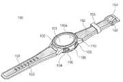
- FIG. 1is a perspective view of the front of a mobile electronic device according to various embodiments.
- FIG. 2is a perspective view of a rear surface of an electronic device according to various embodiments of the present disclosure.
- FIG 3is an exploded perspective view of an electronic device according to various embodiments of the present disclosure.
- FIG. 4is a perspective view illustrating an example of a configuration of an electronic device according to various embodiments.
- FIG. 5is a perspective view illustrating an example of a configuration of an electronic device according to various embodiments of the present disclosure
- FIG. 6is a diagram illustrating one side of a printed circuit board according to various embodiments.
- FIG. 7is a perspective view illustrating an example of a connecting member according to various embodiments.
- FIG. 8is a graph showing total radiation efficiency of an electronic device according to various embodiments and an electronic device according to a comparative embodiment.
- FIG. 9is a graph showing a reflection coefficient (or return loss [dB]) of an electronic device according to various embodiments and an electronic device according to a comparative embodiment.
- FIG. 10is a block diagram illustrating an example of an electronic device in a network environment, according to various embodiments.
- FIG. 1is a perspective view of the front of a mobile electronic device according to various embodiments.
- FIG. 2is a perspective view of a rear surface of an electronic device according to various embodiments of the present disclosure.
- the electronic device 100includes a first surface (or front surface) 110A, a second surface (or rear surface) 110B, and a first surface 110A. and a housing 110 including a side surface 110C surrounding a space between the second surface 110B, and connected to at least a portion of the housing 110 to set the electronic device 100 to a user's body part (eg : It may include binding members 150 and 160 (eg, straps or bands) configured to detachably attach to a wrist, ankle, etc.
- the housingmay refer to a structure forming some of the first surface 110A, the second surface 110B, and the side surface 110C of FIG. 1 .
- the first surface 110Amay be formed by a substantially transparent front plate 101 (eg, a glass plate or a polymer plate including various coating layers).
- the second face 110Bmay be formed by the substantially opaque back plate 107 .
- the rear plate 107is formed, for example, of coated or tinted glass, ceramic, polymer, metal (eg, aluminum, stainless steel (STS), or magnesium), or a combination of at least two of the foregoing materials. It can be.
- the side surface 110Cmay be formed by a side bezel structure (or “side member”) 106 coupled to the front plate 101 and the rear plate 107 and including metal and/or polymer.
- the back plate 107 and the side bezel structure 106may be integrally formed and include the same material (eg, a metal material such as aluminum).
- the coupling members 150 and 160may be formed of various materials and shapes. Integral and plurality of unit links may be formed to flow with each other by woven material, leather, rubber, urethane, metal, ceramic, or a combination of at least two of the above materials.
- the electronic device 100includes a display 120 (see FIG. 3), audio modules 105 and 108, sensor modules 111, key input devices 102, 103 and 104, and connector holes ( 109) may include at least one or more. In some embodiments, the electronic device 100 omits at least one of the components (eg, the key input devices 102, 103, and 104, the connector hole 109, or the sensor module 111) or has other components. Additional elements may be included.
- Display 120may be visible through a substantial portion of front plate 101 , for example.
- the shape of the display 120may be a shape corresponding to the shape of the front plate 101, and may have various shapes such as a circle, an ellipse, or a polygon.
- the display 120may be coupled to or disposed adjacent to a touch sensing circuit, a pressure sensor capable of measuring the intensity (pressure) of a touch, and/or a fingerprint sensor.
- the audio modules 105 and 108may include a microphone hole 105 and a speaker hole 108 .
- a microphone for acquiring external soundmay be disposed inside the microphone hole 105, and in some embodiments, a plurality of microphones may be disposed to detect the direction of sound.
- the speaker hole 108can be used as an external speaker and a receiver for a call.
- the speaker holes 107 and 114 and the microphone hole 105may be implemented as one hole, or a speaker may be included without the speaker holes 107 and 114 (eg, a piezo speaker).
- the sensor module 111may generate an electrical signal or data value corresponding to an internal operating state of the electronic device 100 or an external environmental state.
- the sensor module 111may include, for example, a biometric sensor module 111 (eg, an HRM sensor) disposed on the second surface 110B of the housing 110 .
- the electronic device 100includes a sensor module (not shown), for example, a gesture sensor, a gyro sensor, an air pressure sensor, a magnetic sensor, an acceleration sensor, a grip sensor, a color sensor, an IR (infrared) sensor, a bio sensor, a temperature sensor, At least one of a humidity sensor and an illuminance sensor may be further included.
- the key input devices 102, 103, and 104include a wheel key 102 disposed on a first surface 110A of the housing 110 and rotatable in at least one direction, and/or a side surface 110C of the housing 110. ) may include side key buttons 102 and 103 disposed on.
- the wheel keymay have a shape corresponding to the shape of the front plate 101 .
- the electronic device 100may not include some or all of the above-mentioned key input devices 102, 103, and 104, and the key input devices 102, 103, and 104 that are not included may display It may be implemented in other forms such as soft keys on 120.
- the connector hole 109may accommodate a connector (eg, a USB connector) for transmitting and receiving power and/or data to and from an external electronic device and a connector for transmitting and receiving an audio signal to and from an external electronic device.
- a connectoreg, a USB connector
- Other connector holesmay be included.
- the electronic device 100may further include, for example, a connector cover (not shown) that covers at least a portion of the connector hole 109 and blocks external foreign substances from entering the connector hole.
- the coupling members 150 and 160may be detachably coupled to at least a portion of the housing 110 using the locking members 151 and 161 .
- the fastening members 150 and 160may include one or more of a fixing member 152, a fixing member fastening hole 153, a band guide member 154, and a band fixing ring 155.
- the fixing member 152may be configured to fix the housing 110 and the fastening members 150 and 160 to a part of the user's body (eg, wrist, ankle, etc.).
- the fixing member fastening hole 153corresponds to the fixing member 152 to fix the housing 110 and the fastening members 150 and 160 to a part of the user's body.
- the band guide member 154is configured to limit the movement range of the fixing member 152 when the fixing member 152 is engaged with the fixing member fastening hole 153, so that the fastening members 150 and 160 are attached to a part of the user's body. It can be tightly bonded.
- the band fixing ring 155may limit the movement range of the fastening members 150 and 160 in a state in which the fixing member 152 and the fixing member fastening hole 153 are fastened.
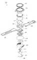
- FIG 3is an exploded perspective view of an electronic device according to various embodiments of the present disclosure.
- an electronic device 300(eg, the electronic device 100 of FIG. 1 ) includes a side bezel structure 310, a wheel key 320, a front plate 101, a display 120, a first 1 antenna 350, second antenna 355, support member 360 (eg bracket), battery 370, printed circuit board 380, sealing member 390, rear plate 393, fastening member (395, 397) (eg, bands or straps), wireless charging coil 345, sensor module 340 (eg, a sensor module including at least one sensor), cover 365, and an optical film 385 .
- At least one of the components of the electronic device 300may be the same as or similar to at least one of the components of the electronic device 100 of FIG. 1 or 2, and overlapping descriptions may not be provided.
- the support member 360may be disposed inside the electronic device 300 and connected to the side bezel structure 310 or integrally formed with the side bezel structure 310 .
- the support member 360may be formed of, for example, a metal material and/or a non-metal (eg, polymer) material.
- the support member 360may have the display 120 coupled to one surface and the printed circuit board 380 coupled to the other surface.
- a processor, memory, and/or interfacemay be mounted on the printed circuit board 380 .
- the processormay include, for example, one or more of a central processing unit, an application processor, a graphic processing unit (GPU), an application processor, a sensor processor, or a communication processor.
- Memorymay include, for example, volatile memory or non-volatile memory.
- the interfacemay include, for example, a high definition multimedia interface (HDMI), a universal serial bus (USB) interface), an SD card interface, and/or an audio interface.
- HDMIhigh definition multimedia interface
- USBuniversal serial bus
- the interfacemay electrically or physically connect the electronic device 300 to an external electronic device, and may include a USB connector, an SD card/MMC connector, or an audio connector.
- the battery 370is a device for supplying power to at least one component of the electronic device 300, and may include, for example, a rechargeable secondary battery. At least a portion of the battery 370 may be disposed on substantially the same plane as the printed circuit board 380 , for example.
- the battery 370may be integrally disposed inside the electronic device 100 or may be disposed detachably from the electronic device 100 .
- the first antenna 350may be disposed between the display 120 and the support member 360 .
- the first antenna 350may include, for example, a near field communication (NFC) antenna, a wireless charging antenna, and/or a magnetic secure transmission (MST) antenna.
- the first antenna 350may, for example, perform short-range communication with an external device, wirelessly transmit/receive power required for charging, and transmit a short-range communication signal or a self-based signal including payment data.
- an antenna structuremay be formed by a part of the side bezel structure 310 and/or the support member 360 or a combination thereof.
- the second antenna 355may be disposed between the circuit board 380 and the back plate 393 .
- the second antenna 355may include, for example, a near field communication (NFC) antenna, a wireless charging antenna, and/or a magnetic secure transmission (MST) antenna.
- the second antenna 355may, for example, perform short-range communication with an external device, wirelessly transmit/receive power required for charging, and transmit a short-range communication signal or a self-based signal including payment data.
- an antenna structuremay be formed by a part of the side bezel structure 310 and/or the back plate 393 or a combination thereof.
- the sealing member 390(eg, seal) may be positioned between the side bezel structure 310 and the rear plate 393 .
- the sealing member 390may be configured to block moisture and foreign substances from entering into the space surrounded by the side bezel structure 310 and the back plate 393 from the outside.
- the wireless charging coil 345may be disposed on one side of the back plate 393.
- the wireless charging coil 345may be disposed between the back plate 393 and the cover 365.
- the wireless charging coil 345may be configured to transmit and receive power signals from an external device.
- the sensor module 340may be disposed between the back plate 393 and the cover 365, for example. In one embodiment, sensor module 340 may at least partially face cover 365 . For example, the sensor module 340 may face the cover 365 by being disposed in a form that is at least partially accommodated in a hollow formed in the wireless charging coil 345 .
- the sensor module 340may include, for example, a substrate unit and a sensor unit disposed on the substrate unit and configured to obtain biometric information. The sensor unit may be disposed to face the cover 365 that is at least partially in contact with the user's wrist while the user is wearing the electronic device 300 .
- the sensor unit of the sensor module 340may include, for example, an optical sensor including a light emitting unit and a light receiving unit for measuring the user's heart rate.
- the cover 365may be at least partially formed of a material capable of transmitting light (eg, substantially transparent resin).
- an optical film 385may be disposed between the cover 365 and the sensor module 340 .
- the cover 365may include electrodes (not shown) for detecting biometric information (a bioelectrical impedance analysis sensor (BIA) signal and/or an electrocardiogram sensor (ECG) sensor signal).
- biometric informationa bioelectrical impedance analysis sensor (BIA) signal and/or an electrocardiogram sensor (ECG) sensor signal.
- FIG. 4is a perspective view illustrating various exemplary configurations of an electronic device according to various embodiments.
- FIG. 5is a perspective view illustrating various exemplary configurations of an electronic device according to various embodiments.
- FIG. 6is a diagram illustrating one side of a printed circuit board according to various embodiments.
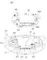
- an electronic device 400(eg, the electronic device 300 of FIG. 3) according to an embodiment includes a printed circuit board 480, a bracket 460, and a housing 410. ), a connecting member 50 (eg, a printed circuit board, a rigid-flexible printed circuit board and/or a flexible printed circuit board), or or the like including at least one conductor), a first button 416 , a second button 417 , and a display 420 .
- a connecting member 50eg, a printed circuit board, a rigid-flexible printed circuit board and/or a flexible printed circuit board, or or the like including at least one conductor
- the printed circuit board 480(eg, the printed circuit board 380 of FIG. 3 ) has a first side 480A and a second side 480B facing in the opposite direction to the first side 480A.
- the first side 480A of the printed circuit board 480faces the first direction 1
- the second side 480Bfaces the second direction 2 opposite to the first direction 1.
- various electronic componentsare provided on the first surface 480A and/or the second surface 480B of the printed circuit board 480.
- module 1092can be deployed.
- a protective member 485 for protecting electronic components disposed on the printed circuit board 480may be disposed on the first surface 480A and/or the second surface 480B of the printed circuit board 480.
- the protective member 485may include an insulating member (eg, resin) covering the electronic component to protect it from external moisture, and a conductive layer formed on the surface of the insulating member to shield electromagnetic interference (EMI) ( For example, it may consist of conformal shielding) and/or a shield can covering electronic components.
- EMIelectromagnetic interference
- printed circuit board 480may be disposed on bracket 460 .
- the printed circuit board 480may be disposed in the first direction 1 of the bracket 460 .
- the second side 480B of the printed circuit board 480may face the bracket 460 .
- the housing 410(eg, the side bezel structure 310 of FIG. 3 ) is a sidewall 415 forming at least a portion of a side surface (eg, the side surface 110C of FIG. 2 ) of the electronic device 400 . ) may be included.
- the side wall 415may extend in a height direction (eg, in the first direction 1) of the electronic device 400 and surround the bracket 460.
- the shape of the sidewall 415may be substantially circular. However, it is not limited thereto, and the sidewall 415 may have various shapes such as a rectangle, a rectangle with rounded corners, or a polygon.
- the housing 410may include a first point 411 and a second point 412 formed on the side wall 415 or protruding inward from the side wall 415 .
- the sidewall 415 of the housing 410extends in one direction (eg, counterclockwise) from the first point 411 to the second point 412, and has a first portion having a first length ( 413) and a second portion 414 extending from the first point 411 to the second point 412 in a direction different from the one direction (eg, clockwise) and having a second length shorter than the first length
- one directioneg, clockwise
- second lengthe.g., clockwise
- the electronic device 400may include an antenna including at least a portion of the housing 410 as an antenna element.
- the housing 410is supplied with power at a first point 411 and grounded at a second point 412 to operate as an antenna for transmitting and receiving a radio signal.
- the first point 411 of the housing 410may contact the first connector 481 disposed on the second surface 480B of the printed circuit board 480 .
- the first connector 481may include, for example, a C-clip connector, but is not limited thereto.
- the wireless communication circuit disposed on the printed circuit board 480(eg, the wireless communication circuit 1092 of FIG. 10) is a transmission line formed on the printed circuit board 480 and a second electrically connected to the transmission line. 1 may be electrically connected to the first point 411 of the housing 410 through the connector 481 .
- the second point 412 of the housing 410may come into contact with the second connector 482 disposed on the second surface 480B of the printed circuit board 480 .
- the second connector 482may include, for example, a C-clip connector, but is not limited thereto.
- the second point 412 of the housing 410may be electrically connected to a ground plane of the printed circuit board 480 through a second connector 482 .
- the ground planemay include a copper foil layer positioned on at least one layer of the printed circuit board 480 .
- the ground planemay be formed in one or a plurality of regions in one or a plurality of layers of the printed circuit board. In this respect, the ground plane may be referred to as at least one ground.
- the housing 410includes a first resonant frequency corresponding to a first designated band (eg, a low-band (LB) of less than 1 GHz, but is not limited thereto) and a second designated band ( Example: A second resonance frequency corresponding to a mid-band (MB, mid-band) of 1 GHz to 2.3 GHz, but is not limited thereto) may be formed.
- a first designated bandeg, a low-band (LB) of less than 1 GHz, but is not limited thereto
- a second designated bandExample: A second resonance frequency corresponding to a mid-band (MB, mid-band) of 1 GHz to 2.3 GHz, but is not limited thereto
- the housing 410is powered at a first point 411 and is shorted to a ground plane (ground) at a second point 412 so that the first resonant frequency band and/or the second resonant frequency band frequency bands can be formed.
- groundground
- the first resonant frequency and the second resonant frequencyare the circumferences of the first part 413 and the second part 414 of the housing 410 divided into the first point 411 and the second point 412, respectively. It may vary according to length (eg, the first length and the second length). The first resonant frequency and the second resonant frequency may vary according to a current path including the first part 413 and the second part 414 of the housing 410 , respectively.
- the wireless communication circuitmay transmit and receive radio signals of the first designated band and the second designated band by feeding power to the first point 411 of the housing 410 .
- the bracket 460(eg, the support member 360 of FIG. 3 ) may be at least partially accommodated within the space formed by the housing 410 .
- the bracket 460may be disposed inside the sidewall 415 of the housing 410 .
- the bracket 460may be at least partially spaced from the sidewall 415 of the housing 410 .
- bracket 460may include sidewall 415 and opposite side surface 460C, and sidewall 460C of bracket 460 may be at least partially spaced from sidewall 415 .
- the bracket 460may support the printed circuit board 480 and the connecting member 50 .
- connection member 50may include a flexible printed circuit board or a rigid-flexible printed circuit board, at least a portion of which is bendable.
- connecting member 50may be disposed at least partially between bracket 460 and sidewall 415 .
- the connecting member 50may be partially seated in the receiving groove 462 formed on the side surface 460C of the bracket 460 and positioned between the bracket 460 and the side wall 415 .
- the connecting member 50may be fixed to the side surface 460C of the bracket 460.
- the connecting member 50may be coupled to the bracket 460 in such a way that the protrusion 464 formed in the receiving groove 462 and the hole 537 formed in the connecting member 50 are fitted.
- the connecting member 50may be coupled to the bracket 460 through an adhesive member (eg, double-sided tape) or a fixing member (eg, a screw).
- connection member 50is formed on the sidewall 415 of the housing 410 when viewed from the side of the electronic device 400 (eg, when viewed in a direction perpendicular to the first direction 1). and/or may be disposed at least partially overlapping with the bracket 460 .
- the connecting member 50may be disposed between the bracket 460 and the first part 413 of the housing 410 .
- the connecting member 50may be closer to the first part 413 than the second part 414 of the housing 410 .
- the connecting member 50may be disposed between the bracket 460 and the second part 414 of the housing 410.
- the connecting member 50may include a first part 51 , a second part 52 , and an extension part 53 .
- extension portion 53may be positioned between bracket 460 and sidewall 415 . In one embodiment, the extension portion 53 may extend along the sidewall 415 of the housing 410 (or the sidewall 460C of the bracket 460). In one embodiment, the extension portion 53 may be at least partially accommodated in the receiving groove 462 of the bracket 460.
- one end 53A of the extension portion 53is positioned between the first button 416 and the bracket 460, and the other end 53B is positioned between the second button 417 and the bracket 460. can be located in
- various parts of the electronic device 400may be disposed on the extension part 53 .
- the first part 531 , the second part 532 , and the third part 533may be disposed on the extension part 53 .
- the first part 531may include a first dome switch and/or a first biosensor (or a first biosensor structure for detecting first biometric information).
- the first dome switchmay be pressed by the first button 416 (eg, the key input device 104 of FIG. 1 ) according to a user's manipulation to generate an electrical signal.
- the first biosensormay include a conductive structure, and the conductive structure may be electrically connected to the first button 416 at least partially formed of a conductive material. The first biosensor and the first button 416 may operate as electrodes for detecting the user's biometric information when the user's body contacts the first button 416 .
- the signal detected through the first biosensor and the first button 416is transferred to a processor (eg, the processor 1020 of FIG. 10 ) of the electronic device 400 through the connecting member 50. and the processor may obtain the user's first biometric information based on the detected signal.
- the first biosensormay include a bioelectrical impedance analysis sensor (BIA sensor), and the first biometric information may include information about components of the user's body, but is not limited thereto. .
- the second component 532may include a second dome switch and/or a second biosensor different from the first biosensor (or a second biosensor structure for detecting second biometric information). .
- the second dome switchmay be pressed by the second button 417 according to a user's manipulation to generate an electrical signal.
- the second biosensormay include a second conductive structure, and the second conductive structure may be at least partially electrically connected to the second button 417 formed of a conductive material.
- the second biosensor and the second button 417may operate as electrodes for detecting the user's biometric information when the user's body contacts the second button 417 .
- signals detected by the second biosensor and the second button 417may be transferred to the processor through the connection member 50 .
- the processormay obtain second biometric information of the user based on the detected signal.
- the second biometric sensormay include an ECG sensor (electrocardiogram sensor), and the second biometric information may include electrocardiogram information of a user, but is not limited thereto.
- the first component 531 and/or the second component 532may include a biometric sensor, and the biometric sensor is a button for the electronic device 400 to obtain user's biometric information.
- the biometric sensoris a button for the electronic device 400 to obtain user's biometric information.
- Itmay be a conductive structure (eg, a conductive plate) to be electrically connected to (or conductively connected to) (416, 417).
- the conductive structureextends from the contact portions 5311 and 5321 and the contact portions 5311 and 5321 (see FIG. 7) that at least partially contact the buttons 416 and 417 and end portions 53A and 53B of the connecting member 50.
- Itmay include fixing parts 5312 and 5322 (see FIG. 7) electrically connected to each other.
- a dome switchmay be disposed between the conductive structure and one surface of the connecting member 50 .
- An electronic deviceincludes an analog-to-digital converter (not shown) that processes analog signals detected from the first biosensor and the second biosensor into digital signals and transmits the digital signals to the processor. can do.
- the analog-to-digital convertermay be disposed on the printed circuit board 480, but is not limited thereto.
- the third part 533may be disposed between the first part 531 and the second part 532 in the extension part 53 .
- the third component 533may include an acoustic sensor.
- the third part 533may be located between the extension part 53 and the bracket 460 .
- a microphone hole 535 through which sound is introducedmay be formed in the third part 533, and the microphone hole 535 may be aligned and communicate with the opening 536 formed in the extension part 53. there is.
- the above-described first part 531, the second part 532, and the third part 533are not limited to the above-described example, and may be replaced with parts having functions different from those described above. may be
- the first portion 51 of the connecting member 50may extend from one end 53A of the extension portion 53 . In one embodiment, the first portion 51 of the connecting member 50 may extend from one end 53A of the extension portion 53 to face the first surface 480A of the printed circuit board 480. . In one embodiment, the first portion 51 may be disposed on the first surface 480A of the printed circuit board 480 .
- the first portion 51may include a plug 511 of a connector, and a receptacle 487 of the connector may be provided on the first surface 480A of the printed circuit board 480. can be placed.
- the first portion 51may be connected to the first surface 480A of the printed circuit board 480 by coupling the plug 511 and the receptacle 487 to each other.
- the connecting member 50it is not limited to the above-described receptacle-plug connector structure, and various methods applicable to those skilled in the art may be used.
- the first portion 51may be disposed on the second surface 480B of the printed circuit board 480 .
- At least one processor disposed on the printed circuit board 480connects the first component 531 and the second component 532 via the connection member 50 . ) and can be operatively connected with the third component 533.
- the at least one processormay be connected to a first component 531, a second component 532, and a third component through conductive traces (or patterns) formed on the printed circuit board 480 and the connection member 50. (533) and can be electrically connected.
- the at least one processormay transmit and/or receive electrical signals to (and/or from) the first component 531, the second component 532, and the third component 533. there is. The electrical signal may be transmitted through the first part 51 of the connecting member 50 .
- the second portion 52 of the connecting member 50may extend from the other end portion 53B of the extension portion 53 . In one embodiment, the second portion 52 of the connecting member 50 may extend from the other end 53B of the extension portion 53 to face the second surface 480B of the printed circuit board 480. . In one embodiment, the second portion 52 may be disposed on the second side 480B of the printed circuit board 480 . In one embodiment, a conductive region 521 (or conductive pad) partially exposed to the conductive pattern of the connecting member 50 may be formed in the second portion 52 . In one embodiment, the conductive region 521 may face the second side 480B of the printed circuit board 480 . In one embodiment, the conductive region 521 may contact the third connector 483 .
- the conductive region 521may be electrically connected to the ground plane of the printed circuit board 480 through the third connector 483 .
- the third connector 483may include, for example, a C-clip, but is not limited thereto.
- the second portion 52 of the connecting member 50may be disposed on the first surface 480A of the printed circuit board 480 .
- connection member 50may include a plurality of conductive traces (or patterns).
- the plurality of conductive tracesinclude signal lines and power lines for the operation of the first component 531, the second component 532, and the third component 533;
- a plurality of ground linesmay be included.
- at least some of the plurality of ground linesmay be directly or indirectly (eg, through another ground line) electrically connected to the conductive region 521 of the second portion 52 .
- the plurality of ground linesmay be electrically connected to a ground plane of the printed circuit board 480 through the conductive region 521 of the second portion 52 .
- connection member 50has a first portion 51 disposed on the printed circuit board 480 and operatively connected to at least one processor, and a second portion 52 provided on the printed circuit board (480).
- a loop structure electrically connected to the ground area of 480)may be formed.
- the first button 416 and the second button 417may be at least partially exposed through the housing 410 .
- the first button 416 and the second button 417are when looking at the side (eg, side 110C of FIG. 2) of the housing 410 (eg, in the first direction 1). When viewed in a vertical direction) may at least partially overlap the connection member 50 .
- the first button 416 and the second button 417are when the sidewall 415 of the housing 410 is viewed from the front (eg, when viewed in a direction perpendicular to the first direction 1). ) may overlap at least partially with the extension portion 53 of the connecting member 50 .
- the first button 416may overlap at least partially with one end 53A of the extension part 53
- the second button 417may overlap with the other end 53B of the extension part 53. They may overlap at least partially.
- display 420(eg, display 120 of FIG. 3 ) may be disposed within housing 410 .
- a bracket 460may be disposed between the display 420 and the printed circuit board 480 .
- the printed circuit board 480is disposed and supported in one direction (eg, the first direction (1)) of the bracket 460, and the display 420 is disposed in the other direction (eg, the second direction (2)). ) can be placed and supported.
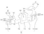
- FIG. 7is a perspective view illustrating a connecting member according to various embodiments.
- the connecting member 50may be at least partially bent.
- the connecting member 50may include a flexible portion(s) and a rigid portion(s).
- the connecting member 50includes a first rigid part 711, a second rigid part 712, a third rigid part 713, a fourth rigid part 714, a fifth rigid part 715, A first flexible part 761 , a second flexible part 762 , a third flexible part 763 , and a fourth flexible part 764 may be included.
- a plug 511may be disposed on the first rigid portion 711 .
- the first flexible portion 761may connect the first rigid portion 711 and the second rigid portion 712 .
- the first flexible portion 761may extend from the first rigid portion 711 to the second rigid portion 712 .
- the first rigid portion 711 and the first flexible portion 761extend from one end 53A of the extension portion 53, so that the first portion 51 of the connecting member 50 ) can be referred to as
- the first part 531may be disposed on the second rigid part 712 .
- the second flexible part 762may connect the second rigid part 712 and the third rigid part 713 .
- the second flexible portion 762may extend from the second rigid portion 712 to the third rigid portion 713 .
- a third component 533is disposed on the third rigid portion 713, and an opening 536 communicating with a microphone hole (eg, 535 in FIG. 4 ) of the third component 533 is formed.
- the third flexible part 763may connect the third rigid part 713 and the fourth rigid part 714 .
- the third flexible portion 763may extend from the third rigid portion 713 to the fourth rigid portion 714 in a direction away from the second flexible portion 762 .
- the second part 532may be disposed on the fourth rigid part 714 .
- the second rigid part 712, the second flexible part 762, the third rigid part 713, the third flexible part 763, and the fourth rigid part 714are the housing 410 ) It may extend along the sidewall (415 in FIG. 4) or the side (460C in FIG. 4) of the bracket (460 in FIG. 4).
- the second rigid part 712, the second flexible part 762, the third rigid part 713, the third flexible part 763, and the fourth rigid part 714 are connected to the connecting member 50 )may be referred to as an extension portion 53 of
- one end 53A of the connecting member 50may be understood to include at least a portion of the second rigid portion 712 .
- the other end 53B of the connecting member 50includes at least a portion of the fourth rigid portion 714 .
- a conductive region 521may be formed in the fifth rigid portion 715 .
- the conductive region 521may be a pad (or conductive pad) electrically connected to a ground region of the printed circuit board 480 through the third connector 483 .
- the fourth flexible part 764may connect the fourth rigid part 714 and the fifth rigid part 715 .
- the fourth flexible portion 764may extend from the fourth rigid portion 714 to the fifth rigid portion 715 .
- the fourth flexible portion 764 and the fifth rigid portion 715extend from the other end 53B of the extension portion 53, so that the second portion 52 of the connecting member 50 ) can be referred to as
- the above-described classification of the rigid part and the flexible partis only an example, and various design changes may be possible.
- the third part 533when the third part 533 is omitted, the third rigid part 713 may be replaced with a flexible part.
- one end 53A (or the other end 53B) of the extension portion 53is described as including at least a portion of the second rigid portion 712 (or the fourth rigid portion 714).
- one end (53A) and / or the other end (53B) of the extension portion 53may be at least partially formed as a flexible portion.
- an electronic device configured to be wearableincludes a sidewall (eg, the sidewall 415 of FIG. 4 ) at least partially used as an antenna.
- a housingeg, housing 410 in FIG. 4
- a first printed circuit boardeg, the printed circuit board 480 of FIG. 4
- a second printed circuit boardeg, connecting member 50 of FIG. 4
- the second printed circuit boardan extension part extending along the sidewall of the housing (eg, extension part 53 of FIG. 4 ), the A first portion (eg, first portion 51 in FIG.
- extension portionextending from one end of the extension portion (eg, one end portion 53A in FIG. 4 ) and connected to the first printed circuit board, and the extension portion a second part (eg, the second part 52 of FIG. 4) extending from the other end (eg, the other end 53B of FIG. 4) and electrically connected to the at least one ground; at least one component disposed on the extension portion; and at least one processor disposed on the first printed circuit board and in operative connection with the at least one component via the first portion of the second printed circuit board (eg, processor 1020 of FIG. 10 ). ; can be included.
- An electronic deviceincludes a bracket (eg, the bracket 460 of FIG. 4 ) disposed within the housing to support the first printed circuit board, and the bracket is at least partially spaced apart from the sidewall. And, the extension portion of the second printed circuit board may be positioned between the bracket and the sidewall.
- a bracketeg, the bracket 460 of FIG. 4
- the first printed circuit boardmay include a first surface of the first printed circuit board (eg, the first surface 480A of FIG. 4 ) or a second surface opposite to the first surface (eg, the first surface 480A of FIG. 4 ).
- a receptacleeg, receptacle 487 in FIG. 4
- the second printed circuit boardis disposed on the first portion and coupled to the receptacle.
- a plugeg, the plug 511 of FIG. 4) may be included.
- the first portion of the second printed circuit boardmay include a first rigid portion (eg, the first rigid portion 711 of FIG. 7 ) and a first flexible portion (eg, the first rigid portion 711 of FIG. 7 ).
- a flexible portion 761), the plugis disposed on the first rigid portion, and the first flexible portion may extend from the first rigid portion to the one end of the extension portion.
- a first buttoneg, first button 416 of FIG. 4
- a second buttoneg, second button 416 of FIG. 4
- the first button and the second buttonmay at least partially overlap the extension portion.
- the first buttonmay at least partially overlap the one end of the extension portion, and the second button may at least partially overlap the other end portion of the extension portion.
- the at least one componentmay include a first component (eg, the first component 531 of FIG. 4 ), a second component (eg, the second component 532 of FIG. 4 ), and the first component.
- a first dome switchcomprising a third component positioned between the first component and the second component (eg, the third component 533 of FIG. 4 ), the first component operatively connected to the first button; and a first biosensor structure including at least one sensor, the second component including a first dome switch operatively connected to the second button and at least one sensor different from the first biosensor; 2 may include a biosensor structure.
- the extended portion of the second printed circuit boardmay include: a second rigid portion (eg, second rigid portion 712 in FIG. 7 ) on which the first component is disposed; a third rigid portion (eg, the third rigid portion 713 of FIG. 7 ) where the third component is disposed; a second flexible portion (eg, the second flexible portion 762 of FIG. 7 ) connecting the second rigid portion and the third rigid portion; a fourth rigid part (eg, the fourth rigid part 714 of FIG. 7 ) where the second part is disposed; and a third flexible part (for example, the third flexible part 763 of FIG. 7) connecting the third rigid part and the fourth rigid part, wherein the one end of the extension part is formed by the second rigid part. portion, and the other end of the extension portion may at least partially include the fourth rigid portion.
- a second rigid portioneg, second rigid portion 712 in FIG. 7
- a third rigid portioneg, the third rigid portion 713 of FIG. 7
- a second flexible portioneg, the second
- the first biosensor structure and/or the second biosensor structureinclude a conductive structure configured to acquire a bioelectrical impedance analysis sensor (BIA sensor) signal and/or an electrocardiogram sensor (ECG sensor) signal, and ,
- the third componentmay include an acoustic sensor.
- the second printed circuit boardincludes a plurality of ground lines
- the second portionincludes a conductive region exposed toward the first printed circuit board (eg, the conductive region 521 of FIG. 7 ). )), wherein at least a portion of the plurality of ground lines is electrically connected to the conductive region, and at least a portion of the plurality of ground lines is connected to the at least one of the plurality of ground lines through the conductive region. can be electrically connected to the ground of
- the second partmay include a fifth rigid part (eg, the fifth rigid part 715 of FIG. 7 ) and a fourth flexible connecting the fifth rigid part and the other end of the extension part. portion (eg, the fourth flexible portion 764 of FIG. 7 ), and the conductive region may be formed on the fifth rigid portion.
- a fifth rigid parteg, the fifth rigid part 715 of FIG. 7
- a fourth flexible connecting the fifth rigid part and the other end of the extension part. portioneg, the fourth flexible portion 764 of FIG. 7
- the conductive regionmay be formed on the fifth rigid portion.
- a C-clip(eg, the third connector 483 of FIG. 4 ) disposed on a first surface of the first printed circuit board or on a second surface opposite to the first surface, and , The conductive region may be in contact with the C-clip and electrically connected to the at least one ground portion of the first printed circuit board.
- the housingincludes a wireless communication circuit (eg, the wireless communication module 1092 of FIG. 10) disposed on the first printed circuit board, and the housing is provided at a first point (eg, the first point in FIG. 4 ( 411) is electrically connected to the wireless communication circuit to supply power, and the housing connects to the at least one ground portion of the first printed circuit board at a second point (eg, second point 412 in FIG. 4 ). can be electrically connected.
- a wireless communication circuiteg, the wireless communication module 1092 of FIG. 1092 of FIG. 1010
- the housingis provided at a first point (eg, the first point in FIG. 4 ( 411) is electrically connected to the wireless communication circuit to supply power, and the housing connects to the at least one ground portion of the first printed circuit board at a second point (eg, second point 412 in FIG. 4 ). can be electrically connected.
- the sidewall of the housingmay include a first portion extending in a first direction from the first point to the second point (eg, the first portion 413 of FIG. 4 ) and from the first point and a second portion extending in a second direction different from the first direction up to the second point (eg, the second portion 414 of FIG. 4 ), and the first portion of the sidewall has a length of the second portion. portion, and the second printed circuit board may be closer to the first portion than the second portion of the sidewall.
- a display(eg, the display 420 of FIG. 4 ) may be included, and the bracket may be disposed between the display and the first printed circuit board.
- a wearable electronic device(eg, the electronic device 400 of FIG. 4 ) includes a housing (eg, the sidewall of FIG. 4 ) including a sidewall (eg, the sidewall of FIG. 4 ) configured to be at least partially used as an antenna.
- housing 410 in FIG. 4); a printed circuit board disposed within the housing and including at least one ground (eg, the printed circuit board 480 of FIG. 4 );
- a connection member including a conductorfor example, the connection member 50 of FIG. 4
- the connection memberan extension portion extending along the sidewall of the housing (for example, the extension portion 53 of FIG. 4), A first portion (eg, first portion 51 in FIG.
- the connecting memberincludes: , and a plurality of ground lines, and at least a portion of the plurality of ground lines may be electrically connected to at least one ground portion of the printed circuit board through the second portion.
- a wearable electronic deviceincludes a C-clip (eg, the third connector 483 of FIG. 4 ) disposed on the printed circuit board, and the printed circuit board is included in the second part.
- a conductive regioneg, the conductive region 521 of FIG. 4
- the C-clip in contact with the conductive regionis formed. It may be electrically connected to at least one grounding part of the printed circuit board.
- a wearable electronic deviceincludes a first button (eg, the first button 416 of FIG. 4 ) and a second button (eg, the first button 416 of FIG. 4 ) that are at least partially exposed through the sidewall of the housing. 2 buttons 417), and the first button and the second button may at least partially overlap the extension part.
- a first buttoneg, the first button 416 of FIG. 4
- a second buttoneg, the first button 416 of FIG. 4
- the first button and the second buttonmay at least partially overlap the extension part.
- the first buttonmay at least partially overlap the one end of the connecting member, and the second button may at least partially overlap the other end of the connecting member.
- the wearable electronic deviceincludes a bracket (eg, bracket 460 of FIG. 4 ) disposed within the housing to support the printed circuit board, the bracket being at least partially spaced apart from the sidewall, ,
- the extension portion of the connecting membermay be located between the bracket and the side wall.
- FIG. 8is a graph showing total efficiency radiation of an electronic device according to an exemplary embodiment and an electronic device according to a comparative embodiment.
- FIG. 9is a graph showing a reflection coefficient (or return loss [dB]) of an electronic device according to an exemplary embodiment and an electronic device according to a comparative embodiment.
- reference numerals 802 and 902may be graphs of electronic devices according to various embodiments, and reference numerals 804 and 904 may be graphs of electronic devices according to comparative embodiments.
- the connecting member of the electronic device according to the comparative embodiment of FIGS. 8 and 9uses only the first part 51 and uses the printed circuit board. It is electrically connected to the ground area of 480 and may not include a loop structure.
- the second part 52 electrically connected to the ground plane of the printed circuit board 480 according to the embodimentmay be omitted.
- connection member of the electronic devicemay affect the radiation field of the antenna due to noise and parasitics, and may deteriorate the performance of the antenna.
- the antenna structureforms a field using a conductive pattern (eg, an outer conductive sidewall) formed on at least a partial area of the housing 410, parallel to the sidewall 415 of the housing 410 (or a standard of the electronic device).
- the connecting member disposed vertically in)is recognized as another antenna element distinct from the housing 410 and may degrade antenna performance.
- the electronic devicemay include a connecting member 50 having both ends forming a loop structure.
- the first part 51which is one end of the connecting member 50, is disposed on the printed circuit board 480 and electrically connected to at least one processor
- the second partwhich is the other end of the connecting member 50 ( 52) may be electrically connected to the ground plane of the printed circuit board 480.
- the connection member 50 including a loop structuredoes not act as a parasitic component even when the housing 410 operates as an antenna, it is possible to reduce and/or prevent performance degradation of the antenna.
- radiation efficiency 802 of an electronic device according to an exemplary embodimentmay be higher than radiation efficiency 804 of an electronic device according to a comparative embodiment in all frequency bands.
- the reflection coefficient 902 of the electronic device according to an embodimentis about 1200 MHz to 1500 MHz and about 1700 than the reflection coefficient 904 of the electronic device according to the comparative embodiment. It may be lower in the MHz to 2000 MHz band. Through this, communication performance of a frequency band used by the electronic device for communication may be improved.
- FIG. 10is a block diagram illustrating an example of an electronic device 1001 within a network environment 1000 according to various embodiments.
- an electronic device 1001communicates with an electronic device 1002 through a first network 1098 (eg, a short-range wireless communication network) or through a second network 1099. It is possible to communicate with at least one of the electronic device 1004 or the server 1008 through (eg, a long-distance wireless communication network). According to an embodiment, the electronic device 1001 may communicate with the electronic device 1004 through the server 1008.
- a first network 1098eg, a short-range wireless communication network
- a second network 1099e.g., a second network 1099. It is possible to communicate with at least one of the electronic device 1004 or the server 1008 through (eg, a long-distance wireless communication network). According to an embodiment, the electronic device 1001 may communicate with the electronic device 1004 through the server 1008.
- the electronic device 1001includes a processor 1020, a memory 1030, an input module 1050, an audio output module 1055, a display module 1060, an audio module 1070, a sensor module ( 1076), interface 1077, connection terminal 1078, haptic module 1079, camera module 1080, power management module 1088, battery 1089, communication module 1090, subscriber identification module 1096 , or an antenna module 1097.
- a processor 1020e.g, a memory 1030, an input module 1050, an audio output module 1055, a display module 1060, an audio module 1070, a sensor module ( 1076), interface 1077, connection terminal 1078, haptic module 1079, camera module 1080, power management module 1088, battery 1089, communication module 1090, subscriber identification module 1096 , or an antenna module 1097.
- at least one of these componentseg, the connection terminal 1078
- some of these componentseg, sensor module 1076,
- the processor 1020for example, executes software (eg, the program 1040) to cause at least one other component (eg, hardware or software component) of the electronic device 1001 connected to the processor 1020. It can control and perform various data processing or calculations. According to one embodiment, as at least part of data processing or operation, processor 1020 transfers commands or data received from other components (eg, sensor module 1076 or communication module 1090) to volatile memory 1032. , process commands or data stored in the volatile memory 1032 , and store resultant data in the non-volatile memory 1034 .
- softwareeg, the program 1040
- processor 1020transfers commands or data received from other components (eg, sensor module 1076 or communication module 1090) to volatile memory 1032. , process commands or data stored in the volatile memory 1032 , and store resultant data in the non-volatile memory 1034 .
- the processor 1020may include a main processor 1021 (eg, a central processing unit or an application processor) or a secondary processor 1023 (eg, a graphic processing unit, a neural network processing unit ( NPU: neural processing unit (NPU), image signal processor, sensor hub processor, or communication processor).
- a main processor 1021eg, a central processing unit or an application processor
- a secondary processor 1023eg, a graphic processing unit, a neural network processing unit ( NPU: neural processing unit (NPU), image signal processor, sensor hub processor, or communication processor.
- NPUneural network processing unit
- NPUneural processing unit
- image signal processorsensor hub processor
- communication processore.g., a communication processor.
- the auxiliary processor 1023may use less power than the main processor 1021 or be set to be specialized for a designated function.
- the auxiliary processor 1023may be implemented separately from or as part of the main processor 1021 .
- the secondary processor 1023may, for example, take the place of the main processor 1021 while the main processor 1021 is inactive (eg sleep), or the main processor 1021 is active (eg application execution). ) state, together with the main processor 1021, at least one of the components of the electronic device 1001 (eg, the display module 1060, the sensor module 1076, or the communication module 1090) It is possible to control at least some of the related functions or states.
- the auxiliary processor 1023eg, image signal processor or communication processor
- may be implemented as part of other functionally related componentseg, camera module 1080 or communication module 1090). there is.
- the auxiliary processor 1023may include a hardware structure specialized for processing an artificial intelligence model.
- AI modelscan be created through machine learning. Such learning may be performed, for example, in the electronic device 1001 itself where the artificial intelligence model is performed, or may be performed through a separate server (eg, the server 1008).
- the learning algorithmmay include, for example, supervised learning, unsupervised learning, semi-supervised learning, or reinforcement learning, but in the above example Not limited.
- the artificial intelligence modelmay include a plurality of artificial neural network layers.
- Artificial neural networksinclude deep neural networks (DNNs), convolutional neural networks (CNNs), recurrent neural networks (RNNs), restricted boltzmann machines (RBMs), deep belief networks (DBNs), bidirectional recurrent deep neural networks (BRDNNs), It may be one of deep Q-networks or a combination of two or more of the foregoing, but is not limited to the foregoing examples.
- the artificial intelligence modelmay include, in addition or alternatively, software structures in addition to hardware structures.
- the memory 1030may store various data used by at least one component (eg, the processor 1020 or the sensor module 1076) of the electronic device 1001 .
- the datamay include, for example, input data or output data for software (eg, the program 1040) and commands related thereto.
- the memory 1030may include a volatile memory 1032 or a non-volatile memory 1034 .
- the program 1040may be stored as software in the memory 1030 and may include, for example, an operating system 1042 , middleware 1044 , or an application 1046 .
- the input module 1050may receive a command or data to be used for a component (eg, the processor 1020) of the electronic device 1001 from an outside of the electronic device 1001 (eg, a user).
- the input module 1050may include, for example, a microphone, a mouse, a keyboard, a key (eg, a button), or a digital pen (eg, a stylus pen).
- the sound output module 1055may output sound signals to the outside of the electronic device 1001 .
- the sound output module 1055may include, for example, a speaker or receiver.
- the speakercan be used for general purposes such as multimedia playback or recording playback.
- a receivermay be used to receive an incoming call. According to one embodiment, the receiver may be implemented separately from the speaker or as part of it.
- the display module 1060may visually provide information to the outside of the electronic device 1001 (eg, a user).
- the display module 1060may include, for example, a display, a hologram device, or a projector and a control circuit for controlling the device.
- the display module 1060may include a touch sensor configured to detect a touch or a pressure sensor configured to measure the intensity of force generated by the touch.
- the audio module 1070may convert sound into an electrical signal or vice versa. According to an embodiment, the audio module 1070 acquires sound through the input module 1050, the sound output module 1055, or an external electronic device connected directly or wirelessly to the electronic device 1001 (eg: Sound may be output through the electronic device 1002 (eg, a speaker or a headphone).
- the audio module 1070acquires sound through the input module 1050, the sound output module 1055, or an external electronic device connected directly or wirelessly to the electronic device 1001 (eg: Sound may be output through the electronic device 1002 (eg, a speaker or a headphone).
- the sensor module 1076detects an operating state (eg, power or temperature) of the electronic device 1001 or an external environmental state (eg, a user state), and generates an electrical signal or data value corresponding to the detected state. can do.
- the sensor module 1076may include, for example, a gesture sensor, a gyro sensor, an air pressure sensor, a magnetic sensor, an acceleration sensor, a grip sensor, a proximity sensor, a color sensor, an IR (infrared) sensor, a bio sensor, It may include a temperature sensor, humidity sensor, or light sensor.
- the interface 1077may support one or more designated protocols that may be used to directly or wirelessly connect the electronic device 1001 to an external electronic device (eg, the electronic device 1002).
- the interface 1077may include, for example, a high definition multimedia interface (HDMI), a universal serial bus (USB) interface, an SD card interface, or an audio interface.
- HDMIhigh definition multimedia interface
- USBuniversal serial bus
- SD card interfaceSecure Digital Card
- connection terminal 1078may include a connector through which the electronic device 1001 may be physically connected to an external electronic device (eg, the electronic device 1002).
- the connection terminal 1078may include, for example, an HDMI connector, a USB connector, an SD card connector, or an audio connector (eg, a headphone connector).
- the haptic module 1079may convert electrical signals into mechanical stimuli (eg, vibration or motion) or electrical stimuli that a user can perceive through tactile or kinesthetic senses.
- the haptic module 1079may include, for example, a motor, a piezoelectric element, or an electrical stimulation device.
- the camera module 1080may capture still images and moving images. According to one embodiment, the camera module 1080 may include one or more lenses, image sensors, image signal processors, or flashes.
- the power management module 1088may manage power supplied to the electronic device 1001 .
- the power management module 1088may be implemented as at least part of a power management integrated circuit (PMIC), for example.
- PMICpower management integrated circuit
- the battery 1089may supply power to at least one component of the electronic device 1001 .
- the battery 1089may include, for example, a non-rechargeable primary battery, a rechargeable secondary battery, or a fuel cell.
- the communication module 1090is a direct (eg, wired) communication channel or a wireless communication channel between the electronic device 1001 and an external electronic device (eg, the electronic device 1002, the electronic device 1004, or the server 1008). Establishment and communication through the established communication channel may be supported.
- the communication module 1090may include one or more communication processors that operate independently of the processor 1020 (eg, an application processor) and support direct (eg, wired) communication or wireless communication.
- the communication module 1090is a wireless communication module 1092 (eg, a cellular communication module, a short-range wireless communication module, or a global navigation satellite system (GNSS) communication module) or a wired communication module 1094 (eg, : a local area network (LAN) communication module or a power line communication module).
- a wireless communication module 1092eg, a cellular communication module, a short-range wireless communication module, or a global navigation satellite system (GNSS) communication module
- GNSSglobal navigation satellite system
- wired communication module 1094eg, : a local area network (LAN) communication module or a power line communication module.
- the corresponding communication moduleis a first network 1098 (eg, a short-distance communication network such as Bluetooth, wireless fidelity (Wi-Fi) direct, or infrared data association (IrDA)) or a second network 1099 (eg : It can communicate with the external electronic device 1004 through a legacy cellular network, a 5G network, a next-generation communication network, the Internet, or a long-distance communication network such as a computer network (eg, LAN or WAN).
- a first network 1098eg, a short-distance communication network such as Bluetooth, wireless fidelity (Wi-Fi) direct, or infrared data association (IrDA)
- a second network 1099eg : It can communicate with the external electronic device 1004 through a legacy cellular network, a 5G network, a next-generation communication network, the Internet, or a long-distance communication network such as a computer network (eg, LAN or WAN).
- the wireless communication module 1092uses subscriber information (eg, International Mobile Subscriber Identifier (IMSI)) stored in the subscriber identification module 1096 within a communication network such as the first network 1098 or the second network 1099.
- subscriber informationeg, International Mobile Subscriber Identifier (IMSI)
- IMSIInternational Mobile Subscriber Identifier
- the electronic device 1001may be identified or authenticated.
- the wireless communication module 1092may support a 5G network after a 4G network and a next-generation communication technology, for example, NR access technology (new radio access technology).
- NR access technologiesinclude high-speed transmission of high-capacity data (enhanced mobile broadband (eMBB)), minimization of terminal power and access of multiple terminals (massive machine type communications (mMTC)), or high reliability and low latency (ultra-reliable and low latency (URLLC)). -latency communications)) can be supported.
- the wireless communication module 1092may support a high frequency band (eg, mmWave band) to achieve a high data rate, for example.
- a high frequency bandeg, mmWave band
- the wireless communication module 1092uses various technologies for securing performance in a high frequency band, such as beamforming, massive multiple-input and multiple-output (MIMO), and full-dimensional multiplexing. Technologies such as input/output (FD-MIMO: full dimensional MIMO), array antenna, analog beam-forming, or large scale antenna may be supported.
- the wireless communication module 1092may support various requirements defined for the electronic device 1001, an external electronic device (eg, the electronic device 1004), or a network system (eg, the second network 1099).
- the wireless communication module 1092may be used to realize peak data rate (eg, 20 Gbps or more) for realizing eMBB, loss coverage (eg, 164 dB or less) for realizing mMTC, or U-plane latency (for realizing URLLC).
- peak data rateeg, 20 Gbps or more
- loss coverageeg, 164 dB or less
- U-plane latencyfor realizing URLLC.
- DLdownlink
- ULuplink each of 0.5 ms or less, or round trip 1 ms or less
- the antenna module 1097may transmit or receive signals or power to the outside (eg, an external electronic device).
- the antenna module 1097may include an antenna including a radiator including a conductor or a conductive pattern formed on a substrate (eg, PCB).
- the antenna module 1097may include a plurality of antennas (eg, an array antenna). In this case, at least one antenna suitable for a communication method used in a communication network such as the first network 1098 or the second network 1099 is selected from the plurality of antennas by, for example, the communication module 1090. can be chosen A signal or power may be transmitted or received between the communication module 1090 and an external electronic device through the selected at least one antenna.
- other componentseg, a radio frequency integrated circuit (RFIC) may be additionally formed as a part of the antenna module 1097 in addition to the radiator.
- RFICradio frequency integrated circuit
- the antenna module 1097may form a mmWave antenna module.
- the mmWave antenna moduleincludes a printed circuit board, an RFIC disposed on or adjacent to a first surface (eg, a lower surface) of the printed circuit board and capable of supporting a designated high frequency band (eg, mmWave band); and a plurality of antennas (eg, array antennas) disposed on or adjacent to a second surface (eg, an upper surface or a side surface) of the printed circuit board and capable of transmitting or receiving signals of the designated high frequency band. can do.
- peripheral deviceseg, a bus, general purpose input and output (GPIO), serial peripheral interface (SPI), or mobile industry processor interface (MIPI)
- signale.g. commands or data
- commands or datamay be transmitted or received between the electronic device 1001 and the external electronic device 1004 through the server 1008 connected to the second network 1099 .
- Each of the external electronic devices 1002 or 1004may be the same as or different from the electronic device 1001 .
- all or part of operations executed in the electronic device 1001may be executed in one or more external electronic devices among the external electronic devices 1002 , 1004 , or 1008 .
- the electronic device 1001when the electronic device 1001 needs to perform a certain function or service automatically or in response to a request from a user or another device, the electronic device 1001 instead of executing the function or service by itself.
- one or more external electronic devicesmay be requested to perform the function or at least part of the service.
- One or more external electronic devices receiving the requestmay execute at least a part of the requested function or service or an additional function or service related to the request, and deliver the execution result to the electronic device 1001 .
- the electronic device 1001may provide the result as at least part of a response to the request as it is or after additional processing.
- cloud computingdistributed computing, mobile edge computing (MEC), or client-server computing technology may be used.
- the electronic device 1001may provide an ultra-low latency service using, for example, distributed computing or mobile edge computing.
- the external electronic device 1004may include an internet of things (IoT) device.
- Server 1008may be an intelligent server using machine learning and/or neural networks.
- the external electronic device 1004 or server 1008may be included in the second network 1099.
- the electronic device 1001may be applied to intelligent services (eg, smart home, smart city, smart car, or health care) based on 5G communication technology and IoT-related technology.
- Electronic devicesmay be devices of various types.
- the electronic devicemay include, for example, a portable communication device (eg, a smart phone), a computer device, a portable multimedia device, a portable medical device, a camera, a wearable device, a home appliance, or the like.
- a portable communication deviceeg, a smart phone
- a computer devicee.g., a laptop, a desktop, a tablet, or the like
- portable multimedia devicee.g., a portable medical device
- a camerae.g., a portable medical device
- a camerae.g., a portable medical device
- a camerae.g., a camera
- a wearable devicee.g., a smart bracelet
- a home appliancee.g., a smart bracelet
- An electronic device according to an embodiment of this documentis not limited to the aforementioned devices.
- first, second, or first or secondarymay simply be used to distinguish a given component from other corresponding components, and may be used to refer to a given component in another aspect (eg, importance or order) is not limited.
- a (e.g., first) componentis said to be “coupled” or “connected” to another (e.g., second) component, with or without the terms “functionally” or “communicatively.”
- the certain componentmay be connected to the other component directly (eg, by wire), wirelessly, or through a third component.
- moduleused in various embodiments of this document may include hardware, software, or firmware, or a unit implemented as a combination thereof, for example, a term such as logic, logic block, component, or circuit. can be used interchangeably with A module may be an integrally constructed component or a minimal unit of components or a portion thereof that performs one or more functions.
- the modulemay be implemented in the form of an application-specific integrated circuit (ASIC).
- ASICapplication-specific integrated circuit
- each component (eg, module or program) of the components described abovemay include a single object or a plurality of objects, and some of the multiple objects may be separately disposed in other components.
- one or more components or operations among the aforementioned componentsmay be omitted, or one or more other components or operations may be added.
- a plurality of componentseg modules or programs
- the integrated componentmay perform one or more functions of each of the plurality of components identically or similarly to those performed by a corresponding component of the plurality of components prior to the integration. .
- operations performed by modules, programs, or other componentsare executed sequentially, in parallel, iteratively, or heuristically, or one or more of the operations are executed in a different order, omitted, or , or one or more other operations may be added.
Landscapes
- Physics & Mathematics (AREA)
- General Physics & Mathematics (AREA)
- Engineering & Computer Science (AREA)
- Microelectronics & Electronic Packaging (AREA)
- Telephone Set Structure (AREA)
Abstract
Description
Translated fromKorean본 문서에서 개시되는 실시 예들은, 인쇄 회로 기판을 포함하는 전자 장치와 관련된다.Embodiments disclosed in this document relate to an electronic device including a printed circuit board.
전자 장치는 무선 신호를 송수신하기 위한 안테나를 포함할 수 있다. 상기 안테나는 하우징의 적어도 일부를 안테나 요소로서 포함할 수 있다. 예를 들어, 상기 전자 장치의 안테나는 하우징의 적어도 일부를 포함하는 금속 부분을 안테나의 방사 요소로서 포함할 수 있다.An electronic device may include an antenna for transmitting and receiving radio signals. The antenna may include at least a portion of the housing as an antenna element. For example, the antenna of the electronic device may include a metal part including at least a part of the housing as a radiating element of the antenna.
한편, 전자 장치는 다양한 기능을 구현하기 위해 하우징을 통해 적어도 부분적으로 노출되는 복수의 전자 부품, 예를 들어, 키 버튼 스위치, 음향 센서, 및 생체 센서를 포함할 수 있다. 전자 장치는, 상기 하우징과 인접하도록 배치되어 상기 복수의 전자 부품들을 작동적으로 연결하는 연결 부재(예: 연성 인쇄 회로 기판)를 포함할 수 있다.Meanwhile, the electronic device may include a plurality of electronic components that are at least partially exposed through a housing to implement various functions, for example, a key button switch, an acoustic sensor, and a biosensor. The electronic device may include a connecting member (eg, a flexible printed circuit board) disposed adjacent to the housing and operatively connecting the plurality of electronic components.
하우징에 인접한 복수의 전자 부품 및 이들을 작동적으로 연결하는 연성 인쇄 회로 기판에 의해, 상기 하우징의 적어도 일부를 포함하는 안테나의 성능이 저하될 수 있다. 예를 들어, 상기 복수의 전자 부품에서 발생하는 노이즈는 안테나의 방사 성능에 영향을 미칠 수 있다. 다른 예를 들어, 전자 부품들이 배치된 상기 연성 인쇄 회로 기판 적어도 일부가 안테나의 요소로 동작하여, 원치 않는 기생 성분이 발생할 수 있다. 안테나 신호가 인접한 하우징에 유기되어 안테나의 방사 성능을 저해할 수 있다.The performance of an antenna comprising at least a portion of the housing may be degraded by a plurality of electronic components adjacent to the housing and a flexible printed circuit board operatively connecting them. For example, noise generated from the plurality of electronic components may affect radiation performance of an antenna. For another example, at least a portion of the flexible printed circuit board on which electronic components are disposed operates as an element of an antenna, and thus an unwanted parasitic component may be generated. An antenna signal may be induced in an adjacent housing and degrade the radiation performance of the antenna.
이러한 문제를 개선하기 위해 매칭 소자를 이용하거나, 또는 그라운드 스위칭을 이용한 방법이 적용될 수 있으나 한계가 있다.In order to improve this problem, a method using a matching element or ground switching may be applied, but there are limitations.
본 개시의 실시 예에 따르면, 안테나의 성능의 저하를 감소 또는 방지할 수 있는, 복수의 부품을 연결하는 연결 부재를 제공할 수 있다.According to an embodiment of the present disclosure, it is possible to provide a connecting member that connects a plurality of parts, which can reduce or prevent degradation of antenna performance.
본 개시의 예시적인 실시 예에 따르면, 사용자가 착용 가능하도록 구성되는 전자 장치가 제공되고, 상기 전자 장치는 적어도 부분적으로 안테나로 이용되는 측벽을 포함하는 하우징, 상기 하우징 내에 배치되고, 적어도 하나의 접지부를 포함하는 제1 인쇄 회로 기판, 제2 인쇄 회로 기판 - 여기서, 상기 제2 인쇄 회로 기판은, 상기 하우징의 측벽을 따라 연장되는 연장 부분, 상기 연장 부분의 일단부로부터 연장되어 상기 인쇄 회로 기판에 연결되는 제1 부분, 및 상기 연장 부분의 타단부로부터 연장되어, 상기 적어도 하나의 접지부에 전기적으로 연결되는 제2 부분을 포함하고 -, 상기 연장 부분 상에 배치되는 적어도 하나의 부품, 및 상기 제1 인쇄 회로 기판 상에 배치되고, 상기 제2 인쇄 회로 기판의 상기 제1 부분을 통해 상기 적어도 하나의 부품과 작동적으로 연결되는 적어도 하나의 프로세서를 포함할 수 있다.According to an exemplary embodiment of the present disclosure, there is provided an electronic device configured to be wearable by a user, the electronic device including a sidewall at least partially used as an antenna, disposed in the housing, and including at least one ground A first printed circuit board including a portion, a second printed circuit board - Here, the second printed circuit board is extended from an extension portion extending along the sidewall of the housing, and one end of the extension portion to the printed circuit board. a first part connected to, and a second part extending from the other end of the extension part and electrically connected to the at least one grounding part, and at least one component disposed on the extension part, and the and at least one processor disposed on a first printed circuit board and in operative connection with the at least one component via the first portion of the second printed circuit board.
본 개시의 예시적인 실시 예에 따른, 웨어러블 전자 장치는, 적어도 부분적으로 안테나로 이용되는 측벽을 포함하는 하우징, 상기 하우징 내에 배치되고, 적어도 하나의 접지부를 포함하는 인쇄 회로 기판, 적어도 하나의 전도체(conductor)를 포함하는 연결 부재 - 여기서, 상기 연결 부재는, 상기 하우징의 측벽을 따라 연장되는 연장 부분, 상기 연장 부분의 일단부로부터 연장되어 상기 인쇄 회로 기판에 연결되는 제1 부분, 및 상기 연장 부분의 타단부로부터 연장되어, 상기 적어도 하나의 접지부에 전기적으로 연결되는 제2 부분을 포함하고 -, 상기 연장 부분 상에 배치되는 적어도 하나의 부품, 및 상기 인쇄 회로 기판 상에 배치되고, 상기 연결 부재를 통해 상기 적어도 하나의 부품과 작동적으로 연결되는 적어도 하나의 프로세서를 포함하고, 상기 연결 부재는, 복수의 그라운드 선로를 포함하고, 상기 복수의 그라운드 선로의 적어도 일부는 상기 제2 부분을 통해 상기 인쇄 회로 기판의 적어도 하나의 접지부에 전기적으로 연결될 수 있다.According to an exemplary embodiment of the present disclosure, a wearable electronic device includes a housing including a sidewall at least partially used as an antenna, a printed circuit board disposed in the housing and including at least one grounding unit, and at least one conductor ( A connecting member including a conductor, wherein the connecting member includes an extension portion extending along a sidewall of the housing, a first portion extending from one end of the extension portion and connected to the printed circuit board, and the extension portion. and a second portion extending from the other end of and electrically connected to the at least one ground, at least one component disposed on the extended portion, and disposed on the printed circuit board, wherein the connection and at least one processor operatively connected to the at least one component through a member, wherein the connecting member includes a plurality of ground lines, at least a portion of the plurality of ground lines through the second portion. It may be electrically connected to at least one ground of the printed circuit board.
본 문서에 개시되는 다양한 예시적인 실시 예들에 따르면, 전자 장치의 다른 구성에 의해 안테나의 성능이 저하되는 것을 감소 또는 방지할 수 있다.According to various exemplary embodiments disclosed in this document, deterioration in performance of an antenna due to other configurations of an electronic device may be reduced or prevented.
본 문서에 개시되는 다양한 예시적인 실시 예들에 따르면, 연결 부재의 일 단을 인쇄 회로 기판의 접지부에 전기적으로 연결함으로써, 안테나의 성능이 저하되는 것을 감소 또는 방지할 수 있다.According to various exemplary embodiments disclosed in this document, by electrically connecting one end of the connection member to the ground of the printed circuit board, deterioration in performance of the antenna may be reduced or prevented.
본 문서에 개시되는 다양한 예시적인 실시 예들에 따르면, 연결 부재의 복수의 그라운드 선로 중 적어도 일부를 인쇄 회로 기판의 접지부에 전기적으로 연결함으로써, 안테나의 성능이 저하되는 것을 감소 또는 방지할 수 있다.According to various exemplary embodiments disclosed in this document, by electrically connecting at least a portion of a plurality of ground lines of the connection member to a ground portion of a printed circuit board, deterioration in performance of the antenna may be reduced or prevented.
본 문서에 개시되는 다양한 예시적인 실시 예들에 따르면, 루프 구조를 형성하는 연결 부재를 통해, 종래의 연결 부재 및 여기에 배치된 부품들에 의한 노이즈 및/또는 기생 성분으로 인한 안테나 성능 저하를 감소 또는 방지할 수 있다.According to various exemplary embodiments disclosed in this document, through a connecting member forming a loop structure, antenna performance degradation due to noise and/or parasitic components caused by a conventional connecting member and components disposed therein is reduced or It can be prevented.
이 외에, 본 문서를 통해 직접적 또는 간접적으로 파악되는 다양한 효과들이 제공될 수 있다.In addition to this, various effects identified directly or indirectly through this document may be provided.
본 개시의 특정 실시 예(들)의 상술한 측면과 기타 측면, 특징 및 이점은 첨부 도면과 함께 취해진 다음의 상세한 설명으로부터 더 명백해질 것이다.The foregoing and other aspects, features and advantages of specific embodiment(s) of the present disclosure will become more apparent from the following detailed description taken in conjunction with the accompanying drawings.
도 1은, 다양한 실시 예에 따른 모바일 전자 장치의 전면의 사시도이다.1 is a perspective view of the front of a mobile electronic device according to various embodiments.
도 2는, 다양한 실시 예에 따른 전자 장치의 후면의 사시도이다.2 is a perspective view of a rear surface of an electronic device according to various embodiments of the present disclosure.
도 3은, 다양한 실시 예에 따른 전자 장치의 전개 사시도이다.3 is an exploded perspective view of an electronic device according to various embodiments of the present disclosure.
도 4는 다양한 실시 예에 따른 전자 장치의 구성의 예를 타내는 사시도이다.4 is a perspective view illustrating an example of a configuration of an electronic device according to various embodiments.
도 5는 다양한 실시 예에 따른 전자 장치의 구성의 예를 나타내는 사시도이다.5 is a perspective view illustrating an example of a configuration of an electronic device according to various embodiments of the present disclosure;
도 6은 다양한 실시 예에 따른 인쇄 회로 기판의 일 면을 나타내는 도면이다.6 is a diagram illustrating one side of a printed circuit board according to various embodiments.
도 7은 다양한 실시 예에 따른 연결 부재의 예를 나타내는 사시도이다.7 is a perspective view illustrating an example of a connecting member according to various embodiments.
도 8은 다양한 실시 예에 따른 전자 장치와 비교 실시 예에 따른 전자 장치의 총 방사 효율(total radiation efficiency)을 나타내는 그래프이다.8 is a graph showing total radiation efficiency of an electronic device according to various embodiments and an electronic device according to a comparative embodiment.
도 9는 다양한 실시 예에 따른 전자 장치와 비교 실시 예에 따른 전자 장치의 반사 계수(reflection coefficient)(또는 반사 손실(return loss)[dB])를 나타내는 그래프이다.9 is a graph showing a reflection coefficient (or return loss [dB]) of an electronic device according to various embodiments and an electronic device according to a comparative embodiment.
도 10은, 다양한 실시 예들에 따른, 네트워크 환경 내의 전자 장치의 예를 나타내는 블록도이다.10 is a block diagram illustrating an example of an electronic device in a network environment, according to various embodiments.
도면의 설명과 관련하여, 동일 또는 유사한 구성요소에 대해서는 동일 또는 유사한 참조 부호가 사용될 수 있다.In connection with the description of the drawings, the same or similar reference numerals may be used for the same or similar elements.
이하, 본 발명의 다양한 예시적인 실시 예가 첨부된 도면을 참조하여 기재된다. 그러나, 이는 본 발명을 특정한 실시 형태에 대해 한정하려는 것이 아니며, 본 발명의 다양한 예시적인 실시 예의 다양한 변경(modifications), 균등물(equivalents), 및/또는 대체물(alternatives)을 포함하는 것으로 이해되어야 한다.Hereinafter, various exemplary embodiments of the present invention will be described with reference to the accompanying drawings. However, it should be understood that this is not intended to limit the present invention to the specific embodiments, but to cover various modifications, equivalents, and/or alternatives of the various exemplary embodiments of the present invention. .
도 1은, 다양한 실시 예에 따른 모바일 전자 장치의 전면의 사시도이다.1 is a perspective view of the front of a mobile electronic device according to various embodiments.
도 2는, 다양한 실시 예에 따른 전자 장치의 후면의 사시도이다.2 is a perspective view of a rear surface of an electronic device according to various embodiments of the present disclosure.
도 1 및 도 2를 참조하면, 일 실시 예에 따른 전자 장치(100)는, 제1 면(또는 전면)(110A), 제2 면(또는 후면)(110B), 및 제1 면(110A) 및 제2 면(110B) 사이의 공간을 둘러싸는 측면(110C)을 포함하는 하우징(110)과, 상기 하우징(110)의 적어도 일부에 연결되고 상기 전자 장치(100)를 사용자의 신체 일부(예: 손목, 발목 등)에 탈착 가능하게 결착하도록 구성된 결착 부재(150, 160)(예: 스트랩(straps) 또는 밴드(bands))를 포함할 수 있다. 일 실시 예(미도시)에서는, 하우징은, 도 1의 제1 면(110A), 제2 면(110B) 및 측면(110C)들 중 일부를 형성하는 구조를 지칭할 수도 있다. 일 실시 예에 따르면, 제1 면(110A)은 적어도 일부분이 실질적으로 투명한 전면 플레이트(101)(예: 다양한 코팅 레이어들을 포함하는 글라스 플레이트, 또는 폴리머 플레이트)에 의하여 형성될 수 있다. 제2 면(110B)은 실질적으로 불투명한 후면 플레이트(107)에 의하여 형성될 수 있다. 상기 후면 플레이트(107)는, 예를 들어, 코팅 또는 착색된 유리, 세라믹, 폴리머, 금속(예: 알루미늄, 스테인레스 스틸(STS), 또는 마그네슘), 또는 상기 물질들 중 적어도 둘의 조합에 의하여 형성될 수 있다. 상기 측면(110C)은, 전면 플레이트(101) 및 후면 플레이트(107)와 결합하며, 금속 및/또는 폴리머를 포함하는 측면 베젤 구조 (또는 “측면 부재”)(106)에 의하여 형성될 수 있다. 어떤 실시 예에서는, 후면 플레이트(107) 및 측면 베젤 구조(106)는 일체로 형성되고 동일한 물질(예: 알루미늄과 같은 금속 물질)을 포함할 수 있다. 상기 결착 부재(150, 160)는 다양한 재질 및 형태로 형성될 수 있다. 직조물, 가죽, 러버, 우레탄, 금속, 세라믹, 또는 상기 물질들 중 적어도 둘의 조합에 의하여 일체형 및 복수의 단위 링크가 서로 유동 가능하도록 형성될 수 있다.Referring to FIGS. 1 and 2 , the
일 실시 예에 따르면, 전자 장치(100)는, 디스플레이(120, 도 3 참조), 오디오 모듈(105, 108), 센서 모듈(111), 키 입력 장치(102, 103, 104) 및 커넥터 홀(109) 중 적어도 하나 이상을 포함할 수 있다. 어떤 실시 예에서는, 전자 장치(100)는, 구성요소들 중 적어도 하나(예: 키 입력 장치(102, 103, 104), 커넥터 홀(109), 또는 센서 모듈(111))를 생략하거나 다른 구성요소를 추가적으로 포함할 수 있다.According to an embodiment, the
디스플레이(120)는, 예를 들어, 전면 플레이트(101)의 상당 부분을 통하여 보일 수 있다. 디스플레이(120)의 형태는, 상기 전면 플레이트(101)의 형태에 대응하는 형태일 수 있으며, 원형, 타원형, 또는 다각형 등 다양한 형태일 수 있다. 디스플레이(120)는, 터치 감지 회로, 터치의 세기(압력)를 측정할 수 있는 압력 센서, 및/또는 지문 센서와 결합되거나 인접하여 배치될 수 있다.
오디오 모듈(105, 108)은, 마이크 홀(105) 및 스피커 홀(108)을 포함할 수 있다. 마이크 홀(105)은 외부의 소리를 획득하기 위한 마이크가 내부에 배치될 수 있고, 어떤 실시 예에서는 소리의 방향을 감지할 수 있도록 복수개의 마이크가 배치될 수 있다. 스피커 홀(108)은, 외부 스피커 및 통화용 리시버로 사용할 수 있다. 어떤 실시 예에서는 스피커 홀(107, 114)과 마이크 홀(105)이 하나의 홀로 구현 되거나, 스피커 홀(107, 114) 없이 스피커가 포함될 수 있다(예: 피에조 스피커).The
센서 모듈(111)은, 전자 장치(100)의 내부의 작동 상태, 또는 외부의 환경 상태에 대응하는 전기 신호 또는 데이터 값을 생성할 수 있다. 센서 모듈(111)은, 예를 들어, 상기 하우징(110)의 제2 면(110B)에 배치된 생체 센서 모듈(111)(예: HRM 센서)을 포함할 수 있다. 전자 장치(100)는, 도시되지 않은 센서 모듈, 예를 들어, 제스처 센서, 자이로 센서, 기압 센서, 마그네틱 센서, 가속도 센서, 그립 센서, 컬러 센서, IR(infrared) 센서, 생체 센서, 온도 센서, 습도 센서, 또는 조도 센서 중 적어도 하나를 더 포함할 수 있다.The
키 입력 장치(102, 103, 104)는, 하우징(110)의 제1 면(110A)에 배치되고 적어도 하나의 방향으로 회전 가능한 휠 키(102), 및/또는 하우징(110)의 측면(110C)에 배치된 사이드 키 버튼(102, 103)을 포함할 수 있다. 휠 키는 전면 플레이트(101)의 형태에 대응하는 형태일 수 있다. 일 실시 예에서, 전자 장치(100)는 상기 언급된 키 입력 장치(102, 103, 104)들 중 일부 또는 전부를 포함하지 않을 수 있고 포함 되지 않은 키 입력 장치(102, 103, 104)는 디스플레이(120) 상에 소프트 키 등 다른 형태로 구현될 수 있다. 커넥터 홀(109)은, 외부 전자 장치와 전력 및/또는 데이터를 송수신하기 위한 커넥터(예를 들어, USB 커넥터)를 수용할 수 있고 외부 전자 장치와 오디오 신호를 송수신하기 위한 커넥터를 수용할 수 있는 다른 커넥터 홀(미도시))을 포함할 수 있다. 전자 장치(100)는, 예를 들면, 커넥터 홀(109)의 적어도 일부를 덮고, 커넥터 홀에 대한 외부 이물질의 유입을 차단하는 커넥터 커버(미도시)를 더 포함할 수 있다.The
결착 부재(150, 160)는 락킹 부재(151, 161)를 이용하여 하우징(110)의 적어도 일부 영역에 탈착 가능하도록 결착될 수 있다. 결착 부재(150, 160)는 고정 부재(152), 고정 부재 체결 홀(153), 밴드 가이드 부재(154), 밴드 고정 고리(155) 중 하나 또는 그 이상을 포함할 수 있다.The
고정 부재(152)는 하우징(110)과 결착 부재(150, 160)를 사용자의 신체 일부(예: 손목, 발목 등)에 고정시키도록 구성될 수 있다. 고정 부재 체결 홀(153)은 고정 부재(152)에 대응하여 하우징(110)과 결착 부재(150, 160)를 사용자의 신체 일부에 고정시킬 수 있다. 밴드 가이드 부재(154)는 고정 부재(152)가 고정 부재 체결 홀(153)과 체결 시 고정 부재(152)의 움직임 범위를 제한하도록 구성됨으로써, 결착 부재(150, 160)가 사용자의 신체 일부에 밀착하여 결착되도록 할 수 있다. 밴드 고정 고리(155)는 고정 부재(152)와 고정 부재 체결 홀(153)이 체결된 상태에서, 결착 부재(150,160)의 움직임 범위를 제한할 수 있다.The fixing
도 3은, 다양한 실시 예에 따른 전자 장치의 전개 사시도이다.3 is an exploded perspective view of an electronic device according to various embodiments of the present disclosure.
도 3을 참조하면, 전자 장치(300)(예: 도 1의 전자 장치(100))는, 측면 베젤 구조(310), 휠 키(320), 전면 플레이트(101), 디스플레이(120), 제1 안테나(350), 제2 안테나(355), 지지 부재(360)(예: 브라켓), 배터리(370), 인쇄 회로 기판(380), 실링 부재(390), 후면 플레이트(393), 결착 부재(395, 397)(예: 밴드(bands) 또는 스트랩(straps)), 무선 충전 코일(345), 센서 모듈(340)(예: 적어도 하나의 센서를 포함하는 센서 모듈), 커버(365), 및 광학 필름(385)을 포함할 수 있다. 전자 장치(300)의 구성요소들 중 적어도 하나는, 도 1, 또는 도 2의 전자 장치(100)의 구성요소들 중 적어도 하나와 동일, 또는 유사할 수 있으며, 중복되는 설명은 제공되지 않을 수 있다. 지지 부재(360)는, 전자 장치(300) 내부에 배치되어 측면 베젤 구조(310)와 연결될 수 있거나, 상기 측면 베젤 구조(310)와 일체로 형성될 수 있다. 지지 부재(360)는, 예를 들어, 금속 재질 및/또는 비금속 (예: 폴리머) 재질로 형성될 수 있다. 지지 부재(360)는, 일면에 디스플레이(120)가 결합되고 타면에 인쇄 회로 기판(380)이 결합될 수 있다. 인쇄 회로 기판(380)에는, 프로세서, 메모리, 및/또는 인터페이스가 장착될 수 있다. 프로세서는, 예를 들어, 중앙처리장치, 어플리케이션 프로세서, GPU(graphic processing unit), 어플리케이션 프로세서 센서 프로세서, 또는 커뮤니케이션 프로세서 중 하나 또는 그 이상을 포함할 수 있다.Referring to FIG. 3 , an electronic device 300 (eg, the
메모리는, 예를 들어, 휘발성 메모리 또는 비휘발성 메모리를 포함할 수 있다. 인터페이스는, 예를 들어, HDMI(high definition multimedia interface), USB(universal serial bus) 인터페이스), SD카드 인터페이스, 및/또는 오디오 인터페이스를 포함할 수 있다. 인터페이스는, 예를 들어, 전자 장치(300)를 외부 전자 장치와 전기적 또는 물리적으로 연결시킬 수 있으며, USB 커넥터, SD 카드/MMC 커넥터, 또는 오디오 커넥터를 포함할 수 있다.Memory may include, for example, volatile memory or non-volatile memory. The interface may include, for example, a high definition multimedia interface (HDMI), a universal serial bus (USB) interface), an SD card interface, and/or an audio interface. The interface may electrically or physically connect the
배터리(370)는, 전자 장치(300)의 적어도 하나의 구성 요소에 전력을 공급하기 위한 장치로서, 예를 들면, 재충전 가능한 2차 전지를 포함할 수 있다. 배터리(370)의 적어도 일부는, 예를 들어, 인쇄 회로 기판(380)과 실질적으로 동일 평면 상에 배치될 수 있다. 배터리(370)는 전자 장치(100) 내부에 일체로 배치될 수 있고, 전자 장치(100)와 탈부착 가능하게 배치될 수도 있다.The
제1 안테나(350)는 디스플레이(120)와 지지 부재(360) 사이에 배치될 수 있다. 제1 안테나(350)는, 예를 들어, NFC(near field communication) 안테나, 무선 충전 안테나, 및/또는 MST(magnetic secure transmission) 안테나를 포함할 수 있다. 제1 안테나(350)는, 예를 들어, 외부 장치와 근거리 통신을 하거나, 충전에 필요한 전력을 무선으로 송수신 할 수 있고, 근거리 통신 신호 또는 결제 데이터를 포함하는 자기-기반 신호를 송출할 수 있다. 일 실시 예에서, 측면 베젤 구조(310) 및/또는 상기 지지 부재(360)의 일부 또는 그 조합에 의하여 안테나 구조가 형성될 수 있다.The
제2 안테나(355)는 회로 기판(380)과 후면 플레이트(393) 사이에 배치될 수 있다. 제2 안테나(355)는, 예를 들어, NFC(near field communication) 안테나, 무선 충전 안테나, 및/또는 MST(magnetic secure transmission) 안테나를 포함할 수 있다. 제2 안테나(355)는, 예를 들어, 외부 장치와 근거리 통신을 하거나, 충전에 필요한 전력을 무선으로 송수신 할 수 있고, 근거리 통신 신호 또는 결제 데이터를 포함하는 자기-기반 신호를 송출할 수 있다. 일 실시 예에서, 측면 베젤 구조(310) 및/또는 상기 후면 플레이트(393)의 일부 또는 그 조합에 의하여 안테나 구조가 형성될 수 있다.The
실링 부재(390)(예: 실(seal))는 측면 베젤 구조(310)와 후면 플레이트(393) 사이에 위치할 수 있다. 실링 부재(390)는, 외부로부터 측면 베젤 구조(310)와 후면 플레이트(393)에 의해 둘러싸인 공간으로 유입되는 습기와 이물을 차단하도록 구성될 수 있다.The sealing member 390 (eg, seal) may be positioned between the
일 실시 예에서, 무선 충전 코일(345)은 후면 플레이트(393)의 일 면에 배치될 수 있다. 예를 들어, 무선 충전 코일(345)은 후면 플레이트(393) 및 커버(365) 사이에 배치될 수 있다. 일 실시 예에서, 무선 충전 코일(345)은 외부 장치로부터 전력 신호를 송수신하도록 구성될 수 있다.In one embodiment, the
일 실시 예에서, 센서 모듈(340)은, 예를 들어, 후면 플레이트(393) 및 커버(365) 사이에 배치될 수 있다. 일 실시 예에서, 센서 모듈(340)은 적어도 부분적으로 커버(365)를 마주볼 수 있다. 예를 들어, 센서 모듈(340)은, 무선 충전 코일(345)에 형성되는 중공 내에 적어도 부분적으로 수용되는 형태로 배치됨으로써, 커버(365)를 마주 볼 수 있다. 센서 모듈(340)은, 예를 들어, 기판부 및 상기 기판 부에 배치되어 생체 정보를 획득하도록 설정되는 센서부를 포함할 수 있다. 상기 센서부는, 사용자가 전자 장치(300)를 착용한 상태에서 사용자의 손목에 적어도 부분적으로 접촉되는 커버(365)를 향하도록 배치될 수 있다. 일 실시 예에서, 센서 모듈(340)의 상기 센서부는, 예를 들어, 사용자의 심박수 측정을 위한 발광부 및 수광부를 포함하는 광학 센서를 포함할 수 있다. 이 경우, 커버(365)는 적어도 부분적으로 광 투과가 가능한 재료(예: 실질적으로 투명한 수지)로 형성될 수 있다. 센서 모듈(340)의 광학적 특성을 향상시키기 위해, 커버(365) 및 센서 모듈(340) 사이에는, 광학 필름(385)이 배치될 수 있다. 일 실시 예에서, 커버(365)에는 생체 정보(BIA 센서(bioelectrical impedance analysis sensor) 신호 및/또는 ECG 센서(electrocardiogram sensor) 신호)를 검출하기 위한 전극(미도시)을 포함할 수 있다.In one embodiment, the
도 4는 다양한 실시 예에 따른 전자 장치의 다양한 예시적인 구성을 나타내는 사시도이다.4 is a perspective view illustrating various exemplary configurations of an electronic device according to various embodiments.
도 5는 다양한 실시 예에 따른 전자 장치의 다양한 예시적인 구성을 나타내는 사시도이다.5 is a perspective view illustrating various exemplary configurations of an electronic device according to various embodiments.
도 6은 다양한 실시 예에 따른 인쇄 회로 기판의 일 면을 나타내는 도면이다.6 is a diagram illustrating one side of a printed circuit board according to various embodiments.
도 4, 도 5 및 도 6을 참조하면, 일 실시 예에 따른 전자 장치(400)(예: 도 3의 전자 장치(300))는 인쇄 회로 기판(480), 브라켓(460), 하우징(410), 연결 부재(50)(예를 들어, 인쇄 회로 기판(printed circuit board), 경-연성 인쇄 회로 기판(rigid-flexible printed circuit board) 및/또는 연성 인쇄 회로 기판(flexible printed circuit board), 또는 적어도 하나의 전도체(conductor)를 포함하는 그 밖에 유사한 것), 제1 버튼(416), 제2 버튼(417), 및 디스플레이(420)를 포함할 수 있다.Referring to FIGS. 4, 5, and 6, an electronic device 400 (eg, the
일 실시 예에서, 인쇄 회로 기판(480)(예: 도 3의 인쇄 회로 기판(380))은 제1 면(480A) 및 제1 면(480A)과 반대 방향을 향하는 제2 면(480B)을 포함할 수 있다. 예를 들어, 인쇄 회로 기판(480)의 제1 면(480A)은 제1 방향(1)을 향하고, 제2 면(480B)은 제1 방향(1)과 반대인 제2 방향(2)을 향할 수 있다.In one embodiment, the printed circuit board 480 (eg, the printed
일 실시 예에서, 인쇄 회로 기판(480)의 제1 면(480A) 및/또는 제2 면(480B)에는, 도시되지 않았으나, 다양한 전자 부품들(예: 도 10의 프로세서(1020) 및 무선 통신 모듈(1092))이 배치될 수 있다. 일 실시 예에서, 인쇄 회로 기판(480)의 제1 면(480A) 및/또는 제2 면(480B)에는 인쇄 회로 기판(480)에 배치된 전자 부품들을 보호하는 보호 부재(485)가 배치될 수 있다. 예를 들어, 보호 부재(485)는 외부의 수분 등으로부터 보호하기 위해 상기 전자 부품을 덮는 절연 부재(예: 수지) 및 EMI(electromagnetic interference) 차폐를 위해 상기 절연 부재의 표면에 형성되는 도전성 레이어(예: 컨포멀 쉴딩(conformal shielding))로 구성되거나 및/또는 전자 부품을 커버하는 쉴드 캔(shield can)으로 구성될 수 있다. 다만 이에 제한되는 것은 아니다.In one embodiment, although not shown, various electronic components (eg, the processor 1020 of FIG. 10 and wireless communication) are provided on the
일 실시 예에서, 인쇄 회로 기판(480)은 브라켓(460) 상에 배치될 수 있다. 예를 들어, 인쇄 회로 기판(480)은 브라켓(460)의 제1 방향(1)에 배치될 수 있다. 일 실시 예에서, 인쇄 회로 기판(480)의 제2 면(480B)은 브라켓(460)을 바라볼 수 있다.In one embodiment, printed
일 실시 예에서, 하우징(410)(예: 도 3의 측면 베젤 구조(310))은 전자 장치(400)의 측면(예: 도 2의 측면(110C))의 적어도 일부를 형성하는 측벽(415)을 포함할 수 있다. 일 실시 예에서, 측벽(415)은 전자 장치(400)의 높이 방향(예: 제1 방향(1))으로 연장되고, 브라켓(460)을 둘러쌀 수 있다. 일 실시 예에서, 하우징(410)을 위에서 바라보았을 때(예: 제1 방향(1) 또는 제2 방향(2)으로 바라보았을 때), 측벽(415)의 형상은 실질적으로 원형일 수 있다. 다만 이에 제한되는 것은 아니며, 측벽(415)은 사각형, 모서리가 둥근 사각형, 또는 다각형 등 다양한 형상을 가질 수 있다.In one embodiment, the housing 410 (eg, the
일 실시 예에서, 하우징(410)은 측벽(415)에 형성되거나 또는 측벽(415)으로부터 내측으로 돌출되어 형성되는 제1 지점(411) 및 제2 지점(412)을 포함할 수 있다.In one embodiment, the
일 실시 예에서, 하우징(410)의 측벽(415)은 제1 지점(411)으로부터 제2 지점(412)까지 일 방향(예: 반 시계 방향)으로 연장되어 제1 길이를 갖는 제1 부분(413) 및 제1 지점(411)으로부터 제2 지점(412)까지 상기 일 방향과 다른 방향(예: 시계 방향)으로 연장되어 상기 제1 길이보다 짧은 제2 길이를 갖는 제2 부분(414)을 포함할 수 있다.In one embodiment, the
일 실시 예에서, 전자 장치(400)는, 하우징(410)의 적어도 일부를 안테나 요소로서 포함하는 안테나를 포함할 수 있다. 일 실시 예에서, 하우징(410)은 제1 지점(411)에서 급전되고, 제2 지점(412)에서 접지되어, 무선 신호를 송수신하기 위한 안테나로 동작할 수 있다.In one embodiment, the
일 실시 예에서, 하우징(410)의 제1 지점(411)은 인쇄 회로 기판(480)의 제2 면(480B)에 배치된 제1 커넥터(481)와 접촉될 수 있다. 제1 커넥터(481)는 예를 들어, C-클립(c-clip) 커넥터를 포함할 수 있으나, 이에 제한되는 것은 아니다. 일 실시 예에서, 인쇄 회로 기판(480)에 배치된 무선 통신 회로(예: 도 10의 무선 통신 회로(1092))는 인쇄 회로 기판(480)에 형성된 전송 선로 및 상기 전송 선로와 전기적으로 연결된 제1 커넥터(481)를 통해 하우징(410)의 제1 지점(411)에 전기적으로 연결될 수 있다.In one embodiment, the
일 실시 예에서, 하우징(410)의 제2 지점(412)은 인쇄 회로 기판(480)의 제2 면(480B)에 배치된 제2 커넥터(482)와 접촉될 수 있다. 제2 커넥터(482)는 예를 들어, C-클립 커넥터를 포함할 수 있으나, 이에 제한되는 것은 아니다. 일 실시 예에서, 하우징(410)의 제2 지점(412)은 제2 커넥터(482)를 통해, 인쇄 회로 기판(480)의 접지 평면(ground plane)에 전기적으로 연결될 수 있다. 상기 접지 평면은, 인쇄 회로 기판(480)의 적어도 하나의 레이어에 위치하는 동박 층을 포함할 수 있다. 상기 접지 평면은, 인쇄 회로 기판의 하나 또는 복수의 레이어에, 하나 또는 복수의 영역으로 형성될 수 있다. 이러한 점에서, 상기 접지 평면은 적어도 하나의 접지부로 참조될 수 있다.In one embodiment, the
일 실시 예에서, 하우징(410)은 제1 지정된 대역(예: 1 GHz 미만의 저 대역(LB, low-band), 다만 이에 제한되지 않는다)에 해당하는 제1 공진 주파수 및 제2 지정된 대역(예: 1 GHz 내지 2.3 GHz의 중 대역(MB, mid-band), 다만 이에 제한되지 않는다)에 해당하는 제2 공진 주파수를 형성할 수 있다. 예를 들어, 하우징(410)은 제1 지점(411)에서 급전되고, 제2 지점(412)에서 접지 평면(그라운드)과 단락(shorting)되어, 상기 제1 공진 주파수 대역 및/또는 제2 공진 주파수 대역을 형성할 수 있다. 상기 제1 공진 주파수 및 상기 제2 공진 주파수는, 제1 지점(411) 및 제2 지점(412)으로 구분되는 하우징(410)의 제1 부분(413) 및 제2 부분(414) 각각의 둘레 길이(예: 상기 제1 길이 및 상기 제2 길이)에 따라 달라질 수 있다. 상기 제1 공진 주파수 및 상기 제2 공진 주파수는, 하우징(410)의 제1 부분(413) 및 제2 부분(414)을 각각 포함하는 전류 경로에 따라 달라질 수 있다.In one embodiment, the
일 실시 예에서, 상기 무선 통신 회로는 하우징(410)의 제1 지점(411)에 급전하여 상기 제1 지정된 대역 및 상기 제2 지정된 대역의 무선 신호를 송수신할 수 있다.In one embodiment, the wireless communication circuit may transmit and receive radio signals of the first designated band and the second designated band by feeding power to the
일 실시 예에서, 브라켓(460)(예: 도 3의 지지 부재(360))은 하우징(410)에 의해 형성된 공간 내에 적어도 부분적으로 수용될 수 있다. 예를 들어, 브라켓(460)은 하우징(410)의 측벽(415) 내부에 배치될 수 있다. 일 실시 예에서, 브라켓(460)은 하우징(410)의 측벽(415)과 적어도 부분적으로 이격될 수 있다. 예를 들어, 브라켓(460)은 측벽(415)과 마주보는 측면(460C)을 포함할 수 있고, 브라켓(460)의 측면(460C)은 측벽(415)과 적어도 부분적으로 이격될 수 있다.In one embodiment, the bracket 460 (eg, the
일 실시 예에서, 브라켓(460)은 인쇄 회로 기판(480) 및 연결 부재(50)를 지지할 수 있다.In one embodiment, the
일 실시 예에서, 연결 부재(50)는 적어도 일부가 휘어질 수 있는 연성 인쇄 회로 기판(flexible printed circuit board) 또는 경-연성 인쇄 회로 기판(rigid-flexible printed circuit board)을 포함할 수 있다.In one embodiment, the
일 실시 예에서, 연결 부재(50)는 적어도 부분적으로 브라켓(460) 및 측벽(415) 사이에 배치될 수 있다. 예를 들어, 연결 부재(50)는, 브라켓(460)의 측면(460C)에 형성된 수용 홈(462)에 부분적으로 안착되어, 브라켓(460) 및 측벽(415) 사이에 위치할 수 있다.In one embodiment, connecting
일 실시 예에서, 연결 부재(50)는, 브라켓(460)의 측면(460C)에 고정 배치될 수 있다. 예를 들어, 연결 부재(50)는, 수용 홈(462)에 형성된 돌출부(464)와 연결 부재(50)에 형성된 홀(537)이 끼움 결합되는 방식으로, 브라켓(460)에 결합될 수 있다. 다른 예를 들어, 연결 부재(50)는, 접착 부재(예: 양면 테이프) 또는 고정 부재(예: 스크류)를 통해 브라켓(460)에 결합될 수 있다.In one embodiment, the connecting
일 실시 예에서, 연결 부재(50)는 전자 장치(400)의 측면을 바라보았을 때(예: 제1 방향(1)에 수직한 방향으로 바라보았을 때), 하우징(410)의 측벽(415) 및/또는 브라켓(460)과 적어도 부분적으로 중첩 배치될 수 있다.In one embodiment, the
일 실시 예에서, 연결 부재(50)는 브라켓(460) 및 하우징(410)의 제1 부분(413) 사이에 배치될 수 있다. 예를 들어, 연결 부재(50)는 하우징(410)의 제2 부분(414) 보다 제1 부분(413)에 더 인접할 수 있다. 다만 이에 제한되는 것은 아니며, 다른 예를 들어, 도시와 달리 연결 부재(50)는 브라켓(460) 및 하우징(410)의 제2 부분(414) 사이에 배치될 수도 있다.In one embodiment, the connecting
일 실시 예에서, 연결 부재(50)는 제1 부분(51), 제2 부분(52), 및 연장 부분(53)을 포함할 수 있다.In one embodiment, the connecting
일 실시 예에서, 연장 부분(53)은 브라켓(460)과 측벽(415) 사이에 위치할 수 있다. 일 실시 예에서, 연장 부분(53)은 하우징(410)의 측벽(415)(또는 브라켓(460)의 측면(460C))을 따라 연장될 수 있다. 일 실시 예에서, 연장 부분(53)은 브라켓(460)의 수용 홈(462)에 적어도 부분적으로 수용될 수 있다.In one embodiment,
일 실시 예에서, 연장 부분(53)의 일단부(53A)는 제1 버튼(416) 및 브라켓(460) 사이에 위치하고, 타단부(53B)는 제2 버튼(417) 및 브라켓(460) 사이에 위치할 수 있다.In one embodiment, one
일 실시 예에서, 연장 부분(53)에는 전자 장치(400)의 다양한 부품들이 배치될 수 있다. 예를 들어, 연장 부분(53)에는 제1 부품(531), 제2 부품(532), 및 제3 부품(533)이 배치될 수 있다.In one embodiment, various parts of the
일 실시 예에서, 제1 부품(531)은 제1 돔 스위치(dome switch) 및/또는 제1 생체 센서(또는 제1 생체 정보 검출을 위한 제1 생체 센서 구조물)를 포함할 수 있다. 일 실시 예에서, 상기 제1 돔 스위치는 사용자의 조작에 따라 제1 버튼(416)(예: 도 1의 키 입력 장치(104))에 의해 가압되어 전기적 신호를 발생시킬 수 있다. 일 실시 예에서, 상기 제1 생체 센서는 도전성 구조물을 포함할 수 있고, 상기 도전성 구조물은 적어도 부분적으로 도전성 물질로 형성된 제1 버튼(416)과 전기적으로 연결될 수 있다. 상기 제1 생체 센서 및 제1 버튼(416)은 사용자의 신체가 제1 버튼(416)에 접촉 시 사용자의 생체 정보를 검출하기 위한 전극으로 동작할 수 있다. 일 실시 예에서, 상기 제1 생체 센서 및 제1 버튼(416)을 통해 검출된 신호는 연결 부재(50)를 통해 전자 장치(400)의 프로세서(예: 도 10의 프로세서(1020))로 전달될 수 있고, 상기 프로세서는 상기 검출된 신호에 기반하여 사용자의 제1 생체 정보를 획득할 수 있다. 일 실시 예에서, 상기 제1 생체 센서는, BIA 센서(bioelectrical impedance analysis sensor)를 포함할 수 있고, 상기 제1 생체 정보는 사용자 신체의 성분에 대한 정보를 포함할 수 있으나, 이에 제한되는 것은 아니다.In one embodiment, the
일 실시 예에서, 제2 부품(532)은 제2 돔 스위치 및/또는 상기 제1 생체 센서와 다른 제2 생체 센서(또는 제2 생체 정보 검출을 위한 제2 생체 센서 구조물)를 포함할 수 있다. 일 실시 예에서, 상기 제2 돔 스위치는 사용자의 조작에 따라 제2 버튼(417)에 의해 가압되어 전기적인 신호를 발생시킬 수 있다. 일 실시 예에서, 상기 제2 생체 센서는 제2 도전성 구조물을 포함할 수 있고, 상기 제2 도전성 구조물은 적어도 부분적으로 도전성 물질로 형성된 제2 버튼(417)과 전기적으로 연결될 수 있다. 일 실시 예에서, 상기 제2 생체 센서 및 제2 버튼(417)은 사용자의 신체가 제2 버튼(417)에 접촉 시 사용자의 생체 정보를 검출하기 위한 전극으로 동작할 수 있다. 일 실시 예에서, 상기 제2 생체 센서 및 제2 버튼(417)에 의해 검출된 신호는 연결 부재(50)를 통해 상기 프로세서로 전달될 수 있다. 상기 프로세서는, 상기 검출된 신호에 기반하여, 사용자의 제2 생체 정보를 획득할 수 있다. 일 실시 예에서, 상기 제2 생체 센서는 ECG 센서(electrocardiogram sensor)를 포함할 수 있고, 상기 제2 생체 정보는 사용자의 심전도 정보를 포함할 수 있으나, 이에 제한되는 것은 아니다.In one embodiment, the
일 실시 예에 따르면, 제1 부품(531) 및/또는 제2 부품(532)은 생체 센서를 포함할 수 있고, 상기 생체 센서는 전자 장치(400)가 사용자의 생체 정보를 획득하기 위하여, 버튼(416, 417)과 전기적으로 연결되기 위한(또는 도전성 연결을 위한) 도전성 구조물(예: 도전성 플레이트)일 수 있다. 도전성 구조물은 버튼(416, 417)와 적어도 부분적으로 접촉하는 접촉 부분(5311, 5321) 및 접촉 부분(5311, 5321)(도 7 참조)으로부터 연장되고 연결 부재(50)의 단부(53A, 53B)에서 전기적으로 연결되는 고정 부분(5312, 5322)(도 7 참조)을 포함할 수 있다. 일 실시 예에서, 상기 도전성 구조물과 연결 부재(50) 일면 사이에 돔 스위치가 배치될 수 있다.According to an embodiment, the
일 실시 예에 따른 전자 장치는 상기 제1 생체 센서 및 상기 제2 생체 센서로부터 검출된 아날로그 신호를 디지털 신호로 처리하고, 상기 디지털 신호를 상기 프로세서로 전달하는 아날로그-디지털 변환기(미도시)를 포함할 수 있다. 상기 아날로그-디지털 변환기는 인쇄 회로 기판(480)에 배치될 수 있으나, 이에 제한되는 것은 아니다.An electronic device according to an embodiment includes an analog-to-digital converter (not shown) that processes analog signals detected from the first biosensor and the second biosensor into digital signals and transmits the digital signals to the processor. can do. The analog-to-digital converter may be disposed on the printed
일 실시 예에서, 제3 부품(533)은 연장 부분(53)에서, 제1 부품(531) 및 제2 부품(532) 사이에 배치될 수 있다. 일 실시 예에서, 제3 부품(533)은 음향 센서를 포함할 수 있다. 일 실시 예에서, 제3 부품(533)은 연장 부분(53) 및 브라켓(460) 사이에 위치할 수 있다. 일 실시 예에서, 제3 부품(533)에는 음향이 유입되는 마이크 홀(535)이 형성될 수 있고, 마이크 홀(535)은 연장 부분(53)에 형성된 개구(536)와 정렬되어 연통될 수 있다.In one embodiment, the
일 실시 예에서, 상술한 제1 부품(531), 제2 부품(532), 및 제3 부품(533)은 상술한 예에 의해 제한되는 것은 아니며, 상술한 것과 다른 기능을 갖는 부품으로 대체될 수도 있다.In one embodiment, the above-described
일 실시 예에서, 연결 부재(50)의 제1 부분(51)은 연장 부분(53)의 일단부(53A)로부터 연장될 수 있다. 일 실시 예에서, 연결 부재(50)의 제1 부분(51)은 인쇄 회로 기판(480)의 제1 면(480A)을 마주보도록 연장 부분(53)의 일단부(53A)로부터 연장될 수 있다. 일 실시 예에서, 제1 부분(51)은 인쇄 회로 기판(480)의 제1 면(480A) 상에 배치될 수 있다. 예를 들어, 제1 부분(51)은 커넥터의 플러그(plug)(511)를 포함할 수 있고, 인쇄 회로 기판(480)의 제1 면(480A)에는 커넥터의 리셉터클(receptacle)(487)이 배치될 수 있다. 일 실시 예에서, 플러그(511)와 리셉터클(487)이 상호 결합되는 방식으로, 제1 부분(51)은 인쇄 회로 기판(480)의 제1 면(480A)에 연결될 수 있다. 다만 연결 부재(50)가 인쇄 회로 기판(480)에 연결되기 위해, 상술한 리셉터클-플러그로 이루어지는 커넥터 구조에 제한되는 것은 아니며, 통상의 기술자가 적용 가능한 다양한 방식이 이용될 수 있다. 일 실시 예에서, 제1 부분(51)은 인쇄 회로 기판(480)의 제2 면(480B)에 배치될 수도 있다.In one embodiment, the
일 실시 예에서, 인쇄 회로 기판(480)에 배치된 적어도 하나의 프로세서(예: 도 10의 프로세서(1020))는, 연결 부재(50)를 통해 제1 부품(531), 제2 부품(532) 및 제3 부품(533)과 작동적으로 연결될 수 있다. 예를 들어, 상기 적어도 하나의 프로세서는 인쇄 회로 기판(480) 및 연결 부재(50)에 형성된 도전성 트레이스(또는 패턴)을 통해 제1 부품(531), 제2 부품(532), 및 제3 부품(533)과 전기적으로 연결될 수 있다. 일 실시 예에서, 상기 적어도 하나의 프로세서는, 제1 부품(531), 제2 부품(532), 및 제3 부품(533)에(및/또는 로부터) 전기적 신호를 송신 및/또는 수신할 수 있다. 상기 전기적 신호는 연결 부재(50)의 제1 부분(51)을 통해 전달될 수 있다.In one embodiment, at least one processor disposed on the printed circuit board 480 (eg, the processor 1020 of FIG. 10 ) connects the
일 실시 예에서, 연결 부재(50)의 제2 부분(52)은 연장 부분(53)의 타단부(53B)로부터 연장될 수 있다. 일 실시 예에서, 연결 부재(50)의 제2 부분(52)은 인쇄 회로 기판(480)의 제2 면(480B)을 마주보도록 연장 부분(53)의 타단부(53B)로부터 연장될 수 있다. 일 실시 예에서, 제2 부분(52)은 인쇄 회로 기판(480)의 제2 면(480B) 상에 배치될 수 있다. 일 실시 예에서, 제2 부분(52)에는 연결 부재(50)의 도전성 패턴이 부분적으로 노출된 도전성 영역(521)(또는 도전성 패드)가 형성될 수 있다. 일 실시 예에서, 도전성 영역(521)은 인쇄 회로 기판(480)의 제2 면(480B)을 바라볼 수 있다. 일 실시 예에서, 도전성 영역(521)은, 제3 커넥터(483)와 접촉될 수 있다. 일 실시 예에서, 도전성 영역(521)은 제3 커넥터(483)를 통해 인쇄 회로 기판(480)의 접지 평면에 전기적으로 연결될 수 있다. 일 실시 예에서, 제3 커넥터(483)는 예를 들어, C-클립을 포함할 수 있으나, 이에 제한되는 것은 아니다. 일 실시 예에서, 연결 부재(50)의 제2 부분(52)은 인쇄 회로 기판(480)의 제1 면(480A) 상에 배치될 수도 있다.In one embodiment, the
일 실시 예에서, 연결 부재(50)는 복수 개의 도전성 트레이스들(또는 패턴)을 포함할 수 있다. 상기 복수 개의 도전성 트레이스들은, 제1 부품(531), 제2 부품(532), 제3 부품(533)의 동작을 위한 신호 선로 및 전력 선로와; 복수의 그라운드 선로를 포함할 수 있다. 일 실시 예에서, 상기 복수의 그라운드 선로들 중 적어도 일부는, 직접 또는 간접적으로(예: 다른 그라운드 선로를 통해) 제2 부분(52)의 도전성 영역(521)에 전기적으로 연결될 수 있다. 상기 복수의 그라운드 선로는, 제2 부분(52)의 도전성 영역(521)을 통해 인쇄 회로 기판(480)의 접지 평면에 전기적으로 연결될 수 있다.In one embodiment, the
일 실시 예에서, 연결 부재(50)는, 제1 부분(51)이 인쇄 회로 기판(480)에 배치되어 적어도 하나의 프로세서와 작동적으로 연결되고, 제2 부분(52)이 인쇄 회로 기판(480)의 접지(ground) 영역과 전기적으로 연결되는 루프 구조를 형성할 수 있다. 연결 부재(50)의 양 단(예: 제1 부분(51) 및 제2 부분(52))이 루프 구조를 형성함으로써, 노이즈 및/또는 기생 성분을 줄일 수 있고, 이로 인해 안테나의 성능 저하를 감소 및/또는 방지할 수 있다. 본 개시의 실시 예와, 비교 실시 예에 따른 효과 차이는 도 8 및 도 9를 참조하여 후술한다.In one embodiment, the
일 실시 예에서, 제1 버튼(416) 및 제2 버튼(417)은 하우징(410)을 통해 적어도 부분적으로 노출될 수 있다. 일 실시 예에서, 제1 버튼(416) 및 제2 버튼(417)은 하우징(410)의 측면(예: 도 2의 측면(110C))을 바라볼 때(예: 제1 방향(1)에 수직한 방향으로 볼 때) 연결 부재(50)와 적어도 부분적으로 중첩될 수 있다. 일 실시 예에서, 제1 버튼(416) 및 제2 버튼(417)은 하우징(410)의 측벽(415)을 정면으로 바라보았을 때(예: 제1 방향(1)에 수직한 방향으로 볼 때) 연결 부재(50)의 연장 부분(53)과 적어도 부분적으로 중첩될 수 있다. 예를 들어, 제1 버튼(416)은 연장 부분(53)의 일단부(53A)와 적어도 부분적으로 중첩될 수 있고, 제2 버튼(417)은 연장 부분(53)의 타단부(53B)와 적어도 부분적으로 중첩될 수 있다.In one embodiment, the
일 실시 예에서, 디스플레이(420)(예: 도 3의 디스플레이(120))는 하우징(410) 내에 배치될 수 있다. 일 실시 예에서, 디스플레이(420)와 인쇄 회로 기판(480) 사이에는, 브라켓(460)이 배치될 수 있다. 예를 들어, 브라켓(460)의 일 방향(예: 제1 방향(1))에는 인쇄 회로 기판(480)이 배치되어 지지되고, 타 방향(예: 제2 방향(2))에는 디스플레이(420)가 배치되어 지지될 수 있다.In one embodiment, display 420 (eg,
도 7은 다양한 실시 예에 따른 연결 부재를 나타내는 사시도이다.7 is a perspective view illustrating a connecting member according to various embodiments.
도 7에서, 전술한 구성과 동일한 참조 부호를 갖는 구성에 대해 중복되는 설명은 반복되지 않을 수 있다.In FIG. 7 , overlapping descriptions of components having the same reference numerals as those described above may not be repeated.
도 7을 참조하면, 일 실시 예에 따른 연결 부재(50)는 적어도 부분적으로 휘어질 수 있다. 일 실시 예에서, 연결 부재(50)는, 플렉서블 부분(들)(flexible portion(s)) 및 리지드 부분(들)(rigid portion(s))을 포함할 수 있다. 예를 들어, 연결 부재(50)는 제1 리지드 부분(711), 제2 리지드 부분(712), 제3 리지드 부분(713), 제4 리지드 부분(714), 제5 리지드 부분(715), 제1 플렉서블 부분(761), 제2 플렉서블 부분(762), 제3 플렉서블 부분(763), 및 제4 플렉서블 부분(764)을 포함할 수 있다.Referring to FIG. 7 , the connecting
일 실시 예에서, 제1 리지드 부분(711)에는 플러그(511)가 배치될 수 있다. 일 실시 예에서, 제1 플렉서블 부분(761)은, 제1 리지드 부분(711)과 제2 리지드 부분(712)을 연결할 수 있다. 예를 들어, 제1 플렉서블 부분(761)은 제1 리지드 부분(711)으로부터 제2 리지드 부분(712)까지 연장될 수 있다. 일 실시 예에서, 제1 리지드 부분(711) 및 제1 플렉서블 부분(761)은, 연장 부분(53)의 일단부(53A)로부터 연장된다는 점에서, 연결 부재(50)의 제1 부분(51)으로 참조될 수 있다.In one embodiment, a
일 실시 예에서, 제2 리지드 부분(712)에는 제1 부품(531)이 배치될 수 있다.In one embodiment, the
일 실시 예에서, 제2 플렉서블 부분(762)은 제2 리지드 부분(712) 및 제3 리지드 부분(713)을 연결할 수 있다. 예를 들어, 제2 플렉서블 부분(762)은 제2 리지드 부분(712)으로부터 제3 리지드 부분(713)까지 연장될 수 있다.In one embodiment, the second
일 실시 예에서, 제3 리지드 부분(713)에는 제3 부품(533)이 배치되고, 제3 부품(533)의 마이크 홀(예: 도 4의 535)과 연통되는 개구(536)가 형성될 수 있다.In one embodiment, a
일 실시 예에서, 제3 플렉서블 부분(763)은 제3 리지드 부분(713) 및 제4 리지드 부분(714)을 연결할 수 있다. 예를 들어, 제3 플렉서블 부분(763)은, 제2 플렉서블 부분(762)과 멀어지는 방향으로, 제3 리지드 부분(713)으로부터 및 제4 리지드 부분(714)까지 연장될 수 있다.In one embodiment, the third
일 실시 예에서, 제4 리지드 부분(714)에는 제2 부품(532)이 배치될 수 있다.In one embodiment, the
일 실시 예에서, 제2 리지드 부분(712), 제2 플렉서블 부분(762), 제3 리지드 부분(713), 제3 플렉서블 부분(763), 및 제4 리지드 부분(714)은, 하우징(410)의 측벽(도 4의 415) 또는 브라켓(도 4의 460)의 측면(도 4의 460C)을 따라 연장될 수 있다. 이러한 점에서, 제2 리지드 부분(712), 제2 플렉서블 부분(762), 제3 리지드 부분(713), 제3 플렉서블 부분(763), 및 제4 리지드 부분(714)은, 연결 부재(50)의 연장 부분(53)으로 참조될 수 있다. 일 실시 예에서, 연결 부재(50)의 일단부(53A)는, 제2 리지드 부분(712)의 적어도 일부를 포함하는 것으로 이해될 수 있다. 일 실시 예에서, 연결 부재(50)의 타단부(53B)는 제4 리지드 부분(714)의 적어도 일부를 포함하는 것으로 이해될 수 있다.In one embodiment, the second
일 실시 예에서, 제5 리지드 부분(715)에는 도전성 영역(521)이 형성될 수 있다. 도전성 영역(521)은 제3 커넥터(483)를 통해 인쇄 회로 기판(480)의 접지(ground) 영역과 전기적으로 연결을 위한 패드(또는 도전성 패드)일 수 있다.In an embodiment, a
일 실시 예에서, 제4 플렉서블 부분(764)은 제4 리지드 부분(714) 및 제5 리지드 부분(715)을 연결할 수 있다. 제4 플렉서블 부분(764)은 제4 리지드 부분(714)으로부터 제5 리지드 부분(715)까지 연장될 수 있다.In one embodiment, the fourth
일 실시 예에서, 제4 플렉서블 부분(764) 및 제5 리지드 부분(715)은, 연장 부분(53)의 타단부(53B)로부터 연장된다는 점에서, 연결 부재(50)의 제2 부분(52)으로 참조될 수 있다.In one embodiment, the fourth
다만, 상술한 리지드 부분-플렉서블 부분의 구분은 예시에 불과하며, 다양한 설계적 변경이 가능할 수 있다. 예를 들어, 제3 부품(533)이 생략되는 경우, 제3 리지드 부분(713)은 플렉서블 부분으로 대체될 수도 있다. 다른 예를 들어, 연장 부분(53)의 일단부(53A)(또는 타단부(53B))는 제2 리지드 부분(712)(또는 제4 리지드 부분(714))의 적어도 일부를 포함하는 것으로 설명하였으나, 일 실시 예에서, 연장 부분(53)의 일단부(53A) 및/또는 타단부(53B)는 적어도 부분적으로 플렉서블 부분으로 형성될 수도 있다.However, the above-described classification of the rigid part and the flexible part is only an example, and various design changes may be possible. For example, when the
예시적인 실시 예에 따르면, 착용 가능하도록 구성되는 전자 장치(예: 도 4의 전자 장치(400))는, 적어도 부분적으로 안테나로 이용되는 측벽(예: 도 4의 측벽(415))을 포함하는 하우징(예: 도 4의 하우징(410)); 상기 하우징 내에 배치되고, 적어도 하나의 접지부를 포함하는 제1 인쇄 회로 기판(예: 도 4의 인쇄 회로 기판(480)); 제2 인쇄 회로 기판(예: 도 4의 연결 부재(50)), 상기 제2 인쇄 회로 기판은, 상기 하우징의 측벽을 따라 연장되는 연장 부분(예: 도 4의 연장 부분(53)), 상기 연장 부분의 일단부(예: 도 4의 일단부(53A))로부터 연장되어 상기 제1 인쇄 회로 기판에 연결되는 제1 부분(예: 도 4의 제1 부분(51)), 및 상기 연장 부분의 타단부(예: 도 4의 타단부(53B))로부터 연장되어, 상기 적어도 하나의 접지부에 전기적으로 연결되는 제2 부분(예: 도 4의 제2 부분(52))을 포함하고; 상기 연장 부분 상에 배치되는 적어도 하나의 부품; 및 상기 제1 인쇄 회로 기판 상에 배치되고, 상기 제2 인쇄 회로 기판의 상기 제1 부분을 통해 상기 적어도 하나의 부품과 작동적으로 연결되는 적어도 하나의 프로세서(예: 도 10의 프로세서(1020);를 포함할 수 있다.According to an exemplary embodiment, an electronic device configured to be wearable (eg, the
예시적인 실시 예에 따른 전자 장치는, 상기 하우징 내에 배치되어 상기 제1 인쇄 회로 기판을 지지하는 브라켓(예: 도 4의 브라켓(460))을 포함하고, 상기 브라켓은 상기 측벽과 적어도 부분적으로 이격되고, 상기 제2 인쇄 회로 기판의 상기 연장 부분은 상기 브라켓 및 상기 측벽 사이에 위치할 수 있다.An electronic device according to an exemplary embodiment includes a bracket (eg, the
예시적인 실시 예에서, 상기 제1 인쇄 회로 기판은, 상기 제1 인쇄 회로 기판의 제1 면(예: 도 4의 제1 면(480A)) 또는 상기 제1 면과 반대 방향의 제2 면(예: 도 5의 제2 면(480B))에 배치된 리셉터클(예: 도 4의 리셉터클(487))을 포함하고, 상기 제2 인쇄 회로 기판은, 상기 제1 부분에 배치되어 상기 리셉터클과 결합되는 플러그(예: 도 4의 플러그(511))를 포함할 수 있다.In an exemplary embodiment, the first printed circuit board may include a first surface of the first printed circuit board (eg, the
예시적인 실시 예에서, 상기 제2 인쇄 회로 기판의 상기 제1 부분은, 제1 리지드 부분(예: 도 7의 제1 리지드 부분(711)) 및 제1 플렉서블 부분(예: 도 7의 제1 플렉서블 부분(761))을 포함하고, 상기 제1 리지드 부분에는 상기 플러그가 배치되고, 상기 제1 플렉서블 부분은, 상기 제1 리지드 부분으로부터, 상기 연장 부분의 상기 일단부까지 연장될 수 있다.In an exemplary embodiment, the first portion of the second printed circuit board may include a first rigid portion (eg, the first
예시적인 실시 예에 따른 전자 장치는, 상기 하우징의 상기 측벽을 통해 적어도 일부가 노출된 제1 버튼(예: 도 4의 제1 버튼(416)) 및 제2 버튼(예: 도 4의 제2 버튼(417))을 포함하고, 상기 하우징의 상기 측벽을 전자 장치의 내측 방향으로 바라 보았을 때, 상기 제1 버튼 및 상기 제2 버튼은 상기 연장 부분과 적어도 부분적으로 중첩될 수 있다.In an electronic device according to an exemplary embodiment, a first button (eg,
예시적인 실시 예에서, 상기 제1 버튼은 상기 연장 부분의 상기 일단부와 적어도 부분적으로 중첩되고, 상기 제2 버튼은 상기 연장 부분의 상기 타단부와 적어도 부분적으로 중첩될 수 있다.In an exemplary embodiment, the first button may at least partially overlap the one end of the extension portion, and the second button may at least partially overlap the other end portion of the extension portion.
예시적인 실시 예에서, 상기 적어도 하나의 부품은, 제1 부품(예: 도 4의 제1 부품(531)), 제2 부품(예: 도 4의 제2 부품(532)), 및 상기 제1 부품과 상기 제2 부품 사이에 위치하는 제3 부품(예: 도 4의 제3 부품(533))을 포함하고, 상기 제1 부품은 상기 제1 버튼과 작동적으로 연결된 제1 돔 스위치 및 적어도 하나의 센서를 포함하는 제1 생체 센서 구조물을 포함하고, 상기 제2 부품은 상기 제2 버튼과 작동적으로 연결된 제1 돔 스위치 및 상기 제1 생체 센서와 다른 적어도 하나의 센서를 포함하는 제2 생체 센서 구조물을 포함할 수 있다.In an exemplary embodiment, the at least one component may include a first component (eg, the
예시적인 실시 예에서, 상기 제2 인쇄 회로 기판의 상기 연장 부분은: 상기 제1 부품이 배치되는 제2 리지드 부분(예: 도 7의 제2 리지드 부분(712)); 상기 제3 부품이 배치되는 제3 리지드 부분(예: 도 7의 제3 리지드 부분(713)); 상기 제2 리지드 부분과 상기 제3 리지드 부분을 연결하는 제2 플렉서블 부분(예: 도 7의 제2 플렉서블 부분(762)); 상기 제2 부품이 배치되는 제4 리지드 부분(예: 도 7의 제4 리지드 부분(714)); 및 상기 제3 리지드 부분과 상기 제4 리지드 부분을 연결하는, 제3 플렉서블 부분(예: 도 7의 제3 플렉서블 부분(763));을 포함하고, 상기 연장 부분의 상기 일단부는 상기 제2 리지드 부분을 적어도 부분적으로 포함하고, 상기 연장 부분의 상기 타단부는 상기 제4 리지드 부분을 적어도 부분적으로 포함할 수 있다.In an exemplary embodiment, the extended portion of the second printed circuit board may include: a second rigid portion (eg, second
예시적인 실시 예에서, 상기 제1 생체 센서 구조물 및/또는 제2 생체 센서 구조물은 BIA 센서(bioelectrical impedance analysis sensor) 신호 및/또는 ECG 센서(electrocardiogram sensor) 신호를 획득하도록 설정되는 도전성 구조물을 포함하고, 상기 제3 부품은 음향 센서를 포함할 수 있다.In an exemplary embodiment, the first biosensor structure and/or the second biosensor structure include a conductive structure configured to acquire a bioelectrical impedance analysis sensor (BIA sensor) signal and/or an electrocardiogram sensor (ECG sensor) signal, and , The third component may include an acoustic sensor.
예시적인 실시 예에서, 상기 제2 인쇄 회로 기판은, 복수의 그라운드 선로를 포함하고, 상기 제2 부분은, 상기 제1 인쇄 회로 기판을 향하여 노출된 도전성 영역(예: 도 7의 도전성 영역(521))을 포함하고, 상기 복수의 그라운드 선로의 적어도 일부는, 상기 도전성 영역에 전기적으로 연결되고, 상기 복수의 그라운드 선로의 적어도 일부는, 상기 도전성 영역을 통해 상기 제1 인쇄 회로 기판의 상기 적어도 하나의 접지부에 전기적으로 연결될 수 있다.In an exemplary embodiment, the second printed circuit board includes a plurality of ground lines, and the second portion includes a conductive region exposed toward the first printed circuit board (eg, the
예시적인 실시 예에서, 상기 제2 부분은, 제5 리지드 부분(예: 도 7의 제5 리지드 부분(715)) 및 상기 제5 리지드 부분과 상기 연장 부분의 상기 타단부를 연결하는 제4 플렉서블 부분(예: 도 7의 제4 플렉서블 부분(764))을 포함하고, 상기 도전성 영역은 상기 제5 리지드 부분에 형성될 수 있다.In an exemplary embodiment, the second part may include a fifth rigid part (eg, the fifth
예시적인 실시 예에서, 상기 제1 인쇄 회로 기판의 제1 면 또는 상기 제1 면과 반대 방향인 제2 면에 배치되는 C-클립(예: 도 4의 제3 커넥터(483))을 포함하고, 상기 도전성 영역은 상기 C-클립과 접촉되어 상기 제1 인쇄 회로 기판의 상기 적어도 하나의 접지부에 전기적으로 연결될 수 있다.In an exemplary embodiment, a C-clip (eg, the
일 실시 예에서, 상기 제1 인쇄 회로 기판에 배치된 무선 통신 회로(예: 도 10의 무선 통신 모듈(1092))를 포함하고, 상기 하우징은 제1 지점(예: 도 4의 제1 지점(411))에서 상기 무선 통신 회로와 전기적으로 연결되어 급전되고, 상기 하우징은 제2 지점(예: 도 4의 제2 지점(412))에서 상기 제1 인쇄 회로 기판의 상기 적어도 하나의 접지부와 전기적으로 연결될 수 있다.In one embodiment, the housing includes a wireless communication circuit (eg, the wireless communication module 1092 of FIG. 10) disposed on the first printed circuit board, and the housing is provided at a first point (eg, the first point in FIG. 4 ( 411) is electrically connected to the wireless communication circuit to supply power, and the housing connects to the at least one ground portion of the first printed circuit board at a second point (eg,
예시적인 실시 예에서, 상기 하우징의 측벽은, 상기 제1 지점으로부터 상기 제2 지점까지 제1 방향으로 연장되는 제1 부분(예: 도 4의 제1 부분(413)) 및 상기 제1 지점으로부터 상기 제2 지점까지 상기 제1 방향과 다른 제2 방향으로 연장되는 제2 부분(예: 도 4의 제2 부분(414))을 포함하고, 상기 측벽의 상기 제1 부분의 길이는 상기 제2 부분의 길이보다 길고, 상기 제2 인쇄 회로 기판은, 상기 측벽의 상기 제2 부분보다 상기 제1 부분에 인접할 수 있다.In an exemplary embodiment, the sidewall of the housing may include a first portion extending in a first direction from the first point to the second point (eg, the
예시적인 실시 예에서, 디스플레이(예: 도 4의 디스플레이(420))를 포함하고, 상기 브라켓은, 상기 디스플레이 및 상기 제1 인쇄 회로 기판 사이에 배치될 수 있다.In an exemplary embodiment, a display (eg, the
예시적인 실시 예에 따른, 웨어러블 전자 장치(예: 도 4의 전자 장치(400))는, 적어도 부분적으로 안테나로 이용되도록 설정되는 측벽(예: 도 4의 측벽))을 포함하는 하우징(예: 도 4의 하우징(410)); 상기 하우징 내에 배치되고, 적어도 하나의 접지부를 포함하는 인쇄 회로 기판(예: 도 4의 인쇄 회로 기판(480)); 전도체(conductor)를 포함하는 연결 부재(예: 도 4의 연결 부재(50)), 상기 연결 부재는, 상기 하우징의 측벽을 따라 연장되는 연장 부분(예: 도 4의 연장 부분(53)), 상기 연장 부분의 일단부(예: 도 4의 일단부(53A))로부터 연장되어 상기 인쇄 회로 기판에 연결되는 제1 부분(예: 도 4의 제1 부분(51)), 및 상기 연장 부분의 타단부(예: 도 4의 타단부(53B))로부터 연장되어, 상기 적어도 하나의 접지부에 전기적으로 연결되는 제2 부분(예: 도 4의 제2 부분(52))을 포함하고; 상기 연장 부분 상에 배치되는 적어도 하나의 부품; 및 상기 인쇄 회로 기판 상에 배치되고, 상기 연결 부재를 통해 상기 적어도 하나의 부품과 작동적으로 연결되는 적어도 하나의 프로세서(예: 도 10의 프로세서(1020));를 포함하고, 상기 연결 부재는, 복수의 그라운드 선로를 포함하고, 상기 복수의 그라운드 선로의 적어도 일부는 상기 제2 부분을 통해 상기 인쇄 회로 기판의 적어도 하나의 접지부에 전기적으로 연결될 수 있다.According to an exemplary embodiment, a wearable electronic device (eg, the
예시적인 실시 예에 따른 웨어러블 전자 장치는, 상기 인쇄 회로 기판 상에 배치되는 C-클립(예: 도 4의 제3 커넥터(483))을 포함하고, 상기 제2 부분에는, 상기 인쇄 회로 기판을 향하여 노출된 도전성 영역(예: 도 4의 도전성 영역(521))이 형성되고, 상기 복수의 그라운드 선로의 적어도 일부는 상기 도전성 영역에 전기적으로 연결되어, 상기 도전성 영역에 접촉된 상기 C-클립을 통해 상기 인쇄 회로 기판의 적어도 하나의 접지부에 전기적으로 연결될 수 있다.A wearable electronic device according to an exemplary embodiment includes a C-clip (eg, the
예시적인 실시 예에 따른 웨어러블 전자 장치는, 상기 하우징의 상기 측벽을 통해 적어도 부분적으로 노출되는 제1 버튼(예: 도 4의 제1 버튼(416)) 및 제2 버튼(예: 도 4의 제2 버튼(417))을 포함하고, 상기 제1 버튼 및 상기 제2 버튼은 상기 연장 부분과 적어도 부분적으로 중첩될 수 있다.A wearable electronic device according to an exemplary embodiment includes a first button (eg, the
예시적인 실시 예에서, 상기 제1 버튼은 상기 연결 부재의 상기 일단부와 적어도 부분적으로 중첩되고, 상기 제2 버튼은 상기 연결 부재의 상기 타단부와 적어도 부분적으로 중첩될 수 있다.In an exemplary embodiment, the first button may at least partially overlap the one end of the connecting member, and the second button may at least partially overlap the other end of the connecting member.
예시적인 실시 예에 따른 웨어러블 전자 장치는, 상기 하우징 내에 배치되어 상기 인쇄 회로 기판을 지지하는 브라켓(예: 도 4의 브라켓(460))을 포함하고, 상기 브라켓은 상기 측벽과 적어도 부분적으로 이격되고, 상기 연결 부재의 연장 부분은 상기 브라켓 및 상기 측벽 사이에 위치할 수 있다.The wearable electronic device according to an exemplary embodiment includes a bracket (eg,
도 8은 예시적인 실시 예에 따른 전자 장치와 비교 실시 예에 따른 전자 장치의 총 방사 효율(total radiation efficiency)을 나타내는 그래프이다.8 is a graph showing total efficiency radiation of an electronic device according to an exemplary embodiment and an electronic device according to a comparative embodiment.
도 9는 예시적인 실시 예에 따른 전자 장치와 비교 실시 예에 따른 전자 장치의 반사 계수(reflection coefficient)(또는 반사 손실(return loss)[dB])를 나타내는 그래프이다.9 is a graph showing a reflection coefficient (or return loss [dB]) of an electronic device according to an exemplary embodiment and an electronic device according to a comparative embodiment.
도 8 및 도 9에서, 참조 부호 802, 902는 다양한 실시 예에 따른 전자 장치의 그래프이고, 참조 부호 804, 904는 비교 실시 예에 따른 전자 장치의 그래프일 수 있다.8 and 9 ,
도 8 및 도 9의 비교 실시 예에 따른 전자 장치의 연결 부재는, 여기에 개시되는 다양한 실시 예에 따른 전자 장치의 연결 부재(50)와 달리, 제1 부분(51)만 이용하여 인쇄 회로 기판(480)의 접지(ground)영역과 전기적 연결되어 루프 구조를 포함하지 않을 수 있다. 예를 들어, 비교 실시 예에 따른 전자 장치는, 일 실시 예에 따른 인쇄 회로 기판(480)의 접지 평면에 전기적으로 연결되는 제2 부분(52)이 생략될 수 있다.Unlike the connecting
비교 실시 예에 따른 전자 장치의 연결 부재는, 노이즈 및 기생으로 안테나의 방사 필드에 영향을 주고, 안테나의 성능을 열화시킬 수 있다. 특히, 안테나 구조는 하우징(410)의 적어도 일부 영역에 형성된 도전성 패턴(예: 외측 도전성 측벽)을 이용하여 필드를 형성하는데, 하우징(410)의 측벽(415)에 평행하게(또는 전자 장치의 기준에서 수직으로) 배치된 연결 부재는, 하우징(410)과 구분되는 다른 안테나 요소로 인식되어 안테나 성능을 저하시킬 수 있다.The connection member of the electronic device according to the comparative embodiment may affect the radiation field of the antenna due to noise and parasitics, and may deteriorate the performance of the antenna. In particular, the antenna structure forms a field using a conductive pattern (eg, an outer conductive sidewall) formed on at least a partial area of the
일 실시 예에 따른, 전자 장치는, 양 단이 루프 구조를 이루는 연결 부재(50)를 포함할 수 있다. 예를 들어, 연결 부재(50)의 일 단인 제1 부분(51)은 인쇄 회로 기판(480)에 배치되어 적어도 하나의 프로세서와 전기적으로 연결되고, 연결 부재(50)의 타 단인 제2 부분(52)은 인쇄 회로 기판(480)의 접지 평면에 전기적으로 연결될 수 있다. 일 실시 예에 따른, 루프 구조를 포함하는 연결 부재(50)는 하우징(410)이 안테나로 동작하더라도, 기생 성분으로 작용하지 않기 때문에, 안테나의 성능의 저하를 감소 및/또는 방지할 수 있다.According to an embodiment, the electronic device may include a connecting
예를 들어, 도 8을 참조하면, 일 실시 예에 따른 전자 장치의 방사 효율(802)은 비교 실시 예에 따른 전자 장치의 방사 효율(804) 보다 전 주파수 대역에서 향상될 수 있다.For example, referring to FIG. 8 ,
다른 예를 들어, 도 9를 참조하면, 일 실시 예에 따른 전자 장치의 반사 계수(902)는, 비교 실시 예에 따른 전자 장치의 반사 계수(904)보다 약 1200 MHz 내지 1500 MHz 대역 및 약 1700 MHz 내지 2000 MHz 대역에서 더 낮을 수 있다. 이를 통해, 전자 장치가 통신에 활용하는 주파수 대역의 통신 성능을 향상시킬 수 있다.For another example, referring to FIG. 9 , the
도 10은, 다양한 실시 예들에 따른, 네트워크 환경(1000) 내의 전자 장치(1001)의 예를 나타내는 블록도이다.10 is a block diagram illustrating an example of an electronic device 1001 within a
도 10을 참조하면, 네트워크 환경(1000)에서 전자 장치(1001)는 제 1 네트워크(1098)(예: 근거리 무선 통신 네트워크)를 통하여 전자 장치(1002)와 통신하거나, 또는 제 2 네트워크(1099)(예: 원거리 무선 통신 네트워크)를 통하여 전자 장치(1004) 또는 서버(1008) 중 적어도 하나 와 통신할 수 있다. 일 실시 예에 따르면, 전자 장치(1001)는 서버(1008)를 통하여 전자 장치(1004)와 통신할 수 있다. 일 실시 예에 따르면, 전자 장치(1001)는 프로세서(1020), 메모리(1030), 입력 모듈(1050), 음향 출력 모듈(1055), 디스플레이 모듈(1060), 오디오 모듈(1070), 센서 모듈(1076), 인터페이스(1077), 연결 단자(1078), 햅틱 모듈(1079), 카메라 모듈(1080), 전력 관리 모듈(1088), 배터리(1089), 통신 모듈(1090), 가입자 식별 모듈(1096), 또는 안테나 모듈(1097)을 포함할 수 있다. 다양한 실시 예에서, 전자 장치(1001)에는, 이 구성요소들 중 적어도 하나(예: 연결 단자(1078))가 생략되거나, 하나 이상의 다른 구성요소가 추가될 수 있다. 다양한 실시 예에서, 이 구성요소들 중 일부들(예: 센서 모듈(1076), 카메라 모듈(1080), 또는 안테나 모듈(1097))은 하나의 구성요소(예: 디스플레이 모듈(1060))로 통합될 수 있다.Referring to FIG. 10 , in a
프로세서(1020)는, 예를 들면, 소프트웨어(예: 프로그램(1040))를 실행하여 프로세서(1020)에 연결된 전자 장치(1001)의 적어도 하나의 다른 구성요소(예: 하드웨어 또는 소프트웨어 구성요소)를 제어할 수 있고, 다양한 데이터 처리 또는 연산을 수행할 수 있다. 일 실시 예에 따르면, 데이터 처리 또는 연산의 적어도 일부로서, 프로세서(1020)는 다른 구성요소(예: 센서 모듈(1076) 또는 통신 모듈(1090))로부터 수신된 명령 또는 데이터를 휘발성 메모리(1032)에 저장하고, 휘발성 메모리(1032)에 저장된 명령 또는 데이터를 처리하고, 결과 데이터를 비휘발성 메모리(1034)에 저장할 수 있다. 일 실시 예에 따르면, 프로세서(1020)는 메인 프로세서(1021)(예: 중앙 처리 장치 또는 어플리케이션 프로세서) 또는 이와는 독립적으로 또는 함께 운영 가능한 보조 프로세서(1023)(예: 그래픽 처리 장치, 신경망 처리 장치(NPU: neural processing unit), 이미지 시그널 프로세서, 센서 허브 프로세서, 또는 커뮤니케이션 프로세서)를 포함할 수 있다. 예를 들어, 전자 장치(1001)가 메인 프로세서(1021) 및 보조 프로세서(1023)를 포함하는 경우, 보조 프로세서(1023)는 메인 프로세서(1021)보다 저전력을 사용하거나, 지정된 기능에 특화되도록 설정될 수 있다. 보조 프로세서(1023)는 메인 프로세서(1021)와 별개로, 또는 그 일부로서 구현될 수 있다.The processor 1020, for example, executes software (eg, the program 1040) to cause at least one other component (eg, hardware or software component) of the electronic device 1001 connected to the processor 1020. It can control and perform various data processing or calculations. According to one embodiment, as at least part of data processing or operation, processor 1020 transfers commands or data received from other components (eg,
보조 프로세서(1023)는, 예를 들면, 메인 프로세서(1021)가 인액티브(예: 슬립) 상태에 있는 동안 메인 프로세서(1021)를 대신하여, 또는 메인 프로세서(1021)가 액티브(예: 어플리케이션 실행) 상태에 있는 동안 메인 프로세서(1021)와 함께, 전자 장치(1001)의 구성요소들 중 적어도 하나의 구성요소(예: 디스플레이 모듈(1060), 센서 모듈(1076), 또는 통신 모듈(1090))와 관련된 기능 또는 상태들의 적어도 일부를 제어할 수 있다. 일 실시 예에 따르면, 보조 프로세서(1023)(예: 이미지 시그널 프로세서 또는 커뮤니케이션 프로세서)는 기능적으로 관련 있는 다른 구성요소(예: 카메라 모듈(1080) 또는 통신 모듈(1090))의 일부로서 구현될 수 있다. 일 실시 예에 따르면, 보조 프로세서(1023)(예: 신경망 처리 장치)는 인공지능 모델의 처리에 특화된 하드웨어 구조를 포함할 수 있다. 인공지능 모델은 기계 학습을 통해 생성될 수 있다. 이러한 학습은, 예를 들어, 인공지능 모델이 수행되는 전자 장치(1001) 자체에서 수행될 수 있고, 별도의 서버(예: 서버(1008))를 통해 수행될 수도 있다. 학습 알고리즘은, 예를 들어, 지도형 학습(supervised learning), 비지도형 학습(unsupervised learning), 준지도형 학습(semi-supervised learning) 또는 강화 학습(reinforcement learning)을 포함할 수 있으나, 전술한 예에 한정되지 않는다. 인공지능 모델은, 복수의 인공 신경망 레이어들을 포함할 수 있다. 인공 신경망은 심층 신경망(DNN: deep neural network), CNN(convolutional neural network), RNN(recurrent neural network), RBM(restricted boltzmann machine), DBN(deep belief network), BRDNN(bidirectional recurrent deep neural network), 심층 Q-네트워크(deep Q-networks) 또는 상기 중 둘 이상의 조합 중 하나일 수 있으나, 전술한 예에 한정되지 않는다. 인공지능 모델은 하드웨어 구조 이외에, 추가적으로 또는 대체적으로, 소프트웨어 구조를 포함할 수 있다.The
메모리(1030)는, 전자 장치(1001)의 적어도 하나의 구성요소(예: 프로세서(1020) 또는 센서 모듈(1076))에 의해 사용되는 다양한 데이터를 저장할 수 있다. 데이터는, 예를 들어, 소프트웨어(예: 프로그램(1040)) 및, 이와 관련된 명령에 대한 입력 데이터 또는 출력 데이터를 포함할 수 있다. 메모리(1030)는, 휘발성 메모리(1032) 또는 비휘발성 메모리(1034)를 포함할 수 있다.The memory 1030 may store various data used by at least one component (eg, the processor 1020 or the sensor module 1076) of the electronic device 1001 . The data may include, for example, input data or output data for software (eg, the program 1040) and commands related thereto. The memory 1030 may include a volatile memory 1032 or a non-volatile memory 1034 .
프로그램(1040)은 메모리(1030)에 소프트웨어로서 저장될 수 있으며, 예를 들면, 운영 체제(1042), 미들 웨어(1044) 또는 어플리케이션(1046)을 포함할 수 있다.The program 1040 may be stored as software in the memory 1030 and may include, for example, an operating system 1042 , middleware 1044 , or an application 1046 .
입력 모듈(1050)은, 전자 장치(1001)의 구성요소(예: 프로세서(1020))에 사용될 명령 또는 데이터를 전자 장치(1001)의 외부(예: 사용자)로부터 수신할 수 있다. 입력 모듈(1050)은, 예를 들면, 마이크, 마우스, 키보드, 키(예: 버튼), 또는 디지털 펜(예: 스타일러스 펜)을 포함할 수 있다.The
음향 출력 모듈(1055)은 음향 신호를 전자 장치(1001)의 외부로 출력할 수 있다. 음향 출력 모듈(1055)은, 예를 들면, 스피커 또는 리시버를 포함할 수 있다. 스피커는 멀티미디어 재생 또는 녹음 재생과 같이 일반적인 용도로 사용될 수 있다. 리시버는 착신 전화를 수신하기 위해 사용될 수 있다. 일 실시 예에 따르면, 리시버는 스피커와 별개로, 또는 그 일부로서 구현될 수 있다.The
디스플레이 모듈(1060)은 전자 장치(1001)의 외부(예: 사용자)로 정보를 시각적으로 제공할 수 있다. 디스플레이 모듈(1060)은, 예를 들면, 디스플레이, 홀로그램 장치, 또는 프로젝터 및 해당 장치를 제어하기 위한 제어 회로를 포함할 수 있다. 일 실시 예에 따르면, 디스플레이 모듈(1060)은 터치를 감지하도록 설정된 터치 센서, 또는 상기 터치에 의해 발생되는 힘의 세기를 측정하도록 설정된 압력 센서를 포함할 수 있다.The
오디오 모듈(1070)은 소리를 전기 신호로 변환시키거나, 반대로 전기 신호를 소리로 변환시킬 수 있다. 일 실시 예에 따르면, 오디오 모듈(1070)은, 입력 모듈(1050)을 통해 소리를 획득하거나, 음향 출력 모듈(1055), 또는 전자 장치(1001)와 직접 또는 무선으로 연결된 외부 전자 장치(예: 전자 장치(1002))(예: 스피커 또는 헤드폰)를 통해 소리를 출력할 수 있다.The
센서 모듈(1076)은 전자 장치(1001)의 작동 상태(예: 전력 또는 온도), 또는 외부의 환경 상태(예: 사용자 상태)를 감지하고, 감지된 상태에 대응하는 전기 신호 또는 데이터 값을 생성할 수 있다. 일 실시 예에 따르면, 센서 모듈(1076)은, 예를 들면, 제스처 센서, 자이로 센서, 기압 센서, 마그네틱 센서, 가속도 센서, 그립 센서, 근접 센서, 컬러 센서, IR(infrared) 센서, 생체 센서, 온도 센서, 습도 센서, 또는 조도 센서를 포함할 수 있다.The
인터페이스(1077)는 전자 장치(1001)가 외부 전자 장치(예: 전자 장치(1002))와 직접 또는 무선으로 연결되기 위해 사용될 수 있는 하나 이상의 지정된 프로토콜들을 지원할 수 있다. 일 실시 예에 따르면, 인터페이스(1077)는, 예를 들면, HDMI(high definition multimedia interface), USB(universal serial bus) 인터페이스, SD카드 인터페이스, 또는 오디오 인터페이스를 포함할 수 있다.The
연결 단자(1078)는, 그를 통해서 전자 장치(1001)가 외부 전자 장치(예: 전자 장치(1002))와 물리적으로 연결될 수 있는 커넥터를 포함할 수 있다. 일 실시 예에 따르면, 연결 단자(1078)는, 예를 들면, HDMI 커넥터, USB 커넥터, SD 카드 커넥터, 또는 오디오 커넥터(예: 헤드폰 커넥터)를 포함할 수 있다.The
햅틱 모듈(1079)은 전기적 신호를 사용자가 촉각 또는 운동 감각을 통해서 인지할 수 있는 기계적인 자극(예: 진동 또는 움직임) 또는 전기적인 자극으로 변환할 수 있다. 일 실시 예에 따르면, 햅틱 모듈(1079)은, 예를 들면, 모터, 압전 소자, 또는 전기 자극 장치를 포함할 수 있다.The
카메라 모듈(1080)은 정지 영상 및 동영상을 촬영할 수 있다. 일 실시 예에 따르면, 카메라 모듈(1080)은 하나 이상의 렌즈들, 이미지 센서들, 이미지 시그널 프로세서들, 또는 플래시들을 포함할 수 있다.The camera module 1080 may capture still images and moving images. According to one embodiment, the camera module 1080 may include one or more lenses, image sensors, image signal processors, or flashes.
전력 관리 모듈(1088)은 전자 장치(1001)에 공급되는 전력을 관리할 수 있다. 일 실시 예에 따르면, 전력 관리 모듈(1088)은, 예를 들면, PMIC(power management integrated circuit)의 적어도 일부로서 구현될 수 있다.The power management module 1088 may manage power supplied to the electronic device 1001 . According to one embodiment, the power management module 1088 may be implemented as at least part of a power management integrated circuit (PMIC), for example.
배터리(1089)는 전자 장치(1001)의 적어도 하나의 구성요소에 전력을 공급할 수 있다. 일 실시 예에 따르면, 배터리(1089)는, 예를 들면, 재충전 불가능한 1차 전지, 재충전 가능한 2차 전지 또는 연료 전지를 포함할 수 있다.The battery 1089 may supply power to at least one component of the electronic device 1001 . According to an embodiment, the battery 1089 may include, for example, a non-rechargeable primary battery, a rechargeable secondary battery, or a fuel cell.
통신 모듈(1090)은 전자 장치(1001)와 외부 전자 장치(예: 전자 장치(1002), 전자 장치(1004), 또는 서버(1008)) 간의 직접(예: 유선) 통신 채널 또는 무선 통신 채널의 수립, 및 수립된 통신 채널을 통한 통신 수행을 지원할 수 있다. 통신 모듈(1090)은 프로세서(1020)(예: 어플리케이션 프로세서)와 독립적으로 운영되고, 직접(예: 유선) 통신 또는 무선 통신을 지원하는 하나 이상의 커뮤니케이션 프로세서를 포함할 수 있다. 일 실시 예에 따르면, 통신 모듈(1090)은 무선 통신 모듈(1092)(예: 셀룰러 통신 모듈, 근거리 무선 통신 모듈, 또는 GNSS(global navigation satellite system) 통신 모듈) 또는 유선 통신 모듈(1094)(예: LAN(local area network) 통신 모듈, 또는 전력선 통신 모듈)을 포함할 수 있다. 이들 통신 모듈 중 해당하는 통신 모듈은 제 1 네트워크(1098)(예: 블루투스, Wi-Fi(wireless fidelity) direct 또는 IrDA(infrared data association)와 같은 근거리 통신 네트워크) 또는 제 2 네트워크(1099)(예: 레거시 셀룰러 네트워크, 5G 네트워크, 차세대 통신 네트워크, 인터넷, 또는 컴퓨터 네트워크(예: LAN 또는 WAN)와 같은 원거리 통신 네트워크)를 통하여 외부의 전자 장치(1004)와 통신할 수 있다. 이런 여러 종류의 통신 모듈들은 하나의 구성요소(예: 단일 칩)로 통합되거나, 또는 서로 별도의 복수의 구성요소들(예: 복수 칩들)로 구현될 수 있다. 무선 통신 모듈(1092)은 가입자 식별 모듈(1096)에 저장된 가입자 정보(예: 국제 모바일 가입자 식별자(IMSI))를 이용하여 제 1 네트워크(1098) 또는 제 2 네트워크(1099)와 같은 통신 네트워크 내에서 전자 장치(1001)를 확인 또는 인증할 수 있다.The communication module 1090 is a direct (eg, wired) communication channel or a wireless communication channel between the electronic device 1001 and an external electronic device (eg, the
무선 통신 모듈(1092)은 4G 네트워크 이후의 5G 네트워크 및 차세대 통신 기술, 예를 들어, NR 접속 기술(new radio access technology)을 지원할 수 있다. NR 접속 기술은 고용량 데이터의 고속 전송(eMBB(enhanced mobile broadband)), 단말 전력 최소화와 다수 단말의 접속(mMTC(massive machine type communications)), 또는 고신뢰도와 저지연(URLLC(ultra-reliable and low-latency communications))을 지원할 수 있다. 무선 통신 모듈(1092)은, 예를 들어, 높은 데이터 전송률 달성을 위해, 고주파 대역(예: mmWave 대역)을 지원할 수 있다. 무선 통신 모듈(1092)은 고주파 대역에서의 성능 확보를 위한 다양한 기술들, 예를 들어, 빔포밍(beamforming), 거대 배열 다중 입출력(massive MIMO(multiple-input and multiple-output)), 전차원 다중입출력(FD-MIMO: full dimensional MIMO), 어레이 안테나(array antenna), 아날로그 빔형성(analog beam-forming), 또는 대규모 안테나(large scale antenna)와 같은 기술들을 지원할 수 있다. 무선 통신 모듈(1092)은 전자 장치(1001), 외부 전자 장치(예: 전자 장치(1004)) 또는 네트워크 시스템(예: 제 2 네트워크(1099))에 규정되는 다양한 요구사항을 지원할 수 있다. 일 실시 예에 따르면, 무선 통신 모듈(1092)은 eMBB 실현을 위한 Peak data rate(예: 20Gbps 이상), mMTC 실현을 위한 손실 Coverage(예: 164dB 이하), 또는 URLLC 실현을 위한 U-plane latency(예: 다운링크(DL) 및 업링크(UL) 각각 0.5ms 이하, 또는 라운드 트립 1ms 이하)를 지원할 수 있다.The wireless communication module 1092 may support a 5G network after a 4G network and a next-generation communication technology, for example, NR access technology (new radio access technology). NR access technologies include high-speed transmission of high-capacity data (enhanced mobile broadband (eMBB)), minimization of terminal power and access of multiple terminals (massive machine type communications (mMTC)), or high reliability and low latency (ultra-reliable and low latency (URLLC)). -latency communications)) can be supported. The wireless communication module 1092 may support a high frequency band (eg, mmWave band) to achieve a high data rate, for example. The wireless communication module 1092 uses various technologies for securing performance in a high frequency band, such as beamforming, massive multiple-input and multiple-output (MIMO), and full-dimensional multiplexing. Technologies such as input/output (FD-MIMO: full dimensional MIMO), array antenna, analog beam-forming, or large scale antenna may be supported. The wireless communication module 1092 may support various requirements defined for the electronic device 1001, an external electronic device (eg, the electronic device 1004), or a network system (eg, the second network 1099). According to an embodiment, the wireless communication module 1092 may be used to realize peak data rate (eg, 20 Gbps or more) for realizing eMBB, loss coverage (eg, 164 dB or less) for realizing mMTC, or U-plane latency (for realizing URLLC). Example: downlink (DL) and uplink (UL) each of 0.5 ms or less, or
안테나 모듈(1097)은 신호 또는 전력을 외부(예: 외부의 전자 장치)로 송신하거나 외부로부터 수신할 수 있다. 일 실시 예에 따르면, 안테나 모듈(1097)은 서브스트레이트(예: PCB) 위에 형성된 도전체 또는 도전성 패턴을 포함하는 방사체를 포함하는 안테나를 포함할 수 있다. 일 실시 예에 따르면, 안테나 모듈(1097)은 복수의 안테나들(예: 어레이 안테나)을 포함할 수 있다. 이런 경우, 제 1 네트워크(1098) 또는 제 2 네트워크(1099)와 같은 통신 네트워크에서 사용되는 통신 방식에 적합한 적어도 하나의 안테나가, 예를 들면, 통신 모듈(1090)에 의하여 상기 복수의 안테나들로부터 선택될 수 있다. 신호 또는 전력은 상기 선택된 적어도 하나의 안테나를 통하여 통신 모듈(1090)과 외부의 전자 장치 간에 송신되거나 수신될 수 있다. 어떤 실시 예에 따르면, 방사체 이외에 다른 부품(예: RFIC(radio frequency integrated circuit))이 추가로 안테나 모듈(1097)의 일부로 형성될 수 있다.The
다양한 실시 예에 따르면, 안테나 모듈(1097)은 mmWave 안테나 모듈을 형성할 수 있다. 일 실시 예에 따르면, mmWave 안테나 모듈은 인쇄 회로 기판, 상기 인쇄 회로 기판의 제 1 면(예: 아래 면)에 또는 그에 인접하여 배치되고 지정된 고주파 대역(예: mmWave 대역)을 지원할 수 있는 RFIC, 및 상기 인쇄 회로 기판의 제 2 면(예: 위 면 또는 측 면)에 또는 그에 인접하여 배치되고 상기 지정된 고주파 대역의 신호를 송신 또는 수신할 수 있는 복수의 안테나들(예: 어레이 안테나)을 포함할 수 있다.According to various embodiments, the
상기 구성요소들 중 적어도 일부는 주변 기기들 간 통신 방식(예: 버스, GPIO(general purpose input and output), SPI(serial peripheral interface), 또는 MIPI(mobile industry processor interface))을 통해 서로 연결되고 신호(예: 명령 또는 데이터)를 상호간에 교환할 수 있다.At least some of the components are connected to each other through a communication method between peripheral devices (eg, a bus, general purpose input and output (GPIO), serial peripheral interface (SPI), or mobile industry processor interface (MIPI)) and signal (e.g. commands or data) can be exchanged with each other.
일 실시 예에 따르면, 명령 또는 데이터는 제 2 네트워크(1099)에 연결된 서버(1008)를 통해서 전자 장치(1001)와 외부의 전자 장치(1004)간에 송신 또는 수신될 수 있다. 외부의 전자 장치(1002, 또는 1004) 각각은 전자 장치(1001)와 동일한 또는 다른 종류의 장치일 수 있다. 일 실시 예에 따르면, 전자 장치(1001)에서 실행되는 동작들의 전부 또는 일부는 외부의 전자 장치들(1002, 1004, 또는 1008) 중 하나 이상의 외부의 전자 장치들에서 실행될 수 있다. 예를 들면, 전자 장치(1001)가 어떤 기능이나 서비스를 자동으로, 또는 사용자 또는 다른 장치로부터의 요청에 반응하여 수행해야 할 경우에, 전자 장치(1001)는 기능 또는 서비스를 자체적으로 실행시키는 대신에 또는 추가적으로, 하나 이상의 외부의 전자 장치들에게 그 기능 또는 그 서비스의 적어도 일부를 수행하라고 요청할 수 있다. 상기 요청을 수신한 하나 이상의 외부의 전자 장치들은 요청된 기능 또는 서비스의 적어도 일부, 또는 상기 요청과 관련된 추가 기능 또는 서비스를 실행하고, 그 실행의 결과를 전자 장치(1001)로 전달할 수 있다. 전자 장치(1001)는 상기 결과를, 그대로 또는 추가적으로 처리하여, 상기 요청에 대한 응답의 적어도 일부로서 제공할 수 있다. 이를 위하여, 예를 들면, 클라우드 컴퓨팅, 분산 컴퓨팅, 모바일 에지 컴퓨팅(MEC: mobile edge computing), 또는 클라이언트-서버 컴퓨팅 기술이 이용될 수 있다. 전자 장치(1001)는, 예를 들어, 분산 컴퓨팅 또는 모바일 에지 컴퓨팅을 이용하여 초저지연 서비스를 제공할 수 있다. 일 실시 예에 있어서, 외부의 전자 장치(1004)는 IoT(internet of things) 기기를 포함할 수 있다. 서버(1008)는 기계 학습 및/또는 신경망을 이용한 지능형 서버일 수 있다. 일 실시 예에 따르면, 외부의 전자 장치(1004) 또는 서버(1008)는 제 2 네트워크(1099) 내에 포함될 수 있다. 전자 장치(1001)는 5G 통신 기술 및 IoT 관련 기술을 기반으로 지능형 서비스(예: 스마트 홈, 스마트 시티, 스마트 카, 또는 헬스 케어)에 적용될 수 있다.According to an embodiment, commands or data may be transmitted or received between the electronic device 1001 and the external
본 문서에 개시된 다양한 실시 예들에 따른 전자 장치는 다양한 형태의 장치가 될 수 있다. 전자 장치는, 예를 들면, 휴대용 통신 장치(예: 스마트폰), 컴퓨터 장치, 휴대용 멀티미디어 장치, 휴대용 의료 기기, 카메라, 웨어러블 장치, 가전 장치 또는 그 밖에 유사한 것을 포함할 수 있다. 본 문서의 실시 예에 따른 전자 장치는 전술한 기기들에 한정되지 않는다.Electronic devices according to various embodiments disclosed in this document may be devices of various types. The electronic device may include, for example, a portable communication device (eg, a smart phone), a computer device, a portable multimedia device, a portable medical device, a camera, a wearable device, a home appliance, or the like. An electronic device according to an embodiment of this document is not limited to the aforementioned devices.
본 문서의 다양한 실시 예들 및 이에 사용된 용어들은 본 문서에 기재된 기술적 특징들을 특정한 실시 예들로 한정하려는 것이 아니며, 해당 실시 예의 다양한 변경, 균등물, 또는 대체물을 포함하는 것으로 이해되어야 한다. 도면의 설명과 관련하여, 유사한 또는 관련된 구성요소에 대해서는 유사한 참조 부호가 사용될 수 있다. 아이템에 대응하는 명사의 단수 형은 관련된 문맥상 명백하게 다르게 지시하지 않는 한, 상기 아이템 한 개 또는 복수 개를 포함할 수 있다. 본 문서에서, "A 또는 B", "A 및 B 중 적어도 하나", "A 또는 B 중 적어도 하나", "A, B 또는 C", "A, B 및 C 중 적어도 하나", 및 "A, B, 또는 C 중 적어도 하나"와 같은 문구들 각각은 그 문구들 중 해당하는 문구에 함께 나열된 항목들 중 어느 하나, 또는 그들의 모든 가능한 조합을 포함할 수 있다. "제 1", "제 2", 또는 "첫째" 또는 "둘째"와 같은 용어들은 단순히 해당 구성요소를 다른 해당 구성요소와 구분하기 위해 사용될 수 있으며, 해당 구성요소들을 다른 측면(예: 중요성 또는 순서)에서 한정하지 않는다. 어떤(예: 제 1) 구성요소가 다른(예: 제 2) 구성요소에, "기능적으로" 또는 "통신적으로"라는 용어와 함께 또는 이런 용어 없이, "커플드" 또는 "커넥티드"라고 언급된 경우, 상기 어떤 구성요소는 상기 다른 구성요소에 직접적으로(예: 유선으로), 무선으로, 또는 제 3 구성요소를 통하여 연결될 수 있다.Various embodiments of this document and terms used therein are not intended to limit the technical features described in this document to specific embodiments, and should be understood to include various modifications, equivalents, or substitutes of the embodiments. In connection with the description of the drawings, like reference numbers may be used for like or related elements. The singular form of a noun corresponding to an item may include one item or a plurality of items, unless the relevant context clearly dictates otherwise. In this document, "A or B", "at least one of A and B", "at least one of A or B", "A, B or C", "at least one of A, B and C", and "A Each of the phrases such as "at least one of , B, or C" may include any one of the items listed together in that phrase, or all possible combinations thereof. Terms such as "first", "second", or "first" or "secondary" may simply be used to distinguish a given component from other corresponding components, and may be used to refer to a given component in another aspect (eg, importance or order) is not limited. A (e.g., first) component is said to be "coupled" or "connected" to another (e.g., second) component, with or without the terms "functionally" or "communicatively." Where mentioned, the certain component may be connected to the other component directly (eg, by wire), wirelessly, or through a third component.
본 문서의 다양한 실시 예들에서 사용된 용어 "모듈"은 하드웨어, 소프트웨어 또는 펌웨어, 또는 이들의 조합으로 구현된 유닛을 포함할 수 있으며, 예를 들면, 로직, 논리 블록, 부품, 또는 회로와 같은 용어와 상호 호환적으로 사용될 수 있다. 모듈은, 일체로 구성된 부품 또는 하나 또는 그 이상의 기능을 수행하는, 상기 부품의 최소 단위 또는 그 일부가 될 수 있다. 예를 들면, 일 실시 예에 따르면, 모듈은 ASIC(application-specific integrated circuit)의 형태로 구현될 수 있다.The term "module" used in various embodiments of this document may include hardware, software, or firmware, or a unit implemented as a combination thereof, for example, a term such as logic, logic block, component, or circuit. can be used interchangeably with A module may be an integrally constructed component or a minimal unit of components or a portion thereof that performs one or more functions. For example, according to one embodiment, the module may be implemented in the form of an application-specific integrated circuit (ASIC).
다양한 실시 예들에 따르면, 상기 기술한 구성요소들의 각각의 구성요소(예: 모듈 또는 프로그램)는 단수 또는 복수의 개체를 포함할 수 있으며, 복수의 개체 중 일부는 다른 구성요소에 분리 배치될 수도 있다. 다양한 실시 예들에 따르면, 전술한 해당 구성요소들 중 하나 이상의 구성요소들 또는 동작들이 생략되거나, 또는 하나 이상의 다른 구성요소들 또는 동작들이 추가될 수 있다. 대체적으로 또는 추가적으로, 복수의 구성요소들(예: 모듈 또는 프로그램)은 하나의 구성요소로 통합될 수 있다. 이런 경우, 통합된 구성요소는 상기 복수의 구성요소들 각각의 구성요소의 하나 이상의 기능들을 상기 통합 이전에 상기 복수의 구성요소들 중 해당 구성요소에 의해 수행되는 것과 동일 또는 유사하게 수행할 수 있다. 다양한 실시 예들에 따르면, 모듈, 프로그램 또는 다른 구성요소에 의해 수행되는 동작들은 순차적으로, 병렬적으로, 반복적으로, 또는 휴리스틱하게 실행되거나, 상기 동작들 중 하나 이상이 다른 순서로 실행되거나, 생략되거나, 또는 하나 이상의 다른 동작들이 추가될 수 있다.According to various embodiments, each component (eg, module or program) of the components described above may include a single object or a plurality of objects, and some of the multiple objects may be separately disposed in other components. . According to various embodiments, one or more components or operations among the aforementioned components may be omitted, or one or more other components or operations may be added. Alternatively or additionally, a plurality of components (eg modules or programs) may be integrated into a single component. In this case, the integrated component may perform one or more functions of each of the plurality of components identically or similarly to those performed by a corresponding component of the plurality of components prior to the integration. . According to various embodiments, operations performed by modules, programs, or other components are executed sequentially, in parallel, iteratively, or heuristically, or one or more of the operations are executed in a different order, omitted, or , or one or more other operations may be added.
본 개시가 다양한 예시적인 실시 예를 참조하여 예시되고 설명되었지만, 다양한 예시적인 실시 예는 제한이 아니라 예시적인 것으로 의도된다는 것이 이해될 것이다. 첨부된 청구 범위 및 그 균등물을 포함하는 본 개시의 진정한 사상 및 전체 범위를 벗어나지 않고 형태 및 세부사항의 다양한 변경이 이루어질 수 있다는 것이 당업자에 의해 추가로 이해될 것이다.Although the present disclosure has been illustrated and described with reference to various exemplary embodiments, it will be understood that the various exemplary embodiments are intended to be illustrative rather than limiting. It will be further appreciated by those skilled in the art that various changes in form and detail may be made without departing from the true spirit and full scope of the present disclosure, including the appended claims and equivalents thereto.
Claims (15)
Translated fromKoreanPriority Applications (2)
| Application Number | Priority Date | Filing Date | Title |
|---|---|---|---|
| EP22833393.6AEP4322711B1 (en) | 2021-06-28 | 2022-05-11 | Electronic device comprising printed circuit board |
| US17/747,537US12101883B2 (en) | 2021-06-28 | 2022-05-18 | Electronic device including printed circuit board |
Applications Claiming Priority (4)
| Application Number | Priority Date | Filing Date | Title |
|---|---|---|---|
| KR20210084313 | 2021-06-28 | ||
| KR10-2021-0084313 | 2021-06-28 | ||
| KR1020210090188AKR20230001477A (en) | 2021-06-28 | 2021-07-09 | Electronic device comprising printed circuit board |
| KR10-2021-0090188 | 2021-07-09 |
Related Child Applications (1)
| Application Number | Title | Priority Date | Filing Date |
|---|---|---|---|
| US17/747,537ContinuationUS12101883B2 (en) | 2021-06-28 | 2022-05-18 | Electronic device including printed circuit board |
Publications (1)
| Publication Number | Publication Date |
|---|---|
| WO2023277337A1true WO2023277337A1 (en) | 2023-01-05 |
Family
ID=84692084
Family Applications (1)
| Application Number | Title | Priority Date | Filing Date |
|---|---|---|---|
| PCT/KR2022/006750CeasedWO2023277337A1 (en) | 2021-06-28 | 2022-05-11 | Electronic device comprising printed circuit board |
Country Status (1)
| Country | Link |
|---|---|
| WO (1) | WO2023277337A1 (en) |
Citations (5)
| Publication number | Priority date | Publication date | Assignee | Title |
|---|---|---|---|---|
| JP2009260863A (en)* | 2008-04-21 | 2009-11-05 | Nec Saitama Ltd | Substrate grounding structure for preventing sensitivity suppression, method, and mobile phone |
| KR20170013682A (en)* | 2015-07-28 | 2017-02-07 | 삼성전자주식회사 | Antenna and electronic device having it |
| KR20180088778A (en)* | 2015-12-21 | 2018-08-07 | 에타 쏘시에떼 아노님 마누팍투레 홀로게레 스위세 | Push-button arrangement for an electronic or electromechanical wristwatch |
| KR20210015563A (en)* | 2019-08-02 | 2021-02-10 | 삼성전자주식회사 | An electronic device comprising a fpcb |
| KR20210046211A (en)* | 2019-10-18 | 2021-04-28 | 삼성전자주식회사 | Watch-type electronic device including antenna |
- 2022
- 2022-05-11WOPCT/KR2022/006750patent/WO2023277337A1/ennot_activeCeased
Patent Citations (5)
| Publication number | Priority date | Publication date | Assignee | Title |
|---|---|---|---|---|
| JP2009260863A (en)* | 2008-04-21 | 2009-11-05 | Nec Saitama Ltd | Substrate grounding structure for preventing sensitivity suppression, method, and mobile phone |
| KR20170013682A (en)* | 2015-07-28 | 2017-02-07 | 삼성전자주식회사 | Antenna and electronic device having it |
| KR20180088778A (en)* | 2015-12-21 | 2018-08-07 | 에타 쏘시에떼 아노님 마누팍투레 홀로게레 스위세 | Push-button arrangement for an electronic or electromechanical wristwatch |
| KR20210015563A (en)* | 2019-08-02 | 2021-02-10 | 삼성전자주식회사 | An electronic device comprising a fpcb |
| KR20210046211A (en)* | 2019-10-18 | 2021-04-28 | 삼성전자주식회사 | Watch-type electronic device including antenna |
Similar Documents
| Publication | Publication Date | Title |
|---|---|---|
| WO2020040543A2 (en) | Electronic device comprising antenna | |
| WO2023058873A1 (en) | Electronic device comprising antenna | |
| WO2023282495A1 (en) | Antenna and electronic device comprising same | |
| WO2022216093A1 (en) | Wearable electronic apparatus comprising antenna | |
| WO2022191535A1 (en) | Electronic apparatus including antenna | |
| WO2022075632A1 (en) | Electronic device comprising antenna | |
| WO2023277489A1 (en) | Wearable electronic device comprising antenna | |
| WO2022055257A1 (en) | Electronic device comprising antenna | |
| WO2022139302A1 (en) | Antenna structure and electronic device comprising same | |
| WO2022108155A1 (en) | Printed circuit board structure and electronic device comprising same | |
| WO2022025521A1 (en) | Antenna and electronic apparatus comprising same | |
| WO2021091264A1 (en) | Grip detection method and electronic device supporting same | |
| WO2023277648A1 (en) | Electronic apparatus including antenna | |
| WO2023090683A1 (en) | Antenna and electronic apparatus comprising same | |
| WO2022215964A1 (en) | Antenna module and electronic device comprising same | |
| WO2022244965A1 (en) | Electronic device | |
| WO2022154317A1 (en) | Contact structure of camera module and electronic apparatus comprising same | |
| WO2022154352A1 (en) | Antenna structure and electronic device comprising same | |
| WO2022220582A1 (en) | Electronic device comprising antenna | |
| WO2023277337A1 (en) | Electronic device comprising printed circuit board | |
| WO2023239075A1 (en) | Wearable electronic device | |
| WO2023249292A1 (en) | Wearable electronic device | |
| WO2023003148A1 (en) | Substrate having conductive layer for shielding electronic component, and electronic device comprising same | |
| WO2025058271A1 (en) | Wearable device comprising antenna | |
| WO2025018542A1 (en) | Wearable device including conductive member for forming antenna |
Legal Events
| Date | Code | Title | Description |
|---|---|---|---|
| 121 | Ep: the epo has been informed by wipo that ep was designated in this application | Ref document number:22833393 Country of ref document:EP Kind code of ref document:A1 | |
| WWE | Wipo information: entry into national phase | Ref document number:2022833393 Country of ref document:EP | |
| ENP | Entry into the national phase | Ref document number:2022833393 Country of ref document:EP Effective date:20231108 | |
| NENP | Non-entry into the national phase | Ref country code:DE | |
| WWG | Wipo information: grant in national office | Ref document number:2022833393 Country of ref document:EP |