WO2023248412A1 - Wavelength-variable laser, wavelength-variable laser module, and method for producing layered structure of wavelength-variable laser - Google Patents
Wavelength-variable laser, wavelength-variable laser module, and method for producing layered structure of wavelength-variable laserDownload PDFInfo
- Publication number
- WO2023248412A1 WO2023248412A1PCT/JP2022/025048JP2022025048WWO2023248412A1WO 2023248412 A1WO2023248412 A1WO 2023248412A1JP 2022025048 WJP2022025048 WJP 2022025048WWO 2023248412 A1WO2023248412 A1WO 2023248412A1
- Authority
- WO
- WIPO (PCT)
- Prior art keywords
- region
- layer
- wavelength
- tunable laser
- electrode pad
- Prior art date
- Legal status (The legal status is an assumption and is not a legal conclusion. Google has not performed a legal analysis and makes no representation as to the accuracy of the status listed.)
- Ceased
Links
Images


Classifications
- H—ELECTRICITY
- H01—ELECTRIC ELEMENTS
- H01S—DEVICES USING THE PROCESS OF LIGHT AMPLIFICATION BY STIMULATED EMISSION OF RADIATION [LASER] TO AMPLIFY OR GENERATE LIGHT; DEVICES USING STIMULATED EMISSION OF ELECTROMAGNETIC RADIATION IN WAVE RANGES OTHER THAN OPTICAL
- H01S5/00—Semiconductor lasers
- H01S5/02—Structural details or components not essential to laser action
- H01S5/026—Monolithically integrated components, e.g. waveguides, monitoring photo-detectors, drivers
- H—ELECTRICITY
- H01—ELECTRIC ELEMENTS
- H01S—DEVICES USING THE PROCESS OF LIGHT AMPLIFICATION BY STIMULATED EMISSION OF RADIATION [LASER] TO AMPLIFY OR GENERATE LIGHT; DEVICES USING STIMULATED EMISSION OF ELECTROMAGNETIC RADIATION IN WAVE RANGES OTHER THAN OPTICAL
- H01S5/00—Semiconductor lasers
- H01S5/04—Processes or apparatus for excitation, e.g. pumping, e.g. by electron beams
- H01S5/042—Electrical excitation ; Circuits therefor
- H—ELECTRICITY
- H01—ELECTRIC ELEMENTS
- H01S—DEVICES USING THE PROCESS OF LIGHT AMPLIFICATION BY STIMULATED EMISSION OF RADIATION [LASER] TO AMPLIFY OR GENERATE LIGHT; DEVICES USING STIMULATED EMISSION OF ELECTROMAGNETIC RADIATION IN WAVE RANGES OTHER THAN OPTICAL
- H01S5/00—Semiconductor lasers
- H01S5/10—Construction or shape of the optical resonator, e.g. extended or external cavity, coupled cavities, bent-guide, varying width, thickness or composition of the active region
- H01S5/12—Construction or shape of the optical resonator, e.g. extended or external cavity, coupled cavities, bent-guide, varying width, thickness or composition of the active region the resonator having a periodic structure, e.g. in distributed feedback [DFB] lasers
- H01S5/125—Distributed Bragg reflector [DBR] lasers
- H—ELECTRICITY
- H01—ELECTRIC ELEMENTS
- H01S—DEVICES USING THE PROCESS OF LIGHT AMPLIFICATION BY STIMULATED EMISSION OF RADIATION [LASER] TO AMPLIFY OR GENERATE LIGHT; DEVICES USING STIMULATED EMISSION OF ELECTROMAGNETIC RADIATION IN WAVE RANGES OTHER THAN OPTICAL
- H01S5/00—Semiconductor lasers
- H01S5/30—Structure or shape of the active region; Materials used for the active region
- H01S5/34—Structure or shape of the active region; Materials used for the active region comprising quantum well or superlattice structures, e.g. single quantum well [SQW] lasers, multiple quantum well [MQW] lasers or graded index separate confinement heterostructure [GRINSCH] lasers
- H01S5/343—Structure or shape of the active region; Materials used for the active region comprising quantum well or superlattice structures, e.g. single quantum well [SQW] lasers, multiple quantum well [MQW] lasers or graded index separate confinement heterostructure [GRINSCH] lasers in AIIIBV compounds, e.g. AlGaAs-laser, InP-based laser
- H—ELECTRICITY
- H01—ELECTRIC ELEMENTS
- H01S—DEVICES USING THE PROCESS OF LIGHT AMPLIFICATION BY STIMULATED EMISSION OF RADIATION [LASER] TO AMPLIFY OR GENERATE LIGHT; DEVICES USING STIMULATED EMISSION OF ELECTROMAGNETIC RADIATION IN WAVE RANGES OTHER THAN OPTICAL
- H01S5/00—Semiconductor lasers
- H01S5/50—Amplifier structures not provided for in groups H01S5/02 - H01S5/30
Definitions
- the present inventionrelates to a wavelength tunable laser that improves optical output characteristics and a method for manufacturing its layer structure.
- wavelength tunable lasersare used in a wide range of applications such as carrier wave light sources for optical communications and gas sensing, it is important to have both a wavelength range that can be covered by one light source and optical output.
- Gas sensinguses the fact that the target gas has a light absorption spectrum unique to the gas to measure the presence (concentration), temperature, and pressure of the gas. That is, by continuously sweeping the wavelength of light from a wavelength tunable laser, the state of the gas is detected from the light absorption intensity and the width of the absorption curve in the vicinity of a specific wavelength. Therefore, in order to detect many absorption lines, it is important to have a wide wavelength range that can be output by a wavelength tunable laser.
- a conventional wavelength tunable laser 40includes an optical gain region 41, a phase adjustment region 42, and at least one wavelength selection filter (TWF) 43, and has the form of an optical resonator. has.
- TWFwavelength selection filter
- resonance modesspecific wavelengths (hereinafter referred to as "resonance modes") 51_1, 51_2, and 51_3 exist in the optical resonator depending on the optical path length of the resonator.
- the wavelength selection filter 43(wavelength spectrum 52) selects a single resonance mode 51_1 among the resonance modes 51_1, 51_2, and 51_3. Further, the wavelength of the resonant mode 51_1 is finely adjusted by changing the refractive index of the phase adjustment region 42, that is, finely adjusting the optical path length of the resonator (arrow 53 in the figure). In this way, a single mode tunable laser is operated.
- Non-Patent Document 1a distributed Bragg reflector (DBR) laser using an InP-based semiconductor and having an oscillation wavelength in the 2 ⁇ m band has been disclosed for CO 2 gas sensing.
- DBRdistributed Bragg reflector
- This DBR laserincludes a DBR region as a TWF.
- a bulk InGaAs materialthat is lattice-matched to InP is used for the DBR region and the phase adjustment region (hereinafter referred to as "tuning region").
- “bulk”refers to a material (crystal) with a thickness of several hundreds of nanometers or more.
- strained InGaAs/InGaAs multiple quantum wellis used as the medium of the optical gain waveguide.
- strained InGaAs/InGaAs-MQWis an MQW in which InGaAs with different compositions are periodically stacked at a thickness less than the critical film thickness of the material, and compressive strain and extensional strain are respectively applied to the InGaAs material. say.
- the strained MQWcan be viewed macroscopically as a lattice-matched system by periodically applying strain in the opposite direction.
- Non-Patent Document 1Although the longest oscillation wavelength of a typical InP-based semiconductor laser is about 1.65 ⁇ m, by using a strained MQW, a wavelength tunable laser that oscillates in a 2 ⁇ m wavelength band can be realized (Non-Patent Document 1).
- Non-Patent Document 1In a current injection type semiconductor wavelength tunable laser, a configuration is disclosed in which a semiconductor having an optically active composition (having optical gain) is inserted into a part of the semiconductor in the tuning region (Non-Patent Document 1). With this configuration, when carriers are injected into the tuning region, some of the injected carriers contribute to optical amplification, so it is possible to change the refractive index of the tuning region and compensate for optical loss accompanying the change in refractive index. In this way, with this configuration, it is possible to suppress a decrease in optical output due to a change in wavelength of the current injection type wavelength tunable laser.
- a wavelength tunable laserincludes, in order, a substrate, a waveguide layer, and a cladding, and an active layer disposed in a part of the waveguide layer; a wavelength selection filter disposed in at least one end region of the waveguide layer; and a barrier region disposed between at least a portion of the waveguide layer not including the active layer and the cladding layer.
- the wavelength tunable laser according to the present inventionincludes a substrate, a waveguide layer, and a cladding in this order, and includes an active layer disposed in a part of the waveguide layer and at least one end of the waveguide layer. a wavelength selection filter disposed in the active layer; a first electrode pad for injecting current into the active layer; a second electrode pad for injecting current into the wavelength selection filter; a third electrode pad for injecting current into at least a portion of the waveguide layer not having the wavelength selection filter; and at least one of the second electrode pad and the third electrode pad.
- the deviceincludes a pad and a resistor portion that connects the first electrode pad.
- the wavelength tunable laser moduleincludes a substrate, a waveguide layer, and a cladding in this order, and includes an active layer disposed in a part of the waveguide layer and at least one of the waveguide layers.
- a wavelength tunable lasercomprising a wavelength selective filter disposed in an end region; a first substrate electrode pad for injecting current into the active layer; and a second substrate electrode pad for injecting current into the wavelength selective filter.
- the wiring boardincludes at least one of the three substrate electrode pads and a resistor that connects the first substrate electrode pad.
- the method for manufacturing a layered structure of a wavelength tunable laser according to the present inventionincludes, in order, a layered structure of a wavelength tunable laser including an n-type substrate, a waveguide layer including an active layer and a bulk core layer, and a p-type cladding layer.
- the manufacturing methodincludes a step of growing a semiconductor crystal for the active layer on the substrate, a step of processing the semiconductor crystal for the active layer into the active layer, and a step of growing the semiconductor crystal for the active layer on the substrate.
- the methodincludes the steps of forming a wavelength selection filter in at least one end region of the semiconductor crystal for the bulk core layer, and growing the semiconductor crystal for the p-type cladding layer.
- a tunable laserit is possible to provide a tunable laser, a tunable laser module, and a method for manufacturing a layered structure of a tunable laser that easily suppresses a decrease in optical output.
- FIG. 1Ais a top schematic diagram showing the configuration of a wavelength tunable laser according to a first embodiment of the present invention.
- FIG. 1Bis a schematic side cross-sectional view taken along line IB-IB' showing the configuration of the wavelength tunable laser according to the first embodiment of the present invention.
- FIG. 2is a flowchart for explaining a method for manufacturing a layered structure of a wavelength tunable laser according to the first embodiment of the present invention.
- FIG. 3Ais a diagram for explaining the effect of the wavelength tunable laser according to the first embodiment of the present invention.
- FIG. 3Bis a diagram for explaining the effect of the wavelength tunable laser according to the first embodiment of the present invention.
- FIG. 1Ais a top schematic diagram showing the configuration of a wavelength tunable laser according to a first embodiment of the present invention.
- FIG. 1Bis a schematic side cross-sectional view taken along line IB-IB' showing the configuration of the wavelength tunable laser according to the first embodiment
- FIG. 4is a diagram for explaining the effect of the wavelength tunable laser according to the first embodiment of the present invention.
- FIG. 5Ais a side cross-sectional schematic diagram showing an example of the configuration of the wavelength tunable laser according to the first embodiment of the present invention.
- FIG. 5Bis a side cross-sectional schematic diagram showing an example of the configuration of the wavelength tunable laser according to the first embodiment of the present invention.
- FIG. 5Cis a side cross-sectional schematic diagram showing an example of the configuration of the wavelength tunable laser according to the first embodiment of the present invention.
- FIG. 5Dis a side cross-sectional schematic diagram showing an example of the configuration of the wavelength tunable laser according to the first embodiment of the present invention.
- FIG. 5Ais a side cross-sectional schematic diagram showing an example of the configuration of the wavelength tunable laser according to the first embodiment of the present invention.
- FIG. 5Bis a side cross-sectional schematic diagram showing an example of the configuration of the wavelength tunable laser according to
- FIG. 5Eis a side cross-sectional schematic diagram showing an example of the configuration of the wavelength tunable laser according to the first embodiment of the present invention.
- FIG. 5Fis a side cross-sectional schematic diagram showing an example of the configuration of the wavelength tunable laser according to the first embodiment of the present invention.
- FIG. 5Gis a side cross-sectional schematic diagram showing an example of the configuration of the wavelength tunable laser according to the first embodiment of the present invention.
- FIG. 5His a side cross-sectional schematic diagram showing an example of the configuration of the wavelength tunable laser according to the first embodiment of the present invention.
- FIG. 5Iis a side cross-sectional schematic diagram showing an example of the configuration of the wavelength tunable laser according to the first embodiment of the present invention.
- FIG. 5Jis a side cross-sectional schematic diagram showing an example of the configuration of the wavelength tunable laser according to the first embodiment of the present invention.
- FIG. 5Kis a side cross-sectional schematic diagram showing an example of the configuration of the wavelength tunable laser according to the first embodiment of the present invention.
- FIG. 6is a top schematic diagram showing the configuration of a wavelength tunable laser according to a second embodiment of the present invention.
- FIG. 7is a schematic top view showing the configuration of a wavelength tunable laser module according to a third embodiment of the present invention.
- FIG. 8Ais a diagram for explaining the configuration of a conventional wavelength tunable laser.
- FIG. 8Bis a diagram for explaining the operation of a conventional wavelength tunable laser.
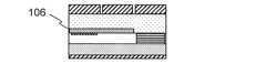
- the wavelength tunable laser 10includes a first wavelength selection region (wavelength selection filter, TWF) in order in the light waveguide direction (x direction in the figure). 11, an optical gain region 12, a phase adjustment region 13, and a second wavelength selection region (wavelength selection filter, TWF) 14.
- TWFwavelength selection filter
- a DBRis used as a wavelength selection filter, and the first wavelength selection region and the second wavelength selection region are respectively the first DBR region 11 and the second DBR region 14.
- the length of the first DBR region 11is 200 to 300 ⁇ m
- the length of the optical gain region 12is 200 to 300 ⁇ m
- the length of the phase adjustment region 13is 100 ⁇ m
- the length of the second DBR region 14is 600 ⁇ m.
- “length”refers to the length in the waveguide direction of light.
- the first DBR region 11 and the second DBR region 14are respectively arranged on the n-type InP substrate 101 in the layer direction (z direction in the figure) in the first waveguide core layer (bulk core) 102_1 and the first waveguide core layer (bulk core) 102_1.
- InGaAs having a composition lattice-matched to InPis used for the first waveguide core layer (bulk core) 102_1 and the second waveguide core layer (bulk core) 102_2.
- a diffraction grating 105is provided between each of the first waveguide core layer (InGaAs bulk core) 102_1 and the second waveguide core layer (InGaAs bulk core) 102_2 and the p-type InP cladding 104.
- the pitch of the diffraction grating 105is determined so that the reflection peak wavelength of the first DBR region 11 and the second DBR region 14 is 2.025 ⁇ m.
- the first DBR region 11 and the second DBR region 14reflect light of a specific wavelength toward the optical gain region 12 .
- the optical gain region 12includes an active layer 103, a p-type InP cladding 104, and an electrode (optical gain electrode) 107_2 in order on the n-type InP substrate 101 in the layer direction (z direction in the figure). .
- the active layer 103is a strained InGaAs/InGaAs multiple quantum well (MQW), and the amount of strain is set so that the peak of the photoluminescence (PL) spectrum is 2.015 ⁇ m.
- MQWmultiple quantum well
- the phase adjustment region 13includes an InGaAs bulk core (second waveguide core layer) 102_2, a p-type InP cladding 104, and an electrode ( phase adjustment electrode) 107_3.
- the phase adjustment region 13finely adjusts the resonator length as a resonator.
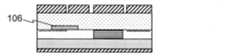
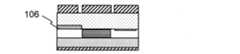
- a barrier region 106is provided at the boundary between the InGaAs bulk core (second waveguide core layer) 102_2 and the p-type InP cladding 104.
- the barrier region 106undoped i (intrinsic)-InP is used, and the layer thickness is about 100 nm.
- the layer thicknessmay be, for example, 20 to 500 nm.
- an n-type electrode 108is provided on the back surface of the n-type InP substrate.
- a layer including a first waveguide core (bulk core) layer, an active layer, and a second waveguide core (bulk core) layer in order in the light waveguide directionwill be referred to as a "waveguide layer.”
- the wavelength tunable laserincludes a substrate, a waveguide layer, and a cladding in this order, and includes an active layer disposed in a part of the waveguide layer and an end portion of the waveguide layer.
- a DBRdisposed in the region (the end region of the first waveguide core layer and the second waveguide core layer) and a barrier region disposed between the waveguide layer and the cladding layer of the phase adjustment region. Be prepared.
- a strained InGaAs/InGaAs multiple quantum wellwhich is the active layer crystal (crystal for the active layer 103) of the optical gain region 12, is grown on the n-type InP substrate 101 (step S1).
- the active layer crystalis processed into an active layer by photolithography and etching (step S2).
- InGaAsis butt-joint grown around the active layer as a bulk core crystal (crystal for the first waveguide core layer 102_1 and second waveguide core layer 102_2) (step S3).
- undoped InP(crystal for barrier region 106) is grown to a thickness of about 100 nm on InGaAs (step S4).
- undoped InP other than the barrier region 106(at least the undoped InP on the active layer) is removed by selective etching to form an undoped InP barrier region (step S5).
- a diffraction grating 105is formed on the surface of the bulk core crystal in the first DBR region 11 and the second DBR region 14 (step S6).
- a crystal for the p-type InP cladding layer(crystal for the cladding 104) is grown on the active layer crystal, bulk core crystal, and undoped InP barrier region 106 (step S7).
- the layered structure of the wavelength tunable laser 10is manufactured.
- the wavelength tunable laser 10is manufactured by processing the waveguide structure, forming electrodes, etc. on the layered structure of this wavelength tunable laser using a normal semiconductor laser manufacturing process.
- high-resistance i-InPis placed as a barrier region 106 directly above the bulk core (second waveguide core layer) 102_2 of the phase adjustment region 13, so that it is not implanted in the phase adjustment region 13.
- a part of the currentflows into the optical gain region 12 by bypassing the bulk core (second waveguide core layer) 102_2 of the phase adjustment region 13.
- the increase in resonator loss due to the increase in carrier density in the bulk core (second waveguide core layer) 102_2 of the phase adjustment region 13can be compensated for by increasing the amount of current to the optical gain region 12. As a result, a decrease in optical output due to phase adjustment can be suppressed.
- undoped i-InPis used for the barrier region 106, but Zn, which is a dopant in the p-InP cladding (for example, p-type concentration is about 1 to 3 ⁇ 10 18 ) 104, diffuses into the undoped i-InP and becomes undoped.
- i-InPcan become p-InP (for example, p-type concentration is about 1 ⁇ 10 16 to 1 ⁇ 10 17 ).
- p-InPfor example, p-type concentration of about 1 ⁇ 10 16 to 1 ⁇ 10 17
- a portion of the injected current in region 13can be provided to optical gain region 12 .
- the barrier region 106only needs to have a resistance high enough to bypass a part of the injected current and supply it to the optical gain region 12, for example, about 1 M ⁇ to 10 M ⁇ , or about 1 M ⁇ to several M ⁇ . It is desirable that the
- Fe-doped InP or n-type InPmay be used for the barrier region 106.
- InAlAs or InGaAlAsmay also be used.
- the wavelength tunable regions 11 and 14 and the phase adjustment region 13be controlled independently. Therefore, it is desirable to have a configuration in which current is separately injected into the wavelength variable regions 11 and 14 and the phase adjustment region 13.
- the control of the wavelength variable region 14may be affected by the current injected into the phase adjustment region 13, and the independence of control may be impaired.
- the wavelength tunable region 14 and the phase adjustment region 13apart from each other, it is possible to suppress the current injected into the phase adjustment region 13 from bypassing the barrier region 106 and flowing into the wavelength tunable region 14. Furthermore, by forming a separation groove structure between the wavelength variable region 14 and the phase adjustment region 13, the current injected into the phase adjustment region 13 can bypass the barrier region 106 and flow into the wavelength variable region 14. can be suppressed.
- ⁇ Effect> 3A and 3Brespectively show a conventional structure in which the bulk core (second waveguide core layer) 102_2 of the phase adjustment region 13 is made of p-InP, and a structure in the present embodiment in which the phase adjustment region 13 is made of i-InP.
- the phase change (dotted line) and relative change in optical output (solid line)are shown when changing the amount of current injected into the cell.
- phase adjustment region 13When the area directly above the bulk core (second waveguide core layer) 102_2 of the phase adjustment region 13 is p-InP, when the injection current is increased to 30 mA, the phase changes to -7 ⁇ rad. In addition, the light intensity is significantly reduced, and the injection current is reduced to -11 dB or less at approximately 16 mA or more.
- the phase adjustment region 13when the area directly above the bulk core (second waveguide core layer) 102_2 of the phase adjustment region 13 is i-InP, the phase changes to -3 ⁇ rad and the light intensity hardly decreases.
- the phase change per currentis smaller and the relative change in light intensity is also smaller than when it is p-InP. This is because a part of the current injected into the phase adjustment region 13 flows into the optical gain region 12.
- the wavelength tunable lasereven if the injection current in the optical gain region 12 increases, the carrier density is fixed, so this injection current does not contribute to a change in the optical phase.
- the current injected into the optical gain region 12increases the optical output.
- the optical outputdrops to -4 dB when the phase change is from 0 to -5 ⁇ rad.
- the optical outputhardly decreases when the phase change is 0 to -3 ⁇ rad.
- the area directly above the bulk core (second waveguide core layer) 102_2 of the phase adjustment region 13is made of i-InP and has a high resistance, the absolute amount of phase change that can be achieved is smaller, but the phase change It is possible to suppress a decrease in the optical output per hit.
- the wavelength tunable region or the phase adjustment region into which the current is injectedcan be supplied to the optical gain region 12.
- the wavelength tunable region or the phase adjustment region into which the current is injectedcan be supplied to the optical gain region 12.
- reduction in the optical output of the wavelength tunable lasercan be suppressed.
- the barrier region 106is arranged in the phase adjustment region 13, but the present invention is not limited to this.
- the barrier region 106may be arranged in the first DBR region 11 or the second DBR region 14, and as shown in FIG. The barrier region 106 may be placed both in the DBR region 14.
- barrier regions 106may be arranged in the phase adjustment region 13, the first DBR region 11, and the second DBR region 14.
- the barrier region 106may be arranged in a part of the phase adjustment region 13 and a part of the second DBR region 14.
- the barrier region 106may be arranged at least in a part of the region other than the optical gain region 12.
- the barrier region 106when disposing the barrier region 106 in the DBR regions 11 and 14, in order to inject the same current into both the DBR regions 11 and 14, as shown in FIGS. It is desirable that the barrier region 106 is disposed in both the second DBR region 14 and the second DBR region 14 .
- both wavelength selection regionsDBR regions
- the amount of currentmay be adjusted so that the same current is injected into 11 and 14.
- the DBRis provided at both ends of the wavelength tunable laser
- a configuration including a reflector that does not have any propertiesmay also be used.
- FIGS. 5F to 5Ha configuration may be adopted in which the first DBR region 11, the optical gain region 12, and the phase adjustment region 13 are sequentially provided.
- FIGS. 5I to 5Ka configuration including an optical gain region 12, a phase adjustment region 13, and a second DBR region 14 in this order may be used.
- the barrier region 106may be disposed at least in a part of the region other than the optical gain region.
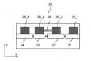
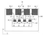
- the wavelength tunable laser 20includes a first DBR region 21, an optical gain region 22, and a phase shift region in order in the light waveguide direction (x direction in the figure). It includes an adjustment region 23 and a second DBR region 24, and includes an electrode pad 25_1, an electrode pad 25_2, an electrode pad 25_3, and an electrode pad 25_4 electrically connected to the respective electrodes.
- the configuration of the wavelength tunable laser in the layer directionis the same as that of a conventional current injection type wavelength tunable laser.
- the electrode pad 25_2 of the optical gain region 22 and the electrode pad 25_3 of the phase adjustment region 23are connected by a resistive portion 26 with a high resistance (about 1 M ⁇ to about 10 M ⁇ ).
- the resistance portion 26is made of an electrode material such as metal.
- a configurationis used in which the same low-resistance material (gold, etc.) as the electrode pads 25_2 and 25_3 is used, and the width or thickness thereof is decreased.
- a high resistance materialsuch as tungsten
- the amount of current flowing from the phase adjustment region 23 to the optical gain region 22can be adjusted by the value of the electrical resistance of the resistance section 26.
- the wavelength tunable laserAccording to the wavelength tunable laser according to the present embodiment, a part of the current injected into the wavelength tunable region or the phase adjustment region is supplied to the optical gain region through the resistance section connecting the pads, so that the current can be increased. Optical loss in the implanted wavelength tunable region or phase adjustment region can be compensated for. As a result, reduction in the optical output of the wavelength tunable laser can be suppressed.
- the electrode pad 25_2 of the optical gain region 22 and the electrode pad 25_3 of the phase adjustment region 23are connected by the resistor section 26, but the present invention is not limited to this.
- the electrode pad 25_2 of the optical gain region 22 and any of the other electrode padsmay be connected through the resistor section 26.
- the electrode pad 25_2 of the optical gain region 22 and the electrode pads 25_1 and 25_4 of the first DBR region 21 or the second DBR region 24may be connected by the resistor section 26.
- the electrode pad 25_2 of the optical gain region 22 and both the electrode pads 25_1 and 25_4 of the first DBR region 21 and the second DBR region 24may be connected by the resistor section 26.
- the electrode pad 25_2 of the optical gain region 22may be connected to all of the other electrode pads 25_1, 25_3, and 25_4.
- the same currentbe injected into the first DBR region 21 and the second DBR region 24.
- a configuration in which the electrode pad 25_2 of the optical gain region 22 and both the electrode pads 25_1 and 25_4 of the first DBR region 21 and the second DBR region 24 are connected by the resistor section 26is desirable.
- both electrodesmay be adjusted so that the same current is injected into the pads 25_1 and 25_4.
- a wavelength tunable laseris provided with a DBR at both ends, but the present invention is not limited to this.
- a configuration including no reflectormay also be used.
- a configurationmay be adopted in which the first DBR region 21, the optical gain region 22, and the phase adjustment region 23 are provided in this order. In this case, if one or both of the electrode pad 25_1 of the first DBR region 21 and the electrode pad 25_3 of the phase adjustment region 23 and the electrode pad 25_2 of the optical gain region 22 are connected by the resistor section 26, good.
- a configurationmay be adopted in which the optical gain region 22, the phase adjustment region 23, and the second DBR region 24 are provided in this order. In this case, if either one or both of the electrode pad 25_3 of the phase adjustment region 23 and the electrode pad 25_4 of the second DBR region 24 and the electrode pad 25_2 of the optical gain region 22 are connected by the resistance section 26, good.
- the wavelength tunable laser module 30includes a wavelength tunable laser 301 mounted on a wiring board 302, and a first DBR region 31 and an optical gain region
- the electrode pads 35_1, 35_2, 35_3, and 35_4 of the phase adjustment region 33 and the second DBR region 34are connected to the substrate electrode pads 36_1, 36_2, 36_3, and 36_4 of the wiring board 302 by wires 37, respectively.
- the substrate electrode pad 36_2 of the wiring board 302 connected to the optical gain region 32 and the substrate electrode pad 36_3 of the wiring board 302 connected to the phase adjustment region 33are connected with high resistance by the resistor 38.
- the resistor 38has a high resistance, about 1M ⁇ to 10M ⁇ .
- the resistor 38is a variable resistor, the amount of current flowing from the phase adjustment region 33 to the optical gain region 32 can be adjusted at the stage of mounting the wavelength tunable laser 301 on the wiring board 302.
- the wavelength tunable laser moduleAccording to the wavelength tunable laser module according to the present embodiment, a part of the current injected into the wavelength tunable region or the phase adjustment region of the wavelength tunable laser is transferred to the optical gain region through the resistor connecting between the substrate electrodes of the wiring board.
- By supplying the current to the currentit is possible to compensate for optical loss in the wavelength variable region or phase adjustment region into which the current is injected. As a result, reduction in the optical output of the wavelength tunable laser can be suppressed.
- the substrate electrode pad 36_2 and the substrate electrode pad 36_3are connected by the resistor 38, but the present invention is not limited to this.
- the substrate electrode pad 36_2 and any of the other electrode padsmay be connected through the resistor section 38.
- the substrate electrode pad 36_2 and the substrate electrode pad 36_1 or the substrate electrode pad 36_4may be connected by the resistor 38.
- the substrate electrode pad 36_2 and both the substrate electrode pads 36_1 and 36_4may be connected by the resistor 38.
- the substrate electrode pad 36_2may be connected to all of the other substrate electrode pads 36_1, 36_3, and 36_4.
- the same currentbe injected into the first DBR region 31 and the second DBR region 34.
- a configuration in which the substrate electrode pad 36_2 and both substrate electrode pads 36_1 and 36_4 are connected by a resistor 38is desirable.
- the amount of currentis adjusted so that the same current is injected into both the electrode pads 36_1, 36_4. Just adjust it.
- a wavelength tunable laseris provided with a DBR at both ends, but the present invention is not limited to this.
- a configuration including no reflectormay also be used.
- a configurationmay be adopted in which the first DBR region 31, the optical gain region 32, and the phase adjustment region 33 are provided in this order.
- the resistor 38may connect either one or both of the substrate electrode pad 36_1 and the substrate electrode pad 36_3 to the substrate electrode pad 36_2.
- the resistor 38may connect either one or both of the substrate electrode pad 36_3 and the substrate electrode pad 36_4 to the substrate electrode pad 36_2.
- a DBRis used as a wavelength variable region (wavelength variable filter)
- the inventionis not limited to this, and a ring resonator, a sampling grating Bragg reflector, etc. may also be used, and Any wavelength filter that returns light of a specific wavelength to the optical gain region may be used.
- a tunable filter structuresuch as a ring resonator may be formed in the bulk core crystal instead of a DBR (diffraction grating).
- the oscillation wavelength band of the wavelength tunable laseris set to about 2.0 ⁇ m and used for CO2 gas sensing, but the invention is not limited to this. It may also be used for sensing ammonia or water. Furthermore, the oscillation wavelength band may be set to about 1.6 to 1.8 ⁇ m and used for sensing CH 4 and HCl, and the oscillation wavelength band is set to about 2.1 to 2.4 ⁇ m and used for sensing N 2 O and CO. May be used.
- the oscillation wavelength band of the wavelength tunable lasermay be set to about 1.3 to 1.55 ⁇ m and used as a laser for optical communication.
- the influence of free electrons of InGaAs in the bulk coreis greater in the wavelength band of 2.0 ⁇ m or more than in the 1.3 to 1.55 ⁇ m wavelength band, and the optical loss is greater. The effect is large.
- an InP-based semiconductoris used as a semiconductor, but other semiconductors such as a GaAs-based semiconductor, a SiGe-based semiconductor, a GaN-based semiconductor, etc. may also be used.
- GaAs, Si, sapphire, etc.may be used for the substrate.
- examples of the structure, dimensions, materials, etc. of each componentare shown in the configuration of the wavelength tunable laser and the wavelength tunable laser module, the method for manufacturing the layered structure, etc., but the present invention is not limited thereto. Any material may be used as long as it exhibits the functions and effects of the wavelength tunable laser and the wavelength tunable laser module.
- the present inventionrelates to a method for manufacturing a wavelength tunable laser, a wavelength tunable laser module, and a layered structure of a wavelength tunable laser, and can be applied to optical communication light sources and gas sensing light sources.
Landscapes
- Physics & Mathematics (AREA)
- Condensed Matter Physics & Semiconductors (AREA)
- General Physics & Mathematics (AREA)
- Electromagnetism (AREA)
- Optics & Photonics (AREA)
- Semiconductor Lasers (AREA)
Abstract
Description
Translated fromJapanese本発明は、光出力特性を向上する波長可変レーザおよびその層構造の製造方法に関する。The present invention relates to a wavelength tunable laser that improves optical output characteristics and a method for manufacturing its layer structure.
波長可変レーザは、光通信用の搬送波光源やガスセンシングなど広い応用範囲で用いられるため、一つの光源がカバーできる波長域と光出力の両立が重要である。Since wavelength tunable lasers are used in a wide range of applications such as carrier wave light sources for optical communications and gas sensing, it is important to have both a wavelength range that can be covered by one light source and optical output.
ガスセンシングでは、ターゲットとするガスが、ガス固有の光吸収スペクトルを有することを利用して、ガスの有無(濃度)や温度・圧力を測定する。すなわち波長可変レーザからの光の波長を連続的に掃引することで、特定の波長の近傍における光吸収強度や吸収曲線の幅からガスの状態を検知する。したがって、多くの吸収線を検知するためには、波長可変レーザが出力できる波長域の広さは重要である。Gas sensing uses the fact that the target gas has a light absorption spectrum unique to the gas to measure the presence (concentration), temperature, and pressure of the gas. That is, by continuously sweeping the wavelength of light from a wavelength tunable laser, the state of the gas is detected from the light absorption intensity and the width of the absorption curve in the vicinity of a specific wavelength. Therefore, in order to detect many absorption lines, it is important to have a wide wavelength range that can be output by a wavelength tunable laser.
一方で、ガスの濃度分布など対象を空間的に測定する場合には、対象空間に複数本のレーザ光線を入射する必要がある。複数本のレーザ光線を実現するために、複数の波長可変レーザを用いる方法が考えられる。しかしながら、異なる波長可変レーザを同期制御するための制御回路が煩雑になる。一方、単一の波長可変レーザを用いて、その光出力を適切な分波器で分岐することで、複数のレーザ光線を取得できる。この方法によれば、煩雑な制御回路は不要である。このとき、レーザ光出力の分岐にともない光出力が減衰する。そこで、単一の波長可変レーザから出力できる光強度も重要である。On the other hand, when spatially measuring an object such as a gas concentration distribution, it is necessary to input multiple laser beams into the object space. In order to realize a plurality of laser beams, a method using a plurality of wavelength tunable lasers can be considered. However, the control circuit for synchronously controlling different wavelength tunable lasers becomes complicated. On the other hand, by using a single wavelength tunable laser and branching its optical output with an appropriate demultiplexer, multiple laser beams can be obtained. According to this method, a complicated control circuit is not required. At this time, the optical output is attenuated as the laser beam output is branched. Therefore, the light intensity that can be output from a single wavelength tunable laser is also important.
従来の波長可変レーザ40は、図8Aに示すように、光利得領域41と、位相調整領域42と、少なくとも1つの波長選択フィルタ(Tunable wavelength filter、TWF)43とを備え、光共振器の形態を有する。この構成により、光利得領域41で発生・増幅する光を光導波路内で共振させる(図中、矢印44)。As shown in FIG. 8A, a conventional wavelength
従来の波長可変レーザ40では、図8Bに示すように、光共振器内において、共振器の光路長に応じた特定の波長(以下「共振モード」という。)51_1、51_2、51_3が存在する。波長選択フィルタ43(波長スペクトル52)により、共振モード51_1、51_2、51_3のうち、単一の共振モード51_1を選択する。また、位相調整領域42の屈折率を変化させ、すなわち共振器の光路長を微調整することで共振モード51_1の波長を微調整する(図中、矢印53)。このように、単一モードの波長可変レーザを動作する。In the conventional wavelength
例えば、CO2ガスセンシング向けに、InP系半導体を用いて2μm帯の発振波長を有する分布ブラッグ反射器(Distributed Bragg Reflector、DBR)レーザが開示されている(非特許文献1)。For example, a distributed Bragg reflector (DBR) laser using an InP-based semiconductor and having an oscillation wavelength in the 2 μm band has been disclosed for CO2 gas sensing (Non-Patent Document 1).
このDBRレーザは、TWFとしてDBR領域を備える。また、DBR領域や位相調整領域(以下、「チューニング領域」という。)にInPと格子整合するバルクInGaAsの材料を用いる。ここで、「バルク」とは数100nm以上の厚さの材料(結晶)をいう。このチューニング領域に電流を注入することで、バルクInGaAsの屈折率を変化させて、DBRレーザの発振波長を制御する。This DBR laser includes a DBR region as a TWF. In addition, a bulk InGaAs material that is lattice-matched to InP is used for the DBR region and the phase adjustment region (hereinafter referred to as "tuning region"). Here, "bulk" refers to a material (crystal) with a thickness of several hundreds of nanometers or more. By injecting a current into this tuning region, the refractive index of the bulk InGaAs is changed to control the oscillation wavelength of the DBR laser.
また、光利得導波路の媒質として、歪InGaAs/InGaAs多重量子井戸(MQW)が用いられる。ここで、歪InGaAs/InGaAs-MQWは、InGaAs材料に対して圧縮歪と伸長歪がそれぞれ印加される組成が異なるInGaAsが、材料の臨界膜厚以下の厚さで周期的に積層されるMQWをいう。このように、歪MQWは、周期的に逆方向の歪を印加することで巨視的には格子整合系とみなせるMQWである。通常のInP系の半導体レーザでは1.65μm程度が最長発振波長とされるが、歪MQWを用いることにより2μm波長帯で発振する波長可変レーザを実現できる(非特許文献1)。Furthermore, strained InGaAs/InGaAs multiple quantum well (MQW) is used as the medium of the optical gain waveguide. Here, strained InGaAs/InGaAs-MQW is an MQW in which InGaAs with different compositions are periodically stacked at a thickness less than the critical film thickness of the material, and compressive strain and extensional strain are respectively applied to the InGaAs material. say. In this way, the strained MQW can be viewed macroscopically as a lattice-matched system by periodically applying strain in the opposite direction. Although the longest oscillation wavelength of a typical InP-based semiconductor laser is about 1.65 μm, by using a strained MQW, a wavelength tunable laser that oscillates in a 2 μm wavelength band can be realized (Non-Patent Document 1).
電流注入型の半導体波長可変レーザは、チューニング領域へのキャリア注入の増加にともなって、波長変化に必要な屈折率変化量だけでなく、光の損失も増加する。このチューニング領域の光損失の増加は、レーザ共振器としての光損失を増加させ、光出力を低下させる。すなわち、電流注入型の波長可変レーザでは、波長変化にともなう光出力の低下が問題である。In a current injection type semiconductor wavelength tunable laser, as carrier injection into the tuning region increases, not only the amount of refractive index change necessary for changing the wavelength but also the optical loss increases. This increase in optical loss in the tuning region increases optical loss as a laser resonator and reduces optical output. That is, in current injection type wavelength tunable lasers, a problem is that the optical output decreases as the wavelength changes.
電流注入型の半導体波長可変レーザにおいて、チューニング領域における半導体の一部に光学活性な(光利得を有する)組成の半導体を挿入する構成が開示されている(非特許文献1)。この構成では、チューニング領域へキャリアが注入されるときに、一部の注入キャリアが光増幅に寄与するので、チューニング領域の屈折率を変化させるとともに、屈折率変化に伴う光損失を補償できる。このように、この構成によれば、電流注入型の波長可変レーザの波長変化にともなう光出力の低下を抑制できる。In a current injection type semiconductor wavelength tunable laser, a configuration is disclosed in which a semiconductor having an optically active composition (having optical gain) is inserted into a part of the semiconductor in the tuning region (Non-Patent Document 1). With this configuration, when carriers are injected into the tuning region, some of the injected carriers contribute to optical amplification, so it is possible to change the refractive index of the tuning region and compensate for optical loss accompanying the change in refractive index. In this way, with this configuration, it is possible to suppress a decrease in optical output due to a change in wavelength of the current injection type wavelength tunable laser.
しかしながら、バルク半導体で構成されるチューニング領域に光学活性な半導体材料を導入するため、半導体結晶成長における製造負荷を増加させるという問題があった。また、レーザ共振器内における光学活性領域の割合が増加するため、素子の信頼性の低下等の問題が生じる可能性があった。However, since an optically active semiconductor material is introduced into a tuning region composed of a bulk semiconductor, there is a problem in that the manufacturing load for semiconductor crystal growth increases. Furthermore, since the proportion of the optically active region within the laser resonator increases, problems such as a decrease in the reliability of the device may occur.
上述したような課題を解決するために、本発明に係る波長可変レーザは、順に、基板と、導波路層と、クラッドとを備え、前記導波路層の一部に配置される活性層と、前記導波路層の少なくとも一方の端部領域に配置される波長選択フィルタと、前記活性層を含まない前記導波路層の少なくとも一部と前記クラッド層との間に配置される障壁領域とを備える。In order to solve the above-mentioned problems, a wavelength tunable laser according to the present invention includes, in order, a substrate, a waveguide layer, and a cladding, and an active layer disposed in a part of the waveguide layer; a wavelength selection filter disposed in at least one end region of the waveguide layer; and a barrier region disposed between at least a portion of the waveguide layer not including the active layer and the cladding layer. .
また、本発明に係る波長可変レーザは、順に、基板と、導波路層と、クラッドとを備え、前記導波路層の一部に配置される活性層と、前記導波路層の少なくとも一方の端部領域に配置される波長選択フィルタと、前記活性層に電流を注入するための第1の電極パッドと、前記波長選択フィルタに電流を注入するための第2の電極パッドと、前記活性層および前記波長選択フィルタを有さない前記導波路層の少なくとも一部に電流を注入するための第3の電極パッドと、前記第2の電極パッドと前記第3の電極パッドとの少なくともいずれかの電極パッドと、前記第1の電極パッドとを接続する抵抗部とを備える。Further, the wavelength tunable laser according to the present invention includes a substrate, a waveguide layer, and a cladding in this order, and includes an active layer disposed in a part of the waveguide layer and at least one end of the waveguide layer. a wavelength selection filter disposed in the active layer; a first electrode pad for injecting current into the active layer; a second electrode pad for injecting current into the wavelength selection filter; a third electrode pad for injecting current into at least a portion of the waveguide layer not having the wavelength selection filter; and at least one of the second electrode pad and the third electrode pad. The device includes a pad and a resistor portion that connects the first electrode pad.
また、本発明に係る波長可変レーザモジュールは、順に、基板と、導波路層と、クラッドとを備え、前記導波路層の一部に配置される活性層と、前記導波路層の少なくとも一方の端部領域に配置される波長選択フィルタとを備える波長可変レーザと、前記活性層に電流を注入するための第1の基板電極パッドと、前記波長選択フィルタに電流を注入するための第2の基板電極パッドと、前記活性層および前記波長選択フィルタを有さない前記導波路層の少なくとも一部に電流を注入するための第3の基板電極パッドと、前記第2の基板電極パッドと前記第3の基板電極パッドとの少なくともいずれかの基板電極パッドと、前記第1の基板電極パッドとを接続する抵抗とを備える配線基板とを備える。Further, the wavelength tunable laser module according to the present invention includes a substrate, a waveguide layer, and a cladding in this order, and includes an active layer disposed in a part of the waveguide layer and at least one of the waveguide layers. a wavelength tunable laser comprising a wavelength selective filter disposed in an end region; a first substrate electrode pad for injecting current into the active layer; and a second substrate electrode pad for injecting current into the wavelength selective filter. a substrate electrode pad; a third substrate electrode pad for injecting current into at least a portion of the waveguide layer not having the active layer and the wavelength selection filter; the second substrate electrode pad and the third substrate electrode pad; The wiring board includes at least one of the three substrate electrode pads and a resistor that connects the first substrate electrode pad.
また、本発明に係る波長可変レーザの層構造の製造方法は、順に、n型基板と、活性層とバルクコア層を含む導波路層と、p型クラッド層とを備える波長可変レーザの層構造の製造方法であって、前記活性層用の半導体結晶を、前記基板上に成長する工程と、前記活性層用の半導体結晶を、前記活性層に加工する工程と、前記活性層の周辺に、前記バルクコア層用の半導体結晶をバットジョイント成長する工程と、前記バルクコア層用の半導体結晶上に、アンドープ半導体結晶を成長する工程と、少なくとも前記活性層上の前記アンドープ半導体結晶を除去する工程と、前記バルクコア層用の半導体結晶の少なくとも一方の端部領域に、波長選択フィルタを形成する工程と、前記p型クラッド層用の半導体結晶を成長する工程とを備える。Further, the method for manufacturing a layered structure of a wavelength tunable laser according to the present invention includes, in order, a layered structure of a wavelength tunable laser including an n-type substrate, a waveguide layer including an active layer and a bulk core layer, and a p-type cladding layer. The manufacturing method includes a step of growing a semiconductor crystal for the active layer on the substrate, a step of processing the semiconductor crystal for the active layer into the active layer, and a step of growing the semiconductor crystal for the active layer on the substrate. a step of butt-joint growing a semiconductor crystal for the bulk core layer; a step of growing an undoped semiconductor crystal on the semiconductor crystal for the bulk core layer; a step of removing the undoped semiconductor crystal on at least the active layer; The method includes the steps of forming a wavelength selection filter in at least one end region of the semiconductor crystal for the bulk core layer, and growing the semiconductor crystal for the p-type cladding layer.
本発明によれば、簡易に光出力の減少を抑制する波長可変レーザ、波長可変レーザモジュールおよび波長可変レーザの層構造の製造方法を提供できる。According to the present invention, it is possible to provide a tunable laser, a tunable laser module, and a method for manufacturing a layered structure of a tunable laser that easily suppresses a decrease in optical output.
<第1の実施の形態>
本発明の第1の実施の形態に係る波長可変レーザについて、図1A~図4を参照して説明する。<First embodiment>
A wavelength tunable laser according to a first embodiment of the present invention will be described with reference to FIGS. 1A to 4.
<波長可変レーザの構成>
本実施の形態に係る波長可変レーザ10は、図1A、Bに示すように、光の導波方向(図中、x方向)に、順に、第1の波長選択領域(波長選択フィルタ、TWF)11と、光利得領域12と、位相調整領域13と、第2の波長選択領域(波長選択フィルタ、TWF)14とを備える。<Configuration of wavelength tunable laser>
As shown in FIGS. 1A and 1B, the
波長可変レーザ10では、波長選択フィルタにDBRを用い、第1の波長選択領域と第2の波長選択領域それぞれを、第1のDBR領域11と第2のDBR領域14とする。In the
第1のDBR領域11の長さは200~300μm、光利得領域12の長さは200~300μm、位相調整領域13の長さは100μm、第2のDBR領域14の長さは600μmである。ここで、「長さ」は、光の導波方向の長さをいう。The length of the
第1のDBR領域11と第2のDBR領域14はそれぞれ、n型InP基板101上に、層方向(図中、z方向)に、順に、第1の導波路コア層(バルクコア)102_1と第2の導波路コア層(バルクコア)102_2と、p型InPクラッド104と、電極(DBR電極)107_1、107_4とを備える。The
ここで、第1の導波路コア層(バルクコア)102_1と第2の導波路コア層(バルクコア)102_2には、InPに格子整合する組成のInGaAsを用いる。Here, InGaAs having a composition lattice-matched to InP is used for the first waveguide core layer (bulk core) 102_1 and the second waveguide core layer (bulk core) 102_2.
ここで、第1の導波路コア層(InGaAsバルクコア)102_1と第2の導波路コア層(InGaAsバルクコア)102_2それぞれと、p型InPクラッド104との間に、回折格子105を備える。回折格子105のピッチは、第1のDBR領域11と第2のDBR領域14の反射ピーク波長が2.025μmになるように決定される。第1のDBR領域11と第2のDBR領域14は、特定の波長の光を光利得領域12に向けて反射する。Here, a
光利得領域12は、n型InP基板101上に、層方向(図中、z方向)に、順に、活性層103と、p型InPクラッド104と、電極(光利得用電極)107_2とを備える。The
活性層103は、歪InGaAs/InGaAs多重量子井戸(MQW)であり、フォトルミネッセンス(PL)スペクトルのピークが2.015μmとなるように歪量が設定される。The
位相調整領域13は、n型InP基板101上に、層方向(図中、z方向)に、順に、InGaAsバルクコア(第2の導波路コア層)102_2と、p型InPクラッド104と、電極(位相調整用電極)107_3とを備える。位相調整領域13は、共振器としての共振器長を微調整する。The
さらに、位相調整領域13において、InGaAsバルクコア(第2の導波路コア層)102_2とp型InPクラッド104との境界に、障壁領域106を備える。障壁領域106には、アンドープのi(intrinsic)-InPを用い、層厚は100nm程度である。ここで、層厚は、例えば20~500nmでもよい。Further, in the
また、n型InP基板の裏面に、n型電極108を備える。Furthermore, an n-
以下、光の導波方向に、順に、第1の導波路コア(バルクコア)層と、活性層と、第2の導波路コア(バルクコア)層とを備える層を、「導波路層」という。Hereinafter, a layer including a first waveguide core (bulk core) layer, an active layer, and a second waveguide core (bulk core) layer in order in the light waveguide direction will be referred to as a "waveguide layer."
このように、本実施の形態の係る波長可変レーザは、順に、基板と、導波路層と、クラッドとを備え、導波路層の一部に配置される活性層と、導波路層の端部領域(第1の導波路コア層と第2の導波路コア層の端部領域)に配置されるDBRと、位相調整領域の導波路層とクラッド層との間に配置される障壁領域とを備える。As described above, the wavelength tunable laser according to the present embodiment includes a substrate, a waveguide layer, and a cladding in this order, and includes an active layer disposed in a part of the waveguide layer and an end portion of the waveguide layer. A DBR disposed in the region (the end region of the first waveguide core layer and the second waveguide core layer) and a barrier region disposed between the waveguide layer and the cladding layer of the phase adjustment region. Be prepared.
<波長可変レーザの層構造の製造方法>
本実施の形態に係る波長可変レーザ10の層構造の製造方法の一例を、図2を参照して説明する。<Method for manufacturing layered structure of wavelength tunable laser>
An example of a method for manufacturing the layered structure of the
初めに、光利得領域12の活性層結晶(活性層103用の結晶)である歪InGaAs/InGaAs多重量子井戸を、n型InP基板101上に成長する(工程S1)。First, a strained InGaAs/InGaAs multiple quantum well, which is the active layer crystal (crystal for the active layer 103) of the
次に、フォトリソグラフィとエッチングによって、活性層結晶を、活性層に加工する(工程S2)。Next, the active layer crystal is processed into an active layer by photolithography and etching (step S2).
次に、活性層の周辺に、バルクコア結晶(第1の導波路コア層102_1と第2の導波路コア層102_2用の結晶)としてInGaAsをバットジョイント成長する(工程S3)。Next, InGaAs is butt-joint grown around the active layer as a bulk core crystal (crystal for the first waveguide core layer 102_1 and second waveguide core layer 102_2) (step S3).
引き続き、バットジョイント成長時に、InGaAs上に、アンドープInP(障壁領域106用の結晶)を100nm程度の厚さで成長する(工程S4)。Subsequently, during butt joint growth, undoped InP (crystal for barrier region 106) is grown to a thickness of about 100 nm on InGaAs (step S4).
次に、障壁領域106以外のアンドープInP(少なくとも活性層上のアンドープInP)を選択エッチングで除去して、アンドープInPの障壁領域を形成する(工程S5)。Next, undoped InP other than the barrier region 106 (at least the undoped InP on the active layer) is removed by selective etching to form an undoped InP barrier region (step S5).
次に、第1のDBR領域11と第2のDBR領域14におけるバルクコア結晶の表面に回折格子105を形成する(工程S6)。Next, a
最後に、活性層結晶と、バルクコア結晶と、アンドープInPの障壁領域106の上に、p型InPクラッド層用の結晶(クラッド104用の結晶)を成長する(工程S7)。Finally, a crystal for the p-type InP cladding layer (crystal for the cladding 104) is grown on the active layer crystal, bulk core crystal, and undoped InP barrier region 106 (step S7).
以上により、波長可変レーザ10の層構造が製造される。Through the above steps, the layered structure of the
この波長可変レーザの層構造について、通常の半導体レーザの製造プロセスにより、導波路構造の加工、電極形成などを行って、波長可変レーザ10を製造する。The
<波長可変レーザの動作>
本実施の形態に係る波長可変レーザ10の動作について、以下に説明する。<Operation of wavelength tunable laser>
The operation of the
図1Bに示すように、位相調整領域13のバルクコア(第2の導波路コア層)102_2の直上に、障壁領域106として高抵抗なi-InPが配置されるため、位相調整領域13で注入される電流の一部は、位相調整領域13のバルクコア(第2の導波路コア層)102_2を迂回して光利得領域12に流れ込む。As shown in FIG. 1B, high-resistance i-InP is placed as a
これにより、位相調整領域13のバルクコア(第2の導波路コア層)102_2内のキャリア密度増加による共振器損失の増加を、光利得領域12への電流量の増加によって補償できる。その結果、位相調整にともなう光出力の低下を抑制できる。Thereby, the increase in resonator loss due to the increase in carrier density in the bulk core (second waveguide core layer) 102_2 of the
ここで、障壁領域106にアンドープi-InPを用いるが、p-InPクラッド(例えばp型濃度が1~3×10¹⁸程度)104のドーパントであるZnがアンドープi-InPに拡散して、アンドープi-InPが、p-InP(例えばp型濃度が1×10¹⁶~1×10¹⁷程度)になり得る。この場合でも、p-InP(例えばp型濃度が1×10¹⁶~1×10¹⁷程度)はp-InPクラッド104に比べて十分p型濃度が低いので、高抵抗の障壁領域106として位相調整領域13での注入電流の一部を光利得領域12に提供することができる。Here, undoped i-InP is used for the
このように、障壁領域106は、注入電流の一部を迂回して光利得領域12に供給できる程度に高抵抗であればよく、例えば1MΩ程度~10MΩ程度であればよく、1MΩ程度~数MΩ程度であることが望ましい。In this way, the
また、障壁領域106には、FeドープInPやn型InPを用いてもよい。また、InP以外にもInAlAsやInGaAlAsを用いてもよい。Additionally, Fe-doped InP or n-type InP may be used for the
本実施の形態に係る波長可変レーザでは、波長制御性の観点から、波長可変領域11、14と位相調整領域13は独立に制御されることが望ましい。そこで、波長可変領域11、14と位相調整領域13に別個に電流が注入される構成が望ましい。In the wavelength tunable laser according to this embodiment, from the viewpoint of wavelength controllability, it is desirable that the wavelength
例えば、本実施の形態に係る波長可変レーザで、位相調整領域13への注入電流が障壁領域106を迂回して、光利得領域12に流れ込むとともに、波長可変領域14にも流れ込む可能性がある。その結果、波長可変領域14の制御が位相調整領域13への注入電流の影響を受け、制御の独立性が損なわれる可能性がある。For example, in the wavelength tunable laser according to this embodiment, there is a possibility that the current injected into the
そこで、波長可変領域14と位相調整領域13とを離して配置することにより、位相調整領域13への注入電流が障壁領域106を迂回して、波長可変領域14に流れ込むことを抑制できる。また、波長可変領域14と位相調整領域13との間に分離用の溝構造を形成することにより、位相調整領域13への注入電流が障壁領域106を迂回して、波長可変領域14に流れ込むことを抑制できる。Therefore, by arranging the
<効果>
図3A、Bそれぞれに、位相調整領域13のバルクコア(第2の導波路コア層)102_2直上がp-InPである従来構造と、i-InPである本実施の形態における構造における位相調整領域13への注入電流量を変化させるときの位相変化(点線)及び光出力の相対変化(実線)を示す。<Effect>
3A and 3B respectively show a conventional structure in which the bulk core (second waveguide core layer) 102_2 of the
位相調整領域13のバルクコア(第2の導波路コア層)102_2直上がp-InPである場合、注入電流を30mAまで増加させるとき、位相は-7πradまで変化する。また、光強度は著しく減少し、注入電流を16mA程度以上で、-11dB以下に減少する。When the area directly above the bulk core (second waveguide core layer) 102_2 of the
一方、位相調整領域13のバルクコア(第2の導波路コア層)102_2直上がi-InPである場合、位相は-3πradまで変化し、光強度はほとんど減少しない。On the other hand, when the area directly above the bulk core (second waveguide core layer) 102_2 of the
このように、バルクコア(第2の導波路コア層)102_2直上がi-InPである場合、p-InPである場合と比べて、電流当たりの位相変化は小さく、光強度の相対変化も小さい。これは、位相調整領域13へ注入した電流の一部が光利得領域12に流れ込むことに起因する。このとき、波長可変レーザにおいて、光利得領域12の注入電流が増加してもそのキャリア密度は固定されるので、この注入電流は光位相の変化には寄与しない。一方、光利得領域12の注入電流は、光出力を増加させる。In this way, when the area directly above the bulk core (second waveguide core layer) 102_2 is i-InP, the phase change per current is smaller and the relative change in light intensity is also smaller than when it is p-InP. This is because a part of the current injected into the
図3A、Bに示す位相調整領域13への注入電流量の変化に対する位相変化及び光出力の相対変化は、図4に示すように、位相変化量と光出力変化の関係にプロットされる。図中、実線が本実施の形態における関係を示し、点線が従来構造における関係を示す。The relative change in phase and optical output with respect to the change in the amount of current injected into the
バルクコア(第2の導波路コア層)102_2直上がi-InPである場合は、位相変化が0~―5πradで光出力が-4dBに低下する。一方、バルクコア(第2の導波路コア層)102_2直上がi-InPである場合、位相変化が0~―3πradで光出力はほとんど低下しない。When the layer directly above the bulk core (second waveguide core layer) 102_2 is i-InP, the optical output drops to -4 dB when the phase change is from 0 to -5πrad. On the other hand, when the area directly above the bulk core (second waveguide core layer) 102_2 is i-InP, the optical output hardly decreases when the phase change is 0 to -3πrad.
このように、位相調整領域13のバルクコア(第2の導波路コア層)102_2の直上をi-InPとして高抵抗化した場合の方が、到達できる絶対的な位相変化量は小さい反面、位相変化当たりの光出力の低下を抑制できる。In this way, if the area directly above the bulk core (second waveguide core layer) 102_2 of the
本実施の形態に係る波長可変レーザによれば、波長可変領域または位相調整領域への注入電流の一部を光利得領域12に供給することにより、電流が注入された波長可変領域または位相調整領域での光損失を補償できる。その結果、波長可変レーザの光出力の低減を抑制できる。According to the wavelength tunable laser according to the present embodiment, by supplying a part of the current injected into the wavelength tunable region or the phase adjustment region to the
<変形例>
本実施の形態では、位相調整領域13に障壁領域106を配置する例を示したが、これに限らない。図5A、Bに示すように、第1のDBR領域11又は第2のDBR領域14に障壁領域106を配置してもよく、図5Cに示すように、第1のDBR領域11と第2のDBR領域14との両方に障壁領域106を配置してもよい。または、図5Dに示すように、位相調整領域13と第1のDBR領域11と第2のDBR領域14とに障壁領域106を配置してもよい。または、図5Eに示すように、位相調整領域13の一部と第2のDBR領域14の一部とに障壁領域106を配置してもよい。<Modified example>
In this embodiment, an example is shown in which the
このように、少なくとも光利得領域12以外の領域の一部に、障壁領域106が配置されればよい。In this way, the
ここで、波長可変レーザの制御において、両方のDBR領域11、14に同等の電流を注入する必要がある。Here, in controlling the wavelength tunable laser, it is necessary to inject the same current into both
したがって、DBR領域11,14に障壁領域106を配置する場合、両方のDBR領域11、14に同等の電流を注入するために、図5C、Dに示すように、第1のDBR領域11と第2のDBR領域14との両方に、障壁領域106が配置される構成が望ましい。Therefore, when disposing the
また、図5C~Eに示すように、第1のDBR領域11と第2のDBR領域14とのいずれか一方に、障壁領域106が配置される構成では、両方の波長選択領域(DBR領域)11、14に同等の電流が注入されるように電流量を調整すればよい。Further, as shown in FIGS. 5C to 5E, in a configuration in which the
また、本実施の形態では、波長可変レーザの両端にDBRを備える例を示したが、これに限らず、いずれか一方の端部にDBRを備え、他方の端部にへき開面ミラーなど波長依存性を有さない反射器を備える構成でもよい。例えば、図5F~Hに示すように、順に、第1のDBR領域11と、光利得領域12と、位相調整領域13とを備える構成でもよい。または、図5I~Kに示すように、順に、光利得領域12と、位相調整領域13と、第2のDBR領域14とを備える構成でもよい。Further, in this embodiment, an example in which the DBR is provided at both ends of the wavelength tunable laser is shown, but the present invention is not limited to this. A configuration including a reflector that does not have any properties may also be used. For example, as shown in FIGS. 5F to 5H, a configuration may be adopted in which the
このように、波長可変レーザのいずれか一方の端部にDBRを備える構成でも、少なくとも光利得領域以外の領域の一部に、障壁領域106が配置されればよい。In this way, even in a configuration in which a DBR is provided at either end of the wavelength tunable laser, the
<第2の実施の形態>
本発明の第2の実施の形態に係る波長可変レーザについて、図6を参照して説明する。<Second embodiment>
A wavelength tunable laser according to a second embodiment of the present invention will be described with reference to FIG. 6.
<波長可変レーザの構成>
本実施の形態に係る波長可変レーザ20は、図6に示すように、光の導波方向(図中、x方向)に、順に、第1のDBR領域21と、光利得領域22と、位相調整領域23と、第2のDBR領域24とを備え、それぞれの電極に電気的に接続する電極パッド25_1、電極パッド25_2、電極パッド25_3、電極パッド25_4を備える。<Configuration of wavelength tunable laser>
As shown in FIG. 6, the
ここで、波長可変レーザの層方向の構成は、従来の電流注入型波長可変レーザと同様である。Here, the configuration of the wavelength tunable laser in the layer direction is the same as that of a conventional current injection type wavelength tunable laser.
また、光利得領域22の電極パッド25_2と位相調整領域23の電極パッド25_3とが、抵抗部26により高抵抗(1MΩ程度~10MΩ程度)で接続される。抵抗部26は金属などの電極材料からなる。Further, the electrode pad 25_2 of the
抵抗部26による高抵抗での接続は、電極パッド25_2、25_3と同じ低抵抗材用(金など)の幅を狭くする構成やその厚さを薄くする構成が用いられる。または、高抵抗な材料(タングステンなど)を用いてもよい。ここで、抵抗部26の電気抵抗の値によって、位相調整領域23から光利得領域22への電流量を調整できる。For high-resistance connection using the
本実施の形態に係る波長可変レーザによれば、波長可変領域または位相調整領域への注入電流の一部を、パッド間を接続する抵抗部を介して光利得領域に供給することにより、電流が注入された波長可変領域または位相調整領域での光損失を補償できる。その結果、波長可変レーザの光出力の低減を抑制できる。According to the wavelength tunable laser according to the present embodiment, a part of the current injected into the wavelength tunable region or the phase adjustment region is supplied to the optical gain region through the resistance section connecting the pads, so that the current can be increased. Optical loss in the implanted wavelength tunable region or phase adjustment region can be compensated for. As a result, reduction in the optical output of the wavelength tunable laser can be suppressed.
また、本実施の形態では、光利得領域22の電極パッド25_2と、位相調整領域23の電極パッド25_3とが、抵抗部26により接続される例を示したが、これに限らない。光利得領域22の電極パッド25_2と、他の電極パッドのいずれかが、抵抗部26により接続されればよい。Further, in this embodiment, an example has been shown in which the electrode pad 25_2 of the
例えば、光利得領域22の電極パッド25_2と、第1のDBR領域21又は第2のDBR領域24の電極パッド25_1、25_4とが、抵抗部26により接続されてもよい。または、光利得領域22の電極パッド25_2と、第1のDBR領域21と第2のDBR領域24の電極パッド25_1、25_4両方とが、抵抗部26により接続されてもよい。または、光利得領域22の電極パッド25_2と、他の電極パッド25_1、25_3、25_4全てが接続されてもよい。For example, the electrode pad 25_2 of the
この場合、第1のDBR領域21と第2のDBR領域24に、同等の電流が注入されるようにすることが望ましい。例えば、光利得領域22の電極パッド25_2と、第1のDBR領域21と第2のDBR領域24の電極パッド25_1、25_4両方とが、抵抗部26により接続される構成が望ましい。In this case, it is desirable that the same current be injected into the
また、光利得領域22の電極パッド25_2と、第1のDBR領域21と第2のDBR領域24の電極パッド25_1、25_4とのいずれか一方が抵抗部26により接続される構成では、両方の電極パッド25_1、25_4に同等の電流が注入されるように電流量を調整すればよい。Furthermore, in a configuration in which the electrode pad 25_2 of the
本実施の形態では、波長可変レーザの両端にDBRを備える例を示したが、これに限らず、いずれか一方の端部にDBRを備え、他方の端部にへき開面ミラーなど波長依存性を有さない反射器を備える構成でもよい。例えば、順に、第1のDBR領域21と、光利得領域22と、位相調整領域23とを備える構成でもよい。この場合、第1のDBR領域21の電極パッド25_1と位相調整領域23の電極パッド25_3のいずれか一方と、又は両方と、光利得領域22の電極パッド25_2とが抵抗部26により接続されればよい。In this embodiment, an example is shown in which a wavelength tunable laser is provided with a DBR at both ends, but the present invention is not limited to this. A configuration including no reflector may also be used. For example, a configuration may be adopted in which the
または、順に、光利得領域22と、位相調整領域23と、第2のDBR領域24とを備える構成でもよい。この場合、位相調整領域23の電極パッド25_3と第2のDBR領域24の電極パッド25_4のいずれか一方と、又は両方と、光利得領域22の電極パッド25_2とが抵抗部26により接続されればよい。Alternatively, a configuration may be adopted in which the
<第3の実施の形態>
本発明の第3の実施の形態に係る波長可変レーザモジュールについて、図7を参照して説明する。<Third embodiment>
A wavelength tunable laser module according to a third embodiment of the present invention will be described with reference to FIG. 7.
<波長可変レーザモジュールの構成>
本実施の形態に係る波長可変レーザモジュール30は、図7に示すように、波長可変レーザ301が配線基板302上に実装され、波長可変レーザ301における第1のDBR領域31と、光利得領域32と、位相調整領域33と、第2のDBR領域34それぞれの電極パッド35_1、35_2、35_3、35_4が、配線基板302の各基板電極パッド36_1、36_2、36_3、36_4にワイヤ37で接続される。<Configuration of wavelength tunable laser module>
As shown in FIG. 7, the wavelength
ここで、光利得領域32に接続される配線基板302の基板電極パッド36_2と、位相調整領域33に接続される配線基板302の基板電極パッド36_3とが、抵抗38により高抵抗で接続される。Here, the substrate electrode pad 36_2 of the
抵抗38は高抵抗であり、1MΩ程度~10MΩ程度である。または、抵抗38を可変抵抗とすれば、波長可変レーザ301を配線基板302に実装する段階で、位相調整領域33から光利得領域32への電流量を調整できる。The
本実施の形態に係る波長可変レーザモジュールによれば、波長可変レーザの波長可変領域または位相調整領域への注入電流の一部を、配線基板の基板電極間を接続する抵抗を介して光利得領域に供給することにより、電流が注入された波長可変領域または位相調整領域での光損失を補償できる。その結果、波長可変レーザの光出力の低減を抑制できる。According to the wavelength tunable laser module according to the present embodiment, a part of the current injected into the wavelength tunable region or the phase adjustment region of the wavelength tunable laser is transferred to the optical gain region through the resistor connecting between the substrate electrodes of the wiring board. By supplying the current to the current, it is possible to compensate for optical loss in the wavelength variable region or phase adjustment region into which the current is injected. As a result, reduction in the optical output of the wavelength tunable laser can be suppressed.
また、本実施の形態では、基板電極パッド36_2と、基板電極パッド36_3とが、抵抗38により接続される例を示したが、これに限らない。基板電極パッド36_2と、他の電極パッドのいずれかが、抵抗部38により接続されればよい。Further, in this embodiment, an example has been shown in which the substrate electrode pad 36_2 and the substrate electrode pad 36_3 are connected by the
例えば、基板電極パッド36_2と、基板電極パッド36_1又は基板電極パッド36_4とが、抵抗38により接続されてもよい。または、基板電極パッド36_2と、基板電極パッド36_1、36_4両方とが、抵抗38により接続されてもよい。または、基板電極パッド36_2と、他の基板電極パッド36_1、36_3、36_4全てが接続されてもよい。For example, the substrate electrode pad 36_2 and the substrate electrode pad 36_1 or the substrate electrode pad 36_4 may be connected by the
この場合、第1のDBR領域31と第2のDBR領域34に、同等の電流が注入されるようにすることが望ましい。例えば、基板電極パッド36_2と、基板電極パッド36_1、36_4両方とが、抵抗38により接続される構成が望ましい。In this case, it is desirable that the same current be injected into the
また、基板電極パッド36_2と、基板電極パッド36_1、36_4とのいずれか一方が抵抗部38により接続される構成では、両方の電極パッド36_1、36_4に同等の電流が注入されるように電流量を調整すればよい。In addition, in a configuration in which the substrate electrode pad 36_2 and either one of the substrate electrode pads 36_1, 36_4 are connected by the
本実施の形態では、波長可変レーザの両端にDBRを備える例を示したが、これに限らず、いずれか一方の端部にDBRを備え、他方の端部にへき開面ミラーなど波長依存性を有さない反射器を備える構成でもよい。例えば、順に、第1のDBR領域31と、光利得領域32と、位相調整領域33とを備える構成でもよい。この場合、基板電極パッド36_1と基板電極パッド36_3のいずれか一方と、又は両方と、基板電極パッド36_2とが、抵抗38により接続されればよい。In this embodiment, an example is shown in which a wavelength tunable laser is provided with a DBR at both ends, but the present invention is not limited to this. A configuration including no reflector may also be used. For example, a configuration may be adopted in which the
または、順に、光利得領域32と、位相調整領域33と、第2のDBR領域34とを備える構成でもよい。この場合、基板電極パッド36_3と基板電極パッド36_4のいずれか一方と、又は両方と、基板電極パッド36_2とが、抵抗38により接続されればよい。Alternatively, a configuration may be adopted in which the
本発明の実施の形態では、波長可変領域(波長可変フィルタ)としてDBRを用いる例を示したが、これに限らず、リング共振器や標本化回折格子ブラッグ反射器などでもよく、波長選択性をもって特定の波長の光を光利得領域に帰還させる波長フィルタであればよい。この場合、波長可変レーザの層構造の製造方法において、DBR(回折格子)の代わりに、バルクコア結晶にリング共振器等の波長可変フィルタの構造を形成すればよい。In the embodiment of the present invention, an example is shown in which a DBR is used as a wavelength variable region (wavelength variable filter), but the invention is not limited to this, and a ring resonator, a sampling grating Bragg reflector, etc. may also be used, and Any wavelength filter that returns light of a specific wavelength to the optical gain region may be used. In this case, in the method for manufacturing a layered structure of a tunable laser, a tunable filter structure such as a ring resonator may be formed in the bulk core crystal instead of a DBR (diffraction grating).
本発明の実施の形態では、波長可変レーザの発振波長帯を2.0μm程度にしてCO2ガスセンシングに用いる例を示したが、これに限らない。アンモニアや水のセンシングに用いてもよい。また、発振波長帯を1.6~1.8μm程度にしてCH4やHClのセンシングに用いてもよく、発振波長帯を2.1~2.4μm程度にしてN2OやCOのセンシングに用いてもよい。In the embodiment of the present invention, an example is shown in which the oscillation wavelength band of the wavelength tunable laser is set to about 2.0 μm and used for CO2 gas sensing, but the invention is not limited to this. It may also be used for sensing ammonia or water. Furthermore, the oscillation wavelength band may be set to about 1.6 to 1.8 μm and used for sensing CH4 and HCl, and the oscillation wavelength band is set to about 2.1 to 2.4 μm and used for sensing N2 O and CO. May be used.
また、波長可変レーザの発振波長帯を1.3~1.55μm程度にして光通信用レーザとして用いてもよい。Further, the oscillation wavelength band of the wavelength tunable laser may be set to about 1.3 to 1.55 μm and used as a laser for optical communication.
波長可変レーザにおいて、2.0μm以上の波長帯の方が、1.3~1.55μm波長帯より、バルクコアのInGaAsの自由電子の影響が大きく、光損失が大きいので、本発明の実施の形態の効果が大きい。In a wavelength tunable laser, the influence of free electrons of InGaAs in the bulk core is greater in the wavelength band of 2.0 μm or more than in the 1.3 to 1.55 μm wavelength band, and the optical loss is greater. The effect is large.
本発明の実施の形態では、半導体としてInP系半導体を用いる例を示したが、GaAs系半導体、SiGe系半導体、GaN系半導体等の他の半導体を用いてもよい。基板には、InP以外にもGaAs,Si、サファイア等を用いてもよい。In the embodiment of the present invention, an example is shown in which an InP-based semiconductor is used as a semiconductor, but other semiconductors such as a GaAs-based semiconductor, a SiGe-based semiconductor, a GaN-based semiconductor, etc. may also be used. In addition to InP, GaAs, Si, sapphire, etc. may be used for the substrate.
本発明の実施の形態では、波長可変レーザおよび波長可変レーザモジュールの構成、層構造の製造方法などにおいて、各構成部の構造、寸法、材料等の一例を示したが、これに限らない。波長可変レーザおよび波長可変レーザモジュールの機能を発揮し効果を奏するものであればよい。In the embodiments of the present invention, examples of the structure, dimensions, materials, etc. of each component are shown in the configuration of the wavelength tunable laser and the wavelength tunable laser module, the method for manufacturing the layered structure, etc., but the present invention is not limited thereto. Any material may be used as long as it exhibits the functions and effects of the wavelength tunable laser and the wavelength tunable laser module.
本発明は、波長可変レーザ、波長可変レーザモジュールおよび波長可変レーザの層構造の製造方法に関するものであって、光通信光源やガスセンシング用光源に適用することができる。The present invention relates to a method for manufacturing a wavelength tunable laser, a wavelength tunable laser module, and a layered structure of a wavelength tunable laser, and can be applied to optical communication light sources and gas sensing light sources.
10 波長可変レーザ
101 基板
103 活性層
104 クラッド
105 波長選択フィルタ
106 障壁領域10
Claims (7)
Translated fromJapanese前記導波路層の一部に配置される活性層と、
前記導波路層の、光の導波方向における少なくとも一方の端部領域に配置される波長選択フィルタと、
前記活性層を含まない前記導波路層の少なくとも一部と前記クラッドとの間に配置される障壁領域と
を備える波長可変レーザ。comprising, in order, a substrate, a waveguide layer, and a cladding,
an active layer disposed in a part of the waveguide layer;
a wavelength selection filter disposed in at least one end region of the waveguide layer in the light waveguide direction;
A wavelength tunable laser comprising: a barrier region disposed between at least a portion of the waveguide layer that does not include the active layer and the cladding.
ことを特徴とする請求項1に記載の波長可変レーザ。The wavelength tunable laser according to claim 1, wherein the barrier region detours a part of the current flowing into the barrier region and supplies it to the active layer.
ことを特徴とする請求項1又は請求項2に記載の波長可変レーザ。The wavelength tunable laser according to claim 1 or 2, wherein the doping concentration of the barrier region is lower than the doping concentration of the cladding.
前記導波路層の一部に配置される活性層と、
前記導波路層の、光の導波方向における少なくとも一方の端部領域に配置される波長選択フィルタと、
前記活性層に電流を注入するための第1の電極パッドと、
前記波長選択フィルタに電流を注入するための第2の電極パッドと、
前記活性層および前記波長選択フィルタを有さない前記導波路層の少なくとも一部に電流を注入するための第3の電極パッドと、
前記第2の電極パッドと前記第3の電極パッドとの少なくともいずれかの電極パッドと、前記第1の電極パッドとを接続する抵抗部と
を備える波長可変レーザ。comprising, in order, a substrate, a waveguide layer, and a cladding,
an active layer disposed in a part of the waveguide layer;
a wavelength selection filter disposed in at least one end region of the waveguide layer in the light waveguide direction;
a first electrode pad for injecting current into the active layer;
a second electrode pad for injecting current into the wavelength selection filter;
a third electrode pad for injecting current into at least a portion of the waveguide layer that does not have the active layer and the wavelength selection filter;
A wavelength tunable laser comprising: at least one of the second electrode pad and the third electrode pad; and a resistor connecting the first electrode pad.
前記導波路層の一部に配置される活性層と、
前記導波路層の、光の導波方向における少なくとも一方の端部領域に配置される波長選択フィルタと
を備える波長可変レーザと、
前記活性層に電流を注入するための第1の基板電極パッドと、
前記波長選択フィルタに電流を注入するための第2の基板電極パッドと、
前記活性層および前記波長選択フィルタを有さない前記導波路層の少なくとも一部に電流を注入するための第3の基板電極パッドと、
前記第2の基板電極パッドと前記第3の基板電極パッドとの少なくともいずれかの基板電極パッドと、前記第1の基板電極パッドとを接続する抵抗と
を備える配線基板と
を備える波長可変レーザモジュール。comprising, in order, a substrate, a waveguide layer, and a cladding,
an active layer disposed in a part of the waveguide layer;
a wavelength selection filter disposed in at least one end region of the waveguide layer in the light waveguide direction;
a first substrate electrode pad for injecting current into the active layer;
a second substrate electrode pad for injecting current into the wavelength selection filter;
a third substrate electrode pad for injecting current into at least a portion of the waveguide layer that does not have the active layer and the wavelength selection filter;
a wiring board comprising: at least one of the second substrate electrode pad and the third substrate electrode pad; and a resistor connecting the first substrate electrode pad; and a wavelength tunable laser module comprising: .
ことを特徴とする請求項5に記載の波長可変レーザモジュール。The wavelength tunable laser module according to claim 5, wherein the resistor is a variable resistor.
前記活性層用の半導体結晶を、前記n型基板上に成長する工程と、
前記成長された活性層用の半導体結晶を、前記活性層に加工する工程と、
前記活性層の周辺に、前記バルクコア層用の半導体結晶をバットジョイント成長する工程と、
前記バルクコア層用の半導体結晶上に、アンドープ半導体結晶を成長する工程と、
少なくとも前記活性層上の前記アンドープ半導体結晶を除去する工程と、
前記バルクコア層用の半導体結晶の少なくとも一方の端部領域に、波長選択フィルタを形成する工程と、
前記p型クラッド層用の半導体結晶を成長する工程と
を備える波長可変レーザの層構造の製造方法。A method for manufacturing a layer structure of a wavelength tunable laser comprising, in order, an n-type substrate, a waveguide layer including an active layer and a bulk core layer, and a p-type cladding layer, the method comprising:
growing a semiconductor crystal for the active layer on the n-type substrate;
processing the grown semiconductor crystal for the active layer into the active layer;
butt-jointly growing a semiconductor crystal for the bulk core layer around the active layer;
growing an undoped semiconductor crystal on the semiconductor crystal for the bulk core layer;
removing the undoped semiconductor crystal on at least the active layer;
forming a wavelength selection filter in at least one end region of the semiconductor crystal for the bulk core layer;
A method for manufacturing a layered structure of a wavelength tunable laser, comprising: growing a semiconductor crystal for the p-type cladding layer.
Priority Applications (2)
| Application Number | Priority Date | Filing Date | Title |
|---|---|---|---|
| JP2024528197AJP7754308B2 (en) | 2022-06-23 | Tunable wavelength laser, tunable wavelength laser module, and method for manufacturing layer structure of tunable wavelength laser | |
| PCT/JP2022/025048WO2023248412A1 (en) | 2022-06-23 | 2022-06-23 | Wavelength-variable laser, wavelength-variable laser module, and method for producing layered structure of wavelength-variable laser |
Applications Claiming Priority (1)
| Application Number | Priority Date | Filing Date | Title |
|---|---|---|---|
| PCT/JP2022/025048WO2023248412A1 (en) | 2022-06-23 | 2022-06-23 | Wavelength-variable laser, wavelength-variable laser module, and method for producing layered structure of wavelength-variable laser |
Publications (1)
| Publication Number | Publication Date |
|---|---|
| WO2023248412A1true WO2023248412A1 (en) | 2023-12-28 |
Family
ID=89379280
Family Applications (1)
| Application Number | Title | Priority Date | Filing Date |
|---|---|---|---|
| PCT/JP2022/025048CeasedWO2023248412A1 (en) | 2022-06-23 | 2022-06-23 | Wavelength-variable laser, wavelength-variable laser module, and method for producing layered structure of wavelength-variable laser |
Country Status (1)
| Country | Link |
|---|---|
| WO (1) | WO2023248412A1 (en) |
Citations (7)
| Publication number | Priority date | Publication date | Assignee | Title |
|---|---|---|---|---|
| JPS6323382A (en)* | 1986-03-24 | 1988-01-30 | Fujikura Ltd | Manufacturing method of distributed reflection semiconductor laser |
| JPH08340153A (en)* | 1995-06-13 | 1996-12-24 | Oki Electric Ind Co Ltd | Distributed feedback semiconductor laser and manufacture thereof |
| JP2006261424A (en)* | 2005-03-17 | 2006-09-28 | Anritsu Corp | Semiconductor laser device and gas detector |
| JP2011053171A (en)* | 2009-09-04 | 2011-03-17 | Kitasato Institute | Measuring method of emission wavelength of wavelength variable light source |
| JP2018011023A (en)* | 2016-07-15 | 2018-01-18 | 日本電信電話株式会社 | Variable wavelength semiconductor laser |
| JP2018067604A (en)* | 2016-10-18 | 2018-04-26 | 三菱電機株式会社 | Semiconductor laser device with optical modulator |
| US20180183207A1 (en)* | 2015-04-30 | 2018-06-28 | Apple Inc. | Vernier effect dbr lasers incorporating integrated tuning elements |
- 2022
- 2022-06-23WOPCT/JP2022/025048patent/WO2023248412A1/ennot_activeCeased
Patent Citations (7)
| Publication number | Priority date | Publication date | Assignee | Title |
|---|---|---|---|---|
| JPS6323382A (en)* | 1986-03-24 | 1988-01-30 | Fujikura Ltd | Manufacturing method of distributed reflection semiconductor laser |
| JPH08340153A (en)* | 1995-06-13 | 1996-12-24 | Oki Electric Ind Co Ltd | Distributed feedback semiconductor laser and manufacture thereof |
| JP2006261424A (en)* | 2005-03-17 | 2006-09-28 | Anritsu Corp | Semiconductor laser device and gas detector |
| JP2011053171A (en)* | 2009-09-04 | 2011-03-17 | Kitasato Institute | Measuring method of emission wavelength of wavelength variable light source |
| US20180183207A1 (en)* | 2015-04-30 | 2018-06-28 | Apple Inc. | Vernier effect dbr lasers incorporating integrated tuning elements |
| JP2018011023A (en)* | 2016-07-15 | 2018-01-18 | 日本電信電話株式会社 | Variable wavelength semiconductor laser |
| JP2018067604A (en)* | 2016-10-18 | 2018-04-26 | 三菱電機株式会社 | Semiconductor laser device with optical modulator |
Also Published As
| Publication number | Publication date |
|---|---|
| JPWO2023248412A1 (en) | 2023-12-28 |
Similar Documents
| Publication | Publication Date | Title |
|---|---|---|
| US5642371A (en) | Optical transmission apparatus | |
| US6600169B2 (en) | Quantum dash device | |
| JP4814525B2 (en) | Optical semiconductor device | |
| JP4954992B2 (en) | Semiconductor light reflecting element, semiconductor laser using the semiconductor light reflecting element, and optical transponder using the semiconductor laser | |
| US20040042069A1 (en) | Placing a semiconductor laser electrically in series with a semiconductor optical amplifier | |
| JP2011003591A (en) | Wavelength locker integrated type semiconductor laser element | |
| JP2005538532A (en) | Tilted cavity semiconductor laser (TCSL) and manufacturing method thereof | |
| US11909174B2 (en) | Reflection filter device and wavelength-tunable laser device | |
| JP4026334B2 (en) | Semiconductor laser, distributed feedback semiconductor laser, and wavelength tunable semiconductor laser | |
| JP5698267B2 (en) | Semiconductor device | |
| JP2011222983A (en) | Semiconductor laser device | |
| JP2011049317A (en) | Semiconductor laser device | |
| JP2009289993A (en) | Semiconductor laser element, and semiconductor optical integrated element | |
| JP2003289169A (en) | Semiconductor laser device | |
| US6661828B2 (en) | Semiconductor laser device | |
| JP7754308B2 (en) | Tunable wavelength laser, tunable wavelength laser module, and method for manufacturing layer structure of tunable wavelength laser | |
| WO2023248412A1 (en) | Wavelength-variable laser, wavelength-variable laser module, and method for producing layered structure of wavelength-variable laser | |
| JP4787207B2 (en) | Semiconductor laser | |
| JP4630128B2 (en) | Semiconductor laser device and wavelength control method | |
| JP2019096792A (en) | Semiconductor laser | |
| US6771681B2 (en) | Distributed feedback semiconductor laser | |
| JP2009246390A (en) | Semiconductor laser device | |
| JP2009124009A (en) | Optical semiconductor device | |
| JP4699137B2 (en) | Semiconductor laser device and wavelength control method | |
| JP4008439B2 (en) | Semiconductor optical amplifier |
Legal Events
| Date | Code | Title | Description |
|---|---|---|---|
| 121 | Ep: the epo has been informed by wipo that ep was designated in this application | Ref document number:22947973 Country of ref document:EP Kind code of ref document:A1 | |
| WWE | Wipo information: entry into national phase | Ref document number:2024528197 Country of ref document:JP | |
| WWE | Wipo information: entry into national phase | Ref document number:18876955 Country of ref document:US | |
| NENP | Non-entry into the national phase | Ref country code:DE | |
| 122 | Ep: pct application non-entry in european phase | Ref document number:22947973 Country of ref document:EP Kind code of ref document:A1 |