WO2023184410A1 - Circuit board, electronic apparatus and manufacturing method for circuit board - Google Patents
Circuit board, electronic apparatus and manufacturing method for circuit boardDownload PDFInfo
- Publication number
- WO2023184410A1 WO2023184410A1PCT/CN2022/084581CN2022084581WWO2023184410A1WO 2023184410 A1WO2023184410 A1WO 2023184410A1CN 2022084581 WCN2022084581 WCN 2022084581WWO 2023184410 A1WO2023184410 A1WO 2023184410A1
- Authority
- WO
- WIPO (PCT)
- Prior art keywords
- reflective
- area
- circuit board
- substrate
- layer
- Prior art date
- Legal status (The legal status is an assumption and is not a legal conclusion. Google has not performed a legal analysis and makes no representation as to the accuracy of the status listed.)
- Ceased
Links
Images


Classifications
- H—ELECTRICITY
- H01—ELECTRIC ELEMENTS
- H01L—SEMICONDUCTOR DEVICES NOT COVERED BY CLASS H10
- H01L25/00—Assemblies consisting of a plurality of semiconductor or other solid state devices
- H01L25/03—Assemblies consisting of a plurality of semiconductor or other solid state devices all the devices being of a type provided for in a single subclass of subclasses H10B, H10D, H10F, H10H, H10K or H10N, e.g. assemblies of rectifier diodes
- H01L25/04—Assemblies consisting of a plurality of semiconductor or other solid state devices all the devices being of a type provided for in a single subclass of subclasses H10B, H10D, H10F, H10H, H10K or H10N, e.g. assemblies of rectifier diodes the devices not having separate containers
- H01L25/075—Assemblies consisting of a plurality of semiconductor or other solid state devices all the devices being of a type provided for in a single subclass of subclasses H10B, H10D, H10F, H10H, H10K or H10N, e.g. assemblies of rectifier diodes the devices not having separate containers the devices being of a type provided for in group H10H20/00
- H01L25/0753—Assemblies consisting of a plurality of semiconductor or other solid state devices all the devices being of a type provided for in a single subclass of subclasses H10B, H10D, H10F, H10H, H10K or H10N, e.g. assemblies of rectifier diodes the devices not having separate containers the devices being of a type provided for in group H10H20/00 the devices being arranged next to each other
- G—PHYSICS
- G02—OPTICS
- G02F—OPTICAL DEVICES OR ARRANGEMENTS FOR THE CONTROL OF LIGHT BY MODIFICATION OF THE OPTICAL PROPERTIES OF THE MEDIA OF THE ELEMENTS INVOLVED THEREIN; NON-LINEAR OPTICS; FREQUENCY-CHANGING OF LIGHT; OPTICAL LOGIC ELEMENTS; OPTICAL ANALOGUE/DIGITAL CONVERTERS
- G02F1/00—Devices or arrangements for the control of the intensity, colour, phase, polarisation or direction of light arriving from an independent light source, e.g. switching, gating or modulating; Non-linear optics
- G02F1/01—Devices or arrangements for the control of the intensity, colour, phase, polarisation or direction of light arriving from an independent light source, e.g. switching, gating or modulating; Non-linear optics for the control of the intensity, phase, polarisation or colour
- G02F1/13—Devices or arrangements for the control of the intensity, colour, phase, polarisation or direction of light arriving from an independent light source, e.g. switching, gating or modulating; Non-linear optics for the control of the intensity, phase, polarisation or colour based on liquid crystals, e.g. single liquid crystal display cells
- G02F1/133—Constructional arrangements; Operation of liquid crystal cells; Circuit arrangements
- G02F1/136—Liquid crystal cells structurally associated with a semi-conducting layer or substrate, e.g. cells forming part of an integrated circuit
- H—ELECTRICITY
- H01—ELECTRIC ELEMENTS
- H01L—SEMICONDUCTOR DEVICES NOT COVERED BY CLASS H10
- H01L23/00—Details of semiconductor or other solid state devices
- H01L23/48—Arrangements for conducting electric current to or from the solid state body in operation, e.g. leads, terminal arrangements ; Selection of materials therefor
- H01L23/488—Arrangements for conducting electric current to or from the solid state body in operation, e.g. leads, terminal arrangements ; Selection of materials therefor consisting of soldered or bonded constructions
- H01L23/498—Leads, i.e. metallisations or lead-frames on insulating substrates, e.g. chip carriers
- H01L23/49838—Geometry or layout
- H—ELECTRICITY
- H01—ELECTRIC ELEMENTS
- H01L—SEMICONDUCTOR DEVICES NOT COVERED BY CLASS H10
- H01L25/00—Assemblies consisting of a plurality of semiconductor or other solid state devices
- H01L25/03—Assemblies consisting of a plurality of semiconductor or other solid state devices all the devices being of a type provided for in a single subclass of subclasses H10B, H10D, H10F, H10H, H10K or H10N, e.g. assemblies of rectifier diodes
- H01L25/04—Assemblies consisting of a plurality of semiconductor or other solid state devices all the devices being of a type provided for in a single subclass of subclasses H10B, H10D, H10F, H10H, H10K or H10N, e.g. assemblies of rectifier diodes the devices not having separate containers
- H01L25/065—Assemblies consisting of a plurality of semiconductor or other solid state devices all the devices being of a type provided for in a single subclass of subclasses H10B, H10D, H10F, H10H, H10K or H10N, e.g. assemblies of rectifier diodes the devices not having separate containers the devices being of a type provided for in group H10D89/00
- H01L25/0655—Assemblies consisting of a plurality of semiconductor or other solid state devices all the devices being of a type provided for in a single subclass of subclasses H10B, H10D, H10F, H10H, H10K or H10N, e.g. assemblies of rectifier diodes the devices not having separate containers the devices being of a type provided for in group H10D89/00 the devices being arranged next to each other
- H—ELECTRICITY
- H01—ELECTRIC ELEMENTS
- H01L—SEMICONDUCTOR DEVICES NOT COVERED BY CLASS H10
- H01L25/00—Assemblies consisting of a plurality of semiconductor or other solid state devices
- H01L25/16—Assemblies consisting of a plurality of semiconductor or other solid state devices the devices being of types provided for in two or more different subclasses of H10B, H10D, H10F, H10H, H10K or H10N, e.g. forming hybrid circuits
- H01L25/167—Assemblies consisting of a plurality of semiconductor or other solid state devices the devices being of types provided for in two or more different subclasses of H10B, H10D, H10F, H10H, H10K or H10N, e.g. forming hybrid circuits comprising optoelectronic devices, e.g. LED, photodiodes
- H—ELECTRICITY
- H05—ELECTRIC TECHNIQUES NOT OTHERWISE PROVIDED FOR
- H05K—PRINTED CIRCUITS; CASINGS OR CONSTRUCTIONAL DETAILS OF ELECTRIC APPARATUS; MANUFACTURE OF ASSEMBLAGES OF ELECTRICAL COMPONENTS
- H05K1/00—Printed circuits
- H—ELECTRICITY
- H05—ELECTRIC TECHNIQUES NOT OTHERWISE PROVIDED FOR
- H05K—PRINTED CIRCUITS; CASINGS OR CONSTRUCTIONAL DETAILS OF ELECTRIC APPARATUS; MANUFACTURE OF ASSEMBLAGES OF ELECTRICAL COMPONENTS
- H05K1/00—Printed circuits
- H05K1/02—Details
- H—ELECTRICITY
- H05—ELECTRIC TECHNIQUES NOT OTHERWISE PROVIDED FOR
- H05K—PRINTED CIRCUITS; CASINGS OR CONSTRUCTIONAL DETAILS OF ELECTRIC APPARATUS; MANUFACTURE OF ASSEMBLAGES OF ELECTRICAL COMPONENTS
- H05K1/00—Printed circuits
- H05K1/02—Details
- H05K1/0274—Optical details, e.g. printed circuits comprising integral optical means
- H—ELECTRICITY
- H05—ELECTRIC TECHNIQUES NOT OTHERWISE PROVIDED FOR
- H05K—PRINTED CIRCUITS; CASINGS OR CONSTRUCTIONAL DETAILS OF ELECTRIC APPARATUS; MANUFACTURE OF ASSEMBLAGES OF ELECTRICAL COMPONENTS
- H05K1/00—Printed circuits
- H05K1/02—Details
- H05K1/11—Printed elements for providing electric connections to or between printed circuits
- H05K1/111—Pads for surface mounting, e.g. lay-out
- H—ELECTRICITY
- H05—ELECTRIC TECHNIQUES NOT OTHERWISE PROVIDED FOR
- H05K—PRINTED CIRCUITS; CASINGS OR CONSTRUCTIONAL DETAILS OF ELECTRIC APPARATUS; MANUFACTURE OF ASSEMBLAGES OF ELECTRICAL COMPONENTS
- H05K3/00—Apparatus or processes for manufacturing printed circuits
- H05K3/22—Secondary treatment of printed circuits
- H—ELECTRICITY
- H10—SEMICONDUCTOR DEVICES; ELECTRIC SOLID-STATE DEVICES NOT OTHERWISE PROVIDED FOR
- H10H—INORGANIC LIGHT-EMITTING SEMICONDUCTOR DEVICES HAVING POTENTIAL BARRIERS
- H10H20/00—Individual inorganic light-emitting semiconductor devices having potential barriers, e.g. light-emitting diodes [LED]
- H10H20/80—Constructional details
- H10H20/85—Packages
- H10H20/855—Optical field-shaping means, e.g. lenses
- H10H20/856—Reflecting means
- H—ELECTRICITY
- H05—ELECTRIC TECHNIQUES NOT OTHERWISE PROVIDED FOR
- H05K—PRINTED CIRCUITS; CASINGS OR CONSTRUCTIONAL DETAILS OF ELECTRIC APPARATUS; MANUFACTURE OF ASSEMBLAGES OF ELECTRICAL COMPONENTS
- H05K2201/00—Indexing scheme relating to printed circuits covered by H05K1/00
- H05K2201/09—Shape and layout
- H05K2201/09209—Shape and layout details of conductors
- H05K2201/09372—Pads and lands
- H05K2201/094—Array of pads or lands differing from one another, e.g. in size, pitch or thickness; Using different connections on the pads
- H—ELECTRICITY
- H05—ELECTRIC TECHNIQUES NOT OTHERWISE PROVIDED FOR
- H05K—PRINTED CIRCUITS; CASINGS OR CONSTRUCTIONAL DETAILS OF ELECTRIC APPARATUS; MANUFACTURE OF ASSEMBLAGES OF ELECTRICAL COMPONENTS
- H05K2201/00—Indexing scheme relating to printed circuits covered by H05K1/00
- H05K2201/10—Details of components or other objects attached to or integrated in a printed circuit board
- H05K2201/10007—Types of components
- H05K2201/10106—Light emitting diode [LED]
Definitions
- the present disclosurerelates to the field of semiconductor technology, and in particular, to a circuit board, an electronic device, and a method of manufacturing a circuit board.
- LED displayrefers to the traditional LEDs that are arrayed and miniaturized and then transferred to the circuit substrate in large quantities to form ultra-fine spacing LEDs. The length of the LEDs from the millimeter level is further reduced to the micron level. A technology that achieves ultra-high pixels and ultra-high resolution and can theoretically adapt to screens of various sizes.
- the present disclosureprovides a circuit board, an electronic device and a manufacturing method of the circuit board.
- the circuit boardincludes:
- a first reflective layerlocated on the same side of the substrate.
- the first reflective layerincludes a plurality of mutually spaced reflective patterns.
- the adjacent reflective patternsThere is a gap therebetween, and the first reflective layer has a first hollow in the area where each pad area in the plurality of pad areas is located.
- At least one pad area among the plurality of pad areasis distributed in an area surrounded by at least one outer outline of the reflection pattern.
- the minimum size of any one of the reflective patternsis greater than the maximum size of the pad area within the area surrounded by the reflective pattern, and at least one of the reflective patterns has only distribution in the area surrounded by the outer contour. There is one pad area among the plurality of pad areas.
- the outer contour shape of at least one of the reflective patternsis different from the shape of the pad area in the area surrounded by the reflective pattern.
- the outer contour shape of at least one of the reflection patternsis a circle, a rectangle, a polygon, an ellipse, etc., and the shape of the pad area in the area surrounded by the reflection pattern is a rectangle.
- the plurality of pad areasinclude a first component pad area and/or a second component pad area, and the first component pad area and the second component pad area The number of pads included or the size of the pads are different.
- the circuit boardincludes a plurality of device areas; the device area includes at least one of the first component pad areas and/or at least one of the second component pad areas;
- At least one of the device areasis distributed in an area surrounded by at least one of the outer contours of the reflection pattern.
- At least one of the reflection patternsincludes a first sub-reflection pattern and a second sub-reflection pattern
- the at least two first component pad areas of the same device areaare distributed in an area surrounded by the outer contour of the first sub-reflective pattern in an array;
- the second component pad area of the same device areais distributed in the second sub-reflective pattern.
- the first sub-reflective pattern and the second sub-reflective patternare connected to each other and form an integrated structure.
- At least one of the reflection patternsis formed in an orthographic projection outer contour shape of the substrate and the first component pad area and the second component pad area in the same device area.
- the shapes formed by the distributed regionsare similar.
- each of the reflection patternshas the same shape.
- At least two of the reflection patternshave different shapes.
- each of the reflection patternsis distributed in an array; along the first direction, the minimum distance between two adjacent reflection patterns is the same, and along the second direction, the minimum distance between two adjacent reflection patterns is The minimum spacing is the same.
- the minimum distance between two adjacent pad areas among the plurality of pad areasis the same as the minimum distance between two adjacent reflective pad areas along the first direction.
- the ratio of the minimum spacing of the patternranges from 3 to 10;
- the ratio range of the minimum spacing between two adjacent pad areas in the plurality of pad areas and the minimum spacing between two adjacent reflective patterns along the second directionis 3 ⁇ 10.
- the minimum distance between two adjacent reflective patternsis greater than 2 mm;
- the minimum distance e2 between two adjacent reflective patternsis greater than 2 mm.
- the material of the first reflective layeris white ink.
- the circuit boardfurther includes a second reflective layer located on a side of the first reflective layer facing away from the substrate.
- the second reflective layerhas a second hollow in the area where the pad area is located;
- the orthographic projection area of the second hollow on the substrateis larger than the orthographic projection area of the first hollow on the substrate, and the orthographic projection of the first hollow on the substrate is located where the second hollow is. within the orthographic projection of the substrate.
- the orthographic projection of the area of the second reflective layer except the second hollow on the substrateat least covers the gap between two adjacent reflective patterns. Orthographic projection of the substrate.
- the area of the second reflective layer other than the second hollowis in the orthographic projection of the substrate, and at least one of the reflective patterns is in the orthographic projection of the substrate. overlap.
- the minimum distance between each of the second hollows and the pad area located in the orthographic projectionis approximately the same.
- the minimum distance between the second hollow and the pad area located in the orthographic projectionis smaller than two adjacent pads in the plurality of pad areas. The minimum spacing between areas.
- the viscosity of the adhesive layerranges from 800 Pa ⁇ s to 2000 Pa ⁇ s.
- the second reflective layerincludes a base material, a first film layer located on a side of the base material away from the first reflective layer, and a first film layer located on the side of the base material facing the first reflective layer. The second film layer on one side of the reflective layer.
- scattering particles and/or microbubblesare dispersed in the substrate.
- the material of the substrateincludes polyethylene terephthalate or polypropylene; the material of the first film layer includes titanium dioxide, and the material of the second film layer includes White oil coating.
- An embodiment of the present disclosurealso provides an electronic device, which includes the circuit board as provided in the embodiment of the present disclosure, and a plurality of first components and/or a plurality of second components, wherein the plurality of first components Each of the plurality of second components is connected to the first component pad area, and each of the plurality of second components is connected to the second component pad area.
- the first elements in the same device areaare connected to each other.
- An embodiment of the present disclosurealso provides a method for manufacturing the circuit board as provided in the example of the present disclosure, which includes:
- a first reflective layer having a plurality of mutually spaced reflective patternsis formed on one side of the substrate.
- the first reflective layer having a plurality of mutually spaced reflective patternsis formed on one side of the substrate, including:
- a first reflective layer having a plurality of mutually spaced reflective patterns and exposing at least part of the pad areasis formed, wherein at least one device area is distributed in at least one of the reflective patterns.
- the first reflective layer having a plurality of mutually spaced reflective patternsis formed on one side of the substrate, including:
- a first reflective layer having a plurality of mutually spaced reflective patterns and exposing at least part of the pad areasis formed, wherein the plurality of pad areas are distributed in at least one of the reflective patterns.
- a pad area within a pad areais formed.
- the manufacturing methodfurther includes:
- a reflective structureis provided, wherein the reflective structure includes a second reflective layer, an adhesive layer located on one side of the second reflective layer, and a first protection layer located on the side of the adhesive layer away from the second reflective layer. layer, and a second protective layer located on the side of the second reflective layer facing away from the adhesive layer;
- Figure 1is a schematic diagram of the process flow for forming a white oil layer
- Figure 2is a schematic cross-sectional view of a reflective sheet structure
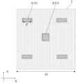
- Figure 3is a schematic top view of a circuit board provided by an embodiment of the present disclosure.
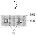
- Figure 4is an enlarged schematic diagram of the dotted circle S1 in Figure 3;
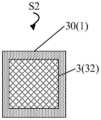
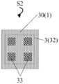
- Figure 5is an enlarged schematic diagram of the dotted circle S2 in Figure 3;
- Figure 6is a schematic top view of a circuit board provided by an embodiment of the present disclosure.
- FIG. 7Ais an enlarged schematic diagram of a reflection pattern according to an embodiment of the present disclosure.
- Figure 7Bis a schematic diagram of a rectangular reflection pattern according to an embodiment of the present disclosure.
- Figure 8is the second enlarged schematic diagram of the reflection pattern according to the embodiment of the present disclosure.
- Figure 9is the third schematic top view of the circuit board provided by the embodiment of the present disclosure.
- Figure 10is a schematic diagram of the first sub-pad area including two pads provided by an embodiment of the present disclosure.
- Figure 11is a schematic diagram of the second sub-pad area including four pads provided by an embodiment of the present disclosure.
- Figure 12Ais a schematic cross-sectional view of a circuit board provided by an embodiment of the present disclosure.
- Figure 12Bis the second schematic cross-sectional view of a circuit board provided by an embodiment of the present disclosure.
- Figure 13is a schematic top view of the second reflective layer provided by an embodiment of the present disclosure.
- Figure 14is the fourth schematic top view of the circuit board provided by the embodiment of the present disclosure.
- Figure 15is a fifth schematic top view of a circuit board provided by an embodiment of the present disclosure.
- Figure 16is the third schematic cross-sectional view of the circuit board provided by the embodiment of the present disclosure.
- Figure 17Ais one of the comparative schematic diagrams of warpage values of circuit boards under different conditions provided by an embodiment of the present disclosure
- Figure 17Bis a second schematic diagram comparing warpage values of circuit boards under different conditions provided by an embodiment of the present disclosure.
- Figure 18is a schematic cross-sectional view of an electronic device provided by an embodiment of the present disclosure.
- Figure 19is a second schematic cross-sectional view of an electronic device provided by an embodiment of the present disclosure.
- Figure 20is a third schematic cross-sectional view of an electronic device provided by an embodiment of the present disclosure.
- Figure 21is a schematic diagram of the series connection of different light-emitting elements in the same light-emitting area provided by an embodiment of the present disclosure
- Figure 22is one of the schematic diagrams of the circuit board manufacturing process provided by the embodiment of the present disclosure.
- Figure 23is the second schematic diagram of the circuit board manufacturing process provided by the embodiment of the present disclosure.
- Figure 24is a schematic diagram of a reflective structure provided by an embodiment of the present disclosure.
- a backlightis required to provide display brightness.
- a high reflectivity reflective structureis essential in the backlight to maximize the light emission efficiency and increase brightness.
- one of the materials of choice for the high reflectivity coating layercould be white ink.
- Figure 1shows the process flow of setting a photosensitive white ink layer on a substrate. The substrate can be cleaned first, and the solid-liquid mixed photosensitive white ink material is printed on a specific area of the substrate, and then pre-cured and finally After curing, a photosensitive white ink layer with high reflectivity can be obtained.
- a high-reflectivity film layeris a reflective sheet.
- the reflective sheetis usually a multi-layer structure, as shown in Figure 2.
- itmay include a lower protective film 042, an adhesive film 043, a reflective layer 04, and an upper protective film. 041.
- a lower protective film 042 of the lowest layerfirmly connect the reflective layer 04 to the surface to be attached through the stickiness of the adhesive film 043, and finally tear off the upper protective film 041. Therefore, you can choose a white ink layer or reflective layer in the backlight to increase the brightness of the light.
- a reflective sheetcan be disposed on the substrate provided with the white ink layer, thereby further increasing the reflectivity of the substrate and reducing energy consumption.
- the white ink materialIn the preparation process of the white ink layer, since the white ink material needs to undergo a curing process to form the white ink layer, the white ink material will generate tensile stress after curing, which is manifested as warping on the substrate.
- Warpageindicates that the cross-section that was originally flat no longer remains flat, that is, deformation occurs. This will affect the reliability and quality of the product.
- the substrateneeds to be fixed by vacuum adsorption equipment for subsequent stages of the process (such as the process section for connecting components to the pads on the substrate).
- the vacuum adsorption equipmentalso has certain limitations. If the warpage value of the substrate is too large, the adsorption equipment cannot adsorb and fix the workpiece, and subsequent processes cannot be carried out.
- the orthographic projection area of the white ink layer on the substrateexceeds more than 80% of the plane area of the entire substrate, and is interconnected everywhere.
- the inventorexplored how to set the white ink layer with the above pattern on the substrate.
- a quadrilateral substrate provided with a white ink layerfor example, the orthogonal projection area of the white ink layer on the substrate exceeds more than 90% of the plane area of the entire substrate
- Select specific sitesfor example, a total of 10 sites
- the warpage value at multiple locations on the substratehas exceeded 2.6mm.
- the vacuum adsorption equipmentcannot The substrate is adsorbed and fixed on the stage, making it impossible to firmly support the substrate, accurately align it, or perform corresponding processes. Therefore, the substrate warpage value has an important impact on subsequent processes.
- the inventorfurther found that if white ink is already provided on the substrate and a reflective layer is installed, not only the tensile stress generated after the white ink solidifies will lead to an increase in the warpage of the substrate; because the reflective layer 04 has a relatively high viscosity,
- the large (>3000Pa ⁇ s) adhesive film 043is attached to the white ink layer, and is baked in a subsequent high-temperature process (such as 150°C, a process section where protective structures are set on components through dripping or printing processes).
- the reflective layer 04will shrink and show a warped morphology. Therefore, on the one hand, it affects the reliable connection, detection and rework of subsequent electronic components (such as micro light-emitting diodes) and substrates; on the other hand, it affects the overall yield of the product.
- the substrate warpage valuewas, for example, a maximum of 1.55mm; after the reflective sheet was installed on the white ink layer, under the process conditions of +150°C, the substrate warpage value was The maximum will become 4.75mm (the equipment can cope with warpage ⁇ 2.6mm). Therefore, after the reflective sheet is attached, the warpage value of the substrate does not meet the equipment requirements for subsequent processes. Therefore, there is an urgent need for a process method for improving substrate warpage.
- Figure 4is an enlarged schematic view of Figure 3 at the dotted circle S1
- Figure 5is an enlarged schematic view of Figure 3 at the dotted circle S2
- Figure 12Ais Figure 3 is a schematic cross-sectional view along the dotted line AA'.
- An embodiment of the present disclosureprovides a circuit board, which includes:
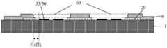
- the first reflective layer 20is located on the same side of the substrate 1 as the pad area 3.
- the first reflective layer 20includes a plurality of mutually spaced reflective patterns 2, with gaps between adjacent reflective patterns 2.
- Pattern 2has a first hollow 30 in the area where pad area 3 is located. Specifically, the exposed area of the first hollow 30 is the area of the substrate 1 .
- the first reflective layerincludes a plurality of mutually spaced reflective patterns 2, and there are gaps between adjacent reflective patterns 2.
- the first reflective layeris formed into a film layer having multiple mutually spaced reflective patterns 2, with Compared with a first reflective layer that is connected everywhere, a plurality of first film layers with mutually spaced reflective patterns 2 can release the tensile stress generated by the placement of the first reflective layer 2 on the circuit board and greatly reduce the risk of damage to the circuit board. Probability of warping.
- At least one pad area 3is distributed in the area surrounded by the outer contour of each reflective pattern 2.
- a pad area 3, for example, the reflective pattern 2includes a first sub-reflective pattern 21 and a second sub-reflective pattern 22, wherein each first sub-reflective pattern 21 is distributed with a first component pad area 31, each There is a second component pad area 32 distributed in the second sub-reflective pattern 22.
- the area of the area surrounded by the outer contours of the first sub-reflective sub-pattern 21 and the second sub-reflective pattern 22is almost the same; but it can be understood that, The size of the first hollow 30 of the first sub-reflective pattern 21 is adapted to the size and shape of the first component pad area 31 , and is carried out in order to fully expose each pad in the first component pad area 31 and take into account process accuracy. Design; the size of the first hollow 30 of the second sub-reflective pattern 22 is adapted to the size and shape of the second component pad area 32 to fully expose each pad in the second component pad area 32 and considering the process accuracy is Design accurately.
- other numbers of pad areas 3may also be distributed in the area surrounded by the outer contour of a reflective pattern 2, and the embodiment of the present disclosure is not limited thereto.
- the minimum size of the reflective pattern 2is larger than the maximum size of the pad area 3 , and only one pad area 3 is distributed in the area surrounded by the outer contour of the reflective pattern 2 . In the embodiment of the present invention, only one pad area 3 is distributed in the area surrounded by the outer contour of the reflective pattern 2.
- the film layer forming the reflective pattern 3is divided into areas (one pad area 3 is an area) exposure, the first reflective layer can include a larger number of reflective patterns but with a single smaller surface area. The tensile stress generated by the circuit board due to the first reflective layer 2 is released more completely, which greatly reduces the cost of the circuit board. Probability of warping.
- the minimum size of the reflection pattern 2can be understood as the perimeter of the outer contour of the orthographic projection of the reflection pattern 2 on the substrate 1, or the side length/diagonal/diameter/length of the shape defined by the orthographic projection of the outer contour.
- the maximum size of the pad area 3can be understood as the perimeter of the outer contour of the orthographic projection of the bonding pad area 3 on the substrate 1, or the side length/diagonal/diameter of the shape defined by the orthographic projection outer contour. wait. For example, taking FIG.
- the shape defined by the outer contour of the reflection pattern 2 in the orthographic projection of the substrate 1is a polygon
- the shape defined by the outer contour of the pad area 3 in the orthographic projection of the substrate 1is a quadrilateral.
- the minimum size of pattern 2can be understood as the length d1 of the shortest side of the polygon
- the maximum size of the pad area 3can be understood as the length d2 of the long side of the rectangle, d1>d2; it can be understood that the vertex corners of the polygon can have rounded corners. Appearance.
- the shape defined by the outer contour of the reflection pattern 2 in the orthographic projection of the substrate 1is a rectangle, and the shape defined by the outer contour of the pad area 3 in the orthographic projection of the substrate 1 is a rectangle.
- the minimum size of the reflective pattern 2can be understood as the short side length d1 of the rectangle, and the maximum size of the pad area 3 can be understood as the long side length d2 of the rectangle, d1>d2.
- the shape defined by the outer contour of the reflection pattern 2 in the orthographic projection of the substrate 1is circular, and the shape defined by the outer contour of the pad area 3 in the orthographic projection of the substrate 1 is rectangular.
- the minimum size of the reflection pattern 2can be understood as the diameter length L0 of the circle
- the maximum size of the pad area 3can be understood as the long side length d2 of the rectangle, L0>d2.
- the shape of the reflective pattern 2is different from the shape of the pad area 3 .
- the shape defined by the outer contour of the orthographic projection of the reflection pattern 2 on the substrate 1is a polygon, and the shape defined by the outer contour of the orthographic projection of the pad area 3 on the substrate 1 is a rectangle; for another example, As shown in FIG. 6 , the shape defined by the outer contour of the reflection pattern 2 in the orthographic projection of the substrate 1 is circular, and the shape defined by the outer contour of the pad area 3 in the orthographic projection of the substrate 1 is a rectangle.
- the plurality of pad areas 3include a first component pad area 31 and/or a second component pad area 32.
- the first component pad area 31The number of pads or the size of the pads included in the second component pad area 32 are different.
- the first component pad area 31includes two solder pads 33 ; as shown in FIG. 11 , the second component pad area 32 includes at least four solder pads 33 .
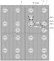
- the circuit boardincludes multiple device areas 5; the device area 5 includes at least one first component pad area 31 and/or at least one second component pad Area 32; at least one device area 5 is distributed in the area surrounded by the outer contour of the reflective pattern 2.
- at least one device area 5is distributed in the area where the reflective pattern 3 is located.
- the film layer forming the reflective pattern 3is divided into regions (with at least one device area 5 distributed as one area). Exposure, so that the area surrounded by the outer contour of the reflective pattern 2 is distributed with at least one device area 5.
- the tension generated by the placement of the first reflective layer 2 on the circuit boardcan be released. tensile stress to avoid the problem of warping of the circuit board when forming the first reflective layer connected everywhere.
- FIG. 9is a schematic illustration using an example in which two device areas 5 can be distributed in the area surrounded by the outer contour of a reflective pattern 2.
- the area surrounded by the outer contour of a reflective pattern 2Other numbers of device areas 5 can also be distributed in the area provided.
- the embodiment of the present disclosureis not limited to this.
- three device areas 5can be distributed in the area surrounded by the outer contour of a reflective pattern 2.
- Four device areas 5may be distributed in an area surrounded by the outer contour of a reflective pattern 2.
- five device areas 5may be distributed in an area surrounded by the outer contour of a reflective pattern 2.
- only one device region 5is distributed in the area surrounded by the outer contour of the reflective pattern 2 .
- the first component pad area 31can be used for welding with the first component, and the first component can be a light-emitting component, for example, a Mini Light Emitting Diode (Mini-LED).
- Mini-LEDsare small in size and high in brightness. They can be widely used in backlight modules of display devices and finely adjust the backlight to achieve high-dynamic range image (High-Dynamic Range, HDR) display.
- typical dimensions (eg length) of Mini-LEDsrange from 50 microns to 200 microns, such as 80 microns to 150 microns.
- the second component pad area 32can be used for welding with the second component.
- the second componentcan be a micro control chip, a micro sensor, a capacitor, an inductor, a resistor, etc.
- a light-emitting areais formed after a plurality of first pad areas 31 of a device area 5 are welded to a plurality of light-emitting elements in a one-to-one correspondence, and after the second pad areas 32 are welded to a micro control chip in a corresponding manner.
- a micro control chip in a light-emitting areacan control the light emission of multiple light-emitting elements in the light-emitting area, realizing zoning control and local dimming (Local Dimming) of the circuit board.
- the Mini-LEDmay include two pins (N and P pins), which are respectively soldered to the two pads 33 of the first component pad area 31 .
- the micro control chipmay include at least 4 pins, which may be welded in one-to-one correspondence with the plurality of pads 33 in the second component pad area 32.
- a first hollow 30is simultaneously exposed for use with the Mini -Two soldering pads 33 bound to two pins of the LED, or four soldering pads 33 simultaneously exposed for binding to four pins of the micro control chip.
- the circuit boardcan be divided into a plurality of device areas arranged in an array. Each device area at least includes a first component pad area for connecting with at least one first component. In some embodiments, each device area also includes A first component pad area with at least one second component. The first component pad area is used to connect to the first component that implements the main function of the circuit board, and the second component pad area is used to connect to the second component that cooperates with the first component to achieve the corresponding function.
- the first componentmay include a Mini-LED, and the main function of the circuit board is to provide lighting; the second component may include a micro control chip for providing control signals to the Mini-LED; and may also include a micro sensor chip for sensing
- the signals of electrical structures/devices on circuit boards such as Mini-LEDcan also include commonly used electronic components such as capacitors, inductors, and resistors.
- the reflective pattern 2includes a first sub-reflective pattern 21 and a second sub-reflective pattern 22 ; at least two first component pad areas 31 belonging to the same device area 5 Distributed in the area where the first sub-reflective pattern 21 is located; the second component pad area 32 of the same device area 5 is distributed in the second sub-reflective pattern 22 .
- the first sub-reflective pattern 21 and the second sub-reflective pattern 22are connected to each other and form an integrated structure.
- each reflective pattern 2corresponds to each device area one-to-one, that is, is distributed in an array; along the first direction In both directions Y, the minimum spacing e2 of two adjacent reflective patterns 2 is the same; the first sub-reflective pattern 21 can be rectangular, and the second sub-reflective pattern 22 can be rectangular. In the same direction, the size of the first sub-reflective pattern 21 is larger than the size of the second reflective pattern 22 .
- Each second sub-reflective pattern 22is located on the same side of each first sub-reflective pattern 21. For example, as shown in FIG. 3, each second sub-reflective pattern 22 extends from the first sub-reflective pattern 21 along the second direction Y to form an integral body. structure.
- the ratio of the minimum distance e4 between two adjacent pad areas 3 to the minimum distance e2 between two adjacent reflective patterns 2ranges from 3 to 10.
- first directionintersects the second direction; the plurality of pad areas are spaced apart along the first direction and/or the second direction.
- the first direction and the second directionare perpendicular to each other, as shown in Figure 3, and any two adjacent pad areas among the plurality of pad areas are spaced apart along the first direction or the second direction; Or any two adjacent pad areas among the plurality of pad areas can also be distributed at intervals with a certain angle between the first direction or the second direction, and the angle ranges from 0° to 60°; or There are at least two pad areas among the plurality of pad areas, spaced apart along the first direction, and at least two pad areas among the plurality of pad areas, spaced apart along the second direction.
- the minimum distance e1 between two adjacent reflective patterns 2is greater than 2 mm; along the second direction Y, the minimum distance between two adjacent reflective patterns 2 Greater than 2mm.
- the minimum distance e1 between two adjacent reflective patterns 2is greater than 2mm, and along the second direction Y, the minimum distance e2 between two adjacent reflective patterns 2 is greater than 2mm. If the precision of the developing equipment allows, the adjacent reflective patterns 2 can be provided with relatively obvious dividing lines to release the tensile stress generated by the first reflective layer 2 on the circuit board.
- e1 and e2may be approximately equal, and e3 and e4 may be approximately equal; specifically, 2mm ⁇ e1 ⁇ 50mm, 2mm ⁇ e2 ⁇ 50mm; specifically, 6mm ⁇ e3 ⁇ 100mm, 6mm ⁇ e4 ⁇ 100mm.
- the reflection pattern 2has an orthographic outline shape of the substrate 1 and the first component pad area 31 and the second component pad area 32 in the same device area 5
- the distribution areasform similar shapes.
- the shape of the distribution area of the first component pad area 31 and the second component pad area 32 in the same device area 5is a "chopper" shape, then the reflection pattern 2 is in the substrate
- the outer contour shape of the orthographic projection of 1is also a "chopper” shape.
- the shape formed by the distribution area of the first component pad area 31 and the second component pad area 32 in the same device area 5can also be other shapes. For example, as shown in FIG.
- the shape of the distribution area of the first component pad area 31 and the second component pad area 32 in the same device area 5The shape of the distribution area of the first component pad area 31 and the second component pad area 32 is a rectangle, so the outline shape of the orthographic projection of the reflection pattern 2 on the substrate 1 can also be a rectangle.
- each reflection pattern 2is the same.
- At least two reflection patterns 2have different shapes.
- the shape differencemay be caused by the different number of components distributed in the surrounding area, or the shape difference may be caused by the same number of components but due to different types of components and/or differences in component distribution density.
- the material of the first reflective layeris thermosetting white ink or photosensitive white ink.
- FIGS. 12A-14wherein FIG. 12A is a schematic cross-sectional view of the circuit board, FIG. 13 is a schematic top view of the second reflective layer 6 , and FIG. 15 is a configuration.
- FIGS. 12A-14wherein FIG. 12A is a schematic cross-sectional view of the circuit board, FIG. 13 is a schematic top view of the second reflective layer 6 , and FIG. 15 is a configuration.
- Figure 14is a schematic top view of another circuit board provided with a second reflective layer.
- the circuit boardalso includes a second reflective layer located on the side of the first reflective layer 20 facing away from the substrate 1 6.
- the second reflective layer 6can be disposed on the side of the first reflective layer 20 away from the substrate 1 through attachment or other means.
- the second reflective layer 6can further improve light utilization and improve the inconsistency between different device areas 5 . Uniform reflection effect.
- the second reflective layer 6can be a reflective sheet, which is a reflective layer that can be attached or stacked on the side of the first reflective layer 20 facing away from the substrate 1 .
- FIG. 12Bwhich is another schematic cross-sectional view along the dotted line AA′ in FIG. 3 .
- the second reflective layer 6may include a base material 601 , and a second reflective layer located on the side of the base material 601 away from the first reflective layer 20 .
- the first film layer 602, and the second film layer 602located on the side of the base material 601 facing the first reflective layer 20.
- the base material 601can be dispersed with scattering particles and/or microbubbles; specifically, the material of the scattering particles can be titanium dioxide; specifically, the material of the base material 601 can be polyethylene terephthalate, or polyethylene terephthalate.
- the first film layer 602can be a scattering layer, the material of the first film layer 602 can be titanium dioxide, and the second film layer 603 can be a reflective material layer, and specifically, white ink material can be used.
- the second reflective layer 6has a second hollow 60 in the area where the pad area 3 is located; the orthographic projection area of the second hollow 60 on the substrate 1 is larger than that of the first hollow 60 .
- a hollow 30is in the orthographic projection area of the substrate 1 , and the orthographic projection of the first hollow 30 on the substrate 1 is located within the orthographic projection of the second hollow 60 on the substrate 1 .
- the orthographic projection area of the second hollow 60 on the substrate 1is larger than the orthographic projection area of the first hollow 30 on the substrate 1 , and the orthographic projection of the first hollow 30 on the substrate 1 is located at the position of the second hollow 60 .
- the orthographic projection of the substrate 1it can be ensured that the light-emitting elements welded to the pad area 3 can fully emit light, and the second hollow 60 can be prevented from affecting the light emission of the light-emitting elements.
- the minimum distance between each second hollow 60 and the pad area 3 located in the orthographic projectionis approximately the same.
- the second reflective layer 6 in the embodiment of the present disclosurecan be baked at a high temperature before the second reflective layer 6 is formed on the circuit board.
- the baking temperature Tis greater than the initial At the temperature Tg, the free volume of the reflective sheet is released, and then naturally cools to room temperature, causing it to shrink to the free volume corresponding to room temperature.
- the volume of the second reflective layer 6does not shrink/only There is slight shrinkage, which can reduce the warpage value of the circuit board.
- the second reflective layer 6 after being baked at high temperature and naturally cooledcan make different areas of the circuit board, each second hollow 60 and the solder joints located in the front projection.
- the minimum spacing between the panel areas 3is approximately the same, which can prevent the second reflective layer 6 that has not been baked at high temperature from being stretched due to the stretching of the second reflective layer 6 after it is attached to the first reflective layer 2.
- the size of the second hollow 6is different between the non-edge area and the edge area of the second reflective layer 6. After being bonded to the first reflective layer 2, it will cause the different pad areas 3 and pad areas 3 in different areas of the circuit board.
- the problem that the second hollows 60 are located at different spacings in the same directionresults in uneven light brightness in different areas of the circuit board.
- the minimum distance between the second hollow 60 and the pad area 3 located in the orthographic projectionis f1, which is smaller than the minimum distance e3 between two adjacent pad areas 3 in the first direction X.
- the minimum distance f1 between the second hollow 60 and the pad area 3 located in the orthographic projectionmay be in the range of 0.45mm ⁇ f1 ⁇ 1mm.
- the second reflective layer 6may still not be able to satisfy the requirements of making each pad area 3 and the pad area 6 due to actual process errors (for example, equipment alignment and other process errors).
- the spacing in the same direction of the second hollow 60 where the pad area 3 is locatedis exactly the same. Therefore, in the embodiment of the present disclosure, the spacing in the same direction of each pad area 3 and the second hollow 60 where the pad area 3 is located are approximately the same. It can be understood as In any two areas of the circuit board, the spacing difference between the pad area 3 and the second hollow 60 where the pad area 3 is located in the same direction is different from the spacing between the pad area 3 and the second hollow 60 where the pad area 3 is located in any one of the areas.
- the spacing ratio of the hollows 60 in the same directionis less than 10%.
- the difference between f1 and f2is a1
- the difference between f1 and f2is a2
- the difference between f1 and f2is a2
- the orthographic projection of the area of the second reflective layer 6 except the second hollow 60 on the substrate 1covers at least two adjacent reflection layers.
- the gap between patterns 2is in the orthographic projection of substrate 1.
- the orthographic projection of the second reflective layer 6 on the substrate 1at least covers the orthographic projection of the gap between adjacent reflective patterns 2 on the substrate 1.
- the gap between adjacent reflective patterns 2can be Shielding can realize that the position of the non-reflective pattern 2 on the circuit board can be covered by the second reflective layer 6 set later, which will not affect the optical performance of the product.
- the orthographic projection of the area of the second reflective layer 6 except the second hollow 60 on the substrate 1is the same as that of the reflective pattern 2 on the substrate 1 .
- the orthographic projectionspartially overlap.
- the area of the second reflective layer 6 except the second hollow 60 in the orthographic projection of the substrate 1also covers the peripheral part of the first hollow 30 of the reflective pattern 2 , that is, the second hollow 60
- the orthographic projection size on the substrate 1should be smaller than the orthographic projection size of the reflective pattern 2 on the substrate 1 to ensure that the area on the circuit board not covered by the reflective pattern 2 can be partially covered by the second reflective layer 6 to improve the product optics. performance.
- the minimum size L of the second hollow 60 in the second reflective layer 6is determined by the processing technology. Taking the shape of the second hollow 60 as a circle as an example, the second hollow The minimum size of 60 refers to the diameter of the second hollow 60. The minimum diameter produced by the current processing method is about 1.5mm.
- the outer contour size L0 of the reflective pattern 2is related to L. A reflective pattern 2 has at least a circumference of Assume a pad area 3, and adjacent reflective patterns 2 are spaced apart from each other. Therefore, the maximum dimension L0 of the outer contour of the reflective pattern 2 is related to the spacing between adjacent components on the circuit board.
- the maximum sizerefers to its diagonal length. If the outer contour shape of the reflection pattern 2 is a circle, the maximum size refers to its diameter length. Reflection When the outer contour shape of Pattern 2 is elliptical, the maximum dimension refers to the length of its major axis.
- L0needs to be slightly larger than L, for example, it satisfies L0>L+reflective sheet attachment accuracy; where the attachment accuracy is determined by the equipment accuracy, for example, the attachment accuracy range is 0-0.2mm.
- the size of the second hollow 60should not be too large, for example, 3mm>L ⁇ 1.5mm.
- a protective structuremay be further provided on the component.
- the size L of the second hollow 60also needs to be slightly smaller than the outline size of the orthographic projection of the protective structure 73 on the substrate 1 , so that there is an overlapping area between the second reflective layer 6 and the protective structure 73 . can partially contact each other for a more secure fixation.
- determining whether a reflective pattern 2 on the circuit board only surrounds one pad area 3is determined by the spacing P between adjacent pad areas 3 and the outer contour size L0 of the reflective pattern 2. This decision is made jointly with the accuracy of the patterning process. If the distance P between any two components on the circuit board is greater than (L0 + process accuracy), that is, the minimum distance between two adjacent reflective patterns 2 (such as L1 and L1') is greater than 0, then you can choose a way in which each pad area 3 is surrounded by a reflective pattern 2.
- the minimum distance between two adjacent reflective patterns 2(such as L1 and L1') will be less than or equal to 0, That is, two reflective patterns 2 have overlapping areas and are connected to each other. In this case, it can be considered that one reflective pattern 2 surrounds a plurality of closely spaced pad areas 3 .
- the first componentis used to realize the main function of the circuit board.
- Multiple first componentsare arranged according to a certain rule and the arrangement density is high. Therefore, the spacing between the first components is relatively small, and the spacing between the first components is relatively small.
- the second component(such as micro IC, sensor, etc.) is small in number, so it is only arranged in a local position of the circuit board, for example, it is usually arranged in the gap between two adjacent first components. Therefore, if a second element is disposed between two adjacent first elements, for example, the line connecting the geometric centers of two adjacent first elements, and there is at least one second element that overlaps with the line, The two first elements and at least one second element located between them are surrounded by a reflective pattern 2 .
- a circuit boardmay have multiple reflective patterns 2 with different outer contour shapes.
- the second reflective layer 6is provided to further improve the utilization rate of light. Therefore, for non-optical functional elements on the circuit board, such as the second element, The second reflective layer 6 does not need to be provided with hollows in the area where the non-optical functional elements are located; however, this will affect the flatness of the second reflective layer 6. To improve this problem, the second reflective layer 6 can be provided with non-optical functions. Set a cross or straight seam at the location of the area where the component is located.
- one device area 5includes four first pad areas 31 (for soldering the first components) and one second pad area 32 (for soldering the second components) , for example, the four first components are connected in series with each other, or two in parallel and then in series, or four in parallel; there is no limit here, one second pad area 32 is located in the four first pad areas 31
- the geometric centersare connected in sequence to form a quadrilateral.
- All components in a device area 5are surrounded by a reflective pattern 2, that is, in the area surrounded by the outer contour of the reflective pattern 2, all components in a device area 5 are distributed, and the first hollows 30 in the reflective pattern 2 are respectively exposed.
- the shape and size of the first pad area 31 and the second pad area 32are different.
- the third pad area corresponding to the pad area 3 A hollow 30varies in shape and size. That is, the second hollow 60 in the second reflective layer 6, such as the second hollow 60 corresponding to the first pad area 31 and the second hollow 60' corresponding to the second element, may also have different sizes.
- the second hollows 60 and 60'are both circular, with diameters L and L' respectively, where L'>L.
- one device area 5may include more first components, and the connection relationships between multiple first components may be designed as needed. At the same time, the first components belonging to the same device area 5
- the arrangement methodis not limited to array arrangement along the X and Y directions, and can also be in other ways without limitation.
- FIG. 16which is a schematic cross-sectional view along the dotted line AA' in FIG. 15 .
- the adhesive layer 63 and the second reflective layer 6are disposed on the first reflective layer 20 by adhesion.
- the adhesive layer 63may be provided with a third hollow in the area corresponding to the second hollow 60 to facilitate the subsequent placement and connection of the first component in the first welding area 31, or the subsequent placement and connection of the second component in the first welding area 31. 2.
- Welding area 32is a schematic cross-sectional view along the dotted line AA' in FIG. 15 .
- the viscosity of the adhesive layer 63ranges from 800 Pa ⁇ s to 2000 Pa ⁇ s.
- the viscosity of the adhesive film of the second reflective layer 6needs to be relatively large (>3000 Pa ⁇ s ), the subsequent dispensing process (such as forming the protective structure of the light-emitting element), and the subsequent high-temperature baking (100°C ⁇ 150°C) after dispensing will further increase the stress on the substrate, thereby increasing the warpage of the substrate.
- the viscosity of the adhesive layer 63ranges from 800 Pa ⁇ s to 2000 Pa ⁇ s.
- the viscosity of the adhesive layer 63 on the second reflective layer 6can be reduced. Viscosity can reduce the warpage of circuit boards.
- the outer contour shape of the reflection pattern 2is a circle, a rectangle, a polygon, an ellipse, etc.
- the shape of the pad area 3is a rectangle.
- the shape of the pad area 3is a rectangle, and the shape of the pad area 3 is the same as or similar to the orthographic projection shape of the component to be connected to the pad in the pad area 3 on the substrate 1, making it easy to weld the components. in pad area 3.
- the protective structure 73is provided on the side of the component (such as the first component 71) away from the substrate 1 through a dripping or printing process to protect The element is corroded by external water and oxygen; since the protective structure 73 needs to cover the second hollow 60 of the second reflective layer 6, the protective structure 73 is prepared by dripping or printing, and its orthographic projection shape on the substrate 1 is circular.
- the orthographic projection shape of the second hollow 60 on the substrate 1 and the orthographic projection shape of the protective structure 73 on the substrate 1are similar to each other, that is, the second hollow
- the orthographic projection shape of 60 on the substrate 1is a shape such as a circle, a regular polygon, or an ellipse.
- the outer contour of the reflective pattern 2is kept aligned with the second hollow 60 in the orthographic projection shape of the substrate 1 .
- the orthographic projection shape of the substrate 1is similar, that is, the orthographic projection shape of the outer contour of the reflection pattern 2 on the substrate 1 is a circular, rectangular, polygonal, elliptical or other shape.
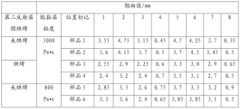
- Figure 17Ashows that after arranging the first reflective layer with different film layer patterns on a quadrilateral substrate, a total of eight locations are selected at equal intervals in each area in four areas close to the four edges of the substrate to test the substrate.
- Pattern 2, at least one device area 5is distributed in each reflective pattern 2, such as the reflective pattern 2 shown in Figure 3 or Figure 9; the first reflective layer 20 on the sample 5 and the sample 6 includes a plurality of mutually spaced
- the reflective pattern 2has only one pad area 3 distributed in each reflective pattern 2, such as the reflective pattern 2 shown in FIG. 6 .
- the maximum warpage value of the first reflective layer on sample 1/sample 2is 1.4mm
- the maximum warpage of the first reflective layer on sample 3/sample 4 and sample 5/sample 6is The values are 0.65mm and 0.45mm respectively.
- the second reflective layer 6is pre-baked at high temperature.
- the prebaked second reflective layer 6is attached, and the warpage of the circuit board is measured as shown in Figure 17B.
- Figure 17Bshows that a quadrilateral substrate is used as the test object, and the second reflective layer 6 is set on it.
- the reflective layerby comparing whether the second reflective layer is baked before setting, and the viscosity of the adhesive layer used to set the second reflective layer, etc., in the four areas close to the four edges of the substrate, each area is equally spaced A total of eight sites were selected for warpage value testing.
- samples 1 and 2select an adhesive layer with a viscosity of 3000 Pa ⁇ s, and set the unbaked second reflective layer on the substrate; for samples 3 and 4, select an adhesive layer with a viscosity of 3000 Pa ⁇ s.
- the baked second reflective layeris placed on the substrate; for samples 5 and 6, an adhesive layer with a viscosity of 800Pa ⁇ s is selected, and the unbaked second reflective layer is The second reflective layer is disposed on the substrate.
- an embodiment of the present disclosurealso provides an electronic device, including a circuit board as provided in an embodiment of the present disclosure, and a plurality of first components 71 and/or a plurality of second components 72 , wherein the plurality of first components 71 Each of the components 71 is connected to the first component pad area 31 , and each of the plurality of second components 72 is connected to the second component pad area 32 .
- the first component 71can be a light-emitting component, and the light-emitting component can include The light-emitting part 711 and the pin 712, the light-emitting element can be a sub-millimeter light-emitting diode (English full name: Mini Light Emitting Diode, English abbreviation: Mini LED) or a micro light-emitting diode (English full name: Micro Light Emitting Diode, English abbreviation: Micro LED) Any of; Mini LED, whose size is greater than or equal to 80 ⁇ m and less than 500 ⁇ m; Micro LED, whose size is less than 80 ⁇ m.
- Mini LEDwhose size is greater than or equal to 80 ⁇ m and less than 500 ⁇ m
- Micro LEDwhose size is less than 80 ⁇ m.
- the side of the light-emitting element facing away from the substrate 1can also be provided with a protective structure 73 , and the surface of the protective structure 73 away from the substrate 1 can be a curved surface; the second element can be a micro control chip, used to control the light-emitting elements in the same device area 5 glow.
- the protective structure 73can fill the area where the first hollow 30 of the first reflective layer 20 is located, and fill the area of the second hollow 60 of the second reflective sheet 6 , as well as the adhesive layer 63 In the area corresponding to the second hollow 60 .
- the dimension h of the substrate 1 in the Z directionranges from 0.5 mm to 1.0 mm. Specifically, for example, h can range from 0.6 mm to 0.8 mm. Specifically, for example, h can be 0.7mm.
- the substrate 1may include an organic resin material such as epoxy, triazine, silicone, or polyimide.
- the substrate 1may be an FR4 type printed circuit board (PCB), or may be an easily deformable flexible PCB.
- the substrate 1may include a ceramic material such as silicon nitride, AIN or Al2O3, or a metal or metal compound, and the substrate 1 may be a metal core printed circuit board (MCPCB) or a metal copper clad laminate such as (MCCL).
- the width d0 of the pad 33 in each pad area 3 in the direction parallel to the first direction 200 ⁇ m, 202 ⁇ m, 204 ⁇ m or 206 ⁇ m; specifically, the size h2 of the first reflective layer 20 in the Z directioncan be 10 ⁇ m ⁇ 50 ⁇ m.
- h2can be 20 ⁇ m ⁇ 40 ⁇ m.
- h2can be 25 ⁇ m.
- the size h3 of the second reflective layer 6 in the Z directionmay be 80 ⁇ m to 120 ⁇ m. Specifically, h3 may be 90 ⁇ m to 110 ⁇ m. Specifically, h3 may be 95 ⁇ m, 100 ⁇ m, 105 ⁇ m, or 110 ⁇ m; specifically, h3 may be 95 ⁇ m, 100 ⁇ m, 105 ⁇ m, or 110 ⁇ m.
- the size h4 of an element 71 in the Z directioncan be 80 ⁇ m to 120 ⁇ m, and h4 can be 90 ⁇ m to 110 ⁇ m.
- h4can be 95 ⁇ m, 100 ⁇ m, 105 ⁇ m or 110 ⁇ m; specifically, the first element 71 is in the first direction.
- the width d3 on The size h5 in the Z directioncan be 0.3mm ⁇ 0.8mm.
- h5can be 0.4mm ⁇ 0.7mm.
- h5can be 0.45mm, 0.5mm, 0.55mm or 0.6mm; specifically , the diameter d5 of the hemispherical protective structure 73 can be 2.0mm ⁇ 3.0mm.
- d5can be 2.3mm ⁇ 2.7mm.
- d5can be 2.3mm, 2.4mm, 2.5mm or 2.6 mm.
- the protective structure 73when the protective structure 73 is set up through a dripping or printing process, air bubbles may enter the area to be surrounded by the protective structure 73. Since the protective structure 73 needs to be cured and molded at high temperatures later, the air bubbles may remain in the area. the above areas. Therefore, the surface of the first reflective layer 20 , the adhesive layer 63 and/or the first reflective layer 6 facing the component may, for example, have an included angle of 30°-80° with the plane of the substrate 1 . In this way, during dripping Or it can facilitate the discharge of gas during the printing process.
- FIG. 19can be another cross-sectional schematic diagram along the dotted line AA' in FIG. 15 after welding components on the pads.
- the substrate 1can include a substrate substrate. 10, and the first wiring layer 11 provided on the side of the base substrate 10 facing the first reflective layer 20.
- the first wiring layer 11can be a single layer wiring layer, or the first wiring layer 11 It can be a composite layer including multiple sub-wiring layers, and an insulating layer can be provided between adjacent sub-wiring layers.
- one of the sub-wiring layerscan be used to lay out different first circuits in the same device area 5 in series.
- a series connection of components, where another sub-trace layercan be used to route voltage traces or other signal traces used to provide electrical signals to the device area.
- FIG. 20may be another cross-sectional schematic diagram along the dotted line AA' in FIG. 15 after welding components on the pads.
- the substrate 1may include a substrate substrate. 10, and the first wiring layer 11 provided on the side of the base substrate 10 facing the first reflective layer 20, and may also include a second wiring layer located on the base substrate 10 away from the first wiring layer 11.
- the first wiring layer 11may be a single-layer wiring layer, used for laying out series lines connecting different first components in the same device area 5
- the second wiring layer 12may be a single-layer wiring layer, used for Route voltage traces or other signal traces that provide electrical signals to the device area.
- each first element 71 in the same device region 5is connected in series in sequence.
- each first element 71 in the same device region 5is electrically connected to the second element 72 .
- an embodiment of the present disclosurealso provides a method for manufacturing the circuit board provided by the embodiment of the present disclosure, as shown in Figure 22, including:
- Step S100Provide a substrate; specifically, as shown in FIG. 19, the substrate 1 may include a base substrate 10 and a first wiring layer 11 disposed on one side of the base substrate 10. Specifically, the first wiring layer 11 is provided on one side of the base substrate 10.
- the wiring layer 11may be a single wiring layer, or the first wiring layer 11 may be a composite layer including multiple sub-wiring layers, and an insulation layer may be provided between adjacent sub-wiring layers.
- One of the sub-wiring layerscan be used to lay out series lines connecting different first elements in the same device area 5 , and the other sub-wiring layer can be used to lay out voltage traces or other signals for providing electrical signals to the device area. Traces.
- FIG. 19the substrate 1 may include a base substrate 10 and a first wiring layer 11 disposed on one side of the base substrate 10.
- the first wiring layer 11is provided on one side of the base substrate 10.
- the wiring layer 11may be a single wiring layer, or the first wiring layer 11 may be a composite layer including multiple sub-wiring layers
- the substrate 1may include a base substrate 10 and a first wiring layer 11 disposed on one side of the base substrate 10 , and may also include a first wiring layer 11 disposed away from the base substrate 10 The second wiring layer 12.
- the first wiring layer 11may be a single-layer wiring layer, used for laying out series lines connecting different first components in the same device area 5
- the second wiring layer 12may be a single-layer wiring layer, used for Route voltage traces or other signal traces that provide electrical signals to the device area.
- the substrate 1may also include a plurality of bonding pads 33 located on the first wiring layer 11 .
- Step S200Form a first reflective layer having a plurality of mutually spaced reflective patterns on one side of the substrate.
- a first reflective layer having a plurality of mutually spaced reflective patternsis formed on one side of the substrate, including:
- Step S211Coat a first reflective film on one side of the substrate
- Step S212Form a first reflective layer having a plurality of mutually spaced reflective patterns and exposing each pad area through a partitioned exposure process, wherein at least one device area is distributed in each reflective pattern.
- a first reflective layer having a plurality of mutually spaced reflective patternsis formed on one side of the substrate, including:
- Step S221Coat a first reflective film on one side of the substrate
- Step S222Form a first reflective layer having a plurality of mutually spaced reflective patterns and exposing each pad area through a sub-area exposure process, wherein one pad area is distributed in each reflection pattern.
- the manufacturing methodfurther includes:
- Step S300Provide a reflective structure.
- the reflective structureincludes a second reflective layer 6, an adhesive layer 63 located on one side of the second reflective layer 6, and the adhesive layer 63 located away from the second reflective layer 6.
- Step S400Bake the reflective structure and make the baking temperature greater than the starting temperature Tg.
- the starting temperature Tgis the temperature at which the cooling rate does not match the volume discharge rate;
- Step S500Remove the first protective layer of the cooled reflective structure, and attach the second reflective layer to the side of the first reflective layer facing away from the substrate through the adhesive layer;
- Step S600Remove the second protective layer.
- componentscan also be disposed on the pad 33 through a die bonding process; after that, electrical testing can be performed to detect the relationship between the components and If a defect is found in the welding of the pad 33, the problem will be determined in time and a repair process will be carried out. If the electrical test passes, the protective structure 73 can be further formed on the component through a dripping or printing process.
- the reflective structure including the second reflective layer 6can be baked at high temperature (T>Tg) to release the free volume of the reflective sheet, and then, Natural cooling causes it to shrink to a free volume corresponding to room temperature.
- T>Tghigh temperature
- Natural coolingcauses it to shrink to a free volume corresponding to room temperature.
- the volume of the second reflective layer 6does not shrink/only shrinks slightly, thereby reducing the warpage of the circuit board.
- the first reflective layerincludes a plurality of mutually spaced reflective patterns 2, and there are gaps between adjacent reflective patterns 2.
- the first reflective layeris formed to have multiple mutually spaced reflective patterns 2.
- the film layer of the spaced reflective pattern 2has a plurality of first film layers of the mutually spaced reflective pattern 2. Compared with the first reflective layer that is connected everywhere, it can release stress and avoid the formation of the first reflective layer that is connected everywhere. , causing the circuit board to warp.
Landscapes
- Engineering & Computer Science (AREA)
- Microelectronics & Electronic Packaging (AREA)
- Physics & Mathematics (AREA)
- Power Engineering (AREA)
- General Physics & Mathematics (AREA)
- Condensed Matter Physics & Semiconductors (AREA)
- Computer Hardware Design (AREA)
- Geometry (AREA)
- Manufacturing & Machinery (AREA)
- Nonlinear Science (AREA)
- Mathematical Physics (AREA)
- Chemical & Material Sciences (AREA)
- Crystallography & Structural Chemistry (AREA)
- Optics & Photonics (AREA)
- Structure Of Printed Boards (AREA)
Abstract
Description
Translated fromChinese本公开涉及半导体技术领域,尤其涉及一种线路板、电子装置和线路板的制作方法。The present disclosure relates to the field of semiconductor technology, and in particular, to a circuit board, an electronic device, and a method of manufacturing a circuit board.
发光二极管(Light-Emitting Diode,LED)显示是指将传统LED阵列化、微缩化后定址巨量转移到电路基板上,形成超小间距LED,将毫米级别的LED长度进一步微缩到微米级,以达到超高像素、超高解析率,理论上能够适应各种尺寸屏幕的技术。Light-Emitting Diode (LED) display refers to the traditional LEDs that are arrayed and miniaturized and then transferred to the circuit substrate in large quantities to form ultra-fine spacing LEDs. The length of the LEDs from the millimeter level is further reduced to the micron level. A technology that achieves ultra-high pixels and ultra-high resolution and can theoretically adapt to screens of various sizes.
发明内容Contents of the invention
本公开提供一种线路板、电子装置和线路板的制作方法。所述线路板包括:The present disclosure provides a circuit board, an electronic device and a manufacturing method of the circuit board. The circuit board includes:
衬底;substrate;
多个焊盘区,位于所述衬底;a plurality of pad areas located on the substrate;
第一反射层,所述第一反射层与所述多个焊盘区位于所述衬底的同侧,所述第一反射层包括多个相互间隔的反射图案,相邻的所述反射图案之间具有间隙,所述第一反射层在所述多个焊盘区中的每个焊盘区所在区域具有第一镂空。A first reflective layer. The first reflective layer and the plurality of pad areas are located on the same side of the substrate. The first reflective layer includes a plurality of mutually spaced reflective patterns. The adjacent reflective patterns There is a gap therebetween, and the first reflective layer has a first hollow in the area where each pad area in the plurality of pad areas is located.
在一种可能的实施方式中,至少一个所述反射图案外轮廓所围设的区域内至少分布有所述多个焊盘区中的一个焊盘区。In a possible implementation, at least one pad area among the plurality of pad areas is distributed in an area surrounded by at least one outer outline of the reflection pattern.
在一种可能的实施方式中,任一个所述反射图案的最小尺寸大于该反射图案围设区域内的焊盘区的最大尺寸,至少一个所述反射图案外轮廓所围设的区域内仅分布有所述多个焊盘区中的一个焊盘区。In a possible implementation, the minimum size of any one of the reflective patterns is greater than the maximum size of the pad area within the area surrounded by the reflective pattern, and at least one of the reflective patterns has only distribution in the area surrounded by the outer contour. There is one pad area among the plurality of pad areas.
在一种可能的实施方式中,至少一个所述反射图案的外轮廓形状与该反 射图案围设区域内的焊盘区的形状不同。In a possible implementation, the outer contour shape of at least one of the reflective patterns is different from the shape of the pad area in the area surrounded by the reflective pattern.
在一种可能的实施方式中,至少一个所述反射图案的外轮廓形状为圆形或矩形或多边形或椭圆等形状,该反射图案围设区域内的焊盘区形状为矩形。In a possible implementation, the outer contour shape of at least one of the reflection patterns is a circle, a rectangle, a polygon, an ellipse, etc., and the shape of the pad area in the area surrounded by the reflection pattern is a rectangle.
在一种可能的实施方式中,所述多个焊盘区包括第一元件焊盘区和/或第二元件焊盘区,所述第一元件焊盘区与所述第二元件焊盘区包括的焊盘个数或者焊盘尺寸不同。In a possible implementation, the plurality of pad areas include a first component pad area and/or a second component pad area, and the first component pad area and the second component pad area The number of pads included or the size of the pads are different.
在一种可能的实施方式中,所述线路板包括多个器件区;所述器件区包括至少一个所述第一元件焊盘区和/或至少一个所述第二元件焊盘区;In a possible implementation, the circuit board includes a plurality of device areas; the device area includes at least one of the first component pad areas and/or at least one of the second component pad areas;
至少一个所述反射图案外轮廓所围设的区域内分布有至少一个所述器件区。At least one of the device areas is distributed in an area surrounded by at least one of the outer contours of the reflection pattern.
在一种可能的实施方式中,至少一个所述反射图案包括第一子反射图案,以及第二子反射图案;In a possible implementation, at least one of the reflection patterns includes a first sub-reflection pattern and a second sub-reflection pattern;
同一所述器件区的所述至少两个第一元件焊盘区分布于所述第一子反射图案外轮廓所围设的区域,呈阵列分布;The at least two first component pad areas of the same device area are distributed in an area surrounded by the outer contour of the first sub-reflective pattern in an array;
同一所述器件区的所述第二元件焊盘区分布于所述第二子反射图案。The second component pad area of the same device area is distributed in the second sub-reflective pattern.
在一种可能的实施方式中,至少一个所述反射图案中,所述第一子反射图案和所述第二子反射图案相互连接并构成一体结构。In a possible implementation, in at least one of the reflective patterns, the first sub-reflective pattern and the second sub-reflective pattern are connected to each other and form an integrated structure.
在一种可能的实施方式中,至少一个所述反射图案在所述衬底的正投影外轮廓形状与同一所述器件区内的所述第一元件焊盘区以及所述第二元件焊盘区分布区域形成的形状相似。In a possible implementation, at least one of the reflection patterns is formed in an orthographic projection outer contour shape of the substrate and the first component pad area and the second component pad area in the same device area. The shapes formed by the distributed regions are similar.
在一种可能的实施方式中,各所述反射图案的形状相同。In a possible implementation, each of the reflection patterns has the same shape.
在一种可能的实施方式中,至少两个所述反射图案具有不同的形状。In a possible implementation, at least two of the reflection patterns have different shapes.
在一种可能的实施方式中,各所述反射图案呈阵列分布;沿第一方向,相邻两个所述反射图案的最小间距相同,沿第二方向,相邻两个所述反射图案的最小间距相同。In a possible implementation, each of the reflection patterns is distributed in an array; along the first direction, the minimum distance between two adjacent reflection patterns is the same, and along the second direction, the minimum distance between two adjacent reflection patterns is The minimum spacing is the same.
在一种可能的实施方式中,沿所述第一方向,所述多个焊盘区中相邻的两个焊盘区的最小间距,与沿所述第一方向相邻两个所述反射图案的最小间 距的比值范围为3~10;In a possible implementation, along the first direction, the minimum distance between two adjacent pad areas among the plurality of pad areas is the same as the minimum distance between two adjacent reflective pad areas along the first direction. The ratio of the minimum spacing of the pattern ranges from 3 to 10;
沿所述第二方向,所述多个焊盘区中相邻的两个焊盘区的最小间距,与沿所述第二方向相邻两个所述反射图案的最小间距的比值范围为3~10。Along the second direction, the ratio range of the minimum spacing between two adjacent pad areas in the plurality of pad areas and the minimum spacing between two adjacent reflective patterns along the second direction is 3 ~10.
在一种可能的实施方式中,沿所述第一方向,相邻两个所述反射图案的最小间距大于2mm;In a possible implementation, along the first direction, the minimum distance between two adjacent reflective patterns is greater than 2 mm;
沿所述第二方向,相邻两个所述反射图案的最小间距e2大于2mm。Along the second direction, the minimum distance e2 between two adjacent reflective patterns is greater than 2 mm.
在一种可能的实施方式中,所述第一反射层的材料为白色油墨。In a possible implementation, the material of the first reflective layer is white ink.
在一种可能的实施方式中,所述线路板还包括位于所述第一反射层背离所述衬底一侧的第二反射层。In a possible implementation, the circuit board further includes a second reflective layer located on a side of the first reflective layer facing away from the substrate.
在一种可能的实施方式中,所述第二反射层在所述焊盘区所在区域具有第二镂空;In a possible implementation, the second reflective layer has a second hollow in the area where the pad area is located;
所述第二镂空在所述衬底的正投影面积大于所述第一镂空在所述衬底的正投影面积,且所述第一镂空在衬底的正投影位于所述第二镂空在所述衬底的正投影内。The orthographic projection area of the second hollow on the substrate is larger than the orthographic projection area of the first hollow on the substrate, and the orthographic projection of the first hollow on the substrate is located where the second hollow is. within the orthographic projection of the substrate.
在一种可能的实施方式中,所述第二反射层除所述第二镂空以外的区域在所述衬底的正投影,至少覆盖相邻的两个所述反射图案之间的所述间隙在所述衬底的正投影。In a possible implementation, the orthographic projection of the area of the second reflective layer except the second hollow on the substrate at least covers the gap between two adjacent reflective patterns. Orthographic projection of the substrate.
在一种可能的实施方式中,所述第二反射层除所述第二镂空以外的区域在所述衬底的正投影,与至少一个所述反射图案在所述衬底的正投影的部分交叠。In a possible implementation, the area of the second reflective layer other than the second hollow is in the orthographic projection of the substrate, and at least one of the reflective patterns is in the orthographic projection of the substrate. overlap.
在一种可能的实施方式中,所述线路板内,各个所述第二镂空与位于正投影内的所述焊盘区的最小间距大致相同。In a possible implementation, in the circuit board, the minimum distance between each of the second hollows and the pad area located in the orthographic projection is approximately the same.
在一种可能的实施方式中,沿第一方向,所述第二镂空与位于正投影内的所述焊盘区的最小间距,小于所述多个焊盘区中相邻的两个焊盘区的最小间距。In a possible implementation, along the first direction, the minimum distance between the second hollow and the pad area located in the orthographic projection is smaller than two adjacent pads in the plurality of pad areas. The minimum spacing between areas.
在一种可能的实施方式中,所述第二反射层与所述第一反射层之间还具有胶黏层。In a possible implementation, there is an adhesive layer between the second reflective layer and the first reflective layer.
在一种可能的实施方式中,所述胶黏层的黏度范围为800Pa·s~2000Pa·s。In a possible implementation, the viscosity of the adhesive layer ranges from 800 Pa·s to 2000 Pa·s.
在一种可能的实施方式中,所述第二反射层包括基材,位于所述基材远离所述第一反射层一侧的第一膜层,以及位于所述基材面向所述第一反射层一侧的第二膜层。In a possible implementation, the second reflective layer includes a base material, a first film layer located on a side of the base material away from the first reflective layer, and a first film layer located on the side of the base material facing the first reflective layer. The second film layer on one side of the reflective layer.
在一种可能的实施方式中,所述基材中分散有散射粒子和/或微泡。In a possible implementation, scattering particles and/or microbubbles are dispersed in the substrate.
在一种可能的实施方式中,所述基材的材料包括聚对苯二甲酸乙二醇酯,或聚丙烯;所述第一膜层的材料包括二氧化钛,所述第二膜层的材料包括白油涂层。In a possible implementation, the material of the substrate includes polyethylene terephthalate or polypropylene; the material of the first film layer includes titanium dioxide, and the material of the second film layer includes White oil coating.
本公开实施例还提供一种电子装置,其中,包括如本公开实施例提供的所述线路板,以及多个第一元件和/或多个第二元件,其中,所述多个第一元件中的每一个与所述第一元件焊盘区连接,所述多个第二元件中的每一个与所述第二元件焊盘区连接。An embodiment of the present disclosure also provides an electronic device, which includes the circuit board as provided in the embodiment of the present disclosure, and a plurality of first components and/or a plurality of second components, wherein the plurality of first components Each of the plurality of second components is connected to the first component pad area, and each of the plurality of second components is connected to the second component pad area.
在一种可能的实施方式中,同一所述器件区的各所述第一元件相互连接。In a possible implementation, the first elements in the same device area are connected to each other.
本公开实施例还提供一种制作如本公开时例提供的所述线路板的制作方法,其中,包括:An embodiment of the present disclosure also provides a method for manufacturing the circuit board as provided in the example of the present disclosure, which includes:
提供一衬底;provide a substrate;
在所述衬底的一侧形成具有多个相互间隔反射图案的第一反射层。A first reflective layer having a plurality of mutually spaced reflective patterns is formed on one side of the substrate.
在一种可能的实施方式中,所述在所述衬底的一侧形成具有多个相互间隔反射图案的第一反射层,包括:In a possible implementation, the first reflective layer having a plurality of mutually spaced reflective patterns is formed on one side of the substrate, including:
在所述衬底的一侧涂覆第一反射薄膜;Coat a first reflective film on one side of the substrate;
通过分区曝光工艺,形成具有多个相互间隔反射图案且暴露所述多个焊盘区中至少部分焊盘区的第一反射层,其中,至少一个所述反射图案内至少分布有一个器件区。Through a partitioned exposure process, a first reflective layer having a plurality of mutually spaced reflective patterns and exposing at least part of the pad areas is formed, wherein at least one device area is distributed in at least one of the reflective patterns.
在一种可能的实施方式中,所述在所述衬底的一侧形成具有多个相互间隔反射图案的第一反射层,包括:In a possible implementation, the first reflective layer having a plurality of mutually spaced reflective patterns is formed on one side of the substrate, including:
在所述衬底的一侧涂覆第一反射薄膜;Coat a first reflective film on one side of the substrate;
通过分区域曝光工艺,形成具有多个相互间隔反射图案且暴露所述多个焊盘区中至少部分焊盘区的第一反射层,其中,至少一个所述反射图案内分布有所述多个焊盘区中的一个焊盘区。Through a sub-area exposure process, a first reflective layer having a plurality of mutually spaced reflective patterns and exposing at least part of the pad areas is formed, wherein the plurality of pad areas are distributed in at least one of the reflective patterns. A pad area within a pad area.
在一种可能的实施方式中,在所述衬底的一侧形成具有多个相互间隔反射图案的第一反射层之后,所述制作方法还包括:In a possible implementation, after forming a first reflective layer having a plurality of mutually spaced reflective patterns on one side of the substrate, the manufacturing method further includes:
提供一反射结构,其中,所述反射结构包括第二反射层,位于所述第二反射层一侧的胶黏层,位于所述胶黏层背离所述第二反射层一侧的第一保护层,以及位于所述第二反射层背离所述胶黏层一侧的第二保护层;A reflective structure is provided, wherein the reflective structure includes a second reflective layer, an adhesive layer located on one side of the second reflective layer, and a first protection layer located on the side of the adhesive layer away from the second reflective layer. layer, and a second protective layer located on the side of the second reflective layer facing away from the adhesive layer;
对所述反射结构进行烘烤,并使烘烤温度大于起始温度Tg,所述起始温度Tg为降温速率与体积排出速率不匹配的温度;Bake the reflective structure to a baking temperature greater than a starting temperature Tg, which is a temperature at which the cooling rate does not match the volume discharge rate;
去除冷却后的所述反射结构的所述第一保护层,通过所述胶黏层将所述第二反射层贴合于所述第一反射层背离所述衬底的一侧;Remove the first protective layer of the cooled reflective structure, and attach the second reflective layer to the side of the first reflective layer away from the substrate through the adhesive layer;
去除所述第二保护层。Remove the second protective layer.
图1为一种白油层的形成工艺流程示意图;Figure 1 is a schematic diagram of the process flow for forming a white oil layer;
图2为一种反射片结构的剖视示意图;Figure 2 is a schematic cross-sectional view of a reflective sheet structure;
图3为本公开实施例提供的线路板俯视示意图之一;Figure 3 is a schematic top view of a circuit board provided by an embodiment of the present disclosure;
图4为图3中虚线圈S1处的放大示意图;Figure 4 is an enlarged schematic diagram of the dotted circle S1 in Figure 3;
图5为图3中虚线圈S2处的放大示意图;Figure 5 is an enlarged schematic diagram of the dotted circle S2 in Figure 3;
图6为本公开实施例提供的线路板俯视示意图之一;Figure 6 is a schematic top view of a circuit board provided by an embodiment of the present disclosure;
图7A为本公开实施例的反射图案放大示意图之一;FIG. 7A is an enlarged schematic diagram of a reflection pattern according to an embodiment of the present disclosure;
图7B为本公开实施例的反射图案为矩形的示意图;Figure 7B is a schematic diagram of a rectangular reflection pattern according to an embodiment of the present disclosure;
图8为本公开实施例的反射图案放大示意图之二;Figure 8 is the second enlarged schematic diagram of the reflection pattern according to the embodiment of the present disclosure;
图9为本公开实施例提供的线路板俯视示意图之三;Figure 9 is the third schematic top view of the circuit board provided by the embodiment of the present disclosure;
图10为本公开实施例提供的第一子焊盘区包括有两个焊盘的示意图;Figure 10 is a schematic diagram of the first sub-pad area including two pads provided by an embodiment of the present disclosure;
图11为本公开实施例提供的第二子焊盘区包括有四个焊盘的示意图;Figure 11 is a schematic diagram of the second sub-pad area including four pads provided by an embodiment of the present disclosure;
图12A为本公开实施例提供的线路板剖视示意图之一;Figure 12A is a schematic cross-sectional view of a circuit board provided by an embodiment of the present disclosure;
图12B为本公开实施例提供的线路板剖视示意图之二;Figure 12B is the second schematic cross-sectional view of a circuit board provided by an embodiment of the present disclosure;
图13为本公开实施例提供的第二反射层的俯视示意图;Figure 13 is a schematic top view of the second reflective layer provided by an embodiment of the present disclosure;
图14为本公开实施例提供的线路板俯视示意图之四;Figure 14 is the fourth schematic top view of the circuit board provided by the embodiment of the present disclosure;
图15为本公开实施例提供的线路板俯视示意图之五;Figure 15 is a fifth schematic top view of a circuit board provided by an embodiment of the present disclosure;
图16为本公开实施例提供的线路板剖视示意图之三;Figure 16 is the third schematic cross-sectional view of the circuit board provided by the embodiment of the present disclosure;
图17A为本公开实施例提供的线路板在不同条件下的翘曲值对比示意图之一;Figure 17A is one of the comparative schematic diagrams of warpage values of circuit boards under different conditions provided by an embodiment of the present disclosure;
图17B为本公开实施例提供的线路板在不同条件下的翘曲值对比示意图之二;Figure 17B is a second schematic diagram comparing warpage values of circuit boards under different conditions provided by an embodiment of the present disclosure;
图18为本公开实施例提供的电子装置剖视示意图之一;Figure 18 is a schematic cross-sectional view of an electronic device provided by an embodiment of the present disclosure;
图19为本公开实施例提供的电子装置剖视示意图之二;Figure 19 is a second schematic cross-sectional view of an electronic device provided by an embodiment of the present disclosure;
图20为本公开实施例提供的电子装置剖视示意图之三;Figure 20 is a third schematic cross-sectional view of an electronic device provided by an embodiment of the present disclosure;
图21为本公开实施例提供的同一发光区不同发光元件的串联示意图;Figure 21 is a schematic diagram of the series connection of different light-emitting elements in the same light-emitting area provided by an embodiment of the present disclosure;
图22为本公开实施例提供的线路板制作流程示意图之一;Figure 22 is one of the schematic diagrams of the circuit board manufacturing process provided by the embodiment of the present disclosure;
图23为本公开实施例提供的线路板制作流程示意图之二;Figure 23 is the second schematic diagram of the circuit board manufacturing process provided by the embodiment of the present disclosure;
图24为本公开实施例提供的反射结构的示意图。Figure 24 is a schematic diagram of a reflective structure provided by an embodiment of the present disclosure.
为了使得本公开实施例的目的、技术方案和优点更加清楚,下面将结合本公开实施例的附图,对本公开实施例的技术方案进行清楚、完整地描述。显然,所描述的实施例是本公开的一部分实施例,而不是全部的实施例。基于所描述的本公开的实施例,本领域普通技术人员在无需创造性劳动的前提下所获得的所有其他实施例,都属于本公开保护的范围。In order to make the purpose, technical solutions and advantages of the embodiments of the present disclosure more clear, the technical solutions of the embodiments of the present disclosure will be clearly and completely described below in conjunction with the drawings of the embodiments of the present disclosure. Obviously, the described embodiments are some, but not all, of the embodiments of the present disclosure. Based on the described embodiments of the present disclosure, all other embodiments obtained by those of ordinary skill in the art without creative efforts fall within the scope of protection of the present disclosure.
除非另外定义,本公开使用的技术术语或者科学术语应当为本公开所属领域内具有一般技能的人士所理解的通常意义。本公开中使用的“第一”、“第二”以及类似的词语并不表示任何顺序、数量或者重要性,而只是用来区分 不同的组成部分。“包括”或者“包含”等类似的词语意指出现该词前面的元件或者物件涵盖出现在该词后面列举的元件或者物件及其等同,而不排除其他元件或者物件。“连接”或者“相连”等类似的词语并非限定于物理的或者机械的连接,而是可以包括电性的连接,不管是直接的还是间接的。“上”、“下”、“左”、“右”等仅用于表示相对位置关系,当被描述对象的绝对位置改变后,则该相对位置关系也可能相应地改变。Unless otherwise defined, technical terms or scientific terms used in this disclosure shall have the usual meaning understood by a person with ordinary skill in the art to which this disclosure belongs. "First", "second" and similar words used in this disclosure do not indicate any order, quantity or importance, but are only used to distinguish different components. Words such as "include" or "comprising" mean that the elements or things appearing before the word include the elements or things listed after the word and their equivalents, without excluding other elements or things. Words such as "connected" or "connected" are not limited to physical or mechanical connections, but may include electrical connections, whether direct or indirect. "Up", "down", "left", "right", etc. are only used to express relative positional relationships. When the absolute position of the described object changes, the relative positional relationship may also change accordingly.
如本文中使用的“大约”或“大致相同”包括所陈述的值且意味着在如由本领域普通技术人员考虑到所讨论的测量和与具体量的测量有关的误差(即,测量系统的限制)而确定的对于具体值的可接受的偏差范围内。例如,“大致相同”可意味着相对于所陈述的值的差异在一种或多种标准偏差范围内,或者在±30%、20%、10%、5%范围内。As used herein, "about" or "substantially the same" includes the stated value and means that the measurement in question and the errors associated with the measurement of the particular quantity (i.e., limitations of the measurement system) are understood to be within the meaning of the measurement as determined by one of ordinary skill in the art. ) within the acceptable deviation range for the specific value determined. For example, "about the same" may mean that the difference from the stated value is within one or more standard deviations, or within ±30%, 20%, 10%, 5%.
在附图中,为了清楚,放大了层、膜、面板、区域等的厚度。在本文中参照作为理想化实施方式的示意图的横截面图描述示例性实施方式。这样,将预计到作为例如制造技术和/或公差的结果的与图的形状的偏差。因而,本文中描述的实施方式不应解释为限于如本文中所示的区域的具体形状,而是包括由例如制造所导致的形状方面的偏差。例如,图示或描述为平坦的区域可典型地具有粗糙的和/或非线性的特征。此外,所图示的尖锐的角可为圆形的。因而,图中所示的区域在本质上是示意性的,并且它们的形状不意图示区域的精确形状,且不意图限制本权利要求的范围。In the drawings, the thickness of layers, films, panels, regions, etc., are exaggerated for clarity. Example embodiments are described herein with reference to cross-sectional illustrations that are schematic illustrations of idealized embodiments. Thus, deviations from the shapes of the drawings, as a result of, for example, manufacturing techniques and/or tolerances, are to be expected. Thus, embodiments described herein should not be construed as limited to the particular shapes of regions illustrated herein but are to include deviations in shapes that result, for example, from manufacturing. For example, regions illustrated or described as flat may typically have rough and/or non-linear features. Additionally, the illustrated sharp corners may be rounded. Thus, the regions shown in the figures are schematic in nature and their shapes do not illustrate the precise shapes of the regions and are not intended to limit the scope of the claims.
为了保持本公开实施例的以下说明清楚且简明,本公开省略了已知功能和已知部件的详细说明。In order to keep the following description of the embodiments of the present disclosure clear and concise, the present disclosure omits detailed descriptions of well-known functions and components.
相关技术中,对于被动式显示面板,需要背光源提供显示亮度,为了保证高亮度,高反射率的反射结构在背光源中必不可少,以便最大限度地提高光线的出射效率,增加亮度。例如,高反射率膜层的选择材料之一可以为白色油墨。图1为在衬底上设置感光型白色油墨层的工艺流程,可以先对衬底进行清洗,将固液混合态的感光型白色油墨材料印刷在基板的特定区域后,进行预固化,以及终固化,就可以得到具有高反射率的感光白色油墨层。例 如,高反射率膜层的其他选择之一为反射片,反射片通常为多叠层结构,如图2所示,例如可以包括下保护膜042、胶粘膜043、反射层04、上保护膜041。在使用时,先将最下层的下保护膜042撕掉,将反射层04通过胶粘膜043的粘性与待贴附表面实现牢固连接,最后,将上保护膜041撕掉。因此,在背光源中可以选择白色油墨层或反射层,来提高出光亮度。在一些情况下,可以在设置有白色油墨层的基板上再设置反射片,从而进一步增加基板反射率,降低能耗。In related technologies, for passive display panels, a backlight is required to provide display brightness. In order to ensure high brightness, a high reflectivity reflective structure is essential in the backlight to maximize the light emission efficiency and increase brightness. For example, one of the materials of choice for the high reflectivity coating layer could be white ink. Figure 1 shows the process flow of setting a photosensitive white ink layer on a substrate. The substrate can be cleaned first, and the solid-liquid mixed photosensitive white ink material is printed on a specific area of the substrate, and then pre-cured and finally After curing, a photosensitive white ink layer with high reflectivity can be obtained. For example, one of the other options for a high-reflectivity film layer is a reflective sheet. The reflective sheet is usually a multi-layer structure, as shown in Figure 2. For example, it may include a lower
在白色油墨层的制备工艺中,由于白色油墨材料需要经过固化工艺后形成白色油墨层,而白色油墨材料在固化后会产生拉伸应力,表现在基板上即为翘曲。In the preparation process of the white ink layer, since the white ink material needs to undergo a curing process to form the white ink layer, the white ink material will generate tensile stress after curing, which is manifested as warping on the substrate.
翘曲表征原来为平面的横截面不再保持为平面,即产生变形,如此,会影响产品的可靠性和质量。如,在线路的制程中,需要通过真空吸附设固定住基板,以进行后续各段工艺(如实现元器件与基板上的焊盘连接的工艺段),然而真空吸附设备也有一定的局限性,如果基板翘曲值过大,则吸附设备无法对工件实现吸附固定,进而无法进行后续制程。而对于背光源中的基板,白色油墨层在基板上正投影的面积超过整个基板的平面面积80%以上,且各处相互连通,发明人探究了在基板上设置上述图案的白色油墨层后基板发生翘曲的情况,对于设置有白色油墨层的四边形基板(例如,白色油墨层在基板上正投影的面积超过整个基板的平面面积90%以上),在靠近基板四条边缘的四个区域中,对每个区域等间距选取特定位点(例如总共10个位点)进行翘曲值测试,发现基板上多个位置处的翘曲值已超过2.6mm,在这种情况下,真空吸附设备无法将基板吸附固定在载台上,进而无法对基板进行稳固承托、准确对位或进行相应的工序。所以,基板翘曲值对后续制程有着重要影响。Warpage indicates that the cross-section that was originally flat no longer remains flat, that is, deformation occurs. This will affect the reliability and quality of the product. For example, in the circuit manufacturing process, the substrate needs to be fixed by vacuum adsorption equipment for subsequent stages of the process (such as the process section for connecting components to the pads on the substrate). However, the vacuum adsorption equipment also has certain limitations. If the warpage value of the substrate is too large, the adsorption equipment cannot adsorb and fix the workpiece, and subsequent processes cannot be carried out. As for the substrate in the backlight, the orthographic projection area of the white ink layer on the substrate exceeds more than 80% of the plane area of the entire substrate, and is interconnected everywhere. The inventor explored how to set the white ink layer with the above pattern on the substrate. In the case of warpage, for a quadrilateral substrate provided with a white ink layer (for example, the orthogonal projection area of the white ink layer on the substrate exceeds more than 90% of the plane area of the entire substrate), in the four areas close to the four edges of the substrate, Select specific sites (for example, a total of 10 sites) at equal intervals in each area to conduct a warpage test. It is found that the warpage value at multiple locations on the substrate has exceeded 2.6mm. In this case, the vacuum adsorption equipment cannot The substrate is adsorbed and fixed on the stage, making it impossible to firmly support the substrate, accurately align it, or perform corresponding processes. Therefore, the substrate warpage value has an important impact on subsequent processes.
发明人进一步发现,如果在基板上已经设置有白色油墨的情况下,再设置反射层时,不仅白色油墨固化后产生的拉伸应力会导致基板翘曲度增大;由于反射层04通过粘度较大(>3000Pa·s)的胶粘膜043的贴附在白色油墨层,在后续高温工艺(例如150℃,通过滴注或打印工艺在元器件上设置保护 结构的工艺段)的烘烤下,还会进一步加大基板的应力和翘曲度;此外,若后续制程中工艺温度(100℃~150℃)大于反射片的起始温度Tg(起始温度Tg为反射片降温速率与体积排出速率不匹配时的温度)时,反射层04会发生收缩,呈现出翘曲的形貌。从而,一方面,影响后续电子元件(例如微型发光二极管)与基板的可靠连接、检测及返修(Rework)等工艺制程;另一方面,影响产品的整体良率。The inventor further found that if white ink is already provided on the substrate and a reflective layer is installed, not only the tensile stress generated after the white ink solidifies will lead to an increase in the warpage of the substrate; because the
例如,在实验中,在白色油墨层上未设置反射片之前,基板翘曲值例如最大为1.55mm;在白色油墨层上设置反射片后,在+150℃的工艺条件下,基板翘曲值最大将变为4.75mm(设备可对应翘曲<2.6mm)。因此,在贴附反射片后,基板翘曲值更不满足执行后续工艺的设备要求。所以,急需一种改善基板翘曲的工艺方法。For example, in the experiment, before the reflective sheet was installed on the white ink layer, the substrate warpage value was, for example, a maximum of 1.55mm; after the reflective sheet was installed on the white ink layer, under the process conditions of +150°C, the substrate warpage value was The maximum will become 4.75mm (the equipment can cope with warpage <2.6mm). Therefore, after the reflective sheet is attached, the warpage value of the substrate does not meet the equipment requirements for subsequent processes. Therefore, there is an urgent need for a process method for improving substrate warpage.
有鉴于此,参见图3-图6,以及图12A所示,其中,图4为图3在虚线圈S1处的放大示意图,图5为图3在虚线圈S2处的放大示意图,图12A为图3沿虚线AA’的一种截面示意图,本公开实施例提供一种线路板,其中,包括:In view of this, please refer to Figures 3 to 6, as well as Figure 12A. Figure 4 is an enlarged schematic view of Figure 3 at the dotted circle S1, Figure 5 is an enlarged schematic view of Figure 3 at the dotted circle S2, and Figure 12A is Figure 3 is a schematic cross-sectional view along the dotted line AA'. An embodiment of the present disclosure provides a circuit board, which includes:
衬底1;substrate1;
多个焊盘区3,位于衬底1;a plurality of
第一反射层20,第一反射层20与焊盘区3位于衬底1的同侧,第一反射层20包括多个相互间隔的反射图案2,相邻反射图案2之间具有间隙,反射图案2在焊盘区3所在区域具有第一镂空30。具体的,第一镂空30处暴露的区域为衬底1的区域。The first
本公开实施例中,第一反射层包括多个相互间隔的反射图案2,相邻反射图案2之间具有间隙,将第一反射层形成为具有多个相互间隔反射图案2的膜层,具有多个相互间隔反射图案2的第一膜层,相比于各处均连通的第一反射层,可以释放线路板因设置第一反射层2而产生的拉伸应力,极大地降低线路板发生翘曲的概率。In the embodiment of the present disclosure, the first reflective layer includes a plurality of mutually spaced
在一种可能的实施方式中,每个反射图案2外轮廓所围设的区域内至少 分布有一个焊盘区3。例如,如图3中,一个反射图案2外轮廓所围设的区域内分布有五个焊盘区3,又例如,如图6中,一个反射图案2外轮廓所围设的区域内分布有一个焊盘区3,例如,反射图案2包括第一子反射图案21,以及第二子反射图案22,其中每个第一子反射图案21内分布有一个第一元件焊盘区31,每个第二子反射图案22内分布有一个第二元件焊盘区32,第一反射子反射图案21与第二子反射图案22的外轮廓所围设的区域的面积几乎相同;但可以理解是,第一子反射图案21的第一镂空30的尺寸与第一元件焊盘区31的尺寸和形状相适应,以完全暴露第一元件焊盘区31中的各个焊盘并考虑工艺精度为准进行设计;第二子反射图案22的第一镂空30的尺寸与第二元件焊盘区32的尺寸和形状相适应,以完全暴露第二元件焊盘区32中的各个焊盘并考虑工艺精度为准进行设计。当然,在具体实施时,一个反射图案2外轮廓所围设的区域内还可以分布有其它数量的焊盘区3,本公开实施例不以此为限。In a possible implementation, at least one
在一种可能的实施方式中,如图6所示,反射图案2的最小尺寸大于焊盘区3的最大尺寸,反射图案2外轮廓所围设的区域内仅分布有一个焊盘区3。本发明实施例中,反射图案2外轮廓所围设的区域内仅分布有一个焊盘区3,在形成反射图案3时,将形成反射图案3的膜层进行分区域(以一个焊盘区3为一个区域)曝光,第一反射层可以包括较多数量但是具有单个较小表面积的反射图案,线路板因设置第一反射层2而产生的拉伸应力释放更彻底,极大地降低线路板发生翘曲的概率。In a possible implementation, as shown in FIG. 6 , the minimum size of the
具体的,反射图案2的最小尺寸,可以理解为反射图案2在衬底1的正投影的外轮廓的周长,或者正投影的外轮廓所限定形状的边长/对角线/直径/长轴等;焊盘区3的最大尺寸,可以理解为焊盘区3在衬底1的正投影的外轮廓的周长,或者正投影的外轮廓所限定形状的边长/对角线/直径等。例如,以图7A所示为例,反射图案2在衬底1的正投影的外轮廓所限定形状为多边形,焊盘区3在衬底1的正投影的外轮廓所限定形状为四边形,反射图案2的最小尺寸可以理解为多边形的最短边的长度d1,焊盘区3的最大尺寸可以 理解为矩形的长边长度d2,d1>d2;可以理解的是,多边形的顶角可以具有圆角形貌。又例如,以图7B所示为例,反射图案2在衬底1的正投影的外轮廓所限定形状为矩形,焊盘区3在衬底1的正投影的外轮廓所限定形状为矩形,反射图案2的最小尺寸可以理解为矩形的短边长度d1,焊盘区3的最大尺寸可以理解为矩形的长边长度d2,d1>d2。又例如,以图8所示为例,反射图案2在衬底1的正投影的外轮廓所限定形状为圆形,焊盘区3在衬底1的正投影的外轮廓所限定形状为矩形,反射图案2的最小尺寸可以理解为圆形的直径长度L0,焊盘区3的最大尺寸可以理解为矩形的长边长度d2,L0>d2。Specifically, the minimum size of the
在一种可能的实施方式中,反射图案2的形状与焊盘区3的形状不同。例如,如图3所示,反射图案2在衬底1的正投影的外轮廓所限定形状为多边形,焊盘区3在衬底1的正投影的外轮廓所限定形状为矩形;又例如,如图6所示,反射图案2在衬底1的正投影的外轮廓所限定形状为圆形,焊盘区3在衬底1的正投影的外轮廓所限定形状为矩形。In a possible implementation, the shape of the
在一种可能的实施方式中,如图3或图9所示,多个焊盘区3包括第一元件焊盘区31和/或第二元件焊盘区32,第一元件焊盘区31与第二元件焊盘区32包括的焊盘个数或者焊盘尺寸不同。具体的,例如,如图10所示,第一元件焊盘区31包括两个焊盘33;如图11所示,第二元件焊盘区32包括至少四个焊盘33。In a possible implementation, as shown in Figure 3 or Figure 9, the plurality of
在一种可能的实施方式中,如图3或图9所示,线路板包括多个器件区5;器件区5包括至少一个第一元件焊盘区31和/或至少一个第二元件焊盘区32;反射图案2外轮廓所围设的区域内至少分布有一个器件区5。本公开实施例中,反射图案3所在区域内至少分布有一个器件区5,在形成反射图案3时,将形成反射图案3的膜层进行分区(以至少分布有一个器件区5为一个区)曝光,使得反射图案2的外轮廓所围设的区域分布有至少一个器件区5,相比于各处均连通的第一反射层,可以释放线路板因设置第一反射层2而产生的拉伸应力,避免形成各处连通的第一反射层时,使线路板发生翘曲的问题。In a possible implementation, as shown in Figure 3 or Figure 9, the circuit board includes
需要说明的是,图9是以一个反射图案2外轮廓所围设的区域内可以分布有两个器件区5为例进行的示意性说明,在具体实施时,一个反射图案2外轮廓所围设的区域内还可以分布有其它数量的器件区5,本公开实施例不以此为限,例如,一个反射图案2外轮廓所围设的区域内可以分布有三个器件区5,又例如,一个反射图案2外轮廓所围设的区域内可以分布有四个器件区5,又例如,一个反射图案2外轮廓所围设的区域内可以分布有五个器件区5。It should be noted that FIG. 9 is a schematic illustration using an example in which two
在一种可能的实施方式中,结合图3所示,反射图案2外轮廓所围设的区域内仅分布有一个器件区5。In a possible implementation, as shown in FIG. 3 , only one
在具体实施时,第一元件焊盘区31可以用于与第一元件进行焊接,第一元件可以为发光元件,例如,可以为迷你发光二极管(Mini Light Emitting Diode,Mini-LED)。Mini-LED的尺寸小且亮度高,可以大量应用于显示装置的背光模组中,并对背光进行精细调节,从而实现高动态范围图像(High-Dynamic Range,HDR)的显示。例如,Mini-LED的典型尺寸(例如长度)为50微米~200微米,例如80微米~150微米。In specific implementation, the first
在具体实施时,第二元件焊盘区32可以用于与第二元件焊接,具体的,第二元件可以为微型控制芯片、微型传感器、电容、电感、电阻等。具体的,一个器件区5的多个第一焊盘区31与多个发光元件一一对应焊接后,第二焊盘区32与微型控制芯片对应焊接后,形成一个发光区。如此,一个发光区内的微型控制芯片可以控制该发光区内多个发光元件的发光,实现线路板的分区控制和区域调光(Local Dimming)。In specific implementation, the second
具体的,Mini-LED可以包括两个引脚(N和P引脚),分别对应与第一元件焊盘区31的两个焊盘33对应焊接。微型控制芯片可以至少包括4个引脚,可以对应与第二元件焊盘区32的多个焊盘33一一对应焊接,在形成反射图案2时,一个第一镂空30同时露出用于与Mini-LED两个引脚绑定的两个焊盘33,或者同时露出用于与微型控制芯片四个引脚绑定的四个焊盘33。Specifically, the Mini-LED may include two pins (N and P pins), which are respectively soldered to the two
线路板可以划分为阵列排布的多个器件区,每个器件区中至少包括用于与至少一个第一元件的第一元件焊盘区,在一些实施例中,每个器件区中还 包括与至少一个第二元件的第一元件焊盘区。其中,第一元件焊盘区用于与实现线路板主功能的第一元件相连接,而第二元件焊盘区用于与配合第一元件实现相应功能的第二元件相连接。例如,第一元件可以包括Mini-LED,线路板的主功能即提供照明;第二元件可以包括微型控制芯片,用于向Mini-LED提供控制信号;还可以包括微型传感器芯片,用于感测Mini-LED等线路板上电学结构/器件的信号,还可以包括电容、电感、电阻等常用的电子元件。The circuit board can be divided into a plurality of device areas arranged in an array. Each device area at least includes a first component pad area for connecting with at least one first component. In some embodiments, each device area also includes A first component pad area with at least one second component. The first component pad area is used to connect to the first component that implements the main function of the circuit board, and the second component pad area is used to connect to the second component that cooperates with the first component to achieve the corresponding function. For example, the first component may include a Mini-LED, and the main function of the circuit board is to provide lighting; the second component may include a micro control chip for providing control signals to the Mini-LED; and may also include a micro sensor chip for sensing The signals of electrical structures/devices on circuit boards such as Mini-LED can also include commonly used electronic components such as capacitors, inductors, and resistors.
在一种可能的实施方式中,结合图3所示,反射图案2包括第一子反射图案21,以及第二子反射图案22;属于同一器件区5的至少两个第一元件焊盘区31分布于第一子反射图案21所在区域;同一器件区5的第二元件焊盘区32分布于第二子反射图案22。In a possible implementation, as shown in FIG. 3 , the
在一种可能的实施方式中,结合图3所示,至少一个反射图案2中,第一子反射图案21和第二子反射图案22相互连接并构成一体结构。In a possible implementation, as shown in FIG. 3 , in at least one
在一些实施例中,如图3所示,各反射图案2与各个器件区一一对应,即呈阵列分布;沿第一方向X,相邻两个反射图案2的最小间距e1相同,沿第二方向Y,相邻两个反射图案2的最小间距e2相同;第一子反射图案21可以为矩形,第二子反射图案22可以为矩形,在同一方向上,第一子反射图案21的尺寸大于第二反射图案22的尺寸。各第二子反射图案22位于各第一子反射图案21的相同侧,例如,如图3中,各第二子反射图案22由第一子反射图案21沿第二方向Y延伸出来,形成一体结构。In some embodiments, as shown in Figure 3, each
在一种可能的实施方式中,结合图3所示,沿第一方向X,相邻两个焊盘区3的最小间距e3,与相邻两个反射图案2的最小间距e1的比值范围为3~10;沿第二方向Y,相邻两个焊盘区3的最小间距e4,与相邻两个反射图案2的最小间距e2的比值范围为3~10。In a possible implementation, as shown in FIG. 3 , along the
可以理解的是,第一方向与第二方向相交;多个焊盘区沿第一方向和/或第二方向间隔排列。在一些实施例中,第一方向与第二方向相互垂直,如图3所示,且多个焊盘区中任意相邻的两个焊盘区,沿第一方向或者第二方向间隔分布;或者多个焊盘区中任意相邻的两个焊盘区,也可以沿与第一方向或 者第二方向具有一定夹角地间隔分布,夹角的取值范围在0°~60°;或者多个焊盘区中至少存在两个焊盘区,沿第一方向间隔分布,同时多个焊盘区中至少存在两个焊盘区,沿第二方向间隔分布。It can be understood that the first direction intersects the second direction; the plurality of pad areas are spaced apart along the first direction and/or the second direction. In some embodiments, the first direction and the second direction are perpendicular to each other, as shown in Figure 3, and any two adjacent pad areas among the plurality of pad areas are spaced apart along the first direction or the second direction; Or any two adjacent pad areas among the plurality of pad areas can also be distributed at intervals with a certain angle between the first direction or the second direction, and the angle ranges from 0° to 60°; or There are at least two pad areas among the plurality of pad areas, spaced apart along the first direction, and at least two pad areas among the plurality of pad areas, spaced apart along the second direction.
在一种可能的实施方式中,结合图3所示,沿第一方向X,相邻两个反射图案2的最小间距e1大于2mm;沿第二方向Y,相邻两个反射图案的最小间距大于2mm。本公开实施例中,沿第一方向X,相邻两个反射图案2的最小间距e1大于2mm,沿第二方向Y,相邻两个反射图案2的最小间距e2大于2mm,可以在曝光及显影设备精度允许的情形下,实现使相邻反射图案2具有较明显的分割线,以释放线路板因设置第一反射层2而产生的拉伸应力。In a possible implementation, as shown in FIG. 3 , along the first direction X, the minimum distance e1 between two adjacent
具体的,e1与e2可以大致相等,e3与e4可以大致相等;具体的,2mm<e1<50mm,2mm<e2<50mm;具体的,6mm<e3<100mm,6mm<e4<100mm。Specifically, e1 and e2 may be approximately equal, and e3 and e4 may be approximately equal; specifically, 2mm<e1<50mm, 2mm<e2<50mm; specifically, 6mm<e3<100mm, 6mm<e4<100mm.
在一种可能的实施方式中,结合图3所示,反射图案2在衬底1的正投影外轮廓形状与同一器件区5内的第一元件焊盘区31以及第二元件焊盘区32分布区域形成的形状相似。具体的,例如,如图7A所示,同一器件区5内的第一元件焊盘区31以及第二元件焊盘区32分布区域形成的形状为“菜刀”形状,则反射图案2在衬底1的正投影外轮廓形状也为“菜刀”形状。当然,同一器件区5内的第一元件焊盘区31以及第二元件焊盘区32分布区域形成的形状也可以为其它形状,又例如,如图7B所示,同一器件区5内的第一元件焊盘区31以及第二元件焊盘区32分布区域形成的形状为矩形,则反射图案2在衬底1的正投影外轮廓形状也可以为矩形。In a possible implementation, as shown in FIG. 3 , the
在一种可能的实施方式中,结合图3所示,各反射图案2的外轮廓形状相同。In a possible implementation, as shown in FIG. 3 , the outer contour shapes of each
在一种可能的实施方式中,至少两个反射图案2具有不同的形状。具体的,可以是其围设区域内分布的元件的个数不同所导致的形状差异,也可以是元件个数相同,但是因为元件种类不同和/或元件分布密度差异导致的形状差异。In a possible implementation, at least two
在一种可能的实施方式中,第一反射层的材料为热固型白色油墨或者为感光型白色油墨。In a possible implementation, the material of the first reflective layer is thermosetting white ink or photosensitive white ink.
具体的,白色油墨可以进行将光反射到线路板的出光侧,增加光利用率。但在实际工艺中,第一反射层由于制备工艺的原因导致厚度不均匀等原因时,不同位置处会产生色差,进而导致反射效果不均。在一种可能的实施方式中,参见图12A-图14所示,其中,图12A为线路板的一种剖视示意图,图13为第二反射层6的俯视示意图,图15为一种设置有第二反射层的线路板俯视示意图,图14为另一种设置有第二反射层的线路板俯视示意图,线路板还包括位于第一反射层20背离衬底1一侧的第二反射层6。该第二反射层6可以通过贴附或者其他的方式设置在第一反射层20背离衬底1的一侧,第二反射层6可以进一步提高光利用率和改善不同器件区5之间的不均匀的反射效果。Specifically, white ink can reflect light to the light exit side of the circuit board to increase light utilization. However, in the actual process, when the thickness of the first reflective layer is uneven due to the preparation process, etc., color difference will occur at different positions, which will lead to uneven reflection effects. In a possible implementation, see FIGS. 12A-14 , wherein FIG. 12A is a schematic cross-sectional view of the circuit board, FIG. 13 is a schematic top view of the second
在一种可能的实施方式中,第二反射层6可以为反射片,为可以通过贴附或者叠设在第一反射层20背离衬底1一侧的反射层。具体的,参见图12B所示,图12B为图3沿虚线AA’的另一种截面示意图,第二反射层6可以包括基材601,以及位于基材601远离第一反射层20一侧的第一膜层602,以及位于基材601面向第一反射层20一侧的第二膜层602。具体的,基材601中可以分散有散射粒子和/或微泡;具体的,散射粒子的材料可以为二氧化钛;具体的,基材601的材料可以聚对苯二甲酸乙二醇酯,或聚丙烯;具体的,第一膜层602可以为散射层,第一膜层602的材料可以为二氧化钛,第二膜层603可以为反光材料层,具体可以使用白色油墨材料。In a possible implementation, the second
在一种可能的实施方式中,结合图12A-图14所示,第二反射层6在焊盘区3所在区域具有第二镂空60;第二镂空60在衬底1的正投影面积大于第一镂空30在衬底1的正投影面积,且第一镂空30在衬底1的正投影位于第二镂空60在衬底1的正投影内。本公开实施例中,第二镂空60在衬底1的正投影面积大于第一镂空30在衬底1的正投影面积,且第一镂空30在衬底1的正投影位于第二镂空60在衬底1的正投影内,可以保证焊接于焊盘区3的发光元件可以充分出光,避免第二镂空60影响发光元件的出光。In a possible implementation, as shown in FIGS. 12A to 14 , the second
在一种可能的实施方式中,结合图12A-图14所示,线路板内,各个第二镂空60与位于正投影内的焊盘区3的最小间距大致相同。具体的,例如,结合图15或图14所示,在平行于第一方向X上,位于线路板的非边缘区域,第二镂空60与位于其正投影内的焊盘区3的最小间距为f1,位于线路板的边缘区域,第二镂空60与位于其正投影内的焊盘区3的最小间距为f2,f1与f2大致相同。在具体实施时,本公开实施例中的第二反射层6,可以在将第二反射层6形成在线路板之前,将第二反射层6进行高温烘烤,当烘烤温度T大于起始温度Tg时,释放反射片的自由体积,然后,自然降温至室温,使其收缩到室温相对应的自由体积,当后续制程中再次处于高温条件时,第二反射层6体积不发生收缩/仅有微小收缩,进而可以降低线路板的翘曲值,而经高温烘烤并自然冷却后的第二反射层6,可以使线路板的不同区域,各个第二镂空60与位于正投影内的焊盘区3的最小间距大致相同,可以避免没有经高温烘烤的第二反射层6在贴附于第一反射层2后,在贴附过程中,由于拉伸第二反射层6会使位于第二反射层6非边缘区域与边缘区域的第二镂空6的尺寸产生差异,再与第一反射层2贴合后,会导致线路板不同区域处,各焊盘区3与焊盘区3所在的第二镂空60在同一方向的间距不同的问题,致使线路板不同区域出光亮度不均匀的问题。In a possible implementation, as shown in FIGS. 12A to 14 , in the circuit board, the minimum distance between each second hollow 60 and the
在一种可能的实施方式中,第二镂空60与位于正投影内的焊盘区3的最小间距为f1,小于第一方向X上相邻两个焊盘区3的最小间距e3。具体的,第二镂空60与位于正投影内的焊盘区3的最小间距f1的范围可以为0.45mm<f1<1mm。In a possible implementation, the minimum distance between the second hollow 60 and the
需要说明的是,即便是经过高温处理以及自然冷却后的第二反射层6,由于实际工艺误差(例如,设备对位等工艺误差),仍可能无法满足使各焊盘区3与焊盘区3所在的第二镂空60在同一方向的间距完全相同,因此,本公开实施例中,各焊盘区3与焊盘区3所在的第二镂空60在同一方向的间距大致相同,可以理解为线路板任意两个区域内,焊盘区3与焊盘区3所在的第二镂空60在同一方向的间距差值,与其中任一区域内焊盘区3与焊盘区3所在 的第二镂空60在同一方向的间距比例小于10%,具体的,例如,如图14中,在线路板内部区域处,f1与f2的差值为a1,在线路板边缘区域处,f1与f2的差值为a2,则(a1-a1)/f1<±10%,(a1-a1)/f2<±10%。It should be noted that even after high-temperature treatment and natural cooling, the second
在一种可能的实施方式中,结合图12A、图15和图14所示,第二反射层6除第二镂空60以外的区域在衬底1的正投影,至少覆盖相邻的两个反射图案2之间的间隙在衬底1的正投影。本公开实施例中,第二反射层6在衬底1的正投影,至少覆盖相邻反射图案2之间的间隙在衬底1的正投影,可以将相邻反射图案2之间的间隙进行遮挡,实现将线路板上无反射图案2的位置可以通过后续设置的第二反射层6加以遮盖,不会影响产品光学性能。In a possible implementation, as shown in FIG. 12A, FIG. 15 and FIG. 14, the orthographic projection of the area of the second
在一种可能的实施方式中,结合图12A、图15和图14所示,第二反射层6除第二镂空60以外的区域在衬底1的正投影,与反射图案2在衬底1的正投影的部分交叠。例如,如图15或图14中,第二反射层6除第二镂空60以外的区域在衬底1的正投影,还覆盖反射图案2第一镂空30外围的部分,即,第二镂空60在衬底1的正投影尺寸,要小于反射图案2在衬底1的正投影尺寸,以保证将线路板上没有被反射图案2覆盖的区域可以被第二反射层6部分遮盖,提高产品光学性能。In a possible implementation, as shown in FIG. 12A , FIG. 15 and FIG. 14 , the orthographic projection of the area of the second
在具体实施时,如图14所示,一方面,第二反射层6中第二镂空60的最小尺寸为L由加工工艺决定,以第二镂空60的形状为圆形为例,第二镂空60的最小尺寸指的是第二镂空60的直径,目前的加工方式制作得到的最小直径大约为1.5mm;另一方面,反射图案2的外轮廓尺寸L0与L相关,一个反射图案2至少围设一个焊盘区3,且相邻的反射图案2之间相互间隔,因此反射图案2外轮廓的最大尺寸L0,与线路板上相邻元件的间距有关。可以理解的是,反射图案2的外轮廓形状为多边形时,最大尺寸指的是其对角线长度,若反射图案2的外轮廓形状为圆形时,最大尺寸指的是其直径长度,反射图案2的外轮廓形状为椭圆形时,最大尺寸指的是其长轴长度。在设计时,L0需要稍大于L,例如满足L0>L+反射片贴附精度;其中,贴附精度由设备精度决定,例如贴附精度的取值范围在0-0.2mm。此外,为了进一步提升线路板 的光线利用率,第二镂空60的尺寸不应过大,例如在3mm>L≥1.5mm。In specific implementation, as shown in Figure 14, on the one hand, the minimum size L of the second hollow 60 in the second
在一些实施例中,还可以在元器件上进一步设置保护结构。结合图18所示,第二镂空60的尺寸L还需要稍小于保护结构73在衬底1上正投影的轮廓尺寸,从而使得第二反射层6与保护结构73之间存在交叠区域,二者能够部分相互接触以实现更牢固地固定。In some embodiments, a protective structure may be further provided on the component. As shown in FIG. 18 , the size L of the second hollow 60 also needs to be slightly smaller than the outline size of the orthographic projection of the
进一步地,如图14所示,决定线路板上的一个反射图案2是否仅围设一个焊盘区3,是由相邻焊盘区3之间的间距P、反射图案2的外轮廓尺寸L0和图案化工艺的精度三者共同该决定。如果,线路板上的任意两个元器件之间的间距P,均满足大于(L0+工艺精度)的情况下,即相邻两个反射图案2之间的最小距离(如L1和L1’)大于0,那么可以选择每个焊盘区3由一个反射图案2围设的方式。可以理解的是,如果线路板上某些焊盘区3之间的间距P不满足上述情况,会使得相邻两个反射图案2之间的最小距离(如L1和L1’)小于等于0,即两个反射图案2存在重叠区域,相互连通,此时则可以考虑由一个反射图案2围设间距较近的多个焊盘区3。Further, as shown in Figure 14, determining whether a
可以理解的是,用于实现线路板主要功能的为第一元件,多个第一元件按一定规律排布,且排布密度较大,因此第一元件之间的间距相对较小,而第二元件(例如微型IC,传感器等),数量较少,因此仅设置在线路板的局部位置,例如通常会设置在相邻两个第一元件之间的间隙处。因此,若相邻两个第一元件之间设置有第二元件,例如相邻的两个第一元件的几何中心连线,至少存在一个第二元件与该连线存在交叠的情况下,由一个反射图案2围设该两个第一元件以及位于其之间的至少一个第二元件。It can be understood that the first component is used to realize the main function of the circuit board. Multiple first components are arranged according to a certain rule and the arrangement density is high. Therefore, the spacing between the first components is relatively small, and the spacing between the first components is relatively small. The second component (such as micro IC, sensor, etc.) is small in number, so it is only arranged in a local position of the circuit board, for example, it is usually arranged in the gap between two adjacent first components. Therefore, if a second element is disposed between two adjacent first elements, for example, the line connecting the geometric centers of two adjacent first elements, and there is at least one second element that overlaps with the line, The two first elements and at least one second element located between them are surrounded by a
再进一步地,一个线路板上,可以具有多种不同外轮廓形状的反射图案2。Furthermore, a circuit board may have multiple
在第一元件为发光二极管的情况下,在一些实施例中,设置第二反射层6的作用是为了进一步提高光线的利用率,因而对于线路板上的非光学功能元件,例如第二元件,第二反射层6在非光学功能元件所在区域可以不设置镂空;但是这样的话,会影响第二反射层6的贴附平整度,为改善此问题,可以在第二反射层6对应非光学功能元件所在区域的位置,设置十字或者一字 型的缝。When the first element is a light-emitting diode, in some embodiments, the second
在一些实施例中,如图15所示,一个器件区5中包括四个第一焊盘区31(用于焊接第一元件)和一个第二焊盘区32(用于焊接第二元件),四个第一元件例如是相互串联连接,或者是两两并联后串联,或者是四个并联方式连接;在此不做限定,一个第二焊盘区32位于四个第一焊盘区31的几何中心顺次连接围设成的四边形内。In some embodiments, as shown in Figure 15, one
一个器件区5中的所有元件由一个反射图案2围设,即反射图案2的外轮廓包围的区域中,分布有一个器件区5的所有元件,反射图案2中的第一镂空30分别暴露出各个焊盘区3,由于第一元件和第二元件的尺寸不同,因此第一焊盘区31和第二焊盘区32的形状和尺寸有差异,相应地,与焊盘区3对应的第一镂空30的形状和尺寸有差异。即第二反射层6中的第二镂空60,例如与第一焊盘区31对应的第二镂空60,以及与第二元件对应的第二镂空60’,也可以具有不同的尺寸。例如第二镂空60和60’均为圆形,直径分别为L和L’,其中L’>L。All components in a
在一些实施例中,一个器件区5中,可以包括更多的第一元件,多个第一元件之间的连接关系可以根据需要选择设计,同时,属于同一器件区5中的第一元件的排布方式不限于沿X,Y方向阵列排布,也可以是其他的方式,不做限定。In some embodiments, one
在一种可能的实施方式中,参见图16所示,其中,图16为图15中沿虚线AA’处的一种截面示意图,第二反射层6与第一反射层20之间还具有胶黏层63,第二反射层6通过贴附的方式设置在第一反射层20上。具体的,胶黏层63在与第二镂空60对应的区域可以设置有第三镂空,以方便后续将第一元件设置并连接在第一焊接区31,或将第二元件设置并连接在第二焊接区32。In a possible implementation, as shown in FIG. 16 , which is a schematic cross-sectional view along the dotted line AA' in FIG. 15 , there is an adhesive between the second
在一种可能的实施方式中,胶黏层63的黏度范围为800Pa·s~2000Pa·s。通常情况下,为了增强第二反射层6(例如,反射片)对在第一反射层20上的粘附性,第二反射层6自带的胶粘膜的黏度需要较大(>3000Pa·s),之后的点胶工艺(例如形成发光元件的保护结构),以及后续点胶后进行的高温 烘烤(100℃~150℃)会进一步增强基板应力,从而增加了基板的翘曲度。为了改善此问题,本公开实施例中,胶黏层63的黏度范围为800Pa·s~2000Pa·s,可以在保证粘附力的前提下,通过降低第二反射层6上胶黏层63的粘度,可以降低线路板的翘曲度。In a possible implementation, the viscosity of the
在一种可能的实施方式中,结合图13、图14以及图18所示,反射图案2的外轮廓形状为圆形或矩形或多边形或椭圆等形状,焊盘区3形状为矩形。本公开实施例中,焊盘区3形状为矩形,焊盘区3的形状与待与焊盘区3中焊盘连接的元件在衬底1的正投影形状相同或相似,易于实现将元件焊接于焊盘区3。本公开实施例中,需要先在线路板上形成第一反射层的多个反射图案2;之后在第一反射层20背离衬底1的一侧形成具有第二镂空60的第二反射层6;随后,将元件(如第一元件71)焊接于焊盘33;之后,再通过滴注或者打印工艺在元件(如第一元件71)远离衬底1的一侧设置保护结构73,以保护元件受到外界水氧的侵蚀;由于保护结构73需要覆盖住第二反射层6的第二镂空60,因保护结构73采用滴注或者打印方式制备,其在衬底1的正投影形状为圆形或椭圆,为了产品均一度以及降低工艺误差和难度,所以第二镂空60在衬底1的正投影形状,与保护结构73在衬底1的正投影形状互为相似形,即,第二镂空60在衬底1的正投影形状为圆形或正多边形或椭圆等形状。在一些实施例中,为了使第二反射层6与第一反射层有更容易对位或贴附,所以反射图案2的外轮廓在衬底1的正投影形状,保持与第二镂空60在衬底1的正投影形状相似,即,反射图案2的外轮廓在衬底1的正投影形状为圆形或矩形或多边形或椭圆等形状。In a possible implementation, as shown in FIG. 13 , FIG. 14 and FIG. 18 , the outer contour shape of the
图17A示出了在四边形的基板上设置具有不同膜层图案的第一反射层后,在靠近基板四条边缘的四个区域中,对每个区域等间距共选取八个位点,测试基板的翘曲值所得到的结果;其中,样品1与样品2上的第一反射层为各处连通的一个整体膜层;样品3与样品4上的第一反射层20包括多个相互间隔的反射图案2,每一反射图案2内至少分布有一个器件区5,例如具有图3或如图9所示的反射图案2;样品5与样品6上的第一反射层20包括多个相 互间隔的反射图案2,每一反射图案2内仅分布有一个焊盘区3,例如具有图6所示的反射图案2。从图17A中可以看出:样品1/样品2上的第一反射层,最大翘曲值为1.4mm,而样品3/样品4和样品5/样品6上的第一反射层的最大翘曲值分别为0.65mm和0.45mm。通过将第一反射层设计成具有多个相互间隔的反射图案,可以降低由于在制备第一反射层时需要将基本处于高温条件(如固化)而产生的拉伸应力,从而降低了基板的翘曲值。Figure 17A shows that after arranging the first reflective layer with different film layer patterns on a quadrilateral substrate, a total of eight locations are selected at equal intervals in each area in four areas close to the four edges of the substrate to test the substrate. The results obtained from the warpage value; wherein, the first reflective layer on
进一步地,以第二反射层6上胶黏层63的粘度为3000Pa·s为例,在第二反射层6贴附第一反射层20之前,将第二反射层6进行高温预烘烤。将预烘烤后的第二反射层6进行贴附,测得线路板翘曲度如图17B所示,其中,图17B中示出了以四边形的基板为测试对象,在其上设置第二反射层,通过对比是否在设置前对第二反射层进行烘烤,以及设置第二反射层所用胶黏层的粘度等条件,在靠近基板四条边缘的四个区域中,对每个区域等间距共选取八个位点进行翘曲值测试所得到的结果。其中,对于样品1与样品2,选取胶黏层粘度为3000Pa·s的胶黏层,将未经烘烤的第二反射层设置在基板上;对于样品3与样品4,选取胶黏层粘度为3000Pa·s的胶黏层,将经烘烤的第二反射层设置在基板上;对于样品5与样品6中,选取胶黏层粘度为800Pa·s的胶黏层,将未经烘烤的第二反射层设置在基板上。从图17B中可以看出,采用同样粘度的黏胶层时,将未经烘烤的第二反射层6设置在基板后,基板的最大翘曲度为4.75mm,而将第二反射层6烘烤后再贴附基板后,基板最大翘曲度为3.5mm,显著降低了翘曲度。参见图17B所示,当第二反射层6上胶黏层63的黏度为3000Pa·s时,基板最大翘曲度为4.75mm,而将胶粘膜粘度降为800Pa·s时,基板最大翘曲度降为3.85mm。所以,降低胶黏层63的粘度后,可以降低基板的翘曲度。Further, taking the viscosity of the
基于同一发明构思,本公开实施例还提供一种电子装置,包括如本公开实施例提供的线路板,以及多个第一元件71和/或多个第二元件72,其中,多个第一元件71中的每一个与第一元件焊盘区31连接,多个第二元件72中的每一个与第二元件焊盘区32连接。Based on the same inventive concept, an embodiment of the present disclosure also provides an electronic device, including a circuit board as provided in an embodiment of the present disclosure, and a plurality of
在具体实施时,参见图18所示,图18可以为图15中沿虚线AA’处并在焊盘上焊接元件后的一种截面示意图,第一元件71可以为发光元件,发光元件可以包括发光部711和引脚712,发光元件可以为次毫米发光二极管(英文全称:Mini Light Emitting Diode,英文简称:Mini LED)或者微型发光二极管(英文全称:Micro Light Emitting Diode,英文简称:Micro LED)中的任一种;Mini LED尺寸大于或等于80μm,且小于500μm;Micro LED,其尺寸小于80μm。发光元件背离衬底1的一侧还可以设置有保护结构73,保护结构73远离衬底1的表面可以为曲面;第二元件可以为微型控制芯片,用于控制同一器件区5内发光元件的发光。其中,结合图16和图18所示,保护结构73可以填充第一反射层20的第一镂空30所在的区域,以及填充第二反射片6的第二镂空60的区域,以及胶黏层63在与第二镂空60对应的区域。具体的,结合图15与图18所示,衬底1在Z方向上的尺寸h在0.5mm~1.0mm之间取值,具体的,例如,h可以为0.6mm~0.8mm,具体的,例如,h可以为0.7mm。衬底1可以包括诸如环氧树脂、三嗪、硅树脂或聚酰亚胺的有机树脂材料。在一些示例实施例中,衬底1可以是FR4类型印刷电路板(PCB),或者可以是易于变形的柔性PCB。在一些示例实施例中,衬底1可以包括诸如氮化硅、AlN或Al2O3的陶瓷材料,或者金属或金属化合物,衬底1可以是诸如金属芯印刷电路板(MCPCB)或金属覆铜层压板(MCCL)。每个焊盘区3中的焊盘33,在平行于第一方向X上的宽度d0可以为150μm~250μm,具体的,例如,d0可以为180μm~220μm,具体的,又例如,d0可以为200μm、202μm、204μm或206μm;具体的,第一反射层20在Z方向上的尺寸h2可以为10μm~50μm,具体的,例如,h2可以为20μm~40μm,具体的,例如,h2可以为25μm、30μm、35μm或40μm;具体的,第一反射层20在平第一方向X上的宽度可以根据具体反射图案2的形状以及大小进行设计,本公开实施例在此不做限制;具体的,第二反射层6在Z方向上的尺寸h3可以为80μm~120μm,具体的,例如,h3可以为90μm~110μm,具体的,例如,h3可以为95μm、100μm、105μm或110μm;具体的,第 一元件71在Z方向上的尺寸h4可以为80μm~120μm,h4可以为90μm~110μm,具体的,例如,h4可以为95μm、100μm、105μm或110μm;具体的,第一元件71在第一方向X上的宽度d3可以为300μm~500μm,d3可以为350μm~450μm,具体的,例如,d3可以为390μm、400μm、410μm或420μm;具体的,保护结构73为半球形时,半球形保护结构73在Z方向上的尺寸h5可以为0.3mm~0.8mm,具体的,例如,h5可以为0.4mm~0.7mm,具体的,例如,h5可以为0.45mm、0.5mm、0.55mm或0.6mm;具体的,半球形保护结构73的直径d5可以为2.0mm~3.0mm,具体的,例如,d5可以为2.3mm~2.7mm,具体的,例如,d5可以为2.3mm、2.4mm、2.5mm或2.6mm。In specific implementation, refer to Figure 18, which can be a schematic cross-sectional view along the dotted line AA' in Figure 15 after welding the components on the pad. The
具体的,在通过滴注或打印工艺设置保护结构73时,保护结构73待围设的区域中可能会进入气泡,由于之后还需要对保护结构73通过高温进行固化成型,则会导致气泡残留在上述区域。因此,第一反射层20、胶黏层63和/或第一反射层6朝向元件一侧的表面,例如可以与衬底1所在平面具有30°-80°的夹角,如此,在滴注或者打印工艺中,利于气体的排出。Specifically, when the
在一种可能的实施方式中,结合图19所示,图19可以为图15中沿虚线AA’处并在焊盘上焊接元件后的另一种截面示意图,衬底1可以包括衬底基板10,以及设置于衬底基板10朝向第一反射层20一侧的第一走线层11,具体的,第一走线层11可以是单层走线层,或者,第一走线层11可以是包括多个子走线层的复合层,相邻子走线层之间可以设置有绝缘层,具体的,例如,其中一子走线层可以用于布设串联同一器件区5内不同第一元件的串联线,其中另一子走线层可以用于布设用于为器件区提供电信号的电压走线或其它信号走线。In a possible implementation, as shown in FIG. 19 , FIG. 19 can be another cross-sectional schematic diagram along the dotted line AA' in FIG. 15 after welding components on the pads. The
在一种可能的实施方式中,结合图20所示,图20可以为图15中沿虚线AA’处并在焊盘上焊接元件后的另一种截面示意图,衬底1可以包括衬底基板10,以及设置于衬底基板10朝向第一反射层20一侧的第一走线层11,还可以包括位于衬底基板10远离第一走线层11的第二走线层。具体的,第一走 线层11可以是单层走线层,用于布设串联同一器件区5内不同第一元件的串联线,第二走线层12可以是单层走线层,用于布设用于为器件区提供电信号的电压走线或其它信号走线。In a possible implementation, as shown in FIG. 20 , FIG. 20 may be another cross-sectional schematic diagram along the dotted line AA' in FIG. 15 after welding components on the pads. The
在一种可能的实施方式中,参见图21所示,同一器件区5的各第一元件71依次串联。In a possible implementation, as shown in FIG. 21 , each
在一种可能的实施方式中,同一器件区5的各第一元件71电连接于第二元件72。In a possible implementation, each
基于同一发明构思,本公开实施例还提供一种制作本公开实施例提供的线路板的制作方法,如图22所示,包括:Based on the same inventive concept, an embodiment of the present disclosure also provides a method for manufacturing the circuit board provided by the embodiment of the present disclosure, as shown in Figure 22, including:
步骤S100、提供一衬底;具体的,结合图19所示,衬底1可以包括衬底基板10,以及设置于衬底基板10一侧的第一走线层11,具体的,第一走线层11可以是单层走线层,或者,第一走线层11可以是包括多个子走线层的复合层,相邻子走线层之间可以设置有绝缘层,具体的,例如,其中一子走线层可以用于布设串联同一器件区5内不同第一元件的串联线,其中另一子走线层可以用于布设用于为器件区提供电信号的电压走线或其它信号走线。或者,结合图20所示,衬底1可以包括衬底基板10,以及设置于衬底基板10一侧的第一走线层11,还可以包括位于衬底基板10远离第一走线层11的第二走线层12。具体的,第一走线层11可以是单层走线层,用于布设串联同一器件区5内不同第一元件的串联线,第二走线层12可以是单层走线层,用于布设用于为器件区提供电信号的电压走线或其它信号走线。具体的,衬底1还可以包括位于第一走线层11的多个焊盘33。Step S100: Provide a substrate; specifically, as shown in FIG. 19, the
步骤S200、在衬底的一侧形成具有多个相互间隔反射图案的第一反射层。Step S200: Form a first reflective layer having a plurality of mutually spaced reflective patterns on one side of the substrate.
在一种可能的实施方式中,关于步骤S200,在衬底的一侧形成具有多个相互间隔反射图案的第一反射层,包括:In a possible implementation, regarding step S200, a first reflective layer having a plurality of mutually spaced reflective patterns is formed on one side of the substrate, including:
步骤S211、在衬底的一侧涂覆第一反射薄膜;Step S211: Coat a first reflective film on one side of the substrate;
步骤S212、通过分区曝光工艺,形成具有多个相互间隔反射图案且暴露各焊盘区的第一反射层,其中,每一反射图案内至少分布有一个器件区。Step S212: Form a first reflective layer having a plurality of mutually spaced reflective patterns and exposing each pad area through a partitioned exposure process, wherein at least one device area is distributed in each reflective pattern.
在一种可能的实施方式中,关于步骤S200,在衬底的一侧形成具有多个相互间隔反射图案的第一反射层,包括:In a possible implementation, regarding step S200, a first reflective layer having a plurality of mutually spaced reflective patterns is formed on one side of the substrate, including:
步骤S221、在衬底的一侧涂覆第一反射薄膜;Step S221: Coat a first reflective film on one side of the substrate;
步骤S222、通过分区域曝光工艺,形成具有多个相互间隔反射图案且暴露各焊盘区的第一反射层,其中,每一反射图案内分布有一个焊盘区。Step S222: Form a first reflective layer having a plurality of mutually spaced reflective patterns and exposing each pad area through a sub-area exposure process, wherein one pad area is distributed in each reflection pattern.
在一种可能的实施方式中,参见图23所示,在步骤S200之后,即,在衬底的一侧形成具有多个相互间隔反射图案的第一反射层之后,制作方法还包括:In a possible implementation, as shown in FIG. 23 , after step S200 , that is, after forming a first reflective layer with a plurality of mutually spaced reflective patterns on one side of the substrate, the manufacturing method further includes:
步骤S300、提供一反射结构,其中,参见图24所示,反射结构包括第二反射层6,位于第二反射层6一侧的胶黏层63,位于胶黏层63背离第二反射层6一侧的第一保护层61,以及位于第二反射层6背离胶黏层63一侧的第二保护层62;Step S300: Provide a reflective structure. As shown in Figure 24, the reflective structure includes a second
步骤S400、对反射结构进行烘烤,并使烘烤温度大于起始温度Tg,起始温度Tg为降温速率与体积排出速率不匹配的温度;Step S400: Bake the reflective structure and make the baking temperature greater than the starting temperature Tg. The starting temperature Tg is the temperature at which the cooling rate does not match the volume discharge rate;
步骤S500、去除冷却后的反射结构的第一保护层,通过胶黏层将第二反射层贴合于第一反射层背离衬底的一侧;Step S500: Remove the first protective layer of the cooled reflective structure, and attach the second reflective layer to the side of the first reflective layer facing away from the substrate through the adhesive layer;
步骤S600、去除第二保护层。Step S600: Remove the second protective layer.
具体的,再去除第二保护层之后,还可以通过固晶工艺,在焊盘33上设置元件(第一元件71和/或第二元件72);之后,可以进行电学测试,以检测元件与焊盘33的焊接情况,若发现不良,则及时确定问题并进行返修工艺,若电学测试通过,则可以进一步通过滴注或者打印工艺,在元件上方形成保护结构73。Specifically, after removing the second protective layer, components (the
本公开实施例中,可以在将第二反射层6形成在线路板之前,将包括有第二反射层6的反射结构进行高温烘烤(T>Tg),释放反射片的自由体积,然后,自然降温,使其收缩到室温相对应的自由体积,当后续制程中再次高温烘烤时,第二反射层6体积不发生收缩/仅有微小收缩,进而可以降低线路板的翘曲。In the embodiment of the present disclosure, before forming the second
本公开实施例的有益效果如下:本公开实施例中,第一反射层包括多个相互间隔的反射图案2,相邻反射图案2之间具有间隙,将第一反射层形成为具有多个相互间隔反射图案2的膜层,具有多个相互间隔反射图案2的第一膜层,相比于各处均连通的第一反射层,可以释放应力,避免形成各处连通的第一反射层时,使线路板发生翘曲的问题。The beneficial effects of the embodiments of the present disclosure are as follows: In the embodiments of the present disclosure, the first reflective layer includes a plurality of mutually spaced
尽管已描述了本发明的优选实施例,但本领域内的技术人员一旦得知了基本创造性概念,则可对这些实施例作出另外的变更和修改。所以,所附权利要求意欲解释为包括优选实施例以及落入本发明范围的所有变更和修改。Although the preferred embodiments of the present invention have been described, those skilled in the art will be able to make additional changes and modifications to these embodiments once the basic inventive concepts are apparent. Therefore, it is intended that the appended claims be construed to include the preferred embodiments and all changes and modifications that fall within the scope of the invention.
显然,本领域的技术人员可以对本发明实施例进行各种改动和变型而不脱离本发明实施例的精神和范围。这样,倘若本发明实施例的这些修改和变型属于本发明权利要求及其等同技术的范围之内,则本发明也意图包含这些改动和变型在内。Obviously, those skilled in the art can make various changes and modifications to the embodiments of the present invention without departing from the spirit and scope of the embodiments of the present invention. In this way, if these modifications and variations of the embodiments of the present invention fall within the scope of the claims of the present invention and equivalent technologies, the present invention is also intended to include these modifications and variations.
Claims (33)
Translated fromChinesePriority Applications (3)
| Application Number | Priority Date | Filing Date | Title |
|---|---|---|---|
| US18/026,887US20240306289A1 (en) | 2022-03-31 | 2022-03-31 | Circuit board, electronic apparatus and manufacturing method for circuit board |
| CN202280000680.XACN117203578A (en) | 2022-03-31 | 2022-03-31 | Circuit board, electronic device and manufacturing method of circuit board |
| PCT/CN2022/084581WO2023184410A1 (en) | 2022-03-31 | 2022-03-31 | Circuit board, electronic apparatus and manufacturing method for circuit board |
Applications Claiming Priority (1)
| Application Number | Priority Date | Filing Date | Title |
|---|---|---|---|
| PCT/CN2022/084581WO2023184410A1 (en) | 2022-03-31 | 2022-03-31 | Circuit board, electronic apparatus and manufacturing method for circuit board |
Publications (1)
| Publication Number | Publication Date |
|---|---|
| WO2023184410A1true WO2023184410A1 (en) | 2023-10-05 |
Family
ID=88198744
Family Applications (1)
| Application Number | Title | Priority Date | Filing Date |
|---|---|---|---|
| PCT/CN2022/084581CeasedWO2023184410A1 (en) | 2022-03-31 | 2022-03-31 | Circuit board, electronic apparatus and manufacturing method for circuit board |
Country Status (3)
| Country | Link |
|---|---|
| US (1) | US20240306289A1 (en) |
| CN (1) | CN117203578A (en) |
| WO (1) | WO2023184410A1 (en) |
Citations (5)
| Publication number | Priority date | Publication date | Assignee | Title |
|---|---|---|---|---|
| KR20020038023A (en)* | 2000-11-16 | 2002-05-23 | 구본준, 론 위라하디락사 | Method for fabricating liquid crystal display panel |
| US20130077295A1 (en)* | 2011-09-27 | 2013-03-28 | Toyoda Gosei Co., Ltd. | Linear light source apparatus |
| WO2013061228A1 (en)* | 2011-10-28 | 2013-05-02 | Koninklijke Philips Electronics N.V. | Light emitting device with integral shaped reflector |
| CN108417685A (en)* | 2017-02-09 | 2018-08-17 | 日亚化学工业株式会社 | light emitting device |
| CN215526304U (en)* | 2021-09-28 | 2022-01-14 | 青岛智动精工电子有限公司 | Lamp panel, backlight module and display device |
Family Cites Families (4)
| Publication number | Priority date | Publication date | Assignee | Title |
|---|---|---|---|---|
| JP6540098B2 (en)* | 2015-02-27 | 2019-07-10 | 日亜化学工業株式会社 | Light emitting device |
| TWI772253B (en)* | 2015-11-13 | 2022-08-01 | 晶元光電股份有限公司 | Light-emitting device |
| JP7421056B2 (en)* | 2018-09-27 | 2024-01-24 | 日亜化学工業株式会社 | Light-emitting device and method for manufacturing the light-emitting device |
| KR20220000710A (en)* | 2020-06-26 | 2022-01-04 | 삼성전자주식회사 | Display appartus and manufacturing method of the same |
- 2022
- 2022-03-31CNCN202280000680.XApatent/CN117203578A/enactivePending
- 2022-03-31USUS18/026,887patent/US20240306289A1/enactivePending
- 2022-03-31WOPCT/CN2022/084581patent/WO2023184410A1/ennot_activeCeased
Patent Citations (5)
| Publication number | Priority date | Publication date | Assignee | Title |
|---|---|---|---|---|
| KR20020038023A (en)* | 2000-11-16 | 2002-05-23 | 구본준, 론 위라하디락사 | Method for fabricating liquid crystal display panel |
| US20130077295A1 (en)* | 2011-09-27 | 2013-03-28 | Toyoda Gosei Co., Ltd. | Linear light source apparatus |
| WO2013061228A1 (en)* | 2011-10-28 | 2013-05-02 | Koninklijke Philips Electronics N.V. | Light emitting device with integral shaped reflector |
| CN108417685A (en)* | 2017-02-09 | 2018-08-17 | 日亚化学工业株式会社 | light emitting device |
| CN215526304U (en)* | 2021-09-28 | 2022-01-14 | 青岛智动精工电子有限公司 | Lamp panel, backlight module and display device |
Also Published As
| Publication number | Publication date |
|---|---|
| CN117203578A (en) | 2023-12-08 |
| US20240306289A1 (en) | 2024-09-12 |
Similar Documents
| Publication | Publication Date | Title |
|---|---|---|
| US11652077B2 (en) | Light-emitting display unit and display apparatus | |
| CN110908177B (en) | Reflector, lighting device and display device | |
| US8637878B2 (en) | Display panel, display device, illumination panel and illumination device, and methods of manufacturing display panel and illumination panel | |
| US8824150B2 (en) | Driving printed circuit board and liquid crystal display device including the same | |
| TWI439769B (en) | Led light bar and backlight module | |
| CN115951521A (en) | Light emitting module and display device | |
| US8546828B2 (en) | Semiconductor light emitting device having heat dissipating vias | |
| US20200019017A1 (en) | Illumination device and display device | |
| US20070194340A1 (en) | Light source and liquid crystal display device using the same | |
| JP2009033088A (en) | Semiconductor light emitting device, manufacturing method thereof, and LED lighting device using the same | |
| EP1942709B1 (en) | Flexible circuit board and liquid crystal display having the same | |
| CN110908180A (en) | Lighting device, display device, and manufacturing method of the lighting device | |
| CN101681052A (en) | Led module and backlight unit having the same | |
| CN109216525B (en) | Light emitting module and display device | |
| CN115084345A (en) | Wiring substrate, backboard and electronic device | |
| TWI844001B (en) | Backlight module | |
| WO2023184410A1 (en) | Circuit board, electronic apparatus and manufacturing method for circuit board | |
| CN114165735A (en) | LED light source and manufacturing method thereof | |
| TW200422709A (en) | Flat panel display | |
| WO2022061770A1 (en) | Flexible circuit board, light bar, backlight module, and liquid crystal display device | |
| CN117918030A (en) | Substrates and electronic devices | |
| US11506352B2 (en) | Light-emitting module for vehicle lamp | |
| WO2022246745A1 (en) | Backlight module and manufacturing method therefor, and display apparatus | |
| TWI835303B (en) | Display device and method of manufacturing display device | |
| TWI780503B (en) | Light-emitting package and method of manufacturing the same |
Legal Events
| Date | Code | Title | Description |
|---|---|---|---|
| WWE | Wipo information: entry into national phase | Ref document number:202280000680.X Country of ref document:CN | |
| WWE | Wipo information: entry into national phase | Ref document number:18026887 Country of ref document:US | |
| 121 | Ep: the epo has been informed by wipo that ep was designated in this application | Ref document number:22934247 Country of ref document:EP Kind code of ref document:A1 | |
| NENP | Non-entry into the national phase | Ref country code:DE | |
| 32PN | Ep: public notification in the ep bulletin as address of the adressee cannot be established | Free format text:NOTING OF LOSS OF RIGHTS PURSUANT TO RULE 112(1) EPC (EPO FORM 1205A DATED 17.01.2025) | |
| 122 | Ep: pct application non-entry in european phase | Ref document number:22934247 Country of ref document:EP Kind code of ref document:A1 |