WO2023157888A1 - Exposure method, device manufacturing method, exposure device, and exposure system - Google Patents
Exposure method, device manufacturing method, exposure device, and exposure systemDownload PDFInfo
- Publication number
- WO2023157888A1 WO2023157888A1PCT/JP2023/005314JP2023005314WWO2023157888A1WO 2023157888 A1WO2023157888 A1WO 2023157888A1JP 2023005314 WJP2023005314 WJP 2023005314WWO 2023157888 A1WO2023157888 A1WO 2023157888A1
- Authority
- WO
- WIPO (PCT)
- Prior art keywords
- exposure
- pattern
- region
- light modulator
- spatial light
- Prior art date
- Legal status (The legal status is an assumption and is not a legal conclusion. Google has not performed a legal analysis and makes no representation as to the accuracy of the status listed.)
- Ceased
Links
Images


Classifications
- G—PHYSICS
- G03—PHOTOGRAPHY; CINEMATOGRAPHY; ANALOGOUS TECHNIQUES USING WAVES OTHER THAN OPTICAL WAVES; ELECTROGRAPHY; HOLOGRAPHY
- G03F—PHOTOMECHANICAL PRODUCTION OF TEXTURED OR PATTERNED SURFACES, e.g. FOR PRINTING, FOR PROCESSING OF SEMICONDUCTOR DEVICES; MATERIALS THEREFOR; ORIGINALS THEREFOR; APPARATUS SPECIALLY ADAPTED THEREFOR
- G03F7/00—Photomechanical, e.g. photolithographic, production of textured or patterned surfaces, e.g. printing surfaces; Materials therefor, e.g. comprising photoresists; Apparatus specially adapted therefor
- G03F7/70—Microphotolithographic exposure; Apparatus therefor
- G03F7/70425—Imaging strategies, e.g. for increasing throughput or resolution, printing product fields larger than the image field or compensating lithography- or non-lithography errors, e.g. proximity correction, mix-and-match, stitching or double patterning
- G03F7/70475—Stitching, i.e. connecting image fields to produce a device field, the field occupied by a device such as a memory chip, processor chip, CCD, flat panel display
- G—PHYSICS
- G02—OPTICS
- G02B—OPTICAL ELEMENTS, SYSTEMS OR APPARATUS
- G02B26/00—Optical devices or arrangements for the control of light using movable or deformable optical elements
- G02B26/08—Optical devices or arrangements for the control of light using movable or deformable optical elements for controlling the direction of light
- G02B26/0816—Optical devices or arrangements for the control of light using movable or deformable optical elements for controlling the direction of light by means of one or more reflecting elements
- G02B26/0833—Optical devices or arrangements for the control of light using movable or deformable optical elements for controlling the direction of light by means of one or more reflecting elements the reflecting element being a micromechanical device, e.g. a MEMS mirror, DMD
- G—PHYSICS
- G03—PHOTOGRAPHY; CINEMATOGRAPHY; ANALOGOUS TECHNIQUES USING WAVES OTHER THAN OPTICAL WAVES; ELECTROGRAPHY; HOLOGRAPHY
- G03F—PHOTOMECHANICAL PRODUCTION OF TEXTURED OR PATTERNED SURFACES, e.g. FOR PRINTING, FOR PROCESSING OF SEMICONDUCTOR DEVICES; MATERIALS THEREFOR; ORIGINALS THEREFOR; APPARATUS SPECIALLY ADAPTED THEREFOR
- G03F7/00—Photomechanical, e.g. photolithographic, production of textured or patterned surfaces, e.g. printing surfaces; Materials therefor, e.g. comprising photoresists; Apparatus specially adapted therefor
- G03F7/20—Exposure; Apparatus therefor
- G—PHYSICS
- G03—PHOTOGRAPHY; CINEMATOGRAPHY; ANALOGOUS TECHNIQUES USING WAVES OTHER THAN OPTICAL WAVES; ELECTROGRAPHY; HOLOGRAPHY
- G03F—PHOTOMECHANICAL PRODUCTION OF TEXTURED OR PATTERNED SURFACES, e.g. FOR PRINTING, FOR PROCESSING OF SEMICONDUCTOR DEVICES; MATERIALS THEREFOR; ORIGINALS THEREFOR; APPARATUS SPECIALLY ADAPTED THEREFOR
- G03F7/00—Photomechanical, e.g. photolithographic, production of textured or patterned surfaces, e.g. printing surfaces; Materials therefor, e.g. comprising photoresists; Apparatus specially adapted therefor
- G03F7/70—Microphotolithographic exposure; Apparatus therefor
- G03F7/70216—Mask projection systems
- G03F7/70275—Multiple projection paths, e.g. array of projection systems, microlens projection systems or tandem projection systems
- G—PHYSICS
- G03—PHOTOGRAPHY; CINEMATOGRAPHY; ANALOGOUS TECHNIQUES USING WAVES OTHER THAN OPTICAL WAVES; ELECTROGRAPHY; HOLOGRAPHY
- G03F—PHOTOMECHANICAL PRODUCTION OF TEXTURED OR PATTERNED SURFACES, e.g. FOR PRINTING, FOR PROCESSING OF SEMICONDUCTOR DEVICES; MATERIALS THEREFOR; ORIGINALS THEREFOR; APPARATUS SPECIALLY ADAPTED THEREFOR
- G03F7/00—Photomechanical, e.g. photolithographic, production of textured or patterned surfaces, e.g. printing surfaces; Materials therefor, e.g. comprising photoresists; Apparatus specially adapted therefor
- G03F7/70—Microphotolithographic exposure; Apparatus therefor
- G03F7/70216—Mask projection systems
- G03F7/70283—Mask effects on the imaging process
- G03F7/70291—Addressable masks, e.g. spatial light modulators [SLMs], digital micro-mirror devices [DMDs] or liquid crystal display [LCD] patterning devices
- G—PHYSICS
- G03—PHOTOGRAPHY; CINEMATOGRAPHY; ANALOGOUS TECHNIQUES USING WAVES OTHER THAN OPTICAL WAVES; ELECTROGRAPHY; HOLOGRAPHY
- G03F—PHOTOMECHANICAL PRODUCTION OF TEXTURED OR PATTERNED SURFACES, e.g. FOR PRINTING, FOR PROCESSING OF SEMICONDUCTOR DEVICES; MATERIALS THEREFOR; ORIGINALS THEREFOR; APPARATUS SPECIALLY ADAPTED THEREFOR
- G03F7/00—Photomechanical, e.g. photolithographic, production of textured or patterned surfaces, e.g. printing surfaces; Materials therefor, e.g. comprising photoresists; Apparatus specially adapted therefor
- G03F7/70—Microphotolithographic exposure; Apparatus therefor
- G03F7/70425—Imaging strategies, e.g. for increasing throughput or resolution, printing product fields larger than the image field or compensating lithography- or non-lithography errors, e.g. proximity correction, mix-and-match, stitching or double patterning
- G03F7/70466—Multiple exposures, e.g. combination of fine and coarse exposures, double patterning or multiple exposures for printing a single feature
- G—PHYSICS
- G03—PHOTOGRAPHY; CINEMATOGRAPHY; ANALOGOUS TECHNIQUES USING WAVES OTHER THAN OPTICAL WAVES; ELECTROGRAPHY; HOLOGRAPHY
- G03F—PHOTOMECHANICAL PRODUCTION OF TEXTURED OR PATTERNED SURFACES, e.g. FOR PRINTING, FOR PROCESSING OF SEMICONDUCTOR DEVICES; MATERIALS THEREFOR; ORIGINALS THEREFOR; APPARATUS SPECIALLY ADAPTED THEREFOR
- G03F7/00—Photomechanical, e.g. photolithographic, production of textured or patterned surfaces, e.g. printing surfaces; Materials therefor, e.g. comprising photoresists; Apparatus specially adapted therefor
- G03F7/70—Microphotolithographic exposure; Apparatus therefor
- G03F7/708—Construction of apparatus, e.g. environment aspects, hygiene aspects or materials
- G03F7/7085—Detection arrangement, e.g. detectors of apparatus alignment possibly mounted on wafers, exposure dose, photo-cleaning flux, stray light, thermal load
- G—PHYSICS
- G03—PHOTOGRAPHY; CINEMATOGRAPHY; ANALOGOUS TECHNIQUES USING WAVES OTHER THAN OPTICAL WAVES; ELECTROGRAPHY; HOLOGRAPHY
- G03F—PHOTOMECHANICAL PRODUCTION OF TEXTURED OR PATTERNED SURFACES, e.g. FOR PRINTING, FOR PROCESSING OF SEMICONDUCTOR DEVICES; MATERIALS THEREFOR; ORIGINALS THEREFOR; APPARATUS SPECIALLY ADAPTED THEREFOR
- G03F9/00—Registration or positioning of originals, masks, frames, photographic sheets or textured or patterned surfaces, e.g. automatically
- H—ELECTRICITY
- H01—ELECTRIC ELEMENTS
- H01L—SEMICONDUCTOR DEVICES NOT COVERED BY CLASS H10
- H01L21/00—Processes or apparatus adapted for the manufacture or treatment of semiconductor or solid state devices or of parts thereof
- H01L21/02—Manufacture or treatment of semiconductor devices or of parts thereof
- H01L21/04—Manufacture or treatment of semiconductor devices or of parts thereof the devices having potential barriers, e.g. a PN junction, depletion layer or carrier concentration layer
- H01L21/18—Manufacture or treatment of semiconductor devices or of parts thereof the devices having potential barriers, e.g. a PN junction, depletion layer or carrier concentration layer the devices having semiconductor bodies comprising elements of Group IV of the Periodic Table or AIIIBV compounds with or without impurities, e.g. doping materials
- H01L21/30—Treatment of semiconductor bodies using processes or apparatus not provided for in groups H01L21/20 - H01L21/26
- H—ELECTRICITY
- H01—ELECTRIC ELEMENTS
- H01L—SEMICONDUCTOR DEVICES NOT COVERED BY CLASS H10
- H01L21/00—Processes or apparatus adapted for the manufacture or treatment of semiconductor or solid state devices or of parts thereof
- H01L21/02—Manufacture or treatment of semiconductor devices or of parts thereof
- H01L21/04—Manufacture or treatment of semiconductor devices or of parts thereof the devices having potential barriers, e.g. a PN junction, depletion layer or carrier concentration layer
- H01L21/48—Manufacture or treatment of parts, e.g. containers, prior to assembly of the devices, using processes not provided for in a single one of the groups H01L21/18 - H01L21/326 or H10D48/04 - H10D48/07
- H01L21/4814—Conductive parts
- H01L21/4846—Leads on or in insulating or insulated substrates, e.g. metallisation
- H01L21/4853—Connection or disconnection of other leads to or from a metallisation, e.g. pins, wires, bumps
Definitions
- Itrelates to exposure methods, device manufacturing methods, exposure apparatuses, and exposure systems.
- the interposeris a chip with only wiring built in, and is manufactured using the semiconductor manufacturing process.
- the photomask used for exposure in the semiconductor manufacturing processhas a fixed exposure size, in order to manufacture a large-area interposer, stitching exposure is used to expose a large pattern by joining multiple patterns on a substrate. technology is used (for example, Patent Document 1).
- an exposure apparatus using a maskis used to form a first exposure pattern in a first region of each of a plurality of pattern formation regions on a substrate with exposure light through a first mask, forming a second exposure pattern with exposure light through a second mask in a second area spaced apart from the first area in each of the pattern formation areas; and modulating the exposure light based on an output from an exposure pattern determination unit.
- forming a first exposure pattern in a first region within a pattern formation region on a substrateForming two exposure patterns, and forming an exposure pattern in a third region between the first region and the second region based on measurement results of the position of the first exposure pattern and the position of the second exposure pattern
- a method of exposurecomprising: forming a
- the surface of the substrateis processed using the first and second exposure patterns formed using the exposure method as masks, and the third region is processed using the exposure method. and processing the surface of the substrate using the exposure pattern formed in the step as a mask.
- a first exposure patternis formed in a first area within a pattern formation area, and a second exposure pattern is formed in a second area spaced apart from the first area within the pattern formation area.
- an exposure pattern determination unitfor determining an exposure pattern based on measurement results of the position of the first exposure pattern and the position of the second exposure pattern; and a signal from the exposure pattern determination unit.
- a spatial light modulatorthat modulates and emits incident light based on an output; an illumination optical system that irradiates the spatial light modulator with illumination light; and a projection optical system for projecting an image of the light modulating surface of the modulator.
- a substrate stageon which a substrate having wiring patterns formed in a plurality of areas spaced apart from each other is placed, and an exposure pattern determining apparatus that determines an exposure pattern based on a measurement result of the positions of the wiring patterns.
- a spatial light modulatorthat modulates and emits incident light based on the output from the exposure pattern determination unit; an illumination optical system that irradiates the spatial light modulator with illumination light; and the plurality of regions. and a projection optical system for projecting an image of the light modulating surface of the spatial light modulator between adjacent regions of the spatial light modulator.
- a first exposure devicefor forming exposure patterns in a plurality of regions separated from each other in a pattern formation region on a substrate with exposure light through each of a plurality of masks; a spatial light modulator that modulates exposure light based on the output from the determination unit, and forms an exposure pattern between adjacent regions of the plurality of regions with the exposure light that has passed through the spatial light modulator; 2.
- An exposure systemis provided comprising: a.
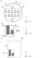
- FIG. 1is a block diagram showing the configuration of an exposure system according to an embodiment.
- FIG. 2is a diagram showing a schematic configuration of the first exposure device.
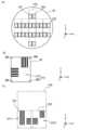
- FIG. 3is a diagram showing a schematic configuration of the exposure apparatus main body of the second exposure apparatus.
- FIG. 4is a diagram showing an example of a spatial light modulator
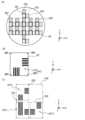
- FIG. 5is a functional block diagram of the pattern determining section of the second exposure apparatus.
- FIG. 6is a flowchart (part 1) showing an example of an interposer manufacturing method.
- FIG. 7is a flowchart (part 2) showing an example of an interposer manufacturing method.
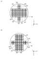
- FIG. 8Ais a diagram showing an example of an interposer having a line and space (L/S) pattern, FIG.
- FIG. 8Bis a cross-sectional diagram of a wafer
- FIG. 2is a diagram showing a plurality of pattern formation regions of FIG.
- FIG. 9Ais a diagram for explaining the first region in the wafer
- FIG. 9Bis a diagram showing an example of the first pattern
- FIG. 9Cis a pattern forming region. It is a figure which shows the state in which the 1st exposure pattern was formed in.
- FIG. 10Ais a diagram for explaining the second region in the wafer
- FIG. 10Bis a diagram showing an example of the second pattern
- FIG. 10Cis a pattern forming region. It is a figure which shows the state in which the 2nd exposure pattern was formed in.
- FIG. 11Ais a diagram for explaining the third region in the wafer
- FIG. 11Ais a diagram for explaining the third region in the wafer
- FIG. 11Bis a diagram showing an example of the third pattern, and FIG. It is a figure which shows the state in which the 3rd exposure pattern was formed in.
- FIG. 12Ais a diagram for explaining the fourth area in the wafer
- FIG. 12Bis a diagram showing an example of the fourth pattern
- FIG. Itis a figure which shows the state in which the 4th exposure pattern was formed in inside.
- FIG. 13is a diagram showing an example of a patterned insulating layer.
- FIG. 14Ais a diagram for explaining the first connection region and the second connection region, and FIG. 14B is a diagram showing an example of misalignment of wiring patterns.
- 15Ais a diagram showing an example of a connection pattern
- FIG. 15Bis a diagram showing an example of a design value pattern
- FIG. 15Cis a diagram showing another example of a connection pattern.
- FIG. 16Ais a diagram for explaining the exposure of the first connection region by the second exposure device
- FIG. 16Bis a diagram for explaining the exposure of the second connection region by the second exposure device.
- Itis a diagram for FIG. 17 is a diagram showing an L/S pattern of an interposer formed on a wafer.
- FIG. 18is a diagram illustrating the case where the second layer is overlaid on the first layer and exposed.
- FIG. 19Ais a diagram showing an example of a reticle
- FIG. 19Bis a diagram showing an example of an exposure pattern formed by rotating the reticle
- FIG. FIG. 4is a diagram showing an example;
- FIG. 1The exposure system according to this embodiment will be described below with reference to FIGS. 1 to 17.
- FIG. 1The exposure system according to this embodiment will be described below with reference to FIGS. 1 to 17.
- FIG. 1is a block diagram showing the configuration of the exposure system ES according to this embodiment.
- the exposure system ESincludes a first exposure device 100, a second exposure device 200, and a control device 400. As shown in FIG. 1, the exposure system ES includes a first exposure device 100, a second exposure device 200, and a control device 400. As shown in FIG. 1, the exposure system ES includes a first exposure device 100, a second exposure device 200, and a control device 400. As shown in FIG.
- the controller 400controls overall operations of the exposure system ES.
- the first exposure apparatus 100is an exposure apparatus that uses a reticle (photomask). The first exposure device 100 exposes the pattern formed on the reticle onto the photosensitive layer of the wafer W0.
- FIG. 2is a diagram showing a schematic configuration of the first exposure apparatus 100.
- the first exposure apparatus 100includes an illumination system 110, a reticle stage device 120, a projection optical system 130, a wafer stage device 140, an alignment detection system 150, and a first exposure controller 160.
- the two directions perpendicular to each other in the horizontal planeare the X1 direction and the Y1 direction, and the vertical direction is the Z1 direction.
- the rotation (tilt) directions about the X1-axis, Y1-axis, and Z1-axisare defined as the ⁇ x1 direction, the ⁇ y1 direction, and the ⁇ z1 direction, respectively.
- the illumination system 110includes a light source and an illumination optical system (both not shown) connected to the light source via a light transmission optical system.
- the light sourceis, for example, an ArF excimer laser light source (wavelength 193 nm).
- the illumination optical systemirradiates the illumination area IAR on the reticle R held by the reticle stage 121 of the reticle stage device 120 with the illumination light from the light source with a substantially uniform illuminance.
- the illumination area IARis a slit-like area elongated in the X1 direction.
- the reticle stage device 120includes a reticle stage 121 and a reticle laser interferometer 122.
- the reticle stage 121holds the reticle R via a holder provided on the reticle stage 121 .
- the reticle stage 121can be finely driven in the X1 and Z1 directions and can be driven within a predetermined stroke range in the scanning direction (Y1 direction) by a reticle stage driving system (not shown).
- the reticle laser interferometer 122irradiates the movable mirrors provided on the X1-direction and Y1-direction end faces of the reticle stage 121 (only the movable mirror MR1 provided on the Y1-direction end face is shown in FIG. 2) with a length-measuring beam.
- the positions of the reticle stage 121 in the X1 direction, the Y1 direction, and the ⁇ z1 directionare always detected with a resolution of about 0.25 nm, for example.
- the projection optical system 130projects the pattern formed on the reticle R onto the wafer W0 placed on the wafer stage 141 (described later) at a predetermined projection magnification (for example, 1 ⁇ 4, 1 ⁇ 5, 1 ⁇ 8 times). etc.).
- the projection optical systemhas a lens barrel 130s and a plurality of optical elements (not shown) arranged in a predetermined positional relationship inside the lens barrel 130s.
- the wafer stage device 140includes a wafer stage 141 and a laser interferometer 142.
- Wafer stage 141holds wafer W0 via a wafer holder (not shown) provided in the center of the upper surface.
- the wafer stage 141is driven by a stage driving system 143 in the X1 direction and the Y1 direction with a predetermined stroke, and is finely driven in the Z1 direction, the ⁇ x1 direction, the ⁇ y1 direction, and the ⁇ z1 direction.
- the laser interferometer 142irradiates the movable mirrors (only the movable mirror MR2 provided on the end face in the Y1 direction is shown in FIG. 2) respectively provided on the end faces in the X1 direction and the Y1 direction of the wafer stage 141 with the length measuring beam.
- the positional information of the wafer stage 141 in the X1 direction, Y1 direction, ⁇ z1 direction, ⁇ x1 direction, and ⁇ y1 directionis always detected with a resolution of, for example, about 0.25 nm.
- the alignment detection system 150is provided on the side surface of the lens barrel 130 s of the projection optical system 130 .
- the alignment detection system 150detects alignment marks and the like formed on the wafer.
- an FIA (Field Image Alignment) systemwhich is a type of image processing type imaging alignment sensor, can be used.
- a diffracted light interference type alignment systemmay be used.
- the first exposure control unit 160comprehensively controls the illumination system 110, the reticle stage device 120, the projection optical system 130, and the wafer stage device 140, and displays the image of the pattern formed on the reticle R held by the reticle stage device 120. , through the projection optical system 130 , onto the wafer W 0 held on the wafer stage 141 .
- the first exposure control unit 160 of this embodimentcontrols each unit to perform exposure by the step-and-scan method.
- the exposure apparatus disclosed in US Pat. No. 10684562may be used as the first exposure apparatus 100 having the above configuration.
- the second exposure apparatus 200is an exposure apparatus that uses a spatial light modulator (SLM) that modulates exposure light according to control by a second exposure control section 260, which will be described later.
- the second exposure apparatus 200includes an exposure apparatus main body section 200A and a pattern determination section 200B.
- FIG. 3is a diagram showing a schematic configuration of the exposure apparatus main body 200A.
- the exposure apparatus main body section 200Aincludes an illumination system 210, a pattern generation device 220, a projection optical system 230, a stage device 240, an alignment detection system 250, and a second exposure control section 260.
- the two directions perpendicular to each other in the horizontal planeare the X2 direction and the Y2 direction, and the vertical direction is the Z2 direction.
- the rotation (inclination) directions about the X2-axis, the Y2-axis, and the Z2-axisare defined as the ⁇ x2 direction, the ⁇ y2 direction, and the ⁇ z2 direction, respectively.
- the illumination system 210includes a light source unit (not shown), an illumination optical system 211, and a reflecting mirror 212.
- the light source systemincludes, for example, a solid-state laser light source (DFB semiconductor laser, fiber laser, etc.).
- the illumination optical system 211includes a shaping optical system for changing illumination conditions, an optical integrator, a field stop, and a relay lens system (all not shown).
- the pattern generation device 220generates a pattern to be projected onto the photosensitive layer of the wafer W0 placed on the stage 241 (described later) of the stage device 240 under the control of the second exposure control unit 260 .
- the pattern generation device 220includes a spatial light modulator 221 and a driver 222 .
- FIG. 4is a diagram showing an example of the spatial light modulator 221.
- the spatial light modulator 221has a plurality of micromirror mechanisms M arranged in a matrix (two-dimensional, array) within the X2-Y2 plane.
- Each of the micromirror mechanisms Mhas a micromirror M1 and a driving mechanism M2 provided on the side opposite to the reflecting surface of the micromirror M1.
- the driving mechanism M2moves, that is, moves up and down the micromirror M1 along an axis extending in the Z2 direction.
- the drive unit 222drives the drive mechanism M2 of each of the plurality of micromirror mechanisms M according to the control signal from the second exposure control unit 260, and turns the micromirror M1 between an on state (on position) and an off state (off position). switch between
- the micromirror M1is located within a region of a size that can be resolved by the projection optical system 230.
- the 0th-order diffracted light IL0 of the illumination light IL from the illumination system 210 entering the regionenters the projection optical system 230 .
- a 2 ⁇ 2 micromirror M1may be positioned within a region of a size that can be resolved by the projection optical system 230 .
- the pattern generation device 220gives a pattern to the illumination light IL by setting each of the plurality of micromirrors M1 to either an ON state or an OFF state.
- the surface on which the plurality of micromirrors M1 set to either the ON state or the OFF state are arrangedmay be referred to as the light modulation surface of the spatial light modulator 221.
- the spatial light modulator 221is not limited to the piston type described above, and may be, for example, a magneto-optical spatial light modulator (MOSLM) or a DMD (digital mirror device). Further, although the spatial light modulator 221 has been described as a reflection type that reflects the illumination light IL, the spatial light modulator 221 may be a transmission type that transmits the illumination light IL, or a diffraction type that diffracts the illumination light IL. But it's okay. The spatial light modulator 221 may spatially and temporally modulate the illumination light IL.
- MOSLMmagneto-optical spatial light modulator
- DMDdigital mirror device
- the projection optical systemhas a lens barrel 230s and a plurality of optical elements (not shown) arranged in a predetermined positional relationship inside the lens barrel 230s.
- the stage device 240includes a stage (substrate stage) 241 , a laser interferometer 242 and a stage driving section 243 .
- the stage 241holds the wafer W0 via a wafer holder (not shown) provided in the center of the upper surface.
- the stage 241can be moved in the X2 direction, the Y2 direction, and the Z2 direction by the stage drive unit 243, and can rotate around the axis extending in the Z2 direction.
- the laser interferometer 242irradiates the reflecting surfaces provided on the X2-direction and Y2-direction end faces of the stage 241 with measurement beams, thereby changing the positions of the stage 241 in the X2-direction, Y2-direction, and ⁇ z2-direction to, for example, 0.00. Detection is always performed with a resolution of about 5 to 1 nm.
- the stage drive section 243drives the stage 241 in accordance with the control signal from the second exposure control section 260 .
- the alignment detection system 250is arranged on the side of the projection optical system 230 .
- an imaging alignment sensoris used as the alignment detection system 250 .
- a detailed configuration of the alignment detection system 250is disclosed, for example, in US Pat. No. 5,637,129.
- the alignment detection system 250detects street lines and position detection marks formed on the wafer W0. The results of detection of street lines and position detection marks by the alignment detection system 250 are output to the second exposure control section 260 .
- the alignment detection system 250also detects alignment marks included in the wiring pattern formed on the wafer W0.
- the wiring patternis formed based on the exposure pattern formed on wafer W ⁇ b>0 by first exposure apparatus 100 . Therefore, it can be said that the alignment detection system 250 detects alignment marks included in the exposure pattern formed on the wafer W0 by the first exposure apparatus 100 .
- the detection result of the alignment mark by the alignment detection system 250is output to the pattern determining section 200B.
- the pattern determination unit 200Bdetermines the pattern to be exposed on the photosensitive layer of the wafer W0 based on the detection result of the alignment marks on the wafer W0 (position of the wiring pattern (exposure pattern)) by the alignment detection system 250.
- the pattern determination section 200Boutputs the determined exposure pattern to the second exposure control section 260.
- FIG. 5is a functional block diagram of the pattern determining section 200B.
- the pattern determining unit 200Bis, for example, a personal computer (PC), and includes a storage unit 310, a determining unit 320, and a receiving unit 330.
- PCpersonal computer
- the storage unit 310stores various data used for determining the pattern to be exposed on the photosensitive layer of the wafer W0.
- Determination unit 320determines a pattern to be exposed on the photosensitive layer of wafer W0 based on the data stored in storage unit 310 and the detection result of the alignment marks on wafer W0 by alignment detection system 250 .
- the receiving section 330receives the output from the alignment detection system 250 of the second exposure apparatus 200 and sends it to the determining section 320 .
- the pattern determination unit 200Bmay be separate from the second exposure apparatus 200 instead of being a part of the second exposure apparatus 200 . That is, the second exposure apparatus 200 does not have to include the pattern determining section 200B.
- the alignment mark detection result by the alignment detection system 250is transmitted to a server outside the second exposure apparatus 200, the server determines the pattern, and the determined pattern is sent to the second exposure apparatus 200 (specifically, the second exposure apparatus 200). 2) may be transmitted to the exposure control unit 260).
- the second exposure control unit 260controls the operations of the illumination system 210, the pattern generation device 220, the stage device 240, etc. so that the exposure pattern determined by the pattern determination unit 200B is formed on the wafer W0. , the image of the light modulating surface of the spatial light modulator 221 is projected onto the wafer W0 held by the stage 241 via the projection optical system 230.
- Light ILenters projection optical system 230 and a reduced image (partially inverted image) of the pattern is formed in projection area IA on wafer W 0 held by stage 241 .
- the second exposure control unit 260performs exposure using a step-and-scan method.
- the second exposure control unit 260moves the stage 241 at an appropriate speed during scan exposure, and in synchronization with this, scrolls the pattern generated by the spatial light modulator 221 (that is, the spatial light modulator change the shape of the pattern generated by H.221).
- the exposure apparatus disclosed in US Patent No. 8089616, US Patent Publication No. 2020/00257205, or International Publication No. 2005/081034may be used.
- Interposer manufacturing methodAn interposer manufacturing method for manufacturing an interposer using the exposure system ES described above will be described with reference to the flow charts of FIGS. 6 and 7.
- FIG. 8Aa case of manufacturing an interposer IP having a line and space (L/S) pattern LS shown in FIG. 8A will be described below.
- the area of the interposer IPis larger than the area of the projection area onto which the image of the pattern formed on the reticle R of the first exposure apparatus 100 is projected.
- wafer W1a wafer to be exposed (hereinafter referred to as wafer W1) is prepared (step ST1).
- FIG. 8Bis a cross-sectional view of wafer W1
- FIG. 8Cis a plan view of wafer W1.
- an insulating layer 12 and a photosensitive layer 13are laminated in this order from the bottom on the surface of the wafer W1.
- Wafer W1is made of, for example, silicon, glass, or an organic material.
- the insulating layer 12is, for example, an insulating layer such as SiO 2 .
- the photosensitive layer 13is, for example, photoresist.
- a plurality of pattern formation regions PTRare defined on the wafer W1.
- an interposer IPhaving an L/S pattern LS can be formed.
- the lateral direction of pattern formation region PTRis the X direction
- the longitudinal direction of pattern formation region PTRis the Y direction
- the normal direction of wafer W1is the Z direction.
- the rotation (tilt) directions about the X-axis, Y-axis, and Z-axisare defined as the ⁇ x direction, the ⁇ y direction, and the ⁇ z direction, respectively.
- the wafer W1is loaded into the first exposure apparatus 100 (step ST2).
- Wafer W ⁇ b>1 loaded into first exposure apparatus 100is placed on wafer stage 141 .
- wafer W1is mounted on wafer stage 141 so that the X-axis of wafer W1 and the X1-axis of first exposure apparatus 100 are aligned.
- first exposure apparatus 100forms first exposure pattern EPT1 in first region ER1 of each of a plurality of pattern formation regions PTR on wafer W1 with exposure light through first reticle R1 (step ST3). ).
- FIG. 9(A)is a diagram for explaining the first region ER1.
- the first region ER1is, for example, the lower left region within the pattern formation region PTR corresponding to the interposer IP.
- FIG. 9Bis a diagram showing an example of the first pattern PT1 formed on the first reticle R1.
- the first pattern PT1includes a first L/S pattern LS1 and alignment marks AM1.
- the first pattern PT1may include patterns such as pads.
- the first exposure apparatus 100drives the wafer stage 141 to sequentially expose a plurality of first regions ER1 to the image of the first pattern PT1 formed on the first reticle R1. As a result, as shown in FIG. 9C, the first exposure pattern EPT1 is formed in the lower left region (first region ER1) of the pattern formation region PTR.
- the first exposure apparatus 100places the second reticle R2 on the second area ER2 separated from the first area ER1 in each of the plurality of pattern formation areas PTR.
- a second exposure pattern EPT2is formed by exposure light through (step ST5).
- FIG. 10(A)is a diagram for explaining the second area ER2.
- the second region ER2is, for example, the lower right region within the pattern formation region PTR corresponding to the interposer IP.
- the first region ER1 and the second region ER2are adjacent in the X direction.
- "adjacent"means separated from each other and next to each other. The same applies to the following description.
- FIG. 10Bis a diagram showing an example of the second pattern PT2 formed on the second reticle R2.
- the second pattern PT2includes a second L/S pattern LS2 and alignment marks AM2.
- the second pattern PT2may include patterns such as pads.
- the first exposure apparatus 100includes a reticle changer capable of exchanging a plurality of reticles, and when the formation of the first exposure pattern EPT1 is completed, the reticle changer changes the first reticle R1 to the second exposure pattern. It is assumed that the reticle R2 is replaced with the reticle R2. After the formation of the first exposure pattern EPT1 is completed, the wafer W1 is unloaded from the first exposure apparatus 100, and a second exposure pattern is formed using another first exposure apparatus 100 in which the second reticle R2 is set. EPT2 may be formed in the second region ER2. That is, a plurality of first exposure apparatuses 100 may be provided. Also, a plurality of reticles may be mounted on the reticle stage 121 .
- the first exposure apparatus 100drives the wafer stage 141 to sequentially expose a plurality of second areas ER2 in the wafer W1 to images of the second pattern PT2 formed on the second reticle R2.
- the second exposure pattern EPT2is formed in the lower right region (second region ER2) of the pattern formation region PTR.
- the first exposure apparatus 100exposes the third regions in each of the plurality of pattern formation regions PTR on the wafer W1 with the exposure light through the third reticle R3.
- a third exposure pattern EPT3is formed in ER3 (step ST7).
- FIG. 11(A)is a diagram for explaining the third area ER3.
- the third region ER3is, for example, the upper left region within the pattern formation region PTR corresponding to the interposer IP, as shown in FIG. 11(A).
- the third region ER3is a region that is different from the first region ER1 and the second region ER2 and that is adjacent to the first region ER1 in the Y direction intersecting the X direction.
- FIG. 11(B)is a diagram showing an example of the third pattern PT3 formed on the third reticle R3.
- the third pattern PT3includes a third L/S pattern LS3 and alignment marks AM3.
- the third pattern PT3may include patterns such as pads.
- the first exposure apparatus 100drives the wafer stage 141 to place the third reticle R3 in the plurality of third areas ER3 within the wafer W1.
- the images of the third pattern PT3 formed on R3are sequentially exposed.
- the third exposure pattern EPT3is formed in the upper left region (third region ER3) of the pattern formation region PTR.
- the first exposure apparatus 100exposes the fourth area ER4 in each of the plurality of pattern formation areas PTR on the wafer W1 through the fourth reticle R4.
- a fourth exposure pattern EPT4is formed with light (step ST8).
- FIG. 12(A)is a diagram for explaining the fourth area ER4.
- the fourth region ER4is, for example, the upper right region within the pattern formation region PTR corresponding to the interposer IP.
- the fourth region ER4is a region adjacent to the third region ER3 in the X direction and adjacent to the second region ER2 in the Y direction.
- FIG. 12(B)is a diagram showing an example of the fourth pattern PT4 formed on the fourth reticle R4.
- the fourth pattern PT4includes a fourth L/S pattern LS4 and an alignment mark AM4.
- the fourth pattern PT4may include patterns such as pads.
- the first exposure apparatus 100drives the wafer stage 141 to change the image of the fourth pattern PT4 formed on the fourth reticle R4. , a plurality of fourth regions ER4 are sequentially exposed. As a result, as shown in FIG. 12C, the fourth exposure pattern EPT4 is formed in the upper right region (fourth region ER4) of the pattern formation region PTR.
- the wafer W1is unloaded from the first exposure apparatus 100 and developed and etched (step ST9). Specifically, the insulating layer 12 formed on the surface of the substrate 11 (the surface of the wafer W1) is etched using the first exposure pattern EPT1 to the fourth exposure pattern EPT4 as masks. Thereby, the insulating layer 12 is patterned as shown in FIG. More specifically, wiring patterns WP1 to WP4 for embedding metal in the patterned insulating layer 12 are formed in a process described later. In FIG. 13, the etched insulating layer 12 is indicated by hatching.
- the width of the wiring included in the wiring patterns WP1 to WP4is, for example, 200 nm or less.
- the width of the wiring included in the wiring patterns WP1 to WP4may be, for example, 400 nm or less.
- the wafer W1is again coated with a resist (step ST10).
- wafer W1is loaded into exposure apparatus main body 200A of second exposure apparatus 200 (step ST11).
- wafer W1is placed on stage 241 after being pre-aligned by a pre-alignment system (not shown).
- wafer W1is mounted on stage 241 so that the X-axis of wafer W1 and the X2-axis of second exposure apparatus 200 are aligned.
- the configuration of the pre-alignment systemthe configuration described in US Pat. No. 6,624,433 can be adopted.
- the alignment detection system 250measures the positions of the alignment marks AM1 to AM4 by detecting the alignment marks AM1 to AM4 formed on the wafer W1 (step ST13).
- the measurement results of the positions of the alignment marks AM1 to AM4are output to the pattern determining section 200B.
- the pattern determination section 200Bdetermines exposure patterns to be formed in the first connection region CR1 and the second connection region CR2 based on the measurement results of the positions of the alignment marks AM1 to AM4 (step ST15). ). More specifically, the exposure pattern formed in the first connection region CR1 and the second connection region CR2 is based on the positions of the wiring patterns WP1 to WP4 obtained from the measurement results of the positions of the alignment marks AM1 to AM4. (hereinafter referred to as a connection pattern) are determined respectively.
- FIG. 14(A)is a diagram explaining the first connection region CR1 and the second connection region CR2.
- the first connection region CR1is a region including a region between the first region ER1 and the second region ER2 and a region between the third region ER3 and the fourth region ER4. be.
- the second connection region CR2is a region including a region between the first region ER1 and the third region ER3 and a region between the second region ER2 and the fourth region ER4.
- the first exposure apparatus 100when forming the first exposure pattern EPT1 to the fourth exposure pattern EPT4 in the first region ER1 to the fourth region ER4, respectively, the first exposure pattern EPT1 to the fourth exposure pattern EPT4 are formed.
- the positionmay deviate from the design position.
- the wiring patterns WP1 to WP4are also formed shifted from the designed positions.
- FIG. 14(B)shows an example of misalignment of the wiring patterns WP1 and WP2.
- the designed positions of the wiring patterns WP1 and WP2are indicated by dotted lines, and the actual positions of the wiring patterns WP1 and WP2 are indicated by solid lines.
- the wiring pattern WP1is shifted in the -X direction and the -Y direction with respect to the design position
- the wiring pattern WP2is shifted in the -X direction and the +Y direction with respect to the design position.
- the determination unit 320 of the pattern determination unit 200Bdetermines the deviation amounts ⁇ X, Y in the X direction from the design positions of the wiring pattern WP1 and the wiring pattern WP2.
- a direction deviation amount ⁇ Y and a rotational direction deviation amount ⁇ z about an axis extending in the Z directionare calculated.
- the determination unit 320determines a connection pattern that connects the wiring pattern WP1 and the wiring pattern WP2.
- the connection patternis a pattern that connects to the wiring pattern WP1 and also connects to the wiring pattern WP2.
- connection pattern that connects the wiring pattern WP1 and the wiring pattern WP2is created based on the wiring patterns WP1 and WP2 formed at the design positions. Therefore, for example, when the actual positions of the wiring patterns WP1 and WP2 are shifted from the design positions as shown in FIG. If the connection patterns are formed as they are, there is a risk that a connection failure such as disconnection may occur between the wiring patterns WP1 and WP2.
- the determination unit 320calculates the positions of the ends of the wirings included in the wiring patterns WP1 and WP2 from the amounts of deviation from the design positions of the wiring patterns WP1 and WP2. Based on the calculated positions of the wiring ends, the determination unit 320 determines a connection pattern CPT that connects the ends of the wirings included in the wiring pattern WP1 and the wiring pattern WP2, as shown in FIG. 15A, for example. to decide. The same applies to the connection pattern between the wiring pattern WP3 and the wiring pattern WP4, the connection pattern between the wiring pattern WP1 and the wiring pattern WP3, and the connection pattern between the wiring pattern WP2 and the wiring pattern WP4.
- connection pattern for connecting the ends of the wiringis created by changing the connection pattern based on the design position stored in the storage unit 310 based on the amount of deviation of each of the wiring patterns WP1 to WP4 from the design position.
- connection pattern CPT-D(design value pattern) based on the wiring patterns WP1 and WP2 formed at the design positions is the pattern shown in FIG. 15(B).
- the determination unit 320uses part of the design value pattern CPT-D' for the central portion of the area between the wiring pattern WP1 and the wiring pattern WP2.
- the connection pattern CPTmay be determined by creating connection patterns CPT-1 and CPT-2 that connect the wiring patterns formed in the central portion and the wiring patterns WP1 and WP2. .
- the design value patternis used for a predetermined region, and the connection pattern for connecting the design value pattern and the actual wiring pattern is created for the other regions. You may do so. By doing so, it is possible to shorten the time required to create the data as compared with the case where the connection pattern data is created from the beginning.
- the pattern determination unit 200Bdetermines the first connection pattern formed in the first connection region CR1 and the second connection pattern formed in the second connection region CR2.
- the first connection patternincludes a connection pattern that connects the wiring pattern WP1 and the wiring pattern WP2, and a connection pattern that connects the wiring pattern WP3 and the wiring pattern WP4.
- the second connection patternincludes a connection pattern that connects the wiring pattern WP1 and the wiring pattern WP3, and a connection pattern that connects the wiring pattern WP2 and the wiring pattern WP4.
- the first connection pattern and the second connection patternare formed using the second exposure apparatus 200 that uses the spatial light modulator 221, so the first connection pattern and the second connection pattern are made different. be able to.
- the connection pattern connecting the wiring pattern WP1 and the wiring pattern WP2can be made different from the connection pattern connecting the wiring pattern WP3 and the wiring pattern WP4.
- the connection pattern connecting the wiring pattern WP1 and the wiring pattern WP3can be made different from the connection pattern connecting the wiring pattern WP2 and the wiring pattern WP4.
- the pattern determination unit 200Bcreates data for forming the first connection pattern and data for forming the second connection pattern, and outputs the data to the second exposure control unit 260.
- the second exposure control section 260causes the pattern generation device 220 to generate a pattern based on the data output from the pattern determination section 200B.
- the second exposure control section 260first causes the pattern generation device 220 (spatial light modulator 221) to generate a pattern for forming the first connection pattern.
- the exposure apparatus main body section 200Aforms the first connection pattern in the first connection region CR1 with exposure light through the spatial light modulator 221 (step ST17). Specifically, the image generated by the light modulating surface of the spatial light modulator 221 is sequentially exposed to the first connection region CR1 based on the data created by the pattern determination unit 200B, thereby changing the first connection pattern to the first It is formed in the connection region CR1 (see FIG. 16A).
- step ST17ends, the orientation of wafer W1 is changed around the axis (Z-axis) that intersects the surface of wafer W1 (step ST19). Specifically, the orientation of wafer W1 is changed by 90 degrees around the Z-axis. By returning wafer W1 from stage 241 to the pre-alignment system and rotating wafer W1 about the Z-axis by 90 degrees, the orientation of wafer W1 can be changed as shown in FIG. 16B. can. As a result, the Y-axis of wafer W1 and the X1-axis of second exposure apparatus 200 are aligned.
- the second exposure control section 260causes the pattern generation device 220 to generate a pattern for forming the second connection pattern.
- the exposure apparatus main body 200Aforms the second connection pattern in the second connection region CR2 with exposure light through the spatial light modulator 221 (step ST21). Specifically, the image generated by the light modulating surface of the spatial light modulator 221 is sequentially exposed to the second connection region CR2 based on the data created by the pattern determination unit 200B, thereby changing the second connection pattern to the second It is formed in the connection region CR2 (see FIG. 16B).
- step ST23development and etching are performed (step ST23). More specifically, the insulating layer 12 is etched using the first connection pattern and the second connection pattern as masks.
- the insulating layer 12 etched in step ST23is the same insulating layer as the insulating layer 12 etched in step ST9.
- CMPChemical Mechanical Polishing
- the interposer IPis singulated by dicing or the like (step ST25). As described above, the interposer IP can be manufactured.
- the exposure methoduses the first exposure apparatus 100 that uses a reticle (photomask) to expose a plurality of beams on wafer W1 with exposure light through first reticle R1.
- a first exposure pattern EPT1is formed in a first region ER1 of each of the pattern formation regions PTR, and a second region ER2 separated from the first region ER1 in each of the pattern formation regions PTR is exposed to light through a second reticle R2.
- the first exposure pattern EPT1 and the second exposure pattern EPT2are formed using the second exposure apparatus 200 that uses the spatial light modulator 221 that modulates the exposure light based on the output from the pattern determination unit 200B.
- the throughputis high, but the stitching accuracy is general. becomes larger than 20 nm. Therefore, it is difficult to narrow the width of the wiring (for example, 200 nm or less).
- the stitching accuracyis high, but the throughput is low.
- the spatial light modulatorIt is possible to achieve higher throughput and higher stitching accuracy than when using only an exposure apparatus that uses . Specifically, a stitching accuracy of approximately 10 nm or less can be achieved. This makes it possible to narrow the width of the wiring (for example, 200 nm or less).
- the exposure methodincludes changing the connection pattern formed by the exposure light through the spatial light modulator 221 based on the positions of the first exposure pattern EPT1 and the second exposure pattern EPT2. . Since the connection pattern can be changed, the first exposure pattern EPT1 and the second exposure pattern EPT2 are reliably connected even when the formation positions of the first exposure pattern EPT1 and the second exposure pattern EPT2 deviate from the designed positions. It is possible to improve the connection reliability of the wiring.
- the exposure methodmeasures the position of the first exposure pattern EPT1 and the position of the second exposure pattern EPT2, and the measurement results of the positions of the first exposure pattern EPT1 and the second exposure pattern EPT2. and changing the connection pattern formed by the exposure light through the spatial light modulator 221 based on the exposure light.
- a connection pattern that connects the first exposure pattern EPT1 and the second exposure pattern EPT2can be determined based on the actual position of the first exposure pattern EPT1 and the actual position of the second exposure pattern EPT2. Therefore, the first exposure pattern EPT1 and the second exposure pattern EPT2 can be reliably connected, and the connection reliability of the wiring can be improved.
- the exposure method according to the present embodimentuses the first exposure apparatus 100 that uses a reticle to expose the first regions ER1 and PTR in each of the plurality of pattern formation regions PTR on the wafer W1 with exposure light through the third reticle R3. It further includes forming a third exposure pattern EPT3 in a third area ER3 different from the second area ER2.
- the first region ER1 and the second region ER2are adjacent in the X direction along the surface of the wafer W1, and the third region ER3 is adjacent to the first region ER1 in the Y direction crossing the X direction.
- connection pattern with the exposure light through the spatial light modulator 221connects between the first region ER1 and the second region ER2 adjacent in the X direction with the exposure light through the spatial light modulator 221.
- an exposure pattern corresponding to the L/S pattern LS of the interposer IPcan be formed in the pattern formation region PTR having an area approximately four times the projected area of the pattern formed on one reticle.
- the wafer W1is changed around the axis (Z-axis) intersecting the surface of the wafer W1, and the exposure light through the spatial light modulator 221 is applied between the first region ER1 and the third region ER3 adjacent in the Y direction.
- Form a connection patterncompared to the case where the stage 241 is driven without changing the orientation of the wafer W1 around the Z-axis and the second connection pattern is formed by the exposure light that has passed through the spatial light modulator 221, the process can be completed in a short time. Since the second connection pattern can be formed, high throughput can be achieved.
- connection pattern formed by exposure light through the spatial light modulator 221includes a pattern that connects with the first exposure pattern EPT1 exposed in the first region ER1. Thereby, a wiring pattern connected to the wiring pattern WP1 formed based on the first exposure pattern EPT1 can be formed.
- the first exposure pattern EPT1 and the second exposure pattern EPT2, and the connection pattern formed by exposure light through the spatial light modulator 221include an L/S pattern. is 200 nm or less. Since a thin L/S pattern can be formed, high-density wiring can be formed. Therefore, the number of communication channels can be increased, and high-speed communication between the logic circuit and the memory arranged on the interposer can be enabled, for example.
- the first exposure pattern EPT1is formed by exposing the image of the first pattern PT1 formed on the first reticle R1 to the first area ER1
- the second exposure pattern EPT2is formed by: It is formed by exposing the image of the second pattern formed on the second reticle R2 different from the first reticle R1 to the second area ER2.
- the method for manufacturing the interposer IPis such that the surface (insulating layer 12) of the wafer W1 is exposed using the first exposure pattern EPT1 and the second exposure pattern EPT2 formed by the first exposure apparatus 100 as masks. and processing (etching) the surface (insulating layer 12) of wafer W1 using the first connection pattern formed in first connection region CR1 by second exposure apparatus 200 as a mask. .
- an interposer IP having a large area, high wiring density, and high connection reliabilitycan be manufactured with high throughput.
- the second exposure apparatus 200includes the stage 241 for mounting the wafer W1 on which the wiring patterns WP1 to WP4 are formed in the plurality of regions ER1 to ER4 separated from each other, and the wiring patterns WP1 to WP4.
- a pattern determination unit 200Bthat determines a connection pattern based on the measurement results of the positions of, a spatial light modulator 221 that modulates and emits incident light based on the output from the pattern determination unit 200B, and a spatial light modulator 221, and a projection optical system 230 for projecting an image of the light modulating surface of the spatial light modulator 221 between adjacent regions among the plurality of regions ER1 to ER4.
- a connection patternthat connects at least any two of the wiring patterns WP1 to WP4 can be formed.
- the exposure system ESforms exposure patterns in a plurality of regions separated from each other in the pattern formation region PTR on the wafer W1 with exposure light passing through each of the plurality of reticles.
- a second exposure device 200that forms an exposure pattern with light.
- the case where the first exposure apparatus 100 exposes the pattern image using the reticle Ris four in the pattern formation region PTR corresponding to the interposer IP. is not limited to In the pattern formation region PTR, the number of regions where the first exposure device 100 exposes the pattern image using the reticle R may be, for example, two, or may be five or more.
- the pattern determination unit 200Bmay determine connection patterns so that the wiring patterns formed in each region are connected as designed.
- the positions of the first exposure pattern EPT1 to the fourth exposure pattern EPT4are detected by detecting the positions of the alignment marks AM1 to AM4 formed on the wafer W1.
- it was measuredit is not limited to this.
- the first reticle R1 to the fourth reticle R4 each having a different patternare used, but the present invention is not limited to this.
- one reticle R5 having a pattern PT5 as shown in FIG. 19Ais rotated as shown in FIG. may be exposed to multiple regions of the
- one sheet including the first pattern PT1 formed on the first reticle R1 and the second pattern PT2 formed on the second reticle R2is printed.
- a single reticle R7 including a reticle R6, a third pattern PT3 formed on the third reticle R3, and a fourth pattern PT4 formed on the fourth reticle R4is used for the first exposure.
- the pattern EPT1 to the fourth exposure pattern EPT4may be formed in the pattern formation region PTR.
- a reticle including the first pattern PT1 and the third pattern PT3 and a reticle including the second pattern PT2 and the fourth pattern PT4are used to form the first exposure pattern EPT1 to the fourth exposure pattern EPT4 in the pattern formation area. It may be formed in the PTR.
- steps ST19 and ST21 in FIG. 7can be omitted, thereby further improving the throughput.
- the region including the first region ER1 and the second region ER2is defined as the first pattern formation region
- the region including the third region ER3 and the fourth region ER4.is a second pattern formation region
- a connection pattern connecting the wiring pattern WP1 and the wiring pattern WP2is formed between the first region ER1 and the second region ER2 in the first pattern formation region
- the second pattern formation regionA connection pattern that connects the wiring pattern WP3 and the wiring pattern WP4 may be formed between the third region ER3 and the fourth region ER4. That is, the first connection region may be divided into two regions and different connection patterns may be formed in each region.
- connection patternthat matches the actual formation positions of the wiring pattern WP1 and the wiring pattern WP2, and a connection pattern that matches the actual formation positions of the wiring pattern WP3 and the wiring pattern WP4. Reliability can be ensured. The same applies to the second connection area.
- the first connection pattern determined by the determination unit 320 of the pattern determination unit 200Bincludes the connection pattern connecting the wiring pattern WP1 and the wiring pattern WP4, and the connection pattern connecting the wiring pattern WP2 and the wiring pattern WP3. and connection patterns.
- the second connection patternmay include a connection pattern connecting the wiring pattern WP1 and the wiring pattern WP4 and a connection pattern connecting the wiring pattern WP2 and the wiring pattern WP3.
- the orientation of the wafer W1is changed by 90 degrees around the Z-axis by the pre-alignment system, and then the second connection patterns are formed.
- the direction of the spatial light modulator 221is changed around the axis (Z-axis) that intersects the light modulation surface of the spatial light modulator 221, and the second connection pattern is formed. good too.
- the orientation of wafer W1is changed by a predetermined angle around the Z-axis by the pre-alignment system, and the orientation of spatial light modulator 221 is changed by a certain angle around the Z-axis.
- the angle for changing the orientation of wafer W1 and the angle for changing the orientation of spatial light modulator 221may be any angle as long as the second connection pattern can be formed in second connection region CR2.
- connection pattern that connects the wiring pattern WP1 and the wiring pattern WP2is formed in the first connection region CR1, but the present invention is not limited to this.
- a connection pattern connected to either one of the wiring pattern WP1 and the wiring pattern WP2may be formed in the first connection region CR1.
- the exposure pattern formed in at least one of the first connection region CR1 and the second connection region CR2may not include a connection pattern.
- development, etching, and resist coatingare performed after the exposure of the images of the first pattern PT1 to the fourth pattern PT4 in the first exposure device 100, but the present invention is not limited to this.
- the wafer W1is loaded into the second exposure apparatus 200, and the alignment marks AM1 to AM4 are exposed as latent image patterns on the resist. may be determined and formed to determine and form the first connection pattern and the second connection pattern.
- the first exposure pattern EPT1is formed in the first region ER1 within the pattern formation region PTR, and the second region ER2 separated from the first region ER1 within the pattern formation region PTR.
- a wafer W1 having a second exposure pattern EPT2 formed thereonis placed on the wafer W1, and the pattern determination unit 200B determines a connection pattern based on the measurement results of the positions of the first exposure pattern EPT1 and the second exposure pattern EPT2. good too.
- step ST10resist coating in FIG. 6
- First exposure apparatus 200Second exposure apparatus 200A Exposure apparatus main body 200B Pattern determination section 221 Spatial light modulator 241 Stage CPT Connection pattern ES Exposure system ER1 to ER4 First to fourth areas EPT1 to EPT4 First to fourth exposure Pattern IP Interposers LS1 to LS4 First to fourth L/S patterns PTR Pattern forming regions PT1 to PT4 First to fourth patterns R, R1 to R7 Reticles W0, W1 Wafers WP1 to WP4 Wiring patterns
Landscapes
- Physics & Mathematics (AREA)
- General Physics & Mathematics (AREA)
- Engineering & Computer Science (AREA)
- Power Engineering (AREA)
- Condensed Matter Physics & Semiconductors (AREA)
- Manufacturing & Machinery (AREA)
- Computer Hardware Design (AREA)
- Microelectronics & Electronic Packaging (AREA)
- Ceramic Engineering (AREA)
- Optics & Photonics (AREA)
- Health & Medical Sciences (AREA)
- Environmental & Geological Engineering (AREA)
- Epidemiology (AREA)
- Public Health (AREA)
- Exposure And Positioning Against Photoresist Photosensitive Materials (AREA)
- Exposure Of Semiconductors, Excluding Electron Or Ion Beam Exposure (AREA)
Abstract
Description
Translated fromJapanese露光方法、デバイス製造方法、露光装置、及び露光システムに関する。It relates to exposure methods, device manufacturing methods, exposure apparatuses, and exposure systems.
先端パッケージング技術において、複数チップを面内に並列配置するために大面積インターポーザーが用いられる場合がある。In advanced packaging technology, large-area interposers are sometimes used to arrange multiple chips side by side.
インターポーザーは、配線のみを作りこんだチップであり、半導体製造工程により製造される。しかしながら、半導体製造工程で露光に使われるフォトマスクでは露光サイズが決まっているため、大面積のインターポーザーを製造するために、基板上で複数のパターンを繋ぎ合わせて大きなパターンを露光するスティッチング露光技術が用いられている(例えば、特許文献1)。The interposer is a chip with only wiring built in, and is manufactured using the semiconductor manufacturing process. However, since the photomask used for exposure in the semiconductor manufacturing process has a fixed exposure size, in order to manufacture a large-area interposer, stitching exposure is used to expose a large pattern by joining multiple patterns on a substrate. technology is used (for example, Patent Document 1).
第1の開示の態様によれば、マスクを用いる露光装置を用いて、第1マスクを介した露光光で基板上の複数のパターン形成領域それぞれの第1領域に第1露光パターンを形成し、前記パターン形成領域それぞれにおいて前記第1領域から離間した第2領域に第2マスクを介した露光光で第2露光パターンを形成することと、露光パターン決定部からの出力に基づいて露光光を変調する空間光変調器を用いる露光装置を用いて、前記パターン形成領域それぞれにおいて前記第1及び第2領域の間に、前記第1及び第2露光パターンの位置に基づいて決定される露光パターンを、前記空間光変調器を介した露光光で形成することと、を含む露光方法が提供される。According to a first aspect of the disclosure, an exposure apparatus using a mask is used to form a first exposure pattern in a first region of each of a plurality of pattern formation regions on a substrate with exposure light through a first mask, forming a second exposure pattern with exposure light through a second mask in a second area spaced apart from the first area in each of the pattern formation areas; and modulating the exposure light based on an output from an exposure pattern determination unit. an exposure pattern determined based on the positions of the first and second exposure patterns between the first and second regions in each of the pattern formation regions using an exposure apparatus that uses a spatial light modulator to and forming with exposure light through the spatial light modulator.
第2の開示の態様によれば、基板上のパターン形成領域内の第1領域に第1露光パターンを形成することと、前記パターン形成領域内において前記第1領域から離間した第2領域に第2露光パターンを形成することと、前記第1露光パターンの位置及び前記第2露光パターンの位置の計測結果に基づいて、前記第1領域と前記第2領域との間の第3領域に露光パターンを形成することと、を含む露光方法が提供される。According to a second aspect of the disclosure, forming a first exposure pattern in a first region within a pattern formation region on a substrate; Forming two exposure patterns, and forming an exposure pattern in a third region between the first region and the second region based on measurement results of the position of the first exposure pattern and the position of the second exposure pattern A method of exposure is provided comprising: forming a
第3の開示の態様によれば、上記露光方法を用いて形成された前記第1及び第2露光パターンをマスクとして前記基板の表面を加工することと、上記露光方法を用いて前記第3領域に形成された前記露光パターンをマスクとして前記基板の前記表面を加工することと、を含むデバイス製造方法が提供される。According to a third aspect of the disclosure, the surface of the substrate is processed using the first and second exposure patterns formed using the exposure method as masks, and the third region is processed using the exposure method. and processing the surface of the substrate using the exposure pattern formed in the step as a mask.
第4の開示の態様によれば、パターン形成領域内の第1領域に第1露光パターンが形成され且つ前記パターン形成領域内において前記第1領域から離間した第2領域に第2露光パターンが形成された基板を載置する基板ステージと、前記第1露光パターンの位置及び前記第2露光パターンの位置の計測結果に基づいて露光パターンを決定する露光パターン決定部と、前記露光パターン決定部からの出力に基づいて、入射する光を変調して射出する空間光変調器と、前記空間光変調器に照明光を照射する照明光学系と、前記第1及び第2領域の間に、前記空間光変調器の光変調面の像を投影する投影光学系と、を備える露光装置が提供される。According to a fourth aspect of the disclosure, a first exposure pattern is formed in a first area within a pattern formation area, and a second exposure pattern is formed in a second area spaced apart from the first area within the pattern formation area. an exposure pattern determination unit for determining an exposure pattern based on measurement results of the position of the first exposure pattern and the position of the second exposure pattern; and a signal from the exposure pattern determination unit. a spatial light modulator that modulates and emits incident light based on an output; an illumination optical system that irradiates the spatial light modulator with illumination light; and a projection optical system for projecting an image of the light modulating surface of the modulator.
第5の開示態様によれば、互いに離間する複数の領域に配線パターンが形成された基板を載置する基板ステージと、前記配線パターンの位置の計測結果に基づいて露光パターンを決定する露光パターン決定部と、前記露光パターン決定部からの出力に基づいて、入射する光を変調して射出する空間光変調器と、前記空間光変調器に照明光を照射する照明光学系と、前記複数の領域のうち隣接する領域の間に、前記空間光変調器の光変調面の像を投影する投影光学系と、を備える露光装置が提供される。According to a fifth aspect of the disclosure, there is provided a substrate stage on which a substrate having wiring patterns formed in a plurality of areas spaced apart from each other is placed, and an exposure pattern determining apparatus that determines an exposure pattern based on a measurement result of the positions of the wiring patterns. a spatial light modulator that modulates and emits incident light based on the output from the exposure pattern determination unit; an illumination optical system that irradiates the spatial light modulator with illumination light; and the plurality of regions. and a projection optical system for projecting an image of the light modulating surface of the spatial light modulator between adjacent regions of the spatial light modulator.
第6の開示態様によれば、基板上のパターン形成領域内の互いに離間する複数の領域に、複数のマスクのそれぞれを介した露光光で露光パターンをそれぞれ形成する第1露光装置と、露光パターン決定部からの出力に基づいて露光光を変調する空間光変調器を備え、前記複数の領域のうち隣接する領域の間に、前記空間光変調器を介した露光光で露光パターンを形成する第2露光装置と、を備える露光システムが提供される。According to a sixth aspect of the disclosure, a first exposure device for forming exposure patterns in a plurality of regions separated from each other in a pattern formation region on a substrate with exposure light through each of a plurality of masks; a spatial light modulator that modulates exposure light based on the output from the determination unit, and forms an exposure pattern between adjacent regions of the plurality of regions with the exposure light that has passed through the spatial light modulator; 2. An exposure system is provided comprising: a.
なお、後述の実施形態の構成を適宜改良しても良く、また、少なくとも一部を他の構成物に代替させても良い。更に、その配置について特に限定のない構成要件は、実施形態で開示した配置に限らず、その機能を達成できる位置に配置することができる。It should be noted that the configuration of the embodiment described later may be modified as appropriate, and at least a portion thereof may be replaced with other components. Furthermore, constituent elements whose arrangement is not particularly limited are not limited to the arrangement disclosed in the embodiments, and can be arranged at positions where their functions can be achieved.
スティッチング露光技術では、例えば2つのマスクを用いて基板上で2つのパターンを繋ぎ合わせて露光するが、パターン同士の繋ぎ合わせ精度(以後、スティッチング精度と記載する)が低下すると、線幅精度が低下するおそれがある。また、配線同士の接続不良や短絡が生じるおそれもある。高いスティッチング精度を確保しつつ、高いスループットを達成することが望まれている。In the stitching exposure technique, for example, two masks are used to join two patterns on a substrate for exposure. may decrease. In addition, there is a possibility that poor connection or short circuit may occur between the wirings. It is desired to achieve high throughput while ensuring high stitching accuracy.
以下、本実施形態に係る露光システムについて、図1~図17に基づいて説明する。The exposure system according to this embodiment will be described below with reference to FIGS. 1 to 17. FIG.
図1は、本実施形態に係る露光システムESの構成を示すブロック図である。図1に示すように、露光システムESは、第1露光装置100と、第2露光装置200と、制御装置400と、を備える。FIG. 1 is a block diagram showing the configuration of the exposure system ES according to this embodiment. As shown in FIG. 1, the exposure system ES includes a
以下では、第1露光装置100および第2露光装置200の被処理対象がウエハW0である場合を例として説明する。制御装置400は、露光システムESの動作を全体的に制御する。In the following, a case where the object to be processed by the
(第1露光装置100)
第1露光装置100は、レチクル(フォトマスク)を用いる露光装置である。第1露光装置100は、レチクルに形成されたパターンを、ウエハW0の感光層に露光する。(First exposure device 100)
The
図2は、第1露光装置100の概略構成を示す図である。図2に示すように、第1露光装置100は、照明系110、レチクルステージ装置120、投影光学系130、ウエハステージ装置140、アライメント検出系150、および第1露光制御部160を備える。第1露光装置100の説明においては、水平面内において互いに直交する2方向をX1方向、Y1方向とし、鉛直方向をZ1方向とする。また、X1軸、Y1軸、及びZ1軸周りの回転(傾斜)方向をそれぞれθx1方向、θy1方向、及びθz1方向とする。FIG. 2 is a diagram showing a schematic configuration of the
照明系110は、光源と、該光源に送光光学系を介して接続された照明光学系(いずれも不図示)と、を備える。光源は、一例としてArFエキシマレーザ光源(波長193nm)である。照明光学系は、光源からの照明光を、レチクルステージ装置120のレチクルステージ121に保持されたレチクルR上の照明領域IARに、ほぼ均一な照度で照射する。照明領域IARはX1方向に細長く伸びるスリット状の領域である。The
レチクルステージ装置120は、レチクルステージ121と、レチクルレーザ干渉計122と、を備える。The
レチクルステージ121は、レチクルステージ121に設けられたホルダを介してレチクルRを保持する。レチクルステージ121は、不図示のレチクルステージ駆動系により、X1方向及びZ1方向に微小駆動可能であり、且つ走査方向(Y1方向)に所定ストローク範囲で駆動可能である。The
レチクルレーザ干渉計122は、レチクルステージ121のX1方向及びY1方向の端面にそれぞれ設けられた移動鏡(図2ではY1方向の端面に設けられた移動鏡MR1のみ図示)に測長ビームを照射することにより、レチクルステージ121のX1方向、Y1方向、及びθz1方向の位置を、例えば0.25nm程度の分解能で常時検出する。The
投影光学系130は、レチクルRに形成されたパターンを、ウエハステージ141(後述)に配置されたウエハW0に、所定の投影倍率(一例として1/4倍、1/5倍、1/8倍等)で縮小投影する。投影光学系は鏡筒130sと、鏡筒130sの内部に所定の位置関係で配置された複数の光学素子(不図示)を有する。The projection
ウエハステージ装置140は、ウエハステージ141と、レーザ干渉計142と、を備える。ウエハステージ141は、上面中央に設けられたウエハホルダ(不図示)を介してウエハW0を保持する。ウエハステージ141は、ステージ駆動系143によりX1方向、及びY1方向に所定ストロークで駆動されるとともに、Z1方向、θx1方向、θy1方向、及びθz1方向に微小駆動される。The
レーザ干渉計142はウエハステージ141のX1方向及びY1方向の端面にそれぞれ設けられた移動鏡(図2では、Y1方向の端面に設けられた移動鏡MR2のみを図示)に測長ビームを照射することにより、ウエハステージ141のX1方向、Y1方向、θz1方向、θx1方向、θy1方向の位置情報を、例えば0.25nm程度の分解能で常時検出する。The
アライメント検出系150は、投影光学系130の鏡筒130sの側面に設けられている。アライメント検出系150は、ウエハに形成されたアライメントマーク等を検出する。アライメント検出系150として、画像処理方式の結像式アライメントセンサの一種であるFIA(Field Image Alignment)系を用いることができる。画像処理方式のアライメント系に代えて、或いはこれに加えて回折光干渉型のアライメント系を用いてもよい。The
第1露光制御部160は、照明系110、レチクルステージ装置120、投影光学系130、ウエハステージ装置140を総合的に制御し、レチクルステージ装置120が保持するレチクルRに形成されたパターンの像を、投影光学系130を介して、ウエハステージ141に保持されたウエハW0上に露光する。本実施形態の第1露光制御部160は、ステップアンドスキャン方式で露光を行うよう各部を制御する。The first
上記の構成を有する第1露光装置100として、米国特許第10684562号明細書に開示された露光装置を用いてもよい。The exposure apparatus disclosed in US Pat. No. 10684562 may be used as the
(第2露光装置200)
第2露光装置200は、後述する第2露光制御部260による制御に応じて露光光を変調する空間光変調器(SLM: Spatial Light Modulator)を用いる露光装置である。第2露光装置200は、露光装置本体部200Aと、パターン決定部200Bと、を備える。(Second exposure device 200)
The
図3は、露光装置本体部200Aの概略構成を示す図である。図3に示すように、露光装置本体部200Aは、照明系210、パターン生成装置220、投影光学系230、ステージ装置240、アライメント検出系250、及び第2露光制御部260を備える。露光装置本体部200Aの説明においては、水平面内において互いに直交する2方向をX2方向、Y2方向とし、鉛直方向をZ2方向とする。また、X2軸、Y2軸、及びZ2軸周りの回転(傾斜)方向をそれぞれθx2方向、θy2方向、及びθz2方向とする。FIG. 3 is a diagram showing a schematic configuration of the exposure apparatus
照明系210は、光源ユニット(不図示)と、照明光学系211と、反射ミラー212と、を備える。光源系は、一例として、固体レーザ光源(DFB半導体レーザ、ファイバレーザ等)を含む。照明光学系211は、照明条件を変更するための成形光学系、オプティカルインテグレータ、視野絞り、リレーレンズ系(いずれも不図示)を含む。The
パターン生成装置220は、第2露光制御部260による制御に応じてステージ装置240のステージ241(後述)に載置されたウエハW0の感光層に投影するパターンを生成する。パターン生成装置220は、空間光変調器221と、駆動部222と、を備える。The
図4は、空間光変調器221の一例を示す図である。図4に示すように、空間光変調器221は、X2-Y2平面内にマトリックス状(2次元状、アレイ状)に配置された複数のマイクロミラー機構Mを有する。マイクロミラー機構Mの各々は、マイクロミラーM1と、マイクロミラーM1の反射面とは反対側に設けられた駆動機構M2とを有する。駆動機構M2は、マイクロミラーM1をZ2方向に延びる軸に沿って移動、つまり上下させる。FIG. 4 is a diagram showing an example of the spatial
駆動部222は、第2露光制御部260からの制御信号に従って複数のマイクロミラー機構Mの各々の駆動機構M2を駆動し、マイクロミラーM1をオン状態(オン位置)とオフ状態(オフ位置)との間で切り替える。The
ここで、各マイクロミラーM1のサイズが投影光学系230で解像することのできないほど小さなサイズであるため、投影光学系230で解像することのできる大きさの領域の中でマイクロミラーM1が全てオン状態又は全てオフ状態である場合、当該領域に入射する照明系210からの照明光ILの0次回折光IL0は、投影光学系230に入射する。投影光学系230で解像することのできる大きさの領域の中に例えば2×2のマイクロミラーM1が位置していてもよい。一方、照明系210からの照明光ILが、オン状態にあるマイクロミラーM1とオフ状態にあるマイクロミラーM1とが交互に位置する領域に入射した場合、この領域で照明光ILが回折され、照明光ILの0次回折光IL0はほぼ消失し、照明光ILの±1次以上の回折光IL1が投影光学系230から外れた非露光光路に至る。パターン生成装置220は、複数のマイクロミラーM1の各々をオン状態及びオフ状態のいずれかに設定することにより、照明光ILにパターンを与える。なお、以後の説明において、オン状態及びオフ状態のいずれかに設定された複数のマイクロミラーM1が配列された面を、空間光変調器221の光変調面と呼ぶ場合がある。典型的には、光変調面は、X2-Y2平面と略平行である。Here, since the size of each micromirror M1 is too small to be resolved by the projection
なお、空間光変調器221は、上述したピストン型に限られるものではなく、例えば、磁気光学空間光変調器(MOSLM: Magneto Optic Spatial Light Modulator)やDMD(デジタルミラーデバイス)等でもよい。また、空間光変調器221を、照明光ILを反射する反射型として説明をしたが、空間光変調器221は、照明光ILを透過する透過型でも良いし、照明光ILを回折する回折型でも良い。空間光変調器221は、照明光ILを空間的に、且つ、時間的に変調することができればよい。Note that the spatial
投影光学系230は、空間光変調器221の光変調面の像を、ステージ241に配置されたウエハW0に、投影倍率β(一例としてβ=1/200、1/400、1/500等)で縮小投影する。即ち、パターン生成装置220を介したエネルギービームにより、ウエハW0に露光パターンを形成する。投影光学系は鏡筒230sと、鏡筒230sの内部に所定の位置関係で配置された複数の光学素子(不図示)を有する。The projection
ステージ装置240は、ステージ(基板ステージ)241と、レーザ干渉計242と、ステージ駆動部243と、を備える。The
ステージ241は、上面中央に設けられたウエハホルダ(不図示)を介してウエハW0を保持する。ステージ241は、ステージ駆動部243によりX2方向、Y2方向及びZ2方向に移動可能であり、且つZ2方向に延びる軸周りに回転可能である。The
レーザ干渉計242はステージ241のX2方向及びY2方向の端面にそれぞれ設けられた反射面に測長ビームを照射することにより、ステージ241のX2方向、Y2方向、θz2方向の位置を、例えば0.5~1nm程度の分解能で常時検出する。The
ステージ駆動部243は、第2露光制御部260からの制御信号に従ってステージ241を駆動する。The
アライメント検出系250は、投影光学系230の側面に配置されている。本実施形態では、結像式アライメントセンサがアライメント検出系250として用いられている。アライメント検出系250の詳細な構成は、例えば、米国特許第5,637,129号明細書に開示されている。The
アライメント検出系250は、ウエハW0上に形成されたストリートラインや位置検出用マークを検出する。アライメント検出系250によるストリートラインや位置検出用マークの検出結果は、第2露光制御部260に出力される。The
また、アライメント検出系250は、ウエハW0上に形成された配線パターンに含まれるアライメントマークを検出する。ここで、配線パターンは、第1露光装置100によってウエハW0上に形成された露光パターンに基づいて形成される。したがって、アライメント検出系250は、第1露光装置100によってウエハW0上に形成された露光パターンに含まれるアライメントマークを検出しているともいえる。アライメント検出系250によるアライメントマークの検出結果は、パターン決定部200Bに出力される。The
パターン決定部200Bは、アライメント検出系250によるウエハW0上のアライメントマークの検出結果(配線パターン(露光パターン)の位置)に基づいて、ウエハW0の感光層に露光するパターンを決定する。パターン決定部200Bは、決定した露光パターンを第2露光制御部260に出力する。The
図5は、パターン決定部200Bの機能ブロック図である。パターン決定部200Bは、例えば、パーソナルコンピュータ(PC)であり、記憶部310、決定部320、及び受信部330を備える。FIG. 5 is a functional block diagram of the
記憶部310は、ウエハW0の感光層に露光するパターンの決定に用いる様々なデータを記憶する。決定部320は、記憶部310に記憶されているデータと、アライメント検出系250によるウエハW0上のアライメントマークの検出結果と、に基づいてウエハW0の感光層に露光するパターンを決定する。受信部330は、第2露光装置200のアライメント検出系250からの出力を受信して決定部320に送る。The
パターン決定部200Bの決定部320が実行する処理の詳細については、後述する。The details of the processing executed by the
なお、パターン決定部200Bは、第2露光装置200の一部ではなく、第2露光装置200と別体であってもよい。すなわち、第2露光装置200は、パターン決定部200Bを備えていなくてもよい。この場合、第2露光装置200外のサーバにアライメント検出系250によるアライメントマークの検出結果を送信し、当該サーバがパターンを決定し、決定したパターンを第2露光装置200(具体的には、第2露光制御部260)に送信すればよい。Note that the
図3に戻り、第2露光制御部260は、パターン決定部200Bが決定した露光パターンをウエハW0上に形成するように、照明系210、パターン生成装置220、ステージ装置240等の動作を制御し、空間光変調器221の光変調面の像を、投影光学系230を介して、ステージ241に保持されたウエハW0上に投影する。Returning to FIG. 3, the second
照明系210からの照明光ILによって空間光変調器221が照明されると、空間光変調器221のマイクロミラーM1にて反射した照明光IL、即ち空間光変調器221によりパターンを与えられた照明光ILが投影光学系230に入射し、該パターンの縮小像(部分倒立像)がステージ241に保持されたウエハW0上の投影領域IAに形成される。When the spatial
本実施形態においては、第2露光制御部260は、ステップアンドスキャン方式で露光を行う。また、第2露光制御部260は、スキャン露光中に、ステージ241を適切な速度で移動させつつ、これに同期して空間光変調器221で生成したパターンをスクロールさせる(即ち、空間光変調器221が生成するパターンの形状を変化させる)。In this embodiment, the second
上記の構成を有する第2露光装置200として、米国特許第8089616号、米国特許公開第2020/00257205号、または国際公開第2005/081034号に開示された露光装置を用いてもよい。As the
(インターポーザー製造方法)
上述した露光システムESを用いてインターポーザーを製造するインターポーザー製造方法について図6及び図7のフローチャートを用いて説明する。以下では、一例として、図8(A)に示すラインアンドスペース(L/S)パターンLSを有するインターポーザーIPを製造する場合について説明する。インターポーザーIPの面積は、第1露光装置100のレチクルRに形成されたパターンの像が投影される投影領域の面積よりも大きい。(Interposer manufacturing method)
An interposer manufacturing method for manufacturing an interposer using the exposure system ES described above will be described with reference to the flow charts of FIGS. 6 and 7. FIG. As an example, a case of manufacturing an interposer IP having a line and space (L/S) pattern LS shown in FIG. 8A will be described below. The area of the interposer IP is larger than the area of the projection area onto which the image of the pattern formed on the reticle R of the
図6に示す方法では、まず、露光対象のウエハ(以下、ウエハW1と記載する)を準備する(ステップST1)。図8(B)は、ウエハW1の断面図であり、図8(C)は、ウエハW1の平面図である。In the method shown in FIG. 6, first, a wafer to be exposed (hereinafter referred to as wafer W1) is prepared (step ST1). FIG. 8B is a cross-sectional view of wafer W1, and FIG. 8C is a plan view of wafer W1.
図8(B)に示すように、ウエハW1の表面には、例えば、絶縁層12及び感光層13が下からこの順番で積層されている。ウエハW1は、例えばシリコン、ガラス、または有機材料からなる。絶縁層12は、例えば、SiO2などの絶縁層である。感光層13は、例えばフォトレジストである。As shown in FIG. 8B, for example, an insulating
図8(C)に示すように、ウエハW1上には複数のパターン形成領域PTRが定義されている。各パターン形成領域PTRに、所定の露光パターンを形成することによって、L/SパターンLSを有するインターポーザーIPを形成することができる。なお、以下の説明では、ウエハW1において、パターン形成領域PTRの短手方向をX方向、パターン形成領域PTRの長手方向をY方向とし、ウエハW1の法線方向をZ方向とする。また、X軸、Y軸、及びZ軸周りの回転(傾斜)方向をそれぞれθx方向、θy方向、及びθz方向とする。As shown in FIG. 8(C), a plurality of pattern formation regions PTR are defined on the wafer W1. By forming a predetermined exposure pattern in each pattern formation region PTR, an interposer IP having an L/S pattern LS can be formed. In the following description, in wafer W1, the lateral direction of pattern formation region PTR is the X direction, the longitudinal direction of pattern formation region PTR is the Y direction, and the normal direction of wafer W1 is the Z direction. Also, the rotation (tilt) directions about the X-axis, Y-axis, and Z-axis are defined as the θx direction, the θy direction, and the θz direction, respectively.
図6に戻り、ウエハW1を第1露光装置100に搬入する(ステップST2)。第1露光装置100に搬入されたウエハW1は、ウエハステージ141に載置される。このとき、ウエハW1のX軸と第1露光装置100のX1軸とが一致するように、ウエハW1はウエハステージ141に載置される。Returning to FIG. 6, the wafer W1 is loaded into the first exposure apparatus 100 (step ST2). Wafer W<b>1 loaded into
次に、第1露光装置100が、ウエハW1上の複数のパターン形成領域PTRそれぞれの第1領域ER1に、第1のレチクルR1を介した露光光で第1露光パターンEPT1を形成する(ステップST3)。Next,
図9(A)は、第1領域ER1について説明するための図である。図9(A)に示すように、第1領域ER1は、例えば、インターポーザーIPに対応するパターン形成領域PTR内の左下の領域である。FIG. 9(A) is a diagram for explaining the first region ER1. As shown in FIG. 9A, the first region ER1 is, for example, the lower left region within the pattern formation region PTR corresponding to the interposer IP.
図9(B)は、第1のレチクルR1に形成された第1パターンPT1の一例を示す図である。図9(B)に示すように、第1パターンPT1は、第1のL/SパターンLS1と、アライメントマークAM1と、を含む。なお、第1パターンPT1は、パッド等のパターンを含んでもよい。FIG. 9B is a diagram showing an example of the first pattern PT1 formed on the first reticle R1. As shown in FIG. 9B, the first pattern PT1 includes a first L/S pattern LS1 and alignment marks AM1. The first pattern PT1 may include patterns such as pads.
第1露光装置100は、ウエハステージ141を駆動して、第1のレチクルR1に形成された第1パターンPT1の像を、複数の第1領域ER1に順次露光する。これにより、図9(C)に示すように、パターン形成領域PTRの左下の領域(第1領域ER1)に、第1露光パターンEPT1が形成される。The
図6に戻り、第1露光パターンEPT1の形成が終了すると、第1露光装置100は、複数のパターン形成領域PTRそれぞれにおいて、第1領域ER1から離間した第2領域ER2に、第2のレチクルR2を介した露光光で第2露光パターンEPT2を形成する(ステップST5)。Returning to FIG. 6, when the formation of the first exposure pattern EPT1 is completed, the
図10(A)は、第2領域ER2について説明するための図である。図10(A)に示すように、第2領域ER2は、例えば、インターポーザーIPに対応するパターン形成領域PTR内の右下の領域である。本実施形態において、第1領域ER1と第2領域ER2とは、X方向において隣接している。本実施形態において、「隣接する」とは、互いに離間しかつ隣り合っていることを意味する。以後の説明においても同様である。FIG. 10(A) is a diagram for explaining the second area ER2. As shown in FIG. 10A, the second region ER2 is, for example, the lower right region within the pattern formation region PTR corresponding to the interposer IP. In this embodiment, the first region ER1 and the second region ER2 are adjacent in the X direction. In this embodiment, "adjacent" means separated from each other and next to each other. The same applies to the following description.
図10(B)は、第2のレチクルR2に形成された第2パターンPT2の一例を示す図である。図10(B)に示すように、第2パターンPT2は、第2のL/SパターンLS2と、アライメントマークAM2と、を含む。第2パターンPT2は、パッド等のパターンを含んでいてもよい。FIG. 10B is a diagram showing an example of the second pattern PT2 formed on the second reticle R2. As shown in FIG. 10B, the second pattern PT2 includes a second L/S pattern LS2 and alignment marks AM2. The second pattern PT2 may include patterns such as pads.
なお、本実施形態では、第1露光装置100は、複数のレチクルを入れ替えることができるレチクルチェンジャーを備え、第1露光パターンEPT1の形成が終了すると、レチクルチェンジャーによって第1のレチクルR1を第2のレチクルR2と入れ替えるものとする。なお、第1露光パターンEPT1の形成が終了した後、ウエハW1を第1露光装置100から搬出し、第2のレチクルR2がセットされた他の第1露光装置100を用いて、第2露光パターンEPT2を第2領域ER2に形成してもよい。すなわち、第1露光装置100は、複数あってもよい。また、レチクルステージ121に複数のレチクルを搭載できるようにしてもよい。In this embodiment, the
第1露光装置100は、ウエハステージ141を駆動して、ウエハW1内の複数の第2領域ER2に、第2のレチクルR2に形成された第2パターンPT2の像を順次露光する。これにより、図10(C)に示すように、パターン形成領域PTRの右下の領域(第2領域ER2)に、第2露光パターンEPT2が形成される。The
図6に戻り、第2露光パターンEPT2の形成が終了すると、第1露光装置100は、第3のレチクルR3を介した露光光で、ウエハW1上の複数のパターン形成領域PTRそれぞれにおいて第3領域ER3に第3露光パターンEPT3を形成する(ステップST7)。Returning to FIG. 6, when the formation of the second exposure pattern EPT2 is completed, the
図11(A)は、第3領域ER3について説明するための図である。第3領域ER3は、図11(A)に示すように、例えば、インターポーザーIPに対応するパターン形成領域PTR内の左上の領域である。第3領域ER3は、第1領域ER1及び第2領域ER2とは異なり、かつ、X方向と交差するY方向において第1領域ER1と隣接する領域である。FIG. 11(A) is a diagram for explaining the third area ER3. The third region ER3 is, for example, the upper left region within the pattern formation region PTR corresponding to the interposer IP, as shown in FIG. 11(A). The third region ER3 is a region that is different from the first region ER1 and the second region ER2 and that is adjacent to the first region ER1 in the Y direction intersecting the X direction.
図11(B)は、第3のレチクルR3に形成された第3パターンPT3の一例を示す図である。図11(B)に示すように、第3パターンPT3は、第3のL/SパターンLS3と、アライメントマークAM3と、を含む。第3パターンPT3は、パッド等のパターンを含んでいてもよい。FIG. 11(B) is a diagram showing an example of the third pattern PT3 formed on the third reticle R3. As shown in FIG. 11B, the third pattern PT3 includes a third L/S pattern LS3 and alignment marks AM3. The third pattern PT3 may include patterns such as pads.
第1露光装置100は、レチクルチェンジャーによって第2のレチクルR2を第3のレチクルR3と入れ替えた後、ウエハステージ141を駆動して、ウエハW1内の複数の第3領域ER3に、第3のレチクルR3に形成された第3パターンPT3の像を順次露光する。これにより、図11(C)に示すように、パターン形成領域PTRの左上の領域(第3領域ER3)に、第3露光パターンEPT3が形成される。After replacing the second reticle R2 with the third reticle R3 by the reticle changer, the
図6に戻り、第3露光パターンEPT3の形成が終了すると、第1露光装置100は、ウエハW1上の複数のパターン形成領域PTRそれぞれにおいて第4領域ER4に、第4のレチクルR4を介した露光光で第4露光パターンEPT4を形成する(ステップST8)。Returning to FIG. 6, when the formation of the third exposure pattern EPT3 is completed, the
図12(A)は、第4領域ER4について説明するための図である。図12(A)に示すように、第4領域ER4は、例えば、インターポーザーIPに対応するパターン形成領域PTR内の右上の領域である。第4領域ER4は、第1領域ER1~第3領域ER3とは異なり、X方向において第3領域ER3と隣接し、Y方向において第2領域ER2と隣接する領域である。FIG. 12(A) is a diagram for explaining the fourth area ER4. As shown in FIG. 12A, the fourth region ER4 is, for example, the upper right region within the pattern formation region PTR corresponding to the interposer IP. Unlike the first region ER1 to the third region ER3, the fourth region ER4 is a region adjacent to the third region ER3 in the X direction and adjacent to the second region ER2 in the Y direction.
図12(B)は、第4のレチクルR4に形成された第4パターンPT4の一例を示す図である。図12(B)に示すように、第4パターンPT4は、第4のL/SパターンLS4と、アライメントマークAM4と、を含む。第4パターンPT4は、パッド等のパターンを含んでいてもよい。FIG. 12(B) is a diagram showing an example of the fourth pattern PT4 formed on the fourth reticle R4. As shown in FIG. 12B, the fourth pattern PT4 includes a fourth L/S pattern LS4 and an alignment mark AM4. The fourth pattern PT4 may include patterns such as pads.
第1露光装置100は、レチクルチェンジャーによって第3のレチクルR3を第4のレチクルR4と入れ替えた後、ウエハステージ141を駆動して、第4のレチクルR4に形成された第4パターンPT4の像を、複数の第4領域ER4に順次露光する。これにより、図12(C)に示すように、パターン形成領域PTRの右上の領域(第4領域ER4)に、第4露光パターンEPT4が形成される。After replacing the third reticle R3 with the fourth reticle R4 by the reticle changer, the
図6に戻り、第4露光パターンEPT4の形成が終了すると、ウエハW1は第1露光装置100から搬出され、現像及びエッチングが行われる(ステップST9)。具体的には、第1露光パターンEPT1~第4露光パターンEPT4をマスクに、基板11の表面に形成されている絶縁層12(ウエハW1の表面)をエッチングする。これにより、図13に示すように絶縁層12がパターニングされる。より具体的には、後述の工程で、パターニングされた絶縁層12に金属を埋め込むための配線パターンWP1~WP4が形成される。図13では、エッチングされた絶縁層12をハッチングで示している。配線パターンWP1~WP4に含まれる配線の幅は、例えば200nm以下である。配線パターンWP1~WP4に含まれる配線の幅は、例えば400nm以下でもよい。Returning to FIG. 6, when the formation of the fourth exposure pattern EPT4 is completed, the wafer W1 is unloaded from the
現像及びエッチングが終了すると、ウエハW1に再びレジストを塗布する(ステップST10)。When the development and etching are completed, the wafer W1 is again coated with a resist (step ST10).
次に、ウエハW1を第2露光装置200の露光装置本体部200Aに搬入する(ステップST11)。露光装置本体部200Aに搬入されると、ウエハW1は、不図示のプリアライメント系によるプリアライメント後、ステージ241に載置される。このとき、ウエハW1のX軸と第2露光装置200のX2軸とが一致するように、ウエハW1はステージ241に載置される。プリアライメント系の構成としては、米国特許第6,624,433号明細書に記載された構成を採用することができる。Next, wafer W1 is loaded into exposure apparatus
次に、アライメント検出系250が、ウエハW1上に形成されたアライメントマークAM1~AM4を検出することにより、アライメントマークAM1~AM4の位置を計測する(ステップST13)。アライメントマークAM1~AM4の位置の計測結果は、パターン決定部200Bに出力される。Next, the
次に、パターン決定部200Bは、アライメントマークAM1~AM4の位置の計測結果に基づいて、第1接続領域CR1と、第2接続領域CR2と、に形成される露光パターンをそれぞれ決定する(ステップST15)。より具体的には、アライメントマークAM1~AM4の位置の計測結果から求められる配線パターンWP1~WP4の位置に基づいて、第1接続領域CR1と、第2接続領域CR2と、に形成される露光パターン(以後、接続パターンと呼ぶ)をそれぞれ決定する。Next, the
図14(A)は、第1接続領域CR1及び第2接続領域CR2ついて説明する図である。図14(A)に示すように、第1接続領域CR1は、第1領域ER1と第2領域ER2との間の領域および第3領域ER3と第4領域ER4との間の領域を含む領域である。第2接続領域CR2は、第1領域ER1と第3領域ER3との間の領域および第2領域ER2と第4領域ER4との間の領域を含む領域である。FIG. 14(A) is a diagram explaining the first connection region CR1 and the second connection region CR2. As shown in FIG. 14A, the first connection region CR1 is a region including a region between the first region ER1 and the second region ER2 and a region between the third region ER3 and the fourth region ER4. be. The second connection region CR2 is a region including a region between the first region ER1 and the third region ER3 and a region between the second region ER2 and the fourth region ER4.
図8(A)に示すインターポーザーIPのL/SパターンLSを形成するには、第1領域ER1、第2領域ER2、第3領域ER3、及び第4領域ER4の各々に形成された配線パターンWP1~WP4同士を接続する必要がある。ここで、第1露光装置100において、第1領域ER1~第4領域ER4にそれぞれ第1露光パターンEPT1~第4露光パターンEPT4を形成するとき、第1露光パターンEPT1~第4露光パターンEPT4の形成位置が設計位置からずれる場合がある。この場合、配線パターンWP1~WP4も設計位置からずれて形成される。In order to form the L/S pattern LS of the interposer IP shown in FIG. It is necessary to connect WP1 to WP4 with each other. Here, in the
図14(B)に、配線パターンWP1及びWP2の位置ずれの一例を示す。図14(B)では、配線パターンWP1及びWP2の設計位置を点線で示し、配線パターンWP1及びWP2の実際の位置を実線で示している。FIG. 14(B) shows an example of misalignment of the wiring patterns WP1 and WP2. In FIG. 14B, the designed positions of the wiring patterns WP1 and WP2 are indicated by dotted lines, and the actual positions of the wiring patterns WP1 and WP2 are indicated by solid lines.
図14(B)の例では、配線パターンWP1は設計位置に対して-X方向及び-Y方向にシフトしており、配線パターンWP2は設計位置に対して-X方向及び+Y方向にシフトしている。In the example of FIG. 14B, the wiring pattern WP1 is shifted in the -X direction and the -Y direction with respect to the design position, and the wiring pattern WP2 is shifted in the -X direction and the +Y direction with respect to the design position. there is
この場合、パターン決定部200Bの決定部320は、アライメント検出系250によるアライメントマークAM1およびAM2の位置計測結果に基づき、配線パターンWP1及び配線パターンWP2それぞれの設計位置に対するX方向のずれ量ΔX、Y方向のずれ量ΔY、及びZ方向に延びる軸周りの回転方向のずれ量Δθzを算出する。In this case, the
次に、決定部320は、配線パターンWP1と配線パターンWP2との間を接続する接続パターンを決定する。接続パターンは、配線パターンWP1に接続するとともに、配線パターンWP2にも接続するパターンである。Next, the
配線パターンWP1と配線パターンWP2とを接続する接続パターンを形成するためのデータは、設計位置に形成された配線パターンWP1及びWP2を基準に作成されている。したがって、例えば図14(B)に示すように配線パターンWP1及びWP2の実際の位置が設計位置に対してずれている場合に、設計位置に形成された配線パターンWP1及びWP2を基準に設計された接続パターンそのまま形成すると、配線パターンWP1及びWP2の間に断絶等の接続不良が生じてしまうおそれがある。The data for forming the connection pattern that connects the wiring pattern WP1 and the wiring pattern WP2 is created based on the wiring patterns WP1 and WP2 formed at the design positions. Therefore, for example, when the actual positions of the wiring patterns WP1 and WP2 are shifted from the design positions as shown in FIG. If the connection patterns are formed as they are, there is a risk that a connection failure such as disconnection may occur between the wiring patterns WP1 and WP2.
そこで、例えば、決定部320は、配線パターンWP1及びWP2それぞれの設計位置に対する各ずれ量から、配線パターンWP1及びWP2に含まれる各配線の端部の位置を算出する。決定部320は、算出した配線の端部の位置に基づいて、例えば図15(A)に示すように、配線パターンWP1と配線パターンWP2とに含まれる配線の端部同士を接続する接続パターンCPTを決定する。配線パターンWP3と配線パターンWP4との間の接続パターン、配線パターンWP1と配線パターンWP3との間の接続パターン、配線パターンWP2と配線パターンWP4との間の接続パターン、についても同様である。Therefore, for example, the
なお、配線の端部同士を接続する接続パターンは、配線パターンWP1~WP4の設計位置に対する各ずれ量に基づいて、記憶部310に格納されている設計位置に基づく接続パターンを変更して作成してもよい。The connection pattern for connecting the ends of the wiring is created by changing the connection pattern based on the design position stored in the
例えば、設計位置に形成された配線パターンWP1及びWP2を基準にした接続パターンCPT-D(設計値パターンとする)が、図15(B)に示すパターンであったとする。この場合において、決定部320は、図15(C)に示すように、配線パターンWP1と配線パターンWP2との間の領域のうち、中央部については設計値パターンの一部CPT-D´を利用し、その他の部分については、中央部に形成される配線パターンと配線パターンWP1及びWP2とを接続する接続パターンCPT-1,CPT-2を作成することによって、接続パターンCPTを決定してもよい。すなわち、接続パターンにより接続する配線パターン間の領域のうち、所定の領域については設計値パターンを利用し、その他の領域については、設計値パターンと実際の配線パターンとを接続する接続パターンを作成するようにしてもよい。このようにすることで、接続パターンのデータを最初から作成する場合と比較して、データ作成にかかる時間を短縮することができる。For example, assume that the connection pattern CPT-D (design value pattern) based on the wiring patterns WP1 and WP2 formed at the design positions is the pattern shown in FIG. 15(B). In this case, as shown in FIG. 15C, the
パターン決定部200Bは、第1接続領域CR1に形成する第1接続パターンと、第2接続領域CR2に形成する第2接続パターンと、を決定する。第1接続パターンは、配線パターンWP1と配線パターンWP2とを接続する接続パターンと、配線パターンWP3と配線パターンWP4とを接続する接続パターンと、を含む。また、第2接続パターンは、配線パターンWP1と配線パターンWP3とを接続する接続パターンと、配線パターンWP2と配線パターンWP4とを接続する接続パターンと、を含む。The
本実施形態では、空間光変調器221を用いる第2露光装置200を用いて、第1接続パターンと、第2接続パターンとを形成するので、第1接続パターンと第2接続パターンとを異ならせることができる。また、第1接続パターンにおいて、配線パターンWP1と配線パターンWP2とを接続する接続パターンと、配線パターンWP3と配線パターンWP4とを接続する接続パターンと、を異ならせることができる。また、第2接続パターンにおいて、配線パターンWP1と配線パターンWP3とを接続する接続パターンと、配線パターンWP2と配線パターンWP4とを接続する接続パターンと、を異ならせることができる。これにより、配線パターンWP1~WP4が設計位置からずれて形成された場合でも、配線パターン同士を確実に接続することができる。In this embodiment, the first connection pattern and the second connection pattern are formed using the
パターン決定部200Bは、第1接続パターンを形成するためのデータと、第2接続パターンを形成するためのデータと、を作成し、第2露光制御部260に出力する。第2露光制御部260は、パターン決定部200Bが出力したデータに基づいて、パターン生成装置220にパターンを生成させる。第2露光制御部260は、まず、第1接続パターンを形成するためのパターンをパターン生成装置220(空間光変調器221)に生成させる。The
図7に戻り、露光装置本体部200Aは、第1接続パターンを、空間光変調器221を介した露光光で第1接続領域CR1に形成する(ステップST17)。具体的には、パターン決定部200Bが作成したデータに基づいて空間光変調器221の光変調面により生成された像を第1接続領域CR1に順次露光することにより、第1接続パターンを第1接続領域CR1に形成する(図16(A)参照)。Returning to FIG. 7, the exposure apparatus
ステップST17が終了すると、ウエハW1の向きを、ウエハW1の表面と交差する軸(Z軸)周りに変更する(ステップST19)。具体的には、ウエハW1の向きを、Z軸周りに90度変更する。なお、ウエハW1をステージ241からプリアライメント系に戻し、プリアライメント系がウエハW1をZ軸周りに90度回転させることにより、図16(B)に示すようにウエハW1の向きを変更することができる。これにより、ウエハW1のY軸と第2露光装置200のX1軸とが一致する。ステップST19の実行中、または、実行後、第2露光制御部260は、第2接続パターンを形成するためのパターンをパターン生成装置220に生成させる。When step ST17 ends, the orientation of wafer W1 is changed around the axis (Z-axis) that intersects the surface of wafer W1 (step ST19). Specifically, the orientation of wafer W1 is changed by 90 degrees around the Z-axis. By returning wafer W1 from
図7に戻り、露光装置本体部200Aは、第2接続パターンを、空間光変調器221を介した露光光で第2接続領域CR2に形成する(ステップST21)。具体的には、パターン決定部200Bが作成したデータに基づいて空間光変調器221の光変調面により生成された像を第2接続領域CR2に順次露光することにより、第2接続パターンを第2接続領域CR2に形成する(図16(B)参照)。Returning to FIG. 7, the exposure apparatus
第2接続領域CR2への第2接続パターンの形成が終了すると、現像・及びエッチングを行う(ステップST23)。より具体的には、第1接続パターン及び第2接続パターンをマスクに絶縁層12をエッチングする。なお、ステップST23においてエッチングする絶縁層12は、ステップST9においてエッチングした絶縁層12と同一の絶縁層である。その後、金属膜を成膜し、さらに成膜された余分な金属をCMP(Chemical Mechanical Polishing)で除去することで絶縁層のエッチングされた部分に金属の配線パターンが形成される。これにより、図17に示すように、インターポーザーIPのL/SパターンLSがウエハW1上に形成される。When the formation of the second connection pattern on the second connection region CR2 is completed, development and etching are performed (step ST23). More specifically, the insulating
その後、ダイシング等により、インターポーザーIPを個片化する(ステップST25)。以上により、インターポーザーIPを製造することができる。After that, the interposer IP is singulated by dicing or the like (step ST25). As described above, the interposer IP can be manufactured.
以上、詳細に説明したように、本実施形態に係る露光方法は、レチクル(フォトマスク)を用いる第1露光装置100を用いて、第1のレチクルR1を介した露光光でウエハW1上の複数のパターン形成領域PTRそれぞれの第1領域ER1に第1露光パターンEPT1を形成し、パターン形成領域PTRそれぞれにおいて第1領域ER1から離間した第2領域ER2に第2のレチクルR2を介した露光光で第2露光パターンEPT2を形成することと、パターン決定部200Bからの出力に基づいて露光光を変調する空間光変調器221を用いる第2露光装置200を用いて、第1露光パターンEPT1及び第2露光パターンEPT2の位置に基づいて決定される接続パターンをパターン形成領域PTRそれぞれの第1領域ER1及び第2領域ER2の間に、空間光変調器221を介した露光光で形成することと、を含む。As described above in detail, the exposure method according to the present embodiment uses the
例えば、レチクルを用いる露光装置のみを使用し、スティッチング露光技術を用いて図8(A)に示すインターポーザーIPのL/Sパターンを露光する場合、スループットは高いが、スティッチング精度は一般的に20nmよりも大きくなる。そのため、配線の幅を狭く(例えば200nm以下)にすることが難しい。For example, if the L/S pattern of the interposer IP shown in FIG. 8A is exposed using a stitching exposure technique using only an exposure apparatus that uses a reticle, the throughput is high, but the stitching accuracy is general. becomes larger than 20 nm. Therefore, it is difficult to narrow the width of the wiring (for example, 200 nm or less).
一方、空間光変調器を用いる露光装置のみを使用して、図8(A)に示すインターポーザーIPのL/Sパターンを露光する場合、スティッチング精度は高いが、スループットが低下する。例えば、空間光変調器を用いる露光装置のみを使用する場合、レチクルを用いる露光装置のみを使用して露光する場合の約15倍の時間がかかってしまう場合もある。On the other hand, if the L/S pattern of the interposer IP shown in FIG. 8(A) is exposed using only an exposure apparatus that uses a spatial light modulator, the stitching accuracy is high, but the throughput is low. For example, when using only an exposure apparatus that uses a spatial light modulator, it may take about 15 times as long as exposure using only an exposure apparatus that uses a reticle.
本実施形態に係る露光方法では、パターン形成領域PTRの大部分をスループットの高い第1露光装置100で露光し、スティッチング領域については第2露光装置200を用いて露光するため、空間光変調器を用いる露光装置のみを使用する場合よりも高いスループットを達成できるとともに、高いスティッチング精度を実現することができる。具体的には、約10nm以下のスティッチング精度を実現することができる。これにより、配線の幅を狭く(例えば、200nm以下)にすることが可能となる。In the exposure method according to the present embodiment, most of the pattern formation region PTR is exposed by the
また、図18に示すように、第1~第4露光パターンEPT1~EPT4が形成された第1層の各領域ER1~ER4上に、第5~第8露光パターンEPT5~EPT8をそれぞれ形成する場合、各領域ER1~ER4に形成されるパターン同士のスティッチング精度は、第2露光装置200を用いて接続パターンを形成することで確保できるため、第1露光装置100における第1層の各領域ER1~ER4に形成されたパターンとの重ね合わせ精度さえ確保すればよい。これにより、複数の露光パターンを重ね合わせる場合において、高いスティッチング精度と、高い重ね合わせ精度と、を確保しつつ、高いスループットを実現することができる。Further, as shown in FIG. 18, when forming fifth to eighth exposure patterns EPT5 to EPT8 on the respective regions ER1 to ER4 of the first layer in which the first to fourth exposure patterns EPT1 to EPT4 are formed. , the stitching accuracy of the patterns formed in each of the regions ER1 to ER4 can be ensured by forming connection patterns using the
また、本実施形態に係る露光方法は、第1露光パターンEPT1及び第2露光パターンEPT2の位置に基づいて、空間光変調器221を介した露光光で形成される接続パターンを変更することを含む。接続パターンを変更することができるため、第1露光パターンEPT1及び第2露光パターンEPT2の形成位置が設計位置からずれた場合でも、第1露光パターンEPT1と第2露光パターンEPT2とを確実に接続することができ、配線の接続信頼性を向上させることができる。Further, the exposure method according to this embodiment includes changing the connection pattern formed by the exposure light through the spatial
また、本実施形態に係る露光方法は、第1露光パターンEPT1の位置と第2露光パターンEPT2の位置とを計測することと、第1露光パターンEPT1及び第2露光パターンEPT2の位置の計測結果に基づいて空間光変調器221を介した露光光で形成される接続パターンを変更することと、を含む。これにより、第1露光パターンEPT1の実際の位置と第2露光パターンEPT2の実際の位置とに基づいて、第1露光パターンEPT1と第2露光パターンEPT2とを接続する接続パターンを決定することができるので、第1露光パターンEPT1と第2露光パターンEPT2とを確実に接続することができ、配線の接続信頼性を向上させることができる。Further, the exposure method according to the present embodiment measures the position of the first exposure pattern EPT1 and the position of the second exposure pattern EPT2, and the measurement results of the positions of the first exposure pattern EPT1 and the second exposure pattern EPT2. and changing the connection pattern formed by the exposure light through the spatial
また、本実施形態に係る露光方法は、レチクルを用いる第1露光装置100を用いて、第3のレチクルR3介した露光光でウエハW1上の複数のパターン形成領域PTRそれぞれにおいて第1領域ER1及び第2領域ER2とは異なる第3領域ER3に第3露光パターンEPT3を形成することをさらに含む。第1領域ER1と第2領域ER2とは、ウエハW1の表面に沿ったX方向において隣接し、第3領域ER3は、X方向と交差するY方向において第1領域ER1と隣接する。さらに、空間光変調器221を介した露光光で接続パターンを形成することは、X方向において隣接する第1領域ER1及び第2領域ER2の間に空間光変調器221を介した露光光で接続パターンを形成することと、Y方向において隣接する第1領域ER1及び第3領域ER3の間に空間光変調器221を介した露光光で接続パターンを形成することと、を含む。これにより、1つのレチクルに形成されたパターンの投影面積の約4倍の面積を有するパターン形成領域PTRに、インターポーザーIPのL/SパターンLSに対応する露光パターンを形成することができる。Further, the exposure method according to the present embodiment uses the
また、本実施形態に係る露光方法では、X方向において隣接する第1領域ER1及び第2領域ER2の間に空間光変調器221を介した露光光で第1接続パターンを形成した後、ウエハW1の向きをウエハW1の表面と交差する軸(Z軸)回りに変更し、Y方向において隣接する第1領域ER1及び第3領域ER3の間に空間光変調器221を介した露光光で第2接続パターンを形成する。これにより、ウエハW1の向きをZ軸周りに変更することなくステージ241を駆動して、空間光変調器221を介した露光光で第2接続パターンを形成する場合と比較して、短時間で第2接続パターンを形成することができるので、高いスループットを実現できる。Further, in the exposure method according to the present embodiment, after forming the first connection pattern with the exposure light through the spatial
また、本実施形態において、空間光変調器221を介した露光光で形成された接続パターンは、第1領域ER1に露光された第1露光パターンEPT1と接続するパターンを含む。これにより、第1露光パターンEPT1に基づいて形成される配線パターンWP1と接続する配線パターンを形成することができる。Also, in the present embodiment, the connection pattern formed by exposure light through the spatial
また、本実施形態において、第1露光パターンEPT1及び第2露光パターンEPT2と、空間光変調器221を介した露光光で形成された接続パターンと、はL/Sパターンを含み、L/Sパターンの幅は200nm以下である。細いL/Sパターンを形成できるため、高密度の配線を形成することが可能となる。そのため、通信チャンネル数を増やすことができ、例えばインターポーザー上に配置されたロジック回路とメモリとの間の高速通信を可能にすることができる。Further, in the present embodiment, the first exposure pattern EPT1 and the second exposure pattern EPT2, and the connection pattern formed by exposure light through the spatial
また、本実施形態において、第1露光パターンEPT1は、第1のレチクルR1に形成された第1パターンPT1の像を、第1領域ER1に露光することにより形成され、第2露光パターンEPT2は、第1のレチクルR1とは異なる第2のレチクルR2に形成された第2パターンの像を、第2領域ER2に露光することにより形成される。これにより、各領域に形成すべき露光パターンが異なる場合でも、レチクルを変更することによって各領域に形成する露光パターンを変更することができる。Further, in the present embodiment, the first exposure pattern EPT1 is formed by exposing the image of the first pattern PT1 formed on the first reticle R1 to the first area ER1, and the second exposure pattern EPT2 is formed by: It is formed by exposing the image of the second pattern formed on the second reticle R2 different from the first reticle R1 to the second area ER2. Thus, even if the exposure pattern to be formed in each area is different, the exposure pattern to be formed in each area can be changed by changing the reticle.
また、本実施形態によれば、インターポーザーIPの製造方法は、第1露光装置100によって形成された第1露光パターンEPT1及び第2露光パターンEPT2をマスクとしてウエハW1の表面(絶縁層12)を加工(エッチング)することと、第2露光装置200によって第1接続領域CR1に形成された第1接続パターンをマスクとしてウエハW1の表面(絶縁層12)を加工(エッチング)することと、を含む。これにより、大面積、高配線密度、及び高い接続信頼性を有するインターポーザーIPを、高スループットで製造することができる。Further, according to the present embodiment, the method for manufacturing the interposer IP is such that the surface (insulating layer 12) of the wafer W1 is exposed using the first exposure pattern EPT1 and the second exposure pattern EPT2 formed by the
また、本実施形態によれば、第2露光装置200は、互いに離間する複数の領域ER1~ER4に配線パターンWP1~WP4が形成されたウエハW1を載置するステージ241と、配線パターンWP1~WP4の位置の計測結果に基づいて接続パターンを決定するパターン決定部200Bと、パターン決定部200Bからの出力に基づいて、入射する光を変調して射出する空間光変調器221と、空間光変調器221に照明光を照射する照明系210と、複数の領域ER1~ER4のうち隣接する領域の間に、空間光変調器221の光変調面の像を投影する投影光学系230と、を備える。これにより、配線パターンWP1~WP4のうち、少なくともいずれか2つを接続する接続パターンを形成することができる。Further, according to the present embodiment, the
また、本実施形態によれば、露光システムESは、ウエハW1上のパターン形成領域PTR内の互いに離間する複数の領域に、複数のレチクルのそれぞれを介した露光光で露光パターンをそれぞれ形成する第1露光装置100と、パターン決定部200Bからの出力に基づいて露光光を変調する空間光変調器221を備え、複数の領域のうち隣接する領域の間に、空間光変調器221を介した露光光で露光パターンを形成する第2露光装置200と、を備える。これにより、パターン形成領域PTRの大部分をスループットの高い第1露光装置100で露光し、スティッチング領域については第2露光装置200を用いて露光するため、スループットを、レチクルを用いる露光装置のみを使用する場合と同程度にできるとともに、高いスティッチング精度を実現することができる。Further, according to the present embodiment, the exposure system ES forms exposure patterns in a plurality of regions separated from each other in the pattern formation region PTR on the wafer W1 with exposure light passing through each of the plurality of reticles. 1 An
なお、上記実施形態では、インターポーザーIPに対応するパターン形成領域PTRにおいて、第1露光装置100がレチクルRを用いてパターンの像を露光する領域の数が4である場合について説明したが、これに限られるものではない。パターン形成領域PTRにおいて、第1露光装置100がレチクルRを用いてパターンの像を露光する領域の数は、例えば、2でもよいし、5以上であってもよい。この場合、パターン決定部200Bが、各領域に形成された配線パターンが設計通りに接続されるよう、接続パターンを決定すればよい。In the above embodiment, the case where the
また、上記実施形態において、第1露光パターンEPT1~第4露光パターンEPT4の位置(配線パターンWP1~WP4の位置)を、ウエハW1上に形成されたアライメントマークAM1~AM4の位置を検出することにより計測していたが、これに限られるものではない。例えば、第1露光パターンEPT1~第4露光パターンEPT4(配線パターンWP1~WP4)各々の一部のユニークな部分を計測することとしてもよい。すなわち、第1露光パターンEPT1~第4露光パターンEPT4各々において、第1露光パターンEPT1~第4露光パターンEPT4の全てを計測しなくてもよい。In the above embodiment, the positions of the first exposure pattern EPT1 to the fourth exposure pattern EPT4 (the positions of the wiring patterns WP1 to WP4) are detected by detecting the positions of the alignment marks AM1 to AM4 formed on the wafer W1. Although it was measured, it is not limited to this. For example, it is also possible to measure a partial unique portion of each of the first exposure pattern EPT1 to fourth exposure pattern EPT4 (wiring patterns WP1 to WP4). That is, in each of the first exposure pattern EPT1 to the fourth exposure pattern EPT4, it is not necessary to measure all of the first exposure pattern EPT1 to the fourth exposure pattern EPT4.
また、上記実施形態では、それぞれに異なるパターンが形成された第1のレチクルR1~第4のレチクルR4を用いていたが、これに限られるものではない。例えば、図19(A)に示すようなパターンPT5が形成された1枚のレチクルR5を図19(B)に示すように回転させながら、レチクルR5に形成されたパターンPT5をパターン形成領域PTR内の複数の領域に露光してもよい。Also, in the above embodiment, the first reticle R1 to the fourth reticle R4 each having a different pattern are used, but the present invention is not limited to this. For example, one reticle R5 having a pattern PT5 as shown in FIG. 19A is rotated as shown in FIG. may be exposed to multiple regions of the
また、上記実施形態において、図19(C)に示すように、第1のレチクルR1に形成された第1パターンPT1と、第2のレチクルR2に形成された第2パターンPT2とを含む1枚のレチクルR6と、第3のレチクルR3に形成された第3パターンPT3と、第4のレチクルR4に形成された第4パターンPT4とを含む1枚のレチクルR7と、を用いて、第1露光パターンEPT1~第4露光パターンEPT4をパターン形成領域PTRに形成してもよい。また、第1パターンPT1と第3パターンPT3とを含むレチクルと、第2パターンPT2と第4パターンPT4とを含むレチクルと、を用いて第1露光パターンEPT1~第4露光パターンEPT4をパターン形成領域PTRに形成してもよい。このようなレチクルを用いることにより、図7のステップST19及びステップST21を省略できるため、スループットを更に向上させることができる。Further, in the above embodiment, as shown in FIG. 19C, one sheet including the first pattern PT1 formed on the first reticle R1 and the second pattern PT2 formed on the second reticle R2 is printed. A single reticle R7 including a reticle R6, a third pattern PT3 formed on the third reticle R3, and a fourth pattern PT4 formed on the fourth reticle R4 is used for the first exposure. The pattern EPT1 to the fourth exposure pattern EPT4 may be formed in the pattern formation region PTR. Also, a reticle including the first pattern PT1 and the third pattern PT3 and a reticle including the second pattern PT2 and the fourth pattern PT4 are used to form the first exposure pattern EPT1 to the fourth exposure pattern EPT4 in the pattern formation area. It may be formed in the PTR. By using such a reticle, steps ST19 and ST21 in FIG. 7 can be omitted, thereby further improving the throughput.
また、上記実施形態において、複数のパターン形成領域PTRそれぞれにおいて、第1領域ER1と第2領域ER2とを含む領域を第1パターン形成領域とし、第3領域ER3と第4領域ER4とを含む領域を第2パターン形成領域とし、第1パターン形成領域内の第1領域ER1と第2領域ER2との間に配線パターンWP1と配線パターンWP2とを接続する接続パターンを形成し、第2パターン形成領域内の第3領域ER3と第4領域ER4との間に配線パターンWP3と配線パターンWP4とを接続する接続パターンを形成するようにしてもよい。すなわち、第1接続領域を2つの領域に分けて、各領域において異なる接続パターンを形成するようにしてもよい。このようにしても、配線パターンWP1及び配線パターンWP2の実際の形成位置に合わせた接続パターンと、配線パターンWP3及び配線パターンWP4の実際の形成位置に合わせた接続パターンと、が形成できるため、接続信頼性を確保することができる。第2接続領域についても同様である。Further, in the above embodiment, in each of the plurality of pattern formation regions PTR, the region including the first region ER1 and the second region ER2 is defined as the first pattern formation region, and the region including the third region ER3 and the fourth region ER4. is a second pattern formation region, a connection pattern connecting the wiring pattern WP1 and the wiring pattern WP2 is formed between the first region ER1 and the second region ER2 in the first pattern formation region, and the second pattern formation region A connection pattern that connects the wiring pattern WP3 and the wiring pattern WP4 may be formed between the third region ER3 and the fourth region ER4. That is, the first connection region may be divided into two regions and different connection patterns may be formed in each region. Even in this way, it is possible to form a connection pattern that matches the actual formation positions of the wiring pattern WP1 and the wiring pattern WP2, and a connection pattern that matches the actual formation positions of the wiring pattern WP3 and the wiring pattern WP4. Reliability can be ensured. The same applies to the second connection area.
また、上記実施形態において、パターン決定部200Bの決定部320が決定する第1接続パターンは、配線パターンWP1と配線パターンWP4とを接続する接続パターンと、配線パターンWP2と配線パターンWP3とを接続する接続パターンと、を含んでいてもよい。また、第2接続パターンは、配線パターンWP1と配線パターンWP4とを接続する接続パターンと、配線パターンWP2と配線パターンWP3とを接続する接続パターンと、を含んでいてもよい。In the above embodiment, the first connection pattern determined by the
また、上記実施形態では、第1接続パターンの形成後、プリアライメント系によってウエハW1の向きをZ軸周りに90度変更し、その後第2接続パターンの形成を行っていたが、これに限られるものではない。例えば、第1接続パターンの形成後、空間光変調器221の向きを、空間光変調器221の光変調面と交差する軸(Z軸)回りに変更し、第2接続パターンの形成を行ってもよい。また、例えば、第1接続パターンの形成後、プリアライメント系によってウエハW1の向きをZ軸周りに所定角度変更し、かつ、空間光変調器221の向きをZ軸周りに所定角度変更するようにしてもよい。ウエハW1の向きを変更する角度と、空間光変調器221の向き変更する角度は、第2接続領域CR2に第2接続パターンを形成できればどのような角度でもよい。Further, in the above-described embodiment, after forming the first connection patterns, the orientation of the wafer W1 is changed by 90 degrees around the Z-axis by the pre-alignment system, and then the second connection patterns are formed. not a thing For example, after forming the first connection pattern, the direction of the spatial
また、上記実施形態では、第1接続領域CR1において、例えば配線パターンWP1と配線パターンWP2とを接続する接続パターンを形成していたが、これに限られるものではない。例えば、第1接続領域CR1において、配線パターンWP1及び配線パターンWP2のいずれか一方に接続する接続パターンを形成してもよい。また、例えば、第1接続領域CR1及び第2接続領域CR2の少なくとも一方において形成される露光パターンが、接続パターンを含まなくてもよい。Also, in the above embodiment, the connection pattern that connects the wiring pattern WP1 and the wiring pattern WP2, for example, is formed in the first connection region CR1, but the present invention is not limited to this. For example, a connection pattern connected to either one of the wiring pattern WP1 and the wiring pattern WP2 may be formed in the first connection region CR1. Also, for example, the exposure pattern formed in at least one of the first connection region CR1 and the second connection region CR2 may not include a connection pattern.
また、上記実施形態では、第1露光装置100における第1パターンPT1~第4パターンPT4の像の露光後、現像・エッチング・レジスト塗布を行っていたが、これに限られるものではない。例えば、第1露光装置100における第1露光パターンEPT1~第4露光パターンEPT4の形成後、第2露光装置200にウエハW1を搬入し、レジストに露光された潜像パターンとしてのアライメントマークAM1~AM4の位置測定を行い、第1接続パターン及び第2接続パターンの決定及び形成を行ってもよい。Further, in the above-described embodiment, development, etching, and resist coating are performed after the exposure of the images of the first pattern PT1 to the fourth pattern PT4 in the
すなわち、第2露光装置200のステージ241には、パターン形成領域PTR内の第1領域ER1に第1露光パターンEPT1が形成され且つパターン形成領域PTR内において第1領域ER1から離間した第2領域ER2に第2露光パターンEPT2が形成されたウエハW1が載置され、パターン決定部200Bは、第1露光パターンEPT1の位置及び第2露光パターンEPT2の位置の計測結果に基づいて接続パターンを決定してもよい。That is, on the
潜像パターンを用いたアライメントの方法は、例えば、US特許番号5440138に開示の方法を用いることができる。この場合、現像及びエッチングの回数を1回に減らし、かつ、図6のステップST10(レジスト塗布)を省略することができるため、スループットを向上することができる。As an alignment method using a latent image pattern, for example, the method disclosed in US Patent No. 5440138 can be used. In this case, the number of times of development and etching can be reduced to one, and step ST10 (resist coating) in FIG. 6 can be omitted, so throughput can be improved.
また、上記実施形態では、インターポーザーを製造する場合について説明したが、これに限られるものではなく、上記実施形態は、例えば再配線層の形成等にも適用できる。Also, in the above embodiment, the case of manufacturing an interposer has been described, but the present invention is not limited to this, and the above embodiment can also be applied to, for example, formation of a rewiring layer.
上述した実施形態は本発明の好適な実施の例である。但し、これに限定されるものではなく、本発明の要旨を逸脱しない範囲内において種々変形実施可能である。The above-described embodiments are examples of preferred implementations of the present invention. However, the present invention is not limited to this, and various modifications can be made without departing from the gist of the present invention.
100 第1露光装置
200 第2露光装置
200A 露光装置本体部
200B パターン決定部
221 空間光変調器
241 ステージ
CPT 接続パターン
ES 露光システム
ER1~ER4 第1~第4領域
EPT1~EPT4 第1~第4露光パターン
IP インターポーザー
LS1~LS4 第1~第4のL/Sパターン
PTR パターン形成領域
PT1~PT4 第1~第4パターン
R、R1~R7 レチクル
W0、W1 ウエハ
WP1~WP4 配線パターン
100
Claims (18)
Translated fromJapanese露光パターン決定部からの出力に基づいて露光光を変調する空間光変調器を用いる露光装置を用いて、前記パターン形成領域それぞれにおいて前記第1及び第2領域の間に、前記第1及び第2露光パターンの位置に基づいて決定される露光パターンを、前記空間光変調器を介した露光光で形成することと、
を含む露光方法。An exposure apparatus using a mask is used to form a first exposure pattern in a first area of each of a plurality of pattern formation areas on a substrate with exposure light through a first mask, and the first area is formed in each of the pattern formation areas. forming a second exposure pattern with exposure light through a second mask in a second region spaced apart from the
Using an exposure apparatus that uses a spatial light modulator that modulates exposure light based on the output from the exposure pattern determining section, the first and second regions are arranged between the first and second regions in each of the pattern formation regions. forming an exposure pattern determined based on the position of the exposure pattern with exposure light through the spatial light modulator;
exposure method, including
を含む請求項1に記載の露光方法。changing the exposure pattern formed by the exposure light through the spatial light modulator based on the positions of the first and second exposure patterns;
The exposure method according to claim 1, comprising:
前記空間光変調器を介した前記露光光で形成される前記露光パターンを変更することは、前記第1及び第2露光パターンの前記位置の計測結果に基づいて前記空間光変調器を介した前記露光光で形成される前記露光パターンを変更することを含む、
請求項2に記載の露光方法。further comprising measuring the position of the first exposure pattern and the position of the second exposure pattern;
Changing the exposure pattern formed by the exposure light through the spatial light modulator is based on measurement results of the positions of the first and second exposure patterns through the spatial light modulator. including changing the exposure pattern formed by exposure light;
The exposure method according to claim 2.
前記第1パターン形成領域内の前記第1領域と前記第2領域との間に形成される前記露光パターンと、前記第2パターン形成領域内の前記第1領域と前記第2領域との間に形成される前記露光パターンとを異ならせる、
請求項1から請求項3のいずれか一項に記載の露光方法。each of the plurality of pattern formation regions includes a first pattern formation region and a second pattern formation region;
Between the exposure pattern formed between the first region and the second region in the first pattern formation region and between the first region and the second region in the second pattern formation region Different from the exposure pattern to be formed,
The exposure method according to any one of claims 1 to 3.
前記第1及び第2領域は、前記基板の表面に沿った第1方向において隣接し、
前記第3領域は、前記第1方向と交差する第2方向において前記第1領域と隣接し、
前記空間光変調器を介した前記露光光で前記露光パターンを形成することは、前記第1方向において隣接する前記第1及び第2領域の間に前記空間光変調器を介した前記露光光で前記露光パターンを形成することと、前記第2方向において隣接する前記第1及び第3領域の間に前記空間光変調器を介した前記露光光で前記露光パターンを形成することと、を含む、
請求項1から請求項4のいずれか一項に記載の露光方法。An exposure apparatus using a mask is used to form a third exposure pattern in a third area different from the first and second areas in each of the plurality of pattern formation areas on the substrate with exposure light through a third mask. further comprising:
the first and second regions are adjacent in a first direction along the surface of the substrate;
the third region is adjacent to the first region in a second direction intersecting the first direction;
Forming the exposure pattern with the exposure light through the spatial light modulator includes forming the exposure pattern between the first and second regions adjacent in the first direction with the exposure light through the spatial light modulator. forming the exposure pattern; and forming the exposure pattern with the exposure light through the spatial light modulator between the first and third regions adjacent in the second direction;
The exposure method according to any one of claims 1 to 4.
請求項5に記載の露光方法。After forming the exposure pattern with the exposure light through the spatial light modulator between the first and second regions adjacent in the first direction, the substrate is oriented around an axis intersecting the surface. forming the exposure pattern with the exposure light through the spatial light modulator between the first and third regions adjacent in the second direction;
The exposure method according to claim 5.
請求項5または請求項6に記載の露光方法。After forming the exposure pattern formed by the exposure light through the spatial light modulator between the first and second regions adjacent in the first direction, the direction of the spatial light modulator is changed to the space. The exposure pattern is formed by the exposure light through the spatial light modulator between the first and third regions adjacent in the second direction, changing around an axis that intersects the light modulation surface of the light modulator. do,
7. The exposure method according to claim 5 or 6.
請求項1から請求項7のいずれか一項に記載の露光方法。The exposure pattern formed by the exposure light through the spatial light modulator includes a pattern connected to the first exposure pattern exposed in the first region,
The exposure method according to any one of claims 1 to 7.
前記配線パターンの幅は200nm以下である、
請求項1から請求項8のいずれか一項に記載の露光方法。the first and second exposure patterns and the exposure pattern formed by the exposure light through the spatial light modulator include a wiring pattern,
Width of the wiring pattern is 200 nm or less,
The exposure method according to any one of claims 1 to 8.
前記第2露光パターンは、前記第1マスクとは異なる前記第2マスクに形成されたパターンの像を、前記第2領域に露光することにより形成される、
請求項1から請求項9のいずれか一項に記載の露光方法。The first exposure pattern is formed by exposing the first area to the image of the pattern formed on the first mask,
The second exposure pattern is formed by exposing the second region to an image of a pattern formed on the second mask, which is different from the first mask.
The exposure method according to any one of claims 1 to 9.
前記パターン形成領域内において前記第1領域から離間した第2領域に第2露光パターンを形成することと、
前記第1露光パターンの位置及び前記第2露光パターンの位置の計測結果に基づいて、前記第1領域と前記第2領域との間の第3領域に露光パターンを形成することと、
を含む露光方法。forming a first exposure pattern in a first area within the pattern forming area on the substrate;
forming a second exposure pattern in a second region spaced apart from the first region within the pattern formation region;
forming an exposure pattern in a third region between the first region and the second region based on measurement results of the position of the first exposure pattern and the position of the second exposure pattern;
exposure method, including
請求項11に記載の露光方法。The exposure pattern formed in the third region includes a pattern connected to the first exposure pattern formed in the first region and a pattern connected to the second exposure pattern formed in the second region. 12. The exposure method according to claim 11, comprising:
請求項11または請求項12に記載の露光方法。Forming the exposure pattern in the third region is performed using an exposure apparatus using a spatial light modulator that modulates exposure light based on an output from an exposure pattern determination unit.
13. The exposure method according to claim 11 or 12.
請求項13に記載の露光方法。Further comprising changing the exposure pattern formed in the third region based on the measurement results of the positions of the first and second exposure patterns.
14. The exposure method according to claim 13.
請求項11から請求項14のいずれか一項に記載の露光方法を用いて前記第3領域に形成された前記露光パターンをマスクとして前記基板の前記表面を加工することと、
を含むデバイス製造方法。processing the surface of the substrate using the first and second exposure patterns formed by the exposure method according to any one of claims 11 to 14 as masks;
processing the surface of the substrate using the exposure pattern formed in the third region using the exposure method according to any one of claims 11 to 14 as a mask;
A device manufacturing method comprising:
前記第1露光パターンの位置及び前記第2露光パターンの位置の計測結果に基づいて露光パターンを決定する露光パターン決定部と、
前記露光パターン決定部からの出力に基づいて、入射する光を変調して射出する空間光変調器と、
前記空間光変調器に照明光を照射する照明光学系と、
前記第1及び第2領域の間に、前記空間光変調器の光変調面の像を投影する投影光学系と、
を備える露光装置。a substrate stage on which a substrate having a first exposure pattern formed in a first area within the pattern formation area and having a second exposure pattern formed in a second area separated from the first area within the pattern formation area; ,
an exposure pattern determination unit that determines an exposure pattern based on measurement results of the position of the first exposure pattern and the position of the second exposure pattern;
a spatial light modulator that modulates and emits incident light based on the output from the exposure pattern determination unit;
an illumination optical system that irradiates the spatial light modulator with illumination light;
a projection optical system that projects an image of the light modulating surface of the spatial light modulator between the first and second regions;
an exposure apparatus.
前記配線パターンの位置の計測結果に基づいて露光パターンを決定する露光パターン決定部と、
前記露光パターン決定部からの出力に基づいて、入射する光を変調して射出する空間光変調器と、
前記空間光変調器に照明光を照射する照明光学系と、
前記複数の領域のうち隣接する領域の間に、前記空間光変調器の光変調面の像を投影する投影光学系と、
を備える露光装置。a substrate stage on which a substrate on which wiring patterns are formed in a plurality of regions separated from each other is placed;
an exposure pattern determination unit that determines an exposure pattern based on the measurement result of the position of the wiring pattern;
a spatial light modulator that modulates and emits incident light based on the output from the exposure pattern determination unit;
an illumination optical system that irradiates the spatial light modulator with illumination light;
a projection optical system that projects an image of the light modulating surface of the spatial light modulator between adjacent regions among the plurality of regions;
an exposure apparatus.
露光パターン決定部からの出力に基づいて露光光を変調する空間光変調器を備え、前記複数の領域のうち隣接する領域の間に、前記空間光変調器を介した露光光で露光パターンを形成する第2露光装置と、
を備える露光システム。
a first exposure device that forms exposure patterns in a plurality of regions separated from each other in a pattern formation region on a substrate by exposure light passing through each of the plurality of masks;
A spatial light modulator that modulates exposure light based on the output from the exposure pattern determination unit, and forms an exposure pattern between adjacent regions of the plurality of regions with the exposure light that has passed through the spatial light modulator. a second exposure device to
An exposure system comprising a
Priority Applications (5)
| Application Number | Priority Date | Filing Date | Title |
|---|---|---|---|
| JP2024501412AJPWO2023157888A1 (en) | 2022-02-17 | 2023-02-15 | |
| EP23756413.3AEP4481498A1 (en) | 2022-02-17 | 2023-02-15 | Exposure method, device manufacturing method, exposure device, and exposure system |
| CN202380019504.5ACN118871862A (en) | 2022-02-17 | 2023-02-15 | Exposure method, device manufacturing method, exposure apparatus, and exposure system |
| KR1020247027066AKR20240135813A (en) | 2022-02-17 | 2023-02-15 | Exposure method, device manufacturing method, exposure apparatus and exposure system |
| US18/780,663US20240377754A1 (en) | 2022-02-17 | 2024-07-23 | Exposure method, device manufacturing method, exposure device, and exposure system |
Applications Claiming Priority (2)
| Application Number | Priority Date | Filing Date | Title |
|---|---|---|---|
| JP2022-022940 | 2022-02-17 | ||
| JP2022022940 | 2022-02-17 |
Related Child Applications (1)
| Application Number | Title | Priority Date | Filing Date |
|---|---|---|---|
| US18/780,663ContinuationUS20240377754A1 (en) | 2022-02-17 | 2024-07-23 | Exposure method, device manufacturing method, exposure device, and exposure system |
Publications (1)
| Publication Number | Publication Date |
|---|---|
| WO2023157888A1true WO2023157888A1 (en) | 2023-08-24 |
Family
ID=87578355
Family Applications (1)
| Application Number | Title | Priority Date | Filing Date |
|---|---|---|---|
| PCT/JP2023/005314CeasedWO2023157888A1 (en) | 2022-02-17 | 2023-02-15 | Exposure method, device manufacturing method, exposure device, and exposure system |
Country Status (7)
| Country | Link |
|---|---|
| US (1) | US20240377754A1 (en) |
| EP (1) | EP4481498A1 (en) |
| JP (1) | JPWO2023157888A1 (en) |
| KR (1) | KR20240135813A (en) |
| CN (1) | CN118871862A (en) |
| TW (1) | TW202338519A (en) |
| WO (1) | WO2023157888A1 (en) |
Families Citing this family (1)
| Publication number | Priority date | Publication date | Assignee | Title |
|---|---|---|---|---|
| TWI873898B (en)* | 2023-10-05 | 2025-02-21 | 力晶積成電子製造股份有限公司 | Stitching method for exposure process |
Citations (12)
| Publication number | Priority date | Publication date | Assignee | Title |
|---|---|---|---|---|
| US5440138A (en) | 1993-01-06 | 1995-08-08 | Nikon Corporation | Exposure method |
| US5637129A (en) | 1995-11-03 | 1997-06-10 | Owens-Brockway Glass Container Inc. | Glass melting furnace plunger needle set-up fixture |
| JP2002303968A (en)* | 2001-04-09 | 2002-10-18 | Toshiba Corp | Master and its manufacturing method and exposure method using the master |
| US6624433B2 (en) | 1994-02-22 | 2003-09-23 | Nikon Corporation | Method and apparatus for positioning substrate and the like |
| US20050081034A1 (en) | 2001-03-09 | 2005-04-14 | Pkware, Inc. | Method and system for asymmetrically encrypting .ZIP files |
| JP2007199711A (en)* | 2005-12-28 | 2007-08-09 | Nikon Corp | Exposure system, device manufacturing system, exposure method, and device manufacturing method |
| JP2008268578A (en)* | 2007-04-20 | 2008-11-06 | Toppan Printing Co Ltd | Division exposure apparatus and division exposure method |
| JP2011181715A (en)* | 2010-03-02 | 2011-09-15 | Nikon Corp | Exposure device |
| US8089616B2 (en) | 2007-07-13 | 2012-01-03 | Nikon Corporation | Pattern forming method and apparatus, exposure method and apparatus, and device manufacturing method and device |
| US20170023732A1 (en) | 2015-07-22 | 2017-01-26 | Renesas Electronics Corporation | Semiconductor device |
| US10684562B2 (en) | 2015-02-23 | 2020-06-16 | Nikon Corporation | Measurement device, lithography system and exposure apparatus, and device manufacturing method |
| US20200257205A1 (en) | 2017-03-16 | 2020-08-13 | Nikon Corporation | Control apparatus and control method, exposure apparatus and exposure method, device manufacturing method, data generating method and program |
Family Cites Families (2)
| Publication number | Priority date | Publication date | Assignee | Title |
|---|---|---|---|---|
| JPH0831404B2 (en)* | 1988-02-24 | 1996-03-27 | 三菱電機株式会社 | Method for manufacturing semiconductor device |
| JP6601173B2 (en)* | 2015-11-12 | 2019-11-06 | ウシオ電機株式会社 | Exposure apparatus, substrate manufacturing system, exposure method, and substrate manufacturing method |
- 2023
- 2023-02-15WOPCT/JP2023/005314patent/WO2023157888A1/ennot_activeCeased
- 2023-02-15JPJP2024501412Apatent/JPWO2023157888A1/jaactivePending
- 2023-02-15CNCN202380019504.5Apatent/CN118871862A/enactivePending
- 2023-02-15KRKR1020247027066Apatent/KR20240135813A/enactivePending
- 2023-02-15EPEP23756413.3Apatent/EP4481498A1/enactivePending
- 2023-02-16TWTW112105594Apatent/TW202338519A/enunknown
- 2024
- 2024-07-23USUS18/780,663patent/US20240377754A1/enactivePending
Patent Citations (12)
| Publication number | Priority date | Publication date | Assignee | Title |
|---|---|---|---|---|
| US5440138A (en) | 1993-01-06 | 1995-08-08 | Nikon Corporation | Exposure method |
| US6624433B2 (en) | 1994-02-22 | 2003-09-23 | Nikon Corporation | Method and apparatus for positioning substrate and the like |
| US5637129A (en) | 1995-11-03 | 1997-06-10 | Owens-Brockway Glass Container Inc. | Glass melting furnace plunger needle set-up fixture |
| US20050081034A1 (en) | 2001-03-09 | 2005-04-14 | Pkware, Inc. | Method and system for asymmetrically encrypting .ZIP files |
| JP2002303968A (en)* | 2001-04-09 | 2002-10-18 | Toshiba Corp | Master and its manufacturing method and exposure method using the master |
| JP2007199711A (en)* | 2005-12-28 | 2007-08-09 | Nikon Corp | Exposure system, device manufacturing system, exposure method, and device manufacturing method |
| JP2008268578A (en)* | 2007-04-20 | 2008-11-06 | Toppan Printing Co Ltd | Division exposure apparatus and division exposure method |
| US8089616B2 (en) | 2007-07-13 | 2012-01-03 | Nikon Corporation | Pattern forming method and apparatus, exposure method and apparatus, and device manufacturing method and device |
| JP2011181715A (en)* | 2010-03-02 | 2011-09-15 | Nikon Corp | Exposure device |
| US10684562B2 (en) | 2015-02-23 | 2020-06-16 | Nikon Corporation | Measurement device, lithography system and exposure apparatus, and device manufacturing method |
| US20170023732A1 (en) | 2015-07-22 | 2017-01-26 | Renesas Electronics Corporation | Semiconductor device |
| US20200257205A1 (en) | 2017-03-16 | 2020-08-13 | Nikon Corporation | Control apparatus and control method, exposure apparatus and exposure method, device manufacturing method, data generating method and program |
Also Published As
| Publication number | Publication date |
|---|---|
| JPWO2023157888A1 (en) | 2023-08-24 |
| US20240377754A1 (en) | 2024-11-14 |
| KR20240135813A (en) | 2024-09-12 |
| EP4481498A1 (en) | 2024-12-25 |
| TW202338519A (en) | 2023-10-01 |
| CN118871862A (en) | 2024-10-29 |
Similar Documents
| Publication | Publication Date | Title |
|---|---|---|
| JP5489068B2 (en) | POSITION MEASUREMENT SYSTEM, EXPOSURE APPARATUS, POSITION MEASUREMENT METHOD, EXPOSURE METHOD, DEVICE MANUFACTURING METHOD, TOOL AND MEASUREMENT METHOD | |
| JP5246488B2 (en) | Moving body driving method and moving body driving system, pattern forming method and apparatus, exposure method and apparatus, and device manufacturing method | |
| JP5195417B2 (en) | Pattern forming apparatus, exposure apparatus, exposure method, and device manufacturing method | |
| JP5971809B2 (en) | Exposure method, exposure apparatus, and device manufacturing method | |
| JP4905452B2 (en) | EXPOSURE APPARATUS, EXPOSURE METHOD, AND DEVICE MANUFACTURING METHOD | |
| JP7147738B2 (en) | Measuring device, measuring method, and exposure device | |
| JPWO2009028157A1 (en) | MOBILE BODY DRIVING METHOD, MOBILE BODY DRIVING SYSTEM, PATTERN FORMING METHOD, AND PATTERN FORMING DEVICE | |
| JPWO2007138834A1 (en) | Exposure apparatus and exposure method | |
| JP2009055032A (en) | MOBILE BODY DRIVING METHOD, MOBILE BODY DRIVING SYSTEM, PATTERN FORMING METHOD AND APPARATUS, EXPOSURE METHOD AND APPARATUS, AND DEVICE MANUFACTURING METHOD | |
| JP2008171960A (en) | Position detection apparatus and exposure apparatus | |
| JP5257832B2 (en) | Calibration method, moving body driving method and moving body driving apparatus, exposure method and exposure apparatus, pattern forming method and pattern forming apparatus, and device manufacturing method | |
| JP2007068256A (en) | Stage device control method | |
| US20240377754A1 (en) | Exposure method, device manufacturing method, exposure device, and exposure system | |
| JP2000021749A (en) | Exposure method and exposure apparatus | |
| JP3335126B2 (en) | Surface position detecting apparatus and scanning projection exposure apparatus using the same | |
| JP2010087310A (en) | Exposure apparatus, and method of manufacturing device | |
| JP2011181850A (en) | Displacement detection unit, stage unit, exposure apparatus, and device manufacturing method | |
| JP5087907B2 (en) | Electronic component manufacturing method, device manufacturing method, and electronic component manufacturing system | |
| JP2009252994A (en) | Aligning method, device method for manufacturing, and aligner | |
| JP4261706B2 (en) | Exposure apparatus and device manufacturing method | |
| JP5360453B2 (en) | Measuring method, exposure method, and device manufacturing method | |
| JP2012089769A (en) | Exposure equipment and method for manufacturing device | |
| US6856404B2 (en) | Scanning exposure method and apparatus, and device manufacturing method using the same | |
| JP5151633B2 (en) | Pattern forming method, pattern forming apparatus, and device manufacturing method | |
| JP5158330B2 (en) | Exposure apparatus and device manufacturing method |
Legal Events
| Date | Code | Title | Description |
|---|---|---|---|
| 121 | Ep: the epo has been informed by wipo that ep was designated in this application | Ref document number:23756413 Country of ref document:EP Kind code of ref document:A1 | |
| ENP | Entry into the national phase | Ref document number:2024501412 Country of ref document:JP Kind code of ref document:A | |
| WWE | Wipo information: entry into national phase | Ref document number:202380019504.5 Country of ref document:CN | |
| ENP | Entry into the national phase | Ref document number:20247027066 Country of ref document:KR Kind code of ref document:A | |
| WWE | Wipo information: entry into national phase | Ref document number:2023756413 Country of ref document:EP | |
| NENP | Non-entry into the national phase | Ref country code:DE | |
| ENP | Entry into the national phase | Ref document number:2023756413 Country of ref document:EP Effective date:20240917 |