WO2023157299A1 - Input device and controller - Google Patents
Input device and controllerDownload PDFInfo
- Publication number
- WO2023157299A1 WO2023157299A1PCT/JP2022/006962JP2022006962WWO2023157299A1WO 2023157299 A1WO2023157299 A1WO 2023157299A1JP 2022006962 WJP2022006962 WJP 2022006962WWO 2023157299 A1WO2023157299 A1WO 2023157299A1
- Authority
- WO
- WIPO (PCT)
- Prior art keywords
- circuit board
- opening
- notch
- sensor
- module housing
- Prior art date
- Legal status (The legal status is an assumption and is not a legal conclusion. Google has not performed a legal analysis and makes no representation as to the accuracy of the status listed.)
- Ceased
Links
Images


Classifications
- A—HUMAN NECESSITIES
- A63—SPORTS; GAMES; AMUSEMENTS
- A63F—CARD, BOARD, OR ROULETTE GAMES; INDOOR GAMES USING SMALL MOVING PLAYING BODIES; VIDEO GAMES; GAMES NOT OTHERWISE PROVIDED FOR
- A63F13/00—Video games, i.e. games using an electronically generated display having two or more dimensions
- A63F13/20—Input arrangements for video game devices
- A63F13/24—Constructional details thereof, e.g. game controllers with detachable joystick handles
- G—PHYSICS
- G06—COMPUTING OR CALCULATING; COUNTING
- G06F—ELECTRIC DIGITAL DATA PROCESSING
- G06F3/00—Input arrangements for transferring data to be processed into a form capable of being handled by the computer; Output arrangements for transferring data from processing unit to output unit, e.g. interface arrangements
- G06F3/01—Input arrangements or combined input and output arrangements for interaction between user and computer
- G06F3/02—Input arrangements using manually operated switches, e.g. using keyboards or dials
- G—PHYSICS
- G06—COMPUTING OR CALCULATING; COUNTING
- G06F—ELECTRIC DIGITAL DATA PROCESSING
- G06F3/00—Input arrangements for transferring data to be processed into a form capable of being handled by the computer; Output arrangements for transferring data from processing unit to output unit, e.g. interface arrangements
- G06F3/01—Input arrangements or combined input and output arrangements for interaction between user and computer
- G06F3/03—Arrangements for converting the position or the displacement of a member into a coded form
- G06F3/033—Pointing devices displaced or positioned by the user, e.g. mice, trackballs, pens or joysticks; Accessories therefor
- G06F3/0338—Pointing devices displaced or positioned by the user, e.g. mice, trackballs, pens or joysticks; Accessories therefor with detection of limited linear or angular displacement of an operating part of the device from a neutral position, e.g. isotonic or isometric joysticks
Definitions
- the present disclosurerelates to input devices and controllers.
- Patent Document 1discloses an operation input device having operation input means and a substrate.
- the operation input meansis arranged on the substrate.
- an object of the present disclosureis to miniaturize the input device and the controller.
- An input deviceincludes a circuit board and an operation module.
- the circuit boardis provided with a first opening or notch.
- the operating modulehas a module housing and an operating member.
- the operation memberis housed in the module housing so as to be partially exposed from the module housing, and can be tilted or slid. When viewed from the thickness direction of the circuit board, the size of the module housing is larger than the first opening or notch.
- the module housinghas a facing portion facing the circuit board in a state in which a part of the module housing is arranged to pass through the first opening or notch.
- a portion of the module housingis arranged to pass through the first opening or cutout. Further, according to the input device of the present disclosure, the size of the module housing is larger than the first opening or the notch when viewed from the thickness direction of the circuit board. By making the size of the first opening or notch smaller than that of the module housing, the area of the circuit board can be effectively utilized. Thereby, the input device can be miniaturized.
- the operation membermay be attached to a portion exposed from the module housing and have a first part that is larger than the first opening or notch when viewed from the thickness direction of the circuit board.
- the facing portionmay be positioned on the back side of the circuit board and the first component may be positioned on the front side of the circuit board.
- the first componentmay include a key top operated by the user, a shaft portion, and a projecting portion.
- the shaft portionmay extend from the keytop toward the circuit board.
- the protrusionmay protrude away from the center of the shaft and toward the circuit board.
- the circuit boardmay be provided with the first opening.
- a sensormay be arranged on the surface of the circuit board to output a signal according to the position or movement of the protrusion or the force applied to the protrusion.
- the sensormay be annular surrounding the first opening when the sensor is viewed from a direction perpendicular to the surface.
- the center of the ring-shaped sensor and protrusionmay coincide with the central axis of the tilting or sliding operation of the operating member. This allows the sensor to more accurately detect the position or movement of the protrusion or the signal corresponding to the force applied to the protrusion.
- the circuit boardmay be provided with a notch.
- the width of the notch at the outer peripheral edge of the circuit boardmay be greater than the width of the module housing.
- the first partmay include a key top operated by a user and a shaft.
- the shaft portionmay extend from the keytop toward the circuit board.
- the operating membermay include a shaft integrally fixed with the first component.
- a sensor that outputs a signal corresponding to the position or movement of the operation member or the force applied to the operation membermay be arranged on the surface side of the circuit board.
- the facing portionmay be located on the back side of the circuit board.
- the sensorwhen viewed from the thickness direction of the circuit board, the sensor is arranged inside the outer edge of the facing portion when the end of the first opening or the end of the notch is used as a reference. may This allows the sensor to be brought closer to the operating member. Therefore, the area of the circuit board that can be effectively used can be increased. Also, by bringing the sensor closer to the operating member, the size of the first component can be reduced. Therefore, the size of the input device can be reduced.
- the facing portionmay include a fixing portion fixed to the circuit board.
- the sensorWhen viewed from the thickness direction of the circuit board, the sensor may be located inside the fixed portion when the edge of the first opening or the edge of the notch is used as a reference. This allows the sensor to be brought closer to the operating member. Therefore, the area of the circuit board that can be effectively used can be increased.
- the distance between the edge of the first opening or the edge of the notch and the outer edge of the facing portion when viewed from the thickness direction of the circuit boardis the distance between the edge of the first opening or the notch. It may be longer than the distance between the end and the outer edge of the sensor. This allows the sensor to be brought closer to the operating member. Therefore, the area of the circuit board that can be effectively used can be increased.
- the facing portionmay include a fixing portion fixed to the circuit board.
- the fixed portionmay be a screw boss, and may be fixed by fastening a screw to the screw boss through the circuit board from a surface opposite to the surface on which the facing portion is located.
- the operation modulecan be fixed to the circuit board while effectively utilizing the space.
- the module housingmay have the first electrode on the facing portion.
- a second electrodemay be provided on the circuit board, and the first electrode and the second electrode may be electrically connected. Thereby, the signal output from the module housing can be taken out from the opposing portion.
- a controllerincludes a circuit board, an operation module, and a controller housing.
- the circuit boardis provided with a first opening or notch.
- the controller housingaccommodates the circuit board and part of the operation module and has a second opening.
- the operating modulehas a module housing and an operating member.
- the operation memberis disposed so as to be partially exposed from the first opening or notch and the second opening, and can be tilted or slid.
- the module housinghas a facing portion facing the circuit board in a state in which a part of the module housing is arranged to pass through the first opening or notch.
- part of the module housingis arranged to pass through the first opening or notch. Therefore, the length of the portion protruding in the thickness direction of the circuit board can be shortened. Therefore, the size of the controller can be reduced.
- the operation membermay be attached to a portion exposed from the module housing, and may include a first part that is larger than the first opening or notch when viewed from the thickness direction of the circuit board.
- the first componentmay include a protrusion, a key top, and a shaft.
- the protrusionmay be housed inside the controller housing.
- the keytopsmay be located outside the controller housing.
- the shaft portionmay extend from the keytop toward the circuit board.
- the protrusionmay protrude away from the center of the shaft and toward the circuit board.
- the size of the keytopmay be smaller than that of the second opening, and the size of the protrusion may be larger than that of the second opening. This can prevent dust from entering the controller housing through the second opening.
- the circuit boardmay be provided with the first opening.
- a sensormay be arranged on the surface of the circuit board to output a signal according to the position or movement of the protrusion or the force applied to the protrusion.
- the sensormay be annular surrounding the first opening when the sensor is viewed from a direction perpendicular to the surface.
- the center of the ring-shaped sensor and protrusionmay coincide with the central axis of the tilting or sliding operation of the operating member. This allows the sensor to more accurately detect the movement of the protrusion.
- the circuit boardmay be provided with a notch.
- the width of the notch at the outer peripheral edge of the circuit boardmay be greater than the width of the module housing.
- the operating membermay include a shaft integrally fixed with the first component.
- a sensor that outputs a signal corresponding to the position or movement of the operating member or the force applied to the operating membermay be arranged on the surface side of the circuit board.
- the facing portionmay be located on the back side of the circuit board.
- the sensorwhen viewed from the thickness direction of the circuit board, the sensor is arranged inside the outer edge of the facing portion when the end of the first opening or the end of the notch is used as a reference. good too. This allows the sensor to be brought closer to the operating member. Therefore, the area of the circuit board that can be effectively used can be increased. Also, by bringing the sensor closer to the operating member, the size of the first component can be reduced. Therefore, the size of the controller can be reduced.
- the facing portionmay include a fixing portion fixed to the circuit board.
- the sensorWhen viewed from the thickness direction of the circuit board, the sensor may be located inside the fixed portion when the edge of the first opening or the edge of the notch is used as a reference. This allows the sensor to be brought closer to the operating member. Therefore, the area of the circuit board that can be effectively used can be increased.
- the distance between the edge of the first opening or the edge of the notch and the outer edge of the facing portionis the edge of the first opening or the edge of the notch. It may be longer than the distance between the part and the outer edge of the sensor. This allows the sensor to be brought closer to the operating member. Therefore, the area of the circuit board that can be effectively used can be increased.
- the facing portionmay include a fixing portion fixed to the circuit board.
- the fixed portionmay be a screw boss, and may be fixed by fastening a screw to the screw boss through the circuit board from a surface opposite to the surface on which the facing portion is located.
- the module housingmay have the first electrode.
- a second electrodemay be provided on the circuit board, and the first electrode and the second electrode may be electrically connected. Thereby, the signal output from the module housing can be taken out from the opposing portion.
- the size of the input device and controllercan be reduced.
- FIG. 1is an exploded perspective schematic diagram showing the configuration of an input device according to a first embodiment
- FIG. 1is a schematic perspective view showing the configuration of an input device according to a first embodiment
- FIG. 1is a schematic plan view showing the configuration of an input device according to a first embodiment
- FIG. 4is a schematic partial cross-sectional view taken along line IV-IV of FIG. 3
- FIG. 5is an enlarged schematic cross-sectional view of a region V in FIG. 4
- FIG. FIG. 4is a schematic partial cross-sectional view taken along line VI-VI of FIG. 3
- Itis a cross-sectional schematic diagram which shows the structure of a sensor.
- FIG. 1is a schematic perspective view showing the configuration of an input device according to a first embodiment
- FIG. 1is a schematic plan view showing the configuration of an input device according to a first embodiment
- FIG. 4is a schematic partial cross-sectional view taken along line IV-IV of FIG. 3
- FIG. 5is an enlarged schematic cross-section
- FIG. 7is an exploded schematic plan view showing the configuration of an input device according to a second embodiment; It is a plane schematic diagram which shows the structure of the controller which concerns on 3rd Embodiment.
- FIG. 10is a schematic partial cross-sectional view taken along line XX of FIG. 9;
- FIG. 11is a schematic partial cross-sectional view showing the configuration of a controller according to a fourth embodiment;
- FIG. 1is an exploded perspective schematic diagram showing the configuration of the input device 100 according to the first embodiment.
- FIG. 2is a schematic perspective view showing the configuration of the input device 100 according to the first embodiment.
- the input device 100 according to the first embodimentmainly has a circuit board 10, an operation module 90, a sensor 41, a flexible printed circuit 42, and screws 1.
- the circuit board 10has a front surface 11 and a back surface 12 .
- the back surface 12is located opposite the front surface 11 .
- a first opening 13is provided in the circuit board 10 .
- the first opening 13penetrates the circuit board 10 .
- the first opening 13opens to each of the front surface 11 and the back surface 12 .
- the circuit board 10may be provided with a notch 15 (see FIG. 8) instead of the first opening 13 . The details of the configuration of the notch 15 will be described later.
- the longitudinal direction of the circuit board 10is defined as a first direction X.
- the lateral direction of the circuit board 10is defined as a second direction Y.
- the thickness direction of the circuit board 10is defined as the third direction Z.
- Each of the first direction X and the second direction Yis perpendicular to the third direction Z.
- a third direction Zis perpendicular to the surface 11 of the circuit board 10 .
- Each of the first direction X and the second direction Yis parallel to the surface 11 of the circuit board 10 .
- the operation module 90mainly has a module housing 30 and an operation member 4.
- the operating member 4is housed in the module housing 30 so as to be partly exposed from the module housing 30 .
- the operating member 4has a first part 50 .
- the first part 50is attached to the part exposed from the module housing 30 .
- the first part 50is located outside the module housing 30 .
- the first component 50has a key top 51 and a projecting portion 52 .
- the keytop 51continues to the projecting portion 52 .
- the keytop 51is positioned above the projecting portion 52 .
- the projecting portion 52is, for example, a skirt portion.
- the skirt portionis configured in an umbrella shape.
- the skirt portionis configured to widen downward along the third direction Z of the shaft portion 2 .
- the skirt portionmay come into direct contact with the circuit board 10 or may come into direct contact with the sensor 41 if the circuit board 10 has the sensor 41 .
- the skirt portionmay indirectly contact the circuit board 10 or the sensor 41 via another member such as a protective sheet.
- the skirt portionprotrudes in a direction away from the center of the shaft portion 2 (specifically, the first direction X and the second direction Y). More specifically, when viewed from a direction parallel to the surface 11 of the circuit board 10, the side surface of the skirt portion has an arc shape. When viewed from a direction perpendicular to the surface 11 of the circuit board 10, the lower end (tip) of the skirt portion is circular (see FIG. 3).
- a screw insertion hole 14is provided in the circuit board 10 .
- the number of screw insertion holes 14is not particularly limited, but is, for example, three.
- a screw insertion hole 14is provided around the first opening 13 .
- the screw insertion holes 14pass through the circuit board 10 .
- the screw insertion holes 14are open on each of the front surface 11 and the back surface 12 .
- a screw 1is inserted into the screw insertion hole 14 .
- An electronic component(not shown) such as a capacitor may be mounted on the circuit board 10 .
- the circuit boardfor example, an FPC (Flexible Printed Circuit) or a membrane sheet may be used.
- polyimide resin, liquid crystal polymer, or epoxy resinmay be used as the base material of the FPC.
- PETPolyethyleneterephthalate
- a portion of the circuit board 10may be bent in the height direction of the circuit board 10 or in a direction parallel to the circuit board (the first direction X or the second direction Y). Copper, silver, or carbon, for example, is used as the wiring pattern of the circuit board 10 .
- the module housing 30may have a structure in which a plurality of parts are combined, or may be composed of a single part.
- Module housing 30includes a facing portion 38 that faces circuit board 10 .
- a portion of the module housing 30has, for example, a dome shape with an open top.
- a portion of the module housing 30is arranged to pass through the first opening 13 or the notch 15 .
- the facing portion 38faces the circuit board 10 with a portion of the module housing 30 extending through the first opening 13 or the notch 15 .
- the module housing 30may rotate about the thickness direction (third direction Z) of the circuit board 10 as an axis.
- a convex portionmay be provided in the first opening 13 and a concave portion may be provided in the upper portion of the module housing 30 .
- the facing portion 38has a fixing portion 36 .
- the fixing portion 36is fixed to the circuit board 10 .
- the number of fixing portions 36is not particularly limited, but is, for example, three.
- the fixing part 36has, for example, a fixing structure, and has, for example, a screw boss.
- the fixed portion 36is fixed by fastening the screw 1 to the screw boss through the circuit board 10 from the surface (front surface 11) opposite to the surface (back surface 12) on which the facing portion 38 is located.
- the fixing portion 36is not limited to a structure having a screw boss.
- the fixing portion 36may have a fixing structure such as a nut insert.
- the fixing portion 36may be a hole through which a screw passes.
- the module housing 30may be fixed to the circuit board 10 by soldering or adhesive. From another point of view, the fixing portion 36 may be fixed with solder or an adhesive.
- the sensor 41may be arranged on the surface 11 of the circuit board 10, as shown in FIG.
- the sensor 41outputs a signal corresponding to the position or movement of the protrusion 52 or the force applied to the protrusion 52 .
- Sensor 41may surround module housing 30 .
- a portion of the module housing 30is arranged to pass through the first opening 13 or the notch 15 . Therefore, the length of the portion protruding in the thickness direction of the circuit board 10 can be shortened.
- the end of the protruding portion 52skirt portion
- the sensor 41can be arranged closer to the operation module 90, and the effective area of the circuit board 10 can be increased.
- FIG. 3is a schematic plan view showing the configuration of the input device 100 according to the first embodiment.
- the module housing 30is larger than the first opening 13 when viewed in the thickness direction of the circuit board 10 .
- the module housing 30has a shape that cannot pass through the first opening 13 .
- the module housing 30has a shape that cannot be moved from one surface side to the other surface side through the first opening 13 .
- a part of the module housing 30may overlap the surface 11 of the circuit board 10 when viewed from the thickness direction of the circuit board 10 .
- the outer edge of the module housing 30may surround the first opening 13 when viewed from the thickness direction of the circuit board 10 .
- the senor 41may have an annular shape surrounding the first opening 13 when viewed from a direction perpendicular to the surface 11 .
- the centers of the ring-shaped sensor 41 and the protrusion 52may coincide with the tilting central axis 8 of the operating member 4 .
- the central axis 8may coincide with the center of the first opening 13 .
- the sensor 41When viewed in the thickness direction of the circuit board 10 , the sensor 41 may be arranged inside the outer edge (first outer edge 21 ) of the facing portion 38 with the end of the first opening 13 as a reference.
- the sensor 41when viewed in the thickness direction of the circuit board 10 , the sensor 41 is located inside (that is, in the second direction) the fixing portion 36 to which the screw 1 is fixed, with the end portion of the first opening 13 as a reference. 1 opening 13 side or central axis 8 side).
- the distance (first distance D1) between the center of the first opening 13 and the outer edge (first outer edge 21) of the facing portion 38is the same as the center of the first opening 13. It may be longer than the distance (second distance D2) to the outer edge of sensor 41 (second outer edge 22).
- the distance between the end of the first opening 13 and the outer edge (first outer edge 21) of the facing portion 38is longer than the distance between the end of the first opening 13 and the outer edge (second outer edge 22) of the sensor 41. It can be long.
- the sensor 41may be arranged outside the outer edge (the first outer edge 21 ) of the facing portion 38 .
- the first distance D1may be the same as the second distance D2, or may be shorter than the second distance D2.
- FIG. 4is a schematic partial cross-sectional view taken along line IV-IV in FIG.
- the partial cross-sectional schematic diagram shown in FIG. 4is parallel to each of the first direction X and the third direction Z.
- the operation member 4further has a shaft portion 2 and a support member 3.
- the shaft portion 2continues to the support member 3 .
- An insertion hole 53is formed in the first component 50 .
- the insertion hole 53penetrates the protrusion 52 and reaches the key top 51 .
- the shaft portion 2is inserted into the insertion hole 53 .
- the shaft portion 2extends along the central axis 8 of the operating member 4 .
- the support member 3is arranged inside the module housing 30 .
- a portion of the support member 3may be exposed from the module housing 30 .
- the projecting portion 52is, for example, umbrella-shaped.
- the protrusion 52partially covers the module housing 30 .
- the key top 51 and the projecting portion 52may be integrated.
- the first component 50may be detachable from the shaft portion 2 .
- the key top 51, the projecting portion 52 and the shaft portion 2may be integrated.
- the shaft portion 2may be included in the first part 50 .
- the operating member 4can be tilted, for example.
- the operating member 4may be tiltable with respect to the central axis 8 in cross sections parallel to each of the first direction X and the third direction Z. As shown in FIG.
- the operating member 4can be tilted, for example, along the first tilting direction S1.
- the key top 51, the protruding portion 52, the shaft portion 2, and the support member 3tilt together.
- part of the module housing 30penetrates through the first opening 13 when the operation module 90 and the circuit board 10 are fixed. Specifically, a portion of the module housing 30 penetrates through the first opening 13 and protrudes upward.
- the facing portion 38extends along the back surface 12 of the circuit board 10 .
- the facing portion 38extends along the first direction X, for example.
- the facing portion 38is positioned, for example, on the back surface 12 side of the circuit board 10 .
- the screw insertion holes 14 provided in the circuit board 10are positioned with respect to the fixing portion 36 provided in the facing portion 38 .
- a screw groove (not shown) that can be fastened with the screw 1is formed in the fixed portion 36 .
- the screw 1passes through the screw insertion hole 14 and is fastened to the fixing portion 36 .
- the sensor 41may be located inside the fixed portion 36 when the operation member 4 is centered. From another point of view, the sensor 41 may be positioned between the fixed portion 36 and the central axis 8 of the operating member 4 . Sensor 41 may be located between fixed portion 36 and a portion of module housing 30 .
- the facing portion 38is positioned on the back surface 12 side of the circuit board 10 has been described, but the position of the facing portion 38 is not limited to the back surface 12 side.
- the facing portion 38may be located on the front surface 11 side of the circuit board 10 .
- the first component 50is positioned on the front surface 11 side of the circuit board 10 .
- the surface of the circuit board 10 that is close to the first component 50is the surface 11 .
- the first component 50 of the operating member 4is located on the surface 11 side of the circuit board 10 when the operating module 90 and the circuit board 10 are fixed. Specifically, the key top 51 , the projecting portion 52 and the shaft portion 2 are positioned on the surface 11 side. In the third direction Z, the circuit board 10 is provided between the sensor 41 and the facing portion 38 .
- the first part 50may be larger than the first opening 13 or the notch 15.
- the first part 50has a shape that cannot pass through the first opening 13 or the notch 15 .
- the diameter of the protrusion 52(first diameter A1) may be larger than the diameter of the first opening 13 (second diameter A2).
- the outer edge of the projecting portion 52may surround the first opening 13 when viewed from the third direction Z.
- FIG. 5is an enlarged schematic cross-sectional view of region V in FIG.
- the module housing 30may be electrically conductive at the facing portion 38 .
- the facing portion 38may be provided with a first electrode 91 .
- the first electrode 91is provided on the second surface 37 of the facing portion 38 .
- the second surface 37faces the back surface 12 .
- a second electrode 92may be provided on the circuit board 10 .
- the second electrode 92is provided on the rear surface 12 of the circuit board 10 .
- the first electrode 91 of the facing portion 38 and the second electrode 92 of the circuit board 10may be electrically connected in a state where the operation module 90 and the circuit board 10 are fixed.
- the first electrode 91may be electrically connected to a variable resistor (not shown) that outputs a signal according to the tilt or position of the operating member 4, for example.
- the variable resistancemay be provided inside or outside the module housing 30 .
- a signal output from the variable resistormay be taken out through the circuit board 10 .
- FIG. 6is a schematic partial cross-sectional view taken along line VI-VI in FIG.
- the partial cross-sectional schematic diagram shown in FIG. 6is parallel to each of the second direction Y and the third direction Z.
- the operating member 4may be tiltable with respect to the central axis 8 in cross sections parallel to each of the second direction Y and the third direction Z.
- the operating member 4can be tilted, for example, along the second tilting direction S2.
- the operating member 4may be tiltable in all directions perpendicular to the third direction Z.
- the sensor 41has a restricting portion 5.
- the restricting portion 5can restrict tilting of the operation member 4 . Specifically, when the operating member 4 tilts along the second tilting direction S2, the projecting portion 52 contacts the restricting portion 5, thereby restricting the tilting of the operating member 4.
- the flexible printed circuit 42may be connected to the sensor 41 on the surface 11 side of the circuit board 10 .
- the flexible printed circuit 42may be folded back at the end of the circuit board 10 and extended to the rear surface 12 side of the circuit board 10 .
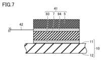
- FIG. 7is a schematic cross-sectional view showing the configuration of the sensor 41.
- the sensor 41may further have a third electrode 93, a cushion material 7, and a fourth electrode 94.
- a third electrode 93is provided on the surface 11 of the circuit board 10 .
- the cushion material 7is provided on the third electrode 93 .
- a fourth electrode 94is provided on the cushion material 7 .
- the cushion material 7is sandwiched between the third electrode 93 and the fourth electrode 94 .
- the restricting portion 5is provided on the fourth electrode 94 .
- the sensor 41is, for example, a capacitive pressure sensor.
- a loadis applied to the sensor 41 when the projecting portion 52 contacts the restricting portion 5 by the user operating the operating member 4 .
- the cushion material 7is deformed.
- the distance between the third electrode 93 and the fourth electrode 94changes.
- the capacitance of sensor 41changes. That is, the sensor 41 detects the capacitance that changes due to the contact of the projecting portion 52 .
- the loadmay be calculated based on the capacitance or change in capacitance between the third electrode 93 and the fourth electrode 94 .
- the controller 200may have a computer (not shown). The computer may calculate the load based on the capacitance or the change in capacitance.
- the computermay perform some control linearly or stepwise depending on the detected capacitance or calculated load.
- the computermay perform certain controls in response to the load exceeding certain thresholds.
- the sensor 41is not limited to a capacitive pressure sensor.
- Sensor 41may be, for example, a non-contact capacitive proximity sensor.
- a signalWhen detecting a signal according to the position or movement of the projecting portion 52, it may be detected by, for example, a capacitance type proximity sensor. Alternatively, when detecting a signal corresponding to the force of the projecting portion 52, it may be detected by, for example, a resistance type, strain gauge type, or capacitance type pressure sensor.
- the pressure sensoris not limited to the above method, and a pressure sensor of any other method may be used as appropriate. Also, a non-contact capacitive proximity sensor and a capacitive pressure sensor are used to detect a signal corresponding to the position or movement of the projecting portion 52 and a signal corresponding to the force of the projecting portion 52. good too.
- the module housing 30 and the operation member 4 from which the first part 50 is removedare inserted into the first opening 13 formed in the circuit board 10 .
- the module housing 30 and the operation member 4 from which the first component 50 is removedare fixed to the circuit board 10 at the facing portion 38 .
- the first component 50is attached to the shaft portion 2 .
- the first component 50can be attached to the shaft portion 2 without making the size of the first opening 13 larger than that of the first component 50 . Therefore, the effective area of the circuit board 10 can be increased.
- the configuration of the input device 100 according to the second embodimentdiffers from that of the input device 100 according to the first embodiment mainly in that a notch 15 is provided instead of the first opening 13.
- the configurationis substantially the same as the input device 100 according to the first embodiment.
- the configuration different from that of the input device 100 according to the first embodimentwill be mainly described.
- FIG. 8is an exploded schematic plan view showing the configuration of the input device 100 according to the second embodiment.
- the circuit board 10is provided with a notch 15 .
- the notch 15penetrates the circuit board 10 .
- the notch 15opens at the outer peripheral edge 16 of the circuit board 10 .
- the width of the notch 15 at the outer peripheral edge 16 of the circuit board 10may be larger than the width of the shaft portion 2 .
- the width (second width W2) of the notch 15 at the outer peripheral end portion 16 of the circuit board 10is larger than the width (first width W1) of a portion of the module housing 30.
- the width of the notch 15may be smaller than the width of the module housing 30 and larger than the width of the shaft portion 2 of the first component 50 . At this time, the shaft portion 2 of the first component 50 can be inserted into the notch 15 along the second direction Y. As shown in FIG.
- the shaft portion 2may be fixed integrally with the first component 50 . After the first component 50 is attached to the shaft portion 2 , it may be fixed so that it cannot be removed from the shaft portion 2 again.
- the width (third width W3) of the first component 50may be larger than the width (second width W2) of the notch 15 at the outer peripheral end portion 16 of the circuit board 10 . Accordingly, even when the shaft portion 2 is integrally fixed to the first component 50, the module housing 30 can be inserted into the notch 15 from the outer peripheral end portion 16 of the circuit board 10 along the second direction Y. be able to.
- the sensor 41may have a shape other than an annular shape.
- the hole of the notch 15(the portion inside the opening of the notch 15 ) may have a portion with a larger diameter or a portion with a smaller diameter than the opening of the notch 15 .
- the size of the module housing 30may be larger than the notch 15 when viewed from the thickness direction of the circuit board 10 .
- the module housing 30may have a shape that cannot pass through the notch 15 .
- the module housing 30may have a shape that prevents the notch 15 from penetrating from one side of the circuit board 10 to the other side. Specifically, when viewed from the thickness direction of the circuit board 10 , the opposing portion 38 of the module housing 30 is arranged so as to overlap the circuit board 10 .
- the module housing 30 and the operating member 4are inserted into the notch 15 formed in the circuit board 10 from the side of the circuit board 10 .
- the operating member 4may be in a state in which the first component 50 is attached to the shaft portion 2, or may be in a state in which the first component 50 and the shaft portion 2 are integrated.
- the module housing 30 and the operation member 4 having the first component 50are fixed to the circuit board 10 at the facing portion 38 . By doing so, it is not necessary to attach the first component 50 to the shaft portion 2 separately, so the attachment process is simplified as compared with the assembling method of the first embodiment.
- the operating member 4may be inserted into the notch 15 of the circuit board 10 with the first component 50 removed, as in the assembling method of the first embodiment.
- the first component 50is attached to the shaft portion 2 after the module housing 30 and the operating member 4 are fixed to the circuit board 10 .
- the configuration of the controller 200 according to the third embodimentwill be described.
- the configuration of the controller 200 according to the third embodimentdiffers from the input device 100 according to the first and second embodiments mainly in that it has a controller housing 110. , is substantially the same as the input device 100 according to the first and second embodiments.
- the configuration different from the input device 100 according to the first embodiment and the second embodimentwill be mainly described.
- FIG. 9is a schematic plan view showing the configuration of the controller 200 according to the third embodiment.
- a controller 200 according to the third embodimenthas an input device 100 and a controller housing 110 .
- Controller housing 110has, for example, a rectangular parallelepiped shape.
- a second opening 103is provided in the controller housing 110 .
- the second opening 103is circular, for example.
- FIG. 10is a schematic partial cross-sectional view taken along line XX in FIG.
- the partial cross-sectional schematic diagram shown in FIG. 10is parallel to each of the first direction X and the third direction Z.
- the input device 100has a circuit board 10 and an operation module 90.
- the circuit board 10is provided with a first opening 13 or a notch 15 .
- the operating module 90has a module housing 30 and an operating member 4 .
- the controller housing 110accommodates the circuit board 10 and part of the operation module 90 .
- the operation member 4is arranged so as to be partially exposed from the first opening 13 or the notch 15 and the second opening 103 .
- the operation member 4can be tilted or slid.
- the module housing 30includes a facing portion 38 that faces the circuit board 10 .
- the facing portion 38faces the circuit board 10 in a state in which a portion of the module housing 30 is arranged to pass through the first opening 13 or the notch 15 .
- the operation module 90 and the circuit board 10are fixed.
- Circuit board 10is fixed to controller housing 110 .
- the controller housing 110has an outer wall surface 101 and an inner wall surface 102.
- the inner wall surface 102is located on the opposite side of the outer wall surface 101 .
- the second opening 103is a through hole.
- the second opening 103opens to each of the outer wall surface 101 and the inner wall surface 102 .
- a protrusion 104may be provided on the outer wall surface 101 .
- the protrusion 104may form the second opening 103 .
- the width of the second opening 103 on the outer wall surface 101(sixth width W6) may be smaller than the width of the second opening 103 on the inner wall surface 102 (fourth width W4).
- the operation member 4mainly has a first part 50, a shaft portion 2, and a support member 3.
- the first component 50is attached to the shaft portion 2 exposed from the module housing 30 .
- the first part 50is larger than the first opening 13 or notch 15 .
- the first component 50has a projecting portion 52 and a key top 51 .
- the projecting portion 52is umbrella-shaped.
- a portion of the protrusion 52may be housed inside the controller housing 110 .
- the protrusion 52may be positioned at the second opening 103 .
- a portion of the protrusion 52may be located outside the controller housing 110 .
- the keytop 51may be positioned outside the controller housing 110 .
- the size of the key top 51is smaller than that of the second opening 103 when viewed from the thickness direction of the circuit board 10 .
- the outer edge of the key top 51is surrounded by the second opening 103 when viewed from the thickness direction of the circuit board 10 .
- the protrusion 52may be larger than the second opening 103 when viewed in the thickness direction of the circuit board 10 .
- the second opening 103may be surrounded by the outer edge of the projecting portion 52 when viewed from the thickness direction of the circuit board 10 .
- the width of the protrusion 52may be greater than the width of the second opening 103 in the outer wall surface 101 (sixth width W6).
- the width (seventh width W7) of the keytop 51may be smaller than the width (sixth width W6) of the second opening 103 in the outer wall surface 101 .
- the width (fifth width W5) of the projecting portion 52may be smaller than the width (fourth width W4) of the second opening 103 in the inner wall surface 102 .
- the configuration of the controller 200 according to the fourth embodimentdiffers from that of the controller 200 according to the third embodiment mainly in that it has a neck support section 105.
- Other configurationsare similar to those of the third embodiment. is substantially the same as the controller 200 according to The configuration different from the controller 200 according to the third embodiment will be mainly described below.
- FIG. 11is a partial cross-sectional schematic diagram showing the configuration of the controller 200 according to the fourth embodiment.
- the partial cross-sectional schematic diagram shown in FIG. 11is parallel to each of the first direction X and the third direction Z.
- the controller 200 according to the fourth embodimenthas a neck support section 105.
- Neck support 105is attached to controller housing 110 .
- the neck support portion 105is provided on the projecting portion 104 .
- the neck support portion 105is, for example, annular.
- the neck support part 105may protrude from the projecting part 104 toward the center of the second opening 103 so as to partially cover the second opening 103 .
- the first part 50 of the operating member 4contacts the neck support portion 105 .
- the tilting of the first component 50 of the operating member 4is restricted by the neck support portion 105 .
- a deformable elastic body or a non-contact type sensormay be provided on the circuit board 10, the neck support 105, or the projecting portion 52.
- the restricting portion 5is deformable. When the operating member 4 tilts, it first contacts the restricting portion 5 . Further application of force to the operating member 4 causes the sensor 41 to output a signal according to the deformation of the restricting portion 5 . When the operating member 4 contacts the neck rest portion 105, tilting of the operating member 4 is restricted.
- the senor 41may be provided on the first component 50.
- a sensor 41may be provided in a range where the first component 50 contacts the neck support portion 105 .
- the sensor 41may be provided on the first component 50 that does not come into direct contact with the neck support portion 105 within the detection range of the sensor 41 .
- the input device 100 according to the first and second embodiments and the controller 200 according to the third and fourth embodimentsmay not have the sensor 41 .
- the tilting of the operation member 4may be restricted by the contact of the operation member 4 with the circuit board 10 .
- an elastic membermay be provided at the contact portion with the operation member 4 .
- the operation member 4may be slidable.
- the operating member 4may slide along a direction perpendicular to the central axis 8, for example.
- the slide directionis a direction perpendicular to the third direction Z, for example.
- the sliding directionmay be the first direction X or the second direction Y.
- the module housing 30is fixed to the circuit board 10 and does not move.
- the centers of the ring-shaped sensor 41 and the projecting portion 52may coincide with the central axis 8 of the slide of the operation member 4 .
- the central axis 8 of the slideis the initial position of the slide.
Landscapes
- Engineering & Computer Science (AREA)
- Multimedia (AREA)
- Human Computer Interaction (AREA)
- General Engineering & Computer Science (AREA)
- Theoretical Computer Science (AREA)
- Physics & Mathematics (AREA)
- General Physics & Mathematics (AREA)
- Position Input By Displaying (AREA)
Abstract
Description
Translated fromJapanese本開示は、入力装置およびコントローラに関する。The present disclosure relates to input devices and controllers.
特開2002-328733号公報(特許文献1)は、操作入力手段と基板とを有する操作入力装置を開示している。当該操作入力装置においては、操作入力手段は、基板上に配置されている。Japanese Patent Laying-Open No. 2002-328733 (Patent Document 1) discloses an operation input device having operation input means and a substrate. In the operation input device, the operation input means is arranged on the substrate.
上記操作入力装置によれば、基板にジョイスティックを実装するため、操作入力装置として一定の厚みが必要になる。本開示の課題は、入力装置およびコントローラを小型化することである。According to the above operation input device, since the joystick is mounted on the substrate, the operation input device requires a certain thickness. An object of the present disclosure is to miniaturize the input device and the controller.
本開示に係る入力装置は、回路基板と、操作モジュールと、を備えている。回路基板には、第1開口または切り欠きが設けられている。操作モジュールは、モジュールハウジングと、操作部材と、を備えている。操作部材は、モジュールハウジングから一部が露出するようにモジュールハウジングに収容され、傾倒またはスライド操作が可能である。回路基板の厚み方向から見て、モジュールハウジングの大きさは、第1開口または切り欠きよりも大きい。モジュールハウジングは、モジュールハウジングの一部が第1開口または切り欠きを貫通するように配設された状態で回路基板と対向する対向部を備えている。対向部と回路基板とが固定されることにより、操作モジュールと回路基板とが固定される。An input device according to the present disclosure includes a circuit board and an operation module. The circuit board is provided with a first opening or notch. The operating module has a module housing and an operating member. The operation member is housed in the module housing so as to be partially exposed from the module housing, and can be tilted or slid. When viewed from the thickness direction of the circuit board, the size of the module housing is larger than the first opening or notch. The module housing has a facing portion facing the circuit board in a state in which a part of the module housing is arranged to pass through the first opening or notch. By fixing the facing portion and the circuit board, the operation module and the circuit board are fixed.
本開示に係る入力装置によれば、モジュールハウジングの一部が第1開口または切り欠きを貫通するように配設される。また本開示に係る入力装置によれば、回路基板の厚み方向から見て、モジュールハウジングの大きさは、第1開口または切り欠きよりも大きい。第1開口または切り欠きの大きさをモジュールハウジングよりも小さくすることにより、回路基板の面積を有効活用することができる。これにより、入力装置を小型化することができる。According to the input device according to the present disclosure, a portion of the module housing is arranged to pass through the first opening or cutout. Further, according to the input device of the present disclosure, the size of the module housing is larger than the first opening or the notch when viewed from the thickness direction of the circuit board. By making the size of the first opening or notch smaller than that of the module housing, the area of the circuit board can be effectively utilized. Thereby, the input device can be miniaturized.
上記に係る入力装置において、操作部材は、モジュールハウジングから露出する部分に取り付けられ、回路基板の厚み方向から見て、第1開口または切り欠きよりも大きい第1部品を有していてもよい。操作モジュールと回路基板とが固定された状態において、対向部は回路基板の裏面側に位置し、第1部品は回路基板の表面側に位置していてもよい。これにより、操作部材に第1部品が取り付けられていない状態で、回路基板の裏面側から第1開口に対してモジュールハウジングを挿入した後、第1開口または切り欠きよりも大きな第1部品をモジュールハウジングから露出する部分に装着して操作部材とすることできる。したがって、第1開口または切り欠きを過度に大きくすることなく、操作部材に大きな部品を設けることができる。In the input device according to the above, the operation member may be attached to a portion exposed from the module housing and have a first part that is larger than the first opening or notch when viewed from the thickness direction of the circuit board. In a state where the operation module and the circuit board are fixed, the facing portion may be positioned on the back side of the circuit board and the first component may be positioned on the front side of the circuit board. Thereby, after the module housing is inserted into the first opening from the back side of the circuit board without the first part attached to the operation member, the first part larger than the first opening or the notch is inserted into the module. It can be used as an operation member by being attached to a portion exposed from the housing. Accordingly, large parts can be provided on the operating member without making the first opening or notch too large.
上記に係る入力装置において、第1部品は、ユーザにより操作されるキートップと、軸部と、突出部とを含んでいてもよい。軸部は、キートップから回路基板に向かって延びていてもよい。突出部は、軸部の中心から離れる方向、かつ回路基板に向かう方向に突出していてもよい。In the input device according to the above, the first component may include a key top operated by the user, a shaft portion, and a projecting portion. The shaft portion may extend from the keytop toward the circuit board. The protrusion may protrude away from the center of the shaft and toward the circuit board.
上記に係る入力装置において、回路基板には、第1開口が設けられていてもよい。回路基板の表面に、突出部の位置または動き、あるいは突出部にかかる力に応じた信号を出力するセンサが配置されていてもよい。表面と垂直な方向からセンサを見たときに、センサは第1開口を囲む環状であってもよい。環状のセンサおよび突出部の中心は、操作部材の傾倒またはスライド操作の中心軸と一致してもよい。これにより、センサがより正確に突出部の位置又は動き、あるいは突出部に係る力に応じた信号を検出することができる。In the input device according to the above, the circuit board may be provided with the first opening. A sensor may be arranged on the surface of the circuit board to output a signal according to the position or movement of the protrusion or the force applied to the protrusion. The sensor may be annular surrounding the first opening when the sensor is viewed from a direction perpendicular to the surface. The center of the ring-shaped sensor and protrusion may coincide with the central axis of the tilting or sliding operation of the operating member. This allows the sensor to more accurately detect the position or movement of the protrusion or the signal corresponding to the force applied to the protrusion.
上記に係る入力装置において、回路基板には、切り欠きが設けられていてもよい。回路基板の外周端部における切り欠きの幅は、モジュールハウジングの幅よりも大きくてもよい。第1部品は、ユーザにより操作されるキートップと、軸部と、を含んでいてもよい。軸部は、キートップから回路基板に向かって延びていてもよい。操作部材は、第1部品と一体的に固定される軸部を含んでいてもよい。これにより、第1部品が軸部と一体的に固定されている場合であっても、モジュールハウジングを回路基板の外周端部から切り欠きに入れることができる。そのため、第1開口の場合に比べて、回路基板において有効活用できるスペースを増やすことができる。In the input device according to the above, the circuit board may be provided with a notch. The width of the notch at the outer peripheral edge of the circuit board may be greater than the width of the module housing. The first part may include a key top operated by a user and a shaft. The shaft portion may extend from the keytop toward the circuit board. The operating member may include a shaft integrally fixed with the first component. Thereby, even when the first component is fixed integrally with the shaft portion, the module housing can be inserted into the notch from the outer peripheral end portion of the circuit board. Therefore, compared to the case of the first opening, it is possible to increase the space that can be effectively used on the circuit board.
上記に係る入力装置において、回路基板の表面側に、操作部材の位置または動き、あるいは操作部材にかかる力に応じた信号を出力するセンサが配置されていてもよい。回路基板の裏面側に、対向部が位置していてもよい。これにより、同一面にセンサと対向部が配置される場合と比較して、回路基板のスペースを有効活用しながらセンサを配置することができる。In the input device according to the above, a sensor that outputs a signal corresponding to the position or movement of the operation member or the force applied to the operation member may be arranged on the surface side of the circuit board. The facing portion may be located on the back side of the circuit board. As a result, the sensor can be arranged while effectively using the space of the circuit board, compared to the case where the sensor and the facing portion are arranged on the same surface.
上記に係る入力装置において、回路基板の厚み方向から見た場合に、第1開口の端部又は切り欠きの端部を基準としたときに、センサは対向部の外縁よりも内側に配置されていてもよい。これにより、センサを操作部材に近づけることができる。そのため、有効活用できる回路基板の面積を増やすことができる。またセンサを操作部材に近づけることで、第1部品が小さくなる。そのため、入力装置を小型化することができる。In the input device according to the above, when viewed from the thickness direction of the circuit board, the sensor is arranged inside the outer edge of the facing portion when the end of the first opening or the end of the notch is used as a reference. may This allows the sensor to be brought closer to the operating member. Therefore, the area of the circuit board that can be effectively used can be increased. Also, by bringing the sensor closer to the operating member, the size of the first component can be reduced. Therefore, the size of the input device can be reduced.
上記に係る入力装置において、対向部は、回路基板と固定される固定部を含んでいてもよい。回路基板の厚み方向から見た場合に、第1開口の端部又は切り欠きの端部を基準としたときに、センサは固定部よりも内側にあってもよい。これにより、センサを操作部材に近づけることができる。そのため、有効活用できる回路基板の面積を増やすことができる。In the input device according to the above, the facing portion may include a fixing portion fixed to the circuit board. When viewed from the thickness direction of the circuit board, the sensor may be located inside the fixed portion when the edge of the first opening or the edge of the notch is used as a reference. This allows the sensor to be brought closer to the operating member. Therefore, the area of the circuit board that can be effectively used can be increased.
上記に係る入力装置において、回路基板の厚み方向から見た場合に、第1開口の端部又は切り欠きの端部と対向部の外縁との距離は、第1開口の端部又は切り欠きの端部とセンサの外縁との距離よりも長くてもよい。これにより、センサを操作部材に近づけることができる。そのため、有効活用できる回路基板の面積を増やすことができる。In the input device according to the above, the distance between the edge of the first opening or the edge of the notch and the outer edge of the facing portion when viewed from the thickness direction of the circuit board is the distance between the edge of the first opening or the notch. It may be longer than the distance between the end and the outer edge of the sensor. This allows the sensor to be brought closer to the operating member. Therefore, the area of the circuit board that can be effectively used can be increased.
上記に係る入力装置において、対向部は、回路基板と固定される固定部を含んでいてもよい。固定部は、ネジボスであって、回路基板において対向部が位置する面と反対の面から回路基板を貫通してネジボスに対してネジが締結されることによって固定されてもよい。これにより、スペースを有効活用しながら、操作モジュールを回路基板に対して固定することができる。In the input device according to the above, the facing portion may include a fixing portion fixed to the circuit board. The fixed portion may be a screw boss, and may be fixed by fastening a screw to the screw boss through the circuit board from a surface opposite to the surface on which the facing portion is located. Thereby, the operation module can be fixed to the circuit board while effectively utilizing the space.
上記に係る入力装置において、モジュールハウジングは、対向部に第1電極を有していてもよい。回路基板には第2電極が設けられ、第1電極と第2電極は電気的に接続されてもよい。これにより、モジュールハウジングから出力された信号を対向部から取り出すことができる。In the input device according to the above, the module housing may have the first electrode on the facing portion. A second electrode may be provided on the circuit board, and the first electrode and the second electrode may be electrically connected. Thereby, the signal output from the module housing can be taken out from the opposing portion.
本開示に係るコントローラは、回路基板と、操作モジュールと、コントローラハウジングと、を備えている。回路基板には、第1開口または切り欠きが設けられている。コントローラハウジングには、回路基板と操作モジュールの一部とが収容され、第2開口が設けられている。操作モジュールは、モジュールハウジングと、操作部材と、を備えている。操作部材は、第1開口または切り欠きと第2開口とから一部が露出するように配設され、傾倒またはスライド操作が可能である。モジュールハウジングは、モジュールハウジングの一部が第1開口または切り欠きを貫通するように配設された状態において回路基板と対向する対向部を有している。対向部と回路基板とが固定されることで、操作モジュールと回路基板とが固定される。A controller according to the present disclosure includes a circuit board, an operation module, and a controller housing. The circuit board is provided with a first opening or notch. The controller housing accommodates the circuit board and part of the operation module and has a second opening. The operating module has a module housing and an operating member. The operation member is disposed so as to be partially exposed from the first opening or notch and the second opening, and can be tilted or slid. The module housing has a facing portion facing the circuit board in a state in which a part of the module housing is arranged to pass through the first opening or notch. By fixing the facing portion and the circuit board, the operation module and the circuit board are fixed.
本開示に係るコントローラによれば、モジュールハウジングの一部が第1開口または切り欠きを貫通するように配設される。これにより、回路基板の厚み方向に突出する部分の長さを短くすることができる。そのため、コントローラを小型化することができる。According to the controller according to the present disclosure, part of the module housing is arranged to pass through the first opening or notch. Thereby, the length of the portion protruding in the thickness direction of the circuit board can be shortened. Therefore, the size of the controller can be reduced.
上記に係るコントローラにおいて、操作部材は、モジュールハウジングから露出する部分に取り付けられ、回路基板の厚み方向から見て、第1開口または切り欠きよりも大きい第1部品を備えていてもよい。第1部品は、突出部と、キートップと、軸部と、を備えていてもよい。突出部は、コントローラハウジングの内側に収容されてもよい。キートップは、コントローラハウジングの外側に位置していてもよい。軸部は、キートップから回路基板に向かって延びていてもよい。突出部は、軸部の中心から離れる方向、かつ回路基板に向かう方向に突出していてもよい。回路基板の厚み方向から見て、キートップの大きさは第2開口よりも小さく、突出部の大きさは第2開口よりも大きくてもよい。これにより、第2開口からコントローラハウジングの内部に、ほこりが入ることを抑制することができる。In the controller according to the above, the operation member may be attached to a portion exposed from the module housing, and may include a first part that is larger than the first opening or notch when viewed from the thickness direction of the circuit board. The first component may include a protrusion, a key top, and a shaft. The protrusion may be housed inside the controller housing. The keytops may be located outside the controller housing. The shaft portion may extend from the keytop toward the circuit board. The protrusion may protrude away from the center of the shaft and toward the circuit board. When viewed from the thickness direction of the circuit board, the size of the keytop may be smaller than that of the second opening, and the size of the protrusion may be larger than that of the second opening. This can prevent dust from entering the controller housing through the second opening.
上記に係るコントローラにおいて、回路基板には、第1開口が設けられていてもよい。回路基板の表面に、突出部の位置または動き、あるいは突出部にかかる力に応じた信号を出力するセンサが配置されていてもよい。表面と垂直な方向からセンサを見たときに、センサは第1開口を囲む環状であってもよい。環状のセンサおよび突出部の中心は、操作部材の傾倒またはスライド操作の中心軸と一致してもよい。これにより、センサがより正確に突出部の動きを検出することができる。In the controller according to the above, the circuit board may be provided with the first opening. A sensor may be arranged on the surface of the circuit board to output a signal according to the position or movement of the protrusion or the force applied to the protrusion. The sensor may be annular surrounding the first opening when the sensor is viewed from a direction perpendicular to the surface. The center of the ring-shaped sensor and protrusion may coincide with the central axis of the tilting or sliding operation of the operating member. This allows the sensor to more accurately detect the movement of the protrusion.
上記に係るコントローラにおいて、回路基板には、切り欠きが設けられていてもよい。回路基板の外周端部における切り欠きの幅は、モジュールハウジングの幅よりも大きくてもよい。操作部材は、第1部品と一体的に固定される軸部を含んでいてもよい。これにより、第1部品が軸部と一体的に固定されている場合であっても、モジュールハウジングを回路基板の外周端部から切り欠きに入れることができる。そのため、第1開口の場合に比べて、回路基板において有効活用できるスペースを増やすことができる。In the controller according to the above, the circuit board may be provided with a notch. The width of the notch at the outer peripheral edge of the circuit board may be greater than the width of the module housing. The operating member may include a shaft integrally fixed with the first component. Thereby, even when the first component is fixed integrally with the shaft portion, the module housing can be inserted into the notch from the outer peripheral end portion of the circuit board. Therefore, compared to the case of the first opening, it is possible to increase the space that can be effectively used on the circuit board.
上記に係るコントローラにおいて、回路基板の表面側に、操作部材の位置または動き、あるいは操作部材にかかる力に応じた信号を出力するセンサが配置されていてもよい。回路基板の裏面側に、対向部が位置していてもよい。これにより、同一面にセンサと対向部が配置される場合と比較して、回路基板のスペースを有効活用しながらセンサを配置することができる。In the controller according to the above, a sensor that outputs a signal corresponding to the position or movement of the operating member or the force applied to the operating member may be arranged on the surface side of the circuit board. The facing portion may be located on the back side of the circuit board. As a result, the sensor can be arranged while effectively using the space of the circuit board, compared to the case where the sensor and the facing portion are arranged on the same surface.
上記に係るコントローラにおいて、回路基板の厚み方向から見た場合に、第1開口の端部又は切り欠きの端部を基準としたときに、センサは対向部の外縁よりも内側に配置されていてもよい。これにより、センサを操作部材に近づけることができる。そのため有効活用できる回路基板の面積を増やすことができる。またセンサを操作部材に近づけることで、第1部品が小さくなる。そのため、コントローラを小型化することができる。In the controller according to the above, when viewed from the thickness direction of the circuit board, the sensor is arranged inside the outer edge of the facing portion when the end of the first opening or the end of the notch is used as a reference. good too. This allows the sensor to be brought closer to the operating member. Therefore, the area of the circuit board that can be effectively used can be increased. Also, by bringing the sensor closer to the operating member, the size of the first component can be reduced. Therefore, the size of the controller can be reduced.
上記に係るコントローラにおいて、対向部は、回路基板と固定される固定部を含んでいてもよい。回路基板の厚み方向から見た場合に、第1開口の端部又は切り欠きの端部を基準としたときに、センサは固定部よりも内側にあってもよい。これにより、センサを操作部材に近づけることができる。そのため、有効活用できる回路基板の面積を増やすことができる。In the controller according to the above, the facing portion may include a fixing portion fixed to the circuit board. When viewed from the thickness direction of the circuit board, the sensor may be located inside the fixed portion when the edge of the first opening or the edge of the notch is used as a reference. This allows the sensor to be brought closer to the operating member. Therefore, the area of the circuit board that can be effectively used can be increased.
上記に係るコントローラにおいて、回路基板の厚み方向から見た場合に、第1開口の端部又は切り欠きの端部と対向部の外縁との距離は、第1開口の端部又は切り欠きの端部とセンサの外縁との距離よりも長くてもよい。これにより、センサを操作部材に近づけることができる。そのため、有効活用できる回路基板の面積を増やすことができる。In the controller according to the above, when viewed from the thickness direction of the circuit board, the distance between the edge of the first opening or the edge of the notch and the outer edge of the facing portion is the edge of the first opening or the edge of the notch. It may be longer than the distance between the part and the outer edge of the sensor. This allows the sensor to be brought closer to the operating member. Therefore, the area of the circuit board that can be effectively used can be increased.
上記に係るコントローラにおいて、対向部は、回路基板と固定される固定部を含んでいてもよい。固定部は、ネジボスであって、回路基板において対向部が位置する面と反対の面から回路基板を貫通してネジボスに対してネジが締結されることによって固定されてもよい。これにより、スペースを有効活用しながら、操作モジュールを回路基板に対して位置決めしつつ固定することができる。In the controller according to the above, the facing portion may include a fixing portion fixed to the circuit board. The fixed portion may be a screw boss, and may be fixed by fastening a screw to the screw boss through the circuit board from a surface opposite to the surface on which the facing portion is located. As a result, the operation module can be positioned and fixed to the circuit board while effectively utilizing the space.
上記に係るコントローラにおいて、モジュールハウジングは、第1電極を有していてよい。回路基板には第2電極が設けられ、第1電極と第2電極は電気的に接続されてもよい。これにより、モジュールハウジングから出力された信号を対向部から取り出すことができる。In the controller according to the above, the module housing may have the first electrode. A second electrode may be provided on the circuit board, and the first electrode and the second electrode may be electrically connected. Thereby, the signal output from the module housing can be taken out from the opposing portion.
本開示によれば、入力装置およびコントローラを小型化することができる。According to the present disclosure, the size of the input device and controller can be reduced.
本開示の実施形態について、図面を参照しながら詳細に説明する。なお、図中の同一または相当部分については、同一符号を付してその説明は繰り返さない。
(第1実施形態)
まず、第1実施形態に係る入力装置100の構成について説明する。Embodiments of the present disclosure will be described in detail with reference to the drawings. The same or corresponding parts in the drawings are given the same reference numerals, and the description thereof will not be repeated.
(First embodiment)
First, the configuration of the
図1は、第1実施形態に係る入力装置100の構成を示す分解斜視模式図である。図2は、第1実施形態に係る入力装置100の構成を示す斜視模式図である。図1および図2に示されるように、第1実施形態に係る入力装置100は、回路基板10と、操作モジュール90と、センサ41と、フレキシブルプリントサーキット42と、ネジ1とを主に有している。回路基板10は、表面11と、裏面12とを有している。裏面12は、表面11の反対側に位置している。回路基板10には、第1開口13が設けられている。第1開口13は、回路基板10を貫通している。第1開口13は、表面11および裏面12の各々に開口している。回路基板10には、第1開口13の代わりに切り欠き15(図8参照)が設けられていてもよい。切り欠き15の構成の詳細については後述する。FIG. 1 is an exploded perspective schematic diagram showing the configuration of the
本明細書において、裏面12から表面11に向かう方向は、上側とする。反対に、表面11から裏面12に向かう方向は、下側とする。回路基板10の長手方向は、第1方向Xとする。回路基板10の短手方向は、第2方向Yとする。回路基板10の厚み方向は、第3方向Zとする。第1方向Xおよび第2方向Yの各々は、第3方向Zに対して垂直である。第3方向Zは、回路基板10の表面11に対して垂直である。第1方向Xおよび第2方向Yの各々は、回路基板10の表面11に平行である。In this specification, the direction from the
図1に示されるように、操作モジュール90は、モジュールハウジング30と、操作部材4とを主に有している。操作部材4は、モジュールハウジング30から一部が露出するようにモジュールハウジング30に収容されている。操作部材4は、第1部品50を有している。第1部品50は、モジュールハウジング30から露出する部分に取り付けられている。第1部品50は、モジュールハウジング30の外部に位置している。第1部品50は、キートップ51と、突出部52とを有している。キートップ51は、突出部52に連なっている。キートップ51は、突出部52の上側に位置している。As shown in FIG. 1, the
突出部52は、例えばスカート部である。スカート部は、傘状に構成されている。スカート部は、第3方向Zに沿って軸部2の下方に向かうにしたがって広がるように構成されている。操作部材4が傾倒された場合、スカート部は、回路基板10と直接接触してもよいし、回路基板10にセンサ41がある場合にはセンサ41と直接接触してもよい。スカート部は、例えば保護シートなどの他の部材を介して、間接的に回路基板10またはセンサ41と接触してもよい。スカート部は、軸部2の中心から離れる方向(具体的には第1方向Xおよび第2方向Y)に突出する。より具体的には、回路基板10の表面11と並行な方向から見た場合、スカート部の側面は円弧状となる。回路基板10の表面11に垂直な方向から見た場合、スカート部の下方端部(先端)は円状となる(図3参照)。The projecting
回路基板10には、ネジ挿入孔14が設けられている。ネジ挿入孔14の数は、特に限定されないが、例えば3個である。ネジ挿入孔14は、第1開口13の周囲に設けられている。ネジ挿入孔14は、回路基板10を貫通している。ネジ挿入孔14は、表面11および裏面12の各々に開口している。ネジ挿入孔14には、ネジ1が挿入される。回路基板10には、例えばコンデンサなどの電子部品(図示せず)が実装されていてもよい。回路基板として、例えばFPC(Flexible Printed Circuit)またはメンブレンシートが用いられてもよい。FPCの基材として、例えばポリイミド樹脂、液晶ポリマーまたはエポキシ樹脂が用いられてもよい。メンブレンシートの基材として、例えばPET(Polyethyleneterephthalate)が用いられてもよい。回路基板10の一部は、回路基板10の高さ方向や回路基板と平行な方向(第1方向X又は第2方向Y)に曲がっていてもよい。回路基板10の配線パターンとして、例えば銅、銀またはカーボンが用いられる。A
モジュールハウジング30は、複数の部品を組み合わせた構造であってもよく、一つの部品から構成されていてもよい。モジュールハウジング30には、回路基板10と対向する対向部38が含まれる。モジュールハウジング30の一部は、例えば上部が開口しているドーム形状を有している。モジュールハウジング30の一部は、第1開口13または切り欠き15を貫通するように配設される。図2に示されるように、対向部38は、モジュールハウジング30の一部が第1開口13または切り欠き15を貫通するように配設された状態で回路基板10と対向する。この状態では、第1開口13にモジュールハウジング30の上部のドーム形状を配設するため、回路基板10の厚み方向(第3方向Z)を軸としてモジュールハウジング30が回転する可能性がある。回転の自由度を抑えるため、第3方向Zから回路基板10とモジュールハウジング30を見た場合に、第1開口13に凸部を設け、モジュールハウジング30の上部に凹み部を設けてもよい。対向部38と回路基板10とが固定されることにより、操作モジュール90と回路基板10とが固定される。The
対向部38は、固定部36を有している。固定部36は、回路基板10と固定される。固定部36の数は、特に限定されないが、例えば3個である。固定部36は、例えば固定構造を有しており、例えばネジボスを有している。固定部36は、回路基板10において対向部38が位置する面(裏面12)と反対の面(表面11)から回路基板10を貫通してネジボスに対してネジ1が締結されることによって固定されてもよい。なお固定部36は、ネジボスを有した構造に限定されない。固定部36は、例えばナットインサート等の固定構造を有していてもよい。あるいは、固定部36は、ネジが貫通する孔であってもよい。また、モジュールハウジング30は、半田付けまたは接着剤により回路基板10に固定されてもよい。別の観点から言えば、固定部36において、半田または接着剤で固定されてもよい。The facing
図2に示されるように、センサ41は、回路基板10の表面11に配置されていてもよい。センサ41は、突出部52の位置または動き、あるいは突出部52にかかる力に応じた信号を出力する。センサ41は、モジュールハウジング30を取り囲んでいてもよい。モジュールハウジング30の一部は、第1開口13または切り欠き15を貫通するように配設される。そのため、回路基板10の厚み方向に突出する部分の長さを短くすることができる。このような構造により、より小さい傾倒角度で突出部52(スカート部)の端部がセンサ41と接触又はセンサ41が感知できる程度の距離に近づけることができる。そのため、センサ41を操作モジュール90に近づけて配置することができ、回路基板10の有効面積を増やすことができる。The
図3は、第1実施形態に係る入力装置100の構成を示す平面模式図である。図3に示されるように、回路基板10の厚み方向から見て、モジュールハウジング30の大きさは、第1開口13よりも大きい。モジュールハウジング30は、第1開口13を貫通することができない形状を有している。モジュールハウジング30は、第1開口13を抜けて、一方の面側から他方の面側に移動することができない形状を含んでいる。別の観点から言えば、回路基板10の厚み方向から見て、モジュールハウジング30の一部は、回路基板10の表面11と重なっていてもよい。回路基板10の厚み方向から見て、モジュールハウジング30の外縁は、第1開口13を囲んでいてもよい。FIG. 3 is a schematic plan view showing the configuration of the
図3に示されるように、表面11と垂直な方向からセンサ41を見たときに、センサ41は第1開口13を囲む環状であってもよい。環状のセンサ41および突出部52の中心は、操作部材4の傾倒の中心軸8と一致してもよい。中心軸8は、第1開口13の中心と一致していてもよい。回路基板10の厚み方向に見た場合、第1開口13の端部を基準として、センサ41は、対向部38の外縁(第1外縁21)よりも内側に配置されていてもよい。As shown in FIG. 3 , the
図3に示されるように、回路基板10の厚み方向に見た場合、第1開口13の端部を基準として、センサ41は、ネジ1が固定される固定部36よりも内側(つまり、第1開口13側または中心軸8側)に位置していてもよい。回路基板10の表面11と垂直な方向から見て、第1開口13の中心と対向部38の外縁(第1外縁21)との距離(第1距離D1)は、第1開口13の中心とセンサ41の外縁(第2外縁22)との距離(第2距離D2)よりも長くてもよい。同様に、第1開口13の端部と対向部38の外縁(第1外縁21)との距離は、第1開口13の端部とセンサ41の外縁(第2外縁22)との距離よりも長くてもよい。As shown in FIG. 3 , when viewed in the thickness direction of the
なお上記においては、センサ41はネジ1よりも内側に位置している構成について説明したが、本開示は上記構成に限定されない。センサ41は、対向部38の外縁(第1外縁21)よりも外側に配置されていてもよい。第1距離D1は、第2距離D2と同じであってもよいし、第2距離D2よりも短くてもよい。In the above description, the configuration in which the
図4は、図3のIV-IV線に沿った一部断面模式図である。図4に示される一部断面模式図は、第1方向Xおよび第3方向Zの各々に平行である。図4に示されるように、操作部材4は、軸部2と、支持部材3とをさらに有している。軸部2は、支持部材3に連なっている。第1部品50には、挿入孔53が形成されている。挿入孔53は、突出部52を貫通し、キートップ51に達している。軸部2は、挿入孔53に挿入されている。軸部2は、操作部材4の中心軸8に沿って延びている。支持部材3は、モジュールハウジング30の内部に配置されている。支持部材3の一部は、モジュールハウジング30から露出していてもよい。突出部52は、例えば傘状である。突出部52は、モジュールハウジング30の一部を覆っている。キートップ51と突出部52とは一体化されていてもよい。第1部品50は、軸部2から着脱可能であってもよい。キートップ51と突出部52と軸部2は一体化されていてもよい。この場合、軸部2は第1部品50に含まれてもよい。FIG. 4 is a schematic partial cross-sectional view taken along line IV-IV in FIG. The partial cross-sectional schematic diagram shown in FIG. 4 is parallel to each of the first direction X and the third direction Z. As shown in FIG. As shown in FIG. 4, the
操作部材4は、例えば傾倒可能である。操作部材4は、第1方向Xおよび第3方向Zの各々に平行な断面において、中心軸8に対して傾倒可能であってもよい。操作部材4は、例えば第1傾倒方向S1に沿って傾倒可能である。キートップ51と、突出部52と、軸部2と、支持部材3とは、一体として傾倒する。The operating
図4に示されるように、操作モジュール90と回路基板10とが固定された状態において、モジュールハウジング30の一部は、第1開口13を貫通している。具体的には、モジュールハウジング30の一部は、第1開口13を貫通し上側に突出している。As shown in FIG. 4, part of the
対向部38は、回路基板10の裏面12に沿って延びている。対向部38は、例えば第1方向Xに沿って延びている。対向部38は、例えば回路基板10の裏面12側に位置している。回路基板10に設けられたネジ挿入孔14は、対向部38に設けられた固定部36に対して位置決めされる。固定部36には、ネジ1と締結可能なネジ溝(図示せず)が形成されている。ネジ1は、ネジ挿入孔14を貫通し、固定部36と締結される。The facing
操作部材4を中心としたときに、センサ41は、固定部36よりも内側にあってもよい。別の観点から言えば、センサ41は、固定部36と、操作部材4の中心軸8との間に位置していてもよい。センサ41は、固定部36と、モジュールハウジング30の一部との間に位置していてもよい。The
なお上記においては、対向部38が回路基板10の裏面12側に位置している場合について説明したが、対向部38の位置は裏面12側に限定されない。対向部38は、回路基板10の表面11側に位置していてもよい。この場合、第1部品50は、回路基板10の表面11側に位置している。第1部品50と近い回路基板10の面が表面11である。In the above description, the case where the facing
図4に示されるように、操作モジュール90と回路基板10とが固定された状態において、操作部材4の第1部品50は回路基板10の表面11側に位置している。具体的には、キートップ51と、突出部52と、軸部2とは、表面11側に位置している。第3方向Zにおいて、回路基板10は、センサ41と対向部38との間に設けられている。As shown in FIG. 4, the
第1部品50は、第1開口13または切り欠き15よりも大きくてもよい。第1部品50は、第1開口13または切り欠き15を貫通できない形状を有している。具体的には、突出部52の直径(第1直径A1)は、第1開口13の直径(第2直径A2)よりも大きくてもよい。別の観点から言えば、第3方向Zから見て、突出部52の外縁は、第1開口13を囲っていてもよい。The
図5は、図4の領域Vの拡大断面模式図である。モジュールハウジング30は、対向部38において導電性を有していてもよい。図5に示されるように、対向部38には、第1電極91が設けられていてもよい。第1電極91は、対向部38の第2表面37に設けられている。第2表面37は、裏面12に対向している。回路基板10には、第2電極92が設けられていてもよい。第2電極92は、回路基板10の裏面12に設けられている。操作モジュール90と回路基板10とが固定された状態において、対向部38の第1電極91と、回路基板10の第2電極92とは、電気的に接続されてもよい。FIG. 5 is an enlarged schematic cross-sectional view of region V in FIG. The
第1電極91は、例えば操作部材4の傾き又は位置に応じた信号を出力する可変抵抗(図示せず)と電気的に接続されていてもよい。可変抵抗は、モジュールハウジング30の内部または外部に設けられていてもよい。可変抵抗から出力された信号は、回路基板10を介して外部に取り出されてもよい。The
図6は、図3のVI-VI線に沿った一部断面模式図である。図6に示される一部断面模式図は、第2方向Yおよび第3方向Zの各々に平行である。図6に示されるように、操作部材4は、第2方向Yおよび第3方向Zの各々に平行な断面において、中心軸8に対して傾倒可能であってもよい。操作部材4は、例えば第2傾倒方向S2に沿って傾倒可能である。操作部材4は、第3方向Zに垂直な全ての方向に傾倒可能であってもよい。FIG. 6 is a schematic partial cross-sectional view taken along line VI-VI in FIG. The partial cross-sectional schematic diagram shown in FIG. 6 is parallel to each of the second direction Y and the third direction Z. As shown in FIG. As shown in FIG. 6, the operating
センサ41は、規制部5を有している。規制部5は、操作部材4の傾倒を規制可能である。具体的には、操作部材4が第2傾倒方向S2に沿って傾倒したとき、突出部52が規制部5に接触することにより、操作部材4の傾倒が規制される。フレキシブルプリントサーキット42は、回路基板10の表面11側において、センサ41に接続されていてもよい。フレキシブルプリントサーキット42は、回路基板10の端部において折り返され、回路基板10の裏面12側まで延びていてもよい。The
図7は、センサ41の構成を示す断面模式図である。図7に示されるように、センサ41は、第3電極93と、クッション材7と、第4電極94とをさらに有していてもよい。第3電極93は、回路基板10の表面11上に設けられている。クッション材7は、第3電極93上に設けられている。第4電極94は、クッション材7上に設けられている。クッション材7は、第3電極93と第4電極94とにより挟まれている。規制部5は、第4電極94上に設けられている。センサ41は、例えば静電容量式圧力センサである。FIG. 7 is a schematic cross-sectional view showing the configuration of the
ユーザが操作部材4を操作することで突出部52が規制部5に接触すると、センサ41に荷重が印加される。これにより、クッション材7が変形する。その結果、第3電極93と第4電極94との間の距離が変化する。結果として、センサ41の静電容量が変化する。すなわち、センサ41は、突出部52の接触により変化する静電容量を検出する。第3電極93と第4電極94との間の静電容量または静電容量の変化に基づいて荷重が算出されてもよい。コントローラ200(図9参照)は、図示しないコンピュータを有していてもよい。コンピュータは、上記静電容量または静電容量の変化に基づいて荷重を算出してもよい。A load is applied to the
コンピュータは、検出された静電容量あるいは算出された荷重によってリニアまたは段階的に、ある制御を実行してもよい。コンピュータは、荷重がある閾値を超えたことに応じて、ある制御を実行してもよい。上記においては、センサ41が静電容量式圧力センサである場合について説明したが、センサ41は静電容量式圧力センサに限定されない。センサ41は、例えば非接触式の静電容量式近接センサでもよいであってもよい。The computer may perform some control linearly or stepwise depending on the detected capacitance or calculated load. The computer may perform certain controls in response to the load exceeding certain thresholds. Although the case where the
突出部52の位置または動きに応じた信号を検出する場合は、例えば静電容量式の近接センサにより検出してもよい。あるいは突出部52の力に応じた信号を検出する場合は、例えば抵抗式、ひずみゲージ式または静電容量式の圧力センサにより検出してもよい。圧力センサは、上記方式に限定されず、適宜その他任意の方式による圧力センサが用いられてもよい。また、非接触式の静電容量式近接センサおよび静電容量式等の圧力センサを用いて、突出部52の位置または動きに応じた信号および突出部52の力に応じた信号を検出してもよい。When detecting a signal according to the position or movement of the projecting
次に、第1実施形態に係る入力装置100の操作モジュール90を回路基板10に組み込み方法について説明する。Next, a method of incorporating the
まず、モジュールハウジング30と第1部品50を外した操作部材4とを、回路基板10に形成された第1開口13に挿入する。次に、モジュールハウジング30と第1部品50が外された状態の操作部材4とを、対向部38で回路基板10に固定する。次に、第1部品50を軸部2に取り付ける。このようにすることで、第1開口13のサイズを第1部品50よりも大きくしなくても、第1部品50を軸部2に取り付けることができる。そのため、回路基板10の有効面積を広げることができる。
(第2実施形態)
次に、第2実施形態に係る入力装置100の構成について説明する。第2実施形態に係る入力装置100の構成は、主に、第1開口13の代わりに切り欠き15が設けられている点において、第1実施形態に係る入力装置100と異なっており、その他の構成については、第1実施形態に係る入力装置100と実質的に同じである。以下、第1実施形態に係る入力装置100と異なる構成を中心に説明する。First, the
(Second embodiment)
Next, the configuration of the
図8は、第2実施形態に係る入力装置100の構成を示す分解平面模式図である。図8に示されるように、回路基板10には、切り欠き15が設けられている。切り欠き15は、回路基板10を貫通している。切り欠き15は、回路基板10の外周端部16において開口している。回路基板10の外周端部16における切り欠き15の幅は、軸部2の幅よりも大きくてもよい。具体的には、第1方向Xにおいて、回路基板10の外周端部16における切り欠き15の幅(第2幅W2)は、モジュールハウジング30の一部の幅(第1幅W1)よりも大きくてもよい。なお、切り欠き15の幅は、モジュールハウジング30の幅よりも小さく、かつ、第1部品50の軸部2の幅よりも大きくてもよい。このとき、第1部品50の軸部2を、第2方向Yに沿って切り欠き15に挿入することができる。FIG. 8 is an exploded schematic plan view showing the configuration of the
軸部2は、第1部品50と一体的に固定されていてもよい。第1部品50は、軸部2に取り付けられた後、軸部2から再度取り外しができないように固定されていてもよい。第1方向Xにおいて、第1部品50の幅(第3幅W3)は、回路基板10の外周端部16における切り欠き15の幅(第2幅W2)よりも大きくてもよい。これにより、軸部2が第1部品50と一体的に固定されている場合においても、第2方向Yに沿って、回路基板10の外周端部16からモジュールハウジング30を切り欠き15に挿入することができる。第2実施形態に係る入力装置100においては、センサ41は、環状以外の形状であってもよい。切り欠き15の孔(切り欠き15の開口から内側の部分)には、切り欠き15の開口と比較して径が広い部分又は径が狭い部分があってもよい。The
回路基板10の厚み方向から見て、モジュールハウジング30の大きさは、切り欠き15よりも大きくてもよい。モジュールハウジング30は、切り欠き15を貫通することができない形状を有していてもよい。モジュールハウジング30は、回路基板10の一方の面から他方の面に向かって切り欠き15を貫通することができない形状を有していてもよい。具体的には、回路基板10の厚み方向から見て、モジュールハウジング30の対向部38は、回路基板10と重なるように配置される。The size of the
次に、第2実施形態に係る入力装置100の操作モジュール90を回路基板10に組み込み方法について説明する。Next, a method of incorporating the
まず、モジュールハウジング30と操作部材4とを、回路基板10の側面側から回路基板10に形成された切り欠き15に挿入する。操作部材4は、第1部品50が軸部2に取り付けられた状態であってもよいし、第1部品50と軸部2とが一体化した状態であってもよい。次に、モジュールハウジング30と第1部品50を有する操作部材4とを、対向部38で回路基板10に固定する。このようにすることで、第1実施形態の組み込み方法と比較して、別途、第1部品50を軸部2に取り付けなくてもよいため、取り付け工程が簡易になる。なお、第2実施形態の組み込み方法においては、第1実施形態の組み込み方法と同様に、第1部品50を取り外した状態で操作部材4を回路基板10の切り欠き15に挿入してもよい。この場合、第1部品50は、回路基板10にモジュールハウジング30と操作部材4とを固定した後、軸部2に取り付けられる。
(第3実施形態)
次に、第3実施形態に係るコントローラ200の構成について説明する。第3実施形態に係るコントローラ200の構成は、主に、コントローラハウジング110を有している点において、第1実施形態および第2実施形態に係る入力装置100と異なっており、その他の構成については、第1実施形態および第2実施形態に係る入力装置100と実質的に同じである。以下、第1実施形態および第2実施形態に係る入力装置100と異なる構成を中心に説明する。First, the
(Third Embodiment)
Next, the configuration of the
図9は、第3実施形態に係るコントローラ200の構成を示す平面模式図である。第3実施形態に係るコントローラ200は、入力装置100と、コントローラハウジング110とを有している。コントローラハウジング110は、例えば直方体形状を有している。コントローラハウジング110には、第2開口103が設けられている。第2開口103は、例えば円形である。FIG. 9 is a schematic plan view showing the configuration of the
図10は、図9のX-X線に沿った一部断面模式図である。図10に示される一部断面模式図は、第1方向Xおよび第3方向Zの各々に平行である。図10に示されるように、入力装置100は、回路基板10と、操作モジュール90とを有している。回路基板10には、第1開口13または切り欠き15が設けられている。操作モジュール90は、モジュールハウジング30と、操作部材4とを有している。コントローラハウジング110には、回路基板10と操作モジュール90の一部とが収容されている。操作部材4は、第1開口13または切り欠き15と第2開口103とから一部が露出するように配設されている。操作部材4は、傾倒またはスライド操作が可能である。FIG. 10 is a schematic partial cross-sectional view taken along line XX in FIG. The partial cross-sectional schematic diagram shown in FIG. 10 is parallel to each of the first direction X and the third direction Z. As shown in FIG. As shown in FIG. 10, the
モジュールハウジング30には、回路基板10に対向する対向部38が含まれる。対向部38は、モジュールハウジング30の一部が第1開口13または切り欠き15を貫通するように配設された状態において回路基板10と対向する。対向部38と回路基板10とが固定されることで、操作モジュール90と回路基板10とが固定される。回路基板10は、コントローラハウジング110に固定される。The
図10に示されるように、コントローラハウジング110は、外壁面101と、内壁面102とを有している。内壁面102は、外壁面101の反対側に位置している。第2開口103は、貫通孔である。第2開口103は、外壁面101および内壁面102の各々に開口している。外壁面101には、突出部104が設けられていてもよい。突出部104は、第2開口103を形成していてもよい。第1方向Xにおいて、外壁面101における第2開口103の幅(第6幅W6)は、内壁面102における第2開口103の幅(第4幅W4)よりも小さくてもよい。As shown in FIG. 10, the
操作部材4は、第1部品50と、軸部2と、支持部材3とを主に有している。第1部品50は、モジュールハウジング30から露出する軸部2に取り付けられている。第1部品50は、第1開口13または切り欠き15よりも大きい。第1部品50は、突出部52と、キートップ51とを有している。突出部52は、傘状である。突出部52の一部は、コントローラハウジング110の内側に収容されてもよい。突出部52は、第2開口103に位置していてもよい。突出部52の一部は、コントローラハウジング110の外側に位置していてもよい。キートップ51は、コントローラハウジング110の外側に位置していてもよい。The
図9に示されるように、回路基板10の厚み方向から見て、キートップ51の大きさは第2開口103よりも小さい。別の観点から言えば、回路基板10の厚み方向から見て、キートップ51の外縁は、第2開口103に囲まれている。回路基板10の厚み方向から見て、突出部52の大きさは第2開口103よりも大きくてもよい。別の観点から言えば、回路基板10の厚み方向から見て、第2開口103は、突出部52の外縁に取り囲まれていてもよい。As shown in FIG. 9, the size of the key top 51 is smaller than that of the
図10に示されるように、第1方向Xにおいて、突出部52の幅(第5幅W5)は、外壁面101における第2開口103の幅(第6幅W6)よりも大きくてもよい。第1方向Xにおいて、キートップ51の幅(第7幅W7)は、外壁面101における第2開口103の幅(第6幅W6)よりも小さくてもよい。第1方向Xにおいて、突出部52の幅(第5幅W5)は、内壁面102における第2開口103の幅(第4幅W4)よりも小さくてもよい。
(第4実施形態)
次に、第4実施形態に係るコントローラ200の構成について説明する。第4実施形態に係るコントローラ200の構成は、主に、首当て部105を有している点において、第3実施形態に係るコントローラ200と異なっており、その他の構成については、第3実施形態に係るコントローラ200と実質的に同じである。以下、第3実施形態に係るコントローラ200と異なる構成を中心に説明する。As shown in FIG. 10 , in the first direction X, the width of the protrusion 52 (fifth width W5) may be greater than the width of the
(Fourth embodiment)
Next, the configuration of the
図11は、第4実施形態に係るコントローラ200の構成を示す一部断面模式図である。図11に示される一部断面模式図は、第1方向Xおよび第3方向Zの各々に平行である。図11に示されるように、第4実施形態に係るコントローラ200は、首当て部105を有している。首当て部105は、コントローラハウジング110に取り付けられている。具体的には、首当て部105は、突出部104上に設けられている。首当て部105は、例えば環状である。FIG. 11 is a partial cross-sectional schematic diagram showing the configuration of the
首当て部105は、第2開口103の一部を覆うように突出部104から第2開口103の中心に向かって張り出していてもよい。操作部材4が傾倒した際、操作部材4の第1部品50は、首当て部105に接触する。別の観点から言えば、操作部材4の第1部品50の傾倒は、首当て部105によって規制される。回路基板10上、首当て部105上又は突出部52上に変形可能な弾性体あるいは非接触式のセンサを設けてもよい。The
次に、センシング方法の具体例について説明する。規制部5は、変形可能である。操作部材4が傾倒すると、まず規制部5に接触する。さらに操作部材4に力を加えると、センサ41は、規制部5の変形に応じて信号を出力する。操作部材4が首当て部105と接触すると、操作部材4の傾倒が制限される。Next, a specific example of the sensing method will be explained. The restricting
別の例として、センサ41は、第1部品50上に設けられていてもよい。第1部品50が首当て部105と接触する範囲にセンサ41を設けてもよい。センサ41が検知する範囲で、首当て部105と直接接触しない第1部品50上にセンサ41を設けてもよい。As another example, the
第1、2実施形態に係る入力装置100および第3、4実施形態に係るコントローラ200は、センサ41を有していなくてもよい。回路基板10にセンサ41を設けない場合、操作部材4が回路基板10と接触することで、操作部材4の傾倒が制限されてもよい。回路基板10を保護するため、操作部材4との接触箇所には弾性部材を設けてもよい。The
なお変形例として、操作部材4は、スライド操作が可能であってもよい。操作部材4は、例えば中心軸8に対して垂直な方向に沿ってスライドしてもよい。スライド方向は、例えば第3方向Zに対して垂直な方向である。スライド方向は、第1方向Xであってもよいし、第2方向Yであってもよい。モジュールハウジング30は、回路基板10に固定されており動かない。As a modification, the
また操作部材4がスライド操作可能である場合には、環状のセンサ41および突出部52の中心は、操作部材4のスライドの中心軸8と一致していてもよい。なおスライドの中心軸8とは、スライドの初期位置のことである。Further, when the
今回開示された実施形態はすべての点で例示であって制限的なものではないと考えられるべきである。本発明の範囲は、上記した説明ではなく、請求の範囲によって示され、請求の範囲と均等の意味および範囲内でのすべての変更が含まれることが意図される。The embodiments disclosed this time should be considered illustrative in all respects and not restrictive. The scope of the present invention is indicated by the scope of the claims rather than the above description, and is intended to include all modifications within the scope and meaning equivalent to the scope of the claims.
1 ネジ、2 軸部、3 支持部材、4 操作部材、5 規制部、7 クッション材、8 中心軸、10 回路基板、11 表面、12 裏面、13 第1開口、14 ネジ挿入孔、15 切り欠き、16 外周端部、21 第1外縁、22 第2外縁、30 モジュールハウジング、36 固定部、37 第2表面、38 対向部、41 センサ、42 フレキシブルプリントサーキット、50 第1部品、51 キートップ、52 突出部、53 挿入孔、90 操作モジュール、91 第1電極、92 第2電極(電極)、93 第3電極、94 第4電極、100 入力装置、101 外壁面、102 内壁面、103 第2開口、104 突出部、105 首当て部、110 コントローラハウジング、200 コントローラ、A1 第1直径、A2 第2直径、D1 第1距離、D2 第2距離、S1 第1傾倒方向、S2 第2傾倒方向、W1 第1幅、W2 第2幅、W3 第3幅、W4 第4幅、W5 第5幅、W6 第6幅、W7 第7幅、X 第1方向、Y 第2方向、Z 第3方向。1 Screw, 2 Shaft, 3 Support member, 4 Operation member, 5 Regulating part, 7 Cushion material, 8 Central shaft, 10 Circuit board, 11 Front surface, 12 Back surface, 13 First opening, 14 Screw insertion hole, 15 Notch , 16 outer peripheral edge, 21 first outer edge, 22 second outer edge, 30 module housing, 36 fixed part, 37 second surface, 38 facing part, 41 sensor, 42 flexible printed circuit, 50 first part, 51 key top, 52 projection, 53 insertion hole, 90 operation module, 91 first electrode, 92 second electrode (electrode), 93 third electrode, 94 fourth electrode, 100 input device, 101 outer wall surface, 102 inner wall surface, 103 second opening, 104 projection, 105 neck support, 110 controller housing, 200 controller, A1 first diameter, A2 second diameter, D1 first distance, D2 second distance, S1 first tilting direction, S2 second tilting direction, W1 1st width, W2 2nd width, W3 3rd width, W4 4th width, W5 5th width, W6 6th width, W7 7th width, X 1st direction, Y 2nd direction, Z 3rd direction.
Claims (21)
Translated fromJapanese操作モジュールと、を備える入力装置であって、
前記操作モジュールは、
モジュールハウジングと、
前記モジュールハウジングから一部が露出するように前記モジュールハウジングに収容され、傾倒またはスライド操作が可能な操作部材と、を備え、
前記回路基板の厚み方向から見て、前記モジュールハウジングの大きさは、前記第1開口または前記切り欠きよりも大きく、
前記モジュールハウジングは、
前記モジュールハウジングの一部が前記第1開口または前記切り欠きを貫通するように配設された状態で前記回路基板と対向する対向部を備え、
前記対向部と前記回路基板とが固定されることにより、前記操作モジュールと前記回路基板とが固定される、入力装置。a circuit board provided with a first opening or notch;
An input device comprising an operation module,
The operation module is
a module housing;
an operation member that is housed in the module housing such that a part thereof is exposed from the module housing, and that can be tilted or slid;
When viewed from the thickness direction of the circuit board, the size of the module housing is larger than the first opening or the notch,
The module housing is
a facing portion facing the circuit board in a state in which a part of the module housing is disposed so as to penetrate the first opening or the notch;
The input device, wherein the operation module and the circuit board are fixed by fixing the facing portion and the circuit board.
前記操作モジュールと前記回路基板とが固定された状態において、前記対向部は前記回路基板の裏面側に位置し、前記第1部品は前記回路基板の表面側に位置する、請求項1に記載の入力装置。The operation member is attached to a portion exposed from the module housing, and has a first part that is larger than the first opening or the notch when viewed from the thickness direction of the circuit board,
2. The apparatus according to claim 1, wherein in a state in which said operation module and said circuit board are fixed, said facing portion is positioned on the back side of said circuit board, and said first component is positioned on the front side of said circuit board. input device.
ユーザにより操作されるキートップと、
前記キートップから前記回路基板に向かって延びる軸部と、
前記軸部の中心から離れる方向、かつ前記回路基板に向かう方向に突出する突出部と、を含む、請求項2に記載の入力装置。The first part is
a keytop operated by a user;
a shaft extending from the key top toward the circuit board;
3. The input device according to claim 2, further comprising a projecting portion projecting in a direction away from the center of said shaft portion and in a direction toward said circuit board.
前記回路基板の表面に、前記突出部の位置または動き、あるいは前記突出部にかかる力に応じた信号を出力するセンサが配置され、
前記表面と垂直な方向から前記センサを見たときに、前記センサは前記第1開口を囲む環状であって、
環状の前記センサおよび前記突出部の中心は、前記操作部材の傾倒またはスライド操作の中心軸と一致する、請求項3に記載の入力装置。The circuit board is provided with the first opening,
A sensor is arranged on the surface of the circuit board for outputting a signal corresponding to the position or movement of the protrusion or the force applied to the protrusion,
When the sensor is viewed from a direction perpendicular to the surface, the sensor has an annular shape surrounding the first opening,
4. The input device according to claim 3, wherein the centers of said ring-shaped sensor and said projecting portion coincide with the central axis of tilting or sliding operation of said operating member.
前記回路基板の外周端部における前記切り欠きの幅は、前記モジュールハウジングの幅よりも大きく、
前記第1部品は、
ユーザにより操作されるキートップと、
前記キートップから前記回路基板に向かって延びる軸部と、を含む、請求項2に記載の入力装置。The circuit board is provided with the notch,
the width of the notch at the outer peripheral edge of the circuit board is greater than the width of the module housing;
The first part is
a keytop operated by a user;
3. The input device according to claim 2, further comprising a shaft extending from said key top toward said circuit board.
前記回路基板の裏面側に、前記対向部が位置している、請求項1から請求項3のいずれか1項に記載の入力装置。a sensor that outputs a signal corresponding to the position or movement of the operating member or the force applied to the operating member is arranged on the surface side of the circuit board;
4. The input device according to any one of claims 1 to 3, wherein said facing portion is located on the back side of said circuit board.
前記回路基板の厚み方向から見た場合に、前記第1開口の端部又は前記切り欠きの端部を基準としたときに前記センサは前記固定部よりも内側にある、請求項6または請求項7に記載の入力装置。The facing portion includes a fixing portion fixed to the circuit board,
6 or claim 1, wherein when viewed from the thickness direction of the circuit board, the sensor is located inside the fixing portion when the end of the first opening or the end of the notch is used as a reference. 8. The input device according to 7.
前記固定部は、ネジボスであって、前記回路基板において前記対向部が位置する面と反対の面から前記回路基板を貫通して前記ネジボスに対してネジが締結されることによって固定される、請求項1から請求項7のいずれか1項に記載の入力装置。The facing portion includes a fixing portion fixed to the circuit board,
The fixing portion is a screw boss, and is fixed by fastening a screw to the screw boss through the circuit board from a surface opposite to the surface on which the facing portion is located. The input device according to any one of claims 1 to 7.
前記回路基板には第2電極が設けられ、前記第1電極と前記第2電極は電気的に接続される、請求項1から請求項10のいずれか1項に記載の入力装置。The module housing has a first electrode on the facing portion,
11. The input device according to claim 1, wherein the circuit board is provided with a second electrode, and the first electrode and the second electrode are electrically connected.
操作モジュールと、
前記回路基板と前記操作モジュールの一部とが収容され、第2開口が設けられたコントローラハウジングと、を備えるコントローラであって、
前記操作モジュールは、
モジュールハウジングと、
前記第1開口または前記切り欠きと前記第2開口とから一部が露出するように配設され、傾倒またはスライド操作が可能な操作部材と、を備え、
前記モジュールハウジングは、前記モジュールハウジングの一部が前記第1開口または前記切り欠きを貫通するように配設された状態において前記回路基板と対向する対向部を有し、
前記対向部と前記回路基板とが固定されることで、前記操作モジュールと前記回路基板とが固定される、コントローラ。a circuit board provided with a first opening or notch;
an operating module;
a controller housing housing the circuit board and a portion of the operation module and having a second opening;
The operation module is
a module housing;
an operation member that is disposed so as to be partially exposed from the first opening or the notch and the second opening and that can be tilted or slid,
The module housing has a facing portion that faces the circuit board in a state in which a portion of the module housing is arranged to penetrate the first opening or the notch,
A controller in which the operation module and the circuit board are fixed by fixing the facing portion and the circuit board.
前記第1部品は、
前記コントローラハウジングの内側に収容される突出部と、
前記コントローラハウジングの外側に位置するキートップと、
前記キートップから前記回路基板に向かって延びる軸部と、を備え、
前記突出部は、前記軸部の中心から離れる方向、かつ前記回路基板に向かう方向に突出し、
前記回路基板の厚み方向から見て、前記キートップの大きさは前記第2開口よりも小さく、前記突出部の大きさは前記第2開口よりも大きい、請求項12に記載のコントローラ。The operation member is attached to a portion exposed from the module housing and includes a first part that is larger than the first opening or the notch when viewed from the thickness direction of the circuit board,
The first part is
a protrusion housed inside the controller housing;
a key top located outside the controller housing;
a shaft extending from the key top toward the circuit board,
the projecting portion projects in a direction away from the center of the shaft portion and in a direction toward the circuit board;
13. The controller according to claim 12, wherein when viewed from the thickness direction of said circuit board, said key top is smaller in size than said second opening, and said protrusion is larger in size than said second opening.
前記回路基板の表面に、前記突出部の位置または動き、あるいは前記突出部にかかる力に応じた信号を出力するセンサが配置され、
前記表面と垂直な方向から前記センサを見たときに、前記センサは前記第1開口を囲む環状であって、
環状の前記センサおよび前記突出部の中心は、前記操作部材の傾倒またはスライド操作の中心軸と一致する、請求項13に記載のコントローラ。The circuit board is provided with the first opening,
A sensor is arranged on the surface of the circuit board for outputting a signal corresponding to the position or movement of the protrusion or the force applied to the protrusion,
When the sensor is viewed from a direction perpendicular to the surface, the sensor has an annular shape surrounding the first opening,
14. The controller according to claim 13, wherein the center of said ring-shaped sensor and said protrusion coincides with the central axis of tilting or sliding operation of said operating member.
前記回路基板の外周端部における前記切り欠きの幅は、前記モジュールハウジングの幅よりも大きく、
前記操作部材は、前記第1部品と一体的に固定される軸部を含む、請求項13に記載のコントローラ。The circuit board is provided with the notch,
the width of the notch at the outer peripheral edge of the circuit board is greater than the width of the module housing;
14. The controller according to claim 13, wherein said operating member includes a shaft portion fixed integrally with said first component.
前記回路基板の裏面側に、前記対向部が位置している、請求項15に記載のコントローラ。a sensor that outputs a signal corresponding to the position or movement of the operating member or the force applied to the operating member is arranged on the surface side of the circuit board;
16. The controller according to claim 15, wherein said facing portion is located on the back side of said circuit board.
前記回路基板の厚み方向から見た場合に、前記第1開口の端部又は前記切り欠きの端部を基準としたときに前記センサは前記固定部よりも内側にある、請求項16または請求項17に記載のコントローラ。The facing portion includes a fixing portion fixed to the circuit board,
Claim 16 or claim 16, wherein when viewed from the thickness direction of the circuit board, the sensor is located inside the fixing portion when the end of the first opening or the end of the notch is used as a reference. 18. The controller according to 17.
前記固定部は、ネジボスであって、前記回路基板において前記対向部が位置する面と反対の面から前記回路基板を貫通して前記ネジボスに対してネジが締結されることによって固定される、請求項12から請求項17のいずれか1項に記載のコントローラ。The facing portion includes a fixing portion fixed to the circuit board,
The fixing portion is a screw boss, and is fixed by fastening a screw to the screw boss through the circuit board from a surface opposite to the surface on which the facing portion is located. 18. A controller according to any one of claims 12-17.
前記回路基板には第2電極が設けられ、前記第1電極と前記第2電極は電気的に接続される、請求項12から請求項20のいずれか1項に記載のコントローラ。The module housing has a first electrode on the facing portion,
21. The controller according to any one of claims 12 to 20, wherein the circuit board is provided with a second electrode, and the first electrode and the second electrode are electrically connected.
Priority Applications (5)
| Application Number | Priority Date | Filing Date | Title |
|---|---|---|---|
| JP2024500908AJPWO2023157299A1 (en) | 2022-02-21 | 2022-02-21 | |
| EP22927198.6AEP4485150A4 (en) | 2022-02-21 | 2022-02-21 | INPUT DEVICE AND CONTROL DEVICE |
| PCT/JP2022/006962WO2023157299A1 (en) | 2022-02-21 | 2022-02-21 | Input device and controller |
| CN202280091033.4ACN118661146A (en) | 2022-02-21 | 2022-02-21 | Input device and controller |
| US18/787,257US20240382840A1 (en) | 2022-02-21 | 2024-07-29 | Input device and controller |
Applications Claiming Priority (1)
| Application Number | Priority Date | Filing Date | Title |
|---|---|---|---|
| PCT/JP2022/006962WO2023157299A1 (en) | 2022-02-21 | 2022-02-21 | Input device and controller |
Related Child Applications (1)
| Application Number | Title | Priority Date | Filing Date |
|---|---|---|---|
| US18/787,257ContinuationUS20240382840A1 (en) | 2022-02-21 | 2024-07-29 | Input device and controller |
Publications (1)
| Publication Number | Publication Date |
|---|---|
| WO2023157299A1true WO2023157299A1 (en) | 2023-08-24 |
Family
ID=87578178
Family Applications (1)
| Application Number | Title | Priority Date | Filing Date |
|---|---|---|---|
| PCT/JP2022/006962CeasedWO2023157299A1 (en) | 2022-02-21 | 2022-02-21 | Input device and controller |
Country Status (5)
| Country | Link |
|---|---|
| US (1) | US20240382840A1 (en) |
| EP (1) | EP4485150A4 (en) |
| JP (1) | JPWO2023157299A1 (en) |
| CN (1) | CN118661146A (en) |
| WO (1) | WO2023157299A1 (en) |
Citations (5)
| Publication number | Priority date | Publication date | Assignee | Title |
|---|---|---|---|---|
| JPS63170726A (en)* | 1986-10-27 | 1988-07-14 | フカ デベロップメンツ ビー.ブイ. | Operation rod |
| JPH08286833A (en)* | 1995-04-12 | 1996-11-01 | Mitsumi Electric Co Ltd | Pointing device |
| JP2002328733A (en) | 2001-04-26 | 2002-11-15 | Matsushita Electric Ind Co Ltd | Operation input device |
| JP2004334472A (en)* | 2003-05-07 | 2004-11-25 | Sony Ericsson Mobilecommunications Japan Inc | Information input device and portable terminal device |
| JP2017033455A (en)* | 2015-08-05 | 2017-02-09 | アルプス電気株式会社 | Input device |
Family Cites Families (3)
| Publication number | Priority date | Publication date | Assignee | Title |
|---|---|---|---|---|
| US6087925A (en)* | 1995-06-29 | 2000-07-11 | Devolpi; Dean | Joystick pointing device |
| JP4121730B2 (en)* | 2001-01-19 | 2008-07-23 | 富士通コンポーネント株式会社 | Pointing device and portable information device |
| JP2004171851A (en)* | 2002-11-19 | 2004-06-17 | Matsushita Electric Ind Co Ltd | Multi-directional operation switch |
- 2022
- 2022-02-21EPEP22927198.6Apatent/EP4485150A4/enactivePending
- 2022-02-21JPJP2024500908Apatent/JPWO2023157299A1/jaactivePending
- 2022-02-21CNCN202280091033.4Apatent/CN118661146A/enactivePending
- 2022-02-21WOPCT/JP2022/006962patent/WO2023157299A1/ennot_activeCeased
- 2024
- 2024-07-29USUS18/787,257patent/US20240382840A1/enactivePending
Patent Citations (5)
| Publication number | Priority date | Publication date | Assignee | Title |
|---|---|---|---|---|
| JPS63170726A (en)* | 1986-10-27 | 1988-07-14 | フカ デベロップメンツ ビー.ブイ. | Operation rod |
| JPH08286833A (en)* | 1995-04-12 | 1996-11-01 | Mitsumi Electric Co Ltd | Pointing device |
| JP2002328733A (en) | 2001-04-26 | 2002-11-15 | Matsushita Electric Ind Co Ltd | Operation input device |
| JP2004334472A (en)* | 2003-05-07 | 2004-11-25 | Sony Ericsson Mobilecommunications Japan Inc | Information input device and portable terminal device |
| JP2017033455A (en)* | 2015-08-05 | 2017-02-09 | アルプス電気株式会社 | Input device |
Non-Patent Citations (1)
| Title |
|---|
| See also references ofEP4485150A4 |
Also Published As
| Publication number | Publication date |
|---|---|
| EP4485150A4 (en) | 2025-03-26 |
| EP4485150A1 (en) | 2025-01-01 |
| JPWO2023157299A1 (en) | 2023-08-24 |
| CN118661146A (en) | 2024-09-17 |
| US20240382840A1 (en) | 2024-11-21 |
Similar Documents
| Publication | Publication Date | Title |
|---|---|---|
| US6430023B1 (en) | Input device | |
| US7633488B2 (en) | Pointing device | |
| US6556186B2 (en) | Keyboard input device with pointing device for controlling cursor position on graphic display and the like | |
| US5541622A (en) | Miniature isometric joystick | |
| JP4108401B2 (en) | Input device and mobile terminal | |
| US6002388A (en) | Pointing stick having a flexible interposer | |
| US6894507B2 (en) | Capacitance type sensor | |
| EP1131688A1 (en) | Surface-mount pointing device | |
| JP2018018159A (en) | Input device | |
| WO2023157299A1 (en) | Input device and controller | |
| US20030066739A1 (en) | Controller with tactile feedback | |
| JP2008078022A (en) | Switch device with touch detection function | |
| JP7589424B2 (en) | Multi-directional input device | |
| JP4594229B2 (en) | Switch device with touch detection function | |
| US12242675B2 (en) | Multi-way input device | |
| JP7449183B2 (en) | Multi-directional input device with switch and multi-directional input system with switch | |
| JP2002236552A (en) | Coordinate input device | |
| JP5241130B2 (en) | Switch mechanism and electronic device having switch mechanism | |
| JP4664873B2 (en) | Switch device | |
| JPH11327686A (en) | Electronics | |
| JP2002007055A (en) | Input device | |
| JP2012076583A (en) | Steering switch and vehicle operation system |
Legal Events
| Date | Code | Title | Description |
|---|---|---|---|
| 121 | Ep: the epo has been informed by wipo that ep was designated in this application | Ref document number:22927198 Country of ref document:EP Kind code of ref document:A1 | |
| WWE | Wipo information: entry into national phase | Ref document number:202280091033.4 Country of ref document:CN | |
| ENP | Entry into the national phase | Ref document number:2024500908 Country of ref document:JP Kind code of ref document:A | |
| WWE | Wipo information: entry into national phase | Ref document number:2022927198 Country of ref document:EP | |
| NENP | Non-entry into the national phase | Ref country code:DE | |
| ENP | Entry into the national phase | Ref document number:2022927198 Country of ref document:EP Effective date:20240923 |