WO2023148861A1 - Cleaning method for plasma processing apparatus - Google Patents
Cleaning method for plasma processing apparatusDownload PDFInfo
- Publication number
- WO2023148861A1 WO2023148861A1PCT/JP2022/004124JP2022004124WWO2023148861A1WO 2023148861 A1WO2023148861 A1WO 2023148861A1JP 2022004124 WJP2022004124 WJP 2022004124WWO 2023148861 A1WO2023148861 A1WO 2023148861A1
- Authority
- WO
- WIPO (PCT)
- Prior art keywords
- cleaning
- plasma processing
- dry cleaning
- processing apparatus
- wafer
- Prior art date
- Legal status (The legal status is an assumption and is not a legal conclusion. Google has not performed a legal analysis and makes no representation as to the accuracy of the status listed.)
- Ceased
Links
Images


Classifications
- H—ELECTRICITY
- H01—ELECTRIC ELEMENTS
- H01J—ELECTRIC DISCHARGE TUBES OR DISCHARGE LAMPS
- H01J37/00—Discharge tubes with provision for introducing objects or material to be exposed to the discharge, e.g. for the purpose of examination or processing thereof
- H01J37/32—Gas-filled discharge tubes
- H01J37/32431—Constructional details of the reactor
- H01J37/32798—Further details of plasma apparatus not provided for in groups H01J37/3244 - H01J37/32788; special provisions for cleaning or maintenance of the apparatus
- H01J37/32853—Hygiene
- H01J37/32862—In situ cleaning of vessels and/or internal parts
- H—ELECTRICITY
- H01—ELECTRIC ELEMENTS
- H01J—ELECTRIC DISCHARGE TUBES OR DISCHARGE LAMPS
- H01J37/00—Discharge tubes with provision for introducing objects or material to be exposed to the discharge, e.g. for the purpose of examination or processing thereof
- H01J37/32—Gas-filled discharge tubes
- H01J37/32009—Arrangements for generation of plasma specially adapted for examination or treatment of objects, e.g. plasma sources
- H01J37/32082—Radio frequency generated discharge
- H01J37/32174—Circuits specially adapted for controlling the RF discharge
- H—ELECTRICITY
- H01—ELECTRIC ELEMENTS
- H01J—ELECTRIC DISCHARGE TUBES OR DISCHARGE LAMPS
- H01J37/00—Discharge tubes with provision for introducing objects or material to be exposed to the discharge, e.g. for the purpose of examination or processing thereof
- H01J37/32—Gas-filled discharge tubes
- H01J37/32431—Constructional details of the reactor
- H01J37/32715—Workpiece holder
- H—ELECTRICITY
- H01—ELECTRIC ELEMENTS
- H01L—SEMICONDUCTOR DEVICES NOT COVERED BY CLASS H10
- H01L21/00—Processes or apparatus adapted for the manufacture or treatment of semiconductor or solid state devices or of parts thereof
- H01L21/02—Manufacture or treatment of semiconductor devices or of parts thereof
- H01L21/04—Manufacture or treatment of semiconductor devices or of parts thereof the devices having potential barriers, e.g. a PN junction, depletion layer or carrier concentration layer
- H01L21/18—Manufacture or treatment of semiconductor devices or of parts thereof the devices having potential barriers, e.g. a PN junction, depletion layer or carrier concentration layer the devices having semiconductor bodies comprising elements of Group IV of the Periodic Table or AIIIBV compounds with or without impurities, e.g. doping materials
- H01L21/30—Treatment of semiconductor bodies using processes or apparatus not provided for in groups H01L21/20 - H01L21/26
- H01L21/302—Treatment of semiconductor bodies using processes or apparatus not provided for in groups H01L21/20 - H01L21/26 to change their surface-physical characteristics or shape, e.g. etching, polishing, cutting
- H01L21/306—Chemical or electrical treatment, e.g. electrolytic etching
- H01L21/3065—Plasma etching; Reactive-ion etching
- H—ELECTRICITY
- H01—ELECTRIC ELEMENTS
- H01L—SEMICONDUCTOR DEVICES NOT COVERED BY CLASS H10
- H01L21/00—Processes or apparatus adapted for the manufacture or treatment of semiconductor or solid state devices or of parts thereof
- H01L21/67—Apparatus specially adapted for handling semiconductor or electric solid state devices during manufacture or treatment thereof; Apparatus specially adapted for handling wafers during manufacture or treatment of semiconductor or electric solid state devices or components ; Apparatus not specifically provided for elsewhere
- H01L21/683—Apparatus specially adapted for handling semiconductor or electric solid state devices during manufacture or treatment thereof; Apparatus specially adapted for handling wafers during manufacture or treatment of semiconductor or electric solid state devices or components ; Apparatus not specifically provided for elsewhere for supporting or gripping
- H01L21/6831—Apparatus specially adapted for handling semiconductor or electric solid state devices during manufacture or treatment thereof; Apparatus specially adapted for handling wafers during manufacture or treatment of semiconductor or electric solid state devices or components ; Apparatus not specifically provided for elsewhere for supporting or gripping using electrostatic chucks
Definitions
- the present disclosurerelates to a cleaning method for a plasma processing apparatus.
- Patent Document 1discloses a method for dry cleaning the inside of a vacuum processing chamber of a vacuum processing apparatus. This dry cleaning is performed in a vacuum processing chamber with a dummy wafer mounted on a sample table.
- Patent Document 2discloses a method for dry cleaning the inside of a plasma processing chamber of a plasma processing system. This dry cleaning is so-called waferless dry cleaning, which is performed without placing a dummy wafer on the susceptor inside the plasma processing chamber.
- the technique according to the present disclosureappropriately dry-cleans the mounting table on which the substrate is mounted inside the chamber of the plasma processing apparatus.
- One aspect of the present disclosureis a cleaning method for a plasma processing apparatus, comprising the steps of: placing a product substrate on a mounting table provided inside a chamber; performing plasma processing on the product substrate; placing a first dummy substrate having a diameter on the mounting table, generating plasma inside the chamber, and performing a first dry cleaning of cleaning the mounting table.
- FIG. 1is a longitudinal sectional view showing an outline of a configuration of a plasma processing apparatus according to this embodiment
- FIG. FIG. 2is a vertical cross-sectional view schematically showing the configuration of an electrostatic chuck and an edge ring according to this embodiment
- FIG. 2is a plan view showing the outline of the configuration of the electrostatic chuck and edge ring according to the embodiment
- FIG. 4is an explanatory diagram showing how dry cleaning is performed using a dummy wafer
- FIG. 4is a flowchart showing main steps of wafer processing according to the first embodiment
- FIG. 4is an explanatory diagram showing a series of wafer processing flows according to the first embodiment using a wafer
- FIG. 4is an explanatory diagram showing the position of a wafer in dry cleaning according to the first embodiment; It is an explanatory view of the 1st position in a 1st embodiment.
- FIG. 4is an explanatory diagram of first to fourth positions in the first embodiment;
- FIG. 10is an explanatory diagram showing a series of wafer processing flows according to a modification of the first embodiment using a wafer;
- FIG. 10is an explanatory diagram showing a series of wafer processing flows according to a modification of the first embodiment using a wafer;
- FIG. 10is an explanatory diagram showing a series of wafer processing flows according to a modification of the first embodiment using a wafer;
- FIG. 10is an explanatory diagram showing a series of wafer processing flows according to a modification of the first embodiment using a wafer;
- FIG. 10is an explanatory diagram showing a series of wafer processing flows according to a modification of the first embodiment using a wafer;
- FIG. 10is an explanatory diagram showing the state of a first dummy wafer in a modified example of the first embodiment;
- FIG. 10is a vertical cross-sectional view showing the schematic configuration of a small-diameter dummy wafer, an electrostatic chuck, and an edge ring according to a second embodiment;
- FIG. 10is a plan view showing the schematic configuration of a small-diameter dummy wafer, an electrostatic chuck, and an edge ring according to a second embodiment;
- FIG. 10is an explanatory diagram showing a series of wafer processing flows according to the second embodiment using a wafer;
- FIG. 10is an explanatory diagram showing a series of wafer processing flows according to the second embodiment using a wafer;
- FIG. 10is an explanatory diagram showing a series of wafer processing flows according to a modification of the second embodiment using a wafer;
- FIG. 10is an explanatory diagram showing a series of wafer processing flows according to a modification of the second embodiment using a wafer;
- wafersIn the manufacturing process of semiconductor devices, plasma processing is performed on semiconductor wafers (hereinafter referred to as "wafers"). In plasma processing, plasma is generated by exciting a processing gas, and the wafer is processed with the plasma.
- a plasma processing apparatusgenerally includes a chamber, a mounting table, and a radio frequency (RF) power supply.
- the radio frequency power supplycomprises a first radio frequency power supply and a second radio frequency power supply.
- a first RF power supplyprovides first RF power to generate a plasma of the gas within the chamber.
- a second high frequency power supplysupplies second high frequency power for biasing to the lower electrode in order to attract ions to the wafer.
- the chamberdefines its interior space as a processing space in which plasma is generated.
- a mounting tableis provided in the chamber.
- the mounting tablehas a lower electrode and an electrostatic chuck.
- An electrostatic chuckis provided on the lower electrode.
- An edge ringis arranged on the electrostatic chuck so as to surround the wafer placed on the electrostatic chuck. The edge ring is provided to control the sheath shape near the edge of the wafer and improve the uniformity of plasma processing on the wafer.
- reaction productsare generated.
- the reaction productadheres to the inner wall of the chamber, the edge ring, etc., and accumulates as a deposit (hereinafter referred to as "depot”).
- Depotsare the cause of the generation of foreign matter (hereinafter referred to as “particles”), and can cause deterioration in product yield and reduction in equipment operating time.
- dry cleaning using plasmais performed inside the chamber. That is, in dry cleaning, a dry cleaning gas is excited to generate plasma, and the plasma is used to remove deposits. Specifically, dry cleaning removes deposits by chemical reaction by radicals and physical reaction by ions (sputtering).
- Dry cleaningmay be performed with a dummy wafer mounted on a mounting table as disclosed in Patent Document 1. Further, dry cleaning may be performed without mounting a dummy wafer on a mounting table (waferless dry cleaning) as disclosed in Patent Document 2.
- radicals and ionsare shielded by the dummy wafer, and regions where it is difficult to supply these radicals and ions (regions where it is difficult for radicals and ions to enter) are generated.
- the second high-frequency powerbias power
- the ionstravel straight toward the dummy wafer, so the efficiency of ion sputtering in the region shielded by the dummy wafer is significantly reduced. For this reason, deposits (for example, deposits containing Si or metal) that are difficult to remove by chemical reaction using radicals cannot be sufficiently removed.
- the technique according to the present disclosureappropriately dry-cleans the mounting table on which the substrate is mounted inside the chamber of the plasma processing apparatus.
- a plasma processing apparatus and a dry cleaning method for the plasma processing apparatus according to the present embodimentwill be described below with reference to the drawings.
- elements having substantially the same functional configurationare denoted by the same reference numerals, thereby omitting redundant description.
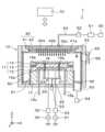
- FIG. 1is a vertical sectional view showing the outline of the configuration of the plasma processing apparatus 1.
- the plasma processing apparatus 1is a capacitively coupled plasma processing apparatus. Further, in the plasma processing apparatus 1, plasma processing is performed on a product wafer W as a product substrate.
- the product wafer Wis a wafer to be subjected to desired plasma processing, and is a wafer having a pattern formed on its surface, for example.
- the product wafer Wis, for example, a silicon wafer with a diameter of 300 mm.
- the plasma processingis not particularly limited, for example, etching processing, film forming processing, diffusion processing, etc. are performed.
- the plasma processing apparatus 1has a substantially cylindrical chamber 10 .
- Chamber 10defines a processing space S within which a plasma is generated.
- the chamber 10is made of aluminum, for example.
- Chamber 10is connected to ground potential.
- An inner wall surface of the chamber 10, that is, a wall surface that defines the processing space S,is formed with a plasma-resistant film.
- the membranemay be a membrane formed by an anodizing process, or a ceramic membrane such as a membrane formed from yttrium oxide.
- a mounting table 11 on which the product wafer W is mountedis housed inside the chamber 10 .
- the mounting table 11has a lower electrode 12 , an electrostatic chuck 13 and an edge ring 14 .
- the lower electrode 12is made of a conductive metal such as aluminum, and has a substantially disk shape.
- a coolant channel 15 ais formed inside the lower electrode 12 .
- Refrigerantis supplied from a chiller unit (not shown) provided outside the chamber 10 to the refrigerant flow path 15a through a refrigerant inlet pipe 15b.
- the refrigerant supplied to the refrigerant channel 15areturns to the chiller unit through the refrigerant outlet channel 15c.
- the electrostatic chuck 13, the edge ring 14, and the product wafer Wcan be cooled to a desired temperature by circulating a coolant such as cooling water in the coolant channel 15a.
- the electrostatic chuck 13is provided on the lower electrode 12 .
- the electrostatic chuck 13is a member capable of attracting and holding both the product wafer W and the edge ring 14 by electrostatic force.
- the electrostatic chuck 13is formed such that the surface of the central portion is higher than the surface of the outer peripheral portion.
- the surface of the central portion of the electrostatic chuck 13serves as a wafer mounting surface on which the product wafer W is mounted, and the surface of the outer peripheral portion of the electrostatic chuck 13 serves as an edge ring mounting surface on which the edge ring 14 is mounted. Become. The details of the configuration of the electrostatic chuck 13 will be described later.
- a first electrode 16 a for attracting and holding the product wafer Wis provided in the central portion inside the electrostatic chuck 13 .
- a second electrode 16 b for attracting and holding the edge ring 14is provided inside the electrostatic chuck 13 on the outer peripheral portion.
- the electrostatic chuck 13has a configuration in which electrodes 16a and 16b are sandwiched between insulating materials made of an insulating material.
- a DC voltageis applied to the first electrode 16a from a DC power supply (not shown).
- the product wafer Wis attracted and held on the surface of the central portion of the electrostatic chuck 13 by the electrostatic force generated thereby.
- a DC voltage from a DC power supply(not shown) is applied to the second electrode 16b.
- the edge ring 14is attracted and held on the surface of the outer peripheral portion of the electrostatic chuck 13 by the electrostatic force generated thereby.
- the edge ring 14is an annular member arranged so as to surround the product wafer W placed on the surface of the central portion of the electrostatic chuck 13 .
- Edge ring 14is provided to improve the uniformity of plasma processing. Therefore, the edge ring 14 is made of a material appropriately selected according to the plasma processing, and can be made of quartz, Si, SiC, or the like, for example. The details of the configuration of the edge ring 14 will be described later.
- the mounting table 11 configured as described aboveis fastened to a substantially cylindrical support member 17 provided at the bottom of the chamber 10 .
- the support member 17is made of an insulator such as ceramic or quartz.
- the mounting table 11may include a temperature control module configured to control at least one of the electrostatic chuck 13, the edge ring 14, and the product wafer W to a desired temperature.
- the temperature control modulemay include heaters, channels, or a combination thereof.
- a temperature control fluidsuch as a refrigerant or a heat transfer gas flows through the flow path.
- a lifter 20 for raising and lowering the product wafer W with respect to the mounting table 11is provided below the mounting table 11 and inside the support member 17 .
- the lifter 20has lifting pins 21 , support members 22 , and drive units 23 .
- the lifting pin 21is a columnar member that rises and falls so as to protrude from the surface of the central portion of the electrostatic chuck 13, and is made of ceramic, for example.
- Three or more elevating pins 21are provided at intervals in the circumferential direction of electrostatic chuck 13 , that is, along the circumferential direction of the surface.
- the lifting pins 21are provided, for example, at regular intervals along the circumferential direction.
- the lifting pin 21is provided so as to extend in the vertical direction.
- the elevating pin 21is inserted through a through hole 24 extending downward from the central surface of the electrostatic chuck 13 to the bottom surface of the lower electrode 12 . That is, the through hole 24 is formed so as to penetrate the central portion of the electrostatic chuck 13 and the lower electrode 12 .
- the support member 22supports a plurality of lifting pins 21.
- the drive unit 23generates a driving force for raising and lowering the support member 22 and raises and lowers the plurality of lifting pins 21 .
- the drive unit 23has a motor (not shown) that generates the driving force.
- the plasma processing apparatus 1further has a first RF (Radio Frequency) power supply 30 , a second RF power supply 31 , a first matching box 32 and a second matching box 33 .
- a first high-frequency power supply 30 and a second high-frequency power supply 31are connected to the lower electrode 12 via a first matching box 32 and a second matching box 33, respectively.
- the first high-frequency power supply 30is a power supply that generates high-frequency power for plasma generation.
- the first high frequency power supply 30supplies the lower electrode 12 with high frequency power HF, which may have a frequency of 27 MHz to 100 MHz, and in one example, 40 MHz.
- the first matching device 32has a circuit for matching the output impedance of the first high-frequency power supply 30 and the input impedance on the load side (lower electrode 12 side). Note that the first high-frequency power supply 30 may not be electrically connected to the lower electrode 12 and may be connected to the showerhead 40 as the upper electrode via the first matching box 32 .
- the second high frequency power supply 31generates high frequency power (bias power) LF for drawing ions into the product wafer W and supplies the high frequency power LF to the lower electrode 12 .
- the frequency of the high frequency power LFmay be in the range of 400 kHz to 13.56 MHz, and in one example is 400 kHz.
- the second matching device 33has a circuit for matching the output impedance of the second high-frequency power supply 31 and the input impedance on the load side (lower electrode 12 side).
- a DC (Direct Current) pulse generatormay be used instead of the second high-frequency power supply 31 .
- a shower head 40is provided above the mounting table 11 so as to face the mounting table 11 .
- the shower head 40has an electrode plate 41 arranged facing the processing space S and an electrode support 42 provided above the electrode plate 41 .
- the electrode plate 41functions as the lower electrode 12 and a pair of upper electrodes.
- the showerhead 40is connected to the ground potential.
- the shower head 40is supported on the top (ceiling surface) of the chamber 10 via an insulating shielding member 43 .
- the electrode plate 41is formed with a plurality of gas ejection ports 41a for supplying a processing gas sent from a gas diffusion chamber 42a, which will be described later, into the processing space S.
- the electrode plate 41is made of, for example, a conductor or semiconductor that generates little Joule heat and has low electrical resistivity.
- the electrode support 42detachably supports the electrode plate 41 .
- the electrode support 42has a structure in which a plasma-resistant film is formed on the surface of a conductive material such as aluminum.
- the membranemay be a membrane formed by an anodizing process, or a ceramic membrane such as a membrane formed from yttrium oxide.
- a gas diffusion chamber 42 ais formed inside the electrode support 42 .
- a plurality of gas flow holes 42bare formed from the gas diffusion chamber 42a to communicate with the gas ejection port 41a.
- a gas supply source group 50 for supplying a processing gas to the gas diffusion chamber 42ais connected to the electrode support 42 via a flow control device group 51, a valve group 52, a gas supply pipe 53, and a gas introduction hole 42c. ing.
- the gas supply source group 50has multiple types of gas supply sources necessary for plasma processing or dry cleaning.
- the flow control device group 51includes a plurality of flow controllers, and the valve group 52 includes a plurality of valves. Each of the plurality of flow controllers in the flow controller group 51 is a mass flow controller or a pressure-controlled flow controller.
- the processing gas from one or more gas supply sources selected from the gas supply source group 50is supplied through the flow control device group 51, the valve group 52, the gas supply pipe 53, and the gas introduction hole 42c. It is supplied to the gas diffusion chamber 42a. Then, the processing gas supplied to the gas diffusion chamber 42a is dispersed in the processing space S in the form of a shower through the gas flow hole 42b and the gas ejection port 41a.
- a deposition shield 60is detachably provided along the inner wall of the chamber 10 in the plasma processing apparatus 1 .
- the deposit shield 60prevents deposits from adhering to the inner wall of the chamber 10, and is made of, for example, an aluminum material coated with ceramics such as yttrium oxide.
- a deposit shield 61is detachably provided on the outer peripheral surface of the support member 17 facing the deposit shield 60 .
- a baffle plate 62is provided at the bottom of the chamber 10 and between the inner wall of the chamber 10 and the support member 17 .
- the baffle plate 62is made of, for example, an aluminum material coated with ceramics such as yttrium oxide.
- a plurality of through holesare formed in the baffle plate 62 .
- the processing space Scommunicates with the exhaust port 63 through the baffle plate 62 .
- An exhaust device 64such as a vacuum pump is connected to the exhaust port 63, and the inside of the processing space S can be decompressed by the exhaust device 64. As shown in FIG.
- a loading/unloading port 65 for the product wafer Wis formed on the side wall of the chamber 10 , and the loading/unloading port 65 can be opened and closed by a gate valve 66 .
- the dry cleaning sectionincludes the lower electrode 12, the second high-frequency power source 31, the gas supply source group 50, and the like. to generate plasma.
- a controller 70is provided in the plasma processing apparatus 1 described above.
- the control unit 70is, for example, a computer having a CPU, memory, etc., and has a program storage unit (not shown).
- a program for controlling plasma processing in the plasma processing apparatus 1is stored in the program storage unit.
- the programmay be recorded in a computer-readable storage medium and installed in the control unit 70 from the storage medium.
- the control unit 70controls transportation of the substrate (including vertical movement of the substrate by the lifter 20 ), plasma processing of the substrate, and execution of dry cleaning in the chamber 10 .
- the product wafer Wis loaded into the chamber 10 and placed on the electrostatic chuck 13 .
- the product wafer Wis placed on the electrostatic chuck 13 so that the center of the product wafer W is at the same position as the center of the electrostatic chuck 13 in plan view.
- the position of this product wafer Wis the processing position in the present disclosure.
- the product wafer Wis electrostatically attracted to and held by the electrostatic chuck 13 by Coulomb force.
- the inside of the chamber 10is depressurized to a desired degree of vacuum by the exhaust device 64 .
- the processing gasis supplied from the gas supply source group 50 to the processing space S through the shower head 40 .
- the first high-frequency power supply 30supplies high-frequency power HF for plasma generation to the lower electrode 12 to excite the processing gas and generate plasma.
- the high-frequency power LF for attracting ionsmay be supplied from the second high-frequency power supply 31 .
- the product wafer Wis subjected to plasma processing by the action of the generated plasma.
- the supply of the high frequency power HF from the first high frequency power supply 30 and the supply of the processing gas from the gas supply source group 50are stopped. Moreover, when the high frequency power LF is being supplied during the plasma processing, the supply of the high frequency power LF is also stopped. Next, the supply of the heat transfer gas to the back surface of the product wafer W is stopped, and the electrostatic chuck 13 stops holding the product wafer W by suction.
- the product wafer Wis unloaded from the chamber 10, and a series of plasma processing for the product wafer W is completed.
- plasmamay be generated using only the high frequency power LF from the second high frequency power supply 31 without using the high frequency power HF from the first high frequency power supply 30 .
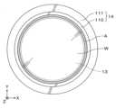
- FIG. 2is a vertical cross-sectional view showing the schematic configuration of the electrostatic chuck 13 and the edge ring 14.
- FIG. 3is a plain view showing the outline of the configuration of the electrostatic chuck 13 and the edge ring 14. As shown in FIG.
- the electrostatic chuck 13has a central portion 100 having a surface 100a on which the product wafer W is placed and an outer peripheral portion 101 having a surface 101a on which the edge ring 14 is placed. It is configured.
- the central portion 100is provided so as to protrude from the outer peripheral portion 101 , and the surface 100 a of the central portion 100 is higher than the surface 101 a of the outer peripheral portion 101 .
- the central portion 100 of the electrostatic chuck 13is formed to have a smaller diameter than the diameter of the product wafer W, for example, so that when the product wafer W is placed on the surface 100a, the peripheral edge portion of the product wafer W touches the electrostatic chuck 13. It projects from the central part 100 of the.
- the electrostatic chuck 13 of the present embodimenthas the central portion 100 and the outer peripheral portion 101 integrally formed, the central portion 100 and the outer peripheral portion 101 may be separate bodies. Further, the electrostatic chuck 13 of this embodiment has the central portion 100 and the outer peripheral portion 101, but the outer peripheral portion 101 may be omitted. In such a case, the edge ring 14 is not placed on the electrostatic chuck 13 but supported by another supporting member (not shown).
- the edge ring 14is provided so as to surround the product wafer W placed on the surface 100a.
- the edge ring 14is formed integrally with a first ring portion 110 having an annular shape and a second ring portion 111 having an annular shape.
- the first ring portion 110 and the second ring portion 111are provided on concentric circles, respectively, and the second ring portion 111 is provided radially outside the first ring portion 110 .
- the surface 110a of the first ring portion 110is lower than the surface 100a.
- the surface 111a of the second ring portion 111is higher than the surface 100a, for example, the same height as the surface Wa of the product wafer W placed on the surface 100a, or higher than the surface Wa of the product wafer W.
- the inner peripheral portion of the surface 111ais inclined toward the surface 110a (inward in the radial direction).
- the inner diameter of the first ring portion 110is larger than the diameter of the central portion 100 and smaller than the diameter of the product wafer W.
- the inner diameter of the second ring portion 111is larger than the diameter of the product wafer W.
- the first ring portion 110is arranged so as to go under the peripheral portion of the product wafer W projecting from the central portion 100 of the electrostatic chuck 13 . That is, as shown in FIGS. 2 and 3, the surface 110a of the first ring portion 110 has a region overlapping the product wafer W and shadowed by the product wafer W in plan view. In the following description, the shadow area of the product wafer W will be referred to as a shadow area A. As shown in FIG.
- Plasma processingproduces reaction products as described above. Reaction products adhere to the edge ring 14 and the like and accumulate as deposits. In order to remove the deposits, dry cleaning using plasma is performed inside the chamber 10 . Dry cleaning removes deposits by chemical reaction by radicals and physical reaction by ions (sputtering). Radical chemical reactions can remove, for example, carbon-based depots. Moreover, the physical reaction by ions can remove, for example, deposits containing Si and metals.
- FIG. 4is an explanatory diagram showing how dry cleaning is performed using the dummy wafer D. As shown in FIG. In FIG. 4, arrows indicate the flow of ions N. In FIG. Also, in order to facilitate understanding of the technology, the flow of radicals is omitted in FIG.
- the dummy wafer Dis a wafer having the same diameter as the product wafer W.
- the dummy wafer Dis a wafer on which no pattern is formed, and is a so-called bare silicon wafer.
- ions Nare supplied to the surfaces 110a and 111a of the edge ring 14 to remove deposits adhering to the surfaces 110a and 111a.
- high-frequency power LFbias power
- the ions Ntravel straight toward the dummy wafer D, so the efficiency of sputtering by the ions N in the shadow region A shielded by the dummy wafer D is significantly reduced.
- depositsfor example, deposits containing Si or metal
- Radicalsare also difficult to supply to the shaded area A, which is in the shadow of the dummy wafer D, so that the deposits cannot be sufficiently removed.
- dummy cleaning of the shadow area Ais performed by shifting the position of the dummy wafer D with respect to the mounting table 11 (edge ring 14). Further, in the dry cleaning method of the second embodiment, a dummy wafer having a diameter smaller than that of the product wafer W (hereinafter referred to as a "small-diameter dummy wafer") is used as the dummy wafer to perform dummy cleaning of the shaded area A.
- FIG. 5is a flowchart showing main steps of wafer processing according to the first embodiment.
- FIG. 6is an explanatory diagram showing a series of wafer processing flows according to the first embodiment using a wafer.
- FIG. 7is an explanatory diagram showing the position of the wafer during dry cleaning according to the first embodiment.
- dry cleaningis performed using four dummy wafers D1 to D4 as described later. These first to fourth dummy wafers D1 to D4 have the same diameter as the product wafer W. Also, in the first embodiment, the first to fourth dummy wafers D1 to D4 are different dummy wafers. However, the first to fourth dummy wafers D1 to D4 may be the same dummy wafer.
- step S11In step S11, one lot, for example, 25 product wafers W are continuously subjected to plasma processing.
- the plasma processing method for each product wafer Wis as described above.
- step S12the first dry cleaning is performed using the first dummy wafer D1.
- the first dummy wafer D1is loaded into the chamber 10 and placed above the electrostatic chuck 13 .
- the first dummy wafer D1is arranged such that the center C1 of the first dummy wafer D1 is displaced from the center C of the electrostatic chuck 13 in the positive Y-axis direction in a plan view. be done.
- the position of this first dummy wafer D1is the first position in the present disclosure. In this case, the first shadow area A1 on the Y-axis negative direction side of the shadow area A of the edge ring 14 is exposed without overlapping the first dummy wafer D1 in plan view.
- one end D1a of the first dummy wafer D1is positioned between the inner peripheral end of the edge ring 14 and the outer peripheral end of the central portion 100 of the electrostatic chuck 13.
- the other end D1b of the first dummy wafer D1is located radially outside the inner peripheral end of the edge ring 14 . Then, the shadow area A1 on the one end D1a side of the edge ring 14 is exposed without overlapping with the first dummy wafer D1.
- the lifter 20 supporting the first dummy wafer D ⁇ b>1is lowered and placed on the electrostatic chuck 13 . Thereafter, by applying a DC voltage to the first electrode 16a of the electrostatic chuck 13, the first dummy wafer D1 is electrostatically attracted to and held by the electrostatic chuck 13 by Coulomb force. Further, after loading the first dummy wafer D1, the inside of the chamber 10 is decompressed to a desired degree of vacuum by the exhaust device 64 .
- dry cleaning gasis supplied to the processing space S from the gas supply source group 50 through the shower head 40 .
- Dry cleaning gasesare, for example, oxygen, oxygen-containing gases, HCl, F2 , Cl2 , hydrogen, nitrogen, argon, SF6 , C2F6 , NF3 , CF4 or mixtures of two or more of these gases.
- high frequency poweris supplied to the lower electrode 12 by the first high frequency power supply 30 and/or the second high frequency power supply 31 .
- the dry cleaning gasis excited to generate plasma, and deposits inside the chamber 10 are removed by a chemical reaction of radicals and a physical reaction of ions (sputtering).
- ionsare also supplied to the first shadow area A1 exposed from the first dummy wafer D1, and deposits attached to the first shadow area A1 are also removed.
- the first dry cleaningis performed.
- the supply of high-frequency power from the first high-frequency power supply 30 and/or the second high-frequency power supply 31 and the supply of processing gas from the gas supply source group 50are stopped.
- the attraction and holding of the first dummy wafer D1 by the electrostatic chuck 13is stopped.
- the first dummy wafer D1is unloaded from the chamber 10, and the first dry cleaning using the first dummy wafer D1 is completed.
- step S13In step S13, the next lot, for example, 25 product wafers W are continuously subjected to plasma processing.
- This step S34is the same as step S11.
- step S14second dry cleaning is performed using the second dummy wafer D2.
- the second dummy wafer D2is arranged above the electrostatic chuck 13 .
- the second dummy wafer D2is arranged so that the center C2 of the second dummy wafer D2 is displaced from the center C of the electrostatic chuck 13 in the positive direction of the X axis in plan view. be done.
- the position of this second dummy wafer D2is the second position in the present disclosure. In this case, the second shadow area A2 on the X-axis negative direction side of the shadow area A of the edge ring 14 is exposed without overlapping the second dummy wafer D2 in plan view.
- the second dummy wafer D2is placed on the electrostatic chuck 13 and held by the electrostatic chuck 13 by attraction.
- the subsequent dry cleaning methodis the same as the first dry cleaning in step S12. That is, deposits inside the chamber 10 are removed using plasma (including radicals and ions) excited by the dry cleaning gas. At this time, deposits adhering to the second shadow area A2 exposed from the second dummy wafer D2 are also removed. Thus, the second dry cleaning is performed.
- step S15In step S15, the next lot, for example, 25 product wafers W are continuously plasma-processed.
- This step S34is the same as step S11.
- step S16third dry cleaning is performed using the third dummy wafer D3.
- a third dummy wafer D3is arranged above the electrostatic chuck 13 .
- the third dummy wafer D3is arranged so that the center C3 of the third dummy wafer D3 is shifted from the center C of the electrostatic chuck 13 in the Y-axis negative direction in plan view. be done.
- the position of this third dummy wafer D3is the third position in the present disclosure.
- the third shadow area A3 on the Y-axis positive direction side of the shadow area A of the edge ring 14is exposed without overlapping the third dummy wafer D3 in plan view.
- the third dummy wafer D3is placed on the electrostatic chuck 13 and held by the electrostatic chuck 13 by suction.
- the subsequent dry cleaning methodis the same as the first dry cleaning in step S12. That is, deposits inside the chamber 10 are removed using plasma (including radicals and ions) excited by the dry cleaning gas. At this time, deposits adhering to the third shadow area A3 exposed from the third dummy wafer D3 are also removed. Thus, the third dry cleaning is performed.
- step S17In step S17, the next lot, for example, 25 product wafers W are continuously plasma-processed.
- This step S34is the same as step S11.
- step S18the fourth dry cleaning is performed using the fourth dummy wafer D4.
- a fourth dummy wafer D4is arranged above the electrostatic chuck 13 .
- the fourth dummy wafer D4is arranged so that the center C4 of the fourth dummy wafer D4 is shifted from the center C of the electrostatic chuck 13 in the negative direction of the X axis in plan view. be done.
- the position of this fourth dummy wafer D4is the fourth position in the present disclosure.
- the fourth shadow area A4 on the X-axis positive direction side of the shadow area A of the edge ring 14is exposed without overlapping the fourth dummy wafer D4 in plan view.
- the fourth dummy wafer D4is placed on the electrostatic chuck 13 and held by the electrostatic chuck 13 by suction.
- the subsequent dry cleaning methodis the same as the first dry cleaning in step S12. That is, deposits inside the chamber 10 are removed using plasma (including radicals and ions) excited by the dry cleaning gas. At this time, deposits adhering to the fourth shadow area A4 exposed from the fourth dummy wafer D4 are also removed. Thus, the fourth dry cleaning is performed.
- step S18for example, steps S11 to S18 are repeated.
- deposits attached to the first to fourth shadow areas A1 to A4can be removed by performing the first to fourth dry cleanings. Therefore, as shown in FIG. 4, the deposits can be properly removed even in the shaded area A where the deposits could not be removed because of the shadow of the dummy wafer D in the prior art.
- portions other than the shadow region Aare exposed on the surfaces 110a and 111a of the edge ring 14, and deposits adhering to these portions can also be properly removed. Therefore, deposits can be removed from the entire surfaces 110a and 111a of the edge ring 14, so that the generation of particles can be suppressed and the yield of products can be improved.
- the operating time of the plasma processing apparatus 1can be lengthened, and it is also possible to extend the mean time between cleanings (MTBC) of the plasma processing apparatus.
- the dummy waferwhen dry cleaning is performed using a dummy wafer, the dummy wafer is placed at an accurate position with respect to the electrostatic chuck 13, that is, at a position where the center of the dummy wafer coincides with the center of the electrostatic chuck 13 in plan view. was sought. Therefore, intentionally displacing the dummy wafers D1 to D4 with respect to the electrostatic chuck 13, as in the first embodiment, is extremely novel and not in the conventional technical concept.
- FIG. 9is an explanatory diagram showing the first to fourth positions.
- a first line segment L1is a line segment connecting the center C of the electrostatic chuck 13 and the center C1 of the first dummy wafer D1.
- a second line segment L2is a line segment connecting the center C of the electrostatic chuck 13 and the center C2 of the second dummy wafer D2.
- a third line segment L3is a line segment connecting the center C of the electrostatic chuck 13 and the center C3 of the third dummy wafer D3.
- a fourth line segment L4is a line segment connecting the center C of the electrostatic chuck 13 and the center C4 of the fourth dummy wafer D4.
- the first angle ⁇ 1is the angle formed by the first line segment L1 and the second line segment L2.
- the second angle ⁇ 2is the angle formed by the second line segment L2 and the third line segment L3.
- a third angle ⁇ 3is an angle formed by the third line segment L3 and the fourth line segment L4.
- a fourth angle ⁇ 4is an angle formed by the fourth line segment L4 and the first line segment L1.
- the first to fourth angles ⁇ 1 to ⁇ 4are equal and 90 degrees.
- the centers C1 to C4 of the first to fourth dummy wafers D1 to D4are arranged on the same circumference at regular intervals.
- the areas of the first to fourth shaded areas A1 to A4can be made uniform. As a result of intensive studies by the inventors, it was found that the entire shaded area A can be covered by the first to fourth shaded areas A1 to A4. In other words, when the first to fourth dry cleanings are performed, the shaded area A is entirely exposed, and the deposit adhering to the shaded area A can be removed.
- the first to fourth dry cleaningsmay be continuously performed after plasma processing is performed on product wafers W of one lot.
- FIG. 10is an explanatory diagram showing a series of wafer processing flows according to this modification using a wafer.
- Step S21In step S21, one lot, for example, 25 product wafers W are continuously subjected to plasma processing. This step S21 is the same as step S11.
- Step S22the first dry cleaning is performed using the first dummy wafer D1.
- step S23the second dry cleaning is performed using the second dummy wafer D2.
- step S24third dry cleaning is performed using the third dummy wafer D3.
- step S25the fourth dry cleaning is performed using the fourth dummy wafer D4.
- step S21for example, steps S21 to S25 are repeated. Further, as shown in FIG. 11, step S21 may be performed a plurality of times, that is, steps S22 to S25 may be performed after plasma processing is performed on product wafers W of a plurality of lots.
- the same effects as in the first embodimentcan be enjoyed. That is, by performing the first to fourth dry cleanings respectively, the deposits adhering to the first to fourth shaded areas A1 to A4 can be removed.
- FIG. 12is an explanatory diagram showing a series of wafer processing flows according to this modification using a wafer.
- Step S30In step S30, one lot, for example, 25 product wafers W are continuously subjected to plasma processing. This step S30 is the same as step S11.
- step S31fifth dry cleaning is performed using the fifth dummy wafer D5.
- a fifth dummy wafer D5is arranged above the electrostatic chuck 13 .
- the fifth dummy wafer D5is arranged so that the center of the fifth dummy wafer D5 is at the same position as the center of the electrostatic chuck 13 in plan view.
- the position of this fifth dummy wafer D5is the fifth position in the present disclosure.
- the fifth dummy wafer D5is placed on the electrostatic chuck 13 and held by the electrostatic chuck 13 by suction.
- the subsequent dry cleaning methodis the same as the first dry cleaning in step S12. That is, deposits inside the chamber 10 are removed using plasma (including radicals and ions) excited by the dry cleaning gas. Thus, the fifth dry cleaning is performed.
- Step S32In step S32, one lot, for example, 25 product wafers W are continuously subjected to plasma processing. This step S32 is the same as step S11.
- Step S33the first dry cleaning is performed using the first dummy wafer D1. This step S33 is the same as step S12.
- Step S34In step S34, one lot, for example, 25 product wafers W are continuously subjected to plasma processing. This step S34 is the same as step S11.
- Step S35the second dry cleaning is performed using the second dummy wafer D2. This step S35 is the same as step S14.
- Step S36In step S36, one lot, for example, 25 product wafers W are continuously subjected to plasma processing. This step S36 is the same as step S11.
- step S37In step S37, third dry cleaning is performed using the third dummy wafer D3. This step S37 is the same as step S16.
- Step S38In step S38, one lot, for example, 25 product wafers W are continuously subjected to plasma processing. This step S38 is the same as step S11.
- step S39the fourth dry cleaning is performed using the fourth dummy wafer D4. This step S39 is the same as step S18.
- step S39for example, steps S30 to S39 are repeated.
- the same effects as in the first embodimentcan be enjoyed. That is, by performing the first to fourth dry cleanings, respectively, the deposits adhering to the first to fourth shaded areas A1 to A4 can be removed.
- the fifth dry cleaningis performed using the fifth dummy wafer D5 in step S31 of this modified example, so-called waferless dry cleaning may be performed instead.
- FIG. 13is an explanatory diagram showing a series of wafer processing flows according to this modification using a wafer.
- Step S41In step S41, one lot, for example, 25 product wafers W are continuously subjected to plasma processing. This step S41 is the same as step S11.
- step S42fifth dry cleaning is performed using the fifth dummy wafer D5. This step S42 is the same as step S31.
- Step S43In step S43, one lot, for example, 25 product wafers W are continuously subjected to plasma processing. This step S43 is the same as step S11.
- Step S44the first dry cleaning is performed using the first dummy wafer D1.
- step S45the second dry cleaning is performed using the second dummy wafer D2.
- step S46third dry cleaning is performed using the third dummy wafer D3.
- step S47the fourth dry cleaning is performed using the fourth dummy wafer D4.
- step S47for example, steps S41 to S47 are repeated.
- the same effects as in the first embodimentcan be enjoyed. That is, by performing the first to fourth dry cleanings respectively, the deposits adhering to the first to fourth shaded areas A1 to A4 can be removed.
- Steps S42 and S43may be performed a plurality of times, that is, steps S44 to S47 may be performed after plasma processing is performed on product wafers W in a plurality of lots. In such a case, if steps S42 and S43 are performed a plurality of times, deposits in the shaded area A that cannot be removed in step S42 will accumulate. Therefore, by performing the first to fourth dry cleanings in steps S43 to S47, the deposits in the shaded area A can be removed.
- step S42 of this modified examplethe fifth dry cleaning is performed using the fifth dummy wafer D5, but instead of this, so-called waferless dry cleaning may be performed.
- the first to fourth dry cleaningsare performed with the first to fourth dummy wafers D1 to D4 placed on the electrostatic chuck 13, respectively. , may be performed in a state separated from the electrostatic chuck 13 .
- the first dry cleaning using the first dummy wafer D1will be described below, the other second to fourth dry cleanings are the same.
- the first ring portion 110may be radially small.
- the distance F1 between the one end D1b and the outer peripheral end of the central portion 100 of the electrostatic chuck 13is sufficiently secured.
- One end D1ais located above the edge ring 14. As shown in FIG. That is, the shaded area A1 on the one end D1a side of the edge ring 14 overlaps the first dummy wafer D1 in plan view and is not completely exposed.
- the first dry cleaningmay be performed while the first dummy wafer D1 is supported by the lifter 20 and separated from the electrostatic chuck 13 as shown in FIG. 14(b).
- the distance F2(margin) between the one end D1b of the first dummy wafer D1 and the outer peripheral end of the central portion 100 of the electrostatic chuck 13 can be sufficiently ensured, and the one end D1a is separated from the inner peripheral end of the edge ring 14. It is positioned between the outer peripheral ends of the central portion 100 of the electrostatic chuck 13 .
- the shaded area A1 on the one end D1a side of the edge ring 14is exposed without overlapping the first dummy wafer D1, and deposits adhering to the shaded area A1 can be removed in the first dry cleaning.
- the inner peripheral portion of the surface 111a of the first ring portion 110 in the edge ring 14is inclined toward the surface 110a.
- the distance H between the back surface D1c of the first dummy wafer D1 shown in FIG. 14(b) and the surface of the electrostatic chuck 13is preferably 2 mm or less. That is, when the distance H is 2 mm or less, the state of the plasma does not change in the first dry cleaning, and the same cleaning effect as when the first dummy wafer D1 is placed on the electrostatic chuck 13 can be obtained. .
- the second to fourth dry cleaningsare performed while the second to fourth dummy wafers D2 to D4 are supported by the lifter 20 and spaced apart from the electrostatic chuck 13, respectively.
- the shaded areas A2 to A4are exposed, and deposits adhering to the shaded areas A2 to A4 can be removed in the second to fourth dry cleanings, respectively.
- the same effects as in the first embodimentcan be enjoyed. That is, by performing the first to fourth dry cleanings respectively, the deposits adhering to the first to fourth shaded areas A1 to A4 can be removed.
- the first to fourth dry cleaningsare performed to expose the shadow areas A1 to A4 and remove the deposits, but the number of dry cleanings is limited to this. not.
- the number of times of dry cleaningshould be at least two or more. For example, when dry cleaning is performed twice, the above-described first dry cleaning and third dry cleaning may be performed.
- the number of product wafers W to be plasma-processed in one lotwas 25, but the number is not limited to this.
- one lotmay consist of two or more sheets, or may consist of one sheet.
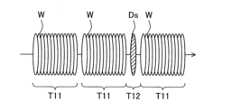
- ⁇ Dry cleaning method of the second embodiment>A dry cleaning method according to the second embodiment will be described.
- plasma processing for product wafers W and dry cleaning using small-diameter dummy wafers Dswill be described.
- the small-diameter dummy wafer Ds used in the dry cleaning of the second embodimentis a wafer having a smaller diameter than the product wafer W.
- FIG. 15is a vertical cross-sectional view showing the schematic configuration of the small-diameter dummy wafer Ds, the electrostatic chuck 13 and the edge ring 14.
- FIG. 16is a plain view showing the outline of the configuration of the small-diameter dummy wafer Ds, the electrostatic chuck 13 and the edge ring 14. As shown in FIG.
- the diameter of the small-diameter dummy wafer Dsis the same as the inner diameter of the edge ring 14. In such a case, the shaded area A is exposed without overlapping the small-diameter dummy wafer Ds in plan view. Note that the diameter of the small-diameter dummy wafer Ds is not limited to the illustrated example.
- FIG. 17is an explanatory diagram showing a series of wafer processing flows according to the second embodiment using a wafer.
- step T11In step T11, one lot, for example, 25 product wafers W are continuously subjected to plasma processing. This step T11 is the same as step S11.
- step T12dry cleaning is performed using the small-diameter dummy wafer Ds.
- a small-diameter dummy wafer Dsis arranged above the electrostatic chuck 13 .
- the small-diameter dummy wafer Dsis arranged so that the center of the small-diameter dummy wafer Ds is at the same position as the center of the electrostatic chuck 13 in plan view.
- the position of this small-diameter dummy wafer Dsis the cleaning position in the present disclosure. In this case, the shaded area A of the edge ring 14 is exposed without overlapping the small-diameter dummy wafer Ds in plan view.
- the small-diameter dummy wafer Dsis placed on the electrostatic chuck 13 and held by the electrostatic chuck 13 by suction. After that, a backside gas is supplied to the back surface of the small-diameter dummy wafer Ds to perform dry cleaning.
- the dry cleaning methodis the same as the first dry cleaning in step S12. That is, deposits inside the chamber 10 are removed using plasma (including radicals and ions) excited by the dry cleaning gas. At this time, deposits adhering to the shadow area A exposed from the small-diameter dummy wafer Ds are also removed. Thus, dry cleaning is performed.
- step T11for example, steps T11 and T12 are repeated. Further, as shown in FIG. 18, step T11 may be performed a plurality of times, that is, step T12 may be performed after plasma processing is performed on product wafers W of a plurality of lots.
- deposits adhering to the shadow area Acan be removed by performing dry cleaning using the small-diameter dummy wafer Ds. That is, as shown in FIG. 4, the deposits can be properly removed even in the shaded area A where the deposits could not be removed because of the shadow of the dummy wafer D in the prior art.
- portions other than the shadow region Aare exposed on the surfaces 110a and 111a of the edge ring 14, and the deposits adhering to these portions can also be properly removed. Therefore, deposits can be removed from the entire surfaces 110a and 111a of the edge ring 14, so that the generation of particles can be suppressed, the yield of products can be improved, and the operating time of the plasma processing apparatus 1 can be extended. It becomes possible.
- the small-diameter dummy wafer Dshas an inner portion (flat portion) with flat upper and lower surfaces, and an outer portion (bevel portion) formed on the outer peripheral side of the inner portion and having chamfered upper and lower surfaces. Also, in the small-diameter dummy wafer Ds, the annular range of 0.4 mm in the radial direction coincides with the bevel portion (chamfered portion). Therefore, it can be inferred that the cleaning effect can be obtained even under the small-diameter dummy wafer Ds as long as it is under the bevel portion.
- the upper limit of the diameter ⁇ A of the small-diameter dummy wafer Dsmay be smaller than the diameter of the product wafer W. That is, the diameter ⁇ A of the small-diameter dummy wafer Ds is preferably within the range of the following formula (1).
- the first high-frequency powermay be lower than the first high-frequency power in placement cleaning.
- the second high-frequency powermay be lower during lift-up cleaning than during placement cleaning (or the second high-frequency power may not be supplied).
- the pressure inside the chamber 10may be higher than in the mounting cleaning.
- Lift-up cleaning and placement cleaningmay be used together. That is, the lift-up cleaning may be performed before (or after) the placement cleaning. As a result, deposits that cannot be completely removed by dry cleaning performed while the small-diameter dummy wafer Ds is placed on the electrostatic chuck 13 (for example, deposits adhering to the gap between the electrostatic chuck 13 and the edge ring 14, and electrostatic Depot attached to the outer peripheral mounting surface of the chuck 13 can be removed.
- lift-up cleaning and placement cleaningare performed under different conditions (that is, when lift-up cleaning is performed with low power)
- lift-up cleaningis preferably performed after placement cleaning.
- the backside gasis supplied to the back surface of the small-diameter dummy wafer Ds for dry cleaning, but the backside gas does not have to be supplied.
- the small-diameter dummy wafer Dsis heated by plasma, and deposits removed by dry cleaning can be prevented from adhering to the small-diameter dummy wafer Ds.
- the frequency of cleaning the small-diameter dummy wafers Dscan be reduced.
- the backside gasmay be supplied during or after dry cleaning to cool the small-diameter dummy wafer Ds.
- the small-diameter dummy wafer Dsmay be cooled in order to unload the small-diameter dummy wafer Ds. That is, after the lift-up cleaning, the small-diameter dummy wafer Ds is placed on the electrostatic chuck 13, and after being attracted and held by the electrostatic chuck 13, a backside gas is supplied to the back surface of the small-diameter dummy wafer Ds to cool the small-diameter dummy wafer Ds.
- FIG. 19is an explanatory diagram showing a series of wafer processing flows according to this modification using a wafer.
- Step T21In step T21, one lot, for example, 25 product wafers W are continuously subjected to plasma processing. This step T21 is the same as step S11.
- step T22fifth dry cleaning (ordinary dry cleaning) is performed using the fifth dummy wafer D5. This step T22 is the same as step S31.
- step T23In step T23, one lot, for example, 25 product wafers W are continuously subjected to plasma processing. This step T23 is the same as step S11.
- step T24dry cleaning is performed using the small-diameter dummy wafer Ds. This step T24 is similar to step T12.
- step T24for example, steps T23 and T24 are repeated.
- steps T22 and T23may be performed multiple times, that is, step T24 may be performed after plasma processing is performed on product wafers W in multiple lots. In such a case, if steps T22 and T23 are performed multiple times, deposits in the shaded area A that cannot be removed in step T22 will accumulate. Therefore, by performing dry cleaning using the small-diameter dummy wafer Ds in step T24, the deposits in the shadow area A can be removed.
- step T22 of this modified examplethe fifth dry cleaning is performed using the fifth dummy wafer D5, but instead of this, so-called waferless dry cleaning may be performed.
- a cleaning method for a plasma processing apparatuscomprising: placing the first dummy substrate at a first position with respect to the mounting table inside the chamber, and performing a first dry cleaning inside the chamber; placing a second dummy substrate at a second position with respect to the mounting table inside the chamber, and performing a second dry cleaning inside the chamber;
- the center of the first position and the center of the second positionare positions different from the center of the mounting table in plan view,
- the cleaning method for a plasma processing apparatuswherein the first position and the second position are different positions in plan view.
- the mounting tableis an electrostatic chuck that holds the first dummy substrate or the second dummy substrate; an edge ring provided to surround the first dummy substrate or the second dummy substrate placed on the electrostatic chuck; In at least the first dry cleaning or the second dry cleaning, one end of the first dummy substrate or the second dummy substrate extends from the inner peripheral end of the edge ring to the outer periphery of the electrostatic chuck in plan view. 5.
- the method for cleaning a plasma processing apparatusaccording to any one of additional items 1 to 4, wherein the edge ring is positioned between the ends, and the other end is positioned outside the inner peripheral end of the edge ring.
- Appendix 76.
- Appendix 8Between the first dry cleaning and the second dry cleaning, plasma processing is performed on the product substrate, 8.
- the plasma treatmentis performed with the product substrate mounted on the mounting table such that the center of the product substrate and the center of the mounting table are at the same position in a plan view.
- Appendix 99.
- the cleaning method for a plasma processing apparatusaccording to any one of additional items 1 to 11, wherein the third position is a position different from the first position and the second position in plan view.
- Appendix 13placing a fourth dummy substrate at a fourth position with respect to the mounting table inside the chamber, and performing a fourth dry cleaning inside the chamber;
- the center of the fourth positionis a position different from the center of the mounting table in plan view, 13.
- [Appendix 14]A first line segment connecting the center of the mounting table and the center of the first position, and a second line segment connecting the center of the mounting table and the center of the second position.
- a plasma processing apparatusa chamber; a mounting table provided inside the chamber for mounting the first dummy substrate or the second dummy substrate; a dry cleaning unit that dry-cleans the interior of the chamber; A control unit that controls the dry cleaning unit, The control unit placing a first dummy substrate at a first position with respect to the mounting table inside the chamber, and performing a first dry cleaning inside the chamber; placing a second dummy substrate at a second position with respect to the mounting table inside the chamber, and performing a second dry cleaning on the inside of the chamber.
- the center of the first position and the center of the second positionare positions different from the center of the mounting table in plan view
- the plasma processing apparatuswherein the first position and the second position are different positions in plan view.
- a cleaning method for a plasma processing apparatuscomprising: placing the product substrate at a processing position on the mounting table inside the chamber, and subjecting the product substrate to plasma processing; placing a dummy substrate having a smaller diameter than the product substrate inside the chamber at a cleaning position with respect to the mounting table, and performing dry cleaning inside the chamber; The cleaning method of the plasma processing apparatus, wherein the center of the processing position and the center of the cleaning position are the same positions as the center of the mounting table in plan view.
- the plasma processing apparatus 1 of the above embodimentis a capacitively coupled plasma processing apparatus
- the plasma processing apparatus to which the present disclosure is appliedis not limited to this.
- the plasma processing apparatusmay be an inductively coupled plasma processing apparatus.
Landscapes
- Engineering & Computer Science (AREA)
- Physics & Mathematics (AREA)
- Plasma & Fusion (AREA)
- Analytical Chemistry (AREA)
- Chemical & Material Sciences (AREA)
- Manufacturing & Machinery (AREA)
- Microelectronics & Electronic Packaging (AREA)
- Power Engineering (AREA)
- Computer Hardware Design (AREA)
- General Physics & Mathematics (AREA)
- Condensed Matter Physics & Semiconductors (AREA)
- Health & Medical Sciences (AREA)
- Epidemiology (AREA)
- Public Health (AREA)
- Drying Of Semiconductors (AREA)
- Container, Conveyance, Adherence, Positioning, Of Wafer (AREA)
Abstract
Description
Translated fromJapanese本開示は、プラズマ処理装置のクリーニング方法に関する。The present disclosure relates to a cleaning method for a plasma processing apparatus.
特許文献1には、真空処理装置の真空処理室の内部をドライクリーニングする方法が開示されている。このドライクリーニングは、真空処理室の内部において試料台にダミーウェハを載置した状態で行われる。
特許文献2には、プラズマ処理システムのプラズマ処理チャンバの内部をドライクリーニングする方法が開示されている。このドライクリーニングは、いわゆるウェハレスドライクリーニングであって、プラズマ処理チャンバの内部においてサセプタにダミーウェハを載置せずに行われる。Patent Document 2 discloses a method for dry cleaning the inside of a plasma processing chamber of a plasma processing system. This dry cleaning is so-called waferless dry cleaning, which is performed without placing a dummy wafer on the susceptor inside the plasma processing chamber.
本開示にかかる技術は、プラズマ処理装置のチャンバの内部において、基板を載置する載置台を適切にドライクリーニングする。The technique according to the present disclosure appropriately dry-cleans the mounting table on which the substrate is mounted inside the chamber of the plasma processing apparatus.
本開示の一態様は、プラズマ処理装置のクリーニング方法であって、チャンバの内部に設けられた載置台に製品基板を載置し、前記製品基板にプラズマ処理を行う工程と、前記製品基板より小さい径を有する第1のダミー基板を前記載置台に載置し、前記チャンバの内部でプラズマを生成し前記載置台をクリーニングする第1のドライクリーニングを行う工程と、を含む。One aspect of the present disclosure is a cleaning method for a plasma processing apparatus, comprising the steps of: placing a product substrate on a mounting table provided inside a chamber; performing plasma processing on the product substrate; placing a first dummy substrate having a diameter on the mounting table, generating plasma inside the chamber, and performing a first dry cleaning of cleaning the mounting table.
本開示によれば、プラズマ処理装置のチャンバの内部において、基板を載置する載置台を適切にドライクリーニングすることができる。According to the present disclosure, it is possible to appropriately dry clean the mounting table on which the substrate is mounted inside the chamber of the plasma processing apparatus.
半導体デバイスの製造工程では、半導体ウェハ(以下、「ウェハ」という。)にプラズマ処理が行われる。プラズマ処理では、処理ガスを励起させることによりプラズマを生成し、当該プラズマによってウェハを処理する。In the manufacturing process of semiconductor devices, plasma processing is performed on semiconductor wafers (hereinafter referred to as "wafers"). In plasma processing, plasma is generated by exciting a processing gas, and the wafer is processed with the plasma.
プラズマ処理は、プラズマ処理装置で行われる。プラズマ処理装置は、一般的に、チャンバ、載置台、高周波(Radio Frequency:RF)電源を備える。一例では、高周波電源は、第1の高周波電源と第2の高周波電源を備える。第1の高周波電源は、チャンバ内のガスのプラズマを生成するために、第1の高周波電力を供給する。第2の高周波電源は、ウェハにイオンを引き組むために、バイアス用の第2の高周波電力を下部電極に供給する。チャンバはその内部空間を、プラズマが生成される処理空間として画成する。載置台は、チャンバ内に設けられている。載置台は、下部電極及び静電チャックを有する。静電チャックは下部電極上に設けられている。静電チャック上には、当該静電チャック上に載置されたウェハを囲むようにエッジリングが配置される。エッジリングは、ウェハの端部付近のシース形状を制御し、ウェハに対するプラズマ処理の均一性を向上させるために設けられる。Plasma processing is performed in plasma processing equipment. A plasma processing apparatus generally includes a chamber, a mounting table, and a radio frequency (RF) power supply. In one example, the radio frequency power supply comprises a first radio frequency power supply and a second radio frequency power supply. A first RF power supply provides first RF power to generate a plasma of the gas within the chamber. A second high frequency power supply supplies second high frequency power for biasing to the lower electrode in order to attract ions to the wafer. The chamber defines its interior space as a processing space in which plasma is generated. A mounting table is provided in the chamber. The mounting table has a lower electrode and an electrostatic chuck. An electrostatic chuck is provided on the lower electrode. An edge ring is arranged on the electrostatic chuck so as to surround the wafer placed on the electrostatic chuck. The edge ring is provided to control the sheath shape near the edge of the wafer and improve the uniformity of plasma processing on the wafer.
プラズマ処理では、反応生成物が生成される。反応生成物は、チャンバの内壁やエッジリング等に付着し、堆積物(以下、「デポ」という。)として堆積する。デポは異物(以下、「パーティクル」という。)発生の原因であり、製品の歩留まりの悪化や装置稼働時間低下を引き起こし得る。そこでデポを除去するため、チャンバの内部では、プラズマを用いたドライクリーニングが行われる。すなわち、ドライクリーニングでは、ドライクリーニングガスを励起させてプラズマを生成し、当該プラズマを用いてデポを除去する。具体的にドライクリーニングは、ラジカルによる化学的反応及びイオンによる物理的反応(スパッタ)によりデポを除去する。In plasma processing, reaction products are generated. The reaction product adheres to the inner wall of the chamber, the edge ring, etc., and accumulates as a deposit (hereinafter referred to as "depot"). Depots are the cause of the generation of foreign matter (hereinafter referred to as "particles"), and can cause deterioration in product yield and reduction in equipment operating time. In order to remove the deposit, dry cleaning using plasma is performed inside the chamber. That is, in dry cleaning, a dry cleaning gas is excited to generate plasma, and the plasma is used to remove deposits. Specifically, dry cleaning removes deposits by chemical reaction by radicals and physical reaction by ions (sputtering).
ドライクリーニングは、特許文献1に開示されたように載置台にダミーウェハを載置した状態で行われる場合がある。また、ドライクリーニングは、特許文献2に開示されたように載置台にダミーウェハを載置しない状態で行われる場合(ウェハレスドライクリーニング)もある。Dry cleaning may be performed with a dummy wafer mounted on a mounting table as disclosed in
ダミーウェハを用いたドライクリーニングにおいては、ラジカル及びイオンがダミーウェハに遮蔽されて、当該ラジカル及びイオンを供給し難い領域(ラジカル及びイオンが入射し難い領域)が生じる。特に、載置台の下部電極に第2の高周波電力(バイアス電力)を供給する場合、イオンはダミーウェハに向かって直進するため、ダミーウェハに遮蔽された領域においてイオンによるスパッタの効率は著しく低下する。このため、ラジカルによる化学的反応では除去し難いデポ(例えば、Siや金属を含む堆積物)を十分に除去することができない。In dry cleaning using a dummy wafer, radicals and ions are shielded by the dummy wafer, and regions where it is difficult to supply these radicals and ions (regions where it is difficult for radicals and ions to enter) are generated. In particular, when the second high-frequency power (bias power) is supplied to the lower electrode of the mounting table, the ions travel straight toward the dummy wafer, so the efficiency of ion sputtering in the region shielded by the dummy wafer is significantly reduced. For this reason, deposits (for example, deposits containing Si or metal) that are difficult to remove by chemical reaction using radicals cannot be sufficiently removed.
また、ダミーウェハを用いないウェハレスドライクリーニングにおいては、ダミーウェハが載置台(静電チャック)に載置されていないため、イオンが載置台表面に直接入射することになる。したがって、バイアス電力を高くすると、載置台が損傷してしまう。このため、バイアス電力を低くする必要があり、イオンによるスパッタの効率は低下する。そして、ラジカルによる化学的反応では除去し難いデポ(例えば、Siや金属を含む堆積物)を十分に除去することができない。In addition, in waferless dry cleaning that does not use a dummy wafer, ions are directly incident on the surface of the mounting table because the dummy wafer is not mounted on the mounting table (electrostatic chuck). Therefore, if the bias power is increased, the mounting table will be damaged. For this reason, it is necessary to lower the bias power, and the efficiency of ion sputtering is lowered. In addition, deposits (for example, deposits containing Si or metal) that are difficult to remove by chemical reaction using radicals cannot be sufficiently removed.
本開示にかかる技術は、プラズマ処理装置のチャンバの内部において、基板を載置する載置台を適切にドライクリーニングする。以下、本実施形態にかかるプラズマ処理装置及びプラズマ処理装置のドライクリーニング方法について、図面を参照しながら説明する。なお、本明細書及び図面において、実質的に同一の機能構成を有する要素においては、同一の符号を付することにより重複説明を省略する。The technique according to the present disclosure appropriately dry-cleans the mounting table on which the substrate is mounted inside the chamber of the plasma processing apparatus. A plasma processing apparatus and a dry cleaning method for the plasma processing apparatus according to the present embodiment will be described below with reference to the drawings. In the present specification and drawings, elements having substantially the same functional configuration are denoted by the same reference numerals, thereby omitting redundant description.
<プラズマ処理装置>
先ず、本実施形態にかかるプラズマ処理装置について説明する。図1は、プラズマ処理装置1の構成の概略を示す縦断面図である。プラズマ処理装置1は、容量結合型のプラズマ処理装置である。またプラズマ処理装置1では、製品基板としての製品ウェハWに対してプラズマ処理を行う。製品ウェハWは、所望のプラズマ処理が行われるウェハであって、例えば表面にパターンが形成されているウェハである。製品ウェハWは、例えば直径300mmのシリコンウェハである。なお、プラズマ処理は特に限定されるものではないが、例えばエッチング処理、成膜処理、拡散処理等が行われる。<Plasma processing equipment>
First, the plasma processing apparatus according to this embodiment will be described. FIG. 1 is a vertical sectional view showing the outline of the configuration of the
図1に示すようにプラズマ処理装置1は、略円筒形状のチャンバ10を有している。チャンバ10は、その内部においてプラズマが生成される処理空間Sを画成する。チャンバ10は、例えばアルミニウムから構成されている。チャンバ10は接地電位に接続されている。チャンバ10の内壁面、すなわち、処理空間Sを画成する壁面には、耐プラズマ性を有する膜が形成されている。この膜は、陽極酸化処理によって形成された膜、又は、酸化イットリウムから形成された膜といったセラミック製の膜であり得る。As shown in FIG. 1, the
チャンバ10の内部には、製品ウェハWを載置する載置台11が収容されている。載置台11は、下部電極12、静電チャック13、及びエッジリング14を有している。なお、下部電極12の裏面側には、例えばアルミニウムから構成される電極プレート(図示せず)が設けられていてもよい。A mounting table 11 on which the product wafer W is mounted is housed inside the
下部電極12は、導電性の金属、例えばアルミニウム等で構成されており、略円板形状を有している。The
下部電極12の内部には、冷媒流路15aが形成されている。冷媒流路15aには、チャンバ10の外部に設けられたチラーユニット(図示せず)から冷媒入口配管15bを介して冷媒が供給される。冷媒流路15aに供給された冷媒は、冷媒出口流路15cを介してチラーユニットに戻るようになっている。冷媒流路15aの中に冷媒、例えば冷却水等を循環させることにより、静電チャック13、エッジリング14、及び製品ウェハWを所望の温度に冷却することができる。A
静電チャック13は、下部電極12上に設けられている。静電チャック13は、製品ウェハWとエッジリング14の両方を静電力により吸着保持可能に構成された部材である。静電チャック13は、外周部の表面に比べて中央部の表面が高く形成されている。静電チャック13の中央部の表面は、製品ウェハWが載置されるウェハ載置面となり、静電チャック13の外周部の表面は、エッジリング14が載置されるエッジリング載置面となる。なお、静電チャック13の構成の詳細については後述する。The
静電チャック13の内部において中央部には、製品ウェハWを吸着保持するための第1の電極16aが設けられている。静電チャック13の内部において外周部には、エッジリング14を吸着保持するための第2の電極16bが設けられている。静電チャック13は、絶縁材料からなる絶縁材の間に電極16a、16bを挟んだ構成を有する。A
第1の電極16aには、直流電源(図示せず)からの直流電圧が印加される。これにより生じる静電力により、静電チャック13の中央部の表面に製品ウェハWが吸着保持される。同様に、第2の電極16bには、直流電源(図示せず)からの直流電圧が印加される。これにより生じる静電力により、静電チャック13の外周部の表面にエッジリング14が吸着保持される。A DC voltage is applied to the
エッジリング14は、静電チャック13の中央部の表面に載置された製品ウェハWを囲むように配置される、環状部材である。エッジリング14は、プラズマ処理の均一性を向上させるために設けられる。このため、エッジリング14は、プラズマ処理に応じて適宜選択される材料から構成されており、例えば石英やSi、SiC等から構成され得る。なお、このエッジリング14の構成の詳細については後述する。The
以上のように構成された載置台11は、チャンバ10の底部に設けられた略円筒形状の支持部材17に締結される。支持部材17は、例えばセラミックや石英等の絶縁体により構成される。The mounting table 11 configured as described above is fastened to a substantially
なお、図示は省略するが、載置台11は、静電チャック13、エッジリング14、及び製品ウェハWのうち少なくとも1つを所望の温度に調節するように構成される温調モジュールを含んでもよい。温調モジュールは、ヒータ、流路、又はこれらの組み合わせを含んでもよい。流路には、冷媒、伝熱ガスのような温調流体が流れる。Although illustration is omitted, the mounting table 11 may include a temperature control module configured to control at least one of the
載置台11の下方であって支持部材17の内側には、載置台11に対して製品ウェハWを昇降させるリフター20が設けられている。リフター20は、昇降ピン21、支持部材22、及び駆動部23を有している。A
昇降ピン21は、静電チャック13の中央部の表面から突没するように昇降する、柱状の部材であり、例えばセラミックから形成される。昇降ピン21は、静電チャック13の周方向、すなわち、表面の周方向に沿って、互いに間隔を空けて3本以上設けられている。昇降ピン21は、例えば、上記周方向に沿って等間隔で設けられている。昇降ピン21は、上下方向に延びるように設けられる。The lifting
昇降ピン21は、静電チャック13の中央部の表面から下方に延び下部電極12の底面まで至る貫通孔24に挿通される。すなわち、貫通孔24は、静電チャック13の中央部及び下部電極12を貫通するように形成されている。The elevating
支持部材22は、複数の昇降ピン21を支持する。駆動部23は、支持部材22を昇降させる駆動力を発生させ、複数の昇降ピン21を昇降させる。駆動部23は、上記駆動力を発生するモータ(図示せず)を有する。The
プラズマ処理装置1は、第1の高周波(RF:Radio Frequency)電源30、第2の高周波電源31、第1の整合器32、及び第2の整合器33を更に有している。第1の高周波電源30と第2の高周波電源31はそれぞれ、第1の整合器32及び第2の整合器33を介して、下部電極12に接続されている。The
第1の高周波電源30は、プラズマ発生用の高周波電力を発生する電源である。第1の高周波電源30からは27MHz~100MHzの周波数であってよく、一例においては40MHzの高周波電力HFが下部電極12に供給される。第1の整合器32は、第1の高周波電源30の出力インピーダンスと負荷側(下部電極12側)の入力インピーダンスを整合させるための回路を有している。なお、第1の高周波電源30は、下部電極12に電気的に接続されていなくてもよく、第1の整合器32を介して上部電極であるシャワーヘッド40に接続されていてもよい。The first high-
第2の高周波電源31は、製品ウェハWにイオンを引き込むための高周波電力(バイアス電力)LFを発生して、当該高周波電力LFを下部電極12に供給する。高周波電力LFの周波数は、400kHz~13.56MHzの範囲内の周波数であってよく、一例においては400kHzである。第2の整合器33は、第2の高周波電源31の出力インピーダンスと負荷側(下部電極12側)の入力インピーダンスを整合させるための回路を有している。なお、第2の高周波電源31に代えて、DC(Direct Current)パルス生成部を用いてもよい。The second high
載置台11の上方には、載置台11と対向するように、シャワーヘッド40が設けられている。シャワーヘッド40は、処理空間Sに面して配置される電極板41、及び電極板41の上方に設けられる電極支持体42を有している。電極板41は、下部電極12と一対の上部電極として機能する。後述するように第1の高周波電源30が下部電極12に電気的に接続されている場合には、シャワーヘッド40は、接地電位に接続される。なお、シャワーヘッド40は、絶縁性遮蔽部材43を介して、チャンバ10の上部(天井面)に支持されている。A
電極板41には、後述のガス拡散室42aから送られる処理ガスを処理空間Sに供給するための複数のガス噴出口41aが形成されている。電極板41は、例えば、発生するジュール熱の少ない低い電気抵抗率を有する導電体又は半導体から構成される。The
電極支持体42は、電極板41を着脱自在に支持するものである。電極支持体42は、例えばアルミニウム等の導電性材料の表面に耐プラズマ性を有する膜が形成された構成を有している。この膜は、陽極酸化処理によって形成された膜、又は、酸化イットリウムから形成された膜といったセラミック製の膜であり得る。電極支持体42の内部には、ガス拡散室42aが形成されている。ガス拡散室42aからは、ガス噴出口41aに連通する複数のガス流通孔42bが形成されている。また、ガス拡散室42aには、後述するガス供給管53に接続されるガス導入孔42cが形成されている。The
また、電極支持体42には、ガス拡散室42aに処理ガスを供給するガス供給源群50が、流量制御機器群51、バルブ群52、ガス供給管53、ガス導入孔42cを介して接続されている。A gas
ガス供給源群50は、プラズマ処理又はドライクリーニングに必要な複数種のガス供給源を有している。流量制御機器群51は複数の流量制御器を含み、バルブ群52は複数のバルブを含んでいる。流量制御機器群51の複数の流量制御器の各々は、マスフローコントローラ又は圧力制御式の流量制御器である。プラズマ処理装置1においては、ガス供給源群50から選択された一以上のガス供給源からの処理ガスが、流量制御機器群51、バルブ群52、ガス供給管53、ガス導入孔42cを介してガス拡散室42aに供給される。そして、ガス拡散室42aに供給された処理ガスは、ガス流通孔42b、ガス噴出口41aを介して、処理空間S内にシャワー状に分散されて供給される。The gas
プラズマ処理装置1には、チャンバ10の内壁に沿ってデポシールド60が着脱自在に設けられている。デポシールド60は、チャンバ10の内壁にデポが付着することを抑制するものであり、例えばアルミニウム材に酸化イットリウム等のセラミックスを被覆することにより構成される。また同様に、デポシールド60に対向する面であって、支持部材17の外周面には、デポシールド61が、着脱自在に設けられている。A
チャンバ10の底部であって、チャンバ10の内壁と支持部材17との間には、バッフルプレート62が設けられている。バッフルプレート62は、例えばアルミニウム材に酸化イットリウム等のセラミックスを被覆することにより構成される。バッフルプレート62には、複数の貫通孔が形成されている。処理空間Sは当該バッフルプレート62を介して排気口63に連通されている。排気口63には例えば真空ポンプ等の排気装置64が接続され、当該排気装置64により処理空間S内を減圧可能に構成されている。A
また、チャンバ10の側壁には製品ウェハWの搬入出口65が形成され、当該搬入出口65はゲートバルブ66により開閉可能となっている。A loading/unloading
なお、本実施形態においてドライクリーニング部は、下部電極12、第2の高周波電源31、ガス供給源群50等を含み、後述するようにチャンバ10の内部をドライクリーニングするため、ドライクリーニングガスを励起させてプラズマを生成する。In this embodiment, the dry cleaning section includes the
以上のプラズマ処理装置1には、制御部70が設けられている。制御部70は、例えばCPUやメモリ等を備えたコンピュータであり、プログラム格納部(図示せず)を有している。プログラム格納部には、プラズマ処理装置1におけるプラズマ処理を制御するプログラムが格納されている。なお、上記プログラムは、コンピュータに読み取り可能な記憶媒体に記録されていたものであって、当該記憶媒体から制御部70にインストールされたものであってもよい。制御部70は、基板の搬送(リフター20による基板の上下動を含む)、基板に対するプラズマ処理およびチャンバ10内のドライクリーニングの実行を制御する。A
<プラズマ処理方法>
次に、以上のように構成されたプラズマ処理装置1を用いて行われるプラズマ処理について説明する。<Plasma treatment method>
Next, plasma processing performed using the
先ず、チャンバ10の内部に製品ウェハWを搬入し、静電チャック13上に製品ウェハWを載置する。この際、平面視において製品ウェハWの中心が静電チャック13の中心と同じ位置になるように、製品ウェハWが静電チャック13上に載置される。この製品ウェハWの位置が、本開示における処理位置である。その後、静電チャック13の第1の電極16aに直流電圧を印加することにより、製品ウェハWはクーロン力によって静電チャック13に静電吸着され、保持される。また、製品ウェハWの搬入後、排気装置64によってチャンバ10の内部を所望の真空度まで減圧する。First, the product wafer W is loaded into the
次に、ガス供給源群50からシャワーヘッド40を介して処理空間Sに処理ガスを供給する。また、第1の高周波電源30によりプラズマ生成用の高周波電力HFを下部電極12に供給し、処理ガスを励起させて、プラズマを生成する。この際、第2の高周波電源31によりイオン引き込み用の高周波電力LFを供給してもよい。そして、生成されたプラズマの作用によって、製品ウェハWにプラズマ処理が施される。Next, the processing gas is supplied from the gas
プラズマ処理を終了する際には、先ず、第1の高周波電源30からの高周波電力HFの供給及びガス供給源群50による処理ガスの供給を停止する。また、プラズマ処理中に高周波電力LFを供給していた場合には、当該高周波電力LFの供給も停止する。次いで、製品ウェハWの裏面への伝熱ガスの供給を停止し、静電チャック13による製品ウェハWの吸着保持を停止する。When terminating the plasma processing, first, the supply of the high frequency power HF from the first high
その後、チャンバ10から製品ウェハWを搬出して、製品ウェハWに対する一連のプラズマ処理が終了する。After that, the product wafer W is unloaded from the
なお、プラズマ処理においては、第1の高周波電源30からの高周波電力HFを使用せず、第2の高周波電源31からの高周波電力LFのみを用いて、プラズマを生成する場合もある。In plasma processing, plasma may be generated using only the high frequency power LF from the second high
<静電チャック及びエッジリング>
次に、上述した静電チャック13及びエッジリング14の主たる構成について説明する。図2は、静電チャック13及びエッジリング14の構成の概略を示す縦断面図である。図3は、静電チャック13及びエッジリング14の構成の概略を示す平明図である。<Electrostatic Chuck and Edge Ring>
Next, main configurations of the
図2に示すように静電チャック13は、製品ウェハWを載置する表面100aを備えた中央部100と、エッジリング14を載置する表面101aを備えた外周部101とが一体になって構成されている。中央部100は外周部101から突起するように設けられ、中央部100の表面100aは外周部101の表面101aより高い。As shown in FIG. 2, the
静電チャック13の中央部100は、例えば製品ウェハWの直径よりも小径に形成されており、製品ウェハWが表面100aに載置されたときに、製品ウェハWの周縁部が静電チャック13の中央部100から張り出すようになっている。The
なお、本実施形態の静電チャック13は中央部100と外周部101が一体に構成されているが、これら中央部100と外周部101は別体であってもよい。また、本実施形態の静電チャック13は、中央部100と外周部101を有しているが、外周部101を省略してもよい。かかる場合、エッジリング14は静電チャック13に載置されず、他の支持部材(図示せず)によって支持される。Although the
エッジリング14は、表面100aに載置された製品ウェハWを囲むように設けられている。エッジリング14は、環状形状を備えた第1のリング部110と、環状形状を備えた第2のリング部111とが一体に構成されている。第1のリング部110と第2のリング部111はそれぞれ同心円上に設けられ、第2のリング部111が第1のリング部110の径方向外側に設けられている。The
第1のリング部110の表面110aは、表面100aよりも低い。第2のリング部111の表面111aは、表面100aよりも高く、例えば表面100aに載置された製品ウェハWの表面Waと同じ高さであるか、或いは製品ウェハWの表面Waよりも高い。また、表面111aの内周部は、表面110a(径方向内側)に向けて傾斜している。The
第1のリング部110の内径は、中央部100の径より大きく、且つ製品ウェハWの径より小さい。第2のリング部111の内径は、製品ウェハWの径より大きい。そして、第1のリング部110は、静電チャック13の中央部100から張り出した製品ウェハWの周縁部の下方側にもぐり込むように配置される。すなわち、図2及び図3に示すように、第1のリング部110の表面110aには、平面視において、製品ウェハWとオーバーラップし、製品ウェハWの影となる領域が形成される。以下の説明では、この製品ウェハWの影となる領域を、陰影領域Aという。The inner diameter of the
<ダミーウェハを用いたドライクリーニングの特徴>
プラズマ処理では、上述したように反応生成物が生成される。反応生成物はエッジリング14等に付着し、デポとして堆積する。そこでデポを除去するため、チャンバ10の内部では、プラズマを用いたドライクリーニングが行われる。ドライクリーニングは、ラジカルによる化学的反応及びイオンによる物理的反応(スパッタ)によりデポを除去する。ラジカルによる化学的反応では、例えば炭素系のデポを除去することができる。また、イオンによる物理的反応では、例えばSiや金属を含むデポを除去することができる。<Characteristics of dry cleaning using dummy wafer>
Plasma processing produces reaction products as described above. Reaction products adhere to the
本実施形態では、ダミーウェハを用いてドライクリーニングを行う。しかしながら、かかる場合、ラジカル及びイオンがダミーウェハに遮蔽されて、当該ラジカル及びイオンを供給し難い領域(ラジカル及びイオンが入射し難い領域)が生じる。以下、このドライクリーニングを行い難い領域について、図4を用いて説明する。図4は、ダミーウェハDを用いてドライクリーニングを行う様子を示す説明図である。図4において、矢印はイオンNの流れを示している。また、技術の理解を容易にするため、図4ではラジカルの流れを省略している。なお、ダミーウェハDは、製品ウェハWと同じ径を有するウェハである。また、ダミーウェハDは、パターンが形成されていないウェハであって、いわゆるベアシリコンウェハである。In this embodiment, dry cleaning is performed using a dummy wafer. However, in such a case, the radicals and ions are shielded by the dummy wafer, resulting in regions where it is difficult to supply the radicals and ions (regions where it is difficult for the radicals and ions to enter). The area where dry cleaning is difficult to perform will be described below with reference to FIG. FIG. 4 is an explanatory diagram showing how dry cleaning is performed using the dummy wafer D. As shown in FIG. In FIG. 4, arrows indicate the flow of ions N. In FIG. Also, in order to facilitate understanding of the technology, the flow of radicals is omitted in FIG. The dummy wafer D is a wafer having the same diameter as the product wafer W. The dummy wafer D is a wafer on which no pattern is formed, and is a so-called bare silicon wafer.
図4に示すようにドライクリーニングを行う際、イオンNはエッジリング14の表面110a、111aに供給され、当該表面110a、111aに付着したデポが除去される。しかしながら、平面視においてダミーウェハDの影となる陰影領域Aには、イオンNが供給され難い。下部電極12に高周波電力LF(バイアス電力)を供給する場合、イオンNはダミーウェハDに向かって直進するため、ダミーウェハDに遮蔽された陰影領域AにおいてイオンNによるスパッタの効率は著しく低下する。このため、ラジカルによる化学的反応では除去し難いデポ(例えば、Siや金属を含む堆積物)を十分に除去することができない。また、ラジカルについても、ダミーウェハDの影となる陰影領域Aには供給され難く、デポを十分に除去することができない。When dry cleaning is performed as shown in FIG. 4, ions N are supplied to the
そこで、第1の実施形態のドライクリーニング方法では、載置台11(エッジリング14)に対するダミーウェハDの位置をずらして、陰影領域Aのダミークリーニングを行う。また、第2の実施形態のドライクリーニング方法では、ダミーウェハとして、製品ウェハWより小さい径を有するウェハ(以下、「小径ダミーウェハ」という。)を用いて、陰影領域Aのダミークリーニングを行う。Therefore, in the dry cleaning method of the first embodiment, dummy cleaning of the shadow area A is performed by shifting the position of the dummy wafer D with respect to the mounting table 11 (edge ring 14). Further, in the dry cleaning method of the second embodiment, a dummy wafer having a diameter smaller than that of the product wafer W (hereinafter referred to as a "small-diameter dummy wafer") is used as the dummy wafer to perform dummy cleaning of the shaded area A.
<第1の実施形態のドライクリーニング方法>
第1の実施形態にかかるドライクリーニング方法について説明する。第1の実施形態では、製品ウェハWに対するプラズマ処理とダミーウェハDを用いたドライクリーニングについて説明する。以下の説明では、これらプラズマ処理とドライクリーニングを合わせて、ウェハ処理という。図5は、第1の実施形態にかかるウェハ処理の主な工程を示すフロー図である。図6は、第1の実施形態にかかるウェハ処理の一連の流れをウェハを用いて示す説明図である。図7は、第1の実施形態にかかるドライクリーニングにおけるウェハの位置を示す説明図である。<Dry cleaning method of the first embodiment>
A dry cleaning method according to the first embodiment will be described. In the first embodiment, plasma processing on product wafers W and dry cleaning using dummy wafers D will be described. In the following description, plasma processing and dry cleaning are collectively referred to as wafer processing. FIG. 5 is a flowchart showing main steps of wafer processing according to the first embodiment. FIG. 6 is an explanatory diagram showing a series of wafer processing flows according to the first embodiment using a wafer. FIG. 7 is an explanatory diagram showing the position of the wafer during dry cleaning according to the first embodiment.
なお、第1の実施形態では、後述するように4つのダミーウェハD1~D4を用いてドライクリーニングを行うが、これら第1~第4のダミーウェハD1~D4は、製品ウェハWと同じ径を有する。また、第1の実施形態において、第1~第4のダミーウェハD1~D4はそれぞれ、異なるダミーウェハである。但し、第1~第4のダミーウェハD1~D4はそれぞれ、同じダミーウェハであってもよい。In the first embodiment, dry cleaning is performed using four dummy wafers D1 to D4 as described later. These first to fourth dummy wafers D1 to D4 have the same diameter as the product wafer W. Also, in the first embodiment, the first to fourth dummy wafers D1 to D4 are different dummy wafers. However, the first to fourth dummy wafers D1 to D4 may be the same dummy wafer.
(ステップS11)
ステップS11では、1ロット、例えば25枚の製品ウェハWに対して連続してプラズマ処理を行う。各製品ウェハWに対するプラズマ処理方法は、上述したとおりである。(Step S11)
In step S11, one lot, for example, 25 product wafers W are continuously subjected to plasma processing. The plasma processing method for each product wafer W is as described above.
(ステップS12)
ステップS12では、第1のダミーウェハD1を用いて第1のドライクリーニングを行う。具体的には先ず、チャンバ10の内部に第1のダミーウェハD1を搬入し、静電チャック13の上方に第1のダミーウェハD1を配置する。この際、図7(a)に示すように、平面視において第1のダミーウェハD1の中心C1が静電チャック13の中心CよりY軸正方向側にずれるように、第1のダミーウェハD1は配置される。この第1のダミーウェハD1の位置が、本開示における第1の位置である。かかる場合、エッジリング14の陰影領域Aのうち、Y軸負方向側の第1の陰影領域A1が、平面視において第1のダミーウェハD1とオーバーラップせず露出する。(Step S12)
In step S12, the first dry cleaning is performed using the first dummy wafer D1. Specifically, first, the first dummy wafer D1 is loaded into the
第1のダミーウェハD1が配置される第1の位置について、より詳細に説明する。図8に示すように、第1のダミーウェハD1の一端D1aは、エッジリング14の内周端から静電チャック13の中央部100の外周端の間に位置する。また、第1のダミーウェハD1の他の一端D1bは、エッジリング14の内周端より径方向外側に位置する。そうすると、エッジリング14において一端D1a側の陰影領域A1が第1のダミーウェハD1とオーバーラップせず露出する。A more detailed description will be given of the first position where the first dummy wafer D1 is arranged. As shown in FIG. 8, one end D1a of the first dummy wafer D1 is positioned between the inner peripheral end of the
次に、第1のダミーウェハD1を支持したリフター20を下降させ、静電チャック13に載置する。その後、静電チャック13の第1の電極16aに直流電圧を印加することにより、第1のダミーウェハD1はクーロン力によって静電チャック13に静電吸着され、保持される。また、第1のダミーウェハD1の搬入後、排気装置64によってチャンバ10の内部を所望の真空度まで減圧する。Next, the
次に、ガス供給源群50からシャワーヘッド40を介して処理空間Sにドライクリーニングガスを供給する。ドライクリーニングガスは、例えば、酸素、酸素含有ガス、HCl、F2、Cl2、水素、窒素、アルゴン、SF6、C2F6、NF3、CF4又はこれらのガスの2種以上の混合物を含むことができる。また、第1の高周波電源30および/または第2の高周波電源31により高周波電力を下部電極12に供給する。そして、ドライクリーニングガスを励起させてプラズマを生成し、ラジカルによる化学的反応及びイオンによる物理的反応(スパッタ)により、チャンバ10の内部のデポを除去する。この際、第1のダミーウェハD1から露出した第1の陰影領域A1に対してもイオンが供給され、当該第1の陰影領域A1に付着したデポも除去される。こうして、第1のドライクリーニングが行われる。Next, dry cleaning gas is supplied to the processing space S from the gas
第1のドライクリーニングを終了する際には、先ず、第1の高周波電源30および/または第2の高周波電源31からの高周波電力の供給及びガス供給源群50による処理ガスの供給を停止する。次いで、静電チャック13による第1のダミーウェハD1の吸着保持を停止する。When finishing the first dry cleaning, first, the supply of high-frequency power from the first high-
その後、チャンバ10から第1のダミーウェハD1を搬出して、第1のダミーウェハD1を用いた第1のドライクリーニングが終了する。After that, the first dummy wafer D1 is unloaded from the
(ステップS13)
ステップS13では、次の1ロット、例えば25枚の製品ウェハWに対して連続してプラズマ処理を行う。このステップS34は、ステップS11と同様である。(Step S13)
In step S13, the next lot, for example, 25 product wafers W are continuously subjected to plasma processing. This step S34 is the same as step S11.
(ステップS14)
ステップS14では、第2のダミーウェハD2を用いて第2のドライクリーニングを行う。具体的には先ず、静電チャック13の上方に第2のダミーウェハD2を配置する。この際、図7(b)に示すように、平面視において第2のダミーウェハD2の中心C2が静電チャック13の中心CよりX軸正方向側にずれるように、第2のダミーウェハD2は配置される。この第2のダミーウェハD2の位置が、本開示における第2の位置である。かかる場合、エッジリング14の陰影領域Aのうち、X軸負方向側の第2の陰影領域A2が、平面視において第2のダミーウェハD2とオーバーラップせず露出する。(Step S14)
In step S14, second dry cleaning is performed using the second dummy wafer D2. Specifically, first, the second dummy wafer D2 is arranged above the
次に、第2のダミーウェハD2を静電チャック13に載置し、更に静電チャック13で吸着保持する。その後のドライクリーニング方法は、ステップS12の第1のライクリーニングと同じである。すなわち、ドライクリーニングガスを励起させたプラズマ(ラジカル及びイオンを含む)を用いてチャンバ10の内部のデポを除去する。この際、第2のダミーウェハD2から露出した第2の陰影領域A2に付着したデポも除去される。こうして、第2のドライクリーニングが行われる。Next, the second dummy wafer D2 is placed on the
(ステップS15)
ステップS15では、次の1ロット、例えば25枚の製品ウェハWに対して連続してプラズマ処理を行う。このステップS34は、ステップS11と同様である。(Step S15)
In step S15, the next lot, for example, 25 product wafers W are continuously plasma-processed. This step S34 is the same as step S11.
(ステップS16)
ステップS16では、第3のダミーウェハD3を用いて第3のドライクリーニングを行う。具体的には先ず、静電チャック13の上方に第3のダミーウェハD3を配置する。この際、図7(c)に示すように、平面視において第3のダミーウェハD3の中心C3が静電チャック13の中心CよりY軸負方向側にずれるように、第3のダミーウェハD3は配置される。この第3のダミーウェハD3の位置が、本開示における第3の位置である。かかる場合、エッジリング14の陰影領域Aのうち、Y軸正方向側の第3の陰影領域A3が、平面視において第3のダミーウェハD3とオーバーラップせず露出する。(Step S16)
In step S16, third dry cleaning is performed using the third dummy wafer D3. Specifically, first, a third dummy wafer D3 is arranged above the
次に、第3のダミーウェハD3を静電チャック13に載置し、更に静電チャック13で吸着保持する。その後のドライクリーニング方法は、ステップS12の第1のライクリーニングと同じである。すなわち、ドライクリーニングガスを励起させたプラズマ(ラジカル及びイオンを含む)を用いてチャンバ10の内部のデポを除去する。この際、第3のダミーウェハD3から露出した第3の陰影領域A3に付着したデポも除去される。こうして、第3のドライクリーニングが行われる。Next, the third dummy wafer D3 is placed on the
(ステップS17)
ステップS17では、次の1ロット、例えば25枚の製品ウェハWに対して連続してプラズマ処理を行う。このステップS34は、ステップS11と同様である。(Step S17)
In step S17, the next lot, for example, 25 product wafers W are continuously plasma-processed. This step S34 is the same as step S11.
(ステップS18)
ステップS18では、第4のダミーウェハD4を用いて第4のドライクリーニングを行う。具体的には先ず、静電チャック13の上方に第4のダミーウェハD4を配置する。この際、図7(d)に示すように、平面視において第4のダミーウェハD4の中心C4が静電チャック13の中心CよりX軸負方向側にずれるように、第4のダミーウェハD4は配置される。この第4のダミーウェハD4の位置が、本開示における第4の位置である。かかる場合、エッジリング14の陰影領域Aのうち、X軸正方向側の第4の陰影領域A4が、平面視において第4のダミーウェハD4とオーバーラップせず露出する。(Step S18)
In step S18, the fourth dry cleaning is performed using the fourth dummy wafer D4. Specifically, first, a fourth dummy wafer D4 is arranged above the
次に、第4のダミーウェハD4を静電チャック13に載置し、更に静電チャック13で吸着保持する。その後のドライクリーニング方法は、ステップS12の第1のライクリーニングと同じである。すなわち、ドライクリーニングガスを励起させたプラズマ(ラジカル及びイオンを含む)を用いてチャンバ10の内部のデポを除去する。この際、第4のダミーウェハD4から露出した第4の陰影領域A4に付着したデポも除去される。こうして、第4のドライクリーニングが行われる。Next, the fourth dummy wafer D4 is placed on the
なお、ステップS18の後は、例えばステップS11~S18が繰り返し行われる。After step S18, for example, steps S11 to S18 are repeated.
以上のように第1の実施形態では、第1~第4のドライクリーニングをそれぞれ行うことによって、第1~第4の陰影領域A1~A4に付着したデポを除去することができる。したがって、図4に示したように従来、ダミーウェハDの陰になってデポを除去できなかった陰影領域Aにおいても、デポを適切に除去することができる。なお、第1の実施形態では、エッジリング14の表面110a、111aにおいて、陰影領域A以外の部分は露出しており、この部分に付着したデポも適切に除去することができる。したがって、エッジリング14の表面110a、111aの全面においてデポを除去できるので、パーティクルの発生を抑制して、製品の歩留まりを向上させることができる。また、プラズマ処理装置1の稼働時間も長くすることができ、更にプラズマ処理装置に関するクリーニング間平均時間(MTBC:Mean Time Between Cleaning)を延長することも可能となる。As described above, in the first embodiment, deposits attached to the first to fourth shadow areas A1 to A4 can be removed by performing the first to fourth dry cleanings. Therefore, as shown in FIG. 4, the deposits can be properly removed even in the shaded area A where the deposits could not be removed because of the shadow of the dummy wafer D in the prior art. In the first embodiment, portions other than the shadow region A are exposed on the
従来、ダミーウェハを用いてドライクリーニングを行う際には、静電チャック13に対して正確な位置、すなわち、平面視においてダミーウェハの中心と静電チャック13の中心が一致する位置にダミーウェハを配置することが求められていた。したがって、第1の実施形態のように、静電チャック13に対して敢えて位置をずらしてダミーウェハD1~D4を配置することは、従来の技術思想にはない極めて斬新なものである。Conventionally, when dry cleaning is performed using a dummy wafer, the dummy wafer is placed at an accurate position with respect to the
上述したように第1の実施形態では、第1~第4のドライクリーニングはそれぞれ、第1~第4のダミーウェハD1~D4が第1~第4の位置に配置された状態で行われる。図9は、第1~第4の位置を示す説明図である。図9において、第1の線分L1は、静電チャック13の中心Cと第1のダミーウェハD1の中心C1とを結ぶ線分である。第2の線分L2は、静電チャック13の中心Cと第2のダミーウェハD2の中心C2とを結ぶ線分である。第3の線分L3は、静電チャック13の中心Cと第3のダミーウェハD3の中心C3とを結ぶ線分である。第4の線分L4は、静電チャック13の中心Cと第4のダミーウェハD4の中心C4とを結ぶ線分である。第1の角度θ1は、第1の線分L1と第2の線分L2とが成す角度である。第2の角度θ2は、第2の線分L2と第3の線分L3とが成す角度である。第3の角度θ3は、第3の線分L3と第4の線分L4とが成す角度である。第4の角度θ4は、第4の線分L4と第1の線分L1とが成す角度である。そして、第1~第4の角度θ1~θ4はそれぞれ等しく、90度である。換言すれば、第1~第4のダミーウェハD1~D4の中心C1~4はそれぞれ、同一円周上に等間隔に配置されている。As described above, in the first embodiment, the first to fourth dry cleanings are performed with the first to fourth dummy wafers D1 to D4 arranged at the first to fourth positions. FIG. 9 is an explanatory diagram showing the first to fourth positions. In FIG. 9, a first line segment L1 is a line segment connecting the center C of the
かかる場合、第1~第4の陰影領域A1~A4の領域を均一にすることができる。そして発明者らが鋭意検討したところ、これら第1~第4の陰影領域A1~A4が陰影領域Aの全体をカバーできることが分かった。換言すれば、第1~第4のドライクリーニングを行うと、陰影領域Aの全体が露出して、当該陰影領域Aに付着したデポを除去することができる。In this case, the areas of the first to fourth shaded areas A1 to A4 can be made uniform. As a result of intensive studies by the inventors, it was found that the entire shaded area A can be covered by the first to fourth shaded areas A1 to A4. In other words, when the first to fourth dry cleanings are performed, the shaded area A is entirely exposed, and the deposit adhering to the shaded area A can be removed.
(第1の実施形態の変形例)
以上の第1の実施形態において、1ロットの製品ウェハWに対するプラズマ処理を行った後、第1~第4のドライクリーニングを連続して行ってもよい。図10は、本変形例にかかるウェハ処理の一連の流れをウェハを用いて示す説明図である。(Modification of the first embodiment)
In the first embodiment described above, the first to fourth dry cleanings may be continuously performed after plasma processing is performed on product wafers W of one lot. FIG. 10 is an explanatory diagram showing a series of wafer processing flows according to this modification using a wafer.
(ステップS21)
ステップS21では、1ロット、例えば25枚の製品ウェハWに対して連続してプラズマ処理を行う。このステップS21は、ステップS11と同様である。(Step S21)
In step S21, one lot, for example, 25 product wafers W are continuously subjected to plasma processing. This step S21 is the same as step S11.
(ステップS22~S25)
ステップS22では、第1のダミーウェハD1を用いて第1のドライクリーニングを行う。ステップS23では、第2のダミーウェハD2を用いて第2のドライクリーニングを行う。ステップS24では、第3のダミーウェハD3を用いて第3のドライクリーニングを行う。ステップS25では、第4のダミーウェハD4を用いて第4のドライクリーニングを行う。これらステップS22~S25は連続して行われ、それぞれステップS12、S14、S16、S18と同様である。(Steps S22 to S25)
In step S22, the first dry cleaning is performed using the first dummy wafer D1. In step S23, the second dry cleaning is performed using the second dummy wafer D2. In step S24, third dry cleaning is performed using the third dummy wafer D3. In step S25, the fourth dry cleaning is performed using the fourth dummy wafer D4. These steps S22 to S25 are performed continuously and are the same as steps S12, S14, S16 and S18, respectively.
なお、ステップS25の後は、例えばステップS21~S25が繰り返し行われる。また、図11に示すようにステップS21を複数回行い、すなわち複数ロットの製品ウェハWに対してプラズマ処理を行った後、ステップS22~S25を行ってもよい。After step S25, for example, steps S21 to S25 are repeated. Further, as shown in FIG. 11, step S21 may be performed a plurality of times, that is, steps S22 to S25 may be performed after plasma processing is performed on product wafers W of a plurality of lots.
本変形例においても、上記第1の実施形態と同様の効果を享受できる。すなわち、第1~第4のドライクリーニングをそれぞれ行うことによって、第1~第4の陰影領域A1~A4に付着したデポを除去することができる。Also in this modified example, the same effects as in the first embodiment can be enjoyed. That is, by performing the first to fourth dry cleanings respectively, the deposits adhering to the first to fourth shaded areas A1 to A4 can be removed.
(第1の実施形態の変形例)
以上の第1の実施形態において、第1~第4のドライクリーニングとは異なる第5のドライクリーニングを行った後、第1~第4のドライクリーニングをそれぞれ、1ロットの製品ウェハWに対するプラズマ処理を行う間に行ってもよい。図12は、本変形例にかかるウェハ処理の一連の流れをウェハを用いて示す説明図である。(Modification of the first embodiment)
In the above-described first embodiment, after performing the fifth dry cleaning different from the first to fourth dry cleanings, the first to fourth dry cleanings are performed on the product wafers W of one lot, respectively. can be done between FIG. 12 is an explanatory diagram showing a series of wafer processing flows according to this modification using a wafer.
(ステップS30)
ステップS30では、1ロット、例えば25枚の製品ウェハWに対して連続してプラズマ処理を行う。このステップS30は、ステップS11と同様である。(Step S30)
In step S30, one lot, for example, 25 product wafers W are continuously subjected to plasma processing. This step S30 is the same as step S11.
(ステップS31)
ステップS31では、第5のダミーウェハD5を用いて第5のドライクリーニングを行う。具体的には先ず、静電チャック13の上方に第5のダミーウェハD5を配置する。この際、平面視において第5のダミーウェハD5の中心が静電チャック13の中心と同じ位置になるように、第5のダミーウェハD5は配置される。この第5のダミーウェハD5の位置が、本開示における第5の位置である。(Step S31)
In step S31, fifth dry cleaning is performed using the fifth dummy wafer D5. Specifically, first, a fifth dummy wafer D5 is arranged above the
次に、第5のダミーウェハD5を静電チャック13に載置し、更に静電チャック13で吸着保持する。その後のドライクリーニング方法は、ステップS12の第1のライクリーニングと同じである。すなわち、ドライクリーニングガスを励起させたプラズマ(ラジカル及びイオンを含む)を用いてチャンバ10の内部のデポを除去する。こうして、第5のドライクリーニングが行われる。Next, the fifth dummy wafer D5 is placed on the
(ステップS32)
ステップS32では、1ロット、例えば25枚の製品ウェハWに対して連続してプラズマ処理を行う。このステップS32は、ステップS11と同様である。(Step S32)
In step S32, one lot, for example, 25 product wafers W are continuously subjected to plasma processing. This step S32 is the same as step S11.
(ステップS33)
ステップS33では、第1のダミーウェハD1を用いて第1のドライクリーニングを行う。このステップS33は、ステップS12と同様である。(Step S33)
In step S33, the first dry cleaning is performed using the first dummy wafer D1. This step S33 is the same as step S12.
(ステップS34)
ステップS34では、1ロット、例えば25枚の製品ウェハWに対して連続してプラズマ処理を行う。このステップS34は、ステップS11と同様である。(Step S34)
In step S34, one lot, for example, 25 product wafers W are continuously subjected to plasma processing. This step S34 is the same as step S11.
(ステップS35)
ステップS35では、第2のダミーウェハD2を用いて第2のドライクリーニングを行う。このステップS35は、ステップS14と同様である。(Step S35)
In step S35, the second dry cleaning is performed using the second dummy wafer D2. This step S35 is the same as step S14.
(ステップS36)
ステップS36では、1ロット、例えば25枚の製品ウェハWに対して連続してプラズマ処理を行う。このステップS36は、ステップS11と同様である。(Step S36)
In step S36, one lot, for example, 25 product wafers W are continuously subjected to plasma processing. This step S36 is the same as step S11.
(ステップS37)
ステップS37では、第3のダミーウェハD3を用いて第3のドライクリーニングを行う。このステップS37は、ステップS16と同様である。(Step S37)
In step S37, third dry cleaning is performed using the third dummy wafer D3. This step S37 is the same as step S16.
(ステップS38)
ステップS38では、1ロット、例えば25枚の製品ウェハWに対して連続してプラズマ処理を行う。このステップS38は、ステップS11と同様である。(Step S38)
In step S38, one lot, for example, 25 product wafers W are continuously subjected to plasma processing. This step S38 is the same as step S11.
(ステップS39)
ステップS39では、第4のダミーウェハD4を用いて第4のドライクリーニングを行う。このステップS39は、ステップS18と同様である。(Step S39)
In step S39, the fourth dry cleaning is performed using the fourth dummy wafer D4. This step S39 is the same as step S18.
なお、ステップS39の後は、例えばステップS30~S39が繰り返し行われる。After step S39, for example, steps S30 to S39 are repeated.
本変形例においても、上記第1の実施形態と同様の効果を享受できる。すなわち、第1~第4のドライクリーニングをそれぞれ行うことによって、第1~第4の陰影領域A1~A4に付着したデポを除去することができる。Also in this modified example, the same effects as in the first embodiment can be enjoyed. That is, by performing the first to fourth dry cleanings, respectively, the deposits adhering to the first to fourth shaded areas A1 to A4 can be removed.
なお、本変形例のステップS31では、第5のダミーウェハD5を用いて第5のドライクリーニングを行ったが、これに代えて、いわゆるウェハレスドライクリーニングを行ってもよい。Although the fifth dry cleaning is performed using the fifth dummy wafer D5 in step S31 of this modified example, so-called waferless dry cleaning may be performed instead.
(第1の実施形態の変形例)
以上の第1の実施形態において、第1~第4のドライクリーニングとは異なる第5のドライクリーニングを行い、更に1ロットの製品ウェハWに対するプラズマ処理を行った後、第1~第4のドライクリーニングを連続して行ってもよい。図13は、本変形例にかかるウェハ処理の一連の流れをウェハを用いて示す説明図である。(Modification of the first embodiment)
In the above-described first embodiment, the fifth dry cleaning different from the first to fourth dry cleanings is performed, and the product wafers W of one lot are subjected to the plasma treatment, followed by the first to fourth dry cleanings. Cleaning may be performed continuously. FIG. 13 is an explanatory diagram showing a series of wafer processing flows according to this modification using a wafer.
(ステップS41)
ステップS41では、1ロット、例えば25枚の製品ウェハWに対して連続してプラズマ処理を行う。このステップS41は、ステップS11と同様である。(Step S41)
In step S41, one lot, for example, 25 product wafers W are continuously subjected to plasma processing. This step S41 is the same as step S11.
(ステップS42)
ステップS42では、第5のダミーウェハD5を用いて第5のドライクリーニングを行う。このステップS42は、ステップS31と同様である。(Step S42)
In step S42, fifth dry cleaning is performed using the fifth dummy wafer D5. This step S42 is the same as step S31.
(ステップS43)
ステップS43では、1ロット、例えば25枚の製品ウェハWに対して連続してプラズマ処理を行う。このステップS43は、ステップS11と同様である。(Step S43)
In step S43, one lot, for example, 25 product wafers W are continuously subjected to plasma processing. This step S43 is the same as step S11.
(ステップS44~S47)
ステップS44では、第1のダミーウェハD1を用いて第1のドライクリーニングを行う。ステップS45では、第2のダミーウェハD2を用いて第2のドライクリーニングを行う。ステップS46では、第3のダミーウェハD3を用いて第3のドライクリーニングを行う。ステップS47では、第4のダミーウェハD4を用いて第4のドライクリーニングを行う。これらステップS44~S47は連続して行われ、それぞれステップS12、S14、S16、S18と同様である。(Steps S44 to S47)
In step S44, the first dry cleaning is performed using the first dummy wafer D1. In step S45, the second dry cleaning is performed using the second dummy wafer D2. In step S46, third dry cleaning is performed using the third dummy wafer D3. In step S47, the fourth dry cleaning is performed using the fourth dummy wafer D4. These steps S44 to S47 are performed continuously and are the same as steps S12, S14, S16 and S18, respectively.
なお、ステップS47の後は、例えばステップS41~S47が繰り返し行われる。After step S47, for example, steps S41 to S47 are repeated.
本変形例においても、上記第1の実施形態と同様の効果を享受できる。すなわち、第1~第4のドライクリーニングをそれぞれ行うことによって、第1~第4の陰影領域A1~A4に付着したデポを除去することができる。Also in this modified example, the same effects as in the first embodiment can be enjoyed. That is, by performing the first to fourth dry cleanings respectively, the deposits adhering to the first to fourth shaded areas A1 to A4 can be removed.
なお、ステップS42及びS43を複数回行い、すなわち複数ロットの製品ウェハWに対してプラズマ処理を行った後、ステップS44~S47を行ってもよい。かかる場合、ステップS42及びS43を複数回行うと、ステップS42では除去できない陰影領域Aのデポが堆積する。そこで、ステップS43~S47において第1~第4のドライクリーニングを行うことで、陰影領域Aのデポを除去することができる。Steps S42 and S43 may be performed a plurality of times, that is, steps S44 to S47 may be performed after plasma processing is performed on product wafers W in a plurality of lots. In such a case, if steps S42 and S43 are performed a plurality of times, deposits in the shaded area A that cannot be removed in step S42 will accumulate. Therefore, by performing the first to fourth dry cleanings in steps S43 to S47, the deposits in the shaded area A can be removed.
また、本変形例のステップS42では、第5のダミーウェハD5を用いて第5のドライクリーニングを行ったが、これに代えて、いわゆるウェハレスドライクリーニングを行ってもよい。Also, in step S42 of this modified example, the fifth dry cleaning is performed using the fifth dummy wafer D5, but instead of this, so-called waferless dry cleaning may be performed.
(第1の実施形態の変形例)
以上の第1の実施形態及びその変形例において、第1~第4のドライクリーニングはそれぞれ、第1~第4のダミーウェハD1~D4が静電チャック13に載置された状態で行われたが、静電チャック13から離間した状態で行われてもよい。以下では、第1のダミーウェハD1を用いた第1のドライクリーニングについて説明するが、他の第2~第4のドライクリーニングも同様である。(Modification of the first embodiment)
In the first embodiment and its modification described above, the first to fourth dry cleanings are performed with the first to fourth dummy wafers D1 to D4 placed on the
例えば、図14(a)に示すようにエッジリング14において第1のリング部110が径方向に小さい場合がある。かかる場合、第1のドライクリーニングを行うために第1のダミーウェハD1を第1の位置に配置したとしても、一端D1bと静電チャック13の中央部100の外周端との距離F1を十分に確保することができず、一端D1aがエッジリング14の上方に位置する。すなわち、エッジリング14において一端D1a側の陰影領域A1が、平面視において第1のダミーウェハD1とオーバーラップし、完全に露出しない。For example, as shown in FIG. 14(a), in the
そこで、図14(b)に示すように第1のダミーウェハD1がリフター20に支持され、静電チャック13から離間した状態で、第1のドライクリーニングを行ってもよい。かかる場合、第1のダミーウェハD1の一端D1bと静電チャック13の中央部100の外周端との距離F2(マージン)を十分に確保することができ、一端D1aはエッジリング14の内周端から静電チャック13の中央部100の外周端の間に位置する。そうすると、エッジリング14において一端D1a側の陰影領域A1が第1のダミーウェハD1とオーバーラップせず露出し、第1のドライクリーニングにおいて陰影領域A1に付着したデポを除去することができる。なお、本変形例では、上述したようにエッジリング14における第1のリング部110の表面111aの内周部は、表面110aに向けて傾斜している。Therefore, the first dry cleaning may be performed while the first dummy wafer D1 is supported by the
発明者らが鋭意検討したところ、図14(b)に示した第1のダミーウェハD1の裏面D1cと静電チャック13の表面との距離Hは2mm以下が好ましいことが分かった。すなわち、この距離Hが2mm以下であると、第1のドライクリーニングにおいてプラズマの状態が変わらず、第1のダミーウェハD1を静電チャック13に載置した状態と同様のクリーニング効果を得ることができる。As a result of intensive studies by the inventors, it was found that the distance H between the back surface D1c of the first dummy wafer D1 shown in FIG. 14(b) and the surface of the
また、第2~第4のドライクリーニングも同様に、それぞれ第2~第4のダミーウェハD2~D4がリフター20に支持され、静電チャック13から離間した状態で行う。そうすると、陰影領域A2~A4が露出し、第2~第4のドライクリーニングのそれぞれにおいて陰影領域A2~A4に付着したデポを除去することができる。Similarly, the second to fourth dry cleanings are performed while the second to fourth dummy wafers D2 to D4 are supported by the
本変形例においても、上記第1の実施形態と同様の効果を享受できる。すなわち、第1~第4のドライクリーニングをそれぞれ行うことによって、第1~第4の陰影領域A1~A4に付着したデポを除去することができる。Also in this modified example, the same effects as in the first embodiment can be enjoyed. That is, by performing the first to fourth dry cleanings respectively, the deposits adhering to the first to fourth shaded areas A1 to A4 can be removed.
なお、以上の第1の実施形態及びその変形例では、第1~第4のドライクリーニングを行って、陰影領域A1~A4を露出させてデポを除去したが、ドライクリーニングの回数はこれに限定されない。ドライクリーニングの回数は少なくとも2回以上であればよい。例えば2回のドライクリーニングを行う場合は、上述した第1のドライクリーニングと第3のドライクリーニングを行えばよい。In the first embodiment and its modification described above, the first to fourth dry cleanings are performed to expose the shadow areas A1 to A4 and remove the deposits, but the number of dry cleanings is limited to this. not. The number of times of dry cleaning should be at least two or more. For example, when dry cleaning is performed twice, the above-described first dry cleaning and third dry cleaning may be performed.
また、以上の第1の実施形態及びその変形例において、プラズマ処理を施す製品ウェハWの1ロットの数は25枚であったが、これに限定されない。例えば、1ロットは2枚以上の複数枚であってもよいし、1枚であってもよい。In addition, in the first embodiment and its modification described above, the number of product wafers W to be plasma-processed in one lot was 25, but the number is not limited to this. For example, one lot may consist of two or more sheets, or may consist of one sheet.
<第2の実施形態のドライクリーニング方法>
第2の実施形態にかかるドライクリーニング方法について説明する。第2の実施形態では、製品ウェハWに対するプラズマ処理と小径ダミーウェハDsを用いたドライクリーニングについて説明する。<Dry cleaning method of the second embodiment>
A dry cleaning method according to the second embodiment will be described. In the second embodiment, plasma processing for product wafers W and dry cleaning using small-diameter dummy wafers Ds will be described.
なお、上述したように、第2の実施形態のドライクリーニングで用いられる小径ダミーウェハDsは、製品ウェハWより小さい径を有するウェハである。図15は、小径ダミーウェハDs、静電チャック13及びエッジリング14の構成の概略を示す縦断面図である。図16は、小径ダミーウェハDs、静電チャック13及びエッジリング14の構成の概略を示す平明図である。Note that, as described above, the small-diameter dummy wafer Ds used in the dry cleaning of the second embodiment is a wafer having a smaller diameter than the product wafer W. FIG. 15 is a vertical cross-sectional view showing the schematic configuration of the small-diameter dummy wafer Ds, the
図15及び図16に示すように、小径ダミーウェハDsの径は、エッジリング14の内径と同じである。かかる場合、陰影領域Aが、平面視において小径ダミーウェハDsとオーバーラップせず露出する。なお、小径ダミーウェハDsの径は図示の例に限定されない。As shown in FIGS. 15 and 16, the diameter of the small-diameter dummy wafer Ds is the same as the inner diameter of the
図17は、第2の実施形態にかかるウェハ処理の一連の流れをウェハを用いて示す説明図である。FIG. 17 is an explanatory diagram showing a series of wafer processing flows according to the second embodiment using a wafer.
(ステップT11)
ステップT11では、1ロット、例えば25枚の製品ウェハWに対して連続してプラズマ処理を行う。このステップT11は、ステップS11と同様である。(Step T11)
In step T11, one lot, for example, 25 product wafers W are continuously subjected to plasma processing. This step T11 is the same as step S11.
(ステップT12)
ステップT12では、小径ダミーウェハDsを用いてドライクリーニングを行う。具体的には先ず、静電チャック13の上方に小径ダミーウェハDsを配置する。この際、平面視において小径ダミーウェハDsの中心が静電チャック13の中心と同じ位置になるように、小径ダミーウェハDsは配置される。この小径ダミーウェハDsの位置が、本開示におけるクリーニング位置である。かかる場合、エッジリング14の陰影領域Aが、平面視において小径ダミーウェハDsとオーバーラップせず露出する。(Step T12)
In step T12, dry cleaning is performed using the small-diameter dummy wafer Ds. Specifically, first, a small-diameter dummy wafer Ds is arranged above the
次に、小径ダミーウェハDsを静電チャック13に載置し、更に静電チャック13で吸着保持する。その後、小径ダミーウェハDsの裏面にバックサイドガスを供給し、ドライクリーニングを実行する。ドライクリーニング方法は、ステップS12の第1のドライクリーニングと同じである。すなわち、ドライクリーニングガスを励起させたプラズマ(ラジカル及びイオンを含む)を用いてチャンバ10の内部のデポを除去する。この際、小径ダミーウェハDsから露出した陰影領域Aに付着したデポも除去される。こうして、ドライクリーニングが行われる。Next, the small-diameter dummy wafer Ds is placed on the
なお、ステップT11の後は、例えばステップT11及びT12が繰り返し行われる。また、図18に示すようにステップT11を複数回行い、すなわち複数ロットの製品ウェハWに対してプラズマ処理を行った後、ステップT12を行ってもよい。After step T11, for example, steps T11 and T12 are repeated. Further, as shown in FIG. 18, step T11 may be performed a plurality of times, that is, step T12 may be performed after plasma processing is performed on product wafers W of a plurality of lots.
以上のように第2の実施形態では、小径ダミーウェハDsを用いてドライクリーニングを行うことによって、陰影領域Aに付着したデポを除去することができる。すなわち、図4に示したように従来、ダミーウェハDの陰になってデポを除去できなかった陰影領域Aにおいても、デポを適切に除去することができる。なお、第2の実施形態では、エッジリング14の表面110a、111aにおいて、陰影領域A以外の部分は露出しており、この部分に付着したデポも適切に除去することができる。したがって、エッジリング14の表面110a、111aの全面においてデポを除去できるので、パーティクルの発生を抑制して、製品の歩留まりを向上させることができ、またプラズマ処理装置1の稼働時間も長くすることが可能となる。As described above, in the second embodiment, deposits adhering to the shadow area A can be removed by performing dry cleaning using the small-diameter dummy wafer Ds. That is, as shown in FIG. 4, the deposits can be properly removed even in the shaded area A where the deposits could not be removed because of the shadow of the dummy wafer D in the prior art. In the second embodiment, portions other than the shadow region A are exposed on the
本発明者らが鋭意検討したところ、小径ダミーウェハDsの径φAに対し、半径が(φA/2-0.4)mmより外周側においてデポを適切に除去することができ、ドライクリーニングの効果を得られることが確認された。ここで、小径ダミーウェハDsは、上面および下面が平坦な内側部(平坦部)と、内側部の外周側に形成され上面および下面が面取りされた外側部(ベベル部)を有する。また、小径ダミーウェハDsにおいて、径方向0.4mmの環状範囲はベベル部(面取り部)と一致する。したがって、小径ダミーウェハDsの下方であっても、ベベル部の下方であれば、クリーニング効果が得られると推測できる。As a result of extensive studies by the present inventors, it was found that deposits can be appropriately removed on the outer peripheral side of the radius (φA/2-0.4) mm with respect to the diameter φA of the small-diameter dummy wafer Ds, and the effect of dry cleaning can be improved. confirmed to be obtained. Here, the small-diameter dummy wafer Ds has an inner portion (flat portion) with flat upper and lower surfaces, and an outer portion (bevel portion) formed on the outer peripheral side of the inner portion and having chamfered upper and lower surfaces. Also, in the small-diameter dummy wafer Ds, the annular range of 0.4 mm in the radial direction coincides with the bevel portion (chamfered portion). Therefore, it can be inferred that the cleaning effect can be obtained even under the small-diameter dummy wafer Ds as long as it is under the bevel portion.
小径ダミーウェハDsの径φAの下限は、静電チャック13の中央部100に対してラジカル及びイオンの入射の影響が及ばない範囲、すなわち、{(静電チャック13の中央部100の外径)/2}≦(φA/2-ベベル長)=平坦部の径φB/2であることが好ましい。また、小径ダミーウェハDsの径φAの上限は、製品ウェハWの直径より小さければよい。すなわち小径ダミーウェハDsの径φAは、下記式(1)の範囲内であることが好ましい。
{(静電チャック13の中央部100の外径)/2}≦{(小径ダミーウェハDsの径φA)/2-(ベベル長)}=平坦部の径φB/2<{(製品ウェハWの径)/2} ・・・(1)The lower limit of the diameter φA of the small-diameter dummy wafer Ds is the range in which the incidence of radicals and ions does not affect the
{(outer diameter of
また、本発明者らが鋭意検討したところ、図14(b)に示したように小径ダミーウェハDsがリフター20に支持され、静電チャック13から離間した状態でドライクリーニングを行った場合、ベベル部よりさらに内周側にもドライクリーニング効果を得られることが確認された。すなわち、かかる場合、半径が(φA/2-X)mmより外周側においてドライクリーニング効果が得られる(但し、Xはベベル長0.4mmより長い)。このように、小径ダミーウェハDsをリフトアップしない場合に比べてドライクリーニング効果が得られる範囲が増加する要因は、小径ダミーウェハDsをリフトアップすると、ラジカル及びイオンが入射可能な範囲が増加するためであると推察される。したがって、小径ダミーウェハDsをリフトアップした状態でドライクリーニング(以下「リフトアップクリーニング」という。)を行ってもよい。この場合、静電チャック13へのダメージを低減させるため、小径ダミーウェハDsを静電チャック13に載置した状態でドライクリーニング(以下「載置クリーニング」という。)を行うときの条件とは異なる条件で行ってもよい。具体的には、リフトアップクリーニングでは、第1の高周波電力を、載置クリーニングにおける第1の高周波電力より低くしてもよい。第2の高周波電力も同様に、リフトアップクリーニングでは載置クリーニングよりも低くしてもよい(または第2の高周波電力を供給しなくてもよい)。また、リフトアップクリーニングでは、載置クリーニングよりもチャンバ10内の圧力を高くしてもよい。Further, as a result of extensive studies by the present inventors, it was found that when the small-diameter dummy wafer Ds is supported by the
リフトアップクリーニングと、載置クリーニングを併用してもよい。すなわち、載置クリーニングを行う前(または行った後)に、リフトアップクリーニングを行ってもよい。これにより、小径ダミーウェハDsを静電チャック13に載置した状態で行うドライクリーニングでは除去しきれないデポ(例えば、静電チャック13とエッジリング14との間の隙間に付着したデポや、静電チャック13の外周側載置面に付着したデポ)を、除去することができる。リフトアップクリーニングと載置クリーニングとを異なる条件で行う場合(すなわち、リフトアップクリーニングを低パワーで行う場合)は、載置クリーニングを行った後にリフトアップクリーニングを行うことが好ましい。Lift-up cleaning and placement cleaning may be used together. That is, the lift-up cleaning may be performed before (or after) the placement cleaning. As a result, deposits that cannot be completely removed by dry cleaning performed while the small-diameter dummy wafer Ds is placed on the electrostatic chuck 13 (for example, deposits adhering to the gap between the
また、ステップT12では、小径ダミーウェハDsの裏面にバックサイドガスを供給してドライクリーニングを行ったが、バックサイドガスは供給しなくてもよい。バックサイドガスを供給しないことにより、小径ダミーウェハDsがプラズマにより加熱され、ドライクリーニングにより除去された堆積物が小径ダミーウェハDsに付着することを抑制することができる。これにより、小径ダミーウェハDsを洗浄する頻度を低減させることができる。この場合、小径ダミーウェハDsの搬出のために、ドライクリーニングの途中または終了後にバックサイドガスを供給し、小径ダミーウェハDsの冷却を行ってもよい。Also, in step T12, the backside gas is supplied to the back surface of the small-diameter dummy wafer Ds for dry cleaning, but the backside gas does not have to be supplied. By not supplying the backside gas, the small-diameter dummy wafer Ds is heated by plasma, and deposits removed by dry cleaning can be prevented from adhering to the small-diameter dummy wafer Ds. As a result, the frequency of cleaning the small-diameter dummy wafers Ds can be reduced. In this case, in order to unload the small-diameter dummy wafer Ds, the backside gas may be supplied during or after dry cleaning to cool the small-diameter dummy wafer Ds.
なお、リフトアップクリーニングを行う場合は、小径ダミーウェハDsと静電チャック13とが離間するため、バックサイドガスの供給は停止する。この場合においても、小径ダミーウェハDsの搬出のために、小径ダミーウェハDsの冷却を行ってもよい。すなわち、リフトアップクリーニング後に小径ダミーウェハDsを静電チャック13に載置し、更に静電チャック13で吸着保持した後に、小径ダミーウェハDsの裏面にバックサイドガスを供給して小径ダミーウェハDsの冷却を行ってもよい。When lift-up cleaning is performed, the supply of the backside gas is stopped because the small-diameter dummy wafer Ds and the
(第2の実施形態の変形例)
以上の第2の実施形態において、通常のドライクリーニングを行い、更に1ロットの製品ウェハWに対するプラズマ処理を行った後、小径ダミーウェハDsを用いたドライクリーニングを行ってもよい。図19は、本変形例にかかるウェハ処理の一連の流れをウェハを用いて示す説明図である。(Modification of Second Embodiment)
In the above-described second embodiment, dry cleaning may be performed using the small-diameter dummy wafers Ds after normal dry cleaning is performed and plasma processing is performed on the product wafers W of one lot. FIG. 19 is an explanatory diagram showing a series of wafer processing flows according to this modification using a wafer.
(ステップT21)
ステップT21では、1ロット、例えば25枚の製品ウェハWに対して連続してプラズマ処理を行う。このステップT21は、ステップS11と同様である。(Step T21)
In step T21, one lot, for example, 25 product wafers W are continuously subjected to plasma processing. This step T21 is the same as step S11.
(ステップT22)
ステップT22では、第5のダミーウェハD5を用いて第5のドライクリーニング(通常のドライクリーニング)を行う。このステップT22は、ステップS31と同様である。(Step T22)
In step T22, fifth dry cleaning (ordinary dry cleaning) is performed using the fifth dummy wafer D5. This step T22 is the same as step S31.
(ステップT23)
ステップT23では、1ロット、例えば25枚の製品ウェハWに対して連続してプラズマ処理を行う。このステップT23は、ステップS11と同様である。(Step T23)
In step T23, one lot, for example, 25 product wafers W are continuously subjected to plasma processing. This step T23 is the same as step S11.
(ステップT24)
ステップT24では、小径ダミーウェハDsを用いてドライクリーニングを行う。このステップT24は、ステップT12と同様である。(Step T24)
In step T24, dry cleaning is performed using the small-diameter dummy wafer Ds. This step T24 is similar to step T12.
なお、ステップT24の後は、例えばステップT23及びT24が繰り返し行われる。After step T24, for example, steps T23 and T24 are repeated.
本変形例においても、上記第2の実施形態と同様の効果を享受できる。すなわち、小径ダミーウェハDsを用いてドライクリーニングを行うことによって、陰影領域Aに付着したデポを除去することができる。Also in this modified example, the same effects as in the second embodiment can be enjoyed. That is, by performing dry cleaning using the small-diameter dummy wafer Ds, deposits adhering to the shadow region A can be removed.
なお、ステップT22及びT23を複数回行い、すなわち複数ロットの製品ウェハWに対してプラズマ処理を行った後、ステップT24を行ってもよい。かかる場合、ステップT22及びT23を複数回行うと、ステップT22では除去できない陰影領域Aのデポが堆積する。そこで、ステップT24において小径ダミーウェハDsを用いてドライクリーニングを行うことで、陰影領域Aのデポを除去することができる。Note that steps T22 and T23 may be performed multiple times, that is, step T24 may be performed after plasma processing is performed on product wafers W in multiple lots. In such a case, if steps T22 and T23 are performed multiple times, deposits in the shaded area A that cannot be removed in step T22 will accumulate. Therefore, by performing dry cleaning using the small-diameter dummy wafer Ds in step T24, the deposits in the shadow area A can be removed.
また、本変形例のステップT22では、第5のダミーウェハD5を用いて第5のドライクリーニングを行ったが、これに代えて、いわゆるウェハレスドライクリーニングを行ってもよい。Also, in step T22 of this modified example, the fifth dry cleaning is performed using the fifth dummy wafer D5, but instead of this, so-called waferless dry cleaning may be performed.
<付記項>
[付記項1]
プラズマ処理装置のクリーニング方法であって、
チャンバの内部において第1のダミー基板を載置台に対する第1の位置に配置し、当該チャンバの内部に第1のドライクリーニングを行う工程と、
前記チャンバの内部において第2のダミー基板を前記載置台に対する第2の位置に配置し、当該チャンバの内部に第2のドライクリーニングを行う工程と、を含み、
前記第1の位置の中心と第2の位置の中心はそれぞれ、平面視において前記載置台の中心と異なる位置であり、
前記第1の位置と前記第2の位置は、平面視において異なる位置である、プラズマ処理装置のクリーニング方法。
[付記項2]
少なくとも前記第1のドライクリーニング又は前記第2のドライクリーニングは、前記第1のダミー基板又は前記第2のダミー基板が前記載置台に載置された状態で行われる、付記項1に記載のプラズマ処理装置のクリーニング方法。
[付記項3]
少なくとも前記第1のドライクリーニング又は前記第2のドライクリーニングは、前記第1のダミー基板又は前記第2のダミー基板がリフターによって支持され、前記載置台から離間した状態で行われる、付記項1に記載のプラズマ処理装置のクリーニング方法。
[付記項4]
少なくとも前記第1のドライクリーニング又は前記第2のドライクリーニングにおいて、前記第1のダミー基板の裏面又は前記第2のダミー基板の裏面と、前記載置台の表面との距離は2mm以下である、付記項3に記載のプラズマ処理装置のクリーニング方法。
[付記項5]
前記載置台は、
前記第1のダミー基板又は前記第2のダミー基板を保持する静電チャックと、
前記静電チャックに載置された前記第1のダミー基板又は前記第2のダミー基板を囲むように設けられるエッジリングと、を備え、
少なくとも前記第1のドライクリーニング又は前記第2のドライクリーニングにおいて、前記第1のダミー基板又は前記第2のダミー基板は、平面視において一端が前記エッジリングの内周端から前記静電チャックの外周端の間に位置し、他端が前記エッジリングの内周端より外側に位置する、付記項1~4のいずれか一項に記載のプラズマ処理装置のクリーニング方法。
[付記項6]
前記第1のダミー基板と前記第2のダミー基板は同一のダミー基板である、付記項1~5のいずれか一項に記載のプラズマ処理装置のクリーニング方法。
[付記項7]
前記第1のダミー基板と前記第2のダミー基板は異なるダミー基板である、付記項1~5のいずれか一項に記載のプラズマ処理装置のクリーニング方法。
[付記項8]
前記第1のドライクリーニングと前記第2のドライクリーニングとの間において、製品基板に対するプラズマ処理を行い、
前記プラズマ処理は、前記製品基板の中心と前記載置台の中心が平面視において同じ位置となるように、前記製品基板が前記載置台に載置された状態で行われる、付記項1~7のいずれか一項に記載のプラズマ処理装置のクリーニング方法。
[付記項9]
前記第1のドライクリーニングと前記第2のドライクリーニングとの間において、前記プラズマ処理は複数回行われる、付記項8に記載のプラズマ処理装置のクリーニング方法。
[付記項10]
前記第1のドライクリーニングと前記第2のドライクリーニングは連続して行われる、付記項1~7のいずれか一項に記載のプラズマ処理装置のクリーニング方法。
[付記項11]
少なくとも前記第1のドライクリーニング又は前記第2のドライクリーニングは、前記載置台に高周波電力を供給した状態で行われる、付記項1~10のいずれか一項に記載のプラズマ処理装置のクリーニング方法。
[付記項12]
前記チャンバの内部において第3のダミー基板を前記載置台に対する第3の位置に配置し、当該チャンバの内部に第3のドライクリーニングを行う工程を更に含み、
前記第3の位置の中心は、平面視において前記載置台の中心と異なる位置であり、
前記第3の位置は、平面視において前記第1の位置及び前記第2の位置と異なる位置である、付記項1~11のいずれか一項に記載のプラズマ処理装置のクリーニング方法。
[付記項13]
前記チャンバの内部において第4のダミー基板を前記載置台に対する第4の位置に配置し、当該チャンバの内部に第4のドライクリーニングを行う工程を更に含み、
前記第4の位置の中心は、平面視において前記載置台の中心と異なる位置であり、
前記第4の位置は、平面視において前記第1の位置、前記第2の位置及び前記第3の位置と異なる位置である、付記項12に記載のプラズマ処理装置のクリーニング方法。
[付記項14]
前記載置台の中心と前記第1の位置の中心とを結ぶ第1の線分と、前記載置台の中心と前記第2の位置の中心とを結ぶ第2の線分とが成す第1の角度と、
前記第2の線分と、前記載置台の中心と前記第3の位置の中心とを結ぶ第3の線分とが成す第2の角度と、
前記第3の線分と、前記載置台の中心と前記第4の位置の中心とを結ぶ第4の線分とが成す第3の角度と、
前記第4の線分と、前記第1の線分とが成す第4の角度と、がそれぞれ等しい、付記項13に記載のプラズマ処理装置のクリーニング方法。
[付記項15]
前記チャンバの内部において第5のダミー基板を前記載置台に対する第5の位置に配置し、当該チャンバの内部に第5のドライクリーニングを行う工程と、
前記第5のドライクリーニングを行った後、製品基板に対してプラズマ処理を行う工程と、を更に含み、
前記第5の位置の中心は、平面視において前記載置台の中心と同じ位置であり、
前記プラズマ処理は、前記製品基板の中心と前記載置台の中心が平面視において同じ位置となるように、前記製品基板が前記載置台に載置された状態で行われ、
前記第1のドライクリーニング、前記第2のドライクリーニング、前記第3のドライクリーニング及び前記第4のドライクリーニングはそれぞれ、前記プラズマ処理を行った後に行われる、付記項13又は14に記載のプラズマ処理装置のクリーニング方法。
[付記項16]
前記チャンバの内部において第5のダミー基板を前記載置台に対する第5の位置に配置し、当該チャンバの内部に第5のドライクリーニングを行う工程と、
前記第5のドライクリーニングを行った後、製品基板に対してプラズマ処理を行う工程と、を更に含み、
前記第5の位置の中心は、平面視において前記載置台の中心と同じ位置であり、
前記プラズマ処理は、前記製品基板の中心と前記載置台の中心が平面視において同じ位置となるように、前記製品基板が前記載置台に載置された状態で行われ、
前記プラズマ処理を行った後、前記第1のドライクリーニング、前記第2のドライクリーニング、前記第3のドライクリーニング及び前記第4のドライクリーニングが連続して行われる、付記項13又は14に記載のプラズマ処理装置のクリーニング方法。
[付記項17]
プラズマ処理装置であって、
チャンバと、
前記チャンバの内部に設けられ、第1のダミー基板又は第2のダミー基板を載置する載置台と、
前記チャンバの内部をドライクリーニングするドライクリーニング部と、
前記ドライクリーニング部を制御する制御部と、を備え、
前記制御部は、
前記チャンバの内部において第1のダミー基板を前記載置台に対する第1の位置に配置し、当該チャンバの内部に第1のドライクリーニングを行う工程と、
前記チャンバの内部において第2のダミー基板を前記載置台に対する第2の位置に配置し、当該チャンバの内部に第2のドライクリーニングを行う工程と、を実行するように前記ドライクリーニング部を制御し、
前記第1の位置の中心と第2の位置の中心はそれぞれ、平面視において前記載置台の中心と異なる位置であり、
前記第1の位置と前記第2の位置は、平面視において異なる位置である、プラズマ処理装置。
[付記項18]
プラズマ処理装置のクリーニング方法であって、
チャンバの内部において製品基板を載置台に対する処理位置に載置し、当該製品基板にプラズマ処理を行う工程と、
前記チャンバの内部において、前記製品基板より小さい径を有するダミー基板を、前記載置台に対するクリーニング位置に配置し、当該チャンバの内部にドライクリーニングを行う工程と、を含み、
前記処理位置の中心と前記クリーニング位置の中心はそれぞれ、平面視において前記載置台の中心と同じ位置である、プラズマ処理装置のクリーニング方法。<Additional notes>
[Appendix 1]
A cleaning method for a plasma processing apparatus, comprising:
placing the first dummy substrate at a first position with respect to the mounting table inside the chamber, and performing a first dry cleaning inside the chamber;
placing a second dummy substrate at a second position with respect to the mounting table inside the chamber, and performing a second dry cleaning inside the chamber;
The center of the first position and the center of the second position are positions different from the center of the mounting table in plan view,
The cleaning method for a plasma processing apparatus, wherein the first position and the second position are different positions in plan view.
[Appendix 2]
The plasma according to
[Appendix 3]
According to
[Appendix 4]
In at least the first dry cleaning or the second dry cleaning, the distance between the back surface of the first dummy substrate or the back surface of the second dummy substrate and the surface of the mounting table is 2 mm or less. Item 4. A method for cleaning a plasma processing apparatus according to item 3.
[Appendix 5]
The mounting table is
an electrostatic chuck that holds the first dummy substrate or the second dummy substrate;
an edge ring provided to surround the first dummy substrate or the second dummy substrate placed on the electrostatic chuck;
In at least the first dry cleaning or the second dry cleaning, one end of the first dummy substrate or the second dummy substrate extends from the inner peripheral end of the edge ring to the outer periphery of the electrostatic chuck in plan view. 5. The method for cleaning a plasma processing apparatus according to any one of
[Appendix 6]
6. The plasma processing apparatus cleaning method according to any one of
[Appendix 7]
6. The plasma processing apparatus cleaning method according to any one of
[Appendix 8]
Between the first dry cleaning and the second dry cleaning, plasma processing is performed on the product substrate,
8. The plasma treatment is performed with the product substrate mounted on the mounting table such that the center of the product substrate and the center of the mounting table are at the same position in a plan view. The method for cleaning a plasma processing apparatus according to any one of
[Appendix 9]
9. The method of cleaning a plasma processing apparatus according to claim 8, wherein the plasma processing is performed multiple times between the first dry cleaning and the second dry cleaning.
[Appendix 10]
8. The plasma processing apparatus cleaning method according to any one of
[Appendix 11]
11. The plasma processing apparatus cleaning method according to any one of
[Appendix 12]
placing a third dummy substrate at a third position with respect to the mounting table inside the chamber, and performing a third dry cleaning inside the chamber;
The center of the third position is a position different from the center of the mounting table in plan view,
12. The cleaning method for a plasma processing apparatus according to any one of
[Appendix 13]
placing a fourth dummy substrate at a fourth position with respect to the mounting table inside the chamber, and performing a fourth dry cleaning inside the chamber;
The center of the fourth position is a position different from the center of the mounting table in plan view,
13. The method of cleaning a plasma processing apparatus according to
[Appendix 14]
A first line segment connecting the center of the mounting table and the center of the first position, and a second line segment connecting the center of the mounting table and the center of the second position. angle and
a second angle formed by the second line segment and a third line segment connecting the center of the mounting table and the center of the third position;
a third angle formed by the third line segment and a fourth line segment connecting the center of the mounting table and the center of the fourth position;
14. The method of cleaning a plasma processing apparatus according to
[Appendix 15]
placing a fifth dummy substrate at a fifth position with respect to the mounting table inside the chamber, and performing a fifth dry cleaning inside the chamber;
further comprising subjecting the product substrate to plasma treatment after performing the fifth dry cleaning,
The center of the fifth position is the same position as the center of the mounting table in plan view,
The plasma treatment is performed with the product substrate mounted on the mounting table such that the center of the product substrate and the center of the mounting table are at the same position in a plan view,
15. The plasma treatment according to claim 13 or 14, wherein the first dry cleaning, the second dry cleaning, the third dry cleaning, and the fourth dry cleaning are each performed after performing the plasma treatment. How to clean the equipment.
[Appendix 16]
placing a fifth dummy substrate at a fifth position with respect to the mounting table inside the chamber, and performing a fifth dry cleaning inside the chamber;
further comprising subjecting the product substrate to plasma treatment after performing the fifth dry cleaning,
The center of the fifth position is the same position as the center of the mounting table in plan view,
The plasma treatment is performed with the product substrate mounted on the mounting table such that the center of the product substrate and the center of the mounting table are at the same position in a plan view,
15. The method according to claim 13 or 14, wherein the first dry cleaning, the second dry cleaning, the third dry cleaning, and the fourth dry cleaning are continuously performed after performing the plasma treatment. A method for cleaning a plasma processing apparatus.
[Appendix 17]
A plasma processing apparatus,
a chamber;
a mounting table provided inside the chamber for mounting the first dummy substrate or the second dummy substrate;
a dry cleaning unit that dry-cleans the interior of the chamber;
A control unit that controls the dry cleaning unit,
The control unit
placing a first dummy substrate at a first position with respect to the mounting table inside the chamber, and performing a first dry cleaning inside the chamber;
placing a second dummy substrate at a second position with respect to the mounting table inside the chamber, and performing a second dry cleaning on the inside of the chamber. ,
The center of the first position and the center of the second position are positions different from the center of the mounting table in plan view,
The plasma processing apparatus, wherein the first position and the second position are different positions in plan view.
[Appendix 18]
A cleaning method for a plasma processing apparatus, comprising:
placing the product substrate at a processing position on the mounting table inside the chamber, and subjecting the product substrate to plasma processing;
placing a dummy substrate having a smaller diameter than the product substrate inside the chamber at a cleaning position with respect to the mounting table, and performing dry cleaning inside the chamber;
The cleaning method of the plasma processing apparatus, wherein the center of the processing position and the center of the cleaning position are the same positions as the center of the mounting table in plan view.
以上の実施形態のプラズマ処理装置1は容量結合型のプラズマ処理装置であったが、本開示が適用されるプラズマ処理装置はこれに限定されない。例えばプラズマ処理装置は、誘導結合型のプラズマ処理装置であってもよい。Although the
今回開示された実施形態はすべての点で例示であって制限的なものではないと考えられるべきである。上記の実施形態は、添付の請求の範囲及びその主旨を逸脱することなく、様々な形態で省略、置換、変更されてもよい。The embodiments disclosed this time should be considered illustrative in all respects and not restrictive. The embodiments described above may be omitted, substituted, or modified in various ways without departing from the scope and spirit of the appended claims.
1 プラズマ処理装置
10 チャンバ
11 載置台
12 下部電極
31 第2の高周波電源
50 ガス供給源群
70 制御部
D1 第1のダミーウェハ
D2 第2のダミーウェハREFERENCE SIGNS
Claims (16)
Translated fromJapanese(a)チャンバの内部に設けられた載置台に製品基板を載置し、前記製品基板にプラズマ処理を行う工程と、
(b)前記製品基板より小さい径を有する第1のダミー基板を前記載置台に載置し、前記チャンバの内部でプラズマを生成し前記載置台をクリーニングする第1のドライクリーニングを行う工程と、を含む、プラズマ処理装置のクリーニング方法。A cleaning method for a plasma processing apparatus, comprising:
(a) mounting a product substrate on a mounting table provided inside a chamber and subjecting the product substrate to plasma processing;
(b) placing a first dummy substrate having a smaller diameter than the product substrate on the mounting table, generating plasma in the chamber to perform a first dry cleaning of cleaning the mounting table; A method of cleaning a plasma processing apparatus, comprising:
前記(a)工程を複数回行った後、前記(b)工程を行う第2のシーケンスと、を含み、
前記第1のシーケンスを複数回行った後、前記第2のシーケンスを行う、請求項3に記載のプラズマ処理装置のクリーニング方法。a first sequence of performing the step (c) after performing the step (a) a plurality of times;
a second sequence of performing the step (b) after performing the step (a) a plurality of times;
4. The method of cleaning a plasma processing apparatus according to claim 3, wherein said second sequence is performed after performing said first sequence a plurality of times.
前記(a)工程を複数回行った後、前記(b)工程を行う第2のシーケンスと、を含み、
前記第1のシーケンスを複数回行った後、前記第2のシーケンスを行う、請求項5に記載のプラズマ処理装置のクリーニング方法。a first sequence of performing the step (d) after performing the step (a) a plurality of times;
a second sequence of performing the step (b) after performing the step (a) a plurality of times;
6. The method of cleaning a plasma processing apparatus according to claim 5, wherein said second sequence is performed after performing said first sequence a plurality of times.
前記第3のドライクリーニングにおいて前記第1の電源から供給される電力は、前記第1のドライクリーニングにおいて前記第1の電源から供給される電力よりも低い、請求項7に記載のプラズマ処理装置のクリーニング方法。The plasma processing apparatus has a first power supply that generates plasma,
8. The plasma processing apparatus of claim 7, wherein power supplied from said first power supply in said third dry cleaning is lower than power supplied from said first power supply in said first dry cleaning. cleaning method.
前記第3のドライクリーニングにおいて前記第2の電源から供給される電力は、前記第1のドライクリーニングにおいて前記第2の電源から供給される電力よりも低い、請求項7に記載のプラズマ処理装置のクリーニング方法。The plasma processing apparatus has a second power supply that supplies bias power to the mounting table,
8. The plasma processing apparatus of claim 7, wherein power supplied from said second power supply in said third dry cleaning is lower than power supplied from said second power supply in said first dry cleaning. cleaning method.
前記第1のドライクリーニングにおいて前記第2の電源から前記バイアス電力を供給し、前記第3のドライクリーニングにおいて前記第2の電源から前記バイアス電力を供給しない、請求項7に記載のプラズマ処理装置のクリーニング方法。The plasma processing apparatus has a second power supply that supplies bias power to the mounting table,
8. The plasma processing apparatus of claim 7, wherein the bias power is supplied from the second power supply during the first dry cleaning, and the bias power is not supplied from the second power supply during the third dry cleaning. cleaning method.
前記第1のダミー基板の径は、前記静電チャックにおいて前記製品基板を載置して保持する部分の径以上であって、前記製品基板の径より小さい、請求項1~6のいずれか一項に記載のプラズマ処理装置のクリーニング方法。The mounting table includes an electrostatic chuck that holds the product substrate,
7. The diameter of the first dummy substrate is equal to or greater than the diameter of a portion of the electrostatic chuck on which the product substrate is placed and held, and is smaller than the diameter of the product substrate. 10. A method for cleaning the plasma processing apparatus according to claim 1.
前記内側部の径が、前記静電チャックにおいて前記製品基板を載置して保持する前記部分の径以上であって、前記製品基板の径より小さい、請求項12に記載のプラズマ処理装置のクリーニング方法。The first dummy substrate has an inner portion with flat upper and lower surfaces, and an outer portion formed on the outer peripheral side of the inner portion and having chamfered upper and lower surfaces,
13. The cleaning of the plasma processing apparatus according to claim 12, wherein the diameter of said inner portion is equal to or greater than the diameter of said portion on which said product substrate is placed and held in said electrostatic chuck and is smaller than the diameter of said product substrate. Method.
(a)チャンバの内部に設けられた載置台に製品基板を載置し、前記製品基板にプラズマ処理を行う工程と、
(b)前記製品基板より小さい径を有する第1のダミー基板を前記載置台から離間した状態で、前記チャンバの内部でプラズマを生成し前記載置台をクリーニングする第1のドライクリーニングを行う工程を含む、プラズマ処理装置のクリーニング方法。A cleaning method for a plasma processing apparatus, comprising:
(a) mounting a product substrate on a mounting table provided inside a chamber and subjecting the product substrate to plasma processing;
(b) performing a first dry cleaning of cleaning the mounting table by generating plasma inside the chamber while separating a first dummy substrate having a smaller diameter than the product substrate from the mounting table; A method of cleaning a plasma processing apparatus, comprising:
チャンバの内部において第1のダミー基板を載置台に対する第1の位置に配置し、当該チャンバの内部に第1のドライクリーニングを行う工程と、
前記チャンバの内部において第2のダミー基板を前記載置台に対する第2の位置に配置し、当該チャンバの内部に第2のドライクリーニングを行う工程と、を含み、
前記第1の位置の中心と第2の位置の中心はそれぞれ、平面視において前記載置台の中心と異なる位置であり、
前記第1の位置と前記第2の位置は、平面視において異なる位置である、プラズマ処理装置のクリーニング方法。A cleaning method for a plasma processing apparatus, comprising:
placing the first dummy substrate at a first position with respect to the mounting table inside the chamber, and performing a first dry cleaning inside the chamber;
placing a second dummy substrate at a second position with respect to the mounting table inside the chamber, and performing a second dry cleaning inside the chamber;
The center of the first position and the center of the second position are positions different from the center of the mounting table in plan view,
The cleaning method for a plasma processing apparatus, wherein the first position and the second position are different positions in plan view.
Priority Applications (3)
| Application Number | Priority Date | Filing Date | Title |
|---|---|---|---|
| PCT/JP2022/004124WO2023148861A1 (en) | 2022-02-02 | 2022-02-02 | Cleaning method for plasma processing apparatus |
| KR1020247029545AKR20240156370A (en) | 2022-02-02 | 2022-02-02 | Method for cleaning plasma treatment device |
| CN202280094526.3ACN119013769A (en) | 2022-02-02 | 2022-02-02 | Method for cleaning plasma processing apparatus |
Applications Claiming Priority (1)
| Application Number | Priority Date | Filing Date | Title |
|---|---|---|---|
| PCT/JP2022/004124WO2023148861A1 (en) | 2022-02-02 | 2022-02-02 | Cleaning method for plasma processing apparatus |
Publications (1)
| Publication Number | Publication Date |
|---|---|
| WO2023148861A1true WO2023148861A1 (en) | 2023-08-10 |
Family
ID=87553362
Family Applications (1)
| Application Number | Title | Priority Date | Filing Date |
|---|---|---|---|
| PCT/JP2022/004124CeasedWO2023148861A1 (en) | 2022-02-02 | 2022-02-02 | Cleaning method for plasma processing apparatus |
Country Status (3)
| Country | Link |
|---|---|
| KR (1) | KR20240156370A (en) |
| CN (1) | CN119013769A (en) |
| WO (1) | WO2023148861A1 (en) |
Citations (4)
| Publication number | Priority date | Publication date | Assignee | Title |
|---|---|---|---|---|
| JP2009283699A (en)* | 2008-05-22 | 2009-12-03 | Hitachi High-Technologies Corp | Vacuum processing apparatus and vacuum processing method |
| JP2014036142A (en)* | 2012-08-09 | 2014-02-24 | Tokyo Electron Ltd | Cleaning method of microwave processor |
| JP2015162544A (en)* | 2014-02-27 | 2015-09-07 | 東京エレクトロン株式会社 | Cleaning method for plasma processing apparatus |
| JP2021141308A (en)* | 2020-03-02 | 2021-09-16 | 東京エレクトロン株式会社 | Cleaning method and plasma processing equipment |
Family Cites Families (2)
| Publication number | Priority date | Publication date | Assignee | Title |
|---|---|---|---|---|
| JP2646905B2 (en) | 1991-09-13 | 1997-08-27 | 株式会社日立製作所 | Vacuum processing apparatus and operating method thereof |
| KR102304823B1 (en) | 2016-03-31 | 2021-09-23 | 도쿄엘렉트론가부시키가이샤 | Controlling Dry Etching Process Characteristics Using Waferless Dry Cleaning Light Emission Spectroscopy |
- 2022
- 2022-02-02WOPCT/JP2022/004124patent/WO2023148861A1/ennot_activeCeased
- 2022-02-02KRKR1020247029545Apatent/KR20240156370A/enactivePending
- 2022-02-02CNCN202280094526.3Apatent/CN119013769A/enactivePending
Patent Citations (4)
| Publication number | Priority date | Publication date | Assignee | Title |
|---|---|---|---|---|
| JP2009283699A (en)* | 2008-05-22 | 2009-12-03 | Hitachi High-Technologies Corp | Vacuum processing apparatus and vacuum processing method |
| JP2014036142A (en)* | 2012-08-09 | 2014-02-24 | Tokyo Electron Ltd | Cleaning method of microwave processor |
| JP2015162544A (en)* | 2014-02-27 | 2015-09-07 | 東京エレクトロン株式会社 | Cleaning method for plasma processing apparatus |
| JP2021141308A (en)* | 2020-03-02 | 2021-09-16 | 東京エレクトロン株式会社 | Cleaning method and plasma processing equipment |
Also Published As
| Publication number | Publication date |
|---|---|
| CN119013769A (en) | 2024-11-22 |
| KR20240156370A (en) | 2024-10-29 |
Similar Documents
| Publication | Publication Date | Title |
|---|---|---|
| JP7345607B2 (en) | Substrate processing equipment | |
| JP7499105B2 (en) | Method for cleaning plasma processing apparatus and plasma processing apparatus | |
| KR101677239B1 (en) | Plasma processing apparatus and plasma processing method | |
| KR100735937B1 (en) | Substrate supporting member and substrate processing apparatus | |
| US20060060141A1 (en) | Process gas introducing mechanism and plasma processing device | |
| JP2001077088A (en) | Plasma processing device | |
| JP7407645B2 (en) | plasma processing equipment | |
| US20190043698A1 (en) | Electrostatic shield for substrate support | |
| KR20180014656A (en) | Substrate processing apparatus and substrate processing method | |
| JP2869384B2 (en) | Plasma processing method | |
| TW201943014A (en) | Mounting apparatus for object to be processed and processing apparatus | |
| JP7204564B2 (en) | Plasma processing equipment | |
| WO2023148861A1 (en) | Cleaning method for plasma processing apparatus | |
| JP7499651B2 (en) | Plasma processing apparatus and method for processing plasma | |
| US20030037879A1 (en) | Top gas feed lid for semiconductor processing chamber | |
| JP2021197548A (en) | Edge ring and plasma processing device | |
| TW202534789A (en) | Method of cleaning plasma processing apparatus | |
| US20240412957A1 (en) | High temperature biasable heater with advanced far edge electrode, electrostatic chuck, and embedded ground electrode | |
| KR100785373B1 (en) | Plasma processing equipment | |
| WO2024095840A1 (en) | Substrate processing apparatus, substrate processing system, and cleaning method | |
| KR20240121860A (en) | Plasma treatment device | |
| TW202331918A (en) | Plasma processing device and plasma processing method | |
| KR20240100538A (en) | An apparatus for treating substrate | |
| KR20230142237A (en) | Substrate supporting unit and substrate processing apparatus | |
| JP2022053960A (en) | Processing device and substrate holding method in processing device |
Legal Events
| Date | Code | Title | Description |
|---|---|---|---|
| 121 | Ep: the epo has been informed by wipo that ep was designated in this application | Ref document number:22924772 Country of ref document:EP Kind code of ref document:A1 | |
| ENP | Entry into the national phase | Ref document number:20247029545 Country of ref document:KR Kind code of ref document:A | |
| NENP | Non-entry into the national phase | Ref country code:DE | |
| WWE | Wipo information: entry into national phase | Ref document number:202280094526.3 Country of ref document:CN | |
| 122 | Ep: pct application non-entry in european phase | Ref document number:22924772 Country of ref document:EP Kind code of ref document:A1 | |
| NENP | Non-entry into the national phase | Ref country code:JP |