WO2023142988A1 - Display panel and display touch-control apparatus - Google Patents
Display panel and display touch-control apparatusDownload PDFInfo
- Publication number
- WO2023142988A1 WO2023142988A1PCT/CN2023/071199CN2023071199WWO2023142988A1WO 2023142988 A1WO2023142988 A1WO 2023142988A1CN 2023071199 WCN2023071199 WCN 2023071199WWO 2023142988 A1WO2023142988 A1WO 2023142988A1
- Authority
- WO
- WIPO (PCT)
- Prior art keywords
- display panel
- layer
- touch
- ground
- panel according
- Prior art date
- Legal status (The legal status is an assumption and is not a legal conclusion. Google has not performed a legal analysis and makes no representation as to the accuracy of the status listed.)
- Ceased
Links
Images


Classifications
- G—PHYSICS
- G06—COMPUTING OR CALCULATING; COUNTING
- G06F—ELECTRIC DIGITAL DATA PROCESSING
- G06F3/00—Input arrangements for transferring data to be processed into a form capable of being handled by the computer; Output arrangements for transferring data from processing unit to output unit, e.g. interface arrangements
- G06F3/01—Input arrangements or combined input and output arrangements for interaction between user and computer
- G06F3/03—Arrangements for converting the position or the displacement of a member into a coded form
- G06F3/041—Digitisers, e.g. for touch screens or touch pads, characterised by the transducing means
- G06F3/0412—Digitisers structurally integrated in a display
- G—PHYSICS
- G06—COMPUTING OR CALCULATING; COUNTING
- G06F—ELECTRIC DIGITAL DATA PROCESSING
- G06F3/00—Input arrangements for transferring data to be processed into a form capable of being handled by the computer; Output arrangements for transferring data from processing unit to output unit, e.g. interface arrangements
- G06F3/01—Input arrangements or combined input and output arrangements for interaction between user and computer
- G06F3/03—Arrangements for converting the position or the displacement of a member into a coded form
- G06F3/041—Digitisers, e.g. for touch screens or touch pads, characterised by the transducing means
- G06F3/0416—Control or interface arrangements specially adapted for digitisers
- G06F3/04164—Connections between sensors and controllers, e.g. routing lines between electrodes and connection pads
- G—PHYSICS
- G06—COMPUTING OR CALCULATING; COUNTING
- G06F—ELECTRIC DIGITAL DATA PROCESSING
- G06F3/00—Input arrangements for transferring data to be processed into a form capable of being handled by the computer; Output arrangements for transferring data from processing unit to output unit, e.g. interface arrangements
- G06F3/01—Input arrangements or combined input and output arrangements for interaction between user and computer
- G06F3/03—Arrangements for converting the position or the displacement of a member into a coded form
- G06F3/041—Digitisers, e.g. for touch screens or touch pads, characterised by the transducing means
- G06F3/044—Digitisers, e.g. for touch screens or touch pads, characterised by the transducing means by capacitive means
- G06F3/0445—Digitisers, e.g. for touch screens or touch pads, characterised by the transducing means by capacitive means using two or more layers of sensing electrodes, e.g. using two layers of electrodes separated by a dielectric layer
- G—PHYSICS
- G06—COMPUTING OR CALCULATING; COUNTING
- G06F—ELECTRIC DIGITAL DATA PROCESSING
- G06F3/00—Input arrangements for transferring data to be processed into a form capable of being handled by the computer; Output arrangements for transferring data from processing unit to output unit, e.g. interface arrangements
- G06F3/01—Input arrangements or combined input and output arrangements for interaction between user and computer
- G06F3/03—Arrangements for converting the position or the displacement of a member into a coded form
- G06F3/041—Digitisers, e.g. for touch screens or touch pads, characterised by the transducing means
- G06F3/044—Digitisers, e.g. for touch screens or touch pads, characterised by the transducing means by capacitive means
- G06F3/0446—Digitisers, e.g. for touch screens or touch pads, characterised by the transducing means by capacitive means using a grid-like structure of electrodes in at least two directions, e.g. using row and column electrodes
Definitions
- This articlerelates to but not limited to the field of touch technology, especially a display panel and a display touch device.
- touch technologyprovides a new human-computer interaction interface, which is more direct and humanized in use. Integrating the touch technology and the flat display technology to form a display touch device can make the flat display device have a touch function.
- Embodiments of the disclosureprovide a display panel and a display touch device.
- an embodiment of the present disclosureprovides a display panel, including: an active area, and a peripheral area located on the periphery of the active area.
- the effective areaincludes: a base substrate, a display structure layer and a touch control structure layer sequentially arranged on the base substrate.
- the peripheral areaincludes: an isolation dam, a first ground trace, and a second ground trace disposed on the base substrate. The first ground trace is located on a side of the isolation dam close to the active area, and the second ground trace is located on a side of the isolation dam away from the active area.
- the peripheral areaincludes: a binding area located on one side of the active area and an edge area located on the other side of the active area.
- the bonding areaincludes at least one ground pin. The first ground trace and the second ground trace are electrically connected to the at least one ground pin of the bonding area.
- the first ground trace and the second ground traceare electrically connected to the same ground pin.
- the first ground trace, the second ground trace and the ground pinare integrated.
- a cover plateis provided on the side of the touch structure layer away from the base substrate; the touch structure layer includes: at least one touch conductive layer; the second ground trace and The touch conductive layer closest to the cover plate is of the same layer structure.
- the second ground wiring and the first ground wiringare of the same layer structure.
- the touch structure layerincludes: a first touch conductive layer, a first touch insulation layer, a second touch conductive layer and a second touch layer sequentially arranged on the display structure layer. control insulation layer.
- the first ground wire and the second ground wirehave the same layer structure as the second touch conductive layer.
- the peripheral areafurther includes: an auxiliary grounding wire; the auxiliary grounding wire and the first touch conductive layer are in the same layer structure.
- the auxiliary ground wiringis connected to the second ground wiring, and the orthographic projection of the auxiliary ground wiring on the base substrate intersects with the orthographic projection of the second ground wiring on the base substrate. stack.
- the orthographic projection of the second touch insulating layer on the base substratepartly overlaps the orthographic projection of the second ground trace on the base substrate.
- the second ground traceincludes a main body and a sawtooth portion facing a side of the active area.
- the second ground traceincludes: an outer trace and an inner trace; the outer trace is located on a side of the inner trace away from the effective area.
- the outer traces and the inner tracesare grounded separately.
- the inner ring routingis provided with a plurality of openings, and the plurality of openings are arranged in at least one row along a direction from the effective area to the edge area.
- the plurality of openings formed by the inner ring routingare arranged in a row along the direction from the effective area to the edge area, and the orthographic projection of the plurality of openings on the base substrate There is no overlap with the orthographic projection of the conductive layer located in the peripheral area and having the same layer structure as the display structure layer on the base substrate.
- the second ground traceincludes: an outer loop trace, an inner loop trace, and a plurality of connecting traces connected between the outer loop trace and the inner loop trace;
- the outer tracesare located on a side of the inner traces away from the effective area.
- the orthographic projection of at least one of the plurality of connecting traces on the base substrateis a rectangle.
- At least one connecting wire among the plurality of connecting wireshas an S-shaped orthographic projection on the base substrate.
- the single connection traceincludes a first extension section and a second extension section connected in sequence, the first extension section extends along the direction from the effective area to the edge area, and the first extension section The extension direction of the two extension sections intersects with the extension direction of the first extension section.
- the first extension section, the second extension section and the first extension section connected in sequenceform a detour, or the second extension section, the first extension section and the second extension section connected in sequence form a detour.
- the number of detours of a single connecting wireis 3 to 5.
- the width of the first extension section and the second extension sectionis 3 micrometers to 5 micrometers, and the distance between adjacent extension sections extending along the same direction is 3 micrometers to 5 micrometers.
- the number of connecting wiresis less than or equal to 40.
- a plurality of transistorsare connected between the outer wiring and the inner wiring, the first pole of a single transistor is electrically connected to the inner wiring, and the first pole of the transistor is electrically connected to the inner wiring.
- the diodesare electrically connected to the outer wiring, and the gate electrode of the transistor is electrically connected to the first power line.
- the transistoris a P-type transistor.
- a plurality of pointed discharge structuresare arranged between the outer trace and the inner trace, at least one pointed discharge structure includes: a first electrode and a second electrode, and the first electrode An integral structure with the outer wiring, the second electrode is located between the first electrode and the inner wiring; the first electrode has a first tip, and the second electrode of the first electrode A tip faces the second electrode; a gap exists between the first tip and the second electrode.
- the second electrodehas a second tip, and the second tip of the second electrode faces the first tip of the first electrode, and the first tip and the second There is a gap between the tips.
- the orthographic projection of the second electrode on the base substrateis a rectangle.
- a plurality of anti-static capacitorsare arranged between the outer ring and the inner ring, and at least one anti-static capacitor includes a first plate and a second plate; the first The pole plate is integrated with the outer ring wiring, and the second pole plate is located on a side of the first pole plate close to the inner ring wiring.
- the first pole platehas a plurality of first comb teeth facing the second pole plate
- the second pole platehas a plurality of second comb teeth facing the first pole plate.
- the comb teeth, the multiple first comb teeth and the multiple second comb teethinterpenetrate each other.
- the distance between the adjacent first comb-tooth portion and the second comb-tooth portion, the width of the first comb-tooth portion and the width of the second comb-tooth portionare approximately the same.
- the first plate of the antistatic capacitoris grounded, and the second plate is a dummy conductive structure.
- both the first plate and the second plate of the anti-static capacitorare multi-layer stacked structures.
- the orthographic projection of the first plate and the second plate of the antistatic capacitor on the base substrateis a mosaic pattern.
- the peripheral areafurther includes: a crack dam, and the crack dam is located on a side of the isolation dam away from the effective area.
- the outer tracesare located on the side of the crack dam away from the effective area, and the orthographic projection of the outer traces on the substrate is the same as the orthographic projection of the crack dam on the substrate There is no overlap.
- a width ratio of the outer traces to the inner tracesis 2.7 to 3.3.
- the peripheral areafurther includes: a plurality of auxiliary electrodes.
- the plurality of auxiliary electrodesare located on a side of the inner-circle wiring close to the base substrate, an insulating layer is provided between the plurality of auxiliary electrodes and the inner-circle wiring, and the inner-circle wiring is
- the orthographic projection of the base substratecovers the orthographic projections of the plurality of auxiliary electrodes on the base substrate.
- the inner ring routingis provided with a plurality of openings, and the orthographic projection of the plurality of auxiliary electrodes on the substrate is arranged in the plurality of openings on the substrate. between orthographic projections of the substrate.
- the plurality of openingsare arranged in a row along a direction from the effective area to the edge area, and an auxiliary electrode is arranged at intervals of two openings.
- the plurality of auxiliary electrodesare dummy conductive structures, and an orthographic projection of the auxiliary electrodes on the base substrate is a rectangle.
- the length of the auxiliary electrode along the fourth directionis greater than the length of the opening along the fourth direction, and the length of the auxiliary electrode along the fifth direction is smaller than the length of the opening along the fifth direction. length.
- the fourth directionis a direction from the effective area toward the edge area, and the fifth direction intersects with the fourth direction.
- the orthographic projection of the outer trace on the base substrate and the orthographic projection of the second touch insulation layer on the base substratedo not overlap.
- an embodiment of the present disclosureprovides a display touch device, including the above-mentioned display panel.
- 1Ais a schematic diagram of conduction of negative charges generated by friction on the surface of a cover plate of a display panel
- FIG. 1Bis a schematic diagram of the negative electric field formed in the display panel by negative charges generated by friction on the surface of the cover plate;
- FIG. 2is a schematic diagram of the arrangement of multiple display touch substrates on a display motherboard
- FIG. 3is a schematic diagram of a display panel according to at least one embodiment of the present disclosure.
- Fig. 4is the partial cross-sectional schematic view along P-P ' direction in Fig. 3;
- FIG. 5is a partially enlarged schematic diagram of area S1 in FIG. 3;
- FIG. 6is a partially enlarged schematic diagram of area S2 in FIG. 3;
- FIG. 7is a partially enlarged schematic diagram of area S3 in FIG. 6;
- Fig. 8is a partial schematic diagram of the binding pin area of the binding area in at least one embodiment of the present disclosure
- FIG. 9is a schematic diagram of a second grounding wire in at least one embodiment of the present disclosure.
- Fig. 10is a schematic partial cross-sectional view along the Q-Q' direction in Fig. 9;
- FIG. 11is another schematic diagram of a second grounding wire in at least one embodiment of the present disclosure.
- FIG. 12A to FIG. 12Care schematic diagrams of the arrangement of connecting wires in at least one embodiment of the present disclosure.
- FIG. 13is another schematic diagram of a second grounding wire in at least one embodiment of the present disclosure.
- FIG. 14is another schematic diagram of a second grounding wire in at least one embodiment of the present disclosure.
- Fig. 15is a schematic partial cross-sectional view along the X-X' direction in Fig. 14;
- FIG. 16is another schematic diagram of a second ground trace in at least one embodiment of the present disclosure.
- FIG. 17is another schematic diagram of a second grounding trace in at least one embodiment of the present disclosure.
- FIG. 18is another schematic diagram of a second ground trace in at least one embodiment of the present disclosure.
- FIG. 19is another schematic diagram of a second ground trace in at least one embodiment of the present disclosure.
- Fig. 20is a schematic partial sectional view along R-R' in Fig. 19;
- FIG. 21is another schematic diagram of a second ground trace in at least one embodiment of the present disclosure.
- Fig. 22is a schematic partial cross-sectional view along the V-V' direction in Fig. 21;
- FIG. 23is another schematic diagram of a second ground trace in at least one embodiment of the present disclosure.
- Fig. 24is a schematic partial cross-sectional view along the U-U' direction in Fig. 23;
- FIG. 25is another schematic diagram of a second ground trace in at least one embodiment of the present disclosure.
- Fig. 26is a schematic partial cross-sectional view along the Y-Y' direction in Fig. 25;
- Fig. 27Ais a kind of partial sectional schematic diagram along Z-Z ' direction in Fig. 25;
- Fig. 27Bis another kind of partial sectional schematic view along Z-Z ' direction in Fig. 25;
- Fig. 27Cis another kind of partial sectional schematic view along Z-Z ' direction in Fig. 25;
- FIG. 28is another schematic diagram of a second ground trace in at least one embodiment of the present disclosure.
- FIG. 29is another schematic diagram of a second ground trace in at least one embodiment of the present disclosure.
- FIG. 30is a partially enlarged schematic diagram of area S4 in FIG. 29;
- FIG. 31is a partially enlarged schematic diagram of area S5 in FIG. 29;
- FIG. 32is a schematic diagram of a display touch device according to at least one embodiment of the present disclosure.
- Embodiments of the present disclosurewill be described in detail below with reference to the accompanying drawings. Embodiments may be embodied in many different forms. Those skilled in the art can easily understand the fact that the manner and contents can be changed into one or more forms without departing from the spirit and scope of the present disclosure. Therefore, the present disclosure should not be interpreted as being limited only to the contents described in the following embodiments. In the case of no conflict, the embodiments in the present disclosure and the features in the embodiments can be combined arbitrarily with each other.
- connectionshould be interpreted in a broad sense unless otherwise specified and limited. For example, it may be a fixed connection, or a detachable connection, or an integral connection; it may be a mechanical connection, or an electrical connection; it may be a direct connection, or an indirect connection through an intermediate piece, or an internal communication between two components.
- electrically connectedincludes the situation that the constituent elements are connected together through an element having some kind of electrical effect.
- the “element having some kind of electrical function”is not particularly limited as long as it can transmit electrical signals between connected components. Examples of “elements having some kind of electrical function” include not only electrodes and wirings but also switching elements such as transistors, resistors, inductors, capacitors, other elements having one or more functions, and the like.
- a transistorrefers to an element including at least three terminals of a gate electrode, a drain electrode, and a source electrode.
- a transistorhas a channel region between a drain electrode (drain electrode terminal, drain region, or drain) and a source electrode (source electrode terminal, source region, or source), and current can flow through the drain electrode, the channel region, and the source electrode .
- a channel regionrefers to a region through which current mainly flows.
- one of the electrodesis called the first pole, and the other electrode is called the second pole.
- the first polecan be the source electrode or the drain electrode
- the second polecan be A drain electrode or a source electrode
- a gate electrode of a transistoris called a gate electrode.
- parallelrefers to a state where the angle formed by two straight lines is not less than -10° and not more than 10°, and therefore also includes a state where the angle is not less than -5° and not more than 5°.
- perpendicularmeans a state in which the angle formed by two straight lines is 80° to 100°, and therefore also includes an angle of 85° to 95°.
- filmand “layer” are interchangeable.
- conductive layermay sometimes be replaced with “conductive film”.
- insulating filmmay sometimes be replaced with “insulating layer”.
- widthrefers to the length in the direction perpendicular to the extending direction of the trace in the extension plane of the trace.
- the display panelprovided by the embodiments of the present disclosure can integrate a touch structure.
- the display panelmay include an organic light emitting diode (OLED) display substrate, or may be a quantum dot light emitting diode (QLED, Quantum Dot Light Emitting Diodes) display substrate, or may be a plasma display device (PDP) display substrate, or may be an electrophoretic display (EPD) display substrate, or may be a liquid crystal display (LCD) substrate.
- the display panelmay include an OLED display substrate, and the OLED display substrate may include: a base substrate, a driving circuit layer disposed on the base substrate, a light emitting element layer disposed on the driving circuit layer, and a light emitting element layer disposed on the on the encapsulation layer.
- the touch structureis set on the packaging layer of the display substrate to form a structure of the touch structure on the thin film encapsulation (Touch on Thin Film Encapsulation, referred to as Touch on TFE).
- Touch on TFEa structure of the touch structure on the thin film encapsulation
- the Touch on TFE structuremainly includes a flexible multi-layer overlay surface (FMLOC, Flexible Multi-Layer On Cell) structure and a flexible single-layer overlay surface (FSLOC, Flexible Single-Layer On Cell) structure.
- FMLOC structureis based on the working principle of mutual capacitance detection. Generally, two layers of metal are used to form the driving (Tx) electrode and the sensing (Rx) electrode.
- the integrated circuit (IC)realizes the touch action by detecting the mutual capacitance between the driving electrode and the sensing electrode.
- the FSLOC structureis based on the working principle of self-capacitance (or voltage) detection. Generally, a single layer of metal is used to form the touch electrode, and the integrated circuit realizes the touch action by detecting the self-capacitance (or voltage) of the touch electrode.
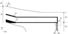
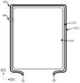
- FIG. 1Ais a schematic diagram of conduction of negative charges generated by friction on the surface of a cover plate of a display panel.
- FIG. 1Bis a schematic diagram of a negative electric field formed in the display panel by negative charges generated by friction on the surface of the cover plate.
- FIG. 1A and FIG. 1Bboth show a cross-sectional structure of a display panel.
- the display panelmay include: a heat dissipation film layer (SCF) 11, a carrier film layer (U-film) 12, a display touch substrate 13, a polarizer (POL, Polarizer) 14, An optical glue (OCA, Optically Clear Adhesive) layer 15 , a cover plate (CG) 16 , an insulating layer 18 and a high-transparency anti-fingerprint film (AF) 19 .
- the cover plate 16may be a glass cover plate.
- the material of the insulating layer 18may be silicon dioxide (SiO 2 ).
- the heat dissipation film layer 11may include a conductive heat dissipation layer 111 and a non-conductive heat dissipation layer 112 stacked in sequence.
- the carrying film layer 12may include a first carrying layer 121 and a second carrying layer 122 stacked in sequence.
- the material of the first carrying layer 121may be polyethylene terephthalate (PET)
- the material of the second carrying layer 122may be pressure sensitive adhesive (PSA, Pressure Sensitive Adhesive).
- the display and touch control substrate 13may include: a base substrate 131 , a display structure layer 132 and a touch control structure layer 133 arranged in sequence.
- the display structure layer 132may include: a driving circuit layer (for example, including a plurality of pixel circuits) and a light emitting element layer (for example, including a plurality of light emitting elements).
- the pixel circuitis electrically connected to the light-emitting element and is configured to drive the light-emitting element to emit light.
- the driving circuit layermay at least include: a semiconductor layer 134 (for example, an active layer including transistors), a power supply line 135 (for example, a low voltage line VSS), and a signal line 136 .
- ink 17is coated between the cover plate 16 and the optical glue layer 15 .
- the metal film layers of the display structure layer 132 of the display touch substrate 13(for example, power lines 135 and signal lines 136) and the metal film layers of the touch structure layer 133 can conduct away static electricity, most of the static electricity is more
- the groundis sequentially passed from the edge of the display panel where there is no metal layer to the lower layer.
- the cover plate 16, the optical adhesive layer 15, the polarizer 14, the display touch substrate 13 and the second carrying layer 122 of the carrying film layer 12all have high conductivity for negative charges, and the ink 17 and the heat dissipation film layer
- the non-conductive heat dissipation layer 112 of 11has medium conductivity to negative charges, and the first carrying layer 121 of the carrying film layer 12 has low conductivity to negative charges.
- the negative charge generated on the surface of the cover plate 16will be transferred from the edge of the display panel to the lower layer, and then pass through the optical adhesive layer 15, the polarizer 14, the insulating layer of the display touch substrate 13 and the base substrate 131, and then pass through the touch control substrate 13 in the display panel.
- the base substrate 131 of the substrate 13gathers on the side away from the cover plate 16 (ie, the back side) to form a negative electric field.
- the negative electric field formed on the display touch substrate 13will cause the threshold voltage (Vth) of the transistor in the driving circuit layer to be positively biased, thereby causing the display touch substrate 13 to light up.
- Vththreshold voltage
- the display paneloften exhibits a greenish display defect.
- This embodimentprovides a display panel, including: an active area and a peripheral area located on the periphery of the active area.
- the active areaincludes a base substrate, a display structure layer and a touch control structure layer sequentially arranged on the base substrate.
- the peripheral areaincludes: an isolation dam, a first ground trace and a second ground trace arranged on the base substrate. The first grounding wire is located on a side of the isolation dam close to the effective area, and the second grounding wire is located on a side of the isolation dam away from the effective area.
- the negative charge generated on the surface of the cover platecan be led out by setting the second grounding wire in the peripheral area, thereby blocking the static electricity conduction path, reducing the negative electric field formed inside the display panel, and improving the negative charge generated by the negative charge.
- the peripheral areamay include: a binding area on one side of the active area and an edge area on the other side of the active area.
- the bonding areaincludes at least one ground pin.
- the first ground trace and the second ground traceare electrically connected to at least one ground pin of the bonding area.
- the first ground trace and the second ground tracemay be electrically connected to the same ground pin.
- the first ground trace, the second ground trace and the ground pinare integrated.
- the first ground trace and the second ground traceare not electrically connected in the edge area, but can be electrically connected in the bonding area.
- this embodimentdoes not limit it. For example, there may be no electrical connection between the first ground trace and the second ground trace.
- a cover plateis provided on a side of the touch structure layer away from the base substrate.
- the touch structure layerincludes: at least one touch conductive layer.
- the second grounding trace and the touch conductive layer closest to the cover platehave the same layer structure.
- the display panelcan be of FSLOC structure
- the touch control structure layerincludes a touch control conductive layer, and the second ground wiring and the touch control conductive layer have the same layer structure; or, the display panel can be of FMLOC structure, and the touch control If the control structure layer includes two touch conductive layers, the second ground trace can be in the same layer structure as the touch conductive layer close to the cover plate.
- this embodimentdoes not limit it. In this example, by arranging the second ground trace and the touch conductive layer closest to the cover to be in the same layer structure, the induced charges generated by friction on the surface of the cover can be effectively derived.
- the second ground wire and the first ground wiremay have the same layer structure.
- the first ground wire and the second ground wiremay be in the same layer structure as a touch conductive layer of the touch structure layer.
- this embodimentdoes not limit it.
- the first ground wire and the second ground wiremay have a different-layer structure.
- the second ground tracemay be located on a side of the first ground trace close to the substrate.
- the touch structure layermay include: a first touch conductive layer, a first touch insulating layer, a second touch conductive layer and a second touch insulating layer sequentially arranged on the display structure layer .
- the first ground wire and the second ground wirehave the same layer structure as the second touch conductive layer.
- this embodimentdoes not limit it.
- the second ground wiring and the second touch conductive layerhave the same layer structure, and the first ground wiring and the first touch conductive layer have the same layer structure.
- the first ground wire and the second touch conductive layerhave the same layer structure, and the second ground wire and the first touch conductive layer have the same layer structure.
- the peripheral areamay further include: auxiliary ground traces.
- the auxiliary ground wiring and the first touch conductive layerare of the same layer structure.
- the auxiliary ground traceis connected to the second ground trace.
- the orthographic projection of the auxiliary ground trace on the substrateoverlaps with the orthographic projection of the second ground trace on the substrate.
- the orthographic projection of the second touch insulating layer on the base substratepartially overlaps the orthographic projection of the second ground trace on the base substrate.
- the orthographic projection of the first touch insulating layer on the base substrate and the orthographic projection of the second grounding trace on the base substratemay not overlap, or partially overlap. However, this embodiment does not limit it.
- the second ground tracemay include a main body and a sawtooth portion facing a side of the active area. That is, the side of the second ground trace facing the active area is in a zigzag shape.
- the contact area between the second ground wire and the second touch insulation layercan be reduced, thereby avoiding peeling of the film layer.
- the second ground tracemay include: an outer trace and an inner trace.
- the outer tracesare on the side of the inner traces away from the active area.
- the outer ring traces and the inner ring tracesare grounded separately. In this example, there is no electrical connection between the inner and outer traces.
- the inner ring wiring and the outer ring wiringcan be used to derive the induced charge generated inside the display panel, and the outer ring wiring can be used to intercept the static electricity introduced from the outside, such as the display panel for electrostatic discharge (ESD, Electro -Static Discharge) static electricity introduced during the test.
- ESDElectro -Static Discharge
- the inner ring routingmay be provided with a plurality of openings, and the plurality of openings are arranged in at least one row along a direction from the effective area to the edge area.
- the multiple openings opened by the inner ring routingare only arranged in one row along the direction from the effective area to the edge area, and the orthographic projection of the multiple openings on the base substrate is located in the peripheral area and has the same layer structure as the display structure layer.
- the orthographic projection of the conductive layer on the substrate substratemay have no overlap.
- opening holes in the inner ring wiringthe large-area contact between the second grounding wiring and the second touch insulating layer can be reduced, thereby avoiding peeling off of the film layer.
- the orthographic projection of the opening on the base substratemay not overlap with the orthographic projection of other conductive layers on the base substrate, thereby preventing static electricity from being conducted downward through the opening and affecting other conductive layers.
- this embodimentis not limited to this.
- the plurality of openingsmay be arranged in two or more rows along the side of the effective region facing the edge region.
- the second ground tracemay include: an outer trace, an inner trace, and a plurality of connection traces connected between the outer trace and the inner trace.
- the outer tracesare on the side of the inner traces away from the active area.
- the orthographic projection of the at least one connection trace on the base substrateis a rectangle.
- the orthographic projection of at least one connecting trace on the base substrateis S-shaped. In this example, by setting the S-shaped connection trace, the resistance of the second ground trace can be increased, so as to prevent static electricity from breaking down the transfer hole and play a protective role. However, this embodiment does not limit it.
- the number of connecting tracesmay be less than or equal to 40.
- the number of connecting wirescan be 6, 19 or 40. However, this embodiment does not limit it.
- a plurality of tip discharge structuresare disposed between the outer traces and the inner traces.
- At least one tip discharge structureincludes: a first electrode and a second electrode.
- the first electrodeis integrated with the outer wiring, and the second electrode is located between the first electrode and the inner wiring.
- the first electrodehas a first tip; the first tip of the first electrode faces the second electrode, and there is a gap between the first tip and the second electrode.
- the second electrodehas a second tip; the second tip of the second electrode faces the first tip of the first electrode with a gap between the first tip and the second tip.
- the orthographic projection of the second electrode on the base substratemay be a rectangle. However, this embodiment does not limit it. In this example, by arranging multiple pointed discharge structures, an electrostatic absorption circuit can be added to avoid concentrated electrostatic discharge, thereby protecting the display panel.
- a plurality of antistatic capacitorsare arranged between the outer trace and the inner trace, and at least one antistatic capacitor includes a first plate and a second plate.
- the first pole plate and the wiring of the outer ringare integrally structured, and the second pole plate is located on a side of the first pole plate close to the wiring of the inner circle.
- the first plate of the anti-static capacitoris grounded, and the second plate is a dummy conductive structure.
- the first pole plate and the second pole plate of the antistatic capacitormay be a multi-layer stacked structure, and the capacitance is increased by increasing the thickness of the pole plates.
- the first pole platehas a plurality of first comb teeth facing the second pole plate
- the second pole platehas a plurality of second comb teeth facing the first pole plate.
- the plurality of first comb-tooth parts and the plurality of second comb-tooth partsinterpenetrate each other. In this way, the capacitance can be increased by increasing the overlapping area between the two plates.
- the anti-static capacitorcan be charged when the instantaneous high-voltage static electricity is connected to play a role of voltage division, thereby protecting the display panel.
- a plurality of transistorsare connected between the outer trace and the inner trace.
- the first pole of a single transistoris electrically connected to the inner wiring
- the second pole of the transistoris electrically connected to the outer wiring
- the gate electrode of the transistoris electrically connected to the first power supply line.
- the transistorsmay be P-type transistors.
- the transistorcan effectively export the induced charges generated inside the display panel to the outer wiring through the inner wiring, and can prevent external static charges from entering the interior from the outside.
- the peripheral areamay further include: a plurality of auxiliary electrodes.
- a plurality of auxiliary electrodesare located on a side of the inner ring trace close to the base substrate.
- An insulating layeris arranged between the plurality of auxiliary electrodes and the inner ring wiring, and the orthographic projection of the inner ring wiring on the base substrate covers the orthographic projection of the plurality of auxiliary electrodes on the base substrate.
- a protective capacitorcan be formed between the inner ring trace and the auxiliary electrode, thereby providing a release path for internal induced charges.
- the display panel of this embodimentwill be described below through some examples.
- a flexible display panelis taken as an example for illustration.
- the display motherboardis prepared first, and then the display motherboard is cut, so that the display motherboard is divided into multiple display touch substrates, and the separated display touch substrates can be used to form a single display panel.
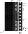
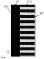
- FIG. 2is a schematic diagram showing the arrangement of a plurality of display touch substrates on a display motherboard.
- a plurality of substrate regions 200 on the display motherboard 100are periodically and regularly arranged, and the cutting region 300 is located outside the substrate regions 200 .
- the substrate area 200at least includes an active area AA and a binding area B1 located on at least one side of the active area AA.
- the active area AAmay include a plurality of sub-pixels arranged regularly, and the bonding area B1 may include a fan-out area and bonding pins.
- a first cutting line X1 and a second cutting line X2are disposed in the cutting area 300 . After all the film layers of the display motherboard are prepared, the cutting equipment performs rough cutting and fine cutting respectively along the first cutting line X1 and the second cutting line X2 to form a display touch substrate.
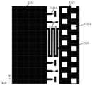
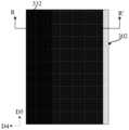
- FIG. 3is a schematic diagram of a display panel according to at least one embodiment of the present disclosure.
- the display panel in this exampleis illustrated by taking the FMLOC structure as an example. However, this embodiment does not limit it.
- the display panelmay have a FSLOC structure with a single touch conductive layer, and both the first ground trace and the second ground trace may have the same layer structure as the touch conductive layer.
- the display panelin a plane parallel to the display panel, may include: an active area AA, and a peripheral area located on the periphery of the active area AA.
- the peripheral areamay include: a binding area B1 on one side of the active area AA and an edge area B2 on the other side of the active area AA.
- the active area AAcan be either a touch area or a display area, and both the touch area and the display area in the following description refer to the active area AA.
- the touch areamay at least include a plurality of touch electrodes arranged regularly, and the edge area B2 may at least include a plurality of touch leads, a first ground wire 331 and a second ground wire 331 .
- the ground wire 332 and the bonding area B1at least include pins connecting the plurality of touch wires, the first ground wire 331 and the second ground wire 332 to an external control device.
- the touch structuremay be a mutual capacitance structure.
- the touch areamay include a plurality of first touch units 310 and a plurality of second touch units 320 .
- the first touch unit 310has a line shape extending along the first direction D1, a plurality of first touch units 310 are arranged in sequence along the second direction D2;
- the second touch unit 320has a line shape extending along the second direction D2,
- the plurality of second touch units 320are arranged in sequence along the first direction D1.
- the first direction D1intersects the second direction D2, for example, the first direction D1 is perpendicular to the second direction D2.
- Each first touch unit 310may include a plurality of first touch electrodes 311 and first connecting portions 312 arranged in sequence along the first direction D1, the first touch electrodes 311 and the first connecting portions 312 are arranged alternately and electrically connected in sequence. connect.
- Each second touch unit 320may include a plurality of second touch electrodes 321 arranged in sequence along the second direction D2, the plurality of second touch electrodes 321 are arranged at intervals, and adjacent second touch electrodes 321 pass through the second The connection parts 322 are electrically connected to each other.
- the film layer where the second connecting portion 322 is locatedis different from the film layer where the first touch electrode 311 and the second touch electrode 321 are located.
- the first touch electrodes 311 and the second touch electrodes 321are alternately arranged in a third direction D3, and the third direction D3 intersects both the first direction D1 and the second direction D2.
- a plurality of first touch electrodes 311, a plurality of second touch electrodes 321 and a plurality of first connecting parts 312can be arranged on the touch layer in the same layer, and can be patterned through the same patterning process.
- the first touch electrode 311 and the first connecting portion 312may be an integral structure connected to each other.
- the second connecting portion 322may be disposed on the bridging layer to electrically connect adjacent second touch electrodes 321 to each other through via holes, and a touch insulating layer is disposed between the touch layer and the bridging layer.
- first touch electrodes 311, multiple second touch electrodes 321 and multiple second connecting parts 322may be arranged on the touch layer in the same layer, and the second touch electrodes 321 and the second touch electrodes
- the two connecting parts 322may be an integral structure connected to each other, and the first connecting part 312 may be disposed on the bridging layer to electrically connect adjacent first touch electrodes 311 to each other through via holes.
- the first touch electrodesmay be driving (Tx) electrodes
- the second touch electrodesmay be sensing (Rx) electrodes.
- the first touch electrodesmay be sensing (Rx) electrodes
- the second touch electrodesmay be driving (Tx) electrodes.
- this embodimentdoes not limit it.
- the first touch electrodes 311 and the second touch electrodes 321may have a rhombus shape, for example, may be a regular rhombus, or a horizontally long rhombus, or a vertically long rhombus.
- the first touch electrodes 311 and the second touch electrodes 321may have any one or more of triangles, squares, trapezoids, parallelograms, pentagons, hexagons and other polygons. , the present disclosure is not limited here.
- the first touch electrodes 311 and the second touch electrodes 321may be in the form of transparent conductive electrodes. In some other exemplary embodiments, the first touch electrode 311 and the second touch electrode 321 may be in the form of a metal grid, the metal grid is formed by interweaving a plurality of metal wires, the metal grid includes a plurality of grid patterns, A mesh pattern is a polygon made of multiple metal lines.
- the first touch electrodes 311 and the second touch electrodes 321 in metal mesh formhave the advantages of low resistance, small thickness and fast response speed.
- the binding area B1is located on one side of the touch area AA, and along a direction away from the touch area AA (for example, the second direction D2), the binding area B1 can It includes: a first fan-out area 201 , a bending area 202 , a second fan-out area 203 , an antistatic area 204 , a driver chip area 205 and a binding pin area 206 arranged in sequence.
- the first fan-out area 201may be provided with signal transmission lines and touch wires of the display substrate.
- the signal transmission lines of the display substratemay at least include a high voltage line VDD, a low voltage line VSS and a plurality of data transmission lines.
- Multiple data transmission linesare configured to connect the data lines (Data Line) of the display area in a fan-out (Fan-out) routing mode, and the high-voltage line VDD and the low-voltage line VSS are configured to connect respectively to the high-level power line and low-level power line of the display substrate power cable.
- the multiple touch wiresare configured to be correspondingly connected to multiple pins in the binding pin area 206 .
- the bending area 202can be provided with grooves, and the grooves are configured to bend the second fan-out area 203 , the antistatic area 204 , the driving chip area 205 and the binding pin area 206 to the back of the touch area AA.
- the second fan-out area 203can be provided with a plurality of touch leads and a plurality of data transmission lines led out in a fan-out manner.
- the anti-static area 204may be provided with an anti-static circuit configured to eliminate static electricity.
- the driver chip area 205can be provided with a source driver circuit (Driver IC), and the source driver circuit is configured to be electrically connected to a plurality of data transmission lines of the second fan-out area 203.
- the driver chip area 205may be provided with a touch and display driver integrated circuit (TDDI, Touch and Display Driver Integration).
- the binding pin area 206can be provided with a plurality of pins (PIN), and the plurality of pins are electrically connected to the plurality of touch leads and the plurality of signal transmission lines of the source drive circuit, and are connected through the bound flexible circuit board (FPC) Connect external controls.
- PINa plurality of pins
- FPCbound flexible circuit board
- the edge area B2is located on multiple sides of the effective area AA away from the binding area B1 .
- the binding area B1is located on the lower side of the active area AA
- the edge areas B2are located on the upper, left, and right sides of the active area AA.
- the edge area B2is at least provided with a first ground wire 331 , a second ground wire 332 and a plurality of touch wires.
- the second ground trace 332is located on a side of the first ground trace 331 away from the active area AA.
- the first ground wire 331 and the second ground wire 332extend from the edge area B2 to the bonding area B1, and are electrically connected to the ground pin in the bonding pin region 206 of the bonding area B1.
- the first ground wire 331 and the second ground wire 332may be electrically connected to the same ground pin in the bonding pin area 206 of the bonding area B1.
- this embodimentdoes not limit it.
- in the edge region B2there is no electrical connection between the first ground trace 331 and the second ground trace 332, and in the bonding region B1, the first ground trace 331 and the second ground trace 332 can be electrically connected. connect.
- the plurality of touch leadsmay include a plurality of driving leads and a plurality of sensing leads.
- the first touch electrodeas the driving electrode and the second touch electrode as the sensing electrode as an example
- the first end of the driving leadis electrically connected to the first touch electrode
- the second end of the driving leadextends along the edge area B2 to Bind region B1.
- the first end of the sensing leadis electrically connected to the second touch electrode, and the second end of the sensing lead extends along the edge area B2 to the binding area B1.
- this embodimentdoes not limit it.
- a first cutting line and a second cutting lineare provided outside the binding area B1 and the edge area B2, and the second cutting line is a fine cutting line, located on the periphery of the binding area B1 and the edge area B2 , the shape of the second cutting line is the same as the outer contours of the binding area B1 and the edge area B2.
- the first cutting lineis a rough cutting line and is located on the periphery of the second cutting line, and the shape of the first cutting line and the outline of the second cutting line may be approximately the same.
- the edge of the second ground trace 332 away from the active area AAcan be obtained through the second cutting line.
- this embodimentdoes not limit it.
- Fig. 4is a schematic partial cross-sectional view along the P-P' direction in Fig. 3 .
- the display panel in the active area AAmay include: a base substrate 30 , a display panel sequentially arranged on the base substrate 30 The structural layer 41 and the touch structural layer 31 .
- the display structure layer 41may include: a driving circuit layer 42 , a light emitting structure layer 43 and an encapsulation layer 44 sequentially disposed on the base substrate 30 .
- the touch structure layer 31uses the encapsulation layer 44 as a base.
- the display structure layermay include other film layers, and other film layers may be disposed between the touch control structure layer and the encapsulation layer, which is not limited in this disclosure.
- the base substrate 30may include a stacked first flexible material layer, a first inorganic material layer, a semiconductor layer, a second flexible material layer, and a second inorganic material layer, the first flexible material layer and the
- the material of the second flexible material layercan adopt materials such as polyimide (PI), polyethylene terephthalate (PET) or through the polymer soft film of surface treatment, the first inorganic material layer and the second inorganic material
- the material of the layercan be silicon nitride (SiNx) or silicon oxide (SiOx), etc., which are used to improve the water and oxygen resistance of the substrate, and the material of the semiconductor layer can be amorphous silicon (a-Si).
- a-Siamorphous silicon
- the driving circuit layer 42 of the active area AAmay include transistors and storage capacitors constituting a pixel circuit.
- a transistorfor example, the first transistor 421
- the driving circuit layer 42 of the active area AAmay include: a semiconductor layer, a first insulating layer 411 , a first gate metal layer, and a second insulating layer disposed on the base substrate 30 in sequence.
- the semiconductor layerincludes at least: an active layer of the first transistor 421 .
- the first gate metal layerat least includes: the gate electrode of the first transistor 421 , and the first capacitor plate of the capacitor of the pixel circuit.
- the second gate metal layerat least includes: a second capacitive plate of the capacitor of the pixel circuit.
- the first source-drain metal layerat least includes: a first pole and a second pole of the first transistor 421 .
- the second source-drain metal layerat least includes: an anode connection electrode 428 configured to connect the anode of the light emitting element and the pixel circuit.
- the first insulating layer 411, the second insulating layer 412, the third insulating layer 413, and the fourth insulating layer 414may be inorganic insulating layers, and the first flat layer 415 and the second flat layer 416 may be organic insulating layer.
- the first insulating layer 411, the second insulating layer 412, the third insulating layer 413 and the fourth insulating layer 414can be any of silicon oxide (SiOx), silicon nitride (SiNx) and silicon oxynitride (SiON).
- SiOxsilicon oxide
- SiNxsilicon nitride
- SiONsilicon oxynitride
- the first insulating layer 411 and the second insulating layer 412may be referred to as gate insulating (GI) layer
- the third insulating layer 413may be referred to as interlayer insulating (ILD) layer
- the fourth insulating layer 414may be referred to as Passivation (PVX) layer.
- the first gate metal layer, the second gate metal layer, the first source-drain metal layer and the second source-drain metal layercan use metal materials, such as silver (Ag), copper (Cu), aluminum (Al), titanium (Ti) Any one or more of molybdenum (Mo), or alloy materials of the above metals, such as aluminum neodymium alloy (AlNd) or molybdenum-niobium alloy (MoNb), can be a single-layer structure, or a multi-layer composite structure, such as Ti /Al/Ti etc.
- metal materialssuch as silver (Ag), copper (Cu), aluminum (Al), titanium (Ti)
- Momolybdenum
- alloy materials of the above metalssuch as aluminum neodymium alloy (AlNd) or molybdenum-niobium alloy (MoNb)
- AlNdaluminum neodymium alloy
- MoNbmolybdenum-niobium alloy
- the semiconductor layercan be made of amorphous indium gallium zinc oxide (a-IGZO), zinc oxynitride (ZnON), indium zinc tin oxide (IZTO), amorphous silicon (a-Si), polysilicon (p-Si), six Materials such as thiophene or polythiophene, that is, the present disclosure is applicable to transistors manufactured based on oxide technology, silicon technology or organic technology.
- a-IGZOamorphous indium gallium zinc oxide
- ZnONzinc oxynitride
- IZTOindium zinc tin oxide
- a-Siamorphous silicon
- p-Sipolysilicon
- six Materialssuch as thiophene or polythiophene, that is, the present disclosure is applicable to transistors manufactured based on oxide technology, silicon technology or organic technology.
- the light emitting structure layer 43 of the active area AAmay include: an anode 431 , a pixel definition layer 434 , an organic light emitting layer 432 and a cathode 433 .
- the anode 431is disposed on the second planar layer 416 and is electrically connected to the anode connection electrode 428 through a via hole opened on the second planar layer 416 .
- the pixel definition layer 434is disposed on the anode 431 and the second flat layer 416, and a pixel opening is disposed thereon, the pixel opening exposes the anode 431, the organic light-emitting layer 432 is disposed in the pixel opening, and the cathode 433 is disposed on the organic light-emitting layer 432,
- the organic light emitting layer 432emits light of a corresponding color under the action of the voltage applied by the anode 431 and the cathode 433 .
- the pixel definition layer 434may be made of materials such as polyimide, acrylic or polyethylene terephthalate.
- the encapsulation layer 44 in the active area AAmay include a stacked first encapsulation layer 441 , a second encapsulation layer 4442 and a third encapsulation layer 443 , the first encapsulation layer 441 and The third encapsulation layer 443 can be made of inorganic materials, the second encapsulation layer 442 can be made of organic materials, and the second encapsulation layer 442 is arranged between the first encapsulation layer 441 and the third encapsulation layer 443, which can ensure that external water vapor cannot enter the light-emitting structure layer 43.
- the touch structure layer 31 of the active area AAmay include: a buffer layer (not shown in FIG. 4 ), a first touch conductive layer (TMA), The first touch insulating layer (TLD) 301 , the second touch conductive layer (TMB) and the second touch insulating layer (TOC) 302 .
- the first touch conductive layermay be the aforementioned bridging layer
- the second touch conductive layermay be the aforementioned touch layer.
- the first touch conductive layermay include a second connection portion 322, and the second touch conductive layer may include a first touch electrode 311, a second touch electrode 321, and a first connection portion 312.
- the buffer layer and the first touch insulation layer 301may use inorganic materials, and the second touch insulation layer 302 may use organic materials.
- the buffer layer and the first touch insulation layer 301can be any one or more of silicon oxide (SiOx), silicon nitride (SiNx) and silicon oxynitride (SiON), and can be single-layer or multi-layer or composite layers.
- the second touch insulating layer 302can be made of polyimide (PI) or the like. However, this embodiment does not limit it.
- the edge area B2may include a first sub-edge area B11 , a second sub-edge area B12 and a third sub-edge area B13 along a direction away from the active area AA.
- the first sub-edge area B11at least includes: a gate driving circuit, a plurality of touch wires and a first ground wire.
- the touch wires and the first ground wiresmay have a double-layer wire structure.
- one touch leadmay include a first sub-lead 313a and a second sub-lead 313b that are electrically connected.
- the first ground tracemay include a first sub-ground trace 331a and a second sub-ground trace 331b electrically connected.
- the second sub-edge area B12is located on the side of the first sub-edge area B11 away from the effective area AA, and the second sub-edge area B12 includes at least: a first isolation dam 513, a second isolation dam 514, and at least one (for example, three) first isolation dams.
- a panel crack detection (PCD, Panel Crack Detection) line 516may be configured to detect the display structure layer 41 .
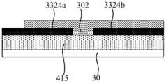
- the third sub-edge area B13is located on a side of the second sub-edge area B12 away from the active area AA, and the third sub-edge area B13 at least includes: a crack dam 515 and a second ground trace 332 .
- the display panel in the first sub-edge area B11may include: a base substrate 30 , a driving circuit layer 42 and a first planar layer 415 sequentially disposed on the base substrate 30 , the second flat layer 416, the first connection electrode 512, the isolation column 511, the cathode 433, the encapsulation layer 44, the plurality of first sub-leads 313a and the first sub-grounding traces 331a arranged on the encapsulation layer 44, the first contact control insulating layer 301 , a plurality of second sub-leads 313b and second sub-grounding traces 331b disposed on the first touch insulating layer 301 , and the second touch insulating layer 302 .
- the driving circuit layer 42 of the first sub-edge region B11may include transistors and storage capacitors constituting a gate driving circuit.
- the gate driving circuit of the first sub-edge region B1may include a scanning driving circuit and a light emission control driving circuit.
- a transistorfor example, the second transistor 422 and a capacitor (for example, the first capacitor 424) of the scanning driving circuit in the edge area B2, and a transistor (for example, the third transistor 423) of the light emission control driving circuit Take a capacitor (for example, the second capacitor 425) as an example for illustration.
- the film structure of the driving circuit layer in the first sub-edge area B1may be similar to that of the driving circuit layer in the active area AA, so details will not be repeated here.
- the first sub-ground wiring 331a and the plurality of first sub-leads 313aare in the same layer structure as the first touch conductive layer
- the second sub-ground wiring 331b and the plurality of second sub-leads 313bare in the same layer structure as the second touch conductive layer.
- multiple first sub-leads 313 a and multiple second sub-leads 313 bcan be electrically connected in one-to-one correspondence, so as to realize a touch lead with a double-layer wiring structure.
- the first sub-ground wiring 331ais electrically connected to the second sub-ground wiring 331b to realize the first ground wiring of a double-layer wiring structure.
- a guard (Guard) lineis provided between the touch lead and the first grounding line, the guard line includes a first guard sub-line 315a and a second guard sub-line 315b electrically connected, the first guard sub-line 315a is connected to the first contact
- the control conductive layerhas the same layer structure, and the second protection sub-line 315b and the second touch conductive layer have the same layer structure.
- the guard lineis a double-layer wiring structure.
- At least one (for example, two) second panel crack detection lines 314may be provided on the side of the first grounding line away from the touch lead wire and the protection line. The second panel crack detection line 314 is configured to detect the touch structure layer 31 .
- the second panel crack detection line 314 and the second touch conductive layerhave the same layer structure.
- the first ground wire, the touch wire and the protection wirecan be a single-layer wire structure, for example, they can be of the same layer structure as the first touch conductive layer or can be of the same layer structure as the second touch conductive layer. layer structure.
- the display panel in the second sub-edge region B12may include: a base substrate 30 and a composite insulating layer disposed on the base substrate 30 , and a first panel crack detection line 516 , low voltage line 426, second connection electrode 427, isolation dam (for example, first isolation dam 513 and second isolation dam 514), first encapsulation layer 441, third encapsulation layer 443, first touch insulation layer 301 and second isolation dam Two touch insulating layers 302 .
- the composite insulating layermay include: a first insulating layer 411 to a third insulating layer 413 stacked on the base substrate 30 .
- the first panel crack detection line 516may be disposed on the second insulating layer 412 and may be in the same layer structure as the second gate metal layer.
- the low-voltage line 426may have the same layer structure as the first source-drain metal layer of the driving circuit layer 42
- the second connection electrode 427may have the same layer structure as the second source-drain metal layer of the driving circuit layer 42 .
- the cathode 433may be electrically connected to the second connection electrode 427 through the first connection electrode 512
- the first connection electrode 512may be electrically connected to the low voltage line 426 through the second connection electrode 427 .
- the first isolation dam 513is located on a side of the second isolation dam 514 close to the active area AA.
- the second isolation dam 514may be formed by stacking the first dam foundation, the second dam foundation, the third dam foundation and the fourth dam foundation.
- the first isolation dam 513may be formed by overlapping the second dam foundation, the third dam foundation and the fourth dam foundation.
- the first dam foundation and the first flat layer 415may have the same layer structure
- the second dam foundationmay have the same layer structure as the second flat layer 416
- the third dam foundationmay have the same layer structure as the pixel definition layer 434
- the fourth dam foundationmay have the same layer structure as the pixel definition layer 434. It is the same layer structure as the isolation column 511. However, this embodiment does not limit it.
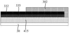
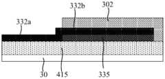
- the display panel of the third sub-edge region B13may include a crack dam 515 and a second ground trace 332 disposed on the base substrate 30 .
- a crack dam 515is formed on the composite insulating layer, and the crack dam 515 may include a plurality of cracks arranged at intervals, and the cracks may expose the base substrate 30 .
- the first planarization layer 415may cover the crack dams 515 .
- the second ground trace 332is disposed on the first planar layer 415 covering the crack dam 515 .
- the second touch insulation layer 302may expose a part of the surface of the second ground trace 332 .
- the orthographic projections of the first touch insulation layer 301 and the second ground wire 332 on the base substrate 30may not overlap.
- the orthographic projection of the second ground trace 332 on the substrate 30 and the orthographic projection of the crack dam 515 on the substrate 30may partially overlap.
- this embodimentdoes not limit it.
- the orthographic projections of the first touch insulation layer 301 and the second ground wire 332 on the base substrate 30may partially overlap.
- a concave-convex crack dam 515is formed in the edge area B1, which is used to avoid affecting the film layer structure of the active area AA and the first sub-edge area B11 during the cutting process of the display motherboard, and a plurality of cracks arranged at intervals Not only can the stress on the effective area AA and the first sub-edge area B11 be reduced, but also the transmission of cracks to the effective area AA and the first sub-edge area B11 can be blocked.
- the first ground trace 331is located in the first sub-edge area B11
- the isolation damis located in the second sub-edge area B12
- the second ground trace 332is located in the third sub-edge area. B13.
- the orthographic projection of the first ground trace 331 on the substrate 30is located on the side of the isolation dam close to the active area AA
- the orthographic projection of the second ground trace 332 on the substrate 30is located on the side of the isolation dam away from the active area AA.
- the first ground wire 331 and the second ground wire 332may have the same layer structure, for example, they both have the same layer structure as the second touch conductive layer. However, this embodiment does not limit it.
- first ground trace and the second ground tracemay have different layer structures, for example, the first ground trace may have the same layer structure as the first touch conductive layer, and the second ground trace may have the same layer structure as the first touch conductive layer.
- the second touch conductive layeris of the same layer structure.
- the second ground wiringmay be in the same layer structure as any conductive layer of the touch control structure layer close to the base substrate.
- the second ground wire 332by arranging the second ground wire 332 in the third sub-edge area B13, the negative charge generated by the friction on the surface of the cover plate can be led out by the second ground wire 332.
- the second touch conductive layerhas a larger thickness and lower resistance than the first touch conductive layer, and the second touch conductive layer is closer to the cover plate than other conductive layers, by setting the second touch conductive layer
- the second ground wire 332is on the same layer as the second touch conductive layer, which can effectively discharge most of the static electricity, thereby reducing the negative electric field formed inside the display panel, and improving the brightness problem caused by the negative electric field.
- the orthographic projection of the second ground trace 332 on the base substrate 30may not overlap with the orthographic projection of other conductive layers on the base substrate 30 .
- FIG. 5is a partially enlarged schematic diagram of area S1 in FIG. 3 .
- FIG. 5simply illustrates the positions of the gate driving circuit 420 and multiple wires in the edge region B2 , and the other structures are omitted.
- the first ground wire 331is located on the side of the plurality of touch wires 313 away from the active area AA, and a protection wire 315 is provided between the first ground wire 331 and the plurality of touch wires 313 .
- the panel crack detection line 314is located on a side of the first grounding line 331 away from the protection line 315 and the plurality of touch leads 313 .
- the orthographic projections of the first grounding trace 331 and the second panel crack detection line 314 on the substratemay overlap with the orthographic projection of the gate driving circuit 420 on the substrate.
- the orthographic projection of the first panel crack detection line 516 on the substrateis located between the orthographic projection of the second ground trace 332 on the substrate and the orthographic projection of the second panel crack detection line 314 on the substrate.
- the metal trace closest to the side of the second ground trace 332 on the orthographic projection of the base substrate that is close to the active area AAis the first panel crack detection line 516 .
- the width of the second ground trace 332is greater than the width of the first ground trace 331 .
- the width of the tracesrefers to the width of the traces on the display touch substrate formed after being cut by the cutting device.
- the width L1 of the first ground trace 331may be about 13.5 microns to 16.5 microns, for example, about 15 microns.
- the width L2 of the second ground trace 332may be approximately 100 microns to 300 microns, for example, may be approximately 125 microns or may be approximately 300 microns.
- the distance L3 between the second ground trace 332 and the nearest metal trace (ie, the first panel crack detection line 516 )may be about 67.5 microns to 82.5 microns, for example, about 75 microns. However, this embodiment does not limit it.
- FIG. 6is a partially enlarged schematic diagram of area S2 in FIG. 3 .
- FIG. 7is a partially enlarged schematic diagram of area S3 in FIG. 6 . Both FIG. 6 and FIG. 7 simply illustrate the positions of the first grounding wire 331 and the second grounding wire 332 , and the other structures are omitted. As shown in FIG. 6 and FIG. 7 , the first ground trace 331 and the second ground trace 332 may extend from the edge area B2 to the bonding area B1 .
- the first grounding trace 331is disconnected and electrically connected through the first bending trace 401; the second grounding trace 332 is disconnected , are electrically connected through the second bent wiring 402 ; the touch lead 313 is disconnected and electrically connected through the third bent wiring 403 . As shown in FIG.
- the first ground trace 331can be electrically connected to the first bending trace 401 through the first via hole K1
- the second ground wire 332can be electrically connected to the second bent wire 402 through the first via hole K1
- the touch lead 313can be electrically connected to the third bent wire 403 through the first via hole K1 .
- the first ground wire 331, the second ground wire 332, and the touch wire 313can have the same layer structure as the second touch conductive layer
- the first bent wire 401, the second bent wire 402 and the third bent wire 403may have the same layer structure as the first source-drain metal layer.
- the film thickness of the bending area 202can be reduced, which is beneficial to bent.
- a holemay be dug on the second ground trace 332 of the first fan-out region 201 to avoid a large-area contact between the second ground trace 332 and the second touch insulating layer. leading to peeling off of the film.
- FIG. 8is a partial schematic diagram of a binding pin area of the binding area according to at least one embodiment of the present disclosure.
- the binding pin area 206is provided with a plurality of binding pins (eg, including the ground pin 405 ).
- the first ground trace 331 and the second ground trace 332extend to the bonding pin area 206 and are electrically connected to the ground pin 405 for subsequent bonding connection with the flexible circuit board.
- the first ground wire 331 , the second ground wire 332 and the ground pin 405may be in one structure, for example, they are all in the same layer structure as the second touch conductive layer.
- the binding pin areamay include multiple ground pins, and the first ground trace and the second ground trace may be electrically connected to different ground pins in the binding pin area.
- the second ground wiringis illustrated below through multiple examples.
- the second ground trace 332 in the area S1 in FIG. 3is taken as an example for illustration.
- the second ground wire 332 and the second touch conductive layermay have the same layer structure.
- the direction along the active area AA toward the edge area B2may be the fourth direction, and the direction that is in the same plane as the fourth direction and intersects the fourth direction is the fifth direction.
- the fifth direction and the fourth directionare located in the same plane, and the fifth direction is perpendicular to the fourth direction.
- the first direction D1may be parallel to the fourth direction
- the second direction D2may be parallel to the fifth direction.
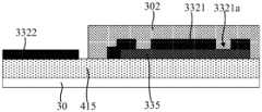
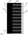
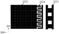
- FIG. 9is a schematic diagram of a second ground trace according to at least one embodiment of the present disclosure.
- Fig. 10is a schematic partial cross-sectional view along the Q-Q' direction in Fig. 9 .
- the second ground wire 332may include: an outer wire 3322 , an inner wire 3321 and a connecting wire 3323 .
- the outer traces 3322are located on the side of the inner traces 3321 away from the active area AA, and the outer traces 3322 and the inner traces 3321 are electrically connected through a plurality of connecting traces 3323 .
- the orthographic projection of the connecting wiring 3323 on the base substrate 30may be a rectangle.
- the connecting wire 3323is electrically connected to the outer wire 3322 , and the other end is electrically connected to the inner wire 3321 .
- the outer-ring wiring 3322, the inner-ring wiring 3321 and the connecting wiring 3323may have an integrated structure.
- a plurality of openings 3321aare formed on the inner ring routing 3321, and the plurality of openings 3321a may be arranged in three rows along the fourth direction D4.
- the openings 3321a in two adjacent columnsare misaligned in the fifth direction D5.
- this embodimentdoes not limit it.
- the orthographic projection of the second touch insulating layer 302 on the base substrate 30intersects the portion of the orthographic projection of the second ground trace 332 on the base substrate 30 stack.
- the second touch insulating layer 302may cover the inner wiring 3321 and not cover the outer wiring 3322 .
- the second ground trace 332can be prevented from being in direct contact with the second touch insulation layer 302 in a large area, and the peeling of the film layer can be avoided.
- FIG. 11is another schematic diagram of a second ground trace according to at least one embodiment of the present disclosure.
- the second ground trace 332may include: an outer loop trace 3322 , an inner loop trace 3321 , and a connecting trace 3323 .
- the outer traces 3322are located on the side of the inner traces 3321 away from the active area AA, and the outer traces 3322 and the inner traces 3321 are electrically connected through a plurality of connecting traces 3323 .
- a plurality of connection traces 3323are located between the outer traces 3322 and the inner traces 3321 .
- One end of a single connecting wire 3323is electrically connected to the outer ring wire 3322 , and the other end is electrically connected to the inner ring 3321 .
- the outer-ring wiring 3322, the inner-ring wiring 3321 and the connecting wiring 3323may have an integrated structure.
- the orthographic projection of the single connecting wire 3323 on the base substratemay be S-shaped.
- the resistance of a single connection wire 3323may be about 10 ohms to 20 ohms, for example, about 12 ohms.
- a single connecting wire 3323may include a plurality of first extension sections 3323a and second extension sections 3323b connected in sequence.
- the first extension section 3323amay extend in the fourth direction D4, and the second extension section 3323b may extend in the fifth direction D5.
- the second extension segment 3323b, the first extension segment 3323a and the second extension segment 3323b connected in sequencemay form a detour.
- a plurality of detoursmay be arranged sequentially along the fourth direction D4.
- a single connection trace 3323may include multiple detours.
- the number of detours of a single connecting wire 3323may be about 3 to 5.
- a single connection trace 3323may include 3 detours.
- the length of the first extension section 3323a(ie, the length along the fourth direction D4 ) is smaller than the length of the second extension section 3323b (ie, the length along the fifth direction D5 ).
- the width of the first extension section 3323a (ie, the length along the fifth direction D5 ) and the width of the second extension section 3323b (ie, the length along the fourth direction D4 )may be approximately the same.
- the width L30 of the first extension segment 3323amay be about 3 microns to 5 microns, such as about 5 microns.
- the distance L31 between adjacent second extension segments 3323bmay be approximately 3 microns to 5 microns, for example, approximately 5 microns.
- the distance between the second extension segment 3323b and the adjacent outer ring trace 3322 and the distance between the second extension segment 3323b and the adjacent inner ring trace 3321may be approximately the same as the distance L31.
- this embodimentdoes not limit it.
- the length of the first extension section connecting the tracesmay be greater than the length of the second extension section, and the sequentially connected first extension section, second extension section, and first extension section may form a detour, and multiple detours may be along the fifth The directions are arranged sequentially.
- the connecting wiresare used to electrically connect the outer ring wires and the inner ring wires, and the length of the connecting wires is extended by multiple folds, which can increase the grounding resistance, thereby increasing the grounding resistance of the second grounding wires. Resistance, and improve the electrostatic protection effect.
- the number of connecting wirescan be matched according to the total resistance and capacitance of the second ground wire, so as to avoid setting too many connecting wires and causing the introduction of external charges due to too small parallel resistance, so that The ESD test fails, or if too few connecting lines are set, the circuit is blown by the instantaneous ESD surge current and fails due to process risks.
- the number of connecting tracesmay be less than or equal to 40.
- the number of connecting wiresmay be about 20 to 40, such as about 6, 19 or 40.
- FIG. 12A to FIG. 12Care schematic diagrams of the arrangement of connecting wires in at least one embodiment of the present disclosure.
- Figures 12A to 12Cbriefly illustrate the locations of multiple connecting traces.
- the second ground tracemay include 6 connection traces 3323.
- the 6 connection traces 3323may be respectively located in the upper, left, and right edge areas, and two connections are arranged on each side. Route 3323.
- the second ground tracemay include 19 connecting traces 3323.
- the 19 connecting traces 3323may be respectively arranged in the upper, left, and right edge areas, wherein the upper edge area There are 5 arrays, and 7 arrays are arranged in the left and right edge areas respectively.
- FIG. 12A to FIG. 12Cbriefly illustrate the locations of multiple connecting traces.
- the second ground tracemay include 6 connection traces 3323.
- the 6 connection traces 3323may be respectively located in the upper, left, and right edge areas, and two connections are arranged on each side. Route 3323.
- the second ground tracemay include 19 connecting
- the second ground tracemay include 40 connecting traces 3323.
- the 40 connecting traces 3323may be respectively arranged in the upper, left, and right edge areas, wherein the upper edge area There are 10 arrays, and 15 arrays are arranged in the left and right edge areas respectively.
- the arrangement positions of the connecting traces 3323 in the left and right edge regionsmay be symmetrical with respect to the centerline of the display panel in the first direction D1, and the arrangement of the connecting traces 3323 in the upper edge region The positions may be symmetrical about the centerline of the display panel in the first direction D1.
- this embodimentdoes not limit it.
- the resistance of the second ground wirecan be increased, and the risk of electrostatic breakdown to adjacent metal film layers can be reduced.
- the inner ring wiring 3321is provided with a plurality of openings 3321a, and the plurality of openings 3321a are arranged in a row along the fourth direction D4.
- the plurality of openings 3321aare sequentially arranged along a fifth direction D5 perpendicular to the fourth direction D4.
- the orthographic projection of the opening 3321a on the base substratemay be a rectangle.
- the size of the opening 3321amay be approximately the same as the size of the sub-pixels in the active area, and the interval between adjacent openings 3321a may be approximately the same as the interval between adjacent sub-pixels in the active area.
- the size of the orthographic projection of the opening 3321a on the base substratemay be about 5 microns ⁇ 5 microns.
- this embodimentdoes not limit it.
- the orthographic projection of the opening on the base substratemay be in other shapes such as a circle or an ellipse.
- the direct contact area between the second grounding wire and the second touch insulation layercan be reduced by setting the opening on the inner ring wire, thereby reducing the risk of peeling off the film layer.
- a plurality of antistatic capacitors 3324are provided between the outer wiring 3322 and the inner wiring 3321 .
- the anti-static capacitor 3324may be arranged in the interval between adjacent connecting wires 3323 .
- At least one anti-static capacitor 3324may include a first plate 3324a and a second plate 3324b.
- the first pole plate 3324a and the outer ring wiring 3322can be integrated.
- the second pole plate 3324bis located on the side of the first pole plate 3324a close to the inner ring wiring 3321 .
- the outer wiring 3322 , the inner wiring 3321 , the connecting wiring 3323 and the first plate 3324 a of the anti-static capacitor 3324may have an integrated structure.
- the first pole plate 3324ahas a plurality of first comb teeth facing the second pole plate 3324b
- the second pole plate 3324bhas a plurality of second comb teeth facing the first pole plate 3324a.
- a plurality of first comb-tooth portions and second comb-tooth portionsmay be interspersed with each other. In this way, the overlapping area of the two plates can be increased in a limited space, and the capacitance distance can be reduced, thereby increasing the capacitance.
- this embodimentis not limited to this.
- the anti-static capacitorcan be charged when passing through the instantaneous high-voltage static electricity, which can divide the voltage and improve the risk of electrostatic breakdown.
- the width ratio of the outer traces 3322 and the inner traces 3321may be about 2.7 to 3.3, for example, about three.
- the width L21 of the inner ring trace 3321may be about 15 microns to 25 microns, for example, may be about 20 microns.
- the width L22 of the outer trace 3322may be about 50 microns to 70 microns, for example, about 60 microns.
- the distance L23 between the outer traces 3322 and the inner traces 3321may be about 50 microns to 60 microns, for example, may be about 45 microns or 55 microns.
- the distance L24 between the second plate 3324b of the anti-static capacitor 3324 and the inner ring trace 3321may be about 12 microns to 35 microns, for example, it may be about 15 microns or 30 microns.
- the distance L25 between the edge of the second pole plate 3324b of the antistatic capacitor 3324 away from the outer ring trace 3322 and the edge of the outer ring trace 3322 close to the second pole plate 3324bcan be about 21 microns to 28 microns, for example, it can be about 25 microns. Micron.
- the second pole plate 3324b of the anti-static capacitor 3324extends along the fifth direction D5.
- the width of a comb-tooth portion and the distance L28 between the first comb-tooth portion of the first pole plate 3324a and the second comb-tooth portion of the second pole plate 3324bcan be approximately the same, for example, about 4 microns to 6 microns, For example, it can be about 5 microns.
- the distance L29 between the second comb portion of the second plate 3324b of the anti-static capacitor 3324 and the outer ring trace 3322may be about 4 microns to 6 microns, for example, may be about 5 microns.
- this embodimentdoes not limit it.
- a better electrostatic conduction effectcan be achieved by setting the second grounding wire with the above dimensions.
- the second grounding wire provided in the edge areacan lead out the induced charge generated inside the display panel through the connecting wire, and the combined structure of the connecting wire and the anti-static capacitor can buffer the discharge time constant of the ESD test , Avoid introducing static charges from the outside of the display panel into the inside, thereby protecting the internal circuits.
- FIG. 13is another schematic diagram of a second ground trace according to at least one embodiment of the present disclosure.
- the inner ring trace 3321 of the second ground trace 332is provided with a plurality of openings 3321a, and the plurality of openings 3321a are arranged in two rows along the fourth direction D4 .
- the openings 3321a in two adjacent columnsare arranged in a staggered manner in the fifth direction D5.
- one opening 3321a in the first row of openings(for example, a row of openings close to the active area) is aligned with the second row of openings (for example, a row of openings away from the active area) in the fourth direction D4.
- the width L21' of the inner ring trace 3321may be about 67 microns to 83 microns, for example, about 75 microns.
- the width L22' of the outer trace 3322may be about 50 microns to 70 microns, for example, about 60 microns.
- this embodimentdoes not limit it.
- FIG. 14is another schematic diagram of a second ground trace according to at least one embodiment of the present disclosure.
- Fig. 15is a schematic partial cross-sectional view along the X-X' direction in Fig. 14 .
- an auxiliary electrode 333is disposed on a side of the inner trace 3321 of the second ground trace 332 close to the base substrate 30 .
- the auxiliary electrode 333may have the same layer structure as the first touch conductive layer.
- the first touch insulation layer 301can cover the auxiliary electrode 333 .
- the auxiliary electrode 333 and the inner trace 3321 of the second ground trace 332can be used as two polar plates of a capacitor to form a protective capacitor and play a protective role.
- the auxiliary electrode 333is a dummy conductive structure without electrical connection.
- the orthographic projection of the auxiliary electrode 333 on the base substrate 30may be a rectangle.
- the orthographic projection of the auxiliary electrodes 333 on the base substrate 30may be arranged at intervals between the orthographic projections of the plurality of openings 3321 a on the base substrate.
- the orthographic projection of the auxiliary electrode 333 on the base substrate 30does not overlap with the orthographic projection of the opening 3321 a on the base substrate 30 .
- the plurality of openings 3321aare arranged in a row along the fourth direction D4, the plurality of auxiliary electrodes 333 may be arranged in a row along the fourth direction D4, and in the fifth direction D5, the plurality of auxiliary electrodes 333 and the plurality of openings
- the holes 3321amay be arranged at intervals.
- one auxiliary electrode 333may be arranged at intervals of two openings 3321a.
- this embodimentdoes not limit it.
- one opening and one auxiliary electrodemay be arranged at intervals, or one auxiliary electrode may be arranged at intervals of three or more openings.
- the length of the auxiliary electrode 333 along the fourth direction D4may be greater than the length of the opening 3321a along the fourth direction D4, and the length of the auxiliary electrode 333 along the fifth direction D5 may be shorter than the length of the opening 3321a along the fourth direction D4.
- the length L32 of the auxiliary electrode 333 along the fourth direction D4can be about 9 microns to 11 microns, for example, it can be about 10 microns
- the length L33 along the fifth direction D5can be about 3.5 microns to 4.5 microns, for example, it can be about 4 microns.
- the distance L34 between the auxiliary electrode 333 and the adjacent opening 3321amay be about 1.5 microns to 2 microns, for example, may be about 1.75 microns.
- the length of the opening 3321a along the fourth direction D4may be about 5 microns, and the length along the fifth direction D5 may be about 5 microns. However, this embodiment does not limit it.
- FIG. 16is another schematic diagram of a second ground trace according to at least one embodiment of the present disclosure.
- a plurality of tip discharge structuresfor example, a first tip discharge structure 3325A and a first tip discharge structure 3325A and The second tip discharge structure 3325B).
- a plurality of tip discharge structuresmay be arranged in the interval between adjacent connection traces 3323 .
- the first tip discharge structure 3325Amay include: a first electrode 3325a and a second electrode 3325b, the first electrode 3325a and the outer trace 3322 may be integrated, the second electrode 3325b may be located between the first electrode 3325a and the inner trace 3321 between.
- the second electrode 3325bis a dummy conductive structure without electrical connection.
- the first electrode 3325ahas a first tip, and the first tip of the first electrode 3325a faces the second electrode 3325b. There is a gap between the first tip of the first electrode 3325a and the second electrode 3325b.
- the orthographic projection of the second electrode 3325b on the base substratemay be a rectangle.
- the second tip discharge structure 3325Bmay include: a first electrode 3325c and a second electrode 3325d, the first electrode 3325c and the outer wiring 3322 may be in one structure, and the second electrode 3325d is located between the first electrode 3325c and the inner wiring 3321 between.
- the second electrode 3325dis a dummy conductive structure without electrical connection.
- the first electrode 3325chas a first tip
- the second electrode 3325dhas a second tip
- the second tip of the second electrode 3325dfaces the first tip of the first electrode 3325c, the first tip of the first electrode 3325c and the second electrode
- the first tip discharge structure 3325Ais a tip-to-line structure
- the second tip discharge structure 3325Bis a tip-to-tip structure.
- the tip-to-tip structures and the tip-to-line structuresmay be arranged at intervals.
- the plurality of tip discharge structures in this exampleadopt a combined design of tip-to-tip structures and tip-to-wire structures, which can improve the influence of process limitations and ensure the functions of the tip discharge structures.
- this embodimentdoes not limit it.
- the tip discharge structures of the second ground tracesmay all be tip-to-line structures or may all be tip-to-tip structures.
- the distance L35 between the first tip of the first electrode 3325a of the first tip discharge structure 3325A and the second electrode 3325bmay be about 2 microns to 3.5 microns, for example, about 3 microns.
- the distance L36 between the first tip of the first electrode 3325c and the second tip of the second electrode 3325d of the second tip discharge structure 3325Bmay be about 2 microns to 3.5 microns, for example, about 3 microns.
- distances L35 and L36may be approximately the same.
- the spacing L35may be different from L36, for example, the spacing L35 may be about 2.5 microns, and the spacing L36 may be about 3 microns.
- this embodimentdoes not limit it.
- an electrostatic absorption loopcan be increased, thereby reducing the risk of electrostatic breakdown.
- FIG. 17is another schematic diagram of a second ground trace according to at least one embodiment of the present disclosure.
- the inner ring 3321 of the second grounding wire 332is provided with a plurality of openings 3321a, and the plurality of openings 3321a are arranged in two rows along the fourth direction D4 .
- the openings 3321a in two adjacent columnsare arranged in a staggered manner in the fifth direction D5.
- the width of the inner trace 3321may be approximately 67 microns to 83 microns, for example, approximately 75 microns
- the width of the outer trace 3322may be approximately 50 microns to 70 microns, such as approximately 60 microns .
- this embodimentdoes not limit it.
- FIG. 18is another schematic diagram of a second ground trace according to at least one embodiment of the present disclosure.
- the side of the second ground trace 332 close to the active areais in a zigzag shape.
- the second ground trace 332may have a body 332a and a serration 332b.
- the sawtooth portion 332bincludes a plurality of protrusions extending from the main body 332a to the side of the active area.
- the plurality of ribscan be approximately the same shape and size.
- the orthographic projection of the convex line on the base substratemay be a rectangle.
- the spacing between adjacent ribsmay be approximately the same.
- the intervals between adjacent ridges and the length of the ridges along the fifth direction D5may be approximately the same.
- the second touch insulation layer 302can cover the serrated portion 332 b of the second ground trace 332 .
- the direct contact area between the second grounding wire 332 and the second touch insulation layer 302can be reduced to prevent peeling of the film layer.
- FIG. 19is another schematic diagram of a second ground trace according to at least one embodiment of the present disclosure.
- Fig. 20is a schematic partial cross-sectional view along R-R' in Fig. 19 .
- the second ground wire 332may be a strip structure without openings.
- An auxiliary ground trace 335may be provided on a side of the second ground trace 332 close to the substrate 30 .
- the auxiliary ground wire 335can be in the same layer structure as the first touch conductive layer.
- the orthographic projection of the auxiliary ground trace 335 on the substrate 30 and the orthographic projection of the second ground trace 332 on the substratemay partially overlap.
- the auxiliary ground trace 335may be disposed in the edge area, and the auxiliary ground trace may not be disposed in the bonding area.
- the auxiliary ground trace 335may only extend to the junction of the bonded area B2 and the edge area B1, and no auxiliary ground trace may be provided in the first fan-out area 201 of the bonded area B2 to avoid It affects other traces of the first touch conductive layer at this position.
- the first touch insulating layer 301may not cover the auxiliary ground wire 335 , so that the auxiliary ground wire 335 and the second ground wire 332 can be in direct contact to realize connection.
- this embodimentdoes not limit it.
- the first touch insulating layermay cover a part of the auxiliary grounding wires, and another part of the auxiliary grounding wires that is not covered may be in direct contact with the second grounding wires.
- the second touch insulating layer 302can cover a part of the second ground wire 332 .
- FIG. 21is another schematic diagram of a second ground trace according to at least one embodiment of the present disclosure.
- Fig. 22is a schematic partial cross-sectional view along the V-V' direction in Fig. 21.
- the second ground trace 332may include: an inner loop trace 3321 , an outer loop trace 3322 and a connecting trace 3323 .
- An auxiliary grounding wiring 335is provided on the side of the inner ring wiring 3321 close to the substrate 30 .
- the auxiliary ground wire 335can be in the same layer structure as the first touch conductive layer.
- the first touch insulation layer 301may not cover or partially cover the auxiliary ground wiring 335 , so that the auxiliary ground wiring 335 not covered by the first touch insulation layer 301 directly contacts the inner ring wiring 3321 .
- the auxiliary grounding wire 335on the side of the inner ring wire 3321 with an opening close to the base substrate 30, it is possible to prevent the charge generated by the friction of the cover plate from going downward from the opening of the inner ring wire.
- the formation of the induced electric fieldcan effectively prevent the formation of the induced electric field, and more effectively prevent the transfer of charges from the cover plate to the inside of the display panel.
- FIG. 23is another schematic diagram of a second ground trace according to at least one embodiment of the present disclosure.
- Fig. 24is a schematic partial cross-sectional view along U-U' direction in Fig. 23 .
- the second ground trace 332may include a main body 332 a and a sawtooth portion 332 b.
- the auxiliary ground wire 335is located on a side of the serrated portion 332b close to the base substrate 30 .
- the auxiliary ground wire 335can be in the same layer structure as the first touch conductive layer.
- the first touch insulation layer 301may not cover or cover part of the auxiliary ground wiring 335, so that the auxiliary ground wiring 335 not covered by the first touch insulation layer 301 directly connects with the serrated part 332b of the second ground wiring 332 touch.
- the sawtooth portion 332 b on the second grounding wire 332the direct contact area between the second grounding wire 332 and the second touch insulation layer 302 can be reduced to prevent the peeling off of the film layer.
- the auxiliary ground wiringcan prevent the electric charges generated by the friction of the cover plate from forming an induced electric field downwards from the spaced positions of the ridges of the serrations, effectively prevent the formation of the induced electric field, and more effectively block the transfer of charges on the cover plate to the inside of the display panel.
- an auxiliary grounding tracemay be provided on the side of the inner ring of the second grounding trace shown in FIG. 11 that is close to the substrate.
- this embodimentdoes not limit it.
- the display panel provided by the above embodimentscan effectively derive the induced charges generated by the surface friction of the cover plate, and can effectively block and alleviate the influence of charge introduction on the internal circuits of the display panel during external ESD testing. Furthermore, the above-described embodiments save material and manufacturing costs.
- FIG. 25is another schematic diagram of a second ground trace according to at least one embodiment of the present disclosure.
- Fig. 26is a schematic partial cross-sectional view along the Y-Y' direction in Fig. 25 .
- the second ground trace 332may include: an outer trace 3322 and an inner trace 3321 .
- a plurality of transistors 337are disposed between the outer trace 3322 and the inner trace 3321 , and the arrangement positions of the plurality of transistors 337 may be similar to the arrangement positions of the connecting traces, so details are not repeated here.
- transistor 337may be a P-type transistor. However, this embodiment does not limit it.
- each transistor 337is connected to an inner trace 3321 and an outer trace 3322 .
- a single transistor 337may include an active layer 3370 , a gate electrode 3373 , a first electrode 3371 and a second electrode 3372 .
- the active layer 3370 of the transistor 337can have the same layer structure as the semiconductor layer of the driving circuit layer
- the gate electrode 3373can have the same layer structure as the first gate metal layer of the driving circuit layer
- the first pole 3371 and the second pole 3372can be the same as The first source-drain metal layer of the driving circuit layer has a same-layer structure.
- the gate electrode 3373 of the transistor 337may be disposed on the first insulating layer 411 covering the active layer 3370 , and the first electrode 3371 and the second electrode 3372 may be disposed on the third insulating layer 413 covering the gate electrode 3373 .
- the first pole 3371 of the transistor 337can be electrically connected to the inner wiring 3321 through the via hole on the first flat layer 415, and the second pole 3372 can be electrically connected to the outer wiring 3322 through the via hole on the first flat layer 415.
- the first pole 3371may be the source electrode of the transistor 337
- the second pole 3372may be the drain electrode of the transistor 337 .
- the gate electrode 3373 of the transistor 337may be electrically connected to the first power supply line VGL.
- the first power line VGLmay be a low potential power line electrically connected to the gate driving circuit.
- the connection method between the first power line VGL and the gate electrode 3373is not limited.
- the first power line VGLis located in the first source-drain metal layer of the driving circuit layer, then the first power line VGL and the gate electrode 3373 can be electrically connected through the connecting electrode; or, the first power line VGL and the gate electrode 3373 can be The same layer structure, for example, the two can be integrated into one structure.
- a transistoris connected between the outer trace and the inner trace.
- the transistorcan effectively export the induced charge generated inside the display panel to the outer trace through the inner trace, and can block the charge from the external ESD test from the outside. go inside.
- Fig. 27Ais a partial cross-sectional schematic view along Z-Z' direction in Fig. 25.
- a plurality of antistatic capacitors 3324are provided between the inner wiring 3321 and the outer wiring 3322 .
- the anti-static capacitor 3324includes a first plate 3324a and a second plate 3324b.
- the first pole plate 3324a and the second pole plate 3324bmay have a single-layer structure, for example, the same layer structure as the second touch conductive layer.
- the structure of the anti-static capacitor 3324can be described with reference to the embodiment corresponding to FIG. 11 , so details are not repeated here.
- Fig. 27Bis another partial cross-sectional schematic view along the Z-Z' direction in Fig. 25 .
- the first plate 3324a of the antistatic capacitor 3324may include: a first sub-plate 3324a1 and a second sub-plate 3324a2 stacked, and the second plate 3324b may be It includes: the stacked fourth sub-plate 3324b1 and the fifth sub-plate 3324b2.
- the first sub-plate 3324a1is in direct contact with the second sub-plate 3324a2, and the fourth sub-plate 3324b1 is in direct contact with the fifth sub-plate 3324b2.
- the orthographic projections of the first sub-plate 3324a and the second sub-plate 3324a2 on the base substrate 30may coincide, and the orthographic projections of the fourth sub-plate 3324b1 and the fifth sub-plate 3324b2 on the base substrate 30 may coincide.
- the first sub-plate 3324a1 and the fourth sub-plate 3324b1can be in the same layer structure as the second touch conductive layer, and the second sub-plate 3324a2 and the fifth sub-plate 3324b2 can be in the same layer as the semiconductor layer of the driving circuit layer structure.
- both the first plate 3324a and the second plate 3324b of the antistatic capacitor 3324have a double-layer structure.
- Fig. 27Cis another partial cross-sectional schematic diagram along the Z-Z' direction in Fig. 25.
- the first plate 3324a of the antistatic capacitor 3324may include: a stacked first sub-plate 3324a1 , a third sub-plate 3324a3 and a second sub-plate 3324a2
- the second pole plate 3324bmay include: a fourth sub-plate 3324b1 , a sixth sub-plate 3324b3 and a fifth sub-plate 3324b2 that are stacked.
- the orthographic projections of the first sub-plate 3324a1, the second sub-plate 3324a2 and the third sub-plate 3324a3 on the base substrate 30can overlap, the fourth sub-plate 3324b1, the fifth sub-plate 3324b2 and the sixth sub-plate Orthographic projections of the polar plate 3324b3 on the base substrate 30 may overlap.
- the first sub-plate 3324a1 and the fourth sub-plate 3324b1can have the same layer structure as the second touch conductive layer, and the third sub-plate 3324a3 and the sixth sub-plate 3324b3 can be connected with the first gate metal layer of the driving circuit layer.
- the second sub-plate 3324a2 and the fifth sub-plate 3324b2may have the same layer structure as the semiconductor layer of the driving circuit layer.
- the first plate 3324a and the second plate 3324b of the anti-static capacitor 3324both have a three-layer structure.
- this embodimentdoes not limit it.
- a sub-plate of the capacitive platemay also be disposed on the first touch conductive layer.
- the thickness of the platescan be increased to increase the capacitance and improve the risk of electrostatic breakdown.
- FIG. 28is another schematic diagram of a second ground trace according to at least one embodiment of the present disclosure.
- the second ground trace 332may include an outer trace 3322 and an inner trace 3321 .
- a transistor 337 and a tip discharge structureare arranged between the inner track 3321 and the outer track 3322 .
- the structure of the transistor 337 in this examplecan refer to the embodiment shown in FIG. 25 , and the description of the tip discharge structure can refer to the embodiment shown in FIG. 16 , so details are not repeated here.
- the induced charge generated inside the display panelcan be derived from the grounding of the outer wiring through the inner wiring and the transistor, and the external static electricity during ESD testing can be discharged through the grounding of the outer wiring, and can also be discharged through the tip discharge structure. put.
- FIG. 29is another schematic diagram of a second ground trace according to at least one embodiment of the present disclosure.
- the second ground trace located in the edge areamay include: an inner trace 3321 and an outer trace 3322 .
- the inner ring wiring 3321 and the outer ring wiring 3322are grounded separately.
- the bond pin region 206 of the bond regionmay include a plurality of individual ground pins.
- the inner ring trace 3321extends to the binding pin area 206 and is electrically connected to one of the ground pins, for example, it may be an integral structure.
- the outer trace 3322extends to the binding pin area 206 and is electrically connected to another ground pin, for example, it may be an integral structure.
- the first ground tracemay be electrically connected to an independent ground pin in the bonding pin area, that is, the first ground trace may not be electrically connected to the inner trace and the outer trace; or , the first ground trace can be connected to the same ground pin as the inner ring trace in the bonding pin area; or, the first ground trace can be connected to the same ground pin as the outer ring trace in the bonding pin area .
- this embodimentdoes not limit it.
- both ends of the inner ring trace 3321may extend to the bonding pin area and be electrically connected to the ground pin respectively, or one end of the inner ring trace 3321 may extend to the bonding pin area, and connect the ground pin.
- Both ends of the outer ring trace 3322may extend to the bonding pin area and be electrically connected to the ground pin respectively, or one end of the outer ring trace 3322 may extend to the bonding pin area and be connected to the ground pin.
- this embodimentdoes not limit it.
- a moatis formed by completely isolating the inner and outer traces of the second ground trace, so that the induced charges generated inside the display panel are discharged to the ground through the inner trace, and external static electricity can pass through the outer trace. Wire ground release.
- FIG. 30is a partially enlarged schematic view of area S4 in FIG. 29 .
- the first direction D1may be parallel to the fourth direction D4
- the second direction D2may be parallel to the fifth direction D5.
- the second grounding tracemay include: an outer loop trace 3322 and an inner loop trace 3321, and an anti-ground trace may be provided between the inner loop trace 3321 and the outer loop trace 3322.
- Electrostatic capacitance 3324Regarding the structure of the anti-static capacitor 3324 , reference can be made to the descriptions of the foregoing embodiments, so details are not repeated here.
- a moatis formed by completely isolating the inner and outer traces of the second ground trace, so that the induced charges generated inside the display panel are discharged to the ground through the inner trace, and external static electricity can pass through the outer trace.
- FIG. 31is a partially enlarged schematic view of area S5 in FIG. 29 .
- the first plate 3324a and the second plate 3324b of the antistatic capacitor 3324can be arranged in an irregular shape at the corner or edge of the edge area, for example, the first Orthographic projections of the pole plate 3324a and the second pole plate 3324b on the base substrate may be a mosaic pattern.
- the anti-static capacitors 3324with the first and second plates having irregular shapes, it is possible to reasonably arrange the anti-static capacitors in the irregular area.
- this embodimentdoes not limit it.
- the orthographic projections of the first plate and the second plate of the anti-static capacitor in the edge area on the base substratemay both be mosaic patterns.
- the anti-static capacitor set in this examplecan be used to dissipate external static electricity.
- the second ground tracemay include an outer trace and an inner trace that are separately grounded, and multiple tip discharge structures may be disposed between the outer trace and the inner trace.
- this embodimentdoes not limit it.
- FIG. 32is a schematic diagram of a display touch device according to at least one embodiment of the present disclosure.
- the present embodimentprovides a display touch device 91 including the display panel 910 of the foregoing embodiments.
- the display panel 910may be an OLED display panel with an integrated touch control structure.
- the display and touch device 91may be any product or component with display and touch functions, such as a mobile phone, a tablet computer, a television, a monitor, a notebook computer, a digital photo frame, or a navigator.
- the display touch device 91may be a wearable display device, for example, it may be worn on a human body in some manner.
- the display and touch control device 91may be a smart watch, a smart bracelet, and the like. However, this embodiment does not limit it.
Landscapes
- Engineering & Computer Science (AREA)
- General Engineering & Computer Science (AREA)
- Theoretical Computer Science (AREA)
- Human Computer Interaction (AREA)
- Physics & Mathematics (AREA)
- General Physics & Mathematics (AREA)
- Computer Networks & Wireless Communication (AREA)
- Devices For Indicating Variable Information By Combining Individual Elements (AREA)
Abstract
Description
Translated fromChinese本申请要求于2022年1月29日提交中国专利局、申请号为202210112870.2、发明名称为“显示面板及显示触控装置”的中国专利申请的优先权,其内容应理解为通过引用的方式并入本申请中。This application claims the priority of the Chinese patent application with the application number 202210112870.2 and the title of the invention "display panel and display touch device" submitted to the China Patent Office on January 29, 2022, the content of which should be understood as being incorporated by reference. included in this application.
本文涉及但不限于触控技术领域,尤指一种显示面板及显示触控装置。This article relates to but not limited to the field of touch technology, especially a display panel and a display touch device.
随着便携式电子显示设备的发展,触控技术提供了一种新的人机互动界面,其在使用上更直接、更人性化。将触控技术与平面显示技术整合在一起,形成显示触控装置,可以使得平面显示装置具有触控功能。With the development of portable electronic display devices, touch technology provides a new human-computer interaction interface, which is more direct and humanized in use. Integrating the touch technology and the flat display technology to form a display touch device can make the flat display device have a touch function.
发明内容Contents of the invention
以下是对本文详细描述的主题的概述。本概述并非是为了限制权利要求的保护范围。The following is an overview of the topics described in detail in this article. This summary is not intended to limit the scope of the claims.
本公开实施例提供一种显示面板及显示触控装置。Embodiments of the disclosure provide a display panel and a display touch device.
一方面,本公开实施例提供一种显示面板,包括:有效区域、位于所述有效区域外围的周边区域。所述有效区域包括:衬底基板、依次设置在所述衬底基板上的显示结构层和触控结构层。所述周边区域包括:设置在所述衬底基板上的隔离坝、第一接地走线和第二接地走线。所述第一接地走线位于所述隔离坝靠近所述有效区域的一侧,所述第二接地走线位于所述隔离坝远离所述有效区域的一侧。On the one hand, an embodiment of the present disclosure provides a display panel, including: an active area, and a peripheral area located on the periphery of the active area. The effective area includes: a base substrate, a display structure layer and a touch control structure layer sequentially arranged on the base substrate. The peripheral area includes: an isolation dam, a first ground trace, and a second ground trace disposed on the base substrate. The first ground trace is located on a side of the isolation dam close to the active area, and the second ground trace is located on a side of the isolation dam away from the active area.
在一些示例性实施方式中,所述周边区域包括:位于所述有效区域一侧的绑定区域以及位于所述有效区域其它侧的边缘区域。所述绑定区域包括至少一个接地引脚。所述第一接地走线和所述第二接地走线与所述绑定区域的所述至少一个接地引脚电连接。In some exemplary embodiments, the peripheral area includes: a binding area located on one side of the active area and an edge area located on the other side of the active area. The bonding area includes at least one ground pin. The first ground trace and the second ground trace are electrically connected to the at least one ground pin of the bonding area.
在一些示例性实施方式中,在所述绑定区域,所述第一接地走线和所述第二接地走线与同一个接地引脚电连接。In some exemplary embodiments, in the bonding area, the first ground trace and the second ground trace are electrically connected to the same ground pin.
在一些示例性实施方式中,在所述绑定区域,所述第一接地走线、所述第二接地走线和所述接地引脚为一体结构。In some exemplary implementations, in the binding area, the first ground trace, the second ground trace and the ground pin are integrated.
在一些示例性实施方式中,所述触控结构层远离所述衬底基板一侧设置有盖板;所述触控结构层包括:至少一个触控导电层;所述第二接地走线与距离所述盖板最近的触控导电层为同层结构。In some exemplary embodiments, a cover plate is provided on the side of the touch structure layer away from the base substrate; the touch structure layer includes: at least one touch conductive layer; the second ground trace and The touch conductive layer closest to the cover plate is of the same layer structure.
在一些示例性实施方式中,所述第二接地走线和第一接地走线为同层结构。In some exemplary implementations, the second ground wiring and the first ground wiring are of the same layer structure.
在一些示例性实施方式中,所述触控结构层包括:依次设置在所述显示结构层上的第一触控导电层、第一触控绝缘层、第二触控导电层和第二触控绝缘层。所述第一接地走线和第二接地走线与所述第二触控导电层为同层结构。In some exemplary embodiments, the touch structure layer includes: a first touch conductive layer, a first touch insulation layer, a second touch conductive layer and a second touch layer sequentially arranged on the display structure layer. control insulation layer. The first ground wire and the second ground wire have the same layer structure as the second touch conductive layer.
在一些示例性实施方式中,所述周边区域还包括:辅助接地走线;所述辅助接地走线与所述第一触控导电层为同层结构。所述辅助接地走线与所述第二接地走线连接,所述辅助接地走线在所述衬底基板的正投影与所述第二接地走线在所述衬底基板的正投影部分交叠。In some exemplary implementations, the peripheral area further includes: an auxiliary grounding wire; the auxiliary grounding wire and the first touch conductive layer are in the same layer structure. The auxiliary ground wiring is connected to the second ground wiring, and the orthographic projection of the auxiliary ground wiring on the base substrate intersects with the orthographic projection of the second ground wiring on the base substrate. stack.
在一些示例性实施方式中,所述第二触控绝缘层在所述衬底基板的正投影与所述第二接地走线在所述衬底基板的正投影部分交叠。In some exemplary implementations, the orthographic projection of the second touch insulating layer on the base substrate partly overlaps the orthographic projection of the second ground trace on the base substrate.
在一些示例性实施方式中,所述第二接地走线包括主体和面向所述有效区域一侧的锯齿部。In some exemplary embodiments, the second ground trace includes a main body and a sawtooth portion facing a side of the active area.
在一些示例性实施方式中,所述第二接地走线包括:外圈走线和内圈走线;所述外圈走线位于所述内圈走线远离所述有效区域的一侧。In some exemplary implementations, the second ground trace includes: an outer trace and an inner trace; the outer trace is located on a side of the inner trace away from the effective area.
在一些示例性实施方式中,所述外圈走线和内圈走线分开接地。In some exemplary implementations, the outer traces and the inner traces are grounded separately.
在一些示例性实施方式中,所述内圈走线开设有多个开孔,所述多个开孔沿着所述有效区域朝向边缘区域的方向设置为至少一列。In some exemplary embodiments, the inner ring routing is provided with a plurality of openings, and the plurality of openings are arranged in at least one row along a direction from the effective area to the edge area.
在一些示例性实施方式中,所述内圈走线开设的多个开孔沿着所述有效区域朝向边缘区域的方向设置为一列,所述多个开孔在所述衬底基板的正投 影与位于周边区域并与所述显示结构层为同层结构的导电层在所述衬底基板的正投影没有交叠。In some exemplary embodiments, the plurality of openings formed by the inner ring routing are arranged in a row along the direction from the effective area to the edge area, and the orthographic projection of the plurality of openings on the base substrate There is no overlap with the orthographic projection of the conductive layer located in the peripheral area and having the same layer structure as the display structure layer on the base substrate.
在一些示例性实施方式中,所述第二接地走线包括:外圈走线、内圈走线以及连接在所述外圈走线和内圈走线之间的多个连接走线;所述外圈走线位于所述内圈走线远离所述有效区域的一侧。In some exemplary implementations, the second ground trace includes: an outer loop trace, an inner loop trace, and a plurality of connecting traces connected between the outer loop trace and the inner loop trace; The outer traces are located on a side of the inner traces away from the effective area.
在一些示例性实施方式中,所述多个连接走线中的至少一个连接走线在所述衬底基板的正投影为矩形。In some exemplary implementations, the orthographic projection of at least one of the plurality of connecting traces on the base substrate is a rectangle.
在一些示例性实施方式中,所述多个连接走线中的至少一个连接走线在所述衬底基板的正投影为S形。In some exemplary implementations, at least one connecting wire among the plurality of connecting wires has an S-shaped orthographic projection on the base substrate.
在一些示例性实施方式中,单个所述连接走线包括依次连接的第一延伸段和第二延伸段,所述第一延伸段沿着所述有效区域朝向边缘区域的方向延伸,所述第二延伸段的延伸方向与第一延伸段的延伸方向交叉。依次连接的第一延伸段、第二延伸段和第一延伸段形成一个迂回,或者,依次连接的第二延伸段、第一延伸段和第二延伸段形成一个迂回。In some exemplary embodiments, the single connection trace includes a first extension section and a second extension section connected in sequence, the first extension section extends along the direction from the effective area to the edge area, and the first extension section The extension direction of the two extension sections intersects with the extension direction of the first extension section. The first extension section, the second extension section and the first extension section connected in sequence form a detour, or the second extension section, the first extension section and the second extension section connected in sequence form a detour.
在一些示例性实施方式中,单个所述连接走线的迂回的个数为3至5个。所述第一延伸段和第二延伸段的宽度为3微米至5微米,沿同一方向延伸的相邻延伸段之间的间距为3微米至5微米。In some exemplary implementations, the number of detours of a single connecting wire is 3 to 5. The width of the first extension section and the second extension section is 3 micrometers to 5 micrometers, and the distance between adjacent extension sections extending along the same direction is 3 micrometers to 5 micrometers.
在一些示例性实施方式中,所述连接走线的数目小于或等于40个。In some exemplary implementations, the number of connecting wires is less than or equal to 40.
在一些示例性实施方式中,所述外圈走线和内圈走线之间连接有多个晶体管,单个所述晶体管的第一极与所述内圈走线电连接,所述晶体管的第二极与所述外圈走线电连接,所述晶体管的栅电极与第一电源线电连接。In some exemplary embodiments, a plurality of transistors are connected between the outer wiring and the inner wiring, the first pole of a single transistor is electrically connected to the inner wiring, and the first pole of the transistor is electrically connected to the inner wiring. The diodes are electrically connected to the outer wiring, and the gate electrode of the transistor is electrically connected to the first power line.
在一些示例性实施方式中,所述晶体管为P型晶体管。In some exemplary embodiments, the transistor is a P-type transistor.
在一些示例性实施方式中,所述外圈走线和所述内圈走线之间设置多个尖端放电结构,至少一个尖端放电结构包括:第一电极和第二电极,所述第一电极与所述外圈走线为一体结构,所述第二电极位于所述第一电极和所述内圈走线之间;所述第一电极具有第一尖端,且所述第一电极的第一尖端面对所述第二电极;所述第一尖端与所述第二电极之间存在间隙。In some exemplary embodiments, a plurality of pointed discharge structures are arranged between the outer trace and the inner trace, at least one pointed discharge structure includes: a first electrode and a second electrode, and the first electrode An integral structure with the outer wiring, the second electrode is located between the first electrode and the inner wiring; the first electrode has a first tip, and the second electrode of the first electrode A tip faces the second electrode; a gap exists between the first tip and the second electrode.
在一些示例性实施方式中,所述第二电极具有第二尖端,且所述第二电 极的第二尖端面对所述第一电极的第一尖端,所述第一尖端和所述第二尖端之间存在间隙。In some exemplary embodiments, the second electrode has a second tip, and the second tip of the second electrode faces the first tip of the first electrode, and the first tip and the second There is a gap between the tips.
在一些示例性实施方式中,所述第二电极在所述衬底基板的正投影为矩形。In some exemplary embodiments, the orthographic projection of the second electrode on the base substrate is a rectangle.
在一些示例性实施方式中,所述外圈走线和所述内圈走线之间设置多个防静电电容,至少一个防静电电容包括第一极板和第二极板;所述第一极板与所述外圈走线为一体结构,所述第二极板位于所述第一极板靠近所述内圈走线的一侧。In some exemplary embodiments, a plurality of anti-static capacitors are arranged between the outer ring and the inner ring, and at least one anti-static capacitor includes a first plate and a second plate; the first The pole plate is integrated with the outer ring wiring, and the second pole plate is located on a side of the first pole plate close to the inner ring wiring.
在一些示例性实施方式中,所述第一极板具有面向所述第二极板的多个第一梳齿部,所述第二极板具有面向所述第一极板的多个第二梳齿部,所述多个第一梳齿部和多个第二梳齿部相互穿插。In some exemplary embodiments, the first pole plate has a plurality of first comb teeth facing the second pole plate, and the second pole plate has a plurality of second comb teeth facing the first pole plate. The comb teeth, the multiple first comb teeth and the multiple second comb teeth interpenetrate each other.
在一些示例性实施方式中,相邻第一梳齿部和第二梳齿部之间的间距、所述第一梳齿部的宽度和所述第二梳齿部的宽度大致相同。In some exemplary embodiments, the distance between the adjacent first comb-tooth portion and the second comb-tooth portion, the width of the first comb-tooth portion and the width of the second comb-tooth portion are approximately the same.
在一些示例性实施方式中,所述防静电电容的第一极板接地,所述第二极板为虚设的导电结构。In some exemplary embodiments, the first plate of the antistatic capacitor is grounded, and the second plate is a dummy conductive structure.
在一些示例性实施方式中,所述防静电电容的第一极板和第二极板均为多层叠设结构。In some exemplary embodiments, both the first plate and the second plate of the anti-static capacitor are multi-layer stacked structures.
在一些示例性实施方式中,所述防静电电容的第一极板和第二极板在所述衬底基板的正投影为马赛克图案。In some exemplary embodiments, the orthographic projection of the first plate and the second plate of the antistatic capacitor on the base substrate is a mosaic pattern.
在一些示例性实施方式中,所述周边区域还包括:裂缝坝,所述裂缝坝位于所述隔离坝远离所述有效区域的一侧。所述外圈走线位于所述裂缝坝远离所述有效区域的一侧,且所述外圈走线在所述衬底基板的正投影与所述裂缝坝在所述衬底基板的正投影没有交叠。In some exemplary embodiments, the peripheral area further includes: a crack dam, and the crack dam is located on a side of the isolation dam away from the effective area. The outer traces are located on the side of the crack dam away from the effective area, and the orthographic projection of the outer traces on the substrate is the same as the orthographic projection of the crack dam on the substrate There is no overlap.
在一些示例性实施方式中,所述外圈走线和所述内圈走线的宽度比为2.7至3.3。In some exemplary embodiments, a width ratio of the outer traces to the inner traces is 2.7 to 3.3.
在一些示例性实施方式中,所述周边区域还包括:多个辅助电极。所述多个辅助电极位于所述内圈走线靠近所述衬底基板的一侧,所述多个辅助电极与所述内圈走线之间设置有绝缘层,所述内圈走线在所述衬底基板的正投 影覆盖所述多个辅助电极在所述衬底基板的正投影。In some exemplary embodiments, the peripheral area further includes: a plurality of auxiliary electrodes. The plurality of auxiliary electrodes are located on a side of the inner-circle wiring close to the base substrate, an insulating layer is provided between the plurality of auxiliary electrodes and the inner-circle wiring, and the inner-circle wiring is The orthographic projection of the base substrate covers the orthographic projections of the plurality of auxiliary electrodes on the base substrate.
在一些示例性实施方式中,所述内圈走线开设有多个开孔,所述多个辅助电极在所述衬底基板的正投影排布在所述多个开孔在所述衬底基板的正投影之间。In some exemplary embodiments, the inner ring routing is provided with a plurality of openings, and the orthographic projection of the plurality of auxiliary electrodes on the substrate is arranged in the plurality of openings on the substrate. between orthographic projections of the substrate.
在一些示例性实施方式中,所述多个开孔沿着所述有效区域朝向边缘区域的方向设置为一列,间隔两个开孔排布有一个辅助电极。In some exemplary embodiments, the plurality of openings are arranged in a row along a direction from the effective area to the edge area, and an auxiliary electrode is arranged at intervals of two openings.
在一些示例性实施方式中,所述多个辅助电极为虚设的导电结构,所述辅助电极在所述衬底基板的正投影为矩形。In some exemplary embodiments, the plurality of auxiliary electrodes are dummy conductive structures, and an orthographic projection of the auxiliary electrodes on the base substrate is a rectangle.
在一些示例性实施方式中,所述辅助电极沿第四方向的长度大于所述开孔沿第四方向的长度,所述辅助电极沿第五方向的长度小于所述开孔沿第五方向的长度。其中,所述第四方向为所述有效区域朝向边缘区域的方向,所述第五方向与所述第四方向交叉。In some exemplary embodiments, the length of the auxiliary electrode along the fourth direction is greater than the length of the opening along the fourth direction, and the length of the auxiliary electrode along the fifth direction is smaller than the length of the opening along the fifth direction. length. Wherein, the fourth direction is a direction from the effective area toward the edge area, and the fifth direction intersects with the fourth direction.
在一些示例性实施方式中,所述外圈走线在所述衬底基板的正投影与第二触控绝缘层在所述衬底基板的正投影没有交叠。In some exemplary implementations, the orthographic projection of the outer trace on the base substrate and the orthographic projection of the second touch insulation layer on the base substrate do not overlap.
另一方面,本公开实施例提供一种显示触控装置,包括如上所述的显示面板。On the other hand, an embodiment of the present disclosure provides a display touch device, including the above-mentioned display panel.
在阅读并理解了附图和详细描述后,可以明白其他方面。Other aspects will be apparent to others upon reading and understanding the drawings and detailed description.
附图用来提供对本公开技术方案的理解,并且构成说明书的一部分,与本公开实施例一起用于解释本公开的技术方案,并不构成对本公开技术方案的限制。附图中一个或多个部件的形状和大小不反映真实比例,目的只是示意说明本公开内容。The accompanying drawings are used to provide an understanding of the technical solution of the present disclosure, and constitute a part of the description, and are used together with the embodiments of the present disclosure to explain the technical solution of the present disclosure, and do not constitute a limitation to the technical solution of the present disclosure. The shape and size of one or more components in the drawings do not reflect true scale, but are for purposes of schematically illustrating the present disclosure.
图1A为显示面板的盖板表面摩擦产生的负电荷的传导示意图;1A is a schematic diagram of conduction of negative charges generated by friction on the surface of a cover plate of a display panel;
图1B为盖板表面摩擦产生的负电荷在显示面板内形成负电场的示意图;FIG. 1B is a schematic diagram of the negative electric field formed in the display panel by negative charges generated by friction on the surface of the cover plate;
图2为一种显示母板上包括多个显示触控基板的排布示意图;FIG. 2 is a schematic diagram of the arrangement of multiple display touch substrates on a display motherboard;
图3为本公开至少一实施例的显示面板的示意图;FIG. 3 is a schematic diagram of a display panel according to at least one embodiment of the present disclosure;
图4为图3中沿P-P’方向的局部剖面示意图;Fig. 4 is the partial cross-sectional schematic view along P-P ' direction in Fig. 3;
图5为图3中区域S1的局部放大示意图;FIG. 5 is a partially enlarged schematic diagram of area S1 in FIG. 3;
图6为图3中区域S2的局部放大示意图;FIG. 6 is a partially enlarged schematic diagram of area S2 in FIG. 3;
图7为图6中区域S3的局部放大示意图;FIG. 7 is a partially enlarged schematic diagram of area S3 in FIG. 6;
图8为本公开至少一实施例的绑定区域的绑定引脚区域的局部示意图;Fig. 8 is a partial schematic diagram of the binding pin area of the binding area in at least one embodiment of the present disclosure;
图9为本公开至少一实施例的第二接地走线的一种示意图;FIG. 9 is a schematic diagram of a second grounding wire in at least one embodiment of the present disclosure;
图10为图9中沿Q-Q’方向的局部剖面示意图;Fig. 10 is a schematic partial cross-sectional view along the Q-Q' direction in Fig. 9;
图11为本公开至少一实施例的第二接地走线的另一示意图;FIG. 11 is another schematic diagram of a second grounding wire in at least one embodiment of the present disclosure;
图12A至图12C为本公开至少一实施例的连接走线的排布示意图;FIG. 12A to FIG. 12C are schematic diagrams of the arrangement of connecting wires in at least one embodiment of the present disclosure;
图13为本公开至少一实施例的第二接地走线的另一示意图;FIG. 13 is another schematic diagram of a second grounding wire in at least one embodiment of the present disclosure;
图14为本公开至少一实施例的第二接地走线的另一示意图;FIG. 14 is another schematic diagram of a second grounding wire in at least one embodiment of the present disclosure;
图15为图14中沿X-X’方向的局部剖面示意图;Fig. 15 is a schematic partial cross-sectional view along the X-X' direction in Fig. 14;
图16为本公开至少一实施例的第二接地走线的另一示意图;FIG. 16 is another schematic diagram of a second ground trace in at least one embodiment of the present disclosure;
图17为本公开至少一实施例的第二接地走线的另一示意图;FIG. 17 is another schematic diagram of a second grounding trace in at least one embodiment of the present disclosure;
图18为本公开至少一实施例的第二接地走线的另一示意图;FIG. 18 is another schematic diagram of a second ground trace in at least one embodiment of the present disclosure;
图19为本公开至少一实施例的第二接地走线的另一示意图;FIG. 19 is another schematic diagram of a second ground trace in at least one embodiment of the present disclosure;
图20为图19中沿R-R’的局部剖面示意图;Fig. 20 is a schematic partial sectional view along R-R' in Fig. 19;
图21为本公开至少一实施例的第二接地走线的另一示意图;FIG. 21 is another schematic diagram of a second ground trace in at least one embodiment of the present disclosure;
图22为图21中沿V-V’方向的局部剖面示意图;Fig. 22 is a schematic partial cross-sectional view along the V-V' direction in Fig. 21;
图23为本公开至少一实施例的第二接地走线的另一示意图;FIG. 23 is another schematic diagram of a second ground trace in at least one embodiment of the present disclosure;
图24为图23中沿U-U’方向的局部剖面示意图;Fig. 24 is a schematic partial cross-sectional view along the U-U' direction in Fig. 23;
图25为本公开至少一实施例的第二接地走线的另一示意图;FIG. 25 is another schematic diagram of a second ground trace in at least one embodiment of the present disclosure;
图26为图25中沿Y-Y’方向的局部剖面示意图;Fig. 26 is a schematic partial cross-sectional view along the Y-Y' direction in Fig. 25;
图27A为图25中沿Z-Z’方向的一种局部剖面示意图;Fig. 27A is a kind of partial sectional schematic diagram along Z-Z ' direction in Fig. 25;
图27B为图25中沿Z-Z’方向的另一种局部剖面示意图;Fig. 27B is another kind of partial sectional schematic view along Z-Z ' direction in Fig. 25;
图27C为图25中沿Z-Z’方向的另一种局部剖面示意图;Fig. 27C is another kind of partial sectional schematic view along Z-Z ' direction in Fig. 25;
图28为本公开至少一实施例的第二接地走线的另一示意图;FIG. 28 is another schematic diagram of a second ground trace in at least one embodiment of the present disclosure;
图29为本公开至少一实施例的第二接地走线的另一示意图;FIG. 29 is another schematic diagram of a second ground trace in at least one embodiment of the present disclosure;
图30为图29中区域S4的局部放大示意图;FIG. 30 is a partially enlarged schematic diagram of area S4 in FIG. 29;
图31为图29中区域S5的局部放大示意图;FIG. 31 is a partially enlarged schematic diagram of area S5 in FIG. 29;
图32为本公开至少一实施例的显示触控装置的示意图。FIG. 32 is a schematic diagram of a display touch device according to at least one embodiment of the present disclosure.
下面将结合附图对本公开的实施例进行详细说明。实施方式可以以多个不同形式来实施。所属技术领域的普通技术人员可以很容易地理解一个事实,就是方式和内容可以在不脱离本公开的宗旨及其范围的条件下被变换为一种或多种形式。因此,本公开不应该被解释为仅限定在下面的实施方式所记载的内容中。在不冲突的情况下,本公开中的实施例及实施例中的特征可以相互任意组合。Embodiments of the present disclosure will be described in detail below with reference to the accompanying drawings. Embodiments may be embodied in many different forms. Those skilled in the art can easily understand the fact that the manner and contents can be changed into one or more forms without departing from the spirit and scope of the present disclosure. Therefore, the present disclosure should not be interpreted as being limited only to the contents described in the following embodiments. In the case of no conflict, the embodiments in the present disclosure and the features in the embodiments can be combined arbitrarily with each other.
在附图中,有时为了明确起见,夸大表示了一个或多个构成要素的大小、层的厚度或区域。因此,本公开的一个方式并不一定限定于该尺寸,附图中各部件的形状和大小不反映真实比例。此外,附图示意性地示出了理想的例子,本公开的一个方式不局限于附图所示的形状或数值等。In the drawings, the size of one or more constituent elements, the thickness of a layer, or a region is sometimes exaggerated for the sake of clarity. Therefore, one aspect of the present disclosure is not necessarily limited to the dimensions, and the shapes and sizes of components in the drawings do not reflect actual scales. In addition, the drawings schematically show ideal examples, and one aspect of the present disclosure is not limited to shapes, numerical values, and the like shown in the drawings.
本公开中的“第一”、“第二”、“第三”等序数词是为了避免构成要素的混同而设置,而不是为了在数量方面上进行限定的。本公开中的“多个”表示两个及以上的数量。Ordinal numerals such as "first", "second", and "third" in the present disclosure are provided to avoid confusion of constituent elements, and are not intended to limit the number. "Plurality" in the present disclosure means two or more quantities.
在本公开中,为了方便起见,使用“中部”、“上”、“下”、“前”、“后”、“竖直”、“水平”、“顶”、“底”、“内”、“外”等指示方位或位置关系的词句以参照附图说明构成要素的位置关系,仅是为了便于描述本说明书和简化描述,而不是指示或暗示所指的装置或元件必须具有特定的方位、以特定的方位构造和操作,因此不能理解为对本公开的限制。构成要素的位置关系根据描述构成要素的方向适当地改变。因此,不局限于在说明书中说明的词句,根据情况可以适当地更换。In this disclosure, "middle", "upper", "lower", "front", "rear", "vertical", "horizontal", "top", "bottom", "inner" are used for convenience , "external" and other words indicating the orientation or positional relationship are used to illustrate the positional relationship of the constituent elements with reference to the drawings, which are only for the convenience of describing this specification and simplifying the description, rather than indicating or implying that the referred device or element must have a specific orientation , are constructed and operate in a particular orientation and therefore are not to be construed as limitations on the present disclosure. The positional relationship of the constituent elements changes appropriately according to the direction in which the constituent elements are described. Therefore, it is not limited to the words and phrases described in the specification, and may be appropriately replaced according to circumstances.
在本公开中,除非另有明确的规定和限定,术语“安装”、“相连”、“连接”应做广义理解。例如,可以是固定连接,或可拆卸连接,或一体地连接;可以是机械连接,或电连接;可以是直接相连,或通过中间件间接相连,或两个元件内部的连通。对于本领域的普通技术人员而言,可以根据情况理解上述术语在本公开中的含义。其中,“电连接”包括构成要素通过具有某种电作用的元件连接在一起的情况。“具有某种电作用的元件”只要可以进行连接的构成要素间的电信号的传输,就对其没有特别的限制。“具有某种电作用的元件”的例子不仅包括电极和布线,而且还包括晶体管等开关元件、电阻器、电感器、电容器、其它具有一种或多种功能的元件等。In the present disclosure, the terms "installation", "connection" and "connection" should be interpreted in a broad sense unless otherwise specified and limited. For example, it may be a fixed connection, or a detachable connection, or an integral connection; it may be a mechanical connection, or an electrical connection; it may be a direct connection, or an indirect connection through an intermediate piece, or an internal communication between two components. Those of ordinary skill in the art can understand the meanings of the above terms in the present disclosure according to the situation. Among them, "electrically connected" includes the situation that the constituent elements are connected together through an element having some kind of electrical effect. The "element having some kind of electrical function" is not particularly limited as long as it can transmit electrical signals between connected components. Examples of "elements having some kind of electrical function" include not only electrodes and wirings but also switching elements such as transistors, resistors, inductors, capacitors, other elements having one or more functions, and the like.
在本公开中,晶体管是指至少包括栅电极、漏电极以及源电极这三个端子的元件。晶体管在漏电极(漏电极端子、漏区域或漏极)与源电极(源电极端子、源区域或源极)之间具有沟道区域,并且电流能够流过漏电极、沟道区域以及源电极。在本公开中,沟道区域是指电流主要流过的区域。In the present disclosure, a transistor refers to an element including at least three terminals of a gate electrode, a drain electrode, and a source electrode. A transistor has a channel region between a drain electrode (drain electrode terminal, drain region, or drain) and a source electrode (source electrode terminal, source region, or source), and current can flow through the drain electrode, the channel region, and the source electrode . In the present disclosure, a channel region refers to a region through which current mainly flows.
在本公开中,为区分晶体管除栅电极之外的两极,将其中一个电极称为第一极,另一电极称为第二极,第一极可以为源电极或者漏电极,第二极可以为漏电极或源电极,另外,将晶体管的栅电极称为控制极。在使用极性相反的晶体管的情况或电路工作中的电流方向变化的情况等下,“源电极”及“漏电极”的功能有时互相调换。因此,在本公开中,“源电极”和“漏电极”可以互相调换。In this disclosure, in order to distinguish the two poles of the transistor except the gate electrode, one of the electrodes is called the first pole, and the other electrode is called the second pole. The first pole can be the source electrode or the drain electrode, and the second pole can be A drain electrode or a source electrode, and a gate electrode of a transistor is called a gate electrode. In cases where transistors with opposite polarities are used or when the direction of current changes during circuit operation, the functions of the "source electrode" and "drain electrode" may be interchanged. Therefore, in the present disclosure, "source electrode" and "drain electrode" may be interchanged with each other.
在本公开中,“平行”是指两条直线形成的角度为-10°以上且10°以下的状态,因此,也包括该角度为-5°以上且5°以下的状态。另外,“垂直”是指两条直线形成的角度为80°以上且100°以下的状态,因此,也包括85°以上且95°以下的角度的状态。In the present disclosure, “parallel” refers to a state where the angle formed by two straight lines is not less than -10° and not more than 10°, and therefore also includes a state where the angle is not less than -5° and not more than 5°. In addition, "perpendicular" means a state in which the angle formed by two straight lines is 80° to 100°, and therefore also includes an angle of 85° to 95°.
在本公开中,“膜”和“层”可以相互调换。例如,有时可以将“导电层”换成为“导电膜”。与此同样,有时可以将“绝缘膜”换成为“绝缘层”。In this disclosure, "film" and "layer" are interchangeable. For example, "conductive layer" may sometimes be replaced with "conductive film". Similarly, "insulating film" may sometimes be replaced with "insulating layer".
本公开中的“约”、“大致”,是指不严格限定界限,允许工艺和测量误差范围内的情况。"About" and "approximately" in the present disclosure refer to the situation that the limit is not strictly limited, and the error range of process and measurement is allowed.
在本公开中,“宽度”表示在走线的延伸平面内,与走线延伸方向垂直的方向的长度。In the present disclosure, "width" refers to the length in the direction perpendicular to the extending direction of the trace in the extension plane of the trace.
本公开实施例提供的显示面板可以集成触控结构。显示面板可以包括有机发光二极管(OLED)显示基板,或者可以是量子点发光二极管(QLED,Quantum Dot Light Emitting Diodes)显示基板,或者可以是等离子体显示装置(PDP)显示基板,或者可以是电泳显示(EPD)显示基板,或者可以是液晶显示(LCD)基板。在一些示例中,显示面板可以包括OLED显示基板,OLED显示基板可以包括:衬底基板、设置在衬底基板上的驱动电路层、设置在驱动电路层上的发光元件层以及设置在发光元件层上的封装层。触控结构设置在显示基板的封装层上,形成触控结构在薄膜封装上(Touch on Thin Film Encapsulation,简称Touch on TFE)的结构,显示结构和触控结构集成在一起,具有轻薄、可折叠等优点,可以满足柔性折叠、窄边框等产品需求。The display panel provided by the embodiments of the present disclosure can integrate a touch structure. The display panel may include an organic light emitting diode (OLED) display substrate, or may be a quantum dot light emitting diode (QLED, Quantum Dot Light Emitting Diodes) display substrate, or may be a plasma display device (PDP) display substrate, or may be an electrophoretic display (EPD) display substrate, or may be a liquid crystal display (LCD) substrate. In some examples, the display panel may include an OLED display substrate, and the OLED display substrate may include: a base substrate, a driving circuit layer disposed on the base substrate, a light emitting element layer disposed on the driving circuit layer, and a light emitting element layer disposed on the on the encapsulation layer. The touch structure is set on the packaging layer of the display substrate to form a structure of the touch structure on the thin film encapsulation (Touch on Thin Film Encapsulation, referred to as Touch on TFE). And other advantages, can meet the needs of flexible folding, narrow frame and other products.
Touch on TFE结构主要包括柔性多层覆盖表面式(FMLOC,Flexible Multi-Layer On Cell)结构和柔性单层覆盖表面式(FSLOC,Flexible Single-Layer On Cell)结构。FMLOC结构是基于互容检测的工作原理,一般采用两层金属形成驱动(Tx)电极和感应(Rx)电极,集成电路(IC)通过检测驱动电极和感应电极间的互容来实现触控动作。FSLOC结构是基于自容(或电压)检测的工作原理,一般采用单层金属形成触控电极,集成电路通过检测触控电极自容(或电压)来实现触控动作。The Touch on TFE structure mainly includes a flexible multi-layer overlay surface (FMLOC, Flexible Multi-Layer On Cell) structure and a flexible single-layer overlay surface (FSLOC, Flexible Single-Layer On Cell) structure. The FMLOC structure is based on the working principle of mutual capacitance detection. Generally, two layers of metal are used to form the driving (Tx) electrode and the sensing (Rx) electrode. The integrated circuit (IC) realizes the touch action by detecting the mutual capacitance between the driving electrode and the sensing electrode. . The FSLOC structure is based on the working principle of self-capacitance (or voltage) detection. Generally, a single layer of metal is used to form the touch electrode, and the integrated circuit realizes the touch action by detecting the self-capacitance (or voltage) of the touch electrode.
图1A为显示面板的盖板表面摩擦产生的负电荷的传导示意图。图1B为盖板表面摩擦产生的负电荷在显示面板内形成负电场的示意图。图1A和图1B所示均为一种显示面板的剖面结构。FIG. 1A is a schematic diagram of conduction of negative charges generated by friction on the surface of a cover plate of a display panel. FIG. 1B is a schematic diagram of a negative electric field formed in the display panel by negative charges generated by friction on the surface of the cover plate. FIG. 1A and FIG. 1B both show a cross-sectional structure of a display panel.
如图1A和图1B所示,显示面板可以包括:依次设置的散热膜层(SCF)11、承载膜层(U-film)12、显示触控基板13、偏光片(POL,Polarizer)14、光学胶(OCA,Optically Clear Adhesive)层15、盖板(CG)16、绝缘层18和高透防指纹膜(AF)19。盖板16可以为玻璃盖板。绝缘层18的材料可以为二氧化硅(SiO2)。散热膜层11可以包括依次叠设的导电散热层111和不导电散热层112。承载膜层12可以包括依次叠设的第一承载层121和第二承载层122。例如,第一承载层121的材料可以为聚对苯二甲酸乙二酯(PET),第二承载层122的材料可以为压敏胶(PSA,Pressure Sensitive Adhesive)。显示触控基板13可以包括:依次设置的衬底基板131、显示结构层132和触 控结构层133。显示结构层132可以包括:驱动电路层(例如,包括多个像素电路)和发光元件层(例如包括多个发光元件)。像素电路与发光元件电连接,配置为驱动发光元件发光。驱动电路层可以至少包括:半导体层134(例如,包括晶体管的有源层)、电源走线135(例如,低压线VSS)、以及信号走线136。在显示面板的边框区域,盖板16和光学胶层15之间涂覆有油墨17。As shown in FIG. 1A and FIG. 1B , the display panel may include: a heat dissipation film layer (SCF) 11, a carrier film layer (U-film) 12, a
如图1A和图1B所示,当用户手指(相当于金属棒)在盖板16表面进行摩擦时,会产生大量负电荷。由于同极性电荷彼此互斥,导致负电荷会扩散运动。由于显示面板的膜层材料大部分为高电阻材料,静电上下传导(即沿垂直剖面方向传导)比横向传导(即沿水平面方向传导)更容易,因此,静电会在盖板16表面积累后向下层传导。由于显示触控基板13的显示结构层132的金属膜层(例如,电源走线135和信号走线136)和触控结构层133的金属膜层可以导走静电,因此,大部分静电更多地是从显示面板的边缘无金属层的位置向下层依次传递。如图1B所示,盖板16、光学胶层15、偏光片14、显示触控基板13和承载膜层12的第二承载层122针对负电荷均具有高传导性,油墨17和散热膜层11的不导电散热层112对负电荷具有中传导性,承载膜层12的第一承载层121对于负电荷的传导能力较低。因此,在盖板16表面产生的负电荷会从显示面板的边缘向下层传递,依次经过光学胶层15、偏光片14、显示触控基板13的绝缘层和衬底基板131,在显示触控基板13的衬底基板131远离盖板16一侧(即背面)聚集形成负电场。在显示触控基板13形成的负电场,会导致驱动电路层的晶体管的阈值电压(Vth)发生正偏,从而造成显示触控基板13发亮的情况。例如,由于绿色子像素启动敏感,显示面板常会表现出画面发绿的显示不良。As shown in FIG. 1A and FIG. 1B , when a user's finger (equivalent to a metal rod) rubs against the surface of the
本实施例提供一种显示面板,包括:有效区域以及位于有效区域外围的周边区域。有效区域包括衬底基板、依次设置在衬底基板上的显示结构层和触控结构层。周边区域包括:设置在衬底基板上的隔离坝、第一接地走线和第二接地走线。第一接地走线位于隔离坝靠近有效区域的一侧,第二接地走线位于隔离坝远离有效区域的一侧。This embodiment provides a display panel, including: an active area and a peripheral area located on the periphery of the active area. The active area includes a base substrate, a display structure layer and a touch control structure layer sequentially arranged on the base substrate. The peripheral area includes: an isolation dam, a first ground trace and a second ground trace arranged on the base substrate. The first grounding wire is located on a side of the isolation dam close to the effective area, and the second grounding wire is located on a side of the isolation dam away from the effective area.
本实施例提供的显示面板,通过在周边区域设置第二接地走线,可以将 盖板表面产生的负电荷导出,从而阻断静电传导路径,减小显示面板内部形成的负电场,改善由于负电场造成的显示结构层发亮情况。In the display panel provided by this embodiment, the negative charge generated on the surface of the cover plate can be led out by setting the second grounding wire in the peripheral area, thereby blocking the static electricity conduction path, reducing the negative electric field formed inside the display panel, and improving the negative charge generated by the negative charge. The luminescence of the display structure layer caused by the electric field.
在一些示例性实施方式中,周边区域可以包括:位于有效区域一侧的绑定区域以及位于有效区域其它侧的边缘区域。绑定区域包括至少一个接地引脚。第一接地走线和第二接地走线与绑定区域的至少一个接地引脚电连接。在一些示例中,在绑定区域,第一接地走线和第二接地走线可以与同一个接地引脚电连接。例如,在绑定区域,第一接地走线、第二接地走线和该接地引脚为一体结构。在本示例中,第一接地走线和第二接地走线在边缘区域没有电连接,在绑定区域可以进行电连接。然而,本实施例对此并不限定。例如,第一接地走线和第二接地走线之间可以没有电连接。In some exemplary embodiments, the peripheral area may include: a binding area on one side of the active area and an edge area on the other side of the active area. The bonding area includes at least one ground pin. The first ground trace and the second ground trace are electrically connected to at least one ground pin of the bonding area. In some examples, in the bonding area, the first ground trace and the second ground trace may be electrically connected to the same ground pin. For example, in the bonding area, the first ground trace, the second ground trace and the ground pin are integrated. In this example, the first ground trace and the second ground trace are not electrically connected in the edge area, but can be electrically connected in the bonding area. However, this embodiment does not limit it. For example, there may be no electrical connection between the first ground trace and the second ground trace.
在一些示例性实施方式中,触控结构层远离衬底基板一侧设置有盖板。触控结构层包括:至少一个触控导电层。第二接地走线与距离盖板最近的触控导电层为同层结构。在一些示例中,显示面板可以为FSLOC结构,触控结构层包括一个触控导电层,则第二接地走线与该触控导电层为同层结构;或者,显示面板可以为FMLOC结构,触控结构层包括两个触控导电层,则第二接地走线可以与靠近盖板的触控导电层为同层结构。然而,本实施例对此并不限定。本示例中,通过设置第二接地走线与距离盖板最近的触控导电层为同层结构,可以有效导出盖板表面摩擦产生的感应电荷。In some exemplary embodiments, a cover plate is provided on a side of the touch structure layer away from the base substrate. The touch structure layer includes: at least one touch conductive layer. The second grounding trace and the touch conductive layer closest to the cover plate have the same layer structure. In some examples, the display panel can be of FSLOC structure, and the touch control structure layer includes a touch control conductive layer, and the second ground wiring and the touch control conductive layer have the same layer structure; or, the display panel can be of FMLOC structure, and the touch control If the control structure layer includes two touch conductive layers, the second ground trace can be in the same layer structure as the touch conductive layer close to the cover plate. However, this embodiment does not limit it. In this example, by arranging the second ground trace and the touch conductive layer closest to the cover to be in the same layer structure, the induced charges generated by friction on the surface of the cover can be effectively derived.
在一些示例性实施方式中,第二接地走线和第一接地走线可以为同层结构。例如,第一接地走线和第二接地走线可以与触控结构层的一个触控导电层为同层结构。然而,本实施例对此并不限定。例如,第一接地走线和第二接地走线可以为异层结构。比如,第二接地走线可以位于第一接地走线靠近衬底基板的一侧。In some exemplary implementations, the second ground wire and the first ground wire may have the same layer structure. For example, the first ground wire and the second ground wire may be in the same layer structure as a touch conductive layer of the touch structure layer. However, this embodiment does not limit it. For example, the first ground wire and the second ground wire may have a different-layer structure. For example, the second ground trace may be located on a side of the first ground trace close to the substrate.
在一些示例性实施方式中,触控结构层可以包括:依次设置在显示结构层上的第一触控导电层、第一触控绝缘层、第二触控导电层和第二触控绝缘层。第一接地走线和第二接地走线与第二触控导电层为同层结构。然而,本实施例对此并不限定。例如,第二接地走线与第二触控导电层为同层结构,第一接地走线与第一触控导电层为同层结构。或者,第一接地走线与第二触控导电层为同层结构,第二接地走线与第一触控导电层为同层结构。In some exemplary embodiments, the touch structure layer may include: a first touch conductive layer, a first touch insulating layer, a second touch conductive layer and a second touch insulating layer sequentially arranged on the display structure layer . The first ground wire and the second ground wire have the same layer structure as the second touch conductive layer. However, this embodiment does not limit it. For example, the second ground wiring and the second touch conductive layer have the same layer structure, and the first ground wiring and the first touch conductive layer have the same layer structure. Alternatively, the first ground wire and the second touch conductive layer have the same layer structure, and the second ground wire and the first touch conductive layer have the same layer structure.
在一些示例性实施方式中,周边区域还可以包括:辅助接地走线。辅助接地走线与第一触控导电层为同层结构。辅助接地走线与第二接地走线连接。辅助接地走线在衬底基板的正投影与第二接地走线在衬底基板的正投影部分交叠。在本示例中,通过在第二接地走线靠近衬底基板一侧设置辅助接地走线,可以更加有效阻挡来自盖板的静电向衬底基板一侧传导。In some exemplary implementations, the peripheral area may further include: auxiliary ground traces. The auxiliary ground wiring and the first touch conductive layer are of the same layer structure. The auxiliary ground trace is connected to the second ground trace. The orthographic projection of the auxiliary ground trace on the substrate overlaps with the orthographic projection of the second ground trace on the substrate. In this example, by arranging an auxiliary grounding trace on the side of the second grounding trace close to the base substrate, it is possible to more effectively block the conduction of static electricity from the cover plate to the base substrate side.
在一些示例性实施方式中,第二触控绝缘层在衬底基板的正投影与第二接地走线在衬底基板的正投影部分交叠。第一触控绝缘层在衬底基板的正投影与第二接地走线在衬底基板的正投影可以没有交叠,或者部分交叠。然而,本实施例对此并不限定。In some exemplary embodiments, the orthographic projection of the second touch insulating layer on the base substrate partially overlaps the orthographic projection of the second ground trace on the base substrate. The orthographic projection of the first touch insulating layer on the base substrate and the orthographic projection of the second grounding trace on the base substrate may not overlap, or partially overlap. However, this embodiment does not limit it.
在一些示例性实施方式中,第二接地走线可以包括主体和面向有效区域一侧的锯齿部。即,第二接地走线面向有效区域的一侧呈锯齿状。本示例可以减小第二接地走线与第二触控绝缘层之间的接触面积,从而避免发生膜层剥落(peeling)。In some exemplary embodiments, the second ground trace may include a main body and a sawtooth portion facing a side of the active area. That is, the side of the second ground trace facing the active area is in a zigzag shape. In this example, the contact area between the second ground wire and the second touch insulation layer can be reduced, thereby avoiding peeling of the film layer.
在一些示例性实施方式中,第二接地走线可以包括:外圈走线和内圈走线。外圈走线位于内圈走线远离有效区域的一侧。外圈走线和内圈走线分开接地。在本示例中,内圈走线和外圈走线之间没有电连接。通过设置内圈走线和外圈走线分开接地,可以利用内圈走线导出显示面板内部产生的感应电荷,利用外圈走线拦截外部引入的静电,例如显示面板进行静电放电(ESD,Electro-Static Discharge)测试时引入的静电。本示例的内圈走线和外圈走线可以将内部感应电荷和外部静电荷隔开,并采用不同路径释放,从而改善显示面板的性能。In some exemplary implementations, the second ground trace may include: an outer trace and an inner trace. The outer traces are on the side of the inner traces away from the active area. The outer ring traces and the inner ring traces are grounded separately. In this example, there is no electrical connection between the inner and outer traces. By setting the inner ring wiring and the outer ring wiring to be grounded separately, the inner ring wiring can be used to derive the induced charge generated inside the display panel, and the outer ring wiring can be used to intercept the static electricity introduced from the outside, such as the display panel for electrostatic discharge (ESD, Electro -Static Discharge) static electricity introduced during the test. The inner and outer traces in this example can separate the internal induced charge from the external static charge and discharge them through different paths, thereby improving the performance of the display panel.
在一些示例性实施方式中,内圈走线可以开设有多个开孔,多个开孔沿着有效区域朝向边缘区域的方向设置为至少一列。例如,内圈走线开设的多个开孔沿着有效区域朝向边缘区域的方向仅设置为一列,多个开孔在衬底基板的正投影与位于周边区域并与显示结构层为同层结构的导电层在衬底基板的正投影可以没有交叠。本示例通过在内圈走线开设开孔,可以减小第二接地走线与第二触控绝缘层之间的大面积接触,从而避免发生膜层剥落。而且,开孔在衬底基板的正投影可以与其他导电层在衬底基板的正投影没有交叠,从而避免静电通过开孔向下传导影响其他导电层。然而,本实施例对此并不 限定。例如,多个开孔沿着有效区域朝向边缘区域的一侧可以排布为两列或两列以上。In some exemplary embodiments, the inner ring routing may be provided with a plurality of openings, and the plurality of openings are arranged in at least one row along a direction from the effective area to the edge area. For example, the multiple openings opened by the inner ring routing are only arranged in one row along the direction from the effective area to the edge area, and the orthographic projection of the multiple openings on the base substrate is located in the peripheral area and has the same layer structure as the display structure layer. The orthographic projection of the conductive layer on the substrate substrate may have no overlap. In this example, by opening holes in the inner ring wiring, the large-area contact between the second grounding wiring and the second touch insulating layer can be reduced, thereby avoiding peeling off of the film layer. Moreover, the orthographic projection of the opening on the base substrate may not overlap with the orthographic projection of other conductive layers on the base substrate, thereby preventing static electricity from being conducted downward through the opening and affecting other conductive layers. However, this embodiment is not limited to this. For example, the plurality of openings may be arranged in two or more rows along the side of the effective region facing the edge region.
在一些示例性实施方式中,第二接地走线可以包括:外圈走线、内圈走线以及连接在外圈走线和内圈走线之间的多个连接走线。外圈走线位于内圈走线远离有效区域的一侧。在一些示例中,至少一个连接走线在衬底基板的正投影为矩形。或者,在一些示例中,至少一个连接走线在衬底基板的正投影为S形。本示例通过设置S形的连接走线,可以增加第二接地走线的电阻,从而防止静电击穿转接孔,起到保护作用。然而,本实施例对此并不限定。In some exemplary implementations, the second ground trace may include: an outer trace, an inner trace, and a plurality of connection traces connected between the outer trace and the inner trace. The outer traces are on the side of the inner traces away from the active area. In some examples, the orthographic projection of the at least one connection trace on the base substrate is a rectangle. Or, in some examples, the orthographic projection of at least one connecting trace on the base substrate is S-shaped. In this example, by setting the S-shaped connection trace, the resistance of the second ground trace can be increased, so as to prevent static electricity from breaking down the transfer hole and play a protective role. However, this embodiment does not limit it.
在一些示例性实施方式中,连接走线的数目可以小于或等于40个。例如,连接走线的数目可以为6个、19个或40个。然而,本实施例对此并不限定。In some exemplary embodiments, the number of connecting traces may be less than or equal to 40. For example, the number of connecting wires can be 6, 19 or 40. However, this embodiment does not limit it.
在一些示例性实施方式中,外圈走线和内圈走线之间设置多个尖端放电结构。至少一个尖端放电结构包括:第一电极和第二电极。第一电极与外圈走线为一体结构,第二电极位于第一电极和内圈走线之间。第一电极具有第一尖端;第一电极的第一尖端面对第二电极,且第一尖端与第二电极之间存在间隙。在一些示例中,第二电极具有第二尖端;第二电极的第二尖端面对第一电极的第一尖端,且第一尖端和第二尖端之间存在间隙。或者,在一些示例中,第二电极在衬底基板的正投影可以为矩形。然而,本实施例对此并不限定。本示例通过设置多个尖端放电结构,可以增加静电吸收回路,避免静电集中放电,从而起到对显示面板的保护作用。In some exemplary implementations, a plurality of tip discharge structures are disposed between the outer traces and the inner traces. At least one tip discharge structure includes: a first electrode and a second electrode. The first electrode is integrated with the outer wiring, and the second electrode is located between the first electrode and the inner wiring. The first electrode has a first tip; the first tip of the first electrode faces the second electrode, and there is a gap between the first tip and the second electrode. In some examples, the second electrode has a second tip; the second tip of the second electrode faces the first tip of the first electrode with a gap between the first tip and the second tip. Alternatively, in some examples, the orthographic projection of the second electrode on the base substrate may be a rectangle. However, this embodiment does not limit it. In this example, by arranging multiple pointed discharge structures, an electrostatic absorption circuit can be added to avoid concentrated electrostatic discharge, thereby protecting the display panel.
在一些示例性实施方式中,外圈走线和内圈走线之间设置多个防静电电容,至少一个防静电电容包括第一极板和第二极板。第一极板与外圈走线为一体结构,第二极板位于第一极板靠近内圈走线的一侧。在一些示例中,防静电电容的第一极板接地,第二极板为虚设的导电结构。在一些示例中,防静电电容的第一极板和第二极板可以为多层叠设结构,通过增加极板厚度而增大电容量。在一些示例中,第一极板具有面向第二极板的多个第一梳齿部,第二极板具有面向第一极板的多个第二梳齿部。多个第一梳齿部和多个第二梳齿部相互穿插。如此一来,可以通过增加两个极板之间的交叠面积来增大电容量。在本示例中,通过设置防静电电容,可以在瞬时高压静电接入时对防静电电容充电,起到分压作用,从而对显示面板的保护作用。In some exemplary embodiments, a plurality of antistatic capacitors are arranged between the outer trace and the inner trace, and at least one antistatic capacitor includes a first plate and a second plate. The first pole plate and the wiring of the outer ring are integrally structured, and the second pole plate is located on a side of the first pole plate close to the wiring of the inner circle. In some examples, the first plate of the anti-static capacitor is grounded, and the second plate is a dummy conductive structure. In some examples, the first pole plate and the second pole plate of the antistatic capacitor may be a multi-layer stacked structure, and the capacitance is increased by increasing the thickness of the pole plates. In some examples, the first pole plate has a plurality of first comb teeth facing the second pole plate, and the second pole plate has a plurality of second comb teeth facing the first pole plate. The plurality of first comb-tooth parts and the plurality of second comb-tooth parts interpenetrate each other. In this way, the capacitance can be increased by increasing the overlapping area between the two plates. In this example, by setting the anti-static capacitor, the anti-static capacitor can be charged when the instantaneous high-voltage static electricity is connected to play a role of voltage division, thereby protecting the display panel.
在一些示例性实施方式中,外圈走线和内圈走线之间连接有多个晶体管。单个晶体管的第一极与内圈走线电连接,晶体管的第二极与外圈走线电连接,晶体管的栅电极与第一电源线电连接。在一些示例中,晶体管可以为P型晶体管。在本示例中,晶体管可以将显示面板内部产生的感应电荷通过内圈走线有效导出至外圈走线,而且可以阻挡外部静电荷从外部进入内部。In some exemplary implementations, a plurality of transistors are connected between the outer trace and the inner trace. The first pole of a single transistor is electrically connected to the inner wiring, the second pole of the transistor is electrically connected to the outer wiring, and the gate electrode of the transistor is electrically connected to the first power supply line. In some examples, the transistors may be P-type transistors. In this example, the transistor can effectively export the induced charges generated inside the display panel to the outer wiring through the inner wiring, and can prevent external static charges from entering the interior from the outside.
在一些示例性实施方式中,周边区域还可以包括:多个辅助电极。多个辅助电极位于内圈走线靠近衬底基板的一侧。多个辅助电极与内圈走线之间设置有绝缘层,内圈走线在衬底基板的正投影覆盖多个辅助电极在衬底基板的正投影。在本示例中,通过设置辅助电极,可以在内圈走线和辅助电极之间形成保护电容,从而提供内部感应电荷的释放路径。In some exemplary embodiments, the peripheral area may further include: a plurality of auxiliary electrodes. A plurality of auxiliary electrodes are located on a side of the inner ring trace close to the base substrate. An insulating layer is arranged between the plurality of auxiliary electrodes and the inner ring wiring, and the orthographic projection of the inner ring wiring on the base substrate covers the orthographic projection of the plurality of auxiliary electrodes on the base substrate. In this example, by setting the auxiliary electrode, a protective capacitor can be formed between the inner ring trace and the auxiliary electrode, thereby providing a release path for internal induced charges.
下面通过一些示例对本实施例的显示面板进行举例说明。The display panel of this embodiment will be described below through some examples.
在一些示例性实施方式中,以柔性显示面板为例进行说明。在柔性显示面板的制备过程中,先制备显示母板,然后对显示母板进行切割,从而使显示母板被分割成多个显示触控基板,分开的显示触控基板均可以用于形成单个显示面板。图2为一种显示母板上包括多个显示触控基板的排布示意图。如图2所示,显示母板100上的多个基板区域200呈周期性规则排布,切割区域300位于基板区域200的外侧。基板区域200至少包括有效区域AA和位于有效区域AA至少一侧的绑定区域B1。例如,有效区域AA可以包括规则排布的多个子像素,绑定区域B1可以包括扇出区和绑定引脚。切割区域300内设置有第一切割道X1和第二切割道X2。在显示母板的所有膜层制备完成后,切割设备分别沿着第一切割道X1和第二切割道X2进行粗切割和精切割,形成显示触控基板。In some exemplary implementations, a flexible display panel is taken as an example for illustration. In the preparation process of the flexible display panel, the display motherboard is prepared first, and then the display motherboard is cut, so that the display motherboard is divided into multiple display touch substrates, and the separated display touch substrates can be used to form a single display panel. FIG. 2 is a schematic diagram showing the arrangement of a plurality of display touch substrates on a display motherboard. As shown in FIG. 2 , a plurality of
图3为本公开至少一实施例的显示面板的示意图。本示例的显示面板以FMLOC结构为例进行示意。然而,本实施例对此并不限定。在另一些示例中,显示面板可以为FSLOC结构,具有单个触控导电层,第一接地走线和第二接地走线可以均与该触控导电层为同层结构。FIG. 3 is a schematic diagram of a display panel according to at least one embodiment of the present disclosure. The display panel in this example is illustrated by taking the FMLOC structure as an example. However, this embodiment does not limit it. In some other examples, the display panel may have a FSLOC structure with a single touch conductive layer, and both the first ground trace and the second ground trace may have the same layer structure as the touch conductive layer.
在一些示例性实施方式中,如图3所示,在平行于显示面板的平面内,显示面板可以包括:有效区域AA、以及位于有效区域AA外围的周边区域。周边区域可以包括:位于有效区域AA一侧的绑定区域B1以及位于有效区 域AA其它侧的边缘区域B2。对于叠设的显示基板和触控结构,有效区域AA既可以是触控区域,或者可以是显示区域,以下描述中的触控区域和显示区域均是指有效区域AA。In some exemplary embodiments, as shown in FIG. 3 , in a plane parallel to the display panel, the display panel may include: an active area AA, and a peripheral area located on the periphery of the active area AA. The peripheral area may include: a binding area B1 on one side of the active area AA and an edge area B2 on the other side of the active area AA. For the stacked display substrate and touch structure, the active area AA can be either a touch area or a display area, and both the touch area and the display area in the following description refer to the active area AA.
在一些示例性实施方式中,如图3所示,触控区域至少可以包括规则排布的多个触控电极,边缘区域B2至少包括多条触控引线、第一接地走线331和第二接地走线332,绑定区域B1至少包括将多条触控引线、第一接地走线331和第二接地走线332连接至外部控制装置的引脚。In some exemplary embodiments, as shown in FIG. 3 , the touch area may at least include a plurality of touch electrodes arranged regularly, and the edge area B2 may at least include a plurality of touch leads, a
在一些示例性实施方式中,触控结构可以为互容式结构。如图3所示,触控区域可以包括多个第一触控单元310和多个第二触控单元320。第一触控单元310具有沿第一方向D1延伸的线形状,多个第一触控单元310沿第二方向D2依次排列;第二触控单元320具有沿第二方向D2延伸的线形状,多个第二触控单元320沿第一方向D1依次排列。其中,第一方向D1与第二方向D2交叉,例如,第一方向D1垂直于第二方向D2。每个第一触控单元310可以包括沿第一方向D1依次排列的多个第一触控电极311和第一连接部312,第一触控电极311和第一连接部312交替设置且依次电连接。每个第二触控单元320可以包括沿第二方向D2依次排列的多个第二触控电极321,多个第二触控电极321间隔设置,相邻的第二触控电极321通过第二连接部322彼此电连接。在一些示例中,第二连接部322所在的膜层不同于第一触控电极311和第二触控电极321所在的膜层。第一触控电极311和第二触控电极321在第三方向D3上交替布置,第三方向D3与第一方向D1和第二方向D2均交叉。In some exemplary embodiments, the touch structure may be a mutual capacitance structure. As shown in FIG. 3 , the touch area may include a plurality of
在一些示例性实施方式中,多个第一触控电极311、多个第二触控电极321和多个第一连接部312可以同层设置在触控层,并且可以通过同一次图案化工艺形成,第一触控电极311和第一连接部312可以为相互连接的一体结构。第二连接部322可以设置在桥接层,通过过孔使相邻的第二触控电极321相互电连接,触控层与桥接层之间设置有触控绝缘层。在一些可能的实现方式中,多个第一触控电极311、多个第二触控电极321和多个第二连接部322可以同层设置在触控层,第二触控电极321和第二连接部322可以为相互连接的一体结构,第一连接部312可以设置在桥接层,通过过孔使相邻 的第一触控电极311相互电连接。在一些示例中,第一触控电极可以是驱动(Tx)电极,第二触控电极可以是感应(Rx)电极。或者,第一触控电极可以是感应(Rx)电极,第二触控电极可以是驱动(Tx)电极。然而,本实施例对此并不限定。In some exemplary embodiments, a plurality of
在一些示例性实施方式中,第一触控电极311和第二触控电极321可以具有菱形状,例如可以是正菱形,或者是横长的菱形,或者是纵长的菱形。在一些可能的实现方式中,第一触控电极311和第二触控电极321可以具有三角形、正方形、梯形、平行四边形、五边形、六边形和其它多边形中的任意一种或多种,本公开在此不做限定。In some exemplary embodiments, the
在一些示例性实施方式中,第一触控电极311和第二触控电极321可以是透明导电电极形式。在另一些示例性实施方式中,第一触控电极311和第二触控电极321可以是金属网格形式,金属网格由多条金属线交织形成,金属网格包括多个网格图案,网格图案是由多条金属线构成的多边形。金属网格式的第一触控电极311和第二触控电极321具有电阻小、厚度小和反应速度快等优点。In some exemplary embodiments, the
在一些示例性实施方式中,如图3所示,绑定区域B1位于触控区域AA的一侧,沿着远离触控区域AA的方向(例如,第二方向D2),绑定区域B1可以包括:依次设置的第一扇出区201、弯折区202、第二扇出区203、防静电区204、驱动芯片区205和绑定引脚区206。第一扇出区201可以设置显示基板的信号传输线和触控引线。显示基板的信号传输线至少可以包括高压线VDD、低压线VSS和多条数据传输线。多条数据传输线配置为以扇出(Fan-out)走线方式连接显示区域的数据线(Data Line),高压线VDD和低压线VSS配置为分别连接显示基板的高电平电源线和低电平电源线。多条触控引线配置为与绑定引脚区206的多个引脚对应连接。弯折区202可以设置凹槽,凹槽配置为使第二扇出区203、防静电区204、驱动芯片区205和绑定引脚区206弯折到触控区域AA的背面。第二扇出区203可以设置多条触控引线和以扇出走线方式引出的多条数据传输线。防静电区204可以设置防静电电路,防静电电路配置为消除静电。驱动芯片区205可以设置源驱动电路(Driver IC),源驱动电路配置为与第二扇出区203的多条数据传输线电 连接。在一些可能的实现方式中,驱动芯片区205可以设置触控与显示驱动器集成电路(TDDI,Touch and Display Driver Integration)。绑定引脚区206可以设置多个引脚(PIN),多个引脚与多条触控引线和源驱动电路的多条信号传输线对应电连接,并通过绑定的柔性电路板(FPC)连接外部控制装置。In some exemplary embodiments, as shown in FIG. 3 , the binding area B1 is located on one side of the touch area AA, and along a direction away from the touch area AA (for example, the second direction D2), the binding area B1 can It includes: a first fan-out
在一些示例性实施方式中,如图3所示,边缘区域B2位于有效区域AA远离绑定区域B1的多侧。例如,绑定区域B1位于有效区域AA的下侧,边缘区域B2位于有效区域AA的上侧、左侧和右侧。边缘区域B2至少设置有第一接地走线331、第二接地走线332以及多条触控引线。第二接地走线332位于第一接地走线331远离有效区域AA的一侧。第一接地走线331和第二接地走线332从边缘区域B2延伸至绑定区域B1,并在绑定区域B1的绑定引脚区206与接地引脚电连接。例如,第一接地走线331和第二接地走线332可以在绑定区域B1的绑定引脚区206与同一个接地引脚电连接。然而,本实施例对此并不限定。在本示例中,在边缘区域B2,第一接地走线331和第二接地走线332之间没有电连接,在绑定区域B1,第一接地走线331和第二接地走线332可以电连接。In some exemplary embodiments, as shown in FIG. 3 , the edge area B2 is located on multiple sides of the effective area AA away from the binding area B1 . For example, the binding area B1 is located on the lower side of the active area AA, and the edge areas B2 are located on the upper, left, and right sides of the active area AA. The edge area B2 is at least provided with a
在一些示例性实施方式中,多条触控引线可以包括多条驱动引线和多条感应引线。以第一触控电极为驱动电极,第二触控电极为感应电极为例,驱动引线的第一端与第一触控电极的电连接,驱动引线的第二端沿着边缘区域B2延伸到绑定区域B1。感应引线的第一端与第二触控电极电连接,感应引线的第二端沿着边缘区域B2延伸到绑定区域B1。然而,本实施例对此并不限定。In some exemplary embodiments, the plurality of touch leads may include a plurality of driving leads and a plurality of sensing leads. Taking the first touch electrode as the driving electrode and the second touch electrode as the sensing electrode as an example, the first end of the driving lead is electrically connected to the first touch electrode, and the second end of the driving lead extends along the edge area B2 to Bind region B1. The first end of the sensing lead is electrically connected to the second touch electrode, and the second end of the sensing lead extends along the edge area B2 to the binding area B1. However, this embodiment does not limit it.
在一些示例性实施方式中,绑定区域B1和边缘区域B2的外侧设置有第一切割线和第二切割线,第二切割线为精切割线,位于绑定区域B1和边缘区域B2的外围,第二切割线的形状与绑定区域B1和边缘区域B2的外轮廓相同。第一切割线为粗切割线,位于第二切割线的外围,第一切割线的形状与第二切割线的轮廓可以大致相同。在本示例中,第二接地走线332远离有效区域AA的边缘可以通过第二切割线得到。然而,本实施例对此并不限定。In some exemplary embodiments, a first cutting line and a second cutting line are provided outside the binding area B1 and the edge area B2, and the second cutting line is a fine cutting line, located on the periphery of the binding area B1 and the edge area B2 , the shape of the second cutting line is the same as the outer contours of the binding area B1 and the edge area B2. The first cutting line is a rough cutting line and is located on the periphery of the second cutting line, and the shape of the first cutting line and the outline of the second cutting line may be approximately the same. In this example, the edge of the
图4为图3中沿P-P’方向的局部剖面示意图。在一些示例性实施方式中, 如图3和图4所示,在垂直于显示面板的方向上,有效区域AA的显示面板可以包括:衬底基板30、依次设置在衬底基板30上的显示结构层41和触控结构层31。显示结构层41可以包括:依次设置在衬底基板30上的驱动电路层42、发光结构层43和封装层44。触控结构层31以封装层44作为基底。在一些可能的实现方式中,显示结构层可以包括其它膜层,触控结构层与封装层之间可以设置其它膜层,本公开在此不做限定。Fig. 4 is a schematic partial cross-sectional view along the P-P' direction in Fig. 3 . In some exemplary embodiments, as shown in FIG. 3 and FIG. 4 , in the direction perpendicular to the display panel, the display panel in the active area AA may include: a
在一些示例性实施方式中,衬底基板30可以包括叠设的第一柔性材料层、第一无机材料层、半导体层、第二柔性材料层和第二无机材料层,第一柔性材料层和第二柔性材料层的材料可以采用聚酰亚胺(PI)、聚对苯二甲酸乙二酯(PET)或经表面处理的聚合物软膜等材料,第一无机材料层和第二无机材料层的材料可以采用氮化硅(SiNx)或氧化硅(SiOx)等,用于提高衬底基板的抗水氧能力,半导体层的材料可以采用非晶硅(a-Si)。然而,本实施例对此并不限定。In some exemplary embodiments, the
在一些示例性实施方式中,有效区域AA的驱动电路层42可以包括构成像素电路的晶体管和存储电容。在图4中以有效区域AA的一个子像素的像素电路的一个晶体管(例如,第一晶体管421)为例进行示意。在一些示例中,如图4所示,有效区域AA的驱动电路层42可以包括:依次设置在衬底基板30上的半导体层、第一绝缘层411、第一栅金属层、第二绝缘层412、第二栅金属层、第三绝缘层413、第一源漏金属层、第四绝缘层414、第一平坦层415、第二源漏金属层和第二平坦层416。在一些示例中,半导体层至少包括:第一晶体管421的有源层。第一栅金属层至少包括:第一晶体管421的栅电极、像素电路的电容的第一电容极板。第二栅金属层至少包括:像素电路的电容的第二电容极板。第一源漏金属层至少包括:第一晶体管421的第一极和第二极。第二源漏金属层至少包括:阳极连接电极428,阳极连接电极428配置为连接发光元件的阳极和像素电路。In some exemplary embodiments, the driving circuit layer 42 of the active area AA may include transistors and storage capacitors constituting a pixel circuit. In FIG. 4 , a transistor (for example, the first transistor 421 ) of a pixel circuit of a sub-pixel in the active area AA is taken as an example for illustration. In some examples, as shown in FIG. 4 , the driving circuit layer 42 of the active area AA may include: a semiconductor layer, a first insulating
在一些示例性实施方式中,第一绝缘层411、第二绝缘层412、第三绝缘层413和第四绝缘层414可以为无机绝缘层,第一平坦层415和第二平坦层416可以为有机绝缘层。例如,第一绝缘层411、第二绝缘层412、第三绝缘层413和第四绝缘层414可以采用硅氧化物(SiOx)、硅氮化物(SiNx)和 氮氧化硅(SiON)中的任意一种或多种,可以是单层、多层或复合层。其中,第一绝缘层411和第二绝缘层412可称之为栅绝缘(GI)层,第三绝缘层413可称之为层间绝缘(ILD)层,第四绝缘层414可称之为钝化(PVX)层。第一栅金属层、第二栅金属层、第一源漏金属层和第二源漏金属层可以采用金属材料,如银(Ag)、铜(Cu)、铝(Al)、钛(Ti)和钼(Mo)中的任意一种或多种,或上述金属的合金材料,如铝钕合金(AlNd)或钼铌合金(MoNb),可以是单层结构,或者多层复合结构,如Ti/Al/Ti等。半导体层可以采用非晶态氧化铟镓锌材料(a-IGZO)、氮氧化锌(ZnON)、氧化铟锌锡(IZTO)、非晶硅(a-Si)、多晶硅(p-Si)、六噻吩或聚噻吩等材料,即本公开适用于基于氧化物(Oxide)技术、硅技术或有机物技术制造的晶体管。In some exemplary embodiments, the first insulating
在一些示例性实施方式中,如图4所示,有效区域AA的发光结构层43可以包括:阳极431、像素定义层434、有机发光层432和阴极433。阳极431设置在第二平坦层416上,通过第二平坦层416上开设的过孔与阳极连接电极428电连接。像素定义层434设置在阳极431和第二平坦层416上,其上设置有像素开口,像素开口暴露出阳极431,有机发光层432设置在像素开口内,阴极433设置在有机发光层432上,有机发光层432在阳极431和阴极433施加电压的作用下出射相应颜色的光线。在一些示例中,像素定义层434可以采用聚酰亚胺、亚克力或聚对苯二甲酸乙二醇酯等材料。In some exemplary embodiments, as shown in FIG. 4 , the light emitting
在一些示例性实施方式中,如图4所示,有效区域AA的封装层44可以包括叠设的第一封装层441、第二封装层4442和第三封装层443,第一封装层441和第三封装层443可采用无机材料,第二封装层442可采用有机材料,第二封装层442设置在第一封装层441和第三封装层443之间,可以保证外界水汽无法进入发光结构层43。In some exemplary embodiments, as shown in FIG. 4 , the encapsulation layer 44 in the active area AA may include a stacked
在一些示例性实施方式中,如图4所示,有效区域AA的触控结构层31可以包括:依次叠设的缓冲层(图4中省略示意)、第一触控导电层(TMA)、第一触控绝缘层(TLD)301、第二触控导电层(TMB)和第二触控绝缘层(TOC)302。例如,第一触控导电层可以为前述的桥接层,第二触控导电层可以为前述的触控层。第一触控导电层可以包括第二连接部322,第二触控 导电层可以包括第一触控电极311、第二触控电极321以及第一连接部312。在一些示例中,缓冲层和第一触控绝缘层301可以采用无机材料,第二触控绝缘层302可以采用有机材料。例如,缓冲层和第一触控绝缘层301可以采用硅氧化物(SiOx)、硅氮化物(SiNx)和氮氧化硅(SiON)中的任意一种或多种,可以是单层、多层或复合层。第二触控绝缘层302可以采用聚酰亚胺(PI)等。然而,本实施例对此并不限定。In some exemplary embodiments, as shown in FIG. 4 , the touch structure layer 31 of the active area AA may include: a buffer layer (not shown in FIG. 4 ), a first touch conductive layer (TMA), The first touch insulating layer (TLD) 301 , the second touch conductive layer (TMB) and the second touch insulating layer (TOC) 302 . For example, the first touch conductive layer may be the aforementioned bridging layer, and the second touch conductive layer may be the aforementioned touch layer. The first touch conductive layer may include a
在一些示例性实施方式中,如图4所示,边缘区域B2沿着远离有效区域AA的方向,可以包括:第一子边缘区域B11、第二子边缘区域B12和第三子边缘区域B13。第一子边缘区域B11至少包括:栅极驱动电路、多条触控引线以及第一接地走线。在本示例中,触控引线和第一接地走线可以为双层走线结构。例如,一条触控引线可以包括电连接的第一子引线313a和第二子引线313b。第一接地走线可以包括电连接的第一子接地走线331a和第二子接地走线331b。第二子边缘区域B12位于第一子边缘区域B11远离有效区域AA的一侧,第二子边缘区域B12至少包括:第一隔离坝513、第二隔离坝514、以及至少一条(例如三条)第一面板裂纹检测(PCD,Panel Crack Detection)线516。第一面板裂纹检测线516可以配置为对显示结构层41进行检测。第三子边缘区域B13位于第二子边缘区域B12远离有效区域AA的一侧,第三子边缘区域B13至少包括:裂缝坝515以及第二接地走线332。In some exemplary embodiments, as shown in FIG. 4 , the edge area B2 may include a first sub-edge area B11 , a second sub-edge area B12 and a third sub-edge area B13 along a direction away from the active area AA. The first sub-edge area B11 at least includes: a gate driving circuit, a plurality of touch wires and a first ground wire. In this example, the touch wires and the first ground wires may have a double-layer wire structure. For example, one touch lead may include a first sub-lead 313a and a second sub-lead 313b that are electrically connected. The first ground trace may include a first
在一些示例性实施方式中,如图4所示,第一子边缘区域B11的显示面板可以包括:衬底基板30以及依次设置在衬底基板30上的驱动电路层42、第一平坦层415、第二平坦层416、第一连接电极512、隔离柱511、阴极433、封装层44、设置在封装层44上的多条第一子引线313a和第一子接地走线331a、第一触控绝缘层301、设置在第一触控绝缘层301上的多条第二子引线313b和第二子接地走线331b、以及第二触控绝缘层302。第一子边缘区域B11的驱动电路层42可以包括构成栅驱动电路的晶体管和存储电容。在一些示例中,第一子边缘区域B1的栅驱动电路可以包括扫描驱动电路和发光控制驱动电路。在图4中边缘区域B2以扫描驱动电路的一个晶体管(例如,第二晶体管422)和一个电容(例如,第一电容424)、以及发光控制驱动电路的一个晶体管(例如,第三晶体管423)和一个电容(例如,第二电容425) 为例进行示意。第一子边缘区域B1的驱动电路层的膜层结构可以与有效区域AA的驱动电路层的膜层结构类似,故于此不再赘述。第一子接地走线331a和多条第一子引线313a与第一触控导电层为同层结构,第二子接地走线331b和多条第二子引线313b与第二触控导电层为同层结构,多条第一子引线313a和多条第二子引线313b可以一一对应电连接,从而实现双层走线结构的触控引线。第一子接地走线331a和第二子接地走线331b电连接,实现双层走线结构的第一接地走线。在触控引线和第一接地走线之间设置有保护(Guard)线,保护线包括电连接的第一保护子线315a和第二保护子线315b,第一保护子线315a与第一触控导电层为同层结构,第二保护子线315b与第二触控导电层为同层结构。换言之,在本示例中,保护线为双层走线结构。第一接地走线远离触控引线和保护线一侧还可以设置至少一条(例如两条)第二面板裂纹检测线314。第二面板裂纹检测线314配置为对触控结构层31进行检测。第二面板裂纹检测线314与第二触控导电层为同层结构。然而,本实施例对此并不限定。在另一些示例中,第一接地走线、触控引线和保护线可以为单层走线结构,例如可以与第一触控导电层为同层结构或者可以与第二触控导电层为同层结构。In some exemplary embodiments, as shown in FIG. 4 , the display panel in the first sub-edge area B11 may include: a
在一些示例性实施方式中,如图4所示,第二子边缘区域B12的显示面板可以包括:衬底基板30以及设置在衬底基板30上的复合绝缘层、第一面板裂纹检测线516、低压线426、第二连接电极427、隔离坝(例如,第一隔离坝513和第二隔离坝514)、第一封装层441、第三封装层443、第一触控绝缘层301和第二触控绝缘层302。复合绝缘层可以包括:叠设在衬底基板30上的第一绝缘层411至第三绝缘层413。第一面板裂纹检测线516可以设置在第二绝缘层412上,可以与第二栅金属层为同层结构。低压线426可以与驱动电路层42的第一源漏金属层为同层结构,第二连接电极427可以与驱动电路层42的第二源漏金属层为同层结构。阴极433可以通过第一连接电极512与第二连接电极427电连接,第一连接电极512可以通过第二连接电极427与低压线426电连接。第一隔离坝513位于第二隔离坝514靠近有效区域AA的一侧。第二隔离坝514可以由第一坝基、第二坝基、第三坝基和第四坝基叠设形成。第一隔离坝513可以由第二坝基、第三坝基和第四坝基叠设形成。其中,第一坝基与可以第一平坦层415为同层结构,第二坝基可以 与第二平坦层416为同层结构,第三坝基可以与像素定义层434为同层结构,第四坝基可以与隔离柱511为同层结构。然而,本实施例对此并不限定。In some exemplary embodiments, as shown in FIG. 4 , the display panel in the second sub-edge region B12 may include: a
在一些示例性实施方式中,如图4所示,第三子边缘区域B13的显示面板可以包括设置在衬底基板30上的裂缝坝515以及第二接地走线332。裂缝坝515形成在复合绝缘层上,裂缝坝515可以包括多个间隔设置的裂缝,裂缝可以暴露出衬底基板30。第一平坦层415可以覆盖裂缝坝515。第二接地走线332设置在覆盖裂缝坝515的第一平坦层415上。第二触控绝缘层302可以暴露出第二接地走线332的部分表面。在一些示例中,第一触控绝缘层301与第二接地走线332在衬底基板30的正投影可以没有交叠。第二接地走线332在衬底基板30的正投影与裂缝坝515在衬底基板30的正投影可以部分交叠。然而,本实施例对此并不限定。例如,第一触控绝缘层301与第二接地走线332在衬底基板30的正投影可以部分交叠。在本示例中,在边缘区域B1形成凹凸状的裂缝坝515,是用于避免在显示母板切割过程中影响有效区域AA和第一子边缘区域B11的膜层结构,多个间隔设置的裂缝不仅能够减小有效区域AA和第一子边缘区域B11的受力,而且能够截断裂纹向有效区域AA和第一子边缘区域B11方向传递。In some exemplary embodiments, as shown in FIG. 4 , the display panel of the third sub-edge region B13 may include a
在一些示例性实施方式中,如图4所示,第一接地走线331位于第一子边缘区域B11,隔离坝位于第二子边缘区域B12,第二接地走线332位于第三子边缘区域B13。第一接地走线331在衬底基板30的正投影位于隔离坝靠近有效区域AA的一侧,第二接地走线332在衬底基板30的正投影位于隔离坝远离有效区域AA的一侧。在本示例中,第一接地走线331和第二接地走线332可以为同层结构,例如均与第二触控导电层为同层结构。然而,本实施例对此并不限定。在另一些示例中,第一接地走线和第二接地走线可以为异层结构,比如,第一接地走线可以与第一触控导电层为同层结构,第二接地走线可以与第二触控导电层为同层结构。在另一些示例中,第二接地走线可以与触控结构层靠近衬底基板的任一导电层为同层结构。In some exemplary implementations, as shown in FIG. 4 , the
本示例性实施例中,通过在第三子边缘区域B13设置第二接地走线332,可以将盖板表面摩擦产生的负电荷利用第二接地走线332导出。另外,由于第二触控导电层相较于第一触控导电层具有较大的厚度和较小的电阻,且第 二触控导电层相较于其他导电层更接近盖板,通过设置第二接地走线332与第二触控导电层同层,可以有效导出大部分静电,从而减小显示面板内部形成的负电场,改善由于负电场造成的发亮问题。In this exemplary embodiment, by arranging the
在一些示例性实施方式中,第二接地走线332在衬底基板30的正投影与其他导电层在衬底基板30的正投影可以没有交叠。通过设置第二接地走线332避开下方所有的金属膜层,可以防止对第二接地走线332下方的金属膜层造成静电击伤。In some exemplary embodiments, the orthographic projection of the
图5为图3中区域S1的局部放大示意图。图5中简单示意了边缘区域B2内的栅极驱动电路420、以及多条走线的位置,省略示意了其余结构。如图5所示,第一接地走线331位于多条触控引线313远离有效区域AA的一侧,第一接地走线331和多条触控引线313之间设置有保护线315,第二面板裂纹检测线314位于第一接地走线331远离保护线315和多条触控引线313的一侧。第一接地走线331和第二面板裂纹检测线314在衬底基板的正投影与栅极驱动电路420在衬底基板的正投影可以存在交叠。第一面板裂纹检测线516在衬底基板的正投影位于第二接地走线332在衬底基板的正投影和第二面板裂纹检测线314在衬底基板的正投影之间。第二接地走线332在衬底基板的正投影靠近有效区域AA的一侧最接近的金属走线为第一面板裂纹检测线516。FIG. 5 is a partially enlarged schematic diagram of area S1 in FIG. 3 . FIG. 5 simply illustrates the positions of the
在一些示例性实施方式中,如图5所示,第二接地走线332的宽度大于第一接地走线331的宽度。本示例中,走线的宽度是指经过切割设备切割后形成的显示触控基板上的走线的宽度。在一些示例中,第一接地走线331的宽度L1可以约为13.5微米至16.5微米,例如可以约为15微米。第二接地走线332的宽度L2可以约为100微米至300微米,例如可以约为125微米或者可以约为300微米。第二接地走线332与最邻近的金属走线(即第一面板裂纹检测线516)之间的间距L3可以约为67.5微米至82.5微米,例如可以约为75微米。然而,本实施例对此并不限定。In some exemplary implementations, as shown in FIG. 5 , the width of the
图6为图3中区域S2的局部放大示意图。图7为图6中区域S3的局部放大示意图。图6和图7中均简单示意了第一接地走线331和第二接地走线332的位置,省略示意了其余结构。如图6和图7所示,第一接地走线331 和第二接地走线332可以从边缘区域B2延伸至绑定区域B1。在第一扇出区201和第二扇出区203之间的弯折区域202,第一接地走线331断开,通过第一弯折走线401电连接;第二接地走线332断开,通过第二弯折走线402电连接;触控引线313断开,通过第三弯折走线403电连接。如图7所示,在绑定区域B1的第一扇出区201和弯折区域202的交界处,第一接地走线331可以通过第一过孔K1与第一弯折走线401电连接,第二接地走线332可以通过第一过孔K1与第二弯折走线402电连接,触控引线313可以通过第一过孔K1与第三弯折走线403电连接。在本示例中,第一接地走线331、第二接地走线332和触控引线313可以与第二触控导电层为同层结构,第一弯折走线401、第二弯折走线402和第三弯折走线403可以与第一源漏金属层为同层结构。在本示例中,通过在弯折区域202对第一接地走线331和第二接地走线332通过弯折走线进行换层连接,可以减薄弯折区域202的膜层厚度,从而有利于弯折。FIG. 6 is a partially enlarged schematic diagram of area S2 in FIG. 3 . FIG. 7 is a partially enlarged schematic diagram of area S3 in FIG. 6 . Both FIG. 6 and FIG. 7 simply illustrate the positions of the
在一些示例中,如图7所示,可以在第一扇出区域201的第二接地走线332上进行挖孔,以避免第二接地走线332和第二触控绝缘层大面积接触,导致膜层剥落问题。In some examples, as shown in FIG. 7 , a hole may be dug on the
图8为本公开至少一实施例的绑定区域的绑定引脚区域的局部示意图。在一些示例性实施方式中,如图8所示,绑定引脚区域206设置多个绑定引脚(例如,包括接地引脚405)。第一接地走线331和第二接地走线332延伸至绑定引脚区域206,并与接地引脚405电连接,以便后续与柔性电路板绑定连接。在绑定引脚区域206,第一接地走线331、第二接地走线332和接地引脚405可以为一体结构,例如均与第二触控导电层为同层结构。然而,本实施例对此并不限定。例如,绑定引脚区域可以包括多个接地引脚,第一接地走线和第二接地走线在绑定引脚区域可以电连接不同的接地引脚。FIG. 8 is a partial schematic diagram of a binding pin area of the binding area according to at least one embodiment of the present disclosure. In some exemplary implementations, as shown in FIG. 8 , the binding
下面通过多个示例对第二接地走线进行举例说明。下述示例中均以图3中区域S1的第二接地走线332为例进行说明。其中,第二接地走线332可以与第二触控导电层为同层结构。在本示例中,沿着有效区域AA朝向边缘区域B2的方向可以为第四方向,与第四方向在同一平面内且与第四方向交叉的方向为第五方向。例如,第五方向与第四方向位于同一平面内,且第五 方向垂直于第四方向。在区域S1中,第一方向D1可以平行于第四方向,第二方向D2可以平行于第五方向。The second ground wiring is illustrated below through multiple examples. In the following examples, the
图9为本公开至少一实施例的第二接地走线的一种示意图。图10为图9中沿Q-Q’方向的局部剖面示意图。在一些示例性实施方式中,如图9所示,第二接地走线332可以包括:外圈走线3322、内圈走线3321以及连接走线3323。外圈走线3322位于内圈走线3321远离有效区域AA的一侧,外圈走线3322和内圈走线3321之间通过多个连接走线3323电连接。连接走线3323在衬底基板30的正投影可以为矩形。连接走线3323的一端与外圈走线3322电连接,另一端与内圈走线3321电连接。外圈走线3322、内圈走线3321和连接走线3323可以为一体结构。内圈走线3321上开设有多个开孔3321a,且多个开孔3321a可以沿第四方向D4排布为三列。相邻两列的开孔3321a在第五方向D5上存在错位。然而,本实施例对此并不限定。FIG. 9 is a schematic diagram of a second ground trace according to at least one embodiment of the present disclosure. Fig. 10 is a schematic partial cross-sectional view along the Q-Q' direction in Fig. 9 . In some exemplary implementations, as shown in FIG. 9 , the
在一些示例性实施方式中,如图9和图10所示,第二触控绝缘层302在衬底基板30上的正投影与第二接地走线332在衬底基板30的正投影部分交叠。例如,第二触控绝缘层302可以覆盖内圈走线3321,不覆盖外圈走线3322。在本示例中,通过对内圈走线3321采用开孔设计,可以避免第二接地走线332与第二触控绝缘层302大面积直接接触,可以避免膜层剥落情况。In some exemplary embodiments, as shown in FIG. 9 and FIG. 10 , the orthographic projection of the second
图11为本公开至少一实施例的第二接地走线的另一示意图。在一些示例性实施方式中,如图11所示,第二接地走线332可以包括:外圈走线3322、内圈走线3321、以及连接走线3323。外圈走线3322位于内圈走线3321远离有效区域AA的一侧,外圈走线3322和内圈走线3321之间通过多个连接走线3323电连接。FIG. 11 is another schematic diagram of a second ground trace according to at least one embodiment of the present disclosure. In some exemplary implementations, as shown in FIG. 11 , the
在一些示例性实施方式中,如图11所示,多个连接走线3323位于外圈走线3322和内圈走线3321之间。单个连接走线3323的一端电连接外圈走线3322,另一端电连接内圈3321。外圈走线3322、内圈走线3321和连接走线3323可以为一体结构。在一些示例中,单个连接走线3323在衬底基板的正投影可以为S型。在一些示例中,单个连接走线3323的电阻可以约为10欧姆至20欧姆,例如可以约为12欧姆。单个连接走线3323可以包括多个依次连接的第一延伸段3323a和第二延伸段3323b。第一延伸段3323a可以沿第 四方向D4延伸,第二延伸段3323b可以沿第五方向D5延伸。依次连接的第二延伸段3323b、第一延伸段3323a和第二延伸段3323b可以形成一个迂回。多个迂回可以沿第四方向D4依次排布。单个连接走线3323可以包括多个迂回。例如,单个连接走线3323的迂回个数可以约为3至5个。如图11所示,单个连接走线3323可以包括3个迂回。在一些示例中,第一延伸段3323a的长度(即沿第四方向D4的长度)小于第二延伸段3323b的长度(即沿第五方向D5的长度)。第一延伸段3323a的宽度(即沿第五方向D5的长度)与第二延伸段3323b的宽度(即沿第四方向D4的长度)可以大致相同。例如,第一延伸段3323a的宽度L30可以约为3微米至5微米,比如可以约为5微米。相邻第二延伸段3323b之间的间距L31可以约为3微米至5微米,比如可以约为5微米。第二延伸段3323b与相邻的外圈走线3322之间的间距、第二延伸段3323b与相邻的内圈走线3321之间的间距可以与间距L31大致相同。然而,本实施例对此并不限定。例如,连接走线的第一延伸段的长度可以大于第二延伸段的长度,依次连接的第一延伸段、第二延伸段和第一延伸段可以形成一个迂回,多个迂回可以沿第五方向依次排布。本示例性实施方式中,利用连接走线电连接外圈走线和内圈走线,且通过多次折回的方式延长连接走线的长度,可以提高接地电阻,从而增加第二接地走线的电阻,并提升静电防护效果。In some exemplary implementations, as shown in FIG. 11 , a plurality of connection traces 3323 are located between the
在一些示例性方式中,连接走线的数量可以根据第二接地走线的总电阻和电容的数量来匹配,以避免设置过多的连接走线导致因并联电阻过小而引入外部电荷,使ESD测试失效,或者设置太少的连接走线导致因工艺风险而使线路被瞬间ESD浪涌电流烧断失效。在一些示例中,连接走线的数目可以小于或等于40个。例如,连接走线的数目可以约为20至40个,比如可以约为6个、19个或40个。In some exemplary manners, the number of connecting wires can be matched according to the total resistance and capacitance of the second ground wire, so as to avoid setting too many connecting wires and causing the introduction of external charges due to too small parallel resistance, so that The ESD test fails, or if too few connecting lines are set, the circuit is blown by the instantaneous ESD surge current and fails due to process risks. In some examples, the number of connecting traces may be less than or equal to 40. For example, the number of connecting wires may be about 20 to 40, such as about 6, 19 or 40.
图12A至图12C为本公开至少一实施例的连接走线的排布示意图。图12A至图12C中简单示意了多个连接走线的位置。如图12A所示,第二接地走线可以包括6个连接走线3323。6个连接走线3323可以分别位于上侧、左侧和右侧的边缘区域,且每一侧排布2个连接走线3323。如图12B所示,第二接地走线可以包括19个连接走线3323。19个连接走线3323可以分别排布 在上侧、左侧和右侧的边缘区域,其中,上侧的边缘区域排布有5个,左侧和右侧的边缘区域分别排布7个。如图12C所示,第二接地走线可以包括40个连接走线3323。40个连接走线3323可以分别排布在上侧、左侧和右侧的边缘区域,其中,上侧的边缘区域排布有10个,左侧和右侧的边缘区域分别排布15个。在一些示例中,左侧和右侧边缘区域内的连接走线3323的排布位置可以相对于显示面板在第一方向D1的中心线对称,上侧边缘区域内的连接走线3323的排布位置可以关于显示面板在第一方向D1的中心线对称。然而,本实施例对此并不限定。本示例性实施方式中,通过控制连接走线的数量,可以实现增加第二接地走线的电阻,而且减小对相邻金属膜层的静电击穿风险。FIG. 12A to FIG. 12C are schematic diagrams of the arrangement of connecting wires in at least one embodiment of the present disclosure. Figures 12A to 12C briefly illustrate the locations of multiple connecting traces. As shown in FIG. 12A , the second ground trace may include 6 connection traces 3323. The 6 connection traces 3323 may be respectively located in the upper, left, and right edge areas, and two connections are arranged on each side.
在一些示例性实施方式中,如图11所示,内圈走线3321开设有多个开孔3321a,多个开孔3321a沿第四方向D4排布为一列。多个开孔3321a沿垂直于第四方向D4的第五方向D5依次排布。在一些示例中,开孔3321a在衬底基板的正投影可以为矩形。开孔3321a的大小与有效区域的子像素的尺寸可以大致相同,相邻开孔3321a的间隔与有效区域的相邻子像素的间隔可以大致相同。例如,开孔3321a在衬底基板的正投影的尺寸可以约为5微米×5微米。然而,本实施例对此并不限定。例如,开孔在衬底基板的正投影可以为圆形或椭圆形等其他形状。本示例中,通过在内圈走线设置开孔,可以减小第二接地走线与第二触控绝缘层的直接接触面积,从而降低膜层剥落风险。In some exemplary embodiments, as shown in FIG. 11 , the
在一些示例性实施方式中,如图11所示,外圈走线3322和内圈走线3321之间设置多个防静电电容3324。防静电电容3324可以排布在相邻连接走线3323之间的间隔内。至少一个防静电电容3324可以包括第一极板3324a和第二极板3324b。第一极板3324a与外圈走线3322可以为一体结构。第二极板3324b位于第一极板3324a靠近内圈走线3321的一侧。在本示例中,外圈走线3322、内圈走线3321、连接走线3323和防静电电容3324的第一极板3324a可以为一体结构。第一极板3324a具有面向第二极板3324b的多个第一梳齿部,第二极板3324b具有面向第一极板3324a的多个第二梳齿部。多个第一梳齿部和第二梳齿部可以相互穿插。如此一来,可以在有限空间内增大两个极板的交叠面积,减小电容间距,从而增大电容量。然而,本实施例 对此并不限定。在本示例中,通过在内圈走线和外圈走线之间设置防静电电容,可以在通过瞬时高压静电时对防静电电容充电,起到分压作用,改善静电击穿风险。In some exemplary implementations, as shown in FIG. 11 , a plurality of
在一些示例性实施方式中,如图11所示,外圈走线3322和内圈走线3321的宽度比可以约为2.7至3.3,例如可以约为3。在一些示例中,内圈走线3321的宽度L21可以约为15微米至25微米,例如可以约为20微米。外圈走线3322的宽度L22可以约为50微米至70微米,例如可以约为60微米。外圈走线3322和内圈走线3321之间的间距L23可以约为50微米至60微米,例如可以约为45微米或55微米。防静电电容3324的第二极板3324b与内圈走线3321之间的间距L24可以约为12微米至35微米,例如可以约为15微米或30微米。防静电电容3324的第二极板3324b远离外圈走线3322的边缘与外圈走线3322靠近第二极板3324b边缘之间的距离L25可以约为21微米至28微米,例如可以约为25微米。防静电电容3324的第二极板3324b沿第五方向D5延伸的主体部分的宽度L26、防静电电容3324的第二极板3324b的第二梳齿部的宽度L27、第一极板3324a的第一梳齿部的宽度、以及第一极板3324a的第一梳齿部和第二极板3324b的第二梳齿部之间的间距L28可以大致相同,比如可以约为4微米至6微米,例如可以约为5微米。防静电电容3324的第二极板3324b的第二梳齿部与外圈走线3322之间的间距L29可以约为4微米至6微米,例如可以约为5微米。然而,本实施例对此并不限定。本示例通过设置如上尺寸的第二接地走线,可以达到较优的静电传导效果。In some exemplary embodiments, as shown in FIG. 11 , the width ratio of the
本示例性实施方式中,在边缘区域设置的第二接地走线可以通过连接走线将显示面板内部产生的感应电荷导出,连接走线和防静电电容的组合结构可以缓冲ESD测试的放电时间常数,避免将静电荷从显示面板外部引入内部,从而保护内部线路。In this exemplary embodiment, the second grounding wire provided in the edge area can lead out the induced charge generated inside the display panel through the connecting wire, and the combined structure of the connecting wire and the anti-static capacitor can buffer the discharge time constant of the ESD test , Avoid introducing static charges from the outside of the display panel into the inside, thereby protecting the internal circuits.
图13为本公开至少一实施例的第二接地走线的另一示意图。在一些示例性实施方式中,如图13所示,第二接地走线332的内圈走线3321开设有多个开孔3321a,且多个开孔3321a沿第四方向D4排布为两列。相邻两列的开孔3321a在第五方向D5上错位排布。在本示例中,第一列开孔(例如,靠 近有效区域的一列开孔)中的一个开孔3321a在第四方向D4上与第二列开孔(例如,远离有效区域的一列开孔)中的两个相邻开孔3321a之间的间隔对齐。在一些示例中,内圈走线3321的宽度L21’可以约为67微米至83微米,例如可以约为75微米。外圈走线3322的宽度L22’可以约为50微米至70微米,例如可以约为60微米。然而,本实施例对此并不限定。关于本实施例的第二接地走线的其余结构可以参照图11所示实施例的说明,故于此不再赘述。FIG. 13 is another schematic diagram of a second ground trace according to at least one embodiment of the present disclosure. In some exemplary implementations, as shown in FIG. 13 , the
图14为本公开至少一实施例的第二接地走线的另一示意图。图15为图14中沿X-X’方向的局部剖面示意图。在一些示例性实施方式中,如图14和图15所示,在第二接地走线332的内圈走线3321靠近衬底基板30的一侧设置辅助电极333。辅助电极333可以与第一触控导电层为同层结构。第一触控绝缘层301可以覆盖辅助电极333。辅助电极333与第二接地走线332的内圈走线3321可以作为电容的两个极板,形成保护电容,起到保护作用。在本示例中,辅助电极333为虚设的导电结构,没有电连接关系。在一些示例中,辅助电极333在衬底基板30的正投影可以为矩形。辅助电极333在衬底基板30的正投影可以间隔排布在多个开孔3321a在衬底基板的正投影之间。辅助电极333在衬底基板30的正投影与开孔3321a在衬底基板30的正投影没有交叠。例如,多个开孔3321a沿第四方向D4排布为一列,多个辅助电极333可以沿第四方向D4排布为一列,且在第五方向D5上,多个辅助电极333和多个开孔3321a可以间隔排布。比如,间隔两个开孔3321a可以排布一个辅助电极333。然而,本实施例对此并不限定。例如,一个开孔和一个辅助电极可以间隔排布,或者,间隔三个及以上开孔排布一个辅助电极。FIG. 14 is another schematic diagram of a second ground trace according to at least one embodiment of the present disclosure. Fig. 15 is a schematic partial cross-sectional view along the X-X' direction in Fig. 14 . In some exemplary implementations, as shown in FIG. 14 and FIG. 15 , an
在一些示例中,如图14所示,辅助电极333沿第四方向D4的长度可以大于开孔3321a沿第四方向D4的长度,辅助电极333沿第五方向D5的长度可以小于开孔3321a沿第五方向D5的长度。其中,辅助电极333沿第四方向D4的长度L32可以约为9微米至11微米,例如可以约为10微米,沿第五方向D5的长度L33可以约为3.5微米至4.5微米,例如可以约为4微米。辅助电极333与相邻的开孔3321a之间的间距L34可以约为1.5微米至2微米,例如可以约为1.75微米。开孔3321a沿第四方向D4的长度可以约为5 微米,沿第五方向D5的长度可以约为5微米。然而,本实施例对此并不限定。In some examples, as shown in FIG. 14 , the length of the
关于本实施例的第二接地走线的其余结构可以参照图11所示实施例的说明,故于此不再赘述。For the rest of the structure of the second grounding wire in this embodiment, reference may be made to the description of the embodiment shown in FIG. 11 , so details will not be repeated here.
图16为本公开至少一实施例的第二接地走线的另一示意图。在一些示例性实施方式中,如图16所示,第二接地走线332的内圈走线3321和外圈走线3322之间设置多个尖端放电结构(例如,第一尖端放电结构3325A和第二尖端放电结构3325B)。多个尖端放电结构可以排布在相邻连接走线3323之间的间隔内。第一尖端放电结构3325A可以包括:第一电极3325a和第二电极3325b,第一电极3325a与外圈走线3322可以为一体结构,第二电极3325b可以位于第一电极3325a和内圈走线3321之间。第二电极3325b为虚设的导电结构,没有电连接关系。第一电极3325a具有第一尖端,且第一电极3325a的第一尖端面对第二电极3325b。第一电极3325a的第一尖端与第二电极3325b之间存在间隙。第二电极3325b在衬底基板的正投影可以为矩形。第二尖端放电结构3325B可以包括:第一电极3325c和第二电极3325d,第一电极3325c与外圈走线3322可以为一体结构,第二电极3325d位于第一电极3325c和内圈走线3321之间。第二电极3325d为虚设的导电结构,没有电连接关系。第一电极3325c具有第一尖端,第二电极3325d具有第二尖端,且第二电极3325d的第二尖端面对第一电极3325c的第一尖端,第一电极3325c的第一尖端和第二电极3325d的第二尖端之间存在间隙。第一尖端放电结构3325A为尖对线结构,第二尖端放电结构3325B为尖对尖结构。在一些示例中,尖对尖结构和尖对线结构可以间隔排布。本示例的多个尖端放电结构采用尖对尖结构和尖对线结构的组合设计,可以改善工艺限制的影响,以保证尖端放电结构的功能。然而,本实施例对此并不限定。在另一些示例中,第二接地走线的尖端放电结构可以均为尖对线结构或者可以均为尖对尖结构。FIG. 16 is another schematic diagram of a second ground trace according to at least one embodiment of the present disclosure. In some exemplary implementations, as shown in FIG. 16 , a plurality of tip discharge structures (for example, a first
在一些示例性实施方式中,如图16所示,第一尖端放电结构3325A的第一电极3325a的第一尖端和第二电极3325b之间的间距L35可以约为2微米至3.5微米,例如可以约为3微米。第二尖端放电结构3325B的第一电极 3325c的第一尖端和第二电极3325d的第二尖端之间的间距L36可以约为2微米至3.5微米,例如可以约为3微米。在一些示例中,间距L35和L36可以大致相同。在另一些示例中,间距L35可以不同于L36,例如间距L35可以约为2.5微米,间距L36可以约为3微米。然而,本实施例对此并不限定。In some exemplary embodiments, as shown in FIG. 16 , the distance L35 between the first tip of the
关于本实施例的第二接地走线的其余结构可以参照前述实施例的说明,故于此不再赘述。For the rest of the structure of the second grounding wire in this embodiment, reference can be made to the description of the foregoing embodiments, so details are not repeated here.
本示例性实施方式中,通过在第二接地走线的外圈走线和内圈走线之间设置尖端放电结构,可以增加静电吸收回路,从而改善静电击穿风险。In this exemplary embodiment, by providing a tip discharge structure between the outer trace and the inner trace of the second ground trace, an electrostatic absorption loop can be increased, thereby reducing the risk of electrostatic breakdown.
图17为本公开至少一实施例的第二接地走线的另一示意图。在一些示例性实施方式中,如图17所示,第二接地走线332的内圈走线3321开设有多个开孔3321a,且多个开孔3321a沿第四方向D4排布为两列。相邻两列的开孔3321a在第五方向D5上错位排布。在本示例中,内圈走线3321的宽度可以约为67微米至83微米,例如可以约为75微米,外圈走线3322的宽度可以约为50微米至70微米,例如可以约为60微米。然而,本实施例对此并不限定。关于本实施例的第二接地走线的其余结构可以参照图16所示实施例的说明,故于此不再赘述。FIG. 17 is another schematic diagram of a second ground trace according to at least one embodiment of the present disclosure. In some exemplary implementations, as shown in FIG. 17 , the
图18为本公开至少一实施例的第二接地走线的另一示意图。在一些示例性实施方式中,如图18所示,第二接地走线332靠近有效区域的一侧呈锯齿状。第二接地走线332可以具有主体332a和锯齿部332b。锯齿部332b包括从主体332a向有效区域一侧延伸的多个凸条。多个凸条的形状和尺寸可以大致相同。凸条在衬底基板的正投影可以为矩形。相邻凸条之间的间隔可以大致相同。例如,相邻凸条之间的间隔、凸条沿第五方向D5的长度可以大致相同。第二触控绝缘层302可以覆盖第二接地走线332的锯齿部332b。在本示例中,通过在第二接地走线332形成锯齿部332b,可以减小第二接地走线332与第二触控绝缘层302之间的直接接触面积,防止膜层剥落情况。FIG. 18 is another schematic diagram of a second ground trace according to at least one embodiment of the present disclosure. In some exemplary implementations, as shown in FIG. 18 , the side of the
图19为本公开至少一实施例的第二接地走线的另一示意图。图20为图19中沿R-R’的局部剖面示意图。在一些示例性实施方式中,如图19和图20所示,第二接地走线332可以为条状结构,且没有设置开孔。第二接地走线332靠近衬底基板30一侧可以设置辅助接地走线335。辅助接地走线335可 以与第一触控导电层为同层结构。辅助接地走线335在衬底基板30的正投影与第二接地走线332在衬底基板的正投影可以部分交叠。辅助接地走线335可以设置在边缘区域,在绑定区域可以不设置辅助接地走线。例如,在图6中,辅助接地走线335可以仅延伸至绑定区域B2和边缘区域B1的交界处,在绑定区域B2的第一扇出区域201可以不设置辅助接地走线,以避免对该位置的第一触控导电层的其他走线产生影响。在一些示例中,第一触控绝缘层301可以不覆盖辅助接地走线335,使得辅助接地走线335与第二接地走线332可以直接接触,实现连接。然而,本实施例对此并不限定。例如,第一触控绝缘层可以覆盖一部分的辅助接地走线,未被覆盖的另一部分辅助接地走线可以与第二接地走线直接接触。第二触控绝缘层302可以覆盖一部分的第二接地走线332。FIG. 19 is another schematic diagram of a second ground trace according to at least one embodiment of the present disclosure. Fig. 20 is a schematic partial cross-sectional view along R-R' in Fig. 19 . In some exemplary embodiments, as shown in FIG. 19 and FIG. 20 , the
在本示例性实施方式中,通过为第二接地走线设置辅助接地走线,可以更有效阻挡来自盖板的电荷。In this exemplary embodiment, by providing an auxiliary ground trace for the second ground trace, charges from the cover plate can be blocked more effectively.
图21为本公开至少一实施例的第二接地走线的另一示意图。图22为图21中沿V-V’方向的局部剖面示意图。在一些示例性实施方式中,如图21和图22所示,第二接地走线332可以包括:内圈走线3321、外圈走线3322和连接走线3323。在内圈走线3321靠近衬底基板30一侧设置辅助接地走线335。辅助接地走线335可以与第一触控导电层为同层结构。第一触控绝缘层301可以不覆盖或者覆盖部分的辅助接地走线335,以使得未被第一触控绝缘层301覆盖的辅助接地走线335直接与内圈走线3321接触。在本示例中,通过在设置开孔的内圈走线3321靠近衬底基板30一侧辅助接地走线335,可以避免盖板摩擦产生的电荷部分从内圈走线的开孔的位置向下形成感应电场,可以有效阻止感应电场的形成,更有效阻隔盖板电荷转移至显示面板内部。关于本实施例的第二接地走线的其余结构可以参照前述实施例的说明,故于次不再赘述。FIG. 21 is another schematic diagram of a second ground trace according to at least one embodiment of the present disclosure. Fig. 22 is a schematic partial cross-sectional view along the V-V' direction in Fig. 21. In some exemplary implementations, as shown in FIG. 21 and FIG. 22 , the
图23为本公开至少一实施例的第二接地走线的另一示意图。图24为图23中沿U-U’方向的局部剖面示意图。在一些示例性实施方式中,如图23和图24所示,第二接地走线332可以包括主体332a和锯齿部332b。辅助接地走线335位于锯齿部332b靠近衬底基板30的一侧。辅助接地走线335可以 与第一触控导电层为同层结构。第一触控绝缘层301可以不覆盖或者覆盖部分的辅助接地走线335,以使得未被第一触控绝缘层301覆盖的辅助接地走线335直接与第二接地走线332的锯齿部332b接触。在本示例中,通过在第二接地走线332形成锯齿部332b,可以减小第二接地走线332与第二触控绝缘层302之间的直接接触面积,防止膜层剥落问题。而且,辅助接地走线可以避免盖板摩擦产生的电荷部分从锯齿部的凸条的间隔位置向下形成感应电场,可以有效阻止感应电场的形成,更有效阻隔盖板电荷转移至显示面板内部。关于本实施例的第二接地走线的其余结构可以参照前述实施例的说明,故依次不再赘述。FIG. 23 is another schematic diagram of a second ground trace according to at least one embodiment of the present disclosure. Fig. 24 is a schematic partial cross-sectional view along U-U' direction in Fig. 23 . In some exemplary embodiments, as shown in FIGS. 23 and 24 , the
上述实施方式所示的结构可以适当地组合。例如,在图11所示的第二接地走线的内圈走线靠近衬底基板一侧可以设置辅助接地走线。然而,本实施例对此并不限定。The configurations shown in the above embodiments can be combined as appropriate. For example, an auxiliary grounding trace may be provided on the side of the inner ring of the second grounding trace shown in FIG. 11 that is close to the substrate. However, this embodiment does not limit it.
上述实施方式提供的显示面板,可以有效导出因盖板表面摩擦产生的感应电荷,而且可以有效阻挡和缓解外部ESD测试时电荷导入对显示面板内部线路的影响。而且,上述实施方式节省材料和制备成本。The display panel provided by the above embodiments can effectively derive the induced charges generated by the surface friction of the cover plate, and can effectively block and alleviate the influence of charge introduction on the internal circuits of the display panel during external ESD testing. Furthermore, the above-described embodiments save material and manufacturing costs.
图25为本公开至少一实施例的第二接地走线的另一示意图。图26为图25中沿Y-Y’方向的局部剖面示意图。在一些示例性实施方式中,如图25和图26所示,第二接地走线332可以包括:外圈走线3322和内圈走线3321。外圈走线3322和内圈走线3321之间设置多个晶体管337,多个晶体管337的排布位置可以类似于连接走线的排布位置,故于此不再赘述。在一些示例中,晶体管337可以为P型晶体管。然而,本实施例对此并不限定。FIG. 25 is another schematic diagram of a second ground trace according to at least one embodiment of the present disclosure. Fig. 26 is a schematic partial cross-sectional view along the Y-Y' direction in Fig. 25 . In some exemplary implementations, as shown in FIG. 25 and FIG. 26 , the
在本示例中,如图26所示,每个晶体管337与内圈走线3321和外圈走线3322连接。单个晶体管337可以包括:有源层3370、栅电极3373、第一极3371和第二极3372。晶体管337的有源层3370可以与驱动电路层的半导体层为同层结构,栅电极3373可以与驱动电路层的第一栅金属层为同层结构,第一极3371和第二极3372可以与驱动电路层的第一源漏金属层为同层结构。晶体管337的栅电极3373可以设置在覆盖有源层3370的第一绝缘层411上,第一极3371和第二极3372可以设置在覆盖栅电极3373的第三绝缘层413上。晶体管337的第一极3371可以通过第一平坦层415上的过孔与内圈走线 3321电连接,第二极3372可以通过第一平坦层415上的过孔与外圈走线3322电连接。例如,第一极3371可以为晶体管337的源电极,第二极3372可以为晶体管337的漏电极。晶体管337的栅电极3373可以与第一电源线VGL电连接。第一电源线VGL可以为栅极驱动电路电连接的低电位电源线。本实施例对于第一电源线VGL和栅电极3373的连接方式并不限定。例如,第一电源线VGL位于驱动电路层的第一源漏金属层,则第一电源线VGL和栅电极3373可以通过连接电极实现电连接;或者,第一电源线VGL和栅电极3373可以为同层结构,比如两者可以为一体结构。In this example, as shown in FIG. 26 , each
本示例在外圈走线和内圈走线之间连接晶体管,晶体管可以将显示面板内部产生的感应电荷通过内圈走线有效导出至外圈走线,而且可以阻挡外部ESD测试时的电荷从外部进入内部。In this example, a transistor is connected between the outer trace and the inner trace. The transistor can effectively export the induced charge generated inside the display panel to the outer trace through the inner trace, and can block the charge from the external ESD test from the outside. go inside.
图27A为图25中沿Z-Z’方向的一种局部剖面示意图。在一些示例性实施方式中,如图25和图27A所示,内圈走线3321和外圈走线3322之间设置多个防静电电容3324。防静电电容3324包括第一极板3324a和第二极板3324b。第一极板3324a和第二极板3324b可以为单层结构,例如与第二触控导电层为同层结构。关于防静电电容3324的结构可以参照图11对应的实施例说明,故于此不再赘述。Fig. 27A is a partial cross-sectional schematic view along Z-Z' direction in Fig. 25. In some exemplary implementations, as shown in FIG. 25 and FIG. 27A , a plurality of
图27B为图25中沿Z-Z’方向的另一局部剖面示意图。在一些示例性实施方式中,如图27B所示,防静电电容3324的第一极板3324a可以包括:叠设的第一子极板3324a1和第二子极板3324a2,第二极板3324b可以包括:叠设的第四子极板3324b1和第五子极板3324b2。第一子极板3324a1和第二子极板3324a2直接接触,第四子极板3324b1和第五子极板3324b2直接接触。例如,第一子极板3324a和第二子极板3324a2在衬底基板30的正投影可以重合,第四子极板3324b1和第五子极板3324b2在衬底基板30的正投影可以重合。第一子极板3324a1和第四子极板3324b1可以与第二触控导电层为同层结构,第二子极板3324a2和第五子极板3324b2可以与驱动电路层的半导体层为同层结构。在本示例中,防静电电容3324的第一极板3324a和第二极板3324b均为双层结构。Fig. 27B is another partial cross-sectional schematic view along the Z-Z' direction in Fig. 25 . In some exemplary embodiments, as shown in FIG. 27B , the
图27C为图25中沿Z-Z’方向的另一局部剖面示意图。在一些示例性实 施方式中,如图27C所示,防静电电容3324的第一极板3324a可以包括:叠设的第一子极板3324a1、第三子极板3324a3和第二子极板3324a2,第二极板3324b可以包括:叠设的第四子极板3324b1、第六子极板3324b3和第五子极板3324b2。例如,第一子极板3324a1、第二子极板3324a2和第三子极板3324a3在衬底基板30的正投影可以重合,第四子极板3324b1、第五子极板3324b2和第六子极板3324b3在衬底基板30的正投影可以重合。第一子极板3324a1和第四子极板3324b1可以与第二触控导电层为同层结构,第三子极板3324a3和第六子极板3324b3可以与驱动电路层的第一栅金属层为同层结构,第二子极板3324a2和第五子极板3324b2可以与驱动电路层的半导体层为同层结构。在本示例中,防静电电容3324的第一极板3324a和第二极板3324b均为三层结构。然而,本实施例对此并不限定。在另一些示例中,还可以在第一触控导电层设置电容极板的子极板。Fig. 27C is another partial cross-sectional schematic diagram along the Z-Z' direction in Fig. 25. In some exemplary embodiments, as shown in FIG. 27C , the
在本示例中,通过设计防静电电容的两个极板为多层结构,可以增加极板厚度从而增大电容量,改善静电击穿风险。In this example, by designing the two plates of the anti-static capacitor as a multi-layer structure, the thickness of the plates can be increased to increase the capacitance and improve the risk of electrostatic breakdown.
图28为本公开至少一实施例的第二接地走线的另一示意图。在一些示例性实施方式中,如图28所示,第二接地走线332可以包括外圈走线3322和内圈走线3321。内圈走线3321和外圈走线3322之间设置晶体管337和尖端放电结构(例如包括:第一尖端放电结构3325A和第二尖端放电结构3325B)。本示例中的晶体管337的结构可以参照图25所示的实施例,尖端放电结构的说明可以参照图16所示的实施例,故于此不再赘述。FIG. 28 is another schematic diagram of a second ground trace according to at least one embodiment of the present disclosure. In some exemplary implementations, as shown in FIG. 28 , the
在本示例中,显示面板内部产生的感应电荷可以通过内圈走线和晶体管从外圈走线接地导出,ESD测试时的外部静电可以通过外圈走线接地释放,还可以通过尖端放电结构泄放。In this example, the induced charge generated inside the display panel can be derived from the grounding of the outer wiring through the inner wiring and the transistor, and the external static electricity during ESD testing can be discharged through the grounding of the outer wiring, and can also be discharged through the tip discharge structure. put.
图29为本公开至少一实施例的第二接地走线的另一示意图。在一些示例性实施方式中,如图29所示,位于边缘区域的第二接地走线可以包括:内圈走线3321和外圈走线3322。内圈走线3321和外圈走线3322分开接地。例如,绑定区域的绑定引脚区206可以包括多个独立的接地引脚。内圈走线3321延伸至绑定引脚区206,并与其中一个接地引脚电连接,例如可以为一体结构。外圈走线3322延伸至绑定引脚区206,并与其中另一个接地引脚电连接, 例如可以为一体结构。在一些示例中,第一接地走线可以在绑定引脚区与独立的一个接地引脚电连接,即第一接地走线可以与内圈走线和外圈走线均没有电连接;或者,第一接地走线可以在绑定引脚区与内圈走线连接同一个接地引脚;或者,第一接地走线可以在绑定引脚区与外圈走线连接同一个接地引脚。然而,本实施例对此并不限定。FIG. 29 is another schematic diagram of a second ground trace according to at least one embodiment of the present disclosure. In some exemplary implementations, as shown in FIG. 29 , the second ground trace located in the edge area may include: an
在一些示例中,内圈走线3321的两端可以均延伸至绑定引脚区,并分别与接地引脚电连接,或者,内圈走线3321的一端可以延伸至绑定引脚区,并连接接地引脚。外圈走线3322的两端可以均延伸至绑定引脚区,并分别与接地引脚电连接,或者,外圈走线3322的一端延伸至绑定引脚区,并连接接地引脚。然而,本实施例对此并不限定。In some examples, both ends of the
在本示例中,通过将第二接地走线的内圈走线和外圈走线完全隔离形成护城河,使得显示面板内部产生的感应电荷通过内圈走线接地放电,外部静电可以通过外圈走线接地释放。In this example, a moat is formed by completely isolating the inner and outer traces of the second ground trace, so that the induced charges generated inside the display panel are discharged to the ground through the inner trace, and external static electricity can pass through the outer trace. Wire ground release.
图30为图29中区域S4的局部放大示意图。在区域S4中,第一方向D1可以平行于第四方向D4,第二方向D2可以平行于第五方向D5。在一些示例性实施方式中,如图30所示,第二接地走线可以包括:外圈走线3322和内圈走线3321,内圈走线3321和外圈走线3322之间可以设置防静电电容3324。关于防静电电容3324的结构可以参照前述实施例的说明,故于此不再赘述。FIG. 30 is a partially enlarged schematic view of area S4 in FIG. 29 . In the region S4, the first direction D1 may be parallel to the fourth direction D4, and the second direction D2 may be parallel to the fifth direction D5. In some exemplary implementations, as shown in FIG. 30 , the second grounding trace may include: an
在本示例中,通过将第二接地走线的内圈走线和外圈走线完全隔离形成护城河,使得显示面板内部产生的感应电荷通过内圈走线接地放电,外部静电可以通过外圈走线接地释放和防静电电容耗散两种方式分流。In this example, a moat is formed by completely isolating the inner and outer traces of the second ground trace, so that the induced charges generated inside the display panel are discharged to the ground through the inner trace, and external static electricity can pass through the outer trace. There are two ways to shunt the wire ground release and the anti-static capacitance dissipation.
图31为图29中区域S5的局部放大示意图。在一些示例性实施方式中,如图31所示,在边缘区域的拐角位置或者边缘位置,防静电电容3324的第一极板3324a和第二极板3324b可以设置为不规则形状,例如第一极板3324a和第二极板3324b在衬底基板的正投影可以为马赛克图案。通过设置具有不规则形状的第一极板和第二极板的防静电电容3324,可以实现在非规则区域内合理排布防静电电容。然而,本实施例对此并不限定。在另一些示例中,边缘区域的防静电电容的第一极板和第二极板在衬底基板的正投影均可以为 马赛克图案。本示例设置的防静电电容可以用于耗散外部静电。FIG. 31 is a partially enlarged schematic view of area S5 in FIG. 29 . In some exemplary embodiments, as shown in FIG. 31 , the
上述实施方式所示的结构可以适当地组合。例如,第二接地走线可以包括分开接地的外圈走线和内圈走线,且外圈走线和内圈走线之间可以设置多个尖端放电结构。然而,本实施例对此并不限定。The configurations shown in the above embodiments can be combined as appropriate. For example, the second ground trace may include an outer trace and an inner trace that are separately grounded, and multiple tip discharge structures may be disposed between the outer trace and the inner trace. However, this embodiment does not limit it.
图32为本公开至少一实施例的显示触控装置的示意图。如图32所示,本实施例提供一种显示触控装置91,包括前述实施例的显示面板910。在一些示例中,显示面板910可以为集成触控结构的OLED显示面板。显示触控装置91可以为:手机、平板电脑、电视机、显示器、笔记本电脑、数码相框或导航仪等任何具有显示和触控功能的产品或部件。在一些示例性实施方式中,显示触控装置91可以为穿戴式显示装置,例如可以通过某些方式佩戴在人体上。比如,显示触控装置91可以为智能手表、智能手环等。然而,本实施例对此并不限定。FIG. 32 is a schematic diagram of a display touch device according to at least one embodiment of the present disclosure. As shown in FIG. 32 , the present embodiment provides a
本公开中的附图只涉及本公开涉及到的结构,其他结构可参考通常设计。在不冲突的情况下,本公开的实施例及实施例中的特征可以相互组合以得到新的实施例。The drawings in the present disclosure only relate to the structures involved in the present disclosure, and other structures may refer to general designs. In the case of no conflict, the embodiments of the present disclosure and the features in the embodiments can be combined with each other to obtain new embodiments.
本领域的普通技术人员应当理解,可以对本公开的技术方案进行修改或者等同替换,而不脱离本公开技术方案的精神和范围,均应涵盖在本公开的权利要求的范围当中。Those skilled in the art should understand that the technical solutions of the present disclosure can be modified or equivalently replaced without departing from the spirit and scope of the technical solutions of the present disclosure, and should be covered by the scope of the claims of the present disclosure.
Claims (40)
Translated fromChinesePriority Applications (2)
| Application Number | Priority Date | Filing Date | Title |
|---|---|---|---|
| US18/281,963US12229360B2 (en) | 2022-01-29 | 2023-01-09 | Display panel and display touch-control apparatus |
| US19/007,621US20250130661A1 (en) | 2022-01-29 | 2025-01-02 | Display panel and display touch-control apparatus |
Applications Claiming Priority (2)
| Application Number | Priority Date | Filing Date | Title |
|---|---|---|---|
| CN202210112870.2ACN116560518A (en) | 2022-01-29 | 2022-01-29 | Display panel and display touch device |
| CN202210112870.2 | 2022-01-29 |
Related Child Applications (2)
| Application Number | Title | Priority Date | Filing Date |
|---|---|---|---|
| US18/281,963A-371-Of-InternationalUS12229360B2 (en) | 2022-01-29 | 2023-01-09 | Display panel and display touch-control apparatus |
| US19/007,621ContinuationUS20250130661A1 (en) | 2022-01-29 | 2025-01-02 | Display panel and display touch-control apparatus |
Publications (1)
| Publication Number | Publication Date |
|---|---|
| WO2023142988A1true WO2023142988A1 (en) | 2023-08-03 |
Family
ID=87470606
Family Applications (1)
| Application Number | Title | Priority Date | Filing Date |
|---|---|---|---|
| PCT/CN2023/071199CeasedWO2023142988A1 (en) | 2022-01-29 | 2023-01-09 | Display panel and display touch-control apparatus |
Country Status (3)
| Country | Link |
|---|---|
| US (2) | US12229360B2 (en) |
| CN (1) | CN116560518A (en) |
| WO (1) | WO2023142988A1 (en) |
Families Citing this family (1)
| Publication number | Priority date | Publication date | Assignee | Title |
|---|---|---|---|---|
| KR20250131909A (en)* | 2024-02-27 | 2025-09-04 | 엘지디스플레이 주식회사 | Display apparatus |
Citations (4)
| Publication number | Priority date | Publication date | Assignee | Title |
|---|---|---|---|---|
| US20120049728A1 (en)* | 2010-09-01 | 2012-03-01 | Samsung Mobile Display Co., Ltd. | Flat Panel Display Panel and Method of Manufacturing the Same |
| CN104866126A (en)* | 2014-02-25 | 2015-08-26 | 宸鸿科技(厦门)有限公司 | Touch panel |
| CN113970984A (en)* | 2019-11-15 | 2022-01-25 | 京东方科技集团股份有限公司 | Touch substrate and manufacturing method thereof, touch display substrate and touch display device |
| CN216979737U (en)* | 2022-01-29 | 2022-07-15 | 京东方科技集团股份有限公司 | Display panel and display touch device |
Family Cites Families (18)
| Publication number | Priority date | Publication date | Assignee | Title |
|---|---|---|---|---|
| FR2839386B1 (en) | 2002-05-02 | 2004-08-06 | St Microelectronics Sa | NON-VOLATILE ONLY READABLE MEMORY BY REDEFINING A METAL OR VIAS LEVEL |
| KR100611226B1 (en) | 2003-11-25 | 2006-08-09 | 삼성에스디아이 주식회사 | Organic electroluminescent display |
| CN101379895A (en) | 2006-02-08 | 2009-03-04 | 株式会社普利司通 | Method for manufacturing optical filter for display, optical filter for display, and display and plasma display panel provided with such optical filter |
| CN105183219A (en) | 2015-08-26 | 2015-12-23 | 京东方科技集团股份有限公司 | Substrate, making method of substrate and display device adopting substrate |
| KR102165964B1 (en)* | 2016-06-24 | 2020-10-15 | 미쓰비시덴키 가부시키가이샤 | Printed board |
| CN106783842B (en) | 2017-01-04 | 2019-05-17 | 京东方科技集团股份有限公司 | A kind of electrostatic discharge protective circuit, array substrate, display panel and display device |
| CN107482041B (en) | 2017-08-16 | 2020-04-24 | 武汉天马微电子有限公司 | Flexible display panel and flexible display device |
| KR20210030145A (en) | 2019-09-09 | 2021-03-17 | 엘지디스플레이 주식회사 | Display Device with Touch Screen |
| CN110718561A (en) | 2019-10-23 | 2020-01-21 | 成都中电熊猫显示科技有限公司 | Fabrication method of array substrate and array substrate |
| KR20210086002A (en) | 2019-12-31 | 2021-07-08 | 엘지디스플레이 주식회사 | Display device |
| CN112130368B (en) | 2020-09-29 | 2022-10-11 | 厦门天马微电子有限公司 | Display panel and display device |
| KR20220078777A (en)* | 2020-12-03 | 2022-06-13 | 삼성디스플레이 주식회사 | Display device |
| CN214586834U (en)* | 2021-01-04 | 2021-11-02 | 京东方科技集团股份有限公司 | Display substrate and display device |
| CN112909069A (en) | 2021-03-26 | 2021-06-04 | 武汉天马微电子有限公司 | Display module and display device |
| CN113157140B (en)* | 2021-05-21 | 2024-09-17 | 京东方科技集团股份有限公司 | Display panel and display device |
| CN113299714B (en) | 2021-05-21 | 2024-02-27 | 京东方科技集团股份有限公司 | Display module, display device and manufacturing method |
| CN113362723A (en) | 2021-06-29 | 2021-09-07 | 京东方科技集团股份有限公司 | Display module and display device |
| CN113690276B (en) | 2021-07-27 | 2024-02-20 | 京东方科技集团股份有限公司 | Display panel |
- 2022
- 2022-01-29CNCN202210112870.2Apatent/CN116560518A/enactivePending
- 2023
- 2023-01-09USUS18/281,963patent/US12229360B2/enactiveActive
- 2023-01-09WOPCT/CN2023/071199patent/WO2023142988A1/ennot_activeCeased
- 2025
- 2025-01-02USUS19/007,621patent/US20250130661A1/enactivePending
Patent Citations (4)
| Publication number | Priority date | Publication date | Assignee | Title |
|---|---|---|---|---|
| US20120049728A1 (en)* | 2010-09-01 | 2012-03-01 | Samsung Mobile Display Co., Ltd. | Flat Panel Display Panel and Method of Manufacturing the Same |
| CN104866126A (en)* | 2014-02-25 | 2015-08-26 | 宸鸿科技(厦门)有限公司 | Touch panel |
| CN113970984A (en)* | 2019-11-15 | 2022-01-25 | 京东方科技集团股份有限公司 | Touch substrate and manufacturing method thereof, touch display substrate and touch display device |
| CN216979737U (en)* | 2022-01-29 | 2022-07-15 | 京东方科技集团股份有限公司 | Display panel and display touch device |
Also Published As
| Publication number | Publication date |
|---|---|
| US12229360B2 (en) | 2025-02-18 |
| CN116560518A (en) | 2023-08-08 |
| US20240160306A1 (en) | 2024-05-16 |
| US20250130661A1 (en) | 2025-04-24 |
Similar Documents
| Publication | Publication Date | Title |
|---|---|---|
| TWI827598B (en) | Display device including a touch member | |
| JP7675059B2 (en) | Touch display panel and electronic device | |
| CN216979737U (en) | Display panel and display touch device | |
| US9991465B2 (en) | Display device having crack prevention portion | |
| TWI780362B (en) | Touch panel and touch display device | |
| KR20180076689A (en) | Display device | |
| KR20180124326A (en) | Display device | |
| TWI867669B (en) | Touch sensor and display device | |
| KR20170113870A (en) | Display device and the method of manufacturing thereof | |
| KR20210046104A (en) | Display device | |
| CN110737370A (en) | Touch display panel, touch display device and driving method thereof | |
| KR20160054664A (en) | Organic light emitting device | |
| JP7577730B2 (en) | Touch structure, touch display panel and electronic device | |
| CN112181214A (en) | Touch display device | |
| US20250130661A1 (en) | Display panel and display touch-control apparatus | |
| KR20240049705A (en) | Display dvice | |
| CN115586843A (en) | touch display device | |
| US20250251810A1 (en) | Display device | |
| CN112667107A (en) | Display panel and display device | |
| WO2021196076A1 (en) | Touch-control structure, touch-control display panel, and electronic apparatus | |
| CN115148761A (en) | Display device | |
| EP4350491B1 (en) | Display device including input sensor with multiple sensing areas | |
| WO2021196082A1 (en) | Touch structure, touch display panel, and electronic device | |
| KR101883152B1 (en) | Semiconductor device | |
| CN117413633A (en) | Display substrate and display device |
Legal Events
| Date | Code | Title | Description |
|---|---|---|---|
| 121 | Ep: the epo has been informed by wipo that ep was designated in this application | Ref document number:23745873 Country of ref document:EP Kind code of ref document:A1 | |
| WWE | Wipo information: entry into national phase | Ref document number:18281963 Country of ref document:US | |
| NENP | Non-entry into the national phase | Ref country code:DE | |
| 32PN | Ep: public notification in the ep bulletin as address of the adressee cannot be established | Free format text:NOTING OF LOSS OF RIGHTS PURSUANT TO RULE 112(1) EPC (EPO FORM 1205A DATED 22.11.2024) | |
| 122 | Ep: pct application non-entry in european phase | Ref document number:23745873 Country of ref document:EP Kind code of ref document:A1 |