WO2023140589A1 - Wearable electronic device comprising antenna - Google Patents
Wearable electronic device comprising antennaDownload PDFInfo
- Publication number
- WO2023140589A1 WO2023140589A1PCT/KR2023/000793KR2023000793WWO2023140589A1WO 2023140589 A1WO2023140589 A1WO 2023140589A1KR 2023000793 WKR2023000793 WKR 2023000793WWO 2023140589 A1WO2023140589 A1WO 2023140589A1
- Authority
- WO
- WIPO (PCT)
- Prior art keywords
- side frame
- electronic device
- lug
- electrical path
- wearable electronic
- Prior art date
- Legal status (The legal status is an assumption and is not a legal conclusion. Google has not performed a legal analysis and makes no representation as to the accuracy of the status listed.)
- Ceased
Links
Images


Classifications
- G—PHYSICS
- G04—HOROLOGY
- G04G—ELECTRONIC TIME-PIECES
- G04G17/00—Structural details; Housings
- G04G17/02—Component assemblies
- G04G17/04—Mounting of electronic components
- G—PHYSICS
- G04—HOROLOGY
- G04G—ELECTRONIC TIME-PIECES
- G04G17/00—Structural details; Housings
- G04G17/02—Component assemblies
- G04G17/06—Electric connectors, e.g. conductive elastomers
- G—PHYSICS
- G04—HOROLOGY
- G04G—ELECTRONIC TIME-PIECES
- G04G21/00—Input or output devices integrated in time-pieces
- G04G21/04—Input or output devices integrated in time-pieces using radio waves
- G—PHYSICS
- G04—HOROLOGY
- G04R—RADIO-CONTROLLED TIME-PIECES
- G04R60/00—Constructional details
- G04R60/06—Antennas attached to or integrated in clock or watch bodies
- H—ELECTRICITY
- H01—ELECTRIC ELEMENTS
- H01Q—ANTENNAS, i.e. RADIO AERIALS
- H01Q1/00—Details of, or arrangements associated with, antennas
- H01Q1/27—Adaptation for use in or on movable bodies
- H01Q1/273—Adaptation for carrying or wearing by persons or animals
- H—ELECTRICITY
- H01—ELECTRIC ELEMENTS
- H01Q—ANTENNAS, i.e. RADIO AERIALS
- H01Q1/00—Details of, or arrangements associated with, antennas
- H01Q1/44—Details of, or arrangements associated with, antennas using equipment having another main function to serve additionally as an antenna, e.g. means for giving an antenna an aesthetic aspect
- H—ELECTRICITY
- H01—ELECTRIC ELEMENTS
- H01Q—ANTENNAS, i.e. RADIO AERIALS
- H01Q5/00—Arrangements for simultaneous operation of antennas on two or more different wavebands, e.g. dual-band or multi-band arrangements
- H01Q5/30—Arrangements for providing operation on different wavebands
- H01Q5/307—Individual or coupled radiating elements, each element being fed in an unspecified way
- H01Q5/314—Individual or coupled radiating elements, each element being fed in an unspecified way using frequency dependent circuits or components, e.g. trap circuits or capacitors
- H01Q5/328—Individual or coupled radiating elements, each element being fed in an unspecified way using frequency dependent circuits or components, e.g. trap circuits or capacitors between a radiating element and ground
- H—ELECTRICITY
- H01—ELECTRIC ELEMENTS
- H01Q—ANTENNAS, i.e. RADIO AERIALS
- H01Q5/00—Arrangements for simultaneous operation of antennas on two or more different wavebands, e.g. dual-band or multi-band arrangements
- H01Q5/30—Arrangements for providing operation on different wavebands
- H01Q5/307—Individual or coupled radiating elements, each element being fed in an unspecified way
- H01Q5/342—Individual or coupled radiating elements, each element being fed in an unspecified way for different propagation modes
- H01Q5/357—Individual or coupled radiating elements, each element being fed in an unspecified way for different propagation modes using a single feed point
- H—ELECTRICITY
- H01—ELECTRIC ELEMENTS
- H01Q—ANTENNAS, i.e. RADIO AERIALS
- H01Q9/00—Electrically-short antennas having dimensions not more than twice the operating wavelength and consisting of conductive active radiating elements
- H01Q9/04—Resonant antennas
- H01Q9/30—Resonant antennas with feed to end of elongated active element, e.g. unipole
- H01Q9/42—Resonant antennas with feed to end of elongated active element, e.g. unipole with folded element, the folded parts being spaced apart a small fraction of the operating wavelength
Definitions
- An embodiment disclosed in this documentrelates to a wearable electronic device including an antenna.
- An electronic devicemay communicate with a network using an antenna, and transmit/receive signals of various frequency bands according to countries, telecommunication companies, and functions used.
- Wearable electronic devicesare manufactured in a lightweight and miniaturized form so as to be easily mounted on the body.
- Various technologiesare being developed to apply an antenna structure for wireless communication within a limited space of a wearable electronic device.
- an antennaWhen an antenna is applied to an electronic device to transmit and receive signals of various frequency bands, space inside the electronic device may be required to install an antenna component.
- an internal space of the wearable electronic devicemay be secured by forming a conductive portion on at least a portion of a housing forming an exterior of the wearable electronic device and using the conductive portion as a radiator of an antenna.
- antenna performance of the wearable electronic devicemay vary depending on the material of the strap. For example, when the strap is made of a metal material, performance of an antenna included in the wearable electronic device may be reduced.
- stable and consistent antenna performancemay be secured by changing an electrical path along which an electrical signal flows according to a use state of the wearable electronic device.
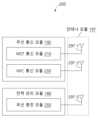
- a wearable electronic device 401includes a housing 400 including a front surface 400A, a rear surface 400B facing a direction opposite to the front surface 400A, and a side surface 400C surrounding an inner space between the front surface 400A and the rear surface 400B, a printed circuit board 430 disposed in the inner space and including a ground, the The housing 400 includes a wireless communication circuit disposed on the printed circuit board 430, an antenna structure electrically connected to the wireless communication circuit and transmitting and receiving a wireless signal, and a processor 420. ) may include a third lug (4001c) and a fourth lug (4001d) to be mounted.
- the antenna structuremay include a side frame 410 made of a conductive material surrounding the circumference of the printed circuit board 430 and forming at least a part of the side surface 400C, a power supply unit 470 for applying an electrical signal to the side frame 410, and a plurality of grounding units 480 connecting the side frame 410 to a ground.
- the plurality of ground parts 480include a first ground part 481 selectively connected to a first point 4131 of the side frame 410 adjacent to the first lug 4001a, a second ground part 482 selectively connected to a second point 4132 of the side frame 410 adjacent to the second lug 4001b, and a third lug 4001c.
- a third ground portion 483selectively connected to the third point 4133 of the side frame 410 adjacent to and a fourth point 4143 of the side frame adjacent to the fourth lug 4001d.
- a fourth ground portion 484 selectively connected tomay be included.
- an operating method of a wearable electronic device 401includes an operation of transmitting and receiving an electrical signal of a corresponding frequency band through an electrical path formed in the side frame 410 to which straps 450 and 460 are connected, an operation of detecting a standing wave ratio of the electrical signal in units of a set time, an operation of determining whether to change an electrical path formed on the side frame 410 based on the detected standing wave ratio, and the side
- An operation of changing an electrical path formed in the frame 410 and an operation of transmitting and receiving an electrical signal of a frequency band corresponding to the changed electrical pathmay be included.
- a wearable electronic deviceincludes a housing 400 including a front surface 400A facing a first direction, a rear surface 400B facing a second direction opposite to the first direction, and a side surface 400C surrounding an inner space between the front surface 400A and the rear surface 400B, a printed circuit board 430 disposed in the inner space, and the printed circuit board 430 ), a processor 420, and an antenna structure for transmitting and receiving radio signals.
- the housing 400may include first lugs 4001a and second lugs 4001b connected to the side surface 400C and to which the first strap 450 is mounted, and third lugs 4001c and fourth lugs 4001d connected to the side surface 400C and to which the second strap 460 is attached.
- the antenna structuresurrounds the printed circuit board 430 and forms at least a part of the side surface 400C, and includes a first part 4111 positioned between the first lug 4001a and the second lug 4001b, a second part 4112 positioned between the second lug 4001b and the third lug 4001c, and the third lug 4001.
- a side frame 410made of a conductive material including a third part 4113 positioned between the fourth lug 4001d and a fourth part 4114 positioned between the fourth lug 4001d and the first lug 4001a, a power feeding part 470 connected to the feeding point 474 of the side frame 410 and applying an electrical signal to the side frame, and It may include a plurality of grounding parts 480 that selectively connect different points of the side frame 410 to the ground so that an electrical path formed on the side frame 410 is changed.
- the wireless communication circuitmay be set to transmit and receive signals of a first frequency band when a first electrical path passing through the first portion 4111 or third portion 4113 is formed in the side frame 410, and to transmit and receive signals of a second frequency band when a second electrical path bypassing the first portion 4111 and the third portion 4113 is formed in the side frame 410.
- stable antenna performancecan be secured by changing an electrical path formed on the side frame according to the material of the strap.
- electrical signalsmay be prevented from being lost through the strap by blocking electrical signals from flowing to a lug portion to which the strap is connected.
- wireless communicationmay be performed in a frequency band suitable for a use state of the wearable electronic device by detecting a change in impedance of an electrical signal.
- FIG. 1is a block diagram of an electronic device in a network environment according to an embodiment.
- FIG. 2is a block diagram of a wireless communication module, a power management module, and an antenna module of an electronic device according to an embodiment.
- 3Ais a front perspective view of a wearable electronic device according to an embodiment.
- 3Bis a rear perspective view of a wearable electronic device according to an embodiment.
- 3Cis an exploded perspective view of a wearable electronic device according to an exemplary embodiment.
- FIG. 4Ais a plan view of a wearable electronic device according to an exemplary embodiment.
- 4Bis a plan view illustrating an antenna structure of a wearable electronic device according to an embodiment.
- 4Cis a block diagram illustrating an antenna structure of a wearable electronic device according to an embodiment.
- 4Dis a graph illustrating signal loss due to mounting of a metal strap in a wearable electronic device according to an exemplary embodiment.
- 5A to 5Dare diagrams illustrating a movement path of an electrical signal according to an operation of a switching circuit of a wearable electronic device according to an exemplary embodiment.
- 6Ais a plan view illustrating an antenna structure of a wearable electronic device according to an embodiment.
- 6B and 6Care diagrams illustrating a movement path of an electrical signal according to an operation of a switching circuit of a wearable electronic device according to an exemplary embodiment.
- FIG. 7is a flowchart illustrating a method of operating a wearable electronic device according to an exemplary embodiment.
- an electronic device 101may communicate with the electronic device 102 through a first network 198 (eg, a short-distance wireless communication network), or may communicate with at least one of the electronic device 104 and the server 108 through a second network 199 (eg, a long-distance wireless communication network).
- the electronic device 101may communicate with the electronic device 104 through the server 108 .
- the electronic device 101includes a processor 120, a memory 130, an input module 150, a sound output module 155, a display module 160, an audio module 170, a sensor module 176, an interface 177, a connection terminal 178, a haptic module 179, a camera module 180, a power management module 188, a battery 189, and a communication module 1. 90), a subscriber identification module 196, or an antenna module 197.
- at least one of these componentseg, the connection terminal 178) may be omitted or one or more other components may be added.
- some of these componentseg, sensor module 176, camera module 180, or antenna module 197) may be integrated into one component (eg, display module 160).
- the processor 120may, for example, execute software (eg, program 140) to control at least one other component (eg, hardware or software component) of the electronic device 101 connected to the processor 120, and may perform various data processing or calculations. According to an embodiment, as at least part of data processing or operation, the processor 120 may store commands or data received from other components (e.g., the sensor module 176 or the communication module 190) in the volatile memory 132, process the commands or data stored in the volatile memory 132, and store the resulting data in the non-volatile memory 134.
- softwareeg, program 140
- the processor 120may store commands or data received from other components (e.g., the sensor module 176 or the communication module 190) in the volatile memory 132, process the commands or data stored in the volatile memory 132, and store the resulting data in the non-volatile memory 134.
- the processor 120may include a main processor 121 (eg, a central processing unit or an application processor) or a secondary processor 123 (eg, a graphics processing unit, a neural processing unit (NPU), an image signal processor, a sensor hub processor, or a communication processor) that may operate independently or together with the main processor 121.
- a main processor 121eg, a central processing unit or an application processor
- a secondary processor 123eg, a graphics processing unit, a neural processing unit (NPU), an image signal processor, a sensor hub processor, or a communication processor
- the secondary processor 123may be implemented separately from or as part of the main processor 121 .
- the auxiliary processor 123functions related to at least one of the components of the electronic device 101 (eg, the display module 160, the sensor module 176, or the communication module 190) along with the main processor 121 while the main processor 121 is in an active (eg, application execution) state or instead of the main processor 121 while the main processor 121 is in an inactive (eg, sleep) state. Alternatively, at least some of the states may be controlled.
- the auxiliary processor 123eg, an image signal processor or a communication processor
- the auxiliary processor 123may include a hardware structure specialized for processing an artificial intelligence model.
- AI modelscan be created through machine learning. Such learning may be performed, for example, in the electronic device 101 itself where the artificial intelligence model is performed, or may be performed through a separate server (eg, the server 108).
- the learning algorithmmay include, for example, supervised learning, unsupervised learning, semi-supervised learning, or reinforcement learning, but is not limited to the above examples.
- the artificial intelligence modelmay include a plurality of artificial neural network layers.
- the artificial neural networkmay be one of a deep neural network (DNN), a convolutional neural network (CNN), a recurrent neural network (RNN), a restricted boltzmann machine (RBM), a deep belief network (DBN), a bidirectional recurrent deep neural network (BRDNN), deep Q-networks, or a combination of two or more of the above, but is not limited to the above examples.
- the artificial intelligence modelmay include, in addition or alternatively, software structures in addition to hardware structures.
- the memory 130may store various data used by at least one component (eg, the processor 120 or the sensor module 176) of the electronic device 101 .
- the datamay include, for example, input data or output data for software (eg, program 140) and commands related thereto.
- the memory 130may include volatile memory 132 or non-volatile memory 134 .
- the program 140may be stored as software in the memory 130 and may include, for example, an operating system 142 , middleware 144 , or an application 146 .
- the input module 150may receive a command or data to be used by a component (eg, the processor 120) of the electronic device 101 from the outside of the electronic device 101 (eg, a user).
- the input module 150may include, for example, a microphone, a mouse, a keyboard, a key (eg, a button), or a digital pen (eg, a stylus pen).
- the sound output module 155may output sound signals to the outside of the electronic device 101 .
- the sound output module 155may include, for example, a speaker or a receiver.
- the speakercan be used for general purposes such as multimedia playback or recording playback.
- a receivermay be used to receive an incoming call. According to one embodiment, the receiver may be implemented separately from the speaker or as part of it.
- the display module 160may visually provide information to the outside of the electronic device 101 (eg, a user).
- the display module 160may include, for example, a display, a hologram device, or a projector and a control circuit for controlling the device.
- the display module 160may include a touch sensor configured to detect a touch or a pressure sensor configured to measure the intensity of force generated by the touch.
- the audio module 170may convert sound into an electrical signal or vice versa. According to an embodiment, the audio module 170 may obtain sound through the input module 150, output sound through the sound output module 155, or an external electronic device (e.g., electronic device 102) (e.g., speaker or headphone) connected directly or wirelessly to the electronic device 101.
- an external electronic devicee.g., electronic device 102
- speaker or headphonee.g., speaker or headphone
- the sensor module 176may detect an operating state (eg, power or temperature) of the electronic device 101 or an external environmental state (eg, a user state), and generate an electrical signal or data value corresponding to the detected state.
- the sensor module 176may include, for example, a gesture sensor, a gyro sensor, an air pressure sensor, a magnetic sensor, an acceleration sensor, a grip sensor, a proximity sensor, a color sensor, an infrared (IR) sensor, a bio sensor, a temperature sensor, a humidity sensor, or an illuminance sensor.
- the interface 177may support one or more designated protocols that may be used to directly or wirelessly connect the electronic device 101 to an external electronic device (eg, the electronic device 102).
- the interface 177may include, for example, a high definition multimedia interface (HDMI), a universal serial bus (USB) interface, an SD card interface, or an audio interface.
- HDMIhigh definition multimedia interface
- USBuniversal serial bus
- SD card interfaceSecure Digital Card interface
- audio interfaceaudio interface
- connection terminal 178may include a connector through which the electronic device 101 may be physically connected to an external electronic device (eg, the electronic device 102).
- the connection terminal 178may include, for example, an HDMI connector, a USB connector, an SD card connector, or an audio connector (eg, a headphone connector).
- the haptic module 179may convert electrical signals into mechanical stimuli (eg, vibration or motion) or electrical stimuli that a user may perceive through tactile or kinesthetic senses.
- the haptic module 179may include, for example, a motor, a piezoelectric element, or an electrical stimulation device.
- the camera module 180may capture still images and moving images. According to one embodiment, the camera module 180 may include one or more lenses, image sensors, image signal processors, or flashes.
- the power management module 188may manage power supplied to the electronic device 101 .
- the power management module 188may be implemented as at least part of a power management integrated circuit (PMIC), for example.
- PMICpower management integrated circuit
- the battery 189may supply power to at least one component of the electronic device 101 .
- the battery 189may include, for example, a non-rechargeable primary battery, a rechargeable secondary battery, or a fuel cell.
- the communication module 190may support establishment of a direct (e.g., wired) communication channel or wireless communication channel between the electronic device 101 and an external electronic device (e.g., the electronic device 102, the electronic device 104, or the server 108), and communication through the established communication channel.
- the communication module 190may include one or more communication processors that operate independently of the processor 120 (eg, an application processor) and support direct (eg, wired) communication or wireless communication.
- the communication module 190may include a wireless communication module 192 (eg, a cellular communication module, a short-range wireless communication module, or a global navigation satellite system (GNSS) communication module) or a wired communication module 194 (eg, a local area network (LAN) communication module or a power line communication module).
- a wireless communication module 192eg, a cellular communication module, a short-range wireless communication module, or a global navigation satellite system (GNSS) communication module
- GNSSglobal navigation satellite system
- wired communication module 194eg, a local area network (LAN) communication module or a power line communication module.
- a corresponding communication module among these communication modulesmay communicate with the external electronic device 104 through a first network 198 (eg, a short-range communication network such as Bluetooth, wireless fidelity (WiFi) direct, or an infrared data association (IrDA)) or a second network 199 (eg, a legacy cellular network, a 5G network, a next-generation communication network, the Internet, or a long-distance communication network such as a computer network (eg, a LAN or a WAN)).
- a first network 198eg, a short-range communication network such as Bluetooth, wireless fidelity (WiFi) direct, or an infrared data association (IrDA)
- a second network 199eg, a legacy cellular network, a 5G network, a next-generation communication network, the Internet, or a long-distance communication network such as a computer network (eg, a LAN or a WAN)
- a computer networkeg, a
- the wireless communication module 192may identify or authenticate the electronic device 101 within a communication network such as the first network 198 or the second network 199 using subscriber information (eg, International Mobile Subscriber Identifier (IMSI)) stored in the subscriber identification module 196.
- subscriber informationeg, International Mobile Subscriber Identifier (IMSI)
- IMSIInternational Mobile Subscriber Identifier
- the wireless communication module 192may support a 5G network after a 4G network and a next-generation communication technology, for example, NR access technology (new radio access technology).
- NR access technologycan support high-speed transmission of high-capacity data (enhanced mobile broadband (eMBB)), minimization of terminal power and access to multiple terminals (massive machine type communications (mMTC)), or high reliability and low latency (URLLC (ultra-reliable and low-latency communications)).
- eMBBenhanced mobile broadband
- mMTCmassive machine type communications
- URLLCultra-reliable and low-latency communications
- the wireless communication module 192may support various technologies for securing performance in a high frequency band, such as beamforming, massive multiple-input and multiple-output (MIMO), full dimensional MIMO (FD-MIMO), an array antenna, analog beam-forming, or a large scale antenna.
- the wireless communication module 192may support various requirements defined for the electronic device 101, an external electronic device (eg, the electronic device 104), or a network system (eg, the second network 199).
- the wireless communication module 192may support peak data rate (eg, 20 Gbps or more) for eMBB realization, loss coverage (eg, 164 dB or less) for mMTC realization, or U-plane latency (eg, downlink (DL) and uplink (UL) 0.5 ms or less, or round trip 1 ms or less) for realizing URLLC.
- peak data rateeg, 20 Gbps or more
- loss coverageeg, 164 dB or less
- U-plane latencyeg, downlink (DL) and uplink (UL) 0.5 ms or less, or round trip 1 ms or less
- the antenna module 197may transmit or receive signals or power to the outside (eg, an external electronic device).
- the antenna module 197may include an antenna including a radiator formed of a conductor or a conductive pattern formed on a substrate (eg, PCB).
- the antenna module 197may include a plurality of antennas (eg, an array antenna). In this case, at least one antenna suitable for a communication method used in a communication network such as the first network 198 or the second network 199 may be selected from the plurality of antennas by, for example, the communication module 190. A signal or power may be transmitted or received between the communication module 190 and an external electronic device through the selected at least one antenna.
- other componentseg, a radio frequency integrated circuit (RFIC) may be additionally formed as a part of the antenna module 197 in addition to the radiator.
- RFICradio frequency integrated circuit
- the antenna module 197may form a mmWave antenna module.
- the mmWave antenna modulemay include a printed circuit board, an RFIC disposed on or adjacent to a first surface (eg, lower surface) of the printed circuit board and capable of supporting a designated high frequency band (eg, mmWave band), and a plurality of antennas (eg, array antennas) disposed on or adjacent to a second surface (eg, upper surface or side surface) of the printed circuit board and capable of transmitting or receiving signals in the designated high frequency band.
- peripheral devicese.g., a bus, general purpose input and output (GPIO), serial peripheral interface (SPI), or mobile industry processor interface (MIPI)
- signalse.g., commands or data
- commands or datamay be transmitted or received between the electronic device 101 and the external electronic device 104 through the server 108 connected to the second network 199 .
- Each of the external electronic devices 102 or 104may be the same as or different from the electronic device 101 .
- all or part of operations executed in the electronic device 101may be executed in one or more external electronic devices among the external electronic devices 102 , 104 , or 108 .
- the electronic device 101may request one or more external electronic devices to perform the function or at least part of the service, instead of or in addition to executing the function or service by itself.
- One or more external electronic devices receiving the requestmay execute at least a part of the requested function or service or an additional function or service related to the request, and deliver the execution result to the electronic device 101 .
- the electronic device 101may provide the result as at least part of a response to the request as it is or additionally processed.
- cloud computingdistributed computing, mobile edge computing (MEC), or client-server computing technology may be used.
- the electronic device 101may provide an ultra-low latency service using, for example, distributed computing or mobile edge computing.
- the external electronic device 104may include an internet of things (IoT) device.
- Server 108may be an intelligent server using machine learning and/or neural networks. According to an embodiment, the external electronic device 104 or server 108 may be included in the second network 199 .
- the electronic device 101may be applied to intelligent services (eg, smart home, smart city, smart car, or health care) based on 5G communication technology and IoT-related technology.
- FIG. 2is a block diagram 200 of a wireless communication module 192, a power management module 188, and an antenna module 197 of the electronic device 101, according to an embodiment.
- the wireless communication module 192may include the MST communication module 210 or the NFC communication module 230, and the power management module 288 may include the wireless charging module 250.
- the antenna module 297may include a plurality of antennas including an MST antenna 297-1 connected to the MST communication module 210, an NFC antenna 297-3 connected to the NFC communication module 230, and a wireless charging antenna 297-5 connected to the wireless charging module 250.
- MST antenna 297-1connected to the MST communication module 210
- NFC antenna 297-3connected to the NFC communication module 230
- a wireless charging antenna 297-5connected to the wireless charging module 250.
- the MST communication module 210may receive a signal including control information or payment information such as card information from the processor 120 (e.g., the processor 120 of FIG. 1), generate a magnetic signal corresponding to the received signal through the MST antenna 297-1, and transmit the generated magnetic signal to the external electronic device 102 (e.g., POS device) (e.g., the electronic device 102 of FIG. 1).
- the MST communication module 210includes a switching module including one or more switches connected to the MST antenna 297-1 (not shown), and controls the switching module to change the direction of voltage or current supplied to the MST antenna 297-1 according to the received signal.
- Changing the direction of the voltage or currentenables the direction of a magnetic signal (eg, magnetic field) transmitted through the MST antenna 297-1 to change accordingly.
- a magnetic signal whose direction is changedis sensed by the external electronic device 102
- an effecte.g., a waveform
- a magnetic field generated when a magnetic card corresponding to the received signale.g., card information
- the payment-related information and control signal received in the form of the magnetic signal by the electronic device 102may be transmitted to an external server 208 (e.g., payment server) through the network 299, for example.
- the NFC communication module 230obtains a signal including control information or payment information such as card information from the processor 120, and transmits the obtained signal to the external electronic device 102 through the NFC antenna 297-3. According to an embodiment, the NFC communication module 230 may receive such a signal transmitted from the external electronic device 102 through the NFC antenna 297-3.
- the wireless charging module 250wirelessly transmits power to the external electronic device 102 (eg, a mobile phone or a wearable device) through the wireless charging antenna 297-5, or wirelessly receives power from the external electronic device 102 (eg, a wireless charging device).
- the wireless charging module 250may support one or more of various wireless charging methods including, for example, a magnetic resonance method or a magnetic induction method.
- some of the MST antenna 297-1, the NFC antenna 297-3, or the wireless charging antenna 297-5may share at least a portion of the radiating part with each other.
- the radiating part of the MST antenna 297-1may be used as the radiating part of the NFC antenna 297-3 or the wireless charging antenna 297-5, and vice versa.
- the antenna module 297may include a switching circuit (not shown) configured to selectively connect (eg, close) or disconnect (eg, open) at least a portion of the antennas 297-1, 297-3, or 297-3 under the control of the wireless communication module 292 (eg, the MST communication module 210 or the NFC communication module 230) or the power management module 288 (eg, the wireless charging module 250).
- the wireless communication module 292eg, the MST communication module 210 or the NFC communication module 230
- the power management module 288eg, the wireless charging module 250.
- the NFC communication module 230 or the wireless charging module 250controls the switching circuit to temporarily separate at least a portion of the radiation portion shared by the NFC antenna 297-3 and the wireless charging antenna 297-5 from the NFC antenna 297-3 and connect it to the wireless charging antenna 297-5.
- At least one function of the MST communication module 210, the NFC communication module 230, or the wireless charging module 250may be controlled by an external processor (eg, the processor 120).
- designated functions (eg, payment functions) of the MST communication module 210 or the NFC communication module 230may be performed in a trusted execution environment (TEE).
- the trusted execution environment (TEE)may form an execution environment in which at least a part of a designated area of the memory 130 (eg, the memory 130 of FIG. 1 ) is allocated to be used to perform, for example, a function requiring a relatively high level of security (eg, a function related to financial transactions or personal information). In this case, access to the designated area may be restrictedly allowed depending on, for example, a subject accessing the area or an application running in the trusted execution environment.
- An electronic devicemay be a device of various types.
- the electronic devicemay include, for example, a portable communication device (eg, a smart phone), a computer device, a portable multimedia device, a portable medical device, a camera, a wearable device, or a home appliance.
- a portable communication devicee.g, a smart phone
- a computer devicee.g., a smart phone
- a portable multimedia devicee.g., a portable medical device
- a camerae.g., a camera
- a wearable devicee.g., a smart bracelet
- first, second, or first or secondarymay be used simply to distinguish a corresponding component from other corresponding components, and do not limit the corresponding components in other respects (e.g., importance or order).
- a (e.g., a first) componentis referred to as “coupled” or “connected” to another (e.g., a second) component, with or without the terms “functionally” or “communicatively,” it means that the component may be connected to the other component directly (e.g., by wire), wirelessly, or through a third component.
- moduleused in the embodiments of this document may include units implemented in hardware, software, or firmware, and may be used interchangeably with terms such as, for example, logic, logical blocks, parts, or circuits.
- a modulemay be an integrally constructed component or a minimal unit of components or a portion thereof that performs one or more functions.
- the modulemay be implemented in the form of an application-specific integrated circuit (ASIC).
- ASICapplication-specific integrated circuit
- the embodiments of this documentmay be implemented as software (eg, program 140) including one or more instructions stored in a storage medium (eg, internal memory 136 or external memory 138) readable by a machine (eg, electronic device 101).
- a processoreg, the processor 120
- a deviceeg, the electronic device 101
- the one or more instructionsmay include code generated by a compiler or code executable by an interpreter.
- the device-readable storage mediummay be provided in the form of a non-transitory storage medium.
- 'non-temporary'only means that the storage medium is a tangible device and does not contain a signal (eg, electromagnetic wave), and this term does not distinguish between the case where data is semi-permanently stored in the storage medium and the case where it is temporarily stored.
- a signaleg, electromagnetic wave
- the method according to various embodiments disclosed in this documentmay be included and provided in a computer program product.
- Computer program productsmay be traded between sellers and buyers as commodities.
- a computer program productmay be distributed in the form of a device-readable storage medium (e.g., compact disc read only memory (CD-ROM)), or distributed (e.g., downloaded or uploaded) online, through an application store (e.g., Play StoreTM) or directly between two user devices (e.g., smartphones).
- an application storee.g., Play StoreTM
- at least part of the computer program productmay be temporarily stored or temporarily created in a device-readable storage medium such as a manufacturer's server, an application store server, or a relay server's memory.
- each component (eg, module or program) of the components described abovemay include a single object or a plurality of objects, and some of the multiple objects may be separately disposed in other components.
- one or more components or operations among the corresponding components described abovemay be omitted, or one or more other components or operations may be added.
- a plurality of componentseg modules or programs
- the integrated componentmay perform one or more functions of each of the plurality of components identically or similarly to those performed by a corresponding component of the plurality of components prior to the integration.
- the actions performed by a module, program, or other componentmay be executed sequentially, in parallel, iteratively, or heuristically, or one or more of the actions may be executed in a different order, may be omitted, or one or more other actions may be added.
- FIG. 3Ais a front perspective view of a wearable electronic device according to an embodiment
- FIG. 3Bis a rear perspective view of the wearable electronic device according to an embodiment
- FIG. 3Cis an exploded perspective view of the wearable electronic device according to an embodiment.
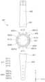
- an electronic device 301(eg, the electronic device 101 of FIG. 1 ) according to an embodiment includes a housing 300 including a front (or first surface) 310A, a rear surface (or second surface) 310B, and a side surface 310C surrounding a space between the front surface 300A and the rear surface 300B, and at least one of the housing 300 Straps 350 and 360 connected to a part and configured to detachably bind the electronic device 301 to a part of the user's body (eg, wrist, ankle, etc.) may be included.
- the housing 300may refer to a structure forming some of the front surface 300A, rear surface 300B, and side surface 300C of FIG. 2A.
- the front surface 300Amay be formed by a front plate 320 (eg, a glass plate or a polymer plate including various coating layers) that is substantially transparent at least in part.
- the back surface 300Bmay be formed by a substantially opaque back plate 393 .
- the rear plate 393may be formed of, for example, coated or colored glass, ceramic, polymer, metal (eg, aluminum, stainless steel (STS), or magnesium), or a combination of at least two of the foregoing materials.
- the side surface 300Cmay be formed by a side frame (or "bezel structure") 310 coupled to the front plate 320 and the rear plate 393 and including metal and/or polymer.
- the back plate 397 and the side frame 310may be integrally formed and include the same material (eg, a metal material such as aluminum).
- the electronic device 301may include at least one of a display 327, audio modules 305 and 308, a sensor module 311, key input devices 302, 303 and 304, and a connector hole 309.
- the electronic device 301may omit at least one of the components (eg, the key input devices 302, 303, 304, the connector hole 309, or the sensor module 311) or may additionally include other components.
- the display 327may be exposed through a substantial portion of the front plate 320 , for example.
- the shape of the display 327may be a shape corresponding to the shape of the front plate 320, and may have various shapes such as a circle, an ellipse, or a polygon.
- the display 327may be coupled to or disposed adjacent to a touch sensing circuit, a pressure sensor capable of measuring the intensity (pressure) of a touch, and/or a fingerprint sensor.
- the audio modules 305 and 308may include a microphone hole 305 and a speaker hole 308 .
- a microphone for acquiring external soundmay be disposed inside the microphone hole 305, and in some embodiments, a plurality of microphones may be disposed to detect the direction of sound.
- the speaker hole 308can be used as an external speaker and a receiver for a call.
- the speaker hole 308 and the microphone hole 305may be implemented as one hole, or a speaker may be included without the speaker hole 308 (eg, a piezo speaker).
- the sensor module 311may generate an electrical signal or data value corresponding to an internal operating state of the electronic device 301 or an external environmental state.
- the sensor module 311may include, for example, a biometric sensor 311 (eg, an HRM sensor) disposed on the rear surface 300B of the housing 300 .
- the electronic device 301may further include at least one of a sensor module (not shown), for example, a gesture sensor, a gyro sensor, an air pressure sensor, a magnetic sensor, an acceleration sensor, a grip sensor, a color sensor, an infrared (IR) sensor, a bio sensor, a temperature sensor, a humidity sensor, or an illuminance sensor.
- a sensor modulenot shown
- a gesture sensorfor example, a gesture sensor, a gyro sensor, an air pressure sensor, a magnetic sensor, an acceleration sensor, a grip sensor, a color sensor, an infrared (IR) sensor, a bio sensor, a temperature sensor, a humidity sensor, or an
- the sensor module 311may include electrode regions 313 and 314 forming part of the surface of the electronic device 301 and a biosignal detection circuit (not shown) electrically connected to the electrode regions 313 and 314.
- the electrode regions 313 and 314may include a first electrode region 313 and a second electrode region 314 disposed on the rear surface 300B of the housing 300 .
- the sensor module 311may be configured such that the electrode areas 313 and 314 obtain an electrical signal from a part of the user's body, and the biosignal detection circuit detects the user's biometric information based on the electrical signal.
- the key input devices 302, 303, and 304may include a wheel key 302 disposed on the first surface 300A of the housing 300 and rotatable in at least one direction, and/or side key buttons 303 and 304 disposed on the side surface 300C of the housing 300.
- the wheel key 302may have a shape corresponding to the shape of the front plate 320 .
- the electronic device 301may not include some or all of the above-mentioned key input devices 302, 303, and 304, and the key input devices 302, 303, and 304 may be implemented in other forms such as soft keys on the display 327.
- the connector hole 309may include another connector hole (not shown) capable of accommodating a connector (e.g., a USB connector) for transmitting and receiving power and/or data to and from an external electronic device and a connector for transmitting and receiving an audio signal to and from the external electronic device.
- the electronic device 301may further include, for example, a connector cover (not shown) that covers at least a portion of the connector hole 309 and blocks external foreign substances from entering the connector hole.
- the straps 350 and 360may be formed of various materials and shapes. Integral and plurality of unit links may be formed to flow with each other by woven material, leather, rubber, urethane, metal, ceramic, or a combination of at least two of the above materials. In one embodiment, the straps 350 and 360 may be detachably attached to at least a portion of the housing 300 using the locking members 351 and 361 .
- the straps 350 and 360may include one or more of a fixing member 352, a fixing member fastening hole 353, a band guide member 354, and a band fixing ring 355.
- the fixing member 352may be configured to fix the housing 300 and the straps 350 and 360 to a part of the user's body (eg, a wrist or an ankle).
- the fixing member fastening hole 353may fix the housing 300 and the straps 350 and 260 to a part of the user's body corresponding to the fixing member 352 .
- the band guide member 354is configured to limit the range of motion of the fixing member 352 when the fixing member 352 is fastened with the fixing member fastening hole 353, so that the straps 350 and 260 are attached to a part of the user's body.
- the band fixing ring 355may limit the movement range of the fastening members 350 and 260 in a state in which the fixing member 352 and the fixing member fastening hole 353 are fastened.
- the electronic device 301is the side frame 310, the front plate 320, the display 327, the first antenna 330, the second antenna 350b, the support member 340 (eg bracket), the battery 370, the printed circuit board 380, the sealing member 390, the rear plate 390, the rear plate 390 93), and and the straps 350 and 360 may be included.
- the support member 340may be disposed inside the electronic device 301 and connected to the side frame 310 or integrally formed with the side frame 310 .
- the support member 360may be formed of, for example, a metal material and/or a non-metal (eg, polymer) material.
- the support member 360may have the display 327 coupled to one surface and the printed circuit board 380 coupled to the other surface.
- a processor, memory, and/or interfacemay be mounted on the printed circuit board 380 .
- the processor(eg, the processor 120 of FIG. 1 ) may include, for example, one or more of a central processing unit, an application processor, a graphic processing unit (GPU), an application processor, a sensor processor, or a communication processor.
- Memorymay include, for example, volatile memory or non-volatile memory.
- the interfacemay include, for example, a high definition multimedia interface (HDMI), a universal serial bus (USB) interface), an SD card interface, and/or an audio interface.
- HDMIhigh definition multimedia interface
- USBuniversal serial bus
- the interfacemay electrically or physically connect the electronic device 300 to an external electronic device, and may include a USB connector, an SD card/MMC connector, or an audio connector.
- the battery 370is a device for supplying power to at least one component of the electronic device 300, and may include, for example, a non-rechargeable primary battery, a rechargeable secondary battery, or a fuel cell. At least a portion of the battery 370 may be disposed on substantially the same plane as the printed circuit board 380 , for example.
- the battery 370may be integrally disposed inside the electronic device 300 or may be disposed detachably from the electronic device 300 .
- the first antenna 330may be disposed between the display 327 and the support member 360 .
- the first antenna 330may include, for example, a near field communication (NFC) antenna, a wireless charging antenna, and/or a magnetic secure transmission (MST) antenna.
- the first antenna 330may, for example, perform short-range communication with an external device, wirelessly transmit/receive power required for charging, and transmit a short-range communication signal or a self-based signal including payment data.
- the antenna structuremay be formed by a part of the side frame 310 structure and/or the support member 360 or a combination thereof.
- the second antenna 350bmay be disposed between the printed circuit board 380 and the rear plate 393 .
- the second antenna 350bmay include, for example, a near field communication (NFC) antenna, a wireless charging antenna, and/or a magnetic secure transmission (MST) antenna.
- the second antenna 350bmay, for example, perform short-range communication with an external device, wirelessly transmit/receive power required for charging, and transmit a short-range communication signal or a self-based signal including payment data.
- an antenna structuremay be formed by a part of the side frame 310 and/or the back plate 393 or a combination thereof.
- the sealing member 390may be positioned between the side frame 310 and the rear plate 393 .
- the sealing member 390may be configured to block moisture and foreign substances from entering into the space surrounded by the side frame 310 and the back plate 393 from the outside.
- FIG. 4Ais a plan view of a wearable electronic device according to an embodiment
- FIG. 4Bis a plan view illustrating an antenna structure of the wearable electronic device according to an embodiment
- FIG. 4Cis a block diagram illustrating an antenna structure of the wearable electronic device according to an embodiment
- the wearable electronic device 401includes a housing 400 (eg, the housing 300 of FIG. 3A ), straps 450 and 460 connected to the housing 400 (eg, the straps 350 and 360 of FIG. 3A ), a display 427 (eg, the display 327 of FIG. 3A ), and a printed circuit board 430 .
- PCBPrinted circuit board
- a wireless communication circuiteg, the wireless communication module 192 of FIG. 1
- an antenna structureeg, a transceiver 491, an impedance tuner 493, and a coupler 492.
- the housing 400may include a front surface 400A facing a first direction (eg, +Z direction in FIG. 4A), a rear surface 400B facing a second direction (eg, -Z direction in FIG. A first direction toward which the front face 400A faces and a second direction toward which the rear face 400B face may be opposite to each other.
- the side surface 400Cmay surround an inner space formed between the front surface 400A and the rear surface 400B.
- Various parts (eg, a battery or a PCB) of the wearable electronic device 401may be disposed in the inner space of the housing 400 surrounded by the side surface 400C.
- the housing 400may include a side frame 410 forming at least a portion of the side surface 400C.
- the side frame 410may connect between the front side 400A and the back side 400B along an edge of the front side 400A or the back side 400B.
- the side frame 410may form at least a portion of the front surface 400A or the rear surface 400B.
- the side frame 410may be formed in a closed loop shape that surrounds the circumference of the front surface 400A based on a state in which the front surface 400A is viewed as shown in FIG. 4A.
- the housing 400may include a plurality of lugs 4001 to which the straps 450 and 460 are mounted.
- a plurality of lugs 4001may be formed on the side surface 400C of the housing 400.
- the plurality of lugs 4001may protrude in an outward direction of the side surface 400C based on a state viewed from the front surface 400A as shown in FIG. 4A.
- a plurality of lugs 4001may be formed on the side frame 410 .
- the plurality of lugs 4001may include first lugs 4001a and second lugs 4001b to which the first strap 450 is connected, and third lugs 4001c and fourth lugs 4001d to which the second strap 460 is mounted.
- the first lug 4001a and the second lug 4001bare connected to the fastening part 451 of the first strap 450 to fix the first strap 450 to the housing 400
- the third lug 4001c and the fourth lug 4001dare connected to the fastening part 461 of the second strap 460 to fix the second strap 460 to the housing 400 0) can be fixed.
- the plurality of lugs 4001may be disposed on the side surface 400C of the housing 400 to be spaced apart from each other.
- the first lug 4001a and the second lug 4001bprotrude from the side surface 400C of the housing 400 toward the -Y axis direction
- the third lug 4001c and fourth lug 4001dprotrude from the side surface 400C of the housing 400 toward the +Y axis direction. It can be.
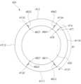
- the first lug 4001a, the second lug 4001b, the third lug 4001c, and the fourth lug 4001dmay be sequentially arranged clockwise on the side surface 400C of the housing 400 with reference to FIG. 4A.
- the side frame 410may include a plurality of areas divided based on a plurality of lugs 4001 .
- the side frame 410includes a first portion 4111 located between the first lug 4001a and the second lug 4001b, a second portion 4112 located between the second lug 4001b and the third lug 4001c, a third lug 4001c, and a fourth lug ( 4001d) may include a third portion 4113 positioned between them and a fourth portion 4114 positioned between the fourth lug 4001d and the first lug 4001a.
- the fastening part 451 of the first strap 450is located in the first part 4111
- the fastening part 461 of the second strap 460can be located in the third part 4113.
- the straps 450 and 460may bind the wearable electronic device 401 to the user's body.
- at least a portion of the straps 450 and 460may be formed of a conductive material (eg, metal), or may be entirely formed of a non-conductive material (eg, plastic).
- display 427may display visual information (eg, images and/or text). In one embodiment, at least a portion of the display 427 may be exposed to the outside through the front surface 400A of the housing 400 .
- a part of the front surface 400A of the housing 400is open or formed of a transparent material, and the display 427 is disposed in the inner space of the housing 400 and exposed to the outside through the front surface 400A of the housing 400.
- the display 427may include a display panel (eg, LCD or OLED) and a touch screen panel (TSP) for receiving a user's input.
- the printed circuit board 430may be disposed in an inner space of the housing 400 .
- a processoreg, the processor 120 of FIG. 1
- the processormay include, for example, one or more of a central processing unit (CPU), an application processor (AP), an image signal processor, a sensor hub processor, or a communication processor.
- the printed circuit board 430may be electrically connected to the antenna structure.
- wireless communication circuitrymay be disposed on printed circuit board 430 .
- the wireless communication circuitmay receive, for example, a radio signal from an external device (eg, the electronic device 104 of FIG. 1 ) or transmit a radio signal to the external device.
- the wireless communication circuitmay transmit and receive wireless signals through an electrical path formed on the side frame 410 .
- the wearable electronic device 401may communicate with an external device (eg, the electronic device 104 of FIG. 1 ) through an antenna structure.
- the antenna structuremay include a side frame 410 , a power supply unit 470 , and a plurality of ground units 480 .
- a part of the side frame 410may function as a radiator of an antenna.
- at least a portion of the side frame 410may be formed of a conductive material (eg, metal).
- the conductive material portion of the side frame 410forms an electrical path through which electrical signals can travel, thereby forming a radiation pattern of a frequency band corresponding to the electrical path.
- an electrical path formed on the side frame 410may be changed.
- a radiation pattern of electromagnetic waves generated from the side frame 410 and a resonance frequency band of an electrical signal transmitted and received through the side frame 410may be changed.
- the wireless communication circuitmay apply an electrical signal to the side frame 410 through a power supply 470 (feeder).
- the wireless communication circuit 490may apply an electrical signal (eg, an RF signal) to the side frame 410 according to data received from the processor.
- the wireless communication circuitmay transmit and receive electrical signals corresponding to electrical paths formed on the side frame 410 .
- the power supply 470may be disposed on the printed circuit board 430 . However, this is for convenience of description, and the arrangement position of the power feeding unit 470 is not limited thereto.
- the power supply unit 470may be electrically connected to a wireless communication circuit through a power supply line (eg, the power supply line 471 of FIG. 5A ).
- the power supply unit 470may be electrically connected to a power supply point (eg, a power supply point 414 of FIG. 5A ) of the side frame 410 through a conductive elastic member (eg, a clip or a pogo pin).
- the power supply point where the power supply unit 470 is connected to the side frame 410is the second part 4112 or the fourth part 4114 of the side frame 410 in a state of looking at the front as shown in FIG. 4 It may be located at any one position.
- the connection position of the power supply part 470 to the side frame 410is located between the connection point of the second ground part 482 to the side frame 410 (eg, the second point 4132 in FIG. 5A) and the connection point of the third ground part 483 (eg, the third point 4133 in FIG. 5A), or the first ground part 48 to the side frame 410. It may be located between the connection point of 1) (eg, the first point 4131 of FIG.
- connection point of the power supply unit 470 to the side frame 410is located between the connection points of the first ground unit 481 and the fourth ground unit 484 to the side frame 410. The case will be described as an example.
- the plurality of ground parts 480may change electrical paths formed on the side frame 410 .
- each of the plurality of grounding units 480may transfer an electrical signal applied to the side frame 410 to the ground.
- the plurality of ground parts 480may be respectively connected to portions of the side frame 410 adjacent to the plurality of lugs 4001 .
- the plurality of ground parts 480include a first ground part 481 connected adjacent to the first lug 4001a, a second ground part 482 connected adjacent to the second lug 4001b, a third ground part 483 connected adjacent to the third lug 4001c, and a fourth ground part 484 connected adjacent to the fourth lug 4001d.
- the electrical signal flowing through the side frame 410is selectively transmitted to the ground through each of the plurality of grounding parts 480, so that the electrical path of the electrical signal applied to the side frame 410 passes through the lug 4001 or avoids it.
- the transceiver 491may output an electrical signal based on communication data received from the processor 420 .
- the transceiver 491may convert an electrical signal received from an external device into communication data recognizable by the processor 420 and transmit the converted communication data to the processor.
- the impedance tuner 493may tune an electrical signal output from the transceiver 491.
- the impedance tuner 493may adjust the impedance of an electrical signal applied to the side frame 410 to be close to a characteristic impedance corresponding to an electrical path formed on the side frame 410 .
- the impedance tuner 493changes the electrical length of the antenna including the side frame 410 to reduce the return loss due to the difference between the characteristic impedance corresponding to the electrical path formed on the side frame 410 and the impedance of the applied electrical signal.
- coupler 492may perform power sampling.
- the coupler 492may extract a forward coupling signal from an electrical signal output from the transceiver 491 and transmit it to the transceiver 491 again.
- the coupler 492extracts a reverse coupling signal from the reflected signal according to the difference between the impedance of the electrical signal applied to the side frame 410 and the characteristic impedance, and transmits it to the transceiver 491.
- the coupler 492may detect a vortage standing wave ratio corresponding to the extracted forward coupling signal and the reverse coupling signal and transfer the detected wave ratio to the processor 420 .
- the standing wave ratiomay be passed from the transceiver 491 to the processor 420.
- the impedance of the antennamay vary according to the material of the straps 450 and 460 connected to the side frame 410 .
- the straps 450 and 460 including a conductive materialare connected to the side frame 410 through the lug 4001, some of the electrical signals applied to the side frame 410 may be transmitted to the straps 450 and 460 through the lug 4001. In this case, an impedance change of the electrical signal applied to the side frame 410 may occur.
- the straps 450 and 460 made of a non-conductive materialare connected to the side frame 410 through the lug 4001, the electrical signal applied to the side frame 410 may pass through the lug 4001, but may not be transmitted to the straps 450 and 460.
- the electrical signal applied to the side frame 410has a relatively small impedance change compared to the case where the straps 450 and 460 including conductive materials are connected to the side frame 410 through the lug 4001, or there may be no substantial impedance change.
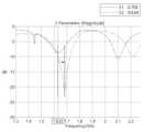
- FIG. 4Dshows a change in impedance of an antenna signal according to the material of the straps 450 and 460 connected to the lug 4001.
- S1 shown in FIG. 4Drepresents the impedance detected when straps 450 and 460 made of non-conductive material are mounted on the lug 4001
- S2represents the impedance detected when the straps 450 and 460 including conductive materials are mounted on the lug 4001.
- the impedance of the antenna structure using the side frame 410 as a radiatorchanges according to the material of the straps 450 and 460 .
- the characteristic deterioration of the antenna radiation performance of the requested service bandoccurs because the resonant frequencies of the antennas have differences of 1.632 GHz and 1.69 GHz, respectively.
- the processor 420may change the wireless communication mode of the wearable electronic device 401 .
- the processor 420may control the shorting operation of the wireless communication circuit and the grounding unit 480 to implement effective antenna performance.
- the processor 420may determine the wireless communication mode of the wearable electronic device 401 based on a change in antenna performance according to the material of the straps 450 and 460 connected to the housing 410 .
- the processor 420may change the wireless communication mode of the wearable electronic device 401 based on an impedance change detected through a wireless communication circuit (eg, the wireless communication module 192 of FIG. 1 ), for example, the detected standing wave ratio.
- the processor 420may perform a wireless communication mode switching operation based on the amount of change in the standing wave ratio detected through the coupler 492 .
- the processor 420may maintain the wireless communication mode of the wearable electronic device 401 when the variation in the standing wave ratio detected through the coupler 492 is within a first range, and may change the wireless communication mode of the wearable electronic device 401 when the variation in the standing wave ratio is located in a second range greater than the first range.
- the amount of change in the standing wave ratiomay be determined according to the material of the straps 450 and 460 connected to the housing 410 .
- the straps 450 and 460 made of metalare connected to the housing 400 through the lugs 4001
- the metal parts of the straps 450 and 460 disposed in the first part 4111 and the third part 4113 of the side frame 410substantially expand the side frame 410, which may cause a difference between the actual antenna performance and the target antenna performance.
- the processor 420may detect the material of the straps 450 and 460 mounted on the housing 400 through a change in antenna performance according to the material of the straps 450 and 460, for example, a change in the standing wave ratio, and based on this, change the wireless communication mode so that effective antenna performance can be exhibited.
- the processor 420may change an electrical path formed on the side frame 410 by controlling a shorting operation (eg, an operation of transmitting electrical signals to the ground) of the plurality of grounding units 480 with respect to the side frame 410. For example, when it is determined that the straps 450 and 460 made of non-conductive material are connected to the lug, the processor 420 may control the shorting operation of the plurality of grounding units 480 so that the electrical signal applied to the side frame 410 flows along an electrical path (eg, the electrical path a1 of FIG. 5A ) passing through the first part 4111 or the third part 4113 of the side frame 410.
- a shorting operationeg, an operation of transmitting electrical signals to the ground
- the electrical signal applied to the side frame 410is adjacent to the lug 4001. It may control the shorting operation of the plurality of grounding parts 480 to be transmitted to the ground.
- the electrical signal applied to the side frame 410may be set to flow along an electrical path (e.g., the electrical path d2 of FIG. 5D) that does not pass through the portion of the side frame 410 to which the straps 450 and 460 are connected, for example, the first portion 4111 and the third portion 4113.
- the electrical path formed in the side frame 410is set to form a path that does not pass through the first part 4111 and the third part 4113, the electric signal applied to the side frame 410.
- the phenomenon of flowing to the metal straps 450 and 460the deterioration of antenna performance due to the metal strap can be reduced.
- the processor 420may control the wireless communication circuit 490 to change a frequency band transmitted and received through an antenna structure according to a change in a wireless communication mode.
- the wireless communication circuitmay be set to transmit and receive an electrical signal of a frequency band corresponding thereto.
- the processor 420may change the wireless communication mode while the wearable electronic device 401 is mounted on the user's body.
- the processor 420may be configured to change an electrical path formed on the side frame 410 in a state in which the housing 400 is recognized as mounted on the user's body through a biometric sensor (eg, the biosensor 311 of FIG. 3C ).
- 5A to 5Dare diagrams illustrating a movement path of an electrical signal according to an operation of a switching circuit of a wearable electronic device according to an exemplary embodiment.
- an electronic device 401may include a printed circuit board 430 on which a wireless communication circuit (eg, the wireless communication circuit 490 of FIG. 4C) is disposed, a side frame 410 functioning as a radiator, a power supply unit 470, and a plurality of ground units 480.
- a wireless communication circuiteg, the wireless communication circuit 490 of FIG. 4C
- a side frame 410functioning as a radiator
- a power supply unit 470e.g, the wireless communication circuit 490 of FIG. 4C
- ground units 480e.g, the wireless communication circuit 490 of FIG. 4C
- the side frame 410may form an electrical path.
- the side frame 410includes a first portion 4111 located between the first lug 4001a and the second lug 4001b, a second portion 4112 located between the second lug 4001b and the third lug 4001c, a third portion 4113 located between the third lug 4001c and the fourth lug 4001d, and a fourth lug 4001c.
- a fourth portion 4114 positioned between the first lug 4001a and the first lug 4001dmay be included.
- a first strapeg, the second strap 450 of FIG. 4A
- a second strapeg, second strap 4 of FIG. 60
- the power feeding unit 470may apply an electrical signal to the side frame 410 .
- the power supply unit 470may electrically connect the printed circuit board 430 and the side frame 410 on which a wireless communication circuit (eg, the transceiver 491 of FIG. 4C ) is disposed.
- the power supply unit 470may be electrically connected to the wireless communication circuit and connected to the power supply point 414 of the side frame 410 through a power supply line 471 .
- the power supply point 414may be electrically connected to any one of the second part 4112 or the fourth part 4114 of the side frame 410 .
- the power supply point 414 to which the power supply unit 470 is connected to the side frame 410 through a power supply line 471may be located between a second point 4132 and a third point 4133 described later, or between the first point 4131 and the fourth point 4134.
- the plurality of ground units 480are connected to the side frame 410 and may change an electrical path through which an electrical signal applied to the side frame 410 flows. In one embodiment, the plurality of ground units 480 may be connected to different points of the side frame 410 and transfer electrical signals flowing through the side frame 410 to the ground according to a shorting operation. In one embodiment, the plurality of ground parts 480 include a first ground part 481 connected to the first point 4131 of the side frame 410 adjacent to the first lug 4001a, a second ground part 482 connected to the second point 4132 of the side frame 410 adjacent to the second lug 4001b, and a side frame 4 adjacent to the third lug 4001c. It may include a third grounding portion 483 connected to the third point 4133 of 10) and a fourth grounding portion 484 connected to the fourth point 4134 of the side frame 410 adjacent to the fourth lug 4001d.
- each of the plurality of ground units 480may selectively connect the side frame 410 to the ground.
- the groundmay be disposed on the printed circuit board 430 or may be disposed in another part of the housing 400 .
- each of the plurality of ground units 480may transfer electrical signals to one ground or to separate electrical signals to a plurality of separate grounds.
- a case in which the ground is disposed on the printed circuit board 430 and each of the plurality of ground parts 480 connects the side frame 410 and the printed circuit board 430 on which the ground is disposedwill be described as an example. However, this is for convenience of explanation, and the embodiment in which the grounding part 480 is connected to the printed circuit board 430 is only one embodiment, and the plurality of grounding parts 480 connected to the side frame 410 are connected to the ground.
- the first grounding portion 481may include a first grounding point 4811 connected to ground and a first grounding line 4812 connecting the first grounding point 4811 and the first point 4131.
- the second grounding portion 482may include a second grounding point 4821 connected to ground and a second grounding line 4822 connecting the second grounding point 4821 and the second point 4132 .
- the third grounding portion 483may include a third grounding point 4831 connected to ground and a third grounding line 4832 connecting the third grounding point 4831 and the third point 4133 .
- the fourth grounding portion 484may include a fourth grounding point 4841 connected to ground and a fourth grounding line 4842 connecting the fourth grounding point 4841 and the fourth point 4143 .
- the ground points 4811 , 4821 , 4831 , and 4841 of each ground part 480may be located on the printed circuit board 430 .
- a switching circuit that performs a short-circuit operationmay be formed in each of the ground lines 4812 , 4822 , 4832 , and 4842 of the plurality of ground units 480 .
- the electrical path through which the electrical signal applied to the side frame 410 flowscan be changed.
- a resonant frequency band of an electrical signal transmitted and received through the side frame 410may be adjusted according to a short-circuit operation of each of the switching circuits formed in the plurality of ground units 480 .
- various types of switching circuitsmay be formed in the ground unit 480 according to design conditions.
- the enlarged view of the second grounding unit 482 shown in FIG. 5Ashows an example of one switching circuit applicable to each grounding unit 480 .
- the switching circuit 4860 formed on the second ground line 4822may include a plurality of ports 4861, 4862, 4863, and 4864, and a switch 4865 selectively connected to at least one of the plurality of ports 4861, 4862, 4863, and 4864.
- the plurality of ports 4861, 4862, 4863, and 4863may include, for example, a first port 4861, a second port 4862, a third port 4863, and a fourth port 4864.
- the first port 4861may be connected to the switch 4865 when the second grounding part 482 does not short-circuit the side frame 481 to the ground.
- the first port 4861may be formed as an open circuit.
- the second port 4862may be connected to the switch 4865 when the grounding part 482 shorts the side frame 481 to the ground.
- the second port 4862may be formed as a short circuit.
- the third port 4863is formed as a short circuit and may include one or more inductors.
- the fourth port 4864is formed as a short circuit and may include one or more capacitors.
- the second grounding portion 482may connect the side frame 481 to the ground.
- the frequency band of the electrical signal applied to the side frame 410may be changed according to the connection state of the switch 4865 to the second port 4862, the third port 4863, or the fourth port 4864.
- the above-described switch circuit structureis an example for convenience of description, and the structure of the switching circuit formed on the ground lines 4812, 4822, 4832, and 4842 of each grounding unit 480 may be formed differently, and the ground line (4812, 4822, 4832, 4842) It is revealed that the switching circuit structure formed is not limited to the above-described example.
- the plurality of grounding units 480are selectively shorted to the side frame 410 through an operation of a switch 4865 formed on the ground lines 4812, 4822, 4832, and 4842, thereby changing the electrical path formed on the side frame 410.
- the shorting operation of the plurality of ground units 481 , 482 , 483 , and 484may be determined according to the wireless communication mode of the wearable electronic device 401 .
- the plurality of grounding parts 480provide an electrical path through which electrical signals applied to the side frame 410 pass through the side frame portion where the strap is mounted, for example, the first portion 4111 or the third portion 4113. It can act to move along.
- the plurality of grounding parts 480may short the first grounding part 481 to the side frame 410 .
- an electrical path leading from the power supply point 414 to the first point 4131may be formed in the side frame 410 .
- the wireless communication circuitmay transmit/receive a signal of a frequency band corresponding to the electrical path a1 or transmit/receive a signal of a frequency band corresponding to the electrical path a2.
- the plurality of grounding parts 480may operate such that the first grounding part 481 and the second grounding part 482 are short-circuited to the side frame 410 (eg, the first grounding line 4812 and the second grounding line 4822 are connected to the side frame 410), as shown in FIG. 5B.
- an electrical path b1is formed from the power supply point 414 to the ground through the third portion 4113 and the second portion 4112 through the second point 4132 and the second ground point 4821, or the first point 4131 and the first ground point 48 from the power feed point 414 via the fourth portion 4114.
- An electrical path b2 leading to groundmay be formed through 11).
- the wireless communication circuitmay transmit/receive a signal of a frequency band corresponding to the electrical path b1 or transmit/receive a signal of a frequency band corresponding to the electrical path b2.
- the plurality of grounding parts 480may operate such that the second grounding part 482 and the third grounding part 483 are short-circuited to the side frame 410 (eg, the second grounding line 4822 and the third grounding line 4832 are connected to the side frame 410), as shown in FIG. 5C.
- an electrical path c1is formed from the power feeding point 414 via the third portion 4113 to the ground through the third point 4133 and the third grounding point 4831, or the second point 4132 and the second grounding point 482 from the power feeding point 414 via the fourth portion 4114 and the first portion 4111.
- An electrical path c2 leading to groundmay be formed through 1).
- the wireless communication circuitmay transmit/receive a signal of a frequency band corresponding to the electrical path c1 or transmit/receive a signal of a frequency band corresponding to the electrical path c2.
- the plurality of grounding units 480may operate so that electrical signals applied to the side frame 410 move along an electrical path bypassing a portion of the side frame 410 where the strap is mounted, for example, the first portion 4111 or the third portion 4113.
- the plurality of grounding parts 480may operate to block electrical signals applied to the side frame 410 from flowing to the straps 450 and 460 through the first part 4111 and the third part 4113.
- the plurality of grounding parts 480may operate such that the first grounding part 481, the second grounding part 482, the third grounding part 483, and the fourth grounding part 484 are short-circuited to the side frame 410 as shown in FIG. 5D.
- the side frame 410has an electrical path formed only in the fourth portion 4114, for example, an electrical path d1 leading to the ground through the first point 4131 and the first grounding point 4811 from the power supply point 414 via the fourth portion 4114.
- An electrical path d1may be formed.
- an electrical signal applied to the side frame 410may flow through an electrical path d1 set so as not to pass through the first portion 4111 and the third portion 4113 to which the strap is connected.
- the wireless communication circuitmay transmit and receive a signal of a frequency band corresponding to the electrical path d1.
- the wearable electronic device 401blocks the electrical signal applied to the side frame 410 from flowing to the strap through the lug through the short-circuiting operation of the ground unit 480, thereby effectively reducing electrical signal loss and antenna performance deterioration.
- the wearable electronic device 401can secure stable wireless communication performance by selectively changing an electrical path formed on the side frame 410 through the plurality of grounding parts 480 based on the material of the strap.
- FIGS. 6A and 6Care diagrams illustrating a movement path of an electrical signal according to an operation of a switching circuit of the wearable electronic device according to an exemplary embodiment.
- a wearable electronic device 601includes a printed circuit board 630 (eg, the printed circuit board 430 of FIG. 4A ) on which a wireless communication circuit (eg, the wireless communication circuit 490 of FIG. 4C ) is disposed, a side frame 610 functioning as a radiator (eg, the side frame 410 of FIG. 4A ), and a power supply 670 (eg, the side frame 410 of FIG. 4A ). a power supply unit 470), and/or a plurality of ground units 680.
- the side frame 610may form an electrical path through which electrical signals flow.
- the side frame 610may include a first lug 6001a and a second lug 6001b for mounting a first strap (eg, the first strap 450 in FIG. 4A), and a third lug 6001c and a fourth lug 6001d for mounting a second strap (eg, the second strap 460 in FIG. 4A).
- the side frame 610is a first part 6111 located between the first lug 6001a and the second lug 6001b, the second part 6112 located between the second lug 6001b and the third lug 6001c, and between the third lug 6001c and the fourth lug 6001d, as shown in FIG. It may include a third part 6113 located on the , and a fourth part 6114 located between the fourth lug 6001d and the first lug 6001a.
- the side frame 610may surround the circumference of the printed circuit board 630 in a closed loop form through the first part 6111, the second part 6112, the third part 6113, and the fourth part 6114.
- the power supply unit 670may apply an electrical signal to the side frame 610 .
- the power supply unit 670may be electrically connected to the power supply point 674 of the side frame 610 through a power supply line 671 .
- the plurality of ground units 680may be selectively shorted to the side frame 610 to change an electrical path formed on the side frame 610 .
- the plurality of ground parts 680include a first ground part 681 selectively connected to a first point 6131 of the side frame 610 adjacent to the first lug 6001a (eg, the first point 481 of FIG. 5A ) and a fourth point 6134 of the side frame 610 adjacent to the fourth lug 6001d (eg, the fourth point 6134 of the side frame 610 of FIG. 5A ).
- a second ground portion 682(eg, the fourth ground portion 682 of FIG. 4A ) selectively connected to the point 484 may be included.
- the first grounding portion 681includes a first grounding point 6811 connected to the ground and a first grounding line 6812 connecting the first grounding point 6811 to the first point 6131
- the second grounding portion 682includes a second grounding point 6821 connected to the ground and the second grounding point 6821 connected to the second point 6134
- a second ground line 6822may be included.
- Switching circuits that can be selectively shorted to the side frame 610may be formed in the first ground line 6821 and the second ground line 6822 .
- a power supply point 614may be located between the first point 6131 and the second point 6134 .
- the first grounding unit 681 and the second grounding unit 682may change electrical paths formed on the side frame 610 by selectively shorting the side frame 610 to ground.
- An electrical path formed on the side frame 610may be determined according to a wireless communication mode of the wearable electronic device 601 .
- the plurality of grounding units 680may be configured such that an electrical signal applied to the side frame 610 moves along an electrical path passing through the first portion 6111 or the third portion 6113 to which the strap is connected, as shown in FIG. 6B.
- the side frame 610has a power supply point 614 to the ground via the third portion 6113, the second portion 6112, and the first portion 6111 through the first point 6131 and the first ground point 6811.
- An electrical path E1may be formed, or an electrical path E2 may be formed from the power supply point 614 via the fourth part 6114 to the ground through the first point 6131 and the first grounding point 6811.
- the wireless communication circuitmay transmit and receive signals of a frequency band corresponding to an electrical path formed on the side frame 610 .
- the plurality of grounding units 680may be set to block electrical signals applied to the side frame 610 from flowing to the strap, as shown in FIG. 6C.
- the first grounding part 681 and the second grounding part 682may be short-circuited to the side frame 610 .
- an electrical path E2may be formed in the side frame 610 from the power supply point 674 via the fourth part 6114 to the ground through the first point 6131 and the first grounding point 6811.
- the electric signal applied to the side frame 610moves to the ground so that it does not pass through the first part 6111 and the third part 6113.
- the electric signal applied to the side frame 610moves to the ground so that it does not pass through the first part 6111 and the third part 6113.
- FIG. 7is a flowchart illustrating a method of operating a wearable electronic device according to an exemplary embodiment.
- each operationmay be performed sequentially, but not necessarily sequentially.
- the order of each operation shown in FIG. 7may be changed, and at least two operations may be performed in parallel.
- each operation shown in FIG. 7is not necessarily performed, and an embodiment may be performed with at least one operation excluded.
- the operations shown in FIG. 7may be performed by at least one component (eg, the processor 420 of FIG. 4C ) of the wearable electronic device 401 .
- the processor 420may recognize whether the wearable electronic device 401 is worn on the user's body. For example, the processor may recognize whether the wearable electronic device 401 is worn on the user's body based on information detected through the biosensor 311 .
- the processor 420may transmit and receive electrical signals with an external device (eg, the electronic device 104 of FIG. 1). In one embodiment, the processor 420 may transmit and receive signals of a frequency band corresponding to an electrical path formed on the side frame 410 by applying an electrical signal to the side frame 410 . For example, the processor transmits and receives an electrical signal in a frequency band corresponding to a first electrical path (eg, electrical path a1 of FIG.
- the wireless communication circuitmay be controlled to transmit/receive an electrical signal of a frequency band corresponding to the electrical path d2) of FIG. 5D.
- a frequency band of a radio signal transmitted and received by the wireless communication circuitmay be changed according to an electrical path formed on the side frame 610 .
- the wireless communication mode of the wearable electronic device 401may be performed the same as the mode performed before operation 720 .
- An electrical path formed on the side frame 410may be arbitrarily changed according to the operation of the processor.
- the processor 420may detect the standing wave ratio of the electrical signal applied to the side frame 410 in a time unit of a set period and compare it with a set reference standing wave ratio. For example, the processor 420 may periodically detect the standing wave ratio of the electrical signal applied to the side frame 410 through the impedance tuner 493 and the coupler 492 . The processor 420 may compare the standard standing wave ratio and the detected standing wave ratio to detect the amount of change in the standing wave ratio. In one embodiment, the standing wave ratio of the electrical signal applied to the side frame 410 may change depending on the material of the straps 450 and 460 connected to the lug 4001 on the side frame.
- the straps 450 and 460 including a metal materialare mounted on the lug 4001
- a phenomenon in which the conductive portion of the side frame substantially expands due to the metal portion of the straps 450 and 460occurs, and electrical signals may be lost or antenna performance may be deteriorated to change the standing wave ratio.
- the straps 450 and 460 made of a non-conductive materialare mounted on the lug 4001
- the standing wave ratio of the electrical signalmay be maintained within a certain range.
- the processor 420may detect whether antenna performance is degraded based on the amount of change in the standing wave ratio.
- the processor 420may determine to change the wireless communication mode of the wearable electronic device 401. For example, the processor 420 may determine whether to change the electrical path formed in the side frame 410 based on the amount of change in the standing wave ratio determined in operation 730 . For example, the processor 420 may maintain a conventional wireless communication mode, for example, an electrical path formed in the side frame 410, and a frequency band of a wireless signal transmitted and received through a wireless communication circuit when the amount of change in the detected standing wave ratio compared to the reference standing wave ratio is within the first range.
- a conventional wireless communication modefor example, an electrical path formed in the side frame 410, and a frequency band of a wireless signal transmitted and received through a wireless communication circuit when the amount of change in the detected standing wave ratio compared to the reference standing wave ratio is within the first range.
- the processor 420may change a wireless communication mode, for example, an electrical path formed in the side frame 410, and a frequency band of a wireless signal transmitted and received through a wireless communication circuit when the amount of change in the detected standing wave ratio compared to the reference standing wave ratio is located in a second range different from the first range.
- operation 720may be performed again.
- the processor 420does not change the wireless communication mode depending on the amount of change in the standing wave ratio according to the material of the strap, and the electrical path formed on the side frame 410 and the frequency band transmitted and received by the wireless communication circuit can be arbitrarily changed according to set conditions (e.g., user setting, antenna operating state).
- an electrical path formed in the side frame 410may be changed.
- the processor 420may control the shorting operation of the ground units 481, 482, 483, and 484 so that the electrical signal applied to the side frame 410 flows through a first electrical path passing through a portion of the side frame 410 where the straps 450 and 460 are mounted or through a second electrical path bypassing a portion of the side frame 410 where the straps 450 and 460 are mounted.
- the ground portion 480 adjacent to the lug 4001may be short-circuited to the side frame 410.
- the wireless communication circuit 490transmits and receives an external device by applying an electrical signal of a frequency band corresponding to the changed electrical path to the side frame.
- a wearable electronic device 401includes a housing 400 including a front surface 400A, a rear surface 400B facing a direction opposite to the front surface 400A, and a side surface 400C surrounding an inner space between the front surface 400A and the rear surface 400B, a printed circuit board 430 disposed in the inner space and including a ground, the The housing 400 includes a wireless communication circuit disposed on the printed circuit board 430, an antenna structure electrically connected to the wireless communication circuit and transmitting and receiving a wireless signal, and a processor 420.
- the antenna structureincludes a side frame 410 made of a conductive material surrounding the circumference of the printed circuit board 430 and forming at least a part of the side surface 400C, a power supply unit 470 for applying an electrical signal to the side frame 410, and a plurality of grounds connecting the side frame 410 to the ground.
- the plurality of ground parts 480include a first ground part 481 selectively connected to a first point 4131 of the side frame 410 adjacent to the first lug 4001a, a second ground part 482 selectively connected to a second point 4132 of the side frame 410 adjacent to the second lug 4001b, and the third ground part 482.
- a third grounding part 483selectively connected to the third point 4133 of the side frame 410 adjacent to the lug 4001c, and a fourth grounding part 484 selectively connected to the fourth point 4143 of the side frame adjacent to the fourth lug 4001d.
- the plurality of ground parts 480based on the material of the first strap 450 or the second strap 460, the electrical signal applied to the side frame 410 flows It can be set to change the electrical path.
- the processor 420when it is determined that the first strap 450 or the second strap 460 mounted on the housing 400 includes a metal material, the electrical signal applied to the side frame 410 is the first strap 450 or the second strap 460 to control the shorting of the plurality of grounds 480 with respect to the side frame 410. .
- the processor 420may control the first grounding part 481, the second grounding part 482, and the third grounding part 483 and the fourth grounding part 484 to be short-circuited to the side frame 410.
- the side frame 410includes a first part 4111 positioned between the first lug 4001a and the second lug 4001b, a second part 4112 positioned between the second lug 4001b and the third lug 4001c, the third lug 4001c and the fourth lug 4001c. It includes a third part 4113 positioned between the 4001d and a fourth part 4114 positioned between the fourth lug 4001d and the first lug 4001a, and the plurality of ground parts 480 may be set to change an electrical path formed on the side frame 410 based on a change in impedance of an electrical signal applied to the side frame 410.
- the side frame 410in a state where the first grounding part 481, the second grounding part 482, the third grounding part 483, and the fourth grounding part 484 are connected to the side frame 410, the side frame 410.
- An electrical path d2 bypassing the first part 4111 and the third part 4113may be formed.
- the side frame 410in a state in which the first grounding part 481, the second grounding part 482, the third grounding part 483, and the fourth grounding part 484 are not connected to the side frame 410, the side frame 410.
- An electrical path passing through the first part 4111 and the third part 4113may be formed.
- an impedance tuner 493 for tuning an electrical signal applied to the side frame 410 and a coupler 492 for detecting a standing wave ratiomay be further included, and the electrical path may be determined based on the standing wave ratio detected through the coupler 492.
- the plurality of ground parts 480operate to form an electrical path on the side frame 410 via the first part 4111 or the third part 4113 when the value of the detected standing wave ratio is within a first range, and when the value of the detected standing wave ratio is within a second range, an electrical path bypassing the first part 4111 and the third part 4113 is formed on the side surface. can be operated to form on the frame 410
- the power supply unit 470is connected to the power supply point 474 of the side frame 410, and the power supply point 474 may be located at any one position between the second point 4132 and the third point 4133 or between the first point 4131 and the fourth point 4134, based on a state viewed from the front side 400A.
- the wearable electronic device 401may further include a biosensor 311 that detects whether the housing 400 is mounted on the user's body.
- the plurality of grounding parts 480are formed on the side frame 410 in a state in which the housing 400 is recognized as being mounted on the user's body through the biosensor 311. It can be set to change the electrical path.
- an operating method of a wearable electronic device 401includes an operation of transmitting and receiving an electrical signal of a corresponding frequency band through an electrical path formed in the side frame 410 to which straps 450 and 460 are connected, an operation of detecting a standing wave ratio of the electrical signal in units of a set time, an operation of determining whether to change an electrical path formed on the side frame 410 based on the detected standing wave ratio, and the side
- An operation of changing an electrical path formed in the frame 410 and an operation of transmitting and receiving an electrical signal of a frequency band corresponding to the changed electrical pathmay be included.
- the operation of changing the electrical path formed in the side frame 410may operate to change the electrical path formed in the side frame into any one of a first electrical path via a side frame portion to which the strap is connected and a second electrical path bypassing a side frame portion to which the strap is connected.
- the operation of determining whether to change the electrical pathmay operate to maintain the electrical path when the detected amount of standing wave ratio change is within a first range, and to change the electrical path when the detected amount of standing wave ratio change is within a second range greater than the first range.
- the method of operating the wearable electronic device 401may further include recognizing whether the wearable electronic device 401 is being worn by a user, and determining whether or not to change the electrical path may be performed when the wearable electronic device 401 is recognized as being worn by the user.
- a wearable electronic deviceincludes a housing 400 including a front surface 400A facing a first direction, a rear surface 400B facing a second direction opposite to the first direction, and a side surface 400C surrounding an inner space between the front surface 400A and the rear surface 400B, a printed circuit board 430 disposed in the inner space, and the printed circuit board 430 ), a processor 420, and an antenna structure for transmitting and receiving radio signals, and the housing 400 includes a first lug 4001a and a second lug 4001b connected to the side surface 400C and equipped with a first strap 450, and a third lug 4001c connected to the side surface 400C and equipped with a second strap 460, and a fourth lug 4001c.
- a lug 4001dis included, and the antenna structure surrounds the printed circuit board 430, forms at least a part of the side surface 400C, and includes a first part 4111 positioned between the first lug 4001a and the second lug 4001b, and a second part 4112 positioned between the second lug 4001b and the third lug 4001c. And, the third portion 4113 located between the third lug 4001c and the fourth lug 4001d, and the fourth portion 4114 located between the fourth lug 4001d and the first lug 4001a.
- a side frame 410made of a conductive material, connected to the power supply point 474 of the side frame 410, and receiving an electrical signal to the side frame and a plurality of grounding parts 480 that selectively connect different points of the side frame 410 to the ground so that the electrical path formed in the side frame 410 is changed, and the wireless communication circuit transmits and receives signals of a first frequency band when a first electrical path is formed in the side frame 410 via the first part 4111 or the third part 4113 And, when a second electrical path bypassing the first part 4111 and the third part 4113 is formed in the side frame 410, it can be set to transmit and receive signals of a second frequency band.
- the plurality of ground parts 480include a first ground part 481 selectively connected to a first point 4131 of the side frame 410 adjacent to the first lug 4001a, a second ground part 482 selectively connected to a second point 4832 of the side frame adjacent to the second lug 4001b, and the third lug 4001c.
- a third ground portion 483selectively connected to the third point 4833 of the side frame 410 adjacent to and a fourth point 4834 of the side frame 410 adjacent to the fourth lug 4001d.
- a fourth ground portion 480 selectively connected tomay be included.
- the power supply point 474may be located between the second point 4112 and the third point 4113 or the first point 4111 and the fourth point 4114.
- the antenna structurefurther includes an impedance tuner 493 for tuning an electrical signal applied to the side frame, and a coupler 492 for detecting a standing wave ratio of the electrical signal, and the processor 420 determines that the first strap 450 or the second strap 460 connected to the housing 400 includes a metal material based on the standing wave ratio detected through the coupler 492 If determined, the plurality of grounding parts 480 may be operated so that the second electrical path is formed in the side frame 410 .
Landscapes
- Physics & Mathematics (AREA)
- General Physics & Mathematics (AREA)
- Telephone Function (AREA)
Abstract
Description
Translated fromKorean본 문서에 개시된 실시 예는 안테나를 포함하는 웨어러블 전자 장치에 관한 것이다.An embodiment disclosed in this document relates to a wearable electronic device including an antenna.
기술 발전에 따라 외부 장치와의 무선 통신이 가능한 전자 장치는 생활 필수품이 되었다. 전자 장치는 안테나를 이용하여 네트워크와 통신할 수 있으며, 국가, 통신사, 사용 기능에 따라 다양한 주파수 대역의 신호를 송수신할 수 있다.With the development of technology, electronic devices capable of wireless communication with external devices have become necessities of life. An electronic device may communicate with a network using an antenna, and transmit/receive signals of various frequency bands according to countries, telecommunication companies, and functions used.
최근에는, 사용자의 신체(예: 손목)에 장착되어 사용되는 웨어러블 전자 장치가 개발되고 있다. 웨어러블 전자 장치는 신체에 장착하기 용이하도록 경량화, 소형화된 형태로 제작되고 있다. 웨어러블 전자 장치의 한정된 공간 안에서 무선 통신을 위한 안테나 구조를 적용하기 위해, 다양한 기술들이 개발되고 있다.Recently, a wearable electronic device worn on and used on a user's body (eg, a wrist) has been developed. Wearable electronic devices are manufactured in a lightweight and miniaturized form so as to be easily mounted on the body. Various technologies are being developed to apply an antenna structure for wireless communication within a limited space of a wearable electronic device.
다양한 주파수 대역의 신호를 송수신하기 위해 안테나를 전자 장치에 적용하는 경우, 안테나 부품을 설치하기 위한 전자 장치 내부 공간이 요구될 수 있다.When an antenna is applied to an electronic device to transmit and receive signals of various frequency bands, space inside the electronic device may be required to install an antenna component.
웨어러블 전자 장치는 사용 특성상 소형으로 제작될 필요가 있으므로, 제한된 내부 공간을 효율적으로 사용하는 안테나 설치 기술이 개발되고 있다. 예를 들어, 웨어러블 전자 장치의 외관을 형성하는 하우징의 적어도 일부에 도전성 부분을 형성하고, 상기 도전성 부분을 안테나의 방사체로 사용함으로써 웨어러블 전자 장치의 내부 공간을 확보할 수 있다.Since the wearable electronic device needs to be manufactured in a small size due to the characteristics of use, an antenna installation technology that efficiently uses a limited internal space is being developed. For example, an internal space of the wearable electronic device may be secured by forming a conductive portion on at least a portion of a housing forming an exterior of the wearable electronic device and using the conductive portion as a radiator of an antenna.
웨어러블 전자 장치가 사용자 신체에 장착되는 경우, 예를 들어, 와치(watch) 형태의 웨어러블 전자 장치가 스트랩을 통해 사용자 손목에 장착되는 경우, 스트랩의 재질에 따라 웨어러블 전자 장치의 안테나 성능이 달라질 수 있다. 예를 들어, 스트랩이 금속 재질일 경우, 웨어러블 전자 장치에 포함된 안테나의 성능이 감소될 수 있다.When a wearable electronic device is mounted on a user's body, for example, when a wearable electronic device in the form of a watch is mounted on a user's wrist through a strap, antenna performance of the wearable electronic device may vary depending on the material of the strap. For example, when the strap is made of a metal material, performance of an antenna included in the wearable electronic device may be reduced.
실시 예들에 따르면, 웨어러블 전자 장치의 사용 상태에 따라 전기적 신호가 흐르는 전기적 경로를 변경함으로써, 안정적이고 일정한 안테나 성능을 확보할 수 있다.According to embodiments, stable and consistent antenna performance may be secured by changing an electrical path along which an electrical signal flows according to a use state of the wearable electronic device.
본 문서에 개시된 실시 예를 통해 이루고자 하는 기술적 과제는 이상에서 언급한 기술적 과제로 한정되지 않으며, 언급되지 않은 또 다른 기술적 과제들은 아래의 기재로부터 본 문서에 기재된 발명이 속하는 기술분야의 통상의 지식을 가진 자에게 명확하게 이해될 수 있을 것이다.The technical problem to be achieved through the embodiments disclosed in this document is not limited to the above-mentioned technical problem, and other technical problems not mentioned above are of ordinary skill in the art to which the invention described in this document belongs from the description below. It will be clear to those skilled in the art.
일 실시 예에 따른 웨어러블(wearable) 전자 장치(401)는, 전면(400A)과, 상기 전면(400A)에 반대되는 방향을 향하는 후면(400B)과, 상기 전면(400A) 및 후면(400B) 사이의 내부 공간을 둘러싸는 측면(400C)을 포함하는 하우징(400), 상기 내부 공간에 배치되고 그라운드를 포함하는 인쇄 회로 기판(430)(printed circuit board), 상기 인쇄 회로 기판(430)에 배치되는 무선 통신 회로, 상기 무선 통신 회로와 전기적으로 연결되고, 무선 신호를 송수신하기 위한 안테나 구조 및, 프로세서(420)를 포함하고, 상기 하우징(400)은, 상기 측면(400C)에 형성되고 제1스트랩(450)이 장착되는 제1러그(4001a) 및 제2러그(4001b)와, 상기 측면(400C)에 형성되고 제2스트랩(460)이 장착되는 제3러그(4001c) 및 제4러그(4001d)를 포함할 수 있다. 상기 안테나 구조는, 상기 인쇄 회로 기판(430)의 둘레를 감싸며 상기 측면(400C)의 적어도 일부를 형성하는 도전성 재질의 측면 프레임(410), 상기 측면 프레임(410)에 전기적 신호를 인가하는 급전부(470), 및 상기 측면 프레임(410)을 그라운드(ground)에 연결하는 복수의 접지부(480)를 포함할 수 있다. 상기 복수의 접지부(480)는, 상기 제1러그(4001a)에 인접한 상기 측면 프레임(410)의 제1지점(4131)에 선택적으로 연결되는 제1접지부(481), 상기 제2러그(4001b)에 인접한 상기 측면 프레임(410)의 제2지점(4132)에 선택적으로 연결되는 제2접지부(482), 상기 제3러그(4001c)에 인접한 상기 측면 프레임(410)의 제3지점(4133)에 선택적으로 연결되는 제3접지부(483), 및 상기 제4러그(4001d)에 인접한 상기 측면 프레임의 제4지점(4143)에 선택적으로 연결되는 제4접지부(484)를 포함할 수 있다.A wearable
일 실시 예에 따른, 웨어러블(wearable) 전자 장치(401)의 동작 방법은, 스트랩(450, 460)이 연결된 측면 프레임(410)에 형성되는 전기적 경로를 통해 대응되는 주파수 대역의 전기적 신호를 송수신하는 동작, 설정된 시간 단위로 상기 전기적 신호의 정재파비를 검출하는 동작, 상기 검출된 정재파비에 기초하여, 상기 측면 프레임(410)에 형성되는 전기적 경로의 변경 여부를 결정하는 동작, 상기 측면 프레임(410)에 형성되는 전기적 경로를 변경하는 동작, 및 상기 변경된 전기적 경로에 대응되는 주파수 대역의 전기적 신호를 송수신하는 동작을 포함할 수 있다.According to an embodiment, an operating method of a wearable
일 실시 예에 따른 웨어러블(wearable) 전자 장치는, 제1방향을 향하는 전면(400A)과, 상기 제1방향에 반대되는 제2방향을 향하는 후면(400B)과, 상기 전면(400A) 및 후면(400B) 사이의 내부 공간을 둘러싸는 측면(400C)을 포함하는 하우징(400), 상기 내부 공간에 배치되는 인쇄 회로 기판(430)(printed circuit board), 상기 인쇄 회로 기판(430)에 배치되는 무선 통신 회로, 프로세서(420), 및 무선 신호를 송수신하기 위한 안테나 구조를 포함할 수 있다. 상기 하우징(400)은 상기 측면(400C)에 연결되고 제1스트랩(450)이 장착되는 제1러그(4001a) 및 제2러그(4001b)와, 상기 측면(400C)에 연결되고 제2스트랩(460)이 장착되는 제3러그(4001c) 및 제4러그(4001d)를 포함할 수 있다. 상기 안테나 구조는, 상기 인쇄 회로 기판(430)의 둘레를 감싸며 상기 측면(400C)의 적어도 일부를 형성하고, 상기 제1러그(4001a) 및 제2러그(4001b) 사이에 위치하는 제1부분(4111)과, 상기 제2러그(4001b) 및 제3러그(4001c) 사이에 위치하는 제2부분(4112)과, 상기 제3러그(4001c) 및 제4러그(4001d) 사이에 위치하는 제3부분(4113)과, 상기 제4러그(4001d) 및 제1러그(4001a) 사이에 위치하는 제4부분(4114)을 포함하는 도전성 재질의 측면 프레임(410), 상기 측면 프레임(410)의 급전 지점(474)에 연결되고, 상기 측면 프레임에 전기적 신호를 인가하는 급전부(470), 및 상기 측면 프레임(410)에 형성되는 전기적 경로가 변경되도록, 상기 측면 프레임(410)의 서로 다른 지점을 선택적으로 그라운드(ground)에 연결하는 복수의 접지부(480)를 포함할 수 있다. 상기 무선 통신 회로는, 상기 측면 프레임(410)에 상기 제1부분(4111) 또는 제3부분(4113)을 경유하는 제1전기적 경로가 형성되면 제1주파수 대역의 신호를 송수신하고, 상기 측면 프레임(410)에 상기 제1부분(4111) 및 제3부분(4113)을 우회하는 제2전기적 경로가 형성되면 제2주파수 대역의 신호를 송수신하도록 설정될 수 있다.A wearable electronic device according to an embodiment includes a
일 실시 예에 따르면, 스트랩의 재질에 따라 측면 프레임에 형성되는 전기적 경로를 변경함으로써 안정적인 안테나 성능을 확보할 수 있다.According to an embodiment, stable antenna performance can be secured by changing an electrical path formed on the side frame according to the material of the strap.
일 실시 예에 따르면, 도전성 재질의 스트랩이 하우징에 장착되는 경우, 스트랩이 연결되는 러그 부분으로 전기적 신호가 흐르는 것을 차단함으로써, 스트랩을 통한 전기적 신호의 손실을 방지할 수 있다.According to one embodiment, when a strap made of a conductive material is mounted on the housing, electrical signals may be prevented from being lost through the strap by blocking electrical signals from flowing to a lug portion to which the strap is connected.
일 실시 예에 따르면, 전기적 신호의 임피던스 변화를 검출함으로써, 웨어러블 전자 장치의 사용 상태에 적합한 주파수 대역으로 무선 통신을 수행할 수 있다.According to an embodiment, wireless communication may be performed in a frequency band suitable for a use state of the wearable electronic device by detecting a change in impedance of an electrical signal.
도 1은 일 실시 예에 따른 네트워크 환경 내의 전자 장치의 블록도이다.1 is a block diagram of an electronic device in a network environment according to an embodiment.
도 2는 일 실시 예에 따른 전자 장치의 무선 통신 모듈, 전력 관리 모듈 및, 안테나 모듈의 블록도이다.2 is a block diagram of a wireless communication module, a power management module, and an antenna module of an electronic device according to an embodiment.
도 3a는 일 실시 예에 따른 웨어러블 전자 장치의 전면 사시도이다.3A is a front perspective view of a wearable electronic device according to an embodiment.
도 3b는 일 실시 예에 따른 웨어러블 전자 장치의 후면 사시도이다.3B is a rear perspective view of a wearable electronic device according to an embodiment.
도 3c는 일 실시 예에 따른 웨어러블 전자 장치의 분해 사시도이다.3C is an exploded perspective view of a wearable electronic device according to an exemplary embodiment.
도 4a는 일 실시 예에 따른 웨어러블 전자 장치의 평면도이다.4A is a plan view of a wearable electronic device according to an exemplary embodiment.
도 4b는 일 실시 예에 따른 웨어러블 전자 장치의 안테나 구조를 도시하는 평면도이다.4B is a plan view illustrating an antenna structure of a wearable electronic device according to an embodiment.
도 4c는 일 실시 예에 따른 웨어러블 전자 장치의 안테나 구조를 도시하는 블록도이다.4C is a block diagram illustrating an antenna structure of a wearable electronic device according to an embodiment.
도 4d는 일 실시 예에 따른 웨어러블 전자 장치에서 메탈 스트랩 장착에 따른 신호 손실을 도시하는 그래프이다.4D is a graph illustrating signal loss due to mounting of a metal strap in a wearable electronic device according to an exemplary embodiment.
도 5a 내지 도 5d 각각은 일 실시 예에 따른 웨어러블 전자 장치의 스위칭 회로 동작에 따른 전기적 신호의 이동 경로를 도시하는 도면이다.5A to 5D are diagrams illustrating a movement path of an electrical signal according to an operation of a switching circuit of a wearable electronic device according to an exemplary embodiment.
도 6a는 일 실시 예에 따른 웨어러블 전자 장치의 안테나 구조를 도시하는 평면도이다.6A is a plan view illustrating an antenna structure of a wearable electronic device according to an embodiment.
도 6b 및 도 6c 각각은 일 실시 예에 따른 웨어러블 전자 장치의 스위칭 회로 동작에 따른 전기적 신호의 이동 경로를 도시하는 도면이다.6B and 6C are diagrams illustrating a movement path of an electrical signal according to an operation of a switching circuit of a wearable electronic device according to an exemplary embodiment.
도 7은 일 실시 예에 따른 웨어러블 전자 장치의 동작 방법을 도시하는 흐름도이다.7 is a flowchart illustrating a method of operating a wearable electronic device according to an exemplary embodiment.
이하, 실시예들을 첨부된 도면들을 참조하여 상세하게 설명한다. 첨부 도면을 참조하여 설명함에 있어, 도면 부호에 관계없이 동일한 구성 요소는 동일한 참조 부호를 부여하고, 이에 대한 중복되는 설명은 생략하기로 한다.Hereinafter, embodiments will be described in detail with reference to the accompanying drawings. In the description with reference to the accompanying drawings, the same reference numerals are given to the same components regardless of reference numerals, and overlapping descriptions thereof will be omitted.
도 1은 다양한 실시예들에 따른 네트워크 환경 내의 전자 장치의 블록도이다. 도 1을 참조하면, 네트워크 환경(100)에서 전자 장치(101)는 제 1 네트워크(198)(예: 근거리 무선 통신 네트워크)를 통하여 전자 장치(102)와 통신하거나, 또는 제 2 네트워크(199)(예: 원거리 무선 통신 네트워크)를 통하여 전자 장치(104) 또는 서버(108) 중 적어도 하나와 통신할 수 있다. 일 실시 예에 따르면, 전자 장치(101)는 서버(108)를 통하여 전자 장치(104)와 통신할 수 있다. 일 실시 예에 따르면, 전자 장치(101)는 프로세서(120), 메모리(130), 입력 모듈(150), 음향 출력 모듈(155), 디스플레이 모듈(160), 오디오 모듈(170), 센서 모듈(176), 인터페이스(177), 연결 단자(178), 햅틱 모듈(179), 카메라 모듈(180), 전력 관리 모듈(188), 배터리(189), 통신 모듈(190), 가입자 식별 모듈(196), 또는 안테나 모듈(197)을 포함할 수 있다. 어떤 실시 예에서는, 전자 장치(101)에는, 이 구성요소들 중 적어도 하나(예: 연결 단자(178))가 생략되거나, 하나 이상의 다른 구성요소가 추가될 수 있다. 어떤 실시 예에서는, 이 구성요소들 중 일부들(예: 센서 모듈(176), 카메라 모듈(180), 또는 안테나 모듈(197))은 하나의 구성요소(예: 디스플레이 모듈(160))로 통합될 수 있다.1 is a block diagram of an electronic device in a network environment according to various embodiments. Referring to FIG. 1 , in a
프로세서(120)는, 예를 들면, 소프트웨어(예: 프로그램(140))를 실행하여 프로세서(120)에 연결된 전자 장치(101)의 적어도 하나의 다른 구성요소(예: 하드웨어 또는 소프트웨어 구성요소)를 제어할 수 있고, 다양한 데이터 처리 또는 연산을 수행할 수 있다. 일 실시 예에 따르면, 데이터 처리 또는 연산의 적어도 일부로서, 프로세서(120)는 다른 구성요소(예: 센서 모듈(176) 또는 통신 모듈(190))로부터 수신된 명령 또는 데이터를 휘발성 메모리(132)에 저장하고, 휘발성 메모리(132)에 저장된 명령 또는 데이터를 처리하고, 결과 데이터를 비휘발성 메모리(134)에 저장할 수 있다. 일실시예에 따르면, 프로세서(120)는 메인 프로세서(121)(예: 중앙 처리 장치 또는 어플리케이션 프로세서) 또는 이와는 독립적으로 또는 함께 운영 가능한 보조 프로세서(123)(예: 그래픽 처리 장치, 신경망 처리 장치(NPU: neural processing unit), 이미지 시그널 프로세서, 센서 허브 프로세서, 또는 커뮤니케이션 프로세서)를 포함할 수 있다. 예를 들어, 전자 장치(101)가 메인 프로세서(121) 및 보조 프로세서(123)를 포함하는 경우, 보조 프로세서(123)는 메인 프로세서(121)보다 저전력을 사용하거나, 지정된 기능에 특화되도록 설정될 수 있다. 보조 프로세서(123)는 메인 프로세서(121)와 별개로, 또는 그 일부로서 구현될 수 있다.The processor 120 may, for example, execute software (eg, program 140) to control at least one other component (eg, hardware or software component) of the electronic device 101 connected to the processor 120, and may perform various data processing or calculations. According to an embodiment, as at least part of data processing or operation, the processor 120 may store commands or data received from other components (e.g., the sensor module 176 or the communication module 190) in the volatile memory 132, process the commands or data stored in the volatile memory 132, and store the resulting data in the non-volatile memory 134. According to one embodiment, the processor 120 may include a main processor 121 (eg, a central processing unit or an application processor) or a secondary processor 123 (eg, a graphics processing unit, a neural processing unit (NPU), an image signal processor, a sensor hub processor, or a communication processor) that may operate independently or together with the main processor 121. For example, when the electronic device 101 includes the main processor 121 and the auxiliary processor 123, the auxiliary processor 123 may use less power than the main processor 121 or may be set to be specialized for a designated function. The secondary processor 123 may be implemented separately from or as part of the main processor 121 .
보조 프로세서(123)는, 예를 들면, 메인 프로세서(121)가 인액티브(예: 슬립) 상태에 있는 동안 메인 프로세서(121)를 대신하여, 또는 메인 프로세서(121)가 액티브(예: 어플리케이션 실행) 상태에 있는 동안 메인 프로세서(121)와 함께, 전자 장치(101)의 구성요소들 중 적어도 하나의 구성요소(예: 디스플레이 모듈(160), 센서 모듈(176), 또는 통신 모듈(190))와 관련된 기능 또는 상태들의 적어도 일부를 제어할 수 있다. 일 실시 예에 따르면, 보조 프로세서(123)(예: 이미지 시그널 프로세서 또는 커뮤니케이션 프로세서)는 기능적으로 관련 있는 다른 구성요소(예: 카메라 모듈(180) 또는 통신 모듈(190))의 일부로서 구현될 수 있다. 일 실시 예에 따르면, 보조 프로세서(123)(예: 신경망 처리 장치)는 인공지능 모델의 처리에 특화된 하드웨어 구조를 포함할 수 있다. 인공지능 모델은 기계 학습을 통해 생성될 수 있다. 이러한 학습은, 예를 들어, 인공지능 모델이 수행되는 전자 장치(101) 자체에서 수행될 수 있고, 별도의 서버(예: 서버(108))를 통해 수행될 수도 있다. 학습 알고리즘은, 예를 들어, 지도형 학습(supervised learning), 비지도형 학습(unsupervised learning), 준지도형 학습(semi-supervised learning) 또는 강화 학습(reinforcement learning)을 포함할 수 있으나, 전술한 예에 한정되지 않는다. 인공지능 모델은, 복수의 인공 신경망 레이어들을 포함할 수 있다. 인공 신경망은 심층 신경망(DNN: deep neural network), CNN(convolutional neural network), RNN(recurrent neural network), RBM(restricted boltzmann machine), DBN(deep belief network), BRDNN(bidirectional recurrent deep neural network), 심층 Q-네트워크(deep Q-networks) 또는 상기 중 둘 이상의 조합 중 하나일 수 있으나, 전술한 예에 한정되지 않는다. 인공지능 모델은 하드웨어 구조 이외에, 추가적으로 또는 대체적으로, 소프트웨어 구조를 포함할 수 있다. The auxiliary processor 123 functions related to at least one of the components of the electronic device 101 (eg, the display module 160, the sensor module 176, or the communication module 190) along with the main processor 121 while the main processor 121 is in an active (eg, application execution) state or instead of the main processor 121 while the main processor 121 is in an inactive (eg, sleep) state. Alternatively, at least some of the states may be controlled. According to an embodiment, the auxiliary processor 123 (eg, an image signal processor or a communication processor) may be implemented as a part of other functionally related components (eg, the
메모리(130)는, 전자 장치(101)의 적어도 하나의 구성요소(예: 프로세서(120) 또는 센서 모듈(176))에 의해 사용되는 다양한 데이터를 저장할 수 있다. 데이터는, 예를 들어, 소프트웨어(예: 프로그램(140)) 및, 이와 관련된 명령에 대한 입력 데이터 또는 출력 데이터를 포함할 수 있다. 메모리(130)는, 휘발성 메모리(132) 또는 비휘발성 메모리(134)를 포함할 수 있다.The memory 130 may store various data used by at least one component (eg, the processor 120 or the sensor module 176) of the electronic device 101 . The data may include, for example, input data or output data for software (eg, program 140) and commands related thereto. The memory 130 may include volatile memory 132 or non-volatile memory 134 .
프로그램(140)은 메모리(130)에 소프트웨어로서 저장될 수 있으며, 예를 들면, 운영 체제(142), 미들 웨어(144) 또는 어플리케이션(146)을 포함할 수 있다.The program 140 may be stored as software in the memory 130 and may include, for example, an operating system 142 , middleware 144 , or an application 146 .
입력 모듈(150)은, 전자 장치(101)의 구성요소(예: 프로세서(120))에 사용될 명령 또는 데이터를 전자 장치(101)의 외부(예: 사용자)로부터 수신할 수 있다. 입력 모듈(150)은, 예를 들면, 마이크, 마우스, 키보드, 키(예: 버튼), 또는 디지털 펜(예: 스타일러스 펜)을 포함할 수 있다.The
음향 출력 모듈(155)은 음향 신호를 전자 장치(101)의 외부로 출력할 수 있다. 음향 출력 모듈(155)은, 예를 들면, 스피커 또는 리시버를 포함할 수 있다. 스피커는 멀티미디어 재생 또는 녹음 재생과 같이 일반적인 용도로 사용될 수 있다. 리시버는 착신 전화를 수신하기 위해 사용될 수 있다. 일 실시 예에 따르면, 리시버는 스피커와 별개로, 또는 그 일부로서 구현될 수 있다.The
디스플레이 모듈(160)은 전자 장치(101)의 외부(예: 사용자)로 정보를 시각적으로 제공할 수 있다. 디스플레이 모듈(160)은, 예를 들면, 디스플레이, 홀로그램 장치, 또는 프로젝터 및 해당 장치를 제어하기 위한 제어 회로를 포함할 수 있다. 일 실시 예에 따르면, 디스플레이 모듈(160)은 터치를 감지하도록 설정된 터치 센서, 또는 상기 터치에 의해 발생되는 힘의 세기를 측정하도록 설정된 압력 센서를 포함할 수 있다.The display module 160 may visually provide information to the outside of the electronic device 101 (eg, a user). The display module 160 may include, for example, a display, a hologram device, or a projector and a control circuit for controlling the device. According to an embodiment, the display module 160 may include a touch sensor configured to detect a touch or a pressure sensor configured to measure the intensity of force generated by the touch.
오디오 모듈(170)은 소리를 전기 신호로 변환시키거나, 반대로 전기 신호를 소리로 변환시킬 수 있다. 일 실시 예에 따르면, 오디오 모듈(170)은, 입력 모듈(150)을 통해 소리를 획득하거나, 음향 출력 모듈(155), 또는 전자 장치(101)와 직접 또는 무선으로 연결된 외부 전자 장치(예: 전자 장치(102))(예: 스피커 또는 헤드폰)를 통해 소리를 출력할 수 있다.The audio module 170 may convert sound into an electrical signal or vice versa. According to an embodiment, the audio module 170 may obtain sound through the
센서 모듈(176)은 전자 장치(101)의 작동 상태(예: 전력 또는 온도), 또는 외부의 환경 상태(예: 사용자 상태)를 감지하고, 감지된 상태에 대응하는 전기 신호 또는 데이터 값을 생성할 수 있다. 일 실시 예에 따르면, 센서 모듈(176)은, 예를 들면, 제스처 센서, 자이로 센서, 기압 센서, 마그네틱 센서, 가속도 센서, 그립 센서, 근접 센서, 컬러 센서, IR(infrared) 센서, 생체 센서, 온도 센서, 습도 센서, 또는 조도 센서를 포함할 수 있다.The sensor module 176 may detect an operating state (eg, power or temperature) of the electronic device 101 or an external environmental state (eg, a user state), and generate an electrical signal or data value corresponding to the detected state. According to one embodiment, the sensor module 176 may include, for example, a gesture sensor, a gyro sensor, an air pressure sensor, a magnetic sensor, an acceleration sensor, a grip sensor, a proximity sensor, a color sensor, an infrared (IR) sensor, a bio sensor, a temperature sensor, a humidity sensor, or an illuminance sensor.
인터페이스(177)는 전자 장치(101)가 외부 전자 장치(예: 전자 장치(102))와 직접 또는 무선으로 연결되기 위해 사용될 수 있는 하나 이상의 지정된 프로토콜들을 지원할 수 있다. 일실시예에 따르면, 인터페이스(177)는, 예를 들면, HDMI(high definition multimedia interface), USB(universal serial bus) 인터페이스, SD카드 인터페이스, 또는 오디오 인터페이스를 포함할 수 있다.The
연결 단자(178)는, 그를 통해서 전자 장치(101)가 외부 전자 장치(예: 전자 장치(102))와 물리적으로 연결될 수 있는 커넥터를 포함할 수 있다. 일 실시 예에 따르면, 연결 단자(178)는, 예를 들면, HDMI 커넥터, USB 커넥터, SD 카드 커넥터, 또는 오디오 커넥터(예: 헤드폰 커넥터)를 포함할 수 있다.The
햅틱 모듈(179)은 전기적 신호를 사용자가 촉각 또는 운동 감각을 통해서 인지할 수 있는 기계적인 자극(예: 진동 또는 움직임) 또는 전기적인 자극으로 변환할 수 있다. 일 실시 예에 따르면, 햅틱 모듈(179)은, 예를 들면, 모터, 압전 소자, 또는 전기 자극 장치를 포함할 수 있다.The haptic module 179 may convert electrical signals into mechanical stimuli (eg, vibration or motion) or electrical stimuli that a user may perceive through tactile or kinesthetic senses. According to one embodiment, the haptic module 179 may include, for example, a motor, a piezoelectric element, or an electrical stimulation device.
카메라 모듈(180)은 정지 영상 및 동영상을 촬영할 수 있다. 일 실시 예에 따르면, 카메라 모듈(180)은 하나 이상의 렌즈들, 이미지 센서들, 이미지 시그널 프로세서들, 또는 플래시들을 포함할 수 있다.The
전력 관리 모듈(188)은 전자 장치(101)에 공급되는 전력을 관리할 수 있다. 일 실시 예에 따르면, 전력 관리 모듈(188)은, 예를 들면, PMIC(power management integrated circuit)의 적어도 일부로서 구현될 수 있다.The power management module 188 may manage power supplied to the electronic device 101 . According to one embodiment, the power management module 188 may be implemented as at least part of a power management integrated circuit (PMIC), for example.
배터리(189)는 전자 장치(101)의 적어도 하나의 구성요소에 전력을 공급할 수 있다. 일 실시 예에 따르면, 배터리(189)는, 예를 들면, 재충전 불가능한 1차 전지, 재충전 가능한 2차 전지 또는 연료 전지를 포함할 수 있다.The
통신 모듈(190)은 전자 장치(101)와 외부 전자 장치(예: 전자 장치(102), 전자 장치(104), 또는 서버(108)) 간의 직접(예: 유선) 통신 채널 또는 무선 통신 채널의 수립, 및 수립된 통신 채널을 통한 통신 수행을 지원할 수 있다. 통신 모듈(190)은 프로세서(120)(예: 어플리케이션 프로세서)와 독립적으로 운영되고, 직접(예: 유선) 통신 또는 무선 통신을 지원하는 하나 이상의 커뮤니케이션 프로세서를 포함할 수 있다. 일 실시 예에 따르면, 통신 모듈(190)은 무선 통신 모듈(192)(예: 셀룰러 통신 모듈, 근거리 무선 통신 모듈, 또는 GNSS(global navigation satellite system) 통신 모듈) 또는 유선 통신 모듈(194)(예: LAN(local area network) 통신 모듈, 또는 전력선 통신 모듈)을 포함할 수 있다. 이들 통신 모듈 중 해당하는 통신 모듈은 제 1 네트워크(198)(예: 블루투스, WiFi(wireless fidelity) direct 또는 IrDA(infrared data association)와 같은 근거리 통신 네트워크) 또는 제 2 네트워크(199)(예: 레거시 셀룰러 네트워크, 5G 네트워크, 차세대 통신 네트워크, 인터넷, 또는 컴퓨터 네트워크(예: LAN 또는 WAN)와 같은 원거리 통신 네트워크)를 통하여 외부의 전자 장치(104)와 통신할 수 있다. 이런 여러 종류의 통신 모듈들은 하나의 구성요소(예: 단일 칩)로 통합되거나, 또는 서로 별도의 복수의 구성요소들(예: 복수 칩들)로 구현될 수 있다. 무선 통신 모듈(192)은 가입자 식별 모듈(196)에 저장된 가입자 정보(예: 국제 모바일 가입자 식별자(IMSI))를 이용하여 제 1 네트워크(198) 또는 제 2 네트워크(199)와 같은 통신 네트워크 내에서 전자 장치(101)를 확인 또는 인증할 수 있다.The communication module 190 may support establishment of a direct (e.g., wired) communication channel or wireless communication channel between the electronic device 101 and an external electronic device (e.g., the
무선 통신 모듈(192)은 4G 네트워크 이후의 5G 네트워크 및 차세대 통신 기술, 예를 들어, NR 접속 기술(new radio access technology)을 지원할 수 있다. NR 접속 기술은 고용량 데이터의 고속 전송(eMBB(enhanced mobile broadband)), 단말 전력 최소화와 다수 단말의 접속(mMTC(massive machine type communications)), 또는 고신뢰도와 저지연(URLLC(ultra-reliable and low-latency communications))을 지원할 수 있다. 무선 통신 모듈(192)은, 예를 들어, 높은 데이터 전송률 달성을 위해, 고주파 대역(예: mmWave 대역)을 지원할 수 있다. 무선 통신 모듈(192)은 고주파 대역에서의 성능 확보를 위한 다양한 기술들, 예를 들어, 빔포밍(beamforming), 거대 배열 다중 입출력(massive MIMO(multiple-input and multiple-output)), 전차원 다중입출력(FD-MIMO: full dimensional MIMO), 어레이 안테나(array antenna), 아날로그 빔형성(analog beam-forming), 또는 대규모 안테나(large scale antenna)와 같은 기술들을 지원할 수 있다. 무선 통신 모듈(192)은 전자 장치(101), 외부 전자 장치(예: 전자 장치(104)) 또는 네트워크 시스템(예: 제 2 네트워크(199))에 규정되는 다양한 요구사항을 지원할 수 있다. 일실시예에 따르면, 무선 통신 모듈(192)은 eMBB 실현을 위한 Peak data rate(예: 20Gbps 이상), mMTC 실현을 위한 손실 Coverage(예: 164dB 이하), 또는 URLLC 실현을 위한 U-plane latency(예: 다운링크(DL) 및 업링크(UL) 각각 0.5ms 이하, 또는 라운드 트립 1ms 이하)를 지원할 수 있다.The wireless communication module 192 may support a 5G network after a 4G network and a next-generation communication technology, for example, NR access technology (new radio access technology). NR access technology can support high-speed transmission of high-capacity data (enhanced mobile broadband (eMBB)), minimization of terminal power and access to multiple terminals (massive machine type communications (mMTC)), or high reliability and low latency (URLLC (ultra-reliable and low-latency communications)). The wireless communication module 192 may support a high frequency band (eg, mmWave band) to achieve a high data rate, for example. The wireless communication module 192 may support various technologies for securing performance in a high frequency band, such as beamforming, massive multiple-input and multiple-output (MIMO), full dimensional MIMO (FD-MIMO), an array antenna, analog beam-forming, or a large scale antenna. The wireless communication module 192 may support various requirements defined for the electronic device 101, an external electronic device (eg, the electronic device 104), or a network system (eg, the second network 199). According to an embodiment, the wireless communication module 192 may support peak data rate (eg, 20 Gbps or more) for eMBB realization, loss coverage (eg, 164 dB or less) for mMTC realization, or U-plane latency (eg, downlink (DL) and uplink (UL) 0.5 ms or less, or round trip 1 ms or less) for realizing URLLC.
안테나 모듈(197)은 신호 또는 전력을 외부(예: 외부의 전자 장치)로 송신하거나 외부로부터 수신할 수 있다. 일 실시 예에 따르면, 안테나 모듈(197)은 서브스트레이트(예: PCB) 위에 형성된 도전체 또는 도전성 패턴으로 이루어진 방사체를 포함하는 안테나를 포함할 수 있다. 일 실시 예에 따르면, 안테나 모듈(197)은 복수의 안테나들(예: 어레이 안테나)을 포함할 수 있다. 이런 경우, 제 1 네트워크(198) 또는 제 2 네트워크(199)와 같은 통신 네트워크에서 사용되는 통신 방식에 적합한 적어도 하나의 안테나가, 예를 들면, 통신 모듈(190)에 의하여 상기 복수의 안테나들로부터 선택될 수 있다. 신호 또는 전력은 상기 선택된 적어도 하나의 안테나를 통하여 통신 모듈(190)과 외부의 전자 장치 간에 송신되거나 수신될 수 있다. 어떤 실시 예에 따르면, 방사체 이외에 다른 부품(예: RFIC(radio frequency integrated circuit))이 추가로 안테나 모듈(197)의 일부로 형성될 수 있다.The
일 실시 예에 따르면, 안테나 모듈(197)은 mmWave 안테나 모듈을 형성할 수 있다. 일 실시 예에 따르면, mmWave 안테나 모듈은 인쇄 회로 기판, 상기 인쇄 회로 기판의 제 1 면(예: 아래 면)에 또는 그에 인접하여 배치되고 지정된 고주파 대역(예: mmWave 대역)을 지원할 수 있는 RFIC, 및 상기 인쇄 회로 기판의 제 2 면(예: 윗 면 또는 측 면)에 또는 그에 인접하여 배치되고 상기 지정된 고주파 대역의 신호를 송신 또는 수신할 수 있는 복수의 안테나들(예: 어레이 안테나)을 포함할 수 있다.According to one embodiment, the
상기 구성요소들 중 적어도 일부는 주변 기기들간 통신 방식(예: 버스, GPIO(general purpose input and output), SPI(serial peripheral interface), 또는 MIPI(mobile industry processor interface))을 통해 서로 연결되고 신호(예: 명령 또는 데이터)를 상호간에 교환할 수 있다.At least some of the components are connected to each other through a communication method between peripheral devices (e.g., a bus, general purpose input and output (GPIO), serial peripheral interface (SPI), or mobile industry processor interface (MIPI)) and signals (e.g., commands or data) can be exchanged with each other.
일 실시 예에 따르면, 명령 또는 데이터는 제 2 네트워크(199)에 연결된 서버(108)를 통해서 전자 장치(101)와 외부의 전자 장치(104)간에 송신 또는 수신될 수 있다. 외부의 전자 장치(102, 또는 104) 각각은 전자 장치(101)와 동일한 또는 다른 종류의 장치일 수 있다. 일 실시 예에 따르면, 전자 장치(101)에서 실행되는 동작들의 전부 또는 일부는 외부의 전자 장치들(102, 104, 또는 108) 중 하나 이상의 외부의 전자 장치들에서 실행될 수 있다. 예를 들면, 전자 장치(101)가 어떤 기능이나 서비스를 자동으로, 또는 사용자 또는 다른 장치로부터의 요청에 반응하여 수행해야 할 경우에, 전자 장치(101)는 기능 또는 서비스를 자체적으로 실행시키는 대신에 또는 추가적으로, 하나 이상의 외부의 전자 장치들에게 그 기능 또는 그 서비스의 적어도 일부를 수행하라고 요청할 수 있다. 상기 요청을 수신한 하나 이상의 외부의 전자 장치들은 요청된 기능 또는 서비스의 적어도 일부, 또는 상기 요청과 관련된 추가 기능 또는 서비스를 실행하고, 그 실행의 결과를 전자 장치(101)로 전달할 수 있다. 전자 장치(101)는 상기 결과를, 그대로 또는 추가적으로 처리하여, 상기 요청에 대한 응답의 적어도 일부로서 제공할 수 있다. 이를 위하여, 예를 들면, 클라우드 컴퓨팅, 분산 컴퓨팅, 모바일 에지 컴퓨팅(MEC: mobile edge computing), 또는 클라이언트-서버 컴퓨팅 기술이 이용될 수 있다. 전자 장치(101)는, 예를 들어, 분산 컴퓨팅 또는 모바일 에지 컴퓨팅을 이용하여 초저지연 서비스를 제공할 수 있다. 다른 실시 예에 있어서, 외부의 전자 장치(104)는 IoT(internet of things) 기기를 포함할 수 있다. 서버(108)는 기계 학습 및/또는 신경망을 이용한 지능형 서버일 수 있다. 일 실시 예에 따르면, 외부의 전자 장치(104) 또는 서버(108)는 제 2 네트워크(199) 내에 포함될 수 있다. 전자 장치(101)는 5G 통신 기술 및 IoT 관련 기술을 기반으로 지능형 서비스(예: 스마트 홈, 스마트 시티, 스마트 카, 또는 헬스 케어)에 적용될 수 있다. According to an embodiment, commands or data may be transmitted or received between the electronic device 101 and the external
도 2는, 일 실시 예들에 따른, 전자 장치(101) 의 무선 통신 모듈(192), 전력 관리 모듈(188), 및 안테나 모듈(197)에 대한 블록도(200)이다.2 is a block diagram 200 of a wireless communication module 192, a power management module 188, and an
도 2를 참조하면, 무선 통신 모듈(192)은 MST 통신 모듈(210) 또는 NFC 통신 모듈(230)을 포함하고, 전력 관리 모듈(288)은 무선 충전 모듈(250)을 포함할 수 있다. 이런 경우, 안테나 모듈(297)은 MST 통신 모듈(210)과 연결된 MST 안테나(297-1), NFC 통신 모듈(230)과 연결된 NFC 안테나(297-3), 및 무선 충전 모듈(250)과 연결된 무선 충전 안테나(297-5)을 포함하는 복수의 안테나들을 포함할 수 있다. 설명의 편의를 위해 도 1와 중복되는 구성 요소는 생략 또는 간략히 기재된다.Referring to FIG. 2 , the wireless communication module 192 may include the MST communication module 210 or the NFC communication module 230, and the power management module 288 may include the wireless charging module 250. In this case, the antenna module 297 may include a plurality of antennas including an MST antenna 297-1 connected to the MST communication module 210, an NFC antenna 297-3 connected to the NFC communication module 230, and a wireless charging antenna 297-5 connected to the wireless charging module 250. For convenience of description, components overlapping those of FIG. 1 are omitted or briefly described.
MST 통신 모듈(210)은 프로세서(120)(예: 도 1의 프로세서(120))로부터 제어 정보, 또는 카드 정보와 같은 결제 정보를 포함한 신호를 수신하고, MST 안테나(297-1)를 통해 상기 수신된 신호에 대응하는 자기 신호를 생성한 후, 상기 생성된 자기 신호를 외부의 전자 장치(102)(예: POS 장치)(예: 도 1의 전자 장치(102))에 전달할 수 있다. 상기 자기 신호를 생성하기 위하여, 일실시예에 따르면, MST 통신 모듈(210)은 MST 안테나(297-1)에 연결된 하나 이상의 스위치들을 포함하는 스위칭 모듈을 포함하고(미도시), 이 스위칭 모듈을 제어하여 MST 안테나(297-1)에 공급되는 전압 또는 전류의 방향을 상기 수신된 신호에 따라 변경할 수 있다. 상기 전압 또는 전류의 방향의 변경은 MST 안테나(297-1)를 통해 송출되는 자기 신호(예: 자기장)의 방향이 그에 따라 변경하는 것을 가능하게 해 준다. 방향이 변경되는 상태의 자기 신호는, 외부의 전자 장치(102)에서 감지되면, 상기 수신된 신호(예: 카드 정보)에 대응하는 마그네틱 카드가 상기 전자 장치(102)의 카드 리더기에 읽히면서(swiped) 발생하는 자기장과 유사한 효과(예: 파형)를 야기할 수 있다. 일 실시 예에 따르면, 전자 장치(102)에서 상기 자기 신호의 형태로 수신된 결제 관련 정보 및 제어 신호는, 예를 들면, 네트 워크(299)를 통해 외부의 서버(208)(예: 결제 서버)로 송신될 수 있다.The MST communication module 210 may receive a signal including control information or payment information such as card information from the processor 120 (e.g., the processor 120 of FIG. 1), generate a magnetic signal corresponding to the received signal through the MST antenna 297-1, and transmit the generated magnetic signal to the external electronic device 102 (e.g., POS device) (e.g., the
NFC 통신 모듈(230)은 프로세서(120)로부터 제어 정보, 또는 카드 정보와 같은 결제 정보를 포함한 신호를 획득하고, 상기 획득된 신호를 NFC 안테나(297-3)를 통해 외부의 전자 장치(102)로 송신할 수 있다. 일 실시 예에 따르면, NFC 통신 모듈(230)은, NFC 안테나(297-3)을 통하여 외부의 전자 장치(102)로부터 송출된 그런 신호를 수신할 수 있다.The NFC communication module 230 obtains a signal including control information or payment information such as card information from the processor 120, and transmits the obtained signal to the external
무선 충전 모듈(250)은 무선 충전 안테나(297-5)를 통해 외부의 전자 장치(102)(예: 휴대폰 또는 웨어러블 디바이스)로 전력을 무선으로 송신하거나, 또는 외부의 전자 장치(102)(예: 무선 충전 장치)로부터 전력을 무선으로 수신할 수 있다. 무선 충전 모듈(250)은, 예를 들면, 자기 공명 방식 또는 자기 유도 방식을 포함하는 다양한 무선 충전 방식 중 하나 이상을 지원할 수 있다.The wireless charging module 250 wirelessly transmits power to the external electronic device 102 (eg, a mobile phone or a wearable device) through the wireless charging antenna 297-5, or wirelessly receives power from the external electronic device 102 (eg, a wireless charging device). The wireless charging module 250 may support one or more of various wireless charging methods including, for example, a magnetic resonance method or a magnetic induction method.
일 실시 예에 따르면, MST 안테나(297-1), NFC 안테나(297-3), 또는 무선 충전 안테나(297-5) 중 일부 안테나들은 방사부의 적어도 일부를 서로 공유할 수 있다. 예를 들면, MST 안테나(297-1)의 방사부는 NFC 안테나(297-3) 또는 무선 충전 안테나(297-5)의 방사부로 사용될 수 있고, 그 반대도 마찬가지이다. 이런 경우, 안테나 모듈(297)은 무선 통신 모듈(292)(예: MST 통신 모듈(210) 또는 NFC 통신 모듈(230)) 또는 전력 관리 모듈(288)(예: 무선 충전 모듈(250))의 제어에 따라 안테나들(297-1, 297-3, 또는 297-3)의 적어도 일부를 선택적으로 연결(예: close) 또는 분리(예: open)하도록 설정된 스위칭 회로(미도시)를 포함할 수 있다. 예를 들어, 전자 장치(200)가 무선 충전 기능을 사용하는 경우, NFC 통신 모듈(230) 또는 무선 충전 모듈(250)은 상기 스위칭 회로를 제어함으로써 NFC 안테나(297-3) 및 무선 충전 안테나(297-5)에 의해 공유된 방사부의 적어도 일부 영역을 일시적으로 NFC 안테나(297-3)와 분리하고 무선 충전 안테나(297-5)와 연결할 수 있다.According to an embodiment, some of the MST antenna 297-1, the NFC antenna 297-3, or the wireless charging antenna 297-5 may share at least a portion of the radiating part with each other. For example, the radiating part of the MST antenna 297-1 may be used as the radiating part of the NFC antenna 297-3 or the wireless charging antenna 297-5, and vice versa. In this case, the antenna module 297 may include a switching circuit (not shown) configured to selectively connect (eg, close) or disconnect (eg, open) at least a portion of the antennas 297-1, 297-3, or 297-3 under the control of the wireless communication module 292 (eg, the MST communication module 210 or the NFC communication module 230) or the power management module 288 (eg, the wireless charging module 250). . For example, when the
일 실시 예에 따르면, MST 통신 모듈(210), NFC 통신 모듈(230), 또는 무선 충전 모듈(250)의 적어도 하나의 기능은 외부의 프로세서(예: 프로세서(120))에 의해 제어될 수 있다. 일 실시 예에 따르면, MST 통신 모듈(210) 또는 NFC 통신 모듈(230)의 지정된 기능(예: 결제 기능)들은 신뢰된 실행 환경(trusted execution environment, TEE)에서 수행될 수 있다. 일 실시 예에 따른 신뢰된 실행 환경(TEE)은, 예를 들면, 상대적으로 높은 수준의 보안이 필요한 기능(예: 금융 거래, 또는 개인 정보 관련 기능)을 수행하는데 사용되기 위해 메모리(130)(예: 도 1의 메모리(130))의 적어도 일부 지정된 영역이 할당되는 실행 환경을 형성할 수 있다. 이런 경우, 상기 지정된 영역에 대한 접근은, 예를 들면, 거기에 접근하는 주체 또는 상기 신뢰된 실행 환경에서 실행되는 어플리케이션에 따라 구분하여 제한적으로 허용될 수 있다.According to one embodiment, at least one function of the MST communication module 210, the NFC communication module 230, or the wireless charging module 250 may be controlled by an external processor (eg, the processor 120). According to an embodiment, designated functions (eg, payment functions) of the MST communication module 210 or the NFC communication module 230 may be performed in a trusted execution environment (TEE). The trusted execution environment (TEE) according to an embodiment may form an execution environment in which at least a part of a designated area of the memory 130 (eg, the memory 130 of FIG. 1 ) is allocated to be used to perform, for example, a function requiring a relatively high level of security (eg, a function related to financial transactions or personal information). In this case, access to the designated area may be restrictedly allowed depending on, for example, a subject accessing the area or an application running in the trusted execution environment.
본 문서에 개시된 일 실시 예들에 따른 전자 장치는 다양한 형태의 장치가 될 수 있다. 전자 장치는, 예를 들면, 휴대용 통신 장치(예: 스마트폰), 컴퓨터 장치, 휴대용 멀티미디어 장치, 휴대용 의료 기기, 카메라, 웨어러블 장치, 또는 가전 장치를 포함할 수 있다. 본 문서의 실시예에 따른 전자 장치는 전술한 기기들에 한정되지 않는다.An electronic device according to an embodiment disclosed in this document may be a device of various types. The electronic device may include, for example, a portable communication device (eg, a smart phone), a computer device, a portable multimedia device, a portable medical device, a camera, a wearable device, or a home appliance. An electronic device according to an embodiment of the present document is not limited to the aforementioned devices.
본 문서의 실시 예들 및 이에 사용된 용어들은 본 문서에 기재된 기술적 특징들을 특정한 실시예들로 한정하려는 것이 아니며, 해당 실시 예의 다양한 변경, 균등물, 또는 대체물을 포함하는 것으로 이해되어야 한다. 도면의 설명과 관련하여, 유사한 또는 관련된 구성요소에 대해서는 유사한 참조 부호가 사용될 수 있다. 아이템에 대응하는 명사의 단수 형은 관련된 문맥상 명백하게 다르게 지시하지 않는 한, 상기 아이템 한 개 또는 복수 개를 포함할 수 있다. 본 문서에서, "A 또는 B", "A 및 B 중 적어도 하나", "A 또는 B 중 적어도 하나", "A, B 또는 C", "A, B 및 C 중 적어도 하나", 및 "A, B, 또는 C 중 적어도 하나"와 같은 문구들 각각은 그 문구들 중 해당하는 문구에 함께 나열된 항목들 중 어느 하나, 또는 그들의 모든 가능한 조합을 포함할 수 있다. "제 1", "제 2", 또는 "첫째" 또는 "둘째"와 같은 용어들은 단순히 해당 구성요소를 다른 해당 구성요소와 구분하기 위해 사용될 수 있으며, 해당 구성요소들을 다른 측면(예: 중요성 또는 순서)에서 한정하지 않는다. 어떤(예: 제 1) 구성요소가 다른(예: 제 2) 구성요소에, "기능적으로" 또는 "통신적으로"라는 용어와 함께 또는 이런 용어 없이, "커플드" 또는 "커넥티드"라고 언급된 경우, 그것은 상기 어떤 구성요소가 상기 다른 구성요소에 직접적으로(예: 유선으로), 무선으로, 또는 제 3 구성요소를 통하여 연결될 수 있다는 것을 의미한다.Embodiments of this document and terms used therein are not intended to limit the technical features described in this document to specific embodiments, and should be understood to include various modifications, equivalents, or substitutes of the embodiments. In connection with the description of the drawings, like reference numbers may be used for like or related elements. The singular form of a noun corresponding to an item may include one item or a plurality of items, unless the relevant context clearly dictates otherwise. In this document, each of the phrases such as "A or B", "at least one of A and B", "at least one of A or B", "A, B or C", "at least one of A, B and C", and "at least one of A, B, or C" may include any one of the items listed together in the corresponding phrase, or all possible combinations thereof. Terms such as "first", "second", or "first" or "secondary" may be used simply to distinguish a corresponding component from other corresponding components, and do not limit the corresponding components in other respects (e.g., importance or order). When a (e.g., a first) component is referred to as “coupled” or “connected” to another (e.g., a second) component, with or without the terms “functionally” or “communicatively,” it means that the component may be connected to the other component directly (e.g., by wire), wirelessly, or through a third component.
본 문서의 실시 예들에서 사용된 용어 "모듈"은 하드웨어, 소프트웨어 또는 펌웨어로 구현된 유닛을 포함할 수 있으며, 예를 들면, 로직, 논리 블록, 부품, 또는 회로와 같은 용어와 상호 호환적으로 사용될 수 있다. 모듈은, 일체로 구성된 부품 또는 하나 또는 그 이상의 기능을 수행하는, 상기 부품의 최소 단위 또는 그 일부가 될 수 있다. 예를 들면, 일 실시 예에 따르면, 모듈은 ASIC(application-specific integrated circuit)의 형태로 구현될 수 있다.The term "module" used in the embodiments of this document may include units implemented in hardware, software, or firmware, and may be used interchangeably with terms such as, for example, logic, logical blocks, parts, or circuits. A module may be an integrally constructed component or a minimal unit of components or a portion thereof that performs one or more functions. For example, according to one embodiment, the module may be implemented in the form of an application-specific integrated circuit (ASIC).
본 문서의 실시 예들은 기기(machine)(예: 전자 장치(101)) 의해 읽을 수 있는 저장 매체(storage medium)(예: 내장 메모리(136) 또는 외장 메모리(138))에 저장된 하나 이상의 명령어들을 포함하는 소프트웨어(예: 프로그램(140))로서 구현될 수 있다. 예를 들면, 기기(예: 전자 장치(101))의 프로세서(예: 프로세서(120))는, 저장 매체로부터 저장된 하나 이상의 명령어들 중 적어도 하나의 명령을 호출하고, 그것을 실행할 수 있다. 이것은 기기가 상기 호출된 적어도 하나의 명령어에 따라 적어도 하나의 기능을 수행하도록 운영되는 것을 가능하게 한다. 상기 하나 이상의 명령어들은 컴파일러에 의해 생성된 코드 또는 인터프리터에 의해 실행될 수 있는 코드를 포함할 수 있다. 기기로 읽을 수 있는 저장 매체는, 비일시적(non-transitory) 저장 매체의 형태로 제공될 수 있다. 여기서, ‘비일시적’은 저장 매체가 실재(tangible)하는 장치이고, 신호(signal)(예: 전자기파)를 포함하지 않는다는 것을 의미할 뿐이며, 이 용어는 데이터가 저장 매체에 반영구적으로 저장되는 경우와 임시적으로 저장되는 경우를 구분하지 않는다.The embodiments of this document may be implemented as software (eg, program 140) including one or more instructions stored in a storage medium (eg, internal memory 136 or external memory 138) readable by a machine (eg, electronic device 101). For example, a processor (eg, the processor 120 ) of a device (eg, the electronic device 101 ) may call at least one command among one or more instructions stored from a storage medium and execute it. This enables the device to be operated to perform at least one function according to the at least one command invoked. The one or more instructions may include code generated by a compiler or code executable by an interpreter. The device-readable storage medium may be provided in the form of a non-transitory storage medium. Here, 'non-temporary' only means that the storage medium is a tangible device and does not contain a signal (eg, electromagnetic wave), and this term does not distinguish between the case where data is semi-permanently stored in the storage medium and the case where it is temporarily stored.
일 실시 예에 따르면, 본 문서에 개시된 다양한 실시예들에 따른 방법은 컴퓨터 프로그램 제품(computer program product)에 포함되어 제공될 수 있다. 컴퓨터 프로그램 제품은 상품으로서 판매자 및 구매자 간에 거래될 수 있다. 컴퓨터 프로그램 제품은 기기로 읽을 수 있는 저장 매체(예: compact disc read only memory(CD-ROM))의 형태로 배포되거나, 또는 어플리케이션 스토어(예: 플레이 스토어TM)를 통해 또는 두 개의 사용자 장치들(예: 스마트 폰들) 간에 직접, 온라인으로 배포(예: 다운로드 또는 업로드)될 수 있다. 온라인 배포의 경우에, 컴퓨터 프로그램 제품의 적어도 일부는 제조사의 서버, 어플리케이션 스토어의 서버, 또는 중계 서버의 메모리와 같은 기기로 읽을 수 있는 저장 매체에 적어도 일시 저장되거나, 임시적으로 생성될 수 있다.According to one embodiment, the method according to various embodiments disclosed in this document may be included and provided in a computer program product. Computer program products may be traded between sellers and buyers as commodities. A computer program product may be distributed in the form of a device-readable storage medium (e.g., compact disc read only memory (CD-ROM)), or distributed (e.g., downloaded or uploaded) online, through an application store (e.g., Play Store™) or directly between two user devices (e.g., smartphones). In the case of online distribution, at least part of the computer program product may be temporarily stored or temporarily created in a device-readable storage medium such as a manufacturer's server, an application store server, or a relay server's memory.
실시 예들에 따르면, 상기 기술한 구성요소들의 각각의 구성요소(예: 모듈 또는 프로그램)는 단수 또는 복수의 개체를 포함할 수 있으며, 복수의 개체 중 일부는 다른 구성요소에 분리 배치될 수도 있다. 실시 예들에 따르면, 전술한 해당 구성요소들 중 하나 이상의 구성요소들 또는 동작들이 생략되거나, 또는 하나 이상의 다른 구성요소들 또는 동작들이 추가될 수 있다. 대체적으로 또는 추가적으로, 복수의 구성요소들(예: 모듈 또는 프로그램)은 하나의 구성요소로 통합될 수 있다. 이런 경우, 통합된 구성요소는 상기 복수의 구성요소들 각각의 구성요소의 하나 이상의 기능들을 상기 통합 이전에 상기 복수의 구성요소들 중 해당 구성요소에 의해 수행되는 것과 동일 또는 유사하게 수행할 수 있다. 다양한 실시예들에 따르면, 모듈, 프로그램 또는 다른 구성요소에 의해 수행되는 동작들은 순차적으로, 병렬적으로, 반복적으로, 또는 휴리스틱하게 실행되거나, 상기 동작들 중 하나 이상이 다른 순서로 실행되거나, 생략되거나, 또는 하나 이상의 다른 동작들이 추가될 수 있다.According to embodiments, each component (eg, module or program) of the components described above may include a single object or a plurality of objects, and some of the multiple objects may be separately disposed in other components. According to embodiments, one or more components or operations among the corresponding components described above may be omitted, or one or more other components or operations may be added. Alternatively or additionally, a plurality of components (eg modules or programs) may be integrated into a single component. In this case, the integrated component may perform one or more functions of each of the plurality of components identically or similarly to those performed by a corresponding component of the plurality of components prior to the integration. According to various embodiments, the actions performed by a module, program, or other component may be executed sequentially, in parallel, iteratively, or heuristically, or one or more of the actions may be executed in a different order, may be omitted, or one or more other actions may be added.
도 3a는 일 실시 예에 따른 웨어러블 전자 장치의 전면 사시도이고, 도 3b는 일 실시 예에 따른 웨어러블 전자 장치의 후면 사시도이고, 도 3c는 일 실시 예에 따른 웨어러블 전자 장치의 분해 사시도이다.3A is a front perspective view of a wearable electronic device according to an embodiment, FIG. 3B is a rear perspective view of the wearable electronic device according to an embodiment, and FIG. 3C is an exploded perspective view of the wearable electronic device according to an embodiment.
도 3a 내지 도 3c를 참조하면, 일 실시 예에 따른 전자 장치(301)(예: 도 1의 전자 장치(101))는, 전면(또는 제 1 면)(310A), 후면(또는 제 2 면)(310B), 및 전면(300A) 및 후면(300B) 사이의 공간을 둘러싸는 측면(310C)을 포함하는 하우징(300)과, 상기 하우징(300)의 적어도 일부에 연결되고 상기 전자 장치(301)를 사용자의 신체 일부(예: 손목, 발목 등)에 탈착 가능하게 결착하도록 구성된 스트랩(350, 360)를 포함할 수 있다. 다른 실시 예(미도시)에서, 하우징(300)은, 도 2a의 전면(300A), 후면(300B) 및 측면(300C)들 중 일부를 형성하는 구조를 지칭할 수도 있다. 일 실시예에 따르면, 전면(300A)은 적어도 일부분이 실질적으로 투명한 전면 플레이트(320)(예: 다양한 코팅 레이어들을 포함하는 글라스 플레이트, 또는 폴리머 플레이트)에 의하여 형성될 수 있다. 후면(300B)은 실질적으로 불투명한 후면 플레이트(393)에 의하여 형성될 수 있다. 상기 후면 플레이트(393)는, 예를 들어, 코팅 또는 착색된 유리, 세라믹, 폴리머, 금속(예: 알루미늄, 스테인레스 스틸(STS), 또는 마그네슘), 또는 상기 물질들 중 적어도 둘의 조합에 의하여 형성될 수 있다. 상기 측면(300C)은, 전면 플레이트(320) 및 후면 플레이트(393)와 결합하며, 금속 및/또는 폴리머를 포함하는 측면 프레임(또는, "베젤 구조")(310)에 의하여 형성될 수 있다. 어떤 실시 예에서, 후면 플레이트(397) 및 측면 프레임(310)은 일체로 형성되고 동일한 물질(예: 알루미늄과 같은 금속 물질)을 포함할 수 있다.Referring to FIGS. 3A to 3C , an electronic device 301 (eg, the electronic device 101 of FIG. 1 ) according to an embodiment includes a
일 실시 예에 따르면, 전자 장치(301)는, 디스플레이(327), 오디오 모듈(305, 308), 센서 모듈(311), 키 입력 장치(302, 303, 304) 및 커넥터 홀(309) 중 적어도 하나 이상을 포함할 수 있다. 어떤 실시 예에서는, 전자 장치(301)는, 구성요소들 중 적어도 하나(예: 키 입력 장치(302, 303, 304), 커넥터 홀(309), 또는 센서 모듈(311))를 생략하거나 다른 구성요소를 추가적으로 포함할 수 있다.According to an embodiment, the
디스플레이(327)는, 예를 들어, 전면 플레이트(320)의 상당 부분을 통하여 노출될 수 있다. 디스플레이(327)의 형태는, 상기 전면 플레이트(320)의 형태에 대응하는 형태일 수 있으며, 원형, 타원형, 또는 다각형 등 다양한 형태일 수 있다. 디스플레이(327)는, 터치 감지 회로, 터치의 세기(압력)를 측정할 수 있는 압력 센서, 및/또는 지문 센서와 결합되거나 인접하여 배치될 수 있다.The
오디오 모듈(305, 308)은, 마이크 홀(305) 및 스피커 홀(308)을 포함할 수 있다. 마이크 홀(305)은 외부의 소리를 획득하기 위한 마이크가 내부에 배치될 수 있고, 어떤 실시예에서는 소리의 방향을 감지할 수 있도록 복수개의 마이크가 배치될 수 있다. 스피커 홀(308)은, 외부 스피커 및 통화용 리시버로 사용할 수 있다. 어떤 실시예에서는 스피커 홀(308)과 마이크 홀(305)이 하나의 홀로 구현되거나, 스피커 홀(308) 없이 스피커가 포함될 수 있다(예: 피에조 스피커).The
센서 모듈(311)은, 전자 장치(301)의 내부의 작동 상태, 또는 외부의 환경 상태에 대응하는 전기 신호 또는 데이터 값을 생성할 수 있다. 센서 모듈(311)은, 예를 들어, 상기 하우징(300)의 후면(300B)에 배치된 생체 센서(311)(예: HRM 센서)을 포함할 수 있다. 일 실시 예에서, 전자 장치(301)는, 도시되지 않은 센서 모듈, 예를 들어, 제스처 센서, 자이로 센서, 기압 센서, 마그네틱 센서, 가속도 센서, 그립 센서, 컬러 센서, IR(infrared) 센서, 생체 센서, 온도 센서, 습도 센서, 또는 조도 센서 중 적어도 하나를 더 포함할 수 있다.The
센서 모듈(311)은 전자 장치(301)의 표면의 일부를 형성하는 전극 영역(313, 314) 및 전극 영역(313, 314)과 전기적으로 연결되는 생체 신호 검출 회로(미도시)를 포함할 수 있다. 예를 들어, 전극 영역(313, 314)은 하우징(300)의 후면(300B)에 배치되는 제1 전극 영역(313)과 제2 전극 영역(314)을 포함할 수 있다. 센서 모듈(311)은 전극 영역(313, 314)이 사용자의 신체 일부로부터 전기 신호를 획득하고, 생체 신호 검출 회로가 상기 전기 신호에 기반하여 사용자의 생체 정보를 검출하도록 구성될 수 있다.The
키 입력 장치(302, 303, 304)는, 하우징(300)의 제 1 면(300A)에 배치되고 적어도 하나의 방향으로 회전 가능한 휠 키(302), 및/또는 하우징(300)의 측면(300C)에 배치된 사이드 키 버튼(303, 304)을 포함할 수 있다. 휠 키(302)는 전면 플레이트(320)의 형태에 대응하는 형태일 수 있다. 다른 실시예에서는, 전자 장치(301)는 상기 언급된 키 입력 장치(302, 303, 304)들 중 일부 또는 전부를 포함하지 않을 수 있고 포함되지 않은 키 입력 장치(302, 303, 304)는 디스플레이(327) 상에 소프트 키 등 다른 형태로 구현될 수 있다.The
커넥터 홀(309)은, 외부 전자 장치와 전력 및/또는 데이터를 송수신하기 위한 커넥터(예를 들어, USB 커넥터)를 수용할 수 있고 외부 전자 장치와 오디오 신호를 송수신하기 위한 커넥터를 수용할 수 있는 다른 커넥터 홀(미도시))을 포함할 수 있다. 전자 장치(301)는, 예를 들면, 커넥터 홀(309)의 적어도 일부를 덮고, 커넥터 홀에 대한 외부 이물질의 유입을 차단하는 커넥터 커버(미도시)를 더 포함할 수 있다.The
일 실시 예에서, 스트랩(350, 360)은 다양한 재질 및 형태로 형성될 수 있다. 직조물, 가죽, 러버, 우레탄, 금속, 세라믹, 또는 상기 물질들 중 적어도 둘의 조합에 의하여 일체형 및 복수의 단위 링크가 서로 유동 가능하도록 형성될 수 있다. 일 실시 예에서, 스트랩(350, 360)은 락킹 부재(351, 361)를 이용하여 하우징(300)의 적어도 일부 영역에 탈착 가능하도록 결착될 수 있다. 스트랩(350, 360)은 고정 부재(352), 고정 부재 체결 홀(353), 밴드 가이드 부재(354), 밴드 고정 고리(355) 중 하나 또는 그 이상을 포함할 수 있다.In one embodiment, the
고정 부재(352)는 하우징(300)과 스트랩(350, 360)을 사용자의 신체 일부(예: 손목, 발목 등)에 고정시키도록 구성될 수 있다. 고정 부재 체결 홀(353)은 고정 부재(352)에 대응하여 하우징(300)과 스트랩(350, 260)을 사용자의 신체 일부에 고정시킬 수 있다. 밴드 가이드 부재(354)는 고정 부재(352)가 고정 부재 체결 홀(353)과 체결 시 고정 부재(352)의 움직임 범위를 제한하도록 구성됨으로써, 스트랩(350, 260)이 사용자의 신체 일부에 밀착하여 결착되도록 할 수 있다. 밴드 고정 고리(355)는 고정 부재(352)와 고정 부재 체결 홀(353)이 체결된 상태에서, 결착 부재(350,260)의 움직임 범위를 제한할 수 있다.The fixing
일 실시 예에서, 전자 장치(301)는 측면 프레임(310), 전면 플레이트(320), 디스플레이(327), 제 1 안테나(330), 제 2 안테나(350b), 지지 부재(340)(예: 브라켓), 배터리(370), 인쇄 회로 기판(380), 실링 부재(390), 후면 플레이트(393), 및 스트랩(350, 360)을 포함할 수 있다.In one embodiment, the
지지 부재(340)는, 전자 장치(301) 내부에 배치되어 측면 프레임(310)과 연결될 수 있거나, 상기 측면 프레임(310)과 일체로 형성될 수 있다. 지지 부재(360)는, 예를 들어, 금속 재질 및/또는 비금속 (예: 폴리머) 재질로 형성될 수 있다. 지지 부재(360)는, 일면에 디스플레이(327)가 결합되고 타면에 인쇄 회로 기판(380)이 결합될 수 있다. 인쇄 회로 기판(380)에는, 프로세서, 메모리, 및/또는 인터페이스가 장착될 수 있다. 프로세서(예: 도 1의 프로세서(120))는, 예를 들어, 중앙처리장치, 어플리케이션 프로세서, GPU(graphic processing unit), 어플리케이션 프로세서 센서 프로세서, 또는 커뮤니케이션 프로세서 중 하나 또는 그 이상을 포함할 수 있다.The
메모리는, 예를 들어, 휘발성 메모리 또는 비휘발성 메모리를 포함할 수 있다. 인터페이스는, 예를 들어, HDMI(high definition multimedia interface), USB(universal serial bus) 인터페이스), SD카드 인터페이스, 및/또는 오디오 인터페이스를 포함할 수 있다. 인터페이스는, 예를 들어, 전자 장치(300)를 외부 전자 장치와 전기적 또는 물리적으로 연결시킬 수 있으며, USB 커넥터, SD 카드/MMC 커넥터, 또는 오디오 커넥터를 포함할 수 있다.Memory may include, for example, volatile memory or non-volatile memory. The interface may include, for example, a high definition multimedia interface (HDMI), a universal serial bus (USB) interface), an SD card interface, and/or an audio interface. The interface may electrically or physically connect the
배터리(370)는, 전자 장치(300)의 적어도 하나의 구성 요소에 전력을 공급하기 위한 장치로서, 예를 들면, 재충전 불가능한 1차 전지, 또는 재충전 가능한 2차 전지, 또는 연료 전지를 포함할 수 있다. 배터리(370)의 적어도 일부는, 예를 들어, 인쇄 회로 기판(380)과 실질적으로 동일 평면 상에 배치될 수 있다. 배터리(370)는 전자 장치(300) 내부에 일체로 배치될 수 있고, 전자 장치(300)와 탈부착 가능하게 배치될 수도 있다.The
제 1 안테나(330)는 디스플레이(327)와 지지부재(360) 사이에 배치될 수 있다. 제 1 안테나(330)는, 예를 들어, NFC(near field communication) 안테나, 무선 충전 안테나, 및/또는 MST(magnetic secure transmission) 안테나를 포함할 수 있다. 제 1 안테나(330)는, 예를 들어, 외부 장치와 근거리 통신을 하거나, 충전에 필요한 전력을 무선으로 송수신 할 수 있고, 근거리 통신 신호 또는 결제 데이터를 포함하는 자기-기반 신호를 송출할 수 있다. 다른 실시 예에서는, 측면 프레임(310) 구조및/또는 상기 지지부재(360)의 일부 또는 그 조합에 의하여 안테나 구조가 형성될 수 있다.The
제 2 안테나(350b)는 인쇄 회로 기판(380)과 후면 플레이트(393) 사이에 배치될 수 있다. 제 2 안테나(350b)는, 예를 들어, NFC(near field communication) 안테나, 무선 충전 안테나, 및/또는 MST(magnetic secure transmission) 안테나를 포함할 수 있다. 제 2 안테나(350b)는, 예를 들어, 외부 장치와 근거리 통신을 하거나, 충전에 필요한 전력을 무선으로 송수신 할 수 있고, 근거리 통신 신호 또는 결제 데이터를 포함하는 자기-기반 신호를 송출할 수 있다. 다른 실시 예에서, 측면 프레임(310) 및/또는 상기 후면 플레이트(393)의 일부 또는 그 조합에 의하여 안테나 구조가 형성될 수 있다.The second antenna 350b may be disposed between the printed
실링 부재(390)는 측면 프레임(310)과 후면 플레이트(393) 사이에 위치할 수 있다. 실링 부재(390)는, 외부로부터 측면 프레임(310)와 후면 플레이트(393)에 의해 둘러싸인 공간으로 유입되는 습기와 이물을 차단하도록 구성될 수 있다.The sealing
도 4a는 일 실시 예에 따른 웨어러블 전자 장치의 평면도이고, 도 4b는 일 실시 예에 따른 웨어러블 전자 장치의 안테나 구조를 도시하는 평면도이고, 도 4c는 일 실시 예에 따른 웨어러블 전자 장치의 안테나 구조를 도시하는 블록도이고, 도 4d는 일 실시 예에 따른 웨어러블 전자 장치에서 메탈 스트랩 장착에 따른 신호 손실을 도시하는 그래프이다.4A is a plan view of a wearable electronic device according to an embodiment, FIG. 4B is a plan view illustrating an antenna structure of the wearable electronic device according to an embodiment, FIG. 4C is a block diagram illustrating an antenna structure of the wearable electronic device according to an embodiment, and FIG.
도 4a 내지 도 4d를 참조하면, 일 실시 예에 따른 웨어러블 전자 장치(401)는 하우징(400)(예: 도 3a의 하우징(300)), 하우징(400)에 연결되는 스트랩(450, 460)(예: 도 3a의 스트랩(350, 360)), 디스플레이(427)(예: 도 3a의 디스플레이(327)), 인쇄 회로 기판(430)(PCB, Printed circuit board)(예: 도 3a의 인쇄 회로 기판(380)), 무선 통신 회로(예: 도 1의 무선 통신 모듈(192)), 안테나 구조, 트랜시버(491), 임피던스 튜너(493) 및, 커플러(492)를 포함할 수 있다.Referring to FIGS. 4A to 4D , the wearable
일 실시 예에서, 하우징(400)은 제1방향(예: 도 4a의 +Z 방향)을 향하는 전면(400A)과, 제2방향(예: 도 4a의 -Z 방향)을 향하는 후면(400B) 및, 전면(400A) 및 후면(400B) 사이의 내부 공간을 둘러싸는 측면(400C)을 포함할 수 있다. 전면(400A)이 향하는 제1방향 및 후면(400B)이 향하는 제2방향은 서로 반대될 수 있다. 일 실시 예에서, 측면(400C)은 전면(400A) 및 후면(400B) 사이에 형성되는 내부 공간을 둘러쌀 수 있다. 측면(400C)이 둘러싸는 하우징(400) 내부 공간에는 웨어러블 전자 장치(401)의 다양한 부품(예: 배터리, 또는 PCB 등)이 배치될 수 있다.In one embodiment, the
일 실시 예에서, 하우징(400)은 측면(400C)의 적어도 일부를 형성하는 측면 프레임(410)을 포함할 수 있다. 예를 들어, 측면 프레임(410)은 전면(400A) 또는 후면(400B)의 가장자리를 따라 전면(400A) 및 후면(400B) 사이를 연결할 수 있다. 다른 실시 예에서, 측면 프레임(410)은 전면(400A) 또는 후면(400B)의 적어도 일부를 형성할 수도 있다. 일 실시 예에서, 측면 프레임(410)은 도 4a와 같이 전면(400A)을 바라본 상태를 기준으로, 전면(400A)의 둘레를 감싸는 폐루프(closed loop) 형태로 형성될 수 있다.In one embodiment, the
일 실시 예에서, 하우징(400)은 스트랩(450, 460)이 장착되기 위한 복수의 러그(4001)를 포함할 수 있다. 일 실시 예에서, 복수의 러그(4001)는 하우징(400)의 측면(400C)에 형성될 수 있다. 예를 들어, 복수의 러그(4001)는 도 4a와 같이 전면(400A)을 바라본 상태를 기준으로, 측면(400C)의 외측 방향으로 돌출 형성될 수 있다. 예를 들어, 복수의 러그(4001)는 측면 프레임(410)에 형성될 수 있다. 일 실시 예에서, 복수의 러그(4001)는 제1스트랩(450)이 연결되기 위한 제1러그(4001a) 및 제2러그(4001b)와, 제2스트랩(460)이 장착되기 위한 제3러그(4001c) 및 제4러그(4001d)를 포함할 수 있다. 제1러그(4001a) 및 제2러그(4001b)는 제1스트랩(450)의 체결 부분(451)에 연결되어 제1스트랩(450)을 하우징(400)에 고정하고, 제3러그(4001c) 및 제4러그(4001d)는 제2스트랩(460)의 체결 부분(461)에 연결되어 제2스트랩(460)을 하우징(400)에 고정할 수 있다. 일 실시 예에서, 복수의 러그(4001)는 서로 이격되도록 하우징(400)의 측면(400C)에 배치될 수 있다. 예를 들어, 도 4a와 같이 전면(400A)을 바라본 상태를 기준으로, 제1러그(4001a) 및 제2러그(4001b)는 -Y축 방향을 향하도록 하우징(400)의 측면(400C)에 돌출 형성되고, 제3러그(4001c) 및 제4러그(4001d)는 +Y축 방향을 향하도록 하우징(400)의 측면(400C)에 돌출 형성될 수 있다. 예를 들어, 제1러그(4001a), 제2러그(4001b), 제3러그(4001c) 및 제4러그(4001d)는 도 4a를 기준으로, 하우징(400)의 측면(400C)에 시계 방향(clockwise)으로 순차적으로 배치될 수 있다.In one embodiment, the
일 실시 예에서, 측면 프레임(410)은 복수의 러그(4001)를 기준으로 구분되는 복수의 영역을 포함할 수 있다. 예를 들어, 측면 프레임(410)은 도 4a와 같이 전면(400A)을 바라본 상태를 기준으로 제1러그(4001a) 및 제2러그(4001b) 사이에 위치하는 제1부분(4111), 제2러그(4001b) 및 제3러그(4001c) 사이에 위치하는 제2부분(4112), 제3러그(4001c) 및 제4러그(4001d) 사이에 위치하는 제3부분(4113) 및, 제4러그(4001d) 및 제1러그(4001a) 사이에 위치하는 제4부분(4114)을 포함할 수 있다. 일 실시 예에서, 제1부분(4111)에는 제1스트랩(450)의 체결 부분(451)이 위치되고, 제3부분(4113)에는 제2스트랩(460)의 체결 부분(461)이 위치될 수 있다.In one embodiment, the
일 실시 예에서, 스트랩(450, 460)은 웨어러블 전자 장치(401)를 사용자의 신체에 결착시킬 수 있다. 일 실시 예에서, 스트랩(450, 460)은 적어도 일부가 전도성 재질(예: 금속)으로 형성되거나, 전체가 비전도성 재질(예: 플라스틱)으로 형성될 수 있다.In one embodiment, the
일 실시 예에서, 디스플레이(427)는 시각적 정보(예: 이미지 및/또는 텍스트)를 표시할 수 있다. 일 실시 예에서, 디스플레이(427)의 적어도 일부는 하우징(400)의 전면(400A)을 통해 외부에 노출될 수 있다. 예를 들어, 하우징(400)은 전면(400A)의 일부가 개방되거나 투명 재질로 형성되고, 디스플레이(427)는 하우징(400) 내부 공간에 배치되어 하우징(400)의 전면(400A)을 통해 외부에 노출될 수 있다. 일 실시 예에서, 디스플레이(427)는 디스플레이(427) 패널(예: LCD, 또는 OLED 등), 사용자의 입력을 수신하기 위한 터치 패널(TSP, touch screen panel)을 포함할 수 있다.In one embodiment,
일 실시 예에서, 인쇄 회로 기판(430)은 하우징(400) 내부 공간에 배치될 수 있다. 일 실시 예에서, 인쇄 회로 기판(430)에는 프로세서(예: 도 1의 프로세서(120))가 배치될 수 있다. 프로세서는 예를 들어, 중앙처리장치(CPU, central process unit), 어플리케이션 프로세서(AP, application processor), 이미지 시그널 프로세서, 센서 허브 프로세서, 또는 커뮤니케이션 프로세서 중 하나 또는 그 이상을 포함할 수 있다. 일 실시 예에서, 인쇄 회로 기판(430)은 안테나 구조와 전기적으로 연결될 수 있다.In one embodiment, the printed
일 실시 예에서, 무선 통신 회로(예: 도 1의 무선 통신 모듈(192))는 인쇄 회로 기판(430)에 배치될 수 있다. 무선 통신 회로는 예를 들어, 외부 장치(예: 도 1의 전자 장치(104))로부터 무선 신호를 수신하거나, 외부 장치로 무선 신호를 송신할 수 있다. 예를 들어, 무선 통신 회로는 측면 프레임(410)에 형성된 전기적 경로를 통해 무선 신호를 송수신할 수 있다.In one embodiment, wireless communication circuitry (eg, wireless communication module 192 of FIG. 1 ) may be disposed on printed
일 실시 예에서, 웨어러블 전자 장치(401)는 안테나 구조를 통해 외부 장치(예: 도 1의 전자 장치(104))와 통신을 수행할 수 있다. 안테나 구조는 측면 프레임(410), 급전부(470), 및 복수의 접지부(480)를 포함할 수 있다.In an embodiment, the wearable
일 실시 예에서, 측면 프레임(410)의 일부는 안테나의 방사체로 기능할 수 있다. 예를 들어, 측면 프레임(410)은 적어도 일부가 도전성 재질(예: 금속)으로 형성될 수 있다. 측면 프레임(410)의 도전성 재질 부분은 전기적 신호가 이동할 수 있는 전기적 경로를 형성함으로써, 전기적 경로에 대응하는 주파수 대역의 방사 패턴을 형성할 수 있다. 일 실시 예에서, 측면 프레임(410)에 형성되는 전기적 경로는 변경될 수 있다. 측면 프레임(410)에 형성되는 전기적 경로에 따라, 측면 프레임(410)에서 발생하는 전자기파의 방사 패턴 및, 측면 프레임(410)을 통해 송수신되는 전기적 신호의 공진 주파수 대역이 변경될 수 있다. 일 실시 예에서, 무선 통신 회로는 급전부(470)(feeder)를 통해 측면 프레임(410)에 전기적 신호를 인가할 수 있다. 예를 들어, 무선 통신 회로(490)는 프로세서로부터 수신된 데이터에 따라 전기적 신호(예: RF 신호)를 측면 프레임(410)에 인가할 수 있다. 무선 통신 회로는 측면 프레임(410)에 형성된 전기적 경로에 대응하는 전기적 신호를 송수신할 수 있다.In one embodiment, a part of the
일 실시 예에서, 급전부(470)는 인쇄 회로 기판(430)에 배치될 수 있다. 다만, 이는 설명의 편의를 위한 것으로 급전부(470)의 배치 위치가 이에 한정되는 것은 아니다. 일 실시 예에서, 급전부(470)는 급전 라인(예: 도 5a의 급전 라인(471))을 통해 무선 통신 회로에 전기적으로 연결될 수 있다. 일 실시 예에서, 급전부(470)는 도전성 탄성 부재(예: -Clip 또는 포고핀)을 통해 측면 프레임(410)의 급전 지점(예: 도 5a의 급전 지점(414))에 전기적으로 연결될 수 있다. 일 실시 예에서, 측면 프레임(410)에 급전부(470)가 연결되는 급전 지점은 도 4ㅠ와 같이 전면을 바라본 상태에서, 측면 프레임(410)의 제2부분(4112) 또는 제4부분(4114) 중 어느 하나의 위치에 위치할 수 있다. 예컨데, 측면 프레임(410)에 대한 급전부(470)의 연결 위치는, 측면 프레임(410)에 대한 제2접지부(482)의 연결 지점(예: 도 5a의 제2지점(4132)) 및 제3접지부(483)의 연결 지점(예: 도 5a의 제3지점(4133)) 사이에 위치하거나, 측면 프레임(410)에 대한 제1접지부(481)의 연결 지점(예: 도 5a의 제1지점(4131)) 및 제4접지부(484)의 연결 지점(예: 도 5a의 제4지점(4134)) 사이에 위치할 수 있다. 이하에서는, 설명의 편의를 위해 측면 프레임(410)에 대한 급전부(470)의 연결 지점이 측면 프레임(410)에 대한 제1접지부(481) 및 제4접지부(484)의 연결 지점 사이에 위치하는 경우를 예시하여 설명하도록 한다.In one embodiment, the
일 실시 예에서, 복수의 접지부(480)는 측면 프레임(410)에 형성되는 전기적 경로를 변경할 수 있다. 일 실시 예에서, 복수의 접지부(480) 각각은 측면 프레임(410)에 인가된 전기적 신호를 그라운드(ground)로 전달할 수 있다. 일 실시 예에서, 복수의 접지부(480)는 복수의 러그(4001)에 인접한 측면 프레임(410) 부위에 각각 연결될 수 있다. 예를 들어, 복수의 접지부(480)는 제1러그(4001a)에 인접하게 연결되는 제1접지부(481), 제2러그(4001b)에 인접하게 연결되는 제2접지부(482), 제3러그(4001c)에 인접하게 연결되는 제3접지부(483) 및, 제4러그(4001d)에 인접하게 연결되는 제4접지부(484)를 포함할 수 있다. 일 실시 예에서, 복수의 접지부(480) 각각을 통해 측면 프레임(410)을 흐르는 전기적 신호가 그라운드에 선택적으로 전달됨으로써, 측면 프레임(410)에 인가된 전기적 신호의 전기적 경로가 러그(4001)를 지나거나 또는, 회피하도록 설정될 수 있다.In one embodiment, the plurality of
일 실시 예에서, 트랜시버(491)는 프로세서(420)로부터 수신된 통신 데이터에 기초하여 전기적 신호를 출력할 수 있다. 트랜시버(491)는 외부 장치로부터 수신된 전기적 신호를 프로세서(420)에서 인식 가능한 통신 데이터로 변환하여 프로세서로 전달할 수 있다.In one embodiment, the
일 실시 예에서, 임피던스 튜너(493)는 트랜시버(491)가 출력한 전기적 신호를 튜닝할 수 있다. 예를 들어, 임피던스 튜너(493)는 측면 프레임(410)에 인가되는 전기적 신호의 임피던스를 측면 프레임(410)에 형성된 전기적 경로에 대응하는 특성 임피던스(characteristic impedance)에 근접하게 조정할 수 있다. 예를 들어, 임피던스 튜너(493)는 측면 프레임(410)을 포함하는 안테나의 전기적 길이를 변경하여, 측면 프레임(410)에 형성된 전기적 경로에 대응하는 특성 임피던스 및, 인가된 전기적 신호의 임피던스의 차이로 인한 반사 손실을 감소시킬 수 있다.In one embodiment, the
일 실시 예에서, 커플러(492)는 전력 추출(power sampling)을 수행할 수 있다. 커플러(492)는 트랜시버(491)에서 출력된 전기적 신호로부터 순방향 커플링 신호(forward coupling singal)를 추출하여 트랜시버(491)로 재 전달할 수 있다. 일 실시 예에서, 커플러(492)는 측면 프레임(410)에 인가된 전기적 신호의 임피던스 및 특성 임피던스의 차이에 따른 반사 신호로부터, 역방향 커플링 신호(reverse coupling signal)를 추출하여 트랜시버(491)로 전달할 수 있다. 일 실시 예에서, 커플러(492)는 추출한 정방향 커플링 신호 및 역방향 커플링 신호에 대응하는 정재파비(vortage standing wave ration)를 검출하여 프로세서(420)로 전달할 수 있다. 일 실시 예에서, 정재파비는 트랜시버(491)로부터 프로세서(420)로 전달될 수도 있다.In one embodiment,
일 실시 예에서, 측면 프레임(410)에 연결되는 스트랩(450, 460)의 재질에 따라 안테나의 임피던스가 변화할 수 있다. 예를 들어, 전도성 재질을 포함하는 스트랩(450, 460)이 러그(4001)를 통해 측면 프레임(410)에 연결되는 경우, 측면 프레임(410)에 인가된 전기적 신호의 일부는 러그(4001)를 통해 스트랩(450, 460)으로 전달될 수 있다. 이 경우, 측면 프레임(410)에 인가된 전기적 신호의 임피던스 변화가 발생할 수 있다. 다른 예에서, 비전도성 재질로 형성되는 스트랩(450, 460)이 러그(4001)를 통해 측면 프레임(410)에 연결되는 경우, 측면 프레임(410)에 인가된 전기적 신호는 러그(4001)를 경유하면서도 스트랩(450, 460)으로 전달되지 않을 수 있다. 예컨데, 스트랩(450, 460)을 통해 전기적 신호가 손실되는 현상이 방지될 수 있다. 이 경우, 측면 프레임(410)에 인가된 전기적 신호는 도전성 재질을 포함하는 스트랩(450, 460)이 러그(4001)를 통해 측면 프레임(410)에 연결된 경우에 비해 상대적으로 작은 임피던스 변화를 가지거나, 실질적인 임피던스 변화가 없을 수 있다.In one embodiment, the impedance of the antenna may vary according to the material of the
도 4d는 러그(4001) 에 연결되는 스트랩(450, 460)의 재질에 따라 나타나는 안테나 신호의 임피던스 변화를 도시한다. 도 4d에 도시된 S1은 비전도성 재질의 스트랩(450, 460)에 러그(4001) 에 장착된 경우에 검출되는 임피던스를 나타내고, S2는 전도성 재질을 포함하는 스트랩(450, 460)이 러그(4001) 에 장착된 경우에 검출되는 임피던스를 나타낸다. 도 4d에 도시된 것과 같이, 스트랩(450, 460)의 재질에 따라 측면 프레임(410)을 방사체로 사용하는 안테나 구조의 임피던스가 변화하는 것을 확인할 수 있다. 이로 인해, 안테나의 공진주파수가 각각 1.632GHz, 1.69GHz의 차이를 가짐으로써 요구하는 서비스 대역의 안테나 방사 성능의 특성 열화가 발생하는 것을 확인할 수 있다.FIG. 4D shows a change in impedance of an antenna signal according to the material of the
일 실시 예에서, 프로세서(420)는 웨어러블 전자 장치(401)의 무선 통신 모드를 변경할 수 있다. 일 실시 예에서, 프로세서(420)는 효과적인 안테나 성능을 구현할 수 있도록, 무선 통신 회로 및 접지부(480)의 단락 동작을 제어할 수 있다. 예를 들어, 프로세서(420)는 하우징(410)에 연결된 스트랩(450, 460)의 재질에 따른 안테나 성능의 변화에 기초하여, 웨어러블 전자 장치(401)의 무선 통신 모드를 결정할 수 있다.In one embodiment, the processor 420 may change the wireless communication mode of the wearable
일 실시 예에서, 프로세서(420)는 무선 통신 회로(예: 도 1의 무선 통신 모듈(192))를 통해 검출되는 임피던스 변화, 예를 들어, 검출된 정재파비에 기초하여 웨어러블 전자 장치(401)의 무선 통신 모드를 변경할 수 있다. 예를 들어, 프로세서(420)는 커플러(492)를 통해 검출된 정재파비의 변화량에 기초하여 무선 통신 모드의 전환 동작을 수행할 수 있다. 예를 들어, 프로세서(420)는 커플러(492)를 통해 검출된 정재파비의 변화량이 제1범위에 위치하면 웨어러블 전자 장치(401)의 무선 통신 모드를 유지하고, 정재파비의 변화량이 제1범위보다 큰 제2범위에 위치하면 웨어러블 전자 장치(401)의 무선 통신 모드를 변경할 수 있다. 일 실시 예에서, 정재파비의 변화량은 하우징(410)에 연결된 스트랩(450, 460)의 재질에 따라 결정될 수 있다. 예를 들어, 금속 재질을 포함하는 스트랩(450, 460)이 러그(4001)를 통해 하우징(400)에 연결되는 경우, 측면 프레임(410)의 제1부분(4111) 및, 제3부분(4113)에 배치된 스트랩(450, 460)의 금속 부분에 의해 실질적으로 측면 프레임(410)이 확장되는 현상이 발생하여 실제 안테나 성능이 목표한 안테나 성능과 차이가 발생할 수 있다. 일 실시 예에서, 프로세서(420)는 스트랩(450, 460)의 재질에 따른 안테나 성능의 변화, 예컨데, 정재파비의 변화량을 통해 하우징(400)에 장착된 스트랩(450, 460)의 재질을 검출하고, 이에 기초하여 효과적인 안테나 성능이 발휘될 수 있도록 무선 통신 모드의 변경 동작을 수행할 수 있다.In one embodiment, the processor 420 may change the wireless communication mode of the wearable
일 실시 예에서, 프로세서(420)는 웨어러블 전자 장치(401)의 무선 통신 모드를 변경하는 경우, 측면 프레임(410)에 대한 복수의 접지부(480)의 단락 동작(예: 전기적 신호를 그라운드로 전달하는 동작)을 제어하여, 측면 프레임(410)에 형성되는 전기적 경로를 변경할 수 있다. 예를 들어, 프로세서(420)는 비전도성 재질의 스트랩(450, 460)이 러그에 연결된 것으로 판단되는 경우, 측면 프레임(410)에 인가된 전기적 신호가 측면 프레임(410)의 제1부분(4111) 또는 제3부분(4113)을 경유하는 전기적 경로(예: 도 5a의 전기적 경로(a1))를 따라 흐르도록 복수의 접지부(480)의 단락 동작을 제어할 수 있다. 일 실시 예에서, 프로세서(420)는 금속 재질을 포함하는 스트랩(450, 460)이 러그(4001)에 연결된 것으로 판단되는 경우, 측면 프레임(410)에 인가된 전기적 신호가 러그(4001)에 인접한 부위에서 그라운드로 전달되도록 복수의 접지부(480)의 단락 동작을 제어할 수 있다. 이 경우, 측면 프레임(410)에 인가된 전기적 신호가 스트랩(450, 460)이 연결된 측면 프레임(410) 부위, 예를 들어, 제1부분(4111) 및 제3부분(4113)을 경유하지 않는 전기적 경로(예: 도 5d의 전기적 경로(d2))를 따라 흐르도록 설정될 수 있다. 예컨데, 측면 프레임(410)에 형성된 전기적 경로가 제1부분(4111) 및 제3부분(4113)을 통과하지 않는 경로를 형성하도록 설정되는 경우, 측면 프레임(410)에 인가된 전기적 신호가 금속 재질의 스트랩(450, 460)으로 흐르는 현상이 감소함으로써, 금속 재질의 스트랩으로 인한 안테나 성능의 저하 현상이 저감될 수 있다.In one embodiment, when the wireless communication mode of the wearable
일 실시 예에서, 프로세서(420)는 무선 통신 모드의 변경에 따라, 안테나 구조를 통해 송수신되는 주파수 대역이 변경되도록 무선 통신 회로(490)를 제어할 수 있다. 일 실시 예에서, 무선 통신 회로는 측면 프레임(410)에 형성되는 전기적 경로가 변경되는 경우, 이에 대응하는 주파수 대역의 전기적 신호를 송수신하도록 설정될 수 있다.In one embodiment, the processor 420 may control the wireless communication circuit 490 to change a frequency band transmitted and received through an antenna structure according to a change in a wireless communication mode. In one embodiment, when an electrical path formed on the
일 실시 예에서, 프로세서(420)는 웨어러블 전자 장치(401)가 사용자의 신체에 장착된 상태에서 무선 통신 모드를 변경할 수 있다. 예를 들어, 프로세서(420)는 생체 센서(예: 도 3c의 생체 센서(311))를 통해 하우징(400)이 사용자 신체에 장착된 것으로 인식된 상태에서, 상기 측면 프레임(410)에 형성되는 전기적 경로를 변경하도록 설정될 수 있다.In one embodiment, the processor 420 may change the wireless communication mode while the wearable
도 5a 내지 도 5d 각각은 일 실시 예에 따른 웨어러블 전자 장치의 스위칭 회로 동작에 따른 전기적 신호의 이동 경로를 도시하는 도면이다.5A to 5D are diagrams illustrating a movement path of an electrical signal according to an operation of a switching circuit of a wearable electronic device according to an exemplary embodiment.
도 5a 내지 도 5d를 참조하면, 일 실시 예에 따른 전자 장치(401)는 무선 통신 회로(예: 도 4c의 무선 통신 회로(490))가 배치되는 인쇄 회로 기판(430), 방사체로 기능하는 측면 프레임(410), 급전부(470), 복수의 접지부(480)를 포함할 수 있다. 5A to 5D, an
일 실시 예에서, 측면 프레임(410)의 적어도 일부는 전기적 경로를 형성할 수 있다. 측면 프레임(410)은 제1러그(4001a) 및 제2러그(4001b) 사이에 위치하는 제1부분(4111), 제2러그(4001b) 및 제3러그(4001c) 사이에 위치하는 제2부분(4112), 제3러그(4001c) 및 제4러그(4001d) 사이에 위치하는 제3부분(4113), 제4러그(4001d) 및 제1러그(4001a) 사이에 위치하는 제4부분(4114)을 포함할 수 있다. 일 실시 예에서, 제1부분(4111)에는 제1러그(4001a) 및 제2러그(4001b)에 연결되는 제1스트랩((예: 도 4a의 제2스트랩(450))이 위치되고, 제3부분(4113)에는 제3러그(4001c) 및 제4러그(4001d)에 연결되는 제2스트랩(예: 도 4a의 제2스트랩(460))이 위치될 수 있다.In one embodiment, at least a portion of the
일 실시 예에서, 급전부(470)는 측면 프레임(410)에 전기적 신호를 인가할 수 있다. 예를 들어, 급전부(470)는 무선 통신 회로(예: 도 4c의 트랜시버(491))가 배치된 인쇄 회로 기판(430) 및 측면 프레임(410)을 전기적으로 연결할 수 있다. 일 실시 예에서, 급전부(470)는 무선 통신 회로와 전기적으로 연결되고, 급전 라인(471)을 통해 측면 프레임(410)의 급전 지점(414)에 연결될 수 있다. 일 실시 예에 따르면, 급전 지점(414)는 측면 프레임(410)의 제2부분(4112) 또는 제4부분(4114) 중 어느 하나에 전기적으로 연결될 수 있다. 예컨데, 측면 프레임(410)에 급전부(470)가 급전 라인(471)을 통해 연결되는 급전 지점(414)은 후술하는 제2지점(4132) 및 제3지점(4133) 사이 또는, 제1지점(4131) 및 제4지점(4134) 사이 중 어느 하나의 위치에 위치할 수 있다.In one embodiment, the
일 실시 예에서, 복수의 접지부(480)는 측면 프레임(410)에 연결되고, 측면 프레임(410)에 인가된 전기적 신호가 흐르는 전기적 경로를 변경할 수 있다. 일 실시 예에서, 복수의 접지부(480)는 측면 프레임(410)의 서로 다른 지점에 각각 연결되고, 단락 동작에 따라 측면 프레임(410)을 흐르는 전기적 신호를 그라운드로 전달할 수 있다. 일 실시 예에서, 복수의 접지부(480)는 제1러그(4001a)에 인접한 측면 프레임(410)의 제1지점(4131)에 연결되는 제1접지부(481), 제2러그(4001b)에 인접한 측면 프레임(410)의 제2지점(4132)에 연결되는 제2접지부(482), 제3러그(4001c)에 인접한 측면 프레임(410)의 제3지점(4133)에 연결되는 제3접지부(483) 및, 제4러그(4001d)에 인접한 측면 프레임(410)의 제4지점(4134)에 연결되는 제4접지부(484)를 포함할 수 있다.In one embodiment, the plurality of
일 실시 예에서, 복수의 접지부(480) 각각은 측면 프레임(410)을 그라운드(ground)에 선택적으로 연결할 수 있다. 일 실시 예에서, 그라운드는 인쇄 회로 기판(430)에 배치되거나, 하우징(400)의 다른 부위에 배치될 수 있다. 또한, 복수의 접지부(480) 각각은 하나의 그라운드로 전기적 신호를 전달하거나, 분리된 복수의 그라운드로 각각 전기적 신호를 전달할 수도 있다. 이하에서는, 그라운드가 인쇄 회로 기판(430)에 배치되고, 복수의 접지부(480) 각각이 측면 프레임(410) 및 그라운드가 배치된 인쇄 회로 기판(430)을 연결하는 경우를 예시하여 설명하도록 한다. 다만, 이는 설명의 편의를 위한 것으로, 접지부(480)가 인쇄 회로 기판(430)에 연결되는 실시 예는 하나의 실시 예에 불과하며, 측면 프레임(410)에 연결된 복수의 접지부(480)가 그라운드가 연결된 부위(예: 그라운드가 형성된 하우징(400)의 다른 부위)에 연결되는 실시 예도 당연히 가능함을 밝힌다.In one embodiment, each of the plurality of
일 실시 예에서, 제1접지부(481)는 그라운드에 연결되는 제1접지지점(4811) 및, 제1접지지점(4811) 및 제1지점(4131)을 연결하는 제1접지라인(4812)를 포함할 수 있다. 제2접지부(482)는 그라운드에 연결되는 제2접지지점(4821) 및, 제2접지지점(4821) 및 제2지점(4132)을 연결하는 제2접지라인(4822)를 포함할 수 있다. 제3접지부(483)은 그라운드에 연결되는 제3접지지점(4831) 및, 제3접지지점(4831) 및 제3지점(4133)을 연결하는 제3접지라인(4832)을 포함할 수 있다. 제4접지부(484)는 그라운드에 연결되는 제4접지지점(4841) 및, 제4접지지점(4841) 및 제4지점(4143)을 연결하는 제4접지라인(4842)을 포함할 수 있다. 일 실시 예에서, 각각의 접지부(480)의 접지지점(4811, 4821, 4831, 4841)은 인쇄 회로 기판(430)에 위치할 수 있다.In one embodiment, the
일 실시 예에서, 복수의 접지부(480)의 접지 라인(4812, 4822, 4832, 4842)에는 단락 동작을 수행하는 스위칭 회로가 각각 형성될 수 있다. 일 실시 예에서, 각각의 접지부(480)의 접지 라인(4812, 4822, 4832, 4842)에 형성된 스위칭 회로의 단락 동작에 따라, 측면 프레임(410)에 인가된 전기적 신호가 흐르는 전기적 경로가 변경될 수 있다. 예컨데, 복수의 접지부(480)에 형성된 스위칭 회로 각각의 단락 동작에 따라, 측면 프레임(410)을 통해 송수신되는 전기적 신호의 공진 주파수 대역이 조절될 수 있다.In one embodiment, a switching circuit that performs a short-circuit operation may be formed in each of the
일 실시 예에서, 접지부(480)에는 설계 조건에 따라 다양한 형태의 스위칭 회로가 형성될 수 있다. 일 예로, 도 5a에 도시된 제2접지부(482)의 확대도는 각각의 접지부(480)에 적용 가능한 하나의 스위칭 회로의 예시를 나타낸다. 예를 들어, 제2접지라인(4822)에 형성된 스위칭 회로(4860)는 복수의 포트(4861, 4862, 4863, 4864)와, 복수의 포트(4861, 4862, 4863, 4864) 중 적어도 하나에 선택적으로 연결되는 스위치(4865)를 포함할 수 있다. 복수의 포트(4861, 4862, 4863, 4863)는 예를 들어, 제1포트(4861), 제2포트(4862), 제3포트(4863) 및, 제4포트(4864)를 포함할 수 있다. 제1포트(4861)은 제2접지부(482)가 측면 프레임(481)을 그라운드에 단락시키지 않는 상태일 때, 스위치(4865)와 연결될 수 있다. 예를 들어, 제1포트(4861)는 개방 회로로 형성될 수 있다. 제2포트(4862)는 접지부(482)가 측면 프레임(481)을 그라운드에 단락시키는 상태일 때, 스위치(4865)와 연결될 수 있다. 예를 들어, 제2포트(4862)는 단락 회로로 형성될 수 있다. 일 실시 예에서, 제3포트(4863)은 단락 회로로 형성되고, 하나 이상의 인덕터(inductor)를 포함할 수 있다. 일 실시 예에서, 제4포트(4864)는 단락 회로로 형성되고, 하나 이상의 커패시터(capacitor)를 포함할 수 있다. 스위치(4865)가 제2포트(4862), 제3포트(4863), 또는 제4포트(4864) 중 어느 하나와 연결될 때, 제2접지부(482)는 측면 프레임(481)을 그라운드에 연결할 수 있다. 이 경우, 2포트(4862), 제3포트(4863), 또는 제4포트(4864)에 대한 스위치(4865)의 연결 상태에 따라, 측면 프레임(410)에 인가된 전기적 신호의 주파수 대역이 변경될 수 있다. 한편, 상술한 스위치 회로 구조는 설명의 편의를 위한 예시적인 것으로, 각각의 접지부(480)의 접지라인(4812, 4822, 4832, 4842)에 형성된 스위칭 회로의 구조는 각기 다르게 형성될 수 있으며, 접지라인(4812, 4822, 4832, 4842)에 형성된 스위칭 회로 구조가 상술한 예시에 한정되는 것은 아님을 밝힌다.In one embodiment, various types of switching circuits may be formed in the
일 실시 예에서, 복수의 접지부(480)는 접지 라인(4812, 4822, 4832, 4842)에 형성된 스위치(4865) 동작을 통해 측면 프레임(410)에 대해 선택적으로 단락됨으로써, 측면 프레임(410)에 형성되는 전기적 경로를 변경할 수 있다. 일 실시 예에서, 복수의 접지부(481, 482, 483, 484)의 단락 동작은 웨어러블 전자 장치(401)의 무선 통신 모드에 따라 결정될 수 있다.In one embodiment, the plurality of grounding
일 실시 예에서, 웨어러블 전자 장치(401)에 비전도성 재질의 스트랩(예: 도 4a의 스트랩(450, 460))이 장착되는 경우(또는, 스트랩이 장착되지 않는 경우), 복수의 접지부(480)는 측면 프레임(410)에 인가된 전기적 신호가 스트랩이 장착된 측면 프레임 부위, 예컨데, 제1부분(4111) 또는 제3부분(4113)을 경유하는 전기적 경로를 따라 이동하도록 동작할 수 있다.In one embodiment, when a strap made of a non-conductive material (eg, the
일 실시 예에서, 복수의 접지부(480)는 제1접지부(481)가 측면 프레임(410)에 단락되도록 할 수 있다. 이 경우, 측면 프레임(410)에는 급전 지점(414)로부터 제1지점(4131)으로 이어지는 전기적 경로가 형성될 수 있다. 예를 들어, 측면 프레임(410)에는 급전 지점(414)로부터 제3부분(4113), 제2부분(4112) 및, 제1부분(4111)을 경유하여 제1지점(4131) 및 제1접지지점(4811)을 통해 그라운드로 이어지는 전기적 경로 a1이 형성되거나, 급전 지점(414)로부터 제4부분(4114)을 경유하여 제1지점(4131) 및 제1접지지점(4811)을 통해 그라운드(4811)로 이어지는 전기적 경로 a2가 형성될 수 있다. 일 실시 예에서, 무선 통신 회로는 전기적 경로 a1에 대응하는 주파수 대역의 신호를 송수신하거나, 전기적 경로 a2에 대응하는 주파수 대역의 신호를 송수신할 수 있다.In one embodiment, the plurality of grounding
일 실시 예에서, 복수의 접지부(480)는 도 5b와 같이 제1접지부(481) 및 제2접지부(482)가 측면 프레임(410)에 단락(예: 제1접지 라인(4812) 및 제2접지 라인(4822)의 측면 프레임(410) 연결)되도록 동작할 수 있다. 이 경우, 측면 프레임(410)에는 급전 지점(414)로부터 제3부분(4113) 및, 제2부분(4112)을 경유하여 제2지점(4132) 및 제2접지지점(4821)을 통해 그라운드로 이어지는 전기적 경로 b1 이 형성되거나, 급전 지점(414)로부터 제4부분(4114)을 경유하여 제1지점(4131) 및 제1접지지점(4811)을 통해 그라운드로 이어지는 전기적 경로 b2가 형성될 수 있다. 일 실시 예에서, 무선 통신 회로는 전기적 경로 b1에 대응하는 주파수 대역의 신호를 송수신하거나, 전기적 경로 b2에 대응하는 주파수 대역의 신호를 송수신할 수 있다.In one embodiment, the plurality of grounding
일 실시 예에서, 복수의 접지부(480)는 도 5c와 같이 제2접지부(482) 및 제3접지부(483)가 측면 프레임(410)에 단락(예: 제2접지 라인(4822) 및 제3접지 라인(4832)의 측면 프레임(410) 연결)되도록 동작할 수 있다. 이 경우, 측면 프레임(410)에는 급전 지점(414)로부터 제3부분(4113)을 경유하여 제3지점(4133) 및 제3접지지점(4831)을 통해 그라운드로 이어지는 전기적 경로 c1 이 형성되거나, 급전 지점(414)로부터 제4부분(4114) 및 제1부분(4111)을 경유하여 제2지점(4132) 및 제2접지지점(4821)을 통해 그라운드로 이어지는 전기적 경로 c2가 형성될 수 있다. 일 실시 예에서, 무선 통신 회로는 전기적 경로 c1에 대응하는 주파수 대역의 신호를 송수신하거나, 전기적 경로 c2에 대응하는 주파수 대역의 신호를 송수신할 수 있다.In one embodiment, the plurality of grounding
일 실시 예에서, 웨어러블 전자 장치(401)에 금속 재질을 포함하는 스트랩이 장착되는 경우, 복수의 접지부(480)는 측면 프레임(410)에 인가된 전기적 신호가 스트랩이 장착된 측면 프레임(410)의 부위, 예컨데, 제1부분(4111) 또는 제3부분(4113)을 우회하는 전기적 경로를 따라 이동하도록 동작할 수 있다. 예를 들어, 복수의 접지부(480)는 측면 프레임(410)에 인가된 전기적 신호가 제1부분(4111) 및 제3부분(4113)을 통해 스트랩(450, 460)으로 흐르는 것을 차단하도록 동작할 수 있다.In one embodiment, when a strap made of a metal material is mounted on the wearable
일 실시 예에서, 복수의 접지부(480)는 도 5d와 같이 제1접지부(481), 제2접지부(482), 제3접지부(483) 및 제4접지부(484)가 측면 프레임(410)에 단락되도록 동작할 수 있다. 이 경우, 측면 프레임(410)에는 제4부분(4114)에만 형성되는 전기적 경로, 예를 들어, 급전 지점(414)로부터 제4부분(4114)을 경유하여 제1지점(4131) 및 제1접지지점(4811)을 통해 그라운드로 이어지는 전기적 경로 d1이 형성될 수 있다. 예컨데, 측면 프레임(410)에 인가된 전기적 신호는 스트랩이 연결된 제1부분(4111) 및 제3부분(4113)을 지나지 않도록 설정된 전기적 경로 d1을 통해 흐를 수 있다.In one embodiment, the plurality of grounding
일 실시 예에서, 무선 통신 회로는 전기적 경로 d1에 대응하는 주파수 대역의 신호를 송수신할 수 있다. 예컨데, 웨어러블 전자 장치(401)는 접지부(480)의 단락 동작을 통해, 측면 프레임(410)에 인가된 전기적 신호가 러그를 통해 스트랩으로 흐르는 것을 차단함으로써, 전기적 신호의 손실 및, 안테나 성능의 열화 현상을 효과적으로 저감할 수 있다.In one embodiment, the wireless communication circuit may transmit and receive a signal of a frequency band corresponding to the electrical path d1. For example, the wearable
일 실시 예에서, 웨어러블 전자 장치(401)는 스트랩의 재질에 기초하여 복수의 접지부(480)를 통해 측면 프레임(410)에 형성되는 전기적 경로를 선택적으로 변경함으로써, 안정적인 무선 통신 성능을 확보할 수 있다.In one embodiment, the wearable
도 6a는 일 실시 예에 따른 웨어러블 전자 장치의 안테나 구조를 도시하는 평면도이고, 도 6b 및 도 6c 각각은 일 실시 예에 따른 웨어러블 전자 장치의 스위칭 회로 동작에 따른 전기적 신호의 이동 경로를 도시하는 도면이다.6A is a plan view illustrating an antenna structure of a wearable electronic device according to an exemplary embodiment, and FIGS. 6B and 6C are diagrams illustrating a movement path of an electrical signal according to an operation of a switching circuit of the wearable electronic device according to an exemplary embodiment.
도 6a 내지 도 6c를 참조하면, 일 실시 예에 따른 웨어러블 전자 장치(601)는 무선 통신 회로(예: 도 4c의 무선 통신 회로(490))가 배치되는 인쇄 회로 기판(630)(예: 도 4a의 인쇄 회로 기판(430)), 방사체로 기능하는 측면 프레임(610)(예: 도 4a의 측면 프레임(410)), 급전부(670)(예: 도 4a의 급전부(470)), 및/또는 복수의 접지부(680)를 포함할 수 있다.Referring to FIGS. 6A to 6C , a wearable
일 실시 예에서, 측면 프레임(610)의 적어도 일부는 전기적 신호가 흐르는 전기적 경로를 형성할 수 있다. 일 실시 예에서, 측면 프레임(610)은 제1스트랩(예: 도 4a의 제1스트랩(450))이 장착되기 위한 제1러그(6001a) 및 제2러그(6001b)와, 제2스트랩(예: 도 4a의 제2스트랩(460))이 장착되기 위한 제3러그(6001c) 및 제4러그(6001d)를 포함할 수 있다. 일 실시 예에서, 측면 프레임(610)은 도 6a와 같이 전면을 바라본 상태에서 제1러그(6001a) 및 제2러그(6001b)사이에 위치하는 제1부분(6111), 제2러그(6001b) 및 제3러그(6001c) 사이에 위치하는 제2부분(6112), 제3러그(6001c) 및 제4러그(6001d) 사이에 위치하는 제3부분(6113) 및, 제4러그(6001d) 및 제1러그(6001a) 사이에 위치하는 제4부분(6114)를 포함할 수 있다. 측면 프레임(610)은 제1부분(6111), 제2부분(6112), 제3부분(6113) 및 제4부분(6114)를 통해 인쇄 회로 기판(630)의 둘레를 폐루프(closed loop) 형태로 둘러쌀 수 있다.In one embodiment, at least a portion of the
일 실시 예에서, 급전부(670)는 측면 프레임(610)에 전기적 신호를 인가할 수 있다. 급전부(670)는 급전 라인(671)을 통해 측면 프레임(610)의 급전 지점(674)에 전기적으로 연결될 수 있다.In one embodiment, the
일 실시 예에서, 복수의 접지부(680)은 측면 프레임(610)에 선택적으로 단락되어, 측면 프레임(610)에 형성되는 전기적 경로를 변경할 수 있다. 예를 들어, 복수의 접지부(680)는 제1러그(6001a)에 인접한 측면 프레임(610)의 제1지점(6131)(예: 도 5a의 제1지점(481))에 선택적으로 연결되는 제1접지부(681) 및, 제4러그(6001d)에 인접한 측면 프레임(610)의 제4지점(6134)(예: 도 5a의 제4지점(484))에 선택적으로 연결되는 제2접지부(682)(예: 도 4a의 제4접지부(682))를 포함할 수 있다. 제1접지부(681)는 그라운드에 연결되는 제1접지지점(6811)과, 제1접지지점(6811)을 제1지점(6131)에 연결하는 제1접지 라인(6812)을 포함하고, 제2접지부(682)는 그라운드에 연결되는 제2접지지점(6821)과, 제2접지지점(6821)을 제2지점(6134)에 연결하는 제2접지 라인(6822)를 포함할 수 있다. 제1접지 라인(6821) 및 제2접지 라인(6822)에는 측면 프레임(610)에 선택적으로 단락될 수 있는 스위칭 회로가 형성될 수 있다. 일 실시 예에서, 제1지점(6131) 및 제2지점(6134) 사이에는 급전 지점(614)이 위치할 수 있다.In one embodiment, the plurality of
일 실시 예에서, 제1접지부(681) 및 제2접지부(682)는 측면 프레임(610)을 그라운드에 선택적으로 단락시킴으로써, 측면 프레임(610)에 형성되는 전기적 경로를 변경할 수 있다. 측면 프레임(610)에 형성되는 전기적 경로는 웨어러블 전자 장치(601)의 무선 통신 모드에 따라 결정될 수 있다.In one embodiment, the
일 실시 예에서, 웨어러블 전자 장치(601)에 비전도성 재질의 스트랩이 장착된 경우, 복수의 접지부(680)는 도 6b에 도시된 것과 같이 측면 프레임(610)에 인가된 전기적 신호가 스트랩이 연결되는 제1부분(6111) 또는 제3부분(6113)을 경유하는 전기적 경로를 따라 이동하도록 설정될 수 있다. 예를 들어, 도 6b와 같이 제1접지부(681)가 측면 프레임(610)의 제1지점(6131)에 단락된 경우, 측면 프레임(610)에는 급전 지점(614)로부터 제3부분(6113), 제2부분(6112) 및, 제1부분(6111)을 경유하여 제1지점(6131) 및 제1접지지점(6811)을 통해 그라운드로 이어지는 전기적 경로 E1이 형성되거나, 급전 지점(614)로부터 제4부분(6114)을 경유하여 제1지점(6131) 및 제1접지지점(6811)을 통해 그라운드로 이어지는 전기적 경로 E2가 형성될 수 있다. 일 실시 예에서, 무선 통신 회로는 측면 프레임(610)에 형성된 전기적 경로에 대응하는 주파수 대역의 신호를 송수신할 수 있다.In one embodiment, when a strap made of a non-conductive material is mounted on the wearable
일 실시 예에서, 웨어러블 전자 장치(601)에 금속 재질을 포함하는 스트랩이 장착된 경우, 복수의 접지부(680)는 도 6c에 도시된 것과 같이 측면 프레임(610)에 인가된 전기적 신호가 스트랩으로 흐르는 것을 차단하도록 설정될 수 있다. 예를 들어, 제1접지부(681) 및 제2접지부(682)는 측면 프레임(610)에 단락될 수 있다. 이 경우, 측면 프레임(610)에는 급전 지점(674)로부터 제4부분(6114)을 경유하여 제1지점(6131) 및 제1접지지점(6811)을 통해 그라운드로 이어지는 전기적 경로 E2가 형성될 수 있다. 예컨데, 제1접지부(681) 및 제2접지부(682)의 단락 동작을 통해, 측면 프레임(610)에 인가된 전기적 신호가 제1부분(6111) 및 제3부분(6113)을 통과하지 않도록 그라운드로 이동함으로써, 스트랩이 장착된 제1부분(6111) 및 제3부분(6113)으로 전기적 신호가 흘러 손실되는 현상이 저감될 수 있다.In one embodiment, when a strap made of a metal material is mounted on the wearable
이하에서는, 일 실시 예에 따른 웨어러블 전자 장치의 동작에 대한 실시 예를 설명하도록 한다. 웨어러블 전자 장치의 동작을 설명함에 있어서, 앞서 설명한 기재와 동일한 기재는 별다른 언급이 없는 한 동일한 것으로 이해할 수 있다.Hereinafter, an embodiment of an operation of a wearable electronic device according to an embodiment will be described. In describing the operation of the wearable electronic device, descriptions identical to those described above may be understood as the same unless otherwise specified.
도 7은 일 실시 예에 따른 웨어러블 전자 장치의 동작 방법을 도시하는 흐름도이다.7 is a flowchart illustrating a method of operating a wearable electronic device according to an exemplary embodiment.
이하의 실시 예에서 각 동작들은 순차적으로 수행될 수 있으나, 반드시 순차적으로 수행되는 것은 아니다. 예를 들어, 도 7에 도시된 각 동작의 순서는 변경될 수 있으며, 적어도 두 동작들이 병렬적으로 수행될 수도 있다. 또한, 도 7에 도시된 각 동작들은 반드시 수행되는 것은 아니며, 적어도 하나의 동작들이 제외된 상태로 실시 예가 수행될 수 있다.In the following embodiments, each operation may be performed sequentially, but not necessarily sequentially. For example, the order of each operation shown in FIG. 7 may be changed, and at least two operations may be performed in parallel. In addition, each operation shown in FIG. 7 is not necessarily performed, and an embodiment may be performed with at least one operation excluded.
일 실시 예에서, 도 7에 도시된 동작들은 웨어러블 전자 장치(401)의 적어도 하나의 구성요소(예: 도 4c의 프로세서(420))에 의해 수행될 수 있다.In one embodiment, the operations shown in FIG. 7 may be performed by at least one component (eg, the processor 420 of FIG. 4C ) of the wearable
동작 710에서, 프로세서(420)는 웨어러블 전자 장치(401)가 사용자 신체에 착용되었는지 여부를 인식할 수 있다. 예를 들어, 프로세서는 생체 센서(311)를 통해 검출되는 정보에 기초하여 웨어러블 전자 장치(401)가 사용자의 신체에 착용되었는지 여부를 인식할 수 있다.In
동작 720에서, 프로세서(420)는 외부 장치(예: 도 1의 전자 장치(104))와 전기적 신호를 송수신할 수 있다. 일 실시 예에서, 프로세서(420)는 측면 프레임(410)에 전기적 신호를 인가하여 측면 프레임(410)에 형성된 전기적 경로에 대응하는 주파수 대역의 신호를 송수신할 수 있다. 예를 들어, 프로세서는 스트랩(450, 460)이 연결된 측면 프레임(410) 부위를 경유하는 제1전기적 경로(예: 도 5a의 전기적 경로 a1)에 대응하는 주파수 대역의 전기적 신호를 송수신하거나, 스트랩(450, 460)이 연결된 측면 프레임(410)의 부위(예: 제1부분(4111), 또는 제3부분(4133))를 우회하는 제2전기적 경로(예: 도 5d의 전기적 경로 d2)에 대응하는 주파수 대역의 전기적 신호를 송수신하도록 무선 통신 회로를 제어할 수 있다. 무선 통신 회로가 송수신하는 무선 신호의 주파수 대역은 측면 프레임(610)에 형성된 전기적 경로에 따라 변경될 수 있다. 일 실시 예에서, 웨어러블 전자 장치(401)의 무선 통신 모드는 동작 720 이전에 수행된 모드와 동일하게 수행될 수 있다. 측면 프레임(410)에 형성되는 전기적 경로는 프로세서의 동작에 따라 임의로 변경될 수 있다.In
동작 730에서, 프로세서(420)는 설정된 주기의 시간 단위로 측면 프레임(410)에 인가되는 전기적 신호의 정재파비를 검출하여 설정된 기준 정재파비와 비교할 수 있다. 예를 들어, 프로세서(420)는 임피던스 튜너(493) 및 커플러(492)를 통해 측면 프레임(410)에 인가된 전기적 신호의 정재파비를 주기적으로 검출할 수 있다. 프로세서(420)는 기준 정재파비 및 검출된 정재파비를 비교하여, 정재파비의 변화량을 검출할 수 있다. 일 실시 예에서, 측면 프레임(410)에 인가되는 전기적 신호의 정재파비는, 측면 프레임에 러그(4001) 에 연결된 스트랩(450, 460)의 재질에 따라 변화할 수 있다. 예를 들어, 금속 재질을 포함하는 스트랩(450, 460)이 러그(4001)에 장착되면 스트랩(450, 460)의 금속 부분으로 인해 측면 프레임의 전도성 부분이 실질적으로 확장되는 현상이 발생해, 전기적 신호가 손실되거나 안테나 성능이 열화되어 정재파비가 변화할 수 있다. 반면, 비전도성 재질로 형성되는 스트랩(450, 460)이 러그(4001) 에 장착되면 전기적 신호의 정재파비가 일정 범위 내로 유지될 수 있다. 예컨데, 프로세서(420)는 정재파비의 변화량에 기초하여, 안테나 성능의 저하 여부를 검출할 수 있다.In
동작 740에서, 프로세서(420)는 웨어러블 전자 장치(401)의 무선 통신 모드 변경을 결정할 수 있다. 예를 들어, 프로세서(420)는 동작 730에서 판단된 정재파비의 변화량에 기초하여 측면 프레임(410)에 형성되는 전기적 경로의 변경 여부를 결정할 수 있다. 예를 들어, 프로세서(420)는 기준 정재파비 대비 검출된 정재파비의 변화량이 제1범위에 위치하면 기존의 무선 통신 모드, 예컨데, 측면 프레임(410)에 형성되는 전기적 경로 및, 무선 통신 회로를 통해 송수신하는 무선 신호의 주파수 대역을 유지할 수 있다. 반면, 프로세서(420)는 기준 정재파비 대비 검출된 정재파비의 변화량이 제1범위와 상이한 제2범위에 위치하면 무선 통신 모드, 예컨데, 측면 프레임(410)에 형성되는 전기적 경로 및, 무선 통신 회로를 통해 송수신하는 무선 신호의 주파수 대역을 변경할 수 있다. 일 실시 예에서, 프로세서(420)가 기존의 무선 통신 모드를 유지하도록 판단하는 경우, 동작 720 이 재 수행될 수 있다. 반면, 프로세서(420)는 스트랩의 재질에 따른 정재파비의 변화량에 종속되어 무선 통신 모드를 변경하는 것이 아니며, 설정된 조건(예: 사용자 설정, 안테나 작동 상태)에 따라 측면 프레임(410)에 형성되는 전기적 경로 및, 무선 통신 회로가 송수신하는 주파수 대역을 임의로 변경할 수 있다.In
동작 750에서, 프로세서(420)의 모드 전환에 따라, 측면 프레임(410)에 형성되는 전기적 경로가 변경될 수 있다. 예를 들어, 프로세서(420)는 측면 프레임(410)에 인가된 전기적 신호가 스트랩(450, 460)이 장착된 측면 프레임(410) 부위를 경유하는 제1전기적 경로를 흐르거나, 스트랩(450, 460)이 장착된 측면 프레임(410) 부위를 우회하는 제2전기적 경로를 흐르도록 접지부(481, 482, 483, 484)의 단락 동작을 제어할 수 있다. 일 실시 예에서, 측면 프레임(410)에 제2전기적 경로가 형성되는 경우, 러그(4001)에 인접한 접지부(480)가 측면 프레임(410)에 단락될 수 있다. 동작 750에서, 무선 통신 회로(490)는 변경된 전기적 경로에 대응하는 주파수 대역의 전기적 신호를 측면 프레임에 인가함으로써, 외부 장치와 송수신할 수 있다.In operation 750, according to the mode conversion of the processor 420, an electrical path formed in the
일 실시 예에 따른 웨어러블(wearable) 전자 장치(401)는, 전면(400A)과, 상기 전면(400A)에 반대되는 방향을 향하는 후면(400B)과, 상기 전면(400A) 및 후면(400B) 사이의 내부 공간을 둘러싸는 측면(400C)을 포함하는 하우징(400), 상기 내부 공간에 배치되고 그라운드를 포함하는 인쇄 회로 기판(430)(printed circuit board), 상기 인쇄 회로 기판(430)에 배치되는 무선 통신 회로, 상기 무선 통신 회로와 전기적으로 연결되고, 무선 신호를 송수신하기 위한 안테나 구조 및, 프로세서(420)를 포함하고, 상기 하우징(400)은, 상기 측면(400C)에 형성되고 제1스트랩(450)이 장착되는 제1러그(4001a) 및 제2러그(4001b)와, 상기 측면(400C)에 형성되고 제2스트랩(460)이 장착되는 제3러그(4001c) 및 제4러그(4001d)를 포함하고, 상기 안테나 구조는, 상기 인쇄 회로 기판(430)의 둘레를 감싸며 상기 측면(400C)의 적어도 일부를 형성하는 도전성 재질의 측면 프레임(410), 상기 측면 프레임(410)에 전기적 신호를 인가하는 급전부(470), 및 상기 측면 프레임(410)을 상기 그라운드(ground)에 연결하는 복수의 접지부(480)를 포함하고, 상기 복수의 접지부(480)는, 상기 제1러그(4001a)에 인접한 상기 측면 프레임(410)의 제1지점(4131)에 선택적으로 연결되는 제1접지부(481), 상기 제2러그(4001b)에 인접한 상기 측면 프레임(410)의 제2지점(4132)에 선택적으로 연결되는 제2접지부(482), 상기 제3러그(4001c)에 인접한 상기 측면 프레임(410)의 제3지점(4133)에 선택적으로 연결되는 제3접지부(483), 및 상기 제4러그(4001d)에 인접한 상기 측면 프레임의 제4지점(4143)에 선택적으로 연결되는 제4접지부(484)를 포함할 수 있다.A wearable
일 실시 예에서, 상기 복수의 접지부(480)는, 상기 제1스트랩(450) 또는 제2스트랩(460)의 재질에 기초하여, 상기 측면 프레임(410)에 인가된 전기적 신호가 흐르는 전기적 경로를 변경하도록 설정될 수 있다.In one embodiment, the plurality of
일 실시 예에서, 상기 프로세서(420)는, 상기 하우징(400)에 장착된 상기 제1스트랩(450) 또는 제2스트랩(460)이 금속 재질을 포함하는 것으로 판단되는 경우, 상기 측면 프레임(410)에 인가된 전기적 신호가 상기 제1스트랩(450) 또는 제2스트랩(460)으로 흐르지 않도록 상기 측면 프레임(410)에 대한 상기 복수의 접지부(480)의 단락을 제어할 수 있다.In one embodiment, the processor 420, when it is determined that the
일 실시 예에서, 상기 프로세서(420)는, 상기 제1스트랩(450) 또는 제2스트랩(460)이 금속 재질을 포함하는 것으로 판단되는 경우, 상기 제1접지부(481), 제2접지부(482), 제3접지부(483) 및 제4접지부(484)가 상기 측면 프레임(410)에 단락되도록 제어할 수 있다.In one embodiment, when it is determined that the
일 실시 예에서, 상기 전면(400A)을 바라본 상태를 기준으로, 상기 측면 프레임(410)은, 상기 제1러그(4001a) 및 제2러그(4001b) 사이에 위치하는 제1부분(4111), 상기 제2러그(4001b) 및 제3러그(4001c) 사이에 위치하는 제2부분(4112), 상기 제3러그(4001c) 및 제4러그(4001d) 사이에 위치하는 제3부분(4113), 및 상기 제4러그(4001d) 및 제1러그(4001a) 사이에 위치하는 제4부분(4114)을 포함하고, 상기 복수의 접지부(480)는, 상기 측면 프레임(410)에 인가된 전기적 신호의 임피던스 변화에 기초하여, 상기 측면 프레임(410)에 형성되는 전기적 경로를 변경하도록 설정될 수 있다.In one embodiment, based on the state viewed from the
일 실시 예에서, 상기 제1접지부(481), 제2접지부(482), 제3접지부(483) 및 제4접지부(484)가 상기 측면 프레임(410)에 연결된 상태에서, 상기 측면 프레임(410)에는 상기 제1부분(4111) 및 제3부분(4113)을 우회하는 전기적 경로(d2)가 형성될 수 있다.In one embodiment, in a state where the
일 실시 예에서, 상기 제1접지부(481), 제2접지부(482), 제3접지부(483) 및 제4접지부(484)가 상기 측면 프레임(410)에 연결되지 않은 상태에서, 상기 측면 프레임(410)에는 상기 제1부분(4111) 및 제3부분(4113)을 경유하는 전기적 경로가 형성될 수 있다.In one embodiment, in a state in which the
일 실시 예에서, 상기 측면 프레임(410)에 인가되는 전기적 신호를 튜닝하는 임피던스 튜너(493), 및 정재파비를 검출하는 커플러(492)를 더 포함하고, 상기 커플러(492)를 통해 검출된 정재파비(vortage standing wave ratio)에 기초하여 상기 전기적 경로가 결정될 수 있다.In one embodiment, an
일 실시 예에서, 상기 복수의 접지부(480)는, 상기 검출된 정재파비의 값이 제1범위에 위치하면, 상기 제1부분(4111) 또는 제3부분(4113)을 경유하는 전기적 경로를 상기 측면 프레임(410)에 형성하도록 동작하고, 상기 검출된 정재파비의 값이 제2범위에 위치하면, 상기 제1부분(4111) 및 제3부분(4113)을 우회하는 전기적 경로를 상기 측면 프레임(410)에 형성하도록 동작할 수 있다In one embodiment, the plurality of
일 실시 예에서, 상기 급전부(470)는 상기 측면 프레임(410)의 급전 지점(474)에 연결되고, 상기 급전 지점(474)은, 상기 전면(400A)을 바라본 상태를 기준으로, 상기 제2지점(4132) 및 제3지점(4133) 사이 또는, 상기 제1지점(4131) 및 제4지점(4134) 사이 중 어느 하나의 위치에 위치할 수 있다.In one embodiment, the
일 실시 예에서, 상기 웨어러블 전자 장치(401)는 상기 하우징(400)이 사용자 신체에 장착되었는지 여부를 검출하는 생체 센서(311)를 더 포함할 수 있다.In one embodiment, the wearable
일 실시 예에서, 상기 복수의 접지부(480)는, 상기 생체 센서(311)를 통해 상기 하우징(400)이 상기 사용자 신체에 장착된 것으로 인식된 상태에서, 상기 측면 프레임(410)에 형성되는 전기적 경로를 변경하도록 설정될 수 있다.In one embodiment, the plurality of grounding
일 실시 예에 따른, 웨어러블(wearable) 전자 장치(401)의 동작 방법은, 스트랩(450, 460)이 연결된 측면 프레임(410)에 형성되는 전기적 경로를 통해 대응되는 주파수 대역의 전기적 신호를 송수신하는 동작, 설정된 시간 단위로 상기 전기적 신호의 정재파비를 검출하는 동작, 상기 검출된 정재파비에 기초하여, 상기 측면 프레임(410)에 형성되는 전기적 경로의 변경 여부를 결정하는 동작, 상기 측면 프레임(410)에 형성되는 전기적 경로를 변경하는 동작, 및 상기 변경된 전기적 경로에 대응되는 주파수 대역의 전기적 신호를 송수신하는 동작을 포함할 수 있다.According to an embodiment, an operating method of a wearable
일 실시 예에서, 상기 측면 프레임(410)에 형성되는 전기적 경로를 변경하는 동작은, 상기 측면 프레임에 형성되는 전기적 경로를, 상기 스트랩이 연결된 측면 프레임 부위를 경유하는 제1전기적 경로, 및 상기 스트랩이 연결된 측면 프레임 부위를 우회하는 제2전기적 경로 중 어느 하나의 전기적 경로로 변경하도록 동작할 수 있다.In one embodiment, the operation of changing the electrical path formed in the
일 실시 예에서, 상기 전기적 경로의 변경 여부를 결정하는 동작은, 상기 검출된 정재파비의 변화량이 제1범위에 위치하면 상기 전기적 경로를 유지하고, 상기 검출된 정재파비의 변화량이 상기 제1범위보다 큰 제2범위에 위치하면 상기 전기적 경로를 변경하도록 동작할 수 있다.In an embodiment, the operation of determining whether to change the electrical path may operate to maintain the electrical path when the detected amount of standing wave ratio change is within a first range, and to change the electrical path when the detected amount of standing wave ratio change is within a second range greater than the first range.
일 실시 예에서, 상기 웨어러블 전자 장치(401)의 동작 방법은, 상기 웨어러블 전자 장치(401)가 사용자에게 착용되었는지 여부를 인식하는 동작을 더 포함하고, 상기 전기적 경로의 변경 여부를 결정하는 동작은, 상기 웨어러블 전자 장치(401)가 사용자에게 착용된 것으로 인식되는 경우에 수행될 수 있다.In an embodiment, the method of operating the wearable
일 실시 예에 따른 웨어러블(wearable) 전자 장치는, 제1방향을 향하는 전면(400A)과, 상기 제1방향에 반대되는 제2방향을 향하는 후면(400B)과, 상기 전면(400A) 및 후면(400B) 사이의 내부 공간을 둘러싸는 측면(400C)을 포함하는 하우징(400), 상기 내부 공간에 배치되는 인쇄 회로 기판(430)(printed circuit board), 상기 인쇄 회로 기판(430)에 배치되는 무선 통신 회로, 프로세서(420), 및 무선 신호를 송수신하기 위한 안테나 구조를 포함하고, 상기 하우징(400)은 상기 측면(400C)에 연결되고 제1스트랩(450)이 장착되는 제1러그(4001a) 및 제2러그(4001b)와, 상기 측면(400C)에 연결되고 제2스트랩(460)이 장착되는 제3러그(4001c) 및 제4러그(4001d)를 포함하고, 상기 안테나 구조는, 상기 인쇄 회로 기판(430)의 둘레를 감싸며 상기 측면(400C)의 적어도 일부를 형성하고, 상기 제1러그(4001a) 및 제2러그(4001b) 사이에 위치하는 제1부분(4111)과, 상기 제2러그(4001b) 및 제3러그(4001c) 사이에 위치하는 제2부분(4112)과, 상기 제3러그(4001c) 및 제4러그(4001d) 사이에 위치하는 제3부분(4113)과, 상기 제4러그(4001d) 및 제1러그(4001a) 사이에 위치하는 제4부분(4114)을 포함하는 도전성 재질의 측면 프레임(410), 상기 측면 프레임(410)의 급전 지점(474)에 연결되고, 상기 측면 프레임에 전기적 신호를 인가하는 급전부(470), 및 상기 측면 프레임(410)에 형성되는 전기적 경로가 변경되도록, 상기 측면 프레임(410)의 서로 다른 지점을 선택적으로 그라운드(ground)에 연결하는 복수의 접지부(480)를 포함하고, 상기 무선 통신 회로는, 상기 측면 프레임(410)에 상기 제1부분(4111) 또는 제3부분(4113)을 경유하는 제1전기적 경로가 형성되면 제1주파수 대역의 신호를 송수신하고, 상기 측면 프레임(410)에 상기 제1부분(4111) 및 제3부분(4113)을 우회하는 제2전기적 경로가 형성되면 제2주파수 대역의 신호를 송수신하도록 설정될 수 있다.A wearable electronic device according to an embodiment includes a
일 실시 예에서, 상기 복수의 접지부(480)는, 상기 제1러그(4001a)에 인접한 상기 측면 프레임(410)의 제1지점(4131)에 선택적으로 연결되는 제1접지부(481), 상기 제2러그(4001b)에 인접한 상기 측면 프레임의 제2지점(4832)에 선택적으로 연결되는 제2접지부(482), 상기 제3러그(4001c)에 인접한 상기 측면 프레임(410)의 제3지점(4833)에 선택적으로 연결되는 제3접지부(483), 및 상기 제4러그(4001d)에 인접한 상기 측면 프레임(410)의 제4지점(4834)에 선택적으로 연결되는 제4접지부(480)를 포함할 수 있다.In one embodiment, the plurality of
일 실시 예에서, 상기 전면(400A)을 바라본 상태를 기준으로, 상기 급전 지점(474)은 상기 제2지점(4112) 및 제3지점(4113) 사이 또는, 상기 제1지점(4111) 및 제4지점(4114) 사이 중 어느 하나의 위치에 위치할 수 있다.In one embodiment, based on a state viewed from the
일 실시 예에서, 상기 안테나 구조는, 상기 측면 프레임에 인가되는 전기적 신호를 튜닝하는 임피던스 튜너(493), 및 상기 전기적 신호의 정재파비를 검출하는 커플러(492)를 더 포함하고, 상기 프로세서(420)는, 상기 커플러(492)를 통해 검출된 정재파비에 기초하여, 상기 하우징(400)에 연결된 제1스트랩(450) 또는 제2스트랩(460)이 금속 재질을 포함하는 것으로 판단되면, 상기 측면 프레임(410)에 상기 제2전기적 경로가 형성되도록 상기 복수의 접지부(480)의 동작시킬 수 있다.In one embodiment, the antenna structure further includes an
Claims (15)
Translated fromKoreanPriority Applications (1)
| Application Number | Priority Date | Filing Date | Title |
|---|---|---|---|
| EP23743436.0AEP4468515A4 (en) | 2022-01-21 | 2023-01-17 | Wearable electronic device comprising antenna |
Applications Claiming Priority (4)
| Application Number | Priority Date | Filing Date | Title |
|---|---|---|---|
| KR10-2022-0009201 | 2022-01-21 | ||
| KR20220009201 | 2022-01-21 | ||
| KR10-2022-0062198 | 2022-05-20 | ||
| KR1020220062198AKR20230113108A (en) | 2022-01-21 | 2022-05-20 | Wearable electronic device including antenna |
Publications (1)
| Publication Number | Publication Date |
|---|---|
| WO2023140589A1true WO2023140589A1 (en) | 2023-07-27 |
Family
ID=87348992
Family Applications (1)
| Application Number | Title | Priority Date | Filing Date |
|---|---|---|---|
| PCT/KR2023/000793CeasedWO2023140589A1 (en) | 2022-01-21 | 2023-01-17 | Wearable electronic device comprising antenna |
Country Status (2)
| Country | Link |
|---|---|
| EP (1) | EP4468515A4 (en) |
| WO (1) | WO2023140589A1 (en) |
Cited By (1)
| Publication number | Priority date | Publication date | Assignee | Title |
|---|---|---|---|---|
| EP4531206A1 (en)* | 2023-09-28 | 2025-04-02 | Guangdong Coros Sports Technology Co., Ltd | Antenna structure and wearable electronic device |
Citations (5)
| Publication number | Priority date | Publication date | Assignee | Title |
|---|---|---|---|---|
| KR20180024336A (en)* | 2016-08-29 | 2018-03-08 | 삼성전자주식회사 | Wearable Device Including Multi-Band Antenna |
| KR20180026861A (en)* | 2016-09-05 | 2018-03-14 | 삼성전자주식회사 | Electronic Device Involving Multi-Band Antenna |
| KR20190024015A (en)* | 2017-08-30 | 2019-03-08 | 삼성전자주식회사 | Antenna for Wearable Device |
| KR20210015460A (en)* | 2019-08-02 | 2021-02-10 | 삼성전자주식회사 | A wearable electronic device comprising an antenna |
| KR20210130063A (en)* | 2020-04-21 | 2021-10-29 | 삼성전자주식회사 | Electronic device and method for setting an antenna path of a transmittion signal in the electronic device |
Family Cites Families (2)
| Publication number | Priority date | Publication date | Assignee | Title |
|---|---|---|---|---|
| US10484112B2 (en)* | 2017-02-24 | 2019-11-19 | Apple Inc. | Dynamically adjustable antennas for wearable devices |
| US10833424B2 (en)* | 2019-02-28 | 2020-11-10 | Motorola Mobility Llc | Reconfigurable antenna suitable for wearables and internet of things (IoT) applications |
- 2023
- 2023-01-17WOPCT/KR2023/000793patent/WO2023140589A1/ennot_activeCeased
- 2023-01-17EPEP23743436.0Apatent/EP4468515A4/enactivePending
Patent Citations (5)
| Publication number | Priority date | Publication date | Assignee | Title |
|---|---|---|---|---|
| KR20180024336A (en)* | 2016-08-29 | 2018-03-08 | 삼성전자주식회사 | Wearable Device Including Multi-Band Antenna |
| KR20180026861A (en)* | 2016-09-05 | 2018-03-14 | 삼성전자주식회사 | Electronic Device Involving Multi-Band Antenna |
| KR20190024015A (en)* | 2017-08-30 | 2019-03-08 | 삼성전자주식회사 | Antenna for Wearable Device |
| KR20210015460A (en)* | 2019-08-02 | 2021-02-10 | 삼성전자주식회사 | A wearable electronic device comprising an antenna |
| KR20210130063A (en)* | 2020-04-21 | 2021-10-29 | 삼성전자주식회사 | Electronic device and method for setting an antenna path of a transmittion signal in the electronic device |
Non-Patent Citations (1)
| Title |
|---|
| See also references ofEP4468515A4* |
Cited By (1)
| Publication number | Priority date | Publication date | Assignee | Title |
|---|---|---|---|---|
| EP4531206A1 (en)* | 2023-09-28 | 2025-04-02 | Guangdong Coros Sports Technology Co., Ltd | Antenna structure and wearable electronic device |
Also Published As
| Publication number | Publication date |
|---|---|
| EP4468515A4 (en) | 2025-05-07 |
| EP4468515A1 (en) | 2024-11-27 |
Similar Documents
| Publication | Publication Date | Title |
|---|---|---|
| WO2020040543A2 (en) | Electronic device comprising antenna | |
| WO2022139376A1 (en) | Electronic device including coil antenna | |
| WO2022154643A1 (en) | Antenna and electronic device comprising same | |
| WO2022086074A1 (en) | Method and electronic device for measuring position on basis of antenna | |
| WO2022158753A1 (en) | Antenna structure and electronic device comprising same | |
| WO2023058873A1 (en) | Electronic device comprising antenna | |
| WO2022216093A1 (en) | Wearable electronic apparatus comprising antenna | |
| WO2023140589A1 (en) | Wearable electronic device comprising antenna | |
| WO2022231352A1 (en) | Electronic apparatus including antenna | |
| WO2021091264A1 (en) | Grip detection method and electronic device supporting same | |
| WO2022196984A1 (en) | Electronic device comprising camera and operating method thereof | |
| WO2022050770A1 (en) | Electronic apparatus comprising capacitance sensor | |
| WO2022154352A1 (en) | Antenna structure and electronic device comprising same | |
| WO2025018542A1 (en) | Wearable device including conductive member for forming antenna | |
| WO2025033670A1 (en) | Electronic device including sensor for identifying location of electronic pen | |
| WO2025048251A1 (en) | Electronic device comprising housing having protruding area | |
| WO2022045608A1 (en) | Electronic apparatus capable of measuring biosignals | |
| WO2023239075A1 (en) | Wearable electronic device | |
| WO2025058271A1 (en) | Wearable device comprising antenna | |
| WO2022203286A1 (en) | Electronic device having plurality of coil antennas | |
| WO2025110484A1 (en) | Accessory device used together with electronic device | |
| WO2025084648A1 (en) | Wearable electronic device including plurality of switch elements | |
| WO2024071931A1 (en) | Electronic device comprising antenna | |
| WO2023140696A1 (en) | Wearable device comprising antenna | |
| WO2023277337A1 (en) | Electronic device comprising printed circuit board |
Legal Events
| Date | Code | Title | Description |
|---|---|---|---|
| 121 | Ep: the epo has been informed by wipo that ep was designated in this application | Ref document number:23743436 Country of ref document:EP Kind code of ref document:A1 | |
| WWE | Wipo information: entry into national phase | Ref document number:2023743436 Country of ref document:EP | |
| NENP | Non-entry into the national phase | Ref country code:DE | |
| ENP | Entry into the national phase | Ref document number:2023743436 Country of ref document:EP Effective date:20240821 |