WO2023087698A1 - Computing apparatus and method for executing convolution operation, and related products - Google Patents
Computing apparatus and method for executing convolution operation, and related productsDownload PDFInfo
- Publication number
- WO2023087698A1 WO2023087698A1PCT/CN2022/099770CN2022099770WWO2023087698A1WO 2023087698 A1WO2023087698 A1WO 2023087698A1CN 2022099770 WCN2022099770 WCN 2022099770WWO 2023087698 A1WO2023087698 A1WO 2023087698A1
- Authority
- WO
- WIPO (PCT)
- Prior art keywords
- output
- dimension
- data
- convolution
- circuit
- Prior art date
- Legal status (The legal status is an assumption and is not a legal conclusion. Google has not performed a legal analysis and makes no representation as to the accuracy of the status listed.)
- Ceased
Links
Images


Classifications
- G—PHYSICS
- G06—COMPUTING OR CALCULATING; COUNTING
- G06F—ELECTRIC DIGITAL DATA PROCESSING
- G06F9/00—Arrangements for program control, e.g. control units
- G06F9/06—Arrangements for program control, e.g. control units using stored programs, i.e. using an internal store of processing equipment to receive or retain programs
- G06F9/46—Multiprogramming arrangements
- G06F9/54—Interprogram communication
- G—PHYSICS
- G06—COMPUTING OR CALCULATING; COUNTING
- G06F—ELECTRIC DIGITAL DATA PROCESSING
- G06F12/00—Accessing, addressing or allocating within memory systems or architectures
- G06F12/02—Addressing or allocation; Relocation
- G06F12/08—Addressing or allocation; Relocation in hierarchically structured memory systems, e.g. virtual memory systems
- G06F12/0802—Addressing of a memory level in which the access to the desired data or data block requires associative addressing means, e.g. caches
- G06F12/0806—Multiuser, multiprocessor or multiprocessing cache systems
- G06F12/0842—Multiuser, multiprocessor or multiprocessing cache systems for multiprocessing or multitasking
- G—PHYSICS
- G06—COMPUTING OR CALCULATING; COUNTING
- G06F—ELECTRIC DIGITAL DATA PROCESSING
- G06F17/00—Digital computing or data processing equipment or methods, specially adapted for specific functions
- G06F17/10—Complex mathematical operations
- G06F17/15—Correlation function computation including computation of convolution operations
- G—PHYSICS
- G06—COMPUTING OR CALCULATING; COUNTING
- G06F—ELECTRIC DIGITAL DATA PROCESSING
- G06F17/00—Digital computing or data processing equipment or methods, specially adapted for specific functions
- G06F17/10—Complex mathematical operations
- G06F17/16—Matrix or vector computation, e.g. matrix-matrix or matrix-vector multiplication, matrix factorization
- G—PHYSICS
- G06—COMPUTING OR CALCULATING; COUNTING
- G06N—COMPUTING ARRANGEMENTS BASED ON SPECIFIC COMPUTATIONAL MODELS
- G06N3/00—Computing arrangements based on biological models
- G06N3/02—Neural networks
- G06N3/04—Architecture, e.g. interconnection topology
- G—PHYSICS
- G06—COMPUTING OR CALCULATING; COUNTING
- G06N—COMPUTING ARRANGEMENTS BASED ON SPECIFIC COMPUTATIONAL MODELS
- G06N3/00—Computing arrangements based on biological models
- G06N3/02—Neural networks
- G06N3/08—Learning methods
- G—PHYSICS
- G06—COMPUTING OR CALCULATING; COUNTING
- G06F—ELECTRIC DIGITAL DATA PROCESSING
- G06F12/00—Accessing, addressing or allocating within memory systems or architectures
- G06F12/02—Addressing or allocation; Relocation
- G06F12/08—Addressing or allocation; Relocation in hierarchically structured memory systems, e.g. virtual memory systems
- G06F12/0802—Addressing of a memory level in which the access to the desired data or data block requires associative addressing means, e.g. caches
- G06F12/0866—Addressing of a memory level in which the access to the desired data or data block requires associative addressing means, e.g. caches for peripheral storage systems, e.g. disk cache
- G06F12/0868—Data transfer between cache memory and other subsystems, e.g. storage devices or host systems
- G—PHYSICS
- G06—COMPUTING OR CALCULATING; COUNTING
- G06F—ELECTRIC DIGITAL DATA PROCESSING
- G06F2209/00—Indexing scheme relating to G06F9/00
- G06F2209/54—Indexing scheme relating to G06F9/54
- G06F2209/543—Local
- G—PHYSICS
- G06—COMPUTING OR CALCULATING; COUNTING
- G06F—ELECTRIC DIGITAL DATA PROCESSING
- G06F2212/00—Indexing scheme relating to accessing, addressing or allocation within memory systems or architectures
- G06F2212/62—Details of cache specific to multiprocessor cache arrangements
Definitions
- the present disclosurerelates generally to the field of data processing. More specifically, the present disclosure relates to a computing device, a method for performing a convolution operation using the computing device, a chip and a board.
- Deep learningDeep Learning
- AIartificial intelligence
- Neural networkis one of the most critical technologies in artificial intelligence and deep learning, among which Convolution Neural Network (CNN) is the most important network type.
- the most critical calculation in the convolutional neural networkis the convolution operation (Convolution Operation) of the convolution layer (Conv layer).
- the function of the convolutional layeris to extract features from the input data. Through multi-layer convolution, complex features can be extracted to ensure that the network has sufficient expressive ability and generalization ability.
- the neural network modelcontains a large number of various types of convolution operations, and the computing performance of the convolution operation greatly affects the computing performance of the entire neural network model.
- the corresponding input feature maps and weightsmay have different dimensions.
- this disclosureproposes a computing device in various aspects, which can make data of various dimensions by folding the width dimension of the input feature map It can adapt to the hardware of convolution operation, so as to improve the computational efficiency of convolution operation.
- the convolution operation in the embodiment of the present disclosurecan be an operation in various neural network models, and these neural network models can be applied in various fields, such as image processing, speech processing, text processing, etc., such processing can include but not limited to identification and classification.
- the coreis split according to Pci or a column of data blocks aligned to Pci is copied and expanded into Ws columns.
- an embodiment of the present disclosureprovides a chip, which includes the computing device in the aforementioned first aspect.
- an embodiment of the present disclosureprovides a board, which includes the aforementioned chip in the second aspect.
- the solutions of the embodiments of the present disclosureapply different width and dimension folding schemes to the input feature maps of different dimensions, so as to adapt to the hardware computing device
- the processing capability of multiple slave processing circuitscan be fully utilized to effectively improve the operational efficiency of the convolution operation.
- weightscan be reused based on a granularity lower than one weight row, thereby reducing frequent data loading and improving computing efficiency.
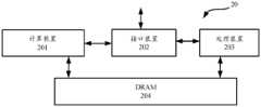
- Fig. 1shows the structural diagram of the board card of the disclosed embodiment
- FIG. 2shows a structural diagram of a combination processing device according to an embodiment of the present disclosure
- FIG. 3shows a schematic diagram of the internal structure of a processor core of a single-core or multi-core computing device according to an embodiment of the disclosure
- FIG. 4shows an example of an exemplary convolution operation principle to which embodiments of the present disclosure can be applied
- Fig. 5shows a schematic structural block diagram of a computing device according to an embodiment of the disclosure
- Figures 6a-6cshow several examples of data width dimension folding according to embodiments of the present disclosure
- Fig. 7schematically shows a schematic storage manner of an input feature map according to some embodiments of the present disclosure
- Fig. 8shows a schematic diagram of a convolution kernel storage method according to an embodiment of the present disclosure
- Fig. 9shows an exemplary loop schematic diagram of calculating a single convolution output point according to an embodiment of the present disclosure
- Fig. 10shows a schematic diagram of operation of multiplexing input feature map data in H dimension according to some embodiments of the present disclosure
- Fig. 11shows a schematic splitting manner of an output feature map according to an embodiment of the present disclosure
- Fig. 13shows a schematic diagram of writing and outputting operation results according to an embodiment of the present disclosure.
- the term “if”may be interpreted as “when” or “once” or “in response to determining” or “in response to detecting” depending on the context.
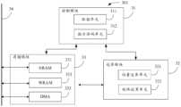
- FIG. 1shows a schematic structural diagram of a board 10 according to an embodiment of the present disclosure.
- the board card 10includes a chip 101, which is a system-on-chip (System on Chip, SoC), or system-on-chip, integrated with one or more combination processing devices, and the combination processing device is an artificial
- SoCSystem on Chip
- the intelligent computing unitis used to support various deep learning and machine learning algorithms to meet the intelligent processing requirements in complex scenarios in the fields of computer vision, speech, natural language processing, and data mining.
- deep learning technologyis widely used in the field of cloud intelligence.
- a notable feature of cloud intelligence applicationsis the large amount of input data, which has high requirements for the storage capacity and computing power of the platform.
- the board 10 of this embodimentis suitable for cloud intelligence applications. applications, with huge off-chip storage, on-chip storage and powerful computing capabilities.
- the chip 101is connected to an external device 103 through an external interface device 102 .
- the external device 103is, for example, a server, a computer, a camera, a display, a mouse, a keyboard, a network card or a wifi interface, and the like.
- the data to be processedcan be transmitted to the chip 101 by the external device 103 through the external interface device 102 .
- the calculation result of the chip 101can be sent back to the external device 103 via the external interface device 102 .
- the external interface device 102may have different interface forms, such as a PCIe interface and the like.
- the board 10also includes a storage device 104 for storing data, which includes one or more storage units 105 .
- the storage device 104is connected and data transmitted with the control device 106 and the chip 101 through the bus.
- the control device 106 in the board 10is configured to regulate the state of the chip 101 .
- the control device 106may include a microcontroller (Micro Controller Unit, MCU).
- FIG. 2is a block diagram showing the combined processing means in the chip 101 of this embodiment.
- the combined processing device 20includes a computing device 201 , an interface device 202 , a processing device 203 and a storage device 204 .
- the computing device 201is configured to perform operations specified by the user, and is mainly implemented as a single-core intelligent processor or a multi-core intelligent processor for performing deep learning or machine learning calculations, which can interact with the processing device 203 through the interface device 202 to Work together to complete user-specified operations.
- the interface device 202is used to transmit data and control instructions between the computing device 201 and the processing device 203 .
- the computing device 201may obtain input data from the processing device 203 via the interface device 202 and write it into a storage device on the computing device 201 .
- the computing device 201may obtain control instructions from the processing device 203 via the interface device 202 and write them into the control cache on the chip of the computing device 201 .
- the interface device 202can also read data in the storage device of the computing device 201 and transmit it to the processing device 203 .
- the processing device 203performs basic control including but not limited to data transfer, starting and/or stopping the computing device 201 .
- the processing device 203may be one or more types of a central processing unit (central processing unit, CPU), a graphics processing unit (graphics processing unit, GPU) or other general-purpose and/or special-purpose processors.
- processorsincluding but not limited to digital signal processors (digital signal processors, DSPs), application specific integrated circuits (application specific integrated circuits, ASICs), field-programmable gate arrays (field-programmable gate arrays, FPGAs) or other Programmable logic devices, discrete gate or transistor logic devices, discrete hardware components, etc., and the number thereof can be determined according to actual needs.
- the computing device 201 of the present disclosurecan be regarded as having a single-core structure or a homogeneous multi-core structure. However, when considering the integration of the computing device 201 and the processing device 203 together, they are considered to form a heterogeneous multi-core structure.
- the storage device 204is used to store data to be processed, which may be a DRAM, which is a DDR memory, and its size is usually 16G or larger, and is used to store data of the computing device 201 and/or the processing device 203 .
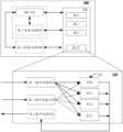
- FIG. 3shows a schematic diagram of the internal structure of a processing core when the computing device 201 is a single-core or multi-core device.
- the computing device 301is used to process input data such as computer vision, speech, natural language, data mining, etc.
- the computing device 301includes three modules: a control module 31 , a computing module 32 and a storage module 33 .
- the control module 31is used to coordinate and control the work of the operation module 32 and the storage module 33 to complete the task of deep learning, which includes an instruction fetch unit (IFU) 311 and an instruction decoding unit (instruction decode unit, IDU) 312.
- the instruction fetching unit 311is used to obtain instructions from the processing device 203, and the instruction decoding unit 312 decodes the obtained instructions, and sends the decoding results to the computing module 32 and the storage module 33 as control information.
- the operation module 32includes a vector operation unit 321 and a matrix operation unit 322 .
- the vector operation unit 321is used to perform vector operations, and can support complex operations such as vector multiplication, addition, and nonlinear transformation;
- the matrix operation unit 322is responsible for the core calculation of the deep learning algorithm, namely matrix multiplication and convolution.
- the storage module 33is used to store or transfer relevant data, including a neuron storage unit (neuron RAM, NRAM) 331, a weight storage unit (weight RAM, WRAM) 332, and a direct memory access module (direct memory access, DMA) 333.
- NRAM 331is used to store input neurons, output neurons and calculated intermediate results;
- WRAM 332is used to store convolution kernels of deep learning networks, that is, weights;
- DMA 333is connected to DRAM 204 through bus 34, responsible for computing device 301 Data transfer between DRAM 204 and DRAM 204.
- an embodiment of the present disclosureprovides a computing device configured to perform a convolution operation, so that the convolution operation in a neural network model, for example, can be optimized.
- the convolutional layer in a neural network modelcan perform convolution operations by applying convolution kernels (also called filters, weights, etc.) to input feature maps (also called input data, neurons, or input neurons) processing for feature extraction.
- the convolution layercan contain multiple convolution kernels, and each element that makes up the convolution kernel corresponds to a weight coefficient and a bias.
- the neural network modelmay contain various convolution operation layers, such as convolution layers that perform forward and conventional 3D convolution operations, and deconvolution layers that perform depthwise convolution operations. In reverse training, it may be necessary to perform reverse depthwise convolution operations or cross-product convolution operations.
- the disclosed embodimentsare mainly optimized for conventional 3D convolution operations, and may also be applied to other types of convolution operations if there is no conflict.
- Xis the input data
- Yis the output data
- Kis the convolution kernel
- Kh and Kware the length and width of K
- sh and sware the strides in the length and width directions
- the formulaignores Bias, fill pad and dilation, and assume that the input data X has been filled, and the convolution kernel has been expanded.
- the formulaignores the N dimension and the C dimension.
- the forward calculation of the neural network modelis independent in the N dimension and fully connected in the C dimension.
- the results of the multiplication of the H, W, and Ci directionsare accumulated, so it is called 3D convolution.
- the Ci dimension of the convolution kernelis equal to the Ci dimension of the input feature map, so the convolution kernel does not slide in the Ci direction, which is a pseudo 3D convolution.
- the above convolution operationis referred to as a 3D convolution operation.
- Fig. 4shows an example of an exemplary conventional 3D convolution operation principle to which embodiments of the present disclosure can be applied.
- the figureexemplarily shows four-dimensional input data X with a size of [N Hi Wi Ci], which can be expressed as N three-dimensional rectangles 410 of size Hi ⁇ Wi ⁇ Ci.
- the figurealso exemplarily shows a four-dimensional convolution kernel K with a size of [Co Kh Kw Ci], which can be expressed as Co three-dimensional convolution kernels 420 of size Kh ⁇ Kw ⁇ Ci.
- the convolution result of the input data X and the convolution kernel Kobtains the output data Y, which is four-dimensional data of the size [N Ho Wo Co], which can be expressed as N three-dimensional rectangles 430 of the size Ho ⁇ Wo ⁇ Co.
- the figurealso specifically shows an example of convolution operation, in which the input data is an input feature map 440 with a size of 6 ⁇ 6 ⁇ 3, and the N dimension is omitted; the convolution kernel is a three-dimensional convolution kernel 450 with a size of 3 ⁇ 3 ⁇ 3 , for a single Co; the output data is a 4 ⁇ 4 output feature map 460 .
- the specific operation processis as follows:
- the convolution kernel 450scans the input feature map 440a according to a certain step size, performs matrix element multiplication and summation on the input features in the convolution window 470, and superimposes the deviation. That is, the value at each position in the output feature map 460 is obtained by performing a two-dimensional convolution operation on the corresponding block and the corresponding convolution kernel of each input feature map and then summing them up. For example, the figure shows that the value of the (0,0) position on the output feature map 460 (that is, the convolution output point) is two-dimensionally performed by the convolution window 470 framed by the black cube in the input feature map and the three-dimensional convolution kernel 450. The three-dimensional convolution operation obtains 3 values, which are summed to obtain the final value.
- the position of the convolution kernel 450can be moved on the input feature map 440 , that is, the convolution window of the convolution output point can be moved.
- the convolution step size (Sx, Sy)is (1,1).
- the convolution operationcan be obtained respectively
- the value at (0,1) or (1,0) position on the feature map 460ais output.
- a convolutional layer of the neural networkthere are N groups of input feature maps, and each group contains Hi ⁇ Wi ⁇ Ci information, where Hi and Wi are the height and width of the input feature map, and Ci is The number of input feature maps, also known as the number of input channels.
- the convolutional layerhas Ci ⁇ Co convolution kernels of Kh ⁇ Kw size, where Ci is the number of input channels, Co is the number of output feature maps (or the number of output channels), Kh and Kw are the height and width.
- the output feature mapcontains Ho ⁇ Wo ⁇ Co pieces of information, where Ho and Wo are the height and width of the output feature map, respectively, and Co is the number of output channels.
- the convolution step sizeSx, Sy
- the size of the convolution step sizewill affect the size of the output feature map.
- input feature map(Feature map), input data, neuron or input neuron are used interchangeably; convolution kernel, filter or weight are used interchangeably; output feature map, output data or output neuron Can be used interchangeably.
- H (height) and Y dimensionsare used interchangeably, and the W (width) and X dimensions are used interchangeably.
- the H dimension of the input feature mapcan be expressed as Hi or Yi
- the H dimension of the output feature mapcan be expressed as Ho or Yo
- the W dimensioncan be expressed similarly.
- each convolution output pointhas a corresponding convolution window, and the shape of the convolution window is equal to the shape of the convolution kernel. The value of each convolution output point corresponds to the result of the multiplication and accumulation of the input feature map and the weight in its convolution window.
- a computing device with a master-slave structuremay be used to implement the above convolution operation.
- different data pathscan be configured for input feature maps and convolution kernels, thereby improving memory access efficiency.
- FIG. 5shows a schematic structural block diagram of a computing device 500 according to an embodiment of the disclosure. It can be understood that this structure can be regarded as the refinement of the internal structure of the operation module of a single processing core in FIG. 3 , or can be regarded as a functional division block diagram based on the combination of multiple operation modules of the processing core shown in FIG. 3 .
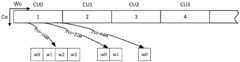
- a computing device 500 in an embodiment of the present disclosuremay be configured to perform various types of convolution operations, which may include a master processing circuit (MA) 510 and a plurality of slave processing circuits (SL) 520, shown in the figure 16 slave processing circuits SL0 to SL15 are shown.
- MAmaster processing circuit
- SLslave processing circuits
- the master processing circuit and the slave processing circuits, as well as multiple slave processing circuits,can communicate with each other through various connections.
- the connection between multiple slave processing circuitscan be hard-wired, or logically configured according to, for example, micro-instructions to form a variety of slave processing circuits
- the topology of the arrayEmbodiments of the present disclosure are not limited in this regard.
- the main processing circuit and the slave processing circuitcan cooperate with each other, thereby realizing parallel operation processing.
- the main processing circuit and the slave processing circuitmay include various calculation circuits, for example, may include a vector operation unit and a matrix operation unit.
- the vector operation unitis used to perform vector operations, and can support complex operations such as vector multiplication, addition, and nonlinear transformation;
- the matrix operation unitis responsible for the core calculations of deep learning algorithms, such as matrix multiplication and convolution.
- the slave processing circuitcan be used to perform intermediate operations on corresponding data in parallel according to the operation instruction to obtain multiple intermediate results, and transmit the multiple intermediate results back to the main processing circuit.
- the computing device 500By setting the computing device 500 as a master-slave structure (such as a master-multiple-slave structure, or a multi-master-multi-slave structure, the present disclosure is not limited in this respect), for the calculation instructions of the forward operation, the data can be disassembled according to the calculation instructions. In this way, multiple slave processing circuits are used to perform parallel calculations on the part with a large amount of calculation to improve the calculation speed, save calculation time, and reduce power consumption.
- a master-slave structuresuch as a master-multiple-slave structure, or a multi-master-multi-slave structure, the present disclosure is not limited in this respect
- multiple multiplexing methods of input feature maps and weightscan be supported, thereby reducing the amount of data access during operations and improving processing efficiency .
- the computing device 500may further include a first storage circuit 530 and a second storage circuit 540 for respectively storing data transmitted via different data channels.
- the first storage circuit 530 and the second storage circuit 540may be two storage blocks formed by dividing the same memory, or may be two independent memories, which are not specifically limited here.
- the first storage circuit 530can be used to store multicast data, that is, the data in the first storage circuit will be transmitted to multiple slave processing circuits through the broadcast bus, and these slave processing circuits receive the same data. It can be understood that broadcasting and multicasting can be implemented through the broadcasting bus. Multicast refers to a communication method that transmits a piece of data to multiple slave processing circuits; broadcasting is a communication method that transmits a piece of data to all slave processing circuits, which is a special case of multicast. Since both multicast and broadcast correspond to a one-to-many transmission mode, there is no special distinction between the two in this document. Broadcast and multicast can be collectively referred to as multicast, and those skilled in the art can clarify their meanings according to the context.
- the second storage circuit 540may be used to store and distribute data, that is, the data in the second storage circuit will be transmitted to different slave processing circuits respectively, and each slave processing circuit receives different data.
- the input feature mapmay be determined as multicast data and stored in the first storage circuit, so as to broadcast the data to a plurality of scheduled slave processing circuits during operation.
- the convolution kernelmay be determined as distributed data and stored in the second storage circuit. These distributed data can be distributed to corresponding slave processing circuits before operation.
- FIG. 5also shows a schematic diagram of the internal structure of the slave processing circuit SL according to an embodiment of the present disclosure.
- each slave processing circuit 520may include a plurality of operation circuits CU 521, a first buffer circuit 522 and a second buffer circuit 523.
- four arithmetic circuits CU0 to CU3are shown.
- the number of computing circuitsmay be more or less depending on specific hardware configurations, and the embodiments of the present disclosure are not limited in this respect.
- the first buffer circuit 522may be used for buffering weights or input feature maps assigned to the slave processing circuit.
- the second buffer circuit 523may be used for buffering the input feature map or the weight assigned to the slave processing circuit. These two buffer circuits are used to select the data involved in the operation.
- the data of the first buffer circuit 522can be a plurality of data rows from, for example, the first storage circuit 530 or the second storage circuit 540, and correspondingly, the data of the second buffer circuit 523 can come from, for example, the second storage circuit 540 or the first storage circuit 540 Multiple data rows of circuit 530. Depending on the specific multiplexing method, these data rows can be distributed to the corresponding computing circuit CU 521 or broadcast to all CUs 521 in the slave processing circuit 520 during the operation.
- Each operation circuit CU521is used to perform bitwise multiply-accumulate operations on the data rows selected from the first buffer circuit and the data rows selected from the second buffer circuit in each operation cycle.
- the slave processing circuit 520may also include a third buffer circuit 524 for buffering the calculation results of each calculation circuit CU 521.
- each processing circuit and storage circuitare shown as separate modules in FIG. 5 , according to different configurations, the storage circuit and the processing circuit may also be combined into one module.
- the first storage circuit 530can be combined with the main processing circuit 510
- the second storage circuit 540can be shared by multiple slave processing circuits 520, and an independent storage area is assigned to each slave processing circuit to speed up access.
- Embodiments of the present disclosureare not limited in this regard.
- the main processing circuit and the slave processing circuitmay belong to different modules of the same processor or chip, or may belong to different processors, and the present disclosure is not limited in this respect.
- the dimensions of the involved multidimensional dataare represented by (N, H, W, C) or (Co, H, W, Ci), which represent the storage order of the data in the memory.
- N, H, W, Cthe dimensions of the involved multidimensional data
- Co, H, W, Cithe storage order of the data in the memory.
- Multidimensional datais usually allocated in continuous storage space, that is, multidimensional data can be expanded in one dimension and stored in the memory in sequence.
- the input feature mapsmay be stored sequentially in a low-dimensional (where C/Ci is the lowest dimension) priority manner.
- Adjacent dimensionsrefer to dimensions that are next to each other in the dimensional information representation of multidimensional data, for example, W and Ci are adjacent.
- W and Ciare adjacent, and their data is also continuous on the memory.
- the main computing unit of the hardwareis a vector multiply-accumulate operator.
- Implementing support for various convolution algorithms in hardware designis essentially to maximize the multiplication and addition operations in the algorithm, and implement them between the on-chip RAM (such as NRAM, WRAM, etc. in Figure 3) and the arithmetic unit through the data path. efficiently exchange the input and output data of the multiply-accumulate operation.
- Hardwareis stored line by line (cache line).
- the read, write, and calculation operationsare most efficient when the entire line is aligned. Therefore, in order to make full use of the bandwidth and adapt to the memory access requirements of the arithmetic unit array, it is usually necessary to
- the datais vectorized and aligned.
- the design of artificial intelligence chipsusually takes the Ci dimension as the lowest dimension, that is, the above-mentioned NHWC arrangement order, and the data on the Ci dimension is continuous. Therefore, vectorization alignment requires that the size of the Ci dimension be aligned to a specified value, such as the alignment value M, so that the number of accesses is performed in units of the alignment value M, and M can also be called the maximum single operation of the hardware.
- Mcan have different values, such as 64bit, 128bit, 256bit, 512bit, etc.
- the size of the input port of the operator arrayis also related to M.
- the input port size of the operator arrayis usually twice the size of M, that is, the input of the alignment value M scale is processed at one time.
- Feature map data and weight dataWhen the Ci dimension of the input feature map is large, it is easier to meet the above alignment requirements.
- the Ci dimension of the input feature mapis small or when the remainder obtained by dividing Ci and M is small, such as less than the size of a cache line, the Ci dimension needs to be filled to one line of data (for example, 512 bits), that is, the padding is invalid Data 0. This filling will cause a large number of redundant calculations, resulting in waste of resources and reducing the efficiency of operations.
- a small convolution scheme suitable for the case of a small channel Cis proposed, in which the operation data is split according to the split unit and the dimension order is converted and stored.
- the amount of data contained in a split unitcan be set as the one-time processing alignment value M of the hardware, so that the calculation and processing can be performed in units of split units, which can give full play to the computing power of the hardware and avoid or reduce invalid calculations.
- both the input feature map and the convolution kernelneed to be pre-blocked and dimensionally converted by software, and the output feature map also needs to be correspondingly block and dimensionally converted by software.
- Increased software complexityIn addition, software is required for alignment during these chunking and dimension conversion processes. Further, these small convolution schemes only support convolution operations with convolution steps of 1 in both width and height directions.
- the embodiment of the present disclosureprovides a convolution scheme of width dimension folding, which only uses the width continuous with the input channel Ci dimension of the input feature map when needed The data in the W dimension is compensated to the Ci dimension, eliminating the need for software to perform data block and dimension conversion processing.
- the folding multiple, Mis the amount of data processed by the hardware at a time; the second buffer circuit is used to buffer the weight data to be performed convolution operation;
- the input feature row selected in and the extended weight row selected or generated from the second buffer circuitperform a bitwise multiplication and accumulation operation, and one of the extended weight rows is split or aligned by the convolution kernel in the Ci dimension according to Pci to A column of data blocks of Pci is copied and expanded into a column of Ws.
- the output data of the upper layer of some convolutional layershas been divided into two segments in the Ci dimension, and the ci size of each segment is 32B (for example, the data type is int8) or 64B (for example, the data type is int16).
- the split granularity Pcimay follow the size of each segment, that is, 32B or 64B.
- the input channel splitting granularity Pcican be determined according to the size of the input channel dimension Ci of the input feature map and the amount of data M processed by the hardware at a time; then the width of the input feature map can be determined according to the splitting granularity Pci The folding multiple Ws of the W dimension.
- WsM/Pci.
- the convolution solution in the embodiment of the present disclosuremay be suitable for any Ci dimension by splitting the Ci dimension according to the split granularity.
- the maximum split granularity Pcidoes not exceed the one-time processing alignment value M of the hardware (or referred to as the benchmark alignment value, the amount of data processed by the hardware at a time). Therefore, under different value ranges of Ci, an appropriate Pci can be selected, and the alignment requirement on the Ci dimension can be reduced by filling data in the adjacent W dimension into the Ci dimension.
- split granularitycan theoretically be M/2 n , considering factors such as the requirements for the W dimension, instruction overhead, and the actual value range of Ci when the split granularity is too small, you can only choose M/2 n A partial value of is used as an alternative split granularity.
- alternative split granularitiesmay include, for example, 64B, 32B, 16B, and 8B.
- the input channel splitting granularity Pcimay be selected as follows:
- the amount of alignment paddingis the same, a larger split granularity is preferred; or when the amount of alignment padding is different, the split granularity with the smallest amount of alignment padding is selected; or when the amount of alignment padding is not much different (such as Within a predetermined range, such as not exceeding 16B), a larger split granularity is preferred.
- the larger split granularity among the split granularities without zero paddingmay be preferably used as Pci, that is, 16B.
- aligning to 8Brequires filling 7B of zeros, and aligning to 16B, 32B, and 64B requires filling 15B of zeros.
- the difference in alignment paddingis only 8B, which is within an acceptable range, so a larger split granularity of 64B can be preferred.
- the data included in each of the three data rowsis shown in a rounded rectangle frame, and the 3 here may also be referred to as the number of split blocks on the Ci dimension.
- the main processing circuit 510 in FIG. 5can determine the input feature map as multicast data and store it in the first storage circuit 530, so as to transmit the data by broadcasting during operation.
- Multiple slave processing circuits for schedulingFrom the width folding scheme described above, it can be known that since WC is a continuous dimension, the format of the input data does not need to be divided into blocks and dimension conversion processing, and the original input data format HWC can be directly received. Therefore, in the first storage circuit 530, the input feature map can be stored therein in an original format (eg, HWC).
- an original formateg, HWC
- the aforementioned alignment processmay be performed when the input feature map is read from the first storage circuit 530 and broadcast to multiple slave processing circuits. That is, during the transmission process from the first storage circuit to the buffer circuit (for example, the first buffer circuit) in the processing circuit, the main processing circuit 510 can control the alignment processing of the Ci dimension to align to the determined input channel Split the granularity Pci, and then fold the corresponding amount of Wi-dimensional data to form a data row, and use a data row as the smallest granularity to broadcast and transmit to the slave processing circuit.
- the input feature mapis the output data of the previous layer, which has been split into two segments in the Ci dimension, so the data format can be [2, hi, wi, 32B] or [2, hi, wi, 64B].
- Fig. 7schematically shows a schematic storage manner of an input feature map according to some embodiments of the present disclosure.
- the input feature mapcan be divided into two segments according to Ci, and the first address interval of the two segments is Ci_seg.stride: the size of each segment ci is 32B or 64B.
- Ci_seg.stridethe size of each segment ci is 32B or 64B.
- the Co value assigned to each slave processing circuit for processingmay be determined.
- each round of operationprocesses a Co value for each slave processing circuit.
- the operationcan be completed in multiple rounds.
- the input feature map datacan be further multiplexed in the H dimension, thereby further reducing the amount of memory access.
- some storage circuitsonly support reading in order of address from small to large when reading data, in order to facilitate reading the corresponding weight data in the H dimension, it is necessary to store the data in the H dimension upside down . This will be described in detail later in conjunction with the convolution operation process.
- the convolution kernelcan be determined as distributed data and stored in the second storage circuit 540, so as to be distributed to or read by the corresponding slave processing circuit before operation.
- the second storage circuit 540can be shared by a plurality of (such as Ns) from the processing circuit 520, and for each from the processing circuit is allocated an independent storage area, so that each data required for computing from the processing circuit only needs to be obtained from its corresponding The storage area can be read to speed up the memory access speed.
- the convolution kernelis divided and stored according to the Co dimension, the convolution kernel corresponding to the Co value allocated to a certain slave processing circuit may be stored in a corresponding storage area of the second storage circuit.
- the divided storage on the Co dimensiondoes not need to perform dimension conversion and other processing, and directly stores the convolution kernel data corresponding to the Co value in the original format (such as KhKwCi) on the second storage circuit That's it.
- Fig. 8shows a schematic diagram of a convolution kernel storage method according to an embodiment of the present disclosure.
- the Co dimension of the convolution kernelis 8, so 8 slave processing circuits are scheduled to perform operations.
- Each storage areastores the convolution kernel corresponding to the Co value to be processed by the slave processing circuit.
- consecutive Co valuesare assigned to the 8 SLs sequentially (ie, in units of interval 1) one by one.
- each storage areait is stored in an inverted manner in the H direction, that is, the convolution kernel is stored in the order of the index from large to small on the height dimension Kh, so that it is convenient to load the convolution kernel to the second When it is on the buffer circuit, it can be read in order of address from small to large.
- the convolution kernel of each Co valuealso performs a similar split alignment process in the Ci dimension.
- the convolution kernelhas been split into two segments in the Ci dimension, so it is similarly segmented and stored.
- Ci splitting and alignment processingmay be performed as required. That is, during the transmission process from the second storage circuit to the buffer circuit (such as the second buffer circuit) in the processing circuit, the alignment process of the Ci dimension of the convolution kernel can be performed to align to the previously determined input channel splitting process. Sub-granularity Pci. Unlike the input feature map, the convolution kernel does not need to fold in the W dimension, but performs corresponding copy expansion according to the folding multiple Ws, which can be seen in the description of the subsequent convolution operation process.
- each slave processing circuitcan perform convolution operation on the input feature map and the corresponding data of the convolution kernel , and then the main processing circuit can splice and process multiple operation results returned from the processing circuit according to the convolution width folding scheme, so as to obtain the input feature map and the output feature map of the convolution operation of the convolution kernel.
- multiple computing circuits CU and buffer circuitsin the slave processing circuit can be used to perform a specific convolution operation process.
- multiple computing cyclesare generally required to complete the required computing in each round of computing.
- the first buffer circuitcan be used to cache the input feature map from the first storage circuit; correspondingly, the second buffer circuit can be used to cache the convolution kernel from the second storage circuit, that is, the weight data .
- Each operation circuit CUcan, in each operation cycle, for the data rows selected from the first buffer circuit (for example, the input feature row) and the data rows selected from the second buffer circuit (for example, some weight rows or Extended weight row) performs a bit-wise multiply-accumulate operation.
- the following descriptionfocuses on the processing of a Co value in a single slave processing circuit SL, and it can be understood that similar processing is performed in other SLs.
- each convolution output point on the output feature mapcorresponds to the result of the multiplication and accumulation of the input feature map and the weight in its convolution window. That is, the value of a single output point is accumulated by the bitwise multiplication of the individual parts.
- FIG. 9shows an exemplary loop diagram for computing a single convolution output point according to an embodiment of the present disclosure.
- the figureshows the various parts and components of the first output point on the output feature map.
- Each data pointis represented by the coordinates ⁇ h, w> of its height and width dimensions, and the size of each data point in the ci direction is Pci.
- the input feature row and the extended weight value roware synchronously selected in the width dimension to calculate different parts of the same output point and .
- Kmaxcan be determined as follows:
- L1is the size of the first buffer circuit, and the unit is a data row; Ncu is the number of scheduled operation circuits, and Ws is a folding multiple of the width dimension.
- Ncuis the number of scheduled operation circuits
- Wsis a folding multiple of the width dimension.
- select the input feature data point ⁇ 0,0> and the weight data point ⁇ 0,0>to perform bitwise multiplication and accumulation to obtain the first part of the sum
- slide 1 stepto the right synchronously to select the input feature
- the data point ⁇ 0,1> and the weight data point ⁇ 0,1>perform bitwise multiplication and accumulation to obtain the second part of the sum. It can be seen that both the first partial sum and the second partial sum belong to the partial sum of the first output point ⁇ 0,0>.
- the cycleis performed according to the number of segments Bci split by Pci according to the Ci dimension.
- the product results on the Ci dimensionalso need to be accumulated. Therefore, both the third partial sum and the fourth partial sum belong to the partial sum of the first output point ⁇ 0,0>.
- the third part sumis essentially the sum of the first part sum and the second part sum obtained by the inner loop.
- the fourth partand is also similar.
- the fifth partial sum, the sixth partial sum and the seventh partial sumall belong to the partial sum of the first output point ⁇ 0,0>. It can also be understood that the fifth part sum is essentially the sum of the third part sum and the fourth part sum obtained by the middle cycle. The sixth and seventh parts are also similar. Since the data of the Kh dimension is not subjected to any dimensional folding or splitting, the convolution scheme of the embodiment of the present disclosure can support a convolution step size of any value on the Kh dimension.
- the input feature map datacan be further multiplexed in the H dimension, thereby further reducing the amount of memory access.
- the input feature lines selected each timecan be multiplexed rn times, respectively, and the rn extended weight lines corresponding to the convolution kernel in the height dimension are subjected to bitwise multiplication and accumulation operations, so as to obtain the output feature map in the height dimension Consecutive rn output blocks, where rn is determined according to the height dimension Kh of the convolution kernel and the convolution step Sy in the height direction of the convolution operation.
- Fig. 10shows a schematic diagram of operations for multiplexing input feature map data in the H dimension according to some embodiments of the present disclosure.
- the parameter configuration for this exampleis similar to Figure 9.
- the number of input feature map multiplexes in the H dimensiondepends on the maximum number of overlaps of adjacent convolution windows in the H dimension.
- multiple computing circuits CU in a single slave processing circuitcan calculate and output feature maps in parallel.
- Ncu output blocksare sequentially divided on the Wo dimension, so that Ncu operation circuits can perform parallel operations respectively, each The output block corresponds to the operation result of one input feature data row.
- Ncu adjacent input feature linesare sequentially selected from the first buffer circuit and distributed to Ncu operation circuits, and a corresponding extended weight data line is selected or generated from the second buffer circuit, and broadcast to Ncu operation circuits, so as to realize the parallel calculation of Ncu output blocks by multiplexing the weight data.
- Fig. 11shows a schematic splitting manner of an output feature map according to an embodiment of the present disclosure.
- Fig. 11only shows the splitting of the output feature map for one Co value in the Wo dimension.
- the output block calculated by a single operation circuit CUmay include different numbers of output points. Specifically, according to the previously determined folding factor Ws in the width dimension, each output block includes Ws output points that are continuous in the width Wo dimension.
- a data rowincludes 4 Wi, and the output points on 4 Wo dimensions can be calculated;
- a data rowincludes 2 Wi, and two output points on the Wo dimension can be calculated;
- a data rowincludes 1 Wi, and 1 can be calculated;
- Fig. 11further shows different configurations of a single output block in the above three cases, including 4, 2 or 1 Wo output points respectively.
- the corresponding weight datacan be constructed as follows: after distributing the convolution kernel in the second storage circuit to When the second buffer circuit of each slave processing circuit, in addition to aligning the Ci dimension of the convolution kernel to Pci, it also splits or aligns a column Ci of Pci in the Ci dimension according to Pci according to the folding multiple Ws of the width dimension. The data is replicated and expanded into Ws columns to form an extended weight data row, which is stored in the second buffer circuit. That is, the shape of one extended weight data row is Ws*Pci, which may correspond to one input feature data row.
- one extended weight data rowcan be selected from the second buffer circuit and broadcast to N CU arithmetic circuits in the slave processing circuit.
- the above-mentioned copying and expanding process of the weight datacan also be performed on the data path from the second buffer circuit to the operation circuit, and the processing method is similar, which will not be described in detail here.
- the first layeris between the operation circuits CU, and the weight is broadcast to Ncu operation circuits, so the number of multiplexing is Ncu; the second layer is each operation circuit Between one or more Wo output points in CU, the weight is extended to calculate Ws output points in each CU, so the number of times of multiplexing is Ws. Therefore, by multiplexing data as much as possible, frequent data access and memory access can be effectively reduced.
- the output points on itcan be split as follows: split the output feature map into (Ws*Ncu)*Ho size regions according to the width dimension Block, calculate the output points block by block, where Ncu is the number of schedulable computing circuits in the slave processing circuit, Ho is the height dimension of the output feature map; for each block, according to the first width dimension, then the height dimension The sequence calculation output circuit.
- the slave processing circuitWhen the slave processing circuit writes the calculation results of the calculation circuits, it can store the calculation results of each calculation circuit in the third buffer circuit of FIG. 5 in the order of Wo dimension first and Ho dimension later.
- the slave processing circuitWhen the slave processing circuit outputs the output points of its internal arithmetic circuit, it can output the output points calculated by its multiple arithmetic circuits in a specific order according to the division method of the output points, so as to facilitate subsequent processing.
- each slave processing circuitprocesses convolution kernels for different output channel Co values, and can output the operation results of each operation circuit in turn in the order of the width dimension Wo first and the height dimension Ho later.
- the main processing circuit in the computing devicecan concatenate and store the operation results output from each slave processing circuit according to the HoWoCo dimensional storage order according to the order of co values.
- Ncu*Ws output points on the Wo dimension of the output feature mapare calculated each time, that is, the output points will be aligned to Ncu*Ws, so there may be redundant calculation output points. On the data path for storing operation results, these redundant output points on the Wo dimension can be filtered out.
- height and width dimension coordinates ⁇ h, w>are used to represent each data point, and the size of each data point in the Ci dimension is Pci, which is 32B in this example.
- the data lineis sent to the operation circuit CU1
- the data line composed of the input feature points ⁇ 0,4> and ⁇ 0,5>is selected, and sent to the operation circuit CU2
- the data line formedis sent to the operation circuit CU3 (the number of choices is shown by a black dotted line box in the figure).
- the inner loop of the Kw dimensionends, that is, the partial sums in the Kw direction have been calculated.
- the outer loopcan be performed, that is, adding 1 to the H dimension.
- slide one step in the direction of Wi from the first buffer circuitto select the corresponding four input feature lines (for clarity, the data in the first buffer circuit is repeatedly drawn in the figure, and shown in a slightly smaller gray dashed box selection), and send them to 4 arithmetic circuits respectively.
- multiplexing in the H dimensionis also inserted.
- the inner loop of the Kw dimensionends, that is, the partial sums in the Kw direction have been calculated.
- the input feature line of each operation circuitis still kept unchanged, and the data point ⁇ 0,0> (that is, "A0 ”), the expanded weight row A0A0 is broadcast to four computing circuits.
- the input feature line of each operation circuitis still kept unchanged, and the data point ⁇ 0,1> (that is, "B0 ”) to expand the extended weight row B0B0, and broadcast to the four computing circuits.
- the inner loop of the Kw dimensionends, that is, the partial sums in the Kw direction have been calculated.
- each computing circuitcan accumulate the final convolution results of ho*Ws 4 output points.
- the four computing circuits in one slave processing circuitobtain ho*(Ws*4) output points on the same Co.
- the 8 slave processing circuitsobtain 8 ho*(Ws*4) output points on Co in total.
- Fig. 13shows a schematic diagram of writing and outputting operation results according to an embodiment of the present disclosure.
- multiple computing circuits CU in a single slave processing circuit SLcan sequentially write computing results into the result buffer circuit (such as the third buffer circuit in FIG. 5 ) according to the computing order.
- the output points of the same Co calculated by each CUmay be first written in the order of Wo (writing cycle 1).
- the read-out ordercan be consistent with the write-in order, that is, the Wo dimension first, and then the Ho dimension. More specifically, reading may be performed sequentially from the result buffer circuits of each slave processing circuit in order of Co at first, and the results of each CU are read out in order of Wo during reading. For example, first read out the two output points w0 and w1 calculated by each CU0 in the eight SLs, then the two output points w2 and w3 calculated by each CU1, then w4 and w5 calculated by CU2, and finally w6 and w5 calculated by CU3 w7 (reading cycle 1). Next, in order of Ho, the output points on each Ho are read (read loop 2). The right view in Figure 13 shows the readout results. Note that when reading in Co order, read in turn on the result buffer circuits of the 8 SLs, so that the Co dimension is continuous, for example, from 0 to 7 .
- An embodiment of the present disclosurealso provides a chip, which may include the data processing device in any embodiment described above with reference to the accompanying drawings. Further, the present disclosure also provides a board, which may include the aforementioned chip.
- the electronic equipment or devices disclosed in this disclosuremay include servers, cloud servers, server clusters, data processing devices, robots, computers, printers, scanners, tablet computers, smart terminals, PC equipment, Internet of Things terminals, mobile Terminals, mobile phones, driving recorders, navigators, sensors, cameras, cameras, video cameras, projectors, watches, earphones, mobile storage, wearable devices, visual terminals, automatic driving terminals, vehicles, household appliances, and/or medical equipment.
- Said vehiclesinclude airplanes, ships and/or vehicles;
- said household appliancesinclude televisions, air conditioners, microwave ovens, refrigerators, rice cookers, humidifiers, washing machines, electric lights, gas stoves, range hoods;
- said medical equipmentincludes nuclear magnetic resonance instruments, Ultrasound and/or electrocardiograph.
- the electronic equipment or device disclosed hereincan also be applied to fields such as the Internet, the Internet of Things, data centers, energy, transportation, public management, manufacturing, education, power grids, telecommunications, finance, retail, construction sites, and medical treatment. Further, the electronic device or device disclosed herein can also be used in application scenarios related to artificial intelligence, big data and/or cloud computing, such as cloud, edge, and terminal.
- electronic devices or devices with high computing power according to the disclosed solutionscan be applied to cloud devices (such as cloud servers), while electronic devices or devices with low power consumption can be applied to terminal devices and/or Edge devices (such as smartphones or cameras).
- the hardware information of the cloud device and the hardware information of the terminal device and/or the edge deviceare compatible with each other, so that according to the hardware information of the terminal device and/or the edge device, the hardware resources of the cloud device can be Match appropriate hardware resources to simulate the hardware resources of terminal devices and/or edge devices, so as to complete the unified management, scheduling and collaborative work of device-cloud integration or cloud-edge-end integration.
- the present disclosureexpresses some methods and their embodiments as a series of actions and combinations thereof, but those skilled in the art can understand that the solution of the present disclosure is not limited by the order of the described actions . Therefore, according to the disclosure or teaching of the present disclosure, those skilled in the art may understand that certain steps may be performed in other orders or simultaneously. Further, those skilled in the art can understand that the embodiments described in the present disclosure can be regarded as optional embodiments, that is, the actions or modules involved therein are not necessarily required for the realization of one or some solutions of the present disclosure. In addition, according to different schemes, the description of some embodiments in this disclosure also has different emphases. In view of this, those skilled in the art may understand the part that is not described in detail in a certain embodiment of the present disclosure, and may also refer to related descriptions of other embodiments.
- a unit described as a separate componentmay or may not be physically separated, and a component shown as a unit may or may not be a physical unit.
- the aforementioned components or unitsmay be located at the same location or distributed over multiple network units.
- some or all of the unitsmay be selected to achieve the purpose of the solutions described in the embodiments of the present disclosure.
- multiple units in the embodiments of the present disclosuremay be integrated into one unit, or each unit exists physically independently.
- the above-mentioned integrated unitsmay also be implemented in the form of hardware, that is, specific hardware circuits, which may include digital circuits and/or analog circuits.
- the physical realization of the hardware structure of the circuitmay include but not limited to physical devices, and the physical devices may include but not limited to devices such as transistors or memristors.
- various devicessuch as computing devices or other processing devices described herein may be implemented by appropriate hardware processors, such as central processing units, GPUs, FPGAs, DSPs, and ASICs.
- the aforementioned storage unit or storage devicecan be any suitable storage medium (including magnetic storage medium or magneto-optical storage medium, etc.), which can be, for example, a variable resistance memory (Resistive Random Access Memory, RRAM), dynamic Random Access Memory (Dynamic Random Access Memory, DRAM), Static Random Access Memory (Static Random Access Memory, SRAM), Enhanced Dynamic Random Access Memory (Enhanced Dynamic Random Access Memory, EDRAM), High Bandwidth Memory (High Bandwidth Memory , HBM), hybrid memory cube (Hybrid Memory Cube, HMC), ROM and RAM, etc.
- RRAMvariable resistance memory
- DRAMDynamic Random Access Memory
- SRAMStatic Random Access Memory
- EDRAMEnhanced Dynamic Random Access Memory
- High Bandwidth MemoryHigh Bandwidth Memory
- HBMHigh Bandwidth Memory
- HMCHybrid Memory Cube
- ROM and RAMetc.
- a computing devicecomprising a plurality of slave processing circuits, each slave processing circuit comprising a first buffer circuit, a second buffer circuit, and a plurality of arithmetic circuits, wherein:
- the second buffer circuitis used to buffer the weight data to be performed convolution operation.
- Each of the operation circuitsis configured to perform alignment on the input feature row selected from the first buffer circuit and the extended weight row selected or generated from the second buffer circuit at each calculation.
- Multiply-accumulate operationwherein an extended weight row is formed by the convolution kernel splitting according to Pci in the Ci dimension or copying and expanding a column of data blocks aligned to Pci into a Ws column.
- each said arithmetic circuitis further configured to:
- the selected input feature linesare multiplexed rn times, and the corresponding rn extended weight lines of the convolution kernel in the height dimension are respectively subjected to bitwise multiplication and accumulation operations to obtain rn output blocks that are continuous in the height dimension of the output feature map , where rn is determined according to the height dimension Kh of the convolution kernel and the convolution step Sy in the height direction of the convolution operation.
- Clause 3The computing device according to Clause 2, further comprising a weight storage circuit for storing the convolution kernel, wherein the convolution kernel is stored in descending order of indexes in the height dimension, so that in When loading into the second buffer circuit, the addresses are read in ascending order of addresses.
- Clause 4The computing device according to any one of Clauses 2-3, wherein for a single output point in the output feature map, the operation circuit calculates the value of the output point in the following order, multi-layer loop, wherein:
- each said slave processing circuitis further configured to:
- the input feature line and the extended weight value lineare synchronously selected in the width dimension to calculate different partial sums of the same output point, and the number of selection times is Nkw.
- Clause 6The computing device according to Clause 5, wherein in each sliding number selection calculation, each of the operation circuits performs the multiplexing rn times for a selected input feature row.
- each of said slave processing circuitscomputes an output point thereon as follows:
- the output feature mapis split into blocks of (Ws*Ncu)*Ho size according to the width dimension, and the output points are calculated block by block, wherein Ncu is the number of schedulable computing circuits in the slave processing circuit, and Ho is The height dimension of the output feature map;
- the output circuitis calculated in the order of the width dimension first, and then the height dimension.
- each of said slave processing circuitscomputes an output point in the width dimension as follows:
- Ncu output blocks that are continuous in the width dimension of the output feature mapare calculated in parallel by using Ncu operation circuits that can be scheduled, and each output block includes Ws output points that are continuous in the width dimension.
- each said slave processing circuitis further configured to:
- each of said slave processing circuitscomputes an output point thereon in the height dimension as follows:
- each operation circuitby multiplexing rn input feature rows, the partial sums of rn output blocks continuous in the height dimension of the output feature map are sequentially calculated, and each output block includes Ws continuous in the width dimension output point.
- Each of the slave processing circuitsis used to process convolution kernels for different output channels co, and output the operation results of each operation circuit in turn in the order of the width dimension Wo first and the height dimension Ho later;
- the calculation deviceis further configured to: concatenate and store the operation results output from each slave processing circuit according to the HoWoCo dimension storage order according to the order of co values.
- Clause 12A chip comprising the computing device according to any one of clauses 1-11.
- Clause 14A method of performing a convolution operation using the computing device of any one of clauses 1-11.
Landscapes
- Engineering & Computer Science (AREA)
- Physics & Mathematics (AREA)
- Theoretical Computer Science (AREA)
- General Physics & Mathematics (AREA)
- Mathematical Physics (AREA)
- Data Mining & Analysis (AREA)
- General Engineering & Computer Science (AREA)
- Software Systems (AREA)
- Computing Systems (AREA)
- Pure & Applied Mathematics (AREA)
- Mathematical Optimization (AREA)
- Mathematical Analysis (AREA)
- Computational Mathematics (AREA)
- Life Sciences & Earth Sciences (AREA)
- Molecular Biology (AREA)
- General Health & Medical Sciences (AREA)
- Evolutionary Computation (AREA)
- Computational Linguistics (AREA)
- Biophysics (AREA)
- Biomedical Technology (AREA)
- Artificial Intelligence (AREA)
- Health & Medical Sciences (AREA)
- Algebra (AREA)
- Databases & Information Systems (AREA)
- Complex Calculations (AREA)
Abstract
Description
Translated fromChinese相关申请的交叉引用Cross References to Related Applications
本公开要求于2021年11月19日申请的、申请号为202111401514.4、发明名称为“执行卷积运算的计算装置、方法及相关产品”的中国专利申请的优先权。This disclosure claims the priority of the Chinese patent application filed on November 19, 2021 with the application number 202111401514.4 and the title of the invention is "Computing device, method and related products for performing convolution operation".
本披露一般地涉及数据处理领域。更具体地,本披露涉及一种计算装置、利用该计算装置执行卷积运算的方法、芯片和板卡。The present disclosure relates generally to the field of data processing. More specifically, the present disclosure relates to a computing device, a method for performing a convolution operation using the computing device, a chip and a board.
目前,深度学习(Deep Learning)已经成为机器学习中的重要分支,也大力助推着人工智能(AI)的发展。深度学习的核心技术——深度神经网络(DNN)已在诸多行业有着广泛的应用。At present, deep learning (Deep Learning) has become an important branch of machine learning, and it is also vigorously promoting the development of artificial intelligence (AI). The core technology of deep learning - deep neural network (DNN) has been widely used in many industries.
神经网络是人工智能、深度学习中最为关键的技术之一,其中卷积神经网络(Convolution Neural Network,CNN)是最为重要的一种网络类型。卷积神经网络中最为关键的计算即为卷积层(Conv layer)的卷积运算(Convolution Operation)。卷积层的功能是对输入数据进行特征提取,通过多层卷积,能够抽取复杂特征,以保证网络具有足够的表达能力和泛化能力。神经网络模型中包含了大量的、各种类型的卷积运算,卷积运算的计算性能极大地影响整个神经网络模型的计算性能。当神经网络模型应用于不同领域时,例如语音识别、机器翻译、图像处理等等,其对应的输入特征图和权值的各个维度大小可能各有不同。为了充分利用深度学习处理器的硬件优势,需要针对不同规模的、和/或不同类型的卷积运算进行优化,以提高执行神经网络模型的计算性能。Neural network is one of the most critical technologies in artificial intelligence and deep learning, among which Convolution Neural Network (CNN) is the most important network type. The most critical calculation in the convolutional neural network is the convolution operation (Convolution Operation) of the convolution layer (Conv layer). The function of the convolutional layer is to extract features from the input data. Through multi-layer convolution, complex features can be extracted to ensure that the network has sufficient expressive ability and generalization ability. The neural network model contains a large number of various types of convolution operations, and the computing performance of the convolution operation greatly affects the computing performance of the entire neural network model. When the neural network model is applied in different fields, such as speech recognition, machine translation, image processing, etc., the corresponding input feature maps and weights may have different dimensions. In order to take full advantage of the hardware advantages of deep learning processors, it is necessary to optimize for different scales and/or different types of convolution operations to improve the computational performance of executing neural network models.
发明内容Contents of the invention
为了至少解决如上所提到的一个或多个技术问题,本披露在多个方面中提出了一种计算装置,其通过对输入特征图的宽度维度进行折叠处理,可以使得各种维度尺寸的数据能够适配卷积运算的硬件,从而提高卷积运算的计算效率。本披露实施例的卷积运算可以是各种神经网络模型中的运算,这些神经网络模型可以应用于各种领域,诸如图像处理、语音处理、文本处理等等,这些处理例如可以包括但不限于识别和分类。In order to at least solve one or more technical problems mentioned above, this disclosure proposes a computing device in various aspects, which can make data of various dimensions by folding the width dimension of the input feature map It can adapt to the hardware of convolution operation, so as to improve the computational efficiency of convolution operation. The convolution operation in the embodiment of the present disclosure can be an operation in various neural network models, and these neural network models can be applied in various fields, such as image processing, speech processing, text processing, etc., such processing can include but not limited to identification and classification.
在第一方面中,本披露实施例提供了一种计算装置,包括多个从处理电路,每个从处理电路包括第一缓冲电路、第二缓冲电路和多个运算电路,其中:所述第一缓冲电路用于缓存将要执行卷积运算的多个输入特征行,其中一个输入特征行包括输入特征图中Pci×Ws=M的数据量,其中Pci为输入通道Ci维度的拆分粒度,Ws为宽度W维度的折叠倍数,M是硬件单次处理数据量;所述第二缓冲电路用于缓存将要执行卷积运算的权值数据;以及每个所述运算电路用于在每次计算时,针对分别从所述第一缓冲电路中选取的输入特征行和从所述第二缓冲电路中选取的或生成的扩展权值行执行对位乘累加运算,其中一个扩展权值行由卷积核在Ci维度上按照Pci拆分或对齐到Pci的一列数据块复制扩展成Ws列而构成。In a first aspect, an embodiment of the present disclosure provides a computing device, including a plurality of slave processing circuits, each slave processing circuit includes a first buffer circuit, a second buffer circuit, and a plurality of arithmetic circuits, wherein: the first A buffer circuit is used to cache a plurality of input feature lines that will perform convolution operations, wherein one input feature line includes the data volume of Pci×Ws=M in the input feature map, where Pci is the split granularity of the input channel Ci dimension, Ws It is the folding multiple of the width W dimension, and M is the amount of data processed by the hardware at a time; the second buffer circuit is used to cache the weight data that will perform the convolution operation; and each of the operation circuits is used for each calculation. , performing a bitwise multiply-accumulate operation on the input feature row selected from the first buffer circuit and the extended weight value row selected or generated from the second buffer circuit, wherein one extended weight value row is obtained by convolution In the Ci dimension, the core is split according to Pci or a column of data blocks aligned to Pci is copied and expanded into Ws columns.
在第二方面中,本披露实施例提供了一种芯片,其包括前述第一方面的计算装置。In a second aspect, an embodiment of the present disclosure provides a chip, which includes the computing device in the aforementioned first aspect.
在第三方面中,本披露实施例提供了一种板卡,其包括前述第二方面的芯片。In a third aspect, an embodiment of the present disclosure provides a board, which includes the aforementioned chip in the second aspect.
根据如上所提供的计算装置、芯片、板卡以及由计算装置实施卷积运算的方法,本披露实施例的方案针对不同维度尺寸的输入特征图应用不同的宽度维度折叠方案,以适应硬件运算装置的处理能力,从而充分利用多个从处理电路的并行处理能力,可以有效提高卷积运算的运算效率。 进一步地,可以基于低于一个权值行的粒度来复用权值,从而减少频繁的数据加载,提升计算效率。其他的优势和效果从后面结合附图的详细描述中将变得易于理解。According to the computing device, the chip, the board and the method for implementing the convolution operation by the computing device as provided above, the solutions of the embodiments of the present disclosure apply different width and dimension folding schemes to the input feature maps of different dimensions, so as to adapt to the hardware computing device The processing capability of multiple slave processing circuits can be fully utilized to effectively improve the operational efficiency of the convolution operation. Furthermore, weights can be reused based on a granularity lower than one weight row, thereby reducing frequent data loading and improving computing efficiency. Other advantages and effects will become easy to understand from the following detailed description in conjunction with the accompanying drawings.
通过参考附图阅读下文的详细描述,本公开示例性实施方式的上述以及其他目的、特征和优点将变得易于理解。在附图中,以示例性而非限制性的方式示出了本公开的若干实施方式,并且相同或对应的标号表示相同或对应的部分,其中:The above and other objects, features and advantages of exemplary embodiments of the present disclosure will become readily understood by reading the following detailed description with reference to the accompanying drawings. In the drawings, several embodiments of the present disclosure are shown by way of illustration and not limitation, and the same or corresponding reference numerals indicate the same or corresponding parts, wherein:
图1示出本披露实施例的板卡的结构图;Fig. 1 shows the structural diagram of the board card of the disclosed embodiment;
图2示出本披露实施例的组合处理装置的结构图;FIG. 2 shows a structural diagram of a combination processing device according to an embodiment of the present disclosure;
图3示出本披露实施例的单核或多核计算装置的处理器核的内部结构示意图;FIG. 3 shows a schematic diagram of the internal structure of a processor core of a single-core or multi-core computing device according to an embodiment of the disclosure;
图4示出可以应用本披露实施例的示例性卷积运算原理示例;FIG. 4 shows an example of an exemplary convolution operation principle to which embodiments of the present disclosure can be applied;
图5示出了根据本披露实施例的计算装置的示意性结构框图;Fig. 5 shows a schematic structural block diagram of a computing device according to an embodiment of the disclosure;
图6a-图6c示出了根据本披露实施例的几种数据宽度维度折叠示例;Figures 6a-6c show several examples of data width dimension folding according to embodiments of the present disclosure;
图7示意性示出了根据本披露一些实施例的输入特征图的示意性存储方式;Fig. 7 schematically shows a schematic storage manner of an input feature map according to some embodiments of the present disclosure;
图8示出了根据本披露实施例的卷积核存储方式示意图;Fig. 8 shows a schematic diagram of a convolution kernel storage method according to an embodiment of the present disclosure;
图9示出了根据本披露实施例的计算单个卷积输出点的示例性循环示意图;Fig. 9 shows an exemplary loop schematic diagram of calculating a single convolution output point according to an embodiment of the present disclosure;
图10示出了根据本披露一些实施例的H维度上复用输入特征图数据的运算示意图;Fig. 10 shows a schematic diagram of operation of multiplexing input feature map data in H dimension according to some embodiments of the present disclosure;
图11示出了根据本披露实施例的输出特征图的示意性拆分方式;Fig. 11 shows a schematic splitting manner of an output feature map according to an embodiment of the present disclosure;
图12a-图12c示出根据本披露实施例的卷积运算方案的运算过程示意图;以及12a-12c show a schematic diagram of an operation process of a convolution operation scheme according to an embodiment of the present disclosure; and
图13示出了根据本披露实施例的运算结果的写入和输出逻辑示意图。Fig. 13 shows a schematic diagram of writing and outputting operation results according to an embodiment of the present disclosure.
下面将结合本披露实施例中的附图,对本披露实施例中的技术方案进行清楚、完整地描述,显然,所描述的实施例是本披露一部分实施例,而不是全部的实施例。基于本披露中的实施例,本领域技术人员在没有做出创造性劳动前提下所获得的所有其他实施例,都属于本披露保护的范围。The following will clearly and completely describe the technical solutions in the embodiments of the present disclosure with reference to the drawings in the embodiments of the present disclosure. Obviously, the described embodiments are part of the embodiments of the present disclosure, not all of them. Based on the embodiments in the present disclosure, all other embodiments obtained by those skilled in the art without creative efforts fall within the protection scope of the present disclosure.
应当理解,本披露的权利要求、说明书及附图中可能出现的术语“第一”、“第二”、“第三”和“第四”等是用于区别不同对象,而不是用于描述特定顺序。本披露的说明书和权利要求书中使用的术语“包括”和“包含”指示所描述特征、整体、步骤、操作、元素和/或组件的存在,但并不排除一个或多个其它特征、整体、步骤、操作、元素、组件和/或其集合的存在或添加。It should be understood that the terms "first", "second", "third" and "fourth" that may appear in the claims, specification and drawings of the present disclosure are used to distinguish different objects, rather than to describe specific order. The terms "comprising" and "comprises" used in the specification and claims of this disclosure indicate the presence of described features, integers, steps, operations, elements and/or components, but do not exclude one or more other features, integers , steps, operations, elements, components, and/or the presence or addition of collections thereof.
还应当理解,在本披露说明书中所使用的术语仅仅是出于描述特定实施例的目的,而并不意在限定本披露。如在本披露说明书和权利要求书中所使用的那样,除非上下文清楚地指明其它情况,否则单数形式的“一”、“一个”及“该”意在包括复数形式。还应当进一步理解,在本披露说明书和权利要求书中使用的术语“和/或”是指相关联列出的项中的一个或多个的任何组合以及所有可能组合,并且包括这些组合。It should also be understood that the terminology used in the present disclosure is only for the purpose of describing specific embodiments, and is not intended to limit the present disclosure. As used in this disclosure and the claims, the singular forms "a", "an" and "the" are intended to include plural referents unless the context clearly dictates otherwise. It should also be further understood that the term "and/or" used in the present disclosure and the claims refers to any combination and all possible combinations of one or more of the associated listed items, and includes these combinations.
如在本说明书和权利要求书中所使用的那样,术语“如果”可以依据上下文被解释为“当...时”或“一旦”或“响应于确定”或“响应于检测到”。As used in this specification and claims, the term "if" may be interpreted as "when" or "once" or "in response to determining" or "in response to detecting" depending on the context.
示例性硬件环境Exemplary hardware environment
图1示出本披露实施例的一种板卡10的结构示意图。如图1所示,板卡10包括芯片101,其是一种系统级芯片(System on Chip,SoC),或称片上系统,集成有一个或多个组合处理装置, 组合处理装置是一种人工智能运算单元,用以支持各类深度学习和机器学习算法,满足计算机视觉、语音、自然语言处理、数据挖掘等领域复杂场景下的智能处理需求。特别是深度学习技术大量应用在云端智能领域,云端智能应用的一个显著特点是输入数据量大,对平台的存储能力和计算能力有很高的要求,此实施例的板卡10适用在云端智能应用,具有庞大的片外存储、片上存储和强大的计算能力。FIG. 1 shows a schematic structural diagram of a board 10 according to an embodiment of the present disclosure. As shown in Figure 1, the board card 10 includes a
芯片101通过对外接口装置102与外部设备103相连接。外部设备103例如是服务器、计算机、摄像头、显示器、鼠标、键盘、网卡或wifi接口等。待处理的数据可以由外部设备103通过对外接口装置102传递至芯片101。芯片101的计算结果可以经由对外接口装置102传送回外部设备103。根据不同的应用场景,对外接口装置102可以具有不同的接口形式,例如PCIe接口等。The
板卡10还包括用于存储数据的存储器件104,其包括一个或多个存储单元105。存储器件104通过总线与控制器件106和芯片101进行连接和数据传输。板卡10中的控制器件106配置用于对芯片101的状态进行调控。为此,在一个应用场景中,控制器件106可以包括单片机(Micro Controller Unit,MCU)。The board 10 also includes a storage device 104 for storing data, which includes one or
图2是示出此实施例的芯片101中的组合处理装置的结构图。如图2中所示,组合处理装置20包括计算装置201、接口装置202、处理装置203和存储装置204。FIG. 2 is a block diagram showing the combined processing means in the
计算装置201配置成执行用户指定的操作,主要实现为单核智能处理器或者多核智能处理器,用以执行深度学习或机器学习的计算,其可以通过接口装置202与处理装置203进行交互,以共同完成用户指定的操作。The
接口装置202用于在计算装置201与处理装置203间传输数据和控制指令。例如,计算装置201可以经由接口装置202从处理装置203中获取输入数据,写入计算装置201片上的存储装置。进一步,计算装置201可以经由接口装置202从处理装置203中获取控制指令,写入计算装置201片上的控制缓存中。替代地或可选地,接口装置202也可以读取计算装置201的存储装置中的数据并传输给处理装置203。The
处理装置203作为通用的处理装置,执行包括但不限于数据搬运、对计算装置201的开启和/或停止等基本控制。根据实现方式的不同,处理装置203可以是中央处理器(central processing unit,CPU)、图形处理器(graphics processing unit,GPU)或其他通用和/或专用处理器中的一种或多种类型的处理器,这些处理器包括但不限于数字信号处理器(digital signal processor,DSP)、专用集成电路(application specific integrated circuit,ASIC)、现场可编程门阵列(field-programmable gate array,FPGA)或者其他可编程逻辑器件、分立门或者晶体管逻辑器件、分立硬件组件等,并且其数目可以根据实际需要来确定。如前所述,仅就本披露的计算装置201而言,其可以视为具有单核结构或者同构多核结构。然而,当将计算装置201和处理装置203整合共同考虑时,二者视为形成异构多核结构。As a general processing device, the
存储装置204用以存储待处理的数据,其可以是DRAM,为DDR内存,大小通常为16G或更大,用于保存计算装置201和/或处理装置203的数据。The
图3示出了计算装置201为单核或多核装置时处理核的内部结构示意图。计算装置301用以处理计算机视觉、语音、自然语言、数据挖掘等输入数据,计算装置301包括三大模块:控制模块31、运算模块32及存储模块33。FIG. 3 shows a schematic diagram of the internal structure of a processing core when the
控制模块31用以协调并控制运算模块32和存储模块33的工作,以完成深度学习的任务,其包括取指单元(instruction fetch unit,IFU)311及指令译码单元(instruction decode unit,IDU)312。取指单元311用以获取来自处理装置203的指令,指令译码单元312则将获取的指令进行 译码,并将译码结果作为控制信息发送给运算模块32和存储模块33。The
运算模块32包括向量运算单元321及矩阵运算单元322。向量运算单元321用以执行向量运算,可支持向量乘、加、非线性变换等复杂运算;矩阵运算单元322负责深度学习算法的核心计算,即矩阵乘及卷积。The
存储模块33用来存储或搬运相关数据,包括神经元存储单元(neuron RAM,NRAM)331、权值存储单元(weight RAM,WRAM)332、直接内存访问模块(direct memory access,DMA)333。NRAM 331用以存储输入神经元、输出神经元和计算后的中间结果;WRAM 332则用以存储深度学习网络的卷积核,即权值;DMA 333通过总线34连接DRAM 204,负责计算装置301与DRAM 204间的数据搬运。The
示例性卷积运算类型Exemplary Convolution Operation Types
基于前述硬件环境,在一个方面中,本披露实施例提供了一种计算装置,其配置用于执行卷积运算,从而可以对例如神经网络模型中的卷积运算进行优化。神经网络模型中的卷积层可以执行卷积运算,通过对输入特征图(也称为输入数据、神经元或输入神经元)应用卷积核(也称为过滤器、权值等)做卷积处理,从而进行特征提取。卷积层内部可以包含多个卷积核,组成卷积核的每个元素对应一个权重系数和一个偏差量bias。Based on the aforementioned hardware environment, in one aspect, an embodiment of the present disclosure provides a computing device configured to perform a convolution operation, so that the convolution operation in a neural network model, for example, can be optimized. The convolutional layer in a neural network model can perform convolution operations by applying convolution kernels (also called filters, weights, etc.) to input feature maps (also called input data, neurons, or input neurons) processing for feature extraction. The convolution layer can contain multiple convolution kernels, and each element that makes up the convolution kernel corresponds to a weight coefficient and a bias.
神经网络模型中可能包含各种卷积运算层,例如执行正向、常规3D卷积运算的卷积层、执行深度(Depthwise)卷积运算的反卷积层。而在反向训练中,可能需要执行反向的深度卷积运算或叉乘卷积运算。本披露实施例主要针对常规3D卷积运算进行优化,在不冲突的情况下,也可以应用于其他类型的卷积运算。The neural network model may contain various convolution operation layers, such as convolution layers that perform forward and conventional 3D convolution operations, and deconvolution layers that perform depthwise convolution operations. In reverse training, it may be necessary to perform reverse depthwise convolution operations or cross-product convolution operations. The disclosed embodiments are mainly optimized for conventional 3D convolution operations, and may also be applied to other types of convolution operations if there is no conflict.
在常规3D卷积运算中,假设卷积层中输入特征图(Feature map)张量形状表示为X[N Hi Wi Ci],卷积核(kernel)的张量形状表示为K[Co Kh Kw Ci],输出的结果为Y[N Ho Wo Co],那么,简化的卷积运算的数学计算公式可以表示如下:In the conventional 3D convolution operation, it is assumed that the input feature map (Feature map) tensor shape in the convolution layer is expressed as X[N Hi Wi Ci], and the tensor shape of the convolution kernel (kernel) is expressed as K[Co Kh Kw Ci], the output result is Y[N Ho Wo Co], then, the mathematical calculation formula of the simplified convolution operation can be expressed as follows:
Yin,jc,jh,jw=∑0≤ic≤ci,0≤ih≤kh,0≤iw≤kwXin,ic,jh×sh+ih,jw×sw+iw×Kjc,ic,ih,iw (1)Yin,jc,jh,jw =∑0≤ic≤ci,0≤ih≤kh,0≤iw≤kw Xin,ic,jh×sh+ih,jw×sw+iw ×Kjc,ic,ih ,iw (1)
上式中,X是输入数据,Y是输出数据,K是卷积核,Kh和Kw是K的长和宽,sh和sw是在长和宽方向上的步长(stride),公式忽略了偏差量bias,填充pad和膨胀dilation,并且假设输入数据X已经做了填充,卷积核已经做了膨胀。公式忽略了N维度和C维度,神经网络模型的正向计算在N维度上的计算都是独立的,在C维度上是全连接的。卷积核在工作时,会按照一定的步长扫过输入特征,在卷积窗口内对输入特征做矩阵元素乘法求和并叠加偏差量。在常规3D卷积运算中,H、W和Ci方向的对位乘积结果会进行累加,因此称为3D卷积。但是这种3D卷积存在约束条件:卷积核的Ci维度大小和输入特征图的Ci维度大小相等,因此卷积核不在Ci方向滑动,是一种伪3D卷积。为了简单起见,上述卷积运算称为3D卷积运算。In the above formula, X is the input data, Y is the output data, K is the convolution kernel, Kh and Kw are the length and width of K, sh and sw are the strides in the length and width directions, and the formula ignores Bias, fill pad and dilation, and assume that the input data X has been filled, and the convolution kernel has been expanded. The formula ignores the N dimension and the C dimension. The forward calculation of the neural network model is independent in the N dimension and fully connected in the C dimension. When the convolution kernel is working, it will scan the input features according to a certain step size, perform matrix element multiplication and summation on the input features in the convolution window, and superimpose the deviation. In the conventional 3D convolution operation, the results of the multiplication of the H, W, and Ci directions are accumulated, so it is called 3D convolution. However, there are constraints in this 3D convolution: the Ci dimension of the convolution kernel is equal to the Ci dimension of the input feature map, so the convolution kernel does not slide in the Ci direction, which is a pseudo 3D convolution. For simplicity, the above convolution operation is referred to as a 3D convolution operation.
图4示出了可以应用本披露实施例的示例性常规3D卷积运算原理示例。Fig. 4 shows an example of an exemplary conventional 3D convolution operation principle to which embodiments of the present disclosure can be applied.
图中示例性示出了大小为[N Hi Wi Ci]的四维输入数据X,其可以表示成N个Hi×Wi×Ci大小的立体矩形410。图中还示例性示出了大小为[Co Kh Kw Ci]的四维卷积核K,其可以表示成Co个Kh×Kw×Ci大小的立体卷积核420。输入数据X与卷积核K的卷积结果得到输出数据Y,其为[N Ho Wo Co]大小的四维数据,可以表示成N个Ho×Wo×Co大小的立体矩形430。The figure exemplarily shows four-dimensional input data X with a size of [N Hi Wi Ci], which can be expressed as N three-
图中还具体示出了一个卷积运算示例,其中输入数据为6×6×3大小的输入特征图440,省去N维度;卷积核为3×3×3大小的立体卷积核450,针对单个Co;输出数据为4×4的输出特征图460。具体运算过程如下:The figure also specifically shows an example of convolution operation, in which the input data is an
卷积核450按照一定的步长扫过输入特征图440a,在卷积窗口470内对输入特征做矩阵元素乘法求和并叠加偏差量。也即,输出特征图460中每个位置上的值由每个输入特征图的对应区块和对应卷积核做二维卷积运算之后再加和得到。例如,图中示出了输出特征图460上(0,0)位置的值(也即卷积输出点)由输入特征图中黑色立方体框出的卷积窗口470与立体卷积核450进行二维卷积运算得到3个值,再加和得到最终值。The
为了得到其他位置的输出,可以在输入特征图440上移动卷积核450的位置,也即移动卷积输出点的卷积窗口。在图中示例中,卷积步长(Sx,Sy)为(1,1),当横向(宽度方向)向右或纵向(高度方向)向下移动一格后做卷积运算,可以分别得到输出特征图460a上(0,1)或(1,0)位置的值。In order to obtain outputs at other positions, the position of the
从上面的描述可知,在神经网络的一个卷积层中,有N组输入特征图,每组包含Hi×Wi×Ci个信息,其中Hi和Wi分别是输入特征图的高度和宽度,Ci是输入特征图的个数,也称为输入通道数。卷积层有Ci×Co个Kh×Kw大小的卷积核,其中Ci是输入通道数,Co是输出特征图的个数(或输出通道数),Kh和Kw分别是卷积核的高度和宽度。输出特征图包含Ho×Wo×Co个信息,其中Ho和Wo分别是输出特征图的高度和宽度,Co是输出通道数。此外,在卷积运算中,还会涉及到卷积步长(Sx,Sy),卷积步长的大小会影响输出特征图的尺寸。As can be seen from the above description, in a convolutional layer of the neural network, there are N groups of input feature maps, and each group contains Hi×Wi×Ci information, where Hi and Wi are the height and width of the input feature map, and Ci is The number of input feature maps, also known as the number of input channels. The convolutional layer has Ci×Co convolution kernels of Kh×Kw size, where Ci is the number of input channels, Co is the number of output feature maps (or the number of output channels), Kh and Kw are the height and width. The output feature map contains Ho×Wo×Co pieces of information, where Ho and Wo are the height and width of the output feature map, respectively, and Co is the number of output channels. In addition, in the convolution operation, the convolution step size (Sx, Sy) is also involved, and the size of the convolution step size will affect the size of the output feature map.
在本文中,输入特征图(Feature map)、输入数据、神经元或输入神经元可互换使用;卷积核、过滤器或权值可互换使用;输出特征图、输出数据或输出神经元可互换使用。此外,H(高度)和Y维度可互换使用,W(宽度)和X维度可互换使用。相应地,输入特征图的H维度可以表示为Hi或Yi,输出特征图的H维度可以表示为Ho或Yo,W维度类似表示。在本披露实施例中,每个卷积输出点具有对应的卷积窗口,卷积窗口的形状等于卷积核的形状。每个卷积输出点的值对应于其卷积窗口内的输入特征图与权值的对位乘累加结果。In this paper, input feature map (Feature map), input data, neuron or input neuron are used interchangeably; convolution kernel, filter or weight are used interchangeably; output feature map, output data or output neuron Can be used interchangeably. Also, the H (height) and Y dimensions are used interchangeably, and the W (width) and X dimensions are used interchangeably. Correspondingly, the H dimension of the input feature map can be expressed as Hi or Yi, the H dimension of the output feature map can be expressed as Ho or Yo, and the W dimension can be expressed similarly. In the disclosed embodiment, each convolution output point has a corresponding convolution window, and the shape of the convolution window is equal to the shape of the convolution kernel. The value of each convolution output point corresponds to the result of the multiplication and accumulation of the input feature map and the weight in its convolution window.
示例性计算装置Exemplary Computing Device
在本披露实施例中,可以采用主从结构的计算装置来实施上述卷积运算。进一步地,可以为输入特征图和卷积核配置不同的数据通路,从而提高访存效率。In the embodiments of the present disclosure, a computing device with a master-slave structure may be used to implement the above convolution operation. Furthermore, different data paths can be configured for input feature maps and convolution kernels, thereby improving memory access efficiency.
图5示出了根据本披露实施例的计算装置500的示意性结构框图。可以理解,该结构可以视为图3中单个处理核的运算模块的内部结构细化,也可以视为在多个图3所示处理核的运算模块基础上联合的功能划分框图。如图5所示,本披露实施例的计算装置500可以配置用于执行各种类型的卷积运算,其可以包括主处理电路(MA)510和多个从处理电路(SL)520,图中示出了16个从处理电路SL0~SL15。本领域技术人员可以理解,从处理电路的数量可以更多或更少,取决于具体的硬件配置,本披露实施例在此方面没有限制。FIG. 5 shows a schematic structural block diagram of a
主处理电路和从处理电路之间以及多个从处理电路之间可以通过各种连接相互通信。在不同的应用场景中,多个从处理电路之间的连接方式既可以是通过硬线布置的硬连接方式,也可以是根据例如微指令进行配置的逻辑连接方式,以形成多种从处理电路阵列的拓扑结构。本披露实施例在此方面没有限制。主处理电路和从处理电路可以相互配合,由此实现并行运算处理。The master processing circuit and the slave processing circuits, as well as multiple slave processing circuits, can communicate with each other through various connections. In different application scenarios, the connection between multiple slave processing circuits can be hard-wired, or logically configured according to, for example, micro-instructions to form a variety of slave processing circuits The topology of the array. Embodiments of the present disclosure are not limited in this regard. The main processing circuit and the slave processing circuit can cooperate with each other, thereby realizing parallel operation processing.
为了支持运算功能,主处理电路和从处理电路可以包括各种计算电路,例如可以包括向量运算单元及矩阵运算单元。向量运算单元用以执行向量运算,可支持向量乘、加、非线性变换等复杂运算;矩阵运算单元负责深度学习算法的核心计算,例如矩阵乘和卷积。In order to support calculation functions, the main processing circuit and the slave processing circuit may include various calculation circuits, for example, may include a vector operation unit and a matrix operation unit. The vector operation unit is used to perform vector operations, and can support complex operations such as vector multiplication, addition, and nonlinear transformation; the matrix operation unit is responsible for the core calculations of deep learning algorithms, such as matrix multiplication and convolution.
从处理电路例如可以用于根据运算指令,对相应的数据并行执行中间运算得到多个中间结果,并将多个中间结果传输回主处理电路。For example, the slave processing circuit can be used to perform intermediate operations on corresponding data in parallel according to the operation instruction to obtain multiple intermediate results, and transmit the multiple intermediate results back to the main processing circuit.
通过将计算装置500设置成主从结构(例如一主多从结构,或者多主多从结构,本披露在此方面没有限制),对于正向运算的计算指令,可以根据计算指令将数据进行拆分,从而通过多个从处理电路对计算量较大的部分进行并行运算以提高运算速度,节省运算时间,进而降低功耗。By setting the
在本披露一些实施例中,通过利用不同的数据通路传输输入特征图和权值,可以支持输入特征图和权值的多种复用方式,从而减小运算期间的数据访存量,提升处理效率。In some embodiments of the present disclosure, by using different data paths to transmit input feature maps and weights, multiple multiplexing methods of input feature maps and weights can be supported, thereby reducing the amount of data access during operations and improving processing efficiency .
具体地,计算装置500中还可以包括第一存储电路530和第二存储电路540,用于分别存储经由不同数据通道传输的数据。可选地,该第一存储电路530和第二存储电路540可以是同一存储器划分形成的两个存储块,也可以是两个独立的存储器,此处不做具体限定。Specifically, the
第一存储电路530可以用于存储多播数据,也即第一存储电路中的数据将通过广播总线传输给多个从处理电路,这些从处理电路接收到相同的数据。可以理解,通过广播总线可以实现广播和多播。多播是指将一份数据传输到多个从处理电路的通信方式;而广播是将一份数据传输到所有从处理电路的通信方式,是多播的一个特例。由于多播和广播都对应一对多的传输方式,本文中未对二者特意区分,广播和多播可以统称为多播,本领域技术人员根据上下文可以明确其含义。The first storage circuit 530 can be used to store multicast data, that is, the data in the first storage circuit will be transmitted to multiple slave processing circuits through the broadcast bus, and these slave processing circuits receive the same data. It can be understood that broadcasting and multicasting can be implemented through the broadcasting bus. Multicast refers to a communication method that transmits a piece of data to multiple slave processing circuits; broadcasting is a communication method that transmits a piece of data to all slave processing circuits, which is a special case of multicast. Since both multicast and broadcast correspond to a one-to-many transmission mode, there is no special distinction between the two in this document. Broadcast and multicast can be collectively referred to as multicast, and those skilled in the art can clarify their meanings according to the context.
第二存储电路540可以用于存储分发数据,也即第二存储电路中的数据将分别传输给不同的从处理电路,每个从处理电路接收到不同的数据。The second storage circuit 540 may be used to store and distribute data, that is, the data in the second storage circuit will be transmitted to different slave processing circuits respectively, and each slave processing circuit receives different data.
通过分别提供第一存储电路和第二存储电路,可以支持针对待运算的数据以不同传输方式进行传输,从而通过在多个从处理电路之间复用多播数据来降低数据访存量。By separately providing the first storage circuit and the second storage circuit, different transmission modes can be supported for the data to be calculated, thereby reducing the amount of data access by multiplexing multicast data among multiple slave processing circuits.
在一些实施例中,可以将输入特征图确定为多播数据并存储在第一存储电路中,以在运算期间通过广播方式将数据传输给调度的多个从处理电路。对应地,可以将卷积核确定为分发数据并存储在第二存储电路中。这些分发数据可以在运算前分发给对应的从处理电路。In some embodiments, the input feature map may be determined as multicast data and stored in the first storage circuit, so as to broadcast the data to a plurality of scheduled slave processing circuits during operation. Correspondingly, the convolution kernel may be determined as distributed data and stored in the second storage circuit. These distributed data can be distributed to corresponding slave processing circuits before operation.
图5还示出了根据本披露实施例的从处理电路SL的内部结构示意图。如图所示,每个从处理电路520可以包括多个运算电路CU 521、第一缓冲电路522和第二缓冲电路523。图中示出了4个运算电路CU0~CU3。本领域技术人员可以理解,运算电路的数量可以更多或更少,取决于具体的硬件配置,本披露实施例在此方面没有限制。FIG. 5 also shows a schematic diagram of the internal structure of the slave processing circuit SL according to an embodiment of the present disclosure. As shown in the figure, each
在一些实施例中,第一缓冲电路522可以用于缓存分配给该从处理电路的权值或输入特征图。相应地,第二缓冲电路523则可以用于缓存分配给该从处理电路的输入特征图或权值。这两个缓冲电路均用于选取参与运算的数据。第一缓冲电路522的数据可以是来自例如第一存储电路530或第二存储电路540的多个数据行,对应地,第二缓冲电路523的数据可以来自例如第二存储电路540或第一存储电路530的多个数据行。取决于具体的复用方式,这些数据行可以在运算期间被分发给对应的运算电路CU 521或广播给该从处理电路520内的所有CU 521。In some embodiments, the first buffer circuit 522 may be used for buffering weights or input feature maps assigned to the slave processing circuit. Correspondingly, the second buffer circuit 523 may be used for buffering the input feature map or the weight assigned to the slave processing circuit. These two buffer circuits are used to select the data involved in the operation. The data of the first buffer circuit 522 can be a plurality of data rows from, for example, the first storage circuit 530 or the second storage circuit 540, and correspondingly, the data of the second buffer circuit 523 can come from, for example, the second storage circuit 540 or the first storage circuit 540 Multiple data rows of circuit 530. Depending on the specific multiplexing method, these data rows can be distributed to the corresponding
每个运算电路CU 521用于在每个运算周期内,针对分别从第一缓冲电路中选取的数据行和从第二缓冲电路中选取的数据行执行对位乘累加运算。Each operation circuit CU521 is used to perform bitwise multiply-accumulate operations on the data rows selected from the first buffer circuit and the data rows selected from the second buffer circuit in each operation cycle.
通过分别提供第一缓冲电路和第二缓冲电路,可以支持针对待运算的数据以不同传输方式进行传输,从而通过在单个从处理电路内的多个运算电路之间尽可能复用数据来降低数据访存量。By separately providing the first buffer circuit and the second buffer circuit, it is possible to support the transmission of the data to be calculated in different transmission modes, thereby reducing data by multiplexing data as much as possible among multiple calculation circuits in a single slave processing circuit. Access volume.
从处理电路520中还可以包括第三缓冲电路524,用于缓存各个运算电路CU 521的运算结果。The
可以理解,虽然在图5中将各个处理电路与存储电路示出为分立的模块,但是根据不同的配置,存储电路与处理电路也可以合并成一个模块。例如,第一存储电路530可以与主处理电路510合并在一起,第二存储电路540则可以由多个从处理电路520共享,并为每个从处理电路分配独立的存储区域,加速访问。本披露实施例在此方面没有限制。此外,在该计算装置中,主处理电路和从处理电路可以属于同一处理器或芯片的不同模块,也可以属于不同处理器,本披露在此方 面也没有限制。It can be understood that although each processing circuit and storage circuit are shown as separate modules in FIG. 5 , according to different configurations, the storage circuit and the processing circuit may also be combined into one module. For example, the first storage circuit 530 can be combined with the
示例性卷积优化方案Exemplary convolution optimization scheme
在本披露实施例中,所涉及的多维数据的维度表征为(N,H,W,C)或(Co,H,W,Ci),其代表了数据在存储器中的存储顺序。可以理解,虽然多维数据具有多个维度,但是因为存储器的布局始终是一维的,因此多维数据与存储器上的存储顺序之间存在对应关系。多维数据通常被分配在连续的存储空间中,也即可以将多维数据进行一维展开,按顺序存储在存储器上。例如,在本披露实施例中,输入特征图可以按照低维度(此处C/Ci为最低维度)优先方式,进行顺序存储。相邻的维度是指多维数据的维度信息表示中相互紧挨着的维度,例如,W和Ci相邻。当存储顺序与维度顺序保持一致时,相邻的维度在存储器上的位置是连续的。此处W和Ci相邻,其数据在存储器上也是连续的。In the embodiments of the present disclosure, the dimensions of the involved multidimensional data are represented by (N, H, W, C) or (Co, H, W, Ci), which represent the storage order of the data in the memory. It can be understood that although the multidimensional data has multiple dimensions, since the layout of the memory is always one-dimensional, there is a corresponding relationship between the multidimensional data and the storage order on the memory. Multidimensional data is usually allocated in continuous storage space, that is, multidimensional data can be expanded in one dimension and stored in the memory in sequence. For example, in the embodiment of the present disclosure, the input feature maps may be stored sequentially in a low-dimensional (where C/Ci is the lowest dimension) priority manner. Adjacent dimensions refer to dimensions that are next to each other in the dimensional information representation of multidimensional data, for example, W and Ci are adjacent. When the storage order is consistent with the dimension order, the positions of adjacent dimensions on the memory are continuous. Here W and Ci are adjacent, and their data is also continuous on the memory.
在智能处理器中,出于算力的需要和面积功耗开销的考虑,硬件的主要运算单元是向量的乘加运算器。在硬件设计中实现各类卷积算法的支持,本质上是最大化地提取算法中的乘加运算,并且通过数据通路实现在片上RAM(诸如图3中的NRAM、WRAM等)和运算器之间高效地交换乘加运算的输入和输出数据。In an intelligent processor, due to the need for computing power and the consideration of area and power consumption, the main computing unit of the hardware is a vector multiply-accumulate operator. Implementing support for various convolution algorithms in hardware design is essentially to maximize the multiplication and addition operations in the algorithm, and implement them between the on-chip RAM (such as NRAM, WRAM, etc. in Figure 3) and the arithmetic unit through the data path. efficiently exchange the input and output data of the multiply-accumulate operation.
硬件在存储上是以一行一行(缓存行)进行存储的,读、写、计算操作在整行对齐时效率最高,因此为了充分利用带宽,适配运算器阵列的访存量等需求,通常需要将数据进行向量化对齐。人工智能芯片的设计通常以Ci维度为最低维度,也即上述NHWC摆放顺序,Ci维度上的数据是连续的。因此,向量化对齐要求需要Ci维度的大小对齐到指定数值,例如对齐值M,从而以该对齐值M为单位进行存取数,M也可以称为硬件单次最大运算量。基于不同的硬件设计,M可以有不同的数值,例如64bit、128bit、256bit、512bit等。通常,运算器阵列的输入端口大小也与M相关,例如在输入数据位宽对称的情形下,运算器阵列的输入端口大小通常为M的2倍,也即一次性处理对齐值M规模的输入特征图数据和权值数据。当输入特征图的Ci维度较大时,比较容易满足上述对齐要求。Hardware is stored line by line (cache line). The read, write, and calculation operations are most efficient when the entire line is aligned. Therefore, in order to make full use of the bandwidth and adapt to the memory access requirements of the arithmetic unit array, it is usually necessary to The data is vectorized and aligned. The design of artificial intelligence chips usually takes the Ci dimension as the lowest dimension, that is, the above-mentioned NHWC arrangement order, and the data on the Ci dimension is continuous. Therefore, vectorization alignment requires that the size of the Ci dimension be aligned to a specified value, such as the alignment value M, so that the number of accesses is performed in units of the alignment value M, and M can also be called the maximum single operation of the hardware. Based on different hardware designs, M can have different values, such as 64bit, 128bit, 256bit, 512bit, etc. Usually, the size of the input port of the operator array is also related to M. For example, in the case of symmetrical input data bit width, the input port size of the operator array is usually twice the size of M, that is, the input of the alignment value M scale is processed at one time. Feature map data and weight data. When the Ci dimension of the input feature map is large, it is easier to meet the above alignment requirements.
当输入特征图的Ci维度较小时或者当Ci与M相除得到的余数较小时,例如小于一个缓存行的大小,则需将Ci维度补齐到一行数据(例如,512比特),即填充无效数据0。这种填充会造成大量的冗余计算,导致资源浪费,降低了运算的效率。When the Ci dimension of the input feature map is small or when the remainder obtained by dividing Ci and M is small, such as less than the size of a cache line, the Ci dimension needs to be filled to one line of data (for example, 512 bits), that is, the padding is
已知提出了一种适合通道C较小情形的小卷积方案,其中将运算数据按照拆分单元进行拆分并转换维度顺序存储。一个拆分单元包含的数据量可以设置成硬件的一次性处理对齐值M,从而以拆分单元为单位进行运算处理,可以充分发挥硬件的算力,避免或减少无效计算。It is known that a small convolution scheme suitable for the case of a small channel C is proposed, in which the operation data is split according to the split unit and the dimension order is converted and stored. The amount of data contained in a split unit can be set as the one-time processing alignment value M of the hardware, so that the calculation and processing can be performed in units of split units, which can give full play to the computing power of the hardware and avoid or reduce invalid calculations.
然而,在这种小卷积方案中,输入特征图和卷积核都需要预先通过软件进行分块和维度转换处理,输出特征图也需要通过软件进行相应地分块和维度转换处理,这无疑增加了软件的复杂度。此外,在这些分块和维度转换处理中,还需要软件进行对齐处理。进一步地,这些小卷积方案仅支持宽度和高度方向的卷积步长均为1的卷积运算。However, in this small convolution scheme, both the input feature map and the convolution kernel need to be pre-blocked and dimensionally converted by software, and the output feature map also needs to be correspondingly block and dimensionally converted by software. Increased software complexity. In addition, software is required for alignment during these chunking and dimension conversion processes. Further, these small convolution schemes only support convolution operations with convolution steps of 1 in both width and height directions.
鉴于此,为了进一步优化卷积运算,减少软件复杂度,本披露实施例提供了一种宽度维度折叠的卷积方案,其通过仅在需要时将与输入特征图的输入通道Ci维度连续的宽度W维度的数据补偿到Ci维度,省去了软件进行数据分块和维度转换处理。In view of this, in order to further optimize the convolution operation and reduce the complexity of the software, the embodiment of the present disclosure provides a convolution scheme of width dimension folding, which only uses the width continuous with the input channel Ci dimension of the input feature map when needed The data in the W dimension is compensated to the Ci dimension, eliminating the need for software to perform data block and dimension conversion processing.
具体地,在一些实施例中提供了一种计算装置,包括多个从处理电路,每个从处理电路包括第一缓冲电路、第二缓冲电路和多个运算电路,其中:第一缓冲电路用于缓存将要执行卷积运算的多个输入特征行,其中一个输入特征行包括输入特征图中Pci×Ws=M的数据量,其中Pci为输 入通道Ci维度的拆分粒度,Ws为宽度W维度的折叠倍数,M是硬件单次处理数据量;第二缓冲电路用于缓存将要执行卷积运算的权值数据;以及每个运算电路用于在每次计算时,针对分别从第一缓冲电路中选取的输入特征行和从第二缓冲电路中选取的或生成的扩展权值行执行对位乘累加运算,其中一个扩展权值行由卷积核在Ci维度上按照Pci拆分或对齐到Pci的一列数据块复制扩展成Ws列而构成。Specifically, in some embodiments, a computing device is provided, including a plurality of slave processing circuits, and each slave processing circuit includes a first buffer circuit, a second buffer circuit, and a plurality of arithmetic circuits, wherein: the first buffer circuit uses To cache multiple input feature lines that will perform convolution operations, one of the input feature lines includes the data volume of Pci×Ws=M in the input feature map, where Pci is the split granularity of the input channel Ci dimension, and Ws is the width W dimension The folding multiple, M is the amount of data processed by the hardware at a time; the second buffer circuit is used to buffer the weight data to be performed convolution operation; The input feature row selected in and the extended weight row selected or generated from the second buffer circuit perform a bitwise multiplication and accumulation operation, and one of the extended weight rows is split or aligned by the convolution kernel in the Ci dimension according to Pci to A column of data blocks of Pci is copied and expanded into a column of Ws.
在一些实施例中,某些卷积层(例如FUCONV)的上一层输出数据在Ci维度上已经分成了两段,每段的ci尺寸为32B(例如数据类型为int8)或64B(例如数据类型为int16)。此时,拆分粒度Pci可以遵照各个段的尺寸,也即32B或64B。In some embodiments, the output data of the upper layer of some convolutional layers (such as FUCONV) has been divided into two segments in the Ci dimension, and the ci size of each segment is 32B (for example, the data type is int8) or 64B (for example, the data type is int16). At this time, the split granularity Pci may follow the size of each segment, that is, 32B or 64B.
在又一些实施例中,可以根据输入特征图的输入通道维度Ci的尺寸和硬件单次处理数据量M,确定输入通道拆分粒度Pci;继而可以根据拆分粒度Pci,确定输入特征图的宽度W维度的折叠倍数Ws。在一些实施例中,Ws=M/Pci。可以理解,本披露实施例的卷积方案通过对Ci维度按照拆分粒度进行拆分,可以适合于任意Ci尺寸。此外,还可以理解,最大拆分粒度Pci不超过硬件的一次性处理对齐值M(或称基准对齐值,硬件单次处理数据量)。由此,在Ci的不同取值范围下,可以选择合适的Pci,通过将相邻的W维度上的数据填补到Ci维度,可以降低对Ci维度的对齐要求。In some other embodiments, the input channel splitting granularity Pci can be determined according to the size of the input channel dimension Ci of the input feature map and the amount of data M processed by the hardware at a time; then the width of the input feature map can be determined according to the splitting granularity Pci The folding multiple Ws of the W dimension. In some embodiments, Ws=M/Pci. It can be understood that the convolution solution in the embodiment of the present disclosure may be suitable for any Ci dimension by splitting the Ci dimension according to the split granularity. In addition, it can also be understood that the maximum split granularity Pci does not exceed the one-time processing alignment value M of the hardware (or referred to as the benchmark alignment value, the amount of data processed by the hardware at a time). Therefore, under different value ranges of Ci, an appropriate Pci can be selected, and the alignment requirement on the Ci dimension can be reduced by filling data in the adjacent W dimension into the Ci dimension.
在一些实施例中,输入通道拆分粒度Pci可以选择为M/2n,n=0,1,2,…,从而便于从次低存储维度W按2n倍折叠数据至最低存储维度Ci。表1示出了几种示例性的输入通道拆分粒度Pci所对应的折叠方案,假设M=64B。In some embodiments, the input channel splitting granularity Pci can be selected as M/2n , n=0, 1,2 , . Table 1 shows folding schemes corresponding to several exemplary input channel splitting granularities Pci, assuming M=64B.
表1Table 1
从表1中可以看出,输入通道拆分粒度越小,Wi补给Ci方向的份数越多,对Wi的对齐限制大小也越大,需要满足Wi/Ws≥1。It can be seen from Table 1 that the smaller the splitting granularity of the input channel is, the more copies Wi will supply in the direction of Ci, and the larger the alignment restriction on Wi will be. Wi/Ws≥1 must be satisfied.
可以理解,虽然理论上拆分粒度可以取M/2n,但是考虑到拆分粒度太小时对W维度的要求、指令开销、实际Ci的取值范围等因素,可以只选择M/2n中的部分值作为备选拆分粒度。在M=64B的示例中,备选拆分粒度例如可以包括64B、32B、16B和8B。It can be understood that although the split granularity can theoretically be M/2n , considering factors such as the requirements for the W dimension, instruction overhead, and the actual value range of Ci when the split granularity is too small, you can only choose M/2n A partial value of is used as an alternative split granularity. In the example of M=64B, alternative split granularities may include, for example, 64B, 32B, 16B, and 8B.
不同的拆分粒度可以适用于不同的运算场景,从而获得不同程度的性能优化。具体地,在一些实施例中,可以按照如下方式来选择输入通道拆分粒度Pci:Different split granularities can be applied to different computing scenarios, thereby obtaining different degrees of performance optimization. Specifically, in some embodiments, the input channel splitting granularity Pci may be selected as follows:
将输入特征图的最低存储维度Ci分别对齐到各个备选拆分粒度;以及Align the lowest storage dimension Ci of the input feature map to each candidate split granularity; and
综合考虑对齐到各个备选拆分粒度的对齐填补量和对应拆分粒度的大小,选择合适的拆分粒度,例如对齐填补量在预定范围内且尽可能大的备选拆分粒度作为Pci。Comprehensively consider the alignment padding amount aligned to each candidate split granularity and the size of the corresponding split granularity, and select an appropriate split granularity, for example, the candidate split granularity with the alignment padding amount within a predetermined range and as large as possible as Pci.
例如,在对齐填补量相同的情况下,优先选择较大的拆分粒度;或者在对齐填补量不同的情况下,选择对齐填补量最小的拆分粒度;或者在对齐填补量相差不大(例如在预定范围内,诸如不超过16B)的情况下,优先选择较大的拆分粒度。For example, when the amount of alignment padding is the same, a larger split granularity is preferred; or when the amount of alignment padding is different, the split granularity with the smallest amount of alignment padding is selected; or when the amount of alignment padding is not much different (such as Within a predetermined range, such as not exceeding 16B), a larger split granularity is preferred.
尽管在上面列出了选择输入通道拆分粒度Pci的规则,然而这些规则仅仅是优选实施例,用于选择最适合当前Ci取值的优选输入通道拆分粒度。以下结合几个示例来描述上述规则的应用。所有示例中假设M=64B,备选拆分粒度包括64B、32B、16B和8B。Although the rules for selecting the input channel splitting granularity Pci are listed above, these rules are only preferred embodiments for selecting the preferred input channel splitting granularity most suitable for the current value of Ci. The following describes the application of the above rules in combination with several examples. Assuming M=64B in all examples, alternative split granularities include 64B, 32B, 16B and 8B.
在一个示例中,假设Ci=48B,则对齐到8B、16B均无需补零,对齐到32B、64B均需补16B。此时,可以优选无需补零的拆分粒度中较大的拆分粒度作为Pci,也即16B。In one example, assuming that Ci=48B, zero padding is not required for alignment to 8B and 16B, and 16B is required for alignment to 32B and 64B. In this case, the larger split granularity among the split granularities without zero padding may be preferably used as Pci, that is, 16B.
在另一个示例中,假设Ci=28B,则对齐到8B、16B、32B均需要补4B的零,对齐到64B需要补36B的零。此时,可以优先选取对齐填补量小的、较大的拆分粒度作为Pci,也即32B。In another example, assuming that Ci=28B, then alignment to 8B, 16B, and 32B needs to be filled with zeros of 4B, and alignment to 64B needs to be filled with zeros of 36B. At this time, a larger split granularity with a small amount of alignment padding can be preferentially selected as Pci, that is, 32B.
在又一个示例中,假设Ci=49B,则对齐到8B需要补7B的零,对齐到16B、32B、64B均需要补15B的零。此时,对齐填补量仅相差8B,在可接受范围内,因此可以优选较大的拆分粒度64B。In yet another example, assuming that Ci=49B, then aligning to 8B requires filling 7B of zeros, and aligning to 16B, 32B, and 64B requires filling 15B of zeros. At this time, the difference in alignment padding is only 8B, which is within an acceptable range, so a larger split granularity of 64B can be preferred.
图6a-图6c示出了根据本披露实施例的几种数据宽度维度折叠示例。在这些示例中,同样假设M=64B。Figures 6a-6c illustrate several examples of data width dimension folding according to embodiments of the present disclosure. In these examples, it is also assumed that M=64B.
如图6a所示,当确定的输入通道拆分粒度Pci=16B时,W维度需要折叠4倍。也即,一个数据行的形状为Wi*Ci=4×16B。当Ci维度的尺寸超过16B时,1*Ci上的数据会拆分在多个数据行中。例如,当Ci=48B时,其上数据会拆分到3个数据行中。图中用圆角矩形框示出了3个数据行各自包括的数据,此处的3也可以称为Ci维度上的拆分块数。As shown in Figure 6a, when the determined input channel splitting granularity Pci=16B, the W dimension needs to be folded by 4 times. That is, the shape of one data line is Wi*Ci=4×16B. When the size of the Ci dimension exceeds 16B, the data on 1*Ci will be split into multiple data rows. For example, when Ci=48B, the data on it will be split into 3 data rows. In the figure, the data included in each of the three data rows is shown in a rounded rectangle frame, and the 3 here may also be referred to as the number of split blocks on the Ci dimension.
如图6b所示,当确定的输入通道拆分粒度Pci=32B时,W维度需要折叠2倍。也即,一个数据行的形状为Wi*Ci=2×32B。同样,当Ci维度的尺寸超过32B时,1*Ci上的数据会拆分在多个数据行中。例如,当Ci=96B时,其上数据会拆分到3个数据行中。图中仅示出单个数据行。As shown in Figure 6b, when the determined input channel splitting granularity Pci=32B, the W dimension needs to be folded twice. That is, the shape of one data row is Wi*Ci=2×32B. Similarly, when the size of the Ci dimension exceeds 32B, the data on 1*Ci will be split into multiple data rows. For example, when Ci=96B, the data on it will be split into 3 data rows. Only a single row of data is shown in the figure.
如图6c所示,当确定的输入通道拆分粒度Pci=64B时,W维度需要折叠1倍,也即无需折叠。此时,一个数据行的形状为Wi*Ci=1×64B。同样,当Ci维度的尺寸超过64B时,1*Ci上的数据会拆分在多个数据行中。例如,当Ci=128B时,其上数据会拆分到2个数据行中。图中仅示出单个数据行。As shown in FIG. 6c, when the input channel splitting granularity Pci=64B is determined, the W dimension needs to be folded twice, that is, no folding is required. At this time, the shape of one data row is Wi*Ci=1×64B. Similarly, when the size of the Ci dimension exceeds 64B, the data on 1*Ci will be split into multiple data rows. For example, when Ci=128B, the data on it will be split into 2 data rows. Only a single row of data is shown in the figure.
如前面所提到,在一些实施例中,图5中的主处理电路510可以将输入特征图确定为多播数据并存储在第一存储电路530中,以在运算期间通过广播方式将数据传输给调度的多个从处理电路。从前面描述的宽度折叠方案可知,由于WC为连续维度,因而输入数据的格式不需要进行分块和维度转换处理,可以直接接收原始输入数据格式HWC。因此,在第一存储电路530中,输入特征图可以按照原始格式(例如HWC)存储于其中。As mentioned above, in some embodiments, the
当从第一存储电路530中读取输入特征图并广播给多个从处理电路时,可以执行前述对齐处理。也即,在从第一存储电路到从处理电路内的缓冲电路(例如第一缓冲电路)的传输过程中,主处理电路510可以控制进行Ci维度的对齐处理,以对齐到所确定的输入通道拆分粒度Pci,继而可以折叠相应数量的Wi维度数据,构成一个数据行,并以一个数据行作为最小粒度,广播传输给从处理电路。The aforementioned alignment process may be performed when the input feature map is read from the first storage circuit 530 and broadcast to multiple slave processing circuits. That is, during the transmission process from the first storage circuit to the buffer circuit (for example, the first buffer circuit) in the processing circuit, the
可以理解,在前述FUCONV卷积层的示例中,输入特征图即前一层的输出数据,其已经在Ci维度上拆分成两段,因此数据格式可以是[2,hi,wi,32B]或[2,hi,wi,64B]。It can be understood that in the aforementioned example of the FUCONV convolutional layer, the input feature map is the output data of the previous layer, which has been split into two segments in the Ci dimension, so the data format can be [2, hi, wi, 32B] or [2, hi, wi, 64B].
图7示意性示出了根据本披露一些实施例的输入特征图的示意性存储方式。如图所示,输入特征图可以按照Ci分成两段存储,两段的首地址间隔Ci_seg.stride:每段ci大小为32B或者64B。对于32B的段,一个数据行的形状为Wi*Ci=2×32B;对于64B的段,一个数据行的形状为Wi*Ci=1×64B。Fig. 7 schematically shows a schematic storage manner of an input feature map according to some embodiments of the present disclosure. As shown in the figure, the input feature map can be divided into two segments according to Ci, and the first address interval of the two segments is Ci_seg.stride: the size of each segment ci is 32B or 64B. For a segment of 32B, the shape of a data row is Wi*Ci=2×32B; for a segment of 64B, the shape of a data row is Wi*Ci=1×64B.
由此,上面描述了本披露实施例中输入特征图的存储格式和经由数据通道的折叠处理。Thus, the above describes the storage format of the input feature map and the folding process via the data channel in the embodiment of the present disclosure.
示例性卷积核存储Example convolution kernel storage
卷积的计算是每一个输入特征图都需要和每一个Co的卷积核进行乘加运算,从而输出Co个输出特征图。然而,并不是片上空间一定能同时存储下所有规模的卷积核和输入特征图,因此,对于硬件而言存在一系列重复加载输入特征数据或者权值数据的操作,如何平衡重复加载输入特 征数据还是权值数据对计算的效率会有一定影响。在实际运算中,为了减少频繁的片外访存,根据参与运算的数据的规模特性,可以采取不同的复用方式。The calculation of convolution is that each input feature map needs to be multiplied and added with each Co convolution kernel to output Co output feature maps. However, not the on-chip space can necessarily store convolution kernels and input feature maps of all sizes at the same time. Therefore, for the hardware, there are a series of operations that repeatedly load input feature data or weight data. How to balance the repeated loading of input feature data Or the weight data will have a certain impact on the efficiency of the calculation. In actual operation, in order to reduce frequent off-chip memory access, different multiplexing methods can be adopted according to the scale characteristics of the data involved in the operation.
根据前面描述的卷积运算原理可知,Co维度上的运算结果无需累加,因此不同Co上的运算分配在不同的运算电路上可以相对独立地进行。也即,在不同的运算电路上可以分配不同Co的卷积核,使用相同的输入特征图进行运算,此时输入特征图在这些运算电路之间复用,复用次数Rn=Ns,Ns为运算电路数量。According to the convolution operation principle described above, it can be known that the operation results on the Co dimension do not need to be accumulated, so the operation distribution on different Co can be relatively independently performed on different operation circuits. That is to say, different Co convolution kernels can be assigned to different computing circuits, and the same input feature map can be used for computing. At this time, the input feature map is multiplexed between these computing circuits, and the multiplexing times Rn=Ns, Ns is number of arithmetic circuits.
在本披露一些实施例中,可以基于卷积核的输出通道Co维度尺寸和可调度的从处理电路数量Ns,确定分配给各个从处理电路处理的Co值。In some embodiments of the present disclosure, based on the output channel Co dimension of the convolution kernel and the number Ns of schedulable slave processing circuits, the Co value assigned to each slave processing circuit for processing may be determined.
为了简化从处理电路的调度,在一些实施例中,可以根据卷积核的输出通道维度Co的尺寸,按照每轮运算每个从处理电路处理一个Co值的方案进行分配。当Co不超过可调度的从处理电路数量时,可以调度Co个从处理电路,每个处理一个Co值。例如,当Co=8时,可以调度8个从处理电路,每个处理一个Co值。当Co超过可调度的从处理电路数量时,可以分多个轮次完成运算。每轮调度尽可能多的从处理电路,每个处理一个Co值。例如,当Co=24时,可以在第一轮调度全部可用的16个从处理电路,处理前16个Co值;在第二轮调度8个从处理电路,处理后8个Co值,由此完成全部运算。In order to simplify the scheduling of the slave processing circuits, in some embodiments, according to the size of the output channel dimension Co of the convolution kernel, it can be allocated according to the scheme that each round of operation processes a Co value for each slave processing circuit. When Co does not exceed the number of schedulable slave processing circuits, Co slave processing circuits can be scheduled, each processing a Co value. For example, when Co=8, 8 slave processing circuits can be scheduled, each processing a Co value. When Co exceeds the number of schedulable slave processing circuits, the operation can be completed in multiple rounds. Each round schedules as many slave processing circuits as possible, each processing a Co value. For example, when Co=24, all available 16 slave processing circuits can be scheduled in the first round to process the first 16 Co values; 8 slave processing circuits can be scheduled in the second round to process the last 8 Co values, thus Complete all calculations.
在一些实施例中,可以进一步地在H维度上复用输入特征图数据,从而进一步减少访存量。在这些实施例中,考虑到有些存储电路在读取数据时,只支持按照地址从小到大的顺序读取,为了方便在H维度读取对应的权值数据,需要将H维度的数据倒置存放。这将在后文结合卷积运算过程进行详细描述。In some embodiments, the input feature map data can be further multiplexed in the H dimension, thereby further reducing the amount of memory access. In these embodiments, considering that some storage circuits only support reading in order of address from small to large when reading data, in order to facilitate reading the corresponding weight data in the H dimension, it is necessary to store the data in the H dimension upside down . This will be described in detail later in conjunction with the convolution operation process.
如前面所提到,在一些实施例中,可以将卷积核确定为分发数据并存储在第二存储电路540中,以在运算前分发给对应的从处理电路或由从处理电路读取。第二存储电路540可以由多个(例如Ns个)从处理电路520共享,并为每个从处理电路分配独立的存储区域,从而每个从处理电路运算所需的数据只需要从其对应的存储区域读取即可,加速访存速度。当将卷积核按照Co维度划分存储时,可以将分配给某个从处理电路的Co值对应的卷积核存储在第二存储电路的相应存储区域中。由于Co维度是卷积核的最高存储维度,因此Co维度上的划分存储无需进行维度转换等处理,直接将对应Co值的卷积核数据按原始格式(例如KhKwCi)存储在第二存储电路上即可。As mentioned above, in some embodiments, the convolution kernel can be determined as distributed data and stored in the second storage circuit 540, so as to be distributed to or read by the corresponding slave processing circuit before operation. The second storage circuit 540 can be shared by a plurality of (such as Ns) from the
图8示出了根据本披露实施例的卷积核存储方式示意图。在此示例中,假设卷积核的Co维度大小为8,因而调度8个从处理电路进行运算。图中示例性示出了为例如Ns=8个从处理电路SL0~SL7分配的8块存储区域800~807。每个存储区域中存储该从处理电路要处理的对应Co值的卷积核。Fig. 8 shows a schematic diagram of a convolution kernel storage method according to an embodiment of the present disclosure. In this example, it is assumed that the Co dimension of the convolution kernel is 8, so 8 slave processing circuits are scheduled to perform operations. The figure exemplarily shows 8 storage areas 800-807 allocated to, for example, Ns=8 slave processing circuits SL0-SL7. Each storage area stores the convolution kernel corresponding to the Co value to be processed by the slave processing circuit.
在一个示例中,将连续的Co值逐个顺序(也即以间隔1为单位)分配给8个SL。例如,图中示出Co=0~7的卷积核依次存储在8个存储区域800~807上。进一步地,在每个存储区域上,按照H方向倒置的方式存储,也即卷积核在高度维度Kh上按照索引从大到小的顺序存放,由此便于在将卷积核加载到第二缓冲电路上时,可以按照地址从小到大的顺序读取。In one example, consecutive Co values are assigned to the 8 SLs sequentially (ie, in units of interval 1) one by one. For example, it is shown in the figure that convolution kernels with Co=0-7 are sequentially stored in eight storage areas 800-807. Further, in each storage area, it is stored in an inverted manner in the H direction, that is, the convolution kernel is stored in the order of the index from large to small on the height dimension Kh, so that it is convenient to load the convolution kernel to the second When it is on the buffer circuit, it can be read in order of address from small to large.
与输入特征图类似的,每个Co值的卷积核在Ci维度上也要执行类似的拆分对齐处理。同样地,在前述FUCONV卷积层的示例中,卷积核已经在Ci维度上拆分成两段,因此也是类似地分段存储。Similar to the input feature map, the convolution kernel of each Co value also performs a similar split alignment process in the Ci dimension. Similarly, in the aforementioned example of the FUCONV convolutional layer, the convolution kernel has been split into two segments in the Ci dimension, so it is similarly segmented and stored.
在一些实施例中,当从第二存储电路中读取卷积核并分发给对应的从处理电路时,可以根据需要执行Ci拆分对齐处理。也即,在从第二存储电路到从处理电路内的缓冲电路(例如第二缓 冲电路)的传输过程中,可以进行卷积核的Ci维度的对齐处理,以对齐到前面确定的输入通道拆分粒度Pci。不同于输入特征图,卷积核无需进行W维度的折叠,而是根据折叠倍数Ws进行对应的复制扩展,这在后续的卷积运算过程的描述中可以看出。In some embodiments, when the convolution kernels are read from the second storage circuit and distributed to corresponding slave processing circuits, Ci splitting and alignment processing may be performed as required. That is, during the transmission process from the second storage circuit to the buffer circuit (such as the second buffer circuit) in the processing circuit, the alignment process of the Ci dimension of the convolution kernel can be performed to align to the previously determined input channel splitting process. Sub-granularity Pci. Unlike the input feature map, the convolution kernel does not need to fold in the W dimension, but performs corresponding copy expansion according to the folding multiple Ws, which can be seen in the description of the subsequent convolution operation process.
单个从处理电路内的示例性卷积运算过程Exemplary convolution operation within a single slave processing circuit
当输入特征图被广播给所调度的从处理电路,卷积核被分发给对应的从处理电路之后以及同时地,各个从处理电路可以对输入特征图和卷积核的对应数据执行卷积运算,继而主处理电路可以根据卷积宽度折叠方案,对多个从处理电路返回的运算结果进行拼接处理,以得到输入特征图和卷积核的卷积运算的输出特征图。具体地,可以利用从处理电路中的多个运算电路CU以及各个缓冲电路(参见图5)来执行具体的卷积运算过程。取决于从处理电路内部缓冲电路的空间大小以及运算电路的算力限制,在每轮运算中通常需要执行多个运算周期来完成所需运算。When the input feature map is broadcast to the scheduled slave processing circuit, after the convolution kernel is distributed to the corresponding slave processing circuit and simultaneously, each slave processing circuit can perform convolution operation on the input feature map and the corresponding data of the convolution kernel , and then the main processing circuit can splice and process multiple operation results returned from the processing circuit according to the convolution width folding scheme, so as to obtain the input feature map and the output feature map of the convolution operation of the convolution kernel. Specifically, multiple computing circuits CU and buffer circuits (see FIG. 5 ) in the slave processing circuit can be used to perform a specific convolution operation process. Depending on the size of the buffer circuit inside the slave processing circuit and the computing power limitation of the computing circuit, multiple computing cycles are generally required to complete the required computing in each round of computing.
在一些实施例中,第一缓冲电路可以用于缓存来自第一存储电路的输入特征图;相应地,第二缓冲电路可以用于缓存来自第二存储电路的卷积核,也即权值数据。每个运算电路CU可以在每个运算周期内,针对分别从第一缓冲电路中选取的数据行(例如输入特征行)和从第二缓冲电路中选取的数据行(例如,部分权值行或扩展权值行)执行对位乘累加运算。为了简便起见,以下描述针对单个从处理电路SL内针对一个Co值的处理,可以理解,其他SL内进行类似的处理。In some embodiments, the first buffer circuit can be used to cache the input feature map from the first storage circuit; correspondingly, the second buffer circuit can be used to cache the convolution kernel from the second storage circuit, that is, the weight data . Each operation circuit CU can, in each operation cycle, for the data rows selected from the first buffer circuit (for example, the input feature row) and the data rows selected from the second buffer circuit (for example, some weight rows or Extended weight row) performs a bit-wise multiply-accumulate operation. For simplicity, the following description focuses on the processing of a Co value in a single slave processing circuit SL, and it can be understood that similar processing is performed in other SLs.
从前面的卷积运算原理可知,输出特征图上每个卷积输出点的值对应于其卷积窗口内的输入特征图与权值的对位乘累加结果。也即,单个输出点的值是由各个部分的对位乘累加起来的。It can be seen from the previous convolution operation principle that the value of each convolution output point on the output feature map corresponds to the result of the multiplication and accumulation of the input feature map and the weight in its convolution window. That is, the value of a single output point is accumulated by the bitwise multiplication of the individual parts.
在一些实施例中,对于输出特征图中单个输出点,可以按如下顺序、多层循环计算该输出点的值,其中:卷积核的Kw维度作为内层循环计算该输出点的部分和,循环次数Nkw=min(Kw,Kmax),其中Kw是卷积核的宽度维度尺寸,Kmax是从处理电路所支持的最大卷积核宽度值;卷积核的Ci维度上按Pci拆分的块数Bci作为中层循环计算该输出点的部分和,循环次数Nci=Bci=ceil(Ci/Pci);卷积核的Kh维度作为外层循环计算该输出点的部分和,循环次数Nkh=Kh,其中Kh是卷积核的高度维度尺寸;以及累加各个部分和,得到该输出点的值,其中总循环次数Ncycle=Nkw*Nci*Nkh。In some embodiments, for a single output point in the output feature map, the value of the output point can be calculated in the following order, multi-layer loop, wherein: the Kw dimension of the convolution kernel is used as the inner loop to calculate the partial sum of the output point, The number of cycles Nkw=min(Kw, Kmax), where Kw is the width dimension of the convolution kernel, and Kmax is the maximum convolution kernel width value supported by the processing circuit; the Ci dimension of the convolution kernel is split by Pci The number Bci calculates the partial sum of the output point as the middle layer cycle, the number of cycles Nci=Bci=ceil(Ci/Pci); the Kh dimension of the convolution kernel is used as the outer layer cycle to calculate the partial sum of the output point, the number of cycles Nkh=Kh, Where Kh is the height dimension of the convolution kernel; and the sum of each part is accumulated to obtain the value of the output point, wherein the total number of cycles Ncycle=Nkw*Nci*Nkh.
图9示出了根据本披露实施例的计算单个卷积输出点的示例性循环示意图。在此示例中,假设卷积核的Kw=2,Ky=3,Ci分成两段,每段32B,输入特征图的Wi=20,Hi=20,Ci同样分成两段,每段32B,宽度和高度方向上的卷积步长Sx=Sy=1。图中示出了输出特征图上第一个输出点的各个部分和构成,每个数据点用其高度、宽度维度的坐标<h,w>表示,每个数据点在ci方向大小为Pci。FIG. 9 shows an exemplary loop diagram for computing a single convolution output point according to an embodiment of the present disclosure. In this example, assuming that Kw=2 of the convolution kernel, Ky=3, Ci is divided into two sections, each section is 32B, Wi=20 of the input feature map, Hi=20, Ci is also divided into two sections, each section is 32B, and the width and the convolution step Sx=Sy=1 in the height direction. The figure shows the various parts and components of the first output point on the output feature map. Each data point is represented by the coordinates <h, w> of its height and width dimensions, and the size of each data point in the ci direction is Pci.
在Kw维度的内层循环中,在第一缓冲电路和第二缓冲电路上以1为步长在宽度维度上同步滑动选取输入特征行和扩展权值行,以计算同一输出点的不同部分和。内层循环的滑动次数,也即循环次数Nkw=min(Kw,Kmax),其中Kw是卷积核的宽度维度尺寸,Kmax是从处理电路所支持的最大卷积核宽度值。In the inner loop of the Kw dimension, on the first buffer circuit and the second buffer circuit with a step size of 1, the input feature row and the extended weight value row are synchronously selected in the width dimension to calculate different parts of the same output point and . The sliding times of the inner loop, that is, the number of loops Nkw=min(Kw, Kmax), where Kw is the width dimension of the convolution kernel, and Kmax is the maximum convolution kernel width value supported by the processing circuit.
在一些实施例中,Kmax可以按如下确定:In some embodiments, Kmax can be determined as follows:
Kmax=L1*Ws-Ncu*Ws+1,Kmax=L1*Ws-Ncu*Ws+1,
其中L1是第一缓冲电路的大小,单位为数据行;Ncu是调度的运算电路数量,Ws是宽度维度的折叠倍数。例如,在L1=8个数据行的第一缓冲电路、Ncu=4的情形下,当Ws=4时,Kmax=17;当Ws=2时,Kmax=9;当Ws=1时,Kmax=5。可以看出,大部分情况下,卷积核的宽度尺寸Kw不会超过Kmax,因此,Nkw=Kw。Wherein L1 is the size of the first buffer circuit, and the unit is a data row; Ncu is the number of scheduled operation circuits, and Ws is a folding multiple of the width dimension. For example, in the case of the first buffer circuit of L1=8 data rows and Ncu=4, when Ws=4, Kmax=17; when Ws=2, Kmax=9; when Ws=1, Kmax= 5. It can be seen that in most cases, the width dimension Kw of the convolution kernel will not exceed Kmax, therefore, Nkw=Kw.
如图9所示,在此示例中,Kw维度的内层循环次数为Nkw=Kw=2。具体地,第一次选取输入特征数据点<0,0>和权值数据点<0,0>执行对位乘累加,得到第一部分和;第二次同步向右滑动1步,选取输入特征数据点<0,1>和权值数据点<0,1>执行对位乘累加,得到第二部分和。可以看出,第一部分和与第二部分和均属于第一输出点<0,0>的部分和。As shown in FIG. 9 , in this example, the number of inner loops of the Kw dimension is Nkw=Kw=2. Specifically, for the first time, select the input feature data point <0,0> and the weight data point <0,0> to perform bitwise multiplication and accumulation to obtain the first part of the sum; for the second time,
在中层循环中,根据Ci维度按Pci拆分的段数Bci进行循环。在图9示例中,Nci=Bci=2。因此,输入特征图与权值同步进行选数,第一次可以先从第一段Ci_seg=0中选取数据执行对位乘累加,得到第三部分和,第二次从第二段Ci_seg=1中选取数据执行对位乘累加,得到第四部分和。从卷积运算原理可以看出,Ci维度上的乘积结果也需要进行累加。因此,第三部分和与第四部分和均属于第一输出点<0,0>的部分和。还可以理解,第三部分和实质是内层循环得到的第一部分和与第二部分和之和。第四部分和也是类似的。In the middle cycle, the cycle is performed according to the number of segments Bci split by Pci according to the Ci dimension. In the example of FIG. 9, Nci=Bci=2. Therefore, the input feature map and weights are selected synchronously. For the first time, data can be selected from the first segment Ci_seg=0 to perform bitwise multiplication and accumulation to obtain the third part of the sum, and the second time from the second segment Ci_seg=1 Select the data to perform bitwise multiplication and accumulation to obtain the fourth part of the sum. It can be seen from the principle of convolution operation that the product results on the Ci dimension also need to be accumulated. Therefore, both the third partial sum and the fourth partial sum belong to the partial sum of the first output point <0,0>. It can also be understood that the third part sum is essentially the sum of the first part sum and the second part sum obtained by the inner loop. The fourth part and is also similar.
在Kh维度的外层循环中,可以根据Kh的大小,相应地在H方向上循环Kh次,来计算各个部分和。如图所示,Kh=3,则需要进行三次循环。第一次从Kh=0这一行选取权值,从Hi=0这一行选取输入特征图,执行对位乘累加,得到第五部分和;第二次从Kh=1这一行选取权值,从Hi=1这一行选取输入特征图,执行对位乘累加,得到第六部分和;第三次从Kh=2这一行选取权值,从Hi=2这一行选取输入特征图,执行对位乘累加,得到第七部分和。可以看出,第五部分和、第六部分和与第七部分和均属于第一输出点<0,0>的部分和。还可以理解,第五部分和实质是中层循环得到的第三部分和与第四部分和之和。第六、第七部分和也是类似的。由于Kh维度的数据没有进行任何维度折叠或拆分,因此本披露实施例的卷积方案可以支持Kh维度上任意数值的卷积步长。In the outer loop of the Kh dimension, each partial sum can be calculated by looping Kh times in the H direction correspondingly according to the size of Kh. As shown in the figure, if Kh=3, three cycles are required. Select the weight value from the line Kh=0 for the first time, select the input feature map from the line Hi=0, perform the multiplication and accumulation of bits, and obtain the fifth part of the sum; select the weight value from the line Kh=1 for the second time, from The line Hi=1 selects the input feature map, executes the multiplication and accumulation to obtain the sixth part of the sum; the third time selects the weight value from the line Kh=2, selects the input feature map from the line Hi=2, and performs the multiplication of the position Add up to get the seventh part of the sum. It can be seen that the fifth partial sum, the sixth partial sum and the seventh partial sum all belong to the partial sum of the first output point <0,0>. It can also be understood that the fifth part sum is essentially the sum of the third part sum and the fourth part sum obtained by the middle cycle. The sixth and seventh parts are also similar. Since the data of the Kh dimension is not subjected to any dimensional folding or splitting, the convolution scheme of the embodiment of the present disclosure can support a convolution step size of any value on the Kh dimension.
可以理解,当卷积核的宽度尺寸超过Kmax时,需要在Kw方向按照该最大卷积核宽度值进行拆分。在这种情况下,除了上面提到的三层循环之外,进一步按照Kw的拆分进行循环处理。It can be understood that when the width of the convolution kernel exceeds Kmax, it needs to be split in the Kw direction according to the maximum convolution kernel width value. In this case, in addition to the three-layer loop mentioned above, further loop processing is performed according to the split of Kw.
如前面所提到的,在一些实施例中,可以进一步地在H维度上复用输入特征图数据,从而进一步减少访存量。具体地,可以将每次选取的输入特征行复用rn次,分别与卷积核在高度维度上对应的rn个扩展权值行进行对位乘累加运算,以得到输出特征图在高度维度上连续的rn个输出块,其中rn根据卷积核的高度维度尺寸Kh和卷积运算的高度方向的卷积步长Sy来确定。As mentioned above, in some embodiments, the input feature map data can be further multiplexed in the H dimension, thereby further reducing the amount of memory access. Specifically, the input feature lines selected each time can be multiplexed rn times, respectively, and the rn extended weight lines corresponding to the convolution kernel in the height dimension are subjected to bitwise multiplication and accumulation operations, so as to obtain the output feature map in the height dimension Consecutive rn output blocks, where rn is determined according to the height dimension Kh of the convolution kernel and the convolution step Sy in the height direction of the convolution operation.
图10示出了根据本披露一些实施例的H维度上复用输入特征图数据的运算示意图。此示例的参数配置与图9类似。Fig. 10 shows a schematic diagram of operations for multiplexing input feature map data in the H dimension according to some embodiments of the present disclosure. The parameter configuration for this example is similar to Figure 9.
如图所示,当同一输入特征数据点在H维度上遍历Kh个权值点执行对位乘累加运算时,其得到的部分和属于不同的输出点。为避免计算溢出,以输入特征数据点<2,0>为例。当输入特征数据点<2,0>与权值数据点<0,0>执行对位乘累加,相当于卷积窗口A的情形,得到第八部分和,其属于输出点<2,0>;当输入特征数据点<2,0>与权值数据点<1,0>执行对位乘累加,相当于卷积窗口B的情形,得到第九部分和,其属于输出点<1,0>;当输入特征数据点<2,0>与权值数据点<2,0>执行对位乘累加,相当于卷积窗口C的情形,得到第十部分和,其属于输出点<0,0>。As shown in the figure, when the same input feature data point traverses Kh weight points in the H dimension to perform bitwise multiplication and accumulation operations, the obtained partial sums belong to different output points. To avoid calculation overflow, take the input feature data point <2,0> as an example. When the input feature data point <2,0> and the weight data point <0,0> perform bitwise multiplication and accumulation, which is equivalent to the case of convolution window A, the eighth part of the sum is obtained, which belongs to the output point <2,0> ;When the input feature data point <2,0> and the weight data point <1,0> perform bitwise multiplication and accumulation, which is equivalent to the case of convolution window B, the ninth part of the sum is obtained, which belongs to the output point <1,0 >; When the input feature data point <2,0> and the weight data point <2,0> perform bitwise multiplication and accumulation, which is equivalent to the situation of the convolution window C, the tenth partial sum is obtained, which belongs to the output point <0, 0>.
由此可见,在H维度上的输入特征图复用次数,取决于相邻卷积窗口在H维度上的最大重叠次数。例如,在上述示例中,Kh=3,Sy=1,输入特征数据点<2,0>同时被三个输出点(也即输出点<2,0>、<1,0>和<0,0>)对应的三个卷积窗口覆盖,因而可以复用3次。可以理解,当Sy>1时,复用次数rn小于Kh,rn=Kh-Sy+1;并且某些数据点不被卷积窗口重叠覆盖,也即不需要复用。It can be seen that the number of input feature map multiplexes in the H dimension depends on the maximum number of overlaps of adjacent convolution windows in the H dimension. For example, in the above example, Kh=3, Sy=1, the input feature data point <2,0> is simultaneously replaced by three output points (that is, output points <2,0>, <1,0> and <0, 0>) corresponding to the three convolution window coverage, so it can be reused 3 times. It can be understood that when Sy>1, the number of multiplexing rn is smaller than Kh, rn=Kh-Sy+1; and some data points are not overlapped and covered by the convolution window, that is, multiplexing is not required.
上面描述了通过多次循环计算部分和以获得单个输出点的值,以及在单个输出点的计算中,穿插H维度上的输入特征图复用,从而可以计算H维度上的多个输出点/输出块。The above describes the calculation of partial sums through multiple cycles to obtain the value of a single output point, and in the calculation of a single output point, the input feature map on the H dimension is interspersed with multiplexing, so that multiple output points on the H dimension can be calculated / output block.
为了充分利用从处理电路内的多个运算电路的并行运行特性,可以由单个从处理电路内的多个运算电路CU并行计算输出特征图。考虑到输出特征图的维度存储顺序以及输入特征图的W折叠,为了简化输出处理,优选地,在Wo维度上顺次划分Ncu个输出块,以分别由Ncu个运算电路进行并行运算,每个输出块对应于一个输入特征数据行的运算结果。在一些实施例中,从第一缓冲电路中顺次选取Ncu个相邻的输入特征行分发给Ncu个运算电路,从第二缓冲电路中选取或生成对应的一个扩展权值数据行,广播给Ncu个运算电路,从而通过复用权值数据来实现Ncu个输出块的并行计算。In order to make full use of the parallel operation characteristics of multiple computing circuits CU in the slave processing circuit, multiple computing circuits CU in a single slave processing circuit can calculate and output feature maps in parallel. Considering the dimensional storage order of the output feature map and the W folding of the input feature map, in order to simplify the output processing, preferably, Ncu output blocks are sequentially divided on the Wo dimension, so that Ncu operation circuits can perform parallel operations respectively, each The output block corresponds to the operation result of one input feature data row. In some embodiments, Ncu adjacent input feature lines are sequentially selected from the first buffer circuit and distributed to Ncu operation circuits, and a corresponding extended weight data line is selected or generated from the second buffer circuit, and broadcast to Ncu operation circuits, so as to realize the parallel calculation of Ncu output blocks by multiplexing the weight data.
图11示出了根据本披露实施例的输出特征图的示意性拆分方式。为了简单起见,图11仅示出一个Co值的输出特征图在Wo维度上的拆分。在此示例中,假设Ncu=4,则在Wo维度上顺次划分4个输出块,每个输出块对应一个输入特征数据行的运算结果。Fig. 11 shows a schematic splitting manner of an output feature map according to an embodiment of the present disclosure. For simplicity, Fig. 11 only shows the splitting of the output feature map for one Co value in the Wo dimension. In this example, assuming that Ncu=4, four output blocks are sequentially divided on the Wo dimension, and each output block corresponds to the operation result of one input feature data row.
进一步地,取决于输入特征图的一个数据行内的不同数据格式,单个运算电路CU计算的输出块中可以包括不同数量的输出点。具体地,根据前面确定的宽度维度折叠倍数Ws,每个输出块包括在宽度Wo维度上连续的Ws个输出点。例如,当输入特征图的Ci按照Pci=16B的粒度拆分时,一个数据行包括4个Wi,可以计算4个Wo维度上的输出点;当输入特征图的Ci按照Pci=32B的粒度拆分时,一个数据行包括2个Wi,可以计算2个Wo维度上的输出点;而当输入特征图的Ci按照Pci=64B的粒度拆分时,一个数据行包括1个Wi,可以计算1个Wo维度上的输出点。图11中进一步示出了上述三种情况下单个输出块的不同构成,分别包括4个、2个或1个Wo输出点。Further, depending on the different data formats within one data row of the input feature map, the output block calculated by a single operation circuit CU may include different numbers of output points. Specifically, according to the previously determined folding factor Ws in the width dimension, each output block includes Ws output points that are continuous in the width Wo dimension. For example, when the Ci of the input feature map is split according to the granularity of Pci=16B, a data row includes 4 Wi, and the output points on 4 Wo dimensions can be calculated; when the Ci of the input feature map is split according to the granularity of Pci=32B Time-sharing, a data row includes 2 Wi, and two output points on the Wo dimension can be calculated; and when the Ci of the input feature map is split according to the granularity of Pci=64B, a data row includes 1 Wi, and 1 can be calculated. An output point on the Wo dimension. Fig. 11 further shows different configurations of a single output block in the above three cases, including 4, 2 or 1 Wo output points respectively.
为了支持单个CU同时计算一个输出块中可能包括的一个或多个Wo输出点,在一些实施例中,可以按如下构造对应的权值数据:在将第二存储电路中的卷积核分发给各个从处理电路的第二缓冲电路时,除了将卷积核的Ci维度对齐到Pci之外,还根据宽度维度的折叠倍数Ws,将在Ci维度上按照Pci拆分或对齐到Pci的一列Ci数据复制扩展成Ws列,构成一个扩展权值数据行,存储在第二缓冲电路中。也即,一个扩展权值数据行的形状为Ws*Pci,可以对应于一个输入特征数据行。由此,可以从第二缓冲电路中选取一个扩展权值数据行,广播给从处理电路内的NCU个运算电路。每个运算电路继而可以针对来自第一缓冲电路的一个输入特征行和来自第二缓冲电路的一个扩展权值数据行,以Pci/M=1/Ws个数据行为单位进行对位乘累加,得到M/Pci=Ws个输出点的部分和。In order to support a single CU to simultaneously calculate one or more Wo output points that may be included in an output block, in some embodiments, the corresponding weight data can be constructed as follows: after distributing the convolution kernel in the second storage circuit to When the second buffer circuit of each slave processing circuit, in addition to aligning the Ci dimension of the convolution kernel to Pci, it also splits or aligns a column Ci of Pci in the Ci dimension according to Pci according to the folding multiple Ws of the width dimension. The data is replicated and expanded into Ws columns to form an extended weight data row, which is stored in the second buffer circuit. That is, the shape of one extended weight data row is Ws*Pci, which may correspond to one input feature data row. Thus, one extended weight data row can be selected from the second buffer circuit and broadcast to NCU arithmetic circuits in the slave processing circuit. Each operation circuit can then carry out bitwise multiplication and accumulation in units of Pci/M=1/Ws data lines for an input feature line from the first buffer circuit and an extended weight data line from the second buffer circuit, to obtain M/Pci=partial sum of Ws output points.
在另一些实施例中,上述权值数据的复制和扩展过程也可以在从第二缓冲电路到运算电路的数据通路上进行,处理方式类似,此处不再详述。In some other embodiments, the above-mentioned copying and expanding process of the weight data can also be performed on the data path from the second buffer circuit to the operation circuit, and the processing method is similar, which will not be described in detail here.
由此可见,上面的运算过程存在两层权值复用:第一层是运算电路CU之间,权值广播给Ncu个运算电路,因而复用次数为Ncu;第二层是每个运算电路内的一个或多个Wo输出点之间,权值通过扩展以用于计算每个CU内的Ws个输出点,因而复用次数为Ws。由此,通过尽可能地复用数据,可以有效减少数据的频繁访问和访存量。It can be seen that there are two layers of weight reuse in the above operation process: the first layer is between the operation circuits CU, and the weight is broadcast to Ncu operation circuits, so the number of multiplexing is Ncu; the second layer is each operation circuit Between one or more Wo output points in CU, the weight is extended to calculate Ws output points in each CU, so the number of times of multiplexing is Ws. Therefore, by multiplexing data as much as possible, frequent data access and memory access can be effectively reduced.
还可以理解,当输出特征图的Wo维度的大小超过单次计算量时,例如,Wo>Ws*Ncu,则可以将Wo按照Ws*Ncu的拆分进行循环处理。It can also be understood that when the size of the Wo dimension of the output feature map exceeds the amount of single calculation, for example, Wo>Ws*Ncu, Wo can be split according to Ws*Ncu for loop processing.
在一些实施例中,对于单个输出通道Co上的输出特征图,可以按如下拆分来计算其上的输出点:将输出特征图按宽度维度拆分成(Ws*Ncu)*Ho大小的区块,逐个区块计算输出点,其中Ncu是所述从处理电路内可调度的运算电路的数量,Ho是输出特征图的高度维度尺寸;针对每个区块,按照先宽度维度,后高度维度的顺序计算输出电路。In some embodiments, for the output feature map on a single output channel Co, the output points on it can be split as follows: split the output feature map into (Ws*Ncu)*Ho size regions according to the width dimension Block, calculate the output points block by block, where Ncu is the number of schedulable computing circuits in the slave processing circuit, Ho is the height dimension of the output feature map; for each block, according to the first width dimension, then the height dimension The sequence calculation output circuit.
从处理电路在写入运算电路的运算结果时,可以按照先Wo维度、后Ho维度的顺序,将各 个运算电路的运算结果存储在例如图5的第三缓冲电路中。从处理电路在输出其内运算电路的输出点时,可以根据输出点的划分方式,按特定顺序输出其内多个运算电路计算的输出点,方便后续处理。例如,每个从处理电路处理针对不同输出通道Co值的卷积核,可以按照先宽度维度Wo、后高度维度Ho的顺序,轮流输出各个运算电路的运算结果。相应地,计算装置中的主处理电路可以按照co值的顺序,将从各个从处理电路输出的运算结果按照HoWoCo的维度存储顺序进行拼接存储。When the slave processing circuit writes the calculation results of the calculation circuits, it can store the calculation results of each calculation circuit in the third buffer circuit of FIG. 5 in the order of Wo dimension first and Ho dimension later. When the slave processing circuit outputs the output points of its internal arithmetic circuit, it can output the output points calculated by its multiple arithmetic circuits in a specific order according to the division method of the output points, so as to facilitate subsequent processing. For example, each slave processing circuit processes convolution kernels for different output channel Co values, and can output the operation results of each operation circuit in turn in the order of the width dimension Wo first and the height dimension Ho later. Correspondingly, the main processing circuit in the computing device can concatenate and store the operation results output from each slave processing circuit according to the HoWoCo dimensional storage order according to the order of co values.
从前面运算过程还可以看出,每次计算输出特征图Wo维度上Ncu*Ws个输出点,也即,输出点会对齐到Ncu*Ws,因此,可能存在多余计算的输出点。在存储运算结果的数据通路上,可以滤除这些Wo维度上多余的输出点。It can also be seen from the previous calculation process that Ncu*Ws output points on the Wo dimension of the output feature map are calculated each time, that is, the output points will be aligned to Ncu*Ws, so there may be redundant calculation output points. On the data path for storing operation results, these redundant output points on the Wo dimension can be filtered out.
以下结合具体实施例描述本披露实施例的卷积运算时的详细运算过程。The detailed operation process of the convolution operation in the embodiment of the present disclosure is described below in conjunction with specific embodiments.
实施例:Ci分为两段,拆分段数Bci=2,每段32B,Co=8Embodiment: Ci is divided into two sections, the number of split sections Bci=2, each section is 32B, Co=8
图12a-图12c示出根据本披露实施例的卷积运算方案的运算过程示意图。在此实施例中,Ci拆分成两段,Ci_seg=0~1,每段32B,因此一个输入特征数据行的格式为2×32B(WiCi),图中示出每行数据包括2列Wi数据,从而一个运算电路计算的输出块包括1×2(CoWo)个输出点。Co=8,则只需调度Ns=8个从处理电路,每个从处理电路处理1个Co值。不防假设卷积核的尺寸为KhKw=3×2。在下面的描述中,使用高度、宽度维度坐标<h,w>来表示各个数据点,每个数据点在Ci维度大小为Pci,在此示例中为32B。12a-12c show schematic diagrams of the operation process of the convolution operation scheme according to the embodiment of the present disclosure. In this embodiment, Ci is split into two sections, Ci_seg=0~1, and each section is 32B, so the format of an input feature data row is 2*32B (WiCi), and the figure shows that each row of data includes 2 columns of Wi data, so that an output block calculated by an operation circuit includes 1×2 (CoWo) output points. Co=8, then only Ns=8 slave processing circuits need to be scheduled, and each slave processing circuit processes 1 Co value. It is not necessary to assume that the size of the convolution kernel is KhKw=3×2. In the following description, height and width dimension coordinates <h, w> are used to represent each data point, and the size of each data point in the Ci dimension is Pci, which is 32B in this example.
图12a示出了针对hi=0时,Ci_seg的中层循环和Kw维度的内层循环的运算过程。按照与输出块的划分方式对应的方式,从第一缓冲电路中选取NCU个输入特征行,分别发送给NCU个运算电路,从第二缓冲电路中选取一个扩展权值行,广播给Ncu个运算电路以供计算。Fig. 12a shows the operation process of the middle loop of Ci_seg and the inner loop of Kw dimension when hi=0. According to the method corresponding to the division method of the output block, select NCU input feature lines from the first buffer circuit, send them to NCU computing circuits respectively, and select an extended weight line from the second buffer circuit, and broadcast it to Ncu An arithmetic circuit for calculation.
在箭头①所示的第1个计算期间,从Ci_seg=0的数据段中选数。具体地,选择由输入特征点<0,0>和<0,1>构成的数据行,发送给第一运算电路CU0,选择由输入特征点<0,2>和<0,3>构成的数据行,发送给运算电路CU1,选择由输入特征点<0,4>和<0,5>构成的数据行,发送给运算电路CU2,以及选择由输入特征点<0,6>和<0,7>构成的数据行,发送给运算电路CU3(图中用黑色虚线框示出选数)。相应地,选择Ci_seg=0的卷积核数据段中由数据点<0,0>(后面简称“A0”)扩展而成的扩展权值行A0A0,广播给四个运算电路。由此,4个运算电路分别执行对位乘累加运算,得到ho=0上w0~w7这8个输出点的部分和,每个运算电路计算相邻的2个输出点。In the first calculation period shown by
由于hi=0这一行数据在H维度上不存在复用,因此此时无需进行H维度上的复用。因此可以继续Kw维度的内层循环。Since there is no multiplexing of the row of data hi=0 in the H dimension, there is no need to perform multiplexing in the H dimension at this time. Therefore, the inner loop of the Kw dimension can be continued.
在箭头②所示的第2个计算期间,仍然从Ci_seg=0的数据段中选数,但是需要进行W维度的滑动。此时,从第一缓冲电路中在Wi方向滑动一步选取对应的4个输入特征行(图中用略小的灰色虚线框示出选数),分别发送给4个运算电路;以及从第二缓冲电路中在Kw方向滑动一步选取由数据点<0,1>(后面简称“B0”)扩展而成的扩展权值行B0B0,广播给4个运算电路。由此,4个运算电路分别执行对位乘累加运算。由于输入特征图与权值同步滑动,因此得到的仍然是ho=0上w0~w7这8个输出点的部分和,这些部分和累加在上一次计算的部分和上。In the second calculation period shown by
此时,Kw维度的内层循环结束,也即Kw方向上的部分和均已计算。接着,进行Ci_seg维度的中层循环。从Ci_seg=1的数据段重复执行上述选数、计算过程。At this point, the inner loop of the Kw dimension ends, that is, the partial sums in the Kw direction have been calculated. Next, the middle loop of the Ci_seg dimension is performed. Repeat the above number selection and calculation process from the data segment with Ci_seg=1.
在箭头③所示的第3个计算期间,分别从Ci_seg=1的卷积核数据段和输入特征图数据段中选数。具体地,选择由Ci_seg=1的输入特征图数据段中输入特征点<0,0>和<0,1>构成的数据行,发 送给第一运算电路CU0,选择由输入特征点<0,2>和<0,3>构成的数据行,发送给运算电路CU1,选择由输入特征点<0,4>和<0,5>构成的数据行,发送给运算电路CU2,以及选择由输入特征点<0,6>和<0,7>构成的数据行,发送给运算电路CU3(图中用黑色虚线框示出选数)。相应地,选择Ci_seg=1的卷积核数据段中由数据点<0,0>(后面简称“a0”)扩展而成的扩展权值行a0a0,广播给四个运算电路。由此,4个运算电路分别执行对位乘累加运算。由于输入特征图与权值同步在Ci维度上取数,根据卷积运算原理,得到的仍然是ho=0这行w0~w7这8个输出点的部分和,这些部分和累加在上一次计算的部分和上。In the third calculation period shown by
在箭头④所示的第4个计算期间,仍然从Ci_seg=1的数据段中选数,但是需要进行W维度的滑动。此时,从第一缓冲电路中在Wi方向滑动一步选取对应的4个输入特征行(图中用略小的灰色虚线框示出选数),分别发送给4个运算电路;以及从第二缓冲电路中在Kw方向滑动一步选取由数据点<0,1>(后面简称“b0”)扩展而成的扩展权值行b0b0,广播给4个运算电路。由此,4个运算电路分别执行对位乘累加运算。由于输入特征图与权值同步滑动,因此得到的仍然是ho=0这行w0~w7这8个输出点的部分和,这些部分和累加在上一次计算的部分和上。In the fourth calculation period shown by
由此完成了hi=0时,Ci_seg的中层循环和Kw的内层循环。Thus, when hi=0, the middle loop of Ci_seg and the inner loop of Kw are completed.
接着,可以进行外层循环,也即在H维度上加1。Then, the outer loop can be performed, that is, adding 1 to the H dimension.
图12b示出了针对hi=1的循环处理。此时,第一缓冲电路中存放的是hi=1这一行的数据。与图12a类似地,首先按照与输出块的划分方式对应的方式,从第一缓冲电路中选取4个输入特征行,分别发送给4个运算电路,从第二缓冲电路中选取一个扩展权值行,广播给4个运算电路以供计算。与图12a不同之处在于,此时的hi=1这一行数据在H维度上存在复用,也即该行数据既可以用于计算输出特征图的ho=0的数据点,也可以用于计算输出特征图的ho=1的数据点,可以复用2次。Figure 12b shows loop processing for hi=1. At this time, the data of the row hi=1 is stored in the first buffer circuit. Similar to Fig. 12a, first select 4 input feature lines from the first buffer circuit in a way corresponding to the division method of the output block, and send them to 4 operation circuits respectively, and select an extended weight value from the second buffer circuit Line, broadcast to 4 arithmetic circuits for calculation. The difference from Figure 12a is that at this time, the row of hi=1 data is multiplexed in the H dimension, that is, the row of data can be used to calculate the data points of ho=0 of the output feature map, and can also be used for Calculate the data point of ho=1 of the output feature map, which can be reused twice.
具体地,在箭头①所示的第1个计算期间,从Ci_seg=0的数据段中选数,选取图中用黑色虚线框示出的4个数据行,分别发送给4个运算电路。此时,应用H维度上的复用。为了能够按顺序计算H维度上的输出点,需要按照H维度倒序方式提取权值数据。首先,选择Ci_seg=0的卷积核数据段中由数据点<1,0>(后面简称“A1”)扩展而成的扩展权值行A1A1,广播给四个运算电路。由此,4个运算电路分别执行对位乘累加运算,得到ho=0这一行中w0~w7这8个输出点的部分和,这些部分和累加在之前计算的对应输出点的部分和上。Specifically, in the first calculation period shown by
接着,在箭头②所示的第2个计算期间,保持各个运算电路的输入特征行不变,选择Ci_seg=0的卷积核数据段中由数据点<0,0>(也即“A0”)扩展而成的扩展权值行A0A0,广播给四个运算电路。由此,4个运算电路分别执行对位乘累加运算,得到ho=1这一行中w0~w7这8个输出点的部分和,每个运算电路计算相邻的2个输出点。Next, during the second calculation period shown by
此时H维度上对输入特征图的复用完成。接着进行Kw维度上的下一循环。At this point, the multiplexing of the input feature map on the H dimension is completed. Then proceed to the next loop on the Kw dimension.
在箭头③所示的第3个计算期间,仍然从Ci_seg=0的数据段中选数,只不过在W维度上滑动1步。此时,从第一缓冲电路中在Wi方向滑动一步选取对应的4个输入特征行(为了清楚起见,图中重复画出了第一缓冲电路中的数据,并用略小的灰色虚线框示出选数),分别发送给4个运算电路。同样地,也插入H维度上的复用。首先,选择Ci_seg=0的卷积核数据段中由数据点<1,1>(后面简称“B1”)扩展而成的扩展权值行B1B1,广播给四个运算电路。由此,4个运算电路分别执行对位乘累加运算,得到ho=0这一行中w0~w7这8个输出点的部分和,并累加到之前的结果上。In the third calculation period shown by
接着,在箭头④所示的第4个计算期间,保持各个运算电路的输入特征行不变,选择Ci_seg=0 的卷积核数据段中由数据点<0,1>(也即“B0”)扩展而成的扩展权值行B0B0,广播给四个运算电路。由此,4个运算电路分别执行对位乘累加运算,得到ho=1这一行中w0~w7这8个输出点的部分和,并累加到之前的结果上。Next, in the fourth calculation period shown by
此时,Kw维度的内层循环结束,也即Kw方向上的部分和均已计算。接着,进行Ci_seg维度的中层循环。从Ci_seg=1的数据段重复执行上述选数、计算过程,同样嵌入H维度上的复用,总计4次计算,此处不再展开详述。为了简单起见,图中仅示出内层循环过程,中层循环的计算过程可以类似推导出。At this point, the inner loop of the Kw dimension ends, that is, the partial sums in the Kw direction have been calculated. Next, the middle loop of the Ci_seg dimension is performed. Repeat the above number selection and calculation process from the data segment with Ci_seg=1, and also embed the multiplexing on the H dimension, with a total of 4 calculations, which will not be described in detail here. For the sake of simplicity, only the inner loop process is shown in the figure, and the calculation process of the middle loop can be deduced similarly.
由此完成了hi=1时,Ci_seg的中层循环和Kw的内层循环。Thus, when hi=1, the middle cycle of Ci_seg and the inner cycle of Kw are completed.
接着,可以继续外层循环,也即在H维度上加1,hi=2。Then, the outer loop can be continued, that is, adding 1 to the H dimension, hi=2.
图12c示出了针对hi=2的循环处理。此时,第一缓冲电路中存放的是hi=2这一行的数据。类似地,首先按照与输出块的划分方式对应的方式,从第一缓冲电路中选取4个输入特征行,分别发送给4个运算电路,从第二缓冲电路中选取一个扩展权值行,广播给4个运算电路以供计算。此时的hi=2这一行数据在H维度上存在复用,并且该行数据既可以用于计算输出特征图的ho=0的数据点,也可以用于ho=1的数据点,还可以用于计算ho=2的输出点,可以复用3次。Figure 12c shows the loop processing for hi=2. At this time, the data of the line hi=2 is stored in the first buffer circuit. Similarly, firstly select 4 input feature lines from the first buffer circuit and send them to 4 operation circuits respectively according to the method corresponding to the division method of the output block, select an extended weight value line from the second buffer circuit, and broadcast Give 4 arithmetic circuits for calculation. At this time, the row of data hi=2 is multiplexed in the H dimension, and this row of data can be used to calculate the data point of ho=0 of the output feature map, or the data point of ho=1, or The output point used to calculate ho=2 can be reused 3 times.
具体地,在箭头①所示的第1个计算期间,从Ci_seg=0的数据段中选数,选取图中用黑色虚线框示出的4个数据行,分别发送给4个运算电路。此时,应用H维度上的复用。为了能够按顺序计算H维度上的输出点,需要按照H维度倒序方式提取权值数据。首先,选择Ci_seg=0的卷积核数据段中由数据点<2,0>(后面简称“A2”)扩展而成的扩展权值行A2A2,广播给四个运算电路。由此,4个运算电路分别执行对位乘累加运算,得到ho=0这一行中w0~w7这8个输出点的部分和,这些部分和累加在之前计算的对应输出点的部分和上。Specifically, in the first calculation period shown by
接着,在箭头②所示的第2个计算期间,保持各个运算电路的输入特征行不变,选择Ci_seg=0的卷积核数据段中由数据点<1,0>(也即“A1”)扩展而成的扩展权值行A1A1,广播给四个运算电路。由此,4个运算电路分别执行对位乘累加运算,得到ho=1这一行中w0~w7这8个输出点的部分和,这些部分和累加在之前计算的对应输出点的部分和上。Next, during the second calculation period shown by
接着,在箭头③所示的第3个计算期间,仍然保持各个运算电路的输入特征行不变,选择Ci_seg=0的卷积核数据段中由数据点<0,0>(也即“A0”)扩展而成的扩展权值行A0A0,广播给四个运算电路。由此,4个运算电路分别执行对位乘累加运算,得到ho=2这一行中w0~w7这8个输出点的部分和。Then, during the third calculation period shown by
此时H维度上对输入特征图的复用完成。接着进行Kw维度上的下一循环。At this point, the multiplexing of the input feature map on the H dimension is completed. Then proceed to the next loop on the Kw dimension.
在箭头④所示的第4个计算期间,仍然从Ci_seg=0的数据段中选数,只不过在W维度上滑动1步。此时,从第一缓冲电路中在Wi方向滑动一步选取对应的4个输入特征行(为了清楚起见,图中重复画出了第一缓冲电路中的数据,并用略小的灰色虚线框示出选数),分别发送给4个运算电路。同样地,也插入H维度上的复用。首先,选择Ci_seg=0的卷积核数据段中由数据点<2,1>(后面简称“B2”)扩展而成的扩展权值行B2B2,广播给四个运算电路。由此,4个运算电路分别执行对位乘累加运算,得到ho=0这一行中w0~w7这8个输出点的部分和,并累加到之前的结果上。In the fourth calculation period shown by
接着,在箭头⑤所示的第5个计算期间,保持各个运算电路的输入特征行不变,选择Ci_seg=0的卷积核数据段中由数据点<1,1>(也即“B1”)扩展而成的扩展权值行B1B1,广播给四个运算电路。由此,4个运算电路分别执行对位乘累加运算,得到ho=1这一行中w0~w7这8个输出点的部分和,并累加到之前的结果上。Next, in the fifth calculation period shown by
接着,在箭头⑥所示的第6个计算期间,仍然保持各个运算电路的输入特征行不变,选择Ci_seg=0的卷积核数据段中由数据点<0,1>(也即“B0”)扩展而成的扩展权值行B0B0,广播给四个运算电路。由此,4个运算电路分别执行对位乘累加运算,得到ho=2这一行中w0~w7这8个输出点的部分和,并累加到之前的结果上。Then, during the sixth calculation period shown by
此时,Kw维度的内层循环结束,也即Kw方向上的部分和均已计算。接着,进行Ci_seg维度的中层循环。从Ci_seg=1的数据段重复执行上述选数、计算过程,同样嵌入H维度上的复用,总计6次计算,此处不再展开详述。为了简单起见,图中仅示出内层循环过程,中层循环的计算过程可以类似推导出。At this point, the inner loop of the Kw dimension ends, that is, the partial sums in the Kw direction have been calculated. Next, the middle loop of the Ci_seg dimension is performed. Repeat the above number selection and calculation process from the data segment with Ci_seg=1, and also embed the multiplexing on the H dimension, with a total of 6 calculations, which will not be described in detail here. For the sake of simplicity, only the inner loop process is shown in the figure, and the calculation process of the middle loop can be deduced similarly.
由此完成了hi=2时,Ci_seg的中层循环和Kw的内层循环。此时,输出特征图上ho=0这一行上w0~w7的8个输出点的值也累加完毕,可以输出。Thus, when hi=2, the middle cycle of Ci_seg and the inner cycle of Kw are completed. At this time, the values of the 8 output points w0-w7 on the line ho=0 on the output feature map are also accumulated and can be output.
接着,可以继续外层循环,也即在H维度上加1,hi=3。如此循环往复,直至处理完整个H维度。Then, the outer loop can be continued, that is, adding 1 to the H dimension, hi=3. This goes on and on until the entire H dimension is processed.
当外层的H维度循环也处理完后,每个运算电路可以累加得到ho*Ws个4输出点的最终卷积结果。1个从处理电路内的4个运算电路则获得同一Co上ho*(Ws*4)个输出点。8个从处理电路总计获得8个Co上ho*(Ws*4)个输出点。After the outer H-dimension loop is also processed, each computing circuit can accumulate the final convolution results of ho*
图13示出了根据本披露实施例的运算结果的写入和输出逻辑示意图。Fig. 13 shows a schematic diagram of writing and outputting operation results according to an embodiment of the present disclosure.
如图所示,单个从处理电路SL内的多个运算电路CU可以根据运算顺序,将运算结果依次写入结果缓冲电路(例如图5的第三缓冲电路)中。具体地,可以首先按照Wo顺序,写入各个CU计算的同一Co的输出点(写入循环①)。接着按照Ho顺序,写入各个CU计算的不同Ho的输出点(写入循环②)。例如对于SL0,首先写入ho=0的w0~w7,接着写入ho=1的w0~w7,然后是ho=2的w0~w7,依次循环。其他SL内进行类似的结果写入,只不过处理的Co值不同。As shown in the figure, multiple computing circuits CU in a single slave processing circuit SL can sequentially write computing results into the result buffer circuit (such as the third buffer circuit in FIG. 5 ) according to the computing order. Specifically, the output points of the same Co calculated by each CU may be first written in the order of Wo (writing cycle ①). Then, according to the order of Ho, write the output points of different Ho calculated by each CU (writing cycle ②). For example, for SL0, write w0-w7 with ho=0 first, then write w0-w7 with ho=1, then write w0-w7 with ho=2, and cycle in turn. Similar results are written in other SLs, but the Co values processed are different.
读出顺序与写入顺序可以一致,也是先Wo维度,再Ho维度。更具体地,可以首先按照Co顺序依次从各个从处理电路的结果缓冲电路中进行读取,在读取时按照Wo顺序,读出各个CU的结果。例如,首先读出8个SL中各个CU0计算的2个输出点w0和w1,然后是各个CU1计算的2个输出点w2和w3,接着CU2计算的w4和w5,最后是CU3计算的w6和w7(读出循环①)。接着,按照Ho顺序,读出各个Ho上的输出点(读出循环②)。图13中右侧视图示出了读出结果,注意,在按照Co顺序读取时,在8个SL的结果缓冲电路上轮流读取,以使得Co维度是连续的,例如从0~7。The read-out order can be consistent with the write-in order, that is, the Wo dimension first, and then the Ho dimension. More specifically, reading may be performed sequentially from the result buffer circuits of each slave processing circuit in order of Co at first, and the results of each CU are read out in order of Wo during reading. For example, first read out the two output points w0 and w1 calculated by each CU0 in the eight SLs, then the two output points w2 and w3 calculated by each CU1, then w4 and w5 calculated by CU2, and finally w6 and w5 calculated by CU3 w7 (reading cycle ①). Next, in order of Ho, the output points on each Ho are read (read loop ②). The right view in Figure 13 shows the readout results. Note that when reading in Co order, read in turn on the result buffer circuits of the 8 SLs, so that the Co dimension is continuous, for example, from 0 to 7 .
以上结合实施例的具体卷积运算过程对本披露实施例提供的卷积优化方案进行了示例性描述和阐释。可以理解,取决于Ci和Co的不同取值,还可以有更多种组合方式,从而获得不同实施例。此外,基于本披露的教导,本领域技术人员可以根据具体的硬件电路配置(诸如从处理电路的个数、从处理电路内的运算电路的个数、硬件单次处理能力等)设想出其他的卷积优化方案,其均落入本披露公开范围内,此处不再一一枚举。The convolution optimization solution provided by the embodiments of the present disclosure has been described and illustrated in combination with the specific convolution operation process of the embodiments above. It can be understood that, depending on different values of Ci and Co, there may be more combinations to obtain different embodiments. In addition, based on the teachings of the present disclosure, those skilled in the art can conceive of other hardware circuit configurations based on specific hardware circuit configurations (such as the number of secondary processing circuits, the number of arithmetic circuits in the secondary processing circuit, the single processing capability of hardware, etc.) Convolution optimization schemes all fall within the disclosure scope of this disclosure, and will not be enumerated here.
本披露实施例还提供了一种芯片,其可以包括前面结合附图描述的任一实施例的数据处理装置。进一步地,本披露还提供了一种板卡,该板卡可以包括前述芯片。An embodiment of the present disclosure also provides a chip, which may include the data processing device in any embodiment described above with reference to the accompanying drawings. Further, the present disclosure also provides a board, which may include the aforementioned chip.
根据不同的应用场景,本披露的电子设备或装置可以包括服务器、云端服务器、服务器集群、数据处理装置、机器人、电脑、打印机、扫描仪、平板电脑、智能终端、PC设备、物联网终端、移动终端、手机、行车记录仪、导航仪、传感器、摄像头、相机、摄像机、投影仪、手表、耳机、移动存储、可穿戴设备、视觉终端、自动驾驶终端、交通工具、家用电器、和/或医疗设备。所述交通工具包括飞机、轮船和/或车辆;所述家用电器包括电视、空调、微波炉、冰箱、电饭煲、加 湿器、洗衣机、电灯、燃气灶、油烟机;所述医疗设备包括核磁共振仪、B超仪和/或心电图仪。本披露的电子设备或装置还可以被应用于互联网、物联网、数据中心、能源、交通、公共管理、制造、教育、电网、电信、金融、零售、工地、医疗等领域。进一步,本披露的电子设备或装置还可以用于云端、边缘端、终端等与人工智能、大数据和/或云计算相关的应用场景中。在一个或多个实施例中,根据本披露方案的算力高的电子设备或装置可以应用于云端设备(例如云端服务器),而功耗小的电子设备或装置可以应用于终端设备和/或边缘端设备(例如智能手机或摄像头)。在一个或多个实施例中,云端设备的硬件信息和终端设备和/或边缘端设备的硬件信息相互兼容,从而可以根据终端设备和/或边缘端设备的硬件信息,从云端设备的硬件资源中匹配出合适的硬件资源来模拟终端设备和/或边缘端设备的硬件资源,以便完成端云一体或云边端一体的统一管理、调度和协同工作。According to different application scenarios, the electronic equipment or devices disclosed in this disclosure may include servers, cloud servers, server clusters, data processing devices, robots, computers, printers, scanners, tablet computers, smart terminals, PC equipment, Internet of Things terminals, mobile Terminals, mobile phones, driving recorders, navigators, sensors, cameras, cameras, video cameras, projectors, watches, earphones, mobile storage, wearable devices, visual terminals, automatic driving terminals, vehicles, household appliances, and/or medical equipment. Said vehicles include airplanes, ships and/or vehicles; said household appliances include televisions, air conditioners, microwave ovens, refrigerators, rice cookers, humidifiers, washing machines, electric lights, gas stoves, range hoods; said medical equipment includes nuclear magnetic resonance instruments, Ultrasound and/or electrocardiograph. The electronic equipment or device disclosed herein can also be applied to fields such as the Internet, the Internet of Things, data centers, energy, transportation, public management, manufacturing, education, power grids, telecommunications, finance, retail, construction sites, and medical treatment. Further, the electronic device or device disclosed herein can also be used in application scenarios related to artificial intelligence, big data and/or cloud computing, such as cloud, edge, and terminal. In one or more embodiments, electronic devices or devices with high computing power according to the disclosed solutions can be applied to cloud devices (such as cloud servers), while electronic devices or devices with low power consumption can be applied to terminal devices and/or Edge devices (such as smartphones or cameras). In one or more embodiments, the hardware information of the cloud device and the hardware information of the terminal device and/or the edge device are compatible with each other, so that according to the hardware information of the terminal device and/or the edge device, the hardware resources of the cloud device can be Match appropriate hardware resources to simulate the hardware resources of terminal devices and/or edge devices, so as to complete the unified management, scheduling and collaborative work of device-cloud integration or cloud-edge-end integration.
需要说明的是,为了简明的目的,本披露将一些方法及其实施例表述为一系列的动作及其组合,但是本领域技术人员可以理解本披露的方案并不受所描述的动作的顺序限制。因此,依据本披露的公开或教导,本领域技术人员可以理解其中的某些步骤可以采用其他顺序来执行或者同时执行。进一步,本领域技术人员可以理解本披露所描述的实施例可以视为可选实施例,即其中所涉及的动作或模块对于本披露某个或某些方案的实现并不一定是必需的。另外,根据方案的不同,本披露对一些实施例的描述也各有侧重。鉴于此,本领域技术人员可以理解本披露某个实施例中没有详述的部分,也可以参见其他实施例的相关描述。It should be noted that, for the purpose of brevity, the present disclosure expresses some methods and their embodiments as a series of actions and combinations thereof, but those skilled in the art can understand that the solution of the present disclosure is not limited by the order of the described actions . Therefore, according to the disclosure or teaching of the present disclosure, those skilled in the art may understand that certain steps may be performed in other orders or simultaneously. Further, those skilled in the art can understand that the embodiments described in the present disclosure can be regarded as optional embodiments, that is, the actions or modules involved therein are not necessarily required for the realization of one or some solutions of the present disclosure. In addition, according to different schemes, the description of some embodiments in this disclosure also has different emphases. In view of this, those skilled in the art may understand the part that is not described in detail in a certain embodiment of the present disclosure, and may also refer to related descriptions of other embodiments.
在具体实现方面,基于本披露的公开和教导,本领域技术人员可以理解本披露所公开的若干实施例也可以通过本文未公开的其他方式来实现。例如,就前文所述的电子设备或装置实施例中的各个单元来说,本文在考虑了逻辑功能的基础上对其进行拆分,而实际实现时也可以有另外的拆分方式。又例如,可以将多个单元或组件结合或者集成到另一个系统,或者对单元或组件中的一些特征或功能进行选择性地禁用。就不同单元或组件之间的连接关系而言,前文结合附图所讨论的连接可以是单元或组件之间的直接或间接耦合。在一些场景中,前述的直接或间接耦合涉及利用接口的通信连接,其中通信接口可以支持电性、光学、声学、磁性或其它形式的信号传输。In terms of specific implementation, based on the disclosure and teachings of the present disclosure, those skilled in the art may understand that several embodiments disclosed in the present disclosure may also be implemented in other ways not disclosed herein. For example, with respect to each unit in the above-mentioned electronic device or device embodiment, this paper divides them on the basis of considering logical functions, but there may be other division methods in actual implementation. As another example, multiple units or components may be combined or integrated into another system, or some features or functions in units or components may be selectively disabled. As far as the connection relationship between different units or components is concerned, the connections discussed above in conjunction with the drawings may be direct or indirect couplings between units or components. In some scenarios, the aforementioned direct or indirect coupling involves a communication connection using an interface, where the communication interface may support electrical, optical, acoustic, magnetic or other forms of signal transmission.
在本披露中,作为分离部件说明的单元可以是或者也可以不是物理上分开的,作为单元示出的部件可以是或者也可以不是物理单元。前述部件或单元可以位于同一位置或者分布到多个网络单元上。另外,根据实际的需要,可以选择其中的部分或者全部单元来实现本披露实施例所述方案的目的。另外,在一些场景中,本披露实施例中的多个单元可以集成于一个单元中或者各个单元物理上单独存在。In the present disclosure, a unit described as a separate component may or may not be physically separated, and a component shown as a unit may or may not be a physical unit. The aforementioned components or units may be located at the same location or distributed over multiple network units. In addition, according to actual needs, some or all of the units may be selected to achieve the purpose of the solutions described in the embodiments of the present disclosure. In addition, in some scenarios, multiple units in the embodiments of the present disclosure may be integrated into one unit, or each unit exists physically independently.
在另外一些实现场景中,上述集成的单元也可以采用硬件的形式实现,即为具体的硬件电路,其可以包括数字电路和/或模拟电路等。电路的硬件结构的物理实现可以包括但不限于物理器件,而物理器件可以包括但不限于晶体管或忆阻器等器件。鉴于此,本文所述的各类装置(例如计算装置或其他处理装置)可以通过适当的硬件处理器来实现,例如中央处理器、GPU、FPGA、DSP和ASIC等。进一步,前述的所述存储单元或存储装置可以是任意适当的存储介质(包括磁存储介质或磁光存储介质等),其例如可以是可变电阻式存储器(Resistive Random Access Memory,RRAM)、动态随机存取存储器(Dynamic Random Access Memory,DRAM)、静态随机存取存储器(Static Random Access Memory,SRAM)、增强动态随机存取存储器(Enhanced Dynamic Random Access Memory,EDRAM)、高带宽存储器(High Bandwidth Memory,HBM)、混合存储器立方体(Hybrid Memory Cube,HMC)、ROM和RAM等。In other implementation scenarios, the above-mentioned integrated units may also be implemented in the form of hardware, that is, specific hardware circuits, which may include digital circuits and/or analog circuits. The physical realization of the hardware structure of the circuit may include but not limited to physical devices, and the physical devices may include but not limited to devices such as transistors or memristors. In view of this, various devices (such as computing devices or other processing devices) described herein may be implemented by appropriate hardware processors, such as central processing units, GPUs, FPGAs, DSPs, and ASICs. Further, the aforementioned storage unit or storage device can be any suitable storage medium (including magnetic storage medium or magneto-optical storage medium, etc.), which can be, for example, a variable resistance memory (Resistive Random Access Memory, RRAM), dynamic Random Access Memory (Dynamic Random Access Memory, DRAM), Static Random Access Memory (Static Random Access Memory, SRAM), Enhanced Dynamic Random Access Memory (Enhanced Dynamic Random Access Memory, EDRAM), High Bandwidth Memory (High Bandwidth Memory , HBM), hybrid memory cube (Hybrid Memory Cube, HMC), ROM and RAM, etc.
依据以下条款可更好地理解前述内容:The foregoing can be better understood in light of the following terms:
条款1、一种计算装置,包括多个从处理电路,每个从处理电路包括第一缓冲电路、第二缓冲电路和多个运算电路,其中:
所述第一缓冲电路用于缓存将要执行卷积运算的多个输入特征行,其中一个输入特征行包括输入特征图中Pci×Ws=M的数据量,其中Pci为输入通道Ci维度的拆分粒度,Ws为宽度W维度的折叠倍数,M是硬件单次处理数据量;The first buffer circuit is used to buffer a plurality of input feature lines to perform convolution operations, wherein one input feature line includes the data volume of Pci×Ws=M in the input feature map, where Pci is the split of the input channel Ci dimension Granularity, Ws is the folding multiple of the width W dimension, and M is the amount of data processed by the hardware at a time;
所述第二缓冲电路用于缓存将要执行卷积运算的权值数据;以及The second buffer circuit is used to buffer the weight data to be performed convolution operation; and
每个所述运算电路用于在每次计算时,针对分别从所述第一缓冲电路中选取的输入特征行和从所述第二缓冲电路中选取的或生成的扩展权值行执行对位乘累加运算,其中一个扩展权值行由卷积核在Ci维度上按照Pci拆分或对齐到Pci的一列数据块复制扩展成Ws列而构成。Each of the operation circuits is configured to perform alignment on the input feature row selected from the first buffer circuit and the extended weight row selected or generated from the second buffer circuit at each calculation. Multiply-accumulate operation, wherein an extended weight row is formed by the convolution kernel splitting according to Pci in the Ci dimension or copying and expanding a column of data blocks aligned to Pci into a Ws column.
条款2、根据条款1所述的计算装置,其中,每个所述运算电路进一步用于:
将选取的输入特征行复用rn次,分别与卷积核在高度维度上对应的rn个扩展权值行进行对位乘累加运算,以得到输出特征图在高度维度上连续的rn个输出块,其中rn根据卷积核的高度维度尺寸Kh和所述卷积运算的高度方向的卷积步长Sy来确定。The selected input feature lines are multiplexed rn times, and the corresponding rn extended weight lines of the convolution kernel in the height dimension are respectively subjected to bitwise multiplication and accumulation operations to obtain rn output blocks that are continuous in the height dimension of the output feature map , where rn is determined according to the height dimension Kh of the convolution kernel and the convolution step Sy in the height direction of the convolution operation.
条款3、根据条款2所述的计算装置,还包括权值存储电路,用于存储所述卷积核,其中所述卷积核在高度维度上按照索引从大到小的顺序存放,以便在加载到所述第二缓冲电路时,按照地址从小到大的顺序读取。
条款4、根据条款2-3任一所述的计算装置,其中对于输出特征图中单个输出点,所述运算电路按如下顺序、多层循环计算所述输出点的值,其中:
卷积核的Kw维度作为内层循环计算所述输出点的部分和,循环次数Nkw=min(Kw,Kmax),其中Kw是卷积核的宽度维度尺寸,Kmax是所述从处理电路所支持的最大卷积核宽度值;The Kw dimension of the convolution kernel is used as an inner loop to calculate the partial sum of the output points, the number of cycles Nkw=min(Kw, Kmax), where Kw is the width dimension of the convolution kernel, and Kmax is the slave processing circuit supported The maximum convolution kernel width value;
卷积核的Ci维度上按Pci拆分的块数Bci作为中层循环计算所述输出点的部分和,循环次数Nci=Bci=ceil(Ci/Pci);On the Ci dimension of the convolution kernel, the number of blocks Bci split by Pci is used as the partial sum of the middle-level cyclic calculation of the output point, the number of cycles Nci=Bci=ceil(Ci/Pci);
卷积核的Kh维度作为外层循环计算所述输出点的部分和,循环次数Nkh=Kh,其中Kh是卷积核的高度维度尺寸;以及The Kh dimension of the convolution kernel is used as the partial sum of the output points of the outer loop calculation, the number of cycles Nkh=Kh, where Kh is the height dimension of the convolution kernel; and
累加各个部分和,得到所述输出点的值,其中总循环次数Ncycle=Nkw*Nci*Nkh。The values of the output points are obtained by accumulating the partial sums, wherein the total number of cycles Ncycle=Nkw*Nci*Nkh.
条款5、根据条款4所述的计算装置,其中在所述内层循环中,每个所述从处理电路进一步用于:
从第一缓冲电路和第二缓冲电路中,在宽度维度上同步滑动选取输入特征行和扩展权值行,以计算相同输出点的不同部分和,选数次数为Nkw。From the first buffer circuit and the second buffer circuit, the input feature line and the extended weight value line are synchronously selected in the width dimension to calculate different partial sums of the same output point, and the number of selection times is Nkw.
条款6、根据条款5所述的计算装置,其中在每次滑动选数计算中,每个所述运算电路针对选取的一个输入特征行,执行所述复用rn次。
条款7、根据条款2-6任一所述的计算装置,其中对于单个输出通道Co上的输出特征图,每个所述从处理电路按如下计算其上的输出点:
将所述输出特征图按宽度维度拆分成(Ws*Ncu)*Ho大小的区块,逐个区块计算输出点,其中Ncu是所述从处理电路内可调度的运算电路的数量,Ho是输出特征图的高度维度尺寸;The output feature map is split into blocks of (Ws*Ncu)*Ho size according to the width dimension, and the output points are calculated block by block, wherein Ncu is the number of schedulable computing circuits in the slave processing circuit, and Ho is The height dimension of the output feature map;
针对每个区块,按照先宽度维度,后高度维度的顺序计算输出电路。For each block, the output circuit is calculated in the order of the width dimension first, and then the height dimension.
条款8、根据条款7所述的计算装置,其中针对每个区块,每个所述从处理电路按如下计算宽度维度上的输出点:Clause 8. The computing device of
利用其内可调度的Ncu个运算电路并行地计算在输出特征图的宽度维度上连续的Ncu个输出块,每个输出块包括在宽度维度上连续的Ws个输出点。Ncu output blocks that are continuous in the width dimension of the output feature map are calculated in parallel by using Ncu operation circuits that can be scheduled, and each output block includes Ws output points that are continuous in the width dimension.
条款9、根据条款8所述的计算装置,其中每个所述从处理电路进一步用于:Clause 9. The computing device of clause 8, wherein each said slave processing circuit is further configured to:
从所述第一缓冲电路中选取相邻的Ncu个输入特征行,分发给所述Ncu个运算电路以供计算;selecting adjacent Ncu input feature lines from the first buffer circuit, and distributing them to the Ncu computing circuits for calculation;
从所述第二缓冲电路中选取或生成对应的一个扩展权值行,广播给所述Ncu个运算电路;Selecting or generating a corresponding extended weight row from the second buffer circuit, and broadcasting to the Ncu computing circuits;
在所述Ncu个运算电路处,针对分发的输入特征行和广播的扩展权值行,以1/Ws个数据行为单位进行对位乘累加,得到Ws个输出点的部分和。At the Ncu computing circuits, for the distributed input feature rows and the broadcast extended weight rows, perform bitwise multiplication and accumulation in units of 1/Ws data rows to obtain partial sums of Ws output points.
条款10、根据条款7-9任一所述的计算装置,其中针对每个区块,每个所述从处理电路在高度维度按如下计算其上的输出点:Clause 10. The computing device according to any one of clauses 7-9, wherein for each block, each of said slave processing circuits computes an output point thereon in the height dimension as follows:
在每个运算电路处,通过复用rn次输入特征行,顺次计算在输出特征图的高度维度上连续的rn个输出块的部分和,每个输出块包括在宽度维度上连续的Ws个输出点。At each operation circuit, by multiplexing rn input feature rows, the partial sums of rn output blocks continuous in the height dimension of the output feature map are sequentially calculated, and each output block includes Ws continuous in the width dimension output point.
条款11、根据条款1-10任一所述的计算装置,其中:
每个所述从处理电路用于处理针对不同输出通道co的卷积核,并且按照先宽度维度Wo、后高度维度Ho的顺序,轮流输出各个运算电路的运算结果;并且Each of the slave processing circuits is used to process convolution kernels for different output channels co, and output the operation results of each operation circuit in turn in the order of the width dimension Wo first and the height dimension Ho later; and
所述计算装置进一步用于:按照co值的顺序,将从各个从处理电路输出的运算结果按照HoWoCo的维度存储顺序进行拼接存储。The calculation device is further configured to: concatenate and store the operation results output from each slave processing circuit according to the HoWoCo dimension storage order according to the order of co values.
条款12、一种芯片,包括根据条款1-11任一所述的计算装置。Clause 12. A chip comprising the computing device according to any one of clauses 1-11.
条款13、一种板卡,包括根据条款12所述的芯片。
条款14、一种利用条款1-11任一所述的计算装置执行卷积运算的方法。
以上对本披露实施例进行了详细介绍,本文中应用了具体个例对本披露的原理及实施方式进行了阐述,以上实施例的说明只是用于帮助理解本披露的方法及其核心思想;同时,对于本领域的一般技术人员,依据本披露的思想,在具体实施方式及应用范围上均会有改变之处,综上所述,本说明书内容不应理解为对本披露的限制。The embodiments of the present disclosure have been introduced in detail above, and specific examples have been used in this article to illustrate the principles and implementation methods of the present disclosure. The descriptions of the above embodiments are only used to help understand the methods and core ideas of the present disclosure; at the same time, for Those skilled in the art may have changes in specific implementation methods and application scopes based on the ideas of the present disclosure. In summary, the contents of this specification should not be construed as limiting the present disclosure.
Claims (14)
Translated fromChinesePriority Applications (1)
| Application Number | Priority Date | Filing Date | Title |
|---|---|---|---|
| US18/711,594US20250086031A1 (en) | 2021-11-19 | 2022-06-20 | Computing apparatus and method for executing convolution operation, and related products |
Applications Claiming Priority (2)
| Application Number | Priority Date | Filing Date | Title |
|---|---|---|---|
| CN202111401514.4 | 2021-11-19 | ||
| CN202111401514.4ACN116150556A (en) | 2021-11-19 | 2021-11-19 | Computing device, method and related products for performing convolution operation |
Publications (1)
| Publication Number | Publication Date |
|---|---|
| WO2023087698A1true WO2023087698A1 (en) | 2023-05-25 |
Family
ID=86356980
Family Applications (1)
| Application Number | Title | Priority Date | Filing Date |
|---|---|---|---|
| PCT/CN2022/099770CeasedWO2023087698A1 (en) | 2021-11-19 | 2022-06-20 | Computing apparatus and method for executing convolution operation, and related products |
Country Status (3)
| Country | Link |
|---|---|
| US (1) | US20250086031A1 (en) |
| CN (1) | CN116150556A (en) |
| WO (1) | WO2023087698A1 (en) |
Families Citing this family (1)
| Publication number | Priority date | Publication date | Assignee | Title |
|---|---|---|---|---|
| US20230363609A1 (en)* | 2021-12-27 | 2023-11-16 | Trifo, Inc. | 3d geometric and semantic awareness with deep learning for autonomous guidance |
Citations (4)
| Publication number | Priority date | Publication date | Assignee | Title |
|---|---|---|---|---|
| US20190251425A1 (en)* | 2018-02-15 | 2019-08-15 | Atlazo, Inc. | Binary neural network accelerator engine methods and systems |
| CN110135554A (en)* | 2019-03-25 | 2019-08-16 | 电子科技大学 | An FPGA-based Convolutional Neural Network Hardware Acceleration Architecture |
| CN112633490A (en)* | 2020-12-31 | 2021-04-09 | 上海寒武纪信息科技有限公司 | Data processing device and method for executing neural network model and related products |
| CN113592068A (en)* | 2021-07-19 | 2021-11-02 | 南京广捷智能科技有限公司 | Configurable general convolutional neural network accelerator |
Family Cites Families (6)
| Publication number | Priority date | Publication date | Assignee | Title |
|---|---|---|---|---|
| CN112840356B (en)* | 2018-10-09 | 2023-04-11 | 华为技术有限公司 | Operation accelerator, processing method and related equipment |
| CN110533164B (en)* | 2019-08-05 | 2023-04-07 | 西安交通大学 | Winograd convolution splitting method for convolution neural network accelerator |
| CN110619387B (en)* | 2019-09-12 | 2023-06-20 | 复旦大学 | Channel expansion method based on convolutional neural network |
| WO2021081854A1 (en)* | 2019-10-30 | 2021-05-06 | 华为技术有限公司 | Convolution operation circuit and convolution operation method |
| CN112765538B (en)* | 2019-11-01 | 2024-03-29 | 中科寒武纪科技股份有限公司 | Data processing method, device, computer equipment and storage medium |
| CN112052941B (en)* | 2020-09-10 | 2024-02-20 | 南京大学 | Efficient memory calculation system applied to CNN (computer numerical network) convolution layer and operation method thereof |
- 2021
- 2021-11-19CNCN202111401514.4Apatent/CN116150556A/enactivePending
- 2022
- 2022-06-20WOPCT/CN2022/099770patent/WO2023087698A1/ennot_activeCeased
- 2022-06-20USUS18/711,594patent/US20250086031A1/enactivePending
Patent Citations (4)
| Publication number | Priority date | Publication date | Assignee | Title |
|---|---|---|---|---|
| US20190251425A1 (en)* | 2018-02-15 | 2019-08-15 | Atlazo, Inc. | Binary neural network accelerator engine methods and systems |
| CN110135554A (en)* | 2019-03-25 | 2019-08-16 | 电子科技大学 | An FPGA-based Convolutional Neural Network Hardware Acceleration Architecture |
| CN112633490A (en)* | 2020-12-31 | 2021-04-09 | 上海寒武纪信息科技有限公司 | Data processing device and method for executing neural network model and related products |
| CN113592068A (en)* | 2021-07-19 | 2021-11-02 | 南京广捷智能科技有限公司 | Configurable general convolutional neural network accelerator |
Also Published As
| Publication number | Publication date |
|---|---|
| CN116150556A (en) | 2023-05-23 |
| US20250086031A1 (en) | 2025-03-13 |
Similar Documents
| Publication | Publication Date | Title |
|---|---|---|
| CN112633490B (en) | Data processing device, method and related product for executing neural network model | |
| WO2023045445A1 (en) | Data processing device, data processing method, and related product | |
| CN115221102A (en) | Method for optimizing convolution operation of system on chip and related product | |
| CN113850377B (en) | Data processing device, data processing method and related products | |
| US20250013492A1 (en) | Computing apparatus, data processing method, and related product | |
| US20240265242A1 (en) | Computing apparatus, method for implementing convulution operation by using computing apparatus, and related product | |
| CN113469337B (en) | Compiling method for optimizing neural network model and related products thereof | |
| WO2023045638A1 (en) | Computing device, method for implementing convolution operation by using computing device, and related product | |
| CN113469333B (en) | Artificial intelligence processors, methods and related products for executing neural network models | |
| WO2023087698A1 (en) | Computing apparatus and method for executing convolution operation, and related products | |
| WO2022134873A1 (en) | Data processing device, data processing method, and related product | |
| CN118897813A (en) | Data transmission device, method, processor, chip and board | |
| CN117235424A (en) | Computing device, computing method and related product | |
| WO2022063183A1 (en) | Device and method for neural network computing, and board and readable storage medium | |
| WO2022134872A1 (en) | Data processing apparatus, data processing method and related product | |
| CN113850379A (en) | Data processing device, data processing method and related products | |
| CN114358261A (en) | Device, board card and method for fusing neural network and readable storage medium | |
| WO2023087814A1 (en) | Computing apparatus, method for implementing convolution operation by using computing apparatus, and related product | |
| CN114692844A (en) | Data processing device, data processing method and related product | |
| CN114692843B (en) | Device, board, method and readable storage medium for computing neural network | |
| CN118898279A (en) | Computing device, chip, board and method for performing convolution operation | |
| WO2022135599A1 (en) | Device, board and method for merging branch structures, and readable storage medium | |
| CN114358264A (en) | Device, board, method and readable storage medium for integrating neural network | |
| CN116484926A (en) | Apparatus and method for adaptive split optimization | |
| CN114330679A (en) | Device, board card and method for fusing neural network and readable storage medium |
Legal Events
| Date | Code | Title | Description |
|---|---|---|---|
| 121 | Ep: the epo has been informed by wipo that ep was designated in this application | Ref document number:22894241 Country of ref document:EP Kind code of ref document:A1 | |
| NENP | Non-entry into the national phase | Ref country code:DE | |
| 122 | Ep: pct application non-entry in european phase | Ref document number:22894241 Country of ref document:EP Kind code of ref document:A1 | |
| WWP | Wipo information: published in national office | Ref document number:18711594 Country of ref document:US |