WO2022247902A1 - Bulk acoustic resonator comprising silicon carbide substrate, filter, and electronic device - Google Patents
Bulk acoustic resonator comprising silicon carbide substrate, filter, and electronic deviceDownload PDFInfo
- Publication number
- WO2022247902A1 WO2022247902A1PCT/CN2022/095209CN2022095209WWO2022247902A1WO 2022247902 A1WO2022247902 A1WO 2022247902A1CN 2022095209 WCN2022095209 WCN 2022095209WWO 2022247902 A1WO2022247902 A1WO 2022247902A1
- Authority
- WO
- WIPO (PCT)
- Prior art keywords
- resonator
- silicon carbide
- layer
- base portion
- electrode layer
- Prior art date
- Legal status (The legal status is an assumption and is not a legal conclusion. Google has not performed a legal analysis and makes no representation as to the accuracy of the status listed.)
- Ceased
Links
Images


Classifications
- H—ELECTRICITY
- H03—ELECTRONIC CIRCUITRY
- H03H—IMPEDANCE NETWORKS, e.g. RESONANT CIRCUITS; RESONATORS
- H03H9/00—Networks comprising electromechanical or electro-acoustic elements; Electromechanical resonators
- H03H9/15—Constructional features of resonators consisting of piezoelectric or electrostrictive material
- H03H9/17—Constructional features of resonators consisting of piezoelectric or electrostrictive material having a single resonator
- H03H9/171—Constructional features of resonators consisting of piezoelectric or electrostrictive material having a single resonator implemented with thin-film techniques, i.e. of the film bulk acoustic resonator [FBAR] type
- H03H9/172—Means for mounting on a substrate, i.e. means constituting the material interface confining the waves to a volume
- H03H9/175—Acoustic mirrors
- H—ELECTRICITY
- H03—ELECTRONIC CIRCUITRY
- H03H—IMPEDANCE NETWORKS, e.g. RESONANT CIRCUITS; RESONATORS
- H03H9/00—Networks comprising electromechanical or electro-acoustic elements; Electromechanical resonators
- H03H9/02—Details
- H—ELECTRICITY
- H03—ELECTRONIC CIRCUITRY
- H03H—IMPEDANCE NETWORKS, e.g. RESONANT CIRCUITS; RESONATORS
- H03H9/00—Networks comprising electromechanical or electro-acoustic elements; Electromechanical resonators
- H03H9/02—Details
- H03H9/02007—Details of bulk acoustic wave devices
- H03H9/02086—Means for compensation or elimination of undesirable effects
- H03H9/02102—Means for compensation or elimination of undesirable effects of temperature influence
- H—ELECTRICITY
- H03—ELECTRONIC CIRCUITRY
- H03H—IMPEDANCE NETWORKS, e.g. RESONANT CIRCUITS; RESONATORS
- H03H9/00—Networks comprising electromechanical or electro-acoustic elements; Electromechanical resonators
- H03H9/15—Constructional features of resonators consisting of piezoelectric or electrostrictive material
- H03H9/17—Constructional features of resonators consisting of piezoelectric or electrostrictive material having a single resonator
- H—ELECTRICITY
- H03—ELECTRONIC CIRCUITRY
- H03H—IMPEDANCE NETWORKS, e.g. RESONANT CIRCUITS; RESONATORS
- H03H9/00—Networks comprising electromechanical or electro-acoustic elements; Electromechanical resonators
- H03H9/46—Filters
- H03H9/54—Filters comprising resonators of piezoelectric or electrostrictive material
- H03H9/56—Monolithic crystal filters
Definitions
- Embodiments of the present inventionrelate to the field of semiconductors, and in particular to a bulk acoustic wave resonator including a silicon carbide substrate, a filter with the resonator, and an electronic device.
- FBARFilm Bulk Acoustic Resonator
- Fig. 1is a schematic diagram of the variation of silicon chip resistance with temperature actually tested. It can be seen from Figure 1 that the measured resistance of the silicon chip shows a steady decrease with the increase of temperature, and the resistance drops to half of the room temperature at 115°C, which will affect the performance of the resonator at this time.
- Fig. 2is a schematic cross-sectional view of a known BAW resonator.
- the BAW resonator of FIG. 2includes a substrate 10 , an acoustic mirror 20 , a bottom electrode 30 , a piezoelectric layer 40 , a top electrode 50 , a passivation layer 60 , a mass loading layer 70 and an electrode connection 90 .
- the resonator in Figure 2is also provided with a gap 80 defined by a cantilevered or bridge structure.
- there is a resistance R between the electrode connecting portion 90 electrically connected to the top electrode 50 and the bottom electrode 30that is, the top electrode 50 and the bottom electrode 30 of the resonator are electrically blocked by the resistance R of the silicon substrate.
- the resistance value of the silicon substrateis relatively high at room temperature, and the resistance R has no obvious influence on the performance of the resonator. At high power, the temperature of the device and the substrate increases, which causes the resistance of the silicon substrate to decrease, thus affecting the performance of the resonator.
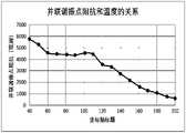
- Fig. 3A and Fig. 3Bare the resonator performance change curve under different substrate temperatures
- Fig. 3Ais the relationship diagram between the series resonance point impedance and the substrate temperature of the resonator as an example
- Fig. 3Bis the resonator as an example A plot of parallel resonance point impedance versus substrate temperature.
- the present inventionis proposed to solve at least one aspect of the above-mentioned technical problems.
- a technical solutionis proposed to reduce the influence of substrate temperature rise on FBAR performance under high power.
- a bulk acoustic wave resonatorincludes a substrate, a bottom electrode, a top electrode, an acoustic mirror and a piezoelectric layer.
- the baseincludes a silicon carbide base portion defining an upper side of the base.
- the acoustic mirror of the resonatoris arranged above the upper side of the silicon carbide base part.
- a bulk acoustic wave resonatorincludes a substrate, a bottom electrode, a top electrode, an acoustic mirror and a piezoelectric layer.
- the baseincludes a silicon carbide base portion defining an upper side of the base. The resistivity of the silicon carbide substrate is greater than 1E6 ⁇ *cm.
- Embodiments of the present inventionalso relate to a filter, including the above bulk acoustic wave resonator.
- Embodiments of the present inventionalso relate to an electronic device, including the above-mentioned filter or resonator.
- Fig. 1is the schematic diagram of the variation of the resistance of silicon chip with temperature in actual test
- FIG. 2is a schematic cross-sectional view of a known bulk acoustic wave resonator
- FIG. 3Ais a relationship diagram between the series resonance point impedance of a resonator and the substrate temperature as an example
- FIG. 3Bis a relationship diagram between the parallel resonance point impedance and the substrate temperature of a resonator as an example
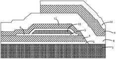
- FIG. 4is a schematic cross-sectional view of a bulk acoustic wave resonator according to an exemplary embodiment of the present invention
- 5A-5Gare a series of cross-sectional schematic diagrams showing the fabrication process of the bulk acoustic wave resonator shown in FIG. 4 according to an exemplary embodiment of the present invention
- FIG. 6is a schematic cross-sectional view of a bulk acoustic wave resonator according to another exemplary embodiment of the present invention.
- FIG. 7is a graph showing the relationship between the parallel resonance impedance Rp of a resonator and the substrate temperature as an example, wherein the dark color corresponds to the silicon substrate, and the light color corresponds to the silicon carbide substrate.
- the substratein the embodiment shown in the present invention, is a substrate of silicon carbide material.
- the substratecan be a composite substrate, but its upper part is a silicon carbide layer, and the lower part can use any other substrate material, such as single crystal silicon, gallium nitride, gallium arsenide, sapphire, quartz, other resistivity Silicon carbide, diamond, etc. can also be single crystal piezoelectric substrates such as lithium niobate, lithium tantalate, and potassium niobate.
- the materialcan be molybdenum, ruthenium, gold, aluminum, magnesium, tungsten, copper, titanium, iridium, osmium, chromium or the composite or alloy of the above metals.
- the first seed layercan be made of materials such as aluminum nitride, zinc oxide, PZT, etc., and can also be a rare earth element doped material containing the above materials in a certain atomic ratio. In the present invention, the first seed layer 3 may not be provided.
- the first bottom electrode layerthe material can be gold (Au), tungsten (W), molybdenum (Mo), platinum (Pt), ruthenium (Ru), iridium (Ir), titanium tungsten (TiW), aluminum (Al ), titanium (Ti), osmium (Os), magnesium (Mg), gold (Au), tungsten (W), molybdenum (Mo), platinum (Pt), ruthenium (Ru), iridium (Ir), germanium (Ge ), copper (Cu), aluminum (Al), chromium (Cr), arsenic-doped gold, and similar metals.
- the etch barrier layercan be SiN, AlN, etc., which has a relatively large etching selectivity ratio with the second bottom electrode. In the embodiment of the present invention, the etching stopper layer 5 may not be provided.
- the second seed layercan be made of aluminum nitride, zinc oxide, PZT and other materials, or it can be a rare earth element doped material containing a certain atomic ratio of the above materials. In the embodiment of the present invention, the second seed layer 6 may not be provided.
- the piezoelectric layercan be a single crystal piezoelectric material, optional, such as: single crystal aluminum nitride, single crystal gallium nitride, single crystal lithium niobate, single crystal lead zirconate titanate (PZT) , single crystal potassium niobate, single crystal quartz film, or single crystal lithium tantalate and other materials, or polycrystalline piezoelectric material (corresponding to single crystal, non-single crystal material), optional, such as polycrystalline nitrogen Aluminum oxide, zinc oxide, PZT, etc., can also be a rare earth element doped material containing a certain atomic ratio of the above materials, such as doped aluminum nitride, which contains at least one rare earth element, such as scandium (Sc ), yttrium (Y), magnesium (Mg), titanium (Ti), lanthanum (La), cerium (Ce), praseodymium (Pr), neodymium (Nd), promethium (Pm
- the material of the top electrodecan be the same as that of the bottom electrode, and the material can be molybdenum, ruthenium, gold, aluminum, magnesium, tungsten, copper, titanium, iridium, osmium, chromium or a combination of the above metals or their alloys.
- the top and bottom electrodesare typically of the same material, but can also be different.
- the passivation layer or process layeris set on the top electrode of the resonator.
- the function of the process layercan be a quality adjustment load or a passivation layer.
- Its materialcan be a dielectric material, such as silicon dioxide, aluminum nitride, nitride silicon etc. In the present invention, the passivation layer or process layer 10 may not be provided.
- Acoustic mirrorwhich can be a cavity, Bragg reflection layer and other equivalent forms can also be used.
- the illustrated embodiment of the inventionemploys a cavity provided on the upper surface of the substrate.
- the acoustic mirroris on the upper side of the substrate 1 .
- Acoustic mirror sacrificial layerthe material can be SiO 2 , silicon nitride, doped silicon dioxide, polysilicon, amorphous silicon and other materials.
- the second bottom electrode layerthe material can be gold (Au), tungsten (W), molybdenum (Mo), platinum (Pt), ruthenium (Ru), iridium (Ir), titanium tungsten (TiW), aluminum (Al ), titanium (Ti), osmium (Os), magnesium (Mg), gold (Au), tungsten (W), molybdenum (Mo), platinum (Pt), ruthenium (Ru), iridium (Ir), germanium (Ge ), copper (Cu), aluminum (Al), chromium (Cr), arsenic-doped gold, and similar metals.
- the first bottom electrode layer and the second bottom electrode layerconstitute an interlayer electrode or a gap electrode, and together serve as a bottom electrode.
- SiCSilicon carbide
- the present inventionchooses to use the SiC substrate for the preparation of the FBAR filter.
- the SiC substratehas good thermal conductivity, in the case of forming effective thermal contact with the stacked structure of the resonator (bottom electrode, top electrode and piezoelectric layer), the heat dissipation capability of the device can be improved, which in turn can improve the resonance.
- the power of the filter or the power of the filtercan be improved.
- FIG. 4is a schematic cross-sectional view of a bulk acoustic wave resonator according to an exemplary embodiment of the present invention.
- the resonatorincludes a substrate 1, a first seed layer 3, a first bottom electrode layer 4, an etch stop layer 5, a second seed layer 6, a piezoelectric layer 8, a top electrode 9 and a passivation layer or process layer 10.
- the substrate 1is not provided with a cavity as shown in FIG. 2 , but a void layer or an acoustic mirror 11 is formed in the bottom electrode, which acts as an acoustic mirror in the form of a cavity.
- a void layer or an acoustic mirror 11is formed in the bottom electrode, which acts as an acoustic mirror in the form of a cavity.
- the upper side of the substrate 1is a flat surface at least in the active area of the resonator.
- the interstitial layer or acoustic mirror 11is surrounded by an etch stop layer 5 that defines the lower surface of the interstitial layer, and a second seed layer 6 that defines the lower surface of the interstitial layer. the upper surface of the interstitial layer.
- etch stop layer 5that defines the lower surface of the interstitial layer
- second seed layer 6that defines the lower surface of the interstitial layer. the upper surface of the interstitial layer.
- the material 11 - 1such as silicon dioxide is surrounded by an etch stop layer 5 (for example, it may be aluminum nitride) and a second seed layer 6 (for example, aluminum nitride).
- the etch barrier layer 5 and the second seed layer 6can not only solve or alleviate the crystallization problem of the piezoelectric layer caused by the amorphous or polycrystalline SiC substrate, but also prevent the sacrificial material 11-1 from being etched during the preparation process. liquid etch away.
- the second seed layer 6in order to reduce the etching of the sacrificial material 11-1 during the preparation process, extends to the outside of the etch stop layer 5 in the horizontal direction for a distance, Optionally, the distance is in the range of 1 ⁇ m-10 ⁇ m.
- only one of the etching stopper layer 5 and the second seed layer 6may be provided.
- the etching stopper layer 5 and the second seed layer 6may not be provided, as shown in FIG. 6 , which can simplify the manufacturing process flow.
- a void layeris formed in the bottom electrode as an acoustic mirror to avoid forming a cavity in the silicon carbide substrate.
- the present inventionis not limited thereto.
- the bottom electrodealso includes a first bottom electrode layer 4 and a second bottom electrode layer 12 electrically connected to each other, and in the thickness direction of the resonator, the first bottom electrode layer 4 is positioned at the second bottom electrode layer.
- a void layer 11is provided on the lower side of the second bottom electrode layer 12 .
- the void layer 11is located in the first bottom electrode layer 4 and the first bottom electrode layer 4 defines at least a part of the boundary of the void layer 11 in the horizontal direction , the void layer 11 forms an acoustic mirror of the resonator, in short, part or all of the void layer 11 can be disposed in the first bottom electrode layer 4 .
- the second bottom electrode layer 12can be a flat layer, and in this case, the piezoelectric layer 8 can be a single crystal piezoelectric layer.
- the void layer 11may be arranged through the first bottom electrode layer 4, or may only be recessed into a part of the first bottom electrode layer 4, that is, the first first electrode layer defines the lower boundary of the void layer, so that the first bottom electrode layer
- the heat exchange area between 4 and the substrate 1increases in the effective area, which is beneficial to increase the heat dissipation of the resonator.
- the void layer 11 and the first bottom electrode layer 4can be formed, and then the sacrificial material layer can be filled in the void layer 11.
- the second bottom electrode layer 12can be provided, and the sacrificial material layer can be etched. Then the void layer 11 is formed.
- the thickness of the void layer 11is in the range of 0.5 ⁇ m-3 ⁇ m.
- the entire substrate 1is a silicon carbide substrate.
- the substrate 10is a silicon carbide substrate, its thickness is not less than 30 ⁇ m in order to enable the resonator to be well prepared and supported.
- the substratemay be a composite substrate, but its upper part is a silicon carbide layer, and its lower part may use any other substrate material.
- the thickness of the composite substrateis not less than 30 ⁇ m, and the thickness of the silicon carbide substrate portion is not less than 5 ⁇ m.
- the material of silicon carbideis discussed further below.
- single crystal silicon carbide materialcan be used, but its price is relatively expensive.
- the SiC substrate used in the present inventionis not limited to single crystal SiC, polycrystalline SiC can also be used, and there is no requirement for crystallinity. In the case of selecting polycrystalline SiC, the processing difficulty of the SiC substrate can also be reduced, thereby reducing its cost.
- the resistivity of the SiC materialis not less than 1E6 ⁇ *cm, which facilitates electrical blocking between the top and bottom electrodes through the resistance of the substrate.
- the requirements of the SiC substrate usedare different from those of conventional SiC substrates, and it is only necessary to use the D-level substrates in Table 1 instead of SiC substrates with better performance.
- Table 1shows the relevant parameters of different grades of SiC substrates.
- General device preparationrequires the use of P-grade SiC substrates.
- the D-grade in Table 1needs to be used. Just base.
- the price of D-grade SiC substratesis one-fourth to one-sixth of P-grade, so it can reduce costs while meeting high power requirements.
- FIG. 4The manufacturing process of the structure shown in FIG. 4 will be illustrated below with reference to FIGS. 5A-5G .
- Step 1As shown in FIG. 5A , a SiC substrate 1 is provided, on which a first seed layer 3 and a first bottom electrode layer 4 are prepared (for example, by deposition and patterning processes).
- Step 2As shown in FIG. 5B , deposit, for example, an aluminum nitride layer on the structure shown in FIG. 5A , and then pattern it to form an etch stop layer 5 .
- Step 3As shown in FIG. 5C , deposit a sacrificial material layer on the structure shown in FIG. 5B , and then pattern it to form the acoustic mirror sacrificial layer 11 - 1 on the etch barrier layer 5 .
- Step 4As shown in FIG. 5D, deposit and pattern a second seed layer 6 on the structure shown in FIG. 5C, and then deposit and pattern an electrode material layer to form a layer covering the second seed layer 6 and the first bottom electrode layer The second bottom electrode layer 12 of the other part of 4.
- Step 5As shown in FIG. 5E , deposit a piezoelectric layer 8 on the structure shown in FIG. 5D .
- Step 6As shown in FIG. 5F , deposit and pattern an electrode material layer on the structure shown in FIG. 5E to form a top electrode 9 .
- Step 7As shown in FIG. 5G , set a passivation layer 10 on the structure shown in FIG. 5F .
- Step 8using an etchant to release the sacrificial layer 11 - 1 of the acoustic mirror to obtain the structure shown in FIG. 4 .
- FIG. 7is a graph showing the relationship between the parallel resonance impedance Rp of a resonator and the substrate temperature as an example, wherein the dark color corresponds to the silicon substrate, and the light color corresponds to the silicon carbide substrate.
- the parallel resonance impedance Rpis normalized. It can be seen from Figure 7 that in the range from normal temperature to 90 °C, the silicon substrate and the silicon carbide substrate have roughly the same effect on the Rp value as the temperature increases, and there is no significant difference between the silicon substrate and the silicon carbide substrate. However, as shown in Figure 7, after the temperature of the substrate exceeds 90°C, the higher the substrate temperature, the lower the Rp value of the resonator using the silicon substrate and the lower the Rp value of the resonator using the silicon carbide substrate. higher.
- silicon carbide substratesare used to prepare bulk acoustic wave resonators, because silicon carbide substrates have good thermal conductivity and form an effective thermal In the case of contact, the heat dissipation capability of the device can be improved, thereby improving the performance of the resonator or the power of the filter.
- the top electrode 50 and the bottom electrode 30 of the resonatorare electrically blocked by the resistance R of the silicon substrate.
- the resistance value of the silicon substrateis relatively high at room temperature, and the resistance R has no obvious influence on the performance of the resonator. At high power, the temperature of the device and the substrate increases, which causes the resistance of the silicon substrate to decrease, thus affecting the performance of the resonator.
- the resistivity of the silicon carbide substrateis greater than that of the silicon substrate, for example, the resistivity of the silicon carbide substrate used is greater than 1E6 ⁇ *cm. This facilitates electrical blocking between the top and bottom electrodes of the resonator through the silicon carbide substrate.
- the cavity of the acoustic mirroris realized by the bottom electrode as the gap electrode, but the present invention is not limited thereto, that is, in the case where it is clear that the silicon carbide substrate defines the upper side of the substrate, it may not Regardless of whether the acoustic mirror is disposed in or on the substrate, for example, although not shown, the acoustic mirror cavity may also be disposed in a silicon carbide substrate.
- the present inventionalso proposes the following bulk acoustic wave resonator structure: the base of the resonator includes a silicon carbide base portion, and the silicon carbide base portion defines the upper side of the base; and the resistivity of the silicon carbide base portion Greater than 1E6 ⁇ *cm.
- the silicon carbide base partis a grade D silicon carbide base part.
- each numerical rangein addition to clearly stating that the endpoint value is not included, can also be the median value of each numerical range in addition to the endpoint value, and these are all within the protection scope of the present invention .
- up and downare relative to the bottom surface of the base of the resonator.
- the side close to the bottom surfaceis the bottom side
- the side away from the bottom surfaceis the top side.
- the side or end of a part near the centeris the inner side or the inner end
- the part The side or end away from the centeris the outside or outer end.
- the effective area of the resonatorrefers to the overlapping area of the acoustic mirror, the bottom electrode, the piezoelectric layer and the top electrode in the thickness direction of the resonator.
- the bulk acoustic wave resonator according to the present inventioncan be used to form filters or electronic devices.
- the electronic equipmenthere includes but is not limited to intermediate products such as RF front-ends, filter amplifier modules, and terminal products such as mobile phones, WIFI, and drones.
- a bulk acoustic wave resonatorcomprising:
- the basecomprises a silicon carbide base portion defining an upper side of the base
- the acoustic mirror of the resonatoris arranged above the upper side of the silicon carbide base part.
- the basefurther includes an additional base portion below the silicon carbide base portion in the thickness direction of the resonator, the material of the additional base portion being different from the silicon carbide base portion. The material at the bottom of the silicon base.
- the bottom electrodeincludes a first electrode layer and a second electrode layer electrically connected to each other, and the first electrode layer and the second electrode layer are resonant There are gaps in the thickness direction of the resonator, and the gaps form an acoustic mirror of the resonator.
- the resonatorfurther comprises a seed layer and/or an etch stop layer disposed between the first electrode layer and the second electrode layer, the seed layer being adapted to define the The upper interface of the void, the etch barrier layer is adapted to define the lower interface of the void.
- the resonatorincludes a seed layer and an etch stop layer surrounding the void;
- the seed layerextends a distance outside the etch stop layer in a horizontal direction.
- the bottom electrodeincludes a first electrode layer and a second electrode layer electrically connected to each other, and in the thickness direction of the resonator, the first electrode layer is at Below the second electrode layer, a gap is provided on the lower side of the second electrode layer, at least a part of the gap is located in the first electrode layer and the first electrode layer defines the boundary of the gap in the horizontal direction At least a portion of the void forms an acoustic mirror of the resonator.
- the upper side of the silicon carbide base partis a flat surface at least in the active area of the resonator
- the second electrode layeris a planar layer at least in the active area of the resonator.
- the piezoelectric layeris a single crystal piezoelectric layer.
- a bulk acoustic wave resonatorcomprising:
- the basecomprises a silicon carbide base portion defining an upper side of the base
- the resistivity of the silicon carbide base portionis greater than 1E6 ⁇ *cm.
- a filtercomprising the resonator according to any one of 1-18.
- An electronic devicecomprising the filter according to 19 or the resonator according to any one of 1-18.
Landscapes
- Physics & Mathematics (AREA)
- Acoustics & Sound (AREA)
- Chemical & Material Sciences (AREA)
- Crystallography & Structural Chemistry (AREA)
- Piezo-Electric Or Mechanical Vibrators, Or Delay Or Filter Circuits (AREA)
Abstract
Description
Translated fromChinese本发明的实施例涉及半导体领域,尤其涉及一种包括碳化硅基底的体声波谐振器、一种具有该谐振器的滤波器以及一种电子设备。Embodiments of the present invention relate to the field of semiconductors, and in particular to a bulk acoustic wave resonator including a silicon carbide substrate, a filter with the resonator, and an electronic device.
随着当今无线通讯技术的飞速发展,小型化便携式终端设备的应用也日益广泛,因而对于高性能、小尺寸的射频前端模块和器件的需求也日益迫切。近年来,以例如为薄膜体声波谐振器(Film Bulk Acoustic Resonator,简称FBAR)为基础的滤波器、双工器等滤波器件越来越为市场所青睐。一方面是因为其插入损耗低、过渡特性陡峭、选择性高、功率容量高、抗静电放电(ESD)能力强等优异的电学性能,另一方面也是因为其体积小、易于集成的特点所致。With the rapid development of today's wireless communication technology, the application of miniaturized portable terminal equipment is becoming more and more extensive, so the demand for high-performance, small-sized RF front-end modules and devices is also increasingly urgent. In recent years, filter devices such as filters and duplexers based on film bulk acoustic resonators (Film Bulk Acoustic Resonator, referred to as FBAR) have become more and more popular in the market. On the one hand, it is due to its excellent electrical properties such as low insertion loss, steep transition characteristics, high selectivity, high power capacity, and strong anti-electrostatic discharge (ESD) capability; on the other hand, it is also due to its small size and easy integration. .
当前的FBAR滤波器制备在硅基底上。单晶硅在室温时的电阻率一般为2000-5000Ω*cm,此时电阻率可以满足使用的要求。但是单晶硅基底的电阻率随温度的升高会降低。图1为实际测试的硅片电阻随温度的变化示意图。由图1可知,实测的硅片电阻随温度的升高呈现稳定的下降,到115℃时电阻即下降为室温的一半,此时会对谐振器的性能产生影响。Current FBAR filters are fabricated on silicon substrates. The resistivity of monocrystalline silicon at room temperature is generally 2000-5000Ω*cm, and the resistivity can meet the requirements of use at this time. But the resistivity of single crystal silicon substrate will decrease with the increase of temperature. Fig. 1 is a schematic diagram of the variation of silicon chip resistance with temperature actually tested. It can be seen from Figure 1 that the measured resistance of the silicon chip shows a steady decrease with the increase of temperature, and the resistance drops to half of the room temperature at 115°C, which will affect the performance of the resonator at this time.
图2为已知的体声波谐振器的截面示意图。图2的体声波谐振器包括基底10、声学镜20、底电极30、压电层40、顶电极50、钝化层60、质量负载层70和电极连接部90。图2中的谐振器还设置有悬翼或桥结构限定的间隙80。如图2所示,与顶电极50电连接的电极连接部90与底电极30之间具有电阻R,即谐振器的顶电极50和底电极30通过硅基底的电阻R进行电学阻断。室温下硅基底的阻值较高,电阻R对谐振器性能无明显影响。在高功率下,器件和基底的温度升高,会导致硅基底的电阻降低,因此会影响谐振器的性能。Fig. 2 is a schematic cross-sectional view of a known BAW resonator. The BAW resonator of FIG. 2 includes a
图3A和图3B是不同基底温度下的谐振器性能变化曲线,图3A为作为一个示例的谐振器的串联谐振点阻抗与基底温度之间的关系图,图3B为作为一个示例的谐振器的并联谐振点阻抗与基底温度之间的关系图。Fig. 3A and Fig. 3B are the resonator performance change curve under different substrate temperatures, Fig. 3A is the relationship diagram between the series resonance point impedance and the substrate temperature of the resonator as an example, Fig. 3B is the resonator as an example A plot of parallel resonance point impedance versus substrate temperature.
从图3A和图3B可知,随着基底温度的升高,串联谐振点的阻抗线性 的上升而并联谐振点的阻抗稳定的下降,所以在硅基底上制备FBAR滤波器在高功率下基底温度上升后会对器件性能有比较大的恶化。It can be seen from Figure 3A and Figure 3B that as the temperature of the substrate increases, the impedance of the series resonance point increases linearly and the impedance of the parallel resonance point decreases steadily, so the FBAR filter fabricated on the silicon substrate increases the substrate temperature under high power. Afterwards, the performance of the device will be greatly deteriorated.
发明内容Contents of the invention
为解决上述技术问题的至少一个方面,提出本发明。本发明中,提出一种将高功率下基底温度上升对FBAR性能的影响降低的技术方案。The present invention is proposed to solve at least one aspect of the above-mentioned technical problems. In the present invention, a technical solution is proposed to reduce the influence of substrate temperature rise on FBAR performance under high power.
根据本发明的实施例的一个方面,提出了一种体声波谐振器。所述体声波谐振器包括基底、底电极、顶电极、声学镜和压电层。基底包括碳化硅基底部,碳化硅基底部限定基底的上侧。谐振器的声学镜设置在碳化硅基底部的上侧的上方。According to an aspect of the embodiments of the present invention, a bulk acoustic wave resonator is proposed. The BAW resonator includes a substrate, a bottom electrode, a top electrode, an acoustic mirror and a piezoelectric layer. The base includes a silicon carbide base portion defining an upper side of the base. The acoustic mirror of the resonator is arranged above the upper side of the silicon carbide base part.
根据本发明的实施例的另一方面,提出了一种体声波谐振器。所述体声波谐振器包括基底、底电极、顶电极、声学镜和压电层。基底包括碳化硅基底部,碳化硅基底部限定基底的上侧。碳化硅基底部的电阻率大于1E6Ω*cm。According to another aspect of the embodiments of the present invention, a bulk acoustic wave resonator is proposed. The BAW resonator includes a substrate, a bottom electrode, a top electrode, an acoustic mirror and a piezoelectric layer. The base includes a silicon carbide base portion defining an upper side of the base. The resistivity of the silicon carbide substrate is greater than 1E6Ω*cm.
本发明的实施例也涉及一种滤波器,包括上述体声波谐振器。Embodiments of the present invention also relate to a filter, including the above bulk acoustic wave resonator.
本发明的实施例还涉及一种电子设备,包括上述的滤波器或者谐振器。Embodiments of the present invention also relate to an electronic device, including the above-mentioned filter or resonator.
以下描述与附图可以更好地帮助理解本发明所公布的各种实施例中的这些和其他特点、优点,图中相同的附图标记始终表示相同的部件,其中:These and other features and advantages of the various disclosed embodiments of the present invention can be better understood from the following description and accompanying drawings, in which the same reference numerals refer to the same parts throughout, wherein:
图1为实际测试的硅片电阻随温度的变化示意图;Fig. 1 is the schematic diagram of the variation of the resistance of silicon chip with temperature in actual test;
图2为已知的体声波谐振器的截面示意图;2 is a schematic cross-sectional view of a known bulk acoustic wave resonator;
图3A为作为一个示例的谐振器的串联谐振点阻抗与基底温度之间的关系图;FIG. 3A is a relationship diagram between the series resonance point impedance of a resonator and the substrate temperature as an example;
图3B为作为一个示例的谐振器的并联谐振点阻抗与基底温度之间的关系图;FIG. 3B is a relationship diagram between the parallel resonance point impedance and the substrate temperature of a resonator as an example;
图4为根据本发明的一个示例性实施例的体声波谐振器的截面示意图;4 is a schematic cross-sectional view of a bulk acoustic wave resonator according to an exemplary embodiment of the present invention;
图5A-5G为根据本发明的一个示例性实施例的显示图4所示的体声波 谐振器的制作过程的系列截面示意图;5A-5G are a series of cross-sectional schematic diagrams showing the fabrication process of the bulk acoustic wave resonator shown in FIG. 4 according to an exemplary embodiment of the present invention;
图6为根据本发明的另一个示例性实施例的体声波谐振器的截面示意图;以及6 is a schematic cross-sectional view of a bulk acoustic wave resonator according to another exemplary embodiment of the present invention; and
图7为作为一个示例的谐振器的并联谐振阻抗Rp与基底温度之间的关系图,其中深色对应于硅基底,而浅色对应于碳化硅基底。FIG. 7 is a graph showing the relationship between the parallel resonance impedance Rp of a resonator and the substrate temperature as an example, wherein the dark color corresponds to the silicon substrate, and the light color corresponds to the silicon carbide substrate.
下面通过实施例,并结合附图,对本发明的技术方案作进一步具体的说明。在说明书中,相同或相似的附图标号指示相同或相似的部件。下述参照附图对本发明实施方式的说明旨在对本发明的总体发明构思进行解释,而不应当理解为对本发明的一种限制。发明的一部分实施例,而并不是全部的实施例。基于本发明中的实施例,本领域普通技术人员所获得的所有其他实施例,都属于本发明保护的范围。The technical solutions of the present invention will be further specifically described below through the embodiments and in conjunction with the accompanying drawings. In the specification, the same or similar reference numerals designate the same or similar components. The following description of the embodiments of the present invention with reference to the accompanying drawings is intended to explain the general inventive concept of the present invention, but should not be construed as a limitation of the present invention. Some, but not all, embodiments of the invention. All other embodiments obtained by persons of ordinary skill in the art based on the embodiments of the present invention belong to the protection scope of the present invention.
首先,本发明的附图4-6中的附图标记说明如下:At first, the reference numerals among the accompanying drawings 4-6 of the present invention are explained as follows:
1:基底,在本发明所示的实施例中,基底为碳化硅材料的基底。在可选的实施例中,基底可以为复合基底,不过其上部为碳化硅层,下部可以采用任意其他基底材料,例如单晶硅、氮化镓、砷化镓、蓝宝石、石英、其他电阻率的碳化硅、金刚石等,也可以是铌酸锂、钽酸锂、铌酸钾等单晶压电基底。1: Substrate, in the embodiment shown in the present invention, the substrate is a substrate of silicon carbide material. In an optional embodiment, the substrate can be a composite substrate, but its upper part is a silicon carbide layer, and the lower part can use any other substrate material, such as single crystal silicon, gallium nitride, gallium arsenide, sapphire, quartz, other resistivity Silicon carbide, diamond, etc. can also be single crystal piezoelectric substrates such as lithium niobate, lithium tantalate, and potassium niobate.
2:底电极(电极引脚或电极连接边),材料可选钼、钌、金、铝、镁、钨、铜,钛、铱、锇、铬或以上金属的复合或其合金等。2: Bottom electrode (electrode pin or electrode connection side), the material can be molybdenum, ruthenium, gold, aluminum, magnesium, tungsten, copper, titanium, iridium, osmium, chromium or the composite or alloy of the above metals.
3:第一种子层,其材料可选氮化铝、氧化锌、PZT等材料,还可以是包含上述材料的一定原子比的稀土元素掺杂材料。在本发明中,也可以不设置第一种子层3。3: The first seed layer can be made of materials such as aluminum nitride, zinc oxide, PZT, etc., and can also be a rare earth element doped material containing the above materials in a certain atomic ratio. In the present invention, the
4:第一底电极层,材料可选金(Au)、钨(W)、钼(Mo)、铂(Pt)、钌(Ru)、铱(Ir)、钛钨(TiW)、铝(Al)、钛(Ti)、锇(Os)、镁(Mg)、金(Au)、钨(W)、钼(Mo)、铂(Pt)、钌(Ru)、铱(Ir)、锗(Ge)、铜(Cu)、铝(Al)、铬(Cr)、砷掺杂金等类似金属。4: The first bottom electrode layer, the material can be gold (Au), tungsten (W), molybdenum (Mo), platinum (Pt), ruthenium (Ru), iridium (Ir), titanium tungsten (TiW), aluminum (Al ), titanium (Ti), osmium (Os), magnesium (Mg), gold (Au), tungsten (W), molybdenum (Mo), platinum (Pt), ruthenium (Ru), iridium (Ir), germanium (Ge ), copper (Cu), aluminum (Al), chromium (Cr), arsenic-doped gold, and similar metals.
5:刻蚀阻挡层,可以是SiN、AlN等和第二底电极有较大刻蚀选择比的材料。在本发明的实施例中,也可以不设置刻蚀阻挡层5。5: The etch barrier layer can be SiN, AlN, etc., which has a relatively large etching selectivity ratio with the second bottom electrode. In the embodiment of the present invention, the
6:第二种子层,可选氮化铝、氧化锌、PZT等材料,也可以是包含 上述材料的一定原子比的稀土元素掺杂材料。在本发明的实施例中,也可以不设置第二种子层6。6: The second seed layer can be made of aluminum nitride, zinc oxide, PZT and other materials, or it can be a rare earth element doped material containing a certain atomic ratio of the above materials. In the embodiment of the present invention, the
8:压电层,压电层可以为单晶压电材料,可选的,如:单晶氮化铝、单晶氮化镓、单晶铌酸锂、单晶锆钛酸铅(PZT)、单晶铌酸钾、单晶石英薄膜、或者单晶钽酸锂等材料,也可以为多晶压电材料(与单晶相对应,非单晶材料),可选的,如多晶氮化铝、氧化锌、PZT等,还可是包含上述材料的一定原子比的稀土元素掺杂材料,例如可以是掺杂氮化铝,掺杂氮化铝至少含一种稀土元素,如钪(Sc)、钇(Y)、镁(Mg)、钛(Ti)、镧(La)、铈(Ce)、镨(Pr)、钕(Nd)、钷(Pm)、钐(Sm)、铕(Eu)、钆(Gd)、铽(Tb)、镝(Dy)、钬(Ho)、铒(Er)、铥(Tm)、镱(Yb)、镥(Lu)等。8: Piezoelectric layer, the piezoelectric layer can be a single crystal piezoelectric material, optional, such as: single crystal aluminum nitride, single crystal gallium nitride, single crystal lithium niobate, single crystal lead zirconate titanate (PZT) , single crystal potassium niobate, single crystal quartz film, or single crystal lithium tantalate and other materials, or polycrystalline piezoelectric material (corresponding to single crystal, non-single crystal material), optional, such as polycrystalline nitrogen Aluminum oxide, zinc oxide, PZT, etc., can also be a rare earth element doped material containing a certain atomic ratio of the above materials, such as doped aluminum nitride, which contains at least one rare earth element, such as scandium (Sc ), yttrium (Y), magnesium (Mg), titanium (Ti), lanthanum (La), cerium (Ce), praseodymium (Pr), neodymium (Nd), promethium (Pm), samarium (Sm), europium (Eu ), gadolinium (Gd), terbium (Tb), dysprosium (Dy), holmium (Ho), erbium (Er), thulium (Tm), ytterbium (Yb), lutetium (Lu), etc.
9:顶电极,其材料可与底电极相同,材料可选钼、钌、金、铝、镁、钨、铜、钛、铱、锇、铬或以上金属的复合或其合金等。顶电极和底电极材料一般相同,但也可以不同。9: The material of the top electrode can be the same as that of the bottom electrode, and the material can be molybdenum, ruthenium, gold, aluminum, magnesium, tungsten, copper, titanium, iridium, osmium, chromium or a combination of the above metals or their alloys. The top and bottom electrodes are typically of the same material, but can also be different.
10:钝化层或工艺层,设置在谐振器的顶电极上,工艺层的作用可以是质量调节负载或钝化层,其材料可以为介质材料,如二氧化硅、氮化铝、氮化硅等。在本发明中,也可以不设置钝化层或工艺层10。10: The passivation layer or process layer is set on the top electrode of the resonator. The function of the process layer can be a quality adjustment load or a passivation layer. Its material can be a dielectric material, such as silicon dioxide, aluminum nitride, nitride silicon etc. In the present invention, the passivation layer or
11:声学镜,可为空腔,也可采用布拉格反射层及其他等效形式。本发明所示的实施例中采用的是设置于基底的上表面的空腔。在本发明中,声学镜处于基底1的上侧。11: Acoustic mirror, which can be a cavity, Bragg reflection layer and other equivalent forms can also be used. The illustrated embodiment of the invention employs a cavity provided on the upper surface of the substrate. In the present invention, the acoustic mirror is on the upper side of the
11-1:声学镜牺牲层,材料可选SiO2、氮化硅、掺杂二氧化硅、多晶硅、非晶硅等材料。11-1: Acoustic mirror sacrificial layer, the material can be SiO2 , silicon nitride, doped silicon dioxide, polysilicon, amorphous silicon and other materials.
12:第二底电极层,材料可选金(Au)、钨(W)、钼(Mo)、铂(Pt)、钌(Ru)、铱(Ir)、钛钨(TiW)、铝(Al)、钛(Ti)、锇(Os)、镁(Mg)、金(Au)、钨(W)、钼(Mo)、铂(Pt)、钌(Ru)、铱(Ir)、锗(Ge)、铜(Cu)、铝(Al)、铬(Cr)、砷掺杂金等类似金属。第一底电极层与第二底电极层构成夹层电极或间隙电极,且一起作为底电极。12: The second bottom electrode layer, the material can be gold (Au), tungsten (W), molybdenum (Mo), platinum (Pt), ruthenium (Ru), iridium (Ir), titanium tungsten (TiW), aluminum (Al ), titanium (Ti), osmium (Os), magnesium (Mg), gold (Au), tungsten (W), molybdenum (Mo), platinum (Pt), ruthenium (Ru), iridium (Ir), germanium (Ge ), copper (Cu), aluminum (Al), chromium (Cr), arsenic-doped gold, and similar metals. The first bottom electrode layer and the second bottom electrode layer constitute an interlayer electrode or a gap electrode, and together serve as a bottom electrode.
碳化硅(SiC)具有优异的高温稳定性且电阻率较高,电阻率随温度的变化不明显。基于上述特点,本发明选择使用SiC基底进行FBAR滤波器的制备。此外,因为SiC基底具备较好的导热率,在与谐振器的叠层结构(底电极、顶电极和压电层)形成有效热接触的情况下,可以提升器件 的散热能力,进而可以提升谐振器的功率或滤波器的功率。Silicon carbide (SiC) has excellent high temperature stability and high resistivity, and the change of resistivity with temperature is not obvious. Based on the above characteristics, the present invention chooses to use the SiC substrate for the preparation of the FBAR filter. In addition, because the SiC substrate has good thermal conductivity, in the case of forming effective thermal contact with the stacked structure of the resonator (bottom electrode, top electrode and piezoelectric layer), the heat dissipation capability of the device can be improved, which in turn can improve the resonance. The power of the filter or the power of the filter.
不过,现有的SiC基底由于硬度较大等原因,刻蚀的难度较大,当前技术形成图2中的空腔20的难度较大,基于此,本发明提出在碳化硅基底上侧,例如在底电极中,制备空腔作为声学镜来解决该问题。下面参照附图4-6示例性说明。However, the existing SiC substrate is difficult to etch due to its high hardness and other reasons, and it is relatively difficult to form the
图4为根据本发明的一个示例性实施例的体声波谐振器的截面示意图。如图4所示,该谐振器包括基底1、第一种子层3、第一底电极层4、刻蚀阻挡层5、第二种子层6、压电层8、顶电极9以及钝化层或工艺层10。FIG. 4 is a schematic cross-sectional view of a bulk acoustic wave resonator according to an exemplary embodiment of the present invention. As shown in Figure 4, the resonator includes a
如图4所示,基底1中并未设置如图2所示的空腔,而是在底电极中形成有空隙层或声学镜11,其作为空腔形式的声学镜。如此,通过在底电极中设置声学镜,可以避免在碳化硅基底上设置声学镜空腔。在本发明的一个示例性实施例中,基底1的上侧至少在谐振器的有效区域内为平坦面。As shown in FIG. 4 , the
如图4所示,空隙层或声学镜11由刻蚀阻挡层5以及第二种子层6所包围,刻蚀阻挡层5限定该空隙层的下侧表面,而第二种子层6则限定该空隙层的上侧表面。在SiC是非晶或者多晶的结构的情况下,为了有利于压电层的结晶满足最终的性能需要,在本发明的实施例中,如图4所示,在空隙层或声学镜11的牺牲材料11-1(参见图5D)例如二氧化硅的周围设置刻蚀阻挡层5(例如其可以为氮化铝)和第二种子层6(例如为氮化铝)。增加刻蚀阻挡层5以及第二种子层6,除了解决或缓解非晶或者多晶SiC基底带来的压电层的结晶问题外,还可以防止牺牲材料11-1在制备过程中被刻蚀液刻蚀掉。此外,在本发明的一个进一步的实施例中,为了减少牺牲材料11-1在制备过程中被刻蚀掉,第二种子层6在水平方向上延伸到刻蚀阻挡层5的外侧一个距离,可选的,所述距离在1μm-10μm的范围内。As shown in FIG. 4, the interstitial layer or
在可选的实施例中,也可以仅仅设置刻蚀阻挡层5和第二种子层6中的一种。In an optional embodiment, only one of the
在可选的实施例中,也可以不设置刻蚀阻挡层5和第二种子层6,如图6所示,这可以简化制作工艺流程。In an optional embodiment, the
在图4和图6所示的实施例中,以在底电极中形成空隙层作为声学镜,以避免在碳化硅基底中形成空腔。但是,本发明不限于此。In the embodiments shown in FIGS. 4 and 6 , a void layer is formed in the bottom electrode as an acoustic mirror to avoid forming a cavity in the silicon carbide substrate. However, the present invention is not limited thereto.
如图4和图6所示,底电极也包括彼此电连接的第一底电极层4与第二底电极层12,在谐振器的厚度方向上,第一底电极层4处于第二底电极层12的下方,所述第二底电极层12的下侧设置有空隙层11。在一个示例性实施例中,所述空隙层11的至少一部分位于所述第一底电极层4中且所述第一底电极层4限定所述空隙层11在水平方向上的边界的至少一部分,所述空隙层11形成谐振器的声学镜,简而言之,空隙层11的一部分或全部可以设置在第一底电极层4中。As shown in Fig. 4 and Fig. 6, the bottom electrode also includes a first
在空隙层11的一部分或全部可以设置在第一底电极层4中的情况下,第二底电极层12可以为平坦层,此时,压电层8可以为单晶压电层。In the case that part or all of the
空隙层11可以贯穿第一底电极层4设置,也可以仅仅凹入到第一底电极层4的一部分,即第一第电极层限定所述空隙层的下侧边界,从而第一底电极层4与基底1之间在有效区域内的换热面积增大,这有利于增加谐振器的散热。如能够理解的,对于该结构(在不设置与刻蚀阻挡层5以及第二种子层6对应的层的情况下),可以采用先形成第一底电极层4的金属层,接着对其图形化而形成空隙层11以及第一底电极层4,之后可以在空隙层11内填充牺牲材料层,将牺牲材料层平坦化之后,可以设置第二底电极层12,对牺牲材料层执行刻蚀后形成所述空隙层11。The
在本发明的一个示例性实施例中,所述的空隙层11的厚度在0.5μm-3μm的范围内。In an exemplary embodiment of the present invention, the thickness of the
在本发明的图4-图6所示的实施例中,基底1整体为碳化硅基底。在可选的实施例中,在基底10为碳化硅基底的情况下,为了使得谐振器能够得到完好的制备和支撑,其厚度不小于30μm。In the embodiments shown in FIGS. 4-6 of the present invention, the
在本发明的可选的实施例中,基底可以为复合基底,不过其上部为碳化硅层,下部可以采用任意其他基底材料。在本发明中,而在基底为复合基底的情况下,为了使得谐振器能够得到完好的制备和支撑,复合基底的厚度不小于30μm,且碳化硅基底部分的厚度不小于5μm。In an optional embodiment of the present invention, the substrate may be a composite substrate, but its upper part is a silicon carbide layer, and its lower part may use any other substrate material. In the present invention, when the substrate is a composite substrate, in order to enable the resonator to be well prepared and supported, the thickness of the composite substrate is not less than 30 μm, and the thickness of the silicon carbide substrate portion is not less than 5 μm.
下面进一步讨论碳化硅的材料。在本发明中,可以使用单晶碳化硅材料,但是其价格相对较贵。本发明所使用的SiC基底不局限于单晶SiC,也可以使用多晶SiC,对结晶度无需求。在选择多晶SiC的情况下,还可以降低SiC基底的加工难度,进而降低其成本。在本发明的一个实施例中,SiC材料的电阻率不小于1E6Ω*cm,这有利于在顶电极和底电极之间通 过基底的电阻进行电学阻断。The material of silicon carbide is discussed further below. In the present invention, single crystal silicon carbide material can be used, but its price is relatively expensive. The SiC substrate used in the present invention is not limited to single crystal SiC, polycrystalline SiC can also be used, and there is no requirement for crystallinity. In the case of selecting polycrystalline SiC, the processing difficulty of the SiC substrate can also be reduced, thereby reducing its cost. In one embodiment of the present invention, the resistivity of the SiC material is not less than 1E6 Ω*cm, which facilitates electrical blocking between the top and bottom electrodes through the resistance of the substrate.
在本发明的一个示例性实施例中,使用的SiC基底和常规的SiC基底的要求不同,只需要使用表1中的D级基底即可,而无需使用性能较好的SiC基底。表1表示的是不同等级SiC基底的相关参数,一般的器件制备需要使用P级SiC基底,而本发明中制备FBAR时,因为考虑是的是SiC电阻特性,只需要使用表1中的D级基底即可。D级SiC基底的价格是P级的四分之一到六分之一,所以在满足高功率需求的同时还可以降低成本。In an exemplary embodiment of the present invention, the requirements of the SiC substrate used are different from those of conventional SiC substrates, and it is only necessary to use the D-level substrates in Table 1 instead of SiC substrates with better performance. Table 1 shows the relevant parameters of different grades of SiC substrates. General device preparation requires the use of P-grade SiC substrates. However, when preparing FBARs in the present invention, because the SiC resistance characteristics are considered, only the D-grade in Table 1 needs to be used. Just base. The price of D-grade SiC substrates is one-fourth to one-sixth of P-grade, so it can reduce costs while meeting high power requirements.
表1Table 1

下面参照图5A-5G示例性说明图4所示结构的制作过程。The manufacturing process of the structure shown in FIG. 4 will be illustrated below with reference to FIGS. 5A-5G .
步骤1:如图5A所示,提供SiC基底1,在其上制备(例如通过沉积和图形化工艺)第一种子层3和第一底电极层4。Step 1: As shown in FIG. 5A , a
步骤2:如图5B所示,在图5A所示结构上沉积例如氮化铝层,然后对其图形化以形成刻蚀阻挡层5。Step 2: As shown in FIG. 5B , deposit, for example, an aluminum nitride layer on the structure shown in FIG. 5A , and then pattern it to form an
步骤3:如图5C所示,在图5B所示结构上沉积牺牲材料层,接着对其图形化,以在刻蚀阻挡层5上形成声学镜牺牲层11-1。Step 3: As shown in FIG. 5C , deposit a sacrificial material layer on the structure shown in FIG. 5B , and then pattern it to form the acoustic mirror sacrificial layer 11 - 1 on the
步骤4:如图5D所示,在图5C所示结构上沉积和图形化第二种子层6,之后,沉积和图形化电极材料层,以形成覆盖第二种子层6以及第一底电极层4的其他部分的第二底电极层12。Step 4: As shown in FIG. 5D, deposit and pattern a
步骤5:如图5E所示,在图5D所示结构上沉积压电层8。Step 5: As shown in FIG. 5E , deposit a
步骤6:如图5F所示,在图5E所示结构上沉积和图形化电极材料层以形成顶电极9。Step 6: As shown in FIG. 5F , deposit and pattern an electrode material layer on the structure shown in FIG. 5E to form a
步骤7:如图5G所示,在图5F所示结构上设置钝化层10。Step 7: As shown in FIG. 5G , set a
步骤8:利用刻蚀剂释放声学镜牺牲层11-1,以得到如图4所示的结构。Step 8: using an etchant to release the sacrificial layer 11 - 1 of the acoustic mirror to obtain the structure shown in FIG. 4 .
需要指出的是,上述对于谐振器的制作工艺仅仅是示例性的,还可以对其作出各种改变,均在本发明的保护范围之内,上述制作工艺也不对本发明的谐振器的结构形成限定作用。It should be pointed out that the above-mentioned manufacturing process for the resonator is only exemplary, and various changes can also be made to it, all within the protection scope of the present invention, and the above-mentioned manufacturing process does not affect the structure of the resonator of the present invention. Limitation.
图7为作为一个示例的谐振器的并联谐振阻抗Rp与基底温度之间的关系图,其中深色对应于硅基底,而浅色对应于碳化硅基底。在图7中,并联谐振阻抗Rp采用归一化处理。从图7可以看出,在常温到90℃的范围内,采用硅基底与碳化硅基底,随着温度升高,对于Rp值的影响大致相同,硅基底相对于碳化硅基底并未出现显著的Rp值的降低,但是,如图7所示,在基底的温度超过90℃之后,基底温度越高,采用硅基底的谐振器的Rp值越低而采用碳化硅基底的谐振器的Rp值则越高。FIG. 7 is a graph showing the relationship between the parallel resonance impedance Rp of a resonator and the substrate temperature as an example, wherein the dark color corresponds to the silicon substrate, and the light color corresponds to the silicon carbide substrate. In Figure 7, the parallel resonance impedance Rp is normalized. It can be seen from Figure 7 that in the range from normal temperature to 90 °C, the silicon substrate and the silicon carbide substrate have roughly the same effect on the Rp value as the temperature increases, and there is no significant difference between the silicon substrate and the silicon carbide substrate. However, as shown in Figure 7, after the temperature of the substrate exceeds 90°C, the higher the substrate temperature, the lower the Rp value of the resonator using the silicon substrate and the lower the Rp value of the resonator using the silicon carbide substrate. higher.
此外,从图3A和图3B可知,随着基底温度的升高,串联谐振点的阻抗线性的上升而并联谐振点的阻抗稳定的下降,所以在硅基底上制备FBAR滤波器在高功率下基底温度上升后会对器件性能有比较大的恶化。In addition, it can be seen from Figure 3A and Figure 3B that as the temperature of the substrate increases, the impedance of the series resonance point increases linearly and the impedance of the parallel resonance point decreases steadily, so the FBAR filter fabricated on the silicon substrate is at high power. After the temperature rises, the performance of the device will be greatly deteriorated.
可见,采用碳化硅基底,在基底温度超过例如90℃的情况下,对于谐振器性能的提升有显著的作用。It can be seen that the use of a silicon carbide substrate has a significant effect on improving the performance of the resonator when the substrate temperature exceeds, for example, 90°C.
如前应提及的,利用碳化硅基底制备体声波谐振器,因为碳化硅基底具备较好的导热率,在与谐振器的叠层结构(底电极、顶电极和压电层)形成有效热接触的情况下,可以提升器件的散热能力,进而可以提升谐振器的性能或滤波器的功率。As mentioned earlier, silicon carbide substrates are used to prepare bulk acoustic wave resonators, because silicon carbide substrates have good thermal conductivity and form an effective thermal In the case of contact, the heat dissipation capability of the device can be improved, thereby improving the performance of the resonator or the power of the filter.
此外,如在背景技术中已经提及的,谐振器的顶电极50和底电极30通过硅基底的电阻R进行电学阻断。室温下硅基底的阻值较高,电阻R对谐振器性能无明显影响。在高功率下,器件和基底的温度升高,会导致硅基底的电阻降低,因此会影响谐振器的性能。但是,在谐振器基底的上侧采用碳化硅基底的情况下,因为碳化硅基底的电阻率大于硅基底的电阻率,例如采用的碳化硅基底部的电阻率大于1E6Ω*cm的情况下,有利于在谐振器的顶电极与底电极之间通过碳化硅基底进行电学阻断。Furthermore, as already mentioned in the background, the
在参照图4-6描述的实施例中,声学镜空腔由底电极为间隙电极而实现,但是本发明不限于此,即在明确了碳化硅基底限定基底的上侧的情况 下,可以不不考虑声学镜设置在基底中还是设置在基底之上,例如,虽然没有示出,声学镜空腔也可以设置在碳化硅基底中。In the embodiments described with reference to FIGS. 4-6 , the cavity of the acoustic mirror is realized by the bottom electrode as the gap electrode, but the present invention is not limited thereto, that is, in the case where it is clear that the silicon carbide substrate defines the upper side of the substrate, it may not Regardless of whether the acoustic mirror is disposed in or on the substrate, for example, although not shown, the acoustic mirror cavity may also be disposed in a silicon carbide substrate.
基于上述,本发明还提出了如下的体声波谐振器结构:谐振器的基底包括碳化硅基底部,所述碳化硅基底部限定所述基底的上侧;且所述碳化硅基底部的电阻率大于1E6Ω*cm。进一步的实施例中,所述碳化硅基底部为D级碳化硅基底部。Based on the above, the present invention also proposes the following bulk acoustic wave resonator structure: the base of the resonator includes a silicon carbide base portion, and the silicon carbide base portion defines the upper side of the base; and the resistivity of the silicon carbide base portion Greater than 1E6Ω*cm. In a further embodiment, the silicon carbide base part is a grade D silicon carbide base part.
需要指出的是,在本发明中,各个数值范围,除了明确指出不包含端点值之外,除了可以为端点值,还可以为各个数值范围的中值,这些均在本发明的保护范围之内。It should be pointed out that in the present invention, each numerical range, in addition to clearly stating that the endpoint value is not included, can also be the median value of each numerical range in addition to the endpoint value, and these are all within the protection scope of the present invention .
在本发明中,上和下是相对于谐振器的基底的底面而言的,对于一个部件,其靠近该底面的一侧为下侧,远离该底面的一侧为上侧。In the present invention, up and down are relative to the bottom surface of the base of the resonator. For a component, the side close to the bottom surface is the bottom side, and the side away from the bottom surface is the top side.
在本发明中,内和外是相对于谐振器的有效区域的中心在水平方向或者径向方向上而言的,一个部件的靠近该中心的一侧或一端为内侧或内端,而该部件的远离该中心的一侧或一端为外侧或外端。对于一个参照位置而言,位于该位置的内侧表示在水平方向或径向方向上处于该位置与该中心之间,位于该位置的外侧表示在水平方向或径向方向上比该位置更远离该中心。在本发明中,谐振器的有效区域是指在谐振器的厚度方向上,声学镜、底电极、压电层和顶电极的重合区域。In the present invention, inside and outside are relative to the center of the effective area of the resonator in the horizontal direction or radial direction, the side or end of a part near the center is the inner side or the inner end, and the part The side or end away from the center is the outside or outer end. For a reference position, being located inside the position means that it is between the position and the center in the horizontal direction or radial direction, and being located outside the position means that it is farther away from the position than the position in the horizontal direction or radial direction. center. In the present invention, the effective area of the resonator refers to the overlapping area of the acoustic mirror, the bottom electrode, the piezoelectric layer and the top electrode in the thickness direction of the resonator.
如本领域技术人员能够理解的,根据本发明的体声波谐振器可以用于形成滤波器或电子设备。As can be understood by those skilled in the art, the bulk acoustic wave resonator according to the present invention can be used to form filters or electronic devices.
这里的电子设备,包括但不限于射频前端、滤波放大模块等中间产品,以及手机、WIFI、无人机等终端产品。The electronic equipment here includes but is not limited to intermediate products such as RF front-ends, filter amplifier modules, and terminal products such as mobile phones, WIFI, and drones.
基于以上,本发明提出了如下技术方案:Based on the above, the present invention proposes the following technical solutions:
1、一种体声波谐振器,包括:1. A bulk acoustic wave resonator, comprising:
基底;base;
底电极;bottom electrode;
顶电极;top electrode;
声学镜;和acoustic mirrors; and
压电层,piezoelectric layer,
其中,所述基底包括碳化硅基底部,所述碳化硅基底部限定所述基底的上侧;且wherein the base comprises a silicon carbide base portion defining an upper side of the base; and
其中,所述谐振器的声学镜设置在所述碳化硅基底部的上侧的上方。Wherein, the acoustic mirror of the resonator is arranged above the upper side of the silicon carbide base part.
2、根据1所述的谐振器,其中,所述碳化硅基底部的电阻率大于1E6Ω*cm。2. The resonator according to 1, wherein the resistivity of the silicon carbide base portion is greater than 1E6Ω*cm.
3、根据2所述的谐振器,其中,所述碳化硅基底部为D级碳化硅基底部。3. The resonator according to 2, wherein the silicon carbide base portion is a grade D silicon carbide base portion.
4、根据1所述的谐振器,其中,所述碳化硅基底部构成所述基底。4. The resonator according to 1, wherein the silicon carbide base portion constitutes the base.
5、根据4所述的谐振器,其中,所述基底的厚度不小于30μm。5. The resonator according to 4, wherein the substrate has a thickness of not less than 30 μm.
6、根据1所述的谐振器,其中,所述基底还包括在谐振器的厚度方向上处于碳化硅基底部的下方的另外的基底部,所述另外的基底部的材料不同于所述碳化硅基底部的材料。6. The resonator according to 1, wherein the base further includes an additional base portion below the silicon carbide base portion in the thickness direction of the resonator, the material of the additional base portion being different from the silicon carbide base portion. The material at the bottom of the silicon base.
7、根据6所述的谐振器,其中,所述基底的厚度不小于30μm,且碳化硅基底部分的厚度不小于5μm。7. The resonator according to 6, wherein the thickness of the base is not less than 30 μm, and the thickness of the silicon carbide base portion is not less than 5 μm.
8、根据1所述的谐振器,其中,所述碳化硅基底部的上侧至少在谐振器的有效区域内为平坦面。8. The resonator according to 1, wherein the upper side of the silicon carbide base portion is a flat surface at least in an effective area of the resonator.
9、根据1-8中任一项所述的谐振器,其中,所述底电极包括彼此电连接的第一电极层与第二电极层,第一电极层与第二电极层之间在谐振器的厚度方向上设置有空隙,所述空隙形成谐振器的声学镜。9. The resonator according to any one of 1-8, wherein the bottom electrode includes a first electrode layer and a second electrode layer electrically connected to each other, and the first electrode layer and the second electrode layer are resonant There are gaps in the thickness direction of the resonator, and the gaps form an acoustic mirror of the resonator.
10、根据9所述的谐振器,其中,所述谐振器还包括设置在第一电极层与第二电极层之间的种子层和/或刻蚀阻挡层,所述种子层适于限定所述空隙的上侧界面,所述刻蚀阻挡层适于限定所述空隙的下侧界面。10. The resonator according to 9, wherein the resonator further comprises a seed layer and/or an etch stop layer disposed between the first electrode layer and the second electrode layer, the seed layer being adapted to define the The upper interface of the void, the etch barrier layer is adapted to define the lower interface of the void.
11、根据10所述的谐振器,其中:11. The resonator according to 10, wherein:
所述谐振器包括种子层和刻蚀阻挡层,所述种子层和刻蚀阻挡层包围所述空隙;以及the resonator includes a seed layer and an etch stop layer surrounding the void; and
所述种子层在水平方向上延伸到所述刻蚀阻挡层的外侧一个距离。The seed layer extends a distance outside the etch stop layer in a horizontal direction.
12、根据11所述的谐振器,其中,所述距离在1μm-10μm的范围内。12. The resonator according to 11, wherein the distance is in the range of 1 μm-10 μm.
13、根据1-8中任一项所述的谐振器,其中,所述底电极包括彼此电连接的第一电极层与第二电极层,在谐振器的厚度方向上,第一电极层处于第二电极层的下方,所述第二电极层的下侧设置有空隙,所述空隙至少一部分位于所述第一电极层中且所述第一电极层限定所述空隙在水平方向上的边界的至少一部分,所述空隙形成谐振器的声学镜。13. The resonator according to any one of 1-8, wherein the bottom electrode includes a first electrode layer and a second electrode layer electrically connected to each other, and in the thickness direction of the resonator, the first electrode layer is at Below the second electrode layer, a gap is provided on the lower side of the second electrode layer, at least a part of the gap is located in the first electrode layer and the first electrode layer defines the boundary of the gap in the horizontal direction At least a portion of the void forms an acoustic mirror of the resonator.
14、根据13所述的谐振器,其中:14. The resonator according to 13, wherein:
所述碳化硅基底部的上侧至少在谐振器的有效区域内为平坦面;The upper side of the silicon carbide base part is a flat surface at least in the active area of the resonator;
所述第二电极层至少在谐振器的有效区域内为平坦层;且the second electrode layer is a planar layer at least in the active area of the resonator; and
所述压电层为单晶压电层。The piezoelectric layer is a single crystal piezoelectric layer.
15、根据14所述的谐振器,其中,所述第一电极层限定所述空隙的下侧边界。15. The resonator of 14, wherein the first electrode layer defines a lower boundary of the void.
16、根据9或13所述的谐振器,其中,所述空隙的厚度在0.5μm-3μm的范围内。16. The resonator according to 9 or 13, wherein the thickness of the void is in the range of 0.5 μm to 3 μm.
17、一种体声波谐振器,包括:17. A bulk acoustic wave resonator comprising:
基底;base;
底电极;bottom electrode;
顶电极;top electrode;
声学镜;和acoustic mirrors; and
压电层,piezoelectric layer,
其中,所述基底包括碳化硅基底部,所述碳化硅基底部限定所述基底的上侧;且wherein the base comprises a silicon carbide base portion defining an upper side of the base; and
其中,所述碳化硅基底部的电阻率大于1E6Ω*cm。Wherein, the resistivity of the silicon carbide base portion is greater than 1E6Ω*cm.
18、根据17所述的谐振器,其中,所述碳化硅基底部为D级碳化硅基底部。18. The resonator according to 17, wherein the silicon carbide base portion is a grade D silicon carbide base portion.
19、一种滤波器,包括根据1-18中任一项所述的谐振器。19. A filter comprising the resonator according to any one of 1-18.
20、一种电子设备,包括根据19所述的滤波器或根据1-18中任一项所述的谐振器。20. An electronic device comprising the filter according to 19 or the resonator according to any one of 1-18.
尽管已经示出和描述了本发明的实施例,对于本领域的普通技术人员而言,可以理解在不脱离本发明的原理和精神的情况下可以对这些实施例进行变化,本发明的范围由所附权利要求及其等同物限定。While embodiments of the present invention have been shown and described, it will be understood by those skilled in the art that changes may be made to these embodiments without departing from the principles and spirit of the invention, the scope of which is defined by The appended claims and their equivalents are defined.
Claims (20)
Translated fromChineseApplications Claiming Priority (2)
| Application Number | Priority Date | Filing Date | Title |
|---|---|---|---|
| CN202110578390.0ACN115412050A (en) | 2021-05-26 | 2021-05-26 | Bulk acoustic wave resonator, filter and electronic device including silicon carbide substrate |
| CN202110578390.0 | 2021-05-26 |
Publications (1)
| Publication Number | Publication Date |
|---|---|
| WO2022247902A1true WO2022247902A1 (en) | 2022-12-01 |
Family
ID=84155357
Family Applications (1)
| Application Number | Title | Priority Date | Filing Date |
|---|---|---|---|
| PCT/CN2022/095209CeasedWO2022247902A1 (en) | 2021-05-26 | 2022-05-26 | Bulk acoustic resonator comprising silicon carbide substrate, filter, and electronic device |
Country Status (2)
| Country | Link |
|---|---|
| CN (1) | CN115412050A (en) |
| WO (1) | WO2022247902A1 (en) |
Citations (7)
| Publication number | Priority date | Publication date | Assignee | Title |
|---|---|---|---|---|
| US20180183405A1 (en)* | 2016-12-23 | 2018-06-28 | Avago Technologies General Ip (Singapore) Pte. Ltd | Bulk baw resonator having electrically insulating substrate |
| US20180183406A1 (en)* | 2016-12-23 | 2018-06-28 | Avago Technologies General Ip (Singapore) Pte. Ltd | Packaged resonator with polymeric air cavity package |
| CN111082776A (en)* | 2019-12-11 | 2020-04-28 | 诺思(天津)微系统有限责任公司 | Bulk acoustic wave resonator, filter and electronic device with electrode with void layer |
| CN111082777A (en)* | 2019-12-31 | 2020-04-28 | 诺思(天津)微系统有限责任公司 | Bulk acoustic wave resonator with gap electrode as bottom electrode, filter and electronic device |
| US20200389150A1 (en)* | 2019-03-28 | 2020-12-10 | Global Communication Semiconductors, Llc | Single-Crystal Bulk Acoustic Wave Resonator and Method of Making Thereof |
| CN114070224A (en)* | 2020-08-06 | 2022-02-18 | 诺思(天津)微系统有限责任公司 | Bulk acoustic wave resonator assembly with acoustic decoupling layer, manufacturing method of bulk acoustic wave resonator assembly, filter and electronic device |
| CN114070237A (en)* | 2020-08-06 | 2022-02-18 | 诺思(天津)微系统有限责任公司 | Bulk Acoustic Wave Resonator Assemblies, Filters, and Electronics with Acoustic Decoupling Layers |
- 2021
- 2021-05-26CNCN202110578390.0Apatent/CN115412050A/enactivePending
- 2022
- 2022-05-26WOPCT/CN2022/095209patent/WO2022247902A1/ennot_activeCeased
Patent Citations (7)
| Publication number | Priority date | Publication date | Assignee | Title |
|---|---|---|---|---|
| US20180183405A1 (en)* | 2016-12-23 | 2018-06-28 | Avago Technologies General Ip (Singapore) Pte. Ltd | Bulk baw resonator having electrically insulating substrate |
| US20180183406A1 (en)* | 2016-12-23 | 2018-06-28 | Avago Technologies General Ip (Singapore) Pte. Ltd | Packaged resonator with polymeric air cavity package |
| US20200389150A1 (en)* | 2019-03-28 | 2020-12-10 | Global Communication Semiconductors, Llc | Single-Crystal Bulk Acoustic Wave Resonator and Method of Making Thereof |
| CN111082776A (en)* | 2019-12-11 | 2020-04-28 | 诺思(天津)微系统有限责任公司 | Bulk acoustic wave resonator, filter and electronic device with electrode with void layer |
| CN111082777A (en)* | 2019-12-31 | 2020-04-28 | 诺思(天津)微系统有限责任公司 | Bulk acoustic wave resonator with gap electrode as bottom electrode, filter and electronic device |
| CN114070224A (en)* | 2020-08-06 | 2022-02-18 | 诺思(天津)微系统有限责任公司 | Bulk acoustic wave resonator assembly with acoustic decoupling layer, manufacturing method of bulk acoustic wave resonator assembly, filter and electronic device |
| CN114070237A (en)* | 2020-08-06 | 2022-02-18 | 诺思(天津)微系统有限责任公司 | Bulk Acoustic Wave Resonator Assemblies, Filters, and Electronics with Acoustic Decoupling Layers |
Also Published As
| Publication number | Publication date |
|---|---|
| CN115412050A (en) | 2022-11-29 |
Similar Documents
| Publication | Publication Date | Title |
|---|---|---|
| CN110061712B (en) | Acoustic resonator, filter and electronic device comprising annular protrusion Liang Yan structure | |
| WO2021042741A1 (en) | Bulk acoustic wave resonator with piezoelectric layer having insert structure, and filter and electronic device | |
| CN111193489B (en) | Bulk acoustic resonators, filters and electronic devices | |
| EP2066027A1 (en) | Thin film piezoelectric resonator and method for manufacturing the same | |
| KR102276515B1 (en) | Bulk-acoustic wave resonator | |
| KR102427930B1 (en) | Acoustic resonator | |
| CN111245400A (en) | Bulk Acoustic Resonators, Filters, and Electronic Devices with Bridge Insertion Structures | |
| CN111917393A (en) | Bulk acoustic wave resonator and manufacturing method, bulk acoustic wave resonator assembly, filter and electronic equipment | |
| CN114070224A (en) | Bulk acoustic wave resonator assembly with acoustic decoupling layer, manufacturing method of bulk acoustic wave resonator assembly, filter and electronic device | |
| WO2022083352A1 (en) | Bulk acoustic resonator and assembly, filter, and electronic device | |
| WO2022228385A1 (en) | Bulk acoustic wave resonator having thickened electrode, filter, and electronic device | |
| WO2022028402A1 (en) | Bulk acoustic wave resonator assembly having acoustic decoupling layer, manufacturing method, filter, and electronic device | |
| WO2022148387A1 (en) | Bulk acoustic wave resonator and manufacturing method therefor, filter, and electronic device | |
| WO2022068562A1 (en) | Bulk acoustic resonator, doping concentration determination method, filter, and electronic device | |
| CN114257204A (en) | Bulk acoustic wave resonator having acoustic resistance layer, assembly and manufacturing method thereof, filter, and electronic device | |
| WO2022062910A1 (en) | Bulk acoustic resonator and assembly, method for adjusting electromechanical coupling coefficient difference, and filter and electronic device | |
| WO2022037572A1 (en) | Bulk acoustic resonator with top electrode having upper and lower gaps, manufacturing method therefor, filter, and electronic device | |
| KR102284129B1 (en) | Acoustic resonator | |
| WO2022247902A1 (en) | Bulk acoustic resonator comprising silicon carbide substrate, filter, and electronic device | |
| WO2024021933A1 (en) | Bulk acoustic resonator having protrusions or recesses provided on lower side of piezoelectric layer, and manufacturing method | |
| WO2022083712A1 (en) | Bulk acoustic resonator, bulk acoustic resonator assembly, filter and electronic device | |
| WO2023030359A1 (en) | Bulk acoustic resonator comprising gap electrode, filter and electronic device | |
| WO2022111415A1 (en) | Bulk acoustic resonator having tungsten electrode, filter, and electronic device | |
| WO2022068552A1 (en) | Bulk acoustic resonator, doping concentration determination method, filter, and electronic device | |
| CN112039487B (en) | Bulk acoustic wave resonator with heat conduction structure, manufacturing method thereof, filter and electronic equipment |
Legal Events
| Date | Code | Title | Description |
|---|---|---|---|
| 121 | Ep: the epo has been informed by wipo that ep was designated in this application | Ref document number:22810626 Country of ref document:EP Kind code of ref document:A1 | |
| NENP | Non-entry into the national phase | Ref country code:DE | |
| 122 | Ep: pct application non-entry in european phase | Ref document number:22810626 Country of ref document:EP Kind code of ref document:A1 | |
| 122 | Ep: pct application non-entry in european phase | Ref document number:22810626 Country of ref document:EP Kind code of ref document:A1 | |
| 122 | Ep: pct application non-entry in european phase | Ref document number:22810626 Country of ref document:EP Kind code of ref document:A1 |