WO2022230958A1 - Optical device - Google Patents
Optical deviceDownload PDFInfo
- Publication number
- WO2022230958A1 WO2022230958A1PCT/JP2022/019176JP2022019176WWO2022230958A1WO 2022230958 A1WO2022230958 A1WO 2022230958A1JP 2022019176 WJP2022019176 WJP 2022019176WWO 2022230958 A1WO2022230958 A1WO 2022230958A1
- Authority
- WO
- WIPO (PCT)
- Prior art keywords
- liquid crystal
- crystal cell
- electrode
- substrate
- electrodes
- Prior art date
- Legal status (The legal status is an assumption and is not a legal conclusion. Google has not performed a legal analysis and makes no representation as to the accuracy of the status listed.)
- Ceased
Links
Images


Classifications
- G—PHYSICS
- G02—OPTICS
- G02F—OPTICAL DEVICES OR ARRANGEMENTS FOR THE CONTROL OF LIGHT BY MODIFICATION OF THE OPTICAL PROPERTIES OF THE MEDIA OF THE ELEMENTS INVOLVED THEREIN; NON-LINEAR OPTICS; FREQUENCY-CHANGING OF LIGHT; OPTICAL LOGIC ELEMENTS; OPTICAL ANALOGUE/DIGITAL CONVERTERS
- G02F1/00—Devices or arrangements for the control of the intensity, colour, phase, polarisation or direction of light arriving from an independent light source, e.g. switching, gating or modulating; Non-linear optics
- G02F1/01—Devices or arrangements for the control of the intensity, colour, phase, polarisation or direction of light arriving from an independent light source, e.g. switching, gating or modulating; Non-linear optics for the control of the intensity, phase, polarisation or colour
- G02F1/13—Devices or arrangements for the control of the intensity, colour, phase, polarisation or direction of light arriving from an independent light source, e.g. switching, gating or modulating; Non-linear optics for the control of the intensity, phase, polarisation or colour based on liquid crystals, e.g. single liquid crystal display cells
- G02F1/133—Constructional arrangements; Operation of liquid crystal cells; Circuit arrangements
- G02F1/1333—Constructional arrangements; Manufacturing methods
- G02F1/1347—Arrangement of liquid crystal layers or cells in which the final condition of one light beam is achieved by the addition of the effects of two or more layers or cells
- G—PHYSICS
- G02—OPTICS
- G02F—OPTICAL DEVICES OR ARRANGEMENTS FOR THE CONTROL OF LIGHT BY MODIFICATION OF THE OPTICAL PROPERTIES OF THE MEDIA OF THE ELEMENTS INVOLVED THEREIN; NON-LINEAR OPTICS; FREQUENCY-CHANGING OF LIGHT; OPTICAL LOGIC ELEMENTS; OPTICAL ANALOGUE/DIGITAL CONVERTERS
- G02F1/00—Devices or arrangements for the control of the intensity, colour, phase, polarisation or direction of light arriving from an independent light source, e.g. switching, gating or modulating; Non-linear optics
- G02F1/01—Devices or arrangements for the control of the intensity, colour, phase, polarisation or direction of light arriving from an independent light source, e.g. switching, gating or modulating; Non-linear optics for the control of the intensity, phase, polarisation or colour
- G02F1/13—Devices or arrangements for the control of the intensity, colour, phase, polarisation or direction of light arriving from an independent light source, e.g. switching, gating or modulating; Non-linear optics for the control of the intensity, phase, polarisation or colour based on liquid crystals, e.g. single liquid crystal display cells
- G02F1/133—Constructional arrangements; Operation of liquid crystal cells; Circuit arrangements
- G02F1/1333—Constructional arrangements; Manufacturing methods
- G02F1/133368—Cells having two substrates with different characteristics, e.g. different thickness or material
- G—PHYSICS
- G02—OPTICS
- G02F—OPTICAL DEVICES OR ARRANGEMENTS FOR THE CONTROL OF LIGHT BY MODIFICATION OF THE OPTICAL PROPERTIES OF THE MEDIA OF THE ELEMENTS INVOLVED THEREIN; NON-LINEAR OPTICS; FREQUENCY-CHANGING OF LIGHT; OPTICAL LOGIC ELEMENTS; OPTICAL ANALOGUE/DIGITAL CONVERTERS
- G02F1/00—Devices or arrangements for the control of the intensity, colour, phase, polarisation or direction of light arriving from an independent light source, e.g. switching, gating or modulating; Non-linear optics
- G02F1/01—Devices or arrangements for the control of the intensity, colour, phase, polarisation or direction of light arriving from an independent light source, e.g. switching, gating or modulating; Non-linear optics for the control of the intensity, phase, polarisation or colour
- G02F1/13—Devices or arrangements for the control of the intensity, colour, phase, polarisation or direction of light arriving from an independent light source, e.g. switching, gating or modulating; Non-linear optics for the control of the intensity, phase, polarisation or colour based on liquid crystals, e.g. single liquid crystal display cells
- G02F1/133—Constructional arrangements; Operation of liquid crystal cells; Circuit arrangements
- G02F1/1333—Constructional arrangements; Manufacturing methods
- G02F1/1337—Surface-induced orientation of the liquid crystal molecules, e.g. by alignment layers
- G—PHYSICS
- G02—OPTICS
- G02F—OPTICAL DEVICES OR ARRANGEMENTS FOR THE CONTROL OF LIGHT BY MODIFICATION OF THE OPTICAL PROPERTIES OF THE MEDIA OF THE ELEMENTS INVOLVED THEREIN; NON-LINEAR OPTICS; FREQUENCY-CHANGING OF LIGHT; OPTICAL LOGIC ELEMENTS; OPTICAL ANALOGUE/DIGITAL CONVERTERS
- G02F1/00—Devices or arrangements for the control of the intensity, colour, phase, polarisation or direction of light arriving from an independent light source, e.g. switching, gating or modulating; Non-linear optics
- G02F1/01—Devices or arrangements for the control of the intensity, colour, phase, polarisation or direction of light arriving from an independent light source, e.g. switching, gating or modulating; Non-linear optics for the control of the intensity, phase, polarisation or colour
- G02F1/13—Devices or arrangements for the control of the intensity, colour, phase, polarisation or direction of light arriving from an independent light source, e.g. switching, gating or modulating; Non-linear optics for the control of the intensity, phase, polarisation or colour based on liquid crystals, e.g. single liquid crystal display cells
- G02F1/133—Constructional arrangements; Operation of liquid crystal cells; Circuit arrangements
- G02F1/1333—Constructional arrangements; Manufacturing methods
- G02F1/1343—Electrodes
- G02F1/134309—Electrodes characterised by their geometrical arrangement
- G02F1/134318—Electrodes characterised by their geometrical arrangement having a patterned common electrode
- G—PHYSICS
- G02—OPTICS
- G02F—OPTICAL DEVICES OR ARRANGEMENTS FOR THE CONTROL OF LIGHT BY MODIFICATION OF THE OPTICAL PROPERTIES OF THE MEDIA OF THE ELEMENTS INVOLVED THEREIN; NON-LINEAR OPTICS; FREQUENCY-CHANGING OF LIGHT; OPTICAL LOGIC ELEMENTS; OPTICAL ANALOGUE/DIGITAL CONVERTERS
- G02F1/00—Devices or arrangements for the control of the intensity, colour, phase, polarisation or direction of light arriving from an independent light source, e.g. switching, gating or modulating; Non-linear optics
- G02F1/01—Devices or arrangements for the control of the intensity, colour, phase, polarisation or direction of light arriving from an independent light source, e.g. switching, gating or modulating; Non-linear optics for the control of the intensity, phase, polarisation or colour
- G02F1/13—Devices or arrangements for the control of the intensity, colour, phase, polarisation or direction of light arriving from an independent light source, e.g. switching, gating or modulating; Non-linear optics for the control of the intensity, phase, polarisation or colour based on liquid crystals, e.g. single liquid crystal display cells
- G02F1/133—Constructional arrangements; Operation of liquid crystal cells; Circuit arrangements
- G02F1/1333—Constructional arrangements; Manufacturing methods
- G02F1/1343—Electrodes
- G02F1/134309—Electrodes characterised by their geometrical arrangement
- G02F1/134381—Hybrid switching mode, i.e. for applying an electric field with components parallel and orthogonal to the substrates
- G—PHYSICS
- G02—OPTICS
- G02F—OPTICAL DEVICES OR ARRANGEMENTS FOR THE CONTROL OF LIGHT BY MODIFICATION OF THE OPTICAL PROPERTIES OF THE MEDIA OF THE ELEMENTS INVOLVED THEREIN; NON-LINEAR OPTICS; FREQUENCY-CHANGING OF LIGHT; OPTICAL LOGIC ELEMENTS; OPTICAL ANALOGUE/DIGITAL CONVERTERS
- G02F1/00—Devices or arrangements for the control of the intensity, colour, phase, polarisation or direction of light arriving from an independent light source, e.g. switching, gating or modulating; Non-linear optics
- G02F1/01—Devices or arrangements for the control of the intensity, colour, phase, polarisation or direction of light arriving from an independent light source, e.g. switching, gating or modulating; Non-linear optics for the control of the intensity, phase, polarisation or colour
- G02F1/13—Devices or arrangements for the control of the intensity, colour, phase, polarisation or direction of light arriving from an independent light source, e.g. switching, gating or modulating; Non-linear optics for the control of the intensity, phase, polarisation or colour based on liquid crystals, e.g. single liquid crystal display cells
- G02F1/133—Constructional arrangements; Operation of liquid crystal cells; Circuit arrangements
- G02F1/1333—Constructional arrangements; Manufacturing methods
- G02F1/1347—Arrangement of liquid crystal layers or cells in which the final condition of one light beam is achieved by the addition of the effects of two or more layers or cells
- G02F1/13471—Arrangement of liquid crystal layers or cells in which the final condition of one light beam is achieved by the addition of the effects of two or more layers or cells in which all the liquid crystal cells or layers remain transparent, e.g. FLC, ECB, DAP, HAN, TN, STN, SBE-LC cells
- G—PHYSICS
- G02—OPTICS
- G02F—OPTICAL DEVICES OR ARRANGEMENTS FOR THE CONTROL OF LIGHT BY MODIFICATION OF THE OPTICAL PROPERTIES OF THE MEDIA OF THE ELEMENTS INVOLVED THEREIN; NON-LINEAR OPTICS; FREQUENCY-CHANGING OF LIGHT; OPTICAL LOGIC ELEMENTS; OPTICAL ANALOGUE/DIGITAL CONVERTERS
- G02F1/00—Devices or arrangements for the control of the intensity, colour, phase, polarisation or direction of light arriving from an independent light source, e.g. switching, gating or modulating; Non-linear optics
- G02F1/01—Devices or arrangements for the control of the intensity, colour, phase, polarisation or direction of light arriving from an independent light source, e.g. switching, gating or modulating; Non-linear optics for the control of the intensity, phase, polarisation or colour
- G02F1/13—Devices or arrangements for the control of the intensity, colour, phase, polarisation or direction of light arriving from an independent light source, e.g. switching, gating or modulating; Non-linear optics for the control of the intensity, phase, polarisation or colour based on liquid crystals, e.g. single liquid crystal display cells
- G02F1/137—Devices or arrangements for the control of the intensity, colour, phase, polarisation or direction of light arriving from an independent light source, e.g. switching, gating or modulating; Non-linear optics for the control of the intensity, phase, polarisation or colour based on liquid crystals, e.g. single liquid crystal display cells characterised by the electro-optical or magneto-optical effect, e.g. field-induced phase transition, orientation effect, guest-host interaction or dynamic scattering
- G02F1/139—Devices or arrangements for the control of the intensity, colour, phase, polarisation or direction of light arriving from an independent light source, e.g. switching, gating or modulating; Non-linear optics for the control of the intensity, phase, polarisation or colour based on liquid crystals, e.g. single liquid crystal display cells characterised by the electro-optical or magneto-optical effect, e.g. field-induced phase transition, orientation effect, guest-host interaction or dynamic scattering based on orientation effects in which the liquid crystal remains transparent
- G02F1/1396—Devices or arrangements for the control of the intensity, colour, phase, polarisation or direction of light arriving from an independent light source, e.g. switching, gating or modulating; Non-linear optics for the control of the intensity, phase, polarisation or colour based on liquid crystals, e.g. single liquid crystal display cells characterised by the electro-optical or magneto-optical effect, e.g. field-induced phase transition, orientation effect, guest-host interaction or dynamic scattering based on orientation effects in which the liquid crystal remains transparent the liquid crystal being selectively controlled between a twisted state and a non-twisted state, e.g. TN-LC cell
- G—PHYSICS
- G02—OPTICS
- G02F—OPTICAL DEVICES OR ARRANGEMENTS FOR THE CONTROL OF LIGHT BY MODIFICATION OF THE OPTICAL PROPERTIES OF THE MEDIA OF THE ELEMENTS INVOLVED THEREIN; NON-LINEAR OPTICS; FREQUENCY-CHANGING OF LIGHT; OPTICAL LOGIC ELEMENTS; OPTICAL ANALOGUE/DIGITAL CONVERTERS
- G02F1/00—Devices or arrangements for the control of the intensity, colour, phase, polarisation or direction of light arriving from an independent light source, e.g. switching, gating or modulating; Non-linear optics
- G02F1/29—Devices or arrangements for the control of the intensity, colour, phase, polarisation or direction of light arriving from an independent light source, e.g. switching, gating or modulating; Non-linear optics for the control of the position or the direction of light beams, i.e. deflection
- G02F1/292—Devices or arrangements for the control of the intensity, colour, phase, polarisation or direction of light arriving from an independent light source, e.g. switching, gating or modulating; Non-linear optics for the control of the position or the direction of light beams, i.e. deflection by controlled diffraction or phased-array beam steering
- G—PHYSICS
- G02—OPTICS
- G02F—OPTICAL DEVICES OR ARRANGEMENTS FOR THE CONTROL OF LIGHT BY MODIFICATION OF THE OPTICAL PROPERTIES OF THE MEDIA OF THE ELEMENTS INVOLVED THEREIN; NON-LINEAR OPTICS; FREQUENCY-CHANGING OF LIGHT; OPTICAL LOGIC ELEMENTS; OPTICAL ANALOGUE/DIGITAL CONVERTERS
- G02F1/00—Devices or arrangements for the control of the intensity, colour, phase, polarisation or direction of light arriving from an independent light source, e.g. switching, gating or modulating; Non-linear optics
- G02F1/29—Devices or arrangements for the control of the intensity, colour, phase, polarisation or direction of light arriving from an independent light source, e.g. switching, gating or modulating; Non-linear optics for the control of the position or the direction of light beams, i.e. deflection
- G02F1/294—Variable focal length devices
- G—PHYSICS
- G02—OPTICS
- G02F—OPTICAL DEVICES OR ARRANGEMENTS FOR THE CONTROL OF LIGHT BY MODIFICATION OF THE OPTICAL PROPERTIES OF THE MEDIA OF THE ELEMENTS INVOLVED THEREIN; NON-LINEAR OPTICS; FREQUENCY-CHANGING OF LIGHT; OPTICAL LOGIC ELEMENTS; OPTICAL ANALOGUE/DIGITAL CONVERTERS
- G02F2201/00—Constructional arrangements not provided for in groups G02F1/00 - G02F7/00
- G02F2201/12—Constructional arrangements not provided for in groups G02F1/00 - G02F7/00 electrode
- G02F2201/122—Constructional arrangements not provided for in groups G02F1/00 - G02F7/00 electrode having a particular pattern
- G—PHYSICS
- G02—OPTICS
- G02F—OPTICAL DEVICES OR ARRANGEMENTS FOR THE CONTROL OF LIGHT BY MODIFICATION OF THE OPTICAL PROPERTIES OF THE MEDIA OF THE ELEMENTS INVOLVED THEREIN; NON-LINEAR OPTICS; FREQUENCY-CHANGING OF LIGHT; OPTICAL LOGIC ELEMENTS; OPTICAL ANALOGUE/DIGITAL CONVERTERS
- G02F2201/00—Constructional arrangements not provided for in groups G02F1/00 - G02F7/00
- G02F2201/12—Constructional arrangements not provided for in groups G02F1/00 - G02F7/00 electrode
- G02F2201/124—Constructional arrangements not provided for in groups G02F1/00 - G02F7/00 electrode interdigital
Definitions
- An embodiment of the present disclosurerelates to a device that utilizes the electro-optic effect of liquid crystals to control the light distribution of light emitted from a light source.
- Patent Literature 1discloses an illumination device that controls the light distribution angle by controlling the orientation of liquid crystals.
- Patent Document 1ripples are prevented by tilting the angle of two liquid crystal cells.
- the angle of the liquid crystal cell itselfis tilted, a highly accurate device for adjusting the angle of the liquid crystal cell is required when the cells are bonded together.
- the angles of the liquid crystal cells themselvesare tilted and laminated. . Therefore, when a glass substrate or the like is used as the substrate, there is a possibility that the strength is lowered.
- An object of one embodiment of the present disclosureis to provide an optical device that is easy to manufacture by eliminating luminance unevenness caused by bonding a plurality of liquid crystal cells together while maintaining strength.
- An optical deviceincludes a first liquid crystal cell and a second liquid crystal cell overlapping the first liquid crystal cell, each of the first liquid crystal cell and the second liquid crystal cell a first substrate provided with first electrodes including a first pattern extending in a direction inclined at a predetermined angle with respect to a first direction; and a substrate inclined at a predetermined angle with respect to a second direction orthogonal to the first direction a second substrate provided with a second electrode including a second pattern extending in a direction; and a liquid crystal layer between the first substrate and the second substrate.
- the first substrate and the second substrateare arranged such that the extension direction and the extension direction of the second pattern of the second electrode intersect each other, and the first electrode and the second electrode are opposed to each other.
- the extending direction of the first pattern of the first electrodeis different in the first liquid crystal cell and the second liquid crystal cell, and the The extending directions of the second patterns of the two electrodes are different from each other.
- An optical deviceincludes a first liquid crystal cell and a second liquid crystal cell overlapping the first liquid crystal cell, each of the first liquid crystal cell and the second liquid crystal cell a first substrate provided with a plurality of first electrodes including a first pattern having first bending points; and a second substrate provided with a plurality of second electrodes including a second pattern having second bending points. and a liquid crystal layer between the first substrate and the second substrate, wherein in the plurality of first electrodes, the arrangement direction of the first bending points is inclined at a predetermined angle with respect to the first direction.
- the arrangement direction of the second bending pointsis inclined by a predetermined angle with respect to the second direction orthogonal to the first direction, and the arrangement direction of the first bending points and the second electrode
- the first substrate and the second substrateare arranged so that the arrangement directions of the bending points are not orthogonal but intersect, and the first electrode and the second electrode are opposed to each other, and the first liquid crystal cell and the second substrate are arranged.
- the arrangement directions of the first bending pointsare different from each other, and the arrangement directions of the second bending points are also different from each other.
- FIG. 1is a perspective view schematically showing the configuration of an optical device according to an embodiment of the present disclosure
- FIG. FIG. 2shows a developed view of a liquid crystal optical element that constitutes an optical device according to an embodiment of the present disclosure
- 1is a perspective view showing the arrangement of electrodes of a first liquid crystal cell and a second liquid crystal cell that constitute a liquid crystal optical element according to an embodiment of the present disclosure
- FIG. 1is a plan view of a first substrate of a liquid crystal cell that constitutes a liquid crystal optical element according to an embodiment of the present disclosure
- FIG. 2is a plan view of a second substrate of a liquid crystal cell that constitutes a liquid crystal optical element according to an embodiment of the present disclosure
- 1is a diagram showing an example of a cross-sectional structure of a liquid crystal cell that constitutes a liquid crystal optical element according to an embodiment of the present disclosure
- FIG. FIG. 2is a cross-sectional view when two liquid crystal cells forming a liquid crystal optical element according to an embodiment of the present disclosure are stacked.
- FIG. 2is a schematic plan view showing a pattern of electrodes provided in a first liquid crystal cell that constitutes a liquid crystal optical element according to an embodiment of the present disclosure;
- FIG. 2is a schematic plan view showing patterns of electrodes respectively provided in a first liquid crystal cell and a second liquid crystal cell that constitute a liquid crystal optical element according to an embodiment of the present disclosure
- FIG. 4is a diagram for explaining the operation of a liquid crystal cell that constitutes a liquid crystal optical element according to an embodiment of the present disclosure
- FIG. 4is a diagram for explaining the operation of a liquid crystal cell that constitutes a liquid crystal optical element according to an embodiment of the present disclosure
- FIG. 4is a diagram for explaining the operation of a liquid crystal cell that constitutes a liquid crystal optical element according to an embodiment of the present disclosure
- FIG. 4is a diagram for explaining the operation of a liquid crystal cell that constitutes a liquid crystal optical element according to an embodiment of the present disclosure
- FIG. 2is a schematic plan view showing an example of a pattern of electrodes provided on a first liquid crystal cell that constitutes a liquid crystal optical element according to an embodiment of the present disclosure
- FIG. 2is a schematic plan view showing an example of patterns of electrodes respectively provided in a first liquid crystal cell and a second liquid crystal cell that constitute a liquid crystal optical element according to an embodiment of the present disclosure
- FIG. 9Bis a schematic diagram for explaining the inclination in the extension direction of the pattern of each electrode shown in FIG. 9A
- FIG. 9Cis a schematic diagram for explaining the inclination in the extension direction of each electrode pattern shown in FIG. 9B
- FIG. 2is a schematic plan view showing an example of a pattern of electrodes provided on a first liquid crystal cell that constitutes a liquid crystal optical element according to an embodiment of the present disclosure
- FIG. 12is a schematic diagram for explaining the position of a bending point of each electrode shown in FIG. 11
- FIG. 4is a schematic diagram for explaining the setting of the angle of the pattern of each electrode
- FIG. 4is a schematic diagram for explaining the setting of the angle of the pattern of each electrode
- FIG. 4is a schematic diagram for explaining the setting of the angle of the pattern of each electrode
- FIG. 4is a schematic diagram for explaining the setting of the angle of the pattern of each electrode
- FIG. 4is a schematic diagram for explaining the setting of the angle of the pattern of each electrode
- FIG. 4is a schematic diagram for explaining the setting of the angle of the pattern of each electrode
- FIG. 4is a schematic diagram for explaining the setting of the angle of the pattern of each electrode
- FIG. 4is a schematic diagram for explaining the setting of the angle of the pattern of
- FIG. 4is a schematic diagram for explaining the setting of the angle of the pattern of each electrode;
- FIG. 2is a schematic plan view showing an example of patterns of electrodes respectively provided in a first liquid crystal cell and a second liquid crystal cell that constitute a liquid crystal optical element according to an embodiment of the present disclosure;
- FIG. 4is a schematic diagram showing variations in how the first liquid crystal cell and the second liquid crystal cell are superimposed;
- FIG. 4is a schematic diagram showing variations in how the first liquid crystal cell and the second liquid crystal cell are superimposed;
- FIG. 4is a schematic diagram showing variations in how the first liquid crystal cell and the second liquid crystal cell are superimposed;
- FIG. 4is a schematic diagram showing variations in how the first liquid crystal cell and the second liquid crystal cell are superimposed;
- FIG. 4is a schematic diagram showing variations in how the first liquid crystal cell and the second liquid crystal cell are superimposed;
- FIG. 4is a schematic diagram showing variations in how the first liquid crystal cell and the second liquid crystal cell are superimposed;
- FIG. 4is
- FIG. 11is a perspective view of an optical device according to a modified example of the present disclosure
- FIG. 4shows a developed view of a liquid crystal optical element that constitutes an optical device according to a modified example of the present disclosure
- FIG. 5is a perspective view showing the arrangement of electrodes of a first liquid crystal cell, a second liquid crystal cell, a third liquid crystal cell, and a fourth liquid crystal cell that constitute a liquid crystal optical element according to a modification of the present disclosure
- FIG. 5is a schematic diagram for explaining an angle formed on an XY coordinate plane by extension directions of electrode patterns in each liquid crystal cell that constitutes a liquid crystal optical element according to a modification of the present disclosure;
- a member or regionwhen a member or region is “above (or below)” another member or region, it means directly above (or directly below) the other member or region unless otherwise specified. Includes not only one case but also the case above (or below) another member or region, that is, the case where another component is included between above (or below) another member or region .
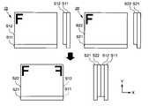
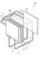
- FIG. 1shows a perspective view of an optical device 100 according to one embodiment of the present disclosure.
- the optical device 100includes a liquid crystal optical element 102 and a circuit board 104 .
- Liquid crystal optical element 102includes a plurality of liquid crystal cells.
- the liquid crystal optical element 102includes at least two liquid crystal cells.
- FIG. 1shows a mode in which the liquid crystal optical element 102 is composed of a first liquid crystal cell 10 and a second liquid crystal cell 20 .
- the first liquid crystal cell 10 and the second liquid crystal cell 20are flat panels, and are arranged so that the flat surfaces of the respective liquid crystal cells overlap each other.
- a transparent adhesive layer(not shown) is provided between the first liquid crystal cell 10 and the second liquid crystal cell 20 .
- the liquid crystal optical element 102has a structure in which adjacent liquid crystal cells are adhered with a transparent adhesive layer.
- the circuit board 104includes circuits for driving the liquid crystal optical element 102 .
- the first liquid crystal cell 10is connected to the circuit board 104 via the first flexible wiring board F1
- the second liquid crystal cell 20is connected to the circuit board 104 via the second flexible wiring board F2.
- the circuit board 104outputs a control signal for controlling the alignment state of the liquid crystal to each liquid crystal cell through the flexible wiring board.
- the light source section 106is arranged on the back side of the liquid crystal optical element 102 .
- the optical device 100is configured such that the light emitted from the light source section 106 is emitted through the liquid crystal optical element 102 to the front side of the drawing.
- the first liquid crystal cell 10 and the second liquid crystal cell 20are arranged in this order from the light source section 106 side.
- the light source unit 106includes a white light source, and an optical element such as a lens may be arranged between the white light source and the liquid crystal optical element 102 as necessary.
- the white light sourceis a light source that emits light close to natural light, and may emit dimmed light such as daylight white or incandescent light.
- the optical device 100has a function of controlling the diffusion direction of light emitted from the light source section 106 by means of the liquid crystal optical element 102 .
- the liquid crystal optical element 102has a function of shaping the light emitted from the light source section 106 into a light distribution pattern such as a square, a cross, or a line.
- FIG. 2shows a developed view of the liquid crystal optical element 102 shown in FIG.
- the liquid crystal optical element 102includes a first liquid crystal cell 10 and a second liquid crystal cell 20 .
- the first liquid crystal cell 10includes a first substrate S11, a second substrate S12, and a first flexible wiring substrate F1.
- the first substrate S11 and the second substrate S12are arranged facing each other with a gap therebetween.
- a liquid crystal layer(not shown) is provided in the gap between the first substrate S11 and the second substrate S12.
- the first flexible wiring board F1is connected to the first board S11.
- the second liquid crystal cell 20includes a first substrate S21, a second substrate S22, and a second flexible wiring substrate F2.
- the first substrate S21 and the second substrate S22are arranged facing each other with a gap therebetween.
- a liquid crystal layer(not shown) is provided in the gap between the first substrate S21 and the second substrate S22.
- the second flexible wiring board F2is connected to the first board S21.
- a first transparent adhesive layer TA1is arranged between the first liquid crystal cell 10 and the second liquid crystal cell 20 between the first liquid crystal cell 10 and the second liquid crystal cell 20, a first transparent adhesive layer TA1 is arranged.
- the first transparent adhesive layer TA1transmits visible light and bonds the second substrate S12 of the first liquid crystal cell 10 and the second substrate S22 of the second liquid crystal cell 20 together.
- the first liquid crystal cell 10 and the second liquid crystal cell 20are arranged such that the second substrate S12 of the first liquid crystal cell 10 and the second substrate S22 of the second liquid crystal cell 20 are connected via the first transparent adhesive layer TA1. They are superimposed and arranged so as to face each other.
- the first transparent adhesive layer TA1preferably has a high transmittance and a refractive index close to those of the first substrates S11, S21 and the second substrates S12, S22.
- an optical elastic resincan be used, for example, an adhesive containing acrylic resin having translucency can be used.
- the thermal expansion coefficient of the first transparent adhesive layer TA1is equal to the thermal expansion coefficient of the first substrates S11, S21 and the second substrates S12, S22. It is preferable to have a value close to the coefficient.
- the thickness of the first transparent adhesive layer TA1is thicker than the cell gap (thickness of the liquid crystal layer) of each liquid crystal cell (first liquid crystal cell 10, second liquid crystal cell 20) in order to relax thermal stress when the temperature rises. is preferred.
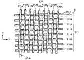
- FIG. 3is a perspective view showing the arrangement of electrodes provided in each of the first liquid crystal cell 10 and the second liquid crystal cell 20.
- the first liquid crystal cell 10includes a first substrate S11 and a second substrate S12, and a first liquid crystal layer LC1 between the first substrate S11 and the second substrate S12.
- the first substrate S11 and the second substrate S12each have a pair of sides (first sides s1) parallel to the X-axis direction (first direction) and parallel to the Y-axis direction (second direction) orthogonal to the X-axis direction. It may have a rectangular shape having a pair of sides (second sides s2).
- a first electrode E11is provided on the surface of the first substrate S11 facing the first liquid crystal layer LC1, and a second electrode E12 is provided on the surface of the second substrate S12 facing the first liquid crystal layer LC1. is provided.
- the first electrode E11 and the second electrode E12are arranged to face each other with the first liquid crystal layer LC1 interposed therebetween.
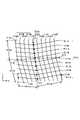
- the first electrode E11includes a plurality of first branch electrodes E11A and a plurality of second branch electrodes E11B each including a first pattern linearly extending in a direction inclined at a predetermined angle with respect to the X-axis direction (first direction). including.
- the extending directions of the plurality of first branched electrodes E11A and the plurality of second branched electrodes 12Bmay be inclined by 0.5 ⁇ 1° or more and 10 ⁇ 1° or less with respect to the X-axis direction.
- the plurality of first branched electrodes E11A and the plurality of second branched electrodes E11Bmay be inclined by 0.5 ⁇ 1° or more and 5 ⁇ 1° or less with respect to the X-axis direction.
- the second electrode E12includes a plurality of third branch electrodes E12A and a plurality of fourth branch electrodes E12B each including a second pattern linearly extending in a direction inclined at a predetermined angle with respect to the Y-axis direction (second direction). including.
- the extending directions of the plurality of third branched electrodes E12A and the plurality of fourth branched electrodes E12Bmay be inclined by 0.5 ⁇ 1° or more and 10 ⁇ 1° or less with respect to the Y-axis direction.
- the plurality of third branched electrodes E12A and the plurality of fourth branched electrodes E12Bmay be inclined by 0.5 ⁇ 1° or more and 5 ⁇ 1° or less with respect to the Y-axis direction.
- the plurality of first branch electrodes 11A and the plurality of second branch electrodes E11Bare alternately arranged in the Y-axis direction, and the plurality of third branch electrodes 12A and the plurality of fourth branch electrodes E12B are alternately arranged in the X-axis direction. be done.
- the X, Y, and Z axis directionsare shown for explanation.
- the first liquid crystal cell 10 and the second liquid crystal cell 20are stacked in the Z-axis direction.
- the extension directions of the plurality of first branch electrodes E11A and the plurality of second branch electrodes E11Bare arranged to be inclined at a predetermined angle with respect to the X-axis direction, and the plurality of third branch electrodes
- the extension directions of the electrode 12A and the plurality of fourth branch electrodes E12Bare arranged at a predetermined angle with respect to the Y-axis direction.
- the plurality of first branched electrodes E11A and the plurality of second branched electrodes E11B, and the plurality of third branched electrodes E12A and the plurality of fourth branched electrodes E12Bare arranged to cross each other so as not to be orthogonal.
- the second liquid crystal cell 20includes a first substrate S21, a second substrate S22, and a second liquid crystal layer LC2 between the first substrate S21 and the second substrate S22.
- a first electrode E21is provided on the surface of the first substrate S21 facing the second liquid crystal layer LC2, and a second electrode E22 is provided on the surface of the second substrate S22 facing the second liquid crystal layer LC2.
- the first electrode E21includes a plurality of first branch electrodes E21A and a plurality of second branch electrodes E21B each including a first pattern linearly extending in a direction inclined at a predetermined angle with respect to the X-axis direction (first direction). include.
- the extending directions of the plurality of first branched electrodes E21A and the plurality of second branched electrodes E21Bmay be inclined by 0.5 ⁇ 1° or more and 10 ⁇ 1° or less with respect to the X-axis direction.
- the plurality of first branched electrodes E21A and the plurality of second branched electrodes E21Bmay be inclined by 0.5 ⁇ 1° or more and 5 ⁇ 1° or less with respect to the X-axis direction.
- the second electrodes E22include a plurality of third branch electrodes E22A and a plurality of fourth branch electrodes E22B each including a second pattern linearly extending in a direction inclined at a predetermined angle with respect to the Y-axis direction (second direction). include.
- the extending directions of the plurality of third branched electrodes E22A and the plurality of fourth branched electrodes E22Bmay be inclined by 0.5 ⁇ 1° or more and 10 ⁇ 1° or less with respect to the Y-axis direction.
- the plurality of third branched electrodes E22A and the plurality of fourth branched electrodes E22Bmay be inclined by 0.5 ⁇ 1° or more and 5 ⁇ 1° or less with respect to the Y-axis direction.
- a plurality of first branch electrodes 21A and a plurality of second branch electrodes E21Bare alternately arranged in the Y-axis direction, and a plurality of third branch electrodes 22A and a plurality of fourth branch electrodes E22B are arranged alternately. They are arranged alternately in the X-axis direction.
- the extending directions of the plurality of first branch electrodes 21A and the plurality of second branch electrodes E21Bare arranged at a predetermined angle with respect to the X-axis direction, and the plurality of third branch electrodes
- the extension directions of the electrode 22A and the plurality of fourth branch electrodes E22Bare arranged at a predetermined angle with respect to the Y-axis direction. That is, the plurality of first branched electrodes E21A and the plurality of second branched electrodes E21B, and the plurality of third branched electrodes E22A and the plurality of fourth branched electrodes E22B are arranged to cross each other so as not to be orthogonal.
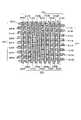
- the first branch electrode E11A and the second branch electrode E11B of the first liquid crystal cell 10 and the first branch electrode E21A and the second branch electrode E21B of the second liquid crystal cell 20are arranged with respect to the X axis. Each is extended while being inclined at a predetermined angle.
- the third branch electrode E12A and the fourth branch electrode E12B of the first liquid crystal cell 10 and the third branch electrode E22A and the fourth branch electrode E22B of the second liquid crystal cell 20are arranged along the Y axis. are extended while being inclined at a predetermined angle with respect to each other.
- the second substrate S12 of the first liquid crystal cell 10 and the second substrate S22 of the second liquid crystal cell 20are arranged to face each other via the first transparent adhesive layer TA1 (not shown in FIG. 3). ing.
- the third branch electrode E12A and the fourth branch electrode E12B of the first liquid crystal cell 10 and the third branch electrode E22A and the fourth branch electrode E22B of the second liquid crystal cell 20are arranged to face each other. Therefore, in the liquid crystal optical element 102, in the state where the first liquid crystal cell 10 and the second liquid crystal cell 20 are superimposed, the third branch electrode E12A and the fourth branch electrode E12B of the first liquid crystal cell 10 are arranged with respect to the Y-axis direction.
- the third branch electrode E22A and the fourth branch electrode E22B of the second liquid crystal cell 20are arranged at a predetermined angle, for example, an angle of ⁇ 2, they are arranged at an angle of 180 ⁇ ⁇ 2 with respect to the Y-axis direction. be.
- the angle ⁇ 2is 0.5 ⁇ 1 ° or more and 10 ⁇ 1°.
- the first substrate S11 of the first liquid crystal cell 10 and the first substrate S21 of the second liquid crystal cell 20are combined with the liquid crystal layer LC1 of the first liquid crystal cell 10 and the second substrate S21 of the first liquid crystal cell 10.
- the substrate S12, the first transparent adhesive layer TA1 (not shown in FIG. 3), the second substrate S22 of the second liquid crystal cell 20, and the liquid crystal layer LC2 of the second liquid crystal cell 20are arranged to face each other.
- the first branch electrode E11A and the second branch electrode E11B of the first liquid crystal cell 10 and the first branch electrode E21A and the second branch electrode E21B of the second liquid crystal cell 20are arranged to face each other.
- the first branch electrode E11A and the second branch electrode E11B of the first liquid crystal cell 10are arranged with respect to the X-axis direction.
- the first branch electrode E21A and the second branch electrode E21B of the second liquid crystal cell 20are arranged at an angle of ⁇ 1
- the first branch electrode E21A and the second branch electrode E21Bare arranged at an angle of 180 ⁇ 1 with respect to the X-axis direction.
- the angle ⁇ 1is 0.5 ⁇ 1° or more and 10 ⁇ 1°.
- the first substrates S11 and S21have the same configuration
- the second substrates S12 and S22have the same configuration.
- the first electrode E11 and the second electrode E12 provided in the first liquid crystal cell 10 and the first electrode E21 and the second electrode E22 provided in the second liquid crystal cell 20have substantially the same size in plan view.
- the light source section (106)is arranged below the first liquid crystal cell 10. As shown in FIG. Light emitted from the light source section (106) and incident on the liquid crystal optical element 102 passes through both the first liquid crystal cell 10 and the second liquid crystal cell 20 and is emitted.
- first liquid crystal cell 10 and the second liquid crystal cell 20have substantially the same configuration, the first liquid crystal cell 10 will be described in more detail below.
- FIG. 4Ashows a plan view of the first substrate S11
- FIG. 4Bshows a plan view of the second substrate S12.
- a first electrode E11is provided on the first substrate S11.
- the first electrode E11includes a plurality of first branch electrodes E11A and a plurality of second branch electrodes E11B.
- the plurality of first branched electrodes E11A and the plurality of second branched electrodes E11Bhave a first pattern, and the first pattern is strip-shaped.
- the first patternextends at a predetermined angle ⁇ 1 with respect to the X-axis direction.
- the strip-shaped pattern of the plurality of first branch electrodes E11A and the strip-shaped pattern of the plurality of second branch electrodes E11Bare alternately arranged at a predetermined interval.
- the plurality of first branch electrodes E11Aare each connected to a first feed line PL11, and the plurality of second branch electrodes E11B are each connected to a second feed line PL12.
- the first power supply line PL11is connected to the first connection terminal T11
- the second power supply line PL12is connected to the second connection terminal T12.
- the first connection terminal T11 and the second connection terminal T12are provided along one edge of the first substrate S11.
- the first substrate S11is provided with a third connection terminal T13 adjacent to the first connection terminal T11 and a fourth connection terminal T14 adjacent to the second connection terminal T12.
- the third connection terminal T13is connected to the fifth power supply line PL15.
- the fifth power supply line PL15is connected to a first power supply terminal PT11 provided at a predetermined position on the surface of the first substrate S11.
- the fourth connection terminal T14is connected to the sixth power supply line PL16.
- the sixth power supply line PL16is connected to a second power supply terminal PT12 provided at a predetermined position in the plane of the first substrate S11.
- the plurality of first branch electrodes E11Aare connected to the first feeder line PL11, and the same voltage is applied to each of them.
- the plurality of second branch electrodes E11Bare connected to a second feeder line PL12, and the same voltage is applied to each of them.
- the plurality of first branch electrodes E11A and the plurality of second branch electrodes E11Bare alternately arranged.
- the plurality of first branched electrodes E11A and the plurality of second branched electrodes E11Bare electrically separated.
- a second electrode E12is provided on the second substrate S12.
- the second electrode E12includes a plurality of third branch electrodes E12A and a plurality of fourth branch electrodes E12B.
- the plurality of third branched electrodes E12A and the plurality of fourth branched electrodes E12Bhave a second pattern, and the second pattern is strip-shaped.
- the second patternextends at a predetermined angle ⁇ 2 with respect to the Y-axis direction.
- the strip-shaped pattern of the plurality of third branch electrodes E12A and the strip-shaped pattern of the plurality of fourth branch electrodes E12Bare alternately arranged with a predetermined interval.
- the plurality of third branch electrodes E12Aare each connected to a third feed line PL13, and the plurality of fourth branch electrodes E12B are each connected to a fourth feed line PL14.
- the third power supply line PL13is connected to the third power supply terminal PT13, and the fourth power supply line PL14 is connected to the fourth power supply terminal PT14.
- the third power supply terminal PT13is provided at a position corresponding to the first power supply terminal PT11 of the first substrate S11, and the fourth power supply terminal PT14 is provided at a position corresponding to the second power supply terminal PT12 of the first substrate S11.
- the plurality of third branch electrodes E12Aare connected to the third feed line PL13, and the same voltage is applied to each of them.
- the plurality of fourth branch electrodes E12Bare connected to a fourth feeder line PL14, and the same voltage is applied to each of them.
- the plurality of third branch electrodes E12A and the plurality of fourth branch electrodes E12Bare alternately arranged.
- the plurality of third branched electrodes E12A and the plurality of fourth branched electrodes E12Bare electrically separated.
- a first connection terminal T11, a second connection terminal T12, a third connection terminal T13, and a fourth connection terminal T14 provided on the first substrate S11are terminals connected to the flexible wiring substrate.
- the first power supply terminal PT11 and the third power supply terminal PT13are electrically connected by a conductive material
- the second power supply terminal PT12 and the fourth power supply terminal PT14are electrically connected to the conductive material. Connected.
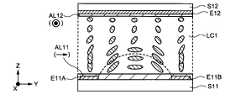
- FIG. 5shows a cross-sectional view of the first liquid crystal cell 10.
- FIG. The cross-sectional structure of the first liquid crystal cell 10 shown in FIG. 5shows the cross-sectional structure corresponding to the A1-A2 line of the first substrate S11 shown in FIG. 4A and the second substrate S12 shown in FIG. 4B.
- the first liquid crystal cell 10has an effective area AA capable of polarizing and scattering incident light.
- the first electrode E11 and the second electrode E12are arranged within the effective area AA.
- the first substrate S11 and the second substrate S12are bonded together by a sealing material SE provided outside the effective area AA (frame area).
- a gap for sealing the first liquid crystal layer LC1is provided between the first substrate S11 and the second substrate S12.
- the first liquid crystal layer LC1is sealed between the first substrate S11 and the second substrate S12 with a sealing material SE.
- the first substrate S11has a first electrode E11 and a first power supply terminal PT11, and has a structure in which a first alignment film AL11 is provided on the first electrode E11.
- the first electrode E11includes a first branch electrode E11A and a second branch electrode E11B.
- the first power supply terminal PT11has a structure continuous from the fifth power supply line PL15, and is arranged outside the sealing material SE.
- the second substrate S12has a second electrode E12 and a third power supply terminal PT13, and has a structure in which a second alignment film AL12 is provided on the second electrode E12.
- the second electrode E12includes a third branch electrode E12A and a fourth branch electrode E12B.
- the third power supply terminal PT13has a structure continuous from the third power supply line PL13, and is arranged outside the sealing material SE.
- the first electrode E11 and the second electrode E12are provided so that the extending directions of the electrode patterns intersect. That is, the extending direction of the first branched electrode E11A and the second branched electrode E11B is arranged so as to cross the extending direction of the third branched electrode E12A and the fourth branched electrode E12B. However, the first electrode E11 and the second electrode E12 are not perpendicular to each other. That is, the extending direction of the first branched electrode E11A and the second branched electrode E11B is not orthogonal to the extending direction of the third branched electrode E12A and the fourth branched electrode E12B.
- the first power supply terminal PT11 and the third power supply terminal PT13are arranged so as to face each other in a region outside the seal material SE.
- the first conductive member CP11is arranged between the first power supply terminal PT11 and the third power supply terminal PT13 to electrically connect them.
- the first conductive member CP11can be made of a conductive paste material, such as silver paste or carbon paste.
- the second power supply terminal PT12 and the fourth power supply terminal PT14are similarly electrically connected to each other via a conductive member.
- the first substrate S11 and the second substrate S12are translucent substrates, such as glass substrates and resin substrates.
- the first electrode E11 and the second electrode E12are transparent electrodes made of a transparent conductive material such as indium tin oxide (ITO) or indium zinc oxide (IZO).
- power supply lines(first power supply line PL11, second power supply line PL12, third power supply line PL13, fourth power supply line PL14, fifth power supply line PL15, sixth power supply line PL16), connection terminals (first connection terminal T11, 2 connection terminal T12, third connection terminal T13, fourth connection terminal T14) and power supply terminals (first power supply terminal PT11, second power supply terminal PT12, third power supply terminal PT13, fourth power supply terminal PT14) are made of aluminum, It is made of metal materials such as titanium, molybdenum, and tungsten.
- the feeder lines(first feeder line PL11, second feeder line PL12, third feeder line PL13, fourth feeder line PL14, fifth feeder line PL15, sixth feeder line PL16) are connected to the first electrode E11 and the second feeder line PL16. It may be formed of the same transparent conductive film as the electrode E12.
- the alignment films AL11 and AL12are formed of horizontal alignment films having an alignment regulating force substantially parallel to the main plane of the substrate.
- first liquid crystal layer LC1for example, twisted nematic liquid crystal (TN (Twisted Nematic) liquid crystal) is used.
- TNTransmission Nematic liquid crystal
- a spacermay be provided between the first substrate S11 and the second substrate S12 to keep the distance between the two substrates constant.
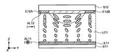
- FIG. 6is a cross-sectional view when the second liquid crystal cell 20 is placed over the first liquid crystal cell 10 shown in FIG. 5 with the first transparent adhesive layer TA1 interposed therebetween.
- the cross-sectional structures of the first liquid crystal cell 10 and the second liquid crystal cell 20 shown in FIG. 6correspond to the cross-sectional structures of the first substrate S11 shown in FIG. 4A and the second substrate S12 shown in FIG. 4B taken along line A1-A2. .
- the configuration of the second liquid crystal cell 20is substantially the same as the configuration of the first liquid crystal cell 10 described with reference to FIG.
- the first electrode E21 and the second electrode E22 of the second liquid crystal cell 20are arranged within the effective area AA.
- the first substrate S21 and the second substrate S22are bonded together by a sealing material SE provided outside the effective area AA.
- a gap for sealing the second liquid crystal layer LC2is provided between the first substrate S21 and the second substrate S22.
- the second liquid crystal layer LC2is sealed between the first substrate S21 and the second substrate S22 with a sealing material SE.
- the second substrate S22 of the second liquid crystal cell 20has the same configuration as the second substrate S12 of the first liquid crystal cell 10. That is, the second substrate S22 has a structure in which the second electrode E22 and the third power supply terminal PT23 are provided, and the second alignment film AL22 is provided on the second electrode E22.
- the second electrode E22includes a third branch electrode E22A and a fourth branch electrode E22B.
- the third power supply terminal PT23has a structure continuous from the third power supply line PL23, and is arranged outside the sealing material SE.
- the second substrate S22is arranged to face the second substrate S12 of the first liquid crystal cell 10 via the first transparent adhesive layer TA1.
- the second substrate S22has a surface (outer surface ES22) opposite to the surface on which the second electrode E22 is provided, with the first transparent adhesive layer TA1 interposed therebetween. It is arranged so as to face the surface (outer surface ES12) opposite to the surface of the second substrate 12 on which the second electrode E12 is provided.
- the first substrate S21 of the second liquid crystal cell 20has the same configuration as the first substrate S11 of the first liquid crystal layer 10. That is, the first substrate S21 has a structure in which a first electrode E21 and a first power supply terminal PT21 are provided, and a first alignment film AL21 is provided on the first electrode E21.
- the first electrode E21includes a first branch electrode E21A and a second branch electrode E21B.
- the first power supply terminal PT21has a structure continuous from the fifth power supply line PL25, and is arranged outside the sealing material SE.
- the first electrode E21 and the second electrode E22are provided so that the extending directions of the electrode patterns intersect. That is, the extending direction of the first branched electrode E21A and the second branched electrode E21B is arranged to intersect with the extending direction of the third branched electrode E22A and the fourth branched electrode E22B. However, the first electrode E21 and the second electrode E22 are not perpendicular to each other. That is, the extending direction of the first branched electrode E21A and the second branched electrode E21B is not orthogonal to the extending direction of the third branched electrode E22A and the fourth branched electrode E22B.
- the first power supply terminal PT21 and the third power supply terminal PT23are arranged so as to face each other in a region outside the seal material SE.
- the first conductive member CP21is arranged between the first power supply terminal PT21 and the third power supply terminal PT23 to electrically connect them.
- the first conductive member CP21can be made of the same material as the first conductive member CP11 of the first liquid crystal cell 10 .
- the second power supply terminal PT22 and the fourth power supply terminal PT24are similarly electrically connected to each other via a conductive member.
- the first substrate S21 and the second substrate S22are translucent substrates, such as glass substrates and resin substrates.
- the first electrode E21 and the second electrode E22are transparent electrodes made of a transparent conductive material such as indium tin oxide (ITO) or indium zinc oxide (IZO).
- the feeder lines, connection terminals, and feeder terminals provided on the first substrate S21 and the second substrate S22 of the second liquid crystal cell 20are provided on the first substrate S11 and the second substrate S12 of the first liquid crystal cell 10.
- the power supply line, connection terminals, and power supply terminalsthey are made of metal materials such as aluminum, titanium, molybdenum, and tungsten.
- the power supply linemay be formed of the same transparent conductive film as the first electrode E21 and the second electrode E22.
- the alignment films AL21 and AL22are formed of horizontal alignment films having an alignment regulating force substantially parallel to the main plane of the substrate.
- the second liquid crystal layer LC2uses twisted nematic liquid crystal (TN (Twisted Nematic) liquid crystal).
- TNTransmission Nematic liquid crystal
- a spacermay be provided between the first substrate S21 and the second substrate S22 to keep the distance between the two substrates constant.
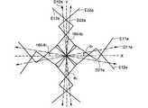
- FIG. 7Ashows the pattern (first pattern) of the first electrode E11 and the pattern (second pattern) of the second electrode E12 when the first substrate S11 and the second substrate S12 are arranged to overlap each other in the first liquid crystal cell 10.
- FIG. 7Bshows the case where the first liquid crystal cell 10 and the second liquid crystal cell 20 are overlapped, that is, the first substrate S11 and the second substrate S12 of the first liquid crystal cell 10 and the second substrate S12 of the second liquid crystal cell 20.
- the extension direction of the first electrode E11 (the first branch electrode E11A and the second branch electrode E11B) of the first liquid crystal cell 10is at an angle ⁇ with respect to the X-axis direction. 1 (the angle ⁇ 1 is 0.5 ⁇ 1° or more and 10 ⁇ 1°).
- the first substrate S11 and the second substrate S12are arranged such that the first electrode E11 and the second electrode E12 face each other. That is, the first substrate S11 and the second substrate S12 shown in FIG. 4A are arranged to face each other. Therefore, as shown in FIG.
- the extending direction of the second electrode E12(the third branch electrode E12A and the fourth branch electrode E12B) are arranged at an angle of 180 ⁇ 2 (angle ⁇ 2 is 0.5 ⁇ 1° or more and 10 ⁇ 1°) with respect to the Y-axis direction.
- the first liquid crystal cell 10 and the second liquid crystal cell 20are arranged such that the second substrate S12 of the first liquid crystal cell 10 and the second substrate S22 of the second liquid crystal cell 20 are the second substrates.
- 1 transparent adhesive layer TA1(not shown in FIGS. 7A and 7B) is disposed so as to face each other. Further, when the first liquid crystal cell 10 and the second liquid crystal cell 20 are arranged to overlap each other, the second substrate S22 of the second liquid crystal cell 20 is provided with the second electrode E22 via the first transparent adhesive layer TA1.
- the surface opposite to the surface on which the second electrode E12 is provided(external surface ES22 in FIG.
- the extending direction of the first electrode E21(the first branched electrode E21A and the second branched electrode E21B) is oriented at an angle of 180 ⁇ 1 ( ⁇ 1 is 0.5 ⁇ 1 ° or more and 10 ⁇ 1 °) with respect to the X-axis direction. °) placed at an angle.
- the extension directions of the first electrode E11 and the first electrode 21are inclined at a predetermined angle with respect to the X-axis direction.
- the extending directions of the second electrode E12 and the second electrode E22are inclined at a predetermined angle with respect to the Y-axis direction.
- the first substrate S11 and the second substrate S12are arranged such that the first electrode E11 and the second electrode E12 face each other.
- the relative arrangement of the first substrate 21 and the second substrate S22 in the second liquid crystal cell 20is the same as the arrangement of the first substrate S11 and the second substrate S12 of the first liquid crystal cell 10 .
- the outer surface of the second substrate S22 of the second liquid crystal cell 20 and the outer surface of the second substrate S12 of the first liquid crystal cell 10are arranged to face each other. Furthermore, the extending direction of the first electrode E11 and the first electrode E21 is inclined with respect to the X-axis direction, that is, the first side s1 of the first substrate S11 and the first substrate S21. Similarly, the extending direction of the second electrode E12 and the second electrode E22 is inclined with respect to the Y-axis direction, that is, the second side s2 of the second substrate S12 and the second substrate S21. Therefore, as shown in FIG.
- the first electrode E11 and the second electrode E12 of the first liquid crystal cell 10 and the first electrode E21 and the second electrode E22 of the second liquid crystal cell 20are at least partially Superimposed in a displaced state. Therefore, interference of light can be prevented, and ripples and luminance unevenness can be reduced. Therefore, when bonding the first liquid crystal cell 10 and the second liquid crystal cell 20 together, it is not necessary to adjust the inclination of the cell itself.
- FIGS. 8A to 8Care schematic cross-sectional views of the first liquid crystal cell 10.
- 8A and 8Bare schematic cross-sectional views of the first liquid crystal cell 10 viewed from the second side s2 side of the first substrate S11, and
- FIG. 8Cshows the first liquid crystal cell 10 on the second substrate S12. It is a cross-sectional schematic diagram at the time of seeing from 1 side s1 side.
- FIG. 8Ashows a partial cross-sectional schematic structure of the first liquid crystal cell 10.
- FIG. 8Bshows a first electrode E11 (first branched electrode E11A, second branched electrode E11B) provided on the first substrate S11, a first alignment film AL11, a second alignment film AL12 provided on the second substrate S12, and a first liquid crystal layer LC1.
- FIG. 8Ashows that the alignment treatment direction of the first alignment film AL11 and the alignment treatment direction of the second alignment film AL12 are different.
- the first alignment film AL11is aligned in a direction ALD1 perpendicular to the X-axis direction and parallel to the Y-axis direction, as shown in FIG. 4A.
- the light distribution direction ALD1intersects the extending directions of the first branched electrodes E11A and the second branched electrodes E11B so as not to be orthogonal.
- the second alignment film AL12is aligned in a direction ALD2 perpendicular to the Y-axis direction and parallel to the X-axis direction, as shown in FIG. 4B.
- the light distribution direction ALD2intersects the extending directions of the third branched electrodes E12A and the fourth branched electrodes E12B so as not to be orthogonal. Therefore, in the first liquid crystal cell 10 shown in FIG. 8A, the first alignment film AL11 is aligned in the horizontal direction of the drawing, and the second alignment film AL12 is aligned in the normal direction of the drawing.
- the orientation treatmentmay be a rubbing treatment or a light distribution treatment.
- FIG. 8Ashows a state in which no voltage is applied to the first branched electrode E11A and the second branched electrode E11B, and shows a state in which the long axis direction of the liquid crystal molecules is twisted by 90 degrees.
- FIG. 8Ashows an example (horizontal alignment) in which the liquid crystal layer LC1 is formed of a positive twisted nematic liquid crystal (TN liquid crystal) and the long axis of the liquid crystal molecules is aligned in the same direction as the alignment direction of the alignment film.
- TN liquid crystalpositive twisted nematic liquid crystal
- the liquid crystalpreferably contains a chiral agent that imparts twist to liquid crystal molecules.
- the liquid crystalmay be vertically aligned.
- FIG. 8Bshows a state in which a low level voltage VL is applied to the first branch electrode E11A and a high level voltage VH is applied to the second branch electrode E11B.
- a horizontal electric fieldis generated between the first branched electrode E11A and the second branched electrode E11B.
- the orientation direction of the liquid crystal molecules on the first substrate S11 sidechanges under the influence of the lateral electric field.
- the orientation of the liquid crystal molecules on the first substrate S11 sidechanges such that the long axis direction is parallel to the direction of the electric field.
- the values of the low-level voltage VL and the high-level voltage VH applied to the first branched electrode E11A and the second branched electrode E11Bare appropriately set. For example, 0 V is applied as the low-level voltage VL1, and a voltage of 5 to 30 V is applied as the high-level voltage VH1. A voltage in which a low-level voltage VL and a high-level voltage VH are alternately applied is applied to the first branch electrode E11A and the second branch electrode E11B. For example, a low-level voltage VL may be applied to the first branch electrode E11A and a high-level voltage VH may be applied to the second branch electrode E11B for a certain period of time.
- a high-level voltage VHmay be applied to the electrode E11A, and a low-level voltage VL may be applied to the second branch electrode E11B. In this way, the voltage may be applied such that the voltage levels are synchronized between the two electrodes and periodically changed.
- the frequency of the voltage applied to the first branched electrode E11A and the second branched electrode E11Bmay be any frequency that allows the liquid crystal molecules to follow changes in the electric field, for example, 15 to 100 Hz.
- FIG. 8Cshows a state in which a low level voltage VL is applied to the third branch electrode E12A and a high level voltage VH is applied to the fourth branch electrode E12B.
- a horizontal electric fieldis generated between the third branched electrode E12A and the fourth branched electrode E12B.
- the orientation direction of the liquid crystal molecules on the second substrate S12 sidechanges under the influence of the horizontal electric field.
- the orientation of the liquid crystal molecules on the second substrate S12 sidechanges so that the long axis direction is parallel to the direction of the electric field.
- the values of the low-level voltage VL and the high-level voltage VH applied to the third branched electrode E12A and the fourth branched electrode E12Bare appropriately set. For example, 0 V is applied as the low-level voltage VL1, and a voltage of 5 to 30 V is applied as the high-level voltage VH1. Voltages in which the low-level voltage VL and the high-level voltage VH are alternately applied to the third branched electrode E12A and the fourth branched electrode E12B are applied to the first branched electrode E11A and the second branched electrode E11B. be.
- the frequency of the voltage applied to the third branched electrode E12A and the fourth branched electrode E12Bmay be any frequency that allows the liquid crystal molecules to follow changes in the electric field, for example, 15 to 100 Hz.
- the refractive index of liquid crystalschanges depending on the orientation state.
- the long axis direction of the liquid crystal moleculesis aligned horizontally with the surface of the substrate, and the liquid crystal molecules are aligned from the first substrate S11 side to the first substrate S11 side.
- the two substrates S12are oriented in a twisted state of 90°.
- the liquid crystal layer LC1has a substantially uniform refractive index distribution in this alignment state.
- the first polarization component PL1 and the second polarization component PL2 orthogonal to the first polarization component PL1 of the light incident on the first liquid crystal cell 10are affected by the initial orientation of the liquid crystal molecules, and the polarization axes are rotated (
- the rotation of the polarization axis in the liquid crystal layeris referred to as optical rotation, the light is transmitted through the first liquid crystal layer LC1 without being refracted (or scattered).
- the first polarization component PL1corresponds to, for example, P-polarization of natural light
- the second polarization componentcorresponds to, for example, S-polarization.
- the first liquid crystal layer LC1in the ON state in which a voltage is applied to the first branch electrode E11A and the second branch electrode E11B to form an electric field, the first liquid crystal layer LC1 has a positive dielectric anisotropy. , the liquid crystal molecules align with their long axes along the electric field. As a result, as shown in FIG. 8B, the first liquid crystal layer LC1 has a region in which the liquid crystal molecules rise substantially vertically above the first branch electrode E11A and the second branch electrode E11B.
- a region that is obliquely oriented along the electric field distribution between the branched electrode E11B, a region that maintains the initial orientation state in a region apart from the first branched electrode E11A and the second branched electrode E11B, and the likeare formed.
- the long axes of the liquid crystal moleculesare aligned in a convex arc along the direction in which the electric field is generated.
- the tilt in the Z direction of the liquid crystal molecules located substantially in the center between the two electrodeshardly changes.
- the liquid crystal molecules located on the respective electrode sides from the central portionare oriented with an inclination (tilt) with respect to the Z direction according to the intensity distribution of the electric field. Therefore, when looking at the liquid crystal on the first substrate S11 side as a whole, liquid crystal molecules are aligned in an arc shape between the first branch electrode E11A and the second branch electrode E11B.
- diffusion of different polarization componentscan be independently controlled on the first substrate S11 side and the second substrate S12 side.
- the first substrate S11 and the second substrate S12 facing each otherare The distance is equal to or longer than the distance between the centers of the first branched electrode E11A and the second branched electrode E11B or the distance between the centers of the third branched electrode E12A and the fourth branched electrode E12B. is preferred.
- the center-to-center distance between the first branched electrode E11A and the second branched electrode E11Bis the distance from the center of the width of the first branched electrode E11A to the center of the width of the second branched electrode E11B.
- Liquid crystal moleculeshave a refractive index anisotropy ⁇ n. Therefore, the first liquid crystal layer LC1 in the ON state has a refractive index distribution or a retardation distribution according to the alignment state of the liquid crystal molecules.
- the retardationhere is represented by ⁇ n ⁇ d, where d is the thickness of the first liquid crystal layer LC1.
- the first polarization component PL1is scattered under the influence of the refractive index distribution of the first liquid crystal layer LC1 when passing through the first liquid crystal layer LC1.
- the second liquid crystal cell 20has the same configuration.
- the incident light passing through the first liquid crystal layer LC1 and the second liquid crystal layer LC2has a predetermined polarized component that is diffused in Moreover, by stacking the first liquid crystal cell 10 and the second liquid crystal cell 20, it is possible to individually control the scattering of specific polarized light components, and to control the light distribution of the light emitted from the light source.
- the optical device 100 of this embodiment described abovein the first liquid crystal cell 10 and the second liquid crystal cell 20, in the X-axis direction, that is, with respect to the first side s1 of the first substrate S11 and the first substrate S21,
- the extending directions of the first electrode E11 and the first electrode E21are inclined by a predetermined angle
- the second electrode E12 and the first electrode E21are arranged in the Y-axis direction, that is, with respect to the second side s2 of the second substrate S12 and the second substrate S21.
- the extending direction of the second electrode E22is inclined by a predetermined angle.
- the extending directions of the first electrode E11 and the second electrode E12are inclined at a predetermined angle with respect to the sides of the first substrate S11 and the second substrate S12 of the first liquid crystal cell 10 .
- the extending directions of the first electrode E21 and the second electrode E22are inclined at a predetermined angle with respect to the sides of the first substrate S21 and the second substrate S22 of the second liquid crystal cell 20 .
- the first liquid crystal cell 10 and the second liquid crystal cell 20are pasted together, even if the first liquid crystal cell 10 and the second liquid crystal cell 20 are superimposed along the corresponding sides of the substrates, the first liquid crystal The first electrode E11 and the second electrode E12 of the cell 10 and the first electrode E21 and the second electrode E22 of the second liquid crystal cell 20 are completely aligned and do not overlap each other. In other words, the first electrode E11 and the second electrode E12 of the first liquid crystal cell 10 and the first electrode E21 and the second electrode E22 of the second liquid crystal cell 20 are overlapped with at least a part thereof being shifted.
- the first liquid crystal cell 10 and the second liquid crystal cell 20are pasted together, it is not necessary to adjust the inclination of the cell itself, so that the optical device 100 can be manufactured easily.
- the first electrode E11(first branch electrode E11A, second branch electrode E11B), E21 (first branch electrodes E21A and E21B) and second electrode E12 of the first liquid crystal cell 10 and the second liquid crystal cell (third branched electrodes E12A, fourth branched electrodes E12B) and E22 (third branched electrodes E22A, E22B) are arranged on the first side s1 or the second side s2 of the first substrates S11, S21 and the second substrates S12, S22. It has a linear pattern inclined at a predetermined angle with respect to the surface.
- the shape of each electrode pattern of the first liquid crystal cell 10 and the second liquid crystal cellis not limited to linear.
- the shapes of the electrodes of the first liquid crystal cell and the second liquid crystal constituting the optical deviceare the same as the shapes of the electrodes of the first liquid crystal cell 10 and the second liquid crystal 10 constituting the optical device 100 according to the first embodiment.
- An example different from the shape ofis described.
- the same reference numeralsor numerals followed by a, b, etc. are assigned to configurations that are the same as or similar to the configuration of the optical device 100 of the first embodiment described above. , detailed description is omitted.
- the configuration other than the shape of each electrode of the first liquid crystal cell and the second liquid crystal constituting the optical deviceis substantially the same as the optical device 100 of the first embodiment described above. Therefore, the shape of each electrode of the first liquid crystal cell and the second liquid crystal constituting the optical device will be mainly described below, and description of other configurations will be omitted.
- FIG. 9Ashows the first electrode E11a and the second electrode E12a when the first substrate S11 and the second substrate S12 are arranged to overlap each other in the first liquid crystal cell 10a constituting the optical device 100a according to the present embodiment. It is a schematic plan view showing.
- FIG. 9Bshows the case in which the first liquid crystal cell 10a and the second liquid crystal cell 20a that constitute the optical device 100a are arranged to overlap, that is, the first substrate S11 and the second substrate S12 of the first liquid crystal cell 10a and the second substrate S11 and the second substrate S12.
- FIG. 4is a schematic plan view showing first electrodes E11a and E21a and second electrodes E12a and E22a when the first substrate S21 and the second substrate S22 of the two-liquid crystal cell 20a are arranged so as to overlap each other.
- FIG. 10Ais a schematic diagram for explaining the inclination in the extending direction of the first electrode E11a and the second electrode E12a shown in FIG. 9A.
- FIG. 10Bis a schematic diagram for explaining the inclination in the extending direction of the first electrode E11a, the second electrode E12a, the first electrode E21a, and the second electrode E22a shown in FIG. 9B.
- the first electrode E11a of the first substrate S11has a first pattern having a zigzag shape in a direction inclined at a predetermined angle with respect to the X-axis direction (first direction). a plurality of first branch electrodes E11A and a plurality of second branch electrodes E11B.
- the zigzag-shaped first patternhas a plurality of bending points.
- the second electrode E12aincludes a plurality of third branch electrodes E12A and a plurality of fourth branch electrodes including a second pattern having a zigzag shape in a direction inclined at a predetermined angle with respect to the Y-axis direction (second direction). E12B.
- the zigzag-shaped second patternhas a plurality of bending points.
- the extension direction D11a of the first electrode E11ais inclined at a predetermined angle ⁇ 1 with respect to the X-axis direction.
- the angle ⁇ 1is 0.5 ⁇ 1° or more and 10 ⁇ 1°.
- the extending direction D12a of the second electrode E12ais inclined at a predetermined angle ⁇ 2 with respect to the Y-axis direction.
- the angle ⁇ 2is 0.5 ⁇ 1 ° or more and 10 ⁇ 1°. That is, the extending direction D11a of the first electrode E11a and the extending direction D12a of the second electrode E12a intersect so as not to be orthogonal.
- the first electrode E21a of the first substrate S21has a zigzag shape and is tilted at a predetermined angle with respect to the X-axis direction (first direction). It includes a plurality of first branched electrodes E21A and a plurality of second branched electrodes E21B including an extended first pattern.
- the second electrode E22ahas a zigzag shape and includes a plurality of third branches including a second pattern extending in a direction inclined at a predetermined angle with respect to the Y-axis direction (second direction). It includes an electrode E22A and a plurality of fourth branch electrodes E22B.
- the shape of the first electrode E21a of the first substrate S21is the same as the shape of the first electrode 11a of the first liquid crystal cell 10a, and the shape of the first electrode E21a of the second substrate S22 is the same.
- the shape of the second electrode E22ais the same as the shape of the second electrode 12a of the first liquid crystal cell 10a.
- the second liquid crystal cell 20ais provided with the second electrode E22a of the second substrate S22 via the first transparent adhesive layer (TA1).
- the surface opposite to the side provided with the second electrode E12a of the first liquid crystal cell 10ais arranged to face the surface opposite to the side provided with the second electrode E12a of the second substrate S12.
- the first branch electrode E21A and the second branch electrode E21B of the first electrode E21abecome the first branch electrode E11A and the second branch electrode E11B of the first electrode E11a in the first liquid crystal cell 10a. are superimposed in a state in which at least a part thereof is shifted in plan view.
- the first electrode E21a of the second liquid crystal cell 20a and the first electrode E11a of the first liquid crystal cell 10ado not overlap each other in a state of being completely aligned in plan view.
- the third branch electrode E22A and the fourth branch electrode E22B of the second electrode E22aare at least one of the second branch electrode E12A and the fourth branch electrode E12B of the second electrode E12a in the first liquid crystal cell 10a in plan view. The parts are superimposed in a shifted state.
- the second electrode E22a of the second liquid crystal cell 20a and the second electrode E12a of the first liquid crystal cell 10ado not overlap each other in a state of being completely aligned in plan view. As shown in FIG.
- the extending direction D11a of the first electrode E21a of the second liquid crystal cell 20ais inclined at an angle of 180 -.theta.1 with respect to the X-axis direction.
- the angle ⁇ 1is 0.5 ⁇ 1° or more and 10 ⁇ 1°.
- the extending direction D22a of the second electrode E22ais inclined at an angle of 180- ⁇ 2 with respect to the Y-axis direction.
- the angle ⁇ 2is 0.5 ⁇ 1 ° or more and 10 ⁇ 1°. That is, the extension direction D21a of the second electrode E21a and the extension direction D22a of the second electrode E22a intersect so as not to be orthogonal.
- the first electrodes E11a and E21a and the second electrodes E12a and E22a of the first liquid crystal cell 10a and the second liquid crystal 20a constituting the optical device 100ahave zigzag shapes. ing. Furthermore, the extending direction of the first electrodes E11a and E21a is inclined at a predetermined angle with respect to the X-axis direction (first direction), and the extending direction of the second electrodes E12a and E22a is tilted with respect to the Y-axis direction (second direction). tilted at a predetermined angle. In the first liquid crystal cell 10a, the first electrode E11a and the second electrode 12a intersect so as not to be perpendicular to each other.
- the first electrode E12a and the second electrode 22aintersect so as not to be perpendicular to each other.
- the first electrodes E11a and E21a and the second electrodes E12a and E22aare arranged so as to completely match each other in a plan view so as not to overlap each other. That is, they are arranged so as to overlap each other with at least a part thereof being shifted.
- the optical device 100acan prevent light interference and reduce ripples and luminance unevenness. Moreover, when the first liquid crystal cell 10a and the second liquid crystal cell 20a are bonded together, it is not necessary to adjust the inclination of the cells themselves.
- each E22ahas a zigzag pattern
- each electrode patternpreferably do not overlap each other.
- each electrode patternhas a zigzag shape
- each electrode patternhas a symmetrical shape
- interferencemay occur when the first liquid crystal cell 10a and the second liquid crystal cell 20a are overlapped. Therefore, in each electrode pattern, the distance between a predetermined bending point and an adjacent bending point may be different from the distance between the predetermined bending point and another adjacent bending point.
- the positions of a plurality of bending pointsmay be random.
- the first electrodes E11a and E21a provided on the first substrates S11 and S21, the second electrodes E12a provided on the second substrates S12 and S22We have described the case where E22a has a zigzag shaped pattern, each with multiple inflection points.
- the shape of each electrode patternis not limited to this.
- the patterns of the first electrodes E11a and E21a and the second electrodes E12a and E22ahave a shape with one bending point, a so-called " ⁇ " shape.
- each electrodemay In this case, if the pattern shape of each electrode is symmetrical, interference may occur when the first liquid crystal cell 10a and the second liquid crystal cell 20a are overlapped. Therefore, in the pattern of each electrode, the distance between the bending point and one end of the pattern may be different from the distance between the predetermined bending point and the other end of the pattern.
- FIG. 11shows the first electrode E11a and the second substrate S12 provided with the first electrode E11a and the second electrode E12a having patterns having a doglegged shape, respectively, when the first substrate S11 and the second substrate S12 are arranged to overlap each other.
- FIG. 11is a schematic plan view showing a second electrode E12a; Here, as in the above embodiment, the first substrate S11 and the second substrate S12 are superimposed so that the first electrode E11a and the second electrode E12a face each other.
- FIG. 12is a schematic diagram for explaining the positions of bending points of the first electrode E11a and the second electrode E12a shown in FIG. In addition, in FIG.
- FIG. 12is a schematic diagram of the first liquid crystal cell 10a viewed from the second substrate S12 side.
- the first electrode E11aincludes a first branched electrode E11A and a second branched electrode E11B.
- Each of the first branched electrode E11A and the second branched electrode E11Bhas a shape including one bending point F11, that is, a so-called " ⁇ "-shaped pattern (first pattern).
- the patterns of the first branched electrode E11A and the second branched electrode E11Bare asymmetrical about the bending point F11.
- the bending point F11 and one end T11a of the pattern of the first electrode E11a(the first branched electrode E11A, the second branched electrode E11B) If W11a is the distance between is.
- the positions of the bending points F11 of the first branched electrode E11A and the second branched electrode E11Bare shifted from the bending points F11 of the adjacent first branched electrode E11 or the second branched electrode E11B in the Y-axis direction.
- the extending direction D11 of the line connecting the bending points F11 of the first branched electrode E11A and the second branched electrode E11Bmay be inclined at a predetermined angle with respect to the Y-axis direction.
- the second electrode E12aincludes a third branch electrode E12A and a fourth branch electrode E12B.
- Each of the third branched electrode E12A and the fourth branched electrode E12Bhas a shape having one bending point F12, that is, a so-called " ⁇ "-shaped pattern (second pattern).
- the patterns of the third branched electrode E12A and the fourth branched electrode E12Bare asymmetrical about the bending point F12.
- the bending point F12 and one end T12a of the pattern of the second electrode E12a(the third branched electrode E12A, the second branched electrode E12B) If W12a is the distance between is. Further, the positions of the bending points F12 of the third branched electrode E12A and the fourth branched electrode E12B are shifted from the bending points F12 of the adjacent third branched electrode E12A or the fourth branched electrode E12B in the X-axis direction. For example, as shown in FIG. 12, the extending direction D12 of the line connecting the bending points F12 of the third branched electrode E12A and the fourth branched electrode E12B may be inclined at a predetermined angle with respect to the X-axis direction.
- each electrodeWhen the pattern of each electrode has a doglegged shape, depending on the angle of the pattern, when the first liquid crystal cell 10a and the second liquid crystal cell 20a are pasted together, the electrodes overlap each other, causing interference and moire. sometimes. In order to prevent interference and suppress the occurrence of moire, it is preferable to devise the setting of the angle of the pattern of each electrode.
- FIGS. 13A to 13Care schematic diagrams for explaining the setting of the angle of the pattern of each electrode when the pattern of each electrode has a doglegged shape.
- the pattern of each electrodeis shown in a simplified form so that the angle of the pattern of the electrode can be easily seen.
- the pattern of each electrodeis arranged on the XY coordinate plane, and the bending point of each electrode is arranged at the origin on the XY coordinate plane for easy understanding of the angle of the pattern of each electrode.
- there is 13Ais a schematic diagram of the first liquid crystal cell 10a viewed from the second substrate S12 side
- FIG. 13Bis a schematic diagram of the second liquid crystal cell 20a viewed from the first substrate S11 side.
- FIG. 13Cshows the first substrate of the second liquid crystal cell 20a when the first liquid crystal cell 10a is overlapped with the outer surface of the second substrate S12 facing the outer surface of the second substrate S22 of the second liquid crystal cell 20a. It is a schematic view when viewed from the S11 side, that is, the light emitting side of the liquid crystal optical element 102 (the same applies to FIGS. 14A to 14C described later).
- FIG. 13Ashows an example of patterns of the first electrode E11a and the second electrode E12a in the first liquid crystal cell 10a.
- the first electrode E11ahas a first extension direction ED1 tilted at an angle ⁇ b with respect to the X-axis and a second extension direction ED1 tilted at an angle ⁇ d with respect to the X-axis about the bending point. Extends in direction ED2.
- the first extension direction ED1is located in the first quadrant on the XY coordinate plane
- the second extension direction ED2is located in the second quadrant on the XY coordinate plane.
- the second electrode E12aextends in a third extending direction ED3 inclined at an angle ⁇ a with respect to the Y axis and in a fourth extending direction ED4 inclined at an angle ⁇ c with respect to the Y axis.
- the third extension direction ED3is positioned in the second quadrant on the XY coordinate plane
- the fourth extension direction ED4is positioned in the fourth quadrant.
- ⁇ a⁇ c or ⁇ a ⁇ c
- FIG. 13Bshows an example of patterns of the first electrode E21a and the second electrode E22a in the second liquid crystal cell 20a.
- the first liquid crystal cell 10a and the second liquid crystal cell 20ahave the same configuration, that is, the pattern of the first electrode E21a in the second liquid crystal cell 20a is the same as the pattern of the first electrode E11a in the first liquid crystal cell 10a.
- the pattern of the second electrode E22a in the second liquid crystal cell 20ais the same as the pattern of the second electrode E12a in the first liquid crystal cell 10a.
- FIG. 13Bshows the electrode patterns of the first electrode E21a and the second electrode E22 in a state where the second substrate S22 of the second liquid crystal cell 20a faces the second substrate S12 of the first liquid crystal cell 10a.
- the second liquid crystal cell 20ais reversed about the X axis, and the second substrate S22 of the second liquid crystal cell 20a and the second substrate S12 of the first liquid crystal cell 10a are bonded together by the first transparent bonding. It shows a state in which they are arranged to face each other with the layer TA1 interposed therebetween.
- the first electrode E21ahas a fifth extension direction ED5 inclined at an angle ⁇ b with respect to the X-axis and a sixth extension direction ED5 inclined at an angle ⁇ d with respect to the X-axis about the bending point. Extends in direction ED6.
- the fifth extension direction ED5is located in the fourth quadrant on the XY coordinate plane
- the sixth extension direction ED6is located in the third quadrant on the XY coordinate plane.
- the second electrode E22aextends in a seventh extending direction ED7 inclined at an angle ⁇ a with respect to the Y-axis and an eighth extending direction ED8 inclined at an angle ⁇ c with respect to the Y-axis. be done.
- the seventh extension direction ED7is positioned in the third quadrant on the XY coordinate plane
- the eighth extension direction ED8is positioned in the first quadrant.
- FIG. 13Cshows the first electrodes E11a and E21a and the second electrodes E12a and E22a when the first liquid crystal cell 10a shown in FIG. 13A and the second liquid crystal cell 20a shown in FIG. Show a pattern.
- the first electrode E11a and the second electrode E12a of the first liquid crystal cell 10a shown in FIG. 13A and the first electrode E21a and the second electrode E22a of the second liquid crystal cell 20a shown in FIG.They are not superimposed in perfect agreement with each other. That is, they are superimposed in a state in which at least a part of them are shifted from each other.
- FIG. 13Cshows the first electrodes E11a and E21a and the second electrodes E12a and E22a when the first liquid crystal cell 10a shown in FIG. 13A and the second liquid crystal cell 20a shown in FIG. Show a pattern.
- the second liquid crystal cell 20ais inverted about the X-axis to form the second substrate S22 of the second liquid crystal cell 20a and the second substrate S12 of the first liquid crystal cell 10a. are arranged to face each other with the first transparent adhesive layer TA1 interposed therebetween.
- FIG. 13Cwhen the second liquid crystal cell 20a is inverted about the X-axis, the extending directions of the corresponding electrode patterns in the first liquid crystal cell 10a and the second liquid crystal cell 20a are different.
- the extension direction of the first electrode E11a of the first liquid crystal cell 10ais the extension direction ED1 extending in the first quadrant and the extension direction ED2 extending in the second quadrant, whereas the extension direction ED2 of the second liquid crystal cell 20a.
- the extension direction of the one electrode E21ais an extension direction ED5 extending in the fourth quadrant and an extension direction ED6 extending in the third quadrant.
- the extending direction of the second electrode E12a of the first liquid crystal cell 10ais the extending direction ED3 extending in the second quadrant and the extending direction ED4 extending in the fourth quadrant, whereas the second electrode E12a of the second liquid crystal cell 20a
- the extension direction of E22ais an extension direction ED7 extending in the third quadrant and an extension direction ED8 extending in the first quadrant.
- the extension direction of the pattern of the second electrode E12a of the first liquid crystal cell 10a and the second electrode E22a of the second liquid crystal cell 20a(here, the second electrode
- the third extending direction ED3 and the fourth extending direction ED4which are the extending directions of the electrode E12a
- the seventh extending direction ED7 and the eighth extending direction ED8which are the extending directions of the second electrode E22a
- the first liquid crystal cell
- the second electrodes E12a and E22a of the second liquid crystal cell 10a and the second liquid crystal cell 20aare completely aligned. In such a case, the overlapping of the electrodes may cause interference and cause moire.
- FIGS. 14A to 14Care other schematic diagrams for explaining the setting of the angle of the pattern of each electrode when the pattern of each electrode has a doglegged shape. Similar to FIGS. 13A to 13C, FIGS. 14A to 14C show the patterns of the electrodes in a simplified manner so that the angles of the patterns of the electrodes can be easily seen. Also, each pattern is arranged on the XY coordinate plane, and the bending point of each electrode is arranged at the origin on the XY coordinate plane.
- FIG. 14Ashows an example of patterns of the first electrode E11a and the second electrode E12a in the first liquid crystal cell 10a.
- the first electrode E11ahas a first extension direction ED1 tilted at an angle ⁇ b with respect to the X-axis and a second extension direction ED1 tilted at an angle ⁇ d with respect to the X-axis about the bending point. Extends in direction ED2.
- the first extension direction ED1is located in the first quadrant on the XY coordinate plane
- the second extension direction ED2is located in the second quadrant on the XY coordinate plane.
- the second electrode E12aextends in a third extending direction ED3 inclined at an angle ⁇ a with respect to the Y axis and in a fourth extending direction ED4 inclined at an angle ⁇ c with respect to the Y axis.
- the third extension direction ED3is positioned in the first quadrant on the XY coordinate plane
- the fourth extension direction ED4is positioned in the fourth quadrant.
- ⁇ a ⁇ ⁇ c and ⁇ b⁇ c or ⁇ b ⁇ ⁇ c .
- ⁇ b⁇ d or ⁇ b ⁇ d .
- FIG. 14Bshows an example of patterns of the first electrode E21a and the second electrode E22a in the second liquid crystal cell 20a.
- the second liquid crystal cell 20ais reversed about the X axis so that the second substrate S22 of the second liquid crystal cell 20a and the second substrate S12 of the first liquid crystal cell 10a are aligned. In this state, they are arranged so as to face each other with the first transparent adhesive layer TA1 interposed therebetween.
- the first electrode E21ahas a fifth extension direction ED5 inclined at an angle ⁇ b with respect to the X axis, and a sixth extension direction ED5 inclined at an angle ⁇ d with respect to the X axis.
- the fifth extension direction ED5is located in the fourth quadrant on the XY coordinate plane, and the sixth extension direction ED6 is located in the third quadrant on the XY coordinate plane.
- the second electrode E22aextends in a seventh extending direction ED7 inclined at an angle ⁇ a with respect to the Y-axis and an eighth extending direction ED8 inclined at an angle ⁇ c with respect to the Y-axis. be done.
- the seventh extension direction ED7is located in the fourth quadrant on the XY coordinate plane, and the eighth extension direction ED8 is located in the first quadrant.
- FIG. 14Cshows the first electrodes E11a and E21a and the second electrodes E12a and E22a when the first liquid crystal cell 10a shown in FIG. 14A and the second liquid crystal cell 20a shown in FIG. Show a pattern.
- the first electrode E11a and the second electrode E12a of the first liquid crystal cell 10a shown in FIG. 14A and the first electrode E21a and the second electrode E22a of the second liquid crystal cell 20a shown in FIG.They are not superimposed in perfect agreement with each other. That is, they are superimposed in a state in which at least a part of them are shifted from each other. As described with reference to FIG.
- the second liquid crystal cell 20ais inverted about the X-axis to form the second substrate S22 of the second liquid crystal cell 20a and the second substrate S12 of the first liquid crystal cell 10a. are arranged to face each other with the first transparent adhesive layer TA1 interposed therebetween.
- the third extending direction ED3 of the second electrode E12a of the first liquid crystal cell 10a and the eighth extending direction ED8 of the second electrode E22a of the second liquid crystal cell 20aare in the same first quadrant.
- the third extension direction ED3since the angle ⁇ a formed between the third extension direction ED3 and the Y-axis and the angle ⁇ c formed between the eighth extension direction ED8 and the Y-axis are different from each other ( ⁇ a ⁇ ⁇ c), the third extension direction ED3
- the second electrode E12a of the first liquid crystal cell 10a extending in the eighth extension direction and the second electrode E22a of the second liquid crystal cell 20a extending in the eighth extension directionare completely matched and do not overlap each other. That is, they are superimposed in a state in which at least a part of them are shifted from each other.
- the fourth extending direction ED4 of the second electrode E12a of the first liquid crystal cell 10a and the seventh extending direction ED7 of the second electrode E22a of the second liquid crystal cell 20abelong to the same fourth quadrant.
- the angle ⁇ c formed between the fourth extension direction ED4 and the Y axisis different from the angle ⁇ a formed between the seventh extension direction ED7 and the Y axis ( ⁇ a ⁇ ⁇ c )
- the fourth extension direction ED4The second electrode E12a of the first liquid crystal cell 10a extending in the seventh extension direction and the second electrode E22a of the second liquid crystal cell 20a extending in the seventh extension direction are completely matched and do not overlap each other.
- the Y-axis and the extending direction of the electrode patterns of the second electrode E12a of the first liquid crystal cell 10a and the second electrode E22a of the second liquid crystal cell 20aare different from each other by 1° or more.
- the second liquid crystal cell 20ais inverted about the Y axis. It is envisioned that the first liquid crystal cell 10a and the first liquid crystal cell 10a are overlapped with each other.
- the second liquid crystal cell 20ais reversed about the Y-axis and overlapped with the first liquid crystal cell 10a, the conditions are opposite to those described with reference to FIGS. 13A to 13C and FIGS. 14A to 14C.
- the extending directions of the electrode patterns of the first electrode E11a of the first liquid crystal cell 10a and the first electrode E21a of the second liquid crystal cell 20aare different from each other, or the first electrode E11a of the first liquid crystal cell 10a and the second If the angle formed by the extending direction of the electrode pattern of the first electrode E21a of the liquid crystal cell 20a and the X-axis is different from each other, the second liquid crystal cell 20a is inverted about the Y-axis and overlapped with the first liquid crystal cell 10a. It is possible to prevent the electrodes from being superimposed in a state of being completely aligned with each other when the electrodes are arranged in the same direction, thereby preventing interference and preventing the occurrence of moire.
- each pattern of the first electrodes E11a and E21a and the second electrodes E12a and E22ahas a zigzag shape or a dogleg shape. explained.
- the shape of each electrode patternis not limited to these, and various shapes are applicable.
- each pattern of the first electrodes E11a, E21a and the second electrodes E12a, E22amay have a wave shape.
- the electrodesmay overlap each other when the first liquid crystal cell 10a and the second liquid crystal cell 20a are overlapped, causing interference. Therefore, when each pattern has a wavy shape, it is preferable that each pattern has an asymmetrical shape with respect to a predetermined axis, such as random wave sizes.
- the patterns of the first electrodes E11a and E21a and the second electrodes E12a and E22amay be arc-shaped.
- each pattern of the first electrodes E11a, E21a and the second electrodes E12a, E22amay be concentric. In such a case, if each pattern has a bilaterally symmetrical shape, the electrodes may overlap each other when the first liquid crystal cell 10a and the second liquid crystal cell 20a are overlapped, causing interference. Therefore, when each electrode pattern has a concentric circular shape, it is preferable that each electrode pattern has a distorted circle or a rotationally asymmetric circle so as to be asymmetrical in the bonding direction.
- the first liquid crystal cell 10aWhen the second liquid crystal cell 20a is overlaid, the second liquid crystal cell 20a is overlaid on the first liquid crystal cell 10a in a state in which the second liquid crystal cell 20a is inverted about the Y direction.
- the method of overlapping the first liquid crystal cell and the second liquid crystal cellis not limited to this. Variations in the method of superimposing the first liquid crystal cell and the second liquid crystal cell will be described below with reference to the drawings.
- FIG. 15schematically shows each electrode when the first liquid crystal cell and the second liquid crystal cell are arranged to overlap, that is, when the first liquid crystal cell and the second liquid crystal cell are arranged to overlap. It is an example of a plan view.
- the first liquid crystal cell and the second liquid crystal cell shown in FIG. 15have the same configuration as the first liquid crystal cell 10 and the second liquid crystal cell 20 in the optical device 100 of the first embodiment described above.
- the extending direction of the pattern (first pattern) of the first electrode E11 and the pattern (second pattern) of the second electrode E12 in the first liquid crystal cell 10 and the first electrode E21 in the second liquid crystal cell 2 and the pattern (second pattern) of the second electrode E22are different from each other. Therefore, when the first liquid crystal cell 10 and the second liquid crystal cell 20 are superimposed, the second liquid crystal cell 20 is rotated by 90° instead of being inverted, so that the first liquid crystal cell 10 and the second liquid crystal cell 20 It is possible to prevent the electrodes from being superimposed in a state where the extending directions of the respective electrodes are completely matched.
- 16A to 16Dare schematic diagrams showing variations in how the first liquid crystal cell 10 and the second liquid crystal cell 20 are superimposed.
- 16A to 16Dare plan views and cross-sectional views of the substrates of the first liquid crystal cell 10 (first substrate S11 and second substrate S12) and the substrates of the second liquid crystal cell 20 (first substrate S21 and second substrate S22), respectively. 1, and a plan view and a cross-sectional view when the first liquid crystal cell 10 and the second liquid crystal cell 20 are overlapped.
- the second liquid crystal cell 20is reversed and arranged above the first liquid crystal cell 10 .
- FIG. 16Ashows the second liquid crystal cell 10 and the second liquid crystal cell 20 in a state in which the second liquid crystal cell 20 is inverted about the Y direction when the first liquid crystal cell 10 and the second liquid crystal cell 20 are overlapped, as in FIGS. 7B and 9B. 20 is superimposed on the first liquid crystal cell 10.
- FIG. FIG. 16Bshows that when the first liquid crystal cell 10 and the second liquid crystal cell 20 are overlapped, the second liquid crystal cell 20 is overlapped with the first liquid crystal cell 10 in a state in which the second liquid crystal cell 20 is inverted about the X direction.
- a matching exampleis shown.
- FIG. 16Cshows that when the first liquid crystal cell 10 and the second liquid crystal cell 20 are superimposed, the second liquid crystal cell 20 is reversed around the Y direction, and the second liquid crystal cell 20 is rotated by 90°. 1 shows an example of overlapping with the liquid crystal cell 10 .
- FIG. 16Dshows that when the first liquid crystal cell 10 and the second liquid crystal cell 20 are superimposed, the second liquid crystal cell 20 is reversed around the X direction, and the second liquid crystal cell 20 is rotated by 90°. 1 shows an example of overlapping with the liquid crystal cell 10 .
- the optical devices 100, 100aare composed of two liquid crystal cells, ie, a first liquid crystal cell 10, 10a and a second liquid crystal cell 20, 20a.
- the number of liquid crystal cells forming the optical deviceis not limited to two.
- FIG. 17shows a perspective view of an optical device 100b according to a modification of the invention.
- the optical device 100bincludes a liquid crystal optical element 102b and a circuit board 104.
- the liquid crystal optical element 102bincludes four liquid crystal cells as an example.
- the liquid crystal optical element 102 bis composed of a first liquid crystal cell 10 , a second liquid crystal cell 20 , a third liquid crystal cell 30 and a fourth liquid crystal cell 40 .
- the configuration of the liquid crystal optical element 102b except for the third liquid crystal cell 30 and the fourth liquid crystal cell 40is substantially the same as the liquid crystal optical element 102 described in the first embodiment. Therefore, the third liquid crystal cell 30 and the fourth liquid crystal cell 40 will be mainly described below, and overlapping descriptions of other configurations will be omitted.
- the third liquid crystal cell 30 and the fourth liquid crystal cell 40are flat panels like the first liquid crystal cell 1 and the second liquid crystal cell 20 .
- the liquid crystal cells 30 and 40are arranged so that their flat surfaces overlap each other.
- the third liquid crystal cell 30is arranged so as to overlap the flat plate surface of the second liquid crystal cell 20 .
- a transparent adhesive layer(not shown) is provided between the second liquid crystal cell 20 and the third liquid crystal cell 30 and between the third liquid crystal cell 30 and the fourth liquid crystal cell 40 .
- the third liquid crystal cell 30is connected to the circuit board 104 via the third flexible wiring board F3
- the fourth liquid crystal cell 40is connected to the circuit board 104 via the fourth flexible wiring board F4.
- the light source section 106is arranged on the back side of the liquid crystal optical element 102b.
- the optical device 100bis configured such that the light emitted from the light source section 106 is emitted to the front side of the drawing through the liquid crystal optical element 102b.
- the first liquid crystal cell 10, the second liquid crystal cell 20, the third liquid crystal cell 30, and the fourth liquid crystal cell 40are arranged in this order from the light source section 106 side.
- FIG. 18shows a developed view of the liquid crystal optical element 102b shown in FIG.
- the liquid crystal optical element 102 bincludes a first liquid crystal cell 10 , a second liquid crystal cell 20 , a third liquid crystal cell 30 and a fourth liquid crystal cell 40 .
- the third liquid crystal cell 30includes a first substrate S31, a second substrate S32, and a third flexible wiring substrate F3, and has the same configuration as the first liquid crystal cell 10.
- the fourth liquid crystal cell 40includes a first substrate S41, a second substrate S42, and a fourth flexible wiring substrate F4, and has the same configuration as the first liquid crystal cell 10.
- a second transparent adhesive layer TA2is arranged between the second liquid crystal cell 20 and the third liquid crystal cell 30 .
- the second transparent adhesive layer TA2transmits visible light and bonds the first substrate S21 of the second liquid crystal cell 20 and the first substrate S31 of the third liquid crystal cell 30 together.
- a third transparent adhesive layer TA3is arranged between the third liquid crystal cell 30 and the fourth liquid crystal cell 40 .
- the third transparent adhesive layer TA3transmits visible light and bonds the second substrate S32 of the third liquid crystal cell 30 and the second substrate S42 of the fourth liquid crystal cell 40 together.
- an optical elastic resincan be used, for example, an adhesive containing acrylic resin having translucency can be used.
- the coefficients of thermal expansion of the second transparent adhesive layer TA2 and the third transparent adhesive layer TA3are equal to those of the first substrate and the second substrate. It preferably has a value close to the coefficient of expansion.
- the thickness of the second transparent adhesive layer TA2 and the third transparent adhesive layer TA3is adjusted to the thickness of each liquid crystal cell (the second liquid crystal cell 20, the third liquid crystal cell 30, the fourth liquid crystal cell) in order to relax the thermal stress when the temperature rises. It is preferably thicker than the cell gap (thickness of the liquid crystal layer) of 40).
- the third liquid crystal cell 30 and the fourth liquid crystal cell 40have substantially the same structure as the first liquid crystal cell 10 and the second liquid crystal cell 20, as described above.
- the third liquid crystal cell 30 and the fourth liquid crystal cell 40are superimposed on the first liquid crystal cell 10 and the second liquid crystal cell 20 while being rotated within a range of 90 ⁇ 10°. have In other words, when the arrangement of the first liquid crystal cell 10 and the second liquid crystal cell 20 is taken as a reference, the third liquid crystal cell 30 and the fourth liquid crystal cell 40 are arranged in a state rotated within a range of 90 ⁇ 10°. .
- the first liquid crystal cell 10 and the second liquid crystal cell 20are arranged in a state rotated within a range of 90 ⁇ 10°.
- FIG. 19is a perspective view showing the arrangement of electrodes provided in each of the first liquid crystal cell 10, the second liquid crystal cell 20, the third liquid crystal cell 30, and the fourth liquid crystal cell 40.
- the third liquid crystal cell 10includes a first substrate S31, a second substrate S32, and a third liquid crystal layer LC3 between the first substrate S31 and the second substrate S32.
- the first substrate S31 and the second substrate S32each have a pair of sides (first sides s2) parallel to the X-axis direction (first direction) and parallel to the Y-axis direction (second direction) orthogonal to the X-axis direction.
- a rectangular shape having a pair of sides (second sides s1)may also be used.
- a first electrode E31is provided on the surface of the first substrate S31 facing the third liquid crystal layer LC3, and a second electrode E32 is provided on the surface of the second substrate S32 facing the third liquid crystal layer LC3. is provided.
- the first electrode E31 and the second electrode E32are arranged to face each other with the third liquid crystal layer LC3 interposed therebetween.
- the second electrode E31includes a plurality of first branch electrodes E31A and a plurality of second branch electrodes E31B each including a first pattern linearly extending in a direction inclined at a predetermined angle with respect to the Y-axis direction (second direction). including.
- the extension directions of the plurality of first branched electrodes E31A and the plurality of second branched electrodes E32Bmay be inclined by 0.5 ⁇ 1° or more and 10 ⁇ 1° or less with respect to the Y-axis direction.
- the plurality of first branched electrodes E31A and the plurality of second branched electrodes E31Bmay be inclined by 0.5 ⁇ 1° or more and 5 ⁇ 1° or less with respect to the Y-axis direction.
- the second electrode E32includes a plurality of third branch electrodes E32A and a plurality of fourth branch electrodes E32B each including a second pattern linearly extending in a direction inclined at a predetermined angle with respect to the X-axis direction (first direction). including.
- the extending directions of the plurality of third branched electrodes E31A and the plurality of fourth branched electrodes E31Bmay be inclined by 0.5 ⁇ 1° or more and 10 ⁇ 1° or less with respect to the X-axis direction.
- the plurality of third branched electrodes E32A and the plurality of fourth branched electrodes E32Bmay be inclined by 0.5 ⁇ 1° or more and 5 ⁇ 1° or less with respect to the X-axis direction.
- the plurality of first branch electrodes 31A and the plurality of second branch electrodes E31Bare alternately arranged, and the plurality of third branch electrodes 32A and the plurality of fourth branch electrodes E32B are alternately arranged.
- the X, Y, and Z axis directionsare shown for explanation.
- the first liquid crystal cell 10, the second liquid crystal cell 20, the third liquid crystal cell 30, and the fourth liquid crystal cell 40are stacked in the Z-axis direction.
- the extending directions of the plurality of first branch electrodes E31A and the plurality of second branch electrodes E31Bextend at a predetermined angle with respect to the Y-axis direction.
- the extension directions of the plurality of third branched electrodes 32A and the plurality of fourth branched electrodes E32Bare arranged at a predetermined angle with respect to the X-axis direction.
- the plurality of first branched electrodes E31A and the plurality of second branched electrodes E31B, and the plurality of third branched electrodes E32A and the plurality of fourth branched electrodes E32Bare arranged to cross each other so as not to be orthogonal.
- the fourth liquid crystal cell 40includes a first substrate S41, a second substrate S42, and a fourth liquid crystal layer LC4 between the first substrate S41 and the second substrate S42.
- a first electrode E41is provided on the surface of the first substrate S41 facing the fourth liquid crystal layer LC4, and a second electrode E42 is provided on the surface of the second substrate S42 facing the fourth liquid crystal layer LC4. is provided.
- the first electrode E41includes a plurality of first branch electrodes E41A and a plurality of second branch electrodes E41B each including a first pattern linearly extending in a direction inclined at a predetermined angle with respect to the Y-axis direction (second direction). include.
- the extending directions of the plurality of first branched electrodes E41A and the plurality of second branched electrodes E41Bmay be inclined by 0.5 ⁇ 1° or more and 10 ⁇ 1° or less with respect to the Y-axis direction.
- the plurality of first branched electrodes E41A and the plurality of second branched electrodes E41Bmay be inclined by 0.5 ⁇ 1° or more and 5 ⁇ 1° or less with respect to the Y-axis direction.
- the second electrode E42includes a plurality of third branch electrodes E42A and a plurality of fourth branch electrodes E42B each including a second pattern linearly extending in a direction inclined at a predetermined angle with respect to the X-axis direction (first direction). include.
- the extending directions of the plurality of third branched electrodes E42A and the plurality of fourth branched electrodes E42Bmay be inclined by 0.5 ⁇ 1° or more and 10 ⁇ 1° or less with respect to the X-axis direction.
- the plurality of third branched electrodes E42A and the plurality of fourth branched electrodes E42Bmay be inclined by 0.5 ⁇ 1° or more and 5 ⁇ 1° or less with respect to the X-axis direction.
- a plurality of first branch electrodes 41A and a plurality of second branch electrodes E41Bare alternately arranged, and a plurality of third branch electrodes 42A and a plurality of fourth branch electrodes E42B are alternately arranged.
- the extending directions of the plurality of first branch electrodes 41A and the plurality of second branch electrodes E41Bare arranged at a predetermined angle with respect to the Y-axis direction, and the plurality of third branch electrodes
- the extension directions of the electrode 42A and the plurality of fourth branch electrodes E42Bare arranged at a predetermined angle with respect to the X-axis direction.
- the plurality of first branched electrodes E41A and the plurality of second branched electrodes E41B, and the plurality of third branched electrodes E42A and the plurality of fourth branched electrodes E42Bare arranged to cross each other so as not to be orthogonal.
- the liquid crystal optical element 102bis composed of a first liquid crystal cell 10, a second liquid crystal cell 20, a third liquid crystal cell 30, and a fourth liquid crystal cell 40 stacked in the Z-axis direction.
- the first substrates S11, S21, S31, and S41have the same configuration
- the second substrate S12, S22, S32 and S42have the same configuration.
- the two electrodes E32 and the first electrode E41 and the second electrode E42 provided in the fourth liquid crystal cell 40have substantially the same size in plan view.
- the second liquid crystal cell 20 and the third liquid crystal cell 30are arranged such that the first substrate S21 of the second liquid crystal cell 20 is attached to the first substrate S31 of the third liquid crystal cell 30 via the second transparent adhesive layer TA2 shown in FIG. arranged to face each other.
- the first substrate S21 of the second liquid crystal cell 20has a surface (outer surface) opposite to the surface on which the first electrode E21 is provided via the second transparent adhesive layer TA2. It is arranged so as to face the surface (outer surface) of the first substrate 31 of the liquid crystal cell 30 opposite to the surface on which the first electrode E31 is provided.
- the third liquid crystal cell 30 and the fourth liquid crystal cell 40are arranged such that the second substrate S42 of the fourth liquid crystal cell 40 is attached to the second substrate S32 of the third liquid crystal cell 30 via the third transparent adhesive layer TA3 shown in FIG. arranged to face each other.
- the second substrate S32 of the third liquid crystal cell 30has a surface (outer surface) opposite to the surface on which the second electrode E32 is provided via the third transparent adhesive layer TA3. It is arranged so as to face the surface (outer surface) of the second substrate 42 of the liquid crystal cell 40 opposite to the surface on which the second electrode E42 is provided.
- the third liquid crystal cell 30 and the fourth liquid crystal cell 40are rotated by 90 ⁇ 10° with respect to the first liquid crystal cell 10 and the second liquid crystal cell 20. has a superimposed structure. Therefore, in the first liquid crystal cell 10 and the second liquid crystal cell 20, the first electrodes E11 and E21 are inclined by 0.5 ⁇ 1° or more and 10 ⁇ 1° or less with respect to the X-axis direction. 30 and the fourth liquid crystal cell 40, the first electrodes E31 and E41 are inclined by 0.5 ⁇ 1° or more and 10 ⁇ 1° or less with respect to the Y-axis direction.
- the second electrodes E12 and E22are inclined by 0.5 ⁇ 1° or more and 10 ⁇ 1° or less with respect to the Y-axis direction.
- the second electrodes E32 and E42are inclined by 0.5 ⁇ 1° or more and 10 ⁇ 1° or less with respect to the X-axis direction.
- the light source section (106)is arranged below the first liquid crystal cell 10.
- the light emitted from the light source (106) and incident on the liquid crystal optical element 102bpasses through all of the first liquid crystal cell 10, the second liquid crystal cell 20, the third liquid crystal cell 30, and the fourth liquid crystal cell 40 and is emitted. be done.
- the first liquid crystal cell 10 and the second liquid crystal cell 20mainly control the diffusion of the polarized light component having the first polarization axis
- the third liquid crystal cell 30 and the fourth liquid crystal cell 40control the diffusion of the polarized light component.
- the diffusion of polarization components with a second polarization axis orthogonal to the first polarization axisis primarily controlled.
- FIG. 20shows the extension directions of the patterns of the first electrodes E11, E21, E31, and E41 provided on the first substrates S11, S21, S31, and S41 in the respective liquid crystal cells 10, 20, 30, and 40, and the second substrate S12.
- S22, S32, and S42are schematic diagrams for explaining angles formed on the XY coordinate plane with extending directions of the patterns of the second electrodes E12, E22, E32, and E42.
- the extending direction of the first electrode pattern when the first substrate and the second substrate are overlappedis indicated by ED1
- the extending direction of the second electrode patternis indicated by ED2.
- is preferably 1° or more.
- the second substrates S12 and S22 of the first liquid crystal cell 10 and the second liquid crystal cell 20are arranged to face each other with the first transparent adhesive layer TA1 interposed therebetween.
- the second substrates S32 and S42 of the third liquid crystal cell 30 and the fourth liquid crystal cell 40are arranged to face each other with the third transparent adhesive layer TA3 interposed therebetween.
- the first substrates S21 and S31 of the second liquid crystal cell 20 and the third liquid crystal cell 30are attached to the second transparent adhesive layer TA2 while the third liquid crystal cell 30 and the fourth liquid crystal cell 40 are rotated in the range of 90 ⁇ 10°. are stacked so as to face each other through the
- the second liquid crystal cell 20is rotated by 90 ⁇ 10° with respect to the first liquid crystal cell 10
- the third liquid crystal cell 30is rotated by 90 ⁇ 10° with respect to the second liquid crystal cell 20.
- the fourth liquid crystal cell 40may be arranged in a state rotated by 90 ⁇ 10° with respect to the third liquid crystal cell 30 .
- the second liquid crystal cell 20, the third liquid crystal cell 30, and the fourth liquid crystal cell 40are It is preferable to adjust the angle between the extension direction of each electrode and the X axis and/or the Y axis so that the extension directions are not the same. As a result, it is possible to prevent the electrode patterns from overlapping each other in a perfectly matched state, thereby preventing interference and reducing the occurrence of moire.
- the electrodes provided on the two substrates in each liquid crystal celleach have the same pattern, and the extending direction of the pattern is inclined at a predetermined angle with respect to the X-axis or the Y-axis.
- the electrode provided on one substratemay extend in the direction parallel to the X-axis or the Y-axis.
- the electrodesmay be provided on substantially the entire surface of the one substrate so that the electrodes provided on one substrate overlap all the electrode patterns provided on the opposing substrate.
Landscapes
- Physics & Mathematics (AREA)
- Nonlinear Science (AREA)
- Mathematical Physics (AREA)
- Chemical & Material Sciences (AREA)
- Crystallography & Structural Chemistry (AREA)
- General Physics & Mathematics (AREA)
- Optics & Photonics (AREA)
- Geometry (AREA)
- Spectroscopy & Molecular Physics (AREA)
- Liquid Crystal (AREA)
Abstract
Description
Translated fromJapanese本開示の一実施形態は、液晶の電気光学効果を利用して光源から放射される光の配光を制御する装置に関する。An embodiment of the present disclosure relates to a device that utilizes the electro-optic effect of liquid crystals to control the light distribution of light emitted from a light source.
液晶レンズを用いて、光源から放射される光の配光を制御する技術が知られている。例えば、特許文献1には、液晶の配向を制御することにより、配光角度を制御する照明装置が開示されている。A technology is known that uses a liquid crystal lens to control the light distribution of light emitted from a light source. For example,
特許文献1では、2枚の液晶セルの角度を傾けることによってリップルを防止する。しかしながら、液晶セル自体の角度を傾けることから、セルを貼り合わせる際に、液晶セルの角度を調整するための高精度の装置が必要とされる。また、貼り合わせる複数の液晶セルを同一のマスクを用いて製造すると、液晶セル自体の角度を傾けて貼り合わせることから、液晶セルの基板が円形でない場合、貼り合わせた際に基板の角がずれる。そのため、基板にガラス基板などを用いている場合、強度が低下する虞がある。In
本開示の一実施形態は、強度を維持しながら、複数の液晶セルを貼り合わせることによって生じる輝度ムラを解消し、製造が容易な光学装置を提供することを目的の一つとする。An object of one embodiment of the present disclosure is to provide an optical device that is easy to manufacture by eliminating luminance unevenness caused by bonding a plurality of liquid crystal cells together while maintaining strength.
本開示の一実施形態に係る光学装置は、第1液晶セルと、前記第1液晶セルと重畳する第2液晶セルと、を含み、前記第1液晶セル、及び前記第2液晶セルのそれぞれは、第1方向に対して所定の角度傾いた方向に延びた第1パターンを含む第1電極設けられた第1基板と、前記第1方向と直交する第2方向に対して所定の角度傾いた方向に延びた第2パターン含む第2電極が設けられた第2基板と、前記第1基板と前記第2基板との間の液晶層と、を含み、前記第1電極の前記第1パターンの延長方向及び前記第2電極の前記第2パターンの延長方向が直交せずに交差し、前記第1電極と前記第2電極とが対向するように前記第1基板と前記第2基板とが配置され、前記第1液晶セル、及び前記第2液晶セルのそれぞれにおいて、前記第1液晶セル及び前記第2液晶セルにおける、前記第1電極の前記第1パターンの延長方向が互いに異なり、且つ前記第2電極の前記第2パターンの延長方向が互いに異なっている。An optical device according to an embodiment of the present disclosure includes a first liquid crystal cell and a second liquid crystal cell overlapping the first liquid crystal cell, each of the first liquid crystal cell and the second liquid crystal cell a first substrate provided with first electrodes including a first pattern extending in a direction inclined at a predetermined angle with respect to a first direction; and a substrate inclined at a predetermined angle with respect to a second direction orthogonal to the first direction a second substrate provided with a second electrode including a second pattern extending in a direction; and a liquid crystal layer between the first substrate and the second substrate. The first substrate and the second substrate are arranged such that the extension direction and the extension direction of the second pattern of the second electrode intersect each other, and the first electrode and the second electrode are opposed to each other. and in each of the first liquid crystal cell and the second liquid crystal cell, the extending direction of the first pattern of the first electrode is different in the first liquid crystal cell and the second liquid crystal cell, and the The extending directions of the second patterns of the two electrodes are different from each other.
本開示の一実施形態に係る光学装置は、第1液晶セルと、前記第1液晶セルと重畳する第2液晶セルと、を含み、前記第1液晶セル、及び前記第2液晶セルのそれぞれは、第1屈曲点を有する第1パターンを含む複数の第1電極が設けられた第1基板と、第2屈曲点を有する第2パターンを含む複数の第2電極が設けられた第2基板と、前記第1基板と前記第2基板との間の液晶層と、を含み、前記複数の第1電極において、第1屈曲点の配置方向は、第1方向に対して所定の角度傾いており、前記複数の第2電極において、第2屈曲点の配置方向は、前記第1方向に直交する第2方向に対して所定の角度傾いており、前記第1屈曲点の配置方向及び前記第2屈曲点の配置方向は直交せずに交差し、前記第1電極と前記第2電極とが対向するように前記第1基板と前記第2基板とが配置され、前記第1液晶セル及び前記第2液晶セルにおける、前記第1屈曲点の配置方向が互いに異なり、且つ、前記第2屈曲点の配置方向が互いに異なっている。An optical device according to an embodiment of the present disclosure includes a first liquid crystal cell and a second liquid crystal cell overlapping the first liquid crystal cell, each of the first liquid crystal cell and the second liquid crystal cell a first substrate provided with a plurality of first electrodes including a first pattern having first bending points; and a second substrate provided with a plurality of second electrodes including a second pattern having second bending points. and a liquid crystal layer between the first substrate and the second substrate, wherein in the plurality of first electrodes, the arrangement direction of the first bending points is inclined at a predetermined angle with respect to the first direction. , in the plurality of second electrodes, the arrangement direction of the second bending points is inclined by a predetermined angle with respect to the second direction orthogonal to the first direction, and the arrangement direction of the first bending points and the second electrode The first substrate and the second substrate are arranged so that the arrangement directions of the bending points are not orthogonal but intersect, and the first electrode and the second electrode are opposed to each other, and the first liquid crystal cell and the second substrate are arranged. In the two liquid crystal cells, the arrangement directions of the first bending points are different from each other, and the arrangement directions of the second bending points are also different from each other.
以下、本開示の実施の形態を、図面等を参照しながら説明する。但し、本開示は多くの異なる態様で実施することが可能であり、以下に例示する実施の形態の記載内容に限定して解釈されるものではない。図面は説明をより明確にするため、実際の態様に比べ、各部の幅、厚さ、形状等について模式的に表される場合があるが、あくまで一例であって、本発明の解釈を限定するものではない。また、本明細書と各図において、既出の図に関して前述したものと同様の要素には、同一の符号(又は数字の後にa、bなどを付した符号)を付して、詳細な説明を適宜省略することがある。さらに各要素に対する「第1」、「第2」と付記された文字は、各要素を区別するために用いられる便宜的な標識であり、特段の説明がない限りそれ以上の意味を有しない。Hereinafter, embodiments of the present disclosure will be described with reference to the drawings and the like. However, the present disclosure can be embodied in many different modes and should not be construed as limited to the description of the embodiments exemplified below. In order to make the description clearer, the drawings may schematically show the width, thickness, shape, etc. of each part compared to the actual embodiment, but this is only an example and limits the interpretation of the present invention. not a thing In addition, in this specification and each figure, the same reference numerals (or numerals followed by a, b, etc.) are attached to the same elements as those described above with respect to the previous figures, and a detailed description is given. It may be omitted as appropriate. Further, the letters "first" and "second" for each element are convenient labels used to distinguish each element and have no further meaning unless otherwise specified.
本明細書において、ある部材又は領域が他の部材又は領域の「上に(又は下に)」あるとする場合、特段の限定がない限りこれは他の部材又は領域の直上(又は直下)にある場合のみでなく他の部材又は領域の上方(又は下方)にある場合を含み、すなわち、他の部材又は領域の上方(又は下方)において間に別の構成要素が含まれている場合も含む。In this specification, when a member or region is “above (or below)” another member or region, it means directly above (or directly below) the other member or region unless otherwise specified. Includes not only one case but also the case above (or below) another member or region, that is, the case where another component is included between above (or below) another member or region .
[第1実施形態]
図1は、本開示の一実施形態に係る光学装置100の斜視図を示す。光学装置100は、液晶光学素子102及び回路基板104を含む。液晶光学素子102は複数の液晶セルを含む。本実施形態において、液晶光学素子102は少なくとも2つの液晶セルを含む。[First embodiment]
FIG. 1 shows a perspective view of an optical device 100 according to one embodiment of the present disclosure. The optical device 100 includes a liquid crystal
図1は、液晶光学素子102が、第1液晶セル10、及び第2液晶セル20で構成される態様を示す。第1液晶セル10、及び第2液晶セル20は平板状のパネルであり、それぞれの液晶セルの平板面が重畳するように配置されている。第1液晶セル10と第2液晶セル20の間には図示されない透明接着層が設けられている。液晶光学素子102は、隣接して配置される液晶セル同士が透明接着層で接着された構造を有する。FIG. 1 shows a mode in which the liquid crystal
回路基板104は、液晶光学素子102を駆動する回路を含む。第1液晶セル10は第1フレキシブル配線基板F1を介して回路基板104と接続され、第2液晶セル20は第2フレキシブル配線基板F2を介して回路基板104と接続される。回路基板104は、各液晶セルに対し、フレキシブル配線基板を介して液晶の配向状態を制御する制御信号を出力する。The
図1に示す光学装置100は、液晶光学素子102の背面側に光源部106が配置されている。光学装置100は、光源部106から放射される光が液晶光学素子102を通して図面の手前側に出射されるように構成されている。液晶光学素子102は、光源部106の側から第1液晶セル10、第2液晶セル20がこの順番に配置されている。In the optical device 100 shown in FIG. 1, the
光源部106は、白色光源を含み、必要に応じて白色光源と液晶光学素子102との間にレンズ等の光学素子が配置されていてもよい。白色光源は自然光に近い光を放射する光源であり、昼白色、電球色と呼ばれるような調光された光を放射するものであってもよい。光学装置100は、光源部106から放射された光の拡散方向を液晶光学素子102によって制御する機能を有する。液晶光学素子102は、光源部106から放射される光を、四角状、十字状、ライン状等の配光パターンに成形する機能を有する。The
図2は、図1に示す液晶光学素子102の展開図を示す。液晶光学素子102は、第1液晶セル10、及び第2液晶セル20を含む。FIG. 2 shows a developed view of the liquid crystal
第1液晶セル10は、第1基板S11と、第2基板S12と、及び第1フレキシブル配線基板F1を含む。第1基板S11と第2基板S12とは間隙をもって対向して配置される。第1基板S11と第2基板S12との間隙部には、図示されない液晶層が設けられる。第1フレキシブル配線基板F1は第1基板S11に接続される。The first
第2液晶セル20は、第1基板S21、第2基板S22、及び第2フレキシブル配線基板F2を含む。第1基板S21と第2基板S22とは間隙をもって対向して配置される。第1基板S21と第2基板S22との間隙部には、図示されない液晶層が設けられる。第2フレキシブル配線基板F2は第1基板S21に接続される。The second
第1液晶セル10と第2液晶セル20との間には、第1透明接着層TA1が配置される。第1透明接着層TA1は、可視光を透過し、第1液晶セル10の第2基板S12と第2液晶セル20の第2基板S22とを接着している。換言すると、第1液晶セル10と第2液晶セル20とは、第1液晶セル10の第2基板S12と第2液晶セル20の第2基板S22とが、第1透明接着層TA1を介して互いに対向するように重畳して配置される。Between the first
第1透明接着層TA1は透過率が高く、屈折率が第1基板S11、S21及び第2基板S12、S22に近いものが好ましい。第1透明接着層TA1としては、光学弾性樹脂を用いることができ、例えば、透光性を有したアクリル樹脂を含む接着材を用いることができる。また、液晶光学素子102は光源部106から輻射される熱で温度が上昇するため、第1透明接着層TA1の熱膨張係数は、第1基板S11、S21及び第2基板S12、S22の熱膨張係数と近い値を有していることが好ましい。The first transparent adhesive layer TA1 preferably has a high transmittance and a refractive index close to those of the first substrates S11, S21 and the second substrates S12, S22. As the first transparent adhesive layer TA1, an optical elastic resin can be used, for example, an adhesive containing acrylic resin having translucency can be used. Further, since the temperature of the liquid crystal
しかし、第1透明接着層TA1の熱膨張係数は、例えば、ガラス基板より高い場合が多いため、温度上昇時の応力緩和を考慮する必要がある。第1透明接着層TA1の厚さは、温度上昇時の熱応力を緩和するため、各液晶セル(第1液晶セル10、第2液晶セル20)のセルギャップ(液晶層の厚さ)より厚いことが好ましい。However, since the coefficient of thermal expansion of the first transparent adhesive layer TA1 is often higher than that of, for example, the glass substrate, it is necessary to consider stress relaxation during temperature rise. The thickness of the first transparent adhesive layer TA1 is thicker than the cell gap (thickness of the liquid crystal layer) of each liquid crystal cell (first
図3は、第1液晶セル10、及び第2液晶セル20のそれぞれに設けられる電極の配置を示す斜視図である。FIG. 3 is a perspective view showing the arrangement of electrodes provided in each of the first
第1液晶セル10は、第1基板S11及び第2基板S12と、第1基板S11と第2基板S12との間の第1液晶層LC1を含む。第1基板S11及び第2基板S12はそれぞれ、X軸方向(第1方向)に平行な一対の辺(第1辺s1)と、X軸方向に直交するY軸方向(第2方向)に平行な一対の辺(第2辺s2)とを有する矩形状であってもよい。第1基板S11には、第1液晶層LC1と対向する側の面に第1電極E11が設けられ、第2基板S12には、第1液晶層LC1と対向する側の面に第2電極E12が設けられる。第1電極E11及び第2電極E12は、第1液晶層LC1を挟んで対向するように配置される。The first
第1電極E11は、X軸方向(第1方向)に対して所定の角度傾いた方向に直線状に延びた第1パターンを含む複数の第1枝電極E11Aと複数の第2枝電極E11Bとを含む。複数の第1枝電極E11A及び複数の第2枝電極12Bの延長方向は、X軸方向に対して0.5±1°以上10±1°以下傾いていてもよい。好ましくは、複数の第1枝電極E11A及び複数の第2枝電極E11Bは、X軸方向に対して0.5±1°以上5±1°以下傾いていてもよい。第2電極E12は、Y軸方向(第2方向)に対して所定の角度傾いた方向に直線状に延びた第2パターンを含む複数の第3枝電極E12Aと複数の第4枝電極E12Bとを含む。複数の第3枝電極E12A及び複数の第4枝電極E12Bの延長方向は、Y軸方向に対して0.5±1°以上10±1°以下傾いていてもよい。好ましくは、複数の第3枝電極E12A及び複数の第4枝電極E12Bは、Y軸方向に対して0.5±1°以上5±1°以下傾いていてもよい。複数の第1枝電極11Aと複数の第2枝電極E11BとはY軸方向に交互に配置され、複数の第3枝電極12Aと複数の第4枝電極E12BとはX軸方向に交互に配置される。The first electrode E11 includes a plurality of first branch electrodes E11A and a plurality of second branch electrodes E11B each including a first pattern linearly extending in a direction inclined at a predetermined angle with respect to the X-axis direction (first direction). including. The extending directions of the plurality of first branched electrodes E11A and the plurality of second branched electrodes 12B may be inclined by 0.5±1° or more and 10±1° or less with respect to the X-axis direction. Preferably, the plurality of first branched electrodes E11A and the plurality of second branched electrodes E11B may be inclined by 0.5±1° or more and 5±1° or less with respect to the X-axis direction. The second electrode E12 includes a plurality of third branch electrodes E12A and a plurality of fourth branch electrodes E12B each including a second pattern linearly extending in a direction inclined at a predetermined angle with respect to the Y-axis direction (second direction). including. The extending directions of the plurality of third branched electrodes E12A and the plurality of fourth branched electrodes E12B may be inclined by 0.5±1° or more and 10±1° or less with respect to the Y-axis direction. Preferably, the plurality of third branched electrodes E12A and the plurality of fourth branched electrodes E12B may be inclined by 0.5±1° or more and 5±1° or less with respect to the Y-axis direction. The plurality of first branch electrodes 11A and the plurality of second branch electrodes E11B are alternately arranged in the Y-axis direction, and the plurality of third branch electrodes 12A and the plurality of fourth branch electrodes E12B are alternately arranged in the X-axis direction. be done.
図3では、説明のためX、Y、Z軸方向を示す。第1液晶セル10、及び第2液晶セル20は、Z軸方向に重ねて配置される。上述したように、第1液晶セル10では、複数の第1枝電極E11A及び複数の第2枝電極E11Bの延長方向がX軸方向に対して所定の角度傾いて配置され、複数の第3枝電極12A及び複数の第4枝電極E12Bの延長方向がY軸方向に対して所定の角度傾いて配置される。すなわち、複数の第1枝電極E11A及び複数の第2枝電極E11Bと、複数の第3枝電極E12A及び複数の第4枝電極E12Bとは、直交しないように交差して配置される。In FIG. 3, the X, Y, and Z axis directions are shown for explanation. The first
第2液晶セル20は、第1基板S21及び第2基板S22と、第1基板S21と第2基板S22との間の第2液晶層LC2とを含む。第1基板S21には、第2液晶層LC2と対向する側の面に第1電極E21が設けられ、第2基板S22には、第2液晶層LC2と対向する側の面に第2電極E22が設けられる。第1電極E21は、X軸方向(第1方向)に対して所定の角度傾いた方向に直線状に延びた第1パターンを含む複数の第1枝電極E21A及び複数の第2枝電極E21Bを含む。複数の第1枝電極E21A及び複数の第2枝電極E21Bの延長方向は、X軸方向に対して0.5±1°以上10±1°以下傾いていてもよい。好ましくは、複数の第1枝電極E21A及び複数の第2枝電極E21Bは、X軸方向に対して0.5±1°以上5±1°以下傾いていてもよい。第2電極E22は、Y軸方向(第2方向)に対して所定の角度傾いた方向に直線状に延びた第2パターンを含む複数の第3枝電極E22A及び複数の第4枝電極E22Bを含む。複数の第3枝電極E22A及び複数の第4枝電極E22Bの延長方向は、Y軸方向に対して0.5±1°以上10±1°以下傾いていてもよい。好ましくは、複数の第3枝電極E22A及び複数の第4枝電極E22Bは、Y軸方向に対して0.5±1°以上5±1°以下傾いていてもよい。The second
第2液晶セル20では、複数の第1枝電極21Aと複数の第2枝電極E21BとがY軸方向に交互に配置され、複数の第3枝電極22Aと複数の第4枝電極E22BとがX軸方向に交互に配置される。上述したように、第2液晶セル20では、複数の第1枝電極21A及び複数の第2枝極E21Bの延長方向がX軸方向に対して所定の角度傾いて配置され、複数の第3枝電極22A及び複数の第4枝電極E22Bの延長方向がY軸方向に対して所定の角度傾いて配置される。すなわち、複数の第1枝電極E21A及び複数の第2枝電極E21Bと、複数の第3枝電極E22A及び複数の第4枝電極E22Bとは、直交しないように交差して配置される。In the second
液晶光学素子102では、第1液晶セル10の第1枝電極E11A及び第2枝電極E11Bと、第2液晶セル20の第1枝電極E21A及び第2枝電極E21Bとは、X軸に対して夫々所定の角度で傾きつつ延長される。同様に、液晶光学素子102では、第1液晶セル10の第3枝電極E12A及び第4枝電極E12Bと、第2液晶セル20の第3枝電極E22A及び第4枝電極E22Bとは、Y軸に対して夫々所定の角度で傾きつつ延長される。In the liquid crystal
液晶光学素子102では、第1液晶セル10の第2基板S12と第2液晶セル20の第2基板S22とが、図3では図示しない第1透明接着層TA1を介して互いに向き合うように配置されている。換言すれば、第1液晶セル10の第3枝電極E12A及び第4枝電極E12Bと、第2液晶セル20の第3枝電極E22A及び第4枝電極E22Bとが向き合うように配置されている。よって、液晶光学素子102において、第1液晶セル10と第2液晶セル20が重畳された状態では、第1液晶セル10の第3枝電極E12A及び第4枝電極E12BがY軸方向に対して所定の角度、例えば角度θ2傾いて配置されている場合、第2液晶セル20の第3枝電極E22A及び第4枝電極E22BはY軸方向に対して角度180-θ2傾くように配置される。角度θ2は、0.5±1°以上10±1°である。In the liquid crystal
また、液晶光学素子102では、第1液晶セル10の第1基板S11と第2液晶セル20の第1基板S21とが、第1液晶セル10の液晶層LC1、第1液晶セル10の第2基板S12、図3では図示しない第1透明接着層TA1、第2液晶セル20の第2基板S22、及び第2液晶セル20の液晶層LC2を介して互いに向き合うように配置されている。換言すれば、第1液晶セル10の第1枝電極E11A及び第2枝電極E11Bと、第2液晶セル20の第1枝電極E21A及び第2枝電極E21Bとが向き合うように配置されている。よって、液晶光学素子102において、第1液晶セル10と第2液晶セル20が重畳された状態では、第1液晶セル10の第1枝電極E11A及び第2枝電極E11BがX軸方向に対して所定の角度、例えば角度θ1傾いて配置されている場合、第2液晶セル20の第1枝電極E21A及び第2枝電極E21BはX軸方向に対して角度180-θ1傾くように配置される。角度θ1は、0.5±1°以上10±1°である。Further, in the liquid crystal
第1液晶セル10、及び第2液晶セル20において、第1基板S11、S21はそれぞれ同一の構成を有し、第2基板S12、S22はそれぞれ同一の構成を有する。第1液晶セル10に設けられる第1電極E11及び第2電極E12、及び第2液晶セル20に設けられる第1電極E21及び第2電極E22は、平面視において略同一の大きさを有している。図3には図示されないが、光源部(106)は、第1液晶セル10の下方側に配置される。光源部(106)から放射され、液晶光学素子102に入射する光は、第1液晶セル10、及び第2液晶セル20の全てを通過して出射される。In the first
第1液晶セル10、及び第2液晶セル20は、実質的に同様の構成を有しているが、以下、代表して第1液晶セル10についてより具体的に説明する。Although the first
図4Aは、第1基板S11の平面図を示し、図4Bは、第2基板S12の平面図を示す。4A shows a plan view of the first substrate S11, and FIG. 4B shows a plan view of the second substrate S12.
図4Aに示すように、第1基板S11には第1電極E11が設けられる。第1電極E11は、複数の第1枝電極E11Aと複数の第2枝電極E11Bとを含む。複数の第1枝電極E11A及び複数の第2枝電極E11Bは第1パターンを有し、第1パターンは帯状である。第1パターンは、X軸方向に対して所定の角度θ1だけ傾いて延長されている。複数の第1枝電極E11Aの帯状のパターンと複数の第2枝電極E11Bの帯状のパターンとは、所定の間隔で離隔して交互に配置される。As shown in FIG. 4A, a first electrode E11 is provided on the first substrate S11. The first electrode E11 includes a plurality of first branch electrodes E11A and a plurality of second branch electrodes E11B. The plurality of first branched electrodes E11A and the plurality of second branched electrodes E11B have a first pattern, and the first pattern is strip-shaped. Thefirst pattern extends at a predetermined angle θ1 with respect to the X-axis direction. The strip-shaped pattern of the plurality of first branch electrodes E11A and the strip-shaped pattern of the plurality of second branch electrodes E11B are alternately arranged at a predetermined interval.
複数の第1枝電極E11Aは、それぞれが第1給電線PL11と接続され、複数の第2枝電極E11Bは、それぞれが第2給電線PL12と接続される。第1給電線PL11は第1接続端子T11と接続され、第2給電線PL12は第2接続端子T12と接続される。第1接続端子T11と第2接続端子T12は第1基板S11の端部の一辺に沿って設けられる。第1基板S11には、第1接続端子T11に隣接して第3接続端子T13が設けられ、第2接続端子T12に隣接して第4接続端子T14が設けられる。第3接続端子T13は、第5給電線PL15と接続される。第5給電線PL15は、第1基板S11の面内の所定の位置に設けられた第1給電端子PT11と接続される。第4接続端子T14は、第6給電線PL16と接続される。第6給電線PL16は、第1基板S11の面内の所定の位置に設けられた第2給電端子PT12と接続される。The plurality of first branch electrodes E11A are each connected to a first feed line PL11, and the plurality of second branch electrodes E11B are each connected to a second feed line PL12. The first power supply line PL11 is connected to the first connection terminal T11, and the second power supply line PL12 is connected to the second connection terminal T12. The first connection terminal T11 and the second connection terminal T12 are provided along one edge of the first substrate S11. The first substrate S11 is provided with a third connection terminal T13 adjacent to the first connection terminal T11 and a fourth connection terminal T14 adjacent to the second connection terminal T12. The third connection terminal T13 is connected to the fifth power supply line PL15. The fifth power supply line PL15 is connected to a first power supply terminal PT11 provided at a predetermined position on the surface of the first substrate S11. The fourth connection terminal T14 is connected to the sixth power supply line PL16. The sixth power supply line PL16 is connected to a second power supply terminal PT12 provided at a predetermined position in the plane of the first substrate S11.
複数の第1枝電極E11Aは第1給電線PL11と接続されて、それぞれ同一の電圧が印加される。複数の第2枝電極E11Bは第2給電線PL12と接続されて、それぞれ同一の電圧が印加される。図4Aに示すように、複数の第1枝電極E11Aと複数の第2枝電極E11Bとは交互に配置される。複数の第1枝電極E11Aと複数の第2枝電極E11Bとは電気的に分離されている。複数の第1枝電極E11Aと複数の第2枝電極E11Bとにそれぞれ異なるレベルの電圧が印加されると、電位差により両電極間に電界が発生する。すなわち、複数の第1枝電極E11Aと複数の第2枝電極E11Bとにより横方向の電界が生じる。The plurality of first branch electrodes E11A are connected to the first feeder line PL11, and the same voltage is applied to each of them. The plurality of second branch electrodes E11B are connected to a second feeder line PL12, and the same voltage is applied to each of them. As shown in FIG. 4A, the plurality of first branch electrodes E11A and the plurality of second branch electrodes E11B are alternately arranged. The plurality of first branched electrodes E11A and the plurality of second branched electrodes E11B are electrically separated. When voltages of different levels are applied to the plurality of first branched electrodes E11A and the plurality of second branched electrodes E11B, an electric field is generated between the electrodes due to the potential difference. That is, a horizontal electric field is generated by the plurality of first branch electrodes E11A and the plurality of second branch electrodes E11B.
図4Bに示すように、第2基板S12には第2電極E12が設けられる。第2電極E12は、複数の第3枝電極E12Aと複数の第4枝電極E12Bとを含む。複数の第3枝電極E12A及び複数の第4枝電極E12Bとは第2パターンを有し、第2パターンは帯状である。第2パターンは、Y軸方向に対して所定の角度θ2だけ傾いて延長されている。複数の第3枝電極E12Aの帯状のパターンと複数の第4枝電極E12Bの帯状のパターンとは、所定の間隔で離隔して交互に配置されている。As shown in FIG. 4B, a second electrode E12 is provided on the second substrate S12. The second electrode E12 includes a plurality of third branch electrodes E12A and a plurality of fourth branch electrodes E12B. The plurality of third branched electrodes E12A and the plurality of fourth branched electrodes E12B have a second pattern, and the second pattern is strip-shaped. Thesecond pattern extends at a predetermined angle θ2 with respect to the Y-axis direction. The strip-shaped pattern of the plurality of third branch electrodes E12A and the strip-shaped pattern of the plurality of fourth branch electrodes E12B are alternately arranged with a predetermined interval.
複数の第3枝電極E12Aは、それぞれが第3給電線PL13と接続され、複数の第4枝電極E12Bは、それぞれが第4給電線PL14と接続される。第3給電線PL13は第3給電端子PT13と接続され、第4給電線PL14は第4給電端子PT14と接続される。第3給電端子PT13は、第1基板S11の第1給電端子PT11に対応する位置に設けられ、第4給電端子PT14は、第1基板S11の第2給電端子PT12に対応する位置に設けられる。The plurality of third branch electrodes E12A are each connected to a third feed line PL13, and the plurality of fourth branch electrodes E12B are each connected to a fourth feed line PL14. The third power supply line PL13 is connected to the third power supply terminal PT13, and the fourth power supply line PL14 is connected to the fourth power supply terminal PT14. The third power supply terminal PT13 is provided at a position corresponding to the first power supply terminal PT11 of the first substrate S11, and the fourth power supply terminal PT14 is provided at a position corresponding to the second power supply terminal PT12 of the first substrate S11.
複数の第3枝電極E12Aは第3給電線PL13と接続されて、それぞれ同一の電圧が印加される。複数の第4枝電極E12Bは第4給電線PL14と接続されて、それぞれ同一の電圧が印加される。図4Bに示すように、複数の第3枝電極E12Aと複数の第4枝電極E12Bとは交互に配置される。複数の第3枝電極E12Aと複数の第4枝電極E12Bとは電気的に分離されている。複数の第3枝電極E12Aと複数の第4枝電極E12Bとにそれぞれ異なるレベルの電圧が印加されると、電位差により両電極間に電界が発生する。すなわち、複数の第3枝電極E12Aと複数の第4枝電極E12Bとにより横方向の電界が生じる。The plurality of third branch electrodes E12A are connected to the third feed line PL13, and the same voltage is applied to each of them. The plurality of fourth branch electrodes E12B are connected to a fourth feeder line PL14, and the same voltage is applied to each of them. As shown in FIG. 4B, the plurality of third branch electrodes E12A and the plurality of fourth branch electrodes E12B are alternately arranged. The plurality of third branched electrodes E12A and the plurality of fourth branched electrodes E12B are electrically separated. When voltages of different levels are applied to the plurality of third branched electrodes E12A and the plurality of fourth branched electrodes E12B, an electric field is generated between the electrodes due to the potential difference. That is, a horizontal electric field is generated by the plurality of third branch electrodes E12A and the plurality of fourth branch electrodes E12B.
第1基板S11に設けられる第1接続端子T11、第2接続端子T12、第3接続端子T13、及び第4接続端子T14は、フレキシブル配線基板と接続される端子である。第1液晶セル10は、第1給電端子PT11と第3給電端子PT13とが導電性材料により電気的に接続され、第2給電端子PT12と第4給電端子PT14とが導電性材料に電気的に接続される。A first connection terminal T11, a second connection terminal T12, a third connection terminal T13, and a fourth connection terminal T14 provided on the first substrate S11 are terminals connected to the flexible wiring substrate. In the first
図5は、第1液晶セル10の断面図を示す。図5に示す第1液晶セル10の断面構造は、図4Aに示す第1基板S11及び図4Bに示す第2基板S12のA1-A2線に対応する断面構造を示す。FIG. 5 shows a cross-sectional view of the first
第1液晶セル10は、入射光を偏光し、散乱することが可能な有効領域AAを有する。第1電極E11及び第2電極E12は有効領域AA内に配置される。第1基板S11及び第2基板S12は、有効領域AAの外側(額縁領域)に設けられたシール材SEによって接着される。第1基板S11と第2基板S12との間には第1液晶層LC1を封入する間隙が設けられる。第1液晶層LC1は、シール材SEによって第1基板S11と第2基板S12との間に封入される。The first
第1基板S11は、第1電極E11、第1給電端子PT11を有し、第1電極E11の上に第1配向膜AL11が設けられた構造を有する。第1電極E11は、第1枝電極E11A及び第2枝電極E11Bを含む。第1給電端子PT11は第5給電線PL15から連続する構造を有し、シール材SEの外側に配置される。The first substrate S11 has a first electrode E11 and a first power supply terminal PT11, and has a structure in which a first alignment film AL11 is provided on the first electrode E11. The first electrode E11 includes a first branch electrode E11A and a second branch electrode E11B. The first power supply terminal PT11 has a structure continuous from the fifth power supply line PL15, and is arranged outside the sealing material SE.
第2基板S12は第2電極E12、第3給電端子PT13を有し、第2電極E12の上に第2配向膜AL12が設けられた構造を有している。第2電極E12は、第3枝電極E12A及び第4枝電極E12Bを含む。第3給電端子PT13は第3給電線PL13から連続する構造を有し、シール材SEの外側に配置される。The second substrate S12 has a second electrode E12 and a third power supply terminal PT13, and has a structure in which a second alignment film AL12 is provided on the second electrode E12. The second electrode E12 includes a third branch electrode E12A and a fourth branch electrode E12B. The third power supply terminal PT13 has a structure continuous from the third power supply line PL13, and is arranged outside the sealing material SE.
第1電極E11と第2電極E12とは、電極パターンの延長方向が交差するように設けられる。すなわち、第1枝電極E11A及び第2枝電極E11Bの延長方向と、第3枝電極E12A及び第4枝電極E12Bの延長方向とが交差するように配置される。但し、第1電極E11と第2電極E12とは互いに直交しない。すなわち、第1枝電極E11A及び第2枝電極E11Bの延長方向と、第3枝電極E12A及び第4枝電極E12Bの延長方向とは直交しない。The first electrode E11 and the second electrode E12 are provided so that the extending directions of the electrode patterns intersect. That is, the extending direction of the first branched electrode E11A and the second branched electrode E11B is arranged so as to cross the extending direction of the third branched electrode E12A and the fourth branched electrode E12B. However, the first electrode E11 and the second electrode E12 are not perpendicular to each other. That is, the extending direction of the first branched electrode E11A and the second branched electrode E11B is not orthogonal to the extending direction of the third branched electrode E12A and the fourth branched electrode E12B.
第1給電端子PT11と第3給電端子PT13とは対向し、シール材SEの外側の領域で対向するように配置される。第1導電性部材CP11は、第1給電端子PT11と第3給電端子PT13との間に配置され、両者を電気的に接続する。第1導電性部材CP11は、導電性のペースト材で形成することができ、例えば、銀ペースト、カーボンペーストが用いられる。なお、図5には示されないが、第2給電端子PT12と第4給電端子PT14とも同様に導電性部材を介して互いに電気的に接続される。The first power supply terminal PT11 and the third power supply terminal PT13 are arranged so as to face each other in a region outside the seal material SE. The first conductive member CP11 is arranged between the first power supply terminal PT11 and the third power supply terminal PT13 to electrically connect them. The first conductive member CP11 can be made of a conductive paste material, such as silver paste or carbon paste. Although not shown in FIG. 5, the second power supply terminal PT12 and the fourth power supply terminal PT14 are similarly electrically connected to each other via a conductive member.
第1基板S11及び第2基板S12は透光性を有する基板であり、例えば、ガラス基板、樹脂基板である。第1電極E11及び第2電極E12は、インジウム錫酸化物(ITO)やインジウム亜鉛酸化物(IZO)などの透明導電材料によって形成された透明電極である。The first substrate S11 and the second substrate S12 are translucent substrates, such as glass substrates and resin substrates. The first electrode E11 and the second electrode E12 are transparent electrodes made of a transparent conductive material such as indium tin oxide (ITO) or indium zinc oxide (IZO).
給電線(第1給電線PL11、第2給電線PL12、第3給電線PL13、第4給電線PL14、第5給電線PL15、第6給電線PL16)、接続端子(第1接続端子T11、第2接続端子T12、第3接続端子T13、第4接続端子T14)、及び給電端子(第1給電端子PT11、第2給電端子PT12、第3給電端子PT13、第4給電端子PT14)は、アルミニウム、チタン、モリブデン、タングステンなどの金属材料によって形成される。なお、給電線(第1給電線PL11、第2給電線PL12、第3給電線PL13、第4給電線PL14、第5給電線PL15、第6給電線PL16)は、第1電極E11及び第2電極E12と同じ透明導電膜で形成されてもよい。power supply lines (first power supply line PL11, second power supply line PL12, third power supply line PL13, fourth power supply line PL14, fifth power supply line PL15, sixth power supply line PL16), connection terminals (first connection terminal T11, 2 connection terminal T12, third connection terminal T13, fourth connection terminal T14) and power supply terminals (first power supply terminal PT11, second power supply terminal PT12, third power supply terminal PT13, fourth power supply terminal PT14) are made of aluminum, It is made of metal materials such as titanium, molybdenum, and tungsten. The feeder lines (first feeder line PL11, second feeder line PL12, third feeder line PL13, fourth feeder line PL14, fifth feeder line PL15, sixth feeder line PL16) are connected to the first electrode E11 and the second feeder line PL16. It may be formed of the same transparent conductive film as the electrode E12.
配向膜AL11及びAL12は、基板の主平面に略平行な配向規制力を有する水平配向膜で形成される。第1液晶層LC1は、例えば、ねじれネマチック液晶(TN(Twisted Nematic)液晶)が用いられる。なお、図5には図示されないが、第1基板S11と第2基板S12との間には、両基板の間隔を一定に保つためのスペーサが設けられていてもよい。The alignment films AL11 and AL12 are formed of horizontal alignment films having an alignment regulating force substantially parallel to the main plane of the substrate. For the first liquid crystal layer LC1, for example, twisted nematic liquid crystal (TN (Twisted Nematic) liquid crystal) is used. Although not shown in FIG. 5, a spacer may be provided between the first substrate S11 and the second substrate S12 to keep the distance between the two substrates constant.
図6は、図5に示した第1液晶セル10の上に第1透明接着層TA1を介して第2液晶セル20を重ねて配置した場合の断面図である。図6に示す第1液晶セル10及び第2液晶セル20の断面構造は、図4Aに示す第1基板S11及び図4Bに示す第2基板S12のA1-A2線の断面構造に対応している。FIG. 6 is a cross-sectional view when the second
第2液晶セル20の構成は、図5を参照して説明した第1液晶セル10の構成と略同様である。第2液晶セル20の第1電極E21及び第2電極E22は有効領域AA内に配置される。第1基板S21及び第2基板S22は、有効領域AAの外側に設けられたシール材SEによって接着される。第1基板S21と第2基板S22との間には第2液晶層LC2を封入する間隙が設けられる。第2液晶層LC2は、シール材SEによって第1基板S21と第2基板S22との間に封入される。The configuration of the second
第2液晶セル20の第2基板S22は、第1液晶セル10の第2基板S12と同じ構成を有する。すなわち、第2基板S22は、第2電極E22、第3給電端子PT23を有し、第2電極E22の上に第2配向膜AL22が設けられた構造を有している。第2電極E22は、第3枝電極E22A及び第4枝電極E22Bを含む。第3給電端子PT23は第3給電線PL23から連続する構造を有し、シール材SEの外側に配置される。第2基板S22は、第1透明接着層TA1を介して第1液晶セル10の第2基板S12に対向するように配置される。詳細には、第2基板S22は、第1透明接着層TA1を介して、第2電極E22が設けられた側の面とは反対側の面(外面ES22)が、第1液晶セル10の第2基板12の第2電極E12が設けられた側の面とは反対側の面(外面ES12)と対向するように配置される。The second substrate S22 of the second
第2液晶セル20の第1基板S21は、第1液晶層10の第1基板S11と同じ構成を有する。すなわち、第1基板S21は、第1電極E21、第1給電端子PT21を有し、第1電極E21の上に第1配向膜AL21が設けられた構造を有する。第1電極E21は、第1枝電極E21A及び第2枝電極E21Bを含む。第1給電端子PT21は第5給電線PL25から連続する構造を有し、シール材SEの外側に配置される。The first substrate S21 of the second
第1電極E21と第2電極E22とは、電極パターンの延長方向が交差するように設けられる。すなわち、第1枝電極E21A及び第2枝電極E21Bの延長方向と、第3枝電極E22A及び第4枝電極E22Bの延長方向とが交差するように配置される。但し、第1電極E21と第2電極E22とは互いに直交しない。すなわち、第1枝電極E21A及び第2枝電極E21Bの延長方向と、第3枝電極E22A及び第4枝電極E22Bの延長方向とは直交しない。The first electrode E21 and the second electrode E22 are provided so that the extending directions of the electrode patterns intersect. That is, the extending direction of the first branched electrode E21A and the second branched electrode E21B is arranged to intersect with the extending direction of the third branched electrode E22A and the fourth branched electrode E22B. However, the first electrode E21 and the second electrode E22 are not perpendicular to each other. That is, the extending direction of the first branched electrode E21A and the second branched electrode E21B is not orthogonal to the extending direction of the third branched electrode E22A and the fourth branched electrode E22B.
第1給電端子PT21と第3給電端子PT23とは対向し、シール材SEの外側の領域で対向するように配置される。第1導電性部材CP21は、第1給電端子PT21と第3給電端子PT23との間に配置され、両者を電気的に接続する。第1導電性部材CP21は、第1液晶セル10の第1導電性部材CP11と同じ材料で形成することができる。なお、図6には示されないが、第2給電端子PT22と第4給電端子PT24とも同様に導電性部材を介して互いに電気的に接続される。The first power supply terminal PT21 and the third power supply terminal PT23 are arranged so as to face each other in a region outside the seal material SE. The first conductive member CP21 is arranged between the first power supply terminal PT21 and the third power supply terminal PT23 to electrically connect them. The first conductive member CP21 can be made of the same material as the first conductive member CP11 of the first
第1基板S21及び第2基板S22は透光性を有する基板であり、例えば、ガラス基板、樹脂基板である。第1電極E21及び第2電極E22は、インジウム錫酸化物(ITO)やインジウム亜鉛酸化物(IZO)などの透明導電材料によって形成された透明電極である。The first substrate S21 and the second substrate S22 are translucent substrates, such as glass substrates and resin substrates. The first electrode E21 and the second electrode E22 are transparent electrodes made of a transparent conductive material such as indium tin oxide (ITO) or indium zinc oxide (IZO).
第2液晶セル20の第1基板S21及び第2基板S22に設けられた各給電線、接続端子、及び給電端子は、第1液晶セル10の第1基S11及び第2基板S12に設けられた給電線、接続端子、及び給電端子と同様に、アルミニウム、チタン、モリブデン、タングステンなどの金属材料によって形成される。なお、給電線は、第1電極E21及び第2電極E22と同じ透明導電膜で形成されてもよい。The feeder lines, connection terminals, and feeder terminals provided on the first substrate S21 and the second substrate S22 of the second
配向膜AL21及びAL22は、基板の主平面に略平行な配向規制力を有する水平配向膜で形成される。第2液晶層LC2は、第1液晶層LC1と同様に、ねじれネマチック液晶(TN(Twisted Nematic)液晶)が用いられる。なお、図6には図示されないが、第1基板S21と第2基板S22との間には、両基板の間隔を一定に保つためのスペーサが設けられていてもよい。The alignment films AL21 and AL22 are formed of horizontal alignment films having an alignment regulating force substantially parallel to the main plane of the substrate. As with the first liquid crystal layer LC1, the second liquid crystal layer LC2 uses twisted nematic liquid crystal (TN (Twisted Nematic) liquid crystal). Although not shown in FIG. 6, a spacer may be provided between the first substrate S21 and the second substrate S22 to keep the distance between the two substrates constant.
図7Aは、第1液晶セル10において、第1基板S11及び第2基板S12が重畳して配置された場合の第1電極E11のパターン(第1パターン)と第2電極E12のパターン(第2パターン)を示す概略平面図である。図7Bは、第1液晶セル10と第2液晶セル20とが重ねて配置された場合、即ち、第1液晶セル10の第1基板S11及び第2基板S12と、第2液晶セル20の第1基板S21及び第2基板S22とが重畳して配置された場合の、第1電極E11、E21のパターン(第1パターン)、及び第2電極E12、E22のパターン(第2パターン)を示す概略平面図である。FIG. 7A shows the pattern (first pattern) of the first electrode E11 and the pattern (second pattern) of the second electrode E12 when the first substrate S11 and the second substrate S12 are arranged to overlap each other in the first
図3及び図4Aを参照して説明したように、第1液晶セル10の第1電極E11(第1枝電極E11A及び第2枝電極E11B)の延長方向は、X軸方向に対して角度θ1(角度θ1は、0.5±1°以上10±1°)傾いて配置される。また、第1液晶セル10において、第1基板S11と第2基板S12とは、第1電極E11と第2電極E12とが互いに対向するように配置される。つまり、図4Aに示した第1基板S11と第2基板S12とは互いに向き合うように配置される。よって、図7Aに示すように、第1液晶セル10において、第2基板S12が第1基板S11と重ねられると、第2電極E12(第3枝電極E12A及び第4枝電極E12B)の延長方向は、Y軸方向に対して角度180-θ2(角度θ2は、0.5±1°以上10±1°)傾いて配置される。As described with reference to FIGS. 3 and 4A, the extension direction of the first electrode E11 (the first branch electrode E11A and the second branch electrode E11B) of the first
図2を参照して説明したように、第1液晶セル10と第2液晶セル20とは、第1液晶セル10の第2基板S12と第2液晶セル20の第2基板S22とが、第1透明接着層TA1(図7A及び図7Bにおいては図示せず)を介して互いに対向するように重畳して配置される。また、第1液晶セル10と第2液晶セル20とを重畳して配置する際、第2液晶セル20の第2基板S22は、第1透明接着層TA1を介して、第2電極E22が設けられた側の面とは反対側の面(図6における外面ES22)が、第1液晶セル10の第2基板12の第2電極E12が設けられた側の面とは反対側の面(図6における外面ES12)と対向するように配置される。よって、図7Bに示すように、第1液晶セル10と第2液晶セル20とが重ねられると、第2液晶セル20の第2電極E22(第3枝電極E22A及び第4枝電極E22B)の延長方向は、Y軸方向に対して角度θ2(角度θ2は、0.5±1°以上10±1°)傾いて配置される。一方、第1電極E21(第1枝電極E21A及び第2枝電極E21B)の延長方向は、X軸方向に対して角度180-θ1(θ1は、0.5±1°以上10±1°)傾いて配置される。As described with reference to FIG. 2, the first
以上に説明したように、本実施形態では、第1液晶セル10及び第2液晶セル20において、第1電極E11及び第1電極21の延長方向はX軸方向に対して所定の角度傾いており、第2電極E12及び第2電極E22の延長方向は、Y軸方向に対して所定の角度傾いている。第1液晶セル10において、第1基板S11及び第2基板S12は、第1電極E11及び第2電極E12が互いに対向するように配置される。また、第2液晶セル20における、第1基板21及び第2基板S22の相対的な配置は、第1液晶セル10の第1基板S11及び第2基板S12の配置と同様である。As described above, in this embodiment, in the first
第1液晶セル10及び第2液晶セル20を重ねる場合、第2液晶セル20の第2基板S22外面と、第1液晶セル10の第2基板S12の外面とが対向するように配置される。さらに、X軸方向、つまり、第1基板S11及び第1基板S21の第1辺s1に対して、第1電極E11及び第1電極E21の延長方向が傾いて設けられている。同様に、Y軸方向、つまり、第2基板S12及び第2基板S21の第2辺s2に対して、第2電極E12及び第2電極E22の延長方向が傾いて設けられている。このため、図7Bに示すように、第1液晶セル10の第1電極E11及び第2電極E12と、第2液晶セル20の第1電極E21及び第2電極E22とは、互いに少なくとも一部がずれた状態で重畳する。そのため、光の干渉を防止して、リップル及び輝度ムラを低減することができる。したがって、第1液晶セル10と第2液晶セル20とを貼り合わせる際に、セル自体の傾きを調整して配置する必要がない。When stacking the first
次に、図8A~図8Cを参照して、第1液晶セル10における電気光学作用について簡単に説明する。図8A~図8Cは、第1液晶セル10の断面模式図である。なお、図8A~図8Cにおいては、説明に必要な構成のみを図示している。図8A及び図8Bは、第1液晶セル10を第1基板S11の第2辺s2側から見た場合の断面模式図であり、図8Cは、第1液晶セル10を第2基板S12の第1辺s1側から見た場合の断面模式図である。Next, the electro-optical action in the first
図8Aは、第1液晶セル10の部分的な断面模式構造を示す。図8Bは、第1基板S11に設けられた第1電極E11(第1枝電極E11A、第2枝電極E11B)、第1配向膜AL11、第2基板S12に設けられた第2配向膜AL12、及び第1液晶層LC1を示す。8A shows a partial cross-sectional schematic structure of the first
図8Aは、第1配向膜AL11の配向処理方向と第2配向膜AL12の配向処理方向とが異なることを示す。具体的には、第1配向膜AL11は、図4Aに示すように、X軸方向に対して垂直な方向、且つY軸方向に対して平行な方向ALD1に配向処理される。換言すると、配光方向ALD1は、第1枝電極E11A及び第2枝電極E11Bの延長方向に対して直交しないように交差する。第2配向膜AL12は、図4Bに示すように、Y軸方向に対して垂直な方向、且つX軸方向に対して平行な方向ALD2に配向処理される。換言すると、配光方向ALD2は、第3枝電極E12A及び第4枝電極E12Bの延長方向に対して直交しないように交差する。このため、図8Aに示す第1液晶セル10は、第1配向膜AL11が図面の左右方向に配向処理され、第2配向膜AL12は図面の法線方向に配向処理されている。なお、配向処理としては、ラビング処理でもよいし、光配処理であってもよい。FIG. 8A shows that the alignment treatment direction of the first alignment film AL11 and the alignment treatment direction of the second alignment film AL12 are different. Specifically, the first alignment film AL11 is aligned in a direction ALD1 perpendicular to the X-axis direction and parallel to the Y-axis direction, as shown in FIG. 4A. In other words, the light distribution direction ALD1 intersects the extending directions of the first branched electrodes E11A and the second branched electrodes E11B so as not to be orthogonal. The second alignment film AL12 is aligned in a direction ALD2 perpendicular to the Y-axis direction and parallel to the X-axis direction, as shown in FIG. 4B. In other words, the light distribution direction ALD2 intersects the extending directions of the third branched electrodes E12A and the fourth branched electrodes E12B so as not to be orthogonal. Therefore, in the first
第1液晶層LC1としてはTN液晶が用いられる。第1配向膜AL11の配向方向ALD1と第2配向膜AL12の配向方向ALD2とは直交するため、第1液晶層LC1の液晶分子は、外部電場の作用を受けない状態で第1配向膜AL11から第2配向膜AL12にかけて、液晶分子の長軸方向が90度捩れるように配向する。図8Aは、第1枝電極E11A及び第2枝電極E11Bに電圧が印加されない状態を示しており、液晶分子の長軸方向が90度捩れて配向している状態を示す。TN liquid crystal is used as the first liquid crystal layer LC1. Since the alignment direction ALD1 of the first alignment film AL11 and the alignment direction ALD2 of the second alignment film AL12 are orthogonal to each other, the liquid crystal molecules of the first liquid crystal layer LC1 move from the first alignment film AL11 without being affected by an external electric field. The long axis direction of the liquid crystal molecules is oriented so as to be twisted by 90 degrees across the second alignment film AL12. FIG. 8A shows a state in which no voltage is applied to the first branched electrode E11A and the second branched electrode E11B, and shows a state in which the long axis direction of the liquid crystal molecules is twisted by 90 degrees.
なお、図8Aは、液晶層LC1がポジ型のねじれネマチック液晶(TN液晶)で形成され、液晶分子の長軸が配向膜の配向方向と同じ方向に配向する例(水平配向)を示すが、配向膜の配向方向を90度回転させることにより、ネガ型の液晶を用いることもできる。液晶には、液晶分子にねじれを付与するカイラル剤が含まれていることが好ましい。また、液晶は、垂直配向されてもよい。FIG. 8A shows an example (horizontal alignment) in which the liquid crystal layer LC1 is formed of a positive twisted nematic liquid crystal (TN liquid crystal) and the long axis of the liquid crystal molecules is aligned in the same direction as the alignment direction of the alignment film. By rotating the alignment direction of the alignment film by 90 degrees, a negative liquid crystal can be used. The liquid crystal preferably contains a chiral agent that imparts twist to liquid crystal molecules. Also, the liquid crystal may be vertically aligned.
図8Bは、第1枝電極E11Aにローレベルの電圧VLが印加され、第2枝電極E11Bにハイレベルの電圧VHが印加された状態を示す。この状態では、第1枝電極E11Aと第2枝電極E11Bとの間に横方向の電界が発生する。図8Bに示すように、第1基板S11側の液晶分子は横電界の影響を受けて配向方向が変化する。例えば、第1基板S11側の液晶分子は、長軸方向が電界の方向と平行な方向に向くように配向が変化する。FIG. 8B shows a state in which a low level voltage VL is applied to the first branch electrode E11A and a high level voltage VH is applied to the second branch electrode E11B. In this state, a horizontal electric field is generated between the first branched electrode E11A and the second branched electrode E11B. As shown in FIG. 8B, the orientation direction of the liquid crystal molecules on the first substrate S11 side changes under the influence of the lateral electric field. For example, the orientation of the liquid crystal molecules on the first substrate S11 side changes such that the long axis direction is parallel to the direction of the electric field.
第1枝電極E11A及び第2枝電極E11Bに印加されるローレベルの電圧VL、ハイレベルの電圧VHの値は適宜設定される。例えば、ローレベルの電圧VL1として0Vが印加され、ハイレベルの電圧VH1として5~30Vの電圧が印加される。第1枝電極E11A及び第2枝電極E11Bには、ローレベルの電圧VLとハイレベルの電圧VHが交互に入れ替わる電圧が印加される。例えば、ある一定期間において、第1枝電極E11Aにローレベルの電圧VLが印加され、第2枝電極E11Bにハイレベルの電圧VHが印加されてもよく、続く次の一定期間では、第1枝電極E11Aにハイレベルの電圧VHが印加され、第2枝電極E11Bにローベルの電圧VLが印加されてもよい。このように、2つの電極間で電圧のレベルが同期して、周期的に変化するように電圧が印加されてもよい。The values of the low-level voltage VL and the high-level voltage VH applied to the first branched electrode E11A and the second branched electrode E11B are appropriately set. For example, 0 V is applied as the low-level voltage VL1, and a voltage of 5 to 30 V is applied as the high-level voltage VH1. A voltage in which a low-level voltage VL and a high-level voltage VH are alternately applied is applied to the first branch electrode E11A and the second branch electrode E11B. For example, a low-level voltage VL may be applied to the first branch electrode E11A and a high-level voltage VH may be applied to the second branch electrode E11B for a certain period of time. A high-level voltage VH may be applied to the electrode E11A, and a low-level voltage VL may be applied to the second branch electrode E11B. In this way, the voltage may be applied such that the voltage levels are synchronized between the two electrodes and periodically changed.
第1枝電極E11A及び第2枝電極E11Bに交互にローレベルの電圧VLとハイレベルの電圧VHを印加することにより、交番電界を発生させ、第1液晶層LC1の劣化を抑制することができる。なお、第1枝電極E11A及び第2枝電極E11Bに印加する電圧の周波数は、液晶分子が電界の変化に追従できる周波数であればよく、例えば、15~100Hzであればよい。By alternately applying the low-level voltage VL and the high-level voltage VH to the first branch electrode E11A and the second branch electrode E11B, an alternating electric field is generated, and deterioration of the first liquid crystal layer LC1 can be suppressed. . The frequency of the voltage applied to the first branched electrode E11A and the second branched electrode E11B may be any frequency that allows the liquid crystal molecules to follow changes in the electric field, for example, 15 to 100 Hz.
図8Cは、第3枝電極E12Aにローレベルの電圧VLが印加され、第4枝電極E12Bにハイレベルの電圧VHが印加された状態を示す。この状態では、第3枝電極E12Aと第4枝電極E12Bとの間に横方向の電界が発生する。図8Cに示すように、第2基板S12側の液晶分子は横電界の影響を受けて配向方向が変化する。例えば、第2基板S12側の液晶分子は、長軸方向が電界の方向と平行な方向に向くように配向が変化する。FIG. 8C shows a state in which a low level voltage VL is applied to the third branch electrode E12A and a high level voltage VH is applied to the fourth branch electrode E12B. In this state, a horizontal electric field is generated between the third branched electrode E12A and the fourth branched electrode E12B. As shown in FIG. 8C, the orientation direction of the liquid crystal molecules on the second substrate S12 side changes under the influence of the horizontal electric field. For example, the orientation of the liquid crystal molecules on the second substrate S12 side changes so that the long axis direction is parallel to the direction of the electric field.
第3枝電極E12A及び第4枝電極E12Bに印加されるローレベルの電圧VL、ハイレベルの電圧VHの値は適宜設定される。例えば、ローレベルの電圧VL1として0Vが印加され、ハイレベルの電圧VH1として5~30Vの電圧が印加される。第3枝電極E12A及び第4枝電極E12Bには、上述した第1枝電極E11A及び第2枝電極E11Bと同様に、ローレベルの電圧VLとハイレベルの電圧VHが交互に入れ替わる電圧が印加される。The values of the low-level voltage VL and the high-level voltage VH applied to the third branched electrode E12A and the fourth branched electrode E12B are appropriately set. For example, 0 V is applied as the low-level voltage VL1, and a voltage of 5 to 30 V is applied as the high-level voltage VH1. Voltages in which the low-level voltage VL and the high-level voltage VH are alternately applied to the third branched electrode E12A and the fourth branched electrode E12B are applied to the first branched electrode E11A and the second branched electrode E11B. be.
第3枝電極E12A及び第4枝電極E12Bに交互にローレベルの電圧VLとハイレベルの電圧VHを印加することにより、交番電界を発生させ、第1液晶層LC1の劣化を抑制することができる。なお、第3枝電極E12A及び第4枝電極E12Bに印加する電圧の周波数は、液晶分子が電界の変化に追従できる周波数であればよく、例えば、15~100Hzであればよい。By alternately applying the low-level voltage VL and the high-level voltage VH to the third branch electrode E12A and the fourth branch electrode E12B, an alternating electric field is generated, and deterioration of the first liquid crystal layer LC1 can be suppressed. . The frequency of the voltage applied to the third branched electrode E12A and the fourth branched electrode E12B may be any frequency that allows the liquid crystal molecules to follow changes in the electric field, for example, 15 to 100 Hz.
液晶は配向状態により屈折率が変化することが知られている。図8Aに示すように、第1液晶層LC1に電界が作用していないオフ(OFF)状態では、液晶分子の長軸方向が基板の表面に水平に配向し、かつ第1基板S11側から第2基板S12側にかけて90°捩れた状態で配向している。液晶層LC1は、この配向状態でほぼ均一な屈折率分布を有している。このため、第1液晶セル10へ入射した光の第1偏光成分PL1及び第1偏光成分PL1に直交する第2偏光成分PL2は、液晶分子の初期配向の影響を受けて偏光軸を回転させる(以降、液晶層内におけるかかる偏光軸の回転作用を旋光という)ものの、ほとんど屈折(あるいは散乱)されることなく第1液晶層LC1を透過する。ここで、第1偏光成分PL1とは、自然光のうち、例えばP偏光に相当し、第2偏光成分とは、例えばS偏光に相当するものとする。It is known that the refractive index of liquid crystals changes depending on the orientation state. As shown in FIG. 8A, in the OFF state where no electric field is applied to the first liquid crystal layer LC1, the long axis direction of the liquid crystal molecules is aligned horizontally with the surface of the substrate, and the liquid crystal molecules are aligned from the first substrate S11 side to the first substrate S11 side. The two substrates S12 are oriented in a twisted state of 90°. The liquid crystal layer LC1 has a substantially uniform refractive index distribution in this alignment state. Therefore, the first polarization component PL1 and the second polarization component PL2 orthogonal to the first polarization component PL1 of the light incident on the first
一方、図8Bに示すように、第1枝電極E11Aと第2枝電極E11Bに電圧が印加され電界が形成されたオン(ON)状態では、第1液晶層LC1が正の誘電率異方性を有している場合、液晶分子は長軸が電界に沿うように配向する。その結果、図8Bに示すように、第1液晶層LC1には、液晶分子が、第1枝電極E11A及び第2枝電極E11Bの上方でほぼ垂直に立ち上がる領域、第1枝電極E11Aと第2枝電極E11Bとの間で電界の分布に沿って斜めに配向する領域、第1枝電極E11A及び第2枝状電極E11Bから離れた領域で初期配向状態が維持される領域等が形成される。On the other hand, as shown in FIG. 8B, in the ON state in which a voltage is applied to the first branch electrode E11A and the second branch electrode E11B to form an electric field, the first liquid crystal layer LC1 has a positive dielectric anisotropy. , the liquid crystal molecules align with their long axes along the electric field. As a result, as shown in FIG. 8B, the first liquid crystal layer LC1 has a region in which the liquid crystal molecules rise substantially vertically above the first branch electrode E11A and the second branch electrode E11B. A region that is obliquely oriented along the electric field distribution between the branched electrode E11B, a region that maintains the initial orientation state in a region apart from the first branched electrode E11A and the second branched electrode E11B, and the like are formed.
図8Bに示すように、第1枝電極E11A及び第2枝電極E11Bの電極間においては、液晶分子の長軸が電界の発生する方向に沿って凸円弧状に配向される。ここで、図8Bに模式的に示すように、両電極間の略中央に位置する液晶分子のZ方向における傾きはほとんど変化しない。一方、中央部からそれぞれの電極側に位置する液晶分子は電界の強度分布に従ってZ方向に対して傾いて(チルトして)配向する。したがって、第1基板S11側の液晶を全体として見れば、第1枝電極E11Aと第2枝電極E11Bとの間で液晶分子が円弧状に配向する。As shown in FIG. 8B, between the electrodes of the first branched electrode E11A and the second branched electrode E11B, the long axes of the liquid crystal molecules are aligned in a convex arc along the direction in which the electric field is generated. Here, as schematically shown in FIG. 8B, the tilt in the Z direction of the liquid crystal molecules located substantially in the center between the two electrodes hardly changes. On the other hand, the liquid crystal molecules located on the respective electrode sides from the central portion are oriented with an inclination (tilt) with respect to the Z direction according to the intensity distribution of the electric field. Therefore, when looking at the liquid crystal on the first substrate S11 side as a whole, liquid crystal molecules are aligned in an arc shape between the first branch electrode E11A and the second branch electrode E11B.
これによって、液晶層LC1には円弧状の誘電率分布が形成され、入射した光のうち、第1枝電極E11Aと第2枝電極E11Bの延長方向に垂直な偏光成分が拡散する。また、図8Cに示すように、第2基板S12側では、第1基板S11の電極と交差するように配置された第3枝電極E12Aa及び第4枝電極E12Bにより、同様な現象が生じ、当該液晶層内で旋光した偏光成分が拡散する。As a result, an arcuate dielectric constant distribution is formed in the liquid crystal layer LC1, and of the incident light, the polarization component perpendicular to the extending direction of the first branch electrode E11A and the second branch electrode E11B is diffused. Further, as shown in FIG. 8C, on the side of the second substrate S12, a similar phenomenon occurs due to the third branched electrodes E12Aa and the fourth branched electrodes E12B arranged so as to intersect the electrodes of the first substrate S11. The optically rotated polarized light component diffuses in the liquid crystal layer.
図8B及び図8Cを参照して説明したように、液晶層LC1において、第1基板S11側及び第2基板S12側で、それぞれ独立して異なる偏光成分の拡散を制御することができる。尚、第1基板S11側で形成される電界と第2基板S12側で形成される電界との相互干渉をできる限り抑制すべく、互いに対向する第1基板S11と第2基板S12との間の距離が、第1枝電極E11Aと第2枝電極E11Bとの中心間距離、又は第3枝電極E12Aと第4枝電極E12Bとの中心間距離の1倍以上の長さを有していることが好ましい。ここで第1枝電極E11Aと第2枝電極E11Bとの中心間距離とは、第1枝電極E11Aの幅の中心から第2枝電極E11Bの幅の中心までの距離である。第3枝電極E12Aと第4枝電極E12Bとの中心間距離についても同様である。As described with reference to FIGS. 8B and 8C, in the liquid crystal layer LC1, diffusion of different polarization components can be independently controlled on the first substrate S11 side and the second substrate S12 side. In order to suppress mutual interference between the electric field formed on the first substrate S11 side and the electric field formed on the second substrate S12 side as much as possible, the first substrate S11 and the second substrate S12 facing each other are The distance is equal to or longer than the distance between the centers of the first branched electrode E11A and the second branched electrode E11B or the distance between the centers of the third branched electrode E12A and the fourth branched electrode E12B. is preferred. Here, the center-to-center distance between the first branched electrode E11A and the second branched electrode E11B is the distance from the center of the width of the first branched electrode E11A to the center of the width of the second branched electrode E11B. The same applies to the center-to-center distance between the third branched electrode E12A and the fourth branched electrode E12B.
液晶分子は、屈折率異方性Δnを有している。このため、オン状態の第1液晶層LC1は、液晶分子の配向状態に応じた屈折率分布、あるいは、リタデーション分布を有する。ここでのリタデーションとは、第1液晶層LC1の厚さをdとしたとき、Δn・dで表されるものである。オン状態では、第1偏光成分PL1は、第1液晶層LC1を透過する際に、第1液晶層LC1の屈折率分布の影響を受けて散乱されることとなる。Liquid crystal molecules have a refractive index anisotropy Δn. Therefore, the first liquid crystal layer LC1 in the ON state has a refractive index distribution or a retardation distribution according to the alignment state of the liquid crystal molecules. The retardation here is represented by Δn·d, where d is the thickness of the first liquid crystal layer LC1. In the ON state, the first polarization component PL1 is scattered under the influence of the refractive index distribution of the first liquid crystal layer LC1 when passing through the first liquid crystal layer LC1.
以上では、第1液晶セル10における電気光学作用について説明したが、第2液晶セル20も同様の構成を有する。Although the electro-optical action in the first
このように、第1液晶セル10と第2液晶セル20を積層することで、第1液晶層LC1及び第2液晶層LC2を通過する入射光は、所定の偏光成分が両液晶層LC1、LC2で拡散される。また、第1液晶セル10と第2液晶セル20を重ねることで、特定の偏光成分の散乱を個別に制御することができ、光源から放射される光の配光を制御することができる。By stacking the first
以上に説明した本実施形態の光学装置100では、第1液晶セル10及び第2液晶セル20において、X軸方向、つまり、第1基板S11及び第1基板S21の第1辺s1に対して、第1電極E11及び第1電極E21の延長方向が所定の角度傾いて設けられ、Y軸方向、つまり、第2基板S12及び第2基板S21の第2辺s2に対して、第2電極E12及び第2電極E22の延長方向が所定の角度傾いて設けられている。また、第1液晶セル10及び第2液晶セル20を重ねる際、第2液晶セル20の第2基板S22の外面(図6におけるES22)と、第1液晶セル10の第2基板S12の外面(図6におけるES12)とが対向するように配置される。このようにして、第1液晶セル10の第1電極E11及び第2電極E12と、第2液晶セル20の第1電極E21及び第2電極E22とが互いに少なくとも一部がずれた状態で重畳されることにより、光源から放射される光の配光を制御しながら、リップルや輝度ムラを防止することができる。In the optical device 100 of this embodiment described above, in the first
また、上述したように、第1液晶セル10の第1基板S11及び第2基板S12の辺に対して第1電極E11及び第2電極E12の延長方向は所定の角度傾いている。同様に、第2液晶セル20の第1基板S21及び第2基板S22の辺に対して第1電極E21及び第2電極E22の延長方向は所定の角度傾いている。これにより、第1液晶セル10及び第2液晶セル20を貼り合わせる際、対応する基板の辺に沿うように第1液晶セル10及び第2液晶セル20を重ねて配置したとしても、第1液晶セル10の第1電極E11及び第2電極E12と、第2液晶セル20の第1電極E21及び第2電極E22とが互いに完全に一致した状態で重畳しない。換言すると、第1液晶セル10の第1電極E11及び第2電極E12と、第2液晶セル20の第1電極E21及び第2電極E22とは、少なくとも一部がずれた状態で重畳する。第1液晶セル10と第2液晶セル20とを貼り合わせる際に、セル自体の傾きを調整して配置する必要がないため、光学装置100の製造が容易である。In addition, as described above, the extending directions of the first electrode E11 and the second electrode E12 are inclined at a predetermined angle with respect to the sides of the first substrate S11 and the second substrate S12 of the first
本実施形態では、第1液晶セル10及び第2液晶セルの第1電極E11(第1枝電極E11A、第2枝電極E11B、)、E21(第1枝電極E21A、E21B)及び第2電極E12(第3枝電極E12A、第4枝電極E12B)、E22(第3枝電極E22A、E22B)は、第1基板S11、S21及び第2基板S12、S22の第1辺s1又は第2辺s2に対して所定の角度傾いた直線状のパターンを有している。しかしながら、第1液晶セル10及び第2液晶セルの各電極パターンの形状は、直線状に限定されるわけではない。In this embodiment, the first electrode E11 (first branch electrode E11A, second branch electrode E11B), E21 (first branch electrodes E21A and E21B) and second electrode E12 of the first
[第2実施形態]
第2実施形態では、光学装置を構成する第1液晶セル及び第2液晶の各電極の形状が第1実施形態に係る光学装置100を構成する第1液晶セル10及び第2液晶10の各電極の形状とは異なる例を説明する。尚、本実施形態において、上述した第1実施形態の光学装置100の構成と同一の構成又は類似する構成については、同一の(又は数字の後にa、bなどを付した)参照符号を付与し、詳細な説明は省略する。[Second embodiment]
In the second embodiment, the shapes of the electrodes of the first liquid crystal cell and the second liquid crystal constituting the optical device are the same as the shapes of the electrodes of the first
本実施形態において、光学装置を構成する第1液晶セル及び第2液晶の各電極の形状を除く他の構成は、上述した第1実施形態の光学装置100と略同一である。そのため、以下では、光学装置を構成する第1液晶セル及び第2液晶の各電極の形状について主に説明し、他の構成に関する説明は省略する。In this embodiment, the configuration other than the shape of each electrode of the first liquid crystal cell and the second liquid crystal constituting the optical device is substantially the same as the optical device 100 of the first embodiment described above. Therefore, the shape of each electrode of the first liquid crystal cell and the second liquid crystal constituting the optical device will be mainly described below, and description of other configurations will be omitted.
図9Aは、本実施形態に係る光学装置100aを構成する第1液晶セル10aにおいて、第1基板S11及び第2基板S12が重畳して配置された場合の第1電極E11aと第2電極E12aを示す概略平面図である。図9Bは、光学装置100aを構成する第1液晶セル10aと第2液晶セル20aとが重ねて配置された場合、即ち、第1液晶セル10aの第1基板S11及び第2基板S12と、第2液晶セル20aの第1基板S21及び第2基板S22とが重畳して配置された場合の、第1電極E11a、E21a、及び第2電極E12a、E22aを示す概略平面図である。図10Aは、図9Aに示す第1電極E11aと第2電極E12aの延長方向の傾きを説明するための概略図である。図10Bは、図9Bに示す第1電極E11a、第2電極E12a、第1電極E21a、及び第2電極E22aの延長方向の傾きを説明するための概略図である。FIG. 9A shows the first electrode E11a and the second electrode E12a when the first substrate S11 and the second substrate S12 are arranged to overlap each other in the first liquid crystal cell 10a constituting the optical device 100a according to the present embodiment. It is a schematic plan view showing. FIG. 9B shows the case in which the first liquid crystal cell 10a and the second liquid crystal cell 20a that constitute the optical device 100a are arranged to overlap, that is, the first substrate S11 and the second substrate S12 of the first liquid crystal cell 10a and the second substrate S11 and the second substrate S12. FIG. 4 is a schematic plan view showing first electrodes E11a and E21a and second electrodes E12a and E22a when the first substrate S21 and the second substrate S22 of the two-liquid crystal cell 20a are arranged so as to overlap each other. FIG. 10A is a schematic diagram for explaining the inclination in the extending direction of the first electrode E11a and the second electrode E12a shown in FIG. 9A. FIG. 10B is a schematic diagram for explaining the inclination in the extending direction of the first electrode E11a, the second electrode E12a, the first electrode E21a, and the second electrode E22a shown in FIG. 9B.
図9Aに示すように、第1液晶セル10aにおいて、第1基板S11の第1電極E11aは、X軸方向(第1方向)に対して所定の角度傾いた方向にジグザグ形状を有する第1パターンを含む複数の第1枝電極E11Aと複数の第2枝電極E11Bとを含む。ジグザグ形状の第1パターンは、複数の屈曲点を有する。同様に、第2電極E12aは、Y軸方向(第2方向)に対して所定の角度傾いた方向にジグザグ形状を有する第2パターンを含む複数の第3枝電極E12Aと複数の第4枝電極E12Bとを含む。ジグザグ形状の第2パターンは、複数の屈曲点を有する。ここで、図10Aに示すように、第1電極E11aの延長方向D11aは、X軸方向に対して所定の角度θ1傾いている。角度θ1は、0.5±1°以上10±1°である。一方、第2電極E12aの延長方向D12aは、Y軸方向に対して所定の角度θ2傾いている。角度θ2は、0.5±1°以上10±1°である。即ち、第1電極E11aの延長方向D11aと第2電極E12aの延長方向D12aとは、直交しないように交差する。As shown in FIG. 9A, in the first liquid crystal cell 10a, the first electrode E11a of the first substrate S11 has a first pattern having a zigzag shape in a direction inclined at a predetermined angle with respect to the X-axis direction (first direction). a plurality of first branch electrodes E11A and a plurality of second branch electrodes E11B. The zigzag-shaped first pattern has a plurality of bending points. Similarly, the second electrode E12a includes a plurality of third branch electrodes E12A and a plurality of fourth branch electrodes including a second pattern having a zigzag shape in a direction inclined at a predetermined angle with respect to the Y-axis direction (second direction). E12B. The zigzag-shaped second pattern has a plurality of bending points. Here, as shown in FIG. 10A, the extension direction D11a of thefirst electrode E11a is inclined at a predetermined angle θ1 with respect to the X-axis direction. The angle θ1 is 0.5±1° or more and 10±1°. On the other hand, the extending direction D12a of thesecond electrode E12a is inclined at a predetermined angle θ2 with respect to the Y-axis direction. The angle θ2 is 0.5±1 ° or more and 10±1°. That is, the extending direction D11a of the first electrode E11a and the extending direction D12a of the second electrode E12a intersect so as not to be orthogonal.
第2液晶セル20aにおいて、第1基板S21の第1電極E21aは、第1電極11aと同様に、ジグザグ形状を有し、X軸方向(第1方向)に対して所定の角度傾いた方向に延びた第1パターンを含む複数の第1枝電極E21Aと複数の第2枝電極E21Bとを含む。第2電極E22aは、第2電極12aと同様に、ジグザグ形状を有し、Y軸方向(第2方向)に対して所定の角度傾いた方向に延びた第2パターンを含む複数の第3枝電極E22Aと複数の第4枝電極E22Bとを含む。第1実施形態と同様に、第2液晶セル20aにおいて、第1基板S21の第1電極E21aの形状は第1液晶セル10aの第1電極11aの形状と同一であり、第2基板S22の第2電極E22aの形状は第1液晶セル10aの第2電極12aの形状と同一である。In the second liquid crystal cell 20a, the first electrode E21a of the first substrate S21, like the first electrode 11a, has a zigzag shape and is tilted at a predetermined angle with respect to the X-axis direction (first direction). It includes a plurality of first branched electrodes E21A and a plurality of second branched electrodes E21B including an extended first pattern. Like the second electrode 12a, the second electrode E22a has a zigzag shape and includes a plurality of third branches including a second pattern extending in a direction inclined at a predetermined angle with respect to the Y-axis direction (second direction). It includes an electrode E22A and a plurality of fourth branch electrodes E22B. As in the first embodiment, in the second liquid crystal cell 20a, the shape of the first electrode E21a of the first substrate S21 is the same as the shape of the first electrode 11a of the first liquid crystal cell 10a, and the shape of the first electrode E21a of the second substrate S22 is the same. The shape of the second electrode E22a is the same as the shape of the second electrode 12a of the first liquid crystal cell 10a.
第1液晶セル10aと第2液晶セル20aとを重ね合わせて貼り合わせる際、第2液晶セル20aは、第1透明接着層(TA1)を介して、第2基板S22の第2電極E22aが設けられた側とは反対側の面が、第1液晶セル10aの第2基板S12の第2電極E12aが設けられた側とは反対側の面と対向するように配置される。すると、図9Bに示すように、第1電極E21aの第1枝電極E21Aと第2枝電極E21Bは、第1液晶セル10aにおける、第1電極E11aの第1枝電極E11Aと第2枝電極E11Bと平面視で少なくとも一部がずれた状態で重畳する。換言すると、第2液晶セル20aの第1電極E21aと第1液晶セル10aの第1電極E11aとは、平面視で互いに完全に一致した状態で重畳しない。同様に、第2電極E22aの第3枝電極E22Aと第4枝電極E22Bは、第1液晶セル10aにおける、第2電極E12aの第2枝電極E12Aと第4枝電極E12Bと平面視で少なくとも一部がずれた状態で重畳する。換言すると、第2液晶セル20aの第2電極E22aと第1液晶セル10aの第2電極E12aとは、平面視で互いに完全に一致した状態で重畳しない。図10Bに示すように、第2液晶セル20aの第1電極E21aの延長方向D11aは、X軸方向に対して角度180-θ1傾いている。角度θ1は、0.5±1°以上10±1°である。一方、第2電極E22aの延長方向D22aは、Y軸方向に対して角度180-θ2傾いている。角度θ2は、0.5±1°以上10±1°である。即ち、第2電極E21aの延長方向D21aと第2電極E22aの延長方向D22aとは、直交しないように交差する。When the first liquid crystal cell 10a and the second liquid crystal cell 20a are superimposed and attached together, the second liquid crystal cell 20a is provided with the second electrode E22a of the second substrate S22 via the first transparent adhesive layer (TA1). The surface opposite to the side provided with the second electrode E12a of the first liquid crystal cell 10a is arranged to face the surface opposite to the side provided with the second electrode E12a of the second substrate S12. Then, as shown in FIG. 9B, the first branch electrode E21A and the second branch electrode E21B of the first electrode E21a become the first branch electrode E11A and the second branch electrode E11B of the first electrode E11a in the first liquid crystal cell 10a. are superimposed in a state in which at least a part thereof is shifted in plan view. In other words, the first electrode E21a of the second liquid crystal cell 20a and the first electrode E11a of the first liquid crystal cell 10a do not overlap each other in a state of being completely aligned in plan view. Similarly, the third branch electrode E22A and the fourth branch electrode E22B of the second electrode E22a are at least one of the second branch electrode E12A and the fourth branch electrode E12B of the second electrode E12a in the first liquid crystal cell 10a in plan view. The parts are superimposed in a shifted state. In other words, the second electrode E22a of the second liquid crystal cell 20a and the second electrode E12a of the first liquid crystal cell 10a do not overlap each other in a state of being completely aligned in plan view. As shown in FIG. 10B, the extending direction D11a of the first electrode E21a of the second liquid crystal cell 20a is inclined at an angle of180 -.theta.1 with respect to the X-axis direction. The angle θ1 is 0.5±1° or more and 10±1°. On the other hand, the extending direction D22a of thesecond electrode E22a is inclined at an angle of 180-θ2 with respect to the Y-axis direction. The angle θ2 is 0.5±1 ° or more and 10±1°. That is, the extension direction D21a of the second electrode E21a and the extension direction D22a of the second electrode E22a intersect so as not to be orthogonal.
以上に説明したように、本実施形態では、光学装置100aを構成する第1液晶セル10a及び第2液晶20aの第1電極E11a、E21a及び第2電極E12a、E22aの形状はジグザグ形状を有している。さらに、第1電極E11a、E21aの延長方向はX軸方向(第1方向)に対して所定の角度傾いており、第2電極E12a、E22aの延長方向はY軸方向(第2方向)に対して所定の角度傾いている。第1液晶セル10aにおいて、第1電極E11aと第2電極12aとは互いに直交しないように交差する。第2液晶セル20aにおいて、第1電極E12aと第2電極22aとは互いに直交しないように交差する。このような第1液晶セル10a及び第2液晶セル20aを、第1液晶セル10aの第2基板S12と第2液晶セル20aの第2基板S22とが対向するように重ねて貼り合わせることにより、第1電極E11a、E21a及び第2電極E12a、E22aとが平面視で互いに完全に一致した状態で重畳しないように配置される。即ち、互いに少なくとも一部がずれた状態で重畳するように配置される。そのため、第1実施形態の光学装置100と同様に、本実施形態に係る光学装置100aは、光の干渉を防止して、リップル及び輝度ムラを低減することができる。また、第1液晶セル10aと第2液晶セル20aとを貼り合わせる際に、セル自体の傾きを調整して配置する必要がない。As described above, in the present embodiment, the first electrodes E11a and E21a and the second electrodes E12a and E22a of the first liquid crystal cell 10a and the second liquid crystal 20a constituting the optical device 100a have zigzag shapes. ing. Furthermore, the extending direction of the first electrodes E11a and E21a is inclined at a predetermined angle with respect to the X-axis direction (first direction), and the extending direction of the second electrodes E12a and E22a is tilted with respect to the Y-axis direction (second direction). tilted at a predetermined angle. In the first liquid crystal cell 10a, the first electrode E11a and the second electrode 12a intersect so as not to be perpendicular to each other. In the second liquid crystal cell 20a, the first electrode E12a and the second electrode 22a intersect so as not to be perpendicular to each other. By laminating the first liquid crystal cell 10a and the second liquid crystal cell 20a such that the second substrate S12 of the first liquid crystal cell 10a and the second substrate S22 of the second liquid crystal cell 20a face each other, The first electrodes E11a and E21a and the second electrodes E12a and E22a are arranged so as to completely match each other in a plan view so as not to overlap each other. That is, they are arranged so as to overlap each other with at least a part thereof being shifted. Therefore, like the optical device 100 of the first embodiment, the optical device 100a according to the present embodiment can prevent light interference and reduce ripples and luminance unevenness. Moreover, when the first liquid crystal cell 10a and the second liquid crystal cell 20a are bonded together, it is not necessary to adjust the inclination of the cells themselves.
本実施形態において、第1液晶セル10a及び第2液晶セル20aにおいて、第1基板S11、S12に設けられた第1電極E11a、E21a及び第2基板S12、S22に設けられた第2電極E12a、E22aがそれぞれジグザグ形状のパターンを有する場合を説明した。ここで、第1液晶セル10a及び第2液晶セル20aに設けられた各電極のパターンがジグザグ形状を有する場合、第1液晶セル10a及び第2液晶セル20aを重ね合わせた際に、各電極パターンの屈曲点が互いに重畳しないことが好ましい。また、各電極パターンがジグザグ形状を有する場合、各電極パターンが左右対称の形状を有すると、第1液晶セル10a及び第2液晶セル20aを重ね合わせた際に、干渉が生じる虞がある。そのため、各電極パターンにおいて、所定の屈曲点と隣接する屈曲点との距離と、該所定の屈曲点と隣接する別の屈曲点との距離とが互いに異なるようにしてもよい。或いは、各電極パターンにおいて、複数の屈曲点の位置をランダムにしてもよい。In the present embodiment, in the first liquid crystal cell 10a and the second liquid crystal cell 20a, the first electrodes E11a and E21a provided on the first substrates S11 and S12, the second electrodes E12a provided on the second substrates S12 and S22, The case where each E22a has a zigzag pattern has been described. Here, when the pattern of each electrode provided in the first liquid crystal cell 10a and the second liquid crystal cell 20a has a zigzag shape, when the first liquid crystal cell 10a and the second liquid crystal cell 20a are overlapped, each electrode pattern preferably do not overlap each other. Further, when each electrode pattern has a zigzag shape, if each electrode pattern has a symmetrical shape, interference may occur when the first liquid crystal cell 10a and the second liquid crystal cell 20a are overlapped. Therefore, in each electrode pattern, the distance between a predetermined bending point and an adjacent bending point may be different from the distance between the predetermined bending point and another adjacent bending point. Alternatively, in each electrode pattern, the positions of a plurality of bending points may be random.
本実施形態では、第1液晶セル10a及び第2液晶セル20aにおいて、第1基板S11、S21に設けられた第1電極E11a、E21a及び第2基板S12、S22に設けられた第2電極E12a、E22aがそれぞれ複数の屈曲点を有するジグザグ形状のパターンを有する場合を説明した。しかしながら、各電極パターンの形状はこれに限定されるわけではない。例えば、第1液晶セル10a及び第2液晶セル20aにおいて、第1電極E11a、E21a及び第2電極E12a、E22aのパターンは、1つの屈曲点を有する形状、いわゆる「く」の字形状を有してもよい。この場合、各電極のパターンの形状が左右対称の形状を有すると、第1液晶セル10a及び第2液晶セル20aを重ね合わせた際に、干渉が生じる虞がある。そのため、各電極のパターンにおいて、屈曲点とパターンの一方の端部との距離と、該所定の屈曲点とパターンの他方の端部との距離とが互いに異なるようにしてもよい。In this embodiment, in the first liquid crystal cell 10a and the second liquid crystal cell 20a, the first electrodes E11a and E21a provided on the first substrates S11 and S21, the second electrodes E12a provided on the second substrates S12 and S22, We have described the case where E22a has a zigzag shaped pattern, each with multiple inflection points. However, the shape of each electrode pattern is not limited to this. For example, in the first liquid crystal cell 10a and the second liquid crystal cell 20a, the patterns of the first electrodes E11a and E21a and the second electrodes E12a and E22a have a shape with one bending point, a so-called "<" shape. may In this case, if the pattern shape of each electrode is symmetrical, interference may occur when the first liquid crystal cell 10a and the second liquid crystal cell 20a are overlapped. Therefore, in the pattern of each electrode, the distance between the bending point and one end of the pattern may be different from the distance between the predetermined bending point and the other end of the pattern.
図11は、くの字形状をそれぞれ有するパターンを含む第1電極E11a及び第2電極E12aが設けられた第1基板S11及び第2基板S12が重畳して配置された場合の第1電極E11aと第2電極E12aを示す概略平面図である。尚、ここでは、上述の実施形態と同様に、第1基板S11と第2基板S12とは、第1電極E11aと第2電極E12aとが互いに対向するように重畳されているものとする。図12は、図11に示す第1電極E11aと第2電極E12aの屈曲点の位置を説明するための概略図である。尚、図12では、屈曲点の位置を視認しやすくするため、第1電極E11aと第2電極E12aを簡略化して示している。また、図12は、図11と同様、第1液晶セル10aを第2基板S12側から平面視した場合の概略図である。FIG. 11 shows the first electrode E11a and the second substrate S12 provided with the first electrode E11a and the second electrode E12a having patterns having a doglegged shape, respectively, when the first substrate S11 and the second substrate S12 are arranged to overlap each other. FIG. 11 is a schematic plan view showing a second electrode E12a; Here, as in the above embodiment, the first substrate S11 and the second substrate S12 are superimposed so that the first electrode E11a and the second electrode E12a face each other. FIG. 12 is a schematic diagram for explaining the positions of bending points of the first electrode E11a and the second electrode E12a shown in FIG. In addition, in FIG. 12, the first electrode E11a and the second electrode E12a are shown in a simplified manner in order to facilitate visual recognition of the positions of the bending points. Also, similarly to FIG. 11, FIG. 12 is a schematic diagram of the first liquid crystal cell 10a viewed from the second substrate S12 side.
図11及び図12に示すように、第1電極E11aは、第1枝電極E11A及び第2枝電極E11Bを含む。第1枝電極E11A及び第2枝電極E11Bは各々、1つの屈曲点F11を含む形状、いわゆる「く」の字形状のパターン(第1パターン)を有する。第1枝電極E11A及び第2枝電極E11Bのパターンは、屈曲点F11を中心に非対称である。具体的には、第1枝電極E11A及び第2枝電極E11Bのパターンにおいて、屈曲点F11と第1電極E11a(第1枝電極E11A、第2枝電極E11B)のパターンの一方の端部T11aとの間の距離をW11aとし、屈曲点F11と第1電極E11a(第1枝電極E11A、第2枝電極E11B)のパターンの他方の端部T11bとの間の距離をW11bとすると、W11a≠W11bである。また、第1枝電極E11A及び第2枝電極E11Bの屈曲点F11の位置は、Y軸方向に対して隣接する第1枝電極E11又は第2枝電極E11Bの屈曲点F11とずれている。例えば、図12に示すように、第1枝電極E11A及び第2枝電極E11Bの屈曲点F11を結んだ線の延長方向D11は、Y軸方向に対して所定の角度傾いていてもよい。As shown in FIGS. 11 and 12, the first electrode E11a includes a first branched electrode E11A and a second branched electrode E11B. Each of the first branched electrode E11A and the second branched electrode E11B has a shape including one bending point F11, that is, a so-called "<"-shaped pattern (first pattern). The patterns of the first branched electrode E11A and the second branched electrode E11B are asymmetrical about the bending point F11. Specifically, in the pattern of the first branched electrode E11A and the second branched electrode E11B, the bending point F11 and one end T11a of the pattern of the first electrode E11a (the first branched electrode E11A, the second branched electrode E11B) If W11a is the distance between is. In addition, the positions of the bending points F11 of the first branched electrode E11A and the second branched electrode E11B are shifted from the bending points F11 of the adjacent first branched electrode E11 or the second branched electrode E11B in the Y-axis direction. For example, as shown in FIG. 12, the extending direction D11 of the line connecting the bending points F11 of the first branched electrode E11A and the second branched electrode E11B may be inclined at a predetermined angle with respect to the Y-axis direction.
同様に、第2電極E12aは、第3枝電極E12A及び第4枝電極E12Bを含む。第3枝電極E12A及び第4枝電極E12Bは各々、1つの屈曲点F12を有する形状、いわゆる「く」の字形状のパターン(第2パターン)を有する。第3枝電極E12A及び第4枝電極E12Bのパターンは、屈曲点F12を中心に非対称である。具体的には、第3枝電極E12A及び第4枝電極E12Bのパターンにおいて、屈曲点F12と第2電極E12a(第3枝電極E12A、第2枝電極E12B)のパターンの一方の端部T12aとの間の距離をW12aとし、屈曲点F12と第2電極E12a(第3枝電極E12A、第2枝電極E12B)のパターンの他方の端部T12bとの間の距離をW12bとすると、W12a≠W12bである。また、第3枝電極E12A及び第4枝電極E12Bの屈曲点F12の位置は、X軸方向に対して隣接する第3枝電極E12A又は第4枝電極E12Bの屈曲点F12とずれている。例えば、図12に示すように、第3枝電極E12A及び第4枝電極E12Bの屈曲点F12を結んだ線の延長方向D12は、X軸方向に対して所定の角度傾いていてもよい。Similarly, the second electrode E12a includes a third branch electrode E12A and a fourth branch electrode E12B. Each of the third branched electrode E12A and the fourth branched electrode E12B has a shape having one bending point F12, that is, a so-called "<"-shaped pattern (second pattern). The patterns of the third branched electrode E12A and the fourth branched electrode E12B are asymmetrical about the bending point F12. Specifically, in the pattern of the third branched electrode E12A and the fourth branched electrode E12B, the bending point F12 and one end T12a of the pattern of the second electrode E12a (the third branched electrode E12A, the second branched electrode E12B) If W12a is the distance between is. Further, the positions of the bending points F12 of the third branched electrode E12A and the fourth branched electrode E12B are shifted from the bending points F12 of the adjacent third branched electrode E12A or the fourth branched electrode E12B in the X-axis direction. For example, as shown in FIG. 12, the extending direction D12 of the line connecting the bending points F12 of the third branched electrode E12A and the fourth branched electrode E12B may be inclined at a predetermined angle with respect to the X-axis direction.
各電極のパターンがくの字形状を有する場合、パターンの角度によっては、第1液晶セル10aと第2液晶セル20aとを貼り合わせた際に、電極同士が重なり合うことによって干渉が生じてモアレが発生する場合がある。干渉を防止してモアレの発生を抑制するためには、各電極のパターンの角度の設定を工夫することが好ましい。When the pattern of each electrode has a doglegged shape, depending on the angle of the pattern, when the first liquid crystal cell 10a and the second liquid crystal cell 20a are pasted together, the electrodes overlap each other, causing interference and moire. sometimes. In order to prevent interference and suppress the occurrence of moire, it is preferable to devise the setting of the angle of the pattern of each electrode.
図13A~図13Cは、各電極のパターンがくの字形状を有する場合の、各電極のパターンの角度の設定を説明するための概略図である。図13A~図13Cでは、電極のパターンの角度を視認しやすくするため、各電極のパターンを簡略化して示している。図13A~図13Cにおいて、各電極のパターンの角度を分かりやすくするため、各電極のパターンをXY座標平面上に配置し、各電極の屈曲点をXY座標平面上の原点に配置して示している。なお、図13Aは第1液晶セル10aを第2基板S12側から平面視した場合の概略図であり、図13Bは第2液晶セル20aを第1基板S11側から平面視した場合の概略図であり、図13Cは第1液晶セル10aを第2基板S12の外面と第2液晶セル20aの第2基板S22の外面を対向して重畳させた場合における、当該第2液晶セル20aの第1基板S11側、すなわち、当該液晶光学素子102の光出射側から平面視した場合の概略図である(後述の図14A~図14Cについても同様)。13A to 13C are schematic diagrams for explaining the setting of the angle of the pattern of each electrode when the pattern of each electrode has a doglegged shape. In FIGS. 13A to 13C, the pattern of each electrode is shown in a simplified form so that the angle of the pattern of the electrode can be easily seen. In FIGS. 13A to 13C, the pattern of each electrode is arranged on the XY coordinate plane, and the bending point of each electrode is arranged at the origin on the XY coordinate plane for easy understanding of the angle of the pattern of each electrode. there is 13A is a schematic diagram of the first liquid crystal cell 10a viewed from the second substrate S12 side, and FIG. 13B is a schematic diagram of the second liquid crystal cell 20a viewed from the first substrate S11 side. FIG. 13C shows the first substrate of the second liquid crystal cell 20a when the first liquid crystal cell 10a is overlapped with the outer surface of the second substrate S12 facing the outer surface of the second substrate S22 of the second liquid crystal cell 20a. It is a schematic view when viewed from the S11 side, that is, the light emitting side of the liquid crystal optical element 102 (the same applies to FIGS. 14A to 14C described later).
図13Aは、第1液晶セル10aにおける第1電極E11a及び第2電極E12aのパターンの一例を示している。図13Aを参照すると、第1電極E11aは、屈曲点を中心に、X軸に対して角度θbだけ傾いた第1延長方向ED1と、X軸に対して角度θdだけ傾いた第2延長方向ED2に延長される。第1延長方向ED1はXY座標平面上の第1象限に位置し、第2延長方向ED2はXY座標平面上の第2象限に位置する。一方、第2電極E12aは、屈曲点を中心に、Y軸に対して角度θaだけ傾いた第3延長方向ED3と、Y軸に対して角度θcだけ傾いた第4延長方向ED4に延長される。第3延長方向ED3はXY座標平面上の第2象限に位置し、第4延長方向ED4は第4象限に位置する。尚、ここでθa=θc又はθa≠θcであり、θb=θc又はθb≠θcであるものとする。また、θb=θd又はθb≠θdであるものとする。FIG. 13A shows an example of patterns of the first electrode E11a and the second electrode E12a in the first liquid crystal cell 10a. Referring to FIG. 13A, the first electrodeE11a has a first extension direction ED1 tilted at an angle θb with respect to the X-axis and a second extension direction ED1 tilted at an angleθd with respect to the X-axis about the bending point. Extends in direction ED2. The first extension direction ED1 is located in the first quadrant on the XY coordinate plane, and the second extension direction ED2 is located in the second quadrant on the XY coordinate plane. On the other hand, the second electrodeE12a extends in a third extending directionED3 inclined at an angle θa with respect to the Y axis and in a fourth extending direction ED4 inclined at an angle θc with respect to the Y axis. be done. The third extension direction ED3 is positioned in the second quadrant on the XY coordinate plane, and the fourth extension direction ED4 is positioned in the fourth quadrant. Here, θa =θc or θa ≠θc , and θb =θc or θb ≠θc . It is also assumed that θb =θd or θb ≠θd .
図13Bは、第2液晶セル20aにおける第1電極E21a及び第2電極E22aのパターンの一例を示している。第1液晶セル10aと第2液晶セル20aとは同一の構成を有している、つまり、第2液晶セル20aにおける第1電極E21aのパターンは第1液晶セル10aにおける第1電極E11aのパターンと同一であり、第2液晶セル20aにおける第2電極E22aのパターンは第1液晶セル10aにおける第2電極E12aのパターンと同一である。上述したように、第1液晶セル10aと第2液晶セル20aとは、重ねて貼り合わされる際に、第1液晶セル10aにおける第2基板S12の第2電極E12aが設けられていない面と第2液晶セル20aにおける第2基板S22の第2電極E22aが設けられていない面とが第1透明接着層TA1を介して対向するように重ねられる。図13Bでは、第2液晶セル20aの第2基板S22が第1液晶セル10aの第2基板S12と対向している状態の第1電極E21a及び第2電極E22の電極パターンを示している。尚、ここでは、一例として、第2液晶セル20aが、X軸を中心に反転されて第2液晶セル20aの第2基板S22と第1液晶セル10aの第2基板S12とが第1透明接着層TA1を介して対向するように配置された状態を示している。FIG. 13B shows an example of patterns of the first electrode E21a and the second electrode E22a in the second liquid crystal cell 20a. The first liquid crystal cell 10a and the second liquid crystal cell 20a have the same configuration, that is, the pattern of the first electrode E21a in the second liquid crystal cell 20a is the same as the pattern of the first electrode E11a in the first liquid crystal cell 10a. The pattern of the second electrode E22a in the second liquid crystal cell 20a is the same as the pattern of the second electrode E12a in the first liquid crystal cell 10a. As described above, when the first liquid crystal cell 10a and the second liquid crystal cell 20a are laminated together, the surface of the second substrate S12 of the first liquid crystal cell 10a on which the second electrode E12a is not provided and the surface of the second substrate S12 are separated from each other. The surface of the second substrate S22 of the two-liquid crystal cell 20a on which the second electrode E22a is not provided faces the surface of the second substrate S22 via the first transparent adhesive layer TA1. FIG. 13B shows the electrode patterns of the first electrode E21a and the second electrode E22 in a state where the second substrate S22 of the second liquid crystal cell 20a faces the second substrate S12 of the first liquid crystal cell 10a. Here, as an example, the second liquid crystal cell 20a is reversed about the X axis, and the second substrate S22 of the second liquid crystal cell 20a and the second substrate S12 of the first liquid crystal cell 10a are bonded together by the first transparent bonding. It shows a state in which they are arranged to face each other with the layer TA1 interposed therebetween.
図13Bを参照すると、第1電極E21aは、屈曲点を中心に、X軸に対して角度θbだけ傾いた第5延長方向ED5と、X軸に対して角度θdだけ傾いた第6延長方向ED6に延長される。第5延長方向ED5はXY座標平面上の第4象限に位置し、第6延長方向ED6はXY座標平面上の第3象限に位置する。一方、第2電極E22aは、屈曲点を中心に、Y軸に対して角度θaだけ傾いた第7延長方向ED7と、Y軸に対して角度θcだけ傾いた第8延長方向ED8に延長される。第7延長方向ED7はXY座標平面上の第3象限に位置し、第8延長方向ED8は第1象限に位置する。Referring to FIG. 13B, the first electrode E21a has a fifth extension directionED5 inclined at an angle θb with respect to the X-axis and a sixth extension directionED5 inclined at an angle θd with respect to the X-axis about the bending point. Extends in direction ED6. The fifth extension direction ED5 is located in the fourth quadrant on the XY coordinate plane, and the sixth extension direction ED6 is located in the third quadrant on the XY coordinate plane. On the other hand, the second electrodeE22a extends in a seventh extending directionED7 inclined at an angle θa with respect to the Y-axis and an eighth extending direction ED8 inclined at an angle θc with respect to the Y-axis. be done. The seventh extension direction ED7 is positioned in the third quadrant on the XY coordinate plane, and the eighth extension direction ED8 is positioned in the first quadrant.
図13Cは、図13Aに示した第1液晶セル10aと図13Bに示した第2液晶セル20aとを重ねて貼り合わせた際の、第1電極E11a、E21a、及び第2電極E12a、E22aのパターンを示す。図13Cを参照すると、図13Aに示した第1液晶セル10aの第1電極E11a及び第2電極E12aと図13Bに示した第2液晶セル20aの第1電極E21aと第2電極E22aとは、互いに完全に一致した状態で重畳していない。即ち、互いに少なくとも一部がずれた状態で重畳されている。図13Bを参照して説明したように、ここでは、第2液晶セル20aは、X軸を中心に反転されて第2液晶セル20aの第2基板S22と第1液晶セル10aの第2基板S12とが第1透明接着層TA1を介して対向するように配置された状態である。図13Cに示すように、第2液晶セル20aがX軸を中心に反転する場合、第1液晶セル10aと第2液晶セル20aとにおける対応する電極のパターンの延長方向が異なっている。具体的には、第1液晶セル10aの第1電極E11aの延長方向は、第1象限に延びる延長方向ED1と第2象限に延びる延長方向ED2であるのに対し、第2液晶セル20aの第1電極E21aの延長方向は、第4象限に延びる延長方向ED5と第3象限に延びるED6である。同様に、第1液晶セル10aの第2電極E12aの延長方向は、第2象限に延びる延長方向ED3と第4象限に延びる延長方向ED4であるのに対し、第2液晶セル20aの第2電極E22aの延長方向は、第3象限に延びる延長方向ED7と第1象限に延びるED8である。このように、第1液晶セル10aと同じ構成を有する第2液晶セル20aをX軸を中心に反転させて第1液晶セル10aと重ねる場合、第1液晶セル10aの第2電極E12a及び第2液晶セル20aの第2電極E22aの電極パターンの延長方向が互いに異なるようにすれば、各電極が互いに完全に一致した状態で重畳することを防止することができる。その結果、干渉を防止してモアレの発生を防ぐことができる。FIG. 13C shows the first electrodes E11a and E21a and the second electrodes E12a and E22a when the first liquid crystal cell 10a shown in FIG. 13A and the second liquid crystal cell 20a shown in FIG. Show a pattern. Referring to FIG. 13C, the first electrode E11a and the second electrode E12a of the first liquid crystal cell 10a shown in FIG. 13A and the first electrode E21a and the second electrode E22a of the second liquid crystal cell 20a shown in FIG. They are not superimposed in perfect agreement with each other. That is, they are superimposed in a state in which at least a part of them are shifted from each other. As described with reference to FIG. 13B, here, the second liquid crystal cell 20a is inverted about the X-axis to form the second substrate S22 of the second liquid crystal cell 20a and the second substrate S12 of the first liquid crystal cell 10a. are arranged to face each other with the first transparent adhesive layer TA1 interposed therebetween. As shown in FIG. 13C, when the second liquid crystal cell 20a is inverted about the X-axis, the extending directions of the corresponding electrode patterns in the first liquid crystal cell 10a and the second liquid crystal cell 20a are different. Specifically, the extension direction of the first electrode E11a of the first liquid crystal cell 10a is the extension direction ED1 extending in the first quadrant and the extension direction ED2 extending in the second quadrant, whereas the extension direction ED2 of the second liquid crystal cell 20a. The extension direction of the one electrode E21a is an extension direction ED5 extending in the fourth quadrant and an extension direction ED6 extending in the third quadrant. Similarly, the extending direction of the second electrode E12a of the first liquid crystal cell 10a is the extending direction ED3 extending in the second quadrant and the extending direction ED4 extending in the fourth quadrant, whereas the second electrode E12a of the second liquid crystal cell 20a The extension direction of E22a is an extension direction ED7 extending in the third quadrant and an extension direction ED8 extending in the first quadrant. In this way, when the second liquid crystal cell 20a having the same structure as the first liquid crystal cell 10a is reversed about the X axis and overlapped with the first liquid crystal cell 10a, the second electrode E12a and the second electrode E12a of the first liquid crystal cell 10a If the extending directions of the electrode patterns of the second electrodes E22a of the liquid crystal cell 20a are different from each other, it is possible to prevent the electrodes from being completely aligned with each other and overlapping each other. As a result, it is possible to prevent interference and prevent occurrence of moire.
一方、第2液晶セル20aがX軸を中心に反転する場合、第1液晶セル10aの第2電極E12a及び第2液晶セル20aの第2電極E22aのパターンの延長方向(ここでは、第2電極E12aの延長方向である第3延長方向ED3及び第4延長方向ED4と第2電極E22aの延長方向である第7延長方向ED7及び第8延長方向ED8)が同じであった場合、第1液晶セル10aと第2液晶セル20aにおいて第2電極E12aとE22aとが完全に一致してしまう場合がある。このような場合、電極が重なり合うことによって干渉が生じてモアレが発生する虞がある。On the other hand, when the second liquid crystal cell 20a is inverted about the X axis, the extension direction of the pattern of the second electrode E12a of the first liquid crystal cell 10a and the second electrode E22a of the second liquid crystal cell 20a (here, the second electrode When the third extending direction ED3 and the fourth extending direction ED4, which are the extending directions of the electrode E12a, and the seventh extending direction ED7 and the eighth extending direction ED8, which are the extending directions of the second electrode E22a, are the same, the first liquid crystal cell In some cases, the second electrodes E12a and E22a of the second liquid crystal cell 10a and the second liquid crystal cell 20a are completely aligned. In such a case, the overlapping of the electrodes may cause interference and cause moire.
図14A~図14Cは、各電極のパターンがくの字形状を有する場合の、各電極のパターンの角度の設定を説明するための別の概略図である。図14A~図14Cでは、図13A~図13Cと同様に、各電極のパターンの角度を視認しやすくするため、各電極のパターンを簡略化して示している。また、各パターンをXY座標平面上に配置し、各電極の屈曲点をXY座標平面上の原点に配置して示している。14A to 14C are other schematic diagrams for explaining the setting of the angle of the pattern of each electrode when the pattern of each electrode has a doglegged shape. Similar to FIGS. 13A to 13C, FIGS. 14A to 14C show the patterns of the electrodes in a simplified manner so that the angles of the patterns of the electrodes can be easily seen. Also, each pattern is arranged on the XY coordinate plane, and the bending point of each electrode is arranged at the origin on the XY coordinate plane.
図14Aは、第1液晶セル10aにおける第1電極E11a及び第2電極E12aのパターンの一例を示している。図14Aを参照すると、第1電極E11aは、屈曲点を中心に、X軸に対して角度θbだけ傾いた第1延長方向ED1と、X軸に対して角度θdだけ傾いた第2延長方向ED2に延長される。第1延長方向ED1はXY座標平面上の第1象限に位置し、第2延長方向ED2はXY座標平面上の第2象限に位置する。一方、第2電極E12aは、屈曲点を中心に、Y軸に対して角度θaだけ傾いた第3延長方向ED3と、Y軸に対して角度θcだけ傾いた第4延長方向ED4に延長される。第3延長方向ED3はXY座標平面上の第1象限に位置し、第4延長方向ED4は第4象限に位置する。尚、ここでθa≠θcであり、θb=θc又はθb≠θcであるものとする。また、θb=θd又はθb≠θdであるものとする。FIG. 14A shows an example of patterns of the first electrode E11a and the second electrode E12a in the first liquid crystal cell 10a. Referring to FIG. 14A, the first electrodeE11a has a first extension direction ED1 tilted at an angle θb with respect to the X-axis and a second extension direction ED1 tilted at an angleθd with respect to the X-axis about the bending point. Extends in direction ED2. The first extension direction ED1 is located in the first quadrant on the XY coordinate plane, and the second extension direction ED2 is located in the second quadrant on the XY coordinate plane. On the other hand, the second electrodeE12a extends in a third extending directionED3 inclined at an angle θa with respect to the Y axis and in a fourth extending direction ED4 inclined at an angle θc with respect to the Y axis. be done. The third extension direction ED3 is positioned in the first quadrant on the XY coordinate plane, and the fourth extension direction ED4 is positioned in the fourth quadrant. Here, it is assumed that θa ≠ θc and θb = θc or θb ≠ θc . It is also assumed that θb =θd or θb ≠θd .
図14Bは、第2液晶セル20aにおける第1電極E21a及び第2電極E22aのパターンの一例を示している。また、図14Bでは、図13Bと同様に、第2液晶セル20aは、X軸を中心に反転されて第2液晶セル20aの第2基板S22と第1液晶セル10aの第2基板S12とが第1透明接着層TA1を介して対向するように配置された状態である。図14Bを参照すると、第1電極E21aは、屈曲点を中心に、X軸に対して角度θbだけ傾いた第5延長方向ED5と、X軸に対して角度θdだけ傾いた第6延長方向ED6に延長される。第5延長方向ED5はXY座標平面上の第4象限に位置し、第6延長方向ED6はXY座標平面上の第3象限に位置する。一方、第2電極E22aは、屈曲点を中心に、Y軸に対して角度θaだけ傾いた第7延長方向ED7と、Y軸に対して角度θcだけ傾いた第8延長方向ED8に延長される。第7延長方向ED7はXY座標平面上の第4象限に位置し、第8延長方向ED8は第1象限に位置する。FIG. 14B shows an example of patterns of the first electrode E21a and the second electrode E22a in the second liquid crystal cell 20a. In FIG. 14B, as in FIG. 13B, the second liquid crystal cell 20a is reversed about the X axis so that the second substrate S22 of the second liquid crystal cell 20a and the second substrate S12 of the first liquid crystal cell 10a are aligned. In this state, they are arranged so as to face each other with the first transparent adhesive layer TA1 interposed therebetween. Referring to FIG. 14B, the first electrode E21a has a fifth extension directionED5 inclined at an angle θb with respect to the X axis, and a sixth extension directionED5 inclined at an angle θd with respect to the X axis. Extends in direction ED6. The fifth extension direction ED5 is located in the fourth quadrant on the XY coordinate plane, and the sixth extension direction ED6 is located in the third quadrant on the XY coordinate plane. On the other hand, the second electrodeE22a extends in a seventh extending directionED7 inclined at an angle θa with respect to the Y-axis and an eighth extending direction ED8 inclined at an angle θc with respect to the Y-axis. be done. The seventh extension direction ED7 is located in the fourth quadrant on the XY coordinate plane, and the eighth extension direction ED8 is located in the first quadrant.
図14Cは、図14Aに示した第1液晶セル10aと図14Bに示した第2液晶セル20aとを重ねて貼り合わせた際の、第1電極E11a、E21a、及び第2電極E12a、E22aのパターンを示す。図14Cを参照すると、図14Aに示した第1液晶セル10aの第1電極E11a及び第2電極E12aと図14Bに示した第2液晶セル20aの第1電極E21aと第2電極E22aとは、互いに完全に一致した状態で重畳していない。即ち、互いに少なくとも一部がずれた状態で重畳される。図14Bを参照して説明したように、ここでは、第2液晶セル20aは、X軸を中心に反転されて第2液晶セル20aの第2基板S22と第1液晶セル10aの第2基板S12とが第1透明接着層TA1を介して対向するように配置された状態である。図13Cとは異なり、図14Cでは、第1液晶セル10aの第2電極E12aの第3延長方向ED3と第2液晶セル20aの第2電極E22aの第8延長方向ED8とは同じ第1象限に属する。しかしながら、第3延長方向ED3とY軸とが成す角度θaと第8延長方向ED8とY軸とが成す角度θcとが互いに異なる(θa≠θc)ため、第3延長方向ED3に延びる第1液晶セル10aの第2電極E12aと、第8延長方向に延びる第2液晶セル20aの第2電極E22aとは完全に一致した状態で重畳しない。即ち、互いに少なくとも一部がずれた状態で重畳される。FIG. 14C shows the first electrodes E11a and E21a and the second electrodes E12a and E22a when the first liquid crystal cell 10a shown in FIG. 14A and the second liquid crystal cell 20a shown in FIG. Show a pattern. Referring to FIG. 14C, the first electrode E11a and the second electrode E12a of the first liquid crystal cell 10a shown in FIG. 14A and the first electrode E21a and the second electrode E22a of the second liquid crystal cell 20a shown in FIG. They are not superimposed in perfect agreement with each other. That is, they are superimposed in a state in which at least a part of them are shifted from each other. As described with reference to FIG. 14B, here, the second liquid crystal cell 20a is inverted about the X-axis to form the second substrate S22 of the second liquid crystal cell 20a and the second substrate S12 of the first liquid crystal cell 10a. are arranged to face each other with the first transparent adhesive layer TA1 interposed therebetween. Unlike FIG. 13C, in FIG. 14C, the third extending direction ED3 of the second electrode E12a of the first liquid crystal cell 10a and the eighth extending direction ED8 of the second electrode E22a of the second liquid crystal cell 20a are in the same first quadrant. belongs to However, since the angle θa formed between the third extension directionED3 and the Y-axis and the angle θc formed between the eighth extension directionED8 and the Y-axis are different from each other (θa≠ θc), the third extension directionED3 The second electrode E12a of the first liquid crystal cell 10a extending in the eighth extension direction and the second electrode E22a of the second liquid crystal cell 20a extending in the eighth extension direction are completely matched and do not overlap each other. That is, they are superimposed in a state in which at least a part of them are shifted from each other.
同様に、図14Cでは、第1液晶セル10aの第2電極E12aの第4延長方向ED4と第2液晶セル20aの第2電極E22aの第7延長方向ED7とは同じ第4象限に属する。しかしながら、第4延長方向ED4とY軸とが成す角度θcと第7延長方向ED7とY軸とが成す角度θaとが互いに異なる(θa≠θc)ため、第4延長方向ED4に延びる第1液晶セル10aの第2電極E12aと、第7延長方向に延びる第2液晶セル20aの第2電極E22aとは完全に一致した状態で重畳しない。即ち、互いに少なくとも一部がずれた状態で重畳される。このように、第1液晶セル10aと同じ構成を有する第2液晶セル20aをX軸を中心に反転させて第1液晶セル10aと重ねる場合、第1液晶セル10aの第2電極E12a及び第2液晶セル20aの第2電極E22aの電極パターンの延長方向とY軸とが成す角度が互いに異なるようにすれば、各電極が互いに完全に一致した状態で重畳することを防止することができる。その結果、干渉を防止してモアレの発生を防ぐことができる。尚、この場合、第1液晶セル10aの第2電極E12a及び第2液晶セル20aの第2電極E22aの電極パターンの延長方向とY軸とが成す角度は1°以上異なっていることが好ましい。Similarly, in FIG. 14C, the fourth extending direction ED4 of the second electrode E12a of the first liquid crystal cell 10a and the seventh extending direction ED7 of the second electrode E22a of the second liquid crystal cell 20a belong to the same fourth quadrant. However, since the angle θc formed between the fourth extension direction ED4 and the Y axis is different from the angle θa formed between the seventh extension direction ED7 and the Y axis (θa ≠ θc ), the fourth extension direction ED4 The second electrode E12a of the first liquid crystal cell 10a extending in the seventh extension direction and the second electrode E22a of the second liquid crystal cell 20a extending in the seventh extension direction are completely matched and do not overlap each other. That is, they are superimposed in a state in which at least a part of them are shifted from each other. In this way, when the second liquid crystal cell 20a having the same structure as the first liquid crystal cell 10a is reversed about the X axis and overlapped with the first liquid crystal cell 10a, the second electrode E12a and the second electrode E12a of the first liquid crystal cell 10a If the angles formed by the extending direction of the electrode pattern of the second electrode E22a of the liquid crystal cell 20a and the Y-axis are different from each other, it is possible to prevent the electrodes from being completely aligned with each other. As a result, it is possible to prevent interference and prevent occurrence of moire. In this case, it is preferable that the Y-axis and the extending direction of the electrode patterns of the second electrode E12a of the first liquid crystal cell 10a and the second electrode E22a of the second liquid crystal cell 20a are different from each other by 1° or more.
図13A~図13C及び図14A~図14Cを参照して、各電極パターンがくの字形状を有する場合、第1液晶セル10aの第2電極E12a及び第2液晶セル20aの第2電極E22aの電極パターンの延長方向が互いに異なるようする、又は第1液晶セル10aの第2電極E12a及び第2液晶セル20aの第2電極E22aの電極パターンの延長方向とY軸とが成す角度が互いに異なるようにすれば、各電極が互いに完全に一致した状態で重畳することを防止することができる。その結果、干渉を防止してモアレの発生を防ぐことができる。尚、これは、第1液晶セル10aと同じ構成を有する第2液晶セル20aをX軸を中心に反転させて第1液晶セル10aと重ねる場合に適用される。13A to 13C and FIGS. 14A to 14C, when each electrode pattern has a doglegged shape, the electrodes of the second electrode E12a of the first liquid crystal cell 10a and the second electrode E22a of the second liquid crystal cell 20a The extension directions of the patterns are different from each other, or the extension directions of the electrode patterns of the second electrode E12a of the first liquid crystal cell 10a and the second electrode E22a of the second liquid crystal cell 20a and the Y axis are different from each other. By doing so, it is possible to prevent the electrodes from overlapping each other in a state of being completely aligned with each other. As a result, it is possible to prevent interference and prevent occurrence of moire. This is applied when the second liquid crystal cell 20a having the same configuration as the first liquid crystal cell 10a is reversed about the X-axis and overlapped with the first liquid crystal cell 10a.
図13A~図13C及び図14A~図14Cにおいて示した例とは異なり、第1液晶セル10aと第2液晶セル20aとを重ねて配置する場合、第2液晶セル20aをY軸を中心に反転させて第1液晶セル10aと重ねて配置する場合が想定される。第2液晶セル20aをY軸を中心に反転させて第1液晶セル10aと重ねて配置する場合は、図13A~図13C及び図14A~図14Cを参照して説明した条件とは逆の条件を満たすことにより、干渉を防止してモアレの発生を防ぐことができる。換言すると、第1液晶セル10aの第1電極E11a及び第2液晶セル20aの第1電極E21aの電極パターンの延長方向が互いに異なるようする、又は第1液晶セル10aの第1電極E11a及び第2液晶セル20aの第1電極E21aの電極パターンの延長方向とX軸とが成す角度が互いに異なるようにすれば、第2液晶セル20aをY軸を中心に反転させて第1液晶セル10aと重ねて配置する場合に各電極が互いに完全に一致した状態で重畳することを防止し、干渉を防止してモアレの発生を防ぐことができる。Unlike the examples shown in FIGS. 13A to 13C and FIGS. 14A to 14C, when the first liquid crystal cell 10a and the second liquid crystal cell 20a are stacked, the second liquid crystal cell 20a is inverted about the Y axis. It is envisioned that the first liquid crystal cell 10a and the first liquid crystal cell 10a are overlapped with each other. When the second liquid crystal cell 20a is reversed about the Y-axis and overlapped with the first liquid crystal cell 10a, the conditions are opposite to those described with reference to FIGS. 13A to 13C and FIGS. 14A to 14C. By satisfying , it is possible to prevent interference and prevent the occurrence of moire. In other words, the extending directions of the electrode patterns of the first electrode E11a of the first liquid crystal cell 10a and the first electrode E21a of the second liquid crystal cell 20a are different from each other, or the first electrode E11a of the first liquid crystal cell 10a and the second If the angle formed by the extending direction of the electrode pattern of the first electrode E21a of the liquid crystal cell 20a and the X-axis is different from each other, the second liquid crystal cell 20a is inverted about the Y-axis and overlapped with the first liquid crystal cell 10a. It is possible to prevent the electrodes from being superimposed in a state of being completely aligned with each other when the electrodes are arranged in the same direction, thereby preventing interference and preventing the occurrence of moire.
以上では、本実施形態において、第1液晶セル10a及び第2液晶セル20aにおいて、第1電極E11a、E21a及び第2電極E12a、E22aの各パターンがジグザグ形状、又はくの字形状を有する場合を説明した。しかしながら、本実施形態において、各電極パターンの形状は、これらに限定されるわけではなく、多様な形状が適用可能である。In the above description, in the first liquid crystal cell 10a and the second liquid crystal cell 20a, each pattern of the first electrodes E11a and E21a and the second electrodes E12a and E22a has a zigzag shape or a dogleg shape. explained. However, in this embodiment, the shape of each electrode pattern is not limited to these, and various shapes are applicable.
例えば、第1電極E11a、E21a及び第2電極E12a、E22aの各パターンは、波形状を有してもよい。このような場合、各パターンの形状が左右対称の形状を有すると、第1液晶セル10a及び第2液晶セル20aを重ね合わせた際に電極同士が重なり、干渉が生じる虞がある。そのため、各パターンが波形状の場合、各パターンにおいて、波のサイズをランダムにするなど、所定の軸を基準に非対称な形状を有していることが好ましい。また、第1電極E11a、E21a及び第2電極E12a、E22aのパターンは、弧形状であってもよい。For example, each pattern of the first electrodes E11a, E21a and the second electrodes E12a, E22a may have a wave shape. In such a case, if each pattern has a bilaterally symmetrical shape, the electrodes may overlap each other when the first liquid crystal cell 10a and the second liquid crystal cell 20a are overlapped, causing interference. Therefore, when each pattern has a wavy shape, it is preferable that each pattern has an asymmetrical shape with respect to a predetermined axis, such as random wave sizes. Also, the patterns of the first electrodes E11a and E21a and the second electrodes E12a and E22a may be arc-shaped.
また、第1電極E11a、E21a及び第2電極E12a、E22aの各パターンは、同心円形状であってもよい。このような場合、各パターンの形状が左右対称の形状を有すると、第1液晶セル10a及び第2液晶セル20aを重ね合わせた際に電極同士が重なり、干渉が生じる虞がある。そのため、各電極パターンが同心円形状の場合、各電極パターンにおいて、貼り合わせ方向において非対称となるように、円形が歪んでいる、又は円が回転非対称であることが好ましい。Also, each pattern of the first electrodes E11a, E21a and the second electrodes E12a, E22a may be concentric. In such a case, if each pattern has a bilaterally symmetrical shape, the electrodes may overlap each other when the first liquid crystal cell 10a and the second liquid crystal cell 20a are overlapped, causing interference. Therefore, when each electrode pattern has a concentric circular shape, it is preferable that each electrode pattern has a distorted circle or a rotationally asymmetric circle so as to be asymmetrical in the bonding direction.
[変形例]
以上、本発明の実施形態について説明したが、上述した本発明の実施形態は、以下のように様々な形態に変形することもできる。また、上述した第1実施形態、第2実施形態、及び以下に説明する変形例は、それぞれ互いに組み合わせて適用することもできる。[Modification]
Although the embodiments of the present invention have been described above, the above-described embodiments of the present invention can be modified in various forms as follows. Further, the above-described first embodiment, second embodiment, and modified examples described below can also be applied in combination with each other.
[変形例1]
図7Bを参照して説明した、第1実施形態に係る第1電極E11、第2電極E12、第1電極E21、及び第2電極E22を示す概略平面図では、第1液晶セル10及び第2液晶セル20を重ね合わせる際、第2液晶セル20をY方向を軸にして反転させた状態の第2液晶セル20を第1液晶セル10と重ね合わせている。同様に、図9Bを参照して説明した、第2実施形態に係る第1電極E11a、第2電極E12a、第1電極E21a、及び第2電極E22aを示す概略平面図では、第1液晶セル10a及び第2液晶セル20aを重ね合わせる際、第2液晶セル20aをY方向を軸にして反転させた状態の第2液晶セル20aを第1液晶セル10aと重ね合わせている。しかしながら、第1液晶セル及び第2液晶セルの重ね合わせ方はこれらに限定されるわけではない。以下、図面を参照して、第1液晶セル及び第2液晶セルの重ね合わせ方のバリエーションを説明する。[Modification 1]
In the schematic plan view showing the first electrode E11, the second electrode E12, the first electrode E21, and the second electrode E22 according to the first embodiment described with reference to FIG. 7B, the first
図15は、第1液晶セルと第2液晶セルとが重ねて配置された場合、即ち、第1液晶セルと、第2液晶セルとが重畳して配置された場合の、各電極を示す概略平面図の一例である。図15に示す第1液晶セル及び第2液晶セルは、上述した第1実施形態に光学装置100における第1液晶セル10及び第2液晶セル20と同一の構成を有するものとする。FIG. 15 schematically shows each electrode when the first liquid crystal cell and the second liquid crystal cell are arranged to overlap, that is, when the first liquid crystal cell and the second liquid crystal cell are arranged to overlap. It is an example of a plan view. The first liquid crystal cell and the second liquid crystal cell shown in FIG. 15 have the same configuration as the first
図15では、第1液晶セル10と第2液晶セル20とを重畳して配置する際、第2液晶セル20の第1基板S21を、第1透明接着層TA1(図示せず)を介して、第1電極E21が設けられた側の面とは反対側の面が、第1液晶セル10の第2基板12の第2電極E12が設けられた側の面とは反対側の面と対向するように配置し、さらに90°回転させて第1液晶セル10と重畳した場合の各電極パターンを示している。In FIG. 15, when the first
図15に示すように、第1液晶セル10における第1電極E11のパターン(第1パターン)及び第2電極E12のパターン(第2パターン)の延長方向と第2液晶セル2における第1電極E21のパターン(第1パターン)及び第2電極E22のパターン(第2パターン)の延長方向は、互いに異なっている。そのため、第1液晶セル10及び第2液晶セル20を重ね合わせる際、第2液晶セル20を反転させることなく、代わりに90°回転させることにより、第1液晶セル10及び第2液晶セル20における各電極の延長方向が完全に一致した状態で重畳することを防止することができる。As shown in FIG. 15, the extending direction of the pattern (first pattern) of the first electrode E11 and the pattern (second pattern) of the second electrode E12 in the first
図15において、上述した第1実施形態に光学装置100における第1液晶セル10及び第2液晶セル20と同一であるが、第2実施形態に光学装置100aにおける第1液晶セル10a及び第2液晶セル20aにも適用可能である。15, which are the same as the first
図16A~図16Dは、第1液晶セル10及び第2液晶セル20の重ね合わせ方のバリエーションを示すための概略図である。図16A~図16Dではそれぞれ、第1液晶セル10の基板(第1基板S11及び第2基板S12)及び第2液晶セル20の基板(第1基板S21及び第2基板S22)の平面図と断面図、及び第1液晶セル10と第2液晶セル20とを重ね合わせた際の平面図及び断面図を示す。ここでは、第1液晶セル10及び第2液晶セル20を重ね合わせる際、第2液晶セル20を反転させて、第1液晶セル10の上側に配置されるものとする。16A to 16D are schematic diagrams showing variations in how the first
図16Aは、図7B及び図9Bと同様に、第1液晶セル10及び第2液晶セル20を重ね合わせる際、第2液晶セル20をY方向を軸にして反転させた状態の第2液晶セル20を第1液晶セル10と重ね合わせている例を示している。図16Bは、第1液晶セル10及び第2液晶セル20を重ね合わせる際、第2液晶セル20をX方向を軸にして反転させた状態の第2液晶セル20を第1液晶セル10と重ね合わせている例を示している。FIG. 16A shows the second
図16Cは、第1液晶セル10及び第2液晶セル20を重ね合わせる際、第2液晶セル20をY方向を軸にして反転させ、さらに90°回転させた状態の第2液晶セル20を第1液晶セル10と重ね合わせている例を示している。図16Dは、第1液晶セル10及び第2液晶セル20を重ね合わせる際、第2液晶セル20をX方向を軸にして反転させ、さらに90°回転させた状態の第2液晶セル20を第1液晶セル10と重ね合わせている例を示している。FIG. 16C shows that when the first
[変形例2]
上記実施形態に係る光学装置100、100aは、2つの液晶セル、即ち第1液晶セル10、10a、及び第2液晶セル20、20aから構成されている。しかしながら、光学装置を構成する液晶セルの数は2つに限定されるわけではない。[Modification 2]
The optical devices 100, 100a according to the above embodiments are composed of two liquid crystal cells, ie, a first
図17は、本発明の変形例に係る光学装置100bの斜視図を示す。光学装置100bは、液晶光学素子102b及び回路基板104を含む。液晶光学素子102bは、一例として4つの液晶セルを含む。FIG. 17 shows a perspective view of an
液晶光学素子102bは、第1液晶セル10、第2液晶セル20、第3液晶セル30、及び第4液晶セル40で構成される。液晶光学素子102bにおいて、第3液晶セル30、及び第4液晶セル40を除いた構成は、第1実施形態において説明した液晶光学素子102と略同様である。そのため、以下では第3液晶セル30及び第4液晶セル40について主に説明し、その他の構成に関する重複する説明は省略する。The liquid crystal
第3液晶セル30及び第4液晶セル40は、第1液晶セル1及び第2液晶セル20と同様に、平板状のパネルである。それぞれの液晶セル30、40の平板面が重畳するように配置されている。第3液晶セル30は、第2液晶セル20の平板面に重畳するように配置されている。第2液晶セル20と第3液晶セル30の間、第3液晶セル30と第4液晶セル40の間には図示されない透明接着層が設けられている。The third
回路基板104は、第3液晶セル30は第3フレキシブル配線基板F3を介して回路基板104と接続され、第4液晶セル40は第4フレキシブル配線基板F4を介して回路基板104と接続される。As for the
図17を参照すると、光学装置100bにおいて、液晶光学素子102bの背面側に光源部106が配置されている。光学装置100bは、光源部106から放射される光が液晶光学素子102bを通して図面の手前側に出射されるように構成されている。液晶光学素子102bは、光源部106の側から第1液晶セル10、第2液晶セル20、第3液晶セル30、第4液晶セル40がこの順番に配置されている。Referring to FIG. 17, in the
図18は、図17に示す液晶光学素子102bの展開図を示す。液晶光学素子102bは、第1液晶セル10、第2液晶セル20、第3液晶セル30、及び第4液晶セル40を含む。FIG. 18 shows a developed view of the liquid crystal
第3液晶セル30は、第1基板S31、第2基板S32、及び第3フレキシブル配線基板F3を含み、第1液晶セル10と同様の構成を有している。第4液晶セル40は、第1基板S41、第2基板S42、及び第4フレキシブル配線基板F4を含み、第1液晶セル10と同様の構成を有している。The third
第2液晶セル20と第3液晶セル30との間には、第2透明接着層TA2が配置される。第2透明接着層TA2は、可視光を透過し、第2液晶セル20の第1基板S21と第3液晶セル30の第1基板S31とを接着している。第3液晶セル30と第4液晶セル40との間には、第3透明接着層TA3が配置される。第3透明接着層TA3は、可視光を透過し、第3液晶セル30の第2基板S32と第4液晶セル40の第2基板S42とを接着している。A second transparent adhesive layer TA2 is arranged between the second
第2透明接着層TA2、及び第3透明接着層TA3は、第1透明接着層TA1と同様に、透過率が高く、屈折率が第1基板S21、S31、S41及び第2基板S22、S32、S42に近いものが好ましい。第2透明接着層TA2、及び第3透明接着層TA3としては、光学弾性樹脂を用いることができ、例えば、透光性を有したアクリル樹脂を含む接着材を用いることができる。また、液晶光学素子102bは光源部106から輻射される熱で温度が上昇するため、第2透明接着層TA2、第3透明接着層TA3の熱膨張係数は、第1基板及び第2基板の熱膨張係数と近い値を有していることが好ましい。The second transparent adhesive layer TA2 and the third transparent adhesive layer TA3, like the first transparent adhesive layer TA1, have high transmittance and refractive indices of the first substrates S21, S31, S41 and the second substrates S22, S32, A value close to S42 is preferable. As the second transparent adhesive layer TA2 and the third transparent adhesive layer TA3, an optical elastic resin can be used, for example, an adhesive containing acrylic resin having translucency can be used. In addition, since the temperature of the liquid crystal
しかし、第2透明接着層TA2、及び第3透明接着層TA3の熱膨張係数は、例えば、ガラス基板より高い場合が多いため、温度上昇時の応力緩和を考慮する必要がある。第2透明接着層TA2、及び第3透明接着層TA3の厚さは、温度上昇時の熱応力を緩和するため、各液晶セル(第2液晶セル20、第3液晶セル30、第4液晶セル40)のセルギャップ(液晶層の厚さ)より厚いことが好ましい。However, since the thermal expansion coefficients of the second transparent adhesive layer TA2 and the third transparent adhesive layer TA3 are often higher than, for example, the glass substrate, it is necessary to consider stress relaxation during temperature rise. The thickness of the second transparent adhesive layer TA2 and the third transparent adhesive layer TA3 is adjusted to the thickness of each liquid crystal cell (the second
第3液晶セル30、及び第4液晶セル40は、上述したように、第1液晶セル10、及び第2液晶セル20と実質的に同じ構造を有する。本例の液晶光学素子102bでは、第1液晶セル10及び第2液晶セル20に対し、第3液晶セル30及び第4液晶セル40は90±10°の範囲で回転した状態で重ねられた構造を有する。換言すれば、第1液晶セル10及び第2液晶セル20の配置を基準とした場合、第3液晶セル30及び第4液晶セル40は90±10°の範囲で回転した状態で配置されている。一方、第3液晶セル30及び第4液晶セル40を基準とした場合、第1液晶セル10及び第2液晶セル20は90±10°の範囲で回転した状態で配置されている。同じ電極パターンを有する液晶セルを複数枚重ね合わせ、その内の一部の液晶セルを回転させることで、電極配置に変化を与えることができ、積層された液晶セルを通過する光の拡散に変化を与えることができる。The third
図19は、第1液晶セル10、第2液晶セル20、第3液晶セル30、及び第4液晶セル40のそれぞれに設けられる電極の配置を示す斜視図である。第1液晶セル10及び第2液晶セル20については、第1実施形態と同様であるため、重複する説明は省略する。FIG. 19 is a perspective view showing the arrangement of electrodes provided in each of the first
第3液晶セル10は、第1基板S31及び第2基板S32と、第1基板S31と第2基板S32との間の第3液晶層LC3を含む。第1基板S31及び第2基板S32はそれぞれ、X軸方向(第1方向)に平行な一対の辺(第1辺s2)と、X軸方向に直交するY軸方向(第2方向)に平行な一対の辺(第2辺s1)とを有する矩形状であってもよい。第1基板S31には、第3液晶層LC3と対向する側の面に第1電極E31が設けられ、第2基板S32には、第3液晶層LC3と対向する側の面に第2電極E32が設けられる。第1電極E31及び第2電極E32は、第3液晶層LC3を挟んで対向するように配置される。The third
第2電極E31は、Y軸方向(第2方向)に対して所定の角度傾いた方向に直線状に延びた第1パターンを含む複数の第1枝電極E31Aと複数の第2枝電極E31Bとを含む。複数の第1枝電極E31A及び複数の第2枝電極32Bの延長方向は、Y軸方向に対して0.5±1°以上10±1°以下傾いていてもよい。好ましくは、複数の第1枝電極E31A及び複数の第2枝電極E31Bは、Y軸方向に対して0.5±1°以上5±1°以下傾いていてもよい。第2電極E32は、X軸方向(第1方向)に対して所定の角度傾いた方向に直線状に延びた第2パターンを含む複数の第3枝電極E32Aと複数の第4枝電極E32Bとを含む。複数の第3枝電極E31A及び複数の第4枝電極E31Bの延長方向は、X軸方向に対して0.5±1°以上10±1°以下傾いていてもよい。好ましくは、複数の第3枝電極E32A及び複数の第4枝電極E32Bは、X軸方向に対して0.5±1°以上5±1°以下傾いていてもよい。複数の第1枝電極31Aと複数の第2枝電極E31Bとは交互に配置され、複数の第3枝電極32Aと複数の第4枝電極E32Bとは交互に配置される。The second electrode E31 includes a plurality of first branch electrodes E31A and a plurality of second branch electrodes E31B each including a first pattern linearly extending in a direction inclined at a predetermined angle with respect to the Y-axis direction (second direction). including. The extension directions of the plurality of first branched electrodes E31A and the plurality of second branched electrodes E32B may be inclined by 0.5±1° or more and 10±1° or less with respect to the Y-axis direction. Preferably, the plurality of first branched electrodes E31A and the plurality of second branched electrodes E31B may be inclined by 0.5±1° or more and 5±1° or less with respect to the Y-axis direction. The second electrode E32 includes a plurality of third branch electrodes E32A and a plurality of fourth branch electrodes E32B each including a second pattern linearly extending in a direction inclined at a predetermined angle with respect to the X-axis direction (first direction). including. The extending directions of the plurality of third branched electrodes E31A and the plurality of fourth branched electrodes E31B may be inclined by 0.5±1° or more and 10±1° or less with respect to the X-axis direction. Preferably, the plurality of third branched electrodes E32A and the plurality of fourth branched electrodes E32B may be inclined by 0.5±1° or more and 5±1° or less with respect to the X-axis direction. The plurality of first branch electrodes 31A and the plurality of second branch electrodes E31B are alternately arranged, and the plurality of third branch electrodes 32A and the plurality of fourth branch electrodes E32B are alternately arranged.
図19では、説明のためX、Y、Z軸方向を示す。第1液晶セル10、第2液晶セル20、第3液晶セル30、及び第4液晶セル40は、Z軸方向に重ねて配置される。第1液晶セル10及び第2液晶セル20と同様に、第3液晶セル30では、複数の第1枝電極E31A及び複数の第2枝電極E31Bの延長方向がY軸方向に対して所定の角度傾いて配置され、複数の第3枝電極32A及び複数の第4枝電極E32Bの延長方向がX軸方向に対して所定の角度傾いて配置される。すなわち、複数の第1枝電極E31A及び複数の第2枝電極E31Bと、複数の第3枝電極E32A及び複数の第4枝電極E32Bとは、直交しないように交差して配置される。In FIG. 19, the X, Y, and Z axis directions are shown for explanation. The first
第4液晶セル40は、第1基板S41及び第2基板S42と、第1基板S41と第2基板S42との間の第4液晶層LC4とを含む。第1基板S41には、第4液晶層LC4と対向する側の面に第1電極E41が設けられ、第2基板S42には、第4液晶層LC4と対向する側の面に第2電極E42が設けられる。第1電極E41は、Y軸方向(第2方向)に対して所定の角度傾いた方向に直線状に延びた第1パターンを含む複数の第1枝電極E41A及び複数の第2枝電極E41Bを含む。複数の第1枝電極E41A及び複数の第2枝電極E41Bの延長方向は、Y軸方向に対して0.5±1°以上10±1°以下傾いていてもよい。好ましくは、複数の第1枝電極E41A及び複数の第2枝電極E41Bは、Y軸方向に対して0.5±1°以上5±1°以下傾いていてもよい。第2電極E42は、X軸方向(第1方向)に対して所定の角度傾いた方向に直線状に延びた第2パターンを含む複数の第3枝電極E42A及び複数の第4枝電極E42Bを含む。複数の第3枝電極E42A及び複数の第4枝電極E42Bの延長方向は、X軸方向に対して0.5±1°以上10±1°以下傾いていてもよい。好ましくは、複数の第3枝電極E42A及び複数の第4枝電極E42Bは、X軸方向に対して0.5±1°以上5±1°以下傾いていてもよい。The fourth
第4液晶セル40では、複数の第1枝電極41Aと複数の第2枝電極E41Bとが交互に配置され、複数の第3枝電極42Aと複数の第4枝電極E42Bとが交互に配置される。上述したように、第4液晶セル40では、複数の第1枝電極41A及び複数の第2枝極E41Bの延長方向がY軸方向に対して所定の角度傾いて配置され、複数の第3枝電極42A及び複数の第4枝電極E42Bの延長方向がX軸方向に対して所定の角度傾いて配置される。すなわち、複数の第1枝電極E41A及び複数の第2枝電極E41Bと、複数の第3枝電極E42A及び複数の第4枝電極E42Bとは、直交しないように交差して配置される。In the fourth
液晶光学素子102bは、Z軸方向に重ねられた第1液晶セル10、第2液晶セル20、第3液晶セル30、及び第4液晶セル40から構成される。第1液晶セル10、第2液晶セル20、第3液晶セル30、及び第4液晶セル40において、第1基板S11、S21、S31、S41はそれぞれ同一の構成を有し、第2基板S12、S22、S32、S42はそれぞれ同一の構成を有する。第1液晶セル10に設けられる第1電極E11及び第2電極E12、第2液晶セル20に設けられる第1電極E21及び第2電極E22、第3液晶セル30に設けられる第1電極E31及び第2電極E32、及び第4液晶セル40に設けられる第1電極E41及び第2電極E42は、平面視において略同一の大きさを有している。The liquid crystal
第2液晶セル20と第3液晶セル30とは、第2液晶セル20の第1基板S21が、図18に示す第2透明接着層TA2を介して第3液晶セル30の第1基板S31に対向するように配置される。詳細には、第2液晶セル20の第1基板S21は、第2透明接着層TA2を介して、第1電極E21が設けられた側の面とは反対側の面(外面)が、第3液晶セル30の第1基板31の第1電極E31が設けられた側の面とは反対側の面(外面)と対向するように配置される。The second
第3液晶セル30と第4液晶セル40とは、第4液晶セル40の第2基板S42が、図18に示す第3透明接着層TA3を介して第3液晶セル30の第2基板S32に対向するように配置される。詳細には、第3液晶セル30の第2基板S32は、第3透明接着層TA3を介して、第2電極E32が設けられた側の面とは反対側の面(外面)が、第4液晶セル40の第2基板42の第2電極E42が設けられた側の面とは反対側の面(外面)と対向するように配置される。The third
上述したように、本例の液晶光学素子102bでは、第1液晶セル10及び第2液晶セル20に対し、第3液晶セル30及び第4液晶セル40は90±10°の範囲で回転した状態で重ねられた構造を有する。したがって、第1液晶セル10及び第2液晶セル20において、第1電極E11、E21は、X軸方向に対して0.5±1°以上10±1°以下傾いているが、第3液晶セル30及び第4液晶セル40において、第1電極E31、E41は、Y軸方向に対して0.5±1°以上10±1°以下傾いている。同様に、第1液晶セル10及び第2液晶セル20において、第2電極E12、E22は、Y軸方向に対して0.5±1°以上10±1°以下傾いているが、第3液晶セル30及び第4液晶セル40において、第2電極E32、E42は、X軸方向に対して0.5±1°以上10±1°以下傾いている。As described above, in the liquid crystal
図19には図示されないが、光源部(106)は、第1液晶セル10の下方側に配置される。光源部(106)から放射され、液晶光学素子102bに入射する光は、第1液晶セル10、第2液晶セル20、第3液晶セル30、及び第4液晶セル40の全てを通過して出射される。なお、本変形例においては、第1液晶セル10と第2液晶セル20によって第1の偏光軸を有する偏光成分の拡散が主として制御され、第3液晶セル30と第4液晶セル40によって、当該第1の偏光軸と直交する第2の偏光軸を有する偏光成分の拡散が主として制御される。Although not shown in FIG. 19, the light source section (106) is arranged below the first
図20は、各液晶セル10、20、30、40における第1基板S11、S21、S31、S41に設けられた第1電極E11、E21、E31、E41のパターンの延長方向と、第2基板S12、S22、S32、S42に設けられた第2電極E12、E22、E32、E42のパターンの延長方向とがXY座標平面上において成す角度を説明するための概略図である。図20において、第1基板と第2基板とを重ね合わせた際の第1電極パターンの延長方向をED1、第2電極パターンの延長方向をED2として示している。延長方向ED1とX軸とが成す角度をθ1とし、延長方向ED2とX軸とが成す角度をθ2とする。FIG. 20 shows the extension directions of the patterns of the first electrodes E11, E21, E31, and E41 provided on the first substrates S11, S21, S31, and S41 in the respective
本例においては、|θ1|≠|90-θ2|を満たす場合、電極パターンが重なり合うことを防止して、干渉を防止しモアレの発生を低減することができる。この場合、|θ1|と|90-θ2|との差は、1°以上であることが好ましい。例えば、第1液晶セル10の第1電極E11のパターンの延長方向ED1がX軸に対して2°傾き(角度θ1=2°)、第2電極E12のパターンの延長方向ED2がX軸に対して89°傾いている(角度θ2=89°)場合における、各液晶セルの第1電極E11、E21、E31、E41のパターンの延長方向、及び第2電極E12、E22、E32、E42のパターンの延長方向がXY座標平面上において成す角度を以下の表1に示す。
尚、以上に説明した変形例2では、第1液晶セル10と第2液晶セル20の第2基板S12、S22を第1透明接着層TA1を介して互いに対向するように配置し、同様に、第3液晶セル30と第4液晶セル40の第2基板S32、S42を第3透明接着層TA3を介して互いに対向するように配置し、さらに第1液晶セル10及び第2液晶セル20に対し、第3液晶セル30及び第4液晶セル40は90±10°の範囲で回転した状態で、第2液晶セル20と第3液晶セル30の第1基板S21、S31を第2透明接着層TA2を介して互いに対向するように重ねている。しかしながら、これは一例であって、各液晶セルの配置はこれに限定されるわけではない。例えば、第2液晶セル20を第1液晶セル10に対して90±10°の範囲回転した状態で配置し、第3液晶セル30を第2液晶セル20に対して90±10°の範囲回転した状態で配置し、第4液晶セル40を第3液晶セル30に対して90±10°の範囲回転した状態で配置してもよい。この場合、第1液晶セル10、第2液晶セル20、第3液晶セル30、及び第4液晶セル40における第1電極E11、E21、E31、E41及び第2電極E12、E22、E32、E42の延長方向が同一方向にならないように、各電極の延長方向とX軸及び又はY軸とが成す角度を調整することが好ましい。これにより、電極パターンが完全に一致した状態で重なり合うことを防止して、干渉を防止しモアレの発生を低減することができる。In the modification 2 described above, the second substrates S12 and S22 of the first
[変形例3]
以上の実施形態においては、各液晶セルにおける2つの基板に設けられた電極はそれぞれ同一のパターンを有し、該パターンの延長方向がX軸又はY軸に対して所定の角度傾いている。しかしながら、各液晶セルにおける2つの基板に設けられた電極のうち、一方の基板に設けられた電極がX軸又はY軸に平行な方向に延びていてもよい。また、一方の基板に設けられた電極が対向する基板に設けられた電極パターンの全てに重複するように、該一方の基板の略全面に設けられていてもよい。[Modification 3]
In the above embodiments, the electrodes provided on the two substrates in each liquid crystal cell each have the same pattern, and the extending direction of the pattern is inclined at a predetermined angle with respect to the X-axis or the Y-axis. However, of the electrodes provided on the two substrates in each liquid crystal cell, the electrode provided on one substrate may extend in the direction parallel to the X-axis or the Y-axis. Alternatively, the electrodes may be provided on substantially the entire surface of the one substrate so that the electrodes provided on one substrate overlap all the electrode patterns provided on the opposing substrate.
10、10a:第1液晶セル、20、20a:第2液晶セル、30:第3液晶セル、40:第4液晶セル、100、100a、100b:光学装置、102、102b:液晶光学素子、104:回路基板、106:光源部、S11、S21、S31、S41:第1基板、S12、S22、S32、S42:第2基板、F1:第1フレキシブル配線基板、F2:第2フレキシブル配線基板、F3:第3フレキシブル配線基板、F4:第4フレキシブル配線基板、TA1:第1透明接着層、TA2:第2透明接着層、TA3:第3透明接着層、LC1:第1液晶層、LC2:第2液晶層、LC3:第3液晶層、LC4:第4液晶層、E11、E21、E31、E41:第1電極、E11A、E21A、E31A、E41A:第1枝電極、E11B、E21B、E31B、E41B:第2枝電極、E12、E22、E32、E42:第2電極、E12A、E22A、E32A、E42A:第3枝電極、E12B、E22B、E32B、E42B:第4枝電極、PL11:第1給電線、PL12:第2給電線、PL13:第3給電線、PL14:第4給電線、PL15:第5給電線、PL16:第6給電線、T11:第1接続端子、T12:第2接続端子、T13:第3接続端子、T14:第4接続端子、PT11:第1給電端子、PT12:第2給電端子、PT13:第3給電端子、PT14:第4給電端子、AL11:第1配向膜、AL12:第2配向膜、SE:シール材、CP11:第1導電性部材10, 10a: first liquid crystal cell; 20, 20a: second liquid crystal cell; 30: third liquid crystal cell; 40: fourth liquid crystal cell; : circuit board, 106: light source section, S11, S21, S31, S41: first board, S12, S22, S32, S42: second board, F1: first flexible wiring board, F2: second flexible wiring board, F3 : third flexible wiring board, F4: fourth flexible wiring board, TA1: first transparent adhesive layer, TA2: second transparent adhesive layer, TA3: third transparent adhesive layer, LC1: first liquid crystal layer, LC2: second Liquid crystal layer, LC3: third liquid crystal layer, LC4: fourth liquid crystal layer, E11, E21, E31, E41: first electrode, E11A, E21A, E31A, E41A: first branch electrode, E11B, E21B, E31B, E41B: Second branch electrode, E12, E22, E32, E42: second electrode, E12A, E22A, E32A, E42A: third branch electrode, E12B, E22B, E32B, E42B: fourth branch electrode, PL11: first feeder line, PL12: second feeder line, PL13: third feeder line, PL14: fourth feeder line, PL15: fifth feeder line, PL16: sixth feeder line, T11: first connection terminal, T12: second connection terminal, T13 : third connection terminal, T14: fourth connection terminal, PT11: first power supply terminal, PT12: second power supply terminal, PT13: third power supply terminal, PT14: fourth power supply terminal, AL11: first alignment film, AL12: Second alignment film, SE: sealing material, CP11: first conductive member
Claims (13)
Translated fromJapanese前記第1液晶セルと重畳する第2液晶セルと、
を含み、
前記第1液晶セル、及び前記第2液晶セルのそれぞれは、
第1方向に対して所定の角度傾いた方向に延びた第1パターンを含む第1電極が設けられた第1基板と、
前記第1方向と直交する第2方向に対して所定の角度傾いた方向に延びた第2パターン含む第2電極が設けられた第2基板と、
前記第1基板と前記第2基板との間の液晶層と、を含み、
前記第1電極の前記第1パターンの延長方向及び前記第2電極の前記第2パターンの延長方向が直交せずに交差し、
前記第1電極と前記第2電極とが対向するように前記第1基板と前記第2基板とが配置され、
前記第1液晶セル及び前記第2液晶セルにおける、前記第1電極の前記第1パターンの延長方向が互いに異なり、且つ、前記第2電極の前記第2パターンの延長方向が互いに異なっている、光学装置。a first liquid crystal cell;
a second liquid crystal cell overlapping the first liquid crystal cell;
including
Each of the first liquid crystal cell and the second liquid crystal cell
a first substrate provided with a first electrode including a first pattern extending in a direction inclined at a predetermined angle with respect to a first direction;
a second substrate provided with a second electrode including a second pattern extending in a direction inclined at a predetermined angle with respect to a second direction orthogonal to the first direction;
a liquid crystal layer between the first substrate and the second substrate;
the extending direction of the first pattern of the first electrode and the extending direction of the second pattern of the second electrode intersect each other without being orthogonal;
the first substrate and the second substrate are arranged such that the first electrode and the second electrode are opposed to each other;
In the first liquid crystal cell and the second liquid crystal cell, the extending direction of the first pattern of the first electrode is different from each other, and the extending direction of the second pattern of the second electrode is different from each other. Device.
前記第3液晶セルと重畳する第4液晶セルと、をさらに含み、
前記第3液晶セル、及び前記第4液晶セルのそれぞれは、
前記第2方向に対して所定の角度傾いた方向に延びた前記第1パターンを含む前記第1電極が設けられた前記第1基板と、
前記第1方向に対して所定の角度傾いた方向に延びた前記第2パターン含む前記第2電極が設けられた前記第2基板と、
前記第1基板と前記第2基板との間の前記液晶層と、を含み、
前記第1電極の前記第1パターン及び前記第2電極の前記第2パターンの延長方向が直交せずに交差し、前記第1電極と前記第2電極とが対向するように前記第1基板と前記第2基板とが配置され、
前記第1液晶セル、前記第2液晶セル、前記第3液晶セル及び前記第4液晶セルにおける、前記第1電極の前記第1パターンが互いに異なり、且つ、前記第2電極の前記第2パターンの延長方向が互いに異なっている、請求項1乃至9の何れか一項に記載の光学装置。a third liquid crystal cell overlapping with the second liquid crystal cell;
a fourth liquid crystal cell overlapping with the third liquid crystal cell;
Each of the third liquid crystal cell and the fourth liquid crystal cell
the first substrate provided with the first electrode including the first pattern extending in a direction inclined at a predetermined angle with respect to the second direction;
the second substrate provided with the second electrode including the second pattern extending in a direction inclined at a predetermined angle with respect to the first direction;
the liquid crystal layer between the first substrate and the second substrate;
The first substrate and the first substrate are arranged so that the extending directions of the first pattern of the first electrode and the second pattern of the second electrode intersect each other without being orthogonal, and the first electrode and the second electrode are opposed to each other. The second substrate is arranged,
The first pattern of the first electrode in the first liquid crystal cell, the second liquid crystal cell, the third liquid crystal cell, and the fourth liquid crystal cell are different from each other, and the second pattern of the second electrode is different from each other. 10. The optical device according to any one of claims 1 to 9, wherein the extension directions are different from each other.
前記第1液晶セルと重畳する第2液晶セルと、
を含み、
前記第1液晶セル、及び前記第2液晶セルのそれぞれは、
第1屈曲点を有する第1パターンを含む複数の第1電極が設けられた第1基板と、
第2屈曲点を有する第2パターンを含む複数の第2電極が設けられた第2基板と、
前記第1基板と前記第2基板との間の液晶層と、を含み、
前記複数の第1電極において、第1屈曲点の配置方向は、第1方向に対して所定の角度傾いており、
前記複数の第2電極において、第2屈曲点の配置方向は、前記第1方向に直交する第2方向に対して所定の角度傾いており、
前記第1屈曲点の配置方向及び前記第2屈曲点の配置方向は直交せずに交差し、
前記第1電極と前記第2電極とが対向するように前記第1基板と前記第2基板とが配置され、
前記第1液晶セル及び前記第2液晶セルにおける、前記第1屈曲点の配置方向が互いに異なり、且つ、前記第2屈曲点の配置方向が互いに異なっている、光学装置。a first liquid crystal cell;
a second liquid crystal cell overlapping the first liquid crystal cell;
including
Each of the first liquid crystal cell and the second liquid crystal cell
a first substrate provided with a plurality of first electrodes including a first pattern having a first bending point;
a second substrate provided with a plurality of second electrodes including a second pattern having a second bending point;
a liquid crystal layer between the first substrate and the second substrate;
In the plurality of first electrodes, the arrangement direction of the first bending points is inclined at a predetermined angle with respect to the first direction,
In the plurality of second electrodes, the arrangement direction of the second bending points is inclined at a predetermined angle with respect to a second direction perpendicular to the first direction,
the arrangement direction of the first bending point and the arrangement direction of the second bending point do not intersect but intersect each other;
the first substrate and the second substrate are arranged such that the first electrode and the second electrode are opposed to each other;
The optical device, wherein the arrangement directions of the first bending points and the arrangement directions of the second bending points in the first liquid crystal cell and the second liquid crystal cell are different from each other.
前記複数の第2電極において、前記第2屈曲点と第2電極の一方の端部との間の第3距離と、前記第2屈曲点と前記第2電極の他方の端部との間の第4距離とは異なっている、請求項12に記載の光学装置。In the plurality of first electrodes, a first distance between the first bending point and one end of the first electrode and a distance between the first bending point and the other end of the first electrode is different from the second distance,
In the plurality of second electrodes, a third distance between the second bending point and one end of the second electrode and a distance between the second bending point and the other end of the second electrode 13. The optical device of claim 12, different from the fourth distance.
Priority Applications (4)
| Application Number | Priority Date | Filing Date | Title |
|---|---|---|---|
| EP22795871.7AEP4332671A4 (en) | 2021-04-28 | 2022-04-27 | OPTICAL DEVICE |
| CN202280029136.8ACN117178226A (en) | 2021-04-28 | 2022-04-27 | Optical device |
| JP2023517608AJPWO2022230958A1 (en) | 2021-04-28 | 2022-04-27 | |
| US18/381,355US12372837B2 (en) | 2021-04-28 | 2023-10-18 | Optical device |
Applications Claiming Priority (2)
| Application Number | Priority Date | Filing Date | Title |
|---|---|---|---|
| JP2021076824 | 2021-04-28 | ||
| JP2021-076824 | 2021-04-28 |
Related Child Applications (1)
| Application Number | Title | Priority Date | Filing Date |
|---|---|---|---|
| US18/381,355ContinuationUS12372837B2 (en) | 2021-04-28 | 2023-10-18 | Optical device |
Publications (1)
| Publication Number | Publication Date |
|---|---|
| WO2022230958A1true WO2022230958A1 (en) | 2022-11-03 |
Family
ID=83848552
Family Applications (1)
| Application Number | Title | Priority Date | Filing Date |
|---|---|---|---|
| PCT/JP2022/019176CeasedWO2022230958A1 (en) | 2021-04-28 | 2022-04-27 | Optical device |
Country Status (5)
| Country | Link |
|---|---|
| US (1) | US12372837B2 (en) |
| EP (1) | EP4332671A4 (en) |
| JP (1) | JPWO2022230958A1 (en) |
| CN (1) | CN117178226A (en) |
| WO (1) | WO2022230958A1 (en) |
Families Citing this family (4)
| Publication number | Priority date | Publication date | Assignee | Title |
|---|---|---|---|---|
| CN116830029A (en)* | 2021-02-18 | 2023-09-29 | 株式会社日本显示器 | Optical element |
| EP4307037A4 (en) | 2021-03-12 | 2025-06-11 | Japan Display Inc. | LIQUID CRYSTAL DEVICE |
| KR102852912B1 (en)* | 2021-08-23 | 2025-09-02 | 가부시키가이샤 재팬 디스프레이 | Liquid crystal light control elements and lighting devices |
| WO2023074106A1 (en)* | 2021-11-01 | 2023-05-04 | 株式会社ジャパンディスプレイ | Optical element |
Citations (2)
| Publication number | Priority date | Publication date | Assignee | Title |
|---|---|---|---|---|
| JP2010525388A (en)* | 2007-04-17 | 2010-07-22 | コーニンクレッカ フィリップス エレクトロニクス エヌ ヴィ | Beam shaping device |
| US20180196318A1 (en) | 2015-09-12 | 2018-07-12 | Lensvector Inc. | Liquid crystal beam control device |
Family Cites Families (5)
| Publication number | Priority date | Publication date | Assignee | Title |
|---|---|---|---|---|
| CN1173216C (en)* | 1997-11-03 | 2004-10-27 | 三星电子株式会社 | Liquid crystal display with altered electrode arrangement |
| KR101222951B1 (en)* | 2005-10-13 | 2013-01-17 | 엘지디스플레이 주식회사 | Liquid Crystal Display Device to Control Viewing Angle |
| JP2011141393A (en)* | 2010-01-06 | 2011-07-21 | Casio Computer Co Ltd | Liquid crystal display apparatus |
| TWI488168B (en)* | 2013-01-07 | 2015-06-11 | Au Optronics Corp | Display device with adjustable viewing angle and driving method thereof |
| WO2017041167A1 (en)* | 2015-09-12 | 2017-03-16 | Lensvector Inc. | Liquid crystal beam control device and manufacture |
- 2022
- 2022-04-27WOPCT/JP2022/019176patent/WO2022230958A1/ennot_activeCeased
- 2022-04-27CNCN202280029136.8Apatent/CN117178226A/enactivePending
- 2022-04-27EPEP22795871.7Apatent/EP4332671A4/enactivePending
- 2022-04-27JPJP2023517608Apatent/JPWO2022230958A1/jaactivePending
- 2023
- 2023-10-18USUS18/381,355patent/US12372837B2/enactiveActive
Patent Citations (2)
| Publication number | Priority date | Publication date | Assignee | Title |
|---|---|---|---|---|
| JP2010525388A (en)* | 2007-04-17 | 2010-07-22 | コーニンクレッカ フィリップス エレクトロニクス エヌ ヴィ | Beam shaping device |
| US20180196318A1 (en) | 2015-09-12 | 2018-07-12 | Lensvector Inc. | Liquid crystal beam control device |
Non-Patent Citations (1)
| Title |
|---|
| See also references ofEP4332671A4 |
Also Published As
| Publication number | Publication date |
|---|---|
| JPWO2022230958A1 (en) | 2022-11-03 |
| EP4332671A4 (en) | 2025-05-28 |
| US20240045276A1 (en) | 2024-02-08 |
| US12372837B2 (en) | 2025-07-29 |
| EP4332671A1 (en) | 2024-03-06 |
| CN117178226A (en) | 2023-12-05 |
Similar Documents
| Publication | Publication Date | Title |
|---|---|---|
| JP7602004B2 (en) | Liquid crystal light control device | |
| WO2022230958A1 (en) | Optical device | |
| JP7703758B2 (en) | Liquid crystal light control device | |
| JP7527472B2 (en) | Liquid crystal light control device | |
| JP7558783B2 (en) | Liquid Crystal Devices | |
| US20230147664A1 (en) | Liquid crystal device | |
| CN115087915A (en) | Light control device and lighting device | |
| CN115004087A (en) | Light control device and lighting device | |
| JP7732062B2 (en) | Liquid crystal light control element and lighting device | |
| JP7504748B2 (en) | Liquid Crystal Devices | |
| JP7565454B2 (en) | Method for driving optical elements | |
| WO2025023036A1 (en) | Liquid crystal light control device | |
| WO2024190482A1 (en) | Liquid crystal light control element and illumination device |
Legal Events
| Date | Code | Title | Description |
|---|---|---|---|
| 121 | Ep: the epo has been informed by wipo that ep was designated in this application | Ref document number:22795871 Country of ref document:EP Kind code of ref document:A1 | |
| WWE | Wipo information: entry into national phase | Ref document number:2023517608 Country of ref document:JP | |
| WWE | Wipo information: entry into national phase | Ref document number:2022795871 Country of ref document:EP | |
| NENP | Non-entry into the national phase | Ref country code:DE | |
| ENP | Entry into the national phase | Ref document number:2022795871 Country of ref document:EP Effective date:20231128 |