WO2022219914A1 - Illumination device and ranging device - Google Patents
Illumination device and ranging deviceDownload PDFInfo
- Publication number
- WO2022219914A1 WO2022219914A1PCT/JP2022/005921JP2022005921WWO2022219914A1WO 2022219914 A1WO2022219914 A1WO 2022219914A1JP 2022005921 WJP2022005921 WJP 2022005921WWO 2022219914 A1WO2022219914 A1WO 2022219914A1
- Authority
- WO
- WIPO (PCT)
- Prior art keywords
- light
- center
- light emitting
- light beam
- angle
- Prior art date
- Legal status (The legal status is an assumption and is not a legal conclusion. Google has not performed a legal analysis and makes no representation as to the accuracy of the status listed.)
- Ceased
Links
Images


Classifications
- G—PHYSICS
- G01—MEASURING; TESTING
- G01S—RADIO DIRECTION-FINDING; RADIO NAVIGATION; DETERMINING DISTANCE OR VELOCITY BY USE OF RADIO WAVES; LOCATING OR PRESENCE-DETECTING BY USE OF THE REFLECTION OR RERADIATION OF RADIO WAVES; ANALOGOUS ARRANGEMENTS USING OTHER WAVES
- G01S17/00—Systems using the reflection or reradiation of electromagnetic waves other than radio waves, e.g. lidar systems
- G01S17/88—Lidar systems specially adapted for specific applications
- G01S17/89—Lidar systems specially adapted for specific applications for mapping or imaging
- G01S17/894—3D imaging with simultaneous measurement of time-of-flight at a 2D array of receiver pixels, e.g. time-of-flight cameras or flash lidar
- F—MECHANICAL ENGINEERING; LIGHTING; HEATING; WEAPONS; BLASTING
- F21—LIGHTING
- F21S—NON-PORTABLE LIGHTING DEVICES; SYSTEMS THEREOF; VEHICLE LIGHTING DEVICES SPECIALLY ADAPTED FOR VEHICLE EXTERIORS
- F21S2/00—Systems of lighting devices, not provided for in main groups F21S4/00 - F21S10/00 or F21S19/00, e.g. of modular construction
- G—PHYSICS
- G01—MEASURING; TESTING
- G01S—RADIO DIRECTION-FINDING; RADIO NAVIGATION; DETERMINING DISTANCE OR VELOCITY BY USE OF RADIO WAVES; LOCATING OR PRESENCE-DETECTING BY USE OF THE REFLECTION OR RERADIATION OF RADIO WAVES; ANALOGOUS ARRANGEMENTS USING OTHER WAVES
- G01S7/00—Details of systems according to groups G01S13/00, G01S15/00, G01S17/00
- G01S7/48—Details of systems according to groups G01S13/00, G01S15/00, G01S17/00 of systems according to group G01S17/00
- G01S7/481—Constructional features, e.g. arrangements of optical elements
- G01S7/4814—Constructional features, e.g. arrangements of optical elements of transmitters alone
- G01S7/4815—Constructional features, e.g. arrangements of optical elements of transmitters alone using multiple transmitters
- H—ELECTRICITY
- H01—ELECTRIC ELEMENTS
- H01S—DEVICES USING THE PROCESS OF LIGHT AMPLIFICATION BY STIMULATED EMISSION OF RADIATION [LASER] TO AMPLIFY OR GENERATE LIGHT; DEVICES USING STIMULATED EMISSION OF ELECTROMAGNETIC RADIATION IN WAVE RANGES OTHER THAN OPTICAL
- H01S5/00—Semiconductor lasers
- H01S5/02—Structural details or components not essential to laser action
- H01S5/022—Mountings; Housings
- H01S5/0225—Out-coupling of light
- H01S5/02253—Out-coupling of light using lenses
- F—MECHANICAL ENGINEERING; LIGHTING; HEATING; WEAPONS; BLASTING
- F21—LIGHTING
- F21Y—INDEXING SCHEME ASSOCIATED WITH SUBCLASSES F21K, F21L, F21S and F21V, RELATING TO THE FORM OR THE KIND OF THE LIGHT SOURCES OR OF THE COLOUR OF THE LIGHT EMITTED
- F21Y2115/00—Light-generating elements of semiconductor light sources
- F21Y2115/30—Semiconductor lasers
Definitions
- This technologyrelates to lighting devices and ranging devices.
- Patent Literature 1describes a VCSEL (VCSEL: Vertical Cavity Surface Emitting Laser) that uses GaAs, InP, or the like as a substrate and is used for distance measurement.
- VCSELVertical Cavity Surface Emitting Laser
- One of the purposes of the present technologyis to provide a novel and useful lighting device and distance measuring device that solve such problems.
- This technologyHaving a light emitting element having a plurality of light emitting parts,
- the position corresponding to the center of the light beamis defined as the light beam center, and the predetermined two light beam centers are defined as the first light beam.
- the angle formed by the center of the first light beam and the center of the second light beam with respect to the light emitting elementis defined as the first angle, and the beam intensity of the beam profile corresponding to the center of the first light beam is the center of the first light beam.
- the second angleis substantially equal to the second angle when the angle at which a predetermined intensity is obtained in the extending direction of the line including the center of the second light beam is defined as the second angle.
- This technologythe lighting device described above; a control unit that controls the lighting device; a light receiving unit that receives reflected light reflected from an object; and a distance measuring unit that calculates a distance to be measured from image data obtained by a light receiving unit.
- FIG. 1is a block diagram showing an example of a schematic configuration of a distance measuring device provided with an illumination device according to one embodiment.
- FIG. 2Ais a diagram showing an irradiation pattern during spot irradiation by the lighting device
- FIG. 2Bis a diagram showing an irradiation pattern during uniform irradiation by the lighting device.
- FIG. 3is a schematic cross-sectional view showing an example of a schematic configuration of a lighting device according to one embodiment.
- FIG. 4is a schematic cross-sectional view showing an example of a light emitting device according to one embodiment.
- FIG. 5is a cross-sectional schematic diagram showing another example of the light emitting device according to one embodiment.
- FIG. 1is a block diagram showing an example of a schematic configuration of a distance measuring device provided with an illumination device according to one embodiment.
- FIG. 2Ais a diagram showing an irradiation pattern during spot irradiation by the lighting device
- FIG. 2Bis a diagram showing
- FIG. 6is a schematic diagram showing an example of a planar configuration of a light emitting element.
- 7Ais a schematic plan view showing an example of the configuration of a microlens array according to one embodiment
- FIG. 7Bis a schematic diagram showing an example of the cross-sectional configuration of the microlens array in FIG. 7A.
- 8Ais a schematic diagram showing the position of the light emitting unit for uniform irradiation with respect to the microlens array shown in FIG. 7A
- FIG. 8Bis the position of the light emitting unit for spot irradiation with respect to the microlens array shown in FIG. 7A.
- FIG. 9is a diagram illustrating a beam shaping function according to one embodiment.
- FIG. 9is a diagram illustrating a beam shaping function according to one embodiment.
- FIG. 10is a diagram showing an irradiation pattern for an irradiation target according to one embodiment.
- FIG. 11is a diagram for explaining the difference in light emitting area of different light emitting portions.
- FIG. 12is a diagram illustrating an example of a configuration of a driving circuit of a lighting device;
- FIG. 13is a diagram for explaining the light emission sequence of the lighting device.
- 14A and 14Bare diagrams to be referred to when explaining terms used in this embodiment.
- 15A and 15Bare diagrams that are referred to when describing the near-field pattern and the far-field pattern.
- FIG. 15is a diagram for explaining an example in which a diffraction element is arranged in FIG. 14; 17A and 17B are diagrams for explaining the split pattern of diffracted light.
- FIG. 15is a diagram for explaining an example in which a diffraction element is arranged in FIG. 14; 17A and 17B are diagrams for explaining the split pattern of diffracted light.
- FIG. 18is a diagram showing a state in which the light emitting element is placed closer than the actual focus position of the refractive element.
- FIG. 19is a diagram showing a state in which the light emitting element is kept away from the actual focus position of the refracting element.
- Figures 20A-20Care diagrams referenced in describing issues to be considered in one embodiment.
- FIG. 21is a diagram referred to when describing an outline of one embodiment.
- 22A and 22Bare diagrams referred to when describing the outline of one embodiment.
- FIG. 23is a diagram referred to when describing an outline of one embodiment.
- FIG. 24is a diagram referred to when describing the angle formed by the centers of adjacent light beams in one embodiment.
- FIG. 25is a diagram that is referred to when explaining the relationship between the angle formed by the centers of adjacent light beams and the angle at which the beam intensity becomes a predetermined intensity.
- FIG. 26Ashows an example of a beam profile (XY beam profile)
- FIG. 26Bis a diagram schematically showing a state in which a plurality of beam profiles shown in FIG. 26A are applied to an irradiation object.
- FIG. 27is a diagram showing an arrangement example of a plurality of beam profiles.
- FIG. 28Ashows an example of a beam profile (XY beam profile)
- FIG. 28Bis a diagram schematically showing a state in which a plurality of beam profiles shown in FIG. 28A are applied to an irradiation object.
- FIG. 29is a diagram showing an arrangement example of a plurality of beam profiles.
- FIG. 30is a diagram showing an arrangement example of a plurality of beam profiles.
- 31A and 31Bshow examples of beam profiles with different shapes
- FIG. 31Cshows an example arrangement of the beam profiles shown in FIGS. 31A and 31B.
- 32A to 32Care diagrams for explaining an example of a beam profile shaping method.
- 33A to 33Care diagrams for explaining another example of the beam profile shaping method.
- 34A to 34Care diagrams for explaining another example of the beam profile shaping method.
- FIG. 35is a diagram referred to when describing the SR structure.
- FIG. 36is a diagram for explaining another example of the beam profile shaping method.
- FIG. 37is a diagram for explaining another example of the beam profile shaping method.
- 38A to 38Dare diagrams that are referred to when explaining the predetermined intensity in one embodiment.
- Figures 39A to 39Eare diagrams that are referred to when describing the predetermined intensity in one embodiment.
- 40A to 40Care diagrams that are referred to when explaining the predetermined intensity in one embodiment.
- 41A to 41Care diagrams for explaining modifications.
- 42A to 42Care diagrams for explaining modifications.
- FIG. 43is a diagram for explaining a modification.
- FIG. 44is a diagram for explaining a modification.
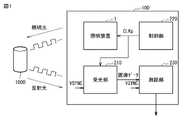
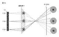
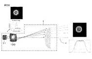
- FIG. 1is a block diagram showing an example of the overall configuration of a distance measuring device 100 according to an embodiment of the present technology.
- the distance measuring device 100is a device that measures the distance from the irradiation object 1000 by irradiating the irradiation object 1000 with illumination light and receiving the reflected light.
- This distance measuring device 100includes an illumination device 1 , a light receiving section 210 , a control section 220 and a distance measuring section 230 .
- the lighting device 1generates irradiation light in synchronization with the square-wave emission control signal CLKp from the control unit 220 .
- This light emission control signal CLKpmay be a periodic signal and is not limited to a rectangular wave.
- the emission control signal CLKpmay be a sine wave.
- the light receiving unit 210receives reflected light reflected from the object 1000 to be irradiated, and detects the amount of received light within each cycle of the vertical synchronization signal VSYNC.
- a plurality of pixel circuitsare arranged in a two-dimensional lattice in the light receiving section 210 .
- the light receiving unit 210supplies image data (frames) corresponding to the amount of light received by these pixel circuits to the distance measuring unit 230 .
- the light receiving unit 210has, for example, a function of correcting distance measurement errors due to multipath.
- the control section 220controls the illumination device 1 and the light receiving section 210 .
- the control unit 220generates the light emission control signal CLKp and supplies it to the illumination device 1 and the light receiving unit 210 .
- the distance measurement unit 230measures the distance to the irradiation object 1000 by the ToF method based on the image data. This distance measuring unit 230 measures the distance for each pixel circuit and generates a depth map that indicates the distance to an object for each pixel using a gradation value. This depth map is used, for example, in image processing that performs blurring processing to a degree that depends on the distance, autofocus (AF) processing that determines the in-focus point of the focus lens according to the distance, and the like.
- AFautofocus
- the illumination device 1emits light from a plurality of light emitting units (light emitting units 110 (first light emitting unit) and 120 (second light emitting unit), see FIG. 6).
- the diffraction element 14, which will be described later,is an optical element that tiles the light L1 and expands the irradiation range to the light L2.
- the lights L110 and L120are for, for example, spot irradiation as shown in FIG. 2A, uniform irradiation as shown in FIG. 2B, and simultaneous irradiation thereof.
- the illumination device 1has, for example, a light emitting element 11, a microlens 12, a collimator lens 13, a diffraction element 14, and a diffraction element .
- the microlens 12, the collimator lens 13, the diffraction element 14 and the diffraction element 34are arranged, for example, in this order on the optical path of the light (lights L110 and L120) emitted from the light emitting element 11.
- the light emitting element 11is held by a holding portion 21, for example, and the collimator lens 13 and the diffraction element 14 are held by a holding portion 22, for example.
- the diffraction element 34is supported by adhesion or the like with respect to the diffraction element 14 .
- the holding portion 21has, for example, one cathode electrode portion 23 and two anode electrode portions 24 and 25 on the surface 21S2 opposite to the surface 21S1 that holds the light emitting element 11, for example. Each member constituting the lighting device 1 will be described in detail below.
- the light emitting element 11is, for example, a surface emitting surface emitting semiconductor laser.
- FIG. 4is a cross-sectional view showing a first structural example of the light emitting element 11 according to an embodiment of the present technology.
- the light emitting elements 11are arranged in an array on the substrate 130 .
- Each of the light emitting elements 11is a semiconductor including a lower DBR (Distributed Bragg Reflector) layer 141, a lower spacer layer 142, an active layer 143, an upper spacer layer 144, an upper DBR layer 145 and a contact layer 146 in this order on the surface side of the substrate 130. It has a layer 140 .
- the upper portion of the semiconductor layer 140specifically, a portion of the lower DBR layer 141, the lower spacer layer 142, the active layer 143, the upper spacer layer 144, the upper DBR layer 145, and the contact layer 146 are formed into a columnar mesa portion 147 and a contact layer 146. It's becoming In this mesa portion 147, the center of the active layer 143 is the light emitting region 143A.
- the upper DBR layer 145is provided with a current constriction layer 148 and a buffer layer 149 .
- the substrate 130is, for example, an n-type GaAs substrate.
- n-type impuritiesinclude silicon (Si) and selenium (Se).
- the semiconductor layersare each composed of, for example, an AlGaAs-based compound semiconductor.
- An AlGaAs-based compound semiconductoris a compound semiconductor containing at least aluminum (Al) and gallium (Ga) among group 13 elements in the periodic table of elements and at least arsenic (As) among group 15 elements in the periodic table of elements. That's what I mean.
- the lower DBR layer 141is formed by alternately stacking low refractive index layers and high refractive index layers (both not shown).
- the low refractive index layeris made of n-type Al x1 Ga 1-x1 As (0 ⁇ x1 ⁇ 1) with a thickness of ⁇ 0 /4n 1 (where ⁇ 0 is the emission wavelength and n 1 is the refractive index), for example.
- the high refractive index layeris composed of, for example, n-type Al x2 Ga 1-x2 As (0 ⁇ x2 ⁇ x1) with a thickness of ⁇ 0 /4n 2 (n2 is the refractive index).
- the lower spacer layer 142is composed of, for example, n-type Al x3 Ga 1-x3 As (0 ⁇ x3 ⁇ 1).
- the upper spacer layer 144is composed of, for example, p-type Al x5 Ga 1-x5 As (0 ⁇ x5 ⁇ 1).
- Examples of p-type impuritiesinclude zinc (Zn), magnesium (Mg) and beryllium (Be).
- the active layer 143has a multi-quantum well (MQW) structure.
- the active layer 143is made of, for example, undoped n-type Al x-4 Ga 1-x4 As (0 ⁇ x4 ⁇ 1).
- the upper DBR layer 145is formed by alternately stacking low refractive index layers and high refractive index layers (both not shown).
- the low refractive index layeris composed of, for example, p-type Al x8 Ga 1-x8 As (0 ⁇ x8 ⁇ 1) with a thickness of ⁇ 0 /4n 3 (n 3 is the refractive index).
- the high refractive index layeris composed of, for example, p-type Al x9 Ga 1-x9 As (0 ⁇ x9 ⁇ x8) with a thickness of ⁇ 0 /4n 4 (n 4 is the refractive index).
- the contact layer 146is composed of, for example, p-type Al x10 Ga 1-x10 As (0 ⁇ x10 ⁇ 1).
- the current confinement layer 148 and the buffer layer 149are provided in the lower DBR layer 141, for example.
- the current confinement layer 148is formed at a position distant from the active layer 143 in relation to the buffer layer 149 .
- the current confinement layer 148is provided, for example, in the lower DBR layer 141, instead of the low refractive index layer, at a portion of the low refractive index layer that is several layers away from the active layer 143 side.
- the current confinement layer 148has a current injection region 148A and a current confinement region 148B.
- the current injection region 148Ais formed in the in-plane central region.
- the current confinement region 148Bis formed in the peripheral edge of the current injection region 148A, that is, in the outer edge region of the current confinement layer 148, and has an annular shape.
- the current injection region 148Ais made of, for example, n-type Al x11 Ga 1-x11 As (0.98 ⁇ x11 ⁇ 1).
- the current confinement region 148Bincludes, for example, aluminum oxide (Al 2 O 3 ). It is obtained by oxidizing from the side.
- the current constriction layer 148has a function of constricting current.
- the buffer layer 149is formed closer to the active layer 143 in relation to the current confinement layer 148 .
- the buffer layer 149is formed adjacent to the current confinement layer 148 .
- the buffer layer 149is formed in contact with the surface (lower surface) of the current confinement layer 148 on the active layer 143 side.
- a thin layer having a thickness of, for example, several nanometersmay be provided between the current confinement layer 148 and the buffer layer 149 .
- the buffer layer 149is provided, for example, in the lower DBR layer 141 at a portion of the high refractive index layer that is several layers away from the current confinement layer 148 instead of the high refractive index layer.
- the buffer layer 149has an unoxidized region and an oxidized region (both not shown).
- the unoxidized regionis mainly formed in the in-plane central region, for example, in a portion in contact with the current injection region 148A.
- the oxidized regionis formed around the periphery of the unoxidized region and has an annular shape.
- the oxidized regionis mainly formed in the in-plane outer edge region, for example, in a portion in contact with the current confinement region 148B.
- the oxidized regionis biased toward the current confinement layer 148 in portions other than the portion corresponding to the outer edge of the buffer layer 149 .
- the unoxidized regionis made of a semiconductor material containing Al, such as n-type Al x12 Ga 1-x12 As (0.85 ⁇ x12 ⁇ 0.98) or n-type In a Al x13 Ga 1-x13- a As (0.85 ⁇ x13 ⁇ 0.98).
- the oxidized regionincludes, for example, aluminum oxide (Al 2 O 3 ), and includes, for example, n-type Al x12 Ga 1-x12 As or n-type In b Al x13 Ga 1-x13-b As. It is obtained by oxidizing an oxidized layer (not shown) from the side surface side of the mesa portion 147 and the layer side to be oxidized.
- the layer to be oxidized of the buffer layer 149is made of a material and has a thickness that oxidizes faster than the upper DBR layer 145 and the lower DBR layer 141 and slower than the layer to be oxidized of the current constriction layer 148 . It is configured.
- an annular upper electrode 151 having an opening (light exit port 151A) at least in a region facing the current injection region 148Ais formed on the upper surface of the mesa portion 147 (the upper surface of the contact layer 146).
- An insulating layer (not shown)is formed on the side surface of the mesa portion 147 and the surface of the periphery.
- the upper electrode 151is connected to different electrode pads by wire bonding or the like through wiring (not shown) for each light emitting unit group.
- a lower electrode 152is provided on the other surface of the substrate 130 .
- the lower electrode 152is electrically connected to the cathode electrode section 23, for example.
- the cathode electrode portionis used as a common electrode and the anode electrode portions are provided separately.
- the upper electrode 151is configured by laminating titanium (Ti), platinum (Pt) and gold (Au) in this order, for example, and is electrically connected to the contact layer 146 above the mesa portion 147. It is
- the lower electrode 152has a structure in which, for example, an alloy of gold (Au) and germanium (Ge), nickel (Ni) and gold (Au) are layered in this order from the substrate 130 side. It is connected to the.
- the plurality of light emitting unitsare, for example, a plurality of light emitting units used for spot irradiation (a plurality of light emitting units 110 for spot irradiation) and a plurality of light emitting units used for uniform irradiation (a plurality of light emitting units for uniform irradiation 120) are arranged in an array on the substrate 130, for example.
- the plurality of light emitting portions 110 and the plurality of light emitting portions 120are physically and electrically separated from each other by the mesa structure of the mesa portion 147 .
- FIG. 5is a cross-sectional view showing a second structural example of the light emitting element 11 according to one embodiment of the present technology.
- the light-emitting element 11 of this second configuration exampleis a multi-junction VCSEL, and includes a P-DBR layer 161, an active layer 162, a tunnel junction 163, an active layer 164, and an N-DBR layer 165. It has a structure in which layers are stacked in order from the radiation side. That is, it has a structure in which two pn junctions are connected, and active regions 162 and 164 that emit light of a laser oscillation wavelength are vertically stacked between them.
- a spacer layer, a buffer layer, a current constriction layer, a mesa portion, a light exit, an upper electrode layer, and a lower electrode layer near the active layermay be provided.
- the diffraction element 34splits the spot light. Therefore, by combining with this multi-junction VCSEL, it is possible to increase the number of spots while maintaining or increasing the light intensity of the spot light. be. Accordingly, it is possible to achieve both accuracy in distance measurement and resolution in distance measurement.
- the light-emitting element 11 described abovehas, for example, a plurality of light-emitting portions 110 and a plurality of light-emitting portions 120 .
- the multiple light emitting units 110 and the multiple light emitting units 120are electrically connected to each other.
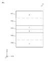
- the plurality of light emitting units 110includes n (for example, 12 in FIG. 6) light emitting units 110 extending in one direction (for example, the Y-axis direction).
- a plurality (for example, nine in FIG. 6) of light-emitting portion groups X (light-emitting portion groups X1 to X9)are configured.
- the plurality of light emitting units 120is a plurality (for example, 9 in FIG.
- each of the light emitting unit groups X1 to X9 and the light emitting unit groups Y1 to Y9are alternately arranged on a substrate 130 having a rectangular shape, for example, as shown in FIG. , electrode pads 240 provided along one side of the substrate 130, and the light emitting unit groups Y1 to Y9 are provided, for example, with electrode pads 250 provided along the other side opposite to the one side of the substrate 130. , are electrically connected to each other.
- the present inventionis not limited to this.
- the number of the plurality of light emitting units 110 and the number of the plurality of light emitting units 120can be arbitrarily arranged according to the desired number, position and amount of light output of light emitting points, respectively.
- the arrangement of the plurality of light emitting units 120may be arranged every two rows of the arrangement of the plurality of light emitting units 110 .
- the microlens 12for example, emits light from a plurality of light emitting units 110 for spot irradiation and a plurality of light emitting units 120 for uniform irradiation (hereinafter referred to as laser beam L110 and laser beam L120, respectively).
- the shape of at least one of the beamsis shaped and emitted.
- FIG. 7Aschematically shows an example of the planar configuration of the microlens 12, and FIG. 7B schematically shows the cross-sectional configuration of the microlens 12 taken along line II shown in FIG. 7A. be.
- the microlens 12is formed by arranging a plurality of microlenses in an array, and has a plurality of lens portions 12A and a parallel plate portion 12B.
- the microlens 12includes parallel plate portions 12B, as shown in FIG. 8B, such that the lens portions 12A face the plurality of light emitting portions 120 for uniform illumination, as shown in FIG. 8A. are arranged to face the plurality of light emitting units 110 for spot irradiation. Accordingly, as shown in FIG. 9, the laser beams L120 emitted from the plurality of light emitting units 120 are refracted by the lens surface of the lens unit 12A to form the light beam center P2' inside the microlens 12, for example.
- the light-emitting points P2 of the plurality of light-emitting sections 120 that are at the same height as the light-emitting points P1 of the plurality of light-emitting sections 110are aligned with the light emitted from the plurality of light-emitting sections 110 and the light emitted from the plurality of light-emitting sections 120 (laser beams L110, The laser beam L120) is shifted in the optical axis direction (for example, the Z-axis direction).
- the laser beams L110 emitted from the plurality of light emitting units 110pass through the microlens 122 as they are (without being refracted).
- a spot-like irradiation pattern as shown in FIG. 10is formed.
- the laser beams L120 emitted from the plurality of light emitting units 120are refracted by the microlenses 122, and, for example, part of the laser beams L120 emitted from the adjacent light emitting units 120 as shown in FIG.
- an irradiation patternis formed in which a predetermined range is irradiated with substantially uniform light intensity.
- switching between the light emission of the plurality of light emitting units 110 and the light emission of the plurality of light emitting units 120enables switching between spot irradiation and uniform irradiation.
- FIG. 9shows an example in which the microlens 12 functions as a relay lens, it is not limited to this.
- the light beam centers P ⁇ b>2 ′ of the plurality of light emitting units 120may be formed between the light emitting units 120 and the microlenses 12 .
- the plurality of light emitting portions 110 and the plurality of light emitting portions 120preferably have different light emitting areas (OA diameters W3, W4).
- the light emitting areas (OA diameter W3) of the multiple light emitting units 110 for spot irradiationare preferably smaller than the light emitting areas (OA diameter W4) of the multiple light emitting units 120 for uniform irradiation.
- the light beams for spot irradiation emitted from the plurality of light emitting units 110(laser beams L110 (first light) emitted in mutually independent spots on the object to be irradiated 1000) are converged to a smaller size.
- a light beam for uniform irradiation emitted from a plurality of light emitting units 120(light beams emitted from adjacent light emitting units 120 are superimposed on each other so that light beams emitted from the light emitting units 120 are substantially uniformly distributed over a predetermined range on the irradiation object 1000 .)
- the laser beam L120 (second light) that irradiates the laser beam L120 (second light))can irradiate a wider range, and can irradiate the irradiation object 1000 uniformly with high output.
- the opening width W1 of the wiring connecting each of the plurality of light emitting portions 110becomes smaller than the opening width W2 of the wiring connecting each of the plurality of light emitting portions 120 .
- the number of light emitting units for spot irradiation and the number of light emitting units for uniform irradiationare the same, but they may be different.
- the FFPFlu Field Pattern
- the FFPmay be different between the light emitting portion for spot irradiation and the light emitting portion for uniform irradiation.
- the collimator lens 13emits the laser beams L110 emitted from the plurality of light emitting sections 110 and the laser beams L120 emitted from the plurality of light emitting sections 120 as substantially parallel light.
- the collimator lens 13is, for example, a lens for collimating the laser beams L110 and L120 emitted from the light emitting units 110 and 120, respectively, and combining them with the diffraction elements 14 and .
- the diffraction element 14divides and emits the laser beams L110 emitted from the plurality of light emitting portions 110 and the laser beams L120 emitted from the plurality of light emitting portions 120 respectively.
- the diffraction element 14divides, for example, the laser beam L110 emitted from the multiple light emitting units 110 and the laser beam L120 emitted from the multiple light emitting units 120 into 3 ⁇ 3.
- each spot of the laser beams L110 and L120 to be spot-irradiatedcan be divided into, for example, five spots, and the number of spots at the time of spot irradiation can be increased.
- the holding portion 21 and the holding portion 22are for holding the light emitting element 11, the collimator lens 13 and the diffraction element 14. Specifically, the holding portion 21 holds the light emitting element 11 in a concave portion C (see FIG. 3) provided on the upper surface (surface 21S1). The holding part 22 holds the collimator lens 13 and the diffraction element 14 . The holding portion 21 and the holding portion 22 are connected to each other so that the light L1 and the light L2 emitted from the light emitting element 11 enter the collimator lens 13, and the light L1 and L2 transmitted through the collimator lens 13 become substantially parallel light. It is
- a plurality of electrode portionsare provided on the back surface (surface 21S2) of the holding portion 21.
- the surface 21S2 of the holding portion 21includes a cathode electrode portion 23 common to the plurality of light emitting portions 110 for spot irradiation and the plurality of light emitting portions 120 for uniform irradiation, and a plurality of light emitting portions for spot irradiation.
- An anode electrode portion 24 of the portion 110 and an anode electrode portion 25 of a plurality of light emitting portions 120 for uniform irradiationare provided.
- the configuration of the plurality of electrode portions provided on the surface 21S2 of the holding portion 21is not limited to the above.
- the cathode electrode portionsmay be formed separately, and the anode electrode portions of the plurality of light emitting portions 110 for spot irradiation and the plurality of light emitting portions 120 for uniform irradiation may be formed as a common electrode portion.
- the collimator lens 13 and the diffraction element 14may be held by the holding portion 21 .
- FIG. 12shows an example of a circuit configuration of a drive circuit that drives the lighting device 1.
- the anodes of the first light-emitting portion group 171 and the second light-emitting portion group 172are connected to a power source (VCC) such as a constant voltage source.
- VCCpower source
- the first light-emitting portion group 171is, for example, a set of light-emitting portions 110 connected to the electrode pads 240 .
- the second light-emitting portion group 172is, for example, a set of light-emitting portions 120 connected to the electrode pads 250 .
- a common cathode of the first light emitting unit group 171 and the second light emitting unit group 172is connected to a laser driver 175 .
- a laser driver 175As the laser driver 175, an N-type MOSFET (Metal Oxide Semiconductor Field Effect Transistor) can be used.
- a P-type MOSFET or bipolar transistormay be used as the laser driver 175 .
- a laser driver 175selectively emits light from the first light emitting unit group 171 and the second light emitting unit group 172 .
- Which of the first light-emitting unit group 171 and the second light-emitting unit group 172 is to emit lightis determined by opening and closing the first switching unit SW1 and the second switching unit SW2. That is, the light emission of the light emitting unit group (first light emitting unit group 171) connected to the X side and the light emission connected to the Y side are controlled by complementary drive control in which one of the two switching units is turned on and the other is turned off.
- the light emission of the group of light emitting units (second group of light emitting units 172)can be switched. In other words, it is possible to individually drive the first light-emitting portion group 171 (one channel) and the second light-emitting portion group 172 (the other channel).
- the first switching section SW1is connected between the power source and the anode of the first light-emitting section group 171 .
- the second switching section SW2is connected between the power source and the anode of the second light-emitting section group 172 .
- a decoupling capacitor CAis connected to a position close to the first light emitting unit group 171, specifically, a connection point PA between the first light emitting unit group 171 and the first switching unit SW1.
- the other end of the decoupling capacitor CAis connected to ground.
- a decoupling capacitor CBis connected to a position close to the second light emitting portion group 172, specifically, a connection point PB between the second light emitting portion group 172 and the second switching portion SW2.
- the other end of the decoupling capacitor CBis connected to ground.
- FIG. 13shows an example of a light emission sequence of the illumination device 1.
- FIG. A section for generating one distance measurement imageis called a “frame”, and one frame is set to a time such as 33.3 msec (frequency of 30 Hz).
- a plurality of accumulation intervals with different conditionscan be provided in a frame. Although eight accumulation intervals are shown in FIG. 13, the number is not limited to this.
- the first light emitting unit group 171emits light in one frame, and the light receiving unit 210 (see FIG. 1) receives the reflected light to generate a ranging image.
- the second light emitting unit group 172is caused to emit light, and the light receiving unit 210 receives the reflected light to generate a ranging image.
- the first light emitting unit group 171 and the second light emitting unit group 172are switched every frame in FIG. 13, they may be switched every multiple frames. Switching of the light emission of the first light emitting unit group 171 and the second light emitting unit group 172 may be performed, for example, in units of one frame, may be performed in units of blocks, or may be performed in units of a plurality of blocks. good too. This makes it possible to switch between two sets of spot irradiation at a faster speed than, for example, a method of mechanically switching the focal positions of laser beams emitted from a plurality of light emitting units.
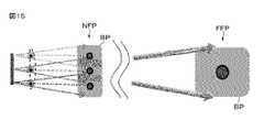
- the beam profile BP of the laser beamincludes a beam profile (NFP (Near Field Pattern)) in the vicinity of the emission end, and a beam profile (FFP ) can be obtained by measuring the beam profile.
- NFPNear Field Pattern
- FFPbeam profile
- a beam profiler system for measuring the beam profilea known one such as a fixed beam profiler or a scanning beam profiler can be applied.
- the beam profile BP of the laser beam emitted from each of the three light emitting portions of the light emitting element 11is normally circular.
- the center of the beam profileis appropriately referred to as the light beam center VLP.
- the pattern of each beam profile projected onto the screen S1000is appropriately referred to as an array.
- FIG. 14is an example in which the light emitting element 11 is placed at the actual focus position of the refractive element, but other examples are also conceivable.
- an illumination patterncan be projected onto the screen S1000 by a laser beam split by the diffraction element 34 as shown in FIG.
- the center of each beam profilewill be referred to as the light beam center
- the illumination pattern created on the screen S1000will be referred to as the array.
- FIG. 17Ais an example in which the 0th order light is split into +1st order light and ⁇ 1st order light.
- the 0th order lightmay be split into four.
- black circlesindicate 0th-order light
- white circlesindicate split diffracted light.
- the light emitting element 11may be placed closer than the actual focus position of the refracting element. In this case the light is diffused. In some cases, light is diverged or converged by shifting the position of the light beam center as shown in FIG. 9 using an optical member such as a microlens without changing the positional relationship between the light emitting element and the refracting element. Also, as shown in FIG. 19, the light emitting element 11 may be placed away from the actual focus position of the refractive element. In this case, the light converges once and then diffuses. In either case, the center of the beam profile is called the light beam center, and the illumination pattern produced on the screen S1000 is called the array.
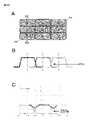
- FIG. 20Ais a diagram schematically showing a beam profile BP defocused by the microlens 12 and illuminated on the screen S1000.
- an array (3 ⁇ 3) of nine beam profiles BPis shown as an example.
- Each beam profile BPhas a light beam center VLP at its center.
- the light beam center VLPcan also be referred to as the beam profile of the laser beam before being defocused.
- the arrangement of the light beam center VLPssubstantially matches the arrangement of the light emitting units for uniform irradiation (the light emitting units 120 in this example).
- the beam profile BPusually has a beam profile (NFP (Near Field Pattern) shape (usually circular) in the vicinity of the emission end of the light emitting section.
- NFPNear Field Pattern
- the arrangement of the light beam centers VLPin other words, the arrangement of the light emitting units 120 is, for example, a lattice-like arrangement with equal intervals, and the shape of the beam profile is circular, the overlapping degree of the beam profile BP is becomes uneven.
- a line connecting the light beam center VLP of the center beam profile BP and the light beam centers VLP of two beam profiles BP horizontally adjacent to the center beam profile BPis defined as AA-AA. line.
- a line connecting the light beam center VLP of the center beam profile BP and the light beam centers VLP of two beam profiles BP diagonally adjacent to the center beam profile BPis defined as a BB-BB line.
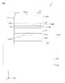
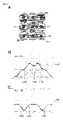
- FIG. 20Bshows how the three beam profiles BP overlap in the direction of the AA-AA line.
- the horizontal axis of FIG. 20Bindicates the position of each beam profile (arbitrary unit), and the vertical axis indicates the normalized beam intensity.
- the beam profile in this examplehas a so-called top-hat shape with a flat top.
- line LNAshows the laser intensity for the middle beam profile BP
- line LNBshows the laser intensity for the left beam profile BP with respect to the middle beam profile BP
- line LNCshows the laser intensity for the middle beam profile BP.
- Line LNDshows the laser intensity superimposed from line LNA to LNC. As indicated by the line LND, there is no drop in laser intensity in the direction of the AA-AA line.
- line LNAindicates the laser intensity of the central beam profile BP
- line LNEindicates the laser intensity of the lower left beam profile BP with respect to the central beam profile BP
- line LNFindicates the central beam profile BP.
- the laser intensity of the lower right beam profile BPis shown with respect to BP.
- Line LNGshows the laser intensity superimposed with lines LNA, LNE and LNF.
- the line LNFthere is an extreme drop in the direction of the BB-BB line where the laser intensity becomes zero. That is, there is a portion where the irradiation object 1000 is not irradiated with the uniformly irradiated laser beam, which may deteriorate the accuracy of distance measurement. Even if the laser intensity does not become 0, the same problem occurs if the laser intensity at the overlapping portion is less than a predetermined value (for example, less than 25% of the peak intensity of the laser intensity).
- One object of the present technologyis to improve such a point.
- the non-uniformity of the laser intensity at the overlapping part of the beam profile BPis caused by the uniformity of the shape of the beam profile BP (specifically, circular shape) with respect to the arrangement of the light emitting parts (lattice, triangle, etc.). It is thought that this occurs because Therefore, in the present technology, by matching the characteristics of the beam profile with the arrangement of the light emitting units, in other words, with the arrangement of the centers of the light beams, the non-uniformity of the laser intensity described above is suppressed.
- a rectangular beam profile BP as shown in FIG. 22B and FIG.did.
- illustration of the diffracted lightis omitted. A specific description will be given below.
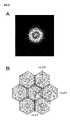
- a screen S1000is arranged on the light exit side of the illumination device 1 .
- the screen S1000shows the arrangement of light emitted from the light emitting element 11 (in this example, the light emitting unit 120 for uniform irradiation).
- screen S1000shows nine beam profiles BP.
- more beam profiles BPexist in practice, but in consideration of the convenience of explanation, nine beam profiles BP are used in this example.
- the central beam profile and the light beam center of the nine beam profiles BPbe the beam profile BP1 and the light beam center VLP1.
- the beam profile above beam profile BP1is assumed to be beam profile BP2 (light beam center VLP2)
- the beam profile below beam profile BP1is assumed to be beam profile BP3 (light beam center VLP3).
- the beam profile on the left side of the beam profile BP1be a beam profile BP4 (light beam center VLP4)
- the beam profile on the right side of the beam profile BP1be a beam profile BP5 (light beam center VLP5).
- the beam profile on the lower left side of the beam profile BP1is assumed to be a beam profile BP6 (light beam center VLP6), and the beam profile on the upper right side of the beam profile BP1 is assumed to be a beam profile BP7 (light beam center VLP7).
- the beam profile on the lower right side of beam profile BP1is assumed to be beam profile BP8 (light beam center VLP8), and the beam profile on the upper left side of beam profile BP1 is assumed to be beam profile BP9 (light beam center VLP9).
- a plane PLA(YZ plane in this example) including the light beam center VLP1 (an example of the first light beam center), the light beam center VLP2 (an example of the second light beam center), and the light beam center VLP3 is defined.
- a plane PLB(XZ plane in this example) including the light beam center VLP1, the light beam center VLP4 (an example of the third light beam center), and the light beam center VLP5 is defined.
- the light beam center VLP1 and the light beam center VLP2are light beam centers adjacent to each other in the Y-axis direction.
- the angle formed by the light beam center VLP1 and the light beam center VLP2is the angle h.
- the beam intensity of the beam profile BP1 (XY beam profile) corresponding to the light beam center VLP1is predetermined (in this example, 50%) is defined as angle ⁇ (second angle).
- angle ⁇second angle.
- Substantially equalmeans that the predetermined intensity to the central intensity defining the angle of the beam profile is allowed to range from 75% to 25% for the angle h.
- the beam intensity at the point where the beam profile BP1 and the beam profile BP2 overlapcan be made 100% (the sum of 50% and 50%). As a result, it is possible to suppress a decrease in beam intensity at a portion where the beam profiles overlap.
- the light beam center VLP1 and the light beam center VLP2have been described as examples, the same applies to other two adjacent light beam centers.
- the angle formed by the light beam center VLP1 and the light beam center VLP4(the third ) is defined as angle l.
- Let the anglebe ⁇ .
- Substantially equalmeans that the predetermined intensity for the angle l is allowed to range from 75% to 25% with respect to the central intensity defining the angle of the beam profile.
- the beam intensity at the point where the beam profile BP1 and the beam profile BP4 overlapcan be made 100% (the sum of 50% and 50%). As a result, it is possible to suppress a decrease in beam intensity at a portion where the beam profiles overlap.
- the light beam center VLP1 and the light beam center VLP4have been described as examples, the same applies to other two adjacent light beam centers.
- the shape of the beam profilemay be square.
- angle h and angle l shown in FIG. 26Bare substantially equal.
- the angle ⁇is 90 degrees.
- the shape of the beam profile BPmay be an equilateral triangle.
- the angle formed by the light beam center VLP1 and the light beam center VLP2 with respect to the light emitting element 11is h1
- the angle formed by the light beam center VLP1 and the light beam center VLP3 with respect to the light emitting element 11is l1.
- An angle ⁇ 1is defined between a plane containing the beam center VLP1 and the light beam center VLP2 and a plane containing the light beam center VLP1 and the light beam center VLP3.
- the angle between the light beam center VLP1 and the light beam center VLP4 with respect to the light emitting element 11is h2
- the angle between the light beam center VLP4 and the light beam center VLP5 with respect to the light emitting element 11is l2
- the light beam center An angle ⁇ 2is defined by a plane including VLP1 and light beam center VLP4 and a plane including light beam center VLP4 and light beam center VLP5.
- the following arrays (1) and (2)are arrayed at the center of the light beam with the minimum period.
- the shape of the beam profile BPmay be substantially hexagonal as shown in FIGS. 28A and 28B.
- FIG. 28Ashows one beam profile
- FIG. 28Bis a diagram schematically showing a plurality of beam profiles with which the object 1000 or the like is irradiated.
- the angle formed by the light beam center VLP1 and the light beam center VLP2is assumed to be angle h.
- the angle formed by the light beam center VLP1 and the light beam center VLP3is defined as an angle l.
- the shape of the beam profile BPmay be a parallelogram as shown in FIG. Also, as shown in FIG. 30, the shape of the beam profile BP may be an equilateral triangle and may be arranged differently from that in FIG. Alternatively, a shape obtained by combining a regular octagonal beam profile BP and a square beam profile BP as shown in FIG. 31A (see FIG. 31C) may be used.
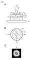
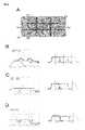
- FIG. 32Ais a partial cross-sectional view of the light-emitting element 11, specifically, the light-emitting portion 120.
- FIG. 32Bis a top view of the configuration shown in FIG. 32A. In addition, in FIG. 32A and FIG. 32B, illustration of a part of the configuration is simplified.
- an annular upper electrode 151 having a light exit opening 151Ais formed in a region of the active layer 143 facing the light emitting region 143A.
- a beam profile BP in which the XY beam profile is square as shown in FIG. 32Ccan be obtained.
- a second exampleis an example of a beam profile corresponding to the shape of the light emitting region of the light emitting unit 120 .
- the light emitting regionmeans the light emitting area (OA diameter W4 described above) of the light emitting portion 120, as shown in FIGS. 33A and 33B.
- the shape of the light emitting regionfor example, square, it is possible to obtain a beam profile BP in which the XY beam profile is square, as shown in FIG. 33C.
- a third exampleis a structure (SR structure) in which the reflectance is controlled depending on the location for each thickness of the refractive material for each surface multilayer in the opening 151A of the upper electrode 151 to suppress the output of the outer circumference.
- a beam profile BPis created by providing a layer structure.
- a second layer 186is provided on a part of the first layer 185 so that the reflectance of the second layer 186 is higher than that of the surrounding area. is.
- a second layer 186is formed by vapor deposition or the like at a location facing the light emitting region 143A. As a result, light output to the periphery of the second layer 186 is suppressed, and a beam profile BP with a square XY beam profile, such as that shown in FIG. 34C, can be obtained.
- a fourth exampleis an example in which the beam profile BP is created by a predetermined optical member.
- an optical member 190is arranged at a distance of 10 to 100 ⁇ m from the light emitting element 11 .
- the optical member 190for example, a microlens that is convex in the direction of incidence of light can be used.
- the beam profilecan be a top hat type beam profile.
- a fifth exampleis an example in which an on-chip lens 191 is provided on the light emitting side of the light emitting section 120, as shown in FIG. It is also possible to create a predetermined beam profile with an on-chip lens 191 .
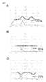
- the angle formed by the centers of the two light beams in the DD-DD directionis approximately equal to the angle at which the beam profile angle reaches 75% of the peak intensity.
- the beam intensity (upper limit of beam intensity) at the point where two beam profiles overlap in the DD-DD directionis +50%.
- the angle formed by the centers of the two light beams in the EE-EE directionshould be substantially equal to the angle when the beam profile angle reaches 50% of the peak intensity. to In this case, as shown in FIG.
- the beam intensity (upper limit of beam intensity) at the point where two beam profiles overlap in the EE-EE directionis 1 (+0%).
- the angle formed by the centers of the two light beams in the FF-FF direction(diagonal direction) is substantially equal to the angle when the angle of the beam profile reaches 25% of the peak intensity. do.
- the beam intensity (upper limit of beam intensity) at the point where two beam profiles overlap in the FF-FF directionis ⁇ 50%. Since it is considered that up to -50% is acceptable in practice, it is preferable to set the predetermined strength in the range of 25 to 75%.
- the angle formed by the centers of the two light beams in the DD-DD directionwhen the angle formed by the centers of the two light beams in the DD-DD direction (horizontal direction) is 25% of the peak intensity of the beam profile, as shown in FIG. 39B may be substantially equal to the angle of In this case, as shown in FIG. 39C, the drop in beam intensity at the point where the two beam profiles overlap in the DD-DD direction can be up to -50%.
- the angle formed by the centers of the two light beams in the EE-EE direction(vertical direction) is the angle when the beam profile angle is 75% of the peak intensity, as shown in FIG. 39D. to be approximately equal to In this case, as shown in FIG.
- the beam intensitycan be +50% where the two beam profiles overlap in the EE-EE direction.
- the angle formed by the centers of the two light beams in the FF-FF direction (diagonal direction) shown in FIG.It may be made substantially equal to the angle at which it becomes 25%.
- the drop in beam intensity at the point where two beam profiles overlap in the FF-FF directioncan be up to -50%.
- the so-called top-hat beam profile shown in FIGS. 41A to 41Chas been described as an example, but the present invention is not limited to this.
- the shape of the individual beam profilesmay be Gaussian shaped.
- the shape of each beam profilemay be a bimodal shape (a shape having two peaks).
- the shape of each beam profilemay be a trimodal shape (a shape having one peak and two smaller peaks).
- the present technologycan also have the following configuration. (1) Having a light emitting element having a plurality of light emitting parts, When the light beams emitted from the plurality of light emitting units are applied to an object to be irradiated, the position corresponding to the center of the light beam is defined as the light beam center, and the center of the predetermined two light beams is defined as the first light.
- An angle formed by the center of the first light beam and the center of the second light beam with respect to the light emitting elementis defined as a first angle
- the beam intensity of the beam profile corresponding to the center of the first light beamis When an angle at which a predetermined intensity is obtained in the extending direction of a line including the center of the first light beam and the center of the second light beam is defined as the second angle, the first angle and the second angle are approximately equal to each other.
- a light beam center adjacent to the first light beam center in a direction different from the predetermined directionis defined as a third light beam center, and an angle formed by the first light beam center and the third light beam center is a third light beam center.
- the beam intensity of the beam file corresponding to the first light beam centeris a predetermined intensity in the extending direction of the line containing the first light beam center and the third light beam center.
- the predetermined intensityis set between 25% and 75% of the peak beam intensity.
- the predetermined intensityis 50%.
- the lighting device according to any one of (1) to (7), wherein the beam profileis a beam profile according to the shape of the light exit opening of the light emitting element.
- the beam profileis a beam profile according to the shape of the light emitting region of the light emitting element.
- the lighting deviceaccording to any one of (1) to (7), wherein the beam profile is formed by providing a layer structure with different reflectance on the light beam emitting side of the light emitting region of the light emitting section.
- the beam profileis formed by a predetermined optical member.
- the light emitting elementhas a plurality of first light emitting units and a plurality of second light emitting units, a first optical member that emits a plurality of first lights emitted from the plurality of first light emitting sections and a plurality of second lights emitted from the plurality of second light emitting sections in parallel with each other;
- a second optical memberthat emits light, and is arranged on an optical path of the plurality of first lights and the plurality of second lights, and refracts or diffracts the plurality of first lights to irradiate the object while increasing the number of spots irradiated to, by refracting or diffracting the plurality of second light, increasing the overlapping range with the second light emitted from the adjacent second light emitting unit 3 optical members and
- a predetermined rangeis irradiated with the uniform irradiation pattern
- a position corresponding to the center of the light beam emitted from the plurality of first light emitting units when the object is irradiated with the light beamis defined as the light beam center
- predetermined two light beam centersare defined as the second light beam center.
- An angle formed by the center of the first light beam and the center of the second light beam with respect to the light emitting elementis defined as a first angle
- the beam intensity of the beam profile corresponding to the center of the first light beamis When an angle at which a predetermined intensity is obtained in the extending direction of a line including the center of the first light beam and the center of the second light beam is defined as the second angle, the first angle and the second angle are approximately equal to each other.
- a lighting deviceaccording to any one of (1) to (12); a control unit that controls the lighting device; a light receiving unit that receives reflected light reflected from an object;
- a distance measuring devicecomprising: a distance measuring unit that calculates a distance to be measured from image data obtained by the light receiving unit.
Landscapes
- Engineering & Computer Science (AREA)
- Physics & Mathematics (AREA)
- General Physics & Mathematics (AREA)
- Computer Networks & Wireless Communication (AREA)
- Radar, Positioning & Navigation (AREA)
- Remote Sensing (AREA)
- Electromagnetism (AREA)
- General Engineering & Computer Science (AREA)
- Condensed Matter Physics & Semiconductors (AREA)
- Optics & Photonics (AREA)
- Measurement Of Optical Distance (AREA)
- Semiconductor Lasers (AREA)
Abstract
Description
Translated fromJapanese本技術は、照明装置および測距装置に関する。This technology relates to lighting devices and ranging devices.
複数の発光部から出射された光を測定対象物に照射し、測定対象物からの反射光を受光することによって測定対象物までの距離を測定する、種々の測距方法(例えば、ToF(Time of Flight)法)が提案されている。例えば、特許文献1には、測距に用いられる、GaAsやInPなどを基板に用いたVCSEL(VCSEL:Vertical Cavity Surface Emitting Laser)が記載されている。Various distance measuring methods (e.g., ToF (Time of Flight) method) has been proposed. For example,
このような分野では、測距の精度を向上させることが望まれている。In such fields, it is desired to improve the accuracy of ranging.
本技術は、係る問題を解決する新規且つ有用な照明装置および測距装置を提供することを目的の一つとする。One of the purposes of the present technology is to provide a novel and useful lighting device and distance measuring device that solve such problems.
本技術は、
複数の発光部を有する発光素子を有し、
複数の発光部から出射された光ビームが照射対象物に対して照射された際に当該光ビームの中心に対応する箇所を光ビーム中心とし、所定の2つの光ビーム中心を第1の光ビーム中心および第2の光ビーム中心とした場合に、
発光素子に対して第1の光ビーム中心および第2の光ビーム中心がなす角度を第1の角度とし、第1の光ビーム中心に対応するビームプロファイルのビーム強度が、第1の光ビーム中心および第2の光ビーム中心を含む線の延在方向において所定強度になる角度を第2の角度とした場合に、第1の角度と第2の角度とが略等しい
照明装置である。This technology
Having a light emitting element having a plurality of light emitting parts,
When the light beams emitted from the plurality of light emitting units are applied to the irradiation object, the position corresponding to the center of the light beam is defined as the light beam center, and the predetermined two light beam centers are defined as the first light beam. When centered and the center of the second light beam,
The angle formed by the center of the first light beam and the center of the second light beam with respect to the light emitting element is defined as the first angle, and the beam intensity of the beam profile corresponding to the center of the first light beam is the center of the first light beam. and the second angle is substantially equal to the second angle when the angle at which a predetermined intensity is obtained in the extending direction of the line including the center of the second light beam is defined as the second angle.
本技術は、
上述した照明装置と、
照明装置を制御する制御部と、
対象物から反射された反射光を受光する受光部と、
受光部で得られた画像データから測距距離を算出する測距部と
を有する
測距装置である。This technology
the lighting device described above;
a control unit that controls the lighting device;
a light receiving unit that receives reflected light reflected from an object;
and a distance measuring unit that calculates a distance to be measured from image data obtained by a light receiving unit.
[規則91に基づく訂正 24.02.2022]
以下、本技術の実施形態等について図面を参照しながら説明する。なお、説明は以下の順序で行う。
<一実施形態>
<変形例>
なお、以下に説明する実施形態等は本技術の好適な具体例であり、本技術の内容がこれらの実施形態等に限定されるものではない。Hereinafter, embodiments and the like of the present technology will be described with reference to the drawings. The description will be given in the following order.
<One embodiment>
<Modification>
Note that the embodiments and the like described below are preferred specific examples of the present technology, and the content of the present technology is not limited to these embodiments and the like.
<一実施形態>
[測距装置の構成]
図1は、本技術の一実施形態における測距装置100の全体構成の一例を示すブロック図である。<One embodiment>
[Configuration of Range Finder]
FIG. 1 is a block diagram showing an example of the overall configuration of a
測距装置100は、照射対象物1000に対して照明光を照射して、その反射光を受光することにより、照射対象物1000との距離を測定する装置である。この測距装置100は、照明装置1と、受光部210と、制御部220と、測距部230とを備える。The
照明装置1は、制御部220からの矩形波の発光制御信号CLKpに同期して照射光を発生するものである。この発光制御信号CLKpは、周期信号であればよく、矩形波に限定されるものではない。例えば、発光制御信号CLKpは、サイン波であってもよい。The
受光部210は、照射対象物1000から反射した反射光を受光して、垂直同期信号VSYNCの周期が経過するたびに、その周期内の受光量を検出するものである。この受光部210には、複数の画素回路が二次元格子状に配置される。この受光部210は、これらの画素回路の受光量に応じた画像データ(フレーム)を測距部230に供給する。なお、受光部210は、例えば、マルチパスによる測距誤差を補正する機能を有する。The
制御部220は、照明装置1および受光部210を制御するものである。この制御部220は、発光制御信号CLKpを生成して、照明装置1および受光部210に供給する。The
測距部230は、画像データに基づいて、照射対象物1000までの距離をToF方式により測定するものである。この測距部230は、画素回路毎に距離を測定して画素毎に物体までの距離を階調値で示すデプスマップを生成する。このデプスマップは、例えば、距離に応じた度合いのぼかし処理を行う画像処理や、距離に応じてフォーカスレンズの合焦点を求めるオートフォーカス(AF)処理等に用いられる。The
一実施形態に係る照明装置1は、複数の発光部(発光部110(第1の発光部),120(第2の発光部)、図6参照)から光を出射する。後述する回折素子14は、光L1をタイリングさせ、照射範囲を光L2へと広げる光学素子であり、3×3にタイリングして照射範囲を広げることが可能である。光L110,L120は、例えば、図2Aに示したようなスポット照射、図2Bに示したような一様照射およびその同時照射を行うものである。The
[照明装置の構成]
図3に示すように、照明装置1は、例えば、発光素子11と、マイクロレンズ12と、コリメータレンズ13と、回折素子14と、回折素子34とを有する。マイクロレンズ12、コリメータレンズ13、回折素子14および回折素子34は、発光素子11から出射された光(光L110,L120)の光路上に、例えば、この順に配置されている。発光素子11は、例えば、保持部21によって保持されており、コリメータレンズ13および回折素子14は、例えば、保持部22に保持されている。回折素子34は、回折素子14に対して接着等により支持されている。保持部21は、例えば、発光素子11を保持する面21S1とは反対側の面21S2に、例えば、1つのカソード電極部23と、2つのアノード電極部24,25を有する。以下、照明装置1を構成する各部材について詳細に説明する。[Configuration of lighting device]
As shown in FIG. 3, the
発光素子11は、例えば、表面出射型の面発光半導体レーザである。図4は、本技術の一実施形態に係る発光素子11の第1の構造例を示す断面図である。The
発光素子11は、基板130上にアレイ状に配置される。発光素子11は、それぞれ、基板130の表面側に下部DBR(Distributed Bragg Reflector)層141、下部スペーサ層142、活性層143、上部スペーサ層144、上部DBR層145およびコンタクト層146をこの順に含む半導体層140を有する。この半導体層140の上部、具体的には、下部DBR層141の一部、下部スペーサ層142、活性層143、上部スペーサ層144、上部DBR層145およびコンタクト層146は、柱状のメサ部147となっている。このメサ部147において、活性層143の中央が発光領域143Aである。また、上部DBR層145には、電流狭窄層148およびバッファ層149が設けられる。The
基板130は、例えば、n型のGaAs基板である。n型不純物としては、例えば、ケイ素(Si)またはセレン(Se)等が挙げられる。半導体層は、例えば、AlGaAs系の化合物半導体によりそれぞれ構成されている。AlGaAs系の化合物半導体とは、元素の周期表における13族元素のうち少なくともアルミニウム(Al)およびガリウム(Ga)と、元素の周期表における15族元素のうち少なくともヒ素(As)とを含む化合物半導体のことをいう。The
下部DBR層141は、低屈折率層および高屈折率層(いずれも図示せず)を交互に積層してなるものである。低屈折率層は、例えば厚さがλ0/4n1(λ0は発光波長、n1は屈折率)のn型Alx1Ga1-x1As(0<x1<1)により構成されている。高屈折率層は、例えば厚さがλ0/4n2(n2は屈折率)のn型Alx2Ga1-x2As(0<x2<x1)により構成されている。The
下部スペーサ層142は、例えば、n型Alx3Ga1-x3As(0<x3<1)により構成されている。上部スペーサ層144は、例えば、p型Alx5Ga1-x5As(0<x5<1)により構成されている。p型不純物としては、例えば、亜鉛(Zn)、マグネシウム(Mg)およびベリリウム(Be)等が挙げられる。The
活性層143は、多重量子井戸構造(Multi Quantum well, MQW)を有している。活性層143は、例えばアンドープのn型Alx-4Ga1-x4As(0<x4<1)により構成されている。The
上部DBR層145は、低屈折率層および高屈折率層(いずれも図示せず)を交互に積層して形成されている。低屈折率層は、例えば厚さがλ0/4n3(n3は屈折率)のp型Alx8Ga1-x8As(0<x8<1)により構成されている。高屈折率層は、例えば厚さがλ0/4n4(n4は屈折率)のp型Alx9Ga1-x9As(0<x9<x8)により構成されている。コンタクト層146は、例えばp型Alx10Ga1-x10As(0<x10<1)により構成されている。The
電流狭窄層148およびバッファ層149は、例えば、下部DBR層141内に設けられている。電流狭窄層148は、バッファ層149との関係で、活性層143から離れた位置に形成されている。電流狭窄層148は、例えば、下部DBR層141内において、活性層143側から数えて例えば数層離れた低屈折率層の部位に、低屈折率層に代わって設けられている。電流狭窄層148は、電流注入領域148Aと、電流狭窄領域148Bとを有している。電流注入領域148Aは、面内の中央領域に形成されている。電流狭窄領域148Bは、電流注入領域148Aの周縁、即ち、電流狭窄層148の外縁領域に形成されており、環状の形状となっている。The
電流注入領域148Aは、例えば、n型Alx11Ga1-x11As(0.98≦x11≦1)によって構成されている。電流狭窄領域148Bは、例えば、酸化アルミニウム(Al2O3)を含んで構成され、例えば、n型Alx11Ga1-x11Asによって構成された被酸化層(図示せず)をメサ部147の側面から酸化することにより得られたものである。これにより、電流狭窄層148は電流を狭窄する機能を有している。The
バッファ層149は、電流狭窄層148との関係で、活性層143寄りに形成されている。バッファ層149は、電流狭窄層148に隣接して形成されている。バッファ層149は、例えば、図4に示したように、電流狭窄層148のうち活性層143側の面(下面)に接して形成されている。なお、電流狭窄層148とバッファ層149との間に、例えば数nm程度の厚さの薄い層が設けられていてもよい。バッファ層149は、例えば、下部DBR層141内において、電流狭窄層148から数えて例えば数層離れた高屈折率層の部位に、高屈折率層に代わって設けられている。The
バッファ層149は、未酸化領域と、酸化領域とを有している(いずれも図示せず)。未酸化領域は、主に面内の中央領域に形成されており、例えば、電流注入領域148Aと接する部位に形成されている。酸化領域は、未酸化領域の周縁に形成されており、環状の形状となっている。酸化領域は、主に面内の外縁領域に形成されており、例えば、電流狭窄領域148Bと接する部位に形成されている。酸化領域は、バッファ層149の外縁に相当する部分以外の部分において、電流狭窄層148側に偏って形成されている。The
未酸化領域は、Alを含む半導体材料によって構成されており、例えば、n型Alx12Ga1-x12As(0.85<x12≦0.98)またはn型InaAlx13Ga1-x13-aAs(0.85<x13≦0.98)によって構成されている。酸化領域は、例えば、酸化アルミニウム(Al2O3)を含んで構成され、例えば、n型Alx12Ga1-x12Asまたはn型InbAlx13Ga1-x13-bAsによって構成された被酸化層(図示せず)をメサ部147の側面側および被酸化層側から酸化することにより得られたものである。このバッファ層149の被酸化層は、上部DBR層145および下部DBR層141よりも酸化速度が速く、且つ、電流狭窄層148の被酸化層よりも酸化速度が遅くなるような材料および厚さによって構成されている。The unoxidized region is made of a semiconductor material containing Al, such as n-type Alx12 Ga1-x12 As (0.85<x12≦0.98) or n-type Ina Alx13 Ga1-x13- a As (0.85<x13≦0.98). The oxidized region includes, for example, aluminum oxide (Al2 O3 ), and includes, for example, n-type Alx12 Ga1-x12 As or n-type Inb Alx13 Ga1-x13-b As. It is obtained by oxidizing an oxidized layer (not shown) from the side surface side of the
メサ部147の上面(コンタクト層146の上面)には、少なくとも電流注入領域148Aとの対向領域に開口(光射出口151A)を有する環状の上部電極151が形成されている。また、メサ部147の側面および周辺の表面には、絶縁層(図示せず)が形成されている。上部電極151は、発光部群毎に、不図示の配線によって、それぞれ異なる電極パットにワイヤボンディング等によって接続される。また、基板130の他の面には、下部電極152が設けられている。下部電極152は、例えば、カソード電極部23と電気的に接続されている。このように、一実施形態は、カソード電極部を共通電極とし、アノード電極部を別々に設けた実施形態である。On the upper surface of the mesa portion 147 (the upper surface of the contact layer 146), an annular
ここで、上部電極151は、例えば、チタン(Ti),白金(Pt)および金(Au)をこの順に積層して構成されたものであり、メサ部147上部のコンタクト層146と電気的に接続されている。下部電極152は、例えば、金(Au)とゲルマニウム(Ge)との合金,ニッケル(Ni)および金(Au)とを基板130側から順に積層した構造を有しており、基板130と電気的に接続されている。Here, the
複数の発光部は、例えば、スポット照射に用いられる複数の発光部(スポット照射用の複数の発光部110)と、一様照射に用いられる複数の発光部(一様照射用の複数の発光部120)とが、例えば、基板130上にアレイ状に配置された構成を有する。複数の発光部110および複数の発光部120は、メサ部147のメサ構造で互いに物理的且つ電気的に分離されている。The plurality of light emitting units are, for example, a plurality of light emitting units used for spot irradiation (a plurality of light emitting
図5は、本技術の一実施形態に係る発光素子11の第2の構造例を示す断面図である。FIG. 5 is a cross-sectional view showing a second structural example of the
この第2の構成例の発光素子11は、マルチジャンクション型のVCSELであり、P-DBR層161と、活性層162と、トンネル接合163と、活性層164と、N-DBR層165とが、放射側から順に積層された構造を有する。すなわち、pnジャンクションが2つ繋がっており、その間にレーザ発振波長を発光する活性層(Active Region)162および164が縦方向に積まれた構造になっている。このように複数の活性層162および164を設けることにより、発光素子11の各々による光の出力を向上させることができる(「Zhu Wenjun, et al. : "Analysis of the operating point of a novel multiple-active-region tunneling-regenerated vertical-cavity surface-emitting laser", Proc. of International Conference on Solid-State and Integrated Circuit Technology, Vol. 6, pp.1306-1309, 2001」参照)。このマルチジャンクション型のVCSELによれば、素子の小型化および低コスト化を図ることが可能となる。なお、第2の構造例では省略したが、第1の構造例と同様に、活性層近傍のスペーサ層、バッファ層、電流狭窄層、メサ部、光出射口、上部電極層、下部電極層が設けられていてもよい。The light-emitting
本技術の一実施形態では、回折素子34によりスポット光の分割を行うため、このマルチジャンクション型のVCSELと組み合わせることにより、スポット光の光強度を維持または高めながら、スポット数を増やすことが可能である。そして、これにより、測距精度と測距解像度を両立することが可能である。In one embodiment of the present technology, the
上述の発光素子11は、例えば、複数の発光部110と複数の発光部120を有する。複数の発光部110および複数の発光部120は、それぞれ、互いに電気的に接続されている。具体的には、例えば、図6に示したように、複数の発光部110は、一方向(例えば、Y軸方向)に延在するn個(例えば、図6では12個)の発光部110からなる複数(例えば、図6では9個)の発光部群X(発光部群X1~X9)を構成している。同様に、複数の発光部120は、一方向(例えば、Y軸方向)に延在するm個(例えば、図6では12個)の発光部120からなる複数(例えば、図6では9個)の発光部群Y(発光部群Y1~Y9)を構成している。各発光部群X1~X9,発光部群Y1~Y9は、例えば、図6に示したように、矩形形状を有する基板130に、交互に配置されており、発光部群X1~X9は、例えば、基板130の一の辺に沿って設けられた電極パット240に、発光部群Y1~Y9は、例えば、基板130の一の辺と対向する他の辺に沿って設けられた電極パット250に、それぞれ電気的に接続されている。なお、図6では、各発光部群X1~X9,Y1~Y9が交互に配置された例を示したが、これに限らない。例えば、複数の発光部110および複数の発光部120の数は、それぞれ、所望の発光点の数、位置および光出力の量によって、任意の配列とすることができる。一例として、複数の発光部120の配列を、複数の発光部110の配列2列おきに配置するようにしてもよい。The light-emitting
マイクロレンズ12は、例えば、スポット照射用の複数の発光部110および一様照射用の複数の発光部120から出射される光(以下、それぞれを、レーザビームL110,レーザビームL120と適宜、称する)のうちの少なくとも一方のビーム形状を成形して出射するものである。図7Aは、マイクロレンズ12の平面構成の一例を模式的に表したものであり、図7Bは、図7Aに示したI-I線におけるマイクロレンズ12の断面構成を模式的に表したものである。マイクロレンズ12は、複数のマイクロレンズがアレイ状に配置されたものであり、複数のレンズ部12Aと、平行平板部12Bとを有している。The
一実施形態では、マイクロレンズ12は、図8Aに示したように、レンズ部12Aが一様照射用の複数の発光部120と正対するように、図8Bに示したように、平行平板部12Bがスポット照射用の複数の発光部110と正対するように配置されている。これにより、図9に示したように、複数の発光部120から出射されたレーザビームL120は、レンズ部12Aのレンズ面で屈折され、例えばマイクロレンズ12内に光ビーム中心P2’を形成する。即ち、複数の発光部110の発光点P1と同じ高さにあった複数の発光部120の発光点P2が、複数の発光部110および複数の発光部120から出射される光(レーザビームL110,レーザビームL120)の光軸方向(例えば、Z軸方向)にずれることとなる。In one embodiment, the
従って、複数の発光部110および複数の発光部120の発光を切り替えることにより、複数の発光部110から出射されたレーザビームL110は、マイクロレンズ122をそのまま(屈折されずに)透過し、例えば、図10に示したようなスポット状の照射パターンを形成する。また、複数の発光部120から出射されたレーザビームL120は、マイクロレンズ122で屈折され、例えば、図10に示したような一部が隣り合う発光部120から出射されたレーザビームL120と重畳することにより、所定の範囲を略一様な光強度で照射する照射パターンを形成する。照明装置1では、この複数の発光部110の発光と、複数の発光部120の発光とを切り替えることにより、スポット照射と一様照射との切り替えが可能となる。Therefore, by switching the light emission of the plurality of light emitting
なお、図9では、マイクロレンズ12がリレーレンズとして機能している例を示しているが、これに限定されるものではない。例えば、複数の発光部120の光ビーム中心P2’は、発光部120とマイクロレンズ12との間に形成されてもよい。Although FIG. 9 shows an example in which the
なお、図11に模式的に示すように、複数の発光部110および複数の発光部120は、互いに異なる発光面積(OA径W3,W4)を有していることが好ましい。具体的には、スポット照射用の複数の発光部110の発光面積(OA径W3)は、一様照射用の複数の発光部120の発光面積(OA径W4)よりも小さいことが好ましい。これにより、複数の発光部110から照射されるスポット照射用の光ビーム(照射対象物1000に対して互いに独立したスポット状に照射されるレーザビームL110(第1の光))は、より小さく集光されるようになり、対象物に対してより小さなスポットでの照射が可能となる。また、複数の発光部120から照射される一様照射用の光ビーム(隣り合う発光部120から出射された光と重畳することで、照射対象物1000に対して、所定の範囲に略一様に照射されるレーザビームL120(第2の光))は、より広い範囲を照射できるようになり、照射対象物1000に対してより均一、且つ、高出力な一様照射が可能となる。また、これに伴い、複数の発光部110のそれぞれを接続する配線の開口幅W1は、複数の発光部120のそれぞれを接続する配線の開口幅W2よりも小さくなる。なお、図11では、スポット照射用の発光部の数と、一様照射用の発光部の数が同一となっているが、異なっていても良い。また、スポット照射用の発光部と一様照射用の発光部で、FFP(Far Field Pattern)が異なっていても良い。In addition, as schematically shown in FIG. 11, the plurality of light emitting
コリメータレンズ13は、複数の発光部110から出射されたレーザビームL110とおよび複数の発光部120から出射されたレーザビームL120とを略平行光として出射するものである。コリメータレンズ13は、例えば、発光部110,120から出射されたレーザビームL110およびレーザビームL120をそれぞれコリメートして、回折素子14,34と結合するためのレンズである。The
回折素子14は、複数の発光部110から出射されたレーザビームL110および複数の発光部120から出射されたレーザビームL120のそれぞれを、分割して出射するものである。回折素子14は、例えば、複数の発光部110から出射されたレーザビームL110および複数の発光部120から出射されたレーザビームL120を、3×3に分割する。回折素子14を配置することにより、レーザビームL110およびレーザビームL120のそれぞれの光束をタイリングし、例えば、照射範囲を増やすことが可能となる。さらに、回折素子34を配置することにより、スポット照射されるレーザビームL110,120のそれぞれのスポットを、例えば5分割することができ、スポット照射時のスポット数を増やすことが可能となる。The
保持部21および保持部22は、発光素子11、コリメータレンズ13および回折素子14を保持するためのものである。具体的には、保持部21は、上面(面21S1)に設けられた凹部C内(図3参照)に発光素子11を保持している。保持部22は、コリメータレンズ13および回折素子14を保持している。保持部21および保持部22は、発光素子11から出射された光L1および光L2をコリメータレンズ13に入射させ、コリメータレンズ13を透過した光L1,L2が略平行光となるように、互いに接続されている。The holding
保持部21の裏面(面21S2)には、複数の電極部が設けられている。具体的には、保持部21の面21S2には、スポット照射用の複数の発光部110および一様照射用の複数の発光部120に共通なカソード電極部23と、スポット照射用の複数の発光部110のアノード電極部24と、一様照射用の複数の発光部120のアノード電極部25とが設けられている。A plurality of electrode portions are provided on the back surface (surface 21S2) of the holding
なお、保持部21の面21S2に設けられる複数の電極部の構成は上記に限定されるものではなく、例えば、スポット照射用の複数の発光部110および一様照射用の複数の発光部120のカソード電極部が別々に形成されていてもよいし、スポット照射用の複数の発光部110および一様照射用の複数の発光部120のアノード電極部が共通電極部として形成されていてもよい。また、コリメータレンズ13および回折素子14が保持部21に保持されていてもよい。The configuration of the plurality of electrode portions provided on the surface 21S2 of the holding
[照明装置の駆動回路]
次に、照明装置1の駆動回路について説明する。図12は、照明装置1を駆動する駆動回路の回路構成の一例を示す。同図に示すように第1の発光部群171および第2の発光部群172のアノードは、定電圧源等の電源(VCC)に接続されている。ここで、第1の発光部群171は、例えば、電極パット240に接続される発光部110の集合である。また、第2の発光部群172は、例えば、電極パット250に接続される発光部120の集合である。[Drive circuit for lighting device]
Next, the driving circuit of the
第1の発光部群171および第2の発光部群172の共通カソードは、レーザドライバ175に接続される。レーザドライバ175としては、N型のMOSFET(Metal Oxide Semiconductor Field Effect Transistor)を用いることができる。レーザドライバ175として、P型のMOSFETやバイポーラ・トランジスタが用いられてもよい。A common cathode of the first light emitting
レーザドライバ175により、第1の発光部群171および第2の発光部群172が選択的に発光される。第1の発光部群171および第2の発光部群172の何れを発光させるかは、第1のスイッチング部SW1および第2のスイッチング部SW2の開閉により行われる。すなわち、2つのスイッチング部の一方をオンにして、他方をオフにする相補的な駆動制御により、X側に接続された発光部群(第1の発光部群171)の発光とY側に接続された発光部群(第2の発光部群172)の発光とを切り替えることができる。換言すれば、第1の発光部群171(一方のチャンネル)および第2の発光部群172(他方のチャンネル)の個別駆動が可能となる。A
第1のスイッチング部SW1は、電源と第1の発光部群171のアノードとの間に接続されている。第2のスイッチング部SW2は、電源と第2の発光部群172のアノードとの間に接続されている。ここで、第1の発光部群171に近接した位置、具体的には、第1の発光部群171と第1のスイッチング部SW1との間の接続点PAにデカップリングコンデンサCAが接続される。デカップリングコンデンサCAの他端はグランドに接続される。また、第2の発光部群172に近接した位置、具体的には、第2の発光部群172と第2のスイッチング部SW2との間の接続点PBにデカップリングコンデンサCBが接続される。デカップリングコンデンサCBの他端はグランドに接続される。係る構成により、デカップリングコンデンサCAに蓄積した電荷を、第1の発光部群171を構成する発光部110に短時間で供給することが可能となり、デカップリングコンデンサCBに蓄積した電荷を、第2の発光部群172を構成する発光部120に短時間で供給することが可能となる。すなわち、照明装置1において、応答性が高く、大電流での変調を実現することが可能となる。The first switching section SW1 is connected between the power source and the anode of the first light-emitting
なお、デカップリングコンデンサCAの一端が、電源と第1のスイッチング部SW1との間に接続され、デカップリングコンデンサCBの一端が、電源と第2のスイッチング部SW2との間に接続されていてもよい。Even if one end of the decoupling capacitor CA is connected between the power supply and the first switching section SW1 and one end of the decoupling capacitor CB is connected between the power supply and the second switching section SW2. good.
[照明装置の駆動方法]
次に、照明装置1の駆動方法の一例について説明する。図13は、照明装置1の発光シーケンスの一例を示す。1枚の測距画像を生成する区間は「フレーム」と呼ばれ、1フレームは例えば33.3msec(周波数30Hz)といった時間に設定される。測距パルスとしては例えば、100MHz・Duty=50%の矩形連続波が用いられ、これが蓄積区間の間、連続的に発光する。フレーム内には、条件を変えた複数の蓄積区間を設けることができる。図13では8つの蓄積区間が示されているが、この数に限定されない。[Method of Driving Lighting Device]
Next, an example of a method for driving the
同図に示すように照明装置1では、ひとつのフレームで第1の発光部群171を発光させ、受光部210(図1参照)が反射光を受光して測距画像を生成する。次のフレームでは第2の発光部群172を発光させ、受光部210が反射光を受光して測距画像を生成する。なお、図13では1フレーム毎に第1の発光部群171と第2の発光部群172とを切り替えているが、複数フレーム毎に切り替えてもよい。なお、第1の発光部群171および第2の発光部群172の発光の切替えは、例えば、1フレーム単位で行ってもよいし、ブロック単位で行ってもよいし、複数ブロック単位で行ってもよい。これにより、例えば、複数の発光部から照射されるレーザビームの焦点位置を機械的に切替える方式と比較して、より早い速度で2組のスポット照射を切替えることが可能となる。As shown in the figure, in the
[発光部の位置とビームプロファイルの関係について]
次に、発光部の位置とビームプロファイルの関係について説明する。[Regarding the relationship between the position of the light emitting part and the beam profile]
Next, the relationship between the position of the light emitting section and the beam profile will be described.
(用語の説明)
始めに、図14を参照して、以下の説明で用いる用語について説明する。なお、図14において照明装置1の構成の図示は、適宜、簡略化している。照明装置1の発光部110、発光部120から出射されたレーザビームはコリメータレンズ13を含む屈折素子を介して照射対象物1000(例えば、スクリーンS1000)に照射される。発光素子11における発光部110、120の配列については顕微鏡等を用いることで確認される。また、レーザビームのビームプロファイルBPは、図15に模式的に示すように、出射端近傍におけるビームプロファイル(NFP(Near Field Pattern)、および、出射端から十分に離れた場所でのビームプロファイル(FFP)を測定することにより得られる。ビームプロファイルを測定するビームプロファイラの方式は、固定式ビームプロファイラや走査式ビームプロファイラ等、公知のものを適用することができる。(Explanation of terms)
First, with reference to FIG. 14, terms used in the following description will be explained. Note that the illustration of the configuration of the
図14に模式的に示すように、例えば、発光素子11の3個の発光部のそれぞれから出射されたレーザビームのビームプロファイルBPは、通常、円形となる。以下では、ビームプロファイルの中心を光ビーム中心VLPと適宜、称する。また、スクリーンS1000投影された各ビームプロファイルのパターンを配列と適宜、称する。As schematically shown in FIG. 14, for example, the beam profile BP of the laser beam emitted from each of the three light emitting portions of the
図14に示した例は、発光素子11を屈折素子の実フォーカス位置においた例であるが、他の例も考えられる。例えば、図16に示すように回折素子34で分割されたレーザビームによってスクリーンS1000に照明パターンが投影され得る。この場合についても個々のビームプロファイルの中心を光ビーム中心と適宜、称し、スクリーンS1000に作られた照明パターンを配列と適宜、称する。なお、図17Aは、0次光が+1次光および-1次光に2分割された例である。図17Bに示すように、0次光が4分割されてもよい。なお、図17Aおよび図17Bにおいて黒丸は0次光を示し、白丸は分割された回折光を示している。The example shown in FIG. 14 is an example in which the
また、図18に示すように、発光素子11が屈折素子の実フォーカス位置より近づけて置かれる場合もある。この場合は、光が拡散する。また、発光素子と屈折素子の位置関係が変わらずに、マイクロレンズ等の光学部材で図9のように光ビーム中心の位置をずらして、光の発散や収束を行う場合もある。また、図19に示すように、発光素子11が屈折素子の実フォーカス位置から遠ざけて置かれる場合もある。この場合は、光が一度収束後、拡散する。何れの場合も、ビームプロファイルの中心を光ビーム中心と称し、スクリーンS1000に作られた照明パターンを配列と称する。Also, as shown in FIG. 18, the
(本技術において考慮すべき問題)
次に、本技術の理解を容易とするために、本技術において考慮すべき問題について説明する。図20Aは、マイクロレンズ12によりデフォーカスされて、スクリーンS1000に照明されたビームプロファイルBPを模式的に示した図である。図20Aでは、一例として、9つのビームプロファイルBPの配列(3×3)が示されている。それぞれのビームプロファイルBPは、その中心に光ビーム中心VLPを有している。光ビーム中心VLPは、デフォーカスされる前のレーザビームのビームプロファイルともいうことができる。光ビーム中心VLPの配列は、一様照射用の発光部(本例では、発光部120)の配列と略一致する。ビームプロファイルBPは、通常、発光部の出射端近傍におけるビームプロファイル(NFP(Near Field Pattern)の形状(通常は、円形)を有する。(Issues to be considered in this technology)
Next, in order to facilitate understanding of the present technology, issues to be considered in the present technology will be described. FIG. 20A is a diagram schematically showing a beam profile BP defocused by the
光ビーム中心VLPの配列、換言すれば、発光部120の配列が、例えば、等間隔の格子状の配列であるのに対して、ビームプロファイルの形状が円形である場合、ビームプロファイルBPの重なり具合が不均一となってしまう。If the arrangement of the light beam centers VLP, in other words, the arrangement of the
例えば、図20Aに示すように、中央のビームプロファイルBPの光ビーム中心VLPおよび当該ビームプロファイルBPに対して水平方向で隣接する2つのビームプロファイルBPの光ビーム中心VLPを結んだ線をAA-AA線とする。また、中央のビームプロファイルBPの光ビーム中心VLPおよび当該ビームプロファイルBPに対して対角方向で隣接する2つのビームプロファイルBPの光ビーム中心VLPを結んだ線をBB-BB線とする。For example, as shown in FIG. 20A, a line connecting the light beam center VLP of the center beam profile BP and the light beam centers VLP of two beam profiles BP horizontally adjacent to the center beam profile BP is defined as AA-AA. line. A line connecting the light beam center VLP of the center beam profile BP and the light beam centers VLP of two beam profiles BP diagonally adjacent to the center beam profile BP is defined as a BB-BB line.
図20Bは、AA-AA線の方向における3つのビームプロファイルBPの重なり具合を示す。図20Bの横軸は各ビームプロファイルの位置(単位は任意単位)、縦軸は正規化されたビーム強度を示す。本例におけるビームプロファイルは、トップが平坦な、所謂、トップハット型と称される形状である。FIG. 20B shows how the three beam profiles BP overlap in the direction of the AA-AA line. The horizontal axis of FIG. 20B indicates the position of each beam profile (arbitrary unit), and the vertical axis indicates the normalized beam intensity. The beam profile in this example has a so-called top-hat shape with a flat top.
図20Bにおいて、ラインLNAは中央のビームプロファイルBPのレーザ強度を示し、ラインLNBは中央のビームプロファイルBPに対して左側のビームプロファイルBPのレーザ強度を示し、ラインLNCは中央のビームプロファイルBPに対して右側のビームプロファイルBPのレーザ強度を示す。ラインLNDは、ラインLNAからLNCまでを重ね合わせたレーザ強度を示す。ラインLNDにより示されるように、AA-AA線の方向では、レーザ強度の落ち込みはみられない。In FIG. 20B, line LNA shows the laser intensity for the middle beam profile BP, line LNB shows the laser intensity for the left beam profile BP with respect to the middle beam profile BP, and line LNC shows the laser intensity for the middle beam profile BP. shows the laser intensity for the beam profile BP on the right. Line LND shows the laser intensity superimposed from line LNA to LNC. As indicated by the line LND, there is no drop in laser intensity in the direction of the AA-AA line.
一方、図20Cにおいて、ラインLNAは中央のビームプロファイルBPのレーザ強度を示し、ラインLNEは中央のビームプロファイルBPに対して左下側のビームプロファイルBPのレーザ強度を示し、ラインLNFは中央のビームプロファイルBPに対して右下側のビームプロファイルBPのレーザ強度を示す。ラインLNGは、ラインLNA、LNE、および、LNFを重ね合わせたレーザ強度を示す。ラインLNFにより示されるように、BB-BB線の方向では、レーザ強度が0になってしまう極端な落ち込みがみられる。すなわち、一様照射のレーザビームが照射対象物1000に照射されていない箇所が存在してしまい、これにより測距の精度が悪化する虞がある。レーザ強度が0にならない場合であっても、重なり箇所のレーザ強度が所定未満(例えば、レーザ強度のピーク強度の25%未満)であると同様の問題が生じる。本技術は、係る点を改善することを目的の一つとする。On the other hand, in FIG. 20C, line LNA indicates the laser intensity of the central beam profile BP, line LNE indicates the laser intensity of the lower left beam profile BP with respect to the central beam profile BP, and line LNF indicates the central beam profile BP. The laser intensity of the lower right beam profile BP is shown with respect to BP. Line LNG shows the laser intensity superimposed with lines LNA, LNE and LNF. As indicated by the line LNF, there is an extreme drop in the direction of the BB-BB line where the laser intensity becomes zero. That is, there is a portion where the
(本実施形態の概略および詳細)
ビームプロファイルBPの重なる箇所におけるレーザ強度の不均一性が生じる原因としては、発光部の配置に(格子状や三角形状等)に対して、ビームプロファイルBPの形状が一定(具体的には円形)であるために生じると考えられる。そこで、本技術では、発光部の配置、換言すれば、光ビーム中心の配列に対してビームプロファイルの特性を合わせることにより、上述したレーザ強度の不均一性の発生を抑制するようにした。例えば、図21に示すような光ビーム中心VLPの配列に対して、図22Aに示すような従来の円形のビームプロファイルBPではなく、図22B、図23に示すような長方形状のビームプロファイルBPとした。なお、図23では、回折光の図示を省略している。以下、具体的に説明する。(Overview and details of this embodiment)
The non-uniformity of the laser intensity at the overlapping part of the beam profile BP is caused by the uniformity of the shape of the beam profile BP (specifically, circular shape) with respect to the arrangement of the light emitting parts (lattice, triangle, etc.). It is thought that this occurs because Therefore, in the present technology, by matching the characteristics of the beam profile with the arrangement of the light emitting units, in other words, with the arrangement of the centers of the light beams, the non-uniformity of the laser intensity described above is suppressed. For example, for the arrangement of the light beam center VLP as shown in FIG. 21, a rectangular beam profile BP as shown in FIG. 22B and FIG. did. In addition, in FIG. 23, illustration of the diffracted light is omitted. A specific description will be given below.
図24に示すように、照明装置1(より具体的な例として発光素子11の位置)を基準に図24に紙面に向かって水平方向をX軸、垂直方向(高さ方向)をY軸、奥行方向をZ軸とする。照明装置1の光出射側にはスクリーンS1000が配置されている。スクリーンS1000には、発光素子11(本例では、一様照射用の発光部120)から出射された光の配列が示されている。具体的には、スクリーンS1000には、9つのビームプロファイルBPが示されている。勿論、実際にはより多くのビームプロファイルBPが存在するが、説明の便宜を考慮して本例では9つのビームプロファイルBPとしている。As shown in FIG. 24, with the lighting device 1 (as a more specific example, the position of the light emitting element 11) as a reference, the horizontal direction toward the plane of FIG. 24 is the X axis, the vertical direction (height direction) is the Y axis, Let the depth direction be the Z-axis. A screen S1000 is arranged on the light exit side of the
9つのビームプロファイルBPのうち、中央のビームプロファイルおよび光ビーム中心をビームプロファイルBP1、光ビーム中心VLP1とする。ビームプロファイルBP1の上側のビームプロファイルをビームプロファイルBP2(光ビーム中心VLP2)、ビームプロファイルBP1の下側のビームプロファイルをビームプロファイルBP3(光ビーム中心VLP3)とする。また、ビームプロファイルBP1の左側のビームプロファイルをビームプロファイルBP4(光ビーム中心VLP4)、ビームプロファイルBP1の右側のビームプロファイルをビームプロファイルBP5(光ビーム中心VLP5)とする。また、ビームプロファイルBP1の左下側のビームプロファイルをビームプロファイルBP6(光ビーム中心VLP6)、ビームプロファイルBP1の右上側のビームプロファイルをビームプロファイルBP7(光ビーム中心VLP7)とする。また、ビームプロファイルBP1の右下側のビームプロファイルをビームプロファイルBP8(光ビーム中心VLP8)、ビームプロファイルBP1の左上側のビームプロファイルをビームプロファイルBP9(光ビーム中心VLP9)とする。Let the central beam profile and the light beam center of the nine beam profiles BP be the beam profile BP1 and the light beam center VLP1. The beam profile above beam profile BP1 is assumed to be beam profile BP2 (light beam center VLP2), and the beam profile below beam profile BP1 is assumed to be beam profile BP3 (light beam center VLP3). Also, let the beam profile on the left side of the beam profile BP1 be a beam profile BP4 (light beam center VLP4), and the beam profile on the right side of the beam profile BP1 be a beam profile BP5 (light beam center VLP5). The beam profile on the lower left side of the beam profile BP1 is assumed to be a beam profile BP6 (light beam center VLP6), and the beam profile on the upper right side of the beam profile BP1 is assumed to be a beam profile BP7 (light beam center VLP7). The beam profile on the lower right side of beam profile BP1 is assumed to be beam profile BP8 (light beam center VLP8), and the beam profile on the upper left side of beam profile BP1 is assumed to be beam profile BP9 (light beam center VLP9).
ここで、光ビーム中心VLP1(第1の光ビーム中心の一例)、光ビーム中心VLP2(第2の光ビーム中心の一例)、光ビーム中心VLP3を含む平面PLA(本例ではYZ面)を規定する。また、光ビーム中心VLP1、光ビーム中心VLP4(第3の光ビーム中心の一例)、光ビーム中心VLP5を含む平面PLB(本例ではXZ面)を規定する。平面PLAと平面PLBとがなす角度をφとする。本例では、φ=90度となる。また、光ビーム中心VLP1および光ビーム中心VLP2は、Y軸方向において互いに隣接した光ビーム中心である。Here, a plane PLA (YZ plane in this example) including the light beam center VLP1 (an example of the first light beam center), the light beam center VLP2 (an example of the second light beam center), and the light beam center VLP3 is defined. do. Also, a plane PLB (XZ plane in this example) including the light beam center VLP1, the light beam center VLP4 (an example of the third light beam center), and the light beam center VLP5 is defined. Let φ be the angle formed by the plane PLA and the plane PLB. In this example, φ=90 degrees. Also, the light beam center VLP1 and the light beam center VLP2 are light beam centers adjacent to each other in the Y-axis direction.
図25に示すように、平面PLAにおいて、照明装置1(より具体的には照明装置1が有する発光素子11)に対して、光ビーム中心VLP1および光ビーム中心VLP2がなす角度(第1の角度)を角度hとする。光ビーム中心VLP1に対応するビームプロファイルBP1(XYビームプロファイル)のビーム強度が、光ビーム中心VLP1および光ビーム中心VLP2を含む線の延在方向(本例では短手方向)において所定(本例では50%)となる角度(第2の角度)を角度αとする。本実施形態では、角度hと角度αとが略等しくなっている(角度h=角度α)。略等しいとは、角度hに対し、ビームプロファイルの角度の定義となる中心強度に対する所定強度が75%から25%までの範囲を許容することを意味する。As shown in FIG. 25, on the plane PLA, the angle formed by the light beam center VLP1 and the light beam center VLP2 (first angle ) is the angle h. The beam intensity of the beam profile BP1 (XY beam profile) corresponding to the light beam center VLP1 is predetermined (in this example, 50%) is defined as angle α (second angle). In this embodiment, the angle h and the angle α are substantially equal (angle h=angle α). Substantially equal means that the predetermined intensity to the central intensity defining the angle of the beam profile is allowed to range from 75% to 25% for the angle h.
角度hと角度αを略等しくすることにより、ビームプロファイルBP1とビームプロファイルBP2とが重なる箇所におけるビーム強度を100%(50%と50%との和)とすることができる。これにより、ビームプロファイルの重なる箇所におけるビーム強度の低下を抑制できる。なお、光ビーム中心VLP1、光ビーム中心VLP2を例にして説明したが、他の隣接する2つの光ビーム中心についても同様のことが言える。By making the angle h and the angle α substantially equal, the beam intensity at the point where the beam profile BP1 and the beam profile BP2 overlap can be made 100% (the sum of 50% and 50%). As a result, it is possible to suppress a decrease in beam intensity at a portion where the beam profiles overlap. Although the light beam center VLP1 and the light beam center VLP2 have been described as examples, the same applies to other two adjacent light beam centers.
また、図25に示すように、平面PLBにおいて、照明装置1(より具体的には照明装置1が有する発光素子11)に対して、光ビーム中心VLP1および光ビーム中心VLP4がなす角度(第3の角度)を角度lとする。光ビーム中心VLP1に対応するビームプロファイルBP1のビーム強度が、光ビーム中心VLP1および光ビーム中心VLP4を含む線の延在方向において所定(本例では50%)となる角度(第4の角度)を角度βとする。本実施形態では、角度lと角度βとが略等しくなっている(角度l=角度β)。略等しいとは、角度lに対し、ビームプロファイルの角度の定義となる中心強度に対する所定強度が75%から25%までの範囲を許容することを意味する。Further, as shown in FIG. 25, on the plane PLB, the angle formed by the light beam center VLP1 and the light beam center VLP4 (the third ) is defined as angle l. An angle (fourth angle) at which the beam intensity of the beam profile BP1 corresponding to the light beam center VLP1 is predetermined (50% in this example) in the extending direction of the line including the light beam center VLP1 and the light beam center VLP4. Let the angle be β. In this embodiment, the angle l and the angle β are substantially equal (angle l=angle β). Substantially equal means that the predetermined intensity for the angle l is allowed to range from 75% to 25% with respect to the central intensity defining the angle of the beam profile.
角度lと角度βを略等しくすることにより、ビームプロファイルBP1とビームプロファイルBP4とが重なる箇所におけるビーム強度を100%(50%と50%との和)とすることができる。これにより、ビームプロファイルの重なる箇所におけるビーム強度の低下を抑制できる。なお、光ビーム中心VLP1、光ビーム中心VLP4を例にして説明したが、他の隣接する2つの光ビーム中心についても同様のことが言える。By making the angle l and the angle β substantially equal, the beam intensity at the point where the beam profile BP1 and the beam profile BP4 overlap can be made 100% (the sum of 50% and 50%). As a result, it is possible to suppress a decrease in beam intensity at a portion where the beam profiles overlap. Although the light beam center VLP1 and the light beam center VLP4 have been described as examples, the same applies to other two adjacent light beam centers.
以上説明した関係を満たすビームプロファイルBPとすることにより、一様照射におけるビームプロファイルBPの重なる箇所でビーム強度が低下してしまうことを抑制することができる。By setting the beam profile BP that satisfies the relationship described above, it is possible to suppress the decrease in beam intensity at the overlapped portion of the beam profile BP in uniform irradiation.
なお、図25に示した例では、ビームプロファイルの形状が長方形状である例を説明したが、これに限定されることはない。例えば、図26Aに示すように、ビームプロファイルの形状が正方形状であってもよい。この場合、図26Bに示す角度hと角度lとが略等しくなる。また、角度φは90度になる。In the example shown in FIG. 25, an example in which the beam profile has a rectangular shape has been described, but the shape is not limited to this. For example, as shown in FIG. 26A, the shape of the beam profile may be square. In this case, angle h and angle l shown in FIG. 26B are substantially equal. Also, the angle φ is 90 degrees.
図27に示すように、ビームプロファイルBPの形状は正三角形状であってもよい。図27において、発光素子11に対して光ビーム中心VLP1と光ビーム中心VLP2とがなす角度をh1、発光素子11に対して光ビーム中心VLP1と光ビーム中心VLP3とがなす角度をl1とし、光ビーム中心VLP1および光ビーム中心VLP2を含む平面と、光ビーム中心VLP1および光ビーム中心VLP3を含む平面とがなす角度を角度φ1とする。また、発光素子11に対して光ビーム中心VLP1と光ビーム中心VLP4とがなす角度をh2、発光素子11に対して光ビーム中心VLP4と光ビーム中心VLP5とがなす角度をl2とし、光ビーム中心VLP1および光ビーム中心VLP4を含む平面と、光ビーム中心VLP4および光ビーム中心VLP5を含む平面とがなす角度を角度φ2とする。本例の場合、下記の配列(1)、(2)を最小周期とする光ビーム中心の配列となる。
(1)l1:h1=√3、φ1=30度の略平行四辺形となる配列
(2)l2:h2=√3、φ2=90度の略長方形となる配列
但し、l1=l2を満たす。As shown in FIG. 27, the shape of the beam profile BP may be an equilateral triangle. In FIG. 27, the angle formed by the light beam center VLP1 and the light beam center VLP2 with respect to the
(1) l1: h1 = √3, φ1 = 30 degrees approximately parallelogram array (2) l2: h2 = 3, φ2 = 90 degrees approximately rectangular array where l1 = l2 is satisfied.
ビームプロファイルBPの形状は、図28A、図28Bに示す略六角形状であってもよい。図28Aは1つのビームプロファイルを示し、図28Bは照射対象物1000等に照射される複数のビームプロファイルを模式的に示した図である。図28Bにおいて、光ビーム中心VLP1および光ビーム中心VLP2がなす角度を角度hとする。また、光ビーム中心VLP1および光ビーム中心VLP3がなす角度を角度lとする。光ビーム中心VLP1および光ビーム中心VLP2を含む平面と、光ビーム中心VLP1および光ビーム中心VLP3を含む平面とがなす角度を角度φとする。この場合、角度l=角度hが成立し、φ=60度となる。The shape of the beam profile BP may be substantially hexagonal as shown in FIGS. 28A and 28B. FIG. 28A shows one beam profile, and FIG. 28B is a diagram schematically showing a plurality of beam profiles with which the
また、ビームプロファイルBPの形状は、図29に示すように、平行四辺形状であってもよい。また、図30に示すように、ビームプロファイルBPの形状を正三角形状とし、図27と異なる配列としてもよい。また、図31Aに示すような正八角形状のビームプロファイルBPと正方形状のビームプロファイルBPとを組み合わせた形状(図31C参照)であってもよい。Also, the shape of the beam profile BP may be a parallelogram as shown in FIG. Also, as shown in FIG. 30, the shape of the beam profile BP may be an equilateral triangle and may be arranged differently from that in FIG. Alternatively, a shape obtained by combining a regular octagonal beam profile BP and a square beam profile BP as shown in FIG. 31A (see FIG. 31C) may be used.
(ビームプロファイルの整形例)
略円形のビームプロファイルを有するレーザビームのビームプロファイルを、上述した関係を満たすビームプロファイルに整形する方法の例について説明する。(Example of beam profile shaping)
An example of a method of shaping the beam profile of a laser beam having a substantially circular beam profile into a beam profile that satisfies the above relationship will be described.
第1の例は、発光部120の光射出口151Aの形状に応じたビームプロファイルとする例である。図32Aは、発光素子11、具体的には、発光部120の部分断面図である。図32Bは、図32Aに示す構成を上面視した図である。なお、図32A、図32Bでは、一部の構成に関する図示を簡略化している。A first example is an example of a beam profile corresponding to the shape of the
図32Aに示すように、活性層143の発光領域143Aとの対向領域に光射出口151Aを有する環状の上部電極151が形成されている。光射出口151Aの形状を、例えば、図32Aの光射出口151Aのような正方形状とすることにより、図32Cに示すような、XYビームプロファイルが正方形状となるビームプロファイルBPを得ることができる。As shown in FIG. 32A, an annular
第2の例は、発光部120の発光領域の形状に応じたビームプロファイルとされる例である。発光領域とは、図33A、図33Bに示すように、発光部120の発光面積(上述したOA径W4)を意味する。発光領域の形状を例えば正方形状とすることによって、例えば、図33Cに示すような、XYビームプロファイルが正方形状となるビームプロファイルBPを得ることができる。A second example is an example of a beam profile corresponding to the shape of the light emitting region of the
第3の例は、上部電極151の開口部151Aに表面多層別屈折材料の厚み毎で、場所によって反射率を制御して外周の出力を抑制した構造(SR構造)、すなわち、異なる反射率の層構造を設けるによりビームプロファイルBPが作られる例である。SR構造は、例えば、図35に示すように、第1の層185の一部に第2の層186を設けることで、第2の層186の箇所の反射率を周囲に比べて高くした例である。図34Aに示すように、発光領域143Aと対向する箇所に第2の層186を蒸着等により形成する。これにより、第2の層186の周囲への光の出力が抑制され、例えば、図34Cに示したような、XYビームプロファイルが正方形状となるビームプロファイルBPを得ることができる。A third example is a structure (SR structure) in which the reflectance is controlled depending on the location for each thickness of the refractive material for each surface multilayer in the
第4の例は、所定の光学部材によりビームプロファイルBPが作られる例である。例えば、図36に示すように、発光素子11に対して10~100μmの箇所に光学部材190を配置する。光学部材190としては、例えば、光が入射する方向に凸となるマイクロレンズを用いることができる。係る光学部材190を用いることにより、例えば、図36に示すように、XYビームプロファイルが円形であり、且つ、Zビームプロファイルが狭い単峰のビームプロファイルを、XYビームプロファイルが正方形状であり、Zビームプロファイルがトップハット型となるビームプロファイルにすることができる。A fourth example is an example in which the beam profile BP is created by a predetermined optical member. For example, as shown in FIG. 36, an
第5の例は、図37に示すように、発光部120の光射出側にオンチップレンズ191を設ける例である。オンチップレンズ191により所定のビームプロファイルをつくることも可能である。A fifth example is an example in which an on-
(所定強度の設定例)
上述した説明では、隣接する2つの光ビーム中心がなす角度とビームプロファイルの角度がピーク強度に対して所定強度になるときの角度とが略等しくなることを説明し、所定強度の一例として50%を例にしたが、これに限定されることはない。例えば、隣接する2つの光ビーム中心の隣接方向に応じて、所定強度が異なっていてもよい。(Example of setting predetermined intensity)
In the above description, it is explained that the angle formed by the centers of two adjacent light beams and the angle when the angle of the beam profile reaches a predetermined intensity with respect to the peak intensity are approximately equal. was taken as an example, but it is not limited to this. For example, the predetermined intensity may differ depending on the direction in which two adjacent light beam centers are adjacent.
例えば、図38Aに示すように、DD-DD方向(水平方向)における2つの光ビーム中心がなす角度が、ビームプロファイルの角度がピーク強度に対して75%になるときの角度と略等しくなるようにする。この場合、図38Bに示すように、DD-DD方向で2つのビームプロファイルが重なる箇所のビーム強度(ビーム強度の上限)は+50%になる。また、図38Aに示すように、EE-EE方向(垂直方向)における2つの光ビーム中心がなす角度が、ビームプロファイルの角度がピーク強度に対して50%になるときの角度と略等しくなるようにする。この場合、図38Cに示すように、EE-EE方向で2つのビームプロファイルが重なる箇所のビーム強度(ビーム強度の上限)は1(+0%)になる。図38Aに示すように、FF-FF方向(対角方向)における2つの光ビーム中心がなす角度が、ビームプロファイルの角度がピーク強度に対して25%になるときの角度と略等しくなるようにする。この場合、図38Dに示すように、FF-FF方向で2つのビームプロファイルが重なる箇所のビーム強度(ビーム強度の上限)は-50%になる。実用上、-50%までが許容できると考えられるから、所定強度は25~75%までの範囲で設定されることが好ましい。For example, as shown in FIG. 38A, the angle formed by the centers of the two light beams in the DD-DD direction (horizontal direction) is approximately equal to the angle at which the beam profile angle reaches 75% of the peak intensity. to In this case, as shown in FIG. 38B, the beam intensity (upper limit of beam intensity) at the point where two beam profiles overlap in the DD-DD direction is +50%. Also, as shown in FIG. 38A, the angle formed by the centers of the two light beams in the EE-EE direction (vertical direction) should be substantially equal to the angle when the beam profile angle reaches 50% of the peak intensity. to In this case, as shown in FIG. 38C, the beam intensity (upper limit of beam intensity) at the point where two beam profiles overlap in the EE-EE direction is 1 (+0%). As shown in FIG. 38A, the angle formed by the centers of the two light beams in the FF-FF direction (diagonal direction) is substantially equal to the angle when the angle of the beam profile reaches 25% of the peak intensity. do. In this case, as shown in FIG. 38D, the beam intensity (upper limit of beam intensity) at the point where two beam profiles overlap in the FF-FF direction is −50%. Since it is considered that up to -50% is acceptable in practice, it is preferable to set the predetermined strength in the range of 25 to 75%.
また、図39Aに示すように、DD-DD方向(水平方向)における2つの光ビーム中心がなす角度が、図39Bに示すように、ビームプロファイルの角度がピーク強度に対して25%になるときの角度と略等しくなるようにしてもよい。この場合、図39Cに示すように、DD-DD方向で2つのビームプロファイルが重なる箇所のビーム強度の低下を-50%までとすることができる。図39Aに示すように、EE-EE方向(垂直方向)における2つの光ビーム中心がなす角度が、図39Dに示すように、ビームプロファイルの角度がピーク強度に対して75%になるときの角度と略等しくなるようにする。この場合、図39Eに示すように、EE-EE方向で2つのビームプロファイルが重なる箇所のビーム強度を+50%とすることができる。このように、ビームプロファイルが長方形状である場合に、短手方向における重なりを多くし、長手方向における重なりを少なくしてもよい。また、図39に示した例において、図40Aに示すFF-FF方向(対角方向)における2つの光ビーム中心がなす角度が、図40Bに示すように、ビームプロファイルの角度がピーク強度に対して25%になるときの角度と略等しくなるようにしてもよい。この場合、図40Cに示すように、FF-FF方向で2つのビームプロファイルが重なる箇所のビーム強度の低下を-50%までとすることができる。図38から図40までを用いて説明した例でも、上述した効果と同様の効果を得ることができる。Also, as shown in FIG. 39A, when the angle formed by the centers of the two light beams in the DD-DD direction (horizontal direction) is 25% of the peak intensity of the beam profile, as shown in FIG. 39B may be substantially equal to the angle of In this case, as shown in FIG. 39C, the drop in beam intensity at the point where the two beam profiles overlap in the DD-DD direction can be up to -50%. As shown in FIG. 39A, the angle formed by the centers of the two light beams in the EE-EE direction (vertical direction) is the angle when the beam profile angle is 75% of the peak intensity, as shown in FIG. 39D. to be approximately equal to In this case, as shown in FIG. 39E, the beam intensity can be +50% where the two beam profiles overlap in the EE-EE direction. In this way, when the beam profile is rectangular, the overlap in the short direction may be increased and the overlap in the longitudinal direction may be decreased. In the example shown in FIG. 39, the angle formed by the centers of the two light beams in the FF-FF direction (diagonal direction) shown in FIG. It may be made substantially equal to the angle at which it becomes 25%. In this case, as shown in FIG. 40C, the drop in beam intensity at the point where two beam profiles overlap in the FF-FF direction can be up to -50%. The same effects as those described above can be obtained in the example described with reference to FIGS. 38 to 40 as well.
<変形例>
以上、本開示の実施形態について具体的に説明したが、本開示の内容は上述した実施形態に限定されるものではなく、本開示の技術的思想に基づく各種の変形が可能である。以下、複数の変形例のそれぞれについて説明する。なお、一実施形態と同一または同質の構成については同一の参照符号を付し、重複した説明を適宜、省略する。<Modification>
Although the embodiments of the present disclosure have been specifically described above, the content of the present disclosure is not limited to the above-described embodiments, and various modifications are possible based on the technical ideas of the present disclosure. Each of the plurality of modified examples will be described below. In addition, the same reference numerals are given to the same or similar configurations as those of one embodiment, and redundant explanations are appropriately omitted.
上述した一実施形態では、図41Aから図41Cに示す、所謂トップハット型のビームプロファイルを例にして説明したがこれに限定されることはない。例えば、図42A~図42Cに示すように、個々のビームプロファイルの形状がガウシアン形状であってもよい。また、図43に示すように個々のビームプロファイルの形状が双峰形状(2つのピークを有する形状)であってもよい。また、図44に示すように、個々のビームプロファイルの形状が3峰形状(1つのピークを有し、当該ピークより小さい2つのピークを有する形状)であってもよい。In the above-described embodiment, the so-called top-hat beam profile shown in FIGS. 41A to 41C has been described as an example, but the present invention is not limited to this. For example, as shown in Figures 42A-42C, the shape of the individual beam profiles may be Gaussian shaped. Moreover, as shown in FIG. 43, the shape of each beam profile may be a bimodal shape (a shape having two peaks). Moreover, as shown in FIG. 44, the shape of each beam profile may be a trimodal shape (a shape having one peak and two smaller peaks).
なお、上述の実施形態は本技術を具現化するための一例を示したものであり、実施形態における事項と、特許請求の範囲における発明特定事項とはそれぞれ対応関係を有する。同様に、特許請求の範囲における発明特定事項と、これと同一名称を付した本技術の実施形態における事項とはそれぞれ対応関係を有する。ただし、本技術は実施形態に限定されるものではなく、その要旨を逸脱しない範囲において実施形態に種々の変形を施すことにより具現化することができる。It should be noted that the above-described embodiment is an example for embodying the present technology, and the matters in the embodiment and the matters specifying the invention in the scope of claims have corresponding relationships. Similarly, the matters specifying the invention in the claims and the matters in the embodiments of the present technology with the same names have corresponding relationships. However, the present technology is not limited to the embodiment, and can be embodied by variously modifying the embodiment without departing from the gist thereof.
なお、本明細書に記載された効果はあくまで例示であって、限定されるものではなく、また、他の効果があってもよい。It should be noted that the effects described in this specification are only examples and are not limited, and other effects may also occur.
なお、本技術は以下のような構成もとることができる。
(1)
複数の発光部を有する発光素子を有し、
前記複数の発光部から出射された光ビームが照射対象物に対して照射された際に当該光ビームの中心に対応する箇所を光ビーム中心とし、所定の2つの光ビーム中心を第1の光ビーム中心および第2の光ビーム中心とした場合に、
前記発光素子に対して前記第1の光ビーム中心および前記第2の光ビーム中心がなす角度を第1の角度とし、前記第1の光ビーム中心に対応するビームプロファイルのビーム強度が、前記第1の光ビーム中心および前記第2の光ビーム中心を含む線の延在方向において所定強度になる角度を第2の角度とした場合に、前記第1の角度と前記第2の角度とが略等しい
照明装置。
(2)
前記第1の光ビーム中心と前記第2の光ビーム中心とは、所定方向において互いに隣接した光ビーム中心である
(1)に記載の照明装置。
(3)
前記所定方向と異なる方向で前記第1の光ビーム中心に隣接する光ビーム中心を第3の光ビーム中心とし、前記第1の光ビーム中心と前記第3の光ビーム中心とがなす角度を第3の角度とし、前記第1の光ビーム中心に対応するビームファイルのビーム強度が、前記第1の光ビーム中心および前記第3の光ビーム中心を含む線の延在方向においてビーム強度が所定強度になる角度を第4の角度とした場合に、前記第3の角度と前記第4の角度とが略等しい
(2)に記載の照明装置。
(4)
前記第1の光ビーム中心および前記第2の光ビーム中心を含む平面と、前記第1の光ビーム中心および前記第3の光ビーム中心を含む平面とがなす角度φが30度または90度である
(3)に記載の照明装置。
(5)
前記第1の角度と前記第3の角度とが略等しい
(4)に記載の照明装置。
(6)
前記所定強度は、ビーム強度のピークに対して25%から75%までの間で設定される
(1)から(5)までの何れかに記載の照明装置。
(7)
前記所定強度が50%である
(6)に記載の照明装置。
(8)
前記ビームプロファイルは、前記発光素子の光射出口の形状に応じたビームプロファイルである
(1)から(7)までの何れかに記載の照明装置。
(9)
前記ビームプロファイルは、前記発光素子の発光領域の形状に応じたビームプロファイルである
(1)から(7)までの何れかに記載の照明装置。
(10)
前記発光部の発光領域の光ビーム出射側に異なる反射率の層構造を設けることで、前記ビームプロファイルが形成される
(1)から(7)までの何れかに記載の照明装置。
(11)
所定の光学部材によって、前記ビームプロファイルが形成される
(1に記載の照明装置。
(12)
前記発光素子は、複数の第1の発光部と複数の第2の発光部とを有し、
複数の前記第1の発光部から出射された複数の第1の光および複数の前記第2の発光部から出射された複数の第2の光をそれぞれ略平行にして出射する第1の光学部材と、
前記複数の第1の光および前記複数の第2の光のうちの少なくとも一方のビーム形状を成形し、互いに異なるビーム形状を有する光として、前記複数の第1の光および前記複数の第2の光を出射する第2の光学部材と
前記複数の第1の光および前記複数の第2の光の光路上に配置され、前記複数の第1の光を屈折または回折することで前記照射対象物に照射されるスポットの数を増やすと共に、前記複数の第2の光を屈折または回折することで、隣り合う前記第2の発光部から出射された前記第2の光との重畳範囲を増やす第3の光学部材と
を備え、
前記複数の第1の発光部から出射された前記複数の第1の光は、照射対象物に対して前記スポット照射のパターンで照射され、
前記複数の第2の発光部から出射された前記複数の第2の光は、前記照射対象物に対して、一部が隣り合う第2の発光部から出射された第2の光と重畳し、所定の範囲を前記一様照射のパターンで照射され、
前記複数の第1の発光部から出射された光ビームが照射対象物に対して照射された際に当該光ビームの中心に対応する箇所を光ビーム中心とし、所定の2つの光ビーム中心を第1の光ビーム中心および第2の光ビーム中心とした場合に、
前記発光素子に対して前記第1の光ビーム中心および前記第2の光ビーム中心がなす角度を第1の角度とし、前記第1の光ビーム中心に対応するビームプロファイルのビーム強度が、前記第1の光ビーム中心および前記第2の光ビーム中心を含む線の延在方向において所定強度になる角度を第2の角度とした場合に、前記第1の角度と前記第2の角度とが略等しい
(1)に記載の照明装置。
(13)
(1)から(12)までの何れかに記載の照明装置と、
前記照明装置を制御する制御部と、
対象物から反射された反射光を受光する受光部と、
前記受光部で得られた画像データから測距距離を算出する測距部と
を有する
測距装置。Note that the present technology can also have the following configuration.
(1)
Having a light emitting element having a plurality of light emitting parts,
When the light beams emitted from the plurality of light emitting units are applied to an object to be irradiated, the position corresponding to the center of the light beam is defined as the light beam center, and the center of the predetermined two light beams is defined as the first light. Assuming the beam center and the second light beam center,
An angle formed by the center of the first light beam and the center of the second light beam with respect to the light emitting element is defined as a first angle, and the beam intensity of the beam profile corresponding to the center of the first light beam is When an angle at which a predetermined intensity is obtained in the extending direction of a line including the center of the first light beam and the center of the second light beam is defined as the second angle, the first angle and the second angle are approximately equal to each other. Equal lighting device.
(2)
The illumination device according to (1), wherein the first light beam center and the second light beam center are light beam centers adjacent to each other in a predetermined direction.
(3)
A light beam center adjacent to the first light beam center in a direction different from the predetermined direction is defined as a third light beam center, and an angle formed by the first light beam center and the third light beam center is a third light beam center. 3, and the beam intensity of the beam file corresponding to the first light beam center is a predetermined intensity in the extending direction of the line containing the first light beam center and the third light beam center. The illumination device according to (2), wherein the third angle is substantially equal to the fourth angle when the angle that results in is the fourth angle.
(4)
an angle φ between a plane containing the first light beam center and the second light beam center and a plane containing the first light beam center and the third light beam center is 30 degrees or 90 degrees; The lighting device according to (3).
(5)
The illumination device according to (4), wherein the first angle and the third angle are substantially equal.
(6)
The illumination device according to any one of (1) to (5), wherein the predetermined intensity is set between 25% and 75% of the peak beam intensity.
(7)
(6), wherein the predetermined intensity is 50%.
(8)
The lighting device according to any one of (1) to (7), wherein the beam profile is a beam profile according to the shape of the light exit opening of the light emitting element.
(9)
The lighting device according to any one of (1) to (7), wherein the beam profile is a beam profile according to the shape of the light emitting region of the light emitting element.
(10)
The lighting device according to any one of (1) to (7), wherein the beam profile is formed by providing a layer structure with different reflectance on the light beam emitting side of the light emitting region of the light emitting section.
(11)
The beam profile is formed by a predetermined optical member.
(12)
The light emitting element has a plurality of first light emitting units and a plurality of second light emitting units,
a first optical member that emits a plurality of first lights emitted from the plurality of first light emitting sections and a plurality of second lights emitted from the plurality of second light emitting sections in parallel with each other; When,
shaping the beam shape of at least one of the plurality of first lights and the plurality of second lights, and forming the plurality of first lights and the plurality of second lights as lights having beam shapes different from each other; a second optical member that emits light, and is arranged on an optical path of the plurality of first lights and the plurality of second lights, and refracts or diffracts the plurality of first lights to irradiate the object while increasing the number of spots irradiated to, by refracting or diffracting the plurality of second light, increasing the overlapping range with the second light emitted from the adjacent second
The plurality of first lights emitted from the plurality of first light emitting units are irradiated onto an irradiation target in the spot irradiation pattern,
The plurality of second light beams emitted from the plurality of second light emitting units partially overlaps the second light beams emitted from adjacent second light emitting units with respect to the object to be irradiated. , a predetermined range is irradiated with the uniform irradiation pattern,
A position corresponding to the center of the light beam emitted from the plurality of first light emitting units when the object is irradiated with the light beam is defined as the light beam center, and predetermined two light beam centers are defined as the second light beam center. Assuming one light beam center and a second light beam center,
An angle formed by the center of the first light beam and the center of the second light beam with respect to the light emitting element is defined as a first angle, and the beam intensity of the beam profile corresponding to the center of the first light beam is When an angle at which a predetermined intensity is obtained in the extending direction of a line including the center of the first light beam and the center of the second light beam is defined as the second angle, the first angle and the second angle are approximately equal to each other. The lighting device according to (1).
(13)
a lighting device according to any one of (1) to (12);
a control unit that controls the lighting device;
a light receiving unit that receives reflected light reflected from an object;
A distance measuring device comprising: a distance measuring unit that calculates a distance to be measured from image data obtained by the light receiving unit.
1・・・照明装置,11・・・発光素子,23・・・カソード電極,24,25・・・アノード電極,100・・・測距装置,110・・・発光部,120・・・発光部,130・・・n型基板,143・・・活性層,151A・・・光射出口、h、l、α、β・・・角度DESCRIPTION OF
Claims (13)
Translated fromJapanese前記複数の発光部から出射された光ビームが照射対象物に対して照射された際に当該光ビームの中心に対応する箇所を光ビーム中心とし、所定の2つの光ビーム中心を第1の光ビーム中心および第2の光ビーム中心とした場合に、
前記発光素子に対して前記第1の光ビーム中心および前記第2の光ビーム中心がなす角度を第1の角度とし、前記第1の光ビーム中心に対応するビームプロファイルのビーム強度が、前記第1の光ビーム中心および前記第2の光ビーム中心を含む線の延在方向において所定強度になる角度を第2の角度とした場合に、前記第1の角度と前記第2の角度とが略等しい
照明装置。Having a light emitting element having a plurality of light emitting parts,
When the light beams emitted from the plurality of light emitting units are applied to an object to be irradiated, the position corresponding to the center of the light beam is defined as the light beam center, and the center of the predetermined two light beams is defined as the first light. Assuming the beam center and the second light beam center,
An angle formed by the center of the first light beam and the center of the second light beam with respect to the light emitting element is defined as a first angle, and the beam intensity of the beam profile corresponding to the center of the first light beam is When an angle at which a predetermined intensity is obtained in the extending direction of a line including the center of the first light beam and the center of the second light beam is defined as the second angle, the first angle and the second angle are approximately equal to each other. Equal lighting device.
請求項1に記載の照明装置。The lighting device according to claim 1, wherein the first light beam center and the second light beam center are light beam centers adjacent to each other in a predetermined direction.
請求項2に記載の照明装置。A light beam center adjacent to the first light beam center in a direction different from the predetermined direction is defined as a third light beam center, and an angle formed by the first light beam center and the third light beam center is a third light beam center. 3, and the beam intensity of the beam file corresponding to the first light beam center is a predetermined intensity in the extending direction of the line containing the first light beam center and the third light beam center. 3. The lighting device according to claim 2, wherein the third angle and the fourth angle are substantially equal when the angle that results in is the fourth angle.
請求項3に記載の照明装置。an angle φ between a plane containing the first light beam center and the second light beam center and a plane containing the first light beam center and the third light beam center is 30 degrees or 90 degrees; The lighting device according to claim 3.
請求項4に記載の照明装置。The lighting device according to claim 4, wherein the first angle and the third angle are substantially equal.
請求項1に記載の照明装置。The illumination device according to claim 1, wherein the predetermined intensity is set between 25% and 75% of the peak beam intensity.
請求項6に記載の照明装置。The lighting device according to claim 6, wherein the predetermined intensity is 50%.
請求項1に記載の照明装置。The lighting device according to claim 1, wherein the beam profile is a beam profile corresponding to the shape of the light exit opening of the light emitting element.
請求項1に記載の照明装置。The lighting device according to claim 1, wherein the beam profile is a beam profile according to the shape of the light emitting region of the light emitting element.
請求項1に記載の照明装置。2. The lighting device according to claim 1, wherein the beam profile is formed by providing a layer structure with different reflectance on a light beam emitting side of the light emitting region of the light emitting section.
請求項1に記載の照明装置。The illumination device according to claim 1, wherein the beam profile is formed by a predetermined optical member.
複数の前記第1の発光部から出射された複数の第1の光および複数の前記第2の発光部から出射された複数の第2の光をそれぞれ略平行にして出射する第1の光学部材と、
前記複数の第1の光および前記複数の第2の光のうちの少なくとも一方のビーム形状を成形し、互いに異なるビーム形状を有する光として、前記複数の第1の光および前記複数の第2の光を出射する第2の光学部材と
前記複数の第1の光および前記複数の第2の光の光路上に配置され、前記複数の第1の光を屈折または回折することで前記照射対象物に照射されるスポットの数を増やすと共に、前記複数の第2の光を屈折または回折することで、隣り合う前記第2の発光部から出射された前記第2の光との重畳範囲を増やす第3の光学部材と
を備え、
前記複数の第1の発光部から出射された前記複数の第1の光は、照射対象物に対して前記スポット照射のパターンで照射され、
前記複数の第2の発光部から出射された前記複数の第2の光は、前記照射対象物に対して、一部が隣り合う第2の発光部から出射された第2の光と重畳し、所定の範囲を前記一様照射のパターンで照射され、
前記複数の第1の発光部から出射された光ビームが照射対象物に対して照射された際に当該光ビームの中心に対応する箇所を光ビーム中心とし、所定の2つの光ビーム中心を第1の光ビーム中心および第2の光ビーム中心とした場合に、
前記発光素子に対して前記第1の光ビーム中心および前記第2の光ビーム中心がなす角度を第1の角度とし、前記第1の光ビーム中心に対応するビームプロファイルのビーム強度が、前記第1の光ビーム中心および前記第2の光ビーム中心を含む線の延在方向において所定強度になる角度を第2の角度とした場合に、前記第1の角度と前記第2の角度とが略等しい
請求項1に記載の照明装置。The light emitting element has a plurality of first light emitting units and a plurality of second light emitting units,
a first optical member that emits a plurality of first lights emitted from the plurality of first light emitting sections and a plurality of second lights emitted from the plurality of second light emitting sections in parallel with each other; When,
shaping the beam shape of at least one of the plurality of first lights and the plurality of second lights, and forming the plurality of first lights and the plurality of second lights as lights having beam shapes different from each other; a second optical member that emits light, and is arranged on an optical path of the plurality of first lights and the plurality of second lights, and refracts or diffracts the plurality of first lights to irradiate the object while increasing the number of spots irradiated to, by refracting or diffracting the plurality of second light, increasing the overlapping range with the second light emitted from the adjacent second light emitting unit 3 optical members and
The plurality of first lights emitted from the plurality of first light emitting units are irradiated onto an irradiation target in the spot irradiation pattern,
The plurality of second light beams emitted from the plurality of second light emitting units partially overlaps the second light beams emitted from adjacent second light emitting units with respect to the object to be irradiated. , a predetermined range is irradiated with the uniform irradiation pattern,
A position corresponding to the center of the light beam emitted from the plurality of first light emitting units when the object is irradiated with the light beam is defined as the light beam center, and predetermined two light beam centers are defined as the second light beam center. Assuming one light beam center and a second light beam center,
An angle formed by the center of the first light beam and the center of the second light beam with respect to the light emitting element is defined as a first angle, and the beam intensity of the beam profile corresponding to the center of the first light beam is When an angle at which a predetermined intensity is obtained in the extending direction of a line including the center of the first light beam and the center of the second light beam is defined as the second angle, the first angle and the second angle are approximately equal to each other. The lighting device of claim 1, which is equal.
前記照明装置を制御する制御部と、
対象物から反射された反射光を受光する受光部と、
前記受光部で得られた画像データから測距距離を算出する測距部と
を有する
測距装置。A lighting device according to claim 1;
a control unit that controls the lighting device;
a light receiving unit that receives reflected light reflected from an object;
A distance measuring device comprising: a distance measuring unit that calculates a distance to be measured from image data obtained by the light receiving unit.
Priority Applications (2)
| Application Number | Priority Date | Filing Date | Title |
|---|---|---|---|
| US18/552,051US20240183946A1 (en) | 2021-04-14 | 2022-02-15 | Illumination device and distance measuring device |
| JP2023514357AJPWO2022219914A1 (en) | 2021-04-14 | 2022-02-15 |
Applications Claiming Priority (2)
| Application Number | Priority Date | Filing Date | Title |
|---|---|---|---|
| JP2021-068625 | 2021-04-14 | ||
| JP2021068625 | 2021-04-14 |
Publications (1)
| Publication Number | Publication Date |
|---|---|
| WO2022219914A1true WO2022219914A1 (en) | 2022-10-20 |
Family
ID=83639591
Family Applications (1)
| Application Number | Title | Priority Date | Filing Date |
|---|---|---|---|
| PCT/JP2022/005921CeasedWO2022219914A1 (en) | 2021-04-14 | 2022-02-15 | Illumination device and ranging device |
Country Status (3)
| Country | Link |
|---|---|
| US (1) | US20240183946A1 (en) |
| JP (1) | JPWO2022219914A1 (en) |
| WO (1) | WO2022219914A1 (en) |
Citations (8)
| Publication number | Priority date | Publication date | Assignee | Title |
|---|---|---|---|---|
| JP2002094129A (en)* | 1999-11-30 | 2002-03-29 | Omron Corp | Optical device and equipment using the optical device |
| JP2007508596A (en)* | 2003-10-17 | 2007-04-05 | エクスプレイ リミテッド | Optical system and method for use in a projection system |
| JP2010186754A (en)* | 2010-05-06 | 2010-08-26 | Necディスプレイソリューションズ株式会社 | Lighting system, and display |
| JP2014086565A (en)* | 2012-10-24 | 2014-05-12 | Fuji Xerox Co Ltd | Surface emission semiconductor laser, surface emission semiconductor laser device, optical transmission device and information processing device |
| US20140376092A1 (en)* | 2013-06-19 | 2014-12-25 | Primesense Ltd. | Integrated structured-light projector |
| WO2018180950A1 (en)* | 2017-03-28 | 2018-10-04 | パナソニックIpマネジメント株式会社 | Light source device and light projection device |
| JP2019113530A (en)* | 2017-12-22 | 2019-07-11 | 株式会社デンソー | Distance measuring device, recognition device, and distance measuring method |
| US20200403382A1 (en)* | 2017-11-17 | 2020-12-24 | Uab Brolis Semiconductors | Radiant Beam Combining of Multiple Multimode Semiconductor Laser Diodes for Directional Laser Beam Delivery Applications |
- 2022
- 2022-02-15USUS18/552,051patent/US20240183946A1/enactivePending
- 2022-02-15JPJP2023514357Apatent/JPWO2022219914A1/janot_activeAbandoned
- 2022-02-15WOPCT/JP2022/005921patent/WO2022219914A1/ennot_activeCeased
Patent Citations (8)
| Publication number | Priority date | Publication date | Assignee | Title |
|---|---|---|---|---|
| JP2002094129A (en)* | 1999-11-30 | 2002-03-29 | Omron Corp | Optical device and equipment using the optical device |
| JP2007508596A (en)* | 2003-10-17 | 2007-04-05 | エクスプレイ リミテッド | Optical system and method for use in a projection system |
| JP2010186754A (en)* | 2010-05-06 | 2010-08-26 | Necディスプレイソリューションズ株式会社 | Lighting system, and display |
| JP2014086565A (en)* | 2012-10-24 | 2014-05-12 | Fuji Xerox Co Ltd | Surface emission semiconductor laser, surface emission semiconductor laser device, optical transmission device and information processing device |
| US20140376092A1 (en)* | 2013-06-19 | 2014-12-25 | Primesense Ltd. | Integrated structured-light projector |
| WO2018180950A1 (en)* | 2017-03-28 | 2018-10-04 | パナソニックIpマネジメント株式会社 | Light source device and light projection device |
| US20200403382A1 (en)* | 2017-11-17 | 2020-12-24 | Uab Brolis Semiconductors | Radiant Beam Combining of Multiple Multimode Semiconductor Laser Diodes for Directional Laser Beam Delivery Applications |
| JP2019113530A (en)* | 2017-12-22 | 2019-07-11 | 株式会社デンソー | Distance measuring device, recognition device, and distance measuring method |
Also Published As
| Publication number | Publication date |
|---|---|
| JPWO2022219914A1 (en) | 2022-10-20 |
| US20240183946A1 (en) | 2024-06-06 |
Similar Documents
| Publication | Publication Date | Title |
|---|---|---|
| US20220342070A1 (en) | Lighting device and distance measurement apparatus | |
| US9048633B2 (en) | Laser device with configurable intensity distribution | |
| US20240019547A1 (en) | Illumination apparatus and ranging apparatus | |
| US12126145B2 (en) | Bottom-emitting vertical cavity surface emitting laser array with integrated directed beam diffuser | |
| CN111048996B (en) | Emitter array with multiple groups of interspersed emitters | |
| KR20080024719A (en) | Vertical Resonant Surface Emission Laser | |
| TWI881986B (en) | Light emitting element and distance measuring device | |
| WO2021235162A1 (en) | Light-emitting device and ranging device | |
| JP7293348B2 (en) | Phase-coupled laser device and method for manufacturing a phase-coupled laser device | |
| CN113589322A (en) | VCSEL linear array for multi-line laser radar | |
| US20240310489A1 (en) | Illumination device and distance measuring device | |
| WO2022219914A1 (en) | Illumination device and ranging device | |
| US20240170921A1 (en) | Light emitting element, illumination device, and distance measuring device | |
| KR20210141092A (en) | Surface-emtting laser device, camera module, and arrangement method of emitter array | |
| US20240219526A1 (en) | Illumination device and ranging device | |
| US20240151821A1 (en) | Optical module and distance measuring device | |
| US20240111030A1 (en) | Optical module and distance measuring device | |
| JP7756153B2 (en) | Illumination and distance measuring devices | |
| US20230238779A1 (en) | Dot-projecting optical device | |
| WO2020040132A1 (en) | Light emission device, light emission method, exposure device and device manufacturing method | |
| US20250030224A1 (en) | Bottom-emitting vertical cavity surface emitting laser array with integrated directed beam diffuser | |
| US20240241388A1 (en) | Fisheye lens dot projector | |
| WO2018164002A1 (en) | Illuminating device |
Legal Events
| Date | Code | Title | Description |
|---|---|---|---|
| 121 | Ep: the epo has been informed by wipo that ep was designated in this application | Ref document number:22787842 Country of ref document:EP Kind code of ref document:A1 | |
| WWE | Wipo information: entry into national phase | Ref document number:2023514357 Country of ref document:JP | |
| WWE | Wipo information: entry into national phase | Ref document number:18552051 Country of ref document:US | |
| NENP | Non-entry into the national phase | Ref country code:DE | |
| 122 | Ep: pct application non-entry in european phase | Ref document number:22787842 Country of ref document:EP Kind code of ref document:A1 |