WO2022215649A1 - Etching method and plasma processing system - Google Patents
Etching method and plasma processing systemDownload PDFInfo
- Publication number
- WO2022215649A1 WO2022215649A1PCT/JP2022/016596JP2022016596WWO2022215649A1WO 2022215649 A1WO2022215649 A1WO 2022215649A1JP 2022016596 WJP2022016596 WJP 2022016596WWO 2022215649 A1WO2022215649 A1WO 2022215649A1
- Authority
- WO
- WIPO (PCT)
- Prior art keywords
- gas
- reaction
- silicon
- etching
- containing film
- Prior art date
- Legal status (The legal status is an assumption and is not a legal conclusion. Google has not performed a legal analysis and makes no representation as to the accuracy of the status listed.)
- Ceased
Links
Images


Classifications
- G—PHYSICS
- G03—PHOTOGRAPHY; CINEMATOGRAPHY; ANALOGOUS TECHNIQUES USING WAVES OTHER THAN OPTICAL WAVES; ELECTROGRAPHY; HOLOGRAPHY
- G03F—PHOTOMECHANICAL PRODUCTION OF TEXTURED OR PATTERNED SURFACES, e.g. FOR PRINTING, FOR PROCESSING OF SEMICONDUCTOR DEVICES; MATERIALS THEREFOR; ORIGINALS THEREFOR; APPARATUS SPECIALLY ADAPTED THEREFOR
- G03F1/00—Originals for photomechanical production of textured or patterned surfaces, e.g., masks, photo-masks, reticles; Mask blanks or pellicles therefor; Containers specially adapted therefor; Preparation thereof
- G03F1/68—Preparation processes not covered by groups G03F1/20 - G03F1/50
- G03F1/80—Etching
- G—PHYSICS
- G03—PHOTOGRAPHY; CINEMATOGRAPHY; ANALOGOUS TECHNIQUES USING WAVES OTHER THAN OPTICAL WAVES; ELECTROGRAPHY; HOLOGRAPHY
- G03F—PHOTOMECHANICAL PRODUCTION OF TEXTURED OR PATTERNED SURFACES, e.g. FOR PRINTING, FOR PROCESSING OF SEMICONDUCTOR DEVICES; MATERIALS THEREFOR; ORIGINALS THEREFOR; APPARATUS SPECIALLY ADAPTED THEREFOR
- G03F7/00—Photomechanical, e.g. photolithographic, production of textured or patterned surfaces, e.g. printing surfaces; Materials therefor, e.g. comprising photoresists; Apparatus specially adapted therefor
- G03F7/004—Photosensitive materials
- G03F7/075—Silicon-containing compounds
- H—ELECTRICITY
- H01—ELECTRIC ELEMENTS
- H01J—ELECTRIC DISCHARGE TUBES OR DISCHARGE LAMPS
- H01J37/00—Discharge tubes with provision for introducing objects or material to be exposed to the discharge, e.g. for the purpose of examination or processing thereof
- H01J37/32—Gas-filled discharge tubes
- H01J37/32009—Arrangements for generation of plasma specially adapted for examination or treatment of objects, e.g. plasma sources
- H01J37/32082—Radio frequency generated discharge
- H01J37/32091—Radio frequency generated discharge the radio frequency energy being capacitively coupled to the plasma
- H—ELECTRICITY
- H01—ELECTRIC ELEMENTS
- H01J—ELECTRIC DISCHARGE TUBES OR DISCHARGE LAMPS
- H01J37/00—Discharge tubes with provision for introducing objects or material to be exposed to the discharge, e.g. for the purpose of examination or processing thereof
- H01J37/32—Gas-filled discharge tubes
- H01J37/32009—Arrangements for generation of plasma specially adapted for examination or treatment of objects, e.g. plasma sources
- H01J37/32082—Radio frequency generated discharge
- H01J37/32137—Radio frequency generated discharge controlling of the discharge by modulation of energy
- H01J37/32155—Frequency modulation
- H01J37/32165—Plural frequencies
- H—ELECTRICITY
- H01—ELECTRIC ELEMENTS
- H01J—ELECTRIC DISCHARGE TUBES OR DISCHARGE LAMPS
- H01J37/00—Discharge tubes with provision for introducing objects or material to be exposed to the discharge, e.g. for the purpose of examination or processing thereof
- H01J37/32—Gas-filled discharge tubes
- H01J37/32431—Constructional details of the reactor
- H01J37/3244—Gas supply means
- H01J37/32449—Gas control, e.g. control of the gas flow
- H—ELECTRICITY
- H01—ELECTRIC ELEMENTS
- H01J—ELECTRIC DISCHARGE TUBES OR DISCHARGE LAMPS
- H01J37/00—Discharge tubes with provision for introducing objects or material to be exposed to the discharge, e.g. for the purpose of examination or processing thereof
- H01J37/32—Gas-filled discharge tubes
- H01J37/32431—Constructional details of the reactor
- H01J37/32458—Vessel
- H—ELECTRICITY
- H01—ELECTRIC ELEMENTS
- H01J—ELECTRIC DISCHARGE TUBES OR DISCHARGE LAMPS
- H01J37/00—Discharge tubes with provision for introducing objects or material to be exposed to the discharge, e.g. for the purpose of examination or processing thereof
- H01J37/32—Gas-filled discharge tubes
- H01J37/32431—Constructional details of the reactor
- H01J37/32715—Workpiece holder
- H—ELECTRICITY
- H01—ELECTRIC ELEMENTS
- H01J—ELECTRIC DISCHARGE TUBES OR DISCHARGE LAMPS
- H01J37/00—Discharge tubes with provision for introducing objects or material to be exposed to the discharge, e.g. for the purpose of examination or processing thereof
- H01J37/32—Gas-filled discharge tubes
- H01J37/32431—Constructional details of the reactor
- H01J37/32798—Further details of plasma apparatus not provided for in groups H01J37/3244 - H01J37/32788; special provisions for cleaning or maintenance of the apparatus
- H—ELECTRICITY
- H01—ELECTRIC ELEMENTS
- H01L—SEMICONDUCTOR DEVICES NOT COVERED BY CLASS H10
- H01L21/00—Processes or apparatus adapted for the manufacture or treatment of semiconductor or solid state devices or of parts thereof
- H01L21/02—Manufacture or treatment of semiconductor devices or of parts thereof
- H01L21/04—Manufacture or treatment of semiconductor devices or of parts thereof the devices having potential barriers, e.g. a PN junction, depletion layer or carrier concentration layer
- H01L21/18—Manufacture or treatment of semiconductor devices or of parts thereof the devices having potential barriers, e.g. a PN junction, depletion layer or carrier concentration layer the devices having semiconductor bodies comprising elements of Group IV of the Periodic Table or AIIIBV compounds with or without impurities, e.g. doping materials
- H01L21/30—Treatment of semiconductor bodies using processes or apparatus not provided for in groups H01L21/20 - H01L21/26
- H01L21/302—Treatment of semiconductor bodies using processes or apparatus not provided for in groups H01L21/20 - H01L21/26 to change their surface-physical characteristics or shape, e.g. etching, polishing, cutting
- H01L21/306—Chemical or electrical treatment, e.g. electrolytic etching
- H01L21/3065—Plasma etching; Reactive-ion etching
- H—ELECTRICITY
- H01—ELECTRIC ELEMENTS
- H01L—SEMICONDUCTOR DEVICES NOT COVERED BY CLASS H10
- H01L21/00—Processes or apparatus adapted for the manufacture or treatment of semiconductor or solid state devices or of parts thereof
- H01L21/02—Manufacture or treatment of semiconductor devices or of parts thereof
- H01L21/04—Manufacture or treatment of semiconductor devices or of parts thereof the devices having potential barriers, e.g. a PN junction, depletion layer or carrier concentration layer
- H01L21/18—Manufacture or treatment of semiconductor devices or of parts thereof the devices having potential barriers, e.g. a PN junction, depletion layer or carrier concentration layer the devices having semiconductor bodies comprising elements of Group IV of the Periodic Table or AIIIBV compounds with or without impurities, e.g. doping materials
- H01L21/30—Treatment of semiconductor bodies using processes or apparatus not provided for in groups H01L21/20 - H01L21/26
- H01L21/31—Treatment of semiconductor bodies using processes or apparatus not provided for in groups H01L21/20 - H01L21/26 to form insulating layers thereon, e.g. for masking or by using photolithographic techniques; After treatment of these layers; Selection of materials for these layers
- H01L21/3105—After-treatment
- H01L21/311—Etching the insulating layers by chemical or physical means
- H01L21/31105—Etching inorganic layers
- H01L21/31111—Etching inorganic layers by chemical means
- H01L21/31116—Etching inorganic layers by chemical means by dry-etching
- H—ELECTRICITY
- H01—ELECTRIC ELEMENTS
- H01L—SEMICONDUCTOR DEVICES NOT COVERED BY CLASS H10
- H01L21/00—Processes or apparatus adapted for the manufacture or treatment of semiconductor or solid state devices or of parts thereof
- H01L21/02—Manufacture or treatment of semiconductor devices or of parts thereof
- H01L21/04—Manufacture or treatment of semiconductor devices or of parts thereof the devices having potential barriers, e.g. a PN junction, depletion layer or carrier concentration layer
- H01L21/18—Manufacture or treatment of semiconductor devices or of parts thereof the devices having potential barriers, e.g. a PN junction, depletion layer or carrier concentration layer the devices having semiconductor bodies comprising elements of Group IV of the Periodic Table or AIIIBV compounds with or without impurities, e.g. doping materials
- H01L21/30—Treatment of semiconductor bodies using processes or apparatus not provided for in groups H01L21/20 - H01L21/26
- H01L21/31—Treatment of semiconductor bodies using processes or apparatus not provided for in groups H01L21/20 - H01L21/26 to form insulating layers thereon, e.g. for masking or by using photolithographic techniques; After treatment of these layers; Selection of materials for these layers
- H01L21/3105—After-treatment
- H01L21/311—Etching the insulating layers by chemical or physical means
- H01L21/31144—Etching the insulating layers by chemical or physical means using masks
- H—ELECTRICITY
- H01—ELECTRIC ELEMENTS
- H01L—SEMICONDUCTOR DEVICES NOT COVERED BY CLASS H10
- H01L21/00—Processes or apparatus adapted for the manufacture or treatment of semiconductor or solid state devices or of parts thereof
- H01L21/02—Manufacture or treatment of semiconductor devices or of parts thereof
- H01L21/04—Manufacture or treatment of semiconductor devices or of parts thereof the devices having potential barriers, e.g. a PN junction, depletion layer or carrier concentration layer
- H01L21/18—Manufacture or treatment of semiconductor devices or of parts thereof the devices having potential barriers, e.g. a PN junction, depletion layer or carrier concentration layer the devices having semiconductor bodies comprising elements of Group IV of the Periodic Table or AIIIBV compounds with or without impurities, e.g. doping materials
- H01L21/30—Treatment of semiconductor bodies using processes or apparatus not provided for in groups H01L21/20 - H01L21/26
- H01L21/31—Treatment of semiconductor bodies using processes or apparatus not provided for in groups H01L21/20 - H01L21/26 to form insulating layers thereon, e.g. for masking or by using photolithographic techniques; After treatment of these layers; Selection of materials for these layers
- H01L21/3205—Deposition of non-insulating-, e.g. conductive- or resistive-, layers on insulating layers; After-treatment of these layers
- H01L21/321—After treatment
- H01L21/3213—Physical or chemical etching of the layers, e.g. to produce a patterned layer from a pre-deposited extensive layer
- H01L21/32133—Physical or chemical etching of the layers, e.g. to produce a patterned layer from a pre-deposited extensive layer by chemical means only
- H01L21/32135—Physical or chemical etching of the layers, e.g. to produce a patterned layer from a pre-deposited extensive layer by chemical means only by vapour etching only
- H01L21/32136—Physical or chemical etching of the layers, e.g. to produce a patterned layer from a pre-deposited extensive layer by chemical means only by vapour etching only using plasmas
- H01L21/32137—Physical or chemical etching of the layers, e.g. to produce a patterned layer from a pre-deposited extensive layer by chemical means only by vapour etching only using plasmas of silicon-containing layers
- H—ELECTRICITY
- H01—ELECTRIC ELEMENTS
- H01L—SEMICONDUCTOR DEVICES NOT COVERED BY CLASS H10
- H01L21/00—Processes or apparatus adapted for the manufacture or treatment of semiconductor or solid state devices or of parts thereof
- H01L21/02—Manufacture or treatment of semiconductor devices or of parts thereof
- H01L21/04—Manufacture or treatment of semiconductor devices or of parts thereof the devices having potential barriers, e.g. a PN junction, depletion layer or carrier concentration layer
- H01L21/18—Manufacture or treatment of semiconductor devices or of parts thereof the devices having potential barriers, e.g. a PN junction, depletion layer or carrier concentration layer the devices having semiconductor bodies comprising elements of Group IV of the Periodic Table or AIIIBV compounds with or without impurities, e.g. doping materials
- H01L21/30—Treatment of semiconductor bodies using processes or apparatus not provided for in groups H01L21/20 - H01L21/26
- H01L21/31—Treatment of semiconductor bodies using processes or apparatus not provided for in groups H01L21/20 - H01L21/26 to form insulating layers thereon, e.g. for masking or by using photolithographic techniques; After treatment of these layers; Selection of materials for these layers
- H01L21/3205—Deposition of non-insulating-, e.g. conductive- or resistive-, layers on insulating layers; After-treatment of these layers
- H01L21/321—After treatment
- H01L21/3213—Physical or chemical etching of the layers, e.g. to produce a patterned layer from a pre-deposited extensive layer
- H01L21/32139—Physical or chemical etching of the layers, e.g. to produce a patterned layer from a pre-deposited extensive layer using masks
- H—ELECTRICITY
- H01—ELECTRIC ELEMENTS
- H01L—SEMICONDUCTOR DEVICES NOT COVERED BY CLASS H10
- H01L21/00—Processes or apparatus adapted for the manufacture or treatment of semiconductor or solid state devices or of parts thereof
- H01L21/67—Apparatus specially adapted for handling semiconductor or electric solid state devices during manufacture or treatment thereof; Apparatus specially adapted for handling wafers during manufacture or treatment of semiconductor or electric solid state devices or components ; Apparatus not specifically provided for elsewhere
- H01L21/67005—Apparatus not specifically provided for elsewhere
- H01L21/67011—Apparatus for manufacture or treatment
- H01L21/67017—Apparatus for fluid treatment
- H01L21/67063—Apparatus for fluid treatment for etching
- H01L21/67069—Apparatus for fluid treatment for etching for drying etching
- H—ELECTRICITY
- H01—ELECTRIC ELEMENTS
- H01J—ELECTRIC DISCHARGE TUBES OR DISCHARGE LAMPS
- H01J2237/00—Discharge tubes exposing object to beam, e.g. for analysis treatment, etching, imaging
- H01J2237/32—Processing objects by plasma generation
- H01J2237/33—Processing objects by plasma generation characterised by the type of processing
- H01J2237/334—Etching
Definitions
- Exemplary embodiments of the present disclosurerelate to etching methods and plasma processing systems.
- Patent Document 1discloses a technique of etching a film in a silicon-containing substrate using a mask containing amorphous carbon or an organic polymer.
- the present disclosureprovides a technique for suppressing shape abnormalities in etching.
- an etching method performed in a plasma processing apparatus having a chambercomprising: (a) a substrate having a silicon-containing film and a mask on the silicon-containing film; (b) etching the silicon-containing film, wherein the step (b) includes (b-1) hydrogen fluoride gas, hydrogen fluoride, and the Etching the silicon-containing film using plasma generated from a first process gas containing a reaction control gas for controlling reaction with the silicon-containing film, wherein the first process gas is the reaction control gas.
- (b-2)a plasma generated from a second processing gas containing hydrogen fluoride gas; wherein the second process gas contains a reaction accelerant gas that promotes the reaction at a lower partial pressure than the reaction accelerant gas in the first process gas. and/or including a reaction-suppressing gas that suppresses the reaction at a higher partial pressure than the reaction-suppressing gas in the first process gas, or not including the reaction-controlling gas.
- FIG. 1schematically illustrates an exemplary plasma processing system
- FIG. 4is a flow chart illustrating an exemplary embodiment of the processing method
- 2is a diagram showing an example of a cross-sectional structure of a substrate W
- FIG.It is an example of the timing chart of process ST2 at the time of using reaction accelerating gas. It is an example of the timing chart of process ST2 at the time of using reaction suppression gas.
- FIG. 10is a diagram showing an example of the cross-sectional structure of the substrate W at the end of the H period
- FIG. 10is a diagram showing an example of the cross-sectional structure of the substrate W at the end of the L period
- FIG. 10is a diagram showing an example of the cross-sectional structure of the substrate W at the end of the H1 period;
- FIG. 10is a diagram showing an example of a cross-sectional structure of the substrate W at the end of the L1 period; It is a flowchart which shows the modification of this processing method. It is a flowchart which shows the modification of this processing method.
- a method of etching performed in a plasma processing apparatus having a chambercomprising: (a) placing a substrate having a silicon-containing film and a mask over the silicon-containing film on a substrate support in the chamber; and (b) etching the silicon-containing film, wherein the step of (b) comprises (b-1) reacting the hydrogen fluoride gas with the hydrogen fluoride and the silicon-containing film.
- the second processing gascontains a reaction promoting gas that promotes the reaction at a lower partial pressure than the reaction promoting gas in the first processing gas and/or contains a reaction suppressing gas that suppresses the reaction. and at a higher partial pressure than the reaction-inhibiting gas therein or without a reaction-controlling gas.
- an etching methodis provided in which step (b-2) is performed after step (b-1) in step (b).
- an etching methodis provided in which step (b-1) is performed after step (b-2) in step (b).
- step b)in step b), step (b-1) and step (b-2) are alternately repeated.
- step (b)in the step (b), (b-1 ) and (b-2) are switched.
- step (b-1)a pulsed wave of the source RF signal having a first duty ratio is used to generate plasma from the first process gas, and (b-2) 2. generating a plasma from the second process gas using a pulsed wave of the source RF signal having a second duty ratio that is less than the first duty ratio.
- the reaction promoting gasis at least one selected from the group consisting of phosphorus-containing gas, nitrogen-containing gas and hydrogen-containing gas.
- the phosphorus-containing gasis a halogenated phosphorus gas.
- the nitrogen-containing gasis at least one selected from the group consisting of NH3 gas, NF3 gas , NO gas and NO2 gas.
- the hydrogen-containing gasis a gas with OH groups.
- the reaction-inhibiting gasis a chlorine-containing gas.
- the chlorine - containing gasconsists of Cl2 gas, SiCl2 gas, SiH2Cl2 gas, SiCl4 gas, Si2Cl6 gas, CHCl3 gas , CCl4 gas and BCl3 gas. At least one selected from the group.
- hydrogen fluoride gashas the highest partial pressure in both the first process gas and the second process gas, excluding inert gases.
- At least one of the first process gas and the second process gasis from the group consisting of a carbon-containing gas, an oxygen-containing gas, a carbon-free fluorine-containing gas, and a halogen-containing gas other than fluorine. It further contains at least one selected.
- reaction inhibiting gas contained in the first process gas and the reaction inhibiting gas contained in the second process gasare the same type of gas.
- reaction accelerant gas contained in the first process gas and the reaction accelerant gas contained in the second process gasare the same type of gas.
- a method of etching performed in a plasma processing apparatus having a chambercomprising: (a) placing a substrate having a silicon-containing film and a mask over the silicon-containing film on a substrate support in the chamber; and (b) etching the silicon-containing film, wherein (b-1) plasma containing hydrogen fluoride active species generated from the first process gas is used to etch the silicon
- the first processing gasis a reaction controlling gas for controlling the reaction between the hydrogen fluoride and the silicon containing film, a reaction promoting gas for promoting the reaction and a reaction for suppressing the reaction.
- the processing gas of 2contains a reaction promoting gas that promotes the reaction at a lower partial pressure than the reaction promoting gas in the first processing gas and/or contains a reaction suppressing gas that suppresses the reaction in the first processing gas. a higher partial pressure than the suppressing gas or no reaction control gas.
- the hydrogen fluoride active speciesare generated from at least one gas of hydrogen fluoride gas or hydrofluorocarbon gas.
- hydrogen fluoride active speciesare generated from a fluorine-containing gas and a hydrogen-containing gas.
- the chambercomprises a chamber, a substrate support provided within the chamber, a plasma generator, and a controller, wherein the controller (a) removes a silicon-containing film and a mask on the silicon-containing film. and (b) etching a silicon-containing film, wherein the control of (b) includes (b-1) hydrogen fluoride gas and , a silicon-containing film is etched using a plasma generated from a first process gas containing hydrogen fluoride and a reaction control gas for controlling a reaction between the silicon-containing film, the first process gas comprising: Control containing at least one of a reaction-promoting gas that promotes the reaction and a reaction-suppressing gas that suppresses the reaction as the reaction control gas, and (b-2) a plasma generated from a second processing gas containing hydrogen fluoride gas.
- the second process gasincludes a reaction-promoting gas at a lower partial pressure than the reaction-promoting gas in the first process gas and/or and a control that includes a reaction inhibiting gas at a higher partial pressure than the reaction inhibiting gas in the first process gas or does not contain a reaction control gas.
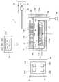
- FIG. 1is a diagram for explaining a configuration example of a capacitively coupled plasma processing apparatus.
- the plasma processing systemincludes a capacitively coupled plasma processing apparatus 1 and a controller 2.
- a capacitively coupled plasma processing apparatus 1includes a plasma processing chamber 10 , a gas supply section 20 , a power supply 30 and an exhaust system 40 . Further, the plasma processing apparatus 1 includes a substrate support section 11 and a gas introduction section.
- the gas introductionis configured to introduce at least one process gas into the plasma processing chamber 10 .
- the gas introduction sectionincludes a showerhead 13 .
- a substrate support 11is positioned within the plasma processing chamber 10 .
- the showerhead 13is arranged above the substrate support 11 . In one embodiment, showerhead 13 forms at least a portion of the ceiling of plasma processing chamber 10 .
- the plasma processing chamber 10has a plasma processing space 10 s defined by a showerhead 13 , side walls 10 a of the plasma processing chamber 10 and a substrate support 11 .
- the plasma processing chamber 10has at least one gas supply port for supplying at least one processing gas to the plasma processing space 10s and at least one gas exhaust port for exhausting gas from the plasma processing space.
- Plasma processing chamber 10is grounded.
- the showerhead 13 and substrate support 11are electrically insulated from the plasma processing chamber 10 housing.
- the substrate support section 11includes a body section 111 and a ring assembly 112 .
- the body portion 111has a central region 111 a for supporting the substrate W and an annular region 111 b for supporting the ring assembly 112 .
- a waferis an example of a substrate W;
- the annular region 111b of the body portion 111surrounds the central region 111a of the body portion 111 in plan view.
- the substrate Wis arranged on the central region 111 a of the main body 111
- the ring assembly 112is arranged on the annular region 111 b of the main body 111 so as to surround the substrate W on the central region 111 a of the main body 111 .
- the central region 111ais also referred to as a substrate support surface for supporting the substrate W
- the annular region 111bis also referred to as a ring support surface for supporting the edge ring assembly 112.
- the body portion 111includes a base 1110 and an electrostatic chuck 1111 .
- Base 1110includes a conductive member.
- a conductive member of the base 1110can function as a bottom electrode.
- An electrostatic chuck 1111is arranged on the base 1110 .
- the electrostatic chuck 1111includes a ceramic member 1111a and an electrostatic electrode 1111b disposed within the ceramic member 1111a.
- Ceramic member 1111ahas a central region 111a. In one embodiment, the ceramic member 1111a also has an annular region 111b. Note that another member surrounding the electrostatic chuck 1111, such as an annular electrostatic chuck or an annular insulating member, may have the annular region 111b.
- the ring assembly 112may be placed on the annular electrostatic chuck or the annular insulating member, or may be placed on both the electrostatic chuck 1111 and the annular insulating member.
- An RF or DC electrodemay also be placed within the ceramic member 1111a, in which case the RF or DC electrode serves as the bottom electrode.
- An RF or DC electrodeis also referred to as a bias electrode when a bias RF signal or DC signal, described below, is connected to the RF or DC electrode. Note that both the conductive member of the base 1110 and the RF or DC electrode may function as the two bottom electrodes.
- Ring assembly 112includes one or more annular members.
- the one or more annular membersinclude one or more edge rings and at least one cover ring.
- the edge ringis made of a conductive material or an insulating material
- the cover ringis made of an insulating material.
- the substrate supporter 11may include a temperature control module configured to adjust at least one of the electrostatic chuck 1111, the ring assembly 112, and the substrate to a target temperature.
- the temperature control modulemay include heaters, heat transfer media, channels 1110a, or combinations thereof.
- channels 1110 aare formed in base 1110 and one or more heaters are positioned in ceramic member 1111 a of electrostatic chuck 1111 .
- the substrate supporter 11may include a heat transfer gas supply unit configured to supply a heat transfer gas between the back surface of the substrate W and the central region 111a.
- the showerhead 13is configured to introduce at least one processing gas from the gas supply unit 20 into the plasma processing space 10s.
- the showerhead 13has at least one gas supply port 13a, at least one gas diffusion chamber 13b, and multiple gas introduction ports 13c.
- the processing gas supplied to the gas supply port 13apasses through the gas diffusion chamber 13b and is introduced into the plasma processing space 10s through a plurality of gas introduction ports 13c.
- showerhead 13also includes an upper electrode.
- the gas introduction partmay include one or more side gas injectors (SGI: Side Gas Injector) attached to one or more openings formed in the side wall 10a.
- SGISide Gas Injector
- the gas supply unit 20may include at least one gas source 21 and at least one flow controller 22 .
- gas supply 20is configured to supply at least one process gas from respective gas sources 21 through respective flow controllers 22 to showerhead 13 .
- Each flow controller 22may include, for example, a mass flow controller or a pressure controlled flow controller.
- gas supply 20may include one or more flow modulation devices that modulate or pulse the flow of at least one process gas.
- Power supply 30includes an RF power supply 31 coupled to plasma processing chamber 10 via at least one impedance matching circuit.
- RF power supply 31is configured to supply at least one RF signal (RF power), such as a source RF signal and a bias RF signal, to at least one bottom electrode and/or at least one top electrode.
- RF power source 31may function as at least part of a plasma generator configured to generate a plasma from one or more process gases in plasma processing chamber 10 .
- a bias RF signalto at least one lower electrode, a bias potential is generated in the substrate W, and ion components in the formed plasma can be drawn into the substrate W.
- the RF power supply 31includes a first RF generator 31a and a second RF generator 31b.
- the first RF generator 31ais coupled to at least one lower electrode and/or at least one upper electrode via at least one impedance matching circuit to generate a source RF signal (source RF power) for plasma generation.
- the source RF signalhas a frequency within the range of 10 MHz to 150 MHz.
- the first RF generator 31amay be configured to generate multiple source RF signals having different frequencies.
- One or more source RF signals generatedare provided to at least one bottom electrode and/or at least one top electrode.
- the second RF generator 31bis coupled to at least one lower electrode via at least one impedance matching circuit and configured to generate a bias RF signal (bias RF power).
- the frequency of the bias RF signalmay be the same as or different from the frequency of the source RF signal.
- the bias RF signalhas a frequency lower than the frequency of the source RF signal.
- the bias RF signalhas a frequency within the range of 100 kHz to 60 MHz.
- the second RF generator 31bmay be configured to generate multiple bias RF signals having different frequencies.
- One or more bias RF signals generatedare provided to at least one bottom electrode. Also, in various embodiments, at least one of the source RF signal and the bias RF signal may be pulsed.
- Power supply 30may also include a DC power supply 32 coupled to plasma processing chamber 10 .
- the DC power supply 32includes a first DC generator 32a and a second DC generator 32b.
- the first DC generator 32ais connected to the at least one bottom electrode and configured to generate a first DC signal.
- a generated first bias DC signalis applied to at least one bottom electrode.
- the second DC generator 32bis connected to the at least one top electrode and configured to generate a second DC signal. The generated second DC signal is applied to at least one top electrode.
- At least one of the first and second DC signalsmay be pulsed.
- a sequence of DC-based voltage pulsesis applied to at least one bottom electrode and/or at least one top electrode.
- the voltage pulsesmay have rectangular, trapezoidal, triangular, or combinations thereof pulse waveforms.
- a waveform generator for generating a sequence of voltage pulses from a DC signalis connected between the first DC generator 32a and the at least one bottom electrode. Therefore, the first DC generator 32a and the waveform generator constitute a voltage pulse generator.
- the voltage pulse generatoris connected to at least one upper electrode.
- the voltage pulsemay have a positive polarity or a negative polarity.
- the sequence of voltage pulsesmay include one or more positive voltage pulses and one or more negative voltage pulses in one cycle.
- the first and second DC generators 32a and 32bmay be provided in addition to the RF power supply 31, and the first DC generator 32a may be provided instead of the second RF generator 31b. good.
- the exhaust system 40may be connected to a gas exhaust port 10e provided at the bottom of the plasma processing chamber 10, for example.
- Exhaust system 40may include a pressure regulating valve and a vacuum pump.
- the pressure regulating valveregulates the pressure in the plasma processing space 10s.
- Vacuum pumpsmay include turbomolecular pumps, dry pumps, or combinations thereof.
- the controller 2processes computer-executable instructions that cause the plasma processing apparatus 1 to perform the various steps described in this disclosure. Controller 2 may be configured to control elements of plasma processing apparatus 1 to perform the various processes described herein. In one embodiment, part or all of the controller 2 may be included in the plasma processing apparatus 1 .
- the control unit 2may include, for example, a computer 2a.
- the computer 2amay include, for example, a processing unit (CPU: Central Processing Unit) 2a1, a storage unit 2a2, and a communication interface 2a3.
- Processing unit 2a1can be configured to perform various control operations by reading a program from storage unit 2a2 and executing the read program. This program may be stored in the storage unit 2a2 in advance, or may be acquired via a medium when necessary.
- the acquired programis stored in the storage unit 2a2, read from the storage unit 2a2 and executed by the processing unit 2a1.
- the mediummay be various storage media readable by the computer 2a, or may be a communication line connected to the communication interface 2a3.
- the storage unit 2a2may include RAM (Random Access Memory), ROM (Read Only Memory), HDD (Hard Disk Drive), SSD (Solid State Drive), or a combination thereof.
- the communication interface 2a3may communicate with the plasma processing apparatus 1 via a communication line such as a LAN (Local Area Network).
- FIG. 2is a flow chart showing an etching method (hereinafter also referred to as "this processing method") according to one exemplary embodiment.
- the processing methodincludes a step ST1 of providing a substrate and a step ST2 of etching the silicon-containing film of the substrate.
- the processing in each stepmay be performed in the plasma processing system shown in FIG.
- An example in which the control unit 2 controls each unit of the plasma processing apparatus 1 to perform the present processing method on the substrate Wwill be described below.
- step ST ⁇ b>1the substrate W is provided within the plasma processing space 10 s of the plasma processing apparatus 1 .
- a substrate Wis provided on the central region 111 a of the substrate support 11 .
- the substrate Wis held on the substrate supporter 11 by the electrostatic chuck 1111 .
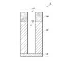
- FIG. 3is a diagram showing an example of the cross-sectional structure of the substrate W provided in step ST1.
- a silicon-containing film SF and a mask MFare laminated in this order on a base film UF.
- the substrate Wmay be used in the manufacture of semiconductor devices.
- Semiconductor devicesinclude, for example, semiconductor memory devices such as DRAMs and 3D-NAND flash memories.
- the base film UFis, for example, a silicon wafer, or an organic film, dielectric film, metal film, semiconductor film, or the like formed on the silicon wafer.
- the base film UFmay be configured by laminating a plurality of films.
- the silicon-containing film SFis a film to be etched in this processing method.
- the silicon-containing film SFis, for example, a silicon oxide film, a silicon nitride film, a silicon oxynitride film, or a polycrystalline silicon film.
- the silicon-containing film SFmay be configured by laminating a plurality of films.
- the silicon-containing film SFmay be configured by alternately stacking a silicon oxide film and a silicon nitride film.
- the silicon-containing film SFmay be configured by alternately stacking a silicon oxide film and a polycrystalline silicon film.
- the mask MFis a film that functions as a mask in etching the silicon-containing film SF.
- the mask MFmay be, for example, a polysilicon film, a boron-doped silicon film, a tungsten-containing film (eg, WC film, WSi film, etc.), an amorphous carbon film, a tin oxide film, or a titanium-containing film (eg, TiN film, etc.).
- the mask MFdefines at least one opening OP on the silicon-containing film SF.
- the opening OPis a space above the silicon-containing film SF and surrounded by sidewalls of the mask MF. That is, the upper surface of silicon-containing film SF has a region covered with mask MF and a region exposed at the bottom of opening OP.
- the opening OPmay have any shape in plan view of the substrate W, that is, when the substrate W is viewed from the top to the bottom in FIG.
- the shapemay be, for example, a circle, an ellipse, a rectangle, a line, or a combination of one or more of these.
- the mask MFmay have multiple sidewalls, and the multiple sidewalls define the multiple openings OP.
- the plurality of openings OPmay each have a linear shape and may be arranged at regular intervals to form a line and space pattern. Also, the plurality of openings OP may each have a hole shape and form an array pattern.
- Each film (base film UF, silicon-containing film SF, mask MF) constituting the substrate Wmay be formed by CVD, ALD, spin coating, or the like.
- the opening OPmay be formed by etching the mask MF.
- the mask MFmay also be formed by lithography.
- Each of the above filmsmay be a flat film, or may be a film having unevenness.
- the substrate Wmay further have another film under the base film UF, and the laminated film of the silicon-containing film SF and the base film UF may function as a multi-layer mask. That is, the other film may be etched using the laminated film of the silicon-containing film SF and the base film UF as a multi-layer mask.
- At least part of the process of forming each film on the substrate Wmay be performed within the space of the plasma processing chamber 10 .
- etching the mask MF to form the opening OPmay be performed in the plasma processing chamber 10 . That is, the etching of the opening OP and the etching of the silicon-containing film SF, which will be described later, may be continuously performed in the same chamber.
- the substrate Wis carried into the plasma processing space 10s of the plasma processing apparatus 1, and the substrate supporting portion 11 A substrate may be provided by being placed in the central region 111a of the .
- the temperature of the substrate supporting portion 11is adjusted to the set temperature by the temperature control module.
- the set temperaturemay be, for example, 70°C or less, 0°C or less, -10°C or less, -20°C or less, -30°C or less, -40°C or less, -50°C or less, -60°C or less, or -70°C or less.
- adjusting or maintaining the temperature of the substrate support 11includes adjusting or maintaining the temperature of the heat transfer fluid flowing through the flow path 1110a at or different from the set temperature.
- adjusting or maintaining the temperature of the substrate support 11includes controlling the pressure of a heat transfer gas (eg, He) between the electrostatic chuck 1111 and the backside of the substrate W.
- a heat transfer gaseg, He
- the timing at which the heat transfer fluid begins to flow in the flow path 1110amay be before or after the substrate W is placed on the substrate supporting portion 11, or may be at the same time.
- the temperature of the substrate supporting portion 11may be adjusted to the set temperature before step ST1. That is, the substrate W may be provided to the substrate supporter 11 after the temperature of the substrate supporter 11 is adjusted to the set temperature.
- Step ST2Etching
- the silicon-containing film SF of the substrate Wis etched.
- the process ST2includes a first etching process ST21 and a second etching process ST22. Further, the step ST2 may include a step ST23 of determining whether the etching stop condition is satisfied. That is, step ST21 and step ST22 may be alternately repeated until it is determined in step ST23 that the stopping condition is satisfied.
- the temperature of the substrate supporting portion 11is maintained at the set temperature adjusted in step ST1.
- Step ST21first etching
- the silicon-containing film SFis etched using plasma generated from the first processing gas.
- the first processing gasis supplied from the gas supply unit 20 into the plasma processing space 10s.
- the first process gasincludes hydrogen fluoride (HF) gas and a reaction control gas that controls the reaction between hydrogen fluoride and the silicon-containing film.
- the first process gasmay contain, as a reaction control gas, a reaction accelerating gas that accelerates the reaction between hydrogen fluoride and the silicon-containing film.
- the first process gasmay include a reaction suppressing gas that suppresses the reaction. Note that the first processing gas may contain both the reaction promoting gas and the reaction inhibiting gas.
- a source RF signalis then supplied to the lower electrode of the substrate support 11 and/or the upper electrode of the showerhead 13 .
- a high frequency electric fieldis generated between the shower head 13 and the substrate supporting portion 11, and plasma is generated from the first processing gas in the plasma processing space 10s.
- a bias signalis supplied to the lower electrode of the substrate supporting portion 11 to generate a bias potential between the plasma and the substrate W.
- Active speciessuch as ions and radicals in the plasma are attracted to the substrate W by the bias potential, and the silicon-containing film SF is etched by the active species.
- Step ST22Second etching
- the silicon-containing film SFis further etched using plasma generated from the second processing gas.
- the second processing gasis supplied from the gas supply unit 20 into the plasma processing space 10s.
- the second process gasincludes hydrogen fluoride (HF) gas.
- the second processing gasmay contain at least one of a reaction promoting gas that promotes the reaction between hydrogen fluoride and the silicon-containing film and a reaction suppressing gas that suppresses the reaction. If the second process gas contains a reaction accelerant gas, the partial pressure of the reaction accelerant gas may be less than the partial pressure of the reaction accelerant gas in the first process gas. When the second process gas includes a reaction-suppressing gas, the partial pressure of the reaction-suppressing gas may be greater than the partial pressure of the reaction-suppressing gas in the first process gas.
- the partial pressure of the reaction promoting gasis smaller than the partial pressure of the reaction promoting gas in the first processing gas, or the partial pressure of the reaction suppressing gas is The pressure may be greater than the partial pressure of the reaction inhibiting gas in the first process gas, or both.
- the second processing gasmay not contain a gas that controls (suppresses or promotes) the reaction between hydrogen fluoride and the silicon-containing film.
- a source RF signalis supplied to the lower electrode of the substrate support 11 and/or the upper electrode of the showerhead 13, as in step ST21.
- a high frequency electric fieldis generated between the shower head 13 and the substrate supporting portion 11, and plasma is generated from the second processing gas in the plasma processing space 10s.
- a bias signalis supplied to the lower electrode of the substrate supporting portion 11 to generate a bias potential between the plasma and the substrate W.
- Active speciessuch as ions and radicals in the plasma are attracted to the substrate W by the bias potential, and the silicon-containing film SF is further etched by the active species.
- step ST21 to step ST22may be performed based on, for example, at least one of the depth of the recess formed in the silicon-containing film SF by etching, the aspect ratio of the recess, and the etching time.
- the bias signalmay be the bias RF signal supplied from the second RF generator 31b.
- the bias signalmay be a bias DC signal supplied from the DC generator 32a. Note that the bias signal may not be supplied in steps ST21 and ST22.
- both the source RF signal and the bias signalmay be continuous waves or pulse waves, or one may be continuous waves and the other may be pulse waves.
- the periods of both pulse wavesmay be synchronized.
- the pulse wavemay have a rectangular, trapezoidal, triangular, or combination waveform.
- the polarity of the bias DC signalcan be either negative or positive provided that the potential of the substrate W is set to provide a potential difference between the plasma and the substrate to attract ions.
- the duty ratio of the pulse wavemay be set as appropriate, for example, 1 to 80% or 5 to 50%.
- the duty ratiois the proportion of the period of the pulse wave in which the power or voltage level is high.
- the duty ratio of the pulse wavemay be the same or different between steps ST21 and ST22.
- the duty ratio of the pulse wave of the source RF signal in step ST22may be made smaller than the duty ratio of the pulse wave of the source RF signal in step ST21.
- Step ST23it is determined whether or not the stop condition is satisfied.
- the stop conditionmay be, for example, whether or not the number of repetitions of the cycle has reached a given number, with the steps ST21 and ST22 being one cycle.
- a stopping conditionmay be, for example, that the etching time has reached a given time.
- the stop conditionmay be, for example, whether the depth of the recess formed by etching has reached a given depth. If it is determined in step ST23 that the stop condition is not satisfied, the cycle including steps ST21 and ST22 is repeated. When it is determined in step ST23 that the stop condition is satisfied, this processing method ends. In addition to step ST23, the determination as to whether the stop condition is satisfied may also be performed between step ST21 and step ST22.
- the HF gasmay have the highest partial pressure among all the gases excluding the inert gas. Further, in the second processing gas, the HF gas may have the highest partial pressure among all the gases except for the inert gas. In one example, in the first process gas and/or the second process gas, the HF gas may be 50% by volume or more, 60% by volume or more, 70% by volume or more with respect to the total flow rate excluding the inert gas, Moreover, 80 volume% or more may be contained. As the HF gas, one having a high purity, for example, a purity of 99.999% or more may be used.
- the reaction promoting gas contained in the first processing gas and/or the second processing gasis, for example, a gas (adsorption promoting gas) that promotes adsorption of active species of hydrogen fluoride in plasma to the silicon-containing film SF. OK.
- the active species of hydrogen fluorideinclude at least one of hydrogen fluoride gas, radicals and ions. At least one selected from the group consisting of phosphorus-containing gas, nitrogen-containing gas and hydrogen-containing gas may be used as the reaction accelerating gas.
- the type of reaction accelerating gas contained in the first processing gas and the type of reaction accelerating gas contained in the second processing gasare may be the same or different.
- a phosphorus-containing gasis a gas that contains phosphorus-containing molecules.
- the phosphorus-containing moleculemay be an oxide such as tetraphosphorus decaoxide ( P4O10 ), tetraphosphorus octaoxide ( P4O8 ), tetraphosphorus hexaoxide ( P4O6 ), and the like. Tetraphosphorus decaoxide is sometimes referred to as diphosphorus pentoxide ( P2O5).
- Phosphorus-containing moleculesinclude phosphorus trifluoride (PF 3 ), phosphorus pentafluoride (PF 5 ), phosphorus trichloride (PCl 3 ), phosphorus pentachloride (PCl 5 ), phosphorus tribromide (PBr 3 ), pentaodorous Halides (phosphorus halides) such as phosphorus chloride (PBr 5 ) and phosphorus iodide (PI 3 ) may also be used. That is, the phosphorus-containing molecule may contain fluorine as a halogen element, such as phosphorus fluoride. Alternatively, the phosphorus-containing molecule may contain a halogen element other than fluorine as the halogen element.
- the phosphorus-containing moleculemay be a phosphoryl halide such as phosphoryl fluoride ( POF3 ), phosphoryl chloride ( POCl3 ), phosphoryl bromide ( POBr3 ).
- Phosphorus - containing moleculesinclude phosphine (PH3), calcium phosphide ( Ca3P2 , etc.), phosphoric acid ( H3PO4 ) , sodium phosphate ( Na3PO4 ), hexafluorophosphoric acid ( HPF6 ), etc. can be Phosphorus-containing molecules may be fluorophosphines (H g PF h ). Here, the sum of g and h is 3 or 5.
- the process gasmay contain, as the at least one phosphorus-containing molecule, one or more of the phosphorus-containing molecules described above.
- the process gascan include at least one of PF3, PCl3, PF5 , PCl5 , POCl3 , PH3 , PBr3 , or PBr5 as the at least one phosphorus-containing molecule. Note that when each phosphorus-containing molecule is liquid or solid, each phosphorus-containing molecule can be vaporized by heating or the like and supplied into the plasma processing space 10s.
- the nitrogen-containing gasin one example, at least one selected from the group consisting of NH3 gas, NF3 gas , NO gas, and NO2 gas may be used.
- a gas having an OH groupmay be used, and in one example, at least one selected from the group consisting of H 2 O gas, H 2 O 2 gas and alcohol may be used.
- the reaction suppressing gas contained in the first processing gas and/or the second processing gasremoves (scavenges) the active species of hydrogen in the plasma, for example, so that the active species of hydrogen fluoride in the plasma and the silicon
- Any gas that suppresses the reaction with the containing film SFmay be used.
- a chlorine-containing gasmay be used as the reaction suppressing gas.
- the chlorine - containing gasis selected from the group consisting of Cl2 gas, SiCl2 gas, SiH2Cl2 gas, SiCl4 gas, Si2Cl6 gas, CHCl3 gas , CCl4 gas and BCl3 gas. At least one may be used.
- the type of the reaction suppressing gas contained in the first processing gas and the type of the reaction suppressing gas contained in the second processing gasare may be the same or different.
- the first process gas and/or the second process gasmay further include a carbon containing gas.
- the carbon-containing gascan be, for example, either or both of a fluorocarbon gas and a hydrofluorocarbon gas.
- the fluorocarbon gasesinclude CF4 gas, C2F2 gas, C2F4 gas, C3F6 gas, C3F8 gas , C4F6 gas , C4F8 gas and C5F At least one selected from the group consisting of 8 gases may be used.
- the hydrofluorocarbon gasis CHF3 gas , CH2F2 gas , CH3F gas , C2HF5 gas, C2H2F4 gas, C2H3F3 gas, C2H4F 2 gas, C3HF7 gas , C3H2F2 gas , C3H2F4 gas , C3H2F6 gas , C3H3F5 gas , C4H2F6 gas , C At least one selected from the group consisting of 4H5F5 gas , C4H2F8 gas , C5H2F6 gas , C5H2F10 gas and C5H3F7 gas may be used.
- the carbon-containing gasmay be a linear one having an unsaturated bond.
- Linear carbon-containing gases having unsaturated bondsinclude, for example, C 3 F 6 (hexafluoropropene) gas, C 4 F 8 (octafluoro-1-butene, octafluoro-2-butene) gas, C 3 H 2 F 4 (1,3,3,3-tetrafluoropropene) gas, C 4 H 2 F 6 (trans-1,1,1,4,4,4-hexafluoro-2-butene) gas , C 4 F 8 O (pentafluoroethyltrifluorovinyl ether) gas, CF 3 COF gas (1,2,2,2-tetrafluoroethan-1-one), CHF 2 COF (difluoroacetic acid fluoride) gas and COF 2 At least one selected from the group consisting of (carbonyl fluoride) gas may be used.
- C 3 F 6hexafluoropropene
- C 4 F 8octafluoro-1-butene
- the first process gas and/or the second process gasmay further include an oxygen-containing gas.
- the oxygen-containing gasmay be, for example, at least one gas selected from the group consisting of O2 , CO and CO2 .
- the first process gas and/or the second process gasmay further comprise a carbon-free, fluorine-containing gas.
- the carbon-free fluorine - containing gasis selected from the group of SF6, NF3 , XeF2, SiF4 , IF5 , IF7 , BrF5 , AsF5 , NF5 , BF3 and WF6 . At least one may be used.
- the first process gas and/or the second process gasmay further include halogen-containing gases other than fluorine.
- the halogen-containing gas other than fluorinemay be, for example, at least one selected from the group consisting of HBr gas, HI gas and I2 gas.
- the first process gas and/or the second process gasmay further contain an inert gas.
- the inert gasmay be, for example, a noble gas such as Ar gas, He gas, Kr gas, or N2 gas.
- the first process gas and/or the second process gasmay contain gases capable of producing HF species in the plasma instead of or in addition to the HF gas.
- Gases capable of producing HF speciesare, for example, hydrofluorocarbon gases.
- the hydrofluorocarbon gasmay have 2 or more, 3 or more, or 4 or more carbon atoms.
- Examples of hydrofluorocarbon gasesinclude CH 2 F 2 gas, C 3 H 2 F 4 gas, C 3 H 2 F 6 gas, C 3 H 3 F 5 gas, C 4 H 2 F 6 gas, and C 4 H 5 gas. It is at least one selected from the group consisting of F5 gas , C4H2F8 gas , C5H2F6 gas , C5H2F10 gas and C5H3F7 gas .
- the hydrofluorocarbon gasis, for example, at least one selected from the group consisting of CH 2 F 2 gas, C 3 H 2 F 4 gas, C 3 H 2 F 6 gas and C 4 H 2 F 6 gas.
- Gases capable of producing HF speciesare, for example, fluorine-containing gases and hydrogen-containing gases.
- a fluorine-containing gasis, for example, a fluorocarbon gas. Fluorocarbon gas, in one example, consists of C2F2 gas, C2F4 gas, C3F6 gas, C3F8 gas , C4F6 gas , C4F8 gas and C5F8 gas . At least one selected from the group.
- the fluorine-containing gasmay also be, for example , NF3 gas or SF6 gas.
- the hydrogen-containing gasis, for example, at least one selected from the group consisting of H2 gas, CH4 gas and NH3 gas.
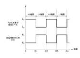
- FIG. 4is an example of a timing chart of step ST2 when a reaction promoting gas is used.
- FIG. 4shows an example of etching the silicon-containing film SF in one cycle of the first etching step ST21 and the second etching step ST2 using a reaction accelerating gas as the reaction control gas.
- the vertical axisrepresents the partial pressure of the reaction accelerating gas contained in the first processing gas or the second processing gas and the adsorption level of hydrogen fluoride on the silicon-containing film SF.
- the horizontal axisindicates etching time.
- P Bindicates that the partial pressure of the accelerant gas is zero or less than “P A ”.
- step ST21this period is hereinafter referred to as "H period”
- time t11 to t12corresponds to step ST22 (this period is hereinafter referred to as "L period”).
- the partial pressure of the reaction promoting gasis constant within each period (H period and L period), but is changed stepwise or continuously (decrease, increase or increase/decrease) within each period. good.
- the adsorption level of hydrogen fluoride gascan change along with the change.
- FIG. 4is a timing chart in the case of using a reaction promoting gas as the reaction controlling gas in step ST2, but instead/or in addition to this, a reaction inhibiting gas may be used as the reaction controlling gas.
- FIG. 5is an example of a timing chart of step ST2 when a reaction suppressing gas is used.
- the partial pressure of the reaction inhibiting gasmay be low or zero (P D ) during the H period and the partial pressure of the reaction inhibiting gas may be high (P C ) during the L period.
- P Dthe partial pressure of the reaction inhibiting gas
- FIG. 6Ais a diagram showing an example of the cross-sectional structure of the substrate W at the end (time t11) of period H (step ST21) in FIG. 4 or 5.
- FIG. 6Bshows an example of the cross-sectional structure of the substrate W at the end (time t12) of the L period (step ST22) in FIG. 4 or 5 .
- the portion of the silicon-containing film SF exposed in the opening OPis etched in the depth direction (the direction from top to bottom in FIG. 6A), and the concave portion is formed.
- RCis formed.
- the silicon-containing film SFmay be etched until or just before the bottom of the recess RC reaches the underlying film UF.
- the adsorption level (L A or L C ) of hydrogen fluoride to the silicon-containing filmis higher than during the L period (step ST21) (see FIGS. 4 and 5).
- L A or L Cthe adsorption level of hydrogen fluoride to the silicon-containing film
- reaction products (by-products) generated by etchingincrease compared to the L period. Reaction by-products may adhere to the sidewalls of the recesses RC and interfere with etching in the horizontal direction (horizontal direction in FIG. 6A). Thereby, the recess RC can be tapered in the depth direction (see FIG. 6A).
- the adsorption level (L B or L D ) of hydrogen fluoride to the silicon-containing filmis lower than in the H period (step ST21) (see FIGS. 4 and 5).
- L B or L Dthe adsorption level of hydrogen fluoride to the silicon-containing film
- the silicon-containing film SFis etched at a lower etching rate than during the H period.
- reaction by-products produced by etchingare reduced compared to the H period, and adsorption to the side walls of the recess RC is suppressed.
- etchingproceeds in the horizontal direction, and the concave portion RC changes from a tapered shape to a rectangular shape (see FIG. 6B). That is, the verticality of the concave portion RC is enhanced.
- the silicon-containing film SFis etched at a high etching rate in the H period (step ST21), and then the recess RC of the silicon-containing film SF is etched in the L period (step ST22). Unfold the bottom. As a result, it is possible to improve the verticality of the recesses formed by etching and suppress shape abnormalities while suppressing a decrease in the etching rate in the entire step ST2.
- FIG. 7is another example of the timing chart of step ST2 when using a reaction accelerating gas.
- FIG. 7shows an example of etching the silicon-containing film SF by repeating one cycle of the first etching step ST21 and the second etching step ST2 using a reaction accelerating gas as the reaction control gas.
- the vertical and horizontal axes in FIG. 7are the same as in FIG. 4, and "P B " indicates that the partial pressure of the reaction promoting gas is zero or less than "P A ".
- “L B ”indicates that the adsorption level (adsorption amount) of hydrogen fluoride to the silicon-containing film SF is smaller than “L A ”.
- P Bindicates that the partial pressure of the reaction promoting gas is zero or less than "P A ".
- L Bindicates that the adsorption level (adsorption amount) of hydrogen fluoride to the silicon-containing film SF is smaller than “L A ”.
- step ST21time 0 to t21 and time t22 to t23 correspond to step ST21 (this period is hereinafter referred to as “H1 period”, “H2 period”, etc.).
- Time t21 to t22 and time t23 to t24correspond to step ST22 (this period is hereinafter referred to as “L1 period”, “L2 period”, etc.).
- the partial pressure of the reaction accelerating gasis constant in each period (H1 period, H2 period, L1 period, L2 period, etc.), but changes (decreases, may be increased or decreased). In this case, the adsorption level of hydrogen fluoride can change along with the change.
- FIG. 7is a timing chart in the case of using a reaction promoting gas as the reaction control gas in step ST2, but instead/or in addition to this, a reaction inhibiting gas may be used as the reaction control gas.
- FIG. 8is another example of the timing chart of step ST2 when using the reaction-suppressing gas.
- step ST1H1 period, H2 period
- the partial pressure of the reaction suppressing gasis reduced or zero (P D )
- step ST2L1 period, L2 period
- the partial pressure of the reaction suppressing gasis reduced. It may be high (P C ).
- the adsorption level (L C ) of hydrogen fluoride in step ST1 (H1 period, H2 period)becomes higher than the adsorption level (L D ) in step ST2 (L1 period, L2 period).
- FIG. 9Ais a diagram showing an example of the cross-sectional structure of the substrate W at the end (time t21) of the H1 period (step ST21 of the first cycle) in FIG. 7 or 8.
- FIG. 9Bshows an example of the cross-sectional structure of the substrate W at the end (time t22) of the L1 period (process ST22 of the first cycle) in FIG. 7 or 8 .
- the portion of the silicon-containing film SF exposed in the opening OPis increased in the depth direction (from top to bottom in FIG. 9A) by the treatment during the H1 period (step ST21 of the first cycle). It is etched to form a recess RC.
- the silicon-containing film SFis etched until the concave portion RC reaches a given depth (for example, a depth of 1/n of the thickness of the silicon-containing film SF when steps ST21 and ST22 are repeated n cycles). be done.
- the silicon-containing film SFis etched at a higher etching rate than during the L1 period, similarly to the above-described H period, while the recess RC can be tapered along the depth direction (see FIG. 9A). ).
- the silicon-containing film SFis etched at an etching rate lower than that in the H1 period, as in the L period described above, while etching proceeds in the horizontal direction, and the concave portion is formed.
- RCapproaches a rectangle from a tapered shape (see FIG. 9B). That is, the verticality of the concave portion RC is enhanced.
- the step ST1(first period, H2 period, etc.) of etching the silicon-containing film SF at a high etching rate and the step of widening the bottom of the recess RC of the silicon-containing film SF ST2 (L1 period, L2 period) is alternately repeated.
- the verticality of the recesses formed by etchingcan be increased, and shape abnormalities can be suppressed.
- FIG. 10is a flowchart showing a modification of this processing method.
- the order of the first etching and the second etchingmay be reversed. That is, after the silicon-containing film SF is first etched using the second processing gas (step ST21A), the silicon-containing film SF may be etched using the first processing gas (step ST23A).
- step ST2Athe determination of whether or not the stopping condition is satisfied may be performed between step ST21A and step ST22A in addition to step ST23.
- FIG. 11is a flowchart showing a modification of this processing method. As shown in FIG. 11, only the first etching may be performed in the etching process. That is, in the etching step ST2B, the silicon-containing film SF may be etched using the first processing gas (step ST2B).
- the temperature of the substrate Wcan increase as the etching progresses.
- hydrogen fluoridetends to be more easily adsorbed to the silicon-containing film SF as the temperature of the substrate W is lower. Therefore, as the etching progresses, the amount of hydrogen fluoride adsorbed may decrease, and the etching rate may decrease. Therefore, for example, the reaction accelerating gas may be supplied from the middle stage to the final stage of the etching process when the etching rate may decrease. Thereby, the decrease in the etching rate can be suppressed.
- the supply amount of the reaction accelerating gasmay be set based on the etching time, the temperature of the substrate W and the substrate supporting portion 11, and the like.
- the amount of etchant (active species of hydrogen fluoride) supplied to the bottom of the recessdecreases as the aspect ratio of the recess formed by etching increases. Therefore, the partial pressure of the reaction control gas may be changed according to the aspect ratio of the recess. For example, the partial pressure of the accelerant gas may be greater for etching high aspect regions than for etching low aspect regions. This can promote the reaction between the etchant and the silicon-containing film SF in the high aspect region.
- the etching ratemay decrease due to deposition of reaction by-products caused by etching of the silicon-containing film SF. Therefore, during etching, a reaction-inhibiting gas may be temporarily supplied to promote volatilization of reaction by-products.
- the reaction-promoting gasmay be supplied at a preset timing, or may be supplied according to the etching state estimated from the plasma emission state or the like.
- the supply amount and supply time of the reaction-inhibiting gasare not limited as long as the volatilization of reaction by-products can be promoted.
- the processing methodmay be performed using a plasma processing apparatus using an arbitrary plasma source, such as inductively coupled plasma or microwave plasma, in addition to the capacitively coupled plasma processing apparatus 1 .
- a plasma processing apparatususing an arbitrary plasma source, such as inductively coupled plasma or microwave plasma, in addition to the capacitively coupled plasma processing apparatus 1 .
- Example 1Using the plasma processing apparatus 1, this processing method was applied to etch a substrate having the same structure as the substrate W shown in FIG.
- An amorphous carbon film having a hole-shaped opening OPwas used as the mask MF.
- a silicon oxide filmwas used as the silicon-containing film SF.
- the first process gascontained Cl 2 gas as a reaction suppressing gas in addition to HF gas.
- the second process gascontained Cl 2 gas as a reaction suppressing gas.
- the partial pressure of the reaction-suppressing gas ( Cl2 gas) in the second process gaswas less than the partial pressure of the reaction-suppressing gas ( Cl2 gas) in the first process.
- the temperature of the substrate supporting portion 11was set to 15.degree. In Example 1, one cycle of step ST21 (620 seconds) and step ST22 (310 seconds) in FIG. 2 was performed. In Example 2, four cycles of step ST21 (150 seconds) and step ST22 (50 seconds) in FIG. 2 were performed in this order.
- Reference Example 1the substrate W having the same configuration as in Examples 1 and 2 was etched using the plasma processing apparatus 1 .
- Reference Example 1using the same processing gas as the first processing gas used in Examples 1 and 2, etching was performed continuously for 840 seconds.
- the temperature of the substrate supporting portion 11was set to 15.degree.
- Table 1shows the etching rate ER [nm/min] and BB bias [nm] of the silicon-containing films SF according to Examples 1, 2, and Reference Example 1.
- the BB biasis the difference between the maximum opening width of the recess formed by etching and the opening width of the bottom.
- Example 1although the etching rate was slightly lower than that of Reference Example 1, the BB bias was small and the verticality of the concave portions was improved.
- Example 2compared with Reference Example 1, the etching rate was improved, the BB bias was small, and the verticality of the concave portion was improved. That is, in both Example 1 and Example 2, it was possible to increase the verticality of the concave portion (suppress shape abnormality) while suppressing a decrease in the etching rate.
- Example 3 and Example 4Using the plasma processing apparatus 1, this processing method was applied to etch a substrate having the same structure as the substrate W shown in FIG. An amorphous carbon film having a hole-shaped opening OP was used as the mask MF. A silicon oxide film was used as the silicon-containing film SF.
- the first process gascontained PF3 gas as a reaction accelerator gas in addition to HF gas.
- the second process gascontained HF gas and no PF3 gas.
- the temperature of the substrate supporting portion 11was set to ⁇ 20° C., and four cycles of step ST21A (40 seconds) and step ST22A (120 seconds) in FIG. 10 were performed.
- Example 3plasma was generated using pulse waves of the source RF signal having the same duty ratio (37%) in both step ST21A and step ST22A.
- Example 4the pulse wave of the source RF signal with a duty ratio of 29% was used in step ST21A, and the plasma was generated by using the pulse wave of the source RF signal with a duty ratio of 37% in step ST22A.
- Table 2shows the etching rate ER [nm/min] and BB bias [nm] of the silicon-containing films SF according to Examples 3 and 4.
- Example 4had a slightly higher etching rate and a slightly larger BB bias than Example 3. It is considered that in Example 4, the heat input to the substrate W was suppressed and the decrease in the etching rate was suppressed by lowering the duty ratio in step ST21A than in step ST22B.
- Embodiments of the present disclosurefurther include the following aspects.
- a device manufacturing method performed in a plasma processing apparatus having a chambercomprising: (a) providing a substrate having a silicon-containing film and a mask over the silicon-containing film on a substrate support within a chamber; (b) etching the silicon-containing film;
- the step (b)is (b-1) etching the silicon-containing film using plasma generated from a first processing gas containing hydrogen fluoride gas and a reaction control gas for controlling the reaction between the hydrogen fluoride and the silicon-containing film; a step in which the first processing gas contains, as the reaction control gas, at least one of a reaction accelerating gas that accelerates the reaction and a reaction inhibiting gas that inhibits the reaction; (b-2) a step of etching the silicon-containing film using plasma generated from a second processing gas containing hydrogen fluoride gas, wherein the second processing gas promotes the reaction; containing a gas at a lower partial pressure than the reaction promoting gas in the first process gas and/or containing a reaction inhibiting gas that suppresses the reaction
- a computer of a plasma processing systemcomprising a chamber, a substrate support provided in the chamber, and a plasma generator, (a) controlling to provide a substrate having a silicon-containing film and a mask over the silicon-containing film on a substrate support within a chamber; (b) controlling etching of the silicon-containing film;
- the control of (b)is (b-1) etching the silicon-containing film using plasma generated from a first processing gas containing hydrogen fluoride gas and a reaction control gas for controlling the reaction between the hydrogen fluoride and the silicon-containing film; control, wherein the first processing gas includes, as the reaction control gas, at least one of a reaction accelerating gas that accelerates the reaction and a reaction inhibiting gas that inhibits the reaction; (b-2) Control for etching the silicon-containing film using plasma generated from a second processing gas containing hydrogen fluoride gas, wherein the second processing gas promotes the reaction.
- reaction control gascontaining a gas at a lower partial pressure than the reaction promoting gas in the first process gas and/or containing a reaction inhibiting gas that suppresses the reaction at a higher partial pressure than the reaction inhibiting gas in the first process gas or control that does not include the reaction control gas.
- Appendix 3A storage medium storing the program according to appendix 2.
Landscapes
- Engineering & Computer Science (AREA)
- Physics & Mathematics (AREA)
- Chemical & Material Sciences (AREA)
- Plasma & Fusion (AREA)
- Analytical Chemistry (AREA)
- General Physics & Mathematics (AREA)
- Power Engineering (AREA)
- Microelectronics & Electronic Packaging (AREA)
- Computer Hardware Design (AREA)
- Manufacturing & Machinery (AREA)
- Condensed Matter Physics & Semiconductors (AREA)
- Chemical Kinetics & Catalysis (AREA)
- General Chemical & Material Sciences (AREA)
- Inorganic Chemistry (AREA)
- Drying Of Semiconductors (AREA)
- Plasma Technology (AREA)
Abstract
Description
Translated fromJapanese本開示の例示的実施形態は、エッチング方法及びプラズマ処理システムに関する。Exemplary embodiments of the present disclosure relate to etching methods and plasma processing systems.
特許文献1には、シリコンを含有する基板内の膜を、アモルファスカーボン又は有機ポリマーを含むマスクを用いてエッチングする技術が開示されている。
本開示は、エッチングの形状異常を抑制する技術を提供する。The present disclosure provides a technique for suppressing shape abnormalities in etching.
本開示の一つの例示的実施形態において、チャンバを有するプラズマ処理装置において実行されるエッチング方法であって、(a)シリコン含有膜と前記シリコン含有膜上のマスクとを有する基板を、チャンバ内の基板支持部上に提供する工程と、(b)前記シリコン含有膜をエッチングする工程と、を含み、前記(b)の工程は、(b-1)フッ化水素ガスと、フッ化水素と前記シリコン含有膜との反応を制御する反応制御ガスとを含む第1の処理ガスから生成したプラズマを用いて前記シリコン含有膜をエッチングする工程であって、前記第1の処理ガスは、前記反応制御ガスとして、前記反応を促進する反応促進ガス及び前記反応を抑制する抑制する反応抑制ガスの少なくとも一方を含む工程と、(b-2)フッ化水素ガスを含む第2の処理ガスから生成したプラズマを用いて前記シリコン含有膜をエッチングする工程であって、前記第2の処理ガスは、前記反応を促進する反応促進ガスを前記第1の処理ガス中の反応促進ガスよりも小さい分圧で含む及び/又は前記反応を抑制する反応抑制ガスを前記第1の処理ガス中の反応抑制ガスよりも高い分圧で含むか、又は、前記反応制御ガスを含まない工程と、を含む、エッチング方法が提供される。In one exemplary embodiment of the present disclosure, an etching method performed in a plasma processing apparatus having a chamber, comprising: (a) a substrate having a silicon-containing film and a mask on the silicon-containing film; (b) etching the silicon-containing film, wherein the step (b) includes (b-1) hydrogen fluoride gas, hydrogen fluoride, and the Etching the silicon-containing film using plasma generated from a first process gas containing a reaction control gas for controlling reaction with the silicon-containing film, wherein the first process gas is the reaction control gas. (b-2) a plasma generated from a second processing gas containing hydrogen fluoride gas; wherein the second process gas contains a reaction accelerant gas that promotes the reaction at a lower partial pressure than the reaction accelerant gas in the first process gas. and/or including a reaction-suppressing gas that suppresses the reaction at a higher partial pressure than the reaction-suppressing gas in the first process gas, or not including the reaction-controlling gas. provided.
本開示の一つの例示的実施形態によれば、エッチングの形状異常を抑制する技術を提供することができる。According to one exemplary embodiment of the present disclosure, it is possible to provide a technique for suppressing shape abnormalities in etching.
以下、本開示の各実施形態について説明する。Each embodiment of the present disclosure will be described below.
一つの例示的実施形態において、チャンバを有するプラズマ処理装置において実行されるエッチング方法であって、(a)シリコン含有膜とシリコン含有膜上のマスクとを有する基板を、チャンバ内の基板支持部上に提供する工程と、(b)シリコン含有膜をエッチングする工程と、を含み、(b)の工程は、(b-1)フッ化水素ガスと、フッ化水素とシリコン含有膜との反応を制御する反応制御ガスとを含む第1の処理ガスから生成したプラズマを用いてシリコン含有膜をエッチングする工程であって、第1の処理ガスは、反応制御ガスとして、反応を促進する反応促進ガス及び反応を抑制する抑制する反応抑制ガスの少なくとも一方を含む工程と、(b-2)フッ化水素ガスを含む第2の処理ガスから生成したプラズマを用いてシリコン含有膜をエッチングする工程であって、第2の処理ガスは、反応を促進する反応促進ガスを第1の処理ガス中の反応促進ガスよりも小さい分圧で含む及び/又は反応を抑制する反応抑制ガスを第1の処理ガス中の反応抑制ガスよりも高い分圧で含むか、又は、反応制御ガスを含まない工程と、を含むエッチング方法が提供される。In one exemplary embodiment, a method of etching performed in a plasma processing apparatus having a chamber, comprising: (a) placing a substrate having a silicon-containing film and a mask over the silicon-containing film on a substrate support in the chamber; and (b) etching the silicon-containing film, wherein the step of (b) comprises (b-1) reacting the hydrogen fluoride gas with the hydrogen fluoride and the silicon-containing film. a step of etching a silicon-containing film using a plasma generated from a first process gas containing a reaction control gas to be controlled, wherein the first process gas is a reaction accelerator gas that accelerates the reaction as the reaction control gas. and (b-2) etching the silicon-containing film using plasma generated from a second processing gas containing hydrogen fluoride gas. The second processing gas contains a reaction promoting gas that promotes the reaction at a lower partial pressure than the reaction promoting gas in the first processing gas and/or contains a reaction suppressing gas that suppresses the reaction. and at a higher partial pressure than the reaction-inhibiting gas therein or without a reaction-controlling gas.
一つの例示的実施形態において、(b)の工程において、(b-1)の工程の後に、(b-2)の工程を行うエッチング方法を提供する。In one exemplary embodiment, an etching method is provided in which step (b-2) is performed after step (b-1) in step (b).
一つの例示的実施形態において、(b)の工程において、(b-2)の工程の後に、(b-1)の工程を行うエッチング方法を提供する。In one exemplary embodiment, an etching method is provided in which step (b-1) is performed after step (b-2) in step (b).
一つの例示的実施形態において、b)の工程において、(b-1)の工程と(b-2)の工程とを交互に繰り返す。In one exemplary embodiment, in step b), step (b-1) and step (b-2) are alternately repeated.
一つの例示的実施形態において、(b)の工程において、エッチングによりシリコン含有膜に形成される凹部の深さ、凹部のアスペクト比、及び、エッチング時間の少なくとも一つに基づいて、(b-1)の工程と(b-2)の工程との切り換えを行う。In one exemplary embodiment, in the step (b), (b-1 ) and (b-2) are switched.
一つの例示的実施形態において、(b-1)の工程において、第1のデューティ比を有するソースRF信号のパルス波を用いて、第1の処理ガスからプラズマを生成し、(bー2)の工程において、第1のデューティ比よりも小さい第2のデューティ比を有するソースRF信号のパルス波を用いて、第2の処理ガスからプラズマを生成する。In one exemplary embodiment, in step (b-1), a pulsed wave of the source RF signal having a first duty ratio is used to generate plasma from the first process gas, and (b-2) 2. generating a plasma from the second process gas using a pulsed wave of the source RF signal having a second duty ratio that is less than the first duty ratio.
一つの例示的実施形態において、反応促進ガスは、リン含有ガス、窒素含有ガス及び水素含有ガスからなる群から選択される少なくとも1種である。In one exemplary embodiment, the reaction promoting gas is at least one selected from the group consisting of phosphorus-containing gas, nitrogen-containing gas and hydrogen-containing gas.
一つの例示的実施形態において、リン含有ガスは、ハロゲン化リンガスである。In one exemplary embodiment, the phosphorus-containing gas is a halogenated phosphorus gas.
一つの例示的実施形態において、窒素含有ガスは、NH3ガス、NF3ガス、NOガス及びNO2ガスからなる群から選択される少なくとも1種である。In one exemplary embodiment, the nitrogen-containing gas is atleast one selected from the group consisting ofNH3 gas, NF3 gas, NO gas and NO2 gas.
一つの例示的実施形態において、水素含有ガスは、OH基を有するガスである。In one exemplary embodiment, the hydrogen-containing gas is a gas with OH groups.
一つの例示的実施形態において、反応抑制ガスは、塩素含有ガスである。In one exemplary embodiment, the reaction-inhibiting gas is a chlorine-containing gas.
一つの例示的実施形態において、塩素含有ガスは、Cl2ガス、SiCl2ガス、SiH2Cl2ガス、SiCl4ガス、Si2Cl6ガス、CHCl3ガス、CCl4ガス及びBCl3ガスからなる群から選択される少なくとも1種である。In one exemplary embodiment, the chlorine- containing gas consists ofCl2 gas,SiCl2 gas,SiH2Cl2 gas,SiCl4 gas,Si2Cl6 gas, CHCl3 gas,CCl4 gas andBCl3 gas. At least one selected from the group.
一つの例示的実施形態において、第1の処理ガス及び第2の処理ガスのいずれにおいても、不活性ガスを除きフッ化水素ガスの分圧が最も大きい。In one exemplary embodiment, hydrogen fluoride gas has the highest partial pressure in both the first process gas and the second process gas, excluding inert gases.
一つの例示的実施形態において、第1の処理ガス及び第2の処理ガスの少なくとも一方は、炭素含有ガス、酸素含有ガス、炭素を含まないフッ素含有ガス及びフッ素以外のハロゲン含有ガスからなる群から選択される少なくとも1種をさらに含む。In one exemplary embodiment, at least one of the first process gas and the second process gas is from the group consisting of a carbon-containing gas, an oxygen-containing gas, a carbon-free fluorine-containing gas, and a halogen-containing gas other than fluorine. It further contains at least one selected.
一つの例示的実施形態において、第1の処理ガスに含まれる反応抑制ガスと、第2の処理ガスに含まれる反応抑制ガスとが互いに同一の種類のガスである。In one exemplary embodiment, the reaction inhibiting gas contained in the first process gas and the reaction inhibiting gas contained in the second process gas are the same type of gas.
一つの例示的実施形態において、第1の処理ガスに含まれる反応促進ガスと、第2の処理ガスに含まれる反応促進ガスとが互いに同一の種類のガスである。In one exemplary embodiment, the reaction accelerant gas contained in the first process gas and the reaction accelerant gas contained in the second process gas are the same type of gas.
一つの例示的実施形態において、チャンバを有するプラズマ処理装置において実行されるエッチング方法であって、(a)シリコン含有膜とシリコン含有膜上のマスクとを有する基板を、チャンバ内の基板支持部上に提供する工程と、(b)シリコン含有膜をエッチングする工程と、を含み、(b-1)第1の処理ガスから生成される、フッ化水素の活性種を含むプラズマを用いて、シリコン含有膜をエッチングする工程であって、第1の処理ガスは、フッ化水素とシリコン含有膜との反応を制御する反応制御ガスとして、反応を促進する反応促進ガス及び反応を抑制する抑制する反応抑制ガスの少なくとも一方を含む工程と、(b-2)第2の処理ガスから生成される、フッ化水素の活性種を含むプラズマを用いて、シリコン含有膜をエッチングする工程であって、第2の処理ガスは、反応を促進する反応促進ガスを第1の処理ガス中の反応促進ガスよりも小さい分圧で含む及び/又は反応を抑制する反応抑制ガスを第1の処理ガス中の反応抑制ガスよりも高い分圧で含むか、又は、反応制御ガスを含まない工程と、を含むエッチング方法が提供される。In one exemplary embodiment, a method of etching performed in a plasma processing apparatus having a chamber, comprising: (a) placing a substrate having a silicon-containing film and a mask over the silicon-containing film on a substrate support in the chamber; and (b) etching the silicon-containing film, wherein (b-1) plasma containing hydrogen fluoride active species generated from the first process gas is used to etch the silicon In the step of etching the containing film, the first processing gas is a reaction controlling gas for controlling the reaction between the hydrogen fluoride and the silicon containing film, a reaction promoting gas for promoting the reaction and a reaction for suppressing the reaction. (b-2) etching the silicon-containing film using plasma containing hydrogen fluoride active species generated from the second process gas, wherein The processing gas of 2 contains a reaction promoting gas that promotes the reaction at a lower partial pressure than the reaction promoting gas in the first processing gas and/or contains a reaction suppressing gas that suppresses the reaction in the first processing gas. a higher partial pressure than the suppressing gas or no reaction control gas.
一つの例示的実施形態において、フッ化水素の活性種は、フッ化水素ガス又はハイドロフルオロカーボンガスの少なくとも1種のガスから生成される。In one exemplary embodiment, the hydrogen fluoride active species are generated from at least one gas of hydrogen fluoride gas or hydrofluorocarbon gas.
一つの例示的実施形態において、フッ化水素の活性種は、フッ素含有ガス及び水素含有ガスから生成される。In one exemplary embodiment, hydrogen fluoride active species are generated from a fluorine-containing gas and a hydrogen-containing gas.
一つの例示的実施形態において、チャンバ、チャンバ内に設けられた基板支持部、プラズマ生成部、及び、制御部を備え、制御部は、(a)シリコン含有膜とシリコン含有膜上のマスクとを有する基板を、チャンバ内の基板支持部上に提供する制御と、(b)シリコン含有膜をエッチングする制御と、を実行し、(b)の制御は、(b-1)フッ化水素ガスと、フッ化水素とシリコン含有膜との反応を制御する反応制御ガスとを含む第1の処理ガスから生成したプラズマを用いてシリコン含有膜をエッチングする制御であって、第1の処理ガスは、反応制御ガスとして、反応を促進する反応促進ガス及び反応を抑制する抑制する反応抑制ガスの少なくとも一方を含む制御と、(b-2)フッ化水素ガスを含む第2の処理ガスから生成したプラズマを用いてシリコン含有膜をエッチングする制御であって、第2の処理ガスは、反応を促進する反応促進ガスを第1の処理ガス中の反応促進ガスよりも小さい分圧で含む及び/又は反応を抑制する反応抑制ガスを第1の処理ガス中の反応抑制ガスよりも高い分圧で含むか、又は、反応制御ガスを含まない制御と、を含むプラズマ処理システムが提供される。In one exemplary embodiment, the chamber comprises a chamber, a substrate support provided within the chamber, a plasma generator, and a controller, wherein the controller (a) removes a silicon-containing film and a mask on the silicon-containing film. and (b) etching a silicon-containing film, wherein the control of (b) includes (b-1) hydrogen fluoride gas and , a silicon-containing film is etched using a plasma generated from a first process gas containing hydrogen fluoride and a reaction control gas for controlling a reaction between the silicon-containing film, the first process gas comprising: Control containing at least one of a reaction-promoting gas that promotes the reaction and a reaction-suppressing gas that suppresses the reaction as the reaction control gas, and (b-2) a plasma generated from a second processing gas containing hydrogen fluoride gas. wherein the second process gas includes a reaction-promoting gas at a lower partial pressure than the reaction-promoting gas in the first process gas and/or and a control that includes a reaction inhibiting gas at a higher partial pressure than the reaction inhibiting gas in the first process gas or does not contain a reaction control gas.
以下、図面を参照して、本開示の各実施形態について詳細に説明する。なお、各図面において同一または同様の要素には同一の符号を付し、重複する説明を省略する。特に断らない限り、図面に示す位置関係に基づいて上下左右等の位置関係を説明する。図面の寸法比率は実際の比率を示すものではなく、また、実際の比率は図示の比率に限られるものではない。Hereinafter, each embodiment of the present disclosure will be described in detail with reference to the drawings. In each drawing, the same or similar elements are denoted by the same reference numerals, and overlapping descriptions are omitted. Unless otherwise specified, positional relationships such as top, bottom, left, and right will be described based on the positional relationships shown in the drawings. The dimensional ratios in the drawings do not indicate the actual ratios, and the actual ratios are not limited to the illustrated ratios.
<プラズマ処理システムの構成例>
以下に、プラズマ処理システムの構成例について説明する。図1は、容量結合型のプラズマ処理装置の構成例を説明するための図である。<Configuration example of plasma processing system>
A configuration example of the plasma processing system will be described below. FIG. 1 is a diagram for explaining a configuration example of a capacitively coupled plasma processing apparatus.
プラズマ処理システムは、容量結合型のプラズマ処理装置1及び制御部2を含む。容量結合型のプラズマ処理装置1は、プラズマ処理チャンバ10、ガス供給部20、電源30及び排気システム40を含む。また、プラズマ処理装置1は、基板支持部11及びガス導入部を含む。ガス導入部は、少なくとも1つの処理ガスをプラズマ処理チャンバ10内に導入するように構成される。ガス導入部は、シャワーヘッド13を含む。基板支持部11は、プラズマ処理チャンバ10内に配置される。シャワーヘッド13は、基板支持部11の上方に配置される。一実施形態において、シャワーヘッド13は、プラズマ処理チャンバ10の天部(ceiling)の少なくとも一部を構成する。プラズマ処理チャンバ10は、シャワーヘッド13、プラズマ処理チャンバ10の側壁10a及び基板支持部11により規定されたプラズマ処理空間10sを有する。プラズマ処理チャンバ10は、少なくとも1つの処理ガスをプラズマ処理空間10sに供給するための少なくとも1つのガス供給口と、プラズマ処理空間からガスを排出するための少なくとも1つのガス排出口とを有する。プラズマ処理チャンバ10は接地される。シャワーヘッド13及び基板支持部11は、プラズマ処理チャンバ10筐体とは電気的に絶縁される。The plasma processing system includes a capacitively coupled
基板支持部11は、本体部111及びリングアセンブリ112を含む。本体部111は、基板Wを支持するための中央領域111aと、リングアセンブリ112を支持するための環状領域111bとを有する。ウェハは基板Wの一例である。本体部111の環状領域111bは、平面視で本体部111の中央領域111aを囲んでいる。基板Wは、本体部111の中央領域111a上に配置され、リングアセンブリ112は、本体部111の中央領域111a上の基板Wを囲むように本体部111の環状領域111b上に配置される。従って、中央領域111aは、基板Wを支持するための基板支持面とも呼ばれ、環状領域111bは、エッジリングアセンブリ112を支持するためのリング支持面とも呼ばれる。The
一実施形態において、本体部111は、基台1110及び静電チャック1111を含む。基台1110は、導電性部材を含む。基台1110の導電性部材は下部電極として機能し得る。静電チャック1111は、基台1110の上に配置される。静電チャック1111は、セラミック部材1111aとセラミック部材1111a内に配置される静電電極1111bとを含む。セラミック部材1111aは、中央領域111aを有する。一実施形態において、セラミック部材1111aは、環状領域111bも有する。なお、環状静電チャックや環状絶縁部材のような、静電チャック1111を囲む他の部材が環状領域111bを有してもよい。この場合、リングアセンブリ112は、環状静電チャック又は環状絶縁部材の上に配置されてもよく、静電チャック1111と環状絶縁部材の両方の上に配置されてもよい。また、RF又はDC電極がセラミック部材1111a内に配置されてもよく、この場合、RF又はDC電極が下部電極として機能する。後述するバイアスRF信号又はDC信号がRF又はDC電極に接続される場合、RF又はDC電極はバイアス電極とも呼ばれる。なお、基台1110の導電性部材とRF又はDC電極との両方が2つの下部電極として機能してもよい。In one embodiment, the
リングアセンブリ112は、1又は複数の環状部材を含む。一実施形態において、1又は複数の環状部材は、1又は複数のエッジリングと少なくとも1つのカバーリングとを含む。エッジリングは、導電性材料又は絶縁材料で形成され、カバーリングは、絶縁材料で形成される。
また、基板支持部11は、静電チャック1111、リングアセンブリ112及び基板のうち少なくとも1つをターゲット温度に調節するように構成される温調モジュールを含んでもよい。温調モジュールは、ヒータ、伝熱媒体、流路1110a、又はこれらの組み合わせを含んでもよい。流路1110aには、ブラインやガスのような伝熱流体が流れる。一実施形態において、流路1110aが基台1110内に形成され、1又は複数のヒータが静電チャック1111のセラミック部材1111a内に配置される。また、基板支持部11は、基板Wの裏面と中央領域111aとの間に伝熱ガスを供給するように構成された伝熱ガス供給部を含んでもよい。Also, the
シャワーヘッド13は、ガス供給部20からの少なくとも1つの処理ガスをプラズマ処理空間10s内に導入するように構成される。シャワーヘッド13は、少なくとも1つのガス供給口13a、少なくとも1つのガス拡散室13b、及び複数のガス導入口13cを有する。ガス供給口13aに供給された処理ガスは、ガス拡散室13bを通過して複数のガス導入口13cからプラズマ処理空間10s内に導入される。また、シャワーヘッド13は、上部電極を含む。なお、ガス導入部は、シャワーヘッド13に加えて、側壁10aに形成された1又は複数の開口部に取り付けられる1又は複数のサイドガス注入部(SGI:Side Gas Injector)を含んでもよい。The
ガス供給部20は、少なくとも1つのガスソース21及び少なくとも1つの流量制御器22を含んでもよい。一実施形態において、ガス供給部20は、少なくとも1つの処理ガスを、それぞれに対応のガスソース21からそれぞれに対応の流量制御器22を介してシャワーヘッド13に供給するように構成される。各流量制御器22は、例えばマスフローコントローラ又は圧力制御式の流量制御器を含んでもよい。さらに、ガス供給部20は、少なくとも1つの処理ガスの流量を変調又はパルス化する1又はそれ以上の流量変調デバイスを含んでもよい。The
電源30は、少なくとも1つのインピーダンス整合回路を介してプラズマ処理チャンバ10に結合されるRF電源31を含む。RF電源31は、ソースRF信号及びバイアスRF信号のような少なくとも1つのRF信号(RF電力)を、少なくとも1つの下部電極及び/又は少なくとも1つの上部電極に供給するように構成される。これにより、プラズマ処理空間10sに供給された少なくとも1つの処理ガスからプラズマが形成される。従って、RF電源31は、プラズマ処理チャンバ10において1又はそれ以上の処理ガスからプラズマを生成するように構成されるプラズマ生成部の少なくとも一部として機能し得る。また、バイアスRF信号を少なくとも1つの下部電極に供給することにより、基板Wにバイアス電位が発生し、形成されたプラズマ中のイオン成分を基板Wに引き込むことができる。
一実施形態において、RF電源31は、第1のRF生成部31a及び第2のRF生成部31bを含む。第1のRF生成部31aは、少なくとも1つのインピーダンス整合回路を介して少なくとも1つの下部電極及び/又は少なくとも1つの上部電極に結合され、プラズマ生成用のソースRF信号(ソースRF電力)を生成するように構成される。一実施形態において、ソースRF信号は、10MHz~150MHzの範囲内の周波数を有する。一実施形態において、第1のRF生成部31aは、異なる周波数を有する複数のソースRF信号を生成するように構成されてもよい。生成された1又は複数のソースRF信号は、少なくとも1つの下部電極及び/又は少なくとも1つの上部電極に供給される。In one embodiment, the
第2のRF生成部31bは、少なくとも1つのインピーダンス整合回路を介して少なくとも1つの下部電極に結合され、バイアスRF信号(バイアスRF電力)を生成するように構成される。バイアスRF信号の周波数は、ソースRF信号の周波数と同じであっても異なっていてもよい。一実施形態において、バイアスRF信号は、ソースRF信号の周波数よりも低い周波数を有する。一実施形態において、バイアスRF信号は、100kHz~60MHzの範囲内の周波数を有する。一実施形態において、第2のRF生成部31bは、異なる周波数を有する複数のバイアスRF信号を生成するように構成されてもよい。生成された1又は複数のバイアスRF信号は、少なくとも1つの下部電極に供給される。また、種々の実施形態において、ソースRF信号及びバイアスRF信号のうち少なくとも1つがパルス化されてもよい。The
また、電源30は、プラズマ処理チャンバ10に結合されるDC電源32を含んでもよい。DC電源32は、第1のDC生成部32a及び第2のDC生成部32bを含む。一実施形態において、第1のDC生成部32aは、少なくとも1つの下部電極に接続され、第1のDC信号を生成するように構成される。生成された第1のバイアスDC信号は、少なくとも1つの下部電極に印加される。一実施形態において、第2のDC生成部32bは、少なくとも1つの上部電極に接続され、第2のDC信号を生成するように構成される。生成された第2のDC信号は、少なくとも1つの上部電極に印加される。
種々の実施形態において、第1及び第2のDC信号のうち少なくとも1つがパルス化されてもよい。この場合、DCに基づく電圧パルスのシーケンスが少なくとも1つの下部電極及び/又は少なくとも1つの上部電極に印加される。電圧パルスは、矩形、台形、三角形又はこれらの組み合わせのパルス波形を有してもよい。一実施形態において、DC信号から電圧パルスのシーケンスを生成するための波形生成部が第1のDC生成部32aと少なくとも1つの下部電極との間に接続される。従って、第1のDC生成部32a及び波形生成部は、電圧パルス生成部を構成する。第2のDC生成部32b及び波形生成部が電圧パルス生成部を構成する場合、電圧パルス生成部は、少なくとも1つの上部電極に接続される。電圧パルスは、正の極性を有してもよく、負の極性を有してもよい。また、電圧パルスのシーケンスは、1周期内に1又は複数の正極性電圧パルスと1又は複数の負極性電圧パルスとを含んでもよい。なお、第1及び第2のDC生成部32a、32bは、RF電源31に加えて設けられてもよく、第1のDC生成部32aが第2のRF生成部31bに代えて設けられてもよい。In various embodiments, at least one of the first and second DC signals may be pulsed. In this case, a sequence of DC-based voltage pulses is applied to at least one bottom electrode and/or at least one top electrode. The voltage pulses may have rectangular, trapezoidal, triangular, or combinations thereof pulse waveforms. In one embodiment, a waveform generator for generating a sequence of voltage pulses from a DC signal is connected between the
排気システム40は、例えばプラズマ処理チャンバ10の底部に設けられたガス排出口10eに接続され得る。排気システム40は、圧力調整弁及び真空ポンプを含んでもよい。圧力調整弁によって、プラズマ処理空間10s内の圧力が調整される。真空ポンプは、ターボ分子ポンプ、ドライポンプ又はこれらの組み合わせを含んでもよい。The
制御部2は、本開示において述べられる種々の工程をプラズマ処理装置1に実行させるコンピュータ実行可能な命令を処理する。制御部2は、ここで述べられる種々の工程を実行するようにプラズマ処理装置1の各要素を制御するように構成され得る。一実施形態において、制御部2の一部又は全てがプラズマ処理装置1に含まれてもよい。制御部2は、例えばコンピュータ2aを含んでもよい。コンピュータ2aは、例えば、処理部(CPU:Central Processing Unit)2a1、記憶部2a2、及び通信インターフェース2a3を含んでもよい。処理部2a1は、記憶部2a2からプログラムを読み出し、読み出されたプログラムを実行することにより種々の制御動作を行うように構成され得る。このプログラムは、予め記憶部2a2に格納されていてもよく、必要なときに、媒体を介して取得されてもよい。取得されたプログラムは、記憶部2a2に格納され、処理部2a1によって記憶部2a2から読み出されて実行される。媒体は、コンピュータ2aに読み取り可能な種々の記憶媒体であってもよく、通信インターフェース2a3に接続されている通信回線であってもよい。記憶部2a2は、RAM(Random Access Memory)、ROM(Read Only Memory)、HDD(Hard Disk Drive)、SSD(Solid State Drive)、又はこれらの組み合わせを含んでもよい。通信インターフェース2a3は、LAN(Local Area Network)等の通信回線を介してプラズマ処理装置1との間で通信してもよい。The
<エッチング方法の一例>
図2は、一つの例示的実施形態に係るエッチング方法(以下「本処理方法」ともいう。)を示すフローチャートである。図2に示すように、本処理方法は、基板を提供する工程ST1と、基板のシリコン含有膜をエッチングする工程ST2とを含む。各工程における処理は、図1に示すプラズマ処理システムで実行されてよい。以下では、制御部2がプラズマ処理装置1の各部を制御して、基板Wに対して本処理方法を実行する場合を例に説明する。<Example of etching method>
FIG. 2 is a flow chart showing an etching method (hereinafter also referred to as "this processing method") according to one exemplary embodiment. As shown in FIG. 2, the processing method includes a step ST1 of providing a substrate and a step ST2 of etching the silicon-containing film of the substrate. The processing in each step may be performed in the plasma processing system shown in FIG. An example in which the
(工程ST1:基板の提供)
工程ST1において、基板Wは、プラズマ処理装置1のプラズマ処理空間10s内に提供される。基板Wは、基板支持部11の中央領域111aに提供される。そして、基板Wは、静電チャック1111により基板支持部11に保持される。(Process ST1: Provision of substrate)
In step ST<b>1 , the substrate W is provided within the
図3は、工程ST1で提供される基板Wの断面構造の一例を示す図である。基板Wは、下地膜UF上に、シリコン含有膜SF及びマスクMFがこの順で積層されている。基板Wは、半導体デバイスの製造に用いられてよい。半導体デバイスは、例えば、DRAM、3D-NANDフラッシュメモリ等の半導体メモリデバイスを含む。FIG. 3 is a diagram showing an example of the cross-sectional structure of the substrate W provided in step ST1. In the substrate W, a silicon-containing film SF and a mask MF are laminated in this order on a base film UF. The substrate W may be used in the manufacture of semiconductor devices. Semiconductor devices include, for example, semiconductor memory devices such as DRAMs and 3D-NAND flash memories.
下地膜UFは、一例では、シリコンウェハやシリコンウェハ上に形成された有機膜、誘電体膜、金属膜、半導体膜等である。下地膜UFは、複数の膜が積層されて構成されてよい。The base film UF is, for example, a silicon wafer, or an organic film, dielectric film, metal film, semiconductor film, or the like formed on the silicon wafer. The base film UF may be configured by laminating a plurality of films.
シリコン含有膜SFは、本処理方法において、エッチングの対象となる膜である。シリコン含有膜SFは、一例では、シリコン酸化膜、シリコン窒化膜、シリコン酸窒化膜、多結晶シリコン膜である。シリコン含有膜SFは、複数の膜が積層されて構成されてよい。例えば、シリコン含有膜SFは、シリコン酸化膜とシリコン窒化膜とが交互に積層されて構成されてよい。また例えば、シリコン含有膜SFは、シリコン酸化膜と多結晶シリコン膜とが交互に積層されて構成されてよい。The silicon-containing film SF is a film to be etched in this processing method. The silicon-containing film SF is, for example, a silicon oxide film, a silicon nitride film, a silicon oxynitride film, or a polycrystalline silicon film. The silicon-containing film SF may be configured by laminating a plurality of films. For example, the silicon-containing film SF may be configured by alternately stacking a silicon oxide film and a silicon nitride film. Further, for example, the silicon-containing film SF may be configured by alternately stacking a silicon oxide film and a polycrystalline silicon film.
マスクMFは、シリコン含有膜SFのエッチングにおいてマスクとして機能する膜である。マスクMFは、例えば、ポリシリコン膜、ホウ素ドープシリコン膜、タングステン含有膜(例えば、WC膜、WSi膜等)、アモルファスカーボン膜又は酸化ズズ膜又はチタン含有膜(例えば、TiN膜等)でよい。The mask MF is a film that functions as a mask in etching the silicon-containing film SF. The mask MF may be, for example, a polysilicon film, a boron-doped silicon film, a tungsten-containing film (eg, WC film, WSi film, etc.), an amorphous carbon film, a tin oxide film, or a titanium-containing film (eg, TiN film, etc.).
図3に示すとおり、マスクMFは、シリコン含有膜SF上において少なくとも一つの開口OPを規定する。開口OPは、シリコン含有膜SF上の空間であって、マスクMFの側壁に囲まれている。すなわち、シリコン含有膜SFの上面は、マスクMFによって覆われた領域と、開口OPの底部において露出した領域とを有する。As shown in FIG. 3, the mask MF defines at least one opening OP on the silicon-containing film SF. The opening OP is a space above the silicon-containing film SF and surrounded by sidewalls of the mask MF. That is, the upper surface of silicon-containing film SF has a region covered with mask MF and a region exposed at the bottom of opening OP.
開口OPは、基板Wの平面視、すなわち、基板Wを図3の上から下に向かう方向に見た場合において、任意の形状を有してよい。当該形状は、例えば、円、楕円、矩形、線やこれらの1種類以上を組み合わせた形状であってよい。マスクMFは、複数の側壁を有し、複数の側壁が複数の開口OPを規定してもよい。複数の開口OPは、それぞれ線形状を有し、一定の間隔で並んでライン&スペースのパターンを構成してもよい。また、複数の開口OPは、それぞれ穴形状を有し、アレイパターンを構成してもよい。The opening OP may have any shape in plan view of the substrate W, that is, when the substrate W is viewed from the top to the bottom in FIG. The shape may be, for example, a circle, an ellipse, a rectangle, a line, or a combination of one or more of these. The mask MF may have multiple sidewalls, and the multiple sidewalls define the multiple openings OP. The plurality of openings OP may each have a linear shape and may be arranged at regular intervals to form a line and space pattern. Also, the plurality of openings OP may each have a hole shape and form an array pattern.
基板Wを構成する各膜(下地膜UF、シリコン含有膜SF、マスクMF)は、それぞれ、CVD法、ALD法、スピンコート法等により形成されてよい。開口OPは、マスクMFをエッチングすることで形成されてよい。またマスクMFは、リソグラフィによって形成されてもよい。なお、上記各膜は、平坦な膜であってよく、また、凹凸を有する膜であってもよい。また基板Wが下地膜UFの下に他の膜をさらに有し、シリコン含有膜SF及び下地膜UFの積層膜が多層マスクとして機能してもよい。すなわち、シリコン含有膜SF及び下地膜UFの積層膜を多層マスクとして、当該他の膜をエッチングしてもよい。Each film (base film UF, silicon-containing film SF, mask MF) constituting the substrate W may be formed by CVD, ALD, spin coating, or the like. The opening OP may be formed by etching the mask MF. The mask MF may also be formed by lithography. Each of the above films may be a flat film, or may be a film having unevenness. Further, the substrate W may further have another film under the base film UF, and the laminated film of the silicon-containing film SF and the base film UF may function as a multi-layer mask. That is, the other film may be etched using the laminated film of the silicon-containing film SF and the base film UF as a multi-layer mask.
基板Wの各膜を形成するプロセスの少なくとも一部は、プラズマ処理チャンバ10の空間内で行われてよい。一例では、マスクMFをエッチングして開口OPを形成する工程は、プラズマ処理チャンバ10で実行されてよい。すなわち、開口OP及び後述するシリコン含有膜SFのエッチングは、同一のチャンバ内で連続して実行されてよい。また、基板Wの各膜の全部又は一部がプラズマ処理装置1の外部の装置やチャンバで形成された後、基板Wがプラズマ処理装置1のプラズマ処理空間10s内に搬入され、基板支持部11の中央領域111aに配置されることで、基板が提供されてもよい。At least part of the process of forming each film on the substrate W may be performed within the space of the
基板Wを基板支持部11の中央領域111aに提供後、基板支持部11の温度が温調モジュールにより設定温度に調整される。設定温度は、例えば、70℃以下、0℃以下、-10℃以下、-20℃以下、-30℃以下、-40℃以下、-50℃以下、-60℃以下又は-70℃以下でよい。一例では、基板支持部11の温度を調整又は維持することは、流路1110aを流れる伝熱流体の温度を設定温度又は設定温度と異なる温度に調整又は維持することを含む。一例では、基板支持部11の温度を調整又は維持することは、静電チャック1111と基板Wの裏面との間の伝熱ガス(例えばHe)の圧力を制御することを含む。なお、流路1110aに伝熱流体が流れ始めるタイミングは、基板Wが基板支持部11に載置される前でも後でもよく、また同時でもよい。また、本処理方法において、基板支持部11の温度は、工程ST1の前に設定温度に調整されてよい。すなわち、基板支持部11の温度が設定温度に調整された後に、基板支持部11に基板Wを提供してよい。After providing the substrate W to the
(工程ST2:エッチング)
工程ST2において、基板Wのシリコン含有膜SFがエッチングされる。工程ST2は、第1のエッチング工程ST21と、第2のエッチング工程ST22とを備える。また工程ST2は、エッチングの停止条件を満たしているか判定する工程ST23を備えてよい。すなわち、工程ST23において停止条件を満たすと判定されるまで、工程ST21と工程ST22とを交互に繰り返してよい。工程ST2における処理の間、基板支持部11の温度は、工程ST1で調整した設定温度に維持される。(Step ST2: Etching)
In step ST2, the silicon-containing film SF of the substrate W is etched. The process ST2 includes a first etching process ST21 and a second etching process ST22. Further, the step ST2 may include a step ST23 of determining whether the etching stop condition is satisfied. That is, step ST21 and step ST22 may be alternately repeated until it is determined in step ST23 that the stopping condition is satisfied. During the process in step ST2, the temperature of the
(工程ST21:第1のエッチング)
工程ST21において、第1の処理ガスから生成したプラズマを用いて、シリコン含有膜SFがエッチングされる。まず、ガス供給部20から第1の処理ガスがプラズマ処理空間10s内に供給される。第1の処理ガスは、フッ化水素(HF)ガスと、フッ化水素とシリコン含有膜との反応を制御する反応制御ガスとを含む。第1の処理ガスは、反応制御ガスとして、フッ化水素とシリコン含有膜との反応を促進する反応促進ガスを含んでよい。第1の処理ガスは、当該反応を抑制する反応抑制ガスを含んでよい。なお、第1の処理ガスは、反応促進ガスと反応抑制ガスの双方を含んでもよい。(Step ST21: first etching)
In step ST21, the silicon-containing film SF is etched using plasma generated from the first processing gas. First, the first processing gas is supplied from the
次に、基板支持部11の下部電極及び/又はシャワーヘッド13の上部電極にソースRF信号が供給される。これにより、シャワーヘッド13と基板支持部11との間で高周波電界が生成され、プラズマ処理空間10s内の第1の処理ガスからプラズマが生成される。また、基板支持部11の下部電極にバイアス信号が供給されて、プラズマと基板Wとの間にバイアス電位が発生する。バイアス電位によって、プラズマ中のイオン、ラジカル等の活性種が基板Wに引きよせられ、当該活性種によってシリコン含有膜SFがエッチングされる。A source RF signal is then supplied to the lower electrode of the
(工程ST22:第2のエッチング)
第2のエッチング工程ST22において、第2の処理ガスから生成したプラズマを用いて、シリコン含有膜SFがさらにエッチングされる。まず、ガス供給部20から第2の処理ガスがプラズマ処理空間10s内に供給される。第2の処理ガスは、フッ化水素(HF)ガスを含む。(Step ST22: Second etching)
In the second etching step ST22, the silicon-containing film SF is further etched using plasma generated from the second processing gas. First, the second processing gas is supplied from the
第2の処理ガスは、フッ化水素とシリコン含有膜との反応を促進する反応促進ガス及び当該反応を抑制する反応抑制ガスの少なくとも一方を含んでよい。第2の処理ガスが反応促進ガスを含む場合、当該反応促進ガスの分圧は、第1の処理ガス中の反応促進ガスの分圧よりも小さくてよい。第2の処理ガスが反応抑制ガスを含む場合、当該反応抑制ガスの分圧は、第1の処理ガス中の反応抑制ガスの分圧よりも大きくてよい。第2の処理ガスが反応促進ガスと反応抑制ガスの双方を含む場合、反応促進ガスの分圧が第1の処理ガス中の反応促進ガスの分圧に比べて小さいか、反応抑制ガスの分圧が第1の処理ガス中の反応抑制ガスの分圧に比べて大きいか、又はその両方であってよい。The second processing gas may contain at least one of a reaction promoting gas that promotes the reaction between hydrogen fluoride and the silicon-containing film and a reaction suppressing gas that suppresses the reaction. If the second process gas contains a reaction accelerant gas, the partial pressure of the reaction accelerant gas may be less than the partial pressure of the reaction accelerant gas in the first process gas. When the second process gas includes a reaction-suppressing gas, the partial pressure of the reaction-suppressing gas may be greater than the partial pressure of the reaction-suppressing gas in the first process gas. When the second processing gas contains both the reaction promoting gas and the reaction suppressing gas, the partial pressure of the reaction promoting gas is smaller than the partial pressure of the reaction promoting gas in the first processing gas, or the partial pressure of the reaction suppressing gas is The pressure may be greater than the partial pressure of the reaction inhibiting gas in the first process gas, or both.
第2の処理ガスは、フッ化水素とシリコン含有膜との反応を制御(抑制又は促進)するガスを含まなくてもよい。The second processing gas may not contain a gas that controls (suppresses or promotes) the reaction between hydrogen fluoride and the silicon-containing film.
次に、工程ST21と同様に、基板支持部11の下部電極及び/又はシャワーヘッド13の上部電極にソースRF信号が供給される。これにより、シャワーヘッド13と基板支持部11との間で高周波電界が生成され、プラズマ処理空間10s内の第2の処理ガスからプラズマが生成される。また、基板支持部11の下部電極にバイアス信号が供給されて、プラズマと基板Wとの間にバイアス電位が発生する。バイアス電位によって、プラズマ中のイオン、ラジカル等の活性種が基板Wに引きよせられ、当該活性種によってシリコン含有膜SFがさらにエッチングされる。Next, a source RF signal is supplied to the lower electrode of the
工程ST21から工程ST22への切り換えは、例えば、エッチングによりシリコン含有膜SFに形成される凹部の深さ、当該凹部のアスペクト比、及び、エッチング時間の少なくともいずれか一つに基づいて行ってよい。The switching from step ST21 to step ST22 may be performed based on, for example, at least one of the depth of the recess formed in the silicon-containing film SF by etching, the aspect ratio of the recess, and the etching time.
工程ST21及び工程ST22において、バイアス信号は、第2のRF生成部31bから供給されるバイアスRF信号であってよい。またバイアス信号は、DC生成部32aから供給されるバイアスDC信号であってもよい。なお、工程ST21及び工程ST22においてバイアス信号が供給されなくてもよい。In steps ST21 and ST22, the bias signal may be the bias RF signal supplied from the
工程ST21及び工程ST22において、ソースRF信号及びバイアス信号は、双方が連続波又はパルス波でよく、また一方が連続波で他方がパルス波でもよい。ソースRF信号及びバイアス信号の双方がパルス波である場合、双方のパルス波の周期は同期してよい。バイアスDC信号を用いる場合、パルス波は、矩形、台形、三角形又はこれらの組み合わせの波形を有してよい。バイアスDC信号の極性は、プラズマと基板との間に電位差を与えてイオンを引き込むように基板Wの電位が設定されれば、負であっても正であってもよい。In steps ST21 and ST22, both the source RF signal and the bias signal may be continuous waves or pulse waves, or one may be continuous waves and the other may be pulse waves. When both the source RF signal and the bias signal are pulse waves, the periods of both pulse waves may be synchronized. If a bias DC signal is used, the pulse wave may have a rectangular, trapezoidal, triangular, or combination waveform. The polarity of the bias DC signal can be either negative or positive provided that the potential of the substrate W is set to provide a potential difference between the plasma and the substrate to attract ions.
ソースRF信号又はバイアス信号としてパルス波を用いる場合、パルス波のデューティ比は適宜設定してよく、例えば、1~80%でよく、また5~50%でよい。ここで、デューティ比は、パルス波の周期における、電力又は電圧レベルが高い期間が占める割合である。また、パルス波のデューティ比は、工程ST21と工程ST22とで同一でよく、また異なっていてもよい。一例では、工程ST22におけるソースRF信号のパルス波のデューティ比を、工程ST21におけるソースRF信号のパルス波のデューティ比よりも小さくしてよい。デューティ比を小さくすることで、プラズマによる基板Wへの入熱が抑制され、工程ST22に比べて基板Wの温度が低くなる。フッ化水素は、基板Wの温度が低いほどシリコン含有膜SFに吸着しやすい傾向があるので、デューティ比を小さくすることで、フッ化水素のシリコン含有膜SFへの吸着を促進し得る。When a pulse wave is used as the source RF signal or bias signal, the duty ratio of the pulse wave may be set as appropriate, for example, 1 to 80% or 5 to 50%. Here, the duty ratio is the proportion of the period of the pulse wave in which the power or voltage level is high. Also, the duty ratio of the pulse wave may be the same or different between steps ST21 and ST22. In one example, the duty ratio of the pulse wave of the source RF signal in step ST22 may be made smaller than the duty ratio of the pulse wave of the source RF signal in step ST21. By reducing the duty ratio, heat input to the substrate W by plasma is suppressed, and the temperature of the substrate W becomes lower than in step ST22. Hydrogen fluoride tends to be more easily adsorbed on the silicon-containing film SF as the temperature of the substrate W is lower. Therefore, by reducing the duty ratio, the adsorption of hydrogen fluoride on the silicon-containing film SF can be promoted.
(工程ST23:終了判定)
工程ST23において、停止条件が満たされるか否かが判定される。停止条件は、例えば、工程ST21及び工程ST22を1サイクルとし、当該サイクルの繰り返し回数が所与の回数に達しているか否かでよい。停止条件は、例えば、エッチング時間が所与の時間に達しているかでもよい。停止条件は、例えば、エッチングにより形成される凹部の深さが所与の深さに達しているかでもよい。工程ST23において停止条件が満たされていないと判定されると、工程ST21及び工程ST22を含むサイクルが繰り返される。工程ST23において停止条件が満たされると判定されると、本処理方法を終了する。なお、停止条件が満たされるか否かの判断を、工程ST23に加え、工程ST21と工程ST22との間でも実行してもよい。(Step ST23: end judgment)
In step ST23, it is determined whether or not the stop condition is satisfied. The stop condition may be, for example, whether or not the number of repetitions of the cycle has reached a given number, with the steps ST21 and ST22 being one cycle. A stopping condition may be, for example, that the etching time has reached a given time. The stop condition may be, for example, whether the depth of the recess formed by etching has reached a given depth. If it is determined in step ST23 that the stop condition is not satisfied, the cycle including steps ST21 and ST22 is repeated. When it is determined in step ST23 that the stop condition is satisfied, this processing method ends. In addition to step ST23, the determination as to whether the stop condition is satisfied may also be performed between step ST21 and step ST22.
(処理ガスの構成)
第1の処理ガスにおいて、不活性ガスを除く全ガスのうち、HFガスの分圧が最も大きくてよい。また第2の処理ガスにおいて、不活性ガスを除く全ガスのうち、HFガスの分圧が最も大きくてよい。一例では、第1の処理ガス及び/又は第2の処理ガスにおいて、HFガスは、不活性ガスを除く総流量に対して、50体積%以上、60体積%以上、70体積%以上でよく、また80体積%以上含まれてよい。なお、HFガスとしては、高純度のもの、例えば、純度が99.999%以上のものを用いてよい。(Composition of processing gas)
In the first processing gas, the HF gas may have the highest partial pressure among all the gases excluding the inert gas. Further, in the second processing gas, the HF gas may have the highest partial pressure among all the gases except for the inert gas. In one example, in the first process gas and/or the second process gas, the HF gas may be 50% by volume or more, 60% by volume or more, 70% by volume or more with respect to the total flow rate excluding the inert gas, Moreover, 80 volume% or more may be contained. As the HF gas, one having a high purity, for example, a purity of 99.999% or more may be used.
第1の処理ガス及び/又は第2の処理ガスに含まれる反応促進ガスは、例えば、プラズマ中のフッ化水素の活性種がシリコン含有膜SFに吸着することを促進するガス(吸着促進ガス)でよい。ここで、フッ化水素の活性種は、フッ化水素のガス、ラジカル及びイオンの少なくともいずれかを含む。反応促進ガスとしては、リン含有ガス、窒素含有ガス及び水素含有ガスからなる群から選択される少なくとも1種を使用してよい。第1の処理ガスと第2の処理ガスの双方が反応促進ガスを含む場合、第1の処理ガスに含まれる反応促進ガスの種類と、第2の処理ガスに含まれる反応促進ガスの種類とは同一でよく、また異なっていてもよい。The reaction promoting gas contained in the first processing gas and/or the second processing gas is, for example, a gas (adsorption promoting gas) that promotes adsorption of active species of hydrogen fluoride in plasma to the silicon-containing film SF. OK. Here, the active species of hydrogen fluoride include at least one of hydrogen fluoride gas, radicals and ions. At least one selected from the group consisting of phosphorus-containing gas, nitrogen-containing gas and hydrogen-containing gas may be used as the reaction accelerating gas. When both the first processing gas and the second processing gas contain a reaction accelerating gas, the type of reaction accelerating gas contained in the first processing gas and the type of reaction accelerating gas contained in the second processing gas are may be the same or different.
リン含有ガスは、リン含有分子を含むガスである。リン含有分子は、十酸化四リン(P4O10)、八酸化四リン(P4O8)、六酸化四リン(P4O6)等の酸化物であってもよい。十酸化四リンは、五酸化二リン(P2O5)と呼ばれることがある。リン含有分子は、三フッ化リン(PF3)、五フッ化リン(PF5)、三塩化リン(PCl3)、五塩化リン(PCl5)、三臭化リン(PBr3)、五臭化リン(PBr5)、ヨウ化リン(PI3)のようなハロゲン化物(ハロゲン化リン)であってもよい。すなわち、リン含有分子は、フッ化リン等、ハロゲン元素としてフッ素を含んでもよい。或いは、リン含有分子は、ハロゲン元素としてフッ素以外のハロゲン元素を含んでもよい。リン含有分子は、フッ化ホスホリル(POF3)、塩化ホスホリル(POCl3)、臭化ホスホリル(POBr3)のようなハロゲン化ホスホリルであってよい。リン含有分子は、ホスフィン(PH3)、リン化カルシウム(Ca3P2等)、リン酸(H3PO4)、リン酸ナトリウム(Na3PO4)、ヘキサフルオロリン酸(HPF6)等であってよい。リン含有分子は、フルオロホスフィン類(HgPFh)であってよい。ここで、gとhの和は、3又は5である。フルオロホスフィン類としては、HPF2、H2PF3が例示される。処理ガスは、少なくとも一つのリン含有分子として、上記のリン含有分子のうち一つ以上のリン含有分子を含み得る。例えば、処理ガスは、少なくとも一つのリン含有分子として、PF3、PCl3、PF5、PCl5、POCl3、PH3、PBr3、又はPBr5の少なくとも一つを含み得る。なお、各リン含有分子が液体又は固体である場合、各リン含有分子は、加熱等によって気化されてプラズマ処理空間10s内に供給され得る。A phosphorus-containing gas is a gas that contains phosphorus-containing molecules. The phosphorus-containing molecule may be an oxide such as tetraphosphorusdecaoxide(P4O10 ), tetraphosphorus octaoxide (P4O8 ), tetraphosphorus hexaoxide(P4O6 ), and the like. Tetraphosphorusdecaoxide is sometimes referred to as diphosphorus pentoxide( P2O5). Phosphorus-containing molecules include phosphorus trifluoride (PF3 ), phosphorus pentafluoride (PF5 ), phosphorus trichloride (PCl3 ), phosphorus pentachloride (PCl5 ), phosphorus tribromide (PBr3 ), pentaodorous Halides (phosphorus halides) such as phosphorus chloride (PBr5 ) and phosphorus iodide (PI3 ) may also be used. That is, the phosphorus-containing molecule may contain fluorine as a halogen element, such as phosphorus fluoride. Alternatively, the phosphorus-containing molecule may contain a halogen element other than fluorine as the halogen element. The phosphorus-containing molecule may be a phosphoryl halide such as phosphoryl fluoride (POF3 ), phosphoryl chloride (POCl3 ), phosphoryl bromide (POBr3 ). Phosphorus- containing molecules include phosphine (PH3), calcium phosphide (Ca3P2 , etc.), phosphoricacid(H3PO4 ), sodium phosphate (Na3PO4 ), hexafluorophosphoric acid (HPF6 ), etc. can be Phosphorus-containing molecules may be fluorophosphines (Hg PFh ). Here, the sum of g and h is 3 or 5. Examples of fluorophosphines include HPF2 and H2 PF3 . The process gas may contain, as the at least one phosphorus-containing molecule, one or more of the phosphorus-containing molecules described above. For example, the process gas can include at least one of PF3, PCl3,PF5 ,PCl5 ,POCl3, PH3,PBr3, orPBr5 as the at least one phosphorus-containing molecule. Note that when each phosphorus-containing molecule is liquid or solid, each phosphorus-containing molecule can be vaporized by heating or the like and supplied into the
窒素含有ガスとしては、一例では、NH3ガス、NF3ガス、NOガス、NO2ガスからなる群から選択される少なくとも1種を用いてよい。As the nitrogen-containing gas, in one example, at leastone selected from the group consisting ofNH3 gas, NF3 gas, NO gas, and NO2 gas may be used.
水素含有ガスとしては、OH基を有するガスを用いてよく、一例では、H2Oガス、H2O2ガス及びアルコールからなる群から選択される少なくとも1種を用いてよい。As the hydrogen-containing gas, a gas having an OH group may be used, and in one example, at least one selected from the group consisting of H2 O gas, H2 O2 gas and alcohol may be used.
第1の処理ガス及び/又は第2の処理ガスに含まれる反応抑制ガスは、例えば、プラズマ中の水素の活性種を除去(スカベンジ)することで、プラズマ中のフッ化水素の活性種とシリコン含有膜SFとの反応を抑制するガスでよい。反応抑制ガスとしては、例えば、塩素含有ガスを用いてよい。一例では、塩素含有ガスは、Cl2ガス、SiCl2ガス、SiH2Cl2ガス、SiCl4ガス、Si2Cl6ガス、CHCl3ガス、CCl4ガス及びBCl3ガスからなる群から選択される少なくとも一種を使用してよい。第1の処理ガスと第2の処理ガスの双方が反応抑制ガスを含む場合、第1の処理ガスに含まれる反応抑制ガスの種類と、第2の処理ガスに含まれる反応抑制ガスの種類とは同一でよく、また異なっていてもよい。The reaction suppressing gas contained in the first processing gas and/or the second processing gas removes (scavenges) the active species of hydrogen in the plasma, for example, so that the active species of hydrogen fluoride in the plasma and the silicon Any gas that suppresses the reaction with the containing film SF may be used. As the reaction suppressing gas, for example, a chlorine-containing gas may be used.In one example, the chlorine- containing gas is selected from the group consisting ofCl2 gas,SiCl2 gas,SiH2Cl2 gas,SiCl4 gas,Si2Cl6 gas, CHCl3 gas,CCl4 gas andBCl3 gas. At least one may be used. When both the first processing gas and the second processing gas contain the reaction suppressing gas, the type of the reaction suppressing gas contained in the first processing gas and the type of the reaction suppressing gas contained in the second processing gas are may be the same or different.
第1の処理ガス及び/又は第2の処理ガスは、炭素含有ガスをさらに含んでよい。炭素含有ガスは、例えば、フルオロカーボンガス及びハイドロフルオロカーボンガスのいずれかまたは両方でよい。一例では、フルオロカーボンガスは、CF4ガス、C2F2ガス、C2F4ガス、C3F6ガス、C3F8ガス、C4F6ガス、C4F8ガス及びC5F8ガスからなる群から選択される少なくとも1種でよい。一例では、ハイドロフルオロカーボンガスは、CHF3ガス、CH2F2ガス、CH3Fガス、C2HF5ガス、C2H2F4ガス、C2H3F3ガス、C2H4F2ガス、C3HF7ガス、C3H2F2ガス、C3H2F4ガス、C3H2F6ガス、C3H3F5ガス、C4H2F6ガス、C4H5F5ガス、C4H2F8ガス、C5H2F6ガス、C5H2F10ガス及びC5H3F7ガスからなる群から選択される少なくとも1種でよい。また、炭素含有ガスは、不飽和結合を有する直鎖状のものであってよい。不飽和結合を有する直鎖状の炭素含有ガスは、例えば、C3F6(ヘキサフルオロプロぺン)ガス、C4F8(オクタフルオロ-1-ブテン、オクタフルオロ-2-ブテン)ガス、C3H2F4(1,3,3,3-テトラフルオロプロペン)ガス、C4H2F6(トランス-1,1,1,4,4,4-ヘキサフルオロ-2-ブテン)ガス、C4F8O(ペンタフルオロエチルトリフルオロビニルエーテル)ガス、CF3COFガス(1,2,2,2-テトラフルオロエタン-1-オン)、CHF2COF(ジフルオロ酢酸フルオライド)ガス及びCOF2(フッ化カルボニル)ガスからなる群から選択される少なくとも1種でよい。The first process gas and/or the second process gas may further include a carbon containing gas. The carbon-containing gas can be, for example, either or both of a fluorocarbon gas and a hydrofluorocarbon gas.In one example, the fluorocarbon gases includeCF4 gas,C2F2 gas,C2F4 gas,C3F6 gas,C3F8gas,C4F6gas,C4F8gas andC5F At least one selected from the group consisting of8 gases may be used.Inone example, the hydrofluorocarbon gas isCHF3 gas,CH2F2gas,CH3Fgas,C2HF5 gas,C2H2F4 gas,C2H3F3 gas,C2H4F2 gas,C3HF7gas ,C3H2F2gas ,C3H2F4gas,C3H2F6gas,C3H3F5gas,C4H2F6gas,CAtleastone selected from the groupconsisting of4H5F5gas ,C4H2F8gas,C5H2F6gas ,C5H2F10gas andC5H3F7gas may be used. . Also, the carbon-containing gas may be a linear one having an unsaturated bond. Linear carbon-containing gases having unsaturated bonds include, for example, C3 F6 (hexafluoropropene) gas, C4 F8 (octafluoro-1-butene, octafluoro-2-butene) gas, C3 H2 F4 (1,3,3,3-tetrafluoropropene) gas, C4 H2 F6 (trans-1,1,1,4,4,4-hexafluoro-2-butene) gas , C4 F8 O (pentafluoroethyltrifluorovinyl ether) gas, CF3 COF gas (1,2,2,2-tetrafluoroethan-1-one), CHF2 COF (difluoroacetic acid fluoride) gas and COF2 At least one selected from the group consisting of (carbonyl fluoride) gas may be used.
第1の処理ガス及び/又は第2の処理ガスは、酸素含有ガスをさらに含んでよい。酸素含有ガスは、例えば、O2、CO及びCO2からなる群から選択される少なくとも1種のガスでよい。The first process gas and/or the second process gas may further include an oxygen-containing gas. The oxygen-containing gas may be, for example, at least one gas selected from the group consisting ofO2 , CO andCO2 .
第1の処理ガス及び/又は第2の処理ガスは、炭素を含まないフッ素含有ガスをさらに含んでよい。一例では、炭素を含まないフッ素含有ガスは、SF6、NF3、XeF2、SiF4、IF5、IF7、BrF5、AsF5、NF5、BF3及びWF6の群から選択される少なくとも1種であってよい。The first process gas and/or the second process gas may further comprise a carbon-free, fluorine-containing gas.In one example, the carbon-free fluorine- containing gas is selected from the group of SF6, NF3, XeF2,SiF4 ,IF5 ,IF7 ,BrF5 ,AsF5 ,NF5 ,BF3 andWF6 . At least one may be used.
第1の処理ガス及び/又は第2の処理ガスは、フッ素以外のハロゲン含有ガスをさらに含んでよい。フッ素以外のハロゲン含有ガスは、例えば、HBrガス、HIガス及びI2ガスからなる群から選択される少なくとも1種でよい。The first process gas and/or the second process gas may further include halogen-containing gases other than fluorine. The halogen-containing gas other than fluorine may be, for example, at least one selected from the group consisting of HBr gas, HI gas andI2 gas.
第1の処理ガス及び/又は第2の処理ガスは、不活性ガスをさらに含んでよい。不活性ガスは、一例では、Arガス、Heガス、Krガス等の貴ガス又はN2ガスでよい。The first process gas and/or the second process gas may further contain an inert gas. The inert gas may be, for example, a noble gas such as Ar gas, He gas, Kr gas, orN2 gas.
第1の処理ガス及び/又は第2の処理ガスは、HFガスに代えて又はHFガスに加えて、プラズマ中にHF種を生成可能なガスを含んでよい。The first process gas and/or the second process gas may contain gases capable of producing HF species in the plasma instead of or in addition to the HF gas.
HF種を生成可能なガスは、例えば、ハイドロフルオロカーボンガスである。ハイドロフルオロカーボンガスは、炭素数が2以上、3以上又は4以上でもよい。ハイドロフルオロカーボンガスは、一例では、CH2F2ガス、C3H2F4ガス、C3H2F6ガス、C3H3F5ガス、C4H2F6ガス、C4H5F5ガス、C4H2F8ガス、C5H2F6ガス、C5H2F10ガス及びC5H3F7ガスからなる群から選択される少なくとも1種である。ハイドロフルオロカーボンガスは、一例では、CH2F2ガス、C3H2F4ガス、C3H2F6ガス及びC4H2F6ガスからなる群から選択される少なくとも1種である。Gases capable of producing HF species are, for example, hydrofluorocarbon gases. The hydrofluorocarbon gas may have 2 or more, 3 or more, or 4 or more carbon atoms. Examples of hydrofluorocarbon gases include CH2 F2 gas, C3 H2 F4 gas, C3 H2 F6 gas, C3 H3 F5 gas, C4 H2 F6 gas, and C4 H5 gas. It is atleastone selected from the group consisting ofF5gas ,C4H2F8gas ,C5H2F6gas,C5H2F10gas andC5H3F7gas . The hydrofluorocarbon gas is, for example, at least one selected from the group consisting of CH2 F2 gas, C3 H2 F4 gas, C3 H2 F6 gas and C4 H2 F6 gas.
HF種を生成可能なガスは、例えば、フッ素含有ガス及び水素含有ガスである。フッ素含有ガスは、例えば、フルオロカーボンガスである。フルオロカーボンガスは、一例では、C2F2ガス、C2F4ガス、C3F6ガス、C3F8ガス、C4F6ガス、C4F8ガス及びC5F8ガスからなる群から選択される少なくとも1種である。またフッ素含有ガスは、例えば、NF3ガス又はSF6ガスでもよい。水素含有ガスは、一例では、H2ガス、CH4ガス及びNH3ガスからなる群から選択される少なくとも一種である。Gases capable of producing HF species are, for example, fluorine-containing gases and hydrogen-containing gases. A fluorine-containing gas is, for example, a fluorocarbon gas.Fluorocarbon gas,in one example, consists ofC2F2 gas,C2F4 gas,C3F6 gas,C3F8 gas,C4F6 gas,C4F8gas andC5F8gas. At least one selected from the group. The fluorine-containing gas may also be, for example, NF3 gas orSF6 gas. The hydrogen-containing gas is, for example, at leastone selected from the group consisting of H2 gas,CH4 gas andNH3 gas.
(工程ST2の一例)
図4は、反応促進ガスを用いた場合の工程ST2のタイミングチャートの一例である。図4は、反応制御ガスとして反応促進ガスを用い、第1のエッチング工程ST21及び第2のエッチング工程ST2の1サイクルで、シリコン含有膜SFをエッチングする例である。図4において、縦軸は、第1の処理ガス又は第2の処理ガスに含まれる反応促進ガスの分圧、及び、シリコン含有膜SFに対するフッ化水素の吸着レベルを示す。横軸は、エッチング時間を示す。「PB」は、反応促進ガスの分圧がゼロであるか、又は、「PA」よりも小さいことを示す。「LB」は、シリコン含有膜SFに対するフッ化水素の吸着レベル(吸着量)が「LA」よりも小さいことを示す。図4では、時間0~t11が工程ST21に対応し(以下この期間を「H期間」という)、時間t11~t12が工程ST22に対応する(以下この期間を「L期間」という)。(Example of process ST2)
FIG. 4 is an example of a timing chart of step ST2 when a reaction promoting gas is used. FIG. 4 shows an example of etching the silicon-containing film SF in one cycle of the first etching step ST21 and the second etching step ST2 using a reaction accelerating gas as the reaction control gas. In FIG. 4, the vertical axis represents the partial pressure of the reaction accelerating gas contained in the first processing gas or the second processing gas and the adsorption level of hydrogen fluoride on the silicon-containing film SF. The horizontal axis indicates etching time. “PB ” indicates that the partial pressure of the accelerant gas is zero or less than “PA ”. “LB ” indicates that the adsorption level (adsorption amount) of hydrogen fluoride to the silicon-containing film SF is smaller than “LA ”. In FIG. 4,
なお、図4では、反応促進ガスの分圧は、各期間(H期間及びL期間)内で一定であるが、各期間内において段階的又は連続的に変化(減少、増加又は増減)させてよい。この場合、フッ化水素ガスの吸着レベルは当該変化に追随して変化しうる。In FIG. 4, the partial pressure of the reaction promoting gas is constant within each period (H period and L period), but is changed stepwise or continuously (decrease, increase or increase/decrease) within each period. good. In this case, the adsorption level of hydrogen fluoride gas can change along with the change.
また図4は、工程ST2において、反応制御ガスとして反応促進ガスを用いた場合のタイミングチャートであるが、これに代えて/又は加えて、反応制御ガスとして反応抑制ガスを用いてもよい。図5は、反応抑制ガスを用いた場合の工程ST2のタイミングチャートの一例である。図5に示すように、H期間において反応抑制ガスの分圧を低く又はゼロにし(PD)、L期間において反応抑制ガスの分圧を高く(PC)してよい。これにより、H期間におけるフッ化水素の吸着レベル(LC)は、L期間における吸着レベル(LD)よりも高くなる。FIG. 4 is a timing chart in the case of using a reaction promoting gas as the reaction controlling gas in step ST2, but instead/or in addition to this, a reaction inhibiting gas may be used as the reaction controlling gas. FIG. 5 is an example of a timing chart of step ST2 when a reaction suppressing gas is used. As shown in FIG. 5, the partial pressure of the reaction inhibiting gas may be low or zero (PD ) during the H period and the partial pressure of the reaction inhibiting gas may be high (PC ) during the L period. As a result, the hydrogen fluoride adsorption level (LC ) during the H period becomes higher than the adsorption level (LD ) during the L period.
図6Aは、図4又は図5のH期間(工程ST21)終了時(時間t11)の基板Wの断面構造の一例を示す図である。図6Bは、図4又は図5のL期間(工程ST22)終了時(時間t12)の基板Wの断面構造の一例を示すである。FIG. 6A is a diagram showing an example of the cross-sectional structure of the substrate W at the end (time t11) of period H (step ST21) in FIG. 4 or 5. FIG. FIG. 6B shows an example of the cross-sectional structure of the substrate W at the end (time t12) of the L period (step ST22) in FIG. 4 or 5 .
図6Aに示すように、H期間(工程ST21)における処理により、シリコン含有膜SFのうち、開口OPにおいて露出した部分が深さ方向(図6Aで上から下に向かう方向)にエッチングされ、凹部RCが形成される。H期間では、凹部RCの底部が下地膜UFに到達するまで又は到達する直前までシリコン含有膜SFをエッチングしてよい。As shown in FIG. 6A, by the treatment in the H period (step ST21), the portion of the silicon-containing film SF exposed in the opening OP is etched in the depth direction (the direction from top to bottom in FIG. 6A), and the concave portion is formed. RC is formed. In the H period, the silicon-containing film SF may be etched until or just before the bottom of the recess RC reaches the underlying film UF.
H期間(工程ST21)において、フッ化水素のシリコン含有膜への吸着レベル(LA又はLC)は、L期間(工程ST21)よりも大きい(図4、図5参照)。これにより、H期間では、フッ化水素のシリコン含有膜SFへの吸着が促進され、L期間よりも高いエッチングレートでシリコン含有膜SFがエッチングされる。他方、H期間では、エッチングにより生じる反応生成物(バイプロダクト)がL期間に比べて増加する。反応副生成物は、凹部RCの側壁に吸着し、水平方向(図6Aの左右方向)のエッチングを妨げ得る。これにより、凹部RCは、深さ方向に沿って先細る形状になり得る(図6A参照)。During the H period (step ST21), the adsorption level (LA or LC ) of hydrogen fluoride to the silicon-containing film is higher than during the L period (step ST21) (see FIGS. 4 and 5). As a result, during the H period, adsorption of hydrogen fluoride to the silicon-containing film SF is promoted, and the silicon-containing film SF is etched at a higher etching rate than during the L period. On the other hand, in the H period, reaction products (by-products) generated by etching increase compared to the L period. Reaction by-products may adhere to the sidewalls of the recesses RC and interfere with etching in the horizontal direction (horizontal direction in FIG. 6A). Thereby, the recess RC can be tapered in the depth direction (see FIG. 6A).
続くL期間(工程ST22)では、フッ化水素のシリコン含有膜への吸着レベル(LB又はLD)は、H期間(工程ST21)よりも小さい(図4、図5参照)。これにより、L期間では、フッ化水素のシリコン含有膜SFへの吸着が抑制され、H期間に比べて低いエッチングレートでシリコン含有膜SFがエッチングされる。他方、L期間では、エッチングにより生じる反応副生成物がH期間に比べて減少し、凹部RCの側壁への吸着が抑制される。これにより、水平方向へのエッチングが進行し、凹部RCは先細り形状から矩形状に近づく(図6B参照)。すなわち凹部RCの垂直性が高まる。In the subsequent L period (step ST22), the adsorption level (LB or LD ) of hydrogen fluoride to the silicon-containing film is lower than in the H period (step ST21) (see FIGS. 4 and 5). Thus, during the L period, adsorption of hydrogen fluoride to the silicon-containing film SF is suppressed, and the silicon-containing film SF is etched at a lower etching rate than during the H period. On the other hand, during the L period, reaction by-products produced by etching are reduced compared to the H period, and adsorption to the side walls of the recess RC is suppressed. As a result, etching proceeds in the horizontal direction, and the concave portion RC changes from a tapered shape to a rectangular shape (see FIG. 6B). That is, the verticality of the concave portion RC is enhanced.
このように、図4又は図5に示す例では、H期間(工程ST21)において高いエッチングレードでシリコン含有膜SFをエッチングし、その後、L期間(工程ST22)でシリコン含有膜SFの凹部RCの底部を広げる。これにより、工程ST2全体におけるエッチングレートの低下を抑制しつつ、エッチングにより形成される凹部の垂直性を高め、形状異常を抑制することができる。Thus, in the example shown in FIG. 4 or 5, the silicon-containing film SF is etched at a high etching rate in the H period (step ST21), and then the recess RC of the silicon-containing film SF is etched in the L period (step ST22). Unfold the bottom. As a result, it is possible to improve the verticality of the recesses formed by etching and suppress shape abnormalities while suppressing a decrease in the etching rate in the entire step ST2.
(工程ST2の他の例)
図7は、反応促進ガスを用いた場合の工程ST2のタイミングチャートの他の例である。図7は、反応制御ガスとして反応促進ガスを用い、第1のエッチング工程ST21及び第2のエッチング工程ST2の1サイクルを複数サイクル繰り返して、シリコン含有膜SFをエッチングする例である。図7の縦軸及び横軸は、図4と同様であり、「PB」は、反応促進ガスの分圧がゼロであるか、又は、「PA」よりも小さいことを示す。「LB」は、シリコン含有膜SFに対するフッ化水素の吸着レベル(吸着量)が「LA」よりも小さいことを示す。図7では、時間0~t21及び時間t22~t23などが工程ST21に対応する(以下この期間を「H1期間」「H2期間」などという)。また時間t21~t22及び時間t23~t24などが工程ST22に対応する(以下この期間を「L1期間」「L2期間」などという)。(Another example of step ST2)
FIG. 7 is another example of the timing chart of step ST2 when using a reaction accelerating gas. FIG. 7 shows an example of etching the silicon-containing film SF by repeating one cycle of the first etching step ST21 and the second etching step ST2 using a reaction accelerating gas as the reaction control gas. The vertical and horizontal axes in FIG. 7 are the same as in FIG. 4, and "PB " indicates that the partial pressure of the reaction promoting gas is zero or less than "PA ". “LB ” indicates that the adsorption level (adsorption amount) of hydrogen fluoride to the silicon-containing film SF is smaller than “LA ”. In FIG. 7,
なお、図7では、反応促進ガスの分圧は、各期間(H1期間、H2期間、L1期間、L2期間等)において一定であるが、各期間内において段階的又は連続的に変化(減少、増加又は増減)させてよい。この場合、フッ化水素の吸着レベルは当該変化に追随して変化しうる。In FIG. 7, the partial pressure of the reaction accelerating gas is constant in each period (H1 period, H2 period, L1 period, L2 period, etc.), but changes (decreases, may be increased or decreased). In this case, the adsorption level of hydrogen fluoride can change along with the change.
また図7は、工程ST2において、反応制御ガスとして反応促進ガスを用いた場合のタイミングチャートであるが、これに代えて/又は加えて、反応制御ガスとして反応抑制ガスを用いてもよい。図8は、反応抑制ガスを用いた場合の工程ST2のタイミングチャートの他の例である。図5に示すように、工程ST1(H1期間、H2期間)において反応抑制ガスの分圧を低く又はゼロにし(PD)、工程ST2(L1期間、L2期間)において反応抑制ガスの分圧を高く(PC)してよい。これにより、工程ST1(H1期間、H2期間)におけるフッ化水素の吸着レベル(LC)は、工程ST2(L1期間、L2期間)における吸着レベル(LD)よりも高くなる。FIG. 7 is a timing chart in the case of using a reaction promoting gas as the reaction control gas in step ST2, but instead/or in addition to this, a reaction inhibiting gas may be used as the reaction control gas. FIG. 8 is another example of the timing chart of step ST2 when using the reaction-suppressing gas. As shown in FIG. 5, in step ST1 (H1 period, H2 period), the partial pressure of the reaction suppressing gas is reduced or zero (PD ), and in step ST2 (L1 period, L2 period), the partial pressure of the reaction suppressing gas is reduced. It may be high (PC ). As a result, the adsorption level (LC ) of hydrogen fluoride in step ST1 (H1 period, H2 period) becomes higher than the adsorption level (LD ) in step ST2 (L1 period, L2 period).
図9Aは、図7又は図8のH1期間(1サイクル目の工程ST21)終了時(時間t21)の基板Wの断面構造の一例を示す図である。図9Bは、図7又は図8のL1期間(1サイクル目の工程ST22)終了時(時間t22)の基板Wの断面構造の一例を示すである。FIG. 9A is a diagram showing an example of the cross-sectional structure of the substrate W at the end (time t21) of the H1 period (step ST21 of the first cycle) in FIG. 7 or 8. FIG. FIG. 9B shows an example of the cross-sectional structure of the substrate W at the end (time t22) of the L1 period (process ST22 of the first cycle) in FIG. 7 or 8 .
図9Aに示すように、H1期間(1サイクル目の工程ST21)における処理により、シリコン含有膜SFのうち、開口OPにおいて露出した部分が深さ方向(図9Aで上から下に向かう方向)にエッチングされ、凹部RCが形成される。H1期間では、凹部RCが所与の深さ(例えば、工程ST21及び工程ST22をnサイクル繰り返す場合において、シリコン含有膜SFの厚みの1/nの深さ)になるまでシリコン含有膜SFがエッチングされる。H1期間では、上述したH期間と同様、L1期間よりも高いエッチングレートでシリコン含有膜SFがエッチングされる一方で、凹部RCは、深さ方向に沿って先細る形状になり得る(図9A参照)。As shown in FIG. 9A, the portion of the silicon-containing film SF exposed in the opening OP is increased in the depth direction (from top to bottom in FIG. 9A) by the treatment during the H1 period (step ST21 of the first cycle). It is etched to form a recess RC. In the H1 period, the silicon-containing film SF is etched until the concave portion RC reaches a given depth (for example, a depth of 1/n of the thickness of the silicon-containing film SF when steps ST21 and ST22 are repeated n cycles). be done. During the H1 period, the silicon-containing film SF is etched at a higher etching rate than during the L1 period, similarly to the above-described H period, while the recess RC can be tapered along the depth direction (see FIG. 9A). ).
続くL1期間(1サイクル目の工程ST22)では、上述したL期間と同様、H1期間に比べて低いエッチングレートでシリコン含有膜SFがエッチングされる一方で、水平方向へのエッチングが進行し、凹部RCは、先細り形状から矩形に近づく(図9B参照)。すなわち凹部RCの垂直性が高まる。In the subsequent L1 period (step ST22 of the first cycle), the silicon-containing film SF is etched at an etching rate lower than that in the H1 period, as in the L period described above, while etching proceeds in the horizontal direction, and the concave portion is formed. RC approaches a rectangle from a tapered shape (see FIG. 9B). That is, the verticality of the concave portion RC is enhanced.
このように、図6又は図7に示す例では、高いエッチングレードでシリコン含有膜SFをエッチングする工程ST1(期1期間、H2期間等)と、シリコン含有膜SFの凹部RCの底部を広げる工程ST2(L1期間、L2期間)とを交互に繰り返す。これにより、工程ST2におけるエッチングレートの低下を抑制しつつ、エッチングにより形成される凹部の垂直性を高め、形状異常を抑制することができる。Thus, in the example shown in FIG. 6 or 7, the step ST1 (first period, H2 period, etc.) of etching the silicon-containing film SF at a high etching rate and the step of widening the bottom of the recess RC of the silicon-containing film SF ST2 (L1 period, L2 period) is alternately repeated. As a result, while suppressing a decrease in the etching rate in step ST2, the verticality of the recesses formed by etching can be increased, and shape abnormalities can be suppressed.
<変形例>
本開示の実施形態は、本開示の範囲及び趣旨から逸脱することなく種々の変形をなし得る。例えば、以下のような変形が可能である。<Modification>
Various modifications may be made to the embodiments of the disclosure without departing from the scope and spirit of the disclosure. For example, the following modifications are possible.
図10は、本処理方法の変形例を示すフローチャートである。図10に示すように、エッチング工程において、第1のエッチングと第2のエッチングの順番を逆にしてよい。すなわち、はじめに第2の処理ガスを用いてシリコン含有膜SFのエッチングを行った後(工程ST21A)、第1の処理ガスを用いてシリコン含有膜SFのエッチングを行ってよい(工程ST23A)。なお、工程ST2Aにおいて、停止条件が満たされるか否かの判断を、工程ST23に加え、工程ST21Aと工程ST22Aとの間でも実行してもよい。FIG. 10 is a flowchart showing a modification of this processing method. As shown in FIG. 10, in the etching process, the order of the first etching and the second etching may be reversed. That is, after the silicon-containing film SF is first etched using the second processing gas (step ST21A), the silicon-containing film SF may be etched using the first processing gas (step ST23A). In step ST2A, the determination of whether or not the stopping condition is satisfied may be performed between step ST21A and step ST22A in addition to step ST23.
図11は、本処理方法の変形例を示すフローチャートである。図11に示すように、エッチング工程において、第1のエッチングのみを行ってもよい。すなわち、エッチング工程ST2Bにおいて、第1の処理ガスを用いてシリコン含有膜SFのエッチングを行う(工程ST2B)ようにしてもよい。FIG. 11 is a flowchart showing a modification of this processing method. As shown in FIG. 11, only the first etching may be performed in the etching process. That is, in the etching step ST2B, the silicon-containing film SF may be etched using the first processing gas (step ST2B).
プラズマからの入熱によって、エッチングの進行に伴って、基板Wの温度が大きくなり得る。ここで、フッ化水素は、基板Wの温度が低いほどシリコン含有膜SFに吸着しやすい傾向がある。そのため、エッチングの進行に伴い、フッ化水素の吸着量が減少し、エッチングレートが低下しうる。そこで、例えば、エッチングレートが低下し得るエッチング工程の中期から終期にかけて反応促進ガスを供給してよい。これにより、エッチングレートの低下を抑制し得る。なお、反応促進ガスの供給量は、エッチング時間、基板Wや基板支持部11の温度等に基づいて設定してよい。Due to the heat input from the plasma, the temperature of the substrate W can increase as the etching progresses. Here, hydrogen fluoride tends to be more easily adsorbed to the silicon-containing film SF as the temperature of the substrate W is lower. Therefore, as the etching progresses, the amount of hydrogen fluoride adsorbed may decrease, and the etching rate may decrease. Therefore, for example, the reaction accelerating gas may be supplied from the middle stage to the final stage of the etching process when the etching rate may decrease. Thereby, the decrease in the etching rate can be suppressed. The supply amount of the reaction accelerating gas may be set based on the etching time, the temperature of the substrate W and the
エッチングにより形成される凹部のアスペクト比が大きくなるにつれて、凹部の底部へのエッチャント(フッ化水素の活性種)の供給量は減少する。そこで、凹部のアスペクト比に応じて反応制御ガスの分圧を変更してもよい。例えば、高アスペクト領域のエッチングでは、低アスペクト領域のエッチングよりも、反応促進ガスの分圧を大きくしてよい。これにより、高アスペクト領域において、エッチャントとシリコン含有膜SFとの反応を促進することができる。The amount of etchant (active species of hydrogen fluoride) supplied to the bottom of the recess decreases as the aspect ratio of the recess formed by etching increases. Therefore, the partial pressure of the reaction control gas may be changed according to the aspect ratio of the recess. For example, the partial pressure of the accelerant gas may be greater for etching high aspect regions than for etching low aspect regions. This can promote the reaction between the etchant and the silicon-containing film SF in the high aspect region.
シリコン含有膜SFのエッチングにより生じる反応副生成物の堆積により、エッチングレートが低下し得る。このため、エッチングの途中で、一時的に反応抑制ガスを供給し、反応副生成物の揮発を促進してよい。反応促進ガスは、予め設定したタイミングで供給してよく、プラズマの発光状態等から推測されるエッチングの状況に応じて供給してもよい。反応抑制ガスの供給量及び供給時間は、反応副生成物の揮発を促進できる限り制限されることはない。The etching rate may decrease due to deposition of reaction by-products caused by etching of the silicon-containing film SF. Therefore, during etching, a reaction-inhibiting gas may be temporarily supplied to promote volatilization of reaction by-products. The reaction-promoting gas may be supplied at a preset timing, or may be supplied according to the etching state estimated from the plasma emission state or the like. The supply amount and supply time of the reaction-inhibiting gas are not limited as long as the volatilization of reaction by-products can be promoted.
また処理方法は、容量結合型のプラズマ処理装置1以外にも、誘導結合型プラズマやマイクロ波プラズマ等、任意のプラズマ源を用いたプラズマ処理装置を用いて実行してよい。Also, the processing method may be performed using a plasma processing apparatus using an arbitrary plasma source, such as inductively coupled plasma or microwave plasma, in addition to the capacitively coupled
<実施例>
次に、本処理方法の実施例について説明する。本開示は、以下の実施例によって何ら限定されるものではない。
(実施例1及び実施例2)
プラズマ処理装置1を用いて本処理方法を適用し、図3に示す基板Wと同様の構造を有する基板をエッチングした。マスクMFとしては、ホール形状の開口OPを有するアモルファスカーボン膜を用いた。シリコン含有膜SFとしては、シリコン酸化膜を用いた。第1の処理ガスは、HFガスに加え、反応抑制ガスとしてCl2ガスを含んでいた。また第2の処理ガスは、HFガスに加え、反応抑制ガスとしてCl2ガスを含んでいた。第2の処理ガスにおける反応抑制ガス(Cl2ガス)の分圧は、第1の処理における反応抑制ガス(Cl2ガス)の分圧よりも小さかった。基板支持部11の温度は15℃に設定した。実施例1では、図2の工程ST21(620秒)及び工程ST22(310秒)を1サイクル行った。実施例2では、図2の工程ST21(150秒)及び工程ST22(50秒)をこの順で4サイクル行った。<Example>
Next, an embodiment of this processing method will be described. The present disclosure is in no way limited by the following examples.
(Example 1 and Example 2)
Using the
(参考例1)
参考例1では、プラズマ処理装置1を用いて、実施例1及び実施例2と同一の構成の基板Wをエッチングした。参考例1では、実施例1及び実施例2で用いた第1の処理ガスと同じ処理ガスを用いて840秒連続してエッチングを行った。基板支持部11の温度は15℃に設定した。(Reference example 1)
In Reference Example 1, the substrate W having the same configuration as in Examples 1 and 2 was etched using the
実施例1、実施例2及び参考例1によるシリコン含有膜SFのエッチングレートER[nm/分]、BBバイアス[nm]を表1に示す。BBバイアスは、エッチングにより形成される凹部の最大開口幅と底部の開口幅との差であり、この値が小さいほど、凹部が矩形に近い(垂直性が高い)ことになる。Table 1 shows the etching rate ER [nm/min] and BB bias [nm] of the silicon-containing films SF according to Examples 1, 2, and Reference Example 1. The BB bias is the difference between the maximum opening width of the recess formed by etching and the opening width of the bottom.

実施例1は、参考例1に比べて、ややエッチングレートはやや低下したものの、BBバイアスは小さく、凹部の垂直性が向上していた。実施例2は、参考例1に比べてエッチングレートが向上し、かつ、BBバイアスも小さく凹部の垂直性が向上していた。すなわち、実施例1及び実施例2ともに、エッチングレートの低下を抑制しつつ、凹部の垂直性を高める(形状異常を抑制する)ことができていた。In Example 1, although the etching rate was slightly lower than that of Reference Example 1, the BB bias was small and the verticality of the concave portions was improved. In Example 2, compared with Reference Example 1, the etching rate was improved, the BB bias was small, and the verticality of the concave portion was improved. That is, in both Example 1 and Example 2, it was possible to increase the verticality of the concave portion (suppress shape abnormality) while suppressing a decrease in the etching rate.
(実施例3及び実施例4)
プラズマ処理装置1を用いて本処理方法を適用し、図3に示す基板Wと同様の構造を有する基板をエッチングした。マスクMFとしては、ホール形状の開口OPを有するアモルファスカーボン膜を用いた。シリコン含有膜SFとしては、シリコン酸化膜を用いた。第1の処理ガスは、HFガスに加え、反応促進ガスとしてPF3ガスを含んでいた。第2の処理ガスは、HFガスを含み、PF3ガスは含んでいなかった。基板支持部11の温度は-20℃に設定し、図10の工程ST21A(40秒)及び工程ST22A(120秒)を4サイクル行った。実施例3では、工程ST21A及び工程ST22Aの双方で、同一のデューティ比(37%)を有するソースRF信号のパルス波を用いてプラズマを生成した。実施例4では、工程ST21Aでデューティ比29%のソースRF信号のパルス波を用い、工程ST22Aでデューティ比37%のソースRF信号のパルス波を用いてプラズマを生成した。(Example 3 and Example 4)
Using the
実施例3及び実施例4によるシリコン含有膜SFのエッチングレートER[nm/分]、BBバイアス[nm]を表2に示す。Table 2 shows the etching rate ER [nm/min] and BB bias [nm] of the silicon-containing films SF according to Examples 3 and 4.

実施例4は、実施例3に比べて、エッチングレートがやや高く、BBバイアスがやや大きかった。実施例4では、工程ST21Aにおいて工程ST22Bよりもデューティ比を下げることで、基板Wへの入熱が抑制され、エッチングレートの低下が抑制されたものと考えられる。Example 4 had a slightly higher etching rate and a slightly larger BB bias than Example 3. It is considered that in Example 4, the heat input to the substrate W was suppressed and the decrease in the etching rate was suppressed by lowering the duty ratio in step ST21A than in step ST22B.
本開示の実施形態は、以下の態様をさらに含む。Embodiments of the present disclosure further include the following aspects.
(付記1)
チャンバを有するプラズマ処理装置において実行されるデバイス製造方法であって、
(a)シリコン含有膜と前記シリコン含有膜上のマスクとを有する基板を、チャンバ内の基板支持部上に提供する工程と、
(b)前記シリコン含有膜をエッチングする工程と、を含み、
前記(b)の工程は、
(b-1)フッ化水素ガスと、フッ化水素と前記シリコン含有膜との反応を制御する反応制御ガスとを含む第1の処理ガスから生成したプラズマを用いて前記シリコン含有膜をエッチングする工程であって、前記第1の処理ガスは、前記反応制御ガスとして、前記反応を促進する反応促進ガス及び前記反応を抑制する抑制する反応抑制ガスの少なくとも一方を含む工程と、
(b-2)フッ化水素ガスを含む第2の処理ガスから生成したプラズマを用いて前記シリコン含有膜をエッチングする工程であって、前記第2の処理ガスは、前記反応を促進する反応促進ガスを前記第1の処理ガス中の反応促進ガスよりも小さい分圧で含む及び/又は前記反応を抑制する反応抑制ガスを前記第1の処理ガス中の反応抑制ガスよりも高い分圧で含むか、又は、前記反応制御ガスを含まない工程と、を含む、デバイス製造方法。(Appendix 1)
A device manufacturing method performed in a plasma processing apparatus having a chamber, comprising:
(a) providing a substrate having a silicon-containing film and a mask over the silicon-containing film on a substrate support within a chamber;
(b) etching the silicon-containing film;
The step (b) is
(b-1) etching the silicon-containing film using plasma generated from a first processing gas containing hydrogen fluoride gas and a reaction control gas for controlling the reaction between the hydrogen fluoride and the silicon-containing film; a step in which the first processing gas contains, as the reaction control gas, at least one of a reaction accelerating gas that accelerates the reaction and a reaction inhibiting gas that inhibits the reaction;
(b-2) a step of etching the silicon-containing film using plasma generated from a second processing gas containing hydrogen fluoride gas, wherein the second processing gas promotes the reaction; containing a gas at a lower partial pressure than the reaction promoting gas in the first process gas and/or containing a reaction inhibiting gas that suppresses the reaction at a higher partial pressure than the reaction inhibiting gas in the first process gas or a step not including the reaction control gas.
(付記2)
チャンバ、前記チャンバ内に設けられた基板支持部、プラズマ生成部を備えるプラズマ処理システムのコンピュータに、
(a)シリコン含有膜と前記シリコン含有膜上のマスクとを有する基板を、チャンバ内の基板支持部上に提供する制御と、
(b)前記シリコン含有膜をエッチングする制御と、を実行させ、
前記(b)の制御は、
(b-1)フッ化水素ガスと、フッ化水素と前記シリコン含有膜との反応を制御する反応制御ガスとを含む第1の処理ガスから生成したプラズマを用いて前記シリコン含有膜をエッチングする制御であって、前記第1の処理ガスは、前記反応制御ガスとして、前記反応を促進する反応促進ガス及び前記反応を抑制する抑制する反応抑制ガスの少なくとも一方を含む制御と、
(b-2)フッ化水素ガスを含む第2の処理ガスから生成したプラズマを用いて前記シリコン含有膜をエッチングする制御であって、前記第2の処理ガスは、前記反応を促進する反応促進ガスを前記第1の処理ガス中の反応促進ガスよりも小さい分圧で含む及び/又は前記反応を抑制する反応抑制ガスを前記第1の処理ガス中の反応抑制ガスよりも高い分圧で含むか、又は、前記反応制御ガスを含まない制御と、を含む、プログラム。(Appendix 2)
A computer of a plasma processing system comprising a chamber, a substrate support provided in the chamber, and a plasma generator,
(a) controlling to provide a substrate having a silicon-containing film and a mask over the silicon-containing film on a substrate support within a chamber;
(b) controlling etching of the silicon-containing film;
The control of (b) is
(b-1) etching the silicon-containing film using plasma generated from a first processing gas containing hydrogen fluoride gas and a reaction control gas for controlling the reaction between the hydrogen fluoride and the silicon-containing film; control, wherein the first processing gas includes, as the reaction control gas, at least one of a reaction accelerating gas that accelerates the reaction and a reaction inhibiting gas that inhibits the reaction;
(b-2) Control for etching the silicon-containing film using plasma generated from a second processing gas containing hydrogen fluoride gas, wherein the second processing gas promotes the reaction. containing a gas at a lower partial pressure than the reaction promoting gas in the first process gas and/or containing a reaction inhibiting gas that suppresses the reaction at a higher partial pressure than the reaction inhibiting gas in the first process gas or control that does not include the reaction control gas.
(付記3)
付記2に記載のプログラムを格納した、記憶媒体。(Appendix 3)
A storage medium storing the program according to
1……プラズマ処理装置、2……制御部、10……プラズマ処理チャンバ、10s……プラズマ処理空間、11……基板支持部、13……シャワーヘッド、20……ガス供給部、31a……第1のRF生成部、31b……第2のRF生成部、32a……第1のDC生成部、SF……シリコン含有膜、MF……マスク、OP……開口、RC……凹部、UF……下地膜、W……基板
Claims (20)
Translated fromJapanese(a)シリコン含有膜と前記シリコン含有膜上のマスクとを有する基板を、チャンバ内に提供する工程と、
(b)前記シリコン含有膜をエッチングする工程と、を含み、
前記(b)の工程は、
(b-1)フッ化水素ガスと、フッ化水素と前記シリコン含有膜との反応を制御する反応制御ガスとを含む第1の処理ガスから生成したプラズマを用いて前記シリコン含有膜をエッチングする工程であって、前記第1の処理ガスは、前記反応制御ガスとして、前記反応を促進する反応促進ガス及び前記反応を抑制する抑制する反応抑制ガスの少なくとも一方を含む工程と、
(b-2)フッ化水素ガスを含む第2の処理ガスから生成したプラズマを用いて前記シリコン含有膜をエッチングする工程であって、前記第2の処理ガスは、前記反応を促進する反応促進ガスを前記第1の処理ガス中の反応促進ガスよりも小さい分圧で含む及び/又は前記反応を抑制する反応抑制ガスを前記第1の処理ガス中の反応抑制ガスよりも高い分圧で含むか、又は、前記反応制御ガスを含まない工程と、を含む、
エッチング方法。An etching method performed in a plasma processing apparatus having a chamber, comprising:
(a) providing in a chamber a substrate having a silicon-containing film and a mask on the silicon-containing film;
(b) etching the silicon-containing film;
The step (b) is
(b-1) etching the silicon-containing film using plasma generated from a first processing gas containing hydrogen fluoride gas and a reaction control gas for controlling the reaction between the hydrogen fluoride and the silicon-containing film; a step in which the first processing gas contains, as the reaction control gas, at least one of a reaction accelerating gas that accelerates the reaction and a reaction inhibiting gas that inhibits the reaction;
(b-2) a step of etching the silicon-containing film using plasma generated from a second processing gas containing hydrogen fluoride gas, wherein the second processing gas promotes the reaction; containing a gas at a lower partial pressure than the reaction promoting gas in the first process gas and/or containing a reaction inhibiting gas that suppresses the reaction at a higher partial pressure than the reaction inhibiting gas in the first process gas or without the reaction control gas,
etching method.
前記(b-2)の工程において、前記第1のデューティ比よりも小さい第2のデューティ比を有するソースRF信号のパルス波を用いて、前記第2の処理ガスからプラズマを生成する、請求項1乃至請求項3のいずれか一項に記載のエッチング方法。In the step (b-1), plasma is generated from the first process gas using a pulse wave of a source RF signal having a first duty ratio;
wherein in step (b-2), plasma is generated from the second process gas using a pulse wave of the source RF signal having a second duty ratio smaller than the first duty ratio. The etching method according to any one of claims 1 to 3.
(a)シリコン含有膜と前記シリコン含有膜上のマスクとを有する基板を、チャンバ内に提供する工程と、
(b)前記シリコン含有膜をエッチングする工程と、を含み、
(b-1)第1の処理ガスから生成される、フッ化水素の活性種を含むプラズマを用いて、前記シリコン含有膜をエッチングする工程であって、前記第1の処理ガスは、フッ化水素と前記シリコン含有膜との反応を制御する反応制御ガスとして、前記反応を促進する反応促進ガス及び前記反応を抑制する抑制する反応抑制ガスの少なくとも一方を含む工程と、
(b-2)第2の処理ガスから生成される、フッ化水素の活性種を含むプラズマを用いて、前記シリコン含有膜をエッチングする工程であって、前記第2の処理ガスは、前記反応を促進する反応促進ガスを前記第1の処理ガス中の反応促進ガスよりも小さい分圧で含む及び/又は前記反応を抑制する反応抑制ガスを前記第1の処理ガス中の反応抑制ガスよりも高い分圧で含むか、又は、前記反応制御ガスを含まない工程と、を含む、
エッチング方法。An etching method performed in a plasma processing apparatus having a chamber, comprising:
(a) providing in a chamber a substrate having a silicon-containing film and a mask on the silicon-containing film;
(b) etching the silicon-containing film;
(b-1) etching the silicon-containing film using plasma containing active species of hydrogen fluoride generated from a first processing gas, wherein the first processing gas is a fluorinated a step of including at least one of a reaction promoting gas for promoting the reaction and a reaction suppressing gas for suppressing the reaction as a reaction controlling gas for controlling the reaction between hydrogen and the silicon-containing film;
(b-2) a step of etching the silicon-containing film using plasma containing active species of hydrogen fluoride generated from a second processing gas, wherein the second processing gas is the reactive and/or contains a reaction-promoting gas that promotes the reaction at a lower partial pressure than the reaction-promoting gas in the first process gas and/or contains a reaction-suppressing gas that suppresses the reaction at a lower partial pressure than the reaction-suppressing gas in the first process gas. at a high partial pressure or without the reaction control gas;
etching method.
前記制御部は、
(a)シリコン含有膜と前記シリコン含有膜上のマスクとを有する基板を、チャンバ内の基板支持部上に提供する制御と、
(b)前記シリコン含有膜をエッチングする制御と、を実行し、
前記(b)の制御は、
(b-1)フッ化水素ガスと、フッ化水素と前記シリコン含有膜との反応を制御する反応制御ガスとを含む第1の処理ガスから生成したプラズマを用いて前記シリコン含有膜をエッチングする制御であって、前記第1の処理ガスは、前記反応制御ガスとして、前記反応を促進する反応促進ガス及び前記反応を抑制する抑制する反応抑制ガスの少なくとも一方を含む制御と、
(b-2)フッ化水素ガスを含む第2の処理ガスから生成したプラズマを用いて前記シリコン含有膜をエッチングする制御であって、前記第2の処理ガスは、前記反応を促進する反応促進ガスを前記第1の処理ガス中の反応促進ガスよりも小さい分圧で含む及び/又は前記反応を抑制する反応抑制ガスを前記第1の処理ガス中の反応抑制ガスよりも高い分圧で含むか、又は、前記反応制御ガスを含まない制御と、を含む、
プラズマ処理システム。
A chamber, a substrate support provided in the chamber, a plasma generation unit, and a control unit,
The control unit
(a) controlling to provide a substrate having a silicon-containing film and a mask over the silicon-containing film on a substrate support within a chamber;
(b) controlling etching of the silicon-containing film;
The control of (b) is
(b-1) etching the silicon-containing film using plasma generated from a first processing gas containing hydrogen fluoride gas and a reaction control gas for controlling the reaction between the hydrogen fluoride and the silicon-containing film; control, wherein the first processing gas includes, as the reaction control gas, at least one of a reaction accelerating gas that accelerates the reaction and a reaction inhibiting gas that inhibits the reaction;
(b-2) Control for etching the silicon-containing film using plasma generated from a second processing gas containing hydrogen fluoride gas, wherein the second processing gas promotes the reaction. containing a gas at a lower partial pressure than the reaction promoting gas in the first process gas and/or containing a reaction inhibiting gas that suppresses the reaction at a higher partial pressure than the reaction inhibiting gas in the first process gas or, a control that does not include the reaction control gas,
Plasma processing system.
Priority Applications (6)
| Application Number | Priority Date | Filing Date | Title |
|---|---|---|---|
| KR1020237007234AKR20230165190A (en) | 2021-04-08 | 2022-03-31 | Etching method and plasma processing system |
| JP2023512996AJP7529902B2 (en) | 2021-04-08 | 2022-03-31 | Etching method and plasma processing system |
| CN202280005781.6ACN116034455A (en) | 2021-04-08 | 2022-03-31 | Etching method and plasma processing system |
| TW111112774ATWI893291B (en) | 2021-04-08 | 2022-04-01 | Etching method and plasma processing system |
| US18/121,700US20230251567A1 (en) | 2021-04-08 | 2023-03-15 | Etching method and plasma processing system |
| JP2024120636AJP2024150701A (en) | 2021-04-08 | 2024-07-25 | Etching method and plasma processing system |
Applications Claiming Priority (2)
| Application Number | Priority Date | Filing Date | Title |
|---|---|---|---|
| US202163172316P | 2021-04-08 | 2021-04-08 | |
| US63/172,316 | 2021-04-08 |
Related Child Applications (1)
| Application Number | Title | Priority Date | Filing Date |
|---|---|---|---|
| US18/121,700Continuation-In-PartUS20230251567A1 (en) | 2021-04-08 | 2023-03-15 | Etching method and plasma processing system |
Publications (1)
| Publication Number | Publication Date |
|---|---|
| WO2022215649A1true WO2022215649A1 (en) | 2022-10-13 |
Family
ID=83546114
Family Applications (1)
| Application Number | Title | Priority Date | Filing Date |
|---|---|---|---|
| PCT/JP2022/016596CeasedWO2022215649A1 (en) | 2021-04-08 | 2022-03-31 | Etching method and plasma processing system |
Country Status (5)
| Country | Link |
|---|---|
| US (1) | US20230251567A1 (en) |
| JP (2) | JP7529902B2 (en) |
| KR (1) | KR20230165190A (en) |
| CN (1) | CN116034455A (en) |
| WO (1) | WO2022215649A1 (en) |
Cited By (1)
| Publication number | Priority date | Publication date | Assignee | Title |
|---|---|---|---|---|
| US20230402289A1 (en)* | 2022-06-10 | 2023-12-14 | Tokyo Electron Limited | Etching method and plasma processing system |
Families Citing this family (1)
| Publication number | Priority date | Publication date | Assignee | Title |
|---|---|---|---|---|
| WO2025106307A1 (en)* | 2023-11-17 | 2025-05-22 | Lam Research Corporation | Selective etch of stack using a hydrogen and fluorine containing gas and an -oh containing gas |
Citations (10)
| Publication number | Priority date | Publication date | Assignee | Title |
|---|---|---|---|---|
| JPH05267242A (en)* | 1992-03-18 | 1993-10-15 | Mitsubishi Electric Corp | Microworking method using plasma etching |
| JP2001007080A (en)* | 1999-06-24 | 2001-01-12 | Sanyo Electric Co Ltd | Method of manufacturing semiconductor device |
| JP2003347260A (en)* | 2002-05-22 | 2003-12-05 | Tokyo Electron Ltd | Treatment equipment and substrate treatment method |
| JP2010003725A (en)* | 2008-06-18 | 2010-01-07 | Sumitomo Precision Prod Co Ltd | Method, apparatus, and program for manufacturing silicon structure |
| JP2016015382A (en)* | 2014-07-01 | 2016-01-28 | 東京エレクトロン株式会社 | Etching method, etching apparatus and storage medium |
| JP2016213427A (en)* | 2015-04-30 | 2016-12-15 | 東京エレクトロン株式会社 | Etching method and etching apparatus |
| JP2017208387A (en)* | 2016-05-16 | 2017-11-24 | 東京エレクトロン株式会社 | Etching method |
| JP2018166147A (en)* | 2017-03-28 | 2018-10-25 | 東京エレクトロン株式会社 | Etching method and recording medium |
| JP2018170380A (en)* | 2017-03-29 | 2018-11-01 | 東京エレクトロン株式会社 | Substrate processing method and storage medium |
| WO2021090798A1 (en)* | 2019-11-08 | 2021-05-14 | 東京エレクトロン株式会社 | Etching method |
Family Cites Families (6)
| Publication number | Priority date | Publication date | Assignee | Title |
|---|---|---|---|---|
| JPH08181116A (en)* | 1994-12-26 | 1996-07-12 | Mitsubishi Electric Corp | Dry etching method and dry etching apparatus |
| JP2012049376A (en)* | 2010-08-27 | 2012-03-08 | Hitachi High-Technologies Corp | Plasma processing apparatus and plasma processing method |
| CN105453233B (en)* | 2013-08-09 | 2019-10-22 | 应用材料公司 | Method and apparatus for pre-cleaning substrate surfaces prior to epitaxial growth |
| JP6423643B2 (en) | 2014-08-08 | 2018-11-14 | 東京エレクトロン株式会社 | Method for etching a multilayer film |
| JP6643045B2 (en)* | 2015-11-05 | 2020-02-12 | 東京エレクトロン株式会社 | Substrate processing method and substrate processing apparatus |
| JP6619703B2 (en)* | 2016-06-28 | 2019-12-11 | 株式会社Screenホールディングス | Etching method |
- 2022
- 2022-03-31JPJP2023512996Apatent/JP7529902B2/enactiveActive
- 2022-03-31WOPCT/JP2022/016596patent/WO2022215649A1/ennot_activeCeased
- 2022-03-31CNCN202280005781.6Apatent/CN116034455A/enactivePending
- 2022-03-31KRKR1020237007234Apatent/KR20230165190A/enactivePending
- 2023
- 2023-03-15USUS18/121,700patent/US20230251567A1/enactivePending
- 2024
- 2024-07-25JPJP2024120636Apatent/JP2024150701A/enactivePending
Patent Citations (10)
| Publication number | Priority date | Publication date | Assignee | Title |
|---|---|---|---|---|
| JPH05267242A (en)* | 1992-03-18 | 1993-10-15 | Mitsubishi Electric Corp | Microworking method using plasma etching |
| JP2001007080A (en)* | 1999-06-24 | 2001-01-12 | Sanyo Electric Co Ltd | Method of manufacturing semiconductor device |
| JP2003347260A (en)* | 2002-05-22 | 2003-12-05 | Tokyo Electron Ltd | Treatment equipment and substrate treatment method |
| JP2010003725A (en)* | 2008-06-18 | 2010-01-07 | Sumitomo Precision Prod Co Ltd | Method, apparatus, and program for manufacturing silicon structure |
| JP2016015382A (en)* | 2014-07-01 | 2016-01-28 | 東京エレクトロン株式会社 | Etching method, etching apparatus and storage medium |
| JP2016213427A (en)* | 2015-04-30 | 2016-12-15 | 東京エレクトロン株式会社 | Etching method and etching apparatus |
| JP2017208387A (en)* | 2016-05-16 | 2017-11-24 | 東京エレクトロン株式会社 | Etching method |
| JP2018166147A (en)* | 2017-03-28 | 2018-10-25 | 東京エレクトロン株式会社 | Etching method and recording medium |
| JP2018170380A (en)* | 2017-03-29 | 2018-11-01 | 東京エレクトロン株式会社 | Substrate processing method and storage medium |
| WO2021090798A1 (en)* | 2019-11-08 | 2021-05-14 | 東京エレクトロン株式会社 | Etching method |
Cited By (1)
| Publication number | Priority date | Publication date | Assignee | Title |
|---|---|---|---|---|
| US20230402289A1 (en)* | 2022-06-10 | 2023-12-14 | Tokyo Electron Limited | Etching method and plasma processing system |
Also Published As
| Publication number | Publication date |
|---|---|
| JP2024150701A (en) | 2024-10-23 |
| JP7529902B2 (en) | 2024-08-06 |
| JPWO2022215649A1 (en) | 2022-10-13 |
| CN116034455A (en) | 2023-04-28 |
| KR20230165190A (en) | 2023-12-05 |
| US20230251567A1 (en) | 2023-08-10 |
| TW202301465A (en) | 2023-01-01 |
Similar Documents
| Publication | Publication Date | Title |
|---|---|---|
| JP7325160B2 (en) | Etching method and plasma processing system | |
| JP7667060B2 (en) | Plasma processing method and plasma processing system | |
| JP2024150701A (en) | Etching method and plasma processing system | |
| JP7348672B2 (en) | Plasma treatment method and plasma treatment system | |
| JP2022172753A (en) | Substrate processing method and substrate processing apparatus | |
| JP2023127546A (en) | Plasma processing method and plasma processing device | |
| JP7674223B2 (en) | Plasma processing method and plasma processing system | |
| JP7257088B1 (en) | Plasma processing method and plasma processing system | |
| US12354837B2 (en) | Plasma processing method and plasma processing apparatus | |
| TWI893291B (en) | Etching method and plasma processing system | |
| JP7712242B2 (en) | Etching method and plasma processing system | |
| US20250191927A1 (en) | Etching method and plasma processing system | |
| US20250323055A1 (en) | Etching method | |
| JP2023171269A (en) | Etching method and plasma treatment system | |
| JP2023181081A (en) | Etching method and plasma treatment system | |
| WO2025018161A1 (en) | Etching method and etching device | |
| WO2022234648A1 (en) | Etching method |
Legal Events
| Date | Code | Title | Description |
|---|---|---|---|
| 121 | Ep: the epo has been informed by wipo that ep was designated in this application | Ref document number:22784633 Country of ref document:EP Kind code of ref document:A1 | |
| ENP | Entry into the national phase | Ref document number:2023512996 Country of ref document:JP Kind code of ref document:A | |
| NENP | Non-entry into the national phase | Ref country code:DE | |
| 122 | Ep: pct application non-entry in european phase | Ref document number:22784633 Country of ref document:EP Kind code of ref document:A1 |