WO2022208662A1 - Optical connection structure, package structure, and optical module - Google Patents
Optical connection structure, package structure, and optical moduleDownload PDFInfo
- Publication number
- WO2022208662A1 WO2022208662A1PCT/JP2021/013551JP2021013551WWO2022208662A1WO 2022208662 A1WO2022208662 A1WO 2022208662A1JP 2021013551 WJP2021013551 WJP 2021013551WWO 2022208662 A1WO2022208662 A1WO 2022208662A1
- Authority
- WO
- WIPO (PCT)
- Prior art keywords
- optical
- grin lens
- light
- substrate
- connection structure
- Prior art date
- Legal status (The legal status is an assumption and is not a legal conclusion. Google has not performed a legal analysis and makes no representation as to the accuracy of the status listed.)
- Ceased
Links
Images


Classifications
- G—PHYSICS
- G02—OPTICS
- G02B—OPTICAL ELEMENTS, SYSTEMS OR APPARATUS
- G02B6/00—Light guides; Structural details of arrangements comprising light guides and other optical elements, e.g. couplings
- G02B6/24—Coupling light guides
- G02B6/26—Optical coupling means
- G02B6/32—Optical coupling means having lens focusing means positioned between opposed fibre ends
- G—PHYSICS
- G02—OPTICS
- G02B—OPTICAL ELEMENTS, SYSTEMS OR APPARATUS
- G02B6/00—Light guides; Structural details of arrangements comprising light guides and other optical elements, e.g. couplings
- G02B6/24—Coupling light guides
- G02B6/42—Coupling light guides with opto-electronic elements
Definitions
- the present inventionrelates to an optical connection structure, a package structure, and an optical module for connecting optical fibers and optical elements.
- optical transmissionsuch as an optical waveguide or an optical fiber is performed between a light emitting element such as a laser diode (LD) and a light receiving element such as a photodiode (PD) arranged on a printed circuit board.
- a light emitting elementsuch as a laser diode (LD)
- a light receiving elementsuch as a photodiode (PD) arranged on a printed circuit board.
- Signal processingis realized by transmission using a medium.
- the optical light emitting elementis integrated with an optical modulation element or the like, or connected discretely, and further connected to a driver or the like that performs electrical-to-optical conversion.
- a configuration including these light emitting elements, light modulating elements, drivers, etc.is mounted as an optical transmitter on an electrical mounting board such as a printed circuit board (PCB).
- PCBprinted circuit board
- the light-receiving elementis appropriately integrated with an optical processor or the like, or connected discretely, and further connected with an electric amplifier circuit or the like for performing optical-electrical conversion.
- a configuration including these photodetectors, optical processors, electrical amplifier circuits, etc.is mounted on a printed circuit board as an optical receiver.
- An optical transmitter/receiver that integrates an optical transmitter and an optical receiveris mounted in a package or on a printed circuit board, and is optically connected to an optical transmission medium such as an optical fiber to form an optical interconnection. Realized. Also, depending on the topology, it is realized through a repeater such as an optical switch.
- semiconductorssuch as silicon and germanium, indium phosphide (InP), gallium arsenide (GaAs), and indium gallium arsenide (InGaAs) are typical examples of light emitting devices, light receiving devices, and light modulation devices used for optical interconnection.
- optical waveguide type optical transceivershave been developed in which a silicon optical circuit (silicon photonics) having a light propagation mechanism, an indium phosphorous optical circuit, or the like are integrated.
- materialssuch as ferroelectrics such as lithium niobate and polymers may also be used as light modulation elements.
- optical functional elementssuch as planar lightwave circuits made of silica glass are sometimes integrated together with the above light emitting elements, light receiving elements, and light modulating elements.
- Optical functional devicesinclude splitters, wavelength multiplexers/demultiplexers, optical switches, polarization control devices, optical filters, and the like.
- an optical waveguide devicea device in which a light emitting device, a light receiving device, an optical modulation device, an optical functional device, a light amplifying device, etc. having the above light propagation and waveguiding mechanisms are integrated will be referred to as an optical waveguide device.
- Non-Patent Document 1In optical waveguide devices, silicon photonics chips are highly integrated, mass-producible, and compatible with electrical components, and are attracting attention as key devices for realizing next-generation optical interconnection (Non-Patent Document 1). .
- Wire bonding, flip chip connection, Ball-grid array (BGA), Land-grid array (LGA ), a method of connecting using a pin-grid array (PGA), a copper pillar, or the likeis used.
- BGABall-grid array
- LGALand-grid array
- PGApin-grid array
- PGAcopper pillar
- one of the methods of connecting a silicon photonics chip and an optical fiberis a structure that connects with an optical fiber array integrated with glass or the like in which a V-groove is formed.
- each core of the optical fiber and each waveguide core of the optical waveguide deviceare required to be connected with low loss.
- alignmentit is necessary to position (hereinafter referred to as alignment) and fix the optical waveguide device and the optical fiber in submicron units.
- alignmentIn a conventional optical waveguide device, alignment (optical alignment) is performed by actually inputting and outputting light and monitoring the power, and it is mounted in a package or on a board in a state integrated with an optical fiber array.
- the Rukotois performed by actually inputting and outputting light and monitoring the power, and it is mounted in a package or on a board in a state integrated with an optical fiber array.
- the side surface of the chipis the adhesive surface, the adhesive area is limited, and there was a concern that it would be difficult to obtain sufficient adhesive strength.
- optical fiberis connected as a pigtail, in the next process such as board mounting, it is necessary to maintain (stabilize) the fixed connection state of the optical fiber, such as routing the optical fiber.
- the mass productivity of the processwas declining.
- an optical connection structurein a package structure that is connected to an optical fiber and has a substrate, comprising: an optical element arranged on the substrate; and an optical path changing portion disposed on a substrate, one end face of the optical path changing portion facing the end face of the optical element.
- an optical connection structurea package structure, and an optical module that can improve mass productivity without directly bonding an optical fiber to an optical element.
- FIG. 1is a schematic side view showing the configuration of an optical module according to the first embodiment of the invention.
- FIG. 2is a schematic side view showing an example of the configuration of the optical module according to the first embodiment of the invention.
- FIG. 3is a schematic side view showing an example of the configuration of the optical module according to the first embodiment of the invention.
- FIG. 4is a schematic top view showing the configuration of the optical module according to the first embodiment of the invention.
- FIG. 5is a schematic top view showing an example of the configuration of the optical module according to the first embodiment of the invention.
- FIG. 6is a schematic side view showing an example of the configuration of the optical module according to the first embodiment of the invention.
- FIG. 7is a schematic side view showing the configuration of an optical module according to the second embodiment of the invention.
- FIG. 8is a schematic side view showing an example of the configuration of the optical module according to the second embodiment of the invention.
- FIG. 9is a schematic side view showing an example of the configuration of the optical module according to the second embodiment of the invention.
- FIG. 10is a schematic top view for explaining the operation of the optical connection structure according to the embodiment of the invention.
- FIG. 1An optical connection structure, a package structure and an optical module according to a first embodiment of the present invention will be described with reference to FIGS. 1 to 5.
- FIG. 1An optical connection structure, a package structure and an optical module according to a first embodiment of the present invention will be described with reference to FIGS. 1 to 5.
- FIG. 1An optical connection structure, a package structure and an optical module according to a first embodiment of the present invention will be described with reference to FIGS. 1 to 5.
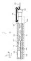
- FIG. 1is a schematic side view showing the configuration of an optical module 1 according to this embodiment.
- the surface on the Z+ side in the drawingis referred to as "upper surface”
- the surface on the Z- sideis referred to as "lower surface”.
- the optical module 1includes a package structure 11, a ferrule 108, and an optical fiber 109. Also, the package structure 11 and the ferrule 108 are fixed by a clip 110 .
- the silicon photonics chip 101 , the GRIN lens 102 and the IC 103are mounted on the substrate 1041 and covered with the molding resin 105 .
- the substrate 1041is a thin-layer wiring substrate having a thickness of approximately 10 ⁇ m to 30 ⁇ m.
- a BGA or LGAis formed as an electrical connection portion 106 on the surface (bottom surface) opposite to the component mounting surface (top surface) of the substrate 1041, and an electrical mounting substrate (not shown) such as a PCB on which an optical package is mounted. It is an electrical interface between
- the silicon photonics chip 101is a chip with an optical circuit and an electric circuit formed on its surface, and has a thickness of 625 ⁇ m, which is the thickness of a standard silicon wafer.
- the silicon photonics chip 101is flip-chip mounted on the substrate 1041 via solder balls or copper pillars, with the surface (circuit surface) on which the optical circuit is formed facing downward, that is, the so-called facedown. Since the silicon photonics chip 101 is mounted face down, the position (height) of input/output light from the silicon photonics chip 101 is low, approximately several tens of ⁇ m to 100 ⁇ m above the upper surface of the substrate 1041 .
- the GRIN lens 102is a cylindrical optical component, and is a gradient index lens in which the refractive index is changed parabolically from the central axis of the cylinder toward the outer periphery.
- a GRIN lenschanges its focal length by changing its length, and its lens characteristics are expressed by the following relational expression.
- Zis the length of the GRIN lens
- ⁇ Ais the refractive index distribution constant determined by the material and manufacturing method
- Pis the pitch representing the meandering period of light rays passing through the lens.
- a GRIN lens with a pitch of about 0.5 (P ⁇ 0.5)is used, and in the case of a general GRIN lens with a diameter of 1.8 mm, the length Z is about 9.6 mm.
- Light emitted from the silicon photonics chip 101enters a low position on one end face of the GRIN lens 102 (the left end face in FIG. 1), and then travels in the direction of travel inside the GRIN lens 102 as indicated by a curve 12 in the figure. It propagates while changing the state of divergence and convergence, and forms an image at a high position on the other end face of the GRIN lens 102 (the right end face in FIG. 1).
- the "low" position of the GRIN lens 102refers to a position below the center axis of the GRIN lens 102, and particularly in FIG.
- the "high" position of the GRIN lens 102refers to a position above the central axis of the GRIN lens 102, and particularly in FIG. .
- the incident position of light on one end surface and the imaging (output) position on the other end surfaceare symmetrical with respect to the central axis of the GRIN lens 102 .
- FIG. 2shows an example in which the silicon photonics chip 101 is mounted face-up, with the surface on which the optical circuit is formed (circuit surface) facing upward.
- lightis incident from a position near the central axis of one end surface (the left end surface in FIG. 2) of the GRIN lens 102 .
- a light ray inside the GRIN lens 102propagates through a path different from that in the case of face-down mounting (FIG. 1) and forms an image on the other end surface (the right end surface in FIG. 2).
- the light incident position on one end surface and the imaging (exiting) position on the other end surfaceare the center of the GRIN lens 102, as in the case of face-down mounting (FIG. 1). It is symmetrical about the axis.
- the electrical connection between the silicon photonics chip 101 and the substrate 1041is realized by wire bonding or TSV (Through Silicon Via).
- the substrate 1041is a multilayer wiring layer in which copper foil layers and insulating resin layers are alternately laminated. It is generally called a redistribution layer (RDL: Re-Distribution Layer).
- RDLRe-Distribution Layer
- the fan-out packagefirst forms an electrical wiring layer (RDL) on a support substrate (wafer or panel), performs chip mounting and resin molding, and finally peels off the support substrate. It can be manufactured by adopting the "RDL First Construction Method".
- RDLelectrical wiring layer
- the substrate 1041is not limited to RDL, and may be a general wiring substrate (organic buildup substrate or ceramic substrate).
- the substratecan be partially thinned or provided with a notch.
- the height of the silicon photonics chip 101 and the GRIN lens 102can be arbitrarily set by making only the portion where the GRIN lens 102 is mounted on the substrate 1042 thinner than the portion where the silicon photonics chip 101 is mounted.
- the substrate 1042is a substrate (thickness: about 1000 ⁇ m) made of ceramic or the like.
- the IC 103is not limited to face-down mounting, and may be face-up mounting. Also, the IC 103 is not limited to a bare chip, and may be a package component. Various optical chips (optical elements) may be mounted as described above in addition to a plurality of ICs, package components, and silicon photonics chips.
- the other end surface of the GRIN lens 102(the right end surface in FIGS. 1 to 3) is exposed from the mold resin 105 and is adhesively fixed to the adapter 107 .
- a short optical fiber or optical waveguide componentis built inside the adapter 107 to guide the light imaged on the other end surface of the GRIN lens 102 .
- the end face of the adapter 107 opposite to the face facing the GRIN lens 102is in contact with the ferrule 108 and further guides the light to the optical fiber 109 built inside the ferrule 108 .
- the optical fiber 109is a single-mode optical fiber, these light guides need to be aligned between parts with submicron precision. Therefore, the adapter 107 is actively centered with respect to the GRIN lens 102 and adhesively fixed at the optimum position.
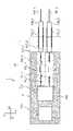
- connection structure between the adapter 107 and the ferrule 108will be described below with reference to the top views shown in FIGS.
- the adapter 107is a rectangular component, and has two round holes for guide pins in the horizontal direction (top and bottom in the figure).
- the rectangular ferrule 108is also provided with a round hole for a guide pin.
- the adapter 107 and the ferrule 108are connected with high accuracy by inserting guide pins 111 (dotted lines in the figure) into these round holes.
- a clip 110is used to maintain contact between the two.
- the dashed line portion in the drawingindicates the optical fiber 109 .
- the ferrule 108 and the adapter 107can be detached by removing the clip 110, and the same fitting mechanism as a known MT connector can be used.
- any mechanism other than the clipcan be applied as long as it applies a pressing force between the ferrules.
- a plate spring component, a coil spring component, or a magnetic force other than mechanical fasteningmay be used.
- the GRIN lens 102has a refractive index distribution that is rotationally symmetrical about the central axis, so that the same light-condensing characteristics as in the vertical direction can be obtained in the horizontal direction.
- the light incident on one end surface (the left end surface in FIG. 4) of the GRIN lens 102 from the arrayed light input/output units in the silicon photonics chip 101passes through the other end surface (the left end surface in FIG. 4). , right end face) are arrayed and imaged.
- an MT ferrulewhich is a general multi-core ferrule
- the ferrule materialfiller-containing resin used in MT ferrules may be used, or other resin materials, glass members, ceramic members, metal members, Si, or the like may be used.
- the guide pin 111may be integrated with the adapter 107 or the ferrule 108 in advance.
- first ferrules 107_1 and 107_2, which are single-core ferrules having a coaxial structure,are provided.
- the first ferrules 107_1, 107_2 and the second ferrules 108_1, 108_2can be connected with high accuracy by the split sleeves 112_1, 112_2.
- This embodimentis designed so that no large optical reflection occurs between the GRIN lens and the silicon photonics chip. For example, by matching the refractive index of the material of the mold resin and the material of the chip end surface and the lens end surface, it is possible to suppress large Fresnel reflection caused by the difference in refractive index.
- the reflected return lightis not recombined by slanting the end faces.
- a known anti-reflection film or the likemay be formed on the end face of the silicon photonics chip or the end face of the GRIN lens. Similarly, there is no anti-reflection between the GRIN lens 102 and the optical fiber or waveguide in the adapter.
- the GRIN lenscan be positioned and mounted on the silicon photonics chip by any method, and can be passively mounted using active alignment, in-plane mechanical accuracy standards of package materials, electrical contacts, and positioning structures. You may
- the package structure according to the present embodimentit is not necessary to directly bond and fix the optical fiber to the silicon photonics chip.
- the packagecan be implemented.
- Optical fiber connectionis performed by engaging the adapter 107 or the first ferrules 107_1 and 107_2 with the ferrule 108 or the second ferrules 108_1 and 108_2, respectively, and performing active alignment with respect to the exposed GRIN lens. It is realized by bonding and fixing each interface.
- the ferrule 108 or the second ferrules 108_1 and 108_2may be removed, and since they are connectors, they can be re-fitted. Therefore, it is possible to proceed to the next process such as PCB mounting without the optical fiber, and the conventional problem of difficulty in handling the pigtail optical fiber can be resolved.
- the package structure according to the present embodimentuses the GRIN lens in the molded package form, so that the silicon photonics chip can be freely arranged in the molded package. It also has the effect of
- the GRIN lensby providing the GRIN lens, it becomes possible to provide the silicon photonics chip in the center of the length of the GRIN lens. can be enhanced.
- the length of the GRIN lenscan be flexibly changed by changing the shape of the refractive index distribution.
- the electrical contacts of the silicon photonics chipare provided on the waveguide layer on the silicon substrate, so the distance between the silicon core and the thickness of the substrate is several tens of ⁇ m or less.
- the thickness of the V-groove substrate used in conventional fiber arraysis required to be approximately several 100 ⁇ m.
- the GRIN lenscan be used to dispose the light input/output portion higher than the conventional position in the board thickness direction, that is, at a position away from the electric mounting board. , it is possible to eliminate the restrictions on the mounting position described above, and it is possible to realize a mounting form with a high degree of freedom.
- the ferrule 108 and the adapter 107similarly interfere with an electrical mounting board (not shown) connected downward via the electrical connection portion 106 (BGA, etc.).
- the lens optical systemmay be disposed upward, similarly to the rays in the lens in FIG.
- a bulk GRIN lensas the optical path conversion unit
- any lens that exhibits the same optical functioncan be used.
- a known GI (Graded Index) fibermay be used. Since the GI fiber is characterized by its small diameter and high accuracy of outline, it is easy to form even more, and the GI fiber array may be formed according to the number of channels of the chip.
- a Fresnel lens, a metasurface lens, or the likemay also be used. It is sufficient if it has a function of emitting light incident from one end face from the other end face with the central axis of the optical path changing portion as an axis of symmetry.
- 113may be directly adhesively fixed.
- FIG. 7An optical connection structure, a package structure and an optical module according to a second embodiment of the present invention will be described with reference to FIGS. 7 to 9.
- FIG. 7An optical connection structure, a package structure and an optical module according to a second embodiment of the present invention will be described with reference to FIGS. 7 to 9.
- FIG. 7An optical connection structure, a package structure and an optical module according to a second embodiment of the present invention will be described with reference to FIGS. 7 to 9.
- the optical module 2differs from that of the first embodiment in that the GRIN lens is divided into a first GRIN lens 2021 and a second GRIN lens 2022 .
- Other configurationsare substantially the same as those of the first embodiment.
- FIG. 7shows an example using a face-down type silicon photonics chip 101 .
- the second GRIN lens 2022is built into the adapter 2071.
- FIG. 8shows a case where a face-up type silicon photonics chip 101 is used. Since the light can be propagated in the vicinity of the central axes of the GRIN lenses 2021 and 2022, the size of the adapter 2072 can be reduced.
- the package structure shown in FIG. 9is an example using a substrate 1042 such as an organic buildup substrate or a ceramic substrate. It is made thinner than the portion where the silicon photonics chip 101 is mounted.
- the first GRIN lens 2021 and the second GRIN lens 2022may be GRIN lenses with different characteristics. For example, by using the second GRIN lens 2022 whose refractive index distribution constant ( ⁇ A) is larger than that of the first GRIN lens 2021, the total length can be shortened, and the other end face of the second GRIN lens 2022 (in FIG. 7, The spot size at the right edge) can be varied.
- ⁇ Arefractive index distribution constant
- an optical waveguide component(not shown).
- NAspot size
- TEC fiberNA expansion fiber
- polymer waveguideglass waveguide
- the interface between the first GRIN lens 2021 and the second GRIN lens 2022serves as an alignment surface and an adhesive fixing surface.
- the couplingis with thick collimated light, it is not always necessary to perform active alignment if the dimensional accuracy of the optical components is sufficient.
- a multi-core ferrule or a single-core ferrulecan be used in the same manner as the configurations shown in FIGS.
- connection of the optical fiberis achieved by aligning the adapters 2071 and 2072 with the ferrule 108 and fixing them by bonding to the exposed first GRIN lens 2021 .
- the ferrule 108 or the second ferrules 108_1 and 108_2may be removed, and since it is a connector type, it can be reconnected. Therefore, it is possible to proceed to the next process such as PCB mounting without the optical fiber, and the conventional problem of difficulty in handling the pigtail optical fiber can be resolved.
- the package structure of this embodimentas in the first embodiment, it is not necessary to directly adhere and fix the optical fiber to the silicon photonics chip. It is possible to package the silicon photonics chip while avoiding the influence of
- the GRIN lenscan be used to position the light input/output section above the conventional position in the board thickness direction, that is, at a position away from the electric mounting board.
- the restrictions on the mounting position described abovecan be eliminated, and a mounting form with a high degree of freedom can be realized.
- imageis not always formed on the output end face of the GRIN lens.
- An imagemay be formed on the end surface of the adapter, or a structure in which light is propagated within a range in which the package structure can operate even if the image is not formed completely (even if the light is not focused) may be used.
- the length of the GRIN lensdetermines the condensing state such as the focal diameter of the output light, so that the optical system can be easily designed. Also, when light is input with an offset with respect to the central axis, an image is formed at a position symmetrical to the central axis and output.
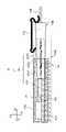
- FIG. 10is a schematic top view of the optical connection structure 10 for explaining the propagation path of light.
- a dotted line 112_1 and a dashed line 12_2 in the figureindicate paths of light propagating inside the GRIN lens 102.
- FIG. 10is a schematic top view of the optical connection structure 10 for explaining the propagation path of light.
- a dotted line 112_1 and a dashed line 12_2 in the figureindicate paths of light propagating inside the GRIN lens 102.
- the light propagated through the waveguides 1012 and 1013is output from the silicon photonics chip 101, propagated (focused) through different paths 12_1 and 12_2 by the GRIN lens 102, and input to different optical fibers 109_2 and 109_4 via the adapter 107. be (combined)
- the silicon photonics chip 101includes an optical device 1011, a first waveguide 1012, and a second waveguide 1013, as an example.
- a modulatoris used as the optical device 1101 here, a mixer, a photodiode, or the like may also be used.
- a modulator 1101is connected to the first waveguide 1102 , modulates input light to generate an optical signal, and the optical signal propagates through the first waveguide 1102 .
- the second waveguide 1103is used for component position adjustment and alignment in the manufacturing process of the package structure 11 (described later).
- the optical connection structure 10uses the GRIN lens 102 to easily input light from different optical fibers into different waveguides of the silicon photonics chip 101, thereby allowing different Output light from the waveguide can be input to different optical fibers.
- a ferrule 108 to which a multicore optical fiber 109 including optical fibers 109_3 and 109_4 is fixed to a silicon photonics chip 101 and a GRIN lens 102 fixed with a mold resin 105is connected to an adapter 107 and fixed with a clip 110. .
- the light for alignmentis input to the optical fiber 109_3 and propagates to the silicon photonics chip 101 through the adapter 107 and the GRIN lens 208 in order.
- the silicon photonics chip 101has a loopback optical circuit (second waveguide) 1013 for alignment, as shown in FIG.
- the alignment light input from the optical fiber 109_3is incident on the other end surface (right side in FIG. 10) of the GRIN lens 102, propagates along the path 12_2, and passes through the silicon photonics chip 101 as described above. is input (coupled) to the second waveguide 1013 , propagates through the second waveguide 1013 and is output from the silicon photonics chip 101 .
- the light output from the silicon photonics chip 101is incident on one end face of the GRIN lens 102 (left side in FIG. 10), propagates along the path 12_2, and converges on the other end face of the GRIN lens 102 (right side in FIG. 10). It is imaged and input to the optical fiber 109_4 via the adapter 107.
- FIG. 10The light output from the silicon photonics chip 101 is incident on one end face of the GRIN lens 102 (left side in FIG. 10), propagates along the path 12_2, and converges on the other end face of the GRIN lens 102 (right side in FIG. 10). It is imaged and input to the optical fiber 109_4 via the adapter 107.
- the intensity (light amount) of light output from the other end of the optical fiber 109_4is measured, and the adapter 107 is positioned (aligned) so that the light intensity (light amount) is maximized.
- the rigidity and productivity of the packagecan be improved by using mold resin.
- optical componentsrequire high-precision alignment of about 0.1 ⁇ m and high reliability, so it was difficult to use a configuration using mold resin.
- the durability and stability of the adhesive fixation in the process of fixing each part with a moldare insufficient. Since it cannot be adjusted, it has been difficult to adjust the position of the component and the optical axis with high accuracy.
- the optical axiscan be adjusted after each component is fixed with a mold. be able to.
- FOWLP and FOPLPcan be used for mounting optical components.
- the GRIN lens end face of the package structure and the fiber arrayare directly connected without using the detachable structure using the adapter and ferrule described above. , may be adhesively fixed.
- the present inventionrelates to an optical module as an optical component, and can be applied to devices and systems such as optical communication.
- optical module 10optical connection structure 11 package structure 101 silicon photonics chip (optical element) 102 GRIN lens (optical path conversion unit) 103 IC 1041 substrate 105 mold resin 106 electrical connection portion 107 adapter 108 ferrule 109 optical fiber
Landscapes
- Physics & Mathematics (AREA)
- General Physics & Mathematics (AREA)
- Optics & Photonics (AREA)
- Optical Couplings Of Light Guides (AREA)
Abstract
Description
Translated fromJapanese本発明は、光ファイバと光素子とを接続する光接続構造、パッケージ構造および光モジュールに関する。The present invention relates to an optical connection structure, a package structure, and an optical module for connecting optical fibers and optical elements.
近年のインターネットトラフィックの急増に伴い、データセンタネットワークの通信容量の拡大が求められている。さらに、伝送容量の拡大および低消費電力化に対応するために、短中距離用途においても光で伝送する光インタコネクションの導入が進んでいる。With the rapid increase in Internet traffic in recent years, there is a need to expand the communication capacity of data center networks. Furthermore, in order to cope with the increase in transmission capacity and the reduction in power consumption, the introduction of optical interconnections for optical transmission is progressing even for short and medium distance applications.
光インタコネクションの代表的な方式においては、プリント基板上に配置されたレーザダイオード(LD)などの光発光素子とフォトダイオード(PD)などの光受光素子間を光導波路や光ファイバなどの光伝送媒体を用いて伝送することで信号処理が実現されている。In a typical optical interconnection system, optical transmission such as an optical waveguide or an optical fiber is performed between a light emitting element such as a laser diode (LD) and a light receiving element such as a photodiode (PD) arranged on a printed circuit board. Signal processing is realized by transmission using a medium.
伝送方式によっては、光発光素子には、光変調素子などが集積され、又はディスクリートに接続され、さらに電気-光変換を行うドライバなどが接続される。これらの光発光素子、光変調素子、ドライバなどを含む構成が光送信機としてプリント基板(PCB:Printed circuit board)などの電気実装基板上に搭載されている。Depending on the transmission method, the optical light emitting element is integrated with an optical modulation element or the like, or connected discretely, and further connected to a driver or the like that performs electrical-to-optical conversion. A configuration including these light emitting elements, light modulating elements, drivers, etc. is mounted as an optical transmitter on an electrical mounting board such as a printed circuit board (PCB).
同様に、光受光素子には、光処理機などが適宜集積され、又はディスクリートに接続され、さらに光-電気変換を行う電気増幅回路などが接続される。これらの光受光素子、光処理機、電気増幅回路などを含む構成が光受信機としてプリント基板上に実装されている。Similarly, the light-receiving element is appropriately integrated with an optical processor or the like, or connected discretely, and further connected with an electric amplifier circuit or the like for performing optical-electrical conversion. A configuration including these photodetectors, optical processors, electrical amplifier circuits, etc. is mounted on a printed circuit board as an optical receiver.
これらの光送信機と光受信機とを一体化した光送受信機などがパッケージ内やプリント基板上に搭載され、光ファイバなどの光伝送媒体と光学的に接続されることで、光インタコネクションが実現されている。また、トポロジーによっては、光スイッチなどの中継器などを介して実現されている。An optical transmitter/receiver that integrates an optical transmitter and an optical receiver is mounted in a package or on a printed circuit board, and is optically connected to an optical transmission medium such as an optical fiber to form an optical interconnection. Realized. Also, depending on the topology, it is realized through a repeater such as an optical switch.
一方、光インタコネクションに用いる光発光素子や光受光素子、光変調素子としては、シリコンやゲルマニウムなどの半導体や、インジウムリン(InP)やガリウムヒ素(GaAs)、インジウムガリウムヒ素(InGaAs)等に代表されるIII-V族半導体などの材料を用いる素子が実用化されている。近年では、これらの素子と共に、光の伝播機構を有するシリコン光回路(シリコンフォトニクス)やインジウムリン光回路などを集積した光導波路型の光送受信機が発展している。また、光変調素子としては、半導体の他に、ニオブ酸リチウムなどの強誘電体系やポリマーなどの材料を用いる場合もある。On the other hand, semiconductors such as silicon and germanium, indium phosphide (InP), gallium arsenide (GaAs), and indium gallium arsenide (InGaAs) are typical examples of light emitting devices, light receiving devices, and light modulation devices used for optical interconnection. Devices using materials such as III-V group semiconductors, which are widely used, have been put to practical use. In recent years, along with these elements, optical waveguide type optical transceivers have been developed in which a silicon optical circuit (silicon photonics) having a light propagation mechanism, an indium phosphorous optical circuit, or the like are integrated. In addition to semiconductors, materials such as ferroelectrics such as lithium niobate and polymers may also be used as light modulation elements.
更に、上記の光発光素子や光受光素子、光変調素子と共に、石英ガラスなどからなる平面光波回路(Planar Lightwave Circuit)などからなる光機能素子が集積されることがある。光機能素子としてはスプリッタ、波長合分波器、光スイッチ、偏波制御素子、光フィルタなどがある。以降、上記の光の伝播、導波機構を有する光発光素子、光受光素子、光変調素子、光機能素子、光増幅素子などを集積したデバイスを光導波路デバイスと呼ぶこととする。Furthermore, optical functional elements such as planar lightwave circuits made of silica glass are sometimes integrated together with the above light emitting elements, light receiving elements, and light modulating elements. Optical functional devices include splitters, wavelength multiplexers/demultiplexers, optical switches, polarization control devices, optical filters, and the like. Hereinafter, a device in which a light emitting device, a light receiving device, an optical modulation device, an optical functional device, a light amplifying device, etc. having the above light propagation and waveguiding mechanisms are integrated will be referred to as an optical waveguide device.
光導波路デバイスにおいて、シリコンフォトニクスチップは集積性、量産性、電気部品との親和性に優れ、次世代の光インタコネクションを実現する上でのキーデバイスとして関心がもたれている(非特許文献1)。In optical waveguide devices, silicon photonics chips are highly integrated, mass-producible, and compatible with electrical components, and are attracting attention as key devices for realizing next-generation optical interconnection (Non-Patent Document 1). .
シリコンフォトニクスチップやドライバ、電気増幅回路などが集積された光送受信機をボード上の電気配線に接続する方法としてワイヤボンディング、フリップチップ接続や、Ball-grid array(BGA)、 Land-grid array(LGA)、 Pin-grid array(PGA)や銅ピラーなどを用いて接続する方法が用いられる。前記接続の際は必要に応じて、インタポーザ部品などの別のパッケージ基板を介して電気実装基板に接続されることもある。Wire bonding, flip chip connection, Ball-grid array (BGA), Land-grid array (LGA ), a method of connecting using a pin-grid array (PGA), a copper pillar, or the like is used. At the time of the connection, if necessary, it may be connected to the electrical mounting board via another package board such as an interposer component.
また、シリコンフォトニクスチップと光ファイバを接続する方法の一つは、V溝を形成したガラスなどと一体化された光ファイバアレイと接続する構造である。この構造においては、光ファイバの各コアと、光導波路デバイスの各導波路のコアとが低損失で接続することが求められる。この低損失の接続のためには、サブミクロン単位で光導波路デバイスと光ファイバとを位置決め(以下、調心という)・固定することが必要である。Also, one of the methods of connecting a silicon photonics chip and an optical fiber is a structure that connects with an optical fiber array integrated with glass or the like in which a V-groove is formed. In this structure, each core of the optical fiber and each waveguide core of the optical waveguide device are required to be connected with low loss. For this low-loss connection, it is necessary to position (hereinafter referred to as alignment) and fix the optical waveguide device and the optical fiber in submicron units.
従来の光導波路デバイスでは、光を実際に入出力させてパワーをモニタしながらの調心(光学調心)が行われ、光ファイバアレイと一体化された状態でパッケージ内やボード上に搭載されることとなる。In a conventional optical waveguide device, alignment (optical alignment) is performed by actually inputting and outputting light and monitoring the power, and it is mounted in a package or on a board in a state integrated with an optical fiber array. The Rukoto.
しかしながら、従来のシリコンフォトニクスチップに光ファイバを接着剤等により接着接続する構造では、以下の問題があった。However, the conventional structure in which optical fibers are adhesively connected to a silicon photonics chip with an adhesive or the like has the following problems.
シリコンフォトニクスチップにファイバアレイを直接接着させるためには、シリコンフォトニクスチップの端面を光学研磨する必要があった。In order to directly bond the fiber array to the silicon photonics chip, it was necessary to optically polish the end face of the silicon photonics chip.
また、チップの側面が接着面であるために、接着面積が限られてしまい、十分な接着力を得ることが難しくなる懸念があった。In addition, since the side surface of the chip is the adhesive surface, the adhesive area is limited, and there was a concern that it would be difficult to obtain sufficient adhesive strength.
また、光ファイバがピッグテールとして接続されているために、ボード実装等の次工程においては、光ファイバの取り回しなど光ファイバの固定接続状態の維持(安定化)するための工程等が必要となり、組立工程の量産性(スループット向上や安定化)が低下していた。In addition, since the optical fiber is connected as a pigtail, in the next process such as board mounting, it is necessary to maintain (stabilize) the fixed connection state of the optical fiber, such as routing the optical fiber. The mass productivity of the process (throughput improvement and stabilization) was declining.
上述したような課題を解決するために、本発明に係る光接続構造は、光ファイバと接続し、基板を有するパッケージ構造における光接続構造であって、前記基板に配置される光素子と、前記基板に配置される光路変換部とを備え、前記光路変換部の一方の端面が、前記光素子の端面と対向することを特徴とする。In order to solve the above-described problems, an optical connection structure according to the present invention is an optical connection structure in a package structure that is connected to an optical fiber and has a substrate, comprising: an optical element arranged on the substrate; and an optical path changing portion disposed on a substrate, one end face of the optical path changing portion facing the end face of the optical element.
本発明によれば、光素子に光ファイバを直接接着することなく、量産性を向上できる光接続構造、パッケージ構造および光モジュールを提供できる。According to the present invention, it is possible to provide an optical connection structure, a package structure, and an optical module that can improve mass productivity without directly bonding an optical fiber to an optical element.
<第1の実施の形態>
本発明の第1の実施の形態に係る光接続構造、パッケージ構造および光モジュールについて、図1~図5を参照して説明する。<First Embodiment>
An optical connection structure, a package structure and an optical module according to a first embodiment of the present invention will be described with reference to FIGS. 1 to 5. FIG.
<パッケージ構造および光モジュールの構成>
図1は、本実施の形態に係る光モジュール1の構成を示す概略側面図である。以下、図1に示すように光モジュール1を構成したときの、図中Z+側にある面を「上面」、Z-側にある面を「下面」とする。<Package Structure and Configuration of Optical Module>
FIG. 1 is a schematic side view showing the configuration of an
本実施の形態に係る光モジュール1は、パッケージ構造11と、フェルール108と、光ファイバ109とを備える。また、パッケージ構造11とフェルール108とがクリップ110によって固定される。The
パッケージ構造11において、シリコンフォトニクスチップ101と、GRINレンズ102と、IC103とが、基板1041の上に実装され、モールド樹脂105によって覆われている。ここで、基板1041は、厚さが10μm~30μm程度の薄層配線基板である。In the
基板1041の部品搭載面(上面)と反対側の面(底面)には、電気接続部106としてBGAまたはLGAが形成され、光パッケージが実装されるPCBなどの電気実装基板(図示せず)との間の電気インタフェースとなっている。A BGA or LGA is formed as an
シリコンフォトニクスチップ101は、光回路と電気回路をその表面に形成したチップであり、厚さは標準的なシリコンウェハ厚さである625μmとしている。The
シリコンフォトニクスチップ101は、光回路が形成される面(回路面)を下向き、いわゆるフェースダウンにして、基板1041上に半田ボール又は銅ピラーなどを介してフリップチップ実装されている。フェースダウンで実装されることから、シリコンフォトニクスチップ101からの入出力光の位置(高さ)は低く、基板1041の上面から上方に数十μm~100数十μm程度である。The
GRINレンズ102は、円柱状の光部品であり、円柱の中心軸から外周部に向かって放物線状に屈折率を変化させた屈折率分布型レンズである。GRINレンズは、その長さを変更することによって焦点距離が変化し、そのレンズ特性は次式の関係式で表現される。The
Z=2πP/√A Z=2πP/√A
ここで、ZはGRINレンズ長、√Aは材料や製法によって決定される屈折率分布定数であり、Pはレンズ内を通る光線の蛇行周期を表すピッチである。Here, Z is the length of the GRIN lens, √A is the refractive index distribution constant determined by the material and manufacturing method, and P is the pitch representing the meandering period of light rays passing through the lens.
本実施の形態では、0.5ピッチ(P≒0.5)程度のGRINレンズを用い、直径1.8mmの一般的なGRINレンズの場合、その長さZは9.6mm程度である。In this embodiment, a GRIN lens with a pitch of about 0.5 (P≈0.5) is used, and in the case of a general GRIN lens with a diameter of 1.8 mm, the length Z is about 9.6 mm.
シリコンフォトニクスチップ101から出射した光が、GRINレンズ102の一方の端面(図1中、左側の端面)の低い位置に入射したのち、図中に曲線12で示すようにGRINレンズ102内部で進行方向や発散・集光の状態を変えて伝搬し、GRINレンズ102の他方の端面(図1中、右側の端面)の高い位置に結像する。Light emitted from the
ここで、GRINレンズ102の「低い」位置はGRINレンズ102の中心軸より下方をいい、とくに図1中では、GRINレンズ102の底面(基板1041と接する面)近傍の場合を示す。Here, the "low" position of the
また、GRINレンズ102の「高い」位置はGRINレンズ102の中心軸より上方をいい、とくに図1中では、GRINレンズ102の上面(基板1041と接する面と反対側の面)近傍の場合を示す。Also, the "high" position of the
GRINレンズ102において、光の一方の端面での入射位置と、他方の端面での結像(出射)位置は、GRINレンズ102の中心軸に対して対称である。In the
また、図2に、シリコンフォトニクスチップ101が、光回路が形成される面(回路面)を上向き、いわゆるフェースアップで実装される例を示す。この場合は、GRINレンズ102の一方の端面(図2中、左側の端面)の中心軸近傍の位置から光が入射している。GRINレンズ102内部における光線は、フェースダウン実装の場合(図1)と異なる経路で伝搬し、他方の端面(図2中、右側の端面)で結像する。Also, FIG. 2 shows an example in which the
ここで、GRINレンズ102において、光の一方の端面での入射位置と、他方の端面での結像(出射)位置は、フェースダウン実装の場合(図1)と同様に、GRINレンズ102の中心軸に対して対称である。Here, in the
シリコンフォトニクスチップ101と基板1041との電気的な接続は、ワイヤボンドもしくは、TSV(Through Silicon Via)によって実現される。The electrical connection between the
基板1041は、銅箔層と絶縁樹脂層が交互に積層された多層配線層であり、ファンアウトウェハレベルパッケージ(FOWLP)技術、もしくはファンアウトパネルレベルパッケージ(FOPLP)技術によって製造される場合には一般的に再配線層(RDL:Re-Distribution Layer)と呼ばれている。The
本実施の形態において、ファンアウトパッケージは、一例として、初めに支持基板(ウェハやパネル)上に電気配線層(RDL)を形成した後、チップ実装と樹脂モールドを行い、最後に支持基板を剥離する「RDLファースト工法」を採用することで作製できる。In this embodiment, the fan-out package, as an example, first forms an electrical wiring layer (RDL) on a support substrate (wafer or panel), performs chip mounting and resin molding, and finally peels off the support substrate. It can be manufactured by adopting the "RDL First Construction Method".
ただし、基板1041はRDLに限らず、一般的な配線基板(有機ビルドアップ基板やセラミック基板)でもよい。However, the
さらに、基板では、部分的に基板を薄くすること、又は切り欠きを設けることが可能である。例えば、図3に示すように、基板1042は、GRINレンズ102搭載部分だけをシリコンフォトニクスチップ101搭載部分より薄くすることにより、シリコンフォトニクスチップ101とGRINレンズ102の高さを任意に設定することができる。ここで、基板1042は、セラミック等により構成される基板(厚さ:1000μm程度)である。Furthermore, the substrate can be partially thinned or provided with a notch. For example, as shown in FIG. 3, the height of the
シリコンフォトニクスチップと同様に、IC103もフェースダウン実装に限らず、フェースアップ実装であっても構わない。また、IC103はベアチップに限らず、パッケージ部品であっても良い。また、複数のICまたはパッケージ部品やシリコンフォトニクスチップ以外にも上述のように各種光チップ(光素子)が搭載されていてもよい。As with the silicon photonics chip, the
本実施の形態では、GRINレンズ102の他方の端面(図1~3中、右側の端面)は、モールド樹脂105から露出しており、アダプタ107と接着固定されている。In the present embodiment, the other end surface of the GRIN lens 102 (the right end surface in FIGS. 1 to 3) is exposed from the
アダプタ107内部には短尺の光ファイバもしくは光導波路部品が内蔵されており、GRINレンズ102の他方の端面に結像した光を導光する。A short optical fiber or optical waveguide component is built inside the
アダプタ107におけるGRINレンズ102と対向する面と反対側の端面は、フェルール108と接触しており、フェルール108内部に内蔵された光ファイバ109へとさらに導光する。The end face of the
光ファイバ109がシングルモード光ファイバの場合、これらの導光はサブミクロン精度で部品間を位置合わせする必要がある。したがって、アダプタ107は、GRINレンズ102に対してアクティブ調心を行い、最適な位置において接着固定される。If the
アダプタ107とフェルール108の接続構造を、図4、5に示す上面図を参照して、以下に説明する。A connection structure between the
図4に示すように、アダプタ107は角型の部品であり、水平方向(図中上下)の2箇所にガイドピン用の丸穴が設けられている。同様に、角型のフェルール108にもガイドピン用の丸穴が設けられている。これらの丸穴にガイドピン111(図中、点線部)を挿入することによって、アダプタ107とフェルール108は高精度に連結される。両者の接触を保持するために、クリップ110で固定されている。ここで、図中破線部は光ファイバ109を示す。As shown in FIG. 4, the
フェルール108とアダプタ107はクリップ110を外すことで脱着することが可能であり、公知のMTコネクタと同じ嵌合メカニズムを用いることができる。なおクリップ以外でもフェルール間に押圧力を加える機構であればいずれでも適用できる。例えば板バネ部品やコイルバネ部品、機械的な締結以外の磁力などを用いてもよい。The
上述の通り、GRINレンズ102は中心軸回りに回転対称な屈折率分布を有しているため、水平面内方向に対しても垂直方向と同様の集光特性が得られる。図4に示すように、シリコンフォトニクスチップ101においてアレイ配列された光入出力部からGRINレンズ102の一方の端面(図4中、左側の端面)に入射する光は、他方の端面(図4中、右側の端面)でアレイ配列して結像する。As described above, the
したがって、角型のフェルール108として、一般的な多芯フェルールであるMTフェルールを使用することができる。なお、フェルールの材料としてはMTフェルールで用いられるフィラー入り樹脂を用いてもよいし、ほかの樹脂材料やガラス部材、セラミック部材、金属部材、Siなどを用いてもよい。またガイドピン111を予めアダプタ107あるいはフェルール108と一体化させておいてもよい。Therefore, as the
または、図5に示すように、GRINレンズと単芯フェルールをそれぞれ複数用いて、一芯ごとに光インタフェースを形成することも可能である。この構成では、複数のGRINレンズ102_1、102_2と、複数の第2のフェルール108_1、108_2とを備える。また、アダプタとして、同軸構造を有する単芯フェルールである第1のフェルール107_1、107_2を備える。第1のフェルール107_1、107_2と第2のフェルール108_1、108_2とは、割りスリーブ112_1、112_2によって高精度に連結させることができる。Alternatively, as shown in FIG. 5, it is also possible to use a plurality of GRIN lenses and single-core ferrules to form an optical interface for each core. This configuration comprises a plurality of GRIN lenses 102_1, 102_2 and a plurality of second ferrules 108_1, 108_2. Also, as adapters, first ferrules 107_1 and 107_2, which are single-core ferrules having a coaxial structure, are provided. The first ferrules 107_1, 107_2 and the second ferrules 108_1, 108_2 can be connected with high accuracy by the split sleeves 112_1, 112_2.
本実施の形態では、GRINレンズとシリコンフォトニクスチップ間において、光学的な大きな反射が生じないよう設計されている。例えば、モールド樹脂の材料と前記チップ端面及びレンズ端面を構成する材料の屈折率を整合させることで屈折率差に起因する大きなフレネル反射を抑制することができる。This embodiment is designed so that no large optical reflection occurs between the GRIN lens and the silicon photonics chip. For example, by matching the refractive index of the material of the mold resin and the material of the chip end surface and the lens end surface, it is possible to suppress large Fresnel reflection caused by the difference in refractive index.
または、端面間を斜めにすることで反射戻り光が再結合しないよう設計してもよい。また、公知の反射防止膜などをシリコンフォトニクスチップ端面やGRINレンズ端面に形成してもよい。また、GRINレンズ102とアダプタ内の光ファイバ又は光導波路間においても同様に反射防止がないよう設計されている。Alternatively, it may be designed so that the reflected return light is not recombined by slanting the end faces. Also, a known anti-reflection film or the like may be formed on the end face of the silicon photonics chip or the end face of the GRIN lens. Similarly, there is no anti-reflection between the
なお、GRINレンズはシリコンフォトニクスチップに対して任意の方法で位置決めして搭載することができ、アクティブ調心あるいはパッケージ部材の面内機械精度基準や、電気接点、位置決め構造を利用してパッシブに搭載してもよい。The GRIN lens can be positioned and mounted on the silicon photonics chip by any method, and can be passively mounted using active alignment, in-plane mechanical accuracy standards of package materials, electrical contacts, and positioning structures. You may
本実施の形態に係るパッケージ構造によれば、シリコンフォトニクスチップに対して光ファイバを直接、接着固定する必要がなくなり、パッケージ構造の製造工程における光ファイバ接続への影響を回避して、シリコンフォトニクスチップをパッケージ実装することができる。According to the package structure according to the present embodiment, it is not necessary to directly bond and fix the optical fiber to the silicon photonics chip. The package can be implemented.
光ファイバの接続は、アダプタ107又は第1のフェルール107_1、107_2を、それぞれフェルール108もしくは第2のフェルール108_1、108_2と嵌合させた状態で、露出したGRINレンズに対してアクティブ調心を行い、それぞれの界面を接着固定して実現する。Optical fiber connection is performed by engaging the
接着後は、フェルール108もしくは第2のフェルール108_1、108_2は外しても構わず、コネクタ方式であることから再度嵌合させることができる。そのため、PCB実装等の次工程へ光ファイバがない状態で進めることができ、従来の課題であるピッグテール光ファイバの扱いの困難性を解消できる。After bonding, the
また、本実施の形態に係るパッケージ構造は、図1~図3に示すように、モールドされたパッケージ形態においてGRINレンズを用いることで、シリコンフォトニクスチップをモールドパッケージ内で自由に配置することができるという効果も奏する。In addition, as shown in FIGS. 1 to 3, the package structure according to the present embodiment uses the GRIN lens in the molded package form, so that the silicon photonics chip can be freely arranged in the molded package. It also has the effect of
すなわち、従来のモールドパッケージ形態においてシリコンフォトニクスチップと光ファイバアレイを直接接続する場合、シリコンフォトニクスチップの端面をパッケージの端面と同一面、又はパッケージ端面のごく近傍に設ける必要があり、電気配線やパッケージ設計の観点で大きな制約があった。That is, when directly connecting a silicon photonics chip and an optical fiber array in a conventional mold package form, it is necessary to provide the end surface of the silicon photonics chip on the same surface as the end surface of the package or very close to the end surface of the package. There were major limitations in terms of design.
一方、GRINレンズを設けることで、シリコンフォトニクスチップをGRINレンズの長さ分中央に設けることが可能となり、同チップへの電気配線のアクセスや前記BGA/LGAとの電気配線の自由度を大幅に高めることができる。なお、GRINレンズの長さは屈折率分布形状を変化させることで柔軟に変更することができる。On the other hand, by providing the GRIN lens, it becomes possible to provide the silicon photonics chip in the center of the length of the GRIN lens. can be enhanced. The length of the GRIN lens can be flexibly changed by changing the shape of the refractive index distribution.
また、図1に示すように、シリコンフォトニクスチップの電気接点はシリコン基板上の導波路層上に設けられるため、シリコン・コアと基板厚さ方向の距離は数10μm以下に配置される。一方、従来のファイバアレイに用いられるV溝基板の厚さは、数100μm程度が必要となる。Also, as shown in FIG. 1, the electrical contacts of the silicon photonics chip are provided on the waveguide layer on the silicon substrate, so the distance between the silicon core and the thickness of the substrate is several tens of μm or less. On the other hand, the thickness of the V-groove substrate used in conventional fiber arrays is required to be approximately several 100 μm.
そのため、フリップチップ接続などを用いた光パッケージに対して、従来の方法で直接ファイバアレイを接着・固定する場合は、V溝基板と電気実装基板が機械的に干渉する。とくに薄いRDL層を用いたパッケージ形態ではその問題が顕著になる。そのため、電気実装基板側に切り欠きを設けるか、電気実装基板上でのパッケージ搭載位置をエッジにする必要があるなどの制約があった。Therefore, when a conventional method is used to directly bond and fix a fiber array to an optical package that uses flip-chip connections, the V-groove substrate and the electrical mounting substrate mechanically interfere. This problem is particularly noticeable in a package form using a thin RDL layer. For this reason, there are restrictions such as the need to provide a notch on the side of the electrical mounting board, or to set the package mounting position on the electrical mounting board to the edge.
一方、本実施の形態に係るパッケージ構造では、GRINレンズを用いて、基板厚さ方向において光の入出力部を従来位置より上方に、すなわち電気実装基板から離れた位置に配置することができるため、上述の実装位置の制約を排除することができ、自由度の高い実装形態を実現することができる。On the other hand, in the package structure according to the present embodiment, the GRIN lens can be used to dispose the light input/output portion higher than the conventional position in the board thickness direction, that is, at a position away from the electric mounting board. , it is possible to eliminate the restrictions on the mounting position described above, and it is possible to realize a mounting form with a high degree of freedom.
なお、図2、3に示すフェースアップ形態においても同様に、フェルール108やアダプタ107が、電気接続部106(BGA等)を介して下方に接続される電気実装基板(図示せず)と干渉する場合は、適宜図1のレンズ内の光線と同様に、レンズ光学系を上方に配置するように構成してもよい。In the face-up configuration shown in FIGS. 2 and 3, the
本実施の形態では、光路変換部として、バルクのGRINレンズを用いる例を示したが、同様の光学的機能を発現するものであれば用いることができる。例えば、公知のGI(Graded Index)ファイバを用いてもよい。GIファイバは細径であり外形精度が高いという特徴からあれ以上に形成することも容易であり、チップのch数に合わせてGIファイバアレイとすればよい。また、フレネルレンズやメタサーフェスレンズなどを用いてもよい。一方の端面から入射する光を、光路変換部の中心軸を対称軸として、他方の端面から出射する機能を有するものであればよい。In the present embodiment, an example of using a bulk GRIN lens as the optical path conversion unit is shown, but any lens that exhibits the same optical function can be used. For example, a known GI (Graded Index) fiber may be used. Since the GI fiber is characterized by its small diameter and high accuracy of outline, it is easy to form even more, and the GI fiber array may be formed according to the number of channels of the chip. A Fresnel lens, a metasurface lens, or the like may also be used. It is sufficient if it has a function of emitting light incident from one end face from the other end face with the central axis of the optical path changing portion as an axis of symmetry.
また、着脱可能な接続構造が必要とされない用途においては、図6に示すように、上述のアダプタ及びフェルールを用いた着脱可能な構造を用いずに、パッケージ構造のGRINレンズ端面とファイバアレイ(ファイバブロック)113とを直接、接着固定する形態としてもよい。For applications that do not require a detachable connection structure, as shown in FIG. block) 113 may be directly adhesively fixed.
<第2実施の形態>
本発明の第2の実施の形態に係る光接続構造、パッケージ構造および光モジュールについて、図7~図9を参照して説明する。<Second Embodiment>
An optical connection structure, a package structure and an optical module according to a second embodiment of the present invention will be described with reference to FIGS. 7 to 9. FIG.
<光接続構造、パッケージ構造および光モジュールの構成>
本実施の形態に係る光モジュール2は、GRINレンズが、第1のGRINレンズ2021と第2のGRINレンズ2022に分割されている点で、第1の実施の形態と異なる。その他の構成は、第1の実施の形態と略同様ある。<Configuration of Optical Connection Structure, Package Structure, and Optical Module>
The
図7に示す構成では、フェースダウン型のシリコンフォトニクスチップ101を用いる例を示す。The configuration shown in FIG. 7 shows an example using a face-down type
パッケージ構造21において、第1のGRINレンズ2021と第2のGRINレンズ2022それぞれのピッチは0.25(P=0.25程度であり、長さは4.6mm程度である。In the
シリコンフォトニクスチップ101からの光は、第1のGRINレンズ2021の一方の端面(図7中、左側の端面)に入射して、第1のGRINレンズ2021の他方の端面(図7中、右側の端面)と第2のGRINレンズ2022の一方の端面(図7中、左側の端面)を介して、第2のGRINレンズ2022の他方の端面(図7中、右側の端面)に結像する。Light from the
第1のGRINレンズ2021のみがモールド樹脂105で覆われ、第1のGRINレンズ2021の他方の端面(図7中、右側の端面)はモールド樹脂105から露出している。Only the
第2のGRINレンズ2022は、アダプタ2071に内蔵されている。The
図8に、フェースアップ型のシリコンフォトニクスチップ101を用いる場合を示す。GRINレンズ2021、2022の中心軸近傍を伝搬させることができるため、アダプタ2072のサイズを小さくすることができる。FIG. 8 shows a case where a face-up type
図9に示すパッケージ構造は、図3に示すパッケージ構造と同様に、有機ビルドアップ基板やセラミック基板等の基板1042を用いた例であり、基板1042において第1のGRINレンズ2021の搭載部分だけをシリコンフォトニクスチップ101搭載部分より薄くしている。Similar to the package structure shown in FIG. 3, the package structure shown in FIG. 9 is an example using a
第1のGRINレンズ2021と第2のGRINレンズ2022は、異なる特性のGRINレンズであってもよい。例えば、屈折率分布定数(√A)が第1のGRINレンズ2021よりも大きい第2のGRINレンズ2022を用いることで全長を短くでき、第2のGRINレンズ2022の他方の端面(図7中、右側の端面)におけるスポットサイズを変えることができる。The
また、アダプタ2071、2072の内部には、第2のGRINレンズ2022の他に、光導波路部品(図示せず)を内蔵させることも可能である。光導波路部品としては、スポットサイズ変換回路や光学系、又はNA拡大ファイバ(TECファイバ)、ポリマー導波路、ガラス導波路等を用いることで、入射側と出射側のNA(スポットサイズ)を変えることができ、より低損失に光ファイバ109へ導光することも可能となる。Further, inside the
本実施の形態では、第1のGRINレンズ2021と第2のGRINレンズ2022との界面が、アライメント面及び接着固定面となる。第1の実施の形態と異なり、太いコリメート光での結合であるため、光部品の寸法精度が十分であれば、必ずしもアクティブ調心を行う必要はない。In this embodiment, the interface between the
本実施の形態では、図4及び図5に示す構成と同様に、多芯フェルールもしくは単芯フェルールを用いることができる。In this embodiment, a multi-core ferrule or a single-core ferrule can be used in the same manner as the configurations shown in FIGS.
光ファイバの接続は、アダプタ2071、2072をフェルール108と嵌合させた状態で、露出した第1のGRINレンズ2021に対して位置合わせを行い接着固定して実現する。The connection of the optical fiber is achieved by aligning the
接着後は、フェルール108又は第2のフェルール108_1、108_2(図示せず)は外しても構わず、コネクタ方式であることから再度嵌合させることができる。そのため、PCB実装等の次工程へ光ファイバがない状態で進めることができ、従来の課題であるピッグテール光ファイバの扱いの困難性を解消できる。After bonding, the
本実施の形態に係るパッケージ構造によれば、第1の実施の形態と同様に、シリコンフォトニクスチップに対して光ファイバを直接、接着固定する必要がなくなり、パッケージ構造の製造工程における光ファイバ接続への影響を回避して、シリコンフォトニクスチップをパッケージ実装することができる。According to the package structure of this embodiment, as in the first embodiment, it is not necessary to directly adhere and fix the optical fiber to the silicon photonics chip. It is possible to package the silicon photonics chip while avoiding the influence of
また、第1の実施例と同様に、シリコンフォトニクスチップのモールドパッケージ内の搭載位置を自由に配置することができるという効果も奏する。In addition, as in the first embodiment, there is also the effect that the mounting position of the silicon photonics chip within the mold package can be freely arranged.
また、第1の実施例と同様に、GRINレンズを用いて、基板厚さ方向において光の入出力部を従来位置より上方に、すなわち電気実装基板から離れた位置に配置することができるため、上述の実装位置の制約を排除することができ、自由度の高い実装形態を実現することができる。In addition, as in the first embodiment, the GRIN lens can be used to position the light input/output section above the conventional position in the board thickness direction, that is, at a position away from the electric mounting board. The restrictions on the mounting position described above can be eliminated, and a mounting form with a high degree of freedom can be realized.
本発明の実施の形態では、光をシリコンフォトニクスチップから出射させる例を示したが、光をシリコンフォトニクスチップに入射させることもできる。この場合、フェルールに固着した光ファイバから入射する光は、上述と逆の経路で、アダプタを介して、GRINレンズの他方の端面(図1中、右側の端面)の高い位置に入射して、GRINレンズの一方の端面(図1中、左側の端面)の低い位置に結像(入射)する。In the embodiments of the present invention, an example in which light is emitted from a silicon photonics chip has been shown, but light can also be made incident on a silicon photonics chip. In this case, the incident light from the optical fiber fixed to the ferrule is incident on the other end surface (the right end surface in FIG. 1) of the GRIN lens at a higher position via the adapter in the reverse route to that described above. An image is formed (incident) at a low position on one end face of the GRIN lens (the left end face in FIG. 1).
本発明の実施の形態では、説明を容易にするために、GRINレンズの出射端面上に結像する場合を示したが、アダプタ内部を伝搬する光路長を考慮する必要があるため、必ずしもGRINレンズの出射端面上に結像するとは限らない。アダプタの端面上に結像してもよいし、完全に結像しなくても(焦点が合わなくても)パッケージ構造として動作できる範囲で光が伝搬する構成であればよい。In the embodiments of the present invention, for ease of explanation, the case where an image is formed on the output end face of the GRIN lens has been shown. image is not always formed on the output end face of the . An image may be formed on the end surface of the adapter, or a structure in which light is propagated within a range in which the package structure can operate even if the image is not formed completely (even if the light is not focused) may be used.
このように、本発明の実施の形態に係るパッケージ構造において、GRINレンズは、その長さで出力光の焦点径などの集光状態が決まるので、光学系を容易に設計できる。また、中心軸に対してオフセットをもって光が入力する場合、中心軸と対称の位置に結像して出力する。Thus, in the package structure according to the embodiment of the present invention, the length of the GRIN lens determines the condensing state such as the focal diameter of the output light, so that the optical system can be easily designed. Also, when light is input with an offset with respect to the central axis, an image is formed at a position symmetrical to the central axis and output.
本発明の実施の形態における光の伝搬について、光接続構造10を例として、図10を参照して説明する。図10は、光の伝搬経路を説明するための光接続構造10の概略上面図である。ここで、図中の点線112_1、破線12_2は、GRINレンズ102内を伝搬する光の経路を示す。The propagation of light according to the embodiment of the present invention will be described with reference to FIG. 10, taking the
光接続構造10での光の伝搬を上面から見ると、図10に示すように、異なる光ファイバ109_1、109_3から入力される光が、GRINレンズ102により異なる経路12_1、12_2で伝搬(集光)して、シリコンフォトニクスチップ101の異なる導波路1012、1013に入力(結合)される。Looking at the propagation of light in the
導波路1012、1013を伝搬した光はシリコンフォトニクスチップ101から出力され、GRINレンズ102により異なる経路12_1、12_2で伝搬(集光)して、アダプタ107を介して、異なる光ファイバ109_2、109_4に入力(結合)される。The light propagated through the
ここで、シリコンフォトニクスチップ101は、一例として、光デバイス1011と、第1の導波路1012と、第2の導波路1013とを備える。ここでは、光デバイス1101として変調器を用いるが、ミキサ、フォトダイオード等でもよい。第1の導波路1102に変調器1101が接続され、入力光を変調して光信号を生成して、光信号が第1の導波路1102を伝搬する。第2の導波路1103は、パッケージ構造11の製造工程における部品位置の調整、調心に用いられる(後述)。Here, the
このように、本発明の実施の形態に係る光接続構造10は、GRINレンズ102を用いることにより、容易に、異なる光ファイバからの入力光をシリコンフォトニクスチップ101の異なる導波路に入力させ、異なる導波路からの出力光を異なる光ファイバに入力させることができる。As described above, the
本発明の実施の形態に係るパッケージ構造の製造におけるアクティブ調心について、以下に説明する。Active alignment in manufacturing the package structure according to the embodiment of the present invention will be described below.
モールド樹脂105で固定されたシリコンフォトニクスチップ101とGRINレンズ102に対して、光ファイバ109_3、109_4を含む多芯光ファイバ109が固着されたフェルール108を、アダプタ107に連結し、クリップ110で固定する。A
次に、調芯用の光を、光ファイバ109_3に入力して、順に、アダプタ107、GRINレンズ208を介して、シリコンフォトニクスチップ101に伝搬する。Next, the light for alignment is input to the optical fiber 109_3 and propagates to the
ここで、シリコンフォトニクスチップ101は、図10に示すように、調芯用のループバック光回路(第2の導波路)1013を有する。Here, the
この構成において、光ファイバ109_3から入力される調芯用の光は、上述の通り、GRINレンズ102の他方の端面(図10中、右側)に入射し、経路12_2で伝搬し、シリコンフォトニクスチップ101の第2の導波路1013に入力(結合)し、第2の導波路1013を伝搬してシリコンフォトニクスチップ101から出力する。In this configuration, the alignment light input from the optical fiber 109_3 is incident on the other end surface (right side in FIG. 10) of the
シリコンフォトニクスチップ101から出力した光は、GRINレンズ102の一方の端面(図10中、左側)に入射し、経路12_2で伝搬し、GRINレンズ102の他方の端面(図10中、右側)で結像して、アダプタ107を介して光ファイバ109_4に入力する。The light output from the
光ファイバ109_4の他端から出力する光の強度(光量)を測定して、光の強度(光量)が最大となるようにアダプタ107を位置合わせする(調心する)。The intensity (light amount) of light output from the other end of the optical fiber 109_4 is measured, and the
本発明の実施の形態では、モールド樹脂を用いることにより、パッケージの剛性や量産性を向上できる。In the embodiment of the present invention, the rigidity and productivity of the package can be improved by using mold resin.
従来、モールド樹脂を用いた構成は、部品の位置精度が10μm程度である電気・電子部品に用いられてきた。Conventionally, configurations using mold resin have been used for electrical and electronic components whose positional accuracy is about 10 μm.
一方、光学部品では0.1μm程度の高精度の位置合わせや高い信頼性が要求されるため、モールド樹脂を用いた構成を用いることは困難であった。また、シリコンフォトニクスと光ファイバとが接着固定される場合には、各部品をモールドで固着する工程における接着固定の耐久性、安定性が不足し、各部品をモールドで固着する工程後に光軸を調整できないため、部品の位置や光軸を高精度で調整することは困難であった。On the other hand, optical components require high-precision alignment of about 0.1 μm and high reliability, so it was difficult to use a configuration using mold resin. In addition, when the silicon photonics and the optical fiber are fixed by adhesive, the durability and stability of the adhesive fixation in the process of fixing each part with a mold are insufficient. Since it cannot be adjusted, it has been difficult to adjust the position of the component and the optical axis with high accuracy.
本発明の実施の形態では、シリコンフォトニクスチップと光ファイバとを直接、接着固定する必要がなく、各部品をモールドで固着した後に、光軸を調整できるので、光部品の実装にモールド樹脂を用いることができる。In the embodiment of the present invention, there is no need to directly bond and fix the silicon photonics chip and the optical fiber, and the optical axis can be adjusted after each component is fixed with a mold. be able to.
同様に、シリコンフォトニクスチップと光ファイバとを直接、接着固定する必要がないので、光部品の実装にFOWLPやFOPLPを用いることができる。Similarly, since the silicon photonics chip and the optical fiber do not need to be directly adhesively fixed, FOWLP and FOPLP can be used for mounting optical components.
本発明の実施の形態で、着脱可能な接続構造が必要とされない用途においては、上述のアダプタ及びフェルールを用いた着脱可能な構造を用いずに、パッケージ構造のGRINレンズ端面とファイバアレイとを直接、接着固定する形態としてもよい。In the embodiments of the present invention, in applications where a detachable connection structure is not required, the GRIN lens end face of the package structure and the fiber array are directly connected without using the detachable structure using the adapter and ferrule described above. , may be adhesively fixed.
本発明の実施の形態では、パッケージ構造の構成、製造方法などにおいて、各構成部の構造、寸法、材料等の一例を示したが、これに限らない。パッケージ構造の機能を発揮し効果を奏するものであればよい。In the embodiment of the present invention, an example of the structure, dimensions, materials, etc. of each component is shown in the structure of the package structure, the manufacturing method, etc., but the present invention is not limited to this. Any material may be used as long as it exhibits the function of the package structure and produces an effect.
本発明は、光部品の光モジュールに関するものであり、光通信等の機器・システムに適用することができる。The present invention relates to an optical module as an optical component, and can be applied to devices and systems such as optical communication.
1 光モジュール
10 光接続構造
11 パッケージ構造
101 シリコンフォトニクスチップ(光素子)
102 GRINレンズ(光路変換部)
103 IC
1041 基板
105 モールド樹脂
106 電気接続部
107 アダプタ
108 フェルール
109 光ファイバ1
102 GRIN lens (optical path conversion unit)
103 IC
1041
Claims (8)
Translated fromJapanese前記基板に配置される光素子と、
前記基板に配置される光路変換部と
を備え、
前記光路変換部の一方の端面が、前記光素子の端面と対向する
ことを特徴とする光接続構造。An optical connection structure in a package structure that connects to an optical fiber and has a substrate,
an optical element arranged on the substrate;
and an optical path changing part arranged on the substrate,
An optical connection structure, wherein one end surface of the optical path changing portion faces an end surface of the optical element.
ことを特徴とする請求項1に記載の光接続構造。2. The optical connection structure according to claim 1, wherein input and output light in said optical path changing portion is propagated between said one end face and the other end face symmetrically with respect to a central axis of said optical path changing portion. .
前記光路変換部と前記アダプタとの間で光が入出力する
ことを特徴とする請求項1又は請求項2に記載の光接続構造。An adapter detachably connected to the optical fiber,
3. The optical connection structure according to claim 1, wherein light is input/output between the optical path changing portion and the adapter.
前記複数の第1のフェルールがそれぞれ、複数の第2のフェルールに接続され、
前記第2のフェルールに前記光ファイバが固着される
ことを特徴とする請求項1又は請求項2に記載の光接続構造。each of the plurality of optical path conversion units is connected to a plurality of first ferrules,
each of the plurality of first ferrules is connected to a plurality of second ferrules;
3. The optical connection structure according to claim 1, wherein the optical fiber is fixed to the second ferrule.
ことを特徴とする請求項1から請求項4のいずれか一項に記載の光接続構造。The optical connection structure according to any one of claims 1 to 4, further comprising another optical path changing portion between the optical path changing portion and the optical fiber.
前記基板と、
前記光素子と前記光路変換部とを覆うモールド樹脂と
を備えるパッケージ構造。an optical connection structure according to any one of claims 1 to 5;
the substrate;
A package structure comprising: a mold resin covering the optical element and the optical path changing portion.
ことを特徴とする請求項6に記載のパッケージ構造。7. The package structure according to claim 6, wherein a portion of the substrate where the optical path changing portion is arranged is thinner than a portion where the optical element is arranged.
光ファイバと、
フェルールと
を備える光モジュール。A package structure according to claim 6 or claim 7;
an optical fiber;
An optical module comprising a ferrule and a .
Priority Applications (2)
| Application Number | Priority Date | Filing Date | Title |
|---|---|---|---|
| PCT/JP2021/013551WO2022208662A1 (en) | 2021-03-30 | 2021-03-30 | Optical connection structure, package structure, and optical module |
| JP2023509967AJP7609257B2 (en) | 2021-03-30 | 2021-03-30 | Optical connection structure, package structure and optical module |
Applications Claiming Priority (1)
| Application Number | Priority Date | Filing Date | Title |
|---|---|---|---|
| PCT/JP2021/013551WO2022208662A1 (en) | 2021-03-30 | 2021-03-30 | Optical connection structure, package structure, and optical module |
Publications (1)
| Publication Number | Publication Date |
|---|---|
| WO2022208662A1true WO2022208662A1 (en) | 2022-10-06 |
Family
ID=83455806
Family Applications (1)
| Application Number | Title | Priority Date | Filing Date |
|---|---|---|---|
| PCT/JP2021/013551CeasedWO2022208662A1 (en) | 2021-03-30 | 2021-03-30 | Optical connection structure, package structure, and optical module |
Country Status (2)
| Country | Link |
|---|---|
| JP (1) | JP7609257B2 (en) |
| WO (1) | WO2022208662A1 (en) |
Citations (8)
| Publication number | Priority date | Publication date | Assignee | Title |
|---|---|---|---|---|
| JPH09304665A (en)* | 1996-05-14 | 1997-11-28 | Nec Corp | Optical coupling structure of light emitting element and optical waveguide |
| JPH10160982A (en)* | 1996-12-03 | 1998-06-19 | Toyo Commun Equip Co Ltd | Optical waveguide module |
| JPH11119064A (en)* | 1997-10-17 | 1999-04-30 | Fujitsu Ltd | Optical transmission terminal |
| JPH11167040A (en)* | 1997-07-18 | 1999-06-22 | Jds Fitel Inc | Optical device |
| WO2003005106A1 (en)* | 2001-07-02 | 2003-01-16 | Furukawa Electric Co., Ltd | Semiconductor laser module and optical amplifier |
| JP2003107293A (en)* | 2001-09-27 | 2003-04-09 | Fujitsu Ltd | Receptacle type optical module and method of producing the same |
| JP2013024937A (en)* | 2011-07-15 | 2013-02-04 | Kita Nippon Electric Cable Co Ltd | Photo module |
| US20160202427A1 (en)* | 2013-09-16 | 2016-07-14 | 3M Innovative Properties Company | Optical coupler |
- 2021
- 2021-03-30JPJP2023509967Apatent/JP7609257B2/enactiveActive
- 2021-03-30WOPCT/JP2021/013551patent/WO2022208662A1/ennot_activeCeased
Patent Citations (8)
| Publication number | Priority date | Publication date | Assignee | Title |
|---|---|---|---|---|
| JPH09304665A (en)* | 1996-05-14 | 1997-11-28 | Nec Corp | Optical coupling structure of light emitting element and optical waveguide |
| JPH10160982A (en)* | 1996-12-03 | 1998-06-19 | Toyo Commun Equip Co Ltd | Optical waveguide module |
| JPH11167040A (en)* | 1997-07-18 | 1999-06-22 | Jds Fitel Inc | Optical device |
| JPH11119064A (en)* | 1997-10-17 | 1999-04-30 | Fujitsu Ltd | Optical transmission terminal |
| WO2003005106A1 (en)* | 2001-07-02 | 2003-01-16 | Furukawa Electric Co., Ltd | Semiconductor laser module and optical amplifier |
| JP2003107293A (en)* | 2001-09-27 | 2003-04-09 | Fujitsu Ltd | Receptacle type optical module and method of producing the same |
| JP2013024937A (en)* | 2011-07-15 | 2013-02-04 | Kita Nippon Electric Cable Co Ltd | Photo module |
| US20160202427A1 (en)* | 2013-09-16 | 2016-07-14 | 3M Innovative Properties Company | Optical coupler |
Also Published As
| Publication number | Publication date |
|---|---|
| JP7609257B2 (en) | 2025-01-07 |
| JPWO2022208662A1 (en) | 2022-10-06 |
Similar Documents
| Publication | Publication Date | Title |
|---|---|---|
| US10466433B2 (en) | Optical module including silicon photonics chip and coupler chip | |
| CN112969946B (en) | Network switch ASIC and optical transceiver assembly | |
| CN111902755B (en) | Light transfer board | |
| US11424837B2 (en) | Method and system for large silicon photonic interposers by stitching | |
| US10365447B2 (en) | Method and system for a chip-on-wafer-on-substrate assembly | |
| KR101584923B1 (en) | Multi-channel transceiver | |
| CN103858040B (en) | For the optical interface of two-way communication | |
| CN116964501A (en) | Method for co-packaging optical modules on a switch package substrate | |
| JP2024167291A (en) | Optical semiconductor module and manufacturing method thereof | |
| Bernabé et al. | On-board silicon photonics-based transceivers with 1-Tb/s capacity | |
| US12326592B2 (en) | Heterogeneous package structures with photonic devices | |
| JP7673800B2 (en) | Mounting structure of optical waveguide device | |
| Bernabé et al. | Packaging and test of photonic integrated circuits (PICs) | |
| JP7609257B2 (en) | Optical connection structure, package structure and optical module | |
| JP2013012548A (en) | Optical module and photo-electric hybrid board | |
| JP7548413B2 (en) | Optical connection structure, package structure, optical module, and method for manufacturing package structure | |
| JP7726274B2 (en) | Optical circuit device package structure and manufacturing method thereof | |
| WO2020003973A1 (en) | Optical component and method for manufacturing same | |
| US20250298200A1 (en) | Wafer alignment in multiple dies | |
| US20250028131A1 (en) | Optical and Electrical Packaging of Photonic Dies | |
| TWI899641B (en) | Multi-chip module | |
| Merget et al. | Glass Molded Optical Interposers for Wafer Scale Datacom Component Packaging | |
| KR20250105668A (en) | optical coupling | |
| Lau | Co-packaged Optics | |
| WO2022264322A1 (en) | Optical circuit device |
Legal Events
| Date | Code | Title | Description |
|---|---|---|---|
| 121 | Ep: the epo has been informed by wipo that ep was designated in this application | Ref document number:21934833 Country of ref document:EP Kind code of ref document:A1 | |
| ENP | Entry into the national phase | Ref document number:2023509967 Country of ref document:JP Kind code of ref document:A | |
| NENP | Non-entry into the national phase | Ref country code:DE | |
| 122 | Ep: pct application non-entry in european phase | Ref document number:21934833 Country of ref document:EP Kind code of ref document:A1 |