WO2022190306A1 - Surge protection circuit and surge protection method - Google Patents
Surge protection circuit and surge protection methodDownload PDFInfo
- Publication number
- WO2022190306A1 WO2022190306A1PCT/JP2021/009713JP2021009713WWO2022190306A1WO 2022190306 A1WO2022190306 A1WO 2022190306A1JP 2021009713 WJP2021009713 WJP 2021009713WWO 2022190306 A1WO2022190306 A1WO 2022190306A1
- Authority
- WO
- WIPO (PCT)
- Prior art keywords
- surge protection
- conductor wiring
- circuit board
- printed circuit
- protection circuit
- Prior art date
- Legal status (The legal status is an assumption and is not a legal conclusion. Google has not performed a legal analysis and makes no representation as to the accuracy of the status listed.)
- Ceased
Links
Images


Classifications
- H—ELECTRICITY
- H05—ELECTRIC TECHNIQUES NOT OTHERWISE PROVIDED FOR
- H05K—PRINTED CIRCUITS; CASINGS OR CONSTRUCTIONAL DETAILS OF ELECTRIC APPARATUS; MANUFACTURE OF ASSEMBLAGES OF ELECTRICAL COMPONENTS
- H05K1/00—Printed circuits
- H05K1/02—Details
- H05K1/0213—Electrical arrangements not otherwise provided for
- H05K1/0254—High voltage adaptations; Electrical insulation details; Overvoltage or electrostatic discharge protection ; Arrangements for regulating voltages or for using plural voltages
- H05K1/0257—Overvoltage protection
- H05K1/0259—Electrostatic discharge [ESD] protection
- H—ELECTRICITY
- H05—ELECTRIC TECHNIQUES NOT OTHERWISE PROVIDED FOR
- H05K—PRINTED CIRCUITS; CASINGS OR CONSTRUCTIONAL DETAILS OF ELECTRIC APPARATUS; MANUFACTURE OF ASSEMBLAGES OF ELECTRICAL COMPONENTS
- H05K1/00—Printed circuits
- H05K1/02—Details
- H05K1/0213—Electrical arrangements not otherwise provided for
- H05K1/0263—High current adaptations, e.g. printed high current conductors or using auxiliary non-printed means; Fine and coarse circuit patterns on one circuit board
- H—ELECTRICITY
- H02—GENERATION; CONVERSION OR DISTRIBUTION OF ELECTRIC POWER
- H02H—EMERGENCY PROTECTIVE CIRCUIT ARRANGEMENTS
- H02H9/00—Emergency protective circuit arrangements for limiting excess current or voltage without disconnection
- H02H9/02—Emergency protective circuit arrangements for limiting excess current or voltage without disconnection responsive to excess current
- H—ELECTRICITY
- H05—ELECTRIC TECHNIQUES NOT OTHERWISE PROVIDED FOR
- H05K—PRINTED CIRCUITS; CASINGS OR CONSTRUCTIONAL DETAILS OF ELECTRIC APPARATUS; MANUFACTURE OF ASSEMBLAGES OF ELECTRICAL COMPONENTS
- H05K7/00—Constructional details common to different types of electric apparatus
- H05K7/14—Mounting supporting structure in casing or on frame or rack
- H—ELECTRICITY
- H02—GENERATION; CONVERSION OR DISTRIBUTION OF ELECTRIC POWER
- H02H—EMERGENCY PROTECTIVE CIRCUIT ARRANGEMENTS
- H02H9/00—Emergency protective circuit arrangements for limiting excess current or voltage without disconnection
- H02H9/04—Emergency protective circuit arrangements for limiting excess current or voltage without disconnection responsive to excess voltage
- H02H9/06—Emergency protective circuit arrangements for limiting excess current or voltage without disconnection responsive to excess voltage using spark-gap arresters
- H—ELECTRICITY
- H05—ELECTRIC TECHNIQUES NOT OTHERWISE PROVIDED FOR
- H05K—PRINTED CIRCUITS; CASINGS OR CONSTRUCTIONAL DETAILS OF ELECTRIC APPARATUS; MANUFACTURE OF ASSEMBLAGES OF ELECTRICAL COMPONENTS
- H05K1/00—Printed circuits
- H05K1/16—Printed circuits incorporating printed electric components, e.g. printed resistor, capacitor, inductor
- H05K1/165—Printed circuits incorporating printed electric components, e.g. printed resistor, capacitor, inductor incorporating printed inductors
Definitions
- the present disclosurerelates to surge protection circuits and surge protection methods.
- a lightning arrester described in Patent Document 1which is an example of a surge protection circuit, has a semiconductor element for protecting circuits and elements provided in the lightning arrester from lightning strikes and the like. It has a coil to protect against sudden ascents.
- the coil described aboveis extremely large compared to the size of the semiconductor element described above. As a result, it has been difficult to miniaturize the surge protection circuit described above.
- An object of the present disclosureis to provide a surge protection circuit that can be easily miniaturized.
- the surge protection circuitincludes a printed circuit board, a surge absorber arranged on the printed circuit board, and a conductive and magnetic element extending in a direction orthogonal to the surface of the printed circuit board. and a conductor wiring having one end connected to the surge absorber and the other end connected to the member, the plane parallel to the surface of the printed circuit board and the center line of the member in the orthogonal direction. and the conductor wiring formed along at least a portion of a virtual helical shape centered at the intersection point on the parallel plane.
- the surge protection circuitAccording to the surge protection circuit according to the present disclosure, miniaturization can be easily achieved compared to a surge protection circuit using a coil.
- FIG. 1is a circuit diagram of a device including a surge protection circuit of Embodiment 1;
- FIG. FIG. 2Ais a perspective view showing the configuration of the surge protection circuit 10 of Embodiment 1.
- FIG. 2Bis a cross-sectional view showing the configuration of the surge protection circuit 10 of Embodiment 1.
- FIG. 3Ais a perspective view showing the operation of the surge protection circuit 10 of Embodiment 1.
- FIG. 3Bis a cross-sectional view showing the operation of the surge protection circuit 10 of Embodiment 1.
- FIG. 4Ais a perspective view showing the relationship between the surge current SC and the magnetic field JK of Embodiment 1.
- FIG. 4Bis a cross-sectional view showing the relationship between the surge current SC and the magnetic field JK in Embodiment 1.
- FIG. 5Ais a diagram (a diagram of the configuration of Embodiment 1) showing a comparison between the surge protection circuit 10 of Embodiment 1 and a surge protection circuit of a comparative example.
- FIG. 5Bis a diagram (a configuration diagram of a comparative example) showing a comparison between the surge protection circuit 10 of the first embodiment and a surge protection circuit of a comparative example.
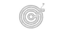
- Modification 1 of the conductor wiring 14is shown.
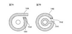
- FIG. 7Ais a view (front view) showing Modified Example 2 of the conductor wiring 14.
- FIG. 7Bis a view (back side view) showing Modified Example 2 of the conductor wiring 14 .
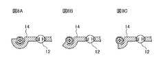
- FIG. 8Ais a view (a view of approximately 180 degrees) showing Modification 3 of the conductor wiring 14.
- FIG. 8Bis a view (a view of approximately 135 degrees) showing Modified Example 3 of the conductor wiring 14 .
- FIG. 8Cis a view (a view of approximately 90 degrees) showing Modified Example 3 of the conductor wiring 14 .
- FIG. 9Ais a perspective view of the configuration of the surge protection circuit 20 of Embodiment 2.
- FIG. 9Bis a cross-sectional view showing the configuration of the surge protection circuit 20 of Embodiment 2.
- FIG. 10Ais a perspective view showing the configuration of the surge protection circuit 30 of Embodiment 3.
- FIG. 10Bis a cross-sectional view showing the configuration of the surge protection circuit 30 of Embodiment 3.
- FIG. 11Ais a perspective view showing the configuration of the surge protection circuit 40 of Embodiment 4.
- FIG. 11Bis a cross-sectional view showing the configuration of the surge protection circuit 40 of the fourth embodiment.
- FIG. 11is a cross-sectional view showing a magnetic field generated by a surge protection circuit 40 of Embodiment 4;
- FIG. 9is a cross-sectional view showing a magnetic field generated by a surge protection circuit 30 of Embodiment 3 of a comparative example;
- Embodiment 1A first embodiment of a surge protection circuit according to the present disclosure will be described.
- FIG. 1is a circuit diagram of equipment including the surge protection circuit of Embodiment 1.
- FIG. 1is a circuit diagram of equipment including the surge protection circuit of Embodiment 1.
- the device KK of Embodiment 1includes a printed circuit board 11, as shown in FIG.
- the printed circuit board 11is provided with a circuit KR such as an electric circuit and an electronic circuit, and a varistor VR and a surge absorber 12 for protecting the circuit KR from lightning or the like.
- a conductor wiring 14is also formed on the printed circuit board 11 .
- a rod-shaped member 13is arranged between the printed circuit board 11 and the housing KT (shown in FIG. 2) of the device KK.
- the circuit KRis supplied with power, for example, single-phase AC 100 V, via the first terminal TN1 and the second terminal TN2, and the first power line PL1 and the second power line PL2.
- the varistor VRis connected between the first power line PL1 and the second power line PL2.
- Surge absorber 12, conductor wiring 14, and bar member 13are connected in series between second power supply line PL2 and ground potential GL.
- the device KKmore precisely, the housing KT of the device KK (illustrated in FIG. 2) is connected to the ground potential GL.
- a portion of the printed circuit board 11 , the surge absorber 12 , the cylindrical rod-shaped member 13 , and the conductor wiring 14constitute the surge protection circuit 10 .
- FIG. 2Ais a perspective view showing the configuration of the surge protection circuit 10 of Embodiment 1.
- FIG. 2Ais a perspective view showing the configuration of the surge protection circuit 10 of Embodiment 1.
- FIG. 2Bis a cross-sectional view showing the configuration of the surge protection circuit 10 of Embodiment 1 on the XZ plane 100 of FIG. 2A.
- the surge protection circuit 10includes a printed circuit board 11, a surge absorber 12, a bar member 13, and conductor wiring 14, as shown in FIG. 2A.
- the surge protection circuit 10corresponds to "surge protection circuit”
- the printed circuit board 11corresponds to “printed circuit board”
- the surge absorber 12corresponds to “surge absorber”
- the rod-shaped member 13corresponds to "member”.
- the conductor wiring 14corresponds to "conductor wiring”.
- the printed circuit board 11is an insulator plate, as is conventionally known.
- a surge absorber 12is arranged on the surface (XY plane) of the printed circuit board 11 .
- a conductor wiring 14is formed on the surface of the printed board 11 , that is, on the upper surface of the printed board 11 .
- the printed circuit board 11is provided with holes AN for fixing the printed circuit board 11 to the equipment KK with the rod-shaped member 13 .
- the surge absorber 12is, for example, a two-terminal arrester.
- the surge absorber 12has a gap between electrodes at both ends, and discharges a surge voltage caused by lightning or the like in the gap.
- the rod-shaped member 13is a screw made of a conductive and magnetic material. Examples of the material include iron and some stainless steels having magnetism.
- the rod-shaped member 13extends in a direction (Z-axis direction) orthogonal to the surface (XY plane) of the printed circuit board 11 .
- the conductor wiring 14has one end connected to the surge absorber 12 and the other end connected to the bar member 13 .
- the surge absorber 12, the conductor wiring 14, and the bar member 13are connected in series with each other.
- the conductor wiring 14is also wired starting from the intersection point KTN between the surface (XY plane) of the printed circuit board 11 and the center line CS of the rod-shaped member 13 in the orthogonal direction (Z-axis direction).
- the conductor wiring 14is further formed along at least part of a virtual spiral KRK centered on the intersection point KTN on the surface (XY plane) of the printed circuit board 11 .
- the conductor wiring 14is formed so as to surround the rod-shaped member 13 .
- the conductor wiring 14is, for example, a plane (XY plane) parallel to the surface (XY plane) of the printed circuit board 11 and imaginary in the printed circuit board 11. (not shown) and the center line CS of the rod-like member 13 may be set as the starting point.
- the intersection point KTNmay exist within a layer of the printed circuit board 11 instead of existing on the surface of the printed circuit board 11 .
- the housing KT of the device KKis basically made of a conductive material, such as metal.
- a conductive materialsuch as metal.
- Part KK1is made of a conductive material.
- the portion KK1 described aboveis formed in a columnar shape extending in the orthogonal direction (Z-axis direction).
- the rod-shaped member 13is screwed to a portion KK1 of the housing KT of the device KK via the hole AN of the printed circuit board 11 described above. Thereby, the printed circuit board 11 and the housing KT of the device KK are mechanically fixed. In addition to mechanically fixing the printed circuit board 11 and the device KK, the rod-shaped member 13 electrically connects the conductor wiring 14 on the printed circuit board 11 and the housing KT of the device KK.
- FIG. 1is a perspective view showing the operation of the surge protection circuit 10 of Embodiment 1.
- FIG. 3Ais a perspective view showing the operation of the surge protection circuit 10 of Embodiment 1.
- FIG. 3Bis a cross-sectional view showing the operation of the surge protection circuit 10 of Embodiment 1.
- FIG. 3Bis a cross-sectional view showing the operation of the surge protection circuit 10 of Embodiment 1.
- the surge absorber 12reacts to the surge voltage, and the dotted arrow , a surge current SC flows. Specifically, the surge current SC passes from the varistor VR (shown in FIG. 1) to the device KK via the surge absorber 12, the conductor wiring 14, and the rod-shaped member 13, as indicated by the dotted arrow. It flows to the housing KT.
- ⁇ Effect of Embodiment 1> 4Ais a perspective view showing the relationship between the surge current SC and the magnetic field JK of Embodiment 1.
- FIG. 4Ais a perspective view showing the relationship between the surge current SC and the magnetic field JK of Embodiment 1.
- FIG. 4Bis a cross-sectional view showing the relationship between the surge current SC and the magnetic field JK in Embodiment 1.
- FIG. 4Bis a cross-sectional view showing the relationship between the surge current SC and the magnetic field JK in Embodiment 1.
- the surge protection circuit 10 of Embodiment 1by adopting the configuration of the conductor wiring 14 of the rod-shaped member 13 described above, a larger space for arrangement is required in the space above the printed circuit board 11 than for the surge absorber 12 and the like. There is no need to place a coil to As a result, the surge protection circuit 10 of the first embodiment can be made smaller than conventional surge protection circuits.
- FIG. 5Ais a diagram (a diagram of the configuration of Embodiment 1) showing a comparison between the surge protection circuit 10 of Embodiment 1 and a surge protection circuit of a comparative example.
- FIG. 5Bis a diagram (a diagram of a configuration of a comparative example) showing a comparison between the surge protection circuit 10 of Embodiment 1 and a surge protection circuit of a comparative example.
- the surge protection circuit 10 of the first embodiment and the surge protection circuit of the comparative exampleeach use an iron screw with a relative magnetic permeability of 1000 or more as the rod-shaped member 13 .
- the conductor wiring 14is formed along the virtual spiral KRK in a small space around the rod-shaped member 13, and theoretically about 30 nH of inductance is generated.
- the conductor wiring 14Xis not along the virtual spiral KRK but straight and folded. formed by
- the conductor wiring 14Xhas a wiring width of 3 mm, generally 0.6 nH/mm. As a result, the total length of the conductor wiring 14X (the length of the dashed-dotted line in FIG. 5B) is required to be approximately 50 mm. From this, it can be said that the space for forming the conductor wiring 14 in the surge protection circuit 10 of the first embodiment is smaller than the space for forming the conductor wiring 14X in the surge protection circuit of the comparative example.
- FIG. 6shows Modification 1 of the conductor wiring 14 .
- the conductor wiring 14may be wound multiple times, such as twice, instead of being wound only once (illustrated in FIG. 2A). This further increases the inductance of the conductor wiring 14, and as a result, it is possible to more strongly suppress a rapid change in the surge current SC.
- FIG. 7Ais a diagram (surface diagram) showing Modified Example 2 of the conductor wiring 14.
- FIG. 7Ais a diagram (surface diagram) showing Modified Example 2 of the conductor wiring 14.
- FIG. 7Bis a view (back side view) showing Modification 2 of the conductor wiring 14.
- FIG. 7Bspecifically shows the rear surface of the printed circuit board 11 seen through from the front surface.
- the conductor wiring 14is formed on both the front surface and the rear surface of the printed circuit board 11, which are two layers. good too.
- a conductor wiring 14A corresponding to half of the conductor wiring 14is formed on the surface of the printed circuit board 11, and as shown in FIG. A conductor wiring 14B corresponding to the remaining half may be formed on the back surface of the printed circuit board 11 .
- the conductor wiring 14A and the conductor wiring 14Bare connected by through holes TH1 and TH2 penetrating the printed circuit board 11, for example.
- the conductor wiring 14may be formed on both sides of the multilayer printed circuit board 11 (not shown) and between the layers.
- FIG. 8Ais a view (a view of about 180 degrees) showing Modification 3 of the conductor wiring 14.
- FIG. 8Ais a view (a view of about 180 degrees) showing Modification 3 of the conductor wiring 14.
- FIG. 8Bis a diagram (a diagram of about 135 degrees) showing Modification 3 of the conductor wiring 14.
- FIG. 8Bis a diagram (a diagram of about 135 degrees) showing Modification 3 of the conductor wiring 14.
- FIG. 8Cis a view (a view of about 90 degrees) showing Modification 3 of the conductor wiring 14.
- the conductor wiring 14is formed along the virtual spiral KRK as shown in FIG. 8A. , and may be formed to a length corresponding to about 135 degrees along the imaginary spiral KRK, as shown in FIG. 8B, and further, As shown in FIG. 8C, it may be formed with a length corresponding to approximately 90 degrees along the virtual helix KRK.
- the inductance of the conductor wiring 14is not increased to the extent that the conductor wiring 14 having a length corresponding to about 270 degrees in the first embodiment increases.
- the length, shape, etc. of the conductor wiring 14can be appropriately adjusted from the viewpoint of the width of the space on the surface of the substrate 11 and the size of the inductance to be increased.
- the direction of the virtual spiral KRK in which the conductor wiring 14 is routedmay be clockwise (for example, shown in FIG. 8) instead of counterclockwise from outside to inside (shown in FIG. 2A). .
- the conductor wiring 14may be wound multiple times as described above (shown in FIG. 6), formed between planes and layers (shown in FIG. 7, etc.), and formed along a portion of the virtual spiral KRK. (illustrated in FIG. 8).
- the rod-shaped member 13may have any shape as long as it has conductivity and magnetism.
- the rod-shaped member 13may have a length that is the same as the length of the portion KK1, and It may have a length exceeding the length of said portion KK1.
- ⁇ Modification of surge absorber 12>instead of using an arrester as the surge absorber 12, another semiconductor element such as a varistor may be used, or both may be used together.
- Surge absorber 12may be connected to a communication line such as a telephone line instead of first and second power lines PL1 and PL2 for supplying power.
- a communication linesuch as a telephone line
- a spacer separate from the device KKmay be used.
- the housing KT of the device KKmay have magnetism in addition to conductivity.
- the device KKmay be supplied with three-phase AC power or DC power instead of being supplied with single-phase AC power from the first and second power lines PL1 and PL2.
- Embodiment 2A second embodiment of the surge protection circuit will be described.
- FIG. 9Ais a perspective view showing the configuration of the surge protection circuit 20 of Embodiment 2.
- FIG. 9Ais a perspective view showing the configuration of the surge protection circuit 20 of Embodiment 2.
- FIG. 9Bis a cross-sectional view showing the configuration of the surge protection circuit 20 of Embodiment 2 on the XZ plane 200 of FIG. 9A.
- the configuration of the surge protection circuit 20 of Embodiment 2will be described with reference to FIGS. 9A and 9B.
- the surge protection circuit 20 of the second embodimentincludes a printed circuit board 21, a surge absorber 22, a bar member 23, and a conductor wiring 24, like the surge protection circuit 10 of the first embodiment (shown in FIG. 2). include.
- the configurations and functions of the printed circuit board 21 and the surge absorber 22 of the second embodimentare basically the same as the configurations and functions of the printed circuit board 11 and the surge absorber 12 of the first embodiment.
- the rod-shaped member 23 of Embodiment 2has conductivity and magnetism like the rod-shaped member 13 of Embodiment 1, but unlike the rod-shaped member 13 of Embodiment 1, it is a spacer instead of a screw.
- the rod-shaped member 23has, for example, a columnar shape or a tubular shape.
- the rod-shaped member 23is mechanically fixed to the equipment KK (not shown).
- the rod-shaped member 23is also screwed through the hole AN of the printed circuit board 21 with a mounting screw 25 . Thereby, the printed circuit board 21 and the housing KT of the device KK are mechanically fixed.
- the mounting screws 25have the mechanical fixing function described above.
- the mounting screw 25does not need to be conductive and magnetic, unlike the bar member 13 of the first embodiment, that is, the conductive and magnetic screw. Therefore, the mounting screws 25 may be made of resin, for example.
- the conductor wiring 24 of the second embodimenthas one end connected to the surge absorber 22 and the other end connected to the rod-shaped member 23 and surrounds the rod-shaped member 23, similarly to the conductor wiring 14 of the first embodiment. is formed as
- the conductor wiring 24 of the second embodimentis formed on the back surface of the printed circuit board 21 unlike the conductor wiring 14 of the first embodiment.
- a conductor wiring 24is formed on the back surface of the printed circuit board 21 by mechanically fixing the rod-shaped member 23 and the device KK and screwing the mounting screws 25 through the holes AN of the printed circuit board 21. are electrically connected to the bar member 23 and the housing KT of the device KK.
- Embodiment 2The operation of the surge protection circuit 20 of the second embodiment is similar to the operation of the surge protection circuit 10 of the first embodiment (shown in FIGS. 3 and 4).
- the conductor wiring 24 formed on the back surface of the printed circuit board 21is connected to the rod-shaped member 23, more specifically, has conductivity and magnetism, and is connected between the printed circuit board 21 and the device KK. is directly and electrically connected to the rod-shaped member 23 which is a spacer of the . Therefore, unlike the rod-like member 13 of Embodiment 1, which is a conductive and magnetic screw, the mounting screw 25 of the second embodiment does not need to have conductivity and magnetism. As a result, for example, when selecting one type of mounting screw 25 from a plurality of types of mounting screw 25 candidates, it is not necessary to consider electrical properties such as conductivity and magnetism. As a result, it is possible to select one type of mounting screw 25 more freely than in the first embodiment, for example, only considering mechanical characteristics and workability of mechanical assembly. can be selected.
- the mounting screw 25 and the hole ANare not necessarily used if the conductor wiring 24 and the rod-shaped member 23 are electrically connected and the conductor wiring 24 is arranged so as to surround the rod-shaped member 23 .
- the portion of the upper surface where the rod-shaped member 23 contacts the printed circuit board 21may be formed into a convex shape, and the convex upper surface portion may be used to position the rod-shaped member 23 on the printed circuit board 21 .
- the rod-shaped member 23can be formed into a convex and threaded shape on the upper surface where the rod-shaped member 23 contacts the printed circuit board 21, and by passing a nut or the like through the convex and threaded upper surface, the printed circuit board can be mounted on the printed circuit board. 21 may be fixed.
- the mounting screw 25may have a length equal to the length of the rod-shaped member 23 instead of having a length about half the length of the rod-shaped member 23, or may have a length equal to the length of the rod-shaped member 23. It may have a length exceeding the height.
- the conductor wiring 24may be wound a plurality of times (shown in FIG. 6), or may be formed on both sides or between layers of the printed circuit board 21 (shown in FIG. 7). 180 degrees, 135 degrees, and 90 degrees along the virtual spiral KRK (shown in FIG. 8), or a combination thereof.
- Embodiment 3A third embodiment of the surge protection circuit will be described.
- FIG. 10Ais a perspective view showing the configuration of the surge protection circuit 30 of Embodiment 3.
- FIG. 10Ais a perspective view showing the configuration of the surge protection circuit 30 of Embodiment 3.
- FIG. 10Bis a cross-sectional view showing the configuration of the surge protection circuit 30 of Embodiment 3 on the XZ plane 300 of FIG. 10A.
- the surge protection circuit 30 of Embodiment 3includes a printed circuit board 31, a surge absorber 32, a truncated conical trapezoidal member 33, and conductor wiring 34 .
- the configurations and functions of the printed circuit board 31 and the surge absorber 32 of the third embodimentare basically the same as the configurations and functions of the printed circuit board 11 and the surge absorber 12 of the first embodiment.
- the housing KT of the device KK of the third embodimentis different from the housing KT of the device KK of the first embodiment and is made of a material having conductivity and magnetism.
- the pedestal member 33is a part of the housing KT of the device KK, and more specifically, it is a portion formed into a trapezoidal shape or the like by press working or the like from the housing KT of the device KK.
- a hole AN2is provided in the upper surface of the platform member 33 .
- the printed circuit board 31 and the housing KT of the device KKare mechanically fixed by screwing the mounting screws 35 through the holes AN of the printed circuit board 31 and the holes AN2 of the pedestal member 33 .
- the mounting screw 35does not need to have electrical conductivity and magnetism, so the material does not matter.
- Embodiment 3The operation of the surge protection circuit 30 of the third embodiment is similar to the operation of the surge protection circuit 10 of the first embodiment (illustrated in FIGS. 3 and 4).
- a surge protection circuit 30 of the third embodimenthas a platform member 33 instead of the rod-shaped member 23 of the second embodiment. Unlike the bar member 23 which is a spacer separate from the housing KT of the device KK, the platform member 33 is a part of the housing KT of the device KK, that is, is integral with the housing KT of the device KK. be. As a result, the surge protection circuit 30 of the third embodiment can reduce the number of parts to be mounted and the number of parts to be assembled, for example, compared to the surge protection circuit 20 of the second embodiment.
- the pedestal member 33may be provided by welding or attaching to the housing KT of the device KK with a conductive adhesive instead of being provided by molding such as press working as described above, or may be provided by press fitting. .
- the mounting screw 35does not have to penetrate the platform member 33 instead of penetrating the platform member 33 as long as the printed circuit board 31 can be fixed to the platform member 33 .
- the convex upper surface portion of the platform member 33may be used to position the platform member 33 on the printed circuit board 31, or the protrusion of the platform member 33 may be used.
- the printed circuit board 31may be fixed by passing a nut or the like through the portion of the upper surface that is formed into a shape and a threaded shape.
- the conductor wiring 34may be wound a plurality of times (shown in FIG. 6), or may be formed on both sides or between layers of the printed circuit board 21 (shown in FIG. 7). 180 degrees along the virtual spiral KRK (shown in FIG. 8), or a combination thereof.
- Embodiment 4A fourth embodiment of the surge protection circuit will be described.
- FIG. 11Ais a perspective view showing the configuration of the surge protection circuit 40 of Embodiment 4.
- FIG. 11Ais a perspective view showing the configuration of the surge protection circuit 40 of Embodiment 4.
- FIG. 11Bis a cross-sectional view showing the configuration of the surge protection circuit 40 of Embodiment 4 on the XZ plane 400 of FIG. 11A.
- the configuration of the surge protection circuit 40 of Embodiment 4will be described with reference to FIGS. 11A and 11B.
- the surge protection circuit 40 of Embodiment 4includes a printed circuit board 41, a surge absorber 42, a platform member 43, conductor wiring 44, including.
- the pedestal member 43 of the fourth embodimentdiffers from the pedestal member 33 of the third embodiment in that the outer diameter 43KE of the upper surface of the pedestal member 43 is larger than the inner diameter 44KE of the conductor wiring 44 .
- the outer diameter 43KE of the upper surface of the platform member 43is the diameter of the upper surface of the platform member 43, which has a substantially circular shape.
- the inner diameter 44KE of the conductor wiring 44is the point at which the conductor wiring 44, which is spirally formed along the imaginary spiral shape KRK, bends at a substantially right angle toward the center line CS. It is approximately twice the distance 44KY between PT and the centerline CS.
- the outer diameter 43KE of the upper surface of the pedestal member 43corresponds to "the diameter of the upper surface of the member”.
- the inner diameter 44KE of the conductor wiring 44corresponds to "the diameter of the virtual circle defined by at least part of the virtual spiral of the conductor wiring”.
- the platform member 43is also provided with a notch 46 as shown in FIG. 11B. Notch 46 ensures that platform member 43 is in principle not electrically connected to the entire conductor trace 44, as shown in FIG. As an exception, the shaped member 43 has a shape to ensure that it is electrically connected only to the circular region RY of the conductor wiring 44 that is in the vicinity of the mounting screw 45 .
- Embodiment 4The operation of the surge protection circuit 40 of the fourth embodiment is similar to the operation of the surge protection circuit 10 of the first embodiment (illustrated in FIGS. 3 and 4).
- FIG. 12shows the magnetic field generated by the surge protection circuit 40 of the fourth embodiment.
- FIG. 13shows the magnetic field generated by the surge protection circuit 30 of Embodiment 3 of the comparative example.
- Embodiment 3which is a comparative example, as shown in FIG.
- the inner diameteris smaller than 34KE.
- the surge protection circuit 40 of the fourth embodimentin contrast to the surge protection circuit 30 of the third embodiment, in the surge protection circuit 40 of the fourth embodiment, as described above with reference to FIG. greater than As a result, all of the magnetic field JK ⁇ b>4 generated by the surge current SC flowing through the conductor wiring 44 passes through the upper surface of the platform member 43 . Therefore, in the surge protection circuit 40 of the fourth embodiment, the inductance can be made larger than in the surge protection circuit 30 of the third embodiment, and as a result, rapid changes in the surge current SC can be further suppressed. becomes possible.
- an insulating sheet membermay be arranged between the conductor wiring 44 and the pedestal member 43 instead of the notch 46 described above.
- the notch 46may not be provided.
- a surge protection circuit according to the present disclosurecan be used, for example, in a surge protection system that protects a semiconductor element for protecting a circuit and elements from a lightning strike or the like from a sudden increase in current caused by the lightning strike or the like.
Landscapes
- Engineering & Computer Science (AREA)
- Microelectronics & Electronic Packaging (AREA)
- Power Engineering (AREA)
- Emergency Protection Circuit Devices (AREA)
- Parts Printed On Printed Circuit Boards (AREA)
- Mounting Of Printed Circuit Boards And The Like (AREA)
Abstract
Description
Translated fromJapanese本開示は、サージ保護回路及びサージ保護方法に関する。The present disclosure relates to surge protection circuits and surge protection methods.
サージ保護回路の一例である、特許文献1に記載された避雷装置は、当該避雷装置内に設けられた回路及び素子を落雷等から保護するための半導体素子を、前記落雷等に起因する電流の急激な上昇から保護するためのコイルを有する。A lightning arrester described in
しかしながら、上記したコイルは、構造上の理由から、上記した半導体素子等の大きさに比して極めて大きい。それにより、上記したサージ保護回路を小型化することが困難であった。However, for structural reasons, the coil described above is extremely large compared to the size of the semiconductor element described above. As a result, it has been difficult to miniaturize the surge protection circuit described above.
本開示の目的は、小型化を容易に行うことができるサージ保護回路を提供することにある。An object of the present disclosure is to provide a surge protection circuit that can be easily miniaturized.
上記した課題を解決すべく、本開示に係るサージ保護回路は、プリント基板と、前記プリント基板上に配置されたサージアブソーバと、前記プリント基板の表面と直交する方向に伸びる、導電性及び磁性を有する部材と、一端が前記サージアブソーバに接続され、他端が前記部材に接続された導体配線であって、前記プリント基板の表面に平行な平面と、前記直交する方向についての前記部材の中心線との交点を起点に、前記平行な面における前記交点を中心とする仮想螺旋形の少なくとも一部に沿って形成された前記導体配線と、を含む。In order to solve the above-described problems, the surge protection circuit according to the present disclosure includes a printed circuit board, a surge absorber arranged on the printed circuit board, and a conductive and magnetic element extending in a direction orthogonal to the surface of the printed circuit board. and a conductor wiring having one end connected to the surge absorber and the other end connected to the member, the plane parallel to the surface of the printed circuit board and the center line of the member in the orthogonal direction. and the conductor wiring formed along at least a portion of a virtual helical shape centered at the intersection point on the parallel plane.
本開示に係るサージ保護回路によれば、コイルを用いるサージ保護回路に比して小型化を容易に行うことができる。According to the surge protection circuit according to the present disclosure, miniaturization can be easily achieved compared to a surge protection circuit using a coil.
実施形態1.
〈実施形態1〉
本開示に係るサージ保護回路の実施形態1について説明する。
<
A first embodiment of a surge protection circuit according to the present disclosure will be described.
〈実施形態1の構成〉
図1は、実施形態1のサージ保護回路を含む機器の回路図である。<Configuration of
FIG. 1 is a circuit diagram of equipment including the surge protection circuit of
実施形態1の機器KKは、図1に示されるように、プリント基板11を含む。プリント基板11には、電気回路及び電子回路等である回路KR、並びに、回路KRを雷等から保護するためのバリスタVR及びサージアブソーバ12が配置されている。プリント基板11には、また、導体配線14が形成されている。プリント基板11及び機器KKの筐体KT(図2に図示。)間には、棒状部材13が配置されている。The device KK of
回路KRは、第1の端子TN1及び第2の端子TN2、並びに、第1の電源線PL1及び第2の電源線PL2を介して電力の供給、例えば、単相交流100Vの供給を受ける。バリスタVRは、第1の電源線PL1及び第2の電源線PL2間に接続されている。サージアブソーバ12、導体配線14、及び棒状部材13は、第2の電源線PL2及び接地電位GL間に直列接続されている。The circuit KR is supplied with power, for example, single-phase AC 100 V, via the first terminal TN1 and the second terminal TN2, and the first power line PL1 and the second power line PL2. The varistor VR is connected between the first power line PL1 and the second power line PL2.
機器KKは、より正確には、機器KKの筐体KT(図2に図示。)は、接地電位GLに接続されている。The device KK, more precisely, the housing KT of the device KK (illustrated in FIG. 2) is connected to the ground potential GL.
プリント基板11の一部、サージアブソーバ12、円柱状である棒状部材13、及び導体配線14は、サージ保護回路10を構成する。A portion of the printed
図2Aは、実施形態1のサージ保護回路10の構成を示す斜視図である。FIG. 2A is a perspective view showing the configuration of the
図2Bは、図2AのXZ平面100についての、実施形態1のサージ保護回路10の構成を示す断面図である。FIG. 2B is a cross-sectional view showing the configuration of the
実施形態1のサージ保護回路10の構成について、図2A、図2Bを参照して説明する。The configuration of the
サージ保護回路10は、図2Aに示されるように、プリント基板11と、サージアブソーバ12と、棒状部材13と、導体配線14と、を含む。The
サージ保護回路10は、「サージ保護回路」に対応し、プリント基板11は、「プリント基板」に対応し、サージアブソーバ12は、「サージアブソーバ」に対応し、棒状部材13は、「部材」に対応し、導体配線14は、「導体配線」に対応する。The
プリント基板11は、従来知られているように、絶縁体の板である。プリント基板11の表面(XY平面)には、サージアブソーバ12が配置されている。プリント基板11の表面には、即ち、プリント基板11の上面には、導体配線14が形成されている。プリント基板11には、図2Bに示されるように、プリント基板11を棒状部材13により機器KKに固定するための孔ANが設けられている。The printed
サージアブソーバ12は、例えば、二端子のアレスタである。サージアブソーバ12は、両端の電極間にギャップが設けられており、当該ギャップ間で雷等に起因するサージ電圧を放電させる。The
棒状部材13は、導電性及び磁性を有する材料で作られたネジである。前記材料として、例えば、鉄、磁性を有する一部のステンレスが挙げられる。棒状部材13は、プリント基板11の表面(XY平面)と直交する方向(Z軸方向)に伸びている。The rod-shaped
導体配線14は、図2Aに示されるように、一端が、サージアブソーバ12に接続され、他端が、棒状部材13に接続されている。換言すれば、サージアブソーバ12、導体配線14、及び棒状部材13は、相互に直列接続されている。導体配線14は、また、プリント基板11の表面(XY平面)と、上記した直交する方向(Z軸方向)についての棒状部材13の中心線CSとの交点KTNを起点として配線されている。導体配線14は、更に、プリント基板11の表面(XY平面)における交点KTNを中心とする仮想螺旋形KRKの少なくとも一部に沿って形成されている。要約すれば、導体配線14は、棒状部材13を囲むように形成されている。As shown in FIG. 2A, the
導体配線14は、プリント基板11の表面(XY平面)に代えて、例えば、プリント基板11の表面(XY平面)に平行な平面(XY平面)であってプリント基板11内に仮想される前記平面(図示せず。)と、棒状部材13の中心線CSとの交点KTNを起点としてもよい。換言すれば、交点KTNは、プリント基板11の表面に存在することに代えて、プリント基板11の層内に存在してもよい。Instead of the surface (XY plane) of the printed
機器KKの筐体KTは、基本的に、導電性の材料、例えば、金属で製造されている。機器KKの筐体KTでは、少なくとも、接地電位GL(図1に図示。)であるべき一部分、例えば、図2Bに示されるように、棒状部材13と接地(図示せず。)との間の一部分KK1は、導電性の材料で製造されている。前記した一部分KK1は、上記した直交する方向(Z軸方向)に伸びる円柱状に成形されている。The housing KT of the device KK is basically made of a conductive material, such as metal. In the housing KT of the equipment KK, at least a portion that should be at the ground potential GL (shown in FIG. 1), for example, between the
棒状部材13は、図2Bに示されるように、上記したプリント基板11の孔ANを介して、上記した機器KKの筐体KTの一部分KK1にネジ締めされている。これにより、プリント基板11と機器KKの筐体KTとは、機械的に固定されている。棒状部材13は、プリント基板11と機器KKと機械的に固定することに加えて、プリント基板11上の導体配線14と機器KKの筐体KTとを電気的に接続している。As shown in FIG. 2B, the rod-shaped
上記した「平行」及び「垂直」は、それぞれ、厳密に平行であること、及び、厳密に垂直であることを要しない。インダクタンス(後述)が少しでも増加しさえすれば、完全な平行でなくて足り、また、完全な垂直でなくて足りる。The above "parallel" and "perpendicular" do not need to be strictly parallel and strictly perpendicular, respectively. As long as the inductance (described later) increases even a little, it is sufficient that they are not perfectly parallel and that they are not perfectly perpendicular.
〈実施形態1の動作〉
図3Aは、実施形態1のサージ保護回路10の動作を示す斜視図である。<Operation of
3A is a perspective view showing the operation of the
図3Bは、実施形態1のサージ保護回路10の動作を示す断面図である。3B is a cross-sectional view showing the operation of the
実施形態1のサージ保護回路10の動作について、図3A、図3Bを参照して説明する。The operation of the
雷等が発生し、前記雷等に起因してサージ電圧(図示せず。)が機器KKに印加されると、サージ保護回路10では、サージアブソーバ12が前記サージ電圧に反応し、点線の矢印で示されるように、サージ電流SCが流れる。具体的には、サージ電流SCは、点線の矢印で示されるように、バリスタVR(図1に図示。)から、サージアブソーバ12、導体配線14、及び棒状部材13を経由して、機器KKの筐体KTへ流れる。When lightning or the like occurs and a surge voltage (not shown) is applied to the equipment KK due to the lightning or the like, in the
〈実施形態1の効果〉
図4Aは、実施形態1のサージ電流SCと磁界JKとの関係を示す斜視図である。<Effect of
4A is a perspective view showing the relationship between the surge current SC and the magnetic field JK of
図4Bは、実施形態1のサージ電流SCと磁界JKとの関係を示す断面図である。4B is a cross-sectional view showing the relationship between the surge current SC and the magnetic field JK in
実施形態1のサージ保護回路10の効果について、図4A、図4Bを参照して説明する。The effect of the
サージ電流SCが、図3A、図3B中の矢印で示されるように、導体配線14に沿って流れると、即ち、XY平面内で流れると、右ねじの法則に従って、図4A及び図4B中の点線の矢印で示されるように、Z軸方向に伸びる棒状部材13の内外を通る磁界JKが生起する。棒状部材13が磁性を有することから、上記した磁界JKが、棒状部材13内を通ることにより、棒状部材13が無いことと比較して、導体配線14のインダクタンスが増加する。その結果、従来のサージ保護回路と同様に、サージ電流SCの急激な変化を、導体配線14の増加したインダクタンスにより緩やかにすること、即ち、抑制することができる。When the surge current SC flows along the
実施形態1のサージ保護回路10では、上記した棒状部材13の導体配線14の構成を採用することにより、プリント基板11上の空間に、サージアブソーバ12等に比して大きい配置用スペースを必要とするコイルを配置する必要が無い。これにより、実施形態1のサージ保護回路10は、従来のサージ保護回路に比して小型化が可能になる。In the
〈比較例との比較〉
図5Aは、実施形態1のサージ保護回路10と比較例のサージ保護回路との比較を示す図(実施形態1の構成の図)である。<Comparison with Comparative Example>
FIG. 5A is a diagram (a diagram of the configuration of Embodiment 1) showing a comparison between the
図5Bは、実施形態1のサージ保護回路10と比較例のサージ保護回路との比較を示す図(比較例の構成の図)である。FIG. 5B is a diagram (a diagram of a configuration of a comparative example) showing a comparison between the
実施形態1のサージ保護回路10の効果と比較例のサージ保護回路の効果との比較を、図5A、図5Bを参照して説明する。A comparison between the effect of the
実施形態1のサージ保護回路10、及び比較例のサージ保護回路には、それぞれ、棒状部材13として、比透磁率が1000以上である鉄ネジが用いられている。The
実施形態1のサージ保護回路10では、導体配線14が、棒状部材13の周辺の僅かなスペースにおける仮想螺旋形KRKに沿って形成されていることにより、理論上、約30nHのインダクタンスが生起する。In the
上記とは対照的に、比較例のサージ保護回路では、上記したと同様の約30nHのインダクタンスが生起するようにすべく、導体配線14Xが、仮想螺旋形KRKに沿ってはなく、直線及び折り返しにより形成されている。In contrast to the above, in the surge protection circuit of the comparative example, in order to generate the same inductance of about 30 nH as described above, the
導体配線14Xは、配線幅が3mmであり、一般的に、0.6nH/mmである。その結果、導体配線14Xの全長(図5B中の一点鎖線の長さ)は、約50mm必要である。このことから、実施形態1のサージ保護回路10における、導体配線14を形成するためのスペースは、比較例のサージ保護回路における、導体配線14Xを形成するためのスペースと比較して小さいといえる。The
〈変形例〉
〈導体配線14の変形例〉
図6は、導体配線14の変形例1を示す。<Modification>
<Modified Example of
FIG. 6 shows
導体配線14は、1回だけ巻くこと(図2Aに図示。)に代えて、2回等の複数回巻いてもよい。これにより、導体配線14のインダクタンスをより増加させ、その結果、サージ電流SCの急激な変化をより強く抑制することができる。The
図7Aは、導体配線14の変形例2を示す図(表面の図)である。FIG. 7A is a diagram (surface diagram) showing Modified Example 2 of the
図7Bは、導体配線14の変形例2を示す図(裏面の図)である。図7Bは、詳しくは、プリント基板11の表面から透視される裏面を示す。FIG. 7B is a view (back side view) showing Modification 2 of the
導体配線14は、導体配線14の全てがプリント基板11の表面のみに形成されること(図2Aに図示。)に代えて、二層であるプリント基板11の表面及び裏面の両面に形成されてもよい。例えば、図7Aに示されるように、導体配線14のうちの半分に相当する導体配線14Aが、プリント基板11の表面に形成され、また、図7Bに示されるように、導体配線14のうちの残り半分に相当する導体配線14Bが、プリント基板11の裏面に形成されてもよい。導体配線14Aと導体配線14Bとは、例えば、プリント基板11を貫通するスルーホールTH1、TH2により接続される。これにより、例えば、プリント基板11に配置すべき電気部品及び電子部品等の大きさ、形状、位置等の自由度を高めることができる。Instead of forming all of the
導体配線14は、さらに、二層であるプリント基板11に形成されることに代えて、多層であるプリント基板11(図示せず。)の両面、及び層間に形成されてもよい。Further, instead of being formed on the two-layer printed
図8Aは、導体配線14の変形例3を示す図(約180度の図)である。FIG. 8A is a view (a view of about 180 degrees) showing Modification 3 of the
図8Bは、導体配線14の変形例3を示す図(約135度の図)である。FIG. 8B is a diagram (a diagram of about 135 degrees) showing Modification 3 of the
図8Cは、導体配線14の変形例3を示す図(約90度の図)である。FIG. 8C is a view (a view of about 90 degrees) showing Modification 3 of the
導体配線14は、仮想螺旋形KRKに沿って約270度に相当する長さに形成されること(図2Aに図示。)に代えて、図8Aに示されるように、仮想螺旋形KRKに沿って約180度に相当する長さに形成されてもよく、また、図8Bに示されるように、仮想螺旋形KRKに沿って約135度に相当する長さに形成されてもよく、さらに、図8Cに示されるように、仮想螺旋形KRKに沿って約90度に相当する長さに形成されてもよい。Instead of forming the
上記した構成を有する変形例3の導体配線14では、導体配線14のインダクタンスを、実施形態1での約270度相当の長さの導体配線14が増大させるほどには増大させないものの、例えば、プリント基板11の表面のスペースの広狭、及び、インダクタンスを増大させるべき大きさの観点から、導体配線14を妥当な長さ、形状等に調整することができる。In the
導体配線14が配線される仮想螺旋形KRKの向きは、外側から内側へ反時計回りの向き(図2Aに図示。)に代えて、時計廻りの向き(例えば、図8に図示。)でもよい。The direction of the virtual spiral KRK in which the
導体配線14は、上記した複数回巻くこと(図6に図示。)、面及び層間に形成すること(図7に図示等。)、及び、仮想螺旋形KRKの一部に沿って形成すること(図8に図示。)を選択的に組み合わせることによって構成されてもよい。The
〈棒状部材13の変形例〉
棒状部材13は、導電性及び磁性を有しさえすれば、形状を問わず、具体的には、ネジであることに代えて、釘、角柱、ブロック等のいずれかであってもよい。<Modified example of rod-shaped
The rod-shaped
棒状部材13は、機器KKの筐体KTの一部分KK1の長さの半分ほどの長さを有することに代えて、前記一部分KK1の長さと同一である長さを有してもよく、また、前記一部分KK1の長さを超過する長さを有してもよい。Instead of having a length about half the length of the portion KK1 of the housing KT of the device KK, the rod-shaped
〈サージアブソーバ12の変形例〉
サージアブソーバ12としてアレスタを使用することに代えて、バリスタ等の他の半導体素子を使用してもよく、または、両者を併用してもよい。<Modification of
Instead of using an arrester as the
サージアブソーバ12は、電力を供給するための第1、第2の電源線PL1、PL2に代えて、電話線等の通信線に接続されてもよい。
〈機器KKの変形例〉
機器KKの筐体KTの一部分KK1を用いることに代えて、機器KKとは別体であるスペーサを用いてもよい。
<Modified example of equipment KK>
Instead of using the portion KK1 of the housing KT of the device KK, a spacer separate from the device KK may be used.
機器KKの筐体KTは、導電性に加えて、磁性を有してもよい。The housing KT of the device KK may have magnetism in addition to conductivity.
機器KKは、第1、第2の電源線PL1、PL2から単相交流の電力の供給を受けることに代えて、三相交流の電力や直流の電力の供給を受けてもよい。The device KK may be supplied with three-phase AC power or DC power instead of being supplied with single-phase AC power from the first and second power lines PL1 and PL2.
実施形態2.
〈実施形態2〉
サージ保護回路の実施形態2について説明する。Embodiment 2.
<Embodiment 2>
A second embodiment of the surge protection circuit will be described.
〈実施形態2の構成〉
図9Aは、実施形態2のサージ保護回路20の構成を示す斜視図である。<Configuration of Embodiment 2>
FIG. 9A is a perspective view showing the configuration of the
図9Bは、図9AのXZ平面200についての、実施形態2のサージ保護回路20の構成を示す断面図である。FIG. 9B is a cross-sectional view showing the configuration of the
実施形態2のサージ保護回路20の構成について、図9A、図9Bを参照して説明する。The configuration of the
実施形態2のサージ保護回路20は、実施形態1のサージ保護回路10(図2に図示。)と同様に、プリント基板21と、サージアブソーバ22と、棒状部材23と、導体配線24と、を含む。The
実施形態2のプリント基板21及びサージアブソーバ22の構成及び機能は、基本的に、実施形態1のプリント基板11及びサージアブソーバ12の構成及び機能と同様である。The configurations and functions of the printed
実施形態2の棒状部材23は、実施形態1の棒状部材13と同様に、導電性及び磁性を有するものの、実施形態1の棒状部材13と相違し、ネジではなくスペーサである。棒状部材23は、例えば、柱状の形状、または、筒状の形状を有する。棒状部材23は、機器KKに機械的に固定されている(図示せず)。棒状部材23は、また、取付用ネジ25によりプリント基板21の孔ANを介して、ネジ締めされている。これにより、プリント基板21と機器KKの筐体KTとは、機械的に固定されている。The rod-shaped
ここで、取付用ネジ25は、上記した機械的な固定の機能を有しさえすれば足りる。その理由から、取付用ネジ25は、実施形態1の棒状部材13、即ち、導電性及び磁性を有するネジとは相違し、導電性及び磁性を有することを要しない。従って、取付用ネジ25は、例えば、樹脂製であってもよい。Here, it is sufficient that the mounting
実施形態2の導体配線24は、実施形態1の導体配線14と同様に、一端が、サージアブソーバ22に接続され、他端が、棒状部材23に接続されており、かつ、棒状部材23を囲むように形成されている。The
実施形態2の導体配線24は、他方で、実施形態1の導体配線14と相違して、プリント基板21の裏面に形成されている。On the other hand, the
上記した棒状部材23と機器KKとの機械的な固定、及び、上記した取付用ネジ25によるプリント基板21の孔ANを介したネジ締めにより、プリント基板21の裏面上に形成された導体配線24は、棒状部材23、及び機器KKの筐体KTと電気的に接続されている。A
〈実施形態2の動作〉
実施形態2のサージ保護回路20の動作は、実施形態1のサージ保護回路10の動作(図3、図4に図示。)と同様である。<Operation of Embodiment 2>
The operation of the
〈実施形態2の効果〉
実施形態2のサージ保護回路20では、プリント基板21の裏面に形成された導体配線24が、棒状部材23と、より詳しくは、導電性及び磁性を有し、かつ、プリント基板21及び機器KK間のスペーサである棒状部材23と、直接的に電気的に接続されている。従って、実施形態2の取付用ネジ25は、導電性及び磁性を有するネジである実施形態1の棒状部材13とは相違して、導電性及び磁性を有することを要しない。これにより、例えば、複数の種類の取付用ネジ25の候補から一種類の取付用ネジ25を選択するときに、導電性及び磁性等の電気的特性を考慮する必要が無い。その結果、前記一種類の取付用ネジ25を選択することを、実施形態1に比してより自由に行うことができ、例えば、機械的特性、機械的な組み立ての作業性のみを考慮して選択することができる。<Effect of Embodiment 2>
In the
〈変形例〉
〈取付用ネジ25の変形例〉
取付用ネジ25及び孔ANは、導体配線24と棒状部材23とが電気的に接続され、かつ、導体配線24が棒状部材23を囲むように配置されれば、必ずしも使用することを要しない。例えば、棒状部材23がプリント基板21と接触する上面の部分を凸形状に成形し、当該凸形状である上面の部分を、プリント基板21に棒状部材23を位置決めするために用いてもよい。例えば、また、棒状部材23がプリント基板21と接触する上面の部分を凸形状かつネジ切り形状に成形し、当該凸形状かつネジ切り形状である上面の部分にナット等を通すことにより、プリント基板21を固定してもよい。<Modification>
<Modified Example of Mounting
The mounting
取付用ネジ25は、棒状部材23の長さの半分ほどの長さを有することに代えて、棒状部材23の長さと同一である長さを有してもよく、また、棒状部材23の長さを超過する長さを有してもよい。The mounting
〈導体配線24の変形例〉
導体配線24は、実施形態1の導体配線14の変形例と同様に、複数回巻いてもよく(図6に図示。)、プリント基板21の両面、層間に形成してもよく(図7に図示等。)、仮想螺旋形KRKに沿って約180度、約135度、約90度に相当する長さに形成してもよく(図8に図示。)、これらを組み合わせてもよい。<Modified Example of
As in the modification of the
実施形態3.
〈実施形態3〉
サージ保護回路の実施形態3について説明する。Embodiment 3.
<Embodiment 3>
A third embodiment of the surge protection circuit will be described.
〈実施形態3の構成〉
図10Aは、実施形態3のサージ保護回路30の構成を示す斜視図である。<Configuration of Embodiment 3>
FIG. 10A is a perspective view showing the configuration of the
図10Bは、図10AのXZ平面300についての、実施形態3のサージ保護回路30の構成を示す断面図である。FIG. 10B is a cross-sectional view showing the configuration of the
実施形態3のサージ保護回路30の構成について、図10A、図10Bを参照して説明する。The configuration of the
実施形態3のサージ保護回路30は、実施形態1のサージ保護回路10(図2に図示。)と同様に、プリント基板31と、サージアブソーバ32と、円錐台状である台状部材33と、導体配線34と、を含む。As with the
実施形態3のプリント基板31及びサージアブソーバ32の構成及び機能は、基本的に、実施形態1のプリント基板11及びサージアブソーバ12の構成及び機能と同様である。The configurations and functions of the printed
実施形態3の機器KKの筐体KTは、実施形態1の機器KKの筐体KTと相違し、導電性及び磁性を有する材料で製造されている。The housing KT of the device KK of the third embodiment is different from the housing KT of the device KK of the first embodiment and is made of a material having conductivity and magnetism.
台状部材33は、機器KKの筐体KTの一部分であり、詳しくは、機器KKの筐体KTからプレス加工等により台形状等に成形された部分である。台状部材33の上面には、孔AN2が設けられている。The
取付用ネジ35によるプリント基板31の孔AN、及び台状部材33の孔AN2を介したネジ締めにより、プリント基板31と機器KKの筐体KTとは、機械的に固定されている。The printed
ここで、取付用ネジ35は、実施形態2の取付用ネジ25と同様に、導電性及び磁性を有することを要しないことから、材質を問わない。Here, like the mounting
〈実施形態3の動作〉
実施形態3のサージ保護回路30の動作は、実施形態1のサージ保護回路10の動作(図3、図4に図示。)と同様である。<Operation of Embodiment 3>
The operation of the
〈実施形態3の効果〉
実施形態3のサージ保護回路30では、実施形態2の棒状部材23に代えて、台状部材33を有する。台状部材33は、機器KKの筐体KTとは別体なスペーサである棒状部材23と相違して、機器KKの筐体KTの一部分であり、即ち、機器KKの筐体KTと同体である。これにより、実施形態3のサージ保護回路30は、実施形態2のサージ保護回路20に比して、例えば、実装すべき部品の点数、組み立てるべき部品の点数を低減することができる。<Effect of Embodiment 3>
A
〈変形例〉
〈台状部材33の変形例〉
台状部材33は、上記したプレス加工等の成形により設けることに代えて、機器KKの筐体KTに溶接や導電性接着剤により取り付けることにより設けてもよく、また、圧入によって設けてもよい。<Modification>
<Modification of
The
〈取付用ネジ35の変形例〉
取付用ネジ35は、プリント基板31を台状部材33に固定することができれば、台状部材33を貫通することに代えて、台状部材33を貫通しなくてもよい。<Modified Example of Mounting
The mounting
取付用ネジ35及び孔AN2は、実施形態2と同様に、導体配線34と台状部材33とが電気的に接続され、かつ、導体配線34が台状部材33を囲むように配置されれば、必ずしも使用することを要しない。例えば、実施形態2と同様に、台状部材33の凸形状に成形された上面の部分を、プリント基板31に台状部材33を位置決めするために用いることにより、または、台状部材33の凸形状かつネジ切り形状に成形された上面の部分にナット等を通すことにより、プリント基板31を固定してもよい。If the mounting
〈導体配線34の変形例〉
導体配線34は、実施形態1の導体配線14の変形例と同様に、複数回巻いてもよく(図6に図示。)、プリント基板21の両面、層間に形成してもよく(図7に図示等。)、仮想螺旋形KRKに沿って約180度等に相当する長さに形成してもよく(図8に図示。)、これらを組み合わせてもよい。<Modified Example of
As in the modification of the
実施形態4.
〈実施形態4〉
サージ保護回路の実施形態4について説明する。Embodiment 4.
<Embodiment 4>
A fourth embodiment of the surge protection circuit will be described.
〈実施形態4の構成〉
図11Aは、実施形態4のサージ保護回路40の構成を示す斜視図である。<Configuration of Embodiment 4>
FIG. 11A is a perspective view showing the configuration of the
図11Bは、図11AのXZ平面400についての、実施形態4のサージ保護回路40の構成を示す断面図である。FIG. 11B is a cross-sectional view showing the configuration of the
実施形態4のサージ保護回路40の構成について、図11A、図11Bを参照して説明する。The configuration of the
実施形態4のサージ保護回路40は、実施形態3のサージ保護回路30(図10に図示。)と同様に、プリント基板41と、サージアブソーバ42と、台状部材43と、導体配線44と、を含む。As with the
実施形態4の台状部材43は、実施形態3の台状部材33と相違して、台状部材43の上面の外径43KEが、導体配線44の内径44KEより大きい。台状部材43の上面の外径43KEは、台状部材43における、概ね円の形状である上面の直径である。導体配線44の内径44KEは、図11Aに示されるように、導体配線44における、仮想螺旋形KRKに沿って螺旋状に形成されている導体配線44が中心線CSに向けて概ね直角に曲がる点PTと、中心線CSとの間の距離44KYの概ね2倍である。The
台状部材43の上面の外径43KEは、「部材の上面の径」に対応する。導体配線44の内径44KEは、「導体配線の仮想螺旋形の少なくとも一部により規定される仮想円の径」に対応する。The outer diameter 43KE of the upper surface of the
台状部材43は、また、図11Bに示されるように、切り欠き46が設けられている。切り欠き46は、図11Bに示されるように、台状部材43が、原則として、導体配線44の全体と電気的に接続されないことを確保し、他方で、図11Aに示されるように、台状部材43が、例外として、導体配線44のうち、取付用ネジ45の近隣である円形の領域RYのみと電気的に接続されることを確保するための形状を有する。The
〈実施形態4の動作〉
実施形態4のサージ保護回路40の動作は、実施形態1のサージ保護回路10の動作(図3、図4に図示。)と同様である。<Operation of Embodiment 4>
The operation of the
〈実施形態4の効果〉
図12は、実施形態4のサージ保護回路40が生起させる磁界を示す。<Effect of Embodiment 4>
FIG. 12 shows the magnetic field generated by the
図13は、比較例の実施形態3のサージ保護回路30が生起させる磁界を示す。FIG. 13 shows the magnetic field generated by the
比較例である実施形態3のサージ保護回路30では、図13に示されるように、実施形態4のサージ保護回路40とは対照的に、台状部材33の外径33KEが、導体配線34の内径34KEより小さい。これにより、導体配線34にサージ電流SC(図3に図示。)が流れることにより生起される磁界JK3の大部分JK3(A)は、台状部材33の上面を通過するものの、磁界JK3の一部分JK3(B)は、台状部材33の上面を通過しない。In the
実施形態3のサージ保護回路30と対照的に、実施形態4のサージ保護回路40では、図12を参照して上述したように、台状部材43の外径43KEが、導体配線44の内径44KEより大きい。これにより、導体配線44にサージ電流SCが流れることにより生起される磁界JK4の全てが、台状部材43の上面を通過する。従って、実施形態4のサージ保護回路40では、実施形態3のサージ保護回路30に比して、インダクタンスをより大きくすることが可能となり、その結果、サージ電流SCの急激な変化をより一層抑制することが可能となる。In contrast to the
〈変形例〉
〈切り欠き46の変形例〉
導体配線44及び台状部材43間の絶縁を確保すべく、上記した切り欠き46に代えて、導体配線44及び台状部材43間に絶縁性のシート部材を配置してもよい。<Modification>
<Modified example of
In order to ensure insulation between the
導体配線44が、プリント基板41の裏面に形成されていることに代えて、例えば、プリント基板41の表面、プリント基板41の層内に形成されているときには、切り欠き46を設けなくてもよい。Instead of forming the
本開示の要旨を逸脱しない範囲で、上述した実施形態同士を組み合わせてもよく、また、各実施形態中の構成要素を適宜、削除し、変更し、または、他の構成要素を追加してもよい。The above-described embodiments may be combined without departing from the gist of the present disclosure, and components in each embodiment may be deleted, changed, or added as appropriate. good.
本開示に係るサージ保護回路は、例えば、回路及び素子を落雷等から保護するための半導体素子を、前記落雷等に起因する電流の急激な上昇から保護するサージ保護システムに利用可能である。A surge protection circuit according to the present disclosure can be used, for example, in a surge protection system that protects a semiconductor element for protecting a circuit and elements from a lightning strike or the like from a sudden increase in current caused by the lightning strike or the like.
10 サージ保護回路、11 プリント基板、12 サージアブソーバ、13 棒状部材、14 導体配線、14A 導体配線、14B 導体配線、14X 導体配線、20 サージ保護回路、21 プリント基板、22 サージアブソーバ、23 棒状部材、24 導体配線、25 取付用ネジ、30 サージ保護回路、31 プリント基板、32 サージアブソーバ、33 台状部材、33KE 外径、34 導体配線、34KE 内径、35 取付用ネジ、40 サージ保護回路、41 プリント基板、42 サージアブソーバ、43 台状部材、43KE 外径、44 導体配線、44KE 内径、44KY 距離、45 取付用ネジ、46 切り欠き、100 XZ平面、200 XZ平面、300 XZ平面、400 XZ平面、AN 孔、AN2 孔、CS 中心線、GL 接地電位、JK 磁界、JK3 磁界、JK4 磁界、KK 機器、KK1 一部分、KR 回路、KRK 仮想螺旋形、KT 筐体、KTN 交点、PL1 第1の電源線、PL2 第2の電源線、RY 領域、SC サージ電流、TH1 スルーホール、TH2 スルーホール、TN1 第1の端子、TN2 第2の端子、VR バリスタ。10 surge protection circuit, 11 printed circuit board, 12 surge absorber, 13 rod-shaped member, 14 conductor wiring, 14A conductor wiring, 14B conductor wiring, 14X conductor wiring, 20 surge protection circuit, 21 printed circuit board, 22 surge absorber, 23 rod-shaped member, 24 Conductor wiring, 25 Mounting screw, 30 Surge protection circuit, 31 Printed circuit board, 32 Surge absorber, 33 Trapezoidal member, 33KE Outer diameter, 34 Conductor wiring, 34KE Inner diameter, 35 Mounting screw, 40 Surge protection circuit, 41 Print Substrate, 42 surge absorber, 43 platform member, 43KE outer diameter, 44 conductor wiring, 44KE inner diameter, 44KY distance, 45 mounting screw, 46 notch, 100 XZ plane, 200 XZ plane, 300 XZ plane, 400 XZ plane, AN hole, AN2 hole, CS center line, GL ground potential, JK magnetic field, JK3 magnetic field, JK4 magnetic field, KK equipment, KK1 part, KR circuit, KRK virtual spiral, KT housing, KTN intersection point, PL1 first power line , PL2 second power supply line, RY region, SC surge current, TH1 through hole, TH2 through hole, TN1 first terminal, TN2 second terminal, VR varistor.
Claims (5)
Translated fromJapanese前記プリント基板上に配置されたサージアブソーバと、
前記プリント基板の表面と直交する方向に伸びる、導電性及び磁性を有する部材と、
一端が前記サージアブソーバに接続され、他端が前記部材に接続された導体配線であって、前記プリント基板の表面に平行な平面と、前記直交する方向についての前記部材の中心線との交点を起点に、前記平行な面における前記交点を中心とする仮想螺旋形の少なくとも一部に沿って形成された前記導体配線と、
を含むサージ保護回路。a printed circuit board;
a surge absorber arranged on the printed circuit board;
a conductive and magnetic member extending in a direction orthogonal to the surface of the printed circuit board;
A conductor wiring having one end connected to the surge absorber and the other end connected to the member, wherein the intersection of a plane parallel to the surface of the printed circuit board and the center line of the member in the orthogonal direction is the conductor trace formed along at least a portion of a virtual spiral centered at the point of intersection in the parallel planes, at a starting point;
including surge protection circuit.
請求項3に記載のサージ保護回路。4. The surge protection circuit of claim 3, wherein the diameter of the upper surface of the member is greater than the diameter of an imaginary circle defined by at least a portion of the imaginary spiral of the conductor trace.
Priority Applications (5)
| Application Number | Priority Date | Filing Date | Title |
|---|---|---|---|
| CN202180095172.XACN116897484A (en) | 2021-03-11 | 2021-03-11 | Surge protection circuits and surge protection methods |
| JP2023505003AJP7301250B2 (en) | 2021-03-11 | 2021-03-11 | Surge protection circuit and surge protection method |
| DE112021006782.6TDE112021006782B4 (en) | 2021-03-11 | 2021-03-11 | OVERVOLTAGE PROTECTION CIRCUIT AND OVERVOLTAGE PROTECTION METHOD |
| PCT/JP2021/009713WO2022190306A1 (en) | 2021-03-11 | 2021-03-11 | Surge protection circuit and surge protection method |
| US18/216,123US20230345628A1 (en) | 2021-03-11 | 2023-06-29 | Surge protection circuit and surge protection method |
Applications Claiming Priority (1)
| Application Number | Priority Date | Filing Date | Title |
|---|---|---|---|
| PCT/JP2021/009713WO2022190306A1 (en) | 2021-03-11 | 2021-03-11 | Surge protection circuit and surge protection method |
Related Child Applications (1)
| Application Number | Title | Priority Date | Filing Date |
|---|---|---|---|
| US18/216,123ContinuationUS20230345628A1 (en) | 2021-03-11 | 2023-06-29 | Surge protection circuit and surge protection method |
Publications (1)
| Publication Number | Publication Date |
|---|---|
| WO2022190306A1true WO2022190306A1 (en) | 2022-09-15 |
Family
ID=83226493
Family Applications (1)
| Application Number | Title | Priority Date | Filing Date |
|---|---|---|---|
| PCT/JP2021/009713CeasedWO2022190306A1 (en) | 2021-03-11 | 2021-03-11 | Surge protection circuit and surge protection method |
Country Status (5)
| Country | Link |
|---|---|
| US (1) | US20230345628A1 (en) |
| JP (1) | JP7301250B2 (en) |
| CN (1) | CN116897484A (en) |
| DE (1) | DE112021006782B4 (en) |
| WO (1) | WO2022190306A1 (en) |
Citations (6)
| Publication number | Priority date | Publication date | Assignee | Title |
|---|---|---|---|---|
| JPH04284686A (en)* | 1991-03-14 | 1992-10-09 | Sharp Corp | Electric circuit manufacturing method |
| JPH05219648A (en)* | 1992-02-06 | 1993-08-27 | Ngk Insulators Ltd | Semiconductor arrester |
| JPH0567042U (en)* | 1992-02-14 | 1993-09-03 | 株式会社ジャルコ | Circuit board |
| JPH0718409U (en)* | 1993-08-24 | 1995-03-31 | 森宮電機株式会社 | Printed circuit board holding mechanism with noise absorption function |
| JPH09199818A (en)* | 1996-01-12 | 1997-07-31 | Canon Inc | Connection structure between grounds |
| JPH1051171A (en)* | 1996-07-31 | 1998-02-20 | Pfu Ltd | Electronic equipment housing |
Family Cites Families (13)
| Publication number | Priority date | Publication date | Assignee | Title |
|---|---|---|---|---|
| JPS5219648A (en) | 1975-08-08 | 1977-02-15 | Sumitomo Chem Co Ltd | Preparation of 1-nitroanthraquinone |
| US5578860A (en) | 1995-05-01 | 1996-11-26 | Motorola, Inc. | Monolithic high frequency integrated circuit structure having a grounded source configuration |
| US6016084A (en)* | 1996-12-27 | 2000-01-18 | Canon Kabushiki Kaisha | Method for connecting printed circuit board with housing, and electronic instrument having connection structure according to the connecting method |
| JP3775885B2 (en)* | 1997-03-27 | 2006-05-17 | アルプス電気株式会社 | Electronics |
| US7151298B1 (en)* | 1999-12-20 | 2006-12-19 | Advanced Micro Devices, Inc. | Electrostatic discharge protection network having distributed components |
| KR100726458B1 (en)* | 2006-01-16 | 2007-06-11 | 삼성전자주식회사 | Substrate Assembly |
| DE102007020882B4 (en)* | 2007-05-04 | 2014-02-13 | Knorr-Bremse Systeme für Nutzfahrzeuge GmbH | Device for checking the attachment of a printed circuit board to a carrier |
| JP2011109255A (en)* | 2009-11-13 | 2011-06-02 | Brother Industries Ltd | Communication apparatus and withstand voltage test method |
| TW201134048A (en)* | 2010-03-30 | 2011-10-01 | Hon Hai Prec Ind Co Ltd | Electronic device |
| TW201143595A (en)* | 2010-05-27 | 2011-12-01 | Hon Hai Prec Ind Co Ltd | High voltage defend device |
| US10087975B2 (en)* | 2016-04-28 | 2018-10-02 | The Boeing Company | Expandable, resin filled fastener, fastener system, and method for composite structures |
| DE112020006584B4 (en)* | 2020-03-25 | 2024-01-04 | Mitsubishi Electric Corporation | Circuit board and electronic device |
| CN217984533U (en)* | 2022-07-22 | 2022-12-06 | 珠海市睿特光电技术有限公司 | Filter network and device |
- 2021
- 2021-03-11DEDE112021006782.6Tpatent/DE112021006782B4/enactiveActive
- 2021-03-11WOPCT/JP2021/009713patent/WO2022190306A1/ennot_activeCeased
- 2021-03-11CNCN202180095172.XApatent/CN116897484A/enactivePending
- 2021-03-11JPJP2023505003Apatent/JP7301250B2/enactiveActive
- 2023
- 2023-06-29USUS18/216,123patent/US20230345628A1/enactivePending
Patent Citations (6)
| Publication number | Priority date | Publication date | Assignee | Title |
|---|---|---|---|---|
| JPH04284686A (en)* | 1991-03-14 | 1992-10-09 | Sharp Corp | Electric circuit manufacturing method |
| JPH05219648A (en)* | 1992-02-06 | 1993-08-27 | Ngk Insulators Ltd | Semiconductor arrester |
| JPH0567042U (en)* | 1992-02-14 | 1993-09-03 | 株式会社ジャルコ | Circuit board |
| JPH0718409U (en)* | 1993-08-24 | 1995-03-31 | 森宮電機株式会社 | Printed circuit board holding mechanism with noise absorption function |
| JPH09199818A (en)* | 1996-01-12 | 1997-07-31 | Canon Inc | Connection structure between grounds |
| JPH1051171A (en)* | 1996-07-31 | 1998-02-20 | Pfu Ltd | Electronic equipment housing |
Also Published As
| Publication number | Publication date |
|---|---|
| DE112021006782B4 (en) | 2024-12-19 |
| US20230345628A1 (en) | 2023-10-26 |
| CN116897484A (en) | 2023-10-17 |
| JP7301250B2 (en) | 2023-06-30 |
| JPWO2022190306A1 (en) | 2022-09-15 |
| DE112021006782T5 (en) | 2023-11-16 |
Similar Documents
| Publication | Publication Date | Title |
|---|---|---|
| KR100668977B1 (en) | Surge voltage protection device | |
| US7492246B2 (en) | Winding structure of transformer | |
| KR20060136276A (en) | Element for protecting from surge voltage | |
| US12381301B2 (en) | Adapter device comprising a coaxial cable coupled to an air-dielectric microstrip and including a non-flat capacitive coupling formed by a non-flat ground plane with a non-flat metal part | |
| WO2020066192A1 (en) | Electronic control device | |
| JP6800783B2 (en) | Protective device | |
| JP7301250B2 (en) | Surge protection circuit and surge protection method | |
| JP6960588B2 (en) | Multi-band compatible antenna and wireless communication device | |
| KR102202405B1 (en) | Spark preventing element for printed circuit board | |
| JP6274369B1 (en) | Portable wireless terminal | |
| JP2005203789A (en) | High current feedthrough device | |
| US9640970B2 (en) | Over-voltage protection device having a coil assembly | |
| KR102165964B1 (en) | Printed board | |
| JP2005278299A (en) | Ground terminal apparatus | |
| JP2016143845A (en) | On-vehicle electronic control device | |
| US7085115B2 (en) | Non-ferrous surge biasing coil having multiple pairs of coils positioned at angles to one another | |
| JP2007067993A (en) | Antenna system and antenna element | |
| CN110380705B (en) | Filter and air conditioning unit | |
| JP2011129747A (en) | Coil for high-frequency equipment and the high-frequency equipment equipped with the same | |
| US5244416A (en) | Multicontact connector protected against interference | |
| JP5966137B2 (en) | Surge protection device for communication path | |
| JP2019140135A (en) | Printed wiring board, printed circuit board and electronic device | |
| JP2022134273A (en) | Choke coil device and electronic device | |
| JP2022142669A (en) | Noise filter | |
| JP2021132139A (en) | Circuit board device |
Legal Events
| Date | Code | Title | Description |
|---|---|---|---|
| 121 | Ep: the epo has been informed by wipo that ep was designated in this application | Ref document number:21930159 Country of ref document:EP Kind code of ref document:A1 | |
| ENP | Entry into the national phase | Ref document number:2023505003 Country of ref document:JP Kind code of ref document:A | |
| WWE | Wipo information: entry into national phase | Ref document number:202180095172.X Country of ref document:CN | |
| WWE | Wipo information: entry into national phase | Ref document number:112021006782 Country of ref document:DE | |
| 122 | Ep: pct application non-entry in european phase | Ref document number:21930159 Country of ref document:EP Kind code of ref document:A1 |