WO2022176484A1 - Semiconductor device - Google Patents
Semiconductor deviceDownload PDFInfo
- Publication number
- WO2022176484A1 WO2022176484A1PCT/JP2022/001713JP2022001713WWO2022176484A1WO 2022176484 A1WO2022176484 A1WO 2022176484A1JP 2022001713 WJP2022001713 WJP 2022001713WWO 2022176484 A1WO2022176484 A1WO 2022176484A1
- Authority
- WO
- WIPO (PCT)
- Prior art keywords
- oxide semiconductor
- semiconductor layer
- region
- electrode
- layer
- Prior art date
- Legal status (The legal status is an assumption and is not a legal conclusion. Google has not performed a legal analysis and makes no representation as to the accuracy of the status listed.)
- Ceased
Links
Images


Classifications
- H—ELECTRICITY
- H10—SEMICONDUCTOR DEVICES; ELECTRIC SOLID-STATE DEVICES NOT OTHERWISE PROVIDED FOR
- H10D—INORGANIC ELECTRIC SEMICONDUCTOR DEVICES
- H10D86/00—Integrated devices formed in or on insulating or conducting substrates, e.g. formed in silicon-on-insulator [SOI] substrates or on stainless steel or glass substrates
- H10D86/40—Integrated devices formed in or on insulating or conducting substrates, e.g. formed in silicon-on-insulator [SOI] substrates or on stainless steel or glass substrates characterised by multiple TFTs
- H10D86/421—Integrated devices formed in or on insulating or conducting substrates, e.g. formed in silicon-on-insulator [SOI] substrates or on stainless steel or glass substrates characterised by multiple TFTs having a particular composition, shape or crystalline structure of the active layer
- H10D86/423—Integrated devices formed in or on insulating or conducting substrates, e.g. formed in silicon-on-insulator [SOI] substrates or on stainless steel or glass substrates characterised by multiple TFTs having a particular composition, shape or crystalline structure of the active layer comprising semiconductor materials not belonging to the Group IV, e.g. InGaZnO
- H—ELECTRICITY
- H10—SEMICONDUCTOR DEVICES; ELECTRIC SOLID-STATE DEVICES NOT OTHERWISE PROVIDED FOR
- H10D—INORGANIC ELECTRIC SEMICONDUCTOR DEVICES
- H10D64/00—Electrodes of devices having potential barriers
- H10D64/01—Manufacture or treatment
- H—ELECTRICITY
- H10—SEMICONDUCTOR DEVICES; ELECTRIC SOLID-STATE DEVICES NOT OTHERWISE PROVIDED FOR
- H10D—INORGANIC ELECTRIC SEMICONDUCTOR DEVICES
- H10D64/00—Electrodes of devices having potential barriers
- H10D64/60—Electrodes characterised by their materials
- H10D64/62—Electrodes ohmically coupled to a semiconductor
- H—ELECTRICITY
- H10—SEMICONDUCTOR DEVICES; ELECTRIC SOLID-STATE DEVICES NOT OTHERWISE PROVIDED FOR
- H10D—INORGANIC ELECTRIC SEMICONDUCTOR DEVICES
- H10D84/00—Integrated devices formed in or on semiconductor substrates that comprise only semiconducting layers, e.g. on Si wafers or on GaAs-on-Si wafers
- H10D84/01—Manufacture or treatment
- H10D84/0123—Integrating together multiple components covered by H10D12/00 or H10D30/00, e.g. integrating multiple IGBTs
- H10D84/0126—Integrating together multiple components covered by H10D12/00 or H10D30/00, e.g. integrating multiple IGBTs the components including insulated gates, e.g. IGFETs
- H—ELECTRICITY
- H10—SEMICONDUCTOR DEVICES; ELECTRIC SOLID-STATE DEVICES NOT OTHERWISE PROVIDED FOR
- H10D—INORGANIC ELECTRIC SEMICONDUCTOR DEVICES
- H10D84/00—Integrated devices formed in or on semiconductor substrates that comprise only semiconducting layers, e.g. on Si wafers or on GaAs-on-Si wafers
- H10D84/01—Manufacture or treatment
- H10D84/02—Manufacture or treatment characterised by using material-based technologies
- H10D84/03—Manufacture or treatment characterised by using material-based technologies using Group IV technology, e.g. silicon technology or silicon-carbide [SiC] technology
- H10D84/038—Manufacture or treatment characterised by using material-based technologies using Group IV technology, e.g. silicon technology or silicon-carbide [SiC] technology using silicon technology, e.g. SiGe
- H—ELECTRICITY
- H10—SEMICONDUCTOR DEVICES; ELECTRIC SOLID-STATE DEVICES NOT OTHERWISE PROVIDED FOR
- H10D—INORGANIC ELECTRIC SEMICONDUCTOR DEVICES
- H10D84/00—Integrated devices formed in or on semiconductor substrates that comprise only semiconducting layers, e.g. on Si wafers or on GaAs-on-Si wafers
- H10D84/80—Integrated devices formed in or on semiconductor substrates that comprise only semiconducting layers, e.g. on Si wafers or on GaAs-on-Si wafers characterised by the integration of at least one component covered by groups H10D12/00 or H10D30/00, e.g. integration of IGFETs
- H10D84/82—Integrated devices formed in or on semiconductor substrates that comprise only semiconducting layers, e.g. on Si wafers or on GaAs-on-Si wafers characterised by the integration of at least one component covered by groups H10D12/00 or H10D30/00, e.g. integration of IGFETs of only field-effect components
- H10D84/83—Integrated devices formed in or on semiconductor substrates that comprise only semiconducting layers, e.g. on Si wafers or on GaAs-on-Si wafers characterised by the integration of at least one component covered by groups H10D12/00 or H10D30/00, e.g. integration of IGFETs of only field-effect components of only insulated-gate FETs [IGFET]
- H—ELECTRICITY
- H10—SEMICONDUCTOR DEVICES; ELECTRIC SOLID-STATE DEVICES NOT OTHERWISE PROVIDED FOR
- H10D—INORGANIC ELECTRIC SEMICONDUCTOR DEVICES
- H10D86/00—Integrated devices formed in or on insulating or conducting substrates, e.g. formed in silicon-on-insulator [SOI] substrates or on stainless steel or glass substrates
- H10D86/40—Integrated devices formed in or on insulating or conducting substrates, e.g. formed in silicon-on-insulator [SOI] substrates or on stainless steel or glass substrates characterised by multiple TFTs
- H10D86/471—Integrated devices formed in or on insulating or conducting substrates, e.g. formed in silicon-on-insulator [SOI] substrates or on stainless steel or glass substrates characterised by multiple TFTs having different architectures, e.g. having both top-gate and bottom-gate TFTs
- H—ELECTRICITY
- H10—SEMICONDUCTOR DEVICES; ELECTRIC SOLID-STATE DEVICES NOT OTHERWISE PROVIDED FOR
- H10D—INORGANIC ELECTRIC SEMICONDUCTOR DEVICES
- H10D86/00—Integrated devices formed in or on insulating or conducting substrates, e.g. formed in silicon-on-insulator [SOI] substrates or on stainless steel or glass substrates
- H10D86/40—Integrated devices formed in or on insulating or conducting substrates, e.g. formed in silicon-on-insulator [SOI] substrates or on stainless steel or glass substrates characterised by multiple TFTs
- H10D86/60—Integrated devices formed in or on insulating or conducting substrates, e.g. formed in silicon-on-insulator [SOI] substrates or on stainless steel or glass substrates characterised by multiple TFTs wherein the TFTs are in active matrices
- H—ELECTRICITY
- H10—SEMICONDUCTOR DEVICES; ELECTRIC SOLID-STATE DEVICES NOT OTHERWISE PROVIDED FOR
- H10D—INORGANIC ELECTRIC SEMICONDUCTOR DEVICES
- H10D30/00—Field-effect transistors [FET]
- H10D30/60—Insulated-gate field-effect transistors [IGFET]
- H10D30/67—Thin-film transistors [TFT]
- H10D30/674—Thin-film transistors [TFT] characterised by the active materials
- H10D30/6755—Oxide semiconductors, e.g. zinc oxide, copper aluminium oxide or cadmium stannate
- H—ELECTRICITY
- H10—SEMICONDUCTOR DEVICES; ELECTRIC SOLID-STATE DEVICES NOT OTHERWISE PROVIDED FOR
- H10K—ORGANIC ELECTRIC SOLID-STATE DEVICES
- H10K59/00—Integrated devices, or assemblies of multiple devices, comprising at least one organic light-emitting element covered by group H10K50/00
- H10K59/10—OLED displays
- H10K59/12—Active-matrix OLED [AMOLED] displays
- H10K59/121—Active-matrix OLED [AMOLED] displays characterised by the geometry or disposition of pixel elements
- H10K59/1213—Active-matrix OLED [AMOLED] displays characterised by the geometry or disposition of pixel elements the pixel elements being TFTs
Definitions
- One of the embodiments of the present inventionrelates to a semiconductor device.
- one embodiment of the present inventionrelates to a semiconductor device using an oxide semiconductor as a channel.
- Patent Document 1semiconductor devices using oxide semiconductors for channels instead of amorphous silicon, low-temperature polysilicon, and single crystal silicon have been developed.
- a semiconductor device in which an oxide semiconductor is used for a channelcan be formed by a simple structure and a low-temperature process similarly to a semiconductor device in which an amorphous silicon is used for a channel.
- a semiconductor device using an oxide semiconductor for a channelis known to have higher mobility than a semiconductor device using an amorphous silicon for a channel.
- a semiconductor device using an oxide semiconductor for a channelis known to have a very low off-state current.
- Patent Document 1discloses a technique of forming an insulating layer covering an oxide semiconductor under conditions in which the insulating layer contains more oxygen.
- the insulating layer formed under conditions containing more oxygencontains many defects. As a result, an abnormality in the characteristics of the semiconductor device or a variation in characteristics in a reliability test occurs, which is considered to be caused by electrons being trapped in the defects. On the other hand, if an insulating layer with few defects is used, oxygen contained in the insulating layer cannot be increased. Therefore, sufficient oxygen cannot be supplied from the insulating layer to the oxide semiconductor. As described above, even when an insulating layer containing a large amount of oxygen is used as an insulating layer covering an oxide semiconductor, it is possible to realize a semiconductor device structure and a manufacturing method thereof for improving the reliability of the semiconductor device. requested.
- An object of one embodiment of the present inventionis to realize a highly reliable semiconductor device.
- a semiconductor deviceincludes an oxide semiconductor layer having a first surface and a second surface opposite to the first surface; a gate electrode facing the oxide semiconductor layer; a gate insulating layer between the semiconductor layer and the gate electrode; and a pair of first electrodes respectively in contact with the first surface of the oxide semiconductor layer, wherein the oxide semiconductor layer includes the pair of first electrodes.
- At least one of the electrodeshas a region in the vicinity of the end portion of the first electrode with a nitrogen composition ratio of 2% or more within a depth range of 2 nanometers or less from the first surface.
- FIG. 1is a cross-sectional view showing an outline of a semiconductor device according to one embodiment of the present invention
- FIG. 1is a plan view showing an outline of a semiconductor device according to one embodiment of the present invention
- FIG. 1is a partially enlarged cross-sectional view of a semiconductor device according to an embodiment of the present invention
- FIG. 1is a cross-sectional STEM image of a semiconductor device according to an embodiment of the present invention
- FIG. 1is a partially enlarged cross-sectional view of a semiconductor device according to an embodiment of the present invention
- FIG.It is a sectional view showing a manufacturing method of a semiconductor device concerning one embodiment of the present invention.
- FIG. 1is a cross-sectional TEM image of a semiconductor device according to an embodiment of the present invention
- 1is a cross-sectional HAADF-STEM image of a semiconductor device according to an embodiment of the present invention
- FIG. 1is a plan view showing an overview of a display device according to an embodiment of the invention
- FIG. 1is a block diagram showing the circuit configuration of a display device according to an embodiment of the invention
- FIG. 1is a circuit diagram showing a pixel circuit of a display device according to an embodiment of the invention
- FIG. 1is a cross-sectional view of a display device according to an embodiment of the invention
- FIG. 1is a plan view of a pixel electrode and a common electrode of a display device according to an embodiment of the invention
- FIG. 1is a circuit diagram showing a pixel circuit of a display device according to an embodiment of the invention
- FIG. 1is a cross-sectional view of a display device according to an embodiment of the invention
- FIG. 1is a cross-sectional view of a display device according to an embodiment of the invention
- the direction from the substrate toward the oxide semiconductor layeris referred to as upward. Conversely, the direction from the oxide semiconductor layer to the substrate is called downward.
- the terms "above” and “below”are used, but for example, the substrate and the oxide semiconductor layer may be arranged in a reversed vertical relationship from that shown in the drawing.
- the expression, for example, an oxide semiconductor layer on a substratemerely describes the vertical relationship between the substrate and the oxide semiconductor layer as described above. Other members may be arranged.
- “Upper” or “lower”means the order of stacking in a structure in which a plurality of layers are stacked, and when expressing a pixel electrode above a transistor, the positional relationship is such that the transistor and the pixel electrode do not overlap in plan view. good too.
- the term “pixel electrode vertically above the transistor”means a positional relationship in which the transistor and the pixel electrode overlap in a plan view.
- Display devicerefers to a structure that displays images using an electro-optic layer.
- the term display devicemay refer to a display panel including an electro-optic layer, or to a structure in which other optical members (e.g., polarizing member, backlight, touch panel, etc.) are attached to the display cell.
- An “electro-optical layer”may include a liquid crystal layer, an electroluminescent (EL) layer, an electrochromic (EC) layer, an electrophoretic layer, unless technically contradictory. Therefore, the embodiments described later will be described by exemplifying a liquid crystal display device including a liquid crystal layer and an organic EL display device including an organic EL layer as display devices. It can be applied to a display device including an optical layer.
- ⁇includes A, B or C
- ⁇includes any one of A, B and C
- ⁇includes one selected from the group consisting of A, B and C
- ⁇does not exclude the case where ⁇ includes a plurality of combinations of A to C, unless otherwise specified.
- these expressionsdo not exclude the case where ⁇ contains other elements.
- FIG. 1A semiconductor device according to an embodiment of the present invention will be described with reference to FIGS. 1 to 17.
- FIG. The semiconductor devices of the embodiments described beloware used in integrated circuits (ICs) such as microprocessors (Micro-Processing Units (MPUs)) or memory circuits in addition to transistors used in display devices. good too.
- ICsintegrated circuits
- MPUsMicro-Processing Units
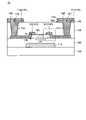
- FIG. 1is a cross-sectional view showing an outline of a semiconductor device according to one embodiment of the present invention.
- FIG. 2is a plan view showing an outline of a semiconductor device according to one embodiment of the present invention.
- FIG. 3is a partially enlarged cross-sectional view of a semiconductor device according to an embodiment of the present invention.
- the semiconductor device 10is provided above the substrate 100 .
- the semiconductor device 10includes a first gate electrode 110, a first gate insulating layer 120, a first oxide semiconductor layer 130, a first source electrode 141, a first drain electrode 143, a first insulating layer 150, an oxide layer 160, a first It has one source wiring 171 and a first drain wiring 173 .
- these electrodesmay be referred to as a pair of first electrodes 140 or simply as the first electrodes 140 .
- the first electrodes 140refer to a pair of first electrodes 140 unless otherwise specified.
- the first source wiring 171 and the first drain wiring 173are not particularly distinguished, these wirings may be referred to as the first conductive layer 170 .
- a first gate electrode 110is provided on the substrate 100 .
- the first gate electrode 110faces the first oxide semiconductor layer 130 .
- the first gate insulating layer 120is provided between the first gate electrode 110 and the first oxide semiconductor layer 130 .
- the first gate electrode 110 and the first gate insulating layer 120are provided below the first oxide semiconductor layer 130 .
- the first electrode 140is provided on the first gate insulating layer 120 and the first oxide semiconductor layer 130 .
- the first electrode 140extends from the upper surface of the first gate insulating layer 120 to the pattern edge of the first oxide semiconductor layer 130 and continues to the upper surface of the first oxide semiconductor layer 130 . That is, the first electrode 140 is in contact with the first oxide semiconductor layer 130 from above the first oxide semiconductor layer 130 .
- the top surface of the first oxide semiconductor layer 130can be called a first surface 137 and the bottom surface thereof can be called a second surface 138 .
- the first electrode 140is in contact with the first surface 137 of the first oxide semiconductor layer 130 .
- the first oxide semiconductor layer 130has a channel region 131 between the first source electrode 141 and the first drain electrode 143 .
- the first oxide semiconductor layer 130 in the channel region 131is exposed from the first source electrode 141 and the first drain electrode 143 . That is, each of the first source electrode 141 and the first drain electrode 143 is in contact with the first oxide semiconductor layer 130 at the end of the channel region 131 .
- the first insulating layer 150covers the first oxide semiconductor layer 130 and the first electrode 140 . Specifically, the first insulating layer 150 covers the first surface 137 of the first oxide semiconductor layer 130 sandwiched between the pair of first electrodes 140 .
- First openings 151 and 153are provided in the first insulating layer 150 .
- the first opening 151is an opening reaching the first source electrode 141 .
- the first opening 153is an opening reaching the first drain electrode 143 .
- An oxide layer 160is provided over the first insulating layer 150 .
- Second openings 161 and 163are provided in the oxide layer 160 .
- the second opening 161is an opening continuous with the first opening 151 .
- the second opening 163is an opening continuous with the first opening 153 .
- the first conductive layer 170is provided on the oxide layer 160 and inside the first openings 151 and 153 .
- the first conductive layer 170is provided in the same region as the oxide layer 160 except for regions where the first openings 151 and 153 are present. That is, the oxide layer 160 is not provided in a region where the first conductive layer 170 is not provided in plan view, and the first insulating layer 150 is exposed from the oxide layer 160 .
- the first conductive layer 170is in contact with the first electrode 140 at the bottoms of the first openings 151 and 153 .
- the first conductive layer 170is electrically connected to the first oxide semiconductor layer 130 through the first electrode 140 .
- the semiconductor device 10a configuration using a bottom-gate transistor in which a gate electrode is provided below an oxide semiconductor layer is exemplified, but the configuration is not limited to this.
- the first oxide semiconductor layer 130is provided inside the first gate electrode 110 in plan view.
- the first oxide semiconductor layer 130is provided inside the first gate electrode 110 in the region where the channel of the semiconductor device 10 is formed.
- the outer edge of the pattern of the first oxide semiconductor layer 130is surrounded by the outer edge of the pattern of the first gate electrode 110 in plan view.
- the first electrode 140crosses the first oxide semiconductor layer 130 in plan view.
- the first electrode 140crosses the first oxide semiconductor layer 130 .
- the second opening 161overlaps the first opening 151 in plan view.
- the second opening 163overlaps the first opening 153 in plan view.
- FIG. 3is an enlarged view of the area surrounded by the dotted line frame in FIG.
- a nitrogen-containing region 139exists near the upper surface of the first oxide semiconductor layer 130 (the surface of the first oxide semiconductor layer 130 on the first insulating layer 150 side) in the channel region 131 .
- the nitrogen-containing region 139exists within 2 nm, 3 nm, or 5 nm in the depth direction from the top surface of the first oxide semiconductor layer 130 .
- the nitrogen-containing region 139contains nitrogen in addition to the main component elements of the first oxide semiconductor layer 130 .
- the composition ratio of nitrogen in the nitrogen-containing region 139is 2% or more, 4% or more, or 6% or more.
- the first oxide semiconductor layer 130is formed in a region near the end of at least one of the pair of first electrodes 140 (particularly on the first source electrode 141 side) by the first oxidation.
- the first oxide semiconductor layer 130In the depth direction from the upper surface (first surface 137) of the semiconductor layer 130, there is a region having a nitrogen composition ratio of 2% or more within a range of 2 nanometers. With this configuration, the reliability of the semiconductor device 10 can be improved.
- the end portion of the channel region 131 on the side of the first electrode 140 and the end portion of the first electrode 140 on the side of the channel region 131are at substantially the same position, but the configuration is not limited to this. For example, the channel region 131 and the first electrode 140 may be separated.
- a method for introducing nitrogen into the nitrogen-containing region 139there is a method in which plasma treatment is performed while the top surface of the first oxide semiconductor layer 130 is exposed.
- a first gate electrode 110 , a first gate insulating layer 120 , a first oxide semiconductor layer 130 , and a first electrode 140are formed over a substrate 100 , and the first electrode 140 is etched to form a first gate electrode 140 of a channel region 131 .
- the oxide semiconductor layer 130is exposed.
- Plasma treatment using a nitrogen-containing gasis performed on the surface of the first oxide semiconductor layer 130 exposed from the first electrode 140, so that nitrogen is introduced into the vicinity of the surface of the first oxide semiconductor layer 130. be.
- the nitrogen-containing region 139is formed by performing plasma processing using N 2 O gas (hereinafter referred to as “N 2 O plasma processing”) as the plasma processing.
- N 2 O plasma processingN 2 O gas
- the composition ratio of nitrogen in the nitrogen-containing region 139is determined by controlling the treatment time of the N 2 O plasma treatment.
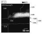
- FIG. 4is a cross-sectional STEM (Scanning Transmission Electron Microscope) image of a semiconductor device according to an embodiment of the present invention.
- the first gate insulating layer 120 and the first insulating layer 150are displayed in black, the first oxide semiconductor layer 130 is displayed in white, and the first electrode 140 is displayed in gray. It is
- the composition analysis of the nitrogen-containing region 139is performed by EDX (Energy Dispersive X-ray spectrometry; energy dispersive X-ray spectrometer) provided in the STEM.
- EDXElectronicgy Dispersive X-ray spectrometry; energy dispersive X-ray spectrometer
- the STEM image shown in FIG. 4is subjected to EDX analysis of 256 points vertically and horizontally.
- the composition ratio of the region specified by the specified line 201 and line extraction width 202 shown belowis calculated.
- the equipment and measurement conditions used for STEM observation and EDX analysis of the nitrogen-containing region 139are as follows.
- the apparatus and conditions shown beloware merely examples, and the present invention is not limited to observations and analyzes conducted under the following apparatus and conditions.
- Calculation of the composition ratiois performed for each point on the designated line 201 in FIG. In the calculation performed at each point of the specified line 201, the EDX spectral data in the range specified by the line extraction width 202 are integrated.
- the analysis results beloware the results of measurements performed including the first insulating layer 150, the first oxide semiconductor layer 130, and the first gate insulating layer 120, as shown in FIG.
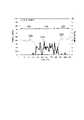
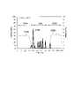
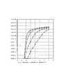
- FIG. 5is a diagram showing the results of composition analysis of the semiconductor device of the comparative example.
- FIG. 6is an enlarged view of the vicinity of the boundary between the first insulating layer 150Z and the first oxide semiconductor layer 130Z in FIG.
- the horizontal axis (“Thk.”) in FIGS. 5 and 6indicates the position of the designated line 201 in the thickness direction.
- the vertical axes in FIGS. 5 and 6indicate the silicon composition ratio (left vertical axis) or the nitrogen composition ratio (right vertical axis).
- 5 and 6show two types of spectra, the spectrum 219Z indicated by a relatively thick line is a spectrum indicating the composition ratio of nitrogen, and the spectrum 229Z indicated by a relatively thin line is a spectrum showing the composition ratio of silicon.
- silicon oxideis used for the first gate insulating layer 120Z and the first insulating layer 150Z
- IGZOis used for the first oxide semiconductor layer 130Z.
- the silicon composition ratio(spectrum 229Z) changes abruptly.
- Nitrogen(spectrum 219Z) is detected in the first oxide semiconductor layer 130Z. In the comparative example of FIG. 5, nitrogen is detected near the center of the first oxide semiconductor layer 130Z.
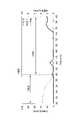
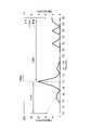
- FIG. 7is a diagram showing the results of composition analysis of the semiconductor device according to one embodiment of the present invention.
- FIG. 8is an enlarged view of the vicinity of the boundary between the first insulating layer 150 and the first oxide semiconductor layer 130 in FIG. In the following description, the description of points that overlap with those in FIGS. 5 and 6 will be omitted.
- nitrogenis detected near the boundary between the first insulating layer 150 and the first oxide semiconductor layer 130 in the semiconductor device 10 .
- the nitrogen composition ratiois within a range (nitrogen-containing region 139) of 2 nm or less. There is an area of about 2 percent (1.88 percent is the correct value in the graph of FIG. 8) or more.
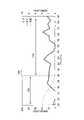
- FIG. 9is a diagram showing the results of composition analysis of the semiconductor device according to one embodiment of the present invention.
- the semiconductor device 10is an enlarged view of the vicinity of the boundary between the first insulating layer 150A and the first oxide semiconductor layer 130A in FIG.
- the semiconductor device 10Ahas substantially the same configuration as the semiconductor device 10 shown in FIGS. 7 and 8, but the conditions for introducing nitrogen into the first oxide semiconductor layer 130A are different. As a result, the composition ratio of nitrogen in the nitrogen-containing region 139A of the semiconductor device 10A is higher than the composition ratio of nitrogen in the nitrogen-containing region 139 of the semiconductor device 10A.
- the composition ratio of nitrogen in the vicinity of the boundary between the first insulating layer 150A and the first oxide semiconductor layer 130Ais the same as that of the first insulating layer 150 of the semiconductor device 10 and the first oxide semiconductor layer 130A. It is larger than the composition ratio of nitrogen in the vicinity of the boundary with the semiconductor layer 130 .
- the nitrogen composition ratiois within a range of 2 nm (the nitrogen-containing region 139A). There is an area of 6 percent or more (6.09 percent is the correct value in the graph of FIG. 10).
- FIGS. 11 to 13are diagrams showing the results of reliability tests performed on the semiconductor devices of the comparative example and the present embodiment.
- the reliability tests shown in FIGS. 11 to 13are tests for evaluating NBTS (Negative Bias Thermal Stress) reliability.
- the conditions for the NBTS reliability testare as follows. ⁇ Light irradiation conditions: No irradiation (dark room) ⁇ Gate voltage: -40V ⁇ Source and drain voltage: 0V ⁇ Stage temperature during stress application: 125°C
- the reason why the reliability of the semiconductor device shown in FIGS.It is believed that there is. That is, it is considered that the higher the composition ratio of nitrogen in the nitrogen-containing regions 139 and 139A, the greater the effect of improving reliability.
- Defectsmay occur on the upper surface of the first oxide semiconductor layer 130 due to the influence of the processes such as film formation and etching of the first electrode 140 . Although the details will be described later, it is considered that the deterioration in reliability caused by the reliability test described above is caused by defects formed on the upper surface of the first oxide semiconductor layer 130 due to the acceptor level. It is considered that introduction of nitrogen into the first oxide semiconductor layer 130 having a defect in the acceptor level reduces the acceptor level and improves the deterioration of reliability.
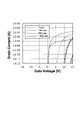
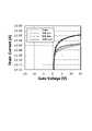
- FIG. 14 and 16are diagrams showing models of simulations performed on a semiconductor device according to an embodiment of the present invention.
- 15 and 17are diagrams showing simulation results performed on a semiconductor device according to an embodiment of the present invention.
- SiOcorresponds to the first gate insulating layer 120 in FIG. 1
- OScorresponds to the first oxide semiconductor layer 130 in FIG. It corresponds to the electrode 140
- PASScorresponds to the first insulating layer 150 .
- an acceptor level defect region(defect doping) is set on the surface of the OS.
- “defect doping”is set for the OS of the entire channel region 131 and the region corresponding to the vicinity of the upper surface of the first oxide semiconductor layer 130 .
- “Defect Doping”is set only for the OS of the region corresponding to the vicinity of the end portion of the first electrode 140 (S/D) in the channel region 131 .
- FIG. 15shows the results of a simulation performed under the conditions that "Defect Doping" is zero (STD), 5 ⁇ 10 18 cm ⁇ 2 , 5 ⁇ 10 19 cm ⁇ 2 , and 5 ⁇ 10 20 cm ⁇ 2 . .
- STDthe conditions for each defect density in "Defect Doping".
- a flexible substrate containing a resin and having flexibilitysuch as a polyimide substrate, an acrylic substrate, a siloxane substrate, or a fluororesin substrate, can be used.
- impuritiesmay be introduced into the above resin.
- the substrate 100does not have to be transparent, so impurities that degrade the transparency of the substrate 100 can be used.
- the substrate 100when the substrate 100 does not need to be flexible, a rigid substrate that transmits light and does not have flexibility, such as a glass substrate, a quartz substrate, or a sapphire substrate, can be used as the substrate 100 .
- the substrate 100may be a semiconductor substrate such as a silicon substrate, a silicon carbide substrate, or a compound semiconductor substrate, or a conductive substrate such as a stainless steel substrate having translucency. A substrate without a film can be used.
- first gate electrode 110the first electrode 140, and the first conductive layer 170.
- these membersinclude aluminum (Al), titanium (Ti), chromium (Cr), cobalt (Co), nickel (Ni), molybdenum (Mo), hafnium (Hf), tantalum (Ta), tungsten (W), bismuth (Bi), silver (Ag), and alloys or compounds thereof are used.
- the above materialsmay be used in a single layer or in a stacked layer.
- the metal element forming the first electrode 140 in contact with the first oxide semiconductor layer 130 among the first electrodes 140is more stable than the oxide of the metal element forming the first oxide semiconductor layer 130 . That is, when there are a plurality of metal elements forming the first oxide semiconductor layer 130, the first electrode in contact with the first oxide semiconductor layer 130 is determined by the Gibbs free energy ( ⁇ G f ) of the metal oxide of each of the plurality of metal elements. It is preferable that the Gibbs free energy of the metal oxide of the metal element forming 140 is smaller.
- IGZOwhen IGZO is used as the first oxide semiconductor layer 130, Ti can be used as a metal in contact with IGZO.
- the Gibbs free energy of indium oxideis larger than the Gibbs free energy of each of Ga oxide and Zn oxide. In other words, indium oxide is chemically unstable and easily reduced.
- the Gibbs free energy of Ti oxideis sufficiently smaller than the Gibbs free energy of each of Ga oxide and Zn oxide, when Ti is formed on IGZO, Ti combines with oxygen in IGZO to form Ti oxide. Form. Since indium oxide is easily reduced as described above, when high energy is supplied while IGZO and Ti are in contact with each other, indium oxide is reduced and Ti is oxidized.
- Common insulating layer materialscan be used as the first gate insulating layer 120 and the first insulating layer 150 .
- these insulating layersinclude silicon oxide (SiO x ), silicon oxynitride (SiO x N y ), silicon nitride (SiN x ), silicon oxynitride (SiN x O y ), aluminum oxide (AlO x ), oxide Inorganic insulating layers such as aluminum nitride (AlO x N y ), aluminum oxynitride (AlN x O y ), and aluminum nitride (AlN x ) can be used. An insulating layer with few defects can be used as these insulating layers.
- the composition ratio of oxygen in the first insulating layer 150is compared with the composition ratio of oxygen in an insulating layer having the same composition as the first insulating layer 150 (hereinafter referred to as “another insulating layer”), the other The oxygen composition ratio in the first insulating layer 150 is closer to the stoichiometric ratio for the insulating layer having the same composition as the first insulating layer 150 than the oxygen composition ratio in the insulating layer.
- SiO x N y and AlO x N yare silicon compounds and aluminum compounds containing nitrogen (N) in a proportion (x>y) smaller than that of oxygen (O). Also, SiN x O y and AlN x O y are silicon compounds and aluminum compounds containing a smaller proportion of oxygen than nitrogen (x>y).
- a metal oxide having semiconductor propertiescan be used as the first oxide semiconductor layer 130 .
- an oxide semiconductor containing indium (In), gallium (Ga), zinc (Zn), and oxygen (O)can be used.
- the oxide semiconductor containing In, Ga, Zn, and O used in this embodimentis not limited to the above composition, and an oxide semiconductor having a composition different from the above can also be used.
- the ratio of Inmay be increased to improve mobility.
- the ratio of Gamay be made larger than the above in order to increase the bandgap and reduce the influence of light irradiation.
- oxide semiconductor containing In, Ga, Zn, and Omay be added.
- metal elementssuch as Al and Sn may be added.
- an oxide semiconductor containing In and Ga (IGO), an oxide semiconductor containing In and Zn (IZO), an oxide semiconductor containing In, Sn and Zn (ITZO), and In and Wcan be used as the first oxide semiconductor layer 130 .
- the first oxide semiconductor layer 130may be amorphous or crystalline.
- the first oxide semiconductor layer 130may have a mixed phase of amorphous and crystal.
- the oxide layer 160an oxide semiconductor layer having the same composition as the first oxide semiconductor layer 130, an oxide conductive layer such as ITO, or an oxide of SiOx , SiOxNy , AlOx , AlOxNy , or the like .
- a material insulating layercan be used.
- the oxide layer 160is preferably formed by a sputtering method.
- the process gas used for sputteringremains in the film of the oxide layer 160 .
- Aris used as a sputtering process gas, Ar may remain in the oxide layer 160 .
- the remaining Arcan be detected by SIMS (Secondary Ion Mass Spectrometry) analysis of the oxide layer 160 .
- SIMSSecondary Ion Mass Spectrometry
- FIG. 18A semiconductor device according to an embodiment of the present invention will be described with reference to FIGS. 18 to 33.
- FIG. The semiconductor devices of the embodiments described beloware used in integrated circuits (ICs) such as microprocessors (Micro-Processing Units (MPUs)) or memory circuits in addition to transistors used in display devices. good too.
- ICsintegrated circuits
- MPUsMicro-Processing Units
- FIG. 18is a partially enlarged cross-sectional view of a semiconductor device according to an embodiment of the present invention.
- FIG. 18corresponds to an enlarged view of the area surrounded by the dotted line frame in FIG.
- the first electrode 140Bhas a first conductive layer 145B, a second conductive layer 147B, and a third conductive layer 149B.
- An oxidized portion 180Bis provided at the pattern end portion of the first electrode 140B.
- the oxidation portion 180Bis provided above the first oxide semiconductor layer 130B.
- the oxide portion 180Bis the oxide of the first electrode 140B.
- the oxidation portion 180Bincludes a first oxidation portion 185B and a third oxidation portion 189B.
- the first oxide portion 185Bis provided at the end of the first conductive layer 145B and is an oxide of the first conductive layer 145B.
- the third oxide portion 189Bis provided at the end of the third conductive layer 149B and is an oxide of the third conductive layer 149B.
- the first oxidation portion 185Bhas conductivity.
- the first oxidation portion 185Bis positioned closer to the channel region 131B than the pattern end of the second conductive layer 147B.
- the configuration in which the oxide of the second conductive layer 147B is not providedis exemplified, but the oxide of the second conductive layer 147B is between the first oxide portion 185B and the third oxide portion 189B.
- a second oxidation sectionmay be provided. That is, the second oxidation portion may be provided at the end of the second conductive layer 147B.
- the second oxidation portionis formed in the manufacturing process of the semiconductor device 10B, but is removed in the subsequent process, so that the structure shown in FIG. 18 is formed.
- the first oxidation portion 185Bdoes not have to be conductive.
- a channel region 131B, a first region 133B, and a second region 135Bare provided in the first oxide semiconductor layer 130B.
- the channel region 131Bis a region where the first electrode 140B is not provided above the first oxide semiconductor layer 130B.
- the oxidized portion 180Bis provided above the first oxide semiconductor layer 130B in the channel region 131B. That is, the oxidized portion 180B overlaps the channel region 131B in plan view.
- the vicinity of the end of the first electrode 140B on the oxidized portion 180B sideoverlaps with a part of the channel region 131B in a plan view.
- the first electrode 140Bdoes not have to overlap the channel region 131B in plan view.
- the first region 133B and the second region 135Bare regions where the first electrode 140B is provided above the first oxide semiconductor layer 130B.
- the channel region 131Bis a region where the first oxide semiconductor layer 130B is exposed from the first electrode 140B in plan view.
- the first region 133B and the second region 135Bare regions where the first oxide semiconductor layer 130B overlaps with the first electrode 140B in plan view.
- the oxide portion 180Bis not provided above the first oxide semiconductor layer 130B in the first region 133B and the second region 135B.
- the first region 133Bis provided over substantially the entire region where the first oxide semiconductor layer 130B overlaps with the first electrode 140B.
- the second region 135Bis provided at a position farther from the oxidation portion 180B in plan view than the first region 133B. That is, there is a region below the first electrode 140B where the second region 135B is not provided.
- the channel region 131B, first region 133B, and second region 135Bare each formed from one oxide semiconductor layer. All of these regions have the same composition and the same crystal state in the state immediately after film formation. However, the composition and crystal state of the first oxide semiconductor layer 130B in each of the above regions are different due to the influence of the manufacturing process of the semiconductor device 10B.
- Indium contained in the first oxide semiconductor layer 130Bis unevenly distributed in the first oxide semiconductor layer 130B in the first region 133B and the second region 135B.
- indiumis not unevenly distributed in the first oxide semiconductor layer 130B in the channel region 131B.
- Whether or not indium is unevenly distributed in the first oxide semiconductor layer 130Bmay differ depending on the evaluation method and evaluation accuracy. If it is determined that indium is unevenly distributed in the first oxide semiconductor layer 130B in the channel region 131B, the degree of uneven distribution of indium in the first oxide semiconductor layer 130B in the channel region 131B is higher than that in the first region 133B. and the degree of uneven distribution of indium in the first oxide semiconductor layer 130B in the second region 135B is greater. The degree of uneven distribution of indium in the first oxide semiconductor layer 130B in the second region 135B is greater than the degree of uneven distribution of indium in the first oxide semiconductor layer 130B in the first region 133B.
- the degree of uneven distribution of indiumis large, which means that the size of a region with a high indium concentration (high-concentration region) is large compared to other regions, or the size of crystallized indium compared to other regions ( or crystal grain size) is large.
- the degree of uneven distribution of indiumcan be measured, for example, by a cross-sectional TEM (Transmission Electron Microscope) image, a cross-sectional STEM (Scanning Transmission Electron Microscope) image, or a cross-sectional SEM (Scanning Electron Microscope) image. ) can be judged by the image. For example, when the contrast of the first oxide semiconductor layer 130B in the first region 133B and the second region 135B is higher than that of the first oxide semiconductor layer 130B in the channel region 131B, the first oxide semiconductor layer 130B in the channel region 131B It can be determined that the degree of uneven distribution of indium is greater in the first oxide semiconductor layer 130B in the first region 133B and the second region 135B than in the semiconductor layer 130B.
- FIGS. 19 to 22are cross-sectional views showing a method of manufacturing a semiconductor device according to one embodiment of the present invention.
- the manufacturing methodan example in which Ti is used for the first conductive layer 145B and the third conductive layer 149B and Al is used for the second conductive layer 147B will be described.
- the pattern of the first oxide semiconductor layer 130Bis formed on the first gate insulating layer 120B provided on the first gate electrode 110B (see FIG. 1), and the pattern of the first electrode 140B is formed. form a pattern.
- a pattern end portion of the first electrode 140Bis located on the first oxide semiconductor layer 130B. Since a general semiconductor process can be used for the manufacturing method up to the structure shown in FIG. 19, detailed description thereof will be omitted.
- N 2 O plasma treatmentis performed as the plasma treatment.
- the N 2 O plasma treatmentis performed on at least the pattern edge of the first electrode 140B.
- an oxidized portion 180Bis formed at the end of the first electrode 140B by the N 2 O plasma treatment.
- the first oxidized portion 185Bis formed at the end of the first conductive layer 145B
- the second oxidized portion 187Bis formed at the end of the second conductive layer 147B
- the end of the third conductive layer 149Bis formed.
- a third oxidation portion 189Bis formed.
- the upper portion of the third conductive layer 149Bwhich is the uppermost layer of the first electrode 140B, is also oxidized by the N 2 O plasma treatment, it is omitted for convenience of explanation.
- the second oxidized portion 187B of the oxidized portion 180Bdisappears in the process until the first insulating layer 150B covering the first electrode 140B is formed. As a result, as shown in FIG. 22, only the first oxidized portion 185B and the third oxidized portion 189B remain at the end of the first electrode 140B.
- the first insulating layer 150Bmay be formed over the structure of FIG. 21 without the second oxidation portion 187B disappearing.
- indiumis segregated in the first oxide semiconductor layer 130B in a region overlapping with the first electrode 140B in plan view.
- FIGS. 23 to 28are cross-sectional images of the samples before the reliability test is performed after the semiconductor device 10B is manufactured.
- FIG. 23is a cross-sectional TEM image of a semiconductor device according to one embodiment of the present invention.
- Tiwas used for the first conductive layer 145B and the third conductive layer 149B
- Alwas used for the second conductive layer 147B
- IGZOwas used for the first oxide semiconductor layer 130B. Structures are shown.
- the first conductive layer 145B (Ti) and the second conductive layer 147B (Al)have different patterns in a cross-sectional view due to their different crystal states.
- the region over which the first electrode 140B is not providedis the channel region 131B
- the regions over which the first electrode 140B is providedare the first region 133B and the second region 135B. corresponds to A mixed crystal region is formed by reaction of Ti and Al between the first conductive layer 145B and the second conductive layer 147B.
- the dotted line connecting the first conductive layer 145B and the third conductive layer 149Bis the location where the end of the second conductive layer 147B is presumed to have existed based on the shapes of these conductive layers. As described above, at least part of the second conductive layer 147B disappears, resulting in a shape as shown in FIG.
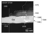
- FIG. 24is a cross-sectional HAADF (High-Angle Annular Dark Field)-STEM image of a semiconductor device according to one embodiment of the present invention.
- FIG. 24is an enlarged STEM image of a part of FIG.
- FIG. 24shows part of the first oxide semiconductor layer 130B, the first conductive layer 145B, and the second conductive layer 147B.
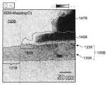
- 25 to 28are EDX mapping measurement results of the semiconductor device according to one embodiment of the present invention.
- FIG. 25shows the EDX mapping measurement results of Ti.
- FIG. 26shows the EDX mapping measurement result of O.
- FIG. FIG. 27shows the EDX mapping measurement results of In.
- FIG. 28shows the EDX mapping measurement results of Al.
- regions where the first oxide semiconductor layer 130B, the first conductive layer 145B, and the second conductive layer 147B are providedare indicated by dotted lines.
- Tiis detected from the area surrounded by the dotted line indicating the first conductive layer 145B, but near the left end of the dotted line, the signal intensity of Ti is smaller than other areas. , the signal intensity of oxygen is large. That is, a first oxidation portion 185B (Ti oxide) is formed at the left end of the first conductive layer 145B.
- the first oxidized portion 185Bhas a partially chipped shape (concave shape in this embodiment). 25 and 26, oxygen is detected from the lower region of the first conductive layer 145B. That is, Ti oxide is formed under Ti.
- dark region 210Bin the contrast of the STEM image in FIG. is a region with a high concentration of A region darker than other regions in FIG. 24 (hereinafter referred to as “dark region 210B”) is a region having a lower indium concentration than other regions as shown in FIG.
- the size of the cluster of bright regions 200B in the second region 135Bis larger than the size of the cluster of bright regions 200B in the first region 133B.
- the channel region 131Bno distinct clusters of bright regions 200B and dark regions 210B are observed, so it is determined that indium is not unevenly distributed.
- a bright region with a small sizeis also confirmed in the first region 133B, but this is because oxygen in the oxide semiconductor is reduced in the surface layer of the first oxide semiconductor layer 130B during the film formation of Ti or in a process after the Ti film formation. , it is considered that a region with a high concentration of indium was partially formed.
- the degree of uneven distribution of indium in the first oxide semiconductor layer 130B in the channel region 131Bis higher than the degree of uneven distribution of indium in the first oxide semiconductor layer 130B in the first region 133B and the second region 135B.
- the indium of the first oxide semiconductor layer 130Bis not unevenly distributed in the region overlapping with the first oxide portion 185B in plan view.
- the degree of uneven distribution of indium in the first oxide semiconductor layer 130B in the second region 135Bis greater than the degree of uneven distribution of indium in the first oxide semiconductor layer 130B in the first region 133B.
- the uneven distribution of indiumis caused by the crystallization of indium. Therefore, the crystal grain size of indium unevenly distributed in the first oxide semiconductor layer 130B in the second region 135B is larger than the crystal grain size of indium unevenly distributed in the first oxide semiconductor layer 130B in the first region 133B. be able to.
- the region where indium is unevenly distributed in the second region 135Bdoes not reach the end of the first conductive layer 145B on the side of the channel region 131B. In other words, in this state, an abnormality in rising of the ON current of the semiconductor device 10B does not occur.
- the area in which oxygen is not detected and the area in which Al is detectedsubstantially match.
- Al oxide on the order of several nanometersexists at the end of the second conductive layer 147B.
- FIG. 29 to 33A display device using a semiconductor device according to an embodiment of the present invention will be described with reference to FIGS. 29 to 33.
- FIG. 29 to 33configurations in which the semiconductor devices described in the first and second embodiments are applied to a circuit of a liquid crystal display device will be described.
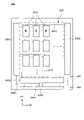
- FIG. 29is a plan view showing an outline of a display device according to one embodiment of the invention.
- the display device 20Chas an array substrate 300C, a sealing portion 400C, a counter substrate 500C, a flexible printed circuit board 600C (FPC600C), and an IC chip 700C.
- the array substrate 300C and the counter substrate 500Care bonded together by a seal portion 400C.
- a plurality of pixel circuits 310Care arranged in a matrix in the liquid crystal region 22C surrounded by the seal portion 400C.
- the liquid crystal region 22Cis a region that overlaps with a liquid crystal element 410C, which will be described later, in plan view.
- the seal region 24C provided with the seal portion 400Cis the region surrounding the liquid crystal region 22C.
- the FPC 600Cis provided in the terminal area 26C.
- the terminal area 26Cis an area where the array substrate 300C is exposed from the counter substrate 500C, and is provided outside the seal area 24C.
- the outside of the sealing area 24Cmeans the outside of the area where the sealing portion 400C is provided and the area surrounded by the sealing portion 400C.
- IC chip 700Cis provided on FPC 600C.
- the IC chip 700Csupplies signals for driving each pixel circuit 310C.
- FIG. 30is a block diagram showing the circuit configuration of the display device according to one embodiment of the invention.
- a source driver circuit 320Cis provided at a position adjacent to the liquid crystal region 22C in which the pixel circuit 310C is arranged in the D1 direction (column direction).
- a gate driver circuit 330Cis provided at a position adjacent (in the row direction).
- a source driver circuit 320C and a gate driver circuit 330Care provided in the seal region 24C.
- the region where the source driver circuit 320C and the gate driver circuit 330C are providedis not limited to the seal region 24C, and may be any region outside the region where the pixel circuit 310C is provided.
- a source wiring 321Cextends in the D1 direction from the source driver circuit 320C and is connected to a plurality of pixel circuits 310C arranged in the D1 direction.
- a gate wiring 331Cextends in the D2 direction from the gate driver circuit 330C and is connected to a plurality of pixel circuits 310C arranged in the D2 direction.
- a terminal portion 333Cis provided in the terminal region 26C.
- the terminal portion 333C and the source driver circuit 320Care connected by a connection wiring 341C.
- the terminal portion 333C and the gate driver circuit 330Care connected by a connection wiring 341C.
- the semiconductor devices 10 and 10A shown in the first and second embodimentsare applied to transistors included in the pixel circuit 310C, source driver circuit 320C, and gate driver circuit 330C.
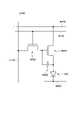
- FIG. 31is a circuit diagram showing a pixel circuit of a display device according to one embodiment of the invention.
- pixel circuit 310Cincludes elements such as transistor 800C, storage capacitor 890C, and liquid crystal element 410C.
- Transistor 800Chas a first gate electrode 810C, a first source electrode 830C, and a first drain electrode 840C.
- the first gate electrode 810Cis connected to the gate wiring 331C.
- the first source electrode 830Cis connected to the source wiring 321C.
- the first drain electrode 840Cis connected to the storage capacitor 890C and the liquid crystal element 410C.
- the semiconductor devices 10 and 10A shown in the first and second embodimentsare applied to the transistor shown in FIG.
- 830Cis referred to as a source electrode and 840C is referred to as a drain electrode, but the source and drain functions of each electrode may be interchanged.
- FIG. 32is a cross-sectional view of a display device according to an embodiment of the invention.
- the display device 20Cis a display device provided with transistors 800C and 900C having different structures on the same substrate.
- the structure of transistor 800Cdiffers from that of transistor 900C.
- the transistor 800Cis a bottom-gate transistor in which the first oxide semiconductor layer 820C is used as a channel.
- the transistor 900Cis a top-gate transistor using the semiconductor layer 920C as a channel.
- transistor 800Cis used in pixel circuit 310C
- transistor 900Cis used in source driver circuit 320C and gate driver circuit 330C. Note that the transistor 900C may be used in the pixel circuit 310C.
- the transistor 800Cis a transistor formed on the substrate 301C and having one or more insulating layers as a base layer.
- the insulating layers 340C, 342C, 344C, and 346Care used as underlying layers.
- a first gate electrode 810Cis provided on the insulating layer 346C.
- a first oxide semiconductor layer 820Cis provided above the first gate electrode 810C.
- the first gate electrode 810Cfaces the first oxide semiconductor layer 820C.
- An insulating layer 348C functioning as a gate insulating layeris provided between the first gate electrode 810C and the first oxide semiconductor layer 820C.
- a first source electrode 830Cis provided at one end of the pattern of the first oxide semiconductor layer 820C, and a first drain electrode 840C is provided at the other end.
- the first source electrode 830C and the first drain electrode 840Care connected to the first oxide semiconductor layer 820C on the top and side surfaces of the first oxide semiconductor layer 820C, respectively.
- First insulating layers 350C and 352Care provided on the first oxide semiconductor layer 820C, the first source electrode 830C, and the first drain electrode 840C. Openings 851C and 861C are provided in the first insulating layers 350C and 352C.
- a first source wiring 850Cis provided on the first insulating layer 352C and inside the opening 851C.
- a first drain wiring 860Cis provided on the first insulating layer 352C and inside the opening 861C.
- An oxide layer 853Cis provided between the upper surface of the first insulating layer 352C and the first source wiring 850C.
- An oxide layer 855Cis provided between the upper surface of the first insulating layer 352C and the first drain wiring 860C.
- a second insulating layer 354Cis provided on the first source wiring 850C and the first drain wiring 860C.
- a common electrode 880Cprovided in common to a plurality of pixels is provided on the second insulating layer 354C.
- a second insulating layer 356Cis provided on the common electrode 880C.
- a third opening 871Cis provided in the second insulating layers 354C and 356C.
- a pixel electrode 870Cis provided on the second insulating layer 356C and inside the third opening 871C. The pixel electrode 870C is connected to the first drain wiring 860C.
- FIG. 33is a plan view of a pixel electrode and a common electrode of a display device according to one embodiment of the invention.
- the common electrode 880Chas an overlapping region that overlaps the pixel electrode 870C in plan view and a non-overlapping region that does not overlap the pixel electrode 870C.
- a horizontal electric fieldis formed from the pixel electrode 870C in the overlapping area toward the common electrode 880C in the non-overlapping area.
- the horizontal electric fieldcauses the liquid crystal molecules contained in the liquid crystal element 410C to operate, thereby determining the gradation of the pixel.
- the semiconductor device 10 of FIG. 1can be applied as the transistor 800C.
- each member in each drawingcorresponds as follows.
- the first gate electrode 110corresponds to the first gate electrode 810C.
- the first gate insulating layer 120corresponds to the insulating layer 348C.
- the first oxide semiconductor layer 130corresponds to the first oxide semiconductor layer 820C.
- the first source electrode 141corresponds to the first source electrode 830C.
- the first drain electrode 143corresponds to the first drain electrode 840C.
- the first insulating layer 150corresponds to the first insulating layers 350C and 352C.
- the first opening 151corresponds to the opening 851C.
- the first opening 153corresponds to the opening 861C.
- Oxide layer 160corresponds to oxide layers 853C and 855C.
- the first source wiring 171corresponds to the first source wiring 850C.
- the first drain wiring 173corresponds to the first drain wiring 860C.
- the transistor 900Cis a transistor formed on the substrate 301C and having an insulating layer 340C as a base layer.
- a light shielding layer 910Cis provided on the insulating layer 340C.
- An insulating layer 342Cis provided on the light shielding layer 910C.
- a semiconductor layer 920Cis provided over the insulating layer 342C.
- a second gate electrode 930Cis provided above the semiconductor layer 920C.
- An insulating layer 344C functioning as a gate insulating layeris provided between the semiconductor layer 920C and the second gate electrode 930C. Insulating layers 346C, 348C, 350C, and 352C are provided on the second gate electrode 930C. Openings 941C and 951C are provided in these insulating layers.
- a second source wiring 940Cis provided on the insulating layer 352C and inside the opening 941C.
- a second drain wiring 950Cis provided on the insulating layer 352C and inside the opening 951C.
- An insulating layer 354Cis provided over the second source wiring 940C and the second drain wiring 950C.
- the second gate electrode 930Cis provided under the same layer (insulating layer 348C) as the gate insulating layer of the transistor 800C.
- FIG. 34A display device using a semiconductor device according to an embodiment of the present invention will be described with reference to FIGS. 34 and 35.
- FIG. 34configurations in which the semiconductor devices described in the first and second embodiments are applied to the circuit of an organic EL display device will be described. Note that the outline and circuit configuration of the display device 20D are the same as those shown in FIGS. 29 and 30, so description thereof will be omitted.
- FIG. 34is a circuit diagram showing a pixel circuit of a display device according to one embodiment of the invention.
- the pixel circuit 310Dincludes elements such as a drive transistor 960D, a selection transistor 970D, a storage capacitor 980D, and a light emitting element DO.
- a source electrode of the selection transistor 970Dis connected to the signal line 971D, and a gate electrode of the selection transistor 970D is connected to the gate line 973D.
- a source electrode of the drive transistor 960Dis connected to the anode power supply line 961D, and a drain electrode of the drive transistor 960D is connected to one end of the light emitting element DO.
- the other end of the light emitting element DOis connected to the cathode power line 963D.
- a gate electrode of the drive transistor 960Dis connected to a drain electrode of the selection transistor 970D.
- the storage capacitor 980Dis connected to the gate and drain electrodes of the driving transistor 960D.
- a gradation signal that determines the light emission intensity of the light emitting element DOis supplied to the signal line 971D.
- the gate line 973Dis supplied with a signal for selecting a pixel row to which the grayscale signal is written.
- FIG. 35is a cross-sectional view of a display device according to an embodiment of the invention.
- the configuration of the display device 20D shown in FIG. 35is similar to that of the display device 20C shown in FIG. differ from 35, the same configuration as that of the display device 20C shown in FIG. 32 will be omitted, and the differences from the display device 20C will be explained.
- the display device 20Dhas a pixel electrode 981D, a light emitting layer 983D, and a common electrode 985D above the insulating layer 354D.
- a pixel electrode 981Dis provided on the insulating layer 354D and inside the third opening 871D.
- An insulating layer 358Dis provided over the pixel electrode 981D.
- An opening 359Dis provided in the insulating layer 358D. Opening 359D corresponds to the light emitting area. That is, the insulating layer 358D defines pixels.
- a light emitting layer 983D and a common electrode 985Dare provided on the pixel electrode 981D exposed by the opening 359D.
- a pixel electrode 981D and a light-emitting layer 983Dare individually provided for each pixel.
- the common electrode 985Dis commonly provided for a plurality of pixels. Different materials are used for the light-emitting layer 983D depending on the display color of the pixel.
- the configurations in which the semiconductor devices described in the first and second embodiments are applied to the liquid crystal display device and the organic EL display deviceare exemplified.
- the semiconductor devicemay be applied to a device (for example, a self-luminous display device other than an organic EL display device or an electronic paper display device).
- the above semiconductor devicecan be applied to a medium-sized display device to a large-sized display device without particular limitation.
Landscapes
- Thin Film Transistor (AREA)
- Engineering & Computer Science (AREA)
- Manufacturing & Machinery (AREA)
Abstract
Description
Translated fromJapanese本発明の実施形態の一つは、半導体装置に関する。特に、本発明の実施形態の一つは、チャネルとして酸化物半導体が用いられた半導体装置に関する。One of the embodiments of the present invention relates to a semiconductor device. In particular, one embodiment of the present invention relates to a semiconductor device using an oxide semiconductor as a channel.
最近、アモルファスシリコン、低温ポリシリコン、および単結晶シリコンに替わり、酸化物半導体をチャネルに用いた半導体装置の開発が進められている(例えば、特許文献1)。酸化物半導体をチャネルに用いた半導体装置は、アモルファスシリコンをチャネルに用いた半導体装置と同様に単純な構造かつ低温プロセスで半導体装置を形成することができる。酸化物半導体をチャネルに用いた半導体装置は、アモルファスシリコンをチャネルに用いた半導体装置よりも高い移動度を有することが知られている。酸化物半導体をチャネルに用いた半導体装置は、オフ電流が非常に低いことが知られている。 Recently, semiconductor devices using oxide semiconductors for channels instead of amorphous silicon, low-temperature polysilicon, and single crystal silicon have been developed (for example, Patent Document 1). A semiconductor device in which an oxide semiconductor is used for a channel can be formed by a simple structure and a low-temperature process similarly to a semiconductor device in which an amorphous silicon is used for a channel. A semiconductor device using an oxide semiconductor for a channel is known to have higher mobility than a semiconductor device using an amorphous silicon for a channel. A semiconductor device using an oxide semiconductor for a channel is known to have a very low off-state current.
酸化物半導体をチャネルに用いた半導体装置が安定した動作をするために、その製造工程において酸化物半導体により多くの酸素を供給し、酸化物半導体に形成される酸素欠損を少なくすることが重要である。酸化物半導体に酸素を供給する方法の一つとして、特許文献1では、酸化物半導体を覆う絶縁層を、当該絶縁層が酸素をより多く含む条件で形成する技術が開示されている。In order for a semiconductor device using an oxide semiconductor for a channel to operate stably, it is important to supply more oxygen to the oxide semiconductor and reduce oxygen vacancies formed in the oxide semiconductor in the manufacturing process. be. As one method for supplying oxygen to an oxide semiconductor,
しかしながら、酸素をより多く含む条件で形成された絶縁層は欠陥を多く含む。その影響で、その欠陥に電子がトラップされることが原因と考えられる半導体装置の特性異常又は信頼性試験における特性変動が発生する。一方、欠陥の少ない絶縁層を用いると、絶縁層に含まれる酸素を多くすることができない。したがって、絶縁層から酸化物半導体に十分に酸素を供給することができない。このように、酸化物半導体を覆う絶縁層として酸素を多く含む絶縁層が用いられた場合であっても、半導体装置の信頼性を向上させるための半導体装置構造及びその製造方法を実現することが要求されている。However, the insulating layer formed under conditions containing more oxygen contains many defects. As a result, an abnormality in the characteristics of the semiconductor device or a variation in characteristics in a reliability test occurs, which is considered to be caused by electrons being trapped in the defects. On the other hand, if an insulating layer with few defects is used, oxygen contained in the insulating layer cannot be increased. Therefore, sufficient oxygen cannot be supplied from the insulating layer to the oxide semiconductor. As described above, even when an insulating layer containing a large amount of oxygen is used as an insulating layer covering an oxide semiconductor, it is possible to realize a semiconductor device structure and a manufacturing method thereof for improving the reliability of the semiconductor device. requested.
本発明の実施形態の一つは、信頼性が高い半導体装置を実現することを課題の一つとする。An object of one embodiment of the present invention is to realize a highly reliable semiconductor device.
本発明の一実施形態に係る半導体装置は、第1面及び前記第1面の反対の第2面を備えた酸化物半導体層と、前記酸化物半導体層に対向するゲート電極と、前記酸化物半導体層と前記ゲート電極との間のゲート絶縁層と、それぞれ前記酸化物半導体層の前記第1面に接する一対の第1電極と、を有し、前記酸化物半導体層は、前記一対の第1電極のうち少なくとも一方の前記第1電極の端部付近の領域において、前記第1面から2ナノメートル以内の深さの範囲内に、窒素の組成比が2パーセント以上の領域を有する。A semiconductor device according to one embodiment of the present invention includes an oxide semiconductor layer having a first surface and a second surface opposite to the first surface; a gate electrode facing the oxide semiconductor layer; a gate insulating layer between the semiconductor layer and the gate electrode; and a pair of first electrodes respectively in contact with the first surface of the oxide semiconductor layer, wherein the oxide semiconductor layer includes the pair of first electrodes. At least one of the electrodes has a region in the vicinity of the end portion of the first electrode with a nitrogen composition ratio of 2% or more within a depth range of 2 nanometers or less from the first surface.
以下に、本発明の各実施の形態について、図面を参照しつつ説明する。以下の開示はあくまで一例にすぎない。当業者が、発明の主旨を保ちつつ、実施形態の構成を適宜変更することによって容易に想到し得る構成は、当然に本発明の範囲に含有される。図面は説明をより明確にするため、実際の態様に比べ、各部の幅、厚さ、形状等について模式的に表される場合がある。しかし、図示された形状はあくまで一例であって、本発明の解釈を限定するものではない。本明細書と各図において、既出の図に関して前述したものと同様の要素には、同一の符号の後にアルファベットを付して、詳細な説明を適宜省略することがある。Each embodiment of the present invention will be described below with reference to the drawings. The following disclosure is by way of example only. Configurations that can be easily conceived by a person skilled in the art by appropriately changing the configurations of the embodiments while maintaining the gist of the invention are naturally included in the scope of the present invention. In order to make the description clearer, the drawings may schematically show the width, thickness, shape, etc. of each part compared to the actual mode. However, the illustrated shape is only an example and does not limit the interpretation of the present invention. In this specification and each figure, elements similar to those described above with respect to previous figures may be given the same reference numerals followed by letters, and detailed description may be omitted as appropriate.
本発明の各実施の形態において、基板から酸化物半導体層に向かう方向を上又は上方という。逆に、酸化物半導体層から基板に向かう方向を下又は下方という。このように、説明の便宜上、上方又は下方という語句を用いて説明するが、例えば、基板と酸化物半導体層との上下関係が図示と逆になるように配置されてもよい。以下の説明で、例えば基板上の酸化物半導体層という表現は、上記のように基板と酸化物半導体層との上下関係を説明しているに過ぎず、基板と酸化物半導体層との間に他の部材が配置されていてもよい。上方又は下方は、複数の層が積層された構造における積層順を意味するものであり、トランジスタの上方の画素電極と表現する場合、平面視でトランジスタと画素電極とが重ならない位置関係であってもよい。一方、トランジスタの鉛直上方の画素電極と表現する場合は、平面視でトランジスタと画素電極とが重なる位置関係を意味する。In each embodiment of the present invention, the direction from the substrate toward the oxide semiconductor layer is referred to as upward. Conversely, the direction from the oxide semiconductor layer to the substrate is called downward. In this way, for convenience of description, the terms "above" and "below" are used, but for example, the substrate and the oxide semiconductor layer may be arranged in a reversed vertical relationship from that shown in the drawing. In the following description, the expression, for example, an oxide semiconductor layer on a substrate, merely describes the vertical relationship between the substrate and the oxide semiconductor layer as described above. Other members may be arranged. "Upper" or "lower" means the order of stacking in a structure in which a plurality of layers are stacked, and when expressing a pixel electrode above a transistor, the positional relationship is such that the transistor and the pixel electrode do not overlap in plan view. good too. On the other hand, the term “pixel electrode vertically above the transistor” means a positional relationship in which the transistor and the pixel electrode overlap in a plan view.
「表示装置」とは、電気光学層を用いて映像を表示する構造体を指す。例えば、表示装置という用語は、電気光学層を含む表示パネルを指す場合もあり、又は表示セルに対して他の光学部材(例えば、偏光部材、バックライト、タッチパネル等)を装着した構造体を指す場合もある。「電気光学層」には、技術的な矛盾が生じない限り、液晶層、エレクトロルミネセンス(EL)層、エレクトロクロミック(EC)層、電気泳動層が含まれ得る。したがって、後述する実施形態について、表示装置として、液晶層を含む液晶表示装置、及び有機EL層を含む有機EL表示装置を例示して説明するが、本実施形態における構造は、上述した他の電気光学層を含む表示装置へ適用することができる。"Display device" refers to a structure that displays images using an electro-optic layer. For example, the term display device may refer to a display panel including an electro-optic layer, or to a structure in which other optical members (e.g., polarizing member, backlight, touch panel, etc.) are attached to the display cell. In some cases. An "electro-optical layer" may include a liquid crystal layer, an electroluminescent (EL) layer, an electrochromic (EC) layer, an electrophoretic layer, unless technically contradictory. Therefore, the embodiments described later will be described by exemplifying a liquid crystal display device including a liquid crystal layer and an organic EL display device including an organic EL layer as display devices. It can be applied to a display device including an optical layer.
本明細書において「αはA、B又はCを含む」、「αはA,B及びCのいずれかを含む」、「αはA,B及びCからなる群から選択される一つを含む」、といった表現は、特に明示が無い限り、αがA~Cの複数の組み合わせを含む場合を排除しない。さらに、これらの表現は、αが他の要素を含む場合も排除しない。In the present specification, "α includes A, B or C", "α includes any one of A, B and C", "α includes one selected from the group consisting of A, B and C ”, does not exclude the case where α includes a plurality of combinations of A to C, unless otherwise specified. Furthermore, these expressions do not exclude the case where α contains other elements.
以下の各実施形態は、技術的な矛盾を生じない限り、互いに組み合わせることができる。The following embodiments can be combined with each other as long as there is no technical contradiction.
〈第1実施形態〉
図1~図17を用いて、本発明の一実施形態に係る半導体装置について説明する。以下に示す実施形態の半導体装置は、表示装置に用いられるトランジスタの他に、例えば、マイクロプロセッサ(Micro-Processing Unit:MPU)などの集積回路(Integrated Circuit:IC)、又はメモリ回路に用いられてもよい。<First Embodiment>
A semiconductor device according to an embodiment of the present invention will be described with reference to FIGS. 1 to 17. FIG. The semiconductor devices of the embodiments described below are used in integrated circuits (ICs) such as microprocessors (Micro-Processing Units (MPUs)) or memory circuits in addition to transistors used in display devices. good too.
[半導体装置10の構成]
図1~図3を用いて、本発明の一実施形態に係る半導体装置10の構成について説明する。図1は、本発明の一実施形態に係る半導体装置の概要を示す断面図である。図2は、本発明の一実施形態に係る半導体装置の概要を示す平面図である。図3は、本発明の一実施形態に係る半導体装置の一部を拡大した断面図である。[Structure of semiconductor device 10]
A configuration of a
図1に示すように、半導体装置10は基板100の上方に設けられている。半導体装置10は、第1ゲート電極110、第1ゲート絶縁層120、第1酸化物半導体層130、第1ソース電極141、第1ドレイン電極143、第1絶縁層150、酸化物層160、第1ソース配線171、及び第1ドレイン配線173を有する。第1ソース電極141及び第1ドレイン電極143を特に区別しない場合、これらの電極を一対の第1電極140又は単に第1電極140という場合がある。以下の説明において、第1電極140という場合、特段の指定がなければ一対の第1電極140を指す。第1ソース配線171及び第1ドレイン配線173を特に区別しない場合、これらの配線を第1導電層170という場合がある。As shown in FIG. 1, the
第1ゲート電極110は基板100の上に設けられている。第1ゲート電極110は第1酸化物半導体層130に対向する。第1ゲート絶縁層120は、第1ゲート電極110と第1酸化物半導体層130との間に設けられている。図1の例では、第1ゲート電極110及び第1ゲート絶縁層120は、第1酸化物半導体層130の下方に設けられている。第1電極140は第1ゲート絶縁層120の上及び第1酸化物半導体層130の上に設けられている。第1電極140は、第1ゲート絶縁層120の上面から第1酸化物半導体層130のパターン端部に乗り上げて、第1酸化物半導体層130の上面まで連続している。つまり、第1電極140は第1酸化物半導体層130の上方から第1酸化物半導体層130に接している。第1酸化物半導体層130の上面を第1面137といい、下面を第2面138ということができる。この場合、第1電極140は第1酸化物半導体層130の第1面137に接するということができる。A
第1酸化物半導体層130は、第1ソース電極141と第1ドレイン電極143との間にチャネル領域131を備えている。チャネル領域131における第1酸化物半導体層130は、第1ソース電極141及び第1ドレイン電極143から露出されている。つまり、第1ソース電極141及び第1ドレイン電極143の各々は、チャネル領域131の端部において、第1酸化物半導体層130に接している。The first
第1絶縁層150は、第1酸化物半導体層130及び第1電極140を覆う。具体的には、第1絶縁層150は一対の第1電極140で挟まれた第1酸化物半導体層130の第1面137を覆う。第1絶縁層150には第1開口151、153が設けられている。第1開口151は第1ソース電極141に達する開口である。第1開口153は第1ドレイン電極143に達する開口である。酸化物層160は第1絶縁層150の上に設けられている。酸化物層160には第2開口161、163が設けられている。第2開口161は第1開口151と連続する開口である。第2開口163は第1開口153と連続する開口である。The first insulating
第1導電層170は酸化物層160の上及び第1開口151、153の内部に設けられている。平面視で、第1開口151、153が存在する領域を除き、第1導電層170は酸化物層160と同じ領域に設けられている。つまり、平面視で第1導電層170が設けられていない領域には酸化物層160は設けられておらず、第1絶縁層150が酸化物層160から露出されている。第1導電層170は第1開口151、153の底部で第1電極140に接している。第1導電層170は、第1電極140を介して第1酸化物半導体層130に電気的に接続されている。The first
本実施形態では、半導体装置10として、ゲート電極が酸化物半導体層の下方に設けられたボトムゲート型トランジスタが用いられた構成を例示するが、この構成に限定されない。例えば、半導体装置10として、ゲート電極が酸化物半導体層の上方に設けられたトップゲート型トランジスタ、又はゲート電極が酸化物半導体層の上方及び下方の両方に設けられたデュアルゲート型トランジスタが用いられてもよい。In this embodiment, as the
図2に示すように、平面視で第1酸化物半導体層130は第1ゲート電極110の内側に設けられている。特に、半導体装置10のチャネルが形成される領域において、第1酸化物半導体層130は第1ゲート電極110の内側に設けられている。換言すると、平面視で第1酸化物半導体層130のパターンの外縁は、第1ゲート電極110のパターンの外縁によって囲まれている。平面視で第1電極140は第1酸化物半導体層130を横切っている。換言すると、第1電極140は第1酸化物半導体層130と交差している。第2開口161は平面視で第1開口151と重なっている。第2開口163は平面視で第1開口153と重なっている。上記の構成はあくまで一実施形態に過ぎず、本発明は上記の構成に限定されない。As shown in FIG. 2, the first
図3は、図1において点線枠で囲まれた領域の拡大図である。図3に示すように、チャネル領域131における第1酸化物半導体層130の上面(第1酸化物半導体層130の第1絶縁層150側の面)付近には窒素含有領域139が存在する。窒素含有領域139は第1酸化物半導体層130の上面からの深さ方向において、2ナノメートル以内、3ナノメートル以内、又は5ナノメートル以内の範囲内に存在する。窒素含有領域139には、第1酸化物半導体層130の主成分元素の他に窒素が含有されている。窒素含有領域139における窒素の組成比は2パーセント以上、4パーセント以上、又は6パーセント以上である。FIG. 3 is an enlarged view of the area surrounded by the dotted line frame in FIG. As shown in FIG. 3 , a nitrogen-containing
詳細は後述するが、第1酸化物半導体層130は、一対の第1電極140のうち少なくとも一方の第1電極140(特に第1ソース電極141側)の端部付近の領域において、第1酸化物半導体層130の上面(第1面137)からの深さ方向において、2ナノメートル以内の範囲内に、窒素の組成比が2パーセント以上の領域を有する。この構成によって、半導体装置10の信頼性を向上させることができる。本実施形態では、チャネル領域131の第1電極140側の端部と、第1電極140のチャネル領域131側の端部とが、ほぼ同じ位置だが、この構成に限定されない。例えば、チャネル領域131と第1電極140とが離隔されていてもよい。Although details will be described later, the first
[窒素含有領域139への窒素の導入方法]
窒素含有領域139へ窒素を導入する方法として、第1酸化物半導体層130の上面が露出された状態でプラズマ処理を行う方法が挙げられる。基板100の上に第1ゲート電極110、第1ゲート絶縁層120、第1酸化物半導体層130、及び第1電極140が形成され、第1電極140がエッチングされて、チャネル領域131の第1酸化物半導体層130が露出される。第1電極140から露出された第1酸化物半導体層130の表面に対して、窒素含有ガスを用いたプラズマ処理が行われることで、第1酸化物半導体層130の表面付近に窒素が導入される。例えば、当該プラズマ処理としてN2Oガスを用いたプラズマ処理(以降、「N2Oプラズマ処理」という)が行われることで、窒素含有領域139が形成される。N2Oプラズマ処理の処理時間が制御されることで、窒素含有領域139における窒素の組成比が決定される。[Method of Introducing Nitrogen into Nitrogen-Containing Region 139]
As a method for introducing nitrogen into the nitrogen-containing
[窒素含有領域139について]
図4~図17を用いて、窒素含有領域139及び当該領域に含まれる窒素が半導体装置10に与える効果について説明する。図4は、本発明の一実施形態に係る半導体装置の断面STEM(Scanning Transmission Electron Microscope;走査型透過電子顕微鏡)像である。図4のSTEM像において、第1ゲート絶縁層120及び第1絶縁層150は黒で表示されており、第1酸化物半導体層130は白で表示されており、第1電極140はグレーで表示されている。[Regarding nitrogen-containing region 139]
The effects of the nitrogen-containing
[窒素含有領域139の分析方法]
窒素含有領域139の組成分析は、STEMに備えられたEDX(Energy Dispersive X-ray spectrometry;エネルギー分散型X線分光分析器)によって行われる。例えば、図4に示すSTEM像について、縦横にそれぞれ256ポイントのEDX分析が行われる。EDX分析によって得られたEDXスペクトルデータに基づき、以下に示す指定ライン201及びライン抽出幅202によって指定された領域の組成比が計算される。[Method for analyzing nitrogen-containing region 139]
The composition analysis of the nitrogen-containing
本実施形態において、窒素含有領域139のSTEM観察及びEDX分析に用いられた装置及び測定条件は以下の通りである。以下に示す装置及び条件は一例であり、本発明は以下の装置及び条件で観察及び分析されたものに限定されない。In this embodiment, the equipment and measurement conditions used for STEM observation and EDX analysis of the nitrogen-containing
[STEM観察]
装置:日本電子製 JEM-ARM200F
条件:加速電圧 200kV
倍率精度 10%[STEM observation]
Device: JEOL JEM-ARM200F
Conditions: acceleration voltage 200 kV
[EDX分析]
装置:日本電子製 JEM-ARM200F
条件:加速電圧 200kV
ビーム径 約0.2nmφ
元素分析装置 JED-2300T
X線検出器 Siドリフト検出器
エネルギー分解能 約140eV
X線取出角 21.9°
立体角 0.98sr
取り込み画素数 256×256[EDX analysis]
Device: JEOL JEM-ARM200F
Conditions: acceleration voltage 200 kV
Beam diameter about 0.2nmφ
Elemental analyzer JED-2300T
X-ray detector Si drift detector Energy resolution about 140 eV
X-ray extraction angle 21.9°
solid angle 0.98sr
Captured pixels 256×256
組成比の計算は、図4の指定ライン201の各点について行われる。指定ライン201の各点において行われる計算において、ライン抽出幅202によって指定された範囲のEDXスペクトルデータが積算される。以下の分析結果は、図4に示すように、第1絶縁層150、第1酸化物半導体層130、及び第1ゲート絶縁層120を含むように測定が行われた結果である。Calculation of the composition ratio is performed for each point on the designated
[比較例における領域139Zの分析結果]
図5及び図6を用いて、比較例の半導体装置に対して酸化物半導体層の組成分析を行った結果を説明する。比較例における半導体装置10Zの構成は本実施形態における半導体装置10の構成とほぼ同じである。したがって、半導体装置10Zの構成を説明する際に図1を参照して説明する。ただし、両者を区別するために、比較例における各構成の符号として、本実施形態における各構成の符号の後に「Z」が追加された符号が付されている。詳細は後述するが、比較例では第1酸化物半導体層130Zの上面に窒素含有領域が形成されていない。したがって、比較例において、本実施形態の窒素含有領域139と同じ領域を領域139Zという。[Results of analysis of
The results of composition analysis of the oxide semiconductor layer of the semiconductor device of the comparative example will be described with reference to FIGS. The configuration of the semiconductor device 10Z in the comparative example is substantially the same as the configuration of the
図5は、比較例の半導体装置について組成分析を行った結果を示す図である。図6は、図5の第1絶縁層150Zと第1酸化物半導体層130Zとの境界付近を拡大した図である。図5及び図6の横軸(「Thk.」)は、指定ライン201の厚さ方向の位置を示す。図5及び図6の縦軸はシリコンの組成比(左の縦軸)又は窒素の組成比(右の縦軸)を示す。図5及び図6には2種類のスペクトルが表示されており、相対的に太い線で表示されたスペクトル219Zは窒素の組成比を示すスペクトルであり、相対的に細い線で表示されたスペクトル229Zはシリコンの組成比を示すスペクトルである。FIG. 5 is a diagram showing the results of composition analysis of the semiconductor device of the comparative example. FIG. 6 is an enlarged view of the vicinity of the boundary between the first insulating
図5及び図6に示す分析結果に係る半導体装置10Zでは、第1ゲート絶縁層120Z及び第1絶縁層150Zとして酸化シリコンが用いられ、第1酸化物半導体層130ZとしてIGZOが用いられた例を示す。第1ゲート絶縁層120Zと第1酸化物半導体層130Zとの境界、及び第1絶縁層150Zと第1酸化物半導体層130Zとの境界において、シリコンの組成比(スペクトル229Z)が急激に変化している。第1酸化物半導体層130Zでは窒素(スペクトル219Z)が検出されている。図5の比較例において、窒素は第1酸化物半導体層130Zの中央付近において検出されている。一方、図6に示すように、窒素は第1絶縁層150Zと第1酸化物半導体層130Zとの境界付近にはほとんど検出されていない。図6において、第1絶縁層150Zで検出されているシリコンのスペクトルがバックグラウンドレベルまで下がった位置を第1絶縁層150Zと第1酸化物半導体層130Zとの境界と定義することができる。図6では、当該境界から2ナノメートル以内の深さの範囲を領域139Zと定義している。In the semiconductor device 10Z according to the analysis results shown in FIGS. 5 and 6, silicon oxide is used for the first
[本実施形態に係る窒素含有領域139の分析結果]
図7~図8を用いて、本実施形態の半導体装置10に対して第1酸化物半導体層130の組成分析を行った結果を説明する。図7は、本発明の一実施形態に係る半導体装置について組成分析を行った結果を示す図である。図8は、図7の第1絶縁層150と第1酸化物半導体層130との境界付近をそれぞれ拡大した図である。以下の説明において、図5及び図6と重複する点については説明を省略する。[Results of Analysis of Nitrogen-Containing
Results of composition analysis of the first
図7に示すように、半導体装置10では、第1絶縁層150と第1酸化物半導体層130との境界付近に窒素が検出されている。図8に示すように、第1絶縁層150と第1酸化物半導体層130との境界からの深さ方向において、2ナノメートル以内の範囲内(窒素含有領域139)に、窒素の組成比が約2パーセント(図8のグラフの正確な値は1.88パーセント)以上の領域が存在する。As shown in FIG. 7, nitrogen is detected near the boundary between the first insulating
[本実施形態に係る窒素含有領域139Aの分析結果]
図9~図10を用いて、本実施形態の半導体装置10Aに対して第1酸化物半導体層130Aの組成分析を行った結果を説明する。本実施形態における半導体装置10Aの構成は上記の半導体装置10の構成とほぼ同じなので、半導体装置10Aの構成を説明する際に図1を参照して説明する。ただし、両者を区別するために、図9~図10における各構成の符号として、図7~図8における各構成の符号の後に「A」が追加された符号が付されている。図9は、本発明の一実施形態に係る半導体装置について組成分析を行った結果を示す図である。図10は、図9の第1絶縁層150Aと第1酸化物半導体層130Aとの境界付近をそれぞれ拡大した図である。半導体装置10Aは、図7及び図8に示す半導体装置10とほぼ同じ構成だが、第1酸化物半導体層130Aに窒素を導入する条件が異なる。その結果、半導体装置10Aの窒素含有領域139Aにおける窒素の組成比は、半導体装置10の窒素含有領域139における窒素の組成比より多い。[Results of Analysis of Nitrogen-Containing
The results of composition analysis of the first
図9に示すように、半導体装置10Aでは、第1絶縁層150Aと第1酸化物半導体層130Aとの境界付近における窒素の組成比は、半導体装置10の第1絶縁層150と第1酸化物半導体層130との境界付近における窒素の組成比よりも大きい。図10に示すように、第1絶縁層150Aと第1酸化物半導体層130Aとの境界からの深さ方向において、2ナノメートル以内の範囲内(窒素含有領域139A)に、窒素の組成比が6パーセント(図10のグラフの正確な値は6.09パーセント)以上の領域が存在する。As shown in FIG. 9, in the semiconductor device 10A, the composition ratio of nitrogen in the vicinity of the boundary between the first insulating
[半導体装置10、10A、10Zの信頼性試験結果]
図11~図13は、比較例及び本実施形態の半導体装置に対して行われた信頼性試験結果を示す図である。図11~図13に示す信頼性試験は、NBTS(Negative Bias Thermal Stress)信頼性を評価する試験である。NBTS信頼性試験の条件は以下の通りである。
・光照射条件:照射無し(暗室)
・ゲート電圧:-40V
・ソース及びドレイン電圧:0V
・ストレス印加時のステージ温度:125℃[Reliability Test Results of
11 to 13 are diagrams showing the results of reliability tests performed on the semiconductor devices of the comparative example and the present embodiment. The reliability tests shown in FIGS. 11 to 13 are tests for evaluating NBTS (Negative Bias Thermal Stress) reliability. The conditions for the NBTS reliability test are as follows.
・Light irradiation conditions: No irradiation (dark room)
・Gate voltage: -40V
・Source and drain voltage: 0V
・Stage temperature during stress application: 125°C
図11~図13に示すように、ストレス印加前(0sec)、及び各ストレス印加時間(100sec~1000sec)経過後に、それぞれの半導体装置の電気特性を評価した結果が重ねて表示されている。ストレス印加前及びストレス印加後の半導体装置の電気特性の測定条件は以下の通りである。
・ソース-ドレイン間電圧:0.1V、10V
・ゲート走査電圧:-15V~15V
・測定環境:暗室
・測定時のステージ温度:125℃(又は「R.T.(室温)」)As shown in FIGS. 11 to 13, the results of evaluating the electrical characteristics of each semiconductor device before stress application (0 sec) and after each stress application time (100 sec to 1000 sec) are displayed superimposed. The conditions for measuring the electrical characteristics of the semiconductor device before and after stress application are as follows.
・Source-drain voltage: 0.1 V, 10 V
・Gate scanning voltage: -15V to 15V
・Measurement environment: dark room ・Stage temperature during measurement: 125°C (or “RT (room temperature)”)
図11に示すように、比較例の半導体装置10Zでは、ストレス印加時間の増加に伴い、しきい値がプラスシフトし、ON電流の立ち上がりが徐々に緩やかになる変化をしている(以下、これらの現象を「信頼性悪化」という)。このような信頼性悪化は、図12及び図13で改善されている。特に、図13では、しきい値のプラスシフトはほとんど起きていない。As shown in FIG. 11, in the semiconductor device 10Z of the comparative example, as the stress application time increases, the threshold value shifts positively, and the rise of the ON current gradually slows down (hereinafter, these This phenomenon is called “reliability deterioration”). Such deterioration in reliability is improved in FIGS. 12 and 13. FIG. In particular, almost no positive threshold shift occurs in FIG.
図5~図10に示す窒素含有領域139、139A及び領域139Zを参照すると、図11~図13の半導体装置の信頼性が改善した理由は、窒素含有領域139、139Aに含まれる窒素と相関があると考えられる。つまり、窒素含有領域139、139Aにおける窒素の組成比が大きいほど上記の信頼性の改善効果が大きいと考えられる。第1酸化物半導体層130、130A、130Zの上面から10nmの位置よりも第1ゲート絶縁層120、120A、120Z側の領域における窒素の量と、半導体装置の信頼性との間には相関が見られない。したがって、半導体装置の信頼性の改善には、第1酸化物半導体層の上面付近(特に、当該上面から2ナノメートル以内の深さの範囲)における窒素が関与していると考えられる。Referring to the nitrogen-containing
第1酸化物半導体層130の上面には、第1電極140の成膜及びエッチングなどの工程による影響で欠陥が発生する場合がある。詳細は後述するが、上記の信頼性試験によって発生する信頼性悪化は、第1酸化物半導体層130の上面に形成された欠陥はアクセプタ準位に起因すると考えられる。アクセプタ準位の欠陥を有する第1酸化物半導体層130中に対して窒素が導入されることによって、アクセプタ準位が減少し、上記の信頼性悪化が改善されたと考えられる。Defects may occur on the upper surface of the first
[半導体装置10における信頼性悪化の再現シミュレーション]
図14~図17を用いて半導体装置10における信頼性悪化を再現したシミュレーション結果について説明する。図14及び図16は、本発明の一実施形態に係る半導体装置に対して行われたシミュレーションのモデルを示す図である。図15及び図17は、本発明の一実施形態に係る半導体装置に対して行われたシミュレーション結果を示す図である。図14及び図16において、「SiO」は図1の第1ゲート絶縁層120に相当し、「OS」は図1の第1酸化物半導体層130に相当し、「S/D」は第1電極140に相当し、「PASS」は第1絶縁層150に相当する。[Reproduction Simulation of Reliability Deterioration in Semiconductor Device 10]
Simulation results that reproduce the reliability deterioration in the
図14及び図16に示すように、OSの表面にアクセプタ準位の欠陥領域(Defect Doping)が設定されている。図14では、チャネル領域131の全域、かつ、第1酸化物半導体層130の上面付近に相当する領域のOSに「Defect Doping」が設定されている。図16では、チャネル領域131のうち第1電極140(S/D)の端部付近に相当する領域のOSだけに「Defect Doping」が設定されている。As shown in FIGS. 14 and 16, an acceptor level defect region (defect doping) is set on the surface of the OS. In FIG. 14 , “defect doping” is set for the OS of the
図15に示す半導体装置の電気特性(Id-Vg特性)は、図14のシミュレーションモデルによって計算されたシミュレーション結果である。図17に示す半導体装置の電気特性(Id-Vg特性)は、図16のシミュレーションモデルによって計算されたシミュレーション結果である。シミュレーション結果は、「Defect Doping」における欠陥密度毎に条件を変えて計算された結果である。図15では、「Defect Doping」がゼロ(STD)、5×1018cm-2、5×1019cm-2、5×1020cm-2の条件について行われたシミュレーション結果が示されている。図17では、「Defect Doping」がゼロ(STD)、5×1018cm-2、5×1019cm-2、5×1020cm-2、5×1021cm-2、5×1022cm-2の条件について行われたシミュレーション結果が示されている。Electrical characteristics (Id-Vg characteristics) of the semiconductor device shown in FIG. 15 are simulation results calculated by the simulation model of FIG. Electrical characteristics (Id-Vg characteristics) of the semiconductor device shown in FIG. 17 are simulation results calculated by the simulation model of FIG. The simulation results are the results calculated by changing the conditions for each defect density in "Defect Doping". FIG. 15 shows the results of a simulation performed under the conditions that "Defect Doping" is zero (STD), 5×1018 cm−2 , 5×1019 cm−2 , and 5×1020 cm−2 . . In FIG. 17, "Defect Doping" is zero (STD), 5×1018 cm−2 , 5×1019 cm−2 , 5×1020 cm−2 , 5×1021 cm−2 , 5×10²² Simulation results performed for cm−2 conditions are shown.
図15及び図17のいずれのシミュレーション結果においても、「Defect Doping」の増加に伴い半導体装置10の電気特性においてしきい値がプラスシフトし、ON電流の立ち上がりが緩やかになっている。つまり、上記シミュレーション結果において、「Defect Doping」起因の信頼性悪化が再現された。図17のシミュレーション結果でも信頼性悪化が再現されている。したがって、半導体装置10のチャネル領域131のうち第1電極140の端部付近、かつ、第1酸化物半導体層130の上面付近に含まれるアクセプタ準位の欠陥が、信頼性悪化の原因と考えられる。In both the simulation results of FIGS. 15 and 17, as the "defect doping" increases, the threshold shifts positively in the electrical characteristics of the
図4~図13に示す実験結果と図14~図17に示すシミュレーション結果とを考慮すると、チャネル領域131のうち第1電極140の端部付近(特に、ソース電極として機能する第1電極140の端部付近)の第1酸化物半導体層130について、第1酸化物半導体層130の上面からの深さ方向において、2ナノメートル以内の範囲に、窒素の組成比が2パーセント以上の領域が存在することで、半導体装置10における信頼性悪化を改善することができる。Considering the experimental results shown in FIGS. 4 to 13 and the simulation results shown in FIGS. In the first oxide semiconductor layer 130 (near the edge), a region having a nitrogen composition ratio of 2% or more exists within 2 nm in the depth direction from the top surface of the first
[半導体装置10の各部材の材質]
基板100として、ポリイミド基板、アクリル基板、シロキサン基板、またはフッ素樹脂基板など、樹脂を含み、可撓性を有するフレキシブル基板を用いることができる。基板100の耐熱性を向上させるために、上記の樹脂に不純物を導入してもよい。特に、半導体装置10がトップエミッション型のディスプレイである場合、基板100が透明である必要はないため、基板100の透明度を悪化させる不純物を用いることができる。一方、基板100が可撓性を有する必要がない場合は、基板100としてガラス基板、石英基板、およびサファイア基板など、透光性を有し、可撓性を有しない剛性基板を用いることができる。表示装置ではない集積回路に半導体装置10が用いられる場合は、基板100としてシリコン基板、炭化シリコン基板、化合物半導体基板などの半導体基板や、ステンレス基板などの導電性基板など、透光性を有さない基板を用いることができる。[Materials of Each Member of Semiconductor Device 10]
As the
第1ゲート電極110、第1電極140、及び第1導電層170として、一般的な金属材料を用いることができる。例えば、これらの部材として、例えば、アルミニウム(Al)、チタン(Ti)、クロム(Cr)、コバルト(Co)、ニッケル(Ni)、モリブデン(Mo)、ハフニウム(Hf)、タンタル(Ta)、タングステン(W)、ビスマス(Bi)、銀(Ag)、及びこれらの合金又は化合物が用いられる。第1ゲート電極110、第1電極140、及び第1導電層170として、上記の材料が単層で用いられてもよく積層で用いられてもよい。General metal materials can be used as the
例えば、第1電極140のうち第1酸化物半導体層130と接する第1電極140を構成する金属元素は、第1酸化物半導体層130を構成する金属元素の酸化物よりも安定である。つまり、第1酸化物半導体層130を構成する金属元素が複数ある場合、複数の金属元素の各々の酸化金属のギブス自由エネルギー(ΔGf)より、第1酸化物半導体層130に接する第1電極140を構成する金属元素の酸化金属のギブス自由エネルギーの方が小さいことが好ましい。For example, the metal element forming the
例えば、第1酸化物半導体層130としてIGZOが用いられた場合、IGZOに接する金属としてTiを用いることができる。酸化インジウムのギブス自由エネルギーは酸化Ga及び酸化Znの各々のギブス自由エネルギーよりも大きい。つまり、酸化インジウムは化学的に不安定であり、還元されやすい。一方、酸化Tiのギブス自由エネルギーは酸化Ga及び酸化Znの各々のギブス自由エネルギーよりも十分に小さいため、TiがIGZO上に形成されると、TiはIGZO中の酸素と結合して酸化Tiを形成する。上記のように酸化インジウムは還元されやすいため、IGZOとTiとが接触した状態で高いエネルギーが供給されると、酸化インジウムが還元され、Tiが酸化される。半導体装置10の場合、IGZO上にTiが成膜されると、IGZO上部(第1領域133)でIGZO中の酸素がTiに奪われ、第1領域133のIGZOがn型化するため、IGZOの抵抗値が小さくなる。この現象によって、IGZOとTiとの接触抵抗が小さくなる。For example, when IGZO is used as the first
第1ゲート絶縁層120及び第1絶縁層150として、一般的な絶縁層性材料を用いることができる。例えば、これらの絶縁層として、酸化シリコン(SiOx)、酸化窒化シリコン(SiOxNy)、窒化シリコン(SiNx)、窒化酸化シリコン(SiNxOy)、酸化アルミニウム(AlOx)、酸化窒化アルミニウム(AlOxNy)、窒化酸化アルミニウム(AlNxOy)、窒化アルミニウム(AlNx)などの無機絶縁層を用いることができる。これらの絶縁層として、欠陥が少ない絶縁層を用いることができる。例えば、第1絶縁層150における酸素の組成比と、第1絶縁層150と同じ組成の絶縁層(以下、「他の絶縁層」という)における酸素の組成比とを比較した場合、当該他の絶縁層における酸素の組成比よりも第1絶縁層150における酸素の組成比の方が第1絶縁層150と同じの組成の絶縁層に対する化学量論比に近い。Common insulating layer materials can be used as the first
上記のSiOxNy及びAlOxNyは、酸素(O)よりも少ない比率(x>y)の窒素(N)を含有するシリコン化合物及びアルミニウム化合物である。また、SiNxOy及びAlNxOyは、窒素よりも少ない比率(x>y)の酸素を含有するシリコン化合物及びアルミニウム化合物である。The above SiOx Ny and AlOx Ny are silicon compounds and aluminum compounds containing nitrogen (N) in a proportion (x>y) smaller than that of oxygen (O). Also, SiNx Oy and AlNx Oy are silicon compounds and aluminum compounds containing a smaller proportion of oxygen than nitrogen (x>y).
第1酸化物半導体層130として、半導体の特性を有する酸化金属を用いることができる。例えば、インジウム(In)、ガリウム(Ga)、亜鉛(Zn)、及び酸素(O)を含む酸化物半導体を用いることができる。特に、In:Ga:Zn:O=1:1:1:4の組成比を有する酸化物半導体を用いることができる。ただし、本実施形態で使用されるIn、Ga、Zn、及びOを含む酸化物半導体は上記の組成に限定されるものではなく、上記とは異なる組成の酸化物半導体を用いることもできる。例えば、移動度を向上させるためにInの比率を上記より大きくしてもよい。また、バンドギャップを大きくし、光照射による影響を小さくするためにGaの比率を上記より大きくしてもよい。A metal oxide having semiconductor properties can be used as the first
In、Ga、Zn、及びOを含む酸化物半導体に他の元素が添加されていてもよく、例えばAl、Snなどの金属元素が添加されていてもよい。上記の酸化物半導体以外にもIn及びGaを含む酸化物半導体(IGO)、In及びZnを含む酸化物半導体(IZO)、In、Sn及びZnを含む酸化物半導体(ITZO)、並びにIn及びWを含む酸化物半導体などを第1酸化物半導体層130として用いることができる。なお、第1酸化物半導体層130はアモルファスであってもよく、結晶性であってもよい。また、第1酸化物半導体層130はアモルファスと結晶の混相であってもよい。Other elements may be added to the oxide semiconductor containing In, Ga, Zn, and O, for example, metal elements such as Al and Sn may be added. In addition to the above oxide semiconductors, an oxide semiconductor containing In and Ga (IGO), an oxide semiconductor containing In and Zn (IZO), an oxide semiconductor containing In, Sn and Zn (ITZO), and In and W can be used as the first
酸化物層160として、第1酸化物半導体層130と同じの組成の酸化物半導体層、ITOなどの酸化物導電層、又はSiOx、SiOxNy、AlOx、AlOxNyなどの酸化物絶縁層を用いることができる。なお、酸化物層160はスパッタリング法で形成することが好ましい。酸化物層160をスパッタリング法で形成した場合、酸化物層160の膜中にはスパッタリングで用いられたプロセスガスが残存する。例えば、スパッタリングのプロセスガスとしてArが用いられた場合、酸化物層160の膜中にはArが残存することがある。残存したArは酸化物層160に対するSIMS(Secondary Ion Mass Spectrometry)分析で検出することができる。なお、酸化物層160として、第1絶縁層150に用いられる材料と同じ組成の酸化絶縁層が用いられる場合、酸化物層160の酸素の組成比は第1絶縁層150の酸素の組成比よりも大きい。As the
〈第2実施形態〉
図18~図33を用いて、本発明の一実施形態に係る半導体装置について説明する。以下に示す実施形態の半導体装置は、表示装置に用いられるトランジスタの他に、例えば、マイクロプロセッサ(Micro-Processing Unit:MPU)などの集積回路(Integrated Circuit:IC)、又はメモリ回路に用いられてもよい。<Second embodiment>
A semiconductor device according to an embodiment of the present invention will be described with reference to FIGS. 18 to 33. FIG. The semiconductor devices of the embodiments described below are used in integrated circuits (ICs) such as microprocessors (Micro-Processing Units (MPUs)) or memory circuits in addition to transistors used in display devices. good too.
[半導体装置10Bの構成]
第2実施形態に係る半導体装置10Bの全体構成は、第1実施形態に係る半導体装置10の全体構成(図1)と同じなので、その説明を省略する。半導体装置10Bについて説明をする際に、図1を参照して説明する場合がある。その場合、図1に記載された部材の符号の後に「B」を付けて説明する。図18は、本発明の一実施形態に係る半導体装置の一部を拡大した断面図である。図18は、図1において点線枠で囲まれた領域の拡大図に相当する。[Structure of
The overall configuration of the
図18に示すように、本実施形態では、第1電極140Bは、第1導電層145B、第2導電層147B、及び第3導電層149Bを有する。第1電極140Bのパターン端部には酸化部180Bが設けられている。酸化部180Bは第1酸化物半導体層130Bの上方に設けられている。酸化部180Bは、第1電極140Bの酸化物である。具体的には、酸化部180Bは、第1酸化部185B及び第3酸化部189Bを含む。第1酸化部185Bは、第1導電層145Bの端部に設けられており、第1導電層145Bの酸化物である。第3酸化部189Bは、第3導電層149Bの端部に設けられており、第3導電層149Bの酸化物である。第1酸化部185Bは導電性を有する。第1酸化部185Bは、第2導電層147Bのパターン端部よりもチャネル領域131B側に位置している。As shown in FIG. 18, in this embodiment, the
本実施形態では、第2導電層147Bの酸化物が設けられていない構成を例示したが、第1酸化部185Bと第3酸化部189Bとの間に第2導電層147Bの酸化物である第2酸化部が設けられていてもよい。つまり、当該第2酸化部は、第2導電層147Bの端部に設けられていてもよい。詳細は後述するが、本実施形態において、当該第2酸化部は半導体装置10Bの製造工程で形成されるが、その後の工程で除去されるため、図18のような構造が形成される。第1酸化部185Bは導電性を有していなくてもよい。In the present embodiment, the configuration in which the oxide of the second
第1酸化物半導体層130Bにはチャネル領域131B、第1領域133B、及び第2領域135Bが備えられている。A
チャネル領域131Bのほとんどは、第1酸化物半導体層130Bの上方に第1電極140Bが設けられていない領域である。酸化部180Bはチャネル領域131Bの第1酸化物半導体層130Bの上方に設けられている。つまり、酸化部180Bは平面視でチャネル領域131Bと重なっている。第1電極140Bの酸化部180B側の端部付近は、平面視でチャネル領域131Bの一部と重なっている。ただし、第1電極140Bが平面視でチャネル領域131Bと重なっていなくてもよい。Most of the
第1領域133B及び第2領域135Bは、第1酸化物半導体層130Bの上方に第1電極140Bが設けられた領域である。換言すると、チャネル領域131Bは、平面視で第1酸化物半導体層130Bが第1電極140Bから露出された領域である。第1領域133B及び第2領域135Bは、平面視で第1酸化物半導体層130Bが第1電極140Bと重なる領域である。第1領域133B及び第2領域135Bの第1酸化物半導体層130Bの上方には酸化部180Bは設けられていない。第1領域133Bは、第1酸化物半導体層130Bが第1電極140Bと重なる領域のほぼ全域に設けられている。一方、第2領域135Bは、第1領域133Bに比べて、平面視で酸化部180Bから遠い位置に設けられている。つまり、第1電極140Bの下方に第2領域135Bが設けられていない領域が存在する。The
チャネル領域131B、第1領域133B、及び第2領域135Bは、それぞれ1つの酸化物半導体層から形成されている。これらの領域は、成膜直後の状態ではいずれも同一の組成及び同一の結晶状態である。しかし、半導体装置10Bの製造工程の影響によって、上記の各領域における第1酸化物半導体層130Bの組成及び結晶状態は異なる。The
第1領域133B及び第2領域135Bにおける第1酸化物半導体層130Bでは、第1酸化物半導体層130Bに含まれるインジウムが偏在している。一方、チャネル領域131Bにおける第1酸化物半導体層130Bでは、インジウムは偏在していない。第1酸化物半導体層130Bにおけるインジウムの偏在の有無は、評価方法及び評価精度によって異なる場合がある。仮に、チャネル領域131Bにおける第1酸化物半導体層130Bにおいてインジウムが偏在していると判定される場合、チャネル領域131Bにおける第1酸化物半導体層130Bのインジウムの偏在の程度に比べて第1領域133B及び第2領域135Bにおける第1酸化物半導体層130Bのインジウムの偏在の程度の方が大きい。第1領域133Bにおける第1酸化物半導体層130Bのインジウムの偏在の程度に比べて第2領域135Bにおける第1酸化物半導体層130Bのインジウムの偏在の程度の方が大きい。Indium contained in the first
ここで、インジウムの偏在の程度が大きいとは、他の領域に比べてインジウムの濃度が高い領域(高濃度領域)のサイズが大きいこと、又は他の領域に比べて結晶化したインジウムのサイズ(又は結晶粒径)が大きいことを意味する。Here, the degree of uneven distribution of indium is large, which means that the size of a region with a high indium concentration (high-concentration region) is large compared to other regions, or the size of crystallized indium compared to other regions ( or crystal grain size) is large.
インジウムの偏在の程度は、例えば断面TEM(Transmission Electron Microscope;透過型電子顕微鏡)像、断面STEM(Scanning Transmission Electron Microscope;走査型透過電子顕微鏡)像、又は断面SEM(Scanning Electron Microscope;走査型電子顕微鏡)像によって判断することができる。例えば、チャネル領域131Bにおける第1酸化物半導体層130Bに比べて第1領域133B及び第2領域135Bにおける第1酸化物半導体層130Bの方がコントラストが大きい場合に、チャネル領域131Bにおける第1酸化物半導体層130Bに比べて第1領域133B及び第2領域135Bにおける第1酸化物半導体層130Bの方がインジウムの偏在の程度が大きいと判断できる。The degree of uneven distribution of indium can be measured, for example, by a cross-sectional TEM (Transmission Electron Microscope) image, a cross-sectional STEM (Scanning Transmission Electron Microscope) image, or a cross-sectional SEM (Scanning Electron Microscope) image. ) can be judged by the image. For example, when the contrast of the first
又は、上記の断面像におけるコントラストにおいて、「明」の部分又は「暗」の部分の塊のサイズが相対的に大きい場合に、インジウムの偏在の程度が大きいと判断できる。又は、例えば、SEM又はSTEMを用いたEDX(Energy Dispersive X-ray spectrometry;エネルギー分散型X線分光法)のマッピング分析(面分析)において、インジウムに起因する信号強度が他の領域よりも大きい領域、つまりインジウムが密集した領域が相対的に大きい場合に、インジウムの偏在の程度が大きいと判断できる。Alternatively, in the contrast in the above cross-sectional image, if the size of the mass in the "bright" portion or the "dark" portion is relatively large, it can be determined that the uneven distribution of indium is large. Or, for example, in EDX (Energy Dispersive X-ray spectrometry) mapping analysis (area analysis) using SEM or STEM, a region where the signal intensity due to indium is greater than other regions , that is, when the region where indium is densely distributed is relatively large, it can be determined that the degree of uneven distribution of indium is large.
[半導体装置10Bの製造方法]
図19~図22を用いて、本発明の一実施形態に係る半導体装置10Bの製造方法について説明する。図19~図22は、本発明の一実施形態に係る半導体装置の製造方法を示す断面図である。以下の製造方法の説明において、第1導電層145B及び第3導電層149BとしてTiが用いられ、第2導電層147BとしてAlが用いられた例について説明する。[Manufacturing Method of
A method of manufacturing a
図19に示すように、第1ゲート電極110B(図1参照)の上に設けられた第1ゲート絶縁層120Bの上に第1酸化物半導体層130Bのパターンを形成し、第1電極140Bのパターンを形成する。第1電極140Bのパターン端部は第1酸化物半導体層130Bの上に位置している。図19に示す構造までの製造方法は一般的な半導体プロセスを用いることができるため、詳細な説明は省略する。As shown in FIG. 19, the pattern of the first
次に、図20に示すように、第1酸化物半導体層130B及び第1電極140Bに対して酸素及び窒素を含むガスを用いたプラズマ処理を行う。本実施形態では、当該プラズマ処理としてN2Oプラズマ処理を行う。上記の工程を換言すると、少なくとも第1電極140Bのパターン端部にN2Oプラズマ処理を行う。Next, as illustrated in FIG. 20, plasma treatment using a gas containing oxygen and nitrogen is performed on the first
N2Oプラズマ処理によって、図21に示すように、第1電極140Bの端部に酸化部180Bが形成される。具体的には、第1導電層145Bの端部に第1酸化部185Bが形成され、第2導電層147Bの端部に第2酸化部187Bが形成され、第3導電層149Bの端部に第3酸化部189Bが形成される。N2Oプラズマ処理で第1電極140Bの最上層である第3導電層149Bの上部も酸化されるが、説明の便宜上省略されている。As shown in FIG. 21, an oxidized
酸化部180Bのうち第2酸化部187Bは、第1電極140Bを覆う第1絶縁層150Bが形成されるまでの工程で消失する。その結果、図22に示すように第1酸化部185B及び第3酸化部189Bだけが第1電極140Bの端部に残った状態になる。The second
本実施形態では第2酸化部187Bが全て消失する例を示したが、第2酸化部187Bの一部が残っていてもよい。第2酸化部187Bが消失せず、図21の構造の上に第1絶縁層150Bが形成されてもよい。In the present embodiment, an example in which the second
上記の第1絶縁層150Bを形成した後に熱処理を行うことで、平面視で第1電極140Bと重なる領域の第1酸化物半導体層130Bにインジウムが偏析する。By performing heat treatment after forming the first insulating
[第1酸化物半導体層130Bにおけるインジウムの偏在]
図23~図28を用いて、第1酸化物半導体層130Bのチャネル領域131B、第1領域133B、及び第2領域135Bにおけるインジウムの偏在の様子について説明する。図23~図28に示す半導体装置10Bの断面像は、半導体装置10Bを製造した後、信頼性試験を行う前のサンプルの断面像である。[Uneven Distribution of Indium in First
How indium is unevenly distributed in the
図23は、本発明の一実施形態に係る半導体装置の断面TEM像である。図23では、上記と同様に、第1導電層145B及び第3導電層149BとしてTiが用いられ、第2導電層147BとしてAlが用いられ、第1酸化物半導体層130BとしてIGZOが用いられた構造が示されている。第1導電層145B(Ti)と第2導電層147B(Al)とは、それぞれの異なる結晶状態に起因して断面視における模様が異なる。第1酸化物半導体層130Bのうち、上方に第1電極140Bが設けられていない領域がチャネル領域131Bであり、上方に第1電極140Bが設けられた領域が第1領域133B及び第2領域135Bに相当する。第1導電層145Bと第2導電層147Bとの間にTiとAlとが反応した混晶領域が形成されている。FIG. 23 is a cross-sectional TEM image of a semiconductor device according to one embodiment of the present invention. In FIG. 23, similarly to the above, Ti was used for the first
図23において、第1導電層145Bと第3導電層149Bとを結ぶ点線は、これらの導電層の形状に基づき、第2導電層147Bの端部が存在していたと推測される箇所である。上記のように、第2導電層147Bの少なくとも一部が消失し、図23に示すような形状になる。In FIG. 23, the dotted line connecting the first
図24は、本発明の一実施形態に係る半導体装置の断面HAADF(High-Angle Annular Dark Field)-STEM像である。図24は、図23の一部の領域を拡大したSTEM像である。図24には、第1酸化物半導体層130B、第1導電層145B、及び第2導電層147Bの一部が示されている。図25~28は、それぞれ本発明の一実施形態に係る半導体装置のEDXマッピング測定結果である。図25はTiのEDXのマッピング測定結果である。図26はOのEDXのマッピング測定結果である。図27はInのEDXのマッピング測定結果である。図28はAlのEDXのマッピング測定結果である。各々の図において、第1酸化物半導体層130B、第1導電層145B、及び第2導電層147Bが設けられた領域が点線で示されている。FIG. 24 is a cross-sectional HAADF (High-Angle Annular Dark Field)-STEM image of a semiconductor device according to one embodiment of the present invention. FIG. 24 is an enlarged STEM image of a part of FIG. FIG. 24 shows part of the first
図24~図26を参照すると、第1導電層145Bを示す点線で囲んだ領域からはTiが検出されているが、当該点線の左端付近では他の領域に比べて、Tiの信号強度が小さく、酸素の信号強度が大きい。つまり、第1導電層145Bの左端に第1酸化部185B(酸化Ti)が形成されている。第1酸化部185Bは、一部が欠けた形状(本実施例の場合、凹形状)である。図25及び図26から、第1導電層145Bの下部領域から酸素が検出されている。つまり、Tiの下部に酸化Tiが形成されている。Referring to FIGS. 24 to 26, Ti is detected from the area surrounded by the dotted line indicating the first
図24及び図27を参照すると、図24のSTEM像のコントラストの明暗において他の領域よりも明るい領域(以下、「明領域200B」という)は、図27に示すように他の領域よりもインジウムの濃度が高い領域である。図24において他の領域よりも暗い領域(以下、「暗領域210B」という)は、図27に示すように他の領域よりもインジウムの濃度が低い領域である。Referring to FIGS. 24 and 27, in the contrast of the STEM image in FIG. is a region with a high concentration of A region darker than other regions in FIG. 24 (hereinafter referred to as “
図24に示すように、第2領域135Bにおける明領域200Bの塊のサイズは、第1領域133Bにおける明領域200Bの塊のサイズよりも大きい。図24において、チャネル領域131Bでは、明確な明領域200B及び暗領域210Bの塊は確認されないため、インジウムは偏在していないと判断される。第1領域133Bにもサイズの小さい明領域が確認されるが、これはTiの成膜時又はTi成膜後の工程で第1酸化物半導体層130Bの表層において酸化物半導体の酸素が還元され、部分的にインジウムの濃度が高い領域が形成されたと考えられる。このように第1酸化物半導体層130Bの表層の酸素が還元されることで、酸化物半導体がn型化していると考えられる。一方、第1領域133B及び第2領域135Bにおける第1酸化物半導体層130Bでは、明領域200B及び暗領域210Bが局在しているため、インジウムは偏在していると判断される。As shown in FIG. 24, the size of the cluster of
上記のインジウムの偏在の様子を換言すると、チャネル領域131Bにおける第1酸化物半導体層130Bのインジウムの偏在の程度よりも、第1領域133B及び第2領域135Bにおける第1酸化物半導体層130Bのインジウムの偏在の程度の方が大きい。つまり、平面視で、第1酸化部185Bと重なる領域における第1酸化物半導体層130Bのインジウムの偏在の程度は、第1電極140Bと重なる領域における第1酸化物半導体層130Bのインジウムの偏在の程度より小さい。上記の例では、平面視で、第1酸化部185Bと重なる領域における第1酸化物半導体層130Bのインジウムは偏在していない。第1領域133Bにおける第1酸化物半導体層130Bのインジウムの偏在の程度よりも、第2領域135Bにおける第1酸化物半導体層130Bのインジウムの偏在の程度の方が大きい。ここで、インジウムの偏在はインジウムの結晶化に起因していると考えられる。したがって、第1領域133Bにおける第1酸化物半導体層130Bの偏在したインジウムの結晶粒径よりも第2領域135Bにおける第1酸化物半導体層130Bの偏在したインジウムの結晶粒径の方が大きい、ということができる。In other words, the degree of uneven distribution of indium in the first
図24及び図27に示すように、第2領域135Bにおいてインジウムが偏在する領域は第1導電層145Bのチャネル領域131B側の端部に達していない。つまり、この状態では、半導体装置10BのON電流の立ち上がり異常は発生しない。As shown in FIGS. 24 and 27, the region where indium is unevenly distributed in the
図24、図26、及び図28を参照すると、酸素が検出されない領域とAlが検出される領域とはほぼ一致している。つまり、第2導電層147Bの端部にはほとんど酸化Alは形成されていないものと考えられる。少なくとも、第2導電層147Bの端部には数十nmオーダーの酸化Alは存在しない。ただし、数nmオーダーの酸化Alが第2導電層147Bの端部に存在している可能性はある。 With reference to Figures 24, 26, and 28, the area in which oxygen is not detected and the area in which Al is detected substantially match. In other words, it is considered that almost no Al oxide is formed at the end of the second
〈第3実施形態〉
図29~図33を用いて、本発明の一実施形態に係る半導体装置を用いた表示装置について説明する。なお、以下に示す実施形態では、上記の第1実施形態及び第2実施形態で説明した半導体装置を液晶表示装置の回路に適用した構成について説明する。<Third Embodiment>
A display device using a semiconductor device according to an embodiment of the present invention will be described with reference to FIGS. 29 to 33. FIG. In the following embodiments, configurations in which the semiconductor devices described in the first and second embodiments are applied to a circuit of a liquid crystal display device will be described.
[表示装置20Cの概要]
図29は、本発明の一実施形態に係る表示装置の概要を示す平面図である。図29に示すように、表示装置20Cは、アレイ基板300C、シール部400C、対向基板500C、フレキシブルプリント回路基板600C(FPC600C)、およびICチップ700Cを有する。アレイ基板300Cおよび対向基板500Cはシール部400Cによって貼り合わせられている。シール部400Cに囲まれた液晶領域22Cには、複数の画素回路310Cがマトリクス状に配置されている。液晶領域22Cは、後述する液晶素子410Cと平面視で重なる領域である。[Overview of
FIG. 29 is a plan view showing an outline of a display device according to one embodiment of the invention. As shown in FIG. 29, the
シール部400Cが設けられたシール領域24Cは、液晶領域22Cの周囲の領域である。FPC600Cは端子領域26Cに設けられている。端子領域26Cはアレイ基板300Cが対向基板500Cから露出された領域であり、シール領域24Cの外側に設けられている。なお、シール領域24Cの外側とは、シール部400Cが設けられた領域及びシール部400Cによって囲まれた領域の外側を意味する。ICチップ700CはFPC600C上に設けられている。ICチップ700Cは各画素回路310Cを駆動させるための信号を供給する。The
[表示装置20Cの回路構成]
図30は、本発明の一実施形態に係る表示装置の回路構成を示すブロック図である。図30に示すように、画素回路310Cが配置された液晶領域22Cに対してD1方向(列方向)に隣接する位置にはソースドライバ回路320Cが設けられており、液晶領域22Cに対してD2方向(行方向)に隣接する位置にはゲートドライバ回路330Cが設けられている。ソースドライバ回路320C及びゲートドライバ回路330Cは、上記のシール領域24Cに設けられている。ただし、ソースドライバ回路320C及びゲートドライバ回路330Cが設けられる領域はシール領域24Cに限定されず、画素回路310Cが設けられた領域の外側であれば、どの領域でもよい。[Circuit Configuration of
FIG. 30 is a block diagram showing the circuit configuration of the display device according to one embodiment of the invention. As shown in FIG. 30, a
ソースドライバ回路320Cからソース配線321CがD1方向に延びており、D1方向に配列された複数の画素回路310Cに接続されている。ゲートドライバ回路330Cからゲート配線331CがD2方向に延びており、D2方向に配列された複数の画素回路310Cに接続されている。A
端子領域26Cには端子部333Cが設けられている。端子部333Cとソースドライバ回路320Cとは接続配線341Cで接続されている。同様に、端子部333Cとゲートドライバ回路330Cとは接続配線341Cで接続されている。FPC600Cが端子部333Cに接続されることで、FPC600Cが接続された外部機器と表示装置20Cとが接続され、外部機器からの信号によって表示装置20Cに設けられた各画素回路310Cが駆動する。A
第1実施形態及び第2実施形態に示す半導体装置10、10Aは、画素回路310C、ソースドライバ回路320C、及びゲートドライバ回路330Cに含まれるトランジスタに適用される。The
[表示装置20Cの画素回路310C]
図31は、本発明の一実施形態に係る表示装置の画素回路を示す回路図である。図31に示すように、画素回路310Cはトランジスタ800C、保持容量890C、及び液晶素子410Cなどの素子を含む。トランジスタ800Cは第1ゲート電極810C、第1ソース電極830C、及び第1ドレイン電極840Cを有する。第1ゲート電極810Cはゲート配線331Cに接続されている。第1ソース電極830Cはソース配線321Cに接続されている。第1ドレイン電極840Cは保持容量890C及び液晶素子410Cに接続されている。第1実施形態及び第2実施形態に示す半導体装置10、10Aは、図31に示すトランジスタに適用される。なお、本実施形態では、説明の便宜上、830Cをソース電極といい、840Cをドレイン電極というが、それぞれの電極のソースとしての機能とドレインとしての機能とが入れ替わってもよい。[
FIG. 31 is a circuit diagram showing a pixel circuit of a display device according to one embodiment of the invention. As shown in FIG. 31,
[表示装置20Cの断面構造]
図32は、本発明の一実施形態に係る表示装置の断面図である。図32に示すように、表示装置20Cは、同一基板上に構造が異なるトランジスタ800C、900Cが設けられた表示装置である。トランジスタ800Cの構造はトランジスタ900Cの構造とは異なる。具体的には、トランジスタ800Cは、チャネルとして第1酸化物半導体層820Cが用いられたボトムゲート型トランジスタである。トランジスタ900Cは、チャネルとして半導体層920Cが用いられたトップゲート型トランジスタである。例えば、トランジスタ800Cは画素回路310Cに用いられ、トランジスタ900Cはソースドライバ回路320C及びゲートドライバ回路330Cに用いられる。なお、トランジスタ900Cが画素回路310Cに用いられてもよい。[Cross-Sectional Structure of
FIG. 32 is a cross-sectional view of a display device according to an embodiment of the invention. As shown in FIG. 32, the
トランジスタ800Cは、基板301Cに形成されたトランジスタであり、一又は複数の絶縁層を下地層とするトランジスタである。本実施例では絶縁層340C、342C、344C、346Cを下地層とする。絶縁層346Cの上に第1ゲート電極810Cが設けられている。第1ゲート電極810Cの上方に第1酸化物半導体層820Cが設けられている。第1ゲート電極810Cは第1酸化物半導体層820Cに対向している。第1ゲート電極810Cと第1酸化物半導体層820Cとの間に、ゲート絶縁層として機能する絶縁層348Cが設けられている。第1酸化物半導体層820Cのパターンの一方の端部には第1ソース電極830Cが設けられており、他方の端部には第1ドレイン電極840Cが設けられている。第1ソース電極830C及び第1ドレイン電極840Cは、それぞれ第1酸化物半導体層820Cの上面及び側面において、第1酸化物半導体層820Cに接続されている。The
第1酸化物半導体層820C、第1ソース電極830C、及び第1ドレイン電極840Cの上に第1絶縁層350C、352Cが設けられている。第1絶縁層350C、352Cには、開口851C、861Cが設けられている。第1絶縁層352Cの上及び開口851Cの内部に第1ソース配線850Cが設けられている。第1絶縁層352Cの上及び開口861Cの内部に第1ドレイン配線860Cが設けられている。第1絶縁層352Cの上面と第1ソース配線850Cとの間には酸化物層853Cが設けられている。第1絶縁層352Cの上面と第1ドレイン配線860Cとの間には酸化物層855Cが設けられている。First insulating
第1ソース配線850C及び第1ドレイン配線860Cの上に第2絶縁層354Cが設けられている。第2絶縁層354Cの上に、複数の画素に共通して設けられる共通電極880Cが設けられている。共通電極880Cの上に第2絶縁層356Cが設けられている。第2絶縁層354C、356Cには第3開口871Cが設けられている。第2絶縁層356Cの上及び第3開口871Cの内部に画素電極870Cが設けられている。画素電極870Cは第1ドレイン配線860Cに接続されている。A second insulating
図33は、本発明の一実施形態に係る表示装置の画素電極及び共通電極の平面図である。図33に示すように、共通電極880Cは、平面視で画素電極870Cと重なる重畳領域と、画素電極870Cと重ならない非重畳領域とを有する。画素電極870Cと共通電極880Cとの間に電圧を供給すると、重畳領域の画素電極870Cから非重畳領域の共通電極880Cに向かって横電界が形成される。この横電界によって液晶素子410Cに含まれる液晶分子が動作することで、画素の階調が決定される。FIG. 33 is a plan view of a pixel electrode and a common electrode of a display device according to one embodiment of the invention. As shown in FIG. 33, the
上記の構造において、トランジスタ800Cとして、図1の半導体装置10を適用することができる。この場合、図1と図32とを対比すると、それぞれの図面における各部材は、以下のように対応する。第1ゲート電極110は第1ゲート電極810Cに対応する。第1ゲート絶縁層120は絶縁層348Cに対応する。第1酸化物半導体層130は第1酸化物半導体層820Cに対応する。第1ソース電極141は第1ソース電極830Cに対応する。第1ドレイン電極143は第1ドレイン電極840Cに対応する。第1絶縁層150は第1絶縁層350C、352Cに対応する。第1開口151は開口851Cに対応する。第1開口153は開口861Cに対応する。酸化物層160は酸化物層853C、855Cに対応する。第1ソース配線171は第1ソース配線850Cに対応する。第1ドレイン配線173は第1ドレイン配線860Cに対応する。In the above structure, the
トランジスタ900Cは、基板301Cに形成されたトランジスタであり、絶縁層340Cを下地層とするトランジスタである。絶縁層340Cの上に遮光層910Cが設けられている。遮光層910Cの上に絶縁層342Cが設けられている。絶縁層342Cの上に半導体層920Cが設けられている。半導体層920Cの上方に第2ゲート電極930Cが設けられている。半導体層920Cと第2ゲート電極930Cとの間に、ゲート絶縁層として機能する絶縁層344Cが設けられている。第2ゲート電極930Cの上に絶縁層346C、348C、350C、352Cが設けられている。これらの絶縁層には、開口941C、951Cが設けられている。絶縁層352Cの上及び開口941Cの内部に第2ソース配線940Cが設けられている。絶縁層352Cの上及び開口951Cの内部に第2ドレイン配線950Cが設けられている。第2ソース配線940C及び第2ドレイン配線950Cの上に絶縁層354Cが設けられている。上記の構成を換言すると、第2ゲート電極930Cは、トランジスタ800Cのゲート絶縁層と同じ層(絶縁層348C)の下方に設けられている、ということができる。The
〈第4実施形態〉
図34及び図35を用いて、本発明の一実施形態に係る半導体装置を用いた表示装置について説明する。なお、以下に示す実施形態では、上記の第1実施形態及び第2実施形態で説明した半導体装置を有機EL表示装置の回路に適用した構成について説明する。なお、表示装置20Dの概要及び回路構成は図29及び図30に示すものと同様なので、説明を省略する。<Fourth Embodiment>
A display device using a semiconductor device according to an embodiment of the present invention will be described with reference to FIGS. 34 and 35. FIG. In the following embodiments, configurations in which the semiconductor devices described in the first and second embodiments are applied to the circuit of an organic EL display device will be described. Note that the outline and circuit configuration of the
[表示装置20Dの画素回路310D]
図34は、本発明の一実施形態に係る表示装置の画素回路を示す回路図である。図34に示すように、画素回路310Dは駆動トランジスタ960D、選択トランジスタ970D、保持容量980D、及び発光素子DOなどの素子を含む。選択トランジスタ970Dのソース電極は信号線971Dに接続され、選択トランジスタ970Dのゲート電極はゲート線973Dに接続されている。駆動トランジスタ960Dのソース電極はアノード電源線961Dに接続され、駆動トランジスタ960Dのドレイン電極は発光素子DOの一端に接続されている。発光素子DOの他端はカソード電源線963Dに接続されている。駆動トランジスタ960Dのゲート電極は選択トランジスタ970Dのドレイン電極に接続されている。保持容量980Dは駆動トランジスタ960Dのゲート電極及びドレイン電極に接続されている。信号線971Dには、発光素子DOの発光強度を決める階調信号が供給される。ゲート線973Dには、上記の階調信号を書き込む画素行を選択する信号が供給される。[
FIG. 34 is a circuit diagram showing a pixel circuit of a display device according to one embodiment of the invention. As shown in FIG. 34, the
[表示装置20Dの断面構造]
図35は、本発明の一実施形態に係る表示装置の断面図である。図35に示す表示装置20Dの構成は、図32に示す表示装置20Cと類似しているが、表示装置20Dの絶縁層354Dよりも上方の構造が表示装置20Cの絶縁層354Cよりも上方の構造と相違する。以下、図35に示す表示装置20Dの構成のうち、図32に示す表示装置20Cと同様の構成については説明を省略し、表示装置20Cとの相違点について説明する。[Cross-Sectional Structure of
FIG. 35 is a cross-sectional view of a display device according to an embodiment of the invention. The configuration of the
図35に示すように、表示装置20Dは、絶縁層354Dの上方に画素電極981D、発光層983D、及び共通電極985Dを有する。画素電極981Dは絶縁層354Dの上及び第3開口871Dの内部に設けられている。画素電極981Dの上に絶縁層358Dが設けられている。絶縁層358Dには開口359Dが設けられている。開口359Dは発光領域に対応する。つまり、絶縁層358Dは画素を画定する。開口359Dによって露出した画素電極981Dの上に発光層983D及び共通電極985Dが設けられている。画素電極981D及び発光層983Dは、各画素に対して個別に設けられている。一方、共通電極985Dは、複数の画素に共通して設けられている。発光層983Dは、画素の表示色に応じて異なる材料が用いられる。As shown in FIG. 35, the
第3実施形態及び第4実施形態では、第1実施形態及び第2実施形態で説明した半導体装置を液晶表示装置及び有機EL表示装置に適用した構成について例示したが、これらの表示装置以外の表示装置(例えば、有機EL表示装置以外の自発光型表示装置又は電子ペーパ型表示装置)に当該半導体装置を適用してもよい。また、中小型の表示装置から大型の表示装置まで、特に限定することなく上記半導体装置の適用が可能である。In the third and fourth embodiments, the configurations in which the semiconductor devices described in the first and second embodiments are applied to the liquid crystal display device and the organic EL display device are exemplified. The semiconductor device may be applied to a device (for example, a self-luminous display device other than an organic EL display device or an electronic paper display device). In addition, the above semiconductor device can be applied to a medium-sized display device to a large-sized display device without particular limitation.
本発明の実施形態として上述した各実施形態は、相互に矛盾しない限りにおいて、適宜組み合わせて実施することができる。また、各実施形態の表示装置を基にして、当業者が適宜構成要素の追加、削除もしくは設計変更を行ったもの、又は、工程の追加、省略もしくは条件変更を行ったものも、本発明の要旨を備えている限り、本発明の範囲に含まれる。Each of the embodiments described above as embodiments of the present invention can be implemented in combination as appropriate as long as they do not contradict each other. In addition, based on the display device of each embodiment, a person skilled in the art may appropriately add, delete, or change the design of components, or add, omit, or change the conditions of a process. As long as it has the gist, it is included in the scope of the present invention.
上述した各実施形態の態様によりもたらされる作用効果とは異なる他の作用効果であっても、本明細書の記載から明らかなもの、又は、当業者において容易に予測し得るものについては、当然に本発明によりもたらされるものと解される。Even if there are other effects that are different from the effects brought about by the aspects of each embodiment described above, those that are obvious from the description of this specification or those that can be easily predicted by those skilled in the art are of course It is understood that it is provided by the present invention.
10:半導体装置、 20C:表示装置、 22C:液晶領域、 24C:シール領域、 26C:端子領域、 100:基板、 110:第1ゲート電極、 120:第1ゲート絶縁層、 130:第1酸化物半導体層、 131:チャネル領域、 133:第1領域、 135B:第2領域、 137:第1面、 138:第2面、 139:窒素含有領域、 139Z:領域、 140:第1電極、 141:第1ソース電極、 143:第1ドレイン電極、 145B:第1導電層、 147B:第2導電層、 149B:第3導電層、 150:第1絶縁層、 151:第1開口、 153:第1開口、 160:酸化物層、 161:第2開口、 163:第2開口、 170:第1導電層、 171:第1ソース配線、 173:第1ドレイン配線、 180B:酸化部、 185B:第1酸化部、 187B:第2酸化部、 189B:第3酸化部、 200B:明領域、 201:指定ライン、 202:ライン抽出幅、 210B:暗領域、 219Z、229Z:スペクトル、 300C:アレイ基板、 301C:基板、 310C:画素回路、 320C:ソースドライバ回路、 321C:ソース配線、 330C:ゲートドライバ回路、 331C:ゲート配線、 333C:端子部、 340C、342C、344C、346C、348C、350C、352C、354C、354D、358D、:絶縁層、 341C:接続配線、 359D:開口、 400C:シール部、 410C:液晶素子、 500C:対向基板、 600C:フレキシブルプリント回路基板、 700C:チップ、 800C:トランジスタ、 810C:第1ゲート電極、 820C:第1酸化物半導体層、 830C:第1ソース電極、 840C:第1ドレイン電極、 850C:第1ソース配線、 851C、861C:開口、 853C、855C:酸化物層、 860C:第1ドレイン配線、 870C:画素電極、 871C:第3開口、 880C:共通電極、 890C:保持容量、 900C:トランジスタ、 910C:遮光層、 920C:半導体層、 930C:第2ゲート電極、 940C:第2ソース配線、 941C、951C:開口、 950C:第2ドレイン配線、 960D:駆動トランジスタ、 961D:アノード電源線、 963D:カソード電源線、 970D:選択トランジスタ、 971D:信号線、 973D:ゲート線、 980D:保持容量、 981D:画素電極、 983D:発光層、 985D:共通電極
10: Semiconductor device 20C: Display device 22C: Liquid crystal region 24C: Seal region 26C: Terminal region 100: Substrate 110: First gate electrode 120: First gate insulating layer 130: First oxide Semiconductor layer 131: Channel region 133: First region 135B: Second region 137: First surface 138: Second surface 139: Nitrogen-containing region 139Z: Region 140: First electrode 141: First source electrode 143: First drain electrode 145B: First conductive layer 147B: Second conductive layer 149B: Third conductive layer 150: First insulating layer 151: First opening 153: First opening 160: oxide layer 161: second opening 163: second opening 170: first conductive layer 171: first source wiring 173: first drain wiring 180B: oxide portion 185B: first Oxidized portion 187B: Second oxidized portion 189B: Third oxidized portion 200B: Bright region 201: Specified line 202: Line extraction width 210B: Dark region 219Z, 229Z: Spectrum 300C: Array substrate 301C : substrate 310C: pixel circuit 320C: source driver circuit 321C: source wiring 330C: gate driver circuit 331C: gate wiring 333C: terminal portion 340C, 342C, 344C, 346C, 348C, 350C, 352C, 354C , 354D, 358D,: insulating layer, 341C: connection wiring, 359D: opening, 400C: seal portion, 410C: liquid crystal element, 500C: counter substrate, 600C: flexible printed circuit board, 700C: chip, 800C: transistor, 810C: First gate electrode 820C: First oxide semiconductor layer 830C: First source electrode 840C: First drain electrode 850C: First source wiring 851C, 861C: Opening 853C, 855C: Oxide layer 860C : first drain wiring 870C: pixel electrode 871C: third opening 880C: common electrode 890C: storage capacitor 900C: transistor 910C: light shielding layer 920C: semiconductor layer 930C: second gate electrode 940C: second source wiring 941C, 951C: opening 950C: second drain wiring 960D: drive transistor 961D: anode power supply line 963D: cathode power supply line 97 0D: selection transistor 971D: signal line 973D: gate line 980D: storage capacitor 981D: pixel electrode 983D: light emitting layer 985D: common electrode
Claims (11)
Translated fromJapanese前記酸化物半導体層に対向するゲート電極と、
前記酸化物半導体層と前記ゲート電極との間のゲート絶縁層と、
それぞれ前記酸化物半導体層の前記第1面に接する一対の第1電極と、を有し、
前記酸化物半導体層は、前記一対の第1電極のうち少なくとも一方の前記第1電極の端部付近の領域において、前記第1面から2ナノメートル以内の深さの範囲内に、窒素の組成比が2パーセント以上の領域を有する半導体装置。an oxide semiconductor layer comprising a first surface and a second surface opposite to the first surface;
a gate electrode facing the oxide semiconductor layer;
a gate insulating layer between the oxide semiconductor layer and the gate electrode;
a pair of first electrodes each in contact with the first surface of the oxide semiconductor layer;
The oxide semiconductor layer has a nitrogen composition within a depth range of 2 nanometers or less from the first surface in a region near an end of at least one of the pair of first electrodes. A semiconductor device having a region with a ratio of 2% or more.
前記絶縁層は、前記一対の第1電極で挟まれた前記酸化物半導体層の前記第1面を覆う、請求項1に記載の半導体装置。further having an insulating layer;
2. The semiconductor device according to claim 1, wherein said insulating layer covers said first surface of said oxide semiconductor layer sandwiched between said pair of first electrodes.
前記第1電極は、前記酸化物半導体層の上方から前記酸化物半導体層に接する、請求項1又は2に記載の半導体装置。further comprising an oxide portion formed at an end portion of the first electrode above the oxide semiconductor layer and being an oxide of the first electrode;
3. The semiconductor device according to claim 1, wherein said first electrode is in contact with said oxide semiconductor layer from above said oxide semiconductor layer.
前記酸化部は、前記第2電極の端部よりも前記チャネル領域側に位置している、請求項5に記載の半導体装置。further comprising a second electrode provided above the first electrode;
6. The semiconductor device according to claim 5, wherein said oxidized portion is located closer to said channel region than an end portion of said second electrode.
Priority Applications (2)
| Application Number | Priority Date | Filing Date | Title |
|---|---|---|---|
| JP2023500644AJPWO2022176484A1 (en) | 2021-02-17 | 2022-01-19 | |
| US18/449,830US20230387322A1 (en) | 2021-02-17 | 2023-08-15 | Semiconductor device |
Applications Claiming Priority (2)
| Application Number | Priority Date | Filing Date | Title |
|---|---|---|---|
| JP2021023751 | 2021-02-17 | ||
| JP2021-023751 | 2021-02-17 |
Related Child Applications (1)
| Application Number | Title | Priority Date | Filing Date |
|---|---|---|---|
| US18/449,830ContinuationUS20230387322A1 (en) | 2021-02-17 | 2023-08-15 | Semiconductor device |
Publications (1)
| Publication Number | Publication Date |
|---|---|
| WO2022176484A1true WO2022176484A1 (en) | 2022-08-25 |
Family
ID=82930777
Family Applications (1)
| Application Number | Title | Priority Date | Filing Date |
|---|---|---|---|
| PCT/JP2022/001713CeasedWO2022176484A1 (en) | 2021-02-17 | 2022-01-19 | Semiconductor device |
Country Status (3)
| Country | Link |
|---|---|
| US (1) | US20230387322A1 (en) |
| JP (1) | JPWO2022176484A1 (en) |
| WO (1) | WO2022176484A1 (en) |
Cited By (1)
| Publication number | Priority date | Publication date | Assignee | Title |
|---|---|---|---|---|
| CN119783610A (en)* | 2023-10-07 | 2025-04-08 | 中国科学院沈阳自动化研究所 | Modeling method of radiation-resistant square-gate-all-around MOSFET semiconductor device |
Citations (6)
| Publication number | Priority date | Publication date | Assignee | Title |
|---|---|---|---|---|
| JP2011142310A (en)* | 2009-12-08 | 2011-07-21 | Semiconductor Energy Lab Co Ltd | Semiconductor device and method of manufacturing the same |
| JP2012134472A (en)* | 2010-11-30 | 2012-07-12 | Semiconductor Energy Lab Co Ltd | Semiconductor device and manufacturing method for the same |
| JP2014007393A (en)* | 2012-05-31 | 2014-01-16 | Semiconductor Energy Lab Co Ltd | Semiconductor device and manufacturing method of the same |
| US20140231810A1 (en)* | 2013-02-21 | 2014-08-21 | Samsung Display Co., Ltd. | Thin film transistor and manufacturing method thereof |
| JP2018022879A (en)* | 2016-07-20 | 2018-02-08 | 株式会社リコー | FIELD EFFECT TRANSISTOR, MANUFACTURING METHOD THEREOF, DISPLAY ELEMENT, IMAGE DISPLAY DEVICE, AND SYSTEM |
| JP2020167235A (en)* | 2019-03-28 | 2020-10-08 | 株式会社ジャパンディスプレイ | Semiconductor device |
Family Cites Families (1)
| Publication number | Priority date | Publication date | Assignee | Title |
|---|---|---|---|---|
| US20130087784A1 (en)* | 2011-10-05 | 2013-04-11 | Semiconductor Energy Laboratory Co., Ltd. | Semiconductor device and manufacturing method thereof |
- 2022
- 2022-01-19WOPCT/JP2022/001713patent/WO2022176484A1/ennot_activeCeased
- 2022-01-19JPJP2023500644Apatent/JPWO2022176484A1/jaactivePending
- 2023
- 2023-08-15USUS18/449,830patent/US20230387322A1/enactivePending
Patent Citations (6)
| Publication number | Priority date | Publication date | Assignee | Title |
|---|---|---|---|---|
| JP2011142310A (en)* | 2009-12-08 | 2011-07-21 | Semiconductor Energy Lab Co Ltd | Semiconductor device and method of manufacturing the same |
| JP2012134472A (en)* | 2010-11-30 | 2012-07-12 | Semiconductor Energy Lab Co Ltd | Semiconductor device and manufacturing method for the same |
| JP2014007393A (en)* | 2012-05-31 | 2014-01-16 | Semiconductor Energy Lab Co Ltd | Semiconductor device and manufacturing method of the same |
| US20140231810A1 (en)* | 2013-02-21 | 2014-08-21 | Samsung Display Co., Ltd. | Thin film transistor and manufacturing method thereof |
| JP2018022879A (en)* | 2016-07-20 | 2018-02-08 | 株式会社リコー | FIELD EFFECT TRANSISTOR, MANUFACTURING METHOD THEREOF, DISPLAY ELEMENT, IMAGE DISPLAY DEVICE, AND SYSTEM |
| JP2020167235A (en)* | 2019-03-28 | 2020-10-08 | 株式会社ジャパンディスプレイ | Semiconductor device |
Cited By (1)
| Publication number | Priority date | Publication date | Assignee | Title |
|---|---|---|---|---|
| CN119783610A (en)* | 2023-10-07 | 2025-04-08 | 中国科学院沈阳自动化研究所 | Modeling method of radiation-resistant square-gate-all-around MOSFET semiconductor device |
Also Published As
| Publication number | Publication date |
|---|---|
| JPWO2022176484A1 (en) | 2022-08-25 |
| US20230387322A1 (en) | 2023-11-30 |
Similar Documents
| Publication | Publication Date | Title |
|---|---|---|
| CN111430367B (en) | Semiconductor device and display device | |
| US20240429320A1 (en) | Array substrate | |
| US11342463B2 (en) | Semiconductor device and manufacturing method of semiconductor device | |
| KR102801339B1 (en) | Semiconductor device | |
| WO2022176484A1 (en) | Semiconductor device | |
| KR102870475B1 (en) | Semiconductor device | |
| KR102733354B1 (en) | Method of manufacturing semiconductor device | |
| TWI841307B (en) | Semiconductor device manufacturing method | |
| TWI898488B (en) | Semiconductor device, display device, and method for manufacturing semiconductor device | |
| KR20240133589A (en) | Semiconductor device | |
| TWI877586B (en) | Semiconductor device manufacturing method | |
| JP2021057461A (en) | Semiconductor device and manufacturing method for semiconductor device | |
| WO2023189493A1 (en) | Semiconductor device | |
| KR20240169711A (en) | semiconductor devices | |
| CN117712178A (en) | Semiconductor device | |
| KR20250136388A (en) | semiconductor devices | |
| CN118872072A (en) | Semiconductor devices | |
| JPWO2023189487A5 (en) | ||
| CN117410316A (en) | Semiconductor device with a semiconductor layer having a plurality of semiconductor layers | |
| JP2024040960A5 (en) |
Legal Events
| Date | Code | Title | Description |
|---|---|---|---|
| 121 | Ep: the epo has been informed by wipo that ep was designated in this application | Ref document number:22755809 Country of ref document:EP Kind code of ref document:A1 | |
| WWE | Wipo information: entry into national phase | Ref document number:2023500644 Country of ref document:JP | |
| NENP | Non-entry into the national phase | Ref country code:DE | |
| 122 | Ep: pct application non-entry in european phase | Ref document number:22755809 Country of ref document:EP Kind code of ref document:A1 |