WO2022145818A1 - Display device and light source device therefor - Google Patents
Display device and light source device thereforDownload PDFInfo
- Publication number
- WO2022145818A1 WO2022145818A1PCT/KR2021/019016KR2021019016WWO2022145818A1WO 2022145818 A1WO2022145818 A1WO 2022145818A1KR 2021019016 WKR2021019016 WKR 2021019016WWO 2022145818 A1WO2022145818 A1WO 2022145818A1
- Authority
- WO
- WIPO (PCT)
- Prior art keywords
- light
- led chip
- optical
- light source
- display device
- Prior art date
- Legal status (The legal status is an assumption and is not a legal conclusion. Google has not performed a legal analysis and makes no representation as to the accuracy of the status listed.)
- Ceased
Links
Images


Classifications
- G—PHYSICS
- G02—OPTICS
- G02F—OPTICAL DEVICES OR ARRANGEMENTS FOR THE CONTROL OF LIGHT BY MODIFICATION OF THE OPTICAL PROPERTIES OF THE MEDIA OF THE ELEMENTS INVOLVED THEREIN; NON-LINEAR OPTICS; FREQUENCY-CHANGING OF LIGHT; OPTICAL LOGIC ELEMENTS; OPTICAL ANALOGUE/DIGITAL CONVERTERS
- G02F1/00—Devices or arrangements for the control of the intensity, colour, phase, polarisation or direction of light arriving from an independent light source, e.g. switching, gating or modulating; Non-linear optics
- G02F1/01—Devices or arrangements for the control of the intensity, colour, phase, polarisation or direction of light arriving from an independent light source, e.g. switching, gating or modulating; Non-linear optics for the control of the intensity, phase, polarisation or colour
- G02F1/13—Devices or arrangements for the control of the intensity, colour, phase, polarisation or direction of light arriving from an independent light source, e.g. switching, gating or modulating; Non-linear optics for the control of the intensity, phase, polarisation or colour based on liquid crystals, e.g. single liquid crystal display cells
- G02F1/133—Constructional arrangements; Operation of liquid crystal cells; Circuit arrangements
- G02F1/1333—Constructional arrangements; Manufacturing methods
- G02F1/1335—Structural association of cells with optical devices, e.g. polarisers or reflectors
- G02F1/133504—Diffusing, scattering, diffracting elements
- G—PHYSICS
- G02—OPTICS
- G02F—OPTICAL DEVICES OR ARRANGEMENTS FOR THE CONTROL OF LIGHT BY MODIFICATION OF THE OPTICAL PROPERTIES OF THE MEDIA OF THE ELEMENTS INVOLVED THEREIN; NON-LINEAR OPTICS; FREQUENCY-CHANGING OF LIGHT; OPTICAL LOGIC ELEMENTS; OPTICAL ANALOGUE/DIGITAL CONVERTERS
- G02F1/00—Devices or arrangements for the control of the intensity, colour, phase, polarisation or direction of light arriving from an independent light source, e.g. switching, gating or modulating; Non-linear optics
- G02F1/01—Devices or arrangements for the control of the intensity, colour, phase, polarisation or direction of light arriving from an independent light source, e.g. switching, gating or modulating; Non-linear optics for the control of the intensity, phase, polarisation or colour
- G02F1/13—Devices or arrangements for the control of the intensity, colour, phase, polarisation or direction of light arriving from an independent light source, e.g. switching, gating or modulating; Non-linear optics for the control of the intensity, phase, polarisation or colour based on liquid crystals, e.g. single liquid crystal display cells
- G02F1/133—Constructional arrangements; Operation of liquid crystal cells; Circuit arrangements
- G02F1/1333—Constructional arrangements; Manufacturing methods
- G02F1/1335—Structural association of cells with optical devices, e.g. polarisers or reflectors
- G02F1/1336—Illuminating devices
- G02F1/133602—Direct backlight
- G02F1/133603—Direct backlight with LEDs
- G—PHYSICS
- G02—OPTICS
- G02F—OPTICAL DEVICES OR ARRANGEMENTS FOR THE CONTROL OF LIGHT BY MODIFICATION OF THE OPTICAL PROPERTIES OF THE MEDIA OF THE ELEMENTS INVOLVED THEREIN; NON-LINEAR OPTICS; FREQUENCY-CHANGING OF LIGHT; OPTICAL LOGIC ELEMENTS; OPTICAL ANALOGUE/DIGITAL CONVERTERS
- G02F1/00—Devices or arrangements for the control of the intensity, colour, phase, polarisation or direction of light arriving from an independent light source, e.g. switching, gating or modulating; Non-linear optics
- G02F1/01—Devices or arrangements for the control of the intensity, colour, phase, polarisation or direction of light arriving from an independent light source, e.g. switching, gating or modulating; Non-linear optics for the control of the intensity, phase, polarisation or colour
- G02F1/13—Devices or arrangements for the control of the intensity, colour, phase, polarisation or direction of light arriving from an independent light source, e.g. switching, gating or modulating; Non-linear optics for the control of the intensity, phase, polarisation or colour based on liquid crystals, e.g. single liquid crystal display cells
- G02F1/133—Constructional arrangements; Operation of liquid crystal cells; Circuit arrangements
- G02F1/1333—Constructional arrangements; Manufacturing methods
- G02F1/1335—Structural association of cells with optical devices, e.g. polarisers or reflectors
- G02F1/1336—Illuminating devices
- G02F1/133602—Direct backlight
- G02F1/133606—Direct backlight including a specially adapted diffusing, scattering or light controlling members
- G02F1/133607—Direct backlight including a specially adapted diffusing, scattering or light controlling members the light controlling member including light directing or refracting elements, e.g. prisms or lenses
- G—PHYSICS
- G02—OPTICS
- G02F—OPTICAL DEVICES OR ARRANGEMENTS FOR THE CONTROL OF LIGHT BY MODIFICATION OF THE OPTICAL PROPERTIES OF THE MEDIA OF THE ELEMENTS INVOLVED THEREIN; NON-LINEAR OPTICS; FREQUENCY-CHANGING OF LIGHT; OPTICAL LOGIC ELEMENTS; OPTICAL ANALOGUE/DIGITAL CONVERTERS
- G02F1/00—Devices or arrangements for the control of the intensity, colour, phase, polarisation or direction of light arriving from an independent light source, e.g. switching, gating or modulating; Non-linear optics
- G02F1/01—Devices or arrangements for the control of the intensity, colour, phase, polarisation or direction of light arriving from an independent light source, e.g. switching, gating or modulating; Non-linear optics for the control of the intensity, phase, polarisation or colour
- G02F1/13—Devices or arrangements for the control of the intensity, colour, phase, polarisation or direction of light arriving from an independent light source, e.g. switching, gating or modulating; Non-linear optics for the control of the intensity, phase, polarisation or colour based on liquid crystals, e.g. single liquid crystal display cells
- G02F1/133—Constructional arrangements; Operation of liquid crystal cells; Circuit arrangements
- G02F1/1333—Constructional arrangements; Manufacturing methods
- G02F1/1335—Structural association of cells with optical devices, e.g. polarisers or reflectors
- G02F1/1336—Illuminating devices
- G02F1/133614—Illuminating devices using photoluminescence, e.g. phosphors illuminated by UV or blue light
- H—ELECTRICITY
- H01—ELECTRIC ELEMENTS
- H01L—SEMICONDUCTOR DEVICES NOT COVERED BY CLASS H10
- H01L25/00—Assemblies consisting of a plurality of semiconductor or other solid state devices
- H01L25/03—Assemblies consisting of a plurality of semiconductor or other solid state devices all the devices being of a type provided for in a single subclass of subclasses H10B, H10D, H10F, H10H, H10K or H10N, e.g. assemblies of rectifier diodes
- H01L25/04—Assemblies consisting of a plurality of semiconductor or other solid state devices all the devices being of a type provided for in a single subclass of subclasses H10B, H10D, H10F, H10H, H10K or H10N, e.g. assemblies of rectifier diodes the devices not having separate containers
- H01L25/075—Assemblies consisting of a plurality of semiconductor or other solid state devices all the devices being of a type provided for in a single subclass of subclasses H10B, H10D, H10F, H10H, H10K or H10N, e.g. assemblies of rectifier diodes the devices not having separate containers the devices being of a type provided for in group H10H20/00
- H01L25/0753—Assemblies consisting of a plurality of semiconductor or other solid state devices all the devices being of a type provided for in a single subclass of subclasses H10B, H10D, H10F, H10H, H10K or H10N, e.g. assemblies of rectifier diodes the devices not having separate containers the devices being of a type provided for in group H10H20/00 the devices being arranged next to each other
- H—ELECTRICITY
- H10—SEMICONDUCTOR DEVICES; ELECTRIC SOLID-STATE DEVICES NOT OTHERWISE PROVIDED FOR
- H10H—INORGANIC LIGHT-EMITTING SEMICONDUCTOR DEVICES HAVING POTENTIAL BARRIERS
- H10H20/00—Individual inorganic light-emitting semiconductor devices having potential barriers, e.g. light-emitting diodes [LED]
- H10H20/80—Constructional details
- H10H20/81—Bodies
- H10H20/814—Bodies having reflecting means, e.g. semiconductor Bragg reflectors
- H—ELECTRICITY
- H10—SEMICONDUCTOR DEVICES; ELECTRIC SOLID-STATE DEVICES NOT OTHERWISE PROVIDED FOR
- H10H—INORGANIC LIGHT-EMITTING SEMICONDUCTOR DEVICES HAVING POTENTIAL BARRIERS
- H10H20/00—Individual inorganic light-emitting semiconductor devices having potential barriers, e.g. light-emitting diodes [LED]
- H10H20/80—Constructional details
- H10H20/85—Packages
- H10H20/851—Wavelength conversion means
- H10H20/8511—Wavelength conversion means characterised by their material, e.g. binder
- H10H20/8512—Wavelength conversion materials
- H—ELECTRICITY
- H10—SEMICONDUCTOR DEVICES; ELECTRIC SOLID-STATE DEVICES NOT OTHERWISE PROVIDED FOR
- H10H—INORGANIC LIGHT-EMITTING SEMICONDUCTOR DEVICES HAVING POTENTIAL BARRIERS
- H10H20/00—Individual inorganic light-emitting semiconductor devices having potential barriers, e.g. light-emitting diodes [LED]
- H10H20/80—Constructional details
- H10H20/85—Packages
- H10H20/852—Encapsulations
- H10H20/854—Encapsulations characterised by their material, e.g. epoxy or silicone resins
- H—ELECTRICITY
- H01—ELECTRIC ELEMENTS
- H01L—SEMICONDUCTOR DEVICES NOT COVERED BY CLASS H10
- H01L25/00—Assemblies consisting of a plurality of semiconductor or other solid state devices
- H01L25/16—Assemblies consisting of a plurality of semiconductor or other solid state devices the devices being of types provided for in two or more different subclasses of H10B, H10D, H10F, H10H, H10K or H10N, e.g. forming hybrid circuits
- H01L25/167—Assemblies consisting of a plurality of semiconductor or other solid state devices the devices being of types provided for in two or more different subclasses of H10B, H10D, H10F, H10H, H10K or H10N, e.g. forming hybrid circuits comprising optoelectronic devices, e.g. LED, photodiodes
- H—ELECTRICITY
- H10—SEMICONDUCTOR DEVICES; ELECTRIC SOLID-STATE DEVICES NOT OTHERWISE PROVIDED FOR
- H10H—INORGANIC LIGHT-EMITTING SEMICONDUCTOR DEVICES HAVING POTENTIAL BARRIERS
- H10H20/00—Individual inorganic light-emitting semiconductor devices having potential barriers, e.g. light-emitting diodes [LED]
- H10H20/80—Constructional details
- H10H20/84—Coatings, e.g. passivation layers or antireflective coatings
- H10H20/841—Reflective coatings, e.g. dielectric Bragg reflectors
- H—ELECTRICITY
- H10—SEMICONDUCTOR DEVICES; ELECTRIC SOLID-STATE DEVICES NOT OTHERWISE PROVIDED FOR
- H10H—INORGANIC LIGHT-EMITTING SEMICONDUCTOR DEVICES HAVING POTENTIAL BARRIERS
- H10H20/00—Individual inorganic light-emitting semiconductor devices having potential barriers, e.g. light-emitting diodes [LED]
- H10H20/80—Constructional details
- H10H20/85—Packages
- H10H20/855—Optical field-shaping means, e.g. lenses
Definitions
- the present inventionrelates to a display device and a light source device thereof, and to a display device capable of maintaining a light profile of a light source including an optical dome, and to the light source device.
- a display deviceconverts acquired or stored electrical information into visual information to display it to a user, and is used in various fields and environments, such as homes and businesses.
- a display deviceAs a display device, a monitor device connected to a personal computer or a server computer, etc., a portable computer device, a navigation terminal device, a general television device, an Internet Protocol television (IPTV) device, a smart phone, a tablet PC, A personal digital assistant (PDA), a portable terminal device such as a cellular phone, various display devices used to reproduce images such as advertisements or movies in an industrial field, or various other audio/video systems etc.
- IPTVInternet Protocol television
- PDApersonal digital assistant
- a display deviceincludes a light source device to convert electrical information into visual information, and the light source device includes a plurality of light sources independently emitting light.
- Each of the plurality of light sourcesincludes, for example, a Light Emitting Diode (LED) or an Organic Light Emitting Diode (OLED).
- LEDLight Emitting Diode
- OLEDOrganic Light Emitting Diode
- a light emitting diode or an organic light emitting diodemay be mounted on a circuit board or substrate.
- the light source devicemay include a lens provided to cover the light source to widen an optical diffusion area of light emitted from the light source.
- a lensprovided to cover the light source to widen an optical diffusion area of light emitted from the light source.
- the number of blocks of local dimmingis reduced, which is a limitation in improving the contrast ratio.
- a recent display devicemay configure a light source device without a lens due to the above-mentioned limitations.
- a light-transmitting resin layer covering the light sourceis included in order to protect the light source.
- the light profile of the light sourcemay be changed due to the light-transmitting resin layer.
- a display deviceincluding a light source having a light profile of a bat-wing shape, an optical dome capable of maintaining a light profile of a bat-wing shape, and a light source device thereof.
- a display deviceincluding an optical dome capable of maintaining a light profile of a light source by specifically defining the shape thereof, and the light source device are provided.
- a display devicecapable of reducing an optical distance while maintaining the number of light sources by defining a specific shape of an optical dome, and a light source device are provided.
- a display devicecapable of reducing the number of light sources while maintaining an optical distance by defining a specific shape of an optical dome, and a light source device thereof are provided.
- a display deviceincludes a printed circuit board, an LED chip provided on the printed circuit board for outputting light, an optical dome covering the LED chip, and light output from the LED chip a liquid crystal panel that blocks or passes When the linear distance until the output light reaches the surface of the optical dome is r1, 1.70 ⁇ r1/r0 ⁇ 1.83 may be satisfied.
- the maximum output lightmay be light emitted at an angle having the largest output in the optical profile of the LED chip.
- the LED chipmay include an n-type semiconductor layer, a p-type semiconductor layer, and a light emitting layer provided between the n-type semiconductor layer and the p-type semiconductor layer to emit light.
- the r0may be a linear distance from the center of the light emitting layer until the light emitted vertically reaches the surface of the optical dome.
- the r1may be a linear distance until the maximum output light emitted from the center of the light emitting layer reaches the surface of the optical dome.
- the LED chipmay be provided to emit blue-based light.
- the display devicemay further include an optical film disposed between the LED chip and the liquid crystal panel.
- the optical filmmay include a quantum dot sheet configured to improve color reproducibility by changing a wavelength of light.
- the LED chipmay be mounted on a mounting surface of the printed circuit board in a Chip On Board (COB) method.
- COBChip On Board
- the LED chipmay have a length of a horizontal side and a length of a vertical side of 500 ⁇ m or less, respectively.
- the LED chipincludes a growth substrate disposed to cover an upper surface of the n-type semiconductor layer or the p-type semiconductor layer, a distributed Bragg reflector (DBR) layer disposed on the upper surface of the growth substrate, and a lower surface of the light emitting layer It may further include a metal reflective layer.
- DBRdistributed Bragg reflector
- the metal reflective layermay include aluminum (Al) or a distributed Bragg reflector (DBR).
- Alaluminum
- DBRdistributed Bragg reflector
- the growth substratemay include a sapphire substrate.
- the display devicemay further include a reflective sheet that includes a through hole through which the optical dome passes, and is attached to the printed circuit board.
- the optical domemay be made of silicone or epoxy resin.
- the display devicemay further include an optical member provided between the LED chip and the liquid crystal panel.
- the optical membermay include a diffusion plate configured to diffuse the light emitted from the LED chip.
- a light source deviceincludes a printed circuit board having a mounting surface, an LED chip mounted on the mounting surface, and an optical dome covering a portion of the mounting surface adjacent to the LED chip and the LED chip. ), wherein, in the optical dome, a linear distance until the light vertically emitted from the LED chip hits the surface of the optical dome is r0, and the maximum output light emitted from the LED chip is the optical dome When the straight line distance to the surface of is r1, 1.70 ⁇ r1/r0 ⁇ 1.83 can be satisfied.
- the maximum output lightmay be light emitted at an angle having the largest output in the optical profile of the LED chip.
- the LED chipmay include an n-type semiconductor layer, a p-type semiconductor layer, and a light emitting layer provided between the n-type semiconductor layer and the p-type semiconductor layer to emit light.
- the r0may be a linear distance from the center of the light emitting layer until the light emitted vertically reaches the surface of the optical dome.
- the r1may be a linear distance until the maximum output light emitted from the center of the light emitting layer reaches the surface of the optical dome.
- the LED chipincludes a growth substrate covering an upper surface of the n-type semiconductor layer or the p-type semiconductor layer, a first distributed Bragg reflector (DBR) layer disposed on the upper surface of the growth substrate, and a first disposed on a lower surface of the light emitting layer It may further include a 2DBR layer.
- DBRdistributed Bragg reflector
- a display deviceincludes a printed circuit board, an LED chip mounted on the printed circuit board and outputting light, and an optical dome formed to surround the LED chip by dispensing to the LED chip.
- a liquid crystal panelthat blocks or passes light output from the LED chip, wherein light emitted vertically from the LED chip toward the optical dome is L1, and the maximum output light emitted from the LED chip is L2 , the distance that L1 moves until it touches the surface of the optical dome is r0, the distance that L2 moves until it touches the surface of the optical dome is r1, and the optical dome is 1.70 ⁇ r1/r0 ⁇ 1.83 may be satisfied.
- a display deviceincluding a light source having a light profile of a bat-wing shape, an optical dome capable of maintaining a light profile of a bat-wing shape, and a light source device thereof.
- a display deviceincluding an optical dome capable of maintaining a light profile of a light source by specifically defining a shape thereof, and a light source device thereof.
- a display devicecapable of reducing an optical distance while maintaining the number of light sources by defining a specific shape of an optical dome, and a light source device thereof.
- a display devicecapable of reducing the number of light sources while maintaining an optical distance by defining a specific shape of an optical dome, and a light source device thereof.
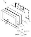
- FIG. 1is a perspective view of a display device according to an embodiment of the present invention.
- FIG. 2is an exploded perspective view of a display device according to an embodiment of the present invention.
- FIG 3is a side cross-sectional view of a liquid crystal panel of a display device according to an exemplary embodiment of the present invention.
- FIG. 4is an exploded perspective view of a light source device according to an embodiment of the present invention.
- FIG. 5is an enlarged and schematically perspective view of a part of a light source device according to an embodiment of the present invention.
- FIG. 6is a view schematically illustrating a cross-section taken along line A-A' of FIG. 5 .
- FIG. 7is an enlarged view of the LED chip shown in FIG. 6 .
- FIG. 8is a view showing an optical profile of an LED chip according to an embodiment of the present invention.
- FIG. 9is a cross-sectional view taken along line B-B' of FIG. 5, and is an enlarged view of the LED chip.
- FIG. 10is a cross-sectional view taken along line B-B' of FIG. 5, illustrating an LED chip and an optical dome according to an embodiment of the present invention.
- FIG. 11is a view showing an optical profile when the optical dome according to an embodiment of the present invention covers the LED chip.
- r0may indicate r 0
- r1may indicate r max .
- the optical filmmay include the optical sheet 140 .
- the optical membermay include a diffusion plate 130 .
- FIG. 1is a perspective view of a display device according to an embodiment of the present invention.
- 2is an exploded perspective view of a display device according to an embodiment of the present invention.
- 3is a side cross-sectional view of a liquid crystal panel of a display device according to an exemplary embodiment of the present invention.
- 4is an exploded perspective view of a light source device according to an embodiment of the present invention.
- FIG. 1is a perspective view of a display device according to an embodiment of the present invention.
- the display device 10is a device capable of processing an image signal received from the outside and visually displaying the processed image.
- the display device 10is a television (Television, TV)
- the present inventionis not limited thereto.
- the display device 10may be implemented in various forms, such as a monitor, a portable multimedia device, and a portable communication device, and the display device 10 is not limited in shape as long as it is a device that visually displays an image. .
- the display device 10may be a large format display (LFD) installed outdoors, such as on the roof of a building or at a bus stop.
- LFDlarge format display
- the outdoorsis not necessarily limited to the outdoors, and the display device 10 according to an embodiment may be installed in any place where a large number of people can enter, even if it is indoors, such as a subway station, a shopping mall, a movie theater, a company, or a store.
- the display apparatus 10may receive content data including video data and audio data from various content sources, and output video and audio corresponding to the video data and audio data.
- the display apparatus 10may receive content data through a broadcast reception antenna or a wired cable, receive content data from a content reproduction device, or receive content data from a content providing server of a content provider.
- the display device 10includes a main body 11 , a screen 12 for displaying an image I, and a support 17 provided under the main body 11 to support the main body 10 .
- the main body 11forms the exterior of the display apparatus 10 , and parts for the display apparatus 10 to display the image I or perform various functions may be provided inside the main body 11 .
- the body 11 shown in FIG. 1has a flat plate shape, but the shape of the body 11 is not limited to that shown in FIG. 1 .
- the body 11may have a curved plate shape.
- the screen 12is formed on the front surface of the main body 11, and can display the image (I).
- the screen 12may display a still image or a moving image.
- the screen 12may display a 2D flat image or a 3D stereoscopic image using the parallax of the user's eyes.
- a plurality of pixels Pare formed on the screen 12 , and an image I displayed on the screen 12 may be formed by light emitted from each of the plurality of pixels P.
- the image Imay be formed on the screen 12 by combining the light emitted by the plurality of pixels P like a mosaic.
- Each of the plurality of pixels Pmay emit light of various brightnesses and of various colors.
- each of the plurality of pixels Pincludes a self-emitting panel (eg, a light emitting diode panel) capable of emitting light directly, or a non-emitting panel capable of passing or blocking light emitted by a light source device or the like. (eg, a liquid crystal panel).
- each of the plurality of pixels Pmay include sub-pixels P R , P G , and P B .
- the sub-pixels P R , P G , P Bare a red sub-pixel P R capable of emitting red light, a green sub-pixel P G capable of emitting green light, and a blue light emitting device. It may include a capable blue sub-pixel P B .
- red lightmay refer to light having a wavelength of approximately 620 nm (nanometer, billionths of a meter) to 750 nm
- green lightmay refer to light having a wavelength of approximately 495 nm to 570 nm
- blue lightmay be It can represent light with a wavelength of approximately 450 nm to 495 nm.
- each of the plurality of pixels Phas various brightnesses and various colors. light can be emitted.
- the main body 11may include various components for generating an image I on the screen S.
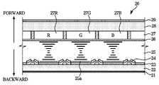
- the body 11includes a light source device 100 that is a surface light source, a liquid crystal panel 20 that blocks or passes light emitted from the light source device 100 , and the light source device 100 . and a control assembly 50 for controlling the operation of the liquid crystal panel 20 , and a power supply assembly 60 for supplying power to the light source device 100 and the liquid crystal panel 20 .
- the main body 11includes a bezel 13 for supporting and fixing the liquid crystal panel 20 , the light source device 100 , the control assembly 50 , and the power assembly 60 , the frame middle mold 14 , and the bottom chassis. (15) and may include a rear cover (16).
- the light source device 100may include a point light source emitting monochromatic light or white light, and may refract, reflect, and scatter light to convert light emitted from the point light source into uniform surface light.
- the light source device 100includes a plurality of light sources emitting monochromatic light or white light, a diffusion plate for diffusing light incident from the plurality of light sources, and a plurality of light sources and for reflecting light emitted from the rear surface of the diffusion plate. It may include a reflective sheet and an optical sheet for refracting and scattering light emitted from the front surface of the diffusion plate.
- the light source device 100may emit uniform surface light toward the front by refracting, reflecting, and scattering light emitted from the light source.
- the configuration of the light source device 100will be described in more detail below.
- the liquid crystal panel 20is provided in front of the light source device 100 and blocks or passes light emitted from the light source device 100 to form the image I.
- the front surface of the liquid crystal panel 20forms the screen S of the display device 10 described above, and the liquid crystal panel 20 may form a plurality of pixels P.
- the plurality of pixels Pmay each independently block or pass the light of the light source device 100 , and the light passed by the plurality of pixels P may be transmitted to the screen S.
- the displayed image Imay be formed.
- the liquid crystal panel 20includes a first polarizing film 21 , a first transparent substrate 22 , a pixel electrode 23 , a thin film transistor 24 , and a liquid crystal layer 25 . , a common electrode 26 , a color filter 27 , a second transparent substrate 28 , and a second polarizing film 29 .
- the first transparent substrate 22 and the second transparent substrate 28may fixedly support the pixel electrode 23 , the thin film transistor 24 , the liquid crystal layer 25 , the common electrode 26 , and the color filter 27 . have.
- the first and second transparent substrates 22 and 28may be made of tempered glass or transparent resin.
- a first polarizing film 21 and a second polarizing film 29are provided outside the first and second transparent substrates 22 and 28 .
- the first polarizing film 21 and the second polarizing film 29may pass a specific light and block other light, respectively.
- the first polarizing film 21transmits light having a magnetic field oscillating in the first direction and blocks other light.
- the second polarizing film 29transmits light having a magnetic field oscillating in the second direction and blocks other light.
- the first direction and the second directionmay be orthogonal to each other. Accordingly, the polarization direction of the light passing through the first polarizing film 21 and the vibration direction of the light passing through the second polarizing film 29 are orthogonal to each other. As a result, generally, light cannot pass through the first polarizing film 21 and the second polarizing film 29 at the same time.
- a color filter 27may be provided inside the second transparent substrate 28 .
- the color filter 27may include, for example, a red filter 27R for passing red light, a green filter 27G for passing green light, and a blue filter 27G for passing blue light.
- the filter 27R, the green filter 27G, and the blue filter 27Bmay be arranged side by side.
- the region in which the color filter 27 is formedcorresponds to the pixel P described above.
- the area in which the red filter 27R is formedcorresponds to the red sub-pixel P R
- the area in which the green filter 27G is formedcorresponds to the green sub-pixel P G
- the area in which the blue filter 27B is formedcorresponds to the blue color. It corresponds to the sub-pixel P B .
- a pixel electrode 23may be provided inside the first transparent substrate 22 , and a common electrode 26 may be provided inside the second transparent substrate 28 .
- the pixel electrode 23 and the common electrode 26are made of a metal material that conducts electricity, and can generate an electric field for changing the arrangement of the liquid crystal molecules 115a constituting the liquid crystal layer 25 to be described below. have.
- the pixel electrode 23 and the common electrode 26are made of a transparent material, and can pass light incident from the outside.
- the pixel electrode 23 and the common electrode 26are indium tin oxide (ITO), indium zinc oxide (IZO), silver nanowire (Ag nano wire), carbon nanotube ( It may be composed of carbon nano tube: CNT), graphene, or PEDOT (3,4-ethylenedioxythiophene).
- a thin film transistor (TFT) 24is provided inside the second transparent substrate 22 .
- the thin film transistor 24may pass or block a current flowing through the pixel electrode 23 .
- an electric fieldmay be formed or removed between the pixel electrode 23 and the common electrode 26 according to the turn-on (closed) or turn-off (open) of the thin film transistor 24 .
- the thin film transistor 24may be made of poly-silicon, and may be formed by a semiconductor process such as lithography, deposition, or ion implantation.
- a liquid crystal layer 25is formed between the pixel electrode 23 and the common electrode 26 , and the liquid crystal layer 25 is filled with liquid crystal molecules 25a.
- Liquid crystalrepresents an intermediate state between a solid (crystal) and a liquid.
- Most of the liquid crystal materialsare organic compounds, and their molecular shape is in the shape of a long and thin rod, and the arrangement of molecules is the same as an irregular state in one direction, but it may have a regular crystal form in another direction.
- the liquid crystalhas both the fluidity of a liquid and the optical anisotropy of a crystal (solid).
- the liquid crystalexhibits optical properties according to the change of the electric field.
- the direction of the arrangement of molecules constituting the liquid crystalmay change according to a change in an electric field.
- the liquid crystal molecules 115a of the liquid crystal layer 25are arranged according to the direction of the electric field, and when the electric field is not generated in the liquid crystal layer 25 , the liquid crystal molecules 115a are irregularly arranged or may be disposed along an alignment layer (not shown).
- the optical properties of the liquid crystal layer 25may vary depending on the presence or absence of an electric field passing through the liquid crystal layer 25 .
- a cable 20a for transmitting image data to the liquid crystal panel 20and a display driver integrated circuit (DDI) for processing digital image data and outputting an analog image signal ( 30) (hereinafter referred to as 'driver IC') is provided.
- DPIdisplay driver integrated circuit
- the cable 20amay electrically connect the control assembly 50/power assembly 60 and the driver IC 30 , and may also electrically connect the driver IC 30 and the liquid crystal panel 20 .
- the cable 20amay include a flexible flat cable or a film cable that can be bent.
- the driver IC 30receives image data and power from the control assembly 50/power assembly 60 through the cable 20a, and supplies image data and driving current to the liquid crystal panel 20 through the cable 20a. can be transmitted
- the cable 20a and the driver IC 30may be integrally implemented as a film cable, a chip on film (COF), a tape carrier package (TCP), or the like.
- the driver IC 30may be disposed on the cable 110b.
- embodimentsare not limited thereto, and the driver IC 30 may be disposed on the liquid crystal panel 20 .
- the control assembly 50may include a control circuit for controlling operations of the liquid crystal panel 20 and the light source device 100 .
- the control circuitmay process image data received from an external content source, transmit image data to the liquid crystal panel 20 , and transmit dimming data to the light source device 100 .
- the power assembly 60supplies power to the liquid crystal panel 20 and the light source device 100 so that the light source device 100 outputs surface light and the liquid crystal panel 20 blocks or passes the light from the light source device 100 .
- the control assembly 50 and the power assembly 60may be implemented as a printed circuit board and various circuits mounted on the printed circuit board.
- the power circuitmay include a capacitor, a coil, a resistor, a processor, and the like, and a power circuit board on which these are mounted.
- the control circuitmay include a memory, a processor, and a control circuit board on which they are mounted.
- the light source device 100will be described.
- FIG. 4is an exploded view of a light source device according to an embodiment.
- the light source device 100includes a light source module 110 for generating light, a reflective sheet 120 for reflecting light, a diffuser plate 130 for uniformly diffusing light, and optics for improving the luminance of emitted light. sheet 140 .
- the light source module 110may include a plurality of light sources 111 emitting light and a substrate 112 supporting/fixing the plurality of light sources 111 .
- the plurality of light sources 111may be arranged in a predetermined pattern so that light is emitted with uniform luminance.
- the plurality of light sources 111may be arranged such that a distance between one light source and light sources adjacent thereto is the same.
- the plurality of light sources 111may be arranged in alignment with rows and columns. Thereby, a plurality of light sources can be arranged such that a square is formed by four adjacent light sources. Also, any one light source may be disposed adjacent to four light sources, and a distance between one light source and four adjacent light sources may be substantially the same.
- a plurality of light sourcesmay be arranged in a plurality of rows, and a light source belonging to each row may be located between two light sources belonging to an adjacent row.
- a plurality of light sourcesmay be arranged such that an approximately equilateral triangle is formed by three adjacent light sources.
- one light sourcemay be disposed adjacent to six light sources, and a distance between one light source and six light sources adjacent thereto may be substantially the same.
- the pattern in which the plurality of light sources 111 are disposedis not limited to the pattern described above, and the plurality of light sources 111 may be disposed in various patterns so that light is emitted with uniform luminance.
- the light source 111can emit monochromatic light (light of a specific wavelength, for example, blue light) or white light (for example, a mixture of red light, green light, and blue light) in various directions when power is supplied. element can be employed.
- the light source 111may include a light emitting diode (LED).
- the substrate 112may fix the plurality of light sources 111 so that the positions of the light sources 111 are not changed. In addition, the substrate 112 may supply power for the light source 111 to emit light to each light source 111 .
- the substrate 112is composed of a synthetic resin or tempered glass or a printed circuit board (PCB) in which a conductive power supply line for fixing the plurality of light sources 111 and supplying power to the light source 111 is formed.
- PCBprinted circuit board
- the reflective sheet 120may reflect the light emitted from the plurality of light sources 111 forward or in a direction close to the front.
- a plurality of through holes 120aare formed in the reflective sheet 120 at positions corresponding to each of the plurality of light sources 111 of the light source module 110 .
- the light source 111 of the light source module 110may pass through the through hole 120a and protrude in front of the reflective sheet 120 .
- the plurality of light sources 111 of the light source module 110are inserted into the plurality of through holes 120a formed in the reflective sheet 120 . Therefore, the substrate 112 of the light source module 110 is positioned at the rear of the reflective sheet 120 , but the plurality of light sources 111 of the light source module 110 may be positioned in front of the reflective sheet 120 . .
- the plurality of light sources 111may emit light from the front of the reflective sheet 120 .
- the plurality of light sources 111may emit light in various directions in front of the reflective sheet 120 . Light may be emitted from the light source 111 toward the diffusion plate 130 as well as emitted from the light source 111 toward the reflective sheet 120 , and the reflective sheet 120 is emitted toward the reflective sheet 120 . The light may be reflected toward the diffusion plate 130 .
- Light emitted from the light source 111passes through various objects such as the diffusion plate 130 and the optical sheet 140 .
- various objectssuch as the diffusion plate 130 and the optical sheet 140 .
- the reflective sheet 120may reflect light reflected by the diffusion plate 130 and the optical sheet 140 .
- the diffusion plate 130may be provided in front of the light source module 110 and the reflective sheet 120 , and may evenly distribute the light emitted from the light source 111 of the light source module 110 .
- the plurality of light sources 111are located in various places on the rear surface of the light source device 100 . Although the plurality of light sources 111 are disposed at equal intervals on the rear surface of the light source device 100 , non-uniformity in luminance may occur depending on the positions of the plurality of light sources 111 .
- the diffusion plate 130may diffuse the light emitted from the plurality of light sources 111 in the diffusion plate 130 in order to remove non-uniformity in luminance due to the plurality of light sources 111 . In other words, the diffusion plate 130 may uniformly emit the non-uniform light of the plurality of light sources 111 to the front.
- the optical sheet 140may include various sheets for improving luminance and uniformity of luminance.
- the optical sheet 140may include a diffusion sheet 141 , a first prism sheet 142 , a second prism sheet 143 , a reflective polarizing sheet 144 , and the like.
- the diffusion sheet 141diffuses light for uniformity of luminance.
- the light emitted from the light source 111may be diffused by the diffusion plate 130 and may be diffused again by the diffusion sheet 141 included in the optical sheet 140 .
- the first and second prism sheets 142 and 143may increase luminance by focusing the light diffused by the diffusion sheet 141 .
- the first and second prism sheets 142 and 143include a prism pattern having a triangular prism shape, and a plurality of the prism patterns are arranged adjacently to form a plurality of bands.
- the reflective polarizing sheet 144is a type of polarizing film and may transmit some of the incident light to improve luminance and reflect the other portion. For example, polarized light in the same direction as the predetermined polarization direction of the reflective polarizing sheet 144 may be transmitted, and polarized light in a direction different from the polarization direction of the reflective polarizing sheet 144 may be reflected. In addition, the light reflected by the reflective polarizing sheet 144 is recycled inside the light source device 100 , and the luminance of the display device 10 may be improved by such light recycle.
- the optical sheet 140is not limited to the sheet or film shown in FIG. 4 , and may include more various sheets or films such as a protective sheet and a quantum dot sheet.
- FIG. 5is an enlarged perspective view of a part of a light source device according to an embodiment of the present invention.
- 6is a cross-sectional view taken along line A-A' of FIG. 5 .
- FIG. 7is an enlarged view of the LED chip shown in FIG. 6 .
- the light source 111 of the light source device 100will be described with reference to FIGS. 5 to 7 .
- the light source module 110includes a plurality of light sources 111 .
- the plurality of light sources 111may pass through the through hole 120a at the rear of the reflective sheet 120 to protrude forward of the reflective sheet 120 . Accordingly, as shown in FIGS. 5 and 6 , a portion of the light source 111 and the substrate 112 may be exposed toward the front of the reflective sheet 120 through the through hole 120a.
- the light source 111may include an electrical/mechanical structure positioned in a region defined by the through hole 120a of the reflective sheet 120 .
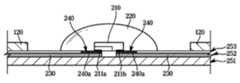
- each of the plurality of light sources 111may include an LED chip 210 and an optical dome 220 .
- the number of light sourcesmay be reduced by widening an optical diffusion region of light emitted from the light source.
- the number of blocks of local dimmingis reduced due to a decrease in the number of light sources, which limits improvement of contrast ratio.
- the light source device 100does not include a lens, and the light source The number of (111) can be increased. Accordingly, an area occupied by each of the plurality of light sources 111 may be narrowed.
- the optical dome 220may cover each of the plurality of light sources 111 while having a smaller size compared to the lens.
- the LED chip 210may include a p-type semiconductor layer 213 and an n-type semiconductor layer 212 for emitting light by recombination of holes and electrons.
- the LED chip 210includes a pair of electrodes 211a and 211b for supplying holes and electrons to the p-type semiconductor layer 213 and the n-type semiconductor layer 212 , respectively.
- the LED chip 210may include a growth substrate 215 , a p-type semiconductor layer 213 , an n-type semiconductor layer 212 , and a light emitting layer 214 .
- the LED chip 210may further include a distributed Bragg reflector (DBR) layer 216 and a metal reflection layer 217 .
- the metal reflective layer 217may include aluminum (Al) or a distributed Bragg reflector (DBR).
- the DBR included in the metal reflective layer 217may have the same configuration as the DBR layer 216 .
- the DBR layer 216is called a first DBR layer
- the metal reflective layer 217is called a second DBR layer.
- the growth substrate 215may be a sapphire substrate useful as a substrate for nitride semiconductor growth.
- the present inventionis not limited thereto, and may be various substrates provided for semiconductor single crystal growth, such as a silicon substrate or a GaN substrate.
- the growth substrate 215may be a sapphire substrate.
- the p-type semiconductor layer 213 , the n-type semiconductor layer 212 , and the emission layer 214may be formed of a nitride semiconductor.
- the light emitting layer 214may emit light corresponding to the bandgap energy size by recombination of electrons and holes.
- the pair of electrodes 211a and 211bmay include an n-type device electrode 211a and a p-type device electrode 211b.
- the n-type device electrode 211a and the p-type device electrode 211bmay be formed of a material capable of ohmic contact with the nitride semiconductor, for example, made of a metal such as silver (Ag) or aluminum (Al). can be formed.
- the DBR layer 216may be prepared by stacking two materials having a difference in refractive index.
- the DBR layer 216 and the metal reflective layer 217may reflect light of a target wavelength.
- the DBR layer 216may be provided on the top surface of the growth substrate 215 .
- the DBR layer 216may reflect a portion of the light emitted from the light emitting layer 214 to increase the light directivity angle with respect to the liquid crystal panel 20 .
- the metal reflective layer 217may be provided on the lower surface of the emission layer 214 . Like the DBR layer 216 , the metal reflective layer 217 may reflect a portion of the light emitted from the light emitting layer 214 to increase the light beam angle with respect to the liquid crystal panel 20 .
- a DBR layermay be provided on an upper surface of the growth substrate 215 , and a metal reflective layer may be provided on a lower surface of the emission layer 214 .
- the first DBR layer 216may be provided on the upper surface of the growth substrate 215
- the second DBR layer 217may be provided on the lower surface of the emission layer 214 .
- the DBR layer 216may be provided on the upper surface of the growth substrate 215
- the metal reflective layer 217 including a metal such as aluminum (Al)may be provided on the lower surface of the emission layer 214 .
- the LED chip 210may convert electrical energy into optical energy.
- the LED chip 210may emit light having a maximum intensity at a predetermined wavelength to which power is supplied.
- the LED chip 210may emit blue light having a peak value at a wavelength representing blue (eg, a wavelength between 450 nm and 495 nm).
- the LED chip 210may be directly attached to the substrate 112 in a Chip On Board (COB) method.
- the light source 111may include an LED chip 210 to which a light emitting diode chip or a light emitting diode die is directly attached to the substrate 112 without separate packaging.
- the length of the horizontal side and the length of the vertical side of the DBR layer 216may be several hundreds of ⁇ m.
- the length of the horizontal side and the length of the vertical side of the upper surface of the growth substrate 215may be several hundreds of ⁇ m.
- a length of a horizontal side and a length of a vertical side of the upper surface of the growth substrate 215may be provided to be 500 ⁇ m or less, respectively.
- the LED chip 210may be manufactured as a flip chip type that does not include a Zener diode.
- the flip chip type LED chip 210does not use an intermediate medium such as a metal lead (wire) or a ball grid array (BGA) when attaching the light emitting diode, which is a semiconductor device, to the substrate 112,
- the electrode pattern of the semiconductor devicemay be fused to the substrate 112 as it is.
- the light source 111 including the flip chip type LED chip 210can be miniaturized.
- the light source module 110 in which a flip-chip type LED chip 210 is attached to the substrate 112 in a chip-on-board methodmay be manufactured.
- a power supply line 230 and a power supply pad 240are provided on the substrate 112 for supplying power to the flip chip type LED chip 210 .
- a power supply line 230 for supplying electrical signals and/or power from the control assembly 50 and/or the power assembly 60 to the LED chip 210is provided on the substrate 112 .
- the substrate 112may be formed by alternately stacking a non-conductive insulation layer 251 and a conductive conductive layer 252 .
- the conductive layer 252is formed with a line or pattern through which power and/or electrical signals pass.
- the conductive layer 252may be made of various materials having electrical conductivity.
- the conductive layer 252may be made of various metal materials such as copper (Cu), tin (Sn), aluminum (Al), or an alloy thereof.
- the dielectric of the insulating layer 251may insulate between the lines or patterns of the conductive layer 252 .
- the insulating layer 251may be made of a dielectric for electrical insulation, for example, FR-4.
- the feed line 230may be implemented by a line or pattern formed in the conductive layer 252 .
- the feeding line 230may be electrically connected to the LED chip 210 through the feeding pad 240 .
- the feeding pad 240may be formed by exposing the feeding line 230 to the outside.
- a protection layer 253may be formed.
- the protective layer 253may include a photo solder resist (PSR).
- the protective layer 253may cover the feed line 230 to block the feed line 230 from being exposed to the outside.
- a window exposing a portion of the feed line 230 to the outsidemay be formed in the protective layer 253 .
- a portion of the feeding line 230 exposed to the outside by the window of the protective layer 253may form the feeding pad 240 .
- a conductive adhesive material 240a for electrical contact between the externally exposed feeding line 230 and the electrodes 211a and 211b of the LED chip 210is applied to the feeding pad 240 .
- a conductive adhesive material 240amay be applied in the window of the protective layer 253 .
- the electrodes 211a and 211b of the LED chip 210may be in contact with the conductive adhesive material 240a, and the LED chip 210 may be electrically connected to the power supply line 230 through the conductive adhesive material 240a.
- the conductive adhesive material 240amay include, for example, solder having electrical conductivity. However, the present invention is not limited thereto, and the conductive adhesive material 240a may include electrically conductive epoxy adhesives.
- Powermay be supplied to the LED chip 210 through the feeding line 230 and the feeding pad 240 , and when power is supplied, the LED chip 210 may emit light.
- a pair of power feeding pads 240 corresponding to each of the pair of electrodes 211a and 211b included in the flip chip type LED chip 210may be provided.
- the optical dome 220may cover the LED chip 210 .
- the optical dome 220may indicate a light-transmitting resin layer.
- the optical dome 220may prevent or suppress damage to the LED chip 210 by an external mechanical action and/or damage to the LED chip 210 by a chemical action.
- the optical dome 220may prevent the LED chip 210 from being separated from the substrate 112 by an external impact.
- the optical dome 220may increase the light extraction efficiency of the LED chip 210 through index matching. Light emitted to the growth substrate 215 may not be emitted to the outside due to a difference in refractive index between the growth substrate 215 and air. The optical dome 220 reduces the refractive index difference between the growth substrate 215 and the air so that the light emitted from the LED chip 210 exits through the growth substrate 215 and the optical dome 220 .
- the optical dome 220may protect the light emitting diode 111 from an external electrical action. Charge generated by the electrostatic discharge does not pass through the optical dome 220 and may flow along the outer surface of the optical dome 220 .
- the optical dome 220may have, for example, a dome shape in which a sphere is cut by a surface not including the center, or a hemispherical shape in which a sphere is cut by a surface including the center.
- the vertical cross-section of the optical dome 220may be, for example, arcuate or semicircular in shape.
- the optical dome 220may be made of silicone or epoxy resin.
- the molten silicone or epoxy resinis discharged onto the LED chip 210 through a nozzle or the like, and then the discharged silicone or epoxy resin is cured to form the optical dome 220 .
- Optical dome 220may be optically transparent or translucent. Light emitted from the LED chip 210 may pass through the optical dome 220 and be emitted to the outside.
- the dome-shaped optical dome 220may refract light like a lens.
- light emitted from the LED chip 210may be scattered by being refracted by the optical dome 220 .
- the optical dome 220may not only protect the LED chip 210 from external mechanical action and/or chemical action or electrical action, but also disperse light emitted from the LED chip 210 .
- FIG. 8is a view showing an optical profile of an LED chip according to an embodiment of the present invention.
- the LED chip 210has a substantially bat-wing-shaped optical profile.
- the LED chip 210includes the first DBR layer 216 and the second DBR layer 217 on the upper and lower sides of the light emitting layer 214, respectively, or DBR on the upper and lower sides of the light emitting side 214, respectively. It includes a layer 216 and a metal reflective layer 217, and has a batwing-shaped optical profile due to this structure.
- the batwing-shaped light profilerefers to an optical profile in which the amount of light emitted from both sides is greater than the amount of light emitted from the LED chip 210 in the vertical direction, as shown in FIG. 8 .
- the amount of light emitted from the LED chip 210 to both sidesis slightly different, but it is preferably uniform.
- the number of LED chips 210can be reduced while maintaining an optical distance.
- the optical distancecan be reduced while maintaining the number of the LED chips 210 . That is, it is possible to reduce the thickness of the display device 10 or reduce the cost.
- the light profile of the LED chip 210may have a bat wing shape as shown in FIG. 8 . This is because it is easy to convert light emitted from the LED chip 210, which is a point light source, into uniform surface light when the light profile has a batwing shape.
- the optical profile of the LED chip 210may be changed. That is, due to the optical dome 220 , the light profile of the batwing shape of the LED chip 210 may change into a Lambertian shape or a shape other than the batwing shape, which may not be intended by the designer.
- a distance from the center of the light source to the center of the optical dome 220is r 0 .
- a vertical distance between the center of the light source and the center of the optical dome 220is r 0 .
- lightis emitted at 0° from the center of the light source.
- the light having the maximum output among the lights emitted from the center of the light sourceis referred to as maximum output light (maximum output light).
- maximum output lightmaximum output light
- ⁇ maxThe angle at which the maximum output light is emitted from the center of the light source.
- FIG. 9is a cross-sectional view taken along line B-B' of FIG. 5, and is an enlarged view of the LED chip.
- the center of the light sourcemay point to the center of the light emitting layer 214 of the LED chip 210 .
- the angle between the light L1 vertically emitted from the center of the emission layer 214 and the maximum output light L2 emitted from the center of the emission layer 214may be ⁇ max .
- the maximum output light L2refers to the light having the maximum output among the lights emitted from the light emitting layer 214 .
- FIG. 10is a cross-sectional view taken along line B-B' of FIG. 5, illustrating an LED chip and an optical dome according to an embodiment of the present invention.
- the distance from the center of the light source of the LED chip 210 to the surface of the optical dome 220is defined.
- a distance between the center of the light emitting layer 214 of the LED chip 210 and the center surface of the optical dome 220is r 0 .
- the moving distanceis referred to as r 0 .
- r maxthe distance from the center of the light emitting layer 214 to the point where the maximum output light L2 emitted therefrom meets the surface of the optical dome 220 is referred to as r max .
- a specific shape of the optical dome 220may be defined as follows.
- the shape of the optical dome 220can be defined by defining the ratio of r max and r 0 as follows.
- the optical dome 220may be provided to satisfy 1.70 ⁇ r max / r 0 ⁇ 1.83. That is, r max may be formed to be 1.70 times to 1.83 times larger than r 0 . Due to the shape of the optical dome 220 , the LED chip 210 according to the spirit of the present invention may maintain the optical profile of the batwing shape even if it is covered by the optical dome 220 .
- FIG. 11is a view showing an optical profile when the optical dome according to an embodiment of the present invention covers the LED chip.
- the optical profile of the LED chip 210 having a batwing-shaped optical profileby specifically defining the shape of the optical dome 220 .
- the optical dome 220is provided on the LED chip 210 , the light profile of the batwing shape of the LED chip 210 may be maintained.
- the optical dome 220may be provided to satisfy 1.70 ⁇ r max / r 0 ⁇ 1.83.
- the light emitted at 0° from the center of the light emitting layer 214 of the LED chip 210moves in a straight line toward the surface of the optical dome 220 for the distance r 0 of the LED chip 210
- the ratio (r max/ r 0 ) of the distance (r max ) that the light emitted at an angle of ⁇ max from the center of the light emitting layer 214 moves in a straight line toward the surface of the optical dome 220is to be defined as 1.70 to 1.83 can
- the LED chip 210may still have a batwing-shaped optical profile. have. That is, even if the light source device 100 includes the optical dome 220 , the light profile of the LED chip 110 may be maintained. Accordingly, the optical distance can be reduced while maintaining the number of light sources, and the number of light sources can be reduced while maintaining the optical distance.
Landscapes
- Physics & Mathematics (AREA)
- Nonlinear Science (AREA)
- General Physics & Mathematics (AREA)
- Engineering & Computer Science (AREA)
- Optics & Photonics (AREA)
- Mathematical Physics (AREA)
- Chemical & Material Sciences (AREA)
- Crystallography & Structural Chemistry (AREA)
- Power Engineering (AREA)
- Microelectronics & Electronic Packaging (AREA)
- Condensed Matter Physics & Semiconductors (AREA)
- Computer Hardware Design (AREA)
- Liquid Crystal (AREA)
- Planar Illumination Modules (AREA)
Abstract
Description
Translated fromKorean본 발명은 디스플레이 장치 및 그 광원 장치에 관한 것으로서, 광학 돔을 포함하는 광원의 광 프로파일을 유지할 수 있는 디스플레이 장치 및 그 광원 장치에 관한 것이다.The present invention relates to a display device and a light source device thereof, and to a display device capable of maintaining a light profile of a light source including an optical dome, and to the light source device.
일반적으로, 디스플레이 장치는, 획득 또는 저장된 전기적 정보를 시각적 정보로 변환하여 사용자에게 표시하고, 가정이나 사업장 등 다양한 분야와 환경에서 이용되고 있다.In general, a display device converts acquired or stored electrical information into visual information to display it to a user, and is used in various fields and environments, such as homes and businesses.
디스플레이 장치로는, 개인용 컴퓨터 또는 서버용 컴퓨터 등에 연결된 모니터 장치나, 휴대용 컴퓨터 장치나, 내비게이션 단말 장치나, 일반 텔레비전 장치나, 인터넷 프로토콜 텔레비전(IPTV, Internet Protocol television) 장치나, 스마트 폰, 태블릿 피씨, 개인용 디지털 보조 장치(PDA, Personal Digital Assistant), 또는 셀룰러 폰 등의 휴대용 단말 장치나, 산업 현장에서 광고나 영화 같은 화상을 재생하기 위해 이용되는 각종 디스플레이 장치나, 또는 이외 다양한 종류의 오디오/비디오 시스템 등이 있다.As a display device, a monitor device connected to a personal computer or a server computer, etc., a portable computer device, a navigation terminal device, a general television device, an Internet Protocol television (IPTV) device, a smart phone, a tablet PC, A personal digital assistant (PDA), a portable terminal device such as a cellular phone, various display devices used to reproduce images such as advertisements or movies in an industrial field, or various other audio/video systems etc.
디스플레이 장치는, 전기적 정보를 시각적 정보로 변환하기 위하여, 광원 장치를 포함하며, 광원 장치는 독립적으로 광을 방출하는 복수의 광원들을 포함한다.A display device includes a light source device to convert electrical information into visual information, and the light source device includes a plurality of light sources independently emitting light.
복수의 광원들 각각은 예를 들어 발광 다이오드(Light Emitting Diode, LED) 또는 유기 발광 다이오드(Organic Light Emitting Diode, OLED)를 포함한다. 예를 들어, 발광 다이오드 또는 유기 발광 다이오드는 기판(circuit board 또는 substrate) 상에 실장될 수 있다.Each of the plurality of light sources includes, for example, a Light Emitting Diode (LED) or an Organic Light Emitting Diode (OLED). For example, a light emitting diode or an organic light emitting diode may be mounted on a circuit board or substrate.
광원 장치는 광원을 커버하도록 마련되는 렌즈를 포함하여 광원에서 발하는 광의 광학 확산 영역을 넓힐 수 있다. 다만, 렌즈를 통한 광학 확산 영역의 확장으로 인해 로컬 디밍(Local Dimming)의 블록(Block) 수가 줄어들고, 이는 명암비를 향상시키는 데에 제약이 된다.The light source device may include a lens provided to cover the light source to widen an optical diffusion area of light emitted from the light source. However, due to the expansion of the optical diffusion region through the lens, the number of blocks of local dimming is reduced, which is a limitation in improving the contrast ratio.
최근의 디스플레이 장치는, 상기한 제약 사항으로 인해 렌즈 없이 광원 장치를 구성할 수 있다. 이러한 광원 장치의 경우, 광원을 보호하기 위해 광원을 커버하는 투광성 수지층을 포함한다. 다만, 투광성 수지층으로 인해 광원의 광 프로파일이 변경될 수 있다.A recent display device may configure a light source device without a lens due to the above-mentioned limitations. In the case of such a light source device, a light-transmitting resin layer covering the light source is included in order to protect the light source. However, the light profile of the light source may be changed due to the light-transmitting resin layer.
배트 윙(Bat-Wing) 형태의 광 프로파일을 갖는 광원과, 배트 윙 형태의 광 프로파일을 유지시킬 수 있는 광학 돔을 포함하는 디스플레이 장치 및 그 광원 장치를 제공한다.Provided are a display device including a light source having a light profile of a bat-wing shape, an optical dome capable of maintaining a light profile of a bat-wing shape, and a light source device thereof.
또한, 그 형상을 구체적으로 정의하여 광원의 광 프로파일을 유지시킬 수 있는 광학 돔을 포함하는 디스플레이 장치 및 그 광원 장치를 제공한다.In addition, a display device including an optical dome capable of maintaining a light profile of a light source by specifically defining the shape thereof, and the light source device are provided.
또한, 광학 돔의 구체적인 형상을 정의하여 광원 수를 유지하면서 광학 거리를 줄일 수 있는 디스플레이 장치 및 그 광원 장치를 제공한다.In addition, a display device capable of reducing an optical distance while maintaining the number of light sources by defining a specific shape of an optical dome, and a light source device are provided.
또한, 광학 돔의 구체적인 형상을 정의하여 광학 거리를 유지하면서 광원 수를 줄일 수 있는 디스플레이 장치 및 그 광원 장치를 제공한다.In addition, a display device capable of reducing the number of light sources while maintaining an optical distance by defining a specific shape of an optical dome, and a light source device thereof are provided.
개시의 일 측면에 따르면, 디스플레이 장치는 인쇄회로기판과, 상기 인쇄회로기판에 마련되고, 광을 출력하는 엘이디 칩과, 상기 엘이디 칩을 커버하는 광학 돔(dome) 및 상기 엘이디 칩에서 출력되는 광을 차단하거나 통과시키는 액정 패널을 포함하고, 상기 광학 돔은, 상기 엘이디 칩으로부터 수직하게 방출된 광이 상기 광학 돔의 표면에 닿을 때까지의 직선 거리를 r0라 하고, 상기 엘이디 칩으로부터 방출되는 최대 출력 광이 상기 광학 돔의 표면에 닿을 때까지의 직선 거리를 r1라 할 때, 1.70 < r1/r0 < 1.83을 만족할 수 있다.According to one aspect of the disclosure, a display device includes a printed circuit board, an LED chip provided on the printed circuit board for outputting light, an optical dome covering the LED chip, and light output from the LED chip a liquid crystal panel that blocks or passes When the linear distance until the output light reaches the surface of the optical dome is r1, 1.70 < r1/r0 < 1.83 may be satisfied.
상기 최대 출력 광은, 상기 엘이디 칩의 광 프로파일에서 가장 큰 출력을 갖는 각도로 방출되는 광일 수 있다.The maximum output light may be light emitted at an angle having the largest output in the optical profile of the LED chip.
상기 엘이디 칩은, n형 반도체층과, p형 반도체층 및 상기 n형 반도체층과 상기 p형 반도체층 사이에 마련되어 광을 방출하도록 마련되는 발광층을 포함할 수 있다.The LED chip may include an n-type semiconductor layer, a p-type semiconductor layer, and a light emitting layer provided between the n-type semiconductor layer and the p-type semiconductor layer to emit light.
상기 r0는 상기 발광층의 중심으로부터 수직하게 방출된 광이 상기 광학 돔의 표면에 닿을 때까지의 직선 거리일 수 있다.The r0 may be a linear distance from the center of the light emitting layer until the light emitted vertically reaches the surface of the optical dome.
상기 r1은 상기 발광층의 중심에서 방출되는 최대 출력 광이 상기 광학 돔의 표면에 닿을 때까지의 직선 거리일 수 있다.The r1 may be a linear distance until the maximum output light emitted from the center of the light emitting layer reaches the surface of the optical dome.
상기 엘이디 칩은 청색 계열의 광을 발광하도록 마련될 수 있다.The LED chip may be provided to emit blue-based light.
상기 디스플레이 장치는 상기 엘이디 칩과 상기 액정 패널 사이에 배치되는 광학 필름을 더 포함할 수 있다.The display device may further include an optical film disposed between the LED chip and the liquid crystal panel.
상기 광학 필름은, 광의 파장을 변화시켜 색 재현성을 향상시키도록 구성되는 퀀텀 닷 시트(Quantum Dot Sheet)를 포함할 수 있다.The optical film may include a quantum dot sheet configured to improve color reproducibility by changing a wavelength of light.
상기 엘이디 칩은 상기 인쇄회로기판의 실장면 상에 칩온보드(Chip On Board, COB) 방식으로 실장될 수 있다.The LED chip may be mounted on a mounting surface of the printed circuit board in a Chip On Board (COB) method.
상기 엘이디 칩은, 가로 변의 길이와 세로 변의 길이가 각각 500μm 이하일 수 있다.The LED chip may have a length of a horizontal side and a length of a vertical side of 500 μm or less, respectively.
상기 엘이디 칩은, 상기 n형 반도체층 또는 상기 p형 반도체층의 상면을 커버하도록 배치되는 성장 기판과, 상기 성장 기판의 상면에 배치되는 DBR(Distributed Bragg reflector)층 및 상기 발광층의 하면에 배치되는 금속 반사층을 더 포함할 수 있다.The LED chip includes a growth substrate disposed to cover an upper surface of the n-type semiconductor layer or the p-type semiconductor layer, a distributed Bragg reflector (DBR) layer disposed on the upper surface of the growth substrate, and a lower surface of the light emitting layer It may further include a metal reflective layer.
상기 금속 반사층은 알루미늄(Al) 또는 DBR(Distributed Bragg reflector)을 포함할 수 있다.The metal reflective layer may include aluminum (Al) or a distributed Bragg reflector (DBR).
상기 성장 기판은 사파이어 기판을 포함할 수 있다.The growth substrate may include a sapphire substrate.
상기 디스플레이 장치는 상기 광학 돔이 통과하도록 마련되는 관통 홀을 포함하고, 상기 인쇄회로기판에 부착되는 반사 시트를 더 포함할 수 있다.The display device may further include a reflective sheet that includes a through hole through which the optical dome passes, and is attached to the printed circuit board.
상기 광학 돔은 실리콘 또는 에폭시 수지로 구성될 수 있다.The optical dome may be made of silicone or epoxy resin.
상기 디스플레이 장치는 상기 엘이디 칩과 상기 액정 패널 사이에 마련되는 광학 부재를 더 포함할 수 있다.The display device may further include an optical member provided between the LED chip and the liquid crystal panel.
상기 광학 부재는 상기 엘이디 칩에서 방출되는 광을 확산시키도록 구성되는 확산판을 포함할 수 있다.The optical member may include a diffusion plate configured to diffuse the light emitted from the LED chip.
개시의 일 측면에 따르면, 광원 장치는 실장면을 가지는 인쇄회로기판과, 상기 실장면 상에 실장되는 엘이디 칩 및 상기 엘이디 칩과 상기 엘이디 칩과 인접한 상기 실장면의 일부분을 커버하는 광학 돔(dome)을 포함하고, 상기 광학 돔은, 상기 엘이디 칩으로부터 수직하게 방출된 광이 상기 광학 돔의 표면에 닿을 때까지의 직선 거리를 r0라 하고, 상기 엘이디 칩으로부터 방출되는 최대 출력 광이 상기 광학 돔의 표면에 닿을 때까지의 직선 거리를 r1라 할 때, 1.70 < r1/r0 < 1.83을 만족할 수 있다.According to one aspect of the disclosure, a light source device includes a printed circuit board having a mounting surface, an LED chip mounted on the mounting surface, and an optical dome covering a portion of the mounting surface adjacent to the LED chip and the LED chip. ), wherein, in the optical dome, a linear distance until the light vertically emitted from the LED chip hits the surface of the optical dome is r0, and the maximum output light emitted from the LED chip is the optical dome When the straight line distance to the surface of is r1, 1.70 < r1/r0 < 1.83 can be satisfied.
상기 최대 출력 광은, 상기 엘이디 칩의 광 프로파일에서 가장 큰 출력을 갖는 각도로 방출되는 광일 수 있다.The maximum output light may be light emitted at an angle having the largest output in the optical profile of the LED chip.
상기 엘이디 칩은, n형 반도체층과, p형 반도체층 및 상기 n형 반도체층과 상기 p형 반도체층 사이에 마련되어 광을 방출하도록 마련되는 발광층을 포함할 수 있다.The LED chip may include an n-type semiconductor layer, a p-type semiconductor layer, and a light emitting layer provided between the n-type semiconductor layer and the p-type semiconductor layer to emit light.
상기 r0는 상기 발광층의 중심으로부터 수직하게 방출된 광이 상기 광학 돔의 표면에 닿을 때까지의 직선 거리일 수 있다.The r0 may be a linear distance from the center of the light emitting layer until the light emitted vertically reaches the surface of the optical dome.
상기 r1은 상기 발광층의 중심에서 방출되는 최대 출력 광이 상기 광학 돔의 표면에 닿을 때까지의 직선 거리일 수 있다.The r1 may be a linear distance until the maximum output light emitted from the center of the light emitting layer reaches the surface of the optical dome.
상기 엘이디 칩은, 상기 n형 반도체층 또는 상기 p형 반도체층의 상면을 커버하는 성장 기판과, 상기 성장 기판의 상면에 배치되는 제1DBR(Distributed Bragg reflector)층 및 상기 발광층의 하면에 배치되는 제2DBR층을 더 포함할 수 있다.The LED chip includes a growth substrate covering an upper surface of the n-type semiconductor layer or the p-type semiconductor layer, a first distributed Bragg reflector (DBR) layer disposed on the upper surface of the growth substrate, and a first disposed on a lower surface of the light emitting layer It may further include a 2DBR layer.
개시의 일 측면에 따르면, 디스플레이 장치는 인쇄회로기판과, 상기 인쇄회로기판에 실장되고, 광을 출력하는 엘이디 칩과, 상기 엘이디 칩에 디스펜싱됨으로써 상기 엘이디 칩을 둘러싸도록 형성되는 광학 돔(dome) 및 상기 엘이디 칩에서 출력되는 광을 차단하거나 통과시키는 액정 패널을 포함하고, 상기 엘이디 칩으로부터 상기 광학 돔을 향해 수직하게 방출되는 광을 L1이라 하고, 상기 엘이디 칩으로부터 방출되는 최대 출력 광을 L2라 할 때, 상기 L1이 상기 광학 돔의 표면에 닿을 때까지 이동한 거리는 r0이고, 상기 L2가 상기 광학 돔의 표면에 닿을 때까지 이동한 거리가 r1이며, 상기 광학 돔은 1.70 < r1/r0 < 1.83을 만족하도록 형성될 수 있다.According to one aspect of the disclosure, a display device includes a printed circuit board, an LED chip mounted on the printed circuit board and outputting light, and an optical dome formed to surround the LED chip by dispensing to the LED chip. ) and a liquid crystal panel that blocks or passes light output from the LED chip, wherein light emitted vertically from the LED chip toward the optical dome is L1, and the maximum output light emitted from the LED chip is L2 , the distance that L1 moves until it touches the surface of the optical dome is r0, the distance that L2 moves until it touches the surface of the optical dome is r1, and the optical dome is 1.70 < r1/r0 <1.83 may be satisfied.
본 개시에 따르면, 배트 윙(Bat-Wing) 형태의 광 프로파일을 갖는 광원과, 배트 윙 형태의 광 프로파일을 유지시킬 수 있는 광학 돔을 포함하는 디스플레이 장치 및 그 광원 장치를 제공할 수 있다.According to the present disclosure, it is possible to provide a display device including a light source having a light profile of a bat-wing shape, an optical dome capable of maintaining a light profile of a bat-wing shape, and a light source device thereof.
본 개시에 따르면, 그 형상을 구체적으로 정의하여 광원의 광 프로파일을 유지시킬 수 있는 광학 돔을 포함하는 디스플레이 장치 및 그 광원 장치를 제공할 수 있다.According to the present disclosure, it is possible to provide a display device including an optical dome capable of maintaining a light profile of a light source by specifically defining a shape thereof, and a light source device thereof.
본 개시에 따르면, 광학 돔의 구체적인 형상을 정의하여 광원 수를 유지하면서 광학 거리를 줄일 수 있는 디스플레이 장치 및 그 광원 장치를 제공할 수 있다.According to the present disclosure, it is possible to provide a display device capable of reducing an optical distance while maintaining the number of light sources by defining a specific shape of an optical dome, and a light source device thereof.
본 개시에 따르면, 광학 돔의 구체적인 형상을 정의하여 광학 거리를 유지하면서 광원 수를 줄일 수 있는 디스플레이 장치 및 그 광원 장치를 제공할 수 있다.According to the present disclosure, it is possible to provide a display device capable of reducing the number of light sources while maintaining an optical distance by defining a specific shape of an optical dome, and a light source device thereof.
도 1은 본 발명의 일 실시예에 따른 디스플레이 장치의 사시도이다.1 is a perspective view of a display device according to an embodiment of the present invention.
도 2는 본 발명의 일 실시예에 따른 디스플레이 장치의 분해 사시도이다.2 is an exploded perspective view of a display device according to an embodiment of the present invention.
도 3은 본 발명의 일 실시에에 따른 디스플레이 장치의 액정 패널의 측단면도이다.3 is a side cross-sectional view of a liquid crystal panel of a display device according to an exemplary embodiment of the present invention.
도 4는 본 발명의 일 실시예에 따른 광원 장치의 분해 사시도이다.4 is an exploded perspective view of a light source device according to an embodiment of the present invention.
도 5는 본 발명의 일 실시예에 따른 광원 장치의 일부를 확대하여 개략적으로 도시한 사시도이다.5 is an enlarged and schematically perspective view of a part of a light source device according to an embodiment of the present invention.
도 6은 도 5의 A-A'에 따른 단면을 개략적으로 도시한 도면이다.FIG. 6 is a view schematically illustrating a cross-section taken along line A-A' of FIG. 5 .
도 7은 도 6에 도시된 엘이디 칩을 확대하여 도시한 도면이다.FIG. 7 is an enlarged view of the LED chip shown in FIG. 6 .
도 8은 본 발명의 일 실시예에 따른 엘이디 칩의 광 프로파일을 나타낸 도면이다.8 is a view showing an optical profile of an LED chip according to an embodiment of the present invention.
도 9는 도 5의 B-B'에 따른 단면도로서, 엘이디 칩을 확대하여 도시한 도면이다.9 is a cross-sectional view taken along line B-B' of FIG. 5, and is an enlarged view of the LED chip.
도 10은 도 5의 B-B'에 따른 단면도로서, 본 발명의 일 실시예에 따른 엘이디 칩과, 광학 돔을 도시한 도면이다.10 is a cross-sectional view taken along line B-B' of FIG. 5, illustrating an LED chip and an optical dome according to an embodiment of the present invention.
도 11은 본 발명의 일 실시예에 따른 광학 돔이 엘이디 칩을 커버하였을 때의 광 프로파일을 나타낸 도면이다.11 is a view showing an optical profile when the optical dome according to an embodiment of the present invention covers the LED chip.
본 명세서에 기재된 실시예는 본 발명의 가장 바람직한 실시예에 불과할 뿐이고 본 발명의 기술적 사상을 모두 대변하는 것은 아니므로, 본 출원 시점에서 있어서 이들을 대체할 수 있는 다양한 균등물 또는 변형예들도 본 발명의 권리 범위에 포함되는 것으로 이해되어야 할 것이다.Since the embodiments described in the present specification are only the most preferred embodiments of the present invention and do not represent all of the technical spirit of the present invention, various equivalents or modifications that can be substituted for them at the time of the present application are also provided in the present invention. It should be understood to be included in the scope of the rights of
설명 중 사용되는 단수의 표현은 문맥상 명백하게 뜻하지 않은 이상 복수의 표현을 포함할 수 있다. 도면에서 요소들의 형상 및 크기 등의 명확한 설명을 위해 과장된 것일 수 있다.A singular expression used in the description may include a plural expression unless the context clearly indicates otherwise. The shapes and sizes of elements in the drawings may be exaggerated for a clear description.
본 명세서에서 '포함하다' 또는 '가지다' 등의 용어는 명세서 상에 기재된 특징, 숫자, 단계, 동작, 구성 요소, 부품 또는 이들을 조합한 것이 존재함을 지칭하려는 것이지, 하나 또는 그 이상의 다른 특징들이나 숫자, 단계, 동작, 구성 요소, 부품 또는 이들을 조합한 것들의 존재 또는 부가 가능성을 미리 배제하지 않는 것으로 이해되어야 한다.In this specification, terms such as 'comprise' or 'have' are intended to refer to the presence of a feature, number, step, operation, component, part, or combination thereof described in the specification, but one or more other features or It should be understood that the existence or addition of numbers, steps, operations, components, parts, or combinations thereof does not preclude the possibility of addition.
제 1, 제 2 등의 용어는 하나의 구성요소를 다른 구성요소로부터 구별하기 위해 사용되는 것으로, 구성요소가 전술된 용어들에 의해 제한되는 것은 아니다.Terms such as first, second, etc. are used to distinguish one component from another, and the component is not limited by the above-mentioned terms.
단수의 표현은 문맥상 명백하게 예외가 있지 않는 한, 복수의 표현을 포함한다.The singular expression includes the plural expression unless the context clearly dictates otherwise.
이하에서는 본 발명에 따른 바람직한 실시예를 첨부된 도면을 참조하여 상세히 설명한다.Hereinafter, preferred embodiments according to the present invention will be described in detail with reference to the accompanying drawings.
본 명세서에서, r0는 r0를 가리킬 수 있고, r1은 rmax를 가리킬 수 있다.In the present specification, r0 may indicate r0 , and r1 may indicate rmax .
이하에서, 광학 필름은 광학 시트(140)를 포함할 수 있다. 광학 부재는 확산판(130)을 포함할 수 있다.Hereinafter, the optical film may include the
도 1은 본 발명의 일 실시예에 따른 디스플레이 장치의 사시도이다. 도 2는 본 발명의 일 실시예에 따른 디스플레이 장치의 분해 사시도이다. 도 3은 본 발명의 일 실시에에 따른 디스플레이 장치의 액정 패널의 측단면도이다. 도 4는 본 발명의 일 실시예에 따른 광원 장치의 분해 사시도이다.1 is a perspective view of a display device according to an embodiment of the present invention. 2 is an exploded perspective view of a display device according to an embodiment of the present invention. 3 is a side cross-sectional view of a liquid crystal panel of a display device according to an exemplary embodiment of the present invention. 4 is an exploded perspective view of a light source device according to an embodiment of the present invention.
도 1은 본 발명의 일 실시예에 따른 디스플레이 장치의 사시도이다.1 is a perspective view of a display device according to an embodiment of the present invention.
디스플레이 장치(10)는 외부로부터 수신되는 영상 신호를 처리하고, 처리된 영상을 시각적으로 표시할 수 있는 장치이다. 이하에서는 디스플레이 장치(10)가 텔레비전(Television, TV)인 경우를 예시하고 있으나, 이에 한정되는 것은 아니다. 예를 들어, 디스플레이 장치(10)는 모니터(Monitor), 휴대용 멀티미디어 장치, 휴대용 통신장치 등 다양한 형태로 구현할 수 있으며, 디스플레이 장치(10)는 영상을 시각적으로 표시하는 장치라면 그 형태가 한정되지 않는다.The
뿐만 아니라, 디스플레이 장치(10)는 건물 옥상이나 버스 정류장과 같은 옥외에 설치되는 대형 디스플레이 장치(Large Format Display, LFD)일 수 있다. 여기서, 옥외는 반드시 야외로 한정되는 것은 아니며, 지하철역, 쇼핑몰, 영화관, 회사, 상점 등 실내이더라도 다수의 사람들이 드나들 수 있는 곳이면 일 실시예에 따른 디스플레이 장치(10)가 설치될 수 있다.In addition, the
디스플레이 장치(10)는 다양한 컨텐츠 소스들로부터 비디오 데이터와 오디오 데이터를 포함하는 컨텐츠 데이터를 수신하고, 비디오 데이터와 오디오 데이터에 대응하는 비디오와 오디오를 출력할 수 있다. 예를 들어, 디스플레이 장치(10)는 방송 수신 안테나 또는 유선 케이블을 통하여 컨텐츠 데이터를 수신하거나, 컨텐츠 재생 장치로부터 컨텐츠 데이터를 수신하거나, 컨텐츠 제공자의 컨텐츠 제공 서버로부터 컨텐츠 데이터를 수신할 수 있다.The
도 1에 도시된 바와 같이 디스플레이 장치(10)는 본체(11), 영상(I)을 표시하는 스크린(12), 본체(11)의 하부에 마련되어 본체(10)를 지지하는 지지대(17)를 포함한다.As shown in FIG. 1 , the
본체(11)는 디스플레이 장치(10)의 외형을 형성하며, 본체(11)의 내부에는 디스플레이 장치(10)가 영상(I)을 표시하거나 각종 기능을 수행하기 위한 부품이 마련될 수 있다. 도 1에 도시된 본체(11)는 평평한 판 형상이나, 본체(11)의 형상이 도 1에 도시된 바에 한정되는 것은 아니다. 예를 들어, 본체(11)는 휘어진 판 형상일 수 있다.The
스크린(12)은 본체(11)의 전면에 형성되며, 영상(I)을 표시할 수 있다. 예를 들어, 스크린(12)은 정지 영상 또는 동영상을 표시할 수 있다. 또한, 스크린(12)은 2차원 평면 영상 또는 사용자의 양안의 시차를 이용한 3차원 입체 영상을 표시할 수 있다.The
스크린(12)에는 복수의 픽셀(P)이 형성되며, 스크린(12)에 표시되는 영상(I)은 복수의 픽셀(P) 각각이 방출하는 광에 의하여 형성될 수 있다. 예들 들어, 복수의 픽셀(P)이 방출하는 광이 마치 모자이크(mosaic)와 같이 조합됨으로써, 스크린(12) 상에 영상(I)이 형성될 수 있다.A plurality of pixels P are formed on the
복수의 픽셀(P) 각각은 다양한 밝기 및 다양한 색상의 광을 방출할 수 있다. 예를 들어, 복수의 픽셀(P) 각각은 직접 광을 방출할 수 있는 자발광 패널(예를 들어, 발광 다이오드 패널)을 포함하거나 광원 장치 등에 의하여 방출된 광을 통과하거나 차단할 수 있는 비자발광 패널(예를 들어, 액정 패널)을 포함할 수 있다.Each of the plurality of pixels P may emit light of various brightnesses and of various colors. For example, each of the plurality of pixels P includes a self-emitting panel (eg, a light emitting diode panel) capable of emitting light directly, or a non-emitting panel capable of passing or blocking light emitted by a light source device or the like. (eg, a liquid crystal panel).
다양한 색상의 광을 방출하기 위하여, 복수의 픽셀(P) 각각은 서브 픽셀들(PR, PG, PB)을 포함할 수 있다.In order to emit light of various colors, each of the plurality of pixels P may include sub-pixels PR , PG , and PB .
서브 픽셀들(PR, PG, PB)은 적색 광을 방출할 수 있는 적색 서브 픽셀(PR)과, 녹색 광을 방출할 수 있는 녹색 서브 픽셀(PG)과, 청색 광을 방출할 수 있는 청색 서브 픽셀(PB)을 포함할 수 있다. 예를 들어, 적색 광은 파장이 대략 620nm (nanometer, 10억분의 1미터)에서 750nm까지의 광을 나타낼 수 있고, 녹색 광은 파장이 대략 495nm에서 570nm까지의 광을 나타낼 수 있으며, 청색 광은 파장이 대략 450nm에서 495nm까지의 광을 나타낼 수 있다.The sub-pixels PR , PG , PB are a red sub-pixel PR capable of emitting red light, a green sub-pixel PG capable of emitting green light, and a blue light emitting device. It may include a capable blue sub-pixel PB . For example, red light may refer to light having a wavelength of approximately 620 nm (nanometer, billionths of a meter) to 750 nm, green light may refer to light having a wavelength of approximately 495 nm to 570 nm, and blue light may be It can represent light with a wavelength of approximately 450 nm to 495 nm.
적색 서브 픽셀(PR)의 적색 광, 녹색 서브 픽셀(PG)의 녹색 광 및 청색 서브 픽셀(PB)의 청색 광의 조합에 의하여, 복수의 픽셀(P) 각각에서 다양한 밝기와 다양한 색상의 광이 출사할 수 있다.By combining the red light of the red sub-pixel PR , the green light of the green sub-pixel PG , and the blue light of the blue sub-pixel PB , each of the plurality of pixels P has various brightnesses and various colors. light can be emitted.
도 2에 도시된 바와 같이, 본체(11)는 스크린(S)에 영상(I)을 생성하기 위한 각종 구성 부품들을 포함할 수 있다.As shown in FIG. 2 , the
예를 들어, 본체(11)는 면광원(surface light source)인 광원 장치(100)와, 광원 장치(100)로부터 방출된 광을 차단하거나 통과하는 액정 패널(20)과, 광원 장치(100) 및 액정 패널(20)의 동작을 제어하는 제어 어셈블리(50)와, 광원 장치(100) 및 액정 패널(20)에 전력을 공급하는 전원 어셈블리(60)를 포함할 수 있다. 또한, 본체(11)는 액정 패널(20), 광원 장치(100), 제어 어셈블리(50) 및 전원 어셈블리(60)을 지지하고 고정하기 위한 베젤(13)과 프레임 미들 몰드(14)와 바텀 샤시(15)와 후면 커버(16)를 포함할 수 있다.For example, the
광원 장치(100)는 단색광 또는 백색광을 방출하는 점 광원을 포함할 수 있으며, 점 광원으로부터 방출되는 광을 균일한 면광으로 변환하기 위하여 광을 굴절, 반사 및 산란시킬 수 있다. 예를 들어, 광원 장치(100)는 단색광 또는 백색광을 방출하는 복수의 광원과, 복수의 광원으로부터 입사된 광을 확산시키는 확산판과, 복수의 광원 및 확산판의 후면으로부터 방출된 광을 반사하는 반사 시트와, 확산판의 전면으로부터 방출된 광을 굴절 및 산란시키는 광학 시트를 포함할 수 있다.The
이처럼, 광원 장치(100)는 광원으로부터 방출된 광을 굴절, 반사 및 산란시킴으로써 전방을 향하여 균일한 면광을 방출할 수 있다.As such, the
광원 장치(100)의 구성은 아래에서 더욱 자세하게 설명된다.The configuration of the
액정 패널(20)은 광원 장치(100)의 전방에 마련되며, 영상(I)을 형성하기 위하여 광원 장치(100)으로부터 방출되는 광을 차단하거나 또는 통과시킨다.The
액정 패널(20)의 전면은 앞서 설명한 디스플레이 장치(10)의 스크린(S)을 형성하며, 액정 패널(20)은 복수의 픽셀들(P)을 형성할 수 있다. 액정 패널(20)은 복수의 픽셀들(P)은 각각 독립적으로 광원 장치(100)의 광을 차단하거나 통과시킬 수 있으며, 복수의 픽셀들(P)에 의하여 통과된 광은 스크린(S)에 표시되는 영상(I)을 형성할 수 있다.The front surface of the
예를 들어, 도 3에 도시된 바와 같이 액정 패널(20)는 제1 편광 필름(21), 제1 투명 기판(22), 픽셀 전극(23), 박막 트랜지스터(24), 액정 층(25), 공통 전극(26), 컬러 필터(27), 제2 투명 기판(28), 제2 편광 필름(29)를 포함할 수 있다.For example, as shown in FIG. 3 , the
제1 투명 기판(22) 및 제2 투명 기판(28)은 픽셀 전극(23), 박막 트랜지스터(24), 액정 층(25), 공통 전극(26) 및 컬러 필터(27)을 고정 지지할 수 있다. 이러한, 제1 및 제2 투명 기판(22, 28)은 강화 유리 또는 투명 수지로 구성될 수 있다.The first
제1 및 제2 투명 기판(22, 28)의 외측에는 제1 편광 필름(21) 및 제2 편광 필름(29)이 마련된다.A first
제1 편광 필름(21)와 제2 편광 필름(29)은 각각 특정한 광을 통과시키고, 다른 광을 차단할 수 있다. 예를 들어, 제1 편광 필름(21)은 제1 방향으로 진동하는 자기장을 갖는 광을 통과시키고, 다른 광을 차단한다. 또한, 제2 편광 필름(29)은 제2 방향으로 진동하는 자기장을 갖는 광을 통과시키고, 다른 광을 차단한다. 이때, 제1 방향과 제2 방향은 서로 직교할 수 있다. 그에 의하여, 제1 편광 필름(21)이 통과시키는 광의 편광 방향과 제2 편광 필름(29)이 통과시키는 광의 진동 방향은 서로 직교한다. 그 결과, 일반적으로 광은 제1 편광 필름(21)과 제2 편광 필름(29)을 동시에 통과할 수 없다.The first
제2 투명 기판(28)의 내측에는 컬러 필터(27)가 마련될 수 있다.A
컬러 필터(27)는 예를 들어 적색 광을 통과시키는 적색 필터(27R)와, 녹색 광을 통과시키는 녹색 필터(27G)와, 청색 광을 통과시키는 청색 필터(27G)를 포함할 수 있으며, 적색 필터(27R)와 녹색 필터(27G)와 청색 필터(27B)는 서로 나란하게 배치될 수 있다. 컬러 필터(27)가 형성된 영역은 앞서 설명한 픽셀(P)에 대응된다. 적색 필터(27R)가 형성된 영역은 적색 서브 픽셀(PR)에 대응되고, 녹색 필터(27G)가 형성된 영역은 녹색 서브 픽셀(PG)에 대응되고, 청색 필터(27B)가 형성된 영역은 청색 서브 픽셀(PB)에 대응된다.The
제1 투명 기판(22)의 내측에는 픽셀 전극(23)이 마련되고, 제2 투명 기판(28)의 내측에는 공통 전극(26)이 마련될 수 있다.A
픽셀 전극(23)과 공통 전극(26)은 전기가 도통되는 금속 재질로 구성되며, 아래에서 설명할 액정 층(25)을 구성하는 액정 분자(115a)의 배치를 변화시키기 위한 전기장을 생성할 수 있다.The
픽셀 전극(23)과 공통 전극(26)은 투명한 재질로 구성되며, 외부로부터 입사되는 광을 통과시킬 수 있다. 예를 들어, 픽셀 전극(23)과 공통 전극(26)은 인듐산화주석(Indium Tin Oxide: ITO), 인듐산화아연(Indium Zinc Oxide: IZO), 은나노와이어(Ag nano wire), 탄소나노튜브(carbon nano tube: CNT), 그래핀(graphene) 또는 PEDOT(3,4-ethylenedioxythiophene) 등으로 구성될 수도 있다.The
제2 투명 기판(22)의 내측에는 박막 트랜지스터(Thin Film Transistor, TFT) (24)가 마련된다.A thin film transistor (TFT) 24 is provided inside the second
박막 트랜지스터(24)는 픽셀 전극(23)에 흐르는 전류를 통과시키거나 차단할 수 있다. 예를 들어, 박막 트랜지스터(24)의 턴온(폐쇄) 또는 턴오프(개방)에 따라 픽셀 전극(23)과 공통 전극(26) 사이에 전기장이 형성되거나 제거될 수 있다.The
박막 트랜지스터(24)는 폴리 실리콘(Poly-Slicon)으로 구성될 수 있으며, 리소그래피(lithography), 증착(deposition), 이온 주입(ion implantation) 공정 등 반도체 공정에 의하여 형성될 수 있다.The
픽셀 전극(23)과 공통 전극(26) 사이에는 액정 층(25)이 형성되며, 액정 층(25)은 액정 분자(25a)에 의하여 채워진다.A
액정은 고체(결정)과 액체의 중간 상태를 나타낸다. 액정 물질의 대부분은 유기화합물이며 분자형상은 가늘고 긴 막대 모양을 하고 있으며, 분자의 배열이 어떤 방향으로는 불규칙한 상태와 같지만, 다른 방향에서는 규칙적인 결정의 형태를 가질 수 있다. 그 결과, 액정은 액체의 유동성과 결정(고체)의 광학적 이방성을 모두 갖는다.Liquid crystal represents an intermediate state between a solid (crystal) and a liquid. Most of the liquid crystal materials are organic compounds, and their molecular shape is in the shape of a long and thin rod, and the arrangement of molecules is the same as an irregular state in one direction, but it may have a regular crystal form in another direction. As a result, the liquid crystal has both the fluidity of a liquid and the optical anisotropy of a crystal (solid).
또한, 액정은 전기장의 변화에 따라 광학적 성질을 나타내기도 한다. 예를 들어, 액정은 전기장의 변화에 따라 액정을 구성하는 분자 배열의 방향이 변화할 수 있다. 액정 층(25)에 전기장이 생성되면 액정 층(25)의 액정 분자(115a)는 전기장의 방향에 따라 배치되고, 액정 층(25)에 전기장이 생성되지 않으면 액정 분자(115a)는 불규칙하게 배치되거나 배향막(미도시)을 따라 배치될 수 있다. 그 결과, 액정 층(25)을 통과하는 전기장의 존부에 따라 액정 층(25)의 광학적 성질이 달라질 수 있다.In addition, the liquid crystal exhibits optical properties according to the change of the electric field. For example, in the liquid crystal, the direction of the arrangement of molecules constituting the liquid crystal may change according to a change in an electric field. When an electric field is generated in the
액정 패널(20)의 일측에는 영상 데이터를 액정 패널(20)로 전송하는 케이블(20a)과, 디지털 영상 데이터를 처리하여 아날로그 영상 신호를 출력하는 디스플레이 드라이버 직접 회로(Display Driver Integrated Circuit, DDI) (30) (이하에서는 '드라이버 IC'라 한다)가 마련된다.On one side of the
케이블(20a)은 제어 어셈블리(50)/전원 어셈블리(60)와 드라이버 IC (30)를 전기적으로 연결하고, 또한 드라이버 IC (30)와 액정 패널(20)을 전기적으로 연결할 수 있다. 케이블(20a)은 휘어질 수 있는 플렉서블 플랫 케이블(flexible flat cable) 또는 필름 케이블(film cable) 등을 포함할 수 있다.The
드라이버 IC (30)는 케이블(20a)을 통하여 제어 어셈블리(50)/전원 어셈블리(60)으로부터 영상 데이터 및 전력을 수신하고, 케이블(20a)을 통하여 액정 패널(20)에 영상 데이터 및 구동 전류를 전송할 수 있다.The
또한, 케이블(20a)과 드라이버 IC (30)는 일체로 일체로 필름 케이블, 칩 온 필름(chip on film, COF), 테이프 캐리어 패키지(Tape Carrier Packet, TCP) 등으로 구현될 수 있다. 다시 말해, 드라이버 IC (30)는 케이블(110b) 상에 배치될 수 있다. 다만, 실시예들은 이에 한정되는 것은 아니며 드라이버 IC (30)는 액정 패널(20) 상에 배치될 수 있다.Also, the
제어 어셈블리(50)는 액정 패널(20) 및 광원 장치(100)의 동작을 제어하는 제어 회로를 포함할 수 있다. 제어 회로는 외부 컨텐츠 소스로부터 수신된 영상 데이터를 처리하고, 액정 패널(20)에 영상 데이터를 전송하고 광원 장치(100)에 디밍(dimming) 데이터를 전송할 수 있다.The
전원 어셈블리(60)는 광원 장치(100)이 면광을 출력하고 액정 패널(20)이 광원 장치(100)의 광을 차단 또는 통과시키도록 액정 패널(20) 및 광원 장치(100)에 전력을 공급할 수 있다.The
제어 어셈블리(50)와 전원 어셈블리(60)는 인쇄 회로 기판과 인쇄 회로 기판에 실장된 각종 회로로 구현될 수 있다. 예를 들어, 전원 회로는 콘덴서, 코일, 저항 소자, 프로세서 등 및 이들이 실장된 전원 회로 기판을 포함할 수 있다. 또한, 제어 회로는 메모리, 프로세서 및 이들이 실장된 제어 회로 기판을 포함할 수 있다.The
이하에서는 광원 장치(100)이 설명된다.Hereinafter, the
도 4는 일 실시예에 의한 광원 장치를 분해 도시한다.4 is an exploded view of a light source device according to an embodiment.
광원 장치(100)는 광을 생성하는 광원 모듈(110), 광을 반사시키는 반사 시트(120), 광을 균일하게 확산시키는 확산판(diffuser plate) (130), 출사되는 광읜 휘도를 향상시키는 광학 시트(140)를 포함한다.The
광원 모듈(110)은 광을 방출하는 복수의 광원(111)과, 복수의 광원(111)을 지지/고정하는 기판(112)를 포함할 수 있다.The
복수의 광원(111)은, 광이 균일한 휘도로 방출되도록 미리 정해진 패턴으로 배치될 수 있다. 복수의 광원(111)은 하나의 광원과 그에 인접한 광원들 사이의 거리가 동일해지도록 배치될 수 있다.The plurality of
예를 들어, 도 4에 도시된 바와 같이 복수의 광원(111)은 행과 열을 맞추어 배치될 수 있다. 그에 의하여, 4개의 인접한 광원에 의하여 정사각형이 형성되도록 복수의 광원이 배치될 수 있다. 또한, 어느 하나의 광원은 4개의 광원과 인접하게 배치되며, 하나의 광원과 그에 4개의 인접한 광원 사이의 거리는 실질적으로 동일할 수 있다.For example, as shown in FIG. 4 , the plurality of
다른 예로, 복수의 광원은 복수의 행으로 배치될 수 있으며, 각각의 행에 속하는 광원은 인접한 행에 속하는 2개의 광원 사이에 위치할 수 있다. 그에 의하여, 3개의 인접한 광원에 의하여 대략 정삼각형이 형성되도록 복수의 광원이 배치될 수 있다. 이때, 하나의 광원은 6개의 광원과 인접하게 배치되며, 하나의 광원과 그에 인접한 6개의 광원 사이의 거리는 실질적으로 동일할 수 있다.As another example, a plurality of light sources may be arranged in a plurality of rows, and a light source belonging to each row may be located between two light sources belonging to an adjacent row. Thereby, a plurality of light sources may be arranged such that an approximately equilateral triangle is formed by three adjacent light sources. In this case, one light source may be disposed adjacent to six light sources, and a distance between one light source and six light sources adjacent thereto may be substantially the same.
다만, 복수의 광원(111)이 배치되는 패턴은 이상에서 설명한 패턴에 한정되지 않으며, 광이 균일한 휘도로 방출되도록 복수의 광원(111)은 다양한 패턴으로 배치될 수 있다.However, the pattern in which the plurality of
광원(111)은 전력이 공급되면 단색광(특정한 파장의 광, 예를 들어 청색 광) 또는 백색광(예를 들어, 적색 광, 녹색 광 및 청색 광이 혼합된 광)을 다양한 방향으로 방출할 수 있는 소자를 채용할 수 있다. 예를 들어, 광원(111)은 발광 다이오드(Light Emitting Diode, LED)을 포함할 수 있다.The
기판(112)은 광원(111)의 위치가 변경되지 않도록 복수의 광원(111)을 고정할 수 있다. 또한, 기판(112)은 광원(111)이 광을 방출하기 위한 전력을 각각의 광원(111)에 공급할 수 있다.The
기판(112)은 복수의 광원(111)을 고정하고, 광원(111)에 전력을 공급하기 위한 전도성 전력 공급 라인이 형성된 합성 수지 또는 강화 유리 또는 인쇄 회로 기판(Printed Circuit Board, PCB)으로 구성될 수 있다.The
반사 시트(120)는 복수의 광원(111)으로부터 방출된 광을 전방으로 또는 전방과 근사한 방향으로 반사시킬 수 있다.The
반사 시트(120)에는 광원 모듈(110)의 복수의 광원(111) 각각에 대응하는 위치에 복수의 관통 홀(120a)이 형성된다. 또한, 광원 모듈(110)의 광원(111)은 관통 홀(120a)을 통과하여, 반사 시트(120)의 앞으로 돌출될 수 있다.A plurality of through
예를 들어, 반사 시트(120)와 광원 모듈(110)의 조립 과정에서 광원 모듈(110)의 복수의 광원(111)은 반사 시트(120)에 형성된 복수의 관통 홀(120a)에 삽입된다. 그로 인하여, 광원 모듈(110)의 기판(112)은 반사 시트(120)의 후방에 위치하지만, 광원 모듈(110)의 복수의 광원(111)은 반사 시트(120)의 전방에 위치할 수 있다.For example, in the process of assembling the
그에 의하여, 복수의 광원(111)은 반사 시트(120)의 전방에서 광을 방출할 수 있다.Accordingly, the plurality of
복수의 광원(111)은 반사 시트(120)의 전방에서 다양한 방향으로 광을 방출할 수 있다. 광은 광원(111)으로부터 확산판(130)을 향하여 방출될 뿐만 아니라 광원(111)으로부터 반사 시트(120)를 향하여 방출될 수 있으며, 반사 시트(120)는 반사 시트(120)를 향하여 방출된 광을 확산판(130)을 향하여 반사시킬 수 있다.The plurality of
광원(111)으로부터 방출된 광은 확산판(130) 및 광학 시트(140) 등 다양한 물체를 통과한다. 광이 확산판(130) 및 광학 시트(140)를 통과할 때, 입사된 광 중 일부는 확산판(130) 및 광학 시트(140)의 표면에서 반사된다. 반사 시트(120)는 확산판(130) 및 광학 시트(140)에 의하여 반사된 광을 반사시킬 수 있다.Light emitted from the
확산판(130)은 광원 모듈(110) 및 반사 시트(120)의 전방에 마련될 수 있으며, 광원 모듈(110)의 광원(111)으로부터 방출된 광을 고르게 분산시킬 수 있다.The
앞서 설명한 바와 같이 복수의 광원(111)은 광원 장치(100)의 후면의 곳곳에 위치한다. 비록, 복수의 광원(111)이 광원 장치(100)의 후면에 등 간격으로 배치되나, 복수의 광원(111)의 위치에 따라 휘도의 불균일이 발생할 수 있다.As described above, the plurality of
확산판(130)은 복수의 광원(111)으로 인한 휘도의 불균일을 제거하기 위하여 복수의 광원(111)으로부터 방출된 광을 확산판(130) 내에서 확산시킬 수 있다. 다시 말해, 확산판(130)은 복수의 광원(111)의 불균일한 광을 전면으로 균일하게 방출할 수 있다.The
광학 시트(140)는 휘도 및 휘도의 균일성을 향상시키기 위한 다양한 시트를 포함할 수 있다. 예를 들어, 광학 시트(140)는 확산 시트(141), 제1 프리즘 시트(142), 제2 프리즘 시트(143), 반사형 편광 시트(144) 등을 포함할 수 있다.The
확산 시트(141)는 휘도의 균일성을 위하여 광을 확산시킨다. 광원(111)으로부터 방출된 광은 확산판(130)에 의하여 확산되고, 광학 시트(140)에 포함된 확산 시트(141)에 의하여 다시 확산될 수 있다.The
제1 및 제2 프리즘 시트(142, 143)는 확산 시트(141)에 의하여 확산된 광을 집광시킴으로써 휘도를 증가시킬 수 있다. 제1 및 제2 프리즘 시트(142, 143)는 삼각 프리즘 형상의 프리즘 패턴을 포함하고, 이 프리즘 패턴은 복수 개가 인접 배열되어 복수 개의 띠 모양을 이룬다.The first and
반사형 편광 시트(144)은 편광 필름의 일종으로 휘도 향상을 위하여 입사된 광 중 일부를 투과시키고, 다른 일부를 반사할 수 있다. 예를 들어, 반사형 편광 시트(144)의 미리 정해진 편광 방향과 동일한 방향의 편광을 투과시키고, 반사형 편광 시트(144)의 편광 방향과 다른 방향의 편광을 반사할 수 있다. 또한, 반사형 편광 시트(144)에 의하여 반사된 광은 광원 장치(100) 내부에서 재활용되며, 이러한 광 재활용(light recycle)에 의하여 디스플레이 장치(10)의 휘도가 향상될 수 있다.The reflective
광학 시트(140)는 도 4에 도시된 시트 또는 필름에 한정되지 않으며, 보호 시트, 퀀텀 닷 시트 등 더욱 다양한 시트 또는 필름을 포함할 수 있다.The
도 5는 본 발명의 일 실시예에 따른 광원 장치의 일부를 확대하여 도시한 사시도이다. 도 6은 도 5의 A-A'에 따른 단면도이다. 도 7은 도 6에 도시된 엘이디 칩을 확대하여 도시한 도면이다.5 is an enlarged perspective view of a part of a light source device according to an embodiment of the present invention. 6 is a cross-sectional view taken along line A-A' of FIG. 5 . FIG. 7 is an enlarged view of the LED chip shown in FIG. 6 .
이하에서는 도 5 내지 도 7을 참조하여, 광원 장치(100)의 광원(111)이 설명된다.Hereinafter, the
앞서 설명된 바와 같이, 광원 모듈(110)은 복수의 광원(111)을 포함한다. 복수의 광원(111)은 반사 시트(120)의 후방에서 관통 홀(120a)을 통과하여 반사 시트(120)의 전방으로 돌출될 수 있다. 그에 의하여, 도 5 및 도 6에 도시된 바와 같이, 광원(111)과 기판(112)의 일부가 관통 홀(120a)을 통하여 반사 시트(120)의 전방을 향하여 노출될 수 있다.As described above, the
광원(111)은 반사 시트(120)의 관통 홀(120a)에 의하여 정의되는 영역에 위치하는 전기적/기계적 구조물을 포함할 수 있다.The
본 발명의 사상에 따르면, 복수의 광원(111) 각각은 엘이디 칩(210)과, 광학 돔(220)을 포함할 수 있다.According to the spirit of the present invention, each of the plurality of
렌즈를 포함하는 광원 장치의 경우, 광원에서 발하는 광의 광학 확산 영역을 넓힘으로써 광원의 개수를 줄일 수 있다. 다만, 광원의 수 감소로 인해 로컬 디밍의 블록 수가 줄어들고, 이로 인해 대조비를 향상시키는 데에 제약이 된다.In the case of a light source device including a lens, the number of light sources may be reduced by widening an optical diffusion region of light emitted from the light source. However, the number of blocks of local dimming is reduced due to a decrease in the number of light sources, which limits improvement of contrast ratio.
본 발명의 사상에 따르면, 광원 장치(100)에 의하여 방출되는 면광의 균일성을 향상시키고 로컬 디밍(local dimming)에 의한 대조비를 향상시키기 위하여, 광원 장치(100)는 렌즈를 포함하지 않고, 광원(111)의 개수를 늘릴 수 있다. 그로 인하여, 복수의 광원(111) 각각이 점유할 수 있는 영역이 협소해질 수 있다. 광학 돔(220)은 렌즈 대비 작은 크기를 가지면서도 복수의 광원(111) 각각을 커버할 수 있다.According to the spirit of the present invention, in order to improve the uniformity of the surface light emitted by the
엘이디 칩(210)은 정공(hole)과 전자(electron)의 재결합에 의하여 광을 방출하기 위한 p형 반도체층(213)과 n형 반도체층(212)을 포함할 수 있다. 또한, 엘이디 칩(210)은, p형 반도체층(213)과 n형 반도체층(212)에 각각 전공과 전자를 공급하기 위한 한 쌍의 전극(211a, 211b)을 포함한다.The
본 발명의 사상에 따르면, 엘이디 칩(210)은 성장 기판(215)과, p형 반도체층(213)과, n형 반도체층(212)과, 발광층(214)을 포함할 수 있다. 또한, 엘이디 칩(210)은 DBR(Distributed Bragg reflector)층(216)과, 금속 반사층(217)을 더 포함할 수 있다. 금속 반사층(217)은 알루미늄(Al) 또는 DBR(Distributed Bragg reflector)을 포함할 수 있다. 금속 반사층(217)이 포함하는 DBR은 DBR층(216)과 동일하게 구성될 수 있다.According to the inventive concept, the
이하에서, 금속 반사층(217)이 DBR을 포함할 때, DBR층(216)을 제1DBR층이라 하고, 금속 반사층(217)을 제2DBR층이라 한다.Hereinafter, when the metal
성장 기판(215)은 질화물 반도체 성장용 기판으로 유용한 사파이어 기판이 사용될 수 있다. 다만, 이에 제한되는 것은 아니고, 실리콘 기판, GaN 기판 등 반도체 단결정 성장용으로 제공되는 다양한 기판일 수 있다. 본 발명의 일 실시예에 따르면, 성장 기판(215)은 사파이어 기판일 수 있다.The
p형 반도체층(213)과, n형 반도체층(212) 및 발광층(214)은 질화물 반도체로 이루어질 수 있다. 발광층(214)은 전자와 정공이 재결합함으로써 그 밴드갭 에너지 크기만큼의 광을 방출할 수 있다.The p-
한 쌍의 전극(211a, 211b)은 n형 소자 전극(211a)과 p형 소자 전극(211b)을 포함할 수 있다. n형 소자 전극(211a)과, p형 소자 전극(211b)은 질화물 반도체와 오믹 컨택(ohmic contact) 할 수 있는 물질로 형성될 수 있으며 일례로 은(Ag), 알루미늄(Al) 등과 같은 금속으로 형성될 수 있다.The pair of
DBR층(216)은 굴절율 차가 있는 두 가지 물질을 적층하여 마련될 수 있다. DBR층(216)과 금속 반사층(217)은 목표하는 파장의 광을 반사시킬 수 있다.The
DBR층(216)은 성장 기판(215)의 상면에 마련될 수 있다. DBR층(216)은 발광층(214)에서 방출되는 광의 일부를 반사시켜 액정 패널(20)에 대한 광 지향각을 증가시킬 수 있다.The
금속 반사층(217)은 발광층(214)의 하면에 마련될 수 있다. 금속 반사층(217)은 DBR층(216)과 마찬가지로, 발광층(214)에서 방출되는 광의 일부를 반사시켜 액정 패널(20)에 대한 광 지향각을 증가시킬 수 있다.The metal
본 발명의 사상에 따르면, 성장 기판(215)의 상면에 DBR층이 마련되고, 또한, 발광층(214)의 하면에 금속 반사층이 마련될 수 있다. 구체적으로, 성장 기판(215)의 상면에는 제1DBR층(216)이 마련되고, 발광층(214)의 하면에는 제2DBR층(217)이 마련될 수 있다. 이와 달리, 성장 기판(215)의 상면에는 DBR층(216)이 마련되고, 발광층(214)의 하면에는 알루미늄(Al)과 같은 금속을 포함하는 금속 반사층(217)이 마련될 수 있다.According to the spirit of the present invention, a DBR layer may be provided on an upper surface of the
엘이디 칩(210)은 전기 에너지를 광 에너지로 전환할 수 있다. 다시 말해, 엘이디 칩(210)은 전력이 공급되는 미리 정해진 파장에서 최대 세기를 가지는 광을 방출할 수 있다. 예를 들어, 엘이디 칩(210)은 청색을 나타내는 파장(예를 들어, 450nm에서 495nm 사이의 파장)에서 피크 값을 가지는 청색 광을 방출할 수 있다.The
엘이디 칩(210)은, 칩 온 보드(Chip On Board, COB) 방식으로, 기판(112)에 직접 부착될 수 있다. 다시 말해, 광원(111)은 별도의 패키징 없이 발광 다이오드 칩(chip) 또는 발광 다이오드 다이(die)가 직접 기판(112)에 부착되는 엘이디 칩(210)을 포함할 수 있다.The
엘이디 칩(210)은 DBR층(216)의 가로 변의 길이와 세로 변의 길이가 각각 수백 μm로 마련될 수 있다. 달리 표현하면, 성장 기판(215)의 상면의 가로 변의 길이와 세로 변의 길이는 각각 수백 μm일 수 있다. 성장 기판(215)의 상면의 가로 변의 길이와 세로 변의 길이는 각각 500μm 이하로 마련될 수 있다.In the
엘이디 칩(210)이 점유하는 영역을 축소하기 위하여, 엘이디 칩(210)은 제너 다이오드를 포함하지 않는 플립 칩(flip chip) 타입으로 제작될 수 있다. 플립 칩 타입의 엘이디 칩(210)은 반도체 소자인 발광 다이오드를 기판(112)에 부착할 때, 금속 리드(와이어) 또는 볼 그리드 어레이(ball grid array, BGA) 등의 중간 매체를 이용하지 아니하고, 반도체 소자의 전극 패턴을 기판(112)에 그대로 융착할 수 있다.In order to reduce the area occupied by the
이처럼, 금속 리드(와이어) 또는 볼 그리드 어레이가 생략됨으로 인하여, 플립 칩 타입의 엘이디 칩(210)을 포함하는 광원(111)은 소형화가 가능하다.As such, since the metal lead (wire) or the ball grid array is omitted, the
광원(111)의 소형화를 위하여 플립 칩 타입의 엘이디 칩(210)이 칩 온 보드 방식으로 기판(112)에 부착된 광원 모듈(110)이 제작될 수 있다.In order to reduce the size of the
기판(112)에는, 플립 칩 타입의 엘이디 칩(210)에 전력을 공급하기 위한, 급전 선로(230)와 급전 패드(240)가 마련된다.A
기판(112)에는, 전기적 신호 및/또는 전력을 제어 어셈블리(50) 및/또는 전원 어셈블리(60)로부터 엘이디 칩(210)에 공급하기 위한 급전 선로(230)가 마련된다.A
도 6에 도시된 바와 같이, 기판(112)은 비전도성의 절연 층(insulation layer) (251)과 전도성의 전도 층(conduction layer) (252)이 교대로 적층되어 형성될 수 있다.As shown in FIG. 6 , the
전도 층(252)에는 전력 및/또는 전기적 신호가 통과하는 선로 또는 패턴이 형성된다. 전도 층(252)은 전기 전도성을 가지는 다양한 소재로 구성될 수 있다. 예를 들어, 전도 층(252)은 구리(Cu) 또는 주석(Sn) 또는 알루미늄(Al) 또는 그 합금 등 다양한 금속 재질로 구성될 수 있다.The
절연 층(251)의 유전체는 전도 층(252)의 선로 또는 패턴 사이를 절연시킬 수 있다. 절연 층(251)은 전기적 절연을 위한 유전체 예를 들어 FR-4로 구성될 수 있다.The dielectric of the insulating
급전 선로(230)는 전도 층(252)에 형성된 선로 또는 패턴에 의하여 구현될 수 있다.The
급전 선로(230)는 급전 패드(240)를 통하여 엘이디 칩(210)과 전기적으로 연결될 수 있다.The
급전 패드(240)는 급전 선로(230)가 외부로 노출됨으로써 형성될 수 있다.The
기판(112)의 최외각에는, 기판(112)를 외부 충격에 의한 손상 및/또는 화학 작용(예를 들어, 부식 등)에 의한 손상 및/또는 광학 작용에 의한 손상을 방지 또는 억제하기 위한 보호 층(protection layer) (253)이 형성될 수 있다. 보호 층(253)은 포토 솔더 레지스터(Photo Solder Resist, PSR)를 포함할 수 있다.At the outermost portion of the
도 6에 도시된 바와 같이 보호 층(253)는 급전 선로(230)가 외부로 노출되는 것을 차단하도록, 급전 선로(230)를 덮을 수 있다.As shown in FIG. 6 , the
급전 선로(230)와 엘이디 칩(210)과의 전기적 접촉을 위하여, 보호 층(253)에는 급전 선로(230)의 일부를 외부로 노출하는 윈도우가 형성될 수 있다. 보호 층(253)의 윈도우에 의하여 외부로 노출된 급전 선로(230)의 일부는 급전 패드(240)를 형성할 수 있다.For electrical contact between the
급전 패드(240)에는, 외부로 노출된 급전 선로(230)과 엘이디 칩(210)의 전극(211a, 211b) 사이의 전기적 접촉을 위한 전도성 접착 물질(240a)이 도포된다. 전도성 접착 물질(240a)은 보호 층(253)의 윈도우 내에 도포될 수 있다.A conductive
엘이디 칩(210)의 전극(211a, 211b)은 전도성 접착 물질(240a)에 접촉되며 엘이디 칩(210)은 전도성 접착 물질(240a)를 통하여 급전 선로(230)와 전기적으로 연결될 수 있다.The
전도성 접착 물질(240a)는 예를 들어 전기 전도성을 가지는 납땝(solder)을 포함할 수 있다. 다만, 이에 한정되지 아니하며, 전도성 접착 물질(240a)은 전기 전도성을 가지는 에폭시 접착체(Electrically Conductive Epoxy Adhesives)를 포함할 수 있다.The conductive
전력은 급전 선로(230)과 급전 패드(240)을 통하여 엘이디 칩(210)에 공급될 수 있으며, 전력이 공급되면 엘이디 칩(210)은 광을 방출할 수 있다. 플립 칩 타입의 엘이디 칩(210)에 포함된 한 쌍의 전극(211a, 211b) 각각에 대응하는 한 쌍의 급전 패드(240)가 마련될 수 있다.Power may be supplied to the
광학 돔(220)은 엘이디 칩(210)을 커버할 수 있다. 광학 돔(220)은 투광성 수지층을 가리킬 수 있다. 광학 돔(220)은 외부의 기계적 작용에 의한 엘이디 칩(210)의 손상 및/또는 화학 작용에 의한 엘이디 칩(210)의 손상 등을 방지 또는 억제할 수 있다. 광학 돔(220)은 외부 충격에 의해 엘이디 칩(210)이 기판(112)으로부터 분리되는 것을 방지할 수 있다.The
또한, 광학 돔(220)은 인덱스 매칭을 통해 엘이디 칩(210)의 광 추출 효율을 증가시킬 수 있다. 성장 기판(215)과 공기(air)와의 굴절률 차이로 인해 성장 기판(215)으로 방출된 광이 외부로 출광되지 않을 수 있다. 광학 돔(220)은 성장 기판(215)과 공기 사이의 굴절률 차를 줄임으로써 엘이디 칩(210)에서 방출되는 광이 성장 기판(215)과 광학 돔(220)을 거쳐 외부로 출광되도록 한다.In addition, the
또한, 광학 돔(220)은 외부의 전기적 작용으로부터 발광 다이오드(111)를 보호할 수 있다. 정전기 방전에 의하여 발생된 전하(charge)는 광학 돔(220)을 통과하지 못하며, 광학 돔(220)의 외면을 따라 흐를 수 있다.In addition, the
광학 돔(220)은 예를 들어 구(sphere)를 그 중심을 포함하지 않는 면으로 절단한 돔 형상을 가지거나 또는 구를 그 중심을 포함하는 면으로 절단한 반구 형상을 가질 수 있다. 광학 돔(220)의 수직 단면은 예를 들어 활꼴이거나 또는 반원 형상일 수 있다.The
광학 돔(220)은 실리콘 또는 에폭시 수지로 구성될 수 있다. 예를 들어, 용융된 실리콘 또는 에폭시 수지는 노즐 등을 통하여 엘이디 칩(210) 상에 토출되고 이후 토출된 실리콘 또는 에폭시 수지가 경화됨으로써, 광학 돔(220)이 형성될 수 있다.The
광학 돔(220)은 광학적으로 투명하거나 또는 반투명할 수 있다. 엘이디 칩(210)로부터 방출된 광은 광학 돔(220)을 통과하여 외부로 방출될 수 있다.
이때, 돔 형상의 광학 돔(220)은 렌즈와 같이 광을 굴절시킬 수 있다. 예를 들어, 엘이디 칩(210)으로부터 방출된 광은, 광학 돔(220)에 의하여 굴절됨으로써, 분산될 수 있다.In this case, the dome-shaped
이처럼, 광학 돔(220)은 엘이디 칩(210)을 외부의 기계적 작용 및/또는 화학적 작용 또는 전기적 작용으로부터 보호할 뿐만 아니라, 엘이디 칩(210)으로부터 방출된 광을 분산시킬 수 있다.In this way, the
도 8은 본 발명의 일 실시예에 따른 엘이디 칩의 광 프로파일을 나타낸 도면이다.8 is a view showing an optical profile of an LED chip according to an embodiment of the present invention.
도 8을 참조하면, 본 발명의 일 실시예에 따른 엘이디 칩(210)은 대략 배트 윙(Bat-Wing) 형태의 광 프로파일(profile)을 갖는다. 상기한 바와 같이, 엘이디 칩(210)은 발광층(214)의 상측과 하측에 각각 제1DBR층(216)과 제2DBR층(217)을 포함하거나, 발광측(214)의 상측과 하측에 각각 DBR층(216)과 금속 반사층(217)을 포함하고, 이러한 구조에 의해 배트 윙 형태의 광 프로파일을 갖는다.Referring to FIG. 8 , the
배트 윙 형태의 광 프로파일이란, 도 8에 도시된 바와 같이, 엘이디 칩(210)으로부터 수직한 방향으로의 광 방출량 보다 양 측방에서의 광 방출량이 큰 형태의 광 프로파일을 가리킨다. 도 8에는 엘이디 칩(210)으로부터 양 측방으로의 광 방출량이 다소 상이하나, 이는 균일한 것이 바람직하다.The batwing-shaped light profile refers to an optical profile in which the amount of light emitted from both sides is greater than the amount of light emitted from the
엘이디 칩(210)과 이를 커버하는 광학 돔(220)이 배트 윙 형태의 광 프로파일을 가지면, 광학 거리(Optical Distance)를 유지하면서 엘이디 칩(210)의 개수를 줄일 수 있다. 또한, 엘이디 칩(210)과 이를 커버하는 광학 돔(220)이 배트 윙 형태의 광 프로파일을 가지면, 엘이디 칩(210)의 개수를 유지하면서 광학 거리를 줄일 수 있다. 즉, 디스플레이 장치(10)의 두께를 줄이거나 원가를 절감할 수 있다.When the
엘이디 칩(210)의 광 프로파일은 도 8에 도시된 바와 같은 배트 윙 형태일 수 있다. 배트 윙 형태의 광 프로파일을 가질 때, 점 광원인 엘이디 칩(210)으로부터 방출되는 광을 균일한 면광으로 변환하기가 용이하기 때문이다.The light profile of the
다만, 엘이디 칩(210) 상에 광학 돔(220)이 마련됨으로써 엘이디 칩(210)의 광 프로파일이 변할 수 있다. 즉, 광학 돔(220)으로 인해 엘이디 칩(210)의 배트 윙 형태의 광 프로파일이 램버시안 형태 또는 배트 윙 형태가 아닌 다른 형태로 변할 수 있고, 이는 설계자의 의도에 의한 것이 아닐 수 있다.However, since the
본 발명의 일 실시예에 따른 엘이디 칩(210)에서, 광원의 중심으로부터 광학 돔(220)의 중심까지의 거리를 r0라 한다. 달리 표현하면, 광원의 중심과 광학 돔(220)의 중심 사이의 수직 거리를 r0라 한다. 이 때, 광원의 중심에서 광이 0°로 방출된다.In the
또한, 광원의 중심에서 방출되는 광 중 최대 출력을 갖는 광을 최대 출력 광(maximum output light)이라 한다. 광원의 중심에서 최대 출력 광이 방출되는 각도를 θmax 라 한다.In addition, the light having the maximum output among the lights emitted from the center of the light source is referred to as maximum output light (maximum output light). The angle at which the maximum output light is emitted from the center of the light source is referred to as θmax .
도 9는 도 5의 B-B'에 따른 단면도로서, 엘이디 칩을 확대하여 도시한 도면이다.9 is a cross-sectional view taken along line B-B' of FIG. 5, and is an enlarged view of the LED chip.
본 발명의 사상에 따르면, 광원의 중심은 엘이디 칩(210)의 발광층(214)의 중심을 가리킬 수 있다.According to the spirit of the present invention, the center of the light source may point to the center of the
도 9를 참조하면, 발광층(214)의 중심으로부터 수직하게 방출되는 광(L1)과 발광층(214)의 중심으로부터 방출되는 최대 출력 광(L2) 사이의 각도는 θmax 일 수 있다. 상기한 바와 같이, 최대 출력 광(L2)은 발광층(214)에서 방출되는 광 중 최대 출력을 갖는 광을 가리킨다.Referring to FIG. 9 , the angle between the light L1 vertically emitted from the center of the
도 10은 도 5의 B-B'에 따른 단면도로서, 본 발명의 일 실시예에 따른 엘이디 칩과, 광학 돔을 도시한 도면이다.10 is a cross-sectional view taken along line B-B' of FIG. 5, illustrating an LED chip and an optical dome according to an embodiment of the present invention.
도 10을 참조하여 엘이디 칩(210)의 광원의 중심으로부터 광학 돔(220)의 표면까지의 거리를 정의한다.Referring to FIG. 10 , the distance from the center of the light source of the
엘이디 칩(210)의 발광층(214)의 중심과 광학 돔(220)의 중심 표면까지의 거리를 r0라 한다. 달리 표현하면, 발광층(214)의 중심으로부터 0°로 방출된 광이 광학 돔(220)의 표면을 향해 직선으로 이동할 때, 그 이동 거리를 r0라 한다.A distance between the center of the
엘이디 칩(210)의 발광층(214)의 중심으로부터 θmax로 방출된 광이 광학 돔(220)의 표면을 향해 직선으로 이동할 때, 그 이동 거리를 rmax라 한다. 달리 표현하면, 발광층(214)의 중심과, 그로부터 방출된 최대 출력 광(L2)이 광학 돔(220)의 표면과 만나는 지점까지의 거리를 rmax라 한다.When the light emitted at θmax from the center of the
본 발명의 사상에 따르면, 광학 돔(220)의 구체적인 형상을 다음과 같이 정의할 수 있다. 구체적으로, rmax와 r0의 비율을 아래와 같이 정의함으로써 광학 돔(220)의 형상을 정의할 수 있다.According to the spirit of the present invention, a specific shape of the
본 발명의 사상에 따르면, 광학 돔(220)은 1.70 < rmax/r0< 1.83을 만족하도록 마련될 수 있다. 즉, rmax는 r0의 1.70배 내지는 1.83배 크게 형성될 수 있다. 이러한 광학 돔(220)의 형상으로 인해, 본 발명의 사상에 따른 엘이디 칩(210)은 광학 돔(220)에 의해 커버되더라도 배트 윙 형태의 광 프로파일이 유지될 수 있다.According to the spirit of the present invention, the
도 11은 본 발명의 일 실시예에 따른 광학 돔이 엘이디 칩을 커버하였을 때의 광 프로파일을 나타낸 도면이다.11 is a view showing an optical profile when the optical dome according to an embodiment of the present invention covers the LED chip.
본 발명의 사상에 따르면, 광학 돔(220)의 형상을 구체적으로 정의함으로써 배트 윙 형태의 광 프로파일을 갖는 엘이디 칩(210)의 광 프로파일을 유지할 수 있다. 달리 표현하면, 광학 돔(220)이 엘이디 칩(210) 상에 마련되더라도 엘이디 칩(210)의 배트 윙 형태의 광 프로파일이 유지될 수 있다.According to the spirit of the present invention, it is possible to maintain the optical profile of the
상기한 바와 같이, 본 발명의 사상에 따른 광학 돔(220)은 1.70 < rmax/r0< 1.83을 만족하도록 마련될 수 있다. 달리 표현하면, 엘이디 칩(210)의 발광층(214)의 중심으로부터 0°로 방출된 광이 광학 돔(220)의 표면을 향해 직선으로 이동하는 거리(r0)에 대한 엘이디 칩(210)의 발광층(214)의 중심으로부터 θmax의 각도로 방출된 광이 광학 돔(220)의 표면을 향해 직선으로 이동한 거리(rmax)의 비율(rmax/r0)은 1.70 내지 1.83으로 정의될 수 있다.As described above, the
도 11을 참조하면, 1.70 < rmax/r0< 1.83을 만족하는 광학 돔(220)이 엘이디 칩(210)을 커버하였을 때, 엘이디 칩(210)이 여전히 배트 윙 형태의 광 프로파일을 가질 수 있다. 즉, 광원 장치(100)가 광학 돔(220)을 포함하더라도 엘이디 칩(110)의 광 프로파일을 유지할 수 있다. 이에 따라, 광원 수를 유지하면서 광학 거리를 줄일 수 있고, 또한, 광학 거리를 유지하면서 광원 수를 줄일 수 있다.Referring to FIG. 11 , when the
특정 실시예에 의하여 상기와 같은 본 발명의 기술적 사상을 설명하였으나 본 발명의 권리범위는 이러한 실시예에 한정되는 것이 아니다. 특허청구범위에 명시된 본 발명의 기술적 사상으로서의 요지를 일탈하지 아니하는 범위 안에서 당분야에서 통상의 지식을 가진 자에 의하여 수정 또는 변형 가능한 다양한 실시예들도 본 발명의 권리범위에 속한다 할 것이다.Although the technical idea of the present invention has been described with reference to specific embodiments, the scope of the present invention is not limited to these embodiments. Various embodiments that can be modified or modified by those of ordinary skill in the art within the scope that do not deviate from the spirit of the present invention specified in the claims will also fall within the scope of the present invention.
Claims (14)
Translated fromKoreanPriority Applications (4)
| Application Number | Priority Date | Filing Date | Title |
|---|---|---|---|
| EP21915616.3AEP4191691A4 (en) | 2021-01-04 | 2021-12-14 | DISPLAY DEVICE AND LIGHT SOURCE DEVICE THEREOF |
| CN202180063586.4ACN116325184A (en) | 2021-01-04 | 2021-12-14 | Display device and light source device thereof |
| US17/733,661US11874561B2 (en) | 2021-01-04 | 2022-04-29 | Display apparatus and light source device thereof with optical dome |
| US18/540,999US12248217B2 (en) | 2021-01-04 | 2023-12-15 | Display apparatus and light source device thereof with optical dome |
Applications Claiming Priority (4)
| Application Number | Priority Date | Filing Date | Title |
|---|---|---|---|
| KR20210000577 | 2021-01-04 | ||
| KR10-2021-0000577 | 2021-01-04 | ||
| KR10-2021-0013117 | 2021-01-29 | ||
| KR1020210013117AKR20220098649A (en) | 2021-01-04 | 2021-01-29 | Display apparatus and light apparatus thereof |
Related Child Applications (1)
| Application Number | Title | Priority Date | Filing Date |
|---|---|---|---|
| US17/733,661ContinuationUS11874561B2 (en) | 2021-01-04 | 2022-04-29 | Display apparatus and light source device thereof with optical dome |
Publications (1)
| Publication Number | Publication Date |
|---|---|
| WO2022145818A1true WO2022145818A1 (en) | 2022-07-07 |
Family
ID=82260629
Family Applications (1)
| Application Number | Title | Priority Date | Filing Date |
|---|---|---|---|
| PCT/KR2021/019016CeasedWO2022145818A1 (en) | 2021-01-04 | 2021-12-14 | Display device and light source device therefor |
Country Status (4)
| Country | Link |
|---|---|
| US (2) | US11874561B2 (en) |
| EP (1) | EP4191691A4 (en) |
| CN (1) | CN116325184A (en) |
| WO (1) | WO2022145818A1 (en) |
Families Citing this family (1)
| Publication number | Priority date | Publication date | Assignee | Title |
|---|---|---|---|---|
| US12278256B2 (en)* | 2022-12-15 | 2025-04-15 | Samsung Electronics Co., Ltd. | Display apparatus including LED with plurality of light emitting layers |
Citations (5)
| Publication number | Priority date | Publication date | Assignee | Title |
|---|---|---|---|---|
| KR20140095722A (en)* | 2013-01-25 | 2014-08-04 | 엘지이노텍 주식회사 | Light emitting device and light apparatus having thereof |
| US20160161089A1 (en)* | 2014-12-03 | 2016-06-09 | Samsung Electronics Co., Ltd. | White light emitting device and display device using the same |
| KR20160141302A (en)* | 2015-05-29 | 2016-12-08 | 삼성전자주식회사 | Semiconductor light emitting diode chip and light emitting device having the same |
| KR20170034653A (en)* | 2015-09-21 | 2017-03-29 | 삼성전자주식회사 | Display appartus |
| KR20190024730A (en)* | 2017-08-31 | 2019-03-08 | 니치아 카가쿠 고교 가부시키가이샤 | Light emitting device |
Family Cites Families (52)
| Publication number | Priority date | Publication date | Assignee | Title |
|---|---|---|---|---|
| JP2003086843A (en) | 2001-09-14 | 2003-03-20 | Sharp Corp | Semiconductor light emitting element and semiconductor light emitting device |
| US7941009B2 (en) | 2003-04-08 | 2011-05-10 | The Penn State Research Foundation | Real-time computerized annotation of pictures |
| US7925049B2 (en) | 2006-08-15 | 2011-04-12 | Sri International | Stereo-based visual odometry method and system |
| WO2008130905A2 (en) | 2007-04-17 | 2008-10-30 | Mikos, Ltd. | System and method for using three dimensional infrared imaging to provide detailed anatomical structure maps |
| US20100182400A1 (en) | 2009-01-16 | 2010-07-22 | World Golf Tour, Inc. | Aligning Images |
| JP2012022779A (en) | 2010-07-12 | 2012-02-02 | Canon Inc | Surface light source device |
| WO2012023459A1 (en) | 2010-08-20 | 2012-02-23 | シャープ株式会社 | Illuminating device, display device and television receiver |
| JP2012204370A (en) | 2011-03-23 | 2012-10-22 | Sony Corp | Light source circuit unit, lighting device, and display device |
| US8638989B2 (en) | 2012-01-17 | 2014-01-28 | Leap Motion, Inc. | Systems and methods for capturing motion in three-dimensional space |
| WO2013123306A1 (en) | 2012-02-16 | 2013-08-22 | Brown University | System and method for simulating realistic clothing |
| US9851877B2 (en) | 2012-02-29 | 2017-12-26 | JVC Kenwood Corporation | Image processing apparatus, image processing method, and computer program product |
| US20150015582A1 (en) | 2013-07-15 | 2015-01-15 | Markus Kaiser | Method and system for 2d-3d image registration |
| KR20150077153A (en) | 2013-12-27 | 2015-07-07 | 서울반도체 주식회사 | Light source module and backlight unit having the same |
| JP6398554B2 (en) | 2014-09-30 | 2018-10-03 | 日亜化学工業株式会社 | Light emitting device and manufacturing method thereof |
| KR102400249B1 (en) | 2015-03-31 | 2022-05-26 | 쑤저우 레킨 세미컨덕터 컴퍼니 리미티드 | Light emitting module and display including the module |
| WO2017029488A2 (en) | 2015-08-14 | 2017-02-23 | Metail Limited | Methods of generating personalized 3d head models or 3d body models |
| US9904849B2 (en) | 2015-08-26 | 2018-02-27 | Digitalglobe, Inc. | System for simplified generation of systems for broad area geospatial object detection |
| US9767565B2 (en) | 2015-08-26 | 2017-09-19 | Digitalglobe, Inc. | Synthesizing training data for broad area geospatial object detection |
| CN105261052B (en) | 2015-11-03 | 2018-09-18 | 沈阳东软医疗系统有限公司 | Method for drafting and device is unfolded in lumen image |
| US9920907B2 (en)* | 2015-11-04 | 2018-03-20 | Nichia Corporation | Light emitting device |
| JP6509446B2 (en) | 2015-12-30 | 2019-05-08 | コーニンクレッカ フィリップス エヌ ヴェKoninklijke Philips N.V. | Synthetic representation of vascular structure |
| CN108496205B (en) | 2015-12-30 | 2023-08-15 | 皇家飞利浦有限公司 | Three-dimensional model of body part |
| US9824451B2 (en) | 2016-04-07 | 2017-11-21 | The Boeing Company | Camera pose estimation |
| CN107657653A (en) | 2016-07-25 | 2018-02-02 | 同方威视技术股份有限公司 | For the methods, devices and systems rebuild to the image of three-dimensional surface |
| US9972067B2 (en) | 2016-10-11 | 2018-05-15 | The Boeing Company | System and method for upsampling of sparse point cloud for 3D registration |
| EP3533031B1 (en) | 2016-10-25 | 2023-08-16 | Koninklijke Philips N.V. | A method and apparatus for segmenting a two-dimensional image of an anatomical structure |
| JP7370860B2 (en) | 2016-10-25 | 2023-10-30 | コーニンクレッカ フィリップス エヌ ヴェ | Radiation therapy system that accurately localizes 3D objects from magnetic resonance images |
| US10102640B2 (en) | 2016-11-29 | 2018-10-16 | Optinav Sp. Z O.O. | Registering three-dimensional image data of an imaged object with a set of two-dimensional projection images of the object |
| US10055880B2 (en) | 2016-12-06 | 2018-08-21 | Activision Publishing, Inc. | Methods and systems to modify a two dimensional facial image to increase dimensional depth and generate a facial image that appears three dimensional |
| US10417781B1 (en) | 2016-12-30 | 2019-09-17 | X Development Llc | Automated data capture |
| JP6657132B2 (en) | 2017-02-27 | 2020-03-04 | 富士フイルム株式会社 | Image classification device, method and program |
| GB201703129D0 (en) | 2017-02-27 | 2017-04-12 | Metail Ltd | Quibbler |
| US9922172B1 (en) | 2017-02-28 | 2018-03-20 | Digital Surgery Limited | Surgical guidance system based on a pre-coded surgical procedural map |
| KR101908851B1 (en) | 2017-04-14 | 2018-10-17 | 한국 한의학 연구원 | Apparatus and method for correcting facial posture |
| JP6947966B2 (en)* | 2017-05-24 | 2021-10-13 | 日亜化学工業株式会社 | Light emitting device |
| CN116884966A (en) | 2017-07-21 | 2023-10-13 | 日亚化学工业株式会社 | Backlight device and light source |
| CN112861760B (en) | 2017-07-25 | 2024-12-27 | 虹软科技股份有限公司 | A method and device for facial expression recognition |
| US10210631B1 (en) | 2017-08-18 | 2019-02-19 | Synapse Technology Corporation | Generating synthetic image data |
| US20190096135A1 (en) | 2017-09-26 | 2019-03-28 | Aquifi, Inc. | Systems and methods for visual inspection based on augmented reality |
| US10552665B2 (en) | 2017-12-12 | 2020-02-04 | Seiko Epson Corporation | Methods and systems for training an object detection algorithm using synthetic images |
| EP3759693A4 (en) | 2018-02-27 | 2021-11-24 | Magic Leap, Inc. | Matching meshes for virtual avatars |
| US11094112B2 (en) | 2018-09-06 | 2021-08-17 | Foresight Ai Inc. | Intelligent capturing of a dynamic physical environment |
| EP3847628A1 (en) | 2018-09-19 | 2021-07-14 | Arbrea Labs Ag | Marker-less augmented reality system for mammoplasty pre-visualization |
| US11010896B2 (en) | 2018-12-17 | 2021-05-18 | Bodygram, Inc. | Methods and systems for generating 3D datasets to train deep learning networks for measurements estimation |
| EP4177973A4 (en)* | 2020-10-27 | 2023-09-27 | Samsung Electronics Co., Ltd. | Display device, and light source device therefor |
| CN114930445A (en)* | 2020-12-03 | 2022-08-19 | 三星电子株式会社 | Display device and light emitting device thereof |
| WO2022119050A1 (en)* | 2020-12-03 | 2022-06-09 | 삼성전자주식회사 | Led chip and display device comprising same |
| US12062737B2 (en)* | 2020-12-17 | 2024-08-13 | Samsung Electronics Co., Ltd. | LED chip and display apparatus including the same |
| US11422407B2 (en)* | 2021-01-04 | 2022-08-23 | Samsung Electronics Co., Ltd. | Display apparatus and light source device thereof |
| CN115039023A (en)* | 2021-01-05 | 2022-09-09 | 三星电子株式会社 | Display device |
| US12046697B2 (en)* | 2021-10-18 | 2024-07-23 | Samsung Electronics Co., Ltd. | Backlight unit including green and blue LEDs and associated distributed bragg reflectors |
| EP4328638A4 (en)* | 2021-10-27 | 2024-11-06 | Samsung Electronics Co., Ltd. | DISPLAY DEVICE AND MANUFACTURING METHOD THEREOF |
- 2021
- 2021-12-14WOPCT/KR2021/019016patent/WO2022145818A1/ennot_activeCeased
- 2021-12-14EPEP21915616.3Apatent/EP4191691A4/enactivePending
- 2021-12-14CNCN202180063586.4Apatent/CN116325184A/enactivePending
- 2022
- 2022-04-29USUS17/733,661patent/US11874561B2/enactiveActive
- 2023
- 2023-12-15USUS18/540,999patent/US12248217B2/enactiveActive
Patent Citations (5)
| Publication number | Priority date | Publication date | Assignee | Title |
|---|---|---|---|---|
| KR20140095722A (en)* | 2013-01-25 | 2014-08-04 | 엘지이노텍 주식회사 | Light emitting device and light apparatus having thereof |
| US20160161089A1 (en)* | 2014-12-03 | 2016-06-09 | Samsung Electronics Co., Ltd. | White light emitting device and display device using the same |
| KR20160141302A (en)* | 2015-05-29 | 2016-12-08 | 삼성전자주식회사 | Semiconductor light emitting diode chip and light emitting device having the same |
| KR20170034653A (en)* | 2015-09-21 | 2017-03-29 | 삼성전자주식회사 | Display appartus |
| KR20190024730A (en)* | 2017-08-31 | 2019-03-08 | 니치아 카가쿠 고교 가부시키가이샤 | Light emitting device |
Non-Patent Citations (1)
| Title |
|---|
| See also references ofEP4191691A4* |
Also Published As
| Publication number | Publication date |
|---|---|
| US20240248348A1 (en) | 2024-07-25 |
| EP4191691A4 (en) | 2024-03-20 |
| CN116325184A (en) | 2023-06-23 |
| EP4191691A1 (en) | 2023-06-07 |
| US20220260877A1 (en) | 2022-08-18 |
| US12248217B2 (en) | 2025-03-11 |
| US11874561B2 (en) | 2024-01-16 |
Similar Documents
| Publication | Publication Date | Title |
|---|---|---|
| WO2020226369A1 (en) | Light emitting diode module | |
| WO2021029615A1 (en) | Display apparatus and manufacturing method thereof | |
| WO2019190042A1 (en) | Display module | |
| WO2022059870A1 (en) | Display apparatus and lighting apparatus thereof | |
| WO2022085875A1 (en) | Display device | |
| EP3717965A1 (en) | Display module | |
| WO2022124481A1 (en) | Display device and light source device thereof | |
| WO2021066329A1 (en) | Display device, display device manufacturing method and backlight unit | |
| WO2020075933A1 (en) | Light source unit and display device comprising same | |
| WO2023022336A1 (en) | Display apparatus and backlight unit | |
| WO2022131647A1 (en) | Led chip and display apparatus including same | |
| WO2022145575A1 (en) | Display device and light source device thereof | |
| WO2023003219A1 (en) | Display device and method for manufacturing same | |
| WO2022119050A1 (en) | Led chip and display device comprising same | |
| WO2022145818A1 (en) | Display device and light source device therefor | |
| KR20220098649A (en) | Display apparatus and light apparatus thereof | |
| KR20220056069A (en) | Display apparatus and light apparatus thereof | |
| WO2024122808A1 (en) | Display apparatus | |
| WO2019225911A1 (en) | Display device and manufacturing method therefor | |
| WO2022092454A1 (en) | Display device, and light source device therefor | |
| WO2024075856A1 (en) | Transparent display device using light-emitting diode | |
| WO2023146066A1 (en) | Display device and light source device thereof | |
| WO2023120866A1 (en) | Display device and light source device thereof | |
| WO2023171874A1 (en) | Display device and light source device thereof | |
| WO2024019257A1 (en) | Display device |
Legal Events
| Date | Code | Title | Description |
|---|---|---|---|
| 121 | Ep: the epo has been informed by wipo that ep was designated in this application | Ref document number:21915616 Country of ref document:EP Kind code of ref document:A1 | |
| ENP | Entry into the national phase | Ref document number:2021915616 Country of ref document:EP Effective date:20230228 | |
| NENP | Non-entry into the national phase | Ref country code:DE |