WO2022134623A1 - Method for forming semiconductor structure and semiconductor structure - Google Patents
Method for forming semiconductor structure and semiconductor structureDownload PDFInfo
- Publication number
- WO2022134623A1 WO2022134623A1PCT/CN2021/112876CN2021112876WWO2022134623A1WO 2022134623 A1WO2022134623 A1WO 2022134623A1CN 2021112876 WCN2021112876 WCN 2021112876WWO 2022134623 A1WO2022134623 A1WO 2022134623A1
- Authority
- WO
- WIPO (PCT)
- Prior art keywords
- layer
- forming
- insulating film
- semiconductor structure
- metal
- Prior art date
- Legal status (The legal status is an assumption and is not a legal conclusion. Google has not performed a legal analysis and makes no representation as to the accuracy of the status listed.)
- Ceased
Links
Images


Classifications
- H—ELECTRICITY
- H10—SEMICONDUCTOR DEVICES; ELECTRIC SOLID-STATE DEVICES NOT OTHERWISE PROVIDED FOR
- H10B—ELECTRONIC MEMORY DEVICES
- H10B12/00—Dynamic random access memory [DRAM] devices
- H10B12/01—Manufacture or treatment
- H10B12/02—Manufacture or treatment for one transistor one-capacitor [1T-1C] memory cells
- H—ELECTRICITY
- H10—SEMICONDUCTOR DEVICES; ELECTRIC SOLID-STATE DEVICES NOT OTHERWISE PROVIDED FOR
- H10B—ELECTRONIC MEMORY DEVICES
- H10B12/00—Dynamic random access memory [DRAM] devices
- H10B12/50—Peripheral circuit region structures
- H—ELECTRICITY
- H01—ELECTRIC ELEMENTS
- H01L—SEMICONDUCTOR DEVICES NOT COVERED BY CLASS H10
- H01L21/00—Processes or apparatus adapted for the manufacture or treatment of semiconductor or solid state devices or of parts thereof
- H01L21/70—Manufacture or treatment of devices consisting of a plurality of solid state components formed in or on a common substrate or of parts thereof; Manufacture of integrated circuit devices or of parts thereof
- H01L21/71—Manufacture of specific parts of devices defined in group H01L21/70
- H01L21/768—Applying interconnections to be used for carrying current between separate components within a device comprising conductors and dielectrics
- H01L21/76801—Applying interconnections to be used for carrying current between separate components within a device comprising conductors and dielectrics characterised by the formation and the after-treatment of the dielectrics, e.g. smoothing
- H01L21/7682—Applying interconnections to be used for carrying current between separate components within a device comprising conductors and dielectrics characterised by the formation and the after-treatment of the dielectrics, e.g. smoothing the dielectric comprising air gaps
- H—ELECTRICITY
- H01—ELECTRIC ELEMENTS
- H01L—SEMICONDUCTOR DEVICES NOT COVERED BY CLASS H10
- H01L21/00—Processes or apparatus adapted for the manufacture or treatment of semiconductor or solid state devices or of parts thereof
- H01L21/70—Manufacture or treatment of devices consisting of a plurality of solid state components formed in or on a common substrate or of parts thereof; Manufacture of integrated circuit devices or of parts thereof
- H01L21/71—Manufacture of specific parts of devices defined in group H01L21/70
- H01L21/768—Applying interconnections to be used for carrying current between separate components within a device comprising conductors and dielectrics
- H01L21/76801—Applying interconnections to be used for carrying current between separate components within a device comprising conductors and dielectrics characterised by the formation and the after-treatment of the dielectrics, e.g. smoothing
- H01L21/76837—Filling up the space between adjacent conductive structures; Gap-filling properties of dielectrics
- H—ELECTRICITY
- H01—ELECTRIC ELEMENTS
- H01L—SEMICONDUCTOR DEVICES NOT COVERED BY CLASS H10
- H01L21/00—Processes or apparatus adapted for the manufacture or treatment of semiconductor or solid state devices or of parts thereof
- H01L21/70—Manufacture or treatment of devices consisting of a plurality of solid state components formed in or on a common substrate or of parts thereof; Manufacture of integrated circuit devices or of parts thereof
- H01L21/71—Manufacture of specific parts of devices defined in group H01L21/70
- H01L21/768—Applying interconnections to be used for carrying current between separate components within a device comprising conductors and dielectrics
- H01L21/76838—Applying interconnections to be used for carrying current between separate components within a device comprising conductors and dielectrics characterised by the formation and the after-treatment of the conductors
- H01L21/76885—By forming conductive members before deposition of protective insulating material, e.g. pillars, studs
- H—ELECTRICITY
- H01—ELECTRIC ELEMENTS
- H01L—SEMICONDUCTOR DEVICES NOT COVERED BY CLASS H10
- H01L23/00—Details of semiconductor or other solid state devices
- H01L23/52—Arrangements for conducting electric current within the device in operation from one component to another, i.e. interconnections, e.g. wires, lead frames
- H01L23/522—Arrangements for conducting electric current within the device in operation from one component to another, i.e. interconnections, e.g. wires, lead frames including external interconnections consisting of a multilayer structure of conductive and insulating layers inseparably formed on the semiconductor body
- H01L23/5222—Capacitive arrangements or effects of, or between wiring layers
- H—ELECTRICITY
- H01—ELECTRIC ELEMENTS
- H01L—SEMICONDUCTOR DEVICES NOT COVERED BY CLASS H10
- H01L23/00—Details of semiconductor or other solid state devices
- H01L23/52—Arrangements for conducting electric current within the device in operation from one component to another, i.e. interconnections, e.g. wires, lead frames
- H01L23/522—Arrangements for conducting electric current within the device in operation from one component to another, i.e. interconnections, e.g. wires, lead frames including external interconnections consisting of a multilayer structure of conductive and insulating layers inseparably formed on the semiconductor body
- H01L23/532—Arrangements for conducting electric current within the device in operation from one component to another, i.e. interconnections, e.g. wires, lead frames including external interconnections consisting of a multilayer structure of conductive and insulating layers inseparably formed on the semiconductor body characterised by the materials
- H01L23/5329—Insulating materials
- H01L23/53295—Stacked insulating layers
- H—ELECTRICITY
- H10—SEMICONDUCTOR DEVICES; ELECTRIC SOLID-STATE DEVICES NOT OTHERWISE PROVIDED FOR
- H10B—ELECTRONIC MEMORY DEVICES
- H10B12/00—Dynamic random access memory [DRAM] devices
- H10B12/30—DRAM devices comprising one-transistor - one-capacitor [1T-1C] memory cells
- H—ELECTRICITY
- H10—SEMICONDUCTOR DEVICES; ELECTRIC SOLID-STATE DEVICES NOT OTHERWISE PROVIDED FOR
- H10B—ELECTRONIC MEMORY DEVICES
- H10B12/00—Dynamic random access memory [DRAM] devices
- H10B12/30—DRAM devices comprising one-transistor - one-capacitor [1T-1C] memory cells
- H10B12/48—Data lines or contacts therefor
Definitions
- the present applicationrelates to, but is not limited to, a method for forming a semiconductor structure and a semiconductor structure.
- DRAMDynamic Random Access Memory
- An embodiment of the present applicationprovides a method for forming a semiconductor structure, including: forming a plurality of discrete transistor structures on a substrate; forming a dielectric layer covering the transistor structures; forming a discrete metal layer on the top surface of the dielectric layer; The gap between the layers forms an opening; the opening is filled with an insulating layer, the dielectric constant of the insulating layer is smaller than that of the dielectric layer, and the insulating layer is used to reduce the parasitic capacitance between the metal layers and reduce the metal layer and the transistor structure parasitic capacitance between.
- An embodiment of the present applicationalso provides a semiconductor structure, which is characterized by comprising: a transistor structure, located on the surface of the substrate; a dielectric layer, covering the substrate and the transistor structure; a metal layer, discretely disposed on the top surface of the dielectric layer; an opening , based on the gap between the metal layers, set in the dielectric layer; the insulating layer, filling the gap between the opening and the metal layer, the dielectric constant of the insulating layer is smaller than the dielectric constant of the dielectric layer, used to reduce the gap between the metal layers , and the parasitic capacitance between the metal layer and the transistor structure.
- 1 to 12are schematic cross-sectional structural diagrams corresponding to each step in a method for forming a semiconductor structure according to an embodiment of the present application;
- FIG. 13is a schematic structural diagram of an application of a semiconductor structure provided by yet another embodiment of the present application.
- the size of semiconductor structuresis gradually reduced, and the spacing between word lines and bit lines is continuously reduced, which makes it difficult to form patterns of metal wiring in the metal layer of the array area.
- the parasitic capacitance between themincreases, which affects the electrical performance of the formed semiconductor structure.
- An embodiment of the present applicationprovides a method for forming a semiconductor structure, including: forming a plurality of discrete transistor structures on a substrate; forming a dielectric layer covering the transistor structures; forming a discrete metal layer on the top surface of the dielectric layer; The gap between the metal layers forms an opening; the opening is filled with an insulating layer, the dielectric constant of the insulating layer is smaller than the dielectric constant of the dielectric layer, and the insulating layer is used to reduce the parasitic capacitance between the metal layers, and reduce the metal layer and the transistor. Parasitic capacitance between structures.
- FIG. 1 to 12are schematic cross-sectional structural diagrams corresponding to each step in the method for forming a semiconductor structure provided by the present embodiment.
- the followingdescribes the method for forming a semiconductor structure provided by the present embodiment in further detail, as follows:
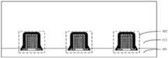
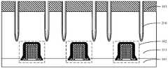
- a substrate 101is provided, a plurality of discrete transistor structures 102 are formed on the substrate 101 , and a dielectric layer 111 covering the transistor structures 102 is formed.
- the material of the substrate 101may include sapphire, silicon, silicon carbide, gallium arsenide, aluminum nitride or zinc oxide, etc.
- the substrate 101is made of silicon material, and it is clear to those skilled in the art that this embodiment uses silicon material
- the substrate 101is used to facilitate the understanding of the subsequent formation method by those skilled in the art, and does not constitute a limitation. In the actual application process, a suitable substrate material can be selected according to requirements.
- the transistor structure 102is discretely located on the substrate 101. It should be noted that the transistor structure 102 given in the drawings is a simplified structure, which is only used to represent the position of the transistor structure 102, and the transistor structure 102 does not constitute a limitation to this embodiment. .
- the substrate 101also includes other semiconductor structures such as the shallow trench isolation structure. Since it does not involve the core points of the present application, it will not be repeated here. Those skilled in the art can understand that the substrate 101 includes making the semiconductor structure normal. Other structures that run.
- the dielectric layer 111is an inter-layer dielectric layer (ILD), which is used to electrically isolate a subsequently formed metal layer from the transistor structure 102 located on the substrate 101 .
- the thickness of the dielectric layer 111is 100 nm ⁇ 150 nm, such as 110 nm, 120 nm, 130 nm or 140 nm; if the thickness of the dielectric layer 111 is less than 100 nm, due to the thinner dielectric layer , so that the distance between the subsequently formed metal layer and the transistor structure 102 is close, and there is a risk of short circuit; if the thickness of the dielectric layer 111 is greater than 150 nm, the thickness of the final semiconductor structure is too thick, which easily limits the application of the semiconductor structure.
- the material of the dielectric layer 111is an insulating material, such as silicon dioxide, silicon nitride, silicon oxynitride, or the like.
- the method for forming the dielectric layer 111includes spin coating (Spin-On Deposition, SOD), and the forming of the dielectric layer 111 by the SOD method has good adhesion and gap filling capability, ensuring that the formed dielectric layer 111 can be The discrete transistor structures 102 are completely covered, avoiding the risk of short circuits in the transistor structures 102 .
- SODspin-On Deposition
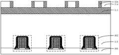
- discrete metal layers 103are formed on the top surface of the dielectric layer 111 , and openings 105 are formed in the gaps between the metal layers 103 .
- a metal film 113 covering the top surface of the dielectric layer 111is formed on the dielectric layer 111, a patterned first mask layer 114 is formed on the top surface of the metal film 113, and a second mask layer is formed on the sidewalls of the first mask layer Membrane layer 124 .
- the initial metal film (not shown)is formed by atomic layer deposition or chemical vapor deposition.
- the initial metal film (not shown)is formed by atomic layer deposition.
- the deposited initial metal film (not shown)has good coverage; in other embodiments, for example, the metal film may be formed by chemical vapor deposition at 500° C. or 600° C.
- the top of the initial metal film (not shown)is polished by chemical mechanical polishing to form a metal film 113 with a relatively flat top surface.
- the removal rateis beneficial to shorten the process cycle.
- the metal film 113can be made of one conductive material or composed of multiple conductive materials, such as doped polysilicon, titanium, titanium nitride, tungsten, and a compound of tungsten, etc.
- the metal film 113is used for the subsequent formation of metal layer to interconnect the capacitor structures in the DRAM array area.
- a first mask(not shown) is formed on the top surface of the metal film 113, and then a patterned photoresist layer is formed on the top surface of the first mask. Based on the patterned photoresist layer patterning A first mask (not shown) forms a patterned first mask layer 114 .
- a second mask layer 124is formed on the sidewall of the first mask layer 114 .
- the second mask layer 124is formed by atomic layer deposition, the second mask layer 124 formed by atomic layer deposition has good density, and the thickness of the second mask layer 124 is controllable.
- the width of the second mask layer 124 formedis 10 nm ⁇ 50 nm, such as 20 nm, 30 nm or 40 nm. If the width of the film layer 124 is less than 10 nm, the width of the subsequently formed opening will be less than 10 nm, and the effect of reducing parasitic capacitance is poor; if the width of the second mask layer 124 is greater than 50 nm, the metal interconnection occupies a larger chip area, It is not conducive to the miniaturization of the semiconductor process.
- the materials of the second mask layer 124 and the first mask layer 114are different, so that there is an etching selectivity ratio for subsequent selective etching of the first mask layer 114 or the second mask layer 124 .
- a third mask layer 134 filling the gap between the second mask layers 124is formed.
- a third mask 104filling the gap between the second mask layers 124 and covering the first mask layer 114 and the second mask layer 124 is formed.
- the chemical vapor deposition methodis used to form the third mask 104, and the chemical vapor deposition to form the third mask 104 has a higher deposition rate, which is beneficial to shorten the process cycle.
- the materials of the third mask 104 and the second mask layer 124are different, so that there is an etching selectivity ratio for subsequent selective etching of the third mask 104 or the second mask layer 124 .
- the third mask 104 on the top surfaces of the first mask layer 114 and the second mask layer 124is removed to form a third mask layer 134 .
- chemical mechanical polishing or etchingis used to remove the third mask 104 on the top surfaces of the first mask layer 114 and the second mask layer 124.
- the third mask 104 on the top surfaces of the first mask layer 114 and the second mask layer 124is removed by mechanical polishing.
- chemical mechanical polishinghas a higher removal rate, which is beneficial to shorten the process cycle. .
- the second mask layer 124(refer to FIG. 4 ) is removed until the metal film 113 (refer to FIG. 4 ) is exposed, and the exposed metal film is removed based on the first mask layer 114 and the third mask layer 134 113 , forming discrete metal layers 103 .
- the second mask layer 124 and the first mask layer 114have an etching selectivity ratio
- the third mask layer 124 and the third mask layer 134have an etching selectivity ratio
- the second mask layer 124is etched by using The speed of the etching process is higher than that of the first mask layer 114 and the third mask layer 134 , and the second mask layer 124 is selectively removed until the metal film 113 is exposed.
- the exposed metal film 113is removed by dry etching.
- the longitudinal etching rate and the lateral etching rateare relatively low, so that the edge morphology of the formed metal layer 103 is good.
- the first mask layer 114 and the third mask layer 134are removed.
- the first mask layer 114 and the third mask layer 134are removed, specifically, the first mask layer 114 and the second mask layer are removed by chemical mechanical polishing or etching 124.
- chemical mechanical polishingis used to remove the first mask layer 114 and the second mask layer 124. Compared with etching, chemical mechanical polishing has a higher removal rate, which is beneficial to shorten the process cycle.
- openings 105are formed in the gaps between the metal layers 103 based on the gaps between the discrete metal layers 103 .
- the insulating layer filling the opening 105is a single-layer structure, and the formed insulating layer of the single-layer structure will be described in detail below with reference to the accompanying drawings.
- the opening 105(refer to FIG. 7 ) is filled with an insulating layer 106 having a dielectric constant smaller than that of the dielectric layer 111 , the insulating layer 106 is used to reduce the parasitic capacitance between the metal layers 103 , and The parasitic capacitance between the metal layer 103 and the transistor structure 102 is reduced.
- the insulating layer 106 filling the opening 105is formed by atomic layer deposition, and the insulating layer 106 formed by atomic layer deposition has good density.
- the material of the insulating layer 106includes doped boron or Phosphorus silicon oxide; in other embodiments, the material of the insulating layer can be specifically set according to the material of the dielectric layer.
- the dielectric constant of the semiconductor structure between the metal layer 103 and the transistor structure 102is reduced, thereby reducing the parasitic capacitance between the metal layer 103 and the transistor structure 102;
- the dielectric constant of the semiconductor structure between the layer 103 and the metal layer 103is reduced, thereby reducing the parasitic capacitance between the metal layer 103 and the metal layer 103; Electrical crosstalk occurs between the smaller metal layers 103 .
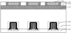
- the insulating layer filling the opening 105is a multi-layer structure.
- the present embodimenttakes the two-layer structure as an example. The following describes the insulating layer of the formed multi-layer structure in detail with reference to the accompanying drawings. In other embodiments, the insulating layer may also be a three-layer or more than three-layer structure. Those skilled in the art will understand that the method for forming a two-layer insulating structure disclosed in this embodiment may be applicable to a multi-layer structure, unless a special insulating layer is used. The formation method of , shall fall within the protection scope of this application.
- a first insulating film 216is formed covering the sidewalls of the opening 105 (refer to FIG. 7 ) and the sidewalls of the metal layer 103 .
- the first insulating film 216is formed by atomic layer deposition, and the first insulating film 216 formed by atomic layer deposition has good density, and the thickness of the first insulating film 216 is controllable.
- the thickness of the formed first insulating film 216is 2 nm ⁇ 10 nm, for example, 4 nm, 6 nm or 8 nm.
- a second insulating film 226is formed on the sidewall of the first insulating film 216.
- the materials of the first insulating film 216 and the second insulating film 226are different, and the first insulating film 216 and the second insulating film 226 together constitute an insulating film Floor.
- the second insulating film 226is formed by atomic layer deposition, and the second insulating film 226 formed by atomic layer deposition has good coverage.
- the vapor deposition methodforms the metal film and the second insulating film.
- the insulating layer of the multilayer structureis formed by insulating films formed of different materials, which can further reduce the dielectric constant of the formed insulating layer.
- the first insulating film 216 and the second insulating film 226can be made of the same material and different materials, even if the first insulating film 216 and the second insulating film 226 are made of the same material, because the first insulating film 216 and The presence of an interface layer between the second insulating films 226 can still reduce the dielectric constant of the formed insulating layer.
- the formed second insulating film 226also surrounds an air gap 206, and the air gap 206 is used to reduce the dielectric constant of the insulating layer.
- this embodimentprovides two methods for forming the air gap 206, which are as follows:
- Method 1The second insulating film 226 is formed on the sidewall of the first insulating film 216 by atomic layer deposition, and the gap between the metal layers 103 is sealed to enclose the air gap 206 .
- Method 2The second insulating film 226 is formed on the top of the sidewall of the first insulating film 216 by a sealing process, and the air gap 206 is formed at the same time.
- the length of the air gap 206is at least 10 nm.
- the length of the air gap 206is 10 nm ⁇ 100 nm, for example, 30 nm, 50 nm, 70 nm or 90 nm; if the length of the air gap 206 is less than 10 nm, the effect of reducing the dielectric constant through the air gap 206 is poor.
- the lengthis greater than 100 nm, and there may be electrical breakdown due to the large air gap, resulting in a short circuit.
- the length of the air gap 206is 10 nm to 100 nm based on the thickness of the dielectric layer 111 being 100 nm to 150 nm. In a specific application process, the length of the air gap 206 can be specifically set according to the thickness of the dielectric layer 111 .
- the dielectric constant of the semiconductor structure between the metal layer 103 and the transistor structure 102is reduced, thereby reducing the parasitic capacitance between the metal layer 103 and the transistor structure 102 .
- the enclosed air gap 206is also located in the gap between the metal layers 103 .
- the air gap 206is also located between the metal layers 103 , which can further reduce the dielectric constant of the semiconductor structure between the metal layers 103 and the metal layers 103 , thereby reducing the parasitic capacitance between the metal layers 103 and the metal layers 103 .
- an openingis formed in the dielectric layer between the metal layers, and the opening is filled with an insulating layer whose dielectric constant is smaller than that of the dielectric layer, thereby reducing the dielectric constant of the semiconductor structure between the metal layer and the transistor structure , thereby reducing the parasitic capacitance between the metal layer and the transistor structure, and reducing the parasitic capacitance between the metal layer and the metal layer.
- a semiconductor structureincluding: a transistor structure, located on the surface of a substrate; a dielectric layer, covering the substrate and the transistor structure; a metal layer, discretely disposed on the top surface of the dielectric layer; an opening, based on between the metal layers
- the gapis set in the dielectric layer; the insulating layer fills the gap between the opening and the metal layer.
- the dielectric constant of the insulating layeris smaller than the dielectric constant of the dielectric layer, which is used to reduce the parasitic capacitance between the metal layers, and the metal layer. Parasitic capacitance between layers and transistor structures.
- the semiconductor structureincludes a substrate 101, and the material of the substrate 101 may include sapphire, silicon, silicon carbide, gallium arsenide, aluminum nitride or zinc oxide, etc.; in this embodiment, the substrate 101 is made of silicon material.
- the transistor structure 102is located on the surface of the substrate 101, and the transistor structure 102 is discretely located on the substrate 101. It should be noted that the transistor structure 102 given in the drawings is a simplified structure, which is only used to reflect the position of the transistor structure 102. The structure 102 does not constitute a limitation to this embodiment.
- the substrate 101also includes other semiconductor structures such as a shallow trench isolation structure. Since it does not involve the core points of the present application, it will not be repeated here. Those skilled in the art can understand that the substrate 101 includes a Other structures in which the semiconductor structure operates normally.
- the dielectric layer 111covers the substrate 101 and the transistor structure 102.
- the dielectric layer 111is an inter-layer dielectric layer (ILD), which is used to electrically isolate the subsequently formed metal layer from the substrate 101. transistor structure 102 on the .
- the thickness of the dielectric layer 111is 100 nm ⁇ 150 nm, such as 110 nm, 120 nm, 130 nm or 140 nm.
- the metal layer 103is discretely disposed on the top surface of the dielectric layer 111.
- the metal layer 103may be made of a conductive material or composed of multiple conductive materials, such as doped polysilicon, titanium, titanium nitride, tungsten and A compound of tungsten, etc., the metal layer 103 is used to interconnect the capacitance structure of the DRAM array area.
- the width of the gap between the metal layersis 10 nm ⁇ 50 nm, such as 20 nm, 30 nm or 40 nm.
- Openings 105are provided in the dielectric layer 111 based on the gap between the metal layers 103 .
- the insulating layer 106has a single-layer structure, the insulating layer 106 fills the gap between the opening 105 and the metal layer 103 , and the dielectric constant of the insulating layer 106 is smaller than the dielectric constant of the dielectric layer 111 to reduce the metal layer.
- the parasitic capacitance between 103 and the parasitic capacitance between the metal layer 103 and the transistor structure 102is included in this embodiment.
- the material of the insulating layer 106includes silicon oxide doped with boron or phosphorus; in other embodiments, the material of the insulating layer can be specifically set according to the material of the dielectric layer.
- the insulating layeris a multi-layer structure. Taking a two-layer structure as an example, the following describes the insulating layer of the multi-layer structure in detail with reference to the accompanying drawings. It should be noted that the insulating layer may also be three layers or three layers. For the above structure, those skilled in the art will understand that the two-layer insulating structure disclosed in this embodiment can be applied to a multi-layer structure. If the structure does not use a special insulating layer, it should fall within the protection scope of the present application.
- the insulating layerincludes: a first insulating film 216 located on the sidewall of the opening 105 and the metal layer 103 ; a second insulating film 226 located on the sidewall of the first insulating film 216 and filling the opening 105 and the metal layer In the gap between the layers 103, the materials of the first insulating film 216 and the second insulating film 226 are different.
- the insulating films of different materialsconstitute the insulating layer of the multilayer structure, which can further reduce the dielectric constant of the formed insulating layer.
- first insulating film 216 and the second insulating film 226can be made of the same material and different materials, even if the first insulating film 216 and the second insulating film 226 are made of the same material, because the first insulating film 216 and The presence of an interface layer between the second insulating films 226 can still reduce the dielectric constant of the formed insulating layer 106 .
- the thickness of the formed first insulating film 216is 2 nm ⁇ 10 nm, for example, 4 nm, 6 nm or 8 nm.
- the insulating layerfurther includes an air gap 206 surrounded by a second insulating film 226 for reducing the dielectric constant of the insulating layer.
- the length of the air gap 206is at least 10 nm.
- the length of the air gap 206is between 10 nm and 100 nm, eg, 30 nm, 50 nm, 70 nm, or 90 nm. It should be noted that the length of the air gap 206 is 10 nm to 100 nm based on the thickness of the dielectric layer 111 being 100 nm to 150 nm. In a specific application process, the length of the air gap 206 can be specifically set according to the thickness of the dielectric layer 111 .
- the air gap 206is also located in the gap between the metal layers 103 , and the air gap 206 is also located between the metal layers 103 , which can further reduce the dielectric of the semiconductor structure between the metal layer 103 and the metal layer 103 constant, thereby reducing the parasitic capacitance between the metal layer 103 and the metal layer 103 .
- the insulating layerincludes a first insulating film located on the sidewall of the opening and the metal layer; a second insulating film located on top of the sidewall of the first insulating film for sealing the gap between the metal layers for sealing
- the first insulating film and the second insulating filmtogether form an air gap, and the materials of the first insulating film and the second insulating film are different; it should be noted that the material of the first insulating film and the second insulating film In the above structure, the air gap is directly formed by the sealed second insulating film, which reduces the dielectric constant of the semiconductor structure between the metal layer and the transistor structure, thereby reducing the parasitic capacitance between the metal layer and the transistor structure.
- the dielectric constant of the insulating layeris smaller than the dielectric constant of the dielectric layer, and the insulating layer is located at the gap between the metal layers, so as to reduce the dielectric constant of the semiconductor structure between the metal layer and the transistor structure, and reduce the dielectric constant between the metal layer and the metal layer.
- the dielectric constant of the semiconductor structurein between, thereby reducing the parasitic capacitance between the metal layer and the transistor structure, and reducing the parasitic capacitance between the metal layer and the metal layer.
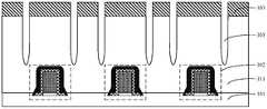
- FIG. 12Another embodiment of the present application provides an application of the above semiconductor structure. This embodiment is described based on the semiconductor structure provided in FIG. 12 as an example. It should be noted that the semiconductor structure provided in FIG. 12 may be replaced with FIG. 8 , FIG. 10 or FIG. 11. The application of the semiconductor structure provided in this embodiment will be described in detail below with reference to the accompanying drawings. Referring to FIG. 13, the details are as follows:
- the substrate 101is also provided with a buried transistor structure 301, the buried transistor structure 301 includes a buried gate 311, a buried source 321 and a buried drain 331, wherein the buried source 321 is used for For electrically connecting the capacitor structure, the buried drain 331 is used for electrically connecting the metal layer 103 .
- the semiconductor structurealso includes an intermediate layer 304 covering the metal layer 103.
- the intermediate layer 304is the semiconductor structure between the metal layer 103 and the capacitor structure 305. Since it has nothing to do with the core content of this application, the intermediate layer 304 is used in this embodiment. Characterize the location in the semiconductor structure.
- the semiconductor structurealso has a first conductive layer 303 penetrating the dielectric layer 111 and part of the substrate 101.
- the first conductive layer 303is used to electrically connect the metal layer 103 and the buried drain 331, so as to realize the electrical connection of the buried drain 331.
- the metal layer 103is connected.
- the second conductive layer 304 penetrating the dielectric layer 111, the intermediate layer 304 and part of the substrate 101, the second conductive layer 304is used to electrically connect the capacitor structure 305 and the buried source electrode 321 to realize the buried source electrode 321 is electrically connected to the capacitor structure.
- the capacitor structure 305is only used to characterize the position of the capacitor structure 305 , and the specific structure of the capacitor structure is not limited. In specific applications, the capacitor structure 305 may adopt capacitors such as column capacitors and double-sided capacitors. structure.
Landscapes
- Engineering & Computer Science (AREA)
- Physics & Mathematics (AREA)
- Condensed Matter Physics & Semiconductors (AREA)
- General Physics & Mathematics (AREA)
- Computer Hardware Design (AREA)
- Microelectronics & Electronic Packaging (AREA)
- Power Engineering (AREA)
- Manufacturing & Machinery (AREA)
- Internal Circuitry In Semiconductor Integrated Circuit Devices (AREA)
Abstract
Description
Translated fromChinese交叉引用cross reference
本申请要求于2020年12月24日递交的名称为“半导体结构的形成方法及半导体结构”、申请号为202011552783.6的中国专利申请的优先权,其通过引用被全部并入本申请。This application claims the priority of the Chinese patent application entitled "Method for Forming Semiconductor Structure and Semiconductor Structure", filed on December 24, 2020, with application number 202011552783.6, which is fully incorporated into this application by reference.
本申请涉及但不限于一种半导体结构的形成方法及半导体结构。The present application relates to, but is not limited to, a method for forming a semiconductor structure and a semiconductor structure.
传统的动态随机存取存储器(Dynamic Random Access Memory,DRAM)阵列区的布局受到字线间距和位线间距的限制。The layout of the traditional dynamic random access memory (Dynamic Random Access Memory, DRAM) array area is limited by the word line spacing and the bit line spacing.
随着技术的进步,半导体结构尺寸逐渐缩小,字线间距和位线间距不断减小,导致阵列区的金属层的金属布线难以形成图案,且由于特征尺寸的缩小,金属层与其他导电结构(例如位于两个阵列之间的晶体管结构)之间的寄生电容增大,影响形成的半导体结构的电学性能。With the advancement of technology, the size of semiconductor structures is gradually reduced, and the spacing between word lines and bit lines is continuously reduced, which makes it difficult for the metal wiring of the metal layer in the array area to form patterns, and due to the shrinking feature size, the metal layer and other conductive structures ( An increase in parasitic capacitance, such as between transistor structures located between two arrays, affects the electrical properties of the resulting semiconductor structure.
如何形成阵列区的金属层,且降低金属层与其他导电结构之间的寄生电容,是当下亟待解决的问题。How to form the metal layer in the array region and reduce the parasitic capacitance between the metal layer and other conductive structures is an urgent problem to be solved at present.
发明内容SUMMARY OF THE INVENTION
本申请实施例提供了一种半导体结构的形成方法,包括:在衬底上形成多个分立的晶体管结构;形成覆盖晶体管结构的介质层;在介质层的顶部表面形成分立的金属层;在金属层之间的间隙形成开口;用绝缘层填充开口,绝缘层的介电常数小于介质层的介电常数,绝缘层用于减小金属层之间的寄生电容,以及减小金属层与晶体管结构之间的寄生电容。An embodiment of the present application provides a method for forming a semiconductor structure, including: forming a plurality of discrete transistor structures on a substrate; forming a dielectric layer covering the transistor structures; forming a discrete metal layer on the top surface of the dielectric layer; The gap between the layers forms an opening; the opening is filled with an insulating layer, the dielectric constant of the insulating layer is smaller than that of the dielectric layer, and the insulating layer is used to reduce the parasitic capacitance between the metal layers and reduce the metal layer and the transistor structure parasitic capacitance between.
本申请实施例还提供了一种一种半导体结构,其特征在于,包括:晶体管结构,位于衬底表面;介质层,覆盖衬底和晶体管结构;金属层,分立设置在介质层顶部表面;开口,基于金属层之间的间隙,设置在介质层中;绝缘层,填充开口和金属层之间的间隙,绝缘层的介电常数小于介质层的介电常数,用 于减小金属层之间的寄生电容,以及金属层与晶体管结构之间的寄生电容。An embodiment of the present application also provides a semiconductor structure, which is characterized by comprising: a transistor structure, located on the surface of the substrate; a dielectric layer, covering the substrate and the transistor structure; a metal layer, discretely disposed on the top surface of the dielectric layer; an opening , based on the gap between the metal layers, set in the dielectric layer; the insulating layer, filling the gap between the opening and the metal layer, the dielectric constant of the insulating layer is smaller than the dielectric constant of the dielectric layer, used to reduce the gap between the metal layers , and the parasitic capacitance between the metal layer and the transistor structure.
图1~图12为本申请一实施例提供的半导体结构的形成方法中各步骤对应的剖面结构示意图;1 to 12 are schematic cross-sectional structural diagrams corresponding to each step in a method for forming a semiconductor structure according to an embodiment of the present application;
图13为本申请又一实施例提供的半导体结构的应用的结构示意图。FIG. 13 is a schematic structural diagram of an application of a semiconductor structure provided by yet another embodiment of the present application.
随着技术的进步,半导体结构尺寸逐渐缩小,字线间距和位线间距不断减小,导致阵列区的金属层的金属布线难以形成图案,且由于特征尺寸的缩小,金属层与其他导电结构,例如位于两个阵列之间的晶体管结构,之间的寄生电容增大,影响形成的半导体结构的电学性能。With the advancement of technology, the size of semiconductor structures is gradually reduced, and the spacing between word lines and bit lines is continuously reduced, which makes it difficult to form patterns of metal wiring in the metal layer of the array area. For example, for transistor structures located between two arrays, the parasitic capacitance between them increases, which affects the electrical performance of the formed semiconductor structure.
本申请一实施例提供了一种半导体结构的形成方法,包括:在衬底上形成多个分立的晶体管结构;形成覆盖晶体管结构的介质层;在介质层的顶部表面形成分立的金属层;在金属层之间的间隙形成开口;用绝缘层填充开口,绝缘层的介电常数小于介质层的介电常数,绝缘层用于减小金属层之间的寄生电容,以及减小金属层与晶体管结构之间的寄生电容。An embodiment of the present application provides a method for forming a semiconductor structure, including: forming a plurality of discrete transistor structures on a substrate; forming a dielectric layer covering the transistor structures; forming a discrete metal layer on the top surface of the dielectric layer; The gap between the metal layers forms an opening; the opening is filled with an insulating layer, the dielectric constant of the insulating layer is smaller than the dielectric constant of the dielectric layer, and the insulating layer is used to reduce the parasitic capacitance between the metal layers, and reduce the metal layer and the transistor. Parasitic capacitance between structures.
本领域的普通技术人员可以理解,在本发明各实施例中,为了使读者更好地理解本申请而提出了许多技术细节。但是,即使没有这些技术细节和基于以下各实施例的种种变化和修改,也可以实现本申请所要求保护的技术方案。It can be understood by those skilled in the art that, in each embodiment of the present invention, many technical details are provided for readers to better understand the present application. However, even without these technical details and various changes and modifications based on the following embodiments, the technical solutions claimed in the present application can be realized.
图1~图12为本实施例提供的半导体结构的形成方法中各步骤对应的剖面结构示意图,以下结合附图对本实施例提供的一种半导体结构的形成方法作进一步详细说明,具体如下:1 to 12 are schematic cross-sectional structural diagrams corresponding to each step in the method for forming a semiconductor structure provided by the present embodiment. The following describes the method for forming a semiconductor structure provided by the present embodiment in further detail, as follows:
参考图1,提供衬底101,在衬底101上形成多个分立的晶体管结构102,形成覆盖晶体管结构102的介质层111。Referring to FIG. 1 , a
衬底101的材料可以包括蓝宝石、硅、碳化硅、砷化镓、氮化铝或者氧化锌等;在本实施例中衬底101采用硅材料,本领域技术人员清楚,本实施例采用硅材料作为衬底101是为了方便本领域技术人员对后续形成方法的理解,并不构成限定,在实际应用过程中,可以根据需求选择合适的基底的材料。The material of the
晶体管结构102分立的位于衬底101上,需要说明的是,附图中给出的 晶体管结构102为简化结构,仅用于体现晶体管结构102的位置,晶体管结构102并不构成对本实施例的限定。另外,衬底101中还包括浅沟槽隔离结构等其他半导体结构,由于并不涉及到本申请的核心要点,在此不过多赘述,本领域技术人员可以理解衬底101中包括使半导体结构正常运行的其他结构。The
在本实施例中,介质层111为层间介质层(inter-layer dielectric,ILD),用于电隔离后续形成的金属层与位于衬底101上的晶体管结构102。在一个例子中,垂直于衬底101表面的方向上,介质层111的厚度为100nm~150nm,例如110nm、120nm、130nm或140nm;若介质层111的厚度低于100nm,由于较薄的介质层,使得后续形成的金属层与晶体管结构102之间的距离近,存在短路的风险;若介质层111的厚度大于150nm,最终形成的半导体结构的厚度过厚,容易限制半导体结构的应用。介质层111的材料采用绝缘材料,例如可以是二氧化硅、氮化硅、氮氧化硅等。In this embodiment, the
具体地,形成介质层111的方法包括采用旋转涂覆(Spin-On Deposition,SOD),采用SOD的方式形成介质层111具有较好的粘附性和间隙填充能力,保证形成的介质层111可以完全覆盖分立的晶体管结构102,避免晶体管结构102出现短路的风险。Specifically, the method for forming the
参考图2~图7,在介质层111的顶部表面形成分立的金属层103,在金属层103之间的间隙形成开口105,以下结合附图对形成分立的金属层103和形成开口105的方法进行进一步详细说明。Referring to FIGS. 2 to 7 ,
参考图2,在介质层111上形成覆盖介质层111顶部表面的金属膜113,在金属膜113顶部表面形成图形化的第一掩膜层114,在第一掩膜层侧壁形成第二掩膜层124。Referring to FIG. 2, a
具体地,采用原子层沉积的方法或化学气相沉积的方法形成初始金属膜(未图示),在本实施例中,采用原子层沉积的方式形成初始金属膜(未图示),采用原子层沉积形成的初始金属膜(未图示)具有良好的覆盖性;在其他实施例中,例如,可以采用500℃或600℃下进行化学气相沉积的方法形成金属膜。Specifically, the initial metal film (not shown) is formed by atomic layer deposition or chemical vapor deposition. In this embodiment, the initial metal film (not shown) is formed by atomic layer deposition. The deposited initial metal film (not shown) has good coverage; in other embodiments, for example, the metal film may be formed by chemical vapor deposition at 500° C. or 600° C.
形成初始金属膜(未图示)后,采用化学机械研磨的方式对初始金属膜(未图示)的顶部进行打磨,形成顶部表面较为平坦的金属膜113,化学机械研磨的方式具有较高的去除速率,有利于缩短工艺周期。After the initial metal film (not shown) is formed, the top of the initial metal film (not shown) is polished by chemical mechanical polishing to form a
在本实施例中,金属膜113可以为一种导电材料或者由多种导电材料构成,例如掺杂多晶硅、钛、氮化钛、钨以及钨的复合物等,金属膜113用于后续形成金属层,对DRAM阵列区的电容结构进行互联。In this embodiment, the
形成金属膜113后,在金属膜113顶部表面形成第一掩膜(未图示),然后在第一掩膜顶部表面形成图形化的光刻胶层,基于图形化的光刻胶层图形化第一掩膜(未图示),形成图形化的第一掩膜层114。After forming the
形成第一掩膜层114后,在第一掩膜层114的侧壁形成第二掩膜层124。After the
具体地,采用原子层沉积的方法形成第二掩膜层124,采用原子层沉积形成的第二掩膜层124具有良好的致密性,且形成第二掩膜层124的厚度可控。Specifically, the
在平行于衬底101表面的方向上,且垂直于第一掩膜层114的方向上,形成的第二掩膜层124的宽度为10nm~50nm,例如20nm、30nm或40nm,若第二掩膜层124的宽度小于10nm,会导致后续形成的开口的宽度小于10nm,降低寄生电容的效果差;若第二掩膜层124的宽度大于50nm,则金属互连占用了更大的芯片面积,不利于半导体工艺的微缩。In the direction parallel to the surface of the
在本实施例中,第二掩膜层124与第一掩膜层114的材料不同,从而存在刻蚀选择比,用于后续选择性刻蚀第一掩膜层114或第二掩膜层124。In this embodiment, the materials of the
参考图3和图4,形成填充第二掩膜层124之间间隙的第三掩膜层134。Referring to FIGS. 3 and 4 , a
具体地,参考图3,形成填充第二掩膜层124之间间隙,且覆盖第一掩膜层114和第二掩膜层124的第三掩膜104。Specifically, referring to FIG. 3 , a
具体地,采用化学气相沉积的方法形成第三掩膜104,采用化学气相沉积形成第三掩膜104具有较高的沉积速率,有利于缩短工艺周期。Specifically, the chemical vapor deposition method is used to form the
在本实施例中,第三掩膜104与第二掩膜层124的材料不同,从而存在刻蚀选择比,用于后续选择性刻蚀第三掩膜104或第二掩膜层124。In this embodiment, the materials of the
参考图4,去除第一掩膜层114和第二掩膜层124顶部表面的第三掩膜104,形成第三掩膜层134。Referring to FIG. 4 , the
形成第三掩膜104后,采用化学机械研磨的方式或者刻蚀的方式去除第一掩膜层114和第二掩膜层124顶部表面的第三掩膜104,在本实施例中,采用化学机械研磨的方式去除第一掩膜层114和第二掩膜层124顶部表面的第三掩 膜104,采用化学机械研磨相较于刻蚀的方式具有较高的去除速率,有利于缩短工艺周期。After the
参考图5,去除第二掩膜层124(参考图4),直至暴露出金属膜113(参考图4),基于第一掩膜层114和第三掩膜层134,去除暴露出的金属膜113,形成分立的金属层103。Referring to FIG. 5 , the second mask layer 124 (refer to FIG. 4 ) is removed until the metal film 113 (refer to FIG. 4 ) is exposed, and the exposed metal film is removed based on the
由于第二掩膜层124与第一掩膜层114存在刻蚀选择比,且第三掩膜层124与第三掩膜层134存在刻蚀选择比,采用对第二掩膜层124刻蚀速度大于第一掩膜层114和第三掩膜层134的刻蚀工艺,选择性去除第二掩膜层124,直至暴露出金属膜113。Since the
去除第二掩膜层124之后,基于第一掩膜层114和第三掩膜层134,采用干法刻蚀的方式刻蚀去除暴露出的金属膜113,由于干法刻蚀具有较高的纵向刻蚀速率,且横向刻蚀速率较低,使形成的金属层103的边缘形貌良好。After removing the
参考图6,去除第一掩膜层114和第三掩膜层134。Referring to FIG. 6, the
形成分立的金属层103之后,去除第一掩膜层114和第三掩膜层134,具体地,采用化学机械研磨的方式或者刻蚀的方式去除第一掩膜层114和第二掩膜层124,在本实施例中,采用化学机械研磨的方式去除第一掩膜层114和第二掩膜层124,采用化学机械研磨相较于刻蚀的方式具有较高的去除速率,有利于缩短工艺周期。After the
参考图7,基于分立的金属层103之间的间隙,在金属层103之间的间隙形成开口105。Referring to FIG. 7 ,
在一个例子中,填充开口105的绝缘层为单层结构,下面结合附图对形成的单层结构的绝缘层进行详细说明。In one example, the insulating layer filling the
参考图8,用绝缘层106填充开口105(参考图7),绝缘层106的介电常数小于介质层111的介电常数,绝缘层106用于减小金属层103之间的寄生电容,以及减小金属层103与晶体管结构102之间的寄生电容。Referring to FIG. 8 , the opening 105 (refer to FIG. 7 ) is filled with an insulating
具体地,采用原子层沉积的方式形成填充开口105的绝缘层106,采用原子层沉积形成的绝缘层106具有良好的致密性,在本实施例中,绝缘层106的材料包括掺杂有硼或磷的氧化硅;在其他实施例中,绝缘层的材料可以根据介 质层的材料进行具体设置。Specifically, the insulating
通过形成绝缘层106替代部分介质层111,使得金属层103与晶体管结构102之间的半导体结构的介电常数减小,从而减小金属层103与晶体管结构102之间的寄生电容;且使得金属层103与金属层103之间的半导体结构的介电常数减小,从而减小金属层103与金属层103之间的寄生电容;另外,通过在金属层103之间设置绝缘层106,防止间隔较小的金属层103之间出现电串扰。By forming the insulating
在另一个例子中,填充开口105的绝缘层为多层结构,本实施例以两层结构为例,下面结合附图对形成的多层结构的绝缘层进行详细说明,需要说明的是,在其他实施例中,绝缘层还可以为三层或三层以上的结构,本领域技术人员理解,本实施例公开的两层绝缘结构的形成方法可以适用于多层结构,若非使用特殊的绝缘层的形成方法,应当属于本申请的保护范围内。In another example, the insulating layer filling the
参考图9,形成覆盖开口105(参考图7)侧壁和金属层103侧壁的第一绝缘膜216。Referring to FIG. 9 , a first
具体地,采用原子层沉积的方法形成第一绝缘膜216,采用原子层沉积形成第一绝缘膜216具有良好的致密性,且形成第一绝缘膜216的厚度可控。Specifically, the first insulating
在本实施例中,形成的第一绝缘膜216的厚度为2nm~10nm,例如4nm、6nm或者8nm。In this embodiment, the thickness of the formed first insulating
参考图10,在第一绝缘膜216的侧壁上形成第二绝缘膜226,第一绝缘膜216和第二绝缘膜226的材料不同,第一绝缘膜216和第二绝缘膜226共同构成绝缘层。10, a second
具体地,采用原子层沉积的方法形成第二绝缘膜226,采用原子层沉积形成第二绝缘膜226具有良好的覆盖性,在其他实施例中,例如,可以采用500℃或600℃下进行化学气相沉积的方法形成金属膜第二绝缘膜。Specifically, the second
相比于单层结构的绝缘层,通过不同材料形成的绝缘膜构成多层结构的绝缘层,可以进一步减少形成的绝缘层的介电常数。需要说明的是,第一绝缘膜216和第二绝缘膜226可以采用相同的材料和不同的材料,即使第一绝缘膜216和第二绝缘膜226采用相同的材料,由于第一绝缘膜216和第二绝缘膜226之间存在界面层,仍可以降低形成的绝缘层的介电常数。Compared with the insulating layer of the single-layer structure, the insulating layer of the multilayer structure is formed by insulating films formed of different materials, which can further reduce the dielectric constant of the formed insulating layer. It should be noted that the first insulating
进一步地,参考图11,形成的第二绝缘膜226还围成空气间隙206,空气间隙206用于减小绝缘层的介电常数。具体地,本实施例给出了两种形成空气间隙206的方法,具体如下:Further, referring to FIG. 11 , the formed second insulating
方法一:采用原子层沉积的方式在第一绝缘膜216侧壁形成第二绝缘膜226,并对金属层103之间的间隙进行封口,以围成空气间隙206。Method 1: The second
方法二:采用封口工艺在第一绝缘膜216侧壁的顶部形成第二绝缘膜226,并同时围成空气间隙206。Method 2: The second
在垂直于衬底101表面的方向上,空气间隙206的长度至少为10nm。在一个例子中,空气间隙206的长度为10nm~100nm,例如,30nm、50nm、70nm或90nm;若空气间隙206的长度小于10nm,通过空气间隙206降低介电常数的效果差,若空气间隙206的长度大于100nm,由于存在较大的空气间隙,可能存在电击穿,从而导致短路的现象。需要说明的是,空气间隙206的长度为10nm~100nm是基于介质层111的厚度为100nm~150nm,在具体的应用过程中,空气间隙206的长度可以根据介质层111的厚度进行具体设置。In the direction perpendicular to the surface of the
通过形成空气间隙206,降低金属层103与晶体管结构102之间的半导体结构的介电常数,进而降低金属层103与晶体管结构102之间的寄生电容。By forming the
更进一步地,参考图12,围成的空气间隙206还位于金属层103之间的间隙中。空气间隙206还位于金属层103之间,可以进一步降低金属层103与金属层103之间半导体结构的介电常数,从而降低金属层103与金属层103之间的寄生电容。Still further, referring to FIG. 12 , the
基于金属层之间的间隙,在金属层间隙的介质层中形成开口,且在开口中填充介电常数小于介质层的绝缘层,降低了金属层与晶体管结构之间的半导体结构的介电常数,从而降低了金属层与晶体管结构之间的寄生电容,且降低了金属层与金属层之间的寄生电容。Based on the gap between the metal layers, an opening is formed in the dielectric layer between the metal layers, and the opening is filled with an insulating layer whose dielectric constant is smaller than that of the dielectric layer, thereby reducing the dielectric constant of the semiconductor structure between the metal layer and the transistor structure , thereby reducing the parasitic capacitance between the metal layer and the transistor structure, and reducing the parasitic capacitance between the metal layer and the metal layer.
上面各种步骤划分,只是为了描述清楚,实现时可以合并为一个步骤或者对某些步骤进行拆分,分解为多个步骤,只要包括相同的逻辑关系,都在本专利的保护范围内;对流程中添加无关紧要的修改或者引入无关紧要的设计,但不改变其流程的核心设计都在该专利的保护范围内。The above division of various steps is only for the purpose of describing clearly, and can be combined into one step or split into some steps during implementation, and decomposed into multiple steps, as long as the same logical relationship is included, all are within the protection scope of this patent; Adding insignificant modifications to the process or introducing insignificant designs without changing the core design of the process is within the scope of protection of this patent.
本申请另一实施例涉及一种半导体结构,包括:晶体管结构,位于衬底表面;介质层,覆盖衬底和晶体管结构;金属层,分立设置在介质层顶部表面;开口,基于金属层之间的间隙,设置在介质层中;绝缘层,填充开口和金属层之间的间隙,绝缘层的介电常数小于介质层的介电常数,用于减小金属层之间的寄生电容,以及金属层与晶体管结构之间的寄生电容。Another embodiment of the present application relates to a semiconductor structure, including: a transistor structure, located on the surface of a substrate; a dielectric layer, covering the substrate and the transistor structure; a metal layer, discretely disposed on the top surface of the dielectric layer; an opening, based on between the metal layers The gap is set in the dielectric layer; the insulating layer fills the gap between the opening and the metal layer. The dielectric constant of the insulating layer is smaller than the dielectric constant of the dielectric layer, which is used to reduce the parasitic capacitance between the metal layers, and the metal layer. Parasitic capacitance between layers and transistor structures.
图8、图10~图12为本实施例提供的半导体结构的剖面结构示意图,以下将结合附图对本实施例提供的半导体结构进行详细说明,与上述实施例相同或相应的部分,以下将不做详细赘述。8 and 10 to 12 are schematic cross-sectional structural diagrams of the semiconductor structure provided in this embodiment. The semiconductor structure provided in this embodiment will be described in detail below with reference to the accompanying drawings. Do details.
参考图8,半导体结构包括衬底101,衬底101的材料可以包括蓝宝石、硅、碳化硅、砷化镓、氮化铝或者氧化锌等;在本实施例中衬底101采用硅材料。8, the semiconductor structure includes a
晶体管结构102,位于衬底101表面,晶体管结构102分立的位于衬底101上,需要说明的是,附图中给出的晶体管结构102为简化结构,仅用于体现晶体管结构102的位置,晶体管结构102并不构成对本实施例的限定。The
需要说明的是,衬底101中还包括浅沟槽隔离结构等其他半导体结构,由于并不涉及到本申请的核心要点,在此不过多赘述,本领域技术人员可以理解衬底101中包括使半导体结构正常运行的其他结构。It should be noted that the
介质层111,覆盖衬底101和晶体管结构102,在本实施例中,介质层111为层间介质层(inter-layer dielectric,ILD),用于电隔离后续形成的金属层与位于衬底101上的晶体管结构102。在一个例子中,垂直于衬底101表面的方向上,介质层111的厚度为100nm~150nm,例如110nm、120nm、130nm或140nm。The
金属层103,分立的设置在介质层111顶部表面,在本实施例中,金属层103可以为一种导电材料或者由多种导电材料构成,例如掺杂多晶硅、钛、氮化钛、钨以及钨的复合物等,金属层103用于对DRAM阵列区的电容结构进行互联。在平行于衬底101表面的方向上,且垂直于第一掩膜层114的方向上,金属层之间的间隙的宽度为10nm~50nm,例如20nm、30nm或40nm。The
开口105(参考图7),基于金属层103之间的间隙,设置在介质层111中。Openings 105 (refer to FIG. 7 ) are provided in the
本实施例中,绝缘层106为单层结构,绝缘层106填充开口105和金属层103之间的间隙,绝缘层106的介电常数小于介质层111的介电常数,用于减小金属层103之间的寄生电容,以及金属层103与晶体管结构102之间的寄生电容。在本实施例中,绝缘层106的材料包括掺杂有硼或磷的氧化硅;在其他实施例中,绝缘层的材料可以根据介质层的材料进行具体设置。In this embodiment, the insulating
在其他实施例中,绝缘层为多层结构,以两层结构为例,下面结合附图对多层结构的绝缘层进行详细说明,需要说明的是,绝缘层还可以为三层或三层以上的结构,本领域技术人员理解,本实施例公开的两层绝缘结构可以适用于多层结构,若非使用特殊的绝缘层的结构,应当属于本申请的保护范围内。In other embodiments, the insulating layer is a multi-layer structure. Taking a two-layer structure as an example, the following describes the insulating layer of the multi-layer structure in detail with reference to the accompanying drawings. It should be noted that the insulating layer may also be three layers or three layers. For the above structure, those skilled in the art will understand that the two-layer insulating structure disclosed in this embodiment can be applied to a multi-layer structure. If the structure does not use a special insulating layer, it should fall within the protection scope of the present application.
在一个例子中,参考图10,绝缘层包括:第一绝缘膜216,位于开口105和金属层103的侧壁;第二绝缘膜226,位于第一绝缘膜216侧壁且填充开口105和金属层103之间的间隙,第一绝缘膜216和第二绝缘膜226的材料不同。相比于单层结构的绝缘层,不同材料的绝缘膜构成多层结构的绝缘层,可以进一步减少形成的绝缘层的介电常数。需要说明的是,第一绝缘膜216和第二绝缘膜226可以采用相同的材料和不同的材料,即使第一绝缘膜216和第二绝缘膜226采用相同的材料,由于第一绝缘膜216和第二绝缘膜226之间存在界面层,仍可以降低形成的绝缘层106的介电常数。In one example, referring to FIG. 10 , the insulating layer includes: a first
具体地,形成的第一绝缘膜216的厚度为2nm~10nm,例如4nm、6nm或者8nm。Specifically, the thickness of the formed first insulating
基于图10的半导体结构,进一步地,参考图11,绝缘层还包括空气间隙206,由第二绝缘膜226围成,用于减小绝缘层的介电常数。在垂直于衬底101表面的方向上,空气间隙206的长度至少为10nm。在一个例子中,空气间隙206的长度为10nm~100nm,例如,30nm、50nm、70nm或90nm。需要说明的是,空气间隙206的长度为10nm~100nm是基于介质层111的厚度为100nm~150nm,在具体的应用过程中,空气间隙206的长度可以根据介质层111的厚度进行具体设置。Based on the semiconductor structure of FIG. 10 , and further referring to FIG. 11 , the insulating layer further includes an
更进一步地,参考图12,空气间隙206还位于金属层103之间的间隙中,空气间隙206还位于金属层103之间,可以进一步降低金属层103与金属层103之间半导体结构的介电常数,从而降低金属层103与金属层103之间的寄生电 容。Further, referring to FIG. 12 , the
在另一个例子中,绝缘层包括第一绝缘膜,位于开口和金属层侧壁;第二绝缘膜,位于第一绝缘膜侧壁顶部,用于对金属层之间的间隙进行封口,进行封口后,第一绝缘膜与第二绝缘膜共同围成空气间隙,第一绝缘膜与第二绝缘膜的材料不同;需要说明的是,第一绝缘膜与第二绝缘膜材料相同,也适用于上述结构,通过封口的第二绝缘膜直接形成空气间隙,降低金属层与晶体管结构之间的半导体结构的介电常数,进而降低金属层与晶体管结构之间的寄生电容。In another example, the insulating layer includes a first insulating film located on the sidewall of the opening and the metal layer; a second insulating film located on top of the sidewall of the first insulating film for sealing the gap between the metal layers for sealing After that, the first insulating film and the second insulating film together form an air gap, and the materials of the first insulating film and the second insulating film are different; it should be noted that the material of the first insulating film and the second insulating film In the above structure, the air gap is directly formed by the sealed second insulating film, which reduces the dielectric constant of the semiconductor structure between the metal layer and the transistor structure, thereby reducing the parasitic capacitance between the metal layer and the transistor structure.
绝缘层的介电常数小于介质层的介电常数,且绝缘层位于金属层之间的间隙处,用于降低金属层与晶体管结构之间半导体结构的介电常数,且降低金属层与金属层之间半导体结构的介电常数,从而降低金属层与晶体管结构之间的寄生电容,以及降低金属层和金属层之间的寄生电容。The dielectric constant of the insulating layer is smaller than the dielectric constant of the dielectric layer, and the insulating layer is located at the gap between the metal layers, so as to reduce the dielectric constant of the semiconductor structure between the metal layer and the transistor structure, and reduce the dielectric constant between the metal layer and the metal layer The dielectric constant of the semiconductor structure in between, thereby reducing the parasitic capacitance between the metal layer and the transistor structure, and reducing the parasitic capacitance between the metal layer and the metal layer.
本申请又一实施例提供了上述半导体结构的应用,本实施例基于图12提供的半导体结构为例进行说明,需要说明的是,图12提供的半导体结构可替换为图8、图10或者图11提供的半导体结构,下面结合附图对本实施例提供的半导体结构的应用进行详细说明,参考图13,具体如下:Another embodiment of the present application provides an application of the above semiconductor structure. This embodiment is described based on the semiconductor structure provided in FIG. 12 as an example. It should be noted that the semiconductor structure provided in FIG. 12 may be replaced with FIG. 8 , FIG. 10 or FIG. 11. The application of the semiconductor structure provided in this embodiment will be described in detail below with reference to the accompanying drawings. Referring to FIG. 13, the details are as follows:
衬底101中还设置有埋入式晶体管结构301,埋入式晶体管结构301包括埋入式栅极311、埋入式源极321和埋入式漏极331,其中埋入式源极321用于电连接电容结构,埋入式漏极331用于电连接金属层103。The
具体地,半导体结构中还具有覆盖金属层103的中间层304,中间层304即金属层103到电容结构305之间的半导体结构,由于与本申请的核心内容无关,本实施例以中间层304表征在半导体结构中的位置。Specifically, the semiconductor structure also includes an
半导体结构中还具有贯穿介质层111和部分衬底101的第一导电层303,第一导电层303用于电连接金属层103和埋入式漏极331,以实现埋入式漏极331电连接金属层103。The semiconductor structure also has a first
半导体结构中贯穿介质层111、中间层304和部分衬底101的第二导电层304,第二导电层304用于电连接电容结构305和埋入式源极321,以实现埋入式源极321电连接电容结构。In the semiconductor structure, the second
需要说明的是,本实施例中电容结构305仅用于表征电容结构305的位置,并不对电容结构的具体结构进行限定,在具体应用中,电容结构305可以采用柱状电容、双面电容等电容结构。It should be noted that in this embodiment, the
由于上述实施例与本实施例相互对应,因此本实施例可与上述实施例互相配合实施。上述实施例中提到的相关技术细节在本实施例中依然有效,在上述实施例中所能达到的技术效果在本实施例中也同样可以实现,为了减少重复,这里不再赘述。相应地,本实施例中提到的相关技术细节也可应用在上述实施例中。Since the above-mentioned embodiment corresponds to this embodiment, this embodiment can be implemented in cooperation with the above-mentioned embodiment. The relevant technical details mentioned in the foregoing embodiment are still valid in this embodiment, and the technical effects that can be achieved in the foregoing embodiment can also be realized in this embodiment, and in order to reduce repetitions, details are not repeated here. Correspondingly, the relevant technical details mentioned in this embodiment can also be applied to the above-mentioned embodiments.
本领域的普通技术人员可以理解,上述各实施例是实现本申请的具体实施例,而在实际应用中,可以在形式上和细节上对其作各种改变,而不偏离本申请的精神和范围。Those of ordinary skill in the art can understand that the above-mentioned embodiments are specific embodiments for realizing the present application, and in practical applications, various changes in form and details can be made without departing from the spirit and the spirit of the present application. scope.
Claims (21)
Translated fromChinesePriority Applications (2)
| Application Number | Priority Date | Filing Date | Title |
|---|---|---|---|
| US17/767,574US12324148B2 (en) | 2020-12-24 | 2021-08-16 | Method for forming semiconductor structure and a semiconductor |
| EP21908628.7AEP4075492A4 (en) | 2020-12-24 | 2021-08-16 | Method for forming semiconductor structure and semiconductor structure |
Applications Claiming Priority (2)
| Application Number | Priority Date | Filing Date | Title |
|---|---|---|---|
| CN202011552783.6 | 2020-12-24 | ||
| CN202011552783.6ACN114678330A (en) | 2020-12-24 | 2020-12-24 | Forming method of semiconductor structure and semiconductor structure |
Publications (1)
| Publication Number | Publication Date |
|---|---|
| WO2022134623A1true WO2022134623A1 (en) | 2022-06-30 |
Family
ID=82070477
Family Applications (1)
| Application Number | Title | Priority Date | Filing Date |
|---|---|---|---|
| PCT/CN2021/112876CeasedWO2022134623A1 (en) | 2020-12-24 | 2021-08-16 | Method for forming semiconductor structure and semiconductor structure |
Country Status (4)
| Country | Link |
|---|---|
| US (1) | US12324148B2 (en) |
| EP (1) | EP4075492A4 (en) |
| CN (1) | CN114678330A (en) |
| WO (1) | WO2022134623A1 (en) |
Families Citing this family (1)
| Publication number | Priority date | Publication date | Assignee | Title |
|---|---|---|---|---|
| US12381077B2 (en)* | 2021-11-29 | 2025-08-05 | Asm Ip Holding B.V. | Methods of filling recesses on substrate surfaces and forming voids therein |
Citations (4)
| Publication number | Priority date | Publication date | Assignee | Title |
|---|---|---|---|---|
| US20140073128A1 (en)* | 2012-07-04 | 2014-03-13 | National Applied Research Laboratories | Manufacturing method for metal line |
| CN103839884A (en)* | 2014-03-10 | 2014-06-04 | 上海华虹宏力半导体制造有限公司 | Semiconductor device structure and forming method thereof |
| CN108028224A (en)* | 2015-10-16 | 2018-05-11 | 索尼公司 | Semiconductor device and method for manufacturing semiconductor device |
| KR20190134203A (en)* | 2018-05-25 | 2019-12-04 | 주식회사 디비하이텍 | Rf switch device with an air-gap and method of manufacturing the same |
Family Cites Families (8)
| Publication number | Priority date | Publication date | Assignee | Title |
|---|---|---|---|---|
| JP3305211B2 (en)* | 1996-09-10 | 2002-07-22 | 松下電器産業株式会社 | Semiconductor device and manufacturing method thereof |
| US5744865A (en)* | 1996-10-22 | 1998-04-28 | Texas Instruments Incorporated | Highly thermally conductive interconnect structure for intergrated circuits |
| JP2012009490A (en)* | 2010-06-22 | 2012-01-12 | Toshiba Corp | Semiconductor device and manufacturing method of the same |
| US8232618B2 (en) | 2010-08-11 | 2012-07-31 | International Business Machines Corporation | Semiconductor structure having a contact-level air gap within the interlayer dielectrics above a semiconductor device and a method of forming the semiconductor structure using a self-assembly approach |
| JP2017005227A (en)* | 2015-06-16 | 2017-01-05 | ルネサスエレクトロニクス株式会社 | Semiconductor device and manufacturing method of the same |
| US10211146B2 (en) | 2016-05-12 | 2019-02-19 | Globalfoundries Inc. | Air gap over transistor gate and related method |
| US11257673B2 (en)* | 2018-11-26 | 2022-02-22 | Taiwan Semiconductor Manufacturing Co., Ltd. | Dual spacer metal patterning |
| CN214428620U (en)* | 2020-12-24 | 2021-10-19 | 长鑫存储技术有限公司 | Semiconductor structure |
- 2020
- 2020-12-24CNCN202011552783.6Apatent/CN114678330A/enactivePending
- 2021
- 2021-08-16USUS17/767,574patent/US12324148B2/enactiveActive
- 2021-08-16EPEP21908628.7Apatent/EP4075492A4/ennot_activeWithdrawn
- 2021-08-16WOPCT/CN2021/112876patent/WO2022134623A1/ennot_activeCeased
Patent Citations (4)
| Publication number | Priority date | Publication date | Assignee | Title |
|---|---|---|---|---|
| US20140073128A1 (en)* | 2012-07-04 | 2014-03-13 | National Applied Research Laboratories | Manufacturing method for metal line |
| CN103839884A (en)* | 2014-03-10 | 2014-06-04 | 上海华虹宏力半导体制造有限公司 | Semiconductor device structure and forming method thereof |
| CN108028224A (en)* | 2015-10-16 | 2018-05-11 | 索尼公司 | Semiconductor device and method for manufacturing semiconductor device |
| KR20190134203A (en)* | 2018-05-25 | 2019-12-04 | 주식회사 디비하이텍 | Rf switch device with an air-gap and method of manufacturing the same |
Non-Patent Citations (1)
| Title |
|---|
| See also references ofEP4075492A4* |
Also Published As
| Publication number | Publication date |
|---|---|
| CN114678330A (en) | 2022-06-28 |
| EP4075492A1 (en) | 2022-10-19 |
| US20240268104A1 (en) | 2024-08-08 |
| US12324148B2 (en) | 2025-06-03 |
| EP4075492A4 (en) | 2023-08-23 |
Similar Documents
| Publication | Publication Date | Title |
|---|---|---|
| KR940006682B1 (en) | Manufacturing Method of Semiconductor Memory Device | |
| CN1123927C (en) | Method for manufacturing semiconductor memory device with self-aligned contacts | |
| US9613967B1 (en) | Memory device and method of fabricating the same | |
| WO2022088758A1 (en) | Method for forming semiconductor structure, and semiconductor structure | |
| WO2022088788A1 (en) | Method for forming semiconductor structure, and semiconductor structure | |
| WO2021258561A1 (en) | Memory forming method and memory | |
| WO2022179022A1 (en) | Method for forming semiconductor structure, and semiconductor structure | |
| CN108666310A (en) | Semiconductor memory device and method of forming the same | |
| WO2021233111A1 (en) | Memory forming method and memory | |
| WO2022134623A1 (en) | Method for forming semiconductor structure and semiconductor structure | |
| US6967150B2 (en) | Method of forming self-aligned contact in fabricating semiconductor device | |
| CN214428620U (en) | Semiconductor structure | |
| CN112635467A (en) | Memory cell structure and forming method | |
| TW202002242A (en) | Dynamic random access memory and methods of manufacturing, reading and writing the same | |
| WO2022062717A1 (en) | Semiconductor structure forming method and semiconductor structure | |
| KR100653983B1 (en) | How to Form Storage Node Contacts | |
| US12108593B2 (en) | Method for preparing semiconductor structure using a first mask comprises a groove | |
| KR100510998B1 (en) | Method for forming the storage node contact | |
| KR100844936B1 (en) | Semiconductor device and manufacturing method | |
| KR100226217B1 (en) | Method for forming charge storage electrode of semiconductor device | |
| KR0164080B1 (en) | Storage electrode manufacturing method | |
| KR20050002005A (en) | Method for fabricating semiconductor device capable of forming storage node contact hole and insulating spacer of bit line | |
| CN116249342A (en) | Preparation method of semiconductor structure, semiconductor structure and semiconductor memory | |
| KR20050003296A (en) | Method for forming the semiconductor memory device having a self-aligned contact hole | |
| KR19990061054A (en) | Capacitor Formation Method of Semiconductor Device |
Legal Events
| Date | Code | Title | Description |
|---|---|---|---|
| WWE | Wipo information: entry into national phase | Ref document number:17767574 Country of ref document:US | |
| WWE | Wipo information: entry into national phase | Ref document number:21908628.7 Country of ref document:EP | |
| ENP | Entry into the national phase | Ref document number:2021908628 Country of ref document:EP Effective date:20220714 | |
| 121 | Ep: the epo has been informed by wipo that ep was designated in this application | Ref document number:21908628 Country of ref document:EP Kind code of ref document:A1 | |
| NENP | Non-entry into the national phase | Ref country code:DE | |
| WWG | Wipo information: grant in national office | Ref document number:17767574 Country of ref document:US |