WO2022133913A1 - Radio frequency signal processing method and device, and receiver - Google Patents
Radio frequency signal processing method and device, and receiverDownload PDFInfo
- Publication number
- WO2022133913A1 WO2022133913A1PCT/CN2020/139045CN2020139045WWO2022133913A1WO 2022133913 A1WO2022133913 A1WO 2022133913A1CN 2020139045 WCN2020139045 WCN 2020139045WWO 2022133913 A1WO2022133913 A1WO 2022133913A1
- Authority
- WO
- WIPO (PCT)
- Prior art keywords
- signal
- interference signal
- radio frequency
- interference
- circuit
- Prior art date
- Legal status (The legal status is an assumption and is not a legal conclusion. Google has not performed a legal analysis and makes no representation as to the accuracy of the status listed.)
- Ceased
Links
Images


Classifications
- H—ELECTRICITY
- H04—ELECTRIC COMMUNICATION TECHNIQUE
- H04B—TRANSMISSION
- H04B1/00—Details of transmission systems, not covered by a single one of groups H04B3/00 - H04B13/00; Details of transmission systems not characterised by the medium used for transmission
- H04B1/06—Receivers
- H04B1/10—Means associated with receiver for limiting or suppressing noise or interference
Definitions
- the present applicationrelates to the technical field of electronic communication, and in particular, to a radio frequency signal processing method, device and receiver.
- the inventors of the present applicationfound that the second-order intermodulation interference signal increases with the increase of the input power, and the increase is twice the increment of the useful signal. Therefore, with the increase of the input signal, the second-order intermodulation interference signal increases faster than the useful signal.
- the input poweris large, the system is easily affected by the interference signal with a frequency similar to the useful signal.
- the main technical problem to be solved by the present applicationis to provide a radio frequency signal processing method, a radio frequency signal processing device and a receiver, which can realize the detection and identification of interference signals of different frequencies and types.
- a technical solution adopted in the present applicationis to provide a radio frequency signal processing method, the method includes: detecting a first interference signal in the radio frequency signal; attenuating/amplifying/delaying the first interference signal processing to obtain a second interference signal; comparing the first interference signal and the second interference signal to form a third interference signal corresponding to the first interference signal, and the third interference signal is a signal that can be detected and identified by the processor.
- the first interference signalis a sine wave signal with a DC component
- detecting the first interference signal in the radio frequency signalincludes: performing wave detection processing on the radio frequency signal to obtain a sine wave signal with a DC component.
- the first interference signalis a sine wave signal without a DC component
- detecting the first interference signal in the radio frequency signalincludes: performing wave detection processing on the radio frequency signal to obtain a sine wave signal with a DC component;
- the wave signalis de-DC processed to obtain a sine wave signal without DC component.
- performing attenuation/amplification/delay processing on the first interference signal to obtain the second interference signalfurther includes: performing attenuation and delay processing on the first interference signal.
- the third interference signalis a level signal. Comparing the first interference signal and the second interference signal, and forming a third interference signal corresponding to the first interference signal includes: if the first interference signal is larger than the second interference signal, then the first interference signal is greater than the second interference signal.
- the third interference signalis a high-level signal; if the first interference signal is greater than the second interference signal, the third interference signal is a low-level signal.
- the first interference signalis a second-order intermodulation interference signal with a frequency less than or equal to 10KHz.
- the methodfurther includes: sending the third interference signal to the mixer, so that the mixer processes the radio frequency signal , get a valid signal.
- the methodbefore detecting the first interference signal in the radio frequency signal, the method further includes: receiving an original radio frequency signal; and performing low-noise amplification processing on the original radio frequency signal to obtain an amplified radio frequency signal.
- the radio frequency signal processing deviceincludes an interference signal processing circuit, and the interference signal processing circuit includes a detection circuit, a processing circuit and a comparison circuit;
- the detection circuitis used for detecting the first interference signal in the radio frequency signal;
- the processing circuitis used for attenuating/amplifying/delaying the first interference signal to obtain the second interference signal;
- the comparing circuitis used for comparing the first interference signal and the The second interference signal forms a third interference signal corresponding to the first interference signal, and the third interference signal is a signal that the processor can detect and identify.
- the detection circuitincludes a detection circuit and a DC removal circuit, the detection circuit includes a diode and a first capacitor, the first end of the diode is the receiving end of the radio frequency signal, the second end of the diode is connected to the first end of the first capacitor, and the first end of the diode is connected to the first end of the first capacitor.
- the second end of the capacitoris grounded;
- the DC removing circuitincludes a first resistor and a second capacitor, the first end of the first resistor is connected to the first end of the first capacitor and the first end of the second capacitor, and the second end of the first resistor is connected ground.
- the processing circuitincludes a second resistor and a third capacitor.
- the first end of the second resistoris connected to the output end of the DC circuit, the second end of the second resistor is connected to the first end of the third capacitor, and the second end of the third capacitor is connected to the output end of the DC circuit. terminal to ground.
- the comparison circuitincludes an operational amplifier and a third resistor, the operational amplifier includes a first input end, a second input end and an output end, the first input end of the operational amplifier is connected to the output end of the processing circuit, and the second input end of the operational amplifier is connected to To the output end of the DC circuit, the output end of the operational amplifier is connected to the first end of the third resistor, and the second end of the third resistor is the output end of the third interference signal.
- the processorincludes a complex programmable logic device, a programmable logic controller, a field programmable logic gate array or a digital signal processor.
- a receiverwhich includes an antenna and a radio frequency signal processing device; the antenna is used for receiving radio frequency signals; the radio frequency signal processing device is connected to the antenna, and the radio frequency signal
- the processing deviceincludes an interference signal detection circuit, the interference signal detection circuit includes an interference signal processing circuit and a processor, and the interference signal processing circuit is used to detect the first interference signal in the radio frequency signal; the first interference signal is attenuated/amplified/delayed processing to obtain a second interference signal; comparing the first interference signal and the second interference signal to form a third interference signal corresponding to the first interference signal, and the third interference signal is a signal that can be detected and identified by the processor.
- the receiveralso includes a receiving circuit, which is connected to the antenna and the radio frequency signal processing device; the receiving circuit includes a low-pass filter, a radio frequency switch, a high-pass filter and a low-noise amplifier connected to each other; the low-pass filter is connected to the antenna, It is used to suppress non-useful frequency signals in the radio frequency signal; the radio frequency switch is connected to the low-pass filter to switch the transmission path of the radio frequency signal; the high-pass filter is connected to the radio frequency switch to suppress the radio frequency signal output by the low-pass filter The non-useful frequency signal in the low-noise amplifier is connected with the high-pass filter to amplify the radio frequency signal output by the high-pass filter.
- the receiving circuitincludes a low-pass filter, a radio frequency switch, a high-pass filter and a low-noise amplifier connected to each other;
- the low-pass filteris connected to the antenna, It is used to suppress non-useful frequency signals in the radio frequency signal;
- the radio frequency switchis connected to
- the beneficial effects of the present applicationare: different from the situation in the prior art, the method provided by the present application performs attenuation/amplification/delay processing on the detected interference signal, and then compares the pre-processed and post-processed signals , which converts the detection of the interference signal into the detection of the difference between the signals, which can reduce the qualification requirements of the detected signal, realize the detection of interference signals of different frequencies and types, and reduce the influence of the interference signals.
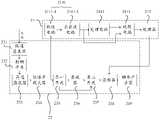
- FIG. 1is a schematic structural diagram of an embodiment of a receiver provided by the present application.
- FIG. 2is a schematic structural diagram of an embodiment of an interference signal detection circuit provided by the present application.
- FIG. 3is a schematic diagram of a waveform output by a comparison circuit in the interference signal detection circuit provided by the present application;
- FIG. 4is a schematic diagram of a specific structure of an interference signal processing circuit provided by the present application.
- FIG. 5is a schematic structural diagram of another embodiment of a receiver provided by the present application.
- FIG. 6is a schematic diagram of the comparison of the output waveforms of the detection circuit before and after the signal passes through the low noise amplifier in the radio frequency signal processing device provided by the present application;
- FIG. 7is a schematic flowchart of an embodiment of a radio frequency signal processing method provided by the present application.
- FIG. 8is a schematic flowchart of another embodiment of a radio frequency signal processing method provided by the present application.
- the present applicationprovides a receiver in which an interference signal detection circuit is added.
- the interference signal detection circuitincludes an interference signal processing circuit and a processor.
- the interference signal processing circuitcan process interference signals of different frequencies and types into a processor.
- the signal form that can be identifiedis used to detect interference signals of different frequencies and types, thereby reducing the impact of the interference signals on the receiver.
- FIG. 1is a schematic structural diagram of an embodiment of a receiver provided by the present application.
- the receiverincludes an antenna 10 and a radio frequency signal processing device 20.
- the antenna 10is used for receiving radio frequency signals
- the radio frequency signal processing device 20is connected to the antenna 10 and is used for processing the received radio frequency signals.
- the radio frequency signal processing device 20includes an interference signal detection circuit 21.
- the interference signal detection circuit 21includes an interference signal processing circuit 211 and a processor 213 that are connected to each other.
- the interference signal processing circuit 211can process the interference signal and can process the interference signal. into a form that can be identified by the processor 213, so that the interference signal can be detected and identified, so as to reduce the influence of the interference signal on the receiver.
- the receiver provided by the present applicationcan adopt the architecture of zero intermediate frequency and low intermediate frequency, and the receiver of the architecture of zero intermediate frequency and low intermediate frequency has the advantages of high integration, miniaturization, low cost and simple architecture.
- the signal processing method of directly converting the radio frequency to the basebandis easily affected by the even-order distortion, which may generate interference signals that cannot be filtered out by the filter, thus affecting the normal operation of the receiver.
- These interference signalsare generally low-frequency signals, which are not easy to be identified and detected.
- an interference signal processing circuit 211 and a processor 213are added to the receiver.
- the interference signal processing circuit 211can process interference signals of different frequencies and types into a signal form that the processor 213 can recognize, so as to realize the detection of different frequencies, Detection of different types of interference signals, thereby reducing the impact of interference signals on the receiver.
- the interference signal processing circuit 211divides the interference signal into two channels, one channel is kept as it is, and the other channel is subjected to attenuation/amplification/delay processing, and then the two channels of signals are compared, and then the comparison result is performed. detection.
- the detection of the interference signalis realized by comparing the difference of the signals in the two circuits, that is, the detection of the interference signal is converted into the detection of the difference between the signals, which can reduce the qualification requirements of the detected signal and realize the detection of different frequencies and different types. Detection of interfering signals.
- the output form of the comparison resultcan be set as required.
- the processor 213is used as the detector of the comparison result. Therefore, the comparison result can be output in a form that can be recognized by the processor 213 .
- the interference signal processing circuit 211at least includes a detection circuit 2111 , a processing circuit 2113 and a comparison circuit 2115 .
- the processing circuit 2113is respectively connected to the detection circuit 2111 and the comparison circuit 2115
- the detection circuit 2111is connected to the comparison circuit 2115 .
- the detection circuit 2111is used to detect the interference signal in the radio frequency signal, which may be recorded as the first interference signal.
- the processing circuit 2113is connected to the detection circuit 2111, and is used for attenuating/amplifying/delaying the first interference signal to obtain a processed interference signal, which may be recorded as the second interference signal.
- the comparison circuit 2115is connected with the detection circuit 2111 and the processing circuit 2113, and is used to compare the first interference signal and the second interference signal, obtain the difference between the two signals, and output the comparison result, which can be recorded as the third interference signal,
- the third interference signalis identified and detected, so as to realize the detection of the interference signal.
- the identification of the first interference signalcan be realized by detecting the third interference signal, that is, the substance of the third interference signal is still the detection of the first interference signal, or the first interference signal is converted into a more easily detectable signal.
- the third interference signalcan also be said to have a certain corresponding relationship with the first interference signal.
- the output form of the comparison result(that is, the form of the third interference signal) can be set as required.
- the processor 213is used as the detector of the comparison result. Therefore, the output third interference signal should be recognized by the processor 213. form. Further, in order to compare the difference between the first interference signal and the second interference signal, a signal form that is easier to process can be selected.
- the first interference signalcan be a sine wave signal, which will be attenuated/amplified/delayed There is a clear difference.
- the detection circuit 2111at least includes a detection circuit 2111-1, and the detection circuit 2111-1 can demodulate the radio frequency signal to extract the interference signal contained therein.
- the detection circuit 2111-1can output the detection result in the form of a sine wave signal with a DC component. If there is an interference signal in the RF signal, it will output a sine wave signal with a DC component. If there is no interference signal in the RF signal, then Output pure DC signal.
- the processing circuit 2113can attenuate or amplify the interference signal, so that the amplitude of the interference signal is reduced, which is different from the interference signal that has not been processed by the processing circuit 2113 .
- the processing circuit 2113can also perform delay processing on the interference signal as required, so that the period of the interference signal processed by the processing circuit 2113 and the interference signal not processed by the processing circuit 2113 is shifted. In other embodiments, the processing circuit 2113 may also perform delay processing while attenuating the interference signal, which is not specifically limited herein.
- FIG. 3is a schematic diagram of the waveform output by the comparison circuit in the interference signal detection circuit provided by the present application.
- signal 1is the interference signal obtained after processing by the detection circuit 2111-1
- signal 2is the interference signal processed by the processing circuit 2113.
- the processing circuit 2113performs attenuation processing on the interference signal. Specifically, after the signal 2 is attenuated by the processing circuit 2113, the amplitude of the signal 2 is reduced relative to that of the signal 1 that has not been attenuated, which can cause a difference between the signal 1 and the signal 2, that is, the interference signal obtained by the detection and the signal obtained after the attenuation process. interference signal difference.
- the comparison circuit 2115can compare and process the received interference signal obtained by detection and the interference signal after attenuation/amplification/delay processing to form a signal corresponding to the interference signal obtained by detection, that is to say, the comparison circuit 2115 will detect the interference signal.
- the resulting interference signalis converted into a difference signal.
- the form of the signal output by the comparison circuit 2115can be specifically set according to the device used to detect the output signal of the comparison circuit 2115.
- the comparison circuit 2115can output the result in the form of a level signal so that the signal output by the comparison circuit 2115 can be recognized by the processor 213.
- the signal 3is the level signal output by the comparison circuit 2115 .
- the comparison circuit 2115compares the signal 1 and the signal 2 to form a signal corresponding to the signal 1, that is to say, the comparison circuit 2115 converts the signal 1 into the signal 3 that can be detected and identified according to the comparison processing result, so that the Signal 1 can be detected and identified. Specifically, from left to right, in the first 1/2 cycle of signal 1, the signal strength of signal 1 is less than the signal strength of signal 2, then signal 3 is a high-level signal; In the cycle period of 2, the signal strength of signal 1 is greater than that of signal 2, then signal 3 is a low-level signal. The signals in other cycles of the signal 1 are compared with the signal 2 in the above-mentioned manner to obtain corresponding level signals, which are not repeated here.
- the comparison circuit 2115outputs a high and low level signal with the same frequency as the interference signal obtained by the detection, otherwise it outputs a 0V low voltage. level signal, so as to realize the detection of interfering signals.
- the processor 213may be a programmable logic device (CPLD, Complex Programming Logic Device), a digital signal processor (DSP, Digital Signal Process), a programmable logic controller (PLC, Programmable Logic Controller) and a field programmable logic gate array ( FPGA, Field Programmable Gate Array), etc., which are not specifically limited here.
- CPLDComplex Programming Logic Device
- DSPDigital Signal Process
- PLCprogrammable logic controller
- FPGAField Programmable Gate Array
- the detection circuit 2111may further include a DC removal circuit 2111-3, and the DC removal circuit 2111-3 may perform DC removal processing on the radio frequency signal demodulated by the detection circuit 2111-1 to obtain a DC removed signal. interfere with the signal.
- the DC removal circuit 2111-3can output the result in the form of a sine wave signal. If there is an interference signal in the radio frequency signal, it will output a sine wave signal. If there is no interference signal in the radio frequency signal, it will output a 0V low level signal.
- the interference signalmay be attenuated/amplified/delayed before DC processing, or may be attenuated/amplified/delayed after DC processing.
- the interference signal processing circuit 211includes a detection circuit 2111, a processing circuit 2113, and a comparison circuit 2115.
- the detection circuit 2111includes a detection circuit 2111-1 and a DC removal circuit 2111-3.
- the processing circuit 2113 and the detection circuitare respectively 2111 is connected to the comparison circuit 2115, and the detection circuit 2111 is connected to the comparison circuit 2115.
- the detection circuit 2111-1includes a diode D1 and a first capacitor C1
- the DC removing circuit 2111-3includes a first resistor R1 and a second capacitor C2
- the processing circuit 2113includes a second resistor R2 and a third capacitor C3, and the comparison circuit 2115 It includes an operational amplifier U1, a third resistor R3 and a power supply terminal VDD.
- the detection circuit 2111-1includes a diode D1 and a first capacitor C1.
- the first end of the diode D1is the radio frequency signal receiving end
- the second end of the diode D1is connected to the first end of the first capacitor C1
- the first end of the first capacitor C1is connected to the first end of the first capacitor C1.
- the second terminalis grounded.
- the voltage of the diode D1can be set to 50V
- the capacitance value of the first capacitor C1can be set to 180pF, which is not specifically limited herein.
- the setting of the detection circuit 2111-1can demodulate the received radio frequency signal to extract the interference signal contained in the radio frequency signal.
- the DC removing circuit 2111-3includes a first resistor R1 and a second capacitor C2.
- the first end of the first resistor R1is connected to the first end of the first capacitor C1 and the first end of the second capacitor C2. Both ends are grounded.
- the capacitance value of the second capacitor C2may be set to 0.01 ⁇ F, and the resistance value of the first resistor R1 may be set to 110 k ⁇ , which are not specifically limited herein. It can be understood that the de-DC circuit 2111-3 can adopt other circuit modes, and is not limited to the RC circuit.
- the setting of the DC-removal circuit 2111-3can perform DC-removal processing on the interference signal output by the detection circuit 2111-1, so that the DC-removed signal only contains a sine wave signal.
- the processing circuit 2113includes a second resistor R2 and a third capacitor C3, the first end of the second resistor R2 is connected to the second end of the second capacitor C2, the second end of the second resistor R2 is connected to the first end of the third capacitor C3, The second end of the third capacitor C3 is grounded.
- the resistance value of the second resistor R2can be set to 1M ⁇ , and the capacitance value of the third capacitor C3 can be set to 680pF, which is not specifically limited herein.
- other manners for performing delay attenuation on the signalmay also be used, which is not limited to an RC circuit, for example, a phase shifter or the like may be used.
- the comparison circuit 2115includes an operational amplifier U1 and a third resistor R3.
- the operational amplifier U1includes a first input terminal, a second input terminal and an output terminal.
- the first input terminal of the operational amplifier U1is connected to the first terminal of the third capacitor C3.
- the operational amplifierThe second input terminal of U1 is connected to the second terminal of the second capacitor C2, the output terminal of the operational amplifier U1 is connected to the first terminal of the third resistor R3, and the second terminal of the third resistor R3 is the output terminal of the third interference signal.
- the amplifier U1also includes one end connected to the power supply VDD and one end connected to the ground.
- the resistance value of the third resistor R3can be set to 1k ⁇ , and the voltage of the power supply terminal VDD can be set to 3V, which is not specifically limited here.
- the setting of the comparison circuit 2115can convert the interference signal into a signal form that can be detected and identified through comparison processing according to the interference signal received by the processing circuit 2113 and the interference signal after the DC removal circuit 2111-3, so as to realize the interference Signal detection.
- the above embodimentprovides a receiver, the receiver is provided with an interference signal detection circuit, the interference signal detection circuit can detect the interference signal in the radio frequency signal, and divide the extracted interference signal into two channels, and the interference signal of one channel remains unchanged , the other interference signal is attenuated/amplified/delayed to make the two interference signals different, and the difference between the two interference signals is compared to form a signal corresponding to the interference signal that has not been attenuated/amplified/delayed
- the interference signal without attenuation/amplification/delay processingis converted into a signal form that can be recognized by the processor, so as to realize the detection and identification of the interference signal in the radio frequency signal and reduce the influence of the interference signal on the receiver. , to improve the anti-jamming capability of the receiver.
- the radio frequency signal processing apparatus 20includes an interference signal processing circuit 211 .
- the interference signal processing circuit 211can be provided in a receiver, a radio and other equipment as a highly integrated and miniaturized integrated circuit, so as to realize the processing of signals in the equipment. It can be understood that the interference signal processing circuit 211 can also be used in different devices as a separate circuit.
- FIG. 5is a schematic structural diagram of another embodiment of the receiver provided by the present application
- FIG. 6is a schematic diagram comparing the output waveforms of the detection circuit before and after the signal in the radio frequency signal processing device provided by the present application after passing through the low-noise amplifier .
- the receiveradopts a zero-IF and low-IF architecture
- the first interference signalis an interference signal with a frequency less than or equal to 10KHz, for example, a second-order intermodulation interference signal with a frequency less than or equal to 10KHz, or a frequency Other interference signals less than or equal to 10KHz, these interference signals with frequencies less than or equal to 10KHz, are not easy to be detected and identified by the back end of the receiver in time, thus affecting the normal operation of the receiver.
- the receiverincludes a receiving circuit 23 and an interference signal detection circuit 21.
- the receiving circuit 23can process the radio frequency signal received by the antenna.
- the method of couplingis coupled to the interference signal detection circuit 21, and the radio frequency signal processed by the receiving circuit 23 is more conducive to the interference signal detection circuit 21 to detect the interference signal with a frequency less than or equal to 10KHz, and then the interference signal affects the receiver.
- the receiverincludes an antenna 10 and a radio frequency signal processing device 20 .
- the radio frequency signal processing device 20includes an interfering signal detection circuit 21 and a receiving circuit 23 which are connected to each other.
- the receivercan couple the received signal part to the interfering signal detection circuit 21, so as to detect the interference signal in the radio frequency signal processed by the receiving circuit 23. Processing is performed so that the interference signal is processed into a form that can be identified, so as to reduce the influence of the interference signal on the receiver.
- the receiving circuit 23can process the radio frequency signal received by the antenna 10, so that most of the interference signals in the radio frequency signal can be filtered out, and the radio frequency signal processed by the receiving circuit 23 is more conducive to the interference signal detection circuit 21. interference signal in the detection.
- the interference signal detection circuit 21can also feed back the detection result to the receiving circuit 23, so that the interference signal that is not easily identified in the receiving circuit 23 can be weakened, so as to reduce the influence of the interference signal on the receiver.
- the receiving circuit 23at least includes a low-pass filter 231 , a radio frequency switch 232 , a high-pass filter 233 , a low-noise amplifier 234 , a first switch 235 , an attenuator 236 , a second switch 237 , a controller 238 and a frequency generator 239.
- the low-pass filter 231is connected to the antenna 10, and is used to pass signals of useful frequencies in the received radio frequency signal, while suppressing signals of non-useful frequencies, that is, to set a required frequency point, allowing lower than all frequencies
- the signal at the desired frequency pointpasses through, and the signal higher than the desired frequency point is filtered out to eliminate part of the interference signal.
- the RF switch 232is connected to the low-pass filter 231, which is used for switching the transmission path of the RF signal.
- the receiving circuit 23 of the present applicationis to receive the radio frequency signal, that is, the radio frequency switch 232 is switched so that the receiving circuit 23 can receive and transmit the radio frequency signal. It can be understood that the radio frequency switch 232 can also be switched so that the receiving circuit 23 is used for transmitting signals.
- the high-pass filter 233is connected with the radio frequency switch 232, and is used for filtering the signal outputted by the radio frequency switch 232, so that the signal of the useful frequency in the radio frequency signal after the low-pass filtering passes through, while suppressing the signal of the non-useful frequency, That is, a desired frequency is set, signals higher than the desired frequency are allowed to pass, and signals lower than the desired frequency are filtered out to further eliminate some interfering signals.
- the low-noise amplifier 234is connected to the high-pass filter 233, and is used for amplifying the signal output by the high-pass filter 233; Through the low-noise amplification processing, the intensity of the interference signal whose frequency is revealed to the bottom can be increased, and the amplitude of the output interference signal waveform can be increased. Among them, a small part of the radio frequency signal after the low-noise amplification processing is coupled into the interference signal detection circuit 21 for processing. and detection, in order to facilitate the detection and processing of the interference signal.
- the first switch 235is connected to the low noise amplifier 234 and is used for selecting a transmission path for the signal output by the low noise amplifier 234 .
- the attenuator 236is connected to the first switch 235, and is used for attenuating the signal output by the low noise amplifier 234, that is, adjusting the size of the signal, so that the signal is attenuated by a certain amount, and the signal output by the low noise amplifier 234 can be attenuated.
- the interference signal contained in the signalis attenuated to a certain extent to weaken the influence of the interference signal.
- the second switch 237is connected to the attenuator 236 for selecting a transmission path for the signal output by the attenuator 236 .
- the mixer 238is connected to the second switch 237 , and the frequency generator 239 is connected to the mixer 238 .
- the frequency generator 239can be used to generate a signal source with a fixed frequency, which can be specifically set according to the signal frequency required by the receiving circuit 23, which is not specifically limited here.
- the mixer 238is used for mixing the signal output by the attenuator 236 and the signal output by the frequency generator 239 to obtain an intermediate frequency signal; and the mixer 238 is also used for performing analog-to-digital conversion and demodulation on the intermediate frequency signal
- the mixer 238can adaptively filter, so that the interference signal fed back by the interference signal detection circuit 21 that is not easily recognized by the receiving circuit 23 can be weakened, so as to reduce the influence of the interference signal on the receiver.
- This embodimentprovides a receiver.
- the receiveris provided with a receiving circuit and an interference signal detection circuit.
- the receiving circuitcan filter and amplify a radio frequency signal, and couple a part of the low-noise amplified radio frequency signal to the interference signal.
- Signal detection circuitto achieve interference detection.
- By filtering and low-noise amplifying the RF signalthe amplitude of the interference signal in the RF signal is increased, and the interference signal is more easily detected, which is conducive to the detection of the interference signal in the RF signal by the interference signal detection circuit, thereby improving the receiver.
- the ability to detect interfering signals in RF signalsreduces the impact of interfering signals on the receiver.
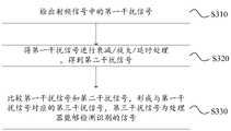
- FIG. 7is a schematic flowchart of an embodiment of a radio frequency signal processing method provided by the present application. The method specifically includes the following steps:
- the radio frequency signalin order to be able to detect the first interference signal in the radio frequency signal, the radio frequency signal may be demodulated to extract the interference signal contained in the radio frequency signal.
- S320Attenuate/amplify/delay the first interference signal to obtain a second interference signal.
- the interference signal processing circuit 211can perform attenuation/amplification/delay processing on the first interference signal, and can adjust the amplitude of the first interference signal or delay the input of the first interference signal, and convert the first interference signal whose amplitude has changed or The delayed input first interference signal is used as the second interference signal.
- S330Compare the first interference signal and the second interference signal to form a third interference signal corresponding to the first interference signal, where the third interference signal is a signal that can be detected and identified by the processor.
- the first interference signal extracted from the radio frequency signalcan be divided into two channels, one channel is processed into the second interference signal, and the other channel is kept as it is.
- a third interference signal corresponding to the first interference signalis formed according to the difference between the two signals, that is, the first interference signal is converted into a third interference signal that can be detected and identified, so as to realize the detection of the interference signal.
- the third interference signalis in the form of a signal that can be identified by the processor 213 .
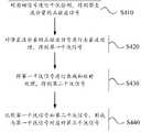
- FIG. 8is a schematic flowchart of another embodiment of the radio frequency signal processing method provided by the present application.
- the scheme shown in FIG. 8can be used to process the interference signal, so that the interference signal in the radio frequency signal can be detected and identified by the processor 213, which specifically includes the following steps:
- S410Perform interference detection on the radio frequency signal to obtain a sine wave signal with a DC component.
- the radio frequency signalmay be a radio frequency signal after filtering and low-noise amplification.
- the filtering processing of the RF signalcan filter out most of the interference signals, and the low-noise amplification processing can increase the amplitude of the interference signal that has not been filtered out, which is more conducive to the detection of the interference signal that cannot be filtered out of the RF signal.
- the detection circuit 2111-1can demodulate a small part of the radio frequency signal coupled from the receiving circuit 23 to extract the interference signal contained in the radio frequency signal.
- the detection circuit 2111-1can output the detection result in the form of a sine wave signal with a DC component. If there is an interference signal in the RF signal, it will output a sine wave signal with a DC component; if there is no interference signal in the RF signal, it will output pure DC signal.
- S420Perform DC removal processing on the sine wave signal with a DC component to obtain a first interference signal.
- the DC-removing circuit 2111-3can perform DC-removing processing on the sine wave signal with a DC component to obtain a sine wave signal without a DC component, and use the sine wave signal without a DC component as the first interference signal.
- the frequency of the sine wave signalis the frequency of the interference signal in the radio frequency signal; if the signal detected by the detection circuit 2111-1 is a pure DC signal, the pure DC signal will obtain a 0V low-level signal after DC removal.
- the first interference signalis an interference signal with a frequency less than or equal to 10KHz, for example, it can be a second-order intermodulation interference signal with a frequency less than or equal to 10KHz, or it can be other interference signals with a frequency less than or equal to 10KHz, which is not specified here. limited.
- S430Attenuate and delay the first interference signal to obtain a second interference signal.
- the processing circuit 2113can perform attenuation processing on the first interference signal, so that the amplitude of the first interference signal is reduced, and at the same time, the scaling circuit 2113 can also perform delay processing on the first interference signal to obtain the first interference signal with reduced amplitude and input delay. For an interference signal, at this time, the first interference signal with reduced amplitude and delayed input is used as the second interference signal, so that there is a difference between the second interference signal and the first interference signal. It can be understood that in other application scenarios, the processing circuit 2113 can also amplify the signal according to actual needs.
- the sine wave signal with DC component/sine wave signal without DC component detected by the detection circuit 2111-1may be subjected to attenuation and delay processing by the processing circuit 2113 first, and then the DC removing circuit 2111 may be performed. -3 for de-DC processing.
- S440Compare the first interference signal and the second interference signal to form a third interference signal corresponding to the first interference signal.
- the comparison circuit 2115can process the received first interference signal and the second interference signal to form a third interference signal that can be detected and identified, that is to say, the comparison circuit 2115 can convert the first interference signal into a more easily detected and identified signal. Signal form to realize the detection of interfering signals.
- the third interference signalis a level signal with the same frequency as the first interference signal.
- the high levelis the power supply voltage of the operational amplifier U1 in the comparison circuit 2115, which can be specifically set according to the power supply terminal VDD used and the requirements of the processor 213, which is not specifically limited here.
- the radio frequency signal processing methodcan detect the interference signal in the radio frequency signal, and divide the extracted interference signal into two channels, one channel of interference signal remains unchanged, and the other channel of interference signal is attenuated /amplification/delay processing to make the difference between the two interference signals, and by comparing the difference between the two interference signals to form a signal form corresponding to the interference signal that has not been attenuated/amplified/delayed, that is to say, the The interference signal that has not been attenuated/amplified/delayed is converted into a signal form that can be recognized by the processor, so as to realize the detection and identification of the interference signal in the radio frequency signal and reduce the influence of the interference signal.
Landscapes
- Engineering & Computer Science (AREA)
- Computer Networks & Wireless Communication (AREA)
- Signal Processing (AREA)
- Noise Elimination (AREA)
Abstract
Description
Translated fromChinese本申请涉及电子通信技术领域,特别是涉及一种射频信号处理方法、装置及接收机。The present application relates to the technical field of electronic communication, and in particular, to a radio frequency signal processing method, device and receiver.
在现代接收机中,越来越多的接收机采用零中频和低中频的架构,因为其具有集成度高、小型化、成本低以及架构简单等优势。但是对于这种将射频直接变频到基带的方式,容易受到偶次项失真的影响。例如会产生二阶互调干扰信号,而二阶互调干扰信号无法使用滤波器滤除,从而影响接收机正常工作。In modern receivers, more and more receivers use zero-IF and low-IF architectures because of their advantages of high integration, miniaturization, low cost, and simple architecture. However, this method of directly converting RF to baseband is susceptible to even-order distortion. For example, a second-order intermodulation interference signal will be generated, and the second-order intermodulation interference signal cannot be filtered out by a filter, thereby affecting the normal operation of the receiver.
本申请的发明人在长期的研发过程中,发现二阶互调干扰信号随着输入功率的增加而增加,并且是以有用信号两倍的增量增加。所以,随着输入信号的增加,二阶互调干扰信号要比有用信号增加的快,当输入功率较大时,系统容易受到与有用信号频率相近的干扰信号的影响。In the long-term research and development process, the inventors of the present application found that the second-order intermodulation interference signal increases with the increase of the input power, and the increase is twice the increment of the useful signal. Therefore, with the increase of the input signal, the second-order intermodulation interference signal increases faster than the useful signal. When the input power is large, the system is easily affected by the interference signal with a frequency similar to the useful signal.
【发明内容】[Content of the invention]
本申请主要解决的技术问题是提供一种射频信号处理方法、射频信号处理装置及接收机,能够实现对不同频率、类型干扰信号的检测识别。The main technical problem to be solved by the present application is to provide a radio frequency signal processing method, a radio frequency signal processing device and a receiver, which can realize the detection and identification of interference signals of different frequencies and types.
为解决上述技术问题,本申请采用的一个技术方案是:提供一种射频信号处理方法,该方法包括:检出射频信号中的第一干扰信号;将第一干扰信号进行衰减/放大/延时处理,得到第二干扰信号;比较第一干扰信号和第二干扰信号,形成与第一干扰信号对应的第三干扰信号,第三干扰信号为处理器能够检测识别的信号。In order to solve the above technical problem, a technical solution adopted in the present application is to provide a radio frequency signal processing method, the method includes: detecting a first interference signal in the radio frequency signal; attenuating/amplifying/delaying the first interference signal processing to obtain a second interference signal; comparing the first interference signal and the second interference signal to form a third interference signal corresponding to the first interference signal, and the third interference signal is a signal that can be detected and identified by the processor.
其中,第一干扰信号为带直流分量的正弦波信号,检出射频信号中的第一干扰信号包括:对射频信号进行检波处理,得到带直流分量的正弦波信号。The first interference signal is a sine wave signal with a DC component, and detecting the first interference signal in the radio frequency signal includes: performing wave detection processing on the radio frequency signal to obtain a sine wave signal with a DC component.
其中,第一干扰信号为不带直流分量的正弦波信号,检出射频信号中的第一干扰信号包括:对射频信号进行检波处理,得到带直流分量的正弦 波信号;对带直流分量的正弦波信号进行去直流处理,得到不带直流分量的正弦波信号。The first interference signal is a sine wave signal without a DC component, and detecting the first interference signal in the radio frequency signal includes: performing wave detection processing on the radio frequency signal to obtain a sine wave signal with a DC component; The wave signal is de-DC processed to obtain a sine wave signal without DC component.
其中,将第一干扰信号进行衰减/放大/延时处理,得到第二干扰信号还包括:对第一干扰信号进行衰减和延时处理。Wherein, performing attenuation/amplification/delay processing on the first interference signal to obtain the second interference signal further includes: performing attenuation and delay processing on the first interference signal.
其中,第三干扰信号为电平信号,比较第一干扰信号和第二干扰信号,形成与第一干扰信号对应的第三干扰信号包括:若第一干扰信号大小于第二干扰信号,则第三干扰信号为高电平信号;若第一干扰信号大于第二干扰信号,则第三干扰信号为低电平信号。The third interference signal is a level signal. Comparing the first interference signal and the second interference signal, and forming a third interference signal corresponding to the first interference signal includes: if the first interference signal is larger than the second interference signal, then the first interference signal is greater than the second interference signal. The third interference signal is a high-level signal; if the first interference signal is greater than the second interference signal, the third interference signal is a low-level signal.
其中,第一干扰信号为频率小于或等于10KHz的二阶互调干扰信号。The first interference signal is a second-order intermodulation interference signal with a frequency less than or equal to 10KHz.
其中,比较第一干扰信号和第二干扰信号,形成与第一干扰信号对应的第三干扰信号之后还包括:将第三干扰信号发给混频器,以使混频器对射频信号进行处理,得到有效信号。Wherein, after comparing the first interference signal and the second interference signal to form a third interference signal corresponding to the first interference signal, the method further includes: sending the third interference signal to the mixer, so that the mixer processes the radio frequency signal , get a valid signal.
其中,检出射频信号中的第一干扰信号之前还包括:接收原始射频信号;将原始射频信号进行低噪声放大处理,得到放大后的射频信号。Wherein, before detecting the first interference signal in the radio frequency signal, the method further includes: receiving an original radio frequency signal; and performing low-noise amplification processing on the original radio frequency signal to obtain an amplified radio frequency signal.
为解决上述技术问题,本申请采用的另一个技术方案是:提供一种射频信号处理装置,射频信号处理装置包括干扰信号处理电路,该干扰信号处理电路包括检出电路、处理电路和比较电路;检出电路用于检出射频信号中的第一干扰信号;处理电路用于将第一干扰信号进行衰减/放大/延时处理,得到第二干扰信号;比较电路用于比较第一干扰信号和第二干扰信号,形成与第一干扰信号对应的第三干扰信号,第三干扰信号为处理器能够检测识别的信号。In order to solve the above technical problem, another technical solution adopted in the present application is to provide a radio frequency signal processing device, the radio frequency signal processing device includes an interference signal processing circuit, and the interference signal processing circuit includes a detection circuit, a processing circuit and a comparison circuit; The detection circuit is used for detecting the first interference signal in the radio frequency signal; the processing circuit is used for attenuating/amplifying/delaying the first interference signal to obtain the second interference signal; the comparing circuit is used for comparing the first interference signal and the The second interference signal forms a third interference signal corresponding to the first interference signal, and the third interference signal is a signal that the processor can detect and identify.
其中,检出电路包括检波电路和去直流电路,检波电路包括二极管和第一电容,二极管的第一端为射频信号的接收端,二极管的第二端连接第一电容的第一端,第一电容的第二端接地;去直流电路包括第一电阻和第二电容,第一电阻的第一端连接第一电容的第一端和第二电容的第一端,第一电阻的第二端接地。The detection circuit includes a detection circuit and a DC removal circuit, the detection circuit includes a diode and a first capacitor, the first end of the diode is the receiving end of the radio frequency signal, the second end of the diode is connected to the first end of the first capacitor, and the first end of the diode is connected to the first end of the first capacitor. The second end of the capacitor is grounded; the DC removing circuit includes a first resistor and a second capacitor, the first end of the first resistor is connected to the first end of the first capacitor and the first end of the second capacitor, and the second end of the first resistor is connected ground.
其中,处理电路包括第二电阻和第三电容,第二电阻的第一端连接去直流电路的输出端,第二电阻的第二端连接第三电容的第一端,第三电容的第二端接地。The processing circuit includes a second resistor and a third capacitor. The first end of the second resistor is connected to the output end of the DC circuit, the second end of the second resistor is connected to the first end of the third capacitor, and the second end of the third capacitor is connected to the output end of the DC circuit. terminal to ground.
其中,比较电路包括运算放大器和第三电阻,运算放大器包括第一输入端、第二输入端和输出端,运算放大器的第一输入端连接处理电路的输出端,运算放大器的第二输入端连接去直流电路的输出端,运算放大器的输出端连接第三电阻的第一端,第三电阻的第二端为第三干扰信号的输出端。The comparison circuit includes an operational amplifier and a third resistor, the operational amplifier includes a first input end, a second input end and an output end, the first input end of the operational amplifier is connected to the output end of the processing circuit, and the second input end of the operational amplifier is connected to To the output end of the DC circuit, the output end of the operational amplifier is connected to the first end of the third resistor, and the second end of the third resistor is the output end of the third interference signal.
其中,处理器包括复杂可编程逻辑器、可编程逻辑控制器、现场可编程逻辑门阵列或数字信号处理器。Wherein, the processor includes a complex programmable logic device, a programmable logic controller, a field programmable logic gate array or a digital signal processor.
为解决上述技术问题,本申请采用的另一个技术方案是:提供一种接收机,该接收机包括天线和射频信号处理装置;天线用于接收射频信号;射频信号处理装置与天线连接,射频信号处理装置包括干扰信号检测电路,干扰信号检测电路包括干扰信号处理电路和处理器,干扰信号处理电路用于检出射频信号中的第一干扰信号;将第一干扰信号进行衰减/放大/延时处理,得到第二干扰信号;比较第一干扰信号和第二干扰信号,形成与第一干扰信号对应的第三干扰信号,第三干扰信号为处理器能够检测识别的信号。In order to solve the above technical problems, another technical solution adopted in the present application is to provide a receiver, which includes an antenna and a radio frequency signal processing device; the antenna is used for receiving radio frequency signals; the radio frequency signal processing device is connected to the antenna, and the radio frequency signal The processing device includes an interference signal detection circuit, the interference signal detection circuit includes an interference signal processing circuit and a processor, and the interference signal processing circuit is used to detect the first interference signal in the radio frequency signal; the first interference signal is attenuated/amplified/delayed processing to obtain a second interference signal; comparing the first interference signal and the second interference signal to form a third interference signal corresponding to the first interference signal, and the third interference signal is a signal that can be detected and identified by the processor.
其中,接收机还包括接收电路,接收电路与天线和射频信号处理装置连接;接收电路包括相互连接的低通滤波器、射频开关、高通滤波器及低噪声放大器;低通滤波器与天线连接,用于抑制射频信号中的非有用频率信号;射频开关与低通滤波器连接,用于切换射频信号的传输路径;高通滤波器与射频开关连接,用于抑制经过低通滤波器输出的射频信号中的非有用频率信号;低噪声放大器与高通滤波器连接,用于对高通滤波器输出的射频信号进行放大处理。The receiver also includes a receiving circuit, which is connected to the antenna and the radio frequency signal processing device; the receiving circuit includes a low-pass filter, a radio frequency switch, a high-pass filter and a low-noise amplifier connected to each other; the low-pass filter is connected to the antenna, It is used to suppress non-useful frequency signals in the radio frequency signal; the radio frequency switch is connected to the low-pass filter to switch the transmission path of the radio frequency signal; the high-pass filter is connected to the radio frequency switch to suppress the radio frequency signal output by the low-pass filter The non-useful frequency signal in the low-noise amplifier is connected with the high-pass filter to amplify the radio frequency signal output by the high-pass filter.
本申请的有益效果是:区别于现有技术的情况,本申请所提供的方法,通过对检出的干扰信号进行衰减/放大/延时处理,然后再对处理前和处理后的信号进行比较,将对干扰信号的检测转化成对信号间差异的检测,能够使被检测信号的限定要求降低,实现不同频率、不同类型的干扰信号的检测,进而减小干扰信号的影响。The beneficial effects of the present application are: different from the situation in the prior art, the method provided by the present application performs attenuation/amplification/delay processing on the detected interference signal, and then compares the pre-processed and post-processed signals , which converts the detection of the interference signal into the detection of the difference between the signals, which can reduce the qualification requirements of the detected signal, realize the detection of interference signals of different frequencies and types, and reduce the influence of the interference signals.
图1是本申请提供的接收机一实施例的结构示意图;1 is a schematic structural diagram of an embodiment of a receiver provided by the present application;
图2是本申请提供的干扰信号检测电路一实施例的结构示意图;2 is a schematic structural diagram of an embodiment of an interference signal detection circuit provided by the present application;
图3是本申请提供的干扰信号检测电路中比较电路输出的波形示意图;3 is a schematic diagram of a waveform output by a comparison circuit in the interference signal detection circuit provided by the present application;
图4是本申请提供的干扰信号处理电路的具体结构示意图;4 is a schematic diagram of a specific structure of an interference signal processing circuit provided by the present application;
图5是本申请提供的接收机另一实施例的结构示意图;5 is a schematic structural diagram of another embodiment of a receiver provided by the present application;
图6是本申请提供的射频信号处理装置中信号经过低噪声放大器前后检波电路输出波形的对比示意图;6 is a schematic diagram of the comparison of the output waveforms of the detection circuit before and after the signal passes through the low noise amplifier in the radio frequency signal processing device provided by the present application;
图7是本申请提供的射频信号处理方法一实施例的流程示意图;7 is a schematic flowchart of an embodiment of a radio frequency signal processing method provided by the present application;
图8是本申请提供的射频信号处理方法另一实施例的流程示意图。FIG. 8 is a schematic flowchart of another embodiment of a radio frequency signal processing method provided by the present application.
下面将结合本申请实施例中的附图,对本申请实施例中的技术方案进行清楚、完整地描述,显然,所描述的实施例仅仅是本申请一部分实施例,而不是全部实施例。基于本申请中的实施例,本领域普通技术人员在没有做出创造性的劳动前提下所获得的所有其他实施例,都属于本申请保护的范围。The technical solutions in the embodiments of the present application will be clearly and completely described below with reference to the drawings in the embodiments of the present application. Obviously, the described embodiments are only a part of the embodiments of the present application, but not all of the embodiments. Based on the embodiments in the present application, all other embodiments obtained by those of ordinary skill in the art without creative efforts shall fall within the protection scope of the present application.
本申请提供一种接收机,该接收机中增设了干扰信号检测电路,干扰信号检测电路包括干扰信号处理电路和处理器,干扰信号处理电路可将不同频率、不同类型的干扰信号处理成处理器能够识别的信号形式,以实现对不同频率、不同类型干扰信号的检测,进而减小干扰信号对接收机的影响。The present application provides a receiver in which an interference signal detection circuit is added. The interference signal detection circuit includes an interference signal processing circuit and a processor. The interference signal processing circuit can process interference signals of different frequencies and types into a processor. The signal form that can be identified is used to detect interference signals of different frequencies and types, thereby reducing the impact of the interference signals on the receiver.
请参阅图1,图1是本申请提供的接收机一实施例的结构示意图。接收机包括天线10和射频信号处理装置20,天线10用于接收射频信号,射频信号处理装置20与天线10连接,用于对接收的射频信号进行处理。Please refer to FIG. 1. FIG. 1 is a schematic structural diagram of an embodiment of a receiver provided by the present application. The receiver includes an
其中,射频信号处理装置20包括干扰信号检测电路21,干扰信号检测电路21包括互相连接的干扰信号处理电路211和处理器213,干扰信号处理电路211可对干扰信号进行处理,能够将干扰信号处理成处理器213能够识别的形式,从而使得干扰信号能够被检测识别,以减小干扰信号对接收机带来的影响。The radio frequency
本申请所提供的接收机可采用零中频和低中频的架构,零中频和低中频架构的接收机具有集成度高、小型化、成本低以及架构简单等优势。但是其将射频直接变频到基带的信号处理方式,容易受到偶次项失真的影响,可能会产生无法使用滤波器滤除的干扰信号,从而影响接收机正常工作。这些干扰信号一般是频率较低的信号,不容易被识别检测。本申请在接收机中增设了干扰信号处理电路211和处理器213,干扰信号处理电路211可将不同频率、不同类型的干扰信号处理成处理器213能够识别的信号形式,以实现对不同频率、不同类型干扰信号的检测,进而减小干扰信号对接收机的影响。The receiver provided by the present application can adopt the architecture of zero intermediate frequency and low intermediate frequency, and the receiver of the architecture of zero intermediate frequency and low intermediate frequency has the advantages of high integration, miniaturization, low cost and simple architecture. However, the signal processing method of directly converting the radio frequency to the baseband is easily affected by the even-order distortion, which may generate interference signals that cannot be filtered out by the filter, thus affecting the normal operation of the receiver. These interference signals are generally low-frequency signals, which are not easy to be identified and detected. In this application, an interference
具体地,干扰信号处理电路211在提取出干扰信号后,将干扰信号分成两路,一路保持原样,另一路进行衰减/放大/延时处理,然后对两路信号进行比较,再对比较结果进行检测。通过比较两路电路中信号的差异性来实现对干扰信号的检测,即将对干扰信号的检测转化成对信号间差异的检测,能够使被检测信号的限定要求降低,实现不同频率、不同类型的干扰信号的检测。比较结果的输出形式可根据需要设置,例如,本申请中使用处理器213作为比较结果的检测器,因此,比较结果可使用处理器213能够识别的形式输出。Specifically, after extracting the interference signal, the interference
请参阅图2,图2是本申请提供的干扰信号检测电路一实施例的结构示意图。该实施方式中,干扰信号处理电路211至少包括检出电路2111、处理电路2113和比较电路2115。处理电路2113分别与检出电路2111和比较电路2115连接,检出电路2111与比较电路2115连接。Please refer to FIG. 2 , which is a schematic structural diagram of an embodiment of an interference signal detection circuit provided by the present application. In this embodiment, the interference
具体地,检出电路2111用于检出射频信号中的干扰信号,可记为第一干扰信号。处理电路2113与检出电路2111连接,用于对第一干扰信号进行衰减/放大/延时处理得到处理后的干扰信号,可记为第二干扰信号。Specifically, the
比较电路2115与检出电路2111和处理电路2113连接,用于比较第一干扰信号和第二干扰信号,得到两信号间的差异,并输出比较结果,可将比较结果记为第三干扰信号,对第三干扰信号进行识别检测,以实现对干扰信号的检测。通过对第三干扰信号的检测可以实现对第一干扰信号的识别,即对第三干扰信号的实质还是对第一干扰信号的检测,或者说是将第 一干扰信号转换成了更易被检测的第三干扰信号,也可以说第三干扰信号与第一干扰信号存在一定的对应关系。比较结果的输出形式(即第三干扰信号的形式)可根据需要设置,例如,本申请中使用处理器213作为比较结果的检测器,因此,输出的第三干扰信号应是处理器213能够识别的形式。进一步地,为了能够比较好的第一干扰信号和第二干扰信号的差异,可选用更易处理的信号形式,例如,第一干扰信号可以是正弦波信号,其经衰减/放大/延时后会有明显差异。The
请继续参阅图2,在一实施方式中,检出电路2111至少包括检波电路2111-1,检波电路2111-1可对射频信号进行解调,提取出所包含的干扰信号。检波电路2111-1可以以带有直流分量的正弦波信号形式输出检出结果,若射频信号中存在干扰信号,则输出带有直流分量的正弦波信号,若射频信号中不存在干扰信号,则输出纯直流信号。Please continue to refer to FIG. 2 , in one embodiment, the
处理电路2113可对干扰信号进行衰减或放大处理,使得干扰信号的幅值减小,与未经过处理电路2113处理的干扰信号产生差异。处理电路2113也可根据需要对干扰信号进行延时处理,使得经过处理电路2113处理后的干扰信号与未经过处理电路2113处理的干扰信号的周期产生位移。在其他实施方式中,处理电路2113还可在对干扰信号进行衰减处理的同时进行延时处理,在此不做具体限定。The
图3是本申请提供的干扰信号检测电路中比较电路输出的波形示意图,图3中信号1为检波电路2111-1处理后得到的干扰信号,信号2为经过处理电路2113处理得到的干扰信号,该实施方式中处理电路2113对干扰信号进行了衰减处理。具体地,信号2经过处理电路2113衰减处理后,信号2相对于未进行衰减处理的信号1幅值减小,能够使得信号1和信号2产生差异,即检波得到的干扰信号和经过衰减处理得到的干扰信号产生差异。FIG. 3 is a schematic diagram of the waveform output by the comparison circuit in the interference signal detection circuit provided by the present application. In FIG. 3, signal 1 is the interference signal obtained after processing by the detection circuit 2111-1, and signal 2 is the interference signal processed by the
比较电路2115可对接收到的检波得到的干扰信号和经过衰减/放大/延时处理后的干扰信号进行比较处理,形成与检波得到的干扰信号对应的信号,也就是说,比较电路2115将检波得到的干扰信号转换成了差异信号。比较电路2115输出的信号形式可根据用于检测比较电路2115输出信号的 器件具体设置,例如,比较电路2115可以以电平信号形式输出结果以使得比较电路2115输出的信号能够被处理器213识别。The
如图3所示,信号3为比较电路2115输出的电平信号。比较电路2115对信号1和信号2进行比较处理,以形成与信号1对应的信号,也就是说,比较电路2115根据比较处理结果将信号1转换成了能够被检测识别出的信号3,从而使得信号1能够被检测识别。具体地,从左至右,在信号1的前1/2的循环周期内,信号1的信号强度小于信号2的信号强度,则信号3为高电平信号;而在信号1的后1/2的循环周期内,信号1的信号强度大于信号2的信号强度,则信号3为低电平信号。信号1的其他循环周期的内的信号以上述方式与信号2进行比较以获得对应的电平信号,在此不再赘述。As shown in FIG. 3 , the signal 3 is the level signal output by the
进一步地,若检波得到的干扰信号和进行衰减/放大/延时处理后得到的干扰信号存在差异,则比较电路2115输出与检波得到的干扰信号同频的高低电平信号,否则输出0V低电平信号,从而实现对干扰信号的检测。Further, if there is a difference between the interference signal obtained by the detection and the interference signal obtained after the attenuation/amplification/delay processing, the
处理器213可以为可编程逻辑器(CPLD,Complex Programming Logic Device)、数字信号处理器(DSP,Digital Signal Process)、可编程逻辑控制器(PLC,Programmable Logic Controller)和现场可编程逻辑门阵列(FPGA,Field Programmable Gate Array)等,在此不做具体限定。The
在其他实施方式中,检出电路2111还可包括去直流电路2111-3,去直流电路2111-3可对经过检波电路2111-1解调后的射频信号进行去直流处理,得到去直流后的干扰信号。去直流电路2111-3可以以正弦波信号形式输出结果,若射频信号中存在干扰信号,则输出正弦波信号,若射频信号中不存在干扰信号,则输出0V低电平信号。In other embodiments, the
上述实施方式中,可以对干扰信号进行衰减/放大/延时处理前去直流处理,也可以衰减/放大/延时处理后去直流处理。In the above-mentioned embodiment, the interference signal may be attenuated/amplified/delayed before DC processing, or may be attenuated/amplified/delayed after DC processing.
请参阅图4,图4是本申请提供的干扰信号处理电路的具体结构示意图。该实施方式中,干扰信号处理电路211包括检出电路2111、处理电路2113和比较电路2115,检出电路2111包括检波电路2111-1和去直流电路2111-3,处理电路2113分别与检出电路2111和比较电路2115连接,检出 电路2111与比较电路2115连接。Please refer to FIG. 4 , which is a schematic diagram of a specific structure of an interference signal processing circuit provided by the present application. In this embodiment, the interference
其中,检波电路2111-1包括二极管D1和第一电容C1,去直流电路2111-3包括第一电阻R1和第二电容C2,处理电路2113包括第二电阻R2和第三电容C3,比较电路2115包括运算放大器U1、第三电阻R3和电源端VDD。The detection circuit 2111-1 includes a diode D1 and a first capacitor C1, the DC removing circuit 2111-3 includes a first resistor R1 and a second capacitor C2, the
具体地,检波电路2111-1包括二极管D1和第一电容C1,二极管D1的第一端为射频信号接收端,二极管D1的第二端连接第一电容C1的第一端,第一电容C1的第二端接地。其中,二极管D1的电压可设为50V,第一电容C1的电容值可设为180pF,在此不做具体限定。检波电路2111-1的设置能够对接收到的射频信号解调,以提取射频信号中包含的干扰信号。Specifically, the detection circuit 2111-1 includes a diode D1 and a first capacitor C1. The first end of the diode D1 is the radio frequency signal receiving end, the second end of the diode D1 is connected to the first end of the first capacitor C1, and the first end of the first capacitor C1 is connected to the first end of the first capacitor C1. The second terminal is grounded. The voltage of the diode D1 can be set to 50V, and the capacitance value of the first capacitor C1 can be set to 180pF, which is not specifically limited herein. The setting of the detection circuit 2111-1 can demodulate the received radio frequency signal to extract the interference signal contained in the radio frequency signal.
去直流电路2111-3包括第一电阻R1和第二电容C2,第一电阻R1的第一端连接第一电容C1的第一端和第二电容C2的第一端,第一电阻R1的第二端接地。其中,第二电容C2的电容值可设为0.01μF,第一电阻R1的电阻值可设为110kΩ,在此不做具体限定。可以理解地,去直流电路2111-3可采用其他电路模式,而不仅限于RC电路。去直流电路2111-3的设置,能够对检波电路2111-1输出的干扰信号进行去直流处理,使得经过去直流处理后的信号只包含有正弦波信号。The DC removing circuit 2111-3 includes a first resistor R1 and a second capacitor C2. The first end of the first resistor R1 is connected to the first end of the first capacitor C1 and the first end of the second capacitor C2. Both ends are grounded. The capacitance value of the second capacitor C2 may be set to 0.01 μF, and the resistance value of the first resistor R1 may be set to 110 kΩ, which are not specifically limited herein. It can be understood that the de-DC circuit 2111-3 can adopt other circuit modes, and is not limited to the RC circuit. The setting of the DC-removal circuit 2111-3 can perform DC-removal processing on the interference signal output by the detection circuit 2111-1, so that the DC-removed signal only contains a sine wave signal.
处理电路2113包括第二电阻R2和第三电容C3,第二电阻R2的第一端连接第二电容C2的第二端,第二电阻R2的第二端连接第三电容C3的第一端,第三电容C3的第二端接地。其中,第二电阻R2的电阻值可设为1MΩ,第三电容C3的电容值可设为680pF,在此不做具体限定。在其他实施方式中,也可以采用其他对信号进行延时衰减的方式,不仅限于RC电路,例如,可以采用移相器等。The
比较电路2115包括运算放大器U1和第三电阻R3,运算放大器U1包括第一输入端、第二输入端和输出端,运算放大器U1的第一输入端连接第三电容C3的第一端,运算放大器U1的第二输入端连接第二电容C2的第二端,运算放大器U1的输出端连接第三电阻R3的第一端,第三电阻R3的第二端为第三干扰信号的输出端,运算放大器U1还包括与电源VDD连接的一端和接地的一端。其中,第三电阻R3的电阻值可设为1kΩ,电源 端VDD的电压可设为3V,在此不做具体限定。比较电路2115的设置,能够根据接收到经过处理电路2113后的干扰信号和去直流电路2111-3后的干扰信号,通过比较处理,将干扰信号转换成能够被检测识别的信号形式,以实现干扰信号的检测。The
以上实施例提供了一种接收机,该接收机设置有干扰信号检测电路,干扰信号检测电路能够检测射频信号中的干扰信号,并将提取出的干扰信号分成两路,一路干扰信号保持不变,另一路干扰信号进行衰减/放大/延时处理,以使两路干扰信号产生差异,通过比较两路干扰信号的差异,以形成与未进行衰减/放大/延时处理的干扰信号对应的信号形式,也就是说将未进行衰减/放大/延时处理的干扰信号转换成能够被处理器识别的信号形式,从而实现对射频信号中干扰信号的检测识别,减小干扰信号对接收机的影响,提高接收机的抗干扰能力。The above embodiment provides a receiver, the receiver is provided with an interference signal detection circuit, the interference signal detection circuit can detect the interference signal in the radio frequency signal, and divide the extracted interference signal into two channels, and the interference signal of one channel remains unchanged , the other interference signal is attenuated/amplified/delayed to make the two interference signals different, and the difference between the two interference signals is compared to form a signal corresponding to the interference signal that has not been attenuated/amplified/delayed In other words, the interference signal without attenuation/amplification/delay processing is converted into a signal form that can be recognized by the processor, so as to realize the detection and identification of the interference signal in the radio frequency signal and reduce the influence of the interference signal on the receiver. , to improve the anti-jamming capability of the receiver.
在其他实施方式中,射频信号处理装置20包括干扰信号处理电路211。干扰信号处理电路211可以作为集成度高、小型化的集成电路设置于接收机、收音机等设备中,以实现对设备中信号的处理。可以理解地,干扰信号处理电路211也可作为一个单独的电路应用在不同设备中。In other embodiments, the radio frequency
请参阅图5和图6,图5是本申请提供的接收机另一实施例的结构示意图,图6是本申请提供的射频信号处理装置中信号经过低噪声放大器前后检波电路输出波形的对比示意图。该实施方式中,接收机采用零中频和低中频的架构,第一干扰信号为频率小于或等于10KHz的干扰信号,例如可以是频率小于或等于10KHz的二阶互调干扰信号,也可为频率小于或等于10KHz的其他干扰信号,这些频率小于或等于10KHz的干扰信号,不容易被接收机后端及时检测识别,从而影响接收机的正常工作。本实施方式中,接收机包括接收电路23和干扰信号检测电路21,接收电路23可对天线接收的射频信号进行处理,大部分射频信号继续进入接收电路23的后级电路,小部分射频信号通过耦合的方式耦合到干扰信号检测电路21,经过接收电路23处理后的射频信号更利于干扰信号检测电路21对频率小于或等于10KHz的干扰信号的检测,进而干扰信号对接收机的影响。Please refer to FIG. 5 and FIG. 6 , FIG. 5 is a schematic structural diagram of another embodiment of the receiver provided by the present application, and FIG. 6 is a schematic diagram comparing the output waveforms of the detection circuit before and after the signal in the radio frequency signal processing device provided by the present application after passing through the low-noise amplifier . In this embodiment, the receiver adopts a zero-IF and low-IF architecture, and the first interference signal is an interference signal with a frequency less than or equal to 10KHz, for example, a second-order intermodulation interference signal with a frequency less than or equal to 10KHz, or a frequency Other interference signals less than or equal to 10KHz, these interference signals with frequencies less than or equal to 10KHz, are not easy to be detected and identified by the back end of the receiver in time, thus affecting the normal operation of the receiver. In this embodiment, the receiver includes a receiving
接收机包括天线10和射频信号处理装置20。射频信号处理装置20包 括互相连接的干扰信号检测电路21和接收电路23,该接收机可将接收信号部分耦合至干扰信号检测电路21,以对经过接收电路23处理后的射频信号中的干扰信号进行处理,使得干扰信号处理成能够被识别的形式,以减小干扰信号对接收机带来的影响。The receiver includes an
其中,接收电路23可对天线10接收到的射频信号进行处理,使得射频信号中大部分的干扰信号得到滤除,且经过接收电路23处理后的射频信号更利于干扰信号检测电路21对射频信号中的干扰信号进行检测。干扰信号检测电路21也可将检测结果反馈至接收电路23,使得在接收电路23不易被识别的干扰信号能够得到削弱,以减小干扰信号对接收机带来的影响。Among them, the receiving
请继续参阅图5,接收电路23至少包括低通滤波器231、射频开关232、高通滤波器233、低噪声放大器234、第一开关235、衰减器236、第二开关237、控制器238和频率产生器239。Please continue to refer to FIG. 5 , the receiving
具体地,低通滤波器231与天线10连接,用于使得接收到的射频信号中的有用频率的信号通过,同时抑制非有用频率的信号,即设定一所需频率点,容许低于所需频率点的信号通过,高于所需频率点的信号被滤除,以消除部分干扰信号。Specifically, the low-
射频开关232与低通滤波器231连接,其用于切换射频信号的传输路径。例如,本申请的接收电路23为接收射频信号,即切换射频开关232以使接收电路23能够接收射频信号并进行传输。可以理解地,也可以切换射频开关232,使接收电路23用于发射信号。The RF switch 232 is connected to the low-
高通滤波器233与射频开关232连接,其用于对通过射频开关232而输出的信号进行滤波,使得经过低通滤波后的射频信号中的有用频率的信号通过,同时抑制非有用频率的信号,即设定一所需频率点,允许高于所需频率点的信号通过,低于所需频率点的信号被滤除,进一步消除部分干扰信号。The high-
低噪声放大器234与高通滤波器233连接,其用于对高通滤波器233输出的信号进行放大处理;具体地,如图6所示,由于滤波后的信号中包含有频率较低的干扰信号,通过低噪声放大处理,能够使频率交底的干扰信号的强度增大,输出的干扰信号波形幅度增大,其中,经过低噪声放大 处理后的射频信号有一小部分耦合进干扰信号检测电路21进行处理和检测,以利于对干扰信号的检测处理。The low-
第一开关235与低噪声放大器234连接,其用于对低噪声放大器234输出的信号进行选择传输路径。The
衰减器236与第一开关235连接,其用于对低噪声放大器234输出的信号进行衰减,即对信号进行大小的调整,使得信号衰减一定的量值,且可以对低噪声放大器234输出的信号中包含的干扰信号进行一定程度上的衰减,以削弱干扰信号的影响。The
第二开关237与衰减器236连接,其用于对衰减器236输出的信号进行选择传输路径。The
混频器238与第二开关237连接,频率产生器239与混频器238连接。频率产生器239可用于产生固定频率的信号源,可根据接收电路23所需的信号频率具体设置,在此不做具体限定。混频器238,其用于将衰减器236输出的信号和频率产生器239输出的信号进行混频,得到一个中频信号;且混频器238还用于将中频信号进行模数转换和解调等,以获得基带信号;同时混频器238可自适应滤波,使得干扰信号检测电路21反馈的不易被接收电路23识别的干扰信号能够得到削弱,以减小干扰信号对接收机的影响。The
本实施例提供了一种接收机,该接收机设置有接收电路和干扰信号检测电路,接收电路能够对射频信号进行滤波和低噪声放大处理,并将低噪声放大后的射频信号耦合一部分至干扰信号检测电路以实现干扰检测。通过对射频信号进行滤波和低噪声放大处理,使得射频信号中的干扰信号幅值增大,干扰信号更易被检测出,有利于干扰信号检测电路对射频信号中干扰信号的检测,从而提高接收机对射频信号中干扰信号的检测能力,减小干扰信号对接收机的影响。This embodiment provides a receiver. The receiver is provided with a receiving circuit and an interference signal detection circuit. The receiving circuit can filter and amplify a radio frequency signal, and couple a part of the low-noise amplified radio frequency signal to the interference signal. Signal detection circuit to achieve interference detection. By filtering and low-noise amplifying the RF signal, the amplitude of the interference signal in the RF signal is increased, and the interference signal is more easily detected, which is conducive to the detection of the interference signal in the RF signal by the interference signal detection circuit, thereby improving the receiver. The ability to detect interfering signals in RF signals reduces the impact of interfering signals on the receiver.
请参阅图2和图7,图7是本申请提供的射频信号处理方法一实施例的流程示意图,该方法具体包括以下步骤:Please refer to FIG. 2 and FIG. 7. FIG. 7 is a schematic flowchart of an embodiment of a radio frequency signal processing method provided by the present application. The method specifically includes the following steps:
S310:检出射频信号中的第一干扰信号。S310: Detect the first interference signal in the radio frequency signal.
该实施方式中,为了能够检测出射频信号中的第一干扰信号,可将射 频信号进行解调,提取出射频信号中包含的干扰信号。In this embodiment, in order to be able to detect the first interference signal in the radio frequency signal, the radio frequency signal may be demodulated to extract the interference signal contained in the radio frequency signal.
S320:将第一干扰信号进行衰减/放大/延时,得到第二干扰信号。S320: Attenuate/amplify/delay the first interference signal to obtain a second interference signal.
干扰信号处理电路211可对第一干扰信号进行衰减/放大/延时处理,能够调整第一干扰信号的幅值大小或延迟输入第一干扰信号,并将幅值发生变化的第一干扰信号或将延时输入的第一干扰信号作为第二干扰信号。The interference
S330:比较第一干扰信号和第二干扰信号,形成与第一干扰信号对应的第三干扰信号,第三干扰信号为处理器能够检测识别的信号。S330: Compare the first interference signal and the second interference signal to form a third interference signal corresponding to the first interference signal, where the third interference signal is a signal that can be detected and identified by the processor.
可将从射频信号中提取出的第一干扰信号分为两路,一路处理成第二干扰信号,另一路保持原样,通过比较两路信号即第一干扰信号和第二干扰信号的差异性,并根据两信号的差异形成与第一干扰信号对应的第三干扰信号,也就是说将第一干扰信号转换成能够被检测识别的第三干扰信号,以实现干扰信号的检测。The first interference signal extracted from the radio frequency signal can be divided into two channels, one channel is processed into the second interference signal, and the other channel is kept as it is. A third interference signal corresponding to the first interference signal is formed according to the difference between the two signals, that is, the first interference signal is converted into a third interference signal that can be detected and identified, so as to realize the detection of the interference signal.
其中,第三干扰信号为能够被处理器213识别的信号形式。The third interference signal is in the form of a signal that can be identified by the
请参阅图5和图8,图8是本申请提供的射频信号处理方法另一实施例的流程示意图。在一具体实施例中,可采用图8所示的方案进行干扰信号处理,以使得射频信号中的干扰信号能够被处理器213检测识别,具体包括以下步骤:Please refer to FIG. 5 and FIG. 8 . FIG. 8 is a schematic flowchart of another embodiment of the radio frequency signal processing method provided by the present application. In a specific embodiment, the scheme shown in FIG. 8 can be used to process the interference signal, so that the interference signal in the radio frequency signal can be detected and identified by the
S410:对射频信号进行干扰检测,得到带直流分量的正弦波信号。S410: Perform interference detection on the radio frequency signal to obtain a sine wave signal with a DC component.
该实施方式中,射频信号可以是经过滤波和低噪声放大处理后的射频信号。对射频信号滤波处理能够滤除大部分干扰信号,低噪声放大处理能够使没有被滤波掉的干扰信号幅值增大,更利于对射频信号中滤除不掉的干扰信号的检测。In this embodiment, the radio frequency signal may be a radio frequency signal after filtering and low-noise amplification. The filtering processing of the RF signal can filter out most of the interference signals, and the low-noise amplification processing can increase the amplitude of the interference signal that has not been filtered out, which is more conducive to the detection of the interference signal that cannot be filtered out of the RF signal.
检波电路2111-1可对从接受电路23耦合出的一小部分射频信号进行解调处理,提取出射频信号中所包含的干扰信号。检波电路2111-1可以以带有直流分量的正弦波信号形式输出检出结果,若射频信号中存在干扰信号,则输出带直流分量的正弦波信号;若射频信号中不存在干扰信号,则输出纯直流信号。The detection circuit 2111-1 can demodulate a small part of the radio frequency signal coupled from the receiving
S420:对带直流分量的正弦波信号进行去直流处理,得到第一干扰信号。S420: Perform DC removal processing on the sine wave signal with a DC component to obtain a first interference signal.
去直流电路2111-3可对带直流分量的正弦波信号进行去直流处理,得到不带直流分量的正弦波信号,并将不带直流分量的正弦波信号作为第一干扰信号,此时得到的正弦波信号的频率即为射频信号中干扰信号的频率;若经过检波电路2111-1检测出的信号为纯直流信号,则纯直流信号经过去直流处理后得到0V低电平信号。The DC-removing circuit 2111-3 can perform DC-removing processing on the sine wave signal with a DC component to obtain a sine wave signal without a DC component, and use the sine wave signal without a DC component as the first interference signal. The frequency of the sine wave signal is the frequency of the interference signal in the radio frequency signal; if the signal detected by the detection circuit 2111-1 is a pure DC signal, the pure DC signal will obtain a 0V low-level signal after DC removal.
其中,第一干扰信号为频率小于或等于10KHz的干扰信号,例如可以是频率小于或等于10KHz的二阶互调干扰信号,也可为频率小于或等于10KHz的其他干扰信号,在此不做具体限定。The first interference signal is an interference signal with a frequency less than or equal to 10KHz, for example, it can be a second-order intermodulation interference signal with a frequency less than or equal to 10KHz, or it can be other interference signals with a frequency less than or equal to 10KHz, which is not specified here. limited.
S430:将第一干扰信号进行衰减和延时处理,得到第二干扰信号。S430: Attenuate and delay the first interference signal to obtain a second interference signal.
处理电路2113可对第一干扰进行衰减处理,使得第一干扰信号的幅值减小,同时缩放电路2113还可对第一干扰信号进行延时处理,得到幅值减小且输入延时的第一干扰信号,此时将幅值减小且输入延时的第一干扰信号作为第二干扰信号,使得第二干扰信号和第一干扰信号产生差别。可以理解地,在其他的应用场景中,处理电路2113也可根据实际需要对信号进行放大处理。The
在其他实施方式中,可对检波电路2111-1检测出的带直流分量的正弦波信号/不带直流分量的正弦波信号先进行处理电路2113的衰减和延时处理,然后进行去直流电路2111-3的去直流处理。In other embodiments, the sine wave signal with DC component/sine wave signal without DC component detected by the detection circuit 2111-1 may be subjected to attenuation and delay processing by the
S440:比较第一干扰信号和第二干扰信号,形成与第一干扰信号对应的第三干扰信号。S440: Compare the first interference signal and the second interference signal to form a third interference signal corresponding to the first interference signal.
比较电路2115可对接收到的第一干扰信号和第二干扰信号进行处理,形成能够被检测识别的第三干扰信号,也就是说比较电路2115能够将第一干扰信号转换成更易被检测识别的信号形式,以实现干扰信号的检测。The
其中,第三干扰信号为与第一干扰信号同频的电平信号。高电平为比较电路2115中运算放大器U1的供电电压,可根据所使用的电源端VDD和处理器213的要求具体设置,在此不做具体限定。The third interference signal is a level signal with the same frequency as the first interference signal. The high level is the power supply voltage of the operational amplifier U1 in the
本申请所提供的一种射频信号处理方法,该射频信号处理方法能够检测射频信号中的干扰信号,并将提取出的干扰信号分成两路,一路干扰信号保持不变,另一路干扰信号进行衰减/放大/延时处理,以使两路干扰信号 产生差异,并通过比较两路干扰信号的差异,以形成与未进行衰减/放大/延时处理的干扰信号对应的信号形式,也就是说将未进行衰减/放大/延时处理的干扰信号转换成能够被处理器识别的信号形式,从而实现对射频信号中干扰信号的检测识别,减小干扰信号的影响。A radio frequency signal processing method provided by the present application, the radio frequency signal processing method can detect the interference signal in the radio frequency signal, and divide the extracted interference signal into two channels, one channel of interference signal remains unchanged, and the other channel of interference signal is attenuated /amplification/delay processing to make the difference between the two interference signals, and by comparing the difference between the two interference signals to form a signal form corresponding to the interference signal that has not been attenuated/amplified/delayed, that is to say, the The interference signal that has not been attenuated/amplified/delayed is converted into a signal form that can be recognized by the processor, so as to realize the detection and identification of the interference signal in the radio frequency signal and reduce the influence of the interference signal.
以上所述仅为本申请的实施方式,并非因此限制本申请的专利范围,凡是利用本申请说明书及附图内容所作的等效结构或等效流程变换,或直接或间接运用在其他相关的技术领域,均同理包括在本申请的专利保护范围内。The above description is only an embodiment of the present application, and is not intended to limit the scope of the patent of the present application. Any equivalent structure or equivalent process transformation made by using the contents of the description and drawings of the present application, or directly or indirectly applied to other related technologies Fields are similarly included within the scope of patent protection of this application.
Claims (15)
Translated fromChinesePriority Applications (1)
| Application Number | Priority Date | Filing Date | Title |
|---|---|---|---|
| PCT/CN2020/139045WO2022133913A1 (en) | 2020-12-24 | 2020-12-24 | Radio frequency signal processing method and device, and receiver |
Applications Claiming Priority (1)
| Application Number | Priority Date | Filing Date | Title |
|---|---|---|---|
| PCT/CN2020/139045WO2022133913A1 (en) | 2020-12-24 | 2020-12-24 | Radio frequency signal processing method and device, and receiver |
Publications (1)
| Publication Number | Publication Date |
|---|---|
| WO2022133913A1true WO2022133913A1 (en) | 2022-06-30 |
Family
ID=82157203
Family Applications (1)
| Application Number | Title | Priority Date | Filing Date |
|---|---|---|---|
| PCT/CN2020/139045CeasedWO2022133913A1 (en) | 2020-12-24 | 2020-12-24 | Radio frequency signal processing method and device, and receiver |
Country Status (1)
| Country | Link |
|---|---|
| WO (1) | WO2022133913A1 (en) |
Cited By (1)
| Publication number | Priority date | Publication date | Assignee | Title |
|---|---|---|---|---|
| CN115529513A (en)* | 2022-10-11 | 2022-12-27 | 中国南方电网有限责任公司超高压输电公司 | Guarantee anti-interference data transmission transfer station of multisource data in wisdom circuit |
Citations (5)
| Publication number | Priority date | Publication date | Assignee | Title |
|---|---|---|---|---|
| JPS5648729A (en)* | 1979-09-28 | 1981-05-02 | Pioneer Electronic Corp | Detecting circuit for multipath disturbance of radio wave |
| JPS58204648A (en)* | 1982-05-24 | 1983-11-29 | Nec Corp | Signal detector |
| US4876743A (en)* | 1986-12-02 | 1989-10-24 | U.S. Philips Corporation | Signal diversity arrangement for mobile reception |
| US6385261B1 (en)* | 1998-01-19 | 2002-05-07 | Mitsubishi Denki Kabushiki Kaisha | Impulse noise detector and noise reduction system |
| CN202261303U (en)* | 2011-09-29 | 2012-05-30 | 中国电子科技集团公司第五十四研究所 | Cognitive radio-based anti-interference device |
- 2020
- 2020-12-24WOPCT/CN2020/139045patent/WO2022133913A1/ennot_activeCeased
Patent Citations (5)
| Publication number | Priority date | Publication date | Assignee | Title |
|---|---|---|---|---|
| JPS5648729A (en)* | 1979-09-28 | 1981-05-02 | Pioneer Electronic Corp | Detecting circuit for multipath disturbance of radio wave |
| JPS58204648A (en)* | 1982-05-24 | 1983-11-29 | Nec Corp | Signal detector |
| US4876743A (en)* | 1986-12-02 | 1989-10-24 | U.S. Philips Corporation | Signal diversity arrangement for mobile reception |
| US6385261B1 (en)* | 1998-01-19 | 2002-05-07 | Mitsubishi Denki Kabushiki Kaisha | Impulse noise detector and noise reduction system |
| CN202261303U (en)* | 2011-09-29 | 2012-05-30 | 中国电子科技集团公司第五十四研究所 | Cognitive radio-based anti-interference device |
Cited By (1)
| Publication number | Priority date | Publication date | Assignee | Title |
|---|---|---|---|---|
| CN115529513A (en)* | 2022-10-11 | 2022-12-27 | 中国南方电网有限责任公司超高压输电公司 | Guarantee anti-interference data transmission transfer station of multisource data in wisdom circuit |
Similar Documents
| Publication | Publication Date | Title |
|---|---|---|
| US10873486B1 (en) | Receiver circuits with blocker attenuating RF filter | |
| US9525461B2 (en) | Suppression method for strong interference noise of carrier channel of power line and circuit structure thereof | |
| CN103227653B (en) | receiver | |
| US11177988B2 (en) | Receiver circuits with blocker attenuating mixer | |
| CN107104687B (en) | Wireless communication system receiver capable of suppressing noise | |
| WO2022179021A1 (en) | Receiver and method for use in ultra high frequency partial discharge detection | |
| CN102291345A (en) | Subsampling based receiver using frequency selective noise canceller | |
| CN109257020A (en) | An Experimental Circuit That Can Realize Weak AM Signal Demodulation | |
| CN212381197U (en) | Digital isolator | |
| WO2022133913A1 (en) | Radio frequency signal processing method and device, and receiver | |
| CN114679230B (en) | Radio frequency signal processing method, device and receiver | |
| US7224750B2 (en) | Apparatus and method for receiving RF signal free of 1/f noise in radio communication system | |
| CN103001654A (en) | A self-adaptive variable intermediate frequency radio frequency receiver | |
| US11139791B2 (en) | Integrated circuit devices with receiver chain peak detectors | |
| US7336938B1 (en) | Phase-alternating mixer with alias and harmonic rejection | |
| CN215871381U (en) | Anti-interference circuit and receiver | |
| CN109557512B (en) | Radar receiver with high sensitivity and high dynamic range | |
| KR100638472B1 (en) | Digital audio amplifiers, audio systems comprising them, and audio signal amplification methods | |
| CN113630198A (en) | A detection system and method for wireless polar coordinate modulation transmitter chip | |
| CN110011678B (en) | Automatic gain control system and method suitable for superheterodyne receiver of abrupt channel | |
| CN103516313A (en) | Low-noise amplifiers for radio frequency receiver | |
| US6121893A (en) | Remote control receiving system | |
| KR101045536B1 (en) | RSSI device of the broadband RF receiver | |
| CN203933647U (en) | Signal magnitude detector and comprise the wireless receiver of this signal magnitude detector | |
| CN105323027B (en) | Broadcasting receiver and tuner |
Legal Events
| Date | Code | Title | Description |
|---|---|---|---|
| 121 | Ep: the epo has been informed by wipo that ep was designated in this application | Ref document number:20966485 Country of ref document:EP Kind code of ref document:A1 | |
| NENP | Non-entry into the national phase | Ref country code:DE | |
| 122 | Ep: pct application non-entry in european phase | Ref document number:20966485 Country of ref document:EP Kind code of ref document:A1 | |
| 122 | Ep: pct application non-entry in european phase | Ref document number:20966485 Country of ref document:EP Kind code of ref document:A1 | |
| 32PN | Ep: public notification in the ep bulletin as address of the adressee cannot be established | Free format text:NOTING OF LOSS OF RIGHTS PURSUANT TO RULE 112(1) EPC (EPO FORM 1205A DATED 11/12/2023) | |
| 122 | Ep: pct application non-entry in european phase | Ref document number:20966485 Country of ref document:EP Kind code of ref document:A1 |