WO2022124169A1 - Transparent display device, laminated glass, and method for producing transparent display device - Google Patents
Transparent display device, laminated glass, and method for producing transparent display deviceDownload PDFInfo
- Publication number
- WO2022124169A1 WO2022124169A1PCT/JP2021/044180JP2021044180WWO2022124169A1WO 2022124169 A1WO2022124169 A1WO 2022124169A1JP 2021044180 WJP2021044180 WJP 2021044180WWO 2022124169 A1WO2022124169 A1WO 2022124169A1
- Authority
- WO
- WIPO (PCT)
- Prior art keywords
- display device
- transparent display
- light
- transparent
- light emitting
- Prior art date
- Legal status (The legal status is an assumption and is not a legal conclusion. Google has not performed a legal analysis and makes no representation as to the accuracy of the status listed.)
- Ceased
Links
Images


Classifications
- H—ELECTRICITY
- H01—ELECTRIC ELEMENTS
- H01L—SEMICONDUCTOR DEVICES NOT COVERED BY CLASS H10
- H01L25/00—Assemblies consisting of a plurality of semiconductor or other solid state devices
- H01L25/03—Assemblies consisting of a plurality of semiconductor or other solid state devices all the devices being of a type provided for in a single subclass of subclasses H10B, H10D, H10F, H10H, H10K or H10N, e.g. assemblies of rectifier diodes
- H01L25/04—Assemblies consisting of a plurality of semiconductor or other solid state devices all the devices being of a type provided for in a single subclass of subclasses H10B, H10D, H10F, H10H, H10K or H10N, e.g. assemblies of rectifier diodes the devices not having separate containers
- H01L25/075—Assemblies consisting of a plurality of semiconductor or other solid state devices all the devices being of a type provided for in a single subclass of subclasses H10B, H10D, H10F, H10H, H10K or H10N, e.g. assemblies of rectifier diodes the devices not having separate containers the devices being of a type provided for in group H10H20/00
- H01L25/0753—Assemblies consisting of a plurality of semiconductor or other solid state devices all the devices being of a type provided for in a single subclass of subclasses H10B, H10D, H10F, H10H, H10K or H10N, e.g. assemblies of rectifier diodes the devices not having separate containers the devices being of a type provided for in group H10H20/00 the devices being arranged next to each other
- H—ELECTRICITY
- H10—SEMICONDUCTOR DEVICES; ELECTRIC SOLID-STATE DEVICES NOT OTHERWISE PROVIDED FOR
- H10H—INORGANIC LIGHT-EMITTING SEMICONDUCTOR DEVICES HAVING POTENTIAL BARRIERS
- H10H20/00—Individual inorganic light-emitting semiconductor devices having potential barriers, e.g. light-emitting diodes [LED]
- H10H20/80—Constructional details
- H10H20/85—Packages
- H10H20/855—Optical field-shaping means, e.g. lenses
- H—ELECTRICITY
- H10—SEMICONDUCTOR DEVICES; ELECTRIC SOLID-STATE DEVICES NOT OTHERWISE PROVIDED FOR
- H10H—INORGANIC LIGHT-EMITTING SEMICONDUCTOR DEVICES HAVING POTENTIAL BARRIERS
- H10H20/00—Individual inorganic light-emitting semiconductor devices having potential barriers, e.g. light-emitting diodes [LED]
- H10H20/80—Constructional details
- H10H20/84—Coatings, e.g. passivation layers or antireflective coatings
- G—PHYSICS
- G09—EDUCATION; CRYPTOGRAPHY; DISPLAY; ADVERTISING; SEALS
- G09F—DISPLAYING; ADVERTISING; SIGNS; LABELS OR NAME-PLATES; SEALS
- G09F9/00—Indicating arrangements for variable information in which the information is built-up on a support by selection or combination of individual elements
- G09F9/30—Indicating arrangements for variable information in which the information is built-up on a support by selection or combination of individual elements in which the desired character or characters are formed by combining individual elements
- G09F9/33—Indicating arrangements for variable information in which the information is built-up on a support by selection or combination of individual elements in which the desired character or characters are formed by combining individual elements being semiconductor devices, e.g. diodes
- H—ELECTRICITY
- H01—ELECTRIC ELEMENTS
- H01L—SEMICONDUCTOR DEVICES NOT COVERED BY CLASS H10
- H01L25/00—Assemblies consisting of a plurality of semiconductor or other solid state devices
- H01L25/16—Assemblies consisting of a plurality of semiconductor or other solid state devices the devices being of types provided for in two or more different subclasses of H10B, H10D, H10F, H10H, H10K or H10N, e.g. forming hybrid circuits
- H01L25/167—Assemblies consisting of a plurality of semiconductor or other solid state devices the devices being of types provided for in two or more different subclasses of H10B, H10D, H10F, H10H, H10K or H10N, e.g. forming hybrid circuits comprising optoelectronic devices, e.g. LED, photodiodes
- H—ELECTRICITY
- H10—SEMICONDUCTOR DEVICES; ELECTRIC SOLID-STATE DEVICES NOT OTHERWISE PROVIDED FOR
- H10H—INORGANIC LIGHT-EMITTING SEMICONDUCTOR DEVICES HAVING POTENTIAL BARRIERS
- H10H20/00—Individual inorganic light-emitting semiconductor devices having potential barriers, e.g. light-emitting diodes [LED]
- H10H20/01—Manufacture or treatment
- H10H20/034—Manufacture or treatment of coatings
- H—ELECTRICITY
- H10—SEMICONDUCTOR DEVICES; ELECTRIC SOLID-STATE DEVICES NOT OTHERWISE PROVIDED FOR
- H10H—INORGANIC LIGHT-EMITTING SEMICONDUCTOR DEVICES HAVING POTENTIAL BARRIERS
- H10H20/00—Individual inorganic light-emitting semiconductor devices having potential barriers, e.g. light-emitting diodes [LED]
- H10H20/01—Manufacture or treatment
- H10H20/036—Manufacture or treatment of packages
- H10H20/0363—Manufacture or treatment of packages of optical field-shaping means
- H—ELECTRICITY
- H10—SEMICONDUCTOR DEVICES; ELECTRIC SOLID-STATE DEVICES NOT OTHERWISE PROVIDED FOR
- H10H—INORGANIC LIGHT-EMITTING SEMICONDUCTOR DEVICES HAVING POTENTIAL BARRIERS
- H10H20/00—Individual inorganic light-emitting semiconductor devices having potential barriers, e.g. light-emitting diodes [LED]
- H10H20/80—Constructional details
- H10H20/85—Packages
- H10H20/855—Optical field-shaping means, e.g. lenses
- H10H20/856—Reflecting means
Definitions
- the present inventionrelates to a transparent display device, a laminated glass, and a method for manufacturing a transparent display device.
- Patent Document 1discloses, among such display devices, a transparent display device in which the size of the LED element is fine and the back side can be visually recognized via the display device.
- the transparent display devicethere was a request that the image displayed on the visual recognition side should not be visible from the back side (opposite side of the visual recognition side). That is, there has been a demand for suppressing leakage of light emitted from the LED element to the back surface side.
- the transparent display device disclosed in Patent Document 2is provided with a light-shielding member that prevents light emitted from a bullet-shaped LED (light-emitting body) from passing through the back side where the light-emitting body is not arranged. ..
- the present inventionhas been made in view of such circumstances, and provides a transparent display device capable of suppressing leakage of light emitted from an LED element to the back surface side.
- the present inventionprovides a transparent display device having the configuration of [1].
- a transparent display devicethat allows you to see the back side from the viewing side.
- the light emitting diode elementis a semiconductor chip having an area of 10,000 ⁇ m 2 or less.
- the main surface of the light emitting diode element on the back surface sideis covered with a light-shielding film. Transparent display device.
- a protective layer covering the light emitting diode elementis further provided on the transparent substrate.
- the transparent display deviceaccording to [1] or [2], further comprising a dimming layer capable of dynamically adjusting the internal transmittance of visible light on the back surface side of the light-shielding film.
- the transparent display deviceaccording to any one of [1] to [8], further comprising a mirror structure formed so as to surround the light emitting diode element.
- the present inventionprovides a laminated glass having the configuration of [11].
- a pair of glass plates and A laminated glassprovided with a transparent display device provided between the pair of glass plates.
- the transparent display deviceis With a transparent base material, A light emitting diode element arranged for each pixel on the transparent substrate is provided.
- a transparent display devicethat allows you to see the back side from the viewing side.
- the light emitting diode elementis a semiconductor chip having an area of 10,000 ⁇ m 2 or less.
- the main surface of the light emitting diode element on the back surface sideis covered with a light-shielding film.
- the present inventionprovides a method for manufacturing a transparent display device having the following configuration [12].
- Itis a manufacturing method of a transparent display device that can visually recognize the back side from the visual side.
- a light emitting diode elementwhich is a semiconductor chip having an area of 10,000 ⁇ m 2 or less for each pixel, is arranged on a transparent substrate. The back surface of the light emitting diode element is covered with a light-shielding film. How to make a transparent device.
- the present inventionit is possible to provide a transparent display device capable of suppressing leakage of light emitted from an LED element to the back surface side.
- FIG. 2is a cross-sectional view taken along the line III-III in FIG.
- sectional drawingwhich shows an example of the manufacturing method of the transparent display device which concerns on 1st Embodiment.
- sectional drawingwhich shows an example of the manufacturing method of the transparent display device which concerns on 1st Embodiment.
- sectional drawingwhich shows an example of the manufacturing method of the transparent display device which concerns on 1st Embodiment.
- sectional drawingwhich shows an example of the manufacturing method of the transparent display device which concerns on 1st Embodiment.
- sectional drawingwhich shows an example of the manufacturing method of the transparent display device which concerns on 1st Embodiment.
- 13is a cross-sectional view taken along the line taken along the line XIV-XIV in FIG. It is a schematic partial sectional view which shows an example of the transparent display device which concerns on 2nd Embodiment. It is a schematic partial plan view which shows an example of the transparent display device which concerns on 3rd Embodiment. 16 is a cross-sectional view taken along the line taken along the line XVII-XVII in FIG. It is a schematic partial sectional view which shows an example of the transparent display device which concerns on the modification of 3rd Embodiment. It is a schematic partial sectional view which shows an example of the transparent display device which concerns on 4th Embodiment.
- the "transparent display device”refers to a display device in which visual information such as a person or a background located on the back side of the display device can be visually recognized under a desired usage environment. Note that visibility is determined at least when the display device is in a non-display state, that is, in a state where it is not energized.
- transparentmeans that the transmittance of visible light is 40% or more, preferably 60% or more, and more preferably 70% or more. It may also indicate that the transmittance is 5% or more and the haze value is 20 or less. When the transmittance is 5% or more, when the outside is viewed from the room during the daytime, the outside can be seen with the same or higher brightness as the room, and sufficient visibility can be ensured.
- the transmittancewhen the transmittance is 40% or more, the back side of the transparent display device can be visually recognized without any problem even if the brightness of the front side and the back side of the transparent display device is about the same. Further, when the haze value is 10 or less, sufficient background contrast can be secured.
- transparentmeans whether or not a color is applied, that is, it may be colorless and transparent, or it may be colored and transparent.
- the transmittancerefers to a value (%) measured by a method conforming to ISO9050.
- the haze valuerefers to a value measured by a method conforming to ISO 14782.
- FIG. 1is a schematic partial plan view showing an example of a transparent display device according to the first embodiment.
- FIG. 2is an enlarged view of region II in FIG.
- FIG. 3is a cross-sectional view taken along the line III-III in FIG.
- the transparent display deviceincludes a transparent base material 10, a light emitting unit 20, an IC (Integrated Circuit) chip 30, wiring 40, a protective layer 50, and a light-shielding film 60. ing.
- the display area 101 in the transparent display deviceis an area composed of a plurality of pixels and in which an image is displayed.
- the imageincludes characters.
- the display area 101is composed of a plurality of pixels arranged in the row direction (x-axis direction) and the column direction (y-axis direction).
- FIG. 1shows a part of the display area 101, and shows a total of 4 pixels, 2 pixels each in the row direction and the column direction.
- one pixel PIXis shown surrounded by an alternate long and short dash line.
- FIGS. 1 to 3are for convenience in explaining the positional relationship of the constituent elements. Normally, the z-axis positive direction is vertically upward, and the xy plane is a horizontal plane. Further, in FIGS. 1 and 2, the transparent base material 10 and the protective layer 50 shown in FIG. 3 are omitted. Further, although FIGS. 1 and 2 are plan views, the light emitting unit 20 and the IC chip 30 are displayed in dots for easy understanding.
- each pixel PIXincludes a light emitting unit 20 and an IC chip 30.
- the light emitting unit 20 and the IC chip 30are arranged in a matrix with a pixel pitch Px in the row direction (x-axis direction) and a pixel pitch Py in the column direction (y-axis direction). If the pixels are arranged in a predetermined direction at a predetermined pixel pitch, the arrangement format of the pixels PIX, that is, the light emitting unit 20 is not limited to the matrix shape.
- the light emitting unit 20 in each pixel PIXincludes at least one light emitting diode element (hereinafter, LED element). That is, the transparent display device according to the present embodiment is a display device that uses an LED element for each pixel PIX, and is called an LED display or the like.
- LED elementlight emitting diode element
- each light emitting unit 20includes a red LED element 21, a green LED element 22, and a blue LED element 23.
- the LED elements 21 to 23correspond to sub-pixels (sub-pixels) constituting one pixel.
- each light emitting unit 20has LED elements 21 to 23 that emit red, green, and blue, which are the three primary colors of light, the transparent display device according to the present embodiment can display a full-color image.
- each light emitting unit 20may include two or more LED elements of similar colors. This makes it possible to expand the dynamics range of the image.
- the LED elements 21 to 23are so-called micro LED elements, which are semiconductor chips having an area of 10,000 ⁇ m 2 or less.
- the width (length in the x-axis direction) and the length (length in the y-axis direction) of the LED element 21 on the transparent substrate 10are, for example, 100 ⁇ m or less, preferably 50 ⁇ m or less, more preferably 50 ⁇ m or less, respectively. It is 20 ⁇ m or less.
- the lower limit of the width and length of the LED elementis, for example, 3 ⁇ m or more due to various manufacturing conditions and the like.
- the dimensions, that is, the width and the length of the LED elements 21 to 23 in FIG. 1are the same, they may be different from each other.
- the area of the LED elements 21 to 23 on the transparent substrate 10is preferably 3,000 ⁇ m 2 or less, more preferably 500 ⁇ m 2 or less.
- the lower limit of the area occupied by one LED elementis, for example, 10 ⁇ m 2 or more due to various manufacturing conditions and the like.
- the area of the LED element and the area of the constituent member such as the wiringrefer to the area occupied by the constituent member such as the LED element and the wiring in the xy plan view in FIG.
- the shape of the LED elements 21 to 23 shown in FIG. 1is rectangular (including a square), but is not particularly limited.
- the transmittance of the LED elements 21 to 23is as low as, for example, about 10% or less.
- the LED elements 21 to 23 having a minute size having an area of 10,000 ⁇ m 2 or lessare used. Therefore, even when observing the transparent display device from a short distance of, for example, several tens of centimeters to 2 m, the LED elements 21 to 23 are almost invisible.
- the area where the transmittance is lowis narrow in the display area 101, and the visibility on the back side is excellent.
- the degree of freedom in arranging the wiring 40 and the likeis large.
- the “region having a low transmittance in the display region 101”is, for example, a region having a transmittance of 20% or less. The same applies hereinafter.
- the transparent display device according to the present embodimentcan be used by being attached to a curved transparent plate such as a window glass for an automobile, or by being enclosed between two curved transparent plates.
- the transparent display device according to the present embodimentcan be curved.
- the LED elements 21 to 23are not particularly limited, but are, for example, inorganic materials.
- the red LED element 21is, for example, AlGaAs, GaAsP, GaP, or the like.
- the green LED element 22is, for example, InGaN, GaN, AlGaN, GaP, AlGaInP, ZnSe, or the like.
- the blue LED element 23is, for example, InGaN, GaN, AlGaN, ZnSe, or the like. Further, the LED elements 21 to 23 may emit not only unpolarized light but also polarized light.
- the function of emitting polarized lightis such that a structure having a pitch shorter than the wavelength of the emitted light is provided inside or on the surface of the LED elements 21 to 23, or a material having chirality is provided in the LED elements 21 to 23. It is realized by preparing the inside or the surface of the 23. Further, when the LED elements 21 to 23 emit polarized light, if a member such as a polarizing film that absorbs or reflects specific polarized light is arranged on the back surface side, the light leaking to the back surface side can be suppressed. preferable.
- the polarizing filmmay act on either linear polarization or circular polarization.
- the luminous efficiencythat is, the energy conversion efficiency of the LED elements 21 to 23 is, for example, 1% or more, preferably 5% or more, and more preferably 15% or more.
- the luminous efficiency of the LED elements 21 to 23is 1% or more, sufficient brightness can be obtained even with the small size LED elements 21 to 23 as described above, and the LED elements 21 to 23 can be used as a display device during the daytime. Further, when the luminous efficiency of the LED element is 15% or more, heat generation is suppressed, and encapsulation inside the laminated glass using the resin adhesive layer becomes easy.
- the pixel pitches Px and Pyare, for example, 100 to 3000 ⁇ m, preferably 180 to 1000 ⁇ m, and more preferably 250 to 400 ⁇ m, respectively.
- the pixel pitches Px and Pyare, for example, 100 to 3000 ⁇ m, preferably 180 to 1000 ⁇ m, and more preferably 250 to 400 ⁇ m, respectively.
- the pixel pitches Px and Pyare, for example, 100 to 3000 ⁇ m, preferably 180 to 1000 ⁇ m, and more preferably 250 to 400 ⁇ m, respectively.
- the pixel pitches Px and Pyare, for example, 100 to 3000 ⁇ m, preferably 180 to 1000 ⁇ m, and more preferably 250 to 400 ⁇ m, respectively.
- the area of one pixel PIXis Px ⁇ Py.
- the area of one pixelis, for example, 1 ⁇ 10 4 ⁇ m 2 to 9 ⁇ 10 6 ⁇ m 2 , preferably 3 ⁇ 10 4 to 1 ⁇ 10 6 ⁇ m 2 , and more preferably 6 ⁇ 10 4 to 2 ⁇ 10 5 ⁇ m 2 . be.
- the area of one pixelmay be appropriately selected depending on the size of the display area 101, the application, the viewing distance, and the like.
- the ratio of the area occupied by the LED elements 21 to 23 to the area of one pixelis, for example, 30% or less, preferably 10% or less, more preferably 5% or less, and further preferably 1% or less.
- three LED elements 21 to 23are arranged in a row in the positive direction of the x-axis in this order in each pixel, but the present invention is not limited to this.
- the arrangement order of the three LED elements 21 to 23may be changed.
- the three LED elements 21 to 23may be arranged in the y-axis direction.
- the three LED elements 21 to 23may be arranged at the vertices of the triangle.
- each light emitting unit 20includes a plurality of LED elements 21 to 23
- the distance between the LED elements 21 to 23 in the light emitting unit 20is, for example, 100 ⁇ m or less, preferably 10 ⁇ m or less. be.
- the LED elements 21 to 23may be arranged so as to be in contact with each other. This makes it easier to standardize the first power supply branch line 41a and improve the aperture ratio.
- each light emitting unit 20includes three LED elements that emit light having different wavelengths, in some light emitting units 20, the LED elements are arranged side by side in the x-axis direction or the y-axis direction, and in the other light emitting unit 20, the LED elements are arranged side by side. , LED elements of each color may be arranged at the apex of the triangle.
- the IC chip 30is arranged for each pixel PIX and drives the light emitting unit 20. Specifically, the IC chip 30 is connected to each of the LED elements 21 to 23 via a drive line 45, and the LED elements 21 to 23 can be individually driven.
- the IC chip 30is, for example, a hybrid IC including an analog region and a logic region.
- the analog regionincludes, for example, a current control circuit, a transformer circuit, and the like.
- the IC chip 30may be arranged for each of a plurality of pixels, and a plurality of pixels to which each IC chip 30 is connected may be driven. For example, if one IC chip 30 is arranged for every four pixels, the number of IC chips 30 can be reduced to 1/4 of the example of FIG. 1, and the area occupied by the IC chip 30 can be reduced. Moreover, the IC chip 30 is not indispensable.
- the area of the IC chip 30is, for example, 100,000 ⁇ m 2 or less, preferably 10,000 ⁇ m 2 or less, and more preferably 5,000 ⁇ m 2 or less.
- the transmittance of the IC chip 30is as low as about 20% or less, but by using the IC chip 30 of the above size, the region of the display region 101 where the transmittance is low is narrowed, and the visibility on the back surface side is improved.
- the wiring 40includes a power supply line 41, a ground line 42, a row data line 43, a column data line 44, and a plurality of drive lines 45.
- the power supply line 41, the ground line 42, and the column data line 44extend in the y-axis direction.
- the row data line 43extends in the x-axis direction.
- the power supply line 41 and the column data line 44are provided on the x-axis negative direction side of the light emitting unit 20 and the IC chip 30, and the ground line 42 is provided from the light emitting unit 20 and the IC chip 30. Is also provided on the positive side of the x-axis.
- the power supply line 41is provided on the side in the negative direction of the x-axis with respect to the column data line 44.
- the row data line 43is provided on the y-axis negative direction side with respect to the light emitting unit 20 and the IC chip 30.
- the power supply line 41includes a first power supply branch line 41a and a second power supply branch line 41b.
- the ground line 42includes a ground branch line 42a.
- the row data line 43includes a row data branch line 43a.
- the column data line 44includes a column data branch line 44a. Each of these branch lines is included in the wiring 40.
- each power supply line 41 extending in the y-axis directionis connected to a light emitting unit 20 and an IC chip 30 of each pixel PIX arranged side by side in the y-axis direction. More specifically, in each pixel PIX, the LED elements 21 to 23 are arranged side by side in the x-axis positive direction in this order on the x-axis positive direction side of the power supply line 41. Therefore, the first power supply branch line 41a branched from the power supply line 41 in the positive direction of the x-axis is connected to the end portion of the LED elements 21 to 23 in the positive direction of the y-axis.
- the IC chip 30is arranged on the y-axis negative direction side of the LED elements 21 to 23. Therefore, between the LED element 21 and the column data line 44, the second power supply branch line 41b branched in the y-axis negative direction from the first power supply branch line 41a is extended in a straight line, and the y-axis of the IC chip 30 is extended. It is connected to the negative side of the x-axis of the end on the positive side.
- each ground wire 42 extending in the y-axis directionis connected to an IC chip 30 of each pixel PIX arranged side by side in the y-axis direction.
- the ground branch line 42a branched from the ground line 42 in the negative direction on the x-axisis linearly extended and connected to the end on the positive side of the x-axis of the IC chip 30.
- the ground line 42is connected to the LED elements 21 to 23 via the ground branch line 42a, the IC chip 30, and the drive line 45.
- each row data line 43 extending in the x-axis directionis connected to an IC chip 30 of each pixel PIX arranged side by side in the x-axis direction (row direction).
- the row data branch line 43a branched from the row data line 43 in the positive direction of the y-axisis linearly extended and connected to the end of the IC chip 30 in the negative direction of the y-axis.
- the row data line 43is connected to the LED elements 21 to 23 via the row data branch line 43a, the IC chip 30, and the drive line 45.
- each column data line 44 extending in the y-axis directionis connected to an IC chip 30 of each pixel PIX arranged side by side in the y-axis direction (column direction).
- the column data branch line 44a branched from the column data line 44 in the positive direction on the x-axisis linearly extended and connected to the end on the negative side of the x-axis of the IC chip 30.
- the column data line 44is connected to the LED elements 21 to 23 via the column data branch line 44a, the IC chip 30, and the drive line 45.
- the drive line 45connects the LED elements 21 to 23 and the IC chip 30 in each pixel PIX. Specifically, in each pixel PIX, three drive lines 45 are extended in the y-axis direction, and each of them is the y-axis negative side end of the LED elements 21 to 23 and the y-axis positive side of the IC chip 30. It is connected to the end.
- the arrangement of the power supply line 41, the ground line 42, the row data line 43, the column data line 44, their branch lines, and the drive line 45 shown in FIG. 1is merely an example and can be changed as appropriate.
- at least one of the power supply line 41 and the ground line 42may extend in the x-axis direction instead of the y-axis direction.
- the power supply line 41 and the column data line 44may be interchanged.
- the entire configuration shown in FIG. 1may be upside down, left-right inverted, or the like. Further, the row data line 43, the column data line 44, their branch lines, and the drive line 45 are not essential.
- the wiring 40is a metal such as copper (Cu), aluminum (Al), silver (Ag), and gold (Au). Of these, a metal containing copper or aluminum as a main component is preferable from the viewpoint of low resistivity and cost. Further, the wiring 40 may be coated with a material such as titanium (Ti), molybdenum (Mo), copper oxide, or carbon for the purpose of reducing the reflectance. Further, the surface of the coated material may have irregularities.
- the width of the wiring 40 in the display area 101 shown in FIG. 1is, for example, 1 to 100 ⁇ m, preferably 3 to 20 ⁇ m. Since the width of the wiring 40 is 100 ⁇ m or less, the wiring 40 is almost invisible even when observing the transparent display device from a short distance of about several tens of centimeters to 2 m, and the visibility on the back side is excellent. .. On the other hand, in the case of the thickness range described later, if the width of the wiring 40 is 1 ⁇ m or more, it is possible to suppress an excessive increase in the resistance of the wiring 40, and suppress a voltage drop and a decrease in signal strength. In addition, it is possible to suppress a decrease in heat conduction due to the wiring 40.
- the wiring 40when the wiring 40 extends mainly in the x-axis direction and the y-axis direction, a cross extending in the x-axis direction and the y-axis direction by the light emitted from the outside of the transparent display device. Diffraction images may occur, reducing the visibility of the back side of the transparent display device. By reducing the width of each wiring, this diffraction can be suppressed and the visibility on the back side can be further improved. From the viewpoint of suppressing diffraction, the width of the wiring 40 may be 50 ⁇ m or less, preferably 10 ⁇ m or less, and more preferably 5 ⁇ m or less.
- the electrical resistivity of the wiring 40is, for example, 1.0 ⁇ 10 -6 ⁇ m or less, preferably 2.0 ⁇ 10 -8 ⁇ m or less.
- the thermal conductivity of the wiring 40is, for example, 150 to 5,500 W / (m ⁇ K), preferably 350 to 450 W / (m ⁇ K).
- the distance between adjacent wirings 40 in the display area 101 shown in FIG. 1is, for example, 3 to 100 ⁇ m, preferably 5 to 30 ⁇ m. If there is an area where the wiring 40 is dense, the visibility on the back side may be hindered. By setting the distance between adjacent wirings 40 to 3 ⁇ m or more, such obstruction of visual recognition can be suppressed. On the other hand, by setting the distance between adjacent wirings 40 to 100 ⁇ m or less, sufficient display capability can be ensured. When the distance between the wirings 40 is not constant due to the curved wiring or the like, the above-mentioned distance between the adjacent wirings 40 indicates the minimum value.
- the ratio of the area occupied by the wiring 40 to the area of one pixelis, for example, 30% or less, preferably 10% or less, more preferably 5% or less, still more preferably 3% or less.
- the transmittance of the wiring 40is as low as 20% or less, or 10% or less, for example.
- the total area occupied by the light emitting unit 20, the IC chip 30, and the wiring 40 with respect to the area of one pixelis, for example, 30% or less, preferably 20% or less, and more preferably 10% or less.
- the light-shielding film 60is formed so as to cover the entire main surface on the back side in each of the LED elements 21 to 23. Therefore, as shown in FIG. 2, in the xy plan view, each light-shielding film 60 is formed so as to overlap each of the LED elements 21 to 23. By covering the main surface of each of the LED elements 21 to 23 on the back surface side with the light-shielding film 60 in this way, it is possible to suppress the light emitted from the LED elements 21 to 23 from leaking to the back surface side.
- the light-shielding film 60preferably covers the entire main surface on the back surface side.
- the light-shielding film 60is, for example, a black resin film having an insulating property, a metal oxide film, a metal nitride film, or the like. More specifically, the light-shielding film 60 is, for example, a black resist film, carbon black or other carbon-based material, a film obtained by completely or partially oxidizing or nitriding Cr, Mo, Ti, Al or the like.
- the light-shielding film 60may be a metal film having conductivity such as a metal Cr film. Further, a resin containing a filler of such a material may be used as the light-shielding film 60.
- the effective refractive index of the resin containing the filleris equal to or less than 0.2 the refractive index of the surrounding transparent base material 10 and the protective layer 50. Further, in order to suppress the reflection of light by the light-shielding film 60, it is preferable that the surface of the light-shielding film 60 is not smooth.
- the light-shielding film 60may be formed so as to protrude from the main surface on the back surface side of each of the LED elements 21 to 23.
- the light-shielding film 60 protruding from the LED elements 21 to 23can prevent the light emitted from the LED elements 21 to 23 to the visual recognition side and reflected on the back surface side from leaking to the back surface side.
- the area of the light-shielding film 60is, for example, 0.6 times or less, preferably 0.4 times or less, and more preferably 0.2 times or less the area of one pixel.
- the transparent base material 10is a transparent material having an insulating property.
- the transparent substrate 10has a two-layer structure of the main substrate 11 and the adhesive layer 12.
- the main substrate 11is, for example, a transparent resin, as will be described in detail later.
- the adhesive layer 12is, for example, an epoxy-based, acrylic-based, olefin-based, polyimide-based, or novolak-based transparent resin adhesive.
- the main substrate 11may be a thin glass plate having a thickness of, for example, 200 ⁇ m or less, preferably 100 ⁇ m or less. Further, the adhesive layer 12 is not essential.
- polyester resinssuch as polyethylene terephthalate (PET) and polyethylene naphthalate (PEN)
- olefin resinssuch as cycloolefin polymer (COP) and cycloolefin copolymer (COC)
- cellulose and acetyl Cellulosecellulose-based resin such as triacetyl cellulose (TAC), imide-based resin such as polyimide (PI), amide-based resin such as polyamide (PA), amide-based resin such as polyamideimide (PAI), polycarbonate (PC), etc.
- Carbonate-based resinsulfone-based resin such as polyether sulfone (PES), paraxylene-based resin such as polyparaxylene, polyethylene (PE), polyvinyl chloride (PVC), polystyrene (PS), polyvinyl acetate (PVAc). ), Vinyl resin such as polyvinyl alcohol (PVA) and polyvinyl butyral (PVB), acrylic resin such as polymethyl methacrylate (PMMA), ethylene / vinyl acetate copolymer resin (EVA), thermoplastic polyurethane (TPU), etc. Examples thereof include urethane-based resins and epoxy-based resins.
- PESpolyether sulfone
- paraxylene-based resinsuch as polyparaxylene
- PEpolyethylene
- PVCpolyvinyl chloride
- PSpolystyrene
- PVAcpolyvinyl acetate
- Vinyl resinsuch as polyvinyl alcohol (PVA) and polyvinyl butyral (PVB
- polyethylene naphthalate (PEN) and polyimide (PI)are preferable from the viewpoint of improving heat resistance.
- cycloolefin polymer (COP), cycloolefin copolymer (COC), polyvinyl butyral (PVB) and the likeare preferable in that the double refractive index is low and distortion and bleeding of the image seen through the transparent substrate can be reduced.
- the above materialsmay be used alone, or two or more kinds of materials may be mixed and used.
- the main substrate 11may be formed by laminating flat plates made of different materials.
- the total thickness of the transparent substrate 10is, for example, 3 to 1000 ⁇ m, preferably 5 to 200 ⁇ m.
- the transparent base material 10may have flexibility.
- the transparent display devicecan be attached to a curved transparent plate, or can be used by being sandwiched between two curved transparent plates. Further, it may be a material that shrinks when heated to 100 ° C. or higher.
- the LED elements 21 to 23 and the IC chip 30are provided on the transparent base material 10, that is, the adhesive layer 12.
- the LED elements 21 to 23are provided on the transparent base material 10, that is, the adhesive layer 12 via the light-shielding film 60.
- the light-shielding film 60is formed on the transparent base material 10, that is, the adhesive layer 12, and the LED elements 21 to 23 are formed on the light-shielding film 60.
- the z-axis positive direction sideis the visual recognition side
- the z-axis negative direction sideis the back surface side.
- the entire main surface on the back surface sideis covered with the light-shielding film 60, and it is possible to suppress the light emitted from the LED elements 21 to 23 from leaking directly to the back surface side.
- the thickness of the light-shielding film 60is, for example, 0.01 to 2 ⁇ m, scattering on the side wall of the light-shielding film 60 can be suppressed.
- the thickness of the light-shielding film 60is preferably 0.5 ⁇ m or less, more preferably 0.1 ⁇ m or less.
- the transparent base material 10is located on the back side of the light-shielding film 60. Therefore, in order to suppress the light emitted from the LED elements 21 to 23 to the visual recognition side and reflected on the back surface side from leaking to the back surface side, the internal transmittance of the visible light of the transparent base material 10 is set to, for example, 90% or less. May be good. From such a viewpoint, the internal transmittance of visible light of the transparent substrate 10 is preferably 70% or less, more preferably 50% or less.
- the transparent substrate 10may absorb only light in a part of the wavelength range of visible light, or may absorb light in the entire wavelength range in visible light.
- the LED elements 21 to 23 and the IC chip 30are connected to the wiring 40 arranged on the transparent base material 10.
- the wiring 40is composed of a first metal layer M1 formed on the main substrate 11 and a second metal layer M2 formed on the adhesive layer 12.
- the total thickness of the wiring 40that is, the thickness of the first metal layer M1 and the thickness of the second metal layer M2 is, for example, 0.1 to 10 ⁇ m, preferably 0.5 to 5 ⁇ m.
- the thickness of the first metal layer M1is, for example, about 0.5 ⁇ m
- the thickness of the second metal layer M2is, for example, about 3 ⁇ m.
- the ground wire 42 extending in the y-axis directionsince the ground wire 42 extending in the y-axis direction has a large amount of current, it has a two-layer structure including the first metal layer M1 and the second metal layer M2. There is. That is, at the portion where the ground wire 42 is provided, the adhesive layer 12 is removed, and the second metal layer M2 is formed on the first metal layer M1.
- the power supply line 41, the row data line 43, and the column data line 44 shown in FIG. 1also have a two-layer structure including the first metal layer M1 and the second metal layer M2. have.
- the power supply line 41, the ground line 42, and the column data line 44 extending in the y-axis directionintersect with the row data line 43 extending in the x-axis direction.
- the row data line 43is composed of only the first metal layer M1
- the power supply line 41, the ground line 42, and the column data line 44are composed of only the second metal layer M2. It is composed of.
- an adhesive layer 12is provided between the first metal layer M1 and the second metal layer M2, and the first metal layer M1 and the second metal layer M2 are insulated from each other.
- the first power supply branch line 41ais composed of only the first metal layer M1
- the column data line 44is the second metal. It is composed of only the layer M2.
- the ground branch line 42a, the drive line 45, and the first power supply branch line 41aare composed of only the second metal layer M2 and cover the end portions of the LED elements 21 to 23 and the IC chip 30. Is formed in.
- the second power supply branch line 41b, the row data branch line 43a, and the column data branch line 44aare also similarly composed of only the second metal layer M2.
- the first power supply branch line 41ais composed of only the first metal layer M1 at the intersection with the column data line 44, and is composed of only the second metal layer M2 at other portions. Further, even if a metal pad made of copper, silver, gold or the like is arranged on the wiring 40 formed on the transparent base material 10, and at least one of the LED elements 21 to 23 and the IC chip 30 is arranged on the metal pad. good.
- the protective layer 50is a transparent resin formed on substantially the entire surface of the transparent base material 10 so as to cover and protect the light emitting portion 20, the IC chip 30, and the wiring 40.
- the thickness of the protective layer 50is, for example, 3 to 1000 ⁇ m, preferably 5 to 200 ⁇ m.
- the elastic modulus of the protective layer 50is, for example, 10 GPa or less. When the elastic modulus is low, the impact at the time of peeling can be absorbed and the damage of the protective layer 50 can be suppressed.
- the internal transmittance of visible light of the protective layer 50is, for example, 50% or more, preferably 70% or more, and more preferably 90% or more.
- the refractive index of the protective layer 50is a transparent layer (not shown in FIG. 3) that is in contact with the visible side of the light emitting unit 20 in order to prevent light from being confined in the protective layer 50 and to take it out to the visual recognition side (z-axis positive direction side). ) Is lower than the refractive index.
- the refractive index of the protective layer 50is higher than the refractive index of the transparent layer in contact with the visible side of the light emitting unit 20.
- the thickness of the protective layer 50is thinner than the longest side of the light-shielding film 60. Even if a transparent layer is further formed between the light-shielding film 60, the wiring 40, and the protective layer 50, the same effect can be obtained if the refractive index of the transparent layer is higher than that of the protective layer 50.
- a vinyl resinsuch as polyethylene (PE), polyvinyl chloride (PVC), polystyrene (PS), polyvinyl acetate (PVAc), polyvinyl alcohol (PVA), polyvinyl butyral (PVB), etc.
- Olefin resinsuch as cycloolefin polymer (COP), cycloolefin copolymer (COC), urethane resin such as thermoplastic polyurethane (TPU), polyester resin such as polyethylene terephthalate (PET), polyethylene naphthalate (PEN), Examples thereof include acrylic resins such as polymethyl methacrylate (PMMA) and thermoplastic resins such as ethylene / vinyl acetate copolymer resin (EVA).
- COPcycloolefin polymer
- COCcycloolefin copolymer
- TPUthermoplastic polyurethane
- PETpolyethylene terephthalate
- PENpolyethylene naphthalate
- acrylic resinssuch as polymethyl methacrylate (PMMA)
- PVAethylene / vinyl acetate copolymer resin
- the entire main surface on the back surface sideis covered with the light-shielding film 60. Therefore, it is possible to prevent the light emitted from the LED elements 21 to 23 from leaking directly to the back surface side.
- the light-shielding film 60is formed so as to protrude from the main surface on the back surface side of the LED elements 21 to 23. Therefore, it is possible to prevent the light emitted from the LED elements 21 to 23 toward the visual recognition side and reflected on the back surface side from leaking to the back surface side.
- the internal transmittance of visible light of the transparent member (transparent base material 10) located on the back side of the light-shielding film 60to 90% or less, it is further suppressed that such reflected light leaks to the back side. can.
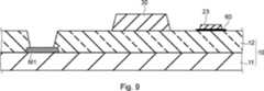
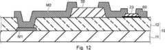
- 4 to 12are cross-sectional views showing an example of a method for manufacturing a transparent display device according to the first embodiment.
- 4 to 12are cross-sectional views corresponding to FIG.
- a first metal layer M1is formed on substantially the entire surface of the main substrate 11, and then the first metal layer M1 is patterned by photolithography to form a lower layer wiring.
- the lower layer wiringis formed by the first metal layer M1 at the position where the power supply line 41, the ground line 42, the row data line 43, the column data line 44, and the like shown in FIG. 1 are formed. No lower layer wiring is formed at the intersection of the power supply line 41, the ground line 42, and the column data line 44 with the row data line 43.
- a light-shielding filmis formed on the tacky adhesive layer 12 (that is, on the transparent substrate 10). 60 is patterned. Here, the light-shielding film 60 is formed at a position where the LED elements 21 to 23 are mounted.
- the IC chip 30is mounted on the adhesive layer 12 (that is, on the transparent substrate 10), and the LED elements 21 to 23 are mounted on the light-shielding film 60.
- the light-shielding film 60may have a tack property like the adhesive layer 12.
- the LED elements 21 to 23are patterned after growing crystals on the wafer by using, for example, a liquid phase growth method, an HVPE (Hydride Vapor Phase Epitaxy) method, a MOCVD (Metal Organic Chemical Vapor Deposition) method, or the like. Obtained by doing.
- the LED elements 21 to 23 patterned on the waferare transferred onto the transparent substrate 10 by using, for example, a micro transfer printing technique.
- the IC chip 30similarly to the LED elements 21 to 23, for example, the IC chip 30 patterned on the Si wafer is transferred onto the transparent substrate 10 by using the micro transfer printing technique.
- the photoresist FR1is formed on substantially the entire surface of the transparent substrate 10 including the main substrate 11 and the adhesive layer 12, and then the photoresist FR1 on the first metal layer M1 is patterned. Remove by.
- the photoresist FR1 at the intersection of the power supply line 41, the ground line 42, and the column data line 44 in the row data line 43 shown in FIG. 1is not removed.
- the adhesive layer 12 at the portion where the photoresist FR1 has been removedis removed by dry etching to expose the first metal layer M1, that is, the lower layer wiring.
- the adhesive layer 12 at the portion where the photoresist FR1 has been removedis removed by dry etching to expose the first metal layer M1, that is, the lower layer wiring.
- all the photoresist FR1 on the transparent substrate 10is removed.
- a seed layer for plating(not shown) is formed on substantially the entire surface of the transparent substrate 10.
- the photoresist FR2 at the portion where the upper layer wiring is formedis removed by patterning to expose the seed layer.
- a second metal layer M2is formed by plating on the portion where the photoresist FR2 has been removed, that is, the seed layer.
- the upper layer wiringis formed by the second metal layer M2.
- a transparent display deviceis obtained by forming the protective layer 50 on substantially the entire surface of the transparent substrate 10.
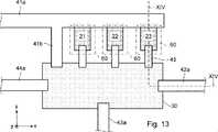
- FIG. 13is a schematic partial plan view showing an example of the transparent display device according to the modified example of the first embodiment, and is a diagram corresponding to FIG. 2.
- FIG. 14is a cross-sectional view taken along the XIV-XIV cutting line in FIG. In FIG. 13, the light-shielding film 60 is drawn by a two-dot chain line.
- the upper surface side of the LED elements 21 to 23is the visual recognition side. Therefore, the entire lower surface of the LED elements 21 to 23 is covered with the light-shielding film 60.
- the lower surface side of the LED elements 21 to 23is the visual recognition side. Therefore, the upper surface of the LED elements 21 to 23 is covered with the light-shielding film 60.
- the entire upper surface of the LED elements 21 to 23is covered with the light-shielding film 60, the first power supply branch line 41a, and the drive line 45.
- the first power supply branch line 41a and the drive line 45also function as a light-shielding film.
- the protective layer 50is located on the back surface side of the light-shielding film 60. Therefore, in order to prevent the light emitted from the LED elements 21 to 23 toward the visual recognition side and reflected on the back side from leaking to the back side, the internal transmittance of the visible light of the protective layer 50 may be set to, for example, 90% or less. good. From such a viewpoint, the internal transmittance of visible light of the protective layer 50 is preferably 70% or less, more preferably 50% or less.
- the protective layer 50may absorb only the light in a part of the wavelength range in the visible light, or may absorb the light in the entire wavelength range in the visible light.
- the transparent base material 10is located on the visual recognition side with respect to the LED elements 21 to 23. Therefore, the internal transmittance of visible light of the transparent substrate 10 is, for example, 50% or more, preferably 70% or more, and more preferably 90% or more.
- the entire main surface on the back sideis a light-shielding film 60 having a function as a light-shielding film, the first power supply branch line 41a, and the like. And covered by the drive line 45. Therefore, it is possible to prevent the light emitted from the LED elements 21 to 23 from leaking directly to the back surface side.
- the light-shielding film 60is formed so as to protrude from the main surface on the back surface side of the LED elements 21 to 23. Therefore, it is possible to prevent the light emitted from the LED elements 21 to 23 toward the visual recognition side and reflected on the back surface side from leaking to the back surface side. Further, by setting the internal transmittance of visible light of the transparent member (protective layer 50) located on the back side of the light-shielding film 60 to 90% or less, it is further suppressed that such reflected light leaks to the back side. can.
- Other configurationsare the same as those of the transparent display device according to the first embodiment.
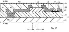
- FIG. 15is a schematic partial cross-sectional view showing an example of the transparent display device according to the second embodiment, and is a diagram corresponding to FIG.
- the antireflection film 70is formed on the visual recognition side of the LED elements 21 to 23.
- the antireflection film 70is formed on the upper surface (on the main surface on the visual recognition side) of the protective layer 50 in the transparent display device shown in FIG. Therefore, it is possible to reduce the light emitted from the LED elements 21 to 23 to the visual recognition side and reflected on the back surface side on the upper surface of the protective layer 50. As a result, it is possible to suppress leakage of such reflected light to the back surface side as compared with the transparent display device according to the first embodiment.
- Other configurationsare the same as those of the transparent display device according to the first embodiment. In the transparent display device shown in FIG. 14, the same effect can be obtained when an antireflection film is formed on the lower surface of the transparent base material 10 (on the main surface on the visual recognition side).
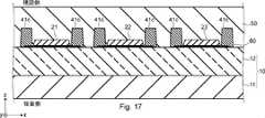
- FIG. 16is a schematic partial plan view showing an example of the transparent display device according to the third embodiment, and is a diagram corresponding to FIG. 2.
- FIG. 17is a cross-sectional view taken along the line of XVII-XVII in FIG.
- a third power supply branch line 41cthat functions as a mirror structure is formed around each of the LED elements 21 to 23.
- a pair of third power supply branch lines 41c branched from the first power supply branch line 41a in the negative direction on the y-axisare formed so as to surround each of the LED elements 21 to 23.
- each of the LED elements 21 to 23is surrounded by a first power supply branch line 41a, a pair of third power supply branch lines 41c, and a drive line 45.
- the third power supply branch line 41c and the drive line 45are separated from each other and are not electrically short-circuited.
- the light emitted from the LED element 23 to the visual recognition side so as to spread in the xy plane directionis the first power supply branch line 41a surrounding the LED element 23, the pair of third power supply branch lines 41c, and the drive. It is reflected by the wall surface of the line 45. Therefore, the traveling direction of the light emitted from the LED element 23 to the visual recognition side can be brought closer to the z-axis positive direction. The same applies to the LED elements 21 and 22.
- the transparent display device according to the present embodimentit is possible to reduce the light emitted from the LED elements 21 to 23 to the visual recognition side and reflected on the upper surface side of the protective layer 50 to the back surface side. As a result, it is possible to suppress leakage of such reflected light to the back surface side as compared with the transparent display device according to the first embodiment.
- Other configurationsare the same as those of the transparent display device according to the first embodiment.
- the present embodiment and the second embodimentcan also be combined. That is, the antireflection film 70 shown in FIG. 15 may be formed on the upper surface of the protective layer 50 in FIG.
- FIG. 18is a schematic partial cross-sectional view showing an example of a transparent display device according to a modification of the third embodiment, and is a diagram corresponding to FIG. 17.
- a convex lens 80 that covers the main surface of the LED elements 21 to 23 on the visual recognition sideis formed. Therefore, the traveling direction of the light emitted from the LED elements 21 to 23 to the visual recognition side can be further brought closer to the z-axis positive direction, and the light reflected on the back surface side on the upper surface of the protective layer 50 can be reduced. As a result, it is possible to suppress such reflected light from leaking to the back side as compared with the transparent display device shown in FIG. In FIG. 18, only the convex lens 80 may be provided without providing the third power supply branch line 41c that functions as a mirror structure.
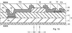
- FIG. 19is a schematic partial cross-sectional view showing an example of the transparent display device according to the fourth embodiment, and is a diagram corresponding to FIG.
- the light control layer 90is formed on the back side of the light shielding film 60. Specifically, in the transparent display device shown in FIG. 3, a dimming layer 90 is formed on the lower surface of the transparent base material 10.
- the dimming layer 90can dynamically adjust the internal transmittance of visible light. By providing the dimming layer 90, it is possible to dynamically suppress the light emitted from the LED elements 21 to 23 to the viewing side and reflected on the back side to leak to the back side.
- a guest host liquid crystalfor example, a guest host liquid crystal, a polymer-dispersed liquid crystal, an electric field-responsive anisotropic particle, an electrochromic material, or the like can be used.
- the dimming layer 90is transparent, and while the LED elements 21 to 23 are emitting light (that is, while not displaying an image). Only while the image is being displayed), the internal transmission of visible light in the dimming layer 90 is reduced. With such a configuration, it is possible to suppress the light emitted from the LED elements 21 to 23 to the visual recognition side and reflected on the back surface side from leaking to the back surface side without lowering the internal transmittance of the visible light of the transparent base material 10. Since the transparent substrate 10 has a high internal transmittance of visible light, the visibility on the back surface side is improved while the image is not displayed. Other configurations are the same as those of the transparent display device according to the first embodiment. In the transparent display device shown in FIG. 14, the same effect is obtained when a dimming layer is formed on the upper surface of the protective layer 50.
- FIG. 20is a schematic plan view showing an example of the laminated glass according to the fifth embodiment.
- FIG. 21is a schematic cross-sectional view showing an example of the laminated glass according to the fifth embodiment.
- the laminated glass 200 shown in FIGS. 20 and 21is used for the windshield of the window glass of an automobile, but is not particularly limited.
- a black shielding portion 201is provided on the entire peripheral edge of the laminated glass 200.
- the shielding portion 201shields sunlight and protects the adhesive for assembling the laminated glass 200 to the automobile from ultraviolet rays. Further, the shielding portion 201 makes the adhesive invisible from the outside.
- the transparent display device 100includes a non-display area 102 provided around the display area in addition to the display area 101 shown in FIG.
- the display area 101is an area composed of a large number of pixels and in which an image is displayed, and therefore detailed description thereof will be omitted.
- FIG. 20is a plan view, the non-display area 102 and the shielding portion 201 are displayed in dots for ease of understanding.
- the non-display area 102is an area that does not have pixels and does not display an image.
- the non-display area 102is densely provided with wide wiring connected to the power supply line 41, the ground line 42, the row data line 43, and the column data line 44 shown in FIG.
- the width of the wiring in the non-display area 102is, for example, 100 to 10,000 ⁇ m, preferably 100 to 5,000 ⁇ m.
- the distance between the wiringsis, for example, 3 to 5,000 ⁇ m, preferably 50 to 1,500 ⁇ m.
- the non-display area 102is opaque and can be visually recognized from inside the vehicle.
- the design of the laminated glass 200is deteriorated. Therefore, in the laminated glass 200 according to the fifth embodiment, at least a part of the non-display area 102 of the transparent display device 100 is provided in the shielding portion 201.
- the non-display area 102 provided in the shielding portion 201is hidden behind the shielding portion 201 and cannot be visually recognized. Therefore, the design of the laminated glass 200 is improved as compared with the case where the entire non-display area 102 can be visually recognized.
- FIG. 21is a cross-sectional view of the display area 101 of the transparent display device 100.
- the laminated glass 200 according to the fifth embodimentis formed by laminating a pair of glass plates 220a and 220b via an interlayer film.
- the laminated glass 200includes the transparent display device 100 according to the first embodiment between the pair of glass plates 220a and 220b via the interlayer films 210a and 210b.
- the interlayer films 210a and 210bare made of, for example, polyvinyl butyral (PVB).
- the refractive index of the interlayer film 210a in contact with the protective layer 50is higher than the refractive index of the protective layer 50 because it is possible to suppress the confinement of light in the protective layer 50 and it is difficult to see from the back.
- the interlayer film 210b and the glass plate 220bare located on the back surface side of the light-shielding film 60. Therefore, in order to prevent the light emitted from the LED elements 21 to 23 toward the visual recognition side and reflected on the back surface side from leaking to the back surface side, the internal transmittance of at least one of the visible light of the interlayer film 210b and the glass plate 220b May be, for example, 90% or less. From such a viewpoint, the internal transmittance of at least one of the interlayer film 210b and the glass plate 220b of visible light is preferably 70% or less, more preferably 50% or less.
- FIG. 22is a schematic cross-sectional view showing another example of the laminated glass according to the fifth embodiment.
- the protective layer 50 in the transparent display device 100is composed of, for example, polyvinyl butyral (PVB), and also has a function as an interlayer film. Therefore, in the laminated glass 200 shown in FIG. 22, the interlayer film 210a formed on the protective layer 50 can be omitted in FIG. 21.
- the refractive index of the glass plate 220a in contact with the protective layer 50is higher than the refractive index of the protective layer 50, it is possible to suppress the confinement of light in the protective layer 50, so that it is difficult to see from the back. preferable.
Landscapes
- Engineering & Computer Science (AREA)
- Power Engineering (AREA)
- Microelectronics & Electronic Packaging (AREA)
- Physics & Mathematics (AREA)
- Condensed Matter Physics & Semiconductors (AREA)
- General Physics & Mathematics (AREA)
- Computer Hardware Design (AREA)
- Devices For Indicating Variable Information By Combining Individual Elements (AREA)
- Led Device Packages (AREA)
Abstract
Description
Translated fromJapanese本発明は、透明表示デバイス、合わせガラス、及び透明表示デバイスの製造方法に関する。The present invention relates to a transparent display device, a laminated glass, and a method for manufacturing a transparent display device.
発光ダイオード(LED:Light Emitting Diode)素子を画素に用いた表示デバイスが知られている。特許文献1には、このような表示デバイスのうち、LED素子のサイズが微細であって、当該表示デバイスを介して背面側を視認可能な透明表示デバイスが開示されている。A display device using a light emitting diode (LED: Light Emitting Diode) element as a pixel is known. Patent Document 1 discloses, among such display devices, a transparent display device in which the size of the LED element is fine and the back side can be visually recognized via the display device.
ここで、透明表示デバイスでは、視認側に表示する画像を背面側(視認側の反対側)からは視認でできないようにしたいという要望があった。すなわち、LED素子から出射した光が背面側に漏れることを抑制したいという要望があった。Here, in the transparent display device, there was a request that the image displayed on the visual recognition side should not be visible from the back side (opposite side of the visual recognition side). That is, there has been a demand for suppressing leakage of light emitted from the LED element to the back surface side.
特許文献2に開示された透明表示デバイスでは、砲弾型LED(発光体)から発せられた光が、当該発光体が配列されていない背面側に透過することを阻害する遮光部材が設けられている。The transparent display device disclosed in Patent Document 2 is provided with a light-shielding member that prevents light emitted from a bullet-shaped LED (light-emitting body) from passing through the back side where the light-emitting body is not arranged. ..
しかしながら、10,000μm2以下の面積を有するLED素子を用いた透明表示デバイスに対し、特許文献2に開示された砲弾型LED用の遮光部材を適用しても、LED素子から出射した光が背面側に漏れることを十分に抑制できない。However, even if the light-shielding member for the bullet-shaped LED disclosed in Patent Document 2 is applied to the transparent display device using the LED element having an area of 10,000 μm2 or less, the light emitted from the LED element remains on the back surface. Leakage to the side cannot be sufficiently suppressed.
本発明は、このような事情に鑑みなされたものであって、LED素子から出射した光が背面側に漏れることを抑制可能な透明表示デバイスを提供するものである。The present invention has been made in view of such circumstances, and provides a transparent display device capable of suppressing leakage of light emitted from an LED element to the back surface side.
本発明は、[1]の構成を有する透明表示デバイスを提供する。
[1]
透明基材と、
前記透明基材上において画素ごとに配置された発光ダイオード素子と、を備え、
視認側から背面側を視認可能な透明表示デバイスであって、
前記発光ダイオード素子は、10,000μm2以下の面積を有する半導体チップであり、
前記発光ダイオード素子における前記背面側の主面が、遮光膜によって覆われている、
透明表示デバイス。The present invention provides a transparent display device having the configuration of [1].
[1]
With a transparent base material,
A light emitting diode element arranged for each pixel on the transparent substrate is provided.
A transparent display device that allows you to see the back side from the viewing side.
The light emitting diode element is a semiconductor chip having an area of 10,000 μm2 or less.
The main surface of the light emitting diode element on the back surface side is covered with a light-shielding film.
Transparent display device.
本発明の一態様においては、
[2]前記遮光膜が、前記発光ダイオード素子における前記背面側の主面全体を覆うと共に、主面からはみ出して形成されている、[1]に記載の透明表示デバイス。In one aspect of the invention
[2] The transparent display device according to [1], wherein the light-shielding film covers the entire main surface of the light-emitting diode element on the back surface side and protrudes from the main surface.
[3]前記遮光膜よりも前記背面側に位置する透明部材における可視光の内部透過率が90%以下である、[1]又は[2]に記載の透明表示デバイス。[3] The transparent display device according to [1] or [2], wherein the internal transmittance of visible light in the transparent member located on the back surface side of the light-shielding film is 90% or less.
[4]前記透明基材が、前記透明部材である、[3]に記載の透明表示デバイス。[4] The transparent display device according to [3], wherein the transparent substrate is the transparent member.
[5]前記透明基材上において前記発光ダイオード素子を覆う保護層と、前記保護層上に形成された反射防止膜と、をさらに備える、[4]に記載の透明表示デバイス。[5] The transparent display device according to [4], further comprising a protective layer covering the light emitting diode element on the transparent substrate and an antireflection film formed on the protective layer.
[6]前記透明基材上において前記発光ダイオード素子を覆う保護層をさらに備え、
前記保護層が、前記透明部材である、[3]に記載の透明表示デバイス。[6] A protective layer covering the light emitting diode element is further provided on the transparent substrate.
The transparent display device according to [3], wherein the protective layer is the transparent member.
[7]前記透明基材における前記視認側の主面上に形成された反射防止膜をさらに備える、[6]に記載の透明表示デバイス。[7] The transparent display device according to [6], further comprising an antireflection film formed on the main surface of the transparent substrate on the visible side.
[8]前記遮光膜よりも前記背面側に、可視光の内部透過率をダイナミックに調整可能な調光層をさらに備える、[1]又は[2]に記載の透明表示デバイス。[8] The transparent display device according to [1] or [2], further comprising a dimming layer capable of dynamically adjusting the internal transmittance of visible light on the back surface side of the light-shielding film.
[9]前記発光ダイオード素子の周囲を囲むように形成されたミラー構造をさらに備える、[1]~[8]のいずれか一項に記載の透明表示デバイス。[9] The transparent display device according to any one of [1] to [8], further comprising a mirror structure formed so as to surround the light emitting diode element.
[10]前記発光ダイオード素子における前記視認側の主面全体が、レンズによって覆われている、[1]~[9]のいずれか一項に記載の透明表示デバイス。[10] The transparent display device according to any one of [1] to [9], wherein the entire main surface of the light emitting diode element on the visual recognition side is covered with a lens.
本発明は、[11]の構成を有する合わせガラスを提供する。
[11]
一対のガラス板と、
前記一対のガラス板との間に設けられた透明表示デバイスと、を備えた合わせガラスであって、
前記透明表示デバイスは、
透明基材と、
前記透明基材上において画素ごとに配置された発光ダイオード素子と、を備え、
視認側から背面側を視認可能な透明表示デバイスであって、
前記発光ダイオード素子は、10,000μm2以下の面積を有する半導体チップであり、
前記発光ダイオード素子における前記背面側の主面が、遮光膜によって覆われている、
合わせガラス。The present invention provides a laminated glass having the configuration of [11].
[11]
A pair of glass plates and
A laminated glass provided with a transparent display device provided between the pair of glass plates.
The transparent display device is
With a transparent base material,
A light emitting diode element arranged for each pixel on the transparent substrate is provided.
A transparent display device that allows you to see the back side from the viewing side.
The light emitting diode element is a semiconductor chip having an area of 10,000 μm2 or less.
The main surface of the light emitting diode element on the back surface side is covered with a light-shielding film.
Laminated glass.
本発明は、以下[12]の構成を有する透明表示デバイスの製造方法を提供する。
[12]
視認側から背面側を視認可能な透明表示デバイスの製造方法であって、
透明基材上において画素ごとに10,000μm2以下の面積を有する半導体チップである発光ダイオード素子を配置し、
前記発光ダイオード素子における前記背面側の主面を、遮光膜によって覆う、
透明表示デバイスの製造方法。The present invention provides a method for manufacturing a transparent display device having the following configuration [12].
[12]
It is a manufacturing method of a transparent display device that can visually recognize the back side from the visual side.
A light emitting diode element, which is a semiconductor chip having an area of 10,000 μm2 or less for each pixel, is arranged on a transparent substrate.
The back surface of the light emitting diode element is covered with a light-shielding film.
How to make a transparent device.
本発明によれば、LED素子から出射した光が背面側に漏れることを抑制可能な透明表示デバイスを提供できる。According to the present invention, it is possible to provide a transparent display device capable of suppressing leakage of light emitted from an LED element to the back surface side.
以下、本発明を適用した具体的な実施形態について、図面を参照しながら詳細に説明する。但し、本発明が以下の実施形態に限定される訳ではない。また、説明を明確にするため、以下の記載及び図面は、適宜、簡略化されている。Hereinafter, specific embodiments to which the present invention is applied will be described in detail with reference to the drawings. However, the present invention is not limited to the following embodiments. Further, in order to clarify the explanation, the following description and drawings are appropriately simplified.
本明細書において「透明表示デバイス」とは、表示デバイスの背面側に位置する人物や背景等の視覚情報を、所望の使用環境下で視認可能な表示デバイスを指す。なお、視認可能とは、少なくとも表示デバイスが非表示状態、すなわち通電されていない状態で判定される。In the present specification, the "transparent display device" refers to a display device in which visual information such as a person or a background located on the back side of the display device can be visually recognized under a desired usage environment. Note that visibility is determined at least when the display device is in a non-display state, that is, in a state where it is not energized.
本明細書において、「透明」とは、可視光の透過率が40%以上、好ましくは60%以上、より好ましくは70%以上であることを指す。また、透過率5%以上かつヘイズ値が20以下であることを指していてもよい。透過率が5%以上であれば、室内から日中の屋外を見た際に、室内と同程度以上の明るさで屋外を見られ、充分な視認性を確保できる。In the present specification, "transparent" means that the transmittance of visible light is 40% or more, preferably 60% or more, and more preferably 70% or more. It may also indicate that the transmittance is 5% or more and the haze value is 20 or less. When the transmittance is 5% or more, when the outside is viewed from the room during the daytime, the outside can be seen with the same or higher brightness as the room, and sufficient visibility can be ensured.
また、透過率が40%以上であれば、透明表示デバイスの前面側と背面側との明るさが同程度であっても、透明表示デバイスの背面側を実質的に問題なく視認できる。また、ヘイズ値が10以下であれば、背景のコントラストを充分に確保できる。
「透明」とは、色が付与されているか否かは問わず、つまり無色透明であってもよく、有色透明であってもよい。
なお、透過率は、ISO9050に準拠する方法により測定された値(%)を指す。ヘイズ値は、ISO14782に準拠する方法により測定された値を指す。Further, when the transmittance is 40% or more, the back side of the transparent display device can be visually recognized without any problem even if the brightness of the front side and the back side of the transparent display device is about the same. Further, when the haze value is 10 or less, sufficient background contrast can be secured.
The term "transparent" means whether or not a color is applied, that is, it may be colorless and transparent, or it may be colored and transparent.
The transmittance refers to a value (%) measured by a method conforming to ISO9050. The haze value refers to a value measured by a method conforming to ISO 14782.
(第1の実施形態)
<透明表示デバイスの構成>
まず、図1~図3を参照して、第1の実施形態に係る透明表示デバイスの構成について説明する。図1は、第1の実施形態に係る透明表示デバイスの一例を示す模式的な部分平面図である。図2は、図1における領域IIの拡大図である。図3は、図2におけるIII-III切断線による断面図である。(First Embodiment)
<Configuration of transparent display device>
First, the configuration of the transparent display device according to the first embodiment will be described with reference to FIGS. 1 to 3. FIG. 1 is a schematic partial plan view showing an example of a transparent display device according to the first embodiment. FIG. 2 is an enlarged view of region II in FIG. FIG. 3 is a cross-sectional view taken along the line III-III in FIG.
図1~図3に示すように、本実施形態に係る透明表示デバイスは、透明基材10、発光部20、IC(Integrated Circuit)チップ30、配線40、保護層50、及び遮光膜60を備えている。透明表示デバイスにおける表示領域101は、複数の画素から構成され、画像が表示される領域である。なお、画像は文字を含む。図1に示すように、表示領域101は、行方向(x軸方向)及び列方向(y軸方向)に並んだ複数の画素から構成されている。図1には、表示領域101の一部が示されており、行方向及び列方向に2画素ずつ計4画素が示されている。ここで、1つの画素PIXが一点鎖線によって囲んで示されている。As shown in FIGS. 1 to 3, the transparent display device according to the present embodiment includes a
なお、当然のことながら、図1~図3に示した右手系xyz直交座標は、構成要素の位置関係を説明するための便宜的なものである。通常、z軸正向きが鉛直上向き、xy平面が水平面である。
また、図1、図2では、図3に示した透明基材10、保護層50が省略されている。さらに、図1、図2は平面図だが、理解を容易にするため、発光部20及びICチップ30がドット表示されている。As a matter of course, the right-handed xyz orthogonal coordinates shown in FIGS. 1 to 3 are for convenience in explaining the positional relationship of the constituent elements. Normally, the z-axis positive direction is vertically upward, and the xy plane is a horizontal plane.
Further, in FIGS. 1 and 2, the
<発光部20、ICチップ30、配線40、及び遮光膜60の平面配置>
まず、図1、図2を参照して、発光部20、ICチップ30、配線40、及び遮光膜60の平面配置について説明する。
図1に示すように、一点鎖線によって囲まれた画素PIXが、行方向(x軸方向)に画素ピッチPxで、列方向(y軸方向)に画素ピッチPyで、マトリクス状に配置されている。ここで、図1に示すように、各画素PIXは、発光部20及びICチップ30を備えている。すなわち、発光部20及びICチップ30は、行方向(x軸方向)に画素ピッチPxで、列方向(y軸方向)に画素ピッチPyで、マトリクス状に配置されている。
なお、所定の方向に所定の画素ピッチで配置されれば、画素PIXすなわち発光部20の配置形式はマトリクス状に限らない。<Plane arrangement of the
First, with reference to FIGS. 1 and 2, the planar arrangement of the
As shown in FIG. 1, the pixel PIX surrounded by the alternate long and short dash line is arranged in a matrix with a pixel pitch Px in the row direction (x-axis direction) and a pixel pitch Py in the column direction (y-axis direction). .. Here, as shown in FIG. 1, each pixel PIX includes a
If the pixels are arranged in a predetermined direction at a predetermined pixel pitch, the arrangement format of the pixels PIX, that is, the
図1に示すように、各画素PIXにおける発光部20は、少なくとも1つの発光ダイオード素子(以下、LED素子)を含む。すなわち、本実施形態による透明表示デバイスは、各画素PIXにLED素子を用いる表示デバイスであり、LEDディスプレイ等と呼ばれる。As shown in FIG. 1, the
図1の例では、各発光部20が、赤色系のLED素子21、緑色系のLED素子22、及び青色系のLED素子23を含んでいる。LED素子21~23は、1つの画素を構成する副画素(サブピクセル)に対応する。このように、各発光部20が、光の三原色である赤、緑、青を発光するLED素子21~23を有するため、本実施形態に係る透明表示デバイスは、フルカラー画像を表示できる。
なお、各発光部20は同系色のLED素子を2つ以上含んでいてもよい。これにより、画像のダイナミクスレンジを拡大できる。In the example of FIG. 1, each
In addition, each
LED素子21~23は、いわゆるマイクロLED素子であり、10,000μm2以下の面積を有する半導体チップである。具体的には、透明基材10上におけるLED素子21の幅(x軸方向の長さ)及び長さ(y軸方向の長さ)はそれぞれ、例えば100μm以下、好ましくは50μm以下、より好ましくは20μm以下である。LED素子22、23についても同様である。LED素子の幅及び長さの下限は、製造上の諸条件等から例えば3μm以上である。
なお、図1におけるLED素子21~23の寸法すなわち幅及び長さは同一であるが、互いに異なっていてもよい。The
Although the dimensions, that is, the width and the length of the
また、透明基材10上においてLED素子21~23の面積は、好ましくは3,000μm2以下、より好ましくは500μm2以下である。なお、1つのLED素子が占める面積の下限は、製造上の諸条件等から例えば10μm2以上である。ここで、本明細書において、LED素子の面積や配線等の構成部材の面積は、図1におけるxy平面視においてLED素子や配線等の構成部材が占める面積を指す。
なお、図1に示したLED素子21~23の形状は、矩形状(正方形を含む)であるが、特に限定されない。The area of the
The shape of the
ここで、LED素子21~23の透過率は、例えば10%以下程度と低い。しかしながら、本実施形態に係る透明表示デバイスでは、上述の通り、面積10,000μm2以下の微小サイズのLED素子21~23を用いている。そのため、例えば数10cm~2m程度の近距離から、透明表示デバイスを観察するような場合でも、LED素子21~23はほとんど視認できない。また、表示領域101において透過率が低い領域が狭く、背面側の視認性に優れている。その上、配線40等の配置の自由度も大きい。
なお、「表示領域101において透過率が低い領域」とは、例えば、透過率が20%以下の領域である。以下同様である。Here, the transmittance of the
The “region having a low transmittance in the
また、微小サイズのLED素子21~23を用いているため、透明表示デバイスを湾曲させても、LED素子が損傷し難い。そのため、本実施形態に係る透明表示デバイスは、自動車用のウインドウガラスのような湾曲した透明板に装着したり、湾曲した2枚の透明板の間に封入したりして使用できる。ここで、透明基材10として可撓性を有する材料を用いれば、本実施形態に係る透明表示デバイスを湾曲させられる。Moreover, since the
LED素子21~23は、特に限定されないが、例えば無機材料である。赤色系のLED素子21は、例えばAlGaAs、GaAsP、GaP等である。緑色系のLED素子22は、例えばInGaN、GaN、AlGaN、GaP、AlGaInP、ZnSe等である。青色系のLED素子23は、例えばInGaN、GaN、AlGaN、ZnSe等である。また、LED素子21~23は、非偏光の光を放出するもののみでなく、偏光された光を放出するものであってもよい。偏光された光を放出する機能は、放出する光の波長よりも短いピッチの構造体をLED素子21~23の内部、もしくは、表面に備えたものや、キラリティを持った材料をLED素子21~23の内部や表面に備えること等によって実現される。また、LED素子21~23が偏光された光を放出する場合、背面側に特定の偏光光を吸収、もしくは、反射する偏光フィルム等の部材を配置すると、背面側に漏れる光を抑制できるため、好ましい。偏光フィルムは、直線偏光、円偏光どちらに対して作用するものでもよい。The
LED素子21~23の発光効率すなわちエネルギー変換効率は、例えば1%以上、好ましくは5%以上、より好ましくは15%以上である。LED素子21~23の発光効率が1%以上であると、上述のように微小サイズのLED素子21~23でも充分な輝度が得られ、表示デバイスとして日中にも利用できる。また、LED素子の発光効率が15%以上であると、発熱が抑制され、樹脂接着層を用いた合わせガラス内部への封入が容易になる。The luminous efficiency, that is, the energy conversion efficiency of the
画素ピッチPx、Pyはそれぞれ、例えば100~3000μm、好ましくは180~1000μm、より好ましくは250~400μmである。画素ピッチPx、Pyを上記範囲とすることによって、充分な表示能を確保しつつ、高い透明性を実現できる。また、透明表示デバイスの背面側からの光によって生じ得る回折現象を抑制できる。
また、本実施形態に係る透明表示デバイスの表示領域101における画素密度は、例えば10ppi以上、好ましくは30ppi以上、より好ましくは60ppi以上である。The pixel pitches Px and Py are, for example, 100 to 3000 μm, preferably 180 to 1000 μm, and more preferably 250 to 400 μm, respectively. By setting the pixel pitches Px and Py in the above range, high transparency can be realized while ensuring sufficient display capability. In addition, it is possible to suppress a diffraction phenomenon that may occur due to light from the back side of the transparent display device.
Further, the pixel density in the
また、1画素PIXの面積はPx×Pyである。1画素の面積は、例えば1×104μm2~9×106μm2、好ましくは3×10⁴~1×106μm2、より好ましくは6×10⁴~2×105μm2である。1画素の面積を1×104μm2~9×106μm2とすることで、適切な表示能を確保しつつ、表示デバイスの透明性を向上させられる。1画素の面積は、表示領域101のサイズ、用途、視認距離等によって適宜選択すればよい。The area of one pixel PIX is Px × Py. The area of one pixel is, for example, 1 × 104 μm2 to 9 × 106 μm2 , preferably 3 × 10⁴ to 1 × 106 μm2 , and more preferably 6 × 10⁴ to 2 × 105 μm2 . be. By setting the area of one pixel to 1 × 104 μm2 to 9 × 106 μm2 , the transparency of the display device can be improved while ensuring an appropriate display capability. The area of one pixel may be appropriately selected depending on the size of the
1画素の面積に対してLED素子21~23が占める面積の割合は、例えば30%以下、好ましくは10%以下、より好ましくは5%以下、さらに好ましくは1%以下である。1画素の面積に対してLED素子21~23が占める面積の割合を30%以下とすることで、透明性及び背面側の視認性が向上する。The ratio of the area occupied by the
図1では、各画素において、3つのLED素子21~23が、この順にx軸正方向に一列に並べて配置されているが、これに限定されない。例えば、3つのLED素子21~23の配置順を変更してもよい。また、3つのLED素子21~23を、y軸方向に並べてもよい。あるいは、3つのLED素子21~23を三角形の頂点に配置してもよい。In FIG. 1, three
また、図1に示すように、各発光部20が複数のLED素子21~23を備えている場合、発光部20におけるLED素子21~23同士の間隔は、例えば100μm以下、好ましくは10μm以下である。また、LED素子21~23同士は、互いに接するように配置されていてもよい。これにより、第1電源分岐線41aを共通化し易くなり、開口率を向上させられる。Further, as shown in FIG. 1, when each
なお、図1の例では、各発光部20における複数のLED素子の配置順、配置方向等は互いに同じだが、異なっていてもよい。また、各発光部20が波長の異なる光を発する3つのLED素子を含む場合、一部の発光部20では、LED素子をx軸方向又はy軸方向に並べて配置し、他の発光部20では、各色のLED素子を三角形の頂点に配置してもよい。In the example of FIG. 1, the arrangement order, arrangement direction, etc. of the plurality of LED elements in each
図1の例では、ICチップ30は、画素PIXごとに配置され、発光部20を駆動する。具体的には、ICチップ30は、LED素子21~23のそれぞれに駆動線45を介して接続されており、LED素子21~23を個別に駆動できる。ICチップ30は、例えば、アナログ領域と論理領域とを備えたハイブリッドICである。アナログ領域は、例えば、電流制御回路及び変圧回路等を含んでいる。In the example of FIG. 1, the
なお、ICチップ30を複数の画素ごとに配置し、各ICチップ30が接続された複数の画素を駆動してもよい。例えば、ICチップ30を4画素ごとに1個配置すれば、ICチップ30の個数を図1の例の1/4に削減し、ICチップ30が占める面積を削減できる。また、ICチップ30は必須ではない。Note that the
ICチップ30の面積は、例えば100,000μm2以下、好ましくは10,000μm2以下、より好ましくは5,000μm2以下である。ICチップ30の透過率は20%以下程度と低いが、上記のサイズのICチップ30を用いることによって、表示領域101において透過率が低い領域が狭くなり、背面側の視認性が向上する。The area of the
図1に示すように、配線40は、電源線41、グランド線42、行データ線43、列データ線44、及び駆動線45を複数ずつ備えている。
図1の例では、電源線41、グランド線42、及び列データ線44はy軸方向に延設されている。他方、行データ線43は、x軸方向に延設されている。As shown in FIG. 1, the
In the example of FIG. 1, the
また、各画素PIXにおいて、電源線41及び列データ線44は、発光部20及びICチップ30よりもx軸負方向側に設けられており、グランド線42は、発光部20及びICチップ30よりもx軸正方向側に設けられている。ここで、電源線41は、列データ線44よりもx軸負方向側に設けられている。また、各画素PIXにおいて、行データ線43は、発光部20及びICチップ30よりもy軸負方向側に設けられている。Further, in each pixel PIX, the
さらに、詳細には後述するが、図1に示すように、電源線41は、第1電源分岐線41a及び第2電源分岐線41bを備えている。グランド線42は、グランド分岐線42aを備えている。行データ線43は、行データ分岐線43aを備えている。列データ線44は、列データ分岐線44aを備えている。これら各分岐線は、配線40に含まれる。Further, as will be described in detail later, as shown in FIG. 1, the
図1に示すように、y軸方向に延設された各電源線41は、y軸方向に並設された各画素PIXの発光部20及びICチップ30に接続されている。より詳細には、各画素PIXにおいて、電源線41よりもx軸正方向側において、LED素子21~23がこの順にx軸正方向に並設されている。そのため、電源線41からx軸正方向に分岐した第1電源分岐線41aが、LED素子21~23のy軸正方向側端部に接続されている。As shown in FIG. 1, each
また、各画素PIXにおいて、ICチップ30は、LED素子21~23のy軸負方向側に配置されている。そのため、LED素子21と列データ線44との間において、第1電源分岐線41aからy軸負方向に分岐した第2電源分岐線41bが、直線状に延設され、ICチップ30のy軸正方向側端部のx軸負方向側に接続されている。Further, in each pixel PIX, the
図1に示すように、y軸方向に延設された各グランド線42は、y軸方向に並設された各画素PIXのICチップ30に接続されている。具体的には、グランド線42からx軸負方向に分岐したグランド分岐線42aが、直線状に延設され、ICチップ30のx軸正方向側端部に接続されている。
ここで、グランド線42は、グランド分岐線42a、ICチップ30、及び駆動線45を介して、LED素子21~23に接続されている。As shown in FIG. 1, each
Here, the
図1に示すように、x軸方向に延設された各行データ線43は、x軸方向(行方向)に並設された各画素PIXのICチップ30に接続されている。具体的には、行データ線43からy軸正方向に分岐した行データ分岐線43aが、直線状に延設され、ICチップ30のy軸負方向側端部に接続されている。
ここで、行データ線43は、行データ分岐線43a、ICチップ30、及び駆動線45を介して、LED素子21~23に接続されている。As shown in FIG. 1, each
Here, the
図1に示すように、y軸方向に延設された各列データ線44は、y軸方向(列方向)に並設された各画素PIXのICチップ30に接続されている。具体的には、列データ線44からx軸正方向に分岐した列データ分岐線44aが、直線状に延設され、ICチップ30のx軸負方向側端部に接続されている。
ここで、列データ線44は、列データ分岐線44a、ICチップ30、及び駆動線45を介して、LED素子21~23に接続されている。As shown in FIG. 1, each
Here, the
駆動線45は、各画素PIXにおいて、LED素子21~23とICチップ30とを接続している。具体的には、各画素PIXにおいて、3本の駆動線45がy軸方向に延設され、それぞれがLED素子21~23のy軸負方向側端部とICチップ30のy軸正方向側端部とを接続している。The
なお、図1に示した電源線41、グランド線42、行データ線43、列データ線44、及びそれらの分岐線、並びに駆動線45の配置はあくまでも一例であり、適宜変更可能である。例えば、電源線41及びグランド線42の少なくとも一方が、y軸方向でなくx軸方向に延設されていてもよい。また、電源線41と列データ線44とを入れ換えた構成でもよい。The arrangement of the
また、図1に示した構成全体を、上下反転させた構成あるいは左右反転させた構成等でもよい。
さらに、行データ線43、列データ線44、及びそれらの分岐線、並びに駆動線45は必須ではない。Further, the entire configuration shown in FIG. 1 may be upside down, left-right inverted, or the like.
Further, the
配線40は、例えば銅(Cu)、アルミニウム(Al)、銀(Ag)、金(Au)等の金属である。このうち、低抵抗率であることやコスト的な観点から銅又はアルミニウムを主成分とする金属であることが好ましい。また、配線40は、反射率を低減することを目的として、チタン(Ti)、モリブデン(Mo)、酸化銅、カーボン等の材料で被覆されていてもよい。また、被覆した材料の表面に凹凸が形成されていてもよい。The
図1に示した表示領域101における配線40の幅は、いずれも例えば1~100μm、好ましくは3~20μmである。配線40の幅が100μm以下であるため、例えば数10cm~2m程度の近距離から、透明表示デバイスを観察するような場合でも、配線40はほとんど視認できず、背面側の視認性に優れている。他方、後述する厚さの範囲の場合、配線40の幅を1μm以上であれば、配線40の抵抗の過度な上昇を抑制し、電圧降下や信号強度の低下を抑制できる。また、配線40による熱伝導の低下も抑制できる。The width of the
ここで、図1に示すように、配線40が主にx軸方向及びy軸方向に延びている場合、透明表示デバイスの外部から照射された光によってx軸方向及びy軸方向に延びた十字回折像が発生し、透明表示デバイスの背面側の視認性が低下する場合がある。各配線の幅を小さくすることによって、この回折を抑制し、背面側の視認性をさらに向上させられる。回折を抑制する観点から、配線40の幅を50μm以下、好ましくは10μm以下、より好ましくは5μm以下としてもよい。Here, as shown in FIG. 1, when the
配線40の電気抵抗率は、例えば1.0×10⁻⁶Ωm以下、好ましくは2.0×10⁻⁸Ωm以下である。また、配線40の熱伝導率は、例えば150~5,500W/(m・K)、好ましくは350~450W/(m・K)である。The electrical resistivity of the
図1に示した表示領域101における隣接する配線40同士の間隔は、例えば3~100μm、好ましくは5~30μmである。配線40が密になっている領域があると、背面側の視認を妨げる場合がある。隣接する配線40同士の間隔を3μm以上とすることによって、そのような視認の妨げを抑制できる。他方、隣接する配線40同士の間隔を100μm以下とすることによって、充分な表示能を確保できる。
なお、配線40が湾曲していること等によって配線40同士の間隔が一定でない場合、上述の隣接する配線40同士の間隔は、その最小値を指す。The distance between
When the distance between the wirings 40 is not constant due to the curved wiring or the like, the above-mentioned distance between the
1画素の面積に対して配線40が占める面積の割合は、例えば30%以下、好ましくは10%以下、より好ましくは5%以下、さらに好ましくは3%以下である。配線40の透過率は、例えば20%以下、あるいは10%以下と低い。しかしながら、1画素において配線40が占める面積の割合を30%以下とすることによって、表示領域101において透過率の低い領域が狭くなり、背面側の視認性が向上する。
さらに、1画素の面積に対して発光部20、ICチップ30、及び配線40が占める面積の合計は、例えば30%以下、好ましくは20%以下、より好ましくは10%以下である。The ratio of the area occupied by the
Further, the total area occupied by the
遮光膜60は、LED素子21~23のそれぞれにおいて、背面側の主面全体を覆うように形成されている。そのため、図2に示すように、xy平面視において、各遮光膜60は、LED素子21~23のそれぞれの全体と重複するように形成されている。このように、LED素子21~23のそれぞれの背面側の主面を遮光膜60によって覆うことによって、LED素子21~23から出射した光が背面側に漏れることを抑制できる。遮光膜60は背面側の主面全体を覆うことが好ましい。The light-shielding
遮光膜60は、例えば絶縁性を有する黒色系の樹脂膜、金属酸化膜、金属窒化膜等である。より具体的には、遮光膜60は、例えば、ブラックレジスト膜、カーボンブラックやその他カーボン系材料、Cr、Mo、Ti、Al等が全体もしくは部分的に酸化や窒化された膜等である。遮光膜60は、金属Cr膜等の導電性を有する金属膜でもよい。また、このような材料のフィラーを含有する樹脂が遮光膜60として用いられてもよい。また、フィラーを含有する樹脂の有効屈折率が、周囲の透明基材10や保護層50の屈折率と同等、もしくは、その差が0.2以内であると好ましい。また、遮光膜60による光の反射を抑制するため、遮光膜60の表面が平滑でない方が好ましい。The light-shielding
図2に示すように、遮光膜60が、LED素子21~23のそれぞれの背面側の主面からはみ出して形成されていてもよい。LED素子21~23からはみ出した遮光膜60によって、LED素子21~23から視認側に出射して背面側に反射した光が、背面側に漏れることを抑制できる。As shown in FIG. 2, the light-shielding
遮光膜60の面積が大きい程、このような反射光が背面側に漏れることを抑制できるが、背面側の視認性は低下する。そのため、遮光膜60の面積は、例えば1画素の面積に対して、0.6倍以下、好ましくは0.4倍以下、さらに好ましくは0.2倍以下である。The larger the area of the light-shielding
<透明表示デバイスの断面構成>
次に、図3を参照して、本実施形態に係る透明表示デバイスの断面構成について説明する。
透明基材10は、絶縁性を有する透明な材料である。図3の例では、透明基材10は、主基板11及び接着剤層12である2層構造を有している。
主基板11は、詳細には後述するように、例えば透明樹脂である。
接着剤層12は、例えばエポキシ系、アクリル系、オレフィン系、ポリイミド系、ノボラック系等の透明樹脂接着剤である。
なお、主基板11は、厚さが例えば200μm以下、好ましくは100μm以下等の薄いガラス板でもよい。また、接着剤層12は、必須ではない。<Cross-sectional configuration of transparent display device>
Next, with reference to FIG. 3, the cross-sectional configuration of the transparent display device according to the present embodiment will be described.
The
The
The
The
主基板11を構成する透明樹脂として、ポリエチレンテレフタレート(PET)、ポリエチレンナフタレート(PEN)等のポリエステル系樹脂、シクロオレフィンポリマー(COP)、シクロオレフィンコポリマー(COC)等のオレフィン系樹脂、セルロース、アセチルセルロース、トリアセチルセルロース(TAC)等のセルロース系樹脂、ポリイミド(PI)等のイミド系樹脂、ポリアミド(PA)等のアミド系樹脂、ポリアミドイミド(PAI)等のアミドイミド系樹脂、ポリカーボネート(PC)等のカーボネート系樹脂、ポリエーテルスルホン(PES)等のスルホン系樹脂、ポリパラキシレン等のパラキシレンケイ系樹脂、ポリエチレン(PE)、ポリ塩化ビニル(PVC)、ポリスチレン(PS)、ポリ酢酸ビニル(PVAc)、ポリビニルアルコール(PVA)、ポリビニルブチラール(PVB)等のビニル系樹脂、ポリメタクリル酸メチル(PMMA)等のアクリル系樹脂、エチレン・酢酸ビニル共重合樹脂(EVA)、熱可塑性ポリウレタン(TPU)等のウレタン系樹脂、エポキシ系樹脂等を例示できる。As the transparent resin constituting the
上記の主基板11に用いられる材料のうち、耐熱性向上の観点からはポリエチレンナフタレート(PEN)、ポリイミド(PI)が好ましい。また、複屈折率が低く、透明基材を通して見た像の歪みや滲みを低減できる点では、シクロオレフィンポリマー(COP)、シクロオレフィンコポリマー(COC)、ポリビニルブチラール(PVB)等が好ましい。
上記材料を単一で用いても、2種以上の材料を混合して用いてもよい。さらに、異なる材料の平板を積層させて主基板11を構成してもよい。Of the materials used for the
The above materials may be used alone, or two or more kinds of materials may be mixed and used. Further, the
透明基材10全体の厚さは、例えば3~1000μm、好ましくは5~200μmである。
また、透明基材10は可撓性を有していてもよい。これにより、例えば透明表示デバイスを湾曲した透明板に装着したり、湾曲した2枚の透明板の間に挟んで使用したりできる。また、100℃以上に加熱した際に収縮する材料であってもよい。The total thickness of the
Further, the
図3に示すように、LED素子21~23及びICチップ30は、透明基材10すなわち接着剤層12上に設けられている。
ここで、図3に示すように、LED素子21~23は、遮光膜60を介して、透明基材10すなわち接着剤層12上に設けられている。換言すると、透明基材10すなわち接着剤層12上に遮光膜60が形成されており、遮光膜60上にLED素子21~23が形成されている。図3の例では、z軸正方向側が視認側、z軸負方向側が背面側である。従って、LED素子21~23のそれぞれにおいて、背面側の主面全体が遮光膜60によって覆われており、LED素子21~23から出射した光が直接背面側に漏れることを抑制できる。遮光膜60の厚さは、例えば0.01~2μmであると、遮光膜60の側壁での散乱を抑制できる。遮光膜60の厚さは、0.5μm以下が好ましく、0.1μm以下がさらに好ましい。As shown in FIG. 3, the
Here, as shown in FIG. 3, the
図3に示すように、透明基材10は、遮光膜60よりも背面側に位置する。そこで、LED素子21~23から視認側に出射して背面側に反射した光が、背面側に漏れることを抑制するため、透明基材10の可視光の内部透過率を、例えば90%以下としてもよい。このような観点からは、透明基材10の可視光の内部透過率は、好ましくは70%以下、より好ましくは50%以下である。ここで、透明基材10は、可視光における一部の波長域の光のみを吸収してもよく、可視光における全体の波長域の光を吸収してもよい。As shown in FIG. 3, the
図3に示すように、LED素子21~23及びICチップ30は、透明基材10上に配置された配線40と接続されている。図3の例では、配線40は、主基板11上に形成された第1メタル層M1、及び接着剤層12上に形成された第2メタル層M2から構成されている。
配線40の厚さすなわち第1メタル層M1の厚さと第2メタル層M2の厚さとの合計は、例えば0.1~10μm、好ましくは0.5~5μmである。第1メタル層M1の厚さは、例えば0.5μm程度、第2メタル層M2の厚さは、例えば3μm程度である。As shown in FIG. 3, the
The total thickness of the
詳細には、図3に示すように、y軸方向に延設されたグランド線42は、電流量が多いため、第1メタル層M1及び第2メタル層M2を含む2層構造を有している。すなわち、グランド線42が設けられた部位では、接着剤層12が除去され、第1メタル層M1上に第2メタル層M2が形成されている。図3には示されていないが、図1に示した電源線41、行データ線43、及び列データ線44も、同様に、第1メタル層M1及び第2メタル層M2を含む2層構造を有している。Specifically, as shown in FIG. 3, since the
ここで、図1に示すように、y軸方向に延設された電源線41、グランド線42、及び列データ線44と、x軸方向に延設された行データ線43とは、交差している。図3には図示されていないが、この交差部では、行データ線43は第1メタル層M1のみから構成され、電源線41、グランド線42、及び列データ線44は第2メタル層M2のみから構成されている。そして、この交差部では、第1メタル層M1と第2メタル層M2との間に接着剤層12が設けられ、第1メタル層M1と第2メタル層M2とが絶縁されている。
同様に、図1に示した列データ線44と第1電源分岐線41aとの交差部では、第1電源分岐線41aが第1メタル層M1のみから構成され、列データ線44が第2メタル層M2のみから構成されている。Here, as shown in FIG. 1, the
Similarly, at the intersection of the
また、図3の例では、グランド分岐線42a、駆動線45、及び第1電源分岐線41aは第2メタル層M2のみから構成され、LED素子21~23及びICチップ30の端部を覆うように形成されている。図3には示されていないが、第2電源分岐線41b、行データ分岐線43a、及び列データ分岐線44aも、同様に、第2メタル層M2のみから構成されている。Further, in the example of FIG. 3, the
なお、第1電源分岐線41aは、上述の通り、列データ線44との交差部では第1メタル層M1のみから構成され、それ以外の部位では第2メタル層M2のみから構成されている。また、透明基材10上に形成された配線40上に、銅、銀、金製等の金属パッドを配置し、その上にLED素子21~23及びICチップ30の少なくとも一方を配置してもよい。As described above, the first power
保護層50は、発光部20、ICチップ30、及び配線40を覆って保護するように、透明基材10上の略全面に形成された透明樹脂である。
保護層50の厚さは、例えば3~1000μm、好ましくは5~200μmである。
保護層50の弾性率は、例えば10GPa以下である。弾性率が低い方が、剥離時の衝撃を吸収でき、保護層50の破損を抑制できる。
保護層50の可視光の内部透過率は、例えば50%以上、好ましくは70%以上、より好ましくは90%以上である。The
The thickness of the
The elastic modulus of the
The internal transmittance of visible light of the
保護層50の屈折率は、保護層50内に光を閉じ込めず、視認側(z軸正方向側)に取り出すためには、発光部20の視認側において接触する透明層(図3では不図示)の屈折率よりも低い方が好ましい。
他方、保護層50の面内平均厚みを1画素のピッチよりも小さくすると、保護層50の屈折率が発光部20の視認側において接触する透明層の屈折率よりも高い方がかえって好ましい。保護層50の内部に光を閉じ込めて導光させることにより、背面側において保護層50に接触している遮光膜60や配線40等によって光が効果的に吸収され、背面側に光が漏れることを抑制できるからである。この場合、保護層50の厚みは、遮光膜60の最も長い辺よりも薄いと、より好ましい。なお、遮光膜60や配線40等と保護層50との間にさらに透明層が形成されていても、当該透明層の屈折率が保護層50よりも高ければ、同様の効果が得られる。The refractive index of the
On the other hand, when the in-plane average thickness of the
保護層50を構成する透明樹脂として、ポリエチレン(PE)、ポリ塩化ビニル(PVC)、ポリスチレン(PS)、ポリ酢酸ビニル(PVAc)、ポリビニルアルコール(PVA)、ポリビニルブチラール(PVB)等のビニル系樹脂、シクロオレフィンポリマー(COP)、シクロオレフィンコポリマー(COC)等のオレフィン系樹脂、熱可塑性ポリウレタン(TPU)等のウレタン系樹脂、ポリエチレンテレフタレート(PET)、ポリエチレンナフタレート(PEN)等のポリエステル系樹脂、ポリメタクリル酸メチル(PMMA)等のアクリル系樹脂、エチレン・酢酸ビニル共重合樹脂(EVA)等の熱可塑性樹脂を例示できる。As the transparent resin constituting the
以上に説明した通り、本実施形態に係る透明表示デバイスでは、LED素子21~23のそれぞれにおいて、背面側の主面全体が、遮光膜60によって覆われている。そのため、LED素子21~23から出射した光が直接背面側に漏れることを抑制できる。
また、遮光膜60が、LED素子21~23の背面側の主面からはみ出して形成されている。そのため、LED素子21~23から視認側に出射して背面側に反射した光が、背面側に漏れることを抑制できる。
さらに、遮光膜60よりも背面側に位置する透明部材(透明基材10)の可視光の内部透過率を90%以下とすることによって、そのような反射光が背面側に漏れることをさらに抑制できる。As described above, in the transparent display device according to the present embodiment, in each of the
Further, the light-shielding
Further, by setting the internal transmittance of visible light of the transparent member (transparent base material 10) located on the back side of the light-shielding
<透明表示デバイスの製造方法>
次に、図3~図12を参照して、第1の実施形態に係る透明表示デバイスの製造方法の一例について説明する。図4~図12は、第1の実施形態に係る透明表示デバイスの製造方法の一例を示す断面図である。図4~図12は、図3に対応した断面図である。<Manufacturing method of transparent display device>
Next, an example of a method for manufacturing a transparent display device according to the first embodiment will be described with reference to FIGS. 3 to 12. 4 to 12 are cross-sectional views showing an example of a method for manufacturing a transparent display device according to the first embodiment. 4 to 12 are cross-sectional views corresponding to FIG.
まず、図4に示すように、主基板11上の略全面に第1メタル層M1を成膜した後、第1メタル層M1をフォトリソグラフィによってパターニングし、下層配線を形成する。具体的には、図1に示した電源線41、グランド線42、行データ線43、及び列データ線44等が形成される位置に、第1メタル層M1によって下層配線を形成する。
なお、電源線41、グランド線42、及び列データ線44における行データ線43との交差部には下層配線を形成しない。First, as shown in FIG. 4, a first metal layer M1 is formed on substantially the entire surface of the
No lower layer wiring is formed at the intersection of the
次に、図5に示すように、主基板11上の略全面に接着剤層12を成膜した後、タック性を有する接着剤層12上に(すなわち透明基材10上に)、遮光膜60をパターニングする。ここで、遮光膜60は、LED素子21~23を実装する位置に形成される。
次に、図6に示すように、接着剤層12上に(すなわち透明基材10上に)、ICチップ30を実装すると共に、遮光膜60上にLED素子21~23を実装する。遮光膜60は、接着剤層12と同様に、タック性を有していてもよい。Next, as shown in FIG. 5, after the
Next, as shown in FIG. 6, the
ここで、LED素子21~23は、例えば液相成長法、HVPE(Hydride Vapor Phase Epitaxy)法、MOCVD(Metal Organic Chemical Vapor Deposition)法等を用いて、ウェハ上に結晶を成長させた後、パターニングすることによって得られる。ウェハ上にパターニングされたLED素子21~23を、例えばマイクロトランスファープリンティング技術を用いて、透明基材10上に転写する。また、ICチップ30についてもLED素子21~23と同様に、例えばSiウェハ上にパターニングされたICチップ30を、マイクロトランスファープリンティング技術を用いて、透明基材10上に転写する。Here, the
次に、図7に示すように、主基板11及び接着剤層12を含む透明基材10上の略全面にフォトレジストFR1を成膜した後、第1メタル層M1上のフォトレジストFR1をパターニングによって除去する。ここで、図1に示した行データ線43における電源線41、グランド線42、及び列データ線44との交差部のフォトレジストFR1は除去されない。Next, as shown in FIG. 7, the photoresist FR1 is formed on substantially the entire surface of the
次に、図8に示すように、フォトレジストFR1が除去された部位の接着剤層12をドライエッチングによって除去し、第1メタル層M1すなわち下層配線を露出させる。
次に、図9に示すように、透明基材10上のフォトレジストFR1を全て除去する。その後、透明基材10上の略全面に図示しないめっき用シード層を形成する。Next, as shown in FIG. 8, the
Next, as shown in FIG. 9, all the photoresist FR1 on the
次に、図10に示すように、透明基材10上の略全面にフォトレジストFR2を成膜した後、上層配線を形成する部位のフォトレジストFR2をパターニングによって除去し、シード層を露出させる。
次に、図11に示すように、フォトレジストFR2が除去された部位すなわちシード層上に、めっきによって第2メタル層M2を形成する。これによって、第2メタル層M2によって上層配線が形成される。Next, as shown in FIG. 10, after the photoresist FR2 is formed on substantially the entire surface of the
Next, as shown in FIG. 11, a second metal layer M2 is formed by plating on the portion where the photoresist FR2 has been removed, that is, the seed layer. As a result, the upper layer wiring is formed by the second metal layer M2.
次に、図12に示すように、フォトレジストFR2を除去する。さらに、フォトレジストFR2の除去によって露出したシード層を、エッチングによって除去する。
最後に、図3に示すように、透明基材10上の略全面に保護層50を形成することによって、透明表示デバイスが得られる。Next, as shown in FIG. 12, the photoresist FR2 is removed. Further, the seed layer exposed by the removal of the photoresist FR2 is removed by etching.
Finally, as shown in FIG. 3, a transparent display device is obtained by forming the
(第1の実施形態の変形例)
次に、図13、図14を参照して、第1の実施形態の変形例に係る透明表示デバイスについて説明する。図13は、第1の実施形態の変形例に係る透明表示デバイスの一例を示す模式的な部分平面図であり、図2に対応する図である。図14は、図13におけるXIV-XIV切断線による断面図である。なお、図13において、遮光膜60は二点鎖線によって描かれている。(Variation example of the first embodiment)
Next, the transparent display device according to the modification of the first embodiment will be described with reference to FIGS. 13 and 14. FIG. 13 is a schematic partial plan view showing an example of the transparent display device according to the modified example of the first embodiment, and is a diagram corresponding to FIG. 2. FIG. 14 is a cross-sectional view taken along the XIV-XIV cutting line in FIG. In FIG. 13, the light-shielding
図2、図3に示した例では、LED素子21~23の上面側が視認側である。そのため、LED素子21~23の下面全体が遮光膜60によって覆われている。これに対し、図13、図14に示した変形例では、LED素子21~23の下面側が視認側である。そのため、LED素子21~23の上面が遮光膜60によって覆われている。図13に示すように、LED素子21~23の上面全体が、遮光膜60、第1電源分岐線41a、及び駆動線45によって覆われている。ここで、第1電源分岐線41a及び駆動線45も遮光膜として機能している。In the examples shown in FIGS. 2 and 3, the upper surface side of the
また、図14に示すように、変形例に係る透明表示デバイスでは、保護層50は、遮光膜60よりも背面側に位置する。そこで、LED素子21~23から視認側に出射して背面側に反射した光が、背面側に漏れることを抑制するため、保護層50の可視光の内部透過率を、例えば90%以下としてもよい。このような観点からは、保護層50の可視光の内部透過率は、好ましくは70%以下、より好ましくは50%以下である。ここで、保護層50は、可視光における一部の波長域の光のみを吸収してもよく、可視光における全体の波長域の光を吸収してもよい。
他方、変形例に係る透明表示デバイスでは、透明基材10は、LED素子21~23よりも視認側に位置する。そのため、透明基材10の可視光の内部透過率は、例えば50%以上、好ましくは70%以上、より好ましくは90%以上である。Further, as shown in FIG. 14, in the transparent display device according to the modified example, the
On the other hand, in the transparent display device according to the modified example, the
以上に説明した通り、変形例に係る透明表示デバイスでも、LED素子21~23のそれぞれにおいて、背面側の主面全体が、遮光膜としての機能を有する遮光膜60、第1電源分岐線41a、及び駆動線45によって覆われている。そのため、LED素子21~23から出射した光が直接背面側に漏れることを抑制できる。As described above, even in the transparent display device according to the modified example, in each of the
また、遮光膜60が、LED素子21~23の背面側の主面からはみ出して形成されている。そのため、LED素子21~23から視認側に出射して背面側に反射した光が、背面側に漏れることを抑制できる。
さらに、遮光膜60よりも背面側に位置する透明部材(保護層50)の可視光の内部透過率を、90%以下とすることによって、そのような反射光が背面側に漏れることをさらに抑制できる。
その他の構成は第1の実施形態に係る透明表示デバイスと同様である。Further, the light-shielding
Further, by setting the internal transmittance of visible light of the transparent member (protective layer 50) located on the back side of the light-shielding
Other configurations are the same as those of the transparent display device according to the first embodiment.
(第2の実施形態)
次に、図15を参照して、第2の実施形態に係る透明表示デバイスについて説明する。図15は、第2の実施形態に係る透明表示デバイスの一例を示す模式的な部分断面図であり、図3に対応する図である。(Second embodiment)
Next, the transparent display device according to the second embodiment will be described with reference to FIG. FIG. 15 is a schematic partial cross-sectional view showing an example of the transparent display device according to the second embodiment, and is a diagram corresponding to FIG.
図15に示すように、本実施形態に係る透明表示デバイスでは、LED素子21~23よりも視認側に反射防止膜70が形成されている。具体的には、図15に示した透明表示デバイスでは、図3に示した透明表示デバイスにおいて、保護層50の上面上(視認側の主面上)に反射防止膜70が形成されている。そのため、LED素子21~23から視認側に出射して保護層50の上面で背面側に反射する光を低減できる。その結果、第1の実施形態に係る透明表示デバイスよりもそのような反射光が背面側に漏れることを抑制できる。
その他の構成は第1の実施形態に係る透明表示デバイスと同様である。
なお、図14に示した透明表示デバイスにおいて、透明基材10の下面上(視認側の主面上)に反射防止膜を形成した場合にも、同様の効果が得られる。As shown in FIG. 15, in the transparent display device according to the present embodiment, the
Other configurations are the same as those of the transparent display device according to the first embodiment.
In the transparent display device shown in FIG. 14, the same effect can be obtained when an antireflection film is formed on the lower surface of the transparent base material 10 (on the main surface on the visual recognition side).
(第3の実施形態)
次に、図16、図17を参照して、第3の実施形態に係る透明表示デバイスについて説明する。図16は、第3の実施形態に係る透明表示デバイスの一例を示す模式的な部分平面図であり、図2に対応する図である。図17は、図16におけるXVII-XVII切断線による断面図である。(Third embodiment)
Next, the transparent display device according to the third embodiment will be described with reference to FIGS. 16 and 17. FIG. 16 is a schematic partial plan view showing an example of the transparent display device according to the third embodiment, and is a diagram corresponding to FIG. 2. FIG. 17 is a cross-sectional view taken along the line of XVII-XVII in FIG.
図16に示すように、本実施形態に係る透明表示デバイスでは、LED素子21~23のそれぞれの周囲に、ミラー構造として機能する第3電源分岐線41cが形成されている。具体的には、第1電源分岐線41aからy軸負方向に分岐した一対の第3電源分岐線41cが、LED素子21~23のそれぞれを囲むように形成されている。As shown in FIG. 16, in the transparent display device according to the present embodiment, a third power
図16に示すように、LED素子21~23のそれぞれは、第1電源分岐線41a、一対の第3電源分岐線41c、及び駆動線45によって、周囲全体を囲まれている。
なお、第3電源分岐線41cと駆動線45とは、離間しており、電気的に短絡していない。As shown in FIG. 16, each of the
The third power
図17に示すように、例えばLED素子23からxy平面方向に広がるように視認側に出射した光は、LED素子23を囲む第1電源分岐線41a、一対の第3電源分岐線41c、及び駆動線45の壁面によって反射される。そのため、LED素子23から視認側に出射した光の進行方向を、z軸正方向に近付けることができる。LED素子21、22についても同様である。As shown in FIG. 17, for example, the light emitted from the
このような構成によって、本実施形態に係る透明表示デバイスでは、LED素子21~23から視認側に出射して保護層50の上面で背面側に反射する光を低減できる。その結果、第1の実施形態に係る透明表示デバイスよりもそのような反射光が背面側に漏れることを抑制できる。
その他の構成は第1の実施形態に係る透明表示デバイスと同様である。
なお、本実施形態と第2の実施形態とを組み合わせることもできる。すなわち、図17における保護層50の上面に、図15に示した反射防止膜70を形成してもよい。With such a configuration, in the transparent display device according to the present embodiment, it is possible to reduce the light emitted from the
Other configurations are the same as those of the transparent display device according to the first embodiment.
It should be noted that the present embodiment and the second embodiment can also be combined. That is, the
(第3の実施形態の変形例)
次に、図18を参照して、第3の実施形態の変形例に係る透明表示デバイスについて説明する。図18は、第3の実施形態の変形例に係る透明表示デバイスの一例を示す模式的な部分断面図であり、図17に対応する図である。(Variation example of the third embodiment)
Next, with reference to FIG. 18, the transparent display device according to the modified example of the third embodiment will be described. FIG. 18 is a schematic partial cross-sectional view showing an example of a transparent display device according to a modification of the third embodiment, and is a diagram corresponding to FIG. 17.
図18に示すように、変形例に係る透明表示デバイスでは、図17に示した透明表示デバイスにおいて、LED素子21~23の視認側の主面を覆う凸レンズ80が形成されている。そのため、LED素子21~23から視認側に出射した光の進行方向を、さらにz軸正方向に近付けられ、保護層50の上面で背面側に反射する光を低減できる。その結果、図17に示した透明表示デバイスよりもそのような反射光が背面側に漏れることを抑制できる。
なお、図18において、ミラー構造として機能する第3電源分岐線41cを設けずに、凸レンズ80のみを設けてもよい。As shown in FIG. 18, in the transparent display device according to the modified example, in the transparent display device shown in FIG. 17, a
In FIG. 18, only the
(第4の実施形態)
次に、図19を参照して、第4の実施形態に係る透明表示デバイスについて説明する。図19は、第4の実施形態に係る透明表示デバイスの一例を示す模式的な部分断面図であり、図3に対応する図である。(Fourth Embodiment)
Next, with reference to FIG. 19, the transparent display device according to the fourth embodiment will be described. FIG. 19 is a schematic partial cross-sectional view showing an example of the transparent display device according to the fourth embodiment, and is a diagram corresponding to FIG.
図19に示すように、本実施形態に係る透明表示デバイスでは、遮光膜60よりも背面側に調光層90が形成されている。具体的には、図3に示した透明表示デバイスにおいて、透明基材10の下面に調光層90が形成されている。As shown in FIG. 19, in the transparent display device according to the present embodiment, the
調光層90は、可視光の内部透過率をダイナミックに調整可能である。調光層90を設けることによって、LED素子21~23から視認側に出射して背面側に反射する光が背面側に漏れることをダイナミックに抑制できる。調光層90として、例えば、ゲストホスト液晶、ポリマー分散液晶、電場応答型異方性粒子、エレクトロクロミック材料等を使用できる。The dimming
例えば、LED素子21~23が光を出射していない間(すなわち画像を表示していない間)、調光層90は透明であり、LED素子21~23が光を出射している間(すなわち画像を表示している間)のみ、調光層90における可視光の内部透過率を下げる。このような構成によって、透明基材10の可視光の内部透過率を下げずに、LED素子21~23から視認側に出射して背面側に反射する光が背面側に漏れることを抑制できる。透明基材10の可視光の内部透過率が高いため、画像を表示していない間における背面側の視認性が向上する。
その他の構成は第1の実施形態に係る透明表示デバイスと同様である。
なお、図14に示した透明表示デバイスにおいて、保護層50の上面に調光層を形成した場合にも、同様の効果を奏する。For example, while the
Other configurations are the same as those of the transparent display device according to the first embodiment.
In the transparent display device shown in FIG. 14, the same effect is obtained when a dimming layer is formed on the upper surface of the
(第5の実施形態)
<透明表示デバイスを備える合わせガラスの構成>
次に、図20、図21を参照して、第5の実施形態に係る合わせガラスの構成について説明する。図20は、第5の実施形態に係る合わせガラスの一例を示す模式的な平面図である。図21は、第5の実施形態に係る合わせガラスの一例を示す模式的な断面図である。図20、図21に示された合わせガラス200は、自動車のウインドウガラスのうちフロントガラスに用いられるが、特に限定されない。(Fifth Embodiment)
<Structure of laminated glass with transparent display device>
Next, the configuration of the laminated glass according to the fifth embodiment will be described with reference to FIGS. 20 and 21. FIG. 20 is a schematic plan view showing an example of the laminated glass according to the fifth embodiment. FIG. 21 is a schematic cross-sectional view showing an example of the laminated glass according to the fifth embodiment. The
まず、図20を参照して、合わせガラス200の平面構成について説明する。
図20に示すように、合わせガラス200の周縁全体に例えば黒色の遮蔽部201が設けられている。遮蔽部201は、日光を遮蔽し、合わせガラス200を自動車に組み付けるための接着剤を紫外線から保護する。また、遮蔽部201によって、当該接着剤が外部から視認できなくなる。First, the planar configuration of the
As shown in FIG. 20, for example, a
図20に示すように、透明表示デバイス100は、図1に示した表示領域101に加え、表示領域の周囲に設けられた非表示領域102を備えている。ここで、表示領域101は、第1の実施形態において説明した通り、多数の画素から構成され、画像が表示される領域であるため、詳細な説明を省略する。
なお、図20は平面図だが、理解を容易にするため、非表示領域102及び遮蔽部201がドット表示されている。As shown in FIG. 20, the
Although FIG. 20 is a plan view, the
非表示領域102は、画素を備えておらず、画像が表示されない領域である。非表示領域102には、図1に示した電源線41、グランド線42、行データ線43、及び列データ線44に接続された太幅の配線が密集して設けられている。非表示領域102における配線の幅は、例えば100~10,000μm、好ましくは100~5,000μmである。配線同士の間隔は、例えば3~5,000μm、好ましくは50~1,500μmである。The
そのため、表示領域101が透明なのに対し、非表示領域102は不透明であって、車内から視認できてしまう。ここで、非表示領域102が視認できると、合わせガラス200の意匠性が低下する。そこで、第5の実施形態に係る合わせガラス200では、透明表示デバイス100の非表示領域102の少なくとも一部が、遮蔽部201に設けられている。遮蔽部201に設けられた非表示領域102は、遮蔽部201に隠れ、視認できない。そのため、非表示領域102の全体を視認できる場合よりも、合わせガラス200の意匠性が向上する。Therefore, while the
次に、図21を参照して、合わせガラス200の断面構成について説明する。図21は、透明表示デバイス100の表示領域101における断面図である。
図21に示すように、第5の実施形態に係る合わせガラス200は、中間膜を介して一対のガラス板220a、220bを貼り合わせたものである。そして、合わせガラス200は、この一対のガラス板220a、220bの間に、中間膜210a、210bを介して第1の実施形態に係る透明表示デバイス100を備えている。中間膜210a、210bは、例えばポリビニルブチラール(PVB)から構成されている。保護層50と接触する中間膜210aの屈折率は、保護層50の屈折率よりも高い方が、保護層50に光を閉じ込めることが抑制できるため、裏からの視認されにくくなり、好ましい。Next, the cross-sectional structure of the
As shown in FIG. 21, the
また、図21に示すように、本実施形態に係る合わせガラス200では、中間膜210b及びガラス板220bが、遮光膜60よりも背面側に位置する。そこで、LED素子21~23から視認側に出射して背面側に反射した光が、背面側に漏れることを抑制するため、中間膜210b及びガラス板220bの少なくともいずれかの可視光の内部透過率を例えば90%以下としてもよい。このような観点からは、中間膜210b及びガラス板220bの少なくともいずれかの可視光の内部透過率は、好ましくは70%以下、より好ましくは50%以下である。Further, as shown in FIG. 21, in the
ここで、図22は、第5の実施形態に係る合わせガラスの他の一例を示す模式的な断面図である。図22に示した合わせガラス200では、透明表示デバイス100における保護層50が、例えばポリビニルブチラール(PVB)から構成され、中間膜としての機能も有している。そのため、図22に示した合わせガラス200では、図21において保護層50上に形成された中間膜210aを省略できる。この場合、保護層50と接触するガラス板220aの屈折率は、保護層50の屈折率よりも高い方が、保護層50に光を閉じ込めることが抑制できるため、裏からの視認されにくくなり、好ましい。Here, FIG. 22 is a schematic cross-sectional view showing another example of the laminated glass according to the fifth embodiment. In the
なお、本発明は上記実施形態に限られたものではなく、趣旨を逸脱しない範囲で適宜変更できる。The present invention is not limited to the above embodiment, and can be appropriately modified without departing from the spirit.
この出願は、2020年12月7日に出願された日本出願特願2020-202483を基礎とする優先権を主張し、その開示の全てをここに取り込む。This application claims priority based on Japanese application Japanese Patent Application No. 2020-202483 filed on December 7, 2020, and incorporates all of its disclosures herein.
10 透明基材
11 主基板
12 接着剤層
20 発光部
21~23 LED素子
30 ICチップ
40 配線
41 電源線
41a 第1電源分岐線
41b 第2電源分岐線
41c 第3電源分岐線
42 グランド線
42a グランド分岐線
43 行データ線
43a 行データ分岐線
44 列データ線
44a 列データ分岐線
45 駆動線
50 保護層
60 遮光膜
70 反射防止膜
80 凸レンズ
90 調光層
100 フレキシブル透明表示デバイス
101 表示領域
102 非表示領域
200 合わせガラス
201 遮蔽部
210a、210b 中間膜
220a、220b ガラス板
FR1、FR2 フォトレジスト
M1 第1メタル層
M2 第2メタル層
PIX 画素10
Claims (12)
Translated fromJapanese前記透明基材上において画素ごとに配置された発光ダイオード素子と、を備え、
視認側から背面側を視認可能な透明表示デバイスであって、
前記発光ダイオード素子は、10,000μm2以下の面積を有する半導体チップであり、
前記発光ダイオード素子における前記背面側の主面が、遮光膜によって覆われている、
透明表示デバイス。With a transparent base material,
A light emitting diode element arranged for each pixel on the transparent substrate is provided.
A transparent display device that allows you to see the back side from the viewing side.
The light emitting diode element is a semiconductor chip having an area of 10,000 μm2 or less.
The main surface of the light emitting diode element on the back surface side is covered with a light-shielding film.
Transparent display device.
請求項1に記載の透明表示デバイス。The light-shielding film covers the entire main surface of the light-emitting diode element on the back surface side and is formed so as to protrude from the main surface.
The transparent display device according to claim 1.
請求項1又は2に記載の透明表示デバイス。The internal transmittance of visible light in the transparent member located on the back surface side of the light-shielding film is 90% or less.
The transparent display device according to claim 1 or 2.
請求項3に記載の透明表示デバイス。The transparent base material is the transparent member.
The transparent display device according to claim 3.
前記保護層上に形成された反射防止膜と、をさらに備える、
請求項4に記載の透明表示デバイス。A protective layer covering the light emitting diode element on the transparent substrate,
Further comprising an antireflection film formed on the protective layer.
The transparent display device according to claim 4.
前記保護層が、前記透明部材である、
請求項3に記載の透明表示デバイス。A protective layer covering the light emitting diode element on the transparent substrate is further provided.
The protective layer is the transparent member.
The transparent display device according to claim 3.
請求項6に記載の透明表示デバイス。Further comprising an antireflection film formed on the main surface of the transparent substrate on the visible side.
The transparent display device according to claim 6.
請求項1又は2に記載の透明表示デバイス。A dimming layer capable of dynamically adjusting the internal transmittance of visible light is further provided on the back surface side of the light-shielding film.
The transparent display device according to claim 1 or 2.
請求項1~8のいずれか一項に記載の透明表示デバイス。Further comprising a mirror structure formed so as to surround the light emitting diode element.
The transparent display device according to any one of claims 1 to 8.
請求項1~9のいずれか一項に記載の透明表示デバイス。The entire main surface of the light emitting diode element on the visual recognition side is covered with a lens.
The transparent display device according to any one of claims 1 to 9.
前記一対のガラス板との間に設けられた透明表示デバイスと、を備えた合わせガラスであって、
前記透明表示デバイスは、
透明基材と、
前記透明基材上において画素ごとに配置された発光ダイオード素子と、を備え、
視認側から背面側を視認可能な透明表示デバイスであって、
前記発光ダイオード素子は、10,000μm2以下の面積を有する半導体チップであり、
前記発光ダイオード素子における前記背面側の主面が、遮光膜によって覆われている、
合わせガラス。A pair of glass plates and
A laminated glass provided with a transparent display device provided between the pair of glass plates.
The transparent display device is
With a transparent base material,
A light emitting diode element arranged for each pixel on the transparent substrate is provided.
A transparent display device that allows you to see the back side from the viewing side.
The light emitting diode element is a semiconductor chip having an area of 10,000 μm2 or less.
The main surface of the light emitting diode element on the back surface side is covered with a light-shielding film.
Laminated glass.
透明基材上において画素ごとに10,000μm2以下の面積を有する半導体チップである発光ダイオード素子を配置し、
前記発光ダイオード素子における前記背面側の主面を、遮光膜によって覆う、
透明表示デバイスの製造方法。It is a manufacturing method of a transparent display device that can visually recognize the back side from the visual side.
A light emitting diode element, which is a semiconductor chip having an area of 10,000 μm2 or less for each pixel, is arranged on a transparent substrate.
The back surface of the light emitting diode element is covered with a light-shielding film.
How to make a transparent device.
Priority Applications (4)
| Application Number | Priority Date | Filing Date | Title |
|---|---|---|---|
| EP21903273.7AEP4258248A4 (en) | 2020-12-07 | 2021-12-02 | TRANSPARENT DISPLAY DEVICE, LAMINATED GLASS AND METHOD FOR PRODUCING A TRANSPARENT DISPLAY DEVICE |
| JP2022568221AJP7704154B2 (en) | 2020-12-07 | 2021-12-02 | Transparent display device, laminated glass, and method for manufacturing transparent display device |
| CN202180080346.5ACN116529804A (en) | 2020-12-07 | 2021-12-02 | Transparent display device, laminated glass, and method for manufacturing transparent display device |
| US18/325,323US20230299058A1 (en) | 2020-12-07 | 2023-05-30 | Transparent display device, laminated glass, and manufacturing method of transparent display device |
Applications Claiming Priority (2)
| Application Number | Priority Date | Filing Date | Title |
|---|---|---|---|
| JP2020202483 | 2020-12-07 | ||
| JP2020-202483 | 2020-12-07 |
Related Child Applications (1)
| Application Number | Title | Priority Date | Filing Date |
|---|---|---|---|
| US18/325,323ContinuationUS20230299058A1 (en) | 2020-12-07 | 2023-05-30 | Transparent display device, laminated glass, and manufacturing method of transparent display device |
Publications (1)
| Publication Number | Publication Date |
|---|---|
| WO2022124169A1true WO2022124169A1 (en) | 2022-06-16 |
Family
ID=81973597
Family Applications (1)
| Application Number | Title | Priority Date | Filing Date |
|---|---|---|---|
| PCT/JP2021/044180CeasedWO2022124169A1 (en) | 2020-12-07 | 2021-12-02 | Transparent display device, laminated glass, and method for producing transparent display device |
Country Status (5)
| Country | Link |
|---|---|
| US (1) | US20230299058A1 (en) |
| EP (1) | EP4258248A4 (en) |
| JP (1) | JP7704154B2 (en) |
| CN (1) | CN116529804A (en) |
| WO (1) | WO2022124169A1 (en) |
Cited By (1)
| Publication number | Priority date | Publication date | Assignee | Title |
|---|---|---|---|---|
| TWI899032B (en) | 2025-04-17 | 2025-09-21 | 友達光電股份有限公司 | Transparent display |
Families Citing this family (1)
| Publication number | Priority date | Publication date | Assignee | Title |
|---|---|---|---|---|
| DE102023135556A1 (en)* | 2023-12-18 | 2025-06-18 | Ams-Osram International Gmbh | OPTOELECTRONIC SEMICONDUCTOR COMPONENT AND DEVICE FOR CLEANING A FLUID |
Citations (10)
| Publication number | Priority date | Publication date | Assignee | Title |
|---|---|---|---|---|
| JP2003066872A (en)* | 2001-08-22 | 2003-03-05 | Sony Corp | Display device |
| JP2006323303A (en)* | 2005-05-20 | 2006-11-30 | Sanyo Epson Imaging Devices Corp | Display device |
| US20070069995A1 (en)* | 2005-09-28 | 2007-03-29 | Shin Hyun S | Flat panel display and a method of driving the same |
| JP2009186905A (en) | 2008-02-08 | 2009-08-20 | Lintec Corp | Transparent light-emitting display body |
| US20180114481A1 (en)* | 2016-10-26 | 2018-04-26 | Boe Technology Group Co., Ltd. | Backlight source, display device and driving method thereof |
| CN111161640A (en)* | 2018-11-07 | 2020-05-15 | 深圳Tcl新技术有限公司 | Assembled LED display panel |
| JP2020085960A (en)* | 2018-11-16 | 2020-06-04 | 株式会社ブイ・テクノロジー | Full color LED display panel |
| WO2020137840A1 (en)* | 2018-12-28 | 2020-07-02 | Agc株式会社 | Transparent display device and mobile object |
| WO2020196134A1 (en)* | 2019-03-22 | 2020-10-01 | Agc株式会社 | Transparent display device, glass sheet with transparent display device, laminated glass with transparent display device, and mobile body |
| JP2020202483A (en) | 2019-06-10 | 2020-12-17 | 株式会社村田製作所 | Filter module |
Family Cites Families (9)
| Publication number | Priority date | Publication date | Assignee | Title |
|---|---|---|---|---|
| TW201118826A (en)* | 2009-11-30 | 2011-06-01 | Aussmak Optoelectronic Corp | Light transmissible display aparatus |
| CN113130725B (en)* | 2015-03-31 | 2024-09-24 | 科锐Led公司 | Light emitting diode with encapsulation and method |
| JP2017118079A (en)* | 2015-12-25 | 2017-06-29 | 大日本印刷株式会社 | Flexible transparent substrate and see-through led display device using the same |
| JP6785563B2 (en)* | 2016-02-19 | 2020-11-18 | 三菱電機株式会社 | Non-linear devices, array substrates, and methods for manufacturing array substrates |
| JP7200949B2 (en)* | 2018-01-25 | 2023-01-10 | Agc株式会社 | Transparent display and laminated glass with transparent display |
| CN208141090U (en)* | 2018-04-09 | 2018-11-23 | 深圳博诚信电子有限公司 | The dedicated backlight module of notebook with shading performance |
| CN110838504B (en)* | 2018-08-15 | 2023-09-12 | 英属开曼群岛商镎创科技股份有限公司 | Transparent display panel |
| CN109148482B (en)* | 2018-08-21 | 2020-11-03 | 京东方科技集团股份有限公司 | Display backplane and preparation method thereof, and display device |
| JP2020100470A (en) | 2018-12-21 | 2020-07-02 | ブラザー工業株式会社 | Sensor output adjusting method and printing apparatus |
- 2021
- 2021-12-02CNCN202180080346.5Apatent/CN116529804A/enactivePending
- 2021-12-02JPJP2022568221Apatent/JP7704154B2/enactiveActive
- 2021-12-02WOPCT/JP2021/044180patent/WO2022124169A1/ennot_activeCeased
- 2021-12-02EPEP21903273.7Apatent/EP4258248A4/enactivePending
- 2023
- 2023-05-30USUS18/325,323patent/US20230299058A1/enactivePending
Patent Citations (10)
| Publication number | Priority date | Publication date | Assignee | Title |
|---|---|---|---|---|
| JP2003066872A (en)* | 2001-08-22 | 2003-03-05 | Sony Corp | Display device |
| JP2006323303A (en)* | 2005-05-20 | 2006-11-30 | Sanyo Epson Imaging Devices Corp | Display device |
| US20070069995A1 (en)* | 2005-09-28 | 2007-03-29 | Shin Hyun S | Flat panel display and a method of driving the same |
| JP2009186905A (en) | 2008-02-08 | 2009-08-20 | Lintec Corp | Transparent light-emitting display body |
| US20180114481A1 (en)* | 2016-10-26 | 2018-04-26 | Boe Technology Group Co., Ltd. | Backlight source, display device and driving method thereof |
| CN111161640A (en)* | 2018-11-07 | 2020-05-15 | 深圳Tcl新技术有限公司 | Assembled LED display panel |
| JP2020085960A (en)* | 2018-11-16 | 2020-06-04 | 株式会社ブイ・テクノロジー | Full color LED display panel |
| WO2020137840A1 (en)* | 2018-12-28 | 2020-07-02 | Agc株式会社 | Transparent display device and mobile object |
| WO2020196134A1 (en)* | 2019-03-22 | 2020-10-01 | Agc株式会社 | Transparent display device, glass sheet with transparent display device, laminated glass with transparent display device, and mobile body |
| JP2020202483A (en) | 2019-06-10 | 2020-12-17 | 株式会社村田製作所 | Filter module |
Non-Patent Citations (1)
| Title |
|---|
| See also references ofEP4258248A4 |
Cited By (1)
| Publication number | Priority date | Publication date | Assignee | Title |
|---|---|---|---|---|
| TWI899032B (en) | 2025-04-17 | 2025-09-21 | 友達光電股份有限公司 | Transparent display |
Also Published As
| Publication number | Publication date |
|---|---|
| CN116529804A (en) | 2023-08-01 |
| JPWO2022124169A1 (en) | 2022-06-16 |
| JP7704154B2 (en) | 2025-07-08 |
| US20230299058A1 (en) | 2023-09-21 |
| EP4258248A4 (en) | 2024-11-20 |
| EP4258248A1 (en) | 2023-10-11 |
Similar Documents
| Publication | Publication Date | Title |
|---|---|---|
| US20210183943A1 (en) | Transparent display device, glass plate with transparent display device, laminated glass with transparent display device, and vehicle | |
| KR102553875B1 (en) | Display device and manufacturing method the same | |
| KR20210085495A (en) | Transparent display device | |
| US20220293670A1 (en) | Display device, method of manufacturing the same, and tiled display device including the same | |
| CN113228144B (en) | Transparent display device and mobile body | |
| US12353075B2 (en) | Electronic device | |
| CN117716500A (en) | Display device and spliced display device including the display device | |
| JP7420136B2 (en) | Transparent display device, glass plate with transparent display device, laminated glass with transparent display device, and moving object | |
| US20230299058A1 (en) | Transparent display device, laminated glass, and manufacturing method of transparent display device | |
| CN110098195A (en) | Circuit board, the display equipment including it and the method that manufactures the circuit board | |
| WO2021132092A1 (en) | Method for manufacturing flexible transparent electronic device and article | |
| US20220131026A1 (en) | Transparent sensing device, laminated glass, and method for manufacturing transparent sensing device | |
| KR102674786B1 (en) | Multi screen display apparatus and method of manufacturing the same | |
| US20230275114A1 (en) | Display device and tiled display device including the same | |
| CN118262617A (en) | Display apparatus | |
| KR102756713B1 (en) | Display apparatus | |
| TWI879782B (en) | Transparent display device, laminated glass, and method for manufacturing transparent display device | |
| US20240222387A1 (en) | Display Device | |
| WO2024232324A1 (en) | Laminated transparent plate and method for producing same | |
| WO2023090335A1 (en) | Transparent electronic device, laminated glass, and method for producing transparent electronic device | |
| JP2021015262A (en) | Transparent display device, laminated glass, and manufacturing method of transparent display device | |
| WO2024143100A1 (en) | Flexible transparent electronic device, laminated glass, and method for producing flexible transparent electronic device | |
| JP2025124038A (en) | display device | |
| KR20250120839A (en) | Transparent display apparatus | |
| WO2022091999A1 (en) | Transparent electronic device, laminated glass, and method for producing transparent electronic device |
Legal Events
| Date | Code | Title | Description |
|---|---|---|---|
| 121 | Ep: the epo has been informed by wipo that ep was designated in this application | Ref document number:21903273 Country of ref document:EP Kind code of ref document:A1 | |
| ENP | Entry into the national phase | Ref document number:2022568221 Country of ref document:JP Kind code of ref document:A | |
| WWE | Wipo information: entry into national phase | Ref document number:202180080346.5 Country of ref document:CN | |
| NENP | Non-entry into the national phase | Ref country code:DE | |
| ENP | Entry into the national phase | Ref document number:2021903273 Country of ref document:EP Effective date:20230707 |