WO2022104604A1 - Light source module and preparation method therefor, and display module - Google Patents
Light source module and preparation method therefor, and display moduleDownload PDFInfo
- Publication number
- WO2022104604A1 WO2022104604A1PCT/CN2020/129860CN2020129860WWO2022104604A1WO 2022104604 A1WO2022104604 A1WO 2022104604A1CN 2020129860 WCN2020129860 WCN 2020129860WWO 2022104604 A1WO2022104604 A1WO 2022104604A1
- Authority
- WO
- WIPO (PCT)
- Prior art keywords
- optical
- control layer
- light
- light source
- optical surface
- Prior art date
- Legal status (The legal status is an assumption and is not a legal conclusion. Google has not performed a legal analysis and makes no representation as to the accuracy of the status listed.)
- Ceased
Links
Images


Classifications
- G—PHYSICS
- G02—OPTICS
- G02B—OPTICAL ELEMENTS, SYSTEMS OR APPARATUS
- G02B6/00—Light guides; Structural details of arrangements comprising light guides and other optical elements, e.g. couplings
- G02B6/0001—Light guides; Structural details of arrangements comprising light guides and other optical elements, e.g. couplings specially adapted for lighting devices or systems
- G02B6/0011—Light guides; Structural details of arrangements comprising light guides and other optical elements, e.g. couplings specially adapted for lighting devices or systems the light guides being planar or of plate-like form
- G02B6/0033—Means for improving the coupling-out of light from the light guide
- G02B6/005—Means for improving the coupling-out of light from the light guide provided by one optical element, or plurality thereof, placed on the light output side of the light guide
- G—PHYSICS
- G02—OPTICS
- G02B—OPTICAL ELEMENTS, SYSTEMS OR APPARATUS
- G02B6/00—Light guides; Structural details of arrangements comprising light guides and other optical elements, e.g. couplings
- G02B6/0001—Light guides; Structural details of arrangements comprising light guides and other optical elements, e.g. couplings specially adapted for lighting devices or systems
- G02B6/0011—Light guides; Structural details of arrangements comprising light guides and other optical elements, e.g. couplings specially adapted for lighting devices or systems the light guides being planar or of plate-like form
- G02B6/0033—Means for improving the coupling-out of light from the light guide
- G02B6/0035—Means for improving the coupling-out of light from the light guide provided on the surface of the light guide or in the bulk of it
- G02B6/0038—Linear indentations or grooves, e.g. arc-shaped grooves or meandering grooves, extending over the full length or width of the light guide
- G—PHYSICS
- G02—OPTICS
- G02F—OPTICAL DEVICES OR ARRANGEMENTS FOR THE CONTROL OF LIGHT BY MODIFICATION OF THE OPTICAL PROPERTIES OF THE MEDIA OF THE ELEMENTS INVOLVED THEREIN; NON-LINEAR OPTICS; FREQUENCY-CHANGING OF LIGHT; OPTICAL LOGIC ELEMENTS; OPTICAL ANALOGUE/DIGITAL CONVERTERS
- G02F1/00—Devices or arrangements for the control of the intensity, colour, phase, polarisation or direction of light arriving from an independent light source, e.g. switching, gating or modulating; Non-linear optics
- G02F1/01—Devices or arrangements for the control of the intensity, colour, phase, polarisation or direction of light arriving from an independent light source, e.g. switching, gating or modulating; Non-linear optics for the control of the intensity, phase, polarisation or colour
- G02F1/13—Devices or arrangements for the control of the intensity, colour, phase, polarisation or direction of light arriving from an independent light source, e.g. switching, gating or modulating; Non-linear optics for the control of the intensity, phase, polarisation or colour based on liquid crystals, e.g. single liquid crystal display cells
- G02F1/133—Constructional arrangements; Operation of liquid crystal cells; Circuit arrangements
- G02F1/1333—Constructional arrangements; Manufacturing methods
- G02F1/1335—Structural association of cells with optical devices, e.g. polarisers or reflectors
- G02F1/1336—Illuminating devices
Definitions
- the present disclosurerelates to the field of display technology, and in particular, to a light source module, a preparation method thereof, and a display module.
- reflective display devicesCompared with transmissive display devices, reflective display devices have softer images and lower power consumption, and can achieve better display effects outdoors, for example, so they are increasingly used in fields such as e-readers and public displays. much favor.
- the reflective display deviceis greatly affected by external ambient light, and when the external ambient light is insufficient, its display effect is reduced.
- the present disclosureprovides a light source module, the light source module comprising:
- the light guide structureincludes a light incident surface and a first surface, and the light emitted by the light source enters the light guide structure through the light incident surface;
- the optical control layeris disposed on the first surface of the light guide structure, the optical control layer includes an optical control layer body, the optical control layer includes a third surface away from the light guide structure and a fourth surface facing the light guide structure;
- optical structuresdisposed in the optical control layer for modulating light incident on the optical structures
- the plurality of optical structuresare arranged at intervals along at least a first direction, and the first direction is perpendicular to the light incident surface;
- each of the optical structuresincludes a trench in the optical control layer, the trench forming an opening in the third surface;
- Each optical structureincludes a first optical surface, a second optical surface, a third optical surface, and a fourth optical surface, the first optical surface, the second optical surface, the third optical surface, and the fourth optical surface
- the optical surfacesare all arranged at intervals from the fourth surface, and the first optical surface, the second optical surface, the third optical surface and the fourth optical surface are successively away from the incident light in the first direction
- the first optical surface and the second optical surfaceare gradually approached in the direction toward the light guide structure, and the second optical surface and the third optical surface are farther away from the light guide structure. gradually approaching in the direction, the third optical surface and the fourth optical surface gradually approaching in the direction toward the light guide structure,
- the grooveis filled with a low refractive index material, and the refractive index of the low refractive index material is smaller than the refractive index of the optical control layer body; or the groove is air, and the optical control layer body is filled with air.
- the refractive indexis greater than that of air.
- the first optical surface and the second optical surfaceconverge at a first intersection
- the second optical surface and the third optical surfaceconverge at a second intersection
- the third optical surface and the The four optical surfacesconverge at a third intersection
- the first, second, and third intersectionsare parallel to each other, and the first, second, and third intersections are all parallel to the
- the first intersecting line, the second intersecting line and the third intersecting lineare all located on the side of the third surface close to the fourth surface.
- ⁇ 1is the angle between the first optical surface and the plane where the first surface of the optical control layer is located
- ⁇ 2is the angle between the first optical surface and the second optical surface
- ⁇ 3is the angle between the second optical surface and the third optical surface
- ⁇ 4is the angle between the third optical surface and the fourth optical surface
- the H1is the distance between the first line of intersection and the plane where the first surface of the optical control layer is located; the H2 is the distance between the second line of intersection and the first surface of the optical control layer the distance between the planes; the H3 is the distance between the third intersection line and the plane where the first surface of the optical control layer is located,
- the first optical surface and the first surface of the optical control layerintersect at a fourth intersection
- the fourth optical surface and the first surface of the optical control layerintersect at a fifth intersection
- M1is the The distance between the second intersection and the fifth intersection in the first direction
- M2is the distance between the first intersection and the fifth intersection in the first direction
- M3is the fourth intersection The distance from the fifth line of intersection in the first direction.
- the first line of intersection, the second line of intersection, the third line of intersection, the fourth line of intersection, and the fifth line of intersectionare all perpendicular to the first direction.
- the refractive index of the light guide structureis substantially equal to the refractive index of the optical control layer body.
- the first optical surfaceis a curved surface concave to the inside of the optical structure, and the second optical surface, the third optical surface and the fourth optical surface are flat surfaces.
- the light source moduleincludes at least a first distribution area and a second distribution area, and in the first direction, the first distribution area is closer to the incident light than the second distribution area noodle,
- the depth of the optical structure located in the first distribution areais smaller than the depth of the optical structure located in the second distribution area; wherein, the depth of the optical structure is the dimension of the optical structure along the second direction, the The second direction is perpendicular to the third surface.
- the light source moduleincludes at least a first distribution area and a second distribution area, and in the first direction, the first distribution area is closer to the incident light than the second distribution area noodle,
- the first pitch of the optical structures located in the first distribution areais greater than the first pitch of the optical structures located in the second distribution area, wherein the first pitch is two adjacent ones of the optical structures.
- the distance of the optical structure along the first directionis greater than the first pitch of the optical structures located in the second distribution area.
- the plurality of optical structuresare spaced apart along at least a third direction, the third direction being parallel to the third surface, and the third direction being perpendicular to the first direction.
- the light source moduleincludes at least a first distribution area and a second distribution area, and in the first direction, the first distribution area is closer to the incident light than the second distribution area noodle,
- the second pitch of the optical structures located in the first distribution areais greater than the second pitch of the optical structures located in the second distribution area, wherein the second pitch is two adjacent ones of the optical structures.
- the distance of the optical structure along the third directionis greater than the second pitch of the optical structures located in the second distribution area, wherein the second pitch is two adjacent ones of the optical structures.
- the light source modulefurther includes:
- the orthographic projection of the first bonding glue on the first surfacecovers the orthographic projection of the plurality of optical structures on the first surface.
- the refractive index of the protective structure, the refractive index of the first adhesive and the refractive index of the optical control layer bodyare substantially equal to each other.
- the light source modulefurther includes:
- a second adhesive and a base material disposed between the light guide structure and the optical control layer, the second adhesive, the base material, and the optical control layerare sequentially away from the light guide Structural settings.
- the refractive index of the second adhesive, the refractive index of the substrate, and the refractive index of the optical control layerare substantially equal to each other.
- the refractive index of the optical control layer bodyis between 1.55 and 1.65.
- the present disclosureprovides a display module, wherein the display module includes the light source module according to the foregoing embodiments.
- the display modulefurther includes a display panel, the display panel is disposed on a side of the light guide structure away from the optical control layer, the display panel is a reflective display panel, and the display panel is a reflective display panel.
- the display surface of the panelfaces the light guide structure.
- the present disclosureprovides a preparation method of a light source module, the preparation method at least includes the following steps:
- the shape of the raised structure of the rolleris the same as the shape of the optical structure to be formed;
- the optical control layer materialis coated on the substrate, and grooves are processed in the optical control material layer by using the above-mentioned roller to form the optical control layer including the optical structure.
- the shape of the grooveis related to the optical structure to be formed. the same shape,
- the optical control layerincludes an optical control layer body, and the refractive index of the optical control layer body is greater than the refractive index of air;
- the optical control layerincludes a third surface and a fourth surface, the groove is formed in the third surface
- the optical structureincludes a first optical surface, a second optical surface, a third optical surface, and a fourth optical surface, the first optical surface, the second optical surface, the third optical surface, and the fourth optical surface are arranged spaced apart from the fourth surface, the first optical surface, the second optical surface, the third optical surface and the fourth optical surface are sequentially arranged in the first direction, the first optical surface The surface and the second optical surface gradually converge towards the fourth surface, the second optical surface and the third optical surface gradually converge towards the first surface, the third optical surface and the fourth optical surface is gradually approached in the direction toward the fourth surface.
- the preparation methodfurther comprises:
- a low-refractive-index materialis filled in the groove, and the refractive index of the low-refractive-index material is smaller than that of the optical control layer body, and the optical structure includes the groove and a low-refractive index material located in the groove. Refractive index material.
- FIG. 1is a cross-sectional view of a light source module according to some exemplary embodiments of the present disclosure
- FIG. 2is a schematic plan view of an optical control layer and an optical structure included in a light source module according to some exemplary embodiments of the present disclosure
- FIG. 3is a schematic cross-sectional view of some exemplary embodiment optical structures of the present disclosure.
- FIG. 4is a schematic diagram of a display module according to some exemplary embodiments of the present disclosure, in which some optical paths are schematically shown;
- FIG. 5is a light path diagram of a display module according to some exemplary embodiments of the present disclosure.
- FIG. 6is a light path diagram of a display module according to some exemplary embodiments of the present disclosure.
- FIG. 7is a schematic cross-sectional view of some exemplary embodiment optical structures of the present disclosure.
- FIG. 8is a schematic diagram of a light source module according to some exemplary embodiments of the present disclosure, wherein the depth distribution of the optical structure is schematically shown;
- Figure 9is an enlarged view of the depth profile of the optical structure shown in Figure 8.
- FIG. 10is a schematic diagram of a light source module according to some exemplary embodiments of the present disclosure, wherein the pitch distribution of the optical structure is schematically shown;
- FIG. 11is an enlarged view of the pitch distribution of the optical structure shown in FIG. 10;
- FIG. 12is a schematic diagram of a two-dimensional distribution of an optical structure of a light source module according to some exemplary embodiments of the present disclosure
- FIG. 13is a cross-sectional view of a light source module according to some exemplary embodiments of the present disclosure.
- FIG. 14is a flowchart of a method for fabricating a light source module according to an embodiment of the present disclosure.
- first directionthe directional expressions "first direction”, “second direction”, “third direction” are used to describe different directions along the light source module or the display module. It should be understood that such representations are exemplary descriptions only, and not limitations of the present disclosure.
- a light source moduleincludes: a light source; a light guide structure, the light guide structure includes a light incident surface and a first surface, and the light emitted by the light source passes through the light source.
- the light incident surfaceenters the light guide structure; an optical control layer, the optical control layer is disposed on the first surface of the light guide structure, the optical control layer includes an optical control layer body, and the optical control layer includes a third surface away from the light guide structure and a fourth surface facing the light guide structure; and a plurality of optical structures disposed in the optical control layer for regulating incident incident on the light guide structure Light on an optical structure, wherein the plurality of optical structures are spaced at least along a first direction, and the first direction is perpendicular to the light incident surface; each of the optical structures includes a a trench that forms an opening in the third surface; and each optical structure includes a first optical surface, a second optical surface, a third optical surface, and a fourth optical surface, the first optical surface, The second optical surface, the third optical surface and the fourth optical surface are all arranged at intervals from the second surface of the optical control layer, the first optical surface, the second optical surface, the The third optical surface and the fourth optical surface are successively away from the light incident surface in the first
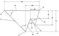
- a light source module 100may include a light source 3 , a light guide structure 2 , an optical control layer 1 , a first adhesive 4 and a protection structure 5 .
- the light source 3may be disposed on one side of the light guide structure 2 , for example, the left side in FIGS. 1 and 2 .
- the light guide structure 2may be formed in the form of a light guide layer or a light guide plate.
- the light guide structure 2may include a first surface 21 , a second surface 22 and a light incident surface 24 .
- the second surface 22is disposed opposite to the first surface 21 , and the light incident surface 24 is connected to the first surface 21 and the second surface 22 .
- the light source 3is arranged opposite to the light incident surface 24, the light emitted by the light source 3 enters the light guide structure 2 through the light incident surface 24, and is transmitted in the light guide structure 2, wherein at least a part of the light can enter the optical control layer 1 through the first surface 21, At least a portion of the light may exit through the second surface 22 .
- the first surface 21may be the surface of the light guide structure 2 on the side close to the optical control layer 1, that is, the upper surface in FIG. 2;
- the second surface 22may be the surface of the light guide structure 2 close to the display panel (described below). ) on one side of the surface, that is, the lower surface in Figure 2.
- the first surface 21 and the second surface 22may be substantially parallel.
- the line perpendicular to a surfaceis called the normal of the surface.
- the first direction D1is parallel to the normal line of the light incident surface 24
- the second direction D2is parallel to the normal line of the first surface 21 or the second surface 22 .
- the third direction D3is perpendicular to both the first direction D1 and the second direction D2.
- the light guide structure 2 , the optical control layer 1 , the first adhesive 4 and the protection structure 5may be stacked in sequence along the second direction D2 , and the first adhesive 4 is used to attach the protection structure 5 to the optical The control layers 1 are bonded together.
- the light source 3may include a light emitting diode (LED for short) or a light bar composed of a plurality of light emitting diodes, but the embodiments of the present disclosure are not limited thereto.
- the light source 3may also include organic light emitting diodes, quantum dots Light-emitting diodes, micro-light-emitting diodes, sub-millimeter light-emitting diodes and other components suitable for light-emitting.
- the optical control layer 1is disposed on the first surface 21 .
- the optical control layer 1may include an optical control layer body 1D and a plurality of optical structures 6 .
- the optical structure 6is disposed on the side of the optical control layer body 1D away from the light guide structure 2 , or on the side of the optical control layer body 1D away from the first surface 21 of the light guide structure 2 .
- the optical control layer 1includes a third surface 11 away from the light guide structure 2 and a fourth surface 12 facing the light guide structure 2 .
- the fourth surface 12may contact the first surface 21 of the light guide structure 2 .
- optical structure 6includes trench 6A.
- the grooves 6Aare recessed from the third surface 11 of the optical control layer toward the fourth surface 12 of the optical control layer, formed as grooves in the optical control layer 1 and having a predetermined depth. That is, the trench 6A forms an opening at the third surface 11 of the optical control layer 1 , or in other words, the trench 6A is opened at the third surface 11 of the optical control layer.
- each groove 6Amay extend along the third direction D3, and its extension length in the third direction D3 may be smaller than the length of the optical control layer 1 along the third direction D3, and at this time, along the third direction D3, there may be spaced At least two grooves 6A.
- each trench 6Amay penetrate the optical control layer 1 along the third direction D3.
- the optical structure 6further includes a low refractive index material 6B filled in the trench 6A.
- the refractive index of the low-refractive-index material 6Bis smaller than that of the material of the optical control layer body 1D, and the low-refractive-index material 6B is, for example, a low-refractive-index optical glue or the like.
- the grooves 6Amay be filled with air. That is, the optical structure 6 includes the trenches 6A and air existing in the trenches 6A.
- the refractive index of the material of the optical control layer body 1Dmay be greater than that of air.
- the optical structure 6includes a first optical surface 61 , a second optical surface 62 , a third optical surface 63 , a fourth optical surface 64 , and a fifth optical surface 65 .
- the first optical surface 61 , the second optical surface 62 , the third optical surface 63 , and the fourth optical surface 64are separated from the light incident surface 24 in sequence, and the four are connected in sequence.
- the fifth optical surface 65connects the first optical surface 61 and the fourth optical surface 64 .
- the fifth optical surface 65may be substantially parallel to the third surface 11 of the optical control layer 1 .
- fifth optical surface 65may be the top surface of low refractive index material 6B, coplanar with third surface 11 of optical control layer 1, at In some embodiments, when the trench 6A is not filled with the low-refractive index material 6B, that is, when the trench 6A is air, the fifth optical surface 65 is a virtual coplanar with the third surface 11 of the optical control layer. surface.
- the first optical surface 61 , the second optical surface 62 , the third optical surface 63 and the fourth optical surface 64are all spaced apart from the fourth surface 12 of the optical control layer 11 , ie, along the The second direction D2 is spaced apart from the fourth surface 12 of the optical control layer 1 by a distance. That is, the trench 6A does not penetrate the optical control layer 1, and the depth of the trench 6A is smaller than the thickness of the optical control layer.
- the fifth optical surface 65is coplanar with the third surface 11 of the optical control layer 1 .
- the depth of the trench 6Arefers to the dimension of the trench 6A along the second direction D2.
- the first optical surface 61 and the second optical surface 62are gradually approached in the direction toward the light guide structure 2
- the second optical surface 62 and the third optical surface 63is gradually approached in the direction away from the light guide structure
- the third optical surface 63 and the fourth optical surface 64are gradually approached in the direction toward the light guide structure.
- the first optical surface 61 and the second optical surface 62converge on the first intersection line 71
- the second optical surface 62 and the third optical surface 63converge on the second intersection line 72
- the third optical surface 63 and the fourth optical surface 64converge
- the first intersection 71, the second intersection 72 and the third intersection 73are parallel to each other
- the first intersection 71, the second intersection 72 and the third intersection 73are all parallel to the
- the third surface 11 of the optical control layer 1is perpendicular to the first direction D1, that is, extends along the third direction D3.
- the first intersection line 71 , the second intersection line 72 and the third intersection line 73are all located on the side of the third surface 11 close to the fourth surface 12 and between the third surface 11 and the fourth surface 12 .
- the first optical surface 61 and the fifth optical surfaceintersect on the fourth intersection line 74, and the fourth optical surface 64 and the fifth optical surface 65 intersect on the fifth intersection line 75, which can also be understood as the first optical surface 61 and the optical control layer 1.
- the third surface 11 of the optical control layer 1intersects at the fourth intersection 74
- the fourth optical surface 64intersects the third surface 11 of the optical control layer 1 at the fifth intersection 75 .
- the fourth intersection line 74 and the fifth intersection line 75also extend along the third direction D3.
- the included angle between the first optical surface 61 and the fifth optical surface 65is the first included angle ⁇ 1
- the included angle between the first optical surface 61 and the second optical surface 62is the second included angle ⁇ 2
- the included angle between the second optical surface 61 and the third optical surface 62is the third included angle ⁇ 3
- the included angle between the third optical surface 63 and the fourth optical surface 64is the fourth included angle ⁇ 4.
- the first included angle ⁇ 1, the second included angle ⁇ 2, the third included angle ⁇ 3 and the fourth included angle ⁇ 4satisfy the following formulas:
- the first included angle ⁇ 1, the second included angle ⁇ 2, the third included angle ⁇ 3, and the fourth included angle ⁇ 4are all acute angles.
- the distance between the first intersection line 71 and the fifth optical surface 65is the first distance H1
- the distance between the second intersection line 72 and the fifth optical surface 65is the second distance H2
- the distance between the third intersection line 73 and the fifth optical surface 65is the second distance H3.
- the first distance H1, the second distance H2 and the third distance H3satisfy the following formula:
- the distance between the second intersection line 72 and the fifth intersection line 75 in the first direction D1is the fourth distance M1
- the distance between the first intersection line 71 and the fifth intersection line 75 in the first direction D1is the fifth distance M2
- the distance between the fourth intersection line 74 and the fifth intersection line 75 in the first direction D1is a sixth distance M3.
- the fourth distance M1, the fifth distance M2 and the sixth distance M3satisfy the following formula:
- the first optical surface 61 , the second optical surface 62 , the third optical surface 63 and the fourth optical surface 64are connected in sequence, as shown in FIGS. 1 and 3 , each groove having a “W” like
- the shape of the bending line, that is, the orthographic projection of each groove 6A on the plane formed by the first direction D1 and the second direction D2is a bending line shape similar to "W".
- the first optical surface 61, the second optical surface 62, the third optical surface 63, the fourth optical surface 64, and the fifth optical surface 65are all flat.
- the refractive index of the optical control layer body 1Dmay be greater than that of the low refractive index material 6B or air, that is, the optical control layer body 1D may be formed of a high refractive index material.
- the refractive index of the optical control layer body 1Dmay be between 1.55 and 1.65.
- the refractive index of the low refractive index material 6Bmay be between 1 and 1.2, and the refractive index of air is about 1.
- the material of the optical control layer body 1Dmay include UV glue (ie, UV-curable optical glue).
- the thickness (dimension along the second direction D2 ) of the optical control layer body 1Dmay be between 10 and 30 ⁇ m.
- the refractive index of the light guide structure 2may be close to the refractive index of the optical control layer body 1D, that is, the refractive indices of the two may be approximately equal.
- the refractive index of the light guide structure 2may be between 1.55 and 1.65.
- the material of the light guide structure 2may include polycarbonate (PC), polymethyl methacrylate (PMMA) or other transparent high refractive index light guide materials.
- the light guide structure 2can play a role of guiding light, and guide the light emitted by the light source 3 into the light source module, and the thickness thereof is, for example, 0.05-0.5 mm.
- the light guide structure 2can also play the role of supporting each film layer.
- the light guide structure 2may have certain bendability.
- the light guide structure 2can be directly used as a substrate for forming the optical control layer 1 thereon.
- UV gluecan be directly formed on the light guide structure 2 and the optical control layer can be formed through processes such as patterning and curing. 1, whereby the base material for manufacturing the optical control layer 1 can be omitted.
- the protection structure 5 of the light source moduleis arranged on the side of the optical control layer 1 away from the light guide structure 2 to protect the optical structure 6 , the optical control layer 1 , the light guide structure 2 and other components below.
- the first bonding glue 4is arranged between the optical control layer 1 and the protective structure 5, and is used for bonding the protective structure 5 and the optical control layer 1.
- the orthographic projection of the first adhesive 4 on the first surface 21 of the light guide structure 2covers the orthographic projection of the plurality of optical structures 6 on the first surface 21 of the light guide structure 2 .
- the bonding area between the protective structure 5 and the optical control layer 1 containing the low-refractive-index material 6Bcan be increased, so that the bonding area between the protective structure 5 and the optical control layer 1 can be increased.
- the bondis stronger.
- the refractive index of the protective structure 5may be close to that of the optical control layer body 1D, that is, the refractive indices of the two may be approximately equal.
- the refractive index of the protective structure 5may be between 1.55 and 1.65.
- the material of the protective structure 5may include polycarbonate (PC), polymethyl methacrylate (PMMA) or other transparent high refractive index materials.
- the thickness (dimension along the second direction D2 ) of the protective structure 5may be between 0.05 and 0.2 mm.
- the protective structure 5includes a first protective surface 51 and a second protective surface 52, the first protective surface 51 is located on the side of the protective structure 5 away from the optical control layer 1, and the second protective surface 52 is located on a side of the protective structure 5 close to the optical control layer 1. side.
- the refractive index of the first adhesive 4may be close to the refractive index of the optical control layer body 1D, that is, the refractive indices of the two may be approximately equal.
- the refractive index of the first adhesive 4may be between 1.55 and 1.65.
- the material of the first bonding glue 4may include UV glue.
- the thickness (dimension along the second direction D2 ) of the first adhesive 4may be about 2 ⁇ m.
- FIG. 4is a schematic diagram of a display module according to some exemplary embodiments of the present disclosure.
- a display module 1000may include the above-mentioned light source module 100 and the display panel 10 .
- the display panel 10may be a reflective display panel.
- the display panel 10may be bonded to the light source module 100 through the adhesive layer 15 .
- the adhesive layer 15may include pressure sensitive adhesive (PSA) or optically clear adhesive (OCA).
- PSApressure sensitive adhesive
- OCAoptically clear adhesive
- the adhesive layer 15may be a transparent adhesive layer.
- the adhesive layer 15is also referred to as the third adhesive in this document.
- the refractive index of the adhesive layer 15may be less than or substantially equal to the refractive index of the light guide structure 2 . In the following description of the optical path, the refractive index of the adhesive layer 15 is smaller than the refractive index of the light guide structure 2 and the optical control layer 1 as an example for description.
- the reflective display panelmay be a reflective liquid crystal display panel, an electronic ink display panel, or an electrowetting-based reflective display panel, which is not particularly limited in the embodiments of the present disclosure.
- the display panel 10may include a liquid crystal cell, and based on the liquid crystal display mode, specific examples of the liquid crystal cell may include: twisted or non-twisted liquid crystal cells, such as TN (twisted nematic) liquid crystal cells, STN (super twisted column) liquid crystal cell, VA (vertically aligned) liquid crystal cell, etc.
- the display panel 10is located on the side of the light guide structure 2 away from the optical control layer 1 .
- the display side of the display panel 10is provided with the light guide structure 2 .
- the side of the protection structure 5 away from the display panel 10is referred to as the display side of the display module, and the side of the display panel 10 away from the protection structure 5 is referred to as the back side of the display module.
- the refractive indices of the light guide structure 2 , the optical control layer 1 , the first adhesive 4 and the protective structure 5are basically the same, and they are all high refractive indices.
- a part of the light incident into the light guide structure 2 by the light source 3for example, the light L1 can pass between the second surface 22 of the light guide structure 2 and the first protective surface 51 of the protective structure 5 without passing through the optical structure 6 . It is totally reflected and propagates along the first direction D1 until the incident incident on the optical structure 6 is regulated by the optical structure 6 .
- the critical angle for total reflection at the first protective surface 51is ⁇ 0,
- ⁇ 0may be equal to about 39°.
- the critical angle for total reflection at the second surface 22 of the light guide structure 2is ⁇ 0′, for example, ⁇ 0′ can be equal to about 39°.
- FIG. 5is a light path diagram of a display module according to some exemplary embodiments of the present disclosure, wherein the light paths of some light rays incident on the optical structure are schematically shown.
- the light ray L2 traveling in the optical control layer body 1Dis incident on the first optical surface 61 of the optical structure 6 and is totally reflected at the first optical surface 61 .
- the critical angle at which total reflection occurs at the first optical surface 61is ⁇ , for example, ⁇ may be equal to about 39°. According to the formula of total reflection, when the angle between the light incident on the first optical surface 61 and the normal direction at the first optical surface 61 is greater than or equal to the critical angle ⁇ , the light will be totally reflected at the first optical surface 61 .
- the angle between the light ray L2 and the normal direction at the first optical surface 61is greater than or equal to the critical angle ⁇ , and it travels toward the second surface 22 of the light guide structure 2 after being totally reflected at the first optical surface 61 .
- the angle between the light L2 and the normal at the second surface 22 of the light guide structure 2is smaller than the critical angle ⁇ 0′, and exits from the second surface 22 of the light guide structure 2 , and then enters the display panel 10 to provide display light for the display panel. .
- the light L3 traveling in the optical control layer body 1Dis incident on the first optical surface 61 of the optical structure 6 , and the included angle between the light L3 and the normal direction at the first optical surface 61 Less than the critical angle ⁇ , the light L3 is refracted at the first optical surface 61 and enters the optical structure 6. After the light L3 propagates in the optical structure 6, it is refracted at the second optical surface 62 of the optical structure 6 and enters the optical control layer body again.
- the critical angle for total reflection at the third optical surface 63is also ⁇ , for example, ⁇ can be equal to about 39°, the angle between the light ray L3 and the normal direction of the first optical surface 63 is greater than or equal to the critical angle ⁇ , and the light ray L3 Total reflection occurs at the third optical surface 63 , which then travels towards the second surface 22 of the light guide structure 2 .
- the angle between the light L3 and the normal at the second surface 22 of the light guide structure 2is smaller than the critical angle ⁇ 0′, and exits from the second surface 22 of the light guide structure 2 , and then enters the display panel 10 to provide display light for the display panel. .
- FIG. 6is a light path diagram of a display module according to some exemplary embodiments of the present disclosure, wherein the light paths of some light rays incident on the optical structure are schematically shown.
- the light L4 traveling in the optical control layer body 1Dis incident on the first optical surface 61 of the optical structure 6 , and the included angle between the light L4 and the normal direction of the first optical surface 61 Less than the critical angle ⁇ , the light L4 is refracted at the first optical surface 61 and enters the optical structure 6. After the light L4 propagates in the optical structure 6, it is refracted at the second optical surface 62 of the optical structure 6 and enters again.
- Optical control layer body 1Dis incident on the first optical surface 61 of the optical structure 6 , and the included angle between the light L4 and the normal direction of the first optical surface 61 Less than the critical angle ⁇ , the light L4 is refracted at the first optical surface 61 and enters the optical structure 6. After the light L4 propagates in the optical structure 6, it is refracted at the second optical surface 62 of the optical structure 6 and enters again.
- Optical control layer body 1DAfter the light L4 propagates in the optical structure 6, it is refracted at the
- the direction in which the light L4 travels in the optical control layer body 1D after passing through the optical structure 6is deflected compared to the direction in which it travels in the optical control layer body 1D before entering the optical structure 6 , eg towards the light guide structure
- the second surface 22 of 2is deflected.
- the light ray L4does not pass through the third optical surface 63 and the fourth optical surface 64 of the optical structure 6, and the light ray L4 continues to travel in the optical control layer body 1D, and is incident on the first optical surface 61 of the other optical structure 6. Total reflection occurs at the first optical surface 61 of the other optical structure 6 , and then travels toward the second surface 22 of the light guide structure 2 .
- the angle between the light L4 and the normal at the second surface 22 of the light guide structure 2is smaller than the critical angle ⁇ 0′, and exits from the second surface 22 of the light guide structure 2 , and then enters the display panel 10 to provide display light for the display panel. .
- the light L5 traveling in the optical control layer body 1Dis incident on the first optical surface 61 of the optical structure 6 , and the included angle between the light L5 and the normal direction at the first optical surface 61 is smaller than the critical angle ⁇ , for example, the light L5 is incident perpendicular to the first optical surface 61, the light L5 is refracted at the first optical surface 61 and enters the optical structure 6, and after the light L5 propagates in the optical structure 6, it is in the optical structure 6. Refraction occurs at the second optical surface 62 of the optical control layer and enters the optical control layer body 1D again.
- the light L5is incident on the third optical surface 63 of the optical structure 6 , the angle between the light L5 and the normal direction at the third optical surface 61 is smaller than the critical angle ⁇ , and it is refracted again at the third optical surface 63 , enter the optical structure 6 again, the optical L5 propagates in the optical structure 6 , refracts at the second optical surface 62 of the optical structure 6 , and enters the optical control layer body 1D again.
- the direction in which the light L5 travels in the optical control layer body 1D after passing through the optical structure 6is deflected compared to the direction in which it travels in the optical control layer body 1D before entering the optical structure 6 , eg towards the light guide structure
- the second surface 22 of 2is deflected.
- the light L5continues to travel in the optical control layer body 1D, is incident on the first optical surface 61 of the other optical structure 6, and is totally reflected at the first optical surface 61 of the other optical structure 6, and then goes toward the guide.
- the second surface 22 of the light structure 2travels.
- the angle between the light L4 and the normal at the second surface 22 of the light guide structure 2is smaller than the critical angle ⁇ 0′, and exits from the second surface 22 of the light guide structure 2 , and then enters the display panel 10 to provide display light for the display panel. .
- some light emitted from the light source 3is regulated by the optical structure 6 .
- the total reflection conditionis not satisfied at the second surface 2 of the light guide structure 2 . 2 exits and then enters the display panel 10 to provide display light for the display panel.
- Other light raysare regulated by the optical structure 6, and after passing through the optical structure 6, they satisfy the condition of total reflection at the second surface 2 of the light guide structure 2, which are reflected in the light guide structure 2, the optical control layer 1, the first adhesive 4 and the protection
- the overall structure composed of structure 5continues to propagate and can be manipulated by other optical structures 6 .
- the light incident into the display panel 10is reflected by the display panel and propagates toward the display side of the display module.
- the light emitted from the light source 3is regulated by the optical structure 6, which increases the light emitted from the light source 3 and incident on the display panel 10 below, thereby improving the brightness of the display panel 10, which is conducive to improving the The display effect of the display module when the external ambient light is insufficient.
- the first optical surface 61 ′is a concave arc surface concave to the inside of the optical structure 6
- the radius of curvature Ris, for example, 35 ⁇ m ⁇ 40 ⁇ m.
- the inside of the groove 6Asurrounded by the optical surface 62 , the third optical surface 63 , and the fourth optical surface 64 .
- the optical structure 6 in this embodimentcan utilize light rays from more angles, thereby improving the utilization rate of light efficiency.
- the luminous flux of the light emitted from the light source 3 and incident on the display panel 10 belowis denoted as the first luminous flux, denoted by Q1;
- the luminous flux of the light directly emitted from the protective structure 5is denoted as the second luminous flux, which is represented by Q2.
- the luminous efficiency ratio Q0Q1/Q2, that is, the luminous efficiency ratio is the ratio of the first luminous flux to the second luminous flux.
- the larger the light efficiency ratio Q0is, the more the light emitted by the light source 3 is effectively utilized, and the more beneficial it is to improve the brightness of the display module.
- the above-mentioned light efficiency ratio Q0 and the first included angle ⁇ 1the third included angle ⁇ 2, the third included angle ⁇ 3, the fourth included angle ⁇ 4 and the radius of curvature R have a certain functional relationship.
- MFis the evaluation function
- Targetis the target value of luminous flux optimization
- f( ⁇ 1, ⁇ 2, ⁇ 3, ⁇ 4, H1, H2, H3, M1, M2, M3, R)represents the first angle ⁇ 1, the second clamp
- the angle ⁇ 2, the third included angle ⁇ 3, the fourth included angle ⁇ 4, and the radius of curvature Rare functions of variables.
- the Monte Carlo tracing algorithmcan be used to make the evaluation function MF approach 0 to the greatest extent.
- the target value of the luminous flux optimization Targetreaches the maximum value, so as to obtain the first angle ⁇ 1, the second angle ⁇ 2, and the third angle.
- the target value Targetan initial value, for example, the absolute value of the first luminous flux Q1 can be 2, and the absolute value of the second luminous flux Q2 can be 10, and a set of ⁇ 1, ⁇ 2, ⁇ 3, ⁇ 4, R is calculated; then gradually Change the target value Target (increase the first luminous flux Q1, decrease the second luminous flux Q2), calculate ⁇ 1, ⁇ 2, ⁇ 3, ⁇ 4, R respectively, until ⁇ 1, ⁇ 2, ⁇ 3, ⁇ 4, R have no solution.
- the optimal solution to obtain the first included angle ⁇ 1 and the second included angle ⁇ 2is:
- the first included angle ⁇ 1, the second included angle ⁇ 2, the third included angle ⁇ 3, and the fourth included angle ⁇ 4may vary within the range of ⁇ 2° of the above optimal solution, for example, the first included angle
- the included angle ⁇ 1can be in the range of 27.5° ⁇ 31.5°
- the second included angle ⁇ 2can be in the range of 35.5° ⁇ 39.5°
- the third included angle ⁇ 3can be in the range of 62° ⁇ 66°
- the fourth included angle ⁇ 4may be in the range of 62° to 66°.
- the radius of curvature Rcan be varied within the range of ⁇ 2 ⁇ m of the above optimal solution.
- the radius of curvature Rmay be in the range of 35 to 39 ⁇ m.
- the values of the first included angle ⁇ 1, the second included angle ⁇ 2, the third included angle ⁇ 3, the fourth included angle ⁇ 4 and the radius of curvature Rcan ensure that the above-mentioned light efficiency ratio Q0 is larger, thereby effectively improving the display mode. Group brightness.
- FIG. 8is a schematic diagram of a light source module according to some exemplary embodiments of the present disclosure, in which the depth distribution of the optical structure is schematically shown.
- FIG. 9is an enlarged view of the depth distribution of the optical structure shown in FIG. 8 .
- 10is a schematic diagram of a light source module according to some exemplary embodiments of the present disclosure, in which the pitch distribution of the optical structure is schematically shown.
- FIG. 11is an enlarged view of the pitch distribution of the optical structure shown in FIG. 10 .
- 12is a schematic diagram of a light source module according to some exemplary embodiments of the present disclosure, in which depth and pitch distributions of optical structures are schematically shown.
- a plurality of optical structures 6are distributed along the first direction D1 at intervals.
- Each optical structure 6has a depth H, and the depth H is the dimension of the optical structure 6 along the second direction D2, that is, the first distance H1 in FIG. 3 .
- the distance between two adjacent optical structures 6is the pitch of the optical structures 6 , which is represented by P.
- Pthe pitch of the optical structures 6
- the first optical surface 61 and the second optical surface 62intersect on a first intersection line 71, which may also be referred to as a top line.
- the pitch Pmay be equal to the distance along the first direction D1 between the top lines 71 of two adjacent optical structures 6 .
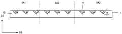
- the light source module 100includes a plurality of distribution areas, and in FIG. 8 and FIG. 9 , three distribution areas DA1 , DA2 , and DA3 are schematically shown.
- the first distribution area DA1is close to the light incident surface 24, the second distribution area DA2 is far away from the light incident surface 24, and the third distribution area DA3 is located between the first distribution area DA1 and the second distribution area DA2.
- the three distribution areasare for schematic illustration, and do not constitute a special limitation to the embodiment of the present disclosure.
- the light source module 100may include a smaller number of (eg two) or more (eg four, five or more) distribution areas.
- At least one optical structure 6is located in the first distribution area DA1, at least one optical structure 6 is located in the third distribution area DA3, and at least one optical structure 6 is located in the second distribution area DA2.
- the optical structure 6 located in the first distribution area DA1will be referred to as the first optical structure 6GA
- the optical structure 6 located in the second distribution area DA2will be referred to as the second optical structure 6GB
- the optical structure 6 located in the third distribution areawill be referred to as the second optical structure 6GB.
- the optical structure 6 in DA3is called the third optical structure 6GC.
- the depth of the first optical structure 6GAcan be represented by HA, and the pitch can be represented by PA; the depth of the second optical structure 6GB can be represented by HB, and the pitch can be represented by PB; the depth of the third optical structure 6GC Can be represented by HC and pitch can be represented by PC.
- a plurality of first optical structures 6GAmay be arranged in the first distribution area DA1
- a plurality of second optical structures 6GBmay be arranged in the second distribution area DA2
- a plurality of third optical structuresmay be arranged in the third distribution area DA3 Optical structure 6GC.
- the cross-sections of the optical structures disposed in each distribution areamay have the same pattern.
- the first optical structure 6GA, the second optical structure 6GB and the third optical structure 6GCmay all have cross-sectional shapes as shown in FIG. 3 or 6, and their cross-sectional shapes are similar, that is, the cross-sectional shapes are in a predetermined ratio, for example, the second optical structure
- the cross-sectional shapes of the structure 6GB and the third optical structure 6GCare enlarged in a predetermined proportion relative to the cross-sectional shape of the first optical structure 6GA, and the cross-sectional shape of the second optical structure 6GB is enlarged in a predetermined proportion relative to the cross-sectional shape of the third optical structure 6GC.
- the depths HA of the plurality of first optical structures 6GAare equal to each other, and the pitches PA of the plurality of first optical structures 6GA are equal to each other.
- the depths HB of the plurality of second optical structures 6GBare equal to each other, and the pitches PB of the plurality of second optical structures 6GB are equal to each other.
- the depths HC of the plurality of third optical structures 6GCare equal to each other, and the pitches PC of the plurality of third optical structures 6GC are equal to each other.
- the pitch PA of the first optical structure 6GAmay be equal to the pitch PC of the third optical structure 6GC
- the pitch PC of the third optical structure 6GCmay be equal to the pitch of the second optical structure 6GB from PB.
- the depth HA of the first optical structure 6GAis less than the depth HC of the third optical structure 6GC, and the depth HB of the third optical structure 6GC is less than the depth HB of the second optical structure 6GB.
- the depth of the optical structures located in the first distribution area DA1is set to be small, so that the first optical structure 6GA extracts the proportion of light. Smaller; the total amount of light on the side away from the light incident surface 24 is small, and the depth of the optical structure located in the second distribution area DA2 is set larger, so that the proportion of light extracted by the second optical structure 6GB is larger; the third distribution The case of the area DA3 lies between the two. In this way, the light distribution in each distribution area of the display module can be made more even, so that the uniformity of the display module can be improved.
- the cross-sections of the optical structures disposed in each distribution areamay have the same pattern.
- the first optical structure 6GA, the second optical structure 6GB and the third optical structure 6GCmay all have the cross-sectional shape shown in FIG. 3 or FIG. 7 , and the cross-sectional shape of the first optical structure 6GA, the cross-sectional shape of the second optical structure 6GB
- the cross-sectional shape and the cross-sectional shape of the third optical structure 6GChave the same size, that is, the ratio between them is 1:1:1, that is, the depth HA of the first optical structure 6GA, the depth HC of the third optical structure 6GC and the The depths HB of the two optical structures 6GB may be equal to each other.
- the pitch PA of the first optical structure 6GAmay be greater than the pitch PC of the third optical structure 6GC, and the pitch PC of the third optical structure 6GC may be greater than the pitch PB of the second optical structure 6GB. That is, the optical structures 6 are sparsely distributed on the side close to the light incident surface 24, and densely distributed on the side far from the light incident surface 24. In other words, the optical structures 6 are arranged in a sparse to dense manner from a side close to the light incident surface 24 to a side away from the light incident surface 24 .
- the total luminous fluxis Q and the number of distribution areas is N
- the total luminous flux A extracted by each distribution areashould be equal to Q/N.
- the plurality of optical structuresmay be sequentially referred to as the first optical structure, the second optical structure, the third optical structure, etc., and so on.
- the light extraction efficiency of the first optical structureis c
- the light extraction efficiency of the second optical structureis d. Under the condition that the structure and size of each optical structure are substantially the same, the light extraction efficiency of each optical structure is substantially the same.
- the luminous flux extracted by the first optical structureis A*c
- the luminous flux extracted by the second optical structureis [A-(A*c)]*d
- so onthat is, the luminous flux that can be extracted by each optical structure
- the direction of the light incident surface 24decreases.
- the optical structures 6are arranged in a sparse to dense manner from the side close to the light incident surface 24 to the side far from the light incident surface 24, so that the light distribution in each distribution area of the display module is relatively uniform, Therefore, the uniformity of the display module can be improved.
- the depth and pitch of the optical structures in each distribution areamay be different.
- the depth HA of the first optical structure 6GAis smaller than the depth HC of the third optical structure 6GC, and the depth HC of the third optical structure 6GC is smaller than the depth HB of the second optical structure 6GB.
- the pitch PA of the first optical structure 6GAmay be greater than the pitch PC of the third optical structure 6GC, and the pitch PB of the third optical structure 6GC may be greater than the pitch PB of the second optical structure 6GB. In this way, the light distribution in each distribution area of the display module is made more even, so that the uniformity of the display module can be improved.
- the number of distribution areascan be determined first according to factors such as the size of the display module and the feasibility of the process; then, the luminous flux distribution in each distribution area can be determined according to the total luminous flux and the number of distribution areas; then, according to each The luminous flux distribution in the distribution area determines the dimensions of the optical structures in each sub-area (eg, the above-mentioned dimensions such as depth and pitch).
- the pitch of the optical structures in each partition areamay be greater than or equal to 30 micrometers and less than or equal to 300 micrometers.
- the inventorfound through research that if the pitch of the optical structure is greater than 300 microns, the distribution of the optical structures will be sparse, resulting in uneven brightness and darkness of the display module during display; It aggravates the inhomogeneity and is not conducive to the function of a single optical structure.
- the light source module 100includes 3 distribution areas.
- the pitches of the optical structures in the respective distribution areasare equal to each other, for example, the pitch is 100 microns.
- the depth of the optical structures in the first distribution areamay be about 4 microns, the depth of the optical structures in the second distribution area may be about 9 microns, and the depth of the optical structures in the third distribution area may be about 14 microns.
- the uniformity of the display modulecan reach more than 60%.
- the light source module 100may include two distribution areas, wherein one distribution area is close to the light incident surface 24 , and the other distribution area is far away from the light incident surface 24 .
- the depth of the optical structures 6 located in the distribution area close to the light incident surface 24may be less than the depth of the optical structures 6 located in the distribution area away from the light incident surface 24, and/or, the depth of the optical structures 6 located in the distribution area close to the light incident surface 24.
- the pitch of the optical structures 6may be smaller than the pitch of the optical structures 6 located in the distribution area away from the light incident surface 24 .
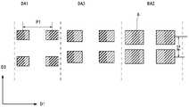
- FIG. 12is a schematic diagram of a two-dimensional distribution of an optical structure of a light source module according to some exemplary embodiments of the present disclosure.
- the orthographic projections of the plurality of optical structures 6 on the optical control layer 1may be two-dimensionally distributed, that is, the plurality of optical structures 6 are arranged at intervals along the first direction D1 and the third direction D3. It also has a cross-sectional shape as shown in FIG. 3 or 6 .
- the distance between two adjacent optical structures 6 along the first direction D1is the first pitch of the optical structures 6, which is represented by P1; the two adjacent optical structures 6 The distance between them along the third direction D3 is the second pitch of the optical structure 6, which is represented by P2.
- the light source module 100may include at least two distribution areas, wherein one distribution area is close to the light incident surface 24 , and the other distribution area is far away from the light incident surface 24 .
- the depth of the optical structures 6 located in the distribution area close to the light incident surface 24may be less than the depth of the optical structures 6 located in the distribution area away from the light incident surface 24, and/or, the depth of the optical structures 6 located in the distribution area close to the light incident surface 24.
- the first pitch P1 of the optical structures 6may be greater than the first pitch P1 of the optical structures 6 located in the distribution area away from the light incident surface 24 , and/or, the optical structures 6 located in the distribution area close to the light incident surface 24
- the second pitch P2 of the optical structures 6may be larger than the second pitch P2 of the optical structures 6 located in the distribution area away from the light incident surface 24 .
- the orthographic projection of the optical structures 6 located in the first distribution area DA1 on the light guide structure 2may be rectangular, and the optical structures 6 located in the second distribution area DA2 on the light guide structure 2 may have a rectangular orthographic projection.
- the orthographic projectionmay be rectangular, and the orthographic projection of the optical structure 6 located in the third distribution area DA3 on the light guide structure 2 may be rectangular.
- the area of the orthographic projection of each optical structure 6 located in the first distribution area DA1 on the light guide structure 2may be smaller than the area of the orthographic projection of each optical structure 6 located in the third distribution area DA3 on the light guide structure 2
- the area of the orthographic projection of each optical structure 6 located in the third distribution area DA3 on the light guide structure 2may be smaller than the area of the orthographic projection of each optical structure 6 located in the second distribution area DA2 on the light guide structure 2 area.
- the display qualitycan be improved.
- the size of the optical structureeg, depth, pitch, etc.
- the brightness uniformity of the display modulecan be improved, so that the display quality can be further improved.
- FIG. 13is a cross-sectional view of a light source module according to some exemplary embodiments of the present disclosure.
- the basic structure of the display module of FIG. 13is substantially the same as that of the display module of FIG.
- the backlight module 100 ′adds a base material 9 and a second adhesive 8 between the light guide structure 2 and the optical control layer 1 .
- the second adhesive 8 , the base material 9 and the optical control layer 1are disposed away from the light guide structure 2 in sequence.
- the optical control layer body 1Dis formed by using UV glue, it needs to coat the UV glue material on the hard substrate 9, go through a patterning process and then cure to form.
- the second adhesive 8adheres the base material 9 on which the optical control layer 1 is formed and the light guide structure 2 together.
- the refractive index of the substrate 9may be close to the refractive index of the optical control layer body 1D, ie, the refractive indices of the two may be approximately equal.
- the refractive index of the substrate 9may be between 1.55 and 1.65.
- the material of the protective structure 5may include polycarbonate (PC), polymethyl methacrylate (PMMA) or other transparent high refractive index materials.
- the thickness (dimension along the second direction D2) of the base material 9may be between 0.05 and 0.2 mm.
- the second adhesive 8may include pressure sensitive adhesive (PSA) or optically clear adhesive (OCA).
- PSApressure sensitive adhesive
- OCAoptically clear adhesive
- the adhesive layer 15may be a transparent adhesive layer.
- the refractive index of the second adhesive 8may be substantially equal to the refractive index of the light guide structure 2 .
- FIG. 14is a flowchart of a method for fabricating a light source module according to an embodiment of the present disclosure.
- the method for preparing the light source moduleincludes the steps of preparing an optical structure.
- the steps of preparing the optical structurecan be performed according to the following steps.
- a toolis prepared.
- the shape of the toolis the same as the shape of the optical structure to be formed, for example, the cross-section of the tool may have a "W"-like bend line shape.
- a roller with a raised structureis prepared.
- the rollerscan be prepared using the tools described above.
- the shape of the protruding structure of the rolleris the same as the shape of the optical structure to be formed, for example, the cross section of the protruding structure of the roller may be in the shape of a bending line similar to "W".
- step S143an optical control layer material such as UV glue is coated on the substrate, and grooves are machined in the optical control layer by using the above-mentioned roller.
- the shape of the grooveis the same as the shape of the optical structure to be formed, for example, the cross-section of the groove may be in the shape of a meander line like "W".
- the light guide structurecan be used as a base material, so that the combination of the base material and the light guide and the second adhesive for the base material can be omitted, which can save costs and make the light source module lighter and thinner.
- the step of preparing the chemical structurecan include the steps of:
- step S144a low refractive index material is filled in the groove, and the refractive index of the low refractive index material is smaller than the refractive index of the optical control layer body, and the optical structure includes the groove and is located in the groove. Low refractive index within the trench.
- the same rollercan be used to process each optical structure, which is beneficial to simplify the process and save the manufacturing cost.
- only one rolleris needed, and by adjusting the processing depth, optical structures with different depths can be formed.
- an embodiment of the present disclosurefurther provides a display device, and the display device may include the above-mentioned display module.
- the display devicemay include but is not limited to: electronic paper, mobile phone, tablet computer, television, monitor, notebook computer, digital photo frame, navigator, and any other product or component with display function. It should be understood that the display device has the same beneficial effects as the display module provided by the foregoing embodiments.
Landscapes
- Physics & Mathematics (AREA)
- General Physics & Mathematics (AREA)
- Optics & Photonics (AREA)
- Nonlinear Science (AREA)
- Mathematical Physics (AREA)
- Chemical & Material Sciences (AREA)
- Crystallography & Structural Chemistry (AREA)
- Planar Illumination Modules (AREA)
Abstract
Description
Translated fromChinese本公开涉及显示技术领域,尤其涉及一种光源模组及其制备方法和显示模组。The present disclosure relates to the field of display technology, and in particular, to a light source module, a preparation method thereof, and a display module.
与透射式的显示装置相比,反射式的显示装置的图像更加柔和、功耗更低,在例如户外可以获得更好的显示效果,因此在例如电子阅读器、公共显示等领域受到越来越多的青睐。反射式显示装置受外部环境光照的影响较大,当外部环境光照不足时,其显示效果降低。Compared with transmissive display devices, reflective display devices have softer images and lower power consumption, and can achieve better display effects outdoors, for example, so they are increasingly used in fields such as e-readers and public displays. much favor. The reflective display device is greatly affected by external ambient light, and when the external ambient light is insufficient, its display effect is reduced.
公开内容public content
本公开提供一种光源模组,所述光源模组包括:The present disclosure provides a light source module, the light source module comprising:
光源;light source;
导光结构,所述导光结构包括入光面和第一表面,所述光源发出的光经所述入光面进入所述导光结构;a light guide structure, the light guide structure includes a light incident surface and a first surface, and the light emitted by the light source enters the light guide structure through the light incident surface;
光学控制层,所述光学控制层设置于所述导光结构的第一表面上,所述光学控制层包括光学控制层本体,所述光学控制层包括远离所述导光结构的第三表面和面向所述导光结构的第四表面;以及an optical control layer, the optical control layer is disposed on the first surface of the light guide structure, the optical control layer includes an optical control layer body, the optical control layer includes a third surface away from the light guide structure and a fourth surface facing the light guide structure; and
多个光学结构,所述多个光学结构设置在所述光学控制层中,用于调节入射到所述光学结构上的光,a plurality of optical structures disposed in the optical control layer for modulating light incident on the optical structures,
其中,所述多个光学结构至少沿第一方向间隔排列,所述第一方向垂直于所述入光面;Wherein, the plurality of optical structures are arranged at intervals along at least a first direction, and the first direction is perpendicular to the light incident surface;
每一个所述光学结构包括位于所述光学控制层中的沟槽,所述沟槽在所述第三表面中形成开口;each of the optical structures includes a trench in the optical control layer, the trench forming an opening in the third surface;
每一个光学结构包括第一光学表面、第二光学表面、第三光学表面以及第四光学表面,所述第一光学表面、所述第二光学表面、所述第三光学表面以及所述第四光学表面均与所述第四表面间隔设置,所述第一光学表面、所述第二光学表面、所述第三光学表面以及所述第四光学表面在第一方向上依次远离所述入光面,所述第一光学表面和所述第二光学表面在朝着所述导光结构的方向上逐渐靠拢, 所述第二光学表面和所述第三光学表面在远离所述导光结构的方向上逐渐靠拢,所述第三光学表面和所述第四光学表面在朝着所述导光结构的方向上逐渐靠拢,Each optical structure includes a first optical surface, a second optical surface, a third optical surface, and a fourth optical surface, the first optical surface, the second optical surface, the third optical surface, and the fourth optical surface The optical surfaces are all arranged at intervals from the fourth surface, and the first optical surface, the second optical surface, the third optical surface and the fourth optical surface are successively away from the incident light in the first direction The first optical surface and the second optical surface are gradually approached in the direction toward the light guide structure, and the second optical surface and the third optical surface are farther away from the light guide structure. gradually approaching in the direction, the third optical surface and the fourth optical surface gradually approaching in the direction toward the light guide structure,
其中,所述沟槽中填充有低折射率材料,所述低折射率材料的折射率小于所述光学控制层本体的折射率;或者所述沟槽中为空气,所述光学控制层本体的折射率大于空气的折射率。Wherein, the groove is filled with a low refractive index material, and the refractive index of the low refractive index material is smaller than the refractive index of the optical control layer body; or the groove is air, and the optical control layer body is filled with air. The refractive index is greater than that of air.
在一些实施例中,所述第一光学表面与第二光学表面会聚在第一交线,所述第二光学表面与第三光学表面会聚在第二交线,所述第三光学表面与第四光学表面会聚在第三交线,所述第一交线、第二交线和第三交线相互平行,所述第一交线、第二交线和第三交线均平行于所述第三表面,所述第一交线、第二交线和第三交线均位于所述第三表面靠近所述第四表面一侧。In some embodiments, the first optical surface and the second optical surface converge at a first intersection, the second optical surface and the third optical surface converge at a second intersection, and the third optical surface and the The four optical surfaces converge at a third intersection, the first, second, and third intersections are parallel to each other, and the first, second, and third intersections are all parallel to the On the third surface, the first intersecting line, the second intersecting line and the third intersecting line are all located on the side of the third surface close to the fourth surface.
在一些实施例中,0°<α1,α2,α3,α4<90°In some embodiments, 0°<α1, α2, α3, α4<90°
H1>H3>H2>0H1>H3>H2>0
M3>M2>M1>0M3>M2>M1>0
其中,α1为所述第一光学表面与所述光学控制层的第一表面所在的平面之间的夹角,α2为所述第一光学表面与所述第二光学表面之间的夹角,α3为所述第二光学表面与所述第三光学表面之间的夹角,α4为所述第三光学表面与所述第四光学表面之间的夹角,Wherein, α1 is the angle between the first optical surface and the plane where the first surface of the optical control layer is located, α2 is the angle between the first optical surface and the second optical surface, α3 is the angle between the second optical surface and the third optical surface, α4 is the angle between the third optical surface and the fourth optical surface,
所述H1为所述第一交线与所述光学控制层的第一表面所在的平面之间的距离;所述H2为所述第二交线与所述光学控制层的第一表面所在的平面之间的距离;所述H3为所述第三交线与所述光学控制层的第一表面所在的平面之间的距离,The H1 is the distance between the first line of intersection and the plane where the first surface of the optical control layer is located; the H2 is the distance between the second line of intersection and the first surface of the optical control layer the distance between the planes; the H3 is the distance between the third intersection line and the plane where the first surface of the optical control layer is located,
所述第一光学表面与所述光学控制层的第一表面相交于第四交线,所述第四光学表面与所述光学控制层的第一表面相交于第五交线,M1为所述第二交线与所述第五交线在第一方向上的距离,M2为所述第一交线与所述第五交线在第一方向上的距离,M3为所述第四交线与所述第五交线在第一方向上的距离。The first optical surface and the first surface of the optical control layer intersect at a fourth intersection, the fourth optical surface and the first surface of the optical control layer intersect at a fifth intersection, and M1 is the The distance between the second intersection and the fifth intersection in the first direction, M2 is the distance between the first intersection and the fifth intersection in the first direction, and M3 is the fourth intersection The distance from the fifth line of intersection in the first direction.
在一些实施例中,所述第一交线、第二交线、第三交线、第四交线以及第五交线均垂直于第一方向。In some embodiments, the first line of intersection, the second line of intersection, the third line of intersection, the fourth line of intersection, and the fifth line of intersection are all perpendicular to the first direction.
在一些实施例中,所述导光结构的折射率与所述光学控制层本体的折射率基本相等。In some embodiments, the refractive index of the light guide structure is substantially equal to the refractive index of the optical control layer body.
在一些实施例中,所述第一光学表面为向所述光学结构内部凹入的曲面,所 述第二光学表面、所述第三光学表面以及所述第四光学表面为平面。In some embodiments, the first optical surface is a curved surface concave to the inside of the optical structure, and the second optical surface, the third optical surface and the fourth optical surface are flat surfaces.
在一些实施例中,所述光源模组至少包括第一分布区域和第二分布区域,在所述第一方向上,所述第一分布区域比所述第二分布区域更靠近所述入光面,In some embodiments, the light source module includes at least a first distribution area and a second distribution area, and in the first direction, the first distribution area is closer to the incident light than the second distribution area noodle,
位于所述第一分布区域中的光学结构的深度小于位于所述第二分布区域中的光学结构的深度;其中,所述光学结构的深度为所述光学结构沿第二方向的尺寸,所述第二方向垂直于所述第三表面。The depth of the optical structure located in the first distribution area is smaller than the depth of the optical structure located in the second distribution area; wherein, the depth of the optical structure is the dimension of the optical structure along the second direction, the The second direction is perpendicular to the third surface.
在一些实施例中,所述光源模组至少包括第一分布区域和第二分布区域,在所述第一方向上,所述第一分布区域比所述第二分布区域更靠近所述入光面,In some embodiments, the light source module includes at least a first distribution area and a second distribution area, and in the first direction, the first distribution area is closer to the incident light than the second distribution area noodle,
位于所述第一分布区域中的光学结构的第一节距大于位于所述第二分布区域中的光学结构的第一节距,其中,所述第一节距为相邻的两个所述光学结构沿所述第一方向的距离。The first pitch of the optical structures located in the first distribution area is greater than the first pitch of the optical structures located in the second distribution area, wherein the first pitch is two adjacent ones of the optical structures. The distance of the optical structure along the first direction.
在一些实施例中,所述多个光学结构至少沿第三方向间隔排列,所述第三方向平行于所述第三表面,所述第三方向垂直于所述第一方向。In some embodiments, the plurality of optical structures are spaced apart along at least a third direction, the third direction being parallel to the third surface, and the third direction being perpendicular to the first direction.
在一些实施例中,所述光源模组至少包括第一分布区域和第二分布区域,在所述第一方向上,所述第一分布区域比所述第二分布区域更靠近所述入光面,In some embodiments, the light source module includes at least a first distribution area and a second distribution area, and in the first direction, the first distribution area is closer to the incident light than the second distribution area noodle,
位于所述第一分布区域中的光学结构的第二节距大于位于所述第二分布区域中的光学结构的第二节距,其中,所述第二节距为相邻的两个所述光学结构沿所述第三方向的距离。The second pitch of the optical structures located in the first distribution area is greater than the second pitch of the optical structures located in the second distribution area, wherein the second pitch is two adjacent ones of the optical structures. The distance of the optical structure along the third direction.
在一些实施例中,所述光源模组还包括:In some embodiments, the light source module further includes:
设置在所述光学控制层远离所述导光结构一侧的保护结构;以及a protective structure disposed on the side of the optical control layer away from the light guide structure; and
设置在所述光学控制层与所述保护结构之间的第一贴合胶,a first bonding glue disposed between the optical control layer and the protective structure,
其中,所述第一贴合胶在所述第一表面上的正投影覆盖所述多个光学结构在所述第一表面上的正投影。Wherein, the orthographic projection of the first bonding glue on the first surface covers the orthographic projection of the plurality of optical structures on the first surface.
在一些实施例中,所述保护结构的折射率、所述第一贴合胶的折射率与所述光学控制层本体的折射率彼此基本相等。In some embodiments, the refractive index of the protective structure, the refractive index of the first adhesive and the refractive index of the optical control layer body are substantially equal to each other.
在一些实施例中,所述光源模组还包括:In some embodiments, the light source module further includes:
设置在所述导光结构和所述光学控制层之间的第二贴合胶和基材,所述第二贴合胶、所述基材,以及所述光学控制层依次远离所述导光结构设置。A second adhesive and a base material disposed between the light guide structure and the optical control layer, the second adhesive, the base material, and the optical control layer are sequentially away from the light guide Structural settings.
在一些实施例中,所述第二贴合胶的折射率、所述基材的折射率以及所述光学控制层的折射率彼此基本相等。In some embodiments, the refractive index of the second adhesive, the refractive index of the substrate, and the refractive index of the optical control layer are substantially equal to each other.
在一些实施例中,所述光学控制层本体的折射率在1.55~1.65之间。In some embodiments, the refractive index of the optical control layer body is between 1.55 and 1.65.
本公开提供一种显示模组,其中,所述显示模组包括根据前述实施例所述的光源模组。The present disclosure provides a display module, wherein the display module includes the light source module according to the foregoing embodiments.
在一些实施例中,所述显示模组还包括显示面板,所述显示面板设置在所述导光结构远离所述光学控制层的一侧,所述显示面板为反射式显示面板,所述显示面板的显示面面向导光结构。In some embodiments, the display module further includes a display panel, the display panel is disposed on a side of the light guide structure away from the optical control layer, the display panel is a reflective display panel, and the display panel is a reflective display panel. The display surface of the panel faces the light guide structure.
本公开提供一种光源模组的制备方法,所述制备方法至少包括以下步骤:The present disclosure provides a preparation method of a light source module, the preparation method at least includes the following steps:
制备带有凸起结构的滚轮,该滚轮的凸起结构的形状与待形成的光学结构的形状相同;preparing a roller with a raised structure, the shape of the raised structure of the roller is the same as the shape of the optical structure to be formed;
在基材上涂布光学控制层材料,并利用上述滚轮在光学控制材料层中加工出沟槽,以形成包括所述光学结构的光学控制层,所述沟槽的形状与待形成的光学结构的形状相同,The optical control layer material is coated on the substrate, and grooves are processed in the optical control material layer by using the above-mentioned roller to form the optical control layer including the optical structure. The shape of the groove is related to the optical structure to be formed. the same shape,
其中,所述光学控制层包括光学控制层本体,所述光学控制层本体的折射率大于空气的折射率;Wherein, the optical control layer includes an optical control layer body, and the refractive index of the optical control layer body is greater than the refractive index of air;
所述光学控制层包括第三表面和第四表面,所述沟槽形成于所述第三表面中;以及the optical control layer includes a third surface and a fourth surface, the groove is formed in the third surface; and
光学结构包括第一光学表面、第二光学表面、第三光学表面以及第四光学表面,所述第一光学表面、所述第二光学表面、所述第三光学表面以及所述第四光学表面均与所述第四表面间隔设置,所述第一光学表面、所述第二光学表面、所述第三光学表面以及所述第四光学表面在第一方向上顺序排列,所述第一光学表面和所述第二光学表面在朝着所述第四表面上逐渐靠拢,所述第二光学表面和所述第三光学表面在朝向所述第一表面上逐渐靠拢,所述第三光学表面和所述第四光学表面在朝着所述第四表面的方向上逐渐靠拢。The optical structure includes a first optical surface, a second optical surface, a third optical surface, and a fourth optical surface, the first optical surface, the second optical surface, the third optical surface, and the fourth optical surface are arranged spaced apart from the fourth surface, the first optical surface, the second optical surface, the third optical surface and the fourth optical surface are sequentially arranged in the first direction, the first optical surface The surface and the second optical surface gradually converge towards the fourth surface, the second optical surface and the third optical surface gradually converge towards the first surface, the third optical surface and the fourth optical surface is gradually approached in the direction toward the fourth surface.
在一些实施例中,所述制备方法还包括:In some embodiments, the preparation method further comprises:
在所述沟槽内填充低折射率材料,所述低折射率材料的折射率小于所述光学控制层本体的折射率,所述光学结构包括所述沟槽以及位于所述沟槽内的低折射率材料。A low-refractive-index material is filled in the groove, and the refractive index of the low-refractive-index material is smaller than that of the optical control layer body, and the optical structure includes the groove and a low-refractive index material located in the groove. Refractive index material.
为了更清楚地说明本公开实施例或相关技术中的技术方案,下面将对实施例或相关技术描述中所需要使用的附图作简单地介绍,显而易见地,下面描述中的 附图仅仅是本公开的一些实施例,对于本领域普通技术人员来讲,在不付出创造性劳动的前提下,还可以根据这些附图获得其他的附图。In order to illustrate the technical solutions in the embodiments of the present disclosure or related technologies more clearly, the following briefly introduces the accompanying drawings that are used in the description of the embodiments or related technologies. Obviously, the drawings in the following description are only the For the disclosed embodiments, for those of ordinary skill in the art, other drawings can also be obtained from these drawings without any creative effort.
图1是根据本公开的一些示例性实施例的光源模组的截面图;1 is a cross-sectional view of a light source module according to some exemplary embodiments of the present disclosure;
图2是根据本公开的一些示例性实施例的光源模组包括的光学控制层和光学结构的平面示意图;2 is a schematic plan view of an optical control layer and an optical structure included in a light source module according to some exemplary embodiments of the present disclosure;
图3是本公开的一些示例性实施例光学结构的截面示意图;3 is a schematic cross-sectional view of some exemplary embodiment optical structures of the present disclosure;
图4是根据本公开的一些示例性实施例的显示模组的示意图,其中示意性示出了一些光路;4 is a schematic diagram of a display module according to some exemplary embodiments of the present disclosure, in which some optical paths are schematically shown;
图5是根据本公开的一些示例性实施例的显示模组的光路图;5 is a light path diagram of a display module according to some exemplary embodiments of the present disclosure;
图6是根据本公开的一些示例性实施例的显示模组的光路图;6 is a light path diagram of a display module according to some exemplary embodiments of the present disclosure;
图7是本公开的一些示例性实施例光学结构的截面示意图;7 is a schematic cross-sectional view of some exemplary embodiment optical structures of the present disclosure;
图8是根据本公开的一些示例性实施例的光源模组的示意图,其中示意性示出了光学结构的深度分布;8 is a schematic diagram of a light source module according to some exemplary embodiments of the present disclosure, wherein the depth distribution of the optical structure is schematically shown;
图9是图8中所示的光学结构的深度分布的放大图;Figure 9 is an enlarged view of the depth profile of the optical structure shown in Figure 8;
图10是根据本公开的一些示例性实施例的光源模组的示意图,其中示意性示出了光学结构的节距分布;10 is a schematic diagram of a light source module according to some exemplary embodiments of the present disclosure, wherein the pitch distribution of the optical structure is schematically shown;
图11是图10中所示的光学结构的节距分布的放大图;FIG. 11 is an enlarged view of the pitch distribution of the optical structure shown in FIG. 10;
图12是根据本公开的一些示例性实施例的光源模组的光学结构的二维分布示意图;12 is a schematic diagram of a two-dimensional distribution of an optical structure of a light source module according to some exemplary embodiments of the present disclosure;
图13是根据本公开的一些示例性实施例的光源模组的截面图;13 is a cross-sectional view of a light source module according to some exemplary embodiments of the present disclosure;
以及as well as
图14是根据本公开实施例的光源模组的制备方法的流程图。FIG. 14 is a flowchart of a method for fabricating a light source module according to an embodiment of the present disclosure.
需要注意的是,为了清晰起见,在用于描述本公开的实施例的附图中,层、结构或区域的尺寸可能被放大或缩小,即这些附图并非按照实际的比例绘制。It should be noted that, in the drawings for describing embodiments of the present disclosure, the dimensions of layers, structures or regions may be exaggerated or reduced for clarity, ie, the drawings are not drawn to actual scale.
下面将结合本公开实施例中的附图,对本公开实施例中的技术方案进行清楚、完整地描述,显然,所描述的实施例仅仅是本公开一部分实施例,而不是全部的实施例。基于本公开中的实施例,本领域普通技术人员在没有做出创造性劳动前提下所获得的所有其他实施例,都属于本公开保护的范围。The technical solutions in the embodiments of the present disclosure will be clearly and completely described below with reference to the accompanying drawings in the embodiments of the present disclosure. Obviously, the described embodiments are only a part of the embodiments of the present disclosure, but not all of the embodiments. Based on the embodiments in the present disclosure, all other embodiments obtained by those of ordinary skill in the art without creative efforts shall fall within the protection scope of the present disclosure.
另外,在下面的详细描述中,为便于解释,阐述了许多具体的细节以提供对 本披露实施例的全面理解。然而明显地,一个或多个实施例在没有这些具体细节的情况下也可以被实施。Furthermore, in the following detailed description, for convenience of explanation, numerous specific details are set forth in order to provide a thorough understanding of the disclosed embodiments. Obviously, however, one or more embodiments may be practiced without these specific details.
应该理解的是,尽管在这里可使用术语第一、第二等来描述不同的元件,但是这些元件不应受这些术语的限制。这些术语仅是用来将一个元件与另一个元件区分开来。例如,在不脱离示例实施例的范围的情况下,第一元件可以被命名为第二元件,类似地,第二元件可以被命名为第一元件。如在这里使用的术语“和/或”包括一个或多个相关所列的项目的任意组合和所有组合。It will be understood that, although the terms first, second, etc. may be used herein to describe various elements, these elements should not be limited by these terms. These terms are only used to distinguish one element from another. For example, a first element could be termed a second element, and, similarly, a second element could be termed a first element, without departing from the scope of example embodiments. As used herein, the term "and/or" includes any and all combinations of one or more of the associated listed items.
应该理解的是,当元件或层被称作“形成在”另一元件或层“上”时,该元件或层可以直接地或间接地形成在另一元件或层上。也就是,例如,可以存在中间元件或中间层。相反,当元件或层被称作“直接形成在”另一元件或层“上”时,不存在中间元件或中间层。应当以类似的方式来解释其它用于描述元件或层之间的关系的词语(例如,“在...之间”与“直接在...之间”、“相邻的”与“直接相邻的”等)。It will be understood that when an element or layer is referred to as being "formed on" another element or layer, it can be directly or indirectly formed on the other element or layer. That is, for example, intervening elements or interlayers may be present. In contrast, when an element or layer is referred to as being "formed directly on" another element or layer, there are no intervening elements or layers present. Other words used to describe the relationship between elements or layers should be interpreted in a similar fashion (eg, "between" versus "directly between", "adjacent" versus "directly" adjacent", etc.).
在本文中,使用方向性表述“第一方向”、“第二方向”、“第三方向”来描述沿光源模组或显示模组的不同方向。应该理解,这样的表示仅为示例性的描述,而不是对本公开的限制。Herein, the directional expressions "first direction", "second direction", "third direction" are used to describe different directions along the light source module or the display module. It should be understood that such representations are exemplary descriptions only, and not limitations of the present disclosure.
本公开的一些示例性实施例提供一种光源模组,所述光源模组包括:光源;导光结构,所述导光结构包括入光面和第一表面,所述光源发出的光经所述入光面进入所述导光结构;光学控制层,所述光学控制层设置于所述导光结构的第一表面上,所述光学控制层包括光学控制层本体,所述光学控制层包括远离所述导光结构的第三表面和面向所述导光结构的第四表面;以及多个光学结构,所述多个光学结构设置在所述光学控制层中,用于调节入射到所述光学结构上的光,其中,所述多个光学结构至少沿第一方向间隔排列,所述第一方向垂直于所述入光面;每一个所述光学结构包括位于所述光学控制层中的沟槽,所述沟槽在所述第三表面中形成开口;以及每一个光学结构包括第一光学表面、第二光学表面、第三光学表面以及第四光学表面,所述第一光学表面、所述第二光学表面、所述第三光学表面以及所述第四光学表面均与所述光学控制层的第二表面间隔设置,所述第一光学表面、所述第二光学表面、所述第三光学表面以及所述第四光学表面在第一方向上依次远离所述入光面,所述第一光学表面和所述第二光学表面在朝着所述导光结构的方向上逐渐靠拢,所述第二光学表面和所述第三光学表面在远离所述导光结构的方向上逐渐靠拢,所述第三光学表面和所述第四光学表面在朝 着所述导光结构的方向上逐渐靠拢,其中,所述沟槽中填充有低折射率材料,所述低折射率材料的折射率小于所述光学控制层本体的折射率;或者所述沟槽中为空气,所述光学控制层本体的折射率大于空气的折射率。在本公开的实施例中,从光源出射的光在所述导光结构和所述光学控制层中传输,并被所述被光学结构调控,增加了从光源出射且入射到下方的部件(例如,反射式显示面板)上的光。Some exemplary embodiments of the present disclosure provide a light source module, the light source module includes: a light source; a light guide structure, the light guide structure includes a light incident surface and a first surface, and the light emitted by the light source passes through the light source. The light incident surface enters the light guide structure; an optical control layer, the optical control layer is disposed on the first surface of the light guide structure, the optical control layer includes an optical control layer body, and the optical control layer includes a third surface away from the light guide structure and a fourth surface facing the light guide structure; and a plurality of optical structures disposed in the optical control layer for regulating incident incident on the light guide structure Light on an optical structure, wherein the plurality of optical structures are spaced at least along a first direction, and the first direction is perpendicular to the light incident surface; each of the optical structures includes a a trench that forms an opening in the third surface; and each optical structure includes a first optical surface, a second optical surface, a third optical surface, and a fourth optical surface, the first optical surface, The second optical surface, the third optical surface and the fourth optical surface are all arranged at intervals from the second surface of the optical control layer, the first optical surface, the second optical surface, the The third optical surface and the fourth optical surface are successively away from the light incident surface in the first direction, and the first optical surface and the second optical surface are gradually approached in the direction toward the light guide structure , the second optical surface and the third optical surface are gradually approached in the direction away from the light guide structure, and the third optical surface and the fourth optical surface are in the direction toward the light guide structure The grooves are filled with low-refractive-index material, and the refractive index of the low-refractive-index material is smaller than the refractive index of the optical control layer body; or the groove is air, and the optical The refractive index of the control layer body is greater than that of air. In the embodiment of the present disclosure, the light emitted from the light source is transmitted in the light guide structure and the optical control layer, and is regulated by the optical structure, adding components that are emitted from the light source and incident below (for example, , reflective display panel).
图1是根据本公开的一些示例性实施例的光源模组的截面图,图2是根据本公开的一些示例性实施例的光源模组包括的光学控制层和光学结构的平面示意图。参照图1和图2,根据本公开实施例的光源模组100可以包括光源3、导光结构2、光学控制层1、第一贴合胶4和保护结构5。1 is a cross-sectional view of a light source module according to some exemplary embodiments of the present disclosure, and FIG. 2 is a schematic plan view of an optical control layer and an optical structure included in the light source module according to some exemplary embodiments of the present disclosure. 1 and 2 , a
如图1和图2所示,光源3可以设置在导光结构2的一侧,例如图1和图2中的左侧。导光结构2可以形成为导光层或导光板的形式。导光结构2可以包括第一表面21、第二表面22和入光面24。第二表面22与第一表面21相对设置,且入光面24连接第一表面21及第二表面22。光源3与入光面24相对设置,光源3发出的光经入光面24进入导光结构2,在导光结构2中传输,其中至少一部分光可以经第一表面21进入光学控制层1,至少一部分光可以经第二表面22出射。As shown in FIGS. 1 and 2 , the
例如,第一表面21可以为导光结构2在靠近光学控制层1的一侧的表面,即图2中的上表面;第二表面22可以为导光结构2在靠近显示面板(下文将描述)的一侧的表面,即图2中的下表面。第一表面21与第二表面22可以基本上平行。For example, the
在本文中,将垂直于某一表面的线称为该表面的法线。参照图2,第一方向D1平行于入光面24的法线,第二方向D2平行于第一表面21或第二表面22的法线。参照图1,第三方向D3垂直于第一方向D1和第二方向D2两者。In this paper, the line perpendicular to a surface is called the normal of the surface. Referring to FIG. 2 , the first direction D1 is parallel to the normal line of the
在一些实施例中,导光结构2、光学控制层1、第一贴合胶4和保护结构5可以沿第二方向D2依次层叠设置,第一贴合胶4用于将保护结构5与光学控制层1粘结在一起。In some embodiments, the
例如,光源3可以包括发光二极管(简称LED)或由多个发光二极管组成的灯条,但本公开的实施例不限于此,在其他实施例中,光源3还可以包括有机发光二极管、量子点发光二极管、微发光二极管、次毫米发光二极管等其他适于发光的元件。For example, the
继续参照图1和图2,光学控制层1设置于第一表面21上。光学控制层1可以包括光学控制层本体1D和多个光学结构6。光学结构6设置在光学控制层本体1D的远离导光结构2的一侧,或者设置在光学控制层本体1D的远离导光结构2的第一表面21的一侧。Continuing to refer to FIGS. 1 and 2 , the
光学控制层1包括远离导光结构2的第三表面11和面向导光结构2的第四表面12。例如,第四表面12可以接触导光结构2的第一表面21。The
例如,在一些实施例中,光学结构6包括沟槽6A。所述沟槽6A从光学控制层的第三表面11朝向光学控制层的第四表面12凹入,形成为位于光学控制层1中且具有预定深度的凹槽。即,沟槽6A在光学控制层1的第三表面11处形成开口,或者说,沟槽6A在光学控制层的第三表面11处敞开。For example, in some embodiments,
结合参照图1和图2,多个沟槽6A沿第一方向D1间隔排列。例如,每一个沟槽6A可以沿第三方向D3延伸,其在第三方向D3的延伸长度可以小于光学控制层1沿第三方向D3的长度,此时沿第三方向D3,可以间隔设置有至少两个沟槽6A。在一些实施例中,每一个沟槽6A可以沿第三方向D3贯穿光学控制层1。Referring to FIG. 1 and FIG. 2 in combination, the plurality of
在一些实施例中,光学结构6还包括填充于所述沟槽6A中的低折射率材料6B。低折射率材料6B的折射率小于光学控制层本体1D的材料的折射率,低折射率材料6B例如低折射率光学胶等。In some embodiments, the
在一些实施例中,所述沟槽6A中可以为空气。即,光学结构6包括沟槽6A和存在于沟槽6A中的空气。光学控制层本体1D的材料的折射率可以大于空气的折射率。In some embodiments, the
图3是本公开的一些示例性实施例光学结构的截面示意图,光学结构6包括第一光学表面61、第二光学表面62、第三光学表面63、第四光学表面64以及第五光学表面65。结合图1至图3所示,第一光学表面61、第二光学表面62、第三光学表面63、第四光学表面64依次远离入光面24,且四者依次连接。第五光学表面65连接第一光学表面61和第四光学表面64。第五光学表面65可以基本平行于光学控制层1的第三表面11。在一些实施例中,当沟槽6A中填充有低折射率材料6B时,第五光学表面65可以是低折射率材料6B的顶面,与光学控制层1的第三表面11共面,在一些实施例中,当沟槽6A中未填充有低折射率材料6B时,即沟槽6A中为空气的情况下,第五光学表面65为与光学控制层的第三表面11共面的虚拟表面。3 is a schematic cross-sectional view of an optical structure of some exemplary embodiments of the present disclosure, the
在一些实施例中,第一光学表面61、第二光学表面62、第三光学表面63以及所述第四光学表面64均与所述光学控制层11的第四表面12间隔设置,即,沿第二方向D2与光学控制层1的第四表面12间隔一段距离。也就是说,沟槽6A并不贯穿光学控制层1,沟槽6A的深度小于光学控制层的厚度。第五光学表面65与光学控制层1的第三表面11共面。其中沟槽6A的深度是指沟槽6A沿第二方向D2的尺寸。In some embodiments, the first
在本公开的实施例中,结合图1-3所示,第一光学表面61和第二光学表面62在朝着导光结构2的方向上逐渐靠拢,第二光学表面62和第三光学表面63在远离所述导光结构的方向上逐渐靠拢,第三光学表面63和第四光学表面64在朝着所述导光结构的方向上逐渐靠拢。第一光学表面61与第二光学表面62会聚在第一交线71,第二光学表面62与第三光学表面63会聚在第二交线72,第三光学表面63与第四光学表面64会聚在第三交线73,第一交线71、第二交线72和第三交线73相互平行,且第一交线71、第二交线72和第三交线73均平行于所述光学控制层1的第三表面11,且垂直于所述第一方向D1,即沿第三方向D3延伸。第一交线71、第二交线72和第三交线73均位于第三表面11靠近第四表面12的一侧,且位于第三表面11和第四表面12之间。第一光学表面61与第五光学表面相交于第四交线74,第四光学表面64与第五光学表面65相交于第五交线75也可以理解为第一光学表面61与光学控制层1的第三表面11相交于第四交线74,第四光学表面64与光学控制层1的第三表面11相交于第五交线75。第四交线74和第五交线75亦沿第三方向D3延伸。In the embodiment of the present disclosure, as shown in FIGS. 1-3 , the first
如图3所示,第一光学表面61与第五光学表面65之间的夹角为第一夹角α1,第一光学表面61与第二光学表面62之间的夹角为第二夹角α2,第二光学表面61与第三光学表面62之间的夹角为第三夹角α3,第三光学表面63与第四光学表面64之间的夹角为第四夹角α4。第一夹角α1、第二夹角α2、第三夹角α3以及第四夹角α4满足以下公式:As shown in FIG. 3 , the included angle between the first
0°<α1,α2,α3,α4<90°,0°<α1, α2, α3, α4<90°,
即第一夹角α1、第二夹角α2、第三夹角α3以及第四夹角α4均为锐角。That is, the first included angle α1, the second included angle α2, the third included angle α3, and the fourth included angle α4 are all acute angles.
第一交线71与第五光学表面65的距离为第一距离H1,第二交线72与第五光学表面65的距离为第二距离H2,第三交线73与第五光学表面65的距离为第二距离H3。第一距离H1、第二距离H2以及第三距离H3满足以下公式:The distance between the
H1>H3>H2>0。H1>H3>H2>0.
第二交线72与第五交线75在第一方向上D1的距离为第四距离M1,第一交线71与第五交线75在第一方向D1上的距离为第五距离M2,第四交线74与第五交线75在第一方向D1上的距离为第六距离M3。第四距离M1、第五距离M2以及第六距离M3满足以下公式:The distance between the
M3>M2>M1>0。M3>M2>M1>0.
在一些实施例中,第一光学表面61、第二光学表面62、第三光学表面63以及第四光学表面64依次连接,如图1和3所示,每个沟槽具有类似“W”的弯折线形状,即每一个沟槽6A在第一方向D1和第二方向D2所构成的平面上的正投影呈类似“W”的弯折线形状。In some embodiments, the first
在一些实施例中,第一光学表面61、第二光学表面62、第三光学表面63、第四光学表面64以及第五光学表面65均为平面。In some embodiments, the first
在本公开的实施例中,光学控制层本体1D的折射率可以大于低折射率材料6B或空气的折射率,即,光学控制层本体1D可以由高折射率材料形成。例如,光学控制层本体1D的折射率可以在1.55~1.65之间。低折射率材料6B的折射率可以在1~1.2之间,空气的折射率在1左右。例如,光学控制层本体1D的材料可以包括UV胶(即,可紫外光固化的光学胶)。光学控制层本体1D的厚度(沿第二方向D2的尺寸)可以在10~30μm之间。In an embodiment of the present disclosure, the refractive index of the optical
在一些实施例中,导光结构2的折射率可以接近于光学控制层本体1D的折射率,即,二者的折射率可以大致相等。例如,导光结构2的折射率可以在1.55~1.65之间。导光结构2的材料可以包括聚碳酸酯(PC)、聚甲基丙烯酸甲酯(PMMA)或其他透明的高折射率导光材料。导光结构2可以起到导光的作用,将光源3发出的光导入光源模组中,其厚度例如为0.05~0.5mm。另外,导光结构2还可以起到承载各个膜层的作用。导光结构2可以具有一定的可弯折性。在一些实施例中,导光结构2可以直接用作在上形成光学控制层1的基材,此时可以直接将UV胶形成在导光结构2上并经过构图、固化等工艺形成光学控制层1,由此可以省去制造成光学控制层1的基材。In some embodiments, the refractive index of the
如图1所示,所述光源模组的保护结构5设置在光学控制层1远离导光结构2的一侧,用于保护下方的光学结构6、光学控制层1、导光结构2等部件。第一贴合胶4设置在光学控制层1与保护结构5之间,用于粘合保护结构5和光学控 制层1。第一贴合胶4在所述导光结构2的第一表面21上的正投影覆盖所述多个光学结构6在所述导光结构2的第一表面21上的正投影。当沟槽6A中填充有低折射率材料6B时,可以增大保护结构5和容纳有低折射率材料6B的光学控制层1的粘结面积,使得粘合保护结构5和光学控制层1的粘结更加牢固。As shown in FIG. 1 , the
保护结构5的折射率可以接近于光学控制层本体1D的折射率,即,二者的折射率可以大致相等。例如,保护结构5的折射率可以在1.55~1.65之间。保护结构5的材料可以包括聚碳酸酯(PC)、聚甲基丙烯酸甲酯(PMMA)或其他透明的高折射率材料。例如,保护结构5的厚度(沿第二方向D2的尺寸)可以在0.05~0.2mm之间。The refractive index of the
保护结构5包括第一保护表面51和第二保护表面52,第一保护表面51位于保护结构5远离光学控制层1的一侧,第二保护表面52位于保护结构5靠近光学控制层1的一侧。The
第一贴合胶4的折射率可以接近于光学控制层本体1D的折射率,即,二者的折射率可以大致相等。例如,第一贴合胶4的折射率可以在1.55~1.65之间。第一贴合胶4的材料可以包括UV胶。例如,第一贴合胶4的厚度(沿第二方向D2的尺寸)可以在2μm左右。The refractive index of the
图4是根据本公开的一些示例性实施例的显示模组的示意图。参照图4,根据本公开实施例的显示模组1000可以包括上述光源模组100和显示面板10。显示面板10可以是反射型显示面板。显示面板10可以通过胶层15与光源模组100粘合。例如,胶层15可以包括压敏胶(PSA)或者光学透明胶(OCA)。胶层15可以为透明的胶层。在本文中胶层15亦称为第三贴合胶。胶层15的折射率可以小于或基本等于导光结构2的折射率。在后续光路描述中,以胶层15的折射率小于导光结构2和光学控制层1的折射率为例来进行介绍。FIG. 4 is a schematic diagram of a display module according to some exemplary embodiments of the present disclosure. Referring to FIG. 4 , a
反射型显示面板可以为反射式液晶显示面板,也可以为电子墨水显示面板,也可以为基于电润湿的反射式显示面板,本公开的实施例不做特别限定。例如,所述显示面板10可以包括液晶盒,并且基于液晶显示模式,液晶盒的具体实例可以包括:扭曲式或非扭曲式液晶盒,如TN(扭曲向列)液晶盒、STN(超扭曲向列)液晶盒、VA(纵向排列)液晶盒等。The reflective display panel may be a reflective liquid crystal display panel, an electronic ink display panel, or an electrowetting-based reflective display panel, which is not particularly limited in the embodiments of the present disclosure. For example, the
显示面板10位于导光结构2远离光学控制层1的一侧。显示面板10的显示侧面向导光结构2设置。为了描述方便,将保护结构5的远离显示面板10的一 侧称为显示模组的显示侧,将显示面板10的远离保护结构5的一侧称为显示模组的背侧。The
图4中示出了在背光模组中一些光的传输路径。如图4A所示,如上所述,导光结构2、光学控制层1、第一贴合胶4和保护结构5的折射率基本相同,均为高折射率。由光源3入射到导光结构2中的一部分光,例如光学L1在未经过光学结构6的情况下,可以在导光结构2的第二表面22和保护结构5的第一保护表面51之间全反射,沿第一方向D1传播,直至入射至光学结构6被光学结构6调控。例如,对于在导光结构2、光学控制层1、第一贴合胶4和保护结构5组成的整体结构中传播的光线来说,第一保护表面51处发生全反射的临界角为β0,例如,β0可以等于约39°,根据全反射公式,当入射至第一保护表面51的光线与第一保护表面51处的法线方向的夹角大于或等于临界角β0时,该光线会在第一保护表面51处发生全反射。导光结构2的第二表面22处发生全反射的临界角为β0’,例如,β0’可以等于约39°,根据全反射公式,当入射至导光结构2的第二表面22的光线与导光结构2的第二表面22处的法线方向的夹角大于或等于临界角β0时,该光线会在导光结构2的第二表面22处发生全反射。Some light transmission paths in the backlight module are shown in FIG. 4 . As shown in FIG. 4A , as described above, the refractive indices of the
图5是根据本公开的一些示例性实施例的显示模组的光路图,其中示意性示出了一些入射至光学结构的光线的光路。FIG. 5 is a light path diagram of a display module according to some exemplary embodiments of the present disclosure, wherein the light paths of some light rays incident on the optical structure are schematically shown.
例如,参照图5所示的光线L2,在光学控制层本体1D中行进的光线L2入射至光学结构6的第一光学表面61,并在第一光学表面61处发生全反射。第一光学表面61处发生全反射的临界角为β,例如,β可以等于约39°。根据全反射公式,当入射至第一光学表面61的光线与第一光学表面61处的法线方向的夹角大于或等于临界角β时,该光线会在第一光学表面61处发生全反射。光线L2与第一光学表面61处的法线方向的夹角大于或等于临界角β,其在第一光学表面61处发生全反射后朝向导光结构2的第二表面22行进。光线L2与导光结构2的第二表面22处的法线的夹角小于临界角β0’,自导光结构2的第二表面22出射,进而入射至显示面板10,为显示面板提供显示光线。For example, referring to the light ray L2 shown in FIG. 5 , the light ray L2 traveling in the optical
例如,参照图5所示的光线L3,在光学控制层本体1D中行进的光线L3入射至光学结构6的第一光学表面61,光线L3与第一光学表面61处的法线方向的夹角小于临界角β,光线L3在第一光学表面61发生折射进入光学结构6,光线L3在光学结构6中传播后,在光学结构6的第二光学表面62处发生折射,再 次进入光学控制层本体1D,由于第二光学表面62处的折射是从光疏介质到光密介质,所以可以使从第二光学表面62射出的光线L2以较大角度射到第三光学表面63。第三光学表面63处发生全反射的临界角亦为β,例如,β可以等于约39°,光线L3与第一光学表面63处的法线方向的夹角大于或等于临界角β,光线L3在在第三光学表面63处发生全反射,随后朝向导光结构2的第二表面22行进。光线L3与导光结构2的第二表面22处的法线的夹角小于临界角β0’,自导光结构2的第二表面22出射,进而入射至显示面板10,为显示面板提供显示光线。For example, referring to the light L3 shown in FIG. 5 , the light L3 traveling in the optical
图6是根据本公开的一些示例性实施例的显示模组的光路图,其中示意性示出了一些入射至光学结构的光线的光路。FIG. 6 is a light path diagram of a display module according to some exemplary embodiments of the present disclosure, wherein the light paths of some light rays incident on the optical structure are schematically shown.
例如,参照图6所示的光线L4,在光学控制层本体1D中行进的光线L4入射至光学结构6的第一光学表面61,光线L4与第一光学表面61处的法线方向的夹角小于临界角β,光线L4在第一光学表面61处发生折射进入该光学结构6,光线L4在该光学结构6中传播后,在该光学结构6的第二光学表面62处发生折射,再次进入光学控制层本体1D。光线L4在穿过该光学结构6后在光学控制层本体1D中行进的方向相较于其在进入该光学结构6前在光学控制层本体1D中行进的方向发生了偏转,例如朝向导光结构2的第二表面22偏转。光线L4并未经过该光学结构6的第三光学表面63和第四光学表面64,光线L4继续在光学控制层本体1D中行进,入射至另一个光学结构6的第一光学表面61,并在所述的另一个光学结构6的第一光学表面61处发生全反射,随后朝向导光结构2的第二表面22行进。光线L4与导光结构2的第二表面22处的法线的夹角小于临界角β0’,自导光结构2的第二表面22出射,进而入射至显示面板10,为显示面板提供显示光线。For example, referring to the light L4 shown in FIG. 6 , the light L4 traveling in the optical
例如,参照图6所示的光线L5,在光学控制层本体1D中行进的光线L5入射至光学结构6的第一光学表面61,光线L5与第一光学表面61处的法线方向的夹角小于临界角β,例如光线L5垂直于第一光学表面61入射,光线L5在第一光学表面61处发生折射进入该光学结构6,光线L5在该光学结构6中传播后,在该光学结构6的第二光学表面62处发生折射,再次进入光学控制层本体1D。随后,光线L5入射到该光学结构6的第三光学表面63,光线L5与第三光学表面61处的法线方向的夹角小于临界角β,其在该第三光学表面63处再次发生折射,再次进入该光学结构6,光学L5在该光学结构6中传播,在该光学结构6 的第二光学表面62处发生折射,再次进入光学控制层本体1D。光线L5在穿过该光学结构6后在光学控制层本体1D中行进的方向相较于其在进入该光学结构6前在光学控制层本体1D中行进的方向发生了偏转,例如朝向导光结构2的第二表面22偏转。光线L5继续在光学控制层本体1D中行进,入射至另一个光学结构6的第一光学表面61,并在所述的另一个光学结构6的第一光学表面61处发生全反射,随后朝向导光结构2的第二表面22行进。光线L4与导光结构2的第二表面22处的法线的夹角小于临界角β0’,自导光结构2的第二表面22出射,进而入射至显示面板10,为显示面板提供显示光线。For example, referring to the light L5 shown in FIG. 6 , the light L5 traveling in the optical
在一些实施例中,从光源3出射的一些光线被光学结构6调控,经过光学结构6后在导光结构2的第二表面2处不满足全反射条件,自导光结构2的第二表面2出射进而入射至显示面板10,为显示面板提供显示光线。另一些光线被光学结构6调控,经过光学结构6后在导光结构2的第二表面2处满足全反射条件,其在导光结构2、光学控制层1、第一贴合胶4和保护结构5组成的整体结构中继续传播,可以被其他光学结构6调控。In some embodiments, some light emitted from the
在一些实施例中,入射至显示面板10中的光线经显示面板反射,朝着显示模组的显示侧传播。在本公开的实施例中,从光源3出射的光被光学结构6调控,增加了从光源3出射且入射到下方的显示面板10上的光,从而提升了显示面板10的亮度,有利于改善显示模组在外部环境光照不足时的显示效果。In some embodiments, the light incident into the
图7是本公开的一些示例性实施例光学结构的截面示意图,其结构与图3所示的光学结构6基本相同,区别在于第一光学表面61’为曲面,例如为弧面。如图7所示,第一光学表面61’为向光学结构6内部凹入的凹弧面,曲率半径R例如为35μm~40μm,光学结构6内部指的是由第一光学表面61、第二光学表面62、第三光学表面63、第四光学表面64围成的沟槽6A的内部。相对于第一光学表面为平面的前述实施例,本实施例中的光学结构6可以利用更多角度的光线,提高光效利用率。7 is a schematic cross-sectional view of the optical structure of some exemplary embodiments of the present disclosure, the structure of which is basically the same as that of the
在本公开的实施例中,从光源3出射且入射到下方的显示面板10上的光的光通量记为第一光通量,用Q1表示;从光源3出射且未入射到下方的显示面板10上而直接从保护结构5出射的光的光通量记为第二光通量,用Q2表示。光效比Q0=Q1/Q2,即光效比为第一光通量与第二光通量的比值。光效比Q0越大,说明光源3出射的光被有效利用的越多,越有利于提升显示模组的亮度。In the embodiment of the present disclosure, the luminous flux of the light emitted from the
在本公开的实施例中,基于图1至图7所示的结构,在各个部件或膜层的厚度、折射率保持不变的情况下,上述光效比Q0与第一夹角α1、第二夹角α2、第三夹角α3、第四夹角α4和曲率半径R存在一定的函数关系。In the embodiments of the present disclosure, based on the structures shown in FIG. 1 to FIG. 7 , under the condition that the thickness and refractive index of each component or film layer remain unchanged, the above-mentioned light efficiency ratio Q0 and the first included angle α1, the third The second included angle α2, the third included angle α3, the fourth included angle α4 and the radius of curvature R have a certain functional relationship.
可以建立如下的评价函数:The following evaluation function can be established:
MF=Target-f(α1,α2,α3,α4,,R),MF=Target-f(α1,α2,α3,α4,,R),
其中,MF为评价函数,Target为光通量优化的目标值,f(α1,α2,α3,α4,H1,H2,H3,M1,M2,M3,R)表示以第一夹角α1、第二夹角α2、第三夹角α3、第四夹角α4、和曲率半径R为变量的函数。Among them, MF is the evaluation function, Target is the target value of luminous flux optimization, f(α1, α2, α3, α4, H1, H2, H3, M1, M2, M3, R) represents the first angle α1, the second clamp The angle α2, the third included angle α3, the fourth included angle α4, and the radius of curvature R are functions of variables.
可以采用蒙特卡洛追迹算法,使评价函数MF最大程度趋近于0,此时光通量优化的目标值Target达到最大值,从而求得第一夹角α1、第二夹角α2、第三夹角α3、第四夹角α4、和曲率半径R的最优解。例如,先给目标值Target一个初始值,例如第一光通量Q1的绝对值可以是2,第二光通量Q2的绝对值可以是10,计算出一组α1,α2,α3,α4,R;然后逐渐改变目标值Target(增大第一光通量Q1,减小第二光通量Q2),分别计算出α1,α2,α3,α4,R,直至α1,α2,α3,α4,R没有解。例如,在一个示例性的实施例中,得到第一夹角α1和第二夹角α2的最优解为:The Monte Carlo tracing algorithm can be used to make the evaluation function MF approach 0 to the greatest extent. At this time, the target value of the luminous flux optimization Target reaches the maximum value, so as to obtain the first angle α1, the second angle α2, and the third angle. The optimal solution of the angle α3, the fourth included angle α4, and the radius of curvature R. For example, first give the target value Target an initial value, for example, the absolute value of the first luminous flux Q1 can be 2, and the absolute value of the second luminous flux Q2 can be 10, and a set of α1, α2, α3, α4, R is calculated; then gradually Change the target value Target (increase the first luminous flux Q1, decrease the second luminous flux Q2), calculate α1, α2, α3, α4, R respectively, until α1, α2, α3, α4, R have no solution. For example, in an exemplary embodiment, the optimal solution to obtain the first included angle α1 and the second included angle α2 is:
α1=29.5°α2=37.5°α3=64°α4=64°R=37μmα1=29.5°α2=37.5°α3=64°α4=64°R=37μm
应该理解,当显示模组的叠层结构、构成叠层结构的各个膜层的折射率等发生变化时,上述α1,α2,α3,α4,H1,H2,H3,M1,M2,M3,R的最优解相应地改变。It should be understood that when the laminated structure of the display module and the refractive index of each film layer constituting the laminated structure change, the above α1, α2, α3, α4, H1, H2, H3, M1, M2, M3, R The optimal solution of , changes accordingly.
在本公开的实施例中,第一夹角α1、第二夹角α2、第三夹角α3、第四夹角α4可以在上述最优解的±2°的范围内变动,例如,第一夹角α1可以在27.5°~31.5°的范围内,第二夹角α2可以在35.5°~39.5°的范围内,第三夹角α3可以在62°~66°的范围内,第四夹角α4可以在62°~66°的范围内。曲率半径R可以在上述最优解的±2μm的范围内变动。例如曲率半径R可以在35~39μm的范围内。In the embodiment of the present disclosure, the first included angle α1, the second included angle α2, the third included angle α3, and the fourth included angle α4 may vary within the range of ±2° of the above optimal solution, for example, the first included angle The included angle α1 can be in the range of 27.5°~31.5°, the second included angle α2 can be in the range of 35.5°~39.5°, the third included angle α3 can be in the range of 62°~66°, the fourth included angle α4 may be in the range of 62° to 66°. The radius of curvature R can be varied within the range of ±2 μm of the above optimal solution. For example, the radius of curvature R may be in the range of 35 to 39 μm.
以此方式,第一夹角α1、第二夹角α2、第三夹角α3、第四夹角α4和曲率半径R的取值可以确保上述光效比Q0较大,从而能够有效提高显示模组的亮度。In this way, the values of the first included angle α1, the second included angle α2, the third included angle α3, the fourth included angle α4 and the radius of curvature R can ensure that the above-mentioned light efficiency ratio Q0 is larger, thereby effectively improving the display mode. Group brightness.
在一些实施例中,第一距离H1、第二距离H2、第三距离H3、第四距离M1、第五距离M2、第六距离M3的值例如为H1=14μm±2μm,H2=6μm±2μm M1=3.8μm±2μm,M2=5.2μm±2μm,M3=19.2μm±2μm。In some embodiments, the values of the first distance H1, the second distance H2, the third distance H3, the fourth distance M1, the fifth distance M2, and the sixth distance M3 are, for example, H1=14μm±2μm, H2=6μm±2μm M1=3.8μm±2μm, M2=5.2μm±2μm, M3=19.2μm±2μm.
图8是根据本公开的一些示例性实施例的光源模组的示意图,其中示意性示 出了光学结构的深度分布。图9是图8中所示的光学结构的深度分布的放大图。图10是根据本公开的一些示例性实施例的光源模组的示意图,其中示意性示出了光学结构的节距分布。图11是图10中所示的光学结构的节距分布的放大图。图12是根据本公开的一些示例性实施例的光源模组的示意图,其中示意性示出了光学结构的深度和节距分布。8 is a schematic diagram of a light source module according to some exemplary embodiments of the present disclosure, in which the depth distribution of the optical structure is schematically shown. FIG. 9 is an enlarged view of the depth distribution of the optical structure shown in FIG. 8 . 10 is a schematic diagram of a light source module according to some exemplary embodiments of the present disclosure, in which the pitch distribution of the optical structure is schematically shown. FIG. 11 is an enlarged view of the pitch distribution of the optical structure shown in FIG. 10 . 12 is a schematic diagram of a light source module according to some exemplary embodiments of the present disclosure, in which depth and pitch distributions of optical structures are schematically shown.
结合参照图1至图12,在本公开的实施例中,多个光学结构6沿第一方向D1间隔分布。每一个光学结构6具有深度H,该深度H为光学结构6沿第二方向D2的尺寸,即为图3中的第一距离H1。相邻的两个光学结构6之间的距离为光学结构6的节距,用P表示。例如,对于一个光学结构6而言,其第一光学表面61与第二光学表面62相交于第一交线71,第一交线71亦可以称为顶线。节距P可以等于相邻的两个光学结构6的顶线71之间沿第一方向D1的距离。1 to 12 , in an embodiment of the present disclosure, a plurality of
例如,光源模组100包括多个分布区域,在图8和图9中,示意性示出了三个分布区域DA1、DA2、DA3。其中,第一分布区域DA1靠近入光面24,第二分布区域DA2远离入光面24,第三分布区域DA3位于第一分布区域DA1与第二分布区域DA2之间。For example, the
需要说明的是,在图示的实施例中,三个分布区域为示意性说明,不构成对本公开实施例的特别限制,在本公开的其他实施例中,光源模组100可以包括更少数量(例如两个)或更多数量(例如四个、五个或更多个)分布区域。It should be noted that, in the illustrated embodiment, the three distribution areas are for schematic illustration, and do not constitute a special limitation to the embodiment of the present disclosure. In other embodiments of the present disclosure, the
至少一个光学结构6位于第一分布区域DA1中,至少一个光学结构6位于第三分布区域DA3中,至少一个光学结构6位于第二分布区域DA2中。为了描述方便,将位于第一分布区域DA1中的光学结构6称为第一光学结构6GA,将位于第二分布区域DA2中的光学结构6称为第二光学结构6GB,将位于第三分布区域DA3中的光学结构6称为第三光学结构6GC。相应地,第一光学结构6GA的深度可以用HA表示,节距可以用于PA表示;第二光学结构6GB的深度可以用HB表示,节距可以用于PB表示;第三光学结构6GC的深度可以用HC表示,节距可以用于PC表示。At least one
在一些实施例中,第一分布区域DA1中可以设置多个第一光学结构6GA,第二分布区域DA2中可以设置多个第二光学结构6GB,第三分布区域DA3中可以设置多个第三光学结构6GC。In some embodiments, a plurality of first optical structures 6GA may be arranged in the first distribution area DA1, a plurality of second optical structures 6GB may be arranged in the second distribution area DA2, and a plurality of third optical structures may be arranged in the third distribution area DA3 Optical structure 6GC.
在一个实施例中,每一个分布区域中设置的光学结构的横截面可以具有相同 的图形。例如,第一光学结构6GA、第二光学结构6GB和第三光学结构6GC均可以具有如图3或6所示的截面形状,他们的截面形状相似,即截面形状呈预定比例,例如第二光学结构6GB和第三光学结构6GC的截面形状相对于第一光学结构6GA的截面形状均呈预定比例放大,第二光学结构6GB截面形状相对于第三光学结构6GC的截面形状呈预定比例放大。In one embodiment, the cross-sections of the optical structures disposed in each distribution area may have the same pattern. For example, the first optical structure 6GA, the second optical structure 6GB and the third optical structure 6GC may all have cross-sectional shapes as shown in FIG. 3 or 6, and their cross-sectional shapes are similar, that is, the cross-sectional shapes are in a predetermined ratio, for example, the second optical structure The cross-sectional shapes of the structure 6GB and the third optical structure 6GC are enlarged in a predetermined proportion relative to the cross-sectional shape of the first optical structure 6GA, and the cross-sectional shape of the second optical structure 6GB is enlarged in a predetermined proportion relative to the cross-sectional shape of the third optical structure 6GC.
例如,多个第一光学结构6GA的深度HA彼此相等,多个第一光学结构6GA的节距PA彼此相等。多个第二光学结构6GB的深度HB彼此相等,多个第二光学结构6GB的节距PB彼此相等。多个第三光学结构6GC的深度HC彼此相等,多个第三光学结构6GC的节距PC彼此相等。For example, the depths HA of the plurality of first optical structures 6GA are equal to each other, and the pitches PA of the plurality of first optical structures 6GA are equal to each other. The depths HB of the plurality of second optical structures 6GB are equal to each other, and the pitches PB of the plurality of second optical structures 6GB are equal to each other. The depths HC of the plurality of third optical structures 6GC are equal to each other, and the pitches PC of the plurality of third optical structures 6GC are equal to each other.
例如,在本公开的一些实施例中,第一光学结构6GA的节距PA可以等于第三光学结构6GC的节距PC,第三光学结构6GC的节距PC可以等于第二光学结构6GB的节距PB。For example, in some embodiments of the present disclosure, the pitch PA of the first optical structure 6GA may be equal to the pitch PC of the third optical structure 6GC, and the pitch PC of the third optical structure 6GC may be equal to the pitch of the second optical structure 6GB from PB.
在本公开的一些实施例中,第一光学结构6GA的深度HA小于第三光学结构6GC的深度HC,第三光学结构6GC的深度HB小于第二光学结构6GB的深度HB。In some embodiments of the present disclosure, the depth HA of the first optical structure 6GA is less than the depth HC of the third optical structure 6GC, and the depth HB of the third optical structure 6GC is less than the depth HB of the second optical structure 6GB.
在本公开的实施例中,由于靠近入光面24一侧的光线总量较大,位于第一分布区域DA1中的光学结构的深度设置得较小,使得第一光学结构6GA提取光线的比例较小;远离入光面24一侧的光线总量较小,位于第二分布区域DA2中的光学结构的深度设置得较大,使得第二光学结构6GB提取光线的比例较大;第三分布区域DA3的情况位于二者之间。这样,可以使得显示模组各个分布区域中的光线分布较平均,从而能够提高显示模组的均一性。In the embodiment of the present disclosure, since the total amount of light on the side close to the
结合参照图10和图11,在本公开的一些实施例中,每一个分布区域中设置的光学结构的横截面可以具有相同的图形。例如,第一光学结构6GA、第二光学结构6GB和第三光学结构6GC均可以具有如图3或图7所示的截面形状,且第一光学结构6GA的截面形状、第二光学结构6GB的截面形状和第三光学结构6GC的截面形状尺寸相同,即它们之间的比例为1∶1∶1,也就是说,第一光学结构6GA的深度HA、第三光学结构6GC的深度HC和第二光学结构6GB的深度HB可以彼此相等。第一光学结构6GA的节距PA可以大于第三光学结构6GC的节距PC,第三光学结构6GC的节距PC可以大于第二光学结构6GB的节距PB。即,光学结构6在靠近入光面24的一侧分布得较稀疏,在远离入光面24的一侧 分布得较密集。或者说,光学结构6自靠近入光面24的一侧至远离入光面24的一侧以由疏到密的方式排列。10 and 11 , in some embodiments of the present disclosure, the cross-sections of the optical structures disposed in each distribution area may have the same pattern. For example, the first optical structure 6GA, the second optical structure 6GB and the third optical structure 6GC may all have the cross-sectional shape shown in FIG. 3 or FIG. 7 , and the cross-sectional shape of the first optical structure 6GA, the cross-sectional shape of the second optical structure 6GB The cross-sectional shape and the cross-sectional shape of the third optical structure 6GC have the same size, that is, the ratio between them is 1:1:1, that is, the depth HA of the first optical structure 6GA, the depth HC of the third optical structure 6GC and the The depths HB of the two optical structures 6GB may be equal to each other. The pitch PA of the first optical structure 6GA may be greater than the pitch PC of the third optical structure 6GC, and the pitch PC of the third optical structure 6GC may be greater than the pitch PB of the second optical structure 6GB. That is, the
例如,设总光通量为Q,分布区域的数量为N,则每个分布区域所提取的总光通量A应等于Q/N。在一个分布区域内,设沿远离光源的方向,多个光学结构可以依次称为第一个光学结构、第二个光学结构、第三个光学结构等,以此类推。第一个光学结构的提光效率为c,第二个光学结构的提光效率为d。在每个光学结构的结构和尺寸基本相同的情况下,每个光学结构的提光效率基本相同。第一个光学结构提取的光通量为A*c,第二个光学结构提取的光通量为[A-(A*c)]*d,以此类推,即,每一个光学结构可以提取的光通量沿远离入光面24的方向递减。在上述实施例中,光学结构6自靠近入光面24的一侧至远离入光面24的一侧以由疏到密的方式排列,使得显示模组各个分布区域中的光线分布较平均,从而能够提高显示模组的均一性。For example, if the total luminous flux is Q and the number of distribution areas is N, the total luminous flux A extracted by each distribution area should be equal to Q/N. In a distribution area, along the direction away from the light source, the plurality of optical structures may be sequentially referred to as the first optical structure, the second optical structure, the third optical structure, etc., and so on. The light extraction efficiency of the first optical structure is c, and the light extraction efficiency of the second optical structure is d. Under the condition that the structure and size of each optical structure are substantially the same, the light extraction efficiency of each optical structure is substantially the same. The luminous flux extracted by the first optical structure is A*c, the luminous flux extracted by the second optical structure is [A-(A*c)]*d, and so on, that is, the luminous flux that can be extracted by each optical structure The direction of the
在一些实施例中,各个分布区域中的光学结构的深度和节距可以均不相同。第一光学结构6GA的深度HA小于第三光学结构6GC的深度HC,第三光学结构6GC的深度HC小于第二光学结构6GB的深度HB。并且,第一光学结构6GA的节距PA可以大于第三光学结构6GC的节距PC,第三光学结构6GC的节距PB可以大于第二光学结构6GB的节距PB。以此方式,使得显示模组各个分布区域中的光线分布较平均,从而能够提高显示模组的均一性。In some embodiments, the depth and pitch of the optical structures in each distribution area may be different. The depth HA of the first optical structure 6GA is smaller than the depth HC of the third optical structure 6GC, and the depth HC of the third optical structure 6GC is smaller than the depth HB of the second optical structure 6GB. Also, the pitch PA of the first optical structure 6GA may be greater than the pitch PC of the third optical structure 6GC, and the pitch PB of the third optical structure 6GC may be greater than the pitch PB of the second optical structure 6GB. In this way, the light distribution in each distribution area of the display module is made more even, so that the uniformity of the display module can be improved.
在具体设计时,可以根据显示模组的尺寸及工艺可行性等因素,先确定分布区域的数量;然后,根据总光通量和分布区域的数量,确定各个分布区域中的光通量分布;然后,根据各个分布区域中的光通量分布,确定出各个分区区域中的光学结构的尺寸(例如上述深度和节距等尺寸)。In the specific design, the number of distribution areas can be determined first according to factors such as the size of the display module and the feasibility of the process; then, the luminous flux distribution in each distribution area can be determined according to the total luminous flux and the number of distribution areas; then, according to each The luminous flux distribution in the distribution area determines the dimensions of the optical structures in each sub-area (eg, the above-mentioned dimensions such as depth and pitch).
例如,在本公开的实施例中,各个分区区域中的光学结构的节距可以大于等于30微米,小于等于300微米。发明人经研究发现,如果光学结构的节距大于300微米,会导致光学结构的分布稀疏,造成显示模组在显示时明暗不均;如果光学结构的节距小于30微米,导致加工工艺困难,加重不均一性,不利于单一光学结构发挥作用。For example, in the embodiment of the present disclosure, the pitch of the optical structures in each partition area may be greater than or equal to 30 micrometers and less than or equal to 300 micrometers. The inventor found through research that if the pitch of the optical structure is greater than 300 microns, the distribution of the optical structures will be sparse, resulting in uneven brightness and darkness of the display module during display; It aggravates the inhomogeneity and is not conducive to the function of a single optical structure.
例如,在一个示例性实施例中,光源模组100包括3个分布区域。各个分布区域中的光学结构的节距彼此相等,例如,节距为100微米。第一分布区域中的光学结构的深度可以为约4微米,第二分布区域中的光学结构的深度可以为约9 微米,第三分布区域中的光学结构的深度可以为约14微米。在该实施例中,显示模组的均一性可以达到60%以上。For example, in one exemplary embodiment, the
例如,在本公开的实施例中,光源模组100可以包括2个分布区域,其中一个分布区域靠近入光面24,另一个分布区域远离入光面24。位于靠近入光面24的分布区域中的光学结构6的深度可以小于位于远离入光面24的分布区域中的光学结构6的深度,和/或,位于靠近入光面24的分布区域中的光学结构6的节距可以小于位于远离入光面24的分布区域中的光学结构6的节距。For example, in the embodiment of the present disclosure, the
图12是根据本公开的一些示例性实施例的光源模组的光学结构的二维分布示意图。12 is a schematic diagram of a two-dimensional distribution of an optical structure of a light source module according to some exemplary embodiments of the present disclosure.
例如,在本公开的实施例中,多个光学结构6在光学控制层1上的正投影可以呈二维分布,即沿第一方向D1和第三方向D3均间隔排列,多个光学结构6同样具有如图3或6所示的截面形状。For example, in the embodiment of the present disclosure, the orthographic projections of the plurality of
在光学结构呈二维分布的情况下,相邻的两个光学结构6之间沿第一方向D1的距离为光学结构6的第一节距,用P1表示;相邻的两个光学结构6之间沿第三方向D3的距离为光学结构6的第二节距,用P2表示。In the case where the optical structures are distributed in two dimensions, the distance between two adjacent
结合参照图1至图12,光源模组100可以包括至少2个分布区域,其中一个分布区域靠近入光面24,另一个分布区域远离入光面24。位于靠近入光面24的分布区域中的光学结构6的深度可以小于位于远离入光面24的分布区域中的光学结构6的深度,和/或,位于靠近入光面24的分布区域中的光学结构6的第一节距P1可以大于位于远离入光面24的分布区域中的光学结构6的第一节距P1,和/或,位于靠近入光面24的分布区域中的光学结构6的第二节距P2可以大于位于远离入光面24的分布区域中的光学结构6的第二节距P2。1 to 12 , the
例如,如图12所示,位于第一分布区域DA1中的光学结构6在导光结构2上的正投影可以呈矩形,位于第二分布区域DA2中的光学结构6在导光结构2上的正投影可以呈矩形,位于第三分布区域DA3中的光学结构6在导光结构2上的正投影可以呈矩形。For example, as shown in FIG. 12 , the orthographic projection of the
位于第一分布区域DA1中的每一个光学结构6在导光结构2上的正投影的面积可以小于位于第三分布区域DA3中的每一个光学结构6在导光结构2上的正投影的面积,位于第三分布区域DA3中的每一个光学结构6在导光结构2上的正投影的面积可以小于位于第二分布区域DA2中的每一个光学结构6在导光 结构2上的正投影的面积。The area of the orthographic projection of each
在本公开的实施例中,通过光源模组的各个膜层之间的折射率匹配,并结合光学结构的调控,使更多来自光源的光经由导光板有效地照射到反射式显示面板上,从而能够提升显示质量。此外,通过设计光学结构的尺寸(例如深度、节距等),可以提高显示模组的亮度均一性,从而能够进一步提升显示质量。In the embodiment of the present disclosure, through the refractive index matching between the respective film layers of the light source module, combined with the adjustment of the optical structure, more light from the light source is effectively irradiated on the reflective display panel through the light guide plate, Thereby, the display quality can be improved. In addition, by designing the size of the optical structure (eg, depth, pitch, etc.), the brightness uniformity of the display module can be improved, so that the display quality can be further improved.
图13是根据本公开的一些示例性实施例的光源模组的截面图,图13的显示模组的基本结构与图1中的显示模组的结构大致相同,其区别在,在图13中,背光模组100’增加了位于导光结构2和光学控制层1之间的基材9和第二贴合胶8。第二贴合胶8、基材9以及光学控制层1依次远离导光结构2设置。13 is a cross-sectional view of a light source module according to some exemplary embodiments of the present disclosure. The basic structure of the display module of FIG. 13 is substantially the same as that of the display module of FIG. , the
由于光学控制层本体1D采用UV胶形成,其需要将UV胶材料涂覆在硬质基材9上经过构图工艺而后固化形成。第二贴合胶8将在其上形成光学控制层1的基材9与导光结构2粘合在一起。Since the optical
在一些实施例中,基材9的折射率可以接近于光学控制层本体1D的折射率,即,二者的折射率可以大致相等。例如,基材9的折射率可以在1.55~1.65之间。保护结构5的材料可以包括聚碳酸酯(PC)、聚甲基丙烯酸甲酯(PMMA)或其他透明的高折射率材料。例如,基材9的厚度(沿第二方向D2的尺寸)可以在0.05~0.2mm之间。In some embodiments, the refractive index of the substrate 9 may be close to the refractive index of the optical
在一些实施例中。第二贴合胶8可以包括压敏胶(PSA)或者光学透明胶(OCA)。胶层15可以为透明的胶层。第二贴合胶8的折射率可以基本等于导光结构2的折射率。In some embodiments. The
图14是根据本公开实施例的光源模组的制备方法的流程图。结合参照图1至图14,所述光源模组的制备方法包括光学结构的制备步骤,例如,光学结构的制备步骤可以按照以下步骤执行。FIG. 14 is a flowchart of a method for fabricating a light source module according to an embodiment of the present disclosure. Referring to FIG. 1 to FIG. 14 , the method for preparing the light source module includes the steps of preparing an optical structure. For example, the steps of preparing the optical structure can be performed according to the following steps.
在步骤S141中,制备刀具。该刀具的形状与待形成的光学结构的形状相同,例如,该刀具的截面可以具有类似“W”的弯折线形状。In step S141, a tool is prepared. The shape of the tool is the same as the shape of the optical structure to be formed, for example, the cross-section of the tool may have a "W"-like bend line shape.
在步骤S142中,制备带有凸起结构的滚轮。例如,可以利用上述刀具制备该滚轮。该滚轮的凸起结构的形状与待形成的光学结构的形状相同,例如,该滚轮的凸起结构的截面可以为类似“W”的弯折线形状。In step S142, a roller with a raised structure is prepared. For example, the rollers can be prepared using the tools described above. The shape of the protruding structure of the roller is the same as the shape of the optical structure to be formed, for example, the cross section of the protruding structure of the roller may be in the shape of a bending line similar to "W".
在步骤S143中,在基材上涂布例如UV胶的光学控制层材料,并利用上述滚轮在光学控制层中加工出沟槽。所述沟槽的形状与待形成的光学结构的形状相 同,例如,该沟槽的截面可以为类似“W”的弯折线形状。In step S143, an optical control layer material such as UV glue is coated on the substrate, and grooves are machined in the optical control layer by using the above-mentioned roller. The shape of the groove is the same as the shape of the optical structure to be formed, for example, the cross-section of the groove may be in the shape of a meander line like "W".
在一些实施例中,导光结构可以用作基材,由此可以省去基材和贴合导光结合以及基材的第二贴合胶,节约成本的同时,使得光源模组更加轻薄。In some embodiments, the light guide structure can be used as a base material, so that the combination of the base material and the light guide and the second adhesive for the base material can be omitted, which can save costs and make the light source module lighter and thinner.
在一些实施例中,学结构的制备步骤可以包括以下步骤:In some embodiments, the step of preparing the chemical structure can include the steps of:
在步骤S144中,在所述沟槽内填充低折射率材料,所述低折射率材料的折射率小于所述光学控制层本体的折射率,所述光学结构包括所述沟槽以及位于所述沟槽内的低折射率。In step S144, a low refractive index material is filled in the groove, and the refractive index of the low refractive index material is smaller than the refractive index of the optical control layer body, and the optical structure includes the groove and is located in the groove. Low refractive index within the trench.
在本公开的实施例中,可以使用同一滚轮,加工出各个光学结构,有利于简化工艺,并节省制造成本。此外,针对具有不同深度的各个光学结构,仍只需要使用一个滚轮,通过调整加工深度,即可形成不同深度的光学结构。In the embodiment of the present disclosure, the same roller can be used to process each optical structure, which is beneficial to simplify the process and save the manufacturing cost. In addition, for each optical structure with different depths, only one roller is needed, and by adjusting the processing depth, optical structures with different depths can be formed.
可选地,本公开的实施例还提供一种显示装置,该显示装置可以包括上述显示模组。所述显示装置可以包括但不限于:电子纸、手机、平板电脑、电视机、显示器、笔记本电脑、数码相框、导航仪等任何具有显示功能的产品或部件。应该理解,该显示装置具有与前述实施例提供的显示模组相同的有益效果。Optionally, an embodiment of the present disclosure further provides a display device, and the display device may include the above-mentioned display module. The display device may include but is not limited to: electronic paper, mobile phone, tablet computer, television, monitor, notebook computer, digital photo frame, navigator, and any other product or component with display function. It should be understood that the display device has the same beneficial effects as the display module provided by the foregoing embodiments.
以上所述,仅为本公开的具体实施方式,但本公开的保护范围并不局限于此,任何熟悉本技术领域的技术人员在本公开揭露的技术范围内,可轻易想到变化或替换,都应涵盖在本公开的保护范围之内。因此,本公开的保护范围应以所述权利要求的保护范围为准。The above are only specific embodiments of the present disclosure, but the protection scope of the present disclosure is not limited to this. should be included within the scope of protection of the present disclosure. Therefore, the protection scope of the present disclosure should be based on the protection scope of the claims.
虽然本公开总体构思的一些实施例已被图示和说明,本领域普通技术人员将理解,在不背离本总体发明构思的原则和精神的情况下,可对这些实施例做出改变,本公开的范围以权利要求和它们的等同物限定。Although some embodiments of the present general inventive concept have been illustrated and described, those of ordinary skill in the art will understand that The scope is defined by the claims and their equivalents.
Claims (19)
Translated fromChinesePriority Applications (4)
| Application Number | Priority Date | Filing Date | Title |
|---|---|---|---|
| US17/310,891US20220350068A1 (en) | 2020-11-18 | 2020-11-18 | Light source module and method for manufacturing the same, and display module |
| PCT/CN2020/129860WO2022104604A1 (en) | 2020-11-18 | 2020-11-18 | Light source module and preparation method therefor, and display module |
| DE112020007176.6TDE112020007176T5 (en) | 2020-11-18 | 2020-11-18 | Light source module and manufacturing method therefor, and display module |
| CN202080002868.9ACN115176196B (en) | 2020-11-18 | 2020-11-18 | Light source module, preparation method thereof and display module |
Applications Claiming Priority (1)
| Application Number | Priority Date | Filing Date | Title |
|---|---|---|---|
| PCT/CN2020/129860WO2022104604A1 (en) | 2020-11-18 | 2020-11-18 | Light source module and preparation method therefor, and display module |
Publications (1)
| Publication Number | Publication Date |
|---|---|
| WO2022104604A1true WO2022104604A1 (en) | 2022-05-27 |
Family
ID=81708121
Family Applications (1)
| Application Number | Title | Priority Date | Filing Date |
|---|---|---|---|
| PCT/CN2020/129860CeasedWO2022104604A1 (en) | 2020-11-18 | 2020-11-18 | Light source module and preparation method therefor, and display module |
Country Status (4)
| Country | Link |
|---|---|
| US (1) | US20220350068A1 (en) |
| CN (1) | CN115176196B (en) |
| DE (1) | DE112020007176T5 (en) |
| WO (1) | WO2022104604A1 (en) |
Families Citing this family (2)
| Publication number | Priority date | Publication date | Assignee | Title |
|---|---|---|---|---|
| CN116229831B (en)* | 2023-02-27 | 2025-09-23 | 合肥维信诺科技有限公司 | Cover and display module |
| ES2993512B2 (en)* | 2023-06-26 | 2025-07-23 | Seat Sa | LIGHTING SYSTEM |
Citations (6)
| Publication number | Priority date | Publication date | Assignee | Title |
|---|---|---|---|---|
| CN101071225A (en)* | 2006-05-11 | 2007-11-14 | 三星电子株式会社 | Illuminating apparatus providing polarized color light and display apparatus including the same |
| US20080252816A1 (en)* | 2007-04-12 | 2008-10-16 | Samsung Electronics Co., Ltd. | Liquid crystal display device having improved viewing angle and brightness |
| CN106164749A (en)* | 2014-02-05 | 2016-11-23 | Lg伊诺特有限公司 | Optical component and use the luminaire of this optical component |
| CN107305265A (en)* | 2016-04-21 | 2017-10-31 | 晨丰光电股份有限公司 | Light guide plate, backlight module and display device |
| CN107533180A (en)* | 2015-04-29 | 2018-01-02 | 三星Sdi株式会社 | Improve the optical film of contrast ratio, the Polarizer comprising it and include its liquid crystal display device |
| US20180136384A1 (en)* | 2016-11-17 | 2018-05-17 | Samsung Display Co., Ltd. | Backlight unit, fabrication method thereof, and display device including the same |
Family Cites Families (19)
| Publication number | Priority date | Publication date | Assignee | Title |
|---|---|---|---|---|
| US6295104B1 (en)* | 1998-05-26 | 2001-09-25 | Minebea Co., Ltd. | Front illuminating system with layer between light guide and LCD |
| JP2002333618A (en)* | 2001-05-07 | 2002-11-22 | Nitto Denko Corp | Reflective liquid crystal display |
| JP2003167132A (en)* | 2001-11-30 | 2003-06-13 | Toyota Industries Corp | Wedge-shaped light guide plate for front light |
| JP2003186008A (en)* | 2001-12-14 | 2003-07-03 | Dainippon Printing Co Ltd | Front light sheet and display device using the same |
| KR101189085B1 (en)* | 2005-07-14 | 2012-11-09 | 삼성디스플레이 주식회사 | Backlight unit and liquid crystal display having the same |
| JP4631628B2 (en)* | 2005-09-13 | 2011-02-16 | 日本電気株式会社 | Lighting device and display device |
| US7845826B2 (en)* | 2008-01-15 | 2010-12-07 | Skc Haas Display Films Co., Ltd. | Multilayered integrated backlight illumination assembly |
| JP2010123464A (en)* | 2008-11-20 | 2010-06-03 | Hitachi Displays Ltd | Illumination device, optical sheet, and liquid crystal display device |
| JP2010262813A (en)* | 2009-05-01 | 2010-11-18 | Hitachi Displays Ltd | Illumination device and liquid crystal display device |
| CN102449512A (en)* | 2009-05-29 | 2012-05-09 | 高通Mems科技公司 | Illumination devices and methods of fabrication thereof |
| US20120051032A1 (en)* | 2009-06-04 | 2012-03-01 | Iori Aoyama | Light emission angle adjusting sheet, display panel, display device, and method for manufacturing light emission angle adjusting sheet |
| JP5789134B2 (en)* | 2011-06-16 | 2015-10-07 | 株式会社ジャパンディスプレイ | LIGHTING DEVICE, DISPLAY DEVICE, AND LIQUID CRYSTAL DISPLAY DEVICE |
| US20140140091A1 (en)* | 2012-11-20 | 2014-05-22 | Sergiy Victorovich Vasylyev | Waveguide illumination system |
| JP5278635B1 (en)* | 2012-03-09 | 2013-09-04 | オムロン株式会社 | Surface light source device |
| CN105182613A (en)* | 2015-10-29 | 2015-12-23 | 京东方科技集团股份有限公司 | Optical structure, display substrate and display device |
| KR102433156B1 (en)* | 2017-09-08 | 2022-08-17 | 삼성디스플레이 주식회사 | Optical member and display including the same |
| EP3797322A4 (en)* | 2018-05-21 | 2022-01-12 | Nitto Denko Corporation | IMPROVED LIGHT DISTRIBUTION ELEMENT |
| CN109031502A (en)* | 2018-09-30 | 2018-12-18 | 惠科股份有限公司 | polarizing structure and display device |
| EP3894917A4 (en)* | 2018-12-11 | 2022-07-13 | Azumo, Inc. | FRONT LIGHTING LIGHT GUIDE WITH DIFFUSE REFLECTIVE SEPARATOR |
- 2020
- 2020-11-18WOPCT/CN2020/129860patent/WO2022104604A1/ennot_activeCeased
- 2020-11-18CNCN202080002868.9Apatent/CN115176196B/enactiveActive
- 2020-11-18USUS17/310,891patent/US20220350068A1/ennot_activeAbandoned
- 2020-11-18DEDE112020007176.6Tpatent/DE112020007176T5/enactivePending
Patent Citations (6)
| Publication number | Priority date | Publication date | Assignee | Title |
|---|---|---|---|---|
| CN101071225A (en)* | 2006-05-11 | 2007-11-14 | 三星电子株式会社 | Illuminating apparatus providing polarized color light and display apparatus including the same |
| US20080252816A1 (en)* | 2007-04-12 | 2008-10-16 | Samsung Electronics Co., Ltd. | Liquid crystal display device having improved viewing angle and brightness |
| CN106164749A (en)* | 2014-02-05 | 2016-11-23 | Lg伊诺特有限公司 | Optical component and use the luminaire of this optical component |
| CN107533180A (en)* | 2015-04-29 | 2018-01-02 | 三星Sdi株式会社 | Improve the optical film of contrast ratio, the Polarizer comprising it and include its liquid crystal display device |
| CN107305265A (en)* | 2016-04-21 | 2017-10-31 | 晨丰光电股份有限公司 | Light guide plate, backlight module and display device |
| US20180136384A1 (en)* | 2016-11-17 | 2018-05-17 | Samsung Display Co., Ltd. | Backlight unit, fabrication method thereof, and display device including the same |
Also Published As
| Publication number | Publication date |
|---|---|
| CN115176196B (en) | 2024-04-09 |
| DE112020007176T5 (en) | 2023-03-16 |
| CN115176196A (en) | 2022-10-11 |
| US20220350068A1 (en) | 2022-11-03 |
Similar Documents
| Publication | Publication Date | Title |
|---|---|---|
| JP7317800B2 (en) | optical device | |
| TWI547736B (en) | Composite optical film and backlight module using the same | |
| CN102411164B (en) | Light guide device, backlight module and liquid crystal display with light guide device | |
| JP5237437B2 (en) | Display device | |
| TWI438531B (en) | Planar light source module and optical film | |
| US10921506B2 (en) | Light guide plate, method of fabricating light guide plate, backlight module, display device | |
| CN108287438A (en) | Backlight module and display equipment | |
| CN111295606A (en) | Light distribution structures and elements, related methods and uses | |
| CN102809105B (en) | Backlight module and display unit | |
| CN204314492U (en) | A kind of diffusion brightening film | |
| CN204228987U (en) | A kind of optically focused brightness enhancement film | |
| WO2020192300A1 (en) | Optical collimating assembly, backlight module, and display device | |
| CN109212660A (en) | Light guide assembly, light collimation assembly, backlight module and display device | |
| TW201915982A (en) | Spliced display apparatus | |
| WO2022104604A1 (en) | Light source module and preparation method therefor, and display module | |
| CN114945862B (en) | Light source module, preparation method thereof and display module | |
| CN112987410A (en) | Front light source and display device | |
| CN116594090A (en) | A viewing angle control film and its preparation method | |
| TWI439736B (en) | Backlight module and optical film thereof | |
| WO2022213909A1 (en) | Transparent one-way light-emitting light source module | |
| CN101191849A (en) | optical board | |
| TWM623427U (en) | Light guide membrane | |
| CN102914813A (en) | Composite light guide plate and manufacturing method thereof | |
| TWI818782B (en) | Multilayer optical film structure and manufacturing method thereof | |
| TW202212912A (en) | Light incoupling tape, related method and uses |
Legal Events
| Date | Code | Title | Description |
|---|---|---|---|
| 121 | Ep: the epo has been informed by wipo that ep was designated in this application | Ref document number:20961895 Country of ref document:EP Kind code of ref document:A1 | |
| 122 | Ep: pct application non-entry in european phase | Ref document number:20961895 Country of ref document:EP Kind code of ref document:A1 | |
| 32PN | Ep: public notification in the ep bulletin as address of the adressee cannot be established | Free format text:NOTING OF LOSS OF RIGHTS PURSUANT TO RULE 112(1) EPC (EPO FORM 1205A DATED 18.01.2024) | |
| 122 | Ep: pct application non-entry in european phase | Ref document number:20961895 Country of ref document:EP Kind code of ref document:A1 |