WO2022091348A1 - Display device and method for manufacturing display device - Google Patents
Display device and method for manufacturing display deviceDownload PDFInfo
- Publication number
- WO2022091348A1 WO2022091348A1PCT/JP2020/040839JP2020040839WWO2022091348A1WO 2022091348 A1WO2022091348 A1WO 2022091348A1JP 2020040839 WJP2020040839 WJP 2020040839WWO 2022091348 A1WO2022091348 A1WO 2022091348A1
- Authority
- WO
- WIPO (PCT)
- Prior art keywords
- region
- transistor
- doped
- concentration
- adjacent
- Prior art date
- Legal status (The legal status is an assumption and is not a legal conclusion. Google has not performed a legal analysis and makes no representation as to the accuracy of the status listed.)
- Ceased
Links
Images


Classifications
- H—ELECTRICITY
- H10—SEMICONDUCTOR DEVICES; ELECTRIC SOLID-STATE DEVICES NOT OTHERWISE PROVIDED FOR
- H10K—ORGANIC ELECTRIC SOLID-STATE DEVICES
- H10K59/00—Integrated devices, or assemblies of multiple devices, comprising at least one organic light-emitting element covered by group H10K50/00
- H10K59/10—OLED displays
- H10K59/12—Active-matrix OLED [AMOLED] displays
- H10K59/1201—Manufacture or treatment
- G—PHYSICS
- G02—OPTICS
- G02F—OPTICAL DEVICES OR ARRANGEMENTS FOR THE CONTROL OF LIGHT BY MODIFICATION OF THE OPTICAL PROPERTIES OF THE MEDIA OF THE ELEMENTS INVOLVED THEREIN; NON-LINEAR OPTICS; FREQUENCY-CHANGING OF LIGHT; OPTICAL LOGIC ELEMENTS; OPTICAL ANALOGUE/DIGITAL CONVERTERS
- G02F1/00—Devices or arrangements for the control of the intensity, colour, phase, polarisation or direction of light arriving from an independent light source, e.g. switching, gating or modulating; Non-linear optics
- G02F1/01—Devices or arrangements for the control of the intensity, colour, phase, polarisation or direction of light arriving from an independent light source, e.g. switching, gating or modulating; Non-linear optics for the control of the intensity, phase, polarisation or colour
- G02F1/13—Devices or arrangements for the control of the intensity, colour, phase, polarisation or direction of light arriving from an independent light source, e.g. switching, gating or modulating; Non-linear optics for the control of the intensity, phase, polarisation or colour based on liquid crystals, e.g. single liquid crystal display cells
- G02F1/133—Constructional arrangements; Operation of liquid crystal cells; Circuit arrangements
- G02F1/136—Liquid crystal cells structurally associated with a semi-conducting layer or substrate, e.g. cells forming part of an integrated circuit
- G02F1/1362—Active matrix addressed cells
- G02F1/1368—Active matrix addressed cells in which the switching element is a three-electrode device
- G—PHYSICS
- G09—EDUCATION; CRYPTOGRAPHY; DISPLAY; ADVERTISING; SEALS
- G09G—ARRANGEMENTS OR CIRCUITS FOR CONTROL OF INDICATING DEVICES USING STATIC MEANS TO PRESENT VARIABLE INFORMATION
- G09G3/00—Control arrangements or circuits, of interest only in connection with visual indicators other than cathode-ray tubes
- G09G3/20—Control arrangements or circuits, of interest only in connection with visual indicators other than cathode-ray tubes for presentation of an assembly of a number of characters, e.g. a page, by composing the assembly by combination of individual elements arranged in a matrix no fixed position being assigned to or needed to be assigned to the individual characters or partial characters
- G09G3/22—Control arrangements or circuits, of interest only in connection with visual indicators other than cathode-ray tubes for presentation of an assembly of a number of characters, e.g. a page, by composing the assembly by combination of individual elements arranged in a matrix no fixed position being assigned to or needed to be assigned to the individual characters or partial characters using controlled light sources
- G09G3/30—Control arrangements or circuits, of interest only in connection with visual indicators other than cathode-ray tubes for presentation of an assembly of a number of characters, e.g. a page, by composing the assembly by combination of individual elements arranged in a matrix no fixed position being assigned to or needed to be assigned to the individual characters or partial characters using controlled light sources using electroluminescent panels
- G09G3/32—Control arrangements or circuits, of interest only in connection with visual indicators other than cathode-ray tubes for presentation of an assembly of a number of characters, e.g. a page, by composing the assembly by combination of individual elements arranged in a matrix no fixed position being assigned to or needed to be assigned to the individual characters or partial characters using controlled light sources using electroluminescent panels semiconductive, e.g. using light-emitting diodes [LED]
- G09G3/3208—Control arrangements or circuits, of interest only in connection with visual indicators other than cathode-ray tubes for presentation of an assembly of a number of characters, e.g. a page, by composing the assembly by combination of individual elements arranged in a matrix no fixed position being assigned to or needed to be assigned to the individual characters or partial characters using controlled light sources using electroluminescent panels semiconductive, e.g. using light-emitting diodes [LED] organic, e.g. using organic light-emitting diodes [OLED]
- G09G3/3225—Control arrangements or circuits, of interest only in connection with visual indicators other than cathode-ray tubes for presentation of an assembly of a number of characters, e.g. a page, by composing the assembly by combination of individual elements arranged in a matrix no fixed position being assigned to or needed to be assigned to the individual characters or partial characters using controlled light sources using electroluminescent panels semiconductive, e.g. using light-emitting diodes [LED] organic, e.g. using organic light-emitting diodes [OLED] using an active matrix
- G09G3/3233—Control arrangements or circuits, of interest only in connection with visual indicators other than cathode-ray tubes for presentation of an assembly of a number of characters, e.g. a page, by composing the assembly by combination of individual elements arranged in a matrix no fixed position being assigned to or needed to be assigned to the individual characters or partial characters using controlled light sources using electroluminescent panels semiconductive, e.g. using light-emitting diodes [LED] organic, e.g. using organic light-emitting diodes [OLED] using an active matrix with pixel circuitry controlling the current through the light-emitting element
- H—ELECTRICITY
- H05—ELECTRIC TECHNIQUES NOT OTHERWISE PROVIDED FOR
- H05B—ELECTRIC HEATING; ELECTRIC LIGHT SOURCES NOT OTHERWISE PROVIDED FOR; CIRCUIT ARRANGEMENTS FOR ELECTRIC LIGHT SOURCES, IN GENERAL
- H05B33/00—Electroluminescent light sources
- H05B33/02—Details
- H—ELECTRICITY
- H05—ELECTRIC TECHNIQUES NOT OTHERWISE PROVIDED FOR
- H05B—ELECTRIC HEATING; ELECTRIC LIGHT SOURCES NOT OTHERWISE PROVIDED FOR; CIRCUIT ARRANGEMENTS FOR ELECTRIC LIGHT SOURCES, IN GENERAL
- H05B33/00—Electroluminescent light sources
- H05B33/12—Light sources with substantially two-dimensional radiating surfaces
- H05B33/14—Light sources with substantially two-dimensional radiating surfaces characterised by the chemical or physical composition or the arrangement of the electroluminescent material, or by the simultaneous addition of the electroluminescent material in or onto the light source
- H—ELECTRICITY
- H10—SEMICONDUCTOR DEVICES; ELECTRIC SOLID-STATE DEVICES NOT OTHERWISE PROVIDED FOR
- H10D—INORGANIC ELECTRIC SEMICONDUCTOR DEVICES
- H10D30/00—Field-effect transistors [FET]
- H10D30/01—Manufacture or treatment
- H10D30/021—Manufacture or treatment of FETs having insulated gates [IGFET]
- H—ELECTRICITY
- H10—SEMICONDUCTOR DEVICES; ELECTRIC SOLID-STATE DEVICES NOT OTHERWISE PROVIDED FOR
- H10D—INORGANIC ELECTRIC SEMICONDUCTOR DEVICES
- H10D30/00—Field-effect transistors [FET]
- H10D30/60—Insulated-gate field-effect transistors [IGFET]
- H10D30/67—Thin-film transistors [TFT]
- H—ELECTRICITY
- H10—SEMICONDUCTOR DEVICES; ELECTRIC SOLID-STATE DEVICES NOT OTHERWISE PROVIDED FOR
- H10K—ORGANIC ELECTRIC SOLID-STATE DEVICES
- H10K59/00—Integrated devices, or assemblies of multiple devices, comprising at least one organic light-emitting element covered by group H10K50/00
- H10K59/10—OLED displays
- H10K59/12—Active-matrix OLED [AMOLED] displays
- H10K59/121—Active-matrix OLED [AMOLED] displays characterised by the geometry or disposition of pixel elements
- H10K59/1213—Active-matrix OLED [AMOLED] displays characterised by the geometry or disposition of pixel elements the pixel elements being TFTs
- H—ELECTRICITY
- H10—SEMICONDUCTOR DEVICES; ELECTRIC SOLID-STATE DEVICES NOT OTHERWISE PROVIDED FOR
- H10D—INORGANIC ELECTRIC SEMICONDUCTOR DEVICES
- H10D86/00—Integrated devices formed in or on insulating or conducting substrates, e.g. formed in silicon-on-insulator [SOI] substrates or on stainless steel or glass substrates
- H10D86/40—Integrated devices formed in or on insulating or conducting substrates, e.g. formed in silicon-on-insulator [SOI] substrates or on stainless steel or glass substrates characterised by multiple TFTs
- H10D86/421—Integrated devices formed in or on insulating or conducting substrates, e.g. formed in silicon-on-insulator [SOI] substrates or on stainless steel or glass substrates characterised by multiple TFTs having a particular composition, shape or crystalline structure of the active layer
- H—ELECTRICITY
- H10—SEMICONDUCTOR DEVICES; ELECTRIC SOLID-STATE DEVICES NOT OTHERWISE PROVIDED FOR
- H10D—INORGANIC ELECTRIC SEMICONDUCTOR DEVICES
- H10D86/00—Integrated devices formed in or on insulating or conducting substrates, e.g. formed in silicon-on-insulator [SOI] substrates or on stainless steel or glass substrates
- H10D86/40—Integrated devices formed in or on insulating or conducting substrates, e.g. formed in silicon-on-insulator [SOI] substrates or on stainless steel or glass substrates characterised by multiple TFTs
- H10D86/60—Integrated devices formed in or on insulating or conducting substrates, e.g. formed in silicon-on-insulator [SOI] substrates or on stainless steel or glass substrates characterised by multiple TFTs wherein the TFTs are in active matrices
Definitions
- the present inventionrelates to a display device.
- Patent Document 1discloses a method in which a drain region (impurity introduction region) is composed of a low concentration region (LDD region) and a high concentration region in the semiconductor layer of an electro-optic device.
- the display deviceincludes a light emitting element and a pixel circuit including a transistor of the first structure, and the semiconductor layer of the transistor of the first structure has a first channel region and the first channel region.
- the first-doped region adjacent to the first channel regionis composed of a high-concentration region and includes the first-doped region and the second-doped region, which are arranged on both sides of the above and are doped with impurities.
- the regionis composed of a low concentration region adjacent to the first channel region and a high concentration region adjacent to the low concentration region, and the high concentration region included in the semiconductor layer of the transistor of the first structure is the semiconductor.
- the dope concentrationis higher than the low concentration region contained in the layer, and the pixel circuit includes a drive transistor which is a transistor of the first structure and a capacitive element connected to a gate electrode of the drive transistor, and emits light. During the light emission period of the element, a drive current flows from the first-doped region of the drive transistor toward the second-doped region.
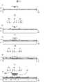
- FIG. 1 (a)is a cross-sectional view of the display device of the present embodiment including a transistor of the first structure and a transistor of the third structure
- FIG. 1 (b)is a second view of the display device of the present embodiment.
- Itis sectional drawing which includes a transistor of a structure.
- Itis a schematic plan view which shows the structure of the display device of this embodiment.
- Itis a circuit diagram which shows an example of a pixel circuit.
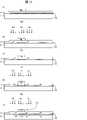
- FIG. 4Ais a cross-sectional view showing a configuration example of a portion of the pixel circuit including a drive transistor and a light emission control transistor
- FIG. 4Bis a cross-sectional view showing a configuration example of a portion of the pixel circuit including a reset transistor.
- FIG. 4Ais a cross-sectional view showing a configuration example of a portion of the pixel circuit including a drive transistor and a light emission control transistor
- FIG. 4Bis a cross-sectional view showing a configuration example of a portion
- FIG 4 (c)is a cross-sectional view showing a configuration example of a portion of a pixel circuit including a threshold control transistor. It is a flowchart which shows the manufacturing method of the display device of Embodiment 1. It is sectional drawing which shows the manufacturing method of the transistor of 1st structure in Embodiment 1. FIG. It is sectional drawing which shows the manufacturing method of the transistor of the 2nd structure in Embodiment 1. FIG. It is sectional drawing which shows the manufacturing method of the transistor of the 3rd structure in Embodiment 1. FIG. It is a flowchart which shows the manufacturing method of the display device of Embodiment 2. It is sectional drawing which shows the manufacturing method of the transistor of 1st structure in Embodiment 2. It is sectional drawing which shows the manufacturing method of the transistor of the 2nd structure in Embodiment 2. It is sectional drawing which shows the manufacturing method of the transistor of the 3rd structure in Embodiment 2.
- FIG. 1 (a)is a cross-sectional view of the display device of the present embodiment including a transistor of the first structure and a transistor of the third structure
- FIG. 1 (b)is a second view of the display device of the present embodiment. It is sectional drawing which includes a transistor of a structure.
- FIG. 2is a schematic plan view showing the configuration of the display device of the present embodiment.
- the substrate 2As shown in FIGS. 1 to 2, in the display device 10, the substrate 2, the thin film transistor layer 4 including the pixel circuit PC, the light emitting element layer 5 including the top emission (light emitting to the upper layer side) type light emitting element ED, and the seal.
- the stop layer 6is formed in this order, and the light emitting element ED and the pixel circuit PC are formed for each sub-pixel SP.
- the substrate 2is a glass substrate or a flexible base material containing a resin such as polyimide as a main component.
- the substrate 2can be composed of two layers of polyimide films and an inorganic film sandwiched between them. ..
- a base coat film (inorganic insulating film) that prevents foreign substances such as water and oxygen from enteringmay be provided on the upper surface (interface with the semiconductor layer SC) of the substrate 2.
- the thin film transistor layer 4is formed on a semiconductor layer SC formed on the substrate 2, a gate insulating film 14 covering the semiconductor layer SC, and a layer above the gate insulating film 14, and forms a gate electrode GE.
- a flattening film 21is provided.
- the semiconductor layer SCis composed of, for example, low-temperature-formed polysilicon (LTPS).
- LTPSlow-temperature-formed polysilicon
- the portion superposed with the gate electrode GEfunctions as a semiconductor (channel), and the portion not superposed is made into a conductor by impurity doping or the like.
- the first metal layer, the second metal layer and the third metal layerare composed of a metal single layer film or a metal multi-layer film containing at least one of, for example, aluminum, tungsten, molybdenum, tantalum, chromium, titanium, and copper. Will be done.
- the gate insulating film 14can be made of, for example, a silicon oxide (SiOx) film.
- the first interlayer insulating film 16 covering the gate electrode GEcan be composed of, for example, a laminated film of silicon oxide (SiOx) and silicon nitride (SiNx).
- the second interlayer insulating film 20can be composed of a single-layer film of silicon oxide (SiOx) or a laminated film of silicon oxide (SiOx) and silicon nitride (SiNx).
- the flattening film 21can be made of a coatable organic material such as polyimide or acrylic resin.
- the light emitting element layer 5includes a lower electrode 22, an insulating edge cover film 23 that covers the edge of the lower electrode 22, an EL (electroluminescence) layer 24 that is higher than the edge cover film 23, and an EL (electroluminescence) layer 24 that is higher than the EL layer 24. Includes the upper electrode 25 of.
- the edge cover film 23is formed by applying an organic material such as polyimide or acrylic resin and then patterning by photolithography.
- each light emitting elementincludes an island-shaped lower electrode 22, an EL layer 24 including a light emitting layer, and an upper electrode 25.
- the upper electrode 25is a solid common electrode common to a plurality of light emitting elements ED.
- the light emitting element EDmay be, for example, an OLED (organic light emitting diode) including an organic layer as a light emitting layer, or a QLED (quantum dot light emitting diode) including a quantum dot layer as a light emitting layer.
- OLEDorganic light emitting diode
- QLEDquantum dot light emitting diode
- the EL layer 24is composed of, for example, laminating a hole injection layer, a hole transport layer, a light emitting layer, an electron transport layer, and an electron injection layer in order from the lower layer side.
- the light emitting layeris formed in an island shape in the opening (for each sub-pixel) of the edge cover film 23 by a vapor deposition method, an inkjet method, or a photolithography method.
- the other layersare formed in an island shape or a solid shape (common layer).
- the hole injection layer, the hole transport layer, the electron transport layer, and the electron injection layermay be configured so as not to form one or more layers.
- the lower electrode 22is a light reflecting electrode composed of, for example, a laminate of ITO (Indium Tin Oxide) and an alloy containing Ag (silver) or Ag.
- the upper electrode 25is made of a metal thin film such as a magnesium-silver alloy and has light transmittance.
- the light emitting element EDWhen the light emitting element ED is an OLED, holes and electrons are recombined in the light emitting layer by the driving current between the lower electrode 22 and the upper electrode 25, and light is emitted in the process of transitioning the resulting excitons to the ground state. Will be done.
- the driving current between the lower electrode 22 and the upper electrode 25causes holes and electrons to recombine in the light emitting layer, and the resulting excitons generate conduction band levels (conduction) of the quantum dots. Light is emitted in the process of transitioning from the band) to the valence band.
- the sealing layer 6 covering the light emitting element layer 5is a layer for preventing foreign substances such as water and oxygen from penetrating into the light emitting element layer 5.
- the pixel circuit PCincludes a transistor TA having a first structure, a transistor TB having a second structure, and a transistor TC having a third structure.
- the transistor TA of the first structure, the transistor TB of the second structure, and the transistor TC of the third structureare P-type transistors (P-type channel type), respectively, and the gate electrode is formed in a layer above the channel region. It is a type.
- the semiconductor layer SC of the transistor TA of the first structureincludes a first channel region CH1 and a first doped region A1 and a second doped region A2 arranged on both sides of the first channel region CH1 and doped with impurities. ..
- the first channel region CH1matches the gate electrode GE of the transistor TA.
- the semiconductor layer SC of the transistor TB having the second structureincludes a second channel region CH2 and a third doped region A3 and a fourth doped region A4 arranged on both sides of the second channel region CH2 and doped with impurities. ..
- the second channel region CH2matches the gate electrode GE of the transistor TB.
- the semiconductor layer SC of the transistor TC of the third structureincludes a third channel region CH3 and a fifth doped region A5 and a sixth doped region A6 arranged on both sides of the third channel region CH3 and doped with impurities. ..
- the third channel region CH3matches the gate electrode GE of the transistor TC.
- the first doped region A1 adjacent to one side of the first channel region CH1is composed of the high concentration region aH, and the other side of the first channel region CH1.
- the second dope region A2 adjacent to the first channel region CH1is composed of a low concentration region aL adjacent to the first channel region CH1 and a high concentration region aH adjacent to the low concentration region aL.
- the third doped region A3 adjacent to one side of the second channel region CH2has a low concentration region aL adjacent to the second channel region CH2 and a high concentration region aL adjacent to the low concentration region aL.
- the fourth doped region A4which is composed of the concentration region aH and is adjacent to the other side of the second channel region CH2, has a low concentration region aL adjacent to the second channel region CH2 and a high concentration region adjacent to the low concentration region aL. It is composed of the region aH.
- the fifth doped region A5 adjacent to one side of the third channel region CH3is composed of the high concentration region aH
- the doping concentration in the high concentration region aHis 10 times or more the doping concentration in the low concentration region aL.
- FIG. 3is a circuit diagram showing an example of a pixel circuit.
- the capacitive element Cp, the reset transistors T1x and T1y in which the gate electrode is connected to the scanning signal line Gn-1 in the previous stage (n-1 stage), and the gate electrodeare in their own stage (n stage).
- the threshold control transistors T2x and T2yconnected to the scanning signal line Gn of the above, the writing control transistor T3 in which the gate electrode is connected to the scanning signal line Gn of its own stage (n stage), and the drive for controlling the current of the light emitting element ED.
- the transistor T4the power supply transistor T5 in which the gate electrode is connected to the light emission control line EM (n stages), the light emission control transistor T6 in which the gate electrode is connected to the light emission control line EM (n stages), and the gate electrode itself.
- the initialization transistor T7 connected to the scanning signal line Gn of the stage (n stage)is included.
- the scanning signal line Gn / Gn-1 and the light emission control line EMare included in the first metal layer, and the data signal line DL, the power supply line PL, and the initialization signal line are included in the third metal layer.
- a part of the scanning signal line Gn, a part of the scanning signal line Gn-1, or a part of the light emission control line EMmay function as a gate electrode GE of each transistor other than the driving transistor T4.
- the drive transistor T4is a transistor TA having a first structure
- the reset transistors T1x / T1y and the threshold control transistors T2x / T2yare transistors TB having a second structure, respectively, and are a write control transistor T3, a power supply transistor T5, and light emission control.
- the transistor T6 and the initialization transistor T7are each a transistor TC having a third structure.
- the gate electrode GE of the drive transistor T4is connected to the power supply line PL via the capacitive element Cp, and is also connected to the initialization signal line IL via the reset transistors T1x and T1y.
- a high voltage side power supply (EL VDD)is supplied to the power supply line PL, and for example, the same low voltage side power supply (ELVSS) is supplied to the cathode (upper electrode 25) of the initialization signal line IL and the light emitting element ED.
- the first doped region (source region) A1 of the drive transistor T4is connected to the data signal line DL via the write control transistor T3, and is also connected to the power supply line PL via the power supply transistor T5.
- the second doped region (drain region) A2 of the drive transistor T4is connected to the anode (lower electrode 22) of the light emitting element ED via the light emitting control transistor T6, and the two threshold control transistors T2x. It is connected to the gate electrode GE of the drive transistor T4 via T2y.
- the anode of the light emitting element EDis connected to the initialization signal line IL via the initialization transistor T7.
- FIG. 4Ais a cross-sectional view showing a configuration example of a portion of the pixel circuit including a drive transistor and a light emission control transistor
- FIG. 4Bis a cross-sectional view showing a configuration example of a portion of the pixel circuit including a reset transistor
- FIG. 4 (c)is a cross-sectional view showing a configuration example of a portion of a pixel circuit including a threshold control transistor.
- the capacitive element Cpis formed so as to include the gate electrode GE and the capacitive electrode CE of the drive transistor T4 (TA), and the capacitive electrode CE is a second interlayer insulating film. It is connected to the power supply line PL through the contact hole formed in 20.
- the second doped region A2 of the drive transistor T4 (TA)is connected to the lower electrode 22 (anode) of the light emitting element ED via the light emission control transistor T6 (TC).
- the drive current Idflows from the first doped region A1 which is the source region of the drive transistor T4 (TA) toward the second doped region A2 which is the drain region.
- the second-doped region A2 of the drive transistor T4 and the fifth-doped region A5 of the light emission control transistor T6are connected to each other via the wiring region Aw of the semiconductor layer SC.
- the wiring region Awis a conductor portion composed of the high concentration region aH.
- the drive current Idflows into the light emitting element ED through the wiring region Aw, the fifth doped region A5 of the light emitting control transistor T6, the third channel region CH3, and the sixth doped region A6.
- the drive transistor T4is a transistor TA having the first structure, the first region A1 which is the source region is composed of the high concentration region aH, and the second region A2 which is the drain region is adjacent to the first channel region CH1.
- the low-concentration region aL and the high-concentration region aHit is possible to improve the drive capability of the drive transistor T4 and reduce the off-current at the same time.
- the paired reset transistors T1x and T1yare connected in series, and the reset transistor T1x has a fourth dope region A4 and the reset transistor T1y has a third dope region A3. Is connected via the wiring area Aw.
- the third doped region A3 of the reset transistor T1xis connected to the initialization signal line IL via the wiring region Aw of the semiconductor layer SC.
- the paired threshold control transistors T2x and T2yare connected in series, and the fourth dope region A4 of the threshold control transistor T2x and the third dope of the threshold control transistor T2y are connected.
- the area A3is connected to the area A3 via the wiring area Aw.
- the third doped region A3 of the threshold control transistor T2xis connected to the upper layer wiring UW via the wiring region Aw of the semiconductor layer SC.
- the reset transistors T1x / T1y and the threshold control transistors T2x / T2yare used as the transistors TB having the second structure, and the third doped region A3 and the fourth doped region A4 are each in the low concentration region adjacent to the second channel region CH2.
- aL and the high concentration region aHit is possible to reduce the off-current of the reset transistor and the threshold control transistor.
- the write control transistor T3, the power supply transistor T5, the light emission control transistor T6, and the initialization transistor T7are each used as a transistor TC having a third structure, and the fifth dope region A5 and the sixth dope region A6 adjacent to the third channel region CH3 are used. By configuring each of them in the high concentration region aH, it is possible to secure the ON currents of these transistors T3, T5, T6, and T7.
- the initialization transistor T7may be a transistor TB having a second structure.
- the transistors T1 to T7 of the pixel circuit PCare divided into the transistor TA of the first structure, the second transistor TB, and the third transistor TC according to the function, thereby increasing the capacity of the transistors T1 to T7. It can be optimized, and a pixel circuit with high brightness and high reliability can be realized.
- FIG. 5is a flowchart showing a manufacturing method of the display device of the first embodiment.
- FIG. 6is a cross-sectional view showing a method of manufacturing a transistor having the first structure according to the first embodiment.
- FIG. 7is a cross-sectional view showing a method of manufacturing a transistor having a second structure according to the first embodiment.
- FIG. 8is a cross-sectional view showing a method of manufacturing a transistor having a third structure according to the first embodiment.
- step S1the substrate 2 (including the base coat film) is formed.
- step S2a film of amorphous silicon (amorphous silicon) is formed.
- step S3the amorphous silicon is dehydrogenated by heat treatment.
- step S4laser annealing is performed by an ELA (Exicimer Laser Anneling) method, and amorphous silicon is used as a semiconductor layer SC made of polysilicon.
- step S5the semiconductor layer SC is patterned by a photolithography method.
- step S6the gate insulating film 14 (for example, silicon oxide) is formed by using the CVA method.
- step S7a first metal layer (molybdenum-based alloy such as molybdenum or MoW) is formed by using a sputtering method.
- step S8patterning of the first metal layer (formation of the gate electrode GE or the like) is performed by a photolithography method.
- step S10flow-concentration doping of impurities is performed on the semiconductor layer SC using the gate electrode GE as a shield (see FIGS. 6 (b), 7 (b), and 8 (b)).
- the gate electrode GEas a shield
- the doping concentrationis, for example, 3.0 ⁇ 10 16 to 2 ⁇ 10 17 [atoms / cm 3 ].
- a low concentration region aLis formed.
- step S10shigh-concentration doping of impurities is performed on the semiconductor layer SC using the gate electrode GE and the mask MK as a shield (see FIGS. 6 (c), 7 (c), and 8 (c)).
- impuritiesfor example, boron is used as the impurity, and the doping concentration is, for example, 1.0 ⁇ 10 19 to 1.0 ⁇ 10 21 [atoms / cm 3 ]. As a result, a high concentration region aH is formed.
- the semiconductor layer SC of the transistor TA (T4) having the first structureeither the first portion P1 superimposed on the gate electrode GE or both sides of the gate electrode GE.
- the mask MK and the gate electrode GEare used as a shield, and the region is higher than the region not superimposed on the mask MK and the gate electrode GE in the semiconductor layer SC.
- Perform concentration dopingAs a result, the first channel region CH1, the first dope region A1 (source region) composed of the high concentration region aH, and the second dope region A2 (drain region) composed of the low concentration region aL and the high concentration region aH ) And are formed.
- a mask MKhaving a portion superimposed on the gate electrode GE and a portion superimposed on both sides of the gate electrode GE.
- the mask MK and the gate electrode GEas a shield, high-concentration doping is performed on the region of the semiconductor layer SC that does not overlap with either the mask MK and the gate electrode GE.
- the second channel region CH2the third-doped region A3 composed of the low-concentration region aL and the high-concentration region aH, and the fourth-doped region A4 composed of the low-concentration region aL and the high-concentration region aH are formed. It is formed.
- step S11the first interlayer insulating film 16 (for example, a laminated film of silicon oxide and silicon nitride) is formed by using the CVA method.
- step S12hydrogenation annealing (heat treatment for the purpose of supplying hydrogen to the crystalline silicon semiconductor layer SC) is performed.
- step S13the first interlayer insulating film 16 is patterned (opening formed) by a photolithography method.
- the second metal layer 19(for example, a titanium / aluminum / titanium laminated film) is formed by using a sputtering method.
- patterning of the second metal layer(formation of the capacitive electrode CE or the like) is performed by a photolithography method.
- the second interlayer insulating film 20(for example, a single layer film of silicon oxide or a laminated film of silicon nitride and silicon oxide) is formed by using the CVA method.
- the first interlayer insulating film 16, the second interlayer insulating film 20, and the gate insulating film 14are patterned by a photolithography method.
- a third metal layerfor example, a titanium / aluminum / titanium laminated film
- a sputtering methodfor example, a sputtering method
- patterning of the third metal layeris performed by a photolithography method.
- the light emitting element layer 5is formed.
- the sealing layer 6is formed.
- FIG. 9is a flowchart showing a method of manufacturing the display device of the second embodiment.
- FIG. 10is a cross-sectional view showing a method of manufacturing a transistor having the first structure according to the second embodiment.
- FIG. 11is a cross-sectional view showing a method of manufacturing a transistor having a second structure according to the second embodiment.
- FIG. 12is a cross-sectional view showing a method of manufacturing a transistor having a third structure according to the second embodiment.
- Steps S1 to S8 of FIG. 9are the same as those of the first embodiment, and in step S9, the first metal layer is patterned by a photolithography method to form a gate layer ML.
- step S10dhigh-concentration doping of impurities is performed on the semiconductor layer SC using the gate layer ML as a shield (see FIGS. 10 (b), 11 (b), and 12 (b)).
- impuritiesfor example, boron is used as the impurity, and the doping concentration is, for example, 1.0 ⁇ 10 19 to 1.0 ⁇ 10 21 [atoms / cm 3 ].
- a high concentration region aHis formed.
- step S10ethe gate layer ML is thinned by etching to form a gate electrode GE (see FIGS. 10 (c), 11 (c), and 12 (c)).
- step S10flow-concentration doping of impurities is performed on the semiconductor layer SC using the gate electrode GE as a shield (FIGS. 10 (d), 11 (d), and 12 (d)). reference).
- the gate electrode GEas a shield
- the doping concentrationis, for example, 3.0 ⁇ 10 16 to 2 ⁇ 10 17 [atoms / cm 3 ].
- a low concentration region aLis formed.
- step S10ssimilarly to the first embodiment, high-concentration doping of impurities is performed on the semiconductor layer SC using the gate electrode GE and the mask MK as a shield (FIGS. 10 (e), 11 (e), and 12 (FIG. 12). See (e).
- boronis used as the impurity, and the doping concentration is, for example, 1.0 ⁇ 10 19 to 1.0 ⁇ 10 21 [atoms / cm 3 ].
- a high concentration region aHis formed.
- Steps S11 to S21 of FIG. 9are the same as those of the first embodiment.
- a light emitting element and a pixel circuit including a transistor of the first structureare provided.
- the semiconductor layer of the transistor of the first structureincludes a first channel region, a first dope region adjacent to one side of the first channel region, and a second dope region adjacent to the other side of the first channel region.
- the first doped regionis composed of a high concentration region in which impurities are heavily doped.
- the second-doped regionis adjacent to the first channel region and is adjacent to the low-concentration region where impurities are doped at a low concentration, and the second-doped region is adjacent to the low-concentration region and is adjacent to the high-concentration region where impurities are doped at a high concentration.
- the pixel circuitincludes a drive transistor which is a transistor having the first structure and a capacitive element connected to a gate electrode of the drive transistor.
- a display devicein which a drive current flows from the first-doped region of the drive transistor toward the second-doped region during the light emitting period of the light-emitting element.
- the pixel circuitincludes a transistor having a second structure.
- the semiconductor layer of the transistor of the second structureincludes a second channel region, a third dope region adjacent to one side of the second channel region, and a fourth dope region adjacent to the other side of the second channel region.
- the third-doped regionis adjacent to the second channel region and is adjacent to the low-concentration region where impurities are doped at a low concentration, and the third-doped region is adjacent to the low-concentration region and is adjacent to the high-concentration region where impurities are doped to a high concentration.
- the fourth-doped regionis adjacent to the second channel region and is adjacent to the low-concentration region where impurities are doped at a low concentration, and the fourth-doped region is adjacent to the low-concentration region and is adjacent to the high-concentration region where impurities are doped to a high concentration.
- the display deviceaccording to, for example, the first aspect, which is configured.
- the pixel circuitincludes a transistor having the second structure and a threshold control transistor connected to a scanning signal line of its own stage and a gate electrode of the drive transistor.
- the pixel circuitincludes a transistor having a third structure.
- the semiconductor layer of the transistor having the third structureincludes a third channel region, a fifth dope region adjacent to one side of the third channel region, and a sixth dope region adjacent to the other side of the third channel region.
- the display deviceaccording to any one of aspects 1 to 12, for example, the transistor having the first structure is a top gate type.
- the transistor of the first structureis a P-channel type and has a P-channel type.
- a method for manufacturing a display deviceincluding a transistor having a first structure including a semiconductor layer and a gate electrode.
- a mask having a first portion superimposed on the gate electrode and a second portion superimposed on any one of both sides of the gate electrodeis used, and the mask and the gate electrode are used as a shield.
- a method for manufacturing a display devicecomprising a fourth step of doping a region not superimposed on either the mask or the gate electrode with impurities at a concentration higher than the low concentration.
- a gate layerwhich is a metal layer, is formed between the first step and the second step, the gate layer is used as a shield, and the concentration is higher than the low concentration with respect to a region of the semiconductor layer that does not overlap with the gate layer.
- the first doped regionis composed of a high concentration region in which impurities are heavily doped.
- the second-doped regioncorresponds to the second portion of the mask, and includes a low-concentration region in which impurities are doped at a low concentration and a high-concentration region adjacent to the low-concentration region in which impurities are heavily doped.
Landscapes
- Engineering & Computer Science (AREA)
- Physics & Mathematics (AREA)
- Microelectronics & Electronic Packaging (AREA)
- Geometry (AREA)
- Manufacturing & Machinery (AREA)
- Nonlinear Science (AREA)
- General Physics & Mathematics (AREA)
- Chemical & Material Sciences (AREA)
- Crystallography & Structural Chemistry (AREA)
- Mathematical Physics (AREA)
- Optics & Photonics (AREA)
- Computer Hardware Design (AREA)
- Theoretical Computer Science (AREA)
- Electroluminescent Light Sources (AREA)
- Thin Film Transistor (AREA)
- Devices For Indicating Variable Information By Combining Individual Elements (AREA)
Abstract
Description
Translated fromJapanese本発明は、表示装置に関する。The present invention relates to a display device.
特許文献1には、電気光学装置の半導体層において、ドレイン領域(不純物導入領域)を、低濃度領域(LDD領域)と高濃度領域とで構成する手法が開示されている。Patent Document 1 discloses a method in which a drain region (impurity introduction region) is composed of a low concentration region (LDD region) and a high concentration region in the semiconductor layer of an electro-optic device.
発光素子用の画素回路において、駆動トランジスタの駆動能力の向上とオフ電流の低減との両立を図る。In the pixel circuit for the light emitting element, both the improvement of the drive capability of the drive transistor and the reduction of the off-current are achieved.
本発明の一態様にかかる表示装置は、発光素子と、第1構造のトランジスタを含む画素回路とを備え、前記第1構造のトランジスタの半導体層は、第1チャネル領域と、前記第1チャネル領域の両側に配され、不純物がドープされた、第1ドープ領域および第2ドープ領域とを含み、前記第1チャネル領域に隣接する前記第1ドープ領域は高濃度領域で構成され、前記第2ドープ領域は、前記第1チャネル領域に隣接する低濃度領域と、当該低濃度領域に隣接する高濃度領域とで構成され、前記第1構造のトランジスタの半導体層に含まれる高濃度領域は、当該半導体層に含まれる低濃度領域よりもドープ濃度が高く、前記画素回路には、前記第1構造のトランジスタである駆動トランジスタと、前記駆動トランジスタのゲート電極に接続する容量素子とが含まれ、前記発光素子の発光期間に、前記駆動トランジスタの前記第1ドープ領域から前記第2ドープ領域に向けて駆動電流が流れる。The display device according to one aspect of the present invention includes a light emitting element and a pixel circuit including a transistor of the first structure, and the semiconductor layer of the transistor of the first structure has a first channel region and the first channel region. The first-doped region adjacent to the first channel region is composed of a high-concentration region and includes the first-doped region and the second-doped region, which are arranged on both sides of the above and are doped with impurities. The region is composed of a low concentration region adjacent to the first channel region and a high concentration region adjacent to the low concentration region, and the high concentration region included in the semiconductor layer of the transistor of the first structure is the semiconductor. The dope concentration is higher than the low concentration region contained in the layer, and the pixel circuit includes a drive transistor which is a transistor of the first structure and a capacitive element connected to a gate electrode of the drive transistor, and emits light. During the light emission period of the element, a drive current flows from the first-doped region of the drive transistor toward the second-doped region.
本発明の一態様によれば、駆動トランジスタの駆動能力の向上とオフ電流の低減との両立を図ることができる。According to one aspect of the present invention, it is possible to achieve both an improvement in the drive capability of the drive transistor and a reduction in the off-current.
図1(a)は、本実施形態の表示装置の、第1構造のトランジスタおよび第3構造のトランジスタを含む断面図であり、図1(b)は、本実施形態の表示装置の、第2構造のトランジスタを含む断面図である。図2は、本実施形態の表示装置の構成を示す模式的平面図である。1 (a) is a cross-sectional view of the display device of the present embodiment including a transistor of the first structure and a transistor of the third structure, and FIG. 1 (b) is a second view of the display device of the present embodiment. It is sectional drawing which includes a transistor of a structure. FIG. 2 is a schematic plan view showing the configuration of the display device of the present embodiment.
図1~図2に示すように、表示装置10では、基板2、画素回路PCを含む薄膜トランジスタ層4、トップエミッション(上層側へ発光する)タイプの発光素子EDを含む発光素子層5、および封止層6がこの順に形成され、サブ画素SPごとに、発光素子EDおよび画素回路PCが形成される。As shown in FIGS. 1 to 2, in the
基板2は、ガラス基板、あるいは、ポリイミド等の樹脂を主成分とする可撓性基材であり、例えば、2層のポリイミド膜およびこれらに挟まれた無機膜によって基板2を構成することもできる。基板2の上面(半導体層SCとの界面)に水、酸素等の異物の侵入を防ぐベースコート膜(無機絶縁膜)を設けてもよい。The
図1に示すように、薄膜トランジスタ層4は、基板2上に形成される半導体層SCと、半導体層SCを覆うゲート絶縁膜14と、ゲート絶縁膜14よりも上層に形成され、ゲート電極GEを含む第1金属層と、第1金属層を覆う第1層間絶縁膜16と、第1層間絶縁膜16よりも上層に形成され、容量電極CEを含む第2金属層と、第2金属層を覆う第2層間絶縁膜20と、第2層間絶縁膜20よりも上層に形成され、電源線PLおよび初期化信号線ILを含む第3金属層と、第3金属層よりも上層に形成される平坦化膜21とを備える。As shown in FIG. 1, the thin
半導体層SCは、例えば低温形成のポリシリコン(LTPS)で構成される。半導体層SCは、ゲート電極GEと重畳する部分は半導体(チャネル)として機能し、重畳しない部分は不純物ドープ等によって導体とされる。The semiconductor layer SC is composed of, for example, low-temperature-formed polysilicon (LTPS). In the semiconductor layer SC, the portion superposed with the gate electrode GE functions as a semiconductor (channel), and the portion not superposed is made into a conductor by impurity doping or the like.
第1金属層、第2金属層および第3金属層は、例えば、アルミニウム、タングステン、モリブデン、タンタル、クロム、チタン、および銅の少なくとも1つを含む、金属単層膜あるいは金属複層膜によって構成される。The first metal layer, the second metal layer and the third metal layer are composed of a metal single layer film or a metal multi-layer film containing at least one of, for example, aluminum, tungsten, molybdenum, tantalum, chromium, titanium, and copper. Will be done.
ゲート絶縁膜14は、例えば酸化シリコン(SiOx)膜で構成することができる。ゲート電極GEを覆う第1層間絶縁膜16は、例えば酸化シリコン(SiOx)および窒化シリコン(SiNx)の積層膜で構成することができる。第2層間絶縁膜20は、酸化シリコン(SiOx)の単層膜あるいは酸化シリコン(SiOx)および窒化シリコン(SiNx)の積層膜で構成することができる。平坦化膜21は、例えば、ポリイミド、アクリル樹脂等の塗布可能な有機材料によって構成することができる。The
発光素子層5は、下部電極22と、下部電極22のエッジを覆う絶縁性のエッジカバー膜23と、エッジカバー膜23よりも上層のEL(エレクトロルミネッセンス)層24と、EL層24よりも上層の上部電極25とを含む。エッジカバー膜23は、例えば、ポリイミド、アクリル樹脂等の有機材料を塗布した後にフォトリソグラフィよってパターニングすることで形成される。The light
発光素子層5には、発光色が異なる複数の発光素子EDが形成され、各発光素子が、島状の下部電極22、発光層を含むEL層24、および上部電極25を含む。上部電極25は、複数の発光素子EDで共通する、ベタ状の共通電極である。A plurality of light emitting elements EDs having different light emitting colors are formed in the light
発光素子EDは、例えば、発光層として有機層を含むOLED(有機発光ダイオード)であってもよいし、発光層として量子ドット層を含むQLED(量子ドット発光ダイオード)であってもよい。The light emitting element ED may be, for example, an OLED (organic light emitting diode) including an organic layer as a light emitting layer, or a QLED (quantum dot light emitting diode) including a quantum dot layer as a light emitting layer.
EL層24は、例えば、下層側から順に、正孔注入層、正孔輸送層、発光層、電子輸送層、電子注入層を積層することで構成される。発光層は、蒸着法あるいはインクジェット法、フォトリソグラフィ法によって、エッジカバー膜23の開口(サブ画素ごと)に、島状に形成される。他の層は、島状あるいはベタ状(共通層)に形成する。また、正孔注入層、正孔輸送層、電子輸送層、電子注入層のうち1以上の層を形成しない構成とすることもできる。The
下部電極22(アノード)は、例えばITO(Indium Tin Oxide)とAg(銀)あるいはAgを含む合金との積層によって構成される、光反射電極である。上部電極25(カソード)は、例えばマグネシウム銀合金等の金属薄膜で構成され、光透過性を有する。The lower electrode 22 (anode) is a light reflecting electrode composed of, for example, a laminate of ITO (Indium Tin Oxide) and an alloy containing Ag (silver) or Ag. The upper electrode 25 (cathode) is made of a metal thin film such as a magnesium-silver alloy and has light transmittance.
発光素子EDがOLEDである場合、下部電極22および上部電極25間の駆動電流によって正孔と電子が発光層内で再結合し、これによって生じたエキシトンが基底状態に遷移する過程で光が放出される。発光素子EDがQLEDである場合、下部電極22および上部電極25間の駆動電流によって正孔と電子が発光層内で再結合し、これによって生じたエキシトンが、量子ドットの伝導帯準位(conduction band)から価電子帯準位(valence band)に遷移する過程で光が放出される。When the light emitting element ED is an OLED, holes and electrons are recombined in the light emitting layer by the driving current between the
発光素子層5を覆う封止層6は、水、酸素等の異物の発光素子層5への浸透を防ぐ層であり、例えば、2層の無機封止膜とこれら間に形成される有機膜とで構成することができる。The
〔実施形態1〕
図1~図2に示すように、画素回路PCは、第1構造のトランジスタTA、第2構造のトランジスタTB、および第3構造のトランジスタTCを含む。第1構造のトランジスタTA、第2構造のトランジスタTB、および第3構造のトランジスタTCはそれぞれ、P型トランジスタ(P型チャネル型)であり、ゲート電極がチャネル領域よりも上層に形成されるトップゲートタイプである。[Embodiment 1]
As shown in FIGS. 1 and 2, the pixel circuit PC includes a transistor TA having a first structure, a transistor TB having a second structure, and a transistor TC having a third structure. The transistor TA of the first structure, the transistor TB of the second structure, and the transistor TC of the third structure are P-type transistors (P-type channel type), respectively, and the gate electrode is formed in a layer above the channel region. It is a type.
第1構造のトランジスタTAの半導体層SCは、第1チャネル領域CH1と、第1チャネル領域CH1の両側に配され、不純物がドープされた、第1ドープ領域A1および第2ドープ領域A2とを含む。第1チャネル領域CH1は、トランジスタTAのゲート電極GEに整合する。The semiconductor layer SC of the transistor TA of the first structure includes a first channel region CH1 and a first doped region A1 and a second doped region A2 arranged on both sides of the first channel region CH1 and doped with impurities. .. The first channel region CH1 matches the gate electrode GE of the transistor TA.
第2構造のトランジスタTBの半導体層SCは、第2チャネル領域CH2と、第2チャネル領域CH2の両側に配され、不純物がドープされた、第3ドープ領域A3および第4ドープ領域A4とを含む。第2チャネル領域CH2は、トランジスタTBのゲート電極GEに整合する。The semiconductor layer SC of the transistor TB having the second structure includes a second channel region CH2 and a third doped region A3 and a fourth doped region A4 arranged on both sides of the second channel region CH2 and doped with impurities. .. The second channel region CH2 matches the gate electrode GE of the transistor TB.
第3構造のトランジスタTCの半導体層SCは、第3チャネル領域CH3と、第3チャネル領域CH3の両側に配され、不純物がドープされた、第5ドープ領域A5および第6ドープ領域A6とを含む。第3チャネル領域CH3は、トランジスタTCのゲート電極GEに整合する。The semiconductor layer SC of the transistor TC of the third structure includes a third channel region CH3 and a fifth doped region A5 and a sixth doped region A6 arranged on both sides of the third channel region CH3 and doped with impurities. .. The third channel region CH3 matches the gate electrode GE of the transistor TC.
図1に示されるように、第1構造のトランジスタTAについては、第1チャネル領域CH1の一方側に隣接する第1ドープ領域A1が高濃度領域aHで構成され、第1チャネル領域CH1の他方側に隣接する第2ドープ領域A2が、第1チャネル領域CH1に隣接する低濃度領域aLと、当該低濃度領域aLに隣接する高濃度領域aHとで構成される。As shown in FIG. 1, for the transistor TA having the first structure, the first doped region A1 adjacent to one side of the first channel region CH1 is composed of the high concentration region aH, and the other side of the first channel region CH1. The second dope region A2 adjacent to the first channel region CH1 is composed of a low concentration region aL adjacent to the first channel region CH1 and a high concentration region aH adjacent to the low concentration region aL.
第2構造のトランジスタTBについては、第2チャネル領域CH2の一方側に隣接する第3ドープ領域A3が、第2チャネル領域CH2に隣接する低濃度領域aLと、当該低濃度領域aLに隣接する高濃度領域aHとで構成され、第2チャネル領域CH2の他方側に隣接する第4ドープ領域A4が、第2チャネル領域CH2に隣接する低濃度領域aLと、当該低濃度領域aLに隣接する高濃度領域aHとで構成される。Regarding the transistor TB having the second structure, the third doped region A3 adjacent to one side of the second channel region CH2 has a low concentration region aL adjacent to the second channel region CH2 and a high concentration region aL adjacent to the low concentration region aL. The fourth doped region A4, which is composed of the concentration region aH and is adjacent to the other side of the second channel region CH2, has a low concentration region aL adjacent to the second channel region CH2 and a high concentration region adjacent to the low concentration region aL. It is composed of the region aH.
第3構造のトランジスタTCについては、第3チャネル領域CH3の一方側に隣接する第5ドープ領域A5が高濃度領域aHで構成され、第3チャネル領域CH3の他方側に隣接する第6ドープ領域A6が高濃度領域aHで構成される。Regarding the transistor TC having the third structure, the fifth doped region A5 adjacent to one side of the third channel region CH3 is composed of the high concentration region aH, and the sixth doped region A6 adjacent to the other side of the third channel region CH3. Is composed of a high concentration region aH.
トランジスタTA、TB、TCにおいては、例えば、高濃度領域aHのドープ濃度が、低濃度領域aLのドープ濃度の10倍以上とされる。In the transistors TA, TB, and TC, for example, the doping concentration in the high concentration region aH is 10 times or more the doping concentration in the low concentration region aL.
図3は画素回路の一例を示す回路図である。図3の画素回路PCは、容量素子Cpと、ゲート電極が前段(n-1段)の走査信号線Gn-1に接続されるリセットトランジスタT1x・T1yと、ゲート電極が自段(n段)の走査信号線Gnに接続される閾値制御トランジスタT2x・T2yと、ゲート電極が自段(n段)の走査信号線Gnに接続される書き込み制御トランジスタT3と、発光素子EDの電流を制御する駆動トランジスタT4と、ゲート電極が発光制御線EM(n段)に接続される電源供給トランジスタT5と、ゲート電極が発光制御線EM(n段)に接続される発光制御トランジスタT6と、ゲート電極が自段(n段)の走査信号線Gnに接続される初期化トランジスタT7と、を含む。FIG. 3 is a circuit diagram showing an example of a pixel circuit. In the pixel circuit PC of FIG. 3, the capacitive element Cp, the reset transistors T1x and T1y in which the gate electrode is connected to the scanning signal line Gn-1 in the previous stage (n-1 stage), and the gate electrode are in their own stage (n stage). The threshold control transistors T2x and T2y connected to the scanning signal line Gn of the above, the writing control transistor T3 in which the gate electrode is connected to the scanning signal line Gn of its own stage (n stage), and the drive for controlling the current of the light emitting element ED. The transistor T4, the power supply transistor T5 in which the gate electrode is connected to the light emission control line EM (n stages), the light emission control transistor T6 in which the gate electrode is connected to the light emission control line EM (n stages), and the gate electrode itself. The initialization transistor T7 connected to the scanning signal line Gn of the stage (n stage) is included.
走査信号線Gn・Gn-1および発光制御線EMは第1金属層に含まれ、データ信号線DL、電源線PL、および初期化信号線は第3金属層に含まれる。走査信号線Gnの一部あるいは走査信号線Gn-1の一部または発光制御線EMの一部が、駆動トランジスタT4以外の各トランジスタのゲート電極GEとして機能してもよい。The scanning signal line Gn / Gn-1 and the light emission control line EM are included in the first metal layer, and the data signal line DL, the power supply line PL, and the initialization signal line are included in the third metal layer. A part of the scanning signal line Gn, a part of the scanning signal line Gn-1, or a part of the light emission control line EM may function as a gate electrode GE of each transistor other than the driving transistor T4.
駆動トランジスタT4は、第1構造のトランジスタTAであり、リセットトランジスタT1x・T1yおよび閾値制御トランジスタT2x・T2yはそれぞれ、第2構造のトランジスタTBであり、書き込み制御トランジスタT3、電源供給トランジスタT5、発光制御トランジスタT6、および初期化トランジスタT7はそれぞれ、第3構造のトランジスタTCである。The drive transistor T4 is a transistor TA having a first structure, and the reset transistors T1x / T1y and the threshold control transistors T2x / T2y are transistors TB having a second structure, respectively, and are a write control transistor T3, a power supply transistor T5, and light emission control. The transistor T6 and the initialization transistor T7 are each a transistor TC having a third structure.
駆動トランジスタT4のゲート電極GEは、容量素子Cpを介して電源線PLに接続されるとともに、リセットトランジスタT1x・T1yを介して初期化信号線ILに接続される。電源線PLには高電圧側電源(ELVDD)が供給され、初期化信号線ILおよび発光素子EDのカソード(上部電極25)には、例えば同一の低電圧側電源(ELVSS)が供給される。The gate electrode GE of the drive transistor T4 is connected to the power supply line PL via the capacitive element Cp, and is also connected to the initialization signal line IL via the reset transistors T1x and T1y. A high voltage side power supply (EL VDD) is supplied to the power supply line PL, and for example, the same low voltage side power supply (ELVSS) is supplied to the cathode (upper electrode 25) of the initialization signal line IL and the light emitting element ED.
駆動トランジスタT4の第1ドープ領域(ソース領域)A1は、書き込み制御トランジスタT3を介してデータ信号線DLに接続されるとともに、電源供給トランジスタT5を介して電源線PLに接続される。駆動トランジスタT4の第2ドープ領域(ドレイン領域)A2は、発光制御トランジスタT6を介して発光素子EDのアノード(下部電極22)に接続されるとともに、直列に接続される2つの閾値制御トランジスタT2x・T2yを介して駆動トランジスタT4のゲート電極GEに接続される。発光素子EDのアノードは、初期化トランジスタT7を介して初期化信号線ILに接続される。The first doped region (source region) A1 of the drive transistor T4 is connected to the data signal line DL via the write control transistor T3, and is also connected to the power supply line PL via the power supply transistor T5. The second doped region (drain region) A2 of the drive transistor T4 is connected to the anode (lower electrode 22) of the light emitting element ED via the light emitting control transistor T6, and the two threshold control transistors T2x. It is connected to the gate electrode GE of the drive transistor T4 via T2y. The anode of the light emitting element ED is connected to the initialization signal line IL via the initialization transistor T7.
図4(a)は、画素回路における駆動トランジスタおよび発光制御トランジスタを含む部分の構成例を示す断面図であり、図4(b)は、画素回路におけるリセットトランジスタを含む部分の構成例を示す断面図であり、図4(c)は、画素回路における閾値制御トランジスタを含む部分の構成例を示す断面図である。FIG. 4A is a cross-sectional view showing a configuration example of a portion of the pixel circuit including a drive transistor and a light emission control transistor, and FIG. 4B is a cross-sectional view showing a configuration example of a portion of the pixel circuit including a reset transistor. FIG. 4 (c) is a cross-sectional view showing a configuration example of a portion of a pixel circuit including a threshold control transistor.
図3および図4(a)に示されるように、駆動トランジスタT4(TA)のゲート電極GEと容量電極CEとを含むように容量素子Cpが形成され、容量電極CEは、第2層間絶縁膜20に形成されたコンタクトホールを介して電源線PLに接続される。As shown in FIGS. 3 and 4A, the capacitive element Cp is formed so as to include the gate electrode GE and the capacitive electrode CE of the drive transistor T4 (TA), and the capacitive electrode CE is a second interlayer insulating film. It is connected to the power supply line PL through the contact hole formed in 20.
図4(a)に示されるように、駆動トランジスタT4(TA)の第2ドープ領域A2は、発光制御トランジスタT6(TC)を介して発光素子EDの下部電極22(アノード)に接続されており、発光素子EDの発光期間には、駆動トランジスタT4(TA)のソース領域である第1ドープ領域A1からドレイン領域である第2ドープ領域A2に向けて駆動電流Idが流れる。駆動トランジスタT4の第2ドープ領域A2と、発光制御トランジスタT6の第5ドープ領域A5とは、半導体層SCの配線領域Aw介して接続されている。配線領域Awは高濃度領域aHで構成される導体部である。駆動電流Idは、配線領域Aw、発光制御トランジスタT6の第5ドープ領域A5、第3チャネル領域CH3、および第6ドープ領域A6を通って発光素子EDに流れ込む。As shown in FIG. 4A, the second doped region A2 of the drive transistor T4 (TA) is connected to the lower electrode 22 (anode) of the light emitting element ED via the light emission control transistor T6 (TC). During the light emitting period of the light emitting element ED, the drive current Id flows from the first doped region A1 which is the source region of the drive transistor T4 (TA) toward the second doped region A2 which is the drain region. The second-doped region A2 of the drive transistor T4 and the fifth-doped region A5 of the light emission control transistor T6 are connected to each other via the wiring region Aw of the semiconductor layer SC. The wiring region Aw is a conductor portion composed of the high concentration region aH. The drive current Id flows into the light emitting element ED through the wiring region Aw, the fifth doped region A5 of the light emitting control transistor T6, the third channel region CH3, and the sixth doped region A6.
このように、駆動トランジスタT4を第1構造のトランジスタTAとし、ソース領域である第1領域A1を高濃度領域aHで構成し、ドレイン領域である第2領域A2を、第1チャネル領域CH1に隣接する低濃度領域aLと、高濃度領域aHとで構成することで、駆動トランジスタT4の駆動能力の向上とオフ電流の低減との両立を図ることができる。In this way, the drive transistor T4 is a transistor TA having the first structure, the first region A1 which is the source region is composed of the high concentration region aH, and the second region A2 which is the drain region is adjacent to the first channel region CH1. By configuring the low-concentration region aL and the high-concentration region aH, it is possible to improve the drive capability of the drive transistor T4 and reduce the off-current at the same time.
図4(b)に示されるように、対となるリセットトランジスタT1x・T1y(TB)は直列接続されており、リセットトランジスタT1xの第4ドープ領域A4と、リセットトランジスタT1yの第3ドープ領域A3とが、配線領域Awを介して接続されている。リセットトランジスタT1xの第3ドープ領域A3は、半導体層SCの配線領域Awを介して初期化信号線ILに接続されている。As shown in FIG. 4B, the paired reset transistors T1x and T1y (TB) are connected in series, and the reset transistor T1x has a fourth dope region A4 and the reset transistor T1y has a third dope region A3. Is connected via the wiring area Aw. The third doped region A3 of the reset transistor T1x is connected to the initialization signal line IL via the wiring region Aw of the semiconductor layer SC.
図4(c)に示されるように、対となる閾値制御トランジスタT2x・T2y(TB)は直列接続されており、閾値制御トランジスタT2xの第4ドープ領域A4と、閾値制御トランジスタT2yの第3ドープ領域A3とが、配線領域Awを介して接続されている。閾値制御トランジスタT2xの第3ドープ領域A3は、半導体層SCの配線領域Awを介して上層配線UWに接続されている。As shown in FIG. 4C, the paired threshold control transistors T2x and T2y (TB) are connected in series, and the fourth dope region A4 of the threshold control transistor T2x and the third dope of the threshold control transistor T2y are connected. The area A3 is connected to the area A3 via the wiring area Aw. The third doped region A3 of the threshold control transistor T2x is connected to the upper layer wiring UW via the wiring region Aw of the semiconductor layer SC.
このように、リセットトランジスタT1x・T1yおよび閾値制御トランジスタT2x・T2yを第2構造のトランジスタTBとし、第3ドープ領域A3および第4ドープ領域A4それぞれを、第2チャネル領域CH2に隣接する低濃度領域aLと、高濃度領域aHとで構成することで、リセットトランジスタおよび閾値制御トランジスタのオフ電流の低減を図ることができる。In this way, the reset transistors T1x / T1y and the threshold control transistors T2x / T2y are used as the transistors TB having the second structure, and the third doped region A3 and the fourth doped region A4 are each in the low concentration region adjacent to the second channel region CH2. By configuring aL and the high concentration region aH, it is possible to reduce the off-current of the reset transistor and the threshold control transistor.
書き込み制御トランジスタT3、電源供給トランジスタT5、発光制御トランジスタT6、および初期化トランジスタT7それぞれを、第3構造のトランジスタTCとし、第3チャネル領域CH3に隣接する第5ドープ領域A5および第6ドープ領域A6それぞれを高濃度領域aHで構成することで、これらのトランジスタT3・T5・T6・T7のON電流を担保することができる。なお、オフ電流の低減を図るために、初期化トランジスタT7を第2構造のトランジスタTBとすることもできる。The write control transistor T3, the power supply transistor T5, the light emission control transistor T6, and the initialization transistor T7 are each used as a transistor TC having a third structure, and the fifth dope region A5 and the sixth dope region A6 adjacent to the third channel region CH3 are used. By configuring each of them in the high concentration region aH, it is possible to secure the ON currents of these transistors T3, T5, T6, and T7. In order to reduce the off-current, the initialization transistor T7 may be a transistor TB having a second structure.
実施形態1では、画素回路PCのトランジスタT1~T7を、機能に応じて、第1構造のトランジスタTA、第2トランジスタTB、および第3トランジスタTCに作り分けることで、トランジスタT1~T7の能力を最適化でき、高輝度かつ高信頼性の画素回路を実現することできる。In the first embodiment, the transistors T1 to T7 of the pixel circuit PC are divided into the transistor TA of the first structure, the second transistor TB, and the third transistor TC according to the function, thereby increasing the capacity of the transistors T1 to T7. It can be optimized, and a pixel circuit with high brightness and high reliability can be realized.
図5は、実施形態1の表示装置の製造方法を示すフローチャートである。図6は、実施形態1における第1構造のトランジスタの製造方法を示す断面図である。図7は、実施形態1における第2構造のトランジスタの製造方法を示す断面図である。図8は、実施形態1における第3構造のトランジスタの製造方法を示す断面図である。FIG. 5 is a flowchart showing a manufacturing method of the display device of the first embodiment. FIG. 6 is a cross-sectional view showing a method of manufacturing a transistor having the first structure according to the first embodiment. FIG. 7 is a cross-sectional view showing a method of manufacturing a transistor having a second structure according to the first embodiment. FIG. 8 is a cross-sectional view showing a method of manufacturing a transistor having a third structure according to the first embodiment.
図5に示すように、ステップS1では基板2(ベースコート膜含む)の形成を行う。ステップS2では、非晶質シリコン(アモルファスシリコン)の成膜を行う。ステップS3では、熱処理による非晶質シリコンの脱水素化を行う。ステップS4では、ELA(Exicimer Laser Anneling)法によるレーザーアニールを行い、非晶質シリコンをポリシリコンからなる半導体層SCとする。ステップS5では、フォトリソグラフィ法により、半導体層SCのパターニングを行う。As shown in FIG. 5, in step S1, the substrate 2 (including the base coat film) is formed. In step S2, a film of amorphous silicon (amorphous silicon) is formed. In step S3, the amorphous silicon is dehydrogenated by heat treatment. In step S4, laser annealing is performed by an ELA (Exicimer Laser Anneling) method, and amorphous silicon is used as a semiconductor layer SC made of polysilicon. In step S5, the semiconductor layer SC is patterned by a photolithography method.
ステップS6では、CVA法を用いてゲート絶縁膜14(例えば、酸化シリコン)の成膜を行う。ステップS7では、スパッタリング法を用いて第1金属層(モリブデンあるいはMoW等のモリブデン系合金)の成膜を行う。ステップS8では、フォトリソグラフィ法により、第1金属層のパターニング(ゲート電極GE等の形成)を行う。In step S6, the gate insulating film 14 (for example, silicon oxide) is formed by using the CVA method. In step S7, a first metal layer (molybdenum-based alloy such as molybdenum or MoW) is formed by using a sputtering method. In step S8, patterning of the first metal layer (formation of the gate electrode GE or the like) is performed by a photolithography method.
ステップS10fでは、ゲート電極GEを遮蔽体として、半導体層SCに対して不純物の低濃度ドーピングを行う(図6(b)・図7(b)・図8(b)参照)。不純物には、例えばボロンを用い、ドープ濃度は、例えば、3.0×10¹⁶ ~2×10¹⁷ 〔atoms/cm3〕とする。これにより、低濃度領域aLが形成される。In step S10f, low-concentration doping of impurities is performed on the semiconductor layer SC using the gate electrode GE as a shield (see FIGS. 6 (b), 7 (b), and 8 (b)). For example, boron is used as the impurity, and the doping concentration is, for example, 3.0 × 10¹⁶ to 2 × 10¹⁷ [atoms / cm3 ]. As a result, a low concentration region aL is formed.
ステップS10sでは、ゲート電極GEおよびマスクMKを遮蔽体として、半導体層SCに対して不純物の高濃度ドーピングを行う(図6(c)・図7(c)・図8(c)参照)。不純物には、例えばボロンを用い、ドープ濃度は、例えば、1.0×10¹⁹ ~1.0×10²¹ 〔atoms/cm3〕とする。これにより、高濃度領域aHが形成される。In step S10s, high-concentration doping of impurities is performed on the semiconductor layer SC using the gate electrode GE and the mask MK as a shield (see FIGS. 6 (c), 7 (c), and 8 (c)). For example, boron is used as the impurity, and the doping concentration is, for example, 1.0 × 10¹⁹ to 1.0 × 10²¹ [atoms / cm3 ]. As a result, a high concentration region aH is formed.
図6(c)に示されるように、第1構造のトランジスタTA(T4)の半導体層SCに対しては、ゲート電極GEに重畳する第1部分P1と、ゲート電極GEの両サイドのいずれか1つに重畳する第2部分P2とを有するマスクMKを用い、マスクMKおよびゲート電極GEを遮蔽体として、半導体層SCにおけるマスクMKおよびゲート電極GEのいずれにも重畳しない領域に対して、高濃度ドーピングを行う。これにより、第1チャネル領域CH1と、高濃度領域aHで構成される第1ドープ領域A1(ソース領域)と、低濃度領域aLおよび高濃度領域aHで構成される第2ドープ領域A2(ドレイン領域)とが形成される。As shown in FIG. 6C, for the semiconductor layer SC of the transistor TA (T4) having the first structure, either the first portion P1 superimposed on the gate electrode GE or both sides of the gate electrode GE. Using a mask MK having a second portion P2 superimposed on one, the mask MK and the gate electrode GE are used as a shield, and the region is higher than the region not superimposed on the mask MK and the gate electrode GE in the semiconductor layer SC. Perform concentration doping. As a result, the first channel region CH1, the first dope region A1 (source region) composed of the high concentration region aH, and the second dope region A2 (drain region) composed of the low concentration region aL and the high concentration region aH ) And are formed.
図7(c)に示されるように、第2構造のトランジスタTBの半導体層SCに対しては、ゲート電極GEに重畳する部分と、ゲート電極GEの両サイドに重畳する部分とを有するマスクMKを用い、マスクMKおよびゲート電極GEを遮蔽体として、半導体層SCにおけるマスクMKおよびゲート電極GEのいずれにも重畳しない領域に対して、高濃度ドーピングを行う。これにより、第2チャネル領域CH2と、低濃度領域aLおよび高濃度領域aHで構成される第3ドープ領域A3と、低濃度領域aLおよび高濃度領域aHで構成される第4ドープ領域A4とが形成される。As shown in FIG. 7 (c), for the semiconductor layer SC of the transistor TB of the second structure, a mask MK having a portion superimposed on the gate electrode GE and a portion superimposed on both sides of the gate electrode GE. With the mask MK and the gate electrode GE as a shield, high-concentration doping is performed on the region of the semiconductor layer SC that does not overlap with either the mask MK and the gate electrode GE. As a result, the second channel region CH2, the third-doped region A3 composed of the low-concentration region aL and the high-concentration region aH, and the fourth-doped region A4 composed of the low-concentration region aL and the high-concentration region aH are formed. It is formed.
図8(c)に示されるように、第3構造のトランジスタTCの半導体層SCに対しては、マスクを用いることなくゲート電極GEを遮蔽体として、半導体層SCにおけるゲート電極GEに重畳しない領域に対して、高濃度ドーピングを行う。これにより、第3チャネル領域CH3と、高濃度領域aHで構成される第5ドープ領域A5と、高濃度領域aHで構成される第6ドープ領域A6とが形成される。As shown in FIG. 8 (c), for the semiconductor layer SC of the transistor TC having the third structure, a region not superimposed on the gate electrode GE in the semiconductor layer SC with the gate electrode GE as a shield without using a mask. However, high-concentration doping is performed. As a result, the third channel region CH3, the fifth-doped region A5 composed of the high-concentration region aH, and the sixth-doped region A6 composed of the high-concentration region aH are formed.
ステップS11では、CVA法を用いて第1層間絶縁膜16(例えば、酸化シリコンと窒化シリコンの積層膜)の成膜を行う。ステップS12では、水素化アニール(結晶性シリコン半導体層SCへの水素供給を目的とした熱処理)を行う。ステップS13では、フォトリソグラフィ法により、第1層間絶縁膜16のパターニング(開口形成)を行う。In step S11, the first interlayer insulating film 16 (for example, a laminated film of silicon oxide and silicon nitride) is formed by using the CVA method. In step S12, hydrogenation annealing (heat treatment for the purpose of supplying hydrogen to the crystalline silicon semiconductor layer SC) is performed. In step S13, the first
ステップS14では、スパッタリング法を用いて第2金属層19(例えば、チタン/アルミニウム/チタンの積層膜)の成膜を行う。ステップS15では、フォトリソグラフィ法により、第2金属層のパターニング(容量電極CE等の形成)を行う。ステップS16では、CVA法を用いて第2層間絶縁膜20(例えば、酸化シリコンの単層膜あるいは窒化シリコンと酸化シリコンの積層膜)の成膜を行う。ステップS17では、フォトリソグラフィ法により、第1層間絶縁膜16、第2層間絶縁膜20およびゲート絶縁膜14のパターニングを行う。ステップS18では、スパッタリング法を用いて第3金属層(例えば、チタン/アルミニウム/チタンの積層膜)の成膜を行う。ステップS19では、フォトリソグラフィ法により、第3金属層のパターニング(データ信号線DL、初期化信号線IL、電源線PL等の形成)を行う。ステップS20では、発光素子層5の形成を行う。ステップS21では、封止層6の形成を行う。In step S14, the second metal layer 19 (for example, a titanium / aluminum / titanium laminated film) is formed by using a sputtering method. In step S15, patterning of the second metal layer (formation of the capacitive electrode CE or the like) is performed by a photolithography method. In step S16, the second interlayer insulating film 20 (for example, a single layer film of silicon oxide or a laminated film of silicon nitride and silicon oxide) is formed by using the CVA method. In step S17, the first
〔実施形態2〕
図9は、実施形態2の表示装置の製造方法を示すフローチャートである。図10は、実施形態2における第1構造のトランジスタの製造方法を示す断面図である。図11は、実施形態2における第2構造のトランジスタの製造方法を示す断面図である。図12は、実施形態2における第3構造のトランジスタの製造方法を示す断面図である。[Embodiment 2]
FIG. 9 is a flowchart showing a method of manufacturing the display device of the second embodiment. FIG. 10 is a cross-sectional view showing a method of manufacturing a transistor having the first structure according to the second embodiment. FIG. 11 is a cross-sectional view showing a method of manufacturing a transistor having a second structure according to the second embodiment. FIG. 12 is a cross-sectional view showing a method of manufacturing a transistor having a third structure according to the second embodiment.
図9のステップS1~ステップS8は実施形態1と同様であり、ステップS9では、フォトリソグラフィ法により、第1金属層をパターニングしてゲート層MLを形成する。ステップS10dでは、ゲート層MLを遮蔽体として、半導体層SCに対して不純物の高濃度ドーピングを行う(図10(b)・図11(b)・図12(b)参照)。不純物には、例えばボロンを用い、ドープ濃度は、例えば、1.0×10¹⁹ ~1.0×10²¹ 〔atoms/cm3〕とする。これにより、高濃度領域aHが形成される。Steps S1 to S8 of FIG. 9 are the same as those of the first embodiment, and in step S9, the first metal layer is patterned by a photolithography method to form a gate layer ML. In step S10d, high-concentration doping of impurities is performed on the semiconductor layer SC using the gate layer ML as a shield (see FIGS. 10 (b), 11 (b), and 12 (b)). For example, boron is used as the impurity, and the doping concentration is, for example, 1.0 × 10¹⁹ to 1.0 × 10²¹ [atoms / cm3 ]. As a result, a high concentration region aH is formed.
ステップS10eでは、ゲート層MLをエッチングによって細らせてゲート電極GEを形成する(図10(c)・図11(c)・図12(c)参照)。In step S10e, the gate layer ML is thinned by etching to form a gate electrode GE (see FIGS. 10 (c), 11 (c), and 12 (c)).
ステップS10fでは、実施形態1と同様に、ゲート電極GEを遮蔽体として、半導体層SCに対して不純物の低濃度ドーピングを行う(図10(d)・図11(d)・図12(d)参照)。不純物には、例えばボロンを用い、ドープ濃度は、例えば、3.0×10¹⁶ ~2×10¹⁷ 〔atoms/cm3〕とする。これにより、低濃度領域aLが形成される。In step S10f, as in the first embodiment, low-concentration doping of impurities is performed on the semiconductor layer SC using the gate electrode GE as a shield (FIGS. 10 (d), 11 (d), and 12 (d)). reference). For example, boron is used as the impurity, and the doping concentration is, for example, 3.0 × 10¹⁶ to 2 × 10¹⁷ [atoms / cm3 ]. As a result, a low concentration region aL is formed.
ステップS10sでは、実施形態1と同様に、ゲート電極GEおよびマスクMKを遮蔽体として、半導体層SCに対して不純物の高濃度ドーピングを行う(図10(e)・図11(e)・図12(e)参照)。不純物には、例えばボロンを用い、ドープ濃度は、例えば、1.0×10¹⁹ ~1.0×10²¹ 〔atoms/cm3〕とする。これにより、高濃度領域aHが形成される。図9のステップS11~ステップS21は実施形態1と同様である。In step S10s, similarly to the first embodiment, high-concentration doping of impurities is performed on the semiconductor layer SC using the gate electrode GE and the mask MK as a shield (FIGS. 10 (e), 11 (e), and 12 (FIG. 12). See (e). For example, boron is used as the impurity, and the doping concentration is, for example, 1.0 × 10¹⁹ to 1.0 × 10²¹ [atoms / cm3 ]. As a result, a high concentration region aH is formed. Steps S11 to S21 of FIG. 9 are the same as those of the first embodiment.
上述の各実施形態は、例示および説明を目的とするものであり、限定を目的とするものではない。これら例示および説明に基づけば、多くの変形形態が可能になることが、当業者には明らかである。Each of the above embodiments is for the purpose of illustration and explanation, not for the purpose of limitation. It will be apparent to those skilled in the art that many variants will be possible based on these examples and explanations.
〔まとめ〕
〔態様1〕
発光素子と、第1構造のトランジスタを含む画素回路とを備え、
前記第1構造のトランジスタの半導体層は、第1チャネル領域と、前記第1チャネル領域の一方側に隣接する第1ドープ領域と、前記第1チャネル領域の他方側に隣接する第2ドープ領域とを含み、
前記第1ドープ領域は、不純物が高濃度にドープされた高濃度領域で構成され、
前記第2ドープ領域は、前記第1チャネル領域に隣接し、不純物が低濃度にドープされた低濃度領域と、当該低濃度領域に隣接し、不純物が高濃度にドープされた高濃度領域とで構成され、
前記画素回路には、前記第1構造のトランジスタである駆動トランジスタと、前記駆動トランジスタのゲート電極に接続する容量素子とが含まれ、
前記発光素子の発光期間に、前記駆動トランジスタの前記第1ドープ領域から前記第2ドープ領域に向けて駆動電流が流れる表示装置。〔summary〕
[Aspect 1]
A light emitting element and a pixel circuit including a transistor of the first structure are provided.
The semiconductor layer of the transistor of the first structure includes a first channel region, a first dope region adjacent to one side of the first channel region, and a second dope region adjacent to the other side of the first channel region. Including
The first doped region is composed of a high concentration region in which impurities are heavily doped.
The second-doped region is adjacent to the first channel region and is adjacent to the low-concentration region where impurities are doped at a low concentration, and the second-doped region is adjacent to the low-concentration region and is adjacent to the high-concentration region where impurities are doped at a high concentration. Configured,
The pixel circuit includes a drive transistor which is a transistor having the first structure and a capacitive element connected to a gate electrode of the drive transistor.
A display device in which a drive current flows from the first-doped region of the drive transistor toward the second-doped region during the light emitting period of the light-emitting element.
〔態様2〕
前記画素回路には、第2構造のトランジスタが含まれ、
前記第2構造のトランジスタの半導体層は、第2チャネル領域と、前記第2チャネル領域の一方側に隣接する第3ドープ領域と、前記第2チャネル領域の他方側に隣接する第4ドープ領域とを含み、
前記第3ドープ領域が、前記第2チャネル領域に隣接し、不純物が低濃度にドープされた低濃度領域と、当該低濃度領域に隣接し、不純物が高濃度にドープされた高濃度領域とで構成され、
前記第4ドープ領域が、前記第2チャネル領域に隣接し、不純物が低濃度にドープされた低濃度領域と、当該低濃度領域に隣接し、不純物が高濃度にドープされた高濃度領域とで構成されている、例えば態様1に記載の表示装置。[Aspect 2]
The pixel circuit includes a transistor having a second structure.
The semiconductor layer of the transistor of the second structure includes a second channel region, a third dope region adjacent to one side of the second channel region, and a fourth dope region adjacent to the other side of the second channel region. Including
The third-doped region is adjacent to the second channel region and is adjacent to the low-concentration region where impurities are doped at a low concentration, and the third-doped region is adjacent to the low-concentration region and is adjacent to the high-concentration region where impurities are doped to a high concentration. Configured,
The fourth-doped region is adjacent to the second channel region and is adjacent to the low-concentration region where impurities are doped at a low concentration, and the fourth-doped region is adjacent to the low-concentration region and is adjacent to the high-concentration region where impurities are doped to a high concentration. The display device according to, for example, the first aspect, which is configured.
〔態様3〕
前記画素回路には、前記第2構造のトランジスタであり、自段の走査信号線と前記駆動トランジスタのゲート電極とに接続する閾値制御トランジスタが含まれる、例えば態様2に記載の表示装置。[Aspect 3]
The display device according to, for example, the second aspect, wherein the pixel circuit includes a transistor having the second structure and a threshold control transistor connected to a scanning signal line of its own stage and a gate electrode of the drive transistor.
〔態様4〕
前記画素回路には、前記閾値制御トランジスタに直列に接続する前記第2構造のトランジスタが含まれる、例えば態様3に記載の表示装置。[Aspect 4]
The display device according to, for example, the third aspect, wherein the pixel circuit includes a transistor having the second structure connected in series with the threshold control transistor.
〔態様5〕
前記画素回路には、前記第2構造のトランジスタであり、自段よりも前の段の走査信号線と初期化信号線とに接続するリセットトランジスタが含まれる、例えば態様2に記載の表示装置。[Aspect 5]
The display device according to, for example, the second aspect, wherein the pixel circuit includes a transistor having the second structure and is connected to a scanning signal line and an initialization signal line in a stage prior to the own stage.
〔態様6〕
前記画素回路には、前記リセットトランジスタに直列に接続する前記第2構造のトランジスタが含まれる、例えば態様5に記載の表示装置。[Aspect 6]
The display device according to, for example, the fifth aspect, wherein the pixel circuit includes a transistor having the second structure connected in series with the reset transistor.
〔態様7〕
前記画素回路には、第3構造のトランジスタが含まれ、
前記第3構造のトランジスタの半導体層は、第3チャネル領域と、前記第3チャネル領域の一方側に隣接する第5ドープ領域と、前記第3チャネル領域の他方側に隣接する第6ドープ領域とを含み、
前記第5ドープ領域および前記第6ドープ領域それぞれが、不純物が高濃度にドープされた高濃度領域で構成されている、例えば態様1~6のいずれか1つに記載の表示装置。[Aspect 7]
The pixel circuit includes a transistor having a third structure.
The semiconductor layer of the transistor having the third structure includes a third channel region, a fifth dope region adjacent to one side of the third channel region, and a sixth dope region adjacent to the other side of the third channel region. Including
The display device according to any one of embodiments 1 to 6, wherein each of the fifth-doped region and the sixth-doped region is composed of a high-concentration region in which impurities are heavily doped.
〔態様8〕
前記第1ドープ領域は、前記第3構造のトランジスタである電源制御トランジスタを介して電源に接続される、例えば態様7に記載の表示装置。[Aspect 8]
The display device according to, for example, the seventh aspect, wherein the first doped region is connected to a power source via a power supply control transistor which is a transistor having the third structure.
〔態様9〕
前記第2ドープ領域は、前記第3構造のトランジスタである発光制御トランジスタを介して前記発光素子に接続される、例えば態様7に記載の表示装置。[Aspect 9]
The display device according to, for example, the seventh aspect, wherein the second doped region is connected to the light emitting element via a light emitting control transistor which is a transistor having the third structure.
〔態様10〕
前記第1ドープ領域は、前記第3構造のトランジスタである書き込み制御トランジスタを介してデータ信号線に接続される、例えば態様7に記載の表示装置。[Aspect 10]
The display device according to, for example, the seventh aspect, wherein the first doped region is connected to a data signal line via a write control transistor which is a transistor having the third structure.
〔態様11〕
前記発光素子のアノードは、前記第3構造のトランジスタである初期化トランジスタを介して初期化信号線に接続される、例えば態様7に記載の表示装置。[Aspect 11]
The display device according to, for example, the seventh aspect, wherein the anode of the light emitting element is connected to an initialization signal line via an initialization transistor which is a transistor of the third structure.
〔態様12〕
前記第1構造のトランジスタのゲート電極と、前記第1チャネル領域とが整合する、例えば態様1~11のいずれか1つに記載の表示装置。[Aspect 12]
The display device according to any one of aspects 1 to 11, for example, wherein the gate electrode of the transistor of the first structure and the first channel region are matched.
〔態様13〕
前記第1構造のトランジスタはトップゲート型である、例えば態様1~12のいずれか1つに記載の表示装置。[Aspect 13]
The display device according to any one of aspects 1 to 12, for example, the transistor having the first structure is a top gate type.
〔態様14〕
前記第1構造のトランジスタはPチャネル型であり、
前記第1ドープ領域はソース領域、前記第2ドープ領域はドレイン領域である、例えば態様1~13のいずれか1つに記載の表示装置。[Aspect 14]
The transistor of the first structure is a P-channel type and has a P-channel type.
The display device according to any one of embodiments 1 to 13, wherein the first-doped region is a source region and the second-doped region is a drain region.
〔態様15〕
前記半導体層が結晶性シリコンを含む、例えば態様1~14のいずれか1つに記載の表示装置。[Aspect 15]
The display device according to any one of aspects 1 to 14, for example, wherein the semiconductor layer contains crystalline silicon.
〔態様16〕
半導体層およびゲート電極を含む第1構造のトランジスタを備える表示装置の製造方法であって、
前記半導体層を形成する第1工程と、
前記ゲート電極を形成する第2工程と、
前記ゲート電極を遮蔽体とし、前記半導体層におけるゲート電極と重畳しない領域に対して、低濃度で不純物をドープする第3工程と、
前記ゲート電極に重畳する第1部分と、前記ゲート電極の両サイドのいずれか1つに重畳する第2部分とを有するマスクを用い、前記マスクおよび前記ゲート電極を遮蔽体として、前記半導体層における前記マスクおよび前記ゲート電極のいずれにも重畳しない領域に対して、前記低濃度よりも高い濃度で不純物をドープする第4工程と、を含む表示装置の製造方法。[Aspect 16]
A method for manufacturing a display device including a transistor having a first structure including a semiconductor layer and a gate electrode.
The first step of forming the semiconductor layer and
The second step of forming the gate electrode and
The third step of using the gate electrode as a shield and doping the region of the semiconductor layer that does not overlap with the gate electrode with impurities at a low concentration.
In the semiconductor layer, a mask having a first portion superimposed on the gate electrode and a second portion superimposed on any one of both sides of the gate electrode is used, and the mask and the gate electrode are used as a shield. A method for manufacturing a display device, comprising a fourth step of doping a region not superimposed on either the mask or the gate electrode with impurities at a concentration higher than the low concentration.
〔態様17〕
前記第1工程および前記第2工程の間に、金属層であるゲート層を形成し、前記ゲート層を遮蔽体とし、前記半導体層におけるゲート層と重畳しない領域に対して、前記低濃度よりも高い濃度で不純物をドープする工程を行い、
前記第2工程では、前記ゲート層をエッチングによって細らせて上記ゲート電極とする、例えば態様16に記載の表示装置の製造方法。[Aspect 17]
A gate layer, which is a metal layer, is formed between the first step and the second step, the gate layer is used as a shield, and the concentration is higher than the low concentration with respect to a region of the semiconductor layer that does not overlap with the gate layer. Performing a process of doping impurities at a high concentration,
The method for manufacturing a display device according to, for example,
〔態様18〕
前記半導体層に、前記ゲート電極と重畳する第1チャネル領域と、前記第1チャネル領域の一方側に隣接する第1ドープ領域と、前記第1チャネル領域の他方側に隣接する第2ドープ領域とを含み、
前記第1ドープ領域は、不純物が高濃度にドープされた高濃度領域で構成され、
前記第2ドープ領域は、前記マスクの第2部分に対応し、不純物が低濃度にドープされた低濃度領域と、当該低濃度領域に隣接し、不純物が高濃度にドープされた高濃度領域とで構成されている、例えば態様16に記載の表示装置の製造方法。[Aspect 18]
A first channel region superimposed on the gate electrode, a first doped region adjacent to one side of the first channel region, and a second doped region adjacent to the other side of the first channel region on the semiconductor layer. Including
The first doped region is composed of a high concentration region in which impurities are heavily doped.
The second-doped region corresponds to the second portion of the mask, and includes a low-concentration region in which impurities are doped at a low concentration and a high-concentration region adjacent to the low-concentration region in which impurities are heavily doped. The method for manufacturing a display device according to, for example, the 16th aspect, which comprises the above.
2 基板
4 薄膜トランジスタ層
5 発光素子層
6 封止層
10 表示装置
14 ゲート絶縁膜
16 第1層間絶縁膜
20 第2層間絶縁膜
ED 発光素子
SC 半導体層
GE ゲート電極
Cp 容量素子
CE 容量電極
TA 第1構造のトランジスタ
TB 第2構造のトランジスタ
TC 第3構造のトランジスタ
T4 駆動トランジスタ
CH1 第1チャネル領域
A1 第1ドープ領域
A2 第2ドープ領域
CH2 第2チャネル領域
A3 第3ドープ領域
A4 第4ドープ領域
CH3 第3チャネル領域
A5 第5ドープ領域
A6 第6ドープ領域2
Claims (18)
Translated fromJapanese前記第1構造のトランジスタの半導体層は、第1チャネル領域と、前記第1チャネル領域の一方側に隣接する第1ドープ領域と、前記第1チャネル領域の他方側に隣接する第2ドープ領域とを含み、
前記第1ドープ領域は、不純物が高濃度にドープされた高濃度領域で構成され、
前記第2ドープ領域は、前記第1チャネル領域に隣接し、不純物が低濃度にドープされた低濃度領域と、当該低濃度領域に隣接し、不純物が高濃度にドープされた高濃度領域とで構成され、
前記画素回路には、前記第1構造のトランジスタである駆動トランジスタと、前記駆動トランジスタのゲート電極に接続する容量素子とが含まれ、
前記発光素子の発光期間に、前記駆動トランジスタの前記第1ドープ領域から前記第2ドープ領域に向けて駆動電流が流れる表示装置。A light emitting element and a pixel circuit including a transistor of the first structure are provided.
The semiconductor layer of the transistor of the first structure includes a first channel region, a first dope region adjacent to one side of the first channel region, and a second dope region adjacent to the other side of the first channel region. Including
The first doped region is composed of a high concentration region in which impurities are heavily doped.
The second-doped region is adjacent to the first channel region and is adjacent to the low-concentration region where impurities are doped at a low concentration, and the second-doped region is adjacent to the low-concentration region and is adjacent to the high-concentration region where impurities are doped at a high concentration. Configured,
The pixel circuit includes a drive transistor which is a transistor having the first structure and a capacitive element connected to a gate electrode of the drive transistor.
A display device in which a drive current flows from the first-doped region of the drive transistor toward the second-doped region during the light emitting period of the light-emitting element.
前記第2構造のトランジスタの半導体層は、第2チャネル領域と、前記第2チャネル領域の一方側に隣接する第3ドープ領域と、前記第2チャネル領域の他方側に隣接する第4ドープ領域とを含み、
前記第3ドープ領域が、前記第2チャネル領域に隣接し、不純物が低濃度にドープされた低濃度領域と、当該低濃度領域に隣接し、不純物が高濃度にドープされた高濃度領域とで構成され、
前記第4ドープ領域が、前記第2チャネル領域に隣接し、不純物が低濃度にドープされた低濃度領域と、当該低濃度領域に隣接し、不純物が高濃度にドープされた高濃度領域とで構成されている請求項1に記載の表示装置。The pixel circuit includes a transistor having a second structure.
The semiconductor layer of the transistor of the second structure includes a second channel region, a third dope region adjacent to one side of the second channel region, and a fourth dope region adjacent to the other side of the second channel region. Including
The third-doped region is adjacent to the second channel region and is adjacent to the low-concentration region where impurities are doped at a low concentration, and the third-doped region is adjacent to the low-concentration region and is adjacent to the high-concentration region where impurities are doped to a high concentration. Configured,
The fourth-doped region is adjacent to the second channel region and is adjacent to the low-concentration region where impurities are doped at a low concentration, and the fourth-doped region is adjacent to the low-concentration region and is adjacent to the high-concentration region where impurities are doped to a high concentration. The display device according to claim 1.
前記第3構造のトランジスタの半導体層は、第3チャネル領域と、前記第3チャネル領域の一方側に隣接する第5ドープ領域と、前記第3チャネル領域の他方側に隣接する第6ドープ領域とを含み、
前記第5ドープ領域および前記第6ドープ領域それぞれが、不純物が高濃度にドープされた高濃度領域で構成されている請求項1~6のいずれか1項に記載の表示装置。The pixel circuit includes a transistor having a third structure.
The semiconductor layer of the transistor having the third structure includes a third channel region, a fifth dope region adjacent to one side of the third channel region, and a sixth dope region adjacent to the other side of the third channel region. Including
The display device according to any one of claims 1 to 6, wherein each of the fifth-doped region and the sixth-doped region is composed of a high-concentration region in which impurities are heavily doped.
前記第1ドープ領域はソース領域、前記第2ドープ領域はドレイン領域である請求項1~13のいずれか1項に記載の表示装置。The transistor of the first structure is a P-channel type and has a P-channel type.
The display device according to any one of claims 1 to 13, wherein the first dope region is a source region and the second dope region is a drain region.
前記半導体層を形成する第1工程と、
前記ゲート電極を形成する第2工程と、
前記ゲート電極を遮蔽体とし、前記半導体層におけるゲート電極と重畳しない領域に対して、低濃度で不純物をドープする第3工程と、
前記ゲート電極に重畳する第1部分と、前記ゲート電極の両サイドのいずれか1つに重畳する第2部分とを有するマスクを用い、前記マスクおよび前記ゲート電極を遮蔽体として、前記半導体層における前記マスクおよび前記ゲート電極のいずれにも重畳しない領域に対して、前記低濃度よりも高い濃度で不純物をドープする第4工程と、を含む表示装置の製造方法。A method for manufacturing a display device including a transistor having a first structure including a semiconductor layer and a gate electrode.
The first step of forming the semiconductor layer and
The second step of forming the gate electrode and
The third step of using the gate electrode as a shield and doping the region of the semiconductor layer that does not overlap with the gate electrode with impurities at a low concentration.
In the semiconductor layer, a mask having a first portion superimposed on the gate electrode and a second portion superimposed on any one of both sides of the gate electrode is used, and the mask and the gate electrode are used as a shield. A method for manufacturing a display device, comprising a fourth step of doping a region not superimposed on either the mask or the gate electrode with impurities at a concentration higher than the low concentration.
前記第2工程では、前記ゲート層をエッチングによって細らせて上記ゲート電極とする請求項16に記載の表示装置の製造方法。A gate layer, which is a metal layer, is formed between the first step and the second step, the gate layer is used as a shield, and the concentration is higher than the low concentration with respect to a region of the semiconductor layer that does not overlap with the gate layer. Performing a process of doping impurities at a high concentration,
The method for manufacturing a display device according to claim 16, wherein in the second step, the gate layer is thinned by etching to form the gate electrode.
前記第1ドープ領域は、不純物が高濃度にドープされた高濃度領域で構成され、
前記第2ドープ領域は、前記マスクの第2部分に対応し、不純物が低濃度にドープされた低濃度領域と、当該低濃度領域に隣接し、不純物が高濃度にドープされた高濃度領域とで構成されている請求項16に記載の表示装置の製造方法。A first channel region superimposed on the gate electrode, a first doped region adjacent to one side of the first channel region, and a second doped region adjacent to the other side of the first channel region on the semiconductor layer. Including
The first doped region is composed of a high concentration region in which impurities are heavily doped.
The second-doped region corresponds to the second portion of the mask, and includes a low-concentration region in which impurities are doped at a low concentration and a high-concentration region adjacent to the low-concentration region in which impurities are heavily doped. The method for manufacturing a display device according to claim 16.
Priority Applications (3)
| Application Number | Priority Date | Filing Date | Title |
|---|---|---|---|
| US18/034,343US20240306425A1 (en) | 2020-10-30 | 2020-10-30 | Display device and method for manufacturing display device |
| JP2022558755AJP7492600B2 (en) | 2020-10-30 | 2020-10-30 | Display device and method for manufacturing the same |
| PCT/JP2020/040839WO2022091348A1 (en) | 2020-10-30 | 2020-10-30 | Display device and method for manufacturing display device |
Applications Claiming Priority (1)
| Application Number | Priority Date | Filing Date | Title |
|---|---|---|---|
| PCT/JP2020/040839WO2022091348A1 (en) | 2020-10-30 | 2020-10-30 | Display device and method for manufacturing display device |
Publications (1)
| Publication Number | Publication Date |
|---|---|
| WO2022091348A1true WO2022091348A1 (en) | 2022-05-05 |
Family
ID=81382119
Family Applications (1)
| Application Number | Title | Priority Date | Filing Date |
|---|---|---|---|
| PCT/JP2020/040839CeasedWO2022091348A1 (en) | 2020-10-30 | 2020-10-30 | Display device and method for manufacturing display device |
Country Status (3)
| Country | Link |
|---|---|
| US (1) | US20240306425A1 (en) |
| JP (1) | JP7492600B2 (en) |
| WO (1) | WO2022091348A1 (en) |
Citations (3)
| Publication number | Priority date | Publication date | Assignee | Title |
|---|---|---|---|---|
| JP2006269808A (en)* | 2005-03-24 | 2006-10-05 | Mitsubishi Electric Corp | Semiconductor device and image display device |
| JP2010113151A (en)* | 2008-11-06 | 2010-05-20 | Hitachi Displays Ltd | Display device |
| WO2012160800A1 (en)* | 2011-05-24 | 2012-11-29 | シャープ株式会社 | Method of manufacturing semiconductor device |
Family Cites Families (3)
| Publication number | Priority date | Publication date | Assignee | Title |
|---|---|---|---|---|
| JP2007188936A (en)* | 2006-01-11 | 2007-07-26 | Epson Imaging Devices Corp | Display device |
| CN105679250B (en) | 2016-04-06 | 2019-01-18 | 京东方科技集团股份有限公司 | A kind of pixel circuit and its driving method, array substrate, display panel and display device |
| CN111490068B (en) | 2019-01-29 | 2022-07-26 | 京东方科技集团股份有限公司 | Display panel, manufacturing method thereof and display device |
- 2020
- 2020-10-30USUS18/034,343patent/US20240306425A1/enactivePending
- 2020-10-30JPJP2022558755Apatent/JP7492600B2/enactiveActive
- 2020-10-30WOPCT/JP2020/040839patent/WO2022091348A1/ennot_activeCeased
Patent Citations (3)
| Publication number | Priority date | Publication date | Assignee | Title |
|---|---|---|---|---|
| JP2006269808A (en)* | 2005-03-24 | 2006-10-05 | Mitsubishi Electric Corp | Semiconductor device and image display device |
| JP2010113151A (en)* | 2008-11-06 | 2010-05-20 | Hitachi Displays Ltd | Display device |
| WO2012160800A1 (en)* | 2011-05-24 | 2012-11-29 | シャープ株式会社 | Method of manufacturing semiconductor device |
Also Published As
| Publication number | Publication date |
|---|---|
| US20240306425A1 (en) | 2024-09-12 |
| JPWO2022091348A1 (en) | 2022-05-05 |
| JP7492600B2 (en) | 2024-05-29 |
Similar Documents
| Publication | Publication Date | Title |
|---|---|---|
| JP4490885B2 (en) | Electroluminescent display device and manufacturing method thereof | |
| US6762564B2 (en) | Display apparatus | |
| JP5595392B2 (en) | EL display panel, EL display device, and method of manufacturing EL display panel | |
| KR101671038B1 (en) | Thin film transistor array device and method for manufacturing thin film transistor array device | |
| KR102713257B1 (en) | Display device and manufacturing method thereof | |
| KR101685716B1 (en) | Thin film transistor array device and method for manufacturing thin film transistor array device | |
| JP2001109404A (en) | EL display device | |
| JP2001100654A (en) | El display device | |
| JP2008123986A (en) | Organic electroluminescence display | |
| WO2019187139A1 (en) | Display device | |
| JP2001100655A (en) | El display device | |
| WO2019224917A1 (en) | Display device | |
| US11955558B2 (en) | Display device | |
| KR20140119256A (en) | Organic light emitting display apparatus and method of manufacturing the same | |
| US12154915B2 (en) | Display device | |
| CN113474830B (en) | Display device and method for manufacturing the same | |
| JP2022077412A (en) | Thin film transistor circuit | |
| WO2020217477A1 (en) | Display device | |
| KR102037487B1 (en) | Method for fabricating Organic Electroluminescence Device and the Organic Electroluminescence Device fabricated by the method | |
| WO2020208704A1 (en) | Display device and manufacturing method | |
| WO2021053792A1 (en) | Display device | |
| JP7492600B2 (en) | Display device and method for manufacturing the same | |
| CN115917636B (en) | Display device and method for manufacturing display device | |
| US20250127015A1 (en) | Display device | |
| WO2020217479A1 (en) | Display device |
Legal Events
| Date | Code | Title | Description |
|---|---|---|---|
| 121 | Ep: the epo has been informed by wipo that ep was designated in this application | Ref document number:20959866 Country of ref document:EP Kind code of ref document:A1 | |
| ENP | Entry into the national phase | Ref document number:2022558755 Country of ref document:JP Kind code of ref document:A | |
| WWE | Wipo information: entry into national phase | Ref document number:18034343 Country of ref document:US | |
| NENP | Non-entry into the national phase | Ref country code:DE | |
| 122 | Ep: pct application non-entry in european phase | Ref document number:20959866 Country of ref document:EP Kind code of ref document:A1 |