WO2022085326A1 - Imaging device, electronic apparatus, and method for manufacturing imaging device - Google Patents
Imaging device, electronic apparatus, and method for manufacturing imaging deviceDownload PDFInfo
- Publication number
- WO2022085326A1 WO2022085326A1PCT/JP2021/033083JP2021033083WWO2022085326A1WO 2022085326 A1WO2022085326 A1WO 2022085326A1JP 2021033083 WJP2021033083 WJP 2021033083WWO 2022085326 A1WO2022085326 A1WO 2022085326A1
- Authority
- WO
- WIPO (PCT)
- Prior art keywords
- image pickup
- glass
- layer portion
- image sensor
- transparent member
- Prior art date
- Legal status (The legal status is an assumption and is not a legal conclusion. Google has not performed a legal analysis and makes no representation as to the accuracy of the status listed.)
- Ceased
Links
Images


Classifications
- H—ELECTRICITY
- H10—SEMICONDUCTOR DEVICES; ELECTRIC SOLID-STATE DEVICES NOT OTHERWISE PROVIDED FOR
- H10F—INORGANIC SEMICONDUCTOR DEVICES SENSITIVE TO INFRARED RADIATION, LIGHT, ELECTROMAGNETIC RADIATION OF SHORTER WAVELENGTH OR CORPUSCULAR RADIATION
- H10F39/00—Integrated devices, or assemblies of multiple devices, comprising at least one element covered by group H10F30/00, e.g. radiation detectors comprising photodiode arrays
- H10F39/80—Constructional details of image sensors
- H10F39/804—Containers or encapsulations
Definitions
- This techniquerelates to an image pickup device, an electronic device, and a method for manufacturing the image pickup device.
- some image pickup devices equipped with an image pickup devicehave the following configurations in order to reduce the size of the package. That is, by mounting a transparent member such as glass on the image sensor via the support resin portion which is a support portion made of resin, the transparent member is mounted with a gap between the image sensor (for example). , Patent Document 1 and Patent Document 2.).
- the periphery between the image pickup element and the transparent memberis sealed by the support resin portion provided on the light receiving surface side of the image pickup element, and the image pickup element is sealed.
- a cavityis formed between the transparent member and the transparent member. Then, the incident light to the image pickup device passes through the transparent member, passes through the cavity, and is received by the light receiving element constituting each pixel arranged in the pixel portion forming the light receiving region of the image pickup element.
- Patent Document 1as a support resin portion for supporting the transparent member on the image pickup element, an ultraviolet curable resin is provided so as to cover an electrode formed on the peripheral edge of the image pickup element and a connection portion of a bonding wire to the electrode.
- the configurationis disclosed.
- Patent Document 2discloses a configuration in which an adhesive layer to which a filler such as silica is added is provided as a support resin portion for supporting the transparent member on the image pickup device.
- the configuration in which the transparent member is mounted on the image sensor via the support resin portionhas the following problems.
- the support resin portionis usually formed by applying a resin with a dispenser so as to surround the pixel portion on the light receiving surface side of the image pickup device. From the viewpoint of not blocking the incident light on the pixel portion in the image pickup device, the resin must be applied to the image pickup element so that the resin portion is not covered with the resin. Therefore, it is necessary to apply the resin to a portion that is separated from the pixel portion to some extent.
- a plurality of electrode padsare formed in a predetermined arrangement on the light receiving surface side of the image pickup element at a portion outside the support resin portion, and are connected to one end side of the bonding wire.
- the transparent memberis mounted after the resin is applied to the image sensor, and the transparent member is mechanically aligned by using image processing or the like.
- image processing or the likewhen sufficient mounting accuracy cannot be obtained for mounting the transparent member, it is necessary to secure a certain distance between the pixel portion and the electrode pad in the image pickup device in relation to the mounting accuracy. That is, in order to prevent the transparent member from interfering with the bonding wire connected to the electrode pad due to the displacement of the transparent member, it is necessary to secure a considerable amount of the resin coating region in the image pickup device. This also causes an increase in chip size.
- the object of this techniqueis an image pickup device, an electronic device, and an image pickup device that can reduce the size of the image pickup element and the package structure in a configuration in which a transparent member is mounted on the image pickup element with a gap. Is to provide a manufacturing method of.
- the image pickup deviceis mounted on a substrate, an image pickup element mounted on the substrate and having a light receiving surface side opposite to the substrate side, and a predetermined image sensor on the light receiving surface side of the image pickup element.
- a transparent memberprovided at intervals of the above, and a support portion that is interposed between the image sensor and the transparent member and forms a cavity that is a closed space between the image sensor and the transparent member.
- a connecting member for electrically connecting the substrate and the image pickup deviceis provided, and the support portion includes a solder layer portion formed of solder.
- connection member and the connection portion of the connection member to the substrate and the image pickup elementare provided around the image pickup element on the substrate. It is provided with a coated resin portion to be coated.
- the transparent memberin the image pickup device, has an external dimension of the image pickup element in a plan view smaller than the outer dimension of the image pickup device, and the range of the outer shape of the image pickup device in a plan view. It is provided inside.
- the support portionis an alloy containing copper or copper on at least one of the image pickup element side and the transparent member side of the solder layer portion. It contains a metal layer portion formed by.
- the support portionis a first connection layer portion which is a connection portion to the image pickup element and a second connection portion which is a connection portion to the transparent member.
- the layer portion and the inner edge of the second connecting layer portion with respect to the cavityare located inside the inner edge of the first connecting layer portion.
- Another aspect of the image pickup apparatusis to provide a fine wiring portion provided on the cavity-side surface of the transparent member in the image pickup device and connected to the GND potential of the image pickup element via the support portion. To prepare.
- the transparent memberis provided on a surface opposite to the cavity side, is electrically connected to the support portion, and supplies a current from the image pickup element. It is provided with a heat-generating fine wiring unit that generates heat when it receives heat. It was
- Another aspect of the image pickup apparatus according to the present technologyis that in the image pickup apparatus, nitrogen gas is sealed in the cavity.
- Another aspect of the image pickup apparatus according to the present technologyis that in the image pickup apparatus, the inside of the cavity is in a vacuum state.
- the electronic deviceis a substrate, an image pickup element mounted on the substrate and having a light receiving surface side opposite to the substrate side, and a predetermined image sensor on the light receiving surface side of the image pickup element.
- a transparent memberprovided at intervals of the above, and a support portion that is interposed between the image sensor and the transparent member and forms a cavity that is a closed space between the image sensor and the transparent member.
- the substrateis provided with a connecting member for electrically connecting the substrate and the image pickup device, and the support portion includes an image pickup device including a solder layer portion formed of solder.
- the method for manufacturing an image pickup deviceincludes a step of preparing a substrate, a step of preparing an image pickup element having a first connection layer portion formed on a light receiving surface side as an image pickup element mounted on the substrate, and a step of preparing an image pickup element.
- a step of preparing a transparent member mounted on the image pickup elementa transparent member having a solder portion formed via a second connection layer portion having a shape corresponding to the first connection layer portion on one side is prepared.
- the transparent memberis placed on the image pickup element, the solder portion is melted, the space is interposed between the image pickup element and the transparent member, and a sealed space is provided between the image pickup element and the transparent member. It includes a step of forming a support portion for forming a cavity.
- Another aspect of the method for manufacturing an image pickup deviceis that, in the method for manufacturing an image pickup device, after the step of forming the support portion, the connection member and the connection are formed around the image pickup element on the substrate. It further includes a step of forming a coated resin portion so as to cover a connection portion to each of the substrate and the image pickup element of the member.
- Another aspect of the method for manufacturing an image pickup deviceis that in the method for manufacturing an image pickup device, the step of preparing the transparent member is performed on a surface of the transparent member on the cavity side via the support portion. It includes a step of forming a fine wiring portion connected to the GND potential of the image pickup element.
- Another aspect of the method for manufacturing an image pickup deviceis that in the method for manufacturing an image pickup device, the step of preparing the transparent member is performed on a surface of the transparent member opposite to the cavity side, with the support portion. It includes a step of forming a heat-generating fine wiring portion that is electrically connected to and generates heat by receiving a current supply from the image pickup element.
- Another aspect of the method for manufacturing an image pickup device according to the present technologyis that in the method for manufacturing an image pickup device, nitrogen gas is sealed in the cavity in the step of forming the support portion.
- Another aspect of the method for manufacturing an image pickup device according to the present technologyis that in the method for manufacturing an image pickup device, the inside of the cavity is evacuated in the step of forming the support portion.
- FIG. 1It is a side sectional view which shows the structure of the image pickup apparatus which concerns on 1st Embodiment of this technique. It is a top view which shows the structure of the image sensor which concerns on 1st Embodiment of this technique. It is a bottom view which shows the structure of the glass and the solder layer part which concerns on 1st Embodiment of this technique. It is a side sectional view which shows the structure of the substrate which concerns on 1st Embodiment of this technique. It is a side sectional view which shows the structure of the image sensor which concerns on 1st Embodiment of this technique. It is a figure which shows the structure of the glass which concerns on 1st Embodiment of this technique. FIG.
- FIG. 6Ais a side sectional view showing the structure of the glass according to the first embodiment of the present technique.
- FIG. 6Bis a bottom view showing the structure of the glass according to the first embodiment of the present technology.
- Itis a side sectional view which shows the state which formed the solder part with respect to the glass side connection layer part of the glass which concerns on 1st Embodiment of this technique. It is explanatory drawing of the assembly process of the image pickup apparatus which concerns on 1st Embodiment of this technique. It is a side sectional view which shows the structure of the modification 1 of the image pickup apparatus which concerns on 1st Embodiment of this technique.
- This technologyhas a structure in which a transparent member is mounted on the image sensor with a gap through the support part.
- the image sensorcan be made smaller, and the package structure can be made smaller. It is an attempt to plan.
- Configuration example of the image pickup apparatus according to the first embodiment>A configuration example of the image pickup apparatus according to the first embodiment of the present technology will be described with reference to FIGS. 1, 2, and 3.
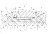
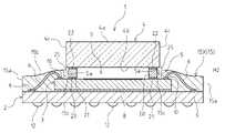
- the top and bottom in FIG. 1are the top and bottom in the image pickup apparatus 1.
- the image pickup device 1is a kind of semiconductor device, and is between the substrate 2, the image sensor 3 as an image pickup element, the glass 4 as a transparent member, and the image sensor 3 and the glass 4.
- a support portion 5 that intervenes and supports the glass 4 on the image sensor 3 and a bonding wire 6 as a plurality of connecting membersare provided.
- the image pickup apparatus 1has a package structure in which a glass 4 is mounted on an image sensor 3 via a support portion 5 and a cavity 7 is formed between the image sensor 3 and the glass 4.
- the glass 4is supported by the support portion 5 provided on the surface 3a, which is the surface on the light receiving side of the image sensor 3, so as to face the surface 3a of the image sensor 3.
- the support portion 5seals the periphery between the image sensor 3 and the glass 4 to form the cavity 7.
- the substrate 2is an organic substrate made of an organic material such as plastic, and is a circuit board on which a predetermined circuit is formed.
- the substrate 2may be another type of substrate such as a ceramic substrate formed of ceramic or the like as a material.
- the substrate 2has a front surface 2a on which the image sensor 3 is mounted and a back surface 2b which is a plate surface on the opposite side thereof.
- the image sensor 3is adhered to the surface 2a side of the substrate 2 by a joining material 8 which is an insulating or conductive adhesive or the like.
- the image sensor 3is mounted on the substrate 2, and the side opposite to the substrate 2 side is the light receiving surface side.
- the image sensor 3is a semiconductor element including a semiconductor substrate made of silicon (Si), which is an example of a semiconductor.
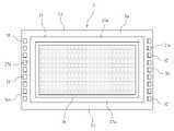
- the image sensor 3is a rectangular plate-shaped chip, and the front surface 3a side, which is the upper plate surface, is the light receiving surface side, and the plate surface on the opposite side is the back surface 3b.
- a plurality of light receiving elements (photoelectric conversion elements)are formed on the surface 3a side of the image sensor 3.
- the image sensor 3is a CMOS (Complementary Metal Oxide Semiconductor) type image sensor.
- the image sensor 3may be another image pickup device such as a CCD (Charge Coupled Device) type image sensor.
- the image sensor 3has a pixel portion 3c on the surface 3a side, which is a pixel region including a large number of pixels formed in a predetermined arrangement such as a Bayer array, as a light receiving portion, and is around the pixel portion 3c. Let the area of be the peripheral area. A predetermined peripheral circuit is formed in the peripheral region.
- the pixel unit 3cincludes an effective pixel region for generating, amplifying, and reading a signal charge by photoelectric conversion in each pixel.
- correlation double sampling (CDS: Correlated Double Sampling), signal amplification, and A / D (A / D)are performed for the pixel signal based on the signal charge generated according to the amount of received light in each pixel.
- Signal processingsuch as Analog / Digital) conversion is performed.
- the pixel of the pixel unit 3chas a photodiode as a photoelectric conversion unit having a photoelectric conversion function, and a plurality of pixel transistors.
- a color filter and an on-chip lensare attached to each pixel of the semiconductor substrate via an antireflection film made of an oxide film or the like, a flattening film made of an organic material, or the like. Correspondingly formed.
- the light incident on the on-chip lensis received by the photodiode through a color filter, a flattening film, or the like.
- the configuration of the image sensor 3 according to the present technologyis not particularly limited.
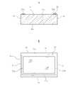
- the glass 4is an example of a transparent member serving as an optical window, has a rectangular plate-like outer shape, and is provided on the surface 3a side of the image sensor 3 in parallel with the image sensor 3 at a predetermined interval. ing.
- the glass 4has a back surface 4b which is an upper plate surface facing the image sensor 3 and a front surface 4a which is an upper surface opposite the back surface 4b.
- the glass 4is supported in a fixed state by the support portion 5 with respect to the image sensor 3.
- the glass 4transmits various types of light incident from an optical system such as a lens located above the glass 4.
- the light transmitted through the glass 4reaches the light receiving surface of the image sensor 3 through the cavity 7.
- the glass 4has a function of protecting the light receiving surface side of the image sensor 3.
- a plastic plate, a silicon plate that transmits only infrared light, or the likecan be used instead of the glass 4.
- the glass 4has an outer dimension in a plan view smaller than the same outer dimension in the image sensor 3, and is provided within the range of the outer shape of the image sensor 3 in a plan view. That is, the glass 4 has an external dimension that is one size smaller than that of the image sensor 3 in a plan view, and is provided so that the four rectangular edges are located inside the four edges of the image sensor 3. ing.
- the vertical dimension and the horizontal dimension of the glass 4are smaller than the vertical dimension and the horizontal dimension of the image sensor 3, respectively.
- the glass 4is arranged with respect to the image sensor 3 so that, for example, the centers in the outer shape in a plan view coincide with each other or substantially coincide with each other. That is, the glass 4 is provided at a position so that the peripheral edge portions along the four sides of the image sensor 3 protrude from the image sensor 3 around the glass 4 in a plan view.
- the support portion 5is interposed between the image sensor 3 and the glass 4, and forms a cavity 7 which is a closed space between the image sensor 3 and the glass 4.
- the support portion 5supports the image sensor 3 in a state where the glass 4 is separated from the image sensor 3, and forms a cavity 7 together with the image sensor 3 and the glass 4.
- the support portion 5is provided in the peripheral region so as to surround the pixel portion 3c on the surface 3a of the image sensor 3.
- the lower side of the support portion 5is connected to the front surface 3a of the image sensor 3, and the upper side is connected to the back surface 4b of the glass 4.
- the support portion 5functions as a sealing portion that airtightly seals the periphery of the cavity 7, and together with the glass 4, blocks the intrusion of moisture (water vapor), dust, and the like from the outside into the cavity 7.
- the package structure of the image pickup apparatus 1is sealed by the glass 4 and the support portion 5 in order to protect the image sensor 3 from the external environment such as water, humidity, and external force.
- the support portion 5is provided in a wall shape over the entire circumference along the outer shape of the image sensor 3 and the glass 4 in a plan view, and has a rectangular frame shape in a plan view and is formed in an endless shape.
- the support portion 5is provided at a position within the range of the outer shape of the glass 4 so as to be along the outer edge of the glass 4 in a plan view.
- the support portion 5is provided at a position slightly inside the side surface 4c of the glass 4. However, the support portion 5 may be provided so that its outer surface is substantially flush with the side surface 4c of the glass 4.
- the bonding wire 6is a conductive wire that electrically connects the substrate 2 and the image sensor 3.
- the bonding wire 6is a thin metal wire made of, for example, Au (gold), Cu (copper), Al (aluminum), or the like.
- the bonding wire 6electrically connects the electrode pad 9 formed on the surface 2a of the substrate 2 and the electrode pad 10 formed on the surface 3a of the image sensor 3.
- the bonding wire 6has a shape, for example, rising from the electrode pad 10 to form a convex top on the upper side and gently descending toward the electrode pad 9 side.
- a plurality of electrode pads 9are formed in a predetermined arrangement on the surface 2a of the substrate 2 on the outer portion of the mounting portion of the image sensor 3, and are connected to one end side of the bonding wire 6.
- a plurality of electrode pads 10are formed in a predetermined arrangement on the outer portion of the support portion 5 on the surface 3a of the image sensor 3, and receive the connection on the other end side of the bonding wire 6.
- the electrode pad 9 and the electrode pad 10As the material of the electrode pad 9 and the electrode pad 10, for example, an aluminum material or the like is used. Specifically, the electrode pad 9 and the electrode pad 10 are made of, for example, a nickel (Ni) plating layer and a gold (Au) plating layer on a layer portion such as copper (Cu), tungsten (W), and titanium (Ti). It is a coating of a plating layer. The electrode pad 9 and the electrode pad 10 are formed by appropriately using plating, sputtering, printing or other film forming methods.
- the plurality of electrode pads 9 of the substrate 2are connected to a plurality of terminal electrodes formed on the back surface 2b side of the substrate 2 via a predetermined wiring portion formed in the substrate 2.
- Solder balls 12are provided on each terminal electrode.
- the solder balls 12are formed, for example, in a two-dimensional grid-like arrangement along the rectangular outer shape of the image sensor 3.
- the solder ball 12is a terminal for making an electrical connection to a circuit board on which the image pickup device 1 is mounted in an electronic device on which the image pickup device 1 is mounted.
- the cavity 7is a flat rectangular space portion between the image sensor 3 and the glass 4.
- the cavity 7can be filled with nitrogen gas ( N2 gas), which is an inert gas, or the inside of the cavity 7 can be in a vacuum state.
- N2 gasnitrogen gas
- the image pickup apparatus 1includes a coating resin portion 15 provided around the image sensor 3 on the substrate 2.
- the coating resin portion 15is a resin portion that covers the connection portions of the bonding wire 6 and the bonding wire 6 to the substrate 2 and the image sensor 3, respectively. That is, the coating resin portion 15 is formed so as to cover the bonding wire 6, the connection portion of the bonding wire 6 to the electrode pad 9 of the substrate 2, and the connection portion of the bonding wire 6 to the electrode pad 10 of the image sensor 3. ing.
- the coated resin portion 15has a side surface portion 15a that is flush with the side surface 2c of the substrate 2, and an upper surface portion 15b that is located at a position lower than the surface 4a of the glass 4.
- the upper surface portion 15bhas a shape that gradually decreases from the inside (glass 4 side) to the outside.
- the coating resin portion 15covers and seals the periphery of the image sensor 3 and the glass 4 on the substrate 2 over the entire circumference. Specifically, in the coated resin portion 15, the peripheral portion of the surface 2a of the substrate 2 on which the electrode pad 9 is formed, the side surface 3d of the image sensor 3, and the electrode pad 10 are formed in a state where the entire bonding wire 6 is filled. It covers the peripheral edge of the surface 3a, the outer side surface of the support 5, and the peripheral edge and the side surface 4c of the back surface 4b of the glass 4.
- the coated resin portion 15is formed by a potting process using a dispenser.
- the coated resin portion 15is formed by applying the resin material to be the coated resin portion 15 to a predetermined portion while being discharged from the nozzle of the dispenser and then curing the resin material.
- the coated resin portion 15may be a portion formed by, for example, injection molding using a mold.
- the resin material of the coating resin portion 15is, for example, a thermosetting resin such as a phenol-based resin, a silicone-based resin, an acrylic-based resin, an epoxy-based resin, a urethane-based resin, a silicon resin, or a polyetheramide-based resin.
- the light transmitted through the glass 4passes through the cavity 7 and is received by the light receiving element constituting each pixel arranged in the pixel portion 3c of the image sensor 3. Is detected.
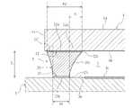
- the support portion 5 included in the image pickup apparatus 1will be described.
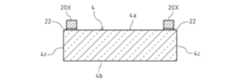
- the support portion 5includes a solder layer portion 20 formed of solder. Further, the support portion 5 has an element-side connection layer portion 21 as a first connection layer portion which is a connection portion to the image sensor 3 and a glass-side connection layer as a second connection layer portion which is a connection portion to the glass 4. Includes part 22.
- the solder layer portion 20is connected to the front surface 3a side of the image sensor 3 via the element side connection layer portion 21, and is connected to the back surface 4b side of the glass 4 via the glass side connection layer portion 22. ..
- the solder layer portion 20, the element side connection layer portion 21, and the glass side connection layer portion 22, which are the layer portions forming the support portion 5,have a common plan view outer shape corresponding to the plan view outer shape of the support portion 5.
- the solder layer portion 20is a layer portion formed of solder as a material and formed in a rectangular frame shape in a plan view, and forms substantially the entire support portion 5 excluding the upper and lower end face portions of the support portion 5.
- the solder layer portion 20has four linear side portions 20a having a rectangular shape corresponding to the rectangular frame-shaped outer shape of the support portion 5 (see FIG. 3).
- the element-side connection layer portion 21is a layer portion that forms an end surface portion on the lower side of the support portion 5 in the support portion 5 formed in a rectangular frame shape in a plan view, and receives the connection on the lower side of the solder layer portion 20. It becomes a part.
- the element-side connecting layer portion 21has four linear side portions 21a having a rectangular shape corresponding to the rectangular frame-shaped outer shape of the support portion 5 in a plan view (see FIG. 2).
- the element-side connection layer portion 21is formed with respect to the surface 3a of the image sensor 3.
- the element-side connection layer portion 21is formed on the surface 3a of the image sensor 3 in a peripheral region where the support portion 5 is located. That is, the element-side connection layer portion 21 is formed in a rectangular frame shape at a portion between the pixel portion 3c and the arrangement region of the electrode pad 10.
- the element-side connection layer portion 21is formed, for example, as a plating layer of nickel (Ni), gold (Au) or the like, or as a portion having a plating layer of nickel (Ni), gold (Au) or the like.
- a nickel (Ni) plating layer and a gold (Au) plating on a layer portionsuch as copper (Cu), tungsten (W), and titanium (Ti). It is a film of a layer.
- the element-side connection layer portion 21is formed by appropriately using a film forming method such as plating, sputtering, vapor deposition, printing or the like.
- the element-side connection layer portion 21is formed simultaneously with the electrode pad 10, for example, as a layer portion common to the electrode pad 10 of the image sensor 3.
- the element-side connection layer portion 21may be a portion formed by a step different from the step of forming the electrode pad 10.
- the glass side connection layer portion 22is a layer portion forming an upper end surface portion of the support portion 5 in the support portion 5 formed in a rectangular frame shape in a plan view, and is a portion that receives the connection on the upper side of the solder layer portion 20. Become. Similar to the element-side connecting layer portion 21, the glass-side connecting layer portion 22 has four linear sides having a predetermined width forming a rectangular shape corresponding to the rectangular frame-shaped outer shape of the supporting portion 5 in a plan view. It has a portion 22a (see FIG. 6B).
- the glass side connecting layer portion 22is formed with respect to the back surface 4b of the glass 4. Similar to the element-side connection layer portion 21, the glass-side connection layer portion 22 is formed as a portion having a plating layer such as nickel (Ni) or gold (Au) or a plating layer. The glass side connection layer portion 22 is formed by plating, sputtering, or the like.
- a step of preparing the substrate 2is performed.
- the substrate 2is obtained, for example, by dicing a substrate member in which a plurality of substrate portions to be the substrate 2 in the image pickup apparatus 1 are two-dimensionally connected to each other.
- a plurality of electrode pads 9are formed on the surface 2a of the substrate 2.
- a step of preparing an image sensor 3 having an element-side connection layer portion 21 formed on the light-receiving surface sideis performed as an image pickup element mounted on the substrate 2.
- a step of forming the element-side connecting layer portion 21 on the surface 3a side of the image sensor 3is performed.
- a frame-shaped element-side connection layer portion 21is formed on the surface 3a side by using a method such as plating or sputtering (see FIG. 2). Further, on the surface 3a of the image sensor 3, a plurality of electrode pads 10 are formed by using plating or the like by the same step as the forming step of the element-side connecting layer portion 21 or by another step.
- a glass 4 having a solder portion 20X formed on one side via a glass side connecting layer portion 22 having a shape corresponding to the element side connecting layer portion 21is prepared.
- the processis performed (see FIG. 7).
- a step of forming the glass-side connecting layer portion 22 on the back surface 4b side of the glass 4 and a step of forming a soldering portion 20X made of solder on the glass-side connecting layer portion 22are performed.
- a frame-shaped glass-side connecting layer portion 22is formed on the back surface 4b side by using a method such as plating or sputtering (see FIG. 2).
- a step of forming the solder portion 20X with respect to the glass side connecting layer portion 22is performed as shown in FIG. 7.
- the solder portion 20Xis a portion that becomes the solder layer portion 20 of the support portion 5 in the image pickup apparatus 1, and is formed entirely on the surface of the glass side connection layer portion 22. That is, the solder portion 20X is formed in a rectangular frame shape corresponding to the shape of the glass side connection layer portion 22.
- the solder portion 20Xis formed to a predetermined thickness by solder plating. However, the solder portion 20X may be formed by another method such as printing. The solder portion 20X is formed so that the solder layer portion 20 is thicker than the element side connection layer portion 21 and the glass side connection layer portion 22.
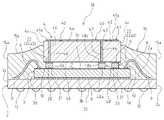
- the assembly processis performed.
- a step of mounting the image sensor 3 on the substrate 2is performed. That is, a die-bonding step is performed in which the image sensor 3 on which the element-side connecting layer portion 21 is formed is die-bonded to the substrate 2 prepared as described above.
- the substrate 2is adhered to a predetermined mounting portion on the surface 2a with an insulating or conductive resin paste or the like as the bonding material 8.
- a step of providing a bonding wire 6 that electrically connects the substrate 2 and the image sensor 3is performed.
- a wire bonding stepis performed in which the electrode pad 9 of the substrate 2 and the electrode pad 10 of the image sensor 3 are connected by a bonding wire 6 and electrically connected.
- the glass 4is placed on the image sensor 3 so that the solder portion 20X is located on the element side connection layer portion 21, the solder portion 20X is melted, and the solder portion 20X is combined with the image sensor 3.
- the step of forming the support portion 5 that is interposed between the glass 4 and the glass 4 to form the cavity 7is performed.
- the glass 4is set on the image sensor 3 by a chip mounter or the like so that the element-side connection layer portion 21 and the solder portion 20X are aligned. After that, reflow is performed at a predetermined temperature. That is, the solder portion 20X provided for the glass 4 via the glass side connection layer portion 22 is used, and the glass 4 is reflow mounted on the image sensor 3 having the element side connection layer portion 21. As a result, the solder portion 20X is once melted and solidified to become the solder layer portion 20, a support portion 5 for supporting the glass 4 is formed on the image sensor 3, and the image sensor 3 and the glass 4 are fixed to each other. Will be.
- nitrogen gascan be sealed in the cavity 7. That is, by performing the reflow process in the nitrogen atmosphere using the nitrogen atmosphere reflow furnace, the nitrogen gas is sealed in the cavity 7. As a result, in the image pickup apparatus 1, a package structure in which nitrogen gas is sealed in the cavity 7 can be obtained.
- the inside of the cavity 7can be evacuated. That is, by performing the reflow process in a vacuum using a vacuum reflow furnace, the inside of the cavity 7 becomes a vacuum state. As a result, in the image pickup apparatus 1, a package structure in which the inside of the cavity 7 is in a vacuum state can be obtained.
- a step of forming the coating resin portion 15is performed as shown in FIG. 8D.
- the coating resin portion 15is formed so as to cover the bonding wire 6 and the connection portion of the bonding wire 6 to the substrate 2 and the image sensor 3 around the image sensor 3 on the substrate 2.
- the coated resin portion 15is formed of a predetermined resin material by potting processing using a dispenser, and a wire sealing step of sealing the bonding wire 6 is performed.
- the coated resin portion 15may be formed by injection molding using, for example, a mold.
- the coating resin portion 15is formed so as to cover most of the side surface 4c with respect to the glass 4 in the thickness direction of the glass 4.
- a step of forming a plurality of solder balls 12 on the back surface 2b side of the substrate 2is performed.
- a ball mounting step of mounting the solder balls 12 on each of the plurality of terminal electrodes formed on the back surface 2b side of the substrate 2is performed.
- the image pickup apparatus 1 as shown in FIG. 1can be obtained.
- the image sensor 3can be miniaturized in a configuration in which the glass 4 is mounted with a gap on the image sensor 3, and the package structure can be obtained. Can be miniaturized.
- the pixelsmay be thickened at the start and end points of the applied resin and bleeding may occur.
- the resinIn order to prevent the resin from being applied to the portion 3c, it is necessary to apply the resin to a portion at a certain distance from the pixel portion 3c.
- the image pickup apparatus 1is provided with a GOC structure in which the image sensor 3 and the glass 4 are directly sealed with solder by having a support portion 5 whose majority is a solder layer portion 20. According to such a configuration, it is not necessary to consider the problem of thickening of the start and end points of the resin and bleeding that occur when the support portion is made of resin, and the distance between the pixel portion 3c and the electrode pad 10 is shortened by design. be able to. As a result, the image sensor 3 can be miniaturized, the package size can be reduced, and the cost can be reduced.
- the distance between the pixel portion 3c and the electrode pad 10can be shortened, and the image sensor 3 can be miniaturized.
- the qualitycan be effectively prevented from invading the inside of the cavity 7 as compared with the case where the support portion is made of resin.
- the reliability of the soldercan be improved.
- moisturecan be prevented from entering the inside of the cavity 7, so that the internal pressure of the cavity 7 during the reflow process performed in the manufacturing process of the image pickup apparatus 1 can be prevented.
- the image pickup apparatus 1includes a coating resin portion 15 that covers the bonding wire 6 around the image sensor 3 on the substrate 2. According to such a configuration, the amount of the resin forming the coated resin portion 15 can be minimized, and the degree of freedom in resin selection can be improved.
- the solder layer portion 20 constituting the support portion 5can secure sufficient strength for supporting the glass 4 with respect to the image sensor 3, the glass 4 is fixed by the coating resin portion 15. No need. Therefore, the coated resin portion 15 may be formed so as to cover the bonding wire 6 and the connecting portion thereof, and the amount of resin can be minimized. Further, when it is not necessary to consider the fixing of the glass 4 by the coated resin portion 15, the types of resins applicable to the resin forming the coated resin portion 15 increase, so that the range of resin selection can be expanded. This makes it possible to reduce costs and the like.
- the glass 4is smaller than the image sensor 3 and is provided within the range of the image sensor 3 in a plan view. According to such a configuration, a space for wiring the bonding wire 6 can be easily secured. As a result, the package structure can be made compact.
- nitrogen gascan be sealed in the cavity 7 or the inside of the cavity 7 can be in a vacuum state.
- Modification example of the image pickup apparatus according to the first embodiment>A modified example of the image pickup apparatus 1 according to the present embodiment will be described.
- the modified examples 1 and the modified example 2 described beloware modified examples of the forming mode of the coated resin portion 15.
- the modified example 3is a modified example of the configuration of the support portion 5.
- the coating resin portion 15Xis formed at a position lower than that of the glass 4, and is not in contact with the side surface 4c of the glass 4. That is, in the first modification, the height position H1 at the uppermost end of the upper surface portion 15b of the coated resin portion 15X is lower than the back surface 4b of the glass 4. Specifically, the coating resin portion 15X covers the entire bonding wire 6 and its connection portion, and the inner edge (inner peripheral side) having the highest height position is the upper end of the solder layer portion 20 of the support portion 5. The height is set to the vicinity of the portion, and the solder layer portion 20 is in contact with the outer side surface.
- the glass 4can be adhered to the image sensor 3 with high strength by the solder layer portion 20 constituting the support portion 5, so that the glass 4 is formed by the coating resin portion 15 covering the bonding wire 6. There is no need to fix. Therefore, unlike the coating resin portion 15X of the modification 1, the coating resin portion 15 can be provided without contacting the glass 4.
- the coating resin portion 15when the coating resin portion 15 is in contact with the side surface 4c of the glass 4, it is possible to suppress the occurrence of cracks on the side surface 4c of the glass 4, which may be a problem in the temperature cycle test. Reliability can be improved. Further, the amount of the resin forming the coated resin portion 15 can be reduced, and the cost can be reduced.
- the coating resin portion 15Yis formed at a position lower than that of the glass 4, does not contact the side surface 4c of the glass 4, and also contacts the support portion 5. Not done.
- the height position H2 at the uppermost end of the upper surface portion 15b of the coated resin portion 15Yis lower than the back surface 4b of the glass 4.
- the coating resin portion 15Yis formed on the inner side (inner peripheral side) so as to separate the gap 25 from the outer side surface 5a of the support portion 5.
- the coating resin portion 15Ycovers the entire bonding wire 6 and its connection portion, and has an inner side end surface 15c that faces the outer side surface 5a of the support portion 5 with a gap 25. ..
- the outer side surface 5a of the support portion 5is a surface portion formed by the outer side surface of the solder layer portion 20, the element side connection layer portion 21, and the glass side connection layer portion 22.
- the generation of cracks on the side surface 4c of the glass 4can be suppressed, the reliability of the apparatus can be improved, and the coating resin portion 15 can be obtained, as in the configuration of the modified example 1.
- the amount of resin forming the resincan be effectively reduced.
- the support portion 5includes a copper layer portion 27 which is a metal layer portion formed of copper or an alloy containing copper on the glass 4 side of the solder layer portion 20. ..
- the copper layer portion 27is provided in place of the glass side connection layer portion 22, and constitutes a connection portion of the support portion 5 to the glass 4.
- a solder layer portion 20is formed on the lower side of the copper layer portion 27. That is, the solder layer portion 20 is provided between the element side connection layer portion 21 and the copper layer portion 27.
- the copper layer portion 27is a layer portion that forms the upper part of the support portion 5 in the support portion 5 formed in a rectangular frame shape in a plan view, and is a portion that receives the connection on the upper side of the solder layer portion 20. Similar to the element-side connecting layer portion 21, the copper layer portion 27 has four linear side portions having a rectangular shape corresponding to the rectangular frame-shaped outer shape of the support portion 5 in a plan view.
- the copper layer portion 27is formed on the back surface 4b of the glass 4.
- the copper layer portion 27is formed by plating with copper (Cu) or a copper alloy, sputtering, vapor deposition, or the like.
- the copper layer portion 27is, for example, half or substantially half the thickness of the entire thickness S1 of the support portion 5. It is formed.
- the total thickness S1 of the support portion 5corresponds to the distance between the front surface 3a of the image sensor 3 and the back surface 4b of the glass 4.
- the copper layer portion 27is formed as a layer portion thicker than the solder layer portion 20.
- the support portion 5is provided in a copper layer portion 27 having a thickness of half or substantially half of the total thickness S1 of the support portion 5, and a support portion provided under the copper layer portion 27. It has a solder layer portion 20 that is thinner than half the total thickness S1 of 5, and an element-side connection layer portion 21 that connects the solder layer portion 20 to the image sensor 3.
- the copper layer portion 27may be formed as a layer portion having substantially the same thickness as the solder layer portion 20, or may be formed as a layer portion having a thickness of a majority of the total thickness S1 of the support portion 5.
- a frame-shaped copper layer portion 27is formed on the back surface 4b side of the glass 4 by a method such as plating or sputtering. It is formed.
- a step of forming the solder portion 20X on the copper layer portion 27is performed.
- the solder portion 20Xis formed so that the thickness of the solder layer portion 20 after reflow is thinner than half of the total thickness S1 of the support portion 5.
- the solder portion 20Xis formed on the entire surface of the copper layer portion 27, and is formed in a rectangular frame shape corresponding to the shape of the copper layer portion 27.
- the solder layer portion 20occupies the entire thickness of the support portion 5.
- the thickness of the soldercan be reduced.
- the layer thickness of the solder portion 20Xwhich is the molten portion, can be reduced in the reflow process, which is the step of forming the support portion 5, so that the image sensor 3 and the glass 4 defined by the layer thickness of the support portion 5 can be reduced. It is possible to facilitate the control of the gap between the two.
- the surface of the copper layer portion 27may be coated with a plating layer such as nickel (Ni) or gold (Au). In this case, the plating layer on the surface of the copper layer portion 27 becomes the joint surface portion with the solder layer portion 20.
- a plating layersuch as nickel (Ni) or gold (Au).
- the copper layer portion 27may be provided on the image sensor 3 side with respect to the solder layer portion 20.
- the copper layer portion 27is formed by plating or the like on the surface 3a of the image sensor 3 instead of the element-side connection layer portion 21, and constitutes a connection portion of the support portion 5 to the image sensor 3.
- the copper layer portion 27may be provided on both sides of the glass 4 side and the image sensor 3 side.
- the solder layer portion 20is interposed between the upper and lower copper layer portions 27.
- the copper layer portion 27may be formed on at least one of the upper side and the lower side of the solder layer portion 20.
- Configuration example of the image pickup device according to the second embodiment>A configuration example of the image pickup apparatus according to the second embodiment of the present technology will be described.
- the image pickup apparatus according to the present embodimenthas a different configuration of the support portion 5 in comparison with the first embodiment.
- the same reference numeralsare used for the parts common to the first embodiment, and the description thereof will be omitted as appropriate.
- the support portion 5has different width dimensions of the element side connection layer portion 21 and the glass side connection layer portion 22 so that the glass side connection layer portion 22 is different from each other.
- the inner edge of the elementis positioned inside the inner edge of the element-side connection layer portion 21.
- the "inside” of the element-side connection layer portion 21 and the glass-side connection layer portion 22is inside the cavity 7, and the support portion 5 shown in FIG. 12 is on the right side. Therefore, the "outside” of the element-side connecting layer portion 21 and the glass-side connecting layer portion 22 is the outside with respect to the cavity 7, and the support portion 5 shown in FIG. 12 is on the left side.
- the element-side connecting layer portion 21 and the glass-side connecting layer portion 22are each formed in a frame shape with a predetermined width as a planar shape.
- the width A2 of each side portion 22a forming the frame shape of the glass side connection layer portion 22is wider than the width A1 of each side portion 21a forming the frame shape of the element side connection layer portion 21.
- the element-side connecting layer portion 21 and the glass-side connecting layer portion 22are formed so that the outer edges of the element-side connecting layer portion 21 and the glass-side connecting layer portion 22 coincide with or substantially coincide with each other in a plan view.
- the end surface 22c forming the inner edge of the glass side connection layer portion 22is located inside the end surface 21c forming the inner edge of the element side connection layer portion 21. I'm letting you.
- the glass-side connection layer portion 22is projected from the inner edge of the element-side connection layer portion 21 projected vertically to the glass-side connection layer portion 22 in relation to the element-side connection layer portion 21. It has an extending portion 22d that is a portion that protrudes inward. As shown in FIG. 13, the extending portion 22d is an inner edge portion of the glass side connecting layer portion 22 that forms the end surface 22c on the inner peripheral side, and is entirely along the frame shape of the glass side connecting layer portion 22. It is formed over the circumference. In FIG. 13, the end face 21c forming the inner outer shape of the element-side connecting layer portion 21 is shown by a two-dot chain line.
- the vertical direction between the inner end faces 22c of the side portions 22a of the glass-side connecting layer portion 22 facing each other in the vertical directionis smaller than the vertical dimension C1 between the inner end faces 21c of the side portions 21a of the element-side connecting layer portions 21 facing in the vertical direction.
- the vertical dimension B2 between the inner end faces 22c of the side portion 22a of the glass side connecting layer portion 22 facing in the lateral directionis the inside of the side portion 21a of the element side connecting layer portion 21 facing in the lateral direction. It is smaller than the vertical dimension C2 between the end faces 21c.
- the solder layer portion 20has a shape corresponding to the formation region of the element side connection layer portion 21 and the glass side connection layer portion 22 due to the surface tension of the solder or the like.
- the solder layer portion 20has an inner side surface 20c from above. The surface is gradually inclined from the inside to the outside toward the lower side (see FIG. 12). That is, the inner side surface 20c is inclined so as to widen the inner space portion of the frame-shaped solder layer portion 20 downward.
- the inner side surface 20c of the solder layer portion 20has a curved surface shape having a concave shape in a side cross-sectional view.
- the glass side connection layer portion 22 located above the element side connection layer portion 21 formed on the surface 3a of the image sensor 3is inside. It has an extension portion 22d to. With such a configuration, it is possible to suppress the incident light transmitted through the glass 4 from hitting the inner side surface 20c of the solder layer portion 20, which is caused by the reflected light from the inner side surface 20c incident on the pixel portion 3c. It is possible to suppress the generation of noise such as so-called flare.
- the incident light L1 transmitted through the glass 4easily hits the inner side surface 20d of the solder layer portion 20, and the reflected light.
- L2is incident on the pixel portion 3c.
- the reflected light L2 incident on the pixel portion 3ccauses noise such as flare in the image.
- the support portion that supports the glass 4is a portion made entirely of resin, in order to prevent incident light on the inner side surface of the support portion, light shielding such as a metal film or an organic film that reflects light on the glass 4 is shielded. It is necessary to take measures such as forming a film.
- the extension portion 22dis formed on the glass side connection layer portion 22 by adjusting the width dimension of the upper and lower connection layer portions (21, 22) of the solder layer portion 20.
- the extending portion 22dcan block light by reflecting the incident light D1 that is about to hit the inner surface of the solder layer portion 20 (see FIG. 12).
- the inner side surface 20c of the solder layer portion 20is gradually inclined from the inside to the outside from the upper side to the lower side. It becomes a surface. As a result, it is possible to prevent the incident light D2 from passing through the glass 4 and hitting the inner side surface 20c of the solder layer portion 20 in the cavity 7 (see FIG. 12). Further, even when the light transmitted through the glass 4 hits the inner side surface 20c of the solder layer portion 20, the inclined shape of the inner side surface 20c suppresses the reflected light from the inner side surface 20d from reaching the pixel portion 3c. can do.
- the incident lighthits the inner side surface 20c of the solder layer portion 20, and the incident light hitting the inner side surface 20c is reflected and incident on the pixel portion 3c. Can be suppressed. As a result, noise can be reduced and the quality of the image obtained by the image pickup apparatus 1 can be improved.
- the extension length of the extension portion 22d in the glass side connection layer portion 22 with respect to the element side connection layer portion 21, that is, the width dimension X 1 of the extension portion 22dis determined based on, for example, the following relationship.
- the magnitude of the incident angle of the incident light that can cause noise with respect to the pixel portion 3cis ⁇ 1
- the thickness of the support portion 5, that is, the front surface 3a of the image sensor 3 and the back surface 4b of the glass 4When the length of the interval between them is T 1 , the following equation (1) holds.
- the incident angle ⁇ 1is an angle of the incident light with respect to the vertical direction in the side sectional view as shown in FIG.
- the width dimension X 1 of the extending portion 22dis set to a length of 58 ⁇ m or more within a range in which the glass side connecting layer portion 22 does not cover the pixel portion 3c. Is preferable.
- the support portion 5has the same width dimension of the element side connection layer portion 21 and the glass side connection layer portion 22, and the width directions of both connection layer portions (in FIG. 15). By shifting the position (in the left-right direction), the inner edge of the glass-side connecting layer portion 22 is positioned inside the inner edge of the element-side connecting layer portion 21.
- the width A2 of each side portion 22a of the glass side connection layer portion 22is the same as the width A1 of each side portion 21a of the element side connection layer portion 21. Then, the glass side connection layer portion 22 is formed inside the element side connection layer portion 21, so that the glass side connection layer portion 22 has the inner end surface 22c of the element side connection layer portion 21 in the plane direction. It is located inside the end surface 21c on the inside of the.
- the glass-side connection layer portion 22is projected from the inner edge of the element-side connection layer portion 21 projected vertically to the glass-side connection layer portion 22 in relation to the element-side connection layer portion 21. It has a protruding portion 22e that is a portion that protrudes inward. Further, the element-side connection layer portion 21 is projected from the outer edge of the glass-side connection layer portion 22 projected vertically to the element-side connection layer portion 21 in relation to the glass-side connection layer portion 22. It has a protruding portion 21e that is a portion that protrudes to the outside.
- the element-side connecting layer portion 21 and the glass-side connecting layer portion 22have a common positional relationship with respect to the four side portions 21a and 22a forming the frame shape. Therefore, in the first modification, the glass-side connecting layer portion 22 is generally inward with respect to the element-side connecting layer portion 21 while having the same width of each side portion in relation to the element-side connecting layer portion 21. It is formed. In the configuration of the first modification, the width dimension of the protruding portion 22e inward of the glass side connecting layer portion 22 is the width dimension X 1 in the above formula (1).
- noisecan be reduced by the inward protruding portion 22e of the glass side connecting layer portion 22 as in the case where the glass side connecting layer portion 22 has the extending portion 22d.
- the connection area of the supporting portion 5 to the image sensor 3can be expanded by the amount that the element-side connecting layer portion 21 has the protruding portion 21e to the outside, so that the support is supported. It becomes easy to secure the joint strength of the portion 5.
- the support portion 5has an extension portion 22d provided on the glass side connection layer portion 22 (see FIG. 12), and the support portion 5 has an outer edge of the element side connection layer portion 21. Is located inside the outer edge of the glass-side connecting layer portion 22.
- the width A2 of each side portion 22a of the glass side connection layer portion 22is wider than the width A1 of each side portion 21a of the element side connection layer portion 21. Then, the glass-side connection layer portion 22 is projected from the outer edge of the element-side connection layer portion 21 projected vertically to the glass-side connection layer portion 22 in relation to the element-side connection layer portion 21. It has a protruding portion 22f that is a portion that protrudes to the outside.
- the element-side connection layer portion 21 and the glass-side connection layer portion 22have a common positional relationship with respect to the four side portions 21a and 22a forming the frame shape. Therefore, in the second modification, the entire element-side connecting layer portion 21 is included in the formation range of the glass-side connecting layer portion 22 in a plan view.
- the noisecan be reduced by the extending portion 22d of the glass side connecting layer portion 22, and the area occupied by the element side connecting layer portion 21 on the surface 3a of the image sensor 3 can be reduced. Therefore, it is possible to reduce the size of the image sensor 3.
- the image pickup apparatus 1A according to the present embodimentincludes a fine wiring portion 30 provided on the back surface 4b, which is the surface of the glass 4 on the cavity 7 side.
- the fine wiring portion 30is connected to the GND potential of the image sensor 3 via the support portion 5.
- the fine wiring portion 30is formed in a mesh shape on the back surface 4b side of the glass 4 as the same layer portion as the glass side connection layer portion 22. Therefore, the fine wiring portion 30 is formed simultaneously with the glass side connection layer portion 22 on the back surface 4b of the glass 4 by using the same material as the glass side connection layer portion 22, for example, by plating or sputtering. However, the fine wiring portion 30 may be a portion formed of a material different from that of the glass side connection layer portion 22.
- the fine wiring portion 30has a plurality of linear wiring portions (31, 32) arranged in a grid pattern along the frame shape of the glass side connection layer portion 22 inside the glass side connection layer portion 22. Have.
- the fine wiring portion 30has a plurality of first wiring portions 31 along the lateral direction (vertical direction in FIG. 18) in the plate surface shape of the glass 4 and the plate surface shape of the glass 4 as a plurality of wiring portions forming a grid pattern. It has a plurality of second wiring portions 32 along the longitudinal direction (left-right direction in FIG. 18). The plurality of first wiring portions 31 and the plurality of second wiring portions 32 are arranged in parallel at predetermined intervals. The first wiring portion 31 and the second wiring portion 32 are orthogonal to each other and form an intersection 33. These wiring portions are formed with a line width narrower than the width of the side portion 22a of the glass side connection layer portion 22.
- the first wiring portion 31connects both end portions to a pair of longitudinal side portions 22a1 of the side portions 22a of the glass side connection layer portion 22 facing each other in the lateral direction of the glass 4. That is, the first wiring portion 31 is formed as the same layer portion as the glass side connection layer portion 22 so as to be erected between the pair of side portions 22a1.
- the second wiring portion 32connects both end portions to a pair of short side portions 22a2 of the side portions 22a of the glass side connection layer portion 22 facing each other in the longitudinal direction of the glass 4. That is, the second wiring portion 32 is formed as the same layer portion as the glass side connection layer portion 22 so as to be erected between the pair of side portions 22a2.
- the fine wiring portion 30is formed as a portion electrically connected to the glass side connection layer portion 22 forming the upper end of the support portion 5, and is connected to the GND potential which is a constant potential of the image sensor 3. ing. That is, in the present embodiment, the element-side connection layer portion 21 forming the lower end of the support portion 5 is formed as an electric conductor wiring portion connected to the GND potential of the image sensor 3 via a predetermined wiring portion.
- the solder layer portion 20 formed on the element-side connection layer portion 21is a portion that electrically connects the element-side connection layer portion 21 and the glass-side connection layer portion 22.
- the fine wiring portion 30is connected to the GND potential of the image sensor 3 via the conductive portion including the glass side connection layer portion 22, the solder layer portion 20, and the element side connection layer portion 21 constituting the support portion 5.
- the support portion 5 and the fine wiring portion 30are both portions of the same potential of the GND potential.
- the first wiring unit 31 and the second wiring unit 32are formed as fine wiring that does not affect the image obtained by the image sensor 3.
- the first wiring portion 31 and the second wiring portion 32are formed, for example, with a line width of 0.15 to 1 ⁇ m, and preferably a line having a line width of 0.15 to 0.5 ⁇ m that is invisible to the naked eye. Formed in width.
- the thickness of the first wiring portion 31 and the second wiring portion 32is, for example, 50 nm to 1 ⁇ m.
- the pitch between the wiring portions of the plurality of first wiring portions 31 and the plurality of second wiring portions 32is, for example, 2 to 10 ⁇ m.
- the element side connection layer portion 21is connected to the GND potential of the image sensor 3 via a predetermined wiring portion in the step of preparing the image sensor 3. It is formed as a part that has been made.
- the step of preparing the glass 4includes a step of forming a fine wiring portion 30 on the back surface 4b of the glass 4.
- the fine wiring portion 30is formed simultaneously with the glass side connection layer portion 22 by plating, sputtering, or the like in the step of forming the glass side connection layer portion 22.
- the fine wiring portion 30may be formed in a process different from the step of forming the glass side connection layer portion 22.
- the fine wiring portion 30may be formed of a material different from the material forming the glass side connection layer portion 22.
- the other stepsare the same as the manufacturing method of the image pickup apparatus 1 of the first embodiment.
- electromagnetic noise incident from the surface 4a of the glass 4can be shielded, and the image sensor 3 can be used.
- the affected electromagnetic noisecan be reduced.
- electromagnetic noisemay be incident on the image pickup device 1A from the surface 4a side of the glass 4 (see arrow P1).
- the electromagnetic noise incident on the glass 4propagates in the glass 4 and is radiated (see arrow P2), which may adversely affect the sensor characteristics of the image sensor 3.
- the fine wiring portion 30is arranged on the back surface 4b of the glass 4 and connected to the GND potential on the image sensor 3, so that the incident light on the pixel portion 3c is obtained. It is possible to absorb and shield the electromagnetic noise incident on the glass 4 without blocking the image sensor 3, and it is possible to reduce the influence of the electromagnetic noise on the image sensor 3. This makes it possible to improve the noise immunity of the image pickup apparatus 1A.
- the wiring portion group of the first wiring portion 31 and the second wiring portion 32 forming the fine wiring portion 30may be formed in a mesh shape, for example, in an oblique direction with respect to the frame shape of the glass side connection layer portion 22. May be formed in.
- the image pickup apparatus 1B according to the present embodimentincludes a heat generating fine wiring portion 40 provided on the surface 4a, which is a surface opposite to the cavity 7 side of the glass 4.
- the heat generation fine wiring unit 40is a wiring unit that is electrically connected to the support unit 5 and generates heat by receiving a current supply from the image sensor 3.
- the heat-generating fine wiring portion 40is formed as a layered portion on the surface 4a of the glass 4 by, for example, plating or sputtering using the same material as the glass side connection layer portion 22.
- the heat generation fine wiring portion 40may be a portion formed of a material different from that of the glass side connection layer portion 22.
- the heat generation fine wiring portion 40has an outer frame portion 41, a fine wiring portion 42, and a connection portion 43.
- the outer frame portion 41, the fine wiring portion 42, and the connection portion 43form a heat-generating fine wiring portion 40 as an integrally continuous electric conductor wiring portion.
- the outer frame portion 41is formed in a rectangular frame shape along the outer shape of the glass 4, and has four linear side portions 41a having a predetermined width forming a rectangular shape.
- the outer frame portion 41has the same shape and dimensions as, for example, the glass side connecting layer portion 22, and is formed so as to overlap the glass side connecting layer portion 22 in a plan view.
- the fine wiring portion 42is a fine linear wiring portion formed in a spiral shape while forming a right-angled corner portion by a plurality of linear portions along the frame shape of the outer frame portion 41.
- the fine wiring portion 42is formed with a line width narrower than the width of the side portion 41a of the outer frame portion 41.
- the fine wiring portion 42connects one end of the spiral shape located on the outer peripheral side to the outer frame portion 41. One end of the fine wiring portion 42 is connected to the vicinity of one corner portion (lower left corner portion in FIG. 20) of the outer frame portion 41. The fine wiring portion 42 connects the other end portion located on the inner peripheral side of the spiral shape to the connection portion 43.
- the connection portion 43is a pad-shaped wiring portion having a square shape.
- the connecting portion 43has, for example, a square shape having a side length equal to the width dimension of the side portion 41a of the outer frame portion 41.
- the connecting portion 43is formed at a position corresponding to a peripheral region which is an outer region of the pixel portion 3c of the image sensor 3 in a plan view. In the example shown in FIG. 20, the connecting portion 43 is formed at a position substantially at the center of the glass 4 in the lateral direction and at a position closer to the right side in the longitudinal direction of the glass 4.
- the heat generation fine wiring portion 40As described above, in the heat generation fine wiring portion 40, one end side of the fine wiring portion 42 is connected to the outer frame portion 41, and the other end side of the fine wiring portion 42 is connected to the connection portion 43.
- the heat generation fine wiring portion 40is electrically connected to the support portion 5 by a first through wiring portion 46 which is a first connection wiring portion provided on the glass 4.
- the first through wiring portion 46is a wiring portion embedded in the first through hole 4d formed so as to penetrate the glass 4 in the plate thickness direction.
- the lower end side of the first through wiring portion 46is electrically connected to the glass side connection layer portion 22, and the upper end side is electrically connected to the outer frame portion 41 of the heat generation fine wiring portion 40. ..
- the first through wiring portion 46is formed by plating, sputtering, or the like, for example, using the same material as the glass side connection layer portion 22.
- the first through hole 4dis a rectangular through hole smaller than the width of the side portion 41a, and the first through wiring portion 46 is formed in a square columnar shape.
- the first through wiring portion 46is located in the middle portion of the side portion 22a2 of one of the side portions 22a of the glass side connection layer portion 22 in a plan view.
- the first through wiring portion 46may be provided so as to electrically connect the glass side connection layer portion 22 and the outer frame portion 41, and the shape and formation portion of the first through wiring portion 46 are particularly limited. It's not something. Further, the first connection wiring portion that electrically connects the glass side connection layer portion 22 and the outer frame portion 41 is provided on the outside of the glass 4 so as to be along the front surface 4a, the side surface 4c, and the back surface 4b of the glass 4, for example. It may be the one that was given.
- the heat generating fine wiring portion 40is formed as a portion electrically connected to the glass side connection layer portion 22 forming the upper end of the support portion 5 via the first through wiring portion 46. It is connected to the first potential of the sensor 3. That is, in the present embodiment, the element-side connection layer portion 21 forming the lower end of the support portion 5 is formed as an electric conductor wiring portion connected to the first potential of the image sensor 3 via a predetermined wiring portion. There is.
- the solder layer portion 20 formed on the element-side connection layer portion 21is a portion that electrically connects the element-side connection layer portion 21 and the glass-side connection layer portion 22, and is provided by the first through wiring portion 46.
- the glass side connection layer portion 22 and the outer frame portion 41 of the heat generation fine wiring portion 40are connected.
- the heat generating fine wiring portion 40is connected to the image sensor 3 at a second potential different from the first potential to which the support portion 5 is connected.
- the image pickup apparatus 1Bhas a second through wiring portion 47, which is a second connecting wiring portion provided on the glass 4, and a glass, as a configuration for connecting the heat generating fine wiring portion 40 to the second potential of the image sensor 3. It has an intervening conductive portion 48 interposed between the image sensor 3 and the image sensor 3.
- the second through wiring portion 47is a wiring portion embedded in the second through hole 4e formed so as to penetrate the glass 4 in the plate thickness direction, similarly to the first through wiring portion 46.
- the lower end side of the second through wiring portion 47is electrically connected to the intervening conductive portion 48, and the upper end side is electrically connected to the connection portion 43 of the heat generation fine wiring portion 40.
- the second through wiring portion 47is formed of, for example, the same material as the glass side connection layer portion 22 by plating, sputtering, or the like.
- the second through hole 4eis a rectangular through hole smaller than the width of the side portion 41a, and the second through wiring portion 47 is formed in a square columnar shape.
- the second through wiring portion 47is located at the center of the connecting portion 43 in a plan view.
- the second through wiring portion 47may be provided so as to electrically connect the connection portion 43 and the intervening conductive portion 48, and the shape and the forming portion of the second through wiring portion 47 are particularly limited. is not. Further, the second connection wiring portion that electrically connects the connection portion 43 and the second through wiring portion 47 is provided on the outside of the glass 4 so as to be along the front surface 4a, the side surface 4c, and the back surface 4b of the glass 4, for example. It may be the one.
- the intervening conductive portion 48is a portion that electrically connects the second through wiring portion 47 and the second potential portion of the image sensor 3.
- the intervening conductive portion 48is formed at a position corresponding to a peripheral region which is an outer region of the pixel portion 3c of the image sensor 3.
- the intervening conductive portion 48is provided between the back surface 4b of the glass 4 and the front surface 3a of the image sensor 3.
- the interposition conductive portion 48is, for example, a portion having a square columnar outer shape, and has the same shape and dimensions as the connection portion 43 in a plan view so as to overlap the connection portion 43 of the heat generating fine wiring portion 40 in a plan view. do.
- the shape and dimensions of the intervening conductive portion 48are not particularly limited.
- the intervening conductive portion 48has the same layer structure as the support portion 5. That is, the intervening conductive portion 48 is formed as a lower connecting layer portion 48a formed on the surface 3a of the image sensor 3 as the same layer portion as the element side connecting layer portion 21, and as the same layer portion as the solder layer portion 20. It has an intermediate layer portion 48b and an upper connecting layer portion 48c formed on the back surface 4b of the glass 4 as the same layer portion as the glass side connecting layer portion 22.
- the lower connection layer portion 48a of the interposition conductive portion 48is formed as an electric conductor wiring portion connected to the second potential of the image sensor 3 via a predetermined wiring portion.
- the intermediate layer portion 48b formed on the lower connecting layer portion 48ais a portion that electrically connects the lower connecting layer portion 48a and the upper connecting layer portion 48c. Then, the intervening conductive portion 48 receives the connection on the lower end side of the second through wiring portion 47 in the upper connection layer portion 48c. Therefore, the upper connecting layer portion 48c of the intervening conductive portion 48 and the connecting portion 43 of the heat generating fine wiring portion 40 are connected by the second through wiring portion 47.
- the heat generating fine wiring portion 40is connected to the second potential of the image sensor 3 via the second through wiring portion 47 and the intervening conductive portion 48.
- the heat-generating fine wiring portion 40is connected to the first potential of the image sensor 3 via the first through wiring portion 46 and the support portion 5, and the second through wiring portion 47 and the interposition conductive portion 48 are connected. It is connected to the second potential of the image sensor 3 via. Therefore, the current supplied from the image sensor 3 flows through the heat generating fine wiring unit 40.
- the heat-generating fine wiring portion 40receives or intervenes a current supplied from the image sensor 3 via the support portion 5 and the first through wiring portion 46 according to the potential difference between the first potential and the second potential.
- the currentis supplied from the image sensor 3 via the conductive portion 48 and the second through wiring portion 47.
- either one of the outer frame portion 41 and the connection portion 43is connected to the minus side of a predetermined circuit such as a drive circuit included in the image sensor 3, and the outer frame portion 41 and the connection portion are connected.
- One of 43is connected to the positive side of the same circuit.
- the fine wiring portion 42 of the heat generation fine wiring portion 40is formed in the portion of the glass 4 that covers the pixel portion 3c of the image sensor 3. Therefore, the fine wiring portion 42 is formed as fine wiring that does not affect the image obtained by the image sensor 3. Specifically, the fine wiring portion 42 is formed, for example, with a line width of 0.15 to 1 ⁇ m, preferably a line width of 0.15 to 0.5 ⁇ m that is invisible to the naked eye.
- the thickness of the heat-generating fine wiring portion 40is, for example, 50 nm to 1 ⁇ m. Further, in the heat generating fine wiring portion 40, the distance between adjacent wiring portions is, for example, 2 to 10 ⁇ m.
- the element-side connection layer portion 21has a first potential of the image sensor 3 via a predetermined wiring portion. Formed as a part connected to. Further, on the surface 3a of the image sensor 3, a lower connection layer portion 48a forming the lower end portion of the interposition conductive portion 48 is formed as a portion connected to a second potential of the image sensor 3 via a predetermined wiring. ..
- the step of preparing the glass 4includes a step of forming a heat generating fine wiring portion 40 on the surface 4a of the glass 4.
- the heat generation fine wiring portion 40is formed by plating, sputtering, or the like.
- As the material of the heat generating fine wiring portion 40for example, silver (Ag), aluminum (Al), platinum (Pt), copper (Cu), nickel (Ni) and the like are used.
- the step of preparing the glass 4includes a step of forming the first through wiring portion 46 and the second through wiring portion 47.
- a step of forming the first through hole 4d and the second through hole 4eis performed on the glass 4 by etching or the like.
- the first through wiring portion 46 and the second through wiring portion 47are formed by embedding a conductive material in each of the first through hole 4d and the second through hole 4e by plating, sputtering, or the like.
- solderis used as a material as a step of forming the upper connecting layer portion 48c on the back surface 4b side of the glass 4 and a portion of the upper connecting layer portion 48c to be the intermediate layer portion 48b.
- the process of forming the solder portionis performed.
- the step of forming the upper connecting layer portion 48cis, for example, the same step as the step of forming the glass side connecting layer portion 22, and the upper connecting layer portion 48c is formed together with the glass side connecting layer portion 22.
- the step of forming the solder portion to be the intermediate layer portion 48bis, for example, the same step as the step of forming the solder portion 20X (see FIG. 7), and the intermediate layer is formed on the upper connecting layer portion 48c together with the solder portion 20X.
- a solder portion to be a portion 48bis formed.
- the glass 4is placed on the image sensor 3 so that the solder portion to be the intermediate layer portion 48b is located on the lower connection layer portion 48a, and becomes the intermediate layer portion 48b.
- the solder portionis melted to form an intervening conductive portion 48 interposed between the image sensor 3 and the glass 4. That is, the solder portion interposed between the lower connection layer portion 48a and the upper connection layer portion 48c is once melted and solidified to become the intermediate layer portion 48b, and the interposition conductive portion 48 is formed at the same time as the support portion 5.
- the solder portion to be the intermediate layer portion 48bis reflowed, and the intermediate layer portion 48b is formed together with the solder layer portion 20.
- the other stepsare the same as the manufacturing method of the image pickup apparatus 1 of the first embodiment.
- the image pickup apparatus 1Bin addition to the action and effect obtained by the image pickup apparatus 1 according to the first embodiment, it is possible to suppress the occurrence of dew condensation on the surface 4a of the glass 4.
- the heat generation fine wiring portion 40is arranged on the surface 4a of the glass 4, and a current is supplied from the image sensor 3 to the heat generation fine wiring portion 40 to generate heat.
- the glass 4can be heated, and the dew condensation that occurs on the surface 4a of the glass 4 can be reduced.
- fogging and freezing of the glass 4can be suppressed without blocking the incident light on the pixel portion 3c.
- the form of wiring of the heat generating fine wiring portion 40is not limited to this embodiment.
- the heat-generating fine wiring portion 40may be provided so as not to block the incident light to the pixel portion 3c and to heat the glass 4 as a whole.
- Configuration example of electronic device>An example of application of the image pickup apparatus according to the above-described embodiment to an electronic device will be described with reference to FIG. 22. Here, an application example of the image pickup apparatus 1 according to the first embodiment will be described.
- the image pickup device 1has an image pickup element (photoelectric conversion section) such as a camera device such as a digital still camera or a video camera, a portable terminal device having an image pickup function, or a copier that uses an image pickup element for an image reading section. It is applicable to all electronic devices using.
- the image pickup devicemay be in the form of one chip, or may be in the form of a module having an image pickup function in which the image pickup unit and the signal processing unit or the optical system are packaged together. It is also good.
- the camera device 100as an electronic device includes an optical unit 102, an image pickup device 1, a DSP (Digital Signal Processor) circuit 103 which is a camera signal processing circuit, a frame memory 104, and a display unit 105. , A recording unit 106, an operation unit 107, and a power supply unit 108.
- the DSP circuit 103, the frame memory 104, the display unit 105, the recording unit 106, the operation unit 107, and the power supply unit 108are appropriately connected via a connection line 109 such as a bus line.
- the optical unit 102includes a plurality of lenses, captures incident light (image light) from the subject, and forms an image on the image pickup surface of the image pickup device 1.
- the image pickup apparatus 1converts the amount of incident light imaged on the image pickup surface by the optical unit 102 into an electric signal in pixel units and outputs it as a pixel signal.
- the display unit 105comprises a panel-type display device such as a liquid crystal panel or an organic EL (Electro Luminescence) panel, and displays a moving image or a still image captured by the image pickup device 1.
- the recording unit 106records a moving image or a still image captured by the image pickup apparatus 1 on a recording medium such as a hard disk or a semiconductor memory.
- the operation unit 107issues operation commands for various functions of the camera device 100 under the operation of the user.
- the power supply unit 108appropriately supplies various power sources that serve as operating power sources for the DSP circuit 103, the frame memory 104, the display unit 105, the recording unit 106, and the operation unit 107 to these supply targets.
- the image sensor 3can be miniaturized by the configuration including the support portion 5 including the solder layer portion 20 in the image pickup device 1, and the package structure can be miniaturized. Can be done. With the miniaturization of the package structure, the miniaturization of the camera device 100 can be promoted.
- the solder layer portion 20 constituting the support portion 5is connected to the back surface 4b of the glass 4 via the glass side connection layer portion 22, but the solder layer portion 20 is the glass 4. It may be a portion extending from the back surface 4b side to the side surface 4c side and including a portion connected to the side surface 4c of the glass 4. In this case, for example, a connection layer portion similar to the glass side connection layer portion 22 is formed on the side surface 4c of the glass 4, and the solder layer portion 20 is formed so as to cover the side surface 4c of the glass 4 by a part thereof.
- the solder portion 20Xwhich is the solder layer portion 20 of the support portion 5, is provided with respect to the glass side connection layer portion 22.
- the solder portion 20Xmay be provided with respect to the element-side connection layer portion 21 in the step of preparing the image sensor 3.
- the present technologycan have the following configurations.
- An image sensormounted on the substrate and having the side opposite to the substrate side as the light receiving surface side.
- a transparent memberprovided on the light receiving surface side of the image sensor at a predetermined distance from the image sensor,
- a support portionthat is interposed between the image pickup element and the transparent member and forms a cavity that is a closed space between the image pickup element and the transparent member.
- a connecting member for electrically connecting the substrate and the image pickup deviceis provided.
- the support portionis an image pickup apparatus including a solder layer portion formed of solder.
- the transparent memberhas an external dimension in a plan view smaller than the external dimension of the image pickup element, and is provided within the range of the outer shape of the image pickup element in a plan view.
- the support portionincludes a metal layer portion formed of copper or an alloy containing copper on at least one of the image sensor side and the transparent member side of the solder layer portion (1) to (3).
- the image pickup apparatusaccording to any one of the above.
- the support portionis It includes a first connection layer portion that is a connection portion to the image pickup device and a second connection layer portion that is a connection portion to the transparent member. Any of the above (1) to (4) in which the inner edge of the second connecting layer portion with respect to the cavity is located inside the inner edge of the first connecting layer portion.
- the imaging deviceaccording to one. (6) The invention according to any one of (1) to (5), further comprising a fine wiring portion provided on the surface of the transparent member on the cavity side and connected to the GND potential of the image pickup device via the support portion. Image sensor. (7) (1) The transparent member is provided on a surface opposite to the cavity side, electrically connected to the support portion, and provided with a heat generating fine wiring portion that generates heat by receiving a current supply from the image pickup element (1). The image pickup apparatus according to any one of (5). (8) The imaging device according to any one of (1) to (7) above, wherein nitrogen gas is sealed in the cavity. (9) The image pickup apparatus according to any one of (1) to (7), wherein the inside of the cavity is in a vacuum state.
- a transparent member having a solder portion formed via a second connection layer portion having a shape corresponding to the first connection layer portion on one sideis prepared.
- a method for manufacturing an image pickup devicewhich comprises a step of forming a support portion for forming a cavity which is a closed space between the image pickup element and the transparent member.
- a coated resin portionis formed around the image pickup element on the substrate so as to cover the connection member and the connection portion of the connection member to the substrate and the image pickup element.
- the step of preparing the transparent memberis The imaging according to the above (11) or (12), which comprises a step of forming a fine wiring portion connected to the GND potential of the image pickup device via the support portion on the surface of the transparent member on the cavity side. How to manufacture the device.
- the step of preparing the transparent memberis The step of forming a heat-generating fine wiring portion that is electrically connected to the support portion and generates heat by receiving a current supply from the image pickup element on a surface of the transparent member opposite to the cavity side. (11) or the method for manufacturing an image pickup device according to (12) above. (15) The method for manufacturing an image pickup apparatus according to any one of (11) to (14) above, wherein in the step of forming the support portion, nitrogen gas is sealed in the cavity. (16) The method for manufacturing an image pickup apparatus according to any one of (11) to (14) above, wherein in the step of forming the support portion, the inside of the cavity is evacuated.
Landscapes
- Solid State Image Pick-Up Elements (AREA)
Abstract
Description
Translated fromJapanese本技術は、撮像装置、電子機器および撮像装置の製造方法に関する。This technique relates to an image pickup device, an electronic device, and a method for manufacturing the image pickup device.
従来、撮像素子を備えた撮像装置には、パッケージの小型化等を図るため、次のような構成を備えたものがある。すなわち、撮像素子上に、樹脂からなる支持部である支持樹脂部を介してガラス等の透明部材をマウントすることで、撮像素子に対して隙間をあけて透明部材を搭載した構成である(例えば、特許文献1、特許文献2参照。)。Conventionally, some image pickup devices equipped with an image pickup device have the following configurations in order to reduce the size of the package. That is, by mounting a transparent member such as glass on the image sensor via the support resin portion which is a support portion made of resin, the transparent member is mounted with a gap between the image sensor (for example). ,
このようないわゆるGOC(Glass on Chip)構造を備えた構成においては、撮像素子の受光面側に設けられた支持樹脂部により、撮像素子と透明部材との間の周囲が封止され、撮像素子と透明部材との間にキャビティが形成される。そして、撮像装置に対する入射光は、透明部材を透過してキャビティ内を通過し、撮像素子の受光領域をなす画素部に配された各画素を構成する受光素子により受光される。In the configuration provided with such a so-called GOC (Glass on Chip) structure, the periphery between the image pickup element and the transparent member is sealed by the support resin portion provided on the light receiving surface side of the image pickup element, and the image pickup element is sealed. A cavity is formed between the transparent member and the transparent member. Then, the incident light to the image pickup device passes through the transparent member, passes through the cavity, and is received by the light receiving element constituting each pixel arranged in the pixel portion forming the light receiving region of the image pickup element.
特許文献1には、撮像素子上に透明部材を支持する支持樹脂部として、撮像素子の周縁部に形成された電極およびこの電極に対するボンディングワイヤの接続部を覆うように紫外線硬化性樹脂を設けた構成が開示されている。また、特許文献2には、撮像素子上に透明部材を支持する支持樹脂部として、シリカ等のフィラーを添加した接着剤層を設けた構成が開示されている。In
上述したように撮像素子上に支持樹脂部を介して透明部材を搭載した構成によれば、次のような問題がある。As described above, the configuration in which the transparent member is mounted on the image sensor via the support resin portion has the following problems.
支持樹脂部は、通常、撮像素子の受光面側において画素部を囲むようにディスペンサによって樹脂を塗布することにより形成される。撮像素子において画素部への入射光を遮らない観点から、撮像素子に対する樹脂の塗布は、画素部に樹脂がかからないようにしなければならない。このため、画素部に対してある程度距離をおいた部位に樹脂を塗布する必要がある。The support resin portion is usually formed by applying a resin with a dispenser so as to surround the pixel portion on the light receiving surface side of the image pickup device. From the viewpoint of not blocking the incident light on the pixel portion in the image pickup device, the resin must be applied to the image pickup element so that the resin portion is not covered with the resin. Therefore, it is necessary to apply the resin to a portion that is separated from the pixel portion to some extent.
したがって、樹脂を塗布することで形成される支持樹脂部を設けるに際しては、撮像素子において画素部と電極パッドとの間の距離を確保しなければならず、結果的に大きな撮像素子設計となり、チップサイズが大きくなってしまう。なお、電極パッドは、撮像素子の受光面側において、支持樹脂部の外側の部位に所定の配列で複数形成され、ボンディングワイヤの一端側の接続を受ける。Therefore, when providing the support resin portion formed by applying the resin, it is necessary to secure the distance between the pixel portion and the electrode pad in the image sensor, resulting in a large image sensor design and a chip. The size will increase. A plurality of electrode pads are formed in a predetermined arrangement on the light receiving surface side of the image pickup element at a portion outside the support resin portion, and are connected to one end side of the bonding wire.
また、ディスペンサによる樹脂の塗布においては、始終点の樹脂の太りやブリードが発生するため、このような樹脂の特性も考慮し、撮像素子において樹脂の塗布領域を確保する設計をする必要がある。このため、チップサイズが大きくなってしまう。In addition, when applying resin with a dispenser, thickening and bleeding of the resin at the start and end points occur, so it is necessary to consider the characteristics of such resin and design to secure the resin application area in the image sensor. Therefore, the chip size becomes large.
さらに、透明部材の搭載においては、撮像素子に樹脂を塗布した後に透明部材が搭載され、画像処理等が用いられて機械的に透明部材のアライメントが行われる。ここで、透明部材の搭載について十分な搭載精度が得られない場合、搭載精度との関係で、撮像素子において画素部と電極パッドとの間にある程度の距離を確保する必要がある。つまり、透明部材の位置ずれが生じ、電極パッドに接続されたボンディングワイヤに透明部材が干渉することを避けるため、撮像素子において樹脂の塗布領域を相当程度確保する必要がある。このことも、チップサイズの大型化を招く原因となる。Further, in mounting the transparent member, the transparent member is mounted after the resin is applied to the image sensor, and the transparent member is mechanically aligned by using image processing or the like. Here, when sufficient mounting accuracy cannot be obtained for mounting the transparent member, it is necessary to secure a certain distance between the pixel portion and the electrode pad in the image pickup device in relation to the mounting accuracy. That is, in order to prevent the transparent member from interfering with the bonding wire connected to the electrode pad due to the displacement of the transparent member, it is necessary to secure a considerable amount of the resin coating region in the image pickup device. This also causes an increase in chip size.
近年では、ウェーハの貼り合わせ技術等により、撮像素子においてロジック回路等を画素下に積層した構造等を作用することで、画素部と電極パッドとの距離を短くできるようになっている。しかしながら、上述のとおり従来の支持樹脂部を有する構成によれば、画素部と電極パッドとの距離をある程度確保する必要があるため、撮像素子の小型化が難しかった。In recent years, it has become possible to shorten the distance between the pixel portion and the electrode pad by acting on a structure in which a logic circuit or the like is laminated under a pixel in an image pickup element by using a wafer bonding technique or the like. However, as described above, according to the conventional configuration having the support resin portion, it is necessary to secure a certain distance between the pixel portion and the electrode pad, so that it is difficult to miniaturize the image pickup device.
本技術の目的は、撮像素子上に隙間をあけて透明部材を搭載した構成において、撮像素子を小型化することができ、パッケージ構造の小型化を図ることができる撮像装置、電子機器および撮像装置の製造方法を提供することである。The object of this technique is an image pickup device, an electronic device, and an image pickup device that can reduce the size of the image pickup element and the package structure in a configuration in which a transparent member is mounted on the image pickup element with a gap. Is to provide a manufacturing method of.
本技術に係る撮像装置は、基板と、前記基板上に実装され、前記基板側と反対側を受光面側とする撮像素子と、前記撮像素子の受光面側に、前記撮像素子に対して所定の間隔をあけて設けられた透明部材と、前記撮像素子と前記透明部材との間に介在し、前記撮像素子と前記透明部材との間に密閉状の空間であるキャビティを形成する支持部と、前記基板と前記撮像素子とを電気的に接続する接続部材と、を備え、前記支持部は、はんだにより形成されたはんだ層部を含むものである。The image pickup device according to the present technology is mounted on a substrate, an image pickup element mounted on the substrate and having a light receiving surface side opposite to the substrate side, and a predetermined image sensor on the light receiving surface side of the image pickup element. A transparent member provided at intervals of the above, and a support portion that is interposed between the image sensor and the transparent member and forms a cavity that is a closed space between the image sensor and the transparent member. A connecting member for electrically connecting the substrate and the image pickup device is provided, and the support portion includes a solder layer portion formed of solder.
本技術に係る撮像装置の他の態様は、前記撮像装置において、前記基板上における前記撮像素子の周囲に設けられ、前記接続部材および前記接続部材の前記基板および前記撮像素子のそれぞれに対する接続部を被覆する被覆樹脂部を備えるものであるAnother aspect of the image pickup apparatus according to the present technology is that in the image pickup apparatus, the connection member and the connection portion of the connection member to the substrate and the image pickup element are provided around the image pickup element on the substrate. It is provided with a coated resin portion to be coated.
本技術に係る撮像装置の他の態様は、前記撮像装置において、前記透明部材は、平面視の外形寸法を前記撮像素子の前記外形寸法よりも小とし、平面視で前記撮像素子の外形の範囲内に設けられているものである。In another aspect of the image pickup device according to the present technique, in the image pickup device, the transparent member has an external dimension of the image pickup element in a plan view smaller than the outer dimension of the image pickup device, and the range of the outer shape of the image pickup device in a plan view. It is provided inside.
本技術に係る撮像装置の他の態様は、前記撮像装置において、前記支持部は、前記はんだ層部の前記撮像素子側および前記透明部材側の少なくともいずれか一側に、銅または銅を含む合金により形成された金属層部を含むものである。Another aspect of the image pickup apparatus according to the present technique is that in the image pickup apparatus, the support portion is an alloy containing copper or copper on at least one of the image pickup element side and the transparent member side of the solder layer portion. It contains a metal layer portion formed by.
本技術に係る撮像装置の他の態様は、前記撮像装置において、前記支持部は、前記撮像素子に対する接続部分である第1の接続層部と、前記透明部材に対する接続部分である第2の接続層部と、を含み、前記第2の接続層部の前記キャビティに対する内側の縁端を、前記第1の接続層部の前記内側の縁端よりも前記内側に位置させているものである。Another aspect of the image pickup apparatus according to the present technique is that in the image pickup apparatus, the support portion is a first connection layer portion which is a connection portion to the image pickup element and a second connection portion which is a connection portion to the transparent member. The layer portion and the inner edge of the second connecting layer portion with respect to the cavity are located inside the inner edge of the first connecting layer portion.
本技術に係る撮像装置の他の態様は、前記撮像装置において、前記透明部材の前記キャビティ側の面に設けられ、前記支持部を介して前記撮像素子のGND電位に接続された微細配線部を備えるものである。Another aspect of the image pickup apparatus according to the present technique is to provide a fine wiring portion provided on the cavity-side surface of the transparent member in the image pickup device and connected to the GND potential of the image pickup element via the support portion. To prepare.
本技術に係る撮像装置の他の態様は、前記撮像装置において、前記透明部材の前記キャビティ側と反対側の面に設けられ、前記支持部と電気的に接続され、前記撮像素子から電流の供給を受けることで発熱する発熱用微細配線部を備えるものである。 Another aspect of the image pickup apparatus according to the present technology is that in the image pickup apparatus, the transparent member is provided on a surface opposite to the cavity side, is electrically connected to the support portion, and supplies a current from the image pickup element. It is provided with a heat-generating fine wiring unit that generates heat when it receives heat. It was
本技術に係る撮像装置の他の態様は、前記撮像装置において、前記キャビティ内には、窒素ガスが封入されているものである。Another aspect of the image pickup apparatus according to the present technology is that in the image pickup apparatus, nitrogen gas is sealed in the cavity.
本技術に係る撮像装置の他の態様は、前記撮像装置において、前記キャビティ内は、真空状態となっているものである。Another aspect of the image pickup apparatus according to the present technology is that in the image pickup apparatus, the inside of the cavity is in a vacuum state.
本技術に係る電子機器は、基板と、前記基板上に実装され、前記基板側と反対側を受光面側とする撮像素子と、前記撮像素子の受光面側に、前記撮像素子に対して所定の間隔をあけて設けられた透明部材と、前記撮像素子と前記透明部材との間に介在し、前記撮像素子と前記透明部材との間に密閉状の空間であるキャビティを形成する支持部と、前記基板と前記撮像素子とを電気的に接続する接続部材と、を備え、前記支持部は、はんだにより形成されたはんだ層部を含む撮像装置を備えたものである。The electronic device according to the present technology is a substrate, an image pickup element mounted on the substrate and having a light receiving surface side opposite to the substrate side, and a predetermined image sensor on the light receiving surface side of the image pickup element. A transparent member provided at intervals of the above, and a support portion that is interposed between the image sensor and the transparent member and forms a cavity that is a closed space between the image sensor and the transparent member. The substrate is provided with a connecting member for electrically connecting the substrate and the image pickup device, and the support portion includes an image pickup device including a solder layer portion formed of solder.
本技術に係る撮像装置の製造方法は、基板を準備する工程と、前記基板に実装される撮像素子として、受光面側に第1の接続層部が形成された撮像素子を準備する工程と、前記撮像素子上に搭載される透明部材として、一側に前記第1の接続層部に対応した形状を有する第2の接続層部を介してはんだ部が形成された透明部材を準備する工程と、前記基板上に前記撮像素子を実装する工程と、前記基板と前記撮像素子を電気的に接続する接続部材を設ける工程と、前記第1の接続層部上に前記はんだ部が位置するように、前記撮像素子上に前記透明部材を載置し、前記はんだ部を溶融させ、前記撮像素子と前記透明部材との間に介在し、前記撮像素子と前記透明部材との間に密閉状の空間であるキャビティを形成する支持部を形成する工程と、を含むものである。The method for manufacturing an image pickup device according to the present technology includes a step of preparing a substrate, a step of preparing an image pickup element having a first connection layer portion formed on a light receiving surface side as an image pickup element mounted on the substrate, and a step of preparing an image pickup element. As a step of preparing a transparent member mounted on the image pickup element, a transparent member having a solder portion formed via a second connection layer portion having a shape corresponding to the first connection layer portion on one side is prepared. A step of mounting the image pickup element on the substrate, a step of providing a connecting member for electrically connecting the substrate and the image pickup element, and a step of providing the solder portion so as to be located on the first connection layer portion. The transparent member is placed on the image pickup element, the solder portion is melted, the space is interposed between the image pickup element and the transparent member, and a sealed space is provided between the image pickup element and the transparent member. It includes a step of forming a support portion for forming a cavity.
本技術に係る撮像装置の製造方法の他の態様は、前記撮像装置の製造方法において、前記支持部を形成する工程の後に、前記基板上における前記撮像素子の周囲に、前記接続部材および前記接続部材の前記基板および前記撮像素子のそれぞれに対する接続部を被覆するように被覆樹脂部を形成する工程をさらに含むものである。Another aspect of the method for manufacturing an image pickup device according to the present technique is that, in the method for manufacturing an image pickup device, after the step of forming the support portion, the connection member and the connection are formed around the image pickup element on the substrate. It further includes a step of forming a coated resin portion so as to cover a connection portion to each of the substrate and the image pickup element of the member.
本技術に係る撮像装置の製造方法の他の態様は、前記撮像装置の製造方法において、前記透明部材を準備する工程は、前記透明部材の前記キャビティ側となる面に、前記支持部を介して前記撮像素子のGND電位に接続される微細配線部を形成する工程を含むものである。Another aspect of the method for manufacturing an image pickup device according to the present technique is that in the method for manufacturing an image pickup device, the step of preparing the transparent member is performed on a surface of the transparent member on the cavity side via the support portion. It includes a step of forming a fine wiring portion connected to the GND potential of the image pickup element.
本技術に係る撮像装置の製造方法の他の態様は、前記撮像装置の製造方法において、前記透明部材を準備する工程は、前記透明部材の前記キャビティ側と反対側となる面に、前記支持部と電気的に接続され、前記撮像素子から電流の供給を受けることで発熱する発熱用微細配線部を形成する工程を含むものである。Another aspect of the method for manufacturing an image pickup device according to the present technique is that in the method for manufacturing an image pickup device, the step of preparing the transparent member is performed on a surface of the transparent member opposite to the cavity side, with the support portion. It includes a step of forming a heat-generating fine wiring portion that is electrically connected to and generates heat by receiving a current supply from the image pickup element.
本技術に係る撮像装置の製造方法の他の態様は、前記撮像装置の製造方法において、前記支持部を形成する工程では、前記キャビティ内に窒素ガスを封入するものである。Another aspect of the method for manufacturing an image pickup device according to the present technology is that in the method for manufacturing an image pickup device, nitrogen gas is sealed in the cavity in the step of forming the support portion.
本技術に係る撮像装置の製造方法の他の態様は、前記撮像装置の製造方法において、前記支持部を形成する工程では、前記キャビティ内を真空とするものである。Another aspect of the method for manufacturing an image pickup device according to the present technology is that in the method for manufacturing an image pickup device, the inside of the cavity is evacuated in the step of forming the support portion.
本技術は、撮像素子上に支持部を介して隙間をあけて透明部材を搭載した構成に関し、支持部の構成を工夫することにより、撮像素子の小型化、延いてはパッケージ構造の小型化を図ろうとするものである。This technology has a structure in which a transparent member is mounted on the image sensor with a gap through the support part. By devising the structure of the support part, the image sensor can be made smaller, and the package structure can be made smaller. It is an attempt to plan.
以下、図面を参照して、本技術を実施するための形態(以下「実施形態」と称する。)を説明する。なお、実施形態の説明は以下の順序で行う。
1.第1実施形態に係る撮像装置の構成例
2.第1実施形態に係る撮像装置の製造方法
3.第1実施形態に係る撮像装置の変形例
4.第2実施形態に係る撮像装置の構成例
5.第2実施形態に係る撮像装置の変形例
6.第3実施形態に係る撮像装置の構成例
7.第3実施形態に係る撮像装置の製造方法
8.第4実施形態に係る撮像装置の構成例
9.第4実施形態に係る撮像装置の製造方法
10.電子機器の構成例Hereinafter, embodiments for carrying out the present technique (hereinafter referred to as “embodiments”) will be described with reference to the drawings. The embodiments will be described in the following order.
1. 1. Configuration example of the image pickup apparatus according to the
<1.第1実施形態に係る撮像装置の構成例>
本技術の第1実施形態に係る撮像装置の構成例について、図1、図2および図3を参照して説明する。なお、図1における上下を撮像装置1における上下とする。<1. Configuration example of the image pickup apparatus according to the first embodiment>
A configuration example of the image pickup apparatus according to the first embodiment of the present technology will be described with reference to FIGS. 1, 2, and 3. The top and bottom in FIG. 1 are the top and bottom in the
図1に示すように、撮像装置1は、半導体装置の一種であり、基板2と、撮像素子としてのイメージセンサ3と、透明部材としてのガラス4と、イメージセンサ3とガラス4との間に介在してイメージセンサ3上にガラス4を支持する支持部5と、複数の接続部材としてのボンディングワイヤ6とを備える。撮像装置1は、イメージセンサ3上に支持部5を介してガラス4をマウントし、イメージセンサ3とガラス4との間にキャビティ7を形成したパッケージ構造を備えている。As shown in FIG. 1, the
撮像装置1においては、イメージセンサ3の受光側の面である表面3aに設けられた支持部5により、イメージセンサ3に対してその表面3aに対向するようにガラス4が支持されている。支持部5により、イメージセンサ3とガラス4との間の周囲が封止され、キャビティ7が形成されている。In the
基板2は、プラスチック等の有機材料等からなる有機基板であって、所定の回路が形成された回路基板である。ただし、基板2は、セラミックス等を材料として形成されたセラミック基板等の他の種類の基板であってもよい。基板2は、イメージセンサ3の実装を受ける表面2aと、その反対側の板面である裏面2bとを有する。基板2の表面2a側には、イメージセンサ3が、絶縁性または導電性の接着剤等である接合材8によって接着されている。The
イメージセンサ3は、基板2上に実装され、基板2側と反対側を受光面側とする。イメージセンサ3は、半導体の一例であるシリコン(Si)により構成された半導体基板を含む半導体素子である。イメージセンサ3は、矩形板状のチップであり、上側の板面である表面3a側を受光面側とし、その反対側の板面を裏面3bとする。イメージセンサ3の表面3a側には、複数の受光素子(光電変換素子)が形成されている。イメージセンサ3は、CMOS(Complementary Metal Oxide Semiconductor)型のイメージセンサである。ただし、イメージセンサ3は、CCD(Charge Coupled Device)型のイメージセンサ等の他の撮像素子であってもよい。The
イメージセンサ3は、表面3a側に、受光部として、例えばベイヤ(Bayer)配列等の所定の配列で形成された多数の画素を含む画素領域である画素部3cを有し、画素部3cの周囲の領域を周辺領域とする。周辺領域には、所定の周辺回路が形成されている。画素部3cは、各画素における光電変換により信号電荷の生成、増幅、および読み出しを行う有効画素領域を含む。イメージセンサ3の周辺回路においては、各画素において受光量に応じて生成された信号電荷に基づいた画素信号について、相関2重サンプリング(CDS:Correlated Double Sampling)や、信号増幅や、A/D(Analog/Digital)変換等の信号処理が行われる。画素部3cの画素は、光電変換機能を有する光電変換部としてのフォトダイオードと、複数の画素トランジスタとを有する。The
イメージセンサ3の表面3a側においては、半導体基板に対して、酸化膜等からなる反射防止膜や、有機材料により形成された平坦化膜等を介して、カラーフィルタおよびオンチップレンズが各画素に対応して形成されている。オンチップレンズに入射した光が、カラーフィルタや平坦化膜等を介してフォトダイオードで受光される。なお、本技術に係るイメージセンサ3の構成は特に限定されない。On the
ガラス4は、光学窓となる透明部材の一例であり、矩形板状の外形を有し、イメージセンサ3の表面3a側に、イメージセンサ3に対して平行状に所定の間隔をあけて設けられている。ガラス4は、イメージセンサ3に対向する上側の板面である裏面4bと、その反対側の上面である表面4aとを有する。ガラス4は、イメージセンサ3に対して支持部5により固定状態で支持されている。The
ガラス4は、その上方に位置するレンズ等の光学系から入射する各種光を透過させる。ガラス4を透過した光は、キャビティ7を介してイメージセンサ3の受光面に到達する。ガラス4は、イメージセンサ3の受光面側を保護する機能を有する。なお、本技術に係る透明部材としては、ガラス4の代わりに、例えば、プラスチック板、あるいは赤外光のみを透過するシリコン板等を用いることができる。The
本実施形態では、ガラス4は、平面視の外形寸法をイメージセンサ3の同外形寸法よりも小とし、平面視でイメージセンサ3の外形の範囲内に設けられている。すなわち、ガラス4は、平面視において、イメージセンサ3よりも一回り小さい外形寸法を有し、矩形状の四方の縁端を、イメージセンサ3の四方の縁端の内側に位置させるように設けられている。In the present embodiment, the
平面視外形を矩形状とするガラス4およびイメージセンサ3について、ガラス4の縦方向の寸法および横方向の寸法は、それぞれイメージセンサ3の縦方向の寸法および横方向の寸法よりも小さい。そして、ガラス4は、イメージセンサ3に対して、例えば平面視外形における中心が互いに一致または略一致するように配置されている。つまり、ガラス4は、イメージセンサ3に対して、平面視でガラス4の周囲にイメージセンサ3の四辺に沿う周縁部がはみ出すような位置に設けられている。Regarding the
支持部5は、イメージセンサ3とガラス4との間に介在し、イメージセンサ3とガラス4との間に密閉状の空間であるキャビティ7を形成する。支持部5は、イメージセンサ3に対してガラス4を離間させた状態で支持し、イメージセンサ3およびガラス4とともにキャビティ7を形成している。The
支持部5は、イメージセンサ3の表面3aにおいて画素部3cを囲むように周辺領域に設けられている。支持部5は、下側をイメージセンサ3の表面3aに接続させ、上側をガラス4の裏面4bに接続させている。支持部5は、キャビティ7の周囲を気密封止する封止部として機能し、ガラス4とともに、キャビティ7に対する外部からの水分(水蒸気)やダスト等の侵入を遮断する。このように、撮像装置1のパッケージ構造は、水、湿度、外力等の外部環境からイメージセンサ3を保護するため、ガラス4および支持部5により密閉された構造となっている。The
支持部5は、イメージセンサ3およびガラス4の平面視外形に沿って全周にわたって壁状に設けられており、平面視で矩形枠状をなし無端状に形成されている。支持部5は、平面視でガラス4の外縁に沿うようにガラス4の外形の範囲内の位置に設けられている。支持部5は、ガラス4の側面4cに対してわずかに内側の位置に設けられている。ただし、支持部5は、その外側面をガラス4の側面4cと略面一とするように設けられてもよい。The
ボンディングワイヤ6は、基板2とイメージセンサ3とを電気的に接続する導電ワイヤである。ボンディングワイヤ6は、例えばAu(金)やCu(銅)やAl(アルミニウム)等からなる金属細線である。ボンディングワイヤ6は、基板2の表面2aに形成された電極パッド9と、イメージセンサ3の表面3aに形成された電極パッド10とを電気的に接続する。ボンディングワイヤ6は、例えば、電極パッド10から立ち上がって上側に凸の頂部をなし、電極パッド9側に向かってなだらかに下がっていく形状を有する。The
電極パッド9は、基板2の表面2aにおいて、イメージセンサ3の実装部の外側の部位に所定の配列で複数形成されており、ボンディングワイヤ6の一端側の接続を受ける。電極パッド10は、イメージセンサ3の表面3aにおいて、支持部5の外側の部位に所定の配列で複数形成されており、ボンディングワイヤ6の他端側の接続を受ける。A plurality of
電極パッド9および電極パッド10の材料としては、例えばアルミニウム材料等が用いられる。具体的には、電極パッド9および電極パッド10は、例えば、銅(Cu)、タングステン(W)、チタン(Ti)等の層部分に対してニッケル(Ni)のめっき層および金(Au)のめっき層を被膜させたものである。電極パッド9および電極パッド10は、めっき、スパッタリング、印刷その他の膜形成方法が適宜用いられて形成される。As the material of the
基板2の複数の電極パッド9は、基板2内に形成された所定の配線部を介して、基板2の裏面2b側に形成された複数の端子電極に接続されている。各端子電極には、はんだボール12が設けられている。はんだボール12は、例えば、イメージセンサ3の矩形状の外形に沿うように2次元的に格子点状の配置で形成される。はんだボール12は、撮像装置1が搭載される電子機器において撮像装置1が実装される回路基板に対する電気的な接続を行うための端子となる。The plurality of
キャビティ7は、イメージセンサ3とガラス4との間における扁平矩形状の空間部分である。キャビティ7に関しては、キャビティ7内に不活性気体である窒素ガス(N2ガス)を封入したり、キャビティ7内を真空状態としたりすることができる。The
また、撮像装置1は、基板2上におけるイメージセンサ3の周囲に設けられた被覆樹脂部15を備える。被覆樹脂部15は、ボンディングワイヤ6およびボンディングワイヤ6の基板2およびイメージセンサ3のそれぞれに対する接続部を被覆する樹脂部である。すなわち、被覆樹脂部15は、ボンディングワイヤ6と、基板2の電極パッド9に対するボンディングワイヤ6の接続部と、イメージセンサ3の電極パッド10に対するボンディングワイヤ6の接続部とを被覆するように形成されている。Further, the
被覆樹脂部15は、基板2の側面2cと面一状となる側面部15aと、ガラス4の表面4aよりも低い位置にある上面部15bとを有する。上面部15bは、内側(ガラス4側)から外側にかけてなだらかに低くなる形状を有する。The
被覆樹脂部15により、基板2上におけるイメージセンサ3およびガラス4の周囲が全周にわたって覆われて封止されている。具体的には、被覆樹脂部15は、ボンディングワイヤ6の全体を埋めた状態で、電極パッド9が形成された基板2の表面2aの周縁部、イメージセンサ3の側面3dおよび電極パッド10が形成された表面3aの周縁部、支持部5の外側の側面、ならびにガラス4の裏面4bの周縁部および側面4cを覆う。The
被覆樹脂部15は、ディスペンサを用いたポッティング加工によって形成される。この場合、被覆樹脂部15となる樹脂材料が、ディスペンサのノズルから吐出されながら所定の部位に塗布された後、硬化させられることにより、被覆樹脂部15が形成される。ただし、被覆樹脂部15は、例えばモールド金型を用いた射出成形等によって形成された部分であってもよい。被覆樹脂部15の樹脂材料は、例えば、フェノール系樹脂,シリコーン系樹脂、アクリル系樹脂、エポキシ系樹脂、ウレタン系樹脂、ケイ素樹脂、ポリエーテルアミド系樹脂等の熱硬化性樹脂である。The
以上のような構成を備えた撮像装置1においては、ガラス4を透過した光が、キャビティ7内を通って、イメージセンサ3の画素部3cに配された各画素を構成する受光素子により受光されて検出される。In the
撮像装置1が備える支持部5について説明する。支持部5は、はんだにより形成されたはんだ層部20を含む。また、支持部5は、イメージセンサ3に対する接続部分である第1の接続層部としての素子側接続層部21と、ガラス4に対する接続部分である第2の接続層部としてのガラス側接続層部22とを含む。The
はんだ層部20は、素子側接続層部21を介して、イメージセンサ3の表面3a側に接続されており、ガラス側接続層部22を介して、ガラス4の裏面4b側に接続されている。支持部5を形成する層部分であるはんだ層部20、素子側接続層部21、およびガラス側接続層部22は、支持部5の平面視外形に対応した共通の平面視外形を有する。The
はんだ層部20は、はんだを材料として形成され、平面視で矩形枠状に形成された支持部5において、支持部5の上下の端面部を除いた略全体をなす層部分である。はんだ層部20は、平面視において、支持部5の矩形枠状の外形に対応して、矩形状をなす4つの所定の幅の直線状の辺部20aを有する(図3参照)。The
素子側接続層部21は、平面視で矩形枠状に形成された支持部5において、支持部5の下側の端面部をなす層部分であり、はんだ層部20の下側の接続を受ける部分となる。素子側接続層部21は、平面視において、支持部5の矩形枠状の外形に対応して、矩形状をなす4つの所定の幅の直線状の辺部21aを有する(図2参照)。The element-side
素子側接続層部21は、イメージセンサ3の表面3aに対して形成されている。素子側接続層部21は、イメージセンサ3の表面3aにおいて、支持部5が位置する周辺領域に形成されている。つまり、素子側接続層部21は、画素部3cと電極パッド10の配設領域との間の部位に、矩形枠状に形成されている。The element-side
素子側接続層部21は、例えば、ニッケル(Ni)、金(Au)等のめっき層として、あるいはニッケル(Ni)、金(Au)等のめっき層を有する部分として形成されている。具体的には、素子側接続層部21は、例えば、銅(Cu)、タングステン(W)、チタン(Ti)等の層部分に対してニッケル(Ni)のめっき層および金(Au)のめっき層を被膜させたものである。素子側接続層部21は、めっき、スパッタリング、蒸着、印刷その他の膜形成方法が適宜用いられて形成される。The element-side
素子側接続層部21は、例えば、イメージセンサ3が有する電極パッド10と共通の層部分として、電極パッド10と同時的に形成される。ただし、素子側接続層部21は、電極パッド10を形成する工程とは別の工程により形成された部分であってもよい。The element-side
ガラス側接続層部22は、平面視で矩形枠状に形成された支持部5において、支持部5の上側の端面部をなす層部分であり、はんだ層部20の上側の接続を受ける部分となる。ガラス側接続層部22は、素子側接続層部21と同様に、平面視において、支持部5の矩形枠状の外形に対応して、矩形状をなす4つの所定の幅の直線状の辺部22aを有する(図6B参照)。The glass side
ガラス側接続層部22は、ガラス4の裏面4bに対して形成されている。ガラス側接続層部22は、素子側接続層部21と同様に、例えばニッケル(Ni)、金(Au)等のめっき層あるいはめっき層を有する部分として形成されている。ガラス側接続層部22は、めっきやスパッタリング等により形成される。The glass side connecting
<2.第1実施形態に係る撮像装置の製造方法>
本技術の第1実施形態に係る撮像装置1の製造方法について、図4から図8を参照して説明する。<2. Method for manufacturing an image pickup apparatus according to the first embodiment>
The manufacturing method of the
撮像装置1の製造方法においては、図4に示すように、基板2を準備する工程が行われる。基板2は、例えば撮像装置1における基板2となる複数の基板部分が2次元的に連なった基板部材がダイシングにより個片化されることにより得られる。基板2の表面2aには、複数の電極パッド9が形成されている。In the manufacturing method of the
また、図5に示すように、基板2に実装される撮像素子として、受光面側に素子側接続層部21が形成されたイメージセンサ3を準備する工程が行われる。ここでは、イメージセンサ3の表面3a側に、素子側接続層部21を形成する工程が行われる。Further, as shown in FIG. 5, a step of preparing an
すなわち、イメージセンサ3においては、表面3a側に、めっきやスパッタリング等の方法が用いられて枠状の素子側接続層部21が形成されている(図2参照)。また、イメージセンサ3の表面3aには、素子側接続層部21の形成工程と同工程により、あるいは別工程により、めっき等が用いられて複数の電極パッド10が形成されている。That is, in the
また、イメージセンサ3上に搭載される透明部材として、一側に素子側接続層部21に対応した形状を有するガラス側接続層部22を介してはんだ部20Xが形成されたガラス4を準備する工程が行われる(図7参照)。ここでは、ガラス4の裏面4b側にガラス側接続層部22を形成する工程と、ガラス側接続層部22上に、はんだを材料とするはんだ部20Xを形成する工程が行われる。Further, as a transparent member mounted on the
図6Aおよび図6Bに示すように、ガラス4においては、裏面4b側に、めっきやスパッタリング等の方法が用いられて枠状のガラス側接続層部22が形成される(図2参照)。ガラス4に対してガラス側接続層部22を形成した後、図7に示すように、ガラス側接続層部22に対して、はんだ部20Xを形成する工程が行われる。はんだ部20Xは、撮像装置1において支持部5のはんだ層部20となる部分であり、ガラス側接続層部22の表面に対して全面的に形成される。つまり、はんだ部20Xは、ガラス側接続層部22の形状に対応して矩形枠状に形成される。As shown in FIGS. 6A and 6B, in the
はんだ部20Xは、はんだめっきにより所定の厚さに形成される。ただし、はんだ部20Xは、印刷等の他の方法によって形成されてもよい。はんだ部20Xは、はんだ層部20が素子側接続層部21およびガラス側接続層部22よりも層厚となるように形成される。The
続いて、組立工程が行われる。組立工程では、まず、図8Aに示すように、基板2上にイメージセンサ3を実装する工程が行われる。すなわち、上述のとおり準備された基板2に対し、素子側接続層部21が形成されたイメージセンサ3をダイボンドするダイボンド工程が行われる。この工程では、図8Aに示すように、基板2の表面2aにおける所定の実装部位に、接合材8となる絶縁性または導電性の樹脂ペースト等によって接着される。Subsequently, the assembly process is performed. In the assembly process, first, as shown in FIG. 8A, a step of mounting the
次に、図8Bに示すように、基板2とイメージセンサ3を電気的に接続するボンディングワイヤ6を設ける工程が行われる。ここでは、基板2の電極パッド9とイメージセンサ3の電極パッド10とをボンディングワイヤ6により結線して電気的に接続するワイヤボンド工程が行われる。Next, as shown in FIG. 8B, a step of providing a
次に、図8Cに示すように、素子側接続層部21上にはんだ部20Xが位置するように、イメージセンサ3上にガラス4を載置し、はんだ部20Xを溶融させ、イメージセンサ3とガラス4との間に介在してキャビティ7を形成する支持部5を形成する工程が行われる。Next, as shown in FIG. 8C, the
具体的には、まず、イメージセンサ3上に、素子側接続層部21とはんだ部20Xが整合するように、チップマウンタ等によってガラス4がセットされる。その後、所定の温度でリフローが行われる。つまり、ガラス4に対してガラス側接続層部22を介して設けられたはんだ部20Xが用いられ、素子側接続層部21を有するイメージセンサ3に対して、ガラス4がリフロー実装される。これにより、はんだ部20Xが一旦溶融して固化してはんだ層部20となり、イメージセンサ3上にガラス4を支持する支持部5が形成され、イメージセンサ3とガラス4とが互いに固定された状態となる。Specifically, first, the
このように支持部5を形成する工程、つまりガラス4をリフロー実装する工程では、キャビティ7内に窒素ガスを封入することができる。すなわち、窒素雰囲気リフロー炉を用いて窒素雰囲気内でリフロー処理を行うことで、キャビティ7内に窒素ガスが封入される。これにより、撮像装置1において、キャビティ7内に窒素ガスを封入したパッケージ構造が得られる。In the step of forming the
また、ガラス4をリフロー実装する工程では、キャビティ7内を真空とすることができる。すなわち、真空リフロー炉を用いて真空内でリフロー処理を行うことで、キャビティ7内が真空状態となる。これにより、撮像装置1において、キャビティ7内を真空状態としたパッケージ構造が得られる。Further, in the process of reflow mounting the
ガラス4をリフロー実装する工程の後に、図8Dに示すように、被覆樹脂部15を形成する工程が行われる。被覆樹脂部15は、基板2上におけるイメージセンサ3の周囲に、ボンディングワイヤ6およびボンディングワイヤ6の基板2およびイメージセンサ3のそれぞれに対する接続部を被覆するように形成される。After the step of reflow mounting the
ここでは、ディスペンサを用いたポッティング加工により、所定の樹脂材料によって被覆樹脂部15が形成され、ボンディングワイヤ6を封止するワイヤ封止工程が行われる。なお、例えばモールド金型を用いた射出成形により被覆樹脂部15を形成してもよい。本実施形態では、被覆樹脂部15は、ガラス4に対して、ガラス4の厚さ方向について側面4cの大部分を覆うように形成される。Here, the coated
そして、図8Eに示すように、基板2の裏面2b側に複数のはんだボール12を形成する工程が行われる。ここでは、基板2の裏面2b側に形成された複数の端子電極のそれぞれに対してはんだボール12を搭載するボールマウント工程が行われる。Then, as shown in FIG. 8E, a step of forming a plurality of
以上のような製造工程により、図1に示すような撮像装置1が得られる。By the manufacturing process as described above, the
以上のような本実施形態に係る撮像装置1およびその製造方法によれば、イメージセンサ3上に隙間をあけてガラス4を搭載した構成において、イメージセンサ3を小型化することができ、パッケージ構造の小型化を図ることができる。According to the
例えば、イメージセンサ3上に、樹脂を塗布することで形成される支持部を介してガラス4を搭載した構成の場合、塗布された樹脂の始終点の太りやブリードの発生等を考慮し、画素部3cに樹脂がかからないようにするため、画素部3cに対してある程度距離をおいた部位に樹脂を塗布する必要がある。また、ガラス4の搭載について十分な搭載精度が得られない場合、ガラス4とボンディングワイヤ6との干渉を避けるため、画素部3cと電極パッド10との間にある程度の距離を確保する必要がある。これらのことから、画素部3cと電極パッド10との間の部位を大きく確保する必要があり、イメージセンサ3のサイズが大きくなってしまう。For example, in the case of a configuration in which the
そこで、本実施形態に撮像装置1は、大部分をはんだ層部20とする支持部5を有することで、イメージセンサ3とガラス4とをいわばダイレクトにはんだで封止したGOC構造を備える。このような構成によれば、支持部が樹脂の場合に発生する樹脂の始終点の太りやブリードの問題を考慮する必要がなく、設計上、画素部3cと電極パッド10の間の距離を縮めることができる。これにより、イメージセンサ3の小型化が可能となり、パッケージサイズを小さくすることができ、また、コストを削減することができる。Therefore, in the present embodiment, the
また、イメージセンサ3に対してはんだを用いてガラス4を接着することで、はんだのセルフアライメントの作用により、ガラス4の位置ずれを抑えることが可能となり、ガラス4の搭載精度を向上することができる。このような点からも、画素部3cと電極パッド10の間の距離を縮めることができ、イメージセンサ3の小型化が可能となる。Further, by adhering the
また、キャビティ7をはんだ層部20により気密封止した構成によれば、支持部が樹脂の場合と比べて、キャビティ7の内部への水分等の侵入を効果的に防ぐことができるため、品質の信頼性を向上することができる。さらに、キャビティ7をはんだ層部20により気密封止した構成によれば、キャビティ7の内部への水分の侵入を防げることから、撮像装置1の製造過程において行われるリフロー処理時のキャビティ7の内圧の増加を抑制することができるうえに、支持部が樹脂の場合と比べて支持部5について高い強度を得ることができる。これにより、イメージセンサ3に対するガラス4の接着幅を縮小させることが可能となり、このような点からも、イメージセンサ3の小型化に貢献することができる。Further, according to the configuration in which the
また、本実施形態に係る撮像装置1は、基板2上におけるイメージセンサ3の周囲に、ボンディングワイヤ6を覆う被覆樹脂部15を備える。このような構成によれば、被覆樹脂部15を形成する樹脂の量を最小限にすることができ、また、樹脂選択の自由度を向上させることができる。Further, the
すなわち、撮像装置1においては、支持部5を構成するはんだ層部20によってイメージセンサ3に対するガラス4の支持強度について十分な強度を確保することができることから、被覆樹脂部15によってガラス4を固定する必要がなくなる。このため、被覆樹脂部15は、ボンディングワイヤ6およびその接続部を被覆するように形成されればよく、樹脂の量を最小限とすることができる。また、被覆樹脂部15によるガラス4の固定を考慮する必要がない場合、被覆樹脂部15を形成する樹脂について適用可能な樹脂の種類が増えるため、樹脂の選択の幅を広げることができる。これにより、コストの削減等を図ることが可能となる。That is, in the
また、本実施形態に係る撮像装置1において、ガラス4は、イメージセンサ3よりも小さく、平面視でイメージセンサ3の範囲内に設けられている。このような構成によれば、ボンディングワイヤ6の配線のためのスペースを容易に確保することができる。これにより、パッケージ構造のコンパクト化を図ることができる。Further, in the
また、本実施形態に係る撮像装置1において、キャビティ7内に窒素ガスを封入したりキャビティ7内を真空状態としたりすることができる。これにより、例えばガラス4をリフロー実装する工程等において、はんだ材料や電極パッド9等の金属部品の酸化を抑制することができる。Further, in the
<3.第1実施形態に係る撮像装置の変形例>
本実施形態に係る撮像装置1の変形例について説明する。以下に説明する変形例1および変形例2は、被覆樹脂部15の形成態様についての変形例である。また、変形例3は、支持部5の構成についての変形例である。<3. Modification example of the image pickup apparatus according to the first embodiment>
A modified example of the
(変形例1)
図9に示すように、変形例1では、被覆樹脂部15Xは、ガラス4よりも低い位置に形成されており、ガラス4の側面4cに接触していない。つまり、変形例1において、被覆樹脂部15Xの上面部15bの最上端の高さ位置H1は、ガラス4の裏面4bよりも低い位置となっている。詳細には、被覆樹脂部15Xは、ボンディングワイヤ6の全体およびその接続部を覆うとともに、最も高さ位置が高い内側(内周側)の縁端を、支持部5のはんだ層部20の上端部近傍までの高さ位置とし、はんだ層部20の外側の側面に接触させている。(Modification 1)
As shown in FIG. 9, in the modified example 1, the
本実施形態の撮像装置1によれば、支持部5を構成するはんだ層部20によりガラス4をイメージセンサ3に対して高強度に接着できるため、ボンディングワイヤ6を覆う被覆樹脂部15でガラス4を固定する必要がない。このため、変形例1の被覆樹脂部15Xのように、被覆樹脂部15を、ガラス4と接触させずに設けることが可能となる。According to the
このような構成によれば、被覆樹脂部15がガラス4の側面4cに接触した構成の場合に温度サイクル試験で問題となり得るガラス4の側面4cのクラックの発生を抑制することができ、装置の信頼性を向上することができる。また、被覆樹脂部15を形成する樹脂の量を減らすことができ、コストを削減することができる。According to such a configuration, when the
(変形例2)
図10に示すように、変形例2では、被覆樹脂部15Yは、ガラス4よりも低い位置に形成されており、ガラス4の側面4cに接触しておらず、かつ、支持部5にも接触していない。変形例2において、被覆樹脂部15Yの上面部15bの最上端の高さ位置H2は、ガラス4の裏面4bよりも低い位置となっている。また、被覆樹脂部15Yは、内側(内周側)において、支持部5の外側の側面5aに対して隙間25を隔てるように形成されている。詳細には、被覆樹脂部15Yは、ボンディングワイヤ6の全体およびその接続部を覆うとともに、内側に、支持部5の外側の側面5aに対して隙間25を隔てて対向した内側側端面15cを有する。なお、支持部5の外側の側面5aは、はんだ層部20、素子側接続層部21、およびガラス側接続層部22の外側の側面により形成された面部である。(Modification 2)
As shown in FIG. 10, in the modified example 2, the coating resin portion 15Y is formed at a position lower than that of the
変形例2の構成によれば、変形例1の構成と同様に、ガラス4の側面4cのクラックの発生を抑制することができ、装置の信頼性を向上することができるとともに、被覆樹脂部15を形成する樹脂の量を効果的に減らすことができる。According to the configuration of the modified example 2, the generation of cracks on the side surface 4c of the
(変形例3)
図11に示すように、変形例3では、支持部5は、はんだ層部20のガラス4側に、銅または銅を含む合金により形成された金属層部である銅層部27を含んでいる。変形例3において、銅層部27は、ガラス側接続層部22の代わりに設けられており、ガラス4に対する支持部5の接続部を構成している。銅層部27の下側に、はんだ層部20が形成されている。つまり、素子側接続層部21と銅層部27との間に、はんだ層部20が設けられている。(Modification 3)
As shown in FIG. 11, in the modified example 3, the
銅層部27は、平面視で矩形枠状に形成された支持部5において、支持部5の上部をなす層部分であり、はんだ層部20の上側の接続を受ける部分となる。銅層部27は、素子側接続層部21と同様に、平面視において、支持部5の矩形枠状の外形に対応して、矩形状をなす4つの直線状の辺部を有する。The
銅層部27は、ガラス4の裏面4bに対して形成されている。銅層部27は、銅(Cu)または銅合金によるめっき、スパッタリング、蒸着等により形成される。The
銅層部27の厚さ(図11に示す側面断面視における上下長さ)について、銅層部27は、例えば、支持部5の全体の厚さS1の半分または略半分の厚さとなるように形成される。ここで、支持部5の全体の厚さS1は、イメージセンサ3の表面3aとガラス4の裏面4bとの距離に相当する。図11に示す例では、銅層部27は、はんだ層部20よりも厚い層部分として形成されている。Regarding the thickness of the copper layer portion 27 (the vertical length in the side sectional view shown in FIG. 11), the
すなわち、図11に示す例において、支持部5は、支持部5の全体の厚さS1の半分または略半分の厚さの銅層部27と、銅層部27の下側に設けられ支持部5の全体の厚さS1の半分よりも薄いはんだ層部20と、はんだ層部20をイメージセンサ3に接続させる素子側接続層部21とを有する。銅層部27は、はんだ層部20と略同じ厚さの層部分として形成されてもよく、支持部5の全体の厚さS1の過半の厚さの層部分として形成されてもよい。That is, in the example shown in FIG. 11, the
変形例3の構成の場合、撮像装置1の製造方法において、ガラス4を準備する工程で、ガラス4の裏面4b側に、めっきやスパッタリング等の方法が用いられて枠状の銅層部27が形成される。ガラス4に対して銅層部27を形成した後、銅層部27に対して、はんだ部20Xを形成する工程が行われる。はんだ部20Xは、リフロー後のはんだ層部20の厚さが支持部5の全体の厚さS1の半分よりも薄くなるように形成される。はんだ部20Xは、銅層部27の表面に対して全面的に形成され、銅層部27の形状に対応して矩形枠状に形成される。In the case of the configuration of the
変形例3の構成によれば、銅層部27によって支持部5の厚さの一部ないしは大部分を確保することができるため、支持部5の全体の厚さに対して占めるはんだ層部20の厚さを薄くすることができる。これにより、支持部5を形成する工程であるリフローの工程で溶融部分となるはんだ部20Xの層厚を薄くすることができるため、支持部5の層厚により規定されるイメージセンサ3とガラス4の間のギャップの制御を行いやすくすることができる。According to the configuration of the
なお、銅層部27は、表面を例えばニッケル(Ni)、金(Au)等のめっき層により被覆したものであってもよい。この場合、銅層部27の表面のめっき層が、はんだ層部20との接合面部となる。The surface of the
また、銅層部27は、はんだ層部20に対してイメージセンサ3側に設けられてもよい。この場合、銅層部27は、素子側接続層部21の代わりに、イメージセンサ3の表面3aに対してめっき等により形成され、イメージセンサ3に対する支持部5の接続部を構成する。さらに、銅層部27は、ガラス4側およびイメージセンサ3側の両側に設けられてもよい。この場合、上下の銅層部27の間にはんだ層部20が介在することになる。このように、銅層部27は、はんだ層部20の上側および下側の少なくともいずれか一側に形成されればよい。Further, the
<4.第2実施形態に係る撮像装置の構成例>
本技術の第2実施形態に係る撮像装置の構成例について説明する。本実施形態に係る撮像装置は、第1実施形態との対比において、支持部5の構成が異なる。以下に説明する各実施形態の説明では、第1実施形態と共通する部分については同一の符号を用いて適宜説明を省略する。<4. Configuration example of the image pickup device according to the second embodiment>
A configuration example of the image pickup apparatus according to the second embodiment of the present technology will be described. The image pickup apparatus according to the present embodiment has a different configuration of the
図12に示すように、本実施形態に係る撮像装置において、支持部5は、素子側接続層部21およびガラス側接続層部22の幅寸法を互いに異ならせており、ガラス側接続層部22の内側の縁端を、素子側接続層部21の内側の縁端よりも内側に位置させている。ここで、素子側接続層部21およびガラス側接続層部22についての「内側」は、キャビティ7に対する内側であり、図12に示す支持部5については右側となる。したがって、素子側接続層部21およびガラス側接続層部22についての「外側」は、キャビティ7に対する外側であり、図12に示す支持部5については左側となる。As shown in FIG. 12, in the image pickup apparatus according to the present embodiment, the
素子側接続層部21およびガラス側接続層部22は、それぞれ平面形状として所定の幅で枠状に形成されている。本実施形態では、ガラス側接続層部22の枠形状をなす各辺部22aの幅A2は、素子側接続層部21の枠形状をなす各辺部21aの幅A1よりも広い。そして、素子側接続層部21およびガラス側接続層部22は、平面視において外側の縁端を一致または略一致させるように形成されている。これにより、ガラス側接続層部22は、平面方向(水平方向)について、その内側の縁端をなす端面22cを、素子側接続層部21の内側の縁端をなす端面21cよりも内側に位置させている。The element-side connecting
したがって、ガラス側接続層部22は、素子側接続層部21との関係において、ガラス側接続層部22に対して上下方向に垂直に投影させた素子側接続層部21の内側の縁端から内側にはみ出す部分となる延出部22dを有する。図13に示すように、延出部22dは、ガラス側接続層部22において、内周側の端面22cを形成する内側の縁部であり、ガラス側接続層部22の枠形状に沿って全周にわたって形成されている。なお、図13においては、素子側接続層部21の内側の外形をなす端面21cを二点鎖線で示している。Therefore, the glass-side
図13に示すように、素子側接続層部21およびガラス側接続層部22の平面形状について、縦方向に対向するガラス側接続層部22の辺部22aの内側の端面22c間の縦方向の寸法B1は、縦方向に対向する素子側接続層部21の辺部21aの内側の端面21c間の縦方向の寸法C1よりも小さい。同様に、横方向に対向するガラス側接続層部22の辺部22aの内側の端面22c間の縦方向の寸法B2は、横方向に対向する素子側接続層部21の辺部21aの内側の端面21c間の縦方向の寸法C2よりも小さい。As shown in FIG. 13, regarding the planar shape of the element-side connecting
ガラス4をリフロー実装する工程において、はんだ層部20は、はんだの表面張力等により、素子側接続層部21およびガラス側接続層部22の形成領域に応じた形状となる。本実施形態に係る支持部5においては、ガラス側接続層部22が素子側接続層部21との関係で延出部22dを有することから、はんだ層部20は、内側面20cを、上側から下側にかけて徐々に内側から外側に向かう傾斜状の面としている(図12参照)。つまり、内側面20cは、枠形状のはんだ層部20の内側の空間部分を下広がりとするように傾斜している。はんだ層部20の内側面20cは、例えば、図12に示すように、側面断面視で凹状をなす曲面形状を有する。In the process of reflow mounting the
本実施形態に係る支持部5を備えた撮像装置1によれば、イメージセンサ3の表面3aに形成された素子側接続層部21に対して上方に位置するガラス側接続層部22が、内側への延出部22dを有する。このような構成により、ガラス4を透過する入射光がはんだ層部20の内側面20cに当たることを抑制することができるので、内側面20cからの反射光が画素部3cに入射することに起因して生じるいわゆるフレア等のノイズが発生することを抑制することができる。According to the
例えば、図14に示すように、ガラス側接続層部22が延出部22dを有さない構成においては、ガラス4を透過する入射光L1がはんだ層部20の内側面20dに当たりやすく、反射光L2が画素部3cに入射するという問題がある。画素部3cに入射する反射光L2は、画像にフレア等のノイズを生じさせる原因となる。例えば、ガラス4を支持する支持部が全体的に樹脂からなる部分である場合、支持部の内側の側面に対する入射光を防ぐためには、ガラス4に光を反射させる金属膜や有機膜等の遮光膜を形成する等の対策を行う必要がある。For example, as shown in FIG. 14, in the configuration in which the glass side connecting
そこで、本実施形態に係る支持部5のように、はんだ層部20の上下の接続層部(21,22)の幅寸法の調整により、ガラス側接続層部22に延出部22dを形成することで、延出部22dにより、はんだ層部20の内側面に当たろうとする入射光D1を反射させること等によって遮光することができる(図12参照)。Therefore, as in the
また、ガラス側接続層部22が素子側接続層部21に対する延出部22dを有することで、はんだ層部20の内側面20cは、上側から下側にかけて徐々に内側から外側に向かう傾斜状の面となる。これにより、ガラス4を透過してキャビティ7内に入射光D2がはんだ層部20の内側面20cに当たることを抑制することができる(図12参照)。また、ガラス4を透過した光がはんだ層部20の内側面20cに当たった場合であっても、内側面20cの傾斜形状により、内側面20dからの反射光が画素部3cに届くことを抑制することができる。Further, since the glass side
このように、本実施形態に係る支持部5によれば、入射光がはんだ層部20の内側面20cに当たること、および内側面20cに当たった入射光が反射して画素部3cに入射することを抑制することができる。これにより、ノイズを低減することができ、撮像装置1により得られる画像の品質を向上することができる。As described above, according to the
ガラス側接続層部22における延出部22dの素子側接続層部21に対する延出長さ、つまり延出部22dの幅寸法X1は、例えば次のような関係に基づいて決められる。図12に示すように、画素部3cに対するノイズの原因となり得る入射光の入射角度の大きさをθ1、支持部5の厚さ、つまりイメージセンサ3の表面3aとガラス4の裏面4bとの間の間隔の長さをT1とした場合、次式(1)が成立する。なお、入射角度θ1は、図13に示すような側面断面視における入射光の鉛直方向に対する角度である。The extension length of the
X1=T1・tanθ1 ・・・(1)X1 = T1 · tan θ1 ... (1)
このように、延出部22dの幅寸法X1は、入射光の入射角度θ1に対するイメージセンサ3とガラス4間の間隔の長さT1によって決まる。そして、延出部22dの幅寸法X1は、式(1)により導かれる値以上の長さに設定されることが好ましい。具体的には、式(1)に基づき、例えば、T1=100[μm]、θ1=30[°]の場合、X1≒58μmとなる。As described above, the width dimension X1 of the extending
一方、延出部22dの幅寸法X1の上限に関しては、画素部3cへの入射光が遮られないように長さが制限される。延出部22dは、例えば、平面視でガラス側接続層部22の内側の縁端が画素部3cに被らないように、つまりガラス側接続層部22の内側の端面22cが平面方向について画素部3cの外側に位置するように形成される。したがって、式(1)に関する上記の数値例の場合、延出部22dの幅寸法X1は、ガラス側接続層部22が画素部3cに被らない範囲で、58μm以上の長さに設定されることが好ましい。On the other hand, regarding the upper limit of the width dimension X1 of the extending
<5.第2実施形態に係る撮像装置の変形例>
本実施形態に係る支持部5の変形例について説明する。上述のとおりノイズとなる画素部3cへの光の入射を抑制する観点からは、ガラス側接続層部22は、平面方向について素子側接続層部21の内側の端面21cから内側にはみ出した部分を有していればよい。したがって、本実施形態に係る支持部5としては、次のような構成のものであってもよい。<5. Modification example of the image pickup apparatus according to the second embodiment>
A modified example of the
(変形例1)
図15に示すように、変形例1では、支持部5は、素子側接続層部21およびガラス側接続層部22の幅寸法を互いに同じとしており、両接続層部の幅方向(図15では左右方向)の位置をずらすことで、ガラス側接続層部22の内側の縁端を、素子側接続層部21の内側の縁端よりも内側に位置させている。(Modification 1)
As shown in FIG. 15, in the modified example 1, the
変形例1では、ガラス側接続層部22の各辺部22aの幅A2は、素子側接続層部21の各辺部21aの幅A1と同じである。そして、ガラス側接続層部22が素子側接続層部21よりも内側に形成されることで、ガラス側接続層部22は、平面方向について、その内側の端面22cを、素子側接続層部21の内側の端面21cよりも内側に位置させている。In the first modification, the width A2 of each
したがって、ガラス側接続層部22は、素子側接続層部21との関係において、ガラス側接続層部22に対して上下方向に垂直に投影させた素子側接続層部21の内側の縁端から内側にはみ出す部分となるはみ出し部22eを有する。また、素子側接続層部21は、ガラス側接続層部22との関係において、素子側接続層部21に対して上下方向に垂直に投影させたガラス側接続層部22の外側の縁端から外側にはみ出す部分となるはみ出し部21eを有する。Therefore, the glass-side
素子側接続層部21およびガラス側接続層部22は、枠形状をなす4つの辺部21a,22aについて共通の位置関係を有する。したがって、変形例1では、ガラス側接続層部22は、素子側接続層部21との関係において、各辺部の幅を同じとしつつ、素子側接続層部21に対して全体的に内側に形成されている。変形例1の構成においては、ガラス側接続層部22の内側へのはみ出し部22eの幅寸法が、上記式(1)における幅寸法X1となる。The element-side connecting
変形例1の構成によれば、ガラス側接続層部22が延出部22dを有する場合と同様にガラス側接続層部22の内側へのはみ出し部22eによってノイズを低減することができる。また、延出部22dを設けた構成との比較において、素子側接続層部21が外側へのはみ出し部21eを有する分、イメージセンサ3に対する支持部5の接続面積を広げることができるため、支持部5の接合強度の確保が容易となる。According to the configuration of the first modification, noise can be reduced by the inward protruding
(変形例2)
図16に示すように、変形例2では、支持部5は、ガラス側接続層部22に延出部22dを設けた構成(図12参照)において、素子側接続層部21の外側の縁端を、ガラス側接続層部22の外側の縁端よりも内側に位置させている。(Modification 2)
As shown in FIG. 16, in the modified example 2, the
変形例2では、ガラス側接続層部22の各辺部22aの幅A2は、素子側接続層部21の各辺部21aの幅A1よりも広い。そして、ガラス側接続層部22は、素子側接続層部21との関係において、ガラス側接続層部22に対して上下方向に垂直に投影させた素子側接続層部21の外側の縁端から外側にはみ出す部分となるはみ出し部22fを有する。In the second modification, the width A2 of each
素子側接続層部21およびガラス側接続層部22は、枠形状をなす4つの辺部21a,22aについて共通の位置関係を有する。したがって、変形例2では、平面視でガラス側接続層部22の形成範囲内に素子側接続層部21の全体が含まれることになる。The element-side
変形例2の構成によれば、ガラス側接続層部22の延出部22dによってノイズを低減することができるとともに、イメージセンサ3の表面3aにおいて素子側接続層部21が占める面積を小さくすることができるので、イメージセンサ3の小型化を図ることができる。According to the configuration of the second modification, the noise can be reduced by the extending
<6.第3実施形態に係る撮像装置の構成例>
本技術の第3実施形態に係る撮像装置の構成例について説明する。図17および図18に示すように、本実施形態に係る撮像装置1Aは、ガラス4のキャビティ7側の面である裏面4bに設けられた微細配線部30を備える。微細配線部30は、支持部5を介してイメージセンサ3のGND電位に接続されている。<6. Configuration example of the image pickup device according to the third embodiment>
A configuration example of the image pickup apparatus according to the third embodiment of the present technology will be described. As shown in FIGS. 17 and 18, the
微細配線部30は、ガラス4の裏面4b側において、ガラス側接続層部22と同じ層部分としてメッシュ状に形成されている。したがって、微細配線部30は、ガラス4の裏面4bに対して、ガラス側接続層部22と同じ材料により、例えばめっきやスパッタリング等によってガラス側接続層部22と同時的に形成される。ただし、微細配線部30は、ガラス側接続層部22と異なる材料により形成された部分であってもよい。微細配線部30は、ガラス側接続層部22の内側において、ガラス側接続層部22の枠形状に沿った格子状をなすように配された複数の直線状の配線部(31,32)を有する。The
微細配線部30は、格子状をなす複数の配線部として、ガラス4の板面形状における短手方向(図18における上下方向)に沿う複数の第1配線部31と、ガラス4の板面形状における長手方向(図18における左右方向)に沿う複数の第2配線部32とを有する。複数の第1配線部31および複数の第2配線部32は、それぞれ所定の間隔をあけて平行状に配されている。第1配線部31および第2配線部32は、互いに直交しており、交差部33を形成している。これらの配線部は、ガラス側接続層部22の辺部22aの幅よりも細い線幅で形成されている。The
第1配線部31は、両端部を、それぞれガラス側接続層部22の辺部22aのうち、ガラス4の短手方向に対向する一対の長手状の辺部22a1に繋げている。つまり、第1配線部31は、ガラス側接続層部22と同じ層部分として、一対の辺部22a1間に架設された態様で形成されている。第2配線部32は、両端部を、それぞれガラス側接続層部22の辺部22aのうち、ガラス4の長手方向に対向する一対の短手状の辺部22a2に繋げている。つまり、第2配線部32は、ガラス側接続層部22と同じ層部分として、一対の辺部22a2間に架設された態様で形成されている。The
このように、微細配線部30は、支持部5の上端をなすガラス側接続層部22と電気的に接続された部分として形成されており、イメージセンサ3の一定電位であるGND電位に接続されている。すなわち、本実施形態では、支持部5の下端をなす素子側接続層部21は、所定の配線部を介してイメージセンサ3のGND電位に接続された電気伝導体配線部として形成されている。そして、素子側接続層部21上に形成されたはんだ層部20は、素子側接続層部21とガラス側接続層部22とを電気的に接続する部分となる。As described above, the
これにより、微細配線部30は、支持部5を構成するガラス側接続層部22、はんだ層部20、および素子側接続層部21を含む導電部分を介して、イメージセンサ3のGND電位に接続されている。つまり、支持部5および微細配線部30は、いずれもGND電位の同電位の部分となる。As a result, the
微細配線部30の大部分は、ガラス4においてイメージセンサ3の画素部3cを覆う部分に形成される。このため、第1配線部31および第2配線部32は、イメージセンサ3により得られる画像に影響を及ぼさない程度の微細な配線として形成されている。具体的には、第1配線部31および第2配線部32は、例えば、0.15~1μmの線幅で形成され、好ましくは、肉眼で見えない程度の0.15~0.5μmの線幅で形成される。また、第1配線部31および第2配線部32の厚さは、例えば50nm~1μmである。また、複数の第1配線部31および複数の第2配線部32の配線部間のピッチは、例えば2~10μmである。Most of the
<7.第3実施形態に係る撮像装置の製造方法>
本技術の第3実施形態に係る撮像装置1Aの製造方法においては、イメージセンサ3を準備する工程で、素子側接続層部21が、所定の配線部を介してイメージセンサ3のGND電位に接続された部分として形成される。<7. Method for manufacturing an image pickup apparatus according to a third embodiment>
In the manufacturing method of the
また、ガラス4を準備する工程は、ガラス4の裏面4bに、微細配線部30を形成する工程を含む。微細配線部30は、ガラス側接続層部22を形成する工程において、めっきやスパッタリング等によってガラス側接続層部22と同時的に形成される。ただし、微細配線部30は、ガラス側接続層部22を形成する工程とは別工程で形成されてもよい。この場合、微細配線部30は、ガラス側接続層部22を形成する材料とは異なる材料により形成されてもよい。微細配線部30の材料としては、例えば、銀(Ag)、アルミニウム(Al)、プラチナ(Pt)、銅(Cu)、ニッケル(Ni)等が用いられる。他の工程は第1実施形態の撮像装置1の製造方法と共通である。Further, the step of preparing the
本実施形態に係る撮像装置1Aによれば、第1実施形態に係る撮像装置1により得られる作用効果に加え、ガラス4の表面4aから入射する電磁ノイズを遮蔽することができ、イメージセンサ3に影響する電磁ノイズを低減することができる。According to the
図17に示すように、撮像装置1が搭載される電子機器において、撮像装置1Aに対しては、ガラス4の表面4a側から電磁ノイズが入射することがある(矢印P1参照)。ガラス4に入射した電磁ノイズは、ガラス4内を伝播して放射され(矢印P2参照)、イメージセンサ3のセンサ特性に悪影響を及ぼす場合がある。As shown in FIG. 17, in an electronic device on which the
そこで、本実施形態に係る撮像装置1Aのように、ガラス4の裏面4bに微細配線部30を配置し、これをイメージセンサ3上のGND電位に接続させることで、画素部3cへの入射光を遮ることなく、ガラス4に入射した電磁ノイズを吸収・遮蔽することができ、イメージセンサ3に対する電磁ノイズの影響を低減することができる。これにより、撮像装置1Aのノイズ耐性を向上することができる。なお、微細配線部30をなす第1配線部31および第2配線部32の配線部群は、メッシュ状に形成されていればよく、例えばガラス側接続層部22の枠形状に対して斜め方向に形成されてもよい。Therefore, as in the
<8.第4実施形態に係る撮像装置の構成例>
本技術の第4実施形態に係る撮像装置の構成例について説明する。図19および図20に示すように、本実施形態に係る撮像装置1Bは、ガラス4のキャビティ7側と反対側の面である表面4aに設けられた発熱用微細配線部40を備える。発熱用微細配線部40は、支持部5と電気的に接続され、イメージセンサ3から電流の供給を受けることで発熱する配線部である。<8. Configuration example of the image pickup apparatus according to the fourth embodiment>
A configuration example of the image pickup apparatus according to the fourth embodiment of the present technology will be described. As shown in FIGS. 19 and 20, the
発熱用微細配線部40は、ガラス4の表面4aに対して、例えばガラス側接続層部22と同じ材料により、例えばめっきやスパッタリング等によって層状の部分として形成されている。ただし、発熱用微細配線部40は、ガラス側接続層部22と異なる材料により形成された部分であってもよい。The heat-generating
発熱用微細配線部40は、外枠部41と、微細配線部42と、接続部43とを有する。外枠部41、微細配線部42および接続部43は、一体的に連続した電気伝導体配線部としての発熱用微細配線部40を形成している。The heat generation
外枠部41は、ガラス4の外形に沿って矩形枠状に形成されており、矩形状をなす所定の幅の4つの直線状の辺部41aを有する。外枠部41は、例えばガラス側接続層部22と同様の形状・寸法を有し、平面視でガラス側接続層部22と重なるように形成される。The
微細配線部42は、外枠部41の枠形状に沿う複数の直線状の部分によって直角状の角部を形成しながら渦巻き状に形成された微細な線状の配線部分である。微細配線部42は、外枠部41の辺部41aの幅よりも細い線幅で形成されている。The
微細配線部42は、渦巻き形状における外周側に位置する一側の端部を、外枠部41に繋げている。微細配線部42の一側の端部は、外枠部41の1つの角部(図20において左下の角部)の近傍に繋がっている。微細配線部42は、渦巻き形状における内周側に位置する他側の端部を、接続部43に繋げている。The
接続部43は、四角形状を有するパッド状の配線部分である。接続部43は、例えば、一辺の長さを外枠部41の辺部41aの幅寸法と同程度の長さとする正方形状を有する。接続部43は、平面視で、イメージセンサ3の画素部3cの外側の領域である周辺領域に対応する位置に形成されている。接続部43は、図20に示す例では、ガラス4の短手方向について略中央の位置、かつガラス4の長手方向について右側寄りの位置に形成されている。The
このように、発熱用微細配線部40においては、微細配線部42の一端側は、外枠部41に接続され、微細配線部42の他端側は、接続部43に接続されている。発熱用微細配線部40は、ガラス4に設けられた第1接続配線部である第1貫通配線部46により、支持部5に電気的に接続されている。As described above, in the heat generation
第1貫通配線部46は、ガラス4を板厚方向に貫通するように形成された第1貫通孔4dに埋め込まれた配線部である。第1貫通配線部46は、下端側を、ガラス側接続層部22に電気的に接続させており、上端側を、発熱用微細配線部40の外枠部41に電気的に接続させている。第1貫通配線部46は、例えば、ガラス側接続層部22と同じ材料により、めっきやスパッタリング等によって形成される。The first through
本実施形態では、第1貫通孔4dは、辺部41aの幅よりも小さい矩形状の貫通孔であり、第1貫通配線部46は四角柱状に形成されている。第1貫通配線部46は、平面視において、ガラス側接続層部22の辺部22aのうち一方の短手状の辺部22a2の中間部に位置している。In the present embodiment, the first through
ただし、第1貫通配線部46は、ガラス側接続層部22と外枠部41とを電気的に接続するように設けられればよく、第1貫通配線部46の形状や形成部位は特に限定されるものではない。また、ガラス側接続層部22と外枠部41とを電気的に接続する第1接続配線部は、例えばガラス4の表面4a、側面4cおよび裏面4bに沿うように、ガラス4の外側に設けられたものであってもよい。However, the first through
このように、発熱用微細配線部40は、第1貫通配線部46を介して、支持部5の上端をなすガラス側接続層部22と電気的に接続された部分として形成されており、イメージセンサ3の第1の電位に接続されている。すなわち、本実施形態では、支持部5の下端をなす素子側接続層部21は、所定の配線部を介してイメージセンサ3の第1の電位に接続された電気伝導体配線部として形成されている。そして、素子側接続層部21上に形成されたはんだ層部20は、素子側接続層部21とガラス側接続層部22とを電気的に接続する部分となり、第1貫通配線部46により、ガラス側接続層部22と発熱用微細配線部40の外枠部41とが接続されている。As described above, the heat generating
一方、発熱用微細配線部40は、イメージセンサ3に対して、支持部5が接続された第1の電位とは異なる第2の電位に接続されている。撮像装置1Bは、発熱用微細配線部40をイメージセンサ3の第2の電位に接続させるための構成として、ガラス4に設けられた第2接続配線部である第2貫通配線部47と、ガラス4とイメージセンサ3との間に介在する介装導電部48とを有する。On the other hand, the heat generating
第2貫通配線部47は、第1貫通配線部46と同様に、ガラス4を板厚方向に貫通するように形成された第2貫通孔4eに埋め込まれた配線部である。第2貫通配線部47は、下端側を、介装導電部48に電気的に接続させており、上端側を、発熱用微細配線部40の接続部43に電気的に接続させている。第2貫通配線部47は、例えば、ガラス側接続層部22と同じ材料により、めっきやスパッタリング等によって形成される。The second through wiring
本実施形態では、第2貫通孔4eは、辺部41aの幅よりも小さい矩形状の貫通孔であり、第2貫通配線部47は四角柱状に形成されている。第2貫通配線部47は、平面視において、接続部43の中央部に位置している。In the present embodiment, the second through hole 4e is a rectangular through hole smaller than the width of the
ただし、第2貫通配線部47は、接続部43と介装導電部48とを電気的に接続するように設けられればよく、第2貫通配線部47の形状や形成部位は特に限定されるものではない。また、接続部43と第2貫通配線部47とを電気的に接続する第2接続配線部は、例えばガラス4の表面4a、側面4cおよび裏面4bに沿うように、ガラス4の外側に設けられたものであってもよい。However, the second through wiring
介装導電部48は、第2貫通配線部47と、イメージセンサ3の第2の電位の部分とを電気的に接続する部分である。介装導電部48は、イメージセンサ3の画素部3cの外側の領域である周辺領域に対応する位置に形成されている。介装導電部48は、ガラス4の裏面4bとイメージセンサ3の表面3aとの間に設けられている。介装導電部48は、例えば、四角柱状の外形を有する部分であり、平面視で発熱用微細配線部40の接続部43と重なるように、平面視の形状・寸法を接続部43と同じとする。なお、介装導電部48の形状や寸法等は特に限定されない。The intervening
介装導電部48は、支持部5と同様の層構造を有する。すなわち、介装導電部48は、素子側接続層部21と同じ層部分としてイメージセンサ3の表面3a上に形成された下接続層部48aと、はんだ層部20と同じ層部分として形成された中間層部48bと、ガラス側接続層部22と同じ層部分としてガラス4の裏面4bに形成された上接続層部48cとを有する。The intervening
介装導電部48の下接続層部48aは、所定の配線部を介してイメージセンサ3の第2の電位に接続された電気伝導体配線部として形成されている。下接続層部48a上に形成された中間層部48bは、下接続層部48aと上接続層部48cとを電気的に接続する部分となる。そして、介装導電部48は、上接続層部48cにおいて、第2貫通配線部47の下端側の接続を受ける。したがって、第2貫通配線部47により、介装導電部48の上接続層部48cと発熱用微細配線部40の接続部43とが接続される。The lower
このように、発熱用微細配線部40は、第2貫通配線部47および介装導電部48を介して、イメージセンサ3の第2の電位に接続されている。これにより、発熱用微細配線部40は、第1貫通配線部46および支持部5を介して、イメージセンサ3の第1の電位に接続され、第2貫通配線部47および介装導電部48を介して、イメージセンサ3の第2の電位に接続されている。したがって、発熱用微細配線部40には、イメージセンサ3から供給される電流が流れる。As described above, the heat generating
発熱用微細配線部40は、第1の電位および第2の電位の電位差に応じて、支持部5および第1貫通配線部46を介してイメージセンサ3からの電流の供給を受けたり、介装導電部48および第2貫通配線部47を介してイメージセンサ3からの電流の供給を受けたりする。発熱用微細配線部40は、例えば、外枠部41および接続部43のいずれか一方を、イメージセンサ3が有する駆動回路等の所定の回路のマイナス側に接続させ、外枠部41および接続部43のいずれか他方を、同回路のプラス側に接続させる。The heat-generating
発熱用微細配線部40の微細配線部42の大部分は、ガラス4においてイメージセンサ3の画素部3cを覆う部分に形成される。このため、微細配線部42は、イメージセンサ3により得られる画像に影響を及ぼさない程度の微細な配線として形成されている。具体的には、微細配線部42は、例えば、0.15~1μmの線幅で形成され、好ましくは、肉眼で見えない程度の0.15~0.5μmの線幅で形成される。また、発熱用微細配線部40の厚さは、例えば50nm~1μmである。また、発熱用微細配線部40において、隣り合う配線部分間の間隔は、例えば2~10μmである。Most of the
<9.第4実施形態に係る撮像装置の製造方法>
本技術の第4実施形態に係る撮像装置1Bの製造方法においては、イメージセンサ3を準備する工程で、素子側接続層部21が、所定の配線部を介してイメージセンサ3の第1の電位に接続された部分として形成される。また、イメージセンサ3の表面3aに、介装導電部48の下端部をなす下接続層部48aが、所定の配線を介してイメージセンサ3の第2の電位に接続された部分として形成される。<9. Method for manufacturing an image pickup apparatus according to a fourth embodiment>
In the manufacturing method of the
また、ガラス4を準備する工程は、ガラス4の表面4aに、発熱用微細配線部40を形成する工程を含む。発熱用微細配線部40は、めっきやスパッタリング等によって形成される。発熱用微細配線部40の材料としては、例えば、銀(Ag)、アルミニウム(Al)、プラチナ(Pt)、銅(Cu)、ニッケル(Ni)等が用いられる。Further, the step of preparing the
また、ガラス4を準備する工程は、第1貫通配線部46および第2貫通配線部47を形成する工程を含む。ここでは、まず、ガラス4に対して、エッチング等によって第1貫通孔4dおよび第2貫通孔4eを形成する工程が行われる。その後、メッキやスパッタリング等によって第1貫通孔4dおよび第2貫通孔4eそれぞれに対して導電材料を埋め込むこと等により、第1貫通配線部46および第2貫通配線部47が形成される。Further, the step of preparing the
また、ガラス4を準備する工程では、ガラス4の裏面4b側に上接続層部48cを形成する工程と、上接続層部48c上に、中間層部48bとなる部分として、はんだを材料とするはんだ部を形成する工程が行われる。上接続層部48cを形成する工程は、例えば、ガラス側接続層部22を形成する工程と同工程であり、ガラス側接続層部22とともに、上接続層部48cが形成される。また、中間層部48bとなるはんだ部を形成する工程は、例えば、はんだ部20X(図7参照)を形成する工程と同工程であり、はんだ部20Xとともに、上接続層部48c上に中間層部48bとなるはんだ部が形成される。Further, in the step of preparing the
そして、ガラス4をリフロー実装する工程において、下接続層部48a上に中間層部48bとなるはんだ部が位置するように、イメージセンサ3上にガラス4を載置し、中間層部48bとなるはんだ部を溶融させ、イメージセンサ3とガラス4との間に介在する介装導電部48が形成される。すなわち、下接続層部48aと上接続層部48cとの間に介在するはんだ部が一旦溶融して固化して中間層部48bとなり、支持部5と同時に介装導電部48が形成される。ここでは、はんだ部20Xのリフローと同工程で、中間層部48bとなるはんだ部がリフローされ、はんだ層部20とともに中間層部48bが形成される。他の工程は第1実施形態の撮像装置1の製造方法と共通である。Then, in the step of reflow mounting the
本実施形態に係る撮像装置1Bによれば、第1実施形態に係る撮像装置1により得られる作用効果に加え、ガラス4の表面4aにおける結露の発生を抑制することができる。According to the
すなわち、本実施形態に係る撮像装置1Bのように、ガラス4の表面4aに発熱用微細配線部40を配置し、これにイメージセンサ3から電流を供給して発熱用微細配線部40を発熱させることで、ガラス4を加熱することができ、ガラス4の表面4aに生じる結露を低減することができる。これにより、画素部3cへの入射光を遮ることなく、ガラス4の曇りや氷結を抑制することができる。なお、発熱用微細配線部40の配線の形態は、本実施形態に限定されるものではない。発熱用微細配線部40は、画素部3cへの入射光を遮らないように、かつ、ガラス4が全体的に加熱されるような形態で設けられればよい。That is, as in the
<10.電子機器の構成例>
上述した実施形態に係る撮像装置の電子機器への適用例について、図22を用いて説明する。なお、ここでは第1実施形態に係る撮像装置1の適用例について説明する。<10. Configuration example of electronic device>
An example of application of the image pickup apparatus according to the above-described embodiment to an electronic device will be described with reference to FIG. 22. Here, an application example of the
撮像装置1は、デジタルスチルカメラやビデオカメラ等のカメラ装置や、撮像機能を有する携帯端末装置や、画像読取部に撮像素子を用いる複写機など、画像取込部(光電変換部)に撮像素子を用いる電子機器全般に対して適用可能である。撮像素子は、ワンチップとして形成された形態のものであってもよいし、撮像部と信号処理部または光学系とがまとめてパッケージングされた撮像機能を有するモジュール状の形態のものであってもよい。The
図22に示すように、電子機器としてのカメラ装置100は、光学部102と、撮像装置1と、カメラ信号処理回路であるDSP(Digital Signal Processor)回路103と、フレームメモリ104と、表示部105と、記録部106と、操作部107と、電源部108とを備える。DSP回路103、フレームメモリ104、表示部105、記録部106、操作部107および電源部108は、バスライン等の接続線109を介して適宜接続されている。As shown in FIG. 22, the
光学部102は、複数のレンズを含み、被写体からの入射光(像光)を取り込んで撮像装置1の撮像面上に結像する。撮像装置1は、光学部102によって撮像面上に結像された入射光の光量を画素単位で電気信号に変換して画素信号として出力する。The
表示部105は、例えば、液晶パネルや有機EL(Electro Luminescence)パネル等のパネル型表示装置からなり、撮像装置1で撮像された動画または静止画を表示する。記録部106は、撮像装置1で撮像された動画または静止画を、ハードディスクや半導体メモリ等の記録媒体に記録する。The
操作部107は、ユーザによる操作の下に、カメラ装置100が持つ様々な機能について操作指令を発する。電源部108は、DSP回路103、フレームメモリ104、表示部105、記録部106および操作部107の動作電源となる各種の電源を、これら供給対象に対して適宜供給する。The
以上のようなカメラ装置100によれば、撮像装置1において、はんだ層部20を含む支持部5を備えた構成により、イメージセンサ3を小型化することができ、パッケージ構造の小型化を図ることができる。パッケージ構造の小型化にともない、カメラ装置100の小型化を進めることができる。According to the
上述した実施形態の説明は本技術の一例であり、本技術は上述の実施形態に限定されることはない。このため、上述した実施形態以外であっても、本開示に係る技術的思想を逸脱しない範囲であれば、設計等に応じて種々の変更が可能であることは勿論である。また、本開示に記載された効果はあくまで例示であって限定されるものでは無く、また他の効果があってもよい。また、上述した各実施形態の構成および変形例の構成は適宜組み合せることができる。 The above-mentioned description of the embodiment is an example of the present technique, and the present technique is not limited to the above-mentioned embodiment. Therefore, it goes without saying that various changes can be made according to the design and the like as long as they do not deviate from the technical idea according to the present disclosure, even if the embodiment is other than the above-described embodiment. Further, the effects described in the present disclosure are merely exemplary and not limited, and other effects may be obtained. In addition, the configurations of the above-described embodiments and the configurations of the modified examples can be appropriately combined. It was
上述した実施形態では、支持部5を構成するはんだ層部20は、ガラス4の裏面4bに対してガラス側接続層部22を介して接続されているが、はんだ層部20は、ガラス4の裏面4b側から側面4c側に延長され、ガラス4の側面4cに対して接続された部分を含む部分であってもよい。この場合、例えば、ガラス4の側面4cにガラス側接続層部22と同様の接続層部が形成され、はんだ層部20がその一部によってガラス4の側面4cを覆うように形成される。In the above-described embodiment, the
また、上述した実施形態では、撮像装置1の製造方法において、支持部5のはんだ層部20となるはんだ部20Xは、ガラス側接続層部22に対して設けられている。この点、はんだ部20Xは、イメージセンサ3を準備する工程において、素子側接続層部21に対して設けられてもよい。Further, in the above-described embodiment, in the manufacturing method of the
なお、本技術は、以下のような構成を取ることができる。
(1)
基板と、
前記基板上に実装され、前記基板側と反対側を受光面側とする撮像素子と、
前記撮像素子の受光面側に、前記撮像素子に対して所定の間隔をあけて設けられた透明部材と、
前記撮像素子と前記透明部材との間に介在し、前記撮像素子と前記透明部材との間に密閉状の空間であるキャビティを形成する支持部と、
前記基板と前記撮像素子とを電気的に接続する接続部材と、を備え、
前記支持部は、はんだにより形成されたはんだ層部を含む
撮像装置。
(2)
前記基板上における前記撮像素子の周囲に設けられ、前記接続部材および前記接続部材の前記基板および前記撮像素子のそれぞれに対する接続部を被覆する被覆樹脂部を備える
前記(1)に記載の撮像装置。
(3)
前記透明部材は、平面視の外形寸法を前記撮像素子の前記外形寸法よりも小とし、平面視で前記撮像素子の外形の範囲内に設けられている
前記(1)または前記(2)に記載の撮像装置。
(4)
前記支持部は、前記はんだ層部の前記撮像素子側および前記透明部材側の少なくともいずれか一側に、銅または銅を含む合金により形成された金属層部を含む
前記(1)~(3)のいずれか1つに記載の撮像装置。
(5)
前記支持部は、
前記撮像素子に対する接続部分である第1の接続層部と、前記透明部材に対する接続部分である第2の接続層部と、を含み、
前記第2の接続層部の前記キャビティに対する内側の縁端を、前記第1の接続層部の前記内側の縁端よりも前記内側に位置させている
前記(1)~(4)のいずれか1つに記載の撮像装置。
(6)
前記透明部材の前記キャビティ側の面に設けられ、前記支持部を介して前記撮像素子のGND電位に接続された微細配線部を備える
前記(1)~(5)のいずれか1つに記載の撮像装置。
(7)
前記透明部材の前記キャビティ側と反対側の面に設けられ、前記支持部と電気的に接続され、前記撮像素子から電流の供給を受けることで発熱する発熱用微細配線部を備える 前記(1)~(5)のいずれか1つに記載の撮像装置。
(8)
前記キャビティ内には、窒素ガスが封入されている
前記(1)~(7)のいずれか1つに記載の撮像装置。
(9)
前記キャビティ内は、真空状態となっている
前記(1)~(7)のいずれか1つに記載の撮像装置。
(10)
基板と、
前記基板上に実装され、前記基板側と反対側を受光面側とする撮像素子と、
前記撮像素子の受光面側に、前記撮像素子に対して所定の間隔をあけて設けられた透明部材と、
前記撮像素子と前記透明部材との間に介在し、前記撮像素子と前記透明部材との間に密閉状の空間であるキャビティを形成する支持部と、
前記基板と前記撮像素子とを電気的に接続する接続部材と、を備え、
前記支持部は、はんだにより形成されたはんだ層部を含む
撮像装置を備えた
電子機器。
(11)
基板を準備する工程と、
前記基板に実装される撮像素子として、受光面側に第1の接続層部が形成された撮像素子を準備する工程と、
前記撮像素子上に搭載される透明部材として、一側に前記第1の接続層部に対応した形状を有する第2の接続層部を介してはんだ部が形成された透明部材を準備する工程と、
前記基板上に前記撮像素子を実装する工程と、
前記基板と前記撮像素子を電気的に接続する接続部材を設ける工程と、
前記第1の接続層部上に前記はんだ部が位置するように、前記撮像素子上に前記透明部材を載置し、前記はんだ部を溶融させ、前記撮像素子と前記透明部材との間に介在し、前記撮像素子と前記透明部材との間に密閉状の空間であるキャビティを形成する支持部を形成する工程と、を含む
撮像装置の製造方法。
(12)
前記支持部を形成する工程の後に、前記基板上における前記撮像素子の周囲に、前記接続部材および前記接続部材の前記基板および前記撮像素子のそれぞれに対する接続部を被覆するように被覆樹脂部を形成する工程をさらに含む
前記(11)に記載の撮像装置の製造方法。
(13)
前記透明部材を準備する工程は、
前記透明部材の前記キャビティ側となる面に、前記支持部を介して前記撮像素子のGND電位に接続される微細配線部を形成する工程を含む
前記(11)または前記(12)に記載の撮像装置の製造方法。
(14)
前記透明部材を準備する工程は、
前記透明部材の前記キャビティ側と反対側となる面に、前記支持部と電気的に接続され、前記撮像素子から電流の供給を受けることで発熱する発熱用微細配線部を形成する工程を含む
前記(11)または前記(12)に記載の撮像装置の製造方法。
(15)
前記支持部を形成する工程では、前記キャビティ内に窒素ガスを封入する
前記(11)~(14)のいずれか1つに記載の撮像装置の製造方法。
(16)
前記支持部を形成する工程では、前記キャビティ内を真空とする
前記(11)~(14)のいずれか1つに記載の撮像装置の製造方法。The present technology can have the following configurations.
(1)
With the board
An image sensor mounted on the substrate and having the side opposite to the substrate side as the light receiving surface side.
A transparent member provided on the light receiving surface side of the image sensor at a predetermined distance from the image sensor,
A support portion that is interposed between the image pickup element and the transparent member and forms a cavity that is a closed space between the image pickup element and the transparent member.
A connecting member for electrically connecting the substrate and the image pickup device is provided.
The support portion is an image pickup apparatus including a solder layer portion formed of solder.
(2)
The image pickup apparatus according to (1), further comprising a coating resin portion provided around the image pickup element on the substrate and covering the connection portion of the connection member and the connection portion of the connection member with respect to each of the substrate and the image pickup element.
(3)
The transparent member has an external dimension in a plan view smaller than the external dimension of the image pickup element, and is provided within the range of the outer shape of the image pickup element in a plan view. The above (1) or the above (2). Image sensor.
(4)
The support portion includes a metal layer portion formed of copper or an alloy containing copper on at least one of the image sensor side and the transparent member side of the solder layer portion (1) to (3). The image pickup apparatus according to any one of the above.
(5)
The support portion is
It includes a first connection layer portion that is a connection portion to the image pickup device and a second connection layer portion that is a connection portion to the transparent member.
Any of the above (1) to (4) in which the inner edge of the second connecting layer portion with respect to the cavity is located inside the inner edge of the first connecting layer portion. The imaging device according to one.
(6)
The invention according to any one of (1) to (5), further comprising a fine wiring portion provided on the surface of the transparent member on the cavity side and connected to the GND potential of the image pickup device via the support portion. Image sensor.
(7)
(1) The transparent member is provided on a surface opposite to the cavity side, electrically connected to the support portion, and provided with a heat generating fine wiring portion that generates heat by receiving a current supply from the image pickup element (1). The image pickup apparatus according to any one of (5).
(8)
The imaging device according to any one of (1) to (7) above, wherein nitrogen gas is sealed in the cavity.
(9)
The image pickup apparatus according to any one of (1) to (7), wherein the inside of the cavity is in a vacuum state.
(10)
With the board
An image sensor mounted on the substrate and having the side opposite to the substrate side as the light receiving surface side.
A transparent member provided on the light receiving surface side of the image sensor at a predetermined distance from the image sensor,
A support portion that is interposed between the image pickup element and the transparent member and forms a cavity that is a closed space between the image pickup element and the transparent member.
A connecting member for electrically connecting the substrate and the image pickup device is provided.
The support portion is an electronic device including an image pickup device including a solder layer portion formed of solder.
(11)
The process of preparing the board and
As an image pickup device mounted on the substrate, a step of preparing an image pickup device in which a first connection layer portion is formed on the light receiving surface side, and a step of preparing an image pickup device.
As a step of preparing a transparent member mounted on the image pickup element, a transparent member having a solder portion formed via a second connection layer portion having a shape corresponding to the first connection layer portion on one side is prepared. ,
The process of mounting the image sensor on the substrate and
A step of providing a connecting member for electrically connecting the substrate and the image pickup device, and
The transparent member is placed on the image pickup element so that the solder portion is located on the first connection layer portion, the solder portion is melted, and the solder portion is interposed between the image pickup element and the transparent member. A method for manufacturing an image pickup device, which comprises a step of forming a support portion for forming a cavity which is a closed space between the image pickup element and the transparent member.
(12)
After the step of forming the support portion, a coated resin portion is formed around the image pickup element on the substrate so as to cover the connection member and the connection portion of the connection member to the substrate and the image pickup element. The method for manufacturing an image pickup device according to (11) above, further comprising the step of performing.
(13)
The step of preparing the transparent member is
The imaging according to the above (11) or (12), which comprises a step of forming a fine wiring portion connected to the GND potential of the image pickup device via the support portion on the surface of the transparent member on the cavity side. How to manufacture the device.
(14)
The step of preparing the transparent member is
The step of forming a heat-generating fine wiring portion that is electrically connected to the support portion and generates heat by receiving a current supply from the image pickup element on a surface of the transparent member opposite to the cavity side. (11) or the method for manufacturing an image pickup device according to (12) above.
(15)
The method for manufacturing an image pickup apparatus according to any one of (11) to (14) above, wherein in the step of forming the support portion, nitrogen gas is sealed in the cavity.
(16)
The method for manufacturing an image pickup apparatus according to any one of (11) to (14) above, wherein in the step of forming the support portion, the inside of the cavity is evacuated.
1,1A,1B 撮像装置
2 基板
3 イメージセンサ(撮像素子)
3a 表面
3c 画素部
4 ガラス(透明部材)
4a 表面
4b 裏面
5 支持部
6 ボンディングワイヤ(接続部材)
7 キャビティ
15 被覆樹脂部
20 はんだ層部
20X はんだ部
21 素子側接続層部
22 ガラス側接続層部
27 銅層部(金属層部)
30 微細配線部
40 発熱用微細配線部
46 第1貫通配線部
47 第2貫通配線部
48 介装導電部
100 カメラ装置(電子機器)1,1A,
7
30
Claims (16)
Translated fromJapanese前記基板上に実装され、前記基板側と反対側を受光面側とする撮像素子と、
前記撮像素子の受光面側に、前記撮像素子に対して所定の間隔をあけて設けられた透明部材と、
前記撮像素子と前記透明部材との間に介在し、前記撮像素子と前記透明部材との間に密閉状の空間であるキャビティを形成する支持部と、
前記基板と前記撮像素子とを電気的に接続する接続部材と、を備え、
前記支持部は、はんだにより形成されたはんだ層部を含む
撮像装置。With the board
An image sensor mounted on the substrate and having the side opposite to the substrate side as the light receiving surface side.
A transparent member provided on the light receiving surface side of the image sensor at a predetermined distance from the image sensor,
A support portion that is interposed between the image pickup element and the transparent member and forms a cavity that is a closed space between the image pickup element and the transparent member.
A connecting member for electrically connecting the substrate and the image pickup device is provided.
The support portion is an image pickup apparatus including a solder layer portion formed of solder.
請求項1に記載の撮像装置。The image pickup apparatus according to claim 1, further comprising a coated resin portion provided around the image pickup element on the substrate and covering the connection portion of the connection member and the connection portion of the connection member with respect to each of the substrate and the image pickup element.
請求項1に記載の撮像装置。The image pickup apparatus according to claim 1, wherein the transparent member has an external dimension in a plan view smaller than the external dimension of the image pickup element and is provided within the range of the outer shape of the image pickup element in a plan view.
請求項1に記載の撮像装置。The image pickup apparatus according to claim 1, wherein the support portion includes a metal layer portion formed of copper or an alloy containing copper on at least one of the image sensor side and the transparent member side of the solder layer portion. ..
前記撮像素子に対する接続部分である第1の接続層部と、前記透明部材に対する接続部分である第2の接続層部と、を含み、
前記第2の接続層部の前記キャビティに対する内側の縁端を、前記第1の接続層部の前記内側の縁端よりも前記内側に位置させている
請求項1に記載の撮像装置。The support portion is
It includes a first connection layer portion that is a connection portion to the image pickup element and a second connection layer portion that is a connection portion to the transparent member.
The image pickup apparatus according to claim 1, wherein the inner edge of the second connecting layer portion with respect to the cavity is located inside the inner edge of the first connecting layer portion.
請求項1に記載の撮像装置。The image pickup apparatus according to claim 1, further comprising a fine wiring portion provided on the surface of the transparent member on the cavity side and connected to the GND potential of the image pickup device via the support portion.
請求項1に記載の撮像装置。The first aspect of the present invention includes a heat-generating fine wiring portion provided on a surface of the transparent member opposite to the cavity side, electrically connected to the support portion, and generating heat by receiving a current supply from the image pickup element. The image pickup device described.
請求項1に記載の撮像装置。The imaging device according to claim 1, wherein nitrogen gas is sealed in the cavity.
請求項1に記載の撮像装置。The imaging device according to claim 1, wherein the inside of the cavity is in a vacuum state.
前記基板上に実装され、前記基板側と反対側を受光面側とする撮像素子と、
前記撮像素子の受光面側に、前記撮像素子に対して所定の間隔をあけて設けられた透明部材と、
前記撮像素子と前記透明部材との間に介在し、前記撮像素子と前記透明部材との間に密閉状の空間であるキャビティを形成する支持部と、
前記基板と前記撮像素子とを電気的に接続する接続部材と、を備え、
前記支持部は、はんだにより形成されたはんだ層部を含む
撮像装置を備えた
電子機器。With the board
An image sensor mounted on the substrate and having the side opposite to the substrate side as the light receiving surface side.
A transparent member provided on the light receiving surface side of the image sensor at a predetermined distance from the image sensor,
A support portion that is interposed between the image pickup element and the transparent member and forms a cavity that is a closed space between the image pickup element and the transparent member.
A connecting member for electrically connecting the substrate and the image pickup device is provided.
The support portion is an electronic device including an image pickup device including a solder layer portion formed of solder.
前記基板に実装される撮像素子として、受光面側に第1の接続層部が形成された撮像素子を準備する工程と、
前記撮像素子上に搭載される透明部材として、一側に前記第1の接続層部に対応した形状を有する第2の接続層部を介してはんだ部が形成された透明部材を準備する工程と、
前記基板上に前記撮像素子を実装する工程と、
前記基板と前記撮像素子を電気的に接続する接続部材を設ける工程と、
前記第1の接続層部上に前記はんだ部が位置するように、前記撮像素子上に前記透明部材を載置し、前記はんだ部を溶融させ、前記撮像素子と前記透明部材との間に介在し、前記撮像素子と前記透明部材との間に密閉状の空間であるキャビティを形成する支持部を形成する工程と、を含む
撮像装置の製造方法。The process of preparing the board and
As an image pickup device mounted on the substrate, a step of preparing an image pickup device in which a first connection layer portion is formed on the light receiving surface side, and a step of preparing an image pickup device.
As a step of preparing a transparent member mounted on the image pickup element, a transparent member having a solder portion formed via a second connection layer portion having a shape corresponding to the first connection layer portion on one side is prepared. ,
The process of mounting the image sensor on the substrate and
A step of providing a connecting member for electrically connecting the substrate and the image pickup device, and
The transparent member is placed on the image pickup element so that the solder portion is located on the first connection layer portion, the solder portion is melted, and the solder portion is interposed between the image pickup element and the transparent member. A method for manufacturing an image pickup device, which comprises a step of forming a support portion for forming a cavity which is a closed space between the image pickup element and the transparent member.
請求項11に記載の撮像装置の製造方法。After the step of forming the support portion, a coating resin portion is formed around the image pickup element on the substrate so as to cover the connection member and the connection portion of the connection member to the substrate and the image pickup element. The method for manufacturing an image pickup device according to claim 11, further comprising a step of making the image sensor.
前記透明部材の前記キャビティ側となる面に、前記支持部を介して前記撮像素子のGND電位に接続される微細配線部を形成する工程を含む
請求項11に記載の撮像装置の製造方法。The step of preparing the transparent member is
The method for manufacturing an image pickup device according to claim 11, further comprising a step of forming a fine wiring portion connected to the GND potential of the image pickup device via the support portion on the surface of the transparent member on the cavity side.
前記透明部材の前記キャビティ側と反対側となる面に、前記支持部と電気的に接続され、前記撮像素子から電流の供給を受けることで発熱する発熱用微細配線部を形成する工程を含む
請求項11に記載の撮像装置の製造方法。The step of preparing the transparent member is
A claim including a step of forming a heat-generating fine wiring portion that is electrically connected to the support portion and generates heat by receiving a current supply from the image pickup element on a surface of the transparent member opposite to the cavity side. Item 11. The method for manufacturing an image pickup apparatus according to Item 11.
請求項11に記載の撮像装置の製造方法。The method for manufacturing an image pickup apparatus according to claim 11, wherein in the step of forming the support portion, nitrogen gas is sealed in the cavity.
請求項11に記載の撮像装置の製造方法。The method for manufacturing an image pickup apparatus according to claim 11, wherein in the step of forming the support portion, the inside of the cavity is evacuated.
Priority Applications (2)
| Application Number | Priority Date | Filing Date | Title |
|---|---|---|---|
| EP21882467.0AEP4235769A4 (en) | 2020-10-22 | 2021-09-09 | Imaging device, electronic apparatus, and method for manufacturing imaging device |
| CN202180068953.XACN116490967A (en) | 2020-10-22 | 2021-09-09 | Imaging device, electronic apparatus, and method of manufacturing imaging device |
Applications Claiming Priority (2)
| Application Number | Priority Date | Filing Date | Title |
|---|---|---|---|
| JP2020177339 | 2020-10-22 | ||
| JP2020-177339 | 2020-10-22 |
Publications (1)
| Publication Number | Publication Date |
|---|---|
| WO2022085326A1true WO2022085326A1 (en) | 2022-04-28 |
Family
ID=81291213
Family Applications (1)
| Application Number | Title | Priority Date | Filing Date |
|---|---|---|---|
| PCT/JP2021/033083CeasedWO2022085326A1 (en) | 2020-10-22 | 2021-09-09 | Imaging device, electronic apparatus, and method for manufacturing imaging device |
Country Status (3)
| Country | Link |
|---|---|
| EP (1) | EP4235769A4 (en) |
| CN (1) | CN116490967A (en) |
| WO (1) | WO2022085326A1 (en) |
Citations (17)
| Publication number | Priority date | Publication date | Assignee | Title |
|---|---|---|---|---|
| JPH10115556A (en)* | 1996-10-11 | 1998-05-06 | Mitsubishi Electric Corp | Infrared detector |
| JPH11326037A (en)* | 1998-05-12 | 1999-11-26 | Mitsubishi Electric Corp | Vacuum package for infrared detector and method of manufacturing the same |
| JP2002016194A (en) | 2000-06-29 | 2002-01-18 | Kyocera Corp | Semiconductor device |
| JP2003110040A (en)* | 2001-10-01 | 2003-04-11 | Kyocera Corp | Optical semiconductor device |
| JP2003163342A (en) | 2001-11-29 | 2003-06-06 | Olympus Optical Co Ltd | Solid-state imaging device and manufacturing method thereof |
| JP2006010405A (en)* | 2004-06-23 | 2006-01-12 | Mitsubishi Electric Corp | Vacuum package for infrared sensor |
| JP2006332680A (en)* | 2005-05-27 | 2006-12-07 | Avago Technologies General Ip (Singapore) Private Ltd | Method for packaging an image sensor and packaged image sensor |
| JP2007158751A (en)* | 2005-12-06 | 2007-06-21 | Hitachi Maxell Ltd | Imaging apparatus and manufacturing method thereof |
| JP2007299929A (en)* | 2006-04-28 | 2007-11-15 | Matsushita Electric Ind Co Ltd | Optical device apparatus and optical device module using the same |
| US20090032925A1 (en)* | 2007-07-31 | 2009-02-05 | England Luke G | Packaging with a connection structure |
| JP2009302102A (en)* | 2008-06-10 | 2009-12-24 | Sony Corp | Solid-state imaging device and its manufacturing method |
| JP2010287619A (en)* | 2009-06-09 | 2010-12-24 | Canon Inc | Solid-state imaging device |
| JP2011066560A (en)* | 2009-09-15 | 2011-03-31 | Sharp Corp | Camera module and electronic information apparatus |
| JP2011142270A (en)* | 2010-01-08 | 2011-07-21 | Toshiba Corp | Imaging device and imaging module |
| JP2012174738A (en)* | 2011-02-17 | 2012-09-10 | Canon Inc | Solid state image pickup device and method of manufacturing the same |
| JP2013024745A (en)* | 2011-07-21 | 2013-02-04 | Panasonic Corp | Infrared sensor |
| JP2014075480A (en)* | 2012-10-04 | 2014-04-24 | Seiko Instruments Inc | Optical device and method for manufacturing optical device |
Family Cites Families (1)
| Publication number | Priority date | Publication date | Assignee | Title |
|---|---|---|---|---|
| EP1041628A3 (en)* | 1999-03-29 | 2008-05-28 | Interuniversitair Microelektronica Centrum Vzw | An image sensor ball grid array package and the fabrication thereof |
- 2021
- 2021-09-09WOPCT/JP2021/033083patent/WO2022085326A1/ennot_activeCeased
- 2021-09-09EPEP21882467.0Apatent/EP4235769A4/enactivePending
- 2021-09-09CNCN202180068953.XApatent/CN116490967A/enactivePending
Patent Citations (17)
| Publication number | Priority date | Publication date | Assignee | Title |
|---|---|---|---|---|
| JPH10115556A (en)* | 1996-10-11 | 1998-05-06 | Mitsubishi Electric Corp | Infrared detector |
| JPH11326037A (en)* | 1998-05-12 | 1999-11-26 | Mitsubishi Electric Corp | Vacuum package for infrared detector and method of manufacturing the same |
| JP2002016194A (en) | 2000-06-29 | 2002-01-18 | Kyocera Corp | Semiconductor device |
| JP2003110040A (en)* | 2001-10-01 | 2003-04-11 | Kyocera Corp | Optical semiconductor device |
| JP2003163342A (en) | 2001-11-29 | 2003-06-06 | Olympus Optical Co Ltd | Solid-state imaging device and manufacturing method thereof |
| JP2006010405A (en)* | 2004-06-23 | 2006-01-12 | Mitsubishi Electric Corp | Vacuum package for infrared sensor |
| JP2006332680A (en)* | 2005-05-27 | 2006-12-07 | Avago Technologies General Ip (Singapore) Private Ltd | Method for packaging an image sensor and packaged image sensor |
| JP2007158751A (en)* | 2005-12-06 | 2007-06-21 | Hitachi Maxell Ltd | Imaging apparatus and manufacturing method thereof |
| JP2007299929A (en)* | 2006-04-28 | 2007-11-15 | Matsushita Electric Ind Co Ltd | Optical device apparatus and optical device module using the same |
| US20090032925A1 (en)* | 2007-07-31 | 2009-02-05 | England Luke G | Packaging with a connection structure |
| JP2009302102A (en)* | 2008-06-10 | 2009-12-24 | Sony Corp | Solid-state imaging device and its manufacturing method |
| JP2010287619A (en)* | 2009-06-09 | 2010-12-24 | Canon Inc | Solid-state imaging device |
| JP2011066560A (en)* | 2009-09-15 | 2011-03-31 | Sharp Corp | Camera module and electronic information apparatus |
| JP2011142270A (en)* | 2010-01-08 | 2011-07-21 | Toshiba Corp | Imaging device and imaging module |
| JP2012174738A (en)* | 2011-02-17 | 2012-09-10 | Canon Inc | Solid state image pickup device and method of manufacturing the same |
| JP2013024745A (en)* | 2011-07-21 | 2013-02-04 | Panasonic Corp | Infrared sensor |
| JP2014075480A (en)* | 2012-10-04 | 2014-04-24 | Seiko Instruments Inc | Optical device and method for manufacturing optical device |
Non-Patent Citations (1)
| Title |
|---|
| See also references ofEP4235769A4 |
Also Published As
| Publication number | Publication date |
|---|---|
| EP4235769A1 (en) | 2023-08-30 |
| EP4235769A4 (en) | 2024-04-03 |
| CN116490967A (en) | 2023-07-25 |
Similar Documents
| Publication | Publication Date | Title |
|---|---|---|
| US7375757B1 (en) | Imaging element, imaging device, camera module and camera system | |
| US7593636B2 (en) | Pin referenced image sensor to reduce tilt in a camera module | |
| US8823872B2 (en) | Image pickup module with improved flatness of image sensor and via electrodes | |
| WO2020026639A1 (en) | Semiconductor device, imaging device, and method for manufacturing semiconductor device | |
| JP4673721B2 (en) | Imaging apparatus and manufacturing method thereof | |
| CN102005437A (en) | Electronic device for image sensing element, wafer-level lens group | |
| WO2017135062A1 (en) | Semiconductor device and manufacturing method, imaging apparatus, and electronic equipment | |
| WO2020039733A1 (en) | Semiconductor device, electronic apparatus, and method for manufacturing semiconductor device | |
| WO2023162713A1 (en) | Semiconductor device, electronic apparatus and method for manufacturing semiconductor device | |
| JP4720120B2 (en) | Semiconductor image sensor module | |
| US10972642B2 (en) | Imager and imaging device | |
| WO2022085326A1 (en) | Imaging device, electronic apparatus, and method for manufacturing imaging device | |
| US12051707B2 (en) | Imaging element unit and imaging device | |
| JP2011066093A (en) | Imaging unit | |
| TW201505441A (en) | Image sensor module | |
| JP4806970B2 (en) | Solid-state imaging device | |
| JP2004173028A (en) | Solid-state image pickup device | |
| US20250006755A1 (en) | Semiconductor device and electronic equipment | |
| JP2006245359A (en) | Photoelectric conversion device, and manufacturing method thereof | |
| JP2010205773A (en) | Solid-state imaging device and method for manufacturing the same | |
| KR100584977B1 (en) | COB type image sensor module and manufacturing method thereof | |
| WO2024009694A1 (en) | Semiconductor device, electronic apparatus, and method for producing semiconductor device | |
| JP2014199949A (en) | Imaging unit | |
| WO2022259684A1 (en) | Solid-state imaging device and electronic apparatus | |
| JP2004134876A (en) | Optical module and method for manufacturing the same, circuit board, and electronic device |
Legal Events
| Date | Code | Title | Description |
|---|---|---|---|
| 121 | Ep: the epo has been informed by wipo that ep was designated in this application | Ref document number:21882467 Country of ref document:EP Kind code of ref document:A1 | |
| WWE | Wipo information: entry into national phase | Ref document number:202180068953.X Country of ref document:CN | |
| NENP | Non-entry into the national phase | Ref country code:DE | |
| ENP | Entry into the national phase | Ref document number:2021882467 Country of ref document:EP Effective date:20230522 | |
| NENP | Non-entry into the national phase | Ref country code:JP |