WO2022016626A1 - Spin electronic device, sot-mram storage unit, storage array, and storage and calculation integrated circuit - Google Patents
Spin electronic device, sot-mram storage unit, storage array, and storage and calculation integrated circuitDownload PDFInfo
- Publication number
- WO2022016626A1 WO2022016626A1PCT/CN2020/107726CN2020107726WWO2022016626A1WO 2022016626 A1WO2022016626 A1WO 2022016626A1CN 2020107726 WCN2020107726 WCN 2020107726WWO 2022016626 A1WO2022016626 A1WO 2022016626A1
- Authority
- WO
- WIPO (PCT)
- Prior art keywords
- transistor
- layer
- sense amplifier
- storage
- heavy metal
- Prior art date
- Legal status (The legal status is an assumption and is not a legal conclusion. Google has not performed a legal analysis and makes no representation as to the accuracy of the status listed.)
- Ceased
Links
Images


Classifications
- G—PHYSICS
- G11—INFORMATION STORAGE
- G11C—STATIC STORES
- G11C11/00—Digital stores characterised by the use of particular electric or magnetic storage elements; Storage elements therefor
- G11C11/02—Digital stores characterised by the use of particular electric or magnetic storage elements; Storage elements therefor using magnetic elements
- G11C11/16—Digital stores characterised by the use of particular electric or magnetic storage elements; Storage elements therefor using magnetic elements using elements in which the storage effect is based on magnetic spin effect
- G11C11/161—Digital stores characterised by the use of particular electric or magnetic storage elements; Storage elements therefor using magnetic elements using elements in which the storage effect is based on magnetic spin effect details concerning the memory cell structure, e.g. the layers of the ferromagnetic memory cell
- G—PHYSICS
- G11—INFORMATION STORAGE
- G11C—STATIC STORES
- G11C11/00—Digital stores characterised by the use of particular electric or magnetic storage elements; Storage elements therefor
- G11C11/02—Digital stores characterised by the use of particular electric or magnetic storage elements; Storage elements therefor using magnetic elements
- G11C11/16—Digital stores characterised by the use of particular electric or magnetic storage elements; Storage elements therefor using magnetic elements using elements in which the storage effect is based on magnetic spin effect
- G11C11/165—Auxiliary circuits
- G11C11/1675—Writing or programming circuits or methods
- G—PHYSICS
- G11—INFORMATION STORAGE
- G11C—STATIC STORES
- G11C11/00—Digital stores characterised by the use of particular electric or magnetic storage elements; Storage elements therefor
- G11C11/02—Digital stores characterised by the use of particular electric or magnetic storage elements; Storage elements therefor using magnetic elements
- G11C11/16—Digital stores characterised by the use of particular electric or magnetic storage elements; Storage elements therefor using magnetic elements using elements in which the storage effect is based on magnetic spin effect
- G11C11/165—Auxiliary circuits
- G11C11/1653—Address circuits or decoders
- G11C11/1655—Bit-line or column circuits
- G—PHYSICS
- G11—INFORMATION STORAGE
- G11C—STATIC STORES
- G11C11/00—Digital stores characterised by the use of particular electric or magnetic storage elements; Storage elements therefor
- G11C11/02—Digital stores characterised by the use of particular electric or magnetic storage elements; Storage elements therefor using magnetic elements
- G11C11/16—Digital stores characterised by the use of particular electric or magnetic storage elements; Storage elements therefor using magnetic elements using elements in which the storage effect is based on magnetic spin effect
- G11C11/165—Auxiliary circuits
- G11C11/1653—Address circuits or decoders
- G11C11/1657—Word-line or row circuits
- G—PHYSICS
- G11—INFORMATION STORAGE
- G11C—STATIC STORES
- G11C11/00—Digital stores characterised by the use of particular electric or magnetic storage elements; Storage elements therefor
- G11C11/02—Digital stores characterised by the use of particular electric or magnetic storage elements; Storage elements therefor using magnetic elements
- G11C11/16—Digital stores characterised by the use of particular electric or magnetic storage elements; Storage elements therefor using magnetic elements using elements in which the storage effect is based on magnetic spin effect
- G11C11/165—Auxiliary circuits
- G11C11/1659—Cell access
- G—PHYSICS
- G11—INFORMATION STORAGE
- G11C—STATIC STORES
- G11C11/00—Digital stores characterised by the use of particular electric or magnetic storage elements; Storage elements therefor
- G11C11/02—Digital stores characterised by the use of particular electric or magnetic storage elements; Storage elements therefor using magnetic elements
- G11C11/16—Digital stores characterised by the use of particular electric or magnetic storage elements; Storage elements therefor using magnetic elements using elements in which the storage effect is based on magnetic spin effect
- G11C11/165—Auxiliary circuits
- G11C11/1673—Reading or sensing circuits or methods
- G—PHYSICS
- G11—INFORMATION STORAGE
- G11C—STATIC STORES
- G11C11/00—Digital stores characterised by the use of particular electric or magnetic storage elements; Storage elements therefor
- G11C11/21—Digital stores characterised by the use of particular electric or magnetic storage elements; Storage elements therefor using electric elements
- G11C11/22—Digital stores characterised by the use of particular electric or magnetic storage elements; Storage elements therefor using electric elements using ferroelectric elements
- G—PHYSICS
- G11—INFORMATION STORAGE
- G11C—STATIC STORES
- G11C8/00—Arrangements for selecting an address in a digital store
- G11C8/16—Multiple access memory array, e.g. addressing one storage element via at least two independent addressing line groups
- H—ELECTRICITY
- H10—SEMICONDUCTOR DEVICES; ELECTRIC SOLID-STATE DEVICES NOT OTHERWISE PROVIDED FOR
- H10B—ELECTRONIC MEMORY DEVICES
- H10B61/00—Magnetic memory devices, e.g. magnetoresistive RAM [MRAM] devices
- H10B61/20—Magnetic memory devices, e.g. magnetoresistive RAM [MRAM] devices comprising components having three or more electrodes, e.g. transistors
- H10B61/22—Magnetic memory devices, e.g. magnetoresistive RAM [MRAM] devices comprising components having three or more electrodes, e.g. transistors of the field-effect transistor [FET] type
- H—ELECTRICITY
- H10—SEMICONDUCTOR DEVICES; ELECTRIC SOLID-STATE DEVICES NOT OTHERWISE PROVIDED FOR
- H10N—ELECTRIC SOLID-STATE DEVICES NOT OTHERWISE PROVIDED FOR
- H10N50/00—Galvanomagnetic devices
- H10N50/10—Magnetoresistive devices
- H—ELECTRICITY
- H10—SEMICONDUCTOR DEVICES; ELECTRIC SOLID-STATE DEVICES NOT OTHERWISE PROVIDED FOR
- H10N—ELECTRIC SOLID-STATE DEVICES NOT OTHERWISE PROVIDED FOR
- H10N50/00—Galvanomagnetic devices
- H10N50/80—Constructional details
- H—ELECTRICITY
- H10—SEMICONDUCTOR DEVICES; ELECTRIC SOLID-STATE DEVICES NOT OTHERWISE PROVIDED FOR
- H10N—ELECTRIC SOLID-STATE DEVICES NOT OTHERWISE PROVIDED FOR
- H10N50/00—Galvanomagnetic devices
- H10N50/80—Constructional details
- H10N50/85—Materials of the active region
Definitions
- the present disclosurebelongs to the technical field of integrated circuits, and in particular, relates to a spintronic device, a SOT-MRAM storage unit, a storage array, and a storage-computing integrated circuit.
- MRAMMagnetic Random Access Memory
- MTJMagnetic Tunnel Junction
- STTSpin Transfer Torque
- the spin-orbit torque (SOT, Spin-Orbit Torque) effectis used to flip the magnetic free layer, and a large current does not need to pass through the magnetic tunnel junction when writing information, which can realize the separation of reading and writing of information, which greatly improves the stability of the device. It has faster magnetization reversal speed and lower critical current density than STT-MRAM, which helps to realize data storage and computation under ultra-low energy consumption, thus promoting the third-generation magnetic random access memory SOT-MRAM in magnetic
- SOTSpin-Orbit Torque
- the spin-orbit momentis expected to solve the bottleneck of speed, energy consumption, and barrier reliability faced by the spin-transfer moment, for the magnetic tunnel junction with perpendicular magnetic anisotropy, the spin-orbit moment alone cannot achieve determinism. oriented magnetization reversal. Under the action of the effective magnetic field, the magnetization is equivalent in the vertical upward and vertical downward states, and a horizontal magnetic field must be applied along the current direction to break this symmetry, in order to achieve deterministic magnetization reversal.
- the introduction of an external magnetic fieldincreases the circuit complexity and reliability risks, making it impossible to effectively scale integration, and also reduces the stability of the ferromagnetic layer, becoming the biggest obstacle to limiting the application of spin-orbit moment. How to enable the spin-orbit moment to complete deterministic magnetization inversion without an external magnetic field and achieve integrated applications compatible with existing CMOS processes is still an urgent technical problem to be solved in the art.
- the present disclosureprovides a spintronic device, a SOT-MRAM storage unit, a storage array, and a storage-computing integrated circuit, which are used to solve the condition that the existing spin-orbit moment cannot operate without an external magnetic field.
- the problemis that the deterministic magnetization inversion can not be realized and the integrated application compatible with the existing CMOS process cannot be realized.
- a spintronic devicecomprising a ferroelectric/ferromagnetic heterostructure, a magnetic tunnel junction, and a spintronic device disposed between the ferroelectric/ferromagnetic heterostructure and the magnetic tunnel junction
- the ferroelectric/ferromagnetic heterostructureincludes a stacked multiferroic material layer and a ferromagnetic layer
- the magnetic tunnel junctionincludes a stacked free layer, an insulating layer and a reference layer.
- the heavy metal layer A layeris disposed between the ferromagnetic layer and the free layer.
- the material of the multiferroic material layeris La x Bi 1-x FeO 3 or BiFeO 3
- the material of the ferromagnetic layeris CoFe
- the material of the heavy metal layeris W, Pt or Ta.
- the material of the free layeris one of FeCo, FeNi, FePd, FePt, CoPd, FeCoB or a Heusler compound
- the material of the insulating layeris MgO or AlO x
- the The material of the reference layeris one of FeCo, FeNi, FePd, FePt, CoPd, FeCoB or a Heusler compound.
- the ferroelectric/ferromagnetic heterostructure and the magnetic tunnel junctionare both cylindrical structures, and the heavy metal layer is a strip structure.
- the spintronic devicefurther includes a first electrode, a second electrode, a third electrode and a fourth electrode; the first electrode is connected to the multiferroic material layer, and the The second electrode is connected to the reference layer, the third electrode is connected to one end of the heavy metal layer, the fourth electrode is connected to the other end of the heavy metal layer, and one end of the heavy metal layer is connected to the heavy metal layer The other end of the set is relatively set.
- a SOT-MRAM memory cellcomprising a first transistor, a second transistor, and the above-mentioned spintronic device; one end of the first transistor and the multiferroic material layer are used for is connected to the write bit line, the other end of the first transistor is connected to one end of the heavy metal layer, the control end of the first transistor is used to connect to the write word line; one end of the second transistor is used to connect to the read bit line, so The other end of the second transistor is connected to the reference layer, and the control end of the second transistor is used to connect to the read word line; the other end of the heavy metal layer is used to connect to the source line, and the other end of the heavy metal layer is connected to the read word line.
- One end of the heavy metal layeris oppositely arranged.
- a storage-calculation integrated circuitcomprising a first storage unit, a second storage unit, a first reference unit and a first sense amplifier, the first storage unit and the second storage unit
- the unitis the above-mentioned SOT-MRAM storage unit;
- the first reference unitis used to provide a first reference voltage, an input end of the first sense amplifier is used to receive the first reference voltage, and the first sense amplifier is used for receiving the first reference voltage.
- the other input terminalis connected to the read bit line connected to the first storage unit and the read bit line connected to the second storage unit, and the output terminal of the first sense amplifier is used as the output terminal of the integrated memory-calculation circuit.
- the first reference unitincludes a first reference resistor; one end of the first reference resistor is connected to an input end of the first sense amplifier and is used for receiving a first reference current, the The other end of the first reference resistor is grounded.
- the first memory cell and the second memory cellare connected to the same write word line, the first memory cell and the second memory cell are connected to the same source line, and the first memory cell and the second memory cell are connected to the same source line.
- a memory cell and the second memory cellare connected to the same read bit line.
- a memory arrayincluding M write bit lines, M read bit lines, N write word lines, N read word lines, N source lines, and M rows and N columns of storage unit, wherein, the storage unit is the above-mentioned SOT-MRAM storage unit, and M and N are positive integers; each storage unit located in the same row is connected to the same write bit line, and each storage unit located in the same row is connected to the same read For bit lines, each memory cell located in the same column is connected to the same write word line, each memory cell located in the same column is connected to the same read word line, and each memory cell located in the same column is connected to the same source line.
- bit line decoderused for providing bit line operating voltages to the M write bit lines and the M read bit lines
- word line decoderis used to provide the N write word lines and the N read word lines word line operating voltage
- source line decoderis used to provide the source line operating voltage and the induced current to the N source lines
- the read operation moduleis used to read the data stored in the memory array, and Perform logical operations on the data stored in the storage array.
- the read operation moduleincludes a second reference unit, a third reference unit, a second sense amplifier, a third sense amplifier, and an output unit;
- the second reference unitis used for The storage array performs a read operation or provides a second reference voltage when performing a logical OR operation on the storage array;
- the third reference unitis used for providing a third reference voltage when performing a logical AND operation on the storage array;
- One input end of the second sense amplifieris used to receive the second reference voltage, the other input end of the second sense amplifier is connected to the M read bit lines, and the output end of the second sense amplifier is connected to the output unit;
- one input end of the third sense amplifieris used to receive the third reference voltage, the other input end of the second sense amplifier is connected to the M read bit lines, and the third sense amplifier is used for receiving the third reference voltage.
- the output end of the amplifieris connected to the output unit; the output end of the output unit serves as the output end of the integrated circuit of storage and calculation.
- the second reference unitincludes a second reference resistor, a third reference resistor, a third transistor, and a fourth transistor; one end of the second reference resistor is connected to the third reference resistor One end and one input end of the second sense amplifier are used to receive a second reference current, the other end of the second reference resistor is connected to one end of the third transistor, and the other end of the third reference resistor is connected to the One end of the fourth transistor, the control end of the third transistor is used to receive the first enable signal, the control end of the fourth transistor is used to receive the second enable signal, the other end of the third transistor and the The other end of the fourth transistor is grounded.
- the third reference unitincludes a fourth reference resistor and a fifth transistor; one end of the fourth reference resistor is connected to an input end of the third sense amplifier and is used for receiving a third reference The other end of the fourth reference resistor is connected to one end of the fifth transistor, the control end of the fifth transistor is used for receiving the third enable signal, and the other end of the fifth transistor is grounded.
- the read operation modulefurther includes a NAND gate circuit and a NOT gate circuit; an input end of the NAND gate circuit is connected to an output end of the second sense amplifier, and the AND gate circuit is connected to an output end of the second sense amplifier.
- the other input end of the NOT circuitis connected to the output end of the third sense amplifier, the output end of the NAND circuit is connected to the output unit and the input end of the NOT circuit, the output of the NOT circuit is connected terminal is connected to the output unit.
- a spintronic deviceincludes a ferroelectric/ferromagnetic heterostructure, a magnetic tunnel junction, and a ferroelectric/ferromagnetic heterostructure and the magnetic tunnel junction disposed between the ferroelectric/ferromagnetic heterostructure and the magnetic tunnel junction heavy metal layer. Due to the interface exchange coupling effect between adjacent multiferroic material layers and ferromagnetic layers in the ferroelectric/ferromagnetic heterostructure, the ferromagnetic layer can generate ferroelectric polarization with the multiferroic material layer Therefore, by applying an electric field to the spintronic device and controlling the ferroelectric switch of the ferromagnetic layer, the generation and disappearance of the interface magnetic field can be controlled.
- the deterministic flip of the magnetization direction of the free layercan be controlled by the interfacial magnetic field generated by the ferroelectric/ferromagnetic heterostructure and the interlayer coupling to jointly enhance the SOT-driven magnetization flip effect of the free layer.
- the spintronic device of one or more embodiments of the present disclosurecan achieve deterministic magnetization inversion without external field assistance.
- the magnetization direction of the free layercan be reversed with a small write current, the write current does not pass through the magnetic tunnel junction, and the effect of the write current on the magnetic tunnel is reduced.
- the spintronic device of one or more embodiments of the present disclosureis compatible with existing magnetic tunnel junction-based device structures, facilitating large-scale fabrication of the spintronic device.
- the integrated circuit of storage and calculationcan realize the access of the storage array and the Boolean logic operation of the stored data, realize the integrated function of storage and calculation, and is compatible with the existing CMOS integrated circuit technology, which is beneficial to large-scale Preparation and integration applications.
- FIG. 1is a schematic structural diagram of an existing STT-MRAM storage unit
- Fig. 2is the structural representation of the existing SOT-MRAM storage unit
- FIG. 3is a schematic structural diagram of a spintronic device according to some embodiments of the present disclosure.
- FIG. 4is a schematic structural diagram of an information storage portion of a spintronic device according to some embodiments of the present disclosure
- FIG. 5is a schematic structural diagram of a ferroelectric/ferromagnetic heterostructure of a spintronic device according to some embodiments of the present disclosure
- FIG. 6is a schematic diagram of spin-torque ferromagnetic resonance testing of spintronic devices according to some embodiments of the present disclosure
- FIG. 7is a waveform diagram of mixed voltages generated by spin-torque ferromagnetic resonance testing of spintronic devices according to some embodiments of the present disclosure
- FIG. 8is a schematic diagram of a circuit structure of a SOT-MRAM memory cell according to some embodiments of the present disclosure.
- FIG. 9is a schematic diagram of a circuit structure for performing a read operation on a SOT-MRAM memory cell according to some embodiments of the present disclosure.
- FIG. 10is a schematic diagram of a circuit structure of a memory-computing integrated circuit according to some embodiments of the present disclosure.
- FIG. 11is a schematic diagram of a circuit structure of a memory array according to some embodiments of the present disclosure.
- FIG. 12is a schematic diagram of a circuit structure of a memory-computing integrated circuit according to other embodiments of the present disclosure.
- FIG. 13is a schematic diagram of a circuit structure of a read operation module according to some embodiments of the present disclosure.
- FIG. 1is a schematic structural diagram of an existing STT-MRAM memory cell.
- the STT-MRAM memory cellincludes a gate transistor 12 disposed between a bit line 11 and a word line 12 and a magnetic tunnel junction.
- the magnetic tunnel junctionincludes The reference layer 14 , the insulating layer 15 and the free layer 16 are stacked.
- the gate transistor 13When the gate transistor 13 is turned on, the magnetic tunnel junction is turned on, and the electrons in the bit line 11 are injected into the reference layer 14 to generate a spin current with the same polarization direction as the reference layer 14 . .
- the spin currenttransitions through the insulating layer 15 and transfers the spin torque into the free layer 16, thereby flipping the magnetization direction of the free layer 16 to be the same as the magnetization direction of the reference layer 14.
- the The magnetic tunnel junctionexhibits a low resistance state, so as to achieve the purpose of writing binary data "0".
- a current in the opposite directionis applied to the STT-MRAM memory cell, electrons flow from the free layer 16 into the reference layer 14, and the polarized electrons in the opposite direction to the reference layer 14 are reflected, causing the The magnetization direction of the free layer 16 is reversed to be opposite to the magnetization direction of the reference layer 14.
- the magnetic tunnel junctionexhibits a high resistance state, so as to achieve the purpose of writing binary data "1".
- the above data writing processrequires a relatively large current to pass through the magnetic tunnel junction, so the information writing process is accompanied by high energy consumption and is not conducive to device stability.
- the SOT-MRAM memory cellincludes a magnetic tunnel junction 23 disposed between a bit line 21 and a word line 22, a heavy metal layer 24 and a gate transistor 25, so
- the magnetic tunnel junctionincludes a stacked reference layer, an insulating layer and a free layer.
- the gate transistor 25When the gate transistor 25 is turned on, the magnetic tunnel junction 23 is turned on to generate a current flowing through the heavy metal layer 24 . Due to the spin Hall effect, the current flowing through the heavy metal layer 24 generates two polarized currents in opposite directions. The spin-polarized electrons accumulate on the edge of the heavy metal layer 24 to generate a spin current and inject into the free layer.
- the spin currentUnder the action of an external magnetic field, the spin current generates a torque on the magnetization in the free layer and the reference layer, inducing a deterministic magnetization reversal of the free layer and the reference layer.
- the magnetic tunnel junction 23When the magnetization direction of the free layer is the same as that of the reference layer, the magnetic tunnel junction 23 exhibits a low resistance state, corresponding to writing binary data “0”; when the magnetization direction of the free layer is the same as the magnetization direction of the reference layer When the magnetization directions of the reference layers are opposite, the magnetic tunnel junction 23 exhibits a high resistance state, corresponding to writing binary data "1".
- the introduction of an external magnetic fieldincreases circuit complexity and reliability risks, making it impossible to effectively scale integration, and also reduces the stability of the free layer and the reference layer, limiting the spin-orbit moment. The biggest barrier to adoption.
- the spintronic device of one or more embodiments of the present disclosureutilizes the principle of magnetoelectric coupling, and realizes full electrical control of directional magnetization inversion at room temperature by applying an electric field to the magnetoelectrically coupled heterojunction. .
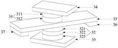
- FIG. 3is a schematic structural diagram of the spintronic device.
- the spintronic deviceincludes a ferroelectric/ferromagnetic heterostructure 31 , a magnetic tunnel junction 32 and a heavy metal layer 33 disposed between the ferroelectric/ferromagnetic heterostructure 31 and the magnetic tunnel junction 32 .
- the ferroelectric/ferromagnetic heterostructure 31includes a stacked multiferroic material layer 311 and a ferromagnetic layer 312, and the magnetic tunnel junction 32 includes a stacked free layer 321, an insulating layer 322 and a reference layer 323, so
- the heavy metal layer 33is disposed between the ferromagnetic layer 312 and the free layer 321 .
- the multiferroic material layer 311has ferromagnetism and ferroelectricity at room temperature, and can couple the inherent ferroelectricity and ferromagnetism under the control of an external electric field. Meanwhile, an interface exchange coupling effect exists between the multiferroic material layer 311 and the ferromagnetic layer 312 .
- the applied electric fieldbreaks the time-reversal symmetry
- the multiferroic material layer 311 and the ferromagnetic layer 312exhibit an interface magnetic field.
- the heavy metal layer 33will generate a spin current, and the interface magnetic field generated by the magnetoelectric coupling replaces the external magnetic field to realize deterministic writing of information storage.
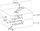
- FIG. 4is a schematic structural diagram of an information storage portion of a spintronic device according to some embodiments of the present disclosure.
- the magnetic tunnel junction 32 and the heavy metal layer 33constitute an information storage part of the spintronic device. Due to the spin Hall effect, when a current flows through the heavy metal layer 33, a polarization current opposite to the spin direction will be generated in the heavy metal layer 33, and the polarization current is accumulated in the Z-axis direction.
- the Z-axis directionis the direction perpendicular to the plane where the heavy metal layer 33 is located
- the Z-axis positive directionis the direction pointing to the ferroelectric/ferromagnetic heterostructure 31
- the Z-axis negative directionis the direction pointing to the magnetic tunnel junction 32 direction.
- the free layer 321In the negative Z-axis direction, spin currents are injected into the free layer 321 . Under the action of the interface magnetic field generated by the ferroelectric/ferromagnetic heterostructure 31 , the free layer 321 generates directional magnetization reversal. When the magnetization direction of the free layer 321 is the same as the magnetization direction of the reference layer 323, the magnetic tunnel junction 32 exhibits a low resistance state, representing the storage of binary data “0”; when the magnetization direction of the free layer 321 is the same as that of the reference layer 323 When the magnetization directions of the reference layer 323 are opposite, the magnetic tunnel junction 32 exhibits a high resistance state, which represents storing binary data "1".
- the materials and thicknesses of the magnetic tunnel junction 32 and the heavy metal layer 33can be selected according to actual application scenarios.
- the material of the heavy metal layer 33may be a strong spin-orbit coupling film such as W, Pt or Ta, and the thickness of the heavy metal layer 33 may be 1 nanometer to 10 nanometers.
- the material of the free layer 321may be one of FeCo, FeNi, FePd, FePt, CoPd, FeCoB or a Heusler compound, and the thickness of the free layer 321 may be 1 nanometer to 2 nanometers.
- the material of the insulating layer 322may be a high-quality tunneling film such as MgO or AlO x, and the thickness of the insulating layer 322 may be 0.8 nanometers to 1.6 nanometers.
- the material of the reference layer 323may be one of FeCo, FeNi, FePd, FePt, CoPd, FeCoB or a Heusler compound, and the thickness of the reference layer 323 may be 1 nm to 2 nm.
- FIG. 5is a schematic structural diagram of a ferroelectric/ferromagnetic heterostructure of a spintronic device according to some embodiments of the present disclosure.
- the multiferroic material layer 311 and the ferromagnetic layer 312constitute a heterostructure.
- the multiferroic material layer 311has ferromagnetic and ferroelectric properties at room temperature, and the ferromagnetic layer 312 has a small magnetostrictive coefficient. Due to the intrinsic magnetoelectric coupling, the material generates a magnetic moment that is in the same and orthogonal direction as the plane projection of the ferroelectric polarization. Therefore, by applying an electric field, magnetization of the material can be achieved.
- An interface exchange couplingis generated between the multiferroic material layer 311 and the ferromagnetic layer 312, so that the magnetic moment of the ferromagnetic layer 312 is coupled with the magnetic sequence of the multiferroic material layer 311, anisotropic and crystal domain structures can be transferred into the ferromagnetic layer 312 through exchange coupling, resulting in an interface magnetic field. Since the switching of magnetization in the ferroelectric/ferromagnetic heterostructure 31 is controlled by the ferroelectric switching of the multiferroic material layer 311, energy dissipation caused by Joule heating can be eliminated.
- the materials and thicknesses of the multiferroic material layer 311 and the ferromagnetic layer 312can be selected according to actual application scenarios.
- the material of the multi-iron material layer 311may be a single-phase multi-ferrous material, for example La x Bi 1-x FeO 3 or the like BiFeO 3 ferroelectric thin film, the multi-iron material layer 311
- the thicknesscan be from 2.5 nm to 4 nm.
- the magnetic order and ferroelectric order of single-phase multiferroic materialscan coexist at room temperature, which provides a prerequisite for regulating the flipping of ferromagnets at room temperature.
- the material of the ferromagnetic layer 312can be single-phase multiferroic and ferromagnetic transition metal materials, for example, a ferromagnetic thin film such as CoFe, and the thickness of the ferromagnetic layer 312 can be 2.5 nanometers to 4 nanometers.
- Heterojunctions composed of single-phase multiferroics, ferromagnetic transition metal materials and single-phase multiferroic materialscan produce interlayer exchange coupling effects.
- the plane projection directions of the domain polarizationsare collinear, implying that the magnetization of the ferromagnet can be controlled by the ferroelectric switching range of the multiferroic system.
- the ferroelectric/ferromagnetic heterostructure 31 , the magnetic tunnel junction 32 and the heavy metal layer 33form a stacked structure, such a design allows read and write operations on the same structure, using only a small The electrical current and the applied electric field enable the deterministic writing of information.
- the ferroelectric/ferromagnetic heterostructure 31 and the magnetic tunnel junction 32may both be cylindrical structures, and the heavy metal layer 33 may be a strip structure.
- the ferroelectric/ferromagnetic heterostructure 31 and the magnetic tunnel junction 32may also be a cuboid-shaped structure or a stacked structure of other shapes such as a ring structure, which is not limited in the present disclosure.
- the heavy metal layer 33can also be in other shapes such as a square, as long as the heavy metal layer 33 has opposite ends, and when an electric field is applied, a current can flow from one end of the heavy metal layer 33 to the opposite end, so that the The heavy metal layer 33 only needs to generate a spin Hall effect.
- the spintronic devicemay further include a first electrode 34 , a second electrode 35 , a third electrode 36 and a fourth electrode 37 .
- the first electrode 34is connected to the multiferroic material layer 311 , that is, one bottom surface of the multiferroic material layer 311 is connected to the ferromagnetic layer 312 , and the other bottom surface of the multiferroic material layer 311 is connected to the first electrode 34 .
- the second electrode 35is connected to the reference layer 323 , that is, one bottom surface of the reference layer 323 is connected to the insulating layer 322 , and the other bottom surface of the reference layer 323 is connected to the second electrode 35 .
- the third electrode 36is connected to one end of the heavy metal layer 33
- the fourth electrode 37is connected to the other end of the heavy metal layer 33
- one end of the heavy metal layer 33is opposite to the other end of the heavy metal layer 33 set up.
- the third electrode 36 and the fourth electrode 37are disposed on the side where the heavy metal layer 33 and the free layer 321 are connected.
- the fourth electrode 37may also be disposed on the side of the heavy metal layer 33 connected to the ferromagnetic layer 312 , or on the side surface of the heavy metal layer 33 , which is not limited in the present disclosure.
- the materials and thicknesses of the first electrode 34 , the second electrode 35 , the third electrode 36 and the fourth electrode 37can be selected according to actual application scenarios. In some embodiments, the first electrode 34.
- the materials of the second electrode 35, the third electrode 36 and the fourth electrode 37can be Cu, Au, W, Pt and other materials, the first electrode 34, the second electrode 35,
- the thicknesses of the third electrode 36 and the fourth electrode 37are in the order of nanometers.
- H RFis the applied radio frequency magnetic field
- Iwriteis the write current
- Hextis the applied magnetic field
- Mis the magnetization direction
- ⁇ FLis the field-like torque generated by the spin current on the ferromagnetic material
- ⁇ DLis the spin current on the iron
- the damping-like torque generated by the magnetic materialthe two act together to reverse the magnetization direction.
- Spin torque ferromagnetic resonanceuses the spin torque generated by alternating current to excite ferromagnetic resonance, which is an effective method to measure the charge-spin conversion efficiency (ie, spin Hall angle).
- the in-plane radio frequency charge current I RFis injected into the heterostructure of the ferromagnetic layer 312 and the heavy metal layer 33, and due to the spin coupling effect, the heavy metal layer 33 generates a spin current and is injected into the ferromagnetic layer 312, and The effect of torque on the magnetization of the ferromagnetic layer 312 is generated. Since the alternating current is oscillating, the resulting oscillating torque also leads to the oscillation of the anisotropic magnetoresistance in the device. Therefore, a mixed voltage Vmix is generated, which is detected by a DC voltmeter or a lock-in amplifier.
- the dark curverepresents the magnetization result driven by ⁇ FL in the heterojunction
- the light curverepresents the heterojunction.
- ⁇ DL- driven magnetizationresults in a mass junction.
- the dark curvehas an antisymmetric Lorentzian line shape, and the light curve has an additional 90° phase difference from the dark curve.
- the ferroelectric polarization of the multiferroic material layer 311is reversed, and then the ferroelectric polarization of the multiferroic material layer 311 is reversed.
- the antiferromagnetic anisotropy field and the tilted magnetic momentby adjusting the magnetic coupling effect of the ferroelectric/ferromagnetic heterostructure 31, promote the antiferromagnetic anisotropy field to generate uniaxial anisotropy to change the ferromagnetic Coercive field of layer 312.
- This magnetoelectric coupling and interlayer coupling effect with electric polarization and magnetizationgenerates the magnetic field required to drive the magnetization inversion of the free layer 321, and effectively induces the deterministic inversion of the magnetic tunnel junction 32 under full electrical operation control, Makes deterministic writing of data information possible.
- a process of magnetization reversal without external field assistancecan be realized, which greatly promotes the miniaturization and integration of the device, thereby facilitating the practical integration application of the spintronic device.
- the spintronic device of one or more embodiments of the present disclosurehas low critical current density, high data write rate, and high resistance to fatigue cycling.
- the spintronic device of one or more embodiments of the present disclosureis compatible with existing magnetic tunnel junction-based device structures, facilitating large-scale fabrication of the spintronic device.
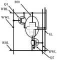
- FIG. 8is a schematic diagram of the circuit structure of the SOT-MRAM storage unit.
- the SOT-MRAM storage unitincludes a first transistor Q1, a second transistor Q2 and a spintronic device 800, and the spintronic device 800 is described above. spintronic devices.
- One end of the first transistor Q1 and the multiferroic material layer of the spintronic device 800are used to connect to the write bit line WBL, and the other end of the first transistor Q1 is connected to the heavy metal layer of the spintronic device 800 One end of the first transistor Q1 is used to connect to the write word line WWL.
- One end of the second transistor Q2is used to connect to the read bit line RBL, the other end of the second transistor Q2 is connected to the reference layer of the spintronic device 800, and the control end of the second transistor Q2 is used to connect to the read bit line RBL. word line RWL.
- the other end of the heavy metal layer of the spintronic device 800is used to connect the source line SL, and the other end of the heavy metal layer of the spintronic device 800 is disposed opposite to one end of the heavy metal layer of the spintronic device 800 .
- the first transistor Q1 and the second transistor Q2may be NMOS transistors, one end of the first transistor Q1 and one end of the second transistor Q2 are the drains of the NMOS transistors, and the One end of the first transistor Q1 and the other end of the second transistor Q2 are the source of the NMOS transistor, and one end of the first transistor Q1 and the control end of the second transistor Q2 are the gate of the NMOS transistor.
- the first transistor Q1 and the second transistor Q2may also be other transistors with switching functions, which are not limited in the present disclosure.
- a low-level voltagefor example, a voltage of 0V
- a high-level voltageis applied to the write bit line WBL and the write word line WWL, for example, a voltage of 1.2V is applied to turn on the first transistor Q1, so that a current flows through the spintronic device 800
- a spin currentis generated in the heavy metal layer of the spintronic device 800, and the spin current is injected into the free layer of the spintronic device 800.
- the free layer of the spintronic device 800Under the action of the magnetic field generated by the mass structure ME, the free layer of the spintronic device 800 generates a directional reversal of the magnetization direction, thereby completing the information writing.
- FIG. 9is a schematic diagram of a circuit structure for performing a read operation on the SOT-MRAM memory cell. 8 and 9, when the SOT-MRAM memory cell is read, a low-level voltage, such as 0V, is applied to the write bit line WBL and the write word line WWL, so that the first A transistor Q1 is turned off, a high-level voltage, such as a 1.2V voltage, is applied to the read word line RWL, and an induced current Isen is applied to the source line SL, such as a current of 100 ⁇ A to 200 ⁇ A, so that the second transistor Q2 On, resulting in the read current shown by the arrow path in Figure 8.
- a low-level voltagesuch as 0V
- the read currentgenerates a corresponding induced voltage Vsen on the read bit line RBL, the induced voltage Vsen is input to one input terminal of the read sense amplifier SA0, and the other input terminal of the read sense amplifier SA0 receives the read reference voltage Vref0 , wherein the read reference voltage Vref0 is generated by the read reference current Iref0 flowing through the read reference resistor Rref0.
- the read sense amplifier SA0compares the sensing voltage Vsen with the read reference voltage Vref0, and outputs the data stored in the SOT-MRAM storage unit according to the comparison result.
- the voltage value corresponding to the induced voltage Vsenis Vp; on the contrary, when binary data "1" is stored, the voltage value corresponding to the induced voltage Vsen is for Vap.
- the resistance value of the read reference resistor Rref0the voltage value of the read reference voltage Vref0 is set to be half of (Vp+Vap).
- the read sense amplifier SA0When the voltage value of the induced voltage Vsen is less than the voltage value of the read reference voltage Vref0, the read sense amplifier SA0 outputs a low level, that is, the SOT-MRAM memory cell exhibits a low resistance state, storing binary data "0" ”; when the voltage value of the induced voltage Vsen is not less than the voltage value of the read reference voltage Vref0, the read sense amplifier SA0 outputs a high level, that is, the SOT-MRAM memory cell presents a high resistance state, storing binary data "1".
- the write bit line WBL, the read bit line RBL, the write word line WWL, and the read word line RWLcan be set according to actual application scenarios, as long as the purpose of the above-mentioned write operation or read operation is achieved.
- an integrated storage-calculation circuitis provided, and the integrated storage-calculation circuit is used to implement a logical OR operation and a logical AND operation of two binary data.
- 10is a schematic diagram of the circuit structure of the integrated storage and calculation circuit, the integrated storage and calculation circuit includes a first storage unit 1001, a second storage unit 1002, a first reference unit and a first sense amplifier SA1, wherein the first The storage unit 1001 and the second storage unit 1002 are the SOT-MRAM storage units described in the foregoing embodiments.
- the first storage unit 1001is used for storing binary data "0" or binary data "1"
- the second storage unit 1002is used for storing binary data "0" or binary data "1"
- the data stored in the first storage unit 1001 and the second storage unit 1002may be written in advance through the write operation methods described in the foregoing embodiments.
- the first memory unit 1001 and the second memory unit 1002may be connected to the same write word line, and the first memory unit 1001 and the second memory unit 1002 may be connected to the same source line, The first storage unit 1001 and the second storage unit 1002 may be connected to the same read bit line.
- first storage unit 1001 and the second storage unit 1002may also be two independent storage units, and do not share a write bit line, a read bit line, a write word line, a read word line, and a source line.
- the present disclosureThis is not limited.
- the first reference unitis used for providing the first reference voltage Vref1.
- the first reference voltage Vref1includes a first reference resistor Rref1.
- One end of the first reference resistor Rref1is connected to an input end of the first sense amplifier SA1 and used to receive the first reference current Iref1, the other end of the first reference resistor Rref1 is grounded, and the first reference current Iref1 flows.
- the first reference voltage Vref1is generated through the first reference resistor Rref1.
- One input end of the first sense amplifier SA1is used to receive the first reference voltage Vref1, and the other input end of the first sense amplifier SA1 is connected to the read bit line connected to the first memory cell 1001 and the The read bit line connected to the second storage unit 1002, the output end of the first sense amplifier SA1 is used as the output end of the integrated memory-calculation circuit.
- the first sense amplifier SA1compares the voltage on the read bit line connected to the first memory cell 1001 and the read bit line connected to the second memory cell 1002 and the first reference voltage Vref1, according to the comparison result An operation result of performing a logical OR operation or a logical AND operation on the two binary data stored in the first storage unit 1001 and the second storage unit 1002 is output.
- the first storage unit 1001 and the second storage unitApply a low-level voltage to the write bit line and the write word line connected to 1002, for example, apply a voltage of 0V to turn off the first transistors in the first storage unit 1001 and the second storage unit 1002, and apply a low-level voltage to the first storage unit.
- the 1001 and the read word line connected to the second memory cell 1002apply a high-level voltage, for example, a voltage of 1.2V, and apply an induced current to the source line connected to the first memory cell 1001 and the second memory cell 1002 Isen, for example, a current of 100 ⁇ A to 200 ⁇ A is applied to turn on the second transistors in the first storage unit 1001 and the second storage unit 1002 , and the first storage unit 1001 and the second storage unit 1002 are connected A corresponding induced voltage Vsen is generated on the read bit line.
- a high-level voltagefor example, a voltage of 1.2V
- Isenfor example, a current of 100 ⁇ A to 200 ⁇ A is applied to turn on the second transistors in the first storage unit 1001 and the second storage unit 1002 , and the first storage unit 1001 and the second storage unit 1002 are connected A corresponding induced voltage Vsen is generated on the read bit line.
- the first storage unit 1001 and the second storage unit 1002when both the first storage unit 1001 and the second storage unit 1002 store binary data "0", the voltage corresponding to the induced voltage Vsen value is Vp,p; when both the first storage unit 1001 and the second storage unit 1002 store binary data "1", the voltage value corresponding to the induced voltage Vsen is Vap,ap; When the storage unit 1001 stores binary data "0" and the second storage unit 1002 stores binary data "1", or the first storage unit 1001 stores binary data "1” and the second storage unit 1002 stores binary data When "0", the voltage value corresponding to the induced voltage Vsen is Va,ap.
- the first memory cell 1001By setting the resistance value of the first reference resistor Rref1 so that the voltage value of the first reference voltage Vref1 is half of (Vp, p+Va, ap), the first memory cell 1001 A logical AND operation is performed with the two binary data stored in the second storage unit 1002 . By setting the resistance value of the first reference resistor Rref1 so that the voltage value of the first reference voltage Vref1 is half of (Vap, ap+Va, ap), the first memory cell 1001 Perform a logical OR operation with the two binary data stored in the second storage unit 1002 .
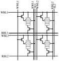
- a memory arrayin a fourth aspect of the present disclosure, includes M write bit lines, M read bit lines, N write word lines, N read word lines, N source lines, and M rows , N columns of storage units, wherein the storage units are the SOT-MRAM storage units described above, and M and N are positive integers.
- FIG. 11is a schematic diagram of a circuit structure of a memory array according to some embodiments of the present disclosure.
- each memory cell in the first rowis connected to the write bit line WBL1, and each memory cell in the second row is connected to the write bit line WBL2; each memory cell in the first row is connected to the read bit line RBL1, and the second row is connected to the read bit line RBL1.
- Each memory cell of the first columnis connected to the read bit line RBL2; each memory cell of the first column is connected to the write word line WWL1, and each memory cell of the second column is connected to the write word line WWL2; each memory cell of the first column is connected to Read word line RWL1, each memory cell in the second column is connected to read word line RWL2; each memory cell in the first column is connected to source line SL1, and each memory cell in the second column is connected to source line SL2.
- FIG. 12is a schematic diagram of the circuit structure of the integrated storage and calculation circuit, the integrated storage and calculation circuit includes a storage array 1201, a bit line decoder 1202, a word line decoder 1203, a source line decoder 1404 and a read operation module 1205, wherein the storage array 1201 is the storage array described above.
- the bit line decoder 1202is connected to the M write bit lines and the M read bit lines, and is used for providing bit line operating voltages to the M write bit lines and the M read bit lines.
- the word line decoder 1203is connected to the N write word lines and the N read word lines, and is used for providing word line operating voltages to the N write word lines and the N read word lines.
- the source line decoder 1204is connected to the N source lines, and is used for providing a source line operating voltage and an induced current to the N source lines.
- the bit line decoder 1202applies a high-level voltage to the write bit lines connected to the selected memory cells, and applies a high level voltage to the write bit lines connected to the unselected memory cells and All read bit lines apply a low level voltage;
- the word line decoder 1203applies a high level voltage to the write word lines connected to the selected memory cells, and applies a high level voltage to the write word lines and all read word lines connected to the unselected memory cells A low-level voltage is applied;
- the source line decoder 1204applies a low-level voltage to all source lines.
- the bit line decoder 1202When performing a read operation or a logic operation on the memory array 1201, the bit line decoder 1202 applies a low-level voltage to all write bit lines; the word line decoder 1203 applies a low-level voltage to the selected memory cells A high-level voltage is applied to the connected read word lines, and a low-level voltage is applied to the read word lines and all write word lines connected to unselected memory cells; the source line decoder 1204 applies induced current to all source lines.
- the read operation module 1205is configured to read the data stored in the storage array 1201 and perform logical operations on the data stored in the storage array 1201 .
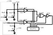
- 13is a schematic diagram of a circuit structure of a read operation module according to some embodiments of the present disclosure.
- the read operation module 1205includes a second reference unit 1301 , a third reference unit 1302 , a second sense amplifier SA2 , and a third sense amplifier SA3 and output unit 1303.
- the second reference unit 1301is used to provide a second reference voltage Vref2 when a read operation is performed on the memory array 1201 or a logical OR operation is performed on the memory array 1201 .
- the second reference unit 1301includes a second reference resistor Rref2, a third reference resistor Rref3, a third transistor Q3 and a fourth transistor Q4.
- One end of the second reference resistor Rref2is connected to one end of the third reference resistor Rref3 and an input end of the second sense amplifier SA2 for receiving the second reference current Iref2, and the other end of the second reference resistor Rref2
- One end of the third transistor Q3is connected, the other end of the third reference resistor Rref3 is connected to one end of the fourth transistor Q4, and the control end of the third transistor Q3 is used to receive the first enable signal EN1, so The control end of the fourth transistor Q4 is used for receiving the second enable signal EN2, and the other end of the third transistor Q3 and the other end of the fourth transistor Q4 are grounded.
- the third reference unit 1302is used to provide a third reference voltage Vref3 when performing a logical AND operation on the memory array 1201 .
- the third reference unit 1302includes a fourth reference resistor Rref4 and a fifth transistor Q5.
- One end of the fourth reference resistor Rref4is connected to an input end of the third sense amplifier SA3 and used to receive the third reference current Iref3, and the other end of the fourth reference resistor Rref4 is connected to one end of the fifth transistor Q5,
- the control end of the fifth transistor Q5is used for receiving the third enable signal EN3, and the other end of the fifth transistor Q5 is grounded.
- One input end of the second sense amplifier SA2is used to receive the second reference voltage Vref2, the other input end of the second sense amplifier SA2 is connected to the M read bit lines, and the second sense amplifier SA2 The output terminal of is connected to the output unit 1303.
- the second sense amplifier SA2compares the voltages on the M read bit lines and the second reference voltage Vref2, and outputs the data stored in the selected memory cell according to the comparison result, or outputs the data stored in the selected column.
- the third sense amplifier SA3compares the voltages on the M read bit lines with the third reference voltage Vref3, and outputs an operation result of performing a logical AND operation on the selected column of memory cells according to the comparison result.
- the output terminal of the output unit 1303is used as the output terminal of the integrated storage and calculation circuit.
- the output unit 1303is configured to shape the data output by the second sense amplifier SA2 and the third sense amplifier SA3 to output binary data "0" or binary data "1".
- the first enable signal EN1controls the third transistor Q3 to turn on
- the second enable signal EN2controls the four transistors Q4 to turn off
- the first enable signal EN2controls the fourth transistor Q4 to turn off.
- the three enable signals EN3control the five transistors Q5 to be turned off
- the second reference current Iref2flows through the second reference resistor Rref2 to generate the second reference voltage Vref2.
- the resistance value of the second reference resistor Rref2reference may be made to the foregoing description of the read operation of the SOT-MRAM memory cell, which will not be repeated here.
- the first enable signal EN1controls the third transistor Q3 to turn off
- the second enable signal EN2controls the four transistors Q4 to turn on
- the third The enable signal EN3controls the five transistors Q5 to be turned off
- the second reference current Iref2flows through the third reference resistor Rref3 to generate the second reference voltage Vref2.
- the first enable signal EN1controls the third transistor Q3 to turn off
- the second enable signal EN2controls the four transistors Q4 to turn off
- the third The enable signal EN3controls the five transistors Q5 to be turned on
- the third reference current Iref3flows through the fourth reference resistor Rref4 to generate the third reference voltage Vref3.
- the third transistor Q3, the fourth transistor Q4 and the fifth transistor Q5may be NMOS transistors, one end of the third transistor Q3, one end of the fourth transistor Q4 and the fifth transistor Q5 One end is the drain of the NMOS transistor, the other end of the third transistor Q3, the other end of the fourth transistor Q4 and the other end of the fifth transistor Q5 are the source of the NMOS transistor, the third transistor Q3
- the control terminal of , the control terminal of the fourth transistor Q4 and the control terminal of the fifth transistor Q5are the gates of the NMOS transistors.
- the third transistor Q3, the fourth transistor Q4 and the fifth transistor Q5may also be other transistors with switching functions, which are not limited in the present disclosure.
- the read operation module 1205may further include a NAND gate circuit NAND and a NOT gate circuit NOT.
- One input end of the NAND gate circuit NANDis connected to the output end of the second sense amplifier SA2, the other input end of the NAND gate circuit NAND is connected to the output end of the third sense amplifier SA3, and the AND
- the output terminal of the NOT circuit NANDis connected to the output unit 1303 and the input terminal of the NOT circuit NOT, and the output terminal of the NOT circuit NOT is connected to the output unit 1303 .
- the output signals of the second sense amplifier SA2 and the third sense amplifier SA3can implement XOR and XOR operations through the NAND gate circuit NAND and the NOT gate circuit NOT.
- the second sense amplifier SA2 and the third sense amplifier SA3may be single-ended output or double-ended output.
- the output of the second sense amplifier SA2 and the output of the third sense amplifier SA3both refer to the in-phase output of the double-ended output.
- the output terminal, or bothrefer to the inverting output terminal of the double-ended output.
- the storage-calculation integrated circuit of one or more embodiments of the present disclosurecan realize the access of the storage array and the Boolean logic operation of the stored data, realize the integrated storage-calculation function, and is compatible with the existing CMOS integrated circuit technology, which is beneficial to large-scale Preparation and integration applications.
Landscapes
- Engineering & Computer Science (AREA)
- Computer Hardware Design (AREA)
- Microelectronics & Electronic Packaging (AREA)
- Mram Or Spin Memory Techniques (AREA)
- Hall/Mr Elements (AREA)
Abstract
Description
Translated fromChinese相关申请的交叉引用CROSS-REFERENCE TO RELATED APPLICATIONS
本申请主张2020年7月21日提交的中国专利申请号202010704837.X且名称为“自旋电子器件、SOT-MRAM存储单元、存储阵列以及存算一体电路”的优先权,其全部内容通过引用包含于此。This application claims the priority of Chinese Patent Application No. 202010704837.X filed on July 21, 2020 and titled "Spintronic Devices, SOT-MRAM Memory Cells, Memory Arrays, and Memory-Computer Integrated Circuits", the entire contents of which are hereby incorporated by reference Included here.
本公开属于集成电路技术领域,尤其涉及一种自旋电子器件、SOT-MRAM存储单元、存储阵列以及存算一体电路。The present disclosure belongs to the technical field of integrated circuits, and in particular, relates to a spintronic device, a SOT-MRAM storage unit, a storage array, and a storage-computing integrated circuit.
在目前诸多的新型非易失性存储器中,自旋电子器件具有的高速度、低能耗、抗疲劳、抗辐射以及易小型化等优点,使其在信息领域受到了全世界的广泛关注。基于磁隧道结(MTJ,Magnetic Tunnel Junction)的磁性随机存储器(MRAM,Magnetic Random Access Memory)是最受关注的一种自旋电子器件。当前大力发展的第二代MRAM是利用自旋转移矩(STT,Spin Transfer Torque)效应来实现的,STT-MRAM的信息写入过程需要较大的电流通过磁隧道结,因而信息写入过程伴随着高能耗且不利于器件稳定性。而利用自旋轨道矩(SOT,Spin-Orbit Torque)效应来翻转磁自由层,写入信息时不需要大电流通过磁隧道结,可以实现信息的读和写分离,极大地提高了器件的稳定性,且拥有比STT-MRAM更快的磁化翻转速度和更低的翻转临界电流密度,有助于实现超低能耗下数据的存储和计算,从而促使第三代磁性随机存储器SOT-MRAM在磁存算一体化和磁人工智能等领域具有广阔的应用前景。Among the many new types of non-volatile memories at present, spintronic devices have the advantages of high speed, low energy consumption, anti-fatigue, anti-radiation, and easy miniaturization, which make them attract worldwide attention in the field of information. Magnetic Random Access Memory (MRAM) based on Magnetic Tunnel Junction (MTJ) is one of the most popular spintronic devices. The second-generation MRAM that is currently vigorously developed is realized by the Spin Transfer Torque (STT, Spin Transfer Torque) effect. The information writing process of STT-MRAM requires a large current to pass through the magnetic tunnel junction, so the information writing process is accompanied by It has high energy consumption and is not conducive to device stability. The spin-orbit torque (SOT, Spin-Orbit Torque) effect is used to flip the magnetic free layer, and a large current does not need to pass through the magnetic tunnel junction when writing information, which can realize the separation of reading and writing of information, which greatly improves the stability of the device. It has faster magnetization reversal speed and lower critical current density than STT-MRAM, which helps to realize data storage and computation under ultra-low energy consumption, thus promoting the third-generation magnetic random access memory SOT-MRAM in magnetic The fields of storage-computing integration and magnetic artificial intelligence have broad application prospects.
虽然自旋轨道矩有望解决自旋转移矩所面临的速度、能耗以及势垒可靠性的瓶颈,但对于垂直磁各向异性的磁隧道结来说,单独的自旋轨道矩无法实现确定性的定向磁化翻转。在有效磁场的作用下,磁化在垂直向上和垂直向下两种状态下是等效的,必须沿电流方向外加一个水平磁场破坏这种对称性,才能实现确定性的磁化翻转。外加磁场的引入增加了电路复杂度和可靠性风险,无法有效微缩集成,也降低了铁磁层的稳定性,成为限制自旋轨道矩应用的最大障碍。如何使自旋轨道矩能够在无外加磁场的条件下完成确定性的磁化翻转并实现与现有CMOS工艺兼容的集成应用,仍是本领域一个亟待解决的技术问题。Although the spin-orbit moment is expected to solve the bottleneck of speed, energy consumption, and barrier reliability faced by the spin-transfer moment, for the magnetic tunnel junction with perpendicular magnetic anisotropy, the spin-orbit moment alone cannot achieve determinism. oriented magnetization reversal. Under the action of the effective magnetic field, the magnetization is equivalent in the vertical upward and vertical downward states, and a horizontal magnetic field must be applied along the current direction to break this symmetry, in order to achieve deterministic magnetization reversal. The introduction of an external magnetic field increases the circuit complexity and reliability risks, making it impossible to effectively scale integration, and also reduces the stability of the ferromagnetic layer, becoming the biggest obstacle to limiting the application of spin-orbit moment. How to enable the spin-orbit moment to complete deterministic magnetization inversion without an external magnetic field and achieve integrated applications compatible with existing CMOS processes is still an urgent technical problem to be solved in the art.
发明内容SUMMARY OF THE INVENTION
针对现有技术存在的问题,本公开提供了一种自旋电子器件、SOT-MRAM存储单元、存储阵列以及存算一体电路,用于解决现有的自旋轨道矩无法在无外加磁场的条件下完成确定性的磁化翻转且无法实现与现有CMOS工艺兼容的集成应用的问题。Aiming at the problems existing in the prior art, the present disclosure provides a spintronic device, a SOT-MRAM storage unit, a storage array, and a storage-computing integrated circuit, which are used to solve the condition that the existing spin-orbit moment cannot operate without an external magnetic field. The problem is that the deterministic magnetization inversion can not be realized and the integrated application compatible with the existing CMOS process cannot be realized.
在本公开的第一方面,提供了一种自旋电子器件,包括铁电/铁磁异质结构、磁隧道结以及设置在所述铁电/铁磁异质结构和所述磁隧道结之间的重金属层;所述铁电/铁磁异 质结构包括层叠设置的多铁性材料层和铁磁层,所述磁隧道结包括层叠设置的自由层、绝缘层以及参考层,所述重金属层设置在所述铁磁层和所述自由层之间。In a first aspect of the present disclosure, there is provided a spintronic device comprising a ferroelectric/ferromagnetic heterostructure, a magnetic tunnel junction, and a spintronic device disposed between the ferroelectric/ferromagnetic heterostructure and the magnetic tunnel junction The ferroelectric/ferromagnetic heterostructure includes a stacked multiferroic material layer and a ferromagnetic layer, and the magnetic tunnel junction includes a stacked free layer, an insulating layer and a reference layer. The heavy metal layer A layer is disposed between the ferromagnetic layer and the free layer.
在本公开的一些实施方式中,所述多铁性材料层的材料为LaxBi1-xFeO3或者BiFeO3,所述铁磁层的材料为CoFe。In some embodiments of the present disclosure, the material of the multiferroic material layer is Lax Bi1-x FeO3 or BiFeO3 , and the material of the ferromagnetic layer is CoFe.
在本公开的一些实施方式中,所述重金属层的材料为W、Pt或者Ta。In some embodiments of the present disclosure, the material of the heavy metal layer is W, Pt or Ta.
在本公开的一些实施方式中,所述自由层的材料为FeCo、FeNi、FePd、FePt、CoPd、FeCoB中的一种或者为Heusler化合物,所述绝缘层的材料为MgO或者AlOx,所述参考层的材料为FeCo、FeNi、FePd、FePt、CoPd、FeCoB中的一种或者为Heusler化合物。In some embodiments of the present disclosure, the material of the free layer is one of FeCo, FeNi, FePd, FePt, CoPd, FeCoB or a Heusler compound, the material of the insulating layer is MgO or AlOx , the The material of the reference layer is one of FeCo, FeNi, FePd, FePt, CoPd, FeCoB or a Heusler compound.
在本公开的一些实施方式中,所述铁电/铁磁异质结构和所述磁隧道结均为圆柱状结构,所述重金属层为条状结构。In some embodiments of the present disclosure, the ferroelectric/ferromagnetic heterostructure and the magnetic tunnel junction are both cylindrical structures, and the heavy metal layer is a strip structure.
在本公开的一些实施方式中,所述自旋电子器件还包括第一电极、第二电极、第三电极以及第四电极;所述第一电极与所述多铁性材料层连接,所述第二电极与所述参考层连接,所述第三电极与所述重金属层的一端连接,所述第四电极与所述重金属层的另一端连接,所述重金属层的一端和所述重金属层的另一端相对设置。In some embodiments of the present disclosure, the spintronic device further includes a first electrode, a second electrode, a third electrode and a fourth electrode; the first electrode is connected to the multiferroic material layer, and the The second electrode is connected to the reference layer, the third electrode is connected to one end of the heavy metal layer, the fourth electrode is connected to the other end of the heavy metal layer, and one end of the heavy metal layer is connected to the heavy metal layer The other end of the set is relatively set.
在本公开的第二方面,提供了一种SOT-MRAM存储单元,包括第一晶体管、第二晶体管以及上述自旋电子器件;所述第一晶体管的一端和所述多铁性材料层用于连接写位线,所述第一晶体管的另一端连接所述重金属层的一端,所述第一晶体管的控制端用于连接写字线;所述第二晶体管的一端用于连接读位线,所述第二晶体管的另一端连接所述参考层,所述第二晶体管的控制端用于连接读字线;所述重金属层的另一端用于连接源线,所述重金属层的另一端与所述重金属层的一端相对设置。In a second aspect of the present disclosure, a SOT-MRAM memory cell is provided, comprising a first transistor, a second transistor, and the above-mentioned spintronic device; one end of the first transistor and the multiferroic material layer are used for is connected to the write bit line, the other end of the first transistor is connected to one end of the heavy metal layer, the control end of the first transistor is used to connect to the write word line; one end of the second transistor is used to connect to the read bit line, so The other end of the second transistor is connected to the reference layer, and the control end of the second transistor is used to connect to the read word line; the other end of the heavy metal layer is used to connect to the source line, and the other end of the heavy metal layer is connected to the read word line. One end of the heavy metal layer is oppositely arranged.
在本公开的第三方面,提供了一种存算一体电路,包括第一存储单元、第二存储单元、第一参考单元以及第一灵敏放大器,所述第一存储单元和所述第二存储单元为上述SOT-MRAM存储单元;所述第一参考单元用于提供第一参考电压,所述第一灵敏放大器的一个输入端用于接收所述第一参考电压,所述第一灵敏放大器的另一个输入端连接所述第一存储单元连接的读位线和所述第二存储单元连接的读位线,所述第一灵敏放大器的输出端作为所述存算一体电路的输出端。In a third aspect of the present disclosure, there is provided a storage-calculation integrated circuit, comprising a first storage unit, a second storage unit, a first reference unit and a first sense amplifier, the first storage unit and the second storage unit The unit is the above-mentioned SOT-MRAM storage unit; the first reference unit is used to provide a first reference voltage, an input end of the first sense amplifier is used to receive the first reference voltage, and the first sense amplifier is used for receiving the first reference voltage. The other input terminal is connected to the read bit line connected to the first storage unit and the read bit line connected to the second storage unit, and the output terminal of the first sense amplifier is used as the output terminal of the integrated memory-calculation circuit.
在本公开的一些实施方式中,所述第一参考单元包括第一参考电阻;所述第一参考电阻的一端连接所述第一灵敏放大器的一个输入端并用于接收第一参考电流,所述第一参考电阻的另一端接地。In some embodiments of the present disclosure, the first reference unit includes a first reference resistor; one end of the first reference resistor is connected to an input end of the first sense amplifier and is used for receiving a first reference current, the The other end of the first reference resistor is grounded.
在本公开的一些实施方式中,所述第一存储单元和所述第二存储单元连接同一条写字线,所述第一存储单元和所述第二存储单元连接同一条源线,所述第一存储单元和所述第二存储单元连接同一条读位线。In some embodiments of the present disclosure, the first memory cell and the second memory cell are connected to the same write word line, the first memory cell and the second memory cell are connected to the same source line, and the first memory cell and the second memory cell are connected to the same source line. A memory cell and the second memory cell are connected to the same read bit line.
在本公开的第四方面,提供了一种存储阵列,包括M条写位线、M条读位线、N条写字线、N条读字线、N条源线以及M行、N列存储单元,其中,所述存储单元为上述SOT-MRAM存储单元,M和N为正整数;位于同一行的每个存储单元连接同一条写位线,位于同一行的每个存储单元连接同一条读位线,位于同一列的每个存储单元连接同一条写字线,位于同一列的每个存储单元连接同一条读字线,位于同一列的每个存储单元连接同一条源线。In a fourth aspect of the present disclosure, a memory array is provided, including M write bit lines, M read bit lines, N write word lines, N read word lines, N source lines, and M rows and N columns of storage unit, wherein, the storage unit is the above-mentioned SOT-MRAM storage unit, and M and N are positive integers; each storage unit located in the same row is connected to the same write bit line, and each storage unit located in the same row is connected to the same read For bit lines, each memory cell located in the same column is connected to the same write word line, each memory cell located in the same column is connected to the same read word line, and each memory cell located in the same column is connected to the same source line.
在本公开的第五方面,提供了另一种存算一体电路,包括位线译码器、字线译码器、源线译码器、读取运算模块以及上述存储阵列;所述位线译码器用于向所述M条写位线以及所述M条读位线提供位线操作电压;所述字线译码器用于向所述N条写字线以及所述N条读字线提供字线操作电压;所述源线译码器用于向所述N条源线提供源线操作电压和感应电流;所述读取运算模块用于读取所述存储阵列存储的数据,并对所述存储阵列存储的数据进行逻辑运算。In a fifth aspect of the present disclosure, there is provided another integrated circuit of memory and calculation, including a bit line decoder, a word line decoder, a source line decoder, a read operation module, and the above-mentioned memory array; the bit line The decoder is used for providing bit line operating voltages to the M write bit lines and the M read bit lines; the word line decoder is used to provide the N write word lines and the N read word lines word line operating voltage; the source line decoder is used to provide the source line operating voltage and the induced current to the N source lines; the read operation module is used to read the data stored in the memory array, and Perform logical operations on the data stored in the storage array.
在本公开的一些实施方式中,所述读取运算模块包括第二参考单元、第三参考单元、第二灵敏放大器、第三灵敏放大器以及输出单元;所述第二参考单元用于在对所述存储阵列进行读取操作或者在对所述存储阵列进行逻辑或运算时提供第二参考电压;所述第三参考单元用于在对所述存储阵列进行逻辑与运算时提供第三参考电压;所述第二灵敏放大器的一个输入端用于接收所述第二参考电压,所述第二灵敏放大器的另一个输入端连接所述M条读位线,所述第二灵敏放大器的输出端连接所述输出单元;所述第三灵敏放大器的一个输入端用于接收所述第三参考电压,所述第二灵敏放大器的另一个输入端连接所述M条读位线,所述第三灵敏放大器的输出端连接所述输出单元;所述输出单元的输出端作为所述存算一体电路的输出端。In some embodiments of the present disclosure, the read operation module includes a second reference unit, a third reference unit, a second sense amplifier, a third sense amplifier, and an output unit; the second reference unit is used for The storage array performs a read operation or provides a second reference voltage when performing a logical OR operation on the storage array; the third reference unit is used for providing a third reference voltage when performing a logical AND operation on the storage array; One input end of the second sense amplifier is used to receive the second reference voltage, the other input end of the second sense amplifier is connected to the M read bit lines, and the output end of the second sense amplifier is connected to the output unit; one input end of the third sense amplifier is used to receive the third reference voltage, the other input end of the second sense amplifier is connected to the M read bit lines, and the third sense amplifier is used for receiving the third reference voltage. The output end of the amplifier is connected to the output unit; the output end of the output unit serves as the output end of the integrated circuit of storage and calculation.
在本公开的一些实施方式中,所述第二参考单元包括第二参考电阻、第三参考电阻、第三晶体管以及第四晶体管;所述第二参考电阻的一端连接所述第三参考电阻的一端和所述第二灵敏放大器的一个输入端并用于接收第二参考电流,所述第二参考电阻的另一端连接所述第三晶体管的一端,所述第三参考电阻的另一端连接所述第四晶体管的一端,所述第三晶体管的控制端用于接收第一使能信号,所述第四晶体管的控制端用于接收第二使能信号,所述第三晶体管的另一端和所述第四晶体管的另一端接地。In some embodiments of the present disclosure, the second reference unit includes a second reference resistor, a third reference resistor, a third transistor, and a fourth transistor; one end of the second reference resistor is connected to the third reference resistor One end and one input end of the second sense amplifier are used to receive a second reference current, the other end of the second reference resistor is connected to one end of the third transistor, and the other end of the third reference resistor is connected to the One end of the fourth transistor, the control end of the third transistor is used to receive the first enable signal, the control end of the fourth transistor is used to receive the second enable signal, the other end of the third transistor and the The other end of the fourth transistor is grounded.
在本公开的一些实施方式中,所述第三参考单元包括第四参考电阻和第五晶体管;所述第四参考电阻的一端连接所述第三灵敏放大器的一个输入端并用于接收第三参考电流,所述第四参考电阻的另一端连接所述第五晶体管的一端,所述第五晶体管的控制端用于接收第三使能信号,所述第五晶体管的另一端接地。In some embodiments of the present disclosure, the third reference unit includes a fourth reference resistor and a fifth transistor; one end of the fourth reference resistor is connected to an input end of the third sense amplifier and is used for receiving a third reference The other end of the fourth reference resistor is connected to one end of the fifth transistor, the control end of the fifth transistor is used for receiving the third enable signal, and the other end of the fifth transistor is grounded.
在本公开的一些实施方式中,所述读取运算模块还包括与非门电路以及非门电路;所述与非门电路的一个输入端连接所述第二灵敏放大器的输出端,所述与非门电路的另一个输入端连接所述第三灵敏放大器的输出端,所述与非门电路的输出端连接所述输出单元和所述非门电路的输入端,所述非门电路的输出端连接所述输出单元。In some embodiments of the present disclosure, the read operation module further includes a NAND gate circuit and a NOT gate circuit; an input end of the NAND gate circuit is connected to an output end of the second sense amplifier, and the AND gate circuit is connected to an output end of the second sense amplifier. The other input end of the NOT circuit is connected to the output end of the third sense amplifier, the output end of the NAND circuit is connected to the output unit and the input end of the NOT circuit, the output of the NOT circuit is connected terminal is connected to the output unit.
根据本公开的一个或多个实施方式的自旋电子器件,包括铁电/铁磁异质结构、磁隧道结以及设置在所述铁电/铁磁异质结构和所述磁隧道结之间的重金属层。由于所述铁电/铁磁异质结构中相邻的多铁性材料层和铁磁层之间存在界面交换耦合效应,所述铁磁层能够产生与所述多铁性材料层铁电极化相关的磁化,进而产生界面磁场,因此,通过对所述自旋电子器件外加电场,控制所述铁磁层的铁电开关,可以控制界面磁场的产生与消失。进一步,在所述磁隧道结中,自由层磁化方向的确定性翻转,可以由所述铁电/铁磁异质结构产生的界面磁场和层间耦合联合增强SOT驱动自由层磁化翻转效应来控制,因而本公开的一个或多个实施方式的自旋电子器件可实现无外场辅助条件下的确定性磁化翻转。此外,本公开的一个或多个实施方式的自旋电子器件,较小的写入电流即可翻转自由层的磁化方 向,写电流不经过所述磁隧道结,减少写电流对所述磁隧道结带来的损伤,提高抗疲劳循环特性,因而其还具有低临界电流密度、高数据写入速率以及高抗疲劳循环特性。此外,本公开的一个或多个实施方式的自旋电子器件与现有的基于磁隧道结的器件结构兼容,有利于所述自旋电子器件的大规模制造。A spintronic device according to one or more embodiments of the present disclosure includes a ferroelectric/ferromagnetic heterostructure, a magnetic tunnel junction, and a ferroelectric/ferromagnetic heterostructure and the magnetic tunnel junction disposed between the ferroelectric/ferromagnetic heterostructure and the magnetic tunnel junction heavy metal layer. Due to the interface exchange coupling effect between adjacent multiferroic material layers and ferromagnetic layers in the ferroelectric/ferromagnetic heterostructure, the ferromagnetic layer can generate ferroelectric polarization with the multiferroic material layer Therefore, by applying an electric field to the spintronic device and controlling the ferroelectric switch of the ferromagnetic layer, the generation and disappearance of the interface magnetic field can be controlled. Further, in the magnetic tunnel junction, the deterministic flip of the magnetization direction of the free layer can be controlled by the interfacial magnetic field generated by the ferroelectric/ferromagnetic heterostructure and the interlayer coupling to jointly enhance the SOT-driven magnetization flip effect of the free layer. , thus the spintronic device of one or more embodiments of the present disclosure can achieve deterministic magnetization inversion without external field assistance. In addition, in the spintronic device of one or more embodiments of the present disclosure, the magnetization direction of the free layer can be reversed with a small write current, the write current does not pass through the magnetic tunnel junction, and the effect of the write current on the magnetic tunnel is reduced. The damage caused by the junction is improved, and the fatigue cycle resistance is improved, so it also has a low critical current density, a high data write rate, and a high fatigue cycle resistance. In addition, the spintronic device of one or more embodiments of the present disclosure is compatible with existing magnetic tunnel junction-based device structures, facilitating large-scale fabrication of the spintronic device.
根据本公开的一个或多个实施方式的存算一体电路,能够实现存储阵列的存取以及所存数据的布尔逻辑运算,实现存算一体功能,且兼容于现有CMOS集成电路工艺,利于大规模制备和集成应用。According to one or more embodiments of the present disclosure, the integrated circuit of storage and calculation can realize the access of the storage array and the Boolean logic operation of the stored data, realize the integrated function of storage and calculation, and is compatible with the existing CMOS integrated circuit technology, which is beneficial to large-scale Preparation and integration applications.
通过阅读下文优选实施方式的详细描述,各种其他的优点和益处对于本领域普通技术人员将变得清楚明了。附图仅用于示出优选实施方式的目的,而并不认为是对本公开的限制。而且在整个附图中,用相同的参考符号表示相同的部件。在附图中:Various other advantages and benefits will become apparent to those of ordinary skill in the art upon reading the following detailed description of the preferred embodiments. The drawings are for purposes of illustrating preferred embodiments only and are not to be considered limiting of the present disclosure. Also, the same components are denoted by the same reference numerals throughout the drawings. In the attached image:
图1为现有的STT-MRAM存储单元的结构示意图;1 is a schematic structural diagram of an existing STT-MRAM storage unit;
图2为现有的SOT-MRAM存储单元的结构示意图;Fig. 2 is the structural representation of the existing SOT-MRAM storage unit;
图3为依据本公开的一些实施例的自旋电子器件的结构示意图;3 is a schematic structural diagram of a spintronic device according to some embodiments of the present disclosure;
图4为依据本公开的一些实施例的自旋电子器件的信息存储部分的结构示意图;4 is a schematic structural diagram of an information storage portion of a spintronic device according to some embodiments of the present disclosure;
图5为依据本公开的一些实施例的自旋电子器件的铁电/铁磁异质结构的结构示意图;5 is a schematic structural diagram of a ferroelectric/ferromagnetic heterostructure of a spintronic device according to some embodiments of the present disclosure;
图6为对本公开的一些实施例的自旋电子器件进行自旋力矩铁磁共振测试的示意图;6 is a schematic diagram of spin-torque ferromagnetic resonance testing of spintronic devices according to some embodiments of the present disclosure;
图7为对本公开的一些实施例的自旋电子器件进行自旋力矩铁磁共振测试产生的混合电压的波形图;7 is a waveform diagram of mixed voltages generated by spin-torque ferromagnetic resonance testing of spintronic devices according to some embodiments of the present disclosure;
图8为依据本公开的一些实施例的SOT-MRAM存储单元的电路结构示意图;8 is a schematic diagram of a circuit structure of a SOT-MRAM memory cell according to some embodiments of the present disclosure;
图9为对本公开的一些实施例的SOT-MRAM存储单元进行读取操作的电路结构示意图;9 is a schematic diagram of a circuit structure for performing a read operation on a SOT-MRAM memory cell according to some embodiments of the present disclosure;
图10为依据本公开的一些实施例的存算一体电路的电路结构示意图;FIG. 10 is a schematic diagram of a circuit structure of a memory-computing integrated circuit according to some embodiments of the present disclosure;
图11为依据本公开的一些实施例的存储阵列的电路结构示意图;11 is a schematic diagram of a circuit structure of a memory array according to some embodiments of the present disclosure;
图12为依据本公开的另一些实施例的存算一体电路的电路结构示意图;以及,12 is a schematic diagram of a circuit structure of a memory-computing integrated circuit according to other embodiments of the present disclosure; and,
图13为依据本公开的一些实施例的读取运算模块的电路结构示意图。13 is a schematic diagram of a circuit structure of a read operation module according to some embodiments of the present disclosure.
图1为现有的STT-MRAM存储单元的结构示意图,所述STT-MRAM存储单元包括设置在位线11和字线12之间的选通晶体管12以及磁隧道结,所述磁隧道结包括层叠设置的参考层14、绝缘层15以及自由层16。当所述选通晶体管13开启时,使所述磁隧道结导通,所述位线11中的电子注入所述参考层14,产生与所述参考层14的极化方向相同的自旋流。自旋流跃迁过所述绝缘层15,将自旋力矩转移到所述自由层16中,从而将所述自由层16的磁化方向翻转为与所述参考层14的磁化方向相同,此时所述磁隧道结呈现低阻态,达到写入二进制数据“0”的目的。当对所述STT-MRAM存储单元施加方向相反的 电流时,电子从所述自由层16流入所述参考层14,与所述参考层14自旋方向相反的极化电子被反射,造成所述自由层16磁化方向翻转为与所述参考层14的磁化方向相反,此时所述磁隧道结呈现高阻态,达到写入二进制数据“1”的目的。对于所述STT-MRAM存储单元,上述数据写入过程需要较大的电流通过所述磁隧道结,因而信息写入过程伴随着高能耗且不利于器件稳定性。FIG. 1 is a schematic structural diagram of an existing STT-MRAM memory cell. The STT-MRAM memory cell includes a gate transistor 12 disposed between a
图2为现有的SOT-MRAM存储单元的结构示意图,所述SOT-MRAM存储单元包括设置在位线21和字线22之间的磁隧道结23、重金属层24以及选通晶体管25,所述磁隧道结包括层叠设置的参考层、绝缘层以及自由层。当所述选通晶体管25开启时,使所述磁隧道结23导通,产生流过所述重金属层24的电流。由于自旋霍尔效应,流过所述重金属层24的电流产生两个方向相反的极化电流。自旋极化电子在所述重金属层24的边缘堆积,产生自旋流注入所述自由层。在外加磁场的作用下,自旋流对所述自由层和所述参考层中的磁化产生力矩,诱导所述自由层和所述参考层发生确定性的磁化翻转。当所述自由层的磁化方向与所述参考层的磁化方向相同时,所述磁隧道结23呈现低阻态,对应写入二进制数据“0”;当所述自由层的磁化方向与所述参考层的磁化方向相反时,所述磁隧道结23呈现高阻态,对应写入二进制数据“1”。对于所述SOT-MRAM存储单元,外加磁场的引入增加了电路复杂度和可靠性风险,无法有效微缩集成,也降低了所述自由层和所述参考层的稳定性,成为限制自旋轨道矩应用的最大障碍。2 is a schematic structural diagram of an existing SOT-MRAM memory cell. The SOT-MRAM memory cell includes a
基于此,本公开的一个或多个实施方式的自旋电子器件,利用磁电耦合的原理,通过外加电场作用于磁电耦合异质结,实现在室温条件下,定向磁化翻转的全电学控制。Based on this, the spintronic device of one or more embodiments of the present disclosure utilizes the principle of magnetoelectric coupling, and realizes full electrical control of directional magnetization inversion at room temperature by applying an electric field to the magnetoelectrically coupled heterojunction. .
下面将参照附图更详细地描述本公开的示例性实施例。虽然附图中显示了本公开的示例性实施例,然而应当理解,可以以各种形式实现本公开而不应被这里阐述的实施例所限制。相反,提供这些实施例是为了能够更透彻地理解本公开,并且能够将本公开的范围完整的传达给本领域的技术人员。Exemplary embodiments of the present disclosure will be described in more detail below with reference to the accompanying drawings. While exemplary embodiments of the present disclosure are shown in the drawings, it should be understood that the present disclosure may be embodied in various forms and should not be limited by the embodiments set forth herein. Rather, these embodiments are provided so that the present disclosure will be more thoroughly understood, and will fully convey the scope of the present disclosure to those skilled in the art.
下面通过附图及具体实施例对本公开的技术方案做进一步的详细说明。The technical solutions of the present disclosure will be further described in detail below through the accompanying drawings and specific embodiments.
在本公开的第一方面,提供了一种自旋电子器件,图3是所述自旋电子器件的结构示意图,所述自旋电子器件包括铁电/铁磁异质结构31、磁隧道结32以及设置在所述铁电/铁磁异质结构31和所述磁隧道结32之间的重金属层33。所述铁电/铁磁异质结构31包括层叠设置的多铁性材料层311和铁磁层312,所述磁隧道结32包括层叠设置的自由层321、绝缘层322以及参考层323,所述重金属层33设置在所述铁磁层312和所述自由层321之间。In a first aspect of the present disclosure, a spintronic device is provided. FIG. 3 is a schematic structural diagram of the spintronic device. The spintronic device includes a ferroelectric/
所述多铁性材料层311在室温条件下具有铁磁性以及铁电性,可以在外加电场的控制下将内在的铁电性与铁磁性耦合。同时,所述多铁性材料层311与所述铁磁层312之间存在界面交换耦合效应。当外加电场打破了时间反演对称性,所述多铁性材料层311与所述铁磁层312则表现出界面磁场。此时,如果有电流流过所述重金属层33,所述重金属层33会产生自旋流,磁电耦合产生的界面磁场代替外加磁场,实现信息存储的确定性写入。The
图4为依据本公开的一些实施例的自旋电子器件的信息存储部分的结构示意图。参考图4,所述磁隧道结32与所述重金属层33构成所述自旋电子器件的信息存储部分。由于自旋霍尔效应,当有电流流过所述重金属层33时,会在所述重金属层33产生与自旋方 向相反的极化电流,所述极化电流在Z轴方向积累。其中,Z轴方向为垂直于所述重金属层33所在平面的方向,Z轴正方向为指向所述铁电/铁磁异质结构31的方向,Z轴负方向为指向所述磁隧道结32的方向。在Z轴负方向,自旋流注入所述自由层321。在所述铁电/铁磁异质结构31产生的界面磁场的作用下,所述自由层321产生定向的磁化翻转。当所述自由层321的磁化方向与所述参考层323的磁化方向相同时,所述磁隧道结32呈现低阻态,代表存储二进制数据“0”;当所述自由层321的磁化方向与所述参考层323的磁化方向相反时,所述磁隧道结32呈现高阻态,代表存储二进制数据“1”。4 is a schematic structural diagram of an information storage portion of a spintronic device according to some embodiments of the present disclosure. Referring to FIG. 4 , the
所述磁隧道结32与所述重金属层33的材料和厚度可根据实际应用场景进行选取。在一些实施方式中,所述重金属层33的材料可以为W、Pt或者Ta等强自旋-轨道耦合薄膜,所述重金属层33的厚度可以为1纳米至10纳米。所述自由层321的材料可以为FeCo、FeNi、FePd、FePt、CoPd、FeCoB中的一种或者为Heusler化合物,所述自由层321的厚度可以为1纳米至2纳米。所述绝缘层322的材料可以为MgO或者AlOx等高质量隧穿薄膜,所述绝缘层322的厚度可以为0.8纳米至1.6纳米。所述参考层323的材料可以为FeCo、FeNi、FePd、FePt、CoPd、FeCoB中的一种或者为Heusler化合物,所述参考层323的厚度可以为1纳米至2纳米。The materials and thicknesses of the
图5为依据本公开的一些实施例的自旋电子器件的铁电/铁磁异质结构的结构示意图。参考图5,所述多铁性材料层311和所述铁磁层312构成异质结构。所述多铁性材料层311在室温条件下具有铁磁性与铁电性,所述铁磁层312具有较小的磁致伸缩系数。由于内在的磁电耦合,材料会产生与铁电极化的平面投影方向相同且正交的磁矩。因此,通过外加电场,可实现材料的磁化。所述多铁性材料层311和所述铁磁层312之间产生界面交换耦合,从而将所述铁磁层312的磁矩与所述多铁性材料层311的磁序耦合,各向异性和晶畴结构可以通过交换耦合转移到所述铁磁层312中,产生界面磁场。由于所述铁电/铁磁异质结构31中磁化的开关是由所述多铁性材料层311的铁电开关控制的,因此可以消除由焦耳热引起的能量耗散。5 is a schematic structural diagram of a ferroelectric/ferromagnetic heterostructure of a spintronic device according to some embodiments of the present disclosure. Referring to FIG. 5 , the
所述多铁性材料层311和所述铁磁层312的材料和厚度可根据实际应用场景进行选取。在一些实施方式中,所述多铁性材料层311的材料可以为单相多铁材料,例如为LaxBi1-xFeO3或者BiFeO3等铁电薄膜,所述多铁性材料层311的厚度可以为2.5纳米至4纳米。单相多铁材料的磁序和铁电序可以在室温条件下共存,为室温调控铁磁体翻转提供了前提。所述铁磁层312的材料可以为单相多铁与铁磁过渡金属材料,例如为CoFe等铁磁薄膜,所述铁磁层312的厚度可以为2.5纳米至4纳米。单相多铁与铁磁过渡金属材料和单相多铁材料构成的异质结能够产生层间的交换耦合效应,每个铁磁畴内的磁化强度与单相多铁材料中相应的铁电畴极化的平面投影方向共线,意味着铁磁体的磁化可以由多铁体系的铁电开关范围控制。The materials and thicknesses of the
在一些实施方式中,所述铁电/铁磁异质结构31、所述磁隧道结32以及所述重金属层33构成堆叠结构,这样的设计允许在同一结构上进行读写操作,只使用小电流以及外加电场实现信息的确定性写入。所述铁电/铁磁异质结构31和所述磁隧道结32可以均为圆柱状结构,所述重金属层33可以为条状结构。当然,所述铁电/铁磁异质结构31和所述磁隧道结32还可以均为长方体状结构或者为环状结构等其它形状叠层结构,本公开对此不进行 限定。所述重金属层33还可以为方形等其他形状,只要保证所述重金属层33具有相对的两端,在外加电场时能够有电流从所述重金属层33的一端流向相对的另一端,从而能够在所述重金属层33产生自旋霍尔效应即可。In some embodiments, the ferroelectric/
当所述自旋电子器件与外部电路连接时,通常需要通过电极与外部电路连接。因此,所述自旋电子器件还可以包括第一电极34、第二电极35、第三电极36以及第四电极37。所述第一电极34与所述多铁性材料层311连接,即所述多铁性材料层311的一个底面连接所述铁磁层312,所述多铁性材料层311的另一个底面连接所述第一电极34。所述第二电极35与所述参考层323连接,即所述参考层323的一个底面连接所述绝缘层322,所述参考层323的另一个底面连接所述第二电极35。所述第三电极36与所述重金属层33的一端连接,所述第四电极37与所述重金属层33的另一端连接,所述重金属层33的一端和所述重金属层33的另一端相对设置。在一些实施方式中,所述第三电极36和所述第四电极37设置在所述重金属层33与所述自由层321连接的一面,在其他实施方式中,所述第三电极36和所述第四电极37也可以设置在所述重金属层33与所述铁磁层312连接的一面,或者设置在所述重金属层33的侧面,本公开对此不进行限定。所述第一电极34、所述第二电极35、所述第三电极36以及所述第四电极37的材料和厚度可根据实际应用场景进行选取,在一些实施方式中,所述第一电极34、所述第二电极35、所述第三电极36以及所述第四电极37的材料可以为Cu、Au、W、Pt等材料,所述第一电极34、所述第二电极35、所述第三电极36以及所述第四电极37的厚度为纳米量级。When the spintronic device is connected to an external circuit, it is usually necessary to connect to the external circuit through electrodes. Therefore, the spintronic device may further include a
图6为对本公开的一些实施方式的自旋电子器件进行自旋力矩铁磁共振测试的示意图。其中,HRF为施加的射频磁场,Iwrite为写入电流,Hext为外加磁场,M为磁化方向,τFL为自旋电流对铁磁材料产生的类场力矩,τDL为自旋电流对铁磁材料产生的类阻尼力矩,两者共同作用翻转磁化方向。自旋力矩铁磁共振利用交流电产生的自旋力矩来激发铁磁谐振,是测量电荷-自旋转换效率(即自旋霍尔角)的有效方法。将平面内射频电荷流IRF注入到所述铁磁层312和所述重金属层33异质结构,由于自旋耦合效应,所述重金属层33产生自旋流注入所述铁磁层312,并对所述铁磁层312的磁化产生力矩的作用。由于交流电是振荡的,产生的振荡力矩也导致了器件中各向异性磁阻的振荡。因此,产生一个混合电压Vmix,由直流电压表或锁相放大器检测。6 is a schematic diagram of spin-torque ferromagnetic resonance testing of spintronic devices of some embodiments of the present disclosure. Among them, HRF is the applied radio frequency magnetic field, Iwrite is the write current, Hext is the applied magnetic field, M is the magnetization direction, τFL is the field-like torque generated by the spin current on the ferromagnetic material, and τDL is the spin current on the iron The damping-like torque generated by the magnetic material, the two act together to reverse the magnetization direction. Spin torque ferromagnetic resonance uses the spin torque generated by alternating current to excite ferromagnetic resonance, which is an effective method to measure the charge-spin conversion efficiency (ie, spin Hall angle). The in-plane radio frequency charge current IRF is injected into the heterostructure of the
图7为所述混合电压Vmix的波形图,虚线表示所述自旋电子器件在6GHz频率下的数据拟合曲线,深色曲线表示异质结中τFL驱动的磁化结果,浅色曲线表示异质结中τDL驱动的磁化结果。深色曲线具有反对称洛伦兹线形状,浅色曲线与深色曲线具有额外的90°相位差。因此,在共振场中,τDL驱动力矩是同相(δ=0),导致产生洛伦兹对称线形状,其中,自旋霍尔角(θsh)可由VS/VA计算获得,VS和FS为测量的对称洛伦兹分量,VA和FA为反对称洛伦兹分量。7 is a waveform diagram of the mixed voltage Vmix, the dotted line represents the data fitting curve of the spintronic device at a frequency of 6 GHz, the dark curve representsthe magnetization result driven by τ FL in the heterojunction, and the light curve represents the heterojunction.τ DL- driven magnetization results in a mass junction. The dark curve has an antisymmetric Lorentzian line shape, and the light curve has an additional 90° phase difference from the dark curve. Thus, the resonance field, τDL drive torque is in phase (δ = 0), resulting in a symmetrical Lorentzian line shape, wherein the spin Hall angle (θsh) by VS / VA obtained by calculation, VS, and symmetrical Lorentzian component FS is the measured, Va and Fa is the Lorentz antisymmetric component.
本公开内容的一个或多个实施方式的自旋电子器件,通过在所述铁电/铁磁异质结构31的两端施加电场,翻转所述多铁性材料层311铁电极化,进而翻转反铁磁各项异性场和倾斜磁矩,通过调节所述铁电/铁磁异质结构31的磁耦合效应,促使反铁磁各项异性场产生单轴各向异性从而改变所述铁磁层312的矫顽场。这种具有电极化和磁化的磁电耦合及层间耦合效应产生驱动所述自由层321磁化翻转所需的磁场,在全电学操作控制时,有 效诱导所述磁隧道结32的确定性翻转,使数据信息的确定性写入成为可能。所述自旋电子器件中可以实现无外场辅助磁化翻转的过程,大幅促进器件可微缩性以及集成度的提高,从而利于所述自旋电子器件的实际集成应用。本公开内容的一个或多个实施方式的自旋电子器件具有低临界电流密度、高数据写入速率以及高抗疲劳循环特性。此外,本公开内容的一个或多个实施方式的自旋电子器件与现有的基于磁隧道结的器件结构兼容,有利于所述自旋电子器件的大规模制造。In the spintronic device of one or more embodiments of the present disclosure, by applying an electric field at both ends of the ferroelectric/
在本公开的第二方面,提供了一种SOT-MRAM存储单元。图8是所述SOT-MRAM存储单元的电路结构示意图,所述SOT-MRAM存储单元包括第一晶体管Q1、第二晶体管Q2以及自旋电子器件800,所述自旋电子器件800为前述描述的自旋电子器件。In a second aspect of the present disclosure, a SOT-MRAM memory cell is provided. FIG. 8 is a schematic diagram of the circuit structure of the SOT-MRAM storage unit. The SOT-MRAM storage unit includes a first transistor Q1, a second transistor Q2 and a
所述第一晶体管Q1的一端和所述自旋电子器件800的多铁性材料层用于连接写位线WBL,所述第一晶体管Q1的另一端连接所述自旋电子器件800的重金属层的一端,所述第一晶体管Q1的控制端用于连接写字线WWL。所述第二晶体管Q2的一端用于连接读位线RBL,所述第二晶体管Q2的另一端连接所述自旋电子器件800的参考层,所述第二晶体管Q2的控制端用于连接读字线RWL。所述自旋电子器件800的重金属层的另一端用于连接源线SL,所述自旋电子器件800的重金属层的另一端与所述自旋电子器件800的重金属层的一端相对设置。在一些实施方式中,所述第一晶体管Q1和所述第二晶体管Q2可以为NMOS晶体管,所述第一晶体管Q1的一端和所述第二晶体管Q2的一端为NMOS晶体管的漏极,所述第一晶体管Q1的一端和所述第二晶体管Q2的另一端为NMOS晶体管的源极,所述第一晶体管Q1的一端和所述第二晶体管Q2的控制端为NMOS晶体管的栅极。当然,所述第一晶体管Q1和所述第二晶体管Q2还可以为其他具有开关功能的晶体管,本公开对此不进行限定。One end of the first transistor Q1 and the multiferroic material layer of the
在对所述SOT-MRAM存储单元进行写操作时,对所述读位线RBL、所述读字线RWL以及所述源线SL施加低电平电压,例如施加0V电压,使所述第二晶体管Q2关闭,对所述写位线WBL和所述写字线WWL施加高电平电压,例如施加1.2V电压,使所述第一晶体管Q1开启,从而有电流流经所述自旋电子器件800的重金属层,在所述自旋电子器件800的重金属层产生自旋流,自旋流注入所述自旋电子器件800的自由层,在所述自旋电子器件800的铁电/铁磁异质结构ME产生的磁场作用下,所述自旋电子器件800的自由层产生磁化方向的定向翻转,完成信息写入。When a write operation is performed on the SOT-MRAM memory cell, a low-level voltage, for example, a voltage of 0V, is applied to the read bit line RBL, the read word line RWL and the source line SL, so that the second The transistor Q2 is turned off, and a high-level voltage is applied to the write bit line WBL and the write word line WWL, for example, a voltage of 1.2V is applied to turn on the first transistor Q1, so that a current flows through the
图9为对所述SOT-MRAM存储单元进行读取操作的电路结构示意图。结合图8和图9,在对所述SOT-MRAM存储单元进行读取操作时,对所述写位线WBL和所述写字线WWL施加低电平电压,例如施加0V电压,使所述第一晶体管Q1关闭,对所述读字线RWL施加高电平电压,例如施加1.2V电压,并对所述源线SL施加感应电流Isen,例如施加100μA至200μA电流,使所述第二晶体管Q2开启,产生图8中箭头路径所示的读电流。所述读电流使所述读位线RBL上产生对应的感应电压Vsen,所述感应电压Vsen输入读灵敏放大器SA0的一个输入端,所述读灵敏放大器SA0的另一个输入端接收读参考电压Vref0,其中,所述读参考电压Vref0由读参考电流Iref0流过读参考电阻Rref0产生。所述读灵敏放大器SA0对所述感应电压Vsen和所述读参考电压Vref0进行比较,根据比较结果输出所述SOT-MRAM存储单元存储的数据。FIG. 9 is a schematic diagram of a circuit structure for performing a read operation on the SOT-MRAM memory cell. 8 and 9, when the SOT-MRAM memory cell is read, a low-level voltage, such as 0V, is applied to the write bit line WBL and the write word line WWL, so that the first A transistor Q1 is turned off, a high-level voltage, such as a 1.2V voltage, is applied to the read word line RWL, and an induced current Isen is applied to the source line SL, such as a current of 100μA to 200μA, so that the second transistor Q2 On, resulting in the read current shown by the arrow path in Figure 8. The read current generates a corresponding induced voltage Vsen on the read bit line RBL, the induced voltage Vsen is input to one input terminal of the read sense amplifier SA0, and the other input terminal of the read sense amplifier SA0 receives the read reference voltage Vref0 , wherein the read reference voltage Vref0 is generated by the read reference current Iref0 flowing through the read reference resistor Rref0. The read sense amplifier SA0 compares the sensing voltage Vsen with the read reference voltage Vref0, and outputs the data stored in the SOT-MRAM storage unit according to the comparison result.
对于所述SOT-MRAM存储单元,在存储二进制数据“0”时,所述感应电压Vsen对应的电压值为Vp;反之,在存储二进制数据“1”时,所述感应电压Vsen对应的电压值为Vap。通过设置所述读参考电阻Rref0的电阻值,使所述读参考电压Vref0的电压值为(Vp+Vap)的二分之一。当所述感应电压Vsen的电压值小于所述读参考电压Vref0的电压值时,所述读灵敏放大器SA0输出低电平,即所述SOT-MRAM存储单元呈现低阻态,存储二进制数据“0”;当所述感应电压Vsen的电压值不小于所述读参考电压Vref0的电压值时,所述读灵敏放大器SA0输出高电平,即所述SOT-MRAM存储单元呈现高阻态,存储二进制数据“1”。For the SOT-MRAM memory cell, when binary data "0" is stored, the voltage value corresponding to the induced voltage Vsen is Vp; on the contrary, when binary data "1" is stored, the voltage value corresponding to the induced voltage Vsen is for Vap. By setting the resistance value of the read reference resistor Rref0, the voltage value of the read reference voltage Vref0 is set to be half of (Vp+Vap). When the voltage value of the induced voltage Vsen is less than the voltage value of the read reference voltage Vref0, the read sense amplifier SA0 outputs a low level, that is, the SOT-MRAM memory cell exhibits a low resistance state, storing binary data "0" ”; when the voltage value of the induced voltage Vsen is not less than the voltage value of the read reference voltage Vref0, the read sense amplifier SA0 outputs a high level, that is, the SOT-MRAM memory cell presents a high resistance state, storing binary data "1".
需要说明的是,在对所述SOT-MRAM存储单元进行写操作或者读取操作时,对所述写位线WBL、所述读位线RBL、所述写字线WWL、所述读字线RWL以及所述源线SL施加的操作电压和感应电流,可根据实际应用场景进行设置,只要达到上述写操作或者读取操作目的即可。It should be noted that when a write operation or a read operation is performed on the SOT-MRAM storage unit, the write bit line WBL, the read bit line RBL, the write word line WWL, and the read word line RWL The operating voltage and induced current applied by the source line SL can be set according to actual application scenarios, as long as the purpose of the above-mentioned write operation or read operation is achieved.
在本公开的第三方面,提供了一种存算一体电路,所述存算一体电路用于实现两个二进制数据的逻辑或运算和逻辑与运算。图10是所述存算一体电路的电路结构示意图,所述存算一体电路包括第一存储单元1001、第二存储单元1002、第一参考单元以及第一灵敏放大器SA1,其中,所述第一存储单元1001和所述第二存储单元1002为前述实施例描述的SOT-MRAM存储单元。In a third aspect of the present disclosure, an integrated storage-calculation circuit is provided, and the integrated storage-calculation circuit is used to implement a logical OR operation and a logical AND operation of two binary data. 10 is a schematic diagram of the circuit structure of the integrated storage and calculation circuit, the integrated storage and calculation circuit includes a
所述第一存储单元1001用于存储二进制数据“0”或者二进制数据“1”,所述第二存储单元1002用于存储二进制数据“0”或者二进制数据“1”。所述第一存储单元1001和所述第二存储单元1002存储的数据,可以通过前述实施例描述的写操作方式预先写入。在一些实施方式中,所述第一存储单元1001和所述第二存储单元1002可以连接同一条写字线,所述第一存储单元1001和所述第二存储单元1002可以连接同一条源线,所述第一存储单元1001和所述第二存储单元1002可以连接同一条读位线。当然,所述第一存储单元1001和所述第二存储单元1002也可以为两个相互独立的存储单元,不共用写位线、读位线、写字线、读字线以及源线,本公开对此不进行限定。The
所述第一参考单元用于提供第一参考电压Vref1。在一些实施方式中,所述第一参考电压Vref1包括第一参考电阻Rref1。所述第一参考电阻Rref1的一端连接所述第一灵敏放大器SA1的一个输入端并用于接收第一参考电流Iref1,所述第一参考电阻Rref1的另一端接地,所述第一参考电流Iref1流过所述第一参考电阻Rref1,产生所述第一参考电压Vref1。The first reference unit is used for providing the first reference voltage Vref1. In some embodiments, the first reference voltage Vref1 includes a first reference resistor Rref1. One end of the first reference resistor Rref1 is connected to an input end of the first sense amplifier SA1 and used to receive the first reference current Iref1, the other end of the first reference resistor Rref1 is grounded, and the first reference current Iref1 flows. The first reference voltage Vref1 is generated through the first reference resistor Rref1.
所述第一灵敏放大器SA1的一个输入端用于接收所述第一参考电压Vref1,所述第一灵敏放大器SA1的另一个输入端连接所述第一存储单元1001连接的读位线和所述第二存储单元1002连接的读位线,所述第一灵敏放大器SA1的输出端作为所述存算一体电路的输出端。所述第一灵敏放大器SA1对所述第一存储单元1001连接的读位线和所述第二存储单元1002连接的读位线上的电压以及所述第一参考电压Vref1进行比较,根据比较结果输出对所述第一存储单元1001和所述第二存储单元1002存储的两个二进制数据进行逻辑或运算或者进行逻辑与运算的运算结果。One input end of the first sense amplifier SA1 is used to receive the first reference voltage Vref1, and the other input end of the first sense amplifier SA1 is connected to the read bit line connected to the
在对所述第一存储单元1001和所述第二存储单元1002存储的两个二进制数据,进 行逻辑或运算或者进行逻辑与运算时,对所述第一存储单元1001和所述第二存储单元1002连接的写位线和写字线施加低电平电压,例如施加0V电压,使所述第一存储单元1001和所述第二存储单元1002中的第一晶体管关闭,对所述第一存储单元1001和所述第二存储单元1002连接的读字线施加高电平电压,例如施加1.2V电压,并对所述第一存储单元1001和所述第二存储单元1002连接的源线施加感应电流Isen,例如施加100μA至200μA电流,使所述第一存储单元1001和所述第二存储单元1002中的第二晶体管开启,在所述第一存储单元1001和所述第二存储单元1002连接的读位线上产生对应的感应电压Vsen。When performing a logical OR operation or a logical AND operation on the two binary data stored in the
对于所述第一存储单元1001和所述第二存储单元1002,当所述第一存储单元1001和所述第二存储单元1002均存储二进制数据“0”时,所述感应电压Vsen对应的电压值为Vp,p;当所述第一存储单元1001和所述第二存储单元1002均存储二进制数据“1”时,所述感应电压Vsen对应的电压值为Vap,ap;当所述第一存储单元1001存储二进制数据“0”、所述第二存储单元1002存储二进制数据“1”时,或者所述第一存储单元1001存储二进制数据“1”、所述第二存储单元1002存储二进制数据“0”时,所述感应电压Vsen对应的电压值为Va,ap。通过设置所述第一参考电阻Rref1的电阻值,使所述第一参考电压Vref1的电压值为(Vp,p+Va,ap)的二分之一,可以实现对所述第一存储单元1001和所述第二存储单元1002存储的两个二进制数据进行逻辑与运算。通过设置所述第一参考电阻Rref1的电阻值,使所述第一参考电压Vref1的电压值为(Vap,ap+Va,ap)的二分之一,可以实现对所述第一存储单元1001和所述第二存储单元1002存储的两个二进制数据进行逻辑或运算。For the
在本公开的第四方面,提供了一种存储阵列,所述存储阵列包括M条写位线、M条读位线、N条写字线、N条读字线、N条源线以及M行、N列存储单元,其中,所述存储单元为前述描述的SOT-MRAM存储单元,M和N为正整数。In a fourth aspect of the present disclosure, a memory array is provided, the memory array includes M write bit lines, M read bit lines, N write word lines, N read word lines, N source lines, and M rows , N columns of storage units, wherein the storage units are the SOT-MRAM storage units described above, and M and N are positive integers.
位于同一行的每个存储单元连接同一条写位线,位于同一行的每个存储单元连接同一条读位线,位于同一列的每个存储单元连接同一条写字线,位于同一列的每个存储单元连接同一条读字线,位于同一列的每个存储单元连接同一条源线。以M和N的取值均为2为例,图11为本公开的一些实施例的存储阵列的电路结构示意图。其中,第一行的每个存储单元均连接写位线WBL1,第二行的每个存储单元均连接写位线WBL2;第一行的每个存储单元均连接读位线RBL1,第二行的每个存储单元均连接读位线RBL2;第一列的每个存储单元均连接写字线WWL1,第二列的每个存储单元均连接写字线WWL2;第一列的每个存储单元均连接读字线RWL1,第二列的每个存储单元均连接读字线RWL2;第一列的每个存储单元均连接源线SL1,第二列的每个存储单元均连接源线SL2。Each memory cell in the same row is connected to the same write bit line, each memory cell in the same row is connected to the same read bit line, each memory cell in the same column is connected to the same write word line, and each memory cell in the same column is connected to the same write word line. The memory cells are connected to the same read word line, and each memory cell in the same column is connected to the same source line. Taking the value of both M and N as 2 as an example, FIG. 11 is a schematic diagram of a circuit structure of a memory array according to some embodiments of the present disclosure. Wherein, each memory cell in the first row is connected to the write bit line WBL1, and each memory cell in the second row is connected to the write bit line WBL2; each memory cell in the first row is connected to the read bit line RBL1, and the second row is connected to the read bit line RBL1. Each memory cell of the first column is connected to the read bit line RBL2; each memory cell of the first column is connected to the write word line WWL1, and each memory cell of the second column is connected to the write word line WWL2; each memory cell of the first column is connected to Read word line RWL1, each memory cell in the second column is connected to read word line RWL2; each memory cell in the first column is connected to source line SL1, and each memory cell in the second column is connected to source line SL2.
在本公开的第五方面,提供了另一种存算一体电路。图12是所述存算一体电路的电路结构示意图,所述存算一体电路包括存储阵列1201、位线译码器1202、字线译码器1203、源线译码器1404以及读取运算模块1205,其中,所述存储阵列1201为前述描述的存储阵列。In a fifth aspect of the present disclosure, another integrated circuit for storing and computing is provided. 12 is a schematic diagram of the circuit structure of the integrated storage and calculation circuit, the integrated storage and calculation circuit includes a
所述位线译码器1202与所述M条写位线以及所述M条读位线连接,用于向所述M条写位线以及所述M条读位线提供位线操作电压。所述字线译码器1203与所述N条写字线以及所述N条读字线连接,用于向所述N条写字线以及所述N条读字线提供字线操作电压。所述源线译码器1204与所述N条源线连接,用于向所述N条源线提供源线操作电 压和感应电流。The
在对所述存储阵列1201进行写操作时,所述位线译码器1202对被选中的存储单元连接的写位线施加高电平电压,对未被选中的存储单元连接的写位线和所有读位线施加低电平电压;所述字线译码器1203对被选中的存储单元连接的写字线施加高电平电压,对未被选中的存储单元连接的写字线和所有读字线施加低电平电压;所述源线译码器1204对所有源线施加低电平电压。When a write operation is performed on the
在对所述存储阵列1201进行读取操作或者进行逻辑运算时,所述位线译码器1202对所有写位线施加低电平电压;所述字线译码器1203对被选中的存储单元连接的读字线施加高电平电压,对未被选中的存储单元连接的读字线和所有写字线施加低电平电压;所述源线译码器1204对所有源线施加感应电流。When performing a read operation or a logic operation on the
需要说明的是,在对所述存储阵列1201进行写操作或者读取操作时,都是选中所述存储阵列1201中的一个存储单元。而在对所述存储阵列1201进行布尔逻辑运算时,是选中所述存储阵列1201中一列存储单元中的两个存储单元。It should be noted that when a write operation or a read operation is performed on the
所述读取运算模块1205用于读取所述存储阵列1201存储的数据,并对所述存储阵列1201存储的数据进行逻辑运算。图13是依据本公开的一些实施例的读取运算模块的电路结构示意图,所述读取运算模块1205包括第二参考单元1301、第三参考单元1302、第二灵敏放大器SA2、第三灵敏放大器SA3以及输出单元1303。The read
所述第二参考单元1301用于在对所述存储阵列1201进行读取操作或者在对所述存储阵列1201进行逻辑或运算时提供第二参考电压Vref2。在一些实施方式中,所述第二参考单元1301包括第二参考电阻Rref2、第三参考电阻Rref3、第三晶体管Q3以及第四晶体管Q4。所述第二参考电阻Rref2的一端连接所述第三参考电阻Rref3的一端和所述第二灵敏放大器SA2的一个输入端并用于接收第二参考电流Iref2,所述第二参考电阻Rref2的另一端连接所述第三晶体管Q3的一端,所述第三参考电阻Rref3的另一端连接所述第四晶体管Q4的一端,所述第三晶体管Q3的控制端用于接收第一使能信号EN1,所述第四晶体管Q4的控制端用于接收第二使能信号EN2,所述第三晶体管Q3的另一端和所述第四晶体管Q4的另一端接地。The
所述第三参考单元1302用于在对所述存储阵列1201进行逻辑与运算时提供第三参考电压Vref3。在一些实施方式中,所述第三参考单元1302包括第四参考电阻Rref4和第五晶体管Q5。所述第四参考电阻Rref4的一端连接所述第三灵敏放大器SA3的一个输入端并用于接收第三参考电流Iref3,所述第四参考电阻Rref4的另一端连接所述第五晶体管Q5的一端,所述第五晶体管Q5的控制端用于接收第三使能信号EN3,所述第五晶体管Q5的另一端接地。The
所述第二灵敏放大器SA2的一个输入端用于接收所述第二参考电压Vref2,所述第二灵敏放大器SA2的另一个输入端连接所述M条读位线,所述第二灵敏放大器SA2的输出端连接所述输出单元1303。所述第二灵敏放大器SA2对所述M条读位线上的电压以及所述第二参考电压Vref2进行比较,根据比较结果输出被选中的一个存储单元存储的数据,或者输出对被选中的一列存储单元进行逻辑或运算的运算结果。One input end of the second sense amplifier SA2 is used to receive the second reference voltage Vref2, the other input end of the second sense amplifier SA2 is connected to the M read bit lines, and the second sense amplifier SA2 The output terminal of is connected to the
所述第三灵敏放大器SA3的一个输入端用于接收所述第三参考电压Vref3,所述第 二灵敏放大器SA3的另一个输入端连接所述M条读位线,所述第三灵敏放大器SA3的输出端连接所述输出单元1303。所述第三灵敏放大器SA3对所述M条读位线上的电压以及所述第三参考电压Vref3进行比较,根据比较结果输出对被选中的一列存储单元进行逻辑与运算的运算结果。One input end of the third sense amplifier SA3 is used to receive the third reference voltage Vref3, the other input end of the second sense amplifier SA3 is connected to the M read bit lines, and the third sense amplifier SA3 The output terminal of is connected to the
所述输出单元1303的输出端作为所述存算一体电路的输出端。所述输出单元1303用于对所述第二灵敏放大器SA2和所述第三灵敏放大器SA3输出的数据进行整形,输出二进制数据“0”或者二进制数据“1”。The output terminal of the
在对所述存储阵列1201进行读取操作时,所述第一使能信号EN1控制所述第三晶体管Q3导通,所述第二使能信号EN2控制所述四晶体管Q4关闭,所述第三使能信号EN3控制所述五晶体管Q5关闭,所述第二参考电流Iref2流过所述第二参考电阻Rref2产生所述第二参考电压Vref2。所述第二参考电阻Rref2的电阻值设置可参考前述对所述SOT-MRAM存储单元进行读取操作的描述,在此不再赘述。When the
在对所述存储阵列1201进行逻辑或运算时,所述第一使能信号EN1控制所述第三晶体管Q3关闭,所述第二使能信号EN2控制所述四晶体管Q4开启,所述第三使能信号EN3控制所述五晶体管Q5关闭,所述第二参考电流Iref2流过所述第三参考电阻Rref3产生所述第二参考电压Vref2。所述第三参考电阻Rref3的电阻值设置可参考前述对两个二进制数据进行逻辑或运算的描述,在此不再赘述。When performing a logical OR operation on the
在对所述存储阵列1201进行逻辑与运算时,所述第一使能信号EN1控制所述第三晶体管Q3关闭,所述第二使能信号EN2控制所述四晶体管Q4关闭,所述第三使能信号EN3控制所述五晶体管Q5开启,所述第三参考电流Iref3流过所述第四参考电阻Rref4产生所述第三参考电压Vref3。所述第四参考电阻Rref4的电阻值设置可参考前述对两个二进制数据进行逻辑与运算的描述,在此不再赘述。When performing a logical AND operation on the
所述第三晶体管Q3、所述第四晶体管Q4以及所述第五晶体管Q5可以为NMOS晶体管,所述第三晶体管Q3的一端、所述第四晶体管Q4的一端以及所述第五晶体管Q5的一端为NMOS晶体管的漏极,所述第三晶体管Q3的另一端、所述第四晶体管Q4的另一端以及所述第五晶体管Q5的另一端为NMOS晶体管的源极,所述第三晶体管Q3的控制端、所述第四晶体管Q4的控制端以及所述第五晶体管Q5的控制端为NMOS晶体管的栅极。当然,所述第三晶体管Q3、所述第四晶体管Q4以及所述第五晶体管Q5还可以为其他具有开关功能的晶体管,本公开对此不进行限定。The third transistor Q3, the fourth transistor Q4 and the fifth transistor Q5 may be NMOS transistors, one end of the third transistor Q3, one end of the fourth transistor Q4 and the fifth transistor Q5 One end is the drain of the NMOS transistor, the other end of the third transistor Q3, the other end of the fourth transistor Q4 and the other end of the fifth transistor Q5 are the source of the NMOS transistor, the third transistor Q3 The control terminal of , the control terminal of the fourth transistor Q4 and the control terminal of the fifth transistor Q5 are the gates of the NMOS transistors. Certainly, the third transistor Q3, the fourth transistor Q4 and the fifth transistor Q5 may also be other transistors with switching functions, which are not limited in the present disclosure.
在一些实施方式中,所述读取运算模块1205还可以包括与非门电路NAND以及非门电路NOT。所述与非门电路NAND的一个输入端连接所述第二灵敏放大器SA2的输出端,所述与非门电路NAND的另一个输入端连接所述第三灵敏放大器SA3的输出端,所述与非门电路NAND的输出端连接所述输出单元1303和所述非门电路NOT的输入端,所述非门电路NOT的输出端连接所述输出单元1303。所述第二灵敏放大器SA2和所述第三灵敏放大器SA3的输出信号,可通过所述与非门电路NAND以及所述非门电路NOT实现异或和异或非运算。In some embodiments, the
需要说明的是,所述第二灵敏放大器SA2和所述第三灵敏放大器SA3可以为单端输出,也可以为双端输出。当所述第二灵敏放大器SA2和所述第三灵敏放大器SA3为双端 输出时,所述第二灵敏放大器SA2的输出端和所述第三灵敏放大器SA3的输出端均指双端输出的同相输出端,或者均指双端输出的反相输出端。It should be noted that, the second sense amplifier SA2 and the third sense amplifier SA3 may be single-ended output or double-ended output. When the second sense amplifier SA2 and the third sense amplifier SA3 are double-ended output, the output of the second sense amplifier SA2 and the output of the third sense amplifier SA3 both refer to the in-phase output of the double-ended output. The output terminal, or both refer to the inverting output terminal of the double-ended output.
本公开内容的一个或多个实施方式的存算一体电路,能够实现存储阵列的存取以及所存数据的布尔逻辑运算,实现存算一体功能,且兼容于现有CMOS集成电路工艺,利于大规模制备和集成应用。The storage-calculation integrated circuit of one or more embodiments of the present disclosure can realize the access of the storage array and the Boolean logic operation of the stored data, realize the integrated storage-calculation function, and is compatible with the existing CMOS integrated circuit technology, which is beneficial to large-scale Preparation and integration applications.
以上所述,仅为本公开的实施例而已,并非用于限定本公开的保护范围,凡在本公开的精神和原则之内所作的任何修改、等同替换和改进等,均应包含在本公开的保护范围之内。The above are only examples of the present disclosure, and are not intended to limit the protection scope of the present disclosure. Any modifications, equivalent replacements, and improvements made within the spirit and principles of the present disclosure shall be included in the present disclosure. within the scope of protection.
Claims (16)
Translated fromChinesePriority Applications (1)
| Application Number | Priority Date | Filing Date | Title |
|---|---|---|---|
| US17/594,684US11790968B2 (en) | 2020-07-21 | 2020-08-07 | Spintronic device, SOT-MRAM storage cell, storage array and in-memory computing circuit |
Applications Claiming Priority (2)
| Application Number | Priority Date | Filing Date | Title |
|---|---|---|---|
| CN202010704837.XACN112002722B (en) | 2020-07-21 | 2020-07-21 | Spintronic devices, SOT-MRAM storage cells, storage arrays, and storage-computing integrated circuits |
| CN202010704837.X | 2020-07-21 |
Publications (1)
| Publication Number | Publication Date |
|---|---|
| WO2022016626A1true WO2022016626A1 (en) | 2022-01-27 |
Family
ID=73466519
Family Applications (1)
| Application Number | Title | Priority Date | Filing Date |
|---|---|---|---|
| PCT/CN2020/107726CeasedWO2022016626A1 (en) | 2020-07-21 | 2020-08-07 | Spin electronic device, sot-mram storage unit, storage array, and storage and calculation integrated circuit |
Country Status (3)
| Country | Link |
|---|---|
| US (1) | US11790968B2 (en) |
| CN (1) | CN112002722B (en) |
| WO (1) | WO2022016626A1 (en) |
Cited By (1)
| Publication number | Priority date | Publication date | Assignee | Title |
|---|---|---|---|---|
| CN119673239A (en)* | 2024-12-04 | 2025-03-21 | 西安电子科技大学 | SOT-MRAM circuit unit and its storage and calculation array circuit based on 2T2M differential structure |
Families Citing this family (16)
| Publication number | Priority date | Publication date | Assignee | Title |
|---|---|---|---|---|
| JP7586694B2 (en)* | 2020-12-01 | 2024-11-19 | Tdk株式会社 | Magnetic Array |
| CN112701215B (en)* | 2020-12-28 | 2023-01-06 | 西安交通大学 | SOT-MRAM of artificial antiferromagnetic fixed layer with ferroelectric auxiliary regulation |
| CN112599161B (en)* | 2020-12-30 | 2022-07-05 | 中国科学院微电子研究所 | Multi-resistance-state spin electronic device, read-write circuit and memory Boolean logic arithmetic unit |
| WO2021253826A1 (en)* | 2021-01-21 | 2021-12-23 | 中国科学院微电子研究所 | Spin-orbit torque magnetic random access memory unit, array, and hamming distance calculation method |
| CN114824063A (en)* | 2021-01-29 | 2022-07-29 | 复旦大学 | Spin orbit torque magnetic memory with multilayer concentric cylindrical unit structure |
| CN115116507B (en)* | 2021-03-17 | 2025-08-19 | 浙江驰拓科技有限公司 | Integrated memory magnetic storage unit |
| CN117121658A (en)* | 2021-06-16 | 2023-11-24 | 华为技术有限公司 | Magnetic memory module, operation method thereof, controller and memory system |
| KR102440814B1 (en)* | 2021-07-01 | 2022-09-07 | 한국과학기술연구원 | Nano spin device using spin current of ferromagnetic material and heavy metal channel |
| US12190927B2 (en)* | 2021-08-20 | 2025-01-07 | Taiwan Semiconductor Manufacturing Company, Ltd. | Memory device with a bias circuit |
| US12387774B2 (en) | 2021-10-13 | 2025-08-12 | Institute of Microelectronics, Chinese Academy of Sciences | Spintronic device, memory cell, memory array and read and write circuit |
| US12185639B2 (en)* | 2021-12-23 | 2024-12-31 | Northwestern University | Antiferromagnetic memory device featuring tunneling magnetoresistance readout and current-induced writing of information |
| CN116419576A (en)* | 2021-12-28 | 2023-07-11 | 浙江驰拓科技有限公司 | SOT-MRAM memory cell, preparation method thereof and SOT-MRAM |
| CN114708893B (en)* | 2022-03-30 | 2025-07-15 | 南京航空航天大学 | A method for designing in-memory operation logic based on unipolar flip spin-orbit torque magnetic memory |
| WO2024197716A1 (en)* | 2023-03-30 | 2024-10-03 | 中国科学院微电子研究所 | Magnetoresistive memory unit, preparation method, array circuit, and binary neural network chip |
| CN117807021B (en)* | 2024-03-01 | 2024-05-10 | 安徽大学 | 2T-2MTJ memory cell and MRAM in-memory computing circuit |
| CN118072779B (en)* | 2024-04-18 | 2024-07-23 | 山东云海国创云计算装备产业创新中心有限公司 | Memory cell structure, control method thereof, array circuit and device, and electronic equipment |
Citations (6)
| Publication number | Priority date | Publication date | Assignee | Title |
|---|---|---|---|---|
| US20060118842A1 (en)* | 2004-12-08 | 2006-06-08 | Yoshihisa Iwata | Magnetic random access memory |
| CN105609630A (en)* | 2016-02-01 | 2016-05-25 | 唐山市众基钢结构有限公司 | Ferromagnetic-antiferromagnetic thin film heterojunction structure, fabrication method thereof and magnetic storage device |
| CN106558333A (en)* | 2015-09-29 | 2017-04-05 | 中国科学院物理研究所 | Including the spin transfer torque MAGNETIC RANDOM ACCESS MEMORY of annular magnet tunnel knot |
| CN109036485A (en)* | 2017-06-09 | 2018-12-18 | 桑迪士克科技有限责任公司 | The memory cell of erect spin track torque magnetic random access memory |
| CN109766309A (en)* | 2018-12-29 | 2019-05-17 | 北京航空航天大学 | Spin-memory-computing integrated chip |
| CN111370438A (en)* | 2018-12-26 | 2020-07-03 | 中电海康集团有限公司 | Magnetic memory array |
Family Cites Families (5)
| Publication number | Priority date | Publication date | Assignee | Title |
|---|---|---|---|---|
| CN107316936B (en)* | 2017-06-20 | 2019-04-09 | 太原理工大学 | A Magnetic Nonvolatile Memory Cell Structure Based on Bidirectional Spin Hall Effect |
| US11605670B2 (en)* | 2018-10-30 | 2023-03-14 | Taiwan Semiconductor Manufacturing Co., Ltd. | Magnetic tunnel junction structures and related methods |
| US11107975B2 (en)* | 2018-10-30 | 2021-08-31 | Taiwan Semiconductor Manufacturing Co., Ltd. | Magnetic tunnel junction structures and related methods |
| CN110993782B (en)* | 2019-12-13 | 2022-08-23 | 南京邮电大学 | Spin-orbit momentum moment magnetic memory based on perovskite type heterojunction substrate and sawtooth type tunneling heterojunction |
| TWI751728B (en)* | 2020-10-07 | 2022-01-01 | 財團法人工業技術研究院 | In-plane magnetized spin-orbit magnetic device |
- 2020
- 2020-07-21CNCN202010704837.XApatent/CN112002722B/enactiveActive
- 2020-08-07WOPCT/CN2020/107726patent/WO2022016626A1/ennot_activeCeased
- 2020-08-07USUS17/594,684patent/US11790968B2/enactiveActive
Patent Citations (6)
| Publication number | Priority date | Publication date | Assignee | Title |
|---|---|---|---|---|
| US20060118842A1 (en)* | 2004-12-08 | 2006-06-08 | Yoshihisa Iwata | Magnetic random access memory |
| CN106558333A (en)* | 2015-09-29 | 2017-04-05 | 中国科学院物理研究所 | Including the spin transfer torque MAGNETIC RANDOM ACCESS MEMORY of annular magnet tunnel knot |
| CN105609630A (en)* | 2016-02-01 | 2016-05-25 | 唐山市众基钢结构有限公司 | Ferromagnetic-antiferromagnetic thin film heterojunction structure, fabrication method thereof and magnetic storage device |
| CN109036485A (en)* | 2017-06-09 | 2018-12-18 | 桑迪士克科技有限责任公司 | The memory cell of erect spin track torque magnetic random access memory |
| CN111370438A (en)* | 2018-12-26 | 2020-07-03 | 中电海康集团有限公司 | Magnetic memory array |
| CN109766309A (en)* | 2018-12-29 | 2019-05-17 | 北京航空航天大学 | Spin-memory-computing integrated chip |
Cited By (1)
| Publication number | Priority date | Publication date | Assignee | Title |
|---|---|---|---|---|
| CN119673239A (en)* | 2024-12-04 | 2025-03-21 | 西安电子科技大学 | SOT-MRAM circuit unit and its storage and calculation array circuit based on 2T2M differential structure |
Also Published As
| Publication number | Publication date |
|---|---|
| CN112002722A (en) | 2020-11-27 |
| US11790968B2 (en) | 2023-10-17 |
| US20220310146A1 (en) | 2022-09-29 |
| CN112002722B (en) | 2024-04-12 |
Similar Documents
| Publication | Publication Date | Title |
|---|---|---|
| CN112002722B (en) | Spintronic devices, SOT-MRAM storage cells, storage arrays, and storage-computing integrated circuits | |
| Ikeda et al. | Magnetic tunnel junctions for spintronic memories and beyond | |
| Zhu | Magnetoresistive random access memory: The path to competitiveness and scalability | |
| Huai | Spin-transfer torque MRAM (STT-MRAM): Challenges and prospects | |
| CN103069564B (en) | Magnetoresistive element and magnetic random-access memory | |
| Engel et al. | The science and technology of magnetoresistive tunneling memory | |
| CN101896976B (en) | High speed low power magnetic devices based on current induced spin-momentum transfer | |
| CN105280214B (en) | Current drive-type MAGNETIC RANDOM ACCESS MEMORY and spin logical device | |
| US10460786B2 (en) | Systems and methods for reducing write error rate in magnetoelectric random access memory through pulse sharpening and reverse pulse schemes | |
| CN104393169B (en) | Spin-orbit torque magnetic random access memory (SOT-MRAM) without external magnetic field | |
| CN106374035B (en) | Use the voltage-controlled magnetic anisotropy switching device of external ferromagnetic bias film | |
| US6654278B1 (en) | Magnetoresistance random access memory | |
| US9230627B2 (en) | High density low power GSHE-STT MRAM | |
| Slaughter | Materials for magnetoresistive random access memory | |
| US7633796B2 (en) | Storage element and memory | |
| US6791868B2 (en) | Ferromagnetic resonance switching for magnetic random access memory | |
| JP5847190B2 (en) | Bipolar spin transfer inversion | |
| US8879307B2 (en) | Magnetoresistive device and nonvolatile memory with the same | |
| US9129692B1 (en) | High density magnetic random access memory | |
| US20170372761A1 (en) | Systems for Source Line Sensing of Magnetoelectric Junctions | |
| CN105633111A (en) | Electrical field assisted writing magnetic tunnel junction unit and writing method thereof | |
| TWI422083B (en) | Magnetic memory lattice and magnetic random access memory | |
| US8089802B2 (en) | Memory device and memory | |
| Han et al. | Perspectives of electric field controlled switching in perpendicular magnetic random access | |
| CN113206190B (en) | Magnetoelectric coupling device with magnetization reversal, memory cell, memory array and memory |
Legal Events
| Date | Code | Title | Description |
|---|---|---|---|
| 121 | Ep: the epo has been informed by wipo that ep was designated in this application | Ref document number:20946486 Country of ref document:EP Kind code of ref document:A1 | |
| NENP | Non-entry into the national phase | Ref country code:DE | |
| 122 | Ep: pct application non-entry in european phase | Ref document number:20946486 Country of ref document:EP Kind code of ref document:A1 |