WO2021258910A1 - Display substrate and display apparatus - Google Patents
Display substrate and display apparatusDownload PDFInfo
- Publication number
- WO2021258910A1 WO2021258910A1PCT/CN2021/094030CN2021094030WWO2021258910A1WO 2021258910 A1WO2021258910 A1WO 2021258910A1CN 2021094030 WCN2021094030 WCN 2021094030WWO 2021258910 A1WO2021258910 A1WO 2021258910A1
- Authority
- WO
- WIPO (PCT)
- Prior art keywords
- light
- display area
- emitting element
- insulating layer
- layer
- Prior art date
- Legal status (The legal status is an assumption and is not a legal conclusion. Google has not performed a legal analysis and makes no representation as to the accuracy of the status listed.)
- Ceased
Links
Images


Classifications
- H—ELECTRICITY
- H10—SEMICONDUCTOR DEVICES; ELECTRIC SOLID-STATE DEVICES NOT OTHERWISE PROVIDED FOR
- H10K—ORGANIC ELECTRIC SOLID-STATE DEVICES
- H10K59/00—Integrated devices, or assemblies of multiple devices, comprising at least one organic light-emitting element covered by group H10K50/00
- H10K59/10—OLED displays
- H10K59/12—Active-matrix OLED [AMOLED] displays
- H10K59/131—Interconnections, e.g. wiring lines or terminals
- H—ELECTRICITY
- H10—SEMICONDUCTOR DEVICES; ELECTRIC SOLID-STATE DEVICES NOT OTHERWISE PROVIDED FOR
- H10D—INORGANIC ELECTRIC SEMICONDUCTOR DEVICES
- H10D86/00—Integrated devices formed in or on insulating or conducting substrates, e.g. formed in silicon-on-insulator [SOI] substrates or on stainless steel or glass substrates
- H10D86/40—Integrated devices formed in or on insulating or conducting substrates, e.g. formed in silicon-on-insulator [SOI] substrates or on stainless steel or glass substrates characterised by multiple TFTs
- H10D86/441—Interconnections, e.g. scanning lines
- H—ELECTRICITY
- H10—SEMICONDUCTOR DEVICES; ELECTRIC SOLID-STATE DEVICES NOT OTHERWISE PROVIDED FOR
- H10D—INORGANIC ELECTRIC SEMICONDUCTOR DEVICES
- H10D86/00—Integrated devices formed in or on insulating or conducting substrates, e.g. formed in silicon-on-insulator [SOI] substrates or on stainless steel or glass substrates
- H10D86/40—Integrated devices formed in or on insulating or conducting substrates, e.g. formed in silicon-on-insulator [SOI] substrates or on stainless steel or glass substrates characterised by multiple TFTs
- H10D86/60—Integrated devices formed in or on insulating or conducting substrates, e.g. formed in silicon-on-insulator [SOI] substrates or on stainless steel or glass substrates characterised by multiple TFTs wherein the TFTs are in active matrices
- H—ELECTRICITY
- H10—SEMICONDUCTOR DEVICES; ELECTRIC SOLID-STATE DEVICES NOT OTHERWISE PROVIDED FOR
- H10K—ORGANIC ELECTRIC SOLID-STATE DEVICES
- H10K50/00—Organic light-emitting devices
- H10K50/80—Constructional details
- H10K50/805—Electrodes
- H10K50/81—Anodes
- H—ELECTRICITY
- H10—SEMICONDUCTOR DEVICES; ELECTRIC SOLID-STATE DEVICES NOT OTHERWISE PROVIDED FOR
- H10K—ORGANIC ELECTRIC SOLID-STATE DEVICES
- H10K59/00—Integrated devices, or assemblies of multiple devices, comprising at least one organic light-emitting element covered by group H10K50/00
- H10K59/10—OLED displays
- H10K59/12—Active-matrix OLED [AMOLED] displays
- H10K59/121—Active-matrix OLED [AMOLED] displays characterised by the geometry or disposition of pixel elements
- H10K59/1213—Active-matrix OLED [AMOLED] displays characterised by the geometry or disposition of pixel elements the pixel elements being TFTs
- H—ELECTRICITY
- H10—SEMICONDUCTOR DEVICES; ELECTRIC SOLID-STATE DEVICES NOT OTHERWISE PROVIDED FOR
- H10K—ORGANIC ELECTRIC SOLID-STATE DEVICES
- H10K59/00—Integrated devices, or assemblies of multiple devices, comprising at least one organic light-emitting element covered by group H10K50/00
- H10K59/10—OLED displays
- H10K59/12—Active-matrix OLED [AMOLED] displays
- H10K59/123—Connection of the pixel electrodes to the thin film transistors [TFT]
- H—ELECTRICITY
- H10—SEMICONDUCTOR DEVICES; ELECTRIC SOLID-STATE DEVICES NOT OTHERWISE PROVIDED FOR
- H10K—ORGANIC ELECTRIC SOLID-STATE DEVICES
- H10K59/00—Integrated devices, or assemblies of multiple devices, comprising at least one organic light-emitting element covered by group H10K50/00
- H10K59/10—OLED displays
- H10K59/12—Active-matrix OLED [AMOLED] displays
- H10K59/124—Insulating layers formed between TFT elements and OLED elements
- H—ELECTRICITY
- H10—SEMICONDUCTOR DEVICES; ELECTRIC SOLID-STATE DEVICES NOT OTHERWISE PROVIDED FOR
- H10K—ORGANIC ELECTRIC SOLID-STATE DEVICES
- H10K59/00—Integrated devices, or assemblies of multiple devices, comprising at least one organic light-emitting element covered by group H10K50/00
- H10K59/60—OLEDs integrated with inorganic light-sensitive elements, e.g. with inorganic solar cells or inorganic photodiodes
- H10K59/65—OLEDs integrated with inorganic image sensors
Definitions
- the embodiment of the present disclosurerelates to a display substrate and a display device.
- Organic Light-Emitting Diode (OLED) display deviceshave the characteristics of wide viewing angle, high contrast, fast response speed, wide color gamut, high screen-to-body ratio, self-luminous, thin and light. Due to the above-mentioned characteristics and advantages, organic light-emitting diode (OLED) display devices have gradually received widespread attention and can be applied to mobile phones, displays, notebook computers, smart watches, digital cameras, instrumentation, flexible wearable devices and other display functions. Device. With the further development of display technology, display devices with a high screen-to-body ratio can no longer meet people's needs, and display devices with a full screen have become the development trend of display technology in the future.
- At least one embodiment of the present disclosureprovides a display substrate including a display area; wherein the display area includes a first display area and a second display area that do not overlap each other, and the second display area at least partially surrounds the first display area.
- Display areathe light transmittance of the first display area is greater than the light transmittance of the second display area;
- the first display areaincludes at least one first light-emitting element, and the second display area includes at least one first A pixel circuit;
- the display areafurther includes at least one first connection line, the first connection line includes a first end located in the first display area and a second end located in the second display area;
- the at least One first light-emitting elementincludes a first sub-light-emitting element, the at least one first pixel circuit includes a first sub-pixel circuit, and the first end of the first connection line is electrically connected to the anode of the first sub-light-emitting element, The second end of the first connection line is electrically connected to the first sub-pixel circuit;
- the first via hole of the layeris electrically connected to the first connection line;
- the cross-sectional shape of the first via hole in a plane perpendicular to the display substrateis an inverted boss shape, and in the first via hole,
- the opening diameter of the second insulating layeris larger than the opening diameter of the first insulating layer;
- the anode of the first sub-light-emitting elementincludes a first groove structure, and the first groove structure is located in the first via hole Inside, and the bottom of the first groove structure is in contact with the first connecting line to achieve electrical connection.
- the display areafurther includes at least one second connecting line, and the second connecting line includes a first end located in the first display area and a first end located in the first display area.
- the at least one first light-emitting elementfurther includes a second sub-light-emitting element
- the at least one first pixel circuitfurther includes a second sub-pixel circuit
- the first end of the second connecting lineIs electrically connected to the anode of the second sub-light-emitting element
- the second end of the second connection lineis electrically connected to the second sub-pixel circuit
- the display substratefurther includes a second connection layer, the second connection Layer is located between the first insulating layer and the second insulating layer, the second connecting line is located on the second connecting layer;
- the anode of the second sub-light emitting elementis located on the anode layer, and the first The anode of the two sub-light-emitting elements is electrically connected to the second connecting line through a
- the surface of the first groove structure away from the first connection layeris curved
- the surface of the second groove structure away from the second connection layeris Surface
- each of the first sub-pixel circuit and the second sub-pixel circuitincludes a first switching transistor, and the first switching transistor includes a gate, a second One electrode and a second electrode;
- the display substratefurther includes a source and drain metal layer and a third insulating layer, the third insulating layer is located on the source and drain metal layer, and the first connection layer is located on the first On the three insulating layer, the first electrode and the second electrode of the first switch transistor are located in the source and drain metal layer; the second end of the first connecting line passes through the third insulating layer
- the holeis electrically connected to the first electrode or the second electrode of the first switching transistor of the first sub-pixel circuit; the second end of the second connecting line passes through the third insulating layer and the first insulating layer
- the fourth via holeis electrically connected to the first pole or the second pole of the first switch transistor of the second sub-pixel circuit.
- the cross-sectional shape of the fourth via in a plane perpendicular to the display substrateis an inverted boss shape, and in the fourth via, the The opening diameter of the first insulating layer is larger than the opening diameter of the third insulating layer.
- the second connection lineis electrically connected to the transition metal layer, and the transition metal layer is connected to the second sub-pixel circuit.
- the first electrode or the second electrode of the first switching transistoris electrically connected in contact, and the transition metal layer and the first connection layer are formed in the same process.
- the second display areafurther includes at least one second light-emitting element and at least one second pixel circuit, and the second light-emitting element and the second pixel circuit are electrically connected to each other.
- the second pixel circuitincludes a second switching transistor, the second switching transistor includes a gate, a first pole, and a second pole, the first pole and the second pole of the second switching transistor are located at the source Drain metal layer; the anode of the second light-emitting element is located in the anode layer, the anode of the second light-emitting element passes through the first insulating layer, the second insulating layer and the third insulating layer
- the fifth via holeis electrically connected to the first pole or the second pole of the second switching transistor; the cross-sectional shape of the fifth via hole in a plane perpendicular to the display substrate is an inverted boss shape.
- the opening diameter of the first insulating layeris larger than the opening diameter of the third insulating layer.
- the opening diameter of the second insulating layeris equal to or larger than the opening diameter of the first insulating layer.
- the anode of the second light-emitting elementincludes a third groove structure, the third groove structure is located in the fifth via, and the third groove The bottom of the groove structure is in contact with the first pole or the second pole of the second switch transistor to achieve electrical connection.
- the display areafurther includes a third display area, the third display area at least partially surrounds the second display area, and the third display area is connected to the third display area.
- the first display area and the second display areado not overlap;
- the third display areaincludes at least one third light-emitting element and at least one third pixel circuit, the third light-emitting element and the third pixel circuit are electrically connected
- the third pixel circuitincludes a third switching transistor, the third switching transistor includes a gate, a first pole, and a second pole, and the first pole and the second pole of the third switching transistor are located in the source and drain Polar metal layer;
- the anode of the third light-emitting elementis located in the anode layer, the anode of the third light-emitting element passes through the first insulating layer, the second insulating layer and the third insulating layer
- the six via holesare electrically connected to the first pole or the second pole of the third switching transistor; the cross-sectional shape of the sixth via hole
- the opening diameter of the second insulating layeris equal to or larger than the opening diameter of the first insulating layer.
- the anode of the third light-emitting elementincludes a fourth groove structure, the fourth groove structure is located in the sixth via, and the fourth groove The bottom of the groove structure is in contact with the first pole or the second pole of the third switch transistor to achieve electrical connection.
- the first connection line and the second connection linerespectively include transparent conductive traces.
- the at least one first light-emitting elementincludes a plurality of first light-emitting elements, the plurality of first light-emitting elements are arranged in an array, and the first connecting line and The second connecting lines all extend along the row direction of the array composed of the plurality of first light-emitting elements.
- the first light-emitting element, the second light-emitting element, and the third light-emitting elementeach include an organic light-emitting diode.
- the at least one first light-emitting elementincludes a plurality of first light-emitting elements
- the at least one second light-emitting elementincludes a plurality of second light-emitting elements
- the at least one The third light-emitting elementincludes a plurality of third light-emitting elements; the distribution density per unit area of the plurality of first light-emitting elements in the first display area is less than or equal to that of the plurality of second light-emitting elements in the second display area.
- a distribution density per unit area in the region, where the distribution density per unit area of the plurality of second light-emitting elements in the second display regionis smaller than the distribution density per unit area of the plurality of third light-emitting elements in the third display region density.
- At least one embodiment of the present disclosurefurther provides a display device, including the display substrate according to any embodiment of the present disclosure.
- the display deviceprovided by an embodiment of the present disclosure further includes a sensor, wherein the display substrate has a first side for display and a second side opposite to the first side, and the first display area allows The light on the first side is at least partially transmitted to the second side, the sensor is disposed on the second side of the display substrate, and the sensor is configured to receive the light from the first side.
- the orthographic projection of the sensor on the display substrateat least partially overlaps the first display area.
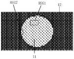
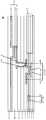
- FIG. 1is a schematic plan view of a display substrate provided by at least one embodiment of the present disclosure
- FIG. 2is a schematic plan view of a first display area and a second display area of the display substrate shown in FIG. 1;
- FIG. 3is an example of the first display area and the second display area of the display substrate shown in FIG. 2;
- FIG. 4is an enlarged view of a partial area REG1 in FIG. 3;
- FIG. 5Ais an enlarged view of a partial area REG2 in FIG. 3;
- FIG. 5Bis an enlarged view of the area in FIG. 5A that includes only one column of first pixel circuits, one column of first light-emitting elements, one column of second pixel circuits, and one column of second light-emitting elements;
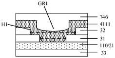
- Fig. 6Ais a schematic cross-sectional view taken along the line A-A' in Fig. 5B;
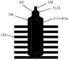
- FIG. 6Bis an enlarged view of the first via hole H1 in FIG. 6A;
- 6Cis a schematic layout of the area corresponding to the first via H1 and the connected anode in FIG. 6A;
- 6Dis a schematic layout of the area corresponding to the third via H3 and the connected source and drain metal layers in FIG. 6A;
- Fig. 7Ais a schematic cross-sectional view taken along the line B-B' in Fig. 5B;
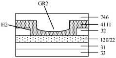
- FIG. 7Bis an enlarged view of the second via hole H2 in FIG. 7A;
- FIG. 7Cis a schematic layout of the area corresponding to the second via H2 and the connected anode in FIG. 7A;
- FIG. 7Dis a schematic diagram of another structure of the fourth via H4;
- FIG. 7Eis a schematic layout of the area corresponding to the fourth via H4 and the connected source and drain metal layers in FIG. 7A;
- Fig. 8Ais a schematic cross-sectional view taken along the line C-C' in Fig. 5B;
- FIG. 8Bis an enlarged view of the fifth via H5 in FIG. 8A;
- FIG. 8Cis a schematic layout of the area corresponding to the fifth via hole H5 and the connected anode and source and drain metal layers in FIG. 8A; FIG.
- FIG. 9is an enlarged view of a partial area REG3 of the third display area of the display substrate shown in FIG. 1;
- Fig. 10Ais a schematic cross-sectional view taken along the line D-D' in Fig. 9;
- FIG. 10Bis an enlarged view of the sixth via hole H6 in FIG. 10A;
- FIG. 11Ais a schematic layout corresponding to a partial area REG4 in FIG. 4; FIG.
- FIG. 11Bis a schematic layout showing only the first connecting line in FIG. 11A;
- FIG. 11Cis a schematic layout showing only the second connecting line in FIG. 11A;
- Fig. 11Dis a schematic cross-sectional view taken along the line E-E' in Fig. 11A;
- 12Ais one of the schematic layouts corresponding to the second light-emitting element in the second display area of the display substrate provided by some embodiments of the present disclosure
- 12Bis the second schematic layout corresponding to the second light-emitting element in the second display area of the display substrate provided by some embodiments of the present disclosure
- FIG. 13Ais a schematic structural diagram of a 7T1C pixel circuit
- FIG. 13Bis a driving timing diagram of the 7T1C pixel circuit shown in FIG. 13A;
- FIG. 14is a schematic block diagram of a display device provided by at least one embodiment of the present disclosure.
- FIG. 15is a schematic diagram of a laminated structure of a display device provided by at least one embodiment of the present disclosure.
- the distribution density per unit area (PPI) of the elementmay be smaller than the distribution density per unit area of light-emitting elements in other display regions of the display substrate.
- the arrangement of the light-emitting elements and corresponding pixel circuits in different areasis different, so that the wiring mode and layout design of the display substrate are different from the usual ones with uniform distribution.
- the display substrate of the light-emitting elementis different. This leads to the need to provide more via holes on the display substrate to achieve electrical connection between the film layers.
- the presence of more vias on the display substrateaffects the stability of the electrical connection, and makes the uniformity of the transmitted light poor, which affects the performance of the under-screen sensor (such as a camera). The sensing effect reduces the performance of the display device using the display substrate.
- At least one embodiment of the present disclosureprovides a display substrate and a display device.
- the display substratecan reduce the difficulty of processing, improve the reliability of electrical connections, improve the uniformity of transmitted light, and help improve the sensitivity of under-screen sensors (such as cameras). Test effect.
- At least one embodiment of the present disclosureprovides a display substrate including a display area.
- the display areaincludes a first display area and a second display area that do not overlap each other, the second display area at least partially surrounds the first display area, and the light transmittance of the first display area is greater than the light transmittance of the second display area.
- the first display areaincludes at least one first light-emitting element, and the second display area includes at least one first pixel circuit.
- the display areafurther includes at least one first connection line, and the first connection line includes a first end located in the first display area and a second end located in the second display area.
- At least one first light-emitting elementincludes a first sub-light-emitting element
- at least one first pixel circuitincludes a first sub-pixel circuit
- the first end of the first connecting lineis electrically connected to the anode of the first sub-light-emitting element.
- the second endis electrically connected to the first sub-pixel circuit.
- the display substrateincludes a first connection layer, a first insulating layer, a second insulating layer, and an anode layer that are sequentially stacked.
- the first connection lineis located in the first connection layer, the anode of the first sub-light-emitting element is located in the anode layer, and the anode of the first sub-light-emitting element is electrically connected to the first connection line through the first via hole penetrating the first insulating layer and the second insulating layer. connect.
- the cross-sectional shape of the first via hole in a plane perpendicular to the display substrateis an inverted boss shape.
- the opening diameter of the second insulating layeris larger than the opening diameter of the first insulating layer.
- the anode of the first sub-light-emitting elementincludes a first groove structure, the first groove structure is located in the first via hole, and the bottom of the first groove structure is in contact with the first connecting line to achieve electrical connection.
- FIG. 1is a schematic plan view of a display substrate provided by at least one embodiment of the present disclosure.
- the display substrate 01includes a display area 10, and the display area 10 includes a first display area 11, a second display area 12 and a third display area 13.
- the first display area 11, the second display area 12, and the third display area 13do not overlap each other.
- the third display area 13at least partially surrounds (eg, partially surrounds) the second display area 12, and the second display area 12 at least partially surrounds (eg, completely surrounds) the first display area 11.
- the display substrate 01may further include a peripheral area that at least partially surrounds the third display area 13.
- the light transmittance of the first display area 11is greater than the light transmittance of the second display area 12.
- at least the first display area 11allows light to pass through.
- the display substrate 01has a first side for display and a second side opposite to the first side.
- the first sideis the front side of the display substrate 01 (that is, the plane shown in FIG. 1 )
- the second sideis the back side of the display substrate 01.
- a sensormay be provided at a position corresponding to the first display area 11 on the second side of the display substrate 01, and the sensor may be, for example, an image sensor or an infrared sensor.
- the sensoris configured to receive light from the first side of the display substrate 01, so that it can perform image shooting, distance sensing, light intensity sensing, and other operations. For example, the light passes through the first display area 11 and then irradiates the sensor, thereby being affected by the sensor. Sensing.
- FIG. 2is a schematic plan view of a first display area and a second display area of the display substrate shown in FIG. 1.
- the second display area 12at least partially surrounds (for example, completely surrounds) the first display area 11.
- the shape of the first display area 11may be a circle or an ellipse, and the shape of the second display area 12 may be a rectangle, but the embodiment of the present disclosure is not limited thereto.
- the shapes of the first display area 11 and the second display area 12may both be rectangles or other suitable shapes.
- FIG. 3is an example of the first display area and the second display area of the display substrate shown in FIG. 2.
- 4is an enlarged view of a partial area REG1 in FIG. 3
- FIG. 5Ais an enlarged view of a partial area REG2 in FIG.
- FIG. 5Bshows that the adjacent first pixel circuit and the first light-emitting element are connected to each other.
- FIGS. 3, 4 and 4 5Ait can be understood that the left side of the first light-emitting element in FIG. 5B may also be provided with other first light-emitting elements not shown, and the right side of the first pixel circuit may also be provided with other first pixel circuits not shown.
- the first display area 11includes at least one (for example, multiple) first light-emitting elements 411.
- the first display area 11includes a plurality of first light emitting elements 411 arranged in an array, and the first light emitting elements 411 are configured to emit light.
- the pixel circuit for driving the first light-emitting element 411is arranged in the second display area 12, thereby reducing the metal coverage area of the first display area 11 and increasing the first display area 11. Therefore, the light transmittance of the first display area 11 is greater than the light transmittance of the second display area 12.
- the plurality of first light-emitting elements 411may be arranged in a plurality of light-emitting units, and these light-emitting units are arranged in an array.
- each light emitting unitmay include one or more first light emitting elements 411.
- the multiple first light-emitting elements 411may emit light of the same color or light of different colors, for example, may emit white light, red light, blue light, green light, etc., which may be determined according to actual needs. No restrictions.
- the arrangement of the plurality of first light-emitting elements 411can refer to the conventional arrangement of pixel units, such as GGRB, RGBG, RGB, etc., which is not limited in the embodiment of the present disclosure.
- the first display area 11allows light from the first side of the display substrate 01 to be at least partially transmitted to the second side of the display substrate 01.
- a sensoron the second side of the display substrate 01 and corresponding to the position of the first display area 11. Strong perception and other operations.
- the second display area 12includes at least one (for example, a plurality of) first pixel circuits 412.
- the first light-emitting elements 411 and the first pixel circuits 412are electrically connected in a one-to-one correspondence, and the plurality of first pixel circuits 412 are used to drive the plurality of first light-emitting elements 411 in a one-to-one correspondence.
- the rectangular frame shown in FIG. 5B(the black frame and white filled area indicated by reference numeral 412) represents the first pixel driving unit, and each first pixel driving unit includes a first pixel circuit 412.
- the first pixel circuit 412is configured to drive a plurality of first light-emitting elements 411 to emit light in a one-to-one correspondence. That is, one first pixel circuit 412 drives one corresponding first light-emitting element 411, and different first pixel circuits 412 drive different first light-emitting elements 411.
- the first pixel driving unitmay include one or more first pixel circuits 412.
- the first pixel driving unitalso includes a first pixel circuit 412.
- the first pixel driving unitalso includes a plurality of first pixel circuits 412, and the number of first light-emitting elements 411 in each light-emitting unit is, for example, It is equal to the number of first pixel circuits 412 in each first pixel driving unit, thereby achieving one-to-one corresponding driving.
- the plurality of first light-emitting elements 411are arranged in an array, and the plurality of first pixel circuits 412 are also arranged in an array.
- array arrangementmay refer to multiple devices being arranged in a group and multiple sets of device arrays, or it may refer to multiple devices themselves being arrayed, which is not limited in the embodiments of the present disclosure.
- FIG. 3, FIG. 4, FIG. 5A, and FIG.The four first pixel circuits 412 form a group, and the multiple groups of first pixel circuits 412 are arranged in an array.
- each first pixel driving unitincludes four first pixel circuits 412.
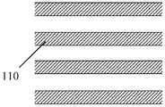
- the display area 10further includes at least one first connection line 110 and at least one second connection line 120.
- the first connecting line 110includes a first end located in the first display area 11 and a second end located in the second display area 12, that is, the first connecting line 110 extends from the first display area 11 to the second display area 12.
- the second connecting line 120includes a first end located in the first display area 11 and a second end located in the second display area 12, that is, the second connecting line 120 extends from the first display area 11 to the second end. Display area 12.
- the first light-emitting element 411includes a first sub-light-emitting element 411a and a second sub-light-emitting element 411b
- the first pixel circuit 412includes a first sub-pixel circuit 412a and a second sub-pixel circuit 412b.
- the first end of the first connection line 110is electrically connected to the anode of the first sub-light emitting element 411a
- the second end of the first connection line 110is electrically connected to the first sub-pixel circuit 412a
- the first connection line 110is configured to connect the first
- the electrical signal provided by the sub-pixel circuit 412ais transmitted to the anode of the first sub-light-emitting element 411a, thereby driving the first sub-light-emitting element 411a to emit light.
- the first end of the second connecting line 120is electrically connected to the anode of the second sub-light-emitting element 411b
- the second end of the second connecting line 120is electrically connected to the second sub-pixel circuit 412b
- the second connecting line 120is configured to connect the second
- the electrical signal provided by the sub-pixel circuit 412bis transmitted to the anode of the second sub-light-emitting element 411b, thereby driving the second sub-light-emitting element 411b to emit light.
- a part of the first light-emitting elements 411(for example, the first sub-light-emitting element 411a) is electrically connected to the first connection line 110, and the other part of the first light-emitting elements 411 (For example, the second sub-light-emitting element 411b) is electrically connected to the second connection line 120, so that all the first light-emitting elements 411 are electrically connected to the corresponding first pixel circuit 412 through the corresponding connection line, thereby realizing the first light emission Component 411 is driven.
- the first connection line 110 and the second connection line 120are located in different film layers of the display substrate 01, that is, the first connection line 110 and the second connection line 120 are located in two different film layers. Due to the different film layers, the orthographic projection of the first connecting line 110 on the display substrate 01 and the orthographic projection of the second connecting line 120 on the display substrate 01 can overlap, so that the wiring space can be effectively used, and the wiring is convenient, so that the first All the first light-emitting elements 411 in a display area 11 are electrically connected to corresponding connecting lines. Even if the number of first light-emitting elements 411 is large and the corresponding connection lines are large, the display substrate 01 can provide sufficient wiring space.
- different film layersare insulated from each other at positions where no vias are provided.
- the wires located in different film layerscan be electrically connected by providing vias.
- these different film layersare prepared in different processes.
- the first processis used to prepare one of these different film layers, and then the second process is used to prepare the other of these different film layers.
- a third processcan also be used to prepare an insulating layer. Insulate each other.
- the first process, the second process, and the third processmay be the same or different.
- the display substrate 01includes a base substrate
- different film layershave different distances from the base substrate. That is, among the different film layers, one film layer is closer to the base substrate, and the other film layer is farther from the base substrate.
- the meaning of the different film layerscan be referred to the above description, and will not be repeated.
- the connecting line used to realize the electrical connection between the first light-emitting element 411 and the first pixel circuit 412is not limited to being located in two different film layers, and may also be located in three different film layers.
- Layer, 4 film layers or any number of film layers, that is, these connecting linesare not limited to the first connecting line 110 and the second connecting line 120 described above, and may also include the first connecting line 110 and the second connecting line 110 and the second connecting line 120 described above.
- the connecting line 120is located on other connecting lines of different film layers, which is not limited in the embodiment of the present disclosure.
- a plurality of first connection lines 110 and a plurality of second connection lines 120form a connection line array, and each connection line in the connection line array (the connection line may be the first connection line 110 or The second connecting line 120) electrically connects one first light-emitting element 411 and one first pixel circuit 412 correspondingly.
- the distance between the correspondingly connected first light-emitting element 411 and the first pixel circuit 412may be substantially similar during the wiring design. .
- a plurality of pixel circuits(including a first pixel circuit 412 and a second pixel circuit 422) are arranged in an array, and a plurality of first light-emitting elements 411 are also arranged in an array.
- the first pixel circuit 412 in the (P-1)th column and the first light-emitting element 411 in the W-th columnpass through a connecting line (which can be the first connecting line 110 or The second connecting line 120) is electrically connected, and the length of the connecting line is, for example, about S1; the first pixel circuit 412 in the (P+1)th column and the first light-emitting element 411 in the (W+1)th column pass through the connecting line ( It may be the electrical connection of the first connecting wire 110 or the second connecting wire 120), and the length of the connecting wire is about S2, for example.
- the difference between S1 and S2is within a certain range and should not be too large.
- the specific value of the difference range of S1 and S2may be determined according to actual requirements, which is not limited in the embodiment of the present disclosure.
- the first pixel circuit 412 and the first light-emitting element 411 located in the (Q-1)th row and the (Q-2)th rowmay adopt a similar wiring manner.
- the embodiment of the present disclosureis not limited to the situation shown in FIG. 5A.
- the distribution positions of the first pixel circuit 412 and the first light-emitting element 411 connected by the connecting linemay also be other positions, which may be determined according to actual needs. The disclosed embodiment does not limit this.
- the distribution mode and positional relationship of the plurality of first connection lines 110 and the plurality of second connection lines 120 in a plane parallel to the display substrate 01are not limited, which can be determined according to actual wiring requirements.
- the first connecting lines 110 and the second connecting lines 120may be arranged at intervals one by one, or may be arranged at intervals in groups, or may be randomly distributed. This is the case in the embodiments of the present disclosure. No restrictions.
- the first sub-light-emitting element 411a and the second sub-light-emitting element 411bmay have no difference in structure and function.
- the first sub-pixel circuit 412a and the second sub-pixel circuit 412bare in structure and function. There may be no difference in function. They are called “first” and “second”, just to distinguish the connection lines (that is, the first connection line 110 and the second connection line 120) connected to these light-emitting elements and the pixel circuit. ), which does not constitute a limitation to the embodiments of the present disclosure.
- FIG. 6Ais a schematic cross-sectional view along the line AA' in FIG. 5B
- FIG. 6Bis an enlarged view of the first via H1 in FIG. 6A
- FIG. 6Cis a diagram corresponding to the first via H1 and the connected anode in FIG. 6A
- the schematic layout of the regionFIG. 6D is a schematic layout of the region corresponding to the third via H3 and the connected source and drain metal layers in FIG. 6A.
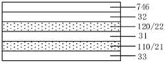
- the display substrate 01includes a third insulating layer 33, a first connection layer 21, a first insulating layer 31, a second insulating layer 32, and an anode layer 40 that are sequentially stacked.
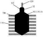
- the first sub-light-emitting element 411aincludes an anode 4111, a cathode 4113, and a light-emitting layer 4112 located between the anode 4111 and the cathode 4113.
- the first connection line 110is located on the first connection layer 21, and the anode 4111 of the first sub-light-emitting element 411 a is located on the anode layer 40.
- the anode 4111 of the first sub-light emitting element 411ais electrically connected to the first connection line 110 through the first via hole H1 penetrating the first insulating layer 31 and the second insulating layer 32.
- the cross-sectional shape of the first via hole H1 in a plane perpendicular to the display substrate 01is an inverted boss shape.
- the inverted boss shapecan be regarded as a shape formed by joining two rectangles of different sizes. The upper rectangle is larger, and the lower rectangle is larger. Therefore, a step is formed on at least one side surface of the inverted boss shape, for example, steps are formed on two side surfaces; for example, the orthographic projection of the part corresponding to the rectangle located below on the base substrate 74 is completely on the rectangle located above The corresponding part is inside the orthographic projection on the base substrate 74.
- each edge of the orthographic projection on the base substrate 74 and the part corresponding to the upper rectangleare on the substrate.
- the edges of the orthographic projection on the substrate 74are spaced apart from each other.
- the opening diameter L2 of the second insulating layer 32is larger than the opening diameter L1 of the first insulating layer 31.
- the opening diameter L2 of the second insulating layer 32may be 6 ⁇ m ⁇ 6 ⁇ m, or the opening diameter L1 of the first insulating layer 31 may be 6 ⁇ m ⁇ 6 ⁇ m. Since the first via hole H1 needs to penetrate through two insulating layers, the depth of the first via hole H1 is relatively large.
- the difficulty of processing the first via hole H1can be reduced, and it is convenient
- a conductive material(for example, the material of the anode 4111) is deposited in the first via hole H1, thereby improving the reliability of the electrical connection.
- the anode 4111 of the first sub-light-emitting element 411aincludes a first groove structure GR1, the first groove structure GR1 is located in the first via H1, and the bottom of the first groove structure GR1 is in contact with the first connecting line 110 to Realize electrical connection.
- the thickness of this partcan be reduced, so that the thickness of this part is not much different from the thickness of other parts of the anode 4111, thereby improving the overall
- the uniformity of the transmitted lightensures that there is no obvious difference in brightness in different areas, and the first display area 11 has better light transmittance, which in turn helps to improve the sensing effect of the under-screen sensor (such as a camera), such as imaging clearer.
- the first via hole H1is in the shape of an inverted boss, when preparing the anode 4111, it is advantageous to form the groove structure, and the process difficulty can be reduced.
- the surface of the first groove structure GR1 away from the first connection layer 21is a curved surface.
- the light intensity of the transmitted lightcan be continuously changed to avoid sudden changes in the light intensity at a local position, thereby further improving the uniformity of the transmitted light.
- the embodiment of the present disclosureis not limited to this.
- the surface of the first groove structure GR1 away from the first connection layer 21may also be a flat surface, an inclined surface, etc., which may be determined according to actual requirements.
- the anode 4111may include multiple anode sub-layers, for example, a three-layer structure of ITO/Ag/ITO (not labeled in the figure), etc.
- the specific form of the anode 4111is not limited in the embodiment of the present disclosure.
- the cathode 4113may be a structure formed on the entire surface of the display substrate 01, and the cathode 4113 may include, for example, metal materials such as lithium (Li), aluminum (Al), magnesium (Mg), and silver (Ag).
- the cathode 4113can be formed as a very thin layer, the cathode 4113 has good light transmittance.
- the anode 4111includes an ITO/Ag/ITO three-layer structure, its thickness may be 86/1000/86A.
- the second connecting line 120is located in a different film layer from the first connecting line 110 (the film layer where the second connecting line 120 is located and the corresponding cross-sectional structure will be described later). Description), and the second connection line 120 and the anode 4111 of the first sub-light-emitting element 411a are also located in different layers. Therefore, although the contour of the second connection line 120 overlaps with the anode 4111 of the first sub-light-emitting element 411a, However, the second connection line 120 is not electrically connected to the anode 4111 of the first sub-light-emitting element 411a.
- the first sub-pixel circuit 412aincludes a first switching transistor (for example, a switching thin film transistor 412T) and a storage capacitor 412C.
- the switching thin film transistor 412Tincludes a gate 4121, an active layer 4122, a first electrode 4123, and a second electrode 4124.
- the first electrode 4123may be a source or a drain
- the second electrode 4124may be a drain or a source.
- the storage capacitor 412Cincludes a first capacitor plate 4125 and a second capacitor plate 4126.
- the active layer 4121is disposed on the base substrate 74, and the first gate insulating layer 741 is disposed on the side of the active layer 4121 away from the base substrate 74.
- the gate 4122 and the first capacitor plate 4125are arranged in the same layer and are located on the side of the first gate insulating layer 741 away from the base substrate 74.
- a second gate insulating layer 742is provided on the side.
- the second capacitor plate 4126is disposed on the side of the second gate insulating layer 742 away from the base substrate 74, and the side of the second capacitor plate 4126 away from the base substrate 74 is provided with an interlayer insulating layer 743.
- the first electrode 4123 and the second electrode 4124are arranged on the side of the interlayer insulating layer 743 away from the base substrate 74, and pass through the first gate insulating layer 741, the second gate insulating layer 742, and the side of the interlayer insulating layer 743.
- the via hole in the interlayer insulating layer 743is electrically connected to the active layer 4121.
- the first electrode 4123 and the second electrode 4124are both located on the source and drain metal layer SD, the third insulating layer 33 is located on the source and drain metal layer SD, and the first connection layer 21 is located on the third insulating layer 33.
- the third insulating layer 33can not only play a role of insulation, but also play a role of planarization.
- the second end of the first connection line 110is electrically connected to the second electrode 4124 of the first switching transistor (for example, the switching thin film transistor 412T) included in the first sub-pixel circuit 412a through the third via hole H3 penetrating the third insulating layer 33. connect.
- the embodiment of the present disclosureis not limited to this.
- the second end of the first connection line 110may also be electrically connected to the first electrode 4123 of the switching thin film transistor 412T included in the first sub-pixel circuit 412a.
- the cross-sectional size of the third via hole H3 in a plane parallel to the display substrate 01may be 4 ⁇ m ⁇ 4 ⁇ m.
- the first display area 11further includes a transparent support layer 78 on the base substrate 74, and the first sub-light-emitting element 411 a is located on the side of the transparent support layer 78 away from the base substrate 74. Therefore, with respect to the base substrate 74, the first sub-light-emitting element 411a in the first display area 11 can be combined with light-emitting elements in other display areas (for example, the second light-emitting element in the second display area 12 described later).
- the element 421 and the third light-emitting element 431 in the third display area 13are at substantially the same height, so that the display effect of the display substrate 01 can be improved.
- the display substrate 01may also include a pixel defining layer 746, an encapsulation layer 747 and other structures.
- the pixel defining layer 746is disposed on the anode 4111 (for example, a partial structure of the anode 4111), and includes a plurality of openings to define different pixels or sub-pixels, and the light emitting layer 4112 is formed in the openings of the pixel defining layer 746.
- the horizontal distance between the opening of the pixel defining layer 746 and the first via hole H1may be 4.6 ⁇ m.
- the encapsulation layer 747may include a single-layer or multi-layer encapsulation structure, for example, the multilayer encapsulation structure includes a stack of an inorganic encapsulation layer and an organic encapsulation layer, thereby improving the encapsulation effect on the display substrate 01.
- the pixel defining layers 746 in the first display area 11, the second display area 12, and the third display area 13are arranged in the same layer, and the pixel defining layers 746 in the first display area 11, the second display area 12 and the third display area 13 are
- the encapsulation layer 747is provided in the same layer, and in some embodiments is still integrally connected, which is not limited in the embodiments of the present disclosure.
- the base substrate 74may be a glass substrate, a quartz substrate, a metal substrate, or a resin substrate, etc., and may be a rigid substrate or a flexible substrate, which is not limited in the embodiments of the present disclosure.
- the first gate insulating layer 741, the second gate insulating layer 742, the interlayer insulating layer 743, the first insulating layer 31, the second insulating layer 32, the third insulating layer 33, the pixel defining layer 746, and the encapsulation layer 747It may include inorganic insulating materials such as silicon oxide, silicon nitride, and silicon oxynitride, or may include organic insulating materials such as polyimide, polyphthalimide, polyphthalamide, acrylic resin, benzocyclobutene, or phenol resin.
- the embodiments of the present disclosuredo not specifically limit the materials of the above-mentioned functional layers.
- the thicknesses of the first insulating layer 31, the second insulating layer 32, and the third insulating layer 33may be 10000-15000A, respectively.
- the material of the active layer 4121may include semiconductor materials such as polysilicon or oxide semiconductor (for example, indium gallium zinc oxide).
- the part of the active layer 4121may be conductive through a conductive process such as doping, so as to have higher conductivity.
- the materials of the gate 4122, the first capacitor plate 4125, and the second capacitor plate 4126may include metal materials or alloy materials, such as molybdenum, aluminum, and titanium.
- the material of the first pole 4123 and the second pole 4124may include a metal material or an alloy material, such as a metal single-layer or multi-layer structure formed of molybdenum, aluminum, titanium, etc.
- the multi-layer structureis a multi-metal laminated layer , Such as titanium, aluminum, titanium three-layer metal laminate (Ti/Al/Ti) and so on.
- the display substrate 01 provided by the embodiment of the present disclosuremay be an organic light emitting diode (OLED) display substrate or a quantum dot light emitting diode (QLED) display substrate, etc.
- OLEDorganic light emitting diode
- QLEDquantum dot light emitting diode
- the embodiment of the present disclosuredoes not limit the specific type of the display substrate.
- the light-emitting layer(for example, the aforementioned light-emitting layer 4112) may include small molecular organic materials or polymer molecular organic materials, may be fluorescent light-emitting materials or phosphorescent light-emitting materials, and may be light-emitting Red light, green light, blue light, or white light.
- the light-emitting layermay further include functional layers such as an electron injection layer, an electron transport layer, a hole injection layer, and a hole transport layer.
- the light-emitting layermay include quantum dot materials, such as silicon quantum dots, germanium quantum dots, cadmium sulfide quantum dots, Cadmium selenide quantum dots, cadmium telluride quantum dots, zinc selenide quantum dots, lead sulfide quantum dots, lead selenide quantum dots, indium phosphide quantum dots and indium arsenide quantum dots, etc.
- the particle size of the quantum dotsis, for example, 2nm ⁇ 20nm.
- FIG. 7Ais a schematic cross-sectional view taken along the line BB' in Fig. 5B
- Fig. 7Bis an enlarged view of the second via H2 in Fig. 7A
- Fig. 7Cis a diagram corresponding to the second via H2 and the connected anode in Fig. 7A
- FIG. 7Dis a schematic diagram of another structure of the fourth via H4
- FIG. 7Eis a schematic layout of the area corresponding to the fourth via H4 and the connected source and drain metal layers in FIG. 7A.
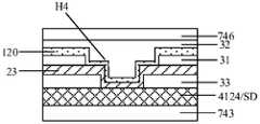
- the display substrate 01further includes a second connecting layer 22, the second connecting layer 22 is located between the first insulating layer 31 and the second insulating layer 32, and the second connecting line 120 is located at the second connecting layer.
- the arrangement of the second sub-light-emitting element 411bis similar to that of the first sub-light-emitting element 411a.
- the arrangement of the first switching transistor (for example, the switching thin film transistor 412T) and the storage capacitor 412C included in the second sub-pixel circuit 412bis the same as that of the first sub-pixel circuit 412b.
- the arrangement of the first switch transistor and the storage capacitor 412C in the sub-pixel circuit 412ais similar. For related description, please refer to the description of FIGS. 6A-6D above, which will not be repeated here.
- the anode 4111 of the second sub-light-emitting element 411bis located on the anode layer 40, and the anode 4111 of the second sub-light-emitting element 411b is electrically connected to the second connection line 120 through the second via H2 penetrating the second insulating layer 32.
- the anode 4111 of the second sub-light-emitting element 411bincludes a second groove structure GR2, the second groove structure GR2 is located in the second via H2, and the bottom of the second groove structure GR2 is in contact with the second connecting line 120 to Realize electrical connection.
- the part of the anode 4111 deposited in the second via hole H2as a groove structure, the thickness of this part can be reduced, so that the thickness of this part is not much different from the thickness of other parts of the anode 4111, thereby improving the overall Uniformity of transmitted light.
- the surface of the second groove structure GR2 away from the second connection layer 22is a curved surface.
- the light intensity of the transmitted lightcan be continuously changed to avoid sudden changes in the light intensity at a local position, thereby further improving the uniformity of the transmitted light.
- the embodiment of the present disclosureis not limited to this.
- the surface of the second groove structure GR2 away from the second connection layer 22may also be a flat surface, an inclined surface, etc., which may be determined according to actual requirements.
- the second end of the second connection line 120passes through the fourth via hole H4 passing through the third insulating layer 33 and the first insulating layer 31 and the first switching transistor (for example, the switching thin film transistor 412T) of the second sub-pixel circuit 412b.
- the second pole 4124is electrically connected.
- the embodiment of the present disclosureis not limited to this.
- the second terminal of the second connecting line 120may also be electrically connected to the first pole 4123 of the switching thin film transistor 412T included in the second sub-pixel circuit 412b.
- the cross-sectional shape of the fourth via hole H4 in a plane perpendicular to the display substrate 01is an inverted boss shape.
- the opening diameter of the first insulating layer 31is larger than the opening diameter of the third insulating layer 33. Since the fourth via H4 needs to penetrate through two insulating layers, the depth of the fourth via H4 is relatively large.
- a conductive material(for example, the material of the second connection line 120) is deposited in the fourth via hole H4, thereby improving the reliability of the electrical connection.
- the first connection line 110is located in a different film layer from the second connection line 120, and the anode 4111 of the first connection line 110 and the second sub-light-emitting element 411b are also located Different film layers, therefore, although the outline of the first connection line 110 overlaps with the anode 4111 of the second sub-light-emitting element 411b, the first connection line 110 is not electrically connected to the anode 4111 of the second sub-light-emitting element 411b.
- connection manner between the second connection line 120 and the first switching transistoris not limited to the manner shown in FIG. Difficulty.
- the second connection line 120is electrically connected to the transition metal layer 23, and the transition metal layer 23 is electrically connected to the first sub-pixel circuit 412b.
- the first pole 4123 or the second pole 4124 of the switching transistoris electrically connected, thereby realizing the electrical connection between the second connection line 120 and the switching thin film transistor 412T.
- the transition metal layer 23 and the first connection layer 21are formed in the same process, that is, the transition metal layer 23 and the first connection layer 21 can be the same film layer, in which a part of the structure forms the first connection line 110. Another part of the structure is used to electrically connect the second connection line 120 and the switching thin film transistor 412T of the second sub-pixel circuit 412b.
- the second display area 12further includes at least one (for example, multiple) second light-emitting elements 421 and at least one (for example, multiple) second pixel circuits 422.
- the second light-emitting element 421is electrically connected to the second pixel circuit 422 in a one-to-one correspondence, and the second pixel circuit 422 is used to drive the second light-emitting element 421 to emit light.
- the rectangular frame indicated by the reference number 422 in FIG. 5Bis only used to show the approximate position of the second pixel circuit 422, and does not indicate the specific shape of the second pixel circuit 422 and the specific boundary of the second pixel circuit 422.
- at least one second light-emitting element 421 and its corresponding second pixel circuit 422constitute a second pixel driving unit 42.
- the second pixel driving unit 42may include a second pixel circuit 422 and a second light-emitting element 421, or may include a plurality of second pixel circuits 422 and a plurality of second light-emitting elements 421.
- the second pixel driving unit 42includes a plurality of second pixel circuits 422 and a plurality of second light-emitting elements 421
- the number of second pixel circuits 422 in each second pixel driving unit 42is, for example, equal to that of the second light-emitting elements 421. Quantity, which realizes one-to-one correspondence drive.
- a plurality of second light emitting elements 421are arranged in an array, and a plurality of second pixel circuits 422 are also arranged in an array.
- array arrangementmay refer to multiple devices being arranged in a group and multiple sets of device arrays, or it may refer to multiple devices themselves being arrayed, which is not limited in the embodiments of the present disclosure.
- every four second light-emitting elements 421form a group, and multiple groups of second light-emitting elements 421 are arranged in an array.
- every four second pixel circuits 422are one group. Groups, multiple groups of second pixel circuits 422 are arranged in an array.
- each second pixel driving unit 42includes four second pixel circuits 422 and four second light-emitting elements 421.
- Fig. 8Ais a schematic cross-sectional view taken along the line CC' in Fig. 5B
- Fig. 8Bis an enlarged view of the fifth via H5 in Fig. 8A
- Fig. 8Cis corresponding to the fifth via H5 and the connected anode and Schematic layout of the area of the source and drain metal layers.
- the second pixel circuit 422includes a second switching transistor (for example, a switching thin film transistor 422T) and a storage capacitor 422C.
- the switching thin film transistor 422Tincludes a gate 4221, an active layer 4222, a first electrode 4223, and a second electrode 4224.
- the first electrode 4223may be a source or a drain
- the second electrode 4224may be a drain or a source.
- the storage capacitor 422Cincludes a first capacitor plate 4225 and a second capacitor plate 4226.
- the active layer 4221is disposed on the base substrate 74, and the first gate insulating layer 741 is disposed on the side of the active layer 4221 away from the base substrate 74.
- the gate 4222 and the first capacitor plate 4225are arranged in the same layer, and are located on the side of the first gate insulating layer 741 away from the base substrate 74.
- a second gate insulating layer 742is provided on the side.
- the second capacitor plate 4226is disposed on the side of the second gate insulating layer 742 away from the base substrate 74, and the side of the second capacitor plate 4226 away from the base substrate 74 is provided with an interlayer insulating layer 743.
- the first electrode 4223 and the second electrode 4224are disposed on the side of the interlayer insulating layer 743 away from the base substrate 74, and pass through the first gate insulating layer 741, the second gate insulating layer 742, and the interlayer insulating layer 743.
- the via hole in the interlayer insulating layer 743is electrically connected to the active layer 4221.
- the first electrode 4223 and the second electrode 4224are both located on the source and drain metal layer SD, and the third insulating layer 33 is located on the source and drain metal layer SD.
- the third insulating layer 33can not only play a role of insulation, but also play a role of planarization.
- the second light-emitting element 421includes an anode 4211, a cathode 4213, and a light-emitting layer 4212 located between the anode 4211 and the cathode 4213, and the anode 4211 is located at the anode layer 40.
- the anode 4211 of the second light-emitting element 421passes through the fifth via hole H5 penetrating the first insulating layer 31, the second insulating layer 32, and the third insulating layer 33 and the first electrode 4223 of the second switching transistor (for example, the switching thin film transistor 42T). Or the second pole 4224 is electrically connected.
- the cross-sectional shape of the fifth via H5 in a plane perpendicular to the display substrate 01is an inverted boss shape.
- the opening diameter L3 of the first insulating layer 31is larger than the opening diameter L4 of the third insulating layer 33. Since the fifth via hole H5 needs to penetrate through three insulating layers, the depth of the fifth via hole H5 is relatively large.
- a conductive materialfor example, the material of the anode 4211
- the opening diameter of the second insulating layer 32is equal to or larger than the opening diameter of the first insulating layer 31.
- the opening diameter of the second insulating layer 32is equal to the opening diameter of the first insulating layer 31, that is, both are equal to L3, so that the same mask can be used to prepare the first insulating layer.
- the openings of an insulating layer 31 and a second insulating layer 32reduce the number of masks required and reduce the production cost.
- the opening diameter of the second insulating layer 32may be larger than the opening diameter of the first insulating layer 31, so that the fifth via H5 can be formed in a three-stage stepped shape to further reduce the processing difficulty and facilitate A conductive material (for example, the material of the anode 4211) is deposited in the fifth via hole H5 to further improve the reliability of the electrical connection.
- a conductive materialfor example, the material of the anode 4211
- the anode 4211 of the second light-emitting element 421includes a third groove structure GR3, the third groove structure GR3 is located in the fifth via H5, and the bottom of the third groove structure GR3 is connected to the second switching transistor (such as a switching thin film transistor).
- the first pole 4223 or the second pole 4224 of 422T)contact to achieve electrical connection.
- the fifth via hole H5is in the shape of an inverted boss, when preparing the anode 4211, it is advantageous to form the groove structure, and the process difficulty can be reduced.
- the surface of the third groove structure GR3 away from the source and drain metal layer SDmay be a curved surface, a flat surface, an inclined surface, etc., which is not limited in the embodiment of the present disclosure.
- FIG. 9is an enlarged view of a partial area REG3 of the third display area of the display substrate shown in FIG. 1.
- the third display area 13includes at least one (for example, multiple) third light-emitting elements 431 and at least one (for example, multiple) third pixel circuits 432.
- the third light-emitting element 431is electrically connected to the third pixel circuit 432 in a one-to-one correspondence, and the third pixel circuit 432 is used to drive the third light-emitting element 431 to emit light.
- At least one third light-emitting element 431 and its corresponding third pixel circuit 432constitute a third pixel driving unit 43.
- the third pixel driving unit 43may include a third pixel circuit 432 and a third light-emitting element 431, or may include a plurality of third pixel circuits 432 and a plurality of third light-emitting elements 431.
- the third pixel driving unit 43includes a plurality of third pixel circuits 432 and a plurality of third light-emitting elements 431
- the number of third pixel circuits 432 in each third pixel driving unit 43is, for example, equal to that of the third light-emitting element 431. Quantity, which realizes one-to-one correspondence drive.
- a plurality of third light emitting elements 431are arranged in an array, and a plurality of third pixel circuits 432 are also arranged in an array.
- array arrangementmay refer to multiple devices being arranged in a group and multiple sets of device arrays, or it may refer to multiple devices themselves being arrayed, which is not limited in the embodiments of the present disclosure.
- every four third light-emitting elements 431form a group, and multiple groups of third light-emitting elements 431 are arranged in an array.
- every four third pixel circuits 432are one group. Groups of third pixel circuits 432 are arranged in an array.
- each third pixel driving unit 43includes four third pixel circuits 432 and four third light-emitting elements 431.
- Fig. 10Ais a schematic cross-sectional view taken along the line D-D' in Fig. 9 and Fig. 10B is an enlarged view of the sixth via H6 in Fig. 10A.
- the third pixel circuit 432includes a third switching transistor (for example, a switching thin film transistor 432T) and a storage capacitor 432C.
- the switching thin film transistor 432Tincludes a gate 4321, an active layer 4322, a first electrode 4323, and a second electrode 4324.
- the first electrode 4323may be a source or a drain
- the second electrode 4324may be a drain or a source.
- the storage capacitor 432Cincludes a first capacitor plate 4325 and a second capacitor plate 4326.
- the active layer 4321is disposed on the base substrate 74, and the first gate insulating layer 741 is disposed on the side of the active layer 4321 away from the base substrate 74.
- the gate 4322 and the first capacitor plate 4325are arranged in the same layer and are located on the side of the first gate insulating layer 741 away from the base substrate 74.
- a second gate insulating layer 742is provided on the side.
- the second capacitor plate 4326is disposed on the side of the second gate insulating layer 742 away from the base substrate 74, and the side of the second capacitor plate 4326 away from the base substrate 74 is provided with an interlayer insulating layer 743.
- the first electrode 4323 and the second electrode 4324are arranged on the side of the interlayer insulating layer 743 away from the base substrate 74, and pass through the first gate insulating layer 741, the second gate insulating layer 742, and the interlayer insulating layer 743.
- the via hole in the interlayer insulating layer 743is electrically connected to the active layer 4321.
- the first electrode 4323 and the second electrode 4324are both located on the source and drain metal layer SD, and the third insulating layer 33 is located on the source and drain metal layer SD.
- the third insulating layer 33can not only play a role of insulation, but also play a role of planarization.
- the third light-emitting element 431includes an anode 4311, a cathode 4313, and a light-emitting layer 4312 located between the anode 4311 and the cathode 4313, and the anode 4311 is located at the anode layer 40.
- the anode 4311 of the third light-emitting element 431passes through the sixth via hole H6 penetrating the first insulating layer 31, the second insulating layer 32, and the third insulating layer 33 and the first electrode 4323 of the third switching transistor (for example, the switching thin film transistor 432T). Or the second pole 4324 is electrically connected.
- the cross-sectional shape of the sixth via hole H6 in a plane perpendicular to the display substrate 01is an inverted boss shape.
- the opening diameter L5 of the first insulating layer 31is larger than the opening diameter L6 of the third insulating layer 33. Since the sixth via hole H6 needs to penetrate through three insulating layers, the depth of the sixth via hole H6 is relatively large.
- a conductive materialfor example, the material of the anode 4311
- the opening diameter of the second insulating layer 32is equal to or larger than the opening diameter of the first insulating layer 31.
- the opening diameter of the second insulating layer 32is equal to the opening diameter of the first insulating layer 31, that is, both are equal to L5, so that the same mask can be used to prepare the first insulating layer.
- the openings of an insulating layer 31 and a second insulating layer 32reduce the number of masks required and reduce the production cost.
- the opening diameter of the second insulating layer 32may be larger than the opening diameter of the first insulating layer 31, so that the sixth via hole H6 can be formed in a three-stage step shape to further reduce the processing difficulty and facilitate A conductive material (for example, the material of the anode 4311) is deposited in the sixth via hole H6 to further improve the reliability of the electrical connection.
- a conductive materialfor example, the material of the anode 4311
- the anode 4311 of the third light-emitting element 431includes a fourth groove structure GR4, the fourth groove structure GR4 is located in the sixth via H6, and the bottom of the fourth groove structure GR4 is connected to the third switching transistor (such as a switching thin film transistor).
- the sixth via hole H6is in the shape of an inverted boss, when preparing the anode 4311, it is advantageous to form the groove structure, and the process difficulty can be reduced.
- the surface of the fourth groove structure GR4 away from the source and drain metal layer SDmay be a curved surface, a flat surface, an inclined surface, etc., which is not limited in the embodiment of the present disclosure.
- FIG. 11Ais a schematic layout corresponding to the partial area REG4 in FIG. 4
- FIG. 11Bis a schematic layout showing only the first connecting line in FIG. 11A
- FIG. 11Cis a schematic layout showing only the second connecting line in FIG. 11A
- FIG. 11Dis a schematic cross-sectional view along the line E-E' in FIG. 11A.
- the first connection line 110 and the second connection line 120extend in respective extending directions, for example, the first connection line 110
- the extending direction of and the extending direction of the second connecting line 120may be the same or different.
- the third insulating layer 33, the first connecting line 110 (that is, the first connecting layer 21), the first insulating layer 31, the second connecting line 120 (that is, the second connecting layer 22), the second The insulating layer 32 and the pixel defining layer 746are stacked in sequence. Since the first insulating layer 31 is provided, the first connection line 110 and the second connection line 120 are insulated from each other and will not be short-circuited.
- FIG. 11Drefer to the foregoing content, which is not shown in FIG. 11D.
- FIG. 12Ais one of the schematic layouts corresponding to the second light-emitting element in the second display area of a display substrate provided by some embodiments of the present disclosure
- FIG. 12Bis a second display area of a display substrate provided by some embodiments of the present disclosure Schematic layout of the second light-emitting element corresponding to the second. For example, as shown in FIGS.
- the first connection line 110 and the second connection line 120are separated from the anode 4211 of the second light-emitting element 421.
- the bottom side(that is, the side where the anode 4211 is close to the base substrate 74) passes through and is insulated from the anode 4211 of the second light-emitting element 421.
- the first connection line 110 and the second connection line 120may respectively include transparent conductive traces, and the transparent conductive traces are made of, for example, indium tin oxide (ITO). Setting the first connecting line 110 and the second connecting line 120 as transparent conductive traces can increase the light transmittance of the display substrate 01.
- ITOindium tin oxide
- the plurality of first light-emitting elements 411are arranged in an array, and the first connection line 110 and the second connection line 120 both extend along the row direction of the array composed of the plurality of first light-emitting elements 411.
- the embodiment of the present disclosureis not limited to this, and the extending direction of the first connection line 110 and the second connection line 120 may also be any other direction, which is not limited by the embodiment of the present disclosure.
- the extension direction of the first connection line 110 and the extension direction of the second connection line 120may be the same or different.
- the first light emitting element 411, the second light emitting element 421, and the third light emitting element 431may each include an organic light emitting diode (OLED).
- OLEDorganic light emitting diode
- the embodiments of the present disclosureare not limited thereto.
- the first light-emitting element 411, the second light-emitting element 421, and the third light-emitting element 431may also be quantum dot light-emitting diodes (QLEDs) or other applicable light-emitting devices. There is no restriction on this.
- the distribution density per unit area of the plurality of first light-emitting elements 411 in the first display area 11is smaller than the distribution density per unit area of the plurality of second light-emitting elements 421 in the second display area 12, and the plurality of second light-emitting elements 421 are
- the distribution density per unit area in the second display area 12is smaller than the distribution density per unit area of the plurality of third light-emitting elements 431 in the third display area 13.
- the first display area 11 and the second display area 12may be referred to as a low-resolution area of the display substrate 01, and correspondingly, the third display area 13 may be referred to as a high-resolution area of the display substrate 01.
- the sum of the pixel light-emitting area of the second display area 12 and the first display area 11may be 1/8 to 1/2 of the pixel light-emitting area of the third display area 13.
- the distribution density per unit area of the plurality of first light-emitting elements 411 in the first display region 11may also be equal to the unit area distribution density of the plurality of second light-emitting elements 421 in the second display region 12 Density, which can be determined according to actual requirements, and the embodiment of the present disclosure does not limit this.
- the display substrate 01By increasing the distribution density per unit area of the light-emitting elements in the first display area 11, the second display area 12, and the third display area 13, it is possible to facilitate the display substrate 01 while ensuring that the three display areas emit light normally to display images.
- the light on the first side of the first display area 11passes through the first display area 11 to reach the second side, thereby facilitating the sensor provided on the second side of the display substrate 01 to sense the light.
- the display substrate 01may also include other structures or components, and is not limited to the structures and components described above.
- the display substrate 01may further include one or more barrier layers, buffer layers, etc., which are not limited in the embodiments of the present disclosure.
- FIG. 13Ais a schematic structural diagram of a 7T1C pixel circuit.
- the aforementioned first pixel circuit 412for example, the first sub-pixel circuit 412a and the second sub-pixel circuit 412b
- the second pixel circuit 422and the third pixel circuit 432 can all adopt the 7T1C pixel circuit.
- the 7T1C pixel circuit 100includes a first transistor CT1, a second transistor CT2, a third transistor CT3, a fourth transistor CT4, a fifth transistor CT5, a sixth transistor CT6, a seventh transistor CT7, and a memory Capacitance Cst.
- the first transistor CT1 to the seventh transistor CT7are all P-type transistors.
- the first terminal of the storage capacitor Cstis connected to the first power supply voltage terminal VDD to receive the first power supply voltage V1
- the second terminal of the storage capacitor Cstis connected to the first node N1.
- the first end of the light emitting element ELis connected to the fourth node N4, and the second end of the light emitting element EL is connected to the second power supply voltage terminal VSS to receive the second power supply voltage V2.
- the control terminal of the first transistor CT1is connected to the first node N1, the first terminal of the first transistor CT1 is connected to the second node N2, and the second terminal of the first transistor CT1 is connected to the third node N3.
- the first terminal of the second transistor CT2is connected to the second node N2, and the second terminal of the second transistor CT2 is connected to the data signal terminal DAT to receive a data signal (for example, a data voltage) Vdata.
- the first terminal of the third transistor CT3is connected to the first node N1, and the second terminal of the third transistor CT3 is connected to the third node N3.
- the first terminal of the fourth transistor CT4is connected to the first node N1, and the second terminal of the fourth transistor CT4 is connected to the first reset signal terminal Init1 to receive the first reset signal Vinit1 provided by the first reset signal terminal Init1.
- the first terminal of the fifth transistor CT5is connected to the first power supply voltage terminal VDD, and the first terminal of the fifth transistor CT5 is connected to the second node N2.
- the first terminal of the sixth transistor CT6is connected to the fourth node N4, and the second terminal of the sixth transistor CT6 is connected to the second reset signal terminal Init2 to receive the second reset signal Vinit2.
- the first terminal of the seventh transistor CT7is connected to the third node N3, and the second terminal of the seventh transistor CT7 is connected to the fourth node N4.
- control terminal GAT1 of the second transistor CT2 and the control terminal GAT2 of the third transistor CT3are both connected to the scan signal terminal GAT (not shown in the figure)
- the control terminal EM1 of the fifth transistor CT5 and the control terminal of the seventh transistor CT7 EM2are all connected to the light-emitting control terminal EM (not shown in the figure)
- the control terminal of the fourth transistor CT4is configured to be connected to the first reset control terminal RST1
- the control terminal of the sixth transistor CT6is configured to be connected to the second reset control terminal RST2.
- FIG. 13Aalso shows the first node N1, the second node N2, the third node N3, the fourth node N4, and the light emitting element EL.
- FIG. 13Bis a driving timing diagram of the 7T1C pixel circuit shown in FIG. 13A. As shown in FIG. 13B, each driving cycle of the 7T1C pixel circuit 100 includes a first phase t1, a second phase t2, and a third phase t3.
- the first reset control terminal RST1receives an active level
- the scan signal terminal GAT, the second reset control terminal RST2 and the light emission control terminal EMall receive an invalid level.
- the fourth transistor CT4is turned on, the second transistor CT2, the third transistor CT3, the fifth transistor CT5, the sixth transistor CT6, and the seventh transistor CT7 are turned off; the fourth transistor CT4 is configured to receive the first reset signal (for example , Reset voltage) Vinit1, and write the first reset signal Vinit1 to the storage capacitor Cst to reset the storage capacitor Cst; the voltage of the first node N1 is Vinit1, and Vinit1 is, for example, a negative value.
- the first transistor CT1is turned on.
- the scan signal terminal GAT and the second reset control terminal RST2receive the valid level
- the first reset control terminal RST1 and the light-emitting control terminal EMreceive the invalid level
- the first transistor CT1 to the third transistor CT3 and the sixth transistor CT6are turned on
- the fourth transistor CT4, the fifth transistor CT5, and the seventh transistor CT7are turned off
- the second transistor CT2receives the data signal Vdata
- the data signal Vdatais turned on
- the first transistor CT1 and the third transistor CT3are written to the control terminal of the first transistor CT1, and the storage capacitor Cst stores the data signal Vdata written to the control terminal of the first transistor CT1 at the control terminal of the first transistor CT1.
- the voltage of a node N1is Vdata+Vth; the sixth transistor CT6 is configured to receive a second reset signal (for example, a reset voltage) Vinit2, and write the second reset signal Vinit2 to the first end of the light-emitting element EL to emit light
- a second reset signalfor example, a reset voltage
- Vinit2The first terminal of the element EL is reset
- Vinit2Vinit2
- Vinit2is, for example, a negative value.
- the light-emitting control terminal EMreceives the valid level, and the first reset control terminal RST1, the scan signal terminal GAT, and the second reset control terminal RST2 receive the invalid level;
- the first transistor CT1, the fifth transistor CT5, and the seventh transistor CT7are turned on, the second transistor CT2, the third transistor CT3, the fourth transistor CT4, and the sixth transistor CT6 are turned off;
- the first transistor CT1is configured to be based on storage
- the data signalfor example, the data voltage
- Vdata in the storage capacitor Cst and the received first power supply voltage V1are controlled to flow through the first transistor CT1 and from the first power supply voltage terminal VDD to the light-emitting element EL for driving the light-emitting element
- the driving current of EL; the voltage of the first node N1is Vdata+Vth, and the voltage of the second node N2 is VDD;
- the driving current Idcan be expressed by the following formula:
- k⁇ Cox ⁇ W/L; ⁇ is the mobility of carriers in the first transistor CT1, Cox is the capacitance of the gate oxide layer of the first transistor CT1, and W/L is the channel of the first transistor CT1.
- the width-to-length ratio of the channelVth is the threshold voltage of the first transistor CT1, Vth is the gate-source voltage of the first transistor CT1, Vg is the gate voltage of the first transistor CT1, and Vs is the source voltage of the first transistor CT1.
- the 7T1C pixel circuit 100 shown in FIGS. 13A and 13Bhas a threshold compensation function.
- the first pixel circuit 412(for example, the first sub-pixel circuit 412a and the second sub-pixel circuit 412b), the second pixel circuit 422, and the third pixel circuit 432 are not limited to the above 7T1C.
- the pixel circuitmay also adopt other applicable pixel circuits, which are not limited in the embodiments of the present disclosure.
- the specific circuit structures of the first pixel circuit 412, the second pixel circuit 422, and the third pixel circuit 432may be the same or different from each other, which may be determined according to actual requirements, which is not limited in the embodiment of the present disclosure.
- the first switching transistor in the first pixel circuit 412, the second switching transistor in the second pixel circuit 422, and the third switching transistor in the third pixel circuit 432may all be the seventh transistor CT7 in FIG. 13A.
- the seventh transistor CT7supplies an electric signal to the anode of the corresponding light emitting element EL.
- the first light-emitting element 411(for example, the first sub-light-emitting element 411a and the second sub-light-emitting element 411b), the second light-emitting element 421, and the third light-emitting element 431 may all be the light-emitting element EL in FIG. 13A. It can be an organic light emitting diode (OLED) or a quantum dot light emitting diode (QLED).
- At least one embodiment of the present disclosurefurther provides a display device, which includes the display substrate provided by any embodiment of the present disclosure.
- the display devicecan reduce the processing difficulty, improve the reliability of the electrical connection, improve the uniformity of transmitted light, and help improve the sensing effect of the under-screen sensor (such as a camera).
- FIG. 14is a schematic block diagram of a display device provided by at least one embodiment of the present disclosure.
- the display device 20includes a display substrate 210, which is a display substrate provided by any embodiment of the present disclosure, such as the aforementioned display substrate 01.
- the display device 20can be any electronic device with a display function, such as a smart phone, a notebook computer, a tablet computer, a TV, and the like.
- the smart phone or tablet computermay have a full-screen design, that is, there is no peripheral area surrounding the third display area 13.
- the smart phone or tablet computeralso has an under-screen sensor (such as a camera, an infrared sensor, etc.), which can perform operations such as image shooting, distance sensing, and light intensity sensing.
- an under-screen sensorsuch as a camera, an infrared sensor, etc.
- FIG. 15is a schematic diagram of a laminated structure of a display device provided by at least one embodiment of the present disclosure.
- the display device 20includes a display substrate 210, and the display substrate 210 is a display substrate provided by any embodiment of the present disclosure, such as the aforementioned display substrate 01.
- the display device 20further includes a sensor 220.
- the display substrate 01has a first side F1 for display and a second side F2 opposite to the first side F1. That is, the first side F1 is the display side, and the second side F2 is the non-display side.
- the display substrate 01is configured to perform a display operation on the first side F1, that is, the first side F1 of the display substrate 01 is the light emitting side of the display substrate 01, and the first side F1 faces the user.
- the first side F1 and the second side F2are opposed to each other in the normal direction of the display surface of the display substrate 01.
- the sensor 220is disposed on the second side F2 of the display substrate 01, and the sensor 220 is configured to receive light from the first side F1.
- the sensor 220 and the first display area 11overlap in the normal direction of the display surface of the display substrate 01 (for example, the direction perpendicular to the display substrate 01), and the sensor 220 may receive and process the data passing through the first display area 11.
- the optical signalmay be visible light, infrared light, etc.
- the first display area 11allows light from the first side F1 to be at least partially transmitted to the second side F2.
- the first display area 11is not provided with a pixel circuit. In this case, the light transmittance of the first display area 11 can be improved.
- the orthographic projection of the sensor 220 on the display substrate 01at least partially overlaps the first display area 11.
- the orthographic projection of the sensor 220 on the display substrate 01is located in the first display area 11.
- the orthographic projection of the sensor 220 on the display substrate 01is similar to the first display. Area 11 partially overlaps. At this time, since the light can propagate to the sensor 220 laterally, it is not necessary that the sensor 220 is completely located at a position corresponding to the first display area 11.
- the first display area 11can be reduced.
- the element in the shielding of the light signal incident to the first display area 11 and irradiated to the sensor 220can improve the signal-to-noise ratio of the image output by the sensor 220.
- the first display area 11may be referred to as a high light transmission area of a low resolution area of the display substrate 01
- the second display area 12may be referred to as a transition area.
- the senor 220may be an image sensor, which may be used to collect an image of the external environment facing the light-collecting surface of the sensor 220, and may be, for example, a CMOS image sensor or a CCD image sensor.
- the sensor 220may also be an infrared sensor, a distance sensor, or the like.
- the sensor 220may be implemented as a camera of a mobile terminal such as a mobile phone, a notebook, etc., and may also include, for example, a lens, a mirror, or an optical waveguide as required.
- Optical devices to modulate the optical pathmay be implemented as a camera of a mobile terminal such as a mobile phone, a notebook, etc., and may also include, for example, a lens, a mirror, or an optical waveguide as required. Optical devices to modulate the optical path.
- the senor 220may include photosensitive pixels arranged in an array.
- each photosensitive pixelmay include a photosensitive detector (for example, a photodiode, a phototransistor) and a switching transistor (for example, a switching thin film transistor).
- the photodiodecan convert the light signal irradiated on it into an electrical signal
- the switching transistorcan be electrically connected with the photodiode to control whether the photodiode is in the state of collecting the light signal and the time for collecting the light signal.
- the anode of the first light-emitting element 411adopts a stacked structure of ITO/Ag/ITO.
- the first display area 11only the anode of the first light-emitting element 411 does not transmit light, that is, it is used for
- the traces for driving the first light-emitting element 411are configured as transparent conductive traces. In this case, not only can the light transmittance of the first display area 11 be further improved, but also the diffraction and reflection caused by various elements in the first display area 11 can be reduced.
- the display device 20may further include more components and structures, which are not limited in the embodiments of the present disclosure.
- the technical effects and detailed description of the display device 20reference may be made to the above description of the display substrate 01, which will not be repeated here.
Landscapes
- Engineering & Computer Science (AREA)
- Microelectronics & Electronic Packaging (AREA)
- Chemical & Material Sciences (AREA)
- Inorganic Chemistry (AREA)
- Physics & Mathematics (AREA)
- Life Sciences & Earth Sciences (AREA)
- Sustainable Development (AREA)
- Geometry (AREA)
- Devices For Indicating Variable Information By Combining Individual Elements (AREA)
- Optics & Photonics (AREA)
- Electroluminescent Light Sources (AREA)
Abstract
Description
Translated fromChinese本申请要求于2020年6月23日递交的中国专利申请第202010580274.8号的优先权,在此全文引用上述中国专利申请公开的内容以作为本申请的一部分。This application claims the priority of the Chinese patent application No. 202010580274.8 filed on June 23, 2020, and the content disclosed in the above Chinese patent application is quoted here in full as a part of this application.
本公开的实施例涉及一种显示基板及显示装置。The embodiment of the present disclosure relates to a display substrate and a display device.
有机发光二极管(Organic Light-Emitting Diode,OLED)显示器件具有视角宽、对比度高、响应速度快、色域广、屏占比高、自发光、轻薄等特点。由于具有上述特点和优势,有机发光二极管(OLED)显示器件逐渐受到人们的广泛关注并且可以适用于手机、显示器、笔记本电脑、智能手表、数码相机、仪器仪表、柔性可穿戴装置等具有显示功能的装置。随着显示技术的进一步发展,具有高屏占比的显示装置已经不能满足人们的需求,具有全面屏的显示装置成为未来显示技术的发展趋势。Organic Light-Emitting Diode (OLED) display devices have the characteristics of wide viewing angle, high contrast, fast response speed, wide color gamut, high screen-to-body ratio, self-luminous, thin and light. Due to the above-mentioned characteristics and advantages, organic light-emitting diode (OLED) display devices have gradually received widespread attention and can be applied to mobile phones, displays, notebook computers, smart watches, digital cameras, instrumentation, flexible wearable devices and other display functions. Device. With the further development of display technology, display devices with a high screen-to-body ratio can no longer meet people's needs, and display devices with a full screen have become the development trend of display technology in the future.
发明内容Summary of the invention
本公开至少一个实施例提供一种显示基板,包括显示区域;其中,所述显示区域包括互不重叠的第一显示区域和第二显示区域,所述第二显示区域至少部分围绕所述第一显示区域,所述第一显示区域的透光率大于所述第二显示区域的透光率;所述第一显示区域包括至少一个第一发光元件,所述第二显示区域包括至少一个第一像素电路;所述显示区域还包括至少一条第一连接线,所述第一连接线包括位于所述第一显示区域的第一端和位于所述第二显示区域的第二端;所述至少一个第一发光元件包括第一子发光元件,所述至少一个第一像素电路包括第一子像素电路,所述第一连接线的第一端与所述第一子发光元件的阳极电连接,所述第一连接线的第二端与所述第一子像素电路电连接;所述显示基板包括依次叠置的第一连接层、第一绝缘层、第二绝缘层和阳极层;所述第一连接线位于所述第一连接层,所述第一子发光元件的阳极位于所述阳极层,所述第一子发光元件的阳极通过贯穿所述第一绝缘层和所述第二绝缘层的第一过孔与所述第一连接线电连接;所述第一过孔在垂直于所述显示基板的平面内的截面形状为倒凸台形状,在所述第一过孔中,所述第二绝缘层的开口口径大于所述第一绝缘层的开口口径;所述第一子发光元件的阳极包括第一凹槽结构,所述第一凹槽结构位于所述第一过孔内,且所述第一凹槽结构的底部与所述第一连接线接触以实现电连接。At least one embodiment of the present disclosure provides a display substrate including a display area; wherein the display area includes a first display area and a second display area that do not overlap each other, and the second display area at least partially surrounds the first display area. Display area, the light transmittance of the first display area is greater than the light transmittance of the second display area; the first display area includes at least one first light-emitting element, and the second display area includes at least one first A pixel circuit; the display area further includes at least one first connection line, the first connection line includes a first end located in the first display area and a second end located in the second display area; the at least One first light-emitting element includes a first sub-light-emitting element, the at least one first pixel circuit includes a first sub-pixel circuit, and the first end of the first connection line is electrically connected to the anode of the first sub-light-emitting element, The second end of the first connection line is electrically connected to the first sub-pixel circuit; the display substrate includes a first connection layer, a first insulating layer, a second insulating layer, and an anode layer that are sequentially stacked; The first connection line is located in the first connection layer, the anode of the first sub-light-emitting element is located in the anode layer, and the anode of the first sub-light-emitting element passes through the first insulating layer and the second insulating layer. The first via hole of the layer is electrically connected to the first connection line; the cross-sectional shape of the first via hole in a plane perpendicular to the display substrate is an inverted boss shape, and in the first via hole, The opening diameter of the second insulating layer is larger than the opening diameter of the first insulating layer; the anode of the first sub-light-emitting element includes a first groove structure, and the first groove structure is located in the first via hole Inside, and the bottom of the first groove structure is in contact with the first connecting line to achieve electrical connection.
例如,在本公开一实施例提供的显示基板中,所述显示区域还包括至少一条第二连接线,所述第二连接线包括位于所述第一显示区域的第一端和位于所述第二显示区域的第二端;所述至少一个第一发光元件还包括第二子发光元件,所述至少一个第一像素电路还包 括第二子像素电路,所述第二连接线的第一端与所述第二子发光元件的阳极电连接,所述第二连接线的第二端与所述第二子像素电路电连接;所述显示基板还包括第二连接层,所述第二连接层位于所述第一绝缘层和所述第二绝缘层之间,所述第二连接线位于所述第二连接层;所述第二子发光元件的阳极位于所述阳极层,所述第二子发光元件的阳极通过贯穿所述第二绝缘层的第二过孔与所述第二连接线电连接;所述第二子发光元件的阳极包括第二凹槽结构,所述第二凹槽结构位于所述第二过孔内,且所述第二凹槽结构的底部与所述第二连接线接触以实现电连接。For example, in the display substrate provided by an embodiment of the present disclosure, the display area further includes at least one second connecting line, and the second connecting line includes a first end located in the first display area and a first end located in the first display area. Two second ends of the display area; the at least one first light-emitting element further includes a second sub-light-emitting element, the at least one first pixel circuit further includes a second sub-pixel circuit, and the first end of the second connecting line Is electrically connected to the anode of the second sub-light-emitting element, and the second end of the second connection line is electrically connected to the second sub-pixel circuit; the display substrate further includes a second connection layer, the second connection Layer is located between the first insulating layer and the second insulating layer, the second connecting line is located on the second connecting layer; the anode of the second sub-light emitting element is located on the anode layer, and the first The anode of the two sub-light-emitting elements is electrically connected to the second connecting line through a second via hole penetrating the second insulating layer; the anode of the second sub-light-emitting element includes a second groove structure, and the second concave The groove structure is located in the second via hole, and the bottom of the second groove structure is in contact with the second connecting line to achieve electrical connection.
例如,在本公开一实施例提供的显示基板中,所述第一凹槽结构远离所述第一连接层的表面为曲面,所述第二凹槽结构远离所述第二连接层的表面为曲面。For example, in the display substrate provided by an embodiment of the present disclosure, the surface of the first groove structure away from the first connection layer is curved, and the surface of the second groove structure away from the second connection layer is Surface.
例如,在本公开一实施例提供的显示基板中,所述第一子像素电路和所述第二子像素电路中的每个包括第一开关晶体管,所述第一开关晶体管包括栅极、第一极和第二极;所述显示基板还包括源漏极金属层和第三绝缘层,所述第三绝缘层位于所述源漏极金属层上,所述第一连接层位于所述第三绝缘层上,所述第一开关晶体管的第一极和第二极位于所述源漏极金属层;所述第一连接线的第二端通过贯穿所述第三绝缘层的第三过孔与所述第一子像素电路的第一开关晶体管的第一极或第二极电连接;所述第二连接线的第二端通过贯穿所述第三绝缘层和所述第一绝缘层的第四过孔与所述第二子像素电路的第一开关晶体管的第一极或第二极电连接。For example, in the display substrate provided by an embodiment of the present disclosure, each of the first sub-pixel circuit and the second sub-pixel circuit includes a first switching transistor, and the first switching transistor includes a gate, a second One electrode and a second electrode; the display substrate further includes a source and drain metal layer and a third insulating layer, the third insulating layer is located on the source and drain metal layer, and the first connection layer is located on the first On the three insulating layer, the first electrode and the second electrode of the first switch transistor are located in the source and drain metal layer; the second end of the first connecting line passes through the third insulating layer The hole is electrically connected to the first electrode or the second electrode of the first switching transistor of the first sub-pixel circuit; the second end of the second connecting line passes through the third insulating layer and the first insulating layer The fourth via hole is electrically connected to the first pole or the second pole of the first switch transistor of the second sub-pixel circuit.
例如,在本公开一实施例提供的显示基板中,所述第四过孔在垂直于所述显示基板的平面内的截面形状为倒凸台形状,在所述第四过孔中,所述第一绝缘层的开口口径大于所述第三绝缘层的开口口径。For example, in the display substrate provided by an embodiment of the present disclosure, the cross-sectional shape of the fourth via in a plane perpendicular to the display substrate is an inverted boss shape, and in the fourth via, the The opening diameter of the first insulating layer is larger than the opening diameter of the third insulating layer.
例如,在本公开一实施例提供的显示基板中,在所述第四过孔中,所述第二连接线与过渡金属层接触电连接,所述过渡金属层与所述第二子像素电路的第一开关晶体管的第一极或第二极接触电连接,所述过渡金属层与所述第一连接层在同一工艺中形成。For example, in the display substrate provided by an embodiment of the present disclosure, in the fourth via hole, the second connection line is electrically connected to the transition metal layer, and the transition metal layer is connected to the second sub-pixel circuit. The first electrode or the second electrode of the first switching transistor is electrically connected in contact, and the transition metal layer and the first connection layer are formed in the same process.
例如,在本公开一实施例提供的显示基板中,所述第二显示区域还包括至少一个第二发光元件和至少一个第二像素电路,所述第二发光元件和所述第二像素电路电连接;所述第二像素电路包括第二开关晶体管,所述第二开关晶体管包括栅极、第一极和第二极,所述第二开关晶体管的第一极和第二极位于所述源漏极金属层;所述第二发光元件的阳极位于所述阳极层,所述第二发光元件的阳极通过贯穿所述第一绝缘层、所述第二绝缘层和所述第三绝缘层的第五过孔与所述第二开关晶体管的第一极或第二极电连接;所述第五过孔在垂直于所述显示基板的平面内的截面形状为倒凸台形状,在所述第五过孔中,所述第一绝缘层的开口口径大于所述第三绝缘层的开口口径。For example, in the display substrate provided by an embodiment of the present disclosure, the second display area further includes at least one second light-emitting element and at least one second pixel circuit, and the second light-emitting element and the second pixel circuit are electrically connected to each other. Connected; the second pixel circuit includes a second switching transistor, the second switching transistor includes a gate, a first pole, and a second pole, the first pole and the second pole of the second switching transistor are located at the source Drain metal layer; the anode of the second light-emitting element is located in the anode layer, the anode of the second light-emitting element passes through the first insulating layer, the second insulating layer and the third insulating layer The fifth via hole is electrically connected to the first pole or the second pole of the second switching transistor; the cross-sectional shape of the fifth via hole in a plane perpendicular to the display substrate is an inverted boss shape. In the fifth via hole, the opening diameter of the first insulating layer is larger than the opening diameter of the third insulating layer.
例如,在本公开一实施例提供的显示基板中,在所述第五过孔中,所述第二绝缘层的开口口径等于或大于所述第一绝缘层的开口口径。For example, in the display substrate provided by an embodiment of the present disclosure, in the fifth via hole, the opening diameter of the second insulating layer is equal to or larger than the opening diameter of the first insulating layer.
例如,在本公开一实施例提供的显示基板中,所述第二发光元件的阳极包括第三凹槽结构,所述第三凹槽结构位于所述第五过孔内,所述第三凹槽结构的底部与所述第二开关晶体管的第一极或第二极接触以实现电连接。For example, in the display substrate provided by an embodiment of the present disclosure, the anode of the second light-emitting element includes a third groove structure, the third groove structure is located in the fifth via, and the third groove The bottom of the groove structure is in contact with the first pole or the second pole of the second switch transistor to achieve electrical connection.
例如,在本公开一实施例提供的显示基板中,所述显示区域还包括第三显示区域,所述第三显示区域至少部分围绕所述第二显示区域,所述第三显示区域与所述第一显示区域和所述第二显示区域不重叠;所述第三显示区域包括至少一个第三发光元件和至少一个第三像素电路,所述第三发光元件和所述第三像素电路电连接;所述第三像素电路包括第三开关晶体管,所述第三开关晶体管包括栅极、第一极和第二极,所述第三开关晶体管的第一极和第二极位于所述源漏极金属层;所述第三发光元件的阳极位于所述阳极层,所述第三发光元件的阳极通过贯穿所述第一绝缘层、所述第二绝缘层和所述第三绝缘层的第六过孔与所述第三开关晶体管的第一极或第二极电连接;所述第六过孔在垂直于所述显示基板的平面内的截面形状为倒凸台形状,在所述第六过孔中,所述第一绝缘层的开口口径大于所述第三绝缘层的开口口径。For example, in the display substrate provided by an embodiment of the present disclosure, the display area further includes a third display area, the third display area at least partially surrounds the second display area, and the third display area is connected to the third display area. The first display area and the second display area do not overlap; the third display area includes at least one third light-emitting element and at least one third pixel circuit, the third light-emitting element and the third pixel circuit are electrically connected The third pixel circuit includes a third switching transistor, the third switching transistor includes a gate, a first pole, and a second pole, and the first pole and the second pole of the third switching transistor are located in the source and drain Polar metal layer; the anode of the third light-emitting element is located in the anode layer, the anode of the third light-emitting element passes through the first insulating layer, the second insulating layer and the third insulating layer The six via holes are electrically connected to the first pole or the second pole of the third switching transistor; the cross-sectional shape of the sixth via hole in a plane perpendicular to the display substrate is an inverted boss shape, and the In the six via holes, the opening diameter of the first insulating layer is larger than the opening diameter of the third insulating layer.
例如,在本公开一实施例提供的显示基板中,在所述第六过孔中,所述第二绝缘层的开口口径等于或大于所述第一绝缘层的开口口径。For example, in the display substrate provided by an embodiment of the present disclosure, in the sixth via hole, the opening diameter of the second insulating layer is equal to or larger than the opening diameter of the first insulating layer.
例如,在本公开一实施例提供的显示基板中,所述第三发光元件的阳极包括第四凹槽结构,所述第四凹槽结构位于所述第六过孔内,所述第四凹槽结构的底部与所述第三开关晶体管的第一极或第二极接触以实现电连接。For example, in the display substrate provided by an embodiment of the present disclosure, the anode of the third light-emitting element includes a fourth groove structure, the fourth groove structure is located in the sixth via, and the fourth groove The bottom of the groove structure is in contact with the first pole or the second pole of the third switch transistor to achieve electrical connection.
例如,在本公开一实施例提供的显示基板中,所述第一连接线和所述第二连接线分别包括透明导电走线。For example, in the display substrate provided by an embodiment of the present disclosure, the first connection line and the second connection line respectively include transparent conductive traces.
例如,在本公开一实施例提供的显示基板中,所述至少一个第一发光元件包括多个第一发光元件,所述多个第一发光元件呈阵列排布,所述第一连接线和所述第二连接线均沿所述多个第一发光元件组成的阵列的行方向延伸。For example, in the display substrate provided by an embodiment of the present disclosure, the at least one first light-emitting element includes a plurality of first light-emitting elements, the plurality of first light-emitting elements are arranged in an array, and the first connecting line and The second connecting lines all extend along the row direction of the array composed of the plurality of first light-emitting elements.
例如,在本公开一实施例提供的显示基板中,所述第一发光元件、所述第二发光元件和所述第三发光元件分别包括有机发光二极管。For example, in the display substrate provided by an embodiment of the present disclosure, the first light-emitting element, the second light-emitting element, and the third light-emitting element each include an organic light-emitting diode.
例如,在本公开一实施例提供的显示基板中,所述至少一个第一发光元件包括多个第一发光元件,所述至少一个第二发光元件包括多个第二发光元件,所述至少一个第三发光元件包括多个第三发光元件;所述多个第一发光元件在所述第一显示区域内的单位面积分布密度小于或等于所述多个第二发光元件在所述第二显示区域内的单位面积分布密度,所述多个第二发光元件在所述第二显示区域内的单位面积分布密度小于所述多个第三发光元件在所述第三显示区域内的单位面积分布密度。For example, in the display substrate provided by an embodiment of the present disclosure, the at least one first light-emitting element includes a plurality of first light-emitting elements, the at least one second light-emitting element includes a plurality of second light-emitting elements, and the at least one The third light-emitting element includes a plurality of third light-emitting elements; the distribution density per unit area of the plurality of first light-emitting elements in the first display area is less than or equal to that of the plurality of second light-emitting elements in the second display area. A distribution density per unit area in the region, where the distribution density per unit area of the plurality of second light-emitting elements in the second display region is smaller than the distribution density per unit area of the plurality of third light-emitting elements in the third display region density.
本公开至少一个实施例还提供一种显示装置,包括本公开任一实施例所述的显示基板。At least one embodiment of the present disclosure further provides a display device, including the display substrate according to any embodiment of the present disclosure.
例如,本公开一实施例提供的显示装置还包括传感器,其中,所述显示基板具有用于显示的第一侧和与所述第一侧相对的第二侧,所述第一显示区域允许来自所述第一侧的光至少部分透射至所述第二侧,所述传感器设置于所述显示基板的第二侧,所述传感器配置为接收来自所述第一侧的光。For example, the display device provided by an embodiment of the present disclosure further includes a sensor, wherein the display substrate has a first side for display and a second side opposite to the first side, and the first display area allows The light on the first side is at least partially transmitted to the second side, the sensor is disposed on the second side of the display substrate, and the sensor is configured to receive the light from the first side.
例如,在本公开一实施例提供的显示装置中,所述传感器在所述显示基板上的正投影与所述第一显示区域至少部分重叠。For example, in the display device provided by an embodiment of the present disclosure, the orthographic projection of the sensor on the display substrate at least partially overlaps the first display area.
为了更清楚地说明本公开实施例的技术方案,下面将对实施例的附图作简单地介绍,显而易见地,下面描述中的附图仅仅涉及本公开的一些实施例,而非对本公开的限制。In order to explain the technical solutions of the embodiments of the present disclosure more clearly, the following will briefly introduce the drawings of the embodiments. Obviously, the drawings in the following description only refer to some embodiments of the present disclosure, and do not limit the present disclosure. .
图1为本公开至少一个实施例提供的一种显示基板的平面示意图;FIG. 1 is a schematic plan view of a display substrate provided by at least one embodiment of the present disclosure;
图2为图1所示的显示基板的第一显示区域和第二显示区域的平面示意图;2 is a schematic plan view of a first display area and a second display area of the display substrate shown in FIG. 1;
图3为图2所示的显示基板的第一显示区域和第二显示区域的一个示例;FIG. 3 is an example of the first display area and the second display area of the display substrate shown in FIG. 2;
图4为图3中的部分区域REG1的放大图;FIG. 4 is an enlarged view of a partial area REG1 in FIG. 3;
图5A为图3中的部分区域REG2的放大图;FIG. 5A is an enlarged view of a partial area REG2 in FIG. 3;
图5B为图5A中仅包含一列第一像素电路、一列第一发光元件、一列第二像素电路和一列第二发光元件的区域的放大图;5B is an enlarged view of the area in FIG. 5A that includes only one column of first pixel circuits, one column of first light-emitting elements, one column of second pixel circuits, and one column of second light-emitting elements;
图6A为图5B中沿A-A’线的剖面示意图;Fig. 6A is a schematic cross-sectional view taken along the line A-A' in Fig. 5B;
图6B为图6A中的第一过孔H1的放大图;FIG. 6B is an enlarged view of the first via hole H1 in FIG. 6A;
图6C为对应于图6A中第一过孔H1及相连的阳极的区域的示意版图;6C is a schematic layout of the area corresponding to the first via H1 and the connected anode in FIG. 6A;
图6D为对应于图6A中第三过孔H3及相连的源漏极金属层的区域的示意版图;6D is a schematic layout of the area corresponding to the third via H3 and the connected source and drain metal layers in FIG. 6A;
图7A为图5B中沿B-B’线的剖面示意图;Fig. 7A is a schematic cross-sectional view taken along the line B-B' in Fig. 5B;
图7B为图7A中的第二过孔H2的放大图;FIG. 7B is an enlarged view of the second via hole H2 in FIG. 7A;
图7C为对应于图7A中第二过孔H2及相连的阳极的区域的示意版图;FIG. 7C is a schematic layout of the area corresponding to the second via H2 and the connected anode in FIG. 7A;
图7D为第四过孔H4的另一种结构示意图;FIG. 7D is a schematic diagram of another structure of the fourth via H4;
图7E为对应于图7A中第四过孔H4及相连的源漏极金属层的区域的示意版图;FIG. 7E is a schematic layout of the area corresponding to the fourth via H4 and the connected source and drain metal layers in FIG. 7A;
图8A为图5B中沿C-C’线的剖面示意图;Fig. 8A is a schematic cross-sectional view taken along the line C-C' in Fig. 5B;
图8B为图8A中的第五过孔H5的放大图;FIG. 8B is an enlarged view of the fifth via H5 in FIG. 8A;
图8C为对应于图8A中第五过孔H5及相连的阳极及源漏极金属层的区域的示意版图;FIG. 8C is a schematic layout of the area corresponding to the fifth via hole H5 and the connected anode and source and drain metal layers in FIG. 8A; FIG.
图9为图1所示的显示基板的第三显示区域的部分区域REG3的放大图;FIG. 9 is an enlarged view of a partial area REG3 of the third display area of the display substrate shown in FIG. 1;
图10A为图9中沿D-D’线的剖面示意图;Fig. 10A is a schematic cross-sectional view taken along the line D-D' in Fig. 9;
图10B为图10A中的第六过孔H6的放大图;FIG. 10B is an enlarged view of the sixth via hole H6 in FIG. 10A;
图11A为图4中的部分区域REG4对应的示意版图;FIG. 11A is a schematic layout corresponding to a partial area REG4 in FIG. 4; FIG.
图11B为图11A中仅示出第一连接线的示意版图;FIG. 11B is a schematic layout showing only the first connecting line in FIG. 11A;
图11C为图11A中仅示出第二连接线的示意版图;FIG. 11C is a schematic layout showing only the second connecting line in FIG. 11A; FIG.
图11D为图11A中沿E-E’线的剖面示意图;Fig. 11D is a schematic cross-sectional view taken along the line E-E' in Fig. 11A;
图12A为本公开一些实施例提供的一种显示基板的第二显示区域中第二发光元件对应的示意版图之一;12A is one of the schematic layouts corresponding to the second light-emitting element in the second display area of the display substrate provided by some embodiments of the present disclosure;
图12B为本公开一些实施例提供的一种显示基板的第二显示区域中第二发光元件对应的示意版图之二;12B is the second schematic layout corresponding to the second light-emitting element in the second display area of the display substrate provided by some embodiments of the present disclosure;
图13A为一种7T1C像素电路的结构示意图;FIG. 13A is a schematic structural diagram of a 7T1C pixel circuit;
图13B为图13A所示的7T1C像素电路的驱动时序图;FIG. 13B is a driving timing diagram of the 7T1C pixel circuit shown in FIG. 13A;
图14为本公开至少一个实施例提供的一种显示装置的示意框图;以及FIG. 14 is a schematic block diagram of a display device provided by at least one embodiment of the present disclosure; and
图15为本公开至少一个实施例提供的一种显示装置的叠层结构示意图。FIG. 15 is a schematic diagram of a laminated structure of a display device provided by at least one embodiment of the present disclosure.
为使本公开实施例的目的、技术方案和优点更加清楚,下面将结合本公开实施例的附图,对本公开实施例的技术方案进行清楚、完整地描述。显然,所描述的实施例是本公开的一部分实施例,而不是全部的实施例。基于所描述的本公开的实施例,本领域普通技术人员在无需创造性劳动的前提下所获得的所有其他实施例,都属于本公开保护的范围。In order to make the objectives, technical solutions, and advantages of the embodiments of the present disclosure clearer, the technical solutions of the embodiments of the present disclosure will be described clearly and completely in conjunction with the accompanying drawings of the embodiments of the present disclosure. Obviously, the described embodiments are part of the embodiments of the present disclosure, rather than all of the embodiments. Based on the described embodiments of the present disclosure, all other embodiments obtained by a person of ordinary skill in the art without creative labor are within the protection scope of the present disclosure.
除非另外定义,本公开使用的技术术语或者科学术语应当为本公开所属领域内具有一般技能的人士所理解的通常意义。本公开中使用的“第一”、“第二”以及类似的词语并不表示任何顺序、数量或者重要性,而只是用来区分不同的组成部分。同样,“一个”、“一”或者“该”等类似词语也不表示数量限制,而是表示存在至少一个。“包括”或者“包含”等类似的词语意指出现该词前面的元件或者物件涵盖出现在该词后面列举的元件或者物件及其等同,而不排除其他元件或者物件。“连接”或者“相连”等类似的词语并非限定于物理的或者机械的连接,而是可以包括电性的连接,不管是直接的还是间接的。“上”、“下”、“左”、“右”等仅用于表示相对位置关系,当被描述对象的绝对位置改变后,则该相对位置关系也可能相应地改变。Unless otherwise defined, the technical or scientific terms used in the present disclosure shall have the usual meanings understood by those with ordinary skills in the field to which this disclosure belongs. The "first", "second" and similar words used in the present disclosure do not indicate any order, quantity or importance, but are only used to distinguish different components. Similarly, similar words such as "a", "one" or "the" do not mean quantity limitation, but mean that there is at least one. "Include" or "include" and other similar words mean that the element or item appearing before the word encompasses the element or item listed after the word and its equivalents, but does not exclude other elements or items. Similar words such as "connected" or "connected" are not limited to physical or mechanical connections, but may include electrical connections, whether direct or indirect. "Up", "Down", "Left", "Right", etc. are only used to indicate the relative position relationship. When the absolute position of the described object changes, the relative position relationship may also change accordingly.
对于当前的具有屏下传感器(例如,摄像头)的显示基板,为了提高显示基板的对应于屏下传感器(摄像头)的显示区域的透光率,对应于屏下传感器(摄像头)的显示区域的发光元件的单位面积分布密度(PPI)可以小于显示基板的其它显示区域的发光元件的单位面积分布密度。For the current display substrates with under-screen sensors (for example, cameras), in order to increase the light transmittance of the display areas of the display substrates corresponding to the under-screen sensors (cameras), corresponding to the luminescence of the under-screen sensors (cameras). The distribution density per unit area (PPI) of the element may be smaller than the distribution density per unit area of light-emitting elements in other display regions of the display substrate.
然而,由于显示基板上不同区域的发光元件的单位面积分布密度不同,导致不同区域的发光元件及相应的像素电路的设置方式不同,使得显示基板的布线方式和版图设计与通常的具有均匀分布的发光元件的显示基板不同。这导致显示基板上需要设置较多过孔,以实现膜层之间的电连接。当采用通常的过孔设置方式时,该显示基板上存在的较多的过孔使得电连接的稳定性受到影响,且使得透射光线的均一性较差,影响了屏下传感器(例如摄像头)的感测效果,从而降低了采用该显示基板的显示装置的性能。However, due to the different distribution densities per unit area of the light-emitting elements in different areas on the display substrate, the arrangement of the light-emitting elements and corresponding pixel circuits in different areas is different, so that the wiring mode and layout design of the display substrate are different from the usual ones with uniform distribution. The display substrate of the light-emitting element is different. This leads to the need to provide more via holes on the display substrate to achieve electrical connection between the film layers. When the usual via setting method is adopted, the presence of more vias on the display substrate affects the stability of the electrical connection, and makes the uniformity of the transmitted light poor, which affects the performance of the under-screen sensor (such as a camera). The sensing effect reduces the performance of the display device using the display substrate.
本公开至少一个实施例提供一种显示基板及显示装置,该显示基板可以降低加工难度,提高电连接的可靠性,提高透射光线的均一性,有助于提升屏下传感器(例如摄像头)的感测效果。At least one embodiment of the present disclosure provides a display substrate and a display device. The display substrate can reduce the difficulty of processing, improve the reliability of electrical connections, improve the uniformity of transmitted light, and help improve the sensitivity of under-screen sensors (such as cameras). Test effect.
下面,将参考附图详细地说明本公开的实施例。应当注意的是,不同的附图中相同的附图标记将用于指代已描述的相同的元件。Hereinafter, embodiments of the present disclosure will be explained in detail with reference to the drawings. It should be noted that the same reference numerals in different drawings will be used to refer to the same elements that have been described.
本公开至少一个实施例提供一种显示基板,该显示基板包括显示区域。显示区域包括互不重叠的第一显示区域和第二显示区域,第二显示区域至少部分围绕第一显示区域,第一显示区域的透光率大于第二显示区域的透光率。第一显示区域包括至少一个第一发光元件,第二显示区域包括至少一个第一像素电路。显示区域还包括至少一条第一连接线,第一连接线包括位于第一显示区域的第一端和位于第二显示区域的第二端。至少一个第一发 光元件包括第一子发光元件,至少一个第一像素电路包括第一子像素电路,第一连接线的第一端与第一子发光元件的阳极电连接,第一连接线的第二端与第一子像素电路电连接。显示基板包括依次叠置的第一连接层、第一绝缘层、第二绝缘层和阳极层。第一连接线位于第一连接层,第一子发光元件的阳极位于阳极层,第一子发光元件的阳极通过贯穿第一绝缘层和第二绝缘层的第一过孔与第一连接线电连接。第一过孔在垂直于显示基板的平面内的截面形状为倒凸台形状,在第一过孔中,第二绝缘层的开口口径大于第一绝缘层的开口口径。第一子发光元件的阳极包括第一凹槽结构,第一凹槽结构位于第一过孔内,且第一凹槽结构的底部与第一连接线接触以实现电连接。At least one embodiment of the present disclosure provides a display substrate including a display area. The display area includes a first display area and a second display area that do not overlap each other, the second display area at least partially surrounds the first display area, and the light transmittance of the first display area is greater than the light transmittance of the second display area. The first display area includes at least one first light-emitting element, and the second display area includes at least one first pixel circuit. The display area further includes at least one first connection line, and the first connection line includes a first end located in the first display area and a second end located in the second display area. At least one first light-emitting element includes a first sub-light-emitting element, at least one first pixel circuit includes a first sub-pixel circuit, and the first end of the first connecting line is electrically connected to the anode of the first sub-light-emitting element. The second end is electrically connected to the first sub-pixel circuit. The display substrate includes a first connection layer, a first insulating layer, a second insulating layer, and an anode layer that are sequentially stacked. The first connection line is located in the first connection layer, the anode of the first sub-light-emitting element is located in the anode layer, and the anode of the first sub-light-emitting element is electrically connected to the first connection line through the first via hole penetrating the first insulating layer and the second insulating layer. connect. The cross-sectional shape of the first via hole in a plane perpendicular to the display substrate is an inverted boss shape. In the first via hole, the opening diameter of the second insulating layer is larger than the opening diameter of the first insulating layer. The anode of the first sub-light-emitting element includes a first groove structure, the first groove structure is located in the first via hole, and the bottom of the first groove structure is in contact with the first connecting line to achieve electrical connection.
图1为本公开至少一个实施例提供的一种显示基板的平面示意图。如图1所示,该显示基板01包括显示区域10,显示区域10包括第一显示区域11、第二显示区域12和第三显示区域13。例如,第一显示区域11、第二显示区域12和第三显示区域13互不重叠。例如,第三显示区域13至少部分围绕(例如,部分围绕)第二显示区域12,第二显示区域12至少部分围绕(例如,完全围绕)第一显示区域11。需要说明是,在一些示例中,显示基板01还可以包括周边区域,该周边区域至少部分围绕第三显示区域13。FIG. 1 is a schematic plan view of a display substrate provided by at least one embodiment of the present disclosure. As shown in FIG. 1, the
例如,第一显示区域11的透光率大于第二显示区域12的透光率。例如,在一些示例中,至少第一显示区域11允许光线透过。例如,该显示基板01具有用于显示的第一侧和与第一侧相对的第二侧。例如,在一些示例中,如图1所示,第一侧为显示基板01的正侧(也即图1所示的平面),第二侧为显示基板01的背侧。例如,可以在显示基板01的第二侧对应于第一显示区域11的位置设置传感器,该传感器例如为图像传感器或红外传感器等。该传感器配置为接收来自显示基板01的第一侧的光线,从而可以进行图像拍摄、距离感知、光强感知等操作,这些光线例如透过第一显示区域11后照射到传感器上,从而被传感器感测。For example, the light transmittance of the
图2为图1所示的显示基板的第一显示区域和第二显示区域的平面示意图。例如,如图1和图2所示,第二显示区域12至少部分围绕(例如,完全围绕)第一显示区域11。FIG. 2 is a schematic plan view of a first display area and a second display area of the display substrate shown in FIG. 1. For example, as shown in FIGS. 1 and 2, the
例如,第一显示区域11的形状可以为圆形或椭圆形,第二显示区域12的形状可以为矩形,但本公开的实施例不限于此。又例如,第一显示区域11和第二显示区域12的形状可以均为矩形或者其它适用的形状。For example, the shape of the
图3为图2所示的显示基板的第一显示区域和第二显示区域的一个示例。图4为图3中的部分区域REG1的放大图,图5A为图3中的部分区域REG2的放大图,图5B为图5A中仅包含一列第一像素电路、一列第一发光元件、一列第二像素电路和一列第二发光元件的区域的放大图。需要说明的是,为了清晰体现第一像素电路与第一发光元件的连接方式,图5B示出了相邻的第一像素电路与第一发光元件彼此连接,但是,根据图3、图4和图5A,可以理解,图5B中的第一发光元件左侧还可以设置有其他未示出的第一发光元件,第一像素电路右侧还可以设置有其他未示出的第一像素电路。FIG. 3 is an example of the first display area and the second display area of the display substrate shown in FIG. 2. 4 is an enlarged view of a partial area REG1 in FIG. 3, FIG. 5A is an enlarged view of a partial area REG2 in FIG. An enlarged view of the area of two pixel circuits and one column of second light-emitting elements. It should be noted that, in order to clearly reflect the connection between the first pixel circuit and the first light-emitting element, FIG. 5B shows that the adjacent first pixel circuit and the first light-emitting element are connected to each other. However, according to FIGS. 3, 4 and 4 5A, it can be understood that the left side of the first light-emitting element in FIG. 5B may also be provided with other first light-emitting elements not shown, and the right side of the first pixel circuit may also be provided with other first pixel circuits not shown.
例如,如图3、图4、图5A和图5B所示,第一显示区域11包括至少一个(例如多个)第一发光元件411。需要说明的是,为清楚起见,相关附图使用了第一发光元件411 的阳极结构来示意性的示出第一发光元件411。例如,第一显示区域11包括阵列排布的多个第一发光元件411,第一发光元件411被配置为发射光线。例如,第一显示区域11中没有像素电路,用于驱动第一发光元件411的像素电路设置在第二显示区域12中,从而减少第一显示区域11的金属覆盖面积,提高第一显示区域11的透光率,由此使得第一显示区域11的透光率大于第二显示区域12的透光率。For example, as shown in FIGS. 3, 4, 5A, and 5B, the
例如,多个第一发光元件411可以设置在多个发光单元中,这些发光单元呈阵列排布。例如,每个发光单元可以包括一个或多个第一发光元件411。例如,多个第一发光元件411可以发射相同颜色的光或不同颜色的光,例如可以发射白光、红光、蓝光、绿光等,这可以根据实际需求而定,本公开的实施例对此不作限制。例如,多个第一发光元件411的排布方式可以参考常规的像素单元排布方式,例如GGRB、RGBG、RGB等,本公开的实施例对此不作限制。For example, the plurality of first light-emitting
例如,第一显示区域11允许来自显示基板01的第一侧的光至少部分透射至显示基板01的第二侧。通过这种方式,可以便于在显示基板01的第二侧且对应于第一显示区域11的位置处设置传感器,该传感器可以接收来自第一侧的光线,从而可以进行图像拍摄、距离感知、光强感知等操作。For example, the
例如,如图3、图4、图5A和图5B所示,第二显示区域12包括至少一个(例如多个)第一像素电路412。例如,第一发光元件411与第一像素电路412一一对应地电连接,多个第一像素电路412用于一一对应地驱动多个第一发光元件411。例如,图5B所示的矩形框(标号412所指示的黑色边框白色填充区域)表示第一像素驱动单元,每个第一像素驱动单元均包括第一像素电路412。例如,第一像素电路412被配置为一一对应地驱动多个第一发光元件411发光。也即是,一个第一像素电路412驱动一个对应的第一发光元件411,不同的第一像素电路412驱动不同的第一发光元件411。For example, as shown in FIGS. 3, 4, 5A, and 5B, the
需要说明的是,在图3、图4、图5A和图5B中,第一像素驱动单元可以包括一个或多个第一像素电路412。当第一显示区域11中的发光单元包括一个第一发光元件411时,该第一像素驱动单元也包括一个第一像素电路412。当第一显示区域11中的发光单元包括多个第一发光元件411时,该第一像素驱动单元也包括多个第一像素电路412,每个发光单元中的第一发光元件411的数量例如等于每个第一像素驱动单元中的第一像素电路412的数量,由此实现一一对应驱动。It should be noted that in FIGS. 3, 4, 5A, and 5B, the first pixel driving unit may include one or more
例如,多个第一发光元件411阵列排布,多个第一像素电路412也阵列排布。这里,“阵列排布”可以指多个器件为一组且多组器件阵列排布,也可以指多个器件自身阵列排布,本公开的实施例对此不作限制。例如,在一些示例中,如图3、图4、图5A和图5B所示,每4个第一发光元件411为一组,多组第一发光元件411呈阵列排布,相应地,每4个第一像素电路412为一组,多组第一像素电路412呈阵列排布,此时,每个第一像素驱动单元中包括4个第一像素电路412。For example, the plurality of first light-emitting
例如,如图3、图4、图5A和图5B所示,显示区域10还包括至少一条第一连接线110和至少一条第二连接线120。第一连接线110包括位于第一显示区域11的第一端和位 于第二显示区域12的第二端,也即是,第一连接线110从第一显示区域11延伸至第二显示区域12。类似地,第二连接线120包括位于第一显示区域11的第一端和位于第二显示区域12的第二端,也即是,第二连接线120从第一显示区域11延伸至第二显示区域12。For example, as shown in FIGS. 3, 4, 5A, and 5B, the
第一发光元件411包括第一子发光元件411a和第二子发光元件411b,第一像素电路412包括第一子像素电路412a和第二子像素电路412b。第一连接线110的第一端与第一子发光元件411a的阳极电连接,第一连接线110的第二端与第一子像素电路412a电连接,第一连接线110配置为将第一子像素电路412a提供的电信号传输至第一子发光元件411a的阳极,从而驱动第一子发光元件411a发光。第二连接线120的第一端与第二子发光元件411b的阳极电连接,第二连接线120的第二端与第二子像素电路412b电连接,第二连接线120配置为将第二子像素电路412b提供的电信号传输至第二子发光元件411b的阳极,从而驱动第二子发光元件411b发光。The first light-emitting
例如,对于位于第一显示区域11内的多个第一发光元件411,一部分第一发光元件411(例如第一子发光元件411a)与第一连接线110电连接,另一部分第一发光元件411(例如第二子发光元件411b)与第二连接线120电连接,从而使得所有的第一发光元件411均通过对应的连接线与对应的第一像素电路412电连接,由此实现第一发光元件411的驱动。For example, for the plurality of first light-emitting
例如,第一连接线110和第二连接线120位于显示基板01的不同膜层中,也即是,第一连接线110和第二连接线120位于两个不同的膜层中。由于位于不同的膜层,第一连接线110在显示基板01上的正投影与第二连接线120在显示基板01上的正投影可以交叠,从而可以有效利用布线空间,便于布线,使得第一显示区域11中的所有第一发光元件411均与对应的连接线电连接。即使第一发光元件411数量较多,对应的连接线较多,该显示基板01也能提供足够的布线空间。For example, the
需要说明的是,不同的膜层在未设置过孔的位置处彼此绝缘。例如,当需要使位于不同的膜层中的走线彼此电连接时,可以通过设置过孔的方式使位于不同的膜层中的走线实现电连接。例如,这些不同的膜层是在不同的工艺中制备的,例如先采用第一工艺制备这些不同的膜层中的一个膜层,然后再采用第二工艺制备这些不同的膜层中的另一个膜层。例如,在实施第一工艺之后且实施第二工艺之前,还可以采用第三工艺制备绝缘层,该绝缘层位于不同的膜层之间,以使不同的膜层在未设置过孔的位置处彼此绝缘。例如,第一工艺、第二工艺和第三工艺可以相同或不同。例如,当该显示基板01包括衬底基板时,在垂直于衬底基板的方向上,不同的膜层距衬底基板的距离不同。也即是,在不同的膜层中,一个膜层距衬底基板较近,而另一个膜层距衬底基板较远。在后文的说明中,不同的膜层的含义可参考上文描述,不再赘述。It should be noted that different film layers are insulated from each other at positions where no vias are provided. For example, when it is necessary to electrically connect the wires located in different film layers to each other, the wires located in different film layers can be electrically connected by providing vias. For example, these different film layers are prepared in different processes. For example, the first process is used to prepare one of these different film layers, and then the second process is used to prepare the other of these different film layers.膜层。 Film layer. For example, after the first process is performed and before the second process is performed, a third process can also be used to prepare an insulating layer. Insulate each other. For example, the first process, the second process, and the third process may be the same or different. For example, when the
需要说明的是,本公开的实施例中,用于实现第一发光元件411与第一像素电路412的电连接的连接线不限于位于两个不同的膜层,还可以位于不同的3个膜层、4个膜层或任意数量的膜层,也即是,这些连接线不限于上文描述的第一连接线110和第二连接线120,还可以包括与第一连接线110和第二连接线120位于不同膜层的其他连接线,本公开的实 施例对此不作限制。It should be noted that, in the embodiments of the present disclosure, the connecting line used to realize the electrical connection between the first light-emitting
例如,如图5A所示,多条第一连接线110和多条第二连接线120构成连接线阵列,该连接线阵列中的每一条连接线(该连接线可以是第一连接线110或第二连接线120)使得一个第一发光元件411和一个第一像素电路412对应电连接。例如,为了使多条连接线的长度差异不会太大从而提高电路环境的均衡性,可以在布线设计时使对应连接的第一发光元件411和第一像素电路412之间的间距大体上相近。例如,在图5A所示的示例中,多个像素电路(包括第一像素电路412和第二像素电路422)阵列排布,多个第一发光元件411也阵列排布。对于位于第Q行的像素电路和第一发光元件411,第(P-1)列的第一像素电路412与第W列的第一发光元件411通过连接线(可以是第一连接线110或第二连接线120)电连接,该连接线的长度例如约为S1;第(P+1)列的第一像素电路412与第(W+1)列的第一发光元件411通过连接线(可以是第一连接线110或第二连接线120)电连接,该连接线的长度例如约为S2。例如,S1与S2的差值在一定范围内,不至于过大。例如,S1与S2的差值范围的具体数值可以根据实际需求而定,本公开的实施例对此不作限制。类似地,位于第(Q-1)行和第(Q-2)行的第一像素电路412和第一发光元件411,可以采用类似的布线方式。For example, as shown in FIG. 5A, a plurality of
相比于使第(P-1)列的第一像素电路412与第(W+1)列的第一发光元件411连接且使第(P+1)列的第一像素电路412与第W列的第一发光元件411连接的情形,图5A所示的示例可以使多条连接线的长度差异不会太大,也即,多条第一连接线110的长度差异不会太大,多条第二连接线120的长度差异不会太大,第一连接线110与第二连接线120的长度差异不会太大,从而可以提高电路环境的均衡性。当然,本公开的实施例不限于图5A所示的情形,连接线所连接的第一像素电路412和第一发光元件411的分布位置也可以为其他位置,这可以根据实际需求而定,本公开的实施例对此不作限制。Compared with connecting the
需要说明的是,多条第一连接线110和多条第二连接线120在平行于显示基板01的平面内的分布方式和位置关系不受限制,这可以根据实际布线需求而定。例如,在平行于显示基板01的平面内,第一连接线110和第二连接线120可以逐一间隔设置,也可以成组地间隔设置,还可以呈无规律分布,本公开的实施例对此不作限制。It should be noted that the distribution mode and positional relationship of the plurality of
需要说明的是,本公开的实施例中,第一子发光元件411a和第二子发光元件411b在结构和功能上可以没有区别,第一子像素电路412a和第二子像素电路412b在结构和功能上也可以没有区别,将其称为“第一”、“第二”,仅是为了区分与这些发光元件和像素电路连接的连接线(也即第一连接线110和第二连接线120),这并不构成对本公开实施例的限制。It should be noted that, in the embodiments of the present disclosure, the first sub-light-emitting
图6A为图5B中沿A-A’线的剖面示意图,图6B为图6A中的第一过孔H1的放大图,图6C为对应于图6A中第一过孔H1及相连的阳极的区域的示意版图,图6D为对应于图6A中第三过孔H3及相连的源漏极金属层的区域的示意版图。6A is a schematic cross-sectional view along the line AA' in FIG. 5B, FIG. 6B is an enlarged view of the first via H1 in FIG. 6A, and FIG. 6C is a diagram corresponding to the first via H1 and the connected anode in FIG. 6A The schematic layout of the region, FIG. 6D is a schematic layout of the region corresponding to the third via H3 and the connected source and drain metal layers in FIG. 6A.
例如,如图6A-6D所示,显示基板01包括依次叠置的第三绝缘层33、第一连接层21、第一绝缘层31、第二绝缘层32和阳极层40。第一子发光元件411a包括阳极4111、阴极 4113以及位于阳极4111与阴极4113之间的发光层4112。第一连接线110位于第一连接层21,第一子发光元件411a的阳极4111位于阳极层40。第一子发光元件411a的阳极4111通过贯穿第一绝缘层31和第二绝缘层32的第一过孔H1与第一连接线110电连接。For example, as shown in FIGS. 6A-6D, the
例如,第一过孔H1在垂直于显示基板01的平面内的截面形状为倒凸台形状。在所示出的截面图(例如图6A和图6B)中,该倒凸台形状可以看作是两个大小不同的矩形拼接而成的形状,位于上方的矩形较大,位于下方的矩形较小,由此在该倒凸台形状的至少一侧面形成台阶,例如在两个侧面形成台阶;例如,位于下方的矩形所对应的部分在衬底基板74上的正投影完全在位于上方的矩形所对应的部分在衬底基板74上的正投影的内部,例如,位于下方的矩形所对应的部分在衬底基板74上的正投影的各个边缘与位于上方的矩形所对应的部分在衬底基板74上的正投影的各个边缘之间均间隔开。例如,在第一过孔H1中,第二绝缘层32的开口口径L2大于第一绝缘层31的开口口径L1。例如,第二绝缘层32的开口口径L2可以为6μm×6μm,或者,第一绝缘层31的开口口径L1可以为6μm×6μm。由于第一过孔H1需要贯穿两层绝缘层,第一过孔H1的深度较大,通过将第一过孔H1设置为倒凸台形状,可以降低第一过孔H1的加工难度,并且便于导电材料(例如阳极4111的材料)沉积在第一过孔H1中,从而提高电连接的可靠性。For example, the cross-sectional shape of the first via hole H1 in a plane perpendicular to the
例如,第一子发光元件411a的阳极4111包括第一凹槽结构GR1,第一凹槽结构GR1位于第一过孔H1内,且第一凹槽结构GR1的底部与第一连接线110接触以实现电连接。通过将阳极4111沉积在第一过孔H1中的部分设置为凹槽结构,可以减小该部分的厚度,使该部分的厚度与阳极4111的其他部分的厚度差异不大,从而在整体上提高透射光线的均一性,使不同区域无明显的亮度差异,并且使第一显示区域11具有较好的透光性,进而有助于提升屏下传感器(例如摄像头)的感测效果,例如使成像更清晰。由于第一过孔H1为倒凸台形状,因此在制备阳极4111时,有利于形成该凹槽结构,可以降低工艺难度。For example, the
例如,在一些示例中,第一凹槽结构GR1远离第一连接层21的表面为曲面。通过这种方式,可以使透射光线的光强连续变化,避免光强在局部位置发生突变,从而进一步提高透射光线的均一性。当然,本公开的实施例不限于此,在其他示例中,第一凹槽结构GR1远离第一连接层21的表面也可以为平面、斜面等,这可以根据实际需求而定。For example, in some examples, the surface of the first groove structure GR1 away from the first connection layer 21 is a curved surface. In this way, the light intensity of the transmitted light can be continuously changed to avoid sudden changes in the light intensity at a local position, thereby further improving the uniformity of the transmitted light. Of course, the embodiment of the present disclosure is not limited to this. In other examples, the surface of the first groove structure GR1 away from the first connection layer 21 may also be a flat surface, an inclined surface, etc., which may be determined according to actual requirements.
例如,阳极4111可以包括多个阳极子层,例如包括ITO/Ag/ITO三层结构等(图中未标示),本公开的实施例对阳极4111的具体形式不做限定。例如,阴极4113可以为显示基板01上整个表面上形成的结构,阴极4113例如可以包括锂(Li)、铝(Al)、镁(Mg)、银(Ag)等金属材料。例如,由于阴极4113可以形成为很薄的一层,因此阴极4113具有良好的透光性。例如,当阳极4111包括ITO/Ag/ITO三层结构时,其厚度可以为86/1000/86A。For example, the
需要说明的是,在图6C所示的版图中,由于第二连接线120位于与第一连接线110不同的膜层(关于第二连接线120所在的膜层及相应的剖面结构将在后文描述),且第二连接线120与第一子发光元件411a的阳极4111也位于不同的膜层,因此,虽然第二连接线120的轮廓与第一子发光元件411a的阳极4111交叠,但是第二连接线120并不与第一子发光元件411a的阳极4111电连接。It should be noted that in the layout shown in FIG. 6C, since the second connecting
例如,如图6A所示,第一子像素电路412a包括第一开关晶体管(例如开关薄膜晶体管412T)和存储电容412C等结构。开关薄膜晶体管412T包括栅极4121、有源层4122、第一极4123和第二极4124。例如,第一极4123可以为源极或漏极,第二极4124可以为漏极或源极。例如,存储电容412C包括第一电容极板4125和第二电容极板4126。For example, as shown in FIG. 6A, the
例如,有源层4121设置在衬底基板74上,有源层4121的远离衬底基板74的一侧设置有第一栅绝缘层741。栅极4122和第一电容极板4125同层设置,且位于第一栅绝缘层741的远离衬底基板74的一侧,栅极4122和第一电容极板4125的远离衬底基板74的一侧设置有第二栅绝缘层742。第二电容极板4126设置在第二栅绝缘层742的远离衬底基板74的一侧,第二电容极板4126的远离衬底基板74的一侧设置有层间绝缘层743。第一极4123和第二极4124(也即源漏电极)设置在层间绝缘层743的远离衬底基板74的一侧,并通过位于第一栅绝缘层741、第二栅绝缘层742和层间绝缘层743中的过孔与有源层4121电连接。第一极4123和第二极4124均位于源漏极金属层SD,第三绝缘层33位于源漏极金属层SD上,第一连接层21位于第三绝缘层33上。第三绝缘层33不仅可以起到绝缘的作用,还可以起到平坦化的作用。For example, the
例如,第一连接线110的第二端通过贯穿第三绝缘层33的第三过孔H3与第一子像素电路412a包括的第一开关晶体管(例如开关薄膜晶体管412T)的第二极4124电连接。当然,本公开的实施例不限于此,在其他示例中,第一连接线110的第二端也可以与第一子像素电路412a包括的开关薄膜晶体管412T的第一极4123电连接。例如,第三过孔H3在平行于显示基板01的平面内的截面尺寸可以为4μm×4μm。For example, the second end of the
例如,第一显示区域11还包括位于衬底基板74上的透明支撑层78,第一子发光元件411a位于透明支撑层78的远离衬底基板74的一侧。由此,相对于衬底基板74来说,第一显示区域11中的第一子发光元件411a可以与其他显示区域中的发光元件(例如后文描述的第二显示区域12中的第二发光元件421以及第三显示区域13中的第三发光元件431)处于基本相同的高度,从而可以提高显示基板01的显示效果。For example, the
例如,该显示基板01还可以包括像素界定层746、封装层747等结构。例如,像素界定层746设置在阳极4111(例如阳极4111的部分结构)上,包括多个开口以界定不同的像素或子像素,发光层4112形成在像素界定层746的开口中。例如,像素界定层746的开口与第一过孔H1的水平距离可以为4.6μm。例如,封装层747可以包括单层或多层封装结构,多层封装结构例如包括无机封装层和有机封装层的叠层,由此提高对显示基板01的封装效果。For example, the
例如,第一显示区域11、第二显示区域12和第三显示区域13中的像素界定层746是同层设置的,第一显示区域11、第二显示区域12和第三显示区域13中的封装层747是同层设置的,在一些实施例中还是一体连接的,本公开的实施例对此不作限制。For example, the
例如,本公开的各个实施例中,衬底基板74可以为玻璃基板、石英基板、金属基板或树脂类基板等,可以是刚性基板或柔性基板,本公开的实施例对此不作限制。For example, in various embodiments of the present disclosure, the
例如,第一栅极绝缘层741、第二栅极绝缘层742、层间绝缘层743、第一绝缘层31、 第二绝缘层32、第三绝缘层33、像素界定层746、封装层747可以包括氧化硅、氮化硅、氮氧化硅等无机绝缘材料,或者可以包括聚酰亚胺、聚酞亚胺、聚酞胺、丙烯酸树脂、苯并环丁烯或酚醛树脂等有机绝缘材料。本公开的实施例对上述各功能层的材料均不做具体限定。例如,第一绝缘层31、第二绝缘层32、第三绝缘层33的厚度可以分别为10000~15000A。For example, the first
例如,有源层4121的材料可以包括多晶硅或氧化物半导体(例如,氧化铟镓锌)等半导体材料。例如,有源层4121的部分可以通过掺杂等导体化处理以导体化,从而具有较高的导电性。For example, the material of the
例如,栅极4122、第一电容极板4125和第二电容极板4126的材料可以包括金属材料或者合金材料,例如包括钼、铝及钛等。For example, the materials of the
例如,第一极4123和第二极4124的材料可以包括金属材料或者合金材料,例如由钼、铝及钛等形成的金属单层或多层结构,例如,该多层结构为多金属层叠层,例如钛、铝、钛三层金属叠层(Ti/Al/Ti)等。For example, the material of the
例如,本公开实施例提供的显示基板01可以为有机发光二极管(OLED)显示基板或者量子点发光二极管(QLED)显示基板等,本公开的实施例对显示基板的具体种类不做限定。For example, the
例如,在显示基板01为有机发光二极管显示基板的情形,发光层(例如前述的发光层4112)可以包括小分子有机材料或聚合物分子有机材料,可以为荧光发光材料或磷光发光材料,可以发红光、绿光、蓝光,或可以发白光等。并且,根据实际不同需要,在不同的示例中,发光层还可以进一步包括电子注入层、电子传输层、空穴注入层、空穴传输层等功能层。For example, in the case that the
例如,在显示基板01为量子点发光二极管(QLED)显示基板的情形,发光层(例如前述的发光层4112)可以包括量子点材料,例如,硅量子点、锗量子点、硫化镉量子点、硒化镉量子点、碲化镉量子点、硒化锌量子点、硫化铅量子点、硒化铅量子点、磷化铟量子点和砷化铟量子点等,量子点的粒径例如为2nm~20nm。For example, when the
图7A为图5B中沿B-B’线的剖面示意图,图7B为图7A中的第二过孔H2的放大图,图7C为对应于图7A中第二过孔H2及相连的阳极的区域的示意版图,图7D为第四过孔H4的另一种结构示意图,图7E为对应于图7A中第四过孔H4及相连的源漏极金属层的区域的示意版图。Fig. 7A is a schematic cross-sectional view taken along the line BB' in Fig. 5B, Fig. 7B is an enlarged view of the second via H2 in Fig. 7A, and Fig. 7C is a diagram corresponding to the second via H2 and the connected anode in Fig. 7A FIG. 7D is a schematic diagram of another structure of the fourth via H4, and FIG. 7E is a schematic layout of the area corresponding to the fourth via H4 and the connected source and drain metal layers in FIG. 7A.
例如,如图7A-7E所示,显示基板01还包括第二连接层22,第二连接层22位于第一绝缘层31和第二绝缘层32之间,第二连接线120位于第二连接层22。第二子发光元件411b的设置方式与第一子发光元件411a的设置方式类似,第二子像素电路412b包括的第一开关晶体管(例如开关薄膜晶体管412T)和存储电容412C的设置方式与第一子像素电路412a中的第一开关晶体管和存储电容412C的设置方式类似,相关说明可参考上文中针对图6A-6D的描述,此处不再赘述。For example, as shown in FIGS. 7A-7E, the
例如,第二子发光元件411b的阳极4111位于阳极层40,第二子发光元件411b的阳 极4111通过贯穿第二绝缘层32的第二过孔H2与第二连接线120电连接。For example, the
例如,第二子发光元件411b的阳极4111包括第二凹槽结构GR2,第二凹槽结构GR2位于第二过孔H2内,且第二凹槽结构GR2的底部与第二连接线120接触以实现电连接。通过将阳极4111沉积在第二过孔H2中的部分设置为凹槽结构,可以减小该部分的厚度,使该部分的厚度与阳极4111的其他部分的厚度差异不大,从而在整体上提高透射光线的均一性。For example, the
例如,在一些示例中,第二凹槽结构GR2远离第二连接层22的表面为曲面。通过这种方式,可以使透射光线的光强连续变化,避免光强在局部位置发生突变,从而进一步提高透射光线的均一性。当然,本公开的实施例不限于此,在其他示例中,第二凹槽结构GR2远离第二连接层22的表面也可以为平面、斜面等,这可以根据实际需求而定。For example, in some examples, the surface of the second groove structure GR2 away from the second connection layer 22 is a curved surface. In this way, the light intensity of the transmitted light can be continuously changed to avoid sudden changes in the light intensity at a local position, thereby further improving the uniformity of the transmitted light. Of course, the embodiment of the present disclosure is not limited to this. In other examples, the surface of the second groove structure GR2 away from the second connection layer 22 may also be a flat surface, an inclined surface, etc., which may be determined according to actual requirements.
例如,第二连接线120的第二端通过贯穿第三绝缘层33和第一绝缘层31的第四过孔H4与第二子像素电路412b的第一开关晶体管(例如开关薄膜晶体管412T)的第二极4124电连接。当然,本公开的实施例不限于此,在其他示例中,第二连接线120的第二端也可以与第二子像素电路412b包括的开关薄膜晶体管412T的第一极4123电连接。For example, the second end of the
例如,如图7A所示,第四过孔H4在垂直于显示基板01的平面内的截面形状为倒凸台形状。例如,在第四过孔H4中,第一绝缘层31的开口口径大于第三绝缘层33的开口口径。由于第四过孔H4需要贯穿两层绝缘层,第四过孔H4的深度较大,通过将第四过孔H4设置为倒凸台形状,可以降低第四过孔H4的加工难度,并且便于导电材料(例如第二连接线120的材料)沉积在第四过孔H4中,从而提高电连接的可靠性。For example, as shown in FIG. 7A, the cross-sectional shape of the fourth via hole H4 in a plane perpendicular to the
需要说明的是,在图7C所示的版图中,由于第一连接线110位于与第二连接线120不同的膜层,且第一连接线110与第二子发光元件411b的阳极4111也位于不同的膜层,因此,虽然第一连接线110的轮廓与第二子发光元件411b的阳极4111交叠,但是第一连接线110并不与第二子发光元件411b的阳极4111电连接。It should be noted that in the layout shown in FIG. 7C, since the
需要说明的是,第二连接线120与第一开关晶体管(例如开关薄膜晶体管412T)的连接方式不限于图7A中所示的方式,还可以通过设置过渡金属层来实现电连接,从而降低工艺难度。例如,在另一些示例中,如图7D所示,在第四过孔H4中,第二连接线120与过渡金属层23接触电连接,过渡金属层23与第二子像素电路412b的第一开关晶体管(例如开关薄膜晶体管412T)的第一极4123或第二极4124接触电连接,由此实现第二连接线120与开关薄膜晶体管412T的电连接。例如,过渡金属层23与第一连接层21在同一工艺中形成,也即,过渡金属层23与第一连接层21可以为同一膜层,在该膜层中,一部分结构形成第一连接线110,另一部分结构用于与第二连接线120和第二子像素电路412b的开关薄膜晶体管412T电连接。通过设置过渡金属层23,可以降低工艺难度,提高电连接的可靠性。It should be noted that the connection manner between the
例如,如图5B所示,第二显示区域12还包括至少一个(例如多个)第二发光元件421以及至少一个(例如多个)第二像素电路422。第二发光元件421与第二像素电路422一一对应地电连接,第二像素电路422用于驱动第二发光元件421发光。需要说明的是, 图5B中标号422所指示的矩形框仅用于示出第二像素电路422的大概位置,而并不表示第二像素电路422的具体形状以及第二像素电路422的具体边界。例如,至少一个第二发光元件421及其对应的第二像素电路422构成一个第二像素驱动单元42。For example, as shown in FIG. 5B, the
需要说明的是,在图5B中,第二像素驱动单元42可以包括一个第二像素电路422及一个第二发光元件421,或者可以包括多个第二像素电路422及多个第二发光元件421。当第二像素驱动单元42包括多个第二像素电路422及多个第二发光元件421时,每个第二像素驱动单元42中的第二像素电路422的数量例如等于第二发光元件421的数量,由此实现一一对应驱动。It should be noted that in FIG. 5B, the second
例如,多个第二发光元件421阵列排布,多个第二像素电路422也阵列排布。这里,“阵列排布”可以指多个器件为一组且多组器件阵列排布,也可以指多个器件自身阵列排布,本公开的实施例对此不作限制。例如,在一些示例中,如图5B所示,每4个第二发光元件421为一组,多组第二发光元件421呈阵列排布,相应地,每4个第二像素电路422为一组,多组第二像素电路422呈阵列排布,此时,每个第二像素驱动单元42中包括4个第二像素电路422和4个第二发光元件421。For example, a plurality of second
图8A为图5B中沿C-C’线的剖面示意图,图8B为图8A中的第五过孔H5的放大图,图8C为对应于图8A中第五过孔H5及相连的阳极及源漏极金属层的区域的示意版图。Fig. 8A is a schematic cross-sectional view taken along the line CC' in Fig. 5B, Fig. 8B is an enlarged view of the fifth via H5 in Fig. 8A, and Fig. 8C is corresponding to the fifth via H5 and the connected anode and Schematic layout of the area of the source and drain metal layers.
例如,如图8A-8C所示,第二像素电路422包括第二开关晶体管(例如开关薄膜晶体管422T)和存储电容422C等结构。开关薄膜晶体管422T包括栅极4221、有源层4222、第一极4223和第二极4224。例如,第一极4223可以为源极或漏极,第二极4224可以为漏极或源极。例如,存储电容422C包括第一电容极板4225和第二电容极板4226。For example, as shown in FIGS. 8A-8C, the
例如,有源层4221设置在衬底基板74上,有源层4221的远离衬底基板74的一侧设置有第一栅绝缘层741。栅极4222和第一电容极板4225同层设置,且位于第一栅绝缘层741的远离衬底基板74的一侧,栅极4222和第一电容极板4225的远离衬底基板74的一侧设置有第二栅绝缘层742。第二电容极板4226设置在第二栅绝缘层742的远离衬底基板74的一侧,第二电容极板4226的远离衬底基板74的一侧设置有层间绝缘层743。第一极4223和第二极4224(也即源漏电极)设置在层间绝缘层743的远离衬底基板74的一侧,并通过位于第一栅绝缘层741、第二栅绝缘层742和层间绝缘层743中的过孔与有源层4221电连接。第一极4223和第二极4224均位于源漏极金属层SD,第三绝缘层33位于源漏极金属层SD上。第三绝缘层33不仅可以起到绝缘的作用,还可以起到平坦化的作用。For example, the
例如,第二发光元件421包括阳极4211、阴极4213以及位于阳极4211与阴极4213之间的发光层4212,阳极4211位于阳极层40。第二发光元件421的阳极4211通过贯穿第一绝缘层31、第二绝缘层32和第三绝缘层33的第五过孔H5与第二开关晶体管(例如开关薄膜晶体管422T)的第一极4223或第二极4224电连接。For example, the second light-emitting
例如,第五过孔H5在垂直于显示基板01的平面内的截面形状为倒凸台形状。在第五过孔H5中,第一绝缘层31的开口口径L3大于第三绝缘层33的开口口径L4。由于第五过孔H5需要贯穿3层绝缘层,第五过孔H5的深度较大,通过将第五过孔H5设置为倒 凸台形状,可以降低第五过孔H5的加工难度,并且便于导电材料(例如阳极4211的材料)沉积在第五过孔H5中,从而提高电连接的可靠性。For example, the cross-sectional shape of the fifth via H5 in a plane perpendicular to the
例如,在第五过孔H5中,第二绝缘层32的开口口径等于或大于第一绝缘层31的开口口径。例如,如图8A-8B所示,在一些示例中,第二绝缘层32的开口口径等于第一绝缘层31的开口口径,也即,均等于L3,由此可以利用同一个掩模板制备第一绝缘层31和第二绝缘层32的开口,从而减少所需要的掩模板的数量,降低生产成本。例如,在另一些示例中,第二绝缘层32的开口口径可以大于第一绝缘层31的开口口径,由此可以使第五过孔H5形成三级台阶状,以进一步降低加工难度,并且便于导电材料(例如阳极4211的材料)沉积在第五过孔H5中,进一步提高电连接的可靠性。For example, in the fifth via hole H5, the opening diameter of the second insulating
例如,第二发光元件421的阳极4211包括第三凹槽结构GR3,第三凹槽结构GR3位于第五过孔H5内,第三凹槽结构GR3的底部与第二开关晶体管(例如开关薄膜晶体管422T)的第一极4223或第二极4224接触以实现电连接。通过将阳极4211沉积在第五过孔H5中的部分设置为凹槽结构,可以减小该部分的厚度,使该部分的厚度与阳极4211的其他部分的厚度差异不大,从而在整体上提高透射光线的均一性。由于第五过孔H5为倒凸台形状,因此在制备阳极4211时,有利于形成该凹槽结构,可以降低工艺难度。例如,第三凹槽结构GR3远离源漏极金属层SD的表面可以为曲面、平面、斜面等,本公开的实施例对此不作限制。For example, the
图9为图1所示的显示基板的第三显示区域的部分区域REG3的放大图。例如,如图9所示,第三显示区域13包括至少一个(例如多个)第三发光元件431和至少一个(例如多个)第三像素电路432。第三发光元件431与第三像素电路432一一对应地电连接,第三像素电路432用于驱动第三发光元件431发光。需要说明的是,图9中标号432所指示的矩形框仅用于示出第三像素电路432的大概位置,而并不表示第三像素电路432的具体形状以及第三像素电路432的具体边界。例如,至少一个第三发光元件431及其对应的第三像素电路432构成一个第三像素驱动单元43。FIG. 9 is an enlarged view of a partial area REG3 of the third display area of the display substrate shown in FIG. 1. For example, as shown in FIG. 9, the
需要说明的是,在图9中,第三像素驱动单元43可以包括一个第三像素电路432及一个第三发光元件431,或者可以包括多个第三像素电路432及多个第三发光元件431。当第三像素驱动单元43包括多个第三像素电路432及多个第三发光元件431时,每个第三像素驱动单元43中的第三像素电路432的数量例如等于第三发光元件431的数量,由此实现一一对应驱动。It should be noted that in FIG. 9, the third
例如,多个第三发光元件431阵列排布,多个第三像素电路432也阵列排布。这里,“阵列排布”可以指多个器件为一组且多组器件阵列排布,也可以指多个器件自身阵列排布,本公开的实施例对此不作限制。例如,在一些示例中,如图9所示,每4个第三发光元件431为一组,多组第三发光元件431呈阵列排布,相应地,每4个第三像素电路432为一组,多组第三像素电路432呈阵列排布,此时,每个第三像素驱动单元43中包括4个第三像素电路432和4个第三发光元件431。For example, a plurality of third
图10A为图9中沿D-D’线的剖面示意图,图10B为图10A中的第六过孔H6的放大 图。Fig. 10A is a schematic cross-sectional view taken along the line D-D' in Fig. 9 and Fig. 10B is an enlarged view of the sixth via H6 in Fig. 10A.
例如,如图10A-10B所示,第三像素电路432包括第三开关晶体管(例如开关薄膜晶体管432T)和存储电容432C等结构。开关薄膜晶体管432T包括栅极4321、有源层4322、第一极4323和第二极4324。例如,第一极4323可以为源极或漏极,第二极4324可以为漏极或源极。例如,存储电容432C包括第一电容极板4325和第二电容极板4326。For example, as shown in FIGS. 10A-10B, the
例如,有源层4321设置在衬底基板74上,有源层4321的远离衬底基板74的一侧设置有第一栅绝缘层741。栅极4322和第一电容极板4325同层设置,且位于第一栅绝缘层741的远离衬底基板74的一侧,栅极4322和第一电容极板4325的远离衬底基板74的一侧设置有第二栅绝缘层742。第二电容极板4326设置在第二栅绝缘层742的远离衬底基板74的一侧,第二电容极板4326的远离衬底基板74的一侧设置有层间绝缘层743。第一极4323和第二极4324(也即源漏电极)设置在层间绝缘层743的远离衬底基板74的一侧,并通过位于第一栅绝缘层741、第二栅绝缘层742和层间绝缘层743中的过孔与有源层4321电连接。第一极4323和第二极4324均位于源漏极金属层SD,第三绝缘层33位于源漏极金属层SD上。第三绝缘层33不仅可以起到绝缘的作用,还可以起到平坦化的作用。For example, the
例如,第三发光元件431包括阳极4311、阴极4313以及位于阳极4311与阴极4313之间的发光层4312,阳极4311位于阳极层40。第三发光元件431的阳极4311通过贯穿第一绝缘层31、第二绝缘层32和第三绝缘层33的第六过孔H6与第三开关晶体管(例如开关薄膜晶体管432T)的第一极4323或第二极4324电连接。For example, the third light-emitting
例如,第六过孔H6在垂直于显示基板01的平面内的截面形状为倒凸台形状。在第六过孔H6中,第一绝缘层31的开口口径L5大于第三绝缘层33的开口口径L6。由于第六过孔H6需要贯穿3层绝缘层,第六过孔H6的深度较大,通过将第六过孔H6设置为倒凸台形状,可以降低第六过孔H6的加工难度,并且便于导电材料(例如阳极4311的材料)沉积在第六过孔H6中,从而提高电连接的可靠性。For example, the cross-sectional shape of the sixth via hole H6 in a plane perpendicular to the
例如,在第六过孔H6中,第二绝缘层32的开口口径等于或大于第一绝缘层31的开口口径。例如,如图10A-10B所示,在一些示例中,第二绝缘层32的开口口径等于第一绝缘层31的开口口径,也即,均等于L5,由此可以利用同一个掩模板制备第一绝缘层31和第二绝缘层32的开口,从而减少所需要的掩模板的数量,降低生产成本。例如,在另一些示例中,第二绝缘层32的开口口径可以大于第一绝缘层31的开口口径,由此可以使第六过孔H6形成三级台阶状,以进一步降低加工难度,并且便于导电材料(例如阳极4311的材料)沉积在第六过孔H6中,进一步提高电连接的可靠性。For example, in the sixth via hole H6, the opening diameter of the second insulating
例如,第三发光元件431的阳极4311包括第四凹槽结构GR4,第四凹槽结构GR4位于第六过孔H6内,第四凹槽结构GR4的底部与第三开关晶体管(例如开关薄膜晶体管432T)的第一极4323或第二极4324接触以实现电连接。通过将阳极4311沉积在第六过孔H6中的部分设置为凹槽结构,可以减小该部分的厚度,使该部分的厚度与阳极4311的其他部分的厚度差异不大,从而在整体上提高透射光线的均一性。由于第六过孔H6为倒凸台形状,因此在制备阳极4311时,有利于形成该凹槽结构,可以降低工艺难度。例如, 第四凹槽结构GR4远离源漏极金属层SD的表面可以为曲面、平面、斜面等,本公开的实施例对此不作限制。For example, the anode 4311 of the third light-emitting
图11A为图4中的部分区域REG4对应的示意版图,图11B为图11A中仅示出第一连接线的示意版图,图11C为图11A中仅示出第二连接线的示意版图,图11D为图11A中沿E-E’线的剖面示意图。例如,如图11A-11C所示,在第一显示区域11中,在未设置阳极的区域,第一连接线110和第二连接线120沿各自的延伸方向延伸,例如,第一连接线110的延伸方向和第二连接线120的延伸方向可以相同或不同。需要说明的是,虽然图11A中第一连接线110和第二连接线120的投影存在交叠,但是,由于第一连接线110和第二连接线120位于不同的膜层,因此两者之间仍然保持绝缘,不会影响各自的信号传输。例如,如图11D所示,第三绝缘层33、第一连接线110(即第一连接层21)、第一绝缘层31、第二连接线120(即第二连接层22)、第二绝缘层32以及像素界定层746依次层叠设置。由于设置了第一绝缘层31,使得第一连接线110和第二连接线120彼此绝缘且不会短路。其他膜层可参考前述内容,图11D中未示出。FIG. 11A is a schematic layout corresponding to the partial area REG4 in FIG. 4, FIG. 11B is a schematic layout showing only the first connecting line in FIG. 11A, and FIG. 11C is a schematic layout showing only the second connecting line in FIG. 11A, and FIG. 11D is a schematic cross-sectional view along the line E-E' in FIG. 11A. For example, as shown in FIGS. 11A-11C, in the
图12A为本公开一些实施例提供的一种显示基板的第二显示区域中第二发光元件对应的示意版图之一,图12B为本公开一些实施例提供的一种显示基板的第二显示区域中第二发光元件对应的示意版图之二。例如,如图12A-12B所示,在第二显示区域12中,在设置有第二发光元件421的区域,第一连接线110和第二连接线120从第二发光元件421的阳极4211的下方(也即阳极4211靠近衬底基板74的一侧)穿过,且与第二发光元件421的阳极4211保持绝缘。12A is one of the schematic layouts corresponding to the second light-emitting element in the second display area of a display substrate provided by some embodiments of the present disclosure, and FIG. 12B is a second display area of a display substrate provided by some embodiments of the present disclosure Schematic layout of the second light-emitting element corresponding to the second. For example, as shown in FIGS. 12A-12B, in the
例如,在本公开的实施例中,第一连接线110和第二连接线120可以分别包括透明导电走线,该透明导电走线例如采用氧化铟锡(Indium tin oxide,ITO)制备。将第一连接线110和第二连接线120设置为透明导电走线,可以提高显示基板01的透光率。For example, in an embodiment of the present disclosure, the
例如,多个第一发光元件411呈阵列排布,第一连接线110和第二连接线120均沿多个第一发光元件411组成的阵列的行方向延伸。当然,本公开的实施例不限于此,第一连接线110和第二连接线120的延伸方向也可以为其他任意的方向,本公开的实施例对此不作限制。例如,第一连接线110的延伸方向和第二连接线120的延伸方向可以相同或不同。For example, the plurality of first light-emitting
例如,第一发光元件411、第二发光元件421和第三发光元件431可以分别包括有机发光二极管(OLED)。当然,本公开的实施例不限于此,第一发光元件411、第二发光元件421和第三发光元件431还可以为量子点发光二极管(QLED)或其他适用的发光器件,本公开的实施例对此不作限制。For example, the first
例如,多个第一发光元件411在第一显示区域11内的单位面积分布密度小于多个第二发光元件421在第二显示区域12内的单位面积分布密度,多个第二发光元件421在第二显示区域12内的单位面积分布密度小于多个第三发光元件431在第三显示区域13内的单位面积分布密度。例如,第一显示区域11和第二显示区域12可以被称为显示基板01的低分辨率区域,相应地,第三显示区域13可以被称为显示基板01的高分辨率区域。例如,第二显示区域12与第一显示区域11的像素发光面积之和可以为第三显示区域13的像素发光 面积的1/8~1/2。For example, the distribution density per unit area of the plurality of first light-emitting
需要说明的是,在一些示例中,多个第一发光元件411在第一显示区域11内的单位面积分布密度也可以等于多个第二发光元件421在第二显示区域12内的单位面积分布密度,这可以根据实际需求而定,本公开的实施例对此不作限制。It should be noted that in some examples, the distribution density per unit area of the plurality of first light-emitting
通过使第一显示区域11、第二显示区域12和第三显示区域13的发光元件的单位面积分布密度依次增大,可以在保证三个显示区域正常发光以显示画面的同时,便于显示基板01的第一侧的光线透过第一显示区域11以到达第二侧,进而便于设置在显示基板01的第二侧的传感器感测光线。By increasing the distribution density per unit area of the light-emitting elements in the
需要说明的是,本公开的实施例中,显示基板01还可以包括其他结构或部件,而不限于上文描述的结构和部件。例如,显示基板01还可以包括一层或多层阻挡层、缓冲层等,本公开的实施例对此不作限制。It should be noted that, in the embodiments of the present disclosure, the
图13A为一种7T1C像素电路的结构示意图。例如,前述的第一像素电路412(例如第一子像素电路412a和第二子像素电路412b)、第二像素电路422、第三像素电路432均可以采用该7T1C像素电路。FIG. 13A is a schematic structural diagram of a 7T1C pixel circuit. For example, the aforementioned first pixel circuit 412 (for example, the
例如,如图13A所示,该7T1C像素电路100包括第一晶体管CT1、第二晶体管CT2、第三晶体管CT3、第四晶体管CT4、第五晶体管CT5、第六晶体管CT6、第七晶体管CT7和存储电容Cst。例如,第一晶体管CT1至第七晶体管CT7均为P型晶体管。For example, as shown in FIG. 13A, the
如图13A所示,存储电容Cst的第一端与第一电源电压端VDD相连,以接收第一电源电压V1,存储电容Cst的第二端与第一节点N1相连。发光元件EL的第一端与第四节点N4相连,发光元件EL的第二端与第二电源电压端VSS相连,以接收第二电源电压V2。第一晶体管CT1的控制端与第一节点N1相连,第一晶体管CT1的第一端与第二节点N2相连,第一晶体管CT1的第二端与第三节点N3相连。第二晶体管CT2的第一端与第二节点N2相连,第二晶体管CT2的第二端与数据信号端DAT相连,以接收数据信号(例如,数据电压)Vdata。第三晶体管CT3的第一端与第一节点N1相连,第三晶体管CT3的第二端与第三节点N3相连。As shown in FIG. 13A, the first terminal of the storage capacitor Cst is connected to the first power supply voltage terminal VDD to receive the first power supply voltage V1, and the second terminal of the storage capacitor Cst is connected to the first node N1. The first end of the light emitting element EL is connected to the fourth node N4, and the second end of the light emitting element EL is connected to the second power supply voltage terminal VSS to receive the second power supply voltage V2. The control terminal of the first transistor CT1 is connected to the first node N1, the first terminal of the first transistor CT1 is connected to the second node N2, and the second terminal of the first transistor CT1 is connected to the third node N3. The first terminal of the second transistor CT2 is connected to the second node N2, and the second terminal of the second transistor CT2 is connected to the data signal terminal DAT to receive a data signal (for example, a data voltage) Vdata. The first terminal of the third transistor CT3 is connected to the first node N1, and the second terminal of the third transistor CT3 is connected to the third node N3.
第四晶体管CT4的第一端与第一节点N1相连,第四晶体管CT4的第二端与第一复位信号端Init1相连,以接收第一复位信号端Init1提供的第一复位信号Vinit1。第五晶体管CT5的第一端与第一电源电压端VDD相连,第五晶体管CT5的第一端与第二节点N2相连。第六晶体管CT6的第一端与第四节点N4相连,第六晶体管CT6的第二端与第二复位信号端Init2相连,以接收第二复位信号Vinit2。第七晶体管CT7的第一端与第三节点N3相连,第七晶体管CT7的第二端与第四节点N4相连。The first terminal of the fourth transistor CT4 is connected to the first node N1, and the second terminal of the fourth transistor CT4 is connected to the first reset signal terminal Init1 to receive the first reset signal Vinit1 provided by the first reset signal terminal Init1. The first terminal of the fifth transistor CT5 is connected to the first power supply voltage terminal VDD, and the first terminal of the fifth transistor CT5 is connected to the second node N2. The first terminal of the sixth transistor CT6 is connected to the fourth node N4, and the second terminal of the sixth transistor CT6 is connected to the second reset signal terminal Init2 to receive the second reset signal Vinit2. The first terminal of the seventh transistor CT7 is connected to the third node N3, and the second terminal of the seventh transistor CT7 is connected to the fourth node N4.
例如,第二晶体管CT2的控制端GAT1和第三晶体管CT3的控制端GAT2均连接至扫描信号端GAT(图中未示出),第五晶体管CT5的控制端EM1和第七晶体管CT7的控制端EM2均连接至发光控制端EM(图中未示出),第四晶体管CT4的控制端被配置为连接第一复位控制端RST1,第六晶体管CT6的控制端被配置为连接第二复位控制端RST2。为描述方便,图13A还示出了第一节点N1、第二节点N2、第三节点N3、第四节点N4和 发光元件EL。For example, the control terminal GAT1 of the second transistor CT2 and the control terminal GAT2 of the third transistor CT3 are both connected to the scan signal terminal GAT (not shown in the figure), the control terminal EM1 of the fifth transistor CT5 and the control terminal of the seventh transistor CT7 EM2 are all connected to the light-emitting control terminal EM (not shown in the figure), the control terminal of the fourth transistor CT4 is configured to be connected to the first reset control terminal RST1, and the control terminal of the sixth transistor CT6 is configured to be connected to the second reset control terminal RST2. For convenience of description, FIG. 13A also shows the first node N1, the second node N2, the third node N3, the fourth node N4, and the light emitting element EL.
图13B为图13A所示的7T1C像素电路的驱动时序图。如图13B所示,该7T1C像素电路100的每个驱动周期包括第一阶段t1、第二阶段t2和第三阶段t3。FIG. 13B is a driving timing diagram of the 7T1C pixel circuit shown in FIG. 13A. As shown in FIG. 13B, each driving cycle of the
如图13A和图13B所示,在第一阶段t1中,第一复位控制端RST1接收有效电平,扫描信号端GAT、第二复位控制端RST2和发光控制端EM均接收无效电平。此种情况下,第四晶体管CT4开启,第二晶体管CT2、第三晶体管CT3、第五晶体管CT5、第六晶体管CT6和第七晶体管CT7关闭;第四晶体管CT4被配置接收第一复位信号(例如,复位电压)Vinit1,且将第一复位信号Vinit1写入至存储电容Cst,以对存储电容Cst复位;第一节点N1的电压为Vinit1,Vinit1例如为负值。例如,在对存储电容Cst复位之后,第一晶体管CT1开启。As shown in FIG. 13A and FIG. 13B, in the first stage t1, the first reset control terminal RST1 receives an active level, and the scan signal terminal GAT, the second reset control terminal RST2 and the light emission control terminal EM all receive an invalid level. In this case, the fourth transistor CT4 is turned on, the second transistor CT2, the third transistor CT3, the fifth transistor CT5, the sixth transistor CT6, and the seventh transistor CT7 are turned off; the fourth transistor CT4 is configured to receive the first reset signal (for example , Reset voltage) Vinit1, and write the first reset signal Vinit1 to the storage capacitor Cst to reset the storage capacitor Cst; the voltage of the first node N1 is Vinit1, and Vinit1 is, for example, a negative value. For example, after resetting the storage capacitor Cst, the first transistor CT1 is turned on.
如图13A和图13B所示,在第二阶段t2中,扫描信号端GAT和第二复位控制端RST2接收有效电平,第一复位控制端RST1和发光控制端EM接收无效电平;此种情况下,第一晶体管CT1至第三晶体管CT3以及第六晶体管CT6开启,第四晶体管CT4、第五晶体管CT5和第七晶体管CT7关闭;第二晶体管CT2接收数据信号Vdata,且数据信号Vdata经由开启的第一晶体管CT1和第三晶体管CT3被写入至第一晶体管CT1的控制端,存储电容Cst在第一晶体管CT1的控制端存储被写入至第一晶体管CT1的控制端的数据信号Vdata,第一节点N1的电压为Vdata+Vth;第六晶体管CT6被配置接收第二复位信号(例如,复位电压)Vinit2,且将第二复位信号Vinit2写入至发光元件EL的第一端,以对发光元件EL的第一端复位,第四节点N4的电压为Vinit2,Vinit2例如为负值。As shown in FIG. 13A and FIG. 13B, in the second stage t2, the scan signal terminal GAT and the second reset control terminal RST2 receive the valid level, and the first reset control terminal RST1 and the light-emitting control terminal EM receive the invalid level; In this case, the first transistor CT1 to the third transistor CT3 and the sixth transistor CT6 are turned on, the fourth transistor CT4, the fifth transistor CT5, and the seventh transistor CT7 are turned off; the second transistor CT2 receives the data signal Vdata, and the data signal Vdata is turned on The first transistor CT1 and the third transistor CT3 are written to the control terminal of the first transistor CT1, and the storage capacitor Cst stores the data signal Vdata written to the control terminal of the first transistor CT1 at the control terminal of the first transistor CT1. The voltage of a node N1 is Vdata+Vth; the sixth transistor CT6 is configured to receive a second reset signal (for example, a reset voltage) Vinit2, and write the second reset signal Vinit2 to the first end of the light-emitting element EL to emit light The first terminal of the element EL is reset, the voltage of the fourth node N4 is Vinit2, and Vinit2 is, for example, a negative value.
如图13A和图13B所示,在第三阶段t3中,发光控制端EM接收有效电平,第一复位控制端RST1、扫描信号端GAT和第二复位控制端RST2接收无效电平;此种情况下,第一晶体管CT1、第五晶体管CT5和第七晶体管CT7开启,第二晶体管CT2、第三晶体管CT3、第四晶体管CT4和第六晶体管CT6关闭;第一晶体管CT1被配置为,基于存储在存储电容Cst中的数据信号(例如,数据电压)Vdata以及所接收的第一电源电压V1,控制流经第一晶体管CT1且从第一电源电压端VDD至发光元件EL、用于驱动发光元件EL的驱动电流;第一节点N1的电压为Vdata+Vth,第二节点N2的电压为VDD;驱动电流Id可以由以下的公式表示:As shown in FIG. 13A and FIG. 13B, in the third phase t3, the light-emitting control terminal EM receives the valid level, and the first reset control terminal RST1, the scan signal terminal GAT, and the second reset control terminal RST2 receive the invalid level; In this case, the first transistor CT1, the fifth transistor CT5, and the seventh transistor CT7 are turned on, the second transistor CT2, the third transistor CT3, the fourth transistor CT4, and the sixth transistor CT6 are turned off; the first transistor CT1 is configured to be based on storage The data signal (for example, the data voltage) Vdata in the storage capacitor Cst and the received first power supply voltage V1 are controlled to flow through the first transistor CT1 and from the first power supply voltage terminal VDD to the light-emitting element EL for driving the light-emitting element The driving current of EL; the voltage of the first node N1 is Vdata+Vth, and the voltage of the second node N2 is VDD; the driving current Id can be expressed by the following formula:

此处,k=μ×Cox×W/L;μ为第一晶体管CT1中载流子的迁移率,Cox为第一晶体管CT1的栅氧化层的电容,W/L为第一晶体管CT1的沟道的宽长比,Vth为第一晶体管CT1的阈值电压,Vth为第一晶体管CT1的栅源电压,Vg为第一晶体管CT1的栅极电压, Vs为第一晶体管CT1的源极电压。Here, k=μ×Cox×W/L; μ is the mobility of carriers in the first transistor CT1, Cox is the capacitance of the gate oxide layer of the first transistor CT1, and W/L is the channel of the first transistor CT1. The width-to-length ratio of the channel, Vth is the threshold voltage of the first transistor CT1, Vth is the gate-source voltage of the first transistor CT1, Vg is the gate voltage of the first transistor CT1, and Vs is the source voltage of the first transistor CT1.
由上述公式可知,第一晶体管CT1生成的驱动电流Id与第一晶体管CT1的阈值电压无关,因此,图13A和图13B所示的7T1C像素电路100具有阈值补偿功能。It can be seen from the above formula that the driving current Id generated by the first transistor CT1 has nothing to do with the threshold voltage of the first transistor CT1. Therefore, the
需要说明的是,本公开的实施例中,第一像素电路412(例如第一子像素电路412a和第二子像素电路412b)、第二像素电路422、第三像素电路432不限于采用上述7T1C像素电路,还可以采用其他适用的像素电路,本公开的实施例对此不作限制。第一像素电路412、第二像素电路422、第三像素电路432的具体电路结构可以相同,也可以彼此不同,这可以根据实际需求而定,本公开的实施例对此不作限制。It should be noted that, in the embodiments of the present disclosure, the first pixel circuit 412 (for example, the
例如,第一像素电路412中的第一开关晶体管、第二像素电路422中的第二开关晶体管和第三像素电路432中的第三开关晶体管均可以为图13A中的第七晶体管CT7,该第七晶体管CT7将电信号提供给对应的发光元件EL的阳极。例如,第一发光元件411(例如第一子发光元件411a和第二子发光元件411b)、第二发光元件421和第三发光元件431均可以为图13A中的发光元件EL,该发光元件EL可以为有机发光二极管(OLED)或量子点发光二极管(QLED)。For example, the first switching transistor in the
本公开至少一个实施例还提供一种显示装置,该显示装置包括本公开任一实施例提供的显示基板。该显示装置可以降低加工难度,提高电连接的可靠性,提高透射光线的均一性,有助于提升屏下传感器(例如摄像头)的感测效果。At least one embodiment of the present disclosure further provides a display device, which includes the display substrate provided by any embodiment of the present disclosure. The display device can reduce the processing difficulty, improve the reliability of the electrical connection, improve the uniformity of transmitted light, and help improve the sensing effect of the under-screen sensor (such as a camera).
图14为本公开至少一个实施例提供的一种显示装置的示意框图。例如,如图14所示,该显示装置20包括显示基板210,显示基板210为本公开任一实施例提供的显示基板,例如前述的显示基板01。该显示装置20可以为任何具有显示功能的电子装置,例如智能手机、笔记本电脑、平板电脑、电视等。例如,当显示装置20为智能手机或平板电脑时,该智能手机或平板电脑可以具有全面屏设计,也即是,没有围绕第三显示区域13的周边区域。并且,该智能手机或平板电脑还具有屏下传感器(例如摄像头、红外传感器等),可以进行图像拍摄、距离感知、光强感知等操作。FIG. 14 is a schematic block diagram of a display device provided by at least one embodiment of the present disclosure. For example, as shown in FIG. 14, the
需要说明的是,对于该显示基板210和显示装置20的其它组成部分(例如,图像数据编码/解码装置、时钟电路等)可以采用适用的部件,这些均是本领域的普通技术人员所应该理解的,在此不做赘述,也不应作为对本公开实施例的限制。It should be noted that for the display substrate 210 and other components of the display device 20 (for example, image data encoding/decoding device, clock circuit, etc.), applicable components can be used, which should be understood by those of ordinary skill in the art. Yes, it will not be repeated here, nor should it be used as a limitation to the embodiments of the present disclosure.
图15为本公开至少一个实施例提供的一种显示装置的叠层结构示意图。例如,如图15所示,该显示装置20包括显示基板210,显示基板210为本公开任一实施例提供的显示基板,例如前述的显示基板01。例如,该显示装置20还包括传感器220。FIG. 15 is a schematic diagram of a laminated structure of a display device provided by at least one embodiment of the present disclosure. For example, as shown in FIG. 15, the
例如,该显示基板01具有用于显示的第一侧F1和与第一侧F1相对的第二侧F2。也即是,第一侧F1为显示侧,第二侧F2为非显示侧。显示基板01被配置为在第一侧F1执行显示操作,也即,显示基板01的第一侧F1为显示基板01的出光侧,第一侧F1朝向用户。第一侧F1和第二侧F2在显示基板01的显示面的法线方向上对置。For example, the
如图15所示,传感器220设置于显示基板01的第二侧F2,并且传感器220配置为接收来自第一侧F1的光。例如,传感器220与第一显示区域11在显示基板01的显示面的 法线方向(例如,垂直于显示基板01的方向)上叠置,传感器220可以接收并处理穿过第一显示区域11的光信号,该光信号可以为可见光、红外光等。例如,第一显示区域11允许来自第一侧F1的光至少部分透射至第二侧F2。例如,第一显示区域11未设置像素电路,此种情况下,可以提升第一显示区域11的透光率。As shown in FIG. 15, the
例如,传感器220在显示基板01上的正投影与第一显示区域11至少部分重叠。例如,在一些示例中,当采用直下式设置方式时,传感器220在显示基板01上的正投影位于第一显示区域11内。例如,在另一些示例中,当采用其他导光元件(例如导光板、导光管等)以使光线从侧面入射至传感器220上时,传感器220在显示基板01上的正投影与第一显示区域11部分重叠。此时,由于光线可以横向传播至传感器220,不需要传感器220完全位于对应于第一显示区域11的位置处。For example, the orthographic projection of the
例如,通过使第一像素电路412设置在第二显示区域12,并使传感器220与第一显示区域11在显示基板01的显示面的法线方向上叠置,可以减小第一显示区域11中的元件对入射至第一显示区域11并照射到传感器220的光信号的遮挡,由此可以提升传感器220输出的图像的信噪比。例如,第一显示区域11可以被称为显示基板01的低分辨率区域的高透光区,第二显示区域12可以被称为过渡区。For example, by disposing the
例如,传感器220可以是图像传感器,可以用于采集传感器220的集光面面对的外部环境的图像,例如可以为CMOS图像传感器或CCD图像传感器。该传感器220还可以是红外传感器、距离传感器等。例如,在该显示装置20为诸如手机、笔记本等移动终端的情形下,该传感器220可实现为诸如手机、笔记本等移动终端的摄像头,并且根据需要还可以包括例如透镜、反射镜或光波导等光学器件,以对光路进行调制。例如,该传感器220可以包括阵列排布感光像素。例如,每个感光像素可以包括光敏探测器(例如,光电二极管、光电晶体管)和开关晶体管(例如,开关薄膜晶体管)。例如,光电二极管可以将照射到其上的光信号转换为电信号,开关晶体管可以与光电二极管电连接,以控制光电二极管是否处于采集光信号的状态以及采集光信号的时间。For example, the
在一些示例中,第一发光元件411的阳极采用ITO/Ag/ITO的叠层结构,则在第一显示区域11中,仅有第一发光元件411的阳极不透光,也即,用于驱动第一发光元件411的走线(例如第一连接线110和第二连接线120)设置为透明导电走线。此种情况下,不仅可以进一步地提升第一显示区域11的透光率,还可以降低第一显示区域11中的各个元件导致的衍射和反射。In some examples, the anode of the first light-emitting
需要说明的是,本公开的实施例中,显示装置20还可以包括更多的部件和结构,本公开的实施例对此不作限制。关于该显示装置20的技术效果和详细说明,可以参考上文中关于显示基板01的描述,此处不再赘述。It should be noted that in the embodiments of the present disclosure, the
有以下几点需要说明:The following points need to be explained:
(1)本公开实施例附图只涉及到本公开实施例涉及到的结构,其他结构可参考通常设计。(1) The drawings of the embodiments of the present disclosure only refer to the structures involved in the embodiments of the present disclosure, and other structures can refer to the usual design.
(2)在不冲突的情况下,本公开的实施例及实施例中的特征可以相互组合以得到新的 实施例。(2) In the case of no conflict, the embodiments of the present disclosure and the features in the embodiments can be combined with each other to obtain a new embodiment.
以上所述,仅为本公开的具体实施方式,但本公开的保护范围并不局限于此,本公开的保护范围应以所述权利要求的保护范围为准。The above are only specific implementations of the present disclosure, but the protection scope of the present disclosure is not limited thereto, and the protection scope of the present disclosure should be subject to the protection scope of the claims.
Claims (19)
Translated fromChinesePriority Applications (4)
| Application Number | Priority Date | Filing Date | Title |
|---|---|---|---|
| KR1020227016393AKR20230026978A (en) | 2020-06-23 | 2021-05-17 | Display board and display device |
| JP2022532839AJP7726882B2 (en) | 2020-06-23 | 2021-05-17 | Display substrate and display device |
| US17/789,405US20230045968A1 (en) | 2020-06-23 | 2021-05-17 | Display substrate and display apparatus |
| EP21830053.1AEP4068384A4 (en) | 2020-06-23 | 2021-05-17 | Display substrate and display apparatus |
Applications Claiming Priority (2)
| Application Number | Priority Date | Filing Date | Title |
|---|---|---|---|
| CN202010580274.8 | 2020-06-23 | ||
| CN202010580274.8ACN113838888B (en) | 2020-06-23 | 2020-06-23 | Display substrate and display device |
Publications (1)
| Publication Number | Publication Date |
|---|---|
| WO2021258910A1true WO2021258910A1 (en) | 2021-12-30 |
Family
ID=78964089
Family Applications (1)
| Application Number | Title | Priority Date | Filing Date |
|---|---|---|---|
| PCT/CN2021/094030CeasedWO2021258910A1 (en) | 2020-06-23 | 2021-05-17 | Display substrate and display apparatus |
Country Status (6)
| Country | Link |
|---|---|
| US (1) | US20230045968A1 (en) |
| EP (1) | EP4068384A4 (en) |
| JP (1) | JP7726882B2 (en) |
| KR (1) | KR20230026978A (en) |
| CN (1) | CN113838888B (en) |
| WO (1) | WO2021258910A1 (en) |
Cited By (2)
| Publication number | Priority date | Publication date | Assignee | Title |
|---|---|---|---|---|
| CN114464757A (en)* | 2022-02-09 | 2022-05-10 | 武汉天马微电子有限公司 | A display panel and display device |
| EP4333022A4 (en)* | 2022-03-01 | 2024-10-16 | BOE Technology Group Co., Ltd. | SCREEN BOARD AND DISPLAY DEVICE |
Families Citing this family (5)
| Publication number | Priority date | Publication date | Assignee | Title |
|---|---|---|---|---|
| CN110634930B (en)* | 2019-09-27 | 2022-02-25 | 京东方科技集团股份有限公司 | Display panel and display device |
| KR20220113584A (en)* | 2021-02-05 | 2022-08-16 | 삼성디스플레이 주식회사 | Display apparatus |
| KR20230102037A (en)* | 2021-12-29 | 2023-07-07 | 삼성디스플레이 주식회사 | Display device |
| CN115064572A (en) | 2022-06-22 | 2022-09-16 | 云谷(固安)科技有限公司 | Display panel and display device |
| CN117457816B (en)* | 2023-12-12 | 2024-08-06 | 惠科股份有限公司 | Transfer substrate, display panel, display device and mass transfer method |
Citations (6)
| Publication number | Priority date | Publication date | Assignee | Title |
|---|---|---|---|---|
| US20140042396A1 (en)* | 2012-08-07 | 2014-02-13 | Lg Display Co., Ltd. | Organic light emitting diode display device |
| CN110189639A (en)* | 2019-06-28 | 2019-08-30 | 昆山国显光电有限公司 | Display base plate, display panel and display device |
| CN110767141A (en)* | 2019-05-31 | 2020-02-07 | 昆山国显光电有限公司 | Display substrate, display panel and display device |
| CN110767729A (en)* | 2019-10-31 | 2020-02-07 | Oppo广东移动通信有限公司 | Display devices and electronic equipment |
| CN111028765A (en)* | 2020-01-03 | 2020-04-17 | 武汉天马微电子有限公司 | Display panel and display device |
| CN111211152A (en)* | 2020-01-14 | 2020-05-29 | 昆山国显光电有限公司 | Display panel and display device |
Family Cites Families (18)
| Publication number | Priority date | Publication date | Assignee | Title |
|---|---|---|---|---|
| JP4209822B2 (en) | 1995-11-27 | 2009-01-14 | 株式会社半導体エネルギー研究所 | Method for manufacturing liquid crystal display device and method for manufacturing EL display device |
| JP2003330387A (en)* | 2002-03-05 | 2003-11-19 | Sanyo Electric Co Ltd | Display apparatus |
| KR100964230B1 (en)* | 2008-08-27 | 2010-06-17 | 삼성모바일디스플레이주식회사 | Flat Panel Display and Manufacturing Method |
| KR101947163B1 (en)* | 2012-02-10 | 2019-02-13 | 삼성디스플레이 주식회사 | Organic light emitting diode display |
| KR102441558B1 (en)* | 2015-04-07 | 2022-09-08 | 삼성디스플레이 주식회사 | Organic light-emitting display apparatus and method for manufacturing the same |
| KR102348876B1 (en)* | 2015-07-29 | 2022-01-10 | 엘지디스플레이 주식회사 | Organic light emitting display device |
| CN206628470U (en)* | 2017-03-16 | 2017-11-10 | 京东方科技集团股份有限公司 | A kind of array base palte and display device |
| US10295875B2 (en)* | 2017-05-12 | 2019-05-21 | A.U. Vista, Inc. | TFT array having conducting lines with low resistance |
| JP6811741B2 (en)* | 2018-04-18 | 2021-01-13 | 株式会社Joled | Manufacturing method of organic EL display panel, organic EL display device, and organic EL display panel |
| CN108878449B (en)* | 2018-06-28 | 2020-07-03 | 京东方科技集团股份有限公司 | Manufacturing method of array substrate, array substrate and display device |
| CN108878501B (en)* | 2018-07-16 | 2021-04-06 | 成都京东方光电科技有限公司 | Display substrate, manufacturing method thereof and display device |
| CN109119451B (en)* | 2018-09-04 | 2020-08-25 | 京东方科技集团股份有限公司 | Display substrate, method for manufacturing the same, and display device |
| CN110943105B (en) | 2018-09-21 | 2022-11-29 | 北京小米移动软件有限公司 | Display structure, display panel and display device |
| CN114551555A (en)* | 2019-03-28 | 2022-05-27 | 合肥京东方卓印科技有限公司 | Array substrate, manufacturing method thereof, display panel and display device |
| KR102767334B1 (en)* | 2019-06-25 | 2025-02-14 | 엘지디스플레이 주식회사 | Display device including sensor |
| CN110288945B (en)* | 2019-06-28 | 2023-09-29 | 武汉天马微电子有限公司 | Display panel and display device |
| CN110491918B (en) | 2019-08-09 | 2024-11-19 | 武汉华星光电半导体显示技术有限公司 | Display panel and display device |
| CN110890026B (en) | 2019-12-05 | 2021-10-15 | 昆山国显光电有限公司 | Display panel and display device |
- 2020
- 2020-06-23CNCN202010580274.8Apatent/CN113838888B/enactiveActive
- 2021
- 2021-05-17JPJP2022532839Apatent/JP7726882B2/enactiveActive
- 2021-05-17USUS17/789,405patent/US20230045968A1/enactivePending
- 2021-05-17EPEP21830053.1Apatent/EP4068384A4/enactivePending
- 2021-05-17KRKR1020227016393Apatent/KR20230026978A/enactivePending
- 2021-05-17WOPCT/CN2021/094030patent/WO2021258910A1/ennot_activeCeased
Patent Citations (6)
| Publication number | Priority date | Publication date | Assignee | Title |
|---|---|---|---|---|
| US20140042396A1 (en)* | 2012-08-07 | 2014-02-13 | Lg Display Co., Ltd. | Organic light emitting diode display device |
| CN110767141A (en)* | 2019-05-31 | 2020-02-07 | 昆山国显光电有限公司 | Display substrate, display panel and display device |
| CN110189639A (en)* | 2019-06-28 | 2019-08-30 | 昆山国显光电有限公司 | Display base plate, display panel and display device |
| CN110767729A (en)* | 2019-10-31 | 2020-02-07 | Oppo广东移动通信有限公司 | Display devices and electronic equipment |
| CN111028765A (en)* | 2020-01-03 | 2020-04-17 | 武汉天马微电子有限公司 | Display panel and display device |
| CN111211152A (en)* | 2020-01-14 | 2020-05-29 | 昆山国显光电有限公司 | Display panel and display device |
Cited By (3)
| Publication number | Priority date | Publication date | Assignee | Title |
|---|---|---|---|---|
| CN114464757A (en)* | 2022-02-09 | 2022-05-10 | 武汉天马微电子有限公司 | A display panel and display device |
| CN114464757B (en)* | 2022-02-09 | 2024-03-26 | 武汉天马微电子有限公司 | A display panel and display device |
| EP4333022A4 (en)* | 2022-03-01 | 2024-10-16 | BOE Technology Group Co., Ltd. | SCREEN BOARD AND DISPLAY DEVICE |
Also Published As
| Publication number | Publication date |
|---|---|
| EP4068384A1 (en) | 2022-10-05 |
| CN113838888B (en) | 2024-10-22 |
| CN113838888A (en) | 2021-12-24 |
| US20230045968A1 (en) | 2023-02-16 |
| JP2023531340A (en) | 2023-07-24 |
| KR20230026978A (en) | 2023-02-27 |
| EP4068384A4 (en) | 2023-07-19 |
| JP7726882B2 (en) | 2025-08-20 |
Similar Documents
| Publication | Publication Date | Title |
|---|---|---|
| CN113745274B (en) | Display substrate and display device | |
| US12232380B2 (en) | Display substrate and display device | |
| CN113838888B (en) | Display substrate and display device | |
| CN113903769B (en) | Display substrate and display device | |
| WO2021244251A1 (en) | Display substrate and display device | |
| WO2021226879A1 (en) | Display substrate and manufacturing method therefor, and display apparatus | |
| WO2021254049A1 (en) | Display substrate and display apparatus | |
| CN114664904A (en) | Array substrate and display panel | |
| WO2023159598A1 (en) | Display substrate and display apparatus | |
| CN117461074A (en) | Display substrate and display device | |
| WO2022252230A1 (en) | Display substrate and display device | |
| CN115039062B (en) | Touch display substrate and touch display device | |
| US20250081777A1 (en) | Display apparatus |
Legal Events
| Date | Code | Title | Description |
|---|---|---|---|
| 121 | Ep: the epo has been informed by wipo that ep was designated in this application | Ref document number:21830053 Country of ref document:EP Kind code of ref document:A1 | |
| ENP | Entry into the national phase | Ref document number:2022532839 Country of ref document:JP Kind code of ref document:A | |
| ENP | Entry into the national phase | Ref document number:2021830053 Country of ref document:EP Effective date:20220627 | |
| NENP | Non-entry into the national phase | Ref country code:DE |