WO2021251155A1 - Semiconductor device and cellular potential measurement device - Google Patents
Semiconductor device and cellular potential measurement deviceDownload PDFInfo
- Publication number
- WO2021251155A1 WO2021251155A1PCT/JP2021/020125JP2021020125WWO2021251155A1WO 2021251155 A1WO2021251155 A1WO 2021251155A1JP 2021020125 WJP2021020125 WJP 2021020125WWO 2021251155 A1WO2021251155 A1WO 2021251155A1
- Authority
- WO
- WIPO (PCT)
- Prior art keywords
- transistor
- input
- semiconductor device
- capacitance
- differential amplifier
- Prior art date
- Legal status (The legal status is an assumption and is not a legal conclusion. Google has not performed a legal analysis and makes no representation as to the accuracy of the status listed.)
- Ceased
Links
Images


Classifications
- G—PHYSICS
- G01—MEASURING; TESTING
- G01N—INVESTIGATING OR ANALYSING MATERIALS BY DETERMINING THEIR CHEMICAL OR PHYSICAL PROPERTIES
- G01N27/00—Investigating or analysing materials by the use of electric, electrochemical, or magnetic means
- G01N27/26—Investigating or analysing materials by the use of electric, electrochemical, or magnetic means by investigating electrochemical variables; by using electrolysis or electrophoresis
- G01N27/403—Cells and electrode assemblies
- G01N27/414—Ion-sensitive or chemical field-effect transistors, i.e. ISFETS or CHEMFETS
- G01N27/4145—Ion-sensitive or chemical field-effect transistors, i.e. ISFETS or CHEMFETS specially adapted for biomolecules, e.g. gate electrode with immobilised receptors
- H—ELECTRICITY
- H03—ELECTRONIC CIRCUITRY
- H03F—AMPLIFIERS
- H03F3/00—Amplifiers with only discharge tubes or only semiconductor devices as amplifying elements
- H03F3/45—Differential amplifiers
- H03F3/45071—Differential amplifiers with semiconductor devices only
- H03F3/45076—Differential amplifiers with semiconductor devices only characterised by the way of implementation of the active amplifying circuit in the differential amplifier
- H03F3/45475—Differential amplifiers with semiconductor devices only characterised by the way of implementation of the active amplifying circuit in the differential amplifier using IC blocks as the active amplifying circuit
- C—CHEMISTRY; METALLURGY
- C12—BIOCHEMISTRY; BEER; SPIRITS; WINE; VINEGAR; MICROBIOLOGY; ENZYMOLOGY; MUTATION OR GENETIC ENGINEERING
- C12M—APPARATUS FOR ENZYMOLOGY OR MICROBIOLOGY; APPARATUS FOR CULTURING MICROORGANISMS FOR PRODUCING BIOMASS, FOR GROWING CELLS OR FOR OBTAINING FERMENTATION OR METABOLIC PRODUCTS, i.e. BIOREACTORS OR FERMENTERS
- C12M41/00—Means for regulation, monitoring, measurement or control, e.g. flow regulation
- C12M41/46—Means for regulation, monitoring, measurement or control, e.g. flow regulation of cellular or enzymatic activity or functionality, e.g. cell viability
- G—PHYSICS
- G01—MEASURING; TESTING
- G01N—INVESTIGATING OR ANALYSING MATERIALS BY DETERMINING THEIR CHEMICAL OR PHYSICAL PROPERTIES
- G01N15/00—Investigating characteristics of particles; Investigating permeability, pore-volume or surface-area of porous materials
- G01N15/10—Investigating individual particles
- G01N15/1031—Investigating individual particles by measuring electrical or magnetic effects
- H—ELECTRICITY
- H03—ELECTRONIC CIRCUITRY
- H03F—AMPLIFIERS
- H03F3/00—Amplifiers with only discharge tubes or only semiconductor devices as amplifying elements
- H03F3/45—Differential amplifiers
- H03F3/45071—Differential amplifiers with semiconductor devices only
- H03F3/45076—Differential amplifiers with semiconductor devices only characterised by the way of implementation of the active amplifying circuit in the differential amplifier
- H03F3/45179—Differential amplifiers with semiconductor devices only characterised by the way of implementation of the active amplifying circuit in the differential amplifier using MOSFET transistors as the active amplifying circuit
- H03F3/45183—Long tailed pairs
- H—ELECTRICITY
- H03—ELECTRONIC CIRCUITRY
- H03F—AMPLIFIERS
- H03F3/00—Amplifiers with only discharge tubes or only semiconductor devices as amplifying elements
- H03F3/45—Differential amplifiers
- H03F3/45071—Differential amplifiers with semiconductor devices only
- H03F3/45076—Differential amplifiers with semiconductor devices only characterised by the way of implementation of the active amplifying circuit in the differential amplifier
- H03F3/45179—Differential amplifiers with semiconductor devices only characterised by the way of implementation of the active amplifying circuit in the differential amplifier using MOSFET transistors as the active amplifying circuit
- H03F3/45269—Complementary non-cross coupled types
- G—PHYSICS
- G01—MEASURING; TESTING
- G01N—INVESTIGATING OR ANALYSING MATERIALS BY DETERMINING THEIR CHEMICAL OR PHYSICAL PROPERTIES
- G01N15/00—Investigating characteristics of particles; Investigating permeability, pore-volume or surface-area of porous materials
- G01N15/10—Investigating individual particles
- G01N2015/1006—Investigating individual particles for cytology
- H—ELECTRICITY
- H03—ELECTRONIC CIRCUITRY
- H03F—AMPLIFIERS
- H03F2203/00—Indexing scheme relating to amplifiers with only discharge tubes or only semiconductor devices as amplifying elements covered by H03F3/00
- H03F2203/45—Indexing scheme relating to differential amplifiers
- H03F2203/45156—At least one capacitor being added at the input of a dif amp
- H—ELECTRICITY
- H03—ELECTRONIC CIRCUITRY
- H03F—AMPLIFIERS
- H03F2203/00—Indexing scheme relating to amplifiers with only discharge tubes or only semiconductor devices as amplifying elements covered by H03F3/00
- H03F2203/45—Indexing scheme relating to differential amplifiers
- H03F2203/45514—Indexing scheme relating to differential amplifiers the FBC comprising one or more switched capacitors, and being coupled between the LC and the IC
Definitions
- the present disclosurerelates to a semiconductor device and a cell potential measuring device, and more particularly to a semiconductor device and a cell potential measuring device capable of improving the measurement accuracy of the potential of a solution.
- the read electrodeis connected to the input transistor on the pMOS transistor side connected to the diode of the current mirror circuit which is the load resistance, and the input transistor on the pMOS transistor side not connected to the diode is connected.
- a closed loopis configured to feed back the output of the differential amplifier.
- a reference electrodeis connected to the input transistor on the pMOS transistor side, which is not connected to the diode, via the sampling capacitance. Then, the potential that is the operating point of the differential amplifier is sample-held in the sampling capacitance by the reset operation. Further, in order to prevent the potential of the sampling capacity from fluctuating due to the leak current, a reset operation is periodically performed.
- the cell potential measuring device of Patent Document 1cannot detect a signal in a frequency band lower than the cutoff frequency based on the cycle of the reset operation of the sampling capacitance, so that the measurement accuracy of the potential of the solution may decrease.
- This disclosureis made in view of such a situation, and is intended to improve the measurement accuracy of the potential of the solution.
- the semiconductor device of the first aspect of the present disclosureis a read electrode that reads out the potential of the solution, a differential amplifier, and the output of the differential amplifier is fed back to a second input different from the first input from the read electrode.
- a first capacitanceconnected in series on the loop, a resistance element connected in parallel with the first capacitance, and connected between a reference electrode indicating a reference potential and the second input. It has a second capacity.
- the cell potential measuring device of the second aspect of the present disclosurediffers from the reading electrode that reads the potential of the cell contained in the solution, the differential amplifier, and the output of the differential amplifier from the first input from the reading electrode.
- a first capacitanceconnected in series on a loop returning to the second input, a resistance element connected in parallel with the first capacitance, a reference electrode indicating a reference potential, and the second input. It has a second capacity connected to and from.
- the potential of the solutionis read out, and a signal indicating the read-out potential is output.
- the potential of the cells contained in the solutionis read out, and a signal indicating the read-out potential is output.
- FIG.It is a circuit diagram which shows the structure of the sensor of Patent Document 1.
- FIG.It is a figure which shows the example of the timing of the reset operation and the sampling operation of the sensor of FIG. It is a graph which shows the example of the frequency characteristic of a differential amplifier.
- Itis a circuit diagram which shows the detailed configuration example of the sensor of FIG.
- Itis a figure which shows the example of the timing of the reset operation and the sampling operation of the sensor of FIG.
- FIG. 1is a circuit diagram showing a configuration of a sensor 11 constituting the cell potential measuring device of Patent Document 1 described above.
- the sensor 11includes a read electrode 41, a differential amplifier 42, a capacity 43, a capacity 44, a reset switch 45, and a switch 46.
- the differential amplifier 42includes a load transistor 61 and a load transistor 62 made of a pMOS transistor, an input transistor 63 and an input transistor 64 made of an nMOS transistor, a constant current source 65, an input terminal 66, an input terminal 67, and an output terminal 68. ..
- the reading electrode 41is placed in a culture solution which is a solution containing living cells, and the potential of the culture solution is read out as the potential of the living cells.
- the read electrode 41is connected to the input terminal 66 of the differential amplifier 42, and an electric signal indicating the read potential (hereinafter referred to as a cell potential signal) is input to the input terminal 66.
- the reference electrode 12is arranged at a position away from the living cells in the culture solution, and reads out the reference potential of the culture solution.
- the reference electrode 12is connected to the input terminal 67 of the differential amplifier 42 via the capacitance 43, and an electric signal (hereinafter referred to as a reference signal) indicating the read reference potential is transmitted to the input terminal 67 via the capacitance 43. Enter in.
- the load transistor 61 and the load transistor 62 of the differential amplifier 42form a current mirror circuit.
- the load transistor 61is connected in series between the power supply of the potential VDD (hereinafter referred to as the power supply VDD) and the input transistor 63. That is, the source of the load transistor 61 is connected to the power supply VDD, and the drain is connected to the drain of the input transistor 63. Further, the gate of the load transistor 61 is connected to the gate of the load transistor 62 and also to the drain of the load transistor 61. That is, the load transistor 61 is diode-connected.
- the load transistor 62is connected in series between the power supply VDD and the input transistor 64. That is, the source of the load transistor 62 is connected to the power supply VDD, and the drain is connected to the drain of the input transistor 64.
- the load transistor 62is not connected to a diode.
- the input transistor 63is connected in series between the load transistor 61 and the constant current source 65. That is, the drain of the input transistor 63 is connected to the drain of the load transistor 61 as described above, and the source is connected to the constant current source 65. The gate of the input transistor 63 is connected to the input terminal 66, and the cell potential signal from the read electrode 41 is input. Since the load transistor 61 is connected to the diode, no amplification gain is applied to the input transistor 63.
- the input transistor 64is connected in series between the load transistor 62 and the constant current source 65. That is, the drain of the input transistor 64 is connected to the drain of the load transistor 62 as described above, and the source is connected to the constant current source 65.
- the gate of the input transistor 63is connected to the input terminal 67, and the reference signal from the reference electrode 12 is input via the capacitance 43. Since the load transistor 62 is not connected to the diode, the input transistor 64 is subjected to amplification gain.
- the constant current source 65is connected to a power source of the potential VSS (hereinafter referred to as a power source VSS).
- the potential VSSis, for example, ground (GND).
- the output terminal 68is connected to a connection point between the drain of the load transistor 62 and the drain of the input transistor 64.
- the differential amplifier 42is a differential amplifier having a current mirror circuit including a load transistor 61 and a load transistor 62 as a load resistance. Further, the differential amplifier 42 amplifies the potential difference between the cell potential signal input to the input terminal 66 and the reference signal input to the input terminal 67, and outputs an output signal indicating the amplified potential difference from the output terminal 68.
- the capacitance 43is connected between the reference electrode 12 and the input terminal 67 of the differential amplifier 42.
- the capacitance 43cancels the noise component mixed in the reading electrode 41 and the reference electrode 102 in the same phase. Further, the capacitance 43 is a sampling capacitance for sample-holding the potential that is the operating point of the differential amplifier 42.
- the capacity 44is connected between the input terminal 67 and the output terminal 68 of the differential amplifier 42. As a result, a closed loop is formed in which the output signal output from the output terminal 68 is fed back to the input terminal 67 as an input signal, and the capacitance 44 is connected on the closed loop.
- the reset switch 45is connected in parallel with the capacitance 44 between the output terminal 68 and the input terminal 67 of the differential amplifier 42.
- the reset switch 45short-circuits the input terminal 67 and the output terminal 68 based on the reset signal Reset supplied from a control circuit (not shown).
- the potential of the electrode 12is sample-held in the capacitance 43 as the operating point of the differential amplifier 42.
- the switch 46outputs the output signal from the differential amplifier 42 to the vertical signal line 14 as a sensor signal under the control of the selection signal input via the sensor drive line 13. Specifically, when the selection signal is input, the switch 46 is turned on and outputs the sensor signal to the vertical signal line 14. As a result, a value indicating the potential of the living cell is sampled. On the other hand, when the selection signal is not input, the switch 46 is turned off and does not output the sensor signal to the vertical signal line 14.
- FIG. 2shows an example of the timing of the reset operation of the sensor 11 and the sampling operation of the potential of the living cell.
- the operating point of the differential amplifier 42is sample-held by the capacitance 43 by the reset operation.
- the potential sample-held in the capacitance 43gradually decreases due to the leak current. Therefore, even if the cell potential signal does not change, the output signal of the differential amplifier 42 gradually decreases, and the value (sample value) of the sensor signal output from the sensor 11 varies.
- the sensor 11cannot detect a signal in a frequency band lower than the cutoff frequency based on the reset operation cycle ⁇ T (hereinafter referred to as reset cycle ⁇ T).
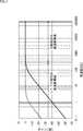
- FIG. 3shows an example of the frequency characteristics of the differential amplifier 42 when the cutoff frequency fc based on the reset period ⁇ T is set to 100 Hz.
- the horizontal axisshows the frequency (Hz), and the vertical axis shows the gain (dB).
- the frequency characteristics of the differential amplifier 42are shown by solid lines.
- action potentialsconsisting of signals with a frequency band of 300 Hz or higher
- synaptic potentialsalso called LFP: Local Field Potential
- the cutoff frequency fcis 100 Hz, it is possible to measure the action potential having a high frequency band, but it is not possible to measure the synaptic potential having a low frequency band, and the measurement accuracy is lowered.
- the present disclosureis intended to improve the measurement accuracy of the potential of a solution such as a culture solution containing living cells.
- FIG. 4is a circuit diagram showing a configuration example of the cell potential measuring device 100 to which the present disclosure is applied.
- the sensing unit 101, the reference electrode 102, the sensor drive line 103, the vertical signal line 104, the vertical selection circuit 105, the A / D conversion circuit 106, the horizontal selection circuit 107, and the output terminal 108are CMOS. It is a semiconductor device (semiconductor device) formed on a semiconductor substrate (chip) which is not shown by using integration technology.
- sensors 121 that read out the electrochemical potential of the culture solution containing living cellsare two-dimensionally arranged in an array (matrix). Further, in the sensing unit 101, a sensor drive line 103 is formed for each row in the horizontal direction with respect to the array-shaped sensor 121, and a vertical signal line 104 is formed for each column in the vertical direction.
- the reference electrode 102corresponds to the reference electrode 12 in FIG. 1, is arranged at a position away from the living cells in the culture solution, and reads out the reference potential of the culture solution.
- the reference electrode 102supplies a reference signal, which is an electric signal indicating the read reference potential, to each sensor 121.
- the vertical selection circuit 105drives each sensor 121 of the sensing unit 101 in units of rows or the like. Specifically, one end of the sensor drive line 103 is connected to the output end (not shown) corresponding to each line of the vertical selection circuit 105.
- the vertical selection circuit 105selects each line in order so as to read the sensor signals from each sensor 121 in order in line units, and outputs the selection signal or the like from the output end connected to the sensor drive line 103 of the selected line.
- the sensor 121 in the selected rowsupplies the output signal indicating the potential of the culture solution as a sensor signal to the vertical signal line 104.
- the A / D conversion circuit 106includes a signal processing circuit for each row of the sensing unit 101. Each signal processing circuit of the A / D conversion circuit 106 performs signal processing such as A / D conversion processing on the sensor signal output from each sensor 121 in the selected line via the vertical signal line 104. The A / D conversion circuit 106 outputs the sensor signal after signal processing obtained by the selected signal processing circuit according to the selective scan of the horizontal selection circuit 107 via the output terminal 108.
- the horizontal selection circuit 107sequentially selects the signal processing circuits of the A / D conversion circuit 106. By the selective scanning by the horizontal selection circuit 107, the sensor signals processed by each signal processing circuit of the A / D conversion circuit 106 are sequentially output to the output terminal 108.
- FIG. 5is a diagram showing a configuration example of the sensor 121A which is the first embodiment of the sensor 121 of FIG. Note that, in FIG. 4, for convenience of explanation, only one line of the sensor 121A is shown.
- Each sensor 121Aincludes a read electrode 141, a differential amplifier 142, a capacitance 143, a capacitance 144, a high resistance 145, and a switch 146, respectively.
- the readout electrode 141corresponds to the readout electrode 41 of the sensor 11 in FIG.
- the readout electrode 141is arranged in the culture medium C containing the living cells.
- the readout electrode 141reads out the potential of the culture solution C as the potential of the living cells contained in the culture solution C, and outputs a cell potential signal which is an electric signal indicating the read-out potential.
- a cell potential signalis input to the differential amplifier 142 from the readout electrode 141. Further, a reference signal is input to the differential amplifier 142 from the reference electrode 102 via the capacitance 143.
- the differential amplifier 142outputs an output signal obtained by amplifying the potential difference between the two input signals.
- the capacity 143corresponds to the capacity 43 of the sensor 11 in FIG. 1 and is connected between the reference electrode 102 and the input terminal of the differential amplifier 142.
- the capacity 144corresponds to the capacity 44 of the sensor 11 in FIG. 1, and is connected between the input terminal and the output terminal on the reference electrode 102 side of the differential amplifier 142.
- the high resistance 145is connected in parallel with the capacitance 144 between the input terminal and the output terminal on the reference electrode 102 side of the differential amplifier 142.
- the high resistance 145is composed of, for example, a resistance element having a very high resistance value (for example, 1 G ⁇ or more) using polysilicon or metal wiring used in a semiconductor process.
- the switch 146corresponds to the switch 46 of the sensor 11 in FIG.
- the switch 146outputs the output signal from the differential amplifier 142 to the vertical signal line 104 as a sensor signal under the control of the selection signal input by the sensor drive line 103 of FIG. Specifically, when the selection signal is input, that is, when the line in which the sensor 121 is arranged is the selection line, the switch 146 is turned on and outputs the sensor signal to the vertical signal line 104. On the other hand, when the selection signal is not input, that is, when the line in which the sensor 121 is arranged is not the selection line, the switch 146 is turned off and does not output the sensor signal to the vertical signal line 104.
- FIG. 6is a circuit diagram showing the configuration of the sensor 121A of FIG. 5 in more detail.
- the sensor 121Aincludes a read electrode 141, a differential amplifier 142, a capacitance 143, a capacitance 144, a high resistance 145, and a switch 146.
- the differential amplifier 142includes a load transistor 161, a load transistor 162, an input transistor 163, an input transistor 164, a constant current source 165, an input terminal 166, an input terminal 167, and an output terminal 168.
- the reset switch 45is replaced with the high resistance 145. That is, the readout electrodes 141 to the capacitance 144 and the switch 146 are configured in the same manner as the readout electrodes 41 to the capacitance 44 and the switch 46 in FIG. Further, the load transistor 161 to the output terminal 168 of the differential amplifier 142 are configured in the same manner as the load transistor 161 to the output terminal 68 of the differential amplifier 42 of FIG.
- the senor 121Acan exert the effect brought about by the one-side feedback type auto-zero differential amplifier as in the sensor 11 of FIG.
- the differential amplifier 142 of the sensor 121Aforms a closed loop that feeds back the output signal as an input signal, the amplification gain is suppressed and the signal input range is widened as compared with the open loop type differential amplifier. Can be done.
- the differential amplifier 142since a circuit or the like is not inserted between the read electrode 141 and the input transistor 163, an amplification gain of 1 or less is not applied to the read signal, and the S / N (Signal / Noise) does not deteriorate. ..
- the output signalis not fed back to the read electrode 141. Thereby, it is possible to prevent the fluctuation of the potential of the readout electrode 141 due to the feedback of the output signal from affecting the activity of the living cell and hindering the accurate measurement of the action potential of the living cell.
- the cutoff frequency fc of the differential amplifier 142is obtained by the following equation (1).
- Rindicates the resistance value of the high resistance 145
- Cgdindicates the capacity of the capacity 144.
- the frequency characteristic of the differential amplifier 142 on the low frequency sideis compared with the frequency characteristic of the differential amplifier 42 (FIG. 1) shown by the solid line. To improve. As a result, it becomes possible to measure synaptic potentials having a low frequency band, and the accuracy of measuring the potentials of living cells is improved.
- the reset operationbecomes unnecessary. As a result, the periodic fluctuation of the output signal due to the reset operation is prevented, and the measurement accuracy of the potential of the living cell is improved.
- FIG. 7shows an example of the timing of the sampling operation of the potential of the living cell of the sensor 121A. In this way, even if the reset operation is not executed, the fluctuation of the output signal is suppressed, so that the measurement accuracy of the potential of the living cell is improved.
- FIG. 8is a circuit diagram showing a configuration example of the sensor 121B which is the second embodiment of the sensor 121 of FIG.
- the parts corresponding to the sensor 121A in FIG. 6are designated by the same reference numerals, and the description thereof will be omitted as appropriate.
- the sensor 121Bis different from the sensor 121A in that a transistor 201 made of an nMOS transistor is provided instead of the high resistance 145.
- the transistor 201is connected in parallel with the capacitance 144 between the input terminal 167 and the output terminal 168 of the differential amplifier 142.
- a bias voltage Vbias lower than the threshold voltage of the transistor 201is applied to the gate of the transistor 201.
- the transistor 201operates in the subthreshold region, and the transistor 201 can be used as a high resistance.
- the bias voltage Vbiasmay be generated by a bias generation circuit (not shown) inside the sensing unit 101, or may be supplied by a voltage supply device external to the sensing unit 101. ..
- the resistance value of the transistor 201can be freely set by changing the bias voltage Vbias applied to the transistor 201. This makes it possible to freely change the frequency characteristics of the differential amplifier 142 from the outside. For example, in the differential amplifier 142, it is possible to cut an unnecessary frequency band and acquire an output signal narrowed down to a necessary frequency band, and it is possible to improve the S / N ratio (reduce noise).
- FIG. 9is a diagram showing a configuration example of the sensor 121C which is the third embodiment of the sensor 121 of FIG.
- the parts corresponding to the sensor 121A in FIG. 6are designated by the same reference numerals, and the description thereof will be omitted as appropriate.
- the sensor 121Cis different from the sensor 121A in that a transistor 221 and a transistor 222 made of an nMOS transistor are provided instead of the high resistance 145.
- the transistor 221 and the transistor 222are connected in series, and are connected in parallel with the capacitance 144 between the output terminal 168 and the input terminal 167. Further, the transistor 221 and the transistor 222 are diode-connected so that the directions in which currents flow are opposite to each other.
- the transistor 221 and the transistor 222can be used as high resistance.
- FIG. 10shows a configuration example of the sensing unit 301, which is a modification of the sensing unit 101 of FIG.
- the sensor 121A of FIG. 6is divided into a read cell 321 and a reference cell 322, and the current mirror circuit and the constant current source included in the sensor 121A are shared by each row.
- the sensing unit 301includes a read cell area 311 and a reference cell area 312 separated from each other.
- the read cell area 311 and the reference cell area 312are arranged so as to be arranged in the vertical direction.
- Read cells 321are two-dimensionally arranged in an array in the read cell area 311.
- the reference cells 341are two-dimensionally arranged in an array.
- the arrangement of the read cell 321 in the read cell area 311 and the arrangement of the reference cell 341 in the reference cell area 312are the same, and the read cell 321 and the reference cell 341 arranged at the same positions of each other operate in cooperation with each other. ..
- a load transistor 313 made of a pMOS transistor, a load transistor 314, and a constant current source 315are provided for each column of the area composed of the read cell area 311 and the reference cell area 312.
- the load transistor 313 and the load transistor 314correspond to the load transistor 161 and the load transistor 162 of the sensor 121A in FIG. 6, and form a current mirror circuit.
- the source of the load transistor 313is connected to the power supply VDD, the drain is connected to each read cell 321 arranged in the same row, and the gate is connected to the gate of the load transistor 314. Further, the load transistor 313 is connected to a diode. That is, the drain of the load transistor 313 and the gate are connected.
- the source of the load transistor 314is connected to the power supply VDD and the drain is connected to each reference cell 341 arranged in the same row.
- the load transistor 314is not connected to a diode.
- the constant current source 315is connected between each read cell 321 and each reference cell 341 arranged in the same row and the power supply VSS (not shown).
- Each read cell 321includes a read electrode 331, an input transistor 332 composed of an nMOS transistor, and a switch 333, respectively, and constitutes a read circuit for the potential of a living cell.
- the readout electrode 331 and the input transistor 332correspond to the readout electrode 141 and the input transistor 163 of the sensor 121A in FIG.
- the drain of the input transistor 332is connected to the drain of the load transistor 313 via the switch 333, the source is connected to the constant current source 315, and the gate is connected to the read electrode 331.
- Each reference cell 322includes an input transistor 352 composed of a capacitance 351 and an nMOS transistor, a capacitance 353, a high resistance 354, and a switch 355, respectively, and constitutes a reference potential readout circuit.
- the capacitance 351, the input transistor 352, the capacitance 353, and the high resistance 354correspond to the capacitance 143, the input transistor 164, the capacitance 144, and the high resistance 145 of the sensor 121A in FIG.
- the drain of the input transistor 352is connected to the drain of the load transistor 314 via the switch 355, the source is connected to the constant current source 315, and the gate is connected to the reference electrode (not shown) via the capacitance 351. ..
- the capacitance 353is connected between the drain of the load transistor 314 and the gate of the input transistor 352.
- the high resistance 354is connected in parallel with the capacitance 353 between the drain of the load transistor 314 and the gate of the input transistor 352.
- the switch 333 of each read cell 321 and the switch 355 of each reference cell 322are turned on or off under the control of a selection signal input via a sensor drive line (not shown). For example, when a selection signal is input to the switch 333 of each read cell 321 in the selected row and the switch 355 of each reference cell 322, the switch 333 and the switch 355 are turned on.
- a circuit similar to the sensor 121A in FIG. 6is configured by the read cell 321 and the reference cell 341 of the selected row, the load transistor 313, the load transistor 314, and the constant current source 315 arranged in the same column.
- the input transistor 332 of the read cell 321 of the selected row, the input transistor 352 of the reference cell 341, the load transistor 313, and the load transistor 314 arranged in the same columnare similar to the differential amplifier 142 of FIG.
- the circuitis configured.
- a sensor signal(output signal) is output from the connection point between the drain of the load transistor 314 and the drain of the input transistor 352 of the reference cell 341 in the selected row.
- the sensing unit 301can exert the following effects in addition to the effects realized by the sensing unit 101 and each sensor 121A in FIG. 4 described above.
- the sensing unit 301can be miniaturized.
- the resolution of the potential of the living cellcan be increased (measurement points are increased).
- the area of the read cell 321can be reduced to increase the spatial resolution of the cell potential, and the size of the input transistor 332 can be increased, resulting in low noise. Can be realized.
- Each read cell 321is composed of only three elements: a read electrode 331, an input transistor 332, and a switch 333. As a result, the area of each read cell 321 can be reduced, and the above-mentioned effect can be further enhanced.
- FIG. 11shows a configuration example of the cell potential measuring device 400, which is a modification of the cell potential measuring device 100 of FIG.
- the parts corresponding to the cell potential measuring device 100are designated by the same reference numerals, and the description thereof will be omitted as appropriate.
- the cell potential measuring device 400is the same as the cell potential measuring device 100 in that it includes a reference electrode 102, a vertical signal line 104, an A / D conversion circuit 106, and an output terminal 108.
- the reference electrode 102is not shown.
- the cell potential measuring device 400is provided with the sensing unit 301 and the vertical selection circuit 401 of FIG. 10 described above instead of the sensing unit 101 and the vertical selection circuit 105. different.
- the vertical selection circuit 401drives each read cell 321 of the read cell area 311 of the sensing unit 301 and each reference cell 341 of the reference cell area 312 in row units. Specifically, one end of a sensor drive line (not shown) is connected to an output end (not shown) corresponding to each row of the read cell area 311 and the reference cell area 312 of the vertical selection circuit 401.
- the vertical selection circuit 105sequentially selects each row of the read cell area 311 and the reference cell area 312 so as to read the sensor signal from each read cell 321 in order in row units, and outputs an output connected to the sensor drive line of the selected row.
- the selection signal etc.is output from the end.
- the switch 333 of the read cell 321 of the selected row and the switch 355 of the reference cell 341are turned on.
- the sensor signalis output from the connection point between the drain of the load transistor 314 and the drain of the input transistor 352 of the reference cell 341 of the selected row, and is supplied to the A / D conversion circuit 106 via the vertical signal line 104.
- a digital sensor signal indicating the potential of the living cellis output from the A / D conversion circuit 106 to the outside of the cell potential measuring device 400 via the output terminal 108.
- the same as the transistor 201 of the sensor 121B of FIG. 8 or the transistor 221 and the transistor 222 of the sensor 121C of FIG.It is possible to use a resistance element having the above configuration.
- the reference electrode 102 in FIG. 4 or the likemay read out a reference potential different from the reference potential of the culture solution.
- the reference electrode 102may be connected to the ground (GND) so that the reference electrode 102 reads out with the ground as the reference potential.
- the reference electrode (not shown) to which the capacity 351 shown in FIG. 10 or the like is connectedmay read out a reference potential different from the reference potential of the culture solution.
- the embodiment of the present disclosureis not limited to the embodiment described above, and various changes can be made without departing from the gist of the present disclosure.
- a readout electrodethat reads out the potential of the solution, and With a differential amplifier A first capacitance connected in series on a loop that feeds back the output of the differential amplifier to a second input different from the first input from the readout electrode.
- a resistance elementconnected in parallel with the first capacitance and A semiconductor device comprising a second capacitance connected between a reference electrode indicating a reference potential and the second input.
- the differential amplifierA current mirror circuit including a first load transistor connected to a diode and a second load transistor not connected to a diode, A first input transistor connected in series with the first load transistor and a gate connected to the read electrode.
- the semiconductor device according to (1) abovecomprising a second input transistor connected in series to the second load transistor and having a gate connected to the first capacitance.
- a read cell regionin which a plurality of read cells including the read electrode and the first input transistor are arranged in an array, and a read cell region.
- the semiconductor device according to (2) abovewherein a plurality of reference cells each including the second input transistor are arranged in an array, and the read cell region and the separated reference cell region are provided.
- the reference cellis With the first capacity With the resistance element
- the semiconductor device according to (3) abovefurther comprising the second capacitance connected between the reference electrode and the gate of the second input transistor.
- a vertical selection circuitthat selects the read cell and the reference cell in row units, and constitutes the differential amplifier by the read cell and the reference cell in the selected row, and the current mirror circuit arranged in the same column.
- the differential amplifierThe first input terminal and The second input terminal and Equipped with an output terminal, The read electrode is connected to the first input terminal and is connected to the first input terminal.
- the first capacitanceis connected between the second input terminal and the output terminal.
- the resistance elementis connected between the second input terminal and the output terminal in parallel with the first capacitance.
- the semiconductor device according to (1)wherein the second capacitance is connected between the reference electrode and the second input terminal.
- the differential amplifierA current mirror circuit including a first load transistor connected to a diode and a second load transistor not connected to a diode, A first input transistor connected in series to the first load transistor and having a gate connected to the first input terminal.
- the resistance elementis formed of metal wiring or polysilicon.
- the resistance elementis composed of a transistor in which a bias voltage operated in a subthreshold region is applied to a gate.
- the resistance elementis The first transistor connected by a diode and (1) to (10) described above, which are connected by a diode and are composed of a second transistor connected in series with the first transistor so that the direction of current flow is opposite to that of the first transistor.
- 100 cell potential measuring device101 sensing unit, 102 reference electrode, 105 vertical selection circuit, 106 A / D conversion circuit, 107 horizontal selection circuit, 121, 121A to 121C sensor, 141 readout electrode, 142 differential amplifier, 143, 144 Capacity, 145 high resistance, 146 switch, 161,162 load transistor, 163,164 input transistor, 166,167 input terminal, 168 output terminal, 2011,221,222 transistor, 301 sensing unit, 311 read cell area, 312 reference cell Region, 313, 314 load transistor, 321 read cell, 331 read electrode, 332 input transistor, 341 reference cell, 351 capacity, 352 input transistor, 353 capacity, 354 high resistance, 400 cell potential measuring device, 401 vertical selection circuit
Landscapes
- Life Sciences & Earth Sciences (AREA)
- Chemical & Material Sciences (AREA)
- Health & Medical Sciences (AREA)
- Engineering & Computer Science (AREA)
- General Health & Medical Sciences (AREA)
- Physics & Mathematics (AREA)
- Analytical Chemistry (AREA)
- Biochemistry (AREA)
- Power Engineering (AREA)
- Wood Science & Technology (AREA)
- Bioinformatics & Cheminformatics (AREA)
- Molecular Biology (AREA)
- Organic Chemistry (AREA)
- Zoology (AREA)
- Immunology (AREA)
- Pathology (AREA)
- General Physics & Mathematics (AREA)
- Microelectronics & Electronic Packaging (AREA)
- Genetics & Genomics (AREA)
- Electrochemistry (AREA)
- Biomedical Technology (AREA)
- Biotechnology (AREA)
- Microbiology (AREA)
- Sustainable Development (AREA)
- Spectroscopy & Molecular Physics (AREA)
- Chemical Kinetics & Catalysis (AREA)
- General Engineering & Computer Science (AREA)
- Cell Biology (AREA)
- Dispersion Chemistry (AREA)
- Investigating Or Analyzing Materials By The Use Of Electric Means (AREA)
- Apparatus Associated With Microorganisms And Enzymes (AREA)
- Measurement Of Current Or Voltage (AREA)
Abstract
Description
Translated fromJapanese本開示は、半導体装置及び細胞電位測定装置に関し、特に、溶液の電位の測定精度を向上できるようにした半導体装置及び細胞電位測定装置に関する。The present disclosure relates to a semiconductor device and a cell potential measuring device, and more particularly to a semiconductor device and a cell potential measuring device capable of improving the measurement accuracy of the potential of a solution.
従来、片側フィードバック型のオートゼロ差動増幅器を備える細胞電位測定装置が提案されている(例えば、特許文献1参照)。Conventionally, a cell potential measuring device including a one-sided feedback type auto-zero differential amplifier has been proposed (see, for example, Patent Document 1).
特許文献1の差動増幅器においては、負荷抵抗となるカレントミラー回路のダイオード接続されているpMOSトランジスタ側の入力トランジスタに読み出し電極が接続されるとともに、ダイオード接続されていないpMOSトランジスタ側の入力トランジスタに差動増幅器の出力を帰還する閉ループが構成されている。また、ダイオード接続されていないpMOSトランジスタ側の入力トランジスタに、サンプリング容量を介して参照電極が接続されている。そして、差動増幅器の動作点となる電位が、リセット動作によりサンプリング容量にサンプルホールドされる。また、サンプリング容量の電位がリーク電流により変動するのを防ぐために、周期的にリセット動作が行われる。In the differential amplifier of
しかしながら、特許文献1の細胞電位測定装置においては、サンプリング容量のリセット動作の周期に基づく遮断周波数より低い周波数帯域の信号を検出できないため、溶液の電位の測定精度が低下するおそれがある。However, the cell potential measuring device of
本開示は、このような状況に鑑みてなされたものであり、溶液の電位の測定精度を向上させるようにするものである。This disclosure is made in view of such a situation, and is intended to improve the measurement accuracy of the potential of the solution.
本開示の第1の側面の半導体装置は、溶液の電位を読み出す読み出し電極と、差動増幅器と、前記差動増幅器の出力を前記読み出し電極からの第1の入力と異なる第2の入力に帰還するループ上に直列に接続されている第1の容量と、前記第1の容量と並列に接続されている抵抗素子と、基準電位を示す参照電極と前記第2の入力との間に接続されている第2の容量とを備える。The semiconductor device of the first aspect of the present disclosure is a read electrode that reads out the potential of the solution, a differential amplifier, and the output of the differential amplifier is fed back to a second input different from the first input from the read electrode. A first capacitance connected in series on the loop, a resistance element connected in parallel with the first capacitance, and connected between a reference electrode indicating a reference potential and the second input. It has a second capacity.
本開示の第2の側面の細胞電位測定装置は、溶液に含まれる細胞の電位を読み出す読み出し電極と、差動増幅器と、前記差動増幅器の出力を前記読み出し電極からの第1の入力と異なる第2の入力に帰還するループ上に直列に接続されている第1の容量と、前記第1の容量と並列に接続されている抵抗素子と、基準電位を示す参照電極と前記第2の入力との間に接続されている第2の容量とを備える。The cell potential measuring device of the second aspect of the present disclosure differs from the reading electrode that reads the potential of the cell contained in the solution, the differential amplifier, and the output of the differential amplifier from the first input from the reading electrode. A first capacitance connected in series on a loop returning to the second input, a resistance element connected in parallel with the first capacitance, a reference electrode indicating a reference potential, and the second input. It has a second capacity connected to and from.
本開示の第1の側面においては、溶液の電位が読み出され、読み出された電位を示す信号が出力される。In the first aspect of the present disclosure, the potential of the solution is read out, and a signal indicating the read-out potential is output.
本開示の第2の側面においては、溶液に含まれる細胞の電位が読み出され、読み出された電位を示す信号が出力される。In the second aspect of the present disclosure, the potential of the cells contained in the solution is read out, and a signal indicating the read-out potential is output.
以下、本開示を実施するための形態(以下、実施の形態という)について説明する。なお、説明は以下の順序で行う。
1.本開示の背景(図1乃至図3)
2.第1の実施の形態:細胞電位測定装置(図4乃至図7)
3.第2の実施の形態:センサ(図8)
4.第3の実施の形態:センサ(図9)
5.第4の実施の形態:センシング部(図10)
6.第5の実施の形態:細胞電位測定装置(図11)
7.変形例
8.その他Hereinafter, embodiments for carrying out the present disclosure (hereinafter referred to as embodiments) will be described. The explanation will be given in the following order.
1. 1. Background of the present disclosure (FIGS. 1 to 3)
2. 2. First Embodiment: Cell potential measuring device (FIGS. 4 to 7)
3. 3. Second embodiment: sensor (FIG. 8)
4. Third Embodiment: Sensor (FIG. 9)
5. Fourth Embodiment: Sensing unit (FIG. 10)
6. Fifth Embodiment: Cell potential measuring device (FIG. 11)
7. Modification example 8. others
<<1.本開示の背景>>
まず、図1乃至図3を参照して、本開示の背景について説明する。<< 1. Background of this disclosure >>
First, the background of the present disclosure will be described with reference to FIGS. 1 to 3.
図1は、上述した特許文献1の細胞電位測定装置を構成するセンサ11の構成を示す回路図である。FIG. 1 is a circuit diagram showing a configuration of a
センサ11は、読み出し電極41、差動増幅器42、容量43、容量44、リセットスイッチ45、及び、スイッチ46を備える。差動増幅器42は、pMOSトランジスタからなる負荷トランジスタ61及び負荷トランジスタ62、nMOSトランジスタからなる入力トランジスタ63及び入力トランジスタ64、定電流源65、入力端子66、入力端子67、並びに、出力端子68を備える。The
読み出し電極41は、生体細胞を含む溶液である培養液の中に配置され、培養液の電位を生体細胞の電位として読み出す。読み出し電極41は、差動増幅器42の入力端子66に接続されており、読み出した電位を示す電気信号(以下、細胞電位信号と称する)を入力端子66に入力する。The
参照電極12は、培養液内の生体細胞から離れた位置に配置され、培養液の基準電位を読み出す。参照電極12は、容量43を介して差動増幅器42の入力端子67に接続されており、読み出した基準電位を示す電気信号(以下、参照信号と称する)を、容量43を介して入力端子67に入力する。The
差動増幅器42の負荷トランジスタ61及び負荷トランジスタ62は、カレントミラー回路を構成する。The
具体的には、負荷トランジスタ61は、電位VDDの電源(以下、電源VDDと称する)と入力トランジスタ63との間に直列に接続されている。すなわち、負荷トランジスタ61のソースは電源VDDに接続され、ドレインは入力トランジスタ63のドレインに接続されている。また、負荷トランジスタ61のゲートは、負荷トランジスタ62のゲートに接続されるとともに、負荷トランジスタ61のドレインに接続されている。すなわち、負荷トランジスタ61は、ダイオード接続されている。Specifically, the
負荷トランジスタ62は、電源VDDと入力トランジスタ64との間に直列に接続されている。すなわち、負荷トランジスタ62のソースは電源VDDに接続され、ドレインは入力トランジスタ64のドレインに接続されている。なお、負荷トランジスタ62は、ダイオード接続されていない。The
入力トランジスタ63は、負荷トランジスタ61と定電流源65との間に直列に接続されている。すなわち、入力トランジスタ63のドレインは、上述したように負荷トランジスタ61のドレインに接続され、ソースは定電流源65に接続されている。入力トランジスタ63のゲートは、入力端子66に接続され、読み出し電極41からの細胞電位信号が入力される。なお、負荷トランジスタ61がダイオード接続されているため、入力トランジスタ63には増幅ゲインがかからない。The
入力トランジスタ64は、負荷トランジスタ62と定電流源65との間に直列に接続されている。すなわち、入力トランジスタ64のドレインは、上述したように負荷トランジスタ62のドレインに接続され、ソースは定電流源65に接続されている。入力トランジスタ63のゲートは、入力端子67に接続され、容量43を介して、参照電極12からの参照信号が入力される。なお、負荷トランジスタ62がダイオード接続されていないため、入力トランジスタ64には増幅ゲインがかかる。The
定電流源65は、電位VSSの電源(以下、電源VSSと称する)に接続されている。電位VSSは、例えば、グラウンド(GND)である。The constant
出力端子68は、負荷トランジスタ62のドレインと入力トランジスタ64のドレインとの接続点に接続されている。The
このように、差動増幅器42は、負荷トランジスタ61及び負荷トランジスタ62からなるカレントミラー回路を負荷抵抗とする差動増幅器である。また、差動増幅器42は、入力端子66に入力される細胞電位信号と、入力端子67に入力される参照信号の電位差を増幅し、増幅した電位差を示す出力信号を出力端子68から出力する。As described above, the
容量43は、参照電極12と差動増幅器42の入力端子67との間に接続されている。容量43は、読み出し電極41と参照電極102に同相で混入するノイズ成分がキャンセルする。また、容量43は、差動増幅器42の動作点となる電位をサンプルホールドするサンプリング容量となる。The
容量44は、差動増幅器42の入力端子67と出力端子68との間に接続されている。これにより、出力端子68から出力された出力信号を入力信号として入力端子67に帰還する閉ループが形成され、閉ループ上に容量44が接続されている。The
リセットスイッチ45は、差動増幅器42の出力端子68と入力端子67との間に、容量44と並列に接続されている。リセットスイッチ45は、図示せぬ制御回路から供給されるリセット信号Resetに基づいて、入力端子67と出力端子68を短絡する。これにより、差動増幅器42の動作点のリセット動作が行われる。すなわち、差動増幅器42の負荷トランジスタ61と負荷トランジスタ62を流れる電流を釣り合わせ、差動増幅器42の入力信号の電位差をゼロ(Vin(+)-Vin(-)=0)にした状態における参照電極12の電位が、差動増幅器42の動作点として容量43にサンプルホールドされる。The
スイッチ46は、センサ駆動線13を介して入力される選択信号による制御の下に、差動増幅器42からの出力信号をセンサ信号として垂直信号線14に出力する。具体的には、スイッチ46は、選択信号が入力された場合、オン状態になり、センサ信号を垂直信号線14に出力する。これにより、生体細胞の電位を示す値がサンプリングされる。一方、スイッチ46は、選択信号が入力されない場合、オフ状態になり、センサ信号を垂直信号線14に出力しない。The
図2は、センサ11のリセット動作と生体細胞の電位のサンプリング動作のタイミングの例を示している。FIG. 2 shows an example of the timing of the reset operation of the
上述したように、センサ11では、リセット動作により差動増幅器42の動作点が容量43にサンプルホールドされる。しかし、容量43にサンプルホールドされた電位は、リーク電流により徐々に低下する。そのため、細胞電位信号が変化しなくても、差動増幅器42の出力信号が徐々に低下し、センサ11から出力されるセンサ信号の値(サンプル値)にバラつきが生じる。As described above, in the
従って、周期的に動作点のリセット動作を行い、センサ11をリフレッシュする必要が生じる。Therefore, it is necessary to periodically reset the operating point to refresh the
一方、センサ11は、リセット動作の周期ΔT(以下、リセット周期ΔTと称する)に基づく遮断周波数より低い周波数帯域の信号を検出できなくなる。On the other hand, the
図3は、リセット周期ΔTに基づく遮断周波数fcを100Hzとした場合の差動増幅器42の周波数特性の例を示している。横軸は周波数(Hz)を示し、縦軸はゲイン(dB)を示している。差動増幅器42の周波数特性は、実線で示されている。FIG. 3 shows an example of the frequency characteristics of the
生体細胞が発生する電位には、一般的に周波数帯域が300Hz以上の信号からなる活動電位と、周波数帯域が300Hz以下の信号からなるシナプス電位(LFP:Local Field Potentialとも呼ばれる)の大きく2種類がある。遮断周波数fcが100Hzの場合、周波数帯域の高い活動電位の測定は可能であるが、周波数帯域が低いシナプス電位の測定ができず、測定精度が低下する。There are roughly two types of potentials generated by living cells: action potentials consisting of signals with a frequency band of 300 Hz or higher and synaptic potentials (also called LFP: Local Field Potential) consisting of signals with a frequency band of 300 Hz or lower. be. When the cutoff frequency fc is 100 Hz, it is possible to measure the action potential having a high frequency band, but it is not possible to measure the synaptic potential having a low frequency band, and the measurement accuracy is lowered.
また、図2の出力信号の波形において破線で示されるように、リセット動作の直後に、リセットスイッチ45のオン/オフの影響により出力信号に揺れが生じる。そのため、リセット動作直後にサンプリングしたセンサ信号にノイズが生じる。Further, as shown by the broken line in the waveform of the output signal in FIG. 2, immediately after the reset operation, the output signal fluctuates due to the influence of the on / off of the
さらに、リーク電流による出力信号の傾きを後段の信号処理で補正する必要が生じ、後段の処理負荷が増大する。Furthermore, it becomes necessary to correct the slope of the output signal due to the leak current in the signal processing in the subsequent stage, which increases the processing load in the subsequent stage.
これに対して、本開示は、生体細胞を含む培養液等の溶液の電位の測定精度を向上させるようにするものである。On the other hand, the present disclosure is intended to improve the measurement accuracy of the potential of a solution such as a culture solution containing living cells.
<<2.第1の実施の形態>>
次に、図4乃至図7を参照して、本開示の第1の実施の形態について説明する。<< 2. First Embodiment >>
Next, the first embodiment of the present disclosure will be described with reference to FIGS. 4 to 7.
<細胞電位測定装置100の構成例>
図4は、本開示を適用した細胞電位測定装置100の構成例を示す回路図である。<Structure example of cell
FIG. 4 is a circuit diagram showing a configuration example of the cell
細胞電位測定装置100は、センシング部101、参照電極102、センサ駆動線103、垂直信号線104、垂直選択回路105、A/D変換回路106、水平選択回路107、及び、出力端子108が、CMOS集積化技術を用いて図示せぬ半導体基板(チップ)に形成された半導体デバイス(半導体装置)である。In the cell
細胞電位測定装置100のセンシング部101には、生体細胞を含む培養液の電気化学的電位を読み出すセンサ121が、アレイ状(行列状)に2次元配置されている。また、センシング部101には、アレイ状のセンサ121に対して水平方向の行ごとにセンサ駆動線103が形成され、垂直方向の列ごとに垂直信号線104が形成されている。In the
参照電極102は、図1の参照電極12に相当し、培養液内の生体細胞から離れた位置に配置され、培養液の基準電位を読み出す。参照電極102は、読み出された基準電位を示す電気信号である参照信号を各センサ121に供給する。The
垂直選択回路105は、センシング部101の各センサ121を行単位等で駆動する。具体的には、垂直選択回路105の各行に対応した図示せぬ出力端には、センサ駆動線103の一端が接続されている。垂直選択回路105は、各センサ121からのセンサ信号を行単位で順に読み出すように、各行を順に選択し、選択行のセンサ駆動線103と接続される出力端から選択信号等を出力する。これにより、選択行のセンサ121は、培養液の電位を示す出力信号をセンサ信号として、垂直信号線104に供給する。The
A/D変換回路106は、センシング部101の列ごとに信号処理回路を備える。A/D変換回路106の各信号処理回路は、選択行の各センサ121から垂直信号線104を介して出力されるセンサ信号に対して、A/D変換処理等の信号処理を行う。A/D変換回路106は、水平選択回路107の選択走査に従って、選択された信号処理回路により得られた信号処理後のセンサ信号を、出力端子108を介して出力する。The A /
水平選択回路107は、A/D変換回路106の信号処理回路を順番に選択する。この水平選択回路107による選択走査により、A/D変換回路106の各信号処理回路で信号処理されたセンサ信号が順番に出力端子108に出力される。The
<センサ121の第1の実施の形態>
図5は、図4のセンサ121の第1の実施の形態であるセンサ121Aの構成例を示す図である。なお、図4では、説明の便宜上、1行分のセンサ121Aのみが図示されている。<First Embodiment of
FIG. 5 is a diagram showing a configuration example of the
各センサ121Aは、読み出し電極141、差動増幅器142、容量143、容量144、高抵抗145、及び、スイッチ146をそれぞれ備える。Each
読み出し電極141は、図1のセンサ11の読み出し電極41に相当する。読み出し電極141は、生体細胞を含む培養液Cの中に配置される。読み出し電極141は、培養液Cの電位を培養液Cに含まれる生体細胞の電位として読み出し、読み出した電位を示す電気信号である細胞電位信号を出力する。The
差動増幅器142には、読み出し電極141から細胞電位信号が入力される。また、差動増幅器142には、参照電極102から容量143を介して参照信号が入力される。差動増幅器142は、この2つの入力信号の電位差を増幅した出力信号を出力する。A cell potential signal is input to the
容量143は、図1のセンサ11の容量43に相当し、参照電極102と差動増幅器142の入力端子との間に接続されている。The
容量144は、図1のセンサ11の容量44に相当し、差動増幅器142の参照電極102側の入力端子と出力端子との間に接続されている。The
高抵抗145は、差動増幅器142の参照電極102側の入力端子と出力端子との間に、容量144と並列に接続されている。高抵抗145は、例えば、半導体プロセスにおいて用いられるポリシリコンやメタル配線を用いた、抵抗値が非常に高い(例えば、1GΩ以上)抵抗素子により構成される。The
スイッチ146は、図1のセンサ11のスイッチ46に相当する。スイッチ146は、図4のセンサ駆動線103により入力される選択信号による制御の下に、差動増幅器142からの出力信号をセンサ信号として垂直信号線104に出力する。具体的には、スイッチ146は、選択信号が入力された場合、すなわちセンサ121が配置されている行が選択行である場合、オン状態になり、センサ信号を垂直信号線104に出力する。一方、スイッチ146は、選択信号が入力されない場合、すなわちセンサ121が配置されている行が選択行ではない場合、オフ状態になり、センサ信号を垂直信号線104に出力しない。The
<センサ121Aの詳細構成例>
図6は、図5のセンサ121Aの構成をさらに詳細に示す回路図である。<Detailed configuration example of
FIG. 6 is a circuit diagram showing the configuration of the
センサ121Aは、上述したように、読み出し電極141、差動増幅器142、容量143、容量144、高抵抗145、及び、スイッチ146を備える。差動増幅器142は、負荷トランジスタ161、負荷トランジスタ162、入力トランジスタ163、入力トランジスタ164、定電流源165、入力端子166、入力端子167、並びに、出力端子168を備える。As described above, the
センサ121Aを図1のセンサ11と比較すると、リセットスイッチ45が高抵抗145に置き換わっている点のみが異なる。すなわち、読み出し電極141乃至容量144及びスイッチ146は、図1の読み出し電極41乃至容量44及びスイッチ46と同様に構成される。また、差動増幅器142の負荷トランジスタ161乃至出力端子168は、図1の差動増幅器42の負荷トランジスタ161乃至出力端子68と同様に構成される。Comparing the
従って、センサ121Aでは、図1のセンサ11と同様に、片側フィードバック型のオートゼロ差動増幅器によりもたらされる効果を奏することができる。Therefore, the
すなわち、センサ121Aの差動増幅器142では、出力信号を入力信号として帰還させる閉ループが形成されるため、オープンループ型の差動増幅器に比べて、増幅ゲインを抑制し、信号入力レンジを広くすることができる。That is, since the
また、差動増幅器142では、読み出し電極141と入力トランジスタ163との間に回路等が挿入されないため、読み出し信号に1以下の増幅ゲインがかからず、S/N(Signal/Noise)が劣化しない。Further, in the
さらに、差動増幅器142では、出力信号が読み出し電極141に帰還されない。これにより、出力信号の帰還による読み出し電極141の電位の変動が、生体細胞の活動に影響を及ぼし、生体細胞の正確な活動電位の測定が妨げられることを防止することができる。Further, in the
加えて、リセットスイッチ45を高抵抗145に置き換えることにより、片側フィードバック型の差動増幅器142の入力端子167側の入力を高抵抗145によりバイアスした構成となる。これにより、例えば、「R.R. Harrison, C. Charles, “A low-power low-noise CMOS amplifier for neural recording applications,” IEEE J. Solid-State Circuits, vol.38, pp. 958-965, 2003」に記載されているように、周波数帯域が低い電位の測定が可能になる。In addition, by replacing the
具体的には、差動増幅器142の遮断周波数fcは、次式(1)により求められる。Specifically, the cutoff frequency fc of the
fc=1/(2π×R×Cgd) ・・・(1)Fc = 1 / (2π x R x Cgd) ... (1)
なお、Rは高抵抗145の抵抗値を示し、Cgdは容量144の容量を示す。Note that R indicates the resistance value of the
例えば、Cgd=10Fの場合、R=10TΩに設定することにより、遮断周波数fc=1.5Hzとなる。これにより、先に示した図3の破線のグラフで示されるように、差動増幅器142の低周波側の周波数特性が、実線で示される差動増幅器42(図1)の周波数特性と比較して向上する。この結果、周波数帯域が低いシナプス電位の測定が可能になり、生体細胞の電位の測定精度が向上する。For example, when Cgd = 10F, the cutoff frequency fc = 1.5Hz can be obtained by setting R = 10TΩ. As a result, as shown by the broken line graph of FIG. 3 shown above, the frequency characteristic of the
また、容量143のリーク電流による出力信号の変動が抑制されるため、リセット動作が不要になる。この結果、リセット動作による周期的な出力信号の揺れが防止され、生体細胞の電位の測定精度が向上する。Further, since the fluctuation of the output signal due to the leakage current of the
例えば、図7は、センサ121Aの生体細胞の電位のサンプリング動作のタイミングの例を示している。このように、リセット動作を実行しなくても、出力信号の変動が抑制されるため、生体細胞の電位の測定精度が向上する。For example, FIG. 7 shows an example of the timing of the sampling operation of the potential of the living cell of the
<<3.第2の実施の形態>>
次に、図8を参照して、本開示の第2の実施の形態について説明する。<< 3. Second embodiment >>
Next, a second embodiment of the present disclosure will be described with reference to FIG.
<センサ121の第2の実施の形態>
図8は、図4のセンサ121の第2の実施の形態であるセンサ121Bの構成例を示す回路図である。なお、図中、図6のセンサ121Aと対応する部分には同じ符号を付しており、その説明は適宜省略する。<Second Embodiment of
FIG. 8 is a circuit diagram showing a configuration example of the
センサ121Bは、センサ121Aと比較して、高抵抗145の代わりに、nMOSトランジスタからなるトランジスタ201が設けられている点が異なる。The
トランジスタ201は、差動増幅器142の入力端子167と出力端子168との間に、容量144と並列に接続されている。トランジスタ201のゲートには、トランジスタ201の閾値電圧より低いバイアス電圧Vbiasが印加される。これにより、トランジスタ201がサブスレッショルド領域で動作し、トランジスタ201を高抵抗として用いることができる。The
なお、バイアス電圧Vbiasは、センシング部101内部のバイアス生成回路(不図示)において生成するようにしてもよいし、センシング部101の外部の電圧供給装置で生成したものを供給するようにしてもよい。The bias voltage Vbias may be generated by a bias generation circuit (not shown) inside the
例えば、トランジスタ201に印加するバイアス電圧Vbiasを変更することで、トランジスタ201の抵抗値を自由に設定することができる。これにより、差動増幅器142の周波数特性を外部から自由に変更することが可能になる。例えば、差動増幅器142において、不要な周波数帯域をカットし、必要な周波数帯域に絞った出力信号を取得することができ、S/Nの向上(低ノイズ化)を実現することができる。For example, the resistance value of the
<<4.第3の実施の形態>>
次に、図9を参照して、本開示の第3の実施の形態について説明する。<< 4. Third Embodiment >>
Next, a third embodiment of the present disclosure will be described with reference to FIG.
<センサ121の第3の実施の形態>
図9は、図4のセンサ121の第3の実施の形態であるセンサ121Cの構成例を示す図である。なお、図中、図6のセンサ121Aと対応する部分には同じ符号を付しており、その説明は適宜省略する。<Third Embodiment of the
FIG. 9 is a diagram showing a configuration example of the
センサ121Cは、センサ121Aと比較して、高抵抗145の代わりに、nMOSトランジスタからなるトランジスタ221及びトランジスタ222が設けられている点が異なる。The
トランジスタ221及びトランジスタ222は、直列に接続されるとともに、出力端子168と入力端子167との間に、容量144と並列に接続されている。また、トランジスタ221とトランジスタ222とは、電流が流れる方向が互いに逆になるようにダイオード接続されている。The
そして、トランジスタ221及びトランジスタ222のドレイン-ソース間の電圧差がともに閾値未満の場合、トランジスタ221及びトランジスタ222に非常に小さい電流しか流れない。従って、トランジスタ221及びトランジスタ222を高抵抗として用いることができる。Then, when the voltage difference between the drain and the source of the
これにより、外部からバイアス電圧を供給しなくても、高抵抗を実現することができる。This makes it possible to achieve high resistance without supplying a bias voltage from the outside.
<<5.第4の実施の形態>>
次に、図10を参照して、本開示の第4の実施の形態について説明する。<< 5. Fourth Embodiment >>
Next, a fourth embodiment of the present disclosure will be described with reference to FIG.
<センシング部301の構成例>
図10は、図4のセンシング部101の変形例であるセンシング部301の構成例を示している。<Configuration example of
FIG. 10 shows a configuration example of the
センシング部301においては、図6のセンサ121Aが、読み出しセル321と参照セル322とに分割されるとともに、センサ121Aが備えていたカレントミラー回路及び定電流源が、各列で共有されている。In the
具体的には、センシング部301は、互いに分離された読み出しセル領域311及び参照セル領域312を備える。読み出しセル領域311と参照セル領域312とは、縦方向に並ぶように配置されている。読み出しセル領域311には、読み出しセル321がアレイ状に2次元配置されている。参照セル領域312は、参照セル341がアレイ状に2次元配置されている。読み出しセル領域311における読み出しセル321の配置と、参照セル領域312における参照セル341の配置とは同様であり、互いに同じ位置に配置されている読み出しセル321と参照セル341とが協調して動作する。Specifically, the
また、読み出しセル領域311及び参照セル領域312により構成される領域の列ごとに、pMOSトランジスタからなる負荷トランジスタ313、負荷トランジスタ314、及び、定電流源315が設けられている。Further, a
負荷トランジスタ313及び負荷トランジスタ314は、図6のセンサ121Aの負荷トランジスタ161及び負荷トランジスタ162に相当し、カレントミラー回路を構成する。負荷トランジスタ313のソースは電源VDDに接続され、ドレインは同じ列に配置されている各読み出しセル321に接続され、ゲートは負荷トランジスタ314のゲートに接続されている。また、負荷トランジスタ313はダイオード接続されている。すなわち、負荷トランジスタ313のドレインとゲートが接続されている。負荷トランジスタ314のソースは電源VDDに接続され、ドレインは同じ列に配置されている各参照セル341に接続されている。なお、負荷トランジスタ314はダイオード接続されていない。The
定電流源315は、同じ列に配置されている各読み出しセル321及び各参照セル341と電源VSS(不図示)との間に接続されている。The constant
各読み出しセル321は、読み出し電極331、nMOSトランジスタからなる入力トランジスタ332、及び、スイッチ333をそれぞれ備え、生体細胞の電位の読み出し回路を構成する。読み出し電極331及び入力トランジスタ332は、図6のセンサ121Aの読み出し電極141及び入力トランジスタ163に相当する。Each read
入力トランジスタ332のドレインは、スイッチ333を介して、負荷トランジスタ313のドレインに接続され、ソースは定電流源315に接続され、ゲートは、読み出し電極331に接続されている。The drain of the
各参照セル322は、容量351、nMOSトランジスタからなる入力トランジスタ352、容量353、高抵抗354、及び、スイッチ355をそれぞれ備え、基準電位の読み出し回路を構成する。容量351、入力トランジスタ352、容量353、及び、高抵抗354は、図6のセンサ121Aの容量143、入力トランジスタ164、容量144、及び、高抵抗145に相当する。Each reference cell 322 includes an
入力トランジスタ352のドレインは、スイッチ355を介して負荷トランジスタ314のドレインに接続され、ソースは定電流源315に接続され、ゲートは、容量351を介して参照電極(不図示)に接続されている。容量353は、負荷トランジスタ314のドレインと入力トランジスタ352のゲートの間に接続されている。高抵抗354は、負荷トランジスタ314のドレインと入力トランジスタ352のゲートの間に、容量353と並列に接続されている。The drain of the
各読み出しセル321のスイッチ333、及び、各参照セル322のスイッチ355は、図示せぬセンサ駆動線を介して入力される選択信号による制御の下に、オン又はオフする。例えば、選択行の各読み出しセル321のスイッチ333、及び、各参照セル322のスイッチ355に選択信号が入力されると、スイッチ333及びスイッチ355がオンされる。これにより、同じ列に配置されている、選択行の読み出しセル321及び参照セル341、負荷トランジスタ313、負荷トランジスタ314、並びに、定電流源315により、図6のセンサ121Aと同様の回路が構成される。また、同じ列に配置されている、選択行の読み出しセル321の入力トランジスタ332及び参照セル341の入力トランジスタ352、負荷トランジスタ313、並びに、負荷トランジスタ314により、図6の差動増幅器142と同様の回路が構成される。The
そして、負荷トランジスタ314のドレインと選択行の参照セル341の入力トランジスタ352のドレインとの間の接続点からセンサ信号(出力信号)が出力される。Then, a sensor signal (output signal) is output from the connection point between the drain of the
このセンシング部301は、上述した図4のセンシング部101及び各センサ121Aにより実現される効果に加えて、下記の効果を奏することができる。The
例えば、カレントミラー回路及び定電流源315が共有されることにより、センシング部301を小型化することができる。又は、読み出しセル321及び参照セル341の数を増やすことにより、生体細胞の電位の分解能を上げる(測定ポイントを増やす)ことができる。For example, by sharing the current mirror circuit and the constant
また、読み出しセル領域311と参照セル領域312とを分離することにより、読み出しセル321の面積を縮小して細胞電位の空間分解能を上げつつ、入力トランジスタ332のサイズを大きくすることができ、低ノイズ化を実現することができる。Further, by separating the read
さらに、高抵抗354の追加が各読み出しセル321に影響せず、各読み出しセル321は、読み出し電極331、入力トランジスタ332、及び、スイッチ333の3素子のみにより構成される。これにより、各読み出しセル321の面積を小さくすることができ、上述した効果をより高めることができる。Further, the addition of the
<<6.第5の実施の形態>>
次に、図11を参照して、本開示の第5の実施の形態について説明する。<< 6. Fifth Embodiment >>
Next, a fifth embodiment of the present disclosure will be described with reference to FIG.
図11は、図4の細胞電位測定装置100の変形例である細胞電位測定装置400の構成例を示している。なお、図中、細胞電位測定装置100と対応する部分には同じ符号を付しており、その説明は適宜省略する。FIG. 11 shows a configuration example of the cell
細胞電位測定装置400は、細胞電位測定装置100と比較して、参照電極102、垂直信号線104、A/D変換回路106、及び、出力端子108を備える点で一致する。なお、参照電極102の図示は省略している。一方、細胞電位測定装置400は、細胞電位測定装置100と比較して、センシング部101及び垂直選択回路105の代わりに、叙述した図10のセンシング部301、及び、垂直選択回路401を備える点が異なる。The cell
なお、この図においては、センシング部301の参照セル領域312の参照セル341の図示の一部を省略しているが、読み出しセル領域311の読み出しセル321と参照セル領域312の参照セル341とは、互いに同じ列及び行の数だけ設けられる。In this figure, a part of the
垂直選択回路401は、センシング部301の読み出しセル領域311の各読み出しセル321、及び、参照セル領域312の各参照セル341を行単位で駆動する。具体的には、垂直選択回路401の読み出しセル領域311及び参照セル領域312の各行に対応した図示せぬ出力端には、図示せぬセンサ駆動線の一端が接続されている。The
垂直選択回路105は、各読み出しセル321からのセンサ信号を行単位で順に読み出すように、読み出しセル領域311及び参照セル領域312の各行を順に選択し、選択行のセンサ駆動線と接続される出力端から選択信号等を出力する。これにより、選択行の読み出しセル321のスイッチ333及び参照セル341のスイッチ355がオンされる。この結果、負荷トランジスタ314のドレインと選択行の参照セル341の入力トランジスタ352のドレインとの間の接続点からセンサ信号が出力され、垂直信号線104を介してA/D変換回路106に供給される。そして、A/D変換回路106から、生体細胞の電位を示すデジタルのセンサ信号が、出力端子108を介して、細胞電位測定装置400の外部に出力される。The
このようにして、低ノイズかつ高速にデジタルのセンサ信号を細胞電位測定装置400の外部に出力することが可能になる。また、垂直選択回路401により読み出しセル321及び参照セル341を順次選択するようにすることにより、多数の読み出し電極331を配列することが可能になる。これにより、より広い範囲においてより高い分解能で生体細胞の電位を測定することが可能になる。In this way, it becomes possible to output a digital sensor signal to the outside of the cell
<<7.変形例>>
例えば、図6のセンサ121A、図8のセンサ121B、及び、図9のセンサ121Cにおいて、参照電極102及び容量143を削除して、差動増幅器142の出力信号が容量144を介して入力端子167に帰還する構成にすることが可能である。<< 7. Modification example >>
For example, in the
例えば、図10のセンシング部301及び図11の細胞電位測定装置400において、高抵抗354の代わりに、図8のセンサ121Bのトランジスタ201、又は、図9のセンサ121Cのトランジスタ221及びトランジスタ222と同様の構成の抵抗素子を用いることが可能である。For example, in the
例えば、図4等の参照電極102が、培養液の基準電位とは異なる基準電位を読み出すようにしてもよい。例えば、参照電極102をグラウンド(GND)に接続し、参照電極102がグラウンドを基準電位として読み出すようにしてもよい。For example, the
同様に、図10等の容量351が接続されている参照電極(不図示)が、培養液の基準電位とは異なる基準電位を読み出すようにしてもよい。Similarly, the reference electrode (not shown) to which the
<<8.その他>><< 8. Others >>
なお、本明細書に記載された効果はあくまで例示であって限定されるものではなく、他の効果があってもよい。It should be noted that the effects described in the present specification are merely examples and are not limited, and other effects may be obtained.
また、本開示の実施の形態は、上述した実施の形態に限定されるものではなく、本開示の要旨を逸脱しない範囲において種々の変更が可能である。Further, the embodiment of the present disclosure is not limited to the embodiment described above, and various changes can be made without departing from the gist of the present disclosure.
なお、本開示は、以下のような構成をとることもできる。Note that this disclosure can also have the following structure.
(1)
溶液の電位を読み出す読み出し電極と、
差動増幅器と、
前記差動増幅器の出力を前記読み出し電極からの第1の入力と異なる第2の入力に帰還するループ上に直列に接続されている第1の容量と、
前記第1の容量と並列に接続されている抵抗素子と、
基準電位を示す参照電極と前記第2の入力との間に接続されている第2の容量と
を備える半導体装置。
(2)
前記差動増幅器は、
ダイオード接続されている第1の負荷トランジスタ、及び、ダイオード接続されていない第2の負荷トランジスタを備えるカレントミラー回路と、
前記第1の負荷トランジスタに直列に接続され、ゲートが前記読み出し電極に接続されている第1の入力トランジスタと、
前記第2の負荷トランジスタに直列に接続され、ゲートが前記第1の容量に接続されている第2の入力トランジスタと
を備える前記(1)に記載の半導体装置。
(3)
前記読み出し電極及び前記第1の入力トランジスタをそれぞれ備える複数の読み出しセルがアレイ状に配置されている読み出しセル領域と、
前記第2の入力トランジスタをそれぞれ備える複数の参照セルがアレイ状に配置され、前記読み出しセル領域と分離されている参照セル領域と
を備える前記(2)に記載の半導体装置。
(4)
前記参照セルは、
前記第1の容量と、
前記抵抗素子と、
前記参照電極と前記第2の入力トランジスタのゲートとの間に接続されている前記第2の容量と
をさらに備える前記(3)に記載の半導体装置。
(5)
前記カレントミラー回路が、前記読み出しセル領域及び前記参照セル領域により構成される領域の列ごとに配置されている
前記(3)又は(4)に記載の半導体装置。
(6)
前記読み出しセル及び前記参照セルを行単位で選択し、選択した行の前記読み出しセル及び前記参照セル、並びに、同じ列に配置されている前記カレントミラー回路により前記差動増幅器を構成させる垂直選択回路を
さらに備える前記(5)に記載の半導体装置。
(7)
前記第2の負荷トランジスタと前記第2の入力トランジスタとの接続点から出力信号が出力される
さらに備える前記(2)乃至(6)のいずれかに記載の半導体装置。
(8)
前記差動増幅器は、
第1の入力端子と、
第2の入力端子と、
出力端子と
を備え、
前記読み出し電極は、前記第1の入力端子に接続され、
前記第1の容量は、前記第2の入力端子と前記出力端子との間に接続され、
前記抵抗素子は、前記第2の入力端子と前記出力端子との間に、前記第1の容量と並列に接続され、
前記第2の容量は、前記参照電極と前記第2の入力端子との間に接続されている
前記(1)に記載の半導体装置。
(9)
前記差動増幅器は、
ダイオード接続されている第1の負荷トランジスタ、及び、ダイオード接続されていない第2の負荷トランジスタを備えるカレントミラー回路と、
前記第1の負荷トランジスタに直列に接続され、ゲートが前記第1の入力端子に接続されている第1の入力トランジスタと、
前記第2の負荷トランジスタに直列に接続され、ゲートが前記第2の入力端子に接続されている第2の入力トランジスタと
を備える前記(8)に記載の半導体装置。
(10)
前記出力端子は、前記第2の負荷トランジスタと前記第2の入力トランジスタとの接続点に接続されている
を備える前記(9)に記載の半導体装置。
(11)
前記抵抗素子は、メタル配線又はポリシリコンにより形成される
前記(1)乃至(10)のいずれかに記載の半導体装置。
(12)
前記抵抗素子は、サブスレッショルド領域で動作させるバイアス電圧がゲートに印加されるトランジスタにより構成される
前記(1)乃至(10)のいずれかに記載の半導体装置。
(13)
前記抵抗素子は、
ダイオード接続されている第1のトランジスタと、
ダイオード接続され、前記第1のトランジスタと電流が流れる方向が逆になるように、前記第1のトランジスタに直列に接続されている第2のトランジスタと
により構成される
前記(1)乃至(10)のいずれかに記載の半導体装置。
(14)
前記抵抗素子は、1GΩ以上である
前記(1)に記載の半導体装置。
(15)
前記読み出し電極、前記差動増幅器、前記第1の容量、前記抵抗素子、及び、前記第2の容量を備えるセンサがアレイ状に配置されている
前記(1)、(2)、及び、(8)乃至(14)のいずれかに記載の半導体装置。
(16)
前記基準電位は、前記溶液の基準電位又はグラウンドである
前記(1)乃至(15)のいずれかに記載の半導体装置。
(17)
溶液に含まれる細胞の電位を読み出す読み出し電極と、
差動増幅器と、
前記差動増幅器の出力を前記読み出し電極からの第1の入力と異なる第2の入力に帰還するループ上に直列に接続されている第1の容量と、
前記第1の容量と並列に接続されている抵抗素子と、
基準電位を示す参照電極と前記第2の入力との間に接続されている第2の容量と
を備える細胞電位測定装置。(1)
A readout electrode that reads out the potential of the solution, and
With a differential amplifier
A first capacitance connected in series on a loop that feeds back the output of the differential amplifier to a second input different from the first input from the readout electrode.
A resistance element connected in parallel with the first capacitance and
A semiconductor device comprising a second capacitance connected between a reference electrode indicating a reference potential and the second input.
(2)
The differential amplifier
A current mirror circuit including a first load transistor connected to a diode and a second load transistor not connected to a diode,
A first input transistor connected in series with the first load transistor and a gate connected to the read electrode.
The semiconductor device according to (1) above, comprising a second input transistor connected in series to the second load transistor and having a gate connected to the first capacitance.
(3)
A read cell region in which a plurality of read cells including the read electrode and the first input transistor are arranged in an array, and a read cell region.
The semiconductor device according to (2) above, wherein a plurality of reference cells each including the second input transistor are arranged in an array, and the read cell region and the separated reference cell region are provided.
(4)
The reference cell is
With the first capacity
With the resistance element
The semiconductor device according to (3) above, further comprising the second capacitance connected between the reference electrode and the gate of the second input transistor.
(5)
The semiconductor device according to (3) or (4), wherein the current mirror circuit is arranged for each column of a region composed of the read cell region and the reference cell region.
(6)
A vertical selection circuit that selects the read cell and the reference cell in row units, and constitutes the differential amplifier by the read cell and the reference cell in the selected row, and the current mirror circuit arranged in the same column. The semiconductor device according to (5) above.
(7)
The semiconductor device according to any one of (2) to (6) above, wherein an output signal is output from a connection point between the second load transistor and the second input transistor.
(8)
The differential amplifier
The first input terminal and
The second input terminal and
Equipped with an output terminal,
The read electrode is connected to the first input terminal and is connected to the first input terminal.
The first capacitance is connected between the second input terminal and the output terminal.
The resistance element is connected between the second input terminal and the output terminal in parallel with the first capacitance.
The semiconductor device according to (1), wherein the second capacitance is connected between the reference electrode and the second input terminal.
(9)
The differential amplifier
A current mirror circuit including a first load transistor connected to a diode and a second load transistor not connected to a diode,
A first input transistor connected in series to the first load transistor and having a gate connected to the first input terminal.
The semiconductor device according to (8) above, comprising a second input transistor connected in series to the second load transistor and having a gate connected to the second input terminal.
(10)
The semiconductor device according to (9) above, wherein the output terminal is connected to a connection point between the second load transistor and the second input transistor.
(11)
The semiconductor device according to any one of (1) to (10) above, wherein the resistance element is formed of metal wiring or polysilicon.
(12)
The semiconductor device according to any one of (1) to (10) above, wherein the resistance element is composed of a transistor in which a bias voltage operated in a subthreshold region is applied to a gate.
(13)
The resistance element is
The first transistor connected by a diode and
(1) to (10) described above, which are connected by a diode and are composed of a second transistor connected in series with the first transistor so that the direction of current flow is opposite to that of the first transistor. The semiconductor device according to any one of.
(14)
The semiconductor device according to (1) above, wherein the resistance element is 1 GΩ or more.
(15)
The (1), (2), and (8), in which the read electrode, the differential amplifier, the first capacitance, the resistance element, and the sensor having the second capacitance are arranged in an array. ) To (14).
(16)
The semiconductor device according to any one of (1) to (15) above, wherein the reference potential is the reference potential of the solution or the ground.
(17)
A readout electrode that reads out the potential of cells contained in the solution,
With a differential amplifier
A first capacitance connected in series on a loop that feeds back the output of the differential amplifier to a second input different from the first input from the readout electrode.
A resistance element connected in parallel with the first capacitance and
A cell potential measuring device comprising a reference electrode indicating a reference potential and a second capacitance connected between the second input.
100 細胞電位測定装置, 101 センシング部, 102 参照電極, 105 垂直選択回路, 106 A/D変換回路, 107 水平選択回路, 121,121A乃至121C センサ, 141 読み出し電極, 142 差動増幅器, 143,144 容量, 145 高抵抗, 146 スイッチ, 161,162 負荷トランジスタ, 163,164 入力トランジスタ, 166,167 入力端子, 168 出力端子, 201,221,222 トランジスタ, 301 センシング部, 311 読み出しセル領域, 312 参照セル領域, 313,314 負荷トランジスタ, 321 読み出しセル, 331 読み出し電極, 332 入力トランジスタ, 341 参照セル, 351 容量, 352 入力トランジスタ, 353 容量, 354 高抵抗, 400 細胞電位測定装置, 401 垂直選択回路100 cell potential measuring device, 101 sensing unit, 102 reference electrode, 105 vertical selection circuit, 106 A / D conversion circuit, 107 horizontal selection circuit, 121, 121A to 121C sensor, 141 readout electrode, 142 differential amplifier, 143, 144 Capacity, 145 high resistance, 146 switch, 161,162 load transistor, 163,164 input transistor, 166,167 input terminal, 168 output terminal, 2011,221,222 transistor, 301 sensing unit, 311 read cell area, 312 reference cell Region, 313, 314 load transistor, 321 read cell, 331 read electrode, 332 input transistor, 341 reference cell, 351 capacity, 352 input transistor, 353 capacity, 354 high resistance, 400 cell potential measuring device, 401 vertical selection circuit
Claims (17)
Translated fromJapanese差動増幅器と、
前記差動増幅器の出力を前記読み出し電極からの第1の入力と異なる第2の入力に帰還するループ上に直列に接続されている第1の容量と、
前記第1の容量と並列に接続されている抵抗素子と、
基準電位を示す参照電極と前記第2の入力との間に接続されている第2の容量と
を備える半導体装置。A readout electrode that reads out the potential of the solution, and
With a differential amplifier
A first capacitance connected in series on a loop that feeds back the output of the differential amplifier to a second input different from the first input from the readout electrode.
A resistance element connected in parallel with the first capacitance and
A semiconductor device comprising a second capacitance connected between a reference electrode indicating a reference potential and the second input.
ダイオード接続されている第1の負荷トランジスタ、及び、ダイオード接続されていない第2の負荷トランジスタを備えるカレントミラー回路と、
前記第1の負荷トランジスタに直列に接続され、ゲートが前記読み出し電極に接続されている第1の入力トランジスタと、
前記第2の負荷トランジスタに直列に接続され、ゲートが前記第1の容量に接続されている第2の入力トランジスタと
を備える請求項1に記載の半導体装置。The differential amplifier
A current mirror circuit including a first load transistor connected to a diode and a second load transistor not connected to a diode,
A first input transistor connected in series with the first load transistor and a gate connected to the read electrode.
The semiconductor device according to claim 1, further comprising a second input transistor connected in series to the second load transistor and having a gate connected to the first capacitance.
前記第2の入力トランジスタをそれぞれ備える複数の参照セルがアレイ状に配置され、前記読み出しセル領域と分離されている参照セル領域と
を備える請求項2に記載の半導体装置。A read cell region in which a plurality of read cells including the read electrode and the first input transistor are arranged in an array, and a read cell region.
The semiconductor device according to claim 2, wherein a plurality of reference cells each including the second input transistor are arranged in an array, and the read cell region and the reference cell region separated from each other are provided.
前記第1の容量と、
前記抵抗素子と、
前記参照電極と前記第2の入力トランジスタのゲートとの間に接続されている前記第2の容量と
をさらに備える請求項3に記載の半導体装置。The reference cell is
With the first capacity
With the resistance element
The semiconductor device according to claim 3, further comprising the second capacitance connected between the reference electrode and the gate of the second input transistor.
請求項3に記載の半導体装置。The semiconductor device according to claim 3, wherein the current mirror circuit is arranged for each column of a region composed of the read cell region and the reference cell region.
さらに備える請求項5に記載の半導体装置。A vertical selection circuit that selects the read cell and the reference cell in row units, and constitutes the differential amplifier by the read cell and the reference cell in the selected row, and the current mirror circuit arranged in the same column. The semiconductor device according to claim 5.
さらに備える請求項2に記載の半導体装置。The semiconductor device according to claim 2, wherein an output signal is output from a connection point between the second load transistor and the second input transistor.
第1の入力端子と、
第2の入力端子と、
出力端子と
を備え、
前記読み出し電極は、前記第1の入力端子に接続され、
前記第1の容量は、前記第2の入力端子と前記出力端子との間に接続され、
前記抵抗素子は、前記第2の入力端子と前記出力端子との間に、前記第1の容量と並列に接続され、
前記第2の容量は、前記参照電極と前記第2の入力端子との間に接続されている
請求項1に記載の半導体装置。The differential amplifier
The first input terminal and
The second input terminal and
Equipped with an output terminal,
The read electrode is connected to the first input terminal and is connected to the first input terminal.
The first capacitance is connected between the second input terminal and the output terminal.
The resistance element is connected between the second input terminal and the output terminal in parallel with the first capacitance.
The semiconductor device according to claim 1, wherein the second capacitance is connected between the reference electrode and the second input terminal.
ダイオード接続されている第1の負荷トランジスタ、及び、ダイオード接続されていない第2の負荷トランジスタを備えるカレントミラー回路と、
前記第1の負荷トランジスタに直列に接続され、ゲートが前記第1の入力端子に接続されている第1の入力トランジスタと、
前記第2の負荷トランジスタに直列に接続され、ゲートが前記第2の入力端子に接続されている第2の入力トランジスタと
を備える請求項8に記載の半導体装置。The differential amplifier
A current mirror circuit including a first load transistor connected to a diode and a second load transistor not connected to a diode,
A first input transistor connected in series to the first load transistor and having a gate connected to the first input terminal.
The semiconductor device according to claim 8, further comprising a second input transistor connected in series to the second load transistor and having a gate connected to the second input terminal.
を備える請求項9に記載の半導体装置。The semiconductor device according to claim 9, wherein the output terminal is connected to a connection point between the second load transistor and the second input transistor.
請求項1に記載の半導体装置。The semiconductor device according to claim 1, wherein the resistance element is formed of metal wiring or polysilicon.
請求項1に記載の半導体装置。The semiconductor device according to claim 1, wherein the resistance element is composed of a transistor in which a bias voltage operated in a subthreshold region is applied to a gate.
ダイオード接続されている第1のトランジスタと、
ダイオード接続され、前記第1のトランジスタと電流が流れる方向が逆になるように、前記第1のトランジスタに直列に接続されている第2のトランジスタと
により構成される
請求項1に記載の半導体装置。The resistance element is
The first transistor connected by a diode and
The semiconductor device according to claim 1, wherein the semiconductor device is configured by a second transistor connected in series to the first transistor so as to be connected by a diode and connected in series with the first transistor so that the direction of current flow is opposite to that of the first transistor. ..
請求項1に記載の半導体装置。The semiconductor device according to claim 1, wherein the resistance element is 1 GΩ or more.
請求項1に記載の半導体装置。The semiconductor device according to claim 1, wherein the read electrode, the differential amplifier, the first capacitance, the resistance element, and the sensor having the second capacitance are arranged in an array.
請求項1に記載の半導体装置。The semiconductor device according to claim 1, wherein the reference potential is the reference potential or ground of the solution.
差動増幅器と、
前記差動増幅器の出力を前記読み出し電極からの第1の入力と異なる第2の入力に帰還するループ上に直列に接続されている第1の容量と、
前記第1の容量と並列に接続されている抵抗素子と、
基準電位を示す参照電極と前記第2の入力との間に接続されている第2の容量と
を備える細胞電位測定装置。A readout electrode that reads out the potential of cells contained in the solution,
With a differential amplifier
A first capacitance connected in series on a loop that feeds back the output of the differential amplifier to a second input different from the first input from the readout electrode.
A resistance element connected in parallel with the first capacitance and
A cell potential measuring device comprising a reference electrode indicating a reference potential and a second capacitance connected between the second input.
Priority Applications (1)
| Application Number | Priority Date | Filing Date | Title |
|---|---|---|---|
| US17/999,860US20230213475A1 (en) | 2020-06-10 | 2021-05-27 | Semiconductor device and cell potential measuring device |
Applications Claiming Priority (2)
| Application Number | Priority Date | Filing Date | Title |
|---|---|---|---|
| JP2020-100623 | 2020-06-10 | ||
| JP2020100623AJP2021196187A (en) | 2020-06-10 | 2020-06-10 | Semiconductor device and cell potential measuring device |
Publications (1)
| Publication Number | Publication Date |
|---|---|
| WO2021251155A1true WO2021251155A1 (en) | 2021-12-16 |
Family
ID=78845536
Family Applications (1)
| Application Number | Title | Priority Date | Filing Date |
|---|---|---|---|
| PCT/JP2021/020125CeasedWO2021251155A1 (en) | 2020-06-10 | 2021-05-27 | Semiconductor device and cellular potential measurement device |
Country Status (3)
| Country | Link |
|---|---|
| US (1) | US20230213475A1 (en) |
| JP (1) | JP2021196187A (en) |
| WO (1) | WO2021251155A1 (en) |
Citations (5)
| Publication number | Priority date | Publication date | Assignee | Title |
|---|---|---|---|---|
| JPH05210986A (en)* | 1991-10-29 | 1993-08-20 | Sony Corp | Resistor |
| EP1278064A1 (en)* | 2001-07-18 | 2003-01-22 | CSEM Centre Suisse d'Electronique et de Microtechnique SA | High-density microelectrode arrangement |
| WO2005080956A1 (en)* | 2004-02-20 | 2005-09-01 | Tanita Corporation | Chlorometer |
| US20200018742A1 (en)* | 2018-07-13 | 2020-01-16 | Imec Vzw | Device and a method for anlysis of cells |
| JP2020051882A (en)* | 2018-09-27 | 2020-04-02 | ソニーセミコンダクタソリューションズ株式会社 | Potential measuring device |
Family Cites Families (2)
| Publication number | Priority date | Publication date | Assignee | Title |
|---|---|---|---|---|
| US10126289B2 (en)* | 2015-02-20 | 2018-11-13 | Georgia Tech Research Corporation | Multimodality CMOS sensor array for physiological characterization of cells |
| CN109313158B (en)* | 2016-06-21 | 2021-09-17 | 索尼公司 | Semiconductor device and cell potential measuring apparatus |
- 2020
- 2020-06-10JPJP2020100623Apatent/JP2021196187A/enactivePending
- 2021
- 2021-05-27USUS17/999,860patent/US20230213475A1/enactivePending
- 2021-05-27WOPCT/JP2021/020125patent/WO2021251155A1/ennot_activeCeased
Patent Citations (5)
| Publication number | Priority date | Publication date | Assignee | Title |
|---|---|---|---|---|
| JPH05210986A (en)* | 1991-10-29 | 1993-08-20 | Sony Corp | Resistor |
| EP1278064A1 (en)* | 2001-07-18 | 2003-01-22 | CSEM Centre Suisse d'Electronique et de Microtechnique SA | High-density microelectrode arrangement |
| WO2005080956A1 (en)* | 2004-02-20 | 2005-09-01 | Tanita Corporation | Chlorometer |
| US20200018742A1 (en)* | 2018-07-13 | 2020-01-16 | Imec Vzw | Device and a method for anlysis of cells |
| JP2020051882A (en)* | 2018-09-27 | 2020-04-02 | ソニーセミコンダクタソリューションズ株式会社 | Potential measuring device |
Also Published As
| Publication number | Publication date |
|---|---|
| JP2021196187A (en) | 2021-12-27 |
| US20230213475A1 (en) | 2023-07-06 |
Similar Documents
| Publication | Publication Date | Title |
|---|---|---|
| US7662341B2 (en) | Sensor arrangement and method for operating a sensor arrangement | |
| JP5175168B2 (en) | Current sampling method and circuit | |
| US20130082936A1 (en) | Sensor array with high linearity | |
| US8129978B2 (en) | Material detector | |
| US7332717B2 (en) | Infrared sensor and infrared sensor array | |
| JP2018109647A (en) | Array column integrator | |
| JP6164797B2 (en) | SIGNAL RECEIVER TEST CIRCUIT, IMAGING DEVICE, SIGNAL RECEIVER TEST METHOD, AND IMAGING DEVICE TEST METHOD | |
| JP2019514278A (en) | Time Contrast Visual Sensor Based on Sample Hold | |
| CN104251739A (en) | Single-capacitor correlated dual-sampling uncooled infrared reading circuit | |
| JP4935227B2 (en) | Temperature detection circuit, operation method thereof, and semiconductor device | |
| JP6919651B2 (en) | Semiconductor device and cell potential measuring device | |
| CN101592696B (en) | Sensor base plate and checking device | |
| WO2021251155A1 (en) | Semiconductor device and cellular potential measurement device | |
| US20140333289A1 (en) | Current detection device for multi-sensor array | |
| US9508402B2 (en) | Readout device, dual-function readout device, and detecting circuit thereof | |
| US7858912B2 (en) | Ultra low voltage CMOS image sensor architecture | |
| US11570391B2 (en) | Digitally-calibrated CTIA image sensor pixel | |
| JP2008283284A (en) | AD converter | |
| US9470744B2 (en) | Analysis circuit for field effect transistors having a displaceable gate structure | |
| JP3909570B2 (en) | AD converter input circuit | |
| US20230333040A1 (en) | Potential measuring device | |
| Selby et al. | A 0.18 µm CMOS switched-capacitor amplifier using current-starving inverter based op-amp for low-power biosensor applications | |
| Mulberry et al. | A half-shared transimpedance amplifier architecture for high-throughput CMOS bioelectronics | |
| Kern et al. | A low-power, offset-corrected potentiostat for chemical imaging applications | |
| Chen et al. | Ultra-low power read-out integrated circuit design |
Legal Events
| Date | Code | Title | Description |
|---|---|---|---|
| 121 | Ep: the epo has been informed by wipo that ep was designated in this application | Ref document number:21821990 Country of ref document:EP Kind code of ref document:A1 | |
| NENP | Non-entry into the national phase | Ref country code:DE | |
| 122 | Ep: pct application non-entry in european phase | Ref document number:21821990 Country of ref document:EP Kind code of ref document:A1 |