WO2021251057A1 - Optical detection circuit and distance measurement device - Google Patents
Optical detection circuit and distance measurement deviceDownload PDFInfo
- Publication number
- WO2021251057A1 WO2021251057A1PCT/JP2021/018346JP2021018346WWO2021251057A1WO 2021251057 A1WO2021251057 A1WO 2021251057A1JP 2021018346 WJP2021018346 WJP 2021018346WWO 2021251057 A1WO2021251057 A1WO 2021251057A1
- Authority
- WO
- WIPO (PCT)
- Prior art keywords
- circuit
- voltage
- detection circuit
- input amplifier
- reference voltage
- Prior art date
- Legal status (The legal status is an assumption and is not a legal conclusion. Google has not performed a legal analysis and makes no representation as to the accuracy of the status listed.)
- Ceased
Links
Images


Classifications
- G—PHYSICS
- G01—MEASURING; TESTING
- G01S—RADIO DIRECTION-FINDING; RADIO NAVIGATION; DETERMINING DISTANCE OR VELOCITY BY USE OF RADIO WAVES; LOCATING OR PRESENCE-DETECTING BY USE OF THE REFLECTION OR RERADIATION OF RADIO WAVES; ANALOGOUS ARRANGEMENTS USING OTHER WAVES
- G01S7/00—Details of systems according to groups G01S13/00, G01S15/00, G01S17/00
- G01S7/48—Details of systems according to groups G01S13/00, G01S15/00, G01S17/00 of systems according to group G01S17/00
- G01S7/483—Details of pulse systems
- G01S7/486—Receivers
- G01S7/4861—Circuits for detection, sampling, integration or read-out
- G—PHYSICS
- G01—MEASURING; TESTING
- G01J—MEASUREMENT OF INTENSITY, VELOCITY, SPECTRAL CONTENT, POLARISATION, PHASE OR PULSE CHARACTERISTICS OF INFRARED, VISIBLE OR ULTRAVIOLET LIGHT; COLORIMETRY; RADIATION PYROMETRY
- G01J1/00—Photometry, e.g. photographic exposure meter
- G01J1/02—Details
- G01J1/0228—Control of working procedures; Failure detection; Spectral bandwidth calculation
- G—PHYSICS
- G01—MEASURING; TESTING
- G01C—MEASURING DISTANCES, LEVELS OR BEARINGS; SURVEYING; NAVIGATION; GYROSCOPIC INSTRUMENTS; PHOTOGRAMMETRY OR VIDEOGRAMMETRY
- G01C3/00—Measuring distances in line of sight; Optical rangefinders
- G01C3/02—Details
- G01C3/06—Use of electric means to obtain final indication
- G01C3/08—Use of electric radiation detectors
- G—PHYSICS
- G01—MEASURING; TESTING
- G01J—MEASUREMENT OF INTENSITY, VELOCITY, SPECTRAL CONTENT, POLARISATION, PHASE OR PULSE CHARACTERISTICS OF INFRARED, VISIBLE OR ULTRAVIOLET LIGHT; COLORIMETRY; RADIATION PYROMETRY
- G01J1/00—Photometry, e.g. photographic exposure meter
- G01J1/42—Photometry, e.g. photographic exposure meter using electric radiation detectors
- G01J1/44—Electric circuits
- G—PHYSICS
- G01—MEASURING; TESTING
- G01S—RADIO DIRECTION-FINDING; RADIO NAVIGATION; DETERMINING DISTANCE OR VELOCITY BY USE OF RADIO WAVES; LOCATING OR PRESENCE-DETECTING BY USE OF THE REFLECTION OR RERADIATION OF RADIO WAVES; ANALOGOUS ARRANGEMENTS USING OTHER WAVES
- G01S17/00—Systems using the reflection or reradiation of electromagnetic waves other than radio waves, e.g. lidar systems
- G01S17/88—Lidar systems specially adapted for specific applications
- G01S17/89—Lidar systems specially adapted for specific applications for mapping or imaging
- G01S17/894—3D imaging with simultaneous measurement of time-of-flight at a 2D array of receiver pixels, e.g. time-of-flight cameras or flash lidar
- G—PHYSICS
- G01—MEASURING; TESTING
- G01S—RADIO DIRECTION-FINDING; RADIO NAVIGATION; DETERMINING DISTANCE OR VELOCITY BY USE OF RADIO WAVES; LOCATING OR PRESENCE-DETECTING BY USE OF THE REFLECTION OR RERADIATION OF RADIO WAVES; ANALOGOUS ARRANGEMENTS USING OTHER WAVES
- G01S7/00—Details of systems according to groups G01S13/00, G01S15/00, G01S17/00
- G01S7/48—Details of systems according to groups G01S13/00, G01S15/00, G01S17/00 of systems according to group G01S17/00
- G01S7/483—Details of pulse systems
- G01S7/486—Receivers
- G01S7/4861—Circuits for detection, sampling, integration or read-out
- G01S7/4863—Detector arrays, e.g. charge-transfer gates
- G—PHYSICS
- G01—MEASURING; TESTING
- G01S—RADIO DIRECTION-FINDING; RADIO NAVIGATION; DETERMINING DISTANCE OR VELOCITY BY USE OF RADIO WAVES; LOCATING OR PRESENCE-DETECTING BY USE OF THE REFLECTION OR RERADIATION OF RADIO WAVES; ANALOGOUS ARRANGEMENTS USING OTHER WAVES
- G01S7/00—Details of systems according to groups G01S13/00, G01S15/00, G01S17/00
- G01S7/48—Details of systems according to groups G01S13/00, G01S15/00, G01S17/00 of systems according to group G01S17/00
- G01S7/483—Details of pulse systems
- G01S7/486—Receivers
- G01S7/487—Extracting wanted echo signals, e.g. pulse detection
- G01S7/4873—Extracting wanted echo signals, e.g. pulse detection by deriving and controlling a threshold value
- G—PHYSICS
- G04—HOROLOGY
- G04F—TIME-INTERVAL MEASURING
- G04F10/00—Apparatus for measuring unknown time intervals by electric means
- G04F10/005—Time-to-digital converters [TDC]
- H—ELECTRICITY
- H10—SEMICONDUCTOR DEVICES; ELECTRIC SOLID-STATE DEVICES NOT OTHERWISE PROVIDED FOR
- H10F—INORGANIC SEMICONDUCTOR DEVICES SENSITIVE TO INFRARED RADIATION, LIGHT, ELECTROMAGNETIC RADIATION OF SHORTER WAVELENGTH OR CORPUSCULAR RADIATION
- H10F30/00—Individual radiation-sensitive semiconductor devices in which radiation controls the flow of current through the devices, e.g. photodetectors
- H10F30/20—Individual radiation-sensitive semiconductor devices in which radiation controls the flow of current through the devices, e.g. photodetectors the devices having potential barriers, e.g. phototransistors
- H10F30/21—Individual radiation-sensitive semiconductor devices in which radiation controls the flow of current through the devices, e.g. photodetectors the devices having potential barriers, e.g. phototransistors the devices being sensitive to infrared, visible or ultraviolet radiation
- H10F30/22—Individual radiation-sensitive semiconductor devices in which radiation controls the flow of current through the devices, e.g. photodetectors the devices having potential barriers, e.g. phototransistors the devices being sensitive to infrared, visible or ultraviolet radiation the devices having only one potential barrier, e.g. photodiodes
- H10F30/225—Individual radiation-sensitive semiconductor devices in which radiation controls the flow of current through the devices, e.g. photodetectors the devices having potential barriers, e.g. phototransistors the devices being sensitive to infrared, visible or ultraviolet radiation the devices having only one potential barrier, e.g. photodiodes the potential barrier working in avalanche mode, e.g. avalanche photodiodes
- H—ELECTRICITY
- H10—SEMICONDUCTOR DEVICES; ELECTRIC SOLID-STATE DEVICES NOT OTHERWISE PROVIDED FOR
- H10F—INORGANIC SEMICONDUCTOR DEVICES SENSITIVE TO INFRARED RADIATION, LIGHT, ELECTROMAGNETIC RADIATION OF SHORTER WAVELENGTH OR CORPUSCULAR RADIATION
- H10F77/00—Constructional details of devices covered by this subclass
- H10F77/95—Circuit arrangements
- H10F77/953—Circuit arrangements for devices having potential barriers
- H10F77/959—Circuit arrangements for devices having potential barriers for devices working in avalanche mode
- G—PHYSICS
- G01—MEASURING; TESTING
- G01J—MEASUREMENT OF INTENSITY, VELOCITY, SPECTRAL CONTENT, POLARISATION, PHASE OR PULSE CHARACTERISTICS OF INFRARED, VISIBLE OR ULTRAVIOLET LIGHT; COLORIMETRY; RADIATION PYROMETRY
- G01J1/00—Photometry, e.g. photographic exposure meter
- G01J1/42—Photometry, e.g. photographic exposure meter using electric radiation detectors
- G01J1/44—Electric circuits
- G01J2001/4446—Type of detector
- G01J2001/446—Photodiode
- G01J2001/4466—Avalanche
- G—PHYSICS
- G01—MEASURING; TESTING
- G01S—RADIO DIRECTION-FINDING; RADIO NAVIGATION; DETERMINING DISTANCE OR VELOCITY BY USE OF RADIO WAVES; LOCATING OR PRESENCE-DETECTING BY USE OF THE REFLECTION OR RERADIATION OF RADIO WAVES; ANALOGOUS ARRANGEMENTS USING OTHER WAVES
- G01S17/00—Systems using the reflection or reradiation of electromagnetic waves other than radio waves, e.g. lidar systems
- G01S17/02—Systems using the reflection of electromagnetic waves other than radio waves
- G01S17/06—Systems determining position data of a target
- G01S17/08—Systems determining position data of a target for measuring distance only
- G—PHYSICS
- G01—MEASURING; TESTING
- G01S—RADIO DIRECTION-FINDING; RADIO NAVIGATION; DETERMINING DISTANCE OR VELOCITY BY USE OF RADIO WAVES; LOCATING OR PRESENCE-DETECTING BY USE OF THE REFLECTION OR RERADIATION OF RADIO WAVES; ANALOGOUS ARRANGEMENTS USING OTHER WAVES
- G01S17/00—Systems using the reflection or reradiation of electromagnetic waves other than radio waves, e.g. lidar systems
- G01S17/88—Lidar systems specially adapted for specific applications
- G01S17/93—Lidar systems specially adapted for specific applications for anti-collision purposes
- G01S17/931—Lidar systems specially adapted for specific applications for anti-collision purposes of land vehicles
Definitions
- This disclosurerelates to a photodetector and a ranging device.
- the ToF (Time of Flight) methodis used as a method for measuring the distance to the subject.
- the light emitted from the light sourcedetects the reflected light reflected by the subject. Subsequently, the distance to the subject is measured based on the time from the emission of the light to the detection of the reflected light.
- a photodetector that uses the ToF methodis generally provided with a photodetection circuit that detects the reflected light.
- the photodetection circuitdetects the voltage change of the photodetector when a photon is incident.
- the reference voltage for detecting this voltage changeis generally fixed.
- the distance measurement errormay increase due to variations in the characteristics of the photodetector. In order to reduce this distance measurement error, it is desirable that the reference voltage is high.
- the dead timewhich is the period during which photons cannot be detected, becomes long, and the distance measurement accuracy may decrease.
- the present disclosureprovides a photodetector and a distance measuring device capable of improving the distance measuring performance.
- the optical detection circuitcorresponds to a comparison result between an avalanche photodiode, a charging circuit that supplies a voltage to the avalanche photodiode, and a voltage and a reference voltage of an input terminal connected to the avalanche photodiode.
- the reference voltage potentialis changed in the voltage control circuit based on the input amplifier including the comparison circuit that changes the voltage level of the output terminal and the voltage control circuit that changes the potential of the reference voltage, and the detection result of the voltage level. It is provided with a state detection circuit for setting the timing of operation.
- the comparison circuitincludes an inverter circuit.
- the voltage control circuitmay include a switching element connected to the inverter circuit and switching according to the output voltage of the state detection circuit, and a resistance element or a current source connected in parallel with the switching element. good.
- the comparison circuitincludes an operational amplifier circuit, and the comparison circuit includes an operational amplifier circuit.
- the voltage control circuitmay include a switch circuit that switches the reference voltage to a first reference voltage or a second reference voltage different from the first reference voltage according to the output voltage of the state detection circuit.
- the comparison circuitincludes an inverter circuit.
- the voltage control circuitmay include a current source connected to the inverter circuit and whose output current value changes according to the output voltage of the state detection circuit.
- the state detection circuitmay include an odd-numbered stage inverter element connected in series with each other.
- the input amplifiermay include a first input amplifier that outputs the comparison result to the signal processing circuit, and a second input amplifier that outputs the comparison result to the state detection circuit.
- circuit configuration of the first input amplifiermay be the same as the circuit configuration of the second input amplifier.
- circuit configuration of the first input amplifiermay be different from the circuit configuration of the second input amplifier.
- the avalanche photodiode, the charging circuit, the input amplifier, and the state detection circuitmay be provided on one semiconductor substrate.
- the avalanche photodiodemay be provided on the first semiconductor substrate, and the charging circuit, the input amplifier, and the state detection circuit may be provided on the second semiconductor substrate bonded to the first semiconductor substrate.
- a quench circuitwhich is connected to the avalanche photodiode and the input terminal of the input amplifier and controls the potential of the input terminal may be further provided.
- the cathode of the avalanche photodiodemay be connected to the input terminal of the input amplifier.
- anode of the avalanche photodiodemay be connected to the input terminal of the input amplifier.
- the ranging deviceincludes any of the above-mentioned photodetector circuits and a signal processing circuit for processing the output signal of the photodetector circuit.
- the signal processing circuitis TDC (Time to Digital Converter) that converts the output signal to a digital value, A histogram generation circuit that measures the number of acquisitions of the digital value, and A distance determination unit that determines the distance from the photodetection circuit to the subject based on the measurement result of the histogram generation circuit may be included.
- TDCTime to Digital Converter
- FIG. 1is a block diagram showing a configuration example of an imaging system using a photodetector circuit and a distance measuring device according to the first embodiment.
- the image pickup system 101 shown in FIG. 1is a system for taking a distance image by using the ToF method, and includes a lighting device 111 and an image pickup device 112.
- the lighting device 111includes a lighting control unit 121 and a light source 122.
- the illumination control unit 121controls the pattern in which the light source 122 irradiates the irradiation light based on the control of the control unit 132 of the image pickup apparatus 112. Specifically, the illumination control unit 121 controls the pattern in which the light source 122 irradiates the irradiation light according to the irradiation code included in the irradiation signal supplied from the control unit 132.
- the irradiation codeconsists of two values, "1" (High) and "0" (Low).
- the illumination control unit 121turns on the light source 122 when the value of the irradiation code is "1", and turns off the light source 122 when the value of the irradiation code is "0".
- the light source 122emits light (irradiation light) in a predetermined wavelength range based on the control of the illumination control unit 121.
- the light source 122is, for example, an infrared laser diode.
- the type of the light source 122 and the wavelength range of the irradiation lightcan be arbitrarily set according to the application of the image pickup system 101 and the like.
- the image pickup apparatus 112receives the reflected light reflected by the subject 102 and the subject 103.
- the image pickup device 112includes a distance measuring device 131, a control unit 132, a display unit 133, and a storage unit 134.
- the distance measuring device 131includes a lens 141, a light detection circuit 142, and a signal processing circuit 143.
- the lens 141forms an image of the incident light on the photodetector circuit 142.
- the configuration of the lens 141is arbitrary, and for example, the lens 141 can be configured by a plurality of lens groups.
- the photodetection circuit 142captures the subject 102, the subject 103, and the like based on the control of the control unit 132. Further, the photodetection circuit 142 outputs the signal obtained by imaging to the signal processing circuit 143.
- the signal processing circuit 143processes the output signal of the photodetection circuit 142 based on the control of the control unit 132. For example, the signal processing circuit 143 detects the distance to the subject based on the output signal of the photodetection circuit 142, and generates a distance image showing the distance to the subject.
- the control unit 132is composed of, for example, a control circuit such as an FPGA (Field Programmable Gate Array), a DSP (Digital Signal Processor), a processor, or the like.
- the control unit 132controls the illumination control unit 121, the light detection circuit 142, and the signal processing circuit 143.
- the display unit 133includes, for example, a panel-type display device such as a liquid crystal display device or an organic EL (ElectroLuminescence) display device.
- a panel-type display devicesuch as a liquid crystal display device or an organic EL (ElectroLuminescence) display device.
- the storage unit 134can be configured by any storage device, storage medium, or the like, and stores a distance image or the like.
- FIG. 2is a block diagram showing a configuration example of the photodetection circuit 142 and the signal processing circuit 143.
- the photodetection circuit 142includes a photodetection element 151, a charging circuit 152, a quench circuit 153, an input amplifier 154, and a state detection circuit 155. These are provided on one semiconductor substrate. Since the photodetector circuit 142 shown in FIG. 2 is a unit circuit corresponding to one pixel, the distance measuring device 131 has a plurality of photodetector circuits 142 according to the number of pixels.
- the optical detection element 151is a photodiode typified by an APD (Avalanche Photo Diode) or a SPAD (Single Photon Avalanche Diode).
- the cathode of the photodetection element 151is connected to the input terminal of the charging circuit 152 and the input amplifier 154.
- the anode of the photodetection element 151is set to a negative voltage VRL by a negative power supply (not shown).
- the charging circuit 152is composed of, for example, a current source and a resistance element connected in series with each other.
- the charging circuit 152supplies a positive voltage to the cathode of the photodetection element 151.
- the photodetection element 151is set to the Geiger mode.
- avalanche multiplicationoccurs and a current flows through the photodetector 151.
- the quench circuit 153is composed of, for example, an N-channel type MOS transistor 156.
- the drain of the N-channel type MOS transistor 156is connected to the cathode of the photodetection element 151 and the input terminal of the input amplifier 154, and the source is grounded.
- the cathode voltage Vcis forcibly set to the ground potential.
- the photodetection function of the photodetection element 151is deteriorated. Therefore, it is possible to avoid erroneous detection of after-pulses and the like in which avalanche multiplication occurs again even though photons are not incident on the photodetection element 151.
- the quench circuit 153is not limited to the N-channel type MOS transistor 156 as long as the cathode voltage Vc can be forcibly set to a potential that lowers the photodetection function of the photodetection element 151.
- the source of the N-channel type MOS transistor 156may be connected to a negative potential instead of being grounded. In this case, there is a concern that the rise of the recharge (recovery) of the cathode voltage Vc will be delayed and the dead time will be long. However, as will be described later, in the present embodiment, the dead time can be shortened by optimizing the reference voltage of the input amplifier 154.
- the input amplifier 154compares the voltage of the input terminal, in other words, the cathode voltage Vc of the photodetection element 151 with the variable reference voltage. Further, in the input amplifier 154, the voltage level of the output terminal changes according to the comparison result.
- the circuit configuration of the input amplifier 154will be described later.
- the state detection circuit 155detects the voltage level of the output terminal of the input amplifier 154 and sets the timing for changing the potential of the reference voltage. The configuration of the state detection circuit 155 will also be described later.
- the signal processing circuit 143includes a TDC 200 (Time to Digital Converter), a histogram generation unit 201, and a distance determination unit 202.
- the TDC200(Time to Digital Converter) converts the output signal of the input amplifier 154 into a digital value. Specifically, the TDC 200 digitally converts the occurrence time of the transition timing of the voltage level of the output terminal of the input amplifier 154.
- the histogram generation unit 201measures the number of acquisitions of the digital value, that is, the number of reactions of the photodetection element 151.
- the distance determination unit 202determines the distance from the photodetection element 151 to the subjects 102 and 103 based on the measurement result of the histogram generation unit 201.
- the distance determination unit 202calculates, for example, an approximate curve for a normal distribution showing the measurement result of the histogram generation unit 201 (so-called Gaussian fitting), and obtains the distance using the approximate curve.
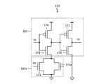
- FIG. 3Ais a circuit diagram showing the configuration of the input amplifier according to the present embodiment.
- the input amplifier 154 according to the present embodimentincludes an inverter circuit 161 and a voltage control circuit 162 connected to the inverter circuit 161.
- the inverter circuit 161corresponds to a comparison circuit.
- the inverter circuit 161includes MOS transistors 170 to 173.
- the MOS transistor 170 and the MOS transistor 172are P-channel type MOS transistors, and the MOS transistor 171 and the MOS transistor 173 are N-channel type MOS transistors.
- the MOS transistor 170 and the MOS transistor 171are connected in series. Further, the MOS transistor 172 and the MOS transistor 173 are connected in series.
- Each gate of the MOS transistor 170 and the MOS transistor 171is an input terminal of the input amplifier 154.
- the cathode voltage Vc of the photodetection element 151is input to each gate.
- the source of the MOS transistor 170is connected to the positive power supply, and the source of the MOS transistor 171 is connected to the voltage control circuit 162.
- Each drain of the MOS transistor 170 and the MOS transistor 171is connected to each gate of the MOS transistor 172 and the MOS transistor 173.
- the source of the MOS transistor 172is connected to a positive power supply, and the source of the MOS transistor 171 is grounded.
- Each drain of the MOS transistor 172 and the MOS transistor 173is an output terminal of the input amplifier 154 and is connected to the state detection circuit 155 and the signal processing circuit 143.
- the voltage control circuit 162includes a switching element 174 and a resistance element 175.
- the switching element 174is, for example, an N-channel type MOS transistor.
- the output voltage Vo of the state detection circuit 155is input to the gate of the switching element 174.
- the drainis connected to the source of the MOS transistor 171.
- the sourceis grounded.
- the resistance element 175is connected in parallel to the switching element 174.
- one of the MOS transistor 170 and the MOS transistor 171is turned on and the other is turned off according to the potential of the cathode voltage Vc of the photodetection element 151.
- the MOS transistor 170is turned on, the MOS transistor 173 is turned on and the MOS transistor 172 is turned off. In this case, the voltage level Vs becomes a low level.
- the MOS transistor 171is turned on, the MOS transistor 172 is turned on and the MOS transistor 173 is turned off. In this case, the voltage level Vs becomes a high level.
- the threshold voltage that switches the voltage level Vs to high level or low levelcorresponds to the potential of the reference voltage.
- the potential of the reference voltageis changed by the voltage control circuit 162.
- the switching element 174 of the voltage control circuit 162When the switching element 174 of the voltage control circuit 162 is turned on, the potential of the reference voltage becomes low. On the contrary, when the switching element 174 is turned off, the potential of the reference voltage becomes high.
- FIG. 3Bis a circuit diagram showing the configuration of the first modification of the input amplifier 154.
- the same components as those of the input amplifier 154 shown in FIG. 3Aare designated by the same reference numerals, and detailed description thereof will be omitted.
- the input amplifier 154 shown in FIG. 3Bhas a different voltage control circuit configuration from the input amplifier 154 shown in FIG. 3A.
- the current source 175ais provided in place of the resistance element 175.
- the current source 175ais an N-channel type MOS transistor.
- the drain of this N-channel type MOS transistoris connected to the drain of the switching element 174, and the source is grounded.
- a reference voltageis input to the gate. This reference voltage is set so that the on-resistance of the switching element 174 is lower than the on-resistance of the current source 175a.
- FIG. 4is a circuit diagram showing the configuration of the second modification of the input amplifier 154.
- the input amplifier 154a according to this modificationincludes an inverter circuit 161a and a voltage control circuit 163 connected to the inverter circuit 161a. Similar to the inverter circuit 161 shown in FIG. 3A, the inverter circuit 161a is composed of MOS transistors 170a to 173a, and therefore detailed description thereof will be omitted.
- the voltage control circuit 163includes a current source 176a, a switch 176b, a switch 176c, and an inverter element 176d.
- the current source 176ais an N-channel type MOS transistor.
- a switch 176b and a switch 176care connected in parallel to the gate of this N-channel type MOS transistor.
- the drainis connected to the source of the MOS transistor 171a.
- the sourceis grounded.
- the output current value of the current source 176achanges according to the gate voltage of the N-channel type MOS transistor. As the gate voltage becomes lower, the output current value becomes smaller, so that the reference voltage for switching the voltage level Vs of the inverter circuit 161a becomes higher.
- the switch 176b and the switch 176care turned on or off based on the output voltage Vo of the state detection circuit 155. A voltage obtained by inverting the potential of the output voltage Vo by the inverter element 176d is input to the switch 176c. Therefore, when one of the switch 176b and the switch 176c is turned on, the other is turned off. When the switch 176b is turned on, the first reference voltage Vref1 is supplied to the current source 176a as the gate voltage.
- the switch 176cwhen the switch 176c is turned on, the second reference voltage Vref2 having a potential different from that of the first reference voltage Vref1 is supplied to the current source 176a as the gate voltage.
- the inverter element 176dmay be provided on the switch 176b side instead of the switch 176c side.
- FIG. 5is a circuit diagram showing a configuration of a third modification of the input amplifier 154.
- the input amplifier 154b according to this modificationincludes an operational amplifier circuit 164 and a switch circuit 165.
- the operational amplifier circuit 164is an example of a comparison circuit, and includes MOS transistors 177 to MOS transistors 180 and a current source 181.
- the MOS transistor 177 and the MOS transistor 178are P-channel type MOS transistors and form a current mirror circuit.
- the MOS transistor 179 and the MOS transistor 180are N-channel type MOS transistors having the same size and the same electrical characteristics, and are connected in parallel to each other via the current mirror circuit.
- the gate of the MOS transistor 179is an input terminal of the input amplifier 154b. Further, the drain of the MOS transistor 178 and the MOS transistor 180 is an output terminal of the input amplifier 154b.
- the current source 181is connected to each source of the MOS transistor 179 and the MOS transistor 180.
- the switch circuit 165is a modification of the voltage control circuit 162, and includes a switch 182, a switch 183, and an inverter element 184.
- the switch 182 and the switch 183are turned on or off based on the output voltage Vo of the state detection circuit 155.
- a voltage obtained by inverting the potential of the output voltage Vo by the inverter element 184is input to the switch 183. Therefore, when one of the switch 182 and the switch 183 is turned on, the other is turned off.
- the switch 182is turned on, the first reference voltage Vref1 is input to the gate of the MOS transistor 180.
- the switch 183when the switch 183 is turned on, the second reference voltage Vref2 having a potential different from that of the first reference voltage Vref1 is input to the gate of the MOS transistor 180.
- the inverter element 184may be provided on the switch 182 side instead of the switch 183 side.
- FIG. 6Ais a circuit diagram showing a configuration of a fourth modification of the input amplifier 154.
- This modificationincludes a configuration including a first input amplifier 154c and a second input amplifier 154d.
- the first input amplifier 154chas a MOS transistor 170c to a MOS transistor 173c, a switching element 174c, and a resistance element 175c, similarly to the input amplifier 154 shown in FIG. 3A.
- the gate of the MOS transistor 170cis an input terminal
- the drains of the MOS transistor 172c and the MOS transistor 173care output terminals. This output terminal is connected to the signal processing circuit 143.
- the second input amplifier 154dalso has a MOS transistor 170d to a MOS transistor 173d, a switching element 174d, and a resistance element 175d, similarly to the input amplifier 154.
- the gate of the MOS transistor 170dis an input terminal
- the drains of the MOS transistor 172d and the MOS transistor 173dare output terminals. This output terminal is connected to the state detection circuit 155.
- the circuit configuration of the first input amplifier 154cis the same as the circuit configuration of the second input amplifier 154d, but may be different.
- FIG. 6Bis a circuit diagram showing the configuration of the fifth modification of the input amplifier 154.
- the same components as those in FIG. 6Aare designated by the same reference numerals, and detailed description thereof will be omitted.
- the configuration of the second input amplifier 154dis different from that of FIG. 6A.
- the second input amplifier 154d according to this modificationis not provided with the switching element 174d and the resistance element 175d, and the source of the MOS transistor 171d is grounded. That is, the second input amplifier 154d does not perform reference voltage control based on the output voltage Vo of the state detection circuit 155.
- the cathode voltage Vc input during the operation of the state detection circuit 155becomes constant, so that the control is stable.
- FIG. 7is a circuit diagram showing the configuration of the state detection circuit 155.
- the state detection circuit 155 shown in FIG. 7can be applied to the input amplifier 154 shown in FIGS. 3A and 3B, the input amplifier 154b shown in FIG. 5, and the second input amplifier 154d shown in FIGS. 6A and 6B.
- the state detection circuit 155is composed of five stages of inverter elements 190 connected in series with each other.
- the state detection circuit 155outputs an input signal after a predetermined time has elapsed.
- the predetermined timecorresponds to the delay time of the input signal and the output signal.
- This delay timecan be set based on the number of stages of the inverter element 190. Therefore, the number of stages of the inverter element 190 is not limited to five, and may be an odd number. By adjusting the number of stages of the inverter element 190, it is possible to set the timing for changing the reference voltage of each input amplifier.
- FIG. 8is a graph showing an example of voltage characteristics of a plurality of photodetecting elements 151.
- the horizontal axisrepresents time and the vertical axis represents the cathode voltage Vc of the photodetector.
- the drop characteristic of the cathode voltage Vc when a photon is incident on the photodetecting element 151 due to the variation in on-resistance and parasitic capacitanceis different among the photodetecting elements. It may be different. In this case, as shown in FIG.
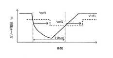
- FIG. 9is a graph showing an example of the voltage characteristics of a single photodetector 151.
- the horizontal axisrepresents time and the vertical axis represents the cathode voltage Vc of the photodetection element 151.
- the cathode voltage Vcdrops.
- the cathode voltage Vcgradually recovers. Photons cannot be detected in the dead time Tdead, which is the period from when the cathode voltage Vc drops to when it recovers.
- the reference voltage Vrefis fixed to a high value, the dead time Tdead becomes long, and the distance measurement performance may be insufficient. Therefore, in order to shorten the dead time Tdead, it is desirable to set the reference voltage Vref to a low value.
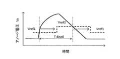
- FIG. 10is a graph showing the voltage characteristics of the photodetection element 151 and the reference voltage characteristics of the input amplifier 154.
- the horizontal axisrepresents time and the vertical axis represents the cathode voltage Vc of the photodetection element 151.
- the voltage control circuit 162can set two reference voltages. Further, the state detection circuit 155 can set the timing for switching between the two reference voltages. Therefore, as shown in FIG. 10, it is possible to detect a drop in the cathode voltage Vc at the high potential first reference voltage Vref1 and detect a recovery of the cathode voltage Vc at the low potential second reference voltage Vref2. In this embodiment, the state detection circuit 155 sets the timing for switching from the first reference voltage Vref1 to the second reference voltage Vref2 at the timing from the falling edge to the rising edge of the cathode voltage Vc. This makes it possible to more accurately measure the drop and recovery of the cathode voltage Vc.
- the reference voltage for detecting the drop in the cathode voltage Vc of the photodetection element 151can be set high, the measurement due to the variation in the output timing among the plurality of photodetection elements 151 is measured. The distance error can be reduced. Further, since the reference voltage for detecting the recovery of the cathode voltage Vc can be set low, the dead time can be shortened. Therefore, it is possible to achieve both the two contradictory requirements of early detection of the drop and recovery of the cathode voltage Vc, and thus it is possible to improve the distance measurement performance.
- FIG. 11is a perspective view showing the structure of the distance measuring device according to the modified example.
- the same components as those of the distance measuring device 131 according to the first embodiment described aboveare designated by the same reference numerals, and detailed description thereof will be omitted.
- the ranging device 131a shown in FIG. 11has a first semiconductor substrate 301 and a second semiconductor substrate 302.
- the first semiconductor substrate 301 and the second semiconductor substrate 302are joined by, for example, a copper pad and are electrically connected.
- a plurality of photodetecting elements 151are arranged two-dimensionally to form a pixel array.
- the forming surface of the photodetection element 151becomes the light receiving surface S of the distance measuring device 131a.
- the second semiconductor substrate 302has a region 312 facing the first semiconductor substrate 301 and a region 322 adjacent to the region 312.
- peripheral parts of the photodetection element 151that is, a charging circuit 152, a quench circuit 153, an input amplifier 154, and a state detection circuit 155 are formed in the photodetection circuit 142.
- a signal processing circuit 143is formed in the region 322.
- the reference voltage for detecting the drop of the cathode voltage Vc of the photodetection element 151 and the recovery of the cathode voltage Vcare detected.
- the reference voltageand can be set separately. Therefore, it is possible to improve the distance measurement performance.
- FIG. 12is a block diagram showing a configuration example of the distance measuring device according to the second embodiment.
- the same components as those of the distance measuring device 131 according to the first embodiment described aboveare designated by the same reference numerals, and detailed description thereof will be omitted.
- the distance measuring device according to the present embodimenthas a different configuration of the photodetector circuit from the first embodiment. Hereinafter, the photodetection circuit according to this embodiment will be described.
- the anode of the photodetection element 151is connected to the input terminal of the input amplifier 154, and the cathode is connected to the power supply. Therefore, the input amplifier 154 detects an increase and recovery of the anode voltage Va based on the comparison between the anode voltage Va of the photodetection element 151 and the reference voltage. Since the circuit configuration of the input amplifier 154 is the same as that of the first embodiment, the reference voltage is switched based on the control of the state detection circuit 155.
- FIG. 13is a graph showing the voltage characteristics of the photodetection element 151 and the reference voltage characteristics of the input amplifier 154.
- the horizontal axisrepresents time and the vertical axis represents the anode voltage Va of the photodetection element 151.
- the anode voltage Varises. After that, the anode voltage Va gradually drops (recovers).
- the voltage control circuit 162switches between the two reference voltages based on the control of the state detection circuit 155. Therefore, as shown in FIG. 13, it is possible to detect an increase in the anode voltage Va at the low potential first reference voltage and detect a decrease in the anode voltage Va at the high potential second reference voltage Vref2. Therefore, it is possible to reduce the ranging error due to the variation in the output timing among the plurality of photodetecting elements 151, and to shorten the dead time Tdead.
- the reference voltage for detecting the increase in the anode voltage Va of the photodetection element 151 and the reference voltage for detecting the decrease in the anode voltage Vacan be set separately. can. Therefore, it is possible to improve the distance measurement performance.
- the technology according to the present disclosurecan be applied to various products.
- the technology according to the present disclosureis realized as a device mounted on a moving body of any kind such as an automobile, an electric vehicle, a hybrid electric vehicle, a motorcycle, a bicycle, a personal mobility, an airplane, a drone, a ship, and a robot. You may.
- FIG. 14is a block diagram showing a schematic configuration example of a vehicle control system, which is an example of a mobile control system to which the technique according to the present disclosure can be applied.
- the vehicle control system 12000includes a plurality of electronic control units connected via the communication network 12001.
- the vehicle control system 12000includes a drive system control unit 12010, a body system control unit 12020, an outside information detection unit 12030, an in-vehicle information detection unit 12040, and an integrated control unit 12050.
- a microcomputer 12051, an audio image output unit 12052, and an in-vehicle network I / F (Interface) 12053are shown as a functional configuration of the integrated control unit 12050.
- the drive system control unit 12010controls the operation of the device related to the drive system of the vehicle according to various programs.
- the drive system control unit 12010has a driving force generator for generating a driving force of a vehicle such as an internal combustion engine or a driving motor, a driving force transmission mechanism for transmitting the driving force to the wheels, and a steering angle of the vehicle. It functions as a control device such as a steering mechanism for adjusting and a braking device for generating braking force of the vehicle.
- the body system control unit 12020controls the operation of various devices mounted on the vehicle body according to various programs.
- the body system control unit 12020functions as a keyless entry system, a smart key system, a power window device, or a control device for various lamps such as headlamps, back lamps, brake lamps, turn signals or fog lamps.
- the body system control unit 12020may be input with radio waves transmitted from a portable device that substitutes for the key or signals of various switches.
- the body system control unit 12020receives inputs of these radio waves or signals and controls a vehicle door lock device, a power window device, a lamp, and the like.
- the outside information detection unit 12030detects information outside the vehicle equipped with the vehicle control system 12000.
- the image pickup unit 12031is connected to the vehicle outside information detection unit 12030.
- the vehicle outside information detection unit 12030causes the image pickup unit 12031 to capture an image of the outside of the vehicle and receives the captured image.
- the vehicle outside information detection unit 12030may perform object detection processing or distance detection processing such as a person, a vehicle, an obstacle, a sign, or a character on the road surface based on the received image.
- the image pickup unit 12031is an optical sensor that receives light and outputs an electric signal according to the amount of the light received.
- the image pickup unit 12031can output an electric signal as an image or can output it as distance measurement information. Further, the light received by the image pickup unit 12031 may be visible light or invisible light such as infrared light.
- the in-vehicle information detection unit 12040detects the in-vehicle information.
- a driver state detection unit 12041that detects the state of the driver is connected to the in-vehicle information detection unit 12040.
- the driver state detection unit 12041includes, for example, a camera that images the driver, and the in-vehicle information detection unit 12040 determines the degree of fatigue or concentration of the driver based on the detection information input from the driver state detection unit 12041. It may be calculated, or it may be determined whether the driver has fallen asleep.
- the microcomputer 12051calculates the control target value of the driving force generator, the steering mechanism, or the braking device based on the information inside and outside the vehicle acquired by the vehicle exterior information detection unit 12030 or the vehicle interior information detection unit 12040, and the drive system control unit.
- a control commandcan be output to 12010.
- the microcomputer 12051realizes ADAS (Advanced Driver Assistance System) functions including vehicle collision avoidance or impact mitigation, follow-up driving based on inter-vehicle distance, vehicle speed maintenance driving, vehicle collision warning, vehicle lane deviation warning, and the like. It is possible to perform cooperative control for the purpose of.
- ADASAdvanced Driver Assistance System
- the microcomputer 12051controls the driving force generating device, the steering mechanism, the braking device, and the like based on the information around the vehicle acquired by the vehicle exterior information detection unit 12030 or the vehicle interior information detection unit 12040. It is possible to perform coordinated control for the purpose of automatic driving that runs autonomously without depending on the operation.
- the microcomputer 12051can output a control command to the body system control unit 12030 based on the information outside the vehicle acquired by the vehicle outside information detection unit 12030.
- the microcomputer 12051controls the headlamps according to the position of the preceding vehicle or the oncoming vehicle detected by the outside information detection unit 12030, and performs cooperative control for the purpose of anti-glare such as switching the high beam to the low beam. It can be carried out.
- the audio image output unit 12052transmits an output signal of at least one of audio and an image to an output device capable of visually or audibly notifying information to the passenger or the outside of the vehicle.
- an audio speaker 12061, a display unit 12062, and an instrument panel 12063are exemplified as output devices.
- the display unit 12062may include, for example, at least one of an onboard display and a heads-up display.
- FIG. 15is a diagram showing an example of the installation position of the image pickup unit 12031.
- the image pickup unit 12031has image pickup units 12101, 12102, 12103, 12104, and 12105.
- the image pickup units 12101, 12102, 12103, 12104, and 12105are provided at positions such as, for example, the front nose, side mirrors, rear bumpers, back doors, and the upper part of the windshield in the vehicle interior of the vehicle 12100.
- the image pickup unit 12101 provided in the front nose and the image pickup section 12105 provided in the upper part of the windshield in the vehicle interiormainly acquire an image in front of the vehicle 12100.
- the image pickup units 12102 and 12103 provided in the side mirrormainly acquire images of the side of the vehicle 12100.
- the image pickup unit 12104 provided in the rear bumper or the back doormainly acquires an image of the rear of the vehicle 12100.
- the image pickup unit 12105 provided on the upper part of the windshield in the vehicle interioris mainly used for detecting a preceding vehicle, a pedestrian, an obstacle, a traffic light, a traffic sign, a lane, or the like.
- FIG. 15shows an example of the shooting range of the imaging units 12101 to 12104.
- the imaging range 12111indicates the imaging range of the imaging unit 12101 provided on the front nose
- the imaging range 1211212113indicates the imaging range of the imaging units 12102 and 12103 provided on the side mirrors, respectively
- the imaging range 12114indicates the rear bumper or the rear bumper.
- the imaging range of the imaging unit 12104 provided on the back dooris shown. For example, by superimposing the image data captured by the image pickup units 12101 to 12104, a bird's-eye view image of the vehicle 12100 can be obtained.
- At least one of the image pickup units 12101 to 12104may have a function of acquiring distance information.
- at least one of the image pickup units 12101 to 12104may be a stereo camera including a plurality of image pickup elements, or may be an image pickup element having pixels for phase difference detection.
- the microcomputer 12051has a distance to each three-dimensional object in the image pickup range 12111 to 12114 based on the distance information obtained from the image pickup unit 12101 to 12104, and a temporal change of this distance (relative speed with respect to the vehicle 12100).
- a predetermined speedfor example, 0 km / h or more
- the microcomputer 12051can set an inter-vehicle distance to be secured in advance in front of the preceding vehicle, and can perform automatic brake control (including follow-up stop control), automatic acceleration control (including follow-up start control), and the like. In this way, it is possible to perform coordinated control for the purpose of automatic driving or the like in which the vehicle travels autonomously without depending on the operation of the driver.
- the microcomputer 12051converts three-dimensional object data related to a three-dimensional object into two-wheeled vehicles, ordinary vehicles, large vehicles, pedestrians, electric poles, and other three-dimensional objects based on the distance information obtained from the image pickup units 12101 to 12104. It can be classified and extracted and used for automatic avoidance of obstacles. For example, the microcomputer 12051 distinguishes obstacles around the vehicle 12100 into obstacles that are visible to the driver of the vehicle 12100 and obstacles that are difficult to see. Then, the microcomputer 12051 determines the collision risk indicating the risk of collision with each obstacle, and when the collision risk is equal to or higher than the set value and there is a possibility of collision, the microcomputer 12051 via the audio speaker 12061 or the display unit 12062. By outputting an alarm to the driver and performing forced deceleration and avoidance steering via the drive system control unit 12010, driving support for collision avoidance can be provided.
- At least one of the image pickup units 12101 to 12104may be an infrared camera that detects infrared rays.
- the microcomputer 12051can recognize a pedestrian by determining whether or not a pedestrian is present in the captured image of the imaging unit 12101 to 12104.
- pedestrian recognitionis, for example, a procedure for extracting feature points in an image captured by an image pickup unit 12101 to 12104 as an infrared camera, and pattern matching processing is performed on a series of feature points indicating the outline of an object to determine whether or not the pedestrian is a pedestrian. It is done by the procedure to determine.
- the audio image output unit 12052determines the square contour line for emphasizing the recognized pedestrian.
- the display unit 12062is controlled so as to superimpose and display. Further, the audio image output unit 12052 may control the display unit 12062 so as to display an icon or the like indicating a pedestrian at a desired position.
- the aboveis an example of a vehicle control system to which the technology according to the present disclosure can be applied.
- the technique according to the present disclosurecan be applied to, for example, the image pickup unit 12031 among the configurations described above.
- the distance measuring devices 131 and 131acan be applied to the image pickup unit 12031.
- the present technologycan have the following configurations.
- An inputincluding a comparison circuit in which the voltage level of the output terminal changes according to the comparison result between the voltage of the input terminal connected to the avalanche photodiode and the reference voltage, and a voltage control circuit for changing the potential of the reference voltage.
- a state detection circuitthat sets a timing for changing the potential of the reference voltage in the voltage control circuit based on the detection result of the voltage level, and a state detection circuit.
- a photodetector circuitThe comparison circuit includes an inverter circuit.
- the voltage control circuitincludes a switching element connected to the inverter circuit and switched according to the output voltage of the state detection circuit, and a resistance element or a current source connected in parallel with the switching element (1).
- the comparison circuitincludes an operational amplifier circuit.
- the voltage control circuitincludes a switch circuit that switches the reference voltage to a first reference voltage or a second reference voltage different from the first reference voltage according to the output voltage of the state detection circuit (1).
- the comparison circuitincludes an inverter circuit.
- the input amplifierincludes a first input amplifier that outputs the comparison result to the signal processing circuit and a second input amplifier that outputs the comparison result to the state detection circuit, from (1) to (5). ).
- the optical detection circuitaccording to any one of the items.
- the photodetector circuit according to (6), wherein the circuit configuration of the first input amplifieris the same as the circuit configuration of the second input amplifier.
- the signal processing circuitis TDC (Time to Digital Converter) that converts the output signal to a digital value
- a histogram generation circuitthat measures the number of acquisitions of the digital value
- the distance measuring devicewhich includes a distance determining unit that determines a distance from the light detection circuit to a subject based on the measurement result of the histogram generation circuit.
- Optical detection circuit 143Signal processing circuit 151: Optical detection element 152: Charging circuit 153: Quench circuit 154, 154a, 154b: Input amplifier 154c: First input amplifier 154d: Second input amplifier 155: State detection circuit 161 161a: Inverter circuit 162: Voltage control circuit 163: Voltage control circuit 164: Operational amplifier circuit 165: Switch circuit 174: Switching element 175: Resistance element 175a: Current source 190: Inverter element 191: Operational amplifier 200: TDC 201: Histogram generation unit 202: Distance determination unit 301: First semiconductor substrate 302: Second semiconductor substrate
Landscapes
- Physics & Mathematics (AREA)
- General Physics & Mathematics (AREA)
- Engineering & Computer Science (AREA)
- Radar, Positioning & Navigation (AREA)
- Remote Sensing (AREA)
- Spectroscopy & Molecular Physics (AREA)
- Computer Networks & Wireless Communication (AREA)
- Electromagnetism (AREA)
- Optical Radar Systems And Details Thereof (AREA)
- Measurement Of Optical Distance (AREA)
Abstract
Description
Translated fromJapanese本開示は、光検出回路および測距装置に関する。This disclosure relates to a photodetector and a ranging device.
被写体までの距離を測定する方法として、ToF(Time of Flight)法が用いられる。ToF法では、光源から出射された光が被写体で反射された反射光を検出する。続いて、光を出射してから反射光を検出するまでの時間に基づいて、被写体までの距離を計測する。The ToF (Time of Flight) method is used as a method for measuring the distance to the subject. In the ToF method, the light emitted from the light source detects the reflected light reflected by the subject. Subsequently, the distance to the subject is measured based on the time from the emission of the light to the detection of the reflected light.
ToF法を用いた測距装置には、一般的に、上記反射光を検出する光検出回路が設けられている。光検出回路では、光子が入射したときの光検出素子の電圧変化を検出している。この電圧変化を検出するための基準電圧は、一般的に固定されている。A photodetector that uses the ToF method is generally provided with a photodetection circuit that detects the reflected light. The photodetection circuit detects the voltage change of the photodetector when a photon is incident. The reference voltage for detecting this voltage change is generally fixed.
上記基準電圧が低いと、光検出素子の特性ばらつきによって、測距誤差が大きくなる場合がある。この測距誤差を低減するためには、基準電圧が高いほうが望ましい。If the above reference voltage is low, the distance measurement error may increase due to variations in the characteristics of the photodetector. In order to reduce this distance measurement error, it is desirable that the reference voltage is high.
しかし、基準電圧が高いと、光子を検出することができない期間であるデッドタイムが長くなって、測距精度が低下する場合がある。However, if the reference voltage is high, the dead time, which is the period during which photons cannot be detected, becomes long, and the distance measurement accuracy may decrease.
本開示は、測距性能を向上させることが可能な光検出回路および測距装置を提供する。The present disclosure provides a photodetector and a distance measuring device capable of improving the distance measuring performance.
本開示の一実施形態に係る光検出回路は、アバランシェフォトダイオードと、アバランシェフォトダイオードに電圧を供給する充電回路と、アバランシェフォトダイオードに接続される入力端子の電圧と基準電圧との比較結果に応じて出力端子の電圧レベルが変化する比較回路と、基準電圧の電位を変化させる電圧制御回路と、を含む入力アンプと、電圧レベルの検出結果に基づいて、電圧制御回路に基準電圧の電位を変化させるタイミングを設定する状態検出回路と、を備える。The optical detection circuit according to the embodiment of the present disclosure corresponds to a comparison result between an avalanche photodiode, a charging circuit that supplies a voltage to the avalanche photodiode, and a voltage and a reference voltage of an input terminal connected to the avalanche photodiode. The reference voltage potential is changed in the voltage control circuit based on the input amplifier including the comparison circuit that changes the voltage level of the output terminal and the voltage control circuit that changes the potential of the reference voltage, and the detection result of the voltage level. It is provided with a state detection circuit for setting the timing of operation.
また、前記比較回路は、インバータ回路を含み、
前記電圧制御回路は、前記インバータ回路に接続され、前記状態検出回路の出力電圧に応じてスイッチングするスイッチング素子と、前記スイッチング素子と並列に接続された抵抗素子または電流源と、を含んでいてもよい。Further, the comparison circuit includes an inverter circuit.
The voltage control circuit may include a switching element connected to the inverter circuit and switching according to the output voltage of the state detection circuit, and a resistance element or a current source connected in parallel with the switching element. good.
また、前記比較回路は、オペアンプ回路を含み、
前記電圧制御回路は、前記状態検出回路の出力電圧に応じて、前記基準電圧を、第1基準電圧、または前記第1基準電圧と異なる第2基準電圧に切り替えるスイッチ回路を含んでいてもよい。Further, the comparison circuit includes an operational amplifier circuit, and the comparison circuit includes an operational amplifier circuit.
The voltage control circuit may include a switch circuit that switches the reference voltage to a first reference voltage or a second reference voltage different from the first reference voltage according to the output voltage of the state detection circuit.
また、前記比較回路は、インバータ回路を含み、
前記電圧制御回路は、前記インバータ回路に接続され、前記状態検出回路の出力電圧に応じて出力電流値が変化する電流源を含んでいてもよい。Further, the comparison circuit includes an inverter circuit.
The voltage control circuit may include a current source connected to the inverter circuit and whose output current value changes according to the output voltage of the state detection circuit.
また、前記状態検出回路は、互いに直列に接続された奇数段のインバータ素子を含んでいてもよい。Further, the state detection circuit may include an odd-numbered stage inverter element connected in series with each other.
また、前記入力アンプは、前記比較結果を信号処理回路へ出力する第1入力アンプと、前記比較結果を前記状態検出回路へ出力する第2入力アンプと、を含んでいてもよい。Further, the input amplifier may include a first input amplifier that outputs the comparison result to the signal processing circuit, and a second input amplifier that outputs the comparison result to the state detection circuit.
また、前記第1入力アンプの回路構成が、前記第2入力アンプの回路構成と同じであってもよい。Further, the circuit configuration of the first input amplifier may be the same as the circuit configuration of the second input amplifier.
また、前記第1入力アンプの回路構成が、前記第2入力アンプの回路構成と異なっていてもよい。Further, the circuit configuration of the first input amplifier may be different from the circuit configuration of the second input amplifier.
また、前記アバランシェフォトダイオード、前記充電回路、前記入力アンプ、および前記状態検出回路が1つの半導体基板に設けられていてもよい。Further, the avalanche photodiode, the charging circuit, the input amplifier, and the state detection circuit may be provided on one semiconductor substrate.
また、前記アバランシェフォトダイオードが第1半導体基板に設けられ、前記充電回路、前記入力アンプ、および前記状態検出回路が、第1半導体基板に接合される第2半導体基板に設けられていてもよい。Further, the avalanche photodiode may be provided on the first semiconductor substrate, and the charging circuit, the input amplifier, and the state detection circuit may be provided on the second semiconductor substrate bonded to the first semiconductor substrate.
また、前記アバランシェフォトダイオードと前記入力アンプの前記入力端子に接続され、前記入力端子の電位を制御するクエンチ回路をさらに備えていてもよい。Further, a quench circuit which is connected to the avalanche photodiode and the input terminal of the input amplifier and controls the potential of the input terminal may be further provided.
また、前記アバランシェフォトダイオードのカソードが前記入力アンプの前記入力端子に接続されていてもよい。Further, the cathode of the avalanche photodiode may be connected to the input terminal of the input amplifier.
また、前記アバランシェフォトダイオードのアノードが前記入力アンプの前記入力端子に接続されていてもよい。Further, the anode of the avalanche photodiode may be connected to the input terminal of the input amplifier.
本開示の一実施形態に係る測距装置は、上述した光検出回路のいずれかと、前記光検出回路の出力信号を処理する信号処理回路と、を備える。The ranging device according to the embodiment of the present disclosure includes any of the above-mentioned photodetector circuits and a signal processing circuit for processing the output signal of the photodetector circuit.
前記信号処理回路は、
前記出力信号をデジタル値に変換するTDC(Time to Digital Converter)と、
前記デジタル値の取得回数を計測するヒストグラム生成回路と、
前記ヒストグラム生成回路の計測結果に基づいて、前記光検出回路から被写体までの距離を判定する距離判定部と、を含んでいてもよい。The signal processing circuit is
TDC (Time to Digital Converter) that converts the output signal to a digital value,
A histogram generation circuit that measures the number of acquisitions of the digital value, and
A distance determination unit that determines the distance from the photodetection circuit to the subject based on the measurement result of the histogram generation circuit may be included.
(第1実施形態)
図1は、第1実施形態に係る光検出回路および測距装置を用いた撮像システムの構成例を示すブロック図である。図1に示す撮像システム101は、ToF法を用いて距離画像の撮影を行うシステムであり、照明装置111および撮像装置112を備える。(First Embodiment)
FIG. 1 is a block diagram showing a configuration example of an imaging system using a photodetector circuit and a distance measuring device according to the first embodiment. The
照明装置111は、照明制御部121および光源122を備える。照明制御部121は、撮像装置112の制御部132の制御に基づいて、光源122が照射光を照射するパターンを制御する。具体的には、照明制御部121は、制御部132から供給される照射信号に含まれる照射コードに従って、光源122が照射光を照射するパターンを制御する。例えば、照射コードは、「1」(High)と「0」(Low)の2値からなる。照明制御部121は、照射コードの値が「1」のとき光源122を点灯させ、照射コードの値が「0」のとき光源122を消灯させる。The lighting device 111 includes a
光源122は、照明制御部121の制御に基づいて、所定の波長域の光(照射光)を発する。光源122は、例えば、赤外線レーザダイオードである。光源122の種類、および、照射光の波長域は、撮像システム101の用途等に応じて任意に設定することが可能である。The
撮像装置112は、照射光が被写体102および被写体103により反射された反射光を受光する。撮像装置112は、測距装置131、制御部132、表示部133、および、記憶部134を備える。The
測距装置131は、レンズ141、光検出回路142、および、信号処理回路143を備える。レンズ141は、入射光を光検出回路142に結像させる。なお、レンズ141の構成は任意であり、例えば、複数のレンズ群によりレンズ141を構成することも可能である。The
光検出回路142は、制御部132の制御に基づいて、被写体102および被写体103等の撮像を行う。また、光検出回路142は、撮像によって得られた信号を信号処理回路143へ出力する。The
信号処理回路143は、制御部132の制御に基づいて、光検出回路142の出力信号を処理する。例えば、信号処理回路143は、光検出回路142の出力信号に基づいて、被写体までの距離を検出し、被写体までの距離を示す距離画像を生成する。The
制御部132は、例えば、FPGA(Field Programmable Gate Array)、DSP(Digital Signal Processor)等の制御回路やプロセッサ等により構成される。制御部132は、照明制御部121、光検出回路142、および、信号処理回路143の制御を行う。The
表示部133は、例えば、液晶表示装置や有機EL(Electro Luminescence)表示装置等のパネル型表示装置からなる。The
記憶部134は、任意の記憶装置や記憶媒体等により構成することができ、距離画像等を記憶する。The
図2は、光検出回路142および信号処理回路143の構成例を示すブロック図である。FIG. 2 is a block diagram showing a configuration example of the
光検出回路142は、光検出素子151と、充電回路152と、クエンチ回路153と、入力アンプ154と、状態検出回路155と、を含む。これらは、1つの半導体基板上に設けられている。なお、図2に示す光検出回路142は、1画素に対応する単位回路であるため、測距装置131は、画素数に応じて複数の光検出回路142を有する。The
光検出素子151は、APD(Avalanche Photo Diode)またはSPAD(Single Photon Avalanche Diode)等に代表されるフォトダイオードである。光検出素子151のカソードは、充電回路152および入力アンプ154の入力端子に接続されている。光検出素子151のアノードは、負電源(不図示)によって負電圧VRLに設定されている。The
充電回路152は、例えば、互いに直列に接続された電流源および抵抗素子で構成されている。充電回路152は、光検出素子151のカソードに正電圧を供給する。その結果、降伏電圧以上の逆電圧が光検出素子151のアノード-カソード間に印加されると、光検出素子151がガイガーモードに設定される。ガイガーモードに設定された光検出素子151に光子が入射すると、アバランシェ増倍が発生し、光検出素子151に電流が流れる。The charging
クエンチ回路153は、例えば、Nチャネル型MOSトランジスタ156で構成されている。Nチャネル型MOSトランジスタ156のドレインは、光検出素子151のカソードおよび入力アンプ154の入力端子に接続され、ソースは接地されている。外部信号APDENがNチャネル型MOSトランジスタ156のゲートに入力されると、カソード電圧Vcはグランド電位に強制的に設定される。この場合、光検出素子151の光検出機能が低下する。そのため、光検出素子151に光子が入射していないにも関わらず、再度アバランシェ増倍が発生するアフターパルス等の誤検出を回避することができる。なお、クエンチ回路153は、カソード電圧Vcを、光検出素子151の光検出機能を低下させる電位に強制的に設定できる構成であれば、Nチャネル型MOSトランジスタ156に制限されない。The quench
なお、Nチャネル型MOSトランジスタ156のソースは、接地される代わりに負電位に接続されていてもよい。この場合、カソード電圧Vcのリチャージ(回復)の立ち上がりが遅くなって、デッドタイムが長くなることが懸念される。しかし、後述するように、本実施形態では、入力アンプ154の基準電圧を最適化することによって、デッドタイムを短縮することができる。The source of the N-channel
入力アンプ154は、入力端子の電圧、換言すると光検出素子151のカソード電圧Vcと、可変の基準電圧とを比較する。また、入力アンプ154では、出力端子の電圧レベルは、比較結果に応じて変化する。入力アンプ154の回路構成については後述する。The
状態検出回路155は、入力アンプ154の出力端子の電圧レベルを検出して上記基準電圧の電位を変化させるタイミングを設定する。状態検出回路155の構成についても後述する。The
信号処理回路143は、TDC200(Time to Digital Converter)と、ヒストグラム生成部201と、距離判定部202と、を含む。TDC200(Time to Digital Converter)は、入力アンプ154の出力信号をデジタル値に変換する。具体的には、TDC200は、入力アンプ154の出力端子の電圧レベルの遷移タイミングの発生時刻をデジタル変換する。The
ヒストグラム生成部201は、上記デジタル値の取得回数、すなわち、光検出素子151の反応回数を計測する。The
距離判定部202は、ヒストグラム生成部201の計測結果に基づいて、光検出素子151から被写体102、103までの距離を判定する。距離判定部202は、例えば、ヒストグラム生成部201の計測結果を示す正規分布に対する近似曲線を算出し(いわゆるガウシアンフィッティング)、近似曲線を用いて距離を求める。The
以下、入力アンプ154の回路構成について説明する。Hereinafter, the circuit configuration of the
図3Aは、本実施形態に係る入力アンプの構成を示す回路図である。本実施形態に係る入力アンプ154は、インバータ回路161と、インバータ回路161に接続された電圧制御回路162と、を含む。インバータ回路161は、比較回路に相当する。FIG. 3A is a circuit diagram showing the configuration of the input amplifier according to the present embodiment. The
インバータ回路161は、MOSトランジスタ170~MOSトランジスタ173を含む。MOSトランジスタ170およびMOSトランジスタ172は、Pチャネル型MOSトランジスタであり、MOSトランジスタ171およびMOSトランジスタ173は、Nチャネル型MOSトランジスタである。MOSトランジスタ170およびMOSトランジスタ171が直列に接続されている。また、MOSトランジスタ172およびMOSトランジスタ173が直列に接続されている。The
MOSトランジスタ170およびMOSトランジスタ171の各ゲートは、入力アンプ154の入力端子である。各ゲートには、光検出素子151のカソード電圧Vcが入力される。MOSトランジスタ170のソースは正電源に接続され、MOSトランジスタ171のソースは電圧制御回路162に接続されている。MOSトランジスタ170およびMOSトランジスタ171の各ドレインは、MOSトランジスタ172およびMOSトランジスタ173の各ゲートに接続されている。MOSトランジスタ172のソースは正電源に接続され、MOSトランジスタ171のソースは接地されている。MOSトランジスタ172およびMOSトランジスタ173の各ドレインは、入力アンプ154の出力端子であり、状態検出回路155および信号処理回路143に接続されている。Each gate of the
電圧制御回路162は、スイッチング素子174と、抵抗素子175とを含む。スイッチング素子174は、例えばNチャネル型MOSトランジスタである。スイッチング素子174のゲートには、状態検出回路155の出力電圧Voが入力される。ドレインは、MOSトランジスタ171のソースに接続されている。ソースは接地されている。一方、抵抗素子175は、スイッチング素子174に並列に接続されている。The
上記のように構成されたインバータ回路161では、光検出素子151のカソード電圧Vcの電位に応じて、MOSトランジスタ170またはMOSトランジスタ171の一方がオンし、他方がオフする。MOSトランジスタ170がオンすると、MOSトランジスタ173がオンし、MOSトランジスタ172がオフする。この場合、電圧レベルVsは、ローレベルとなる。MOSトランジスタ171がオンすると、MOSトランジスタ172がオンし、MOSトランジスタ173がオフする。この場合、電圧レベルVsは、ハイレベルとなる。In the
電圧レベルVsをハイレベルまたはローレベルに切り替えるしきい値電圧は、基準電圧の電位に対応する。基準電圧の電位は、電圧制御回路162によって変化する。電圧制御回路162のスイッチング素子174がオンすると、基準電圧の電位は低くなる。反対に、スイッチング素子174がオフすると、基準電圧の電位は高くなる。The threshold voltage that switches the voltage level Vs to high level or low level corresponds to the potential of the reference voltage. The potential of the reference voltage is changed by the
図3Bは、入力アンプ154の第1変形例の構成を示す回路図である。図3Aに示す入力アンプ154と同様の構成要素には同じ符号を付し、詳細な説明を省略する。図3Bに示す入力アンプ154は、電圧制御回路の構成が図3Aに示す入力アンプ154と異なる。具体的には、本変形例に係る電圧制御回路162aは、電流源175aが抵抗素子175の代わりに設けれている。電流源175aは、Nチャネル型MOSトランジスタである。このNチャネル型MOSトランジスタのドレインは、スイッチング素子174のドレインに接続され、ソースは、接地されている。また、ゲートには、基準電圧が入力される。この基準電圧は、スイッチング素子174のオン抵抗が電流源175aのオン抵抗よりも低くなるように設定される。FIG. 3B is a circuit diagram showing the configuration of the first modification of the
図4は、入力アンプ154の第2変形例の構成を示す回路図である。本変形例に係る入力アンプ154aは、インバータ回路161aと、インバータ回路161aに接続された電圧制御回路163と、を含む。インバータ回路161aは、図3Aに示すインバータ回路161と同様に、MOSトランジスタ170a~MOSトランジスタ173aで構成されているため詳細な説明を省略する。FIG. 4 is a circuit diagram showing the configuration of the second modification of the
一方、電圧制御回路163は、は、電流源176aと、スイッチ176bと、スイッチ176cと、インバータ素子176dと、を含む。電流源176aは、Nチャネル型MOSトランジスタである。このNチャネル型MOSトランジスタのゲートには、スイッチ176bおよびスイッチ176cが並列に接続されている。ドレインは、MOSトランジスタ171aのソースに接続されている。ソースは接地されている。電流源176aの出力電流値は、Nチャネル型MOSトランジスタのゲート電圧に応じて変化する。ゲート電圧が低くなると出力電流値が小さくなるので、インバータ回路161aの電圧レベルVsを切り替える基準電圧は高くなる。反対に、ゲート電圧が高くなると出力電流値が大きくなるので、基準電圧は低くなる。スイッチ176bおよびスイッチ176cは、状態検出回路155の出力電圧Voに基づいてオンまたはオフする。スイッチ176cには、インバータ素子176dによって出力電圧Voの電位を反転させた電圧が入力される。そのため、スイッチ176bおよびスイッチ176cの一方がオンすると他方がオフする。スイッチ176bがオンすると、第1基準電圧Vref1が上記ゲート電圧として電流源176aに供給される。反対にスイッチ176cがオンすると、第1基準電圧Vref1と電位が異なる第2基準電圧Vref2が上記ゲート電圧として電流源176aに供給される。なお、インバータ素子176dは、スイッチ176c側の代わりにスイッチ176b側に設けられていてもよい。On the other hand, the
図5は、入力アンプ154の第3変形例の構成を示す回路図である。本変形例に係る入力アンプ154bは、オペアンプ回路164と、スイッチ回路165と、を含む。オペアンプ回路164は、比較回路の一例であり、MOSトランジスタ177~MOSトランジスタ180と、電流源181と、を含む。MOSトランジスタ177およびMOSトランジスタ178は、Pチャネル型MOSトランジスタであり、カレントミラー回路を構成する。MOSトランジスタ179およびMOSトランジスタ180は、同じサイズで同じ電気的特性を有するNチャネル型MOSトランジスタであり、上記カレントミラー回路を介して互いに並列に接続されている。MOSトランジスタ179のゲートは、入力アンプ154bの入力端子である。また、MOSトランジスタ178およびMOSトランジスタ180のドレインは、入力アンプ154bの出力端子である。電流源181は、MOSトランジスタ179およびMOSトランジスタ180の各ソースに接続されている。FIG. 5 is a circuit diagram showing a configuration of a third modification of the
スイッチ回路165は、電圧制御回路162の変形例であり、スイッチ182と、スイッチ183と、インバータ素子184と、を含む。スイッチ182およびスイッチ183は、状態検出回路155の出力電圧Voに基づいてオンまたはオフする。スイッチ183には、インバータ素子184によって出力電圧Voの電位を反転させた電圧が入力される。そのため、スイッチ182およびスイッチ183の一方がオンすると他方がオフする。スイッチ182がオンすると、第1基準電圧Vref1がMOSトランジスタ180のゲートに入力される。反対にスイッチ183がオンすると、第1基準電圧Vref1と電位が異なる第2基準電圧Vref2がMOSトランジスタ180のゲートに入力される。なお、インバータ素子184は、スイッチ183側の代わりにスイッチ182側に設けられていてもよい。The
図6Aは、入力アンプ154の第4変形例の構成を示す回路図である。本変形例は、第1入力アンプ154cおよび第2入力アンプ154dを含む構成である。第1入力アンプ154cは、図3Aに示す入力アンプ154と同様に、MOSトランジスタ170c~MOSトランジスタ173c、スイッチング素子174c、および抵抗素子175cを有する。第1入力アンプ154cでは、MOSトランジスタ170cのゲートが入力端子であり、MOSトランジスタ172cおよびMOSトランジスタ173cの各ドレインが出力端子である。この出力端子は、信号処理回路143に接続される。FIG. 6A is a circuit diagram showing a configuration of a fourth modification of the
一方、第2入力アンプ154dも、入力アンプ154と同様に、MOSトランジスタ170d~MOSトランジスタ173d、スイッチング素子174d、および抵抗素子175dを有する。第2入力アンプ154dでは、MOSトランジスタ170dのゲートが入力端子であり、MOSトランジスタ172dおよびMOSトランジスタ173dの各ドレインが出力端子である。この出力端子は、状態検出回路155に接続されている。On the other hand, the
なお、本変形例では、第1入力アンプ154cの回路構成は、第2入力アンプ154dの回路構成と同じであるが、異なっていてもよい。In this modification, the circuit configuration of the
図6Bは、入力アンプ154の第5変形例の構成を示す回路図である。図6Aと同様の構成要素には同じ符号を付し、詳細な説明を省略する。本変形例では、第2入力アンプ154dの構成が図6Aと異なる。本変形例に係る第2入力アンプ154dには、スイッチング素子174dおよび抵抗素子175dが設けられておらず、MOSトランジスタ171dのソースは接地されている。すなわち、第2入力アンプ154dは、状態検出回路155の出力電圧Voに基づく基準電圧制御を行わない。本変形例によれば、状態検出回路155の動作時に入力されるカソード電圧Vcが一定になるため、制御が安定する。FIG. 6B is a circuit diagram showing the configuration of the fifth modification of the
以下、状態検出回路155の回路構成について説明する。Hereinafter, the circuit configuration of the
図7は、状態検出回路155の構成を示す回路図である。図7に示す状態検出回路155は、図3A、図3Bに示す入力アンプ154、図5に示す入力アンプ154b、および図6A、図6Bに示す第2入力アンプ154dに適用することができる。この状態検出回路155は、互いに直列に接続された5段のインバータ素子190で構成されている。FIG. 7 is a circuit diagram showing the configuration of the
上記状態検出回路155は、入力信号を所定の時間経過した後に出力する。所定時間は、入力信号と出力信号の遅延時間に相当する。この遅延時間は、インバータ素子190の段数に基づいて設定することができる。そのため、インバータ素子190の段数は5つに限定されず、奇数であればよい。インバータ素子190の段数を調整することによって、各入力アンプの基準電圧を変化させるタイミングを設定することができる。The
図8は、複数の光検出素子151の電圧特性の一例を示すグラフである。図8に示すグラフでは、横軸は時間を示し、縦軸は光検出素子のカソード電圧Vcを示す。複数の光検出素子151を二次元状に配置した画素アレイでは、オン抵抗と寄生容量のばらつきにより、光子が光検出素子151に入射したときのカソード電圧Vcの降下特性が、光検出素子間で異なる場合がる。この場合、図8に示すように、入力アンプの基準電圧Vrefが低値に固定されていると、カソード電圧Vcの降下を検出するタイミングがばらつき測距誤差の要因と成り得る。この測距誤差を低減するためには、基準電圧Vrefを高値に設定することが望ましい。FIG. 8 is a graph showing an example of voltage characteristics of a plurality of
図9は、単数の光検出素子151の電圧特性の一例を示すグラフである。図9に示すグラフでも、横軸は時間を示し、縦軸は光検出素子151のカソード電圧Vcを示す。光検出素子151に光子が入射すると、アバランシェ増倍が発生し、光検出素子151に電流が流れる。これにより、カソード電圧Vcが降下する。アバランシェ増倍が収束すると、カソード電圧Vcが徐々に回復する。カソード電圧Vcが降下してから回復するまでの期間であるデッドタイムTdeadでは、光子を検出することができない。そのため、基準電圧Vrefが高値に固定されていると、デッドタイムTdeadが長くなり、測距性能が不十分になり得る。そのため、デッドタイムTdeadを短くするためには、基準電圧Vrefを低値に設定することが望ましい。FIG. 9 is a graph showing an example of the voltage characteristics of a
図10は、光検出素子151の電圧特性と入力アンプ154の基準電圧特性を示すグラフである。図10に示すグラフでも、横軸は時間を示し、縦軸は光検出素子151のカソード電圧Vcを示す。FIG. 10 is a graph showing the voltage characteristics of the
本実施形態に係る入力アンプ154では、上述したように、電圧制御回路162が、2つの基準電圧を設定することができる。また、状態検出回路155が、2つの基準電圧を切り替えるタイミングを設定することができる。そのため、図10に示すように、高電位の第1基準電圧Vref1でカソード電圧Vcの降下を検出し、低電位の第2基準電圧Vref2でカソード電圧Vcの回復を検出することができる。なお、本実施形態では、状態検出回路155が、第1基準電圧Vref1から第2基準電圧Vref2に切り替えるタイミングを、カソード電圧Vcの立ち下りから立ち上がりのタイミングに合わせている。これにより、カソード電圧Vcの降下および回復をより正確に測定することができる。In the
以上説明した本実施形態によれば、光検出素子151のカソード電圧Vcの降下を検出するための基準電圧を高く設定することができるため、複数の光検出素子151間における出力タイミングのばらつきによる測距誤差を軽減することができる。また、カソード電圧Vcの回復を検出するための基準電圧を低く設定することができるため、デッドタイムを短くすることができる。したがって、カソード電圧Vcの降下および回復の早期検出という相反する2つの要求を両立することができるため、測距性能を向上させることが可能となる。According to the present embodiment described above, since the reference voltage for detecting the drop in the cathode voltage Vc of the
(変形例)
図11は、変形例に係る測距装置の構造を示す斜視図である。なお、上述した第1実施形態に係る測距装置131と同様の構成要素には同じ符号を付し、詳細な説明を省略する。(Modification example)
FIG. 11 is a perspective view showing the structure of the distance measuring device according to the modified example. The same components as those of the
図11に示す測距装置131aは、第1半導体基板301および第2半導体基板302を有する。第1半導体基板301および第2半導体基板302は、例えば銅パッドで接合され、電気的に接続されている。The ranging
第1半導体基板301には、複数の光検出素子151が二次元状に配列されて画素アレイが形成されている。光検出素子151の形成面が、測距装置131aの受光面Sになる。On the
第2半導体基板302は、第1半導体基板301に対向する領域312と、領域312に隣接する領域322を有する。領域312には、光検出回路142のうち、光検出素子151の周辺部品、すなわち充電回路152、クエンチ回路153、入力アンプ154、および状態検出回路155が形成されている。一方、領域322には、信号処理回路143が形成されている。The
以上説明した本変形例の構造であっても、第1実施形態と同様に、光検出素子151のカソード電圧Vcの降下を検出するための基準電圧と、カソード電圧Vcの回復を検出するための基準電圧と、を別々に設定することができる。そのため、測距性能を向上させることが可能となる。Even in the structure of the present modification described above, similarly to the first embodiment, the reference voltage for detecting the drop of the cathode voltage Vc of the
(第2実施形態)
図12は、第2実施形態に係る測距装置の構成例を示すブロック図である。上述した第1実施形態に係る測距装置131と同様の構成要素には同じ符号を付し、詳細な説明を省略する。本実施形態に係る測距装置は、光検出回路の構成が第1実施形態と異なる。以下、本実施形態に係る光検出回路について説明する。(Second Embodiment)
FIG. 12 is a block diagram showing a configuration example of the distance measuring device according to the second embodiment. The same components as those of the
図12に示す光検出回路144では、光検出素子151のアノードが入力アンプ154の入力端子に接続され、カソードは電源に接続されている。そのため、入力アンプ154は、光検出素子151のアノード電圧Vaと基準電圧との比較に基づいて、アノード電圧Vaの上昇および回復を検出する。入力アンプ154の回路構成は、第1実施形態と同様であるため、基準電圧は、状態検出回路155の制御に基づいて切り替わる。In the
図13は、光検出素子151の電圧特性と入力アンプ154の基準電圧特性を示すグラフである。図13に示すグラフでは、横軸は時間を示し、縦軸は光検出素子151のアノード電圧Vaを示す。FIG. 13 is a graph showing the voltage characteristics of the
本実施形態では、光検出素子151に光子が入射すると、アノード電圧Vaが上昇する。その後、アノード電圧Vaが徐々に降下(回復)する。このとき、入力アンプ154では、電圧制御回路162が、状態検出回路155の制御に基づいて、2つの基準電圧を切り替える。そのため、図13に示すように、低電位の第1基準電圧でアノード電圧Vaの上昇を検出し、高電位の第2基準電圧Vref2でアノード電圧Vaの低下を検出することができる。そのため、複数の光検出素子151間における出力タイミングのばらつきによる測距誤差を軽減し、デッドタイムTdeadを短くすることができる。In this embodiment, when a photon is incident on the
以上説明した本実施形態によれば、光検出素子151のアノード電圧Vaの上昇を検出するための基準電圧と、アノード電圧Vaの低下を検出するための基準電圧と、を別々に設定することができる。そのため、測距性能を向上させることが可能となる。According to the present embodiment described above, the reference voltage for detecting the increase in the anode voltage Va of the
<移動体への応用例>
本開示に係る技術(本技術)は、様々な製品へ応用することができる。例えば、本開示に係る技術は、自動車、電気自動車、ハイブリッド電気自動車、自動二輪車、自転車、パーソナルモビリティ、飛行機、ドローン、船舶、ロボット等のいずれかの種類の移動体に搭載される装置として実現されてもよい。<Application example to mobile>
The technology according to the present disclosure (the present technology) can be applied to various products. For example, the technology according to the present disclosure is realized as a device mounted on a moving body of any kind such as an automobile, an electric vehicle, a hybrid electric vehicle, a motorcycle, a bicycle, a personal mobility, an airplane, a drone, a ship, and a robot. You may.
図14は、本開示に係る技術が適用され得る移動体制御システムの一例である車両制御システムの概略的な構成例を示すブロック図である。FIG. 14 is a block diagram showing a schematic configuration example of a vehicle control system, which is an example of a mobile control system to which the technique according to the present disclosure can be applied.
車両制御システム12000は、通信ネットワーク12001を介して接続された複数の電子制御ユニットを備える。図14に示した例では、車両制御システム12000は、駆動系制御ユニット12010、ボディ系制御ユニット12020、車外情報検出ユニット12030、車内情報検出ユニット12040、および統合制御ユニット12050を備える。また、統合制御ユニット12050の機能構成として、マイクロコンピュータ12051、音声画像出力部12052、および車載ネットワークI/F(Interface)12053が図示されている。The
駆動系制御ユニット12010は、各種プログラムにしたがって車両の駆動系に関連する装置の動作を制御する。例えば、駆動系制御ユニット12010は、内燃機関又は駆動用モータ等の車両の駆動力を発生させるための駆動力発生装置、駆動力を車輪に伝達するための駆動力伝達機構、車両の舵角を調節するステアリング機構、および、車両の制動力を発生させる制動装置等の制御装置として機能する。The drive
ボディ系制御ユニット12020は、各種プログラムにしたがって車体に装備された各種装置の動作を制御する。例えば、ボディ系制御ユニット12020は、キーレスエントリシステム、スマートキーシステム、パワーウィンドウ装置、あるいは、ヘッドランプ、バックランプ、ブレーキランプ、ウィンカー又はフォグランプ等の各種ランプの制御装置として機能する。この場合、ボディ系制御ユニット12020には、鍵を代替する携帯機から発信される電波又は各種スイッチの信号が入力され得る。ボディ系制御ユニット12020は、これらの電波又は信号の入力を受け付け、車両のドアロック装置、パワーウィンドウ装置、ランプ等を制御する。The body
車外情報検出ユニット12030は、車両制御システム12000を搭載した車両の外部の情報を検出する。例えば、車外情報検出ユニット12030には、撮像部12031が接続される。車外情報検出ユニット12030は、撮像部12031に車外の画像を撮像させるとともに、撮像された画像を受信する。車外情報検出ユニット12030は、受信した画像に基づいて、人、車、障害物、標識又は路面上の文字等の物体検出処理又は距離検出処理を行ってもよい。The outside
撮像部12031は、光を受光し、その光の受光量に応じた電気信号を出力する光センサである。撮像部12031は、電気信号を画像として出力することもできるし、測距の情報として出力することもできる。また、撮像部12031が受光する光は、可視光であっても良いし、赤外線等の非可視光であっても良い。The
車内情報検出ユニット12040は、車内の情報を検出する。車内情報検出ユニット12040には、例えば、運転者の状態を検出する運転者状態検出部12041が接続される。運転者状態検出部12041は、例えば運転者を撮像するカメラを含み、車内情報検出ユニット12040は、運転者状態検出部12041から入力される検出情報に基づいて、運転者の疲労度合い又は集中度合いを算出してもよいし、運転者が居眠りをしていないかを判別してもよい。The in-vehicle
マイクロコンピュータ12051は、車外情報検出ユニット12030又は車内情報検出ユニット12040で取得される車内外の情報に基づいて、駆動力発生装置、ステアリング機構又は制動装置の制御目標値を演算し、駆動系制御ユニット12010に対して制御指令を出力することができる。例えば、マイクロコンピュータ12051は、車両の衝突回避あるいは衝撃緩和、車間距離に基づく追従走行、車速維持走行、車両の衝突警告、又は車両のレーン逸脱警告等を含むADAS(Advanced Driver Assistance System)の機能実現を目的とした協調制御を行うことができる。The
また、マイクロコンピュータ12051は、車外情報検出ユニット12030又は車内情報検出ユニット12040で取得される車両の周囲の情報に基づいて駆動力発生装置、ステアリング機構又は制動装置等を制御することにより、運転者の操作に拠らずに自律的に走行する自動運転等を目的とした協調制御を行うことができる。Further, the
また、マイクロコンピュータ12051は、車外情報検出ユニット12030で取得される車外の情報に基づいて、ボディ系制御ユニット12030に対して制御指令を出力することができる。例えば、マイクロコンピュータ12051は、車外情報検出ユニット12030で検知した先行車又は対向車の位置に応じてヘッドランプを制御し、ハイビームをロービームに切り替える等の防眩を図ることを目的とした協調制御を行うことができる。Further, the
音声画像出力部12052は、車両の搭乗者又は車外に対して、視覚的又は聴覚的に情報を通知することが可能な出力装置へ音声および画像のうちの少なくとも一方の出力信号を送信する。図14の例では、出力装置として、オーディオスピーカ12061、表示部12062およびインストルメントパネル12063が例示されている。表示部12062は、例えば、オンボードディスプレイおよびヘッドアップディスプレイの少なくとも一つを含んでいてもよい。The audio
図15は、撮像部12031の設置位置の例を示す図である。FIG. 15 is a diagram showing an example of the installation position of the
図15では、撮像部12031として、撮像部12101、12102、12103、12104、12105を有する。In FIG. 15, the
撮像部12101、12102、12103、12104、12105は、例えば、車両12100のフロントノーズ、サイドミラー、リアバンパ、バックドアおよび車室内のフロントガラスの上部等の位置に設けられる。フロントノーズに備えられる撮像部12101および車室内のフロントガラスの上部に備えられる撮像部12105は、主として車両12100の前方の画像を取得する。サイドミラーに備えられる撮像部12102、12103は、主として車両12100の側方の画像を取得する。リアバンパ又はバックドアに備えられる撮像部12104は、主として車両12100の後方の画像を取得する。車室内のフロントガラスの上部に備えられる撮像部12105は、主として先行車両又は、歩行者、障害物、信号機、交通標識又は車線等の検出に用いられる。The
なお、図15には、撮像部12101ないし12104の撮影範囲の一例が示されている。撮像範囲12111は、フロントノーズに設けられた撮像部12101の撮像範囲を示し、撮像範囲1211212113は、それぞれサイドミラーに設けられた撮像部12102,12103の撮像範囲を示し、撮像範囲12114は、リアバンパ又はバックドアに設けられた撮像部12104の撮像範囲を示す。例えば、撮像部12101ないし12104で撮像された画像データが重ね合わせられることにより、車両12100を上方から見た俯瞰画像が得られる。Note that FIG. 15 shows an example of the shooting range of the
撮像部12101ないし12104の少なくとも1つは、距離情報を取得する機能を有していてもよい。例えば、撮像部12101ないし12104の少なくとも1つは、複数の撮像素子からなるステレオカメラであってもよいし、位相差検出用の画素を有する撮像素子であってもよい。At least one of the
例えば、マイクロコンピュータ12051は、撮像部12101ないし12104から得られた距離情報を基に、撮像範囲12111ないし12114内における各立体物までの距離と、この距離の時間的変化(車両12100に対する相対速度)を求めることにより、特に車両12100の進行路上にある最も近い立体物で、車両12100と略同じ方向に所定の速度(例えば、0km/h以上)で走行する立体物を先行車として抽出することができる。さらに、マイクロコンピュータ12051は、先行車の手前に予め確保すべき車間距離を設定し、自動ブレーキ制御(追従停止制御も含む)や自動加速制御(追従発進制御も含む)等を行うことができる。このように運転者の操作に拠らずに自律的に走行する自動運転等を目的とした協調制御を行うことができる。For example, the
例えば、マイクロコンピュータ12051は、撮像部12101ないし12104から得られた距離情報を元に、立体物に関する立体物データを、2輪車、普通車両、大型車両、歩行者、電柱等その他の立体物に分類して抽出し、障害物の自動回避に用いることができる。例えば、マイクロコンピュータ12051は、車両12100の周辺の障害物を、車両12100のドライバが視認可能な障害物と視認困難な障害物とに識別する。そして、マイクロコンピュータ12051は、各障害物との衝突の危険度を示す衝突リスクを判断し、衝突リスクが設定値以上で衝突可能性がある状況であるときには、オーディオスピーカ12061や表示部12062を介してドライバに警報を出力することや、駆動系制御ユニット12010を介して強制減速や回避操舵を行うことで、衝突回避のための運転支援を行うことができる。For example, the
撮像部12101ないし12104の少なくとも1つは、赤外線を検出する赤外線カメラであってもよい。例えば、マイクロコンピュータ12051は、撮像部12101ないし12104の撮像画像中に歩行者が存在するか否かを判定することで歩行者を認識することができる。かかる歩行者の認識は、例えば赤外線カメラとしての撮像部12101ないし12104の撮像画像における特徴点を抽出する手順と、物体の輪郭を示す一連の特徴点にパターンマッチング処理を行って歩行者か否かを判別する手順によって行われる。マイクロコンピュータ12051が、撮像部12101ないし12104の撮像画像中に歩行者が存在すると判定し、歩行者を認識すると、音声画像出力部12052は、当該認識された歩行者に強調のための方形輪郭線を重畳表示するように、表示部12062を制御する。また、音声画像出力部12052は、歩行者を示すアイコン等を所望の位置に表示するように表示部12062を制御してもよい。At least one of the
以上、本開示に係る技術が適用され得る車両制御システムの一例について説明した。本開示に係る技術は、以上説明した構成のうち、例えば撮像部12031に適用され得る。具体的には、測距装置131、131aは、撮像部12031に適用することができる。本開示に係る技術を適用することにより、より測距精度の高い撮影画像を得ることができるため、安全性を向上することが可能になる。The above is an example of a vehicle control system to which the technology according to the present disclosure can be applied. The technique according to the present disclosure can be applied to, for example, the
なお、本技術は以下のような構成を取ることができる。
(1)アバランシェフォトダイオードと、
前記アバランシェフォトダイオードに電圧を供給する充電回路と、
前記アバランシェフォトダイオードに接続される入力端子の電圧と基準電圧との比較結果に応じて出力端子の電圧レベルが変化する比較回路と、前記基準電圧の電位を変化させる電圧制御回路と、を含む入力アンプと、
前記電圧レベルの検出結果に基づいて、前記電圧制御回路に前記基準電圧の電位を変化させるタイミングを設定する状態検出回路と、
を備える光検出回路。
(2)前記比較回路は、インバータ回路を含み、
前記電圧制御回路は、前記インバータ回路に接続され、前記状態検出回路の出力電圧に応じてスイッチングするスイッチング素子と、前記スイッチング素子と並列に接続された抵抗素子または電流源と、を含む、(1)記載の光検出回路。
(3)前記比較回路は、オペアンプ回路を含み、
前記電圧制御回路は、前記状態検出回路の出力電圧に応じて、前記基準電圧を、第1基準電圧、または前記第1基準電圧と異なる第2基準電圧に切り替えるスイッチ回路を含む、(1)に記載の光検出回路。
(4)前記比較回路は、インバータ回路を含み、
前記電圧制御回路は、前記インバータ回路に接続され、前記状態検出回路の出力電圧に応じて出力電流値が変化する電流源を含む、(1)に記載の光検出回路。
(5)前記状態検出回路は、互いに直列に接続された奇数段のインバータ素子を含む、(2)または(3)に記載の光検出回路。
(6)前記入力アンプは、前記比較結果を信号処理回路へ出力する第1入力アンプと、前記比較結果を前記状態検出回路へ出力する第2入力アンプと、を含む、(1)から(5)のいずれか1項に記載の光検出回路。
(7)前記第1入力アンプの回路構成が、前記第2入力アンプの回路構成と同じである、(6)に記載の光検出回路。
(8)前記第1入力アンプの回路構成が、前記第2入力アンプの回路構成と異なっている、(6)に記載の光検出回路。
(9)前記アバランシェフォトダイオード、前記充電回路、前記入力アンプ、および前記状態検出回路が1つの半導体基板に設けられている、(1)から(8)のいずれか1項に記載の光検出回路。
(10)前記アバランシェフォトダイオードが第1半導体基板に設けられ、前記充電回路、前記入力アンプ、および前記状態検出回路が、第1半導体基板に接合される第2半導体基板に設けられている、(1)から(8)のいずれか1項に記載の光検出回路。
(11)前記アバランシェフォトダイオードと前記入力アンプの前記入力端子に接続され、前記入力端子の電位を制御するクエンチ回路をさらに備える、(1)から(10)のいずれか1項に記載の光検出回路。
(12)前記アバランシェフォトダイオードのカソードが前記入力アンプの前記入力端子に接続されている、(1)から(11)のいずれか1項に記載の光検出回路。
(13)前記アバランシェフォトダイオードのアノードが前記入力アンプの前記入力端子に接続されている、(1)から(11)のいずれか1項に記載の光検出回路。
(14)(1)から(13)のいずれか1項に記載の光検出回路と、
前記光検出回路の出力信号を処理する信号処理回路と、を備える、測距装置。
(15)前記信号処理回路は、
前記出力信号をデジタル値に変換するTDC(Time to Digital Converter)と、
前記デジタル値の取得回数を計測するヒストグラム生成回路と、
前記ヒストグラム生成回路の計測結果に基づいて、前記光検出回路から被写体までの距離を判定する距離判定部と、含む、(14)に記載の測距装置。The present technology can have the following configurations.
(1) Avalanche photodiode and
A charging circuit that supplies voltage to the avalanche photodiode,
An input including a comparison circuit in which the voltage level of the output terminal changes according to the comparison result between the voltage of the input terminal connected to the avalanche photodiode and the reference voltage, and a voltage control circuit for changing the potential of the reference voltage. With an amplifier
A state detection circuit that sets a timing for changing the potential of the reference voltage in the voltage control circuit based on the detection result of the voltage level, and a state detection circuit.
A photodetector circuit.
(2) The comparison circuit includes an inverter circuit.
The voltage control circuit includes a switching element connected to the inverter circuit and switched according to the output voltage of the state detection circuit, and a resistance element or a current source connected in parallel with the switching element (1). ) Described optical detection circuit.
(3) The comparison circuit includes an operational amplifier circuit.
The voltage control circuit includes a switch circuit that switches the reference voltage to a first reference voltage or a second reference voltage different from the first reference voltage according to the output voltage of the state detection circuit (1). The light detection circuit described.
(4) The comparison circuit includes an inverter circuit.
The optical detection circuit according to (1), wherein the voltage control circuit includes a current source connected to the inverter circuit and whose output current value changes according to the output voltage of the state detection circuit.
(5) The photodetection circuit according to (2) or (3), wherein the state detection circuit includes an odd-numbered stage inverter element connected in series with each other.
(6) The input amplifier includes a first input amplifier that outputs the comparison result to the signal processing circuit and a second input amplifier that outputs the comparison result to the state detection circuit, from (1) to (5). ). The optical detection circuit according to any one of the items.
(7) The photodetector circuit according to (6), wherein the circuit configuration of the first input amplifier is the same as the circuit configuration of the second input amplifier.
(8) The photodetector circuit according to (6), wherein the circuit configuration of the first input amplifier is different from the circuit configuration of the second input amplifier.
(9) The photodetection circuit according to any one of (1) to (8), wherein the avalanche photodiode, the charging circuit, the input amplifier, and the state detection circuit are provided on one semiconductor substrate. ..
(10) The avalanche photodiode is provided on the first semiconductor substrate, and the charging circuit, the input amplifier, and the state detection circuit are provided on the second semiconductor substrate bonded to the first semiconductor substrate. The optical detection circuit according to any one of 1) to (8).
(11) The photodetection according to any one of (1) to (10), further comprising a quench circuit connected to the avalanche photodiode and the input terminal of the input amplifier and controlling the potential of the input terminal. circuit.
(12) The photodetector circuit according to any one of (1) to (11), wherein the cathode of the avalanche photodiode is connected to the input terminal of the input amplifier.
(13) The photodetector circuit according to any one of (1) to (11), wherein the anode of the avalanche photodiode is connected to the input terminal of the input amplifier.
(14) The photodetector circuit according to any one of (1) to (13) and
A distance measuring device including a signal processing circuit for processing an output signal of the optical detection circuit.
(15) The signal processing circuit is
TDC (Time to Digital Converter) that converts the output signal to a digital value,
A histogram generation circuit that measures the number of acquisitions of the digital value, and
The distance measuring device according to (14), which includes a distance determining unit that determines a distance from the light detection circuit to a subject based on the measurement result of the histogram generation circuit.
142:光検出回路
143:信号処理回路
151:光検出素子
152:充電回路
153:クエンチ回路
154、154a、154b:入力アンプ
154c:第1入力アンプ
154d:第2入力アンプ
155:状態検出回路
161、161a:インバータ回路
162:電圧制御回路
163:電圧制御回路
164:オペアンプ回路
165:スイッチ回路
174:スイッチング素子
175:抵抗素子
175a:電流源
190:インバータ素子
191:オペアンプ
200:TDC
201:ヒストグラム生成部
202:距離判定部
301:第1半導体基板
302:第2半導体基板142: Optical detection circuit 143: Signal processing circuit 151: Optical detection element 152: Charging circuit 153:
201: Histogram generation unit 202: Distance determination unit 301: First semiconductor substrate 302: Second semiconductor substrate
Claims (15)
Translated fromJapanese前記アバランシェフォトダイオードに電圧を供給する充電回路と、
前記アバランシェフォトダイオードに接続される入力端子の電圧と基準電圧との比較結果に応じて出力端子の電圧レベルが変化する比較回路と、前記基準電圧の電位を変化させる電圧制御回路と、を含む入力アンプと、
前記電圧レベルの検出結果に基づいて、前記電圧制御回路に前記基準電圧の電位を変化させるタイミングを設定する状態検出回路と、
を備える光検出回路。Avalanche photodiode and
A charging circuit that supplies voltage to the avalanche photodiode,
An input including a comparison circuit in which the voltage level of the output terminal changes according to the comparison result between the voltage of the input terminal connected to the avalanche photodiode and the reference voltage, and a voltage control circuit for changing the potential of the reference voltage. With an amplifier
A state detection circuit that sets a timing for changing the potential of the reference voltage in the voltage control circuit based on the detection result of the voltage level, and a state detection circuit.
A photodetector circuit.
前記電圧制御回路は、前記インバータ回路に接続され、前記状態検出回路の出力電圧に応じてスイッチングするスイッチング素子と、前記スイッチング素子と並列に接続された抵抗素子または電流源と、を含む、請求項1に記載の光検出回路。The comparison circuit includes an inverter circuit.
The voltage control circuit comprises a switching element connected to the inverter circuit and switched according to the output voltage of the state detection circuit, and a resistance element or a current source connected in parallel with the switching element. The optical detection circuit according to 1.
前記電圧制御回路は、前記状態検出回路の出力電圧に応じて、前記基準電圧を、第1基準電圧、または前記第1基準電圧と異なる第2基準電圧に切り替えるスイッチ回路を含む、請求項1に記載の光検出回路。The comparison circuit includes an operational amplifier circuit.
The first aspect of the present invention includes a switch circuit for switching the reference voltage to a first reference voltage or a second reference voltage different from the first reference voltage according to the output voltage of the state detection circuit. The light detection circuit described.
前記電圧制御回路は、前記インバータ回路に接続され、前記状態検出回路の出力電圧に応じて出力電流値が変化する電流源を含む、請求項1に記載の光検出回路。The comparison circuit includes an inverter circuit.
The optical detection circuit according to claim 1, wherein the voltage control circuit includes a current source connected to the inverter circuit and whose output current value changes according to the output voltage of the state detection circuit.
前記光検出回路の出力信号を処理する信号処理回路と、を備える、測距装置。The photodetector circuit according to claim 1 and
A distance measuring device including a signal processing circuit for processing an output signal of the optical detection circuit.
前記出力信号をデジタル値に変換するTDC(Time to Digital Converter)と、
前記デジタル値の取得回数を計測するヒストグラム生成回路と、
前記ヒストグラム生成回路の計測結果に基づいて、前記光検出回路から被写体までの距離を判定する距離判定部と、含む、請求項14に記載の測距装置。The signal processing circuit is
TDC (Time to Digital Converter) that converts the output signal to a digital value,
A histogram generation circuit that measures the number of acquisitions of the digital value, and
The distance measuring device according to claim 14, further comprising a distance determination unit that determines a distance from the light detection circuit to a subject based on the measurement result of the histogram generation circuit.
Priority Applications (4)
| Application Number | Priority Date | Filing Date | Title |
|---|---|---|---|
| EP21822413.7AEP4166979A4 (en) | 2020-06-12 | 2021-05-14 | OPTICAL DETECTION CIRCUIT AND DISTANCE MEASUREMENT DEVICE |
| KR1020227045889AKR20230024296A (en) | 2020-06-12 | 2021-05-14 | Photodetection circuit and range device |
| US18/000,809US20230231060A1 (en) | 2020-06-12 | 2021-05-14 | Photodetection circuit and distance measuring device |
| JP2022530077AJPWO2021251057A1 (en) | 2020-06-12 | 2021-05-14 |
Applications Claiming Priority (2)
| Application Number | Priority Date | Filing Date | Title |
|---|---|---|---|
| JP2020102438 | 2020-06-12 | ||
| JP2020-102438 | 2020-06-12 |
Publications (1)
| Publication Number | Publication Date |
|---|---|
| WO2021251057A1true WO2021251057A1 (en) | 2021-12-16 |
Family
ID=78847194
Family Applications (1)
| Application Number | Title | Priority Date | Filing Date |
|---|---|---|---|
| PCT/JP2021/018346CeasedWO2021251057A1 (en) | 2020-06-12 | 2021-05-14 | Optical detection circuit and distance measurement device |
Country Status (5)
| Country | Link |
|---|---|
| US (1) | US20230231060A1 (en) |
| EP (1) | EP4166979A4 (en) |
| JP (1) | JPWO2021251057A1 (en) |
| KR (1) | KR20230024296A (en) |
| WO (1) | WO2021251057A1 (en) |
Citations (9)
| Publication number | Priority date | Publication date | Assignee | Title |
|---|---|---|---|---|
| US20080017785A1 (en)* | 2006-07-19 | 2008-01-24 | Raytheon Company | Automatic avalanche photodiode bias setting system based on unity-gain noise measurement |
| JP2014081254A (en) | 2012-10-16 | 2014-05-08 | Toyota Central R&D Labs Inc | Optical ranging apparatus |
| US20160163886A1 (en)* | 2014-12-03 | 2016-06-09 | Realtek Semiconductor Corp. | Biasing voltage generating circuit for avalanche photodiode and related control circuit |
| WO2018181979A1 (en)* | 2017-03-31 | 2018-10-04 | 株式会社デンソー | Photodetector and distance measurement device |
| WO2019087783A1 (en)* | 2017-10-31 | 2019-05-09 | ソニーセミコンダクタソリューションズ株式会社 | Imaging device and imaging system |
| WO2019194039A1 (en)* | 2018-04-04 | 2019-10-10 | 株式会社デンソー | Optical distance measuring apparatus |
| JP2020017861A (en)* | 2018-07-25 | 2020-01-30 | キヤノン株式会社 | Imaging device, imaging device, and signal processing method |
| CN111121986A (en)* | 2019-12-25 | 2020-05-08 | 桂林电子科技大学 | Single photon detection system with rear pulse correction function |
| WO2020121736A1 (en)* | 2018-12-11 | 2020-06-18 | ソニーセミコンダクタソリューションズ株式会社 | Photodetection device and distance measurement device |
Family Cites Families (5)
| Publication number | Priority date | Publication date | Assignee | Title |
|---|---|---|---|---|
| CN104677511B (en)* | 2015-02-09 | 2017-08-15 | 中国计量学院 | A kind of single photon counting discriminator circuit with threshold values automatic control function |
| US11187584B2 (en)* | 2017-04-13 | 2021-11-30 | Captl Llc | Photon counting and spectroscopy |
| JP2020034523A (en)* | 2018-08-31 | 2020-03-05 | ソニーセミコンダクタソリューションズ株式会社 | Light receiving element and distance measuring system |
| JP2021001763A (en)* | 2019-06-20 | 2021-01-07 | ソニーセミコンダクタソリューションズ株式会社 | Distance measurement device, distance measurement method, and distance measurement system |
| CN113534107B (en)* | 2020-04-22 | 2025-05-13 | 上海禾赛科技有限公司 | Detection circuit, receiving unit, and laser radar with adjustable output pulse width |
- 2021
- 2021-05-14WOPCT/JP2021/018346patent/WO2021251057A1/ennot_activeCeased
- 2021-05-14USUS18/000,809patent/US20230231060A1/enactivePending
- 2021-05-14KRKR1020227045889Apatent/KR20230024296A/enactivePending
- 2021-05-14EPEP21822413.7Apatent/EP4166979A4/enactivePending
- 2021-05-14JPJP2022530077Apatent/JPWO2021251057A1/jaactivePending
Patent Citations (9)
| Publication number | Priority date | Publication date | Assignee | Title |
|---|---|---|---|---|
| US20080017785A1 (en)* | 2006-07-19 | 2008-01-24 | Raytheon Company | Automatic avalanche photodiode bias setting system based on unity-gain noise measurement |
| JP2014081254A (en) | 2012-10-16 | 2014-05-08 | Toyota Central R&D Labs Inc | Optical ranging apparatus |
| US20160163886A1 (en)* | 2014-12-03 | 2016-06-09 | Realtek Semiconductor Corp. | Biasing voltage generating circuit for avalanche photodiode and related control circuit |
| WO2018181979A1 (en)* | 2017-03-31 | 2018-10-04 | 株式会社デンソー | Photodetector and distance measurement device |
| WO2019087783A1 (en)* | 2017-10-31 | 2019-05-09 | ソニーセミコンダクタソリューションズ株式会社 | Imaging device and imaging system |
| WO2019194039A1 (en)* | 2018-04-04 | 2019-10-10 | 株式会社デンソー | Optical distance measuring apparatus |
| JP2020017861A (en)* | 2018-07-25 | 2020-01-30 | キヤノン株式会社 | Imaging device, imaging device, and signal processing method |
| WO2020121736A1 (en)* | 2018-12-11 | 2020-06-18 | ソニーセミコンダクタソリューションズ株式会社 | Photodetection device and distance measurement device |
| CN111121986A (en)* | 2019-12-25 | 2020-05-08 | 桂林电子科技大学 | Single photon detection system with rear pulse correction function |
Non-Patent Citations (1)
| Title |
|---|
| See also references ofEP4166979A4 |
Also Published As
| Publication number | Publication date |
|---|---|
| TW202205687A (en) | 2022-02-01 |
| US20230231060A1 (en) | 2023-07-20 |
| JPWO2021251057A1 (en) | 2021-12-16 |
| EP4166979A1 (en) | 2023-04-19 |
| EP4166979A4 (en) | 2023-12-06 |
| KR20230024296A (en) | 2023-02-20 |
Similar Documents
| Publication | Publication Date | Title |
|---|---|---|
| CN113396579A (en) | Event signal detection sensor and control method | |
| US12164029B2 (en) | Time measurement device and time measurement apparatus | |
| CN212321848U (en) | Light detection device and distance measurement sensor | |
| WO2021090691A1 (en) | Sensing device and ranging apparatus | |
| US20230048083A1 (en) | Light receiving device, distance measuring device, and light receiving circuit | |
| WO2020255855A1 (en) | Ranging device and ranging method | |
| CN114502977A (en) | Light receiving device, distance measuring device and light receiving circuit | |
| WO2021065495A1 (en) | Ranging sensor, signal processing method, and ranging module | |
| US20230324518A1 (en) | Distance measurement system and photodetection device | |
| JP2021056142A (en) | Ranging sensor, signal processing method, and ranging module | |
| US20250258283A1 (en) | Photodetection device, distance measuring device, and electronic device | |
| US20250040269A1 (en) | Photodetection device and distance measuring system | |
| US12117313B2 (en) | Photodetection device and photodetection system | |
| US20240302504A1 (en) | Photodetection device and photodetection system | |
| US20230228875A1 (en) | Solid-state imaging element, sensing system, and control method of solid-state imaging element | |
| WO2021251057A1 (en) | Optical detection circuit and distance measurement device | |
| TWI893115B (en) | Light detection circuit and ranging device | |
| WO2022149388A1 (en) | Imaging device and ranging system | |
| WO2024075409A1 (en) | Photodetection device | |
| US20230204770A1 (en) | Ranging device and ranging system | |
| US20240230856A1 (en) | Light receiving element, distance measurement module, distance measurement system, and method for controlling light receiving element | |
| WO2021261079A1 (en) | Light detection device and distance measuring system | |
| KR20240168357A (en) | Measuring device and measuring method | |
| WO2024202651A1 (en) | Light detection device and distance measurement system | |
| WO2025204246A1 (en) | Light detection device and light detection system |
Legal Events
| Date | Code | Title | Description |
|---|---|---|---|
| 121 | Ep: the epo has been informed by wipo that ep was designated in this application | Ref document number:21822413 Country of ref document:EP Kind code of ref document:A1 | |
| ENP | Entry into the national phase | Ref document number:2022530077 Country of ref document:JP Kind code of ref document:A | |
| ENP | Entry into the national phase | Ref document number:20227045889 Country of ref document:KR Kind code of ref document:A | |
| ENP | Entry into the national phase | Ref document number:2021822413 Country of ref document:EP Effective date:20230112 | |
| NENP | Non-entry into the national phase | Ref country code:DE |