WO2021241767A1 - Conductive film, conductive paste, and production method thereof - Google Patents
Conductive film, conductive paste, and production method thereofDownload PDFInfo
- Publication number
- WO2021241767A1 WO2021241767A1PCT/KR2020/006782KR2020006782WWO2021241767A1WO 2021241767 A1WO2021241767 A1WO 2021241767A1KR 2020006782 WKR2020006782 WKR 2020006782WWO 2021241767 A1WO2021241767 A1WO 2021241767A1
- Authority
- WO
- WIPO (PCT)
- Prior art keywords
- conductive paste
- heating element
- metal particles
- magnetic heating
- magnetic
- Prior art date
- Legal status (The legal status is an assumption and is not a legal conclusion. Google has not performed a legal analysis and makes no representation as to the accuracy of the status listed.)
- Ceased
Links
Images


Classifications
- H—ELECTRICITY
- H01—ELECTRIC ELEMENTS
- H01B—CABLES; CONDUCTORS; INSULATORS; SELECTION OF MATERIALS FOR THEIR CONDUCTIVE, INSULATING OR DIELECTRIC PROPERTIES
- H01B1/00—Conductors or conductive bodies characterised by the conductive materials; Selection of materials as conductors
- H01B1/20—Conductive material dispersed in non-conductive organic material
- H01B1/22—Conductive material dispersed in non-conductive organic material the conductive material comprising metals or alloys
- H—ELECTRICITY
- H01—ELECTRIC ELEMENTS
- H01B—CABLES; CONDUCTORS; INSULATORS; SELECTION OF MATERIALS FOR THEIR CONDUCTIVE, INSULATING OR DIELECTRIC PROPERTIES
- H01B13/00—Apparatus or processes specially adapted for manufacturing conductors or cables
- H01B13/0016—Apparatus or processes specially adapted for manufacturing conductors or cables for heat treatment
- H—ELECTRICITY
- H01—ELECTRIC ELEMENTS
- H01B—CABLES; CONDUCTORS; INSULATORS; SELECTION OF MATERIALS FOR THEIR CONDUCTIVE, INSULATING OR DIELECTRIC PROPERTIES
- H01B5/00—Non-insulated conductors or conductive bodies characterised by their form
- H01B5/14—Non-insulated conductors or conductive bodies characterised by their form comprising conductive layers or films on insulating-supports
- H—ELECTRICITY
- H05—ELECTRIC TECHNIQUES NOT OTHERWISE PROVIDED FOR
- H05K—PRINTED CIRCUITS; CASINGS OR CONSTRUCTIONAL DETAILS OF ELECTRIC APPARATUS; MANUFACTURE OF ASSEMBLAGES OF ELECTRICAL COMPONENTS
- H05K3/00—Apparatus or processes for manufacturing printed circuits
- H05K3/10—Apparatus or processes for manufacturing printed circuits in which conductive material is applied to the insulating support in such a manner as to form the desired conductive pattern
- H05K3/12—Apparatus or processes for manufacturing printed circuits in which conductive material is applied to the insulating support in such a manner as to form the desired conductive pattern using thick film techniques, e.g. printing techniques to apply the conductive material or similar techniques for applying conductive paste or ink patterns
Definitions
- the present inventionrelates to a conductive film and a conductive paste for forming the conductive film, and more particularly, to a method of forming a conductive paste by mixing a heating element having a high magnetic susceptibility and conductive metal particles, and printing on a substrate to form a conductive film will be.
- the bonding strengthis very high by placing the desired chip on the silver paste and simultaneously performing sintering and bonding while applying heat and pressure at the same time, but there is a risk of deformation due to pressure applied to the device chip and the entire module.
- Korean Patent Application No. 10-2015-0185221coats metal particles having a magnetic susceptibility with a material having conductivity.
- the coated metal particlesare dispersed in a resin or the like to form a conductive film, which may function as an adhesive layer.
- the metal particles insideare magnetized to generate heat, and by heating the coating layer by the heat, the coating layer can be melted and bonding can be performed.
- a first object of the present inventionis to provide a conductive paste capable of forming a conductive adhesive layer by sintering through induction heating, and a method for manufacturing the same.
- a second object of the present inventionis to provide a conductive film capable of simultaneously satisfying low-temperature bonding and electrical conductivity by adding a small amount of a magnetic heating element to a conductive metal powder having a low melting point, and a conductive paste for manufacturing the same.
- a third object of the present inventionis to provide a conductive film capable of high-speed bonding since induction heating is performed in a short time to selectively heat only a portion where the conductive film is formed.
- the present inventionrelates to an organic material comprising an organic solvent and a dispersant; metal particles dispersed in the organic material and having a first particle diameter; and a magnetic heating element dispersed in the organic material and having a second particle size, wherein the magnetic heating element is contained in an amount of 10 to 50% by weight based on the metal particles.
- the second particle diameter of the magnetic heating elementmay be the same as or smaller than the first particle diameter of the metal particle.
- the magnetic heating elementmay be mixed in an amount of 10 to 20% by weight based on the metal particles.
- the magnetic heating elementmay be a metal oxide-based magnetic heating element.
- the magnetic heating elementmay be a Fe 3 O 4 magnetic heating element.
- the metal particlesmay be at least one of Ag, Ag, Al, Pt, Sn, Cu, Zn, Pd, and Ni.
- the first particle diametermay be 10 nm to 100 um.
- the first particle diametermay be 10 nm to 50 um.
- the second particle diametermay be 10 nm to 10 um.
- the dispersant or organic solvent of the organic materialmay have 30 or less carbon atoms.
- the organic materialmay further include a binder and a catalyst.
- the thickness of the conductive pastemay be 0.001 mm to 0.5 mm.
- the present inventioncomprises the steps of mixing and dispersing an organic material and metal particles having a first particle size; dispersing a magnetic heating element having a second particle size of 10 to 50% by weight based on the metal particles in the organic material in which the metal particles are dispersed; and post-processing and subdividing the organic material in which the metal particles and the magnetic heating element are mixed.
- the second particle diameter of the magnetic heating elementmay be the same as or smaller than the first particle diameter of the metal particle.
- the magnetic heating elementmay be mixed in an amount of 10 to 20% by weight based on the metal particles.
- the present inventionis dispersed in an organic material, the method comprising: applying a conductive paste comprising metal particles having a first particle diameter and a magnetic heating element having a second particle diameter to a substrate; and selectively sintering the applied conductive paste by induction heating to form a conductive film; Including, the magnetic heating element provides a method of manufacturing a conductive film, characterized in that it contains 10 to 50% by weight based on the metal particles.
- the conductive pastemay be sintered through a magnetic field generated by a high frequency frequency of 1 kHz to 40 MHz.
- the temperaturemay be raised to 200° C. or higher within 20 seconds.
- the applying of the conductive paste to the substratemay include applying the conductive paste on the substrate in a roll-to-roll method or a printing method.
- the methodmay further include disposing an object to be bonded on the conductive paste.
- the present inventioncan selectively form a conductive adhesive layer by performing sintering through induction heating.
- low-temperature bonding and electrical conductivitycan be simultaneously satisfied by adding a small amount of a magnetic heating element to the conductive metal powder having a low melting point.
- High-speed bondingis possible because induction heating is performed in a short time to selectively heat only the portion where the conductive film is formed.
- the sintering densitycan be improved.
- the size of the magnetic heating elementis similar to the size of the metal particles, it is possible to lower the raw material price.
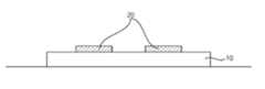
- FIG. 1shows a conductive film substrate according to an embodiment of the present invention.
- FIG. 2is a flowchart illustrating a method of manufacturing a conductive paste for forming the conductive film of FIG. 1 .
- 3A and 3Bare configuration diagrams for explanation of FIG. 2 .
- FIG. 4is a flowchart illustrating a method of forming the conductive film substrate of FIG. 1 .
- 5A to 5Dare process diagrams illustrating the process of FIG. 4 .
- FIG. 6is a graph showing the relationship between electrical conductivity with respect to the content of the magnetic heating element for each device and a graph showing the relationship between electrical conductivity and bonding strength.
- 8A and 8Bshow a surface photograph and a tomographic photograph of a conductive film prepared according to an embodiment of the present invention, respectively.
- each componentis exaggerated, omitted, or schematically illustrated for convenience and clarity of description.
- the size and area of each componentdo not fully reflect the actual size or area.
- FIG. 1shows a conductive film 20 and a substrate 10 according to an embodiment of the present invention.
- the conductive film 20is formed by printing a conductive paste and then sintering it by induction heating.
- the conductive film 20is formed including the metal particles 21 and the magnetic heating element 23 dispersed in the organic material 22 .
- the conductive film 20is formed by selectively sintering only the conductive film 20 by induction heating after a conductive paste is applied or printed on the substrate 10 .
- induction heatingwhen the magnetic heating element 23 included in the conductive paste receives a magnetic force by induction heating from the outside, heat is generated on the surface of the magnetic heating element 23 and sintering of the metal particles 21 proceeds.
- the organic material 22 included in the conductive film 20may include a dispersant or an organic solvent.
- the dispersantis to prevent the metal particles 21 from being agglomerated or agglomerated together, and the organic solvent is to mix all the components and is removed during the sintering process, and if the molecular weight of the organic material 22 is too large, the thermal decomposition temperature is high If high-temperature heat treatment or long-term heat treatment is required, and the molecular weight of the organic material 22 is too small, it is easily dried in the air and it is difficult to secure flow characteristics, so that an appropriate organic material 22 suitable for process conditions is selected.
- the organic material 22may further include a binder, a catalyst, and the like.
- a low carbon numberpreferably 30 or less, and if the carbon number is too large, the boiling point of the organic material 22 increases. As it remains, the sintered density (or bond strength) and reliability may be problematic.
- the magnetic heating element 23 mixed with the metal particles 21 and dispersedmay include a metal-based, alloy-based, oxide-based, nitride-based material containing at least one of Fe, Ni, Co, and Sm, It is composed of a material characterized in that it has magnetic properties.
- the magnetic heating element 23is sintered by induction heating to sinter the metal particles 21 present in the conductive paste.
- the particle size of the magnetic heating element 23is a size that can be included in the thickness of the paste, and is selected in consideration of the heating characteristics according to the induction heating frequency.
- the maximum amount of heatcan be realized at the optimal particle diameter (terminal or single domain), and specifically, the magnetic heating element 23 powder particle diameter is 10 nm to 100 um, preferably 10 nm to 50 um, More preferably, 10 nm to 10 um may be satisfied.
- the size of the powder of the magnetic heating element 23may be similar to or smaller than the size of the metal particles 21, and the type of the magnetic heating element 23 is a material capable of generating heat by an alternating magnetic field generated in high-frequency induction heating, metallic, It may include metal-based, ceramic-based, oxide-based, and the like.
- the metallic heating element 23it may be Fe, Co, Ni Al, Cu, Mo, Ag, Au, Mg, or a metal or alloy containing at least one of these, and as the metallic magnetic heating element 23, Fe, Co, Ni, FexNiy, MnBi, SmCo 5 , Sm 2 Co 17 , SmFe 11 Ti or at least one of these may be included, and the ceramic-based magnetic heating element 23 includes NdFe 14 B, NdFe 14 B, NdFe 14 C, Sm 2 Fe 17 N 3 , Sm 2 Fe 17 Cx, SmFe 7 N is included, and the oxide-based magnetic heating element 23 is a ferrite such as Fe 3 O 4 , XFeyOz (X: Fe, Co, Ni, Mn, Mg, It may be a ferrite represented by Cu, Zn, Cr, Ti, Mn, etc., which may contain one or two or more).
- the shape of the magnetic heating element 23can be applied in various forms such as spherical, plate-shaped, needle-shaped, and the like, and the magnetic heating element 23 satisfies 0.01 to 50% by weight with respect to the metal particles 21, and preferably 1 to 40% by weight. %, more preferably 5 to 30% by weight, and most preferably 10 to 20% by weight.
- the sintering density (bonding strength)is low, and when the content of the magnetic heating element 23 is low, it is difficult to shorten the sintering (bonding) process time, but by reducing the size of the metal particles 21, the magnetic heating element By setting the content of (23) to a small amount, the optimum condition can be satisfied.
- the metal particles 21provide electrical conductivity of the conductive film 20 as a main material constituting the conductive paste. Since the metal particles 21 exist in a particulate form, sintering is required at a specific temperature (metal melting temperature) or higher to have electrical conductivity, and a low melting temperature is required for selective melting, that is, in order not to affect other elements. .
- the metal particles 21 of the present embodimentcan secure electrical conductivity by miniaturizing the particle size to a nano size.
- the metal particles 21may include at least one of Ag, Ag, Al, Pt, Sn, Cu, Zn, Pd, and Ni.
- the metal particles 21may have an average particle diameter of 10 nm to 100 um, preferably 10 nm to 50 um, more preferably 10 nm to 10 um, and most preferably 10 nm to 5 um.
- the particle sizeis smaller than the above range, the content of the organic dispersant present on the surface of the metal particles 21 is rapidly increased, and the residual carbon during sintering increases, so that the sintering density and electrical conductivity may be lowered, and the size of the particles is too large If it is large, the sintering temperature to secure electrical conductivity increases, which may cause thermal damage to the product.
- the shape of the metal particles 21can be implemented in various ways, and various shapes of the metal particles 21 can be mixed and used according to the field of application, such as a spherical shape, a cylindrical shape, a needle shape, a plate shape, and a wire shape.
- the aspect ratio (ratio of width to length) of the metal particles 21can be variably changed according to the sintering temperature and the initial packing density.
- the conductive paste used to form the conductive film 20has a wide thickness of 0.0001 mm (0.1 um or 100 nm) to 50 mm (5 cm), preferably 0.0005 mm (0.5 um or 500 nm) to 10 mm (1 cm). ), more preferably 0.001 mm (1 um or 1000 nm) to 0.5 mm (500 um). If the thickness of the conductive paste is too thick, it takes a long time to remove the organic material 22 present in the paste, so it can be adjusted within the thickness.
- the conductive film 20is formed by applying or printing the conductive paste and sintering through induction heating.
- the substrate 10may be a substrate 10 of various materials, and even when the substrate 10 is a flexible substrate 10, the substrate 10 may not be deformed by low-temperature sintering by selective induction heating. have.
- the conductive paste for forming the conductive film 20is formed by mixing the metal particles 21 and the magnetic heating element 23 dispersed in the organic material 22 as described above, and the induction of the magnetic heating element 23 . It is possible to form the conductive film 20 in which electrical conductivity and device stability are secured by heating and melting the adjacent metal particles 21 by heating. In addition, when sintering by induction heating proceeds, it is economical because sintering proceeds in a short time while proceeding at a low temperature.
- FIG. 2is a flowchart illustrating a method of manufacturing a conductive paste for forming the conductive film 20 of FIG. 1
- FIGS. 3A and 3Bare configuration diagrams for explanation of FIG. 2 .
- the organic material 22 and the metal particles 21are supplied ( S10 ).
- the organic material 22may include the above-mentioned organic solvent and dispersant binder.
- the organic solventmay be formed of a mixture of ethylene carbonate (EC) and Texanol Ester Alcohol (texanol).
- the dispersantmay be a mixture of one or more selected from carboxylic acids, amines, and alcohols. These dispersants may organically coat the surface of the metal particles 21 to improve dispersibility in organic solvents.
- itmay further include a binder and a reducing agent, and the dispersant prevents the metal particles 21 from being aggregated or agglomerated together. That is, in manufacturing the paste, it is prevented that the metal particles 21 are attached to each other to form a mass.
- the dispersantis an alkylamine, polyamine, carboxylic acid, polycarboxylic acid, carboxylate, polycarboxylate, carboxylic acid Amides (carboxylic acid amide), polycarboxylic acid amide (polycarboxylic acid amide), alkyl alcohol (alkyl alcohol), polyalcohol (polyalcohol), alkyl thiol (alkyl thiol), poly thiol (poly thiol) and polyether ( poly ether).
- the binderincreases strength by imparting elasticity and adhesion to the metal particles 21 when manufacturing the paste, and may preferably be polyvinylpyrrolidone (PVP).
- PVPpolyvinylpyrrolidone
- the metal particles 21may include at least one of Ag, Ag, Al, Pt, Sn, Cu, Zn, Pd, and Ni.
- the metal particles 21may have an average particle diameter of 10 nm to 100 um, preferably 10 nm to 50 um, more preferably 10 nm to 10 um, and most preferably 10 nm to 5 um.
- the mixed materialhas a form in which the metal particles 21 are smoothly dispersed in the organic material 22 as shown in FIG. 3A .
- the magnetic heating element 23 for supplying the secondary raw materialis prepared (S30).
- the magnetic heating element 23is also a material capable of generating heat by an alternating magnetic field generated in high-frequency induction heating, and for example, ferrite such as Fe 3 O 4 may be provided.
- the shape of the magnetic heating element 23can be applied in various forms such as spherical, plate-shaped, needle-shaped, and the like, and the heating element 23 satisfies 0.01 to 50% by weight with respect to the metal particles 21, and preferably 1 to 40% by weight. may be, more preferably 5 to 30% by weight, and most preferably 10 to 20% by weight.
- Such a predetermined ratio of the magnetic heating element 23is mixed in the material of FIG. 3A (S40).
- the magnetic heating element 23is arranged with a smaller density than the metal particles 21 as shown in FIG. 3b.
- Filteringis to remove impurities by performing heat treatment or the like. First, large aggregates are improved through physical filtering, and impurities can be removed by secondarily performing chemical filtering.
- the conductive paste prepared in this waycan be provided as solder for conductive bonding between devices, and can be applied to small electronic devices such as light emitting devices and solar cells.
- FIG. 4is a flowchart illustrating a method of forming the conductive film 20 substrate 10 of FIG. 1
- FIGS. 5A to 5Dare process diagrams illustrating the process of FIG. 4 .
- a substrate 10is provided as shown in FIG. 5A ( S100 ).
- the substrate 10may be mainly a printed circuit board 10 , and may be a flexible substrate 10 or a rigid substrate 10 .
- a material of the substrate 10various materials such as metal, organic, and inorganic materials may be used.
- the substrate 10may be a wiring board 10 , a heat sink, or the like. In the case of a heat sink, it may be a metal plate.
- a conductive paste used as a solderis applied to a predetermined position on the substrate 10 ( S110 ).
- Such application of the conductive pastecan be performed by applying the conductive paste accommodated in the groove 110 of the roll 100 to the corresponding position in a roll-to-roll method, or by a printing method as shown in FIG. 5B. It is not limited.
- the printing methodmay be performed by any one method of screen printing, ink jet, gravure, flexo, offset, and aerosol.
- the conductive pasteWhen the conductive paste is applied in a specific shape on the substrate 10 in this way, it is disposed so as to contact the bonding terminal of the device 30 to be bonded as shown in FIG. 5C .
- the device 30 to be bondedmay be various electronic components and may be a part of another printed circuit board 10 .
- Induction heatingcan be implemented by an inductor oven, and a magnetic force line passing through a corresponding conductive film is generated by flowing a predetermined high-frequency current to a coil of the inductor oven.
- the high frequencymay use a frequency of 1 kHz to 40 MHz, preferably 1 kHz to 10 MHz, more preferably 100 kHz to 5 MHz, and most preferably 200 kHz to 2 MHz.
- the secondary self-heatingproceeds and the sintering speed is very fast, and thus the adhesion between the upper and lower substrates 10 is completed.
- FIG. 6is a graph showing the relationship between electrical conductivity with respect to the content of the magnetic heating element 23 depending on the device and a graph showing the relationship between electrical conductivity and bonding strength.
- the decrease of the oxide/ceramic-based magnetic heating element 23 with low electrical conductivityis larger than that of the metal-based magnetic heating element, which means that as the content of the metal-based magnetic heating element 23 increases, the magnetic heating element 23 during induction heating bonding is in the air. It is interpreted that the electrical conductivity decreases because the surface of the magnetic heating element 23 is oxidized by exposure.
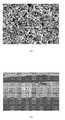
- the maximum attained temperature and the temperature increase time by the frequency of the same sizewere measured while changing the content and material of the magnetic heating element 23 .
- the metal particles 21 in each experimentwere selected from silver (Ag) and the magnetic heating element 23 was selected in various ways, and only iron oxide (Fe 3 O 4 ) was measured while varying the content.
- Experiment heating technologyweight% reached temperature Temperature rise time (sec) Kinds content Kinds content
- Weight%indicates the mass of the magnetic heating element 23 with respect to 100 g of the metal particles 21.
- Table 1shows the time to reach 200° C. during induction heating after adding 1 to 50% by weight of the magnetic heating element 23 and The correlation with the content of the magnetic heating element 23 is shown.
- the experimental methodis the same as that of Table 1, and electrical conductivity was additionally measured.
- the content of the magnetic heating element 23Fe 3 O 4
- the electrical conductivity of the conductive filmis increased. It can be seen that the conductivity decreases, and it can be observed that when the content of the magnetic heating element 23 is 5% by weight during induction heating, it has an electrical conductivity similar to that of the oven heating that does not include the magnetic heating element 23, and oven heating Similarly, it is observed that the electrical conductivity of the conductive film decreases as the content of the magnetic heating element 23 increases even during induction heating.
- the electrical conductivityis higher during induction heating compared to oven heating, which is interpreted that the sintering density of the conductive film is improved by induction heating.
- FIG. 8A and 8Bshow a surface photograph and a tomographic photograph of the conductive film 20 prepared according to an embodiment of the present invention, respectively.
- FIG. 8Ashows the surface of the conductive film 20 obtained by induction heating of a conductive film containing nano-sized Ag metal particles 21 and 10% by weight of Fe 3 O 4 for 200 degrees for 20 seconds
- FIG. 8Bis a cross-section thereof. is analyzed.
- substrate 20conductive film
Landscapes
- Engineering & Computer Science (AREA)
- Physics & Mathematics (AREA)
- Chemical & Material Sciences (AREA)
- Dispersion Chemistry (AREA)
- Spectroscopy & Molecular Physics (AREA)
- Manufacturing & Machinery (AREA)
- Microelectronics & Electronic Packaging (AREA)
- Thermal Sciences (AREA)
- Conductive Materials (AREA)
- Powder Metallurgy (AREA)
Abstract
Description
Translated fromKorean본 발명은 전도막 및 전도막을 형성하기 위한 도전성 페이스트에 관한 것으로, 보다 상세하게는 높은 자화율을 가지는 발열체와 전도성 금속입자를 혼합하여 도전성 페이스트를 형성하고, 기판에 인쇄되어 전도막을 형성하는 방법에 관한 것이다.The present invention relates to a conductive film and a conductive paste for forming the conductive film, and more particularly, to a method of forming a conductive paste by mixing a heating element having a high magnetic susceptibility and conductive metal particles, and printing on a substrate to form a conductive film will be.
현재 본딩(bonding) 기술로서 은(Ag) 페이스트의 전도성 접착제를 이용한 소자 본딩이 널리 활용되고 있다. 이와 같은 접합 페이스트를 활용한 본딩으로는 가압 방식과 무가압 방식이 존재한다.Currently, device bonding using a conductive adhesive of silver (Ag) paste is widely used as a bonding technology. As bonding using such a bonding paste, there are a pressurized method and a non-pressurized method.
가압 방식의 경우, 원하는 칩을 은 페이스트 위에 배치하고 열과 압력을 동시에 가하면서 소결과 접합을 동시 수행하는 방식으로 접합 강도가 매우 높으나 소자 칩 및 전체 모듈에 압력이 가해져 변형의 위험이 있다.In the case of the pressurization method, the bonding strength is very high by placing the desired chip on the silver paste and simultaneously performing sintering and bonding while applying heat and pressure at the same time, but there is a risk of deformation due to pressure applied to the device chip and the entire module.
무가압 방식의 경우, 은 입자의 크기를 매우 작게 형성하여 소결을 촉진하고 난분산시켜 소결 속도를 보장하는 방식이 제안되고 있으나 접합 강도가 약하고 상대적으로 고온을 요하므로 열에 의한 전자 소자의 손상이 문제된다.In the case of the no-pressurization method, a method that promotes sintering by forming very small silver particles and guarantees the sintering speed by making it difficult to disperse has been proposed. do.
이에 대하여, 종래기술로서, 한국특허출원번호 10-2015-0185221호는 자화율을 갖는 금속 입자를 전도성을 가지는 물질로 코팅한다. 이와 같은 코팅된 금속 입자가 수지 등에 분산되어 전도막을 형성하며, 이와 같은 전도막은 접착층으로서 기능할 수 있다.In contrast, as a prior art, Korean Patent Application No. 10-2015-0185221 coats metal particles having a magnetic susceptibility with a material having conductivity. The coated metal particles are dispersed in a resin or the like to form a conductive film, which may function as an adhesive layer.
구체적으로, 전도막 위에 유도가열을 진행하면 내부의 금속입자가 자화되어 열을 발생하고 해당 열에 의해 코팅층을 가열함으로써 코팅층이 녹아 본딩을 수행할 수 있다.Specifically, when induction heating is performed on the conductive film, the metal particles inside are magnetized to generate heat, and by heating the coating layer by the heat, the coating layer can be melted and bonding can be performed.
그러나, 이와 같은 종래기술로서는 유도 가열을 통한 소결이 완료되었을 때에도 코팅층의 표면에 산화층이 존재하여 소결 치밀도가 낮아짐으로써 면저항이 매우 높아 전기전도성이 현저하게 저하된다.However, in this prior art, even when sintering through induction heating is completed, an oxide layer is present on the surface of the coating layer, and the sintering density is lowered.
또한, 각각의 금속 입자를 다른 금속층에 의해 코팅하는 공정을 진행하여도 코팅층의 형성이 원활하게 진행되기 어려워 균일한 전기전도성 및 접촉력을 기대할 수 없는 문제가 있다.In addition, even if the process of coating each metal particle with a different metal layer is performed, it is difficult to smoothly form the coating layer, so there is a problem in that uniform electrical conductivity and contact force cannot be expected.
[선행기술문헌][Prior art literature]
한국특허출원번호 10-2015-0185221 (공개일 : 2017년 07월 04일)Korean Patent Application No. 10-2015-0185221 (published on July 04, 2017)
본 발명의 제1 과제는 유도가열을 통한 소결을 진행하여 전도성 접착층을 형성할 수 있는 도전성 페이스트 및 그의 제조 방법을 제공하는데 목적이 있다.A first object of the present invention is to provide a conductive paste capable of forming a conductive adhesive layer by sintering through induction heating, and a method for manufacturing the same.
본 발명이 이루고자 하는 제2 과제는 낮은 융점을 가지는 도전성 금속 분말에 자성 발열체를 소량 추가함으로써 저온접합 및 전기전도성을 동시에 만족할 수 있는 전도막 및 이를 제조하기 위한 도전성 페이스트를 제공하는 것이다.A second object of the present invention is to provide a conductive film capable of simultaneously satisfying low-temperature bonding and electrical conductivity by adding a small amount of a magnetic heating element to a conductive metal powder having a low melting point, and a conductive paste for manufacturing the same.
본 발명이 이루고자 하는 제3 과제는 유도가열을 단시간에 수행하여 전도막이 형성되어 있는 부분만 선택적으로 가열하므로 고속 접합이 가능한 전도막을 제공하는 것이다.A third object of the present invention is to provide a conductive film capable of high-speed bonding since induction heating is performed in a short time to selectively heat only a portion where the conductive film is formed.
본 발명은 유기 용매 및 분산제를 포함하는 유기물; 상기 유기물 내에 분산되어 있으며 제1 입경을 가지는 금속 입자; 및 상기 유기물 내에 분산되어 있으며, 제2 입경을 가지는 자성 발열체를 포함하며, 상기 자성 발열체는 상기 금속 입자에 대하여 10 내지 50 중량%만큼 함유하는 것을 특징으로 하는 도전성 페이스트를 제공한다.The present invention relates to an organic material comprising an organic solvent and a dispersant; metal particles dispersed in the organic material and having a first particle diameter; and a magnetic heating element dispersed in the organic material and having a second particle size, wherein the magnetic heating element is contained in an amount of 10 to 50% by weight based on the metal particles.
상기 자성 발열체의 제2 입경은 상기 금속 입자의 제1 입경과 같거나 작을 수 있다.The second particle diameter of the magnetic heating element may be the same as or smaller than the first particle diameter of the metal particle.
상기 자성 발열체는 상기 금속 입자에 대하여 10 내지 20중량%만큼 혼합될 수 있다.The magnetic heating element may be mixed in an amount of 10 to 20% by weight based on the metal particles.
상기 자성 발열체는 금속 산화물계 자성 발열체일 수 있다.The magnetic heating element may be a metal oxide-based magnetic heating element.
상기 자성 발열체는 Fe3O4자성 발열체일 수 있다.The magnetic heating element may be a Fe3 O4 magnetic heating element.
상기 금속 입자는 Ag, Ag, Al, Pt, Sn, Cu, Zn, Pd, 및 Ni 중 적어도 하나일 수 있다.The metal particles may be at least one of Ag, Ag, Al, Pt, Sn, Cu, Zn, Pd, and Ni.
상기 제1 입경은 10 nm 내지 100 um 일 수 있다.The first particle diameter may be 10 nm to 100 um.
상기 제1 입경은 10 nm 내지 50 um 일 수 있다.The first particle diameter may be 10 nm to 50 um.
상기 제2 입경은 10 nm 내지 10 um 일 수 있다.The second particle diameter may be 10 nm to 10 um.
상기 유기물의 상기 분산제 또는 유기 용매는 탄소수 30 이하일 수 있다.The dispersant or organic solvent of the organic material may have 30 or less carbon atoms.
상기 유기물은 바인더 및 촉매제를 더 포함할 수 있다.The organic material may further include a binder and a catalyst.
상기 도전성 페이스트의 두께는 0.001 mm ~ 0.5 mm 일 수 있다.The thickness of the conductive paste may be 0.001 mm to 0.5 mm.
한편, 본 발명은 유기물과 제1 입경을 가지는 금속 입자를 혼합하여 분산하는 단계; 상기 금속 입자가 분산된 상기 유기물에 상기 금속 입자에 대하여 10 내지 50 중량%의 제2 입경을 가지는 자성 발열체를 분산하는 단계; 및 상기 금속 입자와 상기 자성 발열체가 혼합된 상기 유기물을 후처리하여 소분하는 단계를 포함하는 도전성 페이스트 제조 방법을 제공한다.On the other hand, the present invention comprises the steps of mixing and dispersing an organic material and metal particles having a first particle size; dispersing a magnetic heating element having a second particle size of 10 to 50% by weight based on the metal particles in the organic material in which the metal particles are dispersed; and post-processing and subdividing the organic material in which the metal particles and the magnetic heating element are mixed.
상기 자성 발열체의 제2 입경은 상기 금속 입자의 제1 입경과 같거나 작을 수 있다.The second particle diameter of the magnetic heating element may be the same as or smaller than the first particle diameter of the metal particle.
상기 자성 발열체는 상기 금속 입자에 대하여 10 내지 20중량%만큼 혼합될 수 있다.The magnetic heating element may be mixed in an amount of 10 to 20% by weight based on the metal particles.
한편, 본 발명은 유기물 내에 분산되어 있으며 제1 입경을 가지는 금속 입자 및 제2 입경을 가지는 자성 발열체를 포함하는 도전성 페이스트를 기판에 도포하는 단계; 및 도포된 도전성 페이스트를 유도 가열로 선택적으로 소결하여 전도막을 형성하는 단계; 를 포함하며, 상기 자성 발열체는 상기 금속 입자에 대하여 10 내지 50 중량% 만큼 함유하는 것을 특징으로 하는 전도막 제조하는 방법을 제공한다.On the other hand, the present invention is dispersed in an organic material, the method comprising: applying a conductive paste comprising metal particles having a first particle diameter and a magnetic heating element having a second particle diameter to a substrate; and selectively sintering the applied conductive paste by induction heating to form a conductive film; Including, the magnetic heating element provides a method of manufacturing a conductive film, characterized in that it contains 10 to 50% by weight based on the metal particles.
상기 유도 가열하는 단계는, 1kHz 내지 40MHz 주파수의 고주파에 의해 생성되는 자기장을 통해 상기 도전성 페이스트를 소결할 수 있다.In the induction heating step, the conductive paste may be sintered through a magnetic field generated by a high frequency frequency of 1 kHz to 40 MHz.
상기 유도 가열하는 단계는, 20초 이내에 200℃ 이상으로 승온할 수 있다.In the induction heating step, the temperature may be raised to 200° C. or higher within 20 seconds.
상기 도전성 페이스트를 기판에 도포하는 단계는, 상기 기판 위에 상기 도전성 페이스트를 롤투롤(roll-to-roll) 방식 또는 인쇄 방식으로 도포할 수 있다.The applying of the conductive paste to the substrate may include applying the conductive paste on the substrate in a roll-to-roll method or a printing method.
상기 기판에 상기 도전성 페이스트를 도포한 후, 상기 도전성 페이스트 위에 접착대상물을 배치하는 단계를 더 포함할 수 있다.After applying the conductive paste to the substrate, the method may further include disposing an object to be bonded on the conductive paste.
상기 해결 수단을 통해, 본 발명은 유도가열을 통한 소결을 진행하여 선택적으로 전도성 접착층을 형성할 수 있다.Through the above solution, the present invention can selectively form a conductive adhesive layer by performing sintering through induction heating.
또한, 낮은 융점을 가지는 도전성 금속 분말에 자성 발열체를 소량 추가함으로써 저온접합 및 전기전도성을 동시에 만족할 수 있다. In addition, low-temperature bonding and electrical conductivity can be simultaneously satisfied by adding a small amount of a magnetic heating element to the conductive metal powder having a low melting point.
유도가열을 단시간에 수행하여 전도막이 형성되어 있는 부분만 선택적으로 가열하므로 고속접합이 가능하며, 전도막 내 분산되어 있는 자성 발열체가 유도 가열 시 동시 발열되어 내부에 존재하는 유기물이 동시 제거되므로 전도막의 소결 치밀도가 개선될 수 있다.High-speed bonding is possible because induction heating is performed in a short time to selectively heat only the portion where the conductive film is formed. The sintering density can be improved.
그리고, 자성 발열체의 크기가 금속입자의 크기와 유사하게 작음으로 원재료 가격을 낮출 수 있다.And, since the size of the magnetic heating element is similar to the size of the metal particles, it is possible to lower the raw material price.
도 1은 본 발명의 일 실시예에 따른 전도막 기판을 나타낸 것이다.1 shows a conductive film substrate according to an embodiment of the present invention.
도 2는 도 1의 전도막을 형성하기 위한 도전성 페이스트 제조 방법을 나타내는 순서도이다.FIG. 2 is a flowchart illustrating a method of manufacturing a conductive paste for forming the conductive film of FIG. 1 .
도 3a 및 도 3b는 도 2의 설명을 위한 구성도이다.3A and 3B are configuration diagrams for explanation of FIG. 2 .
도 4는 도 1의 전도막 기판을 형성하는 방법을 나타내는 순서도이다.4 is a flowchart illustrating a method of forming the conductive film substrate of FIG. 1 .
도 5a 내지 도 5d는 도 4의 공정을 나타내는 공정도이다.5A to 5D are process diagrams illustrating the process of FIG. 4 .
도 6은 자성발열체 함량에 대한 전기전도도의 관계를 소자에 따라 나타낸 그래프 및 전기전도도와 접합 강도 사이의 관계를 나타내는 그래프이다.6 is a graph showing the relationship between electrical conductivity with respect to the content of the magnetic heating element for each device and a graph showing the relationship between electrical conductivity and bonding strength.
도 7은 시간에 따른 유도가열 온도를 각 소재에 따라 나타내는 그래프이다.7 is a graph showing the induction heating temperature according to time for each material.
도 8a 및 도 8b는 본 발명의 실시예에 따라 제조된 전도막의 표면사진 및 단층 사진을 각각 나타낸다.8A and 8B show a surface photograph and a tomographic photograph of a conductive film prepared according to an embodiment of the present invention, respectively.
이하에서 언급되는 “전(F)/후(R)/좌(Le)/우(Ri)/상(U)/하(D)” 등의 방향을 지칭하는 표현은 도면에 표시된 바에 따라 정의하나, 이는 어디까지나 본 발명이 명확하게 이해될 수 있도록 설명하기 위한 것이며, 기준을 어디에 두느냐에 따라 각 방향들을 다르게 정의할 수도 있음은 물론이다.Expressions referring to directions such as “before (F) / after (R) / left (Le) / right (Ri) / up (U) / down (D)” mentioned below are defined as shown in the drawings, but , This is for the purpose of explaining the present invention to the extent that it can be clearly understood, and it goes without saying that each direction may be defined differently depending on where the reference is placed.
이하에서 언급되는 구성요소 앞에 ‘제1, 제2' 등의 표현이 붙는 용어 사용은, 지칭하는 구성요소의 혼동을 피하기 위한 것일 뿐, 구성요소 들 사이의 순서, 중요도 또는 주종관계 등과는 무관하다. 예를 들면, 제1 구성요소 없이 제2 구성요소 만을 포함하는 발명도 구현 가능하다.The use of terms such as 'first, second', etc. added before the components mentioned below is only to avoid confusion of the components referred to, and is irrelevant to the order, importance, or master-slave relationship between the components. . For example, an invention including only the second component without the first component can also be implemented.
도면에서 각 구성의 두께나 크기는 설명의 편의 및 명확성을 위하여 과장되거나 생략되거나 또는 개략적으로 도시되었다. 또한 각 구성요소의 크기와 면적은 실제크기나 면적을 전적으로 반영하는 것은 아니다.In the drawings, the thickness or size of each component is exaggerated, omitted, or schematically illustrated for convenience and clarity of description. In addition, the size and area of each component do not fully reflect the actual size or area.
또한, 본 발명의 구조를 설명하는 과정에서 언급하는 각도와 방향은 도면에 기재된 것을 기준으로 한다. 명세서에서 구조에 대한 설명에서, 각도에 대한 기준점과 위치관계를 명확히 언급하지 않은 경우, 관련 도면을 참조하도록 한다.In addition, angles and directions mentioned in the process of explaining the structure of the present invention are based on those described in the drawings. In the description of the structure in the specification, if the reference point for the angle and the positional relationship are not clearly mentioned, reference is made to the related drawings.
이하 도 1 내지 도 3을 참조하여, 본 발명의 전도막 기판 및 이를 위한 도전성 페이스트 제조 방법을 설명한다.Hereinafter, the conductive film substrate of the present invention and a method of manufacturing a conductive paste therefor will be described with reference to FIGS. 1 to 3 .
도 1은 본 발명의 일 실시예에 따른 전도막(20) 기판(10)을 나타낸 것이다.1 shows a
도 1을 참조하면, 전도막(20)은 도전성 페이스트를 인쇄한 후 유도가열로 소결하여 형성한다. 이때, 전도막(20)은 유기물(22) 내 분산되어 있는 금속 입자(21) 및 자성 발열체(23)를 포함하여 형성되어 있다.Referring to FIG. 1 , the
전도막(20)은 기판(10)의 상부에 도전성 페이스트가 도포 또는 인쇄된 후, 유도 가열로 전도막(20)만 선택적으로 소결하여 형성된다. 여기서, 유도 가열은 도전성 페이스트가 포함하는 자성 발열체(23)가 외부로부터의 유도 가열에 의해 자기력을 받으면 자성 발열체(23)의 표면에서 발열이 일어나 금속 입자(21)의 소결이 진행된다.The
상기 전도막(20) 내에 포함되는 유기물(22)은 분산제 또는 유기 용매를 포함할 수 있다.The
분산제는 금속 입자(21)가 응집되거나 함께 괴상화되는 것을 방지하기 위한 것이고, 유기 용매는 모든 구성 요소들을 혼합시키기 위한 것으로 소결 과정에서 제거되며, 유기물(22)의 분자량이 너무 크면 열분해 온도가 높아 고온 열처리 또는 장시간 열처리 필요하고, 유기물(22)의 분자량이 너무 작으면, 대기 중에서 쉽게 건조되어 유동 특성 확보가 어려워 공정 조건에 맞는 적절한 유기물(22)이 선택된다.The dispersant is to prevent the
이 외에, 유기물(22)은 바인더, 촉매제 등을 더 포함할 수 있다.In addition, the
모든 유기물(22)은 탄소수가 낮은 것, 바람직하게는 30 이하인 것을 사용하는 것이 바람직하며, 탄소수가 너무 많아지면, 유기물(22)의 비점이 높아지게 되기 때문에 소결(또는 접합)시 분산제가 페이스트 내부에 잔류하게 되어, 소결치밀도 (또는 접합강도) 및 신뢰성에 문제가 될 수 있다.For all
한편, 금속 입자(21)와 혼합되어 분산되어 있는 자성 발열체(23)는 Fe, Ni, Co 및 Sm 중 적어도 하나 이상을 포함하고 있는 금속계, 합금계, 산화물계, 질화물계 소재가 포함될 수 있으며, 자기적 성질을 갖는 것을 특징으로 하는 소재로 구성된다.On the other hand, the
이와 같은 자성 발열체(23)는 유도 가열하여 도전성 페이스트 내부에 존재하는 금속 입자(21)의 소결을 수행한다. 자성발열체(23)의 입경은 페이스트의 두께에 포함될 수 있는 크기로서, 유도가열 주파수에 따른 발열 특성도 고려하여 선정된다.The
자성발열체(23)의 경우 최적 입경 (단자구 또는 Single Domain)에서 최대의 발열량 구현 가능하며, 구체적으로, 자성발열체(23) 분말 입경은 10 nm ~ 100 um, 바람직하게는 10 nm ~ 50 um, 보다 바람직하게는 10 nm ~ 10 um 을 충족할 수 있다.In the case of the
자성 발열체(23)의 분말 크기는 금속 입자(21)의 크기와 유사하거나 작을 수 있으며, 자성발열체(23) 종류로는, 고주파 유도가열에서 발생되는 교류자기장에 의해 발열이 가능한 소재로서, 금속성, 금속계, 세라믹계, 산화물계 등을 포함할 수 있다.The size of the powder of the
금속성발열체(23)로서는 Fe, Co, Ni Al, Cu, Mo, Ag, Au, Mg 나, 이들 중 적어도 하나 이상을 포함하는 금속 또는 합금일 수 있으며, 금속계 자성발열체(23)로는 Fe, Co, Ni, FexNiy, MnBi, SmCo5, Sm2Co17, SmFe11Ti 나 이들 중 적어도 하나 이상을 포함할 수 있으며, 세라믹계 자성발열체(23)로는 NdFe14B, NdFe14B, NdFe14C, Sm2Fe17N3, Sm2Fe17Cx, SmFe7N를 포함하고, 산화물계 자성발열체(23)로는 Fe3O4와 같은 페라이트로서, XFeyOz (X : Fe, Co, Ni, Mn, Mg, Cu, Zn, Cr, Ti, Mn등을 하나 혹은 2이상을 포함 할 수 있음)로 표현되는 페라이트일 수 있다.As the
자성발열체(23)의 형상은 구형, 판상형, 침형 등 다양한 형태로 적용 가능하고, 자성발열체(23)는 금속 입자(21)에 대하여 0.01 내지 50중량% 을 충족하고, 바람직하게는 1 내지 40 중량%일 수 있으며, 보다 바람직하게는 5 내지 30중량%, 가장 바람직하게는 10 내지 20 중량%일 수 있다.The shape of the
자성발열체(23) 함량이 높으면 소결 치밀도(접합강도)가 낮고, 자성발열체(23) 함량이 낮으면 소결(접합) 공정시간 단축이 어려우나, 이를 금속 입자(21)의 크기를 줄이고, 자성발열체(23)의 함량을 소량으로 함으로써 최적 조건을 충족할 수 있다.When the content of the
금속 입자(21)는 도전성 페이스트를 구성하는 주 재료로서 전도막(20)의 전기 전도성을 부여한다. 금속 입자(21)는 입자상으로 존재하기 때문에 전기 전도성을 갖기 위해서는 특정온도 (금속 용융온도) 이상에서 소결 필요하며, 선택적 용융을 위하여, 즉 다른 소자들에 영향을 미치지 않기 위하여는 낮은 용융 온도를 요한다.The
이를 위해 본 실시예의 금속 입자(21)는 입자의 크기를 나노 크기로 소형화함으로써 전기 전도성을 확보할 수 있다. 일 예로, 금속 입자(21)는 Ag, Ag, Al, Pt, Sn, Cu, Zn, Pd, 및 Ni 중 적어도 하나 이상을 포함할 수 있다.To this end, the
금속 입자(21)는 평균 입경이 10 nm 내지 100 um, 바람직하게는 10 nm 내지 50 um, 보다 바람직하게는 10 nm 내지 10 um, 가장 바람직하게는 10nm 내지 5um 범위를 충족할 수 있다.The
입경이 상기 범위보다 작으면, 금속 입자(21) 표면에 존재하는 유기분산제의 함량이 급격하게 증가하여, 소결 시 잔류 탄소가 많아져서 소결 치밀도 및 전기전도도가 낮아질 수 있고, 입자의 크기가 너무 크면 전기전도성을 확보하기 위한 소결 온도가 높아져 제품에 열적 손상이 발생할 수 있다.When the particle size is smaller than the above range, the content of the organic dispersant present on the surface of the
금속 입자(21)의 형상은 다양하게 구현 가능하며, 구형, 원통형, 침상형, 판상형, 와이어 형상 등 적용 분야에 따라서 다양한 형상의 금속 입자(21)를 혼합하여 사용할 수 있다.The shape of the
금속 입자(21)의 종횡비 (Aspect Ratio, 가로와 세로의 비)는 소결 온도 및 초기 충진밀도에 따라 가변적으로 변경 가능하다.The aspect ratio (ratio of width to length) of the
이와 같이 전도막(20) 형성에 사용되는 도전성 페이스트는 그 두께가 넓게는 0.0001 mm (0.1um 또는 100nm)~50mm(5cm), 바람직하게는 0.0005 mm (0.5 um 또는 500 nm) ~ 10 mm (1cm), 보다 바람직하게는 0.001 mm (1 um 또는 1000nm) ~ 0.5 mm (500 um)을 충족한다. 도전성 페이스트의 두께가 너무 두꺼우면 페이스트 내부에 존재하는 유기물(22)을 제거하는데 긴 시간이 필요하므로 상기 두께 내에서 조절 가능하다.As such, the conductive paste used to form the
전도막(20)은 상기 도전성 페이스트를 도포 또는 인쇄하고 유도 가열을 통한 소결을 진행하여 형성된다.The
이때, 기판(10)은 다양한 재료의 기판(10)일 수 있으며, 기판(10)이 유연 기판(10)인 경우에도, 기판(10)은 선택적 유도 가열에 의한 저온 소결에 의해 변형되지 않을 수 있다.At this time, the
이와 같은 전도막(20)을 형성하는 도전성 페이스트는 앞서 설명한 바와 같이 유기물(22)에 분산되어 있는 금속 입자(21) 및 자성발열체(23)의 혼합에 의해 형성되며, 자성 발열체(23)의 유도 가열로 이웃한 금속 입자(21)의 가열 및 용융으로 전기전도성 및 소자안정성이 확보되는 전도막(20) 형성이 가능하다. 또한, 유도 가열로 소결 진행할 때, 저온에서 진행하면서도 단시간에 소결이 진행되어 경제적이다.The conductive paste for forming the
이하에서는 도 2 및 도 3을 참고하여 이와 같은 도전성 페이스트의 제조 방법을 설명한다.Hereinafter, a method of manufacturing such a conductive paste will be described with reference to FIGS. 2 and 3 .
도 2는 도 1의 전도막(20)을 형성하기 위한 도전성 페이스트 제조 방법을 나타내는 순서도이고, 도 3a 및 도 3b는 도 2의 설명을 위한 구성도이다.FIG. 2 is a flowchart illustrating a method of manufacturing a conductive paste for forming the
도 2를 참고하면, 유기물(22)과 금속 입자(21)가 공급된다(S10).Referring to FIG. 2 , the
유기물(22)로는 앞서 제시한 유기용매, 분산제 바인더를 포함할 수 있다.The
이때, 유기용매로는 Ethylene carbonate(EC)와 Texanol Ester Alcohol(texanol)의 혼합물로 형성될 수 있다. 분산제는 카르복실산류, 아민류, 알코올류로 부터 선택된 1종 이상의 혼합물을 사용할 수 있다. 이들 분산제는 금속 입자(21)의 표면을 유기코팅하여, 유기 용매에 대한 분산성을 개선시킬 수 있다.In this case, the organic solvent may be formed of a mixture of ethylene carbonate (EC) and Texanol Ester Alcohol (texanol). The dispersant may be a mixture of one or more selected from carboxylic acids, amines, and alcohols. These dispersants may organically coat the surface of the
추가적으로 바인더 및 환원제를 더 포함할 수 있으며, 분산제는 금속 입자(21)가 모이거나 함께 괴상화되는 것을 방지한다. 즉, 페이스트를 제조하는데 있어서, 금속 입자(21)가 서로 부착되어 괴상을 형성하게 되는 것을 방지한다. 여기서, 분산제는 알킬아민(alkylamine), 폴리아민(polyamine), 카르복실산(carboxylic acid), 폴리카르복실산(polycarboxylic acid), 카르복실레이트(carboxylate), 폴리카르복실레이트(polycarboxylate), 카르복실산아미드(carboxylic acid amide), 폴리카르복실산아미드(polycarboxylic acid amide), 알킬알코올(alkyl alcohol), 폴리알코올(polyalcohol), 알킬 싸이올(alkyl thiol), 폴리 싸이올(poly thiol) 및 폴리 에테르(poly ether) 중 적어도 하나를 포함할 수 있다.In addition, it may further include a binder and a reducing agent, and the dispersant prevents the
바인더는 페이스트를 제조할 때, 금속 입자(21)에 탄력성과 점착성을 부여하여 강도를 증가시키며, 바람직하게는 폴리비닐피롤리돈(polyvinylpyrrolidone, PVP)일 수 있다.The binder increases strength by imparting elasticity and adhesion to the
그 외에 금속 입자(21) 및 자성 발열체(23)의 특성을 향상시킬 수 있는 다양한 첨가제가 첨가 가능하다.In addition, various additives capable of improving the properties of the
금속 입자(21)는 앞서 설명한 것과 같이 Ag, Ag, Al, Pt, Sn, Cu, Zn, Pd, 및 Ni 중 적어도 하나 이상을 포함할 수 있다. 금속 입자(21)는 평균 입경이 10 nm 내지 100 um, 바람직하게는 10 nm 내지 50 um, 보다 바람직하게는 10 nm 내지 10 um, 가장 바람직하게는 10nm 내지 5um 범위를 충족할 수 있다.As described above, the
다음으로, 해당 유기물(22)과 금속 입자(21)를 혼합한다(S20).Next, the
이때, 혼합 방법으로 화학 용매 혼합 또는 고온 기계 혼합 등을 수행할 수 있으며 이에 한정되는 것은 아니다.In this case, chemical solvent mixing or high-temperature mechanical mixing may be performed as the mixing method, but the present invention is not limited thereto.
이와 같이 혼합된 재료는 도 3a 와 같이 유기물(22) 내에 금속 입자(21)가 원만하게 분산되어 있는 형태를 가진다.The mixed material has a form in which the
다음으로, 2차 원재료 공급을 위한 자성발열체(23)가 준비된다(S30).Next, the
자성발열체(23) 역시 앞서 설명한 바와 같이, 고주파 유도가열에서 발생되는 교류자기장에 의해 발열이 가능한 소재로서, 일 예로, Fe3O4와 같은 페라이트가 제공될 수 있다.As described above, the
자성발열체(23)의 형상은 구형, 판상형, 침형 등 다양한 형태로 적용 가능하고, 발열체(23)는 금속 입자(21)에 대하여 0.01 내지 50중량%을 충족하고, 바람직하게는 1 내지 40 중량%일 수 있으며, 보다 바람직하게는 5 내지 30중량%일 수 있으며, 가장 바람직하게는 10 내지 20중량%일 수 있다.The shape of the
이와 같은 소정 비율의 자성발열체(23)를 도 3a의 재료 내에 혼합한다(S40).Such a predetermined ratio of the
이때에도 혼합 방법으로는 화학 용매 혼합 또는 고온 기계 혼합이 적용가능하다.Even at this time, as the mixing method, chemical solvent mixing or high-temperature mechanical mixing is applicable.
이때, 금속 입자(21)와 자성 발열체(23)는 크기가 유사하고 그 수효가 자성 발열체(23)가 작으므로 도 3b와 같이 금속 입자(21) 보다 작은 밀도로 자성 발열체(23)가 배열될 수 있다.At this time, since the
다음으로, 필터링을 진행한다(S50). 필터링은 열처리 등을 수행함으로써 불순물을 제거하는 것으로, 1차적으로 물리적 필터링을 통해 거대 응집체를 제고하고, 2차적으로 화학 필터링을 수행하여 불순물을 제거할 수 있다.Next, filtering is performed (S50). Filtering is to remove impurities by performing heat treatment or the like. First, large aggregates are improved through physical filtering, and impurities can be removed by secondarily performing chemical filtering.
다음으로, 이를 적절한 양으로 소분하고 포장하여, 도전성 페이스트를 형성할 수 있다(S60).Next, it may be subdivided into an appropriate amount and packaged to form a conductive paste (S60).
이와 같이 제조되는 도전성 페이스트는 소자들 사이의 전도성 접착을 위한 솔더로서 제공 가능하며, 발광 장치, 솔라셀 등의 소형 전자 소자 등에도 적용 가능하다.The conductive paste prepared in this way can be provided as solder for conductive bonding between devices, and can be applied to small electronic devices such as light emitting devices and solar cells.
이하에서는 도 4 및 도 5를 참고하여 도 1과 같이 도전성 페이스트를 사용한 전도막(20) 생성을 상세히 설명한다.Hereinafter, the formation of the
도 4는 도 1의 전도막(20) 기판(10)을 형성하는 방법을 나타내는 순서도이고, 도 5a 내지 도 5d는 도 4의 공정을 나타내는 공정도이다.4 is a flowchart illustrating a method of forming the
도 4를 참고하면, 도 5a와 같이 기판(10)이 제공된다(S100).Referring to FIG. 4 , a
이와 같은 기판(10)은 주로 인쇄회로기판(10)일 수 있으며, 플렉서블 기판(10) 또는 리지드 기판(10)일 수 있다. 기판(10)의 소재로는 금속, 유기, 무기 등 다양한 물질로 사용될 수 있다. 기판(10)은 배선기판(10), 방열판 등이 될 수 있다. 방열판의 경우, 금속판일 수 있다.The
이때, 솔더로 사용되는 도전성 페이스트를 기판(10) 위의 정해진 위치에 도포한다(S110).At this time, a conductive paste used as a solder is applied to a predetermined position on the substrate 10 ( S110 ).
이와 같은 도전성 페이스트의 도포는 도 5b와 같이 롤(100)의 홈(110)에 수용되는 도전성 페이스트를 롤투롤(roll-to-roll) 방식으로 해당 위치에 도포하거나, 인쇄 방식으로 진행 가능하나 이에 한정되는 것은 아니다.Such application of the conductive paste can be performed by applying the conductive paste accommodated in the
인쇄 방법은 스크린 프린팅(screen printing), 잉크젯(ink jet), 그라비아(gravure), 플렉소(flexo), 오프셋(offset) 및 에어로졸(aerosol) 중 어느 하나의 방법으로 수행될 수 있다.The printing method may be performed by any one method of screen printing, ink jet, gravure, flexo, offset, and aerosol.
이와 같은 방식으로 기판(10) 위에 도전성 페이스트가 특정 형상으로 도포되면, 도 5c와 같이 접합하고자 하는 소자(30)의 접합단자와 맞닿도록 배치한다.When the conductive paste is applied in a specific shape on the
이때, 접합하고자 하는 소자(30)는 다양한 전자 부품일 수 있으며 다른 인쇄회로기판(10)의 일부일 수 있다.In this case, the
다음으로, 도 5d와 같이 유도 가열을 진행한다(S120).Next, induction heating is performed as shown in FIG. 5D (S120).
유도 가열은 인덕터 오븐에 의해 구현가능하며, 인덕터 오븐의 코일에 소정의 고주파수의 전류를 흘려 해당 도전막을 통과하는 자력선이 발생한다. 이때, 고주파는 1kHz 내지 40MHz, 바람직하게는 1kHz 내지 10MHz, 보다 바람직하게는 100 kHz 내지 5MHz, 가장 바람직하게는 200kHz 내지 2MHz의 주파수를 사용할 수 있다.Induction heating can be implemented by an inductor oven, and a magnetic force line passing through a corresponding conductive film is generated by flowing a predetermined high-frequency current to a coil of the inductor oven. In this case, the high frequency may use a frequency of 1 kHz to 40 MHz, preferably 1 kHz to 10 MHz, more preferably 100 kHz to 5 MHz, and most preferably 200 kHz to 2 MHz.
이때, 자력선에 의해 도전막 내의 자성발열체(23)가 자체 발열(Hysteresis Loss)로 금속 입자(21)를 1차 소결 후, 준 벌크 상의 금속 입자(21)가 2차 자체 발열(Eddy Current Loss)을 진행하여 소결된다.At this time, after primary sintering of the
따라서, 2차적으로 자체 발열이 진행되어 소결 속도가 매우 빠르며 이에 따라 상하의 기판(10) 사이에 접착이 완성된다.Accordingly, the secondary self-heating proceeds and the sintering speed is very fast, and thus the adhesion between the upper and
이와 같이 형성되는 접착 전도막(20)에 대하여 다음과 같은 특성이 관찰될 수 있다.The following characteristics can be observed for the adhesive
도 6은 자성발열체(23) 함량에 대한 전기전도도의 관계를 소자에 따라 나타낸 그래프 및 전기전도도와 접합 강도 사이의 관계를 나타내는 그래프이다.6 is a graph showing the relationship between electrical conductivity with respect to the content of the
도 6a를 참고하면, 서로 다른 자성발열체(23)에 대하여, 발열체(23) 함량에 따른 전기전도도를 관찰하였다.Referring to FIG. 6A , for the different
이에 의하면, 도전 입자에 대한 자성발열체(23)의 함량이 커지면, 물질에 관계없이 전기전도도는 감소하는 경향을 나타낸다.According to this, when the content of the
이때, 전기전도도가 낮은 산화물/세라믹계 자성발열체(23)의 감소폭이 금속계 자성별열체 대비 더 크며, 이는 금속계 자성발열체(23)의 함량이 증가할수록 유도가열 접합시 자성발열체(23)가 공기중에 노출되어 자성발열체(23) 표면이 산화되기 때문에 전기전도도가 감소하는 것으로 해석된다.At this time, the decrease of the oxide/ceramic-based
한편, 도 6b를 참고하면 접착 전도막(20)의 경우, 접합강도가 높을수록 내부에 결함 (잔류 유기물(22)/기공)이 비교적 적기 때문에 전기전도도가 우수한 것을 볼 수 있다.On the other hand, referring to FIG. 6B , in the case of the adhesive
한편, 도 1의 전도막(20)의 형성에 대하여 자성발열체(23)의 함량 및 물질을 변화하면서 동일한 크기의 주파수에 의한 최대 도달 온도 및 승온 시간을 측정하였다.Meanwhile, with respect to the formation of the
이때, 각 실험의 금속 입자(21)는 은(Ag)으로, 자성발열체(23)는 다양하게 선택하였으며, 철산화물(Fe3O4)의 경우에만 함량을 변화하면서 측정하였다.In this case, the
결과는 다음의 표 1과 같다.The results are shown in Table 1 below.
중량%(parts per hundred)은 금속 입자(21) 100g 에 대한 자성 발열체(23)의 질량을 나타낸다.표 1은 자성발열체(23) 1~50중량%첨가 후, 유도가열 시 200℃ 도달 시간과 자성발열체(23) 함량과의 상관성을 나타낸다.Weight% (parts per hundred) indicates the mass of the
구체적으로 표 1을 분석하면, Fe3O4에 대한 함량 증가별 승온 시간을 분석하면, 자성발열체(23)의 함량이 증가할수록, 유도 가열 시 200℃까지 급속하게 도달되는 것을 관찰할 수 있다. 또한, 오븐가열 시 200℃ 도달까지 유도가열 대비 긴 시간이 필요한 것을 관찰할 수 있어 유도 가열이 보다 효율적인 것을 볼 수 있다.Specifically, when Table 1 is analyzed, when thetemperature increase time for each content increase for Fe 3 O4 is analyzed, it can be observed that as the content of the
이때, 5번 실험을 볼 때, 금속 입자(21) 단독으로 긴 시간을 유도 가열해도 온도가 증가되지 않는 것이 관찰된다. At this time, when looking at the 5th experiment, it is observed that the temperature does not increase even if the
도 7은 시간에 따른 유도가열 온도를 각 소재에 따라 나타내는 그래프이다.7 is a graph showing the induction heating temperature according to time for each material.
도 7을 참고하면, 표 1의 결과와 같이 금속 입자(21) 단독으로 유도 가열 시에 (fr 그래프) 시간이 경과하여도 온도의 추가적인 상승 없이 1차 상승만으로 소결이 진행되며 소결이 진행되는 온도 자체도 매우 낮은 것으로 관찰된다(A구간).Referring to FIG. 7 , as shown in Table 1, when the
이때, 금속 입자(21)에 철산화물을 10중량% 추가한 경우 (fe 그래프), 2차 상승(B 구간)이 관찰되어 20초 이내에 매우 높은 온도, 200℃ 이상으로 승온되는 것을 볼 수 있다.At this time, when 10% by weight of iron oxide is added to the metal particles 21 (fe graph), a secondary rise (section B) is observed, and it can be seen that the temperature is raised to a very high temperature, 200° C. or more within 20 seconds.
또한 유사 실험에 대하여 각각의 전기전도도를 측정하였다.In addition, each electrical conductivity was measured for a similar experiment.
결과는 표 2와 같다.The results are shown in Table 2.
표 2의 경우, 실험방법은 표 1과 동일하고, 측정을 전기전도도를 추가로 진행한 것이다.표 2를 분석하면, 자성발열체(23)(Fe3O4)의 함량이 증가할수록 도전막의 전기전도도는 감소하는 것을 볼 수 있으며 이는 유도가열 시 자성발열체(23) 함량이 5중량%인 경우, 자성발열체(23)를 포함하지 않는 오븐가열과 유사한 전기 전도도를 가지는 것을 관찰할 수 있고, 오븐가열과 유사하게, 유도가열 시에도 자성발열체(23)의 함량이 증가할수록 도전막의 전기전도도는 감소하는 것으로 관찰된다.In the case of Table 2, the experimental method is the same as that of Table 1, and electrical conductivity was additionally measured. By analyzing Table 2, asthe content of the magnetic heating element 23 (Fe 3 O4 ) increases, the electrical conductivity of the conductive film is increased. It can be seen that the conductivity decreases, and it can be observed that when the content of the
이와 같이, 표 1 과 표 2를 동시 분석한 결과, 자성발열체를 Fe3O4금속 입자 Ag 에 대하여 소정 범위, 즉 10 내지 20중량% 만큼 함유할 때, 200도까지 유도가열로 승온하는데 20초 이내를 충족하면서 전기전도도를 85% 이상으로 확보함으로써 원하는 효과를 얻을 수 있다.As such, as a result of simultaneous analysis of Tables 1 and 2, when the magnetic heating element is contained in a predetermined range, that is, 10 to 20 wt% with respectto Fe 3 O4 metal particles Ag, the temperature is raised to 200 degrees by induction heating for 20 seconds The desired effect can be obtained by securing the electrical conductivity to 85% or more while satisfying the requirements.
이때 잔류 유기물(22)이 상대적으로 적어서 전기 전도도는 오븐 가열과 비교해서는 유도 가열 시가 더 높게 나타나며 이는 도전막의 소결 치밀도가 유도 가열로 개선된 것으로 해석된다.At this time, since the residual
도 8a 및 도 8b는 본 발명의 실시예에 따라 제조된 전도막(20)의 표면사진 및 단층 사진을 각각 나타낸다.8A and 8B show a surface photograph and a tomographic photograph of the
도 8a는 나노 사이즈의 Ag 금속 입자(21)와 10중량%의 Fe3O4이 포함되는 도전막을 200도 20초 동안 유도가열하여 얻은 전도막(20)의 표면을 나타내며, 도 8b는 이의 단면을 분석한 것이다.8A shows the surface of the
도 8a와 같이 표면에 입도를 측정할 수 없게 용융되어 있는 것이 관측되며, 도 8b에서와 같이 Ag 소결체의 두께가 187um 정도로 매우 얇은 막이 형성가능함을 볼 수 있다.It is observed that the surface is melted so that the particle size cannot be measured as shown in FIG. 8A, and it can be seen that a very thin film with a thickness of the Ag sintered body of about 187 μm can be formed as shown in FIG. 8B.
이상에서 본 발명의 바람직한 실시예에 대해 도시하고 설명하였으나, 본 발명은 상술한 특정의 바람직한 실시예에 한정되지 아니하며, 청구범위에서 청구하는 본 발명의 요지를 벗어남이 없이 당해 발명이 속하는 기술분야에서 통상의 지식을 가진 자라면 누구든지 다양한 변형 실시가 가능한 것은 물론이고, 그와 같은 변경은 청구범위 기재의 범위 내에 있게 된다.Although preferred embodiments of the present invention have been illustrated and described above, the present invention is not limited to the specific preferred embodiments described above, and in the technical field to which the present invention belongs, without departing from the gist of the present invention as claimed in the claims Any person skilled in the art can make various modifications, of course, and such modifications are within the scope of the claims.
[부호의 설명][Explanation of code]
10: 기판 20 : 전도막10: substrate 20: conductive film
21: 금속 입자 23: 자성발열체21: metal particles 23: magnetic heating element
Claims (20)
Translated fromKoreanPriority Applications (3)
| Application Number | Priority Date | Filing Date | Title |
|---|---|---|---|
| US17/927,350US20230207151A1 (en) | 2020-05-26 | 2020-05-26 | Conductive film, conductive paste, and production method thereof |
| KR1020227044726AKR102872248B1 (en) | 2020-05-26 | Conductive film, conductive paste and method for producing same | |
| PCT/KR2020/006782WO2021241767A1 (en) | 2020-05-26 | 2020-05-26 | Conductive film, conductive paste, and production method thereof |
Applications Claiming Priority (1)
| Application Number | Priority Date | Filing Date | Title |
|---|---|---|---|
| PCT/KR2020/006782WO2021241767A1 (en) | 2020-05-26 | 2020-05-26 | Conductive film, conductive paste, and production method thereof |
Publications (1)
| Publication Number | Publication Date |
|---|---|
| WO2021241767A1true WO2021241767A1 (en) | 2021-12-02 |
Family
ID=78744852
Family Applications (1)
| Application Number | Title | Priority Date | Filing Date |
|---|---|---|---|
| PCT/KR2020/006782CeasedWO2021241767A1 (en) | 2020-05-26 | 2020-05-26 | Conductive film, conductive paste, and production method thereof |
Country Status (2)
| Country | Link |
|---|---|
| US (1) | US20230207151A1 (en) |
| WO (1) | WO2021241767A1 (en) |
Citations (6)
| Publication number | Priority date | Publication date | Assignee | Title |
|---|---|---|---|---|
| WO1991011081A1 (en)* | 1990-01-16 | 1991-07-25 | Metcal, Inc. | Method, system and composition for soldering by induction heating |
| WO2001008304A1 (en)* | 1999-07-23 | 2001-02-01 | Koninklijke Philips Electronics N.V. | Conductive member |
| US20040129924A1 (en)* | 2002-06-28 | 2004-07-08 | Philip Stark | Induction heating using dual susceptors |
| US20090127253A1 (en)* | 1997-06-06 | 2009-05-21 | Philip Stark | Temperature-controlled induction heating of polymeric materials |
| KR20170075891A (en)* | 2015-12-23 | 2017-07-04 | 전자부품연구원 | Chip adhesiveness structure and method using adhesive material of high heat radiating |
| US20170198116A1 (en)* | 2014-08-29 | 2017-07-13 | 3M Innovative Properties Company | Inductively curable composition |
Family Cites Families (4)
| Publication number | Priority date | Publication date | Assignee | Title |
|---|---|---|---|---|
| JP2005028218A (en)* | 2003-07-08 | 2005-02-03 | Dainippon Printing Co Ltd | Patterning method and liquid used therefor |
| WO2006122195A2 (en)* | 2005-05-11 | 2006-11-16 | Inframat Corporation | Magnetic composites and methods of making and using |
| KR20170075890A (en)* | 2015-12-23 | 2017-07-04 | 전자부품연구원 | Conductive film and method for fabricating the same |
| CN106928672B (en)* | 2017-03-17 | 2019-03-05 | 四川大学 | Has the function of hybrid cross-linked network of heat/magnetic response bidirectional shape memory and self-healing capability polycaprolactone and preparation method thereof |
- 2020
- 2020-05-26USUS17/927,350patent/US20230207151A1/enactivePending
- 2020-05-26WOPCT/KR2020/006782patent/WO2021241767A1/ennot_activeCeased
Patent Citations (6)
| Publication number | Priority date | Publication date | Assignee | Title |
|---|---|---|---|---|
| WO1991011081A1 (en)* | 1990-01-16 | 1991-07-25 | Metcal, Inc. | Method, system and composition for soldering by induction heating |
| US20090127253A1 (en)* | 1997-06-06 | 2009-05-21 | Philip Stark | Temperature-controlled induction heating of polymeric materials |
| WO2001008304A1 (en)* | 1999-07-23 | 2001-02-01 | Koninklijke Philips Electronics N.V. | Conductive member |
| US20040129924A1 (en)* | 2002-06-28 | 2004-07-08 | Philip Stark | Induction heating using dual susceptors |
| US20170198116A1 (en)* | 2014-08-29 | 2017-07-13 | 3M Innovative Properties Company | Inductively curable composition |
| KR20170075891A (en)* | 2015-12-23 | 2017-07-04 | 전자부품연구원 | Chip adhesiveness structure and method using adhesive material of high heat radiating |
Also Published As
| Publication number | Publication date |
|---|---|
| US20230207151A1 (en) | 2023-06-29 |
| KR20230017239A (en) | 2023-02-03 |
Similar Documents
| Publication | Publication Date | Title |
|---|---|---|
| KR102643575B1 (en) | Manufacturing method and bonding material of bonded body | |
| US20120219787A1 (en) | Conductive metal paste composition and method of manufacturing the same | |
| KR101840917B1 (en) | Copper-fine-particle dispersion liquid, conductive-film formation method, and circuit board | |
| EP2150095A1 (en) | Printed circuit board with conductive ink/paste, having plating layers, and method for manufacturing the same | |
| WO2015178696A1 (en) | Conductive composition | |
| JPH11111828A (en) | Electrostatic suction device | |
| WO2016163695A1 (en) | Method for manufacturing multi-layer printed circuit board using conductive copper ink and light sintering, and multi-layer printed circuit board manufactured thereby | |
| WO2022154312A1 (en) | Method for producing non-sintered liquid metal ink | |
| WO2019088509A1 (en) | Surface-treated silver powder and preparation method therefor | |
| KR19990062932A (en) | Electrostatic adsorption system | |
| CN117001206A (en) | Low-temperature sintering type multimodal copper-based soldering paste and preparation method and application thereof | |
| WO2021241767A1 (en) | Conductive film, conductive paste, and production method thereof | |
| WO2024048887A1 (en) | Method for manufacturing sinter bonding film, and method for manufacturing power semiconductor package | |
| KR101841757B1 (en) | Forming method Flexible-PCB electrode pattern by laser sintering of copper ink | |
| WO2017073956A1 (en) | Ink composition for photonic sintering and method for producing same | |
| KR20120098391A (en) | Paste composition of conductive metals and method for preparing the same | |
| KR101729758B1 (en) | A stacking type digitizer using copper-nano-ink for low temperature sintering and a method for manufacturing the same | |
| KR102872248B1 (en) | Conductive film, conductive paste and method for producing same | |
| CN113709996B (en) | High-conductivity electronic circuit capable of being printed rapidly at low temperature and preparation method and application thereof | |
| WO2021241769A1 (en) | Method for manufacturing magnetic heating element particles, conductive paste, and method for forming conductive film using same | |
| WO2019172493A1 (en) | Conductive composition for electromagnetic shielding, electromagnetic shielding layer formed of same, circuit board laminate including same, and method for forming electromagnetic shielding layer | |
| WO2021145627A1 (en) | Silver nanoparticle-embedded copper substrate and method for manufacturing same | |
| WO2025135478A1 (en) | Silver sintering paste composition | |
| WO2022050564A1 (en) | Composite and method for preparing same | |
| JP2004182951A (en) | Conductive ink for gravure printing, and laminated ceramic electronic component |
Legal Events
| Date | Code | Title | Description |
|---|---|---|---|
| 121 | Ep: the epo has been informed by wipo that ep was designated in this application | Ref document number:20937795 Country of ref document:EP Kind code of ref document:A1 | |
| ENP | Entry into the national phase | Ref document number:20227044726 Country of ref document:KR Kind code of ref document:A | |
| NENP | Non-entry into the national phase | Ref country code:DE | |
| 122 | Ep: pct application non-entry in european phase | Ref document number:20937795 Country of ref document:EP Kind code of ref document:A1 | |
| WWR | Wipo information: refused in national office | Ref document number:1020227044726 Country of ref document:KR |