WO2021238140A1 - Double-ended output charging circuit and auxiliary circuit switch control method therefor - Google Patents
Double-ended output charging circuit and auxiliary circuit switch control method thereforDownload PDFInfo
- Publication number
- WO2021238140A1 WO2021238140A1PCT/CN2020/134077CN2020134077WWO2021238140A1WO 2021238140 A1WO2021238140 A1WO 2021238140A1CN 2020134077 WCN2020134077 WCN 2020134077WWO 2021238140 A1WO2021238140 A1WO 2021238140A1
- Authority
- WO
- WIPO (PCT)
- Prior art keywords
- circuit
- auxiliary
- control method
- voltage
- main
- Prior art date
- Legal status (The legal status is an assumption and is not a legal conclusion. Google has not performed a legal analysis and makes no representation as to the accuracy of the status listed.)
- Ceased
Links
Images


Classifications
- H—ELECTRICITY
- H02—GENERATION; CONVERSION OR DISTRIBUTION OF ELECTRIC POWER
- H02M—APPARATUS FOR CONVERSION BETWEEN AC AND AC, BETWEEN AC AND DC, OR BETWEEN DC AND DC, AND FOR USE WITH MAINS OR SIMILAR POWER SUPPLY SYSTEMS; CONVERSION OF DC OR AC INPUT POWER INTO SURGE OUTPUT POWER; CONTROL OR REGULATION THEREOF
- H02M3/00—Conversion of DC power input into DC power output
- H02M3/22—Conversion of DC power input into DC power output with intermediate conversion into AC
- H02M3/24—Conversion of DC power input into DC power output with intermediate conversion into AC by static converters
- H02M3/28—Conversion of DC power input into DC power output with intermediate conversion into AC by static converters using discharge tubes with control electrode or semiconductor devices with control electrode to produce the intermediate AC
- H02M3/325—Conversion of DC power input into DC power output with intermediate conversion into AC by static converters using discharge tubes with control electrode or semiconductor devices with control electrode to produce the intermediate AC using devices of a triode or a transistor type requiring continuous application of a control signal
- H02M3/335—Conversion of DC power input into DC power output with intermediate conversion into AC by static converters using discharge tubes with control electrode or semiconductor devices with control electrode to produce the intermediate AC using devices of a triode or a transistor type requiring continuous application of a control signal using semiconductor devices only
- H02M3/33561—Conversion of DC power input into DC power output with intermediate conversion into AC by static converters using discharge tubes with control electrode or semiconductor devices with control electrode to produce the intermediate AC using devices of a triode or a transistor type requiring continuous application of a control signal using semiconductor devices only having more than one ouput with independent control
- B—PERFORMING OPERATIONS; TRANSPORTING
- B60—VEHICLES IN GENERAL
- B60L—PROPULSION OF ELECTRICALLY-PROPELLED VEHICLES; SUPPLYING ELECTRIC POWER FOR AUXILIARY EQUIPMENT OF ELECTRICALLY-PROPELLED VEHICLES; ELECTRODYNAMIC BRAKE SYSTEMS FOR VEHICLES IN GENERAL; MAGNETIC SUSPENSION OR LEVITATION FOR VEHICLES; MONITORING OPERATING VARIABLES OF ELECTRICALLY-PROPELLED VEHICLES; ELECTRIC SAFETY DEVICES FOR ELECTRICALLY-PROPELLED VEHICLES
- B60L53/00—Methods of charging batteries, specially adapted for electric vehicles; Charging stations or on-board charging equipment therefor; Exchange of energy storage elements in electric vehicles
- B60L53/20—Methods of charging batteries, specially adapted for electric vehicles; Charging stations or on-board charging equipment therefor; Exchange of energy storage elements in electric vehicles characterised by converters located in the vehicle
- H—ELECTRICITY
- H02—GENERATION; CONVERSION OR DISTRIBUTION OF ELECTRIC POWER
- H02J—CIRCUIT ARRANGEMENTS OR SYSTEMS FOR SUPPLYING OR DISTRIBUTING ELECTRIC POWER; SYSTEMS FOR STORING ELECTRIC ENERGY
- H02J7/00—Circuit arrangements for charging or depolarising batteries or for supplying loads from batteries
- H02J7/007—Regulation of charging or discharging current or voltage
- H—ELECTRICITY
- H02—GENERATION; CONVERSION OR DISTRIBUTION OF ELECTRIC POWER
- H02M—APPARATUS FOR CONVERSION BETWEEN AC AND AC, BETWEEN AC AND DC, OR BETWEEN DC AND DC, AND FOR USE WITH MAINS OR SIMILAR POWER SUPPLY SYSTEMS; CONVERSION OF DC OR AC INPUT POWER INTO SURGE OUTPUT POWER; CONTROL OR REGULATION THEREOF
- H02M1/00—Details of apparatus for conversion
- H02M1/0067—Converter structures employing plural converter units, other than for parallel operation of the units on a single load
- H02M1/007—Plural converter units in cascade
- H—ELECTRICITY
- H02—GENERATION; CONVERSION OR DISTRIBUTION OF ELECTRIC POWER
- H02M—APPARATUS FOR CONVERSION BETWEEN AC AND AC, BETWEEN AC AND DC, OR BETWEEN DC AND DC, AND FOR USE WITH MAINS OR SIMILAR POWER SUPPLY SYSTEMS; CONVERSION OF DC OR AC INPUT POWER INTO SURGE OUTPUT POWER; CONTROL OR REGULATION THEREOF
- H02M1/00—Details of apparatus for conversion
- H02M1/38—Means for preventing simultaneous conduction of switches
- H—ELECTRICITY
- H02—GENERATION; CONVERSION OR DISTRIBUTION OF ELECTRIC POWER
- H02M—APPARATUS FOR CONVERSION BETWEEN AC AND AC, BETWEEN AC AND DC, OR BETWEEN DC AND DC, AND FOR USE WITH MAINS OR SIMILAR POWER SUPPLY SYSTEMS; CONVERSION OF DC OR AC INPUT POWER INTO SURGE OUTPUT POWER; CONTROL OR REGULATION THEREOF
- H02M1/00—Details of apparatus for conversion
- H02M1/40—Means for preventing magnetic saturation
- H—ELECTRICITY
- H02—GENERATION; CONVERSION OR DISTRIBUTION OF ELECTRIC POWER
- H02M—APPARATUS FOR CONVERSION BETWEEN AC AND AC, BETWEEN AC AND DC, OR BETWEEN DC AND DC, AND FOR USE WITH MAINS OR SIMILAR POWER SUPPLY SYSTEMS; CONVERSION OF DC OR AC INPUT POWER INTO SURGE OUTPUT POWER; CONTROL OR REGULATION THEREOF
- H02M3/00—Conversion of DC power input into DC power output
- H02M3/22—Conversion of DC power input into DC power output with intermediate conversion into AC
- H02M3/24—Conversion of DC power input into DC power output with intermediate conversion into AC by static converters
- H02M3/28—Conversion of DC power input into DC power output with intermediate conversion into AC by static converters using discharge tubes with control electrode or semiconductor devices with control electrode to produce the intermediate AC
- H02M3/325—Conversion of DC power input into DC power output with intermediate conversion into AC by static converters using discharge tubes with control electrode or semiconductor devices with control electrode to produce the intermediate AC using devices of a triode or a transistor type requiring continuous application of a control signal
- H02M3/335—Conversion of DC power input into DC power output with intermediate conversion into AC by static converters using discharge tubes with control electrode or semiconductor devices with control electrode to produce the intermediate AC using devices of a triode or a transistor type requiring continuous application of a control signal using semiconductor devices only
- H02M3/33569—Conversion of DC power input into DC power output with intermediate conversion into AC by static converters using discharge tubes with control electrode or semiconductor devices with control electrode to produce the intermediate AC using devices of a triode or a transistor type requiring continuous application of a control signal using semiconductor devices only having several active switching elements
- H02M3/33576—Conversion of DC power input into DC power output with intermediate conversion into AC by static converters using discharge tubes with control electrode or semiconductor devices with control electrode to produce the intermediate AC using devices of a triode or a transistor type requiring continuous application of a control signal using semiconductor devices only having several active switching elements having at least one active switching element at the secondary side of an isolation transformer
- H—ELECTRICITY
- H02—GENERATION; CONVERSION OR DISTRIBUTION OF ELECTRIC POWER
- H02J—CIRCUIT ARRANGEMENTS OR SYSTEMS FOR SUPPLYING OR DISTRIBUTING ELECTRIC POWER; SYSTEMS FOR STORING ELECTRIC ENERGY
- H02J2207/00—Indexing scheme relating to details of circuit arrangements for charging or depolarising batteries or for supplying loads from batteries
- H02J2207/20—Charging or discharging characterised by the power electronics converter
- H—ELECTRICITY
- H02—GENERATION; CONVERSION OR DISTRIBUTION OF ELECTRIC POWER
- H02M—APPARATUS FOR CONVERSION BETWEEN AC AND AC, BETWEEN AC AND DC, OR BETWEEN DC AND DC, AND FOR USE WITH MAINS OR SIMILAR POWER SUPPLY SYSTEMS; CONVERSION OF DC OR AC INPUT POWER INTO SURGE OUTPUT POWER; CONTROL OR REGULATION THEREOF
- H02M3/00—Conversion of DC power input into DC power output
- H02M3/01—Resonant DC/DC converters
- H—ELECTRICITY
- H02—GENERATION; CONVERSION OR DISTRIBUTION OF ELECTRIC POWER
- H02M—APPARATUS FOR CONVERSION BETWEEN AC AND AC, BETWEEN AC AND DC, OR BETWEEN DC AND DC, AND FOR USE WITH MAINS OR SIMILAR POWER SUPPLY SYSTEMS; CONVERSION OF DC OR AC INPUT POWER INTO SURGE OUTPUT POWER; CONTROL OR REGULATION THEREOF
- H02M3/00—Conversion of DC power input into DC power output
- H02M3/22—Conversion of DC power input into DC power output with intermediate conversion into AC
- H02M3/24—Conversion of DC power input into DC power output with intermediate conversion into AC by static converters
- H02M3/28—Conversion of DC power input into DC power output with intermediate conversion into AC by static converters using discharge tubes with control electrode or semiconductor devices with control electrode to produce the intermediate AC
- H02M3/325—Conversion of DC power input into DC power output with intermediate conversion into AC by static converters using discharge tubes with control electrode or semiconductor devices with control electrode to produce the intermediate AC using devices of a triode or a transistor type requiring continuous application of a control signal
- H02M3/335—Conversion of DC power input into DC power output with intermediate conversion into AC by static converters using discharge tubes with control electrode or semiconductor devices with control electrode to produce the intermediate AC using devices of a triode or a transistor type requiring continuous application of a control signal using semiconductor devices only
- H02M3/33569—Conversion of DC power input into DC power output with intermediate conversion into AC by static converters using discharge tubes with control electrode or semiconductor devices with control electrode to produce the intermediate AC using devices of a triode or a transistor type requiring continuous application of a control signal using semiconductor devices only having several active switching elements
- H02M3/33573—Full-bridge at primary side of an isolation transformer
- Y—GENERAL TAGGING OF NEW TECHNOLOGICAL DEVELOPMENTS; GENERAL TAGGING OF CROSS-SECTIONAL TECHNOLOGIES SPANNING OVER SEVERAL SECTIONS OF THE IPC; TECHNICAL SUBJECTS COVERED BY FORMER USPC CROSS-REFERENCE ART COLLECTIONS [XRACs] AND DIGESTS
- Y02—TECHNOLOGIES OR APPLICATIONS FOR MITIGATION OR ADAPTATION AGAINST CLIMATE CHANGE
- Y02T—CLIMATE CHANGE MITIGATION TECHNOLOGIES RELATED TO TRANSPORTATION
- Y02T10/00—Road transport of goods or passengers
- Y02T10/60—Other road transportation technologies with climate change mitigation effect
- Y02T10/70—Energy storage systems for electromobility, e.g. batteries
- Y—GENERAL TAGGING OF NEW TECHNOLOGICAL DEVELOPMENTS; GENERAL TAGGING OF CROSS-SECTIONAL TECHNOLOGIES SPANNING OVER SEVERAL SECTIONS OF THE IPC; TECHNICAL SUBJECTS COVERED BY FORMER USPC CROSS-REFERENCE ART COLLECTIONS [XRACs] AND DIGESTS
- Y02—TECHNOLOGIES OR APPLICATIONS FOR MITIGATION OR ADAPTATION AGAINST CLIMATE CHANGE
- Y02T—CLIMATE CHANGE MITIGATION TECHNOLOGIES RELATED TO TRANSPORTATION
- Y02T10/00—Road transport of goods or passengers
- Y02T10/60—Other road transportation technologies with climate change mitigation effect
- Y02T10/7072—Electromobility specific charging systems or methods for batteries, ultracapacitors, supercapacitors or double-layer capacitors
- Y—GENERAL TAGGING OF NEW TECHNOLOGICAL DEVELOPMENTS; GENERAL TAGGING OF CROSS-SECTIONAL TECHNOLOGIES SPANNING OVER SEVERAL SECTIONS OF THE IPC; TECHNICAL SUBJECTS COVERED BY FORMER USPC CROSS-REFERENCE ART COLLECTIONS [XRACs] AND DIGESTS
- Y02—TECHNOLOGIES OR APPLICATIONS FOR MITIGATION OR ADAPTATION AGAINST CLIMATE CHANGE
- Y02T—CLIMATE CHANGE MITIGATION TECHNOLOGIES RELATED TO TRANSPORTATION
- Y02T10/00—Road transport of goods or passengers
- Y02T10/60—Other road transportation technologies with climate change mitigation effect
- Y02T10/72—Electric energy management in electromobility
- Y—GENERAL TAGGING OF NEW TECHNOLOGICAL DEVELOPMENTS; GENERAL TAGGING OF CROSS-SECTIONAL TECHNOLOGIES SPANNING OVER SEVERAL SECTIONS OF THE IPC; TECHNICAL SUBJECTS COVERED BY FORMER USPC CROSS-REFERENCE ART COLLECTIONS [XRACs] AND DIGESTS
- Y02—TECHNOLOGIES OR APPLICATIONS FOR MITIGATION OR ADAPTATION AGAINST CLIMATE CHANGE
- Y02T—CLIMATE CHANGE MITIGATION TECHNOLOGIES RELATED TO TRANSPORTATION
- Y02T10/00—Road transport of goods or passengers
- Y02T10/80—Technologies aiming to reduce greenhouse gasses emissions common to all road transportation technologies
- Y02T10/92—Energy efficient charging or discharging systems for batteries, ultracapacitors, supercapacitors or double-layer capacitors specially adapted for vehicles
- Y—GENERAL TAGGING OF NEW TECHNOLOGICAL DEVELOPMENTS; GENERAL TAGGING OF CROSS-SECTIONAL TECHNOLOGIES SPANNING OVER SEVERAL SECTIONS OF THE IPC; TECHNICAL SUBJECTS COVERED BY FORMER USPC CROSS-REFERENCE ART COLLECTIONS [XRACs] AND DIGESTS
- Y02—TECHNOLOGIES OR APPLICATIONS FOR MITIGATION OR ADAPTATION AGAINST CLIMATE CHANGE
- Y02T—CLIMATE CHANGE MITIGATION TECHNOLOGIES RELATED TO TRANSPORTATION
- Y02T90/00—Enabling technologies or technologies with a potential or indirect contribution to GHG emissions mitigation
- Y02T90/10—Technologies relating to charging of electric vehicles
- Y02T90/14—Plug-in electric vehicles
Definitions
- This patentrelates to the technical field of electric vehicle charging, in particular to a double-terminal output charging circuit and its auxiliary circuit switch control method.
- Vehicle chargersgenerally have an AC input terminal and two DC output terminals.
- the AC input terminalis connected to the mains network.
- the first DC output terminalcharges the high-voltage battery, which is equivalent to the main output circuit; the second DC output terminal is used in the car.
- each output voltage flowmust have a feedback mechanism and stable and controllable performance; the main circuit is directly controlled by feedback, and the auxiliary output circuit is rectified by the first-stage switch.
- a second-stage switching regulator circuitis also needed.
- the driveis not completed within the dead time, which makes the auxiliary output circuit power devices need to use higher-level withstand voltage devices and increase the loss of the absorption circuit.
- the purpose of the present inventionis to provide a dual-terminal output charging circuit auxiliary circuit switch control method in view of the above-mentioned technical problems in the prior art, so as to solve the problem that the dual-terminal output auxiliary circuit second-stage switching regulator circuit in the prior art is turned off in the main
- the technical problemis completed within the dead time of the circuit, thereby effectively reducing the voltage stress of the power device of the auxiliary circuit output circuit and improving the reliability of the circuit.
- the present inventionprovides a method for controlling the auxiliary circuit switch of a double-ended output charging circuit.
- the double-ended output charging circuitincludes a transformer, a primary input circuit arranged on the primary side of the transformer, and a parallel connection on the secondary side of the transformer.
- a main output circuit and an auxiliary output circuitthe primary input circuit is provided with a primary full-bridge inverter circuit, the main output circuit is provided with a main full-bridge inverter circuit, and the auxiliary output circuit is provided with There is a half-bridge inverter circuit and a second-stage switch tube for voltage stabilization.
- the auxiliary circuit switch control methodincludes: a dead time is generated when two first-stage switching tubes in the half-bridge inverter circuit are switched on, and the second-stage switching tube is turned off during the dead time .
- the auxiliary circuit switch control methodfurther includes: the auxiliary circuit switch control method further includes: while the dead time is generated, controlling the conduction frequency of the second-stage switch tube to be the The switching frequency of the switching tube in the main full-bridge inverter circuit is 2 times.
- the second-stage switching tubecompletes one complete switching cycle when the two first-stage switching tubes are respectively turned on.
- the magnetic flux density of the transformeris reversed, the winding voltage of the auxiliary circuit output circuit is reversed, and the magnetic core of the transformer is reversed.
- the time for the magnetic core to recover in reverseis the dead time.
- the turn-off edges of the two first-stage switch tubesare aligned with the turn-on/turn-off edges of the switch tubes in the main full-bridge inverter circuit.
- the voltage phase of the auxiliary winding in the auxiliary output circuitis consistent with the voltage phase of the main winding in the main output circuit.
- the switching tubes located on the cross bridge arm in the primary full-bridge inverter circuit and the switching tubes located on the cross bridge arm in the main full-bridge inverter circuitare switched on and off The timing remains the same, with a phase difference of 180°.
- the present inventionalso provides a double-ended output charging circuit, comprising: a primary input circuit, a main output circuit, an auxiliary output circuit, and a control module; characterized in that, the control module implements any one of claims 1 to 8 The auxiliary circuit switch control method.
- the present inventionhas the following beneficial effects:
- the dead timeis generated by the core reverse recovery of the magnetic core in the bidirectional magnetization process, and the time sequence of the subsequent switching devices is controlled during the dead time to reduce the voltage stress of the synchronous rectifier tube and reduce the loss of the absorption circuit of the synchronous rectifier circuit ;
- the present inventionis simple, reliable, low-cost, and easy to control.
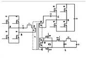
- Figure 1is a diagram of the overall circuit topology.
- Figure 2is a topological structure diagram of the double-ended output circuit.
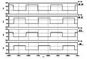
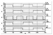
- FIG. 3is a schematic diagram of the conduction of the switching tubes Q5-Q10.
- Figure 4is a schematic diagram of the dead time setting.
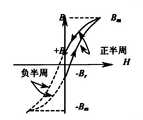
- Figure 5is a schematic diagram of the magnetic flux density change of the transformer and the bidirectional magnetization of the magnetic core.
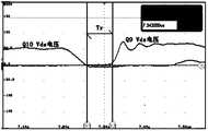
- Figure 6is a schematic diagram of the reverse recovery time of the transformer voltage reversal.
- Figure 7is a schematic diagram of the dead time of the switch tubes Q9 and Q10.
- FIG. 8is a schematic diagram showing the alignment of the turn-off edge of the switch tube Q11 and the turn-off edge of the main output circuit switch tubes Q5, Q6, Q7, and Q8.
- Figure 1shows the overall circuit topology structure diagram, including: double-ended output circuit and control module, the control module controls the working status of the primary input circuit, main output circuit and auxiliary output circuit in the double-ended output circuit, more accurately It controls the on-off state of the switch tube in each circuit.
- the double-ended output circuitis described in detail below.
- the double-ended output circuitis shown in Figure 2 and includes: a transformer, a primary input circuit, a first conversion circuit on the secondary side, and a second conversion circuit on the secondary side.
- Q1, Q2, Q3, Q4are the switch tubes of the primary side input circuit
- the primary side full-bridge inverter circuitincludes: Q1, Q2, Q3, Q4; Q5, Q6, Q7, Q8 are the secondary side first conversion circuit Switch tube; Q9, Q10, Q11, D1 are auxiliary circuit switch tubes.
- L1are the resonant capacitor and resonant inductance of the PFC primary input circuit
- C2is the filter capacitor of the first conversion circuit of the secondary side
- L2is the filter capacitor of the first conversion circuit of the secondary side
- C3are the inductance and capacitance of the second conversion circuit of the secondary side
- C4is the first conversion of the secondary side.
- T1is the transformer
- W1is the winding of the primary input circuit
- W2is the winding of the first conversion circuit on the secondary side
- W3 and W4are the windings of the second conversion circuit on the secondary side.
- L1can be the leakage inductance of T1
- D1can be an active control device such as MOSFET.
- the first conversion circuit of the secondary sideserves as the main output circuit, which includes: Q5, Q6, Q7, Q8, and C4;
- the main full-bridge inverter circuitincludes : Q5, Q6, Q7, Q8;
- the secondary side second conversion circuitis used as the auxiliary output circuit, which includes: Q9, Q10, Q11, D1 and L2;
- the half-bridge inverter circuitincludes: Q9, Q10, where Q9, Q10 are The first level switch tube; Q11 is the second level switch tube.
- the main outputis used as the main feedback, and the duty ratios of Q1, Q2, Q3, Q4, Q5, Q6, Q7, and Q8 of the primary input circuit and the main output circuit are all 50% minus the dead time.
- the upper switch tube and the lower switch tubeare set to be closed at the same time. As shown in Figure 3, this period is dead. District time.
- W1, W2, W3, and W4are integrated in the same magnetic core.
- T1 and W3 and W4 in the auxiliary output circuitalways exist with the main output circuit.
- the induced voltage corresponding to the W2 turns ratioexists.
- the main output circuitis controlled by the main loop based on the input voltage of the primary input circuit and the main output circuit voltage using the duty cycle of the main output circuit switch tube to always control at 50%.
- the voltages of W3, W4, and W1are clamped by the voltage of W2, and form a mapping relationship with the voltage on W2 according to the turns ratio.
- the voltages of W3 and W4follow the voltage of the main output circuit and change, and the output voltage of the auxiliary output circuit and The stability and controllability of the current is achieved by adding a switch regulator circuit to the auxiliary output circuit to form an auxiliary output circuit through Q9, Q10, Q11, D1 and L2.
- Q5 and Q8 in the main output circuitare turned on at the same time, the on time is 50% of the duty cycle minus the dead time, and Q6 and Q7 are turned on at the same time, and the on time is also the duty cycle 50% minus the dead time. That is, the on-times of Q5, Q8 and Q6, Q7 are all 50% of the duty cycle minus the dead time, and the phase difference is 180°.
- the magnetic induction intensity existing on the same transformer, the phase of the induced voltage on W3 and W4is the same as the phase of the voltage on W2, the main output circuit is switched from the conduction of Q5 and Q8 to the conduction of Q6 and Q7, and on W2 The voltage of W3 and W4 are commutated simultaneously.
- the voltages of W3 and W4are commutated synchronously.
- the switching frequency and duty cycle of Q9 and Q10are synchronized with the main output circuit.
- Q10when Q5 and Q8 in the main output circuit are turned on, Q10 is turned on, and when Q6 and Q7 in the main output circuit are turned on, When turned on, Q9 is turned on. Therefore, Q9 and Q10 play the role of synchronous rectification.
- the auxiliary output circuitdetects the feedback of the auxiliary output circuit voltage through the DSP to control the duty cycle of Q11.
- the induced voltages on W3 and W4are rectified by Q9 and Q10 to form a positive voltage V3 on H to L, and 50% of the voltage of V3 comes from windings W3, 50 % Comes from winding W4.
- Q9 and Q10 used for synchronous rectificationwill produce voltage stress spikes at the moment of turning off.
- the sources 1 and 2are related to the main output circuit voltage and the turns ratio of W2, W3, W4, and under the condition of certain leakage inductance, it is related to the rate of change of current.
- the topology structureis a double-ended output output, and the energy conversion is integrated in the voltage follower of the voltage of T1, W3, and W4 to the voltage of W2.
- the voltage of W2when the voltage of W2 is switched from the conduction of Q5 and Q8 to the conduction of Q6 and Q7, the voltage of W2 also changes from the voltage VF at point F to the voltage VD at point D, which is positive, and switches to VF.
- the VD voltagewhich is negative, has a phase difference of 180°.
- the voltage phases of W3 and W4are the same as the phase of the voltage of W2.
- the voltage VJ of W3is also switched from positive to negative for VH, and the voltage of W4 is also switched from positive to negative.
- the reverse recovery timeis proportional to the intensity of the magnetic induction value B, the output circuit side road load increase, the magnetic induction B value increases, the transformer winding roads commutated The required time is lengthened, and the magnetic core reverse recovery time is the dead time of Q9 and Q10 used for synchronous rectification in the auxiliary output circuit.
- VL*di/dt
- the voltage generated by the leakage inductance superimposed on the platform voltage of the windingwill make the voltage stress of the synchronous rectification Q9 and Q10 very high, at this time, it is necessary to increase the absorption circuit to absorb this part of the voltage stress; 2
- Q11is turned off, the voltage of W3 or W4 is a stable voltage, and the winding load capacity is very strong.
- the current when Q11 is turned offis very large, and a large di/dt will also be generated at both ends of the switch Q11.
- a dual-terminal output charging circuit auxiliary circuit switch control methodis as follows:
Landscapes
- Engineering & Computer Science (AREA)
- Power Engineering (AREA)
- Transportation (AREA)
- Mechanical Engineering (AREA)
- Inverter Devices (AREA)
- Dc-Dc Converters (AREA)
Abstract
Description
Translated fromChinese本专利涉及电动汽车充电技术领域,尤其涉及一种双端输出充电电路及其辅路开关控制方法。This patent relates to the technical field of electric vehicle charging, in particular to a double-terminal output charging circuit and its auxiliary circuit switch control method.
车载充电机一般具有一个交流输入端、两个直流输出端,交流输入端连接市电网络,第一直流输出端给高压电池充电,相当于主路输出电路;第二直流输出端给车内用电设备和低压小电池供电,相当于辅路输出电路。这种传统的变压器集成的多端口电源输出中,每一路的输出压流都要必须具有反馈机制和稳定可控的性能;主路直接由反馈进行控制输出,辅路输出电路除了第一级开关整流电路以外,还需要增加第二级开关稳压电路。Vehicle chargers generally have an AC input terminal and two DC output terminals. The AC input terminal is connected to the mains network. The first DC output terminal charges the high-voltage battery, which is equivalent to the main output circuit; the second DC output terminal is used in the car. Powered by electrical equipment and low-voltage small batteries, it is equivalent to the auxiliary output circuit. In this traditional transformer-integrated multi-port power output, each output voltage flow must have a feedback mechanism and stable and controllable performance; the main circuit is directly controlled by feedback, and the auxiliary output circuit is rectified by the first-stage switch. In addition to the circuit, a second-stage switching regulator circuit is also needed.
然而,现有技术中并没有在死区时间内完成驱动的,这就使得辅路输出电路功率器件需要采用更高级别的耐压器件以及增加吸收电路的损耗。However, in the prior art, the drive is not completed within the dead time, which makes the auxiliary output circuit power devices need to use higher-level withstand voltage devices and increase the loss of the absorption circuit.
发明内容Summary of the invention
本发明的目的是针对上述现有技术存在的技术问题,提供一种双端输出充电电路辅路开关控制方法,以解决现有技术中双端输出辅路第二级开关稳压电路的关断在主路的死区时间内完成的技术问题,从而有效地降低辅路输出电路功率器件的电压应力,提高电路的可靠性。The purpose of the present invention is to provide a dual-terminal output charging circuit auxiliary circuit switch control method in view of the above-mentioned technical problems in the prior art, so as to solve the problem that the dual-terminal output auxiliary circuit second-stage switching regulator circuit in the prior art is turned off in the main The technical problem is completed within the dead time of the circuit, thereby effectively reducing the voltage stress of the power device of the auxiliary circuit output circuit and improving the reliability of the circuit.
本发明提出一种双端输出充电电路的辅路开关控制方法,所述双端输出充电电路包括变压器、设于所述变压器原边侧的原边输入电路、并联设于所述变压器副边侧的主路输出电路和辅路输出电路,所述原边输入电路中设有原边全桥逆变电路,所述主路输出电路中设有主路全桥逆变电路,所述辅路输出电路中设有半桥逆变电路和起稳压作用的第二级开关管。所述辅路开关控制方法包括:所述半桥逆变电路中的两个第一级开关管切换导通时产生死区时间,在所述死区时间内将所述第二级开关管关断。The present invention provides a method for controlling the auxiliary circuit switch of a double-ended output charging circuit. The double-ended output charging circuit includes a transformer, a primary input circuit arranged on the primary side of the transformer, and a parallel connection on the secondary side of the transformer. A main output circuit and an auxiliary output circuit, the primary input circuit is provided with a primary full-bridge inverter circuit, the main output circuit is provided with a main full-bridge inverter circuit, and the auxiliary output circuit is provided with There is a half-bridge inverter circuit and a second-stage switch tube for voltage stabilization. The auxiliary circuit switch control method includes: a dead time is generated when two first-stage switching tubes in the half-bridge inverter circuit are switched on, and the second-stage switching tube is turned off during the dead time .
在本发明的实施例中,所述辅路开关控制方法还包括:所述辅路开关控制方法还包括:所述产生死区时间的同时,控制所述第二级开关管的导通频率为所述主路全桥逆变电路中开关管的开关频率的2倍。In an embodiment of the present invention, the auxiliary circuit switch control method further includes: the auxiliary circuit switch control method further includes: while the dead time is generated, controlling the conduction frequency of the second-stage switch tube to be the The switching frequency of the switching tube in the main full-bridge inverter circuit is 2 times.
在本发明的实施例中,所述第二级开关管在所述两个第一级开关管分别导通的时候均完成1个完整的开关周期。In the embodiment of the present invention, the second-stage switching tube completes one complete switching cycle when the two first-stage switching tubes are respectively turned on.
在本发明的实施例中,所述两个第一级开关管切换导通时,所述变压器的磁感应强度反向,所述辅路输出电路的绕组电压进行换向且所述变压器的磁芯反向恢复,所述磁芯反向恢复的时间为所述死区时间。In the embodiment of the present invention, when the two first-stage switch tubes are switched on, the magnetic flux density of the transformer is reversed, the winding voltage of the auxiliary circuit output circuit is reversed, and the magnetic core of the transformer is reversed. To recover, the time for the magnetic core to recover in reverse is the dead time.
在本发明的实施例中,所述磁芯反向恢复时,所述辅路输出电路中辅路绕组的两端电压为0,所述第二级开关管关断时刻流过的电流趋于0。In the embodiment of the present invention, when the magnetic core is reversely recovered, the voltage across the auxiliary winding in the auxiliary output circuit is 0, and the current flowing when the second-stage switch tube is turned off tends to 0.
在本发明的实施例中,所述辅路输出电路的绕组电压进行换向时,所述主路全桥逆变电路中开关管的状态不变。In the embodiment of the present invention, when the winding voltage of the auxiliary output circuit is commutated, the state of the switch tube in the main full-bridge inverter circuit remains unchanged.
在本发明的实施例中,所述两个第一级开关管的关断沿与所述主路全桥逆变电路中开关管的导通沿/关断沿对齐。In the embodiment of the present invention, the turn-off edges of the two first-stage switch tubes are aligned with the turn-on/turn-off edges of the switch tubes in the main full-bridge inverter circuit.
在本发明的实施例中,所述辅路输出电路中辅路绕组的电压相位和所述主路输出电路中主路绕组的电压相位保持一致。In the embodiment of the present invention, the voltage phase of the auxiliary winding in the auxiliary output circuit is consistent with the voltage phase of the main winding in the main output circuit.
在本发明的实施例中,在所述原边全桥逆变电路中位于交叉桥臂上的开关管和在所述主路全桥逆变电路中位于交叉桥臂上的开关管的通断时序保持一致,相位相差180°。In the embodiment of the present invention, the switching tubes located on the cross bridge arm in the primary full-bridge inverter circuit and the switching tubes located on the cross bridge arm in the main full-bridge inverter circuit are switched on and off The timing remains the same, with a phase difference of 180°.
本发明还提出一种双端输出充电电路,包括:原边输入电路、主路输出电路、辅路输出电路及控制模块;其特征在于,所述控制模块执行权利要求1至8任一项所述的辅路开关控制方法。The present invention also provides a double-ended output charging circuit, comprising: a primary input circuit, a main output circuit, an auxiliary output circuit, and a control module; characterized in that, the control module implements any one of
与现有技术相比,本发明具有以下有益效果:Compared with the prior art, the present invention has the following beneficial effects:
1、利用磁芯在双向磁化过程的磁芯反向恢复产生死区时间,在死区时间控制后级开关器件的时序来用于降低同步整流管的电压应力,降低同步整流电路吸收电路的损耗;1. The dead time is generated by the core reverse recovery of the magnetic core in the bidirectional magnetization process, and the time sequence of the subsequent switching devices is controlled during the dead time to reduce the voltage stress of the synchronous rectifier tube and reduce the loss of the absorption circuit of the synchronous rectifier circuit ;
2、相比于采用更高级别的耐压器件以及增加吸收电路损耗的解决方式,本发明简单可靠、成本低、易于控制。2. Compared with the solution of adopting higher-level withstand voltage devices and increasing the loss of the absorption circuit, the present invention is simple, reliable, low-cost, and easy to control.
下面结合实施例和附图对本发明进行详细说明,其中:The present invention will be described in detail below in conjunction with embodiments and drawings, in which:
图1是整体电路拓扑结构图。Figure 1 is a diagram of the overall circuit topology.
图2是双端输出电路拓扑结构图。Figure 2 is a topological structure diagram of the double-ended output circuit.
图3是开关管Q5-Q10的导通情况示意图。Figure 3 is a schematic diagram of the conduction of the switching tubes Q5-Q10.
图4是死区时间设置示意图。Figure 4 is a schematic diagram of the dead time setting.
图5是变压器的磁感应强度变化及磁芯双向磁化示意图。Figure 5 is a schematic diagram of the magnetic flux density change of the transformer and the bidirectional magnetization of the magnetic core.
图6是变压器电压翻转的反向恢复时间示意图。Figure 6 is a schematic diagram of the reverse recovery time of the transformer voltage reversal.
图7是开关管Q9和Q10的死区时间示意图。Figure 7 is a schematic diagram of the dead time of the switch tubes Q9 and Q10.
图8是开关管Q11的关断沿和主路输出电路开关管Q5、Q6、Q7、Q8的关断沿对齐的示意图。FIG. 8 is a schematic diagram showing the alignment of the turn-off edge of the switch tube Q11 and the turn-off edge of the main output circuit switch tubes Q5, Q6, Q7, and Q8.
下面详细描述本发明的实施例,所述实施例的示例在附图中示出。其中,相同或类似的标号表示相同或类似的元件或具有相同或类似的元件;针对电路中诸如连接电阻改变电流/电压适配等惯常操作,本领域的技术人员很容易理解,具体实施例中不做描述。下面通过参考附图描述的实施例是示意性的,仅用于解释本发明,而不能解释为对本发明的限制。The embodiments of the present invention are described in detail below, and examples of the embodiments are shown in the accompanying drawings. Wherein, the same or similar reference signs indicate the same or similar components or have the same or similar components; for the usual operations in the circuit, such as changing the current/voltage adaptation of the connection resistance, it is easy for those skilled in the art to understand that in the specific embodiments No description. The embodiments described below with reference to the accompanying drawings are illustrative, and are only used to explain the present invention, and cannot be construed as limiting the present invention.
如图1所示为整体电路拓扑结构图,包括:双端输出电路和控制模块,控制模块控制双端输出电路中原边输入电路、主路输出电路和辅路输出电路的工作状态,更准确的说是控制各电路中开关管的通断状态。Figure 1 shows the overall circuit topology structure diagram, including: double-ended output circuit and control module, the control module controls the working status of the primary input circuit, main output circuit and auxiliary output circuit in the double-ended output circuit, more accurately It controls the on-off state of the switch tube in each circuit.
下面详细对双端输出电路进行说明,双端输出电路如图2所示,包括:变压器、原边输入电路、副边第一转换电路、副边第二转换电路。其中,Q1、Q2、Q3、Q4是原边输入电路的开关管,原边全桥逆变电路包括:Q1、Q2、Q3、Q4;Q5、Q6、Q7、Q8是副边第一转换电路的开关管;Q9、Q10、Q11、D1是辅路开关管。C1、L1为PFC原边输入电路的谐振电容、谐振电感,C2为副边第一转换电路的滤波电容,L2、C3为副边第二转换电路的电感和电容,C4为副边第一转换电路的谐振电容,T1为变压器,W1为原边输入电路的绕组,W2为副边第一转换电路的绕组,W3和W4为副边第二转换电路的绕组。其中,L1可为T1的漏感;D1可为MOSFET等有源控制器件。The double-ended output circuit is described in detail below. The double-ended output circuit is shown in Figure 2 and includes: a transformer, a primary input circuit, a first conversion circuit on the secondary side, and a second conversion circuit on the secondary side. Among them, Q1, Q2, Q3, Q4 are the switch tubes of the primary side input circuit, the primary side full-bridge inverter circuit includes: Q1, Q2, Q3, Q4; Q5, Q6, Q7, Q8 are the secondary side first conversion circuit Switch tube; Q9, Q10, Q11, D1 are auxiliary circuit switch tubes. C1, L1 are the resonant capacitor and resonant inductance of the PFC primary input circuit, C2 is the filter capacitor of the first conversion circuit of the secondary side, L2, C3 are the inductance and capacitance of the second conversion circuit of the secondary side, and C4 is the first conversion of the secondary side. For the resonant capacitor of the circuit, T1 is the transformer, W1 is the winding of the primary input circuit, W2 is the winding of the first conversion circuit on the secondary side, and W3 and W4 are the windings of the second conversion circuit on the secondary side. Among them, L1 can be the leakage inductance of T1; D1 can be an active control device such as MOSFET.
本发明的实施例中,当双端输出电路处于充电状态时,副边第一转换电路作为主路输出电路,其包括:Q5、Q6、Q7、Q8和C4;主路全桥逆变电路包括:Q5、Q6、Q7、Q8;副边第二转换电路作为辅路输出电路,其包括:Q9、Q10、Q11、D1和L2;半桥逆变电路包括:Q9、Q10,其中,Q9、Q10为第一级开关管;Q11是第二级开关管。主路输出作为主反馈,并且原边输入电路和主路输出电路的Q1、Q2、Q3、Q4、Q5、Q6、Q7、Q8导通的占空比都是50%减去死区时间。其中,为避免位于桥臂上下的一对开关管切换的时候同时导通而引发的短路现象,对上开关管和下开关管设置一个同时关闭的时段,如图3所示,该时段为死区时间。In the embodiment of the present invention, when the double-ended output circuit is in the charging state, the first conversion circuit of the secondary side serves as the main output circuit, which includes: Q5, Q6, Q7, Q8, and C4; the main full-bridge inverter circuit includes : Q5, Q6, Q7, Q8; the secondary side second conversion circuit is used as the auxiliary output circuit, which includes: Q9, Q10, Q11, D1 and L2; the half-bridge inverter circuit includes: Q9, Q10, where Q9, Q10 are The first level switch tube; Q11 is the second level switch tube. The main output is used as the main feedback, and the duty ratios of Q1, Q2, Q3, Q4, Q5, Q6, Q7, and Q8 of the primary input circuit and the main output circuit are all 50% minus the dead time. Among them, in order to avoid the short-circuit phenomenon caused by the simultaneous conduction of a pair of switch tubes located at the upper and lower arms of the bridge arm, the upper switch tube and the lower switch tube are set to be closed at the same time. As shown in Figure 3, this period is dead. District time.
本发明的实施例中,W1、W2、W3、W4集成在同一个磁芯中,当主路输出电路工作时,T1中存在磁感应强度,辅路输出电路中W3和W4始终存在着和主路输出电路中W2匝数比对应的感应电压存在。主路输出电路由主环路根据原边输入电路的输入电压和主路输出电路电压采用主路输出电路开 关管占空比始终控制在50%的方式进行控制,当主路输出电路正在工作时,W3、W4和W1的电压被W2电压钳位,并且和W2上的电压按照匝比的形成映射关系,W3、W4电压是跟随主路输出电路电压变化而变化的,辅路输出电路的输出电压和电流的稳定可控则是通过辅路输出电路增加一级开关稳压电路经过Q9、Q10、Q11、D1和L2形成辅路输出电路实现的。In the embodiment of the present invention, W1, W2, W3, and W4 are integrated in the same magnetic core. When the main output circuit is working, there is magnetic induction in T1, and W3 and W4 in the auxiliary output circuit always exist with the main output circuit. The induced voltage corresponding to the W2 turns ratio exists. The main output circuit is controlled by the main loop based on the input voltage of the primary input circuit and the main output circuit voltage using the duty cycle of the main output circuit switch tube to always control at 50%. When the main output circuit is working, The voltages of W3, W4, and W1 are clamped by the voltage of W2, and form a mapping relationship with the voltage on W2 according to the turns ratio. The voltages of W3 and W4 follow the voltage of the main output circuit and change, and the output voltage of the auxiliary output circuit and The stability and controllability of the current is achieved by adding a switch regulator circuit to the auxiliary output circuit to form an auxiliary output circuit through Q9, Q10, Q11, D1 and L2.
本发明的实施例中,主路输出电路中Q5和Q8同时导通,导通时间都是占空比的50%减去死区时间,Q6和Q7同时导通,导通时间也是占空比的50%减去死区时间。即Q5、Q8和Q6、Q7的导通时间都是占空比的50%减去死区时间而相位相差180°。在同一个变压器上存在的磁感应强度,W3、W4上存在的感应电压的相位和W2上的电压相位一致,主路输出电路由Q5、Q8的导通切换为Q6、Q7的导通,W2上的电压进行换相,与此同时,W3和W4的电压也同步进行换相。其中,Q9和Q10的开关频率以及占空比和主路输出电路保持同步,如图4所示,当主路输出电路中Q5和Q8导通时,Q10导通,当主路输出电路中Q6和Q7导通时,Q9导通。于是,Q9和Q10便起到了同步整流的作用,Q9和Q10是跟随主路输出电路中Q5、Q8和Q6、Q7开关切换时,变压器电压自然换相自主切换导通的。其中,辅路输出电路是通过DSP检测辅路输出电路电压的反馈来控制Q11占空比的。In the embodiment of the present invention, Q5 and Q8 in the main output circuit are turned on at the same time, the on time is 50% of the duty cycle minus the dead time, and Q6 and Q7 are turned on at the same time, and the on time is also the
本发明的实施例中,如图2所示,W3和W4上的感应电压经过Q9和Q10的整流后在H对L上形成一个正电压V3,该V3的电压50%来自于绕组W3,50%来自于绕组W4。当辅路输出电路负载的功率较大的时候,用于同步整流的Q9和Q10在关断的瞬间会产生电压应力尖锋,该应力尖锋的来源有三个:①变压器绕组本身电压换相时的平台电压;②另外一侧同步整流对应绕组的平台电压;③在变压器电压换相带来的电流变化在回路漏感上引起的感应电压。其中,来源①和②是和主路输出电路电压以及W2和W3、W4的匝比有关,在漏感一定的情况下,其和电流的变化速率有关。In the embodiment of the present invention, as shown in Figure 2, the induced voltages on W3 and W4 are rectified by Q9 and Q10 to form a positive voltage V3 on H to L, and 50% of the voltage of V3 comes from windings W3, 50 % Comes from winding W4. When the power of the auxiliary output circuit load is large, Q9 and Q10 used for synchronous rectification will produce voltage stress spikes at the moment of turning off. There are three sources of the stress spikes: ①The voltage of the transformer winding itself is commutation Platform voltage; ②The platform voltage of the winding corresponding to the synchronous rectification on the other side; ③The induced voltage on the loop leakage inductance caused by the current change caused by the voltage commutation of the transformer. Among them, the
本发明的实施例中,拓扑架构为是双端输出输出,能量的转换集成在T1,W3、W4的电压对W2的电压跟随。如图2所示,W2的电压在由Q5、Q8的导通切换到Q6、Q7的导通时,W2的电压也由F点电压VF对D点电压VD,其为正,切换到VF对VD电压,其为负,相位相差180°。W3和W4的电压相位和W2的电压的相位是一致的,W3的电压VJ对VH也由正切换为负,W4的电压VH对VK也由正切换为负。如图5所示,W3和W4电压进行换相时,变压器的磁感应强度B从+Bm变化到-Bm,磁芯双向磁化,磁感应强度的翻转产生反向。而反向恢复需要时间,如图6所示,具体体现在变压器电压翻转需要反 向恢复时间。如图6和图7所示的Tr,该反向恢复时间与磁感应强度B值的大小成正比,辅路输出电路的负载加大,磁感应强度B值随之增大,辅路绕组变压换相所需要的时间加长,磁芯反向恢复时间即为辅路输出电路中用于同步整流作用的Q9、Q10的死区时间。In the embodiment of the present invention, the topology structure is a double-ended output output, and the energy conversion is integrated in the voltage follower of the voltage of T1, W3, and W4 to the voltage of W2. As shown in Figure 2, when the voltage of W2 is switched from the conduction of Q5 and Q8 to the conduction of Q6 and Q7, the voltage of W2 also changes from the voltage VF at point F to the voltage VD at point D, which is positive, and switches to VF. The VD voltage, which is negative, has a phase difference of 180°. The voltage phases of W3 and W4 are the same as the phase of the voltage of W2. The voltage VJ of W3 is also switched from positive to negative for VH, and the voltage of W4 is also switched from positive to negative. As shown in Figure 5, when the W3 and W4 voltages are commutated, the magnetic flux density B of the transformerchanges from +B m to -Bm , the magnetic core is magnetized in both directions, and the reversal of the magnetic flux density reverses. The reverse recovery takes time, as shown in Figure 6, which is embodied in the reverse recovery time required for the voltage reversal of the transformer. Tr as shown in FIG. 6 and FIG. 7, the reverse recovery time is proportional to the intensity of the magnetic induction value B, the output circuit side road load increase, the magnetic induction B value increases, the transformer winding roads commutated The required time is lengthened, and the magnetic core reverse recovery time is the dead time of Q9 and Q10 used for synchronous rectification in the auxiliary output circuit.
本发明的实施例中,绕组电压换相过程中,在用于同步整流作用的Q9、Q10两端电压和绕组电压上升是同步的,但是如果在换相的时候,Q11还在导通,继续从W3、W4上拉能量,则会带来两个问题:①Q9和Q10上电流变化速率会加快,即很大的di/dt,该di/dt会使得线路上的漏感产生很大的感应电压:V=L*di/dt,漏感产生的电压叠加在绕组的平台电压上会使得同步整流的Q9和Q10的电压应力很高,此时则需要增加吸收电路吸收该部分电压应力;②当Q11关断的时刻W3或者W4的电压是稳定的电压,绕组负载能力很强,Q11关断瞬间电流很大,在开关管Q11两端也会产生一个很大的di/dt,该di/dt会使得Q11两端产生很大的电压应力;③Q11关断瞬间的电压应力会叠加在同步整流管两端,使得同步整流在Q11关断时同样产生一个高的电压尖锋。In the embodiment of the present invention, during the winding voltage commutation process, the voltage across Q9 and Q10 used for synchronous rectification and the winding voltage rise are synchronized, but if Q11 is still conducting during the commutation, continue Pulling up energy from W3 and W4 will bring about two problems: ① The current rate of change on Q9 and Q10 will increase, that is, a large di/dt, which will cause a large leakage inductance on the line. Voltage: V=L*di/dt, the voltage generated by the leakage inductance superimposed on the platform voltage of the winding will make the voltage stress of the synchronous rectification Q9 and Q10 very high, at this time, it is necessary to increase the absorption circuit to absorb this part of the voltage stress; ② When Q11 is turned off, the voltage of W3 or W4 is a stable voltage, and the winding load capacity is very strong. The current when Q11 is turned off is very large, and a large di/dt will also be generated at both ends of the switch Q11. This di/ dt will cause a large voltage stress on both ends of Q11; ③The voltage stress at the moment of Q11 turning off will be superimposed on both ends of the synchronous rectifier tube, so that synchronous rectification will also produce a high voltage spike when Q11 is turned off.
本发明的实施例中,一种双端输出充电电路辅路开关控制方法如下:In the embodiment of the present invention, a dual-terminal output charging circuit auxiliary circuit switch control method is as follows:
1、利用绕组电压进行换相,磁芯反向恢复在用于同步整流作用的Q9、Q10切换导通时产生死区时间。与此同时,DSP控制Q11的导通频率为主路输出电路开关管导通频率的2倍,Q11在Q10导通的时候完成一个完整的开关周期,在Q9导通的时候完成一个完整的开关周期。1. Use the winding voltage for phase commutation, and the reverse recovery of the magnetic core produces dead time when Q9 and Q10 for synchronous rectification are switched on. At the same time, DSP controls the conduction frequency of Q11 to be twice the conduction frequency of the switch tube of the main output circuit. Q11 completes a complete switching cycle when Q10 is turned on, and completes a complete switch when Q9 is turned on. cycle.
2、利用DSP控制Q11在死区时间内关断,即如图8所示,Q11的关断沿和主路输出电路中Q5、Q6、Q7、Q8的关断沿对齐。2. Use DSP to control Q11 to turn off during the dead time, that is, as shown in Figure 8, the turn-off edge of Q11 is aligned with the turn-off edge of Q5, Q6, Q7, and Q8 in the main output circuit.
当Q11在Q9和Q10的死区区间关断时,此时变压器正在换相,主路输出电路的开关管都未关断/导通,而W3、W4正处于磁芯的反向恢复之中,绕组两端电压为0,Q11关断时刻流过的电流很小,Q11两端由于硬开关产生的电压应力则可以大大降低。在Q11关断之后,由于后级没有负载,辅路输出电路的变压器绕组上的电流减小,由电流变化在回路漏感上产生的电压V=L*di/dt大大减小,Q9和Q10关断的电压应力也大大减小,从而减小Q9和Q10的吸收电路的损耗以及选用电压较低的开关管用以降低成本。When Q11 is turned off in the dead zone of Q9 and Q10, the transformer is commutation, the switch tubes of the main output circuit are not turned off/conducted, and W3 and W4 are in the reverse recovery of the magnetic core. , The voltage across the winding is 0, the current flowing through Q11 is very small when Q11 is turned off, and the voltage stress at both ends of Q11 due to hard switching can be greatly reduced. After Q11 is turned off, because there is no load in the subsequent stage, the current on the transformer winding of the auxiliary output circuit is reduced, and the voltage V=L*di/dt generated by the current change on the loop leakage inductance is greatly reduced, and Q9 and Q10 are turned off. The off-voltage stress is also greatly reduced, thereby reducing the loss of the absorption circuit of Q9 and Q10 and choosing lower voltage switching tubes to reduce costs.
在本发明的描述中,需要说明的是,除非另有规定和限制,术语“连接”、“包括”、表意序数的词汇等应当作为广义的理解,对于本领域的技术人员而言,可以根据具体情况理解所述术语的具体含义。如在此处使用的,该单 数的形式“一”、“一个”意欲同样包括复数形式,除非上下文清楚地表示之外。In the description of the present invention, it should be noted that, unless otherwise specified and limited, the terms "connected", "includes", and ideographic ordinal words should be understood in a broad sense. For those skilled in the art, the terms Understand the specific meaning of the terms in specific situations. As used herein, the singular forms "a" and "an" are intended to also include plural forms, unless the context clearly indicates otherwise.
在本说明书中,对所述术语的示意性表述不一定指的是相同的实施例或示例。并且,描述的具体特征、结构、材料或者特点可以在任何一个或多个实施例或示例中以合适的方式结合。In this specification, the schematic representations of the terms do not necessarily refer to the same embodiment or example. Moreover, the described specific features, structures, materials or characteristics can be combined in any one or more embodiments or examples in a suitable manner.
尽管已经示出了本发明的实施例,对于本领域的普通技术人员而言,可以理解在不脱离本发明的原理和精神的情况下可以对这些实施例进行多种变化、修改、替换和变形,本发明的范围由所附权利要求及其等同予以限定。Although the embodiments of the present invention have been shown, for those of ordinary skill in the art, it can be understood that various changes, modifications, substitutions and deformations can be made to these embodiments without departing from the principle and spirit of the present invention. The scope of the present invention is defined by the appended claims and their equivalents.
Claims (10)
Translated fromChinesePriority Applications (1)
| Application Number | Priority Date | Filing Date | Title |
|---|---|---|---|
| US17/993,009US20230091718A1 (en) | 2020-05-27 | 2022-11-23 | Two-output charging circuit and method for controlling its auxiliary circuit switch |
Applications Claiming Priority (2)
| Application Number | Priority Date | Filing Date | Title |
|---|---|---|---|
| CN202010464192.7ACN111490577A (en) | 2020-05-27 | 2020-05-27 | Double-end output charging circuit and auxiliary circuit switch control method thereof |
| CN202010464192.7 | 2020-05-27 |
Related Child Applications (1)
| Application Number | Title | Priority Date | Filing Date |
|---|---|---|---|
| US17/993,009ContinuationUS20230091718A1 (en) | 2020-05-27 | 2022-11-23 | Two-output charging circuit and method for controlling its auxiliary circuit switch |
Publications (1)
| Publication Number | Publication Date |
|---|---|
| WO2021238140A1true WO2021238140A1 (en) | 2021-12-02 |
Family
ID=71798431
Family Applications (1)
| Application Number | Title | Priority Date | Filing Date |
|---|---|---|---|
| PCT/CN2020/134077CeasedWO2021238140A1 (en) | 2020-05-27 | 2020-12-04 | Double-ended output charging circuit and auxiliary circuit switch control method therefor |
Country Status (3)
| Country | Link |
|---|---|
| US (1) | US20230091718A1 (en) |
| CN (1) | CN111490577A (en) |
| WO (1) | WO2021238140A1 (en) |
Families Citing this family (6)
| Publication number | Priority date | Publication date | Assignee | Title |
|---|---|---|---|---|
| CN111490577A (en)* | 2020-05-27 | 2020-08-04 | 深圳威迈斯新能源股份有限公司 | Double-end output charging circuit and auxiliary circuit switch control method thereof |
| CN112737344A (en)* | 2020-12-29 | 2021-04-30 | 联合汽车电子有限公司 | Battery charging circuit |
| CN112865263B (en)* | 2021-03-15 | 2024-08-13 | 阳光电源股份有限公司 | Charging and discharging control method and application device |
| CN114070086B (en)* | 2021-10-28 | 2024-01-16 | 西安理工大学 | Working method of arbitrary double-frequency induction heating main circuit |
| CN114337310B (en)* | 2022-03-10 | 2022-08-16 | 浙江日风电气股份有限公司 | Control method, device and medium for reducing voltage stress |
| US11996767B1 (en)* | 2022-06-09 | 2024-05-28 | Apple Inc. | Adaptive timing for high frequency inverters |
Citations (8)
| Publication number | Priority date | Publication date | Assignee | Title |
|---|---|---|---|---|
| US5481449A (en)* | 1994-03-21 | 1996-01-02 | General Electric Company | Efficient, high power density, high power factor converter for very low dc voltage applications |
| CN101895201A (en)* | 2010-07-23 | 2010-11-24 | 中兴通讯股份有限公司 | LLC (Logical Link Control) series resonance converter and drive method thereof |
| CN202218160U (en)* | 2011-08-30 | 2012-05-09 | 南京邮电大学 | An Auxiliary Dual-Transistor Active-Clamp Full-Bridge Soft-Switching Converter |
| CN107196517A (en)* | 2017-07-04 | 2017-09-22 | 广州金升阳科技有限公司 | The drive circuit and driving method of clamp switch in Switching Power Supply |
| CN110198862A (en)* | 2018-09-18 | 2019-09-03 | 深圳欣锐科技股份有限公司 | Integrated vehicle charger circuit and manufacturing method, integrated vehicle charger |
| CN110289667A (en)* | 2019-08-05 | 2019-09-27 | 苏州博沃创新能源科技有限公司 | High-power integrated on-board charger, on-board DC/DC circuit and control method |
| CN111490577A (en)* | 2020-05-27 | 2020-08-04 | 深圳威迈斯新能源股份有限公司 | Double-end output charging circuit and auxiliary circuit switch control method thereof |
| CN212258468U (en)* | 2020-05-27 | 2020-12-29 | 深圳威迈斯新能源股份有限公司 | Double-end output charging circuit |
Family Cites Families (3)
| Publication number | Priority date | Publication date | Assignee | Title |
|---|---|---|---|---|
| CN103718445B (en)* | 2011-08-04 | 2016-10-26 | 株式会社村田制作所 | Switching power unit |
| CN108237943B (en)* | 2018-01-17 | 2019-05-17 | 深圳威迈斯新能源股份有限公司 | A kind of dual output port charging circuit and its control method |
| CN111463878B (en)* | 2020-05-14 | 2021-10-01 | 深圳威迈斯新能源股份有限公司 | Compatible high-power double-end output vehicle-mounted charger and control method thereof |
- 2020
- 2020-05-27CNCN202010464192.7Apatent/CN111490577A/enactivePending
- 2020-12-04WOPCT/CN2020/134077patent/WO2021238140A1/ennot_activeCeased
- 2022
- 2022-11-23USUS17/993,009patent/US20230091718A1/enactivePending
Patent Citations (8)
| Publication number | Priority date | Publication date | Assignee | Title |
|---|---|---|---|---|
| US5481449A (en)* | 1994-03-21 | 1996-01-02 | General Electric Company | Efficient, high power density, high power factor converter for very low dc voltage applications |
| CN101895201A (en)* | 2010-07-23 | 2010-11-24 | 中兴通讯股份有限公司 | LLC (Logical Link Control) series resonance converter and drive method thereof |
| CN202218160U (en)* | 2011-08-30 | 2012-05-09 | 南京邮电大学 | An Auxiliary Dual-Transistor Active-Clamp Full-Bridge Soft-Switching Converter |
| CN107196517A (en)* | 2017-07-04 | 2017-09-22 | 广州金升阳科技有限公司 | The drive circuit and driving method of clamp switch in Switching Power Supply |
| CN110198862A (en)* | 2018-09-18 | 2019-09-03 | 深圳欣锐科技股份有限公司 | Integrated vehicle charger circuit and manufacturing method, integrated vehicle charger |
| CN110289667A (en)* | 2019-08-05 | 2019-09-27 | 苏州博沃创新能源科技有限公司 | High-power integrated on-board charger, on-board DC/DC circuit and control method |
| CN111490577A (en)* | 2020-05-27 | 2020-08-04 | 深圳威迈斯新能源股份有限公司 | Double-end output charging circuit and auxiliary circuit switch control method thereof |
| CN212258468U (en)* | 2020-05-27 | 2020-12-29 | 深圳威迈斯新能源股份有限公司 | Double-end output charging circuit |
Also Published As
| Publication number | Publication date |
|---|---|
| CN111490577A (en) | 2020-08-04 |
| US20230091718A1 (en) | 2023-03-23 |
Similar Documents
| Publication | Publication Date | Title |
|---|---|---|
| WO2021238140A1 (en) | Double-ended output charging circuit and auxiliary circuit switch control method therefor | |
| CN106685231B (en) | A primary-side clamped soft-switching full-bridge converter and its asymmetric control method | |
| WO2021077757A1 (en) | Wide gain control method for variable topology llc resonant converter | |
| CN108900100B (en) | A kind of single-phase high efficiency high frequency isolated form rectifier | |
| CN103312171B (en) | Isolated soft switching double tube positive exciting resonance DC/DC circuit | |
| CN100405723C (en) | ZVS PWM combined three-level DC converter | |
| CN105305829B (en) | The unidirectional DC DC converters of current mode and symmetric double PWM add phase-shifting control method | |
| CN103701356B (en) | A kind of two auxiliary resonance polar form three phase soft switch inverter | |
| CN106533224A (en) | Novel resonant DC-link soft switching inverter and modulation method thereof | |
| CN101471606A (en) | LLC resonant transformation device | |
| CN103595274A (en) | Method for controlling double-direction power flow high-frequency isolated active clamping rectifier | |
| CN104917412A (en) | Single stage power factor correction phase-shift full bridge topology circuit | |
| CN104935172A (en) | Three-level Soft-switching Forward and Flyback Direct-to-Direct Conversion Circuit Topology | |
| WO2014094289A1 (en) | Single-pole switch power source | |
| CN106026674A (en) | Full-bridge and half-bridge hybrid converter with auxiliary LC resonant circuit | |
| CN202750023U (en) | Current type single-stage isolation high-frequency switch power supply without alternating current / direct current (AC/DC) rectifier bridge | |
| CN109302078A (en) | DC-DC switching power supply based on synchronous rectification mode | |
| CN102594152A (en) | Series-type half-bridge DC-DC (direct current) converter | |
| CN110190752A (en) | A bidirectional CLLLC-DCX resonant converter and its control method | |
| CN105406724A (en) | Phase-shifting control full-bridge zero-current converter and direct-current switching power source | |
| CN104578806B (en) | Cascade bilateral soft switch DC/DC circuit topology | |
| CN110224605A (en) | A kind of full-bridge circuit | |
| CN108964467A (en) | Combined type resonant full bridge Zero Current Switch DC converter and its control method | |
| CN212258468U (en) | Double-end output charging circuit | |
| CN107947587A (en) | A kind of high-efficiency constant-flow Width funtion output circuit |
Legal Events
| Date | Code | Title | Description |
|---|---|---|---|
| 121 | Ep: the epo has been informed by wipo that ep was designated in this application | Ref document number:20937975 Country of ref document:EP Kind code of ref document:A1 | |
| NENP | Non-entry into the national phase | Ref country code:DE | |
| 122 | Ep: pct application non-entry in european phase | Ref document number:20937975 Country of ref document:EP Kind code of ref document:A1 |